KR20240012422A - Semiconductor devices, display devices, and electronic devices - Google Patents
Semiconductor devices, display devices, and electronic devices Download PDFInfo
- Publication number
- KR20240012422A KR20240012422A KR1020237042277A KR20237042277A KR20240012422A KR 20240012422 A KR20240012422 A KR 20240012422A KR 1020237042277 A KR1020237042277 A KR 1020237042277A KR 20237042277 A KR20237042277 A KR 20237042277A KR 20240012422 A KR20240012422 A KR 20240012422A
- Authority
- KR
- South Korea
- Prior art keywords
- terminal
- circuit
- selection circuit
- layer
- additionally
- Prior art date
Links
- 239000004065 semiconductor Substances 0.000 title claims abstract description 240
- 230000007274 generation of a signal involved in cell-cell signaling Effects 0.000 claims description 120
- 238000000034 method Methods 0.000 claims description 41
- 210000004185 liver Anatomy 0.000 claims 2
- 239000010410 layer Substances 0.000 description 489
- 239000012212 insulator Substances 0.000 description 258
- 150000004706 metal oxides Chemical class 0.000 description 242
- 229910044991 metal oxide Inorganic materials 0.000 description 222
- 239000004020 conductor Substances 0.000 description 219
- 230000006870 function Effects 0.000 description 196
- 239000010408 film Substances 0.000 description 106
- 238000005401 electroluminescence Methods 0.000 description 97
- 229910052760 oxygen Inorganic materials 0.000 description 88
- QVGXLLKOCUKJST-UHFFFAOYSA-N atomic oxygen Chemical compound [O] QVGXLLKOCUKJST-UHFFFAOYSA-N 0.000 description 85
- 239000001301 oxygen Substances 0.000 description 85
- 239000000463 material Substances 0.000 description 81
- 239000000758 substrate Substances 0.000 description 79
- 238000010586 diagram Methods 0.000 description 63
- 239000012535 impurity Substances 0.000 description 53
- IJGRMHOSHXDMSA-UHFFFAOYSA-N Atomic nitrogen Chemical compound N#N IJGRMHOSHXDMSA-UHFFFAOYSA-N 0.000 description 52
- 229910052739 hydrogen Inorganic materials 0.000 description 49
- 239000001257 hydrogen Substances 0.000 description 49
- 229910052751 metal Inorganic materials 0.000 description 44
- 239000013078 crystal Substances 0.000 description 41
- 229910052782 aluminium Inorganic materials 0.000 description 37
- 108091006146 Channels Proteins 0.000 description 36
- XAGFODPZIPBFFR-UHFFFAOYSA-N aluminium Chemical compound [Al] XAGFODPZIPBFFR-UHFFFAOYSA-N 0.000 description 36
- 239000011701 zinc Substances 0.000 description 36
- 239000002184 metal Substances 0.000 description 35
- UFHFLCQGNIYNRP-UHFFFAOYSA-N Hydrogen Chemical compound [H][H] UFHFLCQGNIYNRP-UHFFFAOYSA-N 0.000 description 34
- VYPSYNLAJGMNEJ-UHFFFAOYSA-N Silicium dioxide Chemical compound O=[Si]=O VYPSYNLAJGMNEJ-UHFFFAOYSA-N 0.000 description 34
- 229910052814 silicon oxide Inorganic materials 0.000 description 33
- 239000011241 protective layer Substances 0.000 description 31
- XUIMIQQOPSSXEZ-UHFFFAOYSA-N Silicon Chemical compound [Si] XUIMIQQOPSSXEZ-UHFFFAOYSA-N 0.000 description 29
- 125000004429 atom Chemical group 0.000 description 29
- 229910052710 silicon Inorganic materials 0.000 description 29
- 239000010703 silicon Substances 0.000 description 29
- XLYOFNOQVPJJNP-UHFFFAOYSA-N water Substances O XLYOFNOQVPJJNP-UHFFFAOYSA-N 0.000 description 27
- 238000009792 diffusion process Methods 0.000 description 26
- 229910052757 nitrogen Inorganic materials 0.000 description 26
- PXHVJJICTQNCMI-UHFFFAOYSA-N Nickel Chemical compound [Ni] PXHVJJICTQNCMI-UHFFFAOYSA-N 0.000 description 21
- 229910052735 hafnium Inorganic materials 0.000 description 21
- 230000015572 biosynthetic process Effects 0.000 description 20
- 230000001965 increasing effect Effects 0.000 description 19
- 230000007547 defect Effects 0.000 description 18
- VBJZVLUMGGDVMO-UHFFFAOYSA-N hafnium atom Chemical compound [Hf] VBJZVLUMGGDVMO-UHFFFAOYSA-N 0.000 description 18
- 230000002093 peripheral effect Effects 0.000 description 18
- 229910052581 Si3N4 Inorganic materials 0.000 description 17
- 239000003086 colorant Substances 0.000 description 17
- 229910052738 indium Inorganic materials 0.000 description 17
- 150000004767 nitrides Chemical class 0.000 description 17
- HQVNEWCFYHHQES-UHFFFAOYSA-N silicon nitride Chemical compound N12[Si]34N5[Si]62N3[Si]51N64 HQVNEWCFYHHQES-UHFFFAOYSA-N 0.000 description 17
- -1 etc.) Substances 0.000 description 16
- 150000002431 hydrogen Chemical class 0.000 description 15
- APFVFJFRJDLVQX-UHFFFAOYSA-N indium atom Chemical compound [In] APFVFJFRJDLVQX-UHFFFAOYSA-N 0.000 description 15
- 238000004519 manufacturing process Methods 0.000 description 15
- 239000010936 titanium Substances 0.000 description 15
- RYGMFSIKBFXOCR-UHFFFAOYSA-N Copper Chemical compound [Cu] RYGMFSIKBFXOCR-UHFFFAOYSA-N 0.000 description 14
- 239000010949 copper Substances 0.000 description 14
- 229910052733 gallium Inorganic materials 0.000 description 14
- 239000000203 mixture Substances 0.000 description 14
- 229910052719 titanium Inorganic materials 0.000 description 14
- 229910052721 tungsten Inorganic materials 0.000 description 14
- OKTJSMMVPCPJKN-UHFFFAOYSA-N Carbon Chemical compound [C] OKTJSMMVPCPJKN-UHFFFAOYSA-N 0.000 description 13
- RTAQQCXQSZGOHL-UHFFFAOYSA-N Titanium Chemical compound [Ti] RTAQQCXQSZGOHL-UHFFFAOYSA-N 0.000 description 13
- 229920005989 resin Polymers 0.000 description 13
- 239000011347 resin Substances 0.000 description 13
- 229910052707 ruthenium Inorganic materials 0.000 description 13
- 229910052715 tantalum Inorganic materials 0.000 description 13
- 239000010937 tungsten Substances 0.000 description 13
- 101100191136 Arabidopsis thaliana PCMP-A2 gene Proteins 0.000 description 12
- 101100048260 Saccharomyces cerevisiae (strain ATCC 204508 / S288c) UBX2 gene Proteins 0.000 description 12
- NRTOMJZYCJJWKI-UHFFFAOYSA-N Titanium nitride Chemical compound [Ti]#N NRTOMJZYCJJWKI-UHFFFAOYSA-N 0.000 description 12
- 229910052802 copper Inorganic materials 0.000 description 12
- 238000002347 injection Methods 0.000 description 12
- 239000007924 injection Substances 0.000 description 12
- GUVRBAGPIYLISA-UHFFFAOYSA-N tantalum atom Chemical compound [Ta] GUVRBAGPIYLISA-UHFFFAOYSA-N 0.000 description 12
- WFKWXMTUELFFGS-UHFFFAOYSA-N tungsten Chemical compound [W] WFKWXMTUELFFGS-UHFFFAOYSA-N 0.000 description 12
- GYHNNYVSQQEPJS-UHFFFAOYSA-N Gallium Chemical compound [Ga] GYHNNYVSQQEPJS-UHFFFAOYSA-N 0.000 description 11
- 229910052799 carbon Inorganic materials 0.000 description 11
- 238000004891 communication Methods 0.000 description 11
- 230000000694 effects Effects 0.000 description 11
- XLOMVQKBTHCTTD-UHFFFAOYSA-N Zinc monoxide Chemical compound [Zn]=O XLOMVQKBTHCTTD-UHFFFAOYSA-N 0.000 description 10
- 230000007423 decrease Effects 0.000 description 10
- 238000010894 electron beam technology Methods 0.000 description 10
- 239000011159 matrix material Substances 0.000 description 10
- 229910052759 nickel Inorganic materials 0.000 description 10
- TWNQGVIAIRXVLR-UHFFFAOYSA-N oxo(oxoalumanyloxy)alumane Chemical compound O=[Al]O[Al]=O TWNQGVIAIRXVLR-UHFFFAOYSA-N 0.000 description 10
- MWUXSHHQAYIFBG-UHFFFAOYSA-N Nitric oxide Chemical compound O=[N] MWUXSHHQAYIFBG-UHFFFAOYSA-N 0.000 description 9
- KJTLSVCANCCWHF-UHFFFAOYSA-N Ruthenium Chemical compound [Ru] KJTLSVCANCCWHF-UHFFFAOYSA-N 0.000 description 9
- 238000002441 X-ray diffraction Methods 0.000 description 9
- 150000001875 compounds Chemical class 0.000 description 9
- 229910000449 hafnium oxide Inorganic materials 0.000 description 9
- WIHZLLGSGQNAGK-UHFFFAOYSA-N hafnium(4+);oxygen(2-) Chemical compound [O-2].[O-2].[Hf+4] WIHZLLGSGQNAGK-UHFFFAOYSA-N 0.000 description 9
- 230000004888 barrier function Effects 0.000 description 8
- 239000000969 carrier Substances 0.000 description 8
- 230000008859 change Effects 0.000 description 8
- AJNVQOSZGJRYEI-UHFFFAOYSA-N digallium;oxygen(2-) Chemical compound [O-2].[O-2].[O-2].[Ga+3].[Ga+3] AJNVQOSZGJRYEI-UHFFFAOYSA-N 0.000 description 8
- 229910001195 gallium oxide Inorganic materials 0.000 description 8
- 229910052746 lanthanum Inorganic materials 0.000 description 8
- FZLIPJUXYLNCLC-UHFFFAOYSA-N lanthanum atom Chemical compound [La] FZLIPJUXYLNCLC-UHFFFAOYSA-N 0.000 description 8
- 125000004430 oxygen atom Chemical group O* 0.000 description 8
- 230000008569 process Effects 0.000 description 8
- 238000012545 processing Methods 0.000 description 8
- 239000002356 single layer Substances 0.000 description 8
- MZLGASXMSKOWSE-UHFFFAOYSA-N tantalum nitride Chemical compound [Ta]#N MZLGASXMSKOWSE-UHFFFAOYSA-N 0.000 description 8
- 239000000853 adhesive Substances 0.000 description 7
- 230000001070 adhesive effect Effects 0.000 description 7
- 238000010438 heat treatment Methods 0.000 description 7
- 230000006872 improvement Effects 0.000 description 7
- 238000002156 mixing Methods 0.000 description 7
- 230000035699 permeability Effects 0.000 description 7
- 229910001925 ruthenium oxide Inorganic materials 0.000 description 7
- WOCIAKWEIIZHES-UHFFFAOYSA-N ruthenium(iv) oxide Chemical compound O=[Ru]=O WOCIAKWEIIZHES-UHFFFAOYSA-N 0.000 description 7
- 238000001228 spectrum Methods 0.000 description 7
- 238000004544 sputter deposition Methods 0.000 description 7
- 239000011135 tin Substances 0.000 description 7
- QTBSBXVTEAMEQO-UHFFFAOYSA-N Acetic acid Chemical compound CC(O)=O QTBSBXVTEAMEQO-UHFFFAOYSA-N 0.000 description 6
- XKRFYHLGVUSROY-UHFFFAOYSA-N Argon Chemical compound [Ar] XKRFYHLGVUSROY-UHFFFAOYSA-N 0.000 description 6
- NBIIXXVUZAFLBC-UHFFFAOYSA-N Phosphoric acid Chemical compound OP(O)(O)=O NBIIXXVUZAFLBC-UHFFFAOYSA-N 0.000 description 6
- 229910052784 alkaline earth metal Inorganic materials 0.000 description 6
- 239000003990 capacitor Substances 0.000 description 6
- 238000006243 chemical reaction Methods 0.000 description 6
- 230000000295 complement effect Effects 0.000 description 6
- 230000005525 hole transport Effects 0.000 description 6
- 239000011229 interlayer Substances 0.000 description 6
- 239000011777 magnesium Substances 0.000 description 6
- 230000003071 parasitic effect Effects 0.000 description 6
- 239000000523 sample Substances 0.000 description 6
- 238000003860 storage Methods 0.000 description 6
- 229910052712 strontium Inorganic materials 0.000 description 6
- CIOAGBVUUVVLOB-UHFFFAOYSA-N strontium atom Chemical compound [Sr] CIOAGBVUUVVLOB-UHFFFAOYSA-N 0.000 description 6
- JBQYATWDVHIOAR-UHFFFAOYSA-N tellanylidenegermanium Chemical compound [Te]=[Ge] JBQYATWDVHIOAR-UHFFFAOYSA-N 0.000 description 6
- YCKRFDGAMUMZLT-UHFFFAOYSA-N Fluorine atom Chemical compound [F] YCKRFDGAMUMZLT-UHFFFAOYSA-N 0.000 description 5
- FYYHWMGAXLPEAU-UHFFFAOYSA-N Magnesium Chemical compound [Mg] FYYHWMGAXLPEAU-UHFFFAOYSA-N 0.000 description 5
- QCWXUUIWCKQGHC-UHFFFAOYSA-N Zirconium Chemical compound [Zr] QCWXUUIWCKQGHC-UHFFFAOYSA-N 0.000 description 5
- 229910045601 alloy Inorganic materials 0.000 description 5
- 239000000956 alloy Substances 0.000 description 5
- 230000003111 delayed effect Effects 0.000 description 5
- 238000002149 energy-dispersive X-ray emission spectroscopy Methods 0.000 description 5
- 230000005669 field effect Effects 0.000 description 5
- 239000000945 filler Substances 0.000 description 5
- 229910052731 fluorine Inorganic materials 0.000 description 5
- 239000011737 fluorine Substances 0.000 description 5
- 229910052732 germanium Inorganic materials 0.000 description 5
- GNPVGFCGXDBREM-UHFFFAOYSA-N germanium atom Chemical compound [Ge] GNPVGFCGXDBREM-UHFFFAOYSA-N 0.000 description 5
- 238000003384 imaging method Methods 0.000 description 5
- 229910010272 inorganic material Inorganic materials 0.000 description 5
- 229910052749 magnesium Inorganic materials 0.000 description 5
- 239000002159 nanocrystal Substances 0.000 description 5
- BASFCYQUMIYNBI-UHFFFAOYSA-N platinum Substances [Pt] BASFCYQUMIYNBI-UHFFFAOYSA-N 0.000 description 5
- 239000002096 quantum dot Substances 0.000 description 5
- 239000000243 solution Substances 0.000 description 5
- 229910052718 tin Inorganic materials 0.000 description 5
- 229910052727 yttrium Inorganic materials 0.000 description 5
- VWQVUPCCIRVNHF-UHFFFAOYSA-N yttrium atom Chemical compound [Y] VWQVUPCCIRVNHF-UHFFFAOYSA-N 0.000 description 5
- 239000011787 zinc oxide Substances 0.000 description 5
- 229910052726 zirconium Inorganic materials 0.000 description 5
- 229910052783 alkali metal Inorganic materials 0.000 description 4
- 150000001340 alkali metals Chemical class 0.000 description 4
- 150000001342 alkaline earth metals Chemical class 0.000 description 4
- 238000001723 curing Methods 0.000 description 4
- 230000005684 electric field Effects 0.000 description 4
- 239000007789 gas Substances 0.000 description 4
- 125000004435 hydrogen atom Chemical group [H]* 0.000 description 4
- 150000002484 inorganic compounds Chemical class 0.000 description 4
- 229910052750 molybdenum Inorganic materials 0.000 description 4
- 230000003287 optical effect Effects 0.000 description 4
- 150000002894 organic compounds Chemical class 0.000 description 4
- RVTZCBVAJQQJTK-UHFFFAOYSA-N oxygen(2-);zirconium(4+) Chemical compound [O-2].[O-2].[Zr+4] RVTZCBVAJQQJTK-UHFFFAOYSA-N 0.000 description 4
- 229920002120 photoresistant polymer Polymers 0.000 description 4
- 229920002037 poly(vinyl butyral) polymer Polymers 0.000 description 4
- 229920000915 polyvinyl chloride Polymers 0.000 description 4
- 239000004800 polyvinyl chloride Substances 0.000 description 4
- 238000001004 secondary ion mass spectrometry Methods 0.000 description 4
- 229910052709 silver Inorganic materials 0.000 description 4
- 239000000126 substance Substances 0.000 description 4
- 229910001928 zirconium oxide Inorganic materials 0.000 description 4
- ZOXJGFHDIHLPTG-UHFFFAOYSA-N Boron Chemical compound [B] ZOXJGFHDIHLPTG-UHFFFAOYSA-N 0.000 description 3
- XEEYBQQBJWHFJM-UHFFFAOYSA-N Iron Chemical compound [Fe] XEEYBQQBJWHFJM-UHFFFAOYSA-N 0.000 description 3
- ZOKXTWBITQBERF-UHFFFAOYSA-N Molybdenum Chemical compound [Mo] ZOKXTWBITQBERF-UHFFFAOYSA-N 0.000 description 3
- 229910052779 Neodymium Inorganic materials 0.000 description 3
- MUBZPKHOEPUJKR-UHFFFAOYSA-N Oxalic acid Chemical compound OC(=O)C(O)=O MUBZPKHOEPUJKR-UHFFFAOYSA-N 0.000 description 3
- OAICVXFJPJFONN-UHFFFAOYSA-N Phosphorus Chemical compound [P] OAICVXFJPJFONN-UHFFFAOYSA-N 0.000 description 3
- 229910000577 Silicon-germanium Inorganic materials 0.000 description 3
- ATJFFYVFTNAWJD-UHFFFAOYSA-N Tin Chemical compound [Sn] ATJFFYVFTNAWJD-UHFFFAOYSA-N 0.000 description 3
- GWEVSGVZZGPLCZ-UHFFFAOYSA-N Titan oxide Chemical compound O=[Ti]=O GWEVSGVZZGPLCZ-UHFFFAOYSA-N 0.000 description 3
- 239000002253 acid Substances 0.000 description 3
- 229910000147 aluminium phosphate Inorganic materials 0.000 description 3
- 238000004458 analytical method Methods 0.000 description 3
- 229910052786 argon Inorganic materials 0.000 description 3
- 230000003190 augmentative effect Effects 0.000 description 3
- 229910052796 boron Inorganic materials 0.000 description 3
- DQXBYHZEEUGOBF-UHFFFAOYSA-N but-3-enoic acid;ethene Chemical compound C=C.OC(=O)CC=C DQXBYHZEEUGOBF-UHFFFAOYSA-N 0.000 description 3
- 229910052804 chromium Inorganic materials 0.000 description 3
- 239000011651 chromium Substances 0.000 description 3
- 238000012937 correction Methods 0.000 description 3
- 238000002003 electron diffraction Methods 0.000 description 3
- 238000005516 engineering process Methods 0.000 description 3
- 239000003822 epoxy resin Substances 0.000 description 3
- 239000005038 ethylene vinyl acetate Substances 0.000 description 3
- 229910052737 gold Inorganic materials 0.000 description 3
- 239000010931 gold Substances 0.000 description 3
- 238000007654 immersion Methods 0.000 description 3
- 229910003437 indium oxide Inorganic materials 0.000 description 3
- PJXISJQVUVHSOJ-UHFFFAOYSA-N indium(iii) oxide Chemical compound [O-2].[O-2].[O-2].[In+3].[In+3] PJXISJQVUVHSOJ-UHFFFAOYSA-N 0.000 description 3
- AMGQUBHHOARCQH-UHFFFAOYSA-N indium;oxotin Chemical compound [In].[Sn]=O AMGQUBHHOARCQH-UHFFFAOYSA-N 0.000 description 3
- 239000011810 insulating material Substances 0.000 description 3
- 238000003475 lamination Methods 0.000 description 3
- 239000012528 membrane Substances 0.000 description 3
- 239000013081 microcrystal Substances 0.000 description 3
- 238000012986 modification Methods 0.000 description 3
- 230000004048 modification Effects 0.000 description 3
- 239000011733 molybdenum Substances 0.000 description 3
- QEFYFXOXNSNQGX-UHFFFAOYSA-N neodymium atom Chemical compound [Nd] QEFYFXOXNSNQGX-UHFFFAOYSA-N 0.000 description 3
- 125000004433 nitrogen atom Chemical group N* 0.000 description 3
- QGLKJKCYBOYXKC-UHFFFAOYSA-N nonaoxidotritungsten Chemical compound O=[W]1(=O)O[W](=O)(=O)O[W](=O)(=O)O1 QGLKJKCYBOYXKC-UHFFFAOYSA-N 0.000 description 3
- 230000001151 other effect Effects 0.000 description 3
- 230000035515 penetration Effects 0.000 description 3
- 229910052698 phosphorus Inorganic materials 0.000 description 3
- 239000011574 phosphorus Substances 0.000 description 3
- 238000000206 photolithography Methods 0.000 description 3
- 229910052697 platinum Inorganic materials 0.000 description 3
- 229920001200 poly(ethylene-vinyl acetate) Polymers 0.000 description 3
- 229910021420 polycrystalline silicon Inorganic materials 0.000 description 3
- 229920000647 polyepoxide Polymers 0.000 description 3
- 239000004332 silver Substances 0.000 description 3
- OGIDPMRJRNCKJF-UHFFFAOYSA-N titanium oxide Inorganic materials [Ti]=O OGIDPMRJRNCKJF-UHFFFAOYSA-N 0.000 description 3
- 238000002834 transmittance Methods 0.000 description 3
- 229910001930 tungsten oxide Inorganic materials 0.000 description 3
- 229910052725 zinc Inorganic materials 0.000 description 3
- YVTHLONGBIQYBO-UHFFFAOYSA-N zinc indium(3+) oxygen(2-) Chemical compound [O--].[Zn++].[In+3] YVTHLONGBIQYBO-UHFFFAOYSA-N 0.000 description 3
- 239000004925 Acrylic resin Substances 0.000 description 2
- 229920000178 Acrylic resin Polymers 0.000 description 2
- JBRZTFJDHDCESZ-UHFFFAOYSA-N AsGa Chemical compound [As]#[Ga] JBRZTFJDHDCESZ-UHFFFAOYSA-N 0.000 description 2
- VYZAMTAEIAYCRO-UHFFFAOYSA-N Chromium Chemical compound [Cr] VYZAMTAEIAYCRO-UHFFFAOYSA-N 0.000 description 2
- 229910001111 Fine metal Inorganic materials 0.000 description 2
- GRYLNZFGIOXLOG-UHFFFAOYSA-N Nitric acid Chemical compound O[N+]([O-])=O GRYLNZFGIOXLOG-UHFFFAOYSA-N 0.000 description 2
- BQCADISMDOOEFD-UHFFFAOYSA-N Silver Chemical compound [Ag] BQCADISMDOOEFD-UHFFFAOYSA-N 0.000 description 2
- LEVVHYCKPQWKOP-UHFFFAOYSA-N [Si].[Ge] Chemical compound [Si].[Ge] LEVVHYCKPQWKOP-UHFFFAOYSA-N 0.000 description 2
- 230000001133 acceleration Effects 0.000 description 2
- 229910021417 amorphous silicon Inorganic materials 0.000 description 2
- 229910052790 beryllium Inorganic materials 0.000 description 2
- ATBAMAFKBVZNFJ-UHFFFAOYSA-N beryllium atom Chemical compound [Be] ATBAMAFKBVZNFJ-UHFFFAOYSA-N 0.000 description 2
- 230000005540 biological transmission Effects 0.000 description 2
- 229910052795 boron group element Inorganic materials 0.000 description 2
- 229910052800 carbon group element Inorganic materials 0.000 description 2
- 239000002131 composite material Substances 0.000 description 2
- 239000000470 constituent Substances 0.000 description 2
- 238000002524 electron diffraction data Methods 0.000 description 2
- 238000005530 etching Methods 0.000 description 2
- 230000005281 excited state Effects 0.000 description 2
- 238000000605 extraction Methods 0.000 description 2
- 239000000446 fuel Substances 0.000 description 2
- YBMRDBCBODYGJE-UHFFFAOYSA-N germanium oxide Inorganic materials O=[Ge]=O YBMRDBCBODYGJE-UHFFFAOYSA-N 0.000 description 2
- PCHJSUWPFVWCPO-UHFFFAOYSA-N gold Chemical compound [Au] PCHJSUWPFVWCPO-UHFFFAOYSA-N 0.000 description 2
- 150000003949 imides Chemical class 0.000 description 2
- 238000010348 incorporation Methods 0.000 description 2
- 230000010354 integration Effects 0.000 description 2
- 150000002500 ions Chemical class 0.000 description 2
- 229910052741 iridium Inorganic materials 0.000 description 2
- GKOZUEZYRPOHIO-UHFFFAOYSA-N iridium atom Chemical compound [Ir] GKOZUEZYRPOHIO-UHFFFAOYSA-N 0.000 description 2
- MRELNEQAGSRDBK-UHFFFAOYSA-N lanthanum(3+);oxygen(2-) Chemical compound [O-2].[O-2].[O-2].[La+3].[La+3] MRELNEQAGSRDBK-UHFFFAOYSA-N 0.000 description 2
- 229910052451 lead zirconate titanate Inorganic materials 0.000 description 2
- 239000010985 leather Substances 0.000 description 2
- 239000007788 liquid Substances 0.000 description 2
- 239000004973 liquid crystal related substance Substances 0.000 description 2
- WPBNNNQJVZRUHP-UHFFFAOYSA-L manganese(2+);methyl n-[[2-(methoxycarbonylcarbamothioylamino)phenyl]carbamothioyl]carbamate;n-[2-(sulfidocarbothioylamino)ethyl]carbamodithioate Chemical compound [Mn+2].[S-]C(=S)NCCNC([S-])=S.COC(=O)NC(=S)NC1=CC=CC=C1NC(=S)NC(=O)OC WPBNNNQJVZRUHP-UHFFFAOYSA-L 0.000 description 2
- 238000005259 measurement Methods 0.000 description 2
- 230000007246 mechanism Effects 0.000 description 2
- 229910021421 monocrystalline silicon Inorganic materials 0.000 description 2
- 229910052758 niobium Inorganic materials 0.000 description 2
- 239000010955 niobium Substances 0.000 description 2
- GUCVJGMIXFAOAE-UHFFFAOYSA-N niobium atom Chemical compound [Nb] GUCVJGMIXFAOAE-UHFFFAOYSA-N 0.000 description 2
- 229910017604 nitric acid Inorganic materials 0.000 description 2
- 230000003647 oxidation Effects 0.000 description 2
- 238000007254 oxidation reaction Methods 0.000 description 2
- SIWVEOZUMHYXCS-UHFFFAOYSA-N oxo(oxoyttriooxy)yttrium Chemical compound O=[Y]O[Y]=O SIWVEOZUMHYXCS-UHFFFAOYSA-N 0.000 description 2
- PVADDRMAFCOOPC-UHFFFAOYSA-N oxogermanium Chemical compound [Ge]=O PVADDRMAFCOOPC-UHFFFAOYSA-N 0.000 description 2
- BPUBBGLMJRNUCC-UHFFFAOYSA-N oxygen(2-);tantalum(5+) Chemical compound [O-2].[O-2].[O-2].[O-2].[O-2].[Ta+5].[Ta+5] BPUBBGLMJRNUCC-UHFFFAOYSA-N 0.000 description 2
- 239000005011 phenolic resin Substances 0.000 description 2
- 229910052696 pnictogen Inorganic materials 0.000 description 2
- 229920001721 polyimide Polymers 0.000 description 2
- 239000009719 polyimide resin Substances 0.000 description 2
- 239000011148 porous material Substances 0.000 description 2
- 230000006798 recombination Effects 0.000 description 2
- 238000005001 rutherford backscattering spectroscopy Methods 0.000 description 2
- 229920002050 silicone resin Polymers 0.000 description 2
- 238000012916 structural analysis Methods 0.000 description 2
- 229910001936 tantalum oxide Inorganic materials 0.000 description 2
- 238000012546 transfer Methods 0.000 description 2
- 238000001771 vacuum deposition Methods 0.000 description 2
- 229910052720 vanadium Inorganic materials 0.000 description 2
- GPPXJZIENCGNKB-UHFFFAOYSA-N vanadium Chemical compound [V]#[V] GPPXJZIENCGNKB-UHFFFAOYSA-N 0.000 description 2
- 238000001039 wet etching Methods 0.000 description 2
- 229910019311 (Ba,Sr)TiO Inorganic materials 0.000 description 1
- POFFJVRXOKDESI-UHFFFAOYSA-N 1,3,5,7-tetraoxa-4-silaspiro[3.3]heptane-2,6-dione Chemical compound O1C(=O)O[Si]21OC(=O)O2 POFFJVRXOKDESI-UHFFFAOYSA-N 0.000 description 1
- 210000002925 A-like Anatomy 0.000 description 1
- 229910052684 Cerium Inorganic materials 0.000 description 1
- ZAMOUSCENKQFHK-UHFFFAOYSA-N Chlorine atom Chemical compound [Cl] ZAMOUSCENKQFHK-UHFFFAOYSA-N 0.000 description 1
- VGGSQFUCUMXWEO-UHFFFAOYSA-N Ethene Chemical compound C=C VGGSQFUCUMXWEO-UHFFFAOYSA-N 0.000 description 1
- JOYRKODLDBILNP-UHFFFAOYSA-N Ethyl urethane Chemical compound CCOC(N)=O JOYRKODLDBILNP-UHFFFAOYSA-N 0.000 description 1
- 239000005977 Ethylene Substances 0.000 description 1
- 229910001218 Gallium arsenide Inorganic materials 0.000 description 1
- 239000004838 Heat curing adhesive Substances 0.000 description 1
- 235000015842 Hesperis Nutrition 0.000 description 1
- 206010021143 Hypoxia Diseases 0.000 description 1
- 235000012633 Iberis amara Nutrition 0.000 description 1
- DGAQECJNVWCQMB-PUAWFVPOSA-M Ilexoside XXIX Chemical compound C[C@@H]1CC[C@@]2(CC[C@@]3(C(=CC[C@H]4[C@]3(CC[C@@H]5[C@@]4(CC[C@@H](C5(C)C)OS(=O)(=O)[O-])C)C)[C@@H]2[C@]1(C)O)C)C(=O)O[C@H]6[C@@H]([C@H]([C@@H]([C@H](O6)CO)O)O)O.[Na+] DGAQECJNVWCQMB-PUAWFVPOSA-M 0.000 description 1
- GPXJNWSHGFTCBW-UHFFFAOYSA-N Indium phosphide Chemical compound [In]#P GPXJNWSHGFTCBW-UHFFFAOYSA-N 0.000 description 1
- WHXSMMKQMYFTQS-UHFFFAOYSA-N Lithium Chemical compound [Li] WHXSMMKQMYFTQS-UHFFFAOYSA-N 0.000 description 1
- HBBGRARXTFLTSG-UHFFFAOYSA-N Lithium ion Chemical compound [Li+] HBBGRARXTFLTSG-UHFFFAOYSA-N 0.000 description 1
- 240000007594 Oryza sativa Species 0.000 description 1
- 235000007164 Oryza sativa Nutrition 0.000 description 1
- 108010075750 P-Type Calcium Channels Proteins 0.000 description 1
- XTXRWKRVRITETP-UHFFFAOYSA-N Vinyl acetate Chemical compound CC(=O)OC=C XTXRWKRVRITETP-UHFFFAOYSA-N 0.000 description 1
- 230000004913 activation Effects 0.000 description 1
- 239000012790 adhesive layer Substances 0.000 description 1
- 239000003570 air Substances 0.000 description 1
- 238000004378 air conditioning Methods 0.000 description 1
- UQZIWOQVLUASCR-UHFFFAOYSA-N alumane;titanium Chemical compound [AlH3].[Ti] UQZIWOQVLUASCR-UHFFFAOYSA-N 0.000 description 1
- 230000003321 amplification Effects 0.000 description 1
- 150000001450 anions Chemical class 0.000 description 1
- 238000013528 artificial neural network Methods 0.000 description 1
- GPBUGPUPKAGMDK-UHFFFAOYSA-N azanylidynemolybdenum Chemical compound [Mo]#N GPBUGPUPKAGMDK-UHFFFAOYSA-N 0.000 description 1
- 239000002585 base Substances 0.000 description 1
- 229910000416 bismuth oxide Inorganic materials 0.000 description 1
- 230000000903 blocking effect Effects 0.000 description 1
- 210000000988 bone and bone Anatomy 0.000 description 1
- OJIJEKBXJYRIBZ-UHFFFAOYSA-N cadmium nickel Chemical compound [Ni].[Cd] OJIJEKBXJYRIBZ-UHFFFAOYSA-N 0.000 description 1
- UBAZGMLMVVQSCD-UHFFFAOYSA-N carbon dioxide;molecular oxygen Chemical compound O=O.O=C=O UBAZGMLMVVQSCD-UHFFFAOYSA-N 0.000 description 1
- 229910002090 carbon oxide Inorganic materials 0.000 description 1
- 150000001768 cations Chemical class 0.000 description 1
- GWXLDORMOJMVQZ-UHFFFAOYSA-N cerium Chemical compound [Ce] GWXLDORMOJMVQZ-UHFFFAOYSA-N 0.000 description 1
- 238000005229 chemical vapour deposition Methods 0.000 description 1
- 229910052801 chlorine Inorganic materials 0.000 description 1
- 239000000460 chlorine Substances 0.000 description 1
- 238000000576 coating method Methods 0.000 description 1
- 229910017052 cobalt Inorganic materials 0.000 description 1
- 239000010941 cobalt Substances 0.000 description 1
- GUTLYIVDDKVIGB-UHFFFAOYSA-N cobalt atom Chemical compound [Co] GUTLYIVDDKVIGB-UHFFFAOYSA-N 0.000 description 1
- 238000002485 combustion reaction Methods 0.000 description 1
- 239000012141 concentrate Substances 0.000 description 1
- PMHQVHHXPFUNSP-UHFFFAOYSA-M copper(1+);methylsulfanylmethane;bromide Chemical compound Br[Cu].CSC PMHQVHHXPFUNSP-UHFFFAOYSA-M 0.000 description 1
- 238000000151 deposition Methods 0.000 description 1
- 238000013461 design Methods 0.000 description 1
- 238000003795 desorption Methods 0.000 description 1
- 238000000502 dialysis Methods 0.000 description 1
- TYIXMATWDRGMPF-UHFFFAOYSA-N dibismuth;oxygen(2-) Chemical compound [O-2].[O-2].[O-2].[Bi+3].[Bi+3] TYIXMATWDRGMPF-UHFFFAOYSA-N 0.000 description 1
- 238000006073 displacement reaction Methods 0.000 description 1
- 238000001312 dry etching Methods 0.000 description 1
- 230000009977 dual effect Effects 0.000 description 1
- 229920001971 elastomer Polymers 0.000 description 1
- 230000005611 electricity Effects 0.000 description 1
- 239000003792 electrolyte Substances 0.000 description 1
- 230000002708 enhancing effect Effects 0.000 description 1
- 230000005284 excitation Effects 0.000 description 1
- 210000000744 eyelid Anatomy 0.000 description 1
- 239000004744 fabric Substances 0.000 description 1
- 210000001061 forehead Anatomy 0.000 description 1
- 238000004817 gas chromatography Methods 0.000 description 1
- 239000011521 glass Substances 0.000 description 1
- 229910002804 graphite Inorganic materials 0.000 description 1
- 239000010439 graphite Substances 0.000 description 1
- 125000005843 halogen group Chemical group 0.000 description 1
- 230000004886 head movement Effects 0.000 description 1
- 239000001307 helium Substances 0.000 description 1
- 229910052734 helium Inorganic materials 0.000 description 1
- SWQJXJOGLNCZEY-UHFFFAOYSA-N helium atom Chemical compound [He] SWQJXJOGLNCZEY-UHFFFAOYSA-N 0.000 description 1
- 238000002173 high-resolution transmission electron microscopy Methods 0.000 description 1
- 239000011147 inorganic material Substances 0.000 description 1
- 238000007689 inspection Methods 0.000 description 1
- 238000009413 insulation Methods 0.000 description 1
- 229910052742 iron Inorganic materials 0.000 description 1
- 238000002955 isolation Methods 0.000 description 1
- 229910052743 krypton Inorganic materials 0.000 description 1
- DNNSSWSSYDEUBZ-UHFFFAOYSA-N krypton atom Chemical compound [Kr] DNNSSWSSYDEUBZ-UHFFFAOYSA-N 0.000 description 1
- HFGPZNIAWCZYJU-UHFFFAOYSA-N lead zirconate titanate Chemical compound [O-2].[O-2].[O-2].[O-2].[O-2].[Ti+4].[Zr+4].[Pb+2] HFGPZNIAWCZYJU-UHFFFAOYSA-N 0.000 description 1
- 239000002649 leather substitute Substances 0.000 description 1
- 229910052744 lithium Inorganic materials 0.000 description 1
- 229910001416 lithium ion Inorganic materials 0.000 description 1
- CPLXHLVBOLITMK-UHFFFAOYSA-N magnesium oxide Inorganic materials [Mg]=O CPLXHLVBOLITMK-UHFFFAOYSA-N 0.000 description 1
- 239000000395 magnesium oxide Substances 0.000 description 1
- AXZKOIWUVFPNLO-UHFFFAOYSA-N magnesium;oxygen(2-) Chemical compound [O-2].[Mg+2] AXZKOIWUVFPNLO-UHFFFAOYSA-N 0.000 description 1
- 230000005389 magnetism Effects 0.000 description 1
- 238000013507 mapping Methods 0.000 description 1
- 150000002736 metal compounds Chemical class 0.000 description 1
- 238000012544 monitoring process Methods 0.000 description 1
- 229910052754 neon Inorganic materials 0.000 description 1
- GKAOGPIIYCISHV-UHFFFAOYSA-N neon atom Chemical compound [Ne] GKAOGPIIYCISHV-UHFFFAOYSA-N 0.000 description 1
- RUFLMLWJRZAWLJ-UHFFFAOYSA-N nickel silicide Chemical compound [Ni]=[Si]=[Ni] RUFLMLWJRZAWLJ-UHFFFAOYSA-N 0.000 description 1
- 229910021334 nickel silicide Inorganic materials 0.000 description 1
- QELJHCBNGDEXLD-UHFFFAOYSA-N nickel zinc Chemical compound [Ni].[Zn] QELJHCBNGDEXLD-UHFFFAOYSA-N 0.000 description 1
- 229910000484 niobium oxide Inorganic materials 0.000 description 1
- URLJKFSTXLNXLG-UHFFFAOYSA-N niobium(5+);oxygen(2-) Chemical compound [O-2].[O-2].[O-2].[O-2].[O-2].[Nb+5].[Nb+5] URLJKFSTXLNXLG-UHFFFAOYSA-N 0.000 description 1
- 238000003199 nucleic acid amplification method Methods 0.000 description 1
- 235000006408 oxalic acid Nutrition 0.000 description 1
- 238000000059 patterning Methods 0.000 description 1
- 230000000149 penetrating effect Effects 0.000 description 1
- 230000000704 physical effect Effects 0.000 description 1
- 229920005591 polysilicon Polymers 0.000 description 1
- 238000003825 pressing Methods 0.000 description 1
- 238000007639 printing Methods 0.000 description 1
- 230000001737 promoting effect Effects 0.000 description 1
- 239000010453 quartz Substances 0.000 description 1
- 230000005855 radiation Effects 0.000 description 1
- 238000005215 recombination Methods 0.000 description 1
- 230000003252 repetitive effect Effects 0.000 description 1
- 235000009566 rice Nutrition 0.000 description 1
- 229910052594 sapphire Inorganic materials 0.000 description 1
- 239000010980 sapphire Substances 0.000 description 1
- 229910021332 silicide Inorganic materials 0.000 description 1
- FVBUAEGBCNSCDD-UHFFFAOYSA-N silicide(4-) Chemical compound [Si-4] FVBUAEGBCNSCDD-UHFFFAOYSA-N 0.000 description 1
- 229920002379 silicone rubber Polymers 0.000 description 1
- 239000004945 silicone rubber Substances 0.000 description 1
- 239000010944 silver (metal) Substances 0.000 description 1
- BSWGGJHLVUUXTL-UHFFFAOYSA-N silver zinc Chemical compound [Zn].[Ag] BSWGGJHLVUUXTL-UHFFFAOYSA-N 0.000 description 1
- 239000000779 smoke Substances 0.000 description 1
- 229910052708 sodium Inorganic materials 0.000 description 1
- 239000011734 sodium Substances 0.000 description 1
- 239000007779 soft material Substances 0.000 description 1
- 230000003595 spectral effect Effects 0.000 description 1
- 238000004611 spectroscopical analysis Methods 0.000 description 1
- 229910002076 stabilized zirconia Inorganic materials 0.000 description 1
- VEALVRVVWBQVSL-UHFFFAOYSA-N strontium titanate Chemical compound [Sr+2].[O-][Ti]([O-])=O VEALVRVVWBQVSL-UHFFFAOYSA-N 0.000 description 1
- 238000006467 substitution reaction Methods 0.000 description 1
- 239000010409 thin film Substances 0.000 description 1
- 229910052723 transition metal Inorganic materials 0.000 description 1
- 150000003624 transition metals Chemical class 0.000 description 1
- 239000011800 void material Substances 0.000 description 1
- 238000010792 warming Methods 0.000 description 1
- 238000005406 washing Methods 0.000 description 1
- 229910052724 xenon Inorganic materials 0.000 description 1
- FHNFHKCVQCLJFQ-UHFFFAOYSA-N xenon atom Chemical compound [Xe] FHNFHKCVQCLJFQ-UHFFFAOYSA-N 0.000 description 1
- 229910001233 yttria-stabilized zirconia Inorganic materials 0.000 description 1
Images


Classifications
-
- G—PHYSICS
- G09—EDUCATION; CRYPTOGRAPHY; DISPLAY; ADVERTISING; SEALS
- G09G—ARRANGEMENTS OR CIRCUITS FOR CONTROL OF INDICATING DEVICES USING STATIC MEANS TO PRESENT VARIABLE INFORMATION
- G09G3/00—Control arrangements or circuits, of interest only in connection with visual indicators other than cathode-ray tubes
- G09G3/20—Control arrangements or circuits, of interest only in connection with visual indicators other than cathode-ray tubes for presentation of an assembly of a number of characters, e.g. a page, by composing the assembly by combination of individual elements arranged in a matrix no fixed position being assigned to or needed to be assigned to the individual characters or partial characters
- G09G3/22—Control arrangements or circuits, of interest only in connection with visual indicators other than cathode-ray tubes for presentation of an assembly of a number of characters, e.g. a page, by composing the assembly by combination of individual elements arranged in a matrix no fixed position being assigned to or needed to be assigned to the individual characters or partial characters using controlled light sources
- G09G3/30—Control arrangements or circuits, of interest only in connection with visual indicators other than cathode-ray tubes for presentation of an assembly of a number of characters, e.g. a page, by composing the assembly by combination of individual elements arranged in a matrix no fixed position being assigned to or needed to be assigned to the individual characters or partial characters using controlled light sources using electroluminescent panels
- G09G3/32—Control arrangements or circuits, of interest only in connection with visual indicators other than cathode-ray tubes for presentation of an assembly of a number of characters, e.g. a page, by composing the assembly by combination of individual elements arranged in a matrix no fixed position being assigned to or needed to be assigned to the individual characters or partial characters using controlled light sources using electroluminescent panels semiconductive, e.g. using light-emitting diodes [LED]
- G09G3/3208—Control arrangements or circuits, of interest only in connection with visual indicators other than cathode-ray tubes for presentation of an assembly of a number of characters, e.g. a page, by composing the assembly by combination of individual elements arranged in a matrix no fixed position being assigned to or needed to be assigned to the individual characters or partial characters using controlled light sources using electroluminescent panels semiconductive, e.g. using light-emitting diodes [LED] organic, e.g. using organic light-emitting diodes [OLED]
- G09G3/3275—Details of drivers for data electrodes
-
- G—PHYSICS
- G09—EDUCATION; CRYPTOGRAPHY; DISPLAY; ADVERTISING; SEALS
- G09F—DISPLAYING; ADVERTISING; SIGNS; LABELS OR NAME-PLATES; SEALS
- G09F9/00—Indicating arrangements for variable information in which the information is built-up on a support by selection or combination of individual elements
- G09F9/30—Indicating arrangements for variable information in which the information is built-up on a support by selection or combination of individual elements in which the desired character or characters are formed by combining individual elements
- G09F9/33—Indicating arrangements for variable information in which the information is built-up on a support by selection or combination of individual elements in which the desired character or characters are formed by combining individual elements being semiconductor devices, e.g. diodes
- G09F9/335—Indicating arrangements for variable information in which the information is built-up on a support by selection or combination of individual elements in which the desired character or characters are formed by combining individual elements being semiconductor devices, e.g. diodes being organic light emitting diodes [OLED]
-
- G—PHYSICS
- G09—EDUCATION; CRYPTOGRAPHY; DISPLAY; ADVERTISING; SEALS
- G09G—ARRANGEMENTS OR CIRCUITS FOR CONTROL OF INDICATING DEVICES USING STATIC MEANS TO PRESENT VARIABLE INFORMATION
- G09G3/00—Control arrangements or circuits, of interest only in connection with visual indicators other than cathode-ray tubes
- G09G3/20—Control arrangements or circuits, of interest only in connection with visual indicators other than cathode-ray tubes for presentation of an assembly of a number of characters, e.g. a page, by composing the assembly by combination of individual elements arranged in a matrix no fixed position being assigned to or needed to be assigned to the individual characters or partial characters
- G09G3/22—Control arrangements or circuits, of interest only in connection with visual indicators other than cathode-ray tubes for presentation of an assembly of a number of characters, e.g. a page, by composing the assembly by combination of individual elements arranged in a matrix no fixed position being assigned to or needed to be assigned to the individual characters or partial characters using controlled light sources
- G09G3/30—Control arrangements or circuits, of interest only in connection with visual indicators other than cathode-ray tubes for presentation of an assembly of a number of characters, e.g. a page, by composing the assembly by combination of individual elements arranged in a matrix no fixed position being assigned to or needed to be assigned to the individual characters or partial characters using controlled light sources using electroluminescent panels
- G09G3/32—Control arrangements or circuits, of interest only in connection with visual indicators other than cathode-ray tubes for presentation of an assembly of a number of characters, e.g. a page, by composing the assembly by combination of individual elements arranged in a matrix no fixed position being assigned to or needed to be assigned to the individual characters or partial characters using controlled light sources using electroluminescent panels semiconductive, e.g. using light-emitting diodes [LED]
- G09G3/3208—Control arrangements or circuits, of interest only in connection with visual indicators other than cathode-ray tubes for presentation of an assembly of a number of characters, e.g. a page, by composing the assembly by combination of individual elements arranged in a matrix no fixed position being assigned to or needed to be assigned to the individual characters or partial characters using controlled light sources using electroluminescent panels semiconductive, e.g. using light-emitting diodes [LED] organic, e.g. using organic light-emitting diodes [OLED]
- G09G3/3225—Control arrangements or circuits, of interest only in connection with visual indicators other than cathode-ray tubes for presentation of an assembly of a number of characters, e.g. a page, by composing the assembly by combination of individual elements arranged in a matrix no fixed position being assigned to or needed to be assigned to the individual characters or partial characters using controlled light sources using electroluminescent panels semiconductive, e.g. using light-emitting diodes [LED] organic, e.g. using organic light-emitting diodes [OLED] using an active matrix
- G09G3/3233—Control arrangements or circuits, of interest only in connection with visual indicators other than cathode-ray tubes for presentation of an assembly of a number of characters, e.g. a page, by composing the assembly by combination of individual elements arranged in a matrix no fixed position being assigned to or needed to be assigned to the individual characters or partial characters using controlled light sources using electroluminescent panels semiconductive, e.g. using light-emitting diodes [LED] organic, e.g. using organic light-emitting diodes [OLED] using an active matrix with pixel circuitry controlling the current through the light-emitting element
-
- H—ELECTRICITY
- H10—SEMICONDUCTOR DEVICES; ELECTRIC SOLID-STATE DEVICES NOT OTHERWISE PROVIDED FOR
- H10K—ORGANIC ELECTRIC SOLID-STATE DEVICES
- H10K59/00—Integrated devices, or assemblies of multiple devices, comprising at least one organic light-emitting element covered by group H10K50/00
- H10K59/10—OLED displays
- H10K59/12—Active-matrix OLED [AMOLED] displays
- H10K59/131—Interconnections, e.g. wiring lines or terminals
-
- G—PHYSICS
- G09—EDUCATION; CRYPTOGRAPHY; DISPLAY; ADVERTISING; SEALS
- G09G—ARRANGEMENTS OR CIRCUITS FOR CONTROL OF INDICATING DEVICES USING STATIC MEANS TO PRESENT VARIABLE INFORMATION
- G09G2330/00—Aspects of power supply; Aspects of display protection and defect management
- G09G2330/02—Details of power systems and of start or stop of display operation
- G09G2330/021—Power management, e.g. power saving
Abstract
리던던시(redundancy)를 가지는 반도체 장치를 제공한다. 제 1 구동 회로와, 제 2 구동 회로와, 제 1 선택 회로와, 제 2 선택 회로와, 전환 회로를 가지고, 제 1 구동 회로의 출력 단자는 제 1 선택 회로의 입력 단자 및 전환 회로의 제 1 단자에 전기적으로 접속되고, 제 2 구동 회로의 출력 단자는 제 2 선택 회로의 입력 단자 및 전환 회로의 제 2 단자에 전기적으로 접속되는 반도체 장치.A semiconductor device having redundancy is provided. It has a first driving circuit, a second driving circuit, a first selection circuit, a second selection circuit, and a switching circuit, wherein the output terminal of the first driving circuit is the input terminal of the first selection circuit and the first terminal of the switching circuit. A semiconductor device electrically connected to a terminal, wherein the output terminal of the second driving circuit is electrically connected to the input terminal of the second selection circuit and the second terminal of the switching circuit.

Description
본 발명의 일 형태는 반도체 장치, 표시 장치, 및 전자 기기에 관한 것이다.One aspect of the present invention relates to semiconductor devices, display devices, and electronic devices.
또한 본 발명의 일 형태는 상기 기술분야에 한정되지 않는다. 본 명세서 등에서 개시(開示)하는 발명의 기술분야는 물건, 구동 방법, 또는 제조 방법에 관한 것이다. 또는 본 발명의 일 형태는 공정(process), 기계(machine), 제품(manufacture), 또는 조성물(composition of matter)에 관한 것이다. 그러므로 더 구체적으로 본 명세서에서 개시하는 본 발명의 일 형태의 기술분야로서는 반도체 장치, 표시 장치, 액정 표시 장치, 발광 장치, 축전 장치, 촬상 장치, 기억 장치, 신호 처리 장치, 프로세서, 전자 기기, 시스템, 이들의 구동 방법, 이들의 제조 방법, 또는 이들의 검사 방법을 일례로서 들 수 있다.Additionally, one form of the present invention is not limited to the above technical field. The technical field of the invention disclosed in this specification and the like relates to products, driving methods, or manufacturing methods. Alternatively, one form of the present invention relates to a process, machine, manufacture, or composition of matter. Therefore, more specifically, the technical fields of one form of the present invention disclosed in this specification include semiconductor devices, display devices, liquid crystal display devices, light emitting devices, power storage devices, imaging devices, memory devices, signal processing devices, processors, electronic devices, and systems. , these driving methods, these manufacturing methods, or these inspection methods can be cited as examples.
예를 들어 VR(가상 현실) 또는 AR(증강 현실) 등의 XR 용도로 적용할 수 있는 표시 장치가 요구되고 있다. 구체적으로는, 예를 들어 현실감 및 몰입감을 높이기 위하여 상기 표시 장치로서 예를 들어 정세도가 높은 것 및 색 재현성이 높은 것 등이 요구되고 있다.For example, there is a demand for display devices that can be applied to XR applications such as VR (virtual reality) or AR (augmented reality). Specifically, for example, in order to increase the sense of reality and immersion, the display device is required to have, for example, high resolution and high color reproducibility.
또한 상기 표시 장치에 적용 가능한 장치의 예로서는, 액정 표시 장치, 유기 EL(Electro Luminescence), 또는 발광 다이오드(LED: Light Emitting Diode) 등의 발광 디바이스를 포함한 발광 장치 등이 있다. 또한 특허문헌 1에는 유기 EL이 포함된 발광 디바이스를 포함하는, 고화소수 및 고정세(高精細)의 표시 장치가 개시되어 있다.Additionally, examples of devices applicable to the display device include light-emitting devices including light-emitting devices such as liquid crystal displays, organic EL (Electro Luminescence), or light-emitting diodes (LEDs). Additionally,
상술한 바와 같이, XR용 기기로서는 표시 품질이 높은 표시 장치가 요구되고 있다. XR용 기기에 포함되는 표시 장치는 현실감 및 몰입감을 높이기 위하여 해상도를 크게 할 필요가 있다. 이 경우, 표시 장치에서는 정해진 크기 내에서, 예를 들어 화소 간 또는 배선 간 등의 피치 폭이나 화소의 크기를 작게 설계함으로써, 상기 크기 내에 제공되는 화소의 개수를 증가시킬 수 있다. 다만 표시 장치 내의 화소의 개수가 증가되면 1프레임당 데이터양이 증가되기 때문에, 표시 장치를 구동시키는 구동 회로(예를 들어 소스 드라이버 회로 또는 게이트 드라이버 회로 등)의 고속화가 요구되고 있다.As described above, display devices with high display quality are required as XR devices. Display devices included in XR devices need to have larger resolutions to increase realism and immersion. In this case, in a display device, the number of pixels provided within a given size can be increased by, for example, designing the pitch width between pixels or between wires or the size of pixels to be small. However, as the number of pixels in the display device increases, the amount of data per frame increases, so there is a demand for higher speed of the driving circuit (for example, source driver circuit or gate driver circuit, etc.) that drives the display device.
또한 표시 장치에서 해상도를 크게 한 경우, 표시 장치에 포함되는 화소의 개수가 많아지기 때문에 표시 장치를 구동시키는 구동 회로의 규모가 크게 된다. 그러므로 XR용 기기에 포함되는 표시 장치에서 구동 회로의 회로 면적은 작게 하는 것이 바람직하다. 구동 회로의 회로 면적을 축소하는 수단으로서는, 예를 들어 트랜지스터 등의 회로 소자의 크기를 작게 하는 수단 등이 있다. 그러나 회로 소자는 크기를 작게 하는 경우, 상기 회로 소자의 특성에 편차가 생길 가능성이 있다. 이에 기인하여, 구동 회로가 적절히 동작하지 않을 수 있다(구동 회로에서 동작 불량이 일어날 수 있다).Additionally, when the resolution in a display device is increased, the number of pixels included in the display device increases, so the scale of the driving circuit that drives the display device becomes larger. Therefore, it is desirable to reduce the circuit area of the driving circuit in the display device included in the XR device. Means for reducing the circuit area of the driving circuit include, for example, means for reducing the size of circuit elements such as transistors. However, when the circuit element is reduced in size, there is a possibility that the characteristics of the circuit element may vary. Due to this, the drive circuit may not operate properly (operation failure may occur in the drive circuit).
본 발명의 일 형태는 소비 전력이 감소된 반도체 장치를 제공하는 것을 과제 중 하나로 한다. 또는 본 발명의 일 형태는 구동 회로가 리던던시(redundancy)를 가지는 반도체 장치를 제공하는 것을 과제 중 하나로 한다. 또는 본 발명의 일 형태는 수율이 높은 반도체 장치를 제공하는 것을 과제 중 하나로 한다. 또는 본 발명의 일 형태는 신규 반도체 장치를 제공하는 것을 과제 중 하나로 한다. 또는 본 발명의 일 형태는 상술한 반도체 장치 중 어느 하나 또는 복수의 반도체 장치를 포함한 표시 장치를 제공하는 것을 과제 중 하나로 한다. 또는 본 발명의 일 형태는 표시 품질이 높은 표시 장치를 제공하는 것을 과제 중 하나로 한다. 또는 본 발명의 일 형태는 상술한 표시 장치 중 어느 것을 가지는 전자 기기를 제공하는 것을 과제 중 하나로 한다.One aspect of the present invention has as one object to provide a semiconductor device with reduced power consumption. Another object of one embodiment of the present invention is to provide a semiconductor device whose driving circuit has redundancy. Alternatively, one aspect of the present invention has as one of its problems the provision of a semiconductor device with high yield. Another object of one embodiment of the present invention is to provide a new semiconductor device. Another object of one embodiment of the present invention is to provide a display device including any one or a plurality of semiconductor devices described above. Another object of one embodiment of the present invention is to provide a display device with high display quality. Another object of one embodiment of the present invention is to provide an electronic device having any of the above-described display devices.
또한 본 발명의 일 형태의 과제는 위에서 열거한 과제에 한정되지 않는다. 위에서 열거한 과제는 다른 과제의 존재를 방해하는 것이 아니다. 또한 다른 과제는 이하에 기재되고 본 항목에서는 언급되지 않은 과제이다. 본 항목에서 언급되지 않은 과제는 통상의 기술자라면 명세서 또는 도면 등의 기재에서 도출할 수 있는 것이고, 이들 기재에서 적절히 추출할 수 있다. 또한 본 발명의 일 형태는 위에서 열거한 과제 및 다른 과제 중 적어도 하나의 과제를 해결하는 것이다. 또한 본 발명의 일 형태는 위에서 열거한 과제 및 다른 과제 모두를 해결할 필요는 없다.Additionally, the problem of one embodiment of the present invention is not limited to the problems listed above. The tasks listed above do not prevent the existence of other tasks. Additionally, other tasks are listed below and are not mentioned in this section. Problems not mentioned in this item can be derived by a person skilled in the art from descriptions such as specifications or drawings, and can be appropriately extracted from these descriptions. Additionally, one form of the present invention solves at least one of the problems listed above and other problems. Additionally, one form of the present invention does not necessarily solve all of the problems listed above and other problems.
(1)(One)
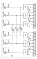
본 발명의 일 형태는 제 1 구동 회로와, 제 2 구동 회로와, 제 1 선택 회로와, 제 2 선택 회로와, 전환 회로를 가지고, 제 1 구동 회로는 제 1 출력 단자를 가지고, 제 2 구동 회로는 제 2 출력 단자를 가지고, 제 1 선택 회로는 입력 단자와 출력 단자를 가지고, 제 2 선택 회로는 입력 단자와 출력 단자를 가지고, 전환 회로는 제 1 단자와 제 2 단자를 가지고, 제 1 출력 단자는 제 1 선택 회로의 입력 단자 및 제 1 단자에 전기적으로 접속되고, 제 2 출력 단자는 제 2 선택 회로의 입력 단자 및 제 2 단자에 전기적으로 접속되고, 제 1 구동 회로는 제 1 데이터 신호를 생성하는 기능과 제 1 데이터 신호를 제 1 출력 단자에 출력하는 기능을 가지고, 제 2 구동 회로는 제 2 데이터 신호를 생성하는 기능과 제 2 데이터 신호를 제 2 출력 단자에 출력하는 기능을 가지고, 제 1 선택 회로는 제 1 선택 회로의 입력 단자와 제 1 선택 회로의 출력 단자 간을 도통 상태 및 비도통 상태 중 한쪽으로 하는 기능을 가지고, 제 2 선택 회로는 제 2 선택 회로의 입력 단자와 제 2 선택 회로의 출력 단자 간을 도통 상태 및 비도통 상태 중 한쪽으로 하는 기능을 가지고, 전환 회로는 제 1 단자와 제 2 단자 간을 도통 상태 및 비도통 상태 중 한쪽으로 하는 기능을 가지는 반도체 장치이다.One form of the present invention has a first drive circuit, a second drive circuit, a first selection circuit, a second selection circuit, and a switching circuit, the first drive circuit has a first output terminal, and the second drive circuit The circuit has a second output terminal, the first selection circuit has an input terminal and an output terminal, the second selection circuit has an input terminal and an output terminal, the switching circuit has a first terminal and a second terminal, the first selection circuit has a first terminal and a second terminal. The output terminal is electrically connected to the input terminal and the first terminal of the first selection circuit, the second output terminal is electrically connected to the input terminal and the second terminal of the second selection circuit, and the first driving circuit receives the first data. The second driving circuit has a function of generating a signal and a function of outputting the first data signal to the first output terminal, and the second driving circuit has a function of generating a second data signal and a function of outputting the second data signal to the second output terminal. wherein the first selection circuit has a function of putting the input terminal of the first selection circuit and the output terminal of the first selection circuit into one of a conductive state and a non-conductive state, and the second selection circuit has an input terminal of the second selection circuit. A semiconductor having a function of setting the output terminals of the first and second selection circuits to one of a conductive state and a non-conductive state, and the switching circuit having a function of setting the first terminal and the second terminal to one of a conductive state and a non-conductive state. It is a device.
(2)(2)
또한 상기 (1)에 있어서, 제 1 모드와, 제 2 모드와, 제 3 모드로 동작하는 기능을 가지고, 제 1 모드는 제 1 선택 회로의 입력 단자와 제 1 선택 회로의 출력 단자 간을 도통 상태 및 비도통 상태 중 한쪽으로 하고, 제 2 선택 회로의 입력 단자와 제 2 선택 회로의 출력 단자 간을 도통 상태 및 비도통 상태 중 다른 쪽으로 하고, 제 1 단자와 제 2 단자 간을 도통 상태로 하고, 제 1 데이터 신호를 제 1 구동 회로의 출력 단자를 통하여 제 1 선택 회로의 출력 단자 및 제 2 선택 회로의 출력 단자 중 어느 한쪽에 출력하고, 제 2 데이터 신호를 제 2 구동 회로의 출력 단자에 출력하지 않고, 제 2 모드는 제 1 선택 회로의 입력 단자와 제 1 선택 회로의 출력 단자 간을 도통 상태 및 비도통 상태 중 한쪽으로 하고, 제 2 선택 회로의 입력 단자와 제 2 선택 회로의 출력 단자 간을 도통 상태 및 비도통 상태 중 다른 쪽으로 하고, 제 1 단자와 제 2 단자 간을 도통 상태로 하고, 제 1 데이터 신호를 제 1 구동 회로의 출력 단자에 출력하지 않고, 제 2 데이터 신호를 제 2 구동 회로의 출력 단자를 통하여 제 1 선택 회로의 출력 단자 및 제 2 선택 회로의 출력 단자 중 어느 한쪽에 출력하고, 제 3 모드는 제 1 선택 회로의 입력 단자와 제 1 선택 회로의 출력 단자 간을 도통 상태로 하고, 제 2 선택 회로의 입력 단자와 제 2 선택 회로의 출력 단자 간을 도통 상태로 하고, 제 1 단자와 제 2 단자 간을 비도통 상태로 하고, 제 1 데이터 신호를 제 1 구동 회로의 출력 단자를 통하여 제 1 선택 회로의 출력 단자에 출력하고, 제 2 데이터 신호를 제 2 구동 회로의 출력 단자를 통하여 제 2 선택 회로의 출력 단자에 출력하는 반도체 장치가 바람직하다.In addition, in (1) above, it has a function of operating in a first mode, a second mode, and a third mode, and the first mode conducts between the input terminal of the first selection circuit and the output terminal of the first selection circuit. One of the conductive state and the non-conductive state is set, the input terminal of the second selection circuit and the output terminal of the second selection circuit are set to the other of the conducting state and the non-conductive state, and the first terminal and the second terminal are set to the conducting state. And outputting the first data signal to either the output terminal of the first selection circuit or the output terminal of the second selection circuit through the output terminal of the first driving circuit, and outputting the second data signal to the output terminal of the second driving circuit. In the second mode, the input terminal of the first selection circuit and the output terminal of the first selection circuit are in either a conductive state or a non-conductive state, and the input terminal of the second selection circuit and the output terminal of the second selection circuit are in either a conductive state or a non-conductive state. The output terminals are in the other of the conduction state and the non-conduction state, the first terminal and the second terminal are in the conduction state, the first data signal is not output to the output terminal of the first driving circuit, and the second data signal is output. is output to either the output terminal of the first selection circuit or the output terminal of the second selection circuit through the output terminal of the second driving circuit, and the third mode is output to the input terminal of the first selection circuit and the output of the first selection circuit. The terminals are in a conductive state, the input terminal of the second selection circuit and the output terminal of the second selection circuit are in a conductive state, and the first terminal and the second terminal are in a non-conductive state, and the first data signal is set to A semiconductor device is preferable that outputs a second data signal to the output terminal of the first selection circuit through the output terminal of the first driving circuit and outputs a second data signal to the output terminal of the second selection circuit through the output terminal of the second driving circuit.
(3)(3)
또한 상기 (1) 또는 상기 (2)에 있어서, 제 1 구동 회로는 제 1 신호 생성 회로와 제 1 스위치를 가지고, 제 2 구동 회로는 제 2 신호 생성 회로와 제 2 스위치를 가지고, 전환 회로는 제 3 스위치를 가지고, 제 1 신호 생성 회로의 출력 단자는 제 1 스위치의 제 1 단자에 전기적으로 접속되고, 제 1 스위치의 제 2 단자는 제 1 구동 회로의 출력 단자에 전기적으로 접속되고, 제 2 신호 생성 회로의 출력 단자는 제 2 스위치의 제 1 단자에 전기적으로 접속되고, 제 2 스위치의 제 2 단자는 제 2 구동 회로의 출력 단자에 전기적으로 접속되고, 제 3 스위치의 제 1 단자는 제 1 단자에 전기적으로 접속되고, 제 3 스위치의 제 2 단자는 제 2 단자에 전기적으로 접속되고, 제 1 신호 생성 회로는 제 1 데이터 신호를 생성하는 기능을 가지고, 제 2 신호 생성 회로는 제 2 데이터 신호를 생성하는 기능을 가지는 반도체 장치가 바람직하다.Also, in (1) or (2) above, the first driving circuit has a first signal generating circuit and a first switch, the second driving circuit has a second signal generating circuit and a second switch, and the switching circuit has With a third switch, the output terminal of the first signal generating circuit is electrically connected to the first terminal of the first switch, the second terminal of the first switch is electrically connected to the output terminal of the first driving circuit, and The output terminal of the two signal generation circuit is electrically connected to the first terminal of the second switch, the second terminal of the second switch is electrically connected to the output terminal of the second driving circuit, and the first terminal of the third switch is electrically connected to the first terminal of the second switch. is electrically connected to the first terminal, the second terminal of the third switch is electrically connected to the second terminal, the first signal generating circuit has a function of generating a first data signal, and the second signal generating circuit has a first data signal. 2 A semiconductor device that has the function of generating a data signal is desirable.
(4)(4)
또한 상기 (3)에 있어서, 제 1 스위치와, 제 2 스위치와, 제 3 스위치 각각은 아날로그 스위치인 반도체 장치가 바람직하다.Also, in the above (3), a semiconductor device is preferred where each of the first switch, second switch, and third switch is an analog switch.
(5)(5)
또한 상기 (1) 내지 상기 (4) 중 어느 하나의 반도체 장치와, 제 1 화소 회로와, 제 2 화소 회로를 가지고, 제 1 화소 회로는 제 1 선택 회로의 출력 단자에 전기적으로 접속되고, 제 2 화소 회로는 제 2 선택 회로의 출력 단자에 전기적으로 접속되는 표시 장치이다.It also has the semiconductor device of any one of (1) to (4) above, a first pixel circuit, and a second pixel circuit, the first pixel circuit being electrically connected to the output terminal of the first selection circuit, and The two-pixel circuit is a display device electrically connected to the output terminal of the second selection circuit.
(6)(6)
본 발명의 다른 일 형태는 제 1 구동 회로와, 제 2 구동 회로와, 제 1 선택 회로와, 제 2 선택 회로와, 전환 회로를 가지고, 제 1 구동 회로는 제 1 출력 단자를 가지고, 제 2 구동 회로는 제 2 출력 단자를 가지고, 제 1 선택 회로는 입력 단자와 복수의 출력 단자를 가지고, 제 2 선택 회로는 입력 단자와 복수의 출력 단자를 가지고, 전환 회로는 제 1 단자와 제 2 단자를 가지고, 제 1 출력 단자는 제 1 선택 회로의 입력 단자 및 제 1 단자에 전기적으로 접속되고, 제 2 출력 단자는 제 2 선택 회로의 입력 단자 및 제 2 단자에 전기적으로 접속되고, 제 1 구동 회로는 제 1 데이터 신호를 생성하는 기능과 제 1 데이터 신호를 제 1 출력 단자에 출력하는 기능을 가지고, 제 2 구동 회로는 제 2 데이터 신호를 생성하는 기능과 제 2 데이터 신호를 제 2 출력 단자에 출력하는 기능을 가지고, 제 1 선택 회로는 제 1 선택 회로의 입력 단자와, 제 1 선택 회로의 복수의 출력 단자 중 적어도 하나 간을 도통 상태로 하고, 제 1 선택 회로의 입력 단자와, 제 1 선택 회로의 복수의 출력 단자의 나머지 각각 간을 비도통 상태로 하는 기능을 가지고, 제 2 선택 회로는 제 2 선택 회로의 입력 단자와, 제 2 선택 회로의 복수의 출력 단자 중 적어도 하나 간을 도통 상태로 하고, 제 2 선택 회로의 입력 단자와 제 2 선택 회로의 복수의 출력 단자의 나머지 각각 간을 비도통 상태로 하는 기능을 가지고, 전환 회로는 제 1 단자와 제 2 단자 간을 도통 상태 및 비도통 상태 중 한쪽으로 하는 기능을 가지는 반도체 장치이다.Another form of the present invention has a first drive circuit, a second drive circuit, a first selection circuit, a second selection circuit, and a switching circuit, the first drive circuit has a first output terminal, and a second The driving circuit has a second output terminal, the first selection circuit has an input terminal and a plurality of output terminals, the second selection circuit has an input terminal and a plurality of output terminals, and the switching circuit has a first terminal and a second terminal. , the first output terminal is electrically connected to the input terminal and the first terminal of the first selection circuit, the second output terminal is electrically connected to the input terminal and the second terminal of the second selection circuit, and the first drive The circuit has a function of generating a first data signal and a function of outputting the first data signal to the first output terminal, and the second driving circuit has a function of generating a second data signal and a function of outputting the second data signal to the second output terminal. has a function of outputting, the first selection circuit conducts between the input terminal of the first selection circuit and at least one of the plurality of output terminals of the first selection circuit, the input terminal of the first selection circuit, and the first selection circuit. It has a function of making each of the remaining output terminals of the first selection circuit into a non-conductive state, and the second selection circuit connects the input terminal of the second selection circuit to at least one of the plurality of output terminals of the second selection circuit. It has a function of making the input terminal of the second selection circuit and the remaining output terminals of the second selection circuit into a non-conductive state, and the switching circuit maintains a conduction state between the first terminal and the second terminal. It is a semiconductor device that has the function of switching to one of the non-conductive states.
(7)(7)
또한 상기 (6)에 있어서, 제 1 모드와, 제 2 모드와, 제 3 모드로 동작하는 기능을 가지고, 제 1 모드는 제 1 선택 회로의 입력 단자와, 제 1 선택 회로의 복수의 출력 단자 중 하나 간 또는 제 2 선택 회로의 입력 단자와, 제 2 선택 회로의 복수의 출력 단자 중 하나 간을 도통 상태로 하고, 제 1 선택 회로의 입력 단자와, 제 1 선택 회로의 복수의 출력 단자의 나머지 각각 간 및 제 2 선택 회로의 입력 단자와, 제 2 선택 회로의 복수의 출력 단자의 나머지 각각 간을 비도통 상태로 하고, 제 1 단자와 제 2 단자 간을 도통 상태로 하고, 제 1 데이터 신호를 제 1 구동 회로의 출력 단자를 통하여 제 1 선택 회로의 복수의 출력 단자 중 어느 하나 또는 제 2 선택 회로의 복수의 출력 단자 중 어느 하나에 출력하고, 제 2 데이터 신호를 제 2 구동 회로의 출력 단자에 출력하지 않고, 제 2 모드는 제 1 선택 회로의 입력 단자와, 제 1 선택 회로의 복수의 출력 단자 중 하나 간 또는 제 2 선택 회로의 입력 단자와, 제 2 선택 회로의 복수의 출력 단자 중 하나 간을 도통 상태로 하고, 제 1 선택 회로의 입력 단자와, 제 1 선택 회로의 복수의 출력 단자의 나머지 각각 간 및 제 2 선택 회로의 입력 단자와, 제 2 선택 회로의 복수의 출력 단자의 나머지 각각 간을 비도통 상태로 하고, 제 1 단자와 제 2 단자 간을 도통 상태로 하고, 제 1 데이터 신호를 제 1 구동 회로의 출력 단자에 출력하지 않고, 제 2 데이터 신호를 제 2 구동 회로의 출력 단자를 통하여 제 1 선택 회로의 복수의 출력 단자 중 어느 하나 또는 제 2 선택 회로의 복수의 출력 단자 중 어느 하나에 출력하고, 제 3 모드는 제 1 선택 회로의 입력 단자와, 제 1 선택 회로의 복수의 출력 단자 중 하나 간을 도통 상태로 하고, 제 1 선택 회로의 입력 단자와, 제 1 선택 회로의 복수의 출력 단자의 나머지 각각 간을 비도통 상태로 하고, 제 2 선택 회로의 입력 단자와, 제 2 선택 회로의 복수의 출력 단자 중 하나 간을 도통 상태로 하고, 제 2 선택 회로의 입력 단자와, 제 2 선택 회로의 복수의 출력 단자의 나머지 각각 간을 비도통 상태로 하고, 제 1 단자와 제 2 단자 간을 비도통 상태로 하고, 제 1 데이터 신호를 제 1 구동 회로의 출력 단자를 통하여 제 1 선택 회로의 복수의 출력 단자 중 어느 하나에 출력하고, 제 2 데이터 신호를 제 2 구동 회로의 출력 단자를 통하여 제 2 선택 회로의 복수의 출력 단자 중 어느 하나에 출력하는 반도체 장치가 바람직하다.In addition, in the above (6), it has a function of operating in a first mode, a second mode, and a third mode, and the first mode is an input terminal of the first selection circuit and a plurality of output terminals of the first selection circuit. conduction between one of the input terminals of the first selection circuit or between the input terminal of the second selection circuit and one of the plurality of output terminals of the second selection circuit, and the input terminal of the first selection circuit and the plurality of output terminals of the first selection circuit The input terminal of the second selection circuit and each of the remainder of the plurality of output terminals of the second selection circuit are in a non-conductive state, and the first terminal and the second terminal are in a conductive state, and the first data A signal is output to one of the plurality of output terminals of the first selection circuit or one of the plurality of output terminals of the second selection circuit through the output terminal of the first driving circuit, and the second data signal is output to the output terminal of the second driving circuit. Without outputting to the output terminal, the second mode is between the input terminal of the first selection circuit and one of the plurality of output terminals of the first selection circuit or between the input terminal of the second selection circuit and the plurality of outputs of the second selection circuit. One of the terminals is in a conductive state, and between the input terminal of the first selection circuit and each of the remaining output terminals of the first selection circuit and the input terminal of the second selection circuit and the plurality of outputs of the second selection circuit. Each of the remaining terminals is in a non-conductive state, and the first terminal and the second terminal are in a conductive state, the first data signal is not output to the output terminal of the first driving circuit, and the second data signal is output to the second terminal. Output is output to one of the plurality of output terminals of the first selection circuit or one of the plurality of output terminals of the second selection circuit through the output terminal of the driving circuit, and the third mode is output to the input terminal of the first selection circuit, and the third mode. One of the plurality of output terminals of the first selection circuit is in a conductive state, and the input terminal of the first selection circuit and each of the remaining output terminals of the first selection circuit are in a non-conductive state, and the second selection circuit The input terminal of and one of the plurality of output terminals of the second selection circuit are in a conductive state, and the input terminal of the second selection circuit and each of the remaining output terminals of the second selection circuit are in a non-conductive state. Then, the first terminal and the second terminal are in a non-conductive state, the first data signal is output to one of the plurality of output terminals of the first selection circuit through the output terminal of the first driving circuit, and the second data signal is output to one of the plurality of output terminals of the first selection circuit. A semiconductor device that outputs a signal to one of a plurality of output terminals of the second selection circuit through the output terminal of the second driving circuit is preferable.
(8)(8)
또한 상기 (6) 또는 상기 (7)에 있어서, 제 1 구동 회로는 제 1 신호 생성 회로와 제 1 스위치를 가지고, 제 2 구동 회로는 제 2 신호 생성 회로와 제 2 스위치를 가지고, 전환 회로는 제 3 스위치를 가지고, 제 1 신호 생성 회로의 출력 단자는 제 1 스위치의 제 1 단자에 전기적으로 접속되고, 제 1 스위치의 제 2 단자는 제 1 구동 회로의 출력 단자에 전기적으로 접속되고, 제 2 신호 생성 회로의 출력 단자는 제 2 스위치의 제 1 단자에 전기적으로 접속되고, 제 2 스위치의 제 2 단자는 제 2 구동 회로의 출력 단자에 전기적으로 접속되고, 제 3 스위치의 제 1 단자는 제 1 단자에 전기적으로 접속되고, 제 3 스위치의 제 2 단자는 제 2 단자에 전기적으로 접속되고, 제 1 신호 생성 회로는 제 1 데이터 신호를 생성하는 기능을 가지고, 제 2 신호 생성 회로는 제 2 데이터 신호를 생성하는 기능을 가지는 반도체 장치가 바람직하다.Also, in (6) or (7) above, the first driving circuit has a first signal generating circuit and a first switch, the second driving circuit has a second signal generating circuit and a second switch, and the switching circuit has With a third switch, the output terminal of the first signal generating circuit is electrically connected to the first terminal of the first switch, the second terminal of the first switch is electrically connected to the output terminal of the first driving circuit, and The output terminal of the two signal generation circuit is electrically connected to the first terminal of the second switch, the second terminal of the second switch is electrically connected to the output terminal of the second driving circuit, and the first terminal of the third switch is electrically connected to the first terminal of the second switch. is electrically connected to the first terminal, the second terminal of the third switch is electrically connected to the second terminal, the first signal generating circuit has a function of generating a first data signal, and the second signal generating circuit has a first data signal. 2 A semiconductor device that has the function of generating a data signal is desirable.
(9)(9)
또한 상기 (8)에 있어서, 제 1 스위치와, 제 2 스위치와, 제 3 스위치 각각은 아날로그 스위치인 반도체 장치가 바람직하다.Also, in the above (8), a semiconductor device is preferred in which each of the first switch, the second switch, and the third switch is an analog switch.
(10)(10)
또한 상기 (6) 내지 상기 (9) 중 어느 하나의 반도체 장치와, 제 1 화소 회로와, 제 2 화소 회로를 가지고, 제 1 화소 회로는 제 1 선택 회로의 복수의 출력 단자 중 적어도 하나에 전기적으로 접속되고, 제 2 화소 회로는 제 2 선택 회로의 복수의 출력 단자 중 적어도 하나에 전기적으로 접속되는 표시 장치이다.It also has the semiconductor device of any one of (6) to (9) above, a first pixel circuit, and a second pixel circuit, wherein the first pixel circuit is electrically connected to at least one of the plurality of output terminals of the first selection circuit. and the second pixel circuit is a display device electrically connected to at least one of a plurality of output terminals of the second selection circuit.
(11)(11)
또한 상기 (6) 내지 상기 (9) 중 어느 하나의 반도체 장치와, 제 1 화소 회로와, 제 2 화소 회로를 가지고, 제 1 화소 회로는 제 1 선택 회로의 복수의 출력 단자 모두에 전기적으로 접속되고, 제 2 화소 회로는 제 2 선택 회로의 복수의 출력 단자 모두에 전기적으로 접속되는 표시 장치이다.Additionally, it has the semiconductor device of any one of (6) to (9) above, a first pixel circuit, and a second pixel circuit, and the first pixel circuit is electrically connected to all of the plurality of output terminals of the first selection circuit. The second pixel circuit is a display device electrically connected to all of the plurality of output terminals of the second selection circuit.
(12)(12)
또한 상기 (5), 상기 (10), 또는 상기 (11)에 기재된 표시 장치와, 하우징을 가지는 전자 기기이다.It is also an electronic device having the display device according to (5), (10), or (11) above, and a housing.
또한 본 명세서 등에서 반도체 장치란, 반도체 특성을 이용한 장치이고, 반도체 소자(예를 들어 트랜지스터, 다이오드, 또는 포토다이오드 등)를 포함한 회로, 또는 이 회로를 포함한 장치 등을 말한다. 또한 반도체 특성을 이용함으로써 기능할 수 있는 장치 전반을 말한다. 예를 들어 집적 회로, 집적 회로를 가지는 칩, 또는 패키지 등에 칩을 수납한 전자 부품은 반도체 장치의 일례이다. 또한 예를 들어 기억 장치, 표시 장치, 발광 장치, 조명 장치, 또는 전자 기기 등은 그 자체가 반도체 장치인 경우가 있고, 반도체 장치를 포함하는 경우가 있다.In addition, in this specification and the like, a semiconductor device refers to a device that utilizes semiconductor characteristics, and refers to a circuit including a semiconductor element (for example, a transistor, diode, or photodiode), or a device including this circuit. It also refers to the overall device that can function by utilizing semiconductor characteristics. For example, an integrated circuit, a chip having an integrated circuit, or an electronic component containing a chip in a package is an example of a semiconductor device. Additionally, for example, memory devices, display devices, light-emitting devices, lighting devices, or electronic devices may themselves be semiconductor devices or include semiconductor devices.
또한 본 명세서 등에서 X와 Y가 접속된다고 기재되는 경우에는, X와 Y가 전기적으로 접속되는 경우와, X와 Y가 기능적으로 접속되는 경우와, X와 Y가 직접 접속되는 경우가 본 명세서 등에 개시되어 있는 것으로 한다. 따라서 소정의 접속 관계, 예를 들어 도면 또는 문장에 나타낸 접속 관계에 한정되지 않고, 도면 또는 문장에 나타낸 접속 관계 이외의 것도 도면 또는 문장에 개시되어 있는 것으로 한다. X 및 Y는 각각 대상물(예를 들어 장치, 소자, 회로, 배선, 전극, 단자, 도전막, 또는 층 등)인 것으로 한다.In addition, when X and Y are described as connected in this specification, etc., the case where X and Y are electrically connected, the case where X and Y are functionally connected, and the case where X and Y are directly connected are disclosed in this specification, etc. It is assumed that it is done. Therefore, it is not limited to a predetermined connection relationship, for example, the connection relationship shown in the drawing or text, and connection relationships other than those shown in the drawing or text are also disclosed in the drawing or text. X and Y are each objects (e.g., devices, elements, circuits, wiring, electrodes, terminals, conductive films, or layers).
X와 Y가 전기적으로 접속되는 경우에는, 일례로서 X와 Y를 전기적으로 접속할 수 있는 소자(예를 들어 스위치, 트랜지스터, 용량 소자, 인덕터, 저항 소자, 다이오드, 표시 디바이스, 발광 디바이스, 또는 부하 등)가 X와 Y 사이에 하나 이상 접속될 수 있다. 또한 스위치는 온 상태 또는 오프 상태가 제어되는 기능을 가진다. 즉 스위치는 도통 상태(온 상태) 또는 비도통 상태(오프 상태)가 되어, 전류를 흘릴지 여부를 제어하는 기능을 가진다.When X and Y are electrically connected, as an example, an element that can electrically connect ) can be connected one or more between X and Y. Additionally, the switch has the function of controlling the on or off state. In other words, the switch has the function of controlling whether or not to flow current by being in a conductive state (on state) or non-conductive state (off state).
X와 Y가 기능적으로 접속되는 경우에는, 일례로서 X와 Y를 기능적으로 접속할 수 있는 회로(예를 들어 논리 회로(예를 들어 인버터, NAND 회로, 또는 NOR 회로 등), 신호 변환 회로(예를 들어 디지털 아날로그 변환 회로, 아날로그 디지털 변환 회로, 또는 감마 보정 회로 등), 전위 레벨 변환 회로(예를 들어 전원 회로(예를 들어 승압 회로, 강압 회로 등) 또는 신호의 전위 레벨을 바꾸는 레벨 시프터 회로 등), 전압원, 전류원, 전환 회로, 증폭 회로(예를 들어 신호 진폭 또는 전류량 등을 크게 할 수 있는 회로, 연산 증폭기, 차동 증폭 회로, 소스 폴로어 회로, 또는 버퍼 회로 등), 신호 생성 회로, 기억 회로, 제어 회로 등)가 X와 Y 사이에 하나 이상 접속될 수 있다. 또한 일례로서, X와 Y 사이에 다른 회로를 끼워도 X로부터 출력된 신호가 Y로 전달되는 경우에는, X와 Y는 기능적으로 접속되는 것으로 한다.When X and Y are functionally connected, as an example, a circuit capable of functionally connecting (e.g. digital-to-analog conversion circuit, analog-to-digital conversion circuit, or gamma correction circuit, etc.), potential level conversion circuit (e.g., power supply circuit (e.g., step-up circuit, step-down circuit, etc.), or level shifter circuit that changes the potential level of the signal, etc. ), voltage source, current source, switching circuit, amplification circuit (for example, a circuit capable of increasing the signal amplitude or current amount, operational amplifier, differential amplifier circuit, source follower circuit, or buffer circuit, etc.), signal generation circuit, memory circuit, control circuit, etc.) may be connected between X and Y. Also, as an example, if a signal output from X is transmitted to Y even if another circuit is inserted between X and Y, X and Y are considered to be functionally connected.
또한 X와 Y가 전기적으로 접속된다고 명시적으로 기재되는 경우에는, X와 Y가 전기적으로 접속되는 경우(즉 X와 Y가 사이에 다른 소자 또는 다른 회로를 끼워 접속되는 경우)와, X와 Y가 직접 접속되는 경우(즉 X와 Y가 사이에 다른 소자 또는 다른 회로를 끼우지 않고 접속되는 경우)를 포함하는 것으로 한다.In addition, when it is explicitly stated that X and Y are electrically connected, there is a case where This shall include the case where is directly connected (i.e., when X and Y are connected without interposing other elements or other circuits between them).
또한 예를 들어 "X와, Y와, 트랜지스터의 소스(또는 제 1 단자 등)와, 드레인(또는 제 2 단자 등)은 서로 전기적으로 접속되고, X, 트랜지스터의 소스(또는 제 1 단자 등), 트랜지스터의 드레인(또는 제 2 단자 등), Y의 순서로 전기적으로 접속된다"라고 표현할 수 있다. 또는 "트랜지스터의 소스(또는 제 1 단자 등)는 X에 전기적으로 접속되고, 트랜지스터의 드레인(또는 제 2 단자 등)은 Y에 전기적으로 접속되고, X, 트랜지스터의 소스(또는 제 1 단자 등), 트랜지스터의 드레인(또는 제 2 단자 등), Y는 이 순서대로 전기적으로 접속된다"라고 표현할 수 있다. 또는 "X는 트랜지스터의 소스(또는 제 1 단자 등)와 드레인(또는 제 2 단자 등)을 통하여 Y에 전기적으로 접속되고, X, 트랜지스터의 소스(또는 제 1 단자 등), 트랜지스터의 드레인(또는 제 2 단자 등), Y는 이 접속 순서로 제공된다"라고 표현할 수 있다. 이들 예와 같은 표현 방법을 사용하여 회로 구성에서의 접속 순서에 대하여 규정함으로써, 트랜지스터의 소스(또는 제 1 단자 등)와 드레인(또는 제 2 단자 등)을 구별하여 기술적 범위를 결정할 수 있다. 또한 이들 표현 방법은 일례이고, 이들 표현 방법에 한정되지 않는다. 여기서, X 및 Y는 각각 대상물(예를 들어 장치, 소자, 회로, 배선, 전극, 단자, 도전막, 또는 층 등)인 것으로 한다.Also, for example, "X, Y, the source (or first terminal, etc.) of the transistor, and the drain (or second terminal, etc.) are electrically connected to each other, and , the drain (or second terminal, etc.) of the transistor, and Y are electrically connected in that order.” or "the source (or first terminal, etc.) of the transistor is electrically connected to X, the drain (or second terminal, etc.) of the transistor is electrically connected to Y, and , the drain (or second terminal, etc.) of the transistor, Y are electrically connected in this order.” or "X is electrically connected to Y through the source (or first terminal, etc.) and drain (or second terminal, etc.) of the transistor, and 2nd terminal, etc.), Y is provided in this connection order.” By specifying the connection order in the circuit configuration using expression methods such as these examples, the technical scope can be determined by distinguishing between the source (or first terminal, etc.) and drain (or second terminal, etc.) of the transistor. Additionally, these expression methods are examples and are not limited to these expression methods. Here, X and Y are each objects (e.g., devices, elements, circuits, wiring, electrodes, terminals, conductive films, or layers).
또한 회로도상 독립된 구성 요소들이 전기적으로 접속되는 것처럼 도시되어 있는 경우에도, 하나의 구성 요소가 복수의 구성 요소의 기능을 겸비하는 경우도 있다. 예를 들어 배선의 일부가 전극으로서도 기능하는 경우에는, 하나의 도전막이 배선의 기능 및 전극의 기능의 양쪽의 구성 요소의 기능을 겸비한다. 따라서 본 명세서에서의 전기적인 접속이란, 이와 같이 하나의 도전막이 복수의 구성 요소의 기능을 겸비하는 경우도 그 범주에 포함한다.Additionally, even when independent components are shown as electrically connected in a circuit diagram, there are cases where one component has the functions of multiple components. For example, when a part of the wiring also functions as an electrode, one conductive film functions as a component of both the wiring function and the electrode function. Therefore, the term electrical connection in this specification also includes cases where one conductive film functions as a plurality of components.
또한 본 명세서 등에서 "저항 소자"란, 예를 들어 0Ω보다 저항값이 높은 회로 소자 또는 배선 등으로 할 수 있다. 그러므로 본 명세서 등에서 "저항 소자"는 예를 들어 저항값을 가지는 배선, 소스와 드레인 간을 전류가 흐르는 트랜지스터, 다이오드, 또는 코일 등을 포함하는 것으로 한다. 그러므로 "저항 소자"라는 용어는 예를 들어 "저항", "부하", 또는 "저항값을 가지는 영역" 등의 용어로 바꿔 말할 수 있는 경우가 있다. 반대로 "저항", "부하", 또는 "저항값을 가지는 영역"이라는 용어는 예를 들어 "저항 소자" 등의 용어로 바꿔 말할 수 있는 경우가 있다. 저항값은 예를 들어 바람직하게는 1mΩ 이상 10Ω 이하, 더 바람직하게는 5mΩ 이상 5Ω 이하, 더욱 바람직하게는 10mΩ 이상 1Ω 이하로 할 수 있다. 또한 예를 들어 1Ω 이상 1×10⁹Ω 이하로 하여도 좋다.In addition, in this specification and the like, the term “resistance element” may be, for example, a circuit element or wiring with a resistance value higher than 0Ω. Therefore, in this specification and the like, a “resistance element” includes, for example, a wiring having a resistance value, a transistor, a diode, or a coil through which current flows between a source and a drain. Therefore, the term “resistance element” may be replaced with terms such as, for example, “resistance”, “load”, or “area with a resistance value”. Conversely, the terms “resistance,” “load,” or “area with a resistance value” may be replaced with terms such as “resistance element,” for example. The resistance value can be, for example, preferably 1 mΩ or more and 10 Ω or less, more preferably 5 mΩ or more and 5 Ω or less, and even more preferably 10 mΩ or more and 1 Ω or less. Also, for example, it may be 1Ω or more and 1×10 9 Ω or less.
또한 본 명세서 등에서 "용량 소자"는, 예를 들어 정전 용량이 0F보다 높은 회로 소자, 정전 용량이 0F보다 높은 배선의 영역, 기생 용량, 또는 트랜지스터의 게이트 용량 등으로 할 수 있다. 또한 예를 들어 "용량 소자", "기생 용량", 또는 "게이트 용량" 등이라는 용어는 예를 들어 "용량" 등의 용어로 바꿔 말할 수 있는 경우가 있다. 반대로 "용량"이라는 용어는 예를 들어 "용량 소자", "기생 용량", 또는 "게이트 용량" 등의 용어로 바꿔 말할 수 있는 경우가 있다. 또한 "용량"의 "한 쌍의 전극"이라는 용어는 예를 들어 "한 쌍의 도전체", "한 쌍의 도전 영역", 또는 "한 쌍의 영역" 등으로 바꿔 말할 수 있다. 또한 정전 용량은 예를 들어 0.05fF 이상 10pF 이하로 할 수 있다. 또한 예를 들어 1pF 이상 10μF 이하로 하여도 좋다.Additionally, in this specification and the like, “capacitance element” may be, for example, a circuit element with a capacitance higher than 0F, a wiring area with a capacitance higher than 0F, a parasitic capacitance, or a gate capacitance of a transistor. Also, for example, terms such as “capacitance element”, “parasitic capacitance”, or “gate capacitance” may be replaced with terms such as “capacitance”. Conversely, the term "capacitance" may be interchanged with terms such as, for example, "capacitance element", "parasitic capacitance", or "gate capacitance". Additionally, the term “a pair of electrodes” in “capacitance” can be replaced with, for example, “a pair of conductors,” “a pair of conductive regions,” or “a pair of regions.” Additionally, the capacitance can be, for example, 0.05fF or more and 10pF or less. Also, for example, it may be set to 1pF or more and 10μF or less.
또한 본 명세서 등에서 트랜지스터는 게이트, 소스, 및 드레인이라고 불리는 3개의 단자를 가진다. 게이트는 트랜지스터의 도통 상태를 제어하는 제어 단자이다. 소스 또는 드레인으로서 기능하는 2개의 단자는 트랜지스터의 입출력 단자이다. 2개의 입출력 단자는 트랜지스터의 도전형(n채널형 또는 p채널형) 및 트랜지스터의 3개의 단자에 인가되는 전위의 높낮이에 따라, 한쪽이 소스가 되고 다른 쪽이 드레인이 된다. 그러므로 본 명세서 등에서는, "소스"와 "드레인"이라는 용어는 바꿔 말할 수 있는 경우가 있다. 또한 본 명세서 등에서는, 트랜지스터의 접속 관계를 설명하는 경우, "소스 및 드레인 중 한쪽"(또는 제 1 전극 또는 제 1 단자), 또는 "소스 및 드레인 중 다른 쪽"(또는 제 2 전극 또는 제 2 단자)이라는 표기를 사용한다. 또한 트랜지스터의 구조에 따라서는 상술한 3개의 단자에 더하여 백 게이트를 가지는 경우가 있다. 이 경우, 본 명세서 등에서 트랜지스터의 게이트 및 백 게이트 중 한쪽을 제 1 게이트라고 부르고, 트랜지스터의 게이트 및 백 게이트 중 다른 쪽을 제 2 게이트라고 부르는 경우가 있다. 또한 같은 트랜지스터에서 "게이트"와 "백 게이트"라는 용어는 서로 바꿀 수 있는 경우가 있다. 또한 트랜지스터가 3개 이상의 게이트를 가지는 경우, 본 명세서 등에서는 각 게이트를 예를 들어 제 1 게이트, 제 2 게이트, 또는 제 3 게이트 등이라고 부를 수 있다.Additionally, in this specification and elsewhere, the transistor has three terminals called gate, source, and drain. The gate is a control terminal that controls the conduction state of the transistor. The two terminals that function as source or drain are the input and output terminals of the transistor. One of the two input/output terminals becomes the source and the other becomes the drain, depending on the conductivity type of the transistor (n-channel type or p-channel type) and the height of the potential applied to the three terminals of the transistor. Therefore, in this specification and the like, the terms “source” and “drain” may be used interchangeably. Additionally, in this specification and the like, when describing the connection relationship of a transistor, “one of the source and the drain” (or the first electrode or the first terminal), or “the other of the source and the drain” (or the second electrode or the second terminal) terminal) is used. Additionally, depending on the structure of the transistor, it may have a back gate in addition to the three terminals described above. In this case, in this specification and the like, one of the gate and back gate of the transistor may be called a first gate, and the other of the gate and back gate of the transistor may be called a second gate. Additionally, the terms "gate" and "back gate" are sometimes interchangeable for the same transistor. Additionally, when the transistor has three or more gates, each gate may be referred to as, for example, a first gate, a second gate, or a third gate in this specification and the like.
예를 들어 본 명세서 등에서, 트랜지스터로서는 2개 이상의 게이트 전극을 가진 멀티 게이트 구조의 트랜지스터를 사용할 수 있다. 멀티 게이트 구조의 트랜지스터로 하면, 채널 형성 영역이 직렬로 접속되기 때문에, 복수의 트랜지스터가 직렬로 접속된다. 따라서 멀티 게이트 구조의 트랜지스터로 하면, 오프 전류의 감소 및 트랜지스터의 내압 향상(신뢰성 향상)을 실현할 수 있다. 또는 멀티 게이트 구조의 트랜지스터로 하면, 포화 영역에서 동작할 때, 드레인과 소스 사이의 전압이 변화되어도 드레인과 소스 사이의 전류가 그다지 변화되지 않기 때문에, 기울기가 평평한 전압-전류 특성을 얻을 수 있다. 기울기가 평평한 전압-전류 특성을 가지는 트랜지스터는, 이상적인 전류원 회로 또는 저항값이 매우 높은 능동 부하를 실현할 수 있다. 그 결과, 기울기가 평평한 전압-전류 특성을 가진 트랜지스터는 예를 들어 특성이 양호한 차동 회로 또는 커런트 미러 회로 등을 실현할 수 있다.For example, in this specification and the like, a transistor with a multi-gate structure having two or more gate electrodes can be used as the transistor. When using a transistor with a multi-gate structure, the channel formation regions are connected in series, so a plurality of transistors are connected in series. Therefore, by using a transistor with a multi-gate structure, it is possible to reduce the off-state current and improve the withstand voltage (improved reliability) of the transistor. Alternatively, in the case of a transistor with a multi-gate structure, when operating in the saturation region, the current between the drain and source does not change much even if the voltage between the drain and source changes, so voltage-current characteristics with a flat slope can be obtained. A transistor with flat voltage-current characteristics can realize an ideal current source circuit or an active load with a very high resistance value. As a result, a transistor with flat voltage-current characteristics can realize, for example, a differential circuit or current mirror circuit with good characteristics.
또한 본 명세서 등에 있어서, 회로도에서 단일의 회로 소자가 도시되어 있는 경우에 상기 회로 소자가 복수의 회로 소자를 가지는 경우가 있다. 예를 들어 회로도에서 하나의 저항 소자가 도시되어 있는 경우에는 2개 이상의 저항 소자가 직렬로 전기적으로 접속되어 있는 경우를 포함하는 것으로 한다. 또한 예를 들어 회로도에서 하나의 용량 소자가 도시되어 있는 경우에는 2개 이상의 용량 소자가 병렬로 전기적으로 접속되어 있는 경우를 포함하는 것으로 한다. 또한 예를 들어 회로도에서 하나의 트랜지스터가 도시되어 있는 경우에는 2개 이상의 트랜지스터가 직렬로 전기적으로 접속되고, 또한 각 트랜지스터의 게이트가 서로 전기적으로 접속되어 있는 경우를 포함하는 것으로 한다. 또한 이와 마찬가지로 예를 들어 회로도에서 하나의 스위치가 도시되어 있는 경우에는 상기 스위치가 2개 이상의 트랜지스터를 가지고, 2개 이상의 트랜지스터가 직렬 또는 병렬로 전기적으로 접속되고, 각 트랜지스터의 게이트가 서로 전기적으로 접속되어 있는 경우를 포함하는 것으로 한다.Additionally, in this specification and the like, when a single circuit element is shown in a circuit diagram, the circuit element may have a plurality of circuit elements. For example, when a single resistance element is shown in a circuit diagram, this includes cases where two or more resistance elements are electrically connected in series. Also, for example, when one capacitive element is shown in a circuit diagram, this includes the case where two or more capacitive elements are electrically connected in parallel. Also, for example, when one transistor is shown in a circuit diagram, this includes cases where two or more transistors are electrically connected in series and the gates of each transistor are electrically connected to each other. Likewise, for example, when a single switch is shown in a circuit diagram, the switch has two or more transistors, the two or more transistors are electrically connected in series or parallel, and the gates of each transistor are electrically connected to each other. It shall include cases where it is.
또한 본 명세서 등에서 "노드"는 예를 들어 회로 구성 또는 디바이스 구조 등에 따라 예를 들어 단자, 배선, 전극, 도전층, 도전체, 또는 불순물 영역 등으로 바꿔 말할 수 있다. 또한 예를 들어 단자 또는 배선 등을 "노드"로 바꿔 말할 수 있다.Additionally, in this specification and the like, “node” may be referred to as, for example, a terminal, wiring, electrode, conductive layer, conductor, or impurity region, depending on the circuit configuration or device structure. Also, for example, a terminal or wiring can be referred to as a “node.”
또한 본 명세서 등에서 "전압"과 "전위"는 적절히 바꿔 말할 수 있다. "전압"은 기준이 되는 전위로부터의 전위차를 말한다. 예를 들어, 기준이 되는 전위를 그라운드 전위(접지 전위)로 하면, "전압"은 "전위"로 바꿔 말할 수 있다. 또한 그라운드 전위는 반드시 0V를 의미하는 것은 아니다. 또한 전위란 상대적인 것이다. 즉, 기준이 되는 전위가 변화됨으로써, 예를 들어 배선에 공급되는 전위, 예를 들어 회로 등에 인가되는 전위, 또는 예를 들어 회로 등으로부터 출력되는 전위 등도 변화된다.Additionally, in this specification and elsewhere, “voltage” and “potential” can be appropriately interchanged. “Voltage” refers to the potential difference from the reference potential. For example, if the reference potential is the ground potential (ground potential), “voltage” can be changed to “potential.” Also, ground potential does not necessarily mean 0V. Also, potential is relative. In other words, as the reference potential changes, the potential supplied to the wiring, for example, the potential applied to the circuit, etc., or the potential output from the circuit, etc. also changes.
또한 본 명세서 등에서 "고레벨 전위" 또는 "저레벨 전위"라는 용어는 특정의 전위를 의미하는 것은 아니다. 예를 들어 2개의 배선의 양쪽이 "고레벨 전위를 공급하는 배선으로서 기능한다"라고 기재되는 경우, 양쪽의 배선이 공급하는 각 고레벨 전위는 서로 같지 않아도 된다. 또한 이와 마찬가지로 2개의 배선의 양쪽이 "저레벨 전위를 공급하는 배선으로서 기능한다"라고 기재되는 경우, 양쪽의 배선이 공급하는 각 저레벨 전위는 서로 같지 않아도 된다.Additionally, in this specification and the like, the terms “high level potential” or “low level potential” do not mean a specific potential. For example, if both sides of two wirings are described as "functioning as wiring that supplies high-level potential," the high-level potentials supplied by both wirings do not need to be the same. Likewise, when both sides of two wires are described as "functioning as wires that supply low-level potentials," the low-level potentials supplied by both wires do not need to be the same.
또한 본 명세서 등에 있어서, "전류"란 전하의 이동 현상(전기 전도)을 말한다. 예를 들어 "양의 하전체(荷電體)의 전기 전도가 발생하고 있다"라는 기재는, "그 반대 방향으로 음의 하전체의 전기 전도가 발생하고 있다"라고 바꿔 말할 수 있다. 그러므로 본 명세서 등에서 "전류"란 별도의 설명이 없는 한, 캐리어의 이동에 따른 전하의 이동 현상(전기 전도)을 말하는 것으로 한다. 여기서의 캐리어란 예를 들어 전자, 정공, 음이온, 양이온, 또는 착이온 등이다. 또한 캐리어는 전류가 흐르는 계(system)(예를 들어 반도체, 금속, 전해액, 또는 진공 중 등)에 따라 다르다. 또한 예를 들어 배선 등에서의 "전류의 방향"은 양전하를 띤 캐리어가 이동하는 방향이고, 양의 전류량으로 기재한다. 바꿔 말하면, 음전하를 띤 캐리어가 이동하는 방향은 전류의 방향과 반대 방향이고, 음의 전류량으로 표현된다. 따라서 본 명세서 등에서 전류의 양과 음(또는 전류의 방향)에 대하여 별도의 설명이 없는 경우, 예를 들어 "소자 A로부터 소자 B로 전류가 흐른다" 등의 기재는 예를 들어 "소자 B로부터 소자 A로 전류가 흐른다" 등으로 바꿔 말할 수 있는 것으로 한다. 또한 예를 들어 "소자 A에 전류가 입력된다" 등의 기재는 "소자 A로부터 전류가 출력된다" 등으로 바꿔 말할 수 있는 것으로 한다.In addition, in this specification and the like, “current” refers to the phenomenon of electric charge movement (electrical conduction). For example, the statement “electrical conduction of a positive charged body is occurring” can be rephrased as “electrical conduction of a negative charged body is occurring in the opposite direction.” Therefore, in this specification, etc., unless otherwise specified, “current” refers to the phenomenon of charge movement (electrical conduction) due to the movement of carriers. The carrier here is, for example, an electron, hole, anion, cation, or complex ion. Additionally, carriers vary depending on the system through which the current flows (e.g., semiconductor, metal, electrolyte, or vacuum, etc.). Also, for example, the “direction of current” in wiring, etc. is the direction in which positively charged carriers move, and is described as the amount of positive current. In other words, the direction in which negatively charged carriers move is opposite to the direction of the current, and is expressed as the amount of negative current. Therefore, in this specification, etc., if there is no separate explanation regarding the positive and negative current (or the direction of the current), for example, descriptions such as “current flows from element A to element B” are, for example, “from element B to element A.” It can be rephrased as “current flows through.” Also, for example, statements such as "current is input to element A" can be rephrased as "current is output from element A", etc.
또한 본 명세서 등에서 "제 1", "제 2", 또는 "제 3"이라는 서수사는 구성 요소의 혼동을 피하기 위하여 붙인 것이다. 따라서 구성 요소의 개수를 한정하는 것이 아니다. 또한 구성 요소의 순서를 한정하는 것이 아니다. 예를 들어 본 명세서 등의 실시형태 중 하나에서 "제 1"로 언급된 구성 요소가 다른 실시형태 또는 청구범위에서 "제 2"로 언급된 구성 요소가 될 수도 있다. 또한 예를 들어 본 명세서 등의 실시형태 중 하나에서 "제 1"로 언급된 구성 요소가 다른 실시형태 또는 청구범위에서 생략될 수도 있다.Additionally, in this specification, etc., the ordinal numbers “first,” “second,” or “third” are added to avoid confusion between constituent elements. Therefore, the number of components is not limited. Also, the order of components is not limited. For example, an element referred to as “first” in one of the embodiments of this specification or the like may be an element referred to as “second” in another embodiment or in the claims. Additionally, for example, an element referred to as “first” in one of the embodiments of this specification or the like may be omitted in other embodiments or claims.
또한 본 명세서 등에서 예를 들어 "위에" 또는 "아래에" 등의 배치를 나타내는 용어는 구성끼리의 위치 관계를 도면을 참조하여 설명하기 위하여 편의상 사용하고 있는 경우가 있다. 또한 구성끼리의 위치 관계는 각 구성을 묘사하는 방향에 따라 적절히 변화된다. 따라서 본 명세서 등에서 설명한 배치를 나타내는 용어는 이에 한정되지 않고 상황에 따라 적절히 환언할 수 있다. 예를 들어 "도전체의 상면에 위치하는 절연체"라는 표현은, 나타낸 도면의 방향을 180° 회전시킴으로써, "도전체의 하면에 위치하는 절연체"라고 바꿔 말할 수 있다.Additionally, in this specification and the like, terms indicating arrangement such as "above" or "below" may be used for convenience in explaining the positional relationship between components with reference to the drawings. Additionally, the positional relationships between components change appropriately depending on the direction in which each component is depicted. Accordingly, terms representing the arrangement described in this specification, etc. are not limited thereto and may be appropriately rephrased depending on the situation. For example, the expression “an insulator located on the upper surface of a conductor” can be changed to “an insulator located on the lower surface of a conductor” by rotating the direction of the drawing by 180°.
또한 "위" 또는 "아래"라는 용어는, 구성 요소의 위치 관계가 바로 위 또는 바로 아래이며 직접 접촉하는 것에 한정되지 않는다. 예를 들어 "절연층 A 위의 전극 B"라는 표현이면, 절연층 A 위에 전극 B가 직접 접촉되어 형성될 필요는 없고, 절연층 A와 전극 B 사이에 다른 구성 요소를 포함하는 것을 제외하지 않는다.Additionally, the terms “above” or “below” are not limited to the positional relationship of components being directly above or below and in direct contact. For example, if the expression is “electrode B on insulating layer A,” electrode B does not need to be formed in direct contact with insulating layer A, and including other components between insulating layer A and electrode B is not excluded. .
또한 본 명세서 등에서 매트릭스로 배열된 구성 요소 및 그 위치 관계를 설명하기 위하여 예를 들어 "행" 또는 "열" 등의 용어를 사용하는 경우가 있다. 또한 구성끼리의 위치 관계는 각 구성을 묘사하는 방향에 따라 적절히 변화된다. 따라서 본 명세서 등에서 설명한 "행" 또는 "열" 등의 용어는 이에 한정되지 않고 상황에 따라 적절히 바꿔 말할 수 있다. 예를 들어 "행 방향"이라는 표현은 나타내는 도면의 방향을 90° 회전시킴으로써 "열 방향"으로 바꿔 말할 수 있는 경우가 있다.Additionally, in this specification and the like, terms such as “row” or “column” may be used to describe components arranged in a matrix and their positional relationships. Additionally, the positional relationships between components change appropriately depending on the direction in which each component is depicted. Accordingly, terms such as “row” or “column” described in this specification, etc. are not limited thereto and may be appropriately rephrased depending on the situation. For example, the expression "row direction" can be changed to "column direction" by rotating the direction of the drawing by 90°.
또한 본 명세서 등에서 예를 들어 "막" 또는 "층" 등의 용어는 상황에 따라 서로 바꿀 수 있는 경우가 있다. 예를 들어 "도전층"이라는 용어를 "도전막"이라는 용어로 변경할 수 있는 경우가 있다. 예를 들어 "절연막"이라는 용어를 "절연층"이라는 용어로 변경할 수 있는 경우가 있다. 또한 예를 들어 "막" 또는 "층" 등의 용어는 이들 용어를 사용하지 않고, 상황에 따라 다른 용어로 바꿀 수 있는 경우가 있다. 예를 들어 "도전층" 또는 "도전막"이라는 용어를 "도전체"라는 용어로 변경할 수 있는 경우가 있다. 또는 예를 들어 "절연층" 또는 "절연막"이라는 용어를 "절연체"라는 용어로 변경할 수 있는 경우가 있다.In addition, in this specification and the like, terms such as "film" or "layer" may be interchanged depending on the situation. For example, there are cases where the term “conductive layer” can be changed to the term “conductive film.” For example, there are cases where the term “insulating film” can be changed to the term “insulating layer.” Also, for example, terms such as “membrane” or “layer” may not be used and may be replaced with other terms depending on the situation. For example, there are cases where the term “conductive layer” or “conductive film” can be changed to the term “conductor.” Or, for example, the term “insulating layer” or “insulating film” may be changed to the term “insulator.”
또한 본 명세서 등에서 예를 들어 "전극", "배선", 또는 "단자" 등의 용어는, 이들 구성 요소를 기능적으로 한정하는 것이 아니다. 예를 들어 "전극"은 "배선"의 일부로서 사용되는 경우가 있고, 그 반대도 마찬가지이다. 또한 "전극" 또는 "배선"이라는 용어는, 예를 들어 복수의 "전극" 또는 "배선"이 일체가 되어 형성되어 있는 경우 등도 포함한다. 또한 예를 들어 "단자"는 "배선" 또는 "전극" 등의 일부로서 사용되는 경우가 있고, 그 반대도 마찬가지이다. 또한 "단자"라는 용어는, 예를 들어 복수의 "전극", "배선", 또는 "단자" 등이 일체가 되어 형성되어 있는 경우 등도 포함한다. 그러므로 예를 들어 "전극"은 "배선" 또는 "단자"의 일부로 할 수 있다. 또한 예를 들어 "단자"는 "배선" 또는 "전극"의 일부로 할 수 있다. 또한 예를 들어 "전극", "배선", 또는 "단자" 등의 용어는 예를 들어 경우에 따라 "영역" 등의 용어로 치환되는 경우가 있다.Additionally, in this specification and elsewhere, terms such as “electrode,” “wiring,” or “terminal” do not functionally limit these components. For example, “electrode” may be used as part of “wiring” and vice versa. Additionally, the term “electrode” or “wiring” also includes, for example, cases where a plurality of “electrodes” or “wiring” are formed as one body. Also, for example, “terminal” may be used as part of “wiring” or “electrode”, and vice versa. Additionally, the term "terminal" also includes, for example, cases where a plurality of "electrodes", "wiring", or "terminals" are formed as one body. Therefore, for example, an “electrode” can be part of a “wiring” or a “terminal.” Also, for example, a “terminal” can be part of a “wiring” or an “electrode.” Also, for example, terms such as “electrode”, “wiring”, or “terminal” may be replaced with terms such as “area” in some cases.
또한 본 명세서 등에서 예를 들어 "배선", "신호선", 또는 "전원선" 등의 용어는, 상황에 따라 서로 바꿀 수 있는 경우가 있다. 예를 들어 "배선"이라는 용어를 "신호선"이라는 용어로 변경할 수 있는 경우가 있다. 또한 예를 들어 "배선"이라는 용어를 "전원선" 등의 용어로 변경할 수 있는 경우가 있다. 또한 그 반대도 마찬가지로 예를 들어 "신호선", "전원선" 등의 용어를 "배선"이라는 용어로 변경할 수 있는 경우가 있다. 또한 예를 들어 "전원선" 등의 용어는 "신호선" 등의 용어로 변경할 수 있는 경우가 있다. 또한 그 반대도 마찬가지로 예를 들어 "신호선" 등의 용어는 "전원선" 등의 용어로 변경할 수 있는 경우가 있다. 또한 배선에 인가되는 "전위"라는 용어는 상황에 따라 예를 들어 "신호" 등의 용어로 변경할 수 있는 경우가 있다. 또한 그 반대도 마찬가지로 예를 들어 "신호" 등의 용어는 "전위"라는 용어로 변경할 수 있는 경우가 있다.Additionally, in this specification and the like, terms such as "wiring", "signal line", or "power line" may be interchanged depending on the situation. For example, there are cases where the term “wiring” can be changed to the term “signal line.” Also, for example, there are cases where the term “wiring” can be changed to a term such as “power line.” Also, vice versa, for example, there are cases where terms such as “signal line” and “power line” can be changed to the term “wiring.” Also, for example, terms such as “power line” may be changed to terms such as “signal line.” Also, vice versa, for example, terms such as “signal line” may be changed to terms such as “power line.” Additionally, the term "potential" applied to the wiring may be changed to a term such as "signal" depending on the situation. Also, vice versa, for example, terms such as “signal” may be changed to the term “potential.”
본 명세서 등에서 반도체의 불순물이란, 예를 들어 반도체층을 구성하는 주성분 이외의 것을 말한다. 예를 들어 농도가 0.1atomic% 미만인 원소는 불순물이다. 반도체에 불순물이 포함되면, 예를 들어 반도체의 결함 준위 밀도가 높아지거나, 캐리어 이동도가 저하되거나, 결정성이 저하되는 경우가 있다. 반도체가 산화물 반도체인 경우, 반도체의 특성을 변화시키는 불순물로서는 예를 들어 1족 원소, 2족 원소, 13족 원소, 14족 원소, 15족 원소, 또는 주성분 이외의 전이 금속 등이 있다. 특히, 예를 들어 수소(물에도 포함됨), 리튬, 소듐, 실리콘, 붕소, 인, 탄소, 또는 질소 등이 있다. 또한 반도체가 실리콘층인 경우, 반도체의 특성을 변화시키는 불순물로서는, 예를 들어 1족 원소, 2족 원소, 13족 원소, 또는 15족 원소 등(다만 산소, 수소는 제외함)이 있다.In this specification and the like, impurities in a semiconductor refer to things other than the main components constituting the semiconductor layer, for example. For example, elements with a concentration of less than 0.1 atomic% are impurities. When impurities are contained in a semiconductor, for example, the density of defect states in the semiconductor may increase, carrier mobility may decrease, or crystallinity may decrease. When the semiconductor is an oxide semiconductor, impurities that change the characteristics of the semiconductor include, for example,
본 명세서 등에서 스위치란, 도통 상태(온 상태) 또는 비도통 상태(오프 상태)가 되어 전류를 흘릴지 여부를 제어하는 기능을 가지는 것을 말한다. 또는 스위치란, 전류를 흘리는 경로를 선택하고 전환하는 기능을 가지는 것을 말한다. 그러므로 스위치는 제어 단자와는 별도로 전류를 흘리는 단자를 2개 또는 3개 이상 포함하는 경우가 있다. 일례로서는 예를 들어 전기적 스위치 또는 기계적 스위치 등을 사용할 수 있다. 즉 스위치는 전류를 제어할 수 있는 것이면 좋고, 특정의 것에 한정되지 않는다.In this specification, etc., a switch refers to a switch that has the function of controlling whether current flows in a conductive state (on state) or a non-conductive state (off state). Alternatively, a switch refers to something that has the function of selecting and switching the path through which electric current flows. Therefore, a switch may include two or three or more terminals that carry current separately from the control terminal. As an example, an electrical switch or a mechanical switch can be used. In other words, the switch can be any switch that can control current, and is not limited to a specific switch.
전기적 스위치의 일례로서는, 트랜지스터(예를 들어 바이폴러 트랜지스터 또는 MOS 트랜지스터 등), 다이오드(예를 들어 PN 다이오드, PIN 다이오드, 쇼트키 다이오드, MIM(Metal Insulator Metal) 다이오드, MIS(Metal Insulator Semiconductor) 다이오드, 또는 다이오드 접속의 트랜지스터 등), 또는 이들을 조합한 논리 회로 등이 있다. 또한 스위치로서 트랜지스터를 사용하는 경우, 트랜지스터의 "도통 상태"란 예를 들어 트랜지스터의 소스 전극과 드레인 전극이 전기적으로 단락되어 있다고 간주할 수 있는 상태, 또는 소스 전극과 드레인 전극 사이에 전류를 흘릴 수 있는 상태 등을 말한다. 또한 트랜지스터의 "비도통 상태"란 트랜지스터의 소스 전극과 드레인 전극이 전기적으로 차단되어 있다고 간주할 수 있는 상태를 말한다. 또한 트랜지스터를 단순히 스위치로서 동작시키는 경우에는, 트랜지스터의 극성(도전형)은 특별히 한정되지 않는다.Examples of electrical switches include transistors (for example, bipolar transistors or MOS transistors), diodes (for example, PN diodes, PIN diodes, Schottky diodes, MIM (Metal Insulator Metal) diodes, and MIS (Metal Insulator Semiconductor) diodes. , or diode-connected transistors, etc.), or logic circuits combining these. Additionally, when using a transistor as a switch, the “conduction state” of the transistor is, for example, a state in which the source and drain electrodes of the transistor can be considered to be electrically short-circuited, or a state in which current cannot flow between the source and drain electrodes. It refers to the state of being, etc. Additionally, the “non-conductive state” of a transistor refers to a state in which the source electrode and drain electrode of the transistor can be considered to be electrically blocked. Additionally, when the transistor is simply operated as a switch, the polarity (conductivity type) of the transistor is not particularly limited.
기계적 스위치의 일례로서는, MEMS(micro electro mechanical systems) 기술을 사용한 스위치가 있다. 그 스위치는 기계적으로 동작시킬 수 있는 전극을 포함하고, 그 전극의 움직임에 따라 도통 상태와 비도통 상태를 제어하여 동작한다.An example of a mechanical switch is a switch using micro electro mechanical systems (MEMS) technology. The switch includes an electrode that can be mechanically operated, and operates by controlling the conduction state and non-conduction state according to the movement of the electrode.
또한 본 명세서 등에 있어서, 각 색의 발광 디바이스(여기서는 청색(B), 녹색(G), 및 적색(R))마다 발광층을 구분 형성하는 구조 또는 구분 도포하는 구조를 SBS(Side By Side) 구조라고 부르는 경우가 있다. 또한 본 명세서 등에서, 백색의 광을 방출할 수 있는 발광 디바이스를 백색 발광 디바이스라고 부르는 경우가 있다. 또한 백색 발광 디바이스는 착색층(예를 들어 컬러 필터)과 조합함으로써, 풀 컬러 표시의 표시 장치를 실현할 수 있다.In addition, in this specification and the like, the structure of separately forming or separately applying the light emitting layer for each color of light emitting device (here, blue (B), green (G), and red (R)) is called an SBS (Side By Side) structure. There are cases where it is called. Additionally, in this specification and the like, a light-emitting device capable of emitting white light may be referred to as a white light-emitting device. Additionally, a white light-emitting device can be combined with a color layer (for example, a color filter) to realize a full-color display device.
또한 발광 디바이스는 싱글 구조와 탠덤 구조로 크게 나눌 수 있다. 싱글 구조의 디바이스는 한 쌍의 전극 사이에 하나의 발광 유닛을 가진다. 상기 발광 유닛은 하나 이상의 발광층을 포함하는 구성으로 하는 것이 바람직하다. 상기 발광 유닛은, 2개의 발광층을 사용하여 백색 발광을 얻는 경우, 2개의 발광층 각각이 방출하는 광의 색이 서로 보색 관계가 되는 발광층을 선택하는 것이 좋다. 예를 들어 제 1 발광층의 발광색과 제 2 발광층의 발광색을 보색으로 함으로써, 발광 디바이스 전체로서 백색의 광을 방출하는 구성으로 할 수 있다. 또한 상기 발광 유닛은, 3개 이상의 발광층을 사용하여 백색 발광을 얻는 경우에는, 3개 이상의 발광층 각각이 방출하는 광의 색이 혼합됨으로써, 발광 디바이스 전체로서 백색의 광을 방출하는 구성으로 하면 좋다.Additionally, light emitting devices can be roughly divided into single structure and tandem structure. A single-structure device has one light-emitting unit between a pair of electrodes. The light emitting unit preferably includes one or more light emitting layers. When the light emitting unit uses two light emitting layers to obtain white light, it is recommended to select light emitting layers whose colors of light emitted by each of the two light emitting layers are complementary to each other. For example, by making the emission color of the first light-emitting layer and the emission color of the second light-emitting layer complementary, the light-emitting device as a whole can be configured to emit white light. Additionally, when white light is emitted using three or more light-emitting layers, the light-emitting unit may be configured to emit white light as a whole by mixing the colors of light emitted by each of the three or more light-emitting layers.
탠덤 구조의 디바이스는 한 쌍의 전극 사이에 2개 이상의 발광 유닛을 가진다. 각 발광 유닛은 하나 이상의 발광층을 포함하는 구성으로 하는 것이 바람직하다. 탠덤 구조의 디바이스는 백색 발광을 얻는 경우, 복수의 발광 유닛의 각 발광층이 방출하는 광의 색이 혼합됨으로써 백색 발광이 얻어지는 구성으로 하면 좋다. 또한 백색 발광이 얻어지는 구성에 대해서는, 싱글 구조의 구성과 같다. 또한 탠덤 구조의 디바이스에서는, 복수의 발광 유닛 사이에 예를 들어 전하 발생층 등의 중간층이 제공되는 것이 바람직하다.A device with a tandem structure has two or more light-emitting units between a pair of electrodes. It is preferable that each light emitting unit includes one or more light emitting layers. When emitting white light, the tandem structure device may be configured so that white light is obtained by mixing the colors of light emitted by each light-emitting layer of a plurality of light-emitting units. Additionally, the configuration for obtaining white light emission is the same as that of the single structure. Additionally, in a device with a tandem structure, it is preferable that an intermediate layer, such as a charge generation layer, is provided between the plurality of light emitting units.
또한 상술한 백색 발광 디바이스(싱글 구조 또는 탠덤 구조)와 SBS 구조의 발광 디바이스를 비교한 경우, SBS 구조의 발광 디바이스는 백색 발광 디바이스보다 소비 전력을 낮게 할 수 있다. 그러므로 본 발명의 일 형태에 따른 표시 장치는 소비 전력을 낮게 억제하려고 하는 경우, SBS 구조의 발광 디바이스를 사용하는 것이 적합하다. 한편, 백색 발광 디바이스는 SBS 구조의 발광 디바이스보다 제조 공정이 간단하다. 그러므로 본 발명의 일 형태에 따른 표시 장치는 백색 발광 디바이스를 적합하게 사용함으로써, 제조 비용을 낮추거나 제조 수율을 높일 수 있다.Additionally, when comparing the white light emitting device (single structure or tandem structure) described above with the light emitting device of the SBS structure, the light emitting device of the SBS structure can consume lower power than the white light emitting device. Therefore, it is appropriate for the display device according to one embodiment of the present invention to use a light emitting device with an SBS structure when attempting to suppress power consumption to a low level. Meanwhile, white light-emitting devices have a simpler manufacturing process than light-emitting devices with an SBS structure. Therefore, the display device according to one embodiment of the present invention can lower manufacturing costs or increase manufacturing yield by appropriately using a white light-emitting device.
본 명세서에서 "평행"이란 2개의 직선이 -10° 이상 10° 이하의 각도로 배치된 상태를 말한다. 따라서 -5° 이상 5° 이하의 경우도 포함된다. 또한 "실질적으로 평행" 또는 "대략 평행"이란 2개의 직선이 -30° 이상 30° 이하의 각도로 배치된 상태를 말한다. 또한 "수직"이란 2개의 직선이 80° 이상 100° 이하의 각도로 배치된 상태를 말한다. 따라서 85° 이상 95° 이하의 경우도 포함된다. 또한 "실질적으로 수직" 또는 "대략 수직"이란 2개의 직선이 60° 이상 120° 이하의 각도로 배치된 상태를 말한다.In this specification, “parallel” refers to a state in which two straight lines are arranged at an angle of -10° or more and 10° or less. Therefore, cases of -5° or more and 5° or less are also included. Additionally, “substantially parallel” or “approximately parallel” refers to a state in which two straight lines are arranged at an angle of -30° or more and 30° or less. Additionally, “perpendicular” refers to a state in which two straight lines are arranged at an angle of 80° or more and 100° or less. Therefore, cases of 85° or more and 95° or less are also included. Additionally, “substantially vertical” or “approximately vertical” refers to a state in which two straight lines are arranged at an angle of 60° or more and 120° or less.
본 발명의 일 형태에 의하여 소비 전력이 감소된 반도체 장치를 제공할 수 있다. 또는 본 발명의 일 형태에 의하여 구동 회로가 리던던시를 가지는 반도체 장치를 제공할 수 있다. 또는 본 발명의 일 형태에 의하여 수율이 높은 반도체 장치를 제공할 수 있다. 또는 본 발명의 일 형태에 의하여, 신규 반도체 장치를 제공할 수 있다. 또는 본 발명의 일 형태에 의하여, 상술한 반도체 장치 중 어느 하나 또는 복수의 반도체 장치를 가지는 표시 장치를 제공할 수 있다. 또는 본 발명의 일 형태에 의하여 표시 품질이 높은 표시 장치를 제공할 수 있다. 또는 본 발명의 일 형태에 의하여 상술한 표시 장치 중 어느 것을 가지는 전자 기기를 제공할 수 있다.According to one embodiment of the present invention, a semiconductor device with reduced power consumption can be provided. Alternatively, according to one embodiment of the present invention, a semiconductor device in which a driving circuit has redundancy can be provided. Alternatively, a semiconductor device with high yield can be provided by one embodiment of the present invention. Alternatively, a new semiconductor device can be provided according to one embodiment of the present invention. Alternatively, according to one embodiment of the present invention, a display device having any one or a plurality of semiconductor devices described above can be provided. Alternatively, a display device with high display quality can be provided by one embodiment of the present invention. Alternatively, an electronic device having any of the above-described display devices can be provided by one embodiment of the present invention.
또한 본 발명의 일 형태의 효과는 위에서 열거한 효과에 한정되지 않는다. 위에서 열거한 효과는 다른 효과의 존재를 방해하는 것이 아니다. 또한 다른 효과는 이하에 기재되고 본 항목에서는 언급되지 않은 효과이다. 본 항목에서 언급되지 않은 효과는 통상의 기술자라면 명세서 또는 도면 등의 기재에서 도출할 수 있는 것이고, 이들 기재에서 적절히 추출할 수 있다. 또한 본 발명의 일 형태는 위에서 열거한 효과 및 다른 효과 중 적어도 하나의 효과를 가지는 것이다. 따라서 본 발명의 일 형태는 경우에 따라서는 위에서 열거한 효과를 가지지 않는 경우도 있다.Additionally, the effects of one embodiment of the present invention are not limited to the effects listed above. The effects listed above do not prevent the existence of other effects. Additionally, other effects are described below and are not mentioned in this section. Effects not mentioned in this item can be derived by those skilled in the art from descriptions such as specifications or drawings, and can be appropriately extracted from these descriptions. Additionally, one embodiment of the present invention has at least one of the effects listed above and other effects. Therefore, one embodiment of the present invention may not have the effects listed above in some cases.
도 1의 (A) 내지 (C)는 반도체 장치의 구성예를 나타낸 도면이다.
도 2의 (A) 및 (B)는 반도체 장치의 동작예를 나타낸 도면이다.
도 3은 반도체 장치의 동작예를 나타낸 도면이다.
도 4의 (A) 및 (B)는 반도체 장치의 동작예를 나타낸 도면이다.
도 5는 반도체 장치의 동작예를 나타낸 도면이다.
도 6의 (A) 및 (B)는 반도체 장치의 동작예를 나타낸 도면이다.
도 7의 (A) 및 (B)는 반도체 장치의 동작예를 나타낸 도면이다.
도 8은 반도체 장치의 구성예를 나타낸 도면이다.
도 9는 반도체 장치의 구성예를 나타낸 도면이다.
도 10은 반도체 장치의 구성예를 나타낸 도면이다.
도 11은 반도체 장치의 동작예를 나타낸 도면이다.
도 12는 반도체 장치의 동작예를 나타낸 도면이다.
도 13은 반도체 장치의 동작예를 나타낸 도면이다.
도 14는 반도체 장치의 동작예를 나타낸 도면이다.
도 15는 반도체 장치의 구성예를 나타낸 도면이다.
도 16의 (A) 내지 (H)는 표시 장치의 구성예를 설명하는 도면이다.
도 17의 (A) 내지 (D)는 화소(230)의 회로 구성예를 설명하는 도면이다.
도 18의 (A) 내지 (D)는 표시 장치의 구성예를 설명하는 도면이다.
도 19의 (A) 내지 (D)는 표시 장치의 구성예를 나타낸 도면이다.
도 20의 (A) 내지 (D)는 표시 장치의 구성예를 나타낸 도면이다.
도 21의 (A) 및 (B)는 표시 장치의 사시도이다.
도 22는 표시 장치의 일례를 나타낸 단면도이다.
도 23은 표시 장치의 일례를 나타낸 단면도이다.
도 24는 표시 장치의 일례를 나타낸 단면도이다.
도 25는 표시 장치의 일례를 나타낸 단면도이다.
도 26의 (A)는 트랜지스터의 구성예를 나타낸 상면도이다. 도 26의 (B) 및 (C)는 트랜지스터의 구성예를 나타낸 단면도이다.
도 27의 (A)는 IGZO의 결정 구조의 분류를 설명하는 도면이다. 도 27의 (B)는 CAAC-IGZO막의 XRD 스펙트럼을 설명하는 도면이다. 도 27의 (C)는 CAAC-IGZO막의 나노빔 전자 회절 패턴을 설명하는 도면이다.
도 28의 (A) 내지 (F)는 전자 기기의 일례를 설명하는 도면이다.
도 29의 (A) 내지 (F)는 전자 기기의 일례를 설명하는 도면이다.
도 30의 (A) 및 (B)는 전자 기기의 일례를 설명하는 도면이다.
도 31은 전자 기기의 일례를 설명하는 도면이다.1 (A) to (C) are diagrams showing a configuration example of a semiconductor device.
Figures 2 (A) and (B) are diagrams showing an example of operation of a semiconductor device.
Figure 3 is a diagram showing an example of operation of a semiconductor device.
Figures 4 (A) and (B) are diagrams showing an example of operation of a semiconductor device.
Figure 5 is a diagram showing an example of operation of a semiconductor device.
Figures 6 (A) and (B) are diagrams showing an example of operation of a semiconductor device.
Figures 7 (A) and (B) are diagrams showing an example of operation of a semiconductor device.
Figure 8 is a diagram showing a configuration example of a semiconductor device.
9 is a diagram showing a configuration example of a semiconductor device.
Figure 10 is a diagram showing a configuration example of a semiconductor device.
11 is a diagram showing an example of operation of a semiconductor device.
Figure 12 is a diagram showing an example of operation of a semiconductor device.
13 is a diagram showing an example of operation of a semiconductor device.
14 is a diagram showing an example of operation of a semiconductor device.
Figure 15 is a diagram showing a configuration example of a semiconductor device.
FIGS. 16A to 16H are diagrams illustrating a configuration example of a display device.
FIGS. 17A to 17D are diagrams illustrating an example circuit configuration of the
18(A) to 18(D) are diagrams explaining a configuration example of a display device.
19(A) to 19(D) are diagrams showing a configuration example of a display device.
20A to 20D are diagrams showing a configuration example of a display device.
Figures 21 (A) and (B) are perspective views of the display device.
Figure 22 is a cross-sectional view showing an example of a display device.
Figure 23 is a cross-sectional view showing an example of a display device.
Figure 24 is a cross-sectional view showing an example of a display device.
Figure 25 is a cross-sectional view showing an example of a display device.
Figure 26 (A) is a top view showing an example of the configuration of a transistor. Figures 26 (B) and (C) are cross-sectional views showing a configuration example of a transistor.
Figure 27(A) is a diagram explaining the classification of the crystal structure of IGZO. Figure 27 (B) is a diagram explaining the XRD spectrum of the CAAC-IGZO film. Figure 27 (C) is a diagram explaining the nanobeam electron diffraction pattern of the CAAC-IGZO film.
Figures 28 (A) to (F) are diagrams illustrating an example of an electronic device.
Figures 29 (A) to (F) are diagrams illustrating an example of an electronic device.
Figures 30 (A) and (B) are diagrams illustrating an example of an electronic device.
31 is a diagram explaining an example of an electronic device.
본 명세서 등에서 금속 산화물(metal oxide)이란, 넓은 의미로의 금속의 산화물이다. 금속 산화물은 예를 들어 산화물 절연체, 산화물 도전체(투명 산화물 도전체를 포함함), 또는 산화물 반도체(Oxide Semiconductor 또는 단순히 OS라고도 함) 등으로 분류된다. 예를 들어 트랜지스터의 채널 형성 영역에 금속 산화물이 포함되는 경우, 상기 금속 산화물을 산화물 반도체라고 하는 경우가 있다. 즉, 증폭 작용, 정류 작용, 및 스위칭 작용 중 적어도 하나를 가지는 트랜지스터의 채널 형성 영역을 구성할 수 있는 것으로서 금속 산화물을 사용한 경우, 상기 금속 산화물을 금속 산화물 반도체(metal oxide semiconductor)라고 부를 수 있다. 또한 OS 트랜지스터라고 기재하는 경우에는, 금속 산화물 또는 산화물 반도체를 포함하는 트랜지스터로 바꿔 말할 수 있다.In this specification and the like, metal oxide refers to an oxide of a metal in a broad sense. Metal oxides are classified, for example, as oxide insulators, oxide conductors (including transparent oxide conductors), or oxide semiconductors (also called oxide semiconductors or simply OS). For example, when a metal oxide is included in the channel formation region of a transistor, the metal oxide is sometimes called an oxide semiconductor. That is, when a metal oxide is used to form a channel forming region of a transistor having at least one of an amplifying function, a rectifying function, and a switching function, the metal oxide may be called a metal oxide semiconductor. Additionally, when referring to an OS transistor, it can be changed to a transistor containing a metal oxide or oxide semiconductor.
또한 본 명세서 등에서, 질소를 포함하는 금속 산화물도 금속 산화물(metal oxide)이라고 총칭하는 경우가 있다. 또한 질소를 포함하는 금속 산화물을 금속 산질화물(metal oxynitride)이라고 하여도 좋다.Additionally, in this specification and the like, metal oxides containing nitrogen may also be collectively referred to as metal oxides. Additionally, metal oxides containing nitrogen may be referred to as metal oxynitrides.
또한 본 명세서 등에서 각 실시형태에 기재된 구성은 다른 실시형태에 기재된 구성과 적절히 조합하여 본 발명의 일 형태로 할 수 있다. 또한 하나의 실시형태에 복수의 구성예가 기재되는 경우에는, 이들 구성예를 서로 적절히 조합할 수 있다.Additionally, the configurations described in each embodiment in this specification and the like can be combined appropriately with the configurations described in other embodiments to form one form of the present invention. Additionally, when multiple configuration examples are described in one embodiment, these configuration examples can be appropriately combined with each other.
또한 어떤 하나의 실시형태에서 설명하는 내용(일부 내용이어도 좋음)은, 그 실시형태에서 설명하는 다른 내용(일부 내용이어도 좋음)과, 하나 또는 복수의 다른 실시형태에서 설명하는 내용(일부 내용이어도 좋음) 중 적어도 하나의 내용에 대하여 예를 들어 적용, 조합, 또는 치환 등을 할 수 있다.In addition, the content explained in one embodiment (which may be partial content) is the other content described in that embodiment (which may be partial content), and the content explained in one or more other embodiments (which may be partial content). ), for example, can be applied, combined, or replaced with respect to at least one of the contents.
또한 실시형태에서 설명하는 내용이란, 각 실시형태에서 다양한 도면을 사용하여 설명하는 내용, 또는 명세서에 기재되는 문장을 사용하여 설명하는 내용을 말한다.In addition, the content explained in the embodiments refers to the content explained using various drawings in each embodiment or the content explained using sentences described in the specification.
또한 어떤 하나의 실시형태에서 설명하는 도면(일부이어도 좋음)은 그 도면의 다른 부분, 그 실시형태에서 설명하는 다른 도면(일부이어도 좋음), 하나 또는 복수의 다른 실시형태에서 설명하는 도면(일부이어도 좋음) 중 적어도 하나의 도면과 조합함으로써 더 많은 도면을 구성할 수 있다.In addition, a drawing (which may be a part) described in one embodiment may be a different part of the drawing, another drawing (which may be a part) described in the embodiment, or a drawing (which may be a part) described in one or more other embodiments. More drawings can be constructed by combining them with at least one of the drawings (good).
본 명세서에 기재되는 실시형태에 대하여 도면을 참조하여 설명한다. 다만, 실시형태는 많은 상이한 형태에서 실시할 수 있다. 따라서 그 취지 및 그 범위에서 벗어남이 없이 그 형태 및 자세한 사항을 다양하게 변경할 수 있는 것은 통상의 기술자라면 용이하게 이해할 수 있다. 따라서 본 발명은 실시형태의 기재 내용에 한정하여 해석되는 것은 아니다. 또한 실시형태의 발명의 구성에서 동일한 부분 또는 같은 기능을 가지는 부분에는 동일한 부호를 상이한 도면 사이에서 공통적으로 사용하고, 이의 반복적인 설명은 생략하는 경우가 있다. 또한 예를 들어 사시도 등에서는, 도면의 명확성을 기하기 위하여 일부의 구성 요소의 기재를 생략하는 경우가 있다.Embodiments described in this specification will be described with reference to the drawings. However, the embodiments may be practiced in many different forms. Therefore, a person skilled in the art can easily understand that the form and details can be changed in various ways without departing from the purpose and scope. Therefore, the present invention should not be construed as limited to the description of the embodiments. In addition, in the configuration of the invention of the embodiment, the same symbols are commonly used in different drawings for the same parts or parts having the same function, and repetitive description thereof may be omitted. Additionally, for example, in perspective views, etc., the description of some components may be omitted to ensure clarity of the drawing.
본 명세서 등에서 복수의 요소에 같은 부호를 사용하는 경우, 특히 이들을 구별할 필요가 있을 때는, 부호에 예를 들어 "_1", "[n]" 또는 "[m, n]" 등의 식별용 부호를 붙여서 기재하는 경우가 있다. 또한 예를 들어 도면 등에서 부호에 예를 들어 "_1" 또는 "[n]", "[m, n]" 등의 식별용 부호를 붙여서 기재하고, 본 명세서 등에서 이들을 구별할 필요가 없는 경우에는, 식별용 부호를 기재하지 않는 경우가 있다.When the same symbol is used for multiple elements in this specification, etc., especially when it is necessary to distinguish them, the symbol is an identification code such as "_1", "[n]", or "[m, n]". In some cases, it is written with . In addition, for example, in drawings, etc., if identification codes such as "_1", "[n]", "[m, n]", etc. are added to the symbols, and there is no need to distinguish between them in this specification, etc., In some cases, identification codes are not provided.
또한 본 명세서의 도면에서 크기, 층의 두께, 또는 영역은 명료화를 위하여 과장되어 있는 경우가 있다. 따라서 도면은 그 스케일에 반드시 한정되는 것은 아니다. 또한 도면은 이상적인 예를 모식적으로 도시한 것이며, 예를 들어 도면에 도시된 형상 또는 값 등에 한정되지 않는다. 예를 들어 노이즈에 기인한 신호, 전압, 또는 전류의 편차, 혹은 타이밍의 어긋남으로 인한 신호, 전압, 또는 전류의 편차 등을 포함할 수 있다.Additionally, in the drawings of this specification, the size, layer thickness, or area may be exaggerated for clarity. Therefore, the drawing is not necessarily limited to its scale. Additionally, the drawings schematically illustrate an ideal example, and are not limited to, for example, shapes or values shown in the drawings. For example, it may include deviations in signals, voltages, or currents due to noise, or deviations in signals, voltages, or currents due to timing misalignment.
또한 본 명세서 등에서 "전극", "배선", 또는 "단자" 등의 용어는, 이들 구성 요소를 기능적으로 한정하는 것이 아니다. 예를 들어 "전극"은 "배선"의 일부로서 사용되는 경우가 있고, 그 반대도 마찬가지이다. 또한 "전극" 또는 "배선"이라는 용어는 예를 들어 복수의 "전극" 또는 "배선"이 일체가 되어 형성되어 있는 경우 등도 포함한다. 또한 예를 들어 "단자"는 "배선" 또는 "전극" 등의 일부로서 사용되는 경우가 있고, 그 반대도 마찬가지이다. 또한 "단자"라는 용어는, 예를 들어 복수의 "전극", "배선", 또는 "단자" 등이 일체가 되어 형성되어 있는 경우 등도 포함한다. 그러므로 예를 들어 "전극"은 "배선" 또는 "단자"의 일부로 할 수 있다. 또한 예를 들어 "단자"는 "배선" 또는 "전극"의 일부라고 할 수 있다. 또한 "전극", "배선", 또는 "단자" 등의 용어는 예를 들어 "영역" 등의 용어로 치환되는 경우가 있다.Additionally, terms such as “electrode,” “wiring,” or “terminal” in this specification and elsewhere do not functionally limit these components. For example, “electrode” may be used as part of “wiring” and vice versa. Additionally, the term “electrode” or “wiring” also includes, for example, cases where a plurality of “electrodes” or “wiring” are formed as one unit. Also, for example, “terminal” may be used as part of “wiring” or “electrode”, and vice versa. Additionally, the term "terminal" also includes, for example, cases where a plurality of "electrodes", "wiring", or "terminals" are formed as one unit. Therefore, for example, an “electrode” can be part of a “wiring” or a “terminal.” Also, for example, a “terminal” may be said to be part of a “wiring” or an “electrode.” Additionally, terms such as “electrode,” “wiring,” or “terminal” may be replaced with terms such as “area,” for example.
(실시형태 1)(Embodiment 1)
본 실시형태에서는 본 발명의 일 형태의 반도체 장치에 대하여 설명한다.In this embodiment, a semiconductor device of one form of the present invention will be described.
도 1의 (A)는 본 발명의 일 형태의 반도체 장치를 설명하기 위한 블록도이다. 도 1의 (A)에 나타낸 회로(100A)는 구동 회로(111)와, 구동 회로(112)와, 전환 회로(121)와, 선택 회로(131A)와, 선택 회로(132A)를 가진다. 구동 회로(111)의 출력 단자(111-O)는 선택 회로(131A)의 입력 단자(131A-I)에 전기적으로 접속되어 있다. 구동 회로(112)의 출력 단자(112-O)는 선택 회로(132A)의 입력 단자(132A-I)에 전기적으로 접속되어 있다. 전환 회로(121)의 제 1 단자(121-1)는 선택 회로(131A)의 입력 단자(131A-I)에 전기적으로 접속되어 있다. 전환 회로(121)의 제 2 단자(121-2)는 선택 회로(132A)의 입력 단자(132A-I)에 전기적으로 접속되어 있다.Figure 1(A) is a block diagram for explaining a semiconductor device of one form of the present invention. The
구동 회로(111)는 신호 생성 회로(SG1)와 스위치(SW1)를 가진다. 신호 생성 회로(SG1)의 출력 단자는 스위치(SW1)의 제 1 단자에 전기적으로 접속되어 있다. 스위치(SW1)의 제 2 단자는 구동 회로(111)의 출력 단자(111-O)에 전기적으로 접속되어 있다. 스위치(SW1)의 제어 단자는 후술하는 INV0의 출력 단자에 전기적으로 접속되어 있다. 신호 생성 회로(SG1)는 제 1 데이터 신호를 생성하는 기능을 가진다.The driving
구동 회로(112)는 신호 생성 회로(SG2)와 스위치(SW2)를 가진다. 신호 생성 회로(SG2)의 출력 단자는 스위치(SW2)의 제 1 단자에 전기적으로 접속되어 있다. 스위치(SW2)의 제 2 단자는 구동 회로(112)의 출력 단자(112-O)에 전기적으로 접속되어 있다. 스위치(SW2)의 제어 단자는 후술하는 INV1의 출력 단자에 전기적으로 접속되어 있다. 신호 생성 회로(SG2)는 제 2 데이터 신호를 생성하는 기능을 가진다.The driving
전환 회로(121)는 스위치(SC1)를 가진다. 스위치(SC1)의 제 1 단자는 전환 회로(121)의 제 1 단자(121-1)에 전기적으로 접속되어 있다. 스위치(SC1)의 제 2 단자는 전환 회로(121)의 제 2 단자(121-2)에 전기적으로 접속되어 있다. 또한 도 1의 (A)에서 스위치(SC1)의 제어 단자는 단자(CHG1)에 전기적으로 접속되어 있다.The
스위치(SW1), 스위치(SW2), 및 스위치(SC1)의 각각으로서 예를 들어 아날로그 스위치를 사용할 수 있다. 또는 스위치(SW1), 스위치(SW2), 및 스위치(SC1) 각각으로서 하나 또는 복수의 트랜지스터를 사용하여도 좋다. 또한 스위치(SW1), 스위치(SW2), 및 스위치(SC1)의 각각에는 MEMS 등의 기계적인 스위치를 적용하여도 좋다. 본 동작예에서는 스위치(SW1), 스위치(SW2), 및 스위치(SC1) 각각에는 아날로그 스위치가 적용되어 있는 것으로 한다. 또한 스위치(SW1), 스위치(SW2), 및 스위치(SC1) 각각은 제어 단자에 고레벨 전위가 인가되었을 때 온 상태가 되고, 제어 단자에 저레벨 전위가 인가되었을 때 오프 상태가 되는 것으로 한다.For example, analog switches can be used as each of the switches SW1, SW2, and SC1. Alternatively, one or more transistors may be used as each of the switch SW1, SW2, and SC1. Additionally, mechanical switches such as MEMS may be applied to each of the switch SW1, switch SW2, and switch SC1. In this operation example, it is assumed that analog switches are applied to each of the switches SW1, SW2, and SC1. Additionally, each of the switches SW1, SW2, and SC1 is turned on when a high level potential is applied to the control terminal, and is turned off when a low level potential is applied to the control terminal.
또한 본 발명의 일 형태의 반도체 장치에는 다양한 반도체를 포함하는 트랜지스터를 사용할 수 있다. 예를 들어 본 발명의 일 형태의 반도체 장치에는 채널 형성 영역에 단결정 반도체, 다결정 반도체, 미결정 반도체, 또는 비정질 반도체를 포함하는 트랜지스터를 사용할 수 있다. 또한 상기 반도체는 주성분이 단일의 원소로 구성되는 단체의 반도체(예를 들어 실리콘(Si) 또는 저마늄(Ge))에 한정되지 않는다. 상기 반도체로서는 예를 들어 화합물 반도체(예를 들어 실리콘 저마늄(SiGe) 또는 비소화 갈륨(GaAs)) 또는 산화물 반도체 등을 사용할 수 있다.Additionally, transistors containing various semiconductors can be used in the semiconductor device of one embodiment of the present invention. For example, a transistor containing a single crystal semiconductor, a polycrystalline semiconductor, a microcrystalline semiconductor, or an amorphous semiconductor in the channel formation region can be used in the semiconductor device of one embodiment of the present invention. Additionally, the semiconductor is not limited to a single semiconductor whose main component is composed of a single element (for example, silicon (Si) or germanium (Ge)). As the semiconductor, for example, a compound semiconductor (eg, silicon germanium (SiGe) or gallium arsenide (GaAs)) or an oxide semiconductor can be used.
도 1의 (B)는 스위치(SW1), 스위치(SW2), 및 스위치(SC1)에 적용 가능한 아날로그 스위치의 회로도이다. 도 1의 (B)에 나타낸 아날로그 스위치는 각각 n채널형 트랜지스터(Trnsw)와, p채널형 트랜지스터(Trpsw)와, 인버터(INVsw)를 가진다. 상기 아날로그 스위치는 예를 들어 단자(143)에 고레벨 전위를 공급함으로써 단자(141)와 단자(142) 간이 도통 상태가 된다. 또한 예를 들어 단자(143)에 저레벨 전위를 공급함으로써 단자(141)와 단자(142) 간이 비도통 상태가 된다. 또한 예를 들어 스위치(SW1), 스위치(SW2), 및 스위치(SC1)의 각 제 1 단자는 도 1의 (B)에 나타낸 단자(141)에 상당한다. 또한 예를 들어 스위치(SW1), 스위치(SW2), 및 스위치(SC1)의 각 제 2 단자는 도 1의 (B)에 나타낸 단자(142)에 상당한다. 또한 예를 들어 스위치(SW1), 스위치(SW2), 및 스위치(SC1)의 각 제어 단자는 도 1의 (B)에 나타낸 단자(143)에 상당한다.Figure 1 (B) is a circuit diagram of an analog switch applicable to the switch SW1, switch SW2, and switch SC1. The analog switch shown in (B) of FIG. 1 has an n-channel transistor (Trnsw), a p-channel transistor (Trpsw), and an inverter (INVsw), respectively. For example, the analog switch supplies a high-level potential to the terminal 143, thereby bringing the terminal 141 and the terminal 142 into a conduction state. Additionally, for example, by supplying a low-level potential to the terminal 143, the terminal 141 and the terminal 142 become non-conductive. Also, for example, each first terminal of the switch SW1, switch SW2, and switch SC1 corresponds to the terminal 141 shown in (B) of FIG. 1. Also, for example, each second terminal of the switch SW1, SW2, and switch SC1 corresponds to the terminal 142 shown in (B) of FIG. 1. Also, for example, each control terminal of the switch SW1, switch SW2, and switch SC1 corresponds to the terminal 143 shown in (B) of FIG. 1.
또한 고레벨 전위와 저레벨 전위의 각각의 값으로서는 예를 들어 고레벨 전위와 저레벨 전위의 전위차가 n채널형 트랜지스터(Trnsw) 및 p채널형 트랜지스터(Trpsw)의 각각의 문턱 전압보다 크게 되는 값으로 하는 것이 바람직하다.In addition, it is preferable that the respective values of the high-level potential and the low-level potential are set to values such that, for example, the potential difference between the high-level potential and the low-level potential is larger than the respective threshold voltages of the n-channel transistor (Trnsw) and the p-channel transistor (Trpsw). do.
단자(STB0)의 전위가 인버터(INV0)를 통하여 구동 회로(111)에 입력된다. 예를 들어 단자(STB0)에 고레벨 전위를 공급함으로써 신호 생성 회로(SG1)가 스탠바이 상태가 되고 스위치(SW1)가 오프 상태가 된다. 또한 예를 들어 단자(STB0)에 저레벨 전위를 공급함으로써 신호 생성 회로(SG1)가 액티브 상태가 되고 스위치(SW1)가 온 상태가 된다.The potential of the terminal STB0 is input to the
단자(STB1)의 전위가 인버터(INV1)를 통하여 구동 회로(112)에 입력된다. 예를 들어 단자(STB1)에 고레벨 전위를 공급함으로써 신호 생성 회로(SG2)가 스탠바이 상태가 되고 스위치(SW2)가 오프 상태가 된다. 또한 예를 들어 단자(STB1)에 저레벨 전위를 공급함으로써 신호 생성 회로(SG2)가 액티브 상태가 되고 스위치(SW2)가 온 상태가 된다.The potential of the terminal STB1 is input to the
단자(CHG1)의 전위가 전환 회로(121)에 입력된다. 예를 들어 단자(CHG1)에 고레벨 전위를 공급함으로써 스위치(SC1)가 온 상태가 된다. 또한 예를 들어 단자(CHG1)에 저레벨 전위를 공급함으로써 스위치(SC1)가 오프 상태가 된다.The potential of the terminal CHG1 is input to the
또한 단자(CHG1)의 전위는 단자(STB0) 및 단자(STB1)의 각각의 전위에 의거한 전위로 할 수 있다. 예를 들어 단자(CHG1)에 공급되는 신호는 단자(STB0)에 공급되는 신호와 단자(STB1)에 공급되는 신호의 배타적 논리합으로 생성되는 신호로 할 수 있다. 그러므로 배타적 논리합의 연산을 수행하는 회로가 회로(100A)의 내부 또는 외부에 제공되어도 좋다. 도 1의 (A)에는 배타적 논리합의 연산을 수행하는 회로(XOR)가 회로(100A)의 외부에 제공된 예를 나타내었다.Additionally, the potential of the terminal CHG1 can be set to a potential based on the respective potentials of the terminal STB0 and the terminal STB1. For example, the signal supplied to the terminal CHG1 can be a signal generated by the exclusive OR of the signal supplied to the terminal STB0 and the signal supplied to the terminal STB1. Therefore, a circuit that performs the exclusive OR operation may be provided inside or outside the
도 1의 (C)는 신호 생성 회로(SG1) 및 신호 생성 회로(SG2) 각각의 구성예를 나타낸 블록도이다. 도 1의 (C)에 나타낸 신호 생성 회로는 패스 트랜지스터 로직 회로(PTL)와 앰프(AMP)를 가진다. 또한 앰프(AMP)는 출력 단자로서 단자(152)와, 동작 상태를 제어하는 신호를 입력하는 단자로서 단자(154)를 가진다.FIG. 1C is a block diagram showing a configuration example of each of the signal generation circuit SG1 and the signal generation circuit SG2. The signal generation circuit shown in FIG. 1C has a pass transistor logic circuit (PTL) and an amplifier (AMP). Additionally, the amplifier (AMP) has a terminal 152 as an output terminal and a terminal 154 as a terminal for inputting a signal that controls the operating state.
패스 트랜지스터 로직 회로(PTL)의 출력 단자는 앰프(AMP)의 입력 단자에 전기적으로 접속되어 있다.The output terminal of the pass transistor logic circuit (PTL) is electrically connected to the input terminal of the amplifier (AMP).
패스 트랜지스터 로직 회로(PTL)는 예를 들어 디지털 비디오 데이터 신호를 아날로그 비디오 데이터 신호로 변환하여, 패스 트랜지스터 로직 회로(PTL)의 출력 단자에 출력하는 기능을 가진다.The pass transistor logic circuit (PTL) has the function of converting, for example, a digital video data signal into an analog video data signal and outputting it to the output terminal of the pass transistor logic circuit (PTL).
앰프(AMP)는 예를 들어 앰프(AMP)의 입력 단자에 입력되는 아날로그 비디오 데이터 신호를 증폭하여 단자(152)에 출력하는 기능을 가진다.For example, the amplifier (AMP) has a function of amplifying an analog video data signal input to the input terminal of the amplifier (AMP) and outputting the signal to the terminal 152.
앰프(AMP)는 단자(154)에 입력되는 신호에 따라 동작 상태를 제어하는 기능을 가진다. 예를 들어, 단자(154)에 고레벨 전위를 공급함으로써 앰프(AMP)가 동작하여, 앰프(AMP) 내에서 증폭된 아날로그 비디오 데이터 신호를 단자(152)에 출력하는 기능이 유효화된다. 또한 예를 들어 단자(154)에 저레벨 전위를 공급함으로써 앰프(AMP)의 동작이 정지되어, 단자(152)에 신호를 출력하는 기능이 무효화된다. 따라서, 앰프(AMP)에 흐르는 정상 전류(steady current)를 정지할 수 있다.The amplifier (AMP) has the function of controlling the operating state according to the signal input to the terminal 154. For example, by supplying a high level potential to the terminal 154, the amplifier (AMP) operates, thereby validating the function of outputting the analog video data signal amplified within the amplifier (AMP) to the terminal 152. Additionally, for example, by supplying a low-level potential to the terminal 154, the operation of the amplifier (AMP) is stopped, and the function of outputting a signal to the terminal 152 is invalidated. Therefore, the steady current flowing through the amplifier (AMP) can be stopped.
또한 구동 회로(111) 및 구동 회로(112)의 동작 시에 있어서, 신호 생성 회로(SG1) 및 신호 생성 회로(SG2) 각각은 예를 들어 단자(154)에 입력되는 전위에 따라 액티브 상태 및 스탠바이 상태 중 어느 한쪽의 상태가 된다. 액티브 상태란, 예를 들어 단자(154)에 고레벨 전위가 입력됨으로써 앰프(AMP)에 의하여 단자(152)에 아날로그 비디오 데이터 신호가 공급되는 상태를 가리킨다. 스탠바이 상태란, 예를 들어 단자(154)에 저레벨 전위가 입력됨으로써 앰프(AMP)의 동작이 정지되어, 단자(152)로의 아날로그 비디오 데이터 신호의 공급이 차단된 상태를 가리킨다.In addition, during the operation of the driving
<선택 회로의 구성예 1><Configuration example 1 of selection circuit>
또한 본 발명의 일 형태의 반도체 장치에서의 선택 회로는 하나 또는 복수의 스위치를 가질 수 있다. 도 1의 (A)에는 선택 회로(131A) 및 선택 회로(132A)가 각각 하나의 스위치를 가지는 예를 나타내었다.Additionally, the selection circuit in the semiconductor device of one embodiment of the present invention may have one or more switches. Figure 1 (A) shows an example in which the
선택 회로(131A)는 스위치(SE1)를 가진다. 스위치(SE1)의 제 1 단자는 선택 회로(131A)의 입력 단자(131A-I)에 전기적으로 접속되어 있다. 스위치(SE1)의 제 2 단자는 단자(SL1)에 전기적으로 접속되어 있다. 또한 도 1의 (A)에서는 스위치(SE1)의 제어 단자는 단자(SEL1)에 전기적으로 접속되어 있다.The
선택 회로(132A)는 스위치(SE2)를 가진다. 스위치(SE2)의 제 1 단자는 선택 회로(132A)의 입력 단자(132A-I)에 전기적으로 접속되어 있다. 스위치(SE2)의 제 2 단자는 단자(SL2)에 전기적으로 접속되어 있다. 또한 도 1의 (A)에서는 스위치(SE2)의 제어 단자는 단자(SEL2)에 전기적으로 접속되어 있다.
단자(SEL1)의 전위가 선택 회로(131A)에 입력된다. 예를 들어, 단자(SEL1)에 고레벨 전위를 공급함으로써 선택 회로(131A)의 입력 단자(131A-I)와 단자(SL1) 간이 도통 상태가 된다. 또한 예를 들어 단자(SEL1)에 저레벨 전위를 공급함으로써 선택 회로(131A)의 입력 단자(131A-I)와 단자(SL1) 간이 비도통 상태가 된다.The potential of the terminal SEL1 is input to the
단자(SEL2)의 전위가 선택 회로(132A)에 입력된다. 예를 들어, 단자(SEL2)에 고레벨 전위를 공급함으로써 선택 회로(132A)의 입력 단자(132A-I)와 단자(SL2) 간이 도통 상태가 된다. 또한 예를 들어 단자(SEL2)에 저레벨 전위를 공급함으로써 선택 회로(132A)의 입력 단자(132A-I)와 단자(SL2) 간이 비도통 상태가 된다.The potential of the terminal SEL2 is input to the
스위치(SE1) 및 스위치(SE2)로서는 상술한 스위치(SW1), 스위치(SW2), 및 스위치(SC1)와 같은 스위치를 사용할 수 있다.As the switch SE1 and SE2, switches such as the switch SW1, SW2, and SC1 described above can be used.
회로(100A)는 화소 회로에 전기적으로 접속되어도 좋다. 도 1의 (A)에는 회로(100A)가 화소 회로(PX1) 및 화소 회로(PX2)에 전기적으로 접속되는 예를 나타내었다. 화소 회로(PX1)는 단자(SL1)를 통하여 회로(100A)에 전기적으로 접속되어 있다. 또한 화소 회로(PX2)는 단자(SL2)를 통하여 회로(100A)에 전기적으로 접속되어 있다.
<동작 모드의 구성예 1><Configuration example 1 of operation mode>
회로(100A)는 상황에 따라 복수의 모드를 전환하여 동작할 수 있다. 복수의 모드로서는 예를 들어 통상 동작 모드, 리던던트(redundant) 동작 모드, 및 고속 동작 모드 등이 있다.The
통상 동작 모드는 신호 생성 회로(SG1)에서 생성되는 제 1 데이터 신호를 단자(SL1) 및 단자(SL2) 중 어느 한쪽에 공급하는 모드이다. 리던던트 동작 모드는 신호 생성 회로(SG2)에서 생성되는 제 2 데이터 신호를 단자(SL1) 및 단자(SL2) 중 어느 한쪽에 공급하는 모드이다. 고속 동작 모드는 신호 생성 회로(SG1)에서 생성되는 제 1 데이터 신호를 단자(SL1)에 공급하고 신호 생성 회로(SG2)에서 생성되는 제 2 데이터 신호를 단자(SL2)에 공급하는 모드이다.The normal operation mode is a mode in which the first data signal generated in the signal generation circuit (SG1) is supplied to either the terminal (SL1) or the terminal (SL2). The redundant operation mode is a mode in which the second data signal generated in the signal generation circuit (SG2) is supplied to either the terminal (SL1) or the terminal (SL2). The high-speed operation mode is a mode in which the first data signal generated by the signal generation circuit SG1 is supplied to the terminal SL1 and the second data signal generated by the signal generation circuit SG2 is supplied to the terminal SL2.
또한 도 1의 (A)에는 도시하지 않았지만, 도 1의 (A)에 나타낸 회로는 회로(100A)의 외부에 논리 회로를 제공하고, 단자(STB0) 및 단자(STB1) 각각에 논리 회로에서 생성되는 신호를 공급하는 구성으로 하여도 좋다. 또한 상기 논리 회로는 통상 동작 모드, 리던던트 동작 모드, 및 고속 동작 모드에 대응하는 전위를 각각 단자(STB0), 단자(STB1), 및 단자(CHG1)에 공급하는 기능을 가지는 것이 바람직하다. 또한 상기 논리 회로는 상기 논리 회로 내의 설정 파라미터의 변경에 의하여 통상 동작 모드, 리던던트 동작 모드, 및 고속 동작 모드 중 어느 하나의 모드로 상황에 따라 전환하여도 좋다.In addition, although not shown in FIG. 1(A), the circuit shown in FIG. 1(A) provides a logic circuit outside the
다음으로 통상 동작 모드, 리던던트 동작 모드, 및 고속 동작 모드 각각에 대하여 자세히 설명한다.Next, each of the normal operation mode, redundant operation mode, and high-speed operation mode will be described in detail.
[통상 동작 모드의 동작예 1][Operation example 1 in normal operation mode]
도 2의 (A) 및 (B)는 통상 동작 모드에서의 스위치(SW1), 스위치(SW2), 및 스위치(SC1)의 상태와, 스위치(SE1) 및 스위치(SE2)의 상태와, 신호 생성 회로에서 생성되는 데이터 신호의 흐름을 설명하기 위한 블록도이다. 또한 데이터 신호의 흐름은 파선 화살표로 나타내었다. 특히, 도 2의 (A)는 제 1 기간에서의 회로(100A)의 구동 상태를 나타낸 것이다. 또한 도 2의 (B)는 제 2 기간에서의 회로(100A)의 구동 상태를 나타낸 것이다.2 (A) and (B) show the states of the switch SW1, SW2, and SC1 in the normal operation mode, the states of the switch SE1 and SE2, and signal generation. This is a block diagram to explain the flow of data signals generated in a circuit. Additionally, the flow of data signals is indicated by dashed arrows. In particular, Figure 2 (A) shows the driving state of the
통상 동작 모드에서는, 저레벨 전위가 단자(STB0)에 공급되고, 고레벨 전위가 단자(STB1)에 공급된다. 이와 같이 함으로써, 스위치(SW1)가 온 상태가 되고, 스위치(SW2)가 오프 상태가 되고, 스위치(SC1)가 온 상태가 된다. 또한 신호 생성 회로(SG1)가 액티브 상태가 됨으로써 제 1 데이터 신호가 신호 생성 회로(SG1)의 출력 단자에 공급된다. 또한 신호 생성 회로(SG2)가 스탠바이 상태가 됨으로써 신호 생성 회로(SG2)의 출력 단자로의 데이터 신호의 공급이 차단된다.In the normal operation mode, a low-level potential is supplied to the terminal STB0, and a high-level potential is supplied to the terminal STB1. By doing this, the switch SW1 is turned on, the switch SW2 is turned off, and the switch SC1 is turned on. Additionally, when the signal generation circuit SG1 becomes active, the first data signal is supplied to the output terminal of the signal generation circuit SG1. Additionally, when the signal generation circuit (SG2) enters the standby state, the supply of data signals to the output terminal of the signal generation circuit (SG2) is blocked.
도 3은 통상 동작 모드에서의 단자(SL1) 및 단자(SL2)에 공급되는 전위의 상태를 설명하기 위한 타이밍 차트의 일례를 나타낸 것이다. 또한 도 3의 타이밍 차트에서는 도 2의 (A)에 나타낸 제 1 기간에서의 전위의 상태를 기간(T1)에 나타내고, 도 2의 (B)에 나타낸 제 2 기간에서의 전위의 상태를 기간(T2)에 나타내었다. 또한 신호 생성 회로(SG1) 및 신호 생성 회로(SG2)의 출력 단자의 전위의 상태를 SG1_O 및 SG2_O로 각각 나타내었다.Figure 3 shows an example of a timing chart for explaining the state of the potential supplied to the terminal SL1 and terminal SL2 in the normal operation mode. In addition, in the timing chart of FIG. 3, the state of the potential in the first period shown in (A) of FIG. 2 is shown as a period (T1), and the state of the potential in the second period shown in (B) of FIG. 2 is shown as a period (T1). It is shown in T2). In addition, the potential states of the output terminals of the signal generation circuit (SG1) and the signal generation circuit (SG2) are indicated as SG1_O and SG2_O, respectively.
도 2의 (A), (B) 및 도 3에 있어서, 제 1 기간에 있어서 신호 생성 회로(SG1)에서 생성되는 제 1 데이터 신호는 데이터 신호(D1_1)라고 나타내고, 제 2 기간에 있어서 신호 생성 회로(SG1)에서 생성되는 제 1 데이터 신호는 데이터 신호(D1_2)라고 나타내었다. 또한 도 3에 있어서, 통상 동작 모드에서는 신호 생성 회로(SG2)의 출력 단자로의 데이터 신호의 공급이 차단되므로, 신호 생성 회로(SG2)의 출력 단자에서의 전위의 상태(SG2_O)는 파선으로 나타내었다.2(A), (B) and FIG. 3, the first data signal generated by the signal generation circuit SG1 in the first period is denoted as the data signal D1_1, and the signal generated in the second period is indicated as data signal D1_1. The first data signal generated in the circuit SG1 is denoted as a data signal D1_2. In addition, in FIG. 3, since the supply of the data signal to the output terminal of the signal generation circuit SG2 is blocked in the normal operation mode, the state of the potential (SG2_O) at the output terminal of the signal generation circuit SG2 is indicated by a broken line. It was.
통상 동작 모드에서는 신호 생성 회로(SG1)에서 생성되는 제 1 데이터 신호가 단자(SL1) 및 단자(SL2) 중 어느 한쪽에 공급된다. 예를 들어, 도 2의 (A) 및 도 3의 기간(T1)에 나타낸 제 1 기간에서는 고레벨 전위가 단자(SEL1)에 공급되고 저레벨 전위가 단자(SEL2)에 공급된다. 이에 의하여, 단자(SL2)의 전위가 직전의 기간의 전위로 유지되고, 데이터 신호(D1_1)가 단자(SL1)에 공급된다. 또한 예를 들어 도 2의 (B) 및 도 3의 기간(T2)에 나타낸 제 2 기간에서는 저레벨 전위가 단자(SEL1)에 공급되고 고레벨 전위가 단자(SEL2)에 공급된다. 이에 의하여, 단자(SL1)의 전위가 직전의 기간의 전위로 유지되고, 데이터 신호(D1_2)가 단자(SL2)에 공급된다.In a normal operation mode, the first data signal generated by the signal generation circuit SG1 is supplied to either the terminal SL1 or the terminal SL2. For example, in the first period shown in (A) of FIG. 2 and the period T1 of FIG. 3, a high level potential is supplied to the terminal SEL1 and a low level potential is supplied to the terminal SEL2. As a result, the potential of the terminal SL2 is maintained at the potential of the immediately preceding period, and the data signal D1_1 is supplied to the terminal SL1. Also, for example, in the second period shown in (B) of FIG. 2 and the period T2 of FIG. 3, a low level potential is supplied to the terminal SEL1 and a high level potential is supplied to the terminal SEL2. As a result, the potential of the terminal SL1 is maintained at the potential of the immediately preceding period, and the data signal D1_2 is supplied to the terminal SL2.
통상 동작 모드의 회로(100A)는 신호 생성 회로(SG2)를 스탠바이 상태로 함으로써 신호 생성 회로(SG2)의 앰프(AMP)의 동작을 정지할 수 있다. 이와 같이 함으로써, 회로(100A)는 상기 앰프(AMP)의 정상 전류를 정지할 수 있다. 그러므로 본 발명의 일 형태의 반도체 장치에서는 소비 전력을 감소시킬 수 있다.The
[리던던트 동작 모드의 동작예 1][Operation example 1 of redundant operation mode]
도 4의 (A) 및 (B)는 리던던트 동작 모드에서의 스위치(SW1), 스위치(SW2), 및 스위치(SC1)의 상태와, 스위치(SE1) 및 스위치(SE2)의 상태와, 신호 생성 회로에서 생성되는 데이터 신호의 흐름을 설명하기 위한 블록도이다. 또한 데이터 신호의 흐름은 파선 화살표로 나타내었다. 특히, 도 4의 (A)는 제 1 기간에서의 회로(100A)의 구동 상태를 나타낸 것이다. 또한 도 4의 (B)는 제 2 기간에서의 회로(100A)의 구동 상태를 나타낸 것이다.4 (A) and (B) show the states of the switch SW1, SW2, and SC1 in the redundant operation mode, the states of the switch SE1 and SE2, and signal generation. This is a block diagram to explain the flow of data signals generated in a circuit. Additionally, the flow of data signals is indicated by dashed arrows. In particular, Figure 4 (A) shows the driving state of the
리던던트 동작 모드에서는, 고레벨 전위가 단자(STB0)에 공급되고, 저레벨 전위가 단자(STB1)에 공급된다. 이와 같이 함으로써, 스위치(SW1)가 오프 상태가 되고, 스위치(SW2)가 온 상태가 되고, 스위치(SC1)가 온 상태가 된다. 또한 신호 생성 회로(SG1)가 스탠바이 상태가 됨으로써 신호 생성 회로(SG1)의 출력 단자로의 데이터 신호의 공급이 차단된다. 또한 신호 생성 회로(SG2)가 액티브 상태가 됨으로써 제 2 데이터 신호가 신호 생성 회로(SG2)의 출력 단자에 공급된다.In the redundant operation mode, a high level potential is supplied to the terminal STB0, and a low level potential is supplied to the terminal STB1. By doing this, the switch SW1 is turned off, the switch SW2 is turned on, and the switch SC1 is turned on. Additionally, when the signal generation circuit (SG1) enters the standby state, the supply of data signals to the output terminal of the signal generation circuit (SG1) is blocked. Additionally, when the signal generation circuit (SG2) becomes active, the second data signal is supplied to the output terminal of the signal generation circuit (SG2).
도 5는 리던던트 동작 모드에서의 단자(SL1) 및 단자(SL2)에 공급되는 전위의 상태를 설명하기 위한 타이밍 차트의 일례를 나타낸 것이다. 또한 도 5의 타이밍 차트에서는 도 4의 (A)에 나타낸 제 1 기간에서의 전위의 상태를 기간(T1)에 나타내고, 도 4의 (B)에 나타낸 제 2 기간에서의 전위의 상태를 기간(T2)에 나타내었다. 또한 신호 생성 회로(SG1) 및 신호 생성 회로(SG2)의 출력 단자의 전위의 상태를 SG1_O 및 SG2_O로 각각 나타내었다.Figure 5 shows an example of a timing chart for explaining the state of the potential supplied to the terminal SL1 and terminal SL2 in the redundant operation mode. In addition, in the timing chart of FIG. 5, the state of the potential in the first period shown in (A) of FIG. 4 is shown as a period (T1), and the state of the potential in the second period shown in (B) of FIG. 4 is shown as period (T1). It is shown in T2). In addition, the potential states of the output terminals of the signal generation circuit (SG1) and the signal generation circuit (SG2) are indicated as SG1_O and SG2_O, respectively.
도 4의 (A), (B) 및 도 5에 있어서, 제 1 기간에 있어서 신호 생성 회로(SG2)에서 생성되는 제 2 데이터 신호는 데이터 신호(D2_1)라고 나타내고, 제 2 기간에 있어서 신호 생성 회로(SG2)에서 생성되는 제 2 데이터 신호는 데이터 신호(D2_2)라고 나타내었다. 또한 도 5에 있어서, 리던던트 동작 모드에서는 신호 생성 회로(SG1)의 출력 단자로의 데이터 신호의 공급이 차단되므로, 신호 생성 회로(SG1)의 출력 단자에서의 전위의 상태(SG1_O)는 파선으로 나타내었다.4 (A), (B) and FIG. 5, the second data signal generated by the signal generation circuit SG2 in the first period is denoted as the data signal D2_1, and the signal generated in the second period is The second data signal generated in the circuit SG2 is referred to as the data signal D2_2. In addition, in FIG. 5, in the redundant operation mode, the supply of the data signal to the output terminal of the signal generation circuit (SG1) is blocked, so the state of the potential (SG1_O) at the output terminal of the signal generation circuit (SG1) is indicated by a broken line. It was.
리던던트 동작 모드에서는 신호 생성 회로(SG2)에서 생성되는 제 2 데이터 신호가 단자(SL1) 및 단자(SL2) 중 어느 한쪽에 공급된다. 예를 들어, 도 4의 (A) 및 도 5의 기간(T1)에 나타낸 제 1 기간에서는 고레벨 전위가 단자(SEL1)에 공급되고 저레벨 전위가 단자(SEL2)에 공급된다. 이에 의하여, 단자(SL2)의 전위가 직전의 기간의 전위로 유지되고, 데이터 신호(D2_1)가 단자(SL1)에 공급된다. 또한 예를 들어 도 4의 (B) 및 도 5의 기간(T2)에 나타낸 제 2 기간에서는 저레벨 전위가 단자(SEL1)에 공급되고 고레벨 전위가 단자(SEL2)에 공급된다. 이에 의하여, 단자(SL1)의 전위가 직전의 기간의 전위로 유지되고, 데이터 신호(D2_2)가 단자(SL2)에 공급된다.In the redundant operation mode, the second data signal generated in the signal generation circuit (SG2) is supplied to one of the terminal (SL1) and the terminal (SL2). For example, in the first period shown in (A) of FIG. 4 and the period T1 of FIG. 5, a high level potential is supplied to the terminal SEL1 and a low level potential is supplied to the terminal SEL2. As a result, the potential of the terminal SL2 is maintained at the potential of the immediately preceding period, and the data signal D2_1 is supplied to the terminal SL1. Also, for example, in the second period shown in (B) of FIG. 4 and the period T2 of FIG. 5, a low level potential is supplied to the terminal SEL1 and a high level potential is supplied to the terminal SEL2. As a result, the potential of the terminal SL1 is maintained at the potential of the immediately preceding period, and the data signal D2_2 is supplied to the terminal SL2.
리던던트 동작 모드의 회로(100A)는 회로(100A)에 리던던시를 가지게 할 수 있다. 즉, 회로(100A)는 통상 동작 모드에 있어서, 예를 들어 회로(100A)의 일부의 회로 소자에 특성 불량 또는 프로세스 불량 등이 발생하여 신호 생성 회로(SG1)가 제 1 데이터 신호를 정상적으로 출력할 수 없는 경우에 리던던트 동작 모드로 전환할 수 있다. 이와 같이 함으로써, 회로(100A)는 신호 생성 회로(SG2)에서 생성되는 제 2 데이터 신호를 사용할 수 있다. 그러므로 회로(100A)의 신뢰성이 향상된다. 따라서, 본 발명의 일 형태의 반도체 장치는 회로(100A)의 제작 수율을 향상시킬 수 있다.The
또한 본 실시형태는 도 2의 (A), (B) 및 도 3을 통상 모드로 하고, 도 4의 (A), (B) 및 도 5를 리던던트 모드로 하여 설명하였지만, 이에 한정되지 않는다. 본 발명의 일 형태는 도 2의 (A), (B) 및 도 3을 리던던트 모드로 하고, 도 4의 (A), (B) 및 도 5를 통상 모드로 하여도 좋다.In addition, although this embodiment has been described using FIGS. 2 (A), (B) and FIG. 3 as a normal mode and FIGS. 4 (A), (B) and FIG. 5 as a redundant mode, the present embodiment is not limited to this. In one embodiment of the present invention, FIGS. 2 (A), (B) and FIG. 3 may be set to redundant mode, and FIGS. 4 (A), (B) and FIG. 5 may be set to normal mode.
[고속 동작 모드의 동작예 1][Operation example 1 in high-speed operation mode]
도 6의 (A) 및 (B)는 고속 동작 모드에서의 스위치(SW1), 스위치(SW2), 및 스위치(SC1)의 상태와, 스위치(SE1) 및 스위치(SE2)의 상태와, 신호 생성 회로에서 생성되는 데이터 신호의 흐름을 설명하기 위한 블록도이다. 또한 데이터 신호의 흐름은 파선 화살표로 나타내었다. 특히, 도 6의 (A)는 제 1 기간에서의 회로(100A)의 구동 상태를 나타낸 것이다. 또한 도 6의 (B)는 제 2 기간에서의 회로(100A)의 구동 상태를 나타낸 것이다.6 (A) and (B) show the states of the switch SW1, SW2, and SC1 in the high-speed operation mode, the states of the switch SE1 and SE2, and signal generation. This is a block diagram to explain the flow of data signals generated in a circuit. Additionally, the flow of data signals is indicated by a dashed arrow. In particular, Figure 6 (A) shows the driving state of the
고속 동작 모드에서는 저레벨 전위가 단자(STB0) 및 단자(STB1) 각각에 공급된다. 이와 같이 함으로써, 스위치(SW1)가 온 상태가 되고, 스위치(SW2)가 온 상태가 되고, 스위치(SC1)가 오프 상태가 된다. 또한 신호 생성 회로(SG1)가 액티브 상태가 됨으로써 제 1 데이터 신호가 신호 생성 회로(SG1)의 출력 단자에 공급된다. 또한 신호 생성 회로(SG2)가 액티브 상태가 됨으로써 제 2 데이터 신호가 신호 생성 회로(SG2)의 출력 단자에 공급된다.In the high-speed operation mode, low-level potential is supplied to each of the terminal (STB0) and terminal (STB1). By doing this, the switch SW1 is turned on, the switch SW2 is turned on, and the switch SC1 is turned off. Additionally, when the signal generation circuit SG1 becomes active, the first data signal is supplied to the output terminal of the signal generation circuit SG1. Additionally, when the signal generation circuit (SG2) becomes active, the second data signal is supplied to the output terminal of the signal generation circuit (SG2).
도 7의 (A)는 고속 동작 모드에서의 단자(SL1) 및 단자(SL2)에 공급되는 전위의 상태를 설명하기 위한 타이밍 차트의 일례를 나타낸 것이다. 또한 도 7의 (A)의 타이밍 차트에서는 도 6의 (A)에 나타낸 제 1 기간에서의 전위의 상태를 기간(T1)에 나타내고, 도 6의 (B)에 나타낸 제 2 기간에서의 전위의 상태를 기간(T2)에 나타내었다. 또한 신호 생성 회로(SG1) 및 신호 생성 회로(SG2)의 출력 단자의 전위의 상태를 SG1_O 및 SG2_O로 각각 나타내었다.Figure 7(A) shows an example of a timing chart for explaining the state of the potential supplied to the terminal SL1 and terminal SL2 in the high-speed operation mode. In addition, in the timing chart of FIG. 7(A), the state of the potential in the first period shown in FIG. 6(A) is shown in a period T1, and the state of the potential in the second period shown in FIG. 6(B) is shown in the period T1. The state is shown in the period (T2). In addition, the potential states of the output terminals of the signal generation circuit (SG1) and the signal generation circuit (SG2) are indicated as SG1_O and SG2_O, respectively.
도 6의 (A), (B) 및 도 7의 (A)에 있어서, 제 1 기간에 있어서 신호 생성 회로(SG1)에서 생성되는 제 1 데이터 신호는 데이터 신호(D1_1)라고 나타내고, 신호 생성 회로(SG2)에서 생성되는 제 2 데이터 신호는 데이터 신호(D2_1)라고 나타내었다. 또한 제 2 기간에 있어서 신호 생성 회로(SG1)에서 생성되는 제 1 데이터 신호는 데이터 신호(D1_2)라고 나타내고, 신호 생성 회로(SG2)에서 생성되는 제 2 데이터 신호는 데이터 신호(D2_2)라고 나타내었다.6(A), (B), and 7(A), the first data signal generated by the signal generation circuit SG1 in the first period is denoted as the data signal D1_1, and the signal generation circuit The second data signal generated at (SG2) is referred to as the data signal (D2_1). Also, in the second period, the first data signal generated by the signal generation circuit SG1 is indicated as the data signal D1_2, and the second data signal generated by the signal generation circuit SG2 is indicated by the data signal D2_2. .
고속 동작 모드에서는 신호 생성 회로(SG1)에서 생성되는 제 1 데이터 신호가 단자(SL1)에 공급되고, 신호 생성 회로(SG2)에서 생성되는 제 2 데이터 신호가 단자(SL2)에 공급된다. 예를 들어, 도 6의 (A) 및 도 7의 (A)의 기간(T1)에 나타낸 제 1 기간에서는 고레벨 전위가 단자(SEL1) 및 단자(SEL2)에 공급된다. 이에 의하여, 데이터 신호(D1_1)가 단자(SL1)에 공급되고, 데이터 신호(D2_1)가 단자(SL2)에 공급된다. 또한 예를 들어 도 6의 (B) 및 도 7의 (A)의 기간(T2)에 나타낸 제 2 기간에서는, 고레벨 전위가 단자(SEL1) 및 단자(SEL2)에 공급된다. 이에 의하여, 데이터 신호(D1_2)가 단자(SL1)에 공급되고, 데이터 신호(D2_2)가 단자(SL2)에 공급된다.In the high-speed operation mode, the first data signal generated by the signal generation circuit SG1 is supplied to the terminal SL1, and the second data signal generated by the signal generation circuit SG2 is supplied to the terminal SL2. For example, in the first period shown in the period T1 in FIGS. 6A and 7A, a high level potential is supplied to the terminal SEL1 and SEL2. Accordingly, the data signal D1_1 is supplied to the terminal SL1, and the data signal D2_1 is supplied to the terminal SL2. Also, for example, in the second period shown in the period T2 in Fig. 6(B) and Fig. 7(A), high level potential is supplied to the terminal SEL1 and terminal SEL2. Accordingly, the data signal D1_2 is supplied to the terminal SL1, and the data signal D2_2 is supplied to the terminal SL2.
고속 동작 모드의 회로(100A)에서는 단자(SL1) 및 단자(SL2)에 같은 시각에 상이한 데이터 신호를 공급할 수 있다. 따라서, 고속 동작 모드의 회로(100A)는 통상 동작 모드에 비하여 고속으로 데이터 신호를 공급할 수 있다. 그러므로 고속 동작 모드의 회로(100A)를 적용한 표시 장치는 프레임 레이트를 향상시킬 수 있다. 즉, 본 발명의 일 형태의 반도체 장치를 사용한 표시 장치는 회로 성능을 향상시킬 수 있다. 이에 의하여, 본 발명의 일 형태의 반도체 장치를 사용한 표시 장치는 표시 품질이 향상될 수 있다.In the
[기록률 향상 모드의 동작예][Operation example of recording rate improvement mode]
또한 회로(100A)는 고속 동작 모드의 변형예로서 기록률 향상 모드로 동작할 수 있다. 또한 회로(100A)는 기록률 향상 모드와 고속 동작 모드에서 동작의 타이밍 차트가 다르다. 또한 회로(100A)의 각 스위치의 상태 및 데이터 신호의 흐름은 고속 동작 모드와 같으므로 상기 고속 동작 모드의 설명을 적절히 참작할 수 있다.Additionally, the
도 7의 (B)는 기록률 향상 모드에서의 단자(SL1) 및 단자(SL2)에 공급되는 전위의 상태를 설명하기 위한 타이밍 차트의 일례를 나타낸 것이다. 또한 도 7의 (B)의 타이밍 차트에서는 제 1 기간에서의 전위의 상태를 기간(T1)에 나타내고, 제 2 기간에서의 전위의 상태를 기간(T2)에 나타내었다. 또한 신호 생성 회로(SG1) 및 신호 생성 회로(SG2)의 출력 단자의 전위의 상태를 SG1_O 및 SG2_O로 각각 나타내었다.Figure 7(B) shows an example of a timing chart for explaining the state of the potential supplied to the terminal SL1 and terminal SL2 in the recording rate improvement mode. Additionally, in the timing chart in FIG. 7B, the state of the potential in the first period is shown in the period T1, and the state of the potential in the second period is shown in the period T2. In addition, the potential states of the output terminals of the signal generation circuit (SG1) and the signal generation circuit (SG2) are indicated as SG1_O and SG2_O, respectively.
기록률 향상 모드에서는, 예를 들어 도 7의 (B)의 제 1 기간(기간(T1)) 및 제 2 기간(기간(T2))에 있어서, 고레벨 전위가 단자(SEL1)에 공급되고 고레벨 전위가 단자(SEL2)에 공급된다. 이와 같이 함으로써, 데이터 신호(D1_1)가 단자(SL1)에 공급되고, 데이터 신호(D2_1)가 단자(SL2)에 공급된다. 또한 앞에서 설명한 기록률 향상 모드에 있어서, 기간(T1) 및 기간(T2)에서의 회로(100A)의 각 스위치의 상태 및 데이터 신호의 흐름은 도 6의 (A)에 상당한다.In the recording rate improvement mode, for example, in the first period (period T1) and the second period (period T2) of Figure 7 (B), a high level potential is supplied to the terminal SEL1 and the high level potential is supplied to the terminal (SEL2). By doing this, the data signal D1_1 is supplied to the terminal SL1, and the data signal D2_1 is supplied to the terminal SL2. Additionally, in the recording rate improvement mode described above, the status of each switch and the flow of data signals in the
기록률 향상 모드의 회로(100A)는 기간(T1) 및 기간(T2)의 양쪽의 기간에 걸쳐 데이터 신호를 공급할 수 있다. 따라서, 기록률 향상 모드의 회로(100A)는 통상 동작 모드에 비하여 데이터 신호의 기록 기간을 길게 할 수 있다. 그러므로 기록률 향상 모드의 회로(100A)를 적용한 표시 장치는 데이터 신호의 기록률을 향상시킬 수 있다. 즉, 본 발명의 일 형태의 반도체 장치를 사용한 표시 장치는 회로 성능을 향상시킬 수 있다. 이에 의하여, 본 발명의 일 형태의 반도체 장치를 사용한 표시 장치는 표시 품질이 향상될 수 있다.The
<변형예 1><Variation example 1>
또한 본 발명의 일 형태의 반도체 장치는 도 1의 (A)의 블록도에 나타낸 구성예에 한정되지 않는다. 본 발명의 일 형태의 반도체 장치는 과제를 해결하기만 하면 적절히 변경되어도 좋다.Additionally, the semiconductor device of one embodiment of the present invention is not limited to the configuration example shown in the block diagram of FIG. 1(A). The semiconductor device of one embodiment of the present invention may be changed appropriately as long as the problem is solved.
도 1의 (A)에서는 회로(100A)로서 구동 회로(111)와, 구동 회로(112)와, 전환 회로(121)와, 선택 회로(131A)와, 선택 회로(132A)를 가지는 구성을 나타내었지만, 이에 한정되지 않는다. 본 발명의 일 형태의 반도체 장치는 3개 이상의 구동 회로와, 2개 이상의 전환 회로와, 3개 이상의 선택 회로를 가지는 구성으로 하여도 좋다.In Figure 1 (A), the
도 8은 본 발명의 일 형태의 반도체 장치의 일례를 나타낸 블록도이다. 도 8에 나타낸 회로(100B)는 구동 회로(111) 내지 구동 회로(113)와, 전환 회로(121) 및 전환 회로(122)와, 선택 회로(131A) 내지 선택 회로(133A)를 가진다. 구동 회로(111)의 출력 단자(111-O)는 선택 회로(131A)의 입력 단자(131A-I)에 전기적으로 접속되어 있다. 구동 회로(112)의 출력 단자(112-O)는 선택 회로(132A)의 입력 단자(132A-I)에 전기적으로 접속되어 있다. 구동 회로(113)의 출력 단자(113-O)는 선택 회로(133A)의 입력 단자(133A-I)에 전기적으로 접속되어 있다. 전환 회로(121)의 제 1 단자(121-1)는 선택 회로(131A)의 입력 단자(131A-I)에 전기적으로 접속되어 있다. 전환 회로(121)의 제 2 단자(121-2)는 선택 회로(132A)의 입력 단자(132A-I)에 전기적으로 접속되어 있다. 전환 회로(122)의 제 1 단자(122-1)는 선택 회로(132A)의 입력 단자(132A-I)에 전기적으로 접속되어 있다. 전환 회로(122)의 제 2 단자(122-2)는 선택 회로(133A)의 입력 단자(133A-I)에 전기적으로 접속되어 있다.Figure 8 is a block diagram showing an example of a semiconductor device of one form of the present invention. The
또한 구동 회로(113)의 구성은 도 1의 (A)를 참조하여 설명한 구동 회로(111) 및 구동 회로(112)와 같은 구성으로 할 수 있다. 또한 전환 회로(122)의 구성은 도 1의 (A)를 참조하여 설명한 전환 회로(121)와 같은 구성으로 할 수 있다. 또한 선택 회로(133A)의 구성은 도 1의 (A)를 참조하여 설명한 선택 회로(131A) 및 선택 회로(132A)와 같은 구성으로 할 수 있다.Additionally, the driving
도 8에 나타낸 회로(100B)의 구성은 도 1의 (A)에 나타낸 회로(100A)보다 더 소비 전력을 감소시킬 수 있다. 또한 회로(100B)의 구성은 회로(100A)보다 리던던시를 더 가질 수 있다. 그러므로 본 발명의 일 형태의 반도체 장치는 회로(100B)의 구성에 의하여, 회로(100B)의 제작 수율을 향상시킬 수 있다. 또한 본 발명의 일 형태의 반도체 장치를 사용한 표시 장치는 회로(100B)의 구성에 의하여, 프레임 레이트의 향상 또는 기록률의 향상 등, 회로 성능을 향상시킬 수 있다. 이에 의하여, 본 발명의 일 형태의 반도체 장치를 사용한 표시 장치는 표시 품질이 향상될 수 있다.The configuration of the
<선택 회로의 구성예 2><Configuration example 2 of selection circuit>
도 1의 (A)에 나타낸 회로(100A)에서는, 선택 회로(131A) 및 선택 회로(132A) 각각이 하나의 스위치를 가졌지만, 이에 한정되지 않는다. 여기서는, 선택 회로가 복수의 스위치를 가지는 경우로서, 회로(100C)의 구성예에 대하여 설명한다.In the
도 9는 회로(100C)의 구성예를 나타낸 블록도이다. 도 9에 나타낸 회로(100C)는 구동 회로(111)와, 구동 회로(112)와, 전환 회로(121)와, 선택 회로(131C)와, 선택 회로(132C)를 가진다. 구동 회로(111)의 출력 단자(111-O)는 선택 회로(131C)의 입력 단자(131C-I)에 전기적으로 접속되어 있다. 구동 회로(112)의 출력 단자(112-O)는 선택 회로(132C)의 입력 단자(132C-I)에 전기적으로 접속되어 있다. 전환 회로(121)의 제 1 단자(121-1)는 선택 회로(131C)의 입력 단자(131C-I)에 전기적으로 접속되어 있다. 전환 회로(121)의 제 2 단자(121-2)는 선택 회로(132C)의 입력 단자(132C-I)에 전기적으로 접속되어 있다.Fig. 9 is a block diagram showing a configuration example of the
또한 여기서는 일례로서 선택 회로(131C) 및 선택 회로(132C) 각각이 6개의 스위치를 가지는 경우에 대하여 설명한다. 다만, 상기 스위치의 개수는 6개에 한정되지 않고, 2 이상의 정수로 하면 좋다. 예를 들어, 상기 스위치의 개수는 본 발명의 일 형태의 반도체 장치를 사용한 표시 장치의 해상도에 따라 정하여도 좋다. 구체적으로는 상기 스위치의 개수는 표시 장치의 해상도를 상기 스위치의 개수로 나눌 때, 나누어떨어지는 수인 것이 바람직하다. 또한 선택 회로(131C) 및 선택 회로(132C) 각각에 포함되는 스위치의 개수는 같아도 좋고, 상이하여도 좋다.Also, here, as an example, a case where each of the
선택 회로(131C)는 스위치(SE1_1) 내지 스위치(SE1_6)를 가진다. 스위치(SE1_1) 내지 스위치(SE1_6)의 각 제 1 단자는 선택 회로(131C)의 입력 단자(131C-I)에 전기적으로 접속되어 있다. 스위치(SE1_1) 내지 스위치(SE1_6)의 제 2 단자는 단자(SL_1) 내지 단자(SL_6)에 각각 전기적으로 접속되어 있다.The
선택 회로(132C)는 스위치(SE2_1) 내지 스위치(SE2_6)를 가진다. 스위치(SE2_1) 내지 스위치(SE2_6)의 각 제 1 단자는 선택 회로(132C)의 입력 단자(132C-I)에 전기적으로 접속되어 있다. 스위치(SE2_1) 내지 스위치(SE2_6)의 제 2 단자는 단자(SL_7) 내지 단자(SL_12)에 각각 전기적으로 접속되어 있다.The
선택 회로(131C)는 일례로서 스위치(SE1_1) 내지 스위치(SE1_6) 중 적어도 하나의 스위치를 온 상태로 하고, 나머지 스위치를 오프 상태로 하는 기능을 가진다. 구체적으로는, 선택 회로(131C)로서는 예를 들어 디멀티플렉서 회로를 적용할 수 있다.As an example, the
선택 회로(132C)는 일례로서 스위치(SE2_1) 내지 스위치(SE2_6) 중 적어도 하나의 스위치를 온 상태로 하고, 나머지 스위치를 오프 상태로 하는 기능을 가진다. 구체적으로는, 선택 회로(132C)로서는 예를 들어 디멀티플렉서 회로를 적용할 수 있다.As an example, the
스위치(SE1_1) 내지 스위치(SE1_6) 및 스위치(SE2_1) 내지 스위치(SE2_6) 각각으로서는 상술한 스위치(SW1), 스위치(SW2), 스위치(SC1)에 적용할 수 있는 스위치를 사용할 수 있다.As the switches SE1_1 to SE1_6 and the switches SE2_1 to SE2_6, switches applicable to the above-described switches SW1, SW2, and SC1 can be used.
회로(100C)는 화소 회로에 전기적으로 접속되어도 좋다. 도 9에는 회로(100C)가 화소 회로(PX_1) 내지 화소 회로(PX_6)에 전기적으로 접속되는 예를 나타내었다. 화소 회로(PX_1) 내지 화소 회로(PX_6)는 각각 단자(SL_1), 단자(SL_3), 단자(SL_5), 단자(SL_8), 단자(SL_10), 및 단자(SL_12)를 통하여 회로(100C)에 전기적으로 접속되어 있다.The
또한 도 9에서는 단자(SL_2), 단자(SL_4), 단자(SL_6), 단자(SL_7), 단자(SL_9), 및 단자(SL_11) 각각이 화소 회로에 접속되지 않은 예를 나타내었지만, 이에 한정되지 않는다. 본 발명의 일 형태는 단자(SL_2), 단자(SL_4), 단자(SL_6), 단자(SL_7), 단자(SL_9), 및 단자(SL_11) 각각이 화소 회로에 접속되어 있는 구성으로 하여도 좋다.9 shows an example in which the terminal SL_2, SL_4, SL_6, SL_7, SL_9, and SL_11 are not connected to the pixel circuit, but the present invention is not limited to this. No. One embodiment of the present invention may be configured so that the terminal SL_2, SL_4, SL_6, SL_7, SL_9, and SL_11 are each connected to a pixel circuit.
도 10은 본 발명의 일 형태의 반도체 장치를 나타낸 블록도이다. 도 10에는 회로(100C)가 화소 회로(PX_1) 내지 화소 회로(PX_12)에 전기적으로 접속되는 예를 나타내었다. 화소 회로(PX_1) 내지 화소 회로(PX_12) 각각은 단자(SL_1) 내지 단자(SL_12) 각각을 통하여 회로(100C)에 전기적으로 접속되어 있다.Figure 10 is a block diagram showing a semiconductor device of one form of the present invention. FIG. 10 shows an example in which the
도 9 및 도 10에 나타낸 바와 같이, 본 발명의 일 형태에 있어서, 회로(100C)에 접속되는 화소 회로의 개수는 한정되지 않는다. 그러므로 본 발명의 일 형태는 회로(100C)의 구성을 변경하지 않고, 표시 장치의 해상도에 따라 회로(100C)에 접속되는 화소 회로의 개수를 증감시킬 수 있다. 이때, 회로(100C)는 후술하는 고해상도 모드로 동작시킬 수 있다.9 and 10, in one embodiment of the present invention, the number of pixel circuits connected to the
또한 도 9 및 도 10에는 나타내지 않았지만, 회로(100C)의 동작 모드를 제어하기 위하여, 도 1의 (A)의 회로(100A)와 같이, 예를 들어 인버터(INV0), 인버터(INV1), 및 회로(XOR) 등이 회로(100C)의 외부에 제공되어도 좋다. 또한 예를 들어 인버터(INV0), 인버터(INV1), 및 회로(XOR) 등의 접속 구성은 도 1의 (A)의 회로(100A)의 기재를 참조할 수 있다.In addition, although not shown in FIGS. 9 and 10, in order to control the operation mode of the
<동작 모드의 구성예 2><Configuration example 2 of operation mode>
회로(100C)는 상황에 따라 복수의 모드를 전환하여 동작할 수 있다. 복수의 모드로서는 예를 들어 통상 동작 모드, 리던던트 동작 모드, 고속 동작 모드, 및 고해상도 모드 등이 있다.The
통상 동작 모드는 도 9에 있어서 신호 생성 회로(SG1)에서 생성되는 제 1 데이터 신호를 단자(SL_1), 단자(SL_3), 단자(SL_5), 단자(SL_8), 단자(SL_10), 및 단자(SL_12) 중 어느 하나에 공급하는 모드이다. 리던던트 동작 모드는 도 9에 있어서 신호 생성 회로(SG2)에서 생성되는 제 2 데이터 신호를 단자(SL_1), 단자(SL_3), 단자(SL_5), 단자(SL_8), 단자(SL_10), 및 단자(SL_12) 중 어느 하나에 공급하는 모드이다. 고속 동작 모드는 도 9에 있어서 신호 생성 회로(SG1)에서 생성되는 제 1 데이터 신호를 단자(SL_1), 단자(SL_3), 및 단자(SL_5) 중 어느 하나에 공급하고 신호 생성 회로(SG2)에서 생성되는 제 2 데이터 신호를 단자(SL_8), 단자(SL_10), 및 단자(SL_12) 중 어느 하나에 공급하는 모드이다. 고해상도 모드는 도 10에 있어서 신호 생성 회로(SG1)에서 생성되는 제 1 데이터 신호를 단자(SL_1) 내지 단자(SL_6) 중 어느 하나에 공급하고 신호 생성 회로(SG2)에서 생성되는 제 2 데이터 신호를 단자(SL_7) 내지 단자(SL_12) 중 어느 하나에 공급하는 모드이다.In the normal operation mode, in FIG. 9, the first data signal generated in the signal generation circuit (SG1) is connected to the terminal (SL_1), the terminal (SL_3), the terminal (SL_5), the terminal (SL_8), the terminal (SL_10), and the terminal ( This is a mode that supplies to any one of SL_12). The redundant operation mode in FIG. 9 connects the second data signal generated in the signal generation circuit (SG2) to the terminal (SL_1), the terminal (SL_3), the terminal (SL_5), the terminal (SL_8), the terminal (SL_10), and the terminal (SL_1). This is a mode that supplies to any one of SL_12). In FIG. 9, the high-speed operation mode supplies the first data signal generated in the signal generation circuit (SG1) to any one of the terminal (SL_1), terminal (SL_3), and terminal (SL_5) and outputs the first data signal from the signal generation circuit (SG2). This is a mode in which the generated second data signal is supplied to one of the terminal SL_8, SL_10, and terminal SL_12. In FIG. 10, the high-resolution mode supplies the first data signal generated by the signal generation circuit SG1 to any one of the terminals SL_1 to SL_6 and supplies the second data signal generated by the signal generation circuit SG2. This mode supplies power to one of terminals (SL_7) to terminals (SL_12).
다음으로 통상 동작 모드, 리던던트 동작 모드, 고속 동작 모드, 및 고해상도 모드 각각에 대하여 자세히 설명한다.Next, each of the normal operation mode, redundant operation mode, high-speed operation mode, and high-resolution mode will be described in detail.
[통상 동작 모드의 동작예 2][Operation example 2 in normal operation mode]
통상 동작 모드에서는, 저레벨 전위가 단자(STB0)에 공급되고, 고레벨 전위가 단자(STB1)에 공급된다. 이와 같이 함으로써, 스위치(SW1)가 온 상태가 되고, 스위치(SW2)가 오프 상태가 되고, 스위치(SC1)가 온 상태가 된다. 또한 신호 생성 회로(SG1)가 액티브 상태가 됨으로써 제 1 데이터 신호가 신호 생성 회로(SG1)의 출력 단자에 공급된다. 또한 신호 생성 회로(SG2)가 스탠바이 상태가 됨으로써 신호 생성 회로(SG2)의 출력 단자로의 데이터 신호의 공급이 차단된다.In the normal operation mode, a low-level potential is supplied to the terminal STB0, and a high-level potential is supplied to the terminal STB1. By doing this, the switch SW1 is turned on, the switch SW2 is turned off, and the switch SC1 is turned on. Additionally, when the signal generation circuit SG1 becomes active, the first data signal is supplied to the output terminal of the signal generation circuit SG1. Additionally, when the signal generation circuit (SG2) enters the standby state, the supply of data signals to the output terminal of the signal generation circuit (SG2) is blocked.
도 11은 통상 동작 모드에서의 단자(SL_1), 단자(SL_3), 단자(SL_5), 단자(SL_8), 단자(SL_10), 및 단자(SL_12)에 공급되는 전위의 상태를 설명하기 위한 타이밍 차트의 일례를 나타낸 것이다. 또한 도 11의 타이밍 차트에는 제 1 기간 내지 제 6 기간의 전위의 상태를 기간(T1) 내지 기간(T6)에 각각 나타내었다. 또한 신호 생성 회로(SG1) 및 신호 생성 회로(SG2)의 출력 단자의 전위의 상태를 SG1_O 및 SG2_O로 각각 나타내었다.11 is a timing chart for explaining the state of the potential supplied to the terminal (SL_1), terminal (SL_3), terminal (SL_5), terminal (SL_8), terminal (SL_10), and terminal (SL_12) in normal operation mode. This shows an example. Additionally, in the timing chart of FIG. 11, the potential states of the first to sixth periods are shown in periods T1 to T6, respectively. In addition, the potential states of the output terminals of the signal generation circuit (SG1) and the signal generation circuit (SG2) are indicated as SG1_O and SG2_O, respectively.
도 11에서, 제 1 기간 내지 제 6 기간 각각에 있어서, 신호 생성 회로(SG1)에서 생성되는 제 1 데이터 신호는 각각 데이터 신호(D1_1) 내지 데이터 신호(D1_6)라고 나타내었다. 또한 통상 동작 모드에서는 신호 생성 회로(SG2)의 출력 단자로의 데이터 신호의 공급이 차단되므로, 신호 생성 회로(SG2)의 출력 단자에서의 전위의 상태(SG2_O)는 파선으로 나타내었다.In FIG. 11 , in each of the first to sixth periods, the first data signals generated by the signal generation circuit SG1 are indicated as data signals D1_1 to D1_6, respectively. Additionally, in the normal operation mode, the supply of the data signal to the output terminal of the signal generation circuit (SG2) is blocked, so the state of the potential (SG2_O) at the output terminal of the signal generation circuit (SG2) is indicated by a broken line.
통상 동작 모드에서는 신호 생성 회로(SG1)에서 생성되는 제 1 데이터 신호가 단자(SL_1), 단자(SL_3), 단자(SL_5), 단자(SL_8), 단자(SL_10), 및 단자(SL_12) 중 어느 하나에 순차적으로 공급된다. 예를 들어, 도 11에 있어서, 기간(T1)에서는 선택 회로(131C)가 단자(SL_1)를 선택함으로써 데이터 신호(D1_1)가 단자(SL_1)에 공급된다. 기간(T2)에서는 선택 회로(132C)가 단자(SL_8)를 선택함으로써 데이터 신호(D1_2)가 단자(SL_8)에 공급된다. 기간(T3)에서는 선택 회로(131C)가 단자(SL_3)를 선택함으로써 데이터 신호(D1_3)가 단자(SL_3)에 공급된다. 기간(T4)에서는 선택 회로(132C)가 단자(SL_10)를 선택함으로써 데이터 신호(D1_4)가 단자(SL_10)에 공급된다. 기간(T5)에서는 선택 회로(131C)가 단자(SL_5)를 선택함으로써 데이터 신호(D1_5)가 단자(SL_5)에 공급된다. 기간(T6)에서는 선택 회로(132C)가 단자(SL_12)를 선택함으로써 데이터 신호(D1_6)가 단자(SL_12)에 공급된다. 또한 앞에서 설명한 통상 동작 모드에서는, 기간(T1) 내지 기간(T6)의 각각에 있어서, 선택 회로(131C)가 선택한 단자 이외의 단자의 전위는 직전의 기간의 전위로 유지되는 것으로 한다.In normal operation mode, the first data signal generated by the signal generation circuit (SG1) is connected to any one of terminal (SL_1), terminal (SL_3), terminal (SL_5), terminal (SL_8), terminal (SL_10), and terminal (SL_12). are supplied sequentially. For example, in FIG. 11, in the period T1, the
통상 동작 모드의 회로(100C)는 신호 생성 회로(SG2)를 스탠바이 상태로 함으로써 신호 생성 회로(SG2)의 앰프(AMP)의 동작을 정지할 수 있다. 그러므로 본 발명의 일 형태의 반도체 장치에서는 소비 전력을 감소시킬 수 있다.The
[리던던트 동작 모드의 동작예 2][Operation example 2 of redundant operation mode]
리던던트 동작 모드에서는, 고레벨 전위가 단자(STB0)에 공급되고, 저레벨 전위가 단자(STB1)에 공급된다. 이와 같이 함으로써, 스위치(SW1)가 오프 상태가 되고, 스위치(SW2)가 온 상태가 되고, 스위치(SC1)가 온 상태가 된다. 또한 신호 생성 회로(SG1)가 스탠바이 상태가 됨으로써 신호 생성 회로(SG1)의 출력 단자로의 데이터 신호의 공급이 차단된다. 또한 신호 생성 회로(SG2)가 액티브 상태가 됨으로써 제 2 데이터 신호가 신호 생성 회로(SG2)의 출력 단자에 공급된다.In the redundant operation mode, a high level potential is supplied to the terminal STB0, and a low level potential is supplied to the terminal STB1. By doing this, the switch SW1 is turned off, the switch SW2 is turned on, and the switch SC1 is turned on. Additionally, when the signal generation circuit (SG1) enters the standby state, the supply of data signals to the output terminal of the signal generation circuit (SG1) is blocked. Additionally, when the signal generation circuit (SG2) becomes active, the second data signal is supplied to the output terminal of the signal generation circuit (SG2).
도 12는 리던던트 동작 모드에서의 단자(SL_1), 단자(SL_3), 단자(SL_5), 단자(SL_8), 단자(SL_10), 및 단자(SL_12)에 공급되는 전위의 상태를 설명하기 위한 타이밍 차트의 일례를 나타낸 것이다. 또한 도 12의 타이밍 차트에는 제 1 기간 내지 제 6 기간의 전위의 상태를 기간(T1) 내지 기간(T6)에 각각 나타내었다. 또한 신호 생성 회로(SG1) 및 신호 생성 회로(SG2)의 출력 단자의 전위의 상태를 SG1_O 및 SG2_O로 각각 나타내었다.12 is a timing chart for explaining the state of the potential supplied to the terminal (SL_1), terminal (SL_3), terminal (SL_5), terminal (SL_8), terminal (SL_10), and terminal (SL_12) in the redundant operation mode. This shows an example. Additionally, in the timing chart of FIG. 12, the potential states of the first to sixth periods are shown in periods T1 to T6, respectively. In addition, the potential states of the output terminals of the signal generation circuit (SG1) and the signal generation circuit (SG2) are indicated as SG1_O and SG2_O, respectively.
도 12에서, 제 1 기간 내지 제 6 기간 각각에 있어서, 신호 생성 회로(SG2)에서 생성되는 제 2 데이터 신호는 각각 데이터 신호(D2_1) 내지 데이터 신호(D2_6)라고 나타내었다. 또한 리던던트 동작 모드에서는 신호 생성 회로(SG1)의 출력 단자로의 데이터 신호의 공급이 차단되므로, 신호 생성 회로(SG1)의 출력 단자에서의 전위의 상태(SG1_O)는 파선으로 나타내었다.In FIG. 12 , in each of the first to sixth periods, the second data signals generated by the signal generation circuit SG2 are indicated as data signals D2_1 to D2_6, respectively. Additionally, in the redundant operation mode, the supply of the data signal to the output terminal of the signal generation circuit (SG1) is blocked, so the state of the potential (SG1_O) at the output terminal of the signal generation circuit (SG1) is indicated by a broken line.
리던던트 동작 모드에서는 신호 생성 회로(SG2)에서 생성되는 제 2 데이터 신호가 단자(SL_1), 단자(SL_3), 단자(SL_5), 단자(SL_8), 단자(SL_10), 및 단자(SL_12) 중 어느 하나에 순차적으로 공급된다. 예를 들어, 도 12에 있어서, 기간(T1)에서는 선택 회로(131C)가 단자(SL_1)를 선택함으로써 데이터 신호(D2_1)가 단자(SL_1)에 공급된다. 기간(T2)에서는 선택 회로(132C)가 단자(SL_8)를 선택함으로써 데이터 신호(D2_2)가 단자(SL_8)에 공급된다. 기간(T3)에서는 선택 회로(131C)가 단자(SL_3)를 선택함으로써 데이터 신호(D2_3)가 단자(SL_3)에 공급된다. 기간(T4)에서는 선택 회로(132C)가 단자(SL_10)를 선택함으로써 데이터 신호(D2_4)가 단자(SL_10)에 공급된다. 기간(T5)에서는 선택 회로(131C)가 단자(SL_5)를 선택함으로써 데이터 신호(D2_5)가 단자(SL_5)에 공급된다. 기간(T6)에서는 선택 회로(132C)가 단자(SL_12)를 선택함으로써 데이터 신호(D2_6)가 단자(SL_12)에 공급된다. 또한 앞에서 설명한 리던던트 동작 모드에서는, 기간(T1) 내지 기간(T6)의 각각에 있어서, 선택 회로(131C)가 선택한 단자 이외의 단자의 전위는 직전의 기간의 전위로 유지되는 것으로 한다.In the redundant operation mode, the second data signal generated in the signal generation circuit (SG2) is connected to any one of terminal (SL_1), terminal (SL_3), terminal (SL_5), terminal (SL_8), terminal (SL_10), and terminal (SL_12). are supplied sequentially. For example, in FIG. 12, in the period T1, the
리던던트 동작 모드의 회로(100C)는 회로(100C)에 리던던시를 가지게 할 수 있다. 즉, 회로(100C)는 통상 동작 모드에 있어서, 예를 들어 회로(100A)의 일부의 회로 소자에 특성 불량 또는 프로세스 불량 등이 발생하여 신호 생성 회로(SG1)가 제 1 데이터 신호를 정상적으로 출력할 수 없는 경우에 리던던트 동작 모드로 전환할 수 있다. 이와 같이 함으로써, 회로(100C)는 신호 생성 회로(SG2)에서 생성되는 제 2 데이터 신호를 사용할 수 있다. 따라서, 본 발명의 일 형태의 반도체 장치는 회로(100C)의 제작 수율을 향상시킬 수 있다.The
또한 본 실시형태는 도 11을 통상 모드로 하고, 도 12를 리던던트 모드로 하여 설명하였지만, 이에 한정되지 않는다. 본 발명의 일 형태는 도 11을 리던던트 모드로 하고, 도 12를 통상 모드로 하여도 좋다.In addition, although this embodiment has been described using FIG. 11 as a normal mode and FIG. 12 as a redundant mode, it is not limited to this. In one embodiment of the present invention, Fig. 11 may be set to a redundant mode, and Fig. 12 may be set to a normal mode.
[고속 동작 모드의 동작예 2][Operation example 2 in high-speed operation mode]
고속 동작 모드에서는 저레벨 전위가 단자(STB0) 및 단자(STB1) 각각에 공급된다. 이와 같이 함으로써, 스위치(SW1)가 온 상태가 되고, 스위치(SW2)가 온 상태가 되고, 스위치(SC1)가 오프 상태가 된다. 또한 신호 생성 회로(SG1)가 액티브 상태가 됨으로써 제 1 데이터 신호가 신호 생성 회로(SG1)의 출력 단자에 공급된다. 또한 신호 생성 회로(SG2)가 액티브 상태가 됨으로써 제 2 데이터 신호가 신호 생성 회로(SG2)의 출력 단자에 공급된다.In the high-speed operation mode, low-level potential is supplied to each of the terminal (STB0) and terminal (STB1). By doing this, the switch SW1 is turned on, the switch SW2 is turned on, and the switch SC1 is turned off. Additionally, when the signal generation circuit SG1 becomes active, the first data signal is supplied to the output terminal of the signal generation circuit SG1. Additionally, when the signal generation circuit (SG2) becomes active, the second data signal is supplied to the output terminal of the signal generation circuit (SG2).
도 13은 고속 동작 모드에서의 단자(SL_1), 단자(SL_3), 단자(SL_5), 단자(SL_8), 단자(SL_10), 및 단자(SL_12)에 공급되는 전위의 상태를 설명하기 위한 타이밍 차트의 일례를 나타낸 것이다. 또한 도 13의 타이밍 차트에는 제 1 기간 내지 제 6 기간의 전위의 상태를 기간(T1) 내지 기간(T6)에 각각 나타내었다. 또한 신호 생성 회로(SG1) 및 신호 생성 회로(SG2)의 출력 단자의 전위의 상태를 SG1_O 및 SG2_O로 각각 나타내었다.13 is a timing chart for explaining the states of potential supplied to terminal (SL_1), terminal (SL_3), terminal (SL_5), terminal (SL_8), terminal (SL_10), and terminal (SL_12) in high-speed operation mode. This shows an example. Additionally, in the timing chart of FIG. 13, the potential states of the first to sixth periods are shown in periods T1 to T6, respectively. In addition, the potential states of the output terminals of the signal generation circuit (SG1) and the signal generation circuit (SG2) are indicated as SG1_O and SG2_O, respectively.
도 13에 있어서, 제 1 기간 내지 제 6 기간에 있어서, 신호 생성 회로(SG1)에서 생성되는 제 1 데이터 신호를 각각 데이터 신호(D1_1) 내지 데이터 신호(D1_6)라고 나타내고, 신호 생성 회로(SG2)에서 생성되는 제 2 데이터 신호를 각각 데이터 신호(D2_1) 내지 데이터 신호(D2_6)라고 나타내었다.In Fig. 13, in the first to sixth periods, the first data signals generated by the signal generation circuit SG1 are respectively denoted as data signals D1_1 to D1_6, and the signal generation circuit SG2 The second data signals generated are denoted as data signals D2_1 to D2_6, respectively.
고속 동작 모드에서는 신호 생성 회로(SG1)에서 생성되는 제 1 데이터 신호가 단자(SL_1), 단자(SL_3), 및 단자(SL_5) 중 어느 하나에 공급되고, 신호 생성 회로(SG2)에서 생성되는 제 2 데이터 신호가 단자(SL_8), 단자(SL_10), 및 단자(SL_12) 중 어느 하나에 공급된다. 예를 들어, 도 13에 있어서, 기간(T1)에서는 선택 회로(131C)가 단자(SL_1)를 선택함으로써 데이터 신호(D1_1)가 단자(SL_1)에 공급되고, 선택 회로(132C)가 단자(SL_8)를 선택함으로써 데이터 신호(D2_1)가 단자(SL_8)에 공급된다. 기간(T2)에서는 선택 회로(131C)가 단자(SL_3)를 선택함으로써 데이터 신호(D1_2)가 단자(SL_3)에 공급되고, 선택 회로(132C)가 단자(SL_10)를 선택함으로써 데이터 신호(D2_2)가 단자(SL_10)에 공급된다. 기간(T3)에서는 선택 회로(131C)가 단자(SL_5)를 선택함으로써 데이터 신호(D1_3)가 단자(SL_5)에 공급되고, 선택 회로(132C)가 단자(SL_12)를 선택함으로써 데이터 신호(D2_3)가 단자(SL_12)에 공급된다. 기간(T4)에서는 선택 회로(131C)가 단자(SL_1)를 선택함으로써 데이터 신호(D1_4)가 단자(SL_1)에 공급되고, 선택 회로(132C)가 단자(SL_8)를 선택함으로써 데이터 신호(D2_4)가 단자(SL_8)에 공급된다. 기간(T5)에서는 선택 회로(131C)가 단자(SL_3)를 선택함으로써 데이터 신호(D1_5)가 단자(SL_3)에 공급되고, 선택 회로(132C)가 단자(SL_10)를 선택함으로써 데이터 신호(D2_5)가 단자(SL_10)에 공급된다. 기간(T6)에서는 선택 회로(131C)가 단자(SL_5)를 선택함으로써 데이터 신호(D1_6)가 단자(SL_5)에 공급되고, 선택 회로(132C)가 단자(SL_12)를 선택함으로써 데이터 신호(D2_6)가 단자(SL_12)에 공급된다. 또한 앞에서 설명한 고속 동작 모드에서는, 기간(T1) 내지 기간(T6)의 각각에 있어서, 선택 회로(131C)가 선택한 단자 이외의 단자의 전위는 직전의 기간의 전위로 유지되는 것으로 한다.In the high-speed operation mode, the first data signal generated by the signal generation circuit SG1 is supplied to any one of the terminal SL_1, SL_3, and terminal SL_5, and the first data signal generated by the signal generation circuit SG2 is supplied. 2 A data signal is supplied to any one of terminal SL_8, terminal SL_10, and terminal SL_12. For example, in FIG. 13, in the period T1, the
고속 동작 모드의 회로(100C)에서는, 단자(SL_1) 및 단자(SL_8)에 같은 시각에 상이한 데이터 신호를 공급할 수 있고, 단자(SL_3) 및 단자(SL_10)에 같은 시각에 상이한 데이터 신호를 공급할 수 있고, 단자(SL_5) 및 단자(SL_12)에 같은 시각에 상이한 데이터 신호를 공급할 수 있다. 즉, 고속 동작 모드의 회로(100C)는 통상 동작 모드의 2분의 1의 기간에서 통상 동작 모드와 같은 개수의 단자에 데이터 신호를 공급할 수 있다. 그러므로 본 발명의 일 형태의 반도체 장치를 사용한 표시 장치는 프레임 레이트의 향상 또는 기록률의 향상 등, 회로 성능을 향상시킬 수 있다. 이에 의하여, 본 발명의 일 형태의 반도체 장치를 사용한 표시 장치는 표시 품질이 향상될 수 있다.In the
[고해상도 모드의 동작예][Example of operation in high resolution mode]
고해상도 모드에서는 저레벨 전위가 단자(STB0) 및 단자(STB1) 각각에 공급된다. 이와 같이 함으로써, 스위치(SW1)가 온 상태가 되고, 스위치(SW2)가 온 상태가 되고, 스위치(SC1)가 오프 상태가 된다. 또한 신호 생성 회로(SG1)가 액티브 상태가 됨으로써 제 1 데이터 신호가 신호 생성 회로(SG1)의 출력 단자에 공급된다. 또한 신호 생성 회로(SG2)가 액티브 상태가 됨으로써 제 2 데이터 신호가 신호 생성 회로(SG2)의 출력 단자에 공급된다.In high-resolution mode, low-level potential is supplied to each of the terminal (STB0) and terminal (STB1). By doing this, the switch SW1 is turned on, the switch SW2 is turned on, and the switch SC1 is turned off. Additionally, when the signal generation circuit SG1 becomes active, the first data signal is supplied to the output terminal of the signal generation circuit SG1. Additionally, when the signal generation circuit (SG2) becomes active, the second data signal is supplied to the output terminal of the signal generation circuit (SG2).
도 14는 고해상도 모드에서의 단자(SL_1) 내지 단자(SL_12)에 공급되는 전위의 상태를 설명하기 위한 타이밍 차트의 일례를 나타낸 것이다. 또한 도 14의 타이밍 차트에는 제 1 기간 내지 제 6 기간의 전위의 상태를 기간(T1) 내지 기간(T6)에 각각 나타내었다. 또한 신호 생성 회로(SG1) 및 신호 생성 회로(SG2)의 출력 단자의 전위의 상태를 SG1_O 및 SG2_O로 각각 나타내었다.FIG. 14 shows an example of a timing chart for explaining the state of the potential supplied to the terminal SL_1 to SL_12 in the high-resolution mode. Additionally, in the timing chart of FIG. 14, the potential states of the first to sixth periods are shown in periods T1 to T6, respectively. In addition, the potential states of the output terminals of the signal generation circuit (SG1) and the signal generation circuit (SG2) are indicated as SG1_O and SG2_O, respectively.
도 14에 있어서, 제 1 기간 내지 제 6 기간에 있어서, 신호 생성 회로(SG1)에서 생성되는 제 1 데이터 신호를 각각 데이터 신호(D1_1) 내지 데이터 신호(D1_6)라고 나타내고, 신호 생성 회로(SG2)에서 생성되는 제 2 데이터 신호를 각각 데이터 신호(D2_1) 내지 데이터 신호(D2_6)라고 나타내었다.In FIG. 14, in the first to sixth periods, the first data signals generated by the signal generation circuit SG1 are respectively denoted as data signals D1_1 to D1_6, and the signal generation circuit SG2 The second data signals generated are denoted as data signals D2_1 to D2_6, respectively.
고해상도 모드에서는, 신호 생성 회로(SG1)에서 생성되는 제 1 데이터 신호가 단자(SL_1) 내지 단자(SL_6) 중 어느 하나에 공급되고, 신호 생성 회로(SG2)에서 생성되는 제 2 데이터 신호가 단자(SL_7) 내지 단자(SL_12) 중 어느 하나에 공급된다. 예를 들어, 도 14에 있어서, 기간(T1)에서는 선택 회로(131C)가 단자(SL_1)를 선택함으로써 데이터 신호(D1_1)가 단자(SL_1)에 공급되고, 선택 회로(132C)가 단자(SL_7)를 선택함으로써 데이터 신호(D2_1)가 단자(SL_7)에 공급된다. 기간(T2)에서는 선택 회로(131C)가 단자(SL_2)를 선택함으로써 데이터 신호(D1_2)가 단자(SL_2)에 공급되고, 선택 회로(132C)가 단자(SL_8)를 선택함으로써 데이터 신호(D2_2)가 단자(SL_8)에 공급된다. 기간(T3)에서는 선택 회로(131C)가 단자(SL_3)를 선택함으로써 데이터 신호(D1_3)가 단자(SL_3)에 공급되고, 선택 회로(132C)가 단자(SL_9)를 선택함으로써 데이터 신호(D2_3)가 단자(SL_9)에 공급된다. 기간(T4)에서는 선택 회로(131C)가 단자(SL_4)를 선택함으로써 데이터 신호(D1_4)가 단자(SL_4)에 공급되고, 선택 회로(132C)가 단자(SL_10)를 선택함으로써 데이터 신호(D2_4)가 단자(SL_10)에 공급된다. 기간(T5)에서는 선택 회로(131C)가 단자(SL_5)를 선택함으로써 데이터 신호(D1_5)가 단자(SL_5)에 공급되고, 선택 회로(132C)가 단자(SL_11)를 선택함으로써 데이터 신호(D2_5)가 단자(SL_11)에 공급된다. 기간(T6)에서는 선택 회로(131C)가 단자(SL_6)를 선택함으로써 데이터 신호(D1_6)가 단자(SL_6)에 공급되고, 선택 회로(132C)가 단자(SL_12)를 선택함으로써 데이터 신호(D2_6)가 단자(SL_12)에 공급된다. 또한 앞에서 설명한 고해상도 모드에서는, 기간(T1) 내지 기간(T6)의 각각에 있어서, 선택 회로(131C)가 선택한 단자 이외의 단자의 전위는 직전의 기간의 전위로 유지되는 것으로 한다.In the high-resolution mode, the first data signal generated by the signal generation circuit SG1 is supplied to one of the terminals SL_1 to SL_6, and the second data signal generated by the signal generation circuit SG2 is supplied to the terminal (SL_1). It is supplied to any one of terminals (SL_7) to (SL_12). For example, in FIG. 14, in the period T1, the
고해상도 모드의 회로(100C)에서는 단자(SL_1) 및 단자(SL_7)에 같은 시각에 상이한 데이터 신호를 공급할 수 있고, 단자(SL_2) 및 단자(SL_8)에 같은 시각에 상이한 데이터 신호를 공급할 수 있고, 단자(SL_3) 및 단자(SL_9)에 같은 시각에 상이한 데이터 신호를 공급할 수 있고, 단자(SL_4) 및 단자(SL_10)에 같은 시각에 상이한 데이터 신호를 공급할 수 있고, 단자(SL_5) 및 단자(SL_11)에 같은 시각에 상이한 데이터 신호를 공급할 수 있고, 단자(SL_6) 및 단자(SL_12)에 같은 시각에 상이한 데이터 신호를 공급할 수 있다. 즉, 고해상도 모드의 회로(100C)는 통상 동작 모드와 같은 기간에서 통상 동작 모드의 2배의 개수의 단자에 데이터 신호를 공급할 수 있다. 그러므로 본 발명의 일 형태의 반도체 장치를 사용한 표시 장치에 있어서, 예를 들어 통상 동작 모드에서 4K 해상도의 표시 장치를 구동시킬 수 있는 경우에는 고해상도 모드에서 8K 해상도의 표시 장치를 구동시킬 수 있다. 이에 의하여, 본 발명의 일 형태의 반도체 장치를 사용한 표시 장치는 표시 품질이 향상될 수 있다.In the high-
<변형예 2><Variation example 2>
또한 본 발명의 일 형태의 반도체 장치는 도 9 및 도 10의 블록도에 나타낸 구성예에 한정되지 않는다. 본 발명의 일 형태의 반도체 장치는 과제를 해결하기만 하면 적절히 변경되어도 좋다.Additionally, the semiconductor device of one embodiment of the present invention is not limited to the configuration example shown in the block diagrams of FIGS. 9 and 10. The semiconductor device of one embodiment of the present invention may be changed appropriately as long as the problem is solved.
도 15는 본 발명의 일 형태에 따른 반도체 장치의 일례를 나타낸 블록도이다. 도 15에 나타낸 회로(100D)는 예를 들어 적색, 녹색, 및 청색의 화소 회로에 비디오 데이터 신호를 공급하는 회로이고, 색마다 회로(100C)가 제공된 구성을 가진다. 예를 들어, 회로(100D)는 적색의 비디오 데이터 신호를 공급하는 회로로서, 구동 회로(111R)와, 구동 회로(112R)와, 전환 회로(121R)와, 선택 회로(131R)와, 선택 회로(132R)를 가진다. 구동 회로(111R)의 출력 단자는 선택 회로(131R)의 입력 단자에 전기적으로 접속되어 있다. 구동 회로(112R)의 출력 단자는 선택 회로(132R)의 입력 단자에 전기적으로 접속되어 있다. 전환 회로(121R)의 제 1 단자는 선택 회로(131R)의 입력 단자에 전기적으로 접속되어 있다. 전환 회로(121R)의 제 2 단자는 선택 회로(132R)의 입력 단자에 전기적으로 접속되어 있다. 또한 예를 들어 회로(100D)는 녹색의 비디오 데이터 신호를 공급하는 회로로서, 구동 회로(111G)와, 구동 회로(112G)와, 전환 회로(121G)와, 선택 회로(131G)와, 선택 회로(132G)를 가진다. 구동 회로(111G)의 출력 단자는 선택 회로(131G)의 입력 단자에 전기적으로 접속되어 있다. 구동 회로(112G)의 출력 단자는 선택 회로(132G)의 입력 단자에 전기적으로 접속되어 있다. 전환 회로(121G)의 제 1 단자는 선택 회로(131G)의 입력 단자에 전기적으로 접속되어 있다. 전환 회로(121G)의 제 2 단자는 선택 회로(132G)의 입력 단자에 전기적으로 접속되어 있다. 또한 예를 들어 회로(100D)는 청색의 비디오 데이터 신호를 공급하는 회로로서, 구동 회로(111B)와, 구동 회로(112B)와, 전환 회로(121B)와, 선택 회로(131B)와, 선택 회로(132B)를 가진다. 구동 회로(111B)의 출력 단자는 선택 회로(131B)의 입력 단자에 전기적으로 접속되어 있다. 구동 회로(112B)의 출력 단자는 선택 회로(132B)의 입력 단자에 전기적으로 접속되어 있다. 전환 회로(121B)의 제 1 단자는 선택 회로(131B)의 입력 단자에 전기적으로 접속되어 있다. 전환 회로(121B)의 제 2 단자는 선택 회로(132B)의 입력 단자에 전기적으로 접속되어 있다.15 is a block diagram showing an example of a semiconductor device according to one embodiment of the present invention. The
또한 화소 회로가 회로(100D)의 외부에 제공되어도 좋다. 도 15는 회로(100D)의 외부에 화소 회로(PX_1R) 내지 화소 회로(PX_6R)와, 화소 회로(PX_1G) 내지 화소 회로(PX_6G)와, 화소 회로(PX_1B) 내지 화소 회로(PX_6B)를 제공한 예를 나타낸 것이다. 화소 회로(PX_1R) 내지 화소 회로(PX_6R)는 예를 들어 적색을 발광하는 화소 회로이다. 화소 회로(PX_1G) 내지 화소 회로(PX_6G)는 예를 들어 녹색을 발광하는 화소 회로이다. 화소 회로(PX_1B) 내지 화소 회로(PX_6B)는 예를 들어 청색을 발광하는 화소 회로이다. 화소 회로(PX_1R) 내지 화소 회로(PX_3R) 각각은 선택 회로(131R)의 복수의 출력 단자 중 어느 하나에 전기적으로 접속되어 있다. 화소 회로(PX_4R) 내지 화소 회로(PX_6R) 각각은 선택 회로(132R)의 복수의 출력 단자 중 어느 하나에 전기적으로 접속되어 있다. 화소 회로(PX_1G) 내지 화소 회로(PX_3G) 각각은 선택 회로(131G)의 복수의 출력 단자 중 어느 하나에 전기적으로 접속되어 있다. 화소 회로(PX_4G) 내지 화소 회로(PX_6G) 각각은 선택 회로(132G)의 복수의 출력 단자 중 어느 하나에 전기적으로 접속되어 있다. 화소 회로(PX_1B) 내지 화소 회로(PX_3B) 각각은 선택 회로(131B)의 복수의 출력 단자 중 어느 하나에 전기적으로 접속되어 있다. 화소 회로(PX_4B) 내지 화소 회로(PX_6B) 각각은 선택 회로(132B)의 복수의 출력 단자 중 어느 하나에 전기적으로 접속되어 있다.Additionally, the pixel circuit may be provided outside of the circuit 100D. 15 shows pixel circuits PX_1R to PX_6R, pixel circuits PX_1G to PX_6G, and pixel circuits PX_1B to PX_6B provided outside the
도 15에 나타낸 회로(100D)의 구성은 적색, 녹색, 및 청색의 각각의 화소 회로마다, 도 9에 나타낸 회로(100C)의 구성이 제공된다고 간주할 수 있다. 즉, 적색, 녹색, 및 청색의 각각의 데이터 신호마다 감마 보정을 수행할 수 있다. 그러므로 본 발명의 일 형태의 반도체 장치를 사용한 표시 장치는 표시 품질을 향상시킬 수 있다.The configuration of the
또한 도 15의 회로(100D)는 적색, 녹색, 및 청색의 3색의 화소 회로에 비디오 데이터 신호를 공급하는 회로 구성에 대하여 나타내었지만, 본 발명의 일 형태는 이에 한정되지 않는다. 화소 회로의 색의 수는 예를 들어 2색으로 하여도 좋고, 4색 이상으로 하여도 좋다. 본 발명의 일 형태는 화소 회로의 색의 수가 2색 또는 4색 이상의 경우에 있어서도, 각 색의 화소 회로마다 회로(100C)를 회로(100D)에 제공하면 된다. 또한 도 15의 회로(100D)를 적색, 녹색, 및 청색의 3색의 화소 회로에 비디오 데이터 신호를 공급하는 회로 구성으로 하였지만, 본 발명의 일 형태는 이에 한정되지 않는다. 본 발명의 일 형태는 예를 들어 마젠타, 시안, 및 황색의 3색으로 하여도 좋다. 또한 본 발명의 일 형태는 적색, 녹색, 청색, 마젠타, 시안, 또는 황색에서 선택된 하나 이상의 화소 회로에 대응하도록 회로(100D)를 구성하여도 좋다.In addition, although the
(실시형태 2)(Embodiment 2)
본 실시형태에서는 본 발명의 일 형태의 반도체 장치를 사용한 표시 장치(10)의 구성예에 대하여 설명한다. 도 16의 (A)는 표시 장치(10)를 설명하는 블록도이다. 표시 장치(10)는 표시 영역(235), 제 1 구동 회로부(231), 및 제 2 구동 회로부(232)를 가진다. 표시 영역(235)은 매트릭스로 배치된 복수의 화소(230)를 가진다. 앞의 실시형태 1에서 설명한 본 발명의 일 형태의 반도체 장치는 제 2 구동 회로부(232)에 사용할 수 있다. 또는 앞의 실시형태 1에서 설명한 본 발명의 일 형태의 반도체 장치는 제 1 구동 회로부(231) 및 제 2 구동 회로부(232) 각각에 또는 어느 하나에 사용할 수 있다. 예를 들어, 도 15에 나타낸 회로(100D)는 도 16의 (A)에 나타낸 제 2 구동 회로부(232)에 복수로 사용할 수 있다.In this embodiment, a configuration example of a
제 1 구동 회로부(231)에 포함되는 회로는 예를 들어 주사선 구동 회로로서 기능한다. 제 2 구동 회로부(232)에 포함되는 회로는 예를 들어 신호선 구동 회로로서 기능한다. 또한 표시 장치(10)는 표시 영역(235)을 사이에 두고 제 1 구동 회로부(231)와 마주 보는 위치에 어떤 회로를 제공하여도 좋다. 또한 표시 장치(10)는 표시 영역(235)을 사이에 두고 제 2 구동 회로부(232)와 마주 보는 위치에 어떤 회로를 제공하여도 좋다. 또한 본 명세서 등에서는 제 1 구동 회로부(231) 및 제 2 구동 회로부(232)에 포함되는 회로의 총칭을 '주변 구동 회로'라고 하는 경우가 있다.The circuit included in the first
주변 구동 회로에는 예를 들어 시프트 레지스터, 레벨 시프터, 인버터, 래치, 아날로그 스위치, 또는 논리 회로 등의 다양한 회로를 사용할 수 있다. 주변 구동 회로에는 예를 들어 트랜지스터 또는 용량 소자 등을 사용할 수 있다.Various circuits such as shift registers, level shifters, inverters, latches, analog switches, or logic circuits can be used in the peripheral driving circuit. For example, transistors or capacitive elements can be used in the peripheral driving circuit.
예를 들어 표시 장치(10)는 화소(230)를 구성하는 트랜지스터로서 OS 트랜지스터를 사용하고, 주변 구동 회로를 구성하는 트랜지스터로서 Si 트랜지스터(채널이 형성되는 반도체층에 실리콘을 포함하는 트랜지스터)를 사용하여도 좋다. OS 트랜지스터는 오프 전류가 낮기 때문에 소비 전력을 감소시킬 수 있다. Si 트랜지스터는 OS 트랜지스터보다 동작 속도가 빠르기 때문에 주변 구동 회로에 사용하면 적합하다. 또한 표시 장치(10)에는 화소(230)를 구성하는 트랜지스터와 주변 구동 회로와 주변 구동 회로를 구성하는 트랜지스터의 양쪽으로서 OS 트랜지스터를 사용하여도 좋다. 또한 표시 장치(10)에는 화소(230)를 구성하는 트랜지스터와 주변 구동 회로와 주변 구동 회로를 구성하는 트랜지스터의 양쪽으로서 Si 트랜지스터를 사용하여도 좋다. 또한 표시 장치(10)에는 화소(230)를 구성하는 트랜지스터로서 Si 트랜지스터를 사용하고 주변 구동 회로를 구성하는 트랜지스터로서 OS 트랜지스터를 사용하여도 좋다.For example, the
또한 화소(230)를 구성하는 트랜지스터에 Si 트랜지스터와 OS 트랜지스터의 양쪽을 사용하여도 좋다. 또한 주변 구동 회로를 구성하는 트랜지스터에 Si 트랜지스터와 OS 트랜지스터의 양쪽을 사용하여도 좋다.Additionally, the transistor constituting the
또한 본 발명의 일 형태의 표시 장치에 있어서, Si 트랜지스터에 사용하는 재료로서는 예를 들어 단결정 실리콘, 다결정 실리콘, 또는 비정질 실리콘 등을 들 수 있다. 또한 본 발명의 일 형태의 표시 장치에 있어서, 반도체층에 저온 폴리실리콘(LTPS(Low Temperature Poly Silicon))을 포함하는 트랜지스터(이하 LTPS 트랜지스터라고도 함)를 사용할 수 있다. LTPS 트랜지스터는 전계 효과 이동도가 높고 주파수 특성이 양호하다.In addition, in the display device of one embodiment of the present invention, materials used for Si transistors include, for example, single crystal silicon, polycrystalline silicon, or amorphous silicon. Additionally, in the display device of one embodiment of the present invention, a transistor (hereinafter also referred to as an LTPS transistor) containing low temperature polysilicon (LTPS) in the semiconductor layer can be used. LTPS transistors have high field effect mobility and good frequency characteristics.
본 발명의 일 형태의 표시 장치는 예를 들어 LTPS 트랜지스터 등의 Si 트랜지스터를 적용함으로써, 고주파수로 구동할 필요가 있는 회로(예를 들어 소스 드라이버 회로)를 표시부와 동일한 기판 위에 형성할 수 있다. 이로써 표시 장치에 실장되는 외부 회로를 간략화할 수 있어, 부품 비용 및 실장 비용을 절감할 수 있다.In the display device of one embodiment of the present invention, for example, by applying Si transistors such as LTPS transistors, circuits that need to be driven at high frequencies (for example, source driver circuits) can be formed on the same substrate as the display unit. As a result, external circuits mounted on the display device can be simplified, reducing component costs and mounting costs.
OS 트랜지스터는 비정질 실리콘을 사용한 트랜지스터에 비하여 전계 효과 이동도가 매우 높다. 또한 OS 트랜지스터는 오프 상태에서의 소스-드레인 간의 누설 전류(이하, 오프 전류라고도 함)가 매우 낮다. 그러므로 상기 트랜지스터와 직렬로 접속된 용량 소자는 상기 용량 소자에 축적된 전하가 오랜 기간에 걸쳐 유지될 수 있다. 또한 본 발명의 일 형태의 표시 장치는 OS 트랜지스터를 적용함으로써 표시 장치의 소비 전력을 감소시킬 수 있다.OS transistors have very high field effect mobility compared to transistors using amorphous silicon. Additionally, the OS transistor has a very low source-drain leakage current (hereinafter referred to as off-current) in the off state. Therefore, the charge accumulated in the capacitive element connected in series with the transistor can be maintained over a long period of time. Additionally, the display device of one embodiment of the present invention can reduce power consumption of the display device by applying an OS transistor.
또한 실온하에서의 채널 폭 1μm당 OS 트랜지스터의 오프 전류값은 1aA(1×10-18A) 이하, 1zA(1×10-21A) 이하, 또는 1yA(1×10-24A) 이하로 할 수 있다. 또한 실온하에서의 채널 폭 1μm당 Si 트랜지스터의 오프 전류값은 1fA(1×10-15A) 이상 1pA(1×10-12A) 이하이다. 따라서 OS 트랜지스터의 오프 전류는 Si 트랜지스터의 오프 전류보다 10자릿수 정도 낮다고 할 수도 있다.In addition, the off-current value of the OS transistor per 1μm channel width at room temperature can be 1aA (1×10 -18 A) or less, 1zA (1× 10-21 A) or less, or 1yA (1× 10-24 A) or less. there is. Additionally, the off-current value of a Si transistor per 1 μm channel width at room temperature is 1 fA (1 × 10 -15 A) or more and 1 pA (1 × 10 -12 A) or less. Therefore, it can be said that the off-state current of the OS transistor is about 10 orders of magnitude lower than that of the Si transistor.
또한 표시 장치(10)는 각각이 실질적으로 평행하게 배치되고, 제 1 구동 회로부(231)에 포함되는 회로에 의하여 전위가 제어되는 m개(m은 1 이상의 정수임)의 배선(236)을 가진다. 또한 표시 장치(10)는 각각이 실질적으로 평행하게 배치되고, 제 2 구동 회로부(232)에 포함되는 회로에 의하여 전위가 제어되는 n개(n은 1 이상의 정수임)의 배선(237)을 가진다.Additionally, the
또한 도 16의 (A)는 배선(236) 및 배선(237)이 화소(230)에 접속되어 있는 예를 나타낸 것이다. 다만, 이는 일례이고, 화소(230)에 접속되는 배선은 배선(236) 및 배선(237)에 한정되지 않는다.Additionally, Figure 16 (A) shows an example in which the
표시 장치(10)는 적색광을 제어하는 화소(230), 녹색광을 제어하는 화소(230), 및 청색광을 제어하는 화소(230)를 합쳐 하나의 화소(240)로서 기능시키고, 각각의 화소(230)의 발광량(발광 휘도)을 제어함으로써, 풀 컬러 표시를 실현할 수 있다. 따라서 상기 3개의 화소(230)는 각각이 부화소로서 기능한다. 즉 3개의 부화소는 각각이 예를 들어 적색광, 녹색광, 또는 청색광의 발광량 등을 제어한다(도 16의 (B) 참조). 또한 3개의 부화소 각각이 제어하는 광의 색은 적색(R), 녹색(G), 및 청색(B)의 조합에 한정되지 않고, 시안(C), 마젠타(M), 및 황색(Y)의 조합이어도 좋다(도 16의 (C) 참조).The
또한 하나의 화소(240)를 구성하는 3개의 화소(230)의 배치는 델타 배치이어도 좋다(도 16의 (D) 참조). 구체적으로는 하나의 화소(240)를 구성하는 3개의 화소(230) 각각의 중심점을 연결하는 선이 삼각형이 되도록 배치하여도 좋다.Additionally, the three
또한 3개의 부화소(화소(230)) 각각의 면적은 같지 않아도 된다. 예를 들어 발광색에 따라 발광 효율 및 신뢰성 등이 다른 경우, 3개의 부화소의 각각의 면적은 발광색마다 변경하여도 좋다(도 16의 (E) 참조). 또한 도 16의 (E)에 나타낸 부화소의 배치는 "S-Stripe RGB 배열" 또는 "S 스트라이프 배열" 등이라고 하여도 좋다.Additionally, the areas of each of the three subpixels (pixels 230) do not need to be the same. For example, if the luminous efficiency and reliability are different depending on the luminous color, the area of each of the three subpixels may be changed for each luminous color (see (E) in FIG. 16). Additionally, the arrangement of subpixels shown in (E) of FIG. 16 may be referred to as an “S-Stripe RGB arrangement” or an “S stripe arrangement”.
또한 화소(240)에서는 4개의 부화소를 합쳐 하나의 화소로서 기능시켜도 좋다. 예를 들어 적색광, 녹색광, 및 청색광을 각각 제어하는 3개의 부화소에 백색광을 제어하는 부화소를 더하여도 좋다(도 16의 (F) 참조). 표시 장치(10)는 백색광을 제어하는 부화소를 더함으로써, 표시 영역의 휘도를 높일 수 있다. 또한 화소(240)에는 예를 들어 적색광, 녹색광, 및 청색광을 각각 제어하는 3개의 부화소에 황색광을 제어하는 부화소를 더하여도 좋다(도 16의 (G) 참조). 또한 화소(240)에는 예를 들어 시안색광, 마젠타색광, 및 황색광을 각각 제어하는 3개의 부화소에 백색광을 제어하는 부화소를 더하여도 좋다(도 16의 (H) 참조).Additionally, in the
또한 화소(240)는 하나의 화소로서 기능시키는 부화소의 수를 늘리고, 예를 들어 적색, 녹색, 청색, 시안, 마젠타, 및 황색 등의 광을 제어하는 부화소를 적절히 조합하여 사용함으로써, 중간조의 재현성을 높일 수 있다. 따라서 본 발명의 일 형태의 표시 장치는 표시 품질을 높일 수 있다.In addition, the
본 발명의 일 형태의 표시 장치는 다양한 규격의 색역을 재현할 수 있다. 예를 들어, 텔레비전 방송에 사용되는 PAL(Phase Alternating Line) 규격 또는 NTSC(National Television System Committee) 규격, 예를 들어 퍼스널 컴퓨터, 디지털 카메라, 또는 프린터 등의 전자 기기에 사용되는 표시 장치에서 널리 사용되는 sRGB(standard RGB) 규격 또는 Adobe RGB 규격, HDTV(High Definition Television, 하이비전이라고도 함)에 사용되는 ITU-R BT.709(International Telecommunication Union Radiocommunication Sector Broadcasting Service(Television) 709) 규격, 디지털 시네마 영사에 사용되는 DCI-P3(Digital Cinema Initiatives P3) 규격, 또는 UHDTV(Ultra High Definition Television, 슈퍼 하이비전이라고도 함)에 사용되는 ITU-R BT.2020(REC.2020(Recommendation 2020)) 규격 등의 색역을 재현할 수 있다.A display device of one embodiment of the present invention can reproduce color gamuts of various standards. For example, the PAL (Phase Alternating Line) standard used in television broadcasting or the NTSC (National Television System Committee) standard, which is widely used in display devices used in electronic devices such as personal computers, digital cameras, or printers. sRGB (standard RGB) standard or Adobe RGB standard, ITU-R BT.709 (International Telecommunication Union Radiocommunication Sector Broadcasting Service (Television) 709) standard used for HDTV (High Definition Television, also known as hi-vision), digital cinema projection Color gamuts such as the DCI-P3 (Digital Cinema Initiatives P3) standard used, or the ITU-R BT.2020 (REC.2020 (Recommendation 2020)) standard used in UHDTV (Ultra High Definition Television, also known as super high vision). It can be reproduced.
또한 본 발명의 일 형태는 예를 들어 화소(240)를 1920×1080의 매트릭스 형태로 배치하면, 소위 풀 하이비전(예를 들어 '2K 해상도', '2K1K', 또는 '2K' 등이라고도 불림)의 해상도로 풀 컬러 표시를 할 수 있는 표시 장치(10)를 실현할 수 있다. 또한 본 발명의 일 형태는 예를 들어 화소(240)를 3840×2160의 매트릭스 형태로 배치하면, 소위 울트라 하이비전(예를 들어 '4K 해상도', '4K2K', 또는 '4K' 등이라고도 불림)의 해상도로 풀 컬러 표시를 할 수 있는 표시 장치(10)를 실현할 수 있다. 또한 본 발명의 일 형태는 예를 들어 화소(240)를 7680×4320의 매트릭스로 배치하면, 소위 슈퍼 하이비전(예를 들어 '8K 해상도', '8K4K', 또는 '8K' 등이라고도 불림)의 해상도로 풀 컬러 표시를 할 수 있는 표시 장치(10)를 실현할 수 있다. 또한 본 발명의 일 형태는 화소(240)를 늘림으로써 16K 또는 32K의 해상도로 풀 컬러 표시를 할 수 있는 표시 장치(10)를 실현할 수도 있다.In addition, in one form of the present invention, for example, if the
또한 표시 영역(235)의 화소 밀도는 100ppi 이상 10000ppi 이하가 바람직하고 1000ppi 이상 10000ppi 이하가 더 바람직하다. 예를 들어 표시 영역(235)의 화소 밀도는 2000ppi 이상 6000ppi 이하이어도 좋고, 3000ppi 이상 5000ppi 이하이어도 좋다.Additionally, the pixel density of the
또한 표시 영역(235)의 종횡비에 대해서는 특별히 한정되지 않는다. 표시 장치(10)의 표시 영역(235)은 예를 들어 1:1(정사각형), 4:3, 16:9, 또는 16:10 등 다양한 종횡비에 대응할 수 있다.Additionally, the aspect ratio of the
또한 표시 영역(235)은 대각 0.1인치 이상 100인치 이하이면 좋고, 100인치 이상이어도 좋다.Additionally, the
또한 표시 장치(10)를 가상 현실(VR: Virtual Reality) 또는 증강 현실(AR: Augmented Reality)용 표시 장치로서 사용하는 경우, 표시 영역(235)은 대각 0.1인치 이상 5.0인치 이하, 바람직하게는 0.5인치 이상 2.0인치 이하, 더 바람직하게는 1인치 이상 1.7인치 이하로 할 수 있다. 예를 들어 표시 영역(235)은 대각 1.5인치 또는 1.5인치 근방으로 하여도 좋다. 표시 장치(10)에 있어서, 표시 영역(235)은 대각 2.0인치 이하, 바람직하게는 1.5인치 근방으로 함으로써 노광 장치(대표적으로는 스캐너 장치)에 의한 한 번의 노광 처리로 처리를 마칠 수 있기 때문에, 제조 공정의 생산성을 향상시킬 수 있다.In addition, when the
<화소(230)의 회로 구성예><Example of circuit configuration of
도 17의 (A)는 화소(230)의 회로 구성예를 나타낸 도면이다. 화소(230)는 화소 회로(431) 및 표시 소자(432)를 가진다.FIG. 17A is a diagram showing an example circuit configuration of the
따라서 각 배선(236)은 표시 영역(235)에서 p행 q열에 배치된 화소 회로(431) 중 어느 행에 배치된 q개의 화소 회로(431)에 전기적으로 접속된다. 또한 각 배선(237)은 p행 q열에 배치된 화소 회로(431) 중 어느 열에 배치된 p개의 화소 회로(431)에 전기적으로 접속된다.Accordingly, each
화소 회로(431)는 트랜지스터(436)와, 용량 소자(433)와, 트랜지스터(451)와, 트랜지스터(434)를 가진다. 또한 화소 회로(431)는 표시 소자(432)에 전기적으로 접속되어 있다.The
트랜지스터(436)의 소스 전극 및 드레인 전극 중 한쪽은 데이터 신호('비디오 신호'라고도 함)가 공급되는 배선(이하 신호선(DL)이라고 함)에 전기적으로 접속된다. 또한 트랜지스터(436)의 게이트 전극은 게이트 신호가 공급되는 배선(이하 주사선(GL)이라고 함)에 전기적으로 접속된다. 신호선(DL) 및 주사선(GL)은 각각 배선(237) 및 배선(236)에 상당한다. 트랜지스터(436)는 노드(435)에 대한 데이터 신호의 기록을 제어하는 기능을 가진다.One of the source and drain electrodes of the
용량 소자(433)의 한 쌍의 전극 중 한쪽은 노드(435)에 전기적으로 접속되고, 다른 쪽은 노드(437)에 전기적으로 접속된다. 또한 트랜지스터(436)의 소스 전극 및 드레인 전극 중 다른 쪽은 노드(435)에 전기적으로 접속된다.One of the pair of electrodes of the
용량 소자(433)는 노드(435)에 기록된 데이터를 유지하는 유지 용량으로서의 기능을 가진다.The
트랜지스터(451)의 소스 전극 및 드레인 전극 중 한쪽은 전위 공급선(VL_a)에 전기적으로 접속되고, 다른 쪽은 노드(437)에 전기적으로 접속된다. 또한 트랜지스터(451)의 게이트 전극은 노드(435)에 전기적으로 접속된다.One of the source and drain electrodes of the
트랜지스터(434)의 소스 전극 및 드레인 전극 중 한쪽은 전위 공급선(V0)에 전기적으로 접속되고, 다른 쪽은 노드(437)에 전기적으로 접속된다. 또한 트랜지스터(434)의 게이트 전극은 주사선(GL)에 전기적으로 접속된다.One of the source and drain electrodes of the
표시 소자(432)의 양극 및 음극 중 한쪽은 전위 공급선(VL_b)에 전기적으로 접속되고, 다른 쪽은 노드(437)에 전기적으로 접속된다.One of the anode and cathode of the
표시 소자(432)로서는 예를 들어 유기 일렉트로루미네선스 소자("유기 EL 소자"라고도 함) 등의 발광 소자("발광 디바이스"라고도 함)를 사용할 수 있다. 다만 표시 소자(432)는 이에 한정되지 않는다. 표시 소자(432)는 예를 들어 무기 재료로 이루어지는 무기 EL 소자를 사용하여도 좋다. 또한 "유기 EL 소자" 및 "무기 EL 소자"를 통틀어 "EL 소자"라고 하는 경우가 있다.As the
EL 소자의 발광색은 EL 소자를 구성하는 재료에 따라 예를 들어 백색, 적색, 녹색, 청색, 시안, 마젠타, 또는 황색 등으로 할 수 있다.The emission color of the EL element can be, for example, white, red, green, blue, cyan, magenta, or yellow depending on the material that makes up the EL element.
컬러 표시를 실현하는 방법으로서는, 발광색이 백색인 표시 소자(432)와 착색층을 조합하는 방법과, 화소마다 발광색이 상이한 표시 소자(432)를 제공하는 방법이 있다. 전자의 방법은 후자의 방법보다 생산성이 높다. 한편으로 후자의 방법에서는 화소마다 표시 소자(432)를 따로따로 형성할 필요가 있기 때문에, 전자의 방법보다 생산성이 떨어진다. 다만 후자의 방법은 전자의 방법보다 색 순도가 높은 발광색을 얻을 수 있다. 후자의 방법에서는 표시 소자(432)에 마이크로캐비티 구조를 부여함으로써 색 순도를 더 높일 수 있다.Methods for realizing color display include a method of combining
표시 소자(432)에는 저분자계 화합물 및 고분자계 화합물 중 어느 것을 사용할 수도 있다. 또한 표시 소자(432)는 무기 화합물을 포함하여도 좋다. 표시 소자(432)를 구성하는 층은 각각 예를 들어 증착법(진공 증착법을 포함함), 전사법, 인쇄법, 잉크젯법, 또는 도포법 등의 방법으로 형성할 수 있다.Either a low molecular compound or a high molecular compound may be used for the
표시 소자(432)는 예를 들어 퀀텀닷(quantum dot) 등의 무기 화합물을 가져도 좋다. 예를 들어 퀀텀닷을 발광층에 사용함으로써, 발광 재료로서 기능시킬 수도 있다.The
전원 전위로서는 예를 들어 상대적으로 고전위 측의 전위 또는 저전위 측의 전위를 사용할 수 있다. 고전위 측의 전원 전위는 고전원 전위("VDD"라고도 함)라고 한다. 저전위 측의 전원 전위는 저전원 전위("VSS"라고도 함)라고 한다. 또한 접지 전위를 고전원 전위 또는 저전원 전위로서 사용할 수도 있다. 예를 들어, 고전원 전위가 접지 전위인 경우, 저전원 전위는 접지 전위보다 낮은 전위이다. 또한 예를 들어 저전원 전위가 접지 전위인 경우, 고전원 전위는 접지 전위보다 높은 전위이다.As the power supply potential, for example, a potential on the relatively high potential side or a potential on the low potential side can be used. The power supply potential on the high potential side is called the high power supply potential (also called “VDD”). The power supply potential on the low potential side is called the low power potential (also called “VSS”). Additionally, the ground potential can be used as a high power potential or a low power potential. For example, when the high power potential is the ground potential, the low power potential is a potential lower than the ground potential. Also, for example, when the low power supply potential is the ground potential, the high power supply potential is a potential higher than the ground potential.
예를 들어, 고전원 전위(VDD)가 전위 공급선(VL_a) 및 전위 공급선(VL_b) 중 한쪽에 공급되고, 저전원 전위(VSS)가 전위 공급선(VL_a) 및 전위 공급선(VL_b) 중 다른 쪽에 공급된다.For example, the high power potential (VDD) is supplied to one of the potential supply line (VL_a) and the potential supply line (VL_b), and the low power potential (VSS) is supplied to the other of the potential supply line (VL_a) and the potential supply line (VL_b). do.
화소 회로(431)를 가지는 표시 장치에서는 주변 구동 회로에 포함되는 회로에 의하여 각 행의 화소 회로(431)를 순차적으로 선택하여, 트랜지스터(436) 및 트랜지스터(434)를 온 상태로 하고 데이터 신호를 노드(435)에 기록한다.In a display device having the
노드(435)에 데이터가 기록된 화소 회로(431)는 트랜지스터(436) 및 트랜지스터(434)가 오프 상태가 됨으로써 유지 상태가 된다. 또한 트랜지스터(451)의 소스 전극과 드레인 전극 사이에 흐르는 전류의 양이 노드(435)에 기록된 데이터의 전위에 따라 제어된다. 이와 같이 함으로써, 표시 소자(432)가 상기 전류량에 따른 휘도로 발광한다. 이를 행마다 순차적으로 수행함으로써 화소 회로(431)를 가지는 표시 장치는 화상을 표시할 수 있다. 또한 트랜지스터(451)는 "구동 트랜지스터"라고도 한다.The
화소(230)에 포함되는 발광 디바이스는 발광 휘도를 높이는 경우, 상기 발광 디바이스에 흘리는 전류의 양을 크게 할 필요가 있다. 그러므로 화소 회로(431)에 포함되는 구동 트랜지스터의 소스와 드레인 사이의 전압을 높일 필요가 있다. OS 트랜지스터는 Si 트랜지스터에 비하여 소스-드레인 간의 내압이 높다. 그러므로 OS 트랜지스터는 소스-드레인 간에 높은 전압을 인가할 수 있다. 이에 의하여, 화소(230)에 포함되는 발광 디바이스는 화소 회로(431)에 포함되는 구동 트랜지스터를 OS 트랜지스터로 함으로써, 상기 발광 디바이스를 흐르는 전류의 양을 크게 하여, 발광 디바이스의 발광 휘도를 높일 수 있다.When the light emitting device included in the
OS 트랜지스터는 포화 영역에서 동작하는 경우, Si 트랜지스터보다 게이트-소스 간의 전압의 변화에 대한 소스-드레인 간의 전류의 변화가 작다. 그러므로 화소 회로(431)에 포함되는 구동 트랜지스터로서 OS 트랜지스터를 적용한 화소(230)는 상기 구동 트랜지스터의 게이트-소스 간의 전압의 변화에 의하여 소스-드레인 간을 흐르는 전류를 자세하게 설정할 수 있기 때문에, 상기 화소(230)에 포함되는 발광 디바이스를 흐르는 전류의 양을 자세히 제어할 수 있다. 그러므로 상기 화소(230)를 사용한 표시 장치는 상기 화소(230)에서의 계조 수를 크게 할 수 있다.When the OS transistor operates in the saturation region, the change in current between the source and drain relative to the change in voltage between the gate and source is smaller than that of the Si transistor. Therefore, the
또한 OS 트랜지스터는 포화 영역에서 동작하는 경우에 흐르는 전류의 포화 특성에 관하여, OS 트랜지스터는 소스-드레인 간의 전압이 서서히 높아진 경우에도 Si 트랜지스터보다 안정적인 정전류(포화 전류)를 흘릴 수 있다. 그러므로 OS 트랜지스터를 구동 트랜지스터로서 사용함으로써, 예를 들어 EL 재료가 포함되는 발광 디바이스의 전류-전압 특성에 편차가 생긴 경우에도 발광 디바이스에 안정적인 전류를 흘릴 수 있다. 즉 OS 트랜지스터가 포화 영역에서 동작하는 경우, 소스-드레인 간의 전압을 높여도 소스-드레인 간의 전류는 거의 변화되지 않는다. 그러므로 OS 트랜지스터를 사용한 표시 장치는 발광 디바이스의 발광 휘도를 안정시킬 수 있다.In addition, regarding the saturation characteristics of the current flowing when the OS transistor operates in the saturation region, the OS transistor can flow a more stable constant current (saturation current) than the Si transistor even when the voltage between the source and drain gradually increases. Therefore, by using the OS transistor as a driving transistor, for example, a stable current can be supplied to the light-emitting device even when there is a deviation in the current-voltage characteristics of the light-emitting device containing EL material. That is, when the OS transistor operates in the saturation region, the current between the source and drain hardly changes even if the voltage between the source and drain is increased. Therefore, a display device using an OS transistor can stabilize the light emission luminance of the light emitting device.
본 발명의 일 형태의 표시 장치는 상술한 바와 같이, 화소 회로에 포함되는 구동 트랜지스터로서 OS 트랜지스터를 사용함으로써, 예를 들어 흑색 표시 부분이 밝게 표시되는 것을 억제하거나, 발광 휘도를 상승시키거나, 계조를 높이거나, 발광 디바이스의 편차를 억제할 수 있다.As described above, the display device of one embodiment of the present invention uses an OS transistor as a driving transistor included in the pixel circuit, so that, for example, black display portions are suppressed from being brightly displayed, light emission luminance is increased, or grayscale is adjusted. can be increased or the deviation of the light emitting device can be suppressed.
도 17의 (B)에 도 17의 (A)에 나타낸 화소(230)의 회로 구성의 변형예를 나타내었다. 도 17의 (B)에 나타낸 회로 구성과 같이 트랜지스터(436)의 게이트 전극은 제 1 주사 신호가 공급되는 선(이하 주사선(GL1)이라고 함)에 전기적으로 접속되어 있다. 또한 트랜지스터(434)의 게이트 전극은 제 2 주사 신호가 공급되는 선(이하 주사선(GL2)이라고 함)에 전기적으로 접속되어 있다.Figure 17(B) shows a modified example of the circuit configuration of the
또한 도 17의 (B)에 나타낸 회로 구성은 도 17의 (A)에 나타낸 회로 구성에 더하여 트랜지스터(438)를 가진다. 트랜지스터(438)의 소스 전극 및 드레인 전극 중 한쪽은 전위 공급선(V0)에 전기적으로 접속되고, 다른 쪽은 노드(435)에 전기적으로 접속된다. 또한 트랜지스터(438)의 게이트 전극은 제 3 주사 신호가 공급되는 선(이하 주사선(GL3)이라고 함)에 전기적으로 접속되어 있다.Additionally, the circuit configuration shown in (B) of FIG. 17 has a
주사선(GL1)은 도 16의 (A)에 나타낸 배선(236)에 상당한다. 도 16의 (A)에서는 주사선(GL2) 및 주사선(GL3) 각각에 대응하는 배선을 도시하지 않았지만 주사선(GL2) 및 주사선(GL3)은 제 1 구동 회로부(231)에 전기적으로 접속된다.The scanning line GL1 corresponds to the
도 17의 (B)에 나타낸 화소(230)는 예를 들어 흑색 표시로 하려고 하는 경우에 트랜지스터(434)와 트랜지스터(438)의 양쪽을 온 상태로 한다. 이로써, 트랜지스터(451)의 소스 전극과 게이트 전극의 전위가 동등하게 된다. 따라서 화소(230)에서는 트랜지스터(451)의 게이트 전압이 0V가 되어 표시 소자(432)에 흐르는 전류를 차단할 수 있다.In the
또한 화소 회로(431)를 구성하는 트랜지스터의 일부 또는 전부를 백 게이트를 가지는 트랜지스터로 구성하여도 좋다. 도 17의 (B)에 나타내는 회로 구성에서는 트랜지스터로서 백 게이트를 가지는 트랜지스터를 사용한다. 예를 들어 트랜지스터(434), 트랜지스터(436), 및 트랜지스터(438) 각각은 게이트와 백 게이트가 전기적으로 접속되어 있다. 또한 트랜지스터(451)는 백 게이트가 노드(437)에 전기적으로 접속되어 있다.Additionally, some or all of the transistors constituting the
도 17의 (C)는 도 17의 (A)에 나타낸 화소(230)의 회로 구성의 변형예를 나타낸 것이다. 도 17의 (C)에 나타낸 회로 구성은 도 17의 (A)에 나타낸 회로 구성에서 트랜지스터(434) 및 전위 공급선(V0)을 제외한 구성을 가진다. 그 이외의 구성에 대해서는 도 17의 (A)에 나타낸 회로 구성의 설명을 참작하면 이해할 수 있다. 따라서 반복되는 설명을 줄이기 위하여, 도 17의 (C)에 나타낸 회로 구성의 자세한 설명은 생략한다.FIG. 17 (C) shows a modified example of the circuit configuration of the
또한 상술한 바와 같이 화소 회로(431)를 구성하는 트랜지스터의 일부 또는 모두를 백 게이트를 가지는 트랜지스터로 구성하여도 좋다. 예를 들어 도 17의 (D)에 나타낸 화소(230)는 트랜지스터(436)에 백 게이트를 가지는 트랜지스터를 사용하여 상기 트랜지스터의 백 게이트와 게이트를 전기적으로 접속하여도 좋다. 또한 트랜지스터(451)에 백 게이트를 가지는 트랜지스터를 사용하여, 상기 트랜지스터의 백 게이트와, 소스 및 드레인 중 한쪽을 전기적으로 접속하여도 좋다.Additionally, as described above, some or all of the transistors constituting the
<발광 소자의 구성예><Configuration example of light emitting device>
본 발명의 일 형태에 따른 반도체 장치에 사용할 수 있는 발광 소자(발광 디바이스라고도 함)에 대하여 설명한다.A light-emitting element (also referred to as a light-emitting device) that can be used in a semiconductor device according to one embodiment of the present invention will be described.
도 18의 (A)에 나타낸 바와 같이 발광 소자(61)는 한 쌍의 전극(도전층(171) 및 도전층(173)) 사이에 EL층(172)을 가진다. EL층(172)은 예를 들어 층(4420), 발광층(4411), 및 층(4430) 등의 복수의 층으로 구성할 수 있다. 층(4420)은 예를 들어 전자 주입성이 높은 물질을 포함하는 층(전자 주입층) 및 전자 수송성이 높은 물질을 포함하는 층(전자 수송층) 등을 가질 수 있다. 발광층(4411)은 예를 들어 발광성 화합물을 가진다. 층(4430)은, 예를 들어 정공 주입성이 높은 물질을 포함한 층(정공 주입층) 및 정공 수송성이 높은 물질을 포함한 층(정공 수송층)을 가질 수 있다.As shown in Figure 18 (A), the
한 쌍의 전극 사이에 제공된 층(4420), 발광층(4411), 및 층(4430)을 가지는 구성은 단일의 발광 유닛으로서 기능할 수 있다. 본 명세서 등에서는 도 18의 (A)의 구성을 싱글 구조라고 한다.A configuration having a
또한 도 18의 (B)는 도 18의 (A)에 나타낸 발광 소자(61)가 가지는 EL층(172)의 변형예를 나타낸 것이다. 구체적으로는, 도 18의 (B)에 나타낸 발광 소자(61)는 도전층(171) 위의 층(4430-1)과, 층(4430-1) 위의 층(4430-2)과, 층(4430-2) 위의 발광층(4411)과, 발광층(4411) 위의 층(4420-1)과, 층(4420-1) 위의 층(4420-2)과, 층(4420-2) 위의 도전층(173)을 가진다. 예를 들어 도전층(171)을 양극으로 하고, 도전층(173)을 음극으로 한 경우, 층(4430-1)이 정공 주입층으로서 기능하고, 층(4430-2)이 정공 수송층으로서 기능하고, 층(4420-1)이 전자 수송층으로서 기능하고, 층(4420-2)이 전자 주입층으로서 기능한다. 또는 도전층(171)을 음극으로 하고, 도전층(173)을 양극으로 한 경우에는, 층(4430-1)이 전자 주입층으로서 기능하고, 층(4430-2)이 전자 수송층으로서 기능하고, 층(4420-1)이 정공 수송층으로서 기능하고, 층(4420-2)이 정공 주입층으로서 기능한다. 발광 소자(61)를 이러한 층 구조로 함으로써, 발광층(4411)에 캐리어를 효율적으로 주입하고, 발광층(4411) 내에서의 캐리어의 재결합의 효율을 높일 수 있다.Additionally, Figure 18 (B) shows a modified example of the
또한 도 18의 (C)에 나타낸 바와 같이 층(4420)과 층(4430) 사이에 복수의 발광층(발광층(4411), 발광층(4412), 및 발광층(4413))이 제공되는 구성도 싱글 구조의 일례이다.In addition, as shown in (C) of FIG. 18, a single structure is provided in which a plurality of light-emitting layers (light-emitting
또한 도 18의 (D)에 나타낸 바와 같이, 복수의 발광 유닛(EL층(172a) 및 EL층(172b))이 중간층(전하 발생층(4440))을 개재(介在)하여 직렬로 접속된 구성을 본 명세서 등에서는 탠덤 구조 또는 스택 구조라고 부른다. 또한 발광 소자(61)를 탠덤 구조로 함으로써, 고휘도 발광이 가능한 발광 소자를 실현할 수 있다.Also, as shown in (D) of FIG. 18, a plurality of light emitting units (
또한 발광 소자(61)를 도 18의 (D)에 나타낸 탠덤 구조로 하는 경우, EL층(172a) 및 EL층(172b) 각각의 발광색을 같게 하여도 좋다. 예를 들어 EL층(172a) 및 EL층(172b)의 발광색을 모두 녹색으로 하여도 좋다. 또한 표시 영역(235)이 R, G, 및 B의 3개의 부화소를 포함하고, 각 부화소가 발광 소자를 가지는 경우, 각 부화소의 발광 소자를 탠덤 구조로 하여도 좋다. 구체적으로는 R의 부화소의 EL층(172a) 및 EL층(172b)은 각각 적색 발광이 가능한 재료를 가진다. 또한 G의 부화소의 EL층(172a) 및 EL층(172b)은 각각 녹색 발광이 가능한 재료를 가진다. 또한 B의 부화소의 EL층(172a) 및 EL층(172b)은 각각 청색 발광이 가능한 재료를 가진다. 바꿔 말하면, 발광층(4411)과 발광층(4412)의 재료가 같아도 좋다. 도 18의 (D)에 나타낸 탠덤 구조의 발광 소자(61)는 EL층(172a) 및 EL층(172b)의 발광색을 같은 색으로 함으로써, 단위 발광 휘도당 전류 밀도를 저감할 수 있다. 따라서, 상기 발광 소자(61)의 신뢰성을 높일 수 있다.Additionally, when the
발광 소자의 발광색은 EL층(172)을 구성하는 재료에 따라 예를 들어 적색, 녹색, 청색, 시안, 마젠타, 황색, 또는 백색 등으로 할 수 있다. 또한 발광 소자는 마이크로캐비티 구조를 부여함으로써 색 순도를 더 높일 수 있다.The emission color of the light emitting element can be, for example, red, green, blue, cyan, magenta, yellow, or white depending on the material constituting the
발광층은 예를 들어 R(적색), G(녹색), B(청색), Y(황색), 또는 O(주황색) 등의 발광을 나타내는 발광 물질을 2개 이상 포함하여도 좋다. 백색광을 방출하는 발광 소자는 발광층에 2종류 이상의 발광 물질을 포함하는 구성으로 하는 것이 바람직하다. 본 발명의 일 형태에 따른 발광 소자에서는 2종류의 발광 물질을 사용하여 백색 발광을 얻는 경우, 2종류의 발광 물질의 각각이 방출하는 광의 색이 보색의 관계가 되는 발광 물질을 선택하면 좋다. 예를 들어 본 발명의 일 형태에 따른 발광 소자는 제 1 발광 물질의 발광색과 제 2 발광 물질의 발광색이 보색 관계가 되도록 함으로써, 발광 소자 전체로서 백색 발광하는 발광 소자로 할 수 있다. 또한 본 발명의 일 형태에 따른 발광 소자는 3종류 이상의 발광 물질을 사용하여 백색 발광을 얻는 경우, 3종류 이상의 발광 물질 각각이 방출하는 광의 색이 혼합됨으로써 발광 소자 전체로서 백색 발광할 수 있는 발광 소자로 하면 좋다.The light-emitting layer may include two or more light-emitting materials that emit light such as R (red), G (green), B (blue), Y (yellow), or O (orange). A light-emitting device that emits white light is preferably configured to include two or more types of light-emitting materials in the light-emitting layer. In the light-emitting device according to one embodiment of the present invention, when white light is obtained using two types of light-emitting materials, a light-emitting material in which the colors of light emitted by each of the two types of light-emitting materials are complementary may be selected. For example, the light-emitting device according to one embodiment of the present invention can be made to emit white light as a whole by making the light-emitting color of the first light-emitting material and the light-emitting color of the second light-emitting material complementary. In addition, the light-emitting device according to one embodiment of the present invention is a light-emitting device that, when white light is emitted using three or more types of light-emitting materials, can emit white light as a whole by mixing the colors of light emitted by each of the three or more types of light-emitting materials. It would be good to do so.
발광층에는 예를 들어 R(적색), G(녹색), B(청색), Y(황색), 또는 O(주황색) 등의 발광을 나타내는 발광 물질을 2개 이상 포함하는 것이 바람직하다. 또한 발광층이 발광 물질을 2개 이상 포함하고, 각 발광 물질의 발광이 R, G, 및 B 중 2개 이상의 색의 스펙트럼 성분을 포함하는 것이 바람직하다.The light-emitting layer preferably contains two or more light-emitting materials that emit light such as R (red), G (green), B (blue), Y (yellow), or O (orange). In addition, it is preferable that the light-emitting layer includes two or more light-emitting materials, and that the light emission of each light-emitting material includes spectral components of two or more colors among R, G, and B.
발광 물질로서는 예를 들어 형광을 방출하는 물질(형광 재료), 인광을 방출하는 물질(인광 재료), 무기 화합물(예를 들어 퀀텀닷 재료 등), 또는 열 활성화 지연 형광을 나타내는 물질(열 활성화 지연 형광(Thermally Activated Delayed Fluorescence: TADF) 재료) 등이 있다. 또한 TADF 재료로서는 단일항 여기 상태와 삼중항 여기 상태 사이가 열평형 상태에 있는 재료를 사용하여도 좋다. 이러한 TADF 재료는 발광 수명(여기 수명)이 짧아지기 때문에, 발광 소자의 고휘도 영역에서의 효율 저하를 억제할 수 있다.Light-emitting materials include, for example, materials that emit fluorescence (fluorescent materials), materials that emit phosphorescence (phosphorescent materials), inorganic compounds (e.g. quantum dot materials, etc.), or materials that exhibit heat-activated delayed fluorescence (heat-activated delayed materials). Fluorescence (Thermally Activated Delayed Fluorescence (TADF) material), etc. Additionally, as the TADF material, a material in thermal equilibrium between the singlet excited state and the triplet excited state may be used. Since these TADF materials have a short emission life (excitation life), a decrease in efficiency in the high-brightness region of the light-emitting device can be suppressed.
<발광 소자의 형성 방법><Method of forming light emitting device>
이하에서는 발광 소자(61)의 형성 방법의 일례에 대하여 설명한다.Below, an example of a method of forming the
도 19의 (A)는 발광 소자(61)의 상면 개략도이다. 또한 본 명세서 등에서는 적색을 나타내는 발광 소자(61R), 녹색을 나타내는 발광 소자(61G), 및 청색을 나타내는 발광 소자(61B)를 통틀어 발광 소자(61)라고 기재하여 설명하는 경우가 있다. 도 19의 (A)에서는 각 발광 소자를 구별하기 쉽게 각 발광 소자의 발광 영역 내에 R, G, B의 부호를 부여하였다. 또한 도 19의 (A)에 나타낸 발광 소자(61)의 구성을 SBS(Side By Side) 구조라고 하여도 좋다. 또한 도 19의 (A)에는 적색(R), 녹색(G), 및 청색(B)의 3개의 색의 발광 소자(61)를 가지는 구성을 예시하였지만, 이에 한정되지 않는다. 본 발명의 일 형태는 예를 들어 4개 이상의 색의 발광 소자(61)를 가지는 구성으로 하여도 좋다.Figure 19 (A) is a top schematic diagram of the
발광 소자(61R), 발광 소자(61G), 및 발광 소자(61B)는 각각 매트릭스로 배열되어 있다. 도 19의 (A)에는 한쪽 방향으로 동일한 색의 발광 소자가 배열되는 소위 스트라이프 배열을 나타내었다. 또한 발광 소자의 배열 방법은 이에 한정되지 않는다. 발광 소자의 배열에는 예를 들어, 델타 배열, 또는 지그재그 배열 등의 배열 방법을 적용하여도 좋다. 또한 발광 소자의 배열에는 예를 들어 펜타일 배열을 사용할 수도 있다.The light-emitting
발광 소자(61R), 발광 소자(61G), 및 발광 소자(61B)로서는 예를 들어 OLED(Organic Light Emitting Diode) 또는 QLED(Quantum-dot Organic Light Emitting Diode) 등의 유기 EL 디바이스를 사용하는 것이 바람직하다. 발광 소자가 가지는 발광 물질로서는 예를 들어 형광을 방출하는 물질(형광 재료), 인광을 방출하는 물질(인광 재료), 무기 화합물(예를 들어 퀀텀닷 재료 등), 또는 열 활성화 지연 형광을 나타내는 물질(열 활성화 지연 형광(TADF) 재료) 등이 있다.As the light-emitting
도 19의 (B)는 도 19의 (A)의 일점쇄선 A1-A2에 대응하는 단면 개략도이다. 도 19의 (B)에는 발광 소자(61R), 발광 소자(61G), 및 발광 소자(61B)의 단면을 도시하였다. 발광 소자(61R), 발광 소자(61G), 및 발광 소자(61B)는 각각 절연층(363) 위에 제공된다. 발광 소자(61R), 발광 소자(61G), 및 발광 소자(61B)는 화소 전극으로서 기능하는 도전층(171) 및 공통 전극으로서 기능하는 도전층(173)을 가진다. 절연층(363)으로서는 무기 절연막 및 유기 절연막 중 한쪽 또는 양쪽을 사용할 수 있다. 절연층(363)으로서 무기 절연막을 사용하는 것이 바람직하다. 무기 절연막으로서는 예를 들어 산화 실리콘막, 산화질화 실리콘막, 질화산화 실리콘막, 질화 실리콘막, 산화 알루미늄막, 산화질화 알루미늄막, 또는 산화 하프늄막 등의 산화물 절연막 또는 질화물 절연막이 있다.FIG. 19(B) is a cross-sectional schematic diagram corresponding to the dashed-dotted line A1-A2 in FIG. 19(A). Figure 19(B) shows cross sections of the
또한 본 명세서 중에 있어서, 질소보다 산소의 함유량이 많은 화합물을 산화질화물이라고 한다. 또한 산소보다 질소의 함유량이 많은 화합물을 질화산화물이라고 한다. 예를 들어 산화질화 실리콘이란 질소보다 산소의 함유량이 많은 화합물을 말한다. 예를 들어 질화산화 실리콘은 산소보다 질소의 함유량이 많은 화합물을 말한다. 또한 각 원소의 함유량은 예를 들어 러더퍼드 후방 산란법(RBS: Rutherford Backscattering Spectrometry) 등을 사용하여 측정할 수 있다.In addition, in this specification, compounds containing more oxygen than nitrogen are called oxynitrides. Additionally, compounds containing more nitrogen than oxygen are called nitride oxides. For example, silicon oxynitride refers to a compound that contains more oxygen than nitrogen. For example, silicon nitride oxide refers to a compound that contains more nitrogen than oxygen. Additionally, the content of each element can be measured using, for example, Rutherford Backscattering Spectrometry (RBS).
발광 소자(61R)는 화소 전극으로서 기능하는 도전층(171)과 공통 전극으로서 기능하는 도전층(173) 사이에 EL층(172R)을 가진다. EL층(172R)은 적어도 적색의 파장 영역에 강도를 가지는 광을 방출하는 발광성 유기 화합물을 가진다. 발광 소자(61G)가 가지는 EL층(172G)은 적어도 녹색 파장 영역에 강도를 가지는 광을 방출하는 발광성 유기 화합물을 가진다. 발광 소자(61B)가 가지는 EL층(172B)은 적어도 청색 파장 영역에 강도를 가지는 광을 방출하는 발광성 유기 화합물을 가진다.The
EL층(172R), EL층(172G), 및 EL층(172B)은 각각 발광성 유기 화합물을 포함한 층(발광층) 이외에 전자 주입층, 전자 수송층, 정공 주입층, 및 정공 수송층 중 하나 이상을 가져도 좋다.The
화소 전극으로서 기능하는 도전층(171)은 발광 소자마다 제공되어 있다. 또한 공통 전극으로서 기능하는 도전층(173)은 각 발광 소자에 공통되는 연속된 층으로서 제공되어 있다. 화소 전극으로서 기능하는 도전층(171) 및 공통 전극으로서 기능하는 도전층(173) 중 어느 한쪽에 가시광에 대하여 투광성을 가지는 도전막을 사용하고, 다른 쪽에 반사성을 가지는 도전막을 사용한다. 본 발명의 일 형태에 따른 표시 장치는 화소 전극으로서 기능하는 도전층(171)을 투광성으로 하고, 공통 전극으로서 기능하는 도전층(173)을 반사성으로 함으로써, 하면 방출형(보텀 이미션형) 표시 장치로 할 수 있다. 또는 본 발명의 일 형태에 따른 표시 장치는 화소 전극으로서 기능하는 도전층(171)을 반사성으로 하고, 공통 전극으로서 기능하는 도전층(173)을 투광성으로 함으로써, 상면 방출형(톱 이미션형) 표시 장치로 할 수 있다. 또한 본 발명의 일 형태에 따른 표시 장치는 화소 전극으로서 기능하는 도전층(171) 및 공통 전극으로서 기능하는 도전층(173)의 양쪽에 투광성으로 함으로써, 양면 발광형(듀얼 이미션형)의 표시 장치로 할 수도 있다.A
예를 들어 발광 소자(61R)가 톱 이미션형인 경우, 발광 소자(61R)로부터 방출되는 광(175R)은 도전층(173) 측으로 방출된다. 발광 소자(61G)가 톱 이미션형인 경우, 발광 소자(61G)로부터 방출되는 광(175G)은 도전층(173) 측으로 방출된다. 발광 소자(61B)가 톱 이미션형인 경우, 발광 소자(61B)로부터 방출되는 광(175B)은 도전층(173) 측으로 방출된다.For example, when the
화소 전극으로서 기능하는 도전층(171)의 단부를 덮어 절연층(272)이 제공되어 있다. 절연층(272)의 단부는 테이퍼 형상인 것이 바람직하다. 절연층(272)에는 절연층(363)에 사용할 수 있는 재료와 같은 재료를 사용할 수 있다.An insulating
또한 절연층(272)은 인접한 화소의 발광 소자(61R), 발광 소자(61G), 및 발광 소자(61B)가 의도치 않게 전기적으로 단락하고 의도치 않게 발광하는 것을 방지하기 위하여 제공한다. 또한 절연층(272)은 EL층(172R), EL층(172G), 및 EL층(172B)의 형성에 메탈 마스크를 사용하는 경우, 메탈 마스크가 도전층(171)에 접촉하지 않도록 하는 기능도 가진다.Additionally, the insulating
EL층(172R), EL층(172G), 및 EL층(172B)은 각각 화소 전극으로서 기능하는 도전층(171)의 상면에 접하는 영역과, 절연층(272)의 표면에 접하는 영역을 가진다. 또한 EL층(172R)의 단부, EL층(172G)의 단부, 및 EL층(172B)의 단부는 절연층(272) 위에 위치한다.The
도 19의 (B)에 나타낸 구성에서는 상이한 2개의 색을 나타내는 발광 소자의 EL층 사이에 틈이 제공된다. 이와 같이 EL층(172R), EL층(172G), 및 EL층(172B)이 서로 접촉하지 않도록 제공되어 있는 것이 바람직하다. 이로써, 상기 구성은 인접한 2개의 EL층을 통하여 전류가 흘러, 의도치 않은 발광이 발생되는 것(크로스토크라고도 함)을 적합하게 방지할 수 있다. 그러므로 본 발명의 일 형태는 콘트라스트를 높일 수 있고, 표시 품질이 높은 표시 장치를 실현할 수 있다.In the configuration shown in Figure 19 (B), a gap is provided between the EL layers of the light emitting elements showing two different colors. In this way, it is preferable that the
EL층(172R), EL층(172G), 및 EL층(172B)은 예를 들어 메탈 마스크 등의 섀도 마스크를 사용한 진공 증착법 등에 의하여 따로따로 형성할 수 있다. 또는 포토리소그래피법으로 이들을 개별적으로 제작하여도 좋다. 본 발명의 일 형태는 포토리소그래피법을 사용함으로써, 메탈 마스크를 사용한 경우에는 실현이 어려운, 정세도가 높은 표시 장치를 실현할 수 있다.The
또한 본 명세서 등에서, 메탈 마스크 또는 FMM(파인 메탈 마스크, 고정세 메탈 마스크)을 사용하여 제작되는 디바이스를 MM(메탈 마스크) 구조의 디바이스라고 부르는 경우가 있다. 또한 본 명세서 등에서 메탈 마스크 또는 FMM을 사용하지 않고 제작된 디바이스를 MML(메탈 마스크리스) 구조의 디바이스라고 부르는 경우가 있다. MML 구조의 표시 장치는 메탈 마스크를 사용하지 않고 제작되기 때문에, MM 구조의 표시 장치보다 화소 배치 및 화소 형상 등의 설계 자유도가 높다.Additionally, in this specification and the like, a device manufactured using a metal mask or FMM (fine metal mask, high-fine metal mask) may be referred to as a device with an MM (metal mask) structure. Additionally, in this specification and elsewhere, a device manufactured without using a metal mask or FMM may be referred to as a device with an MML (metal maskless) structure. Since the MML structure display device is manufactured without using a metal mask, the degree of freedom in design, such as pixel arrangement and pixel shape, is higher than that of the MM structure display device.
공통 전극으로서 기능하는 도전층(173) 위에는 발광 소자(61R), 발광 소자(61G), 및 발광 소자(61B)를 덮어 보호층(271)이 제공되어 있다. 보호층(271)은 위쪽으로부터 각 발광 소자로 예를 들어 물 등의 불순물이 확산되는 것을 방지하는 기능을 가진다.A
보호층(271)은 예를 들어 적어도 무기 절연막을 포함하는 단층 구조 또는 적층 구조를 가질 수 있다. 무기 절연막으로서는 예를 들어 산화 실리콘막, 산화질화 실리콘막, 질화산화 실리콘막, 질화 실리콘막, 산화 알루미늄막, 산화질화 알루미늄막, 또는 산화 하프늄막 등의 산화물막 또는 질화물막이 있다. 또는 보호층(271)으로서 예를 들어 인듐 갈륨 산화물 또는 인듐 갈륨 아연 산화물(IGZO) 등의 반도체 재료를 사용하여도 좋다. 또한 보호층(271)은 예를 들어 ALD법, CVD법, 또는 스퍼터링법을 사용하여 형성하면 좋다. 또한 보호층(271)으로서, 무기 절연막을 포함한 구성을 예시하였지만 이에 한정되지 않는다. 예를 들어 보호층(271)은 무기 절연막과 유기 절연막의 적층 구조로 하여도 좋다.For example, the
보호층(271)으로서 인듐 갈륨 아연 산화물을 사용하는 경우, 웨트 에칭법 또는 드라이 에칭법을 사용하여 가공할 수 있다. 예를 들어 보호층(271)으로서 IGZO를 사용하는 경우, 예를 들어 옥살산, 인산, 또는 혼합 약액(예를 들어 인산, 아세트산, 질산, 및 물의 혼합 약액(혼산 알루미늄 에칭액이라고도 함)) 등의 약액을 사용하여 가공할 수 있다. 또한 상기 혼산 알루미늄 에칭액은 체적비로 인산:아세트산:질산:물=53.3:6.7:3.3:36.7 근방의 비율로 할 수 있다.When indium gallium zinc oxide is used as the
도 19의 (C)에는 상기와 다른 예를 나타내었다. 구체적으로는 도 19의 (C)에서는, 백색의 광을 나타내는 발광 소자(61W)를 가진다. 발광 소자(61W)는 화소 전극으로서 기능하는 도전층(171)과 공통 전극으로서 기능하는 도전층(173) 사이에 백색의 광을 나타내는 EL층(172W)을 가진다.Figure 19(C) shows an example different from the above. Specifically, in Figure 19(C), there is a
EL층(172W)으로서는, 예를 들어 각각의 발광색이 보색 관계가 되도록 선택된 2개 이상의 발광층을 적층한 구성으로 할 수 있다. 또한 발광층 사이에 전하 발생층이 끼워진 적층형 EL층을 사용하여도 좋다.The
도 19의 (C)는 3개의 발광 소자(61W)를 배열한 것을 나타낸 것이다. 착색층(264R)이 왼쪽의 발광 소자(61W)의 상부에 제공된다. 착색층(264R)은 적색의 광을 투과시키는 밴드 패스 필터로서 기능한다. 마찬가지로, 녹색의 광을 투과시키는 착색층(264G)이 중앙의 발광 소자(61W)의 상부에 제공된다. 마찬가지로, 청색의 광을 투과시키는 착색층(264B)이 오른쪽의 발광 소자(61W)의 상부에 제공된다. 이로써 표시 장치는 컬러 화상을 표시할 수 있다.Figure 19(C) shows an arrangement of three light emitting
여기서, 발광 소자(61W)는 인접한 2개의 발광 소자(61W) 사이에서 EL층(172W)과 공통 전극으로서 기능하는 도전층(173)이 각각 분리되어 있다. 이로써, 발광 소자(61W)는 인접한 2개의 발광 소자(61W)에서 EL층(172W)을 통하여 전류가 흘러, 의도치 않은 발광이 발생되는 것을 방지할 수 있다. 특히, EL층(172W)으로서 2개의 발광층 사이에 전하 발생층이 제공되는 적층형 EL층을 사용한 경우에 있어서, 상기 EL 소자를 사용한 표시 장치는 정세도가 높을수록, 즉 인접 화소 간의 거리가 작을수록, 크로스토크의 영향이 현저히 나타나고, 콘트라스트가 저하된다는 문제가 생긴다. 그러므로 본 발명의 일 형태는 이와 같은 구성으로 함으로써, 높은 정세도와 높은 콘트라스트를 겸비하는 표시 장치를 실현할 수 있다.Here, the
EL층(172W) 및 공통 전극으로서 기능하는 도전층(173)은 포토리소그래피법으로 분리시키는 것이 바람직하다. 본 발명의 일 형태는, 이에 의하여, 발광 소자 사이의 간격을 좁힐 수 있기 때문에, 예를 들어 메탈 마스크 등의 섀도 마스크를 사용한 경우에 비하여 개구율이 더 높은 표시 장치를 실현할 수 있다.It is preferable that the
또한 본 발명의 일 형태에 따른 표시 장치에 있어서, 보텀 이미션형 발광 소자인 경우에는 화소 전극으로서 기능하는 도전층(171)과 절연층(363) 사이에 착색층을 제공하면 좋다.Additionally, in the display device according to one embodiment of the present invention, in the case of a bottom emission type light emitting element, a colored layer may be provided between the
도 19의 (D)에는 상기와 다른 예를 나타내었다. 구체적으로는 도 19의 (D)는 발광 소자(61R)와, 발광 소자(61G)와, 발광 소자(61B) 사이에 절연층(272)이 제공되지 않은 구성이다. 본 발명의 일 형태에 따른 표시 장치는 상기 구성으로 함으로써 개구율이 높은 표시 장치로 할 수 있다. 또한 본 발명의 일 형태에 따른 표시 장치는 절연층(272)을 제공하지 않음으로써 발광 소자(61)의 요철이 저감되기 때문에 표시 장치의 시야각이 향상된다. 구체적으로는 상기 표시 장치의 시야각을 150° 이상 180° 미만, 바람직하게는 160° 이상 180° 미만, 더 바람직하게는 160° 이상 180° 미만으로 할 수 있다.Figure 19(D) shows an example different from the above. Specifically, (D) in FIG. 19 is a configuration in which the insulating
또한 보호층(271)은 EL층(172R), EL층(172G), 및 EL층(172B)의 측면을 덮여 있다. 보호층(271)은 상기 구성으로 함으로써, EL층(172R), EL층(172G), 및 EL층(172B)의 측면으로부터 들어갈 수 있는 불순물(대표적으로는 물 등)을 억제할 수 있다. 또한 본 발명의 일 형태에 따른 표시 장치는 상기 구성을 적용함으로써 인접한 발광 소자(61) 사이의 누설 전류가 저감되기 때문에 채도 및 콘트라스트비가 향상되고, 또한 소비 전력이 저감된다.Additionally, the
또한 도 19의 (D)에 나타낸 구성에서는, 도전층(171), EL층(172R), 및 도전층(173)의 상면 형상이 실질적으로 일치한다. 이와 같은 구조는 도전층(171), EL층(172R), 및 도전층(173)을 형성한 후, 예를 들어 레지스트 마스크 등을 사용하여 일괄적으로 형성할 수 있다. 이와 같은 공정은 도전층(173)을 마스크로서 사용하여 EL층(172R) 및 도전층(173)을 가공하기 때문에, 셀프 얼라이먼트 패터닝(self-alignment patterning)이라고 부를 수도 있다. 또한 여기서는 EL층(172R)에 대하여 설명하였지만 EL층(172G) 및 EL층(172B)도 같은 구성으로 할 수 있다.Additionally, in the configuration shown in FIG. 19D, the top surfaces of the
또한 도 19의 (D)에 있어서, 보호층(271) 위에 보호층(273)이 제공된다. 예를 들어 보호층(271)을 피복성이 높은 막을 성막할 수 있는 장치(대표적으로는 ALD 장치 등)를 사용하여 형성하고, 보호층(273)을 보호층(271)보다 피복성이 낮은 막이 성막되는 장치(대표적으로는 스퍼터링 장치 등)를 사용하여 형성할 수 있다. 이에 의하여, 보호층(271)과 보호층(273) 사이에 영역(275)을 제공할 수 있다. 또한 바꿔 말하면, 영역(275)은 EL층(172R)과 EL층(172G) 사이 및 EL층(172G)과 EL층(172B) 사이에 위치한다.Also, in Figure 19(D), a
또한 영역(275)은 예를 들어 공기, 질소, 산소, 이산화 탄소, 및 18족 원소(대표적으로는 헬륨, 네온, 아르곤, 제논, 및 크립톤 등)에서 선택되는 어느 하나 또는 복수를 가진다. 또한 영역(275)에는 예를 들어 보호층(273)의 성막 시에 사용하는 기체가 포함되는 경우가 있다. 예를 들어 스퍼터링법으로 보호층(273)을 성막하는 경우, 영역(275)에는 상기 18족 원소 중 어느 하나 또는 복수가 포함되는 경우가 있다. 또한 영역(275)에 기체가 포함되는 경우, 예를 들어 가스 크로마토그래피법 등으로 상기 기체의 동정을 수행할 수 있다. 또는 스퍼터링법으로 보호층(273)을 성막하는 경우, 보호층(273)의 막 내에도 스퍼터링 시에 사용한 가스가 포함되는 경우가 있다. 이 경우, 보호층(273)을 예를 들어 에너지 분산형 X선 분석(EDX 분석) 등에 의하여 해석하였을 때, 예를 들어 아르곤 등의 원소가 검출되는 경우가 있다.Additionally, the
또한 영역(275)의 굴절률이 보호층(271)의 굴절률보다 낮은 경우, EL층(172R), EL층(172G), 또는 EL층(172B)으로부터 방출되는 광이 보호층(271)과 영역(275)의 계면에서 반사된다. 이에 의하여, 영역(275)은 EL층(172R), EL층(172G), 또는 EL층(172B)으로부터 방출되는 광이 인접한 화소에 입사하는 것을 억제할 수 있는 경우가 있다. 이에 의하여, 영역(275)에서 근접 화소로부터 다른 발광색이 혼입되는 것을 억제할 수 있기 때문에, 표시 장치의 표시 품질을 높일 수 있다.Additionally, when the refractive index of the
또한 도 19의 (D)에 나타낸 구성의 경우, 발광 소자(61R)와 발광 소자(61G) 사이의 영역 또는 발광 소자(61G)와 발광 소자(61B) 사이의 영역(이하에서는, 단순히 발광 소자 간의 거리라고 함)을 좁힐 수 있다. 구체적으로는 발광 소자 간의 거리를 1μm 이하, 바람직하게는 500nm 이하, 더 바람직하게는 200nm 이하, 100nm 이하, 90nm 이하, 70nm 이하, 50nm 이하, 30nm 이하, 20nm 이하, 15nm 이하, 또는 10nm 이하로 할 수 있다. 바꿔 말하면, 상기 구성은 EL층(172R)의 측면과 EL층(172G)의 측면 간의 간격 또는 EL층(172G)의 측면과 EL층(172B)의 측면 간의 간격이 1μm 이하인 영역을 가지고, 바람직하게는 0.5μm(500nm) 이하인 영역을 가지고, 더 바람직하게는 100nm 이하인 영역을 가진다.In addition, in the case of the configuration shown in (D) of FIG. 19, the area between the light-emitting
또한 상기 구성은 예를 들어 영역(275)이 기체를 가지는 경우, 발광 소자 사이에서 소자를 분리시하면서, 예를 들어 각 발광 소자로부터의 광의 혼색 또는 크로스토크 등을 억제할 수 있다.In addition, in the above configuration, for example, when the
또한 영역(275)을 충전재로 매립하여도 좋다. 충전재로서는, 예를 들어 에폭시 수지, 아크릴 수지, 실리콘(silicone) 수지, 페놀 수지, 폴리이미드 수지, 이미드 수지, PVC(폴리바이닐클로라이드) 수지, PVB(폴리바이닐뷰티랄) 수지, 또는 EVA(에틸렌바이닐아세테이트) 수지 등이 있다. 또한 충전재로서 포토레지스트를 사용하여도 좋다. 충전재로서 사용하는 포토레지스트는 포지티브형 포토레지스트이어도 좋고, 네거티브형 포토레지스트이어도 좋다.Additionally, the
또한 상술한 백색 발광 디바이스(싱글 구조 또는 탠덤 구조)와 SBS 구조의 발광 디바이스를 비교한 경우, SBS 구조의 발광 디바이스는 백색 발광 디바이스보다 소비 전력을 낮게 할 수 있다. 그러므로 본 발명의 일 형태에 따른 표시 장치는 소비 전력을 낮게 억제하려고 하는 경우, SBS 구조의 발광 디바이스를 사용하는 것이 적합하다. 한편, 백색 발광 디바이스는 SBS 구조의 발광 디바이스보다 제조 공정이 간단하다. 그러므로 본 발명의 일 형태에 따른 표시 장치는 백색 발광 디바이스를 적합하게 사용함으로써, 제조 비용을 낮추거나 제조 수율을 높일 수 있다.Additionally, when comparing the white light emitting device (single structure or tandem structure) described above with the light emitting device of the SBS structure, the light emitting device of the SBS structure can consume lower power than the white light emitting device. Therefore, it is appropriate for the display device according to one embodiment of the present invention to use a light emitting device with an SBS structure when attempting to suppress power consumption to a low level. Meanwhile, white light-emitting devices have a simpler manufacturing process than light-emitting devices with an SBS structure. Therefore, the display device according to one embodiment of the present invention can lower manufacturing costs or increase manufacturing yield by appropriately using a white light-emitting device.
도 20의 (A)에는 상기와 다른 예를 나타내었다. 구체적으로는, 도 20의 (A)에 나타낸 구성은 절연층(363)의 구성에서 도 19의 (D)에 나타낸 구성과 다르다. 절연층(363)은 발광 소자(61R), 발광 소자(61G), 및 발광 소자(61B)의 가공 시에 상면의 일부가 연삭되어 오목부를 가진다. 또한 보호층(271)이 상기 오목부에 형성된다. 바꿔 말하면, 절연층(363)은 단면에서 보았을 때 도전층(171)의 하면보다 보호층(271)의 하면이 아래에 위치하는 영역을 가진다. 절연층(363)이 상기 영역을 가짐으로써, 아래쪽으로부터 발광 소자(61R), 발광 소자(61G), 및 발광 소자(61B)에 들어갈 수 있는 불순물(대표적으로는 물 등)을 적합하게 억제할 수 있다. 또한 상기 오목부는 발광 소자(61R), 발광 소자(61G), 및 발광 소자(61B)를 가공할 때에 각 발광 소자의 측면에 부착될 수 있는 불순물(잔류물이라고도 함)을 예를 들어 웨트 에칭 등에 의하여 제거할 때 형성될 수 있다. 본 발명의 일 형태에 따른 표시 장치는 상기 잔류물을 제거한 후, 각 발광 소자의 측면을 보호층(271)으로 덮음으로써 신뢰성이 높은 표시 장치로 할 수 있다.Figure 20(A) shows an example different from the above. Specifically, the configuration shown in (A) of FIG. 20 is different from the configuration shown in (D) of FIG. 19 in the configuration of the insulating
도 20의 (B)에는 상기와 다른 예를 나타내었다. 구체적으로 도 20의 (B)에 나타낸 구성은 도 20의 (A)에 나타낸 구성에 더하여 절연층(276)과 마이크로 렌즈 어레이(277)를 가진다. 절연층(276)은 접착층으로서의 기능을 가진다. 또한 절연층(276)의 굴절률이 마이크로렌즈 어레이(277)의 굴절률보다 낮은 경우, 마이크로렌즈 어레이(277)는 발광 소자(61R), 발광 소자(61G), 및 발광 소자(61B)로부터 방출되는 광을 집광할 수 있다. 이에 의하여, 상기 구성은 표시 장치의 광 추출 효율을 높일 수 있다. 특히 사용자가 표시 장치의 표시면의 정면으로부터 상기 표시면을 보았을 때, 밝은 화상을 시인할 수 있으므로 적합하다. 또한 절연층(276)으로서는 예를 들어 자외선 경화형 등의 광 경화형 접착제, 반응 경화형 접착제, 열 경화형 접착제, 또는 혐기형 접착제 등 각종 경화형 접착제를 사용할 수 있다. 이들 접착제로서는 예를 들어 에폭시 수지, 아크릴 수지, 실리콘 수지, 페놀 수지, 폴리이미드 수지, 이미드 수지, PVC(폴리바이닐클로라이드) 수지, PVB(폴리바이닐뷰티랄) 수지, 또는 EVA(에틸렌바이닐아세테이트) 수지 등이 있다. 특히 예를 들어 에폭시 수지 등 투습성이 낮은 재료가 바람직하다. 또한 2액 혼합형 수지를 사용하여도 좋다. 또한 예를 들어 접착 시트 등을 사용하여도 좋다.Figure 20(B) shows an example different from the above. Specifically, the configuration shown in (B) of FIG. 20 has an insulating
도 20의 (C)에는 상기와 다른 예를 나타내었다. 구체적으로는 도 20의 (C)에 나타낸 구성은 도 20의 (A)에 나타낸 구성에서의 발광 소자(61R), 발광 소자(61G), 및 발광 소자(61B) 대신에 3개의 발광 소자(61W)를 가진다. 또한 상기 구성은 3개의 발광 소자(61W)의 위쪽에 절연층(276)을 가진다. 또한 상기 구성은 절연층(276)의 위쪽에 착색층(264R), 착색층(264G), 및 착색층(264B)을 가진다. 구체적으로는 적색의 광을 투과시키는 착색층(264R)이 왼쪽의 발광 소자(61W)와 중첩되는 위치에 제공된다. 또한 녹색의 광을 투과시키는 착색층(264G)이 중앙의 발광 소자(61W)와 중첩되는 위치에 제공된다. 또한 청색의 광을 투과시키는 착색층(264B)이 오른쪽의 발광 소자(61W)와 중첩되는 위치에 제공된다. 이로써 표시 장치는 컬러 화상을 표시할 수 있다. 또한 도 20의 (C)에 나타낸 구성은 도 19의 (C)에 나타낸 구성의 변형예이기도 하다.Figure 20(C) shows an example different from the above. Specifically, the configuration shown in Figure 20(C) has three light emitting
도 20의 (D)에는 상기와 다른 예를 나타내었다. 구체적으로는 도 20의 (D)에 나타낸 구성에서는 보호층(271)이 도전층(171) 및 EL층(172)의 측면과 인접하여 제공되어 있다. 또한 도전층(173)은 각 발광 소자에 공통되는 연속된 층으로서 제공되어 있다. 또한 도 20의 (D)에 나타낸 구성에서는 영역(275)이 충전재로 매립되어 있는 것이 바람직하다.Figure 20(D) shows an example different from the above. Specifically, in the configuration shown in Figure 20(D), the
본 발명의 일 형태에 따른 발광 소자(61)는 미소 광공진기(마이크로캐비티) 구조를 부여함으로써 발광색의 색 순도를 높일 수 있다. 발광 소자(61)에 마이크로캐비티 구조를 부여하는 경우, 상기 발광 소자는 도전층(171)과 도전층(173) 간의 거리 d와 EL층(172)의 굴절률 n의 곱(광학 거리)이 파장 λ의 2분의 1의 m배(m은 1 이상의 정수임)가 되도록 구성하면 좋다. 거리 d는 수학식 1로 산출할 수 있다.The
d=m×λ/(2×n) (수학식 1).d=m×λ/(2×n) (Equation 1).
수학식 1에 따르면 마이크로캐비티 구조의 발광 소자(61)는 발광하는 광의 파장(발광색)에 따라 거리 d가 결정된다. 거리 d는 EL층(172)의 두께에 상당한다. 따라서 EL층(172G)은 EL층(172B)보다 두껍게 제공되고, EL층(172R)은 EL층(172G)보다 두껍게 제공되는 경우가 있다.According to
또한 엄밀하게는 거리 d는 반사 전극으로서 기능하는 도전층(171)의 반사 영역에서 반투과 및 반반사 전극으로서 기능하는 도전층(173)의 반사 영역까지의 거리이다. 예를 들어 도전층(171)이 은과 투명 도전막인 ITO의 적층이고, ITO가 EL층(172) 측에 있는 경우, ITO의 막 두께를 조정함으로써 발광색에 따라 거리 d를 설정할 수 있다. 즉 EL층(172R), EL층(172G), 및 EL층(172B)의 두께가 같아도, 상기 ITO의 두께를 변경함으로써 발광색에 적합한 거리 d를 얻을 수 있다.Additionally, strictly speaking, the distance d is the distance from the reflective area of the
그러나 도전층(171) 및 도전층(173)에서의 반사 영역의 위치를 엄밀하게 결정하기 어려운 경우가 있다. 이 경우, 상기 발광 소자는 도전층(171) 및 도전층(173)의 임의의 위치를 반사 영역으로 가정함으로써 마이크로캐비티의 효과를 충분히 얻을 수 있는 것으로 한다.However, there are cases where it is difficult to precisely determine the positions of the reflection areas in the
발광 소자(61)는 예를 들어 정공 주입층, 정공 수송층, 발광층, 전자 수송층, 또는 전자 주입층 등으로 구성된다. 발광 소자(61)의 자세한 구성예에 대해서는 다른 실시형태에서 설명한다. 발광 소자(61)에 있어서, 마이크로캐비티 구조에서 광의 추출 효율을 높이기 위하여 반사 전극으로서 기능하는 도전층(171)에서 발광층까지의 광학 거리를 λ/4의 홀수배로 하는 것이 바람직하다. 발광 소자(61)에 있어서, 상기 광학 거리를 실현하기 위하여 발광 소자(61)를 구성하는 각 층의 두께를 적절히 조정하는 것이 바람직하다.The
또한 광을 도전층(173) 측으로부터 방출하는 경우에는 도전층(173)의 광 반사율이 광 투과율보다 큰 것이 바람직하다. 도전층(173)의 광의 투과율은 바람직하게는 2% 이상 50% 이하, 더 바람직하게는 2% 이상 30% 이하, 더 바람직하게는 2% 이상 10% 이하로 하면 좋다. 발광 소자(61)는 도전층(173)의 광 투과율을 작게(광 반사율을 크게) 함으로써 마이크로캐비티의 효과를 높일 수 있다.Additionally, when light is emitted from the
도 21의 (A)는 표시 장치(10)의 사시도이다. 도 21의 (A)에 나타낸 표시 장치(10)는 층(50)과 중첩되어 층(60)을 가진다. 층(50)은 매트릭스로 배치된 복수의 화소 회로(51)와, 제 1 구동 회로부(231)와, 제 2 구동 회로부(232)와, 입출력 단자부(29)를 가진다. 층(60)은 매트릭스로 배치된 복수의 발광 소자(61)를 가진다.Figure 21 (A) is a perspective view of the
하나의 화소 회로(51)와 하나의 발광 소자(61)는 서로 전기적으로 접속됨으로써 하나의 화소(230)로서 기능한다. 따라서 층(50)이 가지는 복수의 화소 회로(51)와 층(60)이 가지는 복수의 발광 소자(61)가 중첩되는 영역이 표시 영역(235)으로서 기능한다.One
표시 장치(10)의 동작에 필요한, 예를 들어 전력 및 신호 등은 입출력 단자부(29)를 통하여 표시 장치(10)에 공급된다. 도 21의 (A)에 나타낸 표시 장치(10)에서는 주변 구동 회로가 가지는 트랜지스터와 화소(230)에 포함되는 트랜지스터를 같은 공정에서 형성할 수 있다.Power and signals necessary for the operation of the
또한 도 21의 (B)에 나타낸 바와 같이 표시 장치(10)를 층(40), 층(50), 및 층(60)을 중첩하여 제공하는 구성으로 하여도 좋다. 도 21의 (B)에 나타낸 표시 장치(10)에서는 층(50)에 매트릭스로 배치된 복수의 화소 회로(51)를 제공하고, 층(40)에 제 1 구동 회로부(231) 및 제 2 구동 회로부(232)를 제공하였다. 표시 장치(10)에 있어서, 제 1 구동 회로부(231) 및 제 2 구동 회로부(232)를 화소 회로(51)와 다른 층에 제공함으로써 표시 영역(235) 주위의 베젤의 폭을 좁게 할 수 있기 때문에 표시 영역(235)의 점유 면적을 확대할 수 있다.Additionally, as shown in FIG. 21 (B), the
점유 면적을 확대한 표시 영역(235)은 해상도를 높일 수 있다. 또는 점유 면적을 확대한 표시 영역(235)은 해상도가 일정한 경우, 화소 하나당 점유 면적을 늘릴 수 있기 때문에 발광 휘도를 높일 수 있다. 또한 화소 하나당 점유 면적이 확대됨으로써, 화소 하나당 점유 면적에 대한 발광 면적의 비율('개구율'이라고도 함)을 높일 수 있다. 예를 들어 화소의 개구율을 40% 이상 100% 미만, 바람직하게는 50% 이상 95% 이하, 더 바람직하게는 60% 이상 95% 이하로 할 수 있다. 또한 화소 하나당 점유 면적을 확대함으로써, 발광 소자(61)에 공급하는 전류 밀도를 저감할 수 있다. 따라서, 발광 소자(61)에 가해지는 부하가 경감된다. 그러므로 본 발명의 일 형태의 반도체 장치는 신뢰성을 높일 수 있다. 따라서, 본 발명의 일 형태의 반도체 장치를 포함하는 표시 장치(10)는 신뢰성을 높일 수 있다.The
표시 영역(235)과 주변 구동 회로 등을 적층함으로써 각각을 전기적으로 접속하는 배선을 짧게 할 수 있다. 따라서, 배선 저항 및 기생 용량이 저감된다. 그러므로 본 발명의 일 형태인 반도체 장치의 동작 속도를 높일 수 있다. 또한 본 발명의 일 형태의 반도체 장치는 소비 전력이 저감된다.By stacking the
또한 층(40)은 주변 구동 회로뿐만 아니라, CPU(23)(Central Processing Unit), GPU(24)(Graphics Processing Unit), 및 기억 회로부(25)를 가져도 좋다. 본 실시형태 등에서는 주변 구동 회로, CPU(23), GPU(24), 및 기억 회로부(25)의 총칭으로서 '기능 회로'라고 하는 경우가 있다.Additionally, the
예를 들어 CPU(23)는 기억 회로부(25)에 기억된 프로그램에 따라 GPU(24) 및 층(40)에 제공된 회로의 동작을 제어하는 기능을 가진다. GPU(24)는 화상 데이터를 형성하기 위한 연산 처리를 수행하는 기능을 가진다. 또한 GPU(24)는 많은 행렬 연산(적화 연산(product-sum operation))을 병행하여 수행할 수 있기 때문에, 예를 들어 신경망을 사용한 연산 처리를 고속으로 수행할 수 있다. GPU(24)는 예를 들어 기억 회로부(25)에 기억되어 있는 보정 데이터를 사용하여 화상 데이터를 보정하는 기능을 가진다. 예를 들어 GPU(24)는 밝기, 색조, 및 콘트라스트 등 중 하나 이상을 보정한 화상 데이터를 생성하는 기능을 가진다.For example, the
표시 장치(10)는 GPU(24)를 사용하여 화상 데이터의 업컨버트 또는 다운컨버트를 수행하여도 좋다. 또한 표시 장치(10)는 층(40)에 초해상 회로를 제공하여도 좋다. 초해상 회로는 표시 영역(235)에 포함되는 임의의 화소의 전위를 상기 화소의 주위에 배치된 화소의 전위와, 가중치의 적화 연산에 따라 결정하는 기능을 가진다. 초해상 회로는 해상도가 표시 영역(235)보다 낮은 화상 데이터를 업컨버트하는 기능을 가진다. 또한 초해상 회로는 해상도가 표시 영역(235)보다 높은 화상 데이터를 다운컨버트하는 기능을 가진다.The
표시 장치(10)는 초해상 회로를 가짐으로써 GPU(24)의 부하를 저감할 수 있다. 예를 들어 GPU(24)에서는 2K 해상도(또는 4K 해상도)까지의 처리를 수행하고, 초해상 회로에서 4K 해상도(또는 8K 해상도)로 업컨버트함으로써 GPU(24)에 대한 부하를 저감할 수 있다. 다운컨버트도 마찬가지로 수행하면 좋다.The
또한 층(40)이 가지는 기능 회로는 이들 구성을 모두 가질 필요는 없고, 이들 이외의 구성을 가져도 좋다. 예를 들어 복수의 상이한 전위를 생성하는 전위 생성 회로 및 표시 장치(10)가 가지는 회로마다 전력의 공급 및 정지를 제어하는 파워 매니지먼트 회로 등 중 하나 이상을 가져도 좋다.Additionally, the functional circuit of the
전력의 공급 또는 정지는 CPU(23)를 구성하는 회로마다 수행하여도 좋다. 예를 들어 CPU(23)는 구성하는 회로 중 한동안 사용하지 않는다고 판단된 회로에 대한 전력 공급을 정지하고, 필요할 때에 전력 공급을 재개함으로써 소비 전력을 감소시킬 수 있다. 전력 공급을 재개하는 데 필요한 데이터는 상기 회로를 정지하기 전에 예를 들어 CPU(23) 내의 기억 회로 또는 기억 회로부(25) 등에 기억해 두면 좋다. CPU(23)는 상기 회로를 복귀시키는 데 필요한 데이터를 기억해 둠으로써, 정지한 상기 회로를 고속으로 복귀시킬 수 있다. 또한 CPU(23)는 클록 신호의 공급을 정지함으로써 회로 동작을 정지시켜도 좋다.Supply or stop of power may be performed for each circuit constituting the
또한 기능 회로는 예를 들어, DSP 회로, 센서 회로, 통신 회로, 및 FPGA(Field Programmable Gate Array) 등 중 하나 이상을 가져도 좋다.Additionally, the functional circuit may include, for example, one or more of a DSP circuit, a sensor circuit, a communication circuit, and an FPGA (Field Programmable Gate Array).
또한 층(40)이 가지는 기능 회로를 구성하는 트랜지스터의 일부를 층(50)에 제공하여도 좋다. 또한 층(50)이 가지는 화소 회로(51)를 구성하는 트랜지스터의 일부를 층(40)에 제공하여도 좋다. 따라서 기능 회로를 Si 트랜지스터와 OS 트랜지스터를 포함하여 구성하여도 좋다. 또한 화소 회로(51)를 Si 트랜지스터와 OS 트랜지스터를 포함하여 구성하여도 좋다.Additionally, some of the transistors constituting the functional circuit of the
도 22는 도 21의 (A)에 나타낸 표시 장치(10)의 일부의 단면 구성예를 나타낸 것이다. 도 22에 나타낸 표시 장치(10)는 기판(301), 용량 소자(246), 및 트랜지스터(310)를 포함한 층(50)과, 발광 소자(61R), 발광 소자(61G), 발광 소자(61B)를 포함한 층(60)을 가진다. 층(60)은 층(50)이 가지는 절연층(363) 위에 제공되어 있다.FIG. 22 shows a partial cross-sectional configuration example of the
트랜지스터(310)는 기판(301)에 채널 형성 영역을 가지는 트랜지스터이다. 기판(301)으로서는 예를 들어 단결정 실리콘 기판 등의 반도체 기판을 사용할 수 있다. 트랜지스터(310)는 기판(301)의 일부, 도전층(311), 저저항 영역(312), 절연층(313), 및 절연층(314)을 가진다. 도전층(311)은 게이트 전극으로서 기능한다. 절연층(313)은 기판(301)과 도전층(311) 사이에 위치하고, 게이트 절연층으로서 기능한다. 저저항 영역(312)은 기판(301)에 불순물이 도핑된 영역이고, 소스 및 드레인 중 한쪽으로서 기능한다. 절연층(314)은 도전층(311)의 측면을 덮어 제공되고, 절연층으로서 기능한다.The
인접한 2개의 트랜지스터(310) 사이에, 기판(301)에 매립되도록 소자 분리층(315)이 제공되어 있다.Between two
절연층(261)이 트랜지스터(310)를 덮어 제공된다. 용량 소자(246)가 절연층(261) 위에 제공된다.An insulating
용량 소자(246)는 도전층(241)과, 도전층(245)과, 이들 사이에 위치하는 절연층(243)을 가진다. 도전층(241)은 용량 소자(246)의 한쪽 전극으로서 기능한다. 도전층(245)은 용량 소자(246)의 다른 쪽 전극으로서 기능하고, 절연층(243)은 용량 소자(246)의 유전체로서 기능한다.The
도전층(241)은 절연층(261) 위에 제공되고, 절연층(254)에 매립되어 있다. 도전층(241)은 절연층(261)에 매립된 플러그(266)에 의하여 트랜지스터(310)의 소스 및 드레인 중 한쪽에 전기적으로 접속된다. 절연층(243)은 도전층(241)을 덮어 제공된다. 도전층(245)은 절연층(243)을 개재하여 도전층(241)과 중첩된 영역에 제공된다.The
절연층(255)이 용량 소자(246)를 덮어 제공된다. 절연층(363)이 절연층(255) 위에 제공된다. 발광 소자(61R), 발광 소자(61G), 및 발광 소자(61B)가 절연층(363) 위에 제공된다. 보호층(415)이 발광 소자(61R), 발광 소자(61G), 및 발광 소자(61B) 위에 제공된다. 기판(420)이 수지층(419)을 개재하여 보호층(415)의 상면에 제공된다.An insulating
발광 소자의 화소 전극은 절연층(255) 및 절연층(363)에 매립된 플러그(256), 절연층(254)에 매립된 도전층(241), 및 절연층(261)에 매립된 플러그(266)에 의하여 트랜지스터(310)의 소스 및 드레인 중 한쪽에 전기적으로 접속되어 있다.The pixel electrode of the light emitting device includes a
도 23은 도 22에 나타낸 단면 구성예의 변형예를 나타낸 것이다. 도 23에 나타낸 표시 장치(10)의 단면 구성예에서는 트랜지스터(310) 대신 트랜지스터(320)를 가지는 점이 도 22에 나타낸 단면 구성예와 주로 상이하다. 또한 도 22와 같은 부분에 대해서는 설명을 생략하는 경우가 있다.FIG. 23 shows a modification of the cross-sectional configuration shown in FIG. 22. The cross-sectional configuration example of the
트랜지스터(320)는 채널이 형성되는 반도체층에 금속 산화물(산화물 반도체라고도 함)이 적용된 트랜지스터이다.The
트랜지스터(320)는 반도체층(321), 절연층(323), 도전층(324), 한 쌍의 도전층(325), 절연층(326), 및 도전층(327)을 가진다.The
기판(331)으로서는 절연성 기판 또는 반도체 기판을 사용할 수 있다.As the
절연층(332)이 기판(331) 위에 제공된다. 절연층(332)은 기판(331)으로부터 트랜지스터(320)로 예를 들어 물 또는 수소 등의 불순물이 확산되는 것 및 반도체층(321)으로부터 절연층(332) 측으로 산소가 이탈되는 것을 방지하는 배리어층으로서 기능한다. 절연층(332)에는 산화 실리콘막에 비하여 수소 또는 산소가 확산되기 어려운 막을 사용할 수 있다. 예를 들어 절연층(332)으로서 산화 알루미늄막, 산화 하프늄막, 또는 질화 실리콘막 등을 사용할 수 있다.An insulating
도전층(327)이 절연층(332) 위에 제공된다. 절연층(326)이 도전층(327)을 덮어 제공된다. 도전층(327)은 트랜지스터(320)의 제 1 게이트 전극으로서 기능한다. 절연층(326)의 일부는 제 1 게이트 절연층으로서 기능한다. 절연층(326)의 적어도 반도체층(321)과 접하는 부분에는 예를 들어 산화 실리콘막 등의 산화물 절연막을 사용하는 것이 바람직하다. 절연층(326)의 상면은 평탄화되어 있는 것이 바람직하다.A
반도체층(321)은 절연층(326) 위에 제공된다. 반도체층(321)은 반도체 특성을 가지는 금속 산화물(산화물 반도체라고도 함)막을 가지는 것이 바람직하다. 반도체층(321)에 적합하게 사용할 수 있는 재료의 자세한 사항에 대해서는 후술한다.The
한 쌍의 도전층(325)은 반도체층(321) 위에 접하여 제공되고, 소스 전극 및 드레인 전극으로서 기능한다.A pair of
절연층(328)은 예를 들어 한 쌍의 도전층(325)의 상면 및 측면, 그리고 반도체층(321)의 측면 등을 덮어 제공된다. 절연층(264)이 절연층(328) 위에 제공된다. 절연층(328)은 예를 들어 절연층(264) 등으로부터 반도체층(321)으로 예를 들어 물 또는 수소 등의 불순물이 확산되는 것 및 반도체층(321)으로부터 산소가 이탈되는 것을 방지하는 배리어층으로서 기능한다. 절연층(328)으로서는 상기 절연층(332)과 같은 절연막을 사용할 수 있다.The insulating
절연층(328) 및 절연층(264)에는 반도체층(321)에 도달하는 개구가 제공되어 있다. 절연층(264), 절연층(328), 및 도전층(325)의 측면, 그리고 반도체층(321)의 상면에 접하는 절연층(323)과, 도전층(324)이 상기 개구의 내부에 매립되어 있다. 도전층(324)은 제 2 게이트 전극으로서 기능한다. 절연층(323)은 제 2 게이트 절연층으로서 기능한다.The insulating
도전층(324)의 상면, 절연층(323)의 상면, 및 절연층(264)의 상면은 각각 높이가 실질적으로 일치하도록 평탄화 처리가 실시되어 있다. 또한 이들을 덮어 절연층(329) 및 절연층(265)이 제공된다.The top surface of the
절연층(264) 및 절연층(265)은 층간 절연층으로서 기능한다. 절연층(329)은 예를 들어 절연층(265) 등으로부터 트랜지스터(320)로 예를 들어 물 또는 수소 등의 불순물이 확산되는 것을 방지하는 배리어층으로서 기능한다. 절연층(329)으로서는 상기 절연층(328) 및 절연층(332)과 같은 절연막을 사용할 수 있다.The insulating
한 쌍의 도전층(325) 중 한쪽과 전기적으로 접속되는 플러그(274)는 절연층(265), 절연층(329), 및 절연층(264)에 매립되도록 제공되어 있다. 여기서 플러그(274)는 절연층(265), 절연층(329), 절연층(264), 및 절연층(328) 각각의 개구의 측면 및 도전층(325)의 상면의 일부를 덮는 도전층(274a)과, 도전층(274a)의 상면에 접하는 도전층(274b)을 가지는 것이 바람직하다. 이때 도전층(274a)으로서 수소 및 산소가 확산되기 어려운 도전성 재료를 사용하는 것이 바람직하다.The
도 24는 도 21의 (B)에 나타낸 표시 장치(10)의 일부의 단면 구성예를 나타낸 것이다. 도 24에 나타낸 표시 장치(10)는 층(40)이 가지는 기판(301A)에 채널이 형성되는 트랜지스터(310A)와 층(50)이 가지는 기판(301B)에 채널이 형성되는 트랜지스터(310B)가 적층된 구성을 가진다. 기판(301A)에 기판(301)과 같은 재료를 사용할 수 있다.FIG. 24 shows a partial cross-sectional configuration example of the
도 24에 나타낸 표시 장치(10)는 발광 소자(61)가 제공된 층(60)과, 기판(301B), 트랜지스터(310B), 및 용량 소자(246)가 제공된 층(50)과, 기판(301A) 및 트랜지스터(310A)가 제공된 층(40)이 접합된 구성을 가진다.The
기판(301B)을 관통하는 플러그(343)가 기판(301B)에 제공된다. 플러그(343)는 Si 관통 전극(TSV: Through Silicon Via)으로서 기능한다. 플러그(343)는 기판(301B)의 뒷면(기판(420)과는 반대 측의 표면)에 제공된 도전층(342)에 전기적으로 접속된다. 도전층(341)이 기판(301A)의 절연층(261) 위에 제공된다.A
도전층(341)과 도전층(342)이 접합됨으로써 층(40)과 층(50)이 전기적으로 접속된다.When the
도전층(341) 및 도전층(342)으로서는 같은 도전성 재료를 사용하는 것이 바람직하다. 예를 들어 Al, Cr, Cu, Ta, Sn, Zn, Au, Ag, Pt, Ti, Mo, 및 W에서 선택된 원소를 포함한 금속막, 또는 상술한 원소를 성분으로 하는 금속 질화물막(질화 타이타늄막, 질화 몰리브데넘막, 질화 텅스텐막) 등을 사용할 수 있다. 특히 도전층(341) 및 도전층(342)에는 구리를 사용하는 것이 바람직하다. 이에 의하여 도전층(341)과 도전층(342)의 접합에는 Cu-Cu(Copper·Copper) 직접 접합 기술(Cu(구리)의 패드끼리를 접속함으로써 전기적 도통을 실현하는 기술)을 적용할 수 있다. 또한 도전층(341)과 도전층(342)은 범프를 개재하여 접합되어도 좋다.It is preferable to use the same conductive material as the
도 25는 도 24에 나타낸 단면 구성예의 변형예를 나타낸 것이다. 도 25에 나타낸 표시 장치(10)의 단면 구성예는 기판(301A)에 채널이 형성되는 트랜지스터(310A)와, 채널이 형성되는 반도체층에 금속 산화물을 포함한 트랜지스터(320)가 적층된 구성을 가진다. 또한 도 22 내지 도 24와 같은 부분에 대해서는 설명을 생략하는 경우가 있다.FIG. 25 shows a modified example of the cross-sectional configuration shown in FIG. 24. The cross-sectional configuration example of the
도 25에 나타낸 층(50)은 도 23에 나타낸 층(50)에서 기판(331)을 제외한 구성을 가진다. 도 25에 나타낸 층(40)에서는 절연층(261)이 트랜지스터(310A)를 덮어 제공된다. 도전층(251)이 절연층(261) 위에 제공된다. 절연층(262)이 도전층(251)을 덮어 제공된다. 도전층(252)이 절연층(262) 위에 제공된다. 도전층(251) 및 도전층(252)은 각각 배선으로서 기능한다. 절연층(263) 및 절연층(332)이 도전층(252)을 덮어 제공된다. 트랜지스터(320)가 절연층(332) 위에 제공된다. 절연층(265)이 트랜지스터(320)를 덮어 제공된다. 용량 소자(246)가 절연층(265) 위에 제공된다. 용량 소자(246)와 트랜지스터(320)는 플러그(274)로 전기적으로 접속되어 있다. 층(50)은 층(40)이 가지는 절연층(263)에 중첩되어 제공된다.The
트랜지스터(320)는 화소 회로(51)를 구성하는 트랜지스터로서 사용할 수 있다. 트랜지스터(310)는 화소 회로(51)를 구성하는 트랜지스터 또는 주변 구동 회로를 구성하는 트랜지스터로서 사용할 수 있다. 트랜지스터(310) 및 트랜지스터(320)는 예를 들어 연산 회로 또는 기억 회로 등의 기능 회로를 구성하는 트랜지스터로서 사용할 수 있다.The
도 25에 나타낸 표시 장치(10)는 이와 같은 구성으로 함으로써 발광 소자(61)를 포함한 층(60) 직하에 화소 회로(51)뿐만 아니라 예를 들어 주변 구동 회로 등을 형성할 수 있다. 따라서 도 25에 나타낸 표시 장치(10)는 표시 영역의 주변에 구동 회로를 제공하는 경우에 비하여 표시 장치를 소형화할 수 있게 된다.By having the
본 실시형태에 나타낸 구성은 다른 실시형태 및 실시예에 나타낸 구성과 적절히 조합하여 사용할 수 있다.The configuration shown in this embodiment can be used in appropriate combination with the configuration shown in other embodiments and examples.
(실시형태 3)(Embodiment 3)
본 실시형태에서는, 본 발명의 일 형태에 따른 반도체 장치에 사용할 수 있는 트랜지스터에 대하여 설명한다.In this embodiment, a transistor that can be used in a semiconductor device according to one embodiment of the present invention will be described.
<트랜지스터의 구성예><Configuration example of transistor>
도 26의 (A), (B), 및 (C)는 본 발명의 일 형태에 따른 반도체 장치에 사용할 수 있는 트랜지스터(500)의 상면도 및 단면도이다. 트랜지스터(500)는 본 발명의 일 형태에 따른 반도체 장치에 적용할 수 있다.Figures 26 (A), (B), and (C) are top and cross-sectional views of a
도 26의 (A)는 트랜지스터(500)의 상면도이다. 또한 도 26의 (B) 및 (C)는, 트랜지스터(500)의 단면도이다. 여기서 도 26의 (B)는 도 26의 (A)에 일점쇄선 A1-A2로 나타낸 부분의 단면도이다. 이는 트랜지스터(500)의 채널 길이 방향의 단면도이기도 하다. 또한 도 26의 (C)는 도 26의 (A)에 일점쇄선 A3-A4로 나타낸 부분의 단면도이다. 이는 트랜지스터(500)의 채널 폭 방향의 단면도이기도 하다. 또한 도 26의 (A)의 상면도에서는 도면의 명료화를 위하여 일부의 요소를 생략하였다.Figure 26 (A) is a top view of the
도 26에 나타낸 바와 같이 트랜지스터(500)는 기판(도시하지 않았음) 위에 배치된 금속 산화물(531a)을 가진다. 또한 금속 산화물(531a) 위에 배치된 금속 산화물(531b)을 가진다. 또한 금속 산화물(531b) 위에 서로 이격되어 배치된 도전체(542a) 및 도전체(542b)를 가진다. 또한 도전체(542a) 및 도전체(542b) 위에 배치되며 도전체(542a)와 도전체(542b) 사이에 개구가 형성된 절연체(580)를 가진다. 또한 개구 내에 배치된 도전체(560)를 가진다. 또한 금속 산화물(531b), 도전체(542a), 도전체(542b), 및 절연체(580)와 도전체(560) 사이에 배치된 절연체(550)를 가진다. 또한 금속 산화물(531b), 도전체(542a), 도전체(542b), 및 절연체(580)와 절연체(550) 사이에 배치된 금속 산화물(531c)을 가진다. 여기서 도 26의 (B) 및 (C)에 나타낸 바와 같이 도전체(560)의 상면은 절연체(550), 절연체(554), 금속 산화물(531c), 및 절연체(580)의 상면과 실질적으로 일치하는 것이 바람직하다. 또한 이하에서 금속 산화물(531a), 금속 산화물(531b), 및 금속 산화물(531c)을 통틀어 금속 산화물(531)이라고 하는 경우가 있다. 또한 도전체(542a) 및 도전체(542b)를 통틀어 도전체(542)라고 하는 경우가 있다.As shown in Figure 26,
도 26에 나타낸 트랜지스터(500)에서는 도전체(542a) 및 도전체(542b)의 도전체(560) 측의 측면이 실질적으로 수직인 형상을 가진다. 또한 트랜지스터(500)는 이에 한정되지 않는다. 트랜지스터(500)는 도전체(542a) 및 도전체(542b)의 측면과 저면이 이루는 각을 10° 이상 80° 이하, 바람직하게는 30° 이상 60° 이하로 하여도 좋다. 또한 도전체(542a) 및 도전체(542b)의 대향하는 측면이 복수의 면을 가져도 좋다.In the
도 26에 나타낸 바와 같이 트랜지스터(500)는 절연체(524), 금속 산화물(531a), 금속 산화물(531b), 도전체(542a), 도전체(542b), 및 금속 산화물(531c)과 절연체(580) 사이에 절연체(554)가 배치되는 것이 바람직하다. 여기서 절연체(554)는 도 26의 (B) 및 (C)에 나타낸 바와 같이 금속 산화물(531c)의 측면, 도전체(542a)의 상면과 측면, 도전체(542b)의 상면과 측면, 금속 산화물(531a) 및 금속 산화물(531b)의 측면, 그리고 절연체(524)의 상면에 접하는 것이 바람직하다.As shown in FIG. 26, the
또한 도 26에 나타낸 트랜지스터(500)에서는 채널이 형성되는 영역(이하 채널 형성 영역이라고도 함)과 그 근방에서 금속 산화물(531)로서 금속 산화물(531a), 금속 산화물(531b), 및 금속 산화물(531c)의 3층을 적층하는 구성을 나타내었지만, 본 발명의 일 형태는 이에 한정되지 않는다. 예를 들어 금속 산화물(531)은 금속 산화물(531b)과 금속 산화물(531c)의 2층 구조 또는 4층 이상의 적층 구조를 제공하는 구성으로 하여도 좋다. 또한 도 26에 나타낸 트랜지스터(500)에서는, 도전체(560)를 2층의 적층 구조로서 나타내었지만, 본 발명은 이에 한정되지 않는다. 예를 들어 도전체(560)는 단층 구조이어도 좋고, 3층 이상의 적층 구조이어도 좋다. 또한 예를 들어 금속 산화물(531)은 금속 산화물(531a), 금속 산화물(531b), 및 금속 산화물(531c) 각각이 2층 이상의 적층 구조를 가져도 좋다.In addition, in the
예를 들어 금속 산화물(531c)이 제 1 금속 산화물과, 제 1 금속 산화물 위에 제공된 제 2 금속 산화물로 이루어지는 적층 구조를 가지는 경우, 제 1 금속 산화물은 금속 산화물(531b)과 같은 조성을 가지고, 제 2 금속 산화물은 금속 산화물(531a)과 같은 조성을 가지는 것이 바람직하다.For example, when the
여기서 도전체(560)는 트랜지스터의 게이트 전극으로서 기능한다. 또한 도전체(542a) 및 도전체(542b)는 각각 트랜지스터의 소스 전극 또는 드레인 전극으로서 기능한다. 상술한 바와 같이 도전체(560)는 절연체(580)의 개구, 및 도전체(542a)와 도전체(542b) 사이의 영역에 매립되도록 형성된다. 여기서 도전체(560), 도전체(542a), 및 도전체(542b)의 배치는 절연체(580)의 개구에 대하여 자기 정합(self-aligned)적으로 선택된다. 즉 본 발명의 일 형태는 트랜지스터(500)에서 게이트 전극을 소스 전극과 드레인 전극 사이에 자기 정합적으로 배치시킬 수 있다. 따라서 위치를 맞추기 위한 마진을 제공하지 않고 도전체(560)를 형성할 수 있다. 그러므로 트랜지스터(500)의 점유 면적을 축소할 수 있다. 이로써 표시 장치를 고정세로 할 수 있다. 또한 표시 장치를 슬림 베젤로 할 수 있다.Here, the
도 26에 나타낸 바와 같이 도전체(560)는 절연체(550)의 내측에 제공된 도전체(560a)와, 도전체(560a)의 내측에 매립되도록 제공된 도전체(560b)를 포함하는 것이 바람직하다.As shown in FIG. 26, the
트랜지스터(500)는 기판(도시하지 않았음) 위에 배치된 절연체(514)와, 절연체(514) 위에 배치된 절연체(516)와, 절연체(516)에 매립되도록 배치된 도전체(505)와, 절연체(516)와 도전체(505) 위에 배치된 절연체(522)와, 절연체(522) 위에 배치된 절연체(524)를 가지는 것이 바람직하다. 또한 절연체(524) 위에 금속 산화물(531a)이 배치되는 것이 바람직하다.The
층간막으로서 기능하는 절연체(574) 및 절연체(581)가 트랜지스터(500) 위에 배치되는 것이 바람직하다. 여기서 절연체(574)는 도전체(560), 절연체(550), 절연체(554), 금속 산화물(531c), 및 절연체(580)의 상면에 접하여 배치되는 것이 바람직하다.It is preferable that an
절연체(522), 절연체(554), 및 절연체(574)는 수소(예를 들어, 수소 원자 및 수소 분자 등 중 적어도 하나)의 확산을 억제하는 기능을 가지는 것이 바람직하다. 예를 들어 절연체(522), 절연체(554), 및 절연체(574)는 절연체(524), 절연체(550), 및 절연체(580)보다 수소 투과성이 낮은 것이 바람직하다. 또한 절연체(522) 및 절연체(554)는 산소(예를 들어 산소 원자 및 산소 분자 등 중 적어도 하나)의 확산을 억제하는 기능을 가지는 것이 바람직하다. 예를 들어 절연체(522) 및 절연체(554)는 절연체(524), 절연체(550), 및 절연체(580)보다 산소 투과성이 낮은 것이 바람직하다.The
여기서 절연체(524), 금속 산화물(531), 및 절연체(550)와 절연체(580) 및 절연체(581)는 절연체(554) 및 절연체(574)에 의하여 이격되어 있다. 그러므로 절연체(554) 및 절연체(574)는 절연체(580) 및 절연체(581)에 포함되는 예를 들어 수소 등의 불순물 및 과잉 산소가 절연체(524), 금속 산화물(531), 및 절연체(550)에 혼입되는 것을 억제할 수 있다.Here, the
트랜지스터(500)에 전기적으로 접속되고, 플러그로서 기능하는 도전체(545)(도전체(545a) 및 도전체(545b))가 제공되는 것이 바람직하다. 또한 플러그로서 기능하는 도전체(545)의 측면에 접하여 절연체(541)(절연체(541a) 및 절연체(541b))가 제공된다. 즉 절연체(554), 절연체(580), 절연체(574), 및 절연체(581)의 개구의 내벽에 접하여 절연체(541)가 제공된다. 또한 절연체(541)의 측면에 접하여 도전체(545)의 제 1 도전체가 제공되고, 도전체(545)의 제 1 도전체의 내측에 도전체(545)의 제 2 도전체가 제공되는 구성으로 하여도 좋다. 여기서 도전체(545)의 상면의 높이와 절연체(581)의 상면의 높이는 같은 정도로 할 수 있다. 또한 도 26에 나타낸 트랜지스터(500)에서는 도전체(545)의 제 1 도전체 및 도전체(545)의 제 2 도전체를 적층하는 구성을 나타내었지만, 본 발명의 일 형태는 이에 한정되지 않는다. 예를 들어 도전체(545)를 단층으로 또는 3층 이상의 적층 구조로 제공하는 구성으로 하여도 좋다. 또한 구조체가 적층 구조를 가지는 경우, 형성 순서대로 서수를 붙여 구별하는 경우가 있다.It is desirable to provide conductors 545 (
트랜지스터(500)는 채널 형성 영역을 포함하는 금속 산화물(531)(금속 산화물(531a), 금속 산화물(531b), 및 금속 산화물(531c))에 산화물 반도체로서 기능하는 금속 산화물(이하 산화물 반도체라고도 함)을 사용하는 것이 바람직하다. 예를 들어 금속 산화물(531)의 채널 형성 영역이 되는 금속 산화물로서 밴드 갭이 2eV 이상, 바람직하게는 2.5eV 이상인 것을 사용하는 것이 바람직하다.The
상기 금속 산화물은 적어도 인듐(In) 또는 아연(Zn)을 포함하는 것이 바람직하다. 특히 인듐(In) 및 아연(Zn)을 포함하는 것이 바람직하다. 또한 이들에 더하여 원소 M이 포함되는 것이 바람직하다. 원소 M으로서 알루미늄(Al), 갈륨(Ga), 이트륨(Y), 주석(Sn), 붕소(B), 타이타늄(Ti), 철(Fe), 니켈(Ni), 저마늄(Ge), 지르코늄(Zr), 몰리브데넘(Mo), 란타넘(La), 세륨(Ce), 네오디뮴(Nd), 하프늄(Hf), 탄탈럼(Ta), 텅스텐(W), 마그네슘(Mg), 및 코발트(Co) 중 하나 이상을 사용할 수 있다. 특히 원소 M은 알루미늄(Al), 갈륨(Ga), 이트륨(Y), 및 주석(Sn) 중 하나 이상으로 하는 것이 바람직하다. 또한 원소 M은 Ga 및 Sn 중 어느 한쪽 또는 양쪽을 가지는 것이 더 바람직하다.The metal oxide preferably contains at least indium (In) or zinc (Zn). In particular, it is preferable to include indium (In) and zinc (Zn). Additionally, it is preferable that element M is included in addition to these. Elements M include aluminum (Al), gallium (Ga), yttrium (Y), tin (Sn), boron (B), titanium (Ti), iron (Fe), nickel (Ni), germanium (Ge), and zirconium. (Zr), molybdenum (Mo), lanthanum (La), cerium (Ce), neodymium (Nd), hafnium (Hf), tantalum (Ta), tungsten (W), magnesium (Mg), and cobalt. One or more of (Co) may be used. In particular, the element M is preferably one or more of aluminum (Al), gallium (Ga), yttrium (Y), and tin (Sn). Additionally, it is more preferable that the element M has one or both of Ga and Sn.
또한 도 26의 (B)에 나타낸 바와 같이 금속 산화물(531b)은 도전체(542)와 중첩되지 않은 영역의 막 두께가 도전체(542)와 중첩되는 영역의 막 두께보다 얇아지는 경우가 있다. 이는 도전체(542a) 및 도전체(542b)를 형성할 때, 금속 산화물(531b)의 상면에서의, 도전체(542a) 및 도전체(542b)와 중첩되지 않는 영역의 일부를 제거함으로써 형성된다. 여기서, 금속 산화물(531b)에 있어서, 금속 산화물(531b)의 상면에 도전체(542)가 되는 도전막을 성막하였을 때 상기 도전막과의 계면 근방에 저항이 낮은 영역이 형성되는 경우가 있다. 그러므로 트랜지스터(500)는 금속 산화물(531b)의 상면에서의, 도전체(542a)와 도전체(542b) 사이에 위치하는 저항이 낮은 영역을 제거함으로써, 상기 영역에 채널이 형성되는 것을 방지할 수 있다.Additionally, as shown in (B) of FIG. 26 , the film thickness of the
본 발명의 일 형태에 의하여 크기가 작은 트랜지스터를 가짐으로써, 정세도가 높은 표시 장치를 제공할 수 있다. 또는 온 전류가 큰 트랜지스터를 가짐으로써, 휘도가 높은 표시 장치를 제공할 수 있다. 또는 동작이 빠른 트랜지스터를 가짐으로써, 동작이 빠른 표시 장치를 제공할 수 있다. 또는 전기 특성이 안정된 트랜지스터를 가짐으로써, 신뢰성이 높은 표시 장치를 제공할 수 있다. 또는 오프 전류가 작은 트랜지스터를 가짐으로써, 소비 전력이 낮은 표시 장치를 제공할 수 있다.According to one embodiment of the present invention, a display device with high definition can be provided by having a small-sized transistor. Alternatively, by having a transistor with a large on-state current, a display device with high brightness can be provided. Alternatively, by having a transistor with fast operation, a display device with fast operation can be provided. Alternatively, by having a transistor with stable electrical characteristics, a highly reliable display device can be provided. Alternatively, by having a transistor with a small off-current, a display device with low power consumption can be provided.
본 발명의 일 형태인 표시 장치에 사용할 수 있는 트랜지스터(500)의 자세한 구성에 대하여 설명한다.The detailed configuration of the
도전체(505)는 금속 산화물(531) 및 도전체(560)와 중첩되는 영역을 가지도록 배치된다. 또한 도전체(505)는 절연체(516)에 매립되어 제공되는 것이 바람직하다.The
도전체(505)는 도전체(505a), 도전체(505b), 및 도전체(505c)를 가진다. 도전체(505a)는 절연체(516)에 제공된 개구의 저면 및 측벽에 접하여 제공된다. 도전체(505b)는 도전체(505a)에 형성된 오목부에 매립되도록 제공된다. 여기서 도전체(505b)의 상면은 도전체(505a)의 상면 및 절연체(516)의 상면보다 낮아진다. 도전체(505c)는 도전체(505b)의 상면 및 도전체(505a)의 측면에 접하여 제공된다. 여기서 도전체(505c)의 상면의 높이는 도전체(505a)의 상면의 높이 및 절연체(516)의 상면의 높이와 실질적으로 일치한다. 즉 도전체(505b)는 도전체(505a) 및 도전체(505c)로 감싸이는 구성이다.The
도전체(505a) 및 도전체(505c)에는 예를 들어 수소 원자, 수소 분자, 물 분자, 질소 원자, 질소 분자, 산화 질소 분자(예를 들어 N2O, NO, 또는 NO2 등), 또는 구리 원자 등의 불순물의 확산을 억제하는 기능을 가지는 도전성 재료를 사용하는 것이 바람직하다. 또는 산소(예를 들어 산소 원자 및 산소 분자 등 중 적어도 하나)의 확산을 억제하는 기능을 가지는 도전성 재료를 사용하는 것이 바람직하다.The
도전체(505a) 및 도전체(505c)에 수소의 확산을 저감하는 기능을 가지는 도전성 재료를 사용함으로써, 도전체(505b)에 포함되는 예를 들어 수소 등의 불순물이 예를 들어 절연체(524) 등을 통하여 금속 산화물(531)로 확산되는 것을 억제할 수 있다. 또한 도전체(505a) 및 도전체(505c)에 산소의 확산을 억제하는 기능을 가지는 도전성 재료를 사용함으로써, 도전체(505b)가 산화되어 도전율이 저하하는 것을 억제할 수 있다. 산소의 확산을 억제하는 기능을 가지는 도전성 재료로서는 예를 들어 타이타늄, 질화 타이타늄, 탄탈럼, 질화 탄탈럼, 루테늄, 또는 산화 루테늄 등을 사용하는 것이 바람직하다. 따라서 도전체(505a)로서는 상기 도전성 재료를 단층 또는 적층으로 하면 좋다. 예를 들어 도전체(505a)에는 질화 타이타늄을 사용하면 좋다.By using a conductive material that has a function of reducing diffusion of hydrogen in the
또한 도전체(505b)에는 텅스텐, 구리, 또는 알루미늄을 주성분으로 하는 도전성 재료를 사용하는 것이 바람직하다. 예를 들어 도전체(505b)에는 텅스텐을 사용하면 좋다.Additionally, it is preferable to use a conductive material containing tungsten, copper, or aluminum as a main component for the
여기서 도전체(560)는 제 1 게이트(톱 게이트라고도 함) 전극으로서 기능하는 경우가 있다. 또한 도전체(505)는 제 2 게이트(보텀 게이트라고도 함) 전극으로서 기능하는 경우가 있다. 그 경우 트랜지스터(500)는 도전체(505)에 인가하는 전위를 도전체(560)에 인가하는 전위와는 독립적으로 변화시킴으로써, 트랜지스터(500)의 Vth를 제어할 수 있다. 특히 도전체(505)에 음의 전위를 인가함으로써, 트랜지스터(500)의 Vth를 0V보다 크게 하고, 오프 전류를 작게 할 수 있게 된다. 따라서 도전체(505)에 음의 전위를 인가하는 경우에는 인가하지 않은 경우보다 도전체(560)에 인가하는 전위가 0V일 때의 드레인 전류를 저감할 수 있다.Here, the
도전체(505)는 금속 산화물(531)에서의 채널 형성 영역보다 크게 제공하는 것이 좋다. 특히 도 26의 (C)에 나타낸 바와 같이 도전체(505)는 금속 산화물(531)의 채널 폭 방향과 교차되는 단부보다 외측의 영역으로도 연장되는 것이 바람직하다. 즉 금속 산화물(531)의 채널 폭 방향에서의 측면의 외측에서, 도전체(505)와 도전체(560)는 절연체를 개재하여 중첩되는 것이 바람직하다.The
트랜지스터(500)는 상기 구성을 가짐으로써 제 1 게이트 전극으로서의 기능을 가지는 도전체(560)의 전계와, 제 2 게이트 전극으로서의 기능을 가지는 도전체(505)의 전계에 의하여, 금속 산화물(531)의 채널 형성 영역을 전기적으로 둘러쌀 수 있다.The
도 26의 (C)에 나타낸 바와 같이 도전체(505)는 연장되어 배선으로서도 기능한다. 다만 이에 한정되지 않고, 본 발명의 일 형태는 도전체(505) 아래에 배선으로서 기능하는 도전체를 제공하는 구성으로 하여도 좋다.As shown in Figure 26(C), the
절연체(514)는 예를 들어 물 또는 수소 등의 불순물이 기판 측으로부터 트랜지스터(500)에 혼입되는 것을 억제하는 배리어 절연막으로서 기능하는 것이 바람직하다. 따라서 절연체(514)에는 예를 들어 수소 원자, 수소 분자, 물 분자, 질소 원자, 질소 분자, 산화 질소 분자(예를 들어 N2O, NO, 또는 NO2 등), 또는 구리 원자 등의 불순물의 확산을 억제하는 기능을 가지는(상기 불순물이 투과하기 어려운) 절연성 재료를 사용하는 것이 바람직하다. 또는 산소(예를 들어 산소 원자 및 산소 분자 등 중 적어도 하나)의 확산을 억제하는 기능을 가지는(상기 산소가 투과하기 어려운) 절연성 재료를 사용하는 것이 바람직하다.The
예를 들어 절연체(514)로서 산화 알루미늄 또는 질화 실리콘 등을 사용하는 것이 바람직하다. 이로써 절연체(514)는 예를 들어 물 또는 수소 등의 불순물이 절연체(514)보다 기판 측으로부터 트랜지스터(500) 측으로 확산되는 것을 억제할 수 있다. 또는 절연체(514)는 예를 들어 절연체(524) 등에 포함되는 산소가 절연체(514)보다 기판 측으로 확산되는 것을 억제할 수 있다.For example, it is desirable to use aluminum oxide or silicon nitride as the
층간막으로서 기능하는 절연체(516), 절연체(580), 및 절연체(581)는 절연체(514)보다 유전율이 낮은 것이 바람직하다. 본 발명의 일 형태는 유전율이 낮은 재료를 층간막으로 함으로써, 배선 사이에 생기는 기생 용량을 저감할 수 있다. 예를 들어 절연체(516), 절연체(580), 및 절연체(581)로서 산화 실리콘, 산화질화 실리콘, 질화산화 실리콘, 질화 실리콘, 플루오린을 첨가한 산화 실리콘, 탄소를 첨가한 산화 실리콘, 탄소 및 질소를 첨가한 산화 실리콘, 또는 공공(空孔)을 가지는 산화 실리콘 등을 적절히 사용하면 좋다.The
절연체(522) 및 절연체(524)는 게이트 절연체로서의 기능을 가진다.The
여기서 금속 산화물(531)과 접하는 절연체(524)는 가열에 의하여 산소가 이탈되는 것이 바람직하다. 본 명세서에서는 가열에 의하여 이탈되는 산소를 과잉 산소라고 부르는 경우가 있다. 예를 들어 절연체(524)에는 산화 실리콘 또는 산화질화 실리콘 등을 적절히 사용하면 좋다. 트랜지스터(500)는 산소를 포함하는 절연체(524)를 금속 산화물(531)에 접하여 제공함으로써, 금속 산화물(531) 내의 산소 결손을 저감하여, 트랜지스터(500)의 신뢰성을 향상시킬 수 있다.Here, oxygen is preferably released from the
절연체(524)로서 구체적으로는 가열에 의하여 일부의 산소가 이탈되는 산화물 재료를 사용하는 것이 바람직하다. 가열에 의하여 산소가 이탈되는 산화물이란, TDS(Thermal Desorption Spectroscopy) 분석에서 산소 원자로 환산한 산소의 이탈량이 1.0×10¹⁸atoms/cm3 이상, 바람직하게는 1.0×10¹⁹atoms/cm3 이상, 더 바람직하게는 2.0×10¹⁹atoms/cm3 이상 또는 3.0×10²⁰atoms/cm3 이상인 산화물막이다. 또한 상기 TDS 분석 시에서의 막의 표면 온도는 100℃ 이상 700℃ 이하, 또는 100℃ 이상 400℃ 이하의 범위가 바람직하다.Specifically, it is preferable to use an oxide material from which some oxygen is released when heated as the
도 26의 (C)에 나타낸 바와 같이 절연체(524)는 절연체(554)와 중첩되지 않고, 금속 산화물(531b)과도 중첩되지 않은 영역의 막 두께가 이 외의 영역의 막 두께보다 얇아지는 경우가 있다. 절연체(524)에서 절연체(554)와 중첩되지 않고, 금속 산화물(531b)과도 중첩되지 않은 영역의 막 두께는 상기 산소가 충분히 확산될 수 있는 막 두께인 것이 바람직하다.As shown in (C) of FIG. 26, the film thickness of the region where the
절연체(522)는 예를 들어 절연체(514) 등과 마찬가지로 예를 들어 물 또는 수소 등의 불순물이 기판 측으로부터 트랜지스터(500)에 혼입되는 것을 억제하는 배리어 절연막으로서 기능하는 것이 바람직하다. 예를 들어 절연체(522)는 절연체(524)보다 수소 투과성이 낮은 것이 바람직하다. 본 발명의 일 형태는 절연체(522), 절연체(554), 및 절연체(574)에 의하여 예를 들어 절연체(524), 금속 산화물(531), 및 절연체(550) 등을 둘러쌈으로써, 예를 들어 물 또는 수소 등의 불순물이 외부로부터 트랜지스터(500)로 침입하는 것을 억제할 수 있다.Like the
또한 절연체(522)는 산소(예를 들어 산소 원자 및 산소 분자 등 중 적어도 하나)의 확산을 억제하는 기능을 가지는(상기 산소가 투과하기 어려운) 것이 바람직하다. 예를 들어 절연체(522)는 절연체(524)보다 산소 투과성이 낮은 것이 바람직하다. 절연체(522)가 산소 및 불순물의 확산을 억제하는 기능을 가짐으로써, 금속 산화물(531)이 포함하는 산소가 기판 측으로 확산되는 것을 저감할 수 있다. 또한 도전체(505)가 절연체(524) 및 금속 산화물(531)이 포함하는 산소와 반응하는 것을 억제할 수 있다.In addition, the
절연체(522)로서는 절연성 재료인 알루미늄 및 하프늄 중 한쪽 또는 양쪽의 산화물을 포함하는 절연체를 사용하는 것이 좋다. 알루미늄 및 하프늄 중 한쪽 또는 양쪽의 산화물을 포함하는 절연체로서, 예를 들어 산화 알루미늄, 산화 하프늄, 그리고 알루미늄 및 하프늄을 포함하는 산화물(하프늄알루미네이트) 등을 사용하는 것이 바람직하다. 이와 같은 재료를 사용하여 절연체(522)를 형성한 경우, 절연체(522)는 금속 산화물(531)로부터의 산소의 방출, 그리고 트랜지스터(500)의 주변부로부터 금속 산화물(531)로의 수소 등의 불순물의 혼입을 억제하는 층으로서 기능한다.As the
또는 절연체(522)는 이들 절연체에, 예를 들어 산화 알루미늄, 산화 비스무트, 산화 저마늄, 산화 나이오븀, 산화 실리콘, 산화 타이타늄, 산화 텅스텐, 산화 이트륨, 또는 산화 지르코늄을 첨가하여도 좋다. 또는 이들 절연체를 질화 처리하여도 좋다. 또는 상기 절연체에 산화 실리콘, 산화질화 실리콘, 또는 질화 실리콘을 적층하여 사용하여도 좋다.Alternatively, the
절연체(522)는 예를 들어 산화 알루미늄, 산화 하프늄, 산화 탄탈럼, 산화 지르코늄, 타이타늄산 지르콘산 연(PZT), 타이타늄산 스트론튬(SrTiO3), 또는 (Ba,Sr)TiO3(BST) 등의 소위 high-k 재료를 포함하는 절연체를 단층 또는 적층으로 사용하여도 좋다. 트랜지스터는 트랜지스터의 미세화 및 고집적화가 진행되면, 게이트 절연체의 박막화로 인하여 누설 전류 등의 문제가 발생하는 경우가 있다. 트랜지스터(500)에서 게이트 절연체로서 기능하는 절연체에 high-k 재료를 사용함으로써, 물리적 막 두께를 유지하면서 트랜지스터 동작 시의 게이트 전위를 저감할 수 있게 된다.The
또한 절연체(522) 및 절연체(524)가 2층 이상의 적층 구조를 가져도 좋다. 그 경우, 같은 재료로 이루어지는 적층 구조에 한정되지 않고, 상이한 재료로 이루어지는 적층 구조이어도 좋다. 예를 들어 절연체(522) 아래에 절연체(524)와 같은 절연체를 제공하는 구성으로 하여도 좋다.Additionally, the
금속 산화물(531)은 금속 산화물(531a)과, 금속 산화물(531a) 위의 금속 산화물(531b)과, 금속 산화물(531b) 위의 금속 산화물(531c)을 가진다. 금속 산화물(531)은 금속 산화물(531b) 아래에 금속 산화물(531a)을 가짐으로써, 금속 산화물(531a)보다 아래쪽에 형성된 구조물로부터 금속 산화물(531b)로의 불순물의 확산을 억제할 수 있다. 또한 금속 산화물(531)은 금속 산화물(531b) 위에 금속 산화물(531c)을 가짐으로써, 금속 산화물(531c)보다 위쪽에 형성된 구조물로부터 금속 산화물(531b)로의 불순물의 확산을 억제할 수 있다.The
또한 금속 산화물(531)은 각 금속 원자의 원자수비가 다른 복수의 산화물층으로 이루어지는 적층 구조를 가지는 것이 바람직하다. 예를 들어 금속 산화물(531)이 적어도 인듐(In)과 원소 M을 포함하는 경우, 금속 산화물(531a)을 구성하는 원소 전체의 원자수에 대한, 금속 산화물(531a)에 포함되는 원소 M의 원자수의 비율은 금속 산화물(531b)을 구성하는 원소 전체의 원자수에 대한, 금속 산화물(531b)에 포함되는 원소 M의 원자수의 비율보다 높은 것이 바람직하다. 또한 금속 산화물(531a)에 포함되는 원소 M의 In에 대한 원자수비는 금속 산화물(531b)에 포함되는 원소 M의 In에 대한 원자수비보다 큰 것이 바람직하다. 여기서 금속 산화물(531c)에는 금속 산화물(531a) 또는 금속 산화물(531b)에 사용할 수 있는 금속 산화물을 사용할 수 있다.Additionally, the
금속 산화물(531a) 및 금속 산화물(531c)의 전도대 하단의 에너지가 금속 산화물(531b)의 전도대 하단의 에너지보다 높아지는 것이 바람직하다. 또한 바꿔 말하면 금속 산화물(531a) 및 금속 산화물(531c)의 전자 친화력이 금속 산화물(531b)의 전자 친화력보다 작은 것이 바람직하다. 이 경우, 금속 산화물(531c)에는 금속 산화물(531a)에 사용할 수 있는 금속 산화물을 사용하는 것이 바람직하다. 구체적으로는 금속 산화물(531c)을 구성하는 원소 전체의 원자수에 대한, 금속 산화물(531c)에 포함되는 원소 M의 원자수의 비율은 금속 산화물(531b)을 구성하는 원소 전체의 원자수에 대한, 금속 산화물(531b)에 포함되는 원소 M의 원자수의 비율보다 높은 것이 바람직하다. 또한 금속 산화물(531c)에 포함되는 원소 M의 In에 대한 원자수비는 금속 산화물(531b)에 포함되는 원소 M의 In에 대한 원자수비보다 큰 것이 바람직하다.It is desirable that the energy at the bottom of the conduction band of the
여기서 금속 산화물(531a), 금속 산화물(531b), 및 금속 산화물(531c)의 접합부에서 전도대 하단의 에너지 준위는 완만하게 변화된다. 바꿔 말하면 금속 산화물(531a), 금속 산화물(531b), 및 금속 산화물(531c)의 접합부에서의 전도대 하단의 에너지 준위는 연속적으로 변화 또는 연속 접합한다고도 할 수 있다. 이와 같이 하기 위해서는 금속 산화물(531a)과 금속 산화물(531b)의 계면 및 금속 산화물(531b)과 금속 산화물(531c)의 계면에서 형성되는 혼합층의 결함 준위 밀도를 낮추는 것이 좋다.Here, the energy level at the bottom of the conduction band at the junction of the
구체적으로는 금속 산화물(531a)과 금속 산화물(531b), 금속 산화물(531b)과 금속 산화물(531c)이 산소 이외에 공통의 원소를 가짐으로써(주성분으로 함으로써) 결함 준위 밀도가 낮은 혼합층을 형성할 수 있다. 예를 들어 금속 산화물(531b)이 In-Ga-Zn 산화물인 경우, 금속 산화물(531a) 및 금속 산화물(531c)로서, 예를 들어 In-Ga-Zn 산화물, Ga-Zn 산화물, 또는 산화 갈륨 등을 사용하여도 좋다. 또한 금속 산화물(531c)을 적층 구조로 하여도 좋다. 예를 들어 In-Ga-Zn 산화물과 상기 In-Ga-Zn 산화물 위의 Ga-Zn 산화물의 적층 구조 또는 In-Ga-Zn 산화물과 상기 In-Ga-Zn 산화물 위의 산화 갈륨의 적층 구조를 사용할 수 있다. 바꿔 말하면, In-Ga-Zn 산화물과 In을 포함하지 않는 산화물의 적층 구조를 금속 산화물(531c)로서 사용하여도 좋다.Specifically, the
구체적으로는 금속 산화물(531a)로서 In:Ga:Zn=1:3:4[원자수비] 또는 1:1:0.5[원자수비]의 금속 산화물을 사용하면 좋다. 또한 금속 산화물(531b)로서 In:Ga:Zn=4:2:3[원자수비] 또는 3:1:2[원자수비]의 금속 산화물을 사용하면 좋다. 또한 금속 산화물(531c)로서 In:Ga:Zn=1:3:4[원자수비], In:Ga:Zn=4:2:3[원자수비], Ga:Zn=2:1[원자수비], 또는 Ga:Zn=2:5[원자수비]의 금속 산화물을 사용하면 좋다. 또한 금속 산화물(531c)을 적층 구조로 하는 경우의 구체적인 예로서 In:Ga:Zn=4:2:3[원자수비]과 Ga:Zn=2:1[원자수비]의 적층 구조, In:Ga:Zn=4:2:3[원자수비]과 Ga:Zn=2:5[원자수비]의 적층 구조, 또는 In:Ga:Zn=4:2:3[원자수비]과 산화 갈륨의 적층 구조 등을 들 수 있다.Specifically, a metal oxide with In:Ga:Zn=1:3:4 [atomic ratio] or 1:1:0.5 [atomic ratio] may be used as the
이때, 금속 산화물(531)에서의 캐리어의 주된 경로는 금속 산화물(531b)이다. 금속 산화물(531b)은 금속 산화물(531a) 및 금속 산화물(531c)을 상술한 구성으로 함으로써, 금속 산화물(531a)과 금속 산화물(531b)의 계면 및 금속 산화물(531b)과 금속 산화물(531c)의 계면에서의 결함 준위 밀도를 낮출 수 있다. 그러므로 금속 산화물(531b)은 계면 산란으로 인한 캐리어 전도에 대한 영향이 작아진다. 따라서 트랜지스터(500)는 높은 온 전류 및 높은 주파수 특성을 얻을 수 있다. 또한 금속 산화물(531c)을 적층 구조로 한 경우, 상기 금속 산화물(531c)은 상술한 금속 산화물(531b)과 금속 산화물(531c)의 계면에서의 결함 준위 밀도를 낮추는 효과뿐만 아니라 금속 산화물(531c)이 포함하는 구성 원소가 절연체(550) 측으로 확산되는 것을 억제할 수 있다. 더 구체적으로는 금속 산화물(531c)의 위쪽에 In을 포함하지 않는 산화물을 적층시키는 경우, 상기 금속 산화물(531c)은 절연체(550) 측으로의 In의 확산을 억제할 수 있다. 절연체(550)는 게이트 절연체로서 기능한다. 그러므로 절연체(550)에 In이 확산된 경우, 트랜지스터(500)에서는 특성 불량이 발생한다. 따라서 본 발명의 일 형태는 금속 산화물(531c)을 적층 구조로 함으로써, 신뢰성이 높은 표시 장치를 제공할 수 있게 된다.At this time, the main path of carriers in the
소스 전극 및 드레인 전극으로서 기능하는 도전체(542)(도전체(542a) 및 도전체(542b))가 금속 산화물(531b) 위에 제공된다. 도전체(542)로서 예를 들어 알루미늄, 크로뮴, 구리, 은, 금, 백금, 탄탈럼, 니켈, 타이타늄, 몰리브데넘, 텅스텐, 하프늄, 바나듐, 나이오븀, 망가니즈, 마그네슘, 지르코늄, 베릴륨, 인듐, 루테늄, 이리듐, 스트론튬, 및 란타넘에서 선택된 금속 원소, 상술한 금속 원소를 성분으로 하는 합금, 또는 상술한 금속 원소를 조합한 합금 등을 사용하는 것이 바람직하다. 예를 들어 질화 탄탈럼, 질화 타이타늄, 텅스텐, 타이타늄과 알루미늄을 포함하는 질화물, 탄탈럼과 알루미늄을 포함하는 질화물, 산화 루테늄, 질화 루테늄, 스트론튬과 루테늄을 포함하는 산화물, 또는 란타넘과 니켈을 포함하는 산화물 등을 사용하는 것이 바람직하다. 또한 질화 탄탈럼, 질화 타이타늄, 타이타늄과 알루미늄을 포함하는 질화물, 탄탈럼과 알루미늄을 포함하는 질화물, 산화 루테늄, 질화 루테늄, 스트론튬과 루테늄을 포함하는 산화물, 또는 란타넘과 니켈을 포함하는 산화물은 산화되기 어려운 도전성 재료 또는 산소를 흡수하여도 도전성을 유지하는 재료이기 때문에 바람직하다.Conductors 542 (
금속 산화물(531)과 접하도록 상기 도전체(542)를 제공함으로써 금속 산화물(531)은 도전체(542) 근방에서 산소 농도가 저감되는 경우가 있다. 또한 금속 산화물(531)은 도전체(542) 근방에서 도전체(542)에 포함되는 금속과 금속 산화물(531)의 성분을 포함하는 금속 화합물층이 형성되는 경우가 있다. 이와 같은 경우 금속 산화물(531)의 도전체(542) 근방의 영역은 캐리어 밀도가 증가되어 저저항 영역이 된다.By providing the conductor 542 to be in contact with the
여기서 도전체(542a)와 도전체(542b) 사이의 영역은 절연체(580)의 개구에 중첩되어 형성된다. 이로써 트랜지스터(500)에서는 도전체(542a)와 도전체(542b) 사이에 도전체(560)를 자기 정합적으로 배치할 수 있다.Here, the area between the
절연체(550)는 게이트 절연체로서 기능한다. 절연체(550)는 금속 산화물(531c)의 상면에 접하여 배치하는 것이 바람직하다. 절연체(550)에는 산화 실리콘, 산화질화 실리콘, 질화산화 실리콘, 질화 실리콘, 플루오린을 첨가한 산화 실리콘, 탄소를 첨가한 산화 실리콘, 탄소 및 질소를 첨가한 산화 실리콘, 또는 공공을 가지는 산화 실리콘을 사용할 수 있다. 특히 산화 실리콘 및 산화질화 실리콘은 열에 대하여 안정적이므로 바람직하다.The
절연체(550)는 절연체(524)와 마찬가지로 절연체(550) 내의 예를 들어 물 또는 수소 등 불순물의 농도가 저감되어 있는 것이 바람직하다. 절연체(550)의 막 두께는 1nm 이상 20nm 이하로 하는 것이 바람직하다.Like the
트랜지스터(500)에서 절연체(550)와 도전체(560) 사이에 금속 산화물을 제공하여도 좋다. 상기 금속 산화물은 절연체(550)로부터 도전체(560)로의 산소의 확산을 억제하는 것이 바람직하다. 이로써 상기 금속 산화물은 절연체(550)의 산소로 인한 도전체(560)의 산화를 억제할 수 있다.A metal oxide may be provided between the
상기 금속 산화물은 게이트 절연체의 일부로서의 기능을 가지는 경우가 있다. 따라서 절연체(550)에 산화 실리콘 또는 산화질화 실리콘 등을 사용하는 경우, 상기 금속 산화물에는 비유전율이 높은 high-k 재료인 금속 산화물을 사용하는 것이 바람직하다. 게이트 절연체를 절연체(550)와 상기 금속 산화물의 적층 구조로 함으로써, 열에 대하여 안정적이고 비유전율이 높은 적층 구조로 할 수 있다. 따라서 트랜지스터(500)에서는 게이트 절연체의 물리적 막 두께를 유지한 채, 트랜지스터 동작 시에 인가하는 게이트 전위의 저감화가 가능하다. 또한 게이트 절연체로서 기능하는 절연체의 등가 산화막 두께(EOT)의 박막화가 가능하다.The metal oxide may function as a part of a gate insulator. Therefore, when using silicon oxide or silicon oxynitride for the
상기 금속 산화물은 구체적으로는 예를 들어 하프늄, 알루미늄, 갈륨, 이트륨, 지르코늄, 텅스텐, 타이타늄, 탄탈럼, 니켈, 저마늄, 및 마그네슘 등에서 선택된 1종류 또는 2종류 이상이 포함된 금속 산화물을 사용할 수 있다. 특히 알루미늄 및 하프늄 중 한쪽 또는 양쪽의 산화물을 포함하는 절연체인 산화 알루미늄, 산화 하프늄, 또는 알루미늄 및 하프늄을 포함하는 산화물(하프늄알루미네이트) 등을 사용하는 것이 바람직하다.Specifically, the metal oxide may be, for example, a metal oxide containing one or two or more types selected from hafnium, aluminum, gallium, yttrium, zirconium, tungsten, titanium, tantalum, nickel, germanium, and magnesium. there is. In particular, it is preferable to use aluminum oxide, hafnium oxide, or an oxide containing aluminum and hafnium (hafnium aluminate), which are insulators containing one or both oxides of aluminum and hafnium.
도 26에서 도전체(560)를 2층 구조로 나타내었지만, 단층 구조로 하여도 좋고, 3층 이상의 적층 구조로 하여도 좋다.Although the
도전체(560a)는 상술한, 예를 들어 수소 원자, 수소 분자, 물 분자, 질소 원자, 질소 분자, 산화 질소 분자(N2O, NO, NO2 등), 또는 구리 원자 등의 불순물의 확산을 억제하는 기능을 가지는 도전체를 사용하는 것이 바람직하다. 또는 산소(예를 들어 산소 원자, 및 산소 분자 등 중 적어도 하나)의 확산을 억제하는 기능을 가지는 도전성 재료를 사용하는 것이 바람직하다.The
도전체(560a)가 산소의 확산을 억제하는 기능을 가짐으로써, 절연체(550)에 포함되는 산소에 의하여 도전체(560b)가 산화되어 도전율이 저하되는 것을 억제할 수 있다. 산소의 확산을 억제하는 기능을 가지는 도전성 재료로서는, 예를 들어 탄탈럼, 질화 탄탈럼, 루테늄, 또는 산화 루테늄 등을 사용하는 것이 바람직하다.Since the
도전체(560b)에는 텅스텐, 구리, 또는 알루미늄을 주성분으로 하는 도전성 재료를 사용하는 것이 바람직하다. 또한 도전체(560)는 배선으로서도 기능하기 때문에, 도전성이 높은 도전체를 사용하는 것이 바람직하다. 예를 들어 텅스텐, 구리, 또는 알루미늄을 주성분으로 하는 도전성 재료를 사용할 수 있다. 또한 도전체(560b)는 적층 구조로 하여도 좋다. 예를 들어 타이타늄 또는 질화 타이타늄과 상기 도전성 재료의 적층 구조로 하여도 좋다.It is preferable to use a conductive material containing tungsten, copper, or aluminum as a main component for the
도 26의 (A) 및 (C)에 나타낸 바와 같이 금속 산화물(531b)에서 도전체(542)와 중첩되지 않은 영역, 바꿔 말하면 금속 산화물(531)의 채널 형성 영역에서 금속 산화물(531)의 측면이 도전체(560)로 덮이도록 배치되어 있다. 이로써 제 1 게이트 전극으로서 기능하는 도전체(560)의 전계를 금속 산화물(531)의 측면에 작용시키기 쉬워진다. 따라서 트랜지스터(500)의 온 전류를 증대시켜, 주파수 특성을 향상시킬 수 있다.As shown in (A) and (C) of FIG. 26, the side of the
절연체(554)는 예를 들어 절연체(514) 등과 마찬가지로 예를 들어 물 또는 수소 등의 불순물이 절연체(580) 측으로부터 트랜지스터(500)에 혼입되는 것을 억제하는 배리어 절연막으로서 기능하는 것이 바람직하다. 예를 들어 절연체(554)는 절연체(524)보다 수소 투과성이 낮은 것이 바람직하다. 또한 도 26의 (B) 및 (C)에 나타낸 바와 같이 절연체(554)는 금속 산화물(531c)의 측면, 도전체(542a)의 상면과 측면, 도전체(542b)의 상면과 측면, 금속 산화물(531a) 및 금속 산화물(531b)의 측면, 그리고 절연체(524)의 상면에 접하는 것이 바람직하다. 이와 같은 구성으로 함으로써, 절연체(554)는 절연체(580)에 포함되는 수소가 도전체(542a), 도전체(542b), 금속 산화물(531a), 금속 산화물(531b), 및 절연체(524)의 상면 또는 측면으로부터 금속 산화물(531)로 침입하는 것을 억제할 수 있다.Like the
또한 절연체(554)는 산소(예를 들어 산소 원자 및 산소 분자 등 중 적어도 하나)의 확산을 억제하는 기능을 가지는(상기 산소가 투과하기 어려운) 것이 바람직하다. 예를 들어 절연체(554)는 절연체(580) 또는 절연체(524)보다 산소 투과성이 낮은 것이 바람직하다.In addition, the
절연체(554)는 스퍼터링법을 사용하여 성막되는 것이 바람직하다. 절연체(554)를 산소를 포함하는 분위기에서 스퍼터링법을 사용하여 성막함으로써, 절연체(524)의 절연체(554)와 접하는 영역 근방에 산소를 첨가할 수 있다. 이로써 절연체(554)는 상기 영역으로부터 절연체(524)를 통하여 금속 산화물(531) 내에 산소를 공급할 수 있다. 여기서 절연체(554)가 위쪽으로의 산소 확산을 억제하는 기능을 가짐으로써, 산소가 금속 산화물(531)로부터 절연체(580)로 확산되는 것을 방지할 수 있다. 또한 절연체(522)가 아래쪽으로의 산소 확산을 억제하는 기능을 가짐으로써, 산소가 금속 산화물(531)로부터 기판 측으로 확산되는 것을 방지할 수 있다. 이와 같이 트랜지스터(500)에서는 금속 산화물(531)의 채널 형성 영역에 산소가 공급된다. 이에 의하여, 금속 산화물(531)의 산소 결손을 저감하여, 트랜지스터의 노멀리 온화를 억제할 수 있다.The
절연체(554)로서 예를 들어 알루미늄 및 하프늄 중 한쪽 또는 양쪽의 산화물을 포함하는 절연체를 성막하는 것이 좋다. 또한 알루미늄 및 하프늄 중 한쪽 또는 양쪽의 산화물을 포함하는 절연체로서, 예를 들어 산화 알루미늄, 산화 하프늄, 또는 알루미늄 및 하프늄을 포함하는 산화물(하프늄알루미네이트) 등을 사용하는 것이 바람직하다.As the
수소에 대하여 배리어성을 가지는 절연체(554)가 절연체(524), 절연체(550), 및 금속 산화물(531)을 덮음으로써, 절연체(580)는 절연체(524), 금속 산화물(531), 및 절연체(550)와 이격되어 있다. 이로써 절연체(554)는 트랜지스터(500)의 외부로부터 예를 들어 수소 등의 불순물이 침입하는 것을 억제할 수 있다. 그러므로 트랜지스터(500)에 양호한 전기 특성 및 신뢰성을 부여할 수 있다.The
절연체(580)는 절연체(554)를 개재하여 절연체(524), 금속 산화물(531), 및 도전체(542) 위에 제공된다. 예를 들어 절연체(580)로서 산화 실리콘, 산화질화 실리콘, 질화산화 실리콘, 플루오린을 첨가한 산화 실리콘, 탄소를 첨가한 산화 실리콘, 탄소 및 질소를 첨가한 산화 실리콘, 또는 공공을 가지는 산화 실리콘 등을 포함하는 것이 바람직하다. 특히 산화 실리콘 및 산화질화 실리콘은 열적으로 안정적이므로 바람직하다. 특히 예를 들어 산화 실리콘, 산화질화 실리콘, 또는 공공을 가지는 산화 실리콘 등의 재료는 가열에 의하여 이탈되는 산소를 포함하는 영역을 용이하게 형성할 수 있기 때문에 바람직하다.The
절연체(580)는 예를 들어 물 또는 수소 등 불순물의 농도가 저감되어 있는 것이 바람직하다. 또한 절연체(580)의 상면은 평탄화되어 있어도 좋다.The
절연체(574)는 예를 들어 절연체(514) 등과 마찬가지로 예를 들어 물 또는 수소 등의 불순물이 위쪽으로부터 절연체(580)에 혼입되는 것을 억제하는 배리어 절연막으로서 기능하는 것이 바람직하다. 절연체(574)로서 예를 들어 절연체(514) 또는 절연체(554) 등에 사용할 수 있는 절연체를 사용하면 좋다.Like the
층간막으로서 기능하는 절연체(581)가 절연체(574) 위에 제공하는 것이 바람직하다. 예를 들어 절연체(524)와 마찬가지로 절연체(581)는 막 내의 예를 들어 물 또는 수소 등 불순물의 농도가 저감되어 있는 것이 바람직하다.It is preferable that an
절연체(581), 절연체(574), 절연체(580), 및 절연체(554)에 형성된 개구에 도전체(545a) 및 도전체(545b)를 배치한다. 또한 도전체(545a) 및 도전체(545b)는 도전체(560)를 사이에 두고 대향하여 제공된다. 또한 도전체(545a) 및 도전체(545b)의 상면의 높이는 절연체(581)의 상면과 동일 평면상으로 하여도 좋다.The
또한 절연체(581), 절연체(574), 절연체(580), 및 절연체(554)의 개구의 내벽에 접하여 절연체(541a)가 제공된다. 또한 도전체(545a)의 제 1 도전체가 절연체(541a)의 측면과 접하여 형성되어 있다. 도전체(542a)는 상기 개구의 바닥부의 적어도 일부에 위치하며 도전체(545a)와 접한다. 마찬가지로 절연체(541b)는 절연체(581), 절연체(574), 절연체(580), 및 절연체(554)의 개구의 내벽에 접하여 제공된다. 또한 도전체(545b)의 제 1 도전체가 절연체(541b)의 측면에 접하여 형성되어 있다. 도전체(542b)는 상기 개구의 바닥부의 적어도 일부에 위치하며 도전체(545b)와 접한다.Additionally, an
도전체(545a) 및 도전체(545b)에는 텅스텐, 구리, 또는 알루미늄을 주성분으로 하는 도전성 재료를 사용하는 것이 바람직하다. 또한 도전체(545a) 및 도전체(545b)는 적층 구조로 하여도 좋다.It is preferable to use a conductive material containing tungsten, copper, or aluminum as a main component for the
도전체(545)를 적층 구조로 하는 경우, 금속 산화물(531a), 금속 산화물(531b), 도전체(542), 절연체(554), 절연체(580), 절연체(574), 및 절연체(581)와 접하는 도전체에는 예를 들어 물 또는 수소 등의 불순물의 확산을 억제하는 기능을 가지는 상술한 도전체를 사용하는 것이 바람직하다. 예를 들어 탄탈럼, 질화 탄탈럼, 타이타늄, 질화 타이타늄, 루테늄, 또는 산화 루테늄 등을 사용하는 것이 바람직하다. 또한 예를 들어 물 또는 수소 등의 불순물의 확산을 억제하는 기능을 가지는 도전성 재료를 단층 또는 적층으로 사용하여도 좋다. 도전체(545a) 및 도전체(545b)에 상기 도전성 재료를 사용함으로써, 절연체(580)에 첨가된 산소가 도전체(545a) 및 도전체(545b)에 흡수되는 것을 억제할 수 있다. 또한 절연체(581)보다 위층으로부터 물 또는 수소 등의 불순물이 도전체(545a) 및 도전체(545b)를 통하여 금속 산화물(531)에 혼입되는 것을 억제할 수 있다.When the conductor 545 has a stacked structure,
절연체(541a) 및 절연체(541b)로서 예를 들어 절연체(554) 등에 사용할 수 있는 절연체를 사용하면 좋다. 절연체(541a) 및 절연체(541b)는 절연체(554)에 접하여 제공되기 때문에, 예를 들어 절연체(580) 등으로부터 예를 들어 물 또는 수소 등의 불순물이 도전체(545a) 및 도전체(545b)를 통하여 금속 산화물(531)에 혼입되는 것을 억제할 수 있다. 또한 절연체(541a) 및 절연체(541b)는 절연체(580)에 포함되는 산소가 도전체(545a) 및 도전체(545b)에 흡수되는 것을 억제할 수 있다.As the
또한 도시하지 않았지만, 도전체(545a)의 상면 및 도전체(545b)의 상면에 접하여 배선으로서 기능하는 도전체가 배치되어도 좋다. 배선으로서 기능하는 도전체에는 텅스텐, 구리, 또는 알루미늄을 주성분으로 하는 도전성 재료를 사용하는 것이 바람직하다. 또한 상기 도전체는 적층 구조로 하여도 좋다. 예를 들어 타이타늄 또는 질화 타이타늄과 상기 도전성 재료의 적층으로 하여도 좋다. 상기 도전체는 절연체에 제공된 개구에 매립되도록 형성하여도 좋다.Additionally, although not shown, a conductor functioning as a wiring may be disposed in contact with the upper surface of the
<트랜지스터의 구성 재료><Materials of transistor>
트랜지스터에 사용할 수 있는 구성 재료에 대하여 설명한다.The structural materials that can be used in transistors will be explained.
[기판][Board]
트랜지스터(500)를 형성하는 기판으로서 예를 들어 절연체 기판, 반도체 기판, 또는 도전체 기판을 사용하면 좋다. 상기 기판은 절연체 기판으로서, 예를 들어 유리 기판, 석영 기판, 사파이어 기판, 안정화 지르코니아 기판(예를 들어 이트리아 안정화 지르코니아 기판 등), 또는 수지 기판 등이 있다. 또한 상기 기판은 반도체 기판으로서, 예를 들어 실리콘, 저마늄 등으로 이루어지는 반도체 기판, 또는 탄소화 실리콘, 실리콘 저마늄, 비소화 갈륨, 인화 인듐, 산화 아연, 산화 갈륨으로 이루어지는 화합물 반도체 기판 등이 있다. 또한 상기 기판으로서는 상술한 반도체 기판 내부에 절연체 영역을 가지는 반도체 기판(예를 들어 SOI(Silicon On Insulator) 기판 등)이 있다. 또한 상기 기판으로서는 도전체 기판으로서 예를 들어 흑연 기판, 금속 기판, 합금 기판, 또는 도전성 수지 기판 등이 있다. 또한 상기 기판으로서는 예를 들어 금속의 질화물을 가지는 기판 또는 금속의 산화물을 가지는 기판 등이 있다. 또한 상기 기판으로서는 예를 들어 절연체 기판에 도전체 또는 반도체가 제공된 기판, 반도체 기판에 도전체 또는 절연체가 제공된 기판, 또는 도전체 기판에 반도체 또는 절연체가 제공된 기판 등이 있다. 또한 이들 기판에 소자가 제공된 것을 상기 기판으로서 사용하여도 좋다. 기판에 제공되는 소자로서 예를 들어 용량 소자, 저항 소자, 스위칭 소자, 발광 소자, 또는 기억 소자 등이 있다.As a substrate for forming the
[절연체][Insulator]
절연체로서 예를 들어 절연성을 가지는 산화물, 질화물, 산화질화물, 질화산화물, 금속 산화물, 금속 산화질화물, 또는 금속 질화산화물 등이 있다.Examples of the insulator include an insulating oxide, nitride, oxynitride, nitride oxide, metal oxide, metal oxynitride, or metal nitride oxide.
예를 들어 트랜지스터는 트랜지스터의 미세화 및 고집적화가 진행되면, 게이트 절연체의 박막화로 인하여 예를 들어 누설 전류 등의 문제가 발생되는 경우가 있다. 게이트 절연체로서 기능하는 절연체에 high-k 재료를 사용함으로써, 물리적 막 두께를 유지하면서 트랜지스터 동작 시의 저전압화가 가능하다. 한편 층간막으로서 기능하는 절연체에는 비유전율이 낮은 재료를 사용함으로써, 배선 사이에 생기는 기생 용량을 저감할 수 있다. 따라서 절연체는 기능에 따라 재료를 선택하는 것이 좋다.For example, as transistors progress in miniaturization and high integration, problems such as leakage current may occur due to thinning of the gate insulator. By using high-k materials for the insulator that functions as a gate insulator, it is possible to reduce the voltage during transistor operation while maintaining the physical film thickness. On the other hand, by using a material with a low relative dielectric constant for the insulator that functions as an interlayer film, parasitic capacitance occurring between wiring lines can be reduced. Therefore, it is better to select the insulator material according to its function.
비유전율이 높은 절연체로서, 예를 들어 산화 갈륨, 산화 하프늄, 산화 지르코늄, 알루미늄 및 하프늄을 포함하는 산화물, 알루미늄 및 하프늄을 포함하는 산화질화물, 실리콘 및 하프늄을 포함하는 산화물, 실리콘 및 하프늄을 포함하는 산화질화물, 또는 실리콘 및 하프늄을 포함하는 질화물 등이 있다.Insulators with a high relative dielectric constant, such as gallium oxide, hafnium oxide, zirconium oxide, oxides containing aluminum and hafnium, oxynitrides containing aluminum and hafnium, oxides containing silicon and hafnium, oxides containing silicon and hafnium. There are oxynitrides, or nitrides containing silicon and hafnium.
비유전율이 낮은 절연체로서, 예를 들어 산화 실리콘, 산화질화 실리콘, 질화산화 실리콘, 질화 실리콘, 플루오린을 첨가한 산화 실리콘, 탄소를 첨가한 산화 실리콘, 탄소 및 질소를 첨가한 산화 실리콘, 공공을 가지는 산화 실리콘, 또는 수지 등이 있다.As an insulator with a low relative dielectric constant, for example, silicon oxide, silicon oxynitride, silicon nitride oxide, silicon nitride, silicon oxide with fluorine added, silicon oxide with carbon added, silicon oxide with carbon and nitrogen added, and porosity. Examples include silicon oxide or resin.
산화물 반도체를 사용한 트랜지스터는 예를 들어 수소 등의 불순물 및 산소의 투과를 억제하는 기능을 가지는 절연체(예를 들어 절연체(514), 절연체(522), 절연체(554), 및 절연체(574) 등)로 둘러쌈으로써, 트랜지스터의 전기 특성을 안정화시킬 수 있다. 예를 들어 수소 등의 불순물 및 산소의 투과를 억제하는 기능을 가지는 절연체로서, 예를 들어 붕소, 탄소, 질소, 산소, 플루오린, 마그네슘, 알루미늄, 실리콘, 인, 염소, 아르곤, 갈륨, 저마늄, 이트륨, 지르코늄, 란타넘, 네오디뮴, 하프늄, 또는 탄탈럼을 포함하는 절연체를 단층으로 또는 적층하여 사용하면 좋다. 구체적으로는 예를 들어 수소 등의 불순물 및 산소의 투과를 억제하는 기능을 가지는 절연체로서, 예를 들어 산화 알루미늄, 산화 마그네슘, 산화 갈륨, 산화 저마늄, 산화 이트륨, 산화 지르코늄, 산화 란타넘, 산화 네오디뮴, 산화 하프늄, 또는 산화 탄탈럼 등의 금속 산화물, 질화 알루미늄, 질화 알루미늄 타이타늄, 질화 타이타늄, 질화산화 실리콘, 또는 질화 실리콘 등의 금속 질화물을 사용할 수 있다.A transistor using an oxide semiconductor has an insulator (e.g.,
게이트 절연체로서 기능하는 절연체는 가열에 의하여 이탈되는 산소를 포함한 영역을 가지는 절연체인 것이 바람직하다. 예를 들어 가열에 의하여 이탈되는 산소를 포함하는 영역을 포함하는 산화 실리콘 또는 산화질화 실리콘을 금속 산화물(531)과 접하는 구조로 함으로써, 금속 산화물(531)이 가지는 산소 결손을 보상할 수 있다.The insulator that functions as a gate insulator is preferably an insulator that has a region containing oxygen that is released by heating. For example, by making silicon oxide or silicon oxynitride, which includes a region containing oxygen released by heating, in contact with the
[도전체][Conductor]
도전체로서 예를 들어 알루미늄, 크로뮴, 구리, 은, 금, 백금, 탄탈럼, 니켈, 타이타늄, 몰리브데넘, 텅스텐, 하프늄, 바나듐, 나이오븀, 망가니즈, 마그네슘, 지르코늄, 베릴륨, 인듐, 루테늄, 이리듐, 스트론튬, 및 란타넘 등에서 선택된 금속 원소, 상술한 금속 원소를 성분으로 하는 합금, 또는 상술한 금속 원소를 조합한 합금 등을 사용하는 것이 바람직하다. 예를 들어 질화 탄탈럼, 질화 타이타늄, 텅스텐, 타이타늄과 알루미늄을 포함하는 질화물, 탄탈럼과 알루미늄을 포함하는 질화물, 산화 루테늄, 질화 루테늄, 스트론튬과 루테늄을 포함하는 산화물, 또는 란타넘과 니켈을 포함하는 산화물 등을 사용하는 것이 바람직하다. 또한 질화 탄탈럼, 질화 타이타늄, 타이타늄과 알루미늄을 포함하는 질화물, 탄탈럼과 알루미늄을 포함하는 질화물, 산화 루테늄, 질화 루테늄, 스트론튬과 루테늄을 포함하는 산화물, 또는 란타넘과 니켈을 포함하는 산화물은 산화되기 어려운 도전성 재료 또는 산소를 흡수하여도 도전성을 유지하는 재료이기 때문에 바람직하다. 또한 도전체로서, 예를 들어 인 등의 불순물 원소를 함유시킨 다결정 실리콘으로 대표되는 전기 전도도가 높은 반도체, 또는 예를 들어 니켈 실리사이드 등의 실리사이드를 사용하여도 좋다.As conductors, for example aluminum, chromium, copper, silver, gold, platinum, tantalum, nickel, titanium, molybdenum, tungsten, hafnium, vanadium, niobium, manganese, magnesium, zirconium, beryllium, indium, ruthenium. It is preferable to use metal elements selected from , iridium, strontium, and lanthanum, alloys containing the above-mentioned metal elements as components, or alloys combining the above-mentioned metal elements. For example, tantalum nitride, titanium nitride, tungsten, nitrides containing titanium and aluminum, nitrides containing tantalum and aluminum, ruthenium oxide, ruthenium nitride, oxides containing strontium and ruthenium, or lanthanum and nickel. It is preferable to use an oxide etc. Additionally, tantalum nitride, titanium nitride, nitrides containing titanium and aluminum, nitrides containing tantalum and aluminum, ruthenium oxide, ruthenium nitride, oxides containing strontium and ruthenium, or oxides containing lanthanum and nickel are oxidized. It is preferable because it is a conductive material that is difficult to achieve or a material that maintains conductivity even when absorbing oxygen. Additionally, as a conductor, a semiconductor with high electrical conductivity, such as polycrystalline silicon containing an impurity element such as phosphorus, or a silicide such as nickel silicide may be used.
도전체로서, 상기 재료로 형성되는 도전체를 복수 적층하여 사용하여도 좋다. 예를 들어 상술한 금속 원소를 포함한 재료와, 산소를 포함한 도전성 재료를 조합한 적층 구조로 하여도 좋다. 또한 상술한 금속 원소를 포함한 재료와, 질소를 포함한 도전성 재료를 조합한 적층 구조로 하여도 좋다. 또한 상술한 금속 원소를 포함한 재료와, 산소를 포함한 도전성 재료와, 질소를 포함한 도전성 재료를 조합한 적층 구조로 하여도 좋다.As a conductor, a plurality of conductors formed from the above materials may be stacked and used. For example, it may be a laminate structure that combines a material containing the above-mentioned metal element and a conductive material containing oxygen. Additionally, a laminate structure may be formed by combining a material containing the above-mentioned metal element and a conductive material containing nitrogen. Additionally, a laminate structure may be formed by combining a material containing the above-described metal element, a conductive material containing oxygen, and a conductive material containing nitrogen.
또한 트랜지스터의 채널 형성 영역에 금속 산화물을 사용하는 경우에 있어서 게이트 전극으로서 기능하는 도전체에는 상술한 금속 원소를 포함하는 재료와 산소를 포함하는 도전성 재료를 조합한 적층 구조를 사용하는 것이 바람직하다. 이 경우에는 상기 도전체는 산소를 포함한 도전성 재료를 채널 형성 영역 측에 제공하는 것이 좋다. 산소를 포함한 도전성 재료를 채널 형성 영역 측에 제공함으로써, 상기 도전성 재료로부터 이탈된 산소가 채널 형성 영역에 공급되기 쉬워진다.Additionally, when a metal oxide is used in the channel formation region of a transistor, it is preferable to use a laminate structure combining a material containing the above-described metal element and a conductive material containing oxygen for the conductor functioning as the gate electrode. In this case, it is better to provide the conductor with a conductive material containing oxygen on the channel formation area side. By providing a conductive material containing oxygen on the channel formation region side, oxygen released from the conductive material becomes easy to be supplied to the channel formation region.
특히, 게이트 전극으로서 기능하는 도전체에 채널이 형성되는 금속 산화물에 포함되는 금속 원소 및 산소를 포함하는 도전성 재료를 사용하는 것이 바람직하다. 또한 상기 도전체에 상술한 금속 원소 및 질소를 포함하는 도전성 재료를 사용하여도 좋다. 예를 들어 질화 타이타늄 또는 질화 탄탈럼 등의 질소를 포함하는 도전성 재료를 사용하여도 좋다. 또한 인듐 주석 산화물, 산화 텅스텐을 포함한 인듐 산화물, 산화 텅스텐을 포함한 인듐 아연 산화물, 산화 타이타늄을 포함한 인듐 산화물, 산화 타이타늄을 포함한 인듐 주석 산화물, 인듐 아연 산화물, 또는 실리콘을 첨가한 인듐 주석 산화물을 사용하여도 좋다. 또한 질소를 포함한 인듐 갈륨 아연 산화물을 사용하여도 좋다. 상기 도전체는 이와 같은 재료를 사용함으로써, 채널이 형성되는 금속 산화물에 포함되는 수소를 포획할 수 있는 경우가 있다. 또는 예를 들어 외부의 절연체 등으로부터 혼입되는 수소를 포획할 수 있는 경우가 있다.In particular, it is preferable to use a conductive material containing oxygen and a metal element contained in a metal oxide in which a channel is formed in a conductor functioning as a gate electrode. Additionally, a conductive material containing the above-mentioned metal elements and nitrogen may be used as the conductor. For example, a conductive material containing nitrogen such as titanium nitride or tantalum nitride may be used. Also using indium tin oxide, indium oxide with tungsten oxide, indium zinc oxide with tungsten oxide, indium oxide with titanium oxide, indium tin oxide with titanium oxide, indium zinc oxide, or indium tin oxide with added silicon. It's also good. Additionally, indium gallium zinc oxide containing nitrogen may be used. By using such a material, the conductor may be able to capture hydrogen contained in the metal oxide in which the channel is formed. Alternatively, for example, there are cases where hydrogen mixed from an external insulator, etc. can be captured.
본 실시형태는 적어도 그 일부를 본 명세서 중에 기재하는 다른 실시형태와 적절히 조합하여 실시할 수 있다.This embodiment can be implemented by appropriately combining at least part of it with other embodiments described in this specification.
본 실시형태에 나타낸 구성은 다른 실시형태 및 실시예에 나타낸 구성과 적절히 조합하여 사용할 수 있다.The configuration shown in this embodiment can be used in appropriate combination with the configuration shown in other embodiments and examples.
(실시형태 4)(Embodiment 4)
본 실시형태에서는, 앞의 실시형태에서 설명한 OS 트랜지스터에 사용할 수 있는 금속 산화물(이하, 산화물 반도체라고도 함)에 대하여 설명한다.In this embodiment, a metal oxide (hereinafter also referred to as an oxide semiconductor) that can be used in the OS transistor described in the previous embodiment will be explained.
<결정 구조의 분류><Classification of crystal structure>
우선 산화물 반도체에서의 결정 구조의 분류에 대하여 도 27의 (A)를 사용하여 설명을 한다. 도 27의 (A)는 산화물 반도체, 대표적으로는 IGZO(In과, Ga와, Zn을 포함하는 금속 산화물)의 결정 구조의 분류를 설명하는 도면이다.First, the classification of crystal structures in oxide semiconductors will be explained using Figure 27 (A). Figure 27(A) is a diagram explaining the classification of crystal structures of oxide semiconductors, typically IGZO (metal oxide containing In, Ga, and Zn).
도 27의 (A)에 나타낸 바와 같이, 산화물 반도체는 크게 나누어 'Amorphous(무정형)'와, 'Crystalline(결정성)'과, 'Crystal(결정)'으로 분류된다. 또한 'Amorphous'의 범주에는 completely amorphous가 포함된다. 또한 'Crystalline'의 범주에는 CAAC(c-axis-aligned crystalline), nc(nanocrystalline), 및 CAC(cloud-aligned composite)가 포함된다(excluding single crystal and poly crystal). 또한 'Crystalline'의 분류에서는 single crystal, poly crystal, 및 completely amorphous는 제외된다. 또한 'Crystal'의 범주에는 single crystal 및 poly crystal이 포함된다.As shown in (A) of Figure 27, oxide semiconductors are roughly divided into 'Amorphous', 'Crystalline', and 'Crystal'. Also, the category of 'Amorphous' includes completely amorphous. Additionally, the category of 'Crystalline' includes c-axis-aligned crystalline (CAAC), nanocrystalline (nc), and cloud-aligned composite (CAC) (excluding single crystal and poly crystal). Additionally, single crystal, poly crystal, and completely amorphous are excluded from the classification of 'Crystalline'. Additionally, the category of 'Crystal' includes single crystal and poly crystal.
또한 도 27의 (A)에 나타낸 굵은 테두리 내의 구조는 'Amorphous(무정형)'와 'Crystal(결정)' 사이의 중간 상태이며, 새로운 경계 영역(New crystalline phase)에 속하는 구조이다. 즉 상기 구조는 'Crystal(결정)' 또는 에너지적으로 불안정한 'Amorphous(무정형)'와는 전혀 다른 구조라고 할 수 있다.Additionally, the structure within the thick border shown in (A) of Figure 27 is an intermediate state between 'Amorphous' and 'Crystal' and is a structure belonging to the new boundary region (New crystalline phase). In other words, the above structure can be said to be a completely different structure from 'Crystal' or 'Amorphous', which is energetically unstable.
또한 막 또는 기판의 결정 구조는 X선 회절(XRD: X-Ray Diffraction) 스펙트럼을 사용하여 평가할 수 있다. 도 27의 (B)는 'Crystalline'으로 분류되는 CAAC-IGZO막의 GIXD(Grazing-Incidence XRD) 측정으로 얻어지는 XRD 스펙트럼이다(가로축은 2θ[deg.]로 하고, 세로축은 강도(Intensity)를 임의 단위(a.u.)로 나타냄). 또한 GIXD법은 박막법 또는 Seemann-Bohlin법이라고도 한다. 이후, 도 27의 (B)에 나타낸 GIXD 측정으로 얻어지는 XRD 스펙트럼을 단순히 XRD 스펙트럼이라고 기재한다. 또한 도 27의 (B)에 나타낸 CAAC-IGZO막의 조성은 In:Ga:Zn=4:2:3[원자수비] 근방이다. 또한 도 27의 (B)에 나타낸 CAAC-IGZO막의 두께는 500nm이다.Additionally, the crystal structure of the film or substrate can be evaluated using an X-ray diffraction (XRD) spectrum. Figure 27 (B) is an XRD spectrum obtained by GIXD (Grazing-Incidence (represented as (a.u.)). Additionally, the GIXD method is also called the thin film method or Seemann-Bohlin method. Hereafter, the XRD spectrum obtained by the GIXD measurement shown in (B) of FIG. 27 is simply referred to as the XRD spectrum. Additionally, the composition of the CAAC-IGZO film shown in (B) of FIG. 27 is around In:Ga:Zn=4:2:3 [atomic ratio]. Additionally, the thickness of the CAAC-IGZO film shown in (B) of Figure 27 is 500 nm.
도 27의 (B)에 나타낸 바와 같이, CAAC-IGZO막의 XRD 스펙트럼에서는, 명확한 결정성을 나타내는 피크가 검출된다. 구체적으로는 CAAC-IGZO막의 XRD 스펙트럼에서는 2θ=31° 근방에 c축 배향을 나타내는 피크가 검출된다. 또한 도 27의 (B)에 나타낸 바와 같이, 2θ=31° 근방의 피크는 피크 강도가 검출된 각도를 축으로 좌우 비대칭이다.As shown in Figure 27 (B), a peak indicating clear crystallinity is detected in the XRD spectrum of the CAAC-IGZO film. Specifically, in the XRD spectrum of the CAAC-IGZO film, a peak indicating c-axis orientation is detected near 2θ = 31°. Additionally, as shown in (B) of FIG. 27, the peak around 2θ=31° is left/right asymmetric about the angle at which the peak intensity was detected.
막 또는 기판의 결정 구조는 나노빔 전자 회절법(NBED: Nano Beam Electron Diffraction)에 의하여 관찰되는 회절 패턴(나노빔 전자 회절 패턴이라고도 함)으로 평가할 수 있다. 도 27의 (C)는 CAAC-IGZO막의 회절 패턴이다. 또한 도 27의 (C)는 기판에 대하여 평행하게 전자선이 입사하는 NBED에 의하여 관찰되는 회절 패턴을 나타낸 것이다. 또한 도 27의 (C)에 나타낸 CAAC-IGZO막의 조성은 In:Ga:Zn=4:2:3[원자수비] 근방이다. 또한 나노빔 전자 회절법에서는 프로브 직경을 1nm로 하여 전자선 회절이 수행된다.The crystal structure of the film or substrate can be evaluated by a diffraction pattern (also called nanobeam electron diffraction pattern) observed by nanobeam electron diffraction (NBED). Figure 27 (C) is a diffraction pattern of the CAAC-IGZO film. In addition, Figure 27 (C) shows a diffraction pattern observed by NBED in which an electron beam is incident parallel to the substrate. Additionally, the composition of the CAAC-IGZO film shown in (C) of Figure 27 is around In:Ga:Zn=4:2:3 [atomic ratio]. Additionally, in nanobeam electron diffraction, electron beam diffraction is performed with a probe diameter of 1 nm.
도 27의 (C)에 나타낸 바와 같이, CAAC-IGZO막의 회절 패턴에서는, c축 배향을 나타내는 복수의 스폿이 관찰된다.As shown in Figure 27 (C), a plurality of spots showing c-axis orientation are observed in the diffraction pattern of the CAAC-IGZO film.
[산화물 반도체의 구조][Structure of oxide semiconductor]
또한 산화물 반도체는 구조에 주목한 경우, 도 27의 (A)와 다른 분류가 되는 경우가 있다. 예를 들어 산화물 반도체는 단결정 산화물 반도체와 그 외의 비단결정 산화물 반도체로 나누어진다. 비단결정 산화물 반도체로서, 예를 들어 상술한 CAAC-OS 및 nc-OS가 있다. 또한 비단결정 산화물 반도체에는 예를 들어 다결정 산화물 반도체, a-like OS(amorphous-like oxide semiconductor), 및 비정질 산화물 반도체 등이 포함된다.Additionally, when paying attention to the structure of oxide semiconductors, they may be classified differently from (A) in Figure 27. For example, oxide semiconductors are divided into single crystal oxide semiconductors and non-single crystal oxide semiconductors. As non-single crystal oxide semiconductors, there are, for example, the CAAC-OS and nc-OS described above. Additionally, non-single crystal oxide semiconductors include, for example, polycrystalline oxide semiconductors, amorphous-like oxide semiconductors (a-like OS), and amorphous oxide semiconductors.
여기서 상술한 CAAC-OS, nc-OS, 및 a-like OS의 자세한 내용에 대하여 설명한다.Here, details of the CAAC-OS, nc-OS, and a-like OS described above will be described.
[CAAC-OS][CAAC-OS]
CAAC-OS는 복수의 결정 영역을 포함하며, 상기 복수의 결정 영역은 c축이 특정 방향으로 배향되는 산화물 반도체이다. 또한 특정 방향이란, CAAC-OS막의 두께 방향, CAAC-OS막의 피형성면의 법선 방향, 또는 CAAC-OS막의 표면의 법선 방향을 말한다. 또한 결정 영역이란, 원자 배열에 주기성을 가지는 영역이다. 또한 원자 배열을 격자 배열로 간주하면, 결정 영역은 격자 배열이 정렬된 영역이기도 하다. 또한 CAAC-OS는 a-b면 방향에서 복수의 결정 영역이 연결되는 영역을 가진다. 또한 상기 영역은 변형을 가지는 경우가 있다. 또한 변형이란 복수의 결정 영역이 연결되는 영역에서, 격자 배열이 정렬된 영역과 격자 배열이 정렬된 다른 영역 사이에서 격자 배열의 방향이 변화되는 부분을 가리킨다. 즉 CAAC-OS는 c축 배향을 가지고, a-b면 방향으로는 명확한 배향을 가지지 않는 산화물 반도체이다.The CAAC-OS includes a plurality of crystal regions, and the plurality of crystal regions are oxide semiconductors whose c-axis is oriented in a specific direction. Additionally, the specific direction refers to the thickness direction of the CAAC-OS film, the normal direction of the formation surface of the CAAC-OS film, or the normal direction of the surface of the CAAC-OS film. Additionally, a crystal region is a region that has periodicity in the atomic arrangement. Additionally, if the atomic arrangement is considered a lattice arrangement, the crystal region is also an area where the lattice arrangement is aligned. Additionally, CAAC-OS has a region where multiple crystal regions are connected in the a-b plane direction. Additionally, the region may have deformation. In addition, deformation refers to a portion in which the direction of the lattice array changes between the region where the lattice array is aligned and another region where the lattice array is aligned in the region where a plurality of crystal regions are connected. In other words, CAAC-OS is an oxide semiconductor that has a c-axis orientation and no clear orientation in the a-b plane direction.
또한 상기 복수의 결정 영역 각각은 하나 또는 복수의 미소한 결정(최대 직경이 10nm 미만인 결정)으로 구성된다. 결정 영역이 하나의 미소한 결정으로 구성되는 경우, 상기 결정 영역의 최대 직경은 10nm 미만이 된다. 또한 결정 영역이 복수의 미소한 결정으로 구성되는 경우, 상기 결정 영역의 최대 직경은 수십nm 정도가 되는 경우가 있다.Additionally, each of the plurality of crystal regions is composed of one or a plurality of microscopic crystals (crystals with a maximum diameter of less than 10 nm). When the crystal region consists of a single microscopic crystal, the maximum diameter of the crystal region is less than 10 nm. Additionally, when the crystal region is composed of a plurality of microcrystals, the maximum diameter of the crystal region may be about several tens of nm.
In-M-Zn 산화물(원소 M은 알루미늄, 갈륨, 이트륨, 주석, 및 타이타늄 등에서 선택된 1종류 또는 복수 종류)에서, CAAC-OS는 인듐(In) 및 산소를 가지는 층(이하, In층)과, 원소 M, 아연(Zn), 및 산소를 가지는 층(이하 (M, Zn)층)이 적층된 층상의 결정 구조(층상 구조라고도 함)를 가지는 경향이 있다. 또한 인듐과 원소 M은 서로 치환될 수 있다. 따라서 (M,Zn)층에는 인듐이 포함되는 경우가 있다. 또한 In층에는 원소 M이 포함되는 경우가 있다. 또한 In층에는 Zn이 포함되는 경우도 있다. 상기 층상 구조는 예를 들어 고분해능 TEM(Transmission Electron Microscope) 이미지에서, 격자상(格子像)으로 관찰된다.In In-M-Zn oxide (element M is one or more types selected from aluminum, gallium, yttrium, tin, titanium, etc.), CAAC-OS has a layer containing indium (In) and oxygen (hereinafter referred to as In layer) , it tends to have a layered crystal structure (also referred to as a layered structure) in which layers containing elements M, zinc (Zn), and oxygen (hereinafter referred to as (M, Zn) layers) are stacked. Additionally, indium and element M can be substituted for each other. Therefore, the (M,Zn) layer sometimes contains indium. Additionally, the In layer may contain element M. Additionally, the In layer sometimes contains Zn. The layered structure is observed, for example, in a lattice form in a high-resolution TEM (Transmission Electron Microscope) image.
예를 들어, XRD 장치를 사용하여 CAAC-OS막의 구조 해석을 수행할 때, θ/2θ 스캔을 사용한 Out-of-plane XRD 측정에서는 c축 배향을 나타내는 피크가 2θ=31° 또는 그 근방에서 검출된다. 또한 c축 배향을 나타내는 피크의 위치(2θ의 값)는 CAAC-OS를 구성하는 금속 원소의 종류, 또는 조성 등에 따라 변동되는 경우가 있다.For example, when performing structural analysis of a CAAC-OS film using an do. Additionally, the position (2θ value) of the peak indicating c-axis orientation may vary depending on the type or composition of the metal element constituting the CAAC-OS.
또한 예를 들어 CAAC-OS막의 전자선 회절 패턴에서, 복수의 휘점(스폿)이 관측된다. 또한 어떤 스폿과 다른 스폿은 시료를 투과한 입사 전자선의 스폿(다이렉트 스폿이라고도 함)을 대칭 중심으로 하여 점대칭의 위치에서 관측된다.Also, for example, in the electron beam diffraction pattern of the CAAC-OS film, a plurality of bright points (spots) are observed. In addition, certain spots and other spots are observed at point-symmetric positions with the spot (also called direct spot) of the incident electron beam that passed through the sample as the center of symmetry.
상기 특정 방향에서 CAAC-OS의 결정 영역을 관찰한 경우, 상기 결정 영역 내의 격자 배열은 기본적으로 육방 격자이다. 다만, 상기 격자 배열의 단위 격자는 정육각형에 한정되지 않고, 비정육각형인 경우가 있다. 또한 CAAC-OS는 상기 변형에서 오각형, 칠각형 등의 격자 배열을 가지는 경우가 있다. 또한 CAAC-OS에서는 변형 근방에서도 명확한 결정립계(그레인 바운더리)를 확인하기가 어렵다. 즉 CAAC-OS는 격자 배열의 변형에 의하여 결정립계의 형성이 억제되어 있는 것을 알 수 있다. 이는 CAAC-OS가 a-b면 방향에서 산소 원자의 배열이 조밀하지 않다는 것, 금속 원자가 치환됨으로써 원자 사이의 결합 거리가 변화되는 것 등에 의하여, 변형을 허용할 수 있기 때문일 가능성이 있다.When the crystal region of CAAC-OS is observed from the specific direction, the lattice arrangement within the crystal region is basically a hexagonal lattice. However, the unit lattice of the lattice arrangement is not limited to a regular hexagon, and may be a non-regular hexagon. In addition, CAAC-OS may have a pentagonal, heptagonal, etc. lattice arrangement in the above modification. Additionally, in CAAC-OS, it is difficult to identify clear grain boundaries even near deformation. In other words, it can be seen that the formation of grain boundaries is suppressed in CAAC-OS due to modification of the lattice arrangement. This may be because CAAC-OS can tolerate deformation due to the fact that the arrangement of oxygen atoms in the a-b plane direction is not dense, and the bond distance between atoms changes due to substitution of metal atoms.
또한 명확한 결정립계가 확인되는 결정 구조는 소위 다결정(polycrystal)이다. 결정립계는 재결합 중심이 되고, 캐리어가 포획된다. 그러므로 트랜지스터의 온 전류의 저하 또는 전계 효과 이동도의 저하 등을 일으킬 가능성이 높다. 따라서 명확한 결정립계가 확인되지 않는 CAAC-OS는 트랜지스터의 반도체층에 적합한 결정 구조를 가지는 결정성 산화물의 하나이다. 또한 CAAC-OS를 구성하기 위해서는 Zn을 포함하는 구성이 바람직하다. 예를 들어 In-Zn 산화물 및 In-Ga-Zn 산화물은 In 산화물보다 결정립계의 발생을 억제할 수 있기 때문에 적합하다.Additionally, the crystal structure in which clear grain boundaries are identified is so-called polycrystal. The grain boundary becomes a recombination center and carriers are captured. Therefore, there is a high possibility of causing a decrease in the on-state current of the transistor or a decrease in field effect mobility. Therefore, CAAC-OS, in which no clear grain boundaries are identified, is a type of crystalline oxide with a crystal structure suitable for the semiconductor layer of a transistor. Additionally, in order to construct the CAAC-OS, a composition containing Zn is preferable. For example, In-Zn oxide and In-Ga-Zn oxide are suitable because they can suppress the generation of grain boundaries more than In oxide.
CAAC-OS는 결정성이 높고, 명확한 결정립계가 확인되지 않는 산화물 반도체이다. 따라서 CAAC-OS는 결정립계에 기인하는 전자 이동도의 저하가 일어나기 어렵다고 할 수 있다. 또한 산화물 반도체의 결정성은 불순물의 혼입 및 결함의 생성 등 중 하나 이상으로 인하여 저하하는 경우가 있다. 그러므로 CAAC-OS는 불순물 및 결함(예를 들어 산소 결손 등)이 적은 산화물 반도체라고도 할 수 있다. 따라서 CAAC-OS를 가지는 산화물 반도체는 물리적 성질이 안정된다. 그러므로 CAAC-OS를 가지는 산화물 반도체는 열에 강하고 신뢰성이 높다. 또한 CAAC-OS는 제조 공정에서의 높은 온도(소위 thermal budget)에 대해서도 안정적이다. 따라서 OS 트랜지스터에 CAAC-OS를 사용하면, 상기 OS 트랜지스터의 제조 공정의 자유도를 넓힐 수 있다.CAAC-OS is an oxide semiconductor with high crystallinity and no clear grain boundaries. Therefore, it can be said that CAAC-OS is unlikely to experience a decrease in electron mobility due to grain boundaries. Additionally, the crystallinity of the oxide semiconductor may decrease due to one or more of the following: incorporation of impurities and creation of defects. Therefore, CAAC-OS can also be said to be an oxide semiconductor with few impurities and defects (for example, oxygen vacancies, etc.). Therefore, the physical properties of the oxide semiconductor with CAAC-OS are stable. Therefore, oxide semiconductors with CAAC-OS are resistant to heat and have high reliability. Additionally, CAAC-OS is stable even at high temperatures in the manufacturing process (the so-called thermal budget). Therefore, if CAAC-OS is used in an OS transistor, the degree of freedom in the manufacturing process of the OS transistor can be expanded.
[nc-OS][nc-OS]
nc-OS는 미소한 영역(예를 들어 1nm 이상 10nm 이하인 영역, 특히 1nm 이상 3nm 이하인 영역)에서 원자 배열에 주기성을 가진다. 바꿔 말하면, nc-OS는 미소한 결정을 가진다. 또한 상기 미소한 결정은 크기가 예를 들어 1nm 이상 10nm 이하, 특히 1nm 이상 3nm 이하이다. 그러므로 상기 미소한 결정은 나노 결정이라고도 한다. 또한 nc-OS는 상이한 나노 결정 사이에서 결정 방위에 규칙성이 보이지 않는다. 따라서 막 전체에서 배향성이 보이지 않는다. 그러므로 nc-OS는 분석 방법에 따라서는 a-like OS, 비정질 산화물 반도체와 구별할 수 없는 경우가 있다. 예를 들어 XRD 장치를 사용하여 nc-OS막의 구조 해석을 수행할 때, θ/2θ 스캔을 사용한 Out-of-plane XRD 측정에서는 결정성을 나타내는 피크가 검출되지 않는다. 또한 나노 결정보다 큰 프로브 직경(예를 들어 50nm 이상)의 전자선을 사용하는 전자선 회절(제한 시야 전자선 회절이라고도 함)을 nc-OS막에 대하여 수행하면 헤일로 패턴과 같은 회절 패턴이 관측된다. 한편, nc-OS막에 대하여 나노 결정의 크기와 가깝거나 나노 결정보다 작은 프로브 직경(예를 들어 1nm 이상 30nm 이하)의 전자선을 사용하는 전자선 회절(나노빔 전자 회절이라고도 함)을 수행하면, 다이렉트 스폿을 중심으로 하는 링 형상의 영역 내에 복수의 스폿이 관측되는 전자선 회절 패턴이 취득되는 경우가 있다.The nc-OS has periodicity in the atomic arrangement in a microscopic region (for example, a region between 1 nm and 10 nm, especially a region between 1 nm and 3 nm). In other words, nc-OS has micro-decisions. Additionally, the microcrystals have a size of, for example, 1 nm or more and 10 nm or less, particularly 1 nm or more and 3 nm or less. Therefore, the microcrystals are also called nanocrystals. Additionally, nc-OS shows no regularity in crystal orientation between different nanocrystals. Therefore, no orientation is visible throughout the film. Therefore, depending on the analysis method, nc-OS may be indistinguishable from a-like OS and amorphous oxide semiconductor. For example, when performing structural analysis of an nc-OS film using an XRD device, no peak indicating crystallinity is detected in out-of-plane XRD measurement using θ/2θ scan. Additionally, when electron beam diffraction (also known as limited-field electron beam diffraction) using an electron beam with a probe diameter larger than that of a nanocrystal (e.g., 50 nm or more) is performed on the nc-OS film, a diffraction pattern such as a halo pattern is observed. On the other hand, when electron beam diffraction (also called nanobeam electron diffraction) is performed on the nc-OS film using an electron beam with a probe diameter close to the size of the nanocrystal or smaller than the nanocrystal (for example, 1 nm to 30 nm), direct There are cases where an electron beam diffraction pattern is obtained in which a plurality of spots are observed within a ring-shaped area centered on the spot.
[a-like OS][a-like OS]
a-like OS는 nc-OS와 비정질 산화물 반도체의 중간의 구조를 가지는 산화물 반도체이다. a-like OS는 공동(void) 또는 저밀도 영역을 포함한다. 즉 a-like OS는 nc-OS 및 CAAC-OS에 비하여 결정성이 낮다. 또한 a-like OS는 nc-OS 및 CAAC-OS에 비하여 막 내의 수소 농도가 높다.a-like OS is an oxide semiconductor with a structure intermediate between nc-OS and an amorphous oxide semiconductor. A-like OS contains void or low-density areas. In other words, a-like OS has lower determinism than nc-OS and CAAC-OS. Additionally, a-like OS has a higher hydrogen concentration in the membrane compared to nc-OS and CAAC-OS.
[산화물 반도체의 구성][Composition of oxide semiconductor]
다음으로, 상술한 CAC-OS에 대하여 자세히 설명한다. 또한 CAC-OS는 재료 구성에 관한 것이다.Next, the above-described CAC-OS will be described in detail. CAC-OS is also about material composition.
[CAC-OS][CAC-OS]
CAC-OS란, 예를 들어 금속 산화물을 구성하는 원소가 0.5nm 이상 10nm 이하, 바람직하게는 1nm 이상 3nm 이하, 또는 그 근방의 크기로 편재한 재료의 한 구성이다. 또한 아래에서는 금속 산화물에 하나 또는 복수의 금속 원소가 편재하고, 상기 금속 원소를 가지는 영역이 0.5nm 이상 10nm 이하, 바람직하게는 1nm 이상 3nm 이하, 또는 그 근방의 크기로 혼합된 상태를 모자이크 패턴 또는 패치 패턴이라고도 한다.CAC-OS, for example, is a composition of a material in which elements constituting a metal oxide are ubiquitously distributed in a size of 0.5 nm or more and 10 nm or less, preferably 1 nm or more and 3 nm or less, or thereabouts. In addition, below, a mosaic pattern or a state in which one or more metal elements are ubiquitous in the metal oxide and the regions containing the metal elements are mixed in a size of 0.5 nm or more and 10 nm or less, preferably 1 nm or more or 3 nm or less, or nearby, is used. Also called patch pattern.
또한 CAC-OS란, 재료가 제 1 영역과 제 2 영역으로 분리하여 모자이크 패턴을 형성하고, 상기 제 1 영역이 막 내에 분포된 구성(이하 클라우드상이라고도 함)이다. 즉 CAC-OS는 상기 제 1 영역과 상기 제 2 영역이 혼합된 구성을 가지는 복합 금속 산화물이다.Additionally, CAC-OS is a configuration in which the material is separated into a first region and a second region to form a mosaic pattern, and the first region is distributed within the film (hereinafter also referred to as a cloud image). That is, CAC-OS is a composite metal oxide having a composition in which the first region and the second region are mixed.
여기서 In-Ga-Zn 산화물에서의 CAC-OS를 구성하는 금속 원소에 대한 In, Ga, 및 Zn의 원자수비 각각을 [In], [Ga], 및 [Zn]으로 표기한다. 예를 들어 In-Ga-Zn 산화물에서의 CAC-OS에 있어서, 제 1 영역은 [In]이 CAC-OS막의 조성에서의 [In]보다 큰 영역이다. 또한 제 2 영역은 [Ga]가, CAC-OS막의 조성에서의 [Ga]보다 큰 영역이다. 또는 예를 들어 제 1 영역은 [In]이 제 2 영역에서의 [In]보다 크고, 또한 [Ga]가 제 2 영역에서의 [Ga]보다 작은 영역이다. 또한 제 2 영역은 [Ga]가 제 1 영역에서의 [Ga]보다 크고, 또한 [In]이 제 1 영역에서의 [In]보다 작은 영역이다.Here, the atomic ratios of In, Ga, and Zn to the metal elements constituting the CAC-OS in the In-Ga-Zn oxide are expressed as [In], [Ga], and [Zn], respectively. For example, in CAC-OS made of In-Ga-Zn oxide, the first region is a region where [In] is larger than [In] in the composition of the CAC-OS film. Additionally, the second region is a region where [Ga] is larger than [Ga] in the composition of the CAC-OS film. Or, for example, the first region is a region where [In] is larger than [In] in the second region and [Ga] is smaller than [Ga] in the second region. Additionally, the second region is a region where [Ga] is larger than [Ga] in the first region, and [In] is smaller than [In] in the first region.
구체적으로는 상기 제 1 영역은 인듐 산화물 또는 인듐 아연 산화물 등이 주성분인 영역이다. 또한 상기 제 2 영역은 갈륨 산화물 또는 갈륨 아연 산화물 등이 주성분인 영역이다. 즉 상기 제 1 영역을 In을 주성분으로 하는 영역이라고 환언할 수 있다. 또한 상기 제 2 영역을 Ga를 주성분으로 하는 영역이라고 환언할 수 있다.Specifically, the first region is a region whose main component is indium oxide or indium zinc oxide. Additionally, the second region is a region where gallium oxide or gallium zinc oxide is the main component. In other words, the first region can be said to be a region containing In as a main component. Additionally, the second region can be said to be a region containing Ga as a main component.
또한 상기 제 1 영역과 상기 제 2 영역 사이에서 명확한 경계를 관찰하기가 어려운 경우가 있다.Additionally, there are cases where it is difficult to observe a clear boundary between the first area and the second area.
예를 들어 In-Ga-Zn 산화물에서의 CAC-OS에서는 에너지 분산형 X선 분광법(EDX: Energy Dispersive X-ray spectroscopy)을 사용하여 취득한 EDX 매핑으로부터, In을 주성분으로 하는 영역(제 1 영역)과, Ga를 주성분으로 하는 영역(제 2 영역)이 편재되고 혼합된 구조를 가지는 것을 확인할 수 있다.For example, in CAC-OS in In-Ga-Zn oxide, from EDX mapping acquired using energy dispersive X-ray spectroscopy (EDX), a region containing In as the main component (first region) It can be confirmed that the region containing Ga as the main component (second region) is distributed and has a mixed structure.
따라서, CAC-OS를 트랜지스터에 사용하는 경우에는 상기 CAC-OS에는 제 1 영역에 기인하는 도전성과 제 2 영역에 기인하는 절연성이 상보적으로 작용함으로써, 스위칭 기능(On/Off 기능)을 부여할 수 있다. 즉 CAC-OS는 재료의 일부에서는 도전성 기능을 가지고 재료의 다른 일부에서는 절연성 기능을 가지고, 재료의 전체로서는 반도체로서의 기능을 가진다. 다시 말해 도전성의 기능과 절연성의 기능을 분리함으로써, 양쪽의 기능을 최대한 높일 수 있다. 따라서 CAC-OS를 트랜지스터에 사용함으로써, 상기 트랜지스터는 높은 온 전류(Ion), 높은 전계 효과 이동도(μ), 및 양호한 스위칭 동작을 실현할 수 있다.Therefore, when the CAC-OS is used in a transistor, the CAC-OS has a switching function (On/Off function) by acting complementary to the conductivity due to the first region and the insulation due to the second region. You can. In other words, CAC-OS has a conductive function in part of the material, an insulating function in another part of the material, and a semiconductor function as a whole. In other words, by separating the conductive and insulating functions, both functions can be maximized. Therefore, by using CAC-OS in the transistor, the transistor can realize high on-current (Ion), high field effect mobility (μ), and good switching operation.
산화물 반도체는 다양한 구조를 가지고, 각각이 상이한 특성을 가진다. 본 발명의 일 형태의 산화물 반도체는 비정질 산화물 반도체, 다결정 산화물 반도체, a-like OS, CAC-OS, nc-OS, 및 CAAC-OS 중 2종류 이상을 가져도 좋다.Oxide semiconductors have various structures, and each has different properties. The oxide semiconductor of one form of the present invention may include two or more types of an amorphous oxide semiconductor, a polycrystalline oxide semiconductor, a-like OS, CAC-OS, nc-OS, and CAAC-OS.
<산화물 반도체를 가지는 트랜지스터><Transistor with oxide semiconductor>
이어서, 상기 산화물 반도체를 트랜지스터에 사용하는 경우에 대하여 설명한다.Next, a case where the oxide semiconductor is used in a transistor will be described.
상기 산화물 반도체를 트랜지스터에 사용함으로써, 상기 트랜지스터는 전계 효과 이동도가 높은 트랜지스터를 실현할 수 있다. 또한 높은 신뢰성을 실현할 수 있다.By using the oxide semiconductor in a transistor, the transistor can be realized with high field effect mobility. Additionally, high reliability can be achieved.
특히 트랜지스터에는 채널이 형성되는 반도체층으로서 인듐(In), 갈륨(Ga), 및 아연(Zn)을 포함하는 산화물('IGZO'라고도 기재함)을 사용하는 것이 바람직하다. 또는 상기 반도체층으로서는 인듐(In), 알루미늄(Al), 및 아연(Zn)을 포함하는 산화물('IAZO'라고도 기재함)을 사용하여도 좋다. 또는 상기 반도체층으로서는 인듐(In), 알루미늄(Al), 갈륨(Ga), 및 아연(Zn)을 포함하는 산화물('IAGZO'라고도 기재함)을 사용하여도 좋다.In particular, it is preferable to use an oxide (also referred to as 'IGZO') containing indium (In), gallium (Ga), and zinc (Zn) as a semiconductor layer in which a channel is formed in a transistor. Alternatively, an oxide containing indium (In), aluminum (Al), and zinc (Zn) (also referred to as 'IAZO') may be used as the semiconductor layer. Alternatively, an oxide (also referred to as 'IAGZO') containing indium (In), aluminum (Al), gallium (Ga), and zinc (Zn) may be used as the semiconductor layer.
트랜지스터에는 캐리어 농도가 낮은 산화물 반도체를 사용하는 것이 바람직하다. 예를 들어 산화물 반도체의 캐리어 농도는 1×1017cm-3 이하, 바람직하게는 1×1015cm-3 이하, 더 바람직하게는 1×1013cm-3 이하, 더 바람직하게는 1×1011cm-3 이하, 더 바람직하게는 1×1010cm-3 미만이고, 1×10⁻⁹cm-3 이상이다. 또한 산화물 반도체의 캐리어 농도를 낮추는 경우에는 산화물 반도체 내의 불순물 농도를 낮춤으로써 결함 준위 밀도를 낮추면 좋다. 본 명세서 등에서 불순물 농도가 낮고, 결함 준위 밀도가 낮은 것을 고순도 진성 또는 실질적으로 고순도 진성이라고 한다. 또한 캐리어 농도가 낮은 산화물 반도체를 고순도 진성 또는 실질적으로 고순도 진성인 산화물 반도체라고 부르는 경우가 있다.It is desirable to use an oxide semiconductor with a low carrier concentration in the transistor. For example, the carrier concentration of the oxide semiconductor is 1 × 10 17 cm -3 or less, preferably 1 × 10 15 cm -3 or less, more preferably 1 × 10 13 cm -3 or less, more preferably 1 × 10 11 cm -3 or less, more preferably less than 1×10 10 cm -3 and 1×10 -9 cm -3 or more. Additionally, when lowering the carrier concentration of the oxide semiconductor, it is good to lower the defect level density by lowering the impurity concentration in the oxide semiconductor. In this specification and the like, a low impurity concentration and a low density of defect states is referred to as high purity intrinsic or substantially high purity intrinsic. Additionally, an oxide semiconductor with a low carrier concentration is sometimes called a high-purity intrinsic or substantially high-purity intrinsic oxide semiconductor.
또한 고순도 진성 또는 실질적으로 고순도 진성인 산화물 반도체막은 결함 준위 밀도가 낮기 때문에, 트랩 준위 밀도도 낮아지는 경우가 있다.Additionally, since a high-purity intrinsic or substantially high-purity intrinsic oxide semiconductor film has a low density of defect states, the density of trap states may also be low.
또한 산화물 반도체의 트랩 준위에 포획된 전하는 소실되는 데 걸리는 시간이 길어, 마치 고정 전하처럼 작용하는 경우가 있다. 그러므로 트랩 준위 밀도가 높은 산화물 반도체에 채널 형성 영역이 형성되는 트랜지스터는 전기 특성이 불안정해지는 경우가 있다.Additionally, the charge trapped in the trap level of the oxide semiconductor takes a long time to disappear, so it sometimes acts like a fixed charge. Therefore, the electrical characteristics of a transistor in which a channel formation region is formed in an oxide semiconductor with a high trap state density may become unstable.
따라서 트랜지스터의 전기 특성을 안정시키기 위해서는 산화물 반도체 내의 불순물 농도를 저감하는 것이 유효하다. 또한 산화물 반도체 내의 불순물 농도를 저감하기 위해서는 근접한 막 내의 불순물 농도도 저감하는 것이 바람직하다. 불순물로서는 예를 들어 수소, 질소, 알칼리 금속, 알칼리 토금속, 철, 니켈, 또는 실리콘 등이 있다.Therefore, in order to stabilize the electrical characteristics of the transistor, it is effective to reduce the impurity concentration in the oxide semiconductor. Additionally, in order to reduce the impurity concentration in the oxide semiconductor, it is desirable to also reduce the impurity concentration in the adjacent film. Impurities include, for example, hydrogen, nitrogen, alkali metal, alkaline earth metal, iron, nickel, or silicon.
<불순물><Impurities>
여기서 산화물 반도체 내에서의 각 불순물의 영향에 대하여 설명한다.Here, the effects of each impurity in the oxide semiconductor will be explained.
산화물 반도체에 14족 원소 중 하나인 실리콘 및/또는 탄소가 포함되면, 산화물 반도체에서 결함 준위가 형성된다. 그러므로 산화물 반도체에서의 실리콘 또는 탄소의 농도(이차 이온 질량 분석법(SIMS: Secondary Ion Mass Spectrometry)에 의하여 얻어지는 농도)는 2×10¹⁸atoms/cm3 이하, 바람직하게는 2×10¹⁷atoms/cm3 이하로 한다.When the oxide semiconductor contains silicon and/or carbon, one of the Group 14 elements, a defect level is formed in the oxide semiconductor. Therefore, the concentration of silicon or carbon in the oxide semiconductor (concentration obtained by Secondary Ion Mass Spectrometry (SIMS)) is 2×10 18 atoms/cm 3 or less, preferably 2×10 17 atoms/cm 3 It is as follows.
산화물 반도체에 알칼리 금속 또는 알칼리 토금속이 포함되면, 결함 준위를 형성하고 캐리어를 생성하는 경우가 있다. 따라서 알칼리 금속 또는 알칼리 토금속이 포함되는 산화물 반도체를 사용한 트랜지스터는 노멀리 온 특성을 가지기 쉽다. 그러므로 SIMS에 의하여 얻어지는 산화물 반도체 내의 알칼리 금속 또는 알칼리 토금속의 농도를 1×10¹⁸atoms/cm3 이하, 바람직하게는 2×10¹⁶atoms/cm3 이하로 한다.When an oxide semiconductor contains an alkali metal or alkaline earth metal, defect levels may be formed and carriers may be generated. Therefore, transistors using oxide semiconductors containing alkali metals or alkaline earth metals tend to have normally-on characteristics. Therefore, the concentration of alkali metal or alkaline earth metal in the oxide semiconductor obtained by SIMS is set to 1×10 18 atoms/cm 3 or less, preferably 2×10 16 atoms/cm 3 or less.
산화물 반도체에 질소가 포함되면, 캐리어인 전자가 발생하고 캐리어 농도가 증가되어 n형화되기 쉽다. 그러므로 질소가 포함되는 산화물 반도체를 사용한 트랜지스터는 노멀리 온 특성을 가지기 쉽다. 또는 산화물 반도체에 질소가 포함되면, 트랩 준위가 형성되는 경우가 있다. 이 결과, 트랜지스터의 전기 특성이 불안정해지는 경우가 있다. 그러므로 SIMS에 의하여 얻어지는 산화물 반도체 내의 질소 농도를 5×10¹⁹atoms/cm3 미만, 바람직하게는 5×10¹⁸atoms/cm3 이하, 더 바람직하게는 1×10¹⁸atoms/cm3 이하, 더욱 바람직하게는 5×10¹⁷atoms/cm3 이하로 한다.When nitrogen is included in an oxide semiconductor, carrier electrons are generated and the carrier concentration increases, making it easy to become n-type. Therefore, transistors using oxide semiconductors containing nitrogen tend to have normally-on characteristics. Alternatively, if nitrogen is included in the oxide semiconductor, a trap level may be formed. As a result, the electrical characteristics of the transistor may become unstable. Therefore, the nitrogen concentration in the oxide semiconductor obtained by SIMS is less than 5×10 19 atoms/cm 3 , preferably 5×10 18 atoms/cm 3 or less, more preferably 1×10 18 atoms/cm 3 or less. At least 5×10 17 atoms/cm 3 or less.
산화물 반도체에 수소가 포함되면 금속 원자와 결합하는 산소와 반응하여 물이 되기 때문에, 산소 결손을 형성하는 경우가 있다. 또한 상기 산소 결손에 수소가 들어감으로써, 캐리어인 전자가 생성되는 경우가 있다. 또한 수소의 일부가 금속 원자와 결합하는 산소와 결합하여, 캐리어인 전자를 생성하는 경우가 있다. 따라서 수소가 포함되는 산화물 반도체를 사용한 트랜지스터는 노멀리 온 특성을 가지기 쉽다. 그러므로 산화물 반도체 내의 수소는 가능한 한 저감되어 있는 것이 바람직하다. 구체적으로는 SIMS에 의하여 얻어지는 산화물 반도체 내의 수소 농도를 1×10²⁰atoms/cm3 미만, 바람직하게는 1×10¹⁹atoms/cm3 미만, 더 바람직하게는 5×10¹⁸atoms/cm3 미만, 더 바람직하게는 1×10¹⁸atoms/cm3 미만으로 한다.When hydrogen is included in an oxide semiconductor, it reacts with oxygen bonded to a metal atom to form water, which may form oxygen vacancies. Additionally, there are cases where hydrogen enters the oxygen vacancy, thereby generating carrier electrons. Additionally, there are cases where part of the hydrogen combines with oxygen, which bonds to a metal atom, to generate carrier electrons. Therefore, transistors using oxide semiconductors containing hydrogen tend to have normally-on characteristics. Therefore, it is desirable that hydrogen in the oxide semiconductor is reduced as much as possible. Specifically, the hydrogen concentration in the oxide semiconductor obtained by SIMS is less than 1×10 20 atoms/cm 3 , preferably less than 1×10 19 atoms/cm 3 , more preferably less than 5×10 18 atoms/cm 3 More preferably, it is less than 1×10 18 atoms/cm 3 .
불순물이 충분히 저감된 산화물 반도체를 트랜지스터의 채널 형성 영역에 사용함으로써, 안정된 전기 특성을 부여할 수 있다.By using an oxide semiconductor with sufficiently reduced impurities in the channel formation region of a transistor, stable electrical characteristics can be provided.
본 실시형태에 나타낸 구성은 다른 실시형태 및 실시예에 나타낸 구성과 적절히 조합하여 사용할 수 있다.The configuration shown in this embodiment can be used in appropriate combination with the configuration shown in other embodiments and examples.
(실시형태 5)(Embodiment 5)
본 실시형태에서는 본 발명의 일 형태에 따른 표시 장치를 적용할 수 있는 전자 기기에 대하여 설명한다.In this embodiment, an electronic device to which a display device according to one embodiment of the present invention can be applied will be described.
본 발명의 일 형태에 따른 반도체 장치는 전자 기기의 표시부에 적용할 수 있다. 따라서 본 발명의 일 형태는 표시 품질이 높은 전자 기기를 실현할 수 있다. 또는 본 발명의 일 형태는 정세도가 매우 높은 전자 기기를 실현할 수 있다. 또는 본 발명의 일 형태는 신뢰성이 높은 전자 기기를 실현할 수 있다.A semiconductor device according to one embodiment of the present invention can be applied to a display unit of an electronic device. Accordingly, one embodiment of the present invention can realize an electronic device with high display quality. Alternatively, one embodiment of the present invention can realize an electronic device with extremely high precision. Alternatively, one embodiment of the present invention can realize highly reliable electronic devices.
본 발명의 일 형태에 따른 반도체 장치 등을 사용한 전자 기기로서 예를 들어 텔레비전, 모니터 등의 표시 장치, 조명 장치, 데스크톱형 또는 노트북형 퍼스널 컴퓨터, 워드프로세서, DVD(Digital Versatile Disc) 등의 기록 매체에 저장된 정지 화상 또는 동영상을 재생하는 화상 재생 장치, 포터블 CD 플레이어, 라디오, 테이프 리코더, 헤드폰 스테레오, 스테레오, 탁상 시계, 벽걸이 시계, 무선 전화 핸드셋, 트랜스시버, 자동차 전화, 휴대 전화기, 휴대 정보 단말기, 태블릿형 단말기, 휴대용 게임기, 파친코기 등의 고정식 게임기, 전자식 탁상 계산기, 전자 수첩, 전자책 단말기, 전자 번역기, 음성 입력 기기, 비디오 카메라, 디지털 스틸 카메라, 전기 면도기, 전자 레인지 등의 고주파 가열 장치, 전기 밥솥, 전기 세탁기, 전기 청소기, 온수기, 선풍기, 헤어드라이어, 에어컨디셔너, 가습기, 제습기 등의 공기 조화 설비, 식기 세척기, 식기 건조기, 의류 건조기, 이불 건조기, 전기 냉장고, 전기 냉동고, 전기 냉동 냉장고, DNA 저장용 냉동고, 손전등, 사슬톱 등의 공구, 연기 감지기, 투석 장치 등의 의료 기기 등을 들 수 있다. 또한 예를 들어 유도등, 신호기, 벨트 컨베이어, 엘리베이터, 에스컬레이터, 산업용 로봇, 전력 저장 시스템, 또는 전력의 평준화와 스마트 그리드를 위한 축전 장치 등의 산업 기기 등을 들 수 있다. 또한 연료를 사용한 엔진 또는 축전체로부터의 전력을 사용한 전동기에 의하여 추진하는 이동체 등도 전자 기기의 범주에 포함되는 경우가 있다. 상기 이동체로서는, 예를 들어 전기 자동차(EV), 내연 기관과 전동기 양쪽을 포함하는 하이브리드 자동차(HV), 플러그인 하이브리드 자동차(PHV), 이들의 바퀴 차륜을 무한궤도로 변경한 궤도 차량, 전동 어시스트 자전거를 포함하는 원동기 장치 자전거, 자동 이륜차, 전동 휠체어, 골프용 카트, 소형 또는 대형 선박, 잠수함, 헬리콥터, 항공기, 로켓, 인공위성, 우주 탐사기, 혹성 탐사기, 또는 우주선 등이 있다.Electronic devices using the semiconductor device according to one embodiment of the present invention include, for example, display devices such as televisions and monitors, lighting devices, desktop or laptop-type personal computers, word processors, and recording media such as DVDs (Digital Versatile Discs). Image playback devices that play still images or moving images stored in, portable CD players, radios, tape recorders, headphone stereos, stereos, table clocks, wall clocks, cordless telephone handsets, transceivers, car phones, mobile phones, digital assistants, and tablets. Stationary game machines such as type terminals, portable game machines, pachinko machines, electronic desk calculators, electronic notebooks, e-readers, electronic translators, voice input devices, video cameras, digital still cameras, electric razors, high-frequency heating devices such as microwave ovens, electricity Air conditioning equipment such as rice cookers, electric washing machines, electric vacuum cleaners, water heaters, fans, hair dryers, air conditioners, humidifiers, and dehumidifiers, dishwashers, dish dryers, clothes dryers, blanket dryers, electric refrigerators, electric freezers, electric refrigerators, and DNA storage. Examples include freezers, flashlights, tools such as chainsaws, smoke detectors, and medical devices such as dialysis devices. Also, examples include industrial devices such as guide lights, signals, belt conveyors, elevators, escalators, industrial robots, power storage systems, or power storage devices for power leveling and smart grids. In addition, moving objects propelled by engines using fuel or electric motors using power from an accumulator may also be included in the category of electronic devices. Examples of the moving object include electric vehicles (EV), hybrid vehicles (HV) containing both an internal combustion engine and an electric motor, plug-in hybrid vehicles (PHV), tracked vehicles whose wheels have been changed to crawler tracks, and electric assist bicycles. These include motorized bicycles, motorcycles, electric wheelchairs, golf carts, small or large ships, submarines, helicopters, aircraft, rockets, satellites, space probes, planetary probes, or spacecraft.
본 발명의 일 형태에 따른 전자 기기는 이차 전지(배터리)를 가져도 좋다. 또한 비접촉 전력 전송(傳送)을 사용하여 이차 전지를 충전할 수 있는 것이 바람직하다.The electronic device according to one embodiment of the present invention may have a secondary battery (battery). Additionally, it is desirable to be able to charge the secondary battery using non-contact power transfer.
이차 전지로서는 예를 들어 리튬 이온 이차 전지, 니켈 수소 전지, 니켈 카드뮴 전지, 유기 라디칼 전지, 납축전지, 공기 이차 전지, 니켈 아연 전지, 또는 은 아연 전지 등이 있다.Examples of secondary batteries include lithium ion secondary batteries, nickel hydrogen batteries, nickel cadmium batteries, organic radical batteries, lead acid batteries, air secondary batteries, nickel zinc batteries, and silver zinc batteries.
본 발명의 일 형태에 따른 전자 기기는 안테나를 가져도 좋다. 안테나로 신호를 수신함으로써 표시부에 영상 및 정보 등을 표시할 수 있다. 또한 전자 기기가 안테나 및 이차 전지를 가지는 경우, 안테나를 비접촉 전력 전송에 사용하여도 좋다.The electronic device according to one embodiment of the present invention may have an antenna. By receiving signals with an antenna, images and information can be displayed on the display. Additionally, when an electronic device has an antenna and a secondary battery, the antenna may be used for non-contact power transmission.
본 발명의 일 형태에 따른 전자 기기는 센서(예를 들어 힘, 변위, 위치, 속도, 가속도, 각속도, 회전수, 거리, 광, 액체, 자기, 온도, 화학 물질, 음성, 시간, 경도(硬度), 전기장, 전류, 전압, 전력, 방사선, 유량, 습도, 경사도, 진동, 냄새, 또는 적외선 등을 측정하는 기능을 가지는 것)를 가져도 좋다.Electronic devices according to one form of the present invention include sensors (e.g., force, displacement, position, speed, acceleration, angular velocity, number of rotations, distance, light, liquid, magnetism, temperature, chemical substance, voice, time, longitude) ), may have a function of measuring electric field, current, voltage, power, radiation, flow rate, humidity, gradient, vibration, odor, or infrared rays, etc.).
본 발명의 일 형태에 따른 전자 기기는 다양한 기능을 가질 수 있다. 예를 들어 다양한 정보(예를 들어 정지 화상, 동영상, 또는 텍스트 화상 등)를 표시부에 표시하는 기능, 터치 패널 기능, 달력, 날짜, 또는 시각 등을 표시하는 기능, 다양한 소프트웨어(프로그램)를 실행하는 기능, 무선 통신 기능, 또는 기록 매체에 기록되는 프로그램 또는 데이터를 판독하는 기능 등을 가질 수 있다.An electronic device according to one embodiment of the present invention may have various functions. For example, functions to display various information (e.g. still images, videos, or text images, etc.) on the display, touch panel functions, functions to display calendars, dates, or times, etc., and functions to run various software (programs). It may have a function, a wireless communication function, or a function to read a program or data recorded on a recording medium.
또한 복수의 표시부를 가지는 전자 기기에서는, 표시부의 일부에 화상 정보를 주로 표시하고, 다른 일부에 문자 정보를 주로 표시하는 기능, 또는 복수의 표시부에 시차(視差)를 고려한 화상을 표시함으로써, 입체적인 화상을 표시하는 기능 등을 가질 수 있다. 또한 수상부(受像部)를 가지는 전자 기기에서는, 정지 화상 또는 동영상을 촬영하는 기능, 촬영한 화상을 자동 또는 수동으로 보정하는 기능, 또는 촬영한 화상을 기록 매체(외부 또는 전자 기기에 내장됨)에 저장하는 기능, 촬영한 화상을 표시부에 표시하는 기능 등을 가질 수 있다. 또한 본 발명의 일 형태의 전자 기기에 포함되는 기능은 이들에 한정되지 않는다. 본 발명의 일 형태에 따른 전자 기기는 다양한 기능을 가질 수 있다.Additionally, in electronic devices having multiple display units, there is a function of mainly displaying image information on one part of the display unit and text information on another part, or by displaying images taking parallax into consideration on a plurality of display units, thereby creating a three-dimensional image. It may have a function to display, etc. Additionally, in electronic devices having an image receiving unit, there is a function to capture still images or moving images, a function to automatically or manually correct captured images, or a function to store captured images on a recording medium (external or built into the electronic device). It can have a function to save a captured image, a function to display a captured image on the display, etc. Additionally, the functions included in the electronic device of one form of the present invention are not limited to these. An electronic device according to one embodiment of the present invention may have various functions.
본 발명의 일 형태에 따른 반도체 장치는 고정세의 화상을 표시할 수 있다. 그러므로 특히 휴대형 전자 기기, 장착형 전자 기기(웨어러블 기기), 또는 전자책 단말기 등에 적합하게 사용할 수 있다. 예를 들어 VR 기기 또는 AR 기기 등의 XR 기기에 적합하게 사용할 수 있다.A semiconductor device according to one embodiment of the present invention can display a high-definition image. Therefore, it can be particularly suitable for use in portable electronic devices, wearable electronic devices (wearable devices), or e-readers. For example, it can be used appropriately for XR devices such as VR devices or AR devices.
도 28의 (A)는 파인더(8100)를 장착한 상태의 카메라(8000)의 외관을 나타낸 도면이다.Figure 28 (A) is a diagram showing the appearance of the
카메라(8000)는 하우징(8001), 표시부(8002), 조작 버튼(8003), 및 셔터 버튼(8004) 등을 가진다. 또한 카메라(8000)에는 탈착 가능한 렌즈(8006)가 장착된다. 또한 카메라(8000)는 렌즈(8006)와 하우징이 일체화되어 있어도 좋다.The
카메라(8000)는 셔터 버튼(8004)을 누르거나 터치 패널로서 기능하는 표시부(8002)를 터치함으로써 촬상할 수 있다.The
하우징(8001)은 전극을 가지는 마운트를 가지고, 파인더(8100) 외에 예를 들어 스트로보 장치 등을 접속할 수 있다.The
파인더(8100)는 하우징(8101), 표시부(8102), 및 버튼(8103) 등을 포함한다.The
하우징(8101)은 카메라(8000)의 마운트와 연결되는 마운트에 의하여 카메라(8000)에 장착되어 있다. 파인더(8100)는 예를 들어 카메라(8000)로부터 수신한 영상 등을 표시부(8102)에 표시시킬 수 있다.The
버튼(8103)은 예를 들어 전원 버튼 등으로서의 기능을 가진다.
본 발명의 일 형태에 따른 반도체 장치는 카메라(8000)의 표시부(8002) 및 파인더(8100)의 표시부(8102)에 적용할 수 있다. 또한 파인더(8100)는 카메라(8000)에 내장되어 있어도 좋다.The semiconductor device according to one embodiment of the present invention can be applied to the
도 28의 (B)는 헤드 마운트 디스플레이(8200)의 외관을 나타낸 도면이다.Figure 28(B) is a diagram showing the appearance of the head mounted
헤드 마운트 디스플레이(8200)는 장착부(8201), 렌즈(8202), 본체(8203), 표시부(8204), 및 케이블(8205) 등을 가진다. 또한 장착부(8201)에는 배터리(8206)가 내장된다.The head mounted
케이블(8205)은 배터리(8206)로부터 본체(8203)에 전력을 공급하는 기능을 가진다. 본체(8203)는 예를 들어 무선 수신기 등을 가지고, 수신한 영상 정보를 표시부(8204)에 표시시킬 수 있다. 또한 본체(8203)는 예를 들어 카메라를 가지고, 사용자의 안구 또는 눈꺼풀의 움직임의 정보를 입력 수단으로서 사용할 수 있다.The
또한 장착부(8201)는 예를 들어 사용자와 접하는 위치에 사용자의 안구의 움직임에 따라 흐르는 전류를 검지할 수 있는 복수의 전극이 제공되고 시선을 인식하는 기능을 가져도 좋다. 또한 상기 전극에 흐르는 전류에 의하여 사용자의 맥박을 모니터링하는 기능을 가져도 좋다. 또한 장착부(8201)는 예를 들어 온도 센서, 압력 센서, 또는 가속도 센서 등의 각종 센서를 가져도 좋다. 헤드 마운트 디스플레이(8200)는 예를 들어 사용자의 생체 정보를 표시부(8204)에 표시하는 기능 또는 사용자의 머리 움직임에 맞추어 표시부(8204)에 표시되는 영상을 변화시키는 기능 등을 가져도 좋다.Additionally, the mounting
본 발명의 일 형태에 따른 반도체 장치는 표시부(8204)에 적용할 수 있다.The semiconductor device according to one embodiment of the present invention can be applied to the
도 28의 (C) 내지 (E)는 헤드 마운트 디스플레이(8300)의 외관을 나타낸 도면이다. 헤드 마운트 디스플레이(8300)는 하우징(8301), 표시부(8302), 밴드상의 고정구(8304), 한 쌍의 렌즈(8305)를 가진다.Figures 28 (C) to (E) are diagrams showing the appearance of the head mounted
사용자는 렌즈(8305)를 통하여 표시부(8302)의 표시를 시인할 수 있다. 또한 헤드 마운트 디스플레이(8300)에 예를 들어 표시부(8302)를 만곡시켜 배치하면, 사용자는 높은 현장감을 느낄 수 있어 바람직하다. 또한 예를 들어 표시부(8302)의 상이한 영역에 표시된 다른 화상을 렌즈(8305)를 통하여 시인함으로써 예를 들어 시차를 사용한 3차원 표시 등을 할 수도 있다. 또한 하나의 표시부(8302)를 제공하는 구성에 한정되지 않고, 예를 들어 2개의 표시부(8302)를 제공하여 사용자의 한쪽 눈마다 하나의 표시부를 배치하여도 좋다.The user can view the display on the
본 발명의 일 형태에 따른 반도체 장치는 표시부(8302)에 적용할 수 있다. 본 발명의 일 형태에 따른 반도체 장치는 매우 높은 정세도를 실현할 수도 있다. 예를 들어 도 28의 (E)와 같이 렌즈(8305)를 사용하여 표시를 확대하는 경우에도, 사용자에게 화소가 시인되기 어렵다. 즉 표시부(8302)를 사용하여 사용자에게 현실감이 높은 영상을 시인시킬 수 있다.The semiconductor device according to one embodiment of the present invention can be applied to the
도 28의 (F)는 고글형 헤드 마운트 디스플레이(8400)의 외관을 나타낸 도면이다. 헤드 마운트 디스플레이(8400)는 한 쌍의 하우징(8401)과, 장착부(8402)와, 완충 부재(8403)를 가진다. 한 쌍의 하우징(8401) 내에는 각각 표시부(8404) 및 렌즈(8405)가 제공된다. 한 쌍의 표시부(8404)에 서로 다른 화상을 표시함으로써, 시차를 사용한 3차원 표시를 수행할 수 있다.Figure 28(F) is a diagram showing the appearance of the goggle-type head mounted
사용자는 렌즈(8405)를 통하여 표시부(8404)의 표시를 시인할 수 있다. 렌즈(8405)는 초점 조정 기구를 가지고, 사용자의 시력에 따라 위치를 조정할 수 있다. 표시부(8404)는 정방형 또는 가로로 긴 장방형인 것이 바람직하다. 이로써 현장감을 높일 수 있다.The user can view the display on the
장착부(8402)는 사용자의 얼굴 크기에 따라 조정할 수 있고 또한 흘러내리지 않도록 가소성 및 탄성을 가지는 것이 바람직하다. 또한 장착부(8402)의 일부는 예를 들어 골전도 이어폰으로서 기능하는 진동 기구를 가지는 것이 바람직하다. 이로써 별도로 이어폰 또는 스피커 등의 음향 기기가 불필요하고, 장착하기만 하면 영상과 음성을 즐길 수 있다. 또한 하우징(8401) 내에 예를 들어 무선 통신에 의하여 음성 데이터를 출력하는 기능을 가져도 좋다.The mounting
장착부(8402) 및 완충 부재(8403)는 사용자의 얼굴(이마 또는 뺨 등)에 접촉하는 부분이다. 완충 부재(8403)가 사용자의 얼굴과 밀착되면, 광 누설을 방지할 수 있기 때문에 몰입감을 더 높일 수 있다. 완충 부재(8403)는 사용자가 헤드 마운트 디스플레이(8400)를 장착하였을 때 사용자의 얼굴에 밀착되도록 부드러운 소재를 사용하는 것이 바람직하다. 예를 들어 고무, 실리콘 고무, 우레탄, 또는 스펀지 등의 소재를 사용할 수 있다. 또한 예를 들어 스펀지 등의 표면을 천 또는 피혁(천연 피혁 또는 합성 피혁) 등으로 덮은 것을 사용하면, 사용자의 얼굴과 완충 부재(8403) 사이에 틈이 생기기 어렵기 때문에 광 누설을 적합하게 방지할 수 있다. 또한 이와 같은 소재를 사용하면 촉감이 좋고, 예를 들어 추운 계절 등에 장착한 경우에 사용자가 차갑다고 느끼지 않기 때문에 바람직하다. 완충 부재(8403) 또는 장착부(8402) 등 사용자의 피부에 접촉되는 부재를 탈착 가능한 구성으로 하면, 클리닝 또는 교환이 용이하기 때문에 바람직하다.The mounting
도 29의 (A)는 텔레비전 장치의 일례를 나타낸 도면이다. 텔레비전 장치(7100)는 하우징(7101)에 표시부(7000)가 제공되어 있다. 여기서는 스탠드(7103)에 의하여 하우징(7101)을 지지한 구성을 나타내었다.Figure 29(A) is a diagram showing an example of a television device. The
도 29의 (A)에 있어서, 본 발명의 일 형태의 반도체 장치는 표시부(7000)에 적용할 수 있다.In Figure 29(A), the semiconductor device of one form of the present invention can be applied to the
도 29의 (A)에 나타낸 텔레비전 장치(7100)의 조작은 하우징(7101)이 포함하는 조작 스위치 또는 별체의 리모트 컨트롤러(7111)에 의하여 수행할 수 있다. 또는 표시부(7000)에 터치 센서를 가지고, 예를 들어 손가락 등으로 표시부(7000)를 터치함으로써 텔레비전 장치(7100)를 조작하여도 좋다. 텔레비전 장치(7100)는 리모트 컨트롤러(7111)는 상기 리모트 컨트롤러(7111)로부터 출력되는 정보를 표시하는 표시부를 가져도 좋다. 리모트 컨트롤러(7111)의 조작 키 또는 터치 패널에 의하여 채널 또는 음량을 조작할 수 있다. 또한 표시부(7000)에 표시되는 영상을 조작할 수 있다.The
또한 텔레비전 장치(7100)는 예를 들어 수신기 및 모뎀 등을 가지는 구성으로 할 수 있다. 수신기에 의하여 일반적인 텔레비전 방송을 수신할 수 있다. 또한 모뎀을 통하여 유선 또는 무선에 의하여 통신 네트워크에 접속함으로써 한 방향(송신자로부터 수신자) 또는 쌍방향(예를 들어 송신자와 수신자 사이, 또는 수신자들 사이 등)의 정보 통신을 수행할 수도 있다.Additionally, the
도 29의 (B)는 노트북형 퍼스널 컴퓨터의 일례를 나타낸 도면이다. 노트북형 퍼스널 컴퓨터(7200)는 하우징(7211), 키보드(7212), 포인팅 디바이스(7213), 및 외부 접속 포트(7214) 등을 가진다. 하우징(7211)에 표시부(7000)가 제공된다.Figure 29(B) is a diagram showing an example of a notebook-type personal computer. The notebook-type
도 29의 (B)에 있어서, 본 발명의 일 형태의 반도체 장치는 표시부(7000)에 적용할 수 있다.In Figure 29(B), one type of semiconductor device of the present invention can be applied to the
도 29의 (C) 및 (D)는 디지털 사이니지의 일례를 나타낸 도면이다.Figures 29 (C) and (D) are diagrams showing an example of digital signage.
도 29의 (C)에 나타낸 디지털 사이니지(7300)는 하우징(7301), 표시부(7000), 및 스피커(7303) 등을 포함한다. 또한 LED 램프, 조작 키(전원 스위치 또는 조작 스위치를 포함함), 접속 단자, 각종 센서, 또는 마이크로폰 등을 가질 수 있다.The
도 29의 (D)는 원기둥 형상의 기둥에 장착된 디지털 사이니지를 나타낸 도면이다. 디지털 사이니지(7400)는 기둥(7401)의 곡면을 따라 제공된 표시부(7000)를 가진다.Figure 29 (D) is a diagram showing digital signage mounted on a cylindrical pillar. The
도 29의 (C) 및 (D)에 있어서, 본 발명의 일 형태의 반도체 장치는 표시부(7000)에 적용할 수 있다.In Figures 29 (C) and (D), the semiconductor device of one embodiment of the present invention can be applied to the
디지털 사이니지(7300) 또는 디지털 사이니지(7400)는 표시부(7000)가 넓을수록 한번에 제공할 수 있는 정보량을 늘릴 수 있다. 또한 표시부(7000)가 넓을수록 사람의 눈에 띄기 쉽고, 예를 들어 광고의 홍보 효과를 높일 수 있다.In
디지털 사이니지(7300) 또는 디지털 사이니지(7400)는 표시부(7000)에 터치 패널을 적용하는 것이 바람직하다. 이에 의하여 표시부(7000)에 화상 또는 동영상을 표시할 뿐만 아니라, 사용자가 직관적으로 조작할 수 있다. 또한 노선 정보 또는 교통 정보 등의 정보를 제공하기 위한 용도로 사용하는 경우에는, 직관적인 조작에 의하여 사용성을 높일 수 있다.It is desirable to apply a touch panel to the
또한 도 29의 (C) 및 (D)에 나타낸 바와 같이 디지털 사이니지(7300) 또는 디지털 사이니지(7400)는 예를 들어 사용자가 소유하는 스마트폰 등의 정보 단말기(7311) 또는 정보 단말기(7411)와 무선 통신에 의하여 연계할 수 있는 것이 바람직하다. 예를 들어 표시부(7000)에 표시되는 광고의 정보를 정보 단말기(7311) 또는 정보 단말기(7411)의 화면에 표시시킬 수 있다. 또한 정보 단말기(7311) 또는 정보 단말기(7411)를 조작함으로써 표시부(7000)의 표시를 전환할 수 있다.In addition, as shown in (C) and (D) of FIGS. 29, the
또한 디지털 사이니지(7300) 또는 디지털 사이니지(7400)에 정보 단말기(7311) 또는 정보 단말기(7411)의 화면을 조작 수단(컨트롤러)으로 한 게임을 실행시킬 수도 있다. 이로써 불특정 다수의 사용자가 동시에 게임에 참가하여 즐길 수 있다.Additionally, a game using the
도 29의 (E)는 정보 단말기의 일례를 나타낸 도면이다. 정보 단말기(7550)는 하우징(7551), 표시부(7552), 마이크로폰(7557), 스피커부(7554), 카메라(7553), 및 조작 스위치(7555) 등을 가진다. 본 발명의 일 형태에 따른 반도체 장치는 표시부(7552)에 적용할 수 있다. 또한 표시부(7552)는 터치 패널로서의 기능을 가질 수 있다. 또한 정보 단말기(7550)는 하우징(7551)의 내측에 안테나, 및 배터리 등을 가질 수 있다. 정보 단말기(7550)는 예를 들어 스마트폰, 휴대 전화기, 태블릿형 정보 단말기, 태블릿형 퍼스널 컴퓨터, 또는 전자책 단말기 등으로서 사용할 수 있다.Figure 29(E) is a diagram showing an example of an information terminal. The
도 29의 (F)는 손목시계형의 정보 단말기의 일례를 나타낸 도면이다. 정보 단말기(7660)는 하우징(7661), 표시부(7662), 밴드(7663), 버클(7664), 조작 스위치(7665), 및 입출력 단자(7666) 등을 포함한다. 또한 정보 단말기(7660)는 하우징(7661)의 내측에 예를 들어 안테나 및 배터리 등을 가질 수 있다. 정보 단말기(7660)는 예를 들어 이동 전화, 전자 메일, 문장 열람 및 작성, 음악 재생, 인터넷 통신, 또는 컴퓨터 게임 등의 다양한 애플리케이션을 실행할 수 있다.Figure 29(F) is a diagram showing an example of a wristwatch-type information terminal. The
또한 정보 단말기(7660)는 표시부(7662)에 터치 센서를 가지고, 예를 들어 손가락 또는 스타일러스 등으로 화면을 터치함으로써 조작할 수 있다. 예를 들어 표시부(7662)에 표시된 아이콘(7667)을 터치함으로써 애플리케이션을 기동할 수 있다. 조작 스위치(7665)는 예를 들어 시각 설정 외에 전원의 온, 오프 동작, 무선 통신의 온, 오프 동작, 매너 모드의 실행, 해제, 절전 모드의 실행, 해제 등, 다양한 기능을 가지게 할 수 있다. 예를 들어 정보 단말기(7660)에 설치된 운영 체계에 의하여 조작 스위치(7665)의 기능을 설정할 수도 있다.Additionally, the
또한 정보 단말기(7660)는 통신 규격된 근거리 무선 통신을 실행할 수 있다. 예를 들어 무선 통신 가능한 헤드셋과 상호 통신함으로써 핸즈프리 통화를 할 수 있다. 또한 정보 단말기(7660)는 입출력 단자(7666)를 통하여 다른 정보 단말기와 데이터의 송수신을 수행할 수 있다. 또한 입출력 단자(7666)를 통하여 충전을 수행할 수도 있다. 또한 충전 동작은 입출력 단자(7666)를 통하지 않고 무선 급전에 의하여 수행하여도 좋다.Additionally, the
도 30의 (A)는 자동차(9700)의 외관을 나타낸 도면이다. 도 30의 (B)는 자동차(9700)의 운전석을 나타낸 도면이다. 자동차(9700)는 차체(9701), 차륜(9702), 대시 보드(9703), 및 라이트(9704) 등을 포함한다. 본 발명의 일 형태에 따른 표시 장치는 예를 들어 자동차(9700)의 표시부 등에 사용할 수 있다. 예를 들어 본 발명의 일 형태에 따른 표시 장치는 도 30의 (B)에 나타낸 표시부(9710) 내지 표시부(9715)에 각각에 적용할 수 있다.Figure 30(A) is a diagram showing the exterior of a
표시부(9710) 및 표시부(9711)는 자동차의 앞유리에 제공된 표시 장치이다. 본 발명의 일 형태에 따른 표시 장치는 표시 장치가 포함하는 전극을, 투광성을 가지는 도전성 재료로 제작함으로써, 반대편이 비쳐 보이는 소위 시스루 상태의 표시 장치로 할 수 있다. 시스루 상태의 표시 장치이면, 자동차(9700)의 운전 시에도 시야의 방해가 되지 않는다. 따라서 본 발명의 일 형태에 따른 표시 장치를 자동차(9700)의 앞유리에 설치할 수 있다. 또한 상기 표시 장치는, 예를 들어 상기 표시 장치를 구동시키기 위한 트랜지스터 등을 제공하는 경우에는, 상기 트랜지스터로서 예를 들어 유기 반도체 재료를 사용한 유기 트랜지스터 또는 산화물 반도체를 사용한 트랜지스터 등 투광성을 가지는 트랜지스터를 사용하는 것이 좋다.The
표시부(9712)는 필러 부분에 제공된 표시 장치이다. 예를 들어 차체(9701)에 제공된 촬상 수단으로부터의 영상을 표시부(9712)에 표시함으로써, 필러에 가려진 시야를 보완할 수 있다. 표시부(9713)는 대시 보드(9703)에 제공된 표시 장치이다. 예를 들어 차체(9701)에 제공된 촬상 수단으로부터의 영상을 표시부(9713)에 표시함으로써, 대시 보드(9703)에 가려진 시야를 보완할 수 있다. 즉 자동차(9700)는 차체(9701)에 제공된 촬상 수단으로부터의 영상을 표시부(9712) 및 표시부(9713)에 표시함으로써, 사각을 보완하여, 안전성을 높일 수 있다. 또한 보이지 않는 부분을 보완하는 영상을 표시함으로써, 더 자연스럽고 위화감 없이 안전을 확인할 수 있다.The
또한 도 31은 운전석과 조수석에 벤치 시트를 채용한 자동차(9700)의 실내를 나타낸 도면이다. 표시부(9721)는 도어부에 제공된 표시 장치이다. 예를 들어 차체(9701)에 제공된 촬상 수단으로부터의 영상을 표시부(9721)에 표시함으로써, 도어에 가려진 시야를 보완할 수 있다. 또한 표시부(9722)는 핸들에 제공된 표시 장치이다. 표시부(9723)는 벤치 시트의 착좌면의 중앙부에 제공된 표시 장치이다.Also, Figure 31 is a diagram showing the interior of a
표시부(9714), 표시부(9715), 또는 표시부(9722)는 예를 듣어 내비게이션 정보, 주행 속도, 엔진의 회전수, 주행 거리, 연료의 잔량, 기어의 상태, 또는 에어컨디셔너의 설정 등을 표시함으로써, 사용자에게 다양한 정보를 제공할 수 있다. 또한 표시부에 표시되는 표시 항목 및 레이아웃은 사용자의 취향에 따라 적절히 변경할 수 있다. 또한 상기 정보는 표시부(9710) 내지 표시부(9713), 표시부(9721), 및 표시부(9723) 중 하나 이상에도 표시할 수 있다. 또한 표시부(9710) 내지 표시부(9715), 및 표시부(9721) 내지 표시부(9723) 중 하나 이상은 조명 장치로서 사용할 수도 있다.The
본 실시형태에 나타낸 구성은 다른 실시형태 및 실시예에 나타낸 구성과 적절히 조합하여 사용할 수 있다.The configuration shown in this embodiment can be used in appropriate combination with the configuration shown in other embodiments and examples.
100A: 회로, 111: 구동 회로, 112: 구동 회로, 121: 전환 회로, 131A: 선택 회로, 132A: 선택 회로, 111-O: 단자, 112-O: 단자, 121-1: 단자, 121-2: 단자, 131A-I: 단자, 132A-I: 단자, SG1: 신호 생성 회로, SG2: 신호 생성 회로, SW1: 스위치, SW2: 스위치, SC1: 스위치, 141: 단자, 142: 단자, 143: 단자, Trnsw: n채널형 트랜지스터, Trpsw: p형 채널 트랜지스터, INVsw: 인버터, STB0: 단자, STB1: 단자, CHG1: 단자, INV0: 인버터, INV1: 인버터, XOR: 회로, 152: 단자, 154: 단자, PTL: 패스 트랜지스터 로직 회로, AMP: 앰프, SE1: 스위치, SE2: 스위치, SL1: 단자, SL2: 단자, SEL1: 단자, SEL2: 단자, PX1: 화소 회로, PX2: 화소 회로100A: circuit, 111: driving circuit, 112: driving circuit, 121: switching circuit, 131A: selection circuit, 132A: selection circuit, 111-O: terminal, 112-O: terminal, 121-1: terminal, 121-2 : terminal, 131A-I: terminal, 132A-I: terminal, SG1: signal generation circuit, SG2: signal generation circuit, SW1: switch, SW2: switch, SC1: switch, 141: terminal, 142: terminal, 143: terminal , Trnsw: n-channel transistor, Trpsw: p-type channel transistor, INVsw: inverter, STB0: terminal, STB1: terminal, CHG1: terminal, INV0: inverter, INV1: inverter, XOR: circuit, 152: terminal, 154: terminal. , PTL: pass transistor logic circuit, AMP: amplifier, SE1: switch, SE2: switch, SL1: terminal, SL2: terminal, SEL1: terminal, SEL2: terminal, PX1: pixel circuit, PX2: pixel circuit.
Claims (12)
제 1 구동 회로와, 제 2 구동 회로와, 제 1 선택 회로와, 제 2 선택 회로와, 전환 회로를 가지고,
상기 제 1 구동 회로는 제 1 출력 단자를 가지고,
상기 제 2 구동 회로는 제 2 출력 단자를 가지고,
상기 제 1 선택 회로는 입력 단자와 출력 단자를 가지고,
상기 제 2 선택 회로는 입력 단자와 출력 단자를 가지고,
상기 전환 회로는 제 1 단자와 제 2 단자를 가지고,
상기 제 1 출력 단자는 상기 제 1 선택 회로의 입력 단자 및 상기 제 1 단자에 전기적으로 접속되고,
상기 제 2 출력 단자는 상기 제 2 선택 회로의 입력 단자 및 상기 제 2 단자에 전기적으로 접속되고,
상기 제 1 구동 회로는 제 1 데이터 신호를 생성하는 기능과 상기 제 1 데이터 신호를 상기 제 1 출력 단자에 출력하는 기능을 가지고,
상기 제 2 구동 회로는 제 2 데이터 신호를 생성하는 기능과 상기 제 2 데이터 신호를 상기 제 2 출력 단자에 출력하는 기능을 가지고,
상기 제 1 선택 회로는 상기 제 1 선택 회로의 입력 단자와 상기 제 1 선택 회로의 출력 단자 간을 도통 상태 및 비도통 상태 중 한쪽으로 하는 기능을 가지고,
상기 제 2 선택 회로는 상기 제 2 선택 회로의 입력 단자와 상기 제 2 선택 회로의 출력 단자 간을 도통 상태 및 비도통 상태 중 한쪽으로 하는 기능을 가지고,
상기 전환 회로는 상기 제 1 단자와 상기 제 2 단자 간을 도통 상태 및 비도통 상태 중 한쪽으로 하는 기능을 가지는, 반도체 장치.As a semiconductor device,
It has a first driving circuit, a second driving circuit, a first selection circuit, a second selection circuit, and a switching circuit,
The first driving circuit has a first output terminal,
The second driving circuit has a second output terminal,
The first selection circuit has an input terminal and an output terminal,
The second selection circuit has an input terminal and an output terminal,
The switching circuit has a first terminal and a second terminal,
The first output terminal is electrically connected to the input terminal of the first selection circuit and the first terminal,
The second output terminal is electrically connected to the input terminal of the second selection circuit and the second terminal,
The first driving circuit has a function of generating a first data signal and a function of outputting the first data signal to the first output terminal,
The second driving circuit has a function of generating a second data signal and a function of outputting the second data signal to the second output terminal,
The first selection circuit has a function of putting the input terminal of the first selection circuit and the output terminal of the first selection circuit into one of a conductive state and a non-conductive state,
The second selection circuit has a function of putting the input terminal of the second selection circuit and the output terminal of the second selection circuit into one of a conductive state and a non-conductive state,
The semiconductor device wherein the switching circuit has a function of putting the first terminal and the second terminal in either a conduction state or a non-conduction state.
제 1 모드와, 제 2 모드와, 제 3 모드로 동작하는 기능을 가지고,
상기 제 1 모드는
상기 제 1 선택 회로의 입력 단자와 상기 제 1 선택 회로의 출력 단자 간을 도통 상태 및 비도통 상태 중 한쪽으로 하고,
상기 제 2 선택 회로의 입력 단자와 상기 제 2 선택 회로의 출력 단자 간을 도통 상태 및 비도통 상태 중 다른 쪽으로 하고,
상기 제 1 단자와 상기 제 2 단자 간을 도통 상태로 하고,
상기 제 1 데이터 신호를 상기 제 1 구동 회로의 출력 단자를 통하여 상기 제 1 선택 회로의 출력 단자 및 상기 제 2 선택 회로의 출력 단자 중 어느 한쪽에 출력하고,
상기 제 2 데이터 신호를 상기 제 2 구동 회로의 출력 단자에 출력하지 않고,
상기 제 2 모드는
상기 제 1 선택 회로의 입력 단자와 상기 제 1 선택 회로의 출력 단자 간을 도통 상태 및 비도통 상태 중 한쪽으로 하고,
상기 제 2 선택 회로의 입력 단자와 상기 제 2 선택 회로의 출력 단자 간을 도통 상태 및 비도통 상태 중 다른 쪽으로 하고,
상기 제 1 단자와 상기 제 2 단자 간을 도통 상태로 하고,
상기 제 1 데이터 신호를 상기 제 1 구동 회로의 출력 단자에 출력하지 않고,
상기 제 2 데이터 신호를 상기 제 2 구동 회로의 출력 단자를 통하여 상기 제 1 선택 회로의 출력 단자 및 상기 제 2 선택 회로의 출력 단자 중 어느 한쪽에 출력하고,
상기 제 3 모드는
상기 제 1 선택 회로의 입력 단자와 상기 제 1 선택 회로의 출력 단자 간을 도통 상태로 하고,
상기 제 2 선택 회로의 입력 단자와 상기 제 2 선택 회로의 출력 단자 간을 도통 상태로 하고,
상기 제 1 단자와 상기 제 2 단자 간을 비도통 상태로 하고,
상기 제 1 데이터 신호를 상기 제 1 구동 회로의 출력 단자를 통하여 상기 제 1 선택 회로의 출력 단자에 출력하고,
상기 제 2 데이터 신호를 상기 제 2 구동 회로의 출력 단자를 통하여 상기 제 2 선택 회로의 출력 단자에 출력하는, 반도체 장치.According to claim 1,
Having the function of operating in a first mode, a second mode, and a third mode,
The first mode is
Setting the input terminal of the first selection circuit and the output terminal of the first selection circuit to one of a conductive state and a non-conductive state,
Putting the input terminal of the second selection circuit and the output terminal of the second selection circuit into one of a conductive state and a non-conductive state,
Connecting the first terminal and the second terminal to a conductive state,
Outputting the first data signal to one of the output terminal of the first selection circuit and the output terminal of the second selection circuit through the output terminal of the first driving circuit,
Without outputting the second data signal to the output terminal of the second driving circuit,
The second mode is
Setting the input terminal of the first selection circuit and the output terminal of the first selection circuit to one of a conductive state and a non-conductive state,
Putting the input terminal of the second selection circuit and the output terminal of the second selection circuit into one of a conductive state and a non-conductive state,
Connecting the first terminal and the second terminal to a conductive state,
Without outputting the first data signal to the output terminal of the first driving circuit,
Outputting the second data signal to one of the output terminal of the first selection circuit and the output terminal of the second selection circuit through the output terminal of the second driving circuit,
The third mode is
Conducting between the input terminal of the first selection circuit and the output terminal of the first selection circuit,
Continuing between the input terminal of the second selection circuit and the output terminal of the second selection circuit,
Non-conductive between the first terminal and the second terminal,
Outputting the first data signal to the output terminal of the first selection circuit through the output terminal of the first driving circuit,
A semiconductor device that outputs the second data signal to an output terminal of the second selection circuit through an output terminal of the second driving circuit.
상기 제 1 구동 회로는 제 1 신호 생성 회로와 제 1 스위치를 가지고,
상기 제 2 구동 회로는 제 2 신호 생성 회로와 제 2 스위치를 가지고,
상기 전환 회로는 제 3 스위치를 가지고,
상기 제 1 신호 생성 회로의 출력 단자는 상기 제 1 스위치의 제 1 단자에 전기적으로 접속되고,
상기 제 1 스위치의 제 2 단자는 상기 제 1 구동 회로의 출력 단자에 전기적으로 접속되고,
상기 제 2 신호 생성 회로의 출력 단자는 상기 제 2 스위치의 제 1 단자에 전기적으로 접속되고,
상기 제 2 스위치의 제 2 단자는 상기 제 2 구동 회로의 출력 단자에 전기적으로 접속되고,
상기 제 3 스위치의 제 1 단자는 상기 제 1 단자에 전기적으로 접속되고,
상기 제 3 스위치의 제 2 단자는 상기 제 2 단자에 전기적으로 접속되고,
상기 제 1 신호 생성 회로는 상기 제 1 데이터 신호를 생성하는 기능을 가지고,
상기 제 2 신호 생성 회로는 상기 제 2 데이터 신호를 생성하는 기능을 가지는, 반도체 장치.The method of claim 1 or 2,
The first driving circuit has a first signal generation circuit and a first switch,
The second driving circuit has a second signal generation circuit and a second switch,
The switching circuit has a third switch,
The output terminal of the first signal generating circuit is electrically connected to the first terminal of the first switch,
The second terminal of the first switch is electrically connected to the output terminal of the first driving circuit,
The output terminal of the second signal generating circuit is electrically connected to the first terminal of the second switch,
A second terminal of the second switch is electrically connected to an output terminal of the second driving circuit,
A first terminal of the third switch is electrically connected to the first terminal,
A second terminal of the third switch is electrically connected to the second terminal,
The first signal generating circuit has a function of generating the first data signal,
The semiconductor device wherein the second signal generation circuit has a function of generating the second data signal.
상기 제 1 스위치와, 상기 제 2 스위치와, 상기 제 3 스위치 각각은 아날로그 스위치인, 반도체 장치.According to claim 3,
The semiconductor device, wherein each of the first switch, the second switch, and the third switch is an analog switch.
제 1 항 내지 제 4 항 중 어느 한 항에 따른 반도체 장치와, 제 1 화소 회로와, 제 2 화소 회로를 가지고,
상기 제 1 화소 회로는 상기 제 1 선택 회로의 출력 단자에 전기적으로 접속되고,
상기 제 2 화소 회로는 상기 제 2 선택 회로의 출력 단자에 전기적으로 접속되는, 표시 장치.As a display device,
Having a semiconductor device according to any one of claims 1 to 4, a first pixel circuit, and a second pixel circuit,
The first pixel circuit is electrically connected to an output terminal of the first selection circuit,
The display device wherein the second pixel circuit is electrically connected to an output terminal of the second selection circuit.
제 1 구동 회로와, 제 2 구동 회로와, 제 1 선택 회로와, 제 2 선택 회로와, 전환 회로를 가지고,
상기 제 1 구동 회로는 제 1 출력 단자를 가지고,
상기 제 2 구동 회로는 제 2 출력 단자를 가지고,
상기 제 1 선택 회로는 입력 단자와 복수의 출력 단자를 가지고,
상기 제 2 선택 회로는 입력 단자와 복수의 출력 단자를 가지고,
상기 전환 회로는 제 1 단자와 제 2 단자를 가지고,
상기 제 1 출력 단자는 상기 제 1 선택 회로의 입력 단자 및 상기 제 1 단자에 전기적으로 접속되고,
상기 제 2 출력 단자는 상기 제 2 선택 회로의 입력 단자 및 상기 제 2 단자에 전기적으로 접속되고,
상기 제 1 구동 회로는 제 1 데이터 신호를 생성하는 기능과 상기 제 1 데이터 신호를 상기 제 1 출력 단자에 출력하는 기능을 가지고,
상기 제 2 구동 회로는 제 2 데이터 신호를 생성하는 기능과 상기 제 2 데이터 신호를 상기 제 2 출력 단자에 출력하는 기능을 가지고,
상기 제 1 선택 회로는 상기 제 1 선택 회로의 입력 단자와, 상기 제 1 선택 회로의 복수의 출력 단자 중 적어도 하나 간을 도통 상태로 하고, 상기 제 1 선택 회로의 입력 단자와, 상기 제 1 선택 회로의 복수의 출력 단자의 나머지 각각 간을 비도통 상태로 하는 기능을 가지고,
상기 제 2 선택 회로는 상기 제 2 선택 회로의 입력 단자와, 상기 제 2 선택 회로의 복수의 출력 단자 중 적어도 하나 간을 도통 상태로 하고, 상기 제 2 선택 회로의 입력 단자와, 상기 제 2 선택 회로의 복수의 출력 단자의 나머지 각각 간을 비도통 상태로 하는 기능을 가지고,
상기 전환 회로는 상기 제 1 단자와 상기 제 2 단자 간을 도통 상태 및 비도통 상태 중 한쪽으로 하는 기능을 가지는, 반도체 장치.As a semiconductor device,
It has a first driving circuit, a second driving circuit, a first selection circuit, a second selection circuit, and a switching circuit,
The first driving circuit has a first output terminal,
The second driving circuit has a second output terminal,
The first selection circuit has an input terminal and a plurality of output terminals,
The second selection circuit has an input terminal and a plurality of output terminals,
The switching circuit has a first terminal and a second terminal,
The first output terminal is electrically connected to the input terminal of the first selection circuit and the first terminal,
The second output terminal is electrically connected to the input terminal of the second selection circuit and the second terminal,
The first driving circuit has a function of generating a first data signal and a function of outputting the first data signal to the first output terminal,
The second driving circuit has a function of generating a second data signal and a function of outputting the second data signal to the second output terminal,
The first selection circuit conducts between an input terminal of the first selection circuit and at least one of a plurality of output terminals of the first selection circuit, and connects the input terminal of the first selection circuit to the first selection circuit. It has a function of putting each of the remaining output terminals of the circuit in a non-conductive state,
The second selection circuit conducts between an input terminal of the second selection circuit and at least one of a plurality of output terminals of the second selection circuit, and connects the input terminal of the second selection circuit to the second selection circuit. It has a function of putting each of the remaining output terminals of the circuit in a non-conductive state,
The semiconductor device wherein the switching circuit has a function of putting the first terminal and the second terminal in either a conduction state or a non-conduction state.
제 1 모드와, 제 2 모드와, 제 3 모드로 동작하는 기능을 가지고,
상기 제 1 모드는
상기 제 1 선택 회로의 입력 단자와, 상기 제 1 선택 회로의 복수의 출력 단자 중 하나 간 또는 상기 제 2 선택 회로의 입력 단자와, 상기 제 2 선택 회로의 복수의 출력 단자 중 하나 간을 도통 상태로 하고,
상기 제 1 선택 회로의 입력 단자와, 상기 제 1 선택 회로의 복수의 출력 단자의 나머지 각각 간 및 상기 제 2 선택 회로의 입력 단자와, 상기 제 2 선택 회로의 복수의 출력 단자의 나머지 각각 간을 비도통 상태로 하고,
상기 제 1 단자와 상기 제 2 단자 간을 도통 상태로 하고,
상기 제 1 데이터 신호를 상기 제 1 구동 회로의 출력 단자를 통하여 상기 제 1 선택 회로의 복수의 출력 단자 중 어느 하나 또는 상기 제 2 선택 회로의 복수의 출력 단자 중 어느 하나에 출력하고,
상기 제 2 데이터 신호를 상기 제 2 구동 회로의 출력 단자에 출력하지 않고,
상기 제 2 모드는
상기 제 1 선택 회로의 입력 단자와, 상기 제 1 선택 회로의 복수의 출력 단자 중 하나 간 또는 상기 제 2 선택 회로의 입력 단자와, 상기 제 2 선택 회로의 복수의 출력 단자 중 하나 간을 도통 상태로 하고,
상기 제 1 선택 회로의 입력 단자와, 상기 제 1 선택 회로의 복수의 출력 단자의 나머지 각각 간 및 상기 제 2 선택 회로의 입력 단자와, 상기 제 2 선택 회로의 복수의 출력 단자의 나머지 각각 간을 비도통 상태로 하고,
상기 제 1 단자와 상기 제 2 단자 간을 도통 상태로 하고,
상기 제 1 데이터 신호를 상기 제 1 구동 회로의 출력 단자에 출력하지 않고,
상기 제 2 데이터 신호를 상기 제 2 구동 회로의 출력 단자를 통하여 상기 제 1 선택 회로의 복수의 출력 단자 중 어느 하나 또는 상기 제 2 선택 회로의 복수의 출력 단자 중 어느 하나에 출력하고,
상기 제 3 모드는
상기 제 1 선택 회로의 입력 단자와, 상기 제 1 선택 회로의 복수의 출력 단자 중 하나 간을 도통 상태로 하고, 상기 제 1 선택 회로의 입력 단자와, 상기 제 1 선택 회로의 복수의 출력 단자의 나머지 각각 간을 비도통 상태로 하고,
상기 제 2 선택 회로의 입력 단자와, 상기 제 2 선택 회로의 복수의 출력 단자 중 하나 간을 도통 상태로 하고, 상기 제 2 선택 회로의 입력 단자와, 상기 제 2 선택 회로의 복수의 출력 단자의 나머지 각각 간을 비도통 상태로 하고,
상기 제 1 단자와 상기 제 2 단자 간을 비도통 상태로 하고,
상기 제 1 데이터 신호를 상기 제 1 구동 회로의 출력 단자를 통하여 상기 제 1 선택 회로의 복수의 출력 단자 중 어느 하나에 출력하고,
상기 제 2 데이터 신호를 상기 제 2 구동 회로의 출력 단자를 통하여 상기 제 2 선택 회로의 복수의 출력 단자 중 어느 하나에 출력하는, 반도체 장치.According to claim 6,
Having the function of operating in a first mode, a second mode, and a third mode,
The first mode is
Conductive between the input terminal of the first selection circuit and one of the plurality of output terminals of the first selection circuit or between the input terminal of the second selection circuit and one of the plurality of output terminals of the second selection circuit And,
Between the input terminal of the first selection circuit and each of the remainder of the plurality of output terminals of the first selection circuit and between the input terminal of the second selection circuit and each of the remainder of the plurality of output terminals of the second selection circuit Make it non-conductive,
Connecting the first terminal and the second terminal to a conductive state,
Outputting the first data signal to one of a plurality of output terminals of the first selection circuit or one of a plurality of output terminals of the second selection circuit through the output terminal of the first driving circuit,
Without outputting the second data signal to the output terminal of the second driving circuit,
The second mode is
Conductive between the input terminal of the first selection circuit and one of the plurality of output terminals of the first selection circuit or between the input terminal of the second selection circuit and one of the plurality of output terminals of the second selection circuit And,
Between the input terminal of the first selection circuit and each of the remainder of the plurality of output terminals of the first selection circuit and between the input terminal of the second selection circuit and each of the remainder of the plurality of output terminals of the second selection circuit Make it non-conductive,
Connecting the first terminal and the second terminal to a conductive state,
Without outputting the first data signal to the output terminal of the first driving circuit,
Outputting the second data signal to one of a plurality of output terminals of the first selection circuit or one of a plurality of output terminals of the second selection circuit through the output terminal of the second driving circuit,
The third mode is
Conducting between the input terminal of the first selection circuit and one of the plurality of output terminals of the first selection circuit, and the input terminal of the first selection circuit and the plurality of output terminals of the first selection circuit Each remaining liver is placed in a non-communicating state,
The input terminal of the second selection circuit and one of the plurality of output terminals of the second selection circuit are connected to each other, and the input terminal of the second selection circuit and the plurality of output terminals of the second selection circuit are connected to each other. Each remaining liver is placed in a non-communicating state,
Non-conductive between the first terminal and the second terminal,
Outputting the first data signal to one of a plurality of output terminals of the first selection circuit through an output terminal of the first driving circuit,
A semiconductor device that outputs the second data signal to one of a plurality of output terminals of the second selection circuit through an output terminal of the second driving circuit.
상기 제 1 구동 회로는 제 1 신호 생성 회로와 제 1 스위치를 가지고,
상기 제 2 구동 회로는 제 2 신호 생성 회로와 제 2 스위치를 가지고,
상기 전환 회로는 제 3 스위치를 가지고,
상기 제 1 신호 생성 회로의 출력 단자는 상기 제 1 스위치의 제 1 단자에 전기적으로 접속되고,
상기 제 1 스위치의 제 2 단자는 상기 제 1 구동 회로의 출력 단자에 전기적으로 접속되고,
상기 제 2 신호 생성 회로의 출력 단자는 상기 제 2 스위치의 제 1 단자에 전기적으로 접속되고,
상기 제 2 스위치의 제 2 단자는 상기 제 2 구동 회로의 출력 단자에 전기적으로 접속되고,
상기 제 3 스위치의 제 1 단자는 상기 제 1 단자에 전기적으로 접속되고,
상기 제 3 스위치의 제 2 단자는 상기 제 2 단자에 전기적으로 접속되고,
상기 제 1 신호 생성 회로는 상기 제 1 데이터 신호를 생성하는 기능을 가지고,
상기 제 2 신호 생성 회로는 상기 제 2 데이터 신호를 생성하는 기능을 가지는, 반도체 장치.According to claim 6 or 7,
The first driving circuit has a first signal generation circuit and a first switch,
The second driving circuit has a second signal generation circuit and a second switch,
The switching circuit has a third switch,
The output terminal of the first signal generation circuit is electrically connected to the first terminal of the first switch,
The second terminal of the first switch is electrically connected to the output terminal of the first driving circuit,
The output terminal of the second signal generating circuit is electrically connected to the first terminal of the second switch,
A second terminal of the second switch is electrically connected to an output terminal of the second driving circuit,
A first terminal of the third switch is electrically connected to the first terminal,
A second terminal of the third switch is electrically connected to the second terminal,
The first signal generating circuit has a function of generating the first data signal,
The semiconductor device wherein the second signal generation circuit has a function of generating the second data signal.
상기 제 1 스위치와, 상기 제 2 스위치와, 상기 제 3 스위치 각각은 아날로그 스위치인, 반도체 장치.According to claim 8,
The semiconductor device, wherein each of the first switch, the second switch, and the third switch is an analog switch.
제 6 항 내지 제 9 항 중 어느 한 항에 따른 반도체 장치와, 제 1 화소 회로와, 제 2 화소 회로를 가지고,
상기 제 1 화소 회로는 상기 제 1 선택 회로의 복수의 출력 단자 중 적어도 하나에 전기적으로 접속되고,
상기 제 2 화소 회로는 상기 제 2 선택 회로의 복수의 출력 단자 중 적어도 하나에 전기적으로 접속되는, 표시 장치.As a display device,
Having a semiconductor device according to any one of claims 6 to 9, a first pixel circuit, and a second pixel circuit,
the first pixel circuit is electrically connected to at least one of a plurality of output terminals of the first selection circuit,
The display device wherein the second pixel circuit is electrically connected to at least one of a plurality of output terminals of the second selection circuit.
제 6 항 내지 제 9 항 중 어느 한 항에 따른 반도체 장치와, 제 1 화소 회로와, 제 2 화소 회로를 가지고,
상기 제 1 화소 회로는 상기 제 1 선택 회로의 복수의 출력 단자 모두에 전기적으로 접속되고,
상기 제 2 화소 회로는 상기 제 2 선택 회로의 복수의 출력 단자 모두에 전기적으로 접속되는, 표시 장치.As a display device,
Having a semiconductor device according to any one of claims 6 to 9, a first pixel circuit, and a second pixel circuit,
the first pixel circuit is electrically connected to all of the plurality of output terminals of the first selection circuit,
The display device wherein the second pixel circuit is electrically connected to all of the plurality of output terminals of the second selection circuit.
제 5 항, 제 10 항, 또는 제 11 항에 기재된 표시 장치와, 하우징을 가지는, 전자 기기.As an electronic device,
An electronic device comprising the display device according to claim 5, 10, or 11, and a housing.
Applications Claiming Priority (3)
| Application Number | Priority Date | Filing Date | Title |
|---|---|---|---|
| JPJP-P-2021-089485 | 2021-05-27 | ||
| JP2021089485 | 2021-05-27 | ||
| PCT/IB2022/054713 WO2022249001A1 (en) | 2021-05-27 | 2022-05-20 | Semiconductor device, display device and electronic apparatus |
Publications (1)
| Publication Number | Publication Date |
|---|---|
| KR20240012422A true KR20240012422A (en) | 2024-01-29 |
Family
ID=84229573
Family Applications (1)
| Application Number | Title | Priority Date | Filing Date |
|---|---|---|---|
| KR1020237042277A KR20240012422A (en) | 2021-05-27 | 2022-05-20 | Semiconductor devices, display devices, and electronic devices |
Country Status (4)
| Country | Link |
|---|---|
| JP (1) | JPWO2022249001A1 (en) |
| KR (1) | KR20240012422A (en) |
| CN (1) | CN117377999A (en) |
| WO (1) | WO2022249001A1 (en) |
Citations (1)
| Publication number | Priority date | Publication date | Assignee | Title |
|---|---|---|---|---|
| WO2019220278A1 (en) | 2018-05-17 | 2019-11-21 | 株式会社半導体エネルギー研究所 | Display device, and electronic apparatus |
Family Cites Families (3)
| Publication number | Priority date | Publication date | Assignee | Title |
|---|---|---|---|---|
| KR100688538B1 (en) * | 2005-03-22 | 2007-03-02 | 삼성전자주식회사 | Display panel driving circuit capable of minimizing an arrangement area by changing the internal memory scheme in display panel and method using the same |
| JP4592582B2 (en) * | 2005-07-14 | 2010-12-01 | ルネサスエレクトロニクス株式会社 | Data line driver |
| KR102615855B1 (en) * | 2017-01-25 | 2023-12-21 | 삼성전자주식회사 | Operating Method for display corresponding to display configuration and electronic device supporting the same |
-
2022
- 2022-05-20 JP JP2023523696A patent/JPWO2022249001A1/ja active Pending
- 2022-05-20 KR KR1020237042277A patent/KR20240012422A/en unknown
- 2022-05-20 CN CN202280037156.XA patent/CN117377999A/en active Pending
- 2022-05-20 WO PCT/IB2022/054713 patent/WO2022249001A1/en active Application Filing
Patent Citations (1)
| Publication number | Priority date | Publication date | Assignee | Title |
|---|---|---|---|---|
| WO2019220278A1 (en) | 2018-05-17 | 2019-11-21 | 株式会社半導体エネルギー研究所 | Display device, and electronic apparatus |
Also Published As
| Publication number | Publication date |
|---|---|
| CN117377999A (en) | 2024-01-09 |
| WO2022249001A1 (en) | 2022-12-01 |
| JPWO2022249001A1 (en) | 2022-12-01 |
Similar Documents
| Publication | Publication Date | Title |
|---|---|---|
| KR20230128008A (en) | display system | |
| US20230197004A1 (en) | Display apparatus and electronic device | |
| KR20230148100A (en) | Semiconductor device | |
| WO2022118151A1 (en) | Display system and electronic apparatus | |
| KR20240012422A (en) | Semiconductor devices, display devices, and electronic devices | |
| CN115335891A (en) | Display device and electronic apparatus | |
| WO2023037203A1 (en) | Semiconductor device | |
| WO2023275676A1 (en) | Semiconductor device and drive method for semiconductor device | |
| WO2022219447A1 (en) | Display device | |
| WO2023002291A1 (en) | Semiconductor device | |
| WO2022167893A1 (en) | Semiconductor device | |
| WO2023144644A1 (en) | Display device and method for driving display device | |
| WO2022200937A1 (en) | Display device and electronic instrument | |
| WO2022248963A1 (en) | Semiconductor device | |
| WO2022123390A1 (en) | Operation method for display system | |
| WO2022153146A1 (en) | Display device and electronic equipment | |
| US20230410738A1 (en) | Display device and display correction system | |
| WO2022172124A1 (en) | Display apparatus and electronic equipment | |
| US20240161695A1 (en) | Display apparatus and electronic device | |
| WO2022153144A1 (en) | Light-emitting element, display device, and electronic equipment | |
| CN117529770A (en) | Semiconductor device and method for driving semiconductor device | |
| CN116783639A (en) | Display device and electronic apparatus | |
| CN117203696A (en) | Display device | |
| CN116802717A (en) | Semiconductor device with a semiconductor device having a plurality of semiconductor chips | |
| CN117678345A (en) | Semiconductor device with a semiconductor device having a plurality of semiconductor chips |