KR20230167775A - Display device - Google Patents
Display device Download PDFInfo
- Publication number
- KR20230167775A KR20230167775A KR1020220067399A KR20220067399A KR20230167775A KR 20230167775 A KR20230167775 A KR 20230167775A KR 1020220067399 A KR1020220067399 A KR 1020220067399A KR 20220067399 A KR20220067399 A KR 20220067399A KR 20230167775 A KR20230167775 A KR 20230167775A
- Authority
- KR
- South Korea
- Prior art keywords
- disposed
- bending area
- bridge
- line portion
- sensing
- Prior art date
Links
- 238000005452 bending Methods 0.000 claims abstract description 236
- 238000005538 encapsulation Methods 0.000 claims description 22
- 239000010408 film Substances 0.000 claims description 17
- 238000000926 separation method Methods 0.000 claims description 17
- 239000010409 thin film Substances 0.000 claims description 12
- 239000000463 material Substances 0.000 claims description 10
- 229910010272 inorganic material Inorganic materials 0.000 claims description 4
- 239000011147 inorganic material Substances 0.000 claims description 4
- 239000011368 organic material Substances 0.000 claims description 4
- 238000007789 sealing Methods 0.000 claims description 2
- 239000010410 layer Substances 0.000 description 364
- 238000000034 method Methods 0.000 description 29
- 230000002093 peripheral effect Effects 0.000 description 25
- 101100063523 Arabidopsis thaliana DMP2 gene Proteins 0.000 description 24
- 102100022375 Dentin matrix acidic phosphoprotein 1 Human genes 0.000 description 24
- 101000804518 Homo sapiens Cyclin-D-binding Myb-like transcription factor 1 Proteins 0.000 description 24
- 101000901629 Homo sapiens Dentin matrix acidic phosphoprotein 1 Proteins 0.000 description 24
- 101100520664 Saccharomyces cerevisiae (strain ATCC 204508 / S288c) IRC25 gene Proteins 0.000 description 24
- 239000012044 organic layer Substances 0.000 description 21
- 239000004065 semiconductor Substances 0.000 description 16
- 101000837398 Homo sapiens T-cell leukemia/lymphoma protein 1B Proteins 0.000 description 13
- 102100028678 T-cell leukemia/lymphoma protein 1B Human genes 0.000 description 13
- 230000005540 biological transmission Effects 0.000 description 12
- 229910052751 metal Inorganic materials 0.000 description 10
- 239000002184 metal Substances 0.000 description 10
- 230000000149 penetrating effect Effects 0.000 description 10
- 239000002923 metal particle Substances 0.000 description 7
- 239000002356 single layer Substances 0.000 description 7
- 239000012788 optical film Substances 0.000 description 6
- 229910010413 TiO 2 Inorganic materials 0.000 description 5
- 239000011248 coating agent Substances 0.000 description 4
- 238000000576 coating method Methods 0.000 description 4
- 239000004973 liquid crystal related substance Substances 0.000 description 4
- 238000004519 manufacturing process Methods 0.000 description 4
- JYBNOVKZOPMUFI-UHFFFAOYSA-N n-(3-hydroxy-2-methyl-3,4-diphenylbutyl)-n-methylpropanamide Chemical compound C=1C=CC=CC=1C(O)(C(C)CN(C)C(=O)CC)CC1=CC=CC=C1 JYBNOVKZOPMUFI-UHFFFAOYSA-N 0.000 description 4
- 239000000126 substance Substances 0.000 description 4
- 239000010936 titanium Substances 0.000 description 4
- 101150080924 CNE1 gene Proteins 0.000 description 3
- RTAQQCXQSZGOHL-UHFFFAOYSA-N Titanium Chemical compound [Ti] RTAQQCXQSZGOHL-UHFFFAOYSA-N 0.000 description 3
- 230000007547 defect Effects 0.000 description 3
- 239000002019 doping agent Substances 0.000 description 3
- 239000011521 glass Substances 0.000 description 3
- 239000011347 resin Substances 0.000 description 3
- 229920005989 resin Polymers 0.000 description 3
- 229910052719 titanium Inorganic materials 0.000 description 3
- 229920001609 Poly(3,4-ethylenedioxythiophene) Polymers 0.000 description 2
- VYPSYNLAJGMNEJ-UHFFFAOYSA-N Silicium dioxide Chemical compound O=[Si]=O VYPSYNLAJGMNEJ-UHFFFAOYSA-N 0.000 description 2
- XUIMIQQOPSSXEZ-UHFFFAOYSA-N Silicon Chemical compound [Si] XUIMIQQOPSSXEZ-UHFFFAOYSA-N 0.000 description 2
- GWEVSGVZZGPLCZ-UHFFFAOYSA-N Titan oxide Chemical compound O=[Ti]=O GWEVSGVZZGPLCZ-UHFFFAOYSA-N 0.000 description 2
- 239000000853 adhesive Substances 0.000 description 2
- 230000001070 adhesive effect Effects 0.000 description 2
- 239000012790 adhesive layer Substances 0.000 description 2
- 229910052782 aluminium Inorganic materials 0.000 description 2
- XAGFODPZIPBFFR-UHFFFAOYSA-N aluminium Chemical compound [Al] XAGFODPZIPBFFR-UHFFFAOYSA-N 0.000 description 2
- 230000000052 comparative effect Effects 0.000 description 2
- 239000010949 copper Substances 0.000 description 2
- 230000008021 deposition Effects 0.000 description 2
- 230000014509 gene expression Effects 0.000 description 2
- 229910000449 hafnium oxide Inorganic materials 0.000 description 2
- WIHZLLGSGQNAGK-UHFFFAOYSA-N hafnium(4+);oxygen(2-) Chemical compound [O-2].[O-2].[Hf+4] WIHZLLGSGQNAGK-UHFFFAOYSA-N 0.000 description 2
- 238000002347 injection Methods 0.000 description 2
- 239000007924 injection Substances 0.000 description 2
- TWNQGVIAIRXVLR-UHFFFAOYSA-N oxo(oxoalumanyloxy)alumane Chemical compound O=[Al]O[Al]=O TWNQGVIAIRXVLR-UHFFFAOYSA-N 0.000 description 2
- RVTZCBVAJQQJTK-UHFFFAOYSA-N oxygen(2-);zirconium(4+) Chemical compound [O-2].[O-2].[Zr+4] RVTZCBVAJQQJTK-UHFFFAOYSA-N 0.000 description 2
- 239000004033 plastic Substances 0.000 description 2
- 229920003023 plastic Polymers 0.000 description 2
- 239000002985 plastic film Substances 0.000 description 2
- 229920006255 plastic film Polymers 0.000 description 2
- 229910021420 polycrystalline silicon Inorganic materials 0.000 description 2
- 229910052710 silicon Inorganic materials 0.000 description 2
- 239000010703 silicon Substances 0.000 description 2
- 229910052814 silicon oxide Inorganic materials 0.000 description 2
- OGIDPMRJRNCKJF-UHFFFAOYSA-N titanium oxide Inorganic materials [Ti]=O OGIDPMRJRNCKJF-UHFFFAOYSA-N 0.000 description 2
- 238000002834 transmittance Methods 0.000 description 2
- 229910001928 zirconium oxide Inorganic materials 0.000 description 2
- 239000004925 Acrylic resin Substances 0.000 description 1
- 229920000178 Acrylic resin Polymers 0.000 description 1
- OKTJSMMVPCPJKN-UHFFFAOYSA-N Carbon Chemical compound [C] OKTJSMMVPCPJKN-UHFFFAOYSA-N 0.000 description 1
- RYGMFSIKBFXOCR-UHFFFAOYSA-N Copper Chemical compound [Cu] RYGMFSIKBFXOCR-UHFFFAOYSA-N 0.000 description 1
- MYMOFIZGZYHOMD-UHFFFAOYSA-N Dioxygen Chemical compound O=O MYMOFIZGZYHOMD-UHFFFAOYSA-N 0.000 description 1
- ZOKXTWBITQBERF-UHFFFAOYSA-N Molybdenum Chemical compound [Mo] ZOKXTWBITQBERF-UHFFFAOYSA-N 0.000 description 1
- BQCADISMDOOEFD-UHFFFAOYSA-N Silver Chemical compound [Ag] BQCADISMDOOEFD-UHFFFAOYSA-N 0.000 description 1
- 102100023116 Sodium/nucleoside cotransporter 1 Human genes 0.000 description 1
- 101710123675 Sodium/nucleoside cotransporter 1 Proteins 0.000 description 1
- 102100021541 Sodium/nucleoside cotransporter 2 Human genes 0.000 description 1
- 101710123669 Sodium/nucleoside cotransporter 2 Proteins 0.000 description 1
- XLOMVQKBTHCTTD-UHFFFAOYSA-N Zinc monoxide Chemical compound [Zn]=O XLOMVQKBTHCTTD-UHFFFAOYSA-N 0.000 description 1
- 229910045601 alloy Inorganic materials 0.000 description 1
- 239000000956 alloy Substances 0.000 description 1
- 229910021417 amorphous silicon Inorganic materials 0.000 description 1
- 239000012461 cellulose resin Substances 0.000 description 1
- 229910052802 copper Inorganic materials 0.000 description 1
- 238000005137 deposition process Methods 0.000 description 1
- KPUWHANPEXNPJT-UHFFFAOYSA-N disiloxane Chemical class [SiH3]O[SiH3] KPUWHANPEXNPJT-UHFFFAOYSA-N 0.000 description 1
- 239000000428 dust Substances 0.000 description 1
- 238000005516 engineering process Methods 0.000 description 1
- 239000003822 epoxy resin Substances 0.000 description 1
- 238000005530 etching Methods 0.000 description 1
- 229910021389 graphene Inorganic materials 0.000 description 1
- 230000005525 hole transport Effects 0.000 description 1
- AMGQUBHHOARCQH-UHFFFAOYSA-N indium;oxotin Chemical compound [In].[Sn]=O AMGQUBHHOARCQH-UHFFFAOYSA-N 0.000 description 1
- 239000011810 insulating material Substances 0.000 description 1
- 238000009413 insulation Methods 0.000 description 1
- 239000007788 liquid Substances 0.000 description 1
- 229910044991 metal oxide Inorganic materials 0.000 description 1
- 150000004706 metal oxides Chemical class 0.000 description 1
- 150000002739 metals Chemical class 0.000 description 1
- 239000000113 methacrylic resin Substances 0.000 description 1
- 229910052750 molybdenum Inorganic materials 0.000 description 1
- 239000011733 molybdenum Substances 0.000 description 1
- 239000002070 nanowire Substances 0.000 description 1
- 229910052760 oxygen Inorganic materials 0.000 description 1
- 239000001301 oxygen Substances 0.000 description 1
- 239000002245 particle Substances 0.000 description 1
- 238000000059 patterning Methods 0.000 description 1
- 125000002080 perylenyl group Chemical group C1(=CC=C2C=CC=C3C4=CC=CC5=CC=CC(C1=C23)=C45)* 0.000 description 1
- CSHWQDPOILHKBI-UHFFFAOYSA-N peryrene Natural products C1=CC(C2=CC=CC=3C2=C2C=CC=3)=C3C2=CC=CC3=C1 CSHWQDPOILHKBI-UHFFFAOYSA-N 0.000 description 1
- 238000000206 photolithography Methods 0.000 description 1
- 229920006122 polyamide resin Polymers 0.000 description 1
- 229920000647 polyepoxide Polymers 0.000 description 1
- 229920001721 polyimide Polymers 0.000 description 1
- 239000009719 polyimide resin Substances 0.000 description 1
- 229920001195 polyisoprene Polymers 0.000 description 1
- 229920005591 polysilicon Polymers 0.000 description 1
- 239000002096 quantum dot Substances 0.000 description 1
- 238000002310 reflectometry Methods 0.000 description 1
- 230000035939 shock Effects 0.000 description 1
- 229910052709 silver Inorganic materials 0.000 description 1
- 239000004332 silver Substances 0.000 description 1
- 230000003068 static effect Effects 0.000 description 1
- 239000000758 substrate Substances 0.000 description 1
- 239000000057 synthetic resin Substances 0.000 description 1
- 229920003002 synthetic resin Polymers 0.000 description 1
- 229920002803 thermoplastic polyurethane Polymers 0.000 description 1
- 125000000391 vinyl group Chemical group [H]C([*])=C([H])[H] 0.000 description 1
- 229920002554 vinyl polymer Polymers 0.000 description 1
- YVTHLONGBIQYBO-UHFFFAOYSA-N zinc indium(3+) oxygen(2-) Chemical compound [O--].[Zn++].[In+3] YVTHLONGBIQYBO-UHFFFAOYSA-N 0.000 description 1
- TYHJXGDMRRJCRY-UHFFFAOYSA-N zinc indium(3+) oxygen(2-) tin(4+) Chemical compound [O-2].[Zn+2].[Sn+4].[In+3] TYHJXGDMRRJCRY-UHFFFAOYSA-N 0.000 description 1
Images


Classifications
-
- H—ELECTRICITY
- H10—SEMICONDUCTOR DEVICES; ELECTRIC SOLID-STATE DEVICES NOT OTHERWISE PROVIDED FOR
- H10K—ORGANIC ELECTRIC SOLID-STATE DEVICES
- H10K59/00—Integrated devices, or assemblies of multiple devices, comprising at least one organic light-emitting element covered by group H10K50/00
- H10K59/40—OLEDs integrated with touch screens
-
- G—PHYSICS
- G06—COMPUTING; CALCULATING OR COUNTING
- G06F—ELECTRIC DIGITAL DATA PROCESSING
- G06F3/00—Input arrangements for transferring data to be processed into a form capable of being handled by the computer; Output arrangements for transferring data from processing unit to output unit, e.g. interface arrangements
- G06F3/01—Input arrangements or combined input and output arrangements for interaction between user and computer
- G06F3/03—Arrangements for converting the position or the displacement of a member into a coded form
- G06F3/041—Digitisers, e.g. for touch screens or touch pads, characterised by the transducing means
- G06F3/044—Digitisers, e.g. for touch screens or touch pads, characterised by the transducing means by capacitive means
- G06F3/0445—Digitisers, e.g. for touch screens or touch pads, characterised by the transducing means by capacitive means using two or more layers of sensing electrodes, e.g. using two layers of electrodes separated by a dielectric layer
-
- G—PHYSICS
- G06—COMPUTING; CALCULATING OR COUNTING
- G06F—ELECTRIC DIGITAL DATA PROCESSING
- G06F3/00—Input arrangements for transferring data to be processed into a form capable of being handled by the computer; Output arrangements for transferring data from processing unit to output unit, e.g. interface arrangements
- G06F3/01—Input arrangements or combined input and output arrangements for interaction between user and computer
- G06F3/03—Arrangements for converting the position or the displacement of a member into a coded form
- G06F3/041—Digitisers, e.g. for touch screens or touch pads, characterised by the transducing means
- G06F3/0412—Digitisers structurally integrated in a display
-
- G—PHYSICS
- G06—COMPUTING; CALCULATING OR COUNTING
- G06F—ELECTRIC DIGITAL DATA PROCESSING
- G06F3/00—Input arrangements for transferring data to be processed into a form capable of being handled by the computer; Output arrangements for transferring data from processing unit to output unit, e.g. interface arrangements
- G06F3/01—Input arrangements or combined input and output arrangements for interaction between user and computer
- G06F3/03—Arrangements for converting the position or the displacement of a member into a coded form
- G06F3/041—Digitisers, e.g. for touch screens or touch pads, characterised by the transducing means
- G06F3/0416—Control or interface arrangements specially adapted for digitisers
- G06F3/04164—Connections between sensors and controllers, e.g. routing lines between electrodes and connection pads
-
- G—PHYSICS
- G06—COMPUTING; CALCULATING OR COUNTING
- G06F—ELECTRIC DIGITAL DATA PROCESSING
- G06F3/00—Input arrangements for transferring data to be processed into a form capable of being handled by the computer; Output arrangements for transferring data from processing unit to output unit, e.g. interface arrangements
- G06F3/01—Input arrangements or combined input and output arrangements for interaction between user and computer
- G06F3/03—Arrangements for converting the position or the displacement of a member into a coded form
- G06F3/041—Digitisers, e.g. for touch screens or touch pads, characterised by the transducing means
- G06F3/044—Digitisers, e.g. for touch screens or touch pads, characterised by the transducing means by capacitive means
- G06F3/0443—Digitisers, e.g. for touch screens or touch pads, characterised by the transducing means by capacitive means using a single layer of sensing electrodes
-
- H—ELECTRICITY
- H10—SEMICONDUCTOR DEVICES; ELECTRIC SOLID-STATE DEVICES NOT OTHERWISE PROVIDED FOR
- H10K—ORGANIC ELECTRIC SOLID-STATE DEVICES
- H10K50/00—Organic light-emitting devices
- H10K50/80—Constructional details
- H10K50/805—Electrodes
- H10K50/81—Anodes
-
- H—ELECTRICITY
- H10—SEMICONDUCTOR DEVICES; ELECTRIC SOLID-STATE DEVICES NOT OTHERWISE PROVIDED FOR
- H10K—ORGANIC ELECTRIC SOLID-STATE DEVICES
- H10K50/00—Organic light-emitting devices
- H10K50/80—Constructional details
- H10K50/805—Electrodes
- H10K50/82—Cathodes
-
- H—ELECTRICITY
- H10—SEMICONDUCTOR DEVICES; ELECTRIC SOLID-STATE DEVICES NOT OTHERWISE PROVIDED FOR
- H10K—ORGANIC ELECTRIC SOLID-STATE DEVICES
- H10K50/00—Organic light-emitting devices
- H10K50/80—Constructional details
- H10K50/84—Passivation; Containers; Encapsulations
- H10K50/844—Encapsulations
-
- H—ELECTRICITY
- H10—SEMICONDUCTOR DEVICES; ELECTRIC SOLID-STATE DEVICES NOT OTHERWISE PROVIDED FOR
- H10K—ORGANIC ELECTRIC SOLID-STATE DEVICES
- H10K50/00—Organic light-emitting devices
- H10K50/80—Constructional details
- H10K50/86—Arrangements for improving contrast, e.g. preventing reflection of ambient light
-
- H—ELECTRICITY
- H10—SEMICONDUCTOR DEVICES; ELECTRIC SOLID-STATE DEVICES NOT OTHERWISE PROVIDED FOR
- H10K—ORGANIC ELECTRIC SOLID-STATE DEVICES
- H10K59/00—Integrated devices, or assemblies of multiple devices, comprising at least one organic light-emitting element covered by group H10K50/00
- H10K59/10—OLED displays
- H10K59/12—Active-matrix OLED [AMOLED] displays
- H10K59/122—Pixel-defining structures or layers, e.g. banks
-
- H—ELECTRICITY
- H10—SEMICONDUCTOR DEVICES; ELECTRIC SOLID-STATE DEVICES NOT OTHERWISE PROVIDED FOR
- H10K—ORGANIC ELECTRIC SOLID-STATE DEVICES
- H10K59/00—Integrated devices, or assemblies of multiple devices, comprising at least one organic light-emitting element covered by group H10K50/00
- H10K59/10—OLED displays
- H10K59/12—Active-matrix OLED [AMOLED] displays
- H10K59/123—Connection of the pixel electrodes to the thin film transistors [TFT]
-
- H—ELECTRICITY
- H10—SEMICONDUCTOR DEVICES; ELECTRIC SOLID-STATE DEVICES NOT OTHERWISE PROVIDED FOR
- H10K—ORGANIC ELECTRIC SOLID-STATE DEVICES
- H10K59/00—Integrated devices, or assemblies of multiple devices, comprising at least one organic light-emitting element covered by group H10K50/00
- H10K59/10—OLED displays
- H10K59/12—Active-matrix OLED [AMOLED] displays
- H10K59/124—Insulating layers formed between TFT elements and OLED elements
-
- H—ELECTRICITY
- H10—SEMICONDUCTOR DEVICES; ELECTRIC SOLID-STATE DEVICES NOT OTHERWISE PROVIDED FOR
- H10K—ORGANIC ELECTRIC SOLID-STATE DEVICES
- H10K59/00—Integrated devices, or assemblies of multiple devices, comprising at least one organic light-emitting element covered by group H10K50/00
- H10K59/10—OLED displays
- H10K59/12—Active-matrix OLED [AMOLED] displays
- H10K59/131—Interconnections, e.g. wiring lines or terminals
-
- H—ELECTRICITY
- H10—SEMICONDUCTOR DEVICES; ELECTRIC SOLID-STATE DEVICES NOT OTHERWISE PROVIDED FOR
- H10K—ORGANIC ELECTRIC SOLID-STATE DEVICES
- H10K59/00—Integrated devices, or assemblies of multiple devices, comprising at least one organic light-emitting element covered by group H10K50/00
- H10K59/80—Constructional details
- H10K59/8791—Arrangements for improving contrast, e.g. preventing reflection of ambient light
-
- H—ELECTRICITY
- H10—SEMICONDUCTOR DEVICES; ELECTRIC SOLID-STATE DEVICES NOT OTHERWISE PROVIDED FOR
- H10K—ORGANIC ELECTRIC SOLID-STATE DEVICES
- H10K77/00—Constructional details of devices covered by this subclass and not covered by groups H10K10/80, H10K30/80, H10K50/80 or H10K59/80
- H10K77/10—Substrates, e.g. flexible substrates
- H10K77/111—Flexible substrates
-
- G—PHYSICS
- G06—COMPUTING; CALCULATING OR COUNTING
- G06F—ELECTRIC DIGITAL DATA PROCESSING
- G06F2203/00—Indexing scheme relating to G06F3/00 - G06F3/048
- G06F2203/041—Indexing scheme relating to G06F3/041 - G06F3/045
- G06F2203/04111—Cross over in capacitive digitiser, i.e. details of structures for connecting electrodes of the sensing pattern where the connections cross each other, e.g. bridge structures comprising an insulating layer, or vias through substrate
-
- G—PHYSICS
- G06—COMPUTING; CALCULATING OR COUNTING
- G06F—ELECTRIC DIGITAL DATA PROCESSING
- G06F3/00—Input arrangements for transferring data to be processed into a form capable of being handled by the computer; Output arrangements for transferring data from processing unit to output unit, e.g. interface arrangements
- G06F3/01—Input arrangements or combined input and output arrangements for interaction between user and computer
- G06F3/03—Arrangements for converting the position or the displacement of a member into a coded form
- G06F3/041—Digitisers, e.g. for touch screens or touch pads, characterised by the transducing means
- G06F3/044—Digitisers, e.g. for touch screens or touch pads, characterised by the transducing means by capacitive means
- G06F3/0446—Digitisers, e.g. for touch screens or touch pads, characterised by the transducing means by capacitive means using a grid-like structure of electrodes in at least two directions, e.g. using row and column electrodes
-
- H—ELECTRICITY
- H10—SEMICONDUCTOR DEVICES; ELECTRIC SOLID-STATE DEVICES NOT OTHERWISE PROVIDED FOR
- H10K—ORGANIC ELECTRIC SOLID-STATE DEVICES
- H10K2102/00—Constructional details relating to the organic devices covered by this subclass
- H10K2102/301—Details of OLEDs
- H10K2102/311—Flexible OLED
Abstract
본 발명의 표시장치는, 제1 비벤딩영역, 벤딩영역, 및 상기 벤딩영역을 사이에 두고 상기 제1 비벤딩영역과 제1 방향에서 이격된 제2 비벤딩영역을 포함하는 표시패널 및 감지 전극들, 제1 트레이스 배선, 및 제2 트레이스 배선을 포함하고 상기 표시패널 상에 배치된 입력센서를 포함한다. 상기 제1 트레이스 배선은 제1 라인부분, 상기 제1 라인부분과 다른 층 상에 배치된 제2 라인부분, 및 상기 제1 라인부분과 상기 제2 라인부분을 연결하며, 상기 제1 및 제2 라인부분들과 다른 층 상에 배치된 제1 브릿지를 포함한다. 상기 제2 트레이스 배선은 제3 라인부분, 상기 제3 라인부분과 다른 층 상에 배치된 제4 라인부분, 및 상기 제3 라인부분과 상기 제4 라인부분을 연결하며, 상기 제3 및 상기 제4 라인부분들과 다른 층 상에 배치된 제2 브릿지를 포함하고, 상기 제1 방향과 직교하는 제2 방향에서 볼 때, 상기 제1 및 제2 브릿지들은 서로 비-중첩한다.The display device of the present invention includes a display panel and a sensing electrode including a first non-bending area, a bending area, and a second non-bending area spaced apart from the first non-bending area in a first direction with the bending area interposed therebetween. , a first trace wire, and a second trace wire, and includes an input sensor disposed on the display panel. The first trace wiring connects a first line portion, a second line portion disposed on a different layer from the first line portion, and the first line portion and the second line portion, and connects the first and second line portions. It includes a first bridge disposed on a different layer from the line portions. The second trace wiring connects a third line portion, a fourth line portion disposed on a different layer from the third line portion, and the third line portion and the fourth line portion, and connects the third line portion and the fourth line portion. and a second bridge disposed on a different layer from the four line portions, wherein when viewed in a second direction perpendicular to the first direction, the first and second bridges do not overlap each other.
Description
본 발명은 표시장치에 관한 것으로, 상세하게는 센싱 신뢰도가 개선된 표시장치에 관한 것이다.The present invention relates to a display device, and more specifically to a display device with improved sensing reliability.
사용자에게 영상을 제공하는 스마트 폰, 디지털 카메라, 노트북 컴퓨터, 내비게이션, 및 텔레비전 등의 전자기기는 영상을 표시하기 위한 표시장치를 포함한다. 표시장치는 영상을 생성하여 표시하는 표시패널 및 키보드, 마우스, 또는 입력센서 등의 입력장치를 포함할 수 있다. Electronic devices such as smart phones, digital cameras, laptop computers, navigation systems, and televisions that provide images to users include display devices for displaying images. The display device may include a display panel that generates and displays an image and an input device such as a keyboard, mouse, or input sensor.
입력센서는 표시패널 상에 배치되며, 사용자가 표시장치의 화면을 터치할 경우, 입력 신호가 발생한다. 입력센서에서 발생된 입력 신호는 표시패널에 제공되고, 표시패널은 입력센서로부터 제공받은 입력 신호에 응답하여 입력 신호에 대응하는 영상을 사용자에게 제공할 수 있다.The input sensor is placed on the display panel, and when the user touches the screen of the display device, an input signal is generated. The input signal generated from the input sensor is provided to the display panel, and the display panel can provide the user with an image corresponding to the input signal in response to the input signal received from the input sensor.
본 발명의 목적은, 입력센서의 제조 공정을 단순화하여, 원가가 절감된 표시장치를 제공하는 것이다. 또한, 본 발명의 목적은, 입력센서의 쇼트 불량률을 감소시켜, 센싱 신뢰성이 개선된 표시장치를 제공하는 것이다. The purpose of the present invention is to provide a display device with reduced costs by simplifying the manufacturing process of the input sensor. Additionally, the purpose of the present invention is to provide a display device with improved sensing reliability by reducing the short circuit defect rate of the input sensor.
본 발명에 따른 표시장치는, 화소를 포함하는 제1 비벤딩영역, 가상의 축을 기준으로 벤딩되는 벤딩영역, 및 상기 벤딩영역을 사이에 두고 상기 제1 비벤딩영역과 제1 방향에서 이격된 제2 비벤딩영역을 포함하는 표시패널 및 상기 제1 비벤딩영역에 중첩하는 감지 전극들, 상기 감지 전극들 중 대응하는 감지 전극에 연결된 제1 트레이스 배선, 및 상기 감지 전극들 중 대응하는 감지 전극에 연결된 제2 트레이스 배선을 포함하고 상기 표시패널 상에 배치된 입력센서를 포함한다. 상기 제1 트레이스 배선은, 상기 제1 비벤딩영역에 중첩하는 제1 라인부분, 상기 벤딩영역에 중첩하고 상기 제1 라인부분과 다른 층 상에 배치된 제2 라인부분, 및 상기 제1 비벤딩영역에 중첩하고 상기 제1 라인부분과 상기 제2 라인부분을 연결하며 상기 제1 및 제2 라인부분들과 다른 층 상에 배치된 제1 브릿지를 포함한다. 상기 제2 트레이스 배선은, 상기 제1 비벤딩영역에 중첩하는 제3 라인부분, 상기 벤딩영역에 중첩하고 상기 제3 라인부분과 다른 층 상에 배치된 제4 라인부분, 및 상기 제1 비벤딩영역에 중첩하고 상기 제3 라인부분과 상기 제4 라인부분을 연결하며 상기 제3 및 상기 제4 라인부분들과 다른 층 상에 배치된 제2 브릿지를 포함한다. 상기 제1 방향과 직교하는 제2 방향에서 볼 때, 상기 제1 및 제2 브릿지들은 서로 비-중첩한다.A display device according to the present invention includes a first non-bending area including a pixel, a bending area bent about a virtual axis, and a second area spaced apart from the first non-bending area in a first direction with the bending area interposed therebetween. 2 A display panel including a non-bending area and sensing electrodes overlapping the first non-bending area, a first trace wire connected to a corresponding sensing electrode among the sensing electrodes, and a corresponding sensing electrode among the sensing electrodes. It includes a connected second trace wire and includes an input sensor disposed on the display panel. The first trace wire includes a first line portion overlapping the first non-bending area, a second line portion overlapping the bending area and disposed on a different layer from the first line portion, and the first non-bending area. and a first bridge overlapping an area, connecting the first line portion and the second line portion, and disposed on a different layer from the first and second line portions. The second trace wiring includes a third line portion overlapping the first non-bending area, a fourth line portion overlapping the bending area and disposed on a different layer from the third line portion, and the first non-bending area. A second bridge overlaps the area, connects the third line portion and the fourth line portion, and is disposed on a different layer from the third and fourth line portions. When viewed from a second direction perpendicular to the first direction, the first and second bridges non-overlap each other.
상기 입력센서는, 상기 표시패널 상에 배치되고, 상기 제1 및 제3 라인부분들이 배치된 제1 감지 절연층 및 상기 제1 감지 절연층 상에 배치되고 상기 제1 및 제2 브릿지들이 배치된 제2 감지 절연층을 포함하는 것을 특징으로 할 수 있다.The input sensor is disposed on the display panel, and has a first sensing insulating layer on which the first and third line portions are disposed, and a first sensing insulating layer on which the first and second bridges are disposed. It may be characterized as including a second sensing insulating layer.
상기 제1 감지 절연층은 무기물을 포함하고, 상기 제2 감지 절연층은 유기물을 포함하는 것을 특징으로 할 수 있다.The first sensing insulating layer may include an inorganic material, and the second sensing insulating layer may include an organic material.
상기 감지 전극들은, 상기 제1 감지 절연층에 배치되는 제1 감지 패턴들 및 상기 제2 감지 절연층에 배치되고 상기 제2 감지 절연층에 정의된 컨택홀을 통해 인접한 상기 제1 감지 패턴들과 연결된 연결 패턴을 포함하는 제1 감지 전극 및 상기 제1 감지 전극과 절연되고 상기 제1 감지 절연층에 배치되는 제2 감지 전극을 포함하는 것을 특징으로 할 수 있다.The sensing electrodes include first sensing patterns disposed on the first sensing insulating layer and the first sensing patterns disposed on the second sensing insulating layer and adjacent to each other through a contact hole defined in the second sensing insulating layer. It may be characterized by including a first sensing electrode including a connected connection pattern and a second sensing electrode insulated from the first sensing electrode and disposed on the first sensing insulating layer.
상기 화소는, 트랜지스터 및 상기 트랜지스터와 연결된 발광소자를 포함하고, 상기 표시패널은, 상기 트랜지스터 상에 배치되고 상기 제2 및 제4 라인부분들이 배치된 제1 유기 절연층 및 상기 제1 유기 절연층 상에 배치되고 상기 발광소자가 배치된 제2 유기 절연층을 더 포함하는 것을 특징으로 할 수 있다.The pixel includes a transistor and a light emitting element connected to the transistor, and the display panel includes a first organic insulating layer disposed on the transistor and on which the second and fourth line portions are disposed, and the first organic insulating layer. It may be characterized by further comprising a second organic insulating layer disposed on the light emitting device.
상기 표시패널은 상기 화소와 비-중첩하고 상기 제1 비벤딩영역에 배치된 적어도 하나의 댐 패턴을 더 포함하고, 평면 상에서, 상기 제1 및 제3 라인부분들 중 상기 적어도 하나의 댐 패턴과 중첩한 부분의 상기 제2 방향에서의 폭은 상기 제1 및 제3 라인부분들 중 나머지 부분의 상기 제2 방향에서의 폭보다 넓은 것을 특징으로 할 수 있다.The display panel further includes at least one dam pattern that does not overlap the pixel and is disposed in the first non-bending area, and in a plane, the at least one dam pattern among the first and third line portions and The width of the overlapping portion in the second direction may be wider than the width of the remaining portion of the first and third line portions in the second direction.
상기 발광소자는 상기 제2 유기 절연층에 배치되는 하부전극 및 상기 하부전극 상에 배치되는 상부전극을 포함하고, 상기 표시패널은 상기 제2 유기 절연층 상에 배치되고 상기 하부전극의 적어도 일부를 노출시키는 발광 개구부를 포함하는 화소 정의막을 더 포함하고, 상기 댐 패턴은 상기 제1 유기 절연층, 상기 제2 유기 절연층, 및 상기 화소 정의막 중 적어도 하나와 동일 물질을 포함하는 것을 특징으로 할 수 있다.The light emitting device includes a lower electrode disposed on the second organic insulating layer and an upper electrode disposed on the lower electrode, and the display panel is disposed on the second organic insulating layer and includes at least a portion of the lower electrode. Further comprising a pixel defining layer including a light emitting opening exposed, wherein the dam pattern includes the same material as at least one of the first organic insulating layer, the second organic insulating layer, and the pixel defining layer. You can.
상기 제1 트레이스 배선은, 상기 제2 비벤딩영역에 중첩하고 상기 제1 라인부분과 동일 층 상에 배치되는 제5 라인부분 및 상기 제2 비벤딩영역에 중첩하고 상기 제1 브릿지와 동일 층 상에 배치되며 상기 제2 및 제5 라인부분들과 연결되는 제3 브릿지를 더 포함하고, 상기 제2 트레이스 배선은, 상기 제2 비벤딩영역에 중첩하고 상기 제3 라인부분과 동일 층 상에 배치되는 제6 라인부분 및 상기 제2 비벤딩영역에 중첩하고 상기 제3 브릿지와 동일 층 상에 배치되며 상기 제4 및 제6 라인부분들과 연결되는 제4 브릿지를 더 포함하고, 상기 제2 방향에서 볼 때, 상기 제3 브릿지와 상기 제4 브릿지는 서로 비-중첩한 것을 특징으로 할 수 있다.The first trace wire overlaps the second non-bending area and is disposed on the same layer as the first line part, and a fifth line part overlaps the second non-bending area and is located on the same layer as the first bridge. It further includes a third bridge disposed in and connected to the second and fifth line portions, wherein the second trace wire overlaps the second non-bending area and is disposed on the same layer as the third line portion. It further includes a fourth bridge overlapping the sixth line portion and the second non-bending area, disposed on the same layer as the third bridge, and connected to the fourth and sixth line portions, and extending in the second direction. When viewed from , the third bridge and the fourth bridge may be characterized as non-overlapping with each other.
평면 상에서, 상기 제1 브릿지의 상기 벤딩영역으로부터 이격된 거리는 상기 제2 브릿지의 상기 벤딩영역으로부터 이격된 거리보다 길고, 평면 상에서, 상기 제3 브릿지의 상기 벤딩영역으로부터 이격된 거리는 상기 제4 브릿지의 상기 벤딩영역으로부터 이격된 거리보다 긴 것을 특징으로 할 수 있다.On a plane, the distance from the bending area of the first bridge is longer than the distance from the bending area of the second bridge, and on a plane, the distance from the bending area of the third bridge is longer than that of the fourth bridge. It may be characterized as being longer than the distance separated from the bending area.
평면 상에서, 상기 제1 브릿지의 상기 벤딩영역으로부터 이격된 거리는 상기 제2 브릿지의 상기 벤딩영역으로부터 이격된 거리보다 길고, 평면 상에서, 상기 제3 브릿지의 상기 벤딩영역으로부터 이격된 거리는 상기 제4 브릿지의 상기 벤딩영역으로부터 이격된 거리보다 짧은 것을 특징으로 할 수 있다.On a plane, the distance from the bending area of the first bridge is longer than the distance from the bending area of the second bridge, and on a plane, the distance from the bending area of the third bridge is longer than that of the fourth bridge. It may be characterized as being shorter than the distance separated from the bending area.
상기 표시패널은 상기 제2 비벤딩영역에 중첩하고 상기 제1 및 제2 트레이스 배선들 각각과 전기적으로 연결된 감지 패드들을 더 포함하고, 상기 입력센서는, 상기 제2 비벤딩영역에 중첩하고 상기 제3 브릿지와 동일 층 상에 배치되며 상기 제5 라인부분 및 상기 감지 패드들 중 대응되는 감지 패드와 연결되는 제5 브릿지 및 상기 제2 비벤딩영역에 중첩하고 상기 제4 브릿지와 동일 층 상에 배치되며 상기 제6 라인부분 및 상기 감지 패드들 중 대응되는 감지 패드와 연결되는 제6 브릿지를 더 포함하는 것을 특징으로 할 수 있다.The display panel further includes sensing pads overlapping the second non-bending area and electrically connected to each of the first and second trace wires, and the input sensor overlaps the second non-bending area and is electrically connected to the first and second trace wires, respectively. A fifth bridge disposed on the same layer as the third bridge and connected to the fifth line portion and a corresponding sensing pad among the sensing pads, and overlapping the second non-bending area and disposed on the same layer as the fourth bridge It may further include a sixth bridge connected to the sixth line portion and a corresponding sensing pad among the sensing pads.
상기 제5 라인부분은, 상기 제3 브릿지와 연결되고 상기 제1 방향으로 연장된 제1 부분, 상기 제5 브릿지와 연결되고 상기 제1 방향으로 연장된 제2 부분, 및 상기 제1 및 제2 부분들 사이에 배치되고 상기 제1 방향의 사선 방향으로 연장된 제3 부분을 포함하고, 상기 제6 라인부분은, 상기 제4 브릿지와 연결되고 상기 제1 방향으로 연장된 제4 부분, 상기 제6 브릿지와 연결되고 상기 제1 방향으로 연장된 제5 부분, 및 상기 제4 및 제5 부분들 사이에 배치되고 상기 사선 방향으로 연장된 제6 부분을 포함하는 것을 특징으로 할 수 있다.The fifth line portion includes a first portion connected to the third bridge and extending in the first direction, a second portion connected to the fifth bridge and extending in the first direction, and the first and second a third portion disposed between the portions and extending diagonally in the first direction, wherein the sixth line portion is connected to the fourth bridge and extends in the first direction; 6 It may be characterized by including a fifth part connected to the bridge and extending in the first direction, and a sixth part disposed between the fourth and fifth parts and extending in the diagonal direction.
상기 제2 및 제5 부분들 사이의 이격 거리는 상기 제1 및 제4 부분들 사이의 이격 거리 및 상기 제3 및 제6 부분들 사이의 이격 거리보다 큰 것을 특징으로 할 수 있다.The distance between the second and fifth parts may be greater than the distance between the first and fourth parts and the distance between the third and sixth parts.
상기 제5 브릿지 및 상기 제6 브릿지는 상기 제2 방향으로 서로 이격된 것을 특징으로 할 수 있다.The fifth bridge and the sixth bridge may be spaced apart from each other in the second direction.
상기 제1 트레이스 배선 및 상기 제2 트레이스 배선 각각은 복수 개이고, 상기 제1 트레이스 배선들 및 상기 제2 트레이스 배선들은 서로 교번하여 배열되는 것을 특징으로 할 수 있다.Each of the first trace wires and the second trace wires may be plural, and the first trace wires and the second trace wires may be arranged to alternate with each other.
상기 입력센서는 상기 제1 및 제2 트레이스 배선들 사이에 배치된 제3 트레이스 배선을 더 포함하고, 상기 제3 트레이스 배선은, 상기 제1 비벤딩영역에 중첩하는 제1 추가 라인부분, 상기 벤딩영역에 중첩하고 상기 제1 추가 라인부분과 다른 층 상에 배치된 제2 추가 라인부분, 및 상기 제1 비벤딩영역에 중첩하고 상기 제1 추가 라인부분과 상기 제2 추가 라인부분을 연결하며 상기 제1 및 제2 추가 라인부분들과 다른 층 상에 배치된 제1 추가 브릿지를 포함하고, 상기 제2 방향에서 볼 때, 상기 제1 추가 브릿지는 상기 제1 및 제2 브릿지들 각각과 서로 비-중첩한 것을 특징으로 할 수 있다.The input sensor further includes a third trace wire disposed between the first and second trace wires, wherein the third trace wire includes a first additional line portion overlapping the first non-bending area, and the bending area. a second additional line portion overlapping an area and disposed on a different layer from the first additional line portion, and a second additional line portion overlapping the first non-bending area and connecting the first additional line portion and the second additional line portion, and a first additional bridge disposed on a different layer from the first and second additional line portions, wherein when viewed in the second direction, the first additional bridge is different from each of the first and second bridges. -Can be characterized as overlapping.
상기 제1 트레이스 배선은, 상기 제2 비벤딩영역에 중첩하고 상기 제1 라인부분과 동일 층 상에 배치되는 제5 라인부분 및 상기 제2 비벤딩영역에 중첩하고 상기 제1 브릿지와 동일 층 상에 배치되며 상기 제2 및 제5 라인부분들과 연결되는 제3 브릿지를 더 포함하고, 상기 제2 트레이스 배선은, 상기 제2 비벤딩영역에 중첩하고 상기 제3 라인부분과 동일 층 상에 배치되는 제6 라인부분 및 상기 제2 비벤딩영역에 중첩하고 상기 제2 브릿지와 동일 층 상에 배치되며 상기 제4 및 제6 라인부분들과 연결되는 제4 브릿지를 더 포함하고, 상기 제3 트레이스 배선은, 상기 제2 비벤딩영역에 중첩하고 상기 제1 추가 라인부분과 동일 층 상에 배치되는 제3 추가 라인부분 및 상기 제2 비벤딩영역에 중첩하고 상기 제1 추가 브릿지와 동일 층 상에 배치되며 상기 제2 및 제3 추가 라인부분들과 연결되는 제2 추가 브릿지를 더 포함하고, 상기 제2 방향에서 볼 때, 상기 제3 및 제4 브릿지들 및 상기 제2 추가 브릿지는 서로 비-중첩한 것을 특징으로 할 수 있다.The first trace wire overlaps the second non-bending area and is disposed on the same layer as the first line part, and a fifth line part overlaps the second non-bending area and is located on the same layer as the first bridge. It further includes a third bridge disposed in and connected to the second and fifth line portions, wherein the second trace wire overlaps the second non-bending area and is disposed on the same layer as the third line portion. It further includes a fourth bridge that overlaps the sixth line portion and the second non-bending area, is disposed on the same layer as the second bridge, and is connected to the fourth and sixth line portions, and the third trace The wiring includes a third additional line portion overlapping the second non-bending area and disposed on the same layer as the first additional line portion, and a third additional line portion overlapping the second non-bending area and disposed on the same layer as the first additional bridge. It further includes a second additional bridge disposed and connected to the second and third additional line portions, and when viewed from the second direction, the third and fourth bridges and the second additional bridge are non- It can be characterized as overlapping.
평면 상에서, 상기 제1 및 제2 브릿지들 각각의 상기 제2 방향에서의 폭은 상기 제1 내지 제4 라인부분들 각각의 상기 제2 방향에서의 폭보다 넓은 것을 특징으로 할 수 있다.In a plan view, the width of each of the first and second bridges in the second direction may be wider than the width of each of the first to fourth line portions in the second direction.
상기 입력센서 상에 배치된 편광필름 및 상기 편광필름 상에 배치된 윈도우 패널을 더 포함하는 것을 특징으로 할 수 있다.It may further include a polarizing film disposed on the input sensor and a window panel disposed on the polarizing film.
본 발명에 따른 표시장치는, 제1 비벤딩영역, 가상의 축을 기준으로 벤딩되는 벤딩영역, 및 상기 벤딩영역을 사이에 두고 상기 제1 비벤딩영역과 제1 방향에서 이격된 제2 비벤딩영역을 포함하는 베이스층, 상기 제1 비벤딩영역에 배치된 복수 개의 발광소자들, 상기 제1 비벤딩영역에 배치되고 상기 복수 개의 발광소자들을 밀봉하는 박막 봉지층, 상기 제1 비벤딩영역에 배치되고 상기 박막 봉지층 상에 배치된 감지 전극들, 상기 제1 및 제2 비벤딩영역들과 상기 벤딩영역에 배치되고 상기 감지 전극들 중 대응하는 감지 전극에 연결된 제1 트레이스 배선, 및 상기 제1 및 제2 비벤딩영역들과 상기 벤딩영역에 배치되고 상기 감지 전극들 중 대응하는 감지 전극에 연결된 제2 트레이스 배선을 포함한다. 상기 제1 트레이스 배선은, 상기 제1 비벤딩영역에 배치되는 제1 라인부분, 상기 벤딩영역에 배치되고 상기 제1 라인부분과 다른 층 상에 배치된 제2 라인부분, 및 상기 제1 비벤딩영역에 배치되고 상기 제1 라인부분과 상기 제2 라인부분을 연결하며 상기 제1 및 제2 라인부분들과 다른 층 상에 배치된 제1 브릿지를 포함한다. 상기 제2 트레이스 배선은, 상기 제1 비벤딩영역에 배치되는 제3 라인부분, 상기 벤딩영역에 배치되고 상기 제3 라인부분과 다른 층 상에 배치된 제4 라인부분, 및 상기 제1 비벤딩영역에 배치되고 상기 제3 라인부분과 상기 제4 라인부분을 연결하며 상기 제3 및 제4 라인부분들과 다른 층 상에 배치된 제2 브릿지를 포함한다. 평면 상에서, 상기 제1 브릿지의 상기 벤딩영역으로부터 이격된 거리는 상기 제2 브릿지의 상기 벤딩영역으로부터 이격된 거리와 상이하다.A display device according to the present invention includes a first non-bending area, a bending area bent about a virtual axis, and a second non-bending area spaced apart from the first non-bending area in a first direction with the bending area in between. A base layer including a plurality of light emitting devices disposed in the first non-bending area, a thin film encapsulation layer disposed in the first non-bending area and sealing the plurality of light emitting devices, and disposed in the first non-bending area. sensing electrodes disposed on the thin film encapsulation layer, a first trace wire disposed in the first and second non-bending regions and the bending region and connected to a corresponding sensing electrode among the sensing electrodes, and the first trace wire and second non-bending areas and a second trace wire disposed in the bending area and connected to a corresponding sensing electrode among the sensing electrodes. The first trace wire includes a first line portion disposed in the first non-bending area, a second line portion disposed in the bending area and on a different layer from the first line portion, and the first non-bending area. and a first bridge disposed in the region, connecting the first line portion and the second line portion, and disposed on a different layer from the first and second line portions. The second trace wiring includes a third line portion disposed in the first non-bending area, a fourth line portion disposed in the bending area and on a different layer from the third line portion, and the first non-bending area. A second bridge is disposed in the region, connects the third line portion and the fourth line portion, and includes a second bridge disposed on a different layer from the third and fourth line portions. On a plane, the distance separated from the bending area of the first bridge is different from the distance separated from the bending area of the second bridge.
본 발명에 따르면, 입력센서 내의 트레이스 배선들은 서로 다른 층 상에 배치된 라인부분들을 전기적으로 연결하는 브릿지 패턴들을 포함함으로써, 컨택홀을 형성하기 위한 일부 공정을 생략할 수 있다. 이에 따라, 입력센서의 제조 공정이 단순화되어, 원가가 절감된 표시장치를 제공할 수 있다.According to the present invention, the trace wires in the input sensor include bridge patterns that electrically connect line portions arranged on different layers, so that some processes for forming a contact hole can be omitted. Accordingly, the manufacturing process of the input sensor is simplified, and a display device with reduced costs can be provided.
본 발명에 따르면, 브릿지 패턴들 사이의 이격 거리를 증가시킴에 따라, 무기물을 포함하는 잔막 또는 금속 입자에 의해 트레이스 배선들 간에 쇼트가 발생하는 것을 방지할 수 있다. 이에 따라, 센싱 신뢰도가 개선된 표시장치를 제공할 수 있다.According to the present invention, by increasing the separation distance between bridge patterns, it is possible to prevent short circuits between trace wires from occurring due to residual films or metal particles containing inorganic substances. Accordingly, a display device with improved sensing reliability can be provided.
도 1은 본 발명의 일 실시예에 따른 표시장치의 사시도이다.
도 2는 본 발명의 일 실시예에 따른 표시장치의 분해 사시도이다.
도 3a는 본 발명의 일 실시예에 따른 표시패널의 평면도이다.
도 3b는 본 발명의 일 실시예에 따른 표시패널의 액티브영역의 일부를 확대한 단면도이다.
도 4a는 본 발명의 일 실시예에 따른 표시모듈의 단면도이다.
도 4b는 본 발명의 일 실시예에 따른 입력센서의 평면도이다.
도 5는 도 4b의 PP' 영역을 확대한 본 발명의 일 실시예에 따른 표시모듈의 일부 구성의 평면도이다.
도 6a는 도 5의 I-I'을 따라 절단한 본 발명의 일 실시예에 따른 표시모듈의 단면도이다.
도 6b는 도 5의 II-II'을 따라 절단한 본 발명의 일 실시예에 따른 표시모듈의 단면도이다.
도 7은 도 4b의 PP' 영역을 확대한 본 발명의 일 실시예에 따른 표시모듈의 일부 구성의 평면도이다.
도 8은 본 발명의 일 실시예에 따른 표시모듈의 일부 구성의 확대 평면도이다.1 is a perspective view of a display device according to an embodiment of the present invention.
Figure 2 is an exploded perspective view of a display device according to an embodiment of the present invention.
Figure 3A is a plan view of a display panel according to an embodiment of the present invention.
Figure 3b is an enlarged cross-sectional view of a portion of the active area of the display panel according to an embodiment of the present invention.
Figure 4a is a cross-sectional view of a display module according to an embodiment of the present invention.
Figure 4b is a top view of an input sensor according to an embodiment of the present invention.
Figure 5 is a plan view of a partial configuration of a display module according to an embodiment of the present invention, enlarging the area PP' of Figure 4b.
FIG. 6A is a cross-sectional view of a display module according to an embodiment of the present invention taken along line II' of FIG. 5.
FIG. 6B is a cross-sectional view of a display module according to an embodiment of the present invention taken along line II-II' of FIG. 5.
FIG. 7 is a plan view of a partial configuration of a display module according to an embodiment of the present invention, enlarging the area PP' of FIG. 4B.
Figure 8 is an enlarged plan view of a portion of a display module according to an embodiment of the present invention.
본 명세서에서, 어떤 구성요소(또는 영역, 층, 부분 등)가 다른 구성요소 “상에 있다”, “연결된다”, 또는 “결합된다”고 언급되는 경우에 그것은 다른 구성요소 상에 직접 배치/연결/결합될 수 있거나 또는 그들 사이에 제3의 구성요소가 배치될 수도 있다는 것을 의미한다. In this specification, when a component (or region, layer, portion, etc.) is referred to as being “on,” “connected to,” or “coupled to” another component, it is said to be placed/directly on the other component. This means that they can be connected/combined or a third component can be placed between them.
동일한 도면부호는 동일한 구성요소를 지칭한다. 또한, 도면들에 있어서, 구성요소들의 두께, 비율, 및 치수는 기술적 내용의 효과적인 설명을 위해 과장된 것이다. “및/또는”은 연관된 구성요소들이 정의할 수 있는 하나 이상의 조합을 모두 포함한다.Like reference numerals refer to like elements. Additionally, in the drawings, the thickness, proportions, and dimensions of components are exaggerated for effective explanation of technical content. “And/or” includes all combinations of one or more that can be defined by the associated components.
제1, 제2 등의 용어는 다양한 구성요소들을 설명하는데 사용될 수 있지만, 상기 구성요소들은 상기 용어들에 의해 한정되어서는 안 된다. 상기 용어들은 하나의 구성요소를 다른 구성요소로부터 구별하는 목적으로만 사용된다. 예를 들어, 본 발명의 권리 범위를 벗어나지 않으면서 제1 구성요소는 제2 구성요소로 명명될 수 있고, 유사하게 제2 구성요소도 제1 구성요소로 명명될 수 있다. 단수의 표현은 문맥상 명백하게 다르게 뜻하지 않는 한, 복수 개의 표현을 포함한다.Terms such as first, second, etc. may be used to describe various components, but the components should not be limited by the terms. The above terms are used only for the purpose of distinguishing one component from another. For example, a first component may be named a second component, and similarly, the second component may also be named a first component without departing from the scope of the present invention. Singular expressions include plural expressions unless the context clearly dictates otherwise.
또한, “아래에”, “하측에”, “상에”, “상측에” 등의 용어는 도면에 도시된 구성요소들의 연관관계를 설명하기 위해 사용된다. 상기 용어들은 상대적인 개념으로, 도면에 표시된 방향을 기준으로 설명된다.Additionally, terms such as “below”, “on the lower side”, “on”, and “on the upper side” are used to describe the relationship between the components shown in the drawings. The above terms are relative concepts and are explained based on the direction indicated in the drawings.
"포함하다" 또는 "가지다" 등의 용어는 명세서 상에 기재된 특징, 숫자, 단계, 동작, 구성요소, 부품 또는 이들을 조합한 것이 존재함을 지정하려는 것이지, 하나 또는 그 이상의 다른 특징들이나 숫자, 단계, 동작, 구성요소, 부품 또는 이들을 조합한 것들의 존재 또는 부가 가능성을 미리 배제하지 않는 것으로 이해되어야 한다. Terms such as “include” or “have” are intended to designate the presence of features, numbers, steps, operations, components, parts, or combinations thereof described in the specification, but do not include one or more other features, numbers, or steps. , it should be understood that this does not exclude in advance the possibility of the presence or addition of operations, components, parts, or combinations thereof.
다르게 정의되지 않는 한, 본 명세서에서 사용된 모든 용어 (기술 용어 및 과학 용어 포함)는 본 발명이 속하는 기술 분야의 당업자에 의해 일반적으로 이해되는 것과 동일한 의미를 갖는다. 또한, 일반적으로 사용되는 사전에서 정의된 용어와 같은 용어는 관련 기술의 맥락에서 갖는 의미와 일치하는 의미를 갖는 것으로 해석되어야 하고, 여기서 명시적으로 정의되지 않는 한 너무 이상적이거나 지나치게 형식적인 의미로 해석되어서는 안 된다.Unless otherwise defined, all terms (including technical terms and scientific terms) used in this specification have the same meaning as commonly understood by a person skilled in the art to which the present invention pertains. Additionally, terms such as those defined in commonly used dictionaries should be interpreted as having a meaning consistent with the meaning they have in the context of the relevant technology, and unless explicitly defined herein, should not be interpreted as having an overly idealistic or overly formal meaning. It shouldn't be.
이하, 도면을 참조하여 본 발명의 실시예들을 설명한다.Hereinafter, embodiments of the present invention will be described with reference to the drawings.
도 1은 본 발명의 일 실시예에 따른 표시장치의 사시도이다. 도 2는 본 발명의 일 실시예에 따른 표시장치의 분해 사시도이다.1 is a perspective view of a display device according to an embodiment of the present invention. Figure 2 is an exploded perspective view of a display device according to an embodiment of the present invention.
도 1 및 도 2를 참조하면, 표시장치(DD)는 전기적 신호에 따라 활성화되는 장치일 수 있다. 표시장치(DD)는 다양한 실시예들을 포함할 수 있다. 예를 들어, 표시장치(DD)는 스마트 폰, 스마트 워치, 태블릿, 노트북, 컴퓨터, 스마트 텔레비전 등의 전자장치에 적용될 수 있다. 본 실시예에서, 표시장치(DD)는 스마트 폰인 것을 예시적으로 도시하였다. Referring to FIGS. 1 and 2 , the display device DD may be a device that is activated according to an electrical signal. The display device DD may include various embodiments. For example, the display device DD can be applied to electronic devices such as smart phones, smart watches, tablets, laptops, computers, and smart televisions. In this embodiment, the display device DD is exemplarily shown as a smart phone.
표시장치(DD)는 제1 방향(DR1) 및 이에 직교하는 제2 방향(DR2) 각각에 평행한 표시면(FS)에, 제3 방향(DR3)을 향해 영상(IM)을 표시할 수 있다. 영상(IM)은 동적인 영상은 물론 정지 영상을 포함할 수 있다. 도 1에서 영상(IM)의 일 예로 시계 창 및 아이콘들이 도시되었다. 영상(IM)이 표시되는 표시면(FS)은 표시장치(DD)의 전면(front surface)과 대응될 수 있으며, 윈도우 패널(WP)의 전면과 대응될 수 있다. The display device DD may display the image IM in the third direction DR3 on the display surface FS parallel to the first direction DR1 and the second direction DR2 orthogonal thereto. . Images (IM) may include static images as well as dynamic images. In Figure 1, a watch window and icons are shown as an example of an image (IM). The display surface FS on which the image IM is displayed may correspond to the front surface of the display device DD and the front surface of the window panel WP.
본 실시예에서는 영상(IM)이 표시되는 방향을 기준으로 각 부재들의 전면(또는 상면)과 배면(또는 하면)이 정의된다. 전면과 배면은 제3 방향(DR3)에서 서로 대향되고, 전면과 배면 각각의 법선 방향은 제3 방향(DR3)과 평행할 수 있다. 한편, 제1 내지 제3 방향들(DR1, DR2, DR3)이 지시하는 방향은 상대적인 개념으로서 다른 방향으로 변환될 수 있다. 본 명세서에서 "평면 상에서"는 제3 방향(DR3)에서 보았을 때를 의미할 수 있다.In this embodiment, the front (or upper) and back (or lower) surfaces of each member are defined based on the direction in which the image IM is displayed. The front and back surfaces face each other in the third direction DR3, and the normal directions of the front and back surfaces may be parallel to the third direction DR3. Meanwhile, the direction indicated by the first to third directions DR1, DR2, and DR3 is a relative concept and can be converted to another direction. In this specification, “on a plane” may mean when viewed from the third direction DR3.
도 2에 도시된 바와 같이, 표시장치(DD)는 윈도우 패널(WP), 표시모듈(DM), 구동회로(DC), 광학필름(RPP), 및 하우징(HU)을 포함할 수 있다. 윈도우 패널(WP)과 하우징(HU)은 서로 결합되어 표시장치(DD)의 외관을 구성할 수 있다. As shown in FIG. 2, the display device (DD) may include a window panel (WP), a display module (DM), a driving circuit (DC), an optical film (RPP), and a housing (HU). The window panel (WP) and the housing (HU) may be combined with each other to configure the appearance of the display device (DD).
윈도우 패널(WP)은 광학적으로 투명한 절연 물질을 포함할 수 있다. 예를 들어, 윈도우 패널(WP)은 유리 또는 플라스틱을 포함할 수 있다. 윈도우 패널(WP)은 다층구조 또는 단층구조를 가질 수 있다. 예를 들어, 윈도우 패널(WP)은 접착제로 결합된 복수 개의 플라스틱 필름을 포함하거나, 접착제로 결합된 유리 기판과 플라스틱 필름을 포함할 수 있다.The window panel WP may include an optically transparent insulating material. For example, the window panel WP may include glass or plastic. The window panel (WP) may have a multi-layer structure or a single-layer structure. For example, the window panel WP may include a plurality of plastic films bonded with an adhesive, or may include a glass substrate and a plastic film bonded with an adhesive.
윈도우 패널(WP)의 전면은 상술한 바와 같이, 표시장치(DD)의 표시면(FS)을 정의할 수 있다. 표시면(FS)은 투과영역(TA) 및 베젤영역(BZA)을 포함할 수 있다. 투과영역(TA)은 광학적으로 투명한 영역일 수 있다. 예를 들어, 투과영역(TA)은 약 90% 이상의 가시광선 투과율을 가진 영역일 수 있다.As described above, the front of the window panel WP may define the display surface FS of the display device DD. The display surface (FS) may include a transmission area (TA) and a bezel area (BZA). The transmission area (TA) may be an optically transparent area. For example, the transmission area (TA) may be an area with a visible light transmittance of about 90% or more.
베젤영역(BZA)은 투과영역(TA)에 비해 상대적으로 광 투과율이 낮은 영역일 수 있다. 베젤영역(BZA)은 투과영역(TA)의 형상을 정의할 수 있다. 베젤영역(BZA)은 투과영역(TA)에 인접하며, 투과영역(TA)을 에워쌀 수 있다. The bezel area (BZA) may be an area with relatively low light transmittance compared to the transmission area (TA). The bezel area (BZA) can define the shape of the transmission area (TA). The bezel area (BZA) is adjacent to the transmission area (TA) and may surround the transmission area (TA).
베젤영역(BZA)은 소정의 컬러를 가질 수 있다. 베젤영역(BZA)은 표시모듈(DM)의 주변영역(NAA)을 커버하여 주변영역(NAA)이 외부에서 시인되는 것을 차단할 수 있다. 한편. 이는 예시적으로 도시한 것으로 본 발명의 일 실시예에 따른 윈도우 패널(WP)에 있어서, 베젤영역(BZA)은 생략될 수 있다.The bezel area (BZA) may have a predetermined color. The bezel area (BZA) covers the surrounding area (NAA) of the display module (DM) and can block the surrounding area (NAA) from being viewed from the outside. Meanwhile. This is shown as an example, and in the window panel WP according to an embodiment of the present invention, the bezel area BZA may be omitted.
표시모듈(DM)은 영상(IM)을 표시하고 외부 입력을 감지할 수 있다. 표시모듈(DM)은 액티브영역(AA) 및 주변영역(NAA)을 포함하는 전면(IS)을 포함할 수 있다. 액티브영역(AA)은 전기적 신호에 따라 활성화되는 영역일 수 있다. The display module (DM) can display an image (IM) and detect external input. The display module (DM) may include a front surface (IS) including an active area (AA) and a peripheral area (NAA). The active area (AA) may be an area that is activated according to electrical signals.
본 실시예에서, 액티브영역(AA)은 영상(IM)이 표시되는 영역이며, 동시에 외부 입력이 감지되는 영역일 수 있다. 투과영역(TA)은 액티브영역(AA)의 적어도 일부와 중첩할 수 있다. 예를 들어, 투과영역(TA)은 액티브영역(AA)의 전 면 또는 적어도 일부와 중첩할 수 있다. In this embodiment, the active area (AA) is an area where the image (IM) is displayed and may also be an area where an external input is detected. The transmission area (TA) may overlap at least a portion of the active area (AA). For example, the transmission area (TA) may overlap the entire surface or at least part of the active area (AA).
이에 따라, 사용자는 투과영역(TA)을 통해 영상(IM)을 시인하거나, 외부 입력을 제공할 수 있다. 다만, 이는 예시적으로 도시한 것으로, 본 발명의 일 실시예에 따른 표시모듈(DM)은 액티브영역(AA) 내에서 영상(IM)이 표시되는 영역과 외부 입력이 감지되는 영역이 서로 분리될 수 있으며, 어느 하나의 실시예로 한정되지 않는다.Accordingly, the user can view the image (IM) through the transmission area (TA) or provide an external input. However, this is shown as an example, and in the display module (DM) according to an embodiment of the present invention, the area where the image (IM) is displayed and the area where the external input is detected are separated from each other within the active area (AA). and is not limited to any one example.
주변영역(NAA)은 베젤영역(BZA)에 의해 커버되는 영역일 수 있다. 주변영역(NAA)은 액티브영역(AA)에 인접할 수 있다. 주변영역(NAA)은 액티브영역(AA)을 에워쌀 수 있다. 주변영역(NAA)에는 액티브영역(AA)을 구동하기 위한 구동 회로나 구동 배선 등이 배치될 수 있다. The peripheral area (NAA) may be an area covered by the bezel area (BZA). The peripheral area (NAA) may be adjacent to the active area (AA). The surrounding area (NAA) may surround the active area (AA). A driving circuit or driving wiring for driving the active area (AA) may be disposed in the peripheral area (NAA).
표시모듈(DM)은 표시패널(DP) 및 입력센서(ISL)를 포함할 수 있다. 표시패널(DP)은 실질적으로 영상(IM)을 생성하는 구성일 수 있다. 표시패널(DP)이 생성하는 영상(IM)은 투과영역(TA)을 통해 외부에서 사용자에게 시인될 수 있다.The display module (DM) may include a display panel (DP) and an input sensor (ISL). The display panel DP may be configured to substantially generate an image IM. The image (IM) generated by the display panel (DP) can be viewed by the user from the outside through the transmission area (TA).
표시패널(DP)은 발광형 표시패널일 수 있고, 특별히 제한되지 않는다. 예컨대, 표시패널(DP)은 유기발광 표시패널 또는 무기발광 표시패널일 수 있다. 유기발광 표시패널은 발광층이 유기발광 물질을 포함한다. 무기발광 표시패널은 발광층이 퀀텀닷, 퀀텀로드, 또는 마이크로 LED를 포함한다. 이하, 표시패널(DP)은 유기발광 표시패널로 설명된다.The display panel DP may be an emissive display panel and is not particularly limited. For example, the display panel DP may be an organic light emitting display panel or an inorganic light emitting display panel. In an organic light emitting display panel, the light emitting layer includes an organic light emitting material. Inorganic light-emitting display panels include quantum dots, quantum rods, or micro LEDs in the light-emitting layer. Hereinafter, the display panel DP will be described as an organic light emitting display panel.
입력센서(ISL)는 외부에서 인가되는 외부 입력을 센싱할 수 있다. 외부 입력은 표시 장치(DD)의 외부에서 제공되는 다양한 형태의 입력들을 포함할 수 있다. 예를 들어, 외부 입력은 사용자의 손 등 신체의 일부에 의한 접촉은 물론 표시장치(DD)와 근접하거나, 소정의 거리로 인접하여 인가되는 외부 입력(예를 들어, 호버링)을 포함할 수 있다. 또한, 외부 입력은 힘, 압력, 광 등 다양한 형태를 가질 수 있으며, 어느 하나의 실시예로 한정되지 않는다.The input sensor (ISL) can sense external input applied from outside. External input may include various types of inputs provided from outside the display device DD. For example, external input may include contact by a part of the user's body, such as the user's hand, as well as external input (e.g., hovering) applied close to the display device DD or adjacent to it at a predetermined distance. . Additionally, external input may have various forms such as force, pressure, light, etc., and is not limited to any one embodiment.
구동회로(DC)는 연성 회로기판(CF) 및 메인 회로기판(MB)을 포함할 수 있다. 연성 회로기판(CF)은 표시모듈(DM)과 전기적으로 연결될 수 있다. 연성 회로기판(CF)은 표시모듈(DM)과 메인 회로기판(MB)을 전기적으로 연결할 수 있다. 다만, 이는 예시적인 것으로 도시한 것으로, 본 발명에 따른 연성 회로기판(CF)은 메인 회로기판(MB)과 연결되지 않을 수 있고, 연성 회로기판(CF)은 리지드한 기판일 수 있다.The driving circuit (DC) may include a flexible circuit board (CF) and a main circuit board (MB). The flexible circuit board (CF) may be electrically connected to the display module (DM). The flexible circuit board (CF) can electrically connect the display module (DM) and the main circuit board (MB). However, this is shown as an example, and the flexible circuit board (CF) according to the present invention may not be connected to the main circuit board (MB), and the flexible circuit board (CF) may be a rigid board.
연성 회로기판(CF)은 주변영역(NAA)에 배치된 표시모듈(DM)의 패드들에 접속될 수 있다. 연성 회로기판(CF)은 표시모듈(DM)을 구동하기 위한 전기적 신호를 표시모듈(DM)에 제공할 수 있다. 전기적 신호는 연성 회로기판(CF)에서 생성되거나 메인 회로기판(MB)에서 생성된 것일 수 있다. The flexible circuit board (CF) may be connected to pads of the display module (DM) disposed in the peripheral area (NAA). The flexible circuit board (CF) can provide the display module (DM) with electrical signals for driving the display module (DM). The electrical signal may be generated on a flexible circuit board (CF) or on a main circuit board (MB).
메인 회로기판(MB)은 표시모듈(DM)을 구동하기 위한 각종 구동회로나 전원 공급을 위한 커넥터 등을 포함할 수 있다. 메인 회로기판(MB)은 연성 회로기판(CF)을 통해 표시모듈(DM)에 접속될 수 있다.The main circuit board (MB) may include various driving circuits for driving the display module (DM) or a connector for power supply. The main circuit board (MB) may be connected to the display module (DM) through the flexible circuit board (CF).
광학필름(RPP)은 윈도우 패널(WP) 및 표시모듈(DM) 사이에 배치될 수 있다. 광학필름(RPP)은 윈도우 패널(WP)과 별도의 접착층을 통해 결합될 수 있다. 또한, 광학필름(RPP)은 표시모듈(DM)과 별도의 접착층을 통해 결합될 수 있다. The optical film (RPP) may be disposed between the window panel (WP) and the display module (DM). The optical film (RPP) can be combined with the window panel (WP) through a separate adhesive layer. Additionally, the optical film (RPP) can be combined with the display module (DM) through a separate adhesive layer.
광학필름(RPP)은 윈도우 패널(WP)의 상측으로부터 입사되는 외부광의 반사율을 감소시킨다. 광학필름(RPP)은 위상지연자(retarder) 및 편광자(polarizer)를 포함할 수 있다. 위상지연자(retarder)는 필름타입 또는 액정 코팅타입일 수 있고, λ/2 위상지연자 및/또는 λ/4 위상지연자를 포함할 수 있다. 편광자(polarizer) 역시 필름타입 또는 액정 코팅타입일 수 있다. 필름타입은 연신형 합성수지 필름을 포함하고, 액정 코팅타입은 소정의 배열로 배열된 액정들을 포함할 수 있다. 위상지연자(retarder) 및 편광자(polarizer)는 하나의 편광필름으로 구현될 수 있다. The optical film (RPP) reduces the reflectance of external light incident from the upper side of the window panel (WP). The optical film (RPP) may include a retarder and a polarizer. The retarder may be a film type or a liquid crystal coating type, and may include a λ/2 phase retarder and/or a λ/4 phase retarder. The polarizer may also be a film type or a liquid crystal coating type. The film type may include a stretched synthetic resin film, and the liquid crystal coating type may include liquid crystals arranged in a predetermined arrangement. The retarder and polarizer can be implemented as a single polarizing film.
하우징(HU)은 윈도우 패널(WP)과 결합될 수 있다. 하우징(HU)은 윈도우 패널(WP)과 결합되어 소정의 내부 공간을 제공할 수 있다. 표시모듈(DM)은 내부 공간에 수용될 수 있다.The housing (HU) may be combined with the window panel (WP). The housing (HU) can be combined with the window panel (WP) to provide a predetermined internal space. The display module (DM) can be accommodated in the internal space.
하우징(HU)은 상대적으로 강성이 높은 물질을 포함할 수 있다. 예를 들어, 하우징(HU)은 유리, 플라스틱, 또는 금속을 포함하거나, 이들의 조합으로 구성된 복수 개의 프레임 및/또는 플레이트를 포함할 수 있다. 하우징(HU)은 내부 공간에 수용된 표시장치(DD)의 구성들을 외부 충격으로부터 안정적으로 보호할 수 있다. The housing (HU) may include a material with relatively high rigidity. For example, the housing HU may include a plurality of frames and/or plates made of glass, plastic, or metal, or a combination thereof. The housing HU can stably protect the components of the display device DD accommodated in the internal space from external shock.
도 3a는 본 발명의 일 실시예에 따른 표시패널의 평면도이다. 도 3b는 본 발명의 일 실시예에 따른 표시패널의 일부를 확대한 단면도이다.Figure 3A is a plan view of a display panel according to an embodiment of the present invention. Figure 3b is an enlarged cross-sectional view of a portion of the display panel according to an embodiment of the present invention.
도 3a를 참조하면, 표시패널(DP)은 평면상에서 액티브영역(DP-AA) 및 주변영역(DP-NAA)으로 구분될 수 있다. 표시패널(DP)의 액티브영역(DP-AA)은 영상이 표시되는 영역이고, 주변영역(DP-NAA)은 구동 회로나 구동 배선 등이 배치된 영역일 수 있다. Referring to FIG. 3A, the display panel DP may be divided into an active area (DP-AA) and a peripheral area (DP-NAA) on a plane. The active area (DP-AA) of the display panel (DP) may be an area where an image is displayed, and the peripheral area (DP-NAA) may be an area where a driving circuit or driving wires are placed.
액티브영역(DP-AA)에는 복수의 화소들(PX, 이하 화소들) 각각의 발광소자들이 배치될 수 있다. 액티브영역(DP-AA)은 투과영역(TA, 도 2 참조)의 적어도 일부와 중첩할 수 있고, 주변영역(DP-NAA)은 베젤영역(BZA, 도 2 참조)에 의해 커버될 수 있다. 표시패널(DP)의 액티브영역(DP-AA) 및 주변영역(DP-NAA)은 도 2에 도시된 표시모듈(DM)의 액티브영역(AA) 및 주변영역(NAA)에 각각 대응한다. Light-emitting elements of each of a plurality of pixels (PX, hereinafter referred to as pixels) may be disposed in the active area (DP-AA). The active area (DP-AA) may overlap at least a portion of the transmission area (TA, see FIG. 2), and the peripheral area (DP-NAA) may be covered by the bezel area (BZA, see FIG. 2). The active area (DP-AA) and peripheral area (DP-NAA) of the display panel (DP) correspond to the active area (AA) and peripheral area (NAA) of the display module (DM) shown in FIG. 2, respectively.
일 실시예에 따르면, 표시패널(DP)은 화소들(PX), 복수 개의 신호 라인들(SGL), 주사 구동회로(GDC), 및 신호 패드부(PDP)을 포함할 수 있다.According to one embodiment, the display panel (DP) may include pixels (PX), a plurality of signal lines (SGL), a scan driving circuit (GDC), and a signal pad portion (PDP).
화소들(PX) 각각은 발광소자와 그에 연결된 복수의 트랜지스터들을 포함할 수 있다. 화소들(PX)은 인가되는 전기적 신호에 대응하여 광을 발광할 수 있다. Each of the pixels PX may include a light emitting element and a plurality of transistors connected thereto. The pixels PX may emit light in response to an applied electrical signal.
신호 라인들(SGL)은 스캔 라인들(GL), 데이터 라인들(DL), 전원 라인(PL), 및 제어 신호 라인(CSL)을 포함할 수 있다. 스캔 라인들(GL) 각각은 화소들(PX) 중 대응하는 화소에 연결될 수 있다. 데이터 라인들(DL) 각각은 화소들(PX) 중 대응하는 화소에 연결될 수 있다. 전원 라인(PL)은 화소들(PX)에 연결되어 전원 전압을 제공할 수 있다. 제어 신호 라인(CSL)은 주사 구동회로(GDC)에 제어 신호들을 제공할 수 있다.The signal lines (SGL) may include scan lines (GL), data lines (DL), power lines (PL), and control signal lines (CSL). Each of the scan lines GL may be connected to a corresponding pixel among the pixels PX. Each of the data lines DL may be connected to a corresponding pixel among the pixels PX. The power line PL may be connected to the pixels PX to provide a power voltage. The control signal line (CSL) may provide control signals to the scan driving circuit (GDC).
주사 구동회로(GDC)는 주변영역(DP-NAA)에 배치될 수 있다. 주사 구동회로(GDC)는 스캔 신호들을 생성하고, 스캔 신호들을 스캔 라인들(GL)에 순차적으로 출력할 수 있다. 주사 구동회로(GDC)는 화소들(PX)의 구동 회로에 또 다른 제어 신호를 더 출력할 수 있다.The scan driving circuit (GDC) may be placed in the peripheral area (DP-NAA). The scan driving circuit (GDC) may generate scan signals and sequentially output the scan signals to the scan lines (GL). The scan driving circuit (GDC) may further output another control signal to the driving circuit of the pixels (PX).
주사 구동회로(GDC)는 화소들(PX)의 구동 회로와 동일한 공정, 예컨대 LTPS(Low Temperature Polycrystalline Silicon) 공정 또는 LTPO(Low Temperature Polycrystalline Oxide) 공정을 통해 형성된 복수 개의 박막 트랜지스터들을 포함할 수 있다.The scan driving circuit (GDC) may include a plurality of thin film transistors formed through the same process as the driving circuit of the pixels (PX), for example, a low temperature polycrystalline silicon (LTPS) process or a low temperature polycrystalline oxide (LTPO) process.
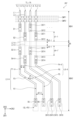
본 실시예에서, 표시패널(DP)은 제1 방향(DR1)으로 순차적으로 배열된 제1 비벤딩영역(NBA1), 벤딩영역(BA), 및 제2 비벤딩영역(NBA2)을 포함할 수 있다. 제1 비벤딩영역(NBA1)은 벤딩영역(BA)을 사이에 두고 제2 비벤딩영역(NBA2)과 제1 방향(DR1)으로 이격될 수 있다. In this embodiment, the display panel DP may include a first non-bending area (NBA1), a bending area (BA), and a second non-bending area (NBA2) sequentially arranged in the first direction DR1. there is. The first non-bending area NBA1 may be spaced apart from the second non-bending area NBA2 in the first direction DR1 with the bending area BA interposed therebetween.
제1 비벤딩영역(NBA1)은 액티브영역(DP-AA)과 주변영역(DP-NAA)의 일부를 포함할 수 있다. 벤딩영역(BA) 및 제2 비벤딩영역(NBA2)은 주변영역(NAA)의 나머지 일부를 이룰 수 있다.The first non-bending area (NBA1) may include a portion of the active area (DP-AA) and the peripheral area (DP-NAA). The bending area (BA) and the second non-bending area (NBA2) may form the remaining part of the peripheral area (NAA).
벤딩영역(BA)은 제2 방향(DR2)으로 연장된 가상의 축을 따라 벤딩될 수 있다. 벤딩영역(BA)이 벤딩되는 경우, 제2 비벤딩영역(NBA2)은 제1 비벤딩영역(NBA1)의 하측에 배치되어 제1 비벤딩영역(NBA1)과 마주할 수 있다. 일 실시예에 따르면, 표시패널(DP)의 제2 방향(DR2)에 대한 폭은 제1 비벤딩영역(NBA1)에서보다 벤딩영역(BA)에서 작을 수 있다.The bending area BA may be bent along a virtual axis extending in the second direction DR2. When the bending area BA is bent, the second non-bending area NBA2 may be disposed below the first non-bending area NBA1 and face the first non-bending area NBA1. According to one embodiment, the width of the display panel DP in the second direction DR2 may be smaller in the bending area BA than in the first non-bending area NBA1.
신호 패드부(PDP)는 제2 비벤딩영역(NBA2)의 끝 단에 인접하여 배치될 수 있다. 신호 패드부(PDP)는 표시 패드들(DP-PD) 및 감지 패드들(ISL-PD1, ISL-PD2)을 포함할 수 있다. The signal pad portion (PDP) may be disposed adjacent to the end of the second non-bending area (NBA2). The signal pad portion (PDP) may include display pads (DP-PD) and sensing pads (ISL-PD1 and ISL-PD2).
표시 패드들(DP-PD)은 표시패널(DP)의 신호 라인들(SGL)의 말단에 각각 연결될 수 있다. 표시 패드들(DP-PD)은 표시패널(DP)과 연성 회로기판(CF, 도 2 참조) 사이를 전기적으로 연결시킬 수 있다.The display pads DP-PD may be respectively connected to ends of the signal lines SGL of the display panel DP. The display pads DP-PD may electrically connect the display panel DP and the flexible circuit board CF (see FIG. 2).
감지 패드들(ISL-PD1, ISL-PD2)은 표시 패드들(DP-PD)을 사이에 두고 제2 방향(DR2)으로 서로 이격된 제1 감지 패드들(ISL-PD1) 및 제2 감지 패드들(ISL-PD2)을 포함할 수 있다. 감지 패드들(ISL-PD1, ISL-PD2)은 도 4b에서 후술할 입력센서(ISL)의 트레이스 배선들(TL)의 말단에 각각 연결될 수 있다. 감지 패드들(ISL-PD1, ISL-PD2)은 입력센서(ISL, 도 2 참조)와 연성 회로기판(CF, 도 2 참조) 사이를 전기적으로 연결시킬 수 있다.The first and second sensing pads (ISL-PD1 and ISL-PD2) are spaced apart from each other in a second direction (DR2) with the display pads (DP-PD) interposed therebetween. may include (ISL-PD2). The sensing pads (ISL-PD1 and ISL-PD2) may each be connected to the ends of the trace wires (TL) of the input sensor (ISL), which will be described later in FIG. 4B. The sensing pads (ISL-PD1, ISL-PD2) may electrically connect the input sensor (ISL, see FIG. 2) and the flexible circuit board (CF, see FIG. 2).
벤딩 라인부분들(TL-B)은 벤딩영역(BA)에서 표시패널(DP)의 절연층들 중 어느 하나에 배치될 수 있다. 벤딩 라인부분들(TL-B)은 트레이스 배선들(TL, 도 4b 참조)의 일부를 이룰 수 있다. 벤딩 라인부분들(TL-B) 각각의 일단은 제1 입력 컨택홀(CNT-I1)을 통해 대응되는 트레이스 배선(TL, 도 4b 참조) 중 제1 비벤딩영역(NBA1)에 배치된 부분과 연결될 수 있다. 또한, 벤딩 라인부분들(TL-B) 각각의 타단은 제2 입력 컨택홀(CNT-I2)을 통해 대응되는 트레이스 배선(TL, 도 4b 참조) 중 제2 비벤딩영역(NBA2)에 배치된 부분과 연결될 수 있다. The bending line portions TL-B may be disposed on any one of the insulating layers of the display panel DP in the bending area BA. The bending line portions TL-B may form part of the trace wires TL (see FIG. 4B). One end of each of the bending line portions (TL-B) is connected to a portion disposed in the first non-bending area (NBA1) among the corresponding trace wires (TL, see FIG. 4B) through the first input contact hole (CNT-I1). can be connected In addition, the other end of each of the bending line portions (TL-B) is disposed in the second non-bending area (NBA2) among the corresponding trace wires (TL, see FIG. 4B) through the second input contact hole (CNT-I2). It can be connected to a part.
표시패널(DP)은 댐 패턴들(DMP1, DMP2)을 포함할 수 있다. 댐 패턴들(DMP1, DMP2)은 제1 비벤딩영역(NBA1)의 주변영역(DP-NAA)에 배치되고 액티브영역(DP-AA)을 에워쌀 수 있다. 댐 패턴들(DMP1, DMP2) 각각은 폐-라인 형상을 가질 수 있다. 댐 패턴들(DMP1, DMP2)은 표시패널(DP)의 잉크젯 공정에 있어서 액상의 유기물이 넘치는 것을 방지하는 댐 역할을 갖는다.The display panel DP may include dam patterns DMP1 and DMP2. The dam patterns DMP1 and DMP2 may be disposed in the peripheral area DP-NAA of the first non-bending area NBA1 and may surround the active area DP-AA. Each of the dam patterns DMP1 and DMP2 may have a closed-line shape. The dam patterns DMP1 and DMP2 serve as dams to prevent liquid organic substances from overflowing during the inkjet process of the display panel DP.
도 3a는 2개의 댐 패턴들(DMP1, DMP2)을 예시적으로 도시하였으나, 댐 패턴의 개수는 어느 하나의 실시예로 한정되는 것은 아니다.Figure 3a illustrates two dam patterns (DMP1, DMP2) as examples, but the number of dam patterns is not limited to any one embodiment.
도 3b는 표시패널(DP)의 액티브영역(DP-AA)의 일부를 확대하여 도시한 단면도이다. 도 3b를 참조하면, 표시패널(DP)은 베이스층(BL), 회로 소자층(DP-CL), 표시 소자층(DP-OLED), 및 박막 봉지층(TFE)을 포함할 수 있다. FIG. 3B is an enlarged cross-sectional view of a portion of the active area DP-AA of the display panel DP. Referring to FIG. 3B, the display panel DP may include a base layer (BL), a circuit element layer (DP-CL), a display element layer (DP-OLED), and a thin film encapsulation layer (TFE).
베이스층(BL)은 회로 소자층(DP-CL), 표시 소자층(DP-OLED), 박막 봉지층(TFE)이 적층될 수 있는 기저층일 수 있다. 베이스층(BL)은 플렉서블 하거나 리지드 할 수 있으며, 어느 하나로 한정되지 않는다. 베이스층(BL)은 단층으로 제공되거나 복층 구조를 가질 수 있으며, 어느 하나로 한정되지 않는다.The base layer (BL) may be a base layer on which a circuit element layer (DP-CL), a display element layer (DP-OLED), and a thin film encapsulation layer (TFE) can be stacked. The base layer (BL) can be flexible or rigid, and is not limited to either one. The base layer (BL) may be provided as a single layer or may have a multi-layer structure, but is not limited to either one.
회로 소자층(DP-CL)은 베이스층(BL) 상에 배치될 수 있다. 회로 소자층(DP-CL)은 복수의 절연층들, 복수의 도전층들, 및 반도체층을 포함할 수 있다. 코팅, 증착 등에 의한 절연층, 반도체층, 및 도전층 형성공정과 포토리소그래피 공정에 의한 절연층, 반도체층, 및 도전층의 패터닝 공정을 통해 회로 소자층(DP-CL)이 형성될 수 있다. 회로 소자층(DP-CL)의 복수의 도전층들은 신호 라인들 또는 화소들(PX, 도 3a 참조) 각각의 제어 회로를 구성할 수 있다.The circuit element layer (DP-CL) may be disposed on the base layer (BL). The circuit element layer DP-CL may include a plurality of insulating layers, a plurality of conductive layers, and a semiconductor layer. A circuit element layer (DP-CL) may be formed through a process of forming an insulating layer, a semiconductor layer, and a conductive layer by coating, deposition, etc., and a patterning process of the insulating layer, a semiconductor layer, and a conductive layer by a photolithography process. A plurality of conductive layers of the circuit element layer DP-CL may form a control circuit for each of the signal lines or pixels PX (see FIG. 3A).
버퍼층(BFL)은 두께 방향으로 적층된 복수 개의 무기층들을 포함할 수 있다. 트랜지스터(TR)는 반도체 패턴 및 게이트(G1)를 포함하고, 반도체 패턴은 버퍼층(BFL) 상에 배치된다. 버퍼층(BFL)은 베이스층(BL)과 반도체 패턴 사이의 결합력을 향상시킨다. The buffer layer (BFL) may include a plurality of inorganic layers stacked in the thickness direction. The transistor TR includes a semiconductor pattern and a gate G1, and the semiconductor pattern is disposed on the buffer layer BFL. The buffer layer (BFL) improves the bonding strength between the base layer (BL) and the semiconductor pattern.
반도체 패턴은 폴리실리콘을 포함할 수 있다. 그러나 이에 제한되지 않고, 반도체 패턴은 비정질실리콘 또는 금속 산화물을 포함할 수도 있다. 도 3b는 일부의 반도체 패턴을 도시한 것일 뿐이고, 회로 소자층(DP-CL)은 평면 상에서 다른 영역에 배치된 반도체 패턴을 더 포함할 수 있다. 반도체 패턴은 화소들(PX, 도 3a 참조)에 걸쳐 특정한 규칙으로 배열될 수 있다. The semiconductor pattern may include polysilicon. However, the pattern is not limited thereto, and the semiconductor pattern may include amorphous silicon or metal oxide. FIG. 3B only shows some semiconductor patterns, and the circuit element layer DP-CL may further include semiconductor patterns arranged in different areas on the plane. The semiconductor pattern may be arranged in a specific rule across the pixels (PX, see FIG. 3A).
반도체 패턴은 도핑 여부에 따라 전기적 성질이 다르다. 반도체 패턴은 도핑농도 및 전도율이 낮은 제1 영역(A1)과 상대적으로 도핑농도 및 전도율이 높은 제2 영역들(S1, D1)을 포함할 수 있다. 하나의 제2 영역(S1)이 제1 영역(A1)의 일측에 배치되고, 다른 하나의 제2 영역(D1)이 제1 영역(A1)의 타측에 배치될 수 있다. 제2 영역들(S1, D1)은 N형 도판트 또는 P형 도판트로 도핑될 수 있다. P타입의 트랜지스터는 P형 도판트로 도핑된 도핑영역을 포함한다. 제1 영역(A1)은 비-도핑영역이거나, 제2 영역들(S1, D1) 대비 낮은 농도로 도핑될 수 있다.Semiconductor patterns have different electrical properties depending on whether they are doped or not. The semiconductor pattern may include a first region (A1) with low doping concentration and conductivity and second regions (S1 and D1) with relatively high doping concentration and conductivity. One second area S1 may be placed on one side of the first area A1, and another second area D1 may be placed on the other side of the first area A1. The second regions S1 and D1 may be doped with an N-type dopant or a P-type dopant. A P-type transistor includes a doped region doped with a P-type dopant. The first area A1 may be a non-doped area or may be doped at a lower concentration than the second areas S1 and D1.
제2 영역들(S1, D1) 각각은 실질적으로 전극 또는 신호 라인의 역할을 갖는다. 하나의 제2 영역(S1)이 트랜지스터(TR)의 소스에 해당하고 다른 하나의 제2 영역(D1)이 트랜지스터(TR)의 드레인에 해당할 수 있다. 도 3b에는 반도체 패턴으로부터 형성된 연결 신호 라인(SCL)의 일부분을 도시하였다. 별도로 도시하지 않았으나, 연결 신호 라인(SCL)은 평면상에서 트랜지스터(TR)의 드레인에 연결될 수 있다.Each of the second regions S1 and D1 substantially functions as an electrode or signal line. One second region S1 may correspond to the source of the transistor TR and the other second region D1 may correspond to the drain of the transistor TR. Figure 3b shows a portion of a connection signal line (SCL) formed from a semiconductor pattern. Although not separately shown, the connection signal line (SCL) may be connected to the drain of the transistor (TR) on a plane.
제1 절연층(10)은 버퍼층(BFL) 상에 배치될 수 있다. 제1 절연층(10)은 복수 개의 화소들(PX, 도 3a 참조)에 공통으로 중첩하며, 반도체 패턴을 커버한다. 제1 절연층(10)은 무기층 및/또는 유기층일 수 있으며, 단층 또는 다층 구조를 가질 수 있다. 제1 절연층(10)은 알루미늄 옥사이드, 티타늄 옥사이드, 실리콘 옥사이드, 실리콘 옥시나이트라이드, 지르코늄 옥사이드, 및 하프늄 옥사이드 중 적어도 하나를 포함할 수 있다. 제1 절연층(10)뿐만 아니라 후술하는 회로 소자층(DP-CL)의 절연층은 무기층 및/또는 유기층일 있으며, 단층 또는 다층 구조를 가질 수 있다. The first insulating
게이트(G1)는 제1 절연층(10) 상에 배치된다. 게이트(G1)는 금속 패턴의 일부분일 수 있다. 게이트(G1)는 제1 영역(A1)에 중첩한다. 반도체 패턴을 도핑하는 공정에서 게이트(G1)는 마스크로 기능할 수 있다.The gate G1 is disposed on the first insulating
제2 절연층(20)은 제1 절연층(10) 상에 배치되며, 게이트(G1)를 커버할 수 있다. 제2 절연층(20)은 화소들(PX, 도 3a 참조)에 공통으로 중첩한다. 상부전극(UE)은 제2 절연층(20) 상에 배치될 수 있다. 상부전극(UE)은 게이트(G1)와 중첩할 수 있다. 상부전극(UE)은 다층의 금속층을 포함할 수 있다. 본 발명의 일 실시예에서 상부전극(UE)은 생략될 수도 있다.The second insulating
제3 절연층(30)은 제2 절연층(20) 상에 배치되며, 상부전극(UE)을 커버할 수 있다. 제1 연결전극(CNE1)은 제3 절연층(30) 상에 배치될 수 있다. 제1 연결전극(CNE1)은 제1 내지 제3 절연층들(10 내지 30)을 관통하는 컨택홀(CNT-1)을 통해 연결 신호 라인(SCL)에 접속될 수 있다. The third insulating
제4 절연층(40)은 제3 절연층(30) 상에 배치되고, 제5 절연층(50)은 제4 절연층(40) 상에 배치될 수 있다. 제5 절연층(50)은 유기층일 수 있다. 제5 절연층(50)은 "제1 유기 절연층"으로 지칭될 수 있다. The fourth insulating
제2 연결전극(CNE2)은 제5 절연층(50) 상에 배치될 수 있다. 제2 연결전극(CNE2)은 제4 및 제5 절연층들(40, 50)을 관통하는 컨택홀(CNT-2)을 통해 제1 연결전극(CNE1)에 접속될 수 있다. The second connection electrode CNE2 may be disposed on the fifth insulating
제6 절연층(60)은 제5 절연층(50) 상에 배치되며, 제2 연결전극(CNE2)을 커버할 수 있다. 제6 절연층(60)은 유기층일 수 있다. 제6 절연층(60)은 "제2 유기 절연층"으로 지칭될 수 있다. 도 3a에서 설명한 벤딩 라인부분들(TL-B)은 제2 연결전극(CNE2)과 동일한 층 상에 배치될 수 있다.The sixth insulating
표시 소자층(DP-OLED)은 발광소자(OLED) 및 화소 정의막(PDL)을 포함한다. 발광소자(OLED)는 제6 절연층(60) 상에 배치될 수 있다. 발광소자(OLED)는 하부전극(AE), 정공 제어층(HCL), 발광층(EML), 전자 제어층(ECL), 및 상부전극(CE)을 포함할 수 있다. The display device layer (DP-OLED) includes a light emitting device (OLED) and a pixel defining layer (PDL). A light emitting device (OLED) may be disposed on the sixth insulating
하부전극(AE)은 제6 절연층(60) 상에 배치될 수 있다. 하부전극(AE)은 제6 절연층(60)을 관통하는 컨택홀(CNT-3)을 통해 제2 연결전극(CNE2)에 연결된다.The lower electrode AE may be disposed on the sixth insulating
화소 정의막(PDL)은 제6 절연층(60) 상에 배치될 수 있다. 화소 정의막(PDL)에는 발광 개구부(OP)가 정의되어, 화소 정의막(PDL)은 하부전극(AE)의 적어도 일부분을 노출시킨다. 화소 정의막(PDL)은 유기층일 수 있다.The pixel defining layer (PDL) may be disposed on the sixth insulating
도 3b에 도시된 것과 같이, 액티브영역(DP-AA)은 발광영역(PXA)과 발광영역(PXA)에 인접한 비발광영역(NPXA)을 포함할 수 있다. 본 실시예에서, 발광영역(PXA)은 발광 개구부(OP)에 의해 노출된 하부전극(AE)의 일부 영역에 대응하게 정의될 수 있다. 비발광영역(NPXA)은 발광영역(PXA)을 에워쌀 수 있다.As shown in FIG. 3B, the active area (DP-AA) may include a light-emitting area (PXA) and a non-emission area (NPXA) adjacent to the light-emitting area (PXA). In this embodiment, the light emitting area PXA may be defined to correspond to a partial area of the lower electrode AE exposed by the light emitting opening OP. The non-emissive area (NPXA) may surround the emissive area (PXA).
정공 제어층(HCL)은 발광영역(PXA)과 비발광영역(NPXA)에 공통으로 배치될 수 있다. 정공 제어층(HCL)은 정공 수송층을 포함하고, 정공 주입층을 더 포함할 수 있다. 정공 제어층(HCL) 상에 발광층(EML)이 배치될 수 있다. 발광층(EML)은 발광 개구부(OP)에 대응하는 영역에 배치될 수 있다. 즉, 발광층(EML)은 화소들(PX, 도 3a 참조) 각각에 분리되어 형성될 수 있다. The hole control layer (HCL) may be commonly disposed in the emission area (PXA) and the non-emission area (NPXA). The hole control layer (HCL) includes a hole transport layer and may further include a hole injection layer. An emission layer (EML) may be disposed on the hole control layer (HCL). The light emitting layer (EML) may be disposed in an area corresponding to the light emitting opening (OP). That is, the light emitting layer (EML) may be formed separately in each of the pixels (PX, see FIG. 3A).
발광층(EML) 상에 전자 제어층(ECL)이 배치될 수 있다. 전자 제어층(ECL)은 발광영역(PXA) 및 비발광영역(NPXA)에 공통으로 배치될 수 있다. 전자 제어층(ECL)은 전자 수송층을 포함하고, 전자 주입층을 더 포함할 수 있다. 정공 제어층(HCL)과 전자 제어층(ECL)은 오픈 마스크를 이용하여 복수 개의 화소들(PX, 도 3a 참조)에 공통으로 형성될 수 있다. An electronic control layer (ECL) may be disposed on the light emitting layer (EML). The electronic control layer (ECL) may be commonly disposed in the emitting area (PXA) and the non-emitting area (NPXA). The electronic control layer (ECL) includes an electron transport layer and may further include an electron injection layer. The hole control layer (HCL) and the electronic control layer (ECL) may be commonly formed in a plurality of pixels (PX, see FIG. 3A) using an open mask.
상부전극(CE)은 전자 제어층(ECL) 상에 배치될 수 있다. 상부전극(CE)은 일체의 형상을 갖고, 복수 개의 화소들(PX, 도 3a 참조)에 공통적으로 배치될 수 있다.The upper electrode (CE) may be disposed on the electronic control layer (ECL). The upper electrode CE has an integrated shape and may be commonly disposed in a plurality of pixels PX (see FIG. 3A).
박막 봉지층(TFE)은 표시 소자층(DP-OLED) 상에 배치되며, 복수 개의 박막들을 포함할 수 있다. 일 실시예에 따르면, 박막 봉지층(TFE)은 제1 봉지 무기층(IOL1), 제1 봉지 무기층(IOL1) 상에 배치된 봉지 유기층(OL), 및 봉지 유기층(OL) 상에 배치된 제2 봉지 무기층(IOL2)을 포함할 수 있다. 제1 봉지 무기층(IOL1) 및 제2 봉지 무기층(IOL2)은 수분/산소로부터 표시 소자층(DP-OLED)을 보호하고, 봉지 유기층(OL)은 먼지 입자와 같은 이물질로부터 표시 소자층(DP-OLED)을 보호할 수 있다.The thin film encapsulation layer (TFE) is disposed on the display element layer (DP-OLED) and may include a plurality of thin films. According to one embodiment, the thin film encapsulation layer (TFE) includes a first encapsulation inorganic layer (IOL1), an encapsulation organic layer (OL) disposed on the first encapsulation inorganic layer (IOL1), and an encapsulation organic layer (OL) disposed on the encapsulation organic layer (OL). It may include a second encapsulation inorganic layer (IOL2). The first encapsulation inorganic layer (IOL1) and the second encapsulation inorganic layer (IOL2) protect the display device layer (DP-OLED) from moisture/oxygen, and the encapsulation organic layer (OL) protects the display device layer (DP-OLED) from foreign substances such as dust particles. DP-OLED) can be protected.
도 4a는 본 발명의 일 실시예에 따른 표시모듈의 단면도이다. 도 4b는 본 발명의 일 실시예에 따른 입력센서의 평면도이다. 도 1 내지 도 3b에서 설명한 구성과 동일/유사한 구성에 대해 동일/유사한 참조 부호를 사용하며, 중복된 설명은 생략한다.Figure 4a is a cross-sectional view of a display module according to an embodiment of the present invention. Figure 4b is a top view of an input sensor according to an embodiment of the present invention. The same/similar reference numerals are used for components that are the same/similar to those described in FIGS. 1 to 3B, and duplicate descriptions are omitted.
도 4a를 참조하면, 표시모듈(DM)은 표시패널(DP) 및 표시패널(DP) 상에 배치된 입력센서(ISL)를 포함할 수 있다. 입력센서(ISL)는 박막 봉지층(TFE) 상에 배치될 수 있다. 입력센서(ISL)는 제1 감지 절연층(TIL1), 제1 감지 도전층(TML1), 제2 감지 절연층(TIL2), 및 제2 감지 도전층(TML2)을 포함할 수 있다. Referring to FIG. 4A, the display module DM may include a display panel DP and an input sensor ISL disposed on the display panel DP. The input sensor (ISL) may be disposed on the thin film encapsulation layer (TFE). The input sensor ISL may include a first sensing insulating layer (TIL1), a first sensing conductive layer (TML1), a second sensing insulating layer (TIL2), and a second sensing conductive layer (TML2).
제1 감지 절연층(TIL1)은 박막 봉지층(TFE) 상에 직접 배치될 수 있다. 일 실시예에 따르면, 제1 감지 절연층(TIL1)은 제2 봉지 무기층(IOL2, 도 3b 참조) 상에 배치될 수 있다. 제2 감지 절연층(TIL2)은 제1 감지 절연층(TIL1) 상에 배치될 수 있다. 한편, 입력센서(ISL)의 일 실시예에 따라 제1 감지 절연층(TIL1)은 생략될 수 있다.The first sensing insulating layer (TIL1) may be directly disposed on the thin film encapsulation layer (TFE). According to one embodiment, the first sensing insulating layer (TIL1) may be disposed on the second encapsulating inorganic layer (IOL2 (see FIG. 3B)). The second sensing insulating layer TIL2 may be disposed on the first sensing insulating layer TIL1. Meanwhile, according to one embodiment of the input sensor (ISL), the first sensing insulating layer (TIL1) may be omitted.
제1 및 제2 감지 절연층들(TIL1, TIL2) 각각은 무기막 또는 유기막을 포함할 수 있다. 일 실시예에서, 제1 감지 절연층(TIL1)은 무기물로 이루어진 무기막을 포함할 수 있다. 무기막은 알루미늄 옥사이드, 티타늄 옥사이드, 실리콘 옥사이드 실리콘 옥시나이트라이드, 지르코늄 옥사이드, 및 하프늄 옥사이드 중 적어도 하나를 포함할 수 있다. 제2 감지 절연층(TIL2)은 유기물로 이루어진 유기막을 포함할 수 있다. 유기막은 아크릴계 수지, 메타크릴계 수지, 폴리이소프렌, 비닐계 수지, 에폭시계 수지, 우레탄계 수지, 셀룰로오스계 수지, 실록산계 수지, 폴리이미드계 수지, 폴리아미드계 수지, 및 페릴렌계 수지 중 적어도 하나를 포함할 수 있다.Each of the first and second sensing insulating layers TIL1 and TIL2 may include an inorganic layer or an organic layer. In one embodiment, the first sensing insulating layer TIL1 may include an inorganic layer made of an inorganic material. The inorganic film may include at least one of aluminum oxide, titanium oxide, silicon oxide, silicon oxynitride, zirconium oxide, and hafnium oxide. The second sensing insulating layer TIL2 may include an organic layer made of an organic material. The organic film includes at least one of acrylic resin, methacrylic resin, polyisoprene, vinyl resin, epoxy resin, urethane resin, cellulose resin, siloxane resin, polyimide resin, polyamide resin, and perylene resin. It can be included.
제1 감지 도전층(TML1)은 제1 감지 절연층(TIL1) 상에 배치되고, 제2 감지 절연층(TIL2)에 의해 커버될 수 있다. 제2 감지 도전층(TML2)은 제2 감지 절연층(TIL2) 상에 배치될 수 있다. 본 실시예에서, 제2 감지 도전층(TML2)은 입력센서(ISL)의 최상부에 배치될 수 있다. The first sensing conductive layer (TML1) may be disposed on the first sensing insulating layer (TIL1) and covered by the second sensing insulating layer (TIL2). The second sensing conductive layer (TML2) may be disposed on the second sensing insulating layer (TIL2). In this embodiment, the second sensing conductive layer (TML2) may be disposed on top of the input sensor (ISL).
제1 및 제2 감지 도전층들(TML1, TML2) 각각은 단층 구조를 갖거나, 다층 구조를 가질 수 있다. 다층 구조의 도전층은 투명 도전층 및 금속층의 조합으로 이루어질 수 있다. 다층 구조의 도전층은 서로 다른 금속을 포함하는 금속층들을 포함할 수 있다. Each of the first and second sensing conductive layers TML1 and TML2 may have a single-layer structure or a multi-layer structure. The multi-layered conductive layer may be composed of a combination of a transparent conductive layer and a metal layer. The multi-layered conductive layer may include metal layers containing different metals.
제1 및 제2 감지 도전층들(TML1, TML2) 각각은 투명 도전층으로 인듐 주석 산화물(ITO, indium tin oxide), 인듐 아연 산화물(IZO, indium zinc oxide), 아연 산화물(ZnO, zinc oxide), 인듐 주석 아연 산화물(ITZO, indium tin zinc oxide), 폴리에틸렌디옥시티오펜(PEDOT, polyethylenedioxythiophene), 금속 나노 와이어, 및 그래핀 중 적어도 하나를 포함할 수 있다. 제1 및 제2 감지 도전층들(TML1, TML2) 각각은 금속층으로 몰리브덴(Mo), 은(Ag), 티타늄(Ti), 구리(Cu), 알루미늄(Al), 및 이들의 합금을 포함할 수 있다. Each of the first and second sensing conductive layers (TML1 and TML2) is a transparent conductive layer made of indium tin oxide (ITO), indium zinc oxide (IZO), and zinc oxide (ZnO). , indium tin zinc oxide (ITZO), polyethylenedioxythiophene (PEDOT), metal nanowire, and graphene. Each of the first and second sensing conductive layers (TML1, TML2) is a metal layer and may include molybdenum (Mo), silver (Ag), titanium (Ti), copper (Cu), aluminum (Al), and alloys thereof. You can.
예를 들어, 제1 및 제2 감지 도전층들(TML1, TML2) 각각은 티타늄/알루미늄/티타늄으로 구성된 3층 구조를 가질 수 있다. 상대적으로 내구성이 높고 반사율이 낮은 금속을 도전층의 외층에 적용할 수 있고, 전기 전도율이 높은 금속을 도전층의 내층에 적용할 수 있다.For example, each of the first and second sensing conductive layers TML1 and TML2 may have a three-layer structure made of titanium/aluminum/titanium. A metal with relatively high durability and low reflectivity can be applied to the outer layer of the conductive layer, and a metal with high electrical conductivity can be applied to the inner layer of the conductive layer.
도 4b를 참조하면, 입력센서(ISL)는 액티브영역(IS-AA) 및 액티브영역(IS-AA)에 인접한 주변영역(IS-NAA)으로 구분될 수 있다. 입력센서(ISL)의 액티브영역(IS-AA) 및 주변영역(IS-NAA)은 각각 표시패널(DP, 도 3a 참조)의 액티브영역(DP-AA, 도 3a 참조) 및 주변영역(DP-NAA, 도 3a 참조)과 대응될 수 있다. 도 4b에는 설명의 편의를 위해 표시패널(DP, 도 3a 참조)의 제1 비벤딩영역(NBA1), 벤딩영역(BA), 및 제2 비벤딩영역(NBA2)을 표시하였다.Referring to FIG. 4B, the input sensor (ISL) can be divided into an active area (IS-AA) and a surrounding area (IS-NAA) adjacent to the active area (IS-AA). The active area (IS-AA) and surrounding area (IS-NAA) of the input sensor (ISL) are the active area (DP-AA, see Figure 3a) and the surrounding area (DP-AA) of the display panel (DP, see Figure 3a), respectively. NAA, see Figure 3a). In FIG. 4B , the first non-bending area (NBA1), the bending area (BA), and the second non-bending area (NBA2) of the display panel (DP, see FIG. 3A) are shown for convenience of explanation.
일 실시예에 따르면, 입력센서(ISL)는 복수의 감지 전극들(TE1, TE2) 및 감지 전극들(TE1, TE2)에 각각 연결되는 복수의 트레이스 배선들(TL)을 포함할 수 있다. 감지 전극들(TE1, TE2)은 제1 감지 전극들(TE1) 및 제2 감지 전극들(TE2)을 포함할 수 있다. According to one embodiment, the input sensor ISL may include a plurality of sensing electrodes TE1 and TE2 and a plurality of trace wires TL connected to the sensing electrodes TE1 and TE2, respectively. The sensing electrodes TE1 and TE2 may include first sensing electrodes TE1 and second sensing electrodes TE2.
제1 감지 전극들(TE1)은 제1 방향(DR1)으로 연장되고, 제2 방향(DR2)을 따라 배열될 수 있다. 제1 감지 전극들(TE1)은 제1 감지 패턴들(SP1) 및 제1 도전 패턴들(BP1)을 포함할 수 있다. 제1 감지 패턴들(SP1)은 제1 방향(DR1)을 따라 배열될 수 있다. 적어도 하나의 제1 도전 패턴(BP1)은 서로 인접한 두 개의 제1 감지 패턴들(SP1)에 연결될 수 있고, "연결 패턴"으로 지칭될 수 있다. The first sensing electrodes TE1 may extend in the first direction DR1 and be arranged along the second direction DR2. The first sensing electrodes TE1 may include first sensing patterns SP1 and first conductive patterns BP1. The first sensing patterns SP1 may be arranged along the first direction DR1. At least one first conductive pattern BP1 may be connected to two adjacent first sensing patterns SP1 and may be referred to as a “connection pattern.”
제2 감지 전극들(TE2)은 제2 방향(DR2)으로 연장되고, 제1 방향(DR1)을 따라 배열될 수 있다. 제2 감지 전극들(TE2)은 제2 감지 패턴들(SP2) 및 제2 도전 패턴들(BP2)을 포함할 수 있다. 제2 감지 패턴들(SP2)은 제2 방향(DR2)을 따라 배열될 수 있다. 적어도 하나의 제2 도전 패턴(BP2)은 서로 인접한 두 개의 제2 감지 패턴들(SP2) 사이에 배치될 수 있다. 일 실시예에 따르면, 제2 감지 패턴들(SP2) 및 제2 도전 패턴들(BP2)은 동일 공정에 의해 패터닝 되는 일체 형상의 패턴일 수 있다.The second sensing electrodes TE2 may extend in the second direction DR2 and be arranged along the first direction DR1. The second sensing electrodes TE2 may include second sensing patterns SP2 and second conductive patterns BP2. The second sensing patterns SP2 may be arranged along the second direction DR2. At least one second conductive pattern BP2 may be disposed between two adjacent second sensing patterns SP2. According to one embodiment, the second sensing patterns SP2 and the second conductive patterns BP2 may be an integrated pattern patterned through the same process.
일 실시예에 따르면, 제1 감지 패턴들(SP1), 제2 감지 패턴들(SP2), 및 제2 도전 패턴들(BP2)은 도 4a에서 설명한 제1 감지 도전층(TML1)에 포함될 수 있다. 즉, 제1 감지 패턴들(SP1), 제2 감지 패턴들(SP2), 및 제2 도전 패턴들(BP2)은 제1 감지 절연층(TIL1)에 배치되고, 제2 감지 절연층(TIL2)에 의해 커버될 수 있다. 제1 도전 패턴들(BP1)은 도 4a에서 설명한 제2 감지 도전층(TML2)에 포함될 수 있다. 즉, 제1 도전 패턴들(BP1)은 제2 감지 절연층(TIL2)에 배치되어, 입력센서(ISL)의 최상부에 배치될 수 있다.According to one embodiment, the first sensing patterns SP1, the second sensing patterns SP2, and the second conductive patterns BP2 may be included in the first sensing conductive layer TML1 described in FIG. 4A. . That is, the first sensing patterns SP1, the second sensing patterns SP2, and the second conductive patterns BP2 are disposed on the first sensing insulating layer TIL1, and the second sensing insulating layer TIL2 It can be covered by . The first conductive patterns BP1 may be included in the second sensing conductive layer TML2 described in FIG. 4A. That is, the first conductive patterns BP1 may be disposed on the second sensing insulating layer TIL2 and on top of the input sensor ISL.
본 발명에 따르면, 입력센서(ISL)는 제2 감지 도전층(TML2)을 커버하는 별도의 절연층을 형성하기 위한 마스크 공정을 생략함으로써, 표시모듈(DM)의 제조 공정을 단순화 할 수 있고, 원가가 절감된 표시모듈(DM)이 제공될 수 있다. According to the present invention, the input sensor (ISL) can simplify the manufacturing process of the display module (DM) by omitting the mask process for forming a separate insulating layer covering the second sensing conductive layer (TML2), A cost-reduced display module (DM) can be provided.
다만, 제2 감지 도전층(TML2)이 절연층에 의해 커버되지 않음에 따라, 외부의 충격 또는 외부로부터 유입된 이물에 의해 손상될 가능성이 높아질 수 있으나, 본 발명에 따라, 제1 감지 패턴들(SP1) 및 제2 감지 전극들(TE2)을 제1 감지 절연층(TIL1)에 배치하고 제1 도전 패턴들(BP1)을 제2 감지 절연층(TIL2)에 배치함으로써, 감지 전극들(TE1, TE2)의 손상을 최소화할 수 있다. 이때, 단면 상에서, 제1 감지 패턴들(SP1), 제2 감지 패턴들(SP2), 및 제2 도전 패턴들(BP2) 각각의 두께는 제1 도전 패턴들(BP1) 각각의 두께보다 두꺼울 수 있다.However, as the second sensing conductive layer (TML2) is not covered by the insulating layer, the possibility of damage from external impact or foreign substances introduced from the outside may increase. However, according to the present invention, the first sensing patterns By disposing (SP1) and the second sensing electrodes (TE2) on the first sensing insulating layer (TIL1) and disposing the first conductive patterns (BP1) on the second sensing insulating layer (TIL2), the sensing electrodes (TE1) , TE2) damage can be minimized. At this time, in cross section, the thickness of each of the first sensing patterns SP1, the second sensing patterns SP2, and the second conductive patterns BP2 may be thicker than the thickness of each of the first conductive patterns BP1. there is.
트레이스 배선들(TL)은 감지 전극들(TE1, TE2)로부터 각각 연장될 수 있다. 트레이스 배선들(TL)은 감지 전극들(TE1, TE2)과 감지 패드들(ISL-PD1, ISL-PD2)을 각각 전기적으로 연결시킬 수 있다. 이를 통해, 감지 전극들(TE1, TE2)은 연성 회로기판(CF, 도 2 참조)을 통해 메인 회로기판(MB, 도 2 참조)과 전기적으로 연결될 수 있다. The trace wires TL may extend from the sensing electrodes TE1 and TE2, respectively. The trace wires TL may electrically connect the sensing electrodes TE1 and TE2 and the sensing pads ISL-PD1 and ISL-PD2, respectively. Through this, the sensing electrodes TE1 and TE2 can be electrically connected to the main circuit board (MB, see FIG. 2) through the flexible circuit board (CF, see FIG. 2).
트레이스 배선들(TL) 각각은 제1 비벤딩영역(NBA1)에서 제1 및 제2 감지 절연층들(TIL1, TIL2, 도 4a 참조) 중 어느 하나에 배치되는 상측 부분, 벤딩영역(BA)에서 표시패널(DP, 도 3a 참조)의 절연층들 중 어느 하나에 배치되는 연결 부분, 및 제2 비벤딩영역(NBA2)에서 제1 및 제2 감지 절연층들(TIL1, TIL2, 도 4a 참조) 중 어느 하나에 배치되는 하측 부분을 포함할 수 있다. Each of the trace wires TL is disposed on one of the first and second sensing insulating layers TIL1 and TIL2 (see FIG. 4A) in the first non-bending area NBA1, and in the bending area BA. A connection portion disposed on one of the insulating layers of the display panel (DP, see FIG. 3A), and the first and second sensing insulating layers (TIL1, TIL2, see FIG. 4A) in the second non-bending area (NBA2) It may include a lower portion disposed on any one of them.
도 4b에는 상측 부분 및 하측 부분은 실선으로 도시하고, 연결 부분은 점선으로 도시하였다. 도 4b의 연결 부분은 도 3a에서 전술한 벤딩 라인부분들(TL-B)과 대응될 수 있다.In Figure 4b, the upper and lower parts are shown with solid lines, and the connecting parts are shown with dotted lines. The connection portion of FIG. 4B may correspond to the bending line portions TL-B described above in FIG. 3A.
상측 부분 및 연결 부분은 제1 비벤딩영역(NBA1)에서 제1 입력 컨택홀(CNT-I1)에 의해 연결되고, 연결 부분 및 하측 부분은 제2 비벤딩영역(NBA2)에서 제2 입력 컨택홀(CNT-I2)에 의해 연결될 수 있다. The upper part and the connection part are connected by a first input contact hole (CNT-I1) in the first non-bending area (NBA1), and the connection part and the lower part are connected by a second input contact hole in the second non-bending area (NBA2). It can be connected by (CNT-I2).
일 실시예에 따르면, 트레이스 배선들(TL)은 제1 내지 제4 그룹 배선들(TL-1, TL-2, TL-3, TL-4)을 포함할 수 있다.According to one embodiment, the trace wires TL may include first to fourth group wires TL-1, TL-2, TL-3, and TL-4.
제1 그룹 배선들(TL-1)은 제2 감지 전극들(TE2) 일부의 일단들에 각각 전기적으로 연결될 수 있다. 제2 그룹 배선들(TL-2)은 제2 감지 전극들(TE2)의 나머지 일부의 타단들에 각각 전기적으로 연결될 수 있다. The first group wires TL-1 may each be electrically connected to ends of some of the second sensing electrodes TE2. The second group wires TL-2 may each be electrically connected to other ends of the remaining portions of the second sensing electrodes TE2.
예를 들어, 제1 그룹 배선들(TL-1)은 제2 감지 전극들(TE2) 중 좌측 하단에 배치된 제2 감지 전극들의 일단에 전기적으로 연결되고, 제2 그룹 배선들(TL-2)은 제2 감지 전극들(TE2) 중 우측 상단에 배치된 제2 감지 전극들의 타단에 전기적으로 연결될 수 있다.For example, the first group wires TL-1 are electrically connected to one end of the second sensing electrodes disposed at the lower left of the second sensing electrodes TE2, and the second group wires TL-2 ) may be electrically connected to the other end of the second sensing electrodes TE2 disposed at the upper right.
제3 그룹 배선들(TL-3)은 제1 감지 전극들(TE1) 일부의 일단들에 각각 전기적으로 연결될 수 있다. 제4 그룹 배선들(TL-4)은 제1 감지 전극들(TE1)의 나머지 일부의 일단들에 각각 전기적으로 연결될 수 있다. 제3 및 제4 그룹 배선들(TL-3, TL-4)이 전기적으로 연결된 제1 감지 전극들(TE1)의 일단들은 벤딩영역(BA)에 인접한 부분일 수 있다. The third group wires TL-3 may each be electrically connected to ends of some of the first sensing electrodes TE1. The fourth group wires TL-4 may each be electrically connected to the remaining ends of the first sensing electrodes TE1. Ends of the first sensing electrodes TE1 to which the third and fourth group wires TL-3 and TL-4 are electrically connected may be adjacent to the bending area BA.
예를 들어, 제3 그룹 배선들(TL-3)은 제1 감지 전극들(TE1) 중 좌측에 배치된 제1 감지 전극들의 일단에 전기적으로 연결되고, 제4 그룹 배선들(TL-4)은 제1 감지 전극들(TE1) 중 우측에 배치된 제1 감지 전극들의 일단에 전기적으로 연결될 수 있다.For example, the third group wires (TL-3) are electrically connected to one end of the first sensing electrodes disposed on the left among the first sensing electrodes (TE1), and the fourth group wires (TL-4) may be electrically connected to one end of the first sensing electrodes TE1 disposed on the right side.
제1 내지 제4 그룹 배선들(TL-1, TL-2, TL-3, TL-4) 각각의 상측 부분은 제1 비벤딩영역(NBA1)에서 감지 전극들(TE1, TE2) 중 대응되는 감지 전극으로부터 벤딩영역(BA)과 가까워지도록 연장될 수 있다. The upper portion of each of the first to fourth group wires (TL-1, TL-2, TL-3, and TL-4) corresponds to a corresponding one of the sensing electrodes (TE1, TE2) in the first non-bending area (NBA1). It may extend from the sensing electrode to be close to the bending area (BA).
예를 들어, 제1 및 제3 그룹 배선들(TL-1, TL-3) 각각의 상측 부분은 감지 전극들(TE1, TE2)과 댐 패턴들(DMP1, DMP2) 사이에서 제1 비벤딩영역(NBA1)의 좌측 엣지와 인접한 좌측 부분에 배치될 수 있다. 제2 및 제4 그룹 배선들(TL-2, TL-4) 각각의 상측 부분은 감지 전극들(TE1, TE2)과 댐 패턴들(DMP1, DMP2) 사이에서 제1 비벤딩영역(NBA1)의 우측 엣지와 인접한 우측 부분에 배치될 수 있다. 제1 내지 제4 그룹 배선들(TL-1, TL-2, TL-3, TL-4) 각각의 상측 부분은 평면 상에서 감지 전극들(TE1, TE2)과 댐 패턴들(DMP1, DMP2) 사이에서부터 벤딩영역(BA)과 가까워지는 제1 방향(DR1)으로 연장될 수 있다.For example, the upper portion of each of the first and third group wires TL-1 and TL-3 is a first non-bending area between the sensing electrodes TE1 and TE2 and the dam patterns DMP1 and DMP2. It can be placed on the left side adjacent to the left edge of (NBA1). The upper portion of each of the second and fourth group wires (TL-2, TL-4) is located between the sensing electrodes (TE1, TE2) and the dam patterns (DMP1, DMP2) of the first non-bending area (NBA1). It can be placed on the right side adjacent to the right edge. The upper portion of each of the first to fourth group wires (TL-1, TL-2, TL-3, and TL-4) is between the sensing electrodes (TE1, TE2) and the dam patterns (DMP1, DMP2) on a plane. It may extend in a first direction DR1 approaching the bending area BA.
제1 내지 제4 그룹 배선들(TL-1, TL-2, TL-3, TL-4) 각각의 하측 부분은 감지 패드들(ISL-PD1, ISL-PD2) 중 대응되는 감지 패드에 연결될 수 있다. 예를 들어, 제1 및 제3 그룹 배선들(TL-1, TL-3) 각각의 하측 부분은 제1 감지 패드들(ISL-PD1) 중 대응되는 제1 감지 패드에 전기적으로 연결되고, 제2 및 제4 그룹 배선들(TL-2, TL-4) 각각의 하측 부분은 제2 감지 패드들(ISL-PD2) 중 대응되는 제2 감지 패드에 전기적으로 연결될 수 있다.The lower portion of each of the first to fourth group wires (TL-1, TL-2, TL-3, and TL-4) may be connected to a corresponding sensing pad among the sensing pads (ISL-PD1 and ISL-PD2). there is. For example, the lower portion of each of the first and third group wires TL-1 and TL-3 is electrically connected to the corresponding first sensing pad among the first sensing pads ISL-PD1, and the The lower portions of each of the second and fourth group wires TL-2 and TL-4 may be electrically connected to a corresponding second sensing pad among the second sensing pads ISL-PD2.
제1 내지 제4 그룹 배선들(TL-1, TL-2, TL-3, TL-4) 각각의 하측 부분은 제3 입력 컨택홀(CNT-I3)에 의해 대응되는 감지 패드에 연결될 수 있다.The lower portion of each of the first to fourth group wires (TL-1, TL-2, TL-3, and TL-4) may be connected to the corresponding sensing pad by the third input contact hole (CNT-I3). .
일 실시예에서, 제1 내지 제4 그룹 배선들(TL-1, TL-2, TL-3, TL-4) 각각의 하측 부분은 제1 방향(DR1)으로 연장된 부분 및 제1 방향(DR1)의 사선 방향으로 연장된 부분을 포함할 수 있다. 트레이스 배선들(TL)의 자세한 형상은 후술한다.In one embodiment, the lower portion of each of the first to fourth group wires TL-1, TL-2, TL-3, and TL-4 has a portion extending in the first direction DR1 and a portion extending in the first direction DR1. It may include a portion extending in the diagonal direction of DR1). The detailed shape of the trace wires TL will be described later.
도 5는 도 4b의 PP' 영역을 확대한 본 발명의 일 실시예에 따른 표시모듈의 일부 구성의 평면도이다. 도 6a는 도 5의 I-I'을 따라 절단한 본 발명의 일 실시예에 따른 표시모듈의 단면도이다. 도 6b는 도 5의 II-II'을 따라 절단한 본 발명의 일 실시예에 따른 표시모듈의 단면도이다. Figure 5 is a plan view of a partial configuration of a display module according to an embodiment of the present invention, enlarging the area PP' of Figure 4b. FIG. 6A is a cross-sectional view of a display module according to an embodiment of the present invention taken along line II' of FIG. 5. FIG. 6B is a cross-sectional view of a display module according to an embodiment of the present invention taken along line II-II' of FIG. 5.
도 5에는 도 4b에 도시한 트레이스 배선들(TL) 중 제1 그룹 배선들(TL-1)의 일부를 도시한 것이다. 도 5는 제1 그룹 배선들(TL-1)만을 예시적으로 도시한 것으로, 이하, 제1 그룹 배선들(TL-1)에 대한 설명은 제2 내지 제4 그룹 배선들(TL-2, TL-3, TL-4, 도 4b 참조)에도 동일/유사하게 적용될 수 있다. 도 6a는 제1 비벤딩영역(NBA1)의 주변영역(NAA)에 해당하는 표시모듈(DM)의 단면을 도시한 것이며, 도 6b는 제1 비벤딩영역(NBA1)의 주변영역(NAA) 일부, 벤딩영역(BA), 및 제2 비벤딩영역(NBA2)에 해당하는 표시모듈(DM)의 단면을 도시한 것이다. 이하, 도 5 내지 도 6b를 참조하여, 주변영역(NAA)에서의 표시모듈(DM)의 적층구조 및 트레이스 배선들(TL)의 구성 및 형상을 자세히 설명한다.FIG. 5 shows a portion of the first group wires TL-1 among the trace wires TL shown in FIG. 4B. FIG. 5 illustrates only the first group wires TL-1. Hereinafter, the first group wires TL-1 will be described with reference to the second to fourth group wires TL-2, It can be applied equally/similarly to TL-3, TL-4, see FIG. 4b). FIG. 6A shows a cross-section of the display module DM corresponding to the peripheral area (NAA) of the first non-bending area (NBA1), and FIG. 6B shows a portion of the peripheral area (NAA) of the first non-bending area (NBA1). , a cross section of the display module (DM) corresponding to the bending area (BA) and the second non-bending area (NBA2) is shown. Hereinafter, with reference to FIGS. 5 to 6B, the stacked structure of the display module DM and the configuration and shape of the trace wires TL in the peripheral area NAA will be described in detail.
우선, 도 6a 및 도 6b를 참조하면, 표시패널(DP)의 베이스층(BL), 버퍼층(BFL), 및 제1 내지 제5 절연층들(10 내지 50)은 제1 비벤딩영역(NBA1)의 주변영역(NAA) 및 제2 비벤딩영역(NBA2) 내에 전체적으로 배치될 수 있다. 유기 물질을 포함하는 제5 절연층(50)은 벤딩영역(BA)에 배치될 수 있는 반면, 무기 물질을 포함하는 버퍼층(BFL) 및 제1 내지 제4 절연층들(10 내지 40)은 벤딩영역(BA)에서 미-배치될 수 있다. First, referring to FIGS. 6A and 6B, the base layer BL, buffer layer BFL, and first to fifth insulating
버퍼층(BFL) 및 제1 내지 제4 절연층들(10 내지 40)에는 벤딩영역(BA) 내에서 벤딩 개구부(OP-BA)가 정의될 수 있다. 버퍼층(BFL) 및 제1 내지 제4 절연층들(10 내지 40)을 적층시킨 후 식각 공정을 통해 벤딩 개구부(OP-BA)를 형성할 수 있다. 이에 따라, 벤딩 개구부(OP-BA)의 내측에 제5 절연층(50)의 일부분이 배치될 수 있다.A bending opening (OP-BA) may be defined within the bending area (BA) in the buffer layer (BFL) and the first to fourth insulating layers (10 to 40). After stacking the buffer layer (BFL) and the first to fourth insulating layers (10 to 40), a bending opening (OP-BA) may be formed through an etching process. Accordingly, a portion of the fifth insulating
일 실시예에 따르면, 표시패널(DP)의 제6 절연층(60), 화소 정의막(PDL), 및 봉지 유기층(OL)은 제1 비벤딩영역(NBA1)의 주변영역(NAA)의 일부, 벤딩영역(BA), 및 제2 비벤딩영역(NBA2)에서 미-배치될 수 있다. 제1 및 제2 봉지 무기층들(IOL1, IOL2)은 제1 비벤딩영역(NBA1)의 주변영역(NAA) 중 봉지 유기층(OL)이 미-배치되는 영역에서 서로 접촉할 수 있고, 봉지 유기층(OL)을 밀봉시킬 수 있다. 제1 봉지 무기층(IOL1)의 일부는 제5 절연층(50)과 접촉할 수 있다.According to one embodiment, the sixth insulating
본 실시예에서, 표시패널(DP)은 댐 패턴들(DMP1, DMP2) 및 절연 패턴(ISP)을 포함할 수 있다.In this embodiment, the display panel DP may include dam patterns DMP1 and DMP2 and an insulating pattern ISP.
댐 패턴들(DMP1, DMP2)은 제6 절연층(60)과 동일 공정으로 형성될 수 있다. 즉, 댐 패턴들(DMP1, DMP2)은 제5 절연층(50) 상에 배치되며 제6 절연층(60)과 동일 물질을 포함할 수 있다. The dam patterns DMP1 and DMP2 may be formed through the same process as the sixth insulating
다만, 이에 한정되지 않으며, 제5 절연층(50)이 제6 절연층(60)과 유사하게 제1 비벤딩영역(NBA1)에만 배치될 수 있고, 이때, 댐 패턴들(DMP1, DMP2)은 제5 절연층(50)과 동일 공정에 의해 형성되어, 제5 절연층(50)과 동일 물질을 포함할 수도 있다. 또는, 제6 절연층(60)이 제1 비벤딩영역(NBA1)의 주변영역(NAA)의 전체에 배치될 수 있고, 이때, 댐 패턴들(DMP1, DMP2)은 화소 정의막(PDL)과 동일 공정에 의해 형성되어, 화소 정의막(PDL)과 동일 물질을 포함할 수도 있다.However, it is not limited to this, and the fifth insulating
도 6a에는 댐 패턴들(DMP1, DMP2) 각각이 단일층을 이루는 것을 예시적으로 도시하였으나, 이에 한정되지 않으며, 댐 패턴들(DMP1, DMP2) 각각은 제5 및 제6 절연층들(50, 60)과 화소 정의막(PDL) 중 적어도 두 개와 동일 공정에 형성되는 다층 구조를 가질 수 있다. 6A exemplarily shows that each of the dam patterns DMP1 and DMP2 forms a single layer, but this is not limited to this, and each of the dam patterns DMP1 and DMP2 includes the fifth and sixth insulating
댐 패턴들(DMP1, DMP2) 각각은 단면 상에서 사다리꼴 형상일 수 있다. 댐 패턴들(DMP1, DMP2)은 제5 절연층(50)에 접촉하는 하면, 이에 대향되는 상면, 및 하면과 상면을 연결하며 경사진 측면을 포함할 수 있다.Each of the dam patterns DMP1 and DMP2 may have a trapezoidal shape in cross section. The dam patterns DMP1 and DMP2 may include a lower surface in contact with the fifth insulating
절연 패턴(ISP)은 제1 비벤딩영역(NBA1)의 주변영역(NAA)으로부터 제2 비벤딩영역(NBA2)까지 연장되어 배치될 수 있다. 절연 패턴(ISP)은 벤딩영역(BA) 전체에 배치될 수 있다. 절연 패턴(ISP)은 댐 패턴들(DMP1, DMP2)을 사이에 두고 제6 절연층(60)과 제1 방향(DR1)으로 이격될 수 있다. The insulating pattern (ISP) may be arranged to extend from the peripheral area (NAA) of the first non-bending area (NBA1) to the second non-bending area (NBA2). The insulating pattern (ISP) may be disposed throughout the bending area (BA). The insulating pattern ISP may be spaced apart from the sixth insulating
절연 패턴(ISP)은 제6 절연층(60)과 동일 공정으로 형성될 수 있다. 즉, 절연 패턴(ISP)은 제5 절연층(50) 상에 배치되며 제6 절연층(60)과 동일 물질을 포함할 수 있다. The insulating pattern (ISP) may be formed through the same process as the sixth insulating
다만, 이에 한정되지 않으며, 제5 절연층(50)이 도 6a 및 도 6b에 도시한 제6 절연층(60)과 유사하게 제1 비벤딩영역(NBA1)에만 배치될 수 있고, 이때, 절연 패턴(ISP)은 제5 절연층(50)과 동일 공정에 의해 형성될 수도 있다. 또는, 제6 절연층(60)이 제1 비벤딩영역(NBA1)의 주변영역(DP-NAA) 전체에 배치될 수 있고, 이때, 절연 패턴(ISP)은 화소 정의막(PDL)과 동일 공정에 의해 형성될 수도 있다.However, it is not limited to this, and the fifth insulating
도 6a에는 절연 패턴(ISP)이 단일층을 이루는 것을 예시적으로 도시하였으나, 이에 한정되지 않으며, 절연 패턴(ISP)은 제5 및 제6 절연층들(50, 60)과 화소 정의막(PDL) 중 적어도 두 개와 동일 공정에 형성되어 다층 구조를 가질 수 있다.6A exemplarily shows that the insulating pattern (ISP) forms a single layer, but the insulating pattern (ISP) is not limited to this, and the insulating pattern (ISP) includes the fifth and sixth insulating
제1 및 제2 봉지 무기층들(IOL1, IOL2)은 댐 패턴들(DMP1, DMP2) 전체 및 절연 패턴(ISP)의 일부와 중첩할 수 있다. 제1 및 제2 봉지 무기층들(IOL1, IOL2)은 벤딩영역(BA) 및 제2 비벤딩영역(NBA2)에 미-배치될 수 있다.The first and second encapsulation inorganic layers (IOL1, IOL2) may overlap the entire dam patterns (DMP1, DMP2) and a portion of the insulating pattern (ISP). The first and second encapsulation inorganic layers (IOL1, IOL2) may not be disposed in the bending area (BA) and the second non-bending area (NBA2).
제1 감지 절연층(TIL1)은 제1 및 제2 비벤딩영역들(NBA1, NBA2)에 중첩하고, 벤딩영역(BA)에는 비-중첩할 수 있다. 제1 감지 절연층(TIL1) 중 제1 비벤딩영역(NBA1)의 주변영역(NAA)에 중첩하는 부분은 댐 패턴들(DMP1, DMP2)과 중첩하고, 절연 패턴(ISP)의 일부와 중첩할 수 있다. 일 실시예에 따르면, 제1 감지 절연층(TIL1)은 절연 패턴(ISP) 상에 배치된 제1 및 제2 봉지 무기층들(IOL1, IOL2)의 끝 단을 커버할 수 있다. The first sensing insulating layer TIL1 may overlap the first and second non-bending areas NBA1 and NBA2 and may not overlap the bending area BA. The portion of the first sensing insulating layer (TIL1) that overlaps the peripheral area (NAA) of the first non-bending area (NBA1) overlaps with the dam patterns (DMP1 and DMP2) and may overlap with a portion of the insulating pattern (ISP). You can. According to one embodiment, the first sensing insulating layer TIL1 may cover ends of the first and second encapsulating inorganic layers IOL1 and IOL2 disposed on the insulating pattern ISP.
제2 감지 절연층(TIL2)은 제1 및 제2 비벤딩영역들(NBA1, NBA2) 및 벤딩영역(BA)에 중첩할 수 있다. 제2 감지 절연층(TIL2)은 댐 패턴들(DMP1, DMP2) 및 절연 패턴(ISP)과 중첩할 수 있다. 제2 감지 절연층(TIL2)은 제1 감지 절연층(TIL1)이 미-배치되는 영역에서 절연 패턴(ISP)과 접촉할 수 있다. 다만, 이에 한정되지 않으며, 제2 감지 절연층(TIL2)은 벤딩영역(BA)에 비-중첩할 수도 있다. The second sensing insulating layer TIL2 may overlap the first and second non-bending areas NBA1 and NBA2 and the bending area BA. The second sensing insulating layer TIL2 may overlap the dam patterns DMP1 and DMP2 and the insulating pattern ISP. The second sensing insulating layer TIL2 may contact the insulating pattern ISP in an area where the first sensing insulating layer TIL1 is not disposed. However, the present invention is not limited to this, and the second sensing insulating layer TIL2 may not overlap the bending area BA.
일 실시예에 따르면, 감지 패드들(ISL-PD1, ISL-PD2, 도 4b 참조)은 제4 절연층(40)에 배치될 수 있다. 다만, 이에 한정되지 않고, 감지 패드들(ISL-PD1, ISL-PD2, 도 4b 참조)은 제1 내지 제3 절연층들(10 내지 30) 중 어느 하나에 배치될 수도 있다. 도 3a에서 전술한 표시 패드들(DP-PD)은 감지 패드들(ISL-PD1, ISL-PD2, 도 4b 참조)과 동일 층 상에 배치될 수 있다. According to one embodiment, the sensing pads (ISL-PD1, ISL-PD2, see FIG. 4B) may be disposed on the fourth insulating
감지 패드들(ISL-PD1, ISL-PD2, 도 4b 참조) 각각의 끝단 부분은 제5 절연층(50), 절연 패턴(ISP), 및 제2 감지 절연층(TIL2)으로부터 노출될 수 있다. 노출된 감지 패드의 끝단 부분에 연성 회로기판(CF, 도 2 참조)이 부착되어, 입력센서(ISL)는 메인 회로기판(MB, 도 2 참조)과 전기적으로 연결될 수 있다. End portions of each of the sensing pads (ISL-PD1 and ISL-PD2, see FIG. 4B) may be exposed from the fifth insulating
도 5를 함께 참조하면, 제1 그룹 배선들(TL-1)은 제1 및 제2 트레이스 배선들(TL1, TL2)을 포함할 수 있다. 본 실시예에서, 제1 및 제2 트레이스 배선들(TL1, TL2) 각각은 복수 개이며, 제1 및 제2 트레이스 배선들(TL1, TL2)은 서로 교번하여 배열될 수 있다. Referring to FIG. 5 together, the first group wires TL-1 may include first and second trace wires TL1 and TL2. In this embodiment, there are a plurality of first and second trace wires TL1 and TL2, and the first and second trace wires TL1 and TL2 may be arranged to alternate with each other.
제1 트레이스 배선(TL1)은 제1 라인부분(L1), 제2 라인부분(L2), 및 제1 브릿지(B1)를 포함할 수 있다. The first trace wire TL1 may include a first line portion L1, a second line portion L2, and a first bridge B1.
도 5에서 제1 라인부분(L1) 및 제1 브릿지(B1)는 실선으로 도시하였으며, 도 4b에서 전술한 상측 부분에 포함될 수 있다. 도 5에는 평면 상에서 상측 부분 중 감지 전극들(TE1, TE2) 및 댐 패턴들(DMP1, DMP2) 사이에서부터 제1 방향(DR1)으로 연장된 부분을 확대하여 도시하였다. 도 5에서 제2 라인부분(L2)은 점선으로 도시하였다. 제2 라인부분(L2)은 도 4b에서 전술한 연결 부분에 포함될 수 있으며, 도 3a에서 전술한 벤딩 라인부분(TL-B)과 대응될 수 있다.In FIG. 5, the first line portion L1 and the first bridge B1 are shown as solid lines, and may be included in the upper portion described above in FIG. 4B. FIG. 5 shows an enlarged portion of the upper portion extending in the first direction DR1 from between the sensing electrodes TE1 and TE2 and the dam patterns DMP1 and DMP2 in a plane view. In FIG. 5, the second line portion L2 is shown as a dotted line. The second line portion L2 may be included in the connection portion described above in FIG. 4B and may correspond to the bending line portion TL-B described above in FIG. 3A.
제1 라인부분(L1)은 제1 비벤딩영역(NBA1)에 중첩할 수 있다. 제1 라인부분(L1)은 도 4a에서 전술한 제1 감지 도전층(TML1)에 포함될 수 있다. 즉, 제1 라인부분(L1)은 제1 감지 절연층(TIL1)에 배치되며, 제2 감지 절연층(TIL2)에 의해 커버될 수 있다.The first line portion L1 may overlap the first non-bending area NBA1. The first line portion L1 may be included in the first sensing conductive layer TML1 described above in FIG. 4A. That is, the first line portion L1 is disposed on the first sensing insulating layer TIL1 and may be covered by the second sensing insulating layer TIL2.
제2 라인부분(L2)은 제1 비벤딩영역(NBA1)의 주변영역(NAA)으로부터 제2 비벤딩영역(NBA2)까지 제1 방향(DR1)으로 연장되어, 벤딩영역(BA) 전체에 중첩할 수 있다. 제2 라인부분(L2)은 제5 절연층(50, 제1 유기 절연층)에 배치되며, 제6 절연층(60, 제2 유기 절연층)에 의해 커버될 수 있다. 제2 라인부분(L2)은 표시패널(DP)의 제2 연결전극(CNE2, 도 3b 참조)과 동일 층 상에 배치될 수 있다.The second line portion L2 extends in the first direction DR1 from the peripheral area NAA of the first non-bending area NBA1 to the second non-bending area NBA2, and overlaps the entire bending area BA. can do. The second line portion L2 is disposed on the fifth insulating layer 50 (first organic insulating layer) and may be covered by the sixth insulating layer 60 (second organic insulating layer). The second line portion L2 may be disposed on the same layer as the second connection electrode CNE2 (see FIG. 3B) of the display panel DP.
제1 브릿지(B1)는 제1 비벤딩영역(NBA1)에 중첩할 수 있다. 제1 브릿지(B1)는 벤딩영역(BA)에 인접한 제1 라인부분(L1)의 일단 및 제1 비벤딩영역(NBA1) 내에 배치된 제2 라인부분(L2)의 일단과 연결될 수 있다. 제1 브릿지(B1)는 도 4a에서 전술한 제2 감지 도전층(TML2)에 포함될 수 있다. 즉, 제1 브릿지(B1)는 제2 감지 절연층(TIL2)에 배치될 수 있다.The first bridge B1 may overlap the first non-bending area NBA1. The first bridge B1 may be connected to one end of the first line portion L1 adjacent to the bending area BA and one end of the second line portion L2 disposed in the first non-bending area NBA1. The first bridge (B1) may be included in the second sensing conductive layer (TML2) described above in FIG. 4A. That is, the first bridge B1 may be disposed on the second sensing insulating layer TIL2.
제1 브릿지(B1)는 제1 컨택홀(CNT1)에 의해 제1 라인부분(L1)과 연결될 수 있다. 제1 컨택홀(CNT1)은 제2 감지 절연층(TIL2)을 관통하여 정의될 수 있다. The first bridge B1 may be connected to the first line portion L1 through the first contact hole CNT1. The first contact hole (CNT1) may be defined by penetrating the second sensing insulating layer (TIL2).
제1 브릿지(B1)는 제2 컨택홀(CNT2)에 의해 제2 라인부분(L2)과 연결될 수 있다. 도 5에 도시한 제2 컨택홀(CNT2)은 도 3a 및 도 4b에 도시한 제1 입력 컨택홀(CNT-I1)과 대응될 수 있다. 제2 컨택홀(CNT2)은 제1 및 제2 감지 절연층들(TIL1, TIL2) 및 제6 절연층(60)을 관통하여 정의될 수 있다. 다만, 다른 일 실시예에 따르면, 제1 감지 절연층(TIL1)은 제2 컨택홀(CNT2)이 정의되는 영역에 미-배치될 수 있고, 이때, 제2 컨택홀(CNT2)은 제2 감지 절연층(TIL2) 및 제6 절연층(60)만을 관통하여 정의될 수도 있다.The first bridge B1 may be connected to the second line portion L2 through the second contact hole CNT2. The second contact hole (CNT2) shown in FIG. 5 may correspond to the first input contact hole (CNT-I1) shown in FIGS. 3A and 4B. The second contact hole CNT2 may be defined by penetrating the first and second sensing insulating layers TIL1 and TIL2 and the sixth insulating
제2 트레이스 배선(TL2)은 제3 라인부분(L3), 제4 라인부분(L4), 및 제2 브릿지(B2)를 포함할 수 있다. The second trace wire TL2 may include a third line portion L3, a fourth line portion L4, and a second bridge B2.
도 5에서 제3 라인부분(L3) 및 제2 브릿지(B2)는 실선으로 도시하였으며, 도 4b에서 전술한 상측 부분에 포함될 수 있다. 도 5에서 제4 라인부분(L4)은 점선으로 도시하였으며, 도 4b에서 전술한 연결 부분에 포함될 수 있다. 또한, 제4 라인부분(L4)은 도 3a에서 전술한 벤딩 라인부분(TL-B)과 대응될 수 있다.In FIG. 5, the third line portion (L3) and the second bridge (B2) are shown as solid lines and may be included in the upper portion described above in FIG. 4B. In FIG. 5, the fourth line portion L4 is shown as a dotted line and may be included in the connection portion described above in FIG. 4B. Additionally, the fourth line portion L4 may correspond to the bending line portion TL-B described above in FIG. 3A.
제3 라인부분(L3)은 제1 비벤딩영역(NBA1)에 중첩할 수 있다. 제3 라인부분(L3)은 도 4a에서 전술한 제1 감지 도전층(TML1)에 포함될 수 있다. 즉, 제3 라인부분(L3)은 제1 감지 절연층(TIL1)에 배치되며, 제2 감지 절연층(TIL2)에 의해 커버될 수 있다.The third line portion L3 may overlap the first non-bending area NBA1. The third line portion L3 may be included in the first sensing conductive layer TML1 described above in FIG. 4A. That is, the third line portion L3 is disposed on the first sensing insulating layer TIL1 and may be covered by the second sensing insulating layer TIL2.
제4 라인부분(L4)은 제1 비벤딩영역(NBA1)으로부터 제2 비벤딩영역(NBA2)까지 제1 방향(DR1)으로 연장되어, 벤딩영역(BA) 전체에 중첩할 수 있다. 제4 라인부분(L4)은 제5 절연층(50, 제1 유기 절연층)에 배치되며, 제6 절연층(60, 제2 유기 절연층)에 의해 커버될 수 있다. 제4 라인부분(L4)은 표시패널(DP)의 제2 연결전극(CNE2, 도 3b 참조)과 동일 층 상에 배치될 수 있다.The fourth line portion L4 extends in the first direction DR1 from the first non-bending area NBA1 to the second non-bending area NBA2 and may overlap the entire bending area BA. The fourth line portion L4 is disposed on the fifth insulating layer 50 (first organic insulating layer) and may be covered by the sixth insulating layer 60 (second organic insulating layer). The fourth line portion L4 may be disposed on the same layer as the second connection electrode CNE2 (see FIG. 3B) of the display panel DP.
제2 브릿지(B2)는 제1 비벤딩영역(NBA1)에 중첩할 수 있다. 제2 브릿지(B2)는 벤딩영역(BA)에 인접한 제3 라인부분(L3)의 일단 및 제1 비벤딩영역(NBA1) 내에 배치된 제4 라인부분(L4)의 일단과 연결될 수 있다. 제2 브릿지(B2)는 도 4a에서 전술한 제2 감지 도전층(TML2)에 포함될 수 있다. 즉, 제2 브릿지(B2)는 제2 감지 절연층(TIL2)에 배치될 수 있다.The second bridge B2 may overlap the first non-bending area NBA1. The second bridge B2 may be connected to one end of the third line portion L3 adjacent to the bending area BA and one end of the fourth line portion L4 disposed in the first non-bending area NBA1. The second bridge B2 may be included in the second sensing conductive layer TML2 described above in FIG. 4A. That is, the second bridge B2 may be disposed on the second sensing insulating layer TIL2.
제2 브릿지(B2)는 제2 감지 절연층(TIL2)에 정의된 제1 컨택홀(CNT1)에 의해 제3 라인부분(L3)과 연결될 수 있다. 제2 브릿지(B2)는 제1 및 제2 감지 절연층들(TIL1, TIL2) 및 제6 절연층(60)에 정의된 제2 컨택홀(CNT2)에 의해 제4 라인부분(L4)과 연결될 수 있다. The second bridge B2 may be connected to the third line portion L3 through the first contact hole CNT1 defined in the second sensing insulating layer TIL2. The second bridge B2 is connected to the fourth line portion L4 by the first and second sensing insulating layers TIL1 and TIL2 and the second contact hole CNT2 defined in the sixth insulating
도 5에는 하나의 제1 라인부분(L1)과 제1 브릿지(B1)를 연결하는 제1 컨택홀(CNT1) 및 하나의 제2 라인부분(L2)과 제2 브릿지(B2)를 연결하는 제1 컨택홀(CNT1)은 각각 두 개인 것을 예시적으로 도시하였다. 다만, 제1 컨택홀(CNT1)의 개수는 어느 하나의 실시예로 한정되는 것은 아니다.5 shows a first contact hole (CNT1) connecting one first line portion (L1) and the first bridge (B1) and a first contact hole (CNT1) connecting one second line portion (L2) and the second bridge (B2). 1 It is shown as an example that there are two contact holes (CNT1) each. However, the number of first contact holes CNT1 is not limited to any one embodiment.
제1 및 제3 라인부분들(L1, L3) 각각은 보상영역들(CA) 및 노멀영역들(NA)을 포함할 수 있다. 보상영역들(CA)은 평면 상에서 제1 및 제3 라인부분들(L1, L3) 중 댐 패턴들(DMP1, DMP2)과 각각 중첩하는 영역들이며, 노멀영역들(NA)은 보상영역들(CA)을 제외한 나머지 영역들일 수 있다.Each of the first and third line portions L1 and L3 may include compensation areas CA and normal areas NA. The compensation areas (CA) are areas that overlap with the dam patterns (DMP1, DMP2) among the first and third line portions (L1, L3) on the plane, respectively, and the normal areas (NA) are the compensation areas (CA) ) may be the remaining areas.
제1 및 제3 라인부분들(L1, L3)을 형성하는 과정에서, 제1 및 제3 라인부분들(L1, L3) 각각의 초기에 제공된 물질(예를 들어, 증착 공정에 의해 제공된 증착 물질)은 보상영역들(CA)에서 경사진 댐 패턴(DMP1, DMP2)의 측면을 따라 흘러내려 노멀영역들(NA)에 비해 얇게 적층될 수 있다. 본 실시예에 따르면, 평면 상에서 보상영역들(CA) 각각의 제2 방향(DR2)에서의 폭을 노멀영역들(NA) 각각의 제2 방향(DR2)에서의 폭보다 넓게 제공함으로써, 상호 커패시턴스 값의 편차를 완화할 수 있고, 센싱 신뢰도를 개선시킬 수 있다.In the process of forming the first and third line portions L1 and L3, a material initially provided to each of the first and third line portions L1 and L3 (e.g., a deposition material provided by a deposition process) ) may flow down along the sides of the inclined dam patterns (DMP1, DMP2) in the compensation areas (CA) and be stacked thinner than the normal areas (NA). According to this embodiment, the width of each of the compensation areas (CA) in the second direction (DR2) on the plane is provided to be wider than the width of each of the normal areas (NA) in the second direction (DR2), thereby creating a mutual capacitance. The deviation of values can be alleviated and sensing reliability can be improved.
본 발명에 따르면, 제1 및 제2 라인부분들(L1, L2)은 제1 브릿지(B1)를 통해 전기적으로 연결되고, 제3 및 제4 라인부분들(L3, L4)은 제2 브릿지(B2)를 통해 전기적으로 연결될 수 있다. 본 발명과 달리, 제1 라인부분(L1)을 제2 라인부분(L2)에 직접 연결하고 제3 라인부분(L3)을 제4 라인부분(L4)에 직접 연결하는 경우, 제1 감지 절연층(TIL1)을 관통하는 컨택홀을 형성하기 위해 별도의 마스크를 필요로 하게 된다.According to the present invention, the first and second line portions (L1, L2) are electrically connected through the first bridge (B1), and the third and fourth line portions (L3, L4) are connected to the second bridge (B1). It can be electrically connected through B2). Unlike the present invention, when the first line portion (L1) is directly connected to the second line portion (L2) and the third line portion (L3) is directly connected to the fourth line portion (L4), the first sensing insulating layer A separate mask is required to form a contact hole penetrating (TIL1).
반면, 본 발명에서는, 제1 브릿지(B1) 및 제1 라인부분(L1)과 제2 브릿지(B2) 및 제3 라인부분(L3)을 각각 연결하는 제1 컨택홀들(CNT1) 및 제1 브릿지(B1) 및 제2 라인부분(L2)과 제2 브릿지(B2) 및 제4 라인부분(L4)을 각각 연결하는 제2 컨택홀들(CNT2)은 모두, 액티브영역(IS-AA, 도 4b 참조)에서 인접한 제1 감지 패턴들(SP1, 도 4b 참조) 및 제1 도전 패턴들(BP1, 도 4b 참조)을 연결하기 위한 컨택홀들과 동일 마스크를 사용하여 동일 공정으로 형성할 수 있다. 이에 따라, 제1 및 제2 라인부분들(L1, L2)과 제3 및 제4 라인부분들(L3, L4)을 전기적으로 연결하기 위하여 별도의 마스크를 더 사용하지 않을 수 있다. 따라서, 표시모듈(DM)의 공정이 단순화되어, 원가가 절감된 표시장치(DD, 도 1 참조)가 제공될 수 있다.On the other hand, in the present invention, first contact holes (CNT1) and first contact holes (CNT1) connecting the first bridge (B1) and the first line portion (L1) with the second bridge (B2) and the third line portion (L3), respectively All of the second contact holes (CNT2) connecting the bridge (B1) and the second line portion (L2) and the second bridge (B2) and the fourth line portion (L4), respectively, are in the active area (IS-AA, FIG. 4b) can be formed in the same process using the same mask as the contact holes for connecting the adjacent first sensing patterns (SP1, see FIG. 4b) and the first conductive patterns (BP1, see FIG. 4b). . Accordingly, a separate mask may not be used to electrically connect the first and second line portions L1 and L2 and the third and fourth line portions L3 and L4. Accordingly, the process of the display module (DM) is simplified, and a cost-reduced display device (DD, see FIG. 1) can be provided.
평면 상에서, 제1 브릿지(B1)의 제2 방향(DR2)에서의 폭은 제1 및 제2 라인부분들(L1, L2) 각각의 제2 방향(DR2)에서의 폭보다 넓을 수 있다. 제2 브릿지(B2)의 제2 방향(DR2)에서의 폭은 제3 및 제4 라인부분들(L3, L4) 각각의 제2 방향(DR2)에서의 폭보다 넓을 수 있다. 이에 따라, 제1 내지 제4 라인부분들(L1, L2, L3, L4)의 배열 또는 제1 및 제2 브릿지들(B1, B2)의 배열에 공정상 오차가 발생하더라도, 컨택 불량이 발생하지 않을 수 있다.In a plan view, the width of the first bridge B1 in the second direction DR2 may be wider than the width of each of the first and second line portions L1 and L2 in the second direction DR2. The width of the second bridge B2 in the second direction DR2 may be wider than the width of each of the third and fourth line portions L3 and L4 in the second direction DR2. Accordingly, even if a process error occurs in the arrangement of the first to fourth line portions (L1, L2, L3, L4) or the arrangement of the first and second bridges (B1, B2), no contact defect occurs. It may not be possible.
일 실시예에 따르면, 제1 및 제2 브릿지들(B1, B2) 각각은 제1 방향(DR1)으로 연장될 수 있다. 제1 및 제2 브릿지들(B1, B2) 각각은 평면 상에서 제1 방향(DR1)으로 연장된 장변들 및 제2 방향(DR2)으로 연장된 단변들을 포함하는 직사각 형상일 수 있다. 다만, 이에 한정되지 않고, 제1 및 제2 브릿지들(B1, B2)의 형상은 제1 및 제2 라인부분들(L1, L2)과 제3 및 제4 라인부분들(L3, L4)을 전기적으로 연결시킬 수 있는 형태라면, 어느 하나의 실시예로 한정되는 것은 아니다.According to one embodiment, each of the first and second bridges B1 and B2 may extend in the first direction DR1. Each of the first and second bridges B1 and B2 may have a rectangular shape in a plane including long sides extending in the first direction DR1 and short sides extending in the second direction DR2. However, it is not limited to this, and the shape of the first and second bridges B1 and B2 includes the first and second line portions L1 and L2 and the third and fourth line portions L3 and L4. As long as it is in a form that can be electrically connected, it is not limited to any one embodiment.
본 발명에 따르면, 제2 방향(DR2)에서 바라볼 때, 제1 및 제2 브릿지들(B1, B2)은 서로 비-중첩할 수 있다. 평면 상에서, 제1 브릿지(B1)의 벤딩영역(BA)으로부터 이격된 거리(d1-1)는 제2 브릿지(B2)의 벤딩영역(BA)으로부터 이격된 거리(d2-1)보다 클 수 있다. According to the present invention, when viewed in the second direction DR2, the first and second bridges B1 and B2 may non-overlap each other. On a plane, the distance d1-1 from the bending area BA of the first bridge B1 may be greater than the distance d2-1 from the bending area BA of the second bridge B2. .
제2 감지 도전층(TML2, 도 4a 참조)이 최상부에 배치됨에 따라, 제2 감지 도전층(TML2, 도 4a 참조)을 형성하는 과정에서, 제2 감지 절연층(TIL2) 내에 잔존하는 수분에 의해 TiO2 잔막이 제2 감지 절연층(TIL2) 상에 형성될 수 있고, 제2 감지 도전층(TML2, 도 4a 참조)을 형성하는 과정에서 제공된 금속 입자 또는 타 공정에서 제공된 금속 입자가 제2 감지 절연층(TIL2) 상에 잔존할 수 있다. 제1 및 제2 브릿지들(B1, B2)이 제2 방향(DR2)으로 정렬되어 나열되는 경우, 제1 및 제2 브릿지들(B1, B2) 사이에 형성된 TiO2 잔막 또는 금속 입자들은 제1 및 제2 브릿지들(B1, B2) 간에 쇼트를 발생시킬 수 있다. As the second sensing conductive layer (TML2, see FIG. 4a) is disposed at the top, in the process of forming the second sensing conductive layer (TML2, see FIG. 4a), moisture remaining in the second sensing insulating layer (TIL2) A TiO 2 residual film may be formed on the second sensing insulating layer (TIL2), and metal particles provided in the process of forming the second sensing conductive layer (TML2, see FIG. 4A) or metal particles provided in another process may form the second sensing conductive layer (TML2). It may remain on the sensing insulating layer (TIL2). When the first and second bridges (B1, B2) are aligned in the second direction (DR2), the TiO 2 remaining film or metal particles formed between the first and second bridges (B1, B2) are And a short circuit may occur between the second bridges B1 and B2.
반면, 본 발명에 따르면, 제2 방향(DR2)에서 볼 때, 제1 및 제2 브릿지들(B1, B2)을 서로 이격 시키고, 벤딩영역(BA)으로부터 제1 및 제2 브릿지들(B1, B2) 사이의 이격 거리를 서로 다르게 배치시킴에 따라, 금속 입자들 또는 TiO2 잔막이 형성되더라도 인접한 제1 및 제2 브릿지들(B1, B2) 간에 쇼트가 발생하는 것을 방지할 수 있다. 이에 따라, 센싱 신뢰도가 개선된 표시장치(DD, 도 1 참조)를 제공할 수 있다.On the other hand, according to the present invention, when viewed in the second direction DR2, the first and second bridges B1 and B2 are spaced apart from each other, and the first and second bridges B1 and B2 are separated from the bending area BA. By arranging the separation distance between B2) differently, it is possible to prevent a short circuit from occurring between adjacent first and second bridges B1 and B2 even if metal particles or a TiO 2 residual film is formed. Accordingly, a display device (DD, see FIG. 1) with improved sensing reliability can be provided.
비교 실시예에 따르면, 제1 및 제2 브릿지들이 제2 방향(DR2)으로 일렬로 정렬될 수 있고, 제1 및 제2 브릿지들 사이의 제2 방향(DR2)에 대한 이격 거리는 1 마이크로미터 이상 20 마이크로미터 이하일 수 있다. 반면, 본 실시예에 따르면, 제1 및 제2 브릿지들(B1, B2) 사이의 제2 방향(DR2)에 대한 이격 거리는 5 마이크로미터 이상 100 마이크로미터 이하일 수 있다. 예를 들어, 본 실시예에 따른 제1 및 제2 브릿지들(B1, B2) 사이의 제2 방향(DR2)에 대한 이격 거리는 비교 실시예에 따른 제1 및 제2 브릿지들 사이의 제2 방향(DR2)에 대한 이격 거리보다 약 5배 커질 수 있다.According to a comparative example, the first and second bridges may be aligned in the second direction DR2, and the separation distance between the first and second bridges in the second direction DR2 is 1 micrometer or more. It may be less than 20 micrometers. On the other hand, according to this embodiment, the separation distance between the first and second bridges B1 and B2 in the second direction DR2 may be 5 micrometers or more and 100 micrometers or less. For example, the separation distance in the second direction DR2 between the first and second bridges B1 and B2 according to the present embodiment is the second direction between the first and second bridges according to the comparative embodiment. It can be about 5 times larger than the separation distance for (DR2).
제1 트레이스 배선(TL1)은 제2 비벤딩영역(NBA2)에 중첩하는 제5 라인부분(L5), 제3 브릿지(B3), 및 제4 브릿지(B4)를 포함하고, 제2 트레이스 배선(TL2)은 제2 비벤딩영역(NBA2)에 중첩하는 제6 라인부분(L6), 제5 브릿지(B5), 및 제6 브릿지(B6)를 포함할 수 있다. 제5 및 제6 라인부분들(L5, L6) 및 제3 내지 제6 브릿지들(B3 내지 B6)은 도 4b에서 전술한 하측 부분에 포함될 수 있다.The first trace wire TL1 includes a fifth line portion L5, a third bridge B3, and a fourth bridge B4 overlapping the second non-bending area NBA2, and the second trace wire ( TL2) may include a sixth line portion L6, a fifth bridge B5, and a sixth bridge B6 overlapping the second non-bending area NBA2. The fifth and sixth line portions (L5, L6) and the third to sixth bridges (B3 to B6) may be included in the lower portion described above in FIG. 4B.
제5 라인부분(L5)은 제2 라인부분(L2)과 전기적으로 연결되고, 제6 라인부분(L6)은 제4 라인부분(L4)과 전기적으로 연결될 수 있다. 제5 및 제6 라인부분들(L5, L6) 각각은 감지 패드들(ISL-PD1) 중 대응되는 감지 패드와 전기적으로 연결될 수 있다.The fifth line portion L5 may be electrically connected to the second line portion L2, and the sixth line portion L6 may be electrically connected to the fourth line portion L4. Each of the fifth and sixth line portions L5 and L6 may be electrically connected to a corresponding sensing pad among the sensing pads ISL-PD1.
제1 트레이스 배선(TL1)의 제5 라인부분(L5)은 제2 라인부분(L2) 및 감지 패드들(ISL-PD1) 중 대응되는 감지 패드(ISL-PD1)와 전기적으로 연결될 수 있다. 제5 라인부분(L5)은 도 4a에서 전술한 제1 감지 도전층(TML1)에 포함될 수 있다. 즉, 제5 라인부분(L5)은 제1 감지 절연층(TIL1)에 배치될 수 있다.The fifth line portion (L5) of the first trace wire (TL1) may be electrically connected to the second line portion (L2) and the corresponding sensing pad (ISL-PD1) among the sensing pads (ISL-PD1). The fifth line portion L5 may be included in the first sensing conductive layer TML1 described above in FIG. 4A. That is, the fifth line portion L5 may be disposed on the first sensing insulating layer TIL1.
일 실시예에서, 제5 라인부분(L5)은 제1 내지 제3 부분들(P1, P2, P3)을 포함할 수 있다.In one embodiment, the fifth line portion L5 may include first to third portions P1, P2, and P3.
제1 부분(P1)의 일단은 제2 라인부분(L2)과 인접한 제5 라인부분(L5)의 일단과 대응될 수 있다. 제1 부분(P1)은 제1 방향(DR1)으로 연장될 수 있다. 제2 부분(P2)의 일단은 대응되는 감지 패드(ISL-PD1)와 인접한 제5 라인부분(L5)의 타단과 대응될 수 있다. 제2 부분(P2)은 제1 방향(DR1)으로 연장될 수 있다.One end of the first part (P1) may correspond to one end of the fifth line part (L5) adjacent to the second line part (L2). The first portion P1 may extend in the first direction DR1. One end of the second part P2 may correspond to the other end of the fifth line part L5 adjacent to the corresponding sensing pad ISL-PD1. The second part P2 may extend in the first direction DR1.
제3 부분(P3)은 제1 및 제2 부분들(P1, P2) 사이에 배치될 수 있다. 제3 부분(P3)은 제1 부분(P1)의 타단으로부터 제2 부분(P2)의 타단까지 연장될 수 있다. 일 실시예에서, 제3 부분(P3)은 제1 방향(DR1)의 사선 방향으로 연장될 수 있다.The third part P3 may be disposed between the first and second parts P1 and P2. The third part P3 may extend from the other end of the first part P1 to the other end of the second part P2. In one embodiment, the third portion P3 may extend diagonally in the first direction DR1.
제2 트레이스 배선(TL2)의 제6 라인부분(L6)은 제4 라인부분(L4) 및 감지 패드들(ISL-PD1) 중 대응되는 감지 패드(ISL-PD1)와 전기적으로 연결될 수 있다. 제6 라인부분(L6)은 도 4a에서 전술한 제1 감지 도전층(TML1)에 포함될 수 있다. 즉, 제6 라인부분(L6)은 제1 감지 절연층(TIL1)에 배치될 수 있다. The sixth line portion L6 of the second trace wire TL2 may be electrically connected to the fourth line portion L4 and the corresponding sensing pad ISL-PD1 among the sensing pads ISL-PD1. The sixth line portion L6 may be included in the first sensing conductive layer TML1 described above in FIG. 4A. That is, the sixth line portion L6 may be disposed on the first sensing insulating layer TIL1.
일 실시예에서, 제6 라인부분(L6)은 제4 내지 제6 부분들(P4, P5, P6)을 포함할 수 있다.In one embodiment, the sixth line portion L6 may include fourth to sixth portions P4, P5, and P6.
제4 부분(P4)의 일단은 제4 라인부분(L4)과 인접한 제6 라인부분(L6)의 일단과 대응될 수 있다. 제4 부분(P4)은 제1 방향(DR1)으로 연장될 수 있다. 제5 부분(P5)의 일단은 대응되는 감지 패드(ISL-PD1)와 인접한 제6 라인부분(L6)의 타단과 대응될 수 있다. 제5 부분(P5)은 제1 방향(DR1)으로 연장될 수 있다.One end of the fourth portion (P4) may correspond to one end of the sixth line portion (L6) adjacent to the fourth line portion (L4). The fourth portion P4 may extend in the first direction DR1. One end of the fifth portion (P5) may correspond to the other end of the sixth line portion (L6) adjacent to the corresponding sensing pad (ISL-PD1). The fifth portion P5 may extend in the first direction DR1.
제6 부분(P6)은 제4 및 제5 부분들(P4, P5) 사이에 배치될 수 있다. 제6 부분(P6)은 제4 부분(P4)의 타단으로부터 제5 부분(P5)의 타단까지 연장될 수 있다. 일 실시예에서, 제6 부분(P6)은 제1 방향(DR1)의 사선 방향으로 연장될 수 있다.The sixth part P6 may be disposed between the fourth and fifth parts P4 and P5. The sixth part P6 may extend from the other end of the fourth part P4 to the other end of the fifth part P5. In one embodiment, the sixth portion P6 may extend diagonally in the first direction DR1.
본 실시예에서, 제2 및 제5 부분들(P2, P5) 사이의 최소 이격 거리(d2-2)는 제1 및 제4 부분들(P1, P4) 사이의 최소 이격 거리(d1-2) 및 제3 및 제6 부분들(P3, P6) 사이의 최소 이격 거리(d3-2)보다 클 수 있다. 사선 방향으로 연장된 제3 및 제6 부분들(P3, P6)을 포함함으로써, 감지 패드들(ISL-PD1)과 연결되는 제2 및 제5 부분들(P2, P5) 사이의 최소 이격 거리를 증가시킬 수 있다.In this embodiment, the minimum separation distance (d2-2) between the second and fifth parts (P2, P5) is the minimum separation distance (d1-2) between the first and fourth parts (P1, P4) and may be greater than the minimum separation distance d3-2 between the third and sixth parts P3 and P6. By including the third and sixth parts (P3, P6) extending diagonally, the minimum separation distance between the second and fifth parts (P2, P5) connected to the sensing pads (ISL-PD1) is reduced. can be increased.
하측 부분 중 감지 패드들(ISL-PD1)과 인접한 제2 및 제5 부분들(P2, P5)에서만 최소 이격 거리(d2-2)를 증가시킴에 따라, 하측 부분 중 제2 및 제5 부분들(P2, P5)을 제외한 나머지 영역들, 상측 부분, 및 연결 부분에서는 트레이스 배선들(TL)이 배치되는 영역을 최소화할 수 있다. 이에 따라, 타 부품 간의 간섭을 줄임으로써, 타 부품의 제작 자유도가 증가할 수 있다. As the minimum separation distance (d2-2) is increased only in the second and fifth parts (P2, P5) adjacent to the sensing pads (ISL-PD1) of the lower part, the second and fifth parts of the lower part In the remaining areas excluding (P2, P5), the upper part, and the connection part, the area where the trace wires TL are placed can be minimized. Accordingly, by reducing interference between other parts, the degree of freedom in manufacturing other parts can be increased.
제1 트레이스 배선(TL1)의 제3 브릿지(B3)는 제2 비벤딩영역(NBA2)에 배치된 제2 라인부분(L2)의 타단 및 제5 라인부분(L5)의 일단(즉, 제1 부분(P1)의 일단)과 연결될 수 있다. 제3 브릿지(B3)는 도 4a에서 전술한 제2 감지 도전층(TML2)에 포함될 수 있다. 즉, 제3 브릿지(B3)는 제2 감지 절연층(TIL2)에 배치될 수 있다.The third bridge B3 of the first trace wire TL1 is connected to the other end of the second line portion L2 and one end of the fifth line portion L5 (i.e., the first It can be connected to one end of part (P1). The third bridge B3 may be included in the second sensing conductive layer TML2 described above in FIG. 4A. That is, the third bridge B3 may be disposed on the second sensing insulating layer TIL2.
제3 브릿지(B3)는 제3 컨택홀(CNT3)에 의해 제2 라인부분(L2)과 연결될 수 있다. 제3 컨택홀(CNT3)은 제2 감지 절연층(TIL2)을 관통하여 정의될 수 있다. The third bridge B3 may be connected to the second line portion L2 through the third contact hole CNT3. The third contact hole (CNT3) may be defined by penetrating the second sensing insulating layer (TIL2).
제3 브릿지(B3)는 제4 컨택홀(CNT4)에 의해 제5 라인부분(L5)과 연결될 수 있다. 제4 컨택홀(CNT4)은 제1 및 제2 감지 절연층들(TIL1, TIL2) 및 제6 절연층(60)을 관통하여 정의될 수 있다. 다만, 다른 일 실시예에 따르면, 제1 감지 절연층(TIL1)은 제4 컨택홀(CNT4)이 정의되는 영역에서 미-배치될 수 있고, 이때, 제4 컨택홀(CNT4)은 제2 감지 절연층(TIL2) 및 제6 절연층(60)만을 관통하여 정의될 수도 있다.The third bridge B3 may be connected to the fifth line portion L5 through the fourth contact hole CNT4. The fourth contact hole CNT4 may be defined by penetrating the first and second sensing insulating layers TIL1 and TIL2 and the sixth insulating
제2 트레이스 배선(TL2)의 제4 브릿지(B4)는 제2 비벤딩영역(NBA2)에 배치된 제4 라인부분(L4)의 타단 및 제6 라인부분(L5)의 일단(즉, 제4 부분(P4)의 일단)과 연결될 수 있다. 제4 브릿지(B4)는 도 4a에서 전술한 제2 감지 도전층(TML2)에 포함될 수 있다. 즉, 제4 브릿지(B4)는 제2 감지 절연층(TIL2)에 배치될 수 있다.The fourth bridge B4 of the second trace wire TL2 is connected to the other end of the fourth line portion L4 and one end of the sixth line portion L5 (i.e., the fourth end of the fourth line portion L5) disposed in the second non-bending area NBA2. It can be connected to one end of the part (P4). The fourth bridge B4 may be included in the second sensing conductive layer TML2 described above in FIG. 4A. That is, the fourth bridge B4 may be disposed on the second sensing insulating layer TIL2.
제4 브릿지(B4)는 제2 감지 절연층(TIL2)에 정의된 제3 컨택홀(CNT3)에 의해 제4 라인부분(L4)과 연결될 수 있다. 제4 브릿지(B4)는 제1 및 제2 감지 절연층들(TIL1, TIL2) 및 제6 절연층(60)에 정의된 제4 컨택홀(CNT4)에 의해 제6 라인부분(L5)과 연결될 수 있다. The fourth bridge B4 may be connected to the fourth line portion L4 through the third contact hole CNT3 defined in the second sensing insulating layer TIL2. The fourth bridge B4 is connected to the sixth line portion L5 by the first and second sensing insulating layers TIL1 and TIL2 and the fourth contact hole CNT4 defined in the sixth insulating
본 발명에 따르면, 제2 및 제5 라인부분들(L2, L5)을 전기적으로 연결하는 제3 브릿지(B3)를 포함함으로써, 제2 및 제5 라인부분들(L2, L5)을 직접 연결하는 컨택홀을 형성하기 위한 별도의 마스크를 더 사용하지 않을 수 있다. 또한, 제4 및 제6 라인부분들(L4, L6)을 전기적으로 연결하는 제4 브릿지(B4)를 포함함으로써, 제4 및 제6 라인부분들(L4, L6)을 직접 연결하는 컨택홀을 형성하기 위한 별도의 마스크를 더 사용하지 않을 수 있다. 따라서, 표시모듈(DM)의 공정이 단순화되어, 원가가 절감된 표시장치(DD, 도 1 참조)가 제공될 수 있다.According to the present invention, the bridge directly connects the second and fifth line portions (L2, L5) by including a third bridge (B3) that electrically connects the second and fifth line portions (L2, L5). A separate mask may not be used to form the contact hole. In addition, by including a fourth bridge (B4) that electrically connects the fourth and sixth line portions (L4, L6), a contact hole is formed that directly connects the fourth and sixth line portions (L4, L6). A separate mask may not be used for forming. Accordingly, the process of the display module (DM) is simplified, and a cost-reduced display device (DD, see FIG. 1) can be provided.
본 발명에 따르면, 제2 방향(DR2)에서 바라볼 때, 제3 및 제4 브릿지들(B3, B4)은 서로 비-중첩할 수 있다. 이에 따라, 제3 및 제4 브릿지들(B3, B4) 사이의 이격 거리를 증가시킴으로써, 제2 감지 절연층(TIL2) 상에 TiO2 잔막 또는 금속 입자들이 형성되더라도, 제3 및 제4 브릿지들(B3, B4) 간에 쇼트가 발생되는 것을 방지할 수 있다. 이에 따라, 센싱 신뢰도가 개선된 표시장치(DD, 도 1 참조)를 제공할 수 있다.According to the present invention, when viewed in the second direction DR2, the third and fourth bridges B3 and B4 may non-overlap each other. Accordingly, by increasing the separation distance between the third and fourth bridges B3 and B4, even if TiO 2 remaining film or metal particles are formed on the second sensing insulating layer TIL2, the third and fourth bridges B3 and B4 It is possible to prevent a short circuit between (B3, B4). Accordingly, a display device (DD, see FIG. 1) with improved sensing reliability can be provided.
본 실시예에 따르면, 평면 상에서 제3 브릿지(B3)의 벤딩영역(BA)으로부터 이격된 거리(d3-1)는 제4 브릿지(B4)의 벤딩영역(BA)으로부터 이격된 거리(d4-1)보다 클 수 있다. 즉, 제1 및 제3 브릿지들(B1, B3) 사이의 이격 거리는 제2 및 제4 브릿지들(B2, B4) 사이의 이격 거리보다 클 수 있다. 이에 따라, 제2 라인부분(L2)의 제1 방향(DR1)에서의 길이는 제4 라인부분(L4)의 제1 방향(DR1)에서의 길이보다 길 수 있다.According to this embodiment, the distance (d3-1) spaced apart from the bending area (BA) of the third bridge (B3) on the plane is the distance (d4-1) spaced apart from the bending area (BA) of the fourth bridge (B4) ) can be larger than That is, the distance between the first and third bridges B1 and B3 may be greater than the distance between the second and fourth bridges B2 and B4. Accordingly, the length of the second line portion L2 in the first direction DR1 may be longer than the length of the fourth line portion L4 in the first direction DR1.
제1 트레이스 배선(TL1)의 제5 브릿지(B5)는 제5 라인부분(L5)의 타단 및 대응되는 감지 패드(ISL-PD1)와 연결될 수 있다. 제5 브릿지(B5)는 도 4a에서 전술한 제2 감지 도전층(TML2)에 포함될 수 있다. 즉, 제5 브릿지(B5)는 제2 감지 절연층(TIL2)에 배치될 수 있다.The fifth bridge B5 of the first trace wire TL1 may be connected to the other end of the fifth line portion L5 and the corresponding sensing pad ISL-PD1. The fifth bridge B5 may be included in the second sensing conductive layer TML2 described above in FIG. 4A. That is, the fifth bridge B5 may be disposed on the second sensing insulating layer TIL2.
제5 브릿지(B5)는 제5 컨택홀(CNT5)에 의해 제5 라인부분(L5)과 연결될 수 있다. 제5 컨택홀(CNT5)은 제2 감지 절연층(TIL2)을 관통하여 정의될 수 있다. The fifth bridge B5 may be connected to the fifth line portion L5 through the fifth contact hole CNT5. The fifth contact hole CNT5 may be defined by penetrating the second sensing insulating layer TIL2.
제5 브릿지(B5)는 제6 컨택홀(CNT6)에 의해 대응되는 감지 패턴(ISL-PD1)과 연결될 수 있다. 제6 컨택홀(CNT6)은 제1 및 제2 감지 절연층들(TIL1, TIL2) 및 제5 및 제6 절연층들(50, 60)을 관통하여 정의될 수 있다. 다만, 다른 일 실시예에 따르면, 제1 감지 절연층(TIL1)은 제6 컨택홀(CNT6)이 정의되는 영역에서 미-배치될 수 있고, 이때, 제6 컨택홀(CNT6)은 제2 감지 절연층(TIL2) 및 제6 절연층(60)만을 관통하여 정의될 수도 있다.The fifth bridge (B5) may be connected to the corresponding sensing pattern (ISL-PD1) through the sixth contact hole (CNT6). The sixth contact hole CNT6 may be defined by penetrating the first and second sensing insulating layers TIL1 and TIL2 and the fifth and sixth insulating
제2 트레이스 배선(TL2)의 제6 브릿지(B6)는 제6 라인부분(L6)의 타단 및 대응되는 감지 패드(ISL-PD1)와 연결될 수 있다. 제6 브릿지(B6)는 도 4a에서 전술한 제2 감지 도전층(TML2)에 포함될 수 있다. 즉, 제6 브릿지(B6)는 제2 감지 절연층(TIL2)에 배치될 수 있다.The sixth bridge B6 of the second trace wire TL2 may be connected to the other end of the sixth line portion L6 and the corresponding sensing pad ISL-PD1. The sixth bridge B6 may be included in the second sensing conductive layer TML2 described above in FIG. 4A. That is, the sixth bridge B6 may be disposed on the second sensing insulating layer TIL2.
제6 브릿지(B6)는 제1 감지 절연층(TIL1)에 정의된 제5 컨택홀(CNT5)에 의해 제6 라인부분(L6)과 연결될 수 있다. 제6 브릿지(B6)는 제1 및 제2 감지 절연층들(TIL1, TIL2) 및 제5 및 제6 절연층들(50, 60)에 정의된 제6 컨택홀(CNT6)에 의해 대응되는 감지 패드(ISL-PD1)와 연결될 수 있다. The sixth bridge B6 may be connected to the sixth line portion L6 through the fifth contact hole CNT5 defined in the first sensing insulating layer TIL1. The sixth bridge B6 is a sensing sensor corresponding to the first and second sensing insulating layers TIL1 and TIL2 and the sixth contact hole CNT6 defined in the fifth and sixth insulating
본 발명에 따르면, 제5 라인부분(L5) 및 대응되는 감지 패드(ISL-PD1)를 전기적으로 연결하는 제5 브릿지(B5)를 포함함으로써, 제5 라인부분(L5) 및 대응되는 감지 패드(ISL-PD1)를 직접 연결하는 컨택홀을 형성하기 위한 별도의 마스크를 더 사용하지 않을 수 있다. 또한, 제6 라인부분(L6) 및 대응되는 감지 패턴(ISL-PD1)을 전기적으로 연결하는 제6 브릿지(B6)를 포함함으로써, 제6 라인부분(L6) 및 대응되는 감지 패드(ISL-PD1)를 직접 연결하는 컨택홀을 형성하기 위한 별도의 마스크를 더 사용하지 않을 수 있다. 따라서, 표시모듈(DM)의 공정이 단순화되어, 원가가 절감된 표시장치(DD, 도 1 참조)가 제공될 수 있다.According to the present invention, by including a fifth bridge (B5) electrically connecting the fifth line portion (L5) and the corresponding sensing pad (ISL-PD1), the fifth line portion (L5) and the corresponding sensing pad ( A separate mask to form a contact hole directly connecting ISL-PD1) may not be used. In addition, by including a sixth bridge (B6) electrically connecting the sixth line portion (L6) and the corresponding sensing pattern (ISL-PD1), the sixth line portion (L6) and the corresponding sensing pad (ISL-PD1) ) may not be used further to form a contact hole that directly connects the contact hole. Accordingly, the process of the display module (DM) is simplified, and a cost-reduced display device (DD, see FIG. 1) can be provided.
일 실시예에 따르면, 제5 및 제6 브릿지들(B5, B6)은 제2 방향(DR2)으로 배열될 수 있다. 제5 라인부분(L5)의 제2 부분(P2) 및 제6 라인부분(L6)의 제5 부분(P5) 사이의 이격 거리가 증가함에 따라, 제5 및 제6 브릿지들(B5, B6) 사이의 이격 거리 또한 증가할 수 있다. 이에 따라, 제5 및 제6 브릿지들(B5, B6)을 일렬로 배치하더라도 TiO2 잔막 또는 금속 입자들에 의한 쇼트 불량이 발생하지 않을 수 있다. 다만, 이에 한정되지 않고, 제5 및 제6 브릿지들(B5, B6) 또한 제1 내지 제4 브릿지들(B1, B2, B3, B4)과 유사하게, 제2 방향(DR2)에서 바라볼 때 서로 비-중첩하게 배치될 수도 있다.According to one embodiment, the fifth and sixth bridges B5 and B6 may be arranged in the second direction DR2. As the separation distance between the second portion (P2) of the fifth line portion (L5) and the fifth portion (P5) of the sixth line portion (L6) increases, the fifth and sixth bridges (B5, B6) The separation distance between them may also increase. Accordingly, even if the fifth and sixth bridges B5 and B6 are arranged in a row, short circuit defects due to TiO 2 remaining film or metal particles may not occur. However, the fifth and sixth bridges B5 and B6 are also similar to the first to fourth bridges B1, B2, B3, and B4 when viewed from the second direction DR2. They may also be placed non-overlapping with each other.
본 발명의 다른 실시예에 따르면, 제1 트레이스 배선(TL1) 중 제5 라인부분(P5) 및 제3 브릿지(B3)를 생략할 수 있고, 제2 트레이스 배선(TL2) 중 제6 라인부분(P6) 및 제4 브릿지(B4)를 생략할 수 있다. 이때, 제2 라인부분(P2)이 제2 비벤딩영역(NBA2)까지 연장되어 대응되는 감지 패드(ISL-PD1)와 연결될 수 있고, 제4 라인부분(P4)이 제2 비벤딩영역(NBA2)까지 연장되어 대응되는 감지 패드(ISL-PD1)와 연결될 수 있다. According to another embodiment of the present invention, the fifth line portion (P5) and the third bridge (B3) of the first trace wiring (TL1) may be omitted, and the sixth line portion (P5) of the second trace wiring (TL2) may be omitted. P6) and the fourth bridge (B4) can be omitted. At this time, the second line portion (P2) may extend to the second non-bending area (NBA2) and be connected to the corresponding sensing pad (ISL-PD1), and the fourth line portion (P4) may extend to the second non-bending area (NBA2). ) and can be connected to the corresponding sensing pad (ISL-PD1).
도 7은 도 4b의 PP' 영역을 확대한 본 발명의 일 실시예에 따른 표시모듈의 일부 구성의 평면도이다. 도 7은 제1 그룹 배선들(TL-1A)만을 예시적으로 도시한 것으로, 이하, 제1 그룹 배선들(TL-1A)에 대한 설명은 제2 내지 제4 그룹 배선들(TL-2, TL-3, TL-4, 도 4b 참조)에도 동일/유사하게 적용될 수 있다. 도 1 내지 도 6b에서 설명한 구성과 동일/유사한 구성에 대해 동일/유사한 참조 부호를 사용하며, 중복된 설명은 생략한다.FIG. 7 is a plan view of a partial configuration of a display module according to an embodiment of the present invention, enlarging the area PP' of FIG. 4B. FIG. 7 illustrates only the first group wires TL-1A. Hereinafter, the first group wires TL-1A will be described with reference to the second to fourth group wires TL-2, It can be applied equally/similarly to TL-3, TL-4, see FIG. 4b). The same/similar reference numerals are used for the same/similar components as those described in FIGS. 1 to 6B, and duplicate descriptions are omitted.
제1 그룹 배선들(TL-1A)은 제1 트레이스 배선(TL1-A) 및 제2 트레이스 배선(TL2-A)을 포함할 수 있다. 제1 트레이스 배선(TL1-A)은 제1, 제2, 및 제5 라인부분들(L1, L2-A, L5-A) 및 제1, 제3, 및 제5 브릿지들(B1, B3-A, B5)을 포함할 수 있다. 제2 트레이스 배선(TL2)은 제3, 제4, 및 제6 라인부분들(L3, L4-A, L6-A) 및 제2, 제4, 및 제6 브릿지들(B2, B4-A, B6)을 포함할 수 있다. The first group wires TL-1A may include a first trace wire TL1-A and a second trace wire TL2-A. The first trace wire (TL1-A) connects the first, second, and fifth line portions (L1, L2-A, L5-A) and the first, third, and fifth bridges (B1, B3- A, B5) may be included. The second trace wiring (TL2) is connected to the third, fourth, and sixth line portions (L3, L4-A, L6-A) and the second, fourth, and sixth bridges (B2, B4-A, B6) may be included.
제1 및 제3 라인부분들(L1, L3) 및 제1 및 제2 브릿지들(B1, B2)은 제1 비벤딩영역(NBA1)에 중첩하고, 제2 및 제4 라인부분들(L2-A, L4-A)은 벤딩영역(BA)에 배치되며, 제5 및 제6 라인부분들(L5-A, L6-A) 및 제3 내지 제6 브릿지들(B3-A, B4-A, B5, B6)은 제2 비벤딩영역(NBA2)에 중첩할 수 있다. The first and third line portions (L1, L3) and the first and second bridges (B1, B2) overlap the first non-bending area (NBA1), and the second and fourth line portions (L2- A, L4-A) are disposed in the bending area BA, and the fifth and sixth line portions (L5-A, L6-A) and the third to sixth bridges (B3-A, B4-A, B5, B6) may overlap the second non-bending area (NBA2).
제2 방향(DR2)에서 바라볼 때, 제1 및 제2 브릿지들(B1, B2)은 서로 비-중첩할 수 있다. 또한, 제2 방향(DR2)에서 바라볼 때, 제3 및 제4 브릿지들(B3-A, B4-A)은 서로 비-중첩할 수 있다.When viewed in the second direction DR2, the first and second bridges B1 and B2 may non-overlap each other. Additionally, when viewed in the second direction DR2, the third and fourth bridges B3-A and B4-A may non-overlap each other.
본 실시예에 따르면, 평면 상에서 제1 브릿지(B1)의 벤딩영역(BA)으로부터 이격된 거리(d1-1)는 제2 브릿지(B2)의 벤딩영역(BA)으로부터 이격된 거리(d2-1)보다 클 수 있다. 평면 상에서 제3 브릿지(B3-A)의 벤딩영역(BA)으로부터 이격된 거리(d3-1')는 제4 브릿지(B4-A)의 벤딩영역(BA)으로부터 이격된 거리(d4-1')보다 작을 수 있다.According to this embodiment, the distance (d1-1) spaced apart from the bending area (BA) of the first bridge (B1) on the plane is the distance (d2-1) spaced apart from the bending area (BA) of the second bridge (B2) ) can be larger than On the plane, the distance (d3-1') from the bending area (BA) of the third bridge (B3-A) is the distance (d4-1') from the bending area (BA) of the fourth bridge (B4-A) ) may be smaller than
일 실시예에 따르면, 제1 및 제3 브릿지들(B1, B3-A) 사이의 이격 거리는 제2 및 제4 브릿지들(B2, B4-A) 사이의 이격 거리와 실질적으로 동일할 수 있다. 즉, 제2 라인부분(L2-A)의 제1 방향(DR1)에서의 길이는 제4 라인부분(L4-A)의 제1 방향(DR1)에서의 길이와 실질적으로 동일할 수 있다. According to one embodiment, the distance between the first and third bridges B1 and B3-A may be substantially the same as the distance between the second and fourth bridges B2 and B4-A. That is, the length of the second line portion L2-A in the first direction DR1 may be substantially the same as the length of the fourth line portion L4-A in the first direction DR1.
제1 트레이스 배선(TL1-A)의 제5 라인부분(L5-A)은 제1 내지 제3 부분들(P1-A, P2, P3)을 포함하고, 제2 트레이스 배선(TL2-A)의 제6 라인부분(L6)은 제4 내지 제6 부분들(P4-A, P5, P6)을 포함할 수 있다. 본 실시예에 따르면, 서로 인접한 제1 및 제2 트레이스 배선들(TL1-A, TL2-A)에 있어서, 제1 부분(P1-A)의 제1 방향(DR1)에서의 길이는 제4 부분(P4-A)의 제1 방향(DR1)에서의 길이보다 길 수 있다. The fifth line part (L5-A) of the first trace wire (TL1-A) includes first to third parts (P1-A, P2, P3), and the fifth line part (L5-A) of the second trace wire (TL2-A) includes the first to third parts (P1-A, P2, P3). The sixth line portion L6 may include fourth to sixth portions P4-A, P5, and P6. According to this embodiment, in the first and second trace wires TL1-A and TL2-A adjacent to each other, the length of the first part P1-A in the first direction DR1 is longer than that of the fourth part. It may be longer than the length in the first direction (DR1) of (P4-A).
도 8은 본 발명의 일 실시예에 따른 표시모듈의 일부 구성의 확대 평면도이다. 도 1 내지 도 7에서 설명한 구성과 동일/유사한 구성에 대해 동일/유사한 참조 부호를 사용하며, 중복된 설명은 생략한다.Figure 8 is an enlarged plan view of a portion of a display module according to an embodiment of the present invention. The same/similar reference numerals are used for components that are the same/similar to those described in FIGS. 1 to 7, and duplicate descriptions are omitted.
본 실시예에서, 트레이스 배선들(TL-B)은 제1 내지 제3 트레이스 배선들(TL1, TL2, TL3)을 포함할 수 있다. 제3 트레이스 배선(TL3)은 제1 및 제2 트레이스 배선들(TL1, TL2) 사이에 배치될 수 있다. 트레이스 배선들(TL-B)은 제1, 제3, 및 제2 트레이스 배선들(TL1, TL3, TL2)의 순서로 반복 배열된 것일 수 있다.In this embodiment, the trace wires TL-B may include first to third trace wires TL1, TL2, and TL3. The third trace wire TL3 may be disposed between the first and second trace wires TL1 and TL2. The trace wires TL-B may be repeatedly arranged in the order of the first, third, and second trace wires TL1, TL3, and TL2.
제1 트레이스 배선(TL1)은 제1, 제2, 및 제5 라인부분들(L1, L2, L5) 및 제1, 제3, 및 제5 브릿지들(B1, B3, B5, 도 5 참조)을 포함할 수 있다. 제2 트레이스 배선(TL2)은 제3, 제4, 및 제6 라인부분들(L3, L4, L6) 및 제2, 제4, 및 제6 브릿지들(B2, B4, B6, 도 5 참조)을 포함할 수 있다. 도 5에서 전술한 제1 내지 제6 라인부분들(L1 내지 L6) 및 제1 내지 제6 브릿지(B1 내지 B6)에 관한 설명은 도 8에도 유사하게 적용될 수 있다.The first trace wire (TL1) has first, second, and fifth line portions (L1, L2, L5) and first, third, and fifth bridges (B1, B3, B5, see FIG. 5). may include. The second trace wire (TL2) is connected to the third, fourth, and sixth line portions (L3, L4, L6) and the second, fourth, and sixth bridges (B2, B4, B6, see FIG. 5). may include. The description of the first to sixth line portions L1 to L6 and the first to sixth bridges B1 to B6 described above in FIG. 5 may be similarly applied to FIG. 8 .
제3 트레이스 배선(TL3)은 제1 내지 제3 추가 라인부분들(L1-M, L2-M, L3-M) 및 제1 및 제2 추가 브릿지들(B1-M, B2-M)을 포함할 수 있다. 제1 추가 라인부분(L1-M) 및 제1 추가 브릿지(B1-M)는 제1 비벤딩영역(NBA1)에 중첩하며 도 4b에서 전술한 상측 부분에 포함되고, 제2 추가 라인부분(L2-M)은 벤딩영역(BA)에 배치되며 도 4b에서 전술한 연결 부분에 포함되고, 제3 추가 라인부분(L3-M) 및 제2 추가 브릿지(B2-M)는 제2 비벤딩영역(NBA2)에 중첩하며 도 4b에서 전술한 하측 부분에 포함될 수 있다.The third trace wiring (TL3) includes first to third additional line portions (L1-M, L2-M, L3-M) and first and second additional bridges (B1-M, B2-M). can do. The first additional line portion (L1-M) and the first additional bridge (B1-M) overlap the first non-bending area (NBA1) and are included in the upper portion described above in FIG. 4B, and the second additional line portion (L2) -M) is disposed in the bending area (BA) and is included in the connection part described above in Figure 4b, and the third additional line part (L3-M) and the second additional bridge (B2-M) are located in the second non-bending area ( NBA2) and may be included in the lower part described above in Figure 4b.
제1 추가 라인부분(L1-M)은 도 4a에서 전술한 제1 감지 도전층(TML1)에 포함되고, 제1 감지 절연층(TIL1)에 배치될 수 있다. 제2 추가 라인부분(L2-M)은 표시패널(DP, 도 6b 참조)의 제5 절연층(50, 도 6b 참조)에 배치될 수 있고, 제2 연결전극(CNE2, 도 3b 참조)과 동일 층 상에 배치될 수 있다.The first additional line portion L1-M may be included in the first sensing conductive layer TML1 described above in FIG. 4A and may be disposed on the first sensing insulating layer TIL1. The second additional line portion (L2-M) may be disposed on the fifth insulating layer (50, see FIG. 6b) of the display panel (DP, see FIG. 6b), and is connected to the second connection electrode (CNE2, see FIG. 3b). It may be placed on the same floor.
제1 추가 브릿지(B1-M)는 벤딩영역(BA)에 인접한 제1 추가 라인부분(L1-M)의 일단 및 제1 비벤딩영역(NBA1)에 배치된 제2 추가 라인부분(L2-M)의 일단과 연결될 수 있다. 제1 추가 브릿지(B1-M)는 도 4a에서 전술한 제2 감지 도전층(TML2)에 포함되고, 제2 감지 절연층(TIL2)에 배치될 수 있다. The first additional bridge (B1-M) has one end of the first additional line portion (L1-M) adjacent to the bending area (BA) and a second additional line portion (L2-M) disposed in the first non-bending area (NBA1). ) can be connected to one end of. The first additional bridge B1-M may be included in the second sensing conductive layer TML2 described above in FIG. 4A and may be disposed on the second sensing insulating layer TIL2.
제1 추가 브릿지(B1-M)는 제1 감지 절연층(TIL1, 도 6a 참조)을 관통하여 정의된 제1 컨택홀(CNT1)을 통해 제1 추가 라인부분(L1-M)과 연결될 수 있다. 제1 추가 브릿지(B1-M)는 제1 및 제2 감지 절연층들(TIL1, TIL2, 도 6a 참조) 및 제6 절연층(60, 도 6a 참조)을 관통하여 정의된 제2 컨택홀(CNT2)을 통해 제2 추가 라인부분(L2-M)과 연결될 수 있다. The first additional bridge (B1-M) may be connected to the first additional line portion (L1-M) through the first contact hole (CNT1) defined through the first sensing insulating layer (TIL1, see FIG. 6A). . The first additional bridge (B1-M) has a second contact hole ( It can be connected to the second additional line part (L2-M) through CNT2).
본 실시예에서, 제2 방향(DR2)에서 바라볼 때, 제1 추가 브릿지(B1-M)는 제1 및 제2 브릿지들(B1, B2) 각각과 비-중첩할 수 있다. 즉, 평면 상에서 제1 추가 브릿지(B1-M)의 벤딩영역(BA)으로부터 이격된 거리는 제1 브릿지(B1)의 벤딩영역(BA)으로부터 이격된 거리 및 제2 브릿지(B2)의 벤딩영역(BA)으로부터 이격된 거리 각각과 상이할 수 있다. In this embodiment, when viewed in the second direction DR2, the first additional bridge B1-M may non-overlap with each of the first and second bridges B1 and B2. That is, the distance from the bending area (BA) of the first additional bridge (B1-M) on the plane is the distance from the bending area (BA) of the first bridge (B1) and the bending area of the second bridge (B2) ( The distance away from BA) may be different from each other.
예를 들어, 제1 추가 브릿지(B1-M)의 벤딩영역(BA)으로부터 이격된 거리는 제2 브릿지(B2)의 벤딩영역(BA)으로부터 이격된 거리보다 길고 제1 브릿지(B1)의 벤딩영역(BA)으로부터 이격된 거리보다 짧을 수 있다.For example, the distance from the bending area (BA) of the first additional bridge (B1-M) is longer than the distance from the bending area (BA) of the second bridge (B2) and the bending area of the first bridge (B1) It may be shorter than the distance from (BA).
제3 추가 라인부분(L3-M)은 제2 추가 라인부분(L2-M) 및 감지 패드들(ISL-PD1, ISL-PD2, 도 4b 참조) 중 대응되는 감지 패드와 전기적으로 연결될 수 있다. 도 8에는 제3 추가 라인부분(L3-M) 중 제2 추가 라인부분(L2-M)과 인접한 일단 부분만 도시하였으나, 제3 추가 라인부분(L3-M)의 타단 부분은 대응되는 감지 패드와 인접할 수 있다.The third additional line portion (L3-M) may be electrically connected to the second additional line portion (L2-M) and a corresponding sensing pad among the sensing pads (ISL-PD1 and ISL-PD2, see FIG. 4B). In Figure 8, only one end of the third additional line part (L3-M) adjacent to the second additional line part (L2-M) is shown, but the other end of the third additional line part (L3-M) has a corresponding sensing pad. It can be adjacent to .
제3 추가 라인부분(L3-M)은 도 4a에서 전술한 제1 감지 도전층(TML1)에 포함되고, 제1 감지 절연층(TIL1)에 배치될 수 있다.The third additional line portion L3-M may be included in the first sensing conductive layer TML1 described above in FIG. 4A and may be disposed on the first sensing insulating layer TIL1.
제2 추가 브릿지(B2-M)는 제2 비벤딩영역(NBA2)에 배치된 제2 추가 라인부분(L2-M)의 타단 및 제3 추가 라인부분(L3-M)의 일단과 연결될 수 있다. 제2 추가 브릿지(B2-M)는 도 4a에서 전술한 제2 감지 도전층(TML2)에 포함되고, 제2 감지 절연층(TIL2, 도 6b 참조)에 배치될 수 있다.The second additional bridge (B2-M) may be connected to the other end of the second additional line portion (L2-M) and one end of the third additional line portion (L3-M) disposed in the second non-bending area (NBA2). . The second additional bridge B2-M may be included in the second sensing conductive layer TML2 described above in FIG. 4A and may be disposed on the second sensing insulating layer TIL2 (see FIG. 6B).
제2 추가 브릿지(B2-M)는 제2 감지 절연층(TIL2, 도 6b 참조)에 정의된 제3 컨택홀(CNT3)에 의해 제2 추가 라인부분(L2-M)과 연결될 수 있다. 제2 추가 브릿지(B2-M)는 제1 및 제2 감지 절연층들(TIL1, TIL2, 도 6b 참조) 및 제6 절연층(60, 도 6b 참조)에 정의된 제4 컨택홀(CNT4)에 의해 제3 추가 라인부분(L3-M)과 연결될 수 있다.The second additional bridge B2-M may be connected to the second additional line portion L2-M through the third contact hole CNT3 defined in the second sensing insulating layer TIL2 (see FIG. 6B). The second additional bridge (B2-M) has a fourth contact hole (CNT4) defined in the first and second sensing insulating layers (TIL1, TIL2, see FIG. 6B) and the sixth insulating layer (60, see FIG. 6B). It can be connected to the third additional line part (L3-M) by .
제3 트레이스 배선(TL3)은 제3 추가 라인부분(L3-M)의 타단에 연결되는 별도의 추가 브릿지를 더 포함할 수 있고, 추가 브릿지는 도 4a에서 전술한 제2 감지 도전층(TML2)에 포함되며 제2 감지 절연층(TIL2)에 배치될 수 있다. The third trace wire TL3 may further include a separate additional bridge connected to the other end of the third additional line portion L3-M, and the additional bridge may be connected to the second sensing conductive layer TML2 described above in FIG. 4A. and may be disposed on the second sensing insulating layer (TIL2).
추가 브릿지는 제2 감지 절연층(TIL2, 도 6b 참조)에 정의된 제5 컨택홀(CNT5, 도 6b 참조)을 통해 제3 추가 라인부분(L3-M)과 연결되고, 제1 및 제2 감지 절연층들(TIL1, TIL2, 도 6b 참조)과 제5 및 제6 절연층들(50, 60, 도 6b 참조)을 관통하여 정의된 제6 컨택홀(CNT6, 도 6b 참조)을 통해 대응되는 감지 패드와 연결될 수 있다.The additional bridge is connected to the third additional line portion (L3-M) through the fifth contact hole (CNT5, see FIG. 6b) defined in the second sensing insulating layer (TIL2, see FIG. 6b), and the first and second Corresponding through a sixth contact hole (CNT6, see FIG. 6b) defined through the sensing insulating layers (TIL1, TIL2, see FIG. 6b) and the fifth and sixth insulating layers (50, 60, see FIG. 6b). It can be connected to a sensing pad that is
이상에서는 본 발명의 바람직한 실시예를 참조하여 설명하였지만, 해당 기술 분야의 숙련된 당업자 또는 해당 기술 분야에 통상의 지식을 갖는 자라면, 후술될 특허청구범상에 기재된 본 발명의 사상 및 기술 영역으로부터 벗어나지 않는 범위 내에서 본 발명을 다양하게 수정 및 변경시킬 수 있음을 이해할 수 있을 것이다. 따라서, 본 발명의 기술적 범위는 명세서의 상세한 설명에 기재된 내용으로 한정되는 것이 아니라 특허청구범위에 의해 정하여져야만 할 것이다.Although the present invention has been described above with reference to preferred embodiments, those skilled in the art or have ordinary knowledge in the relevant technical field should not deviate from the spirit and technical scope of the present invention as set forth in the patent claims to be described later. It will be understood that the present invention can be modified and changed in various ways within the scope not permitted. Therefore, the technical scope of the present invention should not be limited to what is described in the detailed description of the specification, but should be defined by the scope of the patent claims.
DD: 표시장치
DP: 표시패널
ISL: 입력센서
TE1, TE2: 감지 전극들
TL1: 제1 트레이스 배선
TL2: 제2 트레이스 배선
L1: 제1 라인부분
L2: 제2 라인부분
B1: 제1 브릿지
L3: 제3 라인부분
L4: 제4 라인부분
B2: 제2 브릿지
TIL1: 제1 감지 절연층
TIL2: 제2 감지 절연층
50: 제1 유기 절연층
60: 제2 유기 절연층
PDL: 화소 정의막
L5: 제5 라인부분
B3: 제3 브릿지
L6: 제6 라인부분
B4: 제4 브릿지
B5: 제5 브릿지
B6: 제6 브릿지
L1-M: 제1 추가 라인부분
L2-M: 제2 추가 라인부분
B1-M: 제1 추가 브릿지
L3-M: 제3 추가 라인부분
B2-M:제2 추가 브릿지DD: Display device DP: Display panel
ISL: Input sensor TE1, TE2: Sensing electrodes
TL1: 1st trace wiring TL2: 2nd trace wiring
L1: 1st line part L2: 2nd line part
B1: 1st bridge L3: 3rd line part
L4: 4th line part B2: 2nd bridge
TIL1: first sensing insulating layer TIL2: second sensing insulating layer
50: first organic insulating layer 60: second organic insulating layer
PDL: Pixel definition layer L5: Fifth line portion
B3: 3rd bridge L6: 6th line part
B4: 4th bridge B5: 5th bridge
B6: 6th bridge L1-M: 1st additional line part
L2-M: Second additional line part B1-M: First additional bridge
L3-M: Third additional line part B2-M: Second additional bridge
Claims (20)
상기 제1 비벤딩영역에 중첩하는 감지 전극들, 상기 감지 전극들 중 대응하는 감지 전극에 연결된 제1 트레이스 배선, 및 상기 감지 전극들 중 대응하는 감지 전극에 연결된 제2 트레이스 배선을 포함하고, 상기 표시패널 상에 배치된 입력센서를 포함하고,
상기 제1 트레이스 배선은,
상기 제1 비벤딩영역에 중첩하는 제1 라인부분;
상기 벤딩영역에 중첩하고, 상기 제1 라인부분과 다른 층 상에 배치된 제2 라인부분; 및
상기 제1 비벤딩영역에 중첩하고, 상기 제1 라인부분과 상기 제2 라인부분을 연결하며, 상기 제1 및 제2 라인부분들과 다른 층 상에 배치된 제1 브릿지를 포함하고,
상기 제2 트레이스 배선은,
상기 제1 비벤딩영역에 중첩하는 제3 라인부분;
상기 벤딩영역에 중첩하고, 상기 제3 라인부분과 다른 층 상에 배치된 제4 라인부분; 및
상기 제1 비벤딩영역에 중첩하고, 상기 제3 라인부분과 상기 제4 라인부분을 연결하며, 상기 제3 및 상기 제4 라인부분들과 다른 층 상에 배치된 제2 브릿지를 포함하고,
상기 제1 방향과 직교하는 제2 방향에서 볼 때, 상기 제1 및 제2 브릿지들은 서로 비-중첩한 표시장치.A display including a first non-bending area including a pixel, a bending area bent about a virtual axis, and a second non-bending area spaced apart from the first non-bending area in a first direction with the bending area in between. panel; and
comprising sensing electrodes overlapping the first non-bending area, a first trace wire connected to a corresponding sensing electrode among the sensing electrodes, and a second trace wiring connected to a corresponding sensing electrode among the sensing electrodes, Includes an input sensor disposed on the display panel,
The first trace wiring is,
a first line portion overlapping the first non-bending area;
a second line portion overlapping the bending area and disposed on a different layer from the first line portion; and
A first bridge overlapping the first non-bending area, connecting the first line portion and the second line portion, and disposed on a different layer from the first and second line portions,
The second trace wiring is,
a third line portion overlapping the first non-bending area;
a fourth line portion overlapping the bending area and disposed on a different layer from the third line portion; and
a second bridge overlapping the first non-bending area, connecting the third line portion and the fourth line portion, and disposed on a different layer from the third and fourth line portions;
When viewed from a second direction perpendicular to the first direction, the first and second bridges do not overlap each other.
상기 입력센서는,
상기 표시패널 상에 배치되고, 상기 제1 및 제3 라인부분들이 배치된 제1 감지 절연층; 및
상기 제1 감지 절연층 상에 배치되고, 상기 제1 및 제2 브릿지들이 배치된 제2 감지 절연층을 포함하는 표시장치.According to claim 1,
The input sensor is,
a first sensing insulating layer disposed on the display panel and on which the first and third line portions are disposed; and
A display device comprising a second sensing insulating layer disposed on the first sensing insulating layer and on which the first and second bridges are disposed.
상기 제1 감지 절연층은 무기물을 포함하고,
상기 제2 감지 절연층은 유기물을 포함하는 표시장치.According to clause 2,
The first sensing insulating layer includes an inorganic material,
A display device wherein the second sensing insulating layer includes an organic material.
상기 감지 전극들은,
상기 제1 감지 절연층에 배치되는 제1 감지 패턴들 및 상기 제2 감지 절연층에 배치되고 상기 제2 감지 절연층에 정의된 컨택홀을 통해 인접한 상기 제1 감지 패턴들과 연결된 연결 패턴을 포함하는 제1 감지 전극; 및
상기 제1 감지 전극과 절연되고 상기 제1 감지 절연층에 배치되는 제2 감지 전극을 포함하는 표시장치.According to clause 2,
The sensing electrodes are,
It includes first sensing patterns disposed on the first sensing insulating layer and a connection pattern disposed on the second sensing insulating layer and connected to adjacent first sensing patterns through contact holes defined in the second sensing insulating layer. a first sensing electrode; and
A display device comprising a second sensing electrode insulated from the first sensing electrode and disposed on the first sensing insulating layer.
상기 화소는,
트랜지스터; 및
상기 트랜지스터와 연결된 발광소자를 포함하고,
상기 표시패널은,
상기 트랜지스터 상에 배치되고, 상기 제2 및 제4 라인부분들이 배치된 제1 유기 절연층; 및
상기 제1 유기 절연층 상에 배치되고, 상기 발광소자가 배치된 제2 유기 절연층을 더 포함하는 표시장치.According to claim 1,
The pixel is,
transistor; and
Including a light emitting element connected to the transistor,
The display panel is,
a first organic insulating layer disposed on the transistor and on which the second and fourth line portions are disposed; and
The display device further includes a second organic insulating layer disposed on the first organic insulating layer and on which the light emitting element is disposed.
상기 표시패널은 상기 화소와 비-중첩하고 상기 제1 비벤딩영역에 배치된 적어도 하나의 댐 패턴을 더 포함하고,
평면 상에서, 상기 제1 및 제3 라인부분들 중 상기 적어도 하나의 댐 패턴과 중첩한 부분의 상기 제2 방향에서의 폭은 상기 제1 및 제3 라인부분들 중 나머지 부분의 상기 제2 방향에서의 폭보다 넓은 표시장치.According to clause 5,
The display panel further includes at least one dam pattern that does not overlap the pixel and is disposed in the first non-bending area,
On a plane, the width of the portion of the first and third line portions that overlaps the at least one dam pattern in the second direction is the width of the remaining portion of the first and third line portions in the second direction. A display device wider than the width of .
상기 발광소자는 상기 제2 유기 절연층에 배치되는 하부전극 및 상기 하부전극 상에 배치되는 상부전극을 포함하고,
상기 표시패널은 상기 제2 유기 절연층 상에 배치되고 상기 하부전극의 적어도 일부를 노출시키는 발광 개구부를 포함하는 화소 정의막을 더 포함하고,
상기 댐 패턴은 상기 제1 유기 절연층, 상기 제2 유기 절연층, 및 상기 화소 정의막 중 적어도 하나와 동일 물질을 포함하는 표시장치.According to clause 6,
The light emitting device includes a lower electrode disposed on the second organic insulating layer and an upper electrode disposed on the lower electrode,
The display panel further includes a pixel defining layer disposed on the second organic insulating layer and including a light emitting opening exposing at least a portion of the lower electrode,
The dam pattern includes the same material as at least one of the first organic insulating layer, the second organic insulating layer, and the pixel defining layer.
상기 제1 트레이스 배선은,
상기 제2 비벤딩영역에 중첩하고, 상기 제1 라인부분과 동일 층 상에 배치되는 제5 라인부분; 및
상기 제2 비벤딩영역에 중첩하고, 상기 제1 브릿지와 동일 층 상에 배치되며, 상기 제2 및 제5 라인부분들과 연결되는 제3 브릿지를 더 포함하고,
상기 제2 트레이스 배선은,
상기 제2 비벤딩영역에 중첩하고, 상기 제3 라인부분과 동일 층 상에 배치되는 제6 라인부분; 및
상기 제2 비벤딩영역에 중첩하고, 상기 제3 브릿지와 동일 층 상에 배치되며, 상기 제4 및 제6 라인부분들과 연결되는 제4 브릿지를 더 포함하고,
상기 제2 방향에서 볼 때, 상기 제3 브릿지와 상기 제4 브릿지는 서로 비-중첩한 표시장치.According to claim 1,
The first trace wiring is,
a fifth line portion overlapping the second non-bending area and disposed on the same layer as the first line portion; and
It further includes a third bridge overlapping the second non-bending area, disposed on the same layer as the first bridge, and connected to the second and fifth line portions,
The second trace wiring is,
a sixth line portion overlapping the second non-bending area and disposed on the same layer as the third line portion; and
It further includes a fourth bridge overlapping the second non-bending area, disposed on the same layer as the third bridge, and connected to the fourth and sixth line portions,
When viewed from the second direction, the third bridge and the fourth bridge do not overlap each other.
평면 상에서, 상기 제1 브릿지의 상기 벤딩영역으로부터 이격된 거리는 상기 제2 브릿지의 상기 벤딩영역으로부터 이격된 거리보다 길고,
평면 상에서, 상기 제3 브릿지의 상기 벤딩영역으로부터 이격된 거리는 상기 제4 브릿지의 상기 벤딩영역으로부터 이격된 거리보다 긴 표시장치.According to clause 8,
On a plane, the distance separated from the bending area of the first bridge is longer than the distance separated from the bending area of the second bridge,
A display device in which, in a plane view, the distance separated from the bending area of the third bridge is longer than the distance separated from the bending area of the fourth bridge.
평면 상에서, 상기 제1 브릿지의 상기 벤딩영역으로부터 이격된 거리는 상기 제2 브릿지의 상기 벤딩영역으로부터 이격된 거리보다 길고,
평면 상에서, 상기 제3 브릿지의 상기 벤딩영역으로부터 이격된 거리는 상기 제4 브릿지의 상기 벤딩영역으로부터 이격된 거리보다 짧은 표시장치.According to clause 8,
On a plane, the distance separated from the bending area of the first bridge is longer than the distance separated from the bending area of the second bridge,
A display device in which, in a plane view, the distance separated from the bending area of the third bridge is shorter than the distance separated from the bending area of the fourth bridge.
상기 표시패널은 상기 제2 비벤딩영역에 중첩하고 상기 제1 및 제2 트레이스 배선들 각각과 전기적으로 연결된 감지 패드들을 더 포함하고,
상기 입력센서는,
상기 제2 비벤딩영역에 중첩하고, 상기 제3 브릿지와 동일 층 상에 배치되며, 상기 제5 라인부분 및 상기 감지 패드들 중 대응되는 감지 패드와 연결되는 제5 브릿지; 및
상기 제2 비벤딩영역에 중첩하고, 상기 제4 브릿지와 동일 층 상에 배치되며, 상기 제6 라인부분 및 상기 감지 패드들 중 대응되는 감지 패드와 연결되는 제6 브릿지를 더 포함하는 표시장치.According to clause 8,
The display panel further includes sensing pads overlapping the second non-bending area and electrically connected to each of the first and second trace wires,
The input sensor is,
a fifth bridge overlapping the second non-bending area, disposed on the same layer as the third bridge, and connected to the fifth line portion and a corresponding sensing pad among the sensing pads; and
The display device further includes a sixth bridge overlapping the second non-bending area, disposed on the same layer as the fourth bridge, and connected to the sixth line portion and a corresponding one of the sensing pads.
상기 제5 라인부분은,
상기 제3 브릿지와 연결되고, 상기 제1 방향으로 연장된 제1 부분;
상기 제5 브릿지와 연결되고, 상기 제1 방향으로 연장된 제2 부분; 및
상기 제1 및 제2 부분들 사이에 배치되고, 상기 제1 방향의 사선 방향으로 연장된 제3 부분을 포함하고,
상기 제6 라인부분은,
상기 제4 브릿지와 연결되고, 상기 제1 방향으로 연장된 제4 부분;
상기 제6 브릿지와 연결되고, 상기 제1 방향으로 연장된 제5 부분; 및
상기 제4 및 제5 부분들 사이에 배치되고, 상기 사선 방향으로 연장된 제6 부분을 포함하는 표시장치.According to claim 11,
The fifth line part is,
a first portion connected to the third bridge and extending in the first direction;
a second portion connected to the fifth bridge and extending in the first direction; and
It includes a third part disposed between the first and second parts and extending in a diagonal direction in the first direction,
The sixth line part is,
a fourth portion connected to the fourth bridge and extending in the first direction;
a fifth portion connected to the sixth bridge and extending in the first direction; and
A display device including a sixth part disposed between the fourth and fifth parts and extending in the diagonal direction.
상기 제2 및 제5 부분들 사이의 이격 거리는 상기 제1 및 제4 부분들 사이의 이격 거리 및 상기 제3 및 제6 부분들 사이의 이격 거리보다 큰 표시장치.According to claim 12,
The display device wherein the separation distance between the second and fifth parts is greater than the separation distance between the first and fourth parts and the separation distance between the third and sixth parts.
상기 제5 브릿지 및 상기 제6 브릿지는 상기 제2 방향으로 서로 이격된 표시장치.According to claim 11,
The fifth bridge and the sixth bridge are spaced apart from each other in the second direction.
상기 제1 트레이스 배선 및 상기 제2 트레이스 배선 각각은 복수 개이고,
상기 제1 트레이스 배선들 및 상기 제2 트레이스 배선들은 서로 교번하여 배열되는 표시장치.According to claim 1,
Each of the first trace wire and the second trace wire is plural,
A display device in which the first trace wires and the second trace wires are arranged alternately with each other.
상기 입력센서는 상기 제1 및 제2 트레이스 배선들 사이에 배치된 제3 트레이스 배선을 더 포함하고,
상기 제3 트레이스 배선은,
상기 제1 비벤딩영역에 중첩하는 제1 추가 라인부분;
상기 벤딩영역에 중첩하고, 상기 제1 추가 라인부분과 다른 층 상에 배치된 제2 추가 라인부분; 및
상기 제1 비벤딩영역에 중첩하고, 상기 제1 추가 라인부분과 상기 제2 추가 라인부분을 연결하며, 상기 제1 및 제2 추가 라인부분들과 다른 층 상에 배치된 제1 추가 브릿지를 포함하고,
상기 제2 방향에서 볼 때, 상기 제1 추가 브릿지는 상기 제1 및 제2 브릿지들 각각과 서로 비-중첩한 표시장치.According to claim 1,
The input sensor further includes a third trace wire disposed between the first and second trace wires,
The third trace wiring is,
a first additional line portion overlapping the first non-bending area;
a second additional line portion overlapping the bending area and disposed on a different layer from the first additional line portion; and
A first additional bridge overlapping the first non-bending area, connecting the first additional line portion and the second additional line portion, and disposed on a different layer from the first and second additional line portions. do,
When viewed from the second direction, the first additional bridge does not overlap each of the first and second bridges.
상기 제1 트레이스 배선은,
상기 제2 비벤딩영역에 중첩하고, 상기 제1 라인부분과 동일 층 상에 배치되는 제5 라인부분; 및
상기 제2 비벤딩영역에 중첩하고, 상기 제1 브릿지와 동일 층 상에 배치되며, 상기 제2 및 제5 라인부분들과 연결되는 제3 브릿지를 더 포함하고,
상기 제2 트레이스 배선은,
상기 제2 비벤딩영역에 중첩하고, 상기 제3 라인부분과 동일 층 상에 배치되는 제6 라인부분; 및
상기 제2 비벤딩영역에 중첩하고, 상기 제2 브릿지와 동일 층 상에 배치되며, 상기 제4 및 제6 라인부분들과 연결되는 제4 브릿지를 더 포함하고,
상기 제3 트레이스 배선은,
상기 제2 비벤딩영역에 중첩하고, 상기 제1 추가 라인부분과 동일 층 상에 배치되는 제3 추가 라인부분; 및
상기 제2 비벤딩영역에 중첩하고, 상기 제1 추가 브릿지와 동일 층 상에 배치되며, 상기 제2 및 제3 추가 라인부분들과 연결되는 제2 추가 브릿지를 더 포함하고,
상기 제2 방향에서 볼 때, 상기 제3 및 제4 브릿지들 및 상기 제2 추가 브릿지는 서로 비-중첩한 표시장치.According to claim 16,
The first trace wiring is,
a fifth line portion overlapping the second non-bending area and disposed on the same layer as the first line portion; and
It further includes a third bridge overlapping the second non-bending area, disposed on the same layer as the first bridge, and connected to the second and fifth line portions,
The second trace wiring is,
a sixth line portion overlapping the second non-bending area and disposed on the same layer as the third line portion; and
It further includes a fourth bridge overlapping the second non-bending area, disposed on the same layer as the second bridge, and connected to the fourth and sixth line portions,
The third trace wiring is,
a third additional line portion overlapping the second non-bending area and disposed on the same layer as the first additional line portion; and
Further comprising a second additional bridge overlapping the second non-bending area, disposed on the same layer as the first additional bridge, and connected to the second and third additional line portions,
When viewed from the second direction, the third and fourth bridges and the second additional bridge do not overlap each other.
평면 상에서, 상기 제1 및 제2 브릿지들 각각의 상기 제2 방향에서의 폭은 상기 제1 내지 제4 라인부분들 각각의 상기 제2 방향에서의 폭보다 넓은 표시장치.According to claim 1,
In a plan view, a width of each of the first and second bridges in the second direction is wider than a width of each of the first to fourth line portions in the second direction.
상기 입력센서 상에 배치된 편광필름; 및
상기 편광필름 상에 배치된 윈도우 패널을 더 포함하는 표시장치.According to claim 1,
A polarizing film disposed on the input sensor; and
A display device further comprising a window panel disposed on the polarizing film.
상기 제1 비벤딩영역에 배치된 복수 개의 발광소자들;
상기 제1 비벤딩영역에 배치되고, 상기 복수 개의 발광소자들을 밀봉하는 박막 봉지층;
상기 제1 비벤딩영역에 배치되고, 상기 박막 봉지층 상에 배치된 감지 전극들;
상기 제1 및 제2 비벤딩영역들과 상기 벤딩영역에 배치되고, 상기 감지 전극들 중 대응하는 감지 전극에 연결된 제1 트레이스 배선; 및
상기 제1 및 제2 비벤딩영역들과 상기 벤딩영역에 배치되고, 상기 감지 전극들 중 대응하는 감지 전극에 연결된 제2 트레이스 배선을 포함하고,
상기 제1 트레이스 배선은,
상기 제1 비벤딩영역에 배치되는 제1 라인부분;
상기 벤딩영역에 배치되고, 상기 제1 라인부분과 다른 층 상에 배치된 제2 라인부분; 및
상기 제1 비벤딩영역에 배치되고, 상기 제1 라인부분과 상기 제2 라인부분을 연결하며, 상기 제1 및 제2 라인부분들과 다른 층 상에 배치된 제1 브릿지를 포함하고,
상기 제2 트레이스 배선은,
상기 제1 비벤딩영역에 배치되는 제3 라인부분;
상기 벤딩영역에 배치되고, 상기 제3 라인부분과 다른 층 상에 배치된 제4 라인부분; 및
상기 제1 비벤딩영역에 배치되고, 상기 제3 라인부분과 상기 제4 라인부분을 연결하며, 상기 제3 및 제4 라인부분들과 다른 층 상에 배치된 제2 브릿지를 포함하고,
평면 상에서, 상기 제1 브릿지의 상기 벤딩영역으로부터 이격된 거리는 상기 제2 브릿지의 상기 벤딩영역으로부터 이격된 거리와 상이한 표시장치.A base layer including a first non-bending area, a bending area bent about an imaginary axis, and a second non-bending area spaced apart from the first non-bending area in a first direction with the bending area interposed therebetween;
a plurality of light emitting elements arranged in the first non-bending area;
a thin film encapsulation layer disposed in the first non-bending area and sealing the plurality of light emitting devices;
sensing electrodes disposed in the first non-bending area and disposed on the thin film encapsulation layer;
a first trace wire disposed in the first and second non-bending areas and the bending area and connected to a corresponding one of the sensing electrodes; and
It includes the first and second non-bending areas and a second trace wire disposed in the bending area and connected to a corresponding sensing electrode among the sensing electrodes,
The first trace wiring is,
a first line portion disposed in the first non-bending area;
a second line portion disposed in the bending area and disposed on a different layer from the first line portion; and
a first bridge disposed in the first non-bending area, connecting the first line portion and the second line portion, and disposed on a different layer from the first and second line portions;
The second trace wiring is,
a third line portion disposed in the first non-bending area;
a fourth line portion disposed in the bending area and disposed on a different layer from the third line portion; and
a second bridge disposed in the first non-bending area, connecting the third line portion and the fourth line portion, and disposed on a different layer from the third and fourth line portions;
The display device wherein, in a plane view, the distance from the bending area of the first bridge is different from the distance from the bending area of the second bridge.
Priority Applications (3)
| Application Number | Priority Date | Filing Date | Title |
|---|---|---|---|
| KR1020220067399A KR20230167775A (en) | 2022-06-02 | 2022-06-02 | Display device |
| US18/138,172 US20230393696A1 (en) | 2022-06-02 | 2023-04-24 | Display device |
| CN202310445434.1A CN117170516A (en) | 2022-06-02 | 2023-04-24 | display device |
Applications Claiming Priority (1)
| Application Number | Priority Date | Filing Date | Title |
|---|---|---|---|
| KR1020220067399A KR20230167775A (en) | 2022-06-02 | 2022-06-02 | Display device |
Publications (1)
| Publication Number | Publication Date |
|---|---|
| KR20230167775A true KR20230167775A (en) | 2023-12-12 |
Family
ID=88934243
Family Applications (1)
| Application Number | Title | Priority Date | Filing Date |
|---|---|---|---|
| KR1020220067399A KR20230167775A (en) | 2022-06-02 | 2022-06-02 | Display device |
Country Status (3)
| Country | Link |
|---|---|
| US (1) | US20230393696A1 (en) |
| KR (1) | KR20230167775A (en) |
| CN (1) | CN117170516A (en) |
Family Cites Families (2)
| Publication number | Priority date | Publication date | Assignee | Title |
|---|---|---|---|---|
| US10582612B2 (en) * | 2014-06-30 | 2020-03-03 | Lg Display Co., Ltd. | Flexible display device with reduced bend stress wires and manufacturing method for the same |
| KR102457244B1 (en) * | 2016-05-19 | 2022-10-21 | 삼성디스플레이 주식회사 | Display device |
-
2022
- 2022-06-02 KR KR1020220067399A patent/KR20230167775A/en unknown
-
2023
- 2023-04-24 CN CN202310445434.1A patent/CN117170516A/en active Pending
- 2023-04-24 US US18/138,172 patent/US20230393696A1/en active Pending
Also Published As
| Publication number | Publication date |
|---|---|
| US20230393696A1 (en) | 2023-12-07 |
| CN117170516A (en) | 2023-12-05 |
Similar Documents
| Publication | Publication Date | Title |
|---|---|---|
| US11194432B2 (en) | Display device | |
| EP3751338B1 (en) | Display device | |
| KR102078175B1 (en) | Display module | |
| KR20220033558A (en) | Electlonic apparatus | |
| KR20210094194A (en) | Electronic panel and display device comprising thereof | |
| KR20210070457A (en) | Input sensing unit and display device including the same | |
| KR20230167775A (en) | Display device | |
| KR20200018535A (en) | Display module | |
| CN220326173U (en) | Display device | |
| KR20210005368A (en) | Display device | |
| US11868575B2 (en) | Electronic device | |
| KR20230026595A (en) | Display device | |
| US20240081125A1 (en) | Electronic apparatus | |
| US20220050542A1 (en) | Input detection unit and electronic device including same | |
| KR20240015228A (en) | Display device | |
| KR20230070108A (en) | Display device | |
| KR20240001734A (en) | Display device and manufacturing method of the same | |
| KR20220089741A (en) | Electronic device | |
| KR20220051896A (en) | Display device having input sensor and fabricating mathod of the input sensor | |
| KR20240011919A (en) | Display device and manufacturing method of the same | |
| KR20230168613A (en) | Display device and manufacturing method of the same | |
| KR20210105467A (en) | Input sensing unit and electronic apparatus including the same | |
| KR20230014112A (en) | Electronic apparatus | |
| KR20240049760A (en) | Input sensor and electronic device including the same | |
| KR20220016364A (en) | Electronic device |