KR20230092925A - Semiconductor devices, display devices, and electronic devices - Google Patents
Semiconductor devices, display devices, and electronic devices Download PDFInfo
- Publication number
- KR20230092925A KR20230092925A KR1020237013828A KR20237013828A KR20230092925A KR 20230092925 A KR20230092925 A KR 20230092925A KR 1020237013828 A KR1020237013828 A KR 1020237013828A KR 20237013828 A KR20237013828 A KR 20237013828A KR 20230092925 A KR20230092925 A KR 20230092925A
- Authority
- KR
- South Korea
- Prior art keywords
- circuit
- transistor
- signal
- potential
- signal potential
- Prior art date
Links
- 239000004065 semiconductor Substances 0.000 title claims abstract description 179
- 230000015572 biosynthetic process Effects 0.000 claims description 12
- 229910044991 metal oxide Inorganic materials 0.000 claims description 12
- 150000004706 metal oxides Chemical class 0.000 claims description 12
- 229910052733 gallium Inorganic materials 0.000 claims description 8
- 229910052738 indium Inorganic materials 0.000 claims description 7
- 229910052725 zinc Inorganic materials 0.000 claims description 7
- 229910052719 titanium Inorganic materials 0.000 claims description 6
- 229910052782 aluminium Inorganic materials 0.000 claims description 5
- 229910052727 yttrium Inorganic materials 0.000 claims description 5
- 229910052726 zirconium Inorganic materials 0.000 claims description 5
- 229910052684 Cerium Inorganic materials 0.000 claims description 4
- 229910052779 Neodymium Inorganic materials 0.000 claims description 4
- 229910052746 lanthanum Inorganic materials 0.000 claims description 4
- 229910052718 tin Inorganic materials 0.000 claims description 2
- 239000011159 matrix material Substances 0.000 abstract description 2
- 239000010410 layer Substances 0.000 description 152
- 238000010586 diagram Methods 0.000 description 89
- 238000003079 width control Methods 0.000 description 57
- 230000006870 function Effects 0.000 description 50
- 239000000463 material Substances 0.000 description 40
- 239000011701 zinc Substances 0.000 description 34
- 238000000034 method Methods 0.000 description 25
- 239000000758 substrate Substances 0.000 description 25
- 238000006243 chemical reaction Methods 0.000 description 23
- 238000003384 imaging method Methods 0.000 description 18
- 125000004429 atom Chemical group 0.000 description 16
- 239000013078 crystal Substances 0.000 description 16
- 229910052751 metal Inorganic materials 0.000 description 16
- 102100026189 Beta-galactosidase Human genes 0.000 description 15
- 101000765010 Homo sapiens Beta-galactosidase Proteins 0.000 description 15
- XUIMIQQOPSSXEZ-UHFFFAOYSA-N Silicon Chemical compound [Si] XUIMIQQOPSSXEZ-UHFFFAOYSA-N 0.000 description 14
- 239000010703 silicon Substances 0.000 description 14
- 101100016520 Arabidopsis thaliana AHB2 gene Proteins 0.000 description 13
- IJGRMHOSHXDMSA-UHFFFAOYSA-N Atomic nitrogen Chemical compound N#N IJGRMHOSHXDMSA-UHFFFAOYSA-N 0.000 description 13
- 101150114235 HB2 gene Proteins 0.000 description 13
- 101150034828 glb2 gene Proteins 0.000 description 13
- 229910052710 silicon Inorganic materials 0.000 description 13
- 101100009548 Arabidopsis thaliana DHFS gene Proteins 0.000 description 12
- 101100216053 Saccharomycopsis fibuligera GLA1 gene Proteins 0.000 description 12
- 229920005989 resin Polymers 0.000 description 12
- 239000011347 resin Substances 0.000 description 12
- 229910052760 oxygen Inorganic materials 0.000 description 11
- 229910021420 polycrystalline silicon Inorganic materials 0.000 description 11
- PXHVJJICTQNCMI-UHFFFAOYSA-N Nickel Chemical compound [Ni] PXHVJJICTQNCMI-UHFFFAOYSA-N 0.000 description 10
- XLOMVQKBTHCTTD-UHFFFAOYSA-N Zinc monoxide Chemical compound [Zn]=O XLOMVQKBTHCTTD-UHFFFAOYSA-N 0.000 description 10
- 230000001965 increasing effect Effects 0.000 description 10
- 238000004519 manufacturing process Methods 0.000 description 10
- 102100040862 Dual specificity protein kinase CLK1 Human genes 0.000 description 9
- 101000749294 Homo sapiens Dual specificity protein kinase CLK1 Proteins 0.000 description 9
- UFHFLCQGNIYNRP-UHFFFAOYSA-N Hydrogen Chemical compound [H][H] UFHFLCQGNIYNRP-UHFFFAOYSA-N 0.000 description 9
- QVGXLLKOCUKJST-UHFFFAOYSA-N atomic oxygen Chemical compound [O] QVGXLLKOCUKJST-UHFFFAOYSA-N 0.000 description 9
- 239000001257 hydrogen Substances 0.000 description 9
- 229910052739 hydrogen Inorganic materials 0.000 description 9
- 239000002184 metal Substances 0.000 description 9
- 230000003287 optical effect Effects 0.000 description 9
- 239000001301 oxygen Substances 0.000 description 9
- 102100040858 Dual specificity protein kinase CLK4 Human genes 0.000 description 8
- 101000749298 Homo sapiens Dual specificity protein kinase CLK4 Proteins 0.000 description 8
- 102100022778 POC1 centriolar protein homolog A Human genes 0.000 description 8
- 101710125073 POC1 centriolar protein homolog A Proteins 0.000 description 8
- 239000000853 adhesive Substances 0.000 description 8
- 230000001070 adhesive effect Effects 0.000 description 8
- 229910021417 amorphous silicon Inorganic materials 0.000 description 8
- 230000008569 process Effects 0.000 description 8
- 102100022769 POC1 centriolar protein homolog B Human genes 0.000 description 7
- 101710125069 POC1 centriolar protein homolog B Proteins 0.000 description 7
- 239000012790 adhesive layer Substances 0.000 description 7
- 150000001875 compounds Chemical class 0.000 description 7
- 230000007547 defect Effects 0.000 description 7
- 239000012535 impurity Substances 0.000 description 7
- 239000000203 mixture Substances 0.000 description 7
- MFSSHRCJKRDIOL-UHFFFAOYSA-N 2-(2-fluorophenoxy)-4-(2-methylpyrazol-3-yl)benzamide Chemical group CN1C(=CC=N1)C2=CC(=C(C=C2)C(=O)N)OC3=CC=CC=C3F MFSSHRCJKRDIOL-UHFFFAOYSA-N 0.000 description 6
- 102100027206 CD2 antigen cytoplasmic tail-binding protein 2 Human genes 0.000 description 6
- 101000914505 Homo sapiens CD2 antigen cytoplasmic tail-binding protein 2 Proteins 0.000 description 6
- 101000708215 Homo sapiens Ras and Rab interactor 1 Proteins 0.000 description 6
- XEEYBQQBJWHFJM-UHFFFAOYSA-N Iron Chemical compound [Fe] XEEYBQQBJWHFJM-UHFFFAOYSA-N 0.000 description 6
- 102100031485 Ras and Rab interactor 1 Human genes 0.000 description 6
- 230000000875 corresponding effect Effects 0.000 description 6
- 230000000694 effects Effects 0.000 description 6
- 229910052757 nitrogen Inorganic materials 0.000 description 6
- 229910052581 Si3N4 Inorganic materials 0.000 description 5
- 230000004888 barrier function Effects 0.000 description 5
- 239000000969 carrier Substances 0.000 description 5
- 238000009792 diffusion process Methods 0.000 description 5
- 229910052759 nickel Inorganic materials 0.000 description 5
- 238000012545 processing Methods 0.000 description 5
- HQVNEWCFYHHQES-UHFFFAOYSA-N silicon nitride Chemical compound N12[Si]34N5[Si]62N3[Si]51N64 HQVNEWCFYHHQES-UHFFFAOYSA-N 0.000 description 5
- 238000004544 sputter deposition Methods 0.000 description 5
- 239000010936 titanium Substances 0.000 description 5
- 239000011787 zinc oxide Substances 0.000 description 5
- XKRFYHLGVUSROY-UHFFFAOYSA-N Argon Chemical compound [Ar] XKRFYHLGVUSROY-UHFFFAOYSA-N 0.000 description 4
- 101100341026 Caenorhabditis elegans inx-2 gene Proteins 0.000 description 4
- RYGMFSIKBFXOCR-UHFFFAOYSA-N Copper Chemical compound [Cu] RYGMFSIKBFXOCR-UHFFFAOYSA-N 0.000 description 4
- GYHNNYVSQQEPJS-UHFFFAOYSA-N Gallium Chemical compound [Ga] GYHNNYVSQQEPJS-UHFFFAOYSA-N 0.000 description 4
- FYYHWMGAXLPEAU-UHFFFAOYSA-N Magnesium Chemical compound [Mg] FYYHWMGAXLPEAU-UHFFFAOYSA-N 0.000 description 4
- ZOKXTWBITQBERF-UHFFFAOYSA-N Molybdenum Chemical compound [Mo] ZOKXTWBITQBERF-UHFFFAOYSA-N 0.000 description 4
- KDLHZDBZIXYQEI-UHFFFAOYSA-N Palladium Chemical compound [Pd] KDLHZDBZIXYQEI-UHFFFAOYSA-N 0.000 description 4
- RTAQQCXQSZGOHL-UHFFFAOYSA-N Titanium Chemical compound [Ti] RTAQQCXQSZGOHL-UHFFFAOYSA-N 0.000 description 4
- 230000000903 blocking effect Effects 0.000 description 4
- 239000003054 catalyst Substances 0.000 description 4
- 238000004891 communication Methods 0.000 description 4
- 239000000470 constituent Substances 0.000 description 4
- 230000001276 controlling effect Effects 0.000 description 4
- 229910052802 copper Inorganic materials 0.000 description 4
- 239000010949 copper Substances 0.000 description 4
- 229910021419 crystalline silicon Inorganic materials 0.000 description 4
- 239000003822 epoxy resin Substances 0.000 description 4
- 239000011521 glass Substances 0.000 description 4
- 238000002347 injection Methods 0.000 description 4
- 239000007924 injection Substances 0.000 description 4
- 239000011777 magnesium Substances 0.000 description 4
- 239000007769 metal material Substances 0.000 description 4
- 229910052750 molybdenum Inorganic materials 0.000 description 4
- 239000011733 molybdenum Substances 0.000 description 4
- 229910021421 monocrystalline silicon Inorganic materials 0.000 description 4
- 239000002105 nanoparticle Substances 0.000 description 4
- 229920000647 polyepoxide Polymers 0.000 description 4
- 238000001004 secondary ion mass spectrometry Methods 0.000 description 4
- 230000035945 sensitivity Effects 0.000 description 4
- WFKWXMTUELFFGS-UHFFFAOYSA-N tungsten Chemical compound [W] WFKWXMTUELFFGS-UHFFFAOYSA-N 0.000 description 4
- 229910052721 tungsten Inorganic materials 0.000 description 4
- 239000010937 tungsten Substances 0.000 description 4
- 239000004925 Acrylic resin Substances 0.000 description 3
- 229920000178 Acrylic resin Polymers 0.000 description 3
- OKTJSMMVPCPJKN-UHFFFAOYSA-N Carbon Chemical compound [C] OKTJSMMVPCPJKN-UHFFFAOYSA-N 0.000 description 3
- 101000922137 Homo sapiens Peripheral plasma membrane protein CASK Proteins 0.000 description 3
- 101000708222 Homo sapiens Ras and Rab interactor 2 Proteins 0.000 description 3
- 102100031166 Peripheral plasma membrane protein CASK Human genes 0.000 description 3
- 102100031490 Ras and Rab interactor 2 Human genes 0.000 description 3
- VYPSYNLAJGMNEJ-UHFFFAOYSA-N Silicium dioxide Chemical compound O=[Si]=O VYPSYNLAJGMNEJ-UHFFFAOYSA-N 0.000 description 3
- HCHKCACWOHOZIP-UHFFFAOYSA-N Zinc Chemical compound [Zn] HCHKCACWOHOZIP-UHFFFAOYSA-N 0.000 description 3
- QCWXUUIWCKQGHC-UHFFFAOYSA-N Zirconium Chemical compound [Zr] QCWXUUIWCKQGHC-UHFFFAOYSA-N 0.000 description 3
- 239000000956 alloy Substances 0.000 description 3
- XAGFODPZIPBFFR-UHFFFAOYSA-N aluminium Chemical compound [Al] XAGFODPZIPBFFR-UHFFFAOYSA-N 0.000 description 3
- 239000003990 capacitor Substances 0.000 description 3
- 229910052799 carbon Inorganic materials 0.000 description 3
- 239000004020 conductor Substances 0.000 description 3
- 230000003111 delayed effect Effects 0.000 description 3
- 238000010894 electron beam technology Methods 0.000 description 3
- 238000002149 energy-dispersive X-ray emission spectroscopy Methods 0.000 description 3
- -1 etc.) Substances 0.000 description 3
- 230000005669 field effect Effects 0.000 description 3
- 239000007789 gas Substances 0.000 description 3
- LNEPOXFFQSENCJ-UHFFFAOYSA-N haloperidol Chemical compound C1CC(O)(C=2C=CC(Cl)=CC=2)CCN1CCCC(=O)C1=CC=C(F)C=C1 LNEPOXFFQSENCJ-UHFFFAOYSA-N 0.000 description 3
- 230000005525 hole transport Effects 0.000 description 3
- APFVFJFRJDLVQX-UHFFFAOYSA-N indium atom Chemical compound [In] APFVFJFRJDLVQX-UHFFFAOYSA-N 0.000 description 3
- 150000002484 inorganic compounds Chemical class 0.000 description 3
- 229910010272 inorganic material Inorganic materials 0.000 description 3
- 229910052742 iron Inorganic materials 0.000 description 3
- 229910052749 magnesium Inorganic materials 0.000 description 3
- 150000002894 organic compounds Chemical class 0.000 description 3
- 229920001721 polyimide Polymers 0.000 description 3
- 239000002096 quantum dot Substances 0.000 description 3
- 238000007789 sealing Methods 0.000 description 3
- 229910052814 silicon oxide Inorganic materials 0.000 description 3
- 239000002356 single layer Substances 0.000 description 3
- 238000005477 sputtering target Methods 0.000 description 3
- 229910052715 tantalum Inorganic materials 0.000 description 3
- GUVRBAGPIYLISA-UHFFFAOYSA-N tantalum atom Chemical compound [Ta] GUVRBAGPIYLISA-UHFFFAOYSA-N 0.000 description 3
- VWQVUPCCIRVNHF-UHFFFAOYSA-N yttrium atom Chemical compound [Y] VWQVUPCCIRVNHF-UHFFFAOYSA-N 0.000 description 3
- VUFNLQXQSDUXKB-DOFZRALJSA-N 2-[4-[4-[bis(2-chloroethyl)amino]phenyl]butanoyloxy]ethyl (5z,8z,11z,14z)-icosa-5,8,11,14-tetraenoate Chemical group CCCCC\C=C/C\C=C/C\C=C/C\C=C/CCCC(=O)OCCOC(=O)CCCC1=CC=C(N(CCCl)CCCl)C=C1 VUFNLQXQSDUXKB-DOFZRALJSA-N 0.000 description 2
- ZOXJGFHDIHLPTG-UHFFFAOYSA-N Boron Chemical compound [B] ZOXJGFHDIHLPTG-UHFFFAOYSA-N 0.000 description 2
- VYZAMTAEIAYCRO-UHFFFAOYSA-N Chromium Chemical compound [Cr] VYZAMTAEIAYCRO-UHFFFAOYSA-N 0.000 description 2
- MYMOFIZGZYHOMD-UHFFFAOYSA-N Dioxygen Chemical compound O=O MYMOFIZGZYHOMD-UHFFFAOYSA-N 0.000 description 2
- BQCADISMDOOEFD-UHFFFAOYSA-N Silver Chemical compound [Ag] BQCADISMDOOEFD-UHFFFAOYSA-N 0.000 description 2
- 238000002441 X-ray diffraction Methods 0.000 description 2
- 229910052783 alkali metal Inorganic materials 0.000 description 2
- 150000001340 alkali metals Chemical class 0.000 description 2
- 229910052784 alkaline earth metal Inorganic materials 0.000 description 2
- 150000001342 alkaline earth metals Chemical class 0.000 description 2
- 229910052786 argon Inorganic materials 0.000 description 2
- 238000000231 atomic layer deposition Methods 0.000 description 2
- 229910052790 beryllium Inorganic materials 0.000 description 2
- ATBAMAFKBVZNFJ-UHFFFAOYSA-N beryllium atom Chemical compound [Be] ATBAMAFKBVZNFJ-UHFFFAOYSA-N 0.000 description 2
- 230000005540 biological transmission Effects 0.000 description 2
- 229910052796 boron Inorganic materials 0.000 description 2
- DQXBYHZEEUGOBF-UHFFFAOYSA-N but-3-enoic acid;ethene Chemical compound C=C.OC(=O)CC=C DQXBYHZEEUGOBF-UHFFFAOYSA-N 0.000 description 2
- ZMIGMASIKSOYAM-UHFFFAOYSA-N cerium Chemical compound [Ce][Ce][Ce][Ce][Ce][Ce][Ce][Ce][Ce][Ce][Ce][Ce][Ce][Ce][Ce][Ce][Ce][Ce][Ce][Ce][Ce][Ce][Ce][Ce][Ce][Ce][Ce][Ce][Ce][Ce][Ce][Ce][Ce][Ce][Ce][Ce][Ce][Ce] ZMIGMASIKSOYAM-UHFFFAOYSA-N 0.000 description 2
- 230000008859 change Effects 0.000 description 2
- 229910052804 chromium Inorganic materials 0.000 description 2
- 239000011651 chromium Substances 0.000 description 2
- 239000002131 composite material Substances 0.000 description 2
- XCJYREBRNVKWGJ-UHFFFAOYSA-N copper(II) phthalocyanine Chemical compound [Cu+2].C12=CC=CC=C2C(N=C2[N-]C(C3=CC=CC=C32)=N2)=NC1=NC([C]1C=CC=CC1=1)=NC=1N=C1[C]3C=CC=CC3=C2[N-]1 XCJYREBRNVKWGJ-UHFFFAOYSA-N 0.000 description 2
- 238000013461 design Methods 0.000 description 2
- AJNVQOSZGJRYEI-UHFFFAOYSA-N digallium;oxygen(2-) Chemical compound [O-2].[O-2].[O-2].[Ga+3].[Ga+3] AJNVQOSZGJRYEI-UHFFFAOYSA-N 0.000 description 2
- 229910001882 dioxygen Inorganic materials 0.000 description 2
- 230000005684 electric field Effects 0.000 description 2
- 239000005038 ethylene vinyl acetate Substances 0.000 description 2
- 229910001195 gallium oxide Inorganic materials 0.000 description 2
- 229910052732 germanium Inorganic materials 0.000 description 2
- GNPVGFCGXDBREM-UHFFFAOYSA-N germanium atom Chemical compound [Ge] GNPVGFCGXDBREM-UHFFFAOYSA-N 0.000 description 2
- 229910052735 hafnium Inorganic materials 0.000 description 2
- VBJZVLUMGGDVMO-UHFFFAOYSA-N hafnium atom Chemical compound [Hf] VBJZVLUMGGDVMO-UHFFFAOYSA-N 0.000 description 2
- 229910003437 indium oxide Inorganic materials 0.000 description 2
- PJXISJQVUVHSOJ-UHFFFAOYSA-N indium(iii) oxide Chemical compound [O-2].[O-2].[O-2].[In+3].[In+3] PJXISJQVUVHSOJ-UHFFFAOYSA-N 0.000 description 2
- AMGQUBHHOARCQH-UHFFFAOYSA-N indium;oxotin Chemical compound [In].[Sn]=O AMGQUBHHOARCQH-UHFFFAOYSA-N 0.000 description 2
- 239000011261 inert gas Substances 0.000 description 2
- 239000011810 insulating material Substances 0.000 description 2
- FZLIPJUXYLNCLC-UHFFFAOYSA-N lanthanum atom Chemical compound [La] FZLIPJUXYLNCLC-UHFFFAOYSA-N 0.000 description 2
- MRELNEQAGSRDBK-UHFFFAOYSA-N lanthanum(3+);oxygen(2-) Chemical compound [O-2].[O-2].[O-2].[La+3].[La+3] MRELNEQAGSRDBK-UHFFFAOYSA-N 0.000 description 2
- 238000005259 measurement Methods 0.000 description 2
- 150000002739 metals Chemical class 0.000 description 2
- 239000013081 microcrystal Substances 0.000 description 2
- 229910021424 microcrystalline silicon Inorganic materials 0.000 description 2
- 239000002159 nanocrystal Substances 0.000 description 2
- QEFYFXOXNSNQGX-UHFFFAOYSA-N neodymium atom Chemical compound [Nd] QEFYFXOXNSNQGX-UHFFFAOYSA-N 0.000 description 2
- PLDDOISOJJCEMH-UHFFFAOYSA-N neodymium(3+);oxygen(2-) Chemical compound [O-2].[O-2].[O-2].[Nd+3].[Nd+3] PLDDOISOJJCEMH-UHFFFAOYSA-N 0.000 description 2
- 150000004767 nitrides Chemical class 0.000 description 2
- TWNQGVIAIRXVLR-UHFFFAOYSA-N oxo(oxoalumanyloxy)alumane Chemical compound O=[Al]O[Al]=O TWNQGVIAIRXVLR-UHFFFAOYSA-N 0.000 description 2
- 229910052763 palladium Inorganic materials 0.000 description 2
- 239000005011 phenolic resin Substances 0.000 description 2
- BASFCYQUMIYNBI-UHFFFAOYSA-N platinum Chemical compound [Pt] BASFCYQUMIYNBI-UHFFFAOYSA-N 0.000 description 2
- 229920001200 poly(ethylene-vinyl acetate) Polymers 0.000 description 2
- 229920002037 poly(vinyl butyral) polymer Polymers 0.000 description 2
- 239000009719 polyimide resin Substances 0.000 description 2
- 229920000915 polyvinyl chloride Polymers 0.000 description 2
- 239000004800 polyvinyl chloride Substances 0.000 description 2
- 229910052709 silver Inorganic materials 0.000 description 2
- 239000004332 silver Substances 0.000 description 2
- 229910052720 vanadium Inorganic materials 0.000 description 2
- GPPXJZIENCGNKB-UHFFFAOYSA-N vanadium Chemical compound [V]#[V] GPPXJZIENCGNKB-UHFFFAOYSA-N 0.000 description 2
- XLYOFNOQVPJJNP-UHFFFAOYSA-N water Substances O XLYOFNOQVPJJNP-UHFFFAOYSA-N 0.000 description 2
- YVTHLONGBIQYBO-UHFFFAOYSA-N zinc indium(3+) oxygen(2-) Chemical compound [O--].[Zn++].[In+3] YVTHLONGBIQYBO-UHFFFAOYSA-N 0.000 description 2
- QGKMIGUHVLGJBR-UHFFFAOYSA-M (4z)-1-(3-methylbutyl)-4-[[1-(3-methylbutyl)quinolin-1-ium-4-yl]methylidene]quinoline;iodide Chemical compound [I-].C12=CC=CC=C2N(CCC(C)C)C=CC1=CC1=CC=[N+](CCC(C)C)C2=CC=CC=C12 QGKMIGUHVLGJBR-UHFFFAOYSA-M 0.000 description 1
- 229910001316 Ag alloy Inorganic materials 0.000 description 1
- XMWRBQBLMFGWIX-UHFFFAOYSA-N C60 fullerene Chemical compound C12=C3C(C4=C56)=C7C8=C5C5=C9C%10=C6C6=C4C1=C1C4=C6C6=C%10C%10=C9C9=C%11C5=C8C5=C8C7=C3C3=C7C2=C1C1=C2C4=C6C4=C%10C6=C9C9=C%11C5=C5C8=C3C3=C7C1=C1C2=C4C6=C2C9=C5C3=C12 XMWRBQBLMFGWIX-UHFFFAOYSA-N 0.000 description 1
- 102100040844 Dual specificity protein kinase CLK2 Human genes 0.000 description 1
- 101000749291 Homo sapiens Dual specificity protein kinase CLK2 Proteins 0.000 description 1
- 229910000861 Mg alloy Inorganic materials 0.000 description 1
- OAICVXFJPJFONN-UHFFFAOYSA-N Phosphorus Chemical compound [P] OAICVXFJPJFONN-UHFFFAOYSA-N 0.000 description 1
- 239000004642 Polyimide Substances 0.000 description 1
- NRTOMJZYCJJWKI-UHFFFAOYSA-N Titanium nitride Chemical compound [Ti]#N NRTOMJZYCJJWKI-UHFFFAOYSA-N 0.000 description 1
- 238000010521 absorption reaction Methods 0.000 description 1
- 230000001133 acceleration Effects 0.000 description 1
- 238000009825 accumulation Methods 0.000 description 1
- 229910045601 alloy Inorganic materials 0.000 description 1
- 150000001408 amides Chemical class 0.000 description 1
- UMIVXZPTRXBADB-UHFFFAOYSA-N benzocyclobutene Chemical compound C1=CC=C2CCC2=C1 UMIVXZPTRXBADB-UHFFFAOYSA-N 0.000 description 1
- 210000000481 breast Anatomy 0.000 description 1
- 229910052800 carbon group element Inorganic materials 0.000 description 1
- 230000015556 catabolic process Effects 0.000 description 1
- 239000000919 ceramic Substances 0.000 description 1
- 229910000420 cerium oxide Inorganic materials 0.000 description 1
- 238000005229 chemical vapour deposition Methods 0.000 description 1
- 238000000576 coating method Methods 0.000 description 1
- 239000010941 cobalt Substances 0.000 description 1
- 229910017052 cobalt Inorganic materials 0.000 description 1
- GUTLYIVDDKVIGB-UHFFFAOYSA-N cobalt atom Chemical compound [Co] GUTLYIVDDKVIGB-UHFFFAOYSA-N 0.000 description 1
- 239000003086 colorant Substances 0.000 description 1
- PMHQVHHXPFUNSP-UHFFFAOYSA-M copper(1+);methylsulfanylmethane;bromide Chemical compound Br[Cu].CSC PMHQVHHXPFUNSP-UHFFFAOYSA-M 0.000 description 1
- 230000002596 correlated effect Effects 0.000 description 1
- 230000008878 coupling Effects 0.000 description 1
- 238000010168 coupling process Methods 0.000 description 1
- 238000005859 coupling reaction Methods 0.000 description 1
- 238000000151 deposition Methods 0.000 description 1
- 230000006866 deterioration Effects 0.000 description 1
- 229910001873 dinitrogen Inorganic materials 0.000 description 1
- KPUWHANPEXNPJT-UHFFFAOYSA-N disiloxane Chemical class [SiH3]O[SiH3] KPUWHANPEXNPJT-UHFFFAOYSA-N 0.000 description 1
- 238000006073 displacement reaction Methods 0.000 description 1
- 230000009977 dual effect Effects 0.000 description 1
- 239000000428 dust Substances 0.000 description 1
- 230000005685 electric field effect Effects 0.000 description 1
- 238000002524 electron diffraction data Methods 0.000 description 1
- 238000005516 engineering process Methods 0.000 description 1
- 230000002708 enhancing effect Effects 0.000 description 1
- 230000001747 exhibiting effect Effects 0.000 description 1
- 238000007667 floating Methods 0.000 description 1
- 229910003472 fullerene Inorganic materials 0.000 description 1
- PCHJSUWPFVWCPO-UHFFFAOYSA-N gold Chemical compound [Au] PCHJSUWPFVWCPO-UHFFFAOYSA-N 0.000 description 1
- 229910052737 gold Inorganic materials 0.000 description 1
- 239000010931 gold Substances 0.000 description 1
- 229910021389 graphene Inorganic materials 0.000 description 1
- 229910000449 hafnium oxide Inorganic materials 0.000 description 1
- WIHZLLGSGQNAGK-UHFFFAOYSA-N hafnium(4+);oxygen(2-) Chemical compound [O-2].[O-2].[Hf+4] WIHZLLGSGQNAGK-UHFFFAOYSA-N 0.000 description 1
- 230000012447 hatching Effects 0.000 description 1
- 150000003949 imides Chemical class 0.000 description 1
- 238000012905 input function Methods 0.000 description 1
- 238000009413 insulation Methods 0.000 description 1
- 230000001678 irradiating effect Effects 0.000 description 1
- 238000005499 laser crystallization Methods 0.000 description 1
- 239000007788 liquid Substances 0.000 description 1
- 239000004973 liquid crystal related substance Substances 0.000 description 1
- CPLXHLVBOLITMK-UHFFFAOYSA-N magnesium oxide Inorganic materials [Mg]=O CPLXHLVBOLITMK-UHFFFAOYSA-N 0.000 description 1
- 239000000395 magnesium oxide Substances 0.000 description 1
- AXZKOIWUVFPNLO-UHFFFAOYSA-N magnesium;oxygen(2-) Chemical compound [O-2].[Mg+2] AXZKOIWUVFPNLO-UHFFFAOYSA-N 0.000 description 1
- 230000005389 magnetism Effects 0.000 description 1
- 238000013507 mapping Methods 0.000 description 1
- 238000000691 measurement method Methods 0.000 description 1
- 230000001151 other effect Effects 0.000 description 1
- BMMGVYCKOGBVEV-UHFFFAOYSA-N oxo(oxoceriooxy)cerium Chemical compound [Ce]=O.O=[Ce]=O BMMGVYCKOGBVEV-UHFFFAOYSA-N 0.000 description 1
- SIWVEOZUMHYXCS-UHFFFAOYSA-N oxo(oxoyttriooxy)yttrium Chemical compound O=[Y]O[Y]=O SIWVEOZUMHYXCS-UHFFFAOYSA-N 0.000 description 1
- 125000004430 oxygen atom Chemical group O* 0.000 description 1
- BPUBBGLMJRNUCC-UHFFFAOYSA-N oxygen(2-);tantalum(5+) Chemical compound [O-2].[O-2].[O-2].[O-2].[O-2].[Ta+5].[Ta+5] BPUBBGLMJRNUCC-UHFFFAOYSA-N 0.000 description 1
- RVTZCBVAJQQJTK-UHFFFAOYSA-N oxygen(2-);zirconium(4+) Chemical compound [O-2].[O-2].[Zr+4] RVTZCBVAJQQJTK-UHFFFAOYSA-N 0.000 description 1
- 230000035699 permeability Effects 0.000 description 1
- 229910052698 phosphorus Inorganic materials 0.000 description 1
- 239000011574 phosphorus Substances 0.000 description 1
- IEQIEDJGQAUEQZ-UHFFFAOYSA-N phthalocyanine Chemical compound N1C(N=C2C3=CC=CC=C3C(N=C3C4=CC=CC=C4C(=N4)N3)=N2)=C(C=CC=C2)C2=C1N=C1C2=CC=CC=C2C4=N1 IEQIEDJGQAUEQZ-UHFFFAOYSA-N 0.000 description 1
- 238000005268 plasma chemical vapour deposition Methods 0.000 description 1
- 229910052697 platinum Inorganic materials 0.000 description 1
- 229920006122 polyamide resin Polymers 0.000 description 1
- 229920005591 polysilicon Polymers 0.000 description 1
- 239000002243 precursor Substances 0.000 description 1
- 238000007639 printing Methods 0.000 description 1
- 239000010453 quartz Substances 0.000 description 1
- 230000005855 radiation Effects 0.000 description 1
- 239000005871 repellent Substances 0.000 description 1
- 230000003252 repetitive effect Effects 0.000 description 1
- 239000000523 sample Substances 0.000 description 1
- 238000005070 sampling Methods 0.000 description 1
- 239000010980 sapphire Substances 0.000 description 1
- 229910052594 sapphire Inorganic materials 0.000 description 1
- 229920002050 silicone resin Polymers 0.000 description 1
- 239000007787 solid Substances 0.000 description 1
- 238000003860 storage Methods 0.000 description 1
- 239000000126 substance Substances 0.000 description 1
- 229910001936 tantalum oxide Inorganic materials 0.000 description 1
- 238000012546 transfer Methods 0.000 description 1
- 238000002834 transmittance Methods 0.000 description 1
- 238000001771 vacuum deposition Methods 0.000 description 1
- 238000007738 vacuum evaporation Methods 0.000 description 1
- 229910001928 zirconium oxide Inorganic materials 0.000 description 1
Images


Classifications
-
- G—PHYSICS
- G09—EDUCATION; CRYPTOGRAPHY; DISPLAY; ADVERTISING; SEALS
- G09G—ARRANGEMENTS OR CIRCUITS FOR CONTROL OF INDICATING DEVICES USING STATIC MEANS TO PRESENT VARIABLE INFORMATION
- G09G3/00—Control arrangements or circuits, of interest only in connection with visual indicators other than cathode-ray tubes
- G09G3/20—Control arrangements or circuits, of interest only in connection with visual indicators other than cathode-ray tubes for presentation of an assembly of a number of characters, e.g. a page, by composing the assembly by combination of individual elements arranged in a matrix no fixed position being assigned to or needed to be assigned to the individual characters or partial characters
- G09G3/22—Control arrangements or circuits, of interest only in connection with visual indicators other than cathode-ray tubes for presentation of an assembly of a number of characters, e.g. a page, by composing the assembly by combination of individual elements arranged in a matrix no fixed position being assigned to or needed to be assigned to the individual characters or partial characters using controlled light sources
- G09G3/30—Control arrangements or circuits, of interest only in connection with visual indicators other than cathode-ray tubes for presentation of an assembly of a number of characters, e.g. a page, by composing the assembly by combination of individual elements arranged in a matrix no fixed position being assigned to or needed to be assigned to the individual characters or partial characters using controlled light sources using electroluminescent panels
- G09G3/32—Control arrangements or circuits, of interest only in connection with visual indicators other than cathode-ray tubes for presentation of an assembly of a number of characters, e.g. a page, by composing the assembly by combination of individual elements arranged in a matrix no fixed position being assigned to or needed to be assigned to the individual characters or partial characters using controlled light sources using electroluminescent panels semiconductive, e.g. using light-emitting diodes [LED]
- G09G3/3208—Control arrangements or circuits, of interest only in connection with visual indicators other than cathode-ray tubes for presentation of an assembly of a number of characters, e.g. a page, by composing the assembly by combination of individual elements arranged in a matrix no fixed position being assigned to or needed to be assigned to the individual characters or partial characters using controlled light sources using electroluminescent panels semiconductive, e.g. using light-emitting diodes [LED] organic, e.g. using organic light-emitting diodes [OLED]
- G09G3/3225—Control arrangements or circuits, of interest only in connection with visual indicators other than cathode-ray tubes for presentation of an assembly of a number of characters, e.g. a page, by composing the assembly by combination of individual elements arranged in a matrix no fixed position being assigned to or needed to be assigned to the individual characters or partial characters using controlled light sources using electroluminescent panels semiconductive, e.g. using light-emitting diodes [LED] organic, e.g. using organic light-emitting diodes [OLED] using an active matrix
- G09G3/3233—Control arrangements or circuits, of interest only in connection with visual indicators other than cathode-ray tubes for presentation of an assembly of a number of characters, e.g. a page, by composing the assembly by combination of individual elements arranged in a matrix no fixed position being assigned to or needed to be assigned to the individual characters or partial characters using controlled light sources using electroluminescent panels semiconductive, e.g. using light-emitting diodes [LED] organic, e.g. using organic light-emitting diodes [OLED] using an active matrix with pixel circuitry controlling the current through the light-emitting element
-
- G—PHYSICS
- G09—EDUCATION; CRYPTOGRAPHY; DISPLAY; ADVERTISING; SEALS
- G09G—ARRANGEMENTS OR CIRCUITS FOR CONTROL OF INDICATING DEVICES USING STATIC MEANS TO PRESENT VARIABLE INFORMATION
- G09G3/00—Control arrangements or circuits, of interest only in connection with visual indicators other than cathode-ray tubes
- G09G3/20—Control arrangements or circuits, of interest only in connection with visual indicators other than cathode-ray tubes for presentation of an assembly of a number of characters, e.g. a page, by composing the assembly by combination of individual elements arranged in a matrix no fixed position being assigned to or needed to be assigned to the individual characters or partial characters
- G09G3/22—Control arrangements or circuits, of interest only in connection with visual indicators other than cathode-ray tubes for presentation of an assembly of a number of characters, e.g. a page, by composing the assembly by combination of individual elements arranged in a matrix no fixed position being assigned to or needed to be assigned to the individual characters or partial characters using controlled light sources
- G09G3/30—Control arrangements or circuits, of interest only in connection with visual indicators other than cathode-ray tubes for presentation of an assembly of a number of characters, e.g. a page, by composing the assembly by combination of individual elements arranged in a matrix no fixed position being assigned to or needed to be assigned to the individual characters or partial characters using controlled light sources using electroluminescent panels
- G09G3/32—Control arrangements or circuits, of interest only in connection with visual indicators other than cathode-ray tubes for presentation of an assembly of a number of characters, e.g. a page, by composing the assembly by combination of individual elements arranged in a matrix no fixed position being assigned to or needed to be assigned to the individual characters or partial characters using controlled light sources using electroluminescent panels semiconductive, e.g. using light-emitting diodes [LED]
-
- H—ELECTRICITY
- H01—ELECTRIC ELEMENTS
- H01L—SEMICONDUCTOR DEVICES NOT COVERED BY CLASS H10
- H01L27/00—Devices consisting of a plurality of semiconductor or other solid-state components formed in or on a common substrate
- H01L27/02—Devices consisting of a plurality of semiconductor or other solid-state components formed in or on a common substrate including semiconductor components specially adapted for rectifying, oscillating, amplifying or switching and having at least one potential-jump barrier or surface barrier; including integrated passive circuit elements with at least one potential-jump barrier or surface barrier
- H01L27/12—Devices consisting of a plurality of semiconductor or other solid-state components formed in or on a common substrate including semiconductor components specially adapted for rectifying, oscillating, amplifying or switching and having at least one potential-jump barrier or surface barrier; including integrated passive circuit elements with at least one potential-jump barrier or surface barrier the substrate being other than a semiconductor body, e.g. an insulating body
- H01L27/1214—Devices consisting of a plurality of semiconductor or other solid-state components formed in or on a common substrate including semiconductor components specially adapted for rectifying, oscillating, amplifying or switching and having at least one potential-jump barrier or surface barrier; including integrated passive circuit elements with at least one potential-jump barrier or surface barrier the substrate being other than a semiconductor body, e.g. an insulating body comprising a plurality of TFTs formed on a non-semiconducting substrate, e.g. driving circuits for AMLCDs
- H01L27/1222—Devices consisting of a plurality of semiconductor or other solid-state components formed in or on a common substrate including semiconductor components specially adapted for rectifying, oscillating, amplifying or switching and having at least one potential-jump barrier or surface barrier; including integrated passive circuit elements with at least one potential-jump barrier or surface barrier the substrate being other than a semiconductor body, e.g. an insulating body comprising a plurality of TFTs formed on a non-semiconducting substrate, e.g. driving circuits for AMLCDs with a particular composition, shape or crystalline structure of the active layer
- H01L27/1225—Devices consisting of a plurality of semiconductor or other solid-state components formed in or on a common substrate including semiconductor components specially adapted for rectifying, oscillating, amplifying or switching and having at least one potential-jump barrier or surface barrier; including integrated passive circuit elements with at least one potential-jump barrier or surface barrier the substrate being other than a semiconductor body, e.g. an insulating body comprising a plurality of TFTs formed on a non-semiconducting substrate, e.g. driving circuits for AMLCDs with a particular composition, shape or crystalline structure of the active layer with semiconductor materials not belonging to the group IV of the periodic table, e.g. InGaZnO
-
- G—PHYSICS
- G06—COMPUTING; CALCULATING OR COUNTING
- G06F—ELECTRIC DIGITAL DATA PROCESSING
- G06F3/00—Input arrangements for transferring data to be processed into a form capable of being handled by the computer; Output arrangements for transferring data from processing unit to output unit, e.g. interface arrangements
- G06F3/01—Input arrangements or combined input and output arrangements for interaction between user and computer
- G06F3/03—Arrangements for converting the position or the displacement of a member into a coded form
- G06F3/041—Digitisers, e.g. for touch screens or touch pads, characterised by the transducing means
- G06F3/0416—Control or interface arrangements specially adapted for digitisers
-
- G—PHYSICS
- G09—EDUCATION; CRYPTOGRAPHY; DISPLAY; ADVERTISING; SEALS
- G09F—DISPLAYING; ADVERTISING; SIGNS; LABELS OR NAME-PLATES; SEALS
- G09F9/00—Indicating arrangements for variable information in which the information is built-up on a support by selection or combination of individual elements
- G09F9/30—Indicating arrangements for variable information in which the information is built-up on a support by selection or combination of individual elements in which the desired character or characters are formed by combining individual elements
- G09F9/33—Indicating arrangements for variable information in which the information is built-up on a support by selection or combination of individual elements in which the desired character or characters are formed by combining individual elements being semiconductor devices, e.g. diodes
-
- G—PHYSICS
- G09—EDUCATION; CRYPTOGRAPHY; DISPLAY; ADVERTISING; SEALS
- G09G—ARRANGEMENTS OR CIRCUITS FOR CONTROL OF INDICATING DEVICES USING STATIC MEANS TO PRESENT VARIABLE INFORMATION
- G09G3/00—Control arrangements or circuits, of interest only in connection with visual indicators other than cathode-ray tubes
- G09G3/20—Control arrangements or circuits, of interest only in connection with visual indicators other than cathode-ray tubes for presentation of an assembly of a number of characters, e.g. a page, by composing the assembly by combination of individual elements arranged in a matrix no fixed position being assigned to or needed to be assigned to the individual characters or partial characters
- G09G3/22—Control arrangements or circuits, of interest only in connection with visual indicators other than cathode-ray tubes for presentation of an assembly of a number of characters, e.g. a page, by composing the assembly by combination of individual elements arranged in a matrix no fixed position being assigned to or needed to be assigned to the individual characters or partial characters using controlled light sources
- G09G3/30—Control arrangements or circuits, of interest only in connection with visual indicators other than cathode-ray tubes for presentation of an assembly of a number of characters, e.g. a page, by composing the assembly by combination of individual elements arranged in a matrix no fixed position being assigned to or needed to be assigned to the individual characters or partial characters using controlled light sources using electroluminescent panels
- G09G3/32—Control arrangements or circuits, of interest only in connection with visual indicators other than cathode-ray tubes for presentation of an assembly of a number of characters, e.g. a page, by composing the assembly by combination of individual elements arranged in a matrix no fixed position being assigned to or needed to be assigned to the individual characters or partial characters using controlled light sources using electroluminescent panels semiconductive, e.g. using light-emitting diodes [LED]
- G09G3/3208—Control arrangements or circuits, of interest only in connection with visual indicators other than cathode-ray tubes for presentation of an assembly of a number of characters, e.g. a page, by composing the assembly by combination of individual elements arranged in a matrix no fixed position being assigned to or needed to be assigned to the individual characters or partial characters using controlled light sources using electroluminescent panels semiconductive, e.g. using light-emitting diodes [LED] organic, e.g. using organic light-emitting diodes [OLED]
- G09G3/3266—Details of drivers for scan electrodes
-
- G—PHYSICS
- G09—EDUCATION; CRYPTOGRAPHY; DISPLAY; ADVERTISING; SEALS
- G09G—ARRANGEMENTS OR CIRCUITS FOR CONTROL OF INDICATING DEVICES USING STATIC MEANS TO PRESENT VARIABLE INFORMATION
- G09G3/00—Control arrangements or circuits, of interest only in connection with visual indicators other than cathode-ray tubes
- G09G3/20—Control arrangements or circuits, of interest only in connection with visual indicators other than cathode-ray tubes for presentation of an assembly of a number of characters, e.g. a page, by composing the assembly by combination of individual elements arranged in a matrix no fixed position being assigned to or needed to be assigned to the individual characters or partial characters
- G09G3/22—Control arrangements or circuits, of interest only in connection with visual indicators other than cathode-ray tubes for presentation of an assembly of a number of characters, e.g. a page, by composing the assembly by combination of individual elements arranged in a matrix no fixed position being assigned to or needed to be assigned to the individual characters or partial characters using controlled light sources
- G09G3/30—Control arrangements or circuits, of interest only in connection with visual indicators other than cathode-ray tubes for presentation of an assembly of a number of characters, e.g. a page, by composing the assembly by combination of individual elements arranged in a matrix no fixed position being assigned to or needed to be assigned to the individual characters or partial characters using controlled light sources using electroluminescent panels
- G09G3/32—Control arrangements or circuits, of interest only in connection with visual indicators other than cathode-ray tubes for presentation of an assembly of a number of characters, e.g. a page, by composing the assembly by combination of individual elements arranged in a matrix no fixed position being assigned to or needed to be assigned to the individual characters or partial characters using controlled light sources using electroluminescent panels semiconductive, e.g. using light-emitting diodes [LED]
- G09G3/3208—Control arrangements or circuits, of interest only in connection with visual indicators other than cathode-ray tubes for presentation of an assembly of a number of characters, e.g. a page, by composing the assembly by combination of individual elements arranged in a matrix no fixed position being assigned to or needed to be assigned to the individual characters or partial characters using controlled light sources using electroluminescent panels semiconductive, e.g. using light-emitting diodes [LED] organic, e.g. using organic light-emitting diodes [OLED]
- G09G3/3275—Details of drivers for data electrodes
-
- G—PHYSICS
- G11—INFORMATION STORAGE
- G11C—STATIC STORES
- G11C19/00—Digital stores in which the information is moved stepwise, e.g. shift registers
- G11C19/28—Digital stores in which the information is moved stepwise, e.g. shift registers using semiconductor elements
-
- H—ELECTRICITY
- H01—ELECTRIC ELEMENTS
- H01L—SEMICONDUCTOR DEVICES NOT COVERED BY CLASS H10
- H01L27/00—Devices consisting of a plurality of semiconductor or other solid-state components formed in or on a common substrate
- H01L27/02—Devices consisting of a plurality of semiconductor or other solid-state components formed in or on a common substrate including semiconductor components specially adapted for rectifying, oscillating, amplifying or switching and having at least one potential-jump barrier or surface barrier; including integrated passive circuit elements with at least one potential-jump barrier or surface barrier
- H01L27/12—Devices consisting of a plurality of semiconductor or other solid-state components formed in or on a common substrate including semiconductor components specially adapted for rectifying, oscillating, amplifying or switching and having at least one potential-jump barrier or surface barrier; including integrated passive circuit elements with at least one potential-jump barrier or surface barrier the substrate being other than a semiconductor body, e.g. an insulating body
- H01L27/1214—Devices consisting of a plurality of semiconductor or other solid-state components formed in or on a common substrate including semiconductor components specially adapted for rectifying, oscillating, amplifying or switching and having at least one potential-jump barrier or surface barrier; including integrated passive circuit elements with at least one potential-jump barrier or surface barrier the substrate being other than a semiconductor body, e.g. an insulating body comprising a plurality of TFTs formed on a non-semiconducting substrate, e.g. driving circuits for AMLCDs
- H01L27/1248—Devices consisting of a plurality of semiconductor or other solid-state components formed in or on a common substrate including semiconductor components specially adapted for rectifying, oscillating, amplifying or switching and having at least one potential-jump barrier or surface barrier; including integrated passive circuit elements with at least one potential-jump barrier or surface barrier the substrate being other than a semiconductor body, e.g. an insulating body comprising a plurality of TFTs formed on a non-semiconducting substrate, e.g. driving circuits for AMLCDs with a particular composition or shape of the interlayer dielectric specially adapted to the circuit arrangement
-
- H—ELECTRICITY
- H01—ELECTRIC ELEMENTS
- H01L—SEMICONDUCTOR DEVICES NOT COVERED BY CLASS H10
- H01L29/00—Semiconductor devices adapted for rectifying, amplifying, oscillating or switching, or capacitors or resistors with at least one potential-jump barrier or surface barrier, e.g. PN junction depletion layer or carrier concentration layer; Details of semiconductor bodies or of electrodes thereof ; Multistep manufacturing processes therefor
- H01L29/66—Types of semiconductor device ; Multistep manufacturing processes therefor
- H01L29/68—Types of semiconductor device ; Multistep manufacturing processes therefor controllable by only the electric current supplied, or only the electric potential applied, to an electrode which does not carry the current to be rectified, amplified or switched
- H01L29/76—Unipolar devices, e.g. field effect transistors
- H01L29/772—Field effect transistors
- H01L29/78—Field effect transistors with field effect produced by an insulated gate
- H01L29/786—Thin film transistors, i.e. transistors with a channel being at least partly a thin film
- H01L29/7869—Thin film transistors, i.e. transistors with a channel being at least partly a thin film having a semiconductor body comprising an oxide semiconductor material, e.g. zinc oxide, copper aluminium oxide, cadmium stannate
-
- H—ELECTRICITY
- H04—ELECTRIC COMMUNICATION TECHNIQUE
- H04N—PICTORIAL COMMUNICATION, e.g. TELEVISION
- H04N25/00—Circuitry of solid-state image sensors [SSIS]; Control thereof
- H04N25/70—SSIS architectures; Circuits associated therewith
- H04N25/71—Charge-coupled device [CCD] sensors; Charge-transfer registers specially adapted for CCD sensors
- H04N25/74—Circuitry for scanning or addressing the pixel array
-
- H—ELECTRICITY
- H10—SEMICONDUCTOR DEVICES; ELECTRIC SOLID-STATE DEVICES NOT OTHERWISE PROVIDED FOR
- H10K—ORGANIC ELECTRIC SOLID-STATE DEVICES
- H10K39/00—Integrated devices, or assemblies of multiple devices, comprising at least one organic radiation-sensitive element covered by group H10K30/00
- H10K39/30—Devices controlled by radiation
- H10K39/32—Organic image sensors
-
- G—PHYSICS
- G09—EDUCATION; CRYPTOGRAPHY; DISPLAY; ADVERTISING; SEALS
- G09G—ARRANGEMENTS OR CIRCUITS FOR CONTROL OF INDICATING DEVICES USING STATIC MEANS TO PRESENT VARIABLE INFORMATION
- G09G2300/00—Aspects of the constitution of display devices
- G09G2300/04—Structural and physical details of display devices
- G09G2300/0421—Structural details of the set of electrodes
- G09G2300/0426—Layout of electrodes and connections
-
- G—PHYSICS
- G09—EDUCATION; CRYPTOGRAPHY; DISPLAY; ADVERTISING; SEALS
- G09G—ARRANGEMENTS OR CIRCUITS FOR CONTROL OF INDICATING DEVICES USING STATIC MEANS TO PRESENT VARIABLE INFORMATION
- G09G2300/00—Aspects of the constitution of display devices
- G09G2300/08—Active matrix structure, i.e. with use of active elements, inclusive of non-linear two terminal elements, in the pixels together with light emitting or modulating elements
- G09G2300/0809—Several active elements per pixel in active matrix panels
- G09G2300/0819—Several active elements per pixel in active matrix panels used for counteracting undesired variations, e.g. feedback or autozeroing
-
- G—PHYSICS
- G09—EDUCATION; CRYPTOGRAPHY; DISPLAY; ADVERTISING; SEALS
- G09G—ARRANGEMENTS OR CIRCUITS FOR CONTROL OF INDICATING DEVICES USING STATIC MEANS TO PRESENT VARIABLE INFORMATION
- G09G2300/00—Aspects of the constitution of display devices
- G09G2300/08—Active matrix structure, i.e. with use of active elements, inclusive of non-linear two terminal elements, in the pixels together with light emitting or modulating elements
- G09G2300/0809—Several active elements per pixel in active matrix panels
- G09G2300/0842—Several active elements per pixel in active matrix panels forming a memory circuit, e.g. a dynamic memory with one capacitor
- G09G2300/0852—Several active elements per pixel in active matrix panels forming a memory circuit, e.g. a dynamic memory with one capacitor being a dynamic memory with more than one capacitor
-
- G—PHYSICS
- G09—EDUCATION; CRYPTOGRAPHY; DISPLAY; ADVERTISING; SEALS
- G09G—ARRANGEMENTS OR CIRCUITS FOR CONTROL OF INDICATING DEVICES USING STATIC MEANS TO PRESENT VARIABLE INFORMATION
- G09G2300/00—Aspects of the constitution of display devices
- G09G2300/08—Active matrix structure, i.e. with use of active elements, inclusive of non-linear two terminal elements, in the pixels together with light emitting or modulating elements
- G09G2300/0809—Several active elements per pixel in active matrix panels
- G09G2300/0842—Several active elements per pixel in active matrix panels forming a memory circuit, e.g. a dynamic memory with one capacitor
- G09G2300/0857—Static memory circuit, e.g. flip-flop
-
- G—PHYSICS
- G09—EDUCATION; CRYPTOGRAPHY; DISPLAY; ADVERTISING; SEALS
- G09G—ARRANGEMENTS OR CIRCUITS FOR CONTROL OF INDICATING DEVICES USING STATIC MEANS TO PRESENT VARIABLE INFORMATION
- G09G2300/00—Aspects of the constitution of display devices
- G09G2300/08—Active matrix structure, i.e. with use of active elements, inclusive of non-linear two terminal elements, in the pixels together with light emitting or modulating elements
- G09G2300/0809—Several active elements per pixel in active matrix panels
- G09G2300/0842—Several active elements per pixel in active matrix panels forming a memory circuit, e.g. a dynamic memory with one capacitor
- G09G2300/0861—Several active elements per pixel in active matrix panels forming a memory circuit, e.g. a dynamic memory with one capacitor with additional control of the display period without amending the charge stored in a pixel memory, e.g. by means of additional select electrodes
-
- G—PHYSICS
- G09—EDUCATION; CRYPTOGRAPHY; DISPLAY; ADVERTISING; SEALS
- G09G—ARRANGEMENTS OR CIRCUITS FOR CONTROL OF INDICATING DEVICES USING STATIC MEANS TO PRESENT VARIABLE INFORMATION
- G09G2310/00—Command of the display device
- G09G2310/02—Addressing, scanning or driving the display screen or processing steps related thereto
- G09G2310/0264—Details of driving circuits
- G09G2310/0267—Details of drivers for scan electrodes, other than drivers for liquid crystal, plasma or OLED displays
-
- G—PHYSICS
- G09—EDUCATION; CRYPTOGRAPHY; DISPLAY; ADVERTISING; SEALS
- G09G—ARRANGEMENTS OR CIRCUITS FOR CONTROL OF INDICATING DEVICES USING STATIC MEANS TO PRESENT VARIABLE INFORMATION
- G09G2310/00—Command of the display device
- G09G2310/02—Addressing, scanning or driving the display screen or processing steps related thereto
- G09G2310/0264—Details of driving circuits
- G09G2310/0286—Details of a shift registers arranged for use in a driving circuit
-
- G—PHYSICS
- G09—EDUCATION; CRYPTOGRAPHY; DISPLAY; ADVERTISING; SEALS
- G09G—ARRANGEMENTS OR CIRCUITS FOR CONTROL OF INDICATING DEVICES USING STATIC MEANS TO PRESENT VARIABLE INFORMATION
- G09G2330/00—Aspects of power supply; Aspects of display protection and defect management
- G09G2330/02—Details of power systems and of start or stop of display operation
- G09G2330/021—Power management, e.g. power saving
-
- G—PHYSICS
- G09—EDUCATION; CRYPTOGRAPHY; DISPLAY; ADVERTISING; SEALS
- G09G—ARRANGEMENTS OR CIRCUITS FOR CONTROL OF INDICATING DEVICES USING STATIC MEANS TO PRESENT VARIABLE INFORMATION
- G09G2360/00—Aspects of the architecture of display systems
- G09G2360/14—Detecting light within display terminals, e.g. using a single or a plurality of photosensors
-
- H—ELECTRICITY
- H10—SEMICONDUCTOR DEVICES; ELECTRIC SOLID-STATE DEVICES NOT OTHERWISE PROVIDED FOR
- H10K—ORGANIC ELECTRIC SOLID-STATE DEVICES
- H10K59/00—Integrated devices, or assemblies of multiple devices, comprising at least one organic light-emitting element covered by group H10K50/00
- H10K59/10—OLED displays
- H10K59/12—Active-matrix OLED [AMOLED] displays
Abstract
2개의 상이한 회로를 구동하기 위한 공통의 반도체 장치에 관한 것이다. 복수의 신호 전위를 전환하여 외부에 순차적으로 출력할 수 있는 반도체 장치이고, 매트릭스상으로 배치되는 2개의 상이한 회로에 대하여, 한쪽 회로는 모든 행을 동작시키고, 다른 쪽 회로는 모든 행 또는 특정의 행만 동작시킬 수 있다. 예를 들어, 상기 반도체 장치를 센서 소자가 포함된 표시 장치의 화소를 구동하는 행 드라이버로서 적용한 경우, 모든 행의 화소에서의 표시 소자의 동작과, 모든 행 또는 특정의 행의 화소에서의 센서 소자의 동작을 전환하여 수행할 수 있다.It relates to a common semiconductor device for driving two different circuits. A semiconductor device capable of converting a plurality of signal potentials and sequentially outputting them to the outside, wherein, for two different circuits arranged in a matrix, one circuit operates all rows, and the other circuit operates all rows or only a specific row. can make it work. For example, when the semiconductor device is applied as a row driver for driving pixels of a display device including sensor elements, operation of display elements in pixels in all rows and sensor elements in pixels in all rows or a specific row are applied. It can be performed by switching the operation of
Description
본 발명의 일 형태는 반도체 장치 및 상기 반도체 장치를 가지는 표시 장치에 관한 것이다.One embodiment of the present invention relates to a semiconductor device and a display device having the semiconductor device.
또한 본 발명의 일 형태는 상기 기술분야에 한정되지 않는다. 본 명세서 등에 개시(開示)하는 본 발명의 일 형태의 기술분야로서는 반도체 장치, 표시 장치, 발광 장치, 축전 장치, 기억 장치, 촬상 장치, 전자 기기, 조명 장치, 입력 장치, 입출력 장치, 이들의 구동 방법, 또는 이들의 제작 방법을 일례로서 들 수 있다. 반도체 장치란 반도체 특성을 이용함으로써 기능할 수 있는 장치 전반을 가리킨다.Also, one embodiment of the present invention is not limited to the above technical fields. As the technical field of one embodiment of the present invention disclosed in this specification and the like, a semiconductor device, a display device, a light emitting device, a power storage device, a memory device, an imaging device, an electronic device, a lighting device, an input device, an input/output device, and their driving A method or a manufacturing method thereof can be cited as an example. A semiconductor device refers to an overall device that can function by utilizing semiconductor characteristics.
전자 기기의 소형화 또는 디자인의 자유도의 향상을 목적으로 표시 장치의 슬림 베젤화가 요구되고 있다. 표시 장치의 슬림 베젤화에는, 동일 기판 위에, 화소부 및 구동 회로부의 일부 또는 모두를 모놀리식형으로 제공하는 것이 유효하다.In order to reduce the size of electronic devices or improve the degree of freedom of design, a slim bezel of a display device is required. It is effective to provide a part or all of a pixel part and a driving circuit part in a monolithic form on the same substrate to slim the bezel of the display device.
또한 상기 구동 회로부는 화소부와 공통된 공정으로 제작할 수 있기 때문에, IC칩의 실장 등이 불필요하게 되어 제작 비용을 절감할 수 있다. 예를 들어, 특허문헌 1에서는, 시프트 레지스터 등의 회로를 단극성 트랜지스터로 구성하는 기술에 대하여 개시되어 있다.In addition, since the driving circuit part can be manufactured in a process common to that of the pixel part, mounting of an IC chip is not necessary, and manufacturing costs can be reduced. For example,
표시 장치에서는 센서 소자 등을 화소에 포함시켜 기능성을 높일 수 있다. 예를 들어 표시 장치에 정전 용량 센서를 포함시킴으로써 터치 패널로서 기능시킬 수 있다. 또한 표시 장치에 광 센서를 포함시킴으로써 촬상 기능 또는 비접촉 입력 기능 등을 부여할 수 있다.In a display device, functionality may be enhanced by including a sensor element or the like in a pixel. For example, by including a capacitance sensor in the display device, it can function as a touch panel. In addition, by including an optical sensor in the display device, an imaging function or a non-contact input function can be provided.
그러나 센서 소자의 구동에는 표시 소자와 마찬가지로 구동 회로가 필요하기 때문에, 슬림 베젤화하는 데 방해가 된다.However, since a driving circuit is required to drive the sensor element, as in the case of the display element, it is an obstacle to narrowing the bezel.
따라서, 본 발명의 일 형태는 2개의 상이한 회로를 구동하기 위한 반도체 장치를 제공하는 것을 목적 중 하나로 한다. 또는 제 1 회로 및 제 2 회로를 가지는 화소를 구동하기 위한 반도체 장치를 제공하는 것을 목적 중 하나로 한다. 또는 상기 반도체 장치를 가지는 표시 장치를 제공하는 것을 목적 중 하나로 한다. 또는 상기 반도체 장치, 상기 표시 장치의 구동 방법을 제공하는 것을 과제 중 하나로 한다. 또는 신규 반도체 장치, 표시 장치 등을 제공하는 것을 목적 중 하나로 한다.Accordingly, one aspect of the present invention has as one of its objects to provide a semiconductor device for driving two different circuits. Alternatively, one of the objects is to provide a semiconductor device for driving a pixel having a first circuit and a second circuit. Alternatively, one of the objects is to provide a display device having the semiconductor device. Alternatively, one of the tasks is to provide a method for driving the semiconductor device and the display device. Or, one of the purposes is to provide a novel semiconductor device, display device, or the like.
또한 이들 과제의 기재는 다른 과제의 존재를 방해하는 것은 아니다. 또한 본 발명의 일 형태는 이들 과제 모두를 해결할 필요는 없는 것으로 한다. 또한 이들 이외의 과제는 명세서, 도면, 청구항 등의 기재로부터 추출할 수 있다.In addition, the description of these subjects does not obstruct the existence of other subjects. In addition, one embodiment of the present invention assumes that it is not necessary to solve all of these problems. In addition, subjects other than these can be extracted from descriptions, such as specifications, drawings, and claims.
본 발명의 일 형태는 2개의 상이한 회로를 구동하기 위한 공통된 반도체 장치에 관한 것이다. 또는 상기 반도체 장치를 가진 표시 장치에 관한 것이다.One aspect of the invention relates to a common semiconductor device for driving two different circuits. Or, it relates to a display device having the semiconductor device.
본 발명의 일 형태는 제 1 블록과, 제 2 블록과, 제 3 블록과, 제 1 스위치 회로를 가지고, 제 1 블록 내지 제 3 블록의 각각은 복수의 플립플롭 회로 및 복수의 출력 회로를 가지고, 플립플롭 회로의 각각에는 출력 회로가 한 쌍이 되어 전기적으로 접속되고, 제 1 블록 내지 제 3 블록의 각각에 있어서, 복수의 플립플롭 회로는 종속 접속되고, 제 1 블록의 마지막 단의 플립플롭 회로, 제 2 블록의 제 1 단의 플립플롭 회로, 제 2 블록의 마지막 단의 플립플롭 회로, 및 제 3 블록의 제 1 단의 플립플롭 회로는 제 1 스위치 회로에 전기적으로 접속되고, 출력 회로는 제 2 스위치 회로, 제 1 회로, 및 제 2 회로를 가지고, 제 2 스위치 회로는 플립플롭 회로, 제 1 회로, 및 제 2 회로에 전기적으로 접속되는 반도체 장치이다.One aspect of the present invention has a first block, a second block, a third block, and a first switch circuit, each of the first to third blocks having a plurality of flip-flop circuits and a plurality of output circuits , Each of the flip-flop circuits is electrically connected as a pair of output circuits, in each of the first to third blocks, a plurality of flip-flop circuits are connected in cascade, and the flip-flop circuit of the last stage of the first block , the flip-flop circuit of the first stage of the second block, the flip-flop circuit of the last stage of the second block, and the flip-flop circuit of the first stage of the third block are electrically connected to the first switch circuit, and the output circuit is A semiconductor device having a second switch circuit, a first circuit, and a second circuit, wherein the second switch circuit is electrically connected to the flip-flop circuit, the first circuit, and the second circuit.
제 1 스위치 회로는 제 1 블록, 제 2 블록, 및 제 3 블록으로부터의 신호 전위의 출력 동작 및 제 1 블록 및 제 3 블록으로부터의 신호 전위의 출력 동작 중 한쪽을 선택하는 기능을 가질 수 있다.The first switch circuit may have a function of selecting one of an output operation of signal potentials from the first block, the second block, and the third block, and an output operation of signal potentials from the first block and the third block.
제 2 스위치 회로는 플립플롭 회로와 제 1 회로 간의 도통 및 플립플롭 회로와 제 2 회로 간의 도통 중 한쪽을 선택하는 기능을 가질 수 있다.The second switch circuit may have a function of selecting one of conduction between the flip-flop circuit and the first circuit and conduction between the flip-flop circuit and the second circuit.
플립플롭 회로는 제 1 신호 전위를 제 2 스위치 회로에 출력하고, 제 2 스위치 회로는 제 1 신호 전위에 기초한 제 2 신호 전위를 제 1 회로에 출력하고, 제 2 스위치 회로는 제 1 신호 전위에 기초한 제 3 신호 전위를 제 2 회로에 출력하고, 제 1 회로는 제 2 신호 전위에 기초한 제 4 신호 전위를 출력하고, 제 2 회로는 제 3 신호 전위에 기초한 제 5 신호 전위를 출력할 수 있다.The flip-flop circuit outputs a first signal potential to a second switch circuit, the second switch circuit outputs a second signal potential based on the first signal potential to the first circuit, and the second switch circuit outputs a second signal potential to the first signal potential. the third signal potential based on the second circuit, the first circuit outputs a fourth signal potential based on the second signal potential, and the second circuit outputs a fifth signal potential based on the third signal potential. .
제 1 스위치 회로 및 제 2 스위치 회로에는 제 6 신호 전위, 제 7 신호 전위, 또는 제 8 신호 전위를 입력할 수 있고, 제 1 스위치 회로 및 제 2 스위치 회로에 제 6 신호 전위를 입력하였을 때, 제 1 블록 내지 제 3 블록이 가지는 제 1 회로가 신호 전위를 출력하고, 제 1 스위치 회로 및 제 2 스위치 회로에 제 7 신호 전위를 입력하였을 때, 제 1 블록 내지 제 3 블록이 가지는 제 2 회로가 신호 전위를 출력하고, 제 1 스위치 회로 및 제 2 스위치 회로에 제 8 신호 전위를 입력하였을 때, 제 1 블록 및 제 3 블록이 가지는 제 2 회로가 신호 전위를 출력할 수 있다.A sixth signal potential, a seventh signal potential, or an eighth signal potential can be input to the first switch circuit and the second switch circuit, and when the sixth signal potential is input to the first switch circuit and the second switch circuit, When the first circuit of the first to third blocks outputs a signal potential and the seventh signal potential is input to the first switch circuit and the second switch circuit, the second circuit of the first to third blocks outputs a signal potential, and when an eighth signal potential is input to the first switch circuit and the second switch circuit, the second circuit of the first block and the third block can output the signal potential.
제 1 블록이 가지는 플립플롭 회로의 마지막 단이 제 4 단일 때, 제 2 블록이 가지는 플립플롭 회로의 마지막 단은 제 4n 단(n은 2 이상의 정수(整數))이고, 제 3 블록이 가지는 플립플롭 회로의 마지막 단은 제 4n+4 단으로 할 수 있다.When the last stage of the flip-flop circuit of the first block is the fourth single, the last stage of the flip-flop circuit of the second block is the 4n stage (n is an integer greater than or equal to 2), and the flip-flop of the third block The last stage of the flop circuit may be a 4n+4 stage.
또한 본 발명의 다른 일 형태는 상기 반도체 장치와 화소를 가지고, 화소는 표시 소자를 가지는 제 3 회로 및 수광 소자를 가지는 제 4 회로를 가지고, 제 1 회로는 제 3 회로에 전기적으로 접속되고, 제 2 회로는 제 4 회로에 전기적으로 접속되어 있는 표시 장치이다.Another aspect of the present invention includes the semiconductor device and a pixel, the pixel includes a third circuit having a display element and a fourth circuit having a light receiving element, the first circuit being electrically connected to the third circuit, The second circuit is a display device electrically connected to the fourth circuit.
표시 소자는 발광 소자이고, 수광 소자는 발광 소자와 공통된 전극을 가질 수 있다.The display element is a light emitting element, and the light receiving element may have a common electrode with the light emitting element.
또한 제 3 회로 및 제 4 회로는 채널 형성 영역에 금속 산화물을 가지는 트랜지스터를 가지고, 금속 산화물은 In과 Zn과 M(M은 Al, Ti, Ga, Sn, Y, Zr, La, Ce, Nd, 또는 Hf)을 가지는 것이 바람직하다.In addition, the third circuit and the fourth circuit have a transistor having a metal oxide in the channel formation region, and the metal oxide is In, Zn, and M (M is Al, Ti, Ga, Sn, Y, Zr, La, Ce, Nd, or Hf).
본 발명의 일 형태에 의하여, 2개의 상이한 회로를 구동하기 위한 반도체 장치를 제공할 수 있다. 또는 제 1 회로 및 제 2 회로를 가지는 화소를 구동하기 위한 반도체 장치를 제공할 수 있다. 또는 상기 반도체 장치를 가지는 표시 장치를 제공할 수 있다. 또는 상기 반도체 장치, 상기 표시 장치의 구동 방법 등을 제공할 수 있다. 또는 신규 반도체 장치, 표시 장치 등을 제공할 수 있다.According to one aspect of the present invention, a semiconductor device for driving two different circuits can be provided. Alternatively, a semiconductor device for driving a pixel having a first circuit and a second circuit may be provided. Alternatively, a display device including the semiconductor device may be provided. Alternatively, a driving method of the semiconductor device and the display device may be provided. Alternatively, a novel semiconductor device or display device may be provided.
또한 이들 효과의 기재는 다른 효과의 존재를 방해하는 것은 아니다. 또한 본 발명의 일 형태는 이들 효과 모두를 반드시 가질 필요는 없다. 또한 이들 이외의 효과는 명세서, 도면, 청구항 등의 기재로부터 추출할 수 있다.In addition, the description of these effects does not prevent the existence of other effects. In addition, one embodiment of the present invention does not necessarily have all of these effects. In addition, effects other than these can be extracted from descriptions such as specifications, drawings, and claims.
도 1은 반도체 장치를 설명하는 도면이다.
도 2의 (A) 및 (B)는 종래의 예를 설명하는 도면이다. 도 2의 (C) 및 (D)는 반도체 장치의 적용예를 설명하는 도면이다.
도 3은 반도체 장치를 설명하는 도면이다.
도 4는 반도체 장치를 설명하는 도면이다.
도 5의 (A) 및 (B)는 플립플롭 회로를 설명하는 도면이다.
도 6의 (A) 및 (B)는 출력 회로가 가지는 스위치 회로를 설명하는 도면이다.
도 7의 (A) 내지 (D)는 출력 회로가 가지는 회로를 설명하는 도면이다.
도 8의 (A) 내지 (D)는 스위치 회로를 설명하는 도면이다.
도 9의 (A) 및 (B)는 스위치 회로를 설명하는 도면이다.
도 10의 (A) 및 (B)는 스위치 회로를 설명하는 도면이다.
도 11은 반도체 장치를 설명하는 도면이다.
도 12의 (A) 및 (B)는 출력 회로가 가지는 스위치 회로를 설명하는 도면이다.
도 13의 (A) 및 (B)는 출력 회로가 가지는 회로를 설명하는 도면이다.
도 14의 (A) 및 (B)는 출력 회로가 가지는 회로를 설명하는 도면이다.
도 15는 반도체 장치를 설명하는 도면이다.
도 16의 (A) 및 (B)는 플립플롭 회로를 설명하는 도면이다.
도 17의 (A) 및 (B)는 출력 회로가 가지는 스위치 회로를 설명하는 도면이다.
도 18의 (A) 내지 (D)는 출력 회로가 가지는 회로를 설명하는 도면이다.
도 19의 (A) 내지 (D)는 스위치 회로를 설명하는 도면이다.
도 20의 (A) 및 (B)는 스위치 회로를 설명하는 도면이다.
도 21의 (A) 및 (B)는 스위치 회로를 설명하는 도면이다.
도 22는 반도체 장치를 설명하는 도면이다.
도 23의 (A) 및 (B)는 출력 회로가 가지는 스위치 회로를 설명하는 도면이다.
도 24의 (A) 및 (B)는 출력 회로가 가지는 회로를 설명하는 도면이다.
도 25의 (A) 및 (B)는 출력 회로가 가지는 회로를 설명하는 도면이다.
도 26은 표시 장치를 설명하는 도면이다.
도 27의 (A), (B), (D) 및 (E)는 표시 장치의 화소에 적용할 수 있는 회로를 설명하는 도면이다. 도 27의 (C)는 PIX2의 동작을 설명하는 타이밍 차트이다.
도 28은 표시 장치가 가지는 회로의 접속 형태를 설명하는 도면이다.
도 29의 (A) 및 (B)는 화소의 형태를 설명하는 도면이다.
도 30의 (A) 및 (B)는 출력 회로가 가지는 회로를 설명하는 도면이다.
도 31은 표시 장치의 동작을 설명하는 타이밍 차트이다.
도 32는 표시 장치의 동작을 설명하는 타이밍 차트이다.
도 33은 표시 장치의 동작을 설명하는 타이밍 차트이다.
도 34는 표시 장치의 동작을 설명하는 타이밍 차트이다.
도 35는 표시 장치를 설명하는 단면도이다.
도 36의 (A) 및 (B)는 전자 기기를 설명하는 도면이다.
도 37의 (A) 내지 (G)는 전자 기기를 설명하는 도면이다.
도 38의 (A) 내지 (D)는 전자 기기를 설명하는 도면이다.1 is a diagram illustrating a semiconductor device.
2(A) and (B) are diagrams for explaining a conventional example. 2(C) and (D) are diagrams for explaining application examples of the semiconductor device.
3 is a diagram explaining a semiconductor device.
4 is a diagram illustrating a semiconductor device.
5(A) and (B) are diagrams for explaining a flip-flop circuit.
6(A) and (B) are diagrams for explaining the switch circuit included in the output circuit.
7(A) to (D) are diagrams for explaining circuits included in the output circuit.
8(A) to (D) are diagrams for explaining the switch circuit.
9(A) and (B) are diagrams for explaining the switch circuit.
10(A) and (B) are diagrams for explaining the switch circuit.
11 is a diagram for explaining a semiconductor device.
12(A) and (B) are diagrams for explaining the switch circuit included in the output circuit.
13(A) and (B) are diagrams for explaining circuits included in the output circuit.
14(A) and (B) are diagrams for explaining circuits included in the output circuit.
15 is a diagram for explaining a semiconductor device.
16(A) and (B) are diagrams for explaining a flip-flop circuit.
17(A) and (B) are diagrams for explaining the switch circuit included in the output circuit.
18(A) to (D) are diagrams for explaining circuits included in the output circuit.
19(A) to (D) are diagrams for explaining the switch circuit.
20(A) and (B) are diagrams for explaining the switch circuit.
21(A) and (B) are diagrams for explaining the switch circuit.
22 is a diagram for explaining a semiconductor device.
23(A) and (B) are diagrams for explaining the switch circuit included in the output circuit.
24(A) and (B) are diagrams for explaining circuits included in the output circuit.
25(A) and (B) are diagrams for explaining circuits included in the output circuit.
26 is a diagram for explaining the display device.
27(A), (B), (D) and (E) are diagrams for explaining circuits applicable to pixels of the display device. 27(C) is a timing chart explaining the operation of PIX2.
28 is a diagram for explaining the connection form of circuits included in the display device.
29(A) and (B) are diagrams for explaining the shape of a pixel.
30 (A) and (B) are diagrams for explaining circuits included in the output circuit.
31 is a timing chart explaining the operation of the display device.
32 is a timing chart explaining the operation of the display device.
33 is a timing chart explaining the operation of the display device.
34 is a timing chart explaining the operation of the display device.
35 is a cross-sectional view illustrating the display device.
36 (A) and (B) are diagrams for explaining electronic devices.
37 (A) to (G) are diagrams for explaining electronic devices.
38(A) to (D) are diagrams for explaining electronic devices.
실시형태에 대하여 도면을 사용하여 자세히 설명한다. 다만, 본 발명은 이하의 설명에 한정되지 않고, 본 발명의 취지 및 그 범위에서 벗어남이 없이 그 형태 및 자세한 사항을 다양하게 변경할 수 있다는 것은 통상의 기술자라면 용이하게 이해할 수 있다. 따라서 본 발명은 아래의 실시형태의 기재 내용에 한정하여 해석되는 것은 아니다. 또한 아래에서 설명하는 발명의 구성에서, 동일 부분 또는 같은 기능을 가지는 부분에는 동일한 부호를 다른 도면 간에서 공통적으로 사용하고, 이에 대한 반복적인 설명은 생략하는 경우가 있다. 또한 도면을 구성하는 같은 요소의 해칭을 다른 도면 간에서 적절히 생략하거나 또는 변경하는 경우도 있다.Embodiments will be described in detail using drawings. However, the present invention is not limited to the following description, and it can be easily understood by those skilled in the art that the form and details can be variously changed without departing from the spirit and scope of the present invention. Therefore, the present invention is not construed as being limited to the description of the following embodiments. In addition, in the configuration of the invention described below, the same reference numerals are commonly used in different drawings for the same parts or parts having the same functions, and repetitive explanations thereof may be omitted. In addition, hatching of the same elements constituting the drawings may be appropriately omitted or changed between different drawings.
또한 회로도에서는 단일의 요소로서 도시된 경우에도, 기능적으로 문제가 없으면 상기 요소는 복수로 구성되어도 좋다. 예를 들어 스위치로서 동작하는 트랜지스터는 복수가 직렬 또는 병렬로 접속되어도 좋은 경우가 있다. 또한 용량 소자를 분할하여 복수의 위치에 배치하는 경우도 있다.In addition, even when shown as a single element in the circuit diagram, the element may be configured in plural as long as there is no functional problem. For example, there are cases in which a plurality of transistors operating as switches may be connected in series or in parallel. In some cases, the capacitance elements are divided and arranged at a plurality of positions.
또한 하나의 도전체가 배선, 전극, 및 단자 등의 복수의 기능을 겸비하는 경우가 있고, 본 명세서에서는 동일 요소에 대하여 복수의 호칭을 사용하는 경우가 있다. 또한 회로도에서 요소 간이 직접 접속되어 도시되더라도, 실제로는 상기 요소 간이 하나 또는 복수의 도전체를 통하여 접속되는 경우가 있고, 본 명세서에서는 이러한 구성도 직접 접속의 범주에 포함된다.In addition, there are cases where one conductor has a plurality of functions such as wiring, electrodes, and terminals, and in this specification, there are cases where a plurality of names are used for the same element. In addition, even though elements are directly connected in the circuit diagram, there are cases in which elements are actually connected through one or a plurality of conductors, and in this specification, this configuration is also included in the category of direct connection.
(실시형태 1)(Embodiment 1)
본 실시형태에서는 본 발명의 일 형태인 반도체 장치에 대하여 도면을 참조하여 설명한다.In this embodiment, a semiconductor device as one embodiment of the present invention will be described with reference to the drawings.
본 발명의 일 형태는 복수의 신호 전위를 전환하여 외부에 순차적으로 출력할 수 있는 반도체 장치이다. 상기 반도체 장치는 예를 들어 매트릭스상으로 배치되는 2개의 상이한 회로에 대하여, 한쪽 회로는 모든 행을 동작시키고, 다른 쪽 회로는 모든 행 또는 특정의 행만 동작시킬 수 있다.One embodiment of the present invention is a semiconductor device capable of converting a plurality of signal potentials and sequentially outputting them to the outside. The semiconductor device may, for example, operate two different circuits arranged in a matrix, one circuit operating all rows, and the other circuit operating all rows or only a specific row.
예를 들어, 상기 반도체 장치를 센서 소자가 포함된 표시 장치의 화소를 구동하는 행 드라이버로서 적용한 경우, 모든 행의 화소에서의 표시 소자의 동작과, 모든 행 또는 특정의 행의 화소에서의 센서 소자의 동작을 전환하여 수행할 수 있다.For example, when the semiconductor device is applied as a row driver for driving pixels of a display device including sensor elements, operation of display elements in pixels in all rows and sensor elements in pixels in all rows or a specific row are applied. It can be performed by switching the operation of
또한 상기 반도체 장치가 동작시키는 2개의 상이한 회로는 표시 소자를 가지는 회로와 센서 소자를 가지는 회로의 조합에 한정되지 않고, 제 1 표시 소자를 가지는 회로와 제 2 표시 소자를 가지는 회로의 조합이어도 좋다. 예를 들어, 유기 EL 소자 등의 발광 디바이스와 액정 소자 등의 비발광 디바이스를 상기 반도체 장치로 동작시킬 수 있다.Also, the two different circuits operated by the semiconductor device are not limited to a combination of a circuit having a display element and a circuit having a sensor element, and may be a combination of a circuit having a first display element and a circuit having a second display element. For example, a light emitting device such as an organic EL element and a non-light emitting device such as a liquid crystal element can be operated as the semiconductor device.
또는 제 1 센서 소자를 가지는 회로와 제 2 센서 소자를 가지는 회로의 조합이어도 좋다. 예를 들어, 화상 촬상용 촬상 소자와 거리 계측용 촬상 소자(TOF(Time Of Flight) 센서 등)를 상기 반도체 장치로 동작시킬 수 있다. 또는 표시 소자 및 센서 소자 중 한쪽과 메모리 회로의 조합이어도 좋다.Alternatively, a combination of a circuit having the first sensor element and a circuit having the second sensor element may be used. For example, an imaging device for capturing an image and an imaging device for distance measurement (such as a Time Of Flight (TOF) sensor) can be operated with the semiconductor device. Alternatively, a combination of one of a display element and a sensor element and a memory circuit may be used.
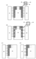
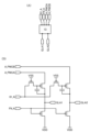
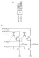
도 2의 (A), (B)는 종래 기술의 예이고, 화소 어레이(23)가 가지는 화소(24)의 구동에 2개의 구동 회로를 사용하는 예를 나타낸 것이다. 종래에는, 화소(24)가 표시 소자를 가지는 회로(25) 및 센서 소자를 가지는 회로(26)를 가지는 경우, 회로(25) 및 회로(26)를 구동하는 데 각각 다른 구동 회로(행 드라이버(21), 행 드라이버(22))가 필요하였다. 이는, 신호를 출력하는 타이밍의 제어 등이 회로(25)와 회로(26)에서 다른 것, 또는 도 2의 (B)에 나타낸 바와 같이 회로(26)가 모든 행에 배치되지 않은 경우 등, 구동하는 행이 회로(25)와 회로(26)에서 다른 경우가 있는 것 등에 기인한다.(A) and (B) of FIG. 2 are examples of the prior art and show an example in which two driving circuits are used to drive the
본 발명의 일 형태의 반도체 장치(20)를 행 드라이버로서 사용함으로써, 도 2의 (C)에 나타낸 모든 행의 회로(25)의 동작 또는 모든 행의 회로(26)의 동작과, 도 2의 (D)에 나타낸 특정의 행의 회로(26)의 동작을 전환하여 수행할 수 있다.By using the
즉, 2개의 상이한 행 드라이버를 하나의 행 드라이버로 할 수 있기 때문에 배선 수, 및 행 드라이버를 구성하는 트랜지스터 등의 점유 면적을 감소시킬 수 있다. 따라서, 슬림 베젤화가 가능하므로 표시 장치 등을 소형화할 수 있다.That is, since two different row drivers can be used as one row driver, the number of wires and the area occupied by transistors and the like constituting the row driver can be reduced. Therefore, since a slim bezel is possible, a display device or the like can be miniaturized.
도 1은 본 발명의 일 형태의 반도체 장치를 설명하는 블록도이다. 반도체 장치(20)는 외부에 신호 전위를 순차적으로 출력하는 순서 회로이고, 시프트 레지스터라고도 불린다. 또한 도 1은 개략도이고, 각 요소에 입력되는 신호 전위, 전원 전위, 및 각 요소 간의 접속 형태 등의 자세한 사항은 생략하였다.1 is a block diagram illustrating a semiconductor device of one embodiment of the present invention. The
반도체 장치(20)는 블록(31), 블록(32) 및 블록(33)을 가진다. 블록(31, 32, 33)의 각각은 복수의 플립플롭 회로(10) 및 출력 회로(11)를 가진다. 블록(31, 32, 33)의 각각이 가지는 복수의 플립플롭 회로(10)는 종속(cascade) 접속된다. 또한 플립플롭 회로(10)의 각각과 출력 회로(11)가 한 쌍이 되어 전기적으로 접속된다.The
블록(31)의 마지막 단의 플립플롭 회로(10), 블록(32)의 제 1 단의 플립플롭 회로(10), 블록(32)의 마지막 단의 플립플롭 회로(10), 및 블록(32)의 마지막 단의 플립플롭 회로(10)는 스위치 회로(15)에 전기적으로 접속된다.The flip-
스위치 회로(15)는 블록(31), 블록(32), 및 블록(33)의 신호 전위의 출력 동작을 유효로 하는 제 1 모드와, 블록(31) 및 블록(33)의 신호 전위의 출력 동작을 유효로 하는 제 2 모드를 전환할 수 있다. 제 1 모드에서는 모든 블록으로부터 외부로 신호 전위를 순차적으로 출력할 수 있다. 제 2 모드에서는 블록(32)이 비동작 상태가 되기 때문에 블록(31) 및 블록(33)으로부터 외부로 신호 전위를 순차적으로 출력할 수 있다.The
또한 도 1에 나타낸 바와 같이, 블록(31)의 제 1 단의 플립플롭 회로(10)에 스타트 펄스(SP)가 공급되고, 제 4 단의 플립플롭 회로(10)를 블록(31)의 마지막 단으로 한 경우, 블록(32)은 제 5 단 내지 제 4n 단(n은 2 이상의 정수)의 플립플롭 회로(10)를 가질 수 있다. 또한 블록(33)은 제 4n+1 단 내지 제 4n+4 단의 플립플롭 회로(10)를 가질 수 있다.1, a start pulse (SP) is supplied to the flip-
예를 들어 제 2 모드에서 n=2로 하였을 때에는, 제 1 단 내지 제 4 단 및 제 9 단 내지 제 12 단의 플립플롭 회로가 신호 전위를 출력하고 제 5 단 내지 제 8 단의 플립플롭 회로가 신호 전위를 출력하지 않는 동작을 수행할 수 있다. 또한 n=9로 하였을 때에는, 제 1 단 내지 제 4 단 및 제 37 단 내지 제 40 단의 플립플롭 회로가 신호 전위를 출력하고 제 5 단 내지 제 36 단의 플립플롭 회로가 신호 전위를 출력하지 않는 동작을 수행할 수 있다.For example, when n = 2 in the second mode, the flip-flop circuits of the first to fourth stages and the ninth to twelfth stages output signal potentials, and the flip-flop circuits of the fifth to eighth stages can perform an operation that does not output a signal potential. When n = 9, flip-flop circuits of
구체적으로는, 화소에 센서 소자 및 표시 소자를 가지는 표시 장치 등에 반도체 장치(20)를 적용한 경우, 화상 데이터의 기록 및 높은 해상도가 필요한 센싱 기능(지문 인증 등)을 수행하는 경우에는 제 1 모드를 사용한다. 한편, 접촉 또는 비접촉에 의한 패널 조작 기능 등은 높은 해상도가 불필요하기 때문에 제 2 모드를 사용한다. 제 2 모드에서는 동작하는 행을 적게 할 수 있기 때문에 고속 동작이 가능하다.Specifically, when the
또한 블록(33) 이후에는 스위치 회로(15), 블록(32), 블록(33)과 같은 구성의 회로를 반복적으로 접속할 수 있다.In addition, after
다음으로 플립플롭 회로(10)에 전기적으로 접속되는 출력 회로(11)에 대하여 설명한다. 출력 회로(11)는 스위치 회로(12), 회로(13), 및 회로(14)를 가진다. 스위치 회로(12)는 플립플롭 회로(10)에 전기적으로 접속된다. 또한 스위치 회로(12)는 회로(13) 및 회로(14)에 전기적으로 접속된다.Next, the
스위치 회로(12)는 플립플롭 회로(10)로부터 입력된 제 1 신호 전위에 기초하여 제 2 신호 전위를 회로(13) 및 회로(14) 중 한쪽에 출력할 수 있다. 또한 회로(13) 및 회로(14) 중 한쪽에는 스위치 회로(12)를 통하여 펄스폭 제어 신호(PWC)가 입력된다. 회로(13) 또는 회로(14)는 펄스폭 제어 신호(PWC) 및 제 2 신호 전위에 기초하여 제 3 신호 전위를 외부로 출력할 수 있다.The
예를 들어 회로(13)는 표시 장치의 화소가 가지는 표시 소자를 구동하는 회로에 전기적으로 접속할 수 있다. 회로(14)는 표시 장치의 화소가 가지는 센서 소자를 구동하는 회로에 전기적으로 접속할 수 있다. 또한 도 1에서는 회로(13) 및 회로(14)로부터의 출력 경로를 각각 하나로서 도시하였지만, 2개 이상이어도 좋다. 스위치 회로(12), 회로(13), 및 회로(14)에 입력하는 펄스폭 제어 신호(PWC)를 증가시킴으로써 상이한 타이밍에서 2개 이상의 경로로부터 신호 전위를 출력할 수 있다.For example, the
도 3 및 도 4는 n=9로 한 경우의 반도체 장치(20)로서 적용할 수 있는 반도체 장치(20a)의 자세한 블록도이다. 도 3 및 도 4에 나타낸 플립플롭 회로(10), 출력 회로(11)(스위치 회로(12), 회로(13), 및 회로(14))는 도 1에 나타낸 블록도와 대응한다. 도 1에 나타낸 스위치 회로(15)는 도 3에 나타낸 스위치 회로(16), 스위치 회로(17), 스위치 회로(18), 및 도 4에 나타낸 스위치 회로(19) 등을 구성 요소로서 가진다.3 and 4 are detailed block diagrams of a
상술한 바와 같이 출력 회로(11)는 회로(13) 또는 회로(14)로부터 신호 전위를 출력할 수 있다. 도 3, 도 4에서는 회로(13)로부터 신호 전위(GLA(GLA[1] 내지 GLA[40]))를 출력하고, 회로(14)로부터 신호 전위(GLB(GLB[1] 내지 GLB[40]))를 출력하는 형태를 도시하였다.As described above, the
또한 도 3은 제 4 단의 플립플롭 회로(10)와 제 5 단의 플립플롭 회로 사이에 스위치 회로(18)를 제공하는 예를 나타낸 것이고, 도 4는 제 36 단의 플립플롭 회로(10)와 제 37 단의 플립플롭 회로(10) 사이에 스위치 회로(19)를 제공하는 예를 나타낸 것이다.3 shows an example of providing a
즉, 도 3에 나타낸 제 1 단 내지 제 4 단의 플립플롭 회로(10) 및 출력 회로(11)가 도 1에 나타낸 블록(31)에 상당한다. 또한 도 3 및 도 4에 나타낸 제 5 단 내지 제 36 단의 플립플롭 회로(10) 및 출력 회로(11)가 도 1에 나타낸 블록(32)에 상당한다. 또한 도 4에 나타낸 제 37 단 내지 제 40 단의 플립플롭 회로(10) 및 출력 회로(11)가 도 1에 나타낸 블록(33)에 상당한다.That is, the flip-
또한 각 블록의 단 수는 도 1의 설명의 범위에서 변경할 수 있다. 또한 도 3 및 도 4에 나타낸 구성에 있어서, 앞의 단의 플립플롭 회로(10)에는 뒤의 단의 플립플롭 회로(10)의 출력 신호가 입력되기 때문에 반도체 장치(20a) 전체에서의 최종 블록(도시하지 않았음)에는 필요한 수의 더미의 플립플롭 회로(10)가 제공된다.Also, the number of stages of each block may be changed within the scope of the description of FIG. 1 . 3 and 4, since the output signal of the flip-
반도체 장치(20a)의 입력 신호로서는 클록 신호(CLK1 내지 CLK4), 펄스폭 제어 신호(PWC1 내지 PWC4), 리셋 신호(RES), 스타트 펄스 신호(SP), 선택 신호(SEL_A), 선택 신호(SEL_B1), 선택 신호(SEL_B2)를 사용할 수 있다.Input signals of the
도 5의 (A)에 플립플롭 회로(10)의 블록도, 도 5의 (B)에 플립플롭 회로(10)의 회로도의 일례를 나타내었다. 플립플롭 회로(10)를 구성하는 트랜지스터 및 용량 소자의 접속 형태에 대해서는 도 5의 (B)를 참조하고, 그 설명은 생략한다. 또한 VDD는 고전위 전원을 나타내고 VSS는 저전위 전원을 나타낸다. 또한 반도체 장치(20a)를 구성하는 트랜지스터는 n채널형 트랜지스터로 한다.An example of a block diagram of the flip-
입력 신호는 2계통의 클록 신호, 리셋 신호(RES), 뒤의 단의 플립플롭 회로(10)로부터 입력되는 리셋 신호(RIN), 앞의 단의 플립플롭 회로(10)로부터 입력되는 시프트 신호(LIN)이다. 또한 제 1 단의 플립플롭 회로(10)에서는 클록 신호(CLK1, CLK2)가 사용되고, 시프트 신호(LIN) 대신 스타트 펄스 신호(SP)가 사용된다.The input signals are a two-system clock signal, a reset signal (RES), a reset signal (RIN) input from the flip-
출력 신호는 신호 전위(01), 신호 전위(SROUT), 신호 전위(FN)이다. 신호 전위(01)는 회로(13) 또는 회로(14)에 있어서 외부로 출력하는 신호 전위의 생성에 사용되고, 신호 전위(FN)는 회로(13) 또는 회로(14)에 있어서 풀다운(pull down) 저항이 되는 트랜지스터의 제어에 사용된다. 신호 전위(SROUT)는 뒤의 단의 플립플롭 회로(10)에 대한 시프트 신호(LIN) 및 앞의 단의 플립플롭 회로(10)에 대한 리셋 신호(RIN)로서 사용된다.The output signals are signal potential (01), signal potential (SROUT), and signal potential (FN). The
도 6의 (A)에 스위치 회로(12)의 블록도, 도 6의 (B)에 스위치 회로(12)의 회로도의 일례를 나타내었다. 스위치 회로(12)를 구성하는 트랜지스터 및 용량 소자의 접속 형태에 대해서는 도 6의 (B)를 참조하고, 그 설명은 생략한다.An example of the block diagram of the
입력 신호는 펄스폭 제어 신호(PWC), 선택 신호(SEL_A), 선택 신호(SEL_B), 플립플롭 회로(10)로부터 입력되는 신호 전위(01) 및 신호 전위(FN)이다. 선택 신호(SEL_A) 및 선택 신호(SEL_B)는 회로(13) 및 회로(14) 중 어느 쪽으로부터 외부에 신호 전위를 출력하는지를 선택하는 신호이다. 선택 신호(SEL_B)는 후술하는 스위치 회로(16)에서 생성되는 신호 전위이다.The input signals are a pulse width control signal (PWC), a selection signal (SEL_A), a selection signal (SEL_B), a signal potential (01) and a signal potential (FN) input from the flip-
출력 신호는 신호 전위(01_A), 신호 전위(01_B), 신호 전위(FN_A), 신호 전위(FN_B), 펄스폭 제어 신호(A_PWC), 펄스폭 제어 신호(B_PWC)이다. 선택 신호(SEL_A)를 입력함으로써 신호 전위(01_A), 신호 전위(FN_A), 펄스폭 제어 신호(A_PWC)가 생성된다. 선택 신호(SEL_B)를 입력함으로써 신호 전위(01_B), 신호 전위(FN_B), 펄스폭 제어 신호(B_PWC)가 생성된다.The output signals are signal potential (01_A), signal potential (01_B), signal potential (FN_A), signal potential (FN_B), pulse width control signal (A_PWC), and pulse width control signal (B_PWC). By inputting the selection signal SEL_A, the signal potential 01_A, the signal potential FN_A, and the pulse width control signal A_PWC are generated. By inputting the selection signal (SEL_B), the signal potential (01_B), the signal potential (FN_B), and the pulse width control signal (B_PWC) are generated.
신호 전위(01_A) 및 신호 전위(01_B)는 회로(13) 또는 회로(14)가 출력하는 신호 전위의 생성에 사용된다. 신호 전위(FN_A) 및 신호 전위(FN_B)는 회로(13) 또는 회로(14)에 있어서 풀다운 저항이 되는 트랜지스터의 제어에 사용된다. 펄스폭 제어 신호(A_PWC), 펄스폭 제어 신호(B_PWC)는 회로(13) 또는 회로(14)가 출력하는 신호 전위의 펄스폭의 제어에 사용된다.The signal potential 01_A and the signal potential 01_B are used to generate a signal potential output by the
즉, 스위치 회로(12)에서 하나의 펄스폭 제어 신호로부터 2개의 펄스폭 제어 신호를 생성하기 위하여, 반도체 장치(20)로의 입력 신호를 줄일 수 있다.That is, in order to generate two pulse width control signals from one pulse width control signal in the
도 7의 (A)에 회로(13)의 블록도, 도 7의 (B)에 회로(13)의 회로도의 일례를 나타내었다. 회로(13)를 구성하는 트랜지스터 및 용량 소자의 접속 형태에 대해서는 도 7의 (B)를 참조하고, 그 설명은 생략한다.An example of a block diagram of the
입력 신호는 스위치 회로(12)로부터 입력되는 신호 전위(01_A), 신호 전위(FN_A), 및 펄스폭 제어 신호(A_PWC)이다. 신호 전위(01_A) 및 펄스폭 제어 신호(A_PWC)를 입력함으로써 생성되는 신호 전위(GLA)를 외부의 회로가 접속된 배선에 출력할 수 있다. 또한 신호 전위(FN_A)를 입력함으로써 풀다운 저항에 상당하는 트랜지스터를 동작시켜 상기 배선의 전위를 VSS로 안정시킬수 있다.The input signals are a signal potential (01_A) input from the
도 7의 (C)에 회로(14)의 블록도, 도 7의 (D)에 회로(14)의 회로도의 일례를 나타내었다. 회로(14)를 구성하는 트랜지스터 및 용량 소자의 접속 형태에 대해서는 도 7의 (D)를 참조하고, 그 설명은 생략한다.An example of a block diagram of the
입력 신호는 스위치 회로(12)로부터 입력되는 신호 전위(01_B), 신호 전위(FN_B), 및 펄스폭 제어 신호(B_PWC)이다. 신호 전위(01_B) 및 펄스폭 제어 신호(B_PWC)를 입력함으로써 생성되는 신호 전위(GLB)를 외부의 회로가 접속된 배선에 출력할 수 있다. 또한 신호 전위(FN_B)를 입력함으로써 풀다운 저항에 상당하는 트랜지스터를 동작시켜 상기 배선의 전위를 VSS로 안정시킬수 있다.The input signals are a signal potential (01_B) input from the
도 8의 (A)에 스위치 회로(16)의 블록도, 도 8의 (B)에 스위치 회로(16)의 회로도의 일례를 나타내었다. 스위치 회로(16)를 구성하는 트랜지스터의 접속 형태에 대해서는 도 8의 (B)를 참조하고, 그 설명은 생략한다.An example of the block diagram of the
입력 신호는 선택 신호(SEL_B1) 및 선택 신호(SEL_B2)이다. 어느 쪽의 선택 신호가 입력되어도 신호 전위(SEL_B)를 생성한다. 신호 전위(SEL_B)는 상술한 스위치 회로(12)에 입력된다. 선택 신호(SEL_B)가 스위치 회로(12)에 입력됨으로써 회로(14)로부터 외부로의 신호 전위의 출력을 유효로 할 수 있다.The input signals are a selection signal SEL_B1 and a selection signal SEL_B2. Regardless of which selection signal is input, a signal potential (SEL_B) is generated. The signal potential SEL_B is input to the
도 8의 (C)에 스위치 회로(17)의 블록도, 도 8의 (D)에 스위치 회로(17)의 회로도의 일례를 나타내었다. 스위치 회로(17)를 구성하는 트랜지스터의 접속 형태에 대해서는 도 8의 (D)를 참조하고, 그 설명은 생략한다.An example of the block diagram of the
입력 신호는 선택 신호(SEL_A) 및 선택 신호(SEL_B1)이다. 어느 쪽의 선택 신호가 입력되어도 신호 전위(SEL_C)를 생성한다. 신호 전위(SEL_C)는 후술하는 스위치 회로(18) 및 스위치 회로(19)에 입력된다.The input signals are a selection signal SEL_A and a selection signal SEL_B1. Regardless of which selection signal is input, a signal potential (SEL_C) is generated. The signal potential SEL_C is input to a
도 9의 (A)에 스위치 회로(18)의 블록도, 도 9의 (B)에 스위치 회로(18)의 회로도의 일례를 나타내었다. 스위치 회로(18)를 구성하는 트랜지스터의 접속 형태에 대해서는 도 9의 (B)를 참조하고, 그 설명은 생략한다.An example of a block diagram of the
입력 신호는 선택 신호(SEL_C), 선택 신호(SEL_B2)이다. 또한 스위치 회로(18)는 단자(SWIN1), 단자(RIN1), 단자(LIN1), 단자(LIN2), 단자(SWIN2)를 가진다. 도 3에 있어서, 단자(SWIN1)는 제 4 단의 플립플롭 회로(10)의 출력 단자(신호 전위(SROUT)를 출력하는 단자)에 전기적으로 접속된다. 단자(RIN1)는 제 4 단의 플립플롭 회로(10)의 입력 단자(리셋 신호(RIN)가 입력되는 단자)에 전기적으로 접속된다. 단자(LIN1)는 제 5 단의 플립플롭 회로(10)의 입력 단자(시프트 신호(LIN)가 입력되는 단자)에 전기적으로 접속된다. 도 3 및 도 4에 있어서, 단자(LIN2)는 제 37 단의 플립플롭 회로(10)의 입력 단자(시프트 신호(LIN)가 입력되는 단자) 및 후술하는 스위치 회로(19)에 전기적으로 접속된다. 단자(SWIN2)는 제 5 단의 플립플롭 회로(10)의 출력 단자(신호 전위(SROUT)를 출력하는 단자)에 전기적으로 접속된다.The input signals are a selection signal SEL_C and a selection signal SEL_B2. Further, the
도 10의 (A)에 스위치 회로(19)의 블록도, 도 10의 (B)에 스위치 회로(19)의 회로도의 일례를 나타내었다. 스위치 회로(19)를 구성하는 트랜지스터의 접속 형태에 대해서는 도 10의 (B)를 참조하고, 그 설명은 생략한다.An example of the block diagram of the
입력 신호는 선택 신호(SEL_C), 선택 신호(SEL_B2)이다. 또한 단자(SWIN1), 단자(RIN1), 단자(RIN2), 단자(LIN1), 단자(SWIN2)를 가진다. 도 4에 있어서, 단자(SWIN1)는 제 36 단의 플립플롭 회로(10)의 출력 단자(신호 전위(SROUT)를 출력하는 단자)에 전기적으로 접속된다. 단자(RIN1)는 제 36 단의 플립플롭 회로(10)의 입력 단자(리셋 신호(RIN)가 입력되는 단자)에 전기적으로 접속된다. 도 3 및 도 4에 있어서, 단자(RIN2)는 제 4 단의 플립플롭 회로(10)의 입력 단자(리셋 신호(RIN)가 입력되는 단자)에 전기적으로 접속된다. 도 4에 있어서, 단자(LIN1)는 제 37 단의 플립플롭 회로(10)의 입력 단자(시프트 신호(LIN)가 입력되는 단자)에 전기적으로 접속된다. 단자(SWIN2)는 제 37 단의 플립플롭 회로(10)의 출력 단자(신호 전위(SROUT)를 출력하는 단자)에 전기적으로 접속된다.The input signals are a selection signal SEL_C and a selection signal SEL_B2. It also has a terminal SWIN1, a terminal RIN1, a terminal RIN2, a terminal LIN1, and a terminal SWIN2. In Fig. 4, the terminal SWIN1 is electrically connected to the output terminal (terminal for outputting the signal potential SROUT) of the flip-
여기서, 스위치 회로(18) 및 스위치 회로(19)에 선택 신호(SEL_C)가 입력된 경우, 스위치 회로(18)에서는 단자(SWIN1)와 단자(LIN1)가 도통하고, 단자(RIN1)와 단자(SWIN2)가 도통한다. 또한 스위치 회로(19)에서는 단자(SWIN1)와 단자(LIN1)가 도통하고, 단자(RIN1)와 단자(SWIN2)가 도통한다.Here, when the selection signal SEL_C is input to the
따라서, 제 4 단의 플립플롭 회로(10)가 출력하는 신호 전위(SROUT)는 시프트 신호(LIN)로서 제 5 단의 플립플롭 회로(10)에 입력된다. 제 5 단의 플립플롭 회로(10)가 출력하는 신호 전위(SROUT)는 리셋 신호(RIN)로서 제 4 단의 플립플롭 회로(10)에 입력된다. 따라서, 선택 신호(SEL_C)를 입력함으로써 도 1에 나타낸 블록(31)과 블록(32)에서의 신호 전위의 출력 동작이 선택된다.Accordingly, the signal potential SROUT output from the fourth-stage flip-
또한 제 36 단의 플립플롭 회로(10)가 출력하는 신호 전위(SROUT)는 시프트 신호(LIN)로서 제 37 단의 플립플롭 회로(10)에 입력된다. 제 37 단의 플립플롭 회로(10)가 출력하는 신호 전위(SROUT)는 리셋 신호(RIN)로서 제 36 단의 플립플롭 회로(10)에 입력된다. 따라서, 선택 신호(SEL_C)를 입력함으로써 도 1에 나타낸 블록(33)에서의 신호 전위의 출력 동작이 더 선택된다.Also, the signal potential SROUT output from the flip-
즉, 선택 신호(SEL_C)를 입력함으로써 도 1에 나타낸 블록(31), 블록(32), 및 블록(33)의 동작이 선택되기 때문에 신호 전위(GLA [1] 내지 GLA[40]) 또는 신호 전위(GLB[1] 내지 GLB[40])를 출력할 수 있다.That is, since the operations of the
한편, 스위치 회로(18) 및 스위치 회로(19)에 선택 신호(SEL_B2)가 입력된 경우, 스위치 회로(18)에서는 단자(SWIN1)와 단자(LIN2)가 도통한다. 또한 스위치 회로(19)에서는 단자(RIN2)와 단자(SWIN2)가 도통한다.On the other hand, when the selection signal SEL_B2 is input to the
따라서, 제 4 단의 플립플롭 회로(10)가 출력하는 신호 전위(SROUT)는 시프트 신호(LIN)로서 제 37 단의 플립플롭 회로(10)에 입력된다. 제 37 단의 플립플롭 회로(10)가 출력하는 신호 전위(SROUT)는 리셋 신호(RIN)로서 제 4 단의 플립플롭 회로(10)에 입력된다.Accordingly, the signal potential SROUT output from the flip-
즉, 선택 신호(SEL_B2)를 입력함으로써 도 1에 나타낸 블록(31) 및 블록(33)에서의 신호 전위의 출력 동작이 선택되기 때문에 신호 전위(GLA[1] 내지 GLA[4]) 및 신호 전위(GLA[37] 내지 GLA[40]) 또는 신호 전위(GLB[1] 내지 GLB[4]) 및 신호 전위(GLB[37] 내지 GLB[40])를 출력할 수 있다.That is, since the output operation of the signal potentials in the
여기까지 설명한 반도체 장치(20a)에 입력하는 선택 신호와 신호 전위를 출력하는 회로에 대하여 표 1에 정리한다.Table 1 summarizes the selection signal input to the
[표 1][Table 1]

또한 앞에서 회로(13) 및 회로(14)로부터 출력하는 신호 전위의 경로가 각각 하나인 예를 나타내었지만, 스위치 회로(12), 회로(13), 및 회로(14)에 입력하는 제어 신호(PWC)를 증가시킴으로써 상이한 타이밍에서 2개 이상의 경로로부터 신호 전위를 출력할 수 있다.In addition, although an example in which the signal potential output from the
도 11은 회로(13) 및 회로(14)로부터 출력하는 신호 전위가 각각 2개인 예를 나타낸 반도체 장치(20b)의 블록도이다. 회로(13)로부터는 신호 전위(GLA1)와 신호 전위(GLA2)를 상이한 타이밍에서 출력할 수 있다. 또한 회로(14)로부터는 신호 전위(GLB1)와 신호 전위(GLB2)를 상이한 타이밍에서 출력할 수 있다.11 is a block diagram of a
입력 신호에 있어서, 펄스폭 제어 신호(PWC)가 펄스폭 제어 신호(PWCA(PWCA1 내지 PWCA4)) 및 펄스폭 제어 신호(PWCB(PWCB1 내지 PWCB4))로 증가하는 점이 도 3 및 도 4에 나타낸 반도체 장치(20a)와 다르다. 또한 스위치 회로(12), 회로(13), 및 회로(14)의 구성이 반도체 장치(20a)와 다르다. 또한 반도체 장치(20b)가 가지는 플립플롭 회로(10), 스위치 회로(16, 17), 스위치 회로(18, 19)(도시하지 않았음)의 구성, 및 이들 요소가 서로 접속되는 구성은 반도체 장치(20a)와 동일한 것으로 할 수 있다.Regarding the input signal, the semiconductor shown in FIGS. 3 and 4 points that the pulse width control signal PWC increases to the pulse width control signals PWCA (PWCA1 to PWCA4) and the pulse width control signals PWCB (PWCB1 to PWCB4). It is different from
도 12의 (A)에 반도체 장치(20b)가 가지는 스위치 회로(12)의 블록도, 도 12의 (B)에 스위치 회로(12)의 회로도의 일례를 나타내었다. 스위치 회로(12)를 구성하는 트랜지스터 및 용량 소자의 접속 형태에 대해서는 도 12의 (B)를 참조하고, 그 설명은 생략한다.An example of a block diagram of the
입력 신호는 펄스폭 제어 신호(PWCA), 펄스폭 제어 신호(PWCB), 선택 신호(SEL_A), 선택 신호(SEL_B), 플립플롭 회로(10)로부터 입력되는 신호 전위(01) 및 신호 전위(FN)이다. 선택 신호(SEL_A) 및 선택 신호(SEL_B)는 회로(13) 및 회로(14) 중 어느 쪽으로부터 외부에 신호 전위를 출력하는지를 선택하는 신호이다.The input signals include a pulse width control signal (PWCA), a pulse width control signal (PWCB), a selection signal (SEL_A), a selection signal (SEL_B), a signal potential (01) input from the flip-
출력 신호는 신호 전위(01_A), 신호 전위(01_B), 신호 전위(FN_A), 신호 전위(FN_B), 펄스폭 제어 신호(A_PWCA), 펄스폭 제어 신호(B_PWCA), 펄스폭 제어 신호(A_PWCB), 펄스폭 제어 신호(B_PWCB)이다. 선택 신호(SEL_A)를 입력함으로써, 신호 전위(01_A), 신호 전위(FN_A), 펄스폭 제어 신호(A_PWCA), 펄스폭 제어 신호(A_PWCB)가 생성된다. 선택 신호(SEL_B)를 입력함으로써, 신호 전위(01_B), 신호 전위(FN_B), 펄스폭 제어 신호(B_PWCA), 펄스폭 제어 신호(B_PWCB)가 생성된다.The output signals are signal potential (01_A), signal potential (01_B), signal potential (FN_A), signal potential (FN_B), pulse width control signal (A_PWCA), pulse width control signal (B_PWCA), pulse width control signal (A_PWCB) , is the pulse width control signal (B_PWCB). By inputting the selection signal SEL_A, the signal potential 01_A, the signal potential FN_A, the pulse width control signal A_PWCA, and the pulse width control signal A_PWCB are generated. By inputting the selection signal SEL_B, the signal potential 01_B, the signal potential FN_B, the pulse width control signal B_PWCA, and the pulse width control signal B_PWCB are generated.
신호 전위(01_A) 및 신호 전위(01_B)는 회로(13) 또는 회로(14)가 출력하는 신호 전위의 생성에 사용된다. 신호 전위(FN_A) 및 신호 전위(FN_B)는 회로(13) 또는 회로(14)에 있어서 풀다운 저항이 되는 트랜지스터의 제어에 사용된다. 펄스폭 제어 신호(A_PWCA, A_PWCB), 펄스폭 제어 신호(B_PWCA, B_PWCB)는 회로(13) 또는 회로(14)가 출력하는 신호 전위의 펄스폭 및 타이밍의 제어에 사용된다.The signal potential 01_A and the signal potential 01_B are used to generate a signal potential output by the
도 13의 (A)에 반도체 장치(20b)가 가지는 회로(13)의 블록도, 도 13의 (B)에 회로(13)의 회로도의 일례를 나타내었다. 회로(13)를 구성하는 트랜지스터 및 용량 소자의 접속 형태에 대해서는 도 13의 (B)를 참조하고, 그 설명은 생략한다.An example of a circuit diagram of the
입력 신호는 스위치 회로(12)로부터 입력되는 신호 전위(01_A), 신호 전위(FN_A), 및 펄스폭 제어 신호(A_PWCA, A_PWCB)이다.The input signals are a signal potential (01_A) input from the
신호 전위(01_A) 및 펄스폭 제어 신호(A_PWCA)를 입력함으로써 신호 전위(GLA1)를 외부의 회로가 접속된 배선에 출력할 수 있다. 또한 신호 전위(FN_A) 및 펄스폭 제어 신호(A_PWCA)를 입력함으로써 풀다운 저항에 상당하는 트랜지스터를 동작시켜 상기 배선의 전위를 VSS로 안정시킬수 있다.By inputting the signal potential (01_A) and the pulse width control signal (A_PWCA), the signal potential (GLA1) can be output to a wire connected to an external circuit. Further, by inputting the signal potential (FN_A) and the pulse width control signal (A_PWCA), the transistor corresponding to the pull-down resistor can be operated to stabilize the potential of the wiring at VSS.
또한 신호 전위(01_A) 및 펄스폭 제어 신호(A_PWCB)를 입력함으로써 신호 전위(GLA2)를 외부의 회로가 접속된 배선에 출력할 수 있다. 또한 신호 전위(FN_A) 및 펄스폭 제어 신호(A_PWCB)를 입력함으로써 풀다운 저항에 상당하는 트랜지스터를 동작시켜 상기 배선의 전위를 VSS로 안정시킬수 있다.In addition, by inputting the signal potential (01_A) and the pulse width control signal (A_PWCB), the signal potential (GLA2) can be output to a wire connected to an external circuit. Further, by inputting the signal potential (FN_A) and the pulse width control signal (A_PWCB), the transistor corresponding to the pull-down resistor can be operated to stabilize the potential of the wiring at VSS.
따라서, 신호 전위(GLA1) 및 신호 전위(GLA2)의 각각을 상이한 타이밍에서 외부로 출력할 수 있다.Accordingly, each of the signal potential GLA1 and the signal potential GLA2 can be output to the outside at different timings.
도 14의 (A)에 반도체 장치(20b)가 가지는 회로(14)의 블록도, 도 14의 (B)에 회로(14)의 회로도의 일례를 나타내었다. 회로(14)를 구성하는 트랜지스터 및 용량 소자의 접속 형태에 대해서는 도 14의 (B)를 참조하고, 그 설명은 생략한다.An example of a circuit diagram of the
입력 신호는 스위치 회로(12)로부터 입력되는 신호 전위(01_B), 신호 전위(FN_B), 및 펄스폭 제어 신호(B_PWCA, B_PWCB)이다.The input signals are the signal potential (01_B) input from the
신호 전위(01_B) 및 펄스폭 제어 신호(B_PWCA)를 입력함으로써 신호 전위(GLB1)를 외부의 회로가 접속된 배선에 출력할 수 있다. 또한 신호 전위(FN_B) 및 펄스폭 제어 신호(B_PWCA)를 입력함으로써 풀다운 저항에 상당하는 트랜지스터를 동작시켜 상기 배선의 전위를 VSS로 안정시킬수 있다.By inputting the signal potential (01_B) and the pulse width control signal (B_PWCA), the signal potential (GLB1) can be output to a wire connected to an external circuit. Further, by inputting the signal potential (FN_B) and the pulse width control signal (B_PWCA), a transistor corresponding to the pull-down resistor is operated to stabilize the potential of the wiring at VSS.
또한 신호 전위(01_B) 및 펄스폭 제어 신호(B_PWCB)를 입력함으로써 신호 전위(GLB2)를 외부의 회로가 접속된 배선에 출력할 수 있다. 또한 신호 전위(FN_B) 및 펄스폭 제어 신호(B_PWCB)를 입력함으로써 풀다운 저항에 상당하는 트랜지스터를 동작시켜 상기 배선의 전위를 VSS로 안정시킬수 있다.Further, by inputting the signal potential (01_B) and the pulse width control signal (B_PWCB), the signal potential (GLB2) can be output to a wire connected to an external circuit. Further, by inputting the signal potential (FN_B) and the pulse width control signal (B_PWCB), a transistor corresponding to the pull-down resistor is operated to stabilize the potential of the wiring at VSS.
따라서, 신호 전위(GLB1) 및 신호 전위(GLB2)의 각각을 상이한 타이밍에서 외부로 출력할 수 있다.Therefore, each of the signal potential GLB1 and the signal potential GLB2 can be output to the outside at different timings.
상술한 반도체 장치(20a) 및 반도체 장치(20b)는 n채널형 트랜지스터를 구성 요소로서 사용할 수 있다. n채널형 트랜지스터의 채널 형성 영역에 사용할 수 있는 반도체 재료로서는 실리콘 또는 금속 산화물이 바람직하다.The
실리콘을 트랜지스터의 채널 형성 영역에 사용한 트랜지스터(이하 Si 트랜지스터)에는 비정질 실리콘, 미결정 실리콘, 다결정 실리콘, 단결정 실리콘 등을 사용할 수 있다. 또한 유리 기판 위 등의 절연 표면 위에 트랜지스터를 제공하는 경우에는 비정질 실리콘 또는 다결정 실리콘을 사용하는 것이 바람직하다.Amorphous silicon, microcrystalline silicon, polycrystalline silicon, single crystal silicon, or the like can be used for a transistor using silicon in its channel formation region (hereinafter referred to as a Si transistor). Further, in the case of providing the transistor on an insulating surface such as on a glass substrate, it is preferable to use amorphous silicon or polycrystalline silicon.
비정질 실리콘은 플라스마 CVD(chemical vapor deposition)법에 의하여 대면적의 유리 기판 위에 형성하는 기술이 확립되어 있기 때문에, 대형의 디바이스에 사용하는 것이 바람직하다. 또한 다결정 실리콘은 이동도가 높은 트랜지스터를 형성할 수 있어 트랜지스터의 크기를 작게 할 수 있기 때문에 정세도가 높은 중소형 디바이스에 사용하는 것이 바람직하다. 또한 다결정 실리콘을 사용한 트랜지스터는 고속 동작이 가능하기 때문에 구동 회로를 형성할 수도 있다. 디바이스로서는 구체적으로는 표시 장치 등을 들 수 있다.Since the technology of forming amorphous silicon on a large-area glass substrate by plasma CVD (chemical vapor deposition) has been established, it is preferable to use it for large-sized devices. In addition, since polycrystalline silicon can form a transistor with high mobility and can reduce the size of the transistor, it is preferable to use it for small and medium-sized devices with high precision. In addition, since a transistor using polycrystalline silicon is capable of high-speed operation, a driving circuit can be formed. Specifically as a device, a display apparatus etc. are mentioned.
고품질의 다결정 실리콘은 레이저 결정화 공정 등을 사용함으로써 용이하게 얻을 수 있다. 또한 고품질의 다결정 실리콘은 비정질 실리콘에 니켈 또는 팔라듐 등의 금속 촉매를 첨가하여 가열하는 고상 성장법으로도 얻을 수 있다. 또한 금속 촉매를 사용한 고상 성장법으로 형성된 다결정 실리콘에 레이저 조사를 수행하여 결정성을 더 높여도 좋다. 또한 금속 촉매는 다결정 실리콘 내에 잔류하고, 트랜지스터의 전기 특성을 악화시키기 때문에, 채널 형성 영역 이외에 인 또는 희가스 등을 첨가한 영역을 제공하고, 상기 영역에 금속 촉매를 포획시키는 것이 바람직하다.High-quality polycrystalline silicon can be easily obtained by using a laser crystallization process or the like. In addition, high-quality polycrystalline silicon can be obtained by a solid-state growth method in which a metal catalyst such as nickel or palladium is added to amorphous silicon and heated. Alternatively, polycrystalline silicon formed by a solid-state growth method using a metal catalyst may be subjected to laser irradiation to further increase crystallinity. In addition, since the metal catalyst remains in the polycrystalline silicon and deteriorates the electrical characteristics of the transistor, it is preferable to provide a region to which phosphorus or a rare gas is added in addition to the channel formation region and to trap the metal catalyst in the region.
한편, 금속 산화물을 채널 형성 영역에 사용한 트랜지스터(이하, OS 트랜지스터)는 비정질 실리콘을 채널 형성 영역에 사용한 트랜지스터보다 이동도가 높다. 또한 스퍼터링법 등으로 유리 기판 등의 절연 표면 위에 형성할 수 있기 때문에 대면적 디바이스로의 대응도 용이하다. 따라서, OS 트랜지스터는 중소형 디바이스로부터 대형의 디바이스까지 널리 적용할 수 있다.On the other hand, a transistor using a metal oxide for a channel formation region (hereinafter referred to as an OS transistor) has higher mobility than a transistor using amorphous silicon for a channel formation region. In addition, since it can be formed on an insulating surface such as a glass substrate by a sputtering method or the like, it is easy to adapt to a large-area device. Therefore, the OS transistor can be widely applied from small to medium-sized devices to large-sized devices.
OS 트랜지스터는 반도체층의 에너지 갭이 크기 때문에, 수yA/μm(채널 폭 1μm당 전류값)로 매우 낮은 오프 전류 특성을 나타낼 수 있다. 그러므로 OS 트랜지스터를 표시 장치의 화소 회로에 사용한 경우에는 화소 회로에 데이터 전위를 장시간 유지할 수 있다.Since the energy gap of the semiconductor layer is large, the OS transistor can exhibit very low off-current characteristics of several yA/μm (current value per 1 μm channel width). Therefore, when the OS transistor is used in the pixel circuit of the display device, the data potential can be held in the pixel circuit for a long time.
따라서 프레임 주파수를 저하시켜도 적절한 화상 표시를 수행할 수 있다. 예를 들어, 동영상 표시를 수행하는 경우에는 제 1 프레임 주파수(예를 들어 60Hz 이상)로 하고, 정지 화상 표시를 수행하는 경우에는 제 1 프레임 주파수보다 낮은 제 2 프레임 주파수(예를 들어 1Hz 내지 10Hz 정도)로 전환함으로써, 표시 장치를 저소비 전력화할 수 있다.Accordingly, appropriate image display can be performed even when the frame frequency is lowered. For example, a first frame frequency (for example, 60 Hz or higher) in case of displaying a moving picture, and a second frame frequency lower than the first frame frequency (for example, 1 Hz to 10 Hz) in case of performing still image display. degree), the display device can be reduced in power consumption.
본 발명의 일 형태의 반도체 장치는 상기 표시 장치의 구동 회로(예를 들어 행 드라이버)에 사용할 수 있다. 구동 회로는 화소 회로와 같은 공정을 사용하여 형성함으로써 IC칩의 실장 등이 불필요하게 되기 때문에 슬림 베젤의 표시 장치를 형성할 수 있다. 즉, 본 발명의 일 형태의 반도체 장치를 화소 회로와 함께 OS 트랜지스터를 사용하여 형성하는 것은 표시 장치의 슬림 베젤화에 유효하다.A semiconductor device of one embodiment of the present invention can be used for a drive circuit (for example, a row driver) of the display device. Since the driving circuit is formed using the same process as the pixel circuit, mounting of an IC chip is unnecessary, and thus a slim bezel display device can be formed. That is, forming the semiconductor device of one embodiment of the present invention using the OS transistor together with the pixel circuit is effective for reducing the bezel of the display device.
또한 화소 회로 및 구동 회로가 가지는 트랜지스터 모두를 Si 트랜지스터 또는 OS 트랜지스터로 형성하는 구성에 한정되지 않고, 화소 회로 및 구동 회로 중 한쪽을 Si 트랜지스터, 다른 쪽을 OS 트랜지스터로 형성하여도 좋다. 또는 화소 회로 및 구동 회로가 가지는 일부의 트랜지스터를 Si 트랜지스터 및 OS 트랜지스터 중 한쪽, 나머지 트랜지스터를 Si 트랜지스터 및 OS 트랜지스터 중 다른 쪽으로 형성하여도 좋다. 상기 구성에 대해서는 표시 장치에 요구되는 기능 등에 따라 적절히 결정하면 좋다.Further, not limited to the configuration in which both the transistors of the pixel circuit and the driver circuit are formed of Si transistors or OS transistors, one of the pixel circuit and the driver circuit may be formed of Si transistors and the other of the OS transistors. Alternatively, some of the transistors included in the pixel circuit and the driver circuit may be formed on one of the Si transistor and the OS transistor, and the other transistor may be formed on the other of the Si transistor and the OS transistor. What is necessary is just to determine the said structure suitably according to the functions requested|required of a display device, etc.
OS 트랜지스터에 사용하는 반도체 재료로서는 에너지 갭이 2eV 이상, 바람직하게는 2.5eV 이상, 더 바람직하게는 3eV 이상인 금속 산화물을 사용할 수 있다. 대표적으로는 인듐을 포함하는 산화물 반도체 등이고, 예를 들어 후술하는 CAAC-OS 또는 CAC-OS 등을 사용할 수 있다. CAAC-OS는 결정을 구성하는 원자가 안정적이고, 신뢰성을 중시하는 트랜지스터 등에 적합하다. 또한 CAC-OS는 이동도 특성이 높기 때문에, 고속 구동을 수행하는 트랜지스터 등에 적합하다.As a semiconductor material used for the OS transistor, a metal oxide having an energy gap of 2 eV or more, preferably 2.5 eV or more, and more preferably 3 eV or more can be used. Typically, it is an oxide semiconductor containing indium, for example, CAAC-OS or CAC-OS described later can be used. CAAC-OS is suitable for transistors, etc., where the atoms constituting the crystal are stable and reliability is important. In addition, since the CAC-OS has high mobility characteristics, it is suitable for transistors and the like that perform high-speed driving.
OS 트랜지스터는 충격 이온화, 애벌란시(avalanche) 항복, 및 단채널 효과 등이 발생하지 않는다는 등 Si 트랜지스터와는 다른 특징을 가지기 때문에, 신뢰성이 높은 회로를 형성할 수 있다. 또한 Si 트랜지스터에서 일어나는 결정성의 불균일로 인한 전기 특성의 편차도 OS 트랜지스터에서는 일어나기 어렵다.Since the OS transistor has characteristics different from those of the Si transistor, such as the absence of impact ionization, avalanche breakdown, and short-channel effect, etc., a highly reliable circuit can be formed. In addition, variations in electrical characteristics due to non-uniformity of crystallinity occurring in Si transistors are unlikely to occur in OS transistors.
OS 트랜지스터에 포함되는 반도체층은 예를 들어 인듐, 아연, 및 M(알루미늄, 타이타늄, 갈륨, 저마늄, 이트륨, 지르코늄, 란타넘, 세륨, 주석, 네오디뮴, 또는 하프늄 등의 금속)을 포함한 In-M-Zn계 산화물로 표기되는 막으로 할 수 있다. In-M-Zn계 산화물은 대표적으로는 스퍼터링법으로 형성할 수 있다. 또는 ALD(Atomic layer deposition)법에 의하여 형성하여도 좋다.The semiconductor layer included in the OS transistor is, for example, In- A film represented by M-Zn-based oxide can be used. An In-M-Zn-based oxide can be typically formed by a sputtering method. Alternatively, it may be formed by an atomic layer deposition (ALD) method.
스퍼터링법에 의하여 In-M-Zn계 산화물을 형성하는 데 사용하는 스퍼터링 타깃의 금속 원소의 원자수비는 In≥M 및 Zn≥M을 만족시키는 것이 바람직하다. 이와 같은 스퍼터링 타깃의 금속 원소의 원자수비로서는 In:M:Zn=1:1:1, In:M:Zn=1:1:1.2, In:M:Zn=3:1:2, In:M:Zn=4:2:3, In:M:Zn=4:2:4.1, In:M:Zn=5:1:6, In:M:Zn=5:1:7, In:M:Zn=5:1:8 등이 바람직하다. 또한 성막되는 반도체층의 원자수비는 각각 상기 스퍼터링 타깃에 포함되는 금속 원소의 원자수비의 ±40%의 변동을 포함한다.It is preferable that the number of atoms of the metal elements of the sputtering target used to form the In-M-Zn-based oxide by the sputtering method satisfies In≥M and Zn≥M. As the atomic number ratio of metal elements of such a sputtering target, In:M:Zn = 1:1:1, In:M:Zn = 1:1:1.2, In:M:Zn = 3:1:2, In:M :Zn=4:2:3, In:M:Zn=4:2:4.1, In:M:Zn=5:1:6, In:M:Zn=5:1:7, In:M:Zn = 5:1:8 and the like are preferred. In addition, the number of atoms of the semiconductor layer to be formed each includes a variation of ±40% of the number of atoms of metal elements included in the sputtering target.
반도체층에는 캐리어 농도가 낮은 산화물 반도체를 사용한다. 예를 들어 반도체층에는 캐리어 농도가 1×10¹⁷/cm3 이하, 바람직하게는 1×10¹⁵/cm3 이하, 더 바람직하게는 1×10¹³/cm3 이하, 더욱 바람직하게는 1×10¹¹/cm3 이하, 더더욱 바람직하게는 1×10¹⁰/cm3 미만이고 1×10⁻⁹/cm3 이상인 산화물 반도체를 사용할 수 있다. 이러한 산화물 반도체를 고순도 진성 또는 실질적으로 고순도 진성인 산화물 반도체라고 한다. 상기 산화물 반도체는 결함 준위 밀도가 낮고, 안정된 특성을 가지는 산화물 반도체라고 할 수 있다.An oxide semiconductor having a low carrier concentration is used for the semiconductor layer. For example, the carrier concentration in the semiconductor layer is 1×10 17 /cm 3 or less, preferably 1×10 15 /cm 3 or less, more preferably 1×10 13 /cm 3 or less, and still more preferably 1×10 An oxide semiconductor having 11 /cm 3 or less, more preferably less than 1×10 10 /cm 3 and 1×10 -9 /cm 3 or more can be used. Such an oxide semiconductor is referred to as a highly purified intrinsic or substantially highly purified intrinsic oxide semiconductor. The oxide semiconductor can be said to be an oxide semiconductor having a low density of defect states and stable characteristics.
또한 이들에 한정되지 않고, 필요로 하는 트랜지스터의 반도체 특성 및 전기 특성(전계 효과 이동도, 문턱 전압 등)에 따라 적절한 조성을 가지는 재료를 사용하면 좋다. 또한 필요로 하는 트랜지스터의 반도체 특성을 얻기 위하여, 반도체층의 캐리어 농도, 불순물 농도, 결함 밀도, 금속 원소와 산소의 원자수비, 원자 간 거리, 밀도 등을 적절하게 하는 것이 바람직하다.In addition, it is not limited to these, and a material having an appropriate composition may be used according to the required semiconductor characteristics and electrical characteristics (field effect mobility, threshold voltage, etc.) of the transistor. Further, in order to obtain required semiconductor characteristics of the transistor, it is desirable to appropriately adjust the carrier concentration, impurity concentration, defect density, metal element to oxygen atom number ratio, interatomic distance, density, and the like in the semiconductor layer.
반도체층을 구성하는 산화물 반도체에 14족 원소의 하나인 실리콘 또는 탄소가 포함되면, 산소 결손이 증가되어 n형화된다. 그러므로 반도체층에서의 실리콘 또는 탄소의 농도(이차 이온 질량 분석법에 의하여 얻어지는 농도)를 2×10¹⁸atoms/cm3 이하, 바람직하게는 2×10¹⁷atoms/cm3 이하로 한다.When silicon or carbon, which is one of
또한 알칼리 금속 및 알칼리 토금속은 산화물 반도체와 결합되면 캐리어를 생성하는 경우가 있고, 이로 인하여 트랜지스터의 오프 전류가 증대될 수 있다. 그러므로 반도체층에서의 알칼리 금속 또는 알칼리 토금속의 농도(이차 이온 질량 분석법에 의하여 얻어지는 농도)를 1×10¹⁸atoms/cm3 이하, 바람직하게는 2×10¹⁶atoms/cm3 이하로 한다.In addition, when alkali metals and alkaline earth metals are combined with oxide semiconductors, carriers may be generated in some cases, which may increase the off-state current of the transistor. Therefore, the concentration of alkali metal or alkaline earth metal (concentration obtained by secondary ion mass spectrometry) in the semiconductor layer is set to 1×10 18 atoms/cm 3 or less, preferably 2×10 16 atoms/cm 3 or less.
또한 반도체층을 구성하는 산화물 반도체에 질소가 포함되면, 캐리어인 전자가 발생하고 캐리어 농도가 증가되어 반도체층이 n형화되기 쉽다. 이 결과, 질소가 포함되는 산화물 반도체를 사용한 트랜지스터는 노멀리 온 특성을 가지기 쉽다. 그러므로 반도체층에서의 질소 농도(이차 이온 질량 분석법에 의하여 얻어지는 농도)는 5×10¹⁸atoms/cm3 이하로 하는 것이 바람직하다.In addition, when nitrogen is included in the oxide semiconductor constituting the semiconductor layer, electrons as carriers are generated and the carrier concentration increases, so that the semiconductor layer tends to be n-type. As a result, a transistor using an oxide semiconductor containing nitrogen tends to have normally-on characteristics. Therefore, the nitrogen concentration (concentration obtained by secondary ion mass spectrometry) in the semiconductor layer is preferably 5×10 18 atoms/cm 3 or less.
또한 반도체층을 구성하는 산화물 반도체에 수소가 포함되면, 금속 원자와 결합되는 산소와 반응하여 물이 되기 때문에, 산화물 반도체 내에 산소 결손을 형성하는 경우가 있다. 산화물 반도체 내의 채널 형성 영역에 산소 결손이 포함되면, 트랜지스터는 노멀리 온 특성을 가지는 경우가 있다. 또한 산소 결손에 수소가 들어간 결함은 도너로서 기능하고, 캐리어인 전자를 생성하는 경우가 있다. 또한 수소의 일부가 금속 원자와 결합된 산소와 결합되어 캐리어인 전자를 생성하는 경우가 있다. 따라서 수소를 많이 포함하는 산화물 반도체를 사용한 트랜지스터는, 노멀리 온 특성을 가지기 쉽다.In addition, when hydrogen is contained in the oxide semiconductor constituting the semiconductor layer, oxygen vacancies may be formed in the oxide semiconductor because it reacts with oxygen bonded to metal atoms to become water. When oxygen vacancies are included in the channel formation region in the oxide semiconductor, the transistor may have normally-on characteristics. In addition, defects in which hydrogen enters oxygen vacancies function as donors and may generate electrons serving as carriers. In addition, there is a case in which a part of hydrogen is combined with oxygen bonded to a metal atom to generate electrons, which are carriers. Therefore, a transistor using an oxide semiconductor containing a large amount of hydrogen tends to have normally-on characteristics.
산소 결손에 수소가 들어간 결함은 산화물 반도체의 도너로서 기능할 수 있다. 그러나 상기 결함을 정량적으로 평가하는 것은 어렵다. 그러므로 산화물 반도체는 도너 농도가 아니라 캐리어 농도로 평가되는 경우가 있다. 따라서 본 명세서 등에서는 산화물 반도체의 파라미터로서, 도너 농도 대신에 전계가 인가되지 않는 상태를 상정한 캐리어 농도를 사용하는 경우가 있다. 즉 본 명세서 등에 기재되는 "캐리어 농도"는 "도너 농도"로 바꿔 말할 수 있는 경우가 있다.A defect in which hydrogen enters an oxygen vacancy can function as a donor of an oxide semiconductor. However, it is difficult to quantitatively evaluate these defects. Therefore, in some cases, an oxide semiconductor is evaluated not by donor concentration but by carrier concentration. Therefore, in this specification and the like, carrier concentration assuming a state in which no electric field is applied is used in place of the donor concentration as a parameter of the oxide semiconductor in some cases. That is, "carrier concentration" described in this specification and the like may be referred to as "donor concentration" in some cases.
그러므로 산화물 반도체 내의 수소는 가능한 한 저감되어 있는 것이 바람직하다. 구체적으로는 이차 이온 질량 분석법(SIMS: Secondary Ion Mass Spectrometry)에 의하여 얻어지는 산화물 반도체의 수소 농도를 1×10²⁰atoms/cm3 미만, 바람직하게는 1×10¹⁹atoms/cm3 미만, 더 바람직하게는 5×10¹⁸atoms/cm3 미만, 더욱 바람직하게는 1×10¹⁸atoms/cm3 미만으로 한다. 수소 등의 불순물이 충분히 저감된 산화물 반도체를 트랜지스터의 채널 형성 영역에 사용함으로써, 안정된 전기 특성을 부여할 수 있다.Therefore, it is desirable that hydrogen in the oxide semiconductor be reduced as much as possible. Specifically, the hydrogen concentration of the oxide semiconductor obtained by secondary ion mass spectrometry (SIMS) is less than 1×10 20 atoms/cm 3 , preferably less than 1×10 19 atoms/cm 3 , more preferably less than 1×10 19 atoms/
또한 반도체층은 예를 들어 비단결정 구조를 가져도 좋다. 비단결정 구조에는 예를 들어 c축 배향된 결정을 가지는 CAAC-OS(C-Axis Aligned Crystalline Oxide Semiconductor), 다결정 구조, 미결정 구조, 또는 비정질 구조가 포함된다. 비단결정 구조에서 비정질 구조는 결함 준위 밀도가 가장 높고, CAAC-OS는 결함 준위 밀도가 가장 낮다.In addition, the semiconductor layer may have, for example, a non-single crystal structure. The non-single-crystal structure includes, for example, a C-Axis Aligned Crystalline Oxide Semiconductor (CAAC-OS) having c-axis oriented crystals, a polycrystal structure, a microcrystal structure, or an amorphous structure. In the non-single-crystal structure, the amorphous structure has the highest density of defect states, and the CAAC-OS has the lowest density of defect states.
비정질 구조를 가지는 산화물 반도체막은 예를 들어 원자 배열이 무질서하고 결정 성분을 가지지 않는다. 또는 비정질 구조를 가지는 산화물막은 예를 들어 완전한 비정질 구조이고 결정부를 가지지 않는다.An oxide semiconductor film having an amorphous structure has, for example, disordered atomic arrangement and no crystalline component. Alternatively, an oxide film having an amorphous structure, for example, has a completely amorphous structure and has no crystal part.
또한 반도체층은 비정질 구조의 영역, 미결정 구조의 영역, 다결정 구조의 영역, CAAC-OS의 영역, 단결정 구조의 영역 중 2개 이상을 가지는 혼합막이어도 좋다. 혼합막은 예를 들어 상술한 영역 중 어느 2개 이상을 가지는 단층 구조 또는 적층 구조를 가지는 경우가 있다.Further, the semiconductor layer may be a mixed film having at least two of an amorphous structure region, a microcrystalline structure region, a polycrystalline structure region, a CAAC-OS region, and a single crystal structure region. The mixed film may have, for example, a single-layer structure or a laminated structure having any two or more of the above-mentioned regions.
아래에서는, 비단결정의 반도체층의 일 형태인 CAC(Cloud-Aligned Composite)-OS의 구성에 대하여 설명한다.Below, the configuration of CAC (Cloud-Aligned Composite)-OS, which is one type of non-single crystal semiconductor layer, will be described.
CAC-OS란, 예를 들어 산화물 반도체를 구성하는 원소가 0.5nm 이상 10nm 이하, 바람직하게는 1nm 이상 2nm 이하, 또는 그 근방의 크기로 편재(偏在)한 재료의 하나의 구성을 말한다. 또한 아래에서는 산화물 반도체에서 하나 또는 그 이상의 금속 원소가 편재하고, 이 금속 원소를 가지는 영역이 0.5nm 이상 10nm 이하, 바람직하게는 1nm 이상 2nm 이하, 또는 그 근방의 크기로 혼재한 상태를 모자이크 패턴 또는 패치 패턴이라고도 한다.CAC-OS refers to one configuration of a material in which elements constituting an oxide semiconductor are unevenly distributed in a size of, for example, 0.5 nm or more and 10 nm or less, preferably 1 nm or more and 2 nm or less, or in the vicinity thereof. In addition, below, one or more metal elements are unevenly distributed in an oxide semiconductor, and a state in which a region having these metal elements is mixed in a size of 0.5 nm or more and 10 nm or less, preferably 1 nm or more and 2 nm or less, or in the vicinity thereof is described as a mosaic pattern or Also called patch pattern.
또한 산화물 반도체는 적어도 인듐을 포함하는 것이 바람직하다. 특히 인듐 및 아연을 포함하는 것이 바람직하다. 또한 이들에 더하여 알루미늄, 갈륨, 이트륨, 구리, 바나듐, 베릴륨, 붕소, 실리콘, 타이타늄, 철, 니켈, 저마늄, 지르코늄, 몰리브데넘, 란타넘, 세륨, 네오디뮴, 하프늄, 탄탈럼, 텅스텐, 및 마그네슘 등에서 선택된 1종류 또는 복수 종류가 포함되어도 좋다.Also, the oxide semiconductor preferably contains at least indium. Particularly preferred are those containing indium and zinc. Also, in addition to these, aluminum, gallium, yttrium, copper, vanadium, beryllium, boron, silicon, titanium, iron, nickel, germanium, zirconium, molybdenum, lanthanum, cerium, neodymium, hafnium, tantalum, tungsten, and One type or a plurality of types selected from magnesium or the like may be included.
예를 들어 In-Ga-Zn 산화물에서의 CAC-OS(CAC-OS 중에서도 In-Ga-Zn 산화물을 특히 CAC-IGZO라고 하여도 좋음)란, 인듐 산화물(이하 InOX1(X1은 0보다 큰 실수(實數))로 함) 또는 인듐 아연 산화물(이하 InX2ZnY2OZ2(X2, Y2, 및 Z2는 0보다 큰 실수임)로 함)과, 갈륨 산화물(이하 GaOX3(X3은 0보다 큰 실수임)으로 함) 또는 갈륨 아연 산화물(이하 GaX4ZnY4OZ4(X4, Y4, 및 Z4는 0보다 큰 실수임)로 함) 등으로 재료가 분리함으로써 모자이크 패턴이 되고, 모자이크 패턴의 InOX1 또는 InX2ZnY2OZ2가 막 내에 균일하게 분포된 구성(이하 클라우드상(cloud-like)이라고도 함)을 말한다.For example, CAC-OS from In-Ga-Zn oxide (Among CAC-OS, In-Ga-Zn oxide may be particularly referred to as CAC-IGZO), indium oxide (hereinafter InO X1 (X1 is a real number greater than 0) (actual number)) or indium zinc oxide (hereinafter referred to as In X2 Zn Y2 O Z2 (where X2, Y2, and Z2 are real numbers greater than 0)), gallium oxide (hereinafter referred to as GaO X3 (where X3 is greater than 0)) Real number) or gallium zinc oxide (hereinafter referred to as Ga X4 Zn Y4 O Z4 (X4, Y4, and Z4 are real numbers greater than 0)), etc. to form a mosaic pattern, and the mosaic pattern of InO It refers to a structure in which X1 or In X2 Zn Y2 O Z2 is uniformly distributed in the film (hereinafter also referred to as cloud-like).
즉 CAC-OS는 GaOX3이 주성분인 영역과, InX2ZnY2OZ2 또는 InOX1이 주성분인 영역이 혼재하는 구성을 가지는 복합 산화물 반도체이다. 또한 본 명세서에서 예를 들어 제 1 영역의 원소 M에 대한 In의 원자수비가, 제 2 영역의 원소 M에 대한 In의 원자수비보다 큰 것을 "제 1 영역은 제 2 영역과 비교하여 In의 농도가 높다"라고 한다.That is, the CAC-OS is a composite oxide semiconductor having a configuration in which a region mainly composed of GaO X3 and a region mainly composed of In X2 Zn Y2 O Z2 or InO X1 coexist. In addition, in the present specification, for example, the atomic number ratio of In to element M in the first region is greater than the atomic number ratio of In to element M in the second region as “concentration of In in the first region compared to the second region” is high".
또한 IGZO는 통칭이며, In, Ga, Zn, 및 O로 이루어지는 하나의 화합물을 말하는 경우가 있다. 대표적인 예로서는, InGaO3(ZnO)m1(m1은 자연수임) 또는 In(1+x0)Ga(1-x0)O3(ZnO)m0(-1≤x0≤1, m0은 임의의 수임)으로 나타내어지는 결정성 화합물을 들 수 있다.In addition, IGZO is a common name and may say one compound which consists of In, Ga, Zn, and O. Representative examples include InGaO 3 (ZnO) m1 (m1 is a natural number) or In (1+x0) Ga (1-x0) O 3 (ZnO) m0 (-1≤x0≤1, m0 is an arbitrary number). A crystalline compound may be mentioned.
상기 결정성 화합물은 단결정 구조, 다결정 구조, 또는 CAAC 구조를 가진다. 또한 CAAC 구조란, 복수의 IGZO의 나노 결정이 c축 배향을 가지고, 또한 a-b면에서는 배향하지 않고 연결된 결정 구조를 말한다.The crystalline compound has a single crystal structure, a polycrystal structure, or a CAAC structure. In addition, a CAAC structure refers to a crystal structure in which a plurality of nanocrystals of IGZO have a c-axis orientation and are connected without orientation in the a-b plane.
한편, CAC-OS는 산화물 반도체의 재료 구성에 관한 것이다. CAC-OS란, In, Ga, Zn, 및 O를 포함하는 재료 구성에서, 일부에 Ga를 주성분으로 하는 나노 입자상으로 관찰되는 영역과, 일부에 In을 주성분으로 하는 나노 입자상으로 관찰되는 영역이 각각 모자이크 패턴으로 무작위로 분산되는 구성을 말한다. 따라서 CAC-OS에서 결정 구조는 부차적인 요소이다.On the other hand, CAC-OS relates to the material composition of an oxide semiconductor. In CAC-OS, in a material composition containing In, Ga, Zn, and O, a region partially observed as nanoparticles mainly composed of Ga and a region observed as nanoparticles mainly composed of In are partially observed, respectively. A composition that is randomly distributed in a mosaic pattern. Therefore, in CAC-OS, crystal structure is a secondary factor.
또한 CAC-OS는 조성이 다른 2종류 이상의 막의 적층 구조를 포함하지 않는 것으로 한다. 예를 들어, In을 주성분으로 하는 막과, Ga를 주성분으로 하는 막의 2층으로 이루어지는 구조는 포함하지 않는다.Further, the CAC-OS shall not include a laminated structure of two or more types of films having different compositions. For example, a structure composed of two layers of a film containing In as a main component and a film containing Ga as a main component is not included.
또한 GaOX3이 주성분인 영역과, InX2ZnY2OZ2 또는 InOX1이 주성분인 영역에서는 명확한 경계가 관찰되지 않는 경우가 있다.In some cases, no clear boundary is observed between a region where GaO X3 is the main component and a region where InX2 Zn Y2 O Z2 or InO X1 is the main component.
또한 갈륨 대신에 알루미늄, 이트륨, 구리, 바나듐, 베릴륨, 붕소, 실리콘, 타이타늄, 철, 니켈, 저마늄, 지르코늄, 몰리브데넘, 란타넘, 세륨, 네오디뮴, 하프늄, 탄탈럼, 텅스텐, 및 마그네슘 등에서 선택된 1종류 또는 복수 종류가 포함되는 경우, CAC-OS란 일부에 상기 금속 원소를 주성분으로 하는 나노 입자상으로 관찰되는 영역과, 일부에 In을 주성분으로 하는 나노 입자상으로 관찰되는 영역이 각각 모자이크 패턴으로 무작위로 분산되는 구성을 말한다.Also, aluminum, yttrium, copper, vanadium, beryllium, boron, silicon, titanium, iron, nickel, germanium, zirconium, molybdenum, lanthanum, cerium, neodymium, hafnium, tantalum, tungsten, and magnesium are used instead of gallium. When the selected one type or plural types are included, CAC-OS is a mosaic pattern in which areas partially observed as nanoparticles mainly composed of the above metal elements and areas observed as nanoparticles mainly composed of In are formed in a mosaic pattern. It refers to a randomly distributed configuration.
CAC-OS는 예를 들어 기판을 의도적으로 가열하지 않는 조건에서 스퍼터링법에 의하여 형성할 수 있다. 또한 CAC-OS를 스퍼터링법에 의하여 형성하는 경우, 성막 가스로서 불활성 가스(대표적으로는 아르곤), 산소 가스, 및 질소 가스에서 선택된 어느 하나 또는 복수를 사용하면 좋다. 또한 성막 시의 성막 가스의 총유량에 대한 산소 가스의 유량비는 낮을수록 바람직하고, 예를 들어 산소 가스의 유량비를 0% 이상 30% 미만, 바람직하게는 0% 이상 10% 이하로 하는 것이 바람직하다.The CAC-OS can be formed, for example, by sputtering under the condition that the substrate is not intentionally heated. In the case of forming the CAC-OS by sputtering, one or more selected from inert gas (typically argon), oxygen gas, and nitrogen gas may be used as the film forming gas. In addition, the lower the flow rate ratio of the oxygen gas to the total flow rate of the film formation gas during film formation, the better. .
CAC-OS는 X선 회절(XRD: X-ray diffraction) 측정법의 하나인 Out-of-plane법에 의한 θ/2θ 스캔을 사용하여 측정하였을 때, 명확한 피크가 관찰되지 않는다는 특징을 가진다. 즉 X선 회절 측정으로부터 측정 영역의 a-b면 방향 및 c축 방향의 배향이 관찰되지 않는다는 것을 알 수 있다.CAC-OS is characterized in that no clear peak is observed when measured using a θ/2θ scan by an out-of-plane method, which is one of X-ray diffraction (XRD) measurement methods. That is, it can be seen from the X-ray diffraction measurement that orientations in the a-b plane direction and the c-axis direction of the measurement area are not observed.
또한 CAC-OS는, 프로브 직경이 1nm인 전자선(나노 빔 전자선이라고도 함)을 조사함으로써 얻어지는 전자선 회절 패턴에서, 링 형상으로 휘도가 높은 영역(링 영역)과 상기 링 영역에 복수의 휘점이 관측된다. 따라서 전자선 회절 패턴으로부터 CAC-OS의 결정 구조가 평면 방향 및 단면 방향에서 배향성을 가지지 않는 nc(nano-crystal) 구조를 가진다는 것을 알 수 있다.In the CAC-OS, in an electron beam diffraction pattern obtained by irradiating an electron beam having a probe diameter of 1 nm (also referred to as a nanobeam electron beam), a ring-shaped region with high luminance (ring region) and a plurality of bright spots are observed in the ring region. . Therefore, it can be seen from the electron diffraction pattern that the crystal structure of the CAC-OS has a nc (nano-crystal) structure having no orientation in the planar and cross-sectional directions.
또한 예를 들어 In-Ga-Zn 산화물에서의 CAC-OS에서는, 에너지 분산형 X선 분광법(EDX: Energy Dispersive X-ray spectroscopy)을 사용하여 취득한 EDX 매핑으로부터, GaOX3이 주성분인 영역과, InX2ZnY2OZ2 또는 InOX1이 주성분인 영역이 편재하고 혼재되는 구조를 가진다는 것을 확인할 수 있다.In addition, for example, in the CAC-OS in In—Ga—Zn oxide, from EDX mapping obtained using energy dispersive X-ray spectroscopy (EDX), a region in which GaO X3 is the main component and In It can be confirmed that the region in which X2 Zn Y2 O Z2 or InO X1 is the main component has an uneven and mixed structure.
CAC-OS는 금속 원소가 균일하게 분포된 IGZO 화합물과는 다른 구조이고, IGZO 화합물과는 다른 성질을 가진다. 즉 CAC-OS는 GaOX3 등이 주성분인 영역과, InX2ZnY2OZ2 또는 InOX1이 주성분인 영역으로 서로 상분리(相分離)되어, 각 원소를 주성분으로 하는 영역이 모자이크 패턴을 형성하는 구조를 가진다.CAC-OS has a structure different from that of the IGZO compound in which metal elements are uniformly distributed, and has properties different from those of the IGZO compound. That is, the CAC-OS has a structure in which a region mainly composed of GaO X3 and the like and a region mainly composed of In X2 Zn Y2 O Z2 or InO X1 are phase-separated from each other, and the regions containing each element as a main component form a mosaic pattern. have
여기서, InX2ZnY2OZ2 또는 InOX1이 주성분인 영역은 GaOX3 등이 주성분인 영역과 비교하여 도전성이 높다. 즉 InX2ZnY2OZ2 또는 InOX1이 주성분인 영역을 캐리어가 흐름으로써, 산화물 반도체로서의 도전성이 나타난다. 따라서 InX2ZnY2OZ2 또는 InOX1이 주성분인 영역이 산화물 반도체 내에 클라우드상으로 분포됨으로써, 높은 전계 효과 이동도(μ)를 실현할 수 있다.Here, the region where InX2 Zn Y2 O Z2 or InO X1 is the main component has higher conductivity than the region where GaO X3 or the like is the main component. That is, when carriers flow through a region in which InX2 Zn Y2 O Z2 or InO X1 is the main component, conductivity as an oxide semiconductor appears. Therefore, a high field effect mobility (μ) can be realized by distributing a region where InX2 Zn Y2 O Z2 or InO X1 as a main component is cloud-shaped in the oxide semiconductor.
한편, GaOX3 등이 주성분인 영역은 InX2ZnY2OZ2 또는 InOX1이 주성분인 영역과 비교하여 절연성이 높다. 즉 GaOX3 등이 주성분인 영역이 산화물 반도체 내에 분포됨으로써, 누설 전류를 억제하고 양호한 스위칭 동작을 실현할 수 있다.On the other hand, a region mainly composed of GaO X3 or the like has higher insulating properties than a region containing In X2 Zn Y2 O Z2 or InO X1 as a main component. That is, by distributing a region in which GaO X3 or the like is the main component within the oxide semiconductor, leakage current can be suppressed and good switching operation can be realized.
따라서 CAC-OS를 반도체 디바이스에 사용한 경우, GaOX3 등에 기인하는 절연성과, InX2ZnY2OZ2 또는 InOX1에 기인하는 도전성이 상보적으로 작용함으로써, 높은 온 전류(Ion) 및 높은 전계 효과 이동도(μ)를 실현할 수 있다.Therefore, when the CAC-OS is used in a semiconductor device, the insulation due to GaO X3 and the conductivity due to In X2 Zn Y2 O Z2 or InO X1 act complementaryly, resulting in high on-current (I on ) and high electric field effect. Mobility (μ) can be realized.
또한 CAC-OS를 사용한 반도체 디바이스는 신뢰성이 높다. 따라서 CAC-OS는 다양한 반도체 장치의 구성 재료로서 적합하다.In addition, semiconductor devices using CAC-OS are highly reliable. Therefore, CAC-OS is suitable as a constituent material of various semiconductor devices.
또한 상술한 반도체 장치(20a) 및 반도체 장치(20b)는 n채널형 트랜지스터를 구성 요소로서 사용하였지만, p채널형 트랜지스터를 구성 요소로서 사용하여도 좋다.Also, although the
도 15는 p채널형 트랜지스터를 회로의 구성 요소로서 사용한 반도체 장치(20c)의 블록도이다. 또한 각 요소 회로의 접속 구성은 도 3 및 도 4에 나타낸 반도체 장치(20a)와 같고, 도 15에서는 일부를 도시하였다. 또한 반도체 장치(20c)는, p채널형 트랜지스터를 회로의 구성 요소로 한 점 외에, 스위치 회로(16) 및 스위치 회로(17)의 구성 및 이들에 입력되는 신호가 반도체 장치(20a)와 다르다.Fig. 15 is a block diagram of a
도 16의 (A)에 플립플롭 회로(10)의 블록도, 도 16의 (B)에 p채널형 트랜지스터로 구성된 플립플롭 회로(10)의 회로도의 일례를 나타내었다. 플립플롭 회로(10)를 구성하는 트랜지스터 및 용량 소자의 접속 형태에 대해서는 도 16의 (B)를 참조하고, 그 설명은 생략한다. 또한 입력 신호 및 출력 신호의 설명에 대해서는 도 5의 (B)의 설명을 참조할 수 있다. 또한 도 16의 (B)에 나타낸 플립플롭 회로(10)에는 도 5의 (B)에 나타낸 전원 전위(VDD, VSS)를 반전한 전원 전위가 공급된다.Fig. 16(A) shows a block diagram of the flip-
도 17의 (A)에 스위치 회로(12)의 블록도, 도 17의 (B)에 p채널형 트랜지스터로 구성한 스위치 회로(12)의 회로도의 일례를 나타내었다. 스위치 회로(12)를 구성하는 트랜지스터 및 용량 소자의 접속 형태에 대해서는 도 6의 (B)를 참조하고, 그 설명은 생략한다. 또한 입력 신호 및 출력 신호의 설명에 대해서는 도 6의 (B)의 설명을 참조할 수 있다. 또한 도 17의 (B)에 나타낸 스위치 회로(12)에는 도 6의 (B)에 나타낸 전원 전위(VDD, VSS)를 반전한 전원 전위가 공급된다.Fig. 17(A) shows an example of a block diagram of the
도 18의 (A)에 회로(13)의 블록도, 도 18의 (B)에 p채널형 트랜지스터로 구성한 회로(13)의 회로도의 일례를 나타내었다. 회로(13)를 구성하는 트랜지스터 및 용량 소자의 접속 형태에 대해서는 도 7의 (B)를 참조하고, 그 설명은 생략한다. 또한 입력 신호 및 출력 신호의 설명에 대해서는 도 7의 (B)의 설명을 참조할 수 있다. 또한 도 18의 (B)에 나타낸 회로(13)에는 도 7의 (B)에 나타낸 전원 전위(VDD, VSS)를 반전한 전원 전위가 공급된다.Fig. 18(A) shows an example of a block diagram of the
도 18의 (C)에 회로(14)의 블록도, 도 18의 (D)에 p채널형 트랜지스터로 구성한 회로(14)의 회로도의 일례를 나타내었다. 회로(14)를 구성하는 트랜지스터 및 용량 소자의 접속 형태에 대해서는 도 18의 (D)를 참조하고, 그 설명은 생략한다. 또한 입력 신호 및 출력 신호의 설명에 대해서는 도 7의 (D)의 설명을 참조할 수 있다. 또한 도 18의 (D)에 나타낸 회로(14)에는 도 7의 (D)에 나타낸 전원 전위(VDD, VSS)를 반전한 전원 전위가 공급된다.Fig. 18(C) shows a block diagram of the
도 19의 (A)에 스위치 회로(16)의 블록도, 도 19의 (B)에 p채널형 트랜지스터로 구성한 스위치 회로(16)의 회로도의 일례를 나타내었다. 스위치 회로(16)를 구성하는 트랜지스터의 접속 형태에 대해서는 도 19의 (B)를 참조하고, 그 설명은 생략한다.Fig. 19(A) shows an example of a block diagram of the
입력 신호는 선택 신호(SEL_A), 선택 신호(SEL_B1), 및 선택 신호(SEL_B2)이다. 선택 신호(SEL_B1) 또는 선택 신호(SEL_B2)가 입력되면, 신호 전위(SEL_B)가 생성된다. 신호 전위(SEL_B)는 상술한 스위치 회로(12)에 입력된다. 선택 신호(SEL_B)가 스위치 회로(12)에 입력됨으로써 회로(14)로부터 외부로의 신호 전위의 출력을 유효로 할 수 있다. 선택 신호(SEL_A)가 입력되면, 유효한 신호 전위(SEL_B)는 생성되지 않는다.The input signals are a selection signal SEL_A, a selection signal SEL_B1, and a selection signal SEL_B2. When the selection signal SEL_B1 or the selection signal SEL_B2 is input, a signal potential SEL_B is generated. The signal potential SEL_B is input to the
도 19의 (C)에 스위치 회로(17)의 블록도, 도 19의 (D)에 p채널형 트랜지스터로 구성한 스위치 회로(17)의 회로도의 일례를 나타내었다. 스위치 회로(17)를 구성하는 트랜지스터의 접속 형태에 대해서는 도 19의 (D)를 참조하고, 그 설명은 생략한다.Fig. 19(C) shows an example of a block diagram of the
입력 신호는 선택 신호(SEL_A), 선택 신호(SEL_B1), 및 선택 신호(SEL_B2)이다. 선택 신호(SEL_B1) 또는 선택 신호(SEL_B2)가 입력되면, 신호 전위(SEL_C)가 생성된다. 신호 전위(SEL_C)는 후술하는 스위치 회로(18) 및 스위치 회로(19)에 입력된다. 선택 신호(SEL_A)가 입력되면, 유효한 신호 전위(SEL_B)는 생성되지 않는다.The input signals are a selection signal SEL_A, a selection signal SEL_B1, and a selection signal SEL_B2. When the selection signal SEL_B1 or the selection signal SEL_B2 is input, a signal potential SEL_C is generated. The signal potential SEL_C is input to a
도 20의 (A)에 스위치 회로(18)의 블록도, 도 20의 (B)에 p채널형 트랜지스터로 구성한 스위치 회로(18)의 회로도의 일례를 나타내었다. 스위치 회로(18)를 구성하는 트랜지스터의 접속 형태에 대해서는 도 20의 (B)를 참조하고, 그 설명은 생략한다. 또한 입력 신호 및 출력 신호의 설명에 대해서는 도 9의 (B)의 설명을 참조할 수 있다. 또한 도 20의 (B)에 나타낸 회로(14)에는 도 9의 (B)에 나타낸 전원 전위(VDD, VSS)를 반전한 전원 전위가 공급된다.Fig. 20(A) shows an example of a block diagram of the
도 21의 (A)에 스위치 회로(19)의 블록도, 도 21의 (B)에 p채널형 트랜지스터로 구성한 스위치 회로(19)의 회로도의 일례를 나타내었다. 스위치 회로(19)를 구성하는 트랜지스터의 접속 형태에 대해서는 도 21의 (B)를 참조하고, 그 설명은 생략한다. 또한 입력 신호 및 출력 신호의 설명에 대해서는 도 10의 (B)의 설명을 참조할 수 있다. 또한 도 21의 (B)에 나타낸 회로(14)에는 도 10의 (B)에 나타낸 전원 전위(VDD, VSS)를 반전한 전원 전위가 공급된다.Fig. 21(A) shows a block diagram of the
또한 앞에서 회로(13) 및 회로(14)로부터 출력하는 신호 전위의 경로가 각각 하나인 예를 나타내었지만, 스위치 회로(12), 회로(13), 및 회로(14)에 입력하는 제어 신호(PWC)를 증가시킴으로써 상이한 타이밍에서 2개 이상의 경로로부터 신호 전위를 출력할 수 있다.In addition, although an example in which the signal potential output from the
도 22는 회로(13) 및 회로(14)로부터 출력하는 신호 전위의 경로가 각각 2개인 예를 나타낸 반도체 장치(20d)의 블록도이다. 회로(13)로부터는 신호 전위(GLA1)와 신호 전위(GLA2)를 상이한 타이밍에서 출력할 수 있다. 또한 회로(14)로부터는 신호 전위(GLB1)와 신호 전위(GLB2)를 상이한 타이밍에서 출력할 수 있다.22 is a block diagram of a
입력 신호에 있어서, 펄스폭 제어 신호(PWC)가 펄스폭 제어 신호(PWCA(PWCA1 내지 PWCA4)) 및 펄스폭 제어 신호(PWCB(PWCB1 내지 PWCB4))로 증가하는 점이 도 5에 나타낸 반도체 장치(20c)와 다르다. 또한 스위치 회로(12), 회로(13), 및 회로(14)의 구성이 반도체 장치(20c)와 다르다. 또한 반도체 장치(20d)가 가지는 플립플롭 회로(10), 스위치 회로(16, 17), 스위치 회로(18, 19)(도시하지 않았음)의 구성, 및 이들 요소가 서로 접속되는 구성은 반도체 장치(20c)와 동일한 것으로 할 수 있다.As for the input signal, the
도 23의 (A)에 반도체 장치(20d)가 가지는 스위치 회로(12)의 블록도, 도 23의 (B)에 p채널형 트랜지스터로 구성한 스위치 회로(12)의 회로도의 일례를 나타내었다. 스위치 회로(12)를 구성하는 트랜지스터 및 용량 소자의 접속 형태에 대해서는 도 23의 (B)를 참조하고, 그 설명은 생략한다. 또한 입력 신호 및 출력 신호의 설명에 대해서는 도 12의 (B)의 설명을 참조할 수 있다. 또한 도 23의 (B)에 나타낸 스위치 회로(12)에는 도 12의 (B)에 나타낸 전원 전위(VDD, VSS)를 반전한 전원 전위가 공급된다.Fig. 23(A) shows an example of a block diagram of the
도 24의 (A)에 반도체 장치(20d)가 가지는 회로(13)의 블록도, 도 24의 (B)에 p채널형 트랜지스터로 구성한 회로(13)의 회로도의 일례를 나타내었다. 회로(13)를 구성하는 트랜지스터 및 용량 소자의 접속 형태에 대해서는 도 24의 (B)를 참조하고, 그 설명은 생략한다. 또한 입력 신호 및 출력 신호의 설명에 대해서는 도 13의 (B)의 설명을 참조할 수 있다. 또한 도 23의 (B)에 나타낸 회로(13)에는 도 13의 (B)에 나타낸 전원 전위(VDD, VSS)를 반전한 전원 전위가 공급된다.24(A) is a block diagram of the
도 25의 (A)에 반도체 장치(20d)가 가지는 회로(14)의 블록도, 도 25의 (B)에 p채널형 트랜지스터로 구성한 회로(14)의 회로도의 일례를 나타내었다. 회로(14)를 구성하는 트랜지스터 및 용량 소자의 접속 형태에 대해서는 도 25의 (B)를 참조하고, 그 설명은 생략한다. 또한 입력 신호 및 출력 신호의 설명에 대해서는 도 14의 (B)의 설명을 참조할 수 있다. 또한 도 23의 (B)에 나타낸 회로(14)에는 도 14의 (B)에 나타낸 전원 전위(VDD, VSS)를 반전한 전원 전위가 공급된다.25(A) is a block diagram of the
또한 p채널형 트랜지스터에는 Si 트랜지스터를 사용하는 것이 바람직하다. 특히 p채널형이어도 이동도가 높은 트랜지스터를 형성할 수 있는 다결정 실리콘 또는 단결정 실리콘을 사용하는 것이 바람직하다.In addition, it is preferable to use a Si transistor for the p-channel transistor. In particular, it is preferable to use polycrystalline silicon or single crystal silicon, which can form a transistor with high mobility even if it is a p-channel type.
또한 화소 회로 및 구동 회로가 가지는 트랜지스터 모두를 Si 트랜지스터로 형성하는 구성에 한정되지 않고, 구동 회로를 Si 트랜지스터, 화소 회로를 OS 트랜지스터로 형성하여도 좋다. 또는 화소 회로 및 구동 회로가 가지는 일부의 트랜지스터를 Si 트랜지스터 및 OS 트랜지스터 중 한쪽, 나머지 트랜지스터를 Si 트랜지스터 및 OS 트랜지스터 중 다른 쪽으로 형성하여도 좋다. 상기 구성에 대해서는 표시 장치에 요구되는 기능 등에 따라 적절히 결정하면 좋다.Further, the configuration is not limited to the configuration in which both the transistors of the pixel circuit and the driver circuit are formed of Si transistors, and the driver circuit may be formed of Si transistors and the pixel circuit may be formed of OS transistors. Alternatively, some of the transistors included in the pixel circuit and the driver circuit may be formed on one of the Si transistor and the OS transistor, and the other transistor may be formed on the other of the Si transistor and the OS transistor. What is necessary is just to determine the said structure suitably according to the functions requested|required of a display device, etc.
본 실시형태는 적어도 그 일부를 본 명세서에 기재되는 다른 실시형태와 적절히 조합하여 실시할 수 있다.This embodiment can be implemented by appropriately combining at least a part of it with other embodiments described in this specification.
(실시형태 2)(Embodiment 2)
본 실시형태에서는 실시형태 1에서 설명한 반도체 장치를 적용할 수 있는 표시 장치에 대하여 설명한다.In this embodiment, a display device to which the semiconductor device described in
도 26은 본 발명의 일 형태의 표시 장치를 설명하는 도면이다. 표시 장치는 열 방향 및 행 방향으로 배치된 화소(24)를 가지는 화소 어레이(23)와, 회로(40)와, 회로(41)와, 회로(42)를 가진다. 또한 도 26에 나타낸 각 블록을 연결하는 배선은 간략화한 것이고, 실제의 배선 수와는 다른 경우가 있다.26 is a diagram for explaining a display device of one embodiment of the present invention. The display device has a
화소(24)는 회로(25) 및 회로(26)를 가진다. 회로(25)는 표시를 위한 광을 방출하는 기능을 가진다. 회로(26)는 광을 검출하는 기능을 가진다. 또한 회로(25) 및 회로(26)를 부화소라고도 할 수 있다.
회로(25)는 가시광을 방출하는 발광 디바이스(발광 소자라고도 함)를 가진다. 발광 디바이스로서는 OLED(Organic Light Emitting Diode) 또는 QLED(Quantum-dot Light Emitting Diode) 등의 EL 소자를 사용하는 것이 바람직하다. EL 소자가 가지는 발광 물질로서는 형광을 발하는 물질(형광 재료), 인광을 발하는 물질(인광 재료), 무기 화합물(퀀텀닷(quantum dot) 재료 등), 열 활성화 지연 형광을 나타내는 물질(열 활성화 지연 형광(Thermally Activated Delayed Fluorescence: TADF) 재료) 등을 들 수 있다. 또한 발광 디바이스로서 마이크로 LED(Light Emitting Diode) 등의 LED를 사용할 수도 있다.The
회로(26)는 수광 디바이스(수광 소자라고도 함)를 가진다. 수광 디바이스로서는, 예를 들어 pn형 또는 pin형 포토다이오드를 사용할 수 있다. 수광 디바이스로서는, 입사하는 광을 검출하고 전하를 발생시키는 광전 변환 소자를 사용할 수 있다. 수광 디바이스에서는 입사하는 광량에 기초하여 발생하는 전하량이 결정된다.The
수광 디바이스로서는 유기 화합물을 광전 변환층에 가지는 유기 포토다이오드를 사용하는 것이 바람직하다. 유기 포토다이오드는 박형화, 경량화, 및 대면적화가 용이하다. 또한 형상 및 디자인의 자유도가 높기 때문에 다양한 표시 장치에 적용할 수 있다. 또는 비정질 실리콘, 결정성 실리콘(단결정 실리콘, 다결정 실리콘, 미결정 실리콘 등), 금속 산화물 등을 사용한 포토다이오드를 수광 디바이스에 사용할 수도 있다.As the light-receiving device, it is preferable to use an organic photodiode having an organic compound in a photoelectric conversion layer. The organic photodiode is easy to make thin, light, and large-area. In addition, since the degree of freedom in shape and design is high, it can be applied to various display devices. Alternatively, a photodiode using amorphous silicon, crystalline silicon (single crystal silicon, polycrystalline silicon, microcrystalline silicon, etc.), metal oxide, or the like may be used for the light receiving device.
포토다이오드의 광전 변환층에 유기 화합물을 사용한 경우, 적절히 재료를 선택함으로써, 자외광으로부터 적외광까지 감도를 가질 수 있다. 광전 변환층에 비정질 실리콘을 사용한 경우에는 주로 가시광에 감도를 가지고, 결정성 실리콘을 사용한 경우에는 가시광으로부터 적외광까지 감도를 가진다. 금속 산화물은 에너지 갭이 크기 때문에, 광전 변환층에 금속 산화물을 사용한 경우에는 주로 가시광보다 에너지가 높은 광에 대하여 높은 감도를 가진다. 또한 금속 산화물로서는 예를 들어 실시형태 1에서 설명한 In-M-Zn계 산화물 등을 사용할 수 있다.When an organic compound is used for the photoelectric conversion layer of a photodiode, sensitivity from ultraviolet light to infrared light can be obtained by appropriately selecting the material. When amorphous silicon is used for the photoelectric conversion layer, it has sensitivity mainly to visible light, and when crystalline silicon is used, it has sensitivity from visible light to infrared light. Since the metal oxide has a large energy gap, when the metal oxide is used in the photoelectric conversion layer, it has high sensitivity to light having higher energy than visible light. In addition, as a metal oxide, the In-M-Zn type oxide etc. which were demonstrated in
본 발명의 일 형태에서는 발광 디바이스로서 유기 EL 소자를 사용하고, 수광 디바이스로서 유기 포토다이오드를 사용한다. 유기 포토다이오드는 유기 EL 소자와 공통된 구성으로 할 수 있는 층이 많다. 그러므로 제작 공정을 크게 늘리지 않고 표시 장치에 수광 디바이스를 내장시킬 수 있다. 예를 들어 수광 디바이스의 광전 변환층과 발광 디바이스의 발광층을 따로따로 형성하고, 이 이외의 층은 발광 디바이스와 수광 디바이스에서 동일한 구성으로 하여도 좋다.In one embodiment of the present invention, an organic EL element is used as a light emitting device and an organic photodiode is used as a light receiving device. An organic photodiode has many layers that can have a structure common to that of an organic EL element. Therefore, the light-receiving device can be incorporated into the display device without greatly increasing the manufacturing process. For example, the photoelectric conversion layer of the light-receiving device and the light-emitting layer of the light-emitting device may be formed separately, and the other layers may have the same structure as the light-emitting device and the light-receiving device.
회로(40)는 회로(25) 및 회로(26)를 구동하기 위한 행 드라이버(게이트 드라이버)이다. 회로(40)에는 실시형태 1에서 설명한 반도체 장치(20a), 반도체 장치(20b), 반도체 장치(20c), 또는 반도체 장치(20d)를 사용할 수 있다.
회로(41)는 회로(25)에 화상 데이터 등을 공급하는 열 드라이버(소스 드라이버)이다. 회로(41)로서는 예를 들어 시프트 레지스터 회로 또는 디코더 회로 등을 사용할 수 있다.The
회로(42)는 회로(26)가 출력하는 데이터의 판독 회로이다. 회로(42)는 예를 들어 A/D 변환 회로를 가지고, 회로(26)로부터 출력된 아날로그 데이터를 디지털 데이터로 변환하는 기능을 가진다. 또한 회로(42)는 회로(26)의 출력 데이터에 대하여 상관 이중 샘플링 처리를 수행하는 CDS 회로를 포함하여도 좋다. 또한 CDS 회로와 A/D 변환 회로 사이에 선택 회로(멀티플렉서 회로)를 가져도 좋다. 또한 디지털 데이터를 외부로 출력하는 열 드라이버를 가져도 좋다.
회로(26)는 입력 인터페이스로서의 기능을 가질 수 있다. 회로(26)는 수광 디바이스를 가지고, 화소 어레이(23)에 도달하는 광량의 변화로부터, 표시 장치에 근접하는 대상물의 위치 정보 등을 판독할 수 있다. 따라서, 터치 패널과 같은 조작을 비접촉으로 수행할 수 있다. 또한 포인터 등의 동작을 비접촉으로 수행할 수 있다.
또한 대상물을 표시 장치에 접촉시켜 회로(26)로 촬상 데이터를 취득하여도 좋다. 대상물을 표시 장치에 접촉시킴으로써, 지문 또는 장문 등의 촬상 데이터를 고해상도로 취득할 수 있다. 즉, 표시 장치에 생체 인증 기능을 부가시킬 수 있다. 또한 본 발명의 일 형태의 표시 장치에서는 회로(25)가 방출하고 대상물에서 반사된 광을 회로(26)에서 수광함으로써 상기 촬상 데이터를 얻을 수 있다. 이때, 회로(25)가 방출하는 광은 녹색 광 또는 백색 광인 것이 바람직하다.Alternatively, the image pickup data may be acquired by the
도 27의 (A)에 회로(25)에 적용할 수 있는 화소 회로(PIX1)의 일례를 나타내었다. 화소 회로(PIX1)는 발광 디바이스(EL), 트랜지스터(M1), 트랜지스터(M2), 트랜지스터(M3), 및 용량 소자(C1)를 가진다. 여기서는 발광 디바이스(EL)로서 발광 다이오드를 사용한 예를 나타내었다. 발광 디바이스(EL)에는 가시광을 방출하는 유기 EL 소자를 사용하는 것이 바람직하다.27(A) shows an example of a pixel circuit PIX1 applicable to the
트랜지스터(M1)는 게이트가 배선(G1)과 전기적으로 접속되고, 소스 및 드레인 중 한쪽이 배선(S1)과 전기적으로 접속되고, 소스 및 드레인 중 다른 쪽이 용량 소자(C1)의 한쪽 전극 및 트랜지스터(M2)의 게이트에 전기적으로 접속된다. 트랜지스터(M2)의 소스 및 드레인 중 한쪽은 배선(V2)에 전기적으로 접속되고, 다른 쪽은 발광 디바이스(EL)의 애노드, 그리고 트랜지스터(M3)의 소스 및 드레인 중 한쪽에 전기적으로 접속된다. 트랜지스터(M3)는 게이트가 배선(G2)에 전기적으로 접속되고, 소스 및 드레인 중 다른 쪽이 배선(V0)에 전기적으로 접속된다. 발광 디바이스(EL)의 캐소드는 배선(V1)에 전기적으로 접속된다.In the transistor M1, a gate is electrically connected to the wiring G1, one of the source and drain is electrically connected to the wiring S1, and the other of the source and the drain is electrically connected to one electrode of the capacitive element C1 and the transistor. It is electrically connected to the gate of (M2). One of the source and drain of the transistor M2 is electrically connected to the wiring V2, and the other is electrically connected to the anode of the light emitting device EL and one of the source and drain of the transistor M3. The gate of the transistor M3 is electrically connected to the wiring G2, and the other of the source and drain is electrically connected to the wiring V0. A cathode of the light emitting device EL is electrically connected to the wire V1.
배선(V1) 및 배선(V2)에는 각각 정전위가 공급된다. 발광 디바이스(EL)의 애노드 측을 고전위로 하고 캐소드 측을 저전위로 함으로써 발광을 수행할 수 있다. 트랜지스터(M1)는 배선(G1)에 공급되는 신호에 의하여 제어되고, 화소 회로(PIX1)의 선택 상태를 제어하기 위한 선택 트랜지스터로서 기능한다. 또한 트랜지스터(M2)는 게이트에 공급되는 전위에 따라 발광 디바이스(EL)를 흐르는 전류를 제어하는 구동 트랜지스터로서 기능한다.A constant potential is supplied to the wiring V1 and the wiring V2, respectively. Light emission can be performed by setting the anode side of the light emitting device EL to a high potential and the cathode side to a low potential. The transistor M1 is controlled by a signal supplied to the wiring G1 and functions as a selection transistor for controlling the selection state of the pixel circuit PIX1. Also, the transistor M2 functions as a driving transistor that controls the current flowing through the light emitting device EL according to the potential supplied to the gate.
트랜지스터(M1)가 도통 상태일 때, 배선(S1)에 공급되는 전위가 트랜지스터(M2)의 게이트에 공급되고, 그 전위에 따라 발광 디바이스(EL)의 발광 휘도를 제어할 수 있다. 트랜지스터(M3)는 배선(G2)에 공급되는 신호에 의하여 제어된다. 트랜지스터(M3)와 발광 디바이스(EL) 사이의 전위를 배선(V0)으로부터 공급되는 일정한 전위로 리셋할 수 있어, 트랜지스터(M2)의 소스 전위를 안정시킨 상태로 트랜지스터(M2)의 게이트에 전위를 기록할 수 있다.When the transistor M1 is in a conducting state, the potential supplied to the wiring S1 is supplied to the gate of the transistor M2, and the light emission luminance of the light emitting device EL can be controlled according to the potential. Transistor M3 is controlled by a signal supplied to wire G2. The potential between the transistor M3 and the light emitting device EL can be reset to a constant potential supplied from the wire V0, so that the source potential of the transistor M2 is stabilized while the potential is applied to the gate of the transistor M2. can be recorded
도 27의 (B)에 회로(25)에 적용할 수 있는 화소 회로(PIX2)의 일례를 나타내었다. 화소 회로(PIX2)는 승압 기능을 가진다. 화소 회로(PIX2)는 발광 디바이스(EL), 트랜지스터(M4), 트랜지스터(M5), 트랜지스터(M6), 트랜지스터(M7), 용량 소자(C2), 및 용량 소자(C3)를 가진다.27(B) shows an example of a pixel circuit PIX2 applicable to the
트랜지스터(M4)는 게이트가 배선(G1)과 전기적으로 접속되고, 소스 및 드레인 중 한쪽이 배선(S1)에 전기적으로 접속되고, 소스 및 드레인 중 다른 쪽이 용량 소자(C2)의 한쪽 전극, 용량 소자(C3)의 한쪽 전극, 및 트랜지스터(M7)의 게이트에 전기적으로 접속된다. 트랜지스터(M5)는 게이트가 배선(G2)과 전기적으로 접속되고, 소스 및 드레인 중 한쪽이 배선(VRW)에 전기적으로 접속되고, 소스 및 드레인 중 다른 쪽이 용량 소자(C2)의 다른 쪽 전극, 트랜지스터(M6)의 소스 및 드레인 중 한쪽에 전기적으로 접속된다.The transistor M4 has a gate electrically connected to the wiring G1, one of the source and drain electrically connected to the wiring S1, and the other of the source and the drain being one electrode of the capacitance element C2, the capacitor It is electrically connected to one electrode of element C3 and the gate of transistor M7. The transistor M5 has a gate electrically connected to the wiring G2, one of the source and drain electrically connected to the wiring VRW, and the other of the source and drain the other electrode of the capacitance element C2; It is electrically connected to one of the source and drain of the transistor M6.
트랜지스터(M6)의 게이트는 배선(G1)에 전기적으로 접속되고, 소스 및 드레인 중 다른 쪽은 용량 소자(C3)의 다른 쪽 전극, 트랜지스터(M7)의 소스 및 드레인 중 한쪽, 및 발광 디바이스(EL)의 애노드에 전기적으로 접속된다. 트랜지스터(M7)의 소스 및 드레인 중 다른 쪽은 배선(V2)에 전기적으로 접속된다.The gate of the transistor M6 is electrically connected to the wiring G1, the other of the source and the drain is the other electrode of the capacitive element C3, one of the source and the drain of the transistor M7, and the light emitting device EL ) is electrically connected to the anode of The other of the source and drain of the transistor M7 is electrically connected to the wiring V2.
트랜지스터(M4) 및 트랜지스터(M6)는 배선(G1)에 공급되는 신호에 의하여 제어되고, 트랜지스터(M5)는 배선(G2)에 공급되는 신호에 의하여 제어된다. 트랜지스터(M7)는 게이트에 공급되는 전위에 따라 발광 디바이스(EL)를 흐르는 전류를 제어하는 구동 트랜지스터로서 기능한다.Transistors M4 and M6 are controlled by the signal supplied to the wire G1, and transistor M5 is controlled by the signal supplied to the wire G2. The transistor M7 functions as a driving transistor that controls the current flowing through the light emitting device EL according to the potential supplied to the gate.
트랜지스터(M5)와 트랜지스터(M6)를 도통시킴으로써, 트랜지스터(M7)와 발광 디바이스(EL) 간의 전위를 배선(VRW)으로부터 공급되는 정전위(예를 들어 리셋 전위(VRES))로 리셋할 수 있다. 따라서, 트랜지스터(M7)의 소스 전위를 안정시킨 상태에서 배선(S1)의 전위를 트랜지스터(M7)의 게이트에 기록할 수 있다. 또한 리셋 전위(VRES)를 배선(V1)과 같은 전위 또는 배선(V1)보다 낮은 전위로 함으로써 발광 디바이스(EL)의 발광을 억제할 수 있다.By conducting the transistors M5 and M6, the potential between the transistor M7 and the light emitting device EL can be reset to a constant potential supplied from the wiring VRW (for example, the reset potential VRES). . Therefore, the potential of the wiring S1 can be written to the gate of the transistor M7 in a state where the source potential of the transistor M7 is stabilized. Further, by setting the reset potential VRES to the same potential as the wiring V1 or to a potential lower than the wiring V1, light emission of the light emitting device EL can be suppressed.
화소 회로(PIX2)에서는 발광 디바이스(EL)의 발광 강도를 높일 수 있다. 도 27의 (C)에 나타낸 타이밍 차트를 사용하여, 화소 회로(PIX2)가 가지는 승압 기능에 대하여 설명한다. 또한 트랜지스터(M7)의 게이트가 접속되어 있는 노드를 노드(ND)로 한다.In the pixel circuit PIX2 , light emitting intensity of the light emitting device EL may be increased. A step-up function of the pixel circuit PIX2 will be described using the timing chart shown in FIG. 27(C). Also, the node to which the gate of the transistor M7 is connected is referred to as the node ND.
우선, 배선(G1) 및 배선(G2)의 전위를 "H"(고전위)로 하면, 트랜지스터(M4)가 도통되고, 노드(ND)에 배선(S1)의 전위(D1)가 공급된다. 또한 트랜지스터(M5) 및 트랜지스터(M6)가 도통되고, 용량 소자(C2)의 다른 쪽 전극에 리셋 전위(VRES)가 공급된다.First, when the potentials of the wirings G1 and G2 are set to "H" (high potential), the transistor M4 is turned on, and the potential D1 of the wiring S1 is supplied to the node ND. Transistors M5 and M6 are also conducted, and the reset potential VRES is supplied to the other electrode of the capacitance element C2.
다음으로, 배선(G1)의 전위를 "L"(저전위)로 하면, 트랜지스터(M4) 및 트랜지스터(M6)가 비도통이 되고, 노드(ND)는 플로팅 상태가 된다. 이때, 용량 소자(C2)에는 전위(D1-VRES)가 유지되어 있다.Next, when the potential of the wiring G1 is set to "L" (low potential), the transistors M4 and M6 become non-conductive, and the node ND enters a floating state. At this time, the potential (D1-VRES) is maintained in the capacitance element C2.
그리고 배선(VRW)의 전위를 리셋 전위(VRES)로부터 승압용 전위(VW)로 변화시키면, 용량 결합에 의하여 용량 소자(C2)의 다른 쪽 전극의 전위의 변화분(VW-VRES)가 노드(ND)의 전위에 가산된다.Then, when the potential of the wiring VRW is changed from the reset potential VRES to the boost potential VW, the change in the potential of the other electrode of the capacitive element C2 (VW-VRES) due to capacitive coupling is the node ( ND) is added to the potential of
또한 실제의 노드(ND)의 전위의 상승분은 노드(ND)의 용량과 용량 소자(C2)의 용량비에 따라 (C2/(CND+C2))Х(VW-VRES)가 된다. 여기서, CND는 노드(ND)의 용량, C2는 용량 소자(C2)의 용량이고, C2가 충분히 크면, (C2/(CND+C2))는 1로 근사한다. 또한 리셋 전위(VRES)=0으로 하면, 노드(ND)의 전위의 상승분은 VW가 된다. 따라서, 노드(ND)는 전위(D1)에서 전위(D1+VW)로 승압된다.In addition, the actual rise of the potential of the node ND is (C 2 /(C ND +C 2 ))Х(VW-VRES) according to the ratio of the capacitance of the node ND and the capacitance of the capacitive element C2. Here, C ND is the capacitance of the node ND, C 2 is the capacitance of the capacitive element C2, and if C 2 is sufficiently large, (C 2 /(C ND +C 2 )) approximates 1. Also, if the reset potential VRES = 0, the increase in the potential of the node ND becomes VW. Therefore, the node ND is boosted from the potential D1 to the potential D1+VW.
노드(ND)의 전위를 승압함으로써, 더 큰 전류를 발광 디바이스(EL)에 흘릴 수 있어, 발광 휘도를 높일 수 있다. 촬상의 대상물을 표시 장치에 접촉시킨 경우, 발광 휘도를 높임으로써 암부가 감소되기 때문에, 더 자세한 촬상 데이터를 얻을 수 있다. 또한 화소가 승압하는 기능을 가짐으로써, 높은 전압을 소스 드라이버로부터 공급할 필요가 없어지므로, 소비 전력을 저감시킬 수도 있다. 또한 고출력의 소스 드라이버도 불필요하게 되므로, 제조 비용을 절감할 수 있다.By boosting the potential of the node ND, a larger current can flow through the light emitting device EL, thereby increasing the light emission luminance. When the object to be captured is brought into contact with the display device, since the dark portion is reduced by increasing the light emission luminance, more detailed imaging data can be obtained. In addition, since the pixel has a voltage-boosting function, there is no need to supply a high voltage from the source driver, so power consumption can be reduced. In addition, since a high-output source driver is not required, manufacturing cost can be reduced.
도 27의 (D)에 회로(26)에 적용할 수 있는 화소 회로(PIX3)의 일례를 나타내었다. 화소 회로(PIX3)는 수광 디바이스(PD), 트랜지스터(M9), 트랜지스터(M10), 트랜지스터(M11), 트랜지스터(M12), 및 용량 소자(C4)를 가진다. 여기서는 수광 디바이스(PD)로서 포토다이오드를 사용한 예를 나타내었다.An example of a pixel circuit PIX3 applicable to the
수광 디바이스(PD)는 캐소드가 배선(V1)에 전기적으로 접속되고, 애노드가 트랜지스터(M9)의 소스 및 드레인 중 한쪽에 전기적으로 접속된다. 트랜지스터(M9)는 게이트가 배선(G4)에 전기적으로 접속되고, 소스 및 드레인 중 다른 쪽이 용량 소자(C4)의 한쪽 전극, 트랜지스터(M10)의 소스 및 드레인 중 한쪽, 그리고 트랜지스터(M11)의 게이트에 전기적으로 접속된다. 트랜지스터(M10)는 게이트가 배선(G5)에 전기적으로 접속되고, 소스 및 드레인 중 다른 쪽이 배선(V4)에 전기적으로 접속된다. 트랜지스터(M11)는 소스 및 드레인 중 한쪽이 배선(V3)에 전기적으로 접속되고, 소스 및 드레인 중 다른 쪽이 트랜지스터(M12)의 소스 및 드레인 중 한쪽에 전기적으로 접속된다. 트랜지스터(M12)는 게이트가 배선(G6)에 전기적으로 접속되고, 소스 및 드레인 중 다른 쪽이 배선(OUT)에 전기적으로 접속된다.The light receiving device PD has a cathode electrically connected to the wiring V1 and an anode electrically connected to one of the source and drain of the transistor M9. The gate of the transistor M9 is electrically connected to the wiring G4, the other of the source and the drain is one electrode of the capacitive element C4, one of the source and drain of the transistor M10, and the transistor M11. electrically connected to the gate. The gate of the transistor M10 is electrically connected to the wiring G5, and the other of the source and drain is electrically connected to the wiring V4. One of the source and drain of the transistor M11 is electrically connected to the wiring V3, and the other of the source and drain is electrically connected to one of the source and drain of the transistor M12. The gate of the transistor M12 is electrically connected to the wiring G6, and the other of the source and drain is electrically connected to the wiring OUT.
배선(V1), 배선(V3), 및 배선(V4)에는 각각 정전위가 공급된다. 수광 디바이스(PD)를 역바이어스로 구동시키는 경우에는, 배선(V4)에 배선(V1)의 전위보다 낮은 전위를 공급한다. 트랜지스터(M10)는 배선(G5)에 공급되는 신호에 의하여 제어되고, 트랜지스터(M11)의 게이트와 접속되는 노드(전하 판독부)의 전위를 배선(V4)에 공급되는 전위로 리셋하는 기능을 가진다. 트랜지스터(M9)는 배선(G4)에 공급되는 신호에 의하여 제어되고, 수광 디바이스(PD)에 축적된 전하의 양에 따라 상기 노드의 전위가 변화되는 타이밍을 제어하는 기능을 가진다. 트랜지스터(M11)는 상기 노드의 전위에 따른 출력을 수행하는 증폭 트랜지스터로서 기능한다. 트랜지스터(M12)는 배선(G6)에 공급되는 신호에 의하여 제어되고, 상기 노드의 전위에 따른 출력을 배선(OUT)과 접속되는 외부 회로에 의하여 판독하기 위한 선택 트랜지스터로서 기능한다.A constant potential is supplied to the wiring V1, the wiring V3, and the wiring V4, respectively. When the light-receiving device PD is driven with a reverse bias, a potential lower than that of the wiring V1 is supplied to the wiring V4. The transistor M10 is controlled by a signal supplied to the wiring G5 and has a function of resetting the potential of the node (charge reading section) connected to the gate of the transistor M11 to the potential supplied to the wiring V4. . The transistor M9 is controlled by a signal supplied to the wiring G4 and has a function of controlling the timing at which the potential of the node changes according to the amount of charge accumulated in the light receiving device PD. The transistor M11 functions as an amplifying transistor that performs an output according to the potential of the node. The transistor M12 is controlled by a signal supplied to the wiring G6 and functions as a selection transistor for reading an output according to the potential of the node by an external circuit connected to the wiring OUT.
여기서, 화소 회로(PIX1 내지 PIX3)가 가지는 트랜지스터로서는 OS 트랜지스터를 적용하는 것이 바람직하다. OS 트랜지스터는 매우 작은 오프 전류를 실현할 수 있다. OS 트랜지스터는 오프 전류가 작다는 특성을 가지기 때문에, 트랜지스터와 직렬로 접속된 용량 소자에 축적된 전하가 장기간에 걸쳐 유지될 수 있다.Here, it is preferable to use an OS transistor as the transistor included in the pixel circuits PIX1 to PIX3. The OS transistor can realize a very small off current. Since the OS transistor has a characteristic of having a small off-state current, charge accumulated in a capacitive element connected in series with the transistor can be held over a long period of time.
그러므로 특히 용량 소자(C1), 용량 소자(C2), 또는 용량 소자(C3)에 전류 경로가 직렬로 접속되는 트랜지스터(M1), 트랜지스터(M4), 트랜지스터(M5), 트랜지스터(M6), 트랜지스터(M9), 및 트랜지스터(M10)에는, OS 트랜지스터를 사용하는 것이 바람직하다. 회로(26)에 OS 트랜지스터를 사용함으로써 장기간의 전하의 유지가 가능하므로, 회로 구성 및 동작 방법을 복잡하게 하지 않고, 모든 화소에서 동시에 전하의 축적 동작을 수행하는 글로벌 셔터 방식을 적용할 수 있다. 또한 이들 이외의 트랜지스터도 마찬가지로, OS 트랜지스터를 사용함으로써 제작 비용을 절감할 수 있다.Therefore, in particular, the transistor M1, the transistor M4, the transistor M5, the transistor M6, the transistor ( M9) and the transistor M10, it is preferable to use an OS transistor. Since charges can be maintained for a long period of time by using the OS transistor in the
또한 화소 회로(PIX1 내지 PIX3)가 가지는 트랜지스터에 Si 트랜지스터를 사용할 수도 있다. 특히, 단결정 실리콘 또는 다결정 실리콘 등 결정성이 높은 실리콘을 사용함으로써, 높은 전계 효과 이동도를 실현할 수 있고, 더 고속으로 동작할 수 있어 바람직하다.Also, Si transistors can be used for the transistors of the pixel circuits PIX1 to PIX3. In particular, it is preferable to use highly crystalline silicon such as single-crystal silicon or poly-crystal silicon because high field-effect mobility can be realized and higher-speed operation can be achieved.
또한 화소 회로(PIX1 내지 PIX3)가 가지는 트랜지스터 중 하나 이상에 OS 트랜지스터를 사용하고, 나머지에 Si 트랜지스터를 사용하는 구성으로 하여도 좋다.Alternatively, a configuration may be adopted in which an OS transistor is used for at least one of the transistors of the pixel circuits PIX1 to PIX3 and Si transistors are used for the rest.
또한 OS 트랜지스터를 사용하는 경우, 도 27의 (E)에 나타낸 바와 같이, 각 트랜지스터에 백 게이트를 제공하여도 좋다. 백 게이트에 프런트 게이트와 같은 전위를 공급함으로써, 온 전류를 높일 수 있다. 또한 이 백 게이트에 정전위를 공급함으로써, 트랜지스터의 문턱 전압을 조정할 수 있다. 또한 트랜지스터에 백 게이트를 제공하는 구성은 도 27의 (A) 내지 (D)에 적용할 수도 있다. 또한 실시형태 1에 나타낸 OS 트랜지스터를 사용할 수 있는 반도체 장치에 적용할 수도 있다.In the case of using OS transistors, as shown in Fig. 27(E), a back gate may be provided for each transistor. By supplying the back gate with the same potential as the front gate, the on-state current can be increased. Further, by supplying a constant potential to this back gate, the threshold voltage of the transistor can be adjusted. Also, the configuration of providing a back gate to the transistor can be applied to FIGS. 27(A) to (D). It can also be applied to a semiconductor device in which the OS transistor shown in
또한 도 27의 (A) 내지 (E)에서는 n채널형 트랜지스터를 사용한 예를 도시하였지만, p채널형 트랜지스터를 사용할 수도 있다.27 (A) to (E) show examples using n-channel transistors, but p-channel transistors can also be used.
다음으로 회로(40)와 화소(24)(회로(25) 및 회로(26))의 접속 형태 및 이들의 동작에 대하여 설명한다. 상술한 바와 같이, 회로(40)에는 실시형태 1에서 설명한 반도체 장치(20a 내지 20d)를 사용할 수 있다. 여기서는, 회로(40)에 반도체 장치(20b)를 사용한 예에 대하여 설명한다.Next, the connection form of the
도 28은 회로(40)의 일부(1단의 플립플롭 회로(10) 및 출력 회로(11)(스위치 회로(12), 회로(13), 회로(14))와, 화소(24)가 가지는 회로(25)와 회로(26)의 접속 형태를 나타낸 도면이다. 또한 회로(25)로서는 도 27의 (B)에 나타낸 화소 회로(PIX2)를 사용하고, 회로(26)로서는 도 27의 (C)에 나타낸 화소 회로(PIX3)를 사용하였다.28 shows a part of circuit 40 (one-stage flip-
또한 도 28에서는, 화소(24)에 회로(25) 및 회로(26)가 각각 하나씩 제공된 구성을 도시하였다. 표시 및 촬상 데이터가 그레이 스케일값에 기초하는 경우에는 상기 구성을 사용할 수 있다. 컬러의 표시를 수행하는 경우에는 적어도 광의 3원색의 각각을 발하는 회로(25)가 필요하다. 그러므로 도 29의 (A)에 나타낸 바와 같이, 화소(24)는 적색의 광을 발하는 회로(25(R)), 녹색의 광을 발하는 회로(25(G)), 청색의 광을 발하는 회로(25(B))가 제공된 구성을 사용할 수 있다.28 shows a configuration in which each of the
도 29의 (A)에 나타낸 구성에서, 회로(25)가 가지는 발광 디바이스(EL)는 적색, 녹색, 또는 청색의 광을 발하는 발광 디바이스를 사용함으로써 형성할 수 있다. 또는 회로(25)가 가지는 발광 디바이스(EL)에 백색의 광을 발하는 발광 디바이스를 사용하고, 상기 발광 디바이스 위에 적색, 녹색, 또는 청색용 컬러 필터를 제공하여도 좋다.In the configuration shown in FIG. 29(A), the light emitting device EL included in the
또한 컬러의 촬상 데이터를 취득하는 경우에는, 도 29의 (B)에 나타낸 바와 같이, 화소(24)는 적색 광 촬상용 회로(26(R)), 녹색 광 촬상용 회로(26(G)), 청색 광 촬상용 회로(26(B))를 가지는 구성을 사용할 수 있다. 이들은, 회로(26)가 가지는 수광 디바이스(PD)로서 적색, 녹색, 및 청색의 광 중 하나의 색의 광을 다른 색의 광보다 강하게 흡수하는 광전 변환층을 가지는 발광 디바이스를 사용함으로써 형성할 수 있다. 또는 회로(26)가 가지는 수광 디바이스(PD)에 적색, 녹색, 및 청색의 파장대에 흡수를 가지는 광전 변환층을 가지는 발광 디바이스를 사용하고, 상기 수광 디바이스 위에 적색, 녹색, 또는 청색의 컬러 필터를 제공하여도 좋다.In the case of obtaining color imaging data, as shown in FIG. , a configuration having a blue light imaging circuit 26(B) can be used. These can be formed by using a light-emitting device having a photoelectric conversion layer that absorbs light of one color among red, green, and blue light more strongly than light of another color as the light-receiving device PD of the
도 28에 나타낸 바와 같이, 회로(13)는 배선(G1) 및 배선(G2)에 전기적으로 출력된다. 배선(G1)에는 회로(13)가 출력하는 신호 전위(GLA1)를 공급할 수 있다. 배선(G2)에는 회로(13)가 출력하는 신호 전위(GLA2)를 공급할 수 있다.As shown in Fig. 28, the
회로(14)는 배선(G5) 및 배선(G6)에 전기적으로 출력된다. 배선(G5)에는 회로(14)가 출력하는 신호 전위(GLB1)를 공급할 수 있다. 배선(G6)에는 회로(14)가 출력하는 신호 전위(GLB2)를 공급할 수 있다.
또한 배선(G5)은 회로(26)가 가지는 트랜지스터(M10)의 게이트에 전기적으로 접속된다. 트랜지스터(M10)는 트랜지스터(M11)의 게이트의 전위를 배선(V4)의 전위로 리셋하는 리셋 동작을 위한 트랜지스터이다. 상술한 바와 같이, 트랜지스터(M9) 및 트랜지스터(M10) 등으로서 OS 트랜지스터를 사용함으로써, 모든 화소에서 동시에 전하의 축적 동작을 수행하는 글로벌 셔터 방식을 적용할 수 있다.Further, the wiring G5 is electrically connected to the gate of the transistor M10 of the
글로벌 셔터 방식에서는, 모든 화소에서 동시 리셋 동작을 수행하기 때문에, 회로(40)로부터 모든 회로(26)에 대하여 일제히 트랜지스터(M10)를 도통시키는 신호 전위를 공급하여야 한다. 이와 같은 경우에는 회로(14)를 도 30의 (A), (B)에 나타낸 구성으로 하는 것이 바람직하다.In the global shutter method, since the simultaneous reset operation is performed in all pixels, a signal potential for conducting the transistor M10 must be supplied from the
상기 구성에서는 신호 전위(FN_B)가 입력되고 또한 리셋용 전원 전위(RSVSS)를 저전위에서 고전위로 반전하였을 때, 신호 전위(GLB1)로서 고전위를 출력할 수 있다. 상기 동작은 전원 전위(RSVSS)를 저전위에서 고전위로 반전하였을 때만 유효하고, 회로(40)로부터 모든 회로(26)에 대하여 일제히 트랜지스터(M10)를 도통시키는 신호 전위를 공급할 수 있다.In the above configuration, when the signal potential FN_B is input and the power supply potential for resetting RSVSS is reversed from a low potential to a high potential, a high potential can be output as the signal potential GLB1. The above operation is effective only when the power source potential RSVSS is inverted from a low potential to a high potential, and a signal potential that makes the transistor M10 conductive can be supplied from the
또한 배선(VRW)에는 선택 회로(50)가 전기적으로 접속된다. 선택 회로(50)는 상술한 리셋 전위(VRES) 및 승압용 전위(VW) 중 한쪽을 배선(VRW)에 공급할 수 있다.Further, the
다음으로 도 31 내지 도 34에 나타낸 타이밍 차트를 사용하여 도 26 및 도 28에 나타낸 회로(40) 및 화소(24)의 동작에 대하여 설명한다. 또한 동작은 모든 회로(25)에 대한 화상 데이터의 기록(통상 발광, 모드 A), 모든 회로(25)에 대한 승압 데이터의 기록(고휘도 발광, 모드 B), 촬상 데이터의 모든 회로(26)로부터의 판독(모드 C), 촬상 데이터의 특정의 회로(26)로부터의 판독(모드 D)으로 나누어 설명한다. 또한 화소(24)의 행의 수는 2340으로 하고, 회로(40)는 상기 행의 수의 화소(24)를 구동하는 신호 전위를 출력할 수 있는 것으로 한다.Next, operations of the
우선, 도 31에 나타낸 타이밍 차트를 사용하여, 화상 데이터의 기록(통상 발광, 모드 A)에 대하여 설명한다. 타이밍 차트에 기재된 입력 신호는 회로(40)에 입력되는 클록 신호(CLK1 내지 CLK4), 펄스폭 제어 신호(PWCA1 내지 PWCA4), 펄스폭 제어 신호(PWCB1 내지 PWCB4), 스타트 펄스 신호(SP)이다. 또한 모드 A 및 모드 B에서는 리셋용 전원 전위(RSVSS)는 항상 저전위로 한다.First, using the timing chart shown in Fig. 31, recording of image data (normal light emission, mode A) will be described. The input signals described in the timing chart are clock signals CLK1 to CLK4 input to the
타이밍 차트에 기재된 출력 신호는 회로(40)의 회로(13)가 출력하는 신호 전위(GLA1[1] 내지 GLA1[2340]), 신호 전위(GLA2[1] 내지 GLA2[2340]), 더미 단의 신호 전위(GLA1[DUM]), 더미 단의 신호 전위(GLA2[DUM])이다.The output signals described in the timing chart are the signal potentials (GLA1[1] to GLA1[2340]) output by the
또한 타이밍 차트에는 회로(40)의 회로(14)가 출력하는 신호 전위(GLB1[1] 내지 GLB1[2340]), 신호 전위(GLB2[1] 내지 GLB2[2340]), 더미 단의 신호 전위(GLB1[DUM]), 더미 단의 신호 전위(GLB2[DUM])를 기재하였지만, 모드 A 및 모드 B의 동작 타이밍에서는 회로(26)가 가지는 트랜지스터를 도통시키는 신호 전위는 회로(14)로부터 출력되지 않는다.Further, in the timing chart, the signal potentials (GLB1[1] to GLB1[2340]) output by the
모드 A의 동작은 도 1에서 설명한 반도체 장치(20)의 동작인 제 1 모드를 이용한다. 우선, 스타트 펄스 신호가 입력되고, 이어서 클록 신호(CLK1 내지 CLK4)가 순차적으로 입력된다. 또한 펄스폭 제어 신호(PWCA1 내지 PWCA4) 및 펄스폭 제어 신호(PWCB1 내지 PWCB4)가 클록 신호(CLK1 내지 CLK4)와 병행하여 순차적으로 입력된다.The operation of mode A uses the first mode of operation of the
입력 신호에 따라, 신호 전위(GLA1)의 펄스 및 신호 전위(GLA2)의 펄스가 같은 펄스폭으로 같은 타이밍에서 제 1 단부터 더미 단까지 순차적으로 출력된다. 신호 전위(GLA1)는 배선(G1)에 공급되고, 회로(25)의 트랜지스터(M4) 및 트랜지스터(M6)를 도통시킨다. 또한 신호 전위(GLA2)는 배선(G2)에 공급되고, 회로(25)의 트랜지스터(M5)를 도통시킨다. 또한 선택 회로(50)는 배선(VRW)에 리셋 전위(VRES)(예를 들어 0V 등의 저전위)를 공급한다(도 28 참조).According to the input signal, the pulse of the signal potential GLA1 and the pulse of the signal potential GLA2 are sequentially output from the first stage to the dummy stage at the same timing with the same pulse width. The signal potential GLA1 is supplied to the wiring G1 and makes the transistors M4 and M6 of the
이때, 회로(25)의 트랜지스터(M7)의 소스에는 리셋 전위(VRES)가 공급되고, 트랜지스터(M7)의 게이트(노드(ND))는 배선(S1)으로부터 공급되는 데이터 전위가 된다. 즉, 트랜지스터(M7)의 소스 전위가 안정된 상태에서 노드(ND)에 데이터 전위를 기록할 수 있다. 상기 데이터 전위에 따라 발광 디바이스(EL)가 발광한다.At this time, the reset potential VRES is supplied to the source of the transistor M7 of the
여기까지가 모드 A에 대한 설명이다.This is the description of Mode A.
다음으로 도 32에 나타낸 타이밍 차트를 사용하여, 승압 데이터의 기록(고휘도 발광, 모드 B)에 대하여 설명한다.Next, using the timing chart shown in Fig. 32, the recording of the boost data (high luminance light emission, mode B) will be described.
모드 B의 동작은 도 1에서 설명한 반도체 장치(20)의 동작인 제 1 모드를 이용한다. 우선, 스타트 펄스 신호가 입력되고, 이어서 클록 신호(CLK1 내지 CLK4)가 순차적으로 입력된다. 또한 펄스폭 제어 신호(PWCA1 내지 PWCA4) 및 펄스폭 제어 신호(PWCB1 내지 PWCB4)가 클록 신호(CLK1 내지 CLK4)와 병행하여 순차적으로 입력된다. 화상 데이터의 기록(통상 발광)과의 차이점은 펄스폭 제어 신호(PWCA)의 펄스폭이 펄스폭 제어 신호(PWCB)의 펄스폭보다 작다는 점이다.The operation of mode B uses the first mode of operation of the
입력 신호에 따라, 신호 전위(GLA1)의 펄스 및 신호 전위(GLA2)의 펄스가 같은 타이밍에서 출력되기 시작하지만 신호 전위(GLA1)의 펄스가 먼저 출력을 완료한다. 상기 동작을 이용하여, 도 27의 (C)에서 설명한 승압 동작을 수행할 수 있다. 또한 상기 동작에 있어서, 선택 회로(50)는 배선(VRW)에 공급하는 전위를 리셋 전위(VRES)에서 전위(VW)로 전환하는 동작을 수행한다(도 28 참조).According to the input signal, the pulse of the signal potential GLA1 and the pulse of the signal potential GLA2 start to be output at the same timing, but the pulse of the signal potential GLA1 finishes output first. Using the above operation, the boosting operation described in (C) of FIG. 27 may be performed. Also, in the above operation, the
여기까지가 승압 데이터의 기록(고휘도 발광)에 대한 설명이다.This is the description of the recording of the boost data (high luminance light emission).
다음으로 도 33에 나타낸 타이밍 차트를 사용하여, 촬상 데이터의 모든 회로(26)로부터의 판독(모드 C)에 대하여 설명한다. 모드 C에서는 모든 행의 화소(24)의 회로(26)로부터 촬상 데이터를 판독하기 때문에 고해상도의 촬상 데이터를 얻을 수 있다.Next, using the timing chart shown in Fig. 33, the reading of imaged data from all circuits 26 (mode C) will be described. In mode C, since imaging data is read from
모드 C의 동작은 도 1에서 설명한 반도체 장치(20)의 동작인 제 1 모드를 이용한다. 모드 C의 동작은 모드 A 또는 모드 B의 동작에서의 발광을 이용하여 촬상 동작을 수행한다. 따라서, 모드 A 또는 모드 B의 동작에 이어서 수행된다.The operation of mode C uses the first mode of operation of the
모드 C의 동작에서는 우선 회로(26)에 의한 촬상 동작이 수행된다. 상기 동작에서는 도 30에서 설명한 리셋용 전원 전위(RSVSS)를 고전위로 반전함으로써 회로(14)로부터 신호 전위(GLB1)로서 고전위를 출력한다. 상기 동작에 의하여, 모든 회로(26)에 대하여 일제히 전하 판독부의 리셋 동작을 수행할 수 있다. 이어서 노광 기간 후, 수광 디바이스에 축적된 전하를 전하 판독부에 전송(傳送)하고, 전하 판독부의 전위를 유지한다. 여기까지가 촬상 동작이다.In the operation of mode C, an imaging operation by the
다음으로 촬상 동작에 의하여 유지된 전하 판독부의 전위의 판독 동작이 수행된다. 판독 동작에서는 우선 스타트 펄스 신호가 입력되고, 이어서 클록 신호((CLK1 내지 CLK4))가 순차적으로 입력된다. 또한 펄스폭 제어 신호(PWCA1 내지 PWCA4)가 클록 신호(CLK1 내지 CLK4)와 병행하여 순차적으로 입력된다. 또한 펄스폭 제어 신호(PWCA)보다 작은 펄스폭의 파형을 가지는 펄스폭 제어 신호(PWCB1 내지 PWCB4)가 펄스폭 제어 신호(PWCA1 내지 PWCA4)의 펄스에 대하여 지연하면서 입력된다.Next, a reading operation of the potential of the charge reading section held by the imaging operation is performed. In the read operation, the start pulse signal is first input, and then the clock signals (CLK1 to CLK4) are sequentially input. Also, the pulse width control signals PWCA1 to PWCA4 are sequentially input in parallel with the clock signals CLK1 to CLK4. In addition, the pulse width control signals PWCB1 to PWCB4 having waveforms with a smaller pulse width than the pulse width control signals PWCA are input with a delay to the pulses of the pulse width control signals PWCA1 to PWCA4.
입력 신호에 따라, 신호 전위(GLB2)의 펄스가 먼저 출력되고, 지연하면서 신호 전위(GLB1)의 펄스가 출력되고, 둘 다 같은 타이밍에서 출력이 완료된다. 상기 동작을 이용하여, 데이터를 취득하였을 때의 전하 판독부의 전위의 판독과, 전하 판독부를 리셋하였을 때의 전하 판독부의 전위의 판독을 수행할 수 있다. 이들 2개의 데이터를 사용하여, 도 26에 나타낸 회로(42)가 가지는 CDS 회로에서 그 차분을 판독할 수 있다. 상기 차분은 데이터 전위(리셋 전위를 포함함)에서 리셋 전위를 뺀 전위이고, 노이즈 성분을 제거한 데이터에 상당한다.According to the input signal, the pulse of the signal potential GLB2 is output first, and the pulse of the signal potential GLB1 is output with a delay, and both output is completed at the same timing. Using the above operation, it is possible to read the potential of the charge reading unit when data is acquired and to read the potential of the charge reading unit when resetting the charge reading unit. Using these two data, the difference can be read in the CDS circuit of the
다음으로, 도 34에 나타낸 타이밍 차트를 사용하여, 촬상 데이터의 특정의 회로(26)로부터의 판독(모드 D)에 대하여 설명한다. 모드 D에서는, 특정의 행의 회로(26)로부터 촬상 데이터를 판독하기 때문에 고속으로 촬상 데이터를 얻을 수 있다.Next, using the timing chart shown in Fig. 34, the reading of the imaging data from the specific circuit 26 (mode D) will be described. In mode D, since imaging data is read from the
모드 D의 동작은 도 1에서 설명한 반도체 장치(20)의 동작인 제 2 모드를 이용한다. 모드 D의 동작에서는 우선 모드 C와 같이 회로(26)에 의하여 촬상 동작이 수행된다.The operation of mode D uses the second mode of operation of the
다음으로 전하 판독부의 전위의 판독 동작이 수행된다. 입력 신호는 모드 C와 같고, 신호 전위(GLB1[1:4]) 및 신호 전위(GLB2[1:4])는 순차적으로 출력되지만, 신호 전위(GLB1[5:36]) 및 신호 전위(GLB2[5:36])는 출력되지 않는다. 또한 신호 전위(GLB1[37:40]) 및 신호 전위(GLB2[37:40])는 순차적으로 출력된다.Next, a read operation of the electric potential of the charge read section is performed. The input signal is the same as in mode C, the signal potential (GLB1[1:4]) and the signal potential (GLB2[1:4]) are output sequentially, but the signal potential (GLB1[5:36]) and the signal potential (GLB2 [5:36]) is not printed. Also, the signal potential (GLB1[37:40]) and the signal potential (GLB2[37:40]) are sequentially output.
따라서 제 1 행의 회로(26)(신호 전위(GLB1[1]), 신호 전위(GLB2[1])가 입력되는 회로(26))부터 제 4 행의 회로(26)까지 순차적으로 판독되고, 제 5 행 내지 제 36 행의 회로(26)는 판독되지 않고, 제 37 행 내지 제 40 행의 회로(26)는 판독된다.Therefore, from the
또한 모드 A, 모드 B, 모드 C, 모드 D의 동작은 중복되지 않고 순차적으로 전환하여 수행된다. 예를 들어, 모드 A에서 모드 B로, 모드 A에서 모드 D로, 모드 B에서 모드 C로, 모드 C에서 모드 A로 전환하는 등의 동작을 수행할 수 있다. 여기서, 모드 B의 표시 동작에서는 승압 동작도 수행되기 때문에 모드 A보다 동작 단계가 많다. 또한 모드 C는 모든 행의 화소로부터의 판독 동작을 수행하므로, 모드 D의 특정의 행의 화소로부터의 판독 동작보다 동작 단계가 많다.In addition, the operations of mode A, mode B, mode C, and mode D are sequentially switched and performed without overlapping. For example, switching from mode A to mode B, mode A to mode D, mode B to mode C, and mode C to mode A may be performed. Here, since a boosting operation is also performed in the display operation of mode B, there are more operation steps than mode A. Mode C also performs a read operation from pixels in all rows, so there are more operation steps than mode D's read operation from pixels in a specific row.
따라서 모드 A, 모드 B, 모드 C, 모드 D에서 각각에 적합한 프레임 주파수로 동작시켜도 좋다. 예를 들어, 모드 A에서는 60Hz로 동작시키고, 30Hz로 전환하여 모드 B의 동작을 수행하여도 좋다. 또는 모드 B에서는 30Hz로 동작시키고, 10Hz로 전환하여 모드 C의 동작을 수행하여도 좋다. 또는 모드 A를 60Hz로 동작시켜 프레임 주파수를 변경하지 않고 모드 D의 동작을 수행하여도 좋다.Therefore, the mode A, mode B, mode C, and mode D may be operated at frame frequencies suitable for each. For example, in mode A, the operation may be performed at 60 Hz, and the operation of mode B may be performed by switching to 30 Hz. Alternatively, in mode B, the mode C operation may be performed by operating at 30 Hz and switching to 10 Hz. Alternatively, the operation of mode D may be performed without changing the frame frequency by operating mode A at 60 Hz.
본 실시형태는 적어도 그 일부를 본 명세서에 기재되는 다른 실시형태와 적절히 조합하여 실시할 수 있다.This embodiment can be implemented by appropriately combining at least a part of it with other embodiments described in this specification.
(실시형태 3)(Embodiment 3)
본 실시형태에서는 실시형태 2에서 설명한 표시 장치의 화소의 구성에 대하여 설명한다.In this embodiment, the configuration of the pixel of the display device described in
도 26에 도시된 표시 장치의 화소(24)의 회로(40)의 일부, 회로(25)의 일부, 회로(26)의 일부를 포함하는 영역의 단면의 일례를 도 35에 나타내었다.FIG. 35 shows an example of a cross section of a region including a part of the
도 35에 도시된 표시 장치는 기판(151)과 기판(152) 사이에 트랜지스터(201), 트랜지스터(205), 트랜지스터(206), 발광 디바이스(190), 및 수광 디바이스(110) 등을 가진다.The display device shown in FIG. 35 has a
기판(152)과 절연층(214)은 접착층(142)에 의하여 접착되어 있다. 발광 디바이스(190) 및 수광 디바이스(110)의 밀봉에는 고체 밀봉 구조 또는 중공 밀봉 구조 등을 적용할 수 있다. 기판(152), 접착층(142), 및 절연층(214)으로 둘러싸인 공간(143)에 불활성 가스(질소, 아르곤 등)가 충전되어 있고, 중공 밀봉 구조가 적용되어 있다. 접착층(142)은 발광 디바이스(190)와 중첩되어 제공되어 있어도 좋다. 또한 기판(152), 접착층(142), 및 절연층(214)으로 둘러싸인 영역을 접착층(142)과는 상이한 수지로 충전하여도 좋다.The
발광 디바이스(190)는 절연층(214) 측으로부터 화소 전극(191), 공통층(112), 발광층(193), 공통층(114), 및 공통 전극(115)의 순서로 적층된 적층 구조를 가진다. 화소 전극(191)은 절연층(214)에 제공된 개구를 통하여 트랜지스터(206)가 가지는 도전층(222b)과 접속되어 있다. 트랜지스터(206)는 발광 디바이스(190)의 구동을 제어하는 기능을 가진다. 화소 전극(191)의 단부는 격벽(216)으로 덮여 있다.The
수광 디바이스(110)는 절연층(214) 측으로부터 화소 전극(111), 공통층(112), 광전 변환층(113), 공통층(114), 및 공통 전극(115)의 순서로 적층된 적층 구조를 가진다. 화소 전극(111)은 절연층(214)에 제공된 개구를 통하여 트랜지스터(205)가 가지는 도전층(222b)과 전기적으로 접속되어 있다. 화소 전극(111)의 단부는 격벽(216)으로 덮여 있다.In the
발광 디바이스(190)가 발하는 광은 기판(152) 측으로 사출된다. 또한 수광 디바이스(110)에는 기판(152) 및 공간(143)을 통하여 광이 입사한다. 기판(152)에는 가시광에 대한 투과성이 높은 재료를 사용하는 것이 바람직하다.Light emitted from the
화소 전극(111) 및 화소 전극(191)은 동일한 재료 및 동일한 공정으로 제작할 수 있다. 공통층(112), 공통층(114), 및 공통 전극(115)은 수광 디바이스(110)와 발광 디바이스(190)의 양쪽에 사용된다. 수광 디바이스(110)와 발광 디바이스(190)는 광전 변환층(113)과 발광층(193)의 구성이 상이한 점 이외는 모두 공통된 구성으로 할 수 있다. 이로써, 제작 공정을 크게 늘리지 않고 표시 장치에 수광 디바이스(110)를 내장시킬 수 있다.The
기판(152)에서 기판(151) 측의 면에는 차광층(148)이 제공되어 있다. 차광층(148)은 수광 디바이스(110)와 중첩되는 위치 및 발광 디바이스(190)와 중첩되는 위치에 개구를 가진다. 또한 수광 디바이스(110)와 중첩되는 위치에는 컬러 필터 등의 광학 필터(149)가 제공되어 있다. 또한 광학 필터(149)를 제공하지 않는 구성으로 할 수도 있다.A
트랜지스터(201), 트랜지스터(205), 및 트랜지스터(206)는 모두 기판(151) 위에 형성되어 있다. 이들 트랜지스터는 동일한 재료 및 동일한 공정으로 제작할 수 있다.
기판(151) 위에는 절연층(211), 절연층(213), 절연층(215), 및 절연층(214)이 이 순서대로 제공되어 있다. 절연층(211)은 그 일부가 각 트랜지스터의 게이트 절연층으로서 기능한다. 절연층(213)은 그 일부가 각 트랜지스터의 게이트 절연층으로서 기능한다. 절연층(215)은 트랜지스터를 덮어 제공된다. 절연층(214)은 트랜지스터를 덮어 제공되며 평탄화층으로서의 기능을 가진다. 또한 게이트 절연층의 개수 및 트랜지스터를 덮는 절연층의 개수는 한정되지 않고, 각각 단층이어도 좋고, 2층 이상이어도 좋다.On the
트랜지스터를 덮는 절연층 중 적어도 하나의 층에 물 및 수소 등의 불순물이 확산되기 어려운 재료를 사용하는 것이 바람직하다. 이에 의하여 절연층을 배리어층으로서 기능시킬 수 있다. 이와 같은 구성으로 함으로써, 외부로부터 트랜지스터로 불순물이 확산되는 것을 효과적으로 억제할 수 있고, 표시 장치의 신뢰성을 높일 수 있다.It is preferable to use a material in which impurities such as water and hydrogen are difficult to diffuse for at least one of the insulating layers covering the transistor. In this way, the insulating layer can function as a barrier layer. With such a configuration, diffusion of impurities from the outside into the transistor can be effectively suppressed, and reliability of the display device can be improved.
절연층(211), 절연층(213), 및 절연층(215)으로서는 무기 절연막을 사용하는 것이 바람직하다. 무기 절연막으로서는 예를 들어 질화 실리콘막, 산화질화 실리콘막, 산화 실리콘막, 질화산화 실리콘막, 산화 알루미늄막, 또는 질화 알루미늄막을 사용할 수 있다. 또한 산화질화 실리콘막이란, 그 조성으로서 질소보다 산소의 함유량이 많은 막을 말하고 질화산화 실리콘막이란, 그 조성으로서 산소보다 질소의 함유량이 많은 막을 말한다. 또는 산화 하프늄막, 산화 이트륨막, 산화 지르코늄막, 산화 갈륨막, 산화 탄탈럼막, 산화 마그네슘막, 산화 란타넘막, 산화 세륨막, 또는 산화 네오디뮴막을 사용하여도 좋다. 또한 상술한 절연막을 2개 이상 적층하여 사용하여도 좋다.As the insulating
평탄화층으로서 기능하는 절연층(214)에는 유기 절연막이 적합하다. 유기 절연막에 사용할 수 있는 재료로서는 아크릴 수지, 폴리이미드 수지, 에폭시 수지, 폴리아마이드 수지, 폴리이미드아마이드 수지, 실록산 수지, 벤조사이클로뷰텐계 수지, 페놀 수지, 및 이들 수지의 전구체 등을 들 수 있다.An organic insulating film is suitable for the insulating
여기서 유기 절연막은 무기 절연막과 비교하여 불순물에 대한 배리어성이 낮은 경우가 많다. 그러므로 유기 절연막은 표시 장치의 단부 근방에 개구를 가지는 것이 바람직하다. 이로써, 표시 장치의 단부로부터 유기 절연막을 통하여 불순물이 확산되는 것을 억제할 수 있다. 또는 유기 절연막의 단부가 표시 장치의 단부보다 내측에 위치하도록 유기 절연막을 형성하고, 표시 장치의 단부에서 유기 절연막이 노출되지 않도록 하여도 좋다.Here, organic insulating films often have lower impurity barrier properties than inorganic insulating films. Therefore, it is preferable that the organic insulating film has an opening near the end of the display device. In this way, diffusion of impurities from the end of the display device through the organic insulating film can be suppressed. Alternatively, the organic insulating film may be formed so that the end of the organic insulating film is located inside the end of the display device, and the organic insulating film may not be exposed at the end of the display device.
도 35에 도시된 영역(228)에서는 절연층(214)에 개구가 형성되어 있다. 이로써, 절연층(214)에 유기 절연막을 사용하는 경우에도 절연층(214)을 통하여 외부로부터 회로(25) 또는 회로(26)로 불순물이 확산되는 것을 억제할 수 있다. 따라서 표시 장치의 신뢰성을 높일 수 있다.An opening is formed in the insulating
트랜지스터(201), 트랜지스터(205), 및 트랜지스터(206)는 게이트로서 기능하는 도전층(221), 게이트 절연층으로서 기능하는 절연층(211), 소스 및 드레인으로서 기능하는 도전층(222a) 및 도전층(222b), 반도체층(231), 게이트 절연층으로서 기능하는 절연층(213), 그리고 게이트로서 기능하는 도전층(223)을 가진다. 여기서는 동일한 도전막을 가공하여 얻어지는 복수의 층에 같은 해치 패턴을 부여하였다. 절연층(211)은 도전층(221)과 반도체층(231) 사이에 위치한다. 절연층(213)은 도전층(223)과 반도체층(231) 사이에 위치한다.The
본 실시형태의 표시 장치가 가지는 트랜지스터의 구조는 특별히 한정되지 않는다. 예를 들어 플레이너(planar)형 트랜지스터, 스태거형 트랜지스터, 역스태거형 트랜지스터 등을 사용할 수 있다. 또한 톱 게이트형 및 보텀 게이트형 중 어느 트랜지스터 구조로 하여도 좋다. 또는 채널이 형성되는 반도체층의 상하에 게이트가 제공되어도 좋다.The structure of the transistor included in the display device of this embodiment is not particularly limited. For example, a planar type transistor, a stagger type transistor, an inverted stagger type transistor, or the like can be used. In addition, it is good also as a transistor structure of either a top-gate type or a bottom-gate type. Alternatively, gates may be provided above and below the semiconductor layer in which the channel is formed.
트랜지스터(201), 트랜지스터(205), 및 트랜지스터(206)에는 채널이 형성되는 반도체층을 2개의 게이트로 협지하는 구성이 적용되어 있다. 2개의 게이트를 접속시키고 이들에 동일한 신호를 공급함으로써 트랜지스터를 구동시켜도 좋다. 또는 2개의 게이트 중 한쪽에 트랜지스터의 문턱 전압을 제어하기 위한 전위를 공급하고, 다른 쪽에 구동시키기 위한 전위를 공급하여도 좋다.The
트랜지스터에 사용되는 반도체 재료의 결정성에 대해서도 특별히 한정되지 않고, 비정질 반도체, 단결정 반도체, 및 단결정 이외의 결정성을 가지는 반도체(미결정 반도체, 다결정 반도체, 또는 일부에 결정 영역을 가지는 반도체) 중 어느 것을 사용하여도 좋다. 단결정 반도체 또는 결정성을 가지는 반도체를 사용하면, 트랜지스터 특성의 열화를 억제할 수 있기 때문에 바람직하다.The crystallinity of the semiconductor material used in the transistor is not particularly limited, and any of amorphous semiconductors, single-crystal semiconductors, and semiconductors having crystallinity other than single-crystal (microcrystal semiconductor, polycrystal semiconductor, or semiconductor having a crystalline region in part) is used. You can do it. It is preferable to use a single crystal semiconductor or a semiconductor having crystallinity because deterioration of transistor characteristics can be suppressed.
트랜지스터의 반도체층은 금속 산화물(산화물 반도체라고도 함)을 가지는 것이 바람직하다. 또는 트랜지스터의 반도체층은 실리콘을 가져도 좋다. 실리콘으로서는 비정질 실리콘, 결정성 실리콘(저온 폴리실리콘, 단결정 실리콘 등) 등을 들 수 있다.The semiconductor layer of the transistor preferably has a metal oxide (also referred to as an oxide semiconductor). Alternatively, the semiconductor layer of the transistor may contain silicon. As silicon, amorphous silicon, crystalline silicon (low-temperature polysilicon, monocrystal silicon, etc.), etc. are mentioned.
회로(40)가 가지는 트랜지스터, 회로(25)가 가지는 트랜지스터, 및 회로(26)가 가지는 트랜지스터는 같은 구조이어도 좋고, 다른 구조이어도 좋다.The transistor included in the
기판(151) 위에서 기판(152)이 중첩되지 않은 영역에는 접속부(204)가 제공되어 있다. 접속부(204)에서는 배선(165)이 도전층(166) 및 접속층(242)을 통하여 FPC(172a)에 전기적으로 접속되어 있다. 접속부(204)의 상면에서는 화소 전극(191)과 동일한 도전막을 가공하여 얻어진 도전층(166)이 노출되어 있다. 이로써, 접속층(242)을 통하여 접속부(204)와 FPC(172a)를 전기적으로 접속할 수 있다.On the
기판(152) 외측에는 각종 광학 부재를 배치할 수 있다. 광학 부재로서는 편광판, 위상차판, 광 확산층(확산 필름 등), 반사 방지층, 및 집광 필름 등을 들 수 있다. 또한 기판(152) 외측에는 먼지의 부착을 억제하는 대전 방지막, 오염이 부착되기 어렵게 하는 발수성의 막, 사용에 따른 손상의 발생을 억제하는 하드 코트막, 충격 흡수층 등을 배치하여도 좋다.Various optical members may be disposed outside the
기판(151) 및 기판(152)에는 유리, 석영, 세라믹, 사파이어, 수지 등을 사용할 수 있다.Glass, quartz, ceramic, sapphire, resin, or the like can be used for the
접착층으로서는, 자외선 경화형 등의 광 경화형 접착제, 반응 경화형 접착제, 열 경화형 접착제, 혐기형 접착제 등 각종 경화형 접착제를 사용할 수 있다. 이들 접착제로서는 에폭시 수지, 아크릴 수지, 실리콘(silicone) 수지, 페놀 수지, 폴리이미드 수지, 이미드 수지, PVC(폴리바이닐클로라이드) 수지, PVB(폴리바이닐뷰티랄) 수지, EVA(에틸렌바이닐아세테이트) 수지 등을 들 수 있다. 특히 에폭시 수지 등의 투습성이 낮은 재료가 바람직하다. 또한 2액 혼합형 수지를 사용하여도 좋다. 또한 접착 시트 등을 사용하여도 좋다.As the adhesive layer, various curable adhesives such as photocurable adhesives such as ultraviolet curable adhesives, reaction curable adhesives, heat curable adhesives, and anaerobic adhesives can be used. Examples of these adhesives include epoxy resins, acrylic resins, silicone resins, phenol resins, polyimide resins, imide resins, PVC (polyvinyl chloride) resins, PVB (polyvinyl butyral) resins, and EVA (ethylene vinyl acetate) resins. etc. can be mentioned. Materials with low moisture permeability, such as an epoxy resin, are especially preferable. Also, a two-component mixed type resin may be used. An adhesive sheet or the like may also be used.
접속층(242)으로서는 이방성 도전 필름(ACF: Anisotropic Conductive Film), 이방성 도전 페이스트(ACP: Anisotropic Conductive Paste) 등을 사용할 수 있다.As the
발광 디바이스(190)에는 톱 이미션형, 보텀 이미션형, 듀얼 이미션형 등이 있다. 본 발명의 일 형태에서는 톱 이미션형으로 하는 것이 바람직하지만, 발광 디바이스(190)의 광의 사출면과 수광 디바이스(110)의 광의 입사면을 같은 방향으로 함으로써, 다른 구성을 적용할 수도 있다.The
발광 디바이스(190)는 적어도 발광층(193)을 가진다. 발광 디바이스(190)는 발광층(193) 이외의 층으로서 정공 주입성이 높은 물질, 정공 수송성이 높은 물질, 정공 차단 재료, 전자 수송성이 높은 물질, 전자 주입성이 높은 물질, 또는 양극성의 물질(전자 수송성 및 정공 수송성이 높은 물질) 등을 포함하는 층을 더 가져도 좋다. 예를 들어 공통층(112)은 정공 주입층 및 정공 수송층 중 한쪽 또는 양쪽을 가지는 것이 바람직하다. 예를 들어 공통층(114)은 전자 수송층 및 전자 주입층 중 한쪽 또는 양쪽을 가지는 것이 바람직하다.The
공통층(112), 발광층(193), 및 공통층(114)에는 저분자계 화합물 및 고분자계 화합물 중 어느 쪽이든 사용할 수 있고, 무기 화합물을 포함하여도 좋다. 공통층(112), 발광층(193), 및 공통층(114)을 구성하는 층은 증착법(진공 증착법을 포함함), 전사법, 인쇄법, 잉크젯법, 도포법 등의 방법으로 형성할 수 있다.For the
발광층(193)은 발광 재료로서 퀀텀닷 등의 무기 화합물을 가져도 좋다.The light-emitting
수광 디바이스(110)의 광전 변환층(113)은 반도체를 포함한다. 상기 반도체로서는 실리콘 등의 무기 반도체, 또는 유기 화합물을 포함하는 유기 반도체를 사용할 수 있다. 본 실시형태에서는 광전 변환층(113)이 가지는 반도체로서 유기 반도체를 사용하는 예를 나타낸다. 유기 반도체를 사용함으로써, 발광 디바이스(190)의 발광층(193)과 수광 디바이스(110)의 광전 변환층(113)을 같은 방법(예를 들어 진공 증착법)으로 형성할 수 있어, 제조 장치를 공통화할 수 있기 때문에 바람직하다.The
광전 변환층(113)이 가지는 n형 반도체의 재료로서는, 풀러렌(예를 들어 C60, C70 등) 또는 그 유도체 등의 전자 수용성의 유기 반도체 재료를 들 수 있다. 또한 광전 변환층(113)이 가지는 p형 반도체의 재료로서는, 구리(II)프탈로사이아닌(Copper(II) phthalocyanine; CuPc), 테트라페닐다이벤조페리플란텐(Tetraphenyldibenzoperiflanthene; DBP), 아연 프탈로사이아닌(Zinc Phthalocyanine: ZnPc) 등의 전자 공여성의 유기 반도체 재료를 들 수 있다.Examples of the n-type semiconductor material included in the
예를 들어 광전 변환층(113)은 n형 반도체와 p형 반도체를 공증착하여 형성할 수 있다.For example, the
트랜지스터의 게이트, 소스, 및 드레인 이외에, 표시 장치를 구성하는 각종 배선 및 전극 등의 도전층에 사용할 수 있는 재료로서는 알루미늄, 타이타늄, 크로뮴, 니켈, 구리, 이트륨, 지르코늄, 몰리브데넘, 은, 탄탈럼, 및 텅스텐 등의 금속, 그리고 상기 금속을 주성분으로 하는 합금 등을 들 수 있다. 이들 재료를 포함하는 막을 단층 구조 또는 적층 구조로 사용할 수 있다.In addition to the gate, source, and drain of transistors, materials that can be used for conductive layers such as various wires and electrodes constituting display devices include aluminum, titanium, chromium, nickel, copper, yttrium, zirconium, molybdenum, silver, and tantalum. metals such as rum and tungsten, and alloys containing the metals as main components; and the like. A film containing these materials can be used in a single-layer structure or a laminated structure.
또한 투광성을 가지는 도전 재료로서는 산화 인듐, 인듐 주석 산화물, 인듐 아연 산화물, 산화 아연, 갈륨을 포함하는 산화 아연 등의 도전성 산화물 또는 그래핀을 사용할 수 있다. 또는 금, 은, 백금, 마그네슘, 니켈, 텅스텐, 크로뮴, 몰리브데넘, 철, 코발트, 구리, 팔라듐, 및 타이타늄 등의 금속 재료, 그리고 상기 금속 재료를 포함하는 합금 재료를 사용할 수 있다. 또는 상기 금속 재료의 질화물(예를 들어, 질화 타이타늄) 등을 사용하여도 좋다. 또한 금속 재료, 합금 재료(또는 이들의 질화물)를 사용하는 경우에는, 투광성을 가질 정도로 얇게 하는 것이 바람직하다. 또한 상기 재료의 적층막을 도전층으로서 사용할 수 있다. 예를 들어, 은과 마그네슘의 합금과, 인듐 주석 산화물의 적층막 등을 사용하면, 도전성을 높일 수 있기 때문에 바람직하다. 이들은 표시 장치를 구성하는 각종 배선, 전극 등의 도전층, 및 표시 소자가 가지는 도전층(화소 전극 또는 공통 전극으로서 기능하는 도전층)에도 사용할 수 있다.As the light-transmitting conductive material, conductive oxides such as indium oxide, indium tin oxide, indium zinc oxide, zinc oxide, zinc oxide containing gallium, or graphene can be used. Alternatively, metal materials such as gold, silver, platinum, magnesium, nickel, tungsten, chromium, molybdenum, iron, cobalt, copper, palladium, and titanium, and alloy materials including the metal materials may be used. Alternatively, a nitride of the above metal material (for example, titanium nitride) or the like may be used. In the case of using a metal material or an alloy material (or a nitride thereof), it is preferable to make it thin enough to have light transmission properties. In addition, a laminated film of the above materials can be used as the conductive layer. For example, it is preferable to use a laminated film of an alloy of silver and magnesium and indium tin oxide because conductivity can be increased. These can also be used for conductive layers such as various wirings and electrodes constituting the display device, and conductive layers (conductive layers functioning as pixel electrodes or common electrodes) included in display elements.
각 절연층에 사용할 수 있는 절연 재료로서는 예를 들어 아크릴 수지, 에폭시 수지 등의 수지, 산화 실리콘, 산화질화 실리콘, 질화산화 실리콘, 질화 실리콘, 산화 알루미늄 등의 무기 절연 재료가 있다.Examples of insulating materials that can be used for each insulating layer include resins such as acrylic resins and epoxy resins, and inorganic insulating materials such as silicon oxide, silicon oxynitride, silicon nitride oxide, silicon nitride, and aluminum oxide.
본 실시형태의 표시 장치는 표시부에 수광 디바이스와 발광 디바이스를 가지고, 표시부는 화상을 표시하는 기능 및 광을 검출하는 기능의 양쪽을 가진다. 이로써, 표시부의 외부 또는 표시 장치의 외부에 센서를 제공하는 경우와 비교하여, 전자 기기의 소형화 및 경량화를 도모할 수 있다. 또한 표시부의 외부 또는 표시 장치의 외부에 제공하는 센서와 조합하여 더 많은 기능을 가지는 전자 기기를 실현할 수도 있다.The display device of this embodiment has a light receiving device and a light emitting device in the display portion, and the display portion has both a function of displaying an image and a function of detecting light. This makes it possible to reduce the size and weight of the electronic device compared to the case where the sensor is provided outside the display unit or outside the display device. In addition, an electronic device having more functions can be realized by combining with a sensor provided outside the display unit or outside the display device.
수광 디바이스는 광전 변환층 이외의 적어도 하나의 층을 발광 디바이스(EL 소자)와 공통된 구성으로 할 수 있다. 또한 수광 디바이스는 광전 변환층 이외의 모든 층을 발광 디바이스(EL 소자)와 공통된 구성으로 하여도 좋다. 예를 들어 발광 디바이스의 제작 공정에 광전 변환층의 성막 공정을 추가하기만 하면, 발광 디바이스와 수광 디바이스를 동일 기판 위에 형성할 수 있다. 또한 수광 디바이스와 발광 디바이스는 화소 전극 및 공통 전극을 동일한 재료 및 동일한 공정으로 형성할 수 있다. 또한 수광 디바이스에 전기적으로 접속되는 회로와, 발광 디바이스에 전기적으로 접속되는 회로를 동일한 재료 및 동일한 공정으로 제작함으로써, 표시 장치의 제작 공정을 간략화할 수 있다. 이와 같이, 복잡한 공정을 가지지 않아도 수광 디바이스를 내장하며 편리성이 높은 표시 장치를 제작할 수 있다.The light-receiving device may have at least one layer other than the photoelectric conversion layer of a configuration common to that of the light-emitting device (EL element). Further, the light-receiving device may have all layers other than the photoelectric conversion layer having a configuration common to that of the light-emitting device (EL element). For example, a light emitting device and a light receiving device can be formed on the same substrate simply by adding a photoelectric conversion layer film formation step to the manufacturing process of the light emitting device. Also, the pixel electrode and the common electrode of the light receiving device and the light emitting device can be formed with the same material and the same process. Further, the manufacturing process of the display device can be simplified by manufacturing the circuit electrically connected to the light-receiving device and the circuit electrically connected to the light-emitting device using the same material and the same process. In this way, a highly convenient display device having a built-in light receiving device can be manufactured without complicated processes.
본 실시형태는 적어도 그 일부를 본 명세서에 기재되는 다른 실시형태와 적절히 조합하여 실시할 수 있다.This embodiment can be implemented by appropriately combining at least a part of it with other embodiments described in this specification.
(실시형태 4)(Embodiment 4)
본 실시형태에서는 본 발명의 일 형태의 표시 장치를 적용할 수 있는 전자 기기의 예에 대하여 설명한다.In this embodiment, an example of an electronic device to which the display device of one embodiment of the present invention can be applied will be described.
도 36의 (A)에 나타낸 전자 기기(6500)는 스마트폰으로서 사용할 수 있는 휴대 정보 단말기이다.The
전자 기기(6500)는 하우징(6501), 표시부(6502), 전원 버튼(6503), 버튼(6504), 스피커(6505), 마이크로폰(6506), 카메라(6507), 및 광원(6508) 등을 포함한다. 표시부(6502)는 터치 패널 기능을 가진다.The
표시부(6502)에 본 발명의 일 형태의 표시 장치를 적용할 수 있다.A display device of one embodiment of the present invention can be applied to the
도 36의 (B)는 하우징(6501)의 마이크로폰(6506) 측의 단부를 포함한 단면 개략도이다.36(B) is a cross-sectional schematic view including an end portion of the
하우징(6501)의 표시면 측에는 투광성을 가지는 보호 부재(6510)가 제공되고, 하우징(6501)과 보호 부재(6510)로 둘러싸인 공간 내에 표시 패널(6511), 광학 부재(6512), 터치 센서 패널(6513), 프린트 기판(6517), 배터리(6518) 등이 배치되어 있다.A
보호 부재(6510)에는 표시 패널(6511), 광학 부재(6512), 및 터치 센서 패널(6513)이 도시하지 않은 접착층에 의하여 고정되어 있다.A
또한 표시부(6502)보다 외측의 영역에서 표시 패널(6511)의 일부가 접혀 있다. 또한 이 접힌 부분에 FPC(6515)가 접속되어 있다. FPC(6515)에는 IC(6516)가 실장되어 있다. 또한 FPC(6515)는 프린트 기판(6517)에 제공된 단자와 접속되어 있다.Also, a part of the
표시 패널(6511)에는 본 발명의 일 형태의 표시 장치를 적용할 수 있다. 본 발명의 일 형태인 슬림 베젤의 표시 장치를 사용함으로써 소형이고 경량한 전자 기기를 실현할 수 있다.A display device of one embodiment of the present invention can be applied to the
본 실시형태는 적어도 그 일부를 본 명세서에 기재되는 다른 실시형태와 적절히 조합하여 실시할 수 있다.This embodiment can be implemented by appropriately combining at least a part of it with other embodiments described in this specification.
(실시형태 5)(Embodiment 5)
본 실시형태에서는 본 발명의 일 형태의 표시 장치를 가지는 전자 기기에 대하여 설명한다.In this embodiment, an electronic device having a display device of one embodiment of the present invention will be described.
이하에서 예시하는 전자 기기는 표시부에 본 발명의 일 형태의 표시 장치를 가지는 것이다. 따라서, 높은 해상도가 실현된 전자 기기이다. 또한 높은 해상도와 큰 화면이 양립된 전자 기기로 할 수 있다.The electronic devices exemplified below have a display device of one embodiment of the present invention in a display portion. Therefore, it is an electronic device in which high resolution is realized. In addition, it can be done with an electronic device that has both a high resolution and a large screen.
본 발명의 일 형태의 전자 기기의 표시부에는 예를 들어 풀 하이비전, 4K2K, 8K4K, 16K8K, 또는 그 이상의 해상도를 가지는 영상을 표시할 수 있다.For example, full high-vision, 4K2K, 8K4K, 16K8K, or higher resolution images can be displayed on the display unit of the electronic device of one embodiment of the present invention.
전자 기기로서는 예를 들어 텔레비전 장치, 노트북형 퍼스널 컴퓨터, 모니터 장치, 디지털 사이니지, 파칭코기, 게임기 등 비교적 큰 화면을 가지는 전자 기기 이외에, 디지털 카메라, 디지털 비디오 카메라, 디지털 액자, 휴대 전화기, 휴대용 게임기, 휴대 정보 단말기, 음향 재생 장치 등이 있다.Examples of electronic devices include television devices, notebook personal computers, monitor devices, digital signage, pachinko machines, game consoles and other electronic devices having relatively large screens, as well as digital cameras, digital video cameras, digital picture frames, mobile phones, and portable game machines. , portable information terminals, sound reproducing devices, and the like.
본 발명의 일 형태가 적용된 전자 기기는 가옥, 빌딩의 내벽 또는 외벽, 자동차 등의 내장 또는 외장 등의 평면 또는 곡면을 따라 제공할 수 있다.An electronic device to which one embodiment of the present invention is applied may be provided along a flat or curved surface, such as an inner or outer wall of a house or a building, or an interior or exterior of an automobile.
도 37의 (A) 내지 (G)에 나타낸 전자 기기는 하우징(9000), 표시부(9001), 스피커(9003), 조작 키(9005)(전원 스위치 또는 조작 스위치를 포함함), 접속 단자(9006), 센서(9007)(힘, 변위, 위치, 속도, 가속도, 각속도, 회전수, 거리, 광, 액체, 자기, 온도, 화학 물질, 음성, 시간, 경도, 전기장, 전류, 전압, 전력, 방사선, 유량, 습도, 경사도, 진동, 냄새, 또는 적외선을 측정하는 기능을 포함하는 것), 마이크로폰(9008) 등을 가진다.The electronic device shown in (A) to (G) of FIG. 37 includes a
도 37의 (A) 내지 (G)에 나타낸 전자 기기는 다양한 기능을 가진다. 예를 들어 다양한 정보(정지 화상, 동영상, 텍스트 화상 등)를 표시부에 표시하는 기능, 터치 패널 기능, 달력, 날짜, 또는 시각 등을 표시하는 기능, 다양한 소프트웨어(프로그램)에 의하여 처리를 제어하는 기능, 무선 통신 기능, 기록 매체에 기록되는 프로그램 또는 데이터를 판독하여 처리하는 기능 등을 가질 수 있다. 또한 전자 기기의 기능은 이들에 한정되지 않고, 다양한 기능을 가질 수 있다. 전자 기기는 복수의 표시부를 가져도 좋다. 또한 전자 기기는 카메라 등이 제공되고, 정지 화상 또는 동영상을 촬영하고 기록 매체(외부 기록 매체 또는 카메라에 내장된 기록 매체)에 저장하는 기능, 촬영한 화상을 표시부에 표시하는 기능 등을 가져도 좋다.The electronic devices shown in (A) to (G) of FIG. 37 have various functions. For example, a function to display various information (still images, moving images, text images, etc.) on the display unit, a touch panel function, a function to display a calendar, date, or time, a function to control processing by various software (programs) , a wireless communication function, a function of reading and processing a program or data recorded on a recording medium, and the like. In addition, the functions of the electronic device are not limited thereto and may have various functions. The electronic device may have a plurality of display units. In addition, the electronic device may be provided with a camera or the like, and may have a function of taking a still image or moving picture and storing it in a recording medium (external recording medium or a recording medium built into the camera), a function of displaying the captured image on a display unit, and the like. .
도 37의 (A) 내지 (G)에 나타낸 전자 기기의 자세한 사항에 대하여 아래에서 설명한다.Details of the electronic device shown in (A) to (G) of FIG. 37 will be described below.
도 37의 (A)는 텔레비전 장치(9100)를 나타낸 사시도이다. 텔레비전 장치(9100)에는 대화면, 예를 들어 50인치 이상 또는 100인치 이상의 표시부(9001)를 제공할 수 있다.37(A) is a perspective view showing the
도 37의 (B)는 휴대 정보 단말기(9101)를 나타낸 사시도이다. 휴대 정보 단말기(9101)는 예를 들어 스마트폰으로서 사용할 수 있다. 또한 휴대 정보 단말기(9101)에는 스피커(9003), 접속 단자(9006), 센서(9007) 등을 제공하여도 좋다. 또한 휴대 정보 단말기(9101)는 문자 및 화상 정보를 그 복수의 면에 표시할 수 있다. 도 37의 (B)에는 3개의 아이콘(9050)을 표시한 예를 나타내었다. 또한 파선의 직사각형으로 나타낸 정보(9051)를 표시부(9001)의 다른 면에 표시할 수도 있다. 정보(9051)의 일례로서는 전자 메일, SNS, 전화 등의 착신의 알림, 전자 메일 또는 SNS 등의 제목, 송신자명, 일시, 시각, 배터리의 잔량, 안테나 수신의 강도 등이 있다. 또는 정보(9051)가 표시되는 위치에는 아이콘(9050) 등을 표시하여도 좋다.Fig. 37(B) is a perspective view showing the
도 37의 (C)는 휴대 정보 단말기(9102)를 나타낸 사시도이다. 휴대 정보 단말기(9102)는 표시부(9001)의 3면 이상에 정보를 표시하는 기능을 가진다. 여기서는 정보(9052), 정보(9053), 정보(9054)가 각각 다른 면에 표시되어 있는 예를 나타내었다. 예를 들어 사용자는 옷의 가슴 포켓에 휴대 정보 단말기(9102)를 수납한 상태에서, 휴대 정보 단말기(9102) 위쪽에서 볼 수 있는 위치에 표시된 정보(9053)를 확인할 수도 있다. 사용자는 휴대 정보 단말기(9102)를 주머니로부터 꺼내지 않고 표시를 확인하고, 예를 들어 전화를 받을지 여부를 판단할 수 있다.Fig. 37(C) is a perspective view showing the
도 37의 (D)는 손목시계형 휴대 정보 단말기(9200)를 나타낸 사시도이다. 또한 표시부(9001)는 그 표시면이 만곡되어 제공되고, 만곡된 표시면을 따라 표시를 수행할 수 있다. 또한 휴대 정보 단말기(9200)는 예를 들어 무선 통신이 가능한 헤드세트와 상호 통신함으로써 핸즈프리로 통화할 수도 있다. 또한 휴대 정보 단말기(9200)는 접속 단자(9006)에 의하여 다른 정보 단말기와 상호로 데이터를 주고받거나 충전을 할 수도 있다. 또한 무선 급전에 의하여 충전하여도 좋다.37(D) is a perspective view illustrating a wristwatch type
도 37의 (E), (F), 및 (G)는 접을 수 있는 휴대 정보 단말기(9201)를 나타낸 사시도이다. 또한 도 37의 (E)는 휴대 정보 단말기(9201)를 펼친 상태의 사시도이고, 도 37의 (G)는 접은 상태의 사시도이고, 도 37의 (F)는 도 37의 (E) 및 (G) 중 한쪽으로부터 다른 쪽으로 변화되는 도중의 상태의 사시도이다. 휴대 정보 단말기(9201)는 접은 상태에서는 가반성이 우수하고, 펼친 상태에서는 이음매가 없고 넓은 표시 영역에 의하여 표시의 일람성이 우수하다. 휴대 정보 단말기(9201)가 가지는 표시부(9001)는 힌지(9055)에 의하여 연결된 3개의 하우징(9000)으로 지지된다. 예를 들어 표시부(9001)는 곡률 반경 1mm 이상 150mm 이하로 구부릴 수 있다.37 (E), (F), and (G) are perspective views showing the foldable
도 38의 (A)에 텔레비전 장치의 일례를 나타내었다. 텔레비전 장치(7100)는 하우징(7101)에 표시부(7500)가 제공되어 있다. 여기서는 스탠드(7103)에 의하여 하우징(7101)을 지지한 구성을 도시하였다.38(A) shows an example of a television device. In the
도 38의 (A)에 나타낸 텔레비전 장치(7100)는 하우징(7101)이 가지는 조작 스위치 또는 별체의 리모트 컨트롤러(7111)에 의하여 조작할 수 있다. 또는 표시부(7500)에 터치 패널을 적용하고 이를 터치함으로써 텔레비전 장치(7100)를 조작하여도 좋다. 리모트 컨트롤러(7111)는 조작 버튼 이외에 표시부를 가져도 좋다.The
또한 텔레비전 장치(7100)는 텔레비전 방송의 수신기 또는 네트워크 접속을 위한 통신 장치를 가져도 좋다.The
도 38의 (B)에 노트북형 퍼스널 컴퓨터(7200)를 나타내었다. 노트북형 퍼스널 컴퓨터(7200)는 하우징(7211), 키보드(7212), 포인팅 디바이스(7213), 외부 접속 포트(7214) 등을 가진다. 하우징(7211)에 표시부(7500)가 제공되어 있다.A notebook type
도 38의 (C) 및 (D)에 디지털 사이니지(Digital Signage: 전자 간판)의 일례를 나타내었다.An example of a digital signage (digital signage) is shown in (C) and (D) of FIG. 38 .
도 38의 (C)에 나타낸 디지털 사이니지(7300)는 하우징(7301), 표시부(7500), 및 스피커(7303) 등을 가진다. 또한 LED 램프, 조작 키(전원 스위치 또는 조작 스위치를 포함함), 접속 단자, 각종 센서, 마이크로폰 등을 가질 수 있다.The
또한 도 38의 (D)는 원기둥 모양의 기둥(7401)에 장착된 디지털 사이니지(7400)를 나타낸 것이다. 디지털 사이니지(7400)는 기둥(7401)의 곡면을 따라 제공된 표시부(7500)를 가진다.Also, (D) of FIG. 38 shows a
표시부(7500)가 넓을수록 한번에 제공할 수 있는 정보량을 늘릴 수 있고, 또한 사람의 눈에 띄기 쉽기 때문에, 예를 들어 광고의 선전 효과를 높이는 효과가 있다.As the
표시부(7500)에 터치 패널을 적용하여, 사용자가 조작할 수 있는 구성으로 하는 것이 바람직하다. 이로써, 광고 용도뿐만 아니라, 노선 정보, 교통 정보, 상업 시설의 안내 정보 등, 사용자가 요구하는 정보를 제공하기 위한 용도로 사용할 수도 있다.It is preferable to apply a touch panel to the
또한 도 38의 (C) 및 (D)에 나타낸 바와 같이, 디지털 사이니지(7300) 또는 디지털 사이니지(7400)는 사용자가 소유하는 스마트폰 등의 정보 단말기(7311)와 무선 통신에 의하여 연계할 수 있는 것이 바람직하다. 예를 들어 표시부(7500)에 표시되는 광고의 정보를 정보 단말기(7311)의 화면에 표시하거나 정보 단말기(7311)를 조작함으로써, 표시부(7500)의 표시를 전환할 수 있다.In addition, as shown in (C) and (D) of FIG. 38, the
또한 디지털 사이니지(7300) 또는 디지털 사이니지(7400)에 정보 단말기(7311)를 조작 수단(컨트롤러)으로 한 게임을 실행시킬 수도 있다. 이로써, 불특정 다수의 사용자가 동시에 게임에 참가하여 즐길 수 있다.In addition, the
도 38의 (A) 내지 (D)의 표시부(7500)에 본 발명의 일 형태의 표시 장치를 적용할 수 있다.A display device of one embodiment of the present invention can be applied to the
본 실시형태는 적어도 그 일부를 본 명세서에 기재되는 다른 실시형태와 적절히 조합하여 실시할 수 있다.This embodiment can be implemented by appropriately combining at least a part of it with other embodiments described in this specification.
C1: 용량 소자, C2: 용량 소자, C3: 용량 소자, C4: 용량 소자, EL: 발광 디바이스, G1: 배선, G2: 배선, G4: 배선, G5: 배선, G6: 배선, M1: 트랜지스터, M2: 트랜지스터, M3: 트랜지스터, M4: 트랜지스터, M5: 트랜지스터, M6: 트랜지스터, M7: 트랜지스터, M9: 트랜지스터, M10: 트랜지스터, M11: 트랜지스터, M12: 트랜지스터, PD: 수광 디바이스, PIX1: 화소 회로, PIX2: 화소 회로, PIX3: 화소 회로, S1: 배선, V0: 배선, V1: 배선, V2: 배선, V3: 배선, V4: 배선, VRW: 배선, 10: 플립플롭 회로, 11: 출력 회로, 12: 스위치 회로, 13: 회로, 14: 회로, 15: 스위치 회로, 16: 스위치 회로, 17: 스위치 회로, 18: 스위치 회로, 19: 스위치 회로, 20: 반도체 장치, 20a: 반도체 장치, 20b: 반도체 장치, 20c: 반도체 장치, 20d: 반도체 장치, 21: 행 드라이버, 22: 행 드라이버, 23: 화소 어레이, 24: 화소, 25: 회로, 26: 회로, 31: 블록, 32: 블록, 33: 블록, 40: 회로, 41: 회로, 42: 회로, 50: 선택 회로, 110: 수광 디바이스, 111: 화소 전극, 112: 공통층, 113: 광전 변환층, 114: 공통층, 115: 공통 전극, 142: 접착층, 143: 공간, 148: 차광층, 149: 광학 필터, 151: 기판, 152: 기판, 165: 배선, 166: 도전층, 172a: FPC, 190: 발광 디바이스, 191: 화소 전극, 193: 발광층, 201: 트랜지스터, 204: 접속부, 205: 트랜지스터, 206: 트랜지스터, 211: 절연층, 213: 절연층, 214: 절연층, 215: 절연층, 216: 격벽, 221: 도전층, 222a: 도전층, 222b: 도전층, 223: 도전층, 228: 영역, 231: 반도체층, 242: 접속층, 6500: 전자 기기, 6501: 하우징, 6502: 표시부, 6503: 전원 버튼, 6504: 버튼, 6505: 스피커, 6506: 마이크로폰, 6507: 카메라, 6508: 광원, 6510: 보호 부재, 6511: 표시 패널, 6512: 광학 부재, 6513: 터치 센서 패널, 6515: FPC, 6516: IC, 6517: 프린트 기판, 6518: 배터리, 7100: 텔레비전 장치, 7101: 하우징, 7103: 스탠드, 7111: 리모트 컨트롤러, 7200: 노트북형 퍼스널 컴퓨터, 7211: 하우징, 7212: 키보드, 7213: 포인팅 디바이스, 7214: 외부 접속 포트, 7300: 디지털 사이니지, 7301: 하우징, 7303: 스피커, 7311: 정보 단말기, 7400: 디지털 사이니지, 7401: 기둥, 7500: 표시부, 9000: 하우징, 9001: 표시부, 9003: 스피커, 9005: 조작 키, 9006: 접속 단자, 9007: 센서, 9008: 마이크로폰, 9050: 아이콘, 9051: 정보, 9052: 정보, 9053: 정보, 9054: 정보, 9055: 힌지, 9100: 텔레비전 장치, 9101: 휴대 정보 단말기, 9102: 휴대 정보 단말기, 9200: 휴대 정보 단말기, 9201: 휴대 정보 단말기C1: Capacitance element, C2: Capacitance element, C3: Capacitance element, C4: Capacitance element, EL: Light emitting device, G1: Wiring, G2: Wiring, G4: Wiring, G5: Wiring, G6: Wiring, M1: Transistor, M2 : Transistor, M3: Transistor, M4: Transistor, M5: Transistor, M6: Transistor, M7: Transistor, M9: Transistor, M10: Transistor, M11: Transistor, M12: Transistor, PD: Light-receiving device, PIX1: Pixel circuit, PIX2 : pixel circuit, PIX3: pixel circuit, S1: wiring, V0: wiring, V1: wiring, V2: wiring, V3: wiring, V4: wiring, VRW: wiring, 10: flip-flop circuit, 11: output circuit, 12: 13: circuit, 14: circuit, 15: switch circuit, 16: switch circuit, 17: switch circuit, 18: switch circuit, 19: switch circuit, 20: semiconductor device, 20a: semiconductor device, 20b: semiconductor device , 20c: semiconductor device, 20d: semiconductor device, 21: row driver, 22: row driver, 23: pixel array, 24: pixel, 25: circuit, 26: circuit, 31: block, 32: block, 33: block, 40: circuit, 41: circuit, 42: circuit, 50: selection circuit, 110: light-receiving device, 111: pixel electrode, 112: common layer, 113: photoelectric conversion layer, 114: common layer, 115: common electrode, 142: 143: space, 148: light blocking layer, 149: optical filter, 151: substrate, 152: substrate, 165: wiring, 166: conductive layer, 172a: FPC, 190: light emitting device, 191: pixel electrode, 193: light emitting layer , 201: transistor, 204: connection part, 205: transistor, 206: transistor, 211: insulating layer, 213: insulating layer, 214: insulating layer, 215: insulating layer, 216: barrier rib, 221: conductive layer, 222a: conductive layer , 222b: conductive layer, 223: conductive layer, 228: region, 231: semiconductor layer, 242: connection layer, 6500: electronic device, 6501: housing, 6502: display unit, 6503: power button, 6504: button, 6505: speaker , 6506: microphone, 6507: camera, 6508: light source, 6510: protection member, 6511: display panel, 6512: optical member, 6513: touch sensor panel, 6515: FPC, 6516: IC, 6517: printed circuit board, 6518: battery , 7100: television device, 7101: housing, 7103: stand, 7111: remote controller, 7200: notebook type personal computer, 7211: housing, 7212: keyboard, 7213: pointing device, 7214: external connection port, 7300: digital signage , 7301: housing, 7303: speaker, 7311: information terminal, 7400: digital signage, 7401: pole, 7500: display, 9000: housing, 9001: display, 9003: speaker, 9005: control key, 9006: connection terminal, 9007: sensor; 9008: microphone; 9050: icon; 9051: information; 9052: information; 9053: information; 9054: information; 9055: hinge; 9100: television device; : portable information terminal, 9201: portable information terminal
Claims (10)
제 1 블록과, 제 2 블록과, 제 3 블록과, 제 1 스위치 회로를 가지고,
상기 제 1 블록 내지 상기 제 3 블록의 각각은 복수의 플립플롭 회로 및 복수의 출력 회로를 가지고,
상기 플립플롭 회로의 각각에는 상기 출력 회로가 한 쌍이 되어 전기적으로 접속되고,
상기 제 1 블록 내지 상기 제 3 블록의 각각에 있어서, 복수의 상기 플립플롭 회로는 종속(cascade) 접속되고,
상기 제 1 블록의 마지막 단의 플립플롭 회로, 상기 제 2 블록의 제 1 행의 플립플롭 회로, 상기 제 2 블록의 마지막 단의 플립플롭 회로, 및 상기 제 3 블록의 제 1 행의 플립플롭 회로는 상기 제 1 스위치 회로에 전기적으로 접속되고,
상기 출력 회로는 제 2 스위치 회로, 제 1 회로, 및 제 2 회로를 가지고,
상기 제 2 스위치 회로는 상기 플립플롭 회로, 상기 제 1 회로, 및 상기 제 2 회로에 전기적으로 접속되는, 반도체 장치.As a semiconductor device,
With a 1st block, a 2nd block, a 3rd block, and a 1st switch circuit,
Each of the first block to the third block has a plurality of flip-flop circuits and a plurality of output circuits,
The output circuits are electrically connected to each of the flip-flop circuits as a pair,
In each of the first block to the third block, a plurality of the flip-flop circuits are cascade connected,
The flip-flop circuit of the last stage of the first block, the flip-flop circuit of the first row of the second block, the flip-flop circuit of the last stage of the second block, and the flip-flop circuit of the first row of the third block Is electrically connected to the first switch circuit,
the output circuit has a second switch circuit, a first circuit, and a second circuit;
wherein the second switch circuit is electrically connected to the flip-flop circuit, the first circuit, and the second circuit.
상기 제 1 스위치 회로는 상기 제 1 블록, 상기 제 2 블록, 및 상기 제 3 블록으로부터의 신호 전위의 출력 동작 및 상기 제 1 블록 및 상기 제 3 블록으로부터의 신호 전위의 출력 동작 중 한쪽을 선택하는 기능을 가지는, 반도체 장치.According to claim 1,
The first switch circuit selects one of an output operation of signal potentials from the first block, the second block, and the third block, and an output operation of signal potentials from the first block and the third block. A semiconductor device having a function.
상기 제 2 스위치 회로는 상기 플립플롭 회로와 상기 제 1 회로 간의 도통 및 상기 플립플롭 회로와 상기 제 2 회로 간의 도통 중 한쪽을 선택하는 기능을 가지는, 반도체 장치.According to claim 1 or 2,
wherein the second switch circuit has a function of selecting one of conduction between the flip-flop circuit and the first circuit and conduction between the flip-flop circuit and the second circuit.
상기 플립플롭 회로는 제 1 신호 전위를 상기 제 2 스위치 회로에 출력하고,
상기 제 2 스위치 회로는 상기 제 1 신호 전위에 기초한 제 2 신호 전위를 상기 제 1 회로에 출력하고,
상기 제 2 스위치 회로는 상기 제 1 신호 전위에 기초한 제 3 신호 전위를 상기 제 2 회로에 출력하고,
상기 제 1 회로는 상기 제 2 신호 전위에 기초한 제 4 신호 전위를 출력하고,
상기 제 2 회로는 상기 제 3 신호 전위에 기초한 제 5 신호 전위를 출력하는, 반도체 장치.According to any one of claims 1 to 3,
the flip-flop circuit outputs a first signal potential to the second switch circuit;
the second switch circuit outputs a second signal potential based on the first signal potential to the first circuit;
the second switch circuit outputs a third signal potential based on the first signal potential to the second circuit;
the first circuit outputs a fourth signal potential based on the second signal potential;
and the second circuit outputs a fifth signal potential based on the third signal potential.
상기 제 1 스위치 회로 및 상기 제 2 스위치 회로에는 제 6 신호 전위, 제 7 신호 전위, 또는 제 8 신호 전위를 입력할 수 있고,
상기 제 1 스위치 회로 및 상기 제 2 스위치 회로에 상기 제 6 신호 전위를 입력하였을 때, 상기 제 1 블록 내지 상기 제 3 블록이 가지는 상기 제 1 회로가 신호 전위를 출력하고,
상기 제 1 스위치 회로 및 상기 제 2 스위치 회로에 상기 제 7 신호 전위를 입력하였을 때, 상기 제 1 블록 내지 상기 제 3 블록이 가지는 상기 제 2 회로가 신호 전위를 출력하고,
상기 제 1 스위치 회로 및 상기 제 2 스위치 회로에 상기 제 8 신호 전위를 입력하였을 때, 상기 제 1 블록 및 상기 제 3 블록이 가지는 상기 제 2 회로가 신호 전위를 출력하는, 반도체 장치.According to any one of claims 1 to 4,
A sixth signal potential, a seventh signal potential, or an eighth signal potential may be input to the first switch circuit and the second switch circuit;
When the sixth signal potential is input to the first switch circuit and the second switch circuit, the first circuit of the first block to the third block outputs a signal potential;
When the seventh signal potential is input to the first switch circuit and the second switch circuit, the second circuit of the first block to the third block outputs a signal potential;
wherein the second circuit of the first block and the third block outputs a signal potential when the eighth signal potential is input to the first switch circuit and the second switch circuit.
상기 제 1 블록이 가지는 상기 플립플롭 회로의 마지막 단이 제 4 단일 때, 상기 제 2 블록이 가지는 상기 플립플롭 회로의 마지막 단은 제 4n 단(n은 2 이상의 정수(整數))이고,
상기 제 3 블록이 가지는 상기 플립플롭 회로의 마지막 단은 제 4n+4 단인, 반도체 장치.According to any one of claims 1 to 5,
When the last stage of the flip-flop circuit of the first block is the fourth single, the last stage of the flip-flop circuit of the second block is the 4nth stage (n is an integer greater than or equal to 2);
The semiconductor device of claim 1 , wherein the last stage of the flip-flop circuit of the third block is a 4n+4 stage.
제 1 항 내지 제 6 항 중 어느 한 항에 기재된 반도체 장치와 화소를 가지고,
상기 화소는 표시 소자를 가지는 제 3 회로 및 수광 소자를 가지는 제 4 회로를 가지고,
상기 제 1 회로는 상기 제 3 회로에 전기적으로 접속되고, 상기 제 2 회로는 상기 제 4 회로에 전기적으로 접속되는, 표시 장치.As a display device,
A semiconductor device according to any one of claims 1 to 6 and a pixel;
the pixel has a third circuit having a display element and a fourth circuit having a light receiving element;
wherein the first circuit is electrically connected to the third circuit, and the second circuit is electrically connected to the fourth circuit.
상기 표시 소자는 발광 소자이고,
상기 수광 소자는 상기 발광 소자와 공통된 전극을 가지는, 표시 장치.According to claim 7,
The display element is a light emitting element,
The display device, wherein the light receiving element has an electrode common to the light emitting element.
상기 제 3 회로 및 상기 제 4 회로는 채널 형성 영역에 금속 산화물을 가지는 트랜지스터를 가지고, 상기 금속 산화물은 In과, Zn과, M(M은 Al, Ti, Ga, Sn, Y, Zr, La, Ce, Nd, 또는 Hf)을 가지는, 표시 장치.According to claim 7 or 8,
The third circuit and the fourth circuit have a transistor having a metal oxide in a channel formation region, and the metal oxide is In, Zn, M (M is Al, Ti, Ga, Sn, Y, Zr, La, Ce, Nd, or Hf), a display device.
제 7 항 내지 제 9 항 중 어느 한 항에 기재된 표시 장치를 가지는, 전자 기기.As an electronic device,
An electronic device comprising the display device according to any one of claims 7 to 9.
Applications Claiming Priority (3)
| Application Number | Priority Date | Filing Date | Title |
|---|---|---|---|
| JP2020182536 | 2020-10-30 | ||
| JPJP-P-2020-182536 | 2020-10-30 | ||
| PCT/IB2021/059548 WO2022090858A1 (en) | 2020-10-30 | 2021-10-18 | Semiconductor device, display device, and electronic apparatus |
Publications (1)
| Publication Number | Publication Date |
|---|---|
| KR20230092925A true KR20230092925A (en) | 2023-06-26 |
Family
ID=81383658
Family Applications (1)
| Application Number | Title | Priority Date | Filing Date |
|---|---|---|---|
| KR1020237013828A KR20230092925A (en) | 2020-10-30 | 2021-10-18 | Semiconductor devices, display devices, and electronic devices |
Country Status (5)
| Country | Link |
|---|---|
| US (1) | US20230395022A1 (en) |
| JP (1) | JPWO2022090858A1 (en) |
| KR (1) | KR20230092925A (en) |
| CN (1) | CN116490914A (en) |
| WO (1) | WO2022090858A1 (en) |
Citations (1)
| Publication number | Priority date | Publication date | Assignee | Title |
|---|---|---|---|---|
| JP2014211621A (en) | 2013-04-04 | 2014-11-13 | 株式会社半導体エネルギー研究所 | Pulse generation circuit and semiconductor device |
Family Cites Families (5)
| Publication number | Priority date | Publication date | Assignee | Title |
|---|---|---|---|---|
| JP5238230B2 (en) * | 2007-11-27 | 2013-07-17 | ルネサスエレクトロニクス株式会社 | Driver and display device |
| JP2015232602A (en) * | 2014-06-09 | 2015-12-24 | 株式会社ジャパンディスプレイ | Display device |
| JP2016142880A (en) * | 2015-01-30 | 2016-08-08 | 株式会社ジャパンディスプレイ | Display device |
| CN110832573B (en) * | 2017-04-27 | 2023-07-18 | 株式会社半导体能源研究所 | Display unit, display device and electronic equipment |
| DE112019006497T5 (en) * | 2018-12-28 | 2021-11-11 | Semiconductor Energy Laboratory Co., Ltd. | Display device |
-
2021
- 2021-10-18 KR KR1020237013828A patent/KR20230092925A/en unknown
- 2021-10-18 US US18/033,710 patent/US20230395022A1/en active Pending
- 2021-10-18 CN CN202180071692.7A patent/CN116490914A/en active Pending
- 2021-10-18 WO PCT/IB2021/059548 patent/WO2022090858A1/en active Application Filing
- 2021-10-18 JP JP2022558371A patent/JPWO2022090858A1/ja active Pending
Patent Citations (1)
| Publication number | Priority date | Publication date | Assignee | Title |
|---|---|---|---|---|
| JP2014211621A (en) | 2013-04-04 | 2014-11-13 | 株式会社半導体エネルギー研究所 | Pulse generation circuit and semiconductor device |
Also Published As
| Publication number | Publication date |
|---|---|
| JPWO2022090858A1 (en) | 2022-05-05 |
| US20230395022A1 (en) | 2023-12-07 |
| CN116490914A (en) | 2023-07-25 |
| WO2022090858A1 (en) | 2022-05-05 |
Similar Documents
| Publication | Publication Date | Title |
|---|---|---|
| WO2020148604A1 (en) | Display apparatus and electronic device | |
| US20220320064A1 (en) | Semiconductor device and manufacturing method thereof | |
| WO2021250507A1 (en) | Drive method for display device | |
| US20220352265A1 (en) | Display module and electronic device | |
| US20230152926A1 (en) | Display Apparatus, Driving Method Thereof, and Electronic Device | |
| US20220292871A1 (en) | Imaging device and driving method thereof | |
| WO2021130581A1 (en) | Display device | |
| CN114365474A (en) | Image pickup device, image pickup module, electronic apparatus, and image pickup method | |
| US20230103995A1 (en) | Display device | |
| WO2022043826A1 (en) | Semiconductor device, display device and electronic device | |
| WO2022090858A1 (en) | Semiconductor device, display device, and electronic apparatus | |
| US20240074272A1 (en) | Display Apparatus, Display Module, and Electronic Device | |
| KR20230029675A (en) | Display and electronic devices | |
| KR20220031570A (en) | semiconductor device | |
| US20240144879A1 (en) | Semiconductor device, display apparatus, and electronic device | |
| WO2021064509A1 (en) | Display device | |
| US20230412935A1 (en) | Semiconductor device, method for driving semiconductor device, and electronic device | |
| US20230221811A1 (en) | Electronic device | |
| WO2022224074A1 (en) | Display device | |
| US20230165055A1 (en) | Display device, display module, and electronic device |