KR20230070221A - Cyclic low-temperature film growth process - Google Patents
Cyclic low-temperature film growth process Download PDFInfo
- Publication number
- KR20230070221A KR20230070221A KR1020237010054A KR20237010054A KR20230070221A KR 20230070221 A KR20230070221 A KR 20230070221A KR 1020237010054 A KR1020237010054 A KR 1020237010054A KR 20237010054 A KR20237010054 A KR 20237010054A KR 20230070221 A KR20230070221 A KR 20230070221A
- Authority
- KR
- South Korea
- Prior art keywords
- substrate
- process chamber
- reactive
- plasma
- temperature
- Prior art date
Links
Images


Classifications
-
- C—CHEMISTRY; METALLURGY
- C23—COATING METALLIC MATERIAL; COATING MATERIAL WITH METALLIC MATERIAL; CHEMICAL SURFACE TREATMENT; DIFFUSION TREATMENT OF METALLIC MATERIAL; COATING BY VACUUM EVAPORATION, BY SPUTTERING, BY ION IMPLANTATION OR BY CHEMICAL VAPOUR DEPOSITION, IN GENERAL; INHIBITING CORROSION OF METALLIC MATERIAL OR INCRUSTATION IN GENERAL
- C23C—COATING METALLIC MATERIAL; COATING MATERIAL WITH METALLIC MATERIAL; SURFACE TREATMENT OF METALLIC MATERIAL BY DIFFUSION INTO THE SURFACE, BY CHEMICAL CONVERSION OR SUBSTITUTION; COATING BY VACUUM EVAPORATION, BY SPUTTERING, BY ION IMPLANTATION OR BY CHEMICAL VAPOUR DEPOSITION, IN GENERAL
- C23C10/00—Solid state diffusion of only metal elements or silicon into metallic material surfaces
- C23C10/02—Pretreatment of the material to be coated
-
- C—CHEMISTRY; METALLURGY
- C23—COATING METALLIC MATERIAL; COATING MATERIAL WITH METALLIC MATERIAL; CHEMICAL SURFACE TREATMENT; DIFFUSION TREATMENT OF METALLIC MATERIAL; COATING BY VACUUM EVAPORATION, BY SPUTTERING, BY ION IMPLANTATION OR BY CHEMICAL VAPOUR DEPOSITION, IN GENERAL; INHIBITING CORROSION OF METALLIC MATERIAL OR INCRUSTATION IN GENERAL
- C23C—COATING METALLIC MATERIAL; COATING MATERIAL WITH METALLIC MATERIAL; SURFACE TREATMENT OF METALLIC MATERIAL BY DIFFUSION INTO THE SURFACE, BY CHEMICAL CONVERSION OR SUBSTITUTION; COATING BY VACUUM EVAPORATION, BY SPUTTERING, BY ION IMPLANTATION OR BY CHEMICAL VAPOUR DEPOSITION, IN GENERAL
- C23C10/00—Solid state diffusion of only metal elements or silicon into metallic material surfaces
- C23C10/06—Solid state diffusion of only metal elements or silicon into metallic material surfaces using gases
- C23C10/08—Solid state diffusion of only metal elements or silicon into metallic material surfaces using gases only one element being diffused
-
- C—CHEMISTRY; METALLURGY
- C23—COATING METALLIC MATERIAL; COATING MATERIAL WITH METALLIC MATERIAL; CHEMICAL SURFACE TREATMENT; DIFFUSION TREATMENT OF METALLIC MATERIAL; COATING BY VACUUM EVAPORATION, BY SPUTTERING, BY ION IMPLANTATION OR BY CHEMICAL VAPOUR DEPOSITION, IN GENERAL; INHIBITING CORROSION OF METALLIC MATERIAL OR INCRUSTATION IN GENERAL
- C23C—COATING METALLIC MATERIAL; COATING MATERIAL WITH METALLIC MATERIAL; SURFACE TREATMENT OF METALLIC MATERIAL BY DIFFUSION INTO THE SURFACE, BY CHEMICAL CONVERSION OR SUBSTITUTION; COATING BY VACUUM EVAPORATION, BY SPUTTERING, BY ION IMPLANTATION OR BY CHEMICAL VAPOUR DEPOSITION, IN GENERAL
- C23C16/00—Chemical coating by decomposition of gaseous compounds, without leaving reaction products of surface material in the coating, i.e. chemical vapour deposition [CVD] processes
- C23C16/02—Pretreatment of the material to be coated
-
- C—CHEMISTRY; METALLURGY
- C23—COATING METALLIC MATERIAL; COATING MATERIAL WITH METALLIC MATERIAL; CHEMICAL SURFACE TREATMENT; DIFFUSION TREATMENT OF METALLIC MATERIAL; COATING BY VACUUM EVAPORATION, BY SPUTTERING, BY ION IMPLANTATION OR BY CHEMICAL VAPOUR DEPOSITION, IN GENERAL; INHIBITING CORROSION OF METALLIC MATERIAL OR INCRUSTATION IN GENERAL
- C23C—COATING METALLIC MATERIAL; COATING MATERIAL WITH METALLIC MATERIAL; SURFACE TREATMENT OF METALLIC MATERIAL BY DIFFUSION INTO THE SURFACE, BY CHEMICAL CONVERSION OR SUBSTITUTION; COATING BY VACUUM EVAPORATION, BY SPUTTERING, BY ION IMPLANTATION OR BY CHEMICAL VAPOUR DEPOSITION, IN GENERAL
- C23C16/00—Chemical coating by decomposition of gaseous compounds, without leaving reaction products of surface material in the coating, i.e. chemical vapour deposition [CVD] processes
- C23C16/22—Chemical coating by decomposition of gaseous compounds, without leaving reaction products of surface material in the coating, i.e. chemical vapour deposition [CVD] processes characterised by the deposition of inorganic material, other than metallic material
- C23C16/30—Deposition of compounds, mixtures or solid solutions, e.g. borides, carbides, nitrides
- C23C16/34—Nitrides
- C23C16/345—Silicon nitride
-
- C—CHEMISTRY; METALLURGY
- C23—COATING METALLIC MATERIAL; COATING MATERIAL WITH METALLIC MATERIAL; CHEMICAL SURFACE TREATMENT; DIFFUSION TREATMENT OF METALLIC MATERIAL; COATING BY VACUUM EVAPORATION, BY SPUTTERING, BY ION IMPLANTATION OR BY CHEMICAL VAPOUR DEPOSITION, IN GENERAL; INHIBITING CORROSION OF METALLIC MATERIAL OR INCRUSTATION IN GENERAL
- C23C—COATING METALLIC MATERIAL; COATING MATERIAL WITH METALLIC MATERIAL; SURFACE TREATMENT OF METALLIC MATERIAL BY DIFFUSION INTO THE SURFACE, BY CHEMICAL CONVERSION OR SUBSTITUTION; COATING BY VACUUM EVAPORATION, BY SPUTTERING, BY ION IMPLANTATION OR BY CHEMICAL VAPOUR DEPOSITION, IN GENERAL
- C23C16/00—Chemical coating by decomposition of gaseous compounds, without leaving reaction products of surface material in the coating, i.e. chemical vapour deposition [CVD] processes
- C23C16/44—Chemical coating by decomposition of gaseous compounds, without leaving reaction products of surface material in the coating, i.e. chemical vapour deposition [CVD] processes characterised by the method of coating
- C23C16/455—Chemical coating by decomposition of gaseous compounds, without leaving reaction products of surface material in the coating, i.e. chemical vapour deposition [CVD] processes characterised by the method of coating characterised by the method used for introducing gases into reaction chamber or for modifying gas flows in reaction chamber
- C23C16/45523—Pulsed gas flow or change of composition over time
- C23C16/45525—Atomic layer deposition [ALD]
- C23C16/45527—Atomic layer deposition [ALD] characterized by the ALD cycle, e.g. different flows or temperatures during half-reactions, unusual pulsing sequence, use of precursor mixtures or auxiliary reactants or activations
-
- C—CHEMISTRY; METALLURGY
- C23—COATING METALLIC MATERIAL; COATING MATERIAL WITH METALLIC MATERIAL; CHEMICAL SURFACE TREATMENT; DIFFUSION TREATMENT OF METALLIC MATERIAL; COATING BY VACUUM EVAPORATION, BY SPUTTERING, BY ION IMPLANTATION OR BY CHEMICAL VAPOUR DEPOSITION, IN GENERAL; INHIBITING CORROSION OF METALLIC MATERIAL OR INCRUSTATION IN GENERAL
- C23C—COATING METALLIC MATERIAL; COATING MATERIAL WITH METALLIC MATERIAL; SURFACE TREATMENT OF METALLIC MATERIAL BY DIFFUSION INTO THE SURFACE, BY CHEMICAL CONVERSION OR SUBSTITUTION; COATING BY VACUUM EVAPORATION, BY SPUTTERING, BY ION IMPLANTATION OR BY CHEMICAL VAPOUR DEPOSITION, IN GENERAL
- C23C8/00—Solid state diffusion of only non-metal elements into metallic material surfaces; Chemical surface treatment of metallic material by reaction of the surface with a reactive gas, leaving reaction products of surface material in the coating, e.g. conversion coatings, passivation of metals
- C23C8/02—Pretreatment of the material to be coated
-
- C—CHEMISTRY; METALLURGY
- C23—COATING METALLIC MATERIAL; COATING MATERIAL WITH METALLIC MATERIAL; CHEMICAL SURFACE TREATMENT; DIFFUSION TREATMENT OF METALLIC MATERIAL; COATING BY VACUUM EVAPORATION, BY SPUTTERING, BY ION IMPLANTATION OR BY CHEMICAL VAPOUR DEPOSITION, IN GENERAL; INHIBITING CORROSION OF METALLIC MATERIAL OR INCRUSTATION IN GENERAL
- C23C—COATING METALLIC MATERIAL; COATING MATERIAL WITH METALLIC MATERIAL; SURFACE TREATMENT OF METALLIC MATERIAL BY DIFFUSION INTO THE SURFACE, BY CHEMICAL CONVERSION OR SUBSTITUTION; COATING BY VACUUM EVAPORATION, BY SPUTTERING, BY ION IMPLANTATION OR BY CHEMICAL VAPOUR DEPOSITION, IN GENERAL
- C23C8/00—Solid state diffusion of only non-metal elements into metallic material surfaces; Chemical surface treatment of metallic material by reaction of the surface with a reactive gas, leaving reaction products of surface material in the coating, e.g. conversion coatings, passivation of metals
- C23C8/06—Solid state diffusion of only non-metal elements into metallic material surfaces; Chemical surface treatment of metallic material by reaction of the surface with a reactive gas, leaving reaction products of surface material in the coating, e.g. conversion coatings, passivation of metals using gases
- C23C8/08—Solid state diffusion of only non-metal elements into metallic material surfaces; Chemical surface treatment of metallic material by reaction of the surface with a reactive gas, leaving reaction products of surface material in the coating, e.g. conversion coatings, passivation of metals using gases only one element being applied
- C23C8/20—Carburising
-
- C—CHEMISTRY; METALLURGY
- C23—COATING METALLIC MATERIAL; COATING MATERIAL WITH METALLIC MATERIAL; CHEMICAL SURFACE TREATMENT; DIFFUSION TREATMENT OF METALLIC MATERIAL; COATING BY VACUUM EVAPORATION, BY SPUTTERING, BY ION IMPLANTATION OR BY CHEMICAL VAPOUR DEPOSITION, IN GENERAL; INHIBITING CORROSION OF METALLIC MATERIAL OR INCRUSTATION IN GENERAL
- C23C—COATING METALLIC MATERIAL; COATING MATERIAL WITH METALLIC MATERIAL; SURFACE TREATMENT OF METALLIC MATERIAL BY DIFFUSION INTO THE SURFACE, BY CHEMICAL CONVERSION OR SUBSTITUTION; COATING BY VACUUM EVAPORATION, BY SPUTTERING, BY ION IMPLANTATION OR BY CHEMICAL VAPOUR DEPOSITION, IN GENERAL
- C23C8/00—Solid state diffusion of only non-metal elements into metallic material surfaces; Chemical surface treatment of metallic material by reaction of the surface with a reactive gas, leaving reaction products of surface material in the coating, e.g. conversion coatings, passivation of metals
- C23C8/06—Solid state diffusion of only non-metal elements into metallic material surfaces; Chemical surface treatment of metallic material by reaction of the surface with a reactive gas, leaving reaction products of surface material in the coating, e.g. conversion coatings, passivation of metals using gases
- C23C8/08—Solid state diffusion of only non-metal elements into metallic material surfaces; Chemical surface treatment of metallic material by reaction of the surface with a reactive gas, leaving reaction products of surface material in the coating, e.g. conversion coatings, passivation of metals using gases only one element being applied
- C23C8/24—Nitriding
-
- C—CHEMISTRY; METALLURGY
- C23—COATING METALLIC MATERIAL; COATING MATERIAL WITH METALLIC MATERIAL; CHEMICAL SURFACE TREATMENT; DIFFUSION TREATMENT OF METALLIC MATERIAL; COATING BY VACUUM EVAPORATION, BY SPUTTERING, BY ION IMPLANTATION OR BY CHEMICAL VAPOUR DEPOSITION, IN GENERAL; INHIBITING CORROSION OF METALLIC MATERIAL OR INCRUSTATION IN GENERAL
- C23C—COATING METALLIC MATERIAL; COATING MATERIAL WITH METALLIC MATERIAL; SURFACE TREATMENT OF METALLIC MATERIAL BY DIFFUSION INTO THE SURFACE, BY CHEMICAL CONVERSION OR SUBSTITUTION; COATING BY VACUUM EVAPORATION, BY SPUTTERING, BY ION IMPLANTATION OR BY CHEMICAL VAPOUR DEPOSITION, IN GENERAL
- C23C8/00—Solid state diffusion of only non-metal elements into metallic material surfaces; Chemical surface treatment of metallic material by reaction of the surface with a reactive gas, leaving reaction products of surface material in the coating, e.g. conversion coatings, passivation of metals
- C23C8/06—Solid state diffusion of only non-metal elements into metallic material surfaces; Chemical surface treatment of metallic material by reaction of the surface with a reactive gas, leaving reaction products of surface material in the coating, e.g. conversion coatings, passivation of metals using gases
- C23C8/36—Solid state diffusion of only non-metal elements into metallic material surfaces; Chemical surface treatment of metallic material by reaction of the surface with a reactive gas, leaving reaction products of surface material in the coating, e.g. conversion coatings, passivation of metals using gases using ionised gases, e.g. ionitriding
-
- H—ELECTRICITY
- H01—ELECTRIC ELEMENTS
- H01L—SEMICONDUCTOR DEVICES NOT COVERED BY CLASS H10
- H01L21/00—Processes or apparatus adapted for the manufacture or treatment of semiconductor or solid state devices or of parts thereof
- H01L21/02—Manufacture or treatment of semiconductor devices or of parts thereof
- H01L21/02104—Forming layers
- H01L21/02107—Forming insulating materials on a substrate
- H01L21/02109—Forming insulating materials on a substrate characterised by the type of layer, e.g. type of material, porous/non-porous, pre-cursors, mixtures or laminates
- H01L21/02112—Forming insulating materials on a substrate characterised by the type of layer, e.g. type of material, porous/non-porous, pre-cursors, mixtures or laminates characterised by the material of the layer
- H01L21/02123—Forming insulating materials on a substrate characterised by the type of layer, e.g. type of material, porous/non-porous, pre-cursors, mixtures or laminates characterised by the material of the layer the material containing silicon
- H01L21/0217—Forming insulating materials on a substrate characterised by the type of layer, e.g. type of material, porous/non-porous, pre-cursors, mixtures or laminates characterised by the material of the layer the material containing silicon the material being a silicon nitride not containing oxygen, e.g. SixNy or SixByNz
-
- H—ELECTRICITY
- H01—ELECTRIC ELEMENTS
- H01L—SEMICONDUCTOR DEVICES NOT COVERED BY CLASS H10
- H01L21/00—Processes or apparatus adapted for the manufacture or treatment of semiconductor or solid state devices or of parts thereof
- H01L21/02—Manufacture or treatment of semiconductor devices or of parts thereof
- H01L21/02104—Forming layers
- H01L21/02107—Forming insulating materials on a substrate
- H01L21/02225—Forming insulating materials on a substrate characterised by the process for the formation of the insulating layer
- H01L21/02227—Forming insulating materials on a substrate characterised by the process for the formation of the insulating layer formation by a process other than a deposition process
- H01L21/02247—Forming insulating materials on a substrate characterised by the process for the formation of the insulating layer formation by a process other than a deposition process formation by nitridation, e.g. nitridation of the substrate
-
- H—ELECTRICITY
- H01—ELECTRIC ELEMENTS
- H01L—SEMICONDUCTOR DEVICES NOT COVERED BY CLASS H10
- H01L21/00—Processes or apparatus adapted for the manufacture or treatment of semiconductor or solid state devices or of parts thereof
- H01L21/02—Manufacture or treatment of semiconductor devices or of parts thereof
- H01L21/02104—Forming layers
- H01L21/02107—Forming insulating materials on a substrate
- H01L21/02225—Forming insulating materials on a substrate characterised by the process for the formation of the insulating layer
- H01L21/02227—Forming insulating materials on a substrate characterised by the process for the formation of the insulating layer formation by a process other than a deposition process
- H01L21/02252—Forming insulating materials on a substrate characterised by the process for the formation of the insulating layer formation by a process other than a deposition process formation by plasma treatment, e.g. plasma oxidation of the substrate
-
- H—ELECTRICITY
- H01—ELECTRIC ELEMENTS
- H01L—SEMICONDUCTOR DEVICES NOT COVERED BY CLASS H10
- H01L21/00—Processes or apparatus adapted for the manufacture or treatment of semiconductor or solid state devices or of parts thereof
- H01L21/02—Manufacture or treatment of semiconductor devices or of parts thereof
- H01L21/02104—Forming layers
- H01L21/02107—Forming insulating materials on a substrate
- H01L21/02225—Forming insulating materials on a substrate characterised by the process for the formation of the insulating layer
- H01L21/02227—Forming insulating materials on a substrate characterised by the process for the formation of the insulating layer formation by a process other than a deposition process
- H01L21/02255—Forming insulating materials on a substrate characterised by the process for the formation of the insulating layer formation by a process other than a deposition process formation by thermal treatment
-
- H—ELECTRICITY
- H01—ELECTRIC ELEMENTS
- H01L—SEMICONDUCTOR DEVICES NOT COVERED BY CLASS H10
- H01L21/00—Processes or apparatus adapted for the manufacture or treatment of semiconductor or solid state devices or of parts thereof
- H01L21/02—Manufacture or treatment of semiconductor devices or of parts thereof
- H01L21/02104—Forming layers
- H01L21/02107—Forming insulating materials on a substrate
- H01L21/02296—Forming insulating materials on a substrate characterised by the treatment performed before or after the formation of the layer
- H01L21/02299—Forming insulating materials on a substrate characterised by the treatment performed before or after the formation of the layer pre-treatment
- H01L21/02312—Forming insulating materials on a substrate characterised by the treatment performed before or after the formation of the layer pre-treatment treatment by exposure to a gas or vapour
- H01L21/02315—Forming insulating materials on a substrate characterised by the treatment performed before or after the formation of the layer pre-treatment treatment by exposure to a gas or vapour treatment by exposure to a plasma
-
- H—ELECTRICITY
- H01—ELECTRIC ELEMENTS
- H01L—SEMICONDUCTOR DEVICES NOT COVERED BY CLASS H10
- H01L21/00—Processes or apparatus adapted for the manufacture or treatment of semiconductor or solid state devices or of parts thereof
- H01L21/02—Manufacture or treatment of semiconductor devices or of parts thereof
- H01L21/02104—Forming layers
- H01L21/02107—Forming insulating materials on a substrate
- H01L21/02296—Forming insulating materials on a substrate characterised by the treatment performed before or after the formation of the layer
- H01L21/02318—Forming insulating materials on a substrate characterised by the treatment performed before or after the formation of the layer post-treatment
- H01L21/02321—Forming insulating materials on a substrate characterised by the treatment performed before or after the formation of the layer post-treatment introduction of substances into an already existing insulating layer
- H01L21/02329—Forming insulating materials on a substrate characterised by the treatment performed before or after the formation of the layer post-treatment introduction of substances into an already existing insulating layer introduction of nitrogen
- H01L21/02332—Forming insulating materials on a substrate characterised by the treatment performed before or after the formation of the layer post-treatment introduction of substances into an already existing insulating layer introduction of nitrogen into an oxide layer, e.g. changing SiO to SiON
-
- H—ELECTRICITY
- H01—ELECTRIC ELEMENTS
- H01L—SEMICONDUCTOR DEVICES NOT COVERED BY CLASS H10
- H01L21/00—Processes or apparatus adapted for the manufacture or treatment of semiconductor or solid state devices or of parts thereof
- H01L21/02—Manufacture or treatment of semiconductor devices or of parts thereof
- H01L21/02104—Forming layers
- H01L21/02107—Forming insulating materials on a substrate
- H01L21/02296—Forming insulating materials on a substrate characterised by the treatment performed before or after the formation of the layer
- H01L21/02318—Forming insulating materials on a substrate characterised by the treatment performed before or after the formation of the layer post-treatment
- H01L21/02337—Forming insulating materials on a substrate characterised by the treatment performed before or after the formation of the layer post-treatment treatment by exposure to a gas or vapour
- H01L21/0234—Forming insulating materials on a substrate characterised by the treatment performed before or after the formation of the layer post-treatment treatment by exposure to a gas or vapour treatment by exposure to a plasma
-
- C—CHEMISTRY; METALLURGY
- C23—COATING METALLIC MATERIAL; COATING MATERIAL WITH METALLIC MATERIAL; CHEMICAL SURFACE TREATMENT; DIFFUSION TREATMENT OF METALLIC MATERIAL; COATING BY VACUUM EVAPORATION, BY SPUTTERING, BY ION IMPLANTATION OR BY CHEMICAL VAPOUR DEPOSITION, IN GENERAL; INHIBITING CORROSION OF METALLIC MATERIAL OR INCRUSTATION IN GENERAL
- C23C—COATING METALLIC MATERIAL; COATING MATERIAL WITH METALLIC MATERIAL; SURFACE TREATMENT OF METALLIC MATERIAL BY DIFFUSION INTO THE SURFACE, BY CHEMICAL CONVERSION OR SUBSTITUTION; COATING BY VACUUM EVAPORATION, BY SPUTTERING, BY ION IMPLANTATION OR BY CHEMICAL VAPOUR DEPOSITION, IN GENERAL
- C23C10/00—Solid state diffusion of only metal elements or silicon into metallic material surfaces
- C23C10/04—Diffusion into selected surface areas, e.g. using masks
-
- C—CHEMISTRY; METALLURGY
- C23—COATING METALLIC MATERIAL; COATING MATERIAL WITH METALLIC MATERIAL; CHEMICAL SURFACE TREATMENT; DIFFUSION TREATMENT OF METALLIC MATERIAL; COATING BY VACUUM EVAPORATION, BY SPUTTERING, BY ION IMPLANTATION OR BY CHEMICAL VAPOUR DEPOSITION, IN GENERAL; INHIBITING CORROSION OF METALLIC MATERIAL OR INCRUSTATION IN GENERAL
- C23C—COATING METALLIC MATERIAL; COATING MATERIAL WITH METALLIC MATERIAL; SURFACE TREATMENT OF METALLIC MATERIAL BY DIFFUSION INTO THE SURFACE, BY CHEMICAL CONVERSION OR SUBSTITUTION; COATING BY VACUUM EVAPORATION, BY SPUTTERING, BY ION IMPLANTATION OR BY CHEMICAL VAPOUR DEPOSITION, IN GENERAL
- C23C16/00—Chemical coating by decomposition of gaseous compounds, without leaving reaction products of surface material in the coating, i.e. chemical vapour deposition [CVD] processes
- C23C16/04—Coating on selected surface areas, e.g. using masks
-
- C—CHEMISTRY; METALLURGY
- C23—COATING METALLIC MATERIAL; COATING MATERIAL WITH METALLIC MATERIAL; CHEMICAL SURFACE TREATMENT; DIFFUSION TREATMENT OF METALLIC MATERIAL; COATING BY VACUUM EVAPORATION, BY SPUTTERING, BY ION IMPLANTATION OR BY CHEMICAL VAPOUR DEPOSITION, IN GENERAL; INHIBITING CORROSION OF METALLIC MATERIAL OR INCRUSTATION IN GENERAL
- C23C—COATING METALLIC MATERIAL; COATING MATERIAL WITH METALLIC MATERIAL; SURFACE TREATMENT OF METALLIC MATERIAL BY DIFFUSION INTO THE SURFACE, BY CHEMICAL CONVERSION OR SUBSTITUTION; COATING BY VACUUM EVAPORATION, BY SPUTTERING, BY ION IMPLANTATION OR BY CHEMICAL VAPOUR DEPOSITION, IN GENERAL
- C23C8/00—Solid state diffusion of only non-metal elements into metallic material surfaces; Chemical surface treatment of metallic material by reaction of the surface with a reactive gas, leaving reaction products of surface material in the coating, e.g. conversion coatings, passivation of metals
- C23C8/04—Treatment of selected surface areas, e.g. using masks
Landscapes
- Chemical & Material Sciences (AREA)
- Engineering & Computer Science (AREA)
- Physics & Mathematics (AREA)
- Organic Chemistry (AREA)
- Metallurgy (AREA)
- Mechanical Engineering (AREA)
- Materials Engineering (AREA)
- Chemical Kinetics & Catalysis (AREA)
- Computer Hardware Design (AREA)
- Power Engineering (AREA)
- Microelectronics & Electronic Packaging (AREA)
- Manufacturing & Machinery (AREA)
- General Physics & Mathematics (AREA)
- Condensed Matter Physics & Semiconductors (AREA)
- Plasma & Fusion (AREA)
- General Chemical & Material Sciences (AREA)
- Inorganic Chemistry (AREA)
- Formation Of Insulating Films (AREA)
- Chemical Vapour Deposition (AREA)
- Insulated Gate Type Field-Effect Transistor (AREA)
Abstract
질화 방법은 약 400℃ 미만의 온도에서 공정 챔버 내에 동일계에서 다음의 단계를 주기적으로 수행하는 것을 포함한다: 공정 챔버에서 기판의 미반응성 표면을 에너지 플럭스에 노출시킴으로써 미반응성 표면을 처리하여 미반응성 표면을 반응성 표면으로 전환시키는 단계, 및 질소계 가스를 사용하여 반응성 표면을 질화시켜 반응성 표면을 후속 미반응성 표면을 포함하는 질화물 층으로 전환시키는 단계.The nitridation method includes periodically performing the following steps in situ in a process chamber at a temperature of less than about 400° C.: treating the unreactive surface of a substrate by exposing it to an energy flux in the process chamber to treat the unreacted surface converting the reactive surface into a reactive surface, and nitriding the reactive surface using a nitrogen-based gas to convert the reactive surface into a nitride layer comprising a subsequent unreactive surface.
Description
관련 특허 및 출원에 대한 상호 참조Cross references to related patents and applications
본 출원은 2020년 9월 19일자로 출원된 미국 가특허 출원 제17/026,168호의 출원일의 이익 및 우선권을 주장하고, 이 출원은 그 전체가 본원에 참조로 포함된다.This application claims the benefit of and priority to the filing date of US Provisional Patent Application Serial No. 17/026,168, filed on September 19, 2020, which application is incorporated herein by reference in its entirety.
기술분야technology field
본 발명은 일반적으로 저온 필름 성장 공정에 관한 것이며, 특정 실시형태에서, 저온에서 주기적으로 수행되는 필름 성장 공정 방법 및 장치에 관한 것이다.[0002] The present invention relates generally to low temperature film growth processes, and in certain embodiments, to methods and apparatus for film growth processes performed periodically at low temperatures.
마이크로전자 워크피스 내의 디바이스 형성은 기판 상의 다수의 재료 층의 형성, 패터닝 및 제거를 포함하는 일련의 제조 기술을 수반할 수 있다. 필름 형성 공정은 디바이스 형성 과정에 필수적이며, 기판 표면 상에 증착 및/또는 성장될 수 있다. 예를 들어, 필름 성장 공정은 통상적으로 필름의 구성 요소 및/또는 결정 성장을 위한 시드(seed) 영역으로서 기판(예를 들어, 노출된 표면)의 재료를 이용한다.Device formation within a microelectronic workpiece may involve a series of fabrication techniques including forming, patterning, and removing multiple layers of material on a substrate. A film formation process is essential to the device formation process and can be deposited and/or grown on a substrate surface. For example, film growth processes typically utilize the material of a substrate (eg, exposed surface) as a component of the film and/or as a seed region for crystal growth.
질화물 재료가 마이크로전자 디바이스의 제조에서 장벽 층, 패시베이션 층, 유전체 층, 마스크 층으로서, 그리고 기판으로서 사용될 수 있다. 마이크로전자 디바이스에 유용한 질화물의 몇 가지 예에는 질화규소, 옥시질화규소, 질화알루미늄 및 질화갈륨이 있다. 통상적으로, 기판으로부터의 재료를 구성 요소로서 포함하는 질화물 필름을 형성하기 위해 열 질화 및 플라즈마 질화와 같은 질화 공정이 사용된다.Nitride materials can be used as barrier layers, passivation layers, dielectric layers, mask layers, and as substrates in the fabrication of microelectronic devices. Some examples of nitrides useful in microelectronic devices are silicon nitride, silicon oxynitride, aluminum nitride and gallium nitride. Conventionally, nitriding processes such as thermal nitriding and plasma nitriding are used to form a nitride film comprising material from a substrate as a component.
질화와 같은 열 및 플라즈마 보조된 필름 성장 공정은 몇 가지 단점을 가질 수 있다. 예를 들어, 열 질화 공정은 많은 마이크로전자 공작물의 열 이력(thermal budget)을 초과할 수 있다(예를 들어, 디바이스가 이미 형성된 경우). 추가적으로, 플라즈마 질화와 같은 플라즈마 보조된 공정은 바람직하지 않게 기판의 표면을 손상시킬 수 있다. 따라서, 기판 손상을 최소화하면서 저온에서 수행되는 필름 성장 공정이 바람직할 수 있다.Thermal and plasma assisted film growth processes such as nitridation can have several drawbacks. For example, thermal nitridation processes can exceed the thermal budget of many microelectronic workpieces (eg, when devices have already been formed). Additionally, plasma assisted processes such as plasma nitridation can undesirably damage the surface of the substrate. Thus, a film growth process performed at a low temperature while minimizing substrate damage may be desirable.
본 발명의 실시형태에 따라, 질화 방법은 약 400℃ 미만의 온도에서 공정 챔버 내에 동일계에서 다음의 단계를 주기적으로 수행하는 것을 포함한다: 공정 챔버에서 기판의 미반응성 표면을 에너지 플럭스(flux)에 노출시킴으로써 미반응성 표면을 처리하여 미반응성 표면을 반응성 표면으로 전환시키는 단계, 및 질소계 가스를 사용하여 반응성 표면을 질화시켜 반응성 표면을 후속 미반응성 표면을 포함하는 질화물 층으로 전환시키는 단계.According to an embodiment of the present invention, a nitridation method includes periodically performing the following steps in situ in a process chamber at a temperature of less than about 400° C.: subjecting an unreactive surface of a substrate to an energy flux in the process chamber. treating the unreactive surface by exposing to convert the unreactive surface into a reactive surface, and nitriding the reactive surface using a nitrogen-based gas to convert the reactive surface into a nitride layer comprising the subsequent unreactive surface.
본 발명의 다른 실시형태에 따라, 질화 방법은 약 400℃ 미만의 온도에서 플라즈마 공정 챔버 내에 동일계에서 다음의 단계를 주기적으로 수행하는 것을 포함한다: 플라즈마 공정 챔버에서 발생된 플라즈마로부터의 이온 및 광자로 규소 기판에 충격을 줌으로써 규소 기판의 미반응성 영역으로부터 수소를 제거하여 미반응성 영역을 반응성 영역으로 전환시키는 단계; 및 히드로질소 가스를 사용하여 반응성 영역을 질화시켜 반응성 영역을 후속 미반응성 영역을 포함하는 질화물 영역으로 전환시키는 단계.According to another embodiment of the present invention, a method of nitridation includes periodically performing the following steps in situ in a plasma process chamber at a temperature of less than about 400° C.: With ions and photons from a plasma generated in the plasma process chamber. converting the unreacted region into a reactive region by removing hydrogen from the unreactive region of the silicon substrate by impacting the silicon substrate; and nitriding the reactive region using hydronitrogen gas to convert the reactive region into a nitride region comprising a subsequent unreacted region.
본 발명의 또 다른 실시형태에 따라, 필름 성장 방법은 약 400℃ 미만의 온도에서 공정 챔버 내에 동일계에서 다음의 단계를 주기적으로 수행하는 것을 포함한다: 공정 챔버에서 제1 재료를 포함하는 기판의 수소화된 표면 상에 입사한 에너지 플럭스를 사용하여 수소화된 표면으로부터 수소를 제거함으로써 수소화된 표면을 처리하여 수소화된 표면을 반응성 표면으로 전환시키는 단계, 및 반응성 표면을 제2 재료를 포함하는 수소계 가스에 노출시켜 반응성 표면을 후속 수소화된 표면 및 제1 재료 및 제2 재료를 포함하는 화합물을 포함하는 필름으로 전환시키는 단계.According to another embodiment of the present invention, a film growth method includes periodically performing the following steps in situ in a process chamber at a temperature of less than about 400° C.: Hydrogenation of a substrate comprising a first material in the process chamber. treating the hydrogenated surface by removing hydrogen from the hydrogenated surface using an energy flux incident on the hydrogenated surface to convert the hydrogenated surface into a reactive surface; and subjecting the reactive surface to a hydrogen-based gas comprising a second material. Exposing to convert the reactive surface to a film comprising a compound comprising a subsequently hydrogenated surface and a first material and a second material.
본 발명 및 본 발명의 이점에 대한 보다 완전한 이해를 위해, 첨부 도면과 함께 이루어지는 이하의 설명을 이제 참조한다:
도 1a, 1b, 1c, 1d, 1e, 1f, 1g 및 1h는 본 발명의 실시형태에 따라 약 400℃ 미만의 온도에서 공정 챔버 내에 동일계에서 주기적으로 수행되는 예시적인 질화 공정을 예시하며, 도 1a는 미반응성 표면을 포함하는 기판의 초기 상태를 나타내고, 도 1b는 제1 처리 단계를 나타내고, 도 1c는 질화물 필름을 형성하는 제1 질화 단계를 나타내고, 도 1d는 질화물 필름 상에 형성된 후속 미반응성 표면을 나타내고, 도 1e는 제2 처리 단계를 나타내고, 도 1f는 제2 질화 단계를 나타내고, 도 1g는 질화물 필름 상에 형성된 또 다른 후속 미반응성 표면을 나타내고, 도 1h는 제3 처리 단계를 나타낸다;
도 2는 본 발명의 실시형태에 따라 약 400℃ 미만의 온도에서 옥시질화규소를 형성하는 데 사용되는 또 다른 예시적인 질화 공정을 예시한다;
도 3은 본 발명의 실시형태에 따라 약 400℃ 미만의 온도에서 탄화규소를 형성하는 데 사용되는 예시적인 탄화 공정을 예시한다;
도 4는 본 발명의 실시형태에 따라 약 400℃ 미만의 온도에서 수행되는 예시적인 필름 성장 공정을 예시한다;
도 5는 본 발명의 실시형태에 따른 예시적인 필름 성장 장치를 예시한다;
도 6은 본 발명의 실시형태에 따른 예시적인 플라즈마 공정 장치를 예시한다;
도 7은 본 발명의 실시형태에 따른 예시적인 질화 방법을 예시한다;
도 8은 본 발명의 실시형태에 따른 예시적인 필름 성장 방법을 예시한다.
상이한 도면에서 대응하는 숫자와 부호는 일반적으로 달리 표시되지 않는 한 대응하는 부분을 나타낸다. 도면은 실시형태의 관련 양태를 명확하게 예시하기 위해 도시되며, 반드시 일정한 비율로 도시된 것은 아니다. 도면에 도시된 특징부의 에지는 반드시 특징부의 범위의 끝을 나타내는 것은 아니다.For a more complete understanding of the present invention and its advantages, reference is now made to the following description taken together with the accompanying drawings:
1A, 1B, 1C, 1D, 1E, 1F, 1G, and 1H illustrate an exemplary nitridation process performed periodically in situ in a process chamber at a temperature of less than about 400° C. in accordance with an embodiment of the present invention; represents the initial state of the substrate comprising an unreacted surface, FIG. 1b shows a first processing step, FIG. 1c shows a first nitridation step to form a nitride film, and FIG. Figure 1e shows a second processing step, Figure 1f shows a second nitriding step, Figure 1g shows another subsequent unreacted surface formed on the nitride film, and Figure 1h shows a third processing step. ;
2 illustrates another exemplary nitridation process used to form silicon oxynitride at a temperature of less than about 400° C. in accordance with an embodiment of the present invention;
3 illustrates an exemplary carbonization process used to form silicon carbide at a temperature less than about 400° C. in accordance with an embodiment of the present invention;
4 illustrates an exemplary film growth process performed at a temperature of less than about 400° C. in accordance with an embodiment of the present invention;
5 illustrates an exemplary film growing apparatus in accordance with an embodiment of the present invention;
6 illustrates an exemplary plasma processing apparatus in accordance with an embodiment of the present invention;
7 illustrates an exemplary nitridation method in accordance with an embodiment of the present invention;
8 illustrates an exemplary film growth method in accordance with an embodiment of the present invention.
Corresponding numbers and symbols in the different drawings generally indicate corresponding parts unless otherwise indicated. The drawings are drawn to clearly illustrate relevant aspects of the embodiments and have not necessarily been drawn to scale. The edge of a feature shown in the drawings does not necessarily represent the end of the range of the feature.
다양한 실시형태의 제조 및 사용이 이하에서 상세히 논의된다. 그러나, 본원에 기재된 다양한 실시형태는 매우 다양한 특정 상황에서 적용 가능한 것으로 이해되어야 한다. 논의된 특정 실시형태는 단지 다양한 실시형태를 만들고 사용하기 위한 특정 방식을 예시하는 것일 뿐이며, 제한된 범위로 해석되어서는 안 된다.The manufacture and use of various embodiments are discussed in detail below. However, it should be understood that the various embodiments described herein are applicable in a wide variety of specific situations. The specific embodiments discussed are merely illustrative of specific ways to make and use the various embodiments, and should not be construed as limiting.
질화(또한 "질화되는"으로도 불림)는 기판의 노출된 표면에 질화물을 형성하는 방법이다. 질화물은 질소를 기판의 재료와 반응시킴으로써 형성된다. 열 질화(또한 "가스 질화"로도 지칭됨)는 보통 고온(예를 들어, 적어도 600℃ 및 전형적으로 > 900℃)에서 수행된다. 열 질화 공정의 질화 효율은 온도가 낮아질수록 감소하고, 많은 경우 400℃ 미만에서 완전히 중단된다. 질소 공급원은 보통 암모니아(NH3)이고, 이는 NH3 주변에 기판을 배치시킴으로써 기판에 제공된다.Nitriding (also called "nitriding") is a method of forming a nitride on an exposed surface of a substrate. Nitride is formed by reacting nitrogen with the material of the substrate. Thermal nitriding (also referred to as “gas nitriding”) is usually performed at high temperatures (eg, at least 600° C. and typically >900° C.). The nitriding efficiency of the thermal nitriding process decreases as the temperature decreases and in many cases stops completely below 400 °C. The nitrogen source is usually ammonia (NH 3 ), which is provided to the substrate by placing the substrate around NH 3 .
열 질화 공정은 여러 가지 단점을 갖는다. 요구되는 고온은 전형적으로 마이크로전자 기판의 열 이력에 비해 매우 높아서, 허용될 수 없는 높은 기판 온도를 초래한다. 예를 들어, 상승된 기판 온도는 제어되지 않는 도판트의 재확산을 유발하여 바람직하지 않은 도판트 재분배를 초래할 수 있다. 디바이스 열화 및 재료 변형과 같은 기판 재료에 대한 다른 부작용이 또한 일어날 수 있다. 따라서, 열 질화 공정은 종종 디바이스 제작 공정과 상용될 수 없다(예를 들어, 진보된 노드(node)의 경우).The thermal nitriding process has several disadvantages. The high temperatures required are typically very high compared to the thermal history of microelectronic substrates, resulting in unacceptably high substrate temperatures. For example, elevated substrate temperatures can cause uncontrolled redistribution of dopants, resulting in undesirable dopant redistribution. Other side effects to substrate materials such as device degradation and material deformation may also occur. Therefore, thermal nitridation processes are often not compatible with device fabrication processes (eg, for advanced nodes).
기판의 노출된 표면에 질화물을 형성하는 방법으로서 플라즈마 질화가 또한 사용된다. 플라즈마 질화는 잠재적으로 더 낮은 온도로 인해 열 질화에 대한 대안으로 고려되지만, 여전히 전형적으로 대략 400℃에서 수행된다. 400℃의 플라즈마 질화 온도는 600℃ 미만일지라도, 보다 정확하게는 마이크로전자 기판의 열 이력에 비해 중간 정도의 온도로서 여겨질 수 있다(예를 들어, 디바이스 관점에서 낮은 온도가 아님). 추가로, 플라즈마 질화는 기판에 대한 손상 및 비등각 질화를 유도한다는 잠재적인 추가 단점을 갖는다.Plasma nitriding is also used as a method of forming a nitride on an exposed surface of a substrate. Plasma nitridation is considered an alternative to thermal nitridation due to its potentially lower temperature, but is still typically performed at around 400°C. Although a plasma nitridation temperature of 400°C is less than 600°C, it can more accurately be considered an intermediate temperature relative to the thermal history of a microelectronic substrate (ie, not a low temperature from a device standpoint). In addition, plasma nitridation has the potential additional disadvantage of inducing damage to the substrate and non-conformal nitridation.
열 질화 및 플라즈마 질화 외에 또는 그 대신에 다른 기술을 사용할 수 있다. 예를 들어, 정교한 반응 화학이 사용될 수 있다. 그러나, 이는 비용 및 복잡성을 상승시킬 수 있다. 원자층 증착(ALD)과 같은 기술이 또한 사용될 수 있다. 그러나, ALD는 느리고(예를 들어, 1 내지 2 nm/min), 값비싸고, 민감하여, 매우 순수한 재료와 정밀한 작동 조건을 필요로 하고, 전처리 표면 준비를 수반한다. 또한, ALD는, 예컨대 열 ALD 및 플라즈마 향상 ALD에서 높은 기판 온도를 필요로 할 수 있다.Other techniques may be used in addition to or in place of thermal nitridation and plasma nitridation. For example, sophisticated reaction chemistries can be used. However, this can increase cost and complexity. Techniques such as atomic layer deposition (ALD) may also be used. However, ALD is slow (eg, 1-2 nm/min), expensive, sensitive, requires very pure materials and precise operating conditions, and involves pretreatment surface preparation. ALD can also require high substrate temperatures, such as in thermal ALD and plasma enhanced ALD.
통상적인 질화 공정은 불리하게는 고온(예를 들어, 기판의 열 이력보다 높음) 및 여러 장비(예를 들어, 복잡성을 증가시키고, 처리량을 감소시키고, 오염물에 대한 노출 가능성을 증가시킴)를 필요로 한다. 또한, 질화 공정 온도를 저하시키기 위한 통상적인 메커니즘은 값비싸며, 복잡하고, 기판 손상과 같은 다른 바람직하지 않은 효과를 초래한다. 이러한 통상적인 질화 공정의 단점은 또한 다양한 다른 통상적인 필름 성장 공정에도 적용된다. 따라서, 저온에서 수행될 수 있고, 기판 손상을 최소화하며, 추가의 특수 장비 없이 수행될 수 있는 필름 성장 공정이 바람직할 수 있다.Conventional nitridation processes disadvantageously require high temperatures (e.g., higher than the thermal history of the substrate) and multiple equipment (e.g., increase complexity, reduce throughput, and increase the potential for exposure to contaminants). do it with In addition, conventional mechanisms for lowering the nitridation process temperature are expensive, complex, and lead to other undesirable effects such as substrate damage. These disadvantages of conventional nitridation processes also apply to a variety of other conventional film growth processes. Thus, a film growth process that can be performed at low temperatures, minimizes substrate damage, and can be performed without additional specialized equipment may be desirable.
본 발명자들은 400℃ 미만의 암모니아(NH3) 주변에서 규소(Si) 질화가 발생하지 않음을 확인하였다. 그러나, 더 낮은 온도(예를 들어, 400℃ 미만)에서 질화에 대한 반응 장벽은 Si 표면 상에 화학흡착된 NH3으로부터 해리된 수소(H) 원자에 의한 Si 표면의 패시베이션 때문일 수 있다. 본 발명자들은 H 제거에 의해 생성된 단글링(dangling) 결합이 더 낮은 온도에서의 질화를 촉진함을 발견하였다. 결과적으로, 실온 또는 400℃ 미만의 임의의 저온에서 질화물 형성을 달성하기 위해 완전히 상이한 체제를 모색할 수 있다.The present inventors have confirmed that silicon (Si) nitrification does not occur around ammonia (NH 3 ) below 400°C. However, the reaction barrier to nitridation at lower temperatures (eg, less than 400° C.) may be due to passivation of the Si surface by hydrogen (H) atoms dissociated from NH 3 chemisorbed on the Si surface. We found that dangling bonds created by H removal promote nitridation at lower temperatures. As a result, completely different regimes may be sought to achieve nitride formation at room temperature or at any low temperature below 400°C.
추가로, 표면으로부터 말단 종을 제거함으로써 다른 필름 성장 공정의 반응 장벽을 또한 극복하거나 감소시킬 수 있다. 예를 들어, 이러한 개념은 Si 질화뿐만 아니라 임의의 반도체 및 금속성 표면 질화로 확장될 수 있다. 추가적으로, 질화물 성장, 영역 선택적 증착(ASD), 탄화물 형성, 산화물 형성 등과 같은 다른 필름 성장 공정에 잠재적으로 유용하다.Additionally, the reaction barriers of other film growth processes can also be overcome or reduced by removing terminal species from the surface. For example, this concept can be extended to any semiconductor and metallic surface nitride, not just Si nitride. Additionally, it is potentially useful for other film growth processes such as nitride growth, area selective deposition (ASD), carbide formation, oxide formation, and the like.
다양한 실시형태에서, 필름 성장 공정은 약 400℃ 미만의 온도에서 공정 챔버 내에 동일계에서 처리 단계 및 표면 노출 단계를 주기적으로 수행하는 것을 포함한다. 처리 단계는 미반응성 표면에 입사한 에너지 플럭스를 발생시켜 공정 챔버에서 기판의 미반응성 표면을 반응성 표면으로 전환시키는 단계를 포함한다. 예를 들어, 미반응성 표면은 수소화된(즉, 수소 말단) 표면일 수 있고, 에너지 플럭스는 수소의 일부 또는 전부를 제거하여 반응성 표면(예를 들어, 단글링 결합을 가짐)을 생성시킬 수 있다.In various embodiments, the film growing process includes periodically performing a treatment step and a surface exposure step in situ within a process chamber at a temperature of less than about 400°C. The processing step includes converting the unreacted surface of the substrate into a reactive surface in a process chamber by generating an energy flux incident on the unreactive surface. For example, the unreactive surface can be a hydrogenated (ie, hydrogen terminated) surface, and the energy flux can remove some or all of the hydrogen to create a reactive surface (eg, with dangling bonds). .
표면 노출 단계는 반응성 표면을 반응성 재료를 포함하는 전구체 가스(예를 들어, 수소계 가스)에 노출시키는 단계를 포함한다. 전구체 가스의 반응성 재료는 벌크 재료를 포함하는 기판의 표면 및 서브표면과 반응하여, 반응성 재료 및 벌크 재료로부터 형성된 화합물을 포함하는 필름을 형성한다. 상기 반응으로부터 형성된 필름은 또한 후속 미반응성 표면을 포함한다. 즉, 전구체 가스에 노출된 필름의 표면은 시간 경과에 따라 반응성이 약해져서 다음 주기의 후속 처리 단계에서 처리에 이용가능한 또 다른 미반응성 표면을 생성한다(예를 들어, 공정은 자가-제한적임).Exposing the surface includes exposing the reactive surface to a precursor gas (eg, a hydrogen-based gas) comprising a reactive material. The reactive material of the precursor gas reacts with the surface and subsurface of the substrate comprising the bulk material to form a film comprising the reactive material and a compound formed from the bulk material. The film formed from the reaction also includes a subsequent unreacted surface. That is, the surface of the film exposed to the precursor gas becomes less reactive over time, making another unreactive surface available for processing in subsequent processing steps in the next cycle (eg, the process is self-limiting).
다양한 실시형태에서, 필름 성장 공정은 질화 공정이다. 온도는 400℃보다 상당히 더 낮을 수 있다(예를 들어, < 약 250℃ 또는 실온). 에너지 플럭스는 에너지 입자, 열 플래싱(thermal flashing) 또는 적합한 다른 수단을 사용하여 제공될 수 있다. 일부 실시형태에서, 공정 챔버는 플라즈마 공정 챔버이고, 에너지 플럭스는 플라즈마 공정 챔버에서 발생된 플라즈마를 사용하여 제공된다. 기판은 임의의 적합한 기판일 수 있고, 일부 실시형태에서 Si를 포함한다. 일 실시형태에서, 전구체 가스는 NH3 가스이다.In various embodiments, the film growth process is a nitridation process. The temperature may be significantly lower than 400°C (eg < about 250°C or room temperature). The energy flux may be provided using energetic particles, thermal flashing, or other suitable means. In some embodiments, the process chamber is a plasma process chamber and the energy flux is provided using plasma generated in the plasma process chamber. The substrate can be any suitable substrate, and in some embodiments includes Si. In one embodiment, the precursor gas is NH 3 gas.
본원에 기재된 필름 성장 공정은 유리하게는 약 400℃ 미만의 저온, 예컨대 약 250℃ 미만에서 또는 약 실온에서 필름 성장(예를 들어, Si 또는 다른 표면의 열 질화)을 가능하게 할 수 있다. 실온/저온에서 질화 또는 질화물 성장은 공정 통합 및 새로운 자본 설비 개발에 상당히 유리할 수 있다. 예를 들어, 필름 성장 공정은 공정 윈도우를 확장시키면서 현재의 설비에 가치를 더할 수 있다.The film growth processes described herein may advantageously enable film growth (eg, thermal nitridation of Si or other surfaces) at low temperatures of less than about 400° C., such as less than about 250° C. or about room temperature. Nitridation or nitride growth at room/cold temperatures can have significant advantages for process integration and new capital equipment development. For example, a film growth process can add value to existing equipment while extending the process window.
필름 성장 공정 실시형태는 로직 및 메모리 디바이스 및 프로세스 둘 모두에 유리할 수 있다. 필름 성장 공정(예를 들어, 질화 및/또는 질화물 성장 공정)은 유리하게는 고온(예를 들어, 열 공정에서), 중간 정도의 온도(예를 들어, 플라즈마 공정에서)의 요건을 피할 수 있고, 이는 디바이스 특성 및 공정 통합에 유리할 수 있다.Film growth process embodiments can be beneficial to both logic and memory devices and processes. Film growth processes (e.g., nitridation and/or nitride growth processes) can advantageously avoid high temperature (e.g., in thermal processes), moderate temperature (e.g., in plasma processes) requirements and , which can be advantageous for device characterization and process integration.
추가적으로, 층별 자가-제한 필름 성장 공정은 유리하게는 약 400℃ 미만의 저온/실온에서 달성될 수 있다. 추가의 이점은 Si 표면의 여러 영역에서 영역 선택된 필름 성장(예를 들어, ASD)을 가능하게 한다는 것일 수 있다. 메커니즘은 유리하게는 Si 표면으로부터 다른 적합한 표면, 예컨대 다른 반도체 표면, 금속성 표면 및 유전체 표면까지 확장될 수 있다.Additionally, the layer-by-layer self-limiting film growth process can advantageously be achieved at low/room temperatures below about 400°C. A further advantage may be that it enables area-selected film growth (eg ASD) in multiple areas of the Si surface. The mechanism can advantageously extend from Si surfaces to other suitable surfaces, such as other semiconductor surfaces, metallic surfaces and dielectric surfaces.
하기 제공된 실시형태는 필름 성장 공정, 특히 저온에서 주기적으로 수행되는 필름 성장 공정을 위한 다양한 방법 및 장치를 설명한다. 다음의 설명은 실시형태를 설명한다. 도 1a 내지 1h는 예시적인 질화 공정을 설명하기 위해 사용된다. 또 다른 예시적인 질화 공정은 도 2를 사용하여 설명되고 있다. 도 3 및 4는 각각 예시적인 탄화 공정 및 예시적인 필름 성장 공정을 설명하기 위해 사용된다. 2개의 예시적인 장치가 도 5 및 6을 사용하여 설명되고 있는 한편, 예시적인 질화 방법은 도 7을 사용하여 설명되고 있고, 예시적인 필름 성장 방법은 도 8을 사용하여 설명되고 있다.The embodiments provided below describe various methods and apparatus for film growth processes, particularly those that are performed periodically at low temperatures. The following description describes an embodiment. 1A-1H are used to describe an exemplary nitridation process. Another exemplary nitridation process is described using FIG. 2 . 3 and 4 are used to describe an exemplary carbonization process and an exemplary film growth process, respectively. While two exemplary devices are described using FIGS. 5 and 6 , an exemplary nitridation method is described using FIG. 7 and an exemplary film growth method is described using FIG. 8 .
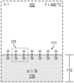
도 1a, 1b, 1c, 1d, 1e, 1f, 1g 및 1h는 본 발명의 실시형태에 따라 약 400℃ 미만의 온도에서 공정 챔버 내에 동일계에서 주기적으로 수행되는 예시적인 질화 공정을 예시한다. 도 1a는 미반응성 표면을 포함하는 기판의 초기 상태를 나타내고, 도 1b는 제1 처리 단계를 나타내고, 도 1c는 질화물 필름을 형성하는 제1 질화 단계를 나타내고, 도 1d는 질화물 필름 상에 형성된 후속 미반응성 표면을 나타내고, 도 1e는 제2 처리 단계를 나타내고, 도 1f는 제2 질화 단계를 나타내고, 도 1g는 질화물 필름 상에 형성된 또 다른 후속 미반응성 표면을 나타내고, 도 1h는 제3 처리 단계를 나타낸다.1A, 1B, 1C, 1D, 1E, 1F, 1G, and 1H illustrate an exemplary nitridation process performed periodically in situ in a process chamber at a temperature of less than about 400° C. in accordance with an embodiment of the present invention. 1A shows an initial state of a substrate comprising an unreacted surface, FIG. 1B shows a first processing step, FIG. 1C shows a first nitridation step to form a nitride film, and FIG. 1D shows a subsequent step formed on the nitride film. FIG. 1e shows a second processing step, FIG. 1f shows a second nitriding step, FIG. 1g shows another subsequent unreacted surface formed on the nitride film, and FIG. 1h shows a third processing step. indicates
도 1a를 참조하면, 질화 공정(100)은 벌크 영역(118) 및 미반응성 표면(111)을 포함하는 기판(110)의 초기 상태를 포함한다. 미반응성 표면(111)은 말단 결합에 의해 패시베이션되는 패시베이션된 표면일 수 있다. 예를 들어, 미반응성 표면(111)은 도시된 바와 같이 수소화된 표면일 수 있다. 대안적으로, 미반응성 표면(111)은 다른 종(즉, 질소와 반응하여 질화물을 형성하는 기판(110)의 재료와 상이한 종)으로 말단화될 수 있다.Referring to FIG. 1A , nitridation process 100 includes an initial state of
다양한 실시형태에서 기판(110)은 반도체 기판이고, 일 실시형태에서 규소 기판이다. 다른 실시형태에서, 반도체 기판은 게르마늄(Ge)일 수 있거나, 갈륨(Ga), 비소(As), 질소(N) 등을 포함한 반도체 화합물일 수 있다. 대안적으로, 기판(110)은 금속성 기판 또는 유전체 기판일 수 있다. 예를 들어, 기판(110)은 알루미늄, 탄소(예를 들어, 그래핀) 또는 산화규소(SiO2)일 수 있다. 추가적으로, 기판(110)은 다수의 상이한 재료 층을 포함할 수 있고, 다층 기판의 상부 층일 수 있다. 예를 들어, 기판(110)은 다른 재료의 상부에 형성된 SiO2일 수 있다.In
기판(110)은 공정 챔버(102) 내에 배치된다. 공정 챔버(102)는 임의의 적합한 공정 챔버(102)일 수 있다. 그러나, 공정 챔버(102)는 단지 저온 공정 챔버이면 된다(예를 들어, 기판을 약 400℃ 초과로 가열할 필요는 없다). 다양한 실시형태에서 공정 챔버(102)는 다목적 공정 챔버이고, 일 실시형태에서 플라즈마 공정 챔버이다.
이제 도 1b를 참조하면, 질화 공정(100)은 공정 챔버(102)에서 동일계로 수행되는 제1 처리 단계를 추가로 포함하며, 여기서 에너지 플럭스(120)가 기판(110)의 미반응성 표면(111)에 제공된다. 에너지 플럭스(120)는 미반응성 표면(111)을 반응성 표면(112)으로 전환시킨다. 예를 들어, 미반응성 표면(111)이 수소화된 표면인 경우(도시된 바와 같음), 에너지 플럭스(120)는 충분한 에너지를 미반응성 표면(111)에 제공함으로써 수소를 제거하여 반응성 표면(112)을 떠나게 한다. 도시된 바와 같이, 반응성 표면(112)은 표면에 생성된 단글링 결합으로 인해 반응성일 수 있다(예를 들어, 반응성 표면(112)과의 반응은 에너지적으로 유리할 수 있다).Referring now to FIG. 1B , nitridation process 100 further includes a first processing step performed in situ in
일부 경우, 에너지 플럭스(120) 또는 처리 기간은 미반응성 표면의 영역만이 반응성이 되게 할 수 있다. 예를 들어, 미반응성 영역(예를 들어, 미반응성 영역(131)으로 정성적으로 표시됨)은 반응성 영역(예를 들어, 반응성 영역(132))으로 전환될 수 있지만, 미반응성 표면(111)의 다른 부분은 미반응성으로 남아 있다(예를 들어, 수소 말단화). 즉, 처리는 각 주기 동안 모든 수소를 제거할 수 없다.In some cases, the
에너지 플럭스(120)는 반응성 표면(112)에서 기판(110)의 벌크 재료(140)를 노출시킬 수 있다. 예를 들어, 기판(110)의 벌크 영역(118)은 벌크 재료(140)를 포함할 수 있다. 이러한 특정 예에서, 벌크 재료(140)는 Si이지만, 다른 벌크 재료도 가능하다. 본 개시내용의 목적을 위해, 용어 "벌크"는 기판(110)의 대부분을 구성하는 재료를 지칭한다(이는 다층 기판의 상부 층일 수 있다).
에너지 플럭스(120)는 기판 온도를 400℃ 초과로 상승시키지 않거나, 기판(110)의 기저 구조를 손상시키지 않는 임의의 적합한 방법을 사용하여 기판에 제공될 수 있다. 예를 들어, 에너지 플럭스(120)는 에너지 입자(예를 들어, 이온, 전자, 라디칼, 광자)를 사용하여 기판(110)에 제공될 수 있다. 다양한 실시형태에서 에너지 플럭스(120)는 에너지 입자의 빔(beam)이고, 일부 실시형태에서 플라즈마에 의해 발생된 에너지 입자의 혼합물이다. 예를 들어, 에너지 플럭스(120)는 전자 빔 조사, 이온 빔 조사(예를 들어, 불활성 이온, 예컨대 Ar+, He+ 등), 자외선(UV) 조사(즉, < 400 nm 파장), 불활성 라디칼 빔 조사, 불활성 가스 플라즈마(예를 들어, He 플라즈마, Ar 플라즈마 등), 또는 400℃ 초과 후 빠르게 저온으로 복귀하는 미반응성 표면의 열 플래싱을 포함할 수 있다.
일 실시형태에서, 에너지 플럭스(120)는 헬륨(He) 플라즈마에 의해 발생된다. 불활성 가스 플라즈마, 예컨대 He 플라즈마가 다음의 에너지 입자 빔의 조합인 에너지 플럭스 공급원으로서 작용할 수 있다: 이온, 전자, 라디칼 및 광자. He 플라즈마는 기판(110)의 표면을 달리 손상시키지 않으면서 말단 종의 결합을 파괴하기에 충분한 에너지를 갖는 이온(He+) 및 광자를 발생시킬 수 있다. 예를 들어, S-H 결합(도시된 바와 같음)의 특정 예에서, 에너지 플럭스(120)는 미반응성 표면(111)의 S-H 결합에 적어도 약 4.06 eV를 제공할 수 있다. 즉, 이온 및 광자의 평균 에너지는 적어도 약 4.06 eV일 수 있다. 그러나, 일부 경우, 더 낮은 에너지가 또한 표면으로부터 H를 제거하기에 충분할 수 있다(예를 들어, 모두 합하여 필요한 에너지를 제공함). 예를 들어, 이온 및 광자의 평균 에너지는 4.06 eV 미만일 수 있다(예를 들어, 1.114 eV 이하만큼 낮다).In one embodiment,
He 플라즈마에 의해 발생된 에너지 입자에는, 예를 들어 에너지 이온, 라디칼, 전자 및 광자가 포함될 수 있다. He 플라즈마의 특정 예에 대해서, 방출된 광자(예를 들어, UV 광자)는 유리한 에너지(예를 들어, 약 24 eV)를 가질 수 있다. 특히, He는 가벼워서 기판 표면(예를 들어, Si/SiN 표면)에 대한 충격이 최소이거나 손상을 주지 않고, 유리하게는 또한 표면으로부터 말단 종(예를 들어, H)을 효율적으로 제거할 수 있는 고 에너지 광자(약 24 eV), 이온 및 라디칼이라는 두 가지 장점을 제공할 수 있다.Energetic particles generated by the He plasma may include, for example, energetic ions, radicals, electrons, and photons. For the specific example of a He plasma, the emitted photons (eg, UV photons) may have advantageous energies (eg, about 24 eV). In particular, He is light so that the impact to the substrate surface (eg Si/SiN surface) is minimal or non-damaging, and advantageously also can efficiently remove terminal species (eg H) from the surface. It can offer two advantages: high-energy photons (about 24 eV), ions and radicals.
효율적으로 표면 결합을 파괴하는 데 필요한 에너지는 미반응성 표면(111)에 의해 에너지가 흡수되는 방법에 따라 달라질 수 있음을 유의해야 한다. 예를 들어, 입사 입자로부터의 에너지는 몇몇 국소 표면 원자들 중에 분산되어 필요한 입자 에너지를 증가시킬 수 있다. 추가적으로, 말단 종의 탈착 단면은 에너지 의존적일 수 있고, 단면을 최대화하면 유리하게는 효율이 향상될 수 있다. 기판에 대한 에너지 플럭스(120)의 균일성은 공정의 자가-제한적 특성으로 인해 대부분의 경우 중요하지 않지만, 바람직할 수 있다.It should be noted that the energy required to effectively break surface bonds may vary depending on how the energy is absorbed by the
다른 실시형태에서, 에너지 플럭스(120)는 열 플래싱(예를 들어, 밀리초 플래싱) 또는 집속 입자 빔(예를 들어, 이온 빔 공급원, 전자 빔 공급원, 예컨대 e-건, 광자 공급원, 예컨대 UV 램프, 라디칼 공급원, 예컨대 라디칼 발생기 등)과 같은 기술을 사용하여 부분적으로 또는 전체적으로 발생될 수 있다. 예를 들어, 열 플래싱 및/또는 집속 입자 빔은 유리하게는 에너지가 영역 선택적 필름 성장(예를 들어, ASD)을 허용하는 미반응성 표면(111)의 국소 영역(예를 들어, 미반응성 영역(131))으로 향하게 할 수 있다. 에너지 공급원(들)의 특정 선택은 구현 용이성, 에너지 이력, 균일성, 효율 및 디바이스 공정 상용성을 포함한 다양한 인자에 따라 좌우될 수 있다.In other embodiments, the
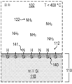
도 1c를 참조하면, 질화 공정(100)은 공정 챔버(102)에서 전구체 가스(122)를 제공하는 단계를 포함하는 질화 단계를 추가로 포함한다. 전구체 가스(122)는 기판(110)으로부터의 벌크 재료(140)(예를 들어, Si)와 반응하는 반응성 재료(141)(예를 들어, N)를 포함한다. 예를 들어, 전구체 가스(122)는 처리 단계 후 공정 챔버(102)로 도입될 수 있거나, 질화 공정(100) 동안 존재할 수 있다. 다양한 실시형태에서 전구체 가스(122)는 수소계 가스이고, 일부 실시형태에서 히드로질소 가스(N m H n , 또한 수소화질소로도 지칭됨)이다.Referring to FIG. 1C , nitridation process 100 further includes a nitridation step that includes providing
예를 들어, 전구체 가스(122)는 아잔(N m H m +2), 예컨대 히드라진(N2H4) 또는 시클로아잔(N m H m )일 수 있고, 질소계 이온, 예컨대 암모늄(NH4 +)을 포함할 수 있다. 일 실시형태에서, 전구체 가스(122)는 도시된 바와 같이 암모니아(NH3)이다. 전구체 가스(122)는 불활성 가스와 같은 다른 가스(예를 들어, 담체 가스)와 함께 제공될 수 있다. 일 실시형태에서, 전구체 가스(122)는 NH3이고, 1:4의 비(NH3:Ar)로 아르곤(Ar)과 함께 제공된다.For example,
그러나, 다른 작용기 및 N 및 H 이외의 원소가 또한 포함될 수 있다. 또한, 전구체 가스(122)는 질소를 포함할 수 없다. 일부 실시형태에서 전구체 가스(122)는 탄화수소 가스이고, 다른 실시형태에서 전구체 가스(122)는 또 다른 수소계 가스이다. 전구체 가스에 수소를 포함시키는 것은 기판 유형에 의해 영향을 받을 수 있다. 예를 들어, 미반응성 표면(111)이 매 주기 마다 수소로 말단화되는 경우 수소가 전구체 가스에 포함될 수 있지만, 다른 경우에는 또 다른 원소 또는 작용기일 수 있다.However, other functional groups and elements other than N and H may also be included. Also,
NH3(뿐만 아니라, 예를 들어, 다른 히드로질소 전구체)은 기판을 전혀 가열시키지 않으면서 질화 동안 용이하게 NH x (x = 1, 2) 및 H(+ H)로 해리된다는 장점을 가질 수 있다. 또한, 반응성 표면(112)(예를 들어, 표면 Si 원자로부터 단글링 결합을 가짐)의 존재 하에, 질화는 유리하게는 임의의 기판 온도에서 열역학적으로 유리할 수 있다(즉, 단글링 결합이 이용가능한 경우 질화에 대한 반응 장벽이 거의 없음). 도 1c 및 다른 유사한 도면에서, 질화된 표면 부위는 명확성을 위해 N으로 예시되었지만, 예를 들어, NH x (x = 1, 2)와 같은 다른 질소-함유 종일 수도 있음을 유의해야 한다. 유사한 개념이 N 이외의 다른 반응성 종에도 적용된다.NH 3 (as well as other hydronitrogen precursors, for example) may have the advantage that it readily dissociates into NH x ( x = 1, 2) and H(+ H) during nitridation without heating the substrate at all. . Also, in the presence of a reactive surface 112 (eg, having dangling bonds from surface Si atoms), nitridation may advantageously be thermodynamically favorable at any substrate temperature (ie, where dangling bonds are available). almost no reaction barrier to nitration). It should be noted that in FIG. 1C and other similar figures, the nitrided surface regions are illustrated as N for clarity, but may also be other nitrogen-containing species, such as, for example, NH x ( x = 1, 2). A similar concept applies to other reactive species other than N.
처리 단계는 진공(예를 들어, 중간 진공 또는 고 진공) 하에 수행될 수 있다. 추가적으로, 처리 단계는 비수소 환경(예를 들어, NH3과 같은 주변 수소계 가스의 존재 없이)에서 수행될 수 있고, 이어서 처리 공정(예를 들어, H 제거 공정) 중단과 동시에(또는 중단 후 시간을 두고) 전구체 가스(122)가 도입될 수 있다. 예를 들어, 에너지 플럭스(120)를 제공하는 에너지 공급원의 공급 전력이 제거(즉, 중단)될 수 있고, 전구체 가스(122)가 공정 챔버(102)로 도입되어 질화 단계가 시작될 수 있다.The treatment step may be performed under vacuum (eg, medium vacuum or high vacuum). Additionally, the treatment step can be performed in a non-hydrogen environment (eg, without the presence of an ambient hydrogen-based gas such as NH 3 ), followed by (or after) interruption of the treatment process (eg, H removal process). Over time)
대안적으로, 처리 단계 및 질화 단계는 동시에 수행될 수 있다. 즉, 에너지 플럭스(120)(예를 들어, He 플라즈마와 같은 불활성 플라즈마)가 전구체 가스(122)(예를 들어, NH3)와 동시에 공정 챔버(102)에 제공될 수 있다. 이러한 시나리오에서, H 원자는 기판(110)의 노출된 표면에서 연속적으로 축적되고 제거되어 심지어 H가 표면의 영역을 패시베이션하는 경우에도 열역학적으로(즉, 에너지적으로) 유리한 부위가 일정하게 발생될 수 있다. 그러한 시나리오는 전체 표면 또는 표면의 상당 부분이 임의의 주어진 시간에서 미반응성 또는 반응성인 것이 아니라 오히려 미반응성 영역(131) 및 반응성 영역(132)을 형성시키는 상황의 예일 수 있다.Alternatively, the treatment step and the nitriding step may be performed simultaneously. That is, an energy flux 120 (eg, an inert plasma such as a He plasma) may be provided to the
이제 도 1d를 참조하면, 질화 공정(100)의 질화 단계는 전구체 가스(122)의 반응성 재료(141)가 계속해서 기판(110)의 벌크 재료(140)와 결합을 형성하여 질화물 화합물(144)을 포함하는 질화물 층(142)을 계속 형성한다. 도시된 바와 같이, 질화물 화합물(144)은 반응성 재료(141)와 벌크 재료(140)의 결합(Si-N)을 포함한다. 일 실시형태에서, 질화물 화합물(144)은 Si3N4이다.Referring now to FIG. 1D , the nitridation step of the nitridation process 100 is such that the
그러나, 전구체 가스(122)는 또한 반응성 표면(112)을 후속 미반응성 표면(111)으로 전환시켜 질화 단계가 자가-제한되게 한다. 즉, 기판(110)의 표면에서 질화 반응은 반응 부위(예를 들어, 단글링 결합)를 말단 종(예를 들어, H)이 차지함에 따라 지연되거나 중단될 수 있다. 예를 들어, Si 단글링 결합은 질화를 촉진시킬 수 있지만, 질화는 도시된 바와 같이 H 원자에 의해 패시베이션되는 것처럼 단글링 결합이 이용가능하지 않는 경우 진행될 수 없다.However,
결과적으로, 처리 및 질화 단계는 유리하게는 층별(또는 실질적으로 층별) 공정에서 질화물 층을 형성하도록 주기적으로 반복될 수 있다. 그러한 층별 제어는 높은 균일성 및/또는 정확한 두께 제어를 가능하게 할 수 있다.Consequently, the treatment and nitriding steps can advantageously be repeated periodically to form the nitride layer in a layer-by-layer (or substantially layer-by-layer) process. Such layer-by-layer control can enable high uniformity and/or precise thickness control.
동일계에서의 주기적 공정은 유리하게는 통상적인 층별 공정(예컨대, 대략 분 단위의 단계를 갖는 ALD)과 비교할 경우 훨씬 더 높은 속도로 수행될 수 있다. 예를 들어, 처리 단계 및 질화 단계 둘 모두는 대략 초 단위로 발생할 수 있다. 일 실시형태에서, 처리 단계는 약 5초 미만 내에 수행된다. 일 실시형태에서, 질화 단계는 약 5초 미만 내에 수행된다. 처리 및 질화 단계의 기간은 에너지 플럭스, 주기 효율, 가스 유량, 펌핑 속도 및/또는 온도(예를 들어, 더 높은 온도에서 더 빠름)에 따라 좌우될 수 있다. 처리 단계 및 질화 단계 각각의 기간은 질화 공정의 주어진 구현예의 특정한 상세 사항에 따라 유사하거나 상이할 수 있다.The in situ cyclic process can advantageously be performed at much higher rates when compared to conventional layer-by-layer processes (e.g., ALD with steps on the order of minutes). For example, both the processing step and the nitriding step may occur on the order of seconds. In one embodiment, the processing step is performed in less than about 5 seconds. In one embodiment, the nitriding step is performed in less than about 5 seconds. The duration of the treatment and nitridation steps may depend on energy flux, cycle efficiency, gas flow rate, pumping speed and/or temperature (eg faster at higher temperatures). The duration of each of the treatment step and nitridation step may be similar or different depending on the specific details of a given embodiment of the nitridation process.
추가로, 질화 공정의 동일계 성능은 또한 유익하게는 공정 챔버로부터 기판을 제거하지 않으면서 다른 제작 공정 후에 질화물 형성을 가능하게 할 수 있다. 예를 들어, 공정 챔버는 질화 공정을 위한 질화 공정 챔버로서 사용되기 전에 및/또는 그 후에 플라즈마 공정 챔버로서 사용되는 다목적 공정 챔버일 수 있다.Additionally, the in situ performance of the nitridation process may also advantageously enable nitride formation after other fabrication processes without removing the substrate from the process chamber. For example, the process chamber may be a multi-purpose process chamber that is used as a plasma process chamber before and/or after being used as a nitridation process chamber for a nitridation process.
이제 도 1e, 1f, 1g 및 1h를 참조하면, 처리 단계 및 질화 단계는 주기적인 방식으로 반복되어, 기판(110)에서 증가된 두께의 질화물 층(142)이 계속 형성되는 것으로 예시된다. 제2 처리 단계는 이전 질화 단계의 자가-제한적 특성의 결과로서 형성된 후속 미반응성 표면(111)이 반응성 표면(112)으로 전환되도록 수행되고(도 1e), 이는 결국 질화물 층(142)의 두께가 증가한 후 제2 질화 단계(도 1f) 동안 다시 미반응성 표면(111)으로 전환된다(도 1g). 에너지 플럭스(120)가 다시 제3 처리 단계(도 1h) 등에 적용된다.Referring now to FIGS. 1E, 1F, 1G, and 1H, the processing and nitridation steps are repeated in a cyclical fashion, illustrated as continuing to form an increased thickness of
상기 단계 각각은 약 400℃ 미만의 온도에서 수행된다. 예를 들어, 온도는 약 250℃ 미만일 수 있고, 실온일 수도 있다. 실온은 일반적으로 저온인 것으로 정의될 수 있고(예를 들어, 약 20℃ 내지 약 40℃, 예컨대 25℃, 22℃ 등), 공정 챔버 내에서의 주변 온도를 지칭할 수 있다. 그러나, "실온"은 또한 공정 중에 추가 챔버 또는 기판 가열이 제공되지 않는 상황을 지칭할 수 있다(예를 들어, 에너지 플럭스는 국소 표면 가열을 초래할 수 있다). 추가적으로, 상기 단계는 또한 실온 미만의 온도에서 수행될 수 있다(예를 들어, 0℃ 이하).Each of the above steps is performed at a temperature of less than about 400°C. For example, the temperature may be less than about 250° C., and may be room temperature. Room temperature may generally be defined as being low temperature (eg, from about 20° C. to about 40° C., such as 25° C., 22° C., etc.) and may refer to the ambient temperature within the process chamber. However, “room temperature” may also refer to situations in which no additional chamber or substrate heating is provided during processing (eg energy flux may result in localized surface heating). Additionally, the step can also be performed at a temperature below room temperature (eg, below 0° C.).
중요하게는, 기판 전체는 약 400℃ 초과로 상승되지 않고, 많은 경우 훨씬 더 낮다. 예를 들어, 추가 챔버 또는 기판 가열은 특정 목적에 바람직하지 않다면 회피될 수 있다(예를 들어, 특정 상황에서 유용할 수 있는 Si-NH x 결합된 필름). 예를 들어, 챔버 온도는 일부 실시형태에서 Si, N 및 H를 포함한 3원 화합물(규소 질소수화물)을 형성하도록 약 250℃에서 유지될 수 있다. 즉, 온도(약 400℃ 미만이고, 약 250℃ 미만일 수도 있음)는 질화물 층의 수소 함량을 제어하는 데 유용할 수 있다.Importantly, the substrate as a whole does not rise above about 400° C., and in many cases much lower. For example, additional chamber or substrate heating may be avoided if not desirable for a particular purpose (eg, Si-NH x bonded films, which may be useful in certain situations). For example, the chamber temperature may be maintained at about 250° C. to form a ternary compound (silicon nitrohydrate) comprising Si, N and H in some embodiments. That is, the temperature (less than about 400° C., and possibly less than about 250° C.) can be useful in controlling the hydrogen content of the nitride layer.
열 플래싱의 경우, 기판 표면의 온도는 미반응성 표면에 필요한 에너지를 제공하지만 기판의 다른 영역이 손상되는 것을 방지하도록 대략 밀리초 단위로 국소 증가할 수 있다.In the case of thermal flashing, the temperature of the substrate surface may increase locally on the order of milliseconds to provide the unreacted surface with the necessary energy but prevent other areas of the substrate from being damaged.
도 2는 본 발명의 실시형태에 따라 약 400℃ 미만의 온도에서 옥시질화규소를 형성하는 데 사용되는 또 다른 예시적인 질화 공정을 예시한다. 예로서, 도 2의 질화 공정은 도 1a 내지 1h의 질화 공정 또는 도 4의 필름 성장 공정과 같은 본원에 기재된 다른 필름 성장 공정의 특정 구현예일 수 있다(예를 들어, 질화 공정). 유사하게 표기된 요소는 이전에 설명된 바와 같을 수 있다.2 illustrates another exemplary nitridation process used to form silicon oxynitride at a temperature less than about 400° C. in accordance with an embodiment of the present invention. As an example, the nitridation process of FIG. 2 may be a specific embodiment of another film growth process described herein, such as the nitridation process of FIGS. 1A-1H or the film growth process of FIG. 4 (eg, a nitridation process). Likely labeled elements may be as previously described.
도 2를 참조하면, 질화 공정(200)은 벌크 영역(218) 및 질화물 층(242)을 포함하는 기판(210)을 포함한다. 여기서 그리고 이하에서, 패턴 [x10]이 뒤따르는 요소는 다양한 실시형태에서 플라즈마 공정 챔버의 관련 구현예일 수 있다는 규정이 간결성 및 명확성을 위해 채택되었음을 유의해야 한다. 예를 들어, 기판(210)은 달리 언급된 것을 제외하고는 기판(110)과 유사할 수 있다. 전술한 세 자리 숫자 넘버링 체계와 함께 유사한 용어를 사용함으로써 명확해지는 바와 같은, 유사한 규정이 다른 요소에 대해서도 채택되었다.Referring to FIG. 2 ,
질화 공정(200)은 또한 간결성 및 명확성을 위해, 질화 단계의 대표적인 자가-제한된 단계에 의해서만 예시되었고, 나머지 단계들은 도 1a 내지 1h의 것과 유사하지만, 약간의 차이가 있고, 그 중 일부가 하기에 기재된다. 질화 공정(200)에서, 기판(210)은 산화물이다(예를 들어, 전체 층 또는 다층 기판 상의 산화물 층). 기판(210)의 벌크 영역(218)은 도시된 바와 같이 SiO2를 포함하여, Si 및 O 둘 모두를 포함하는 벌크 재료(240)를 생성한다.
전구체 가스(222)는 에너지 플럭스를 기판(210)의 미반응성 표면(211)으로 전달하는 처리 단계 동안 또는 그 후 질화 단계 동안 제공된다. 전구체 가스(222)는 반응성 재료(241)(도시된 바와 같은 N)를 포함하는 히드로질소 가스이지만, 상기 기재된 바와 같은 다른 가스일 수도 있다. 일 실시형태에서, 전구체 가스(222)는 NH3이다.
생성된 질화물 층(242)은 반응성 재료(241)(N)와 벌크 재료(240)(Si 및 산소, O)의 반응으로부터 형성된 옥시질화물 화합물(244)을 포함한다. 하나의 특정 예에서, 옥시질화물 화합물(244)은 옥시질화규소(예를 들어, Si2N2O, 또는 SiO2 와 Si3N4 사이에서 국소 변형이 있는 어느 정도의 무정형 상태)이지만, 질화 공정(200)은 다른 옥시질화물의 형성으로 일반화될 수 있다.The resulting
도 3은 본 발명의 실시형태에 따라 약 400℃ 미만의 온도에서 탄화규소를 형성하는 데 사용되는 예시적인 탄화 공정을 예시한다. 도 3의 탄화 공정은, 예를 들어 도 4의 필름 성장 공정과 같은 본원에 기재된 다른 필름 성장 공정의 특정 구현예일 수 있다. 유사하게 표기된 요소는 이전에 설명된 바와 같을 수 있다.3 illustrates an exemplary carbonization process used to form silicon carbide at a temperature less than about 400° C. in accordance with an embodiment of the present invention. The carbonization process of FIG. 3 may be specific embodiments of other film growth processes described herein, such as, for example, the film growth process of FIG. 4 . Likely labeled elements may be as previously described.
도 3을 참조하면, 탄화 공정(300)은 벌크 영역(318) 및 탄화물 층(342)을 포함하는 기판(310)을 포함한다. 도 2에서와 같이, 탄화 공정(300)은 간결성 및 명확성을 위해 탄화 단계(이는 질화 단계와 유사함)의 대표적인 자가-제한된 단계에 의해서만 예시된다. 나머지 단계들은 도 1a 내지 1h의 것과 유사하지만, 약간의 차이가 있고, 그 중 일부가 하기에 기재된다.Referring to FIG. 3 , a
탄화 공정(300)에서, 기판(310)은 반도체이고, 일부 실시형태에서 Si이다(예를 들어, 전체 층 또는 다층 기판 상의 Si 층). 기판(310)의 벌크 영역(318)은 도시된 바와 같이 Si를 갖는 벌크 재료(340)를 포함한다. 전구체 가스(322)는 에너지 플럭스를 기판(310)의 미반응성 표면(311)으로 전달하는 처리 단계 동안 또는 그 후 탄화 단계 동안 제공된다.In
상기 기재된 전구체와 반대로, 전구체 가스(322)는 반응성 재료(341)(도시된 바와 같은 탄소, C)를 포함하는 탄화수소 가스이지만, C를 포함한 다른 가스일 수도 있다. 다양한 실시형태에서, 전구체 가스(322)는 알칸이다. 대안적으로 또는 추가적으로, 전구체 가스(322)는 다른 탄화수소 가스, 예컨대 알켄, 알킨, 및/또는 환형 및 치환된 버전을 포함한다. 일 실시형태에서, 전구체 가스(322)는 메탄(CH4)을 포함한다. 일 실시형태에서, 전구체 가스(322)는 에틸렌(C2H4)을 포함한다.Contrary to the precursors described above,
생성된 탄화물 층(342)은 반응성 재료(341)(C)와 벌크 재료(340)(Si)의 반응으로부터 형성된 탄화물 화합물(344)을 포함한다. 하나의 특정 예에서, 탄화물 화합물(344)은 탄화규소(SiC)이지만, 탄화 공정(300)은 다른 탄화물의 형성으로 일반화될 수 있다.The resulting
도 4는 본 발명의 실시형태에 따라 약 400℃ 미만의 온도에서 수행되는 예시적인 필름 성장 공정을 예시한다. 예로서, 도 4의 필름 성장 공정은 도 1a 내지 1h 및 2의 질화 공정 또는 도 3의 탄화 공정과 같은 본원에 기재된 다른 필름 성장 공정(예를 들어, 질화 공정, 탄화 공정 등)의 일반적인 구현예일 수 있다. 유사하게 표기된 요소는 이전에 설명된 바와 같을 수 있다.4 illustrates an exemplary film growth process performed at a temperature less than about 400° C. in accordance with an embodiment of the present invention. As an example, the film growth process of FIG. 4 would be a typical implementation of other film growth processes described herein (eg, nitridation process, carbonization process, etc.) such as the nitridation process of FIGS. 1A-1H and 2 or the carbonization process of FIG. 3 . can Likely labeled elements may be as previously described.
도 4를 참조하면, 필름 성장 공정(400)은 벌크 영역(418) 및 필름(442)을 포함하는 기판(410)을 포함한다. 도 2에서와 같이, 필름 성장 공정(400)은 간결성 및 명확성을 위해 필름 성장 단계(이는 질화 단계의 일반화임)의 대표적인 자가-제한된 단계에 의해서만 예시된다. 나머지 단계들은 도 1a 내지 1h의 것과 유사하지만, 약간의 차이가 있고, 그 중 일부가 하기에 기재된다.Referring to FIG. 4 , a
필름(442)은 필름 성장 단계 동안 형성되며, 여기서 전구체 가스(422)는 에너지 플럭스를 기판(410)의 미반응성 표면(411)으로 전달하는 처리 단계 동안 또는 그 후에 제공된다. 필름(442)은 전구체 가스(422)의 반응성 재료(441)와 기판(410)의 벌크 재료(440)의 반응 결과이다.Film 442 is formed during a film growth step, where
이러한 일반화된 시나리오에서, 반응성 재료(441)는 일부 종 Z(구체적인 예는 N 및 C임)로서 예시되지만, 벌크 재료(440)는 일부 종 X(구체적으로 Si 및 Si, O를 포함하는 예가 제공됨)로서 예시된다. 이어서, 필름(442)은 X 및 Z를 포함하는(예를 들어, X-Z 결합) 화합물(444)을 포함한다. 예를 들어, X는 C(예를 들어, 기판(410)이 그래핀인 경우), 알루미늄(Al) 및 구체적으로 기재되지 않은 다른 것일 수 있다. 마찬가지로, Z는 O, 반응성 작용기 등일 수 있다.In this generalized scenario,
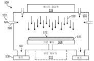
도 5는 본 발명의 실시형태에 따른 예시적인 필름 성장 장치를 예시한다. 도 5의 필름 성장 장치는 도 1a 내지 1h 및 2 내지 4의 필름 성장 공정과 같은 본원에 기재된 임의의 필름 성장 공정을 수행하는 데 사용될 수 있다. 도 5의 필름 성장 장치는 또한 도 7 및 8에서 후속적으로 기재되는 바와 같은 필름 성장 방법을 수행하는 데 사용될 수 있다. 유사하게 표기된 요소는 이전에 설명된 바와 같을 수 있다.5 illustrates an exemplary film growing apparatus in accordance with an embodiment of the present invention. The film growing apparatus of FIG. 5 can be used to perform any of the film growing processes described herein, such as the film growing processes of FIGS. 1A-1H and 2-4. The film growing apparatus of FIG. 5 can also be used to perform a film growing method as subsequently described in FIGS. 7 and 8 . Likely labeled elements may be as previously described.
도 5를 참조하면, 필름 성장 장치(500)는 공정 챔버(502) 내에서 기판(510)을 지지하는 기판 홀더(504)를 포함한다. 예를 들어, 공정 챔버(502)는 다목적 공정 챔버일 수 있다. 전구체 가스(522)와 같은 다양한 가스(여기서는 NH3으로서 도시됨)가 하나 이상의 가스 주입구(506)를 통해 공정 챔버(502)로 제공될 수 있다. 압력(예를 들어, 중간 진공, 고 진공 등)은 펌프(508)를 사용하여 공정 챔버(502) 내에서 조절될 수 있으며, 펌프는 전구체 가스(522)뿐만 아니라 다른 가스를 하나 이상의 가스 출구(507)를 통해 공정 챔버(502) 밖으로 배출시킨다.Referring to FIG. 5 , a
에너지 공급원(514)은 기판(510)의 표면(512)에 에너지 플럭스(520)를 제공한다. 상기 기재된 바와 같이, 에너지 플럭스(520)는 전구체 가스(522) 후에 또는 그 동안에 제공될 수 있다. 에너지 공급원(514)은 플라즈마 공급원, 이온 빔 공급원, 전자 빔 공급원, 광자 공급원(예를 들어, UV 광 공급원), 라디칼 빔 공급원, 열 플래싱 공급원 등과 같은 임의의 적합한 에너지 공급원 또는 에너지 공급원들의 조합일 수 있다.
온도 제어(즉, 약 400℃ 미만)가 바람직한 경우, 선택적인 온도 제어기(516)가 기판 홀더(504) 및/또는 기판(510)의 온도를 제어하도록 포함될 수 있다. 선택적인 온도 제어기(516)는 또한 일부 구현예에서 열 플래싱 공급원과 같은 에너지 공급원을 포함할 수 있다.If temperature control (ie, less than about 400° C.) is desired, an
도 6은 본 발명의 실시형태에 따른 예시적인 플라즈마 공정 장치를 예시한다. 도 6의 플라즈마 공정 장치는 도 1a 내지 1h 및 2 내지 4의 필름 성장 공정과 같은 본원에 기재된 임의의 필름 성장 공정을 수행하는 데 사용될 수 있다. 추가적으로, 도 6의 플라즈마 공정 장치는 도 7 및 8에서 후속적으로 기재되는 바와 같은 필름 성장 방법을 수행하는 데 사용될 수 있다. 유사하게 표기된 요소는 이전에 설명된 바와 같을 수 있다.6 illustrates an exemplary plasma processing apparatus in accordance with an embodiment of the present invention. The plasma processing apparatus of FIG. 6 can be used to perform any of the film growth processes described herein, such as the film growth processes of FIGS. 1A-1H and 2-4. Additionally, the plasma processing apparatus of FIG. 6 can be used to perform the film growth method as subsequently described in FIGS. 7 and 8 . Likely labeled elements may be as previously described.
도 6을 참조하면, 플라즈마 공정 장치(600)는 플라즈마 공정 챔버(602) 내에서 기판(610)을 지지하는 기판 홀더(604)를 포함한다. 도 6의 플라즈마 공정 장치는 도 5의 필름 성장 장치의 특정 구현예일 수 있고, 여기서 에너지 공급원은 플라즈마 공급원(614)이고, 플라즈마 공정 챔버(602)에서 발생된 플라즈마(620)에 의해 기판(610)의 표면(612)으로 에너지 플럭스가 제공된다. 예를 들어, 플라즈마(620)는 하나 이상의 가스 주입구(606)를 통해 공급된 불활성 가스(624)(예를 들어, He)를 사용하여 발생된 불활성 플라즈마(예를 들어, He 플라즈마)일 수 있다.Referring to FIG. 6 , a
전구체 가스(622)는 또한 가스 주입구(606)(예를 들어, 불활성 가스(624)와 동일한 가스 주입구 또는 전용 가스 주입구)를 통해 제공될 수 있다. 펌프(608)는 하나 이상의 가스 출구(607)를 통해 플라즈마 공정 챔버(602)로부터 전구체 가스(622), 불활성 가스(624) 및 임의의 다른 가스를 배출한다. 상기와 같이, 선택적인 온도 제어기(616)가 기판 온도 제어가 바람직한 경우 포함될 수 있다.
도 7은 본 발명의 실시형태에 따른 예시적인 질화 방법을 예시한다. 도 7의 방법은 다른 방법 및 공정과 조합될 수 있고, 예로서 도 5의 필름 성장 장치 또는 도 6의 플라즈마 공정 장치와 같은 본원에 기재된 임의의 필름 성장 장치를 사용하여 수행될 수 있다. 또한, 도 7의 방법은, 예로서 도 1a 내지 1h의 질화 공정 또는 도 4의 필름 성장 공정과 같은 본원에 기재된 임의의 공정 실시형태의 일부 또는 모든 단계를 적용할 수 있다. 도 7의 단계의 배열 및 넘버링은 논리적 순서로 나타내었지만, 제한되지는 않는다. 도 7의 방법 단계는 당업자에게 명백할 수 있는 바와 같은 임의의 적합한 순서로 또는 서로 동시에 수행될 수 있다.7 illustrates an exemplary nitridation method in accordance with an embodiment of the present invention. The method of FIG. 7 can be combined with other methods and processes and can be performed using any of the film growing devices described herein, such as, for example, the film growing device of FIG. 5 or the plasma process device of FIG. 6 . Further, the method of FIG. 7 may employ some or all of the steps of any process embodiment described herein, such as, for example, the nitridation process of FIGS. 1A-1H or the film growth process of FIG. 4 . The arrangement and numbering of steps in FIG. 7 are shown in logical order, but are not limiting. The method steps of FIG. 7 may be performed concurrently with one another or in any suitable order as will be apparent to one skilled in the art.
도 7을 참조하면, 질화 방법(700)의 단계(701)는 기판의 미반응성 표면을 에너지 플럭스에 노출시킴으로써 미반응성 표면을 처리하여 미반응성 표면을 반응성 표면으로 전환시키는 단계를 포함한다. 질화 방법(700)의 단계(702)는 질소계 가스를 사용하여 반응성 표면을 질화시켜 반응성 표면을 후속 미반응성 표면을 포함하는 질화물 층으로 전환시키는 단계를 포함한다. 단계(701) 및 단계(702)는 약 400℃ 미만의 온도로 공정 챔버에서(즉, 공정 챔버로부터 기판을 제거하지 않으면서 동일계에서) 수행된다.Referring to FIG. 7 , step 701 of
단계(703)는 단계(701) 및 단계(702)를 주기적으로 수행하는 것이다. 구체적으로, 단계(702)는 후속적으로 수행되는 처리 단계(단계(701))에 의해 제거될 수 있는 후속 미반응성 표면에 의해 자가-제한될 수 있다. 질화 방법(700)은 질화물 필름의 원하는 균일성 및/또는 두께가 달성될 때까지 계속될 수 있다. 일부 경우, 방법론(예를 들어, 동일계)은 공정 조건이 조절될 수 있거나 주기가 적시에 종결될 수 있도록 질화물 층의 상태를 동력학적으로 결정하기 위해 이용될 수 있다. 예를 들어, 동일계 타원편광법이 사용될 수 있다. 추가적으로, 에너지 플럭스(예를 들어, 플라즈마 발생) 동안 종들의 비(예를 들어, N/H 신호 비)가 통찰력을 부여할 수 있다.Step 703 is to perform
도 8은 본 발명의 실시형태에 따른 예시적인 필름 성장 방법을 예시한다. 도 8의 방법은 다른 방법 및 공정과 조합될 수 있고, 예로서 도 5의 필름 성장 장치 또는 도 6의 플라즈마 공정 장치와 같은 본원에 기재된 임의의 필름 성장 장치를 사용하여 수행될 수 있다. 추가적으로, 도 8의 방법은, 예로서 도 1a 내지 1h의 질화 공정 또는 도 4의 필름 성장 공정과 같은 본원에 기재된 임의의 공정 실시형태의 일부 또는 모든 단계를 적용할 수 있다. 도 8의 단계의 배열 및 넘버링은 논리적 순서로 나타내었지만, 제한되지는 않는다. 도 8의 방법 단계는 당업자에게 명백할 수 있는 바와 같은 임의의 적합한 순서로 또는 서로 동시에 수행될 수 있다.8 illustrates an exemplary film growth method in accordance with an embodiment of the present invention. The method of FIG. 8 can be combined with other methods and processes and can be performed using any of the film growing devices described herein, such as, for example, the film growing device of FIG. 5 or the plasma process device of FIG. 6 . Additionally, the method of FIG. 8 may employ some or all of the steps of any process embodiment described herein, such as, for example, the nitridation process of FIGS. 1A-1H or the film growth process of FIG. 4 . The arrangement and numbering of steps in FIG. 8 are shown in logical order, but are not limiting. The method steps of FIG. 8 may be performed concurrently with one another or in any suitable order as will be apparent to one skilled in the art.
도 8을 참조하면, 필름 성장 방법(800)의 단계(801)는 기판의 수소화된 표면 상에 입사한 에너지 플럭스를 사용하여 수소화된 표면으로부터 수소를 제거함으로써 수소화된 표면을 처리하여 수소화된 표면을 반응성 표면으로 전환시키는 단계를 포함한다. 기판은 제1 재료를 포함한다. 반응성 표면은 단계(802)에서 제2 재료를 포함하는 수소계 가스에 노출되어 반응성 표면이 필름으로 전환된다. 필름은 후속 수소화된 표면, 및 제1 재료 및 제2 재료를 포함하는 화합물을 포함한다. 단계(801 및 802)는 약 400℃ 미만의 온도로 공정 챔버에서 수행된다. 단계(803)는 단계(801) 및 단계(802)를 주기적으로 수행하는 것이다.Referring to FIG. 8 , step 801 of the
본 발명의 예시적인 실시형태가 여기에 요약되어 있다. 본원에 제출된 청구범위뿐만 아니라 명세서 전체로부터 다른 실시형태가 또한 이해될 수 있다.Exemplary embodiments of the present invention are summarized herein. Other embodiments may also be understood from the entire specification as well as the claims filed herein.
실시예 1. 약 400℃ 미만의 온도에서 공정 챔버 내에 동일계에서 다음의 단계를 주기적으로 수행하는 것을 포함하는, 질화 방법: 공정 챔버에서 기판의 미반응성 표면을 에너지 플럭스에 노출시킴으로써 미반응성 표면을 처리하여 미반응성 표면을 반응성 표면으로 전환시키는 단계; 및 질소계 가스를 사용하여 반응성 표면을 질화시켜 반응성 표면을 후속 미반응성 표면을 포함하는 질화물 층으로 전환시키는 단계.Example 1. A method of nitridation comprising periodically performing the following steps in situ in a process chamber at a temperature of less than about 400° C.: treating the unreactive surface of a substrate by exposing it to an energy flux in the process chamber. converting the non-reactive surface into a reactive surface; and nitriding the reactive surface using a nitrogen-based gas to convert the reactive surface into a nitride layer comprising a subsequent unreactive surface.
실시예 2. 실시예 1에 있어서, 미반응성 표면의 각각의 처리를 약 5초 미만 동안 수행하고, 반응성 표면의 각각의 질화를 약 5초 미만 동안 수행하는, 방법.Example 2. The method of Example 1, wherein each treatment of the unreactive surface is performed for less than about 5 seconds and each nitridation of the reactive surface is performed for less than about 5 seconds.
실시예 3. 실시예 1 및 2 중 하나에 있어서, 질소계 가스는 암모니아(NH3)를 포함하는, 방법.Example 3. The method of any one of Examples 1 and 2, wherein the nitrogenous gas comprises ammonia (NH3).
실시예 4. 실시예 1 내지 3 중 하나에 있어서, 미반응성 표면을 처리하는 단계는 공정 챔버에서 발생된 플라즈마를 사용하여 에너지 플럭스를 제공하는 단계를 포함하는, 방법.Example 4. The method of any of Examples 1-3, wherein treating the unreacted surface comprises providing an energy flux using a plasma generated in the process chamber.
실시예 5. 실시예 1 내지 4 중 하나에 있어서, 미반응성 표면을 처리하는 단계는 이온 빔 공급원, 전자 빔 공급원, 광자 공급원, 라디칼 공급원 또는 열 플래싱 공급원을 사용하여 에너지 플럭스를 제공하는 단계를 포함하는, 방법.Example 5 The method of any one of Examples 1-4, wherein treating the unreacted surface comprises providing an energy flux using an ion beam source, an electron beam source, a photon source, a radical source, or a thermal flashing source. How to.
실시예 6. 실시예 1 내지 5 중 하나에 있어서, 미반응성 표면을 처리하는 단계는 공급 전력을 적용하여 에너지 플럭스를 발생시키는 단계, 및 질소계 가스의 공정 챔버로의 전파를 방지하는 단계를 동시에 포함하며, 반응성 표면을 질화시키는 단계는 공급 전력을 제거하는 단계, 및 질소계 가스를 공정 챔버로 공급하는 단계를 동시에 포함하는, 방법.Example 6. The method of any one of Examples 1-5, wherein treating the unreacted surface simultaneously applies supply electrical power to generate an energy flux and prevents propagation of a nitrogen-based gas into the process chamber. wherein nitriding the reactive surface simultaneously includes removing the supply power and supplying a nitrogen-based gas to the process chamber.
실시예 7. 약 400℃ 미만의 온도에서 플라즈마 공정 챔버 내에 동일계에서 다음의 단계를 주기적으로 수행하는 것을 포함하는, 질화 방법: 플라즈마 공정 챔버에서 발생된 플라즈마로부터의 이온 및 광자로 규소 기판에 충격을 줌으로써 규소 기판의 미반응성 영역으로부터 수소를 제거하여 미반응성 영역을 반응성 영역으로 전환시키는 단계; 및 히드로질소 가스를 사용하여 반응성 영역을 질화시켜 반응성 영역을 후속 미반응성 영역을 포함하는 질화물 영역으로 전환시키는 단계.Example 7. A nitridation method comprising periodically performing the following steps in situ in a plasma process chamber at a temperature of less than about 400° C.: bombarding a silicon substrate with ions and photons from a plasma generated in the plasma process chamber. converting the unreacted region into a reactive region by removing hydrogen from the unreacted region of the silicon substrate by providing; and nitriding the reactive region using hydronitrogen gas to convert the reactive region into a nitride region comprising a subsequent unreacted region.
실시예 8. 실시예 7에 있어서, 이온 및 광자는 약 4.06 eV 초과의 평균 에너지를 포함하는, 방법.Example 8. The method of Example 7, wherein the ions and photons comprise an average energy greater than about 4.06 eV.
실시예 9. 실시예 7 및 8 중 하나에 있어서, 미반응성 영역으로부터 수소를 제거하는 단계 및 반응성 영역을 질화시키는 단계를 동시에 수행하는, 방법.Example 9. The method of any one of Examples 7 and 8, wherein removing hydrogen from the unreacted region and nitriding the reactive region are performed simultaneously.
실시예 10. 실시예 7 내지 9 중 하나에 있어서, 히드로질소 가스는 암모니아(NH3)를 포함하는, 방법.Example 10. The method of any of Examples 7-9, wherein the hydronitrogen gas comprises ammonia (NH 3 ).
실시예 11. 실시예 7 내지 10 중 하나에 있어서, 플라즈마 공정 챔버에서 발생된 플라즈마는 헬륨 플라즈마인, 방법.Example 11. The method of any one of examples 7-10, wherein the plasma generated in the plasma processing chamber is a helium plasma.
실시예 12. 실시예 7 내지 11 중 하나에 있어서, 온도는 약 30℃ 미만인, 방법.Example 12. The method of any of Examples 7-11, wherein the temperature is less than about 30°C.
실시예 13. 약 400℃ 미만의 온도에서 공정 챔버 내에 동일계에서 다음의 단계를 주기적으로 수행하는 것을 포함하는, 필름 성장 방법: 공정 챔버에서 제1 재료를 포함하는 기판의 수소화된 표면 상에 입사한 에너지 플럭스를 사용하여 수소화된 표면으로부터 수소를 제거함으로써 수소화된 표면을 처리하여 수소화된 표면을 반응성 표면으로 전환시키는 단계, 및 반응성 표면을 제2 재료를 포함하는 수소계 가스에 노출시켜 반응성 표면을 후속 수소화된 표면 및 제1 재료 및 제2 재료를 포함하는 화합물을 포함하는 필름으로 전환시키는 단계.Example 13. A method of growing a film comprising periodically performing the following steps in situ in a process chamber at a temperature of less than about 400° C.: incident on a hydrogenated surface of a substrate comprising a first material in a process chamber. treating the hydrogenated surface by removing hydrogen from the hydrogenated surface using an energy flux to convert the hydrogenated surface into a reactive surface, and exposing the reactive surface to a hydrogen-based gas comprising a second material to subsequently convert the reactive surface to Converting to a film comprising a hydrogenated surface and a compound comprising the first material and the second material.
실시예 14. 실시예 13에 있어서, 단계들을 주기적으로 반복하기 전에, 기판을 약 250℃의 온도로 가열하는 단계를 추가로 포함하고, 단계들을 주기적으로 반복하는 동안 상기 온도를 유지시키는, 방법.Example 14. The method of Example 13, further comprising heating the substrate to a temperature of about 250° C. prior to periodically repeating the steps, and maintaining the temperature during the periodic repetition of the steps.
실시예 15. 실시예 13 및 14 중 하나에 있어서, 단계들을 주기적으로 반복하기 전에, 공정 챔버 내에서 기판을 플라즈마 공정으로 처리하는 단계를 추가로 포함하고, 상기 기판을 플라즈마 공정과 단계들을 주기적으로 수행하는 것 사이에서 공정 챔버로부터 제거하지 않는, 방법.Example 15 The method of any one of Examples 13 and 14, further comprising subjecting the substrate to a plasma process in the process chamber prior to periodically repeating the steps, wherein the plasma process and steps are periodically repeated. A method that does not remove from the process chamber between performances.
실시예 16. 실시예 15에 있어서, 기판의 수소화된 표면을 처리하는 단계는 수소화된 표면을 열 플래싱하여 수소화된 표면의 온도를 국소적으로 증가시키는 단계를 포함하는, 방법.Example 16. The method of Example 15, wherein treating the hydrogenated surface of the substrate comprises thermal flashing the hydrogenated surface to locally increase the temperature of the hydrogenated surface.
실시예 17. 실시예 13 내지 16 중 하나에 있어서, 수소화된 표면을 처리하는 단계는 공정 챔버에서 발생된 플라즈마를 사용하여 수소화된 표면을 처리하는 단계를 포함하는, 방법.Example 17. The method of any of examples 13-16, wherein treating the hydrogenated surface comprises treating the hydrogenated surface using a plasma generated in a process chamber.
실시예 18. 실시예 13 내지 17 중 하나에 있어서, 제1 재료는 질소이고, 제2 재료는 규소이고, 화합물은 질화규소인, 방법.Example 18. The method of any of examples 13-17, wherein the first material is nitrogen, the second material is silicon, and the compound is silicon nitride.
실시예 19. 실시예 13 내지 17 중 하나에 있어서, 제1 재료는 질소이고, 제2 재료는 산화규소이고, 화합물은 옥시질화규소인, 방법.Example 19. The method of any of Examples 13-17, wherein the first material is nitrogen, the second material is silicon oxide, and the compound is silicon oxynitride.
실시예 20. 실시예 13 내지 17 중 하나에 있어서, 제1 재료는 탄소이고, 제2 재료는 규소이고, 화합물은 탄화규소인, 방법.Example 20. The method of any of Examples 13-17, wherein the first material is carbon, the second material is silicon, and the compound is silicon carbide.
본 발명이 예시적인 실시형태를 참조하여 설명되었지만, 이 설명이 제한된 의미로 해석되는 것은 아니다. 본 발명의 다른 실시형태뿐만 아니라, 예시적인 실시형태의 다양한 수정 및 조합이, 상세한 설명을 참조할 경우, 당업자에게 명백할 것이다. 따라서, 첨부된 청구범위는 임의의 그러한 변경 또는 실시형태를 포함하는 것으로 의도된다.Although the present invention has been described with reference to exemplary embodiments, this description is not to be construed in a limiting sense. Various modifications and combinations of the illustrative embodiments, as well as other embodiments of the present invention, will become apparent to those skilled in the art upon reference to the detailed description. Accordingly, the appended claims are intended to cover any such permutations or embodiments.
Claims (20)
상기 공정 챔버에서 기판의 미반응성 표면을 에너지 플럭스에 노출시킴으로써 상기 미반응성 표면을 처리하여 상기 미반응성 표면을 반응성 표면으로 전환시키는 단계; 및
질소계 가스를 사용하여 상기 반응성 표면을 질화시켜 상기 반응성 표면을 후속 미반응성 표면을 포함하는 질화물 층으로 전환시키는 단계.A method of nitriding comprising periodically performing the following steps in situ in a process chamber at a temperature of less than about 400° C.:
converting the unreactive surface to a reactive surface by treating the unreactive surface of the substrate by exposing the unreactive surface to an energy flux in the process chamber; and
Nitriding the reactive surface using a nitrogen-based gas to convert the reactive surface into a nitride layer comprising a subsequent unreactive surface.
미반응성 표면의 각각의 처리를 약 5초 미만 동안 수행하고,
반응성 표면의 각각의 질화를 약 5초 미만 동안 수행하는 것을 추가로 포함하는, 방법.According to claim 1,
each treatment of the unreacted surface is performed for less than about 5 seconds;
further comprising performing each nitridation of the reactive surface for less than about 5 seconds.
상기 질소계 가스는 암모니아 (NH3)를 포함하는, 방법.According to claim 1,
wherein the nitrogen-based gas comprises ammonia (NH 3 ).
상기 미반응성 표면을 처리하는 단계는 상기 공정 챔버에서 발생된 플라즈마를 사용하여 상기 에너지 플럭스를 제공하는 단계를 포함하는, 방법.According to claim 1,
wherein treating the unreacted surface comprises providing the energy flux using a plasma generated in the process chamber.
상기 미반응성 표면을 처리하는 단계는 이온 빔 공급원, 전자 빔 공급원, 광자 공급원, 라디칼 공급원 또는 열 플래싱 공급원을 사용하여 상기 에너지 플럭스를 제공하는 단계를 포함하는, 방법.According to claim 1,
wherein treating the unreacted surface comprises providing the energy flux using an ion beam source, an electron beam source, a photon source, a radical source or a thermal flashing source.
상기 미반응성 표면을 처리하는 단계는
공급 전력을 적용하여 상기 에너지 플럭스를 발생시키는 단계, 및
상기 질소계 가스의 상기 공정 챔버로의 전파를 방지하는 단계를 동시에 포함하고;
상기 반응성 표면을 질화시키는 단계는
상기 공급 전력을 제거하는 단계, 및
상기 질소계 가스를 상기 공정 챔버로 공급하는 단계를 동시에 포함하는, 방법.According to claim 1,
The step of treating the unreacted surface is
applying power supply to generate the energy flux; and
simultaneously preventing propagation of the nitrogen-based gas into the process chamber;
Nitriding the reactive surface
removing the power supply; and
simultaneously supplying the nitrogen-based gas to the process chamber.
상기 플라즈마 공정 챔버에서 발생된 플라즈마로부터의 이온 및 광자로 규소 기판에 충격을 줌으로써 상기 규소 기판의 미반응성 영역으로부터 수소를 제거하여 상기 미반응성 영역을 반응성 영역으로 전환시키는 단계; 및
히드로질소 가스를 사용하여 상기 반응성 영역을 질화시켜 상기 반응성 영역을 후속 미반응성 영역을 포함하는 질화물 영역으로 전환시키는 단계.A method of nitriding comprising periodically performing the following steps in situ in a plasma process chamber at a temperature of less than about 400° C.:
converting the unreactive region into a reactive region by removing hydrogen from the unreactive region of the silicon substrate by bombarding the silicon substrate with ions and photons from the plasma generated in the plasma process chamber; and
nitriding the reactive region using hydronitrogen gas to convert the reactive region into a nitride region comprising a subsequent unreacted region.
상기 이온 및 광자는 약 4.06 eV 초과의 평균 에너지를 포함하는, 방법.According to claim 7,
wherein the ions and photons comprise an average energy greater than about 4.06 eV.
상기 미반응성 영역으로부터 상기 수소를 제거하는 단계 및 상기 반응성 영역을 질화시키는 단계를 동시에 수행하는, 방법.According to claim 7,
The method of simultaneously performing the step of removing the hydrogen from the unreacted region and the step of nitriding the reactive region.
상기 히드로질소 가스는 암모니아(NH3)를 포함하는, 방법.According to claim 7,
wherein the hydronitrogen gas comprises ammonia (NH 3 ).
상기 플라즈마 공정 챔버에서 발생된 플라즈마는 헬륨 플라즈마인, 방법.According to claim 7,
The method of claim 1, wherein the plasma generated in the plasma processing chamber is a helium plasma.
상기 온도는 약 30℃ 미만인, 방법.According to claim 7,
wherein the temperature is less than about 30°C.
상기 공정 챔버에서 제1 재료를 포함하는 기판의 수소화된 표면 상에 입사한 에너지 플럭스를 사용하여 상기 수소화된 표면으로부터 수소를 제거함으로써 상기 수소화된 표면을 처리하여 상기 수소화된 표면을 반응성 표면으로 전환시키는 단계, 및
상기 반응성 표면을 제2 재료를 포함하는 수소계 가스에 노출시켜 상기 반응성 표면을 후속 수소화된 표면 및 상기 제1 재료 및 상기 제2 재료를 포함하는 화합물을 포함하는 필름으로 전환시키는 단계.A method of growing a film comprising periodically performing the following steps in situ in a process chamber at a temperature of less than about 400°C:
treating the hydrogenated surface by removing hydrogen from the hydrogenated surface using an energy flux incident on the hydrogenated surface of a substrate comprising a first material in the process chamber to convert the hydrogenated surface into a reactive surface. step, and
Exposing the reactive surface to a hydrogen-based gas comprising a second material to convert the reactive surface into a film comprising a subsequently hydrogenated surface and a compound comprising the first material and the second material.
상기 단계들을 주기적으로 반복하기 전에, 상기 기판을 약 250℃의 온도로 가열하는 단계를 추가로 포함하고, 상기 단계들을 주기적으로 반복하는 동안 상기 온도를 유지시키는, 방법.According to claim 13,
The method further comprises heating the substrate to a temperature of about 250° C. prior to periodically repeating the steps, and maintaining the temperature while repeating the steps periodically.
상기 단계들을 주기적으로 반복하기 전에, 상기 공정 챔버 내에서 상기 기판을 플라즈마 공정으로 처리하는 단계를 추가로 포함하고, 상기 기판을 상기 플라즈마 공정과 상기 단계들을 주기적으로 수행하는 것 사이에서 상기 공정 챔버로부터 제거하지 않는, 방법.According to claim 13,
further comprising subjecting the substrate to a plasma process within the process chamber prior to periodically repeating the steps, and removing the substrate from the process chamber between the plasma process and periodically performing the steps. How not to remove it.
상기 기판의 상기 수소화된 표면을 처리하는 단계는 상기 수소화된 표면을 열 플래싱하여 상기 수소화된 표면의 온도를 국소적으로 증가시키는 단계를 포함하는, 방법.According to claim 15,
Wherein treating the hydrogenated surface of the substrate comprises thermal flashing the hydrogenated surface to locally increase a temperature of the hydrogenated surface.
상기 수소화된 표면을 처리하는 단계는 상기 공정 챔버에서 발생된 플라즈마를 사용하여 상기 수소화된 표면을 처리하는 단계를 포함하는, 방법.According to claim 13,
The method of claim 1 , wherein treating the hydrogenated surface includes treating the hydrogenated surface using a plasma generated in the process chamber.
상기 제1 재료는 질소이고, 상기 제2 재료는 규소이고, 상기 화합물은 질화규소인, 방법.According to claim 13,
wherein the first material is nitrogen, the second material is silicon, and the compound is silicon nitride.
상기 제1 재료는 질소이고, 상기 제2 재료는 산화규소이고, 상기 화합물은 옥시질화규소인, 방법.According to claim 13,
wherein the first material is nitrogen, the second material is silicon oxide, and the compound is silicon oxynitride.
상기 제1 재료는 탄소이고, 상기 제2 재료는 규소이고, 상기 화합물은 탄화규소인, 방법.According to claim 13,
wherein the first material is carbon, the second material is silicon, and the compound is silicon carbide.
Applications Claiming Priority (3)
| Application Number | Priority Date | Filing Date | Title |
|---|---|---|---|
| US17/026,168 US11605536B2 (en) | 2020-09-19 | 2020-09-19 | Cyclic low temperature film growth processes |
| US17/026,168 | 2020-09-19 | ||
| PCT/US2021/050516 WO2022060875A1 (en) | 2020-09-19 | 2021-09-15 | Cyclic low temperature film growth processes |
Publications (1)
| Publication Number | Publication Date |
|---|---|
| KR20230070221A true KR20230070221A (en) | 2023-05-22 |
Family
ID=80741237
Family Applications (1)
| Application Number | Title | Priority Date | Filing Date |
|---|---|---|---|
| KR1020237010054A KR20230070221A (en) | 2020-09-19 | 2021-09-15 | Cyclic low-temperature film growth process |
Country Status (6)
| Country | Link |
|---|---|
| US (2) | US11605536B2 (en) |
| JP (1) | JP2023541682A (en) |
| KR (1) | KR20230070221A (en) |
| CN (1) | CN116829762A (en) |
| TW (1) | TW202225440A (en) |
| WO (1) | WO2022060875A1 (en) |
Family Cites Families (16)
| Publication number | Priority date | Publication date | Assignee | Title |
|---|---|---|---|---|
| US4715937A (en) | 1986-05-05 | 1987-12-29 | The Board Of Trustees Of The Leland Stanford Junior University | Low-temperature direct nitridation of silicon in nitrogen plasma generated by microwave discharge |
| US6682973B1 (en) * | 2002-05-16 | 2004-01-27 | Advanced Micro Devices, Inc. | Formation of well-controlled thin SiO, SiN, SiON layer for multilayer high-K dielectric applications |
| US7297641B2 (en) | 2002-07-19 | 2007-11-20 | Asm America, Inc. | Method to form ultra high quality silicon-containing compound layers |
| US7972663B2 (en) | 2002-12-20 | 2011-07-05 | Applied Materials, Inc. | Method and apparatus for forming a high quality low temperature silicon nitride layer |
| US8138104B2 (en) | 2005-05-26 | 2012-03-20 | Applied Materials, Inc. | Method to increase silicon nitride tensile stress using nitrogen plasma in-situ treatment and ex-situ UV cure |
| US8129290B2 (en) | 2005-05-26 | 2012-03-06 | Applied Materials, Inc. | Method to increase tensile stress of silicon nitride films using a post PECVD deposition UV cure |
| US7732342B2 (en) | 2005-05-26 | 2010-06-08 | Applied Materials, Inc. | Method to increase the compressive stress of PECVD silicon nitride films |
| US7648927B2 (en) | 2005-06-21 | 2010-01-19 | Applied Materials, Inc. | Method for forming silicon-containing materials during a photoexcitation deposition process |
| KR101313705B1 (en) | 2005-06-24 | 2013-10-01 | 주성엔지니어링(주) | Deposition method of low temperature poly silicon and plasma generation apparatus for the same |
| WO2008123264A1 (en) | 2007-03-23 | 2008-10-16 | Semiconductor Energy Laboratory Co., Ltd. | Semiconductor device and manufacturing method thereof |
| US20090120924A1 (en) | 2007-11-08 | 2009-05-14 | Stephen Moffatt | Pulse train annealing method and apparatus |
| US20090155606A1 (en) | 2007-12-13 | 2009-06-18 | Asm Genitech Korea Ltd. | Methods of depositing a silicon nitride film |
| JP5467007B2 (en) | 2009-09-30 | 2014-04-09 | 株式会社日立国際電気 | Semiconductor device manufacturing method and substrate processing apparatus |
| KR20130135261A (en) | 2010-11-03 | 2013-12-10 | 어플라이드 머티어리얼스, 인코포레이티드 | Apparatus and methods for deposition of silicon carbide and silicon carbonitride films |
| US8728955B2 (en) | 2012-02-14 | 2014-05-20 | Novellus Systems, Inc. | Method of plasma activated deposition of a conformal film on a substrate surface |
| US9911620B2 (en) | 2015-02-23 | 2018-03-06 | Lam Research Corporation | Method for achieving ultra-high selectivity while etching silicon nitride |
-
2020
- 2020-09-19 US US17/026,168 patent/US11605536B2/en active Active
-
2021
- 2021-09-15 CN CN202180063927.8A patent/CN116829762A/en active Pending
- 2021-09-15 WO PCT/US2021/050516 patent/WO2022060875A1/en active Application Filing
- 2021-09-15 JP JP2023517928A patent/JP2023541682A/en active Pending
- 2021-09-15 KR KR1020237010054A patent/KR20230070221A/en unknown
- 2021-09-17 TW TW110134741A patent/TW202225440A/en unknown
-
2023
- 2023-01-17 US US18/155,507 patent/US20230154745A1/en active Pending
Also Published As
| Publication number | Publication date |
|---|---|
| US11605536B2 (en) | 2023-03-14 |
| TW202225440A (en) | 2022-07-01 |
| US20220093395A1 (en) | 2022-03-24 |
| CN116829762A (en) | 2023-09-29 |
| US20230154745A1 (en) | 2023-05-18 |
| JP2023541682A (en) | 2023-10-03 |
| WO2022060875A1 (en) | 2022-03-24 |
Similar Documents
| Publication | Publication Date | Title |
|---|---|---|
| TWI819197B (en) | Method of forming structure | |
| JP7309962B2 (en) | Formation of SiN thin film | |
| US20210118667A1 (en) | Method of topology-selective film formation of silicon oxide | |
| TWI819196B (en) | STRUCTURE INCLUDING SiOC LAYER AND METHOD OF FORMING SAME | |
| KR102576563B1 (en) | Cyclic Fluid Deposition and High-Density Plasma Treatment Processes for High-Quality Gap Fill Solutions | |
| KR100954254B1 (en) | Tensile and compressive stressed materials for semiconductors | |
| TW202142723A (en) | Method for deposition of silicon nitride layer using pretreatment, structure formed using the method, and system for performing the method | |
| TWI398925B (en) | Boron nitride and boron nitride-derived materials deposition method | |
| US7327001B1 (en) | PMOS transistor with compressive dielectric capping layer | |
| JP3529989B2 (en) | Film forming method and semiconductor device manufacturing method | |
| TWI794551B (en) | Methods for forming a silicon nitride film | |
| WO2006088062A1 (en) | Production method for semiconductor device and substrate processing device | |
| WO2009012067A1 (en) | Boron derived materials deposition method | |
| TW201323647A (en) | Atomic layer deposition of films using precursors containing hafnium or zirconium | |
| JP2023536422A (en) | Multilayer deposition and processing of silicon nitride films | |
| CN110199380B (en) | Method for producing insulating layers on silicon carbide | |
| KR20230070221A (en) | Cyclic low-temperature film growth process | |
| JP2023138441A (en) | Methods for depositing gap-filling fluids, and related systems and devices | |
| JP2006319306A (en) | In-situ growth method of polycrystalline thin film | |
| US20220076996A1 (en) | Methods for depositing gap filing fluids and related systems and devices | |
| KR102663011B1 (en) | Methods for forming a silicon nitride film on a substrate and related semiconductor device structures | |
| KR100431306B1 (en) | Method for formig gate of semiconductor device using gate oxide made of double film of aluminium oxide and yttrium oxynitride | |
| Yamaguchi et al. | Modification Effect of a-Si 1-xNx: H Surface by Hydrogen Radicals | |
| KR20050116492A (en) | Method for manufacturing the aluminium oxide thin film of semiconductor devices using the atomic layer deposition | |
| Ren et al. | Novel in-situ Ion Bombardment Process for A Thermally Stable (> 800° C) Plasma Deposited Dielectric |