KR20230054664A - Display devices, electronic devices, and head-mounted displays - Google Patents
Display devices, electronic devices, and head-mounted displays Download PDFInfo
- Publication number
- KR20230054664A KR20230054664A KR1020237004846A KR20237004846A KR20230054664A KR 20230054664 A KR20230054664 A KR 20230054664A KR 1020237004846 A KR1020237004846 A KR 1020237004846A KR 20237004846 A KR20237004846 A KR 20237004846A KR 20230054664 A KR20230054664 A KR 20230054664A
- Authority
- KR
- South Korea
- Prior art keywords
- layer
- light emitting
- emitting element
- insulator
- lens
- Prior art date
Links
- 239000000758 substrate Substances 0.000 claims abstract description 96
- 239000011347 resin Substances 0.000 claims abstract description 86
- 229920005989 resin Polymers 0.000 claims abstract description 86
- 230000004888 barrier function Effects 0.000 claims description 89
- 238000006243 chemical reaction Methods 0.000 claims description 55
- 239000003086 colorant Substances 0.000 claims description 3
- 238000004040 coloring Methods 0.000 abstract description 29
- 238000010030 laminating Methods 0.000 abstract 1
- 239000010410 layer Substances 0.000 description 773
- 239000012212 insulator Substances 0.000 description 269
- 239000004020 conductor Substances 0.000 description 178
- 239000010408 film Substances 0.000 description 121
- 239000004065 semiconductor Substances 0.000 description 93
- 238000000034 method Methods 0.000 description 54
- 229910044991 metal oxide Inorganic materials 0.000 description 49
- 150000004706 metal oxides Chemical class 0.000 description 49
- 229910052760 oxygen Inorganic materials 0.000 description 47
- QVGXLLKOCUKJST-UHFFFAOYSA-N atomic oxygen Chemical compound [O] QVGXLLKOCUKJST-UHFFFAOYSA-N 0.000 description 46
- 239000001301 oxygen Substances 0.000 description 46
- 239000013078 crystal Substances 0.000 description 43
- 239000000463 material Substances 0.000 description 43
- 229910052739 hydrogen Inorganic materials 0.000 description 41
- 239000001257 hydrogen Substances 0.000 description 41
- UFHFLCQGNIYNRP-UHFFFAOYSA-N Hydrogen Chemical compound [H][H] UFHFLCQGNIYNRP-UHFFFAOYSA-N 0.000 description 40
- 230000015572 biosynthetic process Effects 0.000 description 34
- 239000012535 impurity Substances 0.000 description 34
- 239000011701 zinc Substances 0.000 description 25
- 230000000903 blocking effect Effects 0.000 description 22
- IJGRMHOSHXDMSA-UHFFFAOYSA-N Atomic nitrogen Chemical compound N#N IJGRMHOSHXDMSA-UHFFFAOYSA-N 0.000 description 21
- 238000009792 diffusion process Methods 0.000 description 21
- 238000004519 manufacturing process Methods 0.000 description 19
- VYPSYNLAJGMNEJ-UHFFFAOYSA-N silicon dioxide Inorganic materials O=[Si]=O VYPSYNLAJGMNEJ-UHFFFAOYSA-N 0.000 description 19
- 239000000203 mixture Substances 0.000 description 18
- 229910052581 Si3N4 Inorganic materials 0.000 description 17
- 125000004429 atom Chemical group 0.000 description 17
- HQVNEWCFYHHQES-UHFFFAOYSA-N silicon nitride Chemical compound N12[Si]34N5[Si]62N3[Si]51N64 HQVNEWCFYHHQES-UHFFFAOYSA-N 0.000 description 17
- 229910052814 silicon oxide Inorganic materials 0.000 description 17
- 150000001875 compounds Chemical class 0.000 description 16
- 239000002096 quantum dot Substances 0.000 description 16
- XUIMIQQOPSSXEZ-UHFFFAOYSA-N Silicon Chemical compound [Si] XUIMIQQOPSSXEZ-UHFFFAOYSA-N 0.000 description 15
- 229910052710 silicon Inorganic materials 0.000 description 15
- 239000010703 silicon Substances 0.000 description 15
- XLYOFNOQVPJJNP-UHFFFAOYSA-N water Substances O XLYOFNOQVPJJNP-UHFFFAOYSA-N 0.000 description 15
- 229910052782 aluminium Inorganic materials 0.000 description 13
- XAGFODPZIPBFFR-UHFFFAOYSA-N aluminium Chemical group [Al] XAGFODPZIPBFFR-UHFFFAOYSA-N 0.000 description 13
- 238000011156 evaluation Methods 0.000 description 13
- TWNQGVIAIRXVLR-UHFFFAOYSA-N oxo(oxoalumanyloxy)alumane Chemical compound O=[Al]O[Al]=O TWNQGVIAIRXVLR-UHFFFAOYSA-N 0.000 description 13
- 229910052738 indium Inorganic materials 0.000 description 12
- 239000010409 thin film Substances 0.000 description 12
- 238000002441 X-ray diffraction Methods 0.000 description 11
- 229910052733 gallium Inorganic materials 0.000 description 11
- 229910052751 metal Inorganic materials 0.000 description 11
- 229910052757 nitrogen Inorganic materials 0.000 description 11
- 230000007547 defect Effects 0.000 description 10
- 238000010586 diagram Methods 0.000 description 10
- 229910052735 hafnium Inorganic materials 0.000 description 10
- APFVFJFRJDLVQX-UHFFFAOYSA-N indium atom Chemical compound [In] APFVFJFRJDLVQX-UHFFFAOYSA-N 0.000 description 10
- GYHNNYVSQQEPJS-UHFFFAOYSA-N Gallium Chemical compound [Ga] GYHNNYVSQQEPJS-UHFFFAOYSA-N 0.000 description 9
- 230000007423 decrease Effects 0.000 description 9
- 238000010894 electron beam technology Methods 0.000 description 9
- 238000005192 partition Methods 0.000 description 9
- 238000004088 simulation Methods 0.000 description 9
- PXHVJJICTQNCMI-UHFFFAOYSA-N Nickel Chemical group [Ni] PXHVJJICTQNCMI-UHFFFAOYSA-N 0.000 description 8
- RTAQQCXQSZGOHL-UHFFFAOYSA-N Titanium Chemical group [Ti] RTAQQCXQSZGOHL-UHFFFAOYSA-N 0.000 description 8
- -1 hafnium nitride Chemical class 0.000 description 8
- 150000004767 nitrides Chemical class 0.000 description 8
- 238000001228 spectrum Methods 0.000 description 8
- 229910052719 titanium Inorganic materials 0.000 description 8
- 239000010936 titanium Chemical group 0.000 description 8
- OKTJSMMVPCPJKN-UHFFFAOYSA-N Carbon Chemical compound [C] OKTJSMMVPCPJKN-UHFFFAOYSA-N 0.000 description 7
- RYGMFSIKBFXOCR-UHFFFAOYSA-N Copper Chemical compound [Cu] RYGMFSIKBFXOCR-UHFFFAOYSA-N 0.000 description 7
- 239000000853 adhesive Substances 0.000 description 7
- 230000001070 adhesive effect Effects 0.000 description 7
- 238000004891 communication Methods 0.000 description 7
- VBJZVLUMGGDVMO-UHFFFAOYSA-N hafnium atom Chemical compound [Hf] VBJZVLUMGGDVMO-UHFFFAOYSA-N 0.000 description 7
- 229910000449 hafnium oxide Inorganic materials 0.000 description 7
- WIHZLLGSGQNAGK-UHFFFAOYSA-N hafnium(4+);oxygen(2-) Chemical compound [O-2].[O-2].[Hf+4] WIHZLLGSGQNAGK-UHFFFAOYSA-N 0.000 description 7
- 238000005259 measurement Methods 0.000 description 7
- 239000002184 metal Substances 0.000 description 7
- 238000012545 processing Methods 0.000 description 7
- WFKWXMTUELFFGS-UHFFFAOYSA-N tungsten Chemical compound [W] WFKWXMTUELFFGS-UHFFFAOYSA-N 0.000 description 7
- 229910052721 tungsten Inorganic materials 0.000 description 7
- 239000010937 tungsten Substances 0.000 description 7
- MWUXSHHQAYIFBG-UHFFFAOYSA-N Nitric oxide Chemical compound O=[N] MWUXSHHQAYIFBG-UHFFFAOYSA-N 0.000 description 6
- BUGBHKTXTAQXES-UHFFFAOYSA-N Selenium Chemical compound [Se] BUGBHKTXTAQXES-UHFFFAOYSA-N 0.000 description 6
- 229910052799 carbon Inorganic materials 0.000 description 6
- 238000005229 chemical vapour deposition Methods 0.000 description 6
- 230000000694 effects Effects 0.000 description 6
- 238000002003 electron diffraction Methods 0.000 description 6
- 238000001459 lithography Methods 0.000 description 6
- 238000013041 optical simulation Methods 0.000 description 6
- 238000000206 photolithography Methods 0.000 description 6
- 230000005855 radiation Effects 0.000 description 6
- 229910052711 selenium Inorganic materials 0.000 description 6
- 239000011669 selenium Substances 0.000 description 6
- 238000004544 sputter deposition Methods 0.000 description 6
- 229910052715 tantalum Inorganic materials 0.000 description 6
- GUVRBAGPIYLISA-UHFFFAOYSA-N tantalum atom Chemical compound [Ta] GUVRBAGPIYLISA-UHFFFAOYSA-N 0.000 description 6
- 239000012790 adhesive layer Substances 0.000 description 5
- 229910052784 alkaline earth metal Inorganic materials 0.000 description 5
- 239000000969 carrier Substances 0.000 description 5
- 229910052802 copper Inorganic materials 0.000 description 5
- 239000010949 copper Substances 0.000 description 5
- 238000009826 distribution Methods 0.000 description 5
- 239000011521 glass Substances 0.000 description 5
- CPLXHLVBOLITMK-UHFFFAOYSA-N magnesium oxide Inorganic materials [Mg]=O CPLXHLVBOLITMK-UHFFFAOYSA-N 0.000 description 5
- 125000004430 oxygen atom Chemical group O* 0.000 description 5
- 229920001721 polyimide Polymers 0.000 description 5
- 230000008569 process Effects 0.000 description 5
- 239000002356 single layer Substances 0.000 description 5
- 238000004528 spin coating Methods 0.000 description 5
- 229910052725 zinc Inorganic materials 0.000 description 5
- XEEYBQQBJWHFJM-UHFFFAOYSA-N Iron Chemical group [Fe] XEEYBQQBJWHFJM-UHFFFAOYSA-N 0.000 description 4
- ATJFFYVFTNAWJD-UHFFFAOYSA-N Tin Chemical compound [Sn] ATJFFYVFTNAWJD-UHFFFAOYSA-N 0.000 description 4
- NRTOMJZYCJJWKI-UHFFFAOYSA-N Titanium nitride Chemical compound [Ti]#N NRTOMJZYCJJWKI-UHFFFAOYSA-N 0.000 description 4
- XLOMVQKBTHCTTD-UHFFFAOYSA-N Zinc monoxide Chemical compound [Zn]=O XLOMVQKBTHCTTD-UHFFFAOYSA-N 0.000 description 4
- 229910052783 alkali metal Inorganic materials 0.000 description 4
- 150000001340 alkali metals Chemical class 0.000 description 4
- 150000001342 alkaline earth metals Chemical class 0.000 description 4
- 229910052785 arsenic Inorganic materials 0.000 description 4
- 238000000231 atomic layer deposition Methods 0.000 description 4
- 229910052800 carbon group element Inorganic materials 0.000 description 4
- 238000000576 coating method Methods 0.000 description 4
- AJNVQOSZGJRYEI-UHFFFAOYSA-N digallium;oxygen(2-) Chemical compound [O-2].[O-2].[O-2].[Ga+3].[Ga+3] AJNVQOSZGJRYEI-UHFFFAOYSA-N 0.000 description 4
- 238000005530 etching Methods 0.000 description 4
- 229910001195 gallium oxide Inorganic materials 0.000 description 4
- 238000001341 grazing-angle X-ray diffraction Methods 0.000 description 4
- 239000011810 insulating material Substances 0.000 description 4
- 239000000395 magnesium oxide Substances 0.000 description 4
- 239000002159 nanocrystal Substances 0.000 description 4
- 229910052759 nickel Inorganic materials 0.000 description 4
- 239000000523 sample Substances 0.000 description 4
- 239000000126 substance Substances 0.000 description 4
- 229910052714 tellurium Inorganic materials 0.000 description 4
- PORWMNRCUJJQNO-UHFFFAOYSA-N tellurium atom Chemical compound [Te] PORWMNRCUJJQNO-UHFFFAOYSA-N 0.000 description 4
- 229910052718 tin Inorganic materials 0.000 description 4
- 229910052727 yttrium Inorganic materials 0.000 description 4
- VWQVUPCCIRVNHF-UHFFFAOYSA-N yttrium atom Chemical group [Y] VWQVUPCCIRVNHF-UHFFFAOYSA-N 0.000 description 4
- 239000004925 Acrylic resin Substances 0.000 description 3
- 229920000178 Acrylic resin Polymers 0.000 description 3
- OAICVXFJPJFONN-UHFFFAOYSA-N Phosphorus Chemical compound [P] OAICVXFJPJFONN-UHFFFAOYSA-N 0.000 description 3
- NINIDFKCEFEMDL-UHFFFAOYSA-N Sulfur Chemical compound [S] NINIDFKCEFEMDL-UHFFFAOYSA-N 0.000 description 3
- HCHKCACWOHOZIP-UHFFFAOYSA-N Zinc Chemical compound [Zn] HCHKCACWOHOZIP-UHFFFAOYSA-N 0.000 description 3
- RQNWIZPPADIBDY-UHFFFAOYSA-N arsenic atom Chemical compound [As] RQNWIZPPADIBDY-UHFFFAOYSA-N 0.000 description 3
- 229910052793 cadmium Inorganic materials 0.000 description 3
- BDOSMKKIYDKNTQ-UHFFFAOYSA-N cadmium atom Chemical compound [Cd] BDOSMKKIYDKNTQ-UHFFFAOYSA-N 0.000 description 3
- 229910052798 chalcogen Inorganic materials 0.000 description 3
- 239000002131 composite material Substances 0.000 description 3
- 238000000151 deposition Methods 0.000 description 3
- 238000011161 development Methods 0.000 description 3
- 238000002524 electron diffraction data Methods 0.000 description 3
- 238000002149 energy-dispersive X-ray emission spectroscopy Methods 0.000 description 3
- 239000003822 epoxy resin Substances 0.000 description 3
- 210000001508 eye Anatomy 0.000 description 3
- 230000005669 field effect Effects 0.000 description 3
- 238000010438 heat treatment Methods 0.000 description 3
- 125000004435 hydrogen atom Chemical group [H]* 0.000 description 3
- 239000011229 interlayer Substances 0.000 description 3
- UQSXHKLRYXJYBZ-UHFFFAOYSA-N iron oxide Inorganic materials [Fe]=O UQSXHKLRYXJYBZ-UHFFFAOYSA-N 0.000 description 3
- AXZKOIWUVFPNLO-UHFFFAOYSA-N magnesium;oxygen(2-) Chemical compound [O-2].[Mg+2] AXZKOIWUVFPNLO-UHFFFAOYSA-N 0.000 description 3
- 238000001000 micrograph Methods 0.000 description 3
- 230000003647 oxidation Effects 0.000 description 3
- 238000007254 oxidation reaction Methods 0.000 description 3
- 239000005011 phenolic resin Substances 0.000 description 3
- 229910052698 phosphorus Inorganic materials 0.000 description 3
- 239000011574 phosphorus Substances 0.000 description 3
- 229910052696 pnictogen Inorganic materials 0.000 description 3
- 229920000647 polyepoxide Polymers 0.000 description 3
- 239000009719 polyimide resin Substances 0.000 description 3
- 239000011241 protective layer Substances 0.000 description 3
- 238000004549 pulsed laser deposition Methods 0.000 description 3
- 229910052707 ruthenium Inorganic materials 0.000 description 3
- 238000007650 screen-printing Methods 0.000 description 3
- 229910052717 sulfur Inorganic materials 0.000 description 3
- 239000011593 sulfur Substances 0.000 description 3
- ZOXJGFHDIHLPTG-UHFFFAOYSA-N Boron Chemical compound [B] ZOXJGFHDIHLPTG-UHFFFAOYSA-N 0.000 description 2
- PXGOKWXKJXAPGV-UHFFFAOYSA-N Fluorine Chemical compound FF PXGOKWXKJXAPGV-UHFFFAOYSA-N 0.000 description 2
- FYYHWMGAXLPEAU-UHFFFAOYSA-N Magnesium Chemical compound [Mg] FYYHWMGAXLPEAU-UHFFFAOYSA-N 0.000 description 2
- ZOKXTWBITQBERF-UHFFFAOYSA-N Molybdenum Chemical compound [Mo] ZOKXTWBITQBERF-UHFFFAOYSA-N 0.000 description 2
- 239000004642 Polyimide Substances 0.000 description 2
- KJTLSVCANCCWHF-UHFFFAOYSA-N Ruthenium Chemical compound [Ru] KJTLSVCANCCWHF-UHFFFAOYSA-N 0.000 description 2
- QCWXUUIWCKQGHC-UHFFFAOYSA-N Zirconium Chemical compound [Zr] QCWXUUIWCKQGHC-UHFFFAOYSA-N 0.000 description 2
- 230000001133 acceleration Effects 0.000 description 2
- 238000004220 aggregation Methods 0.000 description 2
- 230000002776 aggregation Effects 0.000 description 2
- 150000001408 amides Chemical class 0.000 description 2
- 239000002585 base Substances 0.000 description 2
- UMIVXZPTRXBADB-UHFFFAOYSA-N benzocyclobutene Chemical compound C1=CC=C2CCC2=C1 UMIVXZPTRXBADB-UHFFFAOYSA-N 0.000 description 2
- 229910052790 beryllium Inorganic materials 0.000 description 2
- ATBAMAFKBVZNFJ-UHFFFAOYSA-N beryllium atom Chemical compound [Be] ATBAMAFKBVZNFJ-UHFFFAOYSA-N 0.000 description 2
- 229910052796 boron Inorganic materials 0.000 description 2
- 229910052795 boron group element Inorganic materials 0.000 description 2
- DQXBYHZEEUGOBF-UHFFFAOYSA-N but-3-enoic acid;ethene Chemical compound C=C.OC(=O)CC=C DQXBYHZEEUGOBF-UHFFFAOYSA-N 0.000 description 2
- 239000011248 coating agent Substances 0.000 description 2
- PMHQVHHXPFUNSP-UHFFFAOYSA-M copper(1+);methylsulfanylmethane;bromide Chemical compound Br[Cu].CSC PMHQVHHXPFUNSP-UHFFFAOYSA-M 0.000 description 2
- KPUWHANPEXNPJT-UHFFFAOYSA-N disiloxane Chemical class [SiH3]O[SiH3] KPUWHANPEXNPJT-UHFFFAOYSA-N 0.000 description 2
- 230000005684 electric field Effects 0.000 description 2
- 238000000295 emission spectrum Methods 0.000 description 2
- 239000005038 ethylene vinyl acetate Substances 0.000 description 2
- 238000000605 extraction Methods 0.000 description 2
- 239000011737 fluorine Substances 0.000 description 2
- 229910052731 fluorine Inorganic materials 0.000 description 2
- 230000014509 gene expression Effects 0.000 description 2
- 229910052732 germanium Inorganic materials 0.000 description 2
- GNPVGFCGXDBREM-UHFFFAOYSA-N germanium atom Chemical compound [Ge] GNPVGFCGXDBREM-UHFFFAOYSA-N 0.000 description 2
- 229910052736 halogen Inorganic materials 0.000 description 2
- 150000002431 hydrogen Chemical class 0.000 description 2
- AMWRITDGCCNYAT-UHFFFAOYSA-L hydroxy(oxo)manganese;manganese Chemical compound [Mn].O[Mn]=O.O[Mn]=O AMWRITDGCCNYAT-UHFFFAOYSA-L 0.000 description 2
- 229910003437 indium oxide Inorganic materials 0.000 description 2
- PJXISJQVUVHSOJ-UHFFFAOYSA-N indium(iii) oxide Chemical compound [O-2].[O-2].[O-2].[In+3].[In+3] PJXISJQVUVHSOJ-UHFFFAOYSA-N 0.000 description 2
- 238000009413 insulation Methods 0.000 description 2
- 229910052742 iron Inorganic materials 0.000 description 2
- 235000013980 iron oxide Nutrition 0.000 description 2
- 229910052746 lanthanum Inorganic materials 0.000 description 2
- FZLIPJUXYLNCLC-UHFFFAOYSA-N lanthanum atom Chemical compound [La] FZLIPJUXYLNCLC-UHFFFAOYSA-N 0.000 description 2
- MRELNEQAGSRDBK-UHFFFAOYSA-N lanthanum(3+);oxygen(2-) Chemical compound [O-2].[O-2].[O-2].[La+3].[La+3] MRELNEQAGSRDBK-UHFFFAOYSA-N 0.000 description 2
- 229910052749 magnesium Inorganic materials 0.000 description 2
- 239000011777 magnesium Substances 0.000 description 2
- 239000011159 matrix material Substances 0.000 description 2
- 229910052750 molybdenum Inorganic materials 0.000 description 2
- 239000011733 molybdenum Substances 0.000 description 2
- PLDDOISOJJCEMH-UHFFFAOYSA-N neodymium(3+);oxygen(2-) Chemical compound [O-2].[O-2].[O-2].[Nd+3].[Nd+3] PLDDOISOJJCEMH-UHFFFAOYSA-N 0.000 description 2
- 125000004433 nitrogen atom Chemical group N* 0.000 description 2
- 238000007645 offset printing Methods 0.000 description 2
- BPUBBGLMJRNUCC-UHFFFAOYSA-N oxygen(2-);tantalum(5+) Chemical compound [O-2].[O-2].[O-2].[O-2].[O-2].[Ta+5].[Ta+5] BPUBBGLMJRNUCC-UHFFFAOYSA-N 0.000 description 2
- RVTZCBVAJQQJTK-UHFFFAOYSA-N oxygen(2-);zirconium(4+) Chemical compound [O-2].[O-2].[Zr+4] RVTZCBVAJQQJTK-UHFFFAOYSA-N 0.000 description 2
- 230000000704 physical effect Effects 0.000 description 2
- 229920001200 poly(ethylene-vinyl acetate) Polymers 0.000 description 2
- 229920002037 poly(vinyl butyral) polymer Polymers 0.000 description 2
- 229920006122 polyamide resin Polymers 0.000 description 2
- 229920000915 polyvinyl chloride Polymers 0.000 description 2
- 239000004800 polyvinyl chloride Substances 0.000 description 2
- 239000011148 porous material Substances 0.000 description 2
- 239000002243 precursor Substances 0.000 description 2
- 238000007639 printing Methods 0.000 description 2
- 239000003223 protective agent Substances 0.000 description 2
- 239000010453 quartz Substances 0.000 description 2
- 229910001925 ruthenium oxide Inorganic materials 0.000 description 2
- WOCIAKWEIIZHES-UHFFFAOYSA-N ruthenium(iv) oxide Chemical compound O=[Ru]=O WOCIAKWEIIZHES-UHFFFAOYSA-N 0.000 description 2
- 238000005488 sandblasting Methods 0.000 description 2
- 229910052594 sapphire Inorganic materials 0.000 description 2
- 239000010980 sapphire Substances 0.000 description 2
- HBMJWWWQQXIZIP-UHFFFAOYSA-N silicon carbide Chemical compound [Si+]#[C-] HBMJWWWQQXIZIP-UHFFFAOYSA-N 0.000 description 2
- 229910010271 silicon carbide Inorganic materials 0.000 description 2
- 230000003595 spectral effect Effects 0.000 description 2
- 238000012916 structural analysis Methods 0.000 description 2
- 229910001936 tantalum oxide Inorganic materials 0.000 description 2
- 238000010345 tape casting Methods 0.000 description 2
- XSOKHXFFCGXDJZ-UHFFFAOYSA-N telluride(2-) Chemical compound [Te-2] XSOKHXFFCGXDJZ-UHFFFAOYSA-N 0.000 description 2
- 238000002230 thermal chemical vapour deposition Methods 0.000 description 2
- OGIDPMRJRNCKJF-UHFFFAOYSA-N titanium oxide Inorganic materials [Ti]=O OGIDPMRJRNCKJF-UHFFFAOYSA-N 0.000 description 2
- 239000011787 zinc oxide Substances 0.000 description 2
- 229910052726 zirconium Inorganic materials 0.000 description 2
- 229910001928 zirconium oxide Inorganic materials 0.000 description 2
- SKJCKYVIQGBWTN-UHFFFAOYSA-N (4-hydroxyphenyl) methanesulfonate Chemical compound CS(=O)(=O)OC1=CC=C(O)C=C1 SKJCKYVIQGBWTN-UHFFFAOYSA-N 0.000 description 1
- PFNQVRZLDWYSCW-UHFFFAOYSA-N (fluoren-9-ylideneamino) n-naphthalen-1-ylcarbamate Chemical compound C12=CC=CC=C2C2=CC=CC=C2C1=NOC(=O)NC1=CC=CC2=CC=CC=C12 PFNQVRZLDWYSCW-UHFFFAOYSA-N 0.000 description 1
- IHGSAQHSAGRWNI-UHFFFAOYSA-N 1-(4-bromophenyl)-2,2,2-trifluoroethanone Chemical compound FC(F)(F)C(=O)C1=CC=C(Br)C=C1 IHGSAQHSAGRWNI-UHFFFAOYSA-N 0.000 description 1
- VUFNLQXQSDUXKB-DOFZRALJSA-N 2-[4-[4-[bis(2-chloroethyl)amino]phenyl]butanoyloxy]ethyl (5z,8z,11z,14z)-icosa-5,8,11,14-tetraenoate Chemical compound CCCCC\C=C/C\C=C/C\C=C/C\C=C/CCCC(=O)OCCOC(=O)CCCC1=CC=C(N(CCCl)CCCl)C=C1 VUFNLQXQSDUXKB-DOFZRALJSA-N 0.000 description 1
- WUPHOULIZUERAE-UHFFFAOYSA-N 3-(oxolan-2-yl)propanoic acid Chemical compound OC(=O)CCC1CCCO1 WUPHOULIZUERAE-UHFFFAOYSA-N 0.000 description 1
- QIHHYQWNYKOHEV-UHFFFAOYSA-N 4-tert-butyl-3-nitrobenzoic acid Chemical compound CC(C)(C)C1=CC=C(C(O)=O)C=C1[N+]([O-])=O QIHHYQWNYKOHEV-UHFFFAOYSA-N 0.000 description 1
- MARUHZGHZWCEQU-UHFFFAOYSA-N 5-phenyl-2h-tetrazole Chemical compound C1=CC=CC=C1C1=NNN=N1 MARUHZGHZWCEQU-UHFFFAOYSA-N 0.000 description 1
- JBRZTFJDHDCESZ-UHFFFAOYSA-N AsGa Chemical compound [As]#[Ga] JBRZTFJDHDCESZ-UHFFFAOYSA-N 0.000 description 1
- 229910052582 BN Inorganic materials 0.000 description 1
- PZNSFCLAULLKQX-UHFFFAOYSA-N Boron nitride Chemical compound N#B PZNSFCLAULLKQX-UHFFFAOYSA-N 0.000 description 1
- OYPRJOBELJOOCE-UHFFFAOYSA-N Calcium Chemical compound [Ca] OYPRJOBELJOOCE-UHFFFAOYSA-N 0.000 description 1
- 229910052684 Cerium Inorganic materials 0.000 description 1
- QPLDLSVMHZLSFG-UHFFFAOYSA-N Copper oxide Chemical compound [Cu]=O QPLDLSVMHZLSFG-UHFFFAOYSA-N 0.000 description 1
- 239000005751 Copper oxide Substances 0.000 description 1
- MBMLMWLHJBBADN-UHFFFAOYSA-N Ferrous sulfide Chemical compound [Fe]=S MBMLMWLHJBBADN-UHFFFAOYSA-N 0.000 description 1
- 229910002601 GaN Inorganic materials 0.000 description 1
- 229910005540 GaP Inorganic materials 0.000 description 1
- 229910001218 Gallium arsenide Inorganic materials 0.000 description 1
- JMASRVWKEDWRBT-UHFFFAOYSA-N Gallium nitride Chemical compound [Ga]#N JMASRVWKEDWRBT-UHFFFAOYSA-N 0.000 description 1
- 229910000673 Indium arsenide Inorganic materials 0.000 description 1
- GPXJNWSHGFTCBW-UHFFFAOYSA-N Indium phosphide Chemical compound [In]#P GPXJNWSHGFTCBW-UHFFFAOYSA-N 0.000 description 1
- 229910052779 Neodymium Inorganic materials 0.000 description 1
- 206010034972 Photosensitivity reaction Diseases 0.000 description 1
- 229910000577 Silicon-germanium Inorganic materials 0.000 description 1
- 238000003917 TEM image Methods 0.000 description 1
- GWEVSGVZZGPLCZ-UHFFFAOYSA-N Titan oxide Chemical compound O=[Ti]=O GWEVSGVZZGPLCZ-UHFFFAOYSA-N 0.000 description 1
- 239000005083 Zinc sulfide Substances 0.000 description 1
- DBKNIEBLJMAJHX-UHFFFAOYSA-N [As]#B Chemical compound [As]#B DBKNIEBLJMAJHX-UHFFFAOYSA-N 0.000 description 1
- XHCLAFWTIXFWPH-UHFFFAOYSA-N [O-2].[O-2].[O-2].[O-2].[O-2].[V+5].[V+5] Chemical compound [O-2].[O-2].[O-2].[O-2].[O-2].[V+5].[V+5] XHCLAFWTIXFWPH-UHFFFAOYSA-N 0.000 description 1
- LEVVHYCKPQWKOP-UHFFFAOYSA-N [Si].[Ge] Chemical compound [Si].[Ge] LEVVHYCKPQWKOP-UHFFFAOYSA-N 0.000 description 1
- 238000002835 absorbance Methods 0.000 description 1
- 238000010521 absorption reaction Methods 0.000 description 1
- LVQULNGDVIKLPK-UHFFFAOYSA-N aluminium antimonide Chemical compound [Sb]#[Al] LVQULNGDVIKLPK-UHFFFAOYSA-N 0.000 description 1
- MDPILPRLPQYEEN-UHFFFAOYSA-N aluminium arsenide Chemical compound [As]#[Al] MDPILPRLPQYEEN-UHFFFAOYSA-N 0.000 description 1
- COOGPNLGKIHLSK-UHFFFAOYSA-N aluminium sulfide Chemical compound [Al+3].[Al+3].[S-2].[S-2].[S-2] COOGPNLGKIHLSK-UHFFFAOYSA-N 0.000 description 1
- 229910021417 amorphous silicon Inorganic materials 0.000 description 1
- 238000004458 analytical method Methods 0.000 description 1
- MRPWWVMHWSDJEH-UHFFFAOYSA-N antimony telluride Chemical compound [SbH3+3].[SbH3+3].[TeH2-2].[TeH2-2].[TeH2-2] MRPWWVMHWSDJEH-UHFFFAOYSA-N 0.000 description 1
- 239000012298 atmosphere Substances 0.000 description 1
- 230000003190 augmentative effect Effects 0.000 description 1
- NWAIGJYBQQYSPW-UHFFFAOYSA-N azanylidyneindigane Chemical compound [In]#N NWAIGJYBQQYSPW-UHFFFAOYSA-N 0.000 description 1
- CJDPJFRMHVXWPT-UHFFFAOYSA-N barium sulfide Chemical compound [S-2].[Ba+2] CJDPJFRMHVXWPT-UHFFFAOYSA-N 0.000 description 1
- JRPBQTZRNDNNOP-UHFFFAOYSA-N barium titanate Chemical compound [Ba+2].[Ba+2].[O-][Ti]([O-])([O-])[O-] JRPBQTZRNDNNOP-UHFFFAOYSA-N 0.000 description 1
- 229910002113 barium titanate Inorganic materials 0.000 description 1
- RJWLRCHYHHXJLX-UHFFFAOYSA-N barium(2+);selenium(2-) Chemical compound [Se-2].[Ba+2] RJWLRCHYHHXJLX-UHFFFAOYSA-N 0.000 description 1
- 238000005452 bending Methods 0.000 description 1
- FQDSYGKTHDFFCM-UHFFFAOYSA-N beryllium sulfide Chemical compound S=[Be] FQDSYGKTHDFFCM-UHFFFAOYSA-N 0.000 description 1
- 230000005540 biological transmission Effects 0.000 description 1
- 229910052797 bismuth Inorganic materials 0.000 description 1
- JCXGWMGPZLAOME-UHFFFAOYSA-N bismuth atom Chemical compound [Bi] JCXGWMGPZLAOME-UHFFFAOYSA-N 0.000 description 1
- 238000004061 bleaching Methods 0.000 description 1
- FFBGYFUYJVKRNV-UHFFFAOYSA-N boranylidynephosphane Chemical compound P#B FFBGYFUYJVKRNV-UHFFFAOYSA-N 0.000 description 1
- ODWXUNBKCRECNW-UHFFFAOYSA-M bromocopper(1+) Chemical compound Br[Cu+] ODWXUNBKCRECNW-UHFFFAOYSA-M 0.000 description 1
- 210000005252 bulbus oculi Anatomy 0.000 description 1
- 229910052980 cadmium sulfide Inorganic materials 0.000 description 1
- UHYPYGJEEGLRJD-UHFFFAOYSA-N cadmium(2+);selenium(2-) Chemical compound [Se-2].[Cd+2] UHYPYGJEEGLRJD-UHFFFAOYSA-N 0.000 description 1
- 229910052791 calcium Inorganic materials 0.000 description 1
- 239000011575 calcium Substances 0.000 description 1
- JGIATAMCQXIDNZ-UHFFFAOYSA-N calcium sulfide Chemical compound [Ca]=S JGIATAMCQXIDNZ-UHFFFAOYSA-N 0.000 description 1
- NNLOHLDVJGPUFR-UHFFFAOYSA-L calcium;3,4,5,6-tetrahydroxy-2-oxohexanoate Chemical compound [Ca+2].OCC(O)C(O)C(O)C(=O)C([O-])=O.OCC(O)C(O)C(O)C(=O)C([O-])=O NNLOHLDVJGPUFR-UHFFFAOYSA-L 0.000 description 1
- 239000006229 carbon black Substances 0.000 description 1
- 229910002090 carbon oxide Inorganic materials 0.000 description 1
- 239000000919 ceramic Substances 0.000 description 1
- ZMIGMASIKSOYAM-UHFFFAOYSA-N cerium Chemical compound [Ce][Ce][Ce][Ce][Ce][Ce][Ce][Ce][Ce][Ce][Ce][Ce][Ce][Ce][Ce][Ce][Ce][Ce][Ce][Ce][Ce][Ce][Ce][Ce][Ce][Ce][Ce][Ce][Ce][Ce][Ce][Ce][Ce][Ce][Ce][Ce][Ce][Ce] ZMIGMASIKSOYAM-UHFFFAOYSA-N 0.000 description 1
- 229910000420 cerium oxide Inorganic materials 0.000 description 1
- 150000004770 chalcogenides Chemical class 0.000 description 1
- 230000008859 change Effects 0.000 description 1
- 229910000428 cobalt oxide Inorganic materials 0.000 description 1
- INPLXZPZQSLHBR-UHFFFAOYSA-N cobalt(2+);sulfide Chemical compound [S-2].[Co+2] INPLXZPZQSLHBR-UHFFFAOYSA-N 0.000 description 1
- IVMYJDGYRUAWML-UHFFFAOYSA-N cobalt(ii) oxide Chemical compound [Co]=O IVMYJDGYRUAWML-UHFFFAOYSA-N 0.000 description 1
- 230000000295 complement effect Effects 0.000 description 1
- 239000000470 constituent Substances 0.000 description 1
- 238000011109 contamination Methods 0.000 description 1
- 229910000431 copper oxide Inorganic materials 0.000 description 1
- ORTQZVOHEJQUHG-UHFFFAOYSA-L copper(II) chloride Chemical compound Cl[Cu]Cl ORTQZVOHEJQUHG-UHFFFAOYSA-L 0.000 description 1
- GBRBMTNGQBKBQE-UHFFFAOYSA-L copper;diiodide Chemical compound I[Cu]I GBRBMTNGQBKBQE-UHFFFAOYSA-L 0.000 description 1
- 239000011258 core-shell material Substances 0.000 description 1
- 229910021419 crystalline silicon Inorganic materials 0.000 description 1
- 238000007766 curtain coating Methods 0.000 description 1
- 238000004042 decolorization Methods 0.000 description 1
- 238000013461 design Methods 0.000 description 1
- JDRBQFRTJYMQQI-UHFFFAOYSA-L difluorocopper hydrofluoride Chemical compound [Cu](F)F.F JDRBQFRTJYMQQI-UHFFFAOYSA-L 0.000 description 1
- ZZEMEJKDTZOXOI-UHFFFAOYSA-N digallium;selenium(2-) Chemical compound [Ga+3].[Ga+3].[Se-2].[Se-2].[Se-2] ZZEMEJKDTZOXOI-UHFFFAOYSA-N 0.000 description 1
- 238000003618 dip coating Methods 0.000 description 1
- 238000007599 discharging Methods 0.000 description 1
- 238000006073 displacement reaction Methods 0.000 description 1
- 238000001312 dry etching Methods 0.000 description 1
- 230000005611 electricity Effects 0.000 description 1
- 210000000744 eyelid Anatomy 0.000 description 1
- 230000004907 flux Effects 0.000 description 1
- VTGARNNDLOTBET-UHFFFAOYSA-N gallium antimonide Chemical compound [Sb]#[Ga] VTGARNNDLOTBET-UHFFFAOYSA-N 0.000 description 1
- HZXMRANICFIONG-UHFFFAOYSA-N gallium phosphide Chemical compound [Ga]#P HZXMRANICFIONG-UHFFFAOYSA-N 0.000 description 1
- 239000007789 gas Substances 0.000 description 1
- BIXHRBFZLLFBFL-UHFFFAOYSA-N germanium nitride Chemical compound N#[Ge]N([Ge]#N)[Ge]#N BIXHRBFZLLFBFL-UHFFFAOYSA-N 0.000 description 1
- GPMBECJIPQBCKI-UHFFFAOYSA-N germanium telluride Chemical compound [Te]=[Ge]=[Te] GPMBECJIPQBCKI-UHFFFAOYSA-N 0.000 description 1
- 238000005247 gettering Methods 0.000 description 1
- 125000005843 halogen group Chemical group 0.000 description 1
- LNEPOXFFQSENCJ-UHFFFAOYSA-N haloperidol Chemical compound C1CC(O)(C=2C=CC(Cl)=CC=2)CCN1CCCC(=O)C1=CC=C(F)C=C1 LNEPOXFFQSENCJ-UHFFFAOYSA-N 0.000 description 1
- 210000003128 head Anatomy 0.000 description 1
- 238000002173 high-resolution transmission electron microscopy Methods 0.000 description 1
- 150000003949 imides Chemical class 0.000 description 1
- 238000007654 immersion Methods 0.000 description 1
- 238000000671 immersion lithography Methods 0.000 description 1
- WPYVAWXEWQSOGY-UHFFFAOYSA-N indium antimonide Chemical compound [Sb]#[In] WPYVAWXEWQSOGY-UHFFFAOYSA-N 0.000 description 1
- RPQDHPTXJYYUPQ-UHFFFAOYSA-N indium arsenide Chemical compound [In]#[As] RPQDHPTXJYYUPQ-UHFFFAOYSA-N 0.000 description 1
- AKUCEXGLFUSJCD-UHFFFAOYSA-N indium(3+);selenium(2-) Chemical compound [Se-2].[Se-2].[Se-2].[In+3].[In+3] AKUCEXGLFUSJCD-UHFFFAOYSA-N 0.000 description 1
- 238000007641 inkjet printing Methods 0.000 description 1
- 230000010354 integration Effects 0.000 description 1
- VBMVTYDPPZVILR-UHFFFAOYSA-N iron(2+);oxygen(2-) Chemical class [O-2].[Fe+2] VBMVTYDPPZVILR-UHFFFAOYSA-N 0.000 description 1
- 238000003475 lamination Methods 0.000 description 1
- 229910000464 lead oxide Inorganic materials 0.000 description 1
- 229910052981 lead sulfide Inorganic materials 0.000 description 1
- 229940056932 lead sulfide Drugs 0.000 description 1
- 239000007788 liquid Substances 0.000 description 1
- 238000001748 luminescence spectrum Methods 0.000 description 1
- 238000004020 luminiscence type Methods 0.000 description 1
- QENHCSSJTJWZAL-UHFFFAOYSA-N magnesium sulfide Chemical compound [Mg+2].[S-2] QENHCSSJTJWZAL-UHFFFAOYSA-N 0.000 description 1
- 230000005389 magnetism Effects 0.000 description 1
- 238000013507 mapping Methods 0.000 description 1
- 239000012528 membrane Substances 0.000 description 1
- VCEXCCILEWFFBG-UHFFFAOYSA-N mercury telluride Chemical compound [Hg]=[Te] VCEXCCILEWFFBG-UHFFFAOYSA-N 0.000 description 1
- 239000007769 metal material Substances 0.000 description 1
- 239000013081 microcrystal Substances 0.000 description 1
- 238000002156 mixing Methods 0.000 description 1
- CWQXQMHSOZUFJS-UHFFFAOYSA-N molybdenum disulfide Chemical compound S=[Mo]=S CWQXQMHSOZUFJS-UHFFFAOYSA-N 0.000 description 1
- 238000012544 monitoring process Methods 0.000 description 1
- 229910021421 monocrystalline silicon Inorganic materials 0.000 description 1
- HWJHZLJIIWOTGZ-UHFFFAOYSA-N n-(hydroxymethyl)acetamide Chemical compound CC(=O)NCO HWJHZLJIIWOTGZ-UHFFFAOYSA-N 0.000 description 1
- QEFYFXOXNSNQGX-UHFFFAOYSA-N neodymium atom Chemical compound [Nd] QEFYFXOXNSNQGX-UHFFFAOYSA-N 0.000 description 1
- 230000006855 networking Effects 0.000 description 1
- 229910000480 nickel oxide Inorganic materials 0.000 description 1
- 230000001151 other effect Effects 0.000 description 1
- BMMGVYCKOGBVEV-UHFFFAOYSA-N oxo(oxoceriooxy)cerium Chemical compound [Ce]=O.O=[Ce]=O BMMGVYCKOGBVEV-UHFFFAOYSA-N 0.000 description 1
- SIWVEOZUMHYXCS-UHFFFAOYSA-N oxo(oxoyttriooxy)yttrium Chemical compound O=[Y]O[Y]=O SIWVEOZUMHYXCS-UHFFFAOYSA-N 0.000 description 1
- YEXPOXQUZXUXJW-UHFFFAOYSA-N oxolead Chemical compound [Pb]=O YEXPOXQUZXUXJW-UHFFFAOYSA-N 0.000 description 1
- GNRSAWUEBMWBQH-UHFFFAOYSA-N oxonickel Chemical compound [Ni]=O GNRSAWUEBMWBQH-UHFFFAOYSA-N 0.000 description 1
- SOQBVABWOPYFQZ-UHFFFAOYSA-N oxygen(2-);titanium(4+) Chemical class [O-2].[O-2].[Ti+4] SOQBVABWOPYFQZ-UHFFFAOYSA-N 0.000 description 1
- 230000003071 parasitic effect Effects 0.000 description 1
- 238000000059 patterning Methods 0.000 description 1
- 230000035515 penetration Effects 0.000 description 1
- 230000035699 permeability Effects 0.000 description 1
- 239000012466 permeate Substances 0.000 description 1
- 230000036211 photosensitivity Effects 0.000 description 1
- 239000000049 pigment Substances 0.000 description 1
- 229910021420 polycrystalline silicon Inorganic materials 0.000 description 1
- 229920000642 polymer Polymers 0.000 description 1
- 229920005591 polysilicon Polymers 0.000 description 1
- 125000006239 protecting group Chemical group 0.000 description 1
- 230000009257 reactivity Effects 0.000 description 1
- 230000006798 recombination Effects 0.000 description 1
- OQRNKLRIQBVZHK-UHFFFAOYSA-N selanylideneantimony Chemical compound [Sb]=[Se] OQRNKLRIQBVZHK-UHFFFAOYSA-N 0.000 description 1
- UKGBSHWRVFPDKV-UHFFFAOYSA-N selanylideneberyllium Chemical compound [Se]=[Be] UKGBSHWRVFPDKV-UHFFFAOYSA-N 0.000 description 1
- OMEPJWROJCQMMU-UHFFFAOYSA-N selanylidenebismuth;selenium Chemical compound [Se].[Bi]=[Se].[Bi]=[Se] OMEPJWROJCQMMU-UHFFFAOYSA-N 0.000 description 1
- AHMCFSORHHSTSB-UHFFFAOYSA-N selanylidenecalcium Chemical compound [Se]=[Ca] AHMCFSORHHSTSB-UHFFFAOYSA-N 0.000 description 1
- IRPLSAGFWHCJIQ-UHFFFAOYSA-N selanylidenecopper Chemical compound [Se]=[Cu] IRPLSAGFWHCJIQ-UHFFFAOYSA-N 0.000 description 1
- GGYFMLJDMAMTAB-UHFFFAOYSA-N selanylidenelead Chemical compound [Pb]=[Se] GGYFMLJDMAMTAB-UHFFFAOYSA-N 0.000 description 1
- WVGIJSKXRWIMLY-UHFFFAOYSA-N selanylidenemagnesium Chemical compound [Se]=[Mg] WVGIJSKXRWIMLY-UHFFFAOYSA-N 0.000 description 1
- YQMLDSWXEQOSPP-UHFFFAOYSA-N selanylidenemercury Chemical compound [Hg]=[Se] YQMLDSWXEQOSPP-UHFFFAOYSA-N 0.000 description 1
- MFIWAIVSOUGHLI-UHFFFAOYSA-N selenium;tin Chemical compound [Sn]=[Se] MFIWAIVSOUGHLI-UHFFFAOYSA-N 0.000 description 1
- 229920002050 silicone resin Polymers 0.000 description 1
- 239000006104 solid solution Substances 0.000 description 1
- 239000002904 solvent Substances 0.000 description 1
- 229910052566 spinel group Inorganic materials 0.000 description 1
- 238000005507 spraying Methods 0.000 description 1
- 238000005477 sputtering target Methods 0.000 description 1
- 238000003860 storage Methods 0.000 description 1
- 229910052712 strontium Inorganic materials 0.000 description 1
- CIOAGBVUUVVLOB-UHFFFAOYSA-N strontium atom Chemical compound [Sr] CIOAGBVUUVVLOB-UHFFFAOYSA-N 0.000 description 1
- 238000006467 substitution reaction Methods 0.000 description 1
- YPMOSINXXHVZIL-UHFFFAOYSA-N sulfanylideneantimony Chemical compound [Sb]=S YPMOSINXXHVZIL-UHFFFAOYSA-N 0.000 description 1
- VDNSGQQAZRMTCI-UHFFFAOYSA-N sulfanylidenegermanium Chemical compound [Ge]=S VDNSGQQAZRMTCI-UHFFFAOYSA-N 0.000 description 1
- GKCNVZWZCYIBPR-UHFFFAOYSA-N sulfanylideneindium Chemical compound [In]=S GKCNVZWZCYIBPR-UHFFFAOYSA-N 0.000 description 1
- QXKXDIKCIPXUPL-UHFFFAOYSA-N sulfanylidenemercury Chemical compound [Hg]=S QXKXDIKCIPXUPL-UHFFFAOYSA-N 0.000 description 1
- MZLGASXMSKOWSE-UHFFFAOYSA-N tantalum nitride Chemical compound [Ta]#N MZLGASXMSKOWSE-UHFFFAOYSA-N 0.000 description 1
- UCMJLSDIXYLIDJ-UHFFFAOYSA-N tellanylidenebarium Chemical compound [Ba]=[Te] UCMJLSDIXYLIDJ-UHFFFAOYSA-N 0.000 description 1
- JBQYATWDVHIOAR-UHFFFAOYSA-N tellanylidenegermanium Chemical compound [Te]=[Ge] JBQYATWDVHIOAR-UHFFFAOYSA-N 0.000 description 1
- OCGWQDWYSQAFTO-UHFFFAOYSA-N tellanylidenelead Chemical compound [Pb]=[Te] OCGWQDWYSQAFTO-UHFFFAOYSA-N 0.000 description 1
- XPDICGYEJXYUDW-UHFFFAOYSA-N tetraarsenic tetrasulfide Chemical compound S1[As]2S[As]3[As]1S[As]2S3 XPDICGYEJXYUDW-UHFFFAOYSA-N 0.000 description 1
- WYUZTTNXJUJWQQ-UHFFFAOYSA-N tin telluride Chemical compound [Te]=[Sn] WYUZTTNXJUJWQQ-UHFFFAOYSA-N 0.000 description 1
- AFNRRBXCCXDRPS-UHFFFAOYSA-N tin(ii) sulfide Chemical compound [Sn]=S AFNRRBXCCXDRPS-UHFFFAOYSA-N 0.000 description 1
- 238000001771 vacuum deposition Methods 0.000 description 1
- 229910052720 vanadium Inorganic materials 0.000 description 1
- GPPXJZIENCGNKB-UHFFFAOYSA-N vanadium Chemical group [V]#[V] GPPXJZIENCGNKB-UHFFFAOYSA-N 0.000 description 1
- 229910001935 vanadium oxide Inorganic materials 0.000 description 1
- 238000001039 wet etching Methods 0.000 description 1
- YVTHLONGBIQYBO-UHFFFAOYSA-N zinc indium(3+) oxygen(2-) Chemical compound [O--].[Zn++].[In+3] YVTHLONGBIQYBO-UHFFFAOYSA-N 0.000 description 1
- 229910052984 zinc sulfide Inorganic materials 0.000 description 1
- DRDVZXDWVBGGMH-UHFFFAOYSA-N zinc;sulfide Chemical compound [S-2].[Zn+2] DRDVZXDWVBGGMH-UHFFFAOYSA-N 0.000 description 1
Images


Classifications
-
- H—ELECTRICITY
- H10—SEMICONDUCTOR DEVICES; ELECTRIC SOLID-STATE DEVICES NOT OTHERWISE PROVIDED FOR
- H10K—ORGANIC ELECTRIC SOLID-STATE DEVICES
- H10K59/00—Integrated devices, or assemblies of multiple devices, comprising at least one organic light-emitting element covered by group H10K50/00
- H10K59/80—Constructional details
- H10K59/8793—Arrangements for polarized light emission
-
- H—ELECTRICITY
- H01—ELECTRIC ELEMENTS
- H01L—SEMICONDUCTOR DEVICES NOT COVERED BY CLASS H10
- H01L33/00—Semiconductor devices with at least one potential-jump barrier or surface barrier specially adapted for light emission; Processes or apparatus specially adapted for the manufacture or treatment thereof or of parts thereof; Details thereof
- H01L33/48—Semiconductor devices with at least one potential-jump barrier or surface barrier specially adapted for light emission; Processes or apparatus specially adapted for the manufacture or treatment thereof or of parts thereof; Details thereof characterised by the semiconductor body packages
- H01L33/58—Optical field-shaping elements
-
- G—PHYSICS
- G02—OPTICS
- G02B—OPTICAL ELEMENTS, SYSTEMS OR APPARATUS
- G02B27/00—Optical systems or apparatus not provided for by any of the groups G02B1/00 - G02B26/00, G02B30/00
- G02B27/01—Head-up displays
- G02B27/017—Head mounted
-
- G—PHYSICS
- G02—OPTICS
- G02B—OPTICAL ELEMENTS, SYSTEMS OR APPARATUS
- G02B27/00—Optical systems or apparatus not provided for by any of the groups G02B1/00 - G02B26/00, G02B30/00
- G02B27/01—Head-up displays
- G02B27/017—Head mounted
- G02B27/0172—Head mounted characterised by optical features
-
- G—PHYSICS
- G02—OPTICS
- G02B—OPTICAL ELEMENTS, SYSTEMS OR APPARATUS
- G02B5/00—Optical elements other than lenses
- G02B5/20—Filters
-
- G—PHYSICS
- G09—EDUCATION; CRYPTOGRAPHY; DISPLAY; ADVERTISING; SEALS
- G09F—DISPLAYING; ADVERTISING; SIGNS; LABELS OR NAME-PLATES; SEALS
- G09F9/00—Indicating arrangements for variable information in which the information is built-up on a support by selection or combination of individual elements
- G09F9/30—Indicating arrangements for variable information in which the information is built-up on a support by selection or combination of individual elements in which the desired character or characters are formed by combining individual elements
-
- H—ELECTRICITY
- H01—ELECTRIC ELEMENTS
- H01L—SEMICONDUCTOR DEVICES NOT COVERED BY CLASS H10
- H01L33/00—Semiconductor devices with at least one potential-jump barrier or surface barrier specially adapted for light emission; Processes or apparatus specially adapted for the manufacture or treatment thereof or of parts thereof; Details thereof
- H01L33/02—Semiconductor devices with at least one potential-jump barrier or surface barrier specially adapted for light emission; Processes or apparatus specially adapted for the manufacture or treatment thereof or of parts thereof; Details thereof characterised by the semiconductor bodies
- H01L33/14—Semiconductor devices with at least one potential-jump barrier or surface barrier specially adapted for light emission; Processes or apparatus specially adapted for the manufacture or treatment thereof or of parts thereof; Details thereof characterised by the semiconductor bodies with a carrier transport control structure, e.g. highly-doped semiconductor layer or current-blocking structure
- H01L33/145—Semiconductor devices with at least one potential-jump barrier or surface barrier specially adapted for light emission; Processes or apparatus specially adapted for the manufacture or treatment thereof or of parts thereof; Details thereof characterised by the semiconductor bodies with a carrier transport control structure, e.g. highly-doped semiconductor layer or current-blocking structure with a current-blocking structure
-
- H—ELECTRICITY
- H01—ELECTRIC ELEMENTS
- H01L—SEMICONDUCTOR DEVICES NOT COVERED BY CLASS H10
- H01L33/00—Semiconductor devices with at least one potential-jump barrier or surface barrier specially adapted for light emission; Processes or apparatus specially adapted for the manufacture or treatment thereof or of parts thereof; Details thereof
- H01L33/48—Semiconductor devices with at least one potential-jump barrier or surface barrier specially adapted for light emission; Processes or apparatus specially adapted for the manufacture or treatment thereof or of parts thereof; Details thereof characterised by the semiconductor body packages
- H01L33/50—Wavelength conversion elements
- H01L33/505—Wavelength conversion elements characterised by the shape, e.g. plate or foil
-
- H—ELECTRICITY
- H04—ELECTRIC COMMUNICATION TECHNIQUE
- H04N—PICTORIAL COMMUNICATION, e.g. TELEVISION
- H04N5/00—Details of television systems
- H04N5/64—Constructional details of receivers, e.g. cabinets or dust covers
-
- H—ELECTRICITY
- H05—ELECTRIC TECHNIQUES NOT OTHERWISE PROVIDED FOR
- H05B—ELECTRIC HEATING; ELECTRIC LIGHT SOURCES NOT OTHERWISE PROVIDED FOR; CIRCUIT ARRANGEMENTS FOR ELECTRIC LIGHT SOURCES, IN GENERAL
- H05B33/00—Electroluminescent light sources
- H05B33/02—Details
-
- H—ELECTRICITY
- H05—ELECTRIC TECHNIQUES NOT OTHERWISE PROVIDED FOR
- H05B—ELECTRIC HEATING; ELECTRIC LIGHT SOURCES NOT OTHERWISE PROVIDED FOR; CIRCUIT ARRANGEMENTS FOR ELECTRIC LIGHT SOURCES, IN GENERAL
- H05B33/00—Electroluminescent light sources
- H05B33/12—Light sources with substantially two-dimensional radiating surfaces
- H05B33/22—Light sources with substantially two-dimensional radiating surfaces characterised by the chemical or physical composition or the arrangement of auxiliary dielectric or reflective layers
-
- H—ELECTRICITY
- H10—SEMICONDUCTOR DEVICES; ELECTRIC SOLID-STATE DEVICES NOT OTHERWISE PROVIDED FOR
- H10K—ORGANIC ELECTRIC SOLID-STATE DEVICES
- H10K50/00—Organic light-emitting devices
-
- H—ELECTRICITY
- H10—SEMICONDUCTOR DEVICES; ELECTRIC SOLID-STATE DEVICES NOT OTHERWISE PROVIDED FOR
- H10K—ORGANIC ELECTRIC SOLID-STATE DEVICES
- H10K59/00—Integrated devices, or assemblies of multiple devices, comprising at least one organic light-emitting element covered by group H10K50/00
-
- H—ELECTRICITY
- H10—SEMICONDUCTOR DEVICES; ELECTRIC SOLID-STATE DEVICES NOT OTHERWISE PROVIDED FOR
- H10K—ORGANIC ELECTRIC SOLID-STATE DEVICES
- H10K59/00—Integrated devices, or assemblies of multiple devices, comprising at least one organic light-emitting element covered by group H10K50/00
- H10K59/10—OLED displays
- H10K59/12—Active-matrix OLED [AMOLED] displays
- H10K59/123—Connection of the pixel electrodes to the thin film transistors [TFT]
-
- H—ELECTRICITY
- H10—SEMICONDUCTOR DEVICES; ELECTRIC SOLID-STATE DEVICES NOT OTHERWISE PROVIDED FOR
- H10K—ORGANIC ELECTRIC SOLID-STATE DEVICES
- H10K59/00—Integrated devices, or assemblies of multiple devices, comprising at least one organic light-emitting element covered by group H10K50/00
- H10K59/30—Devices specially adapted for multicolour light emission
- H10K59/35—Devices specially adapted for multicolour light emission comprising red-green-blue [RGB] subpixels
-
- H—ELECTRICITY
- H10—SEMICONDUCTOR DEVICES; ELECTRIC SOLID-STATE DEVICES NOT OTHERWISE PROVIDED FOR
- H10K—ORGANIC ELECTRIC SOLID-STATE DEVICES
- H10K59/00—Integrated devices, or assemblies of multiple devices, comprising at least one organic light-emitting element covered by group H10K50/00
- H10K59/80—Constructional details
- H10K59/87—Passivation; Containers; Encapsulations
- H10K59/873—Encapsulations
-
- H—ELECTRICITY
- H10—SEMICONDUCTOR DEVICES; ELECTRIC SOLID-STATE DEVICES NOT OTHERWISE PROVIDED FOR
- H10K—ORGANIC ELECTRIC SOLID-STATE DEVICES
- H10K59/00—Integrated devices, or assemblies of multiple devices, comprising at least one organic light-emitting element covered by group H10K50/00
- H10K59/80—Constructional details
- H10K59/875—Arrangements for extracting light from the devices
- H10K59/879—Arrangements for extracting light from the devices comprising refractive means, e.g. lenses
-
- H—ELECTRICITY
- H10—SEMICONDUCTOR DEVICES; ELECTRIC SOLID-STATE DEVICES NOT OTHERWISE PROVIDED FOR
- H10K—ORGANIC ELECTRIC SOLID-STATE DEVICES
- H10K59/00—Integrated devices, or assemblies of multiple devices, comprising at least one organic light-emitting element covered by group H10K50/00
- H10K59/90—Assemblies of multiple devices comprising at least one organic light-emitting element
-
- H—ELECTRICITY
- H10—SEMICONDUCTOR DEVICES; ELECTRIC SOLID-STATE DEVICES NOT OTHERWISE PROVIDED FOR
- H10K—ORGANIC ELECTRIC SOLID-STATE DEVICES
- H10K77/00—Constructional details of devices covered by this subclass and not covered by groups H10K10/80, H10K30/80, H10K50/80 or H10K59/80
- H10K77/10—Substrates, e.g. flexible substrates
-
- G—PHYSICS
- G02—OPTICS
- G02B—OPTICAL ELEMENTS, SYSTEMS OR APPARATUS
- G02B27/00—Optical systems or apparatus not provided for by any of the groups G02B1/00 - G02B26/00, G02B30/00
- G02B27/01—Head-up displays
- G02B27/0101—Head-up displays characterised by optical features
- G02B2027/0112—Head-up displays characterised by optical features comprising device for genereting colour display
-
- H—ELECTRICITY
- H01—ELECTRIC ELEMENTS
- H01L—SEMICONDUCTOR DEVICES NOT COVERED BY CLASS H10
- H01L25/00—Assemblies consisting of a plurality of individual semiconductor or other solid state devices ; Multistep manufacturing processes thereof
- H01L25/03—Assemblies consisting of a plurality of individual semiconductor or other solid state devices ; Multistep manufacturing processes thereof all the devices being of a type provided for in the same subgroup of groups H01L27/00 - H01L33/00, or in a single subclass of H10K, H10N, e.g. assemblies of rectifier diodes
- H01L25/04—Assemblies consisting of a plurality of individual semiconductor or other solid state devices ; Multistep manufacturing processes thereof all the devices being of a type provided for in the same subgroup of groups H01L27/00 - H01L33/00, or in a single subclass of H10K, H10N, e.g. assemblies of rectifier diodes the devices not having separate containers
- H01L25/075—Assemblies consisting of a plurality of individual semiconductor or other solid state devices ; Multistep manufacturing processes thereof all the devices being of a type provided for in the same subgroup of groups H01L27/00 - H01L33/00, or in a single subclass of H10K, H10N, e.g. assemblies of rectifier diodes the devices not having separate containers the devices being of a type provided for in group H01L33/00
- H01L25/0753—Assemblies consisting of a plurality of individual semiconductor or other solid state devices ; Multistep manufacturing processes thereof all the devices being of a type provided for in the same subgroup of groups H01L27/00 - H01L33/00, or in a single subclass of H10K, H10N, e.g. assemblies of rectifier diodes the devices not having separate containers the devices being of a type provided for in group H01L33/00 the devices being arranged next to each other
-
- H—ELECTRICITY
- H01—ELECTRIC ELEMENTS
- H01L—SEMICONDUCTOR DEVICES NOT COVERED BY CLASS H10
- H01L33/00—Semiconductor devices with at least one potential-jump barrier or surface barrier specially adapted for light emission; Processes or apparatus specially adapted for the manufacture or treatment thereof or of parts thereof; Details thereof
- H01L33/48—Semiconductor devices with at least one potential-jump barrier or surface barrier specially adapted for light emission; Processes or apparatus specially adapted for the manufacture or treatment thereof or of parts thereof; Details thereof characterised by the semiconductor body packages
- H01L33/50—Wavelength conversion elements
-
- H—ELECTRICITY
- H01—ELECTRIC ELEMENTS
- H01L—SEMICONDUCTOR DEVICES NOT COVERED BY CLASS H10
- H01L33/00—Semiconductor devices with at least one potential-jump barrier or surface barrier specially adapted for light emission; Processes or apparatus specially adapted for the manufacture or treatment thereof or of parts thereof; Details thereof
- H01L33/48—Semiconductor devices with at least one potential-jump barrier or surface barrier specially adapted for light emission; Processes or apparatus specially adapted for the manufacture or treatment thereof or of parts thereof; Details thereof characterised by the semiconductor body packages
- H01L33/62—Arrangements for conducting electric current to or from the semiconductor body, e.g. lead-frames, wire-bonds or solder balls
Abstract
표시 장치의 사용자가 밝은 화상을 시인할 수 있는 표시 장치를 제공한다. 아래층으로부터 제 1 기판과, 발광 소자와, 절연층과, 착색층과, 평탄화층과, 평볼록 렌즈와, 수지층과, 제 2 기판이 이 순서대로 서로 적층되어 제공된 표시 장치이다. 평볼록 렌즈는 표시 장치의 위 방향으로 볼록한 형상을 가진다. 평볼록 렌즈의 볼록부는 수지층과 접하고, 수지층의 굴절률은 렌즈의 굴절률보다 낮다. 발광 소자가 방출하는 광은 평볼록 렌즈에 의하여 정면 방향으로 집광된다.A display device in which a user of the display device can view a bright image is provided. A display device provided by laminating a first substrate, a light emitting element, an insulating layer, a coloring layer, a flattening layer, a plano-convex lens, a resin layer, and a second substrate from the lower layer in this order. The plano-convex lens has a convex shape in an upward direction of the display device. The convex portion of the plano-convex lens is in contact with the resin layer, and the refractive index of the resin layer is lower than that of the lens. Light emitted from the light emitting element is condensed in a front direction by a plano-convex lens.

Description
본 발명의 일 형태는 표시 장치에 관한 것이다. 또한 본 발명의 일 형태는 전자 기기에 관한 것이다. 또한 본 발명의 일 형태는 헤드 마운트 디스플레이에 관한 것이다.One embodiment of the present invention relates to a display device. Also, one embodiment of the present invention relates to an electronic device. Also, one aspect of the present invention relates to a head mounted display.
또한 본 발명의 일 형태는 상기 기술분야에 한정되지 않는다. 본 명세서 등에서 개시(開示)하는 본 발명의 일 형태의 기술분야로서는 반도체 장치, 표시 장치, 발광 장치, 축전 장치, 기억 장치, 전자 기기, 조명 장치, 입력 장치, 입출력 장치, 이들의 구동 방법, 또는 이들의 제조 방법을 일례로 들 수 있다. 반도체 장치란 반도체 특성을 이용함으로써 기능할 수 있는 장치 전반을 가리킨다.Also, one embodiment of the present invention is not limited to the above technical fields. As the technical field of one embodiment of the present invention disclosed in this specification and the like, a semiconductor device, a display device, a light emitting device, a power storage device, a memory device, an electronic device, a lighting device, an input device, an input/output device, and a driving method thereof, or Methods for producing these can be cited as an example. A semiconductor device refers to an overall device that can function by utilizing semiconductor characteristics.
증강 현실(AR: Augmented Reality) 또는 가상 현실(VR: Virtual Reality)용 표시 장치로서, 웨어러블형 표시 장치 및 거치형 표시 장치가 보급되고 있다. 웨어러블형 표시 장치로서는 예를 들어 헤드 마운트 디스플레이(HMD: Head Mounted Display) 및 안경형 표시 장치 등이 있다. 거치형 표시 장치로서는 예를 들어 헤드업 디스플레이(HUD: Head-Up Display) 등이 있다. 예를 들어 특허문헌 1에는, 사용자의 눈을 촬상하기 쉬운 헤드 마운트 디스플레이에 대하여 개시되어 있다.As display devices for augmented reality (AR) or virtual reality (VR), wearable display devices and stationary display devices are becoming popular. Examples of the wearable display device include a head mounted display (HMD) and a glasses type display device. As the stationary display device, there is, for example, a head-up display (HUD) or the like. For example,
HMD 등, 표시면과 사용자의 거리가 가까운 표시 장치에서는 사용자가 화소를 시인(視認)하기 쉬워 입자감을 강하게 느끼기 때문에, AR 또는 VR의 몰입감 및 현장감이 저하될 경우가 있다. 그러므로, 사용자에게 화소가 시인되지 않도록 미세한 화소를 가지는 표시 장치가 요구된다. 즉 고정세(高精細) 표시 장치가 요구된다.In a display device, such as an HMD, in which the distance between the display surface and the user is short, the user easily sees the pixels and feels a strong graininess, so the immersion and realism of AR or VR may be reduced. Therefore, a display device having fine pixels is required so that the pixels are not visually recognized by the user. That is, a high definition display device is required.
화소가 미세화되면, 화소의 개구율이 저하되는 경우가 있다. 이에 의하여 화소의 점유 면적 중, 표시 소자의 점유 면적의 비율이 작아진다. 따라서 예를 들어 표시 소자로서 발광 소자를 사용하는 경우, 표시 장치의 사용자가 시인하는 화상이 어두워지는 경우가 있다. 또한 표시 장치에 밝은 화상을 표시하려고 하면, 발광 소자에 큰 전류를 흐르게 할 필요가 있기 때문에, 표시 장치의 소비 전력이 커지고, 또한 표시 장치의 수명이 짧아져 표시 장치의 신뢰성이 저하되는 경우가 있다.When a pixel is miniaturized, the aperture ratio of a pixel may decrease. As a result, the ratio of the area occupied by the display element to the area occupied by the pixels is reduced. Therefore, for example, when a light emitting element is used as a display element, an image visually recognized by a user of the display device may be dark. In addition, when a bright image is displayed on the display device, it is necessary to pass a large current through the light emitting element, so the power consumption of the display device increases, and the lifetime of the display device is shortened, resulting in a decrease in reliability of the display device. .
본 발명의 일 형태는 사용자가 밝은 화상을 시인할 수 있는 표시 장치를 제공하는 것을 과제 중 하나로 한다. 또한 본 발명의 일 형태는 소비 전력이 작은 표시 장치를 제공하는 것을 과제 중 하나로 한다. 또한 본 발명의 일 형태는 신뢰성이 높은 표시 장치를 제공하는 것을 과제 중 하나로 한다. 또한 본 발명의 일 형태는 미세한 화소를 가지는 표시 장치를 제공하는 것을 과제 중 하나로 한다. 또한 본 발명의 일 형태는 고품질의 화상을 표시할 수 있는 표시 장치를 제공하는 것을 과제 중 하나로 한다. 또한 본 발명의 일 형태는 저렴한 표시 장치를 제공하는 것을 과제 중 하나로 한다. 또한 본 발명의 일 형태는 신규 표시 장치를 제공하는 것을 과제 중 하나로 한다. 또한 본 발명의 일 형태는 상기 표시 장치의 제작 방법을 제공하는 것을 과제 중 하나로 한다.An object of one embodiment of the present invention is to provide a display device through which a user can visually recognize a bright image. Another aspect of the present invention makes it one of the problems to provide a display device with low power consumption. Furthermore, one aspect of the present invention makes it one of the problems to provide a highly reliable display device. In one embodiment of the present invention, one of the problems is to provide a display device having fine pixels. Another aspect of the present invention makes it one of the problems to provide a display device capable of displaying high-quality images. Furthermore, one aspect of the present invention makes providing an inexpensive display device one of the problems. In one embodiment of the present invention, one of the problems is to provide a novel display device. Furthermore, one aspect of the present invention makes it one of the tasks to provide a manufacturing method of the display device.
또한 이들 과제의 기재는 다른 과제의 존재를 방해하는 것이 아니다. 단, 본 발명의 일양태는 이러한 과제 모두를 해결할 필요는 없는 것으로 한다. 또한 이들 외의 과제는 명세서, 도면, 청구항 등의 기재에서 추출할 수 있다.In addition, the description of these subjects does not obstruct the existence of other subjects. However, one aspect of the present invention assumes that it is not necessary to solve all of these problems. In addition, tasks other than these can be extracted from descriptions such as specifications, drawings, and claims.
본 발명의 일 형태는 제 1 발광 소자와, 제 1 착색층과, 제 1 렌즈와, 제 1 기판과, 제 2 기판과, 절연층과, 평탄화층과, 수지층을 가지고, 제 1 렌즈는 제 1 평탄부와 제 1 볼록부를 가지고, 제 1 발광 소자가 제 1 기판 위에 제공되고, 절연층이 제 1 발광 소자 위에 제공되고, 제 1 착색층이 제 1 발광 소자와 중첩되는 영역을 가지도록 절연층 위에 제공되고, 평탄화층이 제 1 착색층 위에 제공되고, 제 1 평탄부가 평탄화층과 접하고, 또한 제 1 발광 소자와 중첩되는 영역을 가지도록 제 1 렌즈가 제공되고, 수지층이 제 1 볼록부와 접하고, 제 2 기판이 수지층과 접하고, 수지층의 굴절률은 제 1 렌즈의 굴절률보다 낮은 표시 장치이다.One embodiment of the present invention includes a first light emitting element, a first colored layer, a first lens, a first substrate, a second substrate, an insulating layer, a flattening layer, and a resin layer, wherein the first lens comprises: having a first flat portion and a first convex portion, a first light emitting element is provided over the first substrate, an insulating layer is provided over the first light emitting element, and a first colored layer has a region overlapping the first light emitting element. A first lens is provided on the insulating layer, a flattening layer is provided on the first colored layer, the first flattening portion is in contact with the flattening layer and has a region overlapping the first light emitting element, and a resin layer is provided on the first colored layer. The display device is in contact with the convex portion, the second substrate is in contact with the resin layer, and the refractive index of the resin layer is lower than that of the first lens.
또는 상기 형태에서 제 2 발광 소자와, 제 2 착색층과, 제 2 렌즈를 가지고, 제 2 렌즈는 제 2 평탄부와 제 2 볼록부를 가지고, 제 2 발광 소자가 제 1 기판 위에 제공되고, 절연층이 제 2 발광 소자 위에 제공되고, 제 2 착색층이 제 2 발광 소자와 중첩되는 영역을 가지도록 절연층 위에 제공되고, 제 2 평탄부가 평탄화층과 접하고, 또한 제 2 발광 소자와 중첩되는 영역을 가지도록 제 2 렌즈가 제공되고, 수지층이 제 2 볼록부와 접하고, 수지층의 굴절률은 제 2 렌즈의 굴절률보다 낮고, 제 1 착색층과 제 2 착색층은 상이한 색의 광을 투과하고, 제 1 착색층의 두께와 제 2 착색층의 두께는 상이하여도 좋다.or, in the above aspect, a second light emitting element, a second colored layer, and a second lens, the second lens having a second flat part and a second convex part, the second light emitting element being provided on the first substrate, and insulating A layer is provided over the second light emitting element, the second colored layer is provided over the insulating layer so as to have a region overlapping with the second light emitting element, and the second flattening portion is in contact with the flattening layer and also overlaps with the second light emitting element. A second lens is provided so as to have, the resin layer is in contact with the second convex portion, the refractive index of the resin layer is lower than the refractive index of the second lens, the first colored layer and the second colored layer transmit light of different colors, , the thickness of the first colored layer and the thickness of the second colored layer may be different.
또는 본 발명의 일 형태는 발광 소자와, 파장 변환층과, 렌즈와, 제 1 기판과, 제 2 기판과, 절연층과, 평탄화층과, 수지층을 가지고, 렌즈는 평탄부와 볼록부를 가지고, 발광 소자가 제 1 기판 위에 제공되고, 절연층이 발광 소자 위에 제공되고, 파장 변환층이 발광 소자와 중첩되는 영역을 가지도록 절연층 위에 제공되고, 평탄화층이 파장 변환층 위에 제공되고, 평탄부가 평탄화층과 접하고, 또한 발광 소자와 중첩되는 영역을 가지도록 렌즈가 제공되고, 수지층이 볼록부와 접하고, 제 2 기판이 수지층과 접하고, 수지층의 굴절률은 렌즈의 굴절률보다 낮은 표시 장치이다.Alternatively, one embodiment of the present invention has a light emitting element, a wavelength conversion layer, a lens, a first substrate, a second substrate, an insulating layer, a flattening layer, and a resin layer, and the lens has a flat portion and a convex portion. , a light emitting element is provided over the first substrate, an insulating layer is provided over the light emitting element, a wavelength conversion layer is provided over the insulating layer so as to have a region overlapping with the light emitting element, a planarization layer is provided over the wavelength conversion layer, and A display device in which a lens is provided so as to have a region that is in contact with the additional flattening layer and overlaps with the light emitting element, the resin layer is in contact with the convex portion, the second substrate is in contact with the resin layer, and the refractive index of the resin layer is lower than the refractive index of the lens am.
또는 본 발명의 일 형태는 제 1 기판과, 제 1 발광 소자와, 제 2 발광 소자와, 절연층과, 제 1 착색층과, 제 2 착색층과, 격벽과, 제 1 렌즈와, 제 2 렌즈를 가지고, 제 1 발광 소자와 제 2 발광 소자가 제 1 기판 위에 제공되고, 절연층이 제 1 발광 소자 위 및 제 2 발광 소자 위에 제공되고, 격벽이 절연층 위에 제공되고, 제 1 착색층이 격벽의 측면과 접하고, 또한 제 1 발광 소자와 중첩되는 영역을 가지도록 절연층 위에 제공되고, 제 2 착색층이 격벽의 측면과 접하고, 또한 제 2 발광 소자와 중첩되는 영역을 가지도록 절연층 위에 제공되고, 제 1 렌즈가 제 1 착색층 위에 제 1 발광 소자와 중첩되는 영역을 가지도록 제공되고, 제 2 렌즈가 제 2 착색층 위에 제 2 발광 소자와 중첩되는 영역을 가지도록 제공되고, 격벽의 굴절률은 제 1 착색층의 굴절률 및 제 2 착색층의 굴절률보다 낮은 표시 장치이다.Alternatively, one embodiment of the present invention is a first substrate, a first light emitting element, a second light emitting element, an insulating layer, a first colored layer, a second colored layer, a barrier rib, a first lens, and a second With a lens, a first light emitting element and a second light emitting element are provided over a first substrate, an insulating layer is provided over the first light emitting element and over the second light emitting element, a barrier rib is provided over the insulating layer, and a first colored layer An insulating layer is provided on the insulating layer so as to have a region in contact with the side surface of the barrier rib and overlapping with the first light emitting element, and a second colored layer in contact with the side surface of the barrier rib and having a region overlapping with the second light emitting element. a first lens is provided on the first colored layer to have an area overlapping with the first light emitting element, and a second lens is provided on the second colored layer to have an area overlapping with the second light emitting element; The refractive index of the barrier rib is a display device lower than the refractive index of the first colored layer and the refractive index of the second colored layer.
또는 상기 형태에서 표시 장치는 평탄화층을 가지고, 제 1 렌즈는 제 1 평탄부와 제 1 볼록부를 가지고, 제 2 렌즈는 제 2 평탄부와 제 2 볼록부를 가지고, 평탄화층이 제 1 착색층 위 및 제 2 착색층 위에 제공되고, 제 1 평탄부 및 제 2 평탄부가 평탄화층과 접하여도 좋다.Alternatively, in the above aspect, the display device has a flattening layer, the first lens has a first flat portion and a first convex portion, the second lens has a second flat portion and a second convex portion, and the flattening layer is on the first colored layer. and the second colored layer, and the first flat portion and the second flat portion may be in contact with the flattening layer.
또는 상기 형태에서 제 1 착색층의 두께와 제 2 착색층의 두께는 상이하여도 좋다.Alternatively, in the above aspect, the thickness of the first colored layer and the thickness of the second colored layer may be different.
또는 본 발명의 일 형태는 제 1 기판과, 제 1 발광 소자와, 제 2 발광 소자와, 절연층과, 파장 변환층과, 격벽과, 제 1 렌즈와, 제 2 렌즈를 가지고, 제 1 발광 소자와 제 2 발광 소자가 제 1 기판 위에 제공되고, 절연층이 제 1 발광 소자 위 및 제 2 발광 소자 위에 제공되고, 격벽이 절연층 위에 제공되고, 파장 변환층이 격벽의 측면과 접하고, 또한 제 1 발광 소자와 중첩되는 영역을 가지도록 절연층 위에 제공되고, 제 1 렌즈가 파장 변환층 위에 제 1 발광 소자와 중첩되는 영역을 가지도록 제공되고, 제 2 렌즈가 제 2 발광 소자와 중첩되는 영역을 가지도록 제공되고, 격벽의 굴절률은 파장 변환층의 굴절률보다 낮은 표시 장치이다.Alternatively, one embodiment of the present invention includes a first substrate, a first light emitting element, a second light emitting element, an insulating layer, a wavelength conversion layer, a barrier rib, a first lens, and a second lens, and a first light emitting element. An element and a second light emitting element are provided on a first substrate, an insulating layer is provided over the first light emitting element and over the second light emitting element, a barrier rib is provided over the insulating layer, a wavelength conversion layer is in contact with a side surface of the barrier rib, and A first lens is provided on the insulating layer to have an area overlapping with the first light emitting element, a first lens is provided on the wavelength conversion layer to have an area overlapping with the first light emitting element, and a second lens is provided to overlap the second light emitting element. It is provided to have a region, and the refractive index of the barrier rib is lower than the refractive index of the wavelength conversion layer.
또는 상기 형태에서 표시 장치는 평탄화층을 가지고, 제 1 렌즈는 제 1 평탄부와 제 1 볼록부를 가지고, 제 2 렌즈는 제 2 평탄부와 제 2 볼록부를 가지고, 평탄화층이 파장 변환층 위에 제공되고, 제 1 평탄부 및 제 2 평탄부가 평탄화층과 접하여도 좋다.Alternatively, in the above aspect, the display device has a flattening layer, the first lens has a first flat portion and a first convex portion, the second lens has a second flat portion and a second convex portion, and the flattening layer is provided on the wavelength conversion layer. Alternatively, the first flattening portion and the second flattening portion may be in contact with the flattening layer.
또는 상기 형태에서 표시 장치는 제 2 기판과 수지층을 가지고, 수지층이 제 1 볼록부 및 제 2 볼록부와 접하고, 제 2 기판이 수지층과 접하고, 수지층의 굴절률은 제 1 렌즈의 굴절률 및 제 2 렌즈의 굴절률보다 낮아도 좋다.Alternatively, in the above aspect, the display device has a second substrate and a resin layer, the resin layer is in contact with the first convex portion and the second convex portion, the second substrate is in contact with the resin layer, and the refractive index of the resin layer is the refractive index of the first lens. and may be lower than the refractive index of the second lens.
또는 상기 형태에서 평탄화층이 제 1 착색층의 상면 및 측면, 그리고 제 2 착색층의 상면 및 측면과 접하고, 평탄화층의 굴절률은 제 1 착색층의 굴절률 및 제 2 착색층의 굴절률보다 낮아도 좋다.Alternatively, in the above aspect, the flattening layer may be in contact with the top and side surfaces of the first colored layer and the top and side surfaces of the second colored layer, and the refractive index of the flattening layer may be lower than the refractive index of the first colored layer and the refractive index of the second colored layer.
또는 상기 형태에서 제 1 렌즈와 제 2 렌즈는 인접하고, 제 1 착색층과 제 2 착색층은 이격되어 있어도 좋다.Alternatively, in the above configuration, the first lens and the second lens may be adjacent to each other, and the first colored layer and the second colored layer may be separated from each other.
또는 상기 형태에서 절연층은 평탄화된 층이어도 좋다.Alternatively, in the above aspect, the insulating layer may be a planarized layer.
본 발명의 일 형태의 표시 장치와 배터리를 가지는 전자 기기도 본 발명의 일 형태이다.An electronic device having a display device and a battery of one embodiment of the present invention is also one embodiment of the present invention.
본 발명의 일 형태의 표시 장치와 장착부를 가지는 헤드 마운트 디스플레이도 본 발명의 일 형태이다.A head mounted display having a display device and an attaching part of one embodiment of the present invention is also one embodiment of the present invention.
본 발명의 일 형태에 의하여 사용자가 밝은 화상을 시인할 수 있는 표시 장치를 제공할 수 있다. 또한 본 발명의 일 형태에 의하여 소비 전력이 작은 표시 장치를 제공할 수 있다. 또한 본 발명의 일 형태에 의하여 신뢰성이 높은 표시 장치를 제공할 수 있다. 또한 본 발명의 일 형태에 의하여 미세한 화소를 가지는 표시 장치를 제공할 수 있다. 또한 본 발명의 일 형태에 의하여 고품질의 화상을 표시할 수 있는 표시 장치를 제공할 수 있다. 또한 본 발명의 일 형태에 의하여 저렴한 표시 장치를 제공할 수 있다. 또한 본 발명의 일 형태에 의하여 신규 표시 장치를 제공할 수 있다. 또한 본 발명의 일 형태에 의하여 상기 표시 장치의 제작 방법을 제공할 수 있다.According to one aspect of the present invention, a display device capable of allowing a user to visually recognize a bright image can be provided. In addition, according to one embodiment of the present invention, a display device with low power consumption can be provided. Furthermore, according to one embodiment of the present invention, a highly reliable display device can be provided. In addition, according to one embodiment of the present invention, a display device having fine pixels can be provided. Furthermore, according to one embodiment of the present invention, a display device capable of displaying high-quality images can be provided. In addition, according to one embodiment of the present invention, an inexpensive display device can be provided. Furthermore, according to one embodiment of the present invention, a novel display device can be provided. In addition, according to one embodiment of the present invention, a manufacturing method of the display device can be provided.
또한 이들 효과의 기재는 다른 효과의 존재를 방해하는 것은 아니다. 또한 본 발명의 일 형태는 이들 효과 모두를 반드시 가질 필요는 없다. 또한 이들 외의 효과는 명세서, 도면, 청구항 등의 기재에서 추출할 수 있다.In addition, the description of these effects does not prevent the existence of other effects. In addition, one embodiment of the present invention does not necessarily have all of these effects. In addition, effects other than these can be extracted from descriptions such as specifications, drawings, and claims.
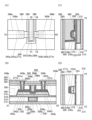
도 1의 (A)는 표시 장치의 구성예를 나타낸 단면도이다. 도 1의 (B)는 광의 진행 방향의 일례를 나타낸 도면이다.
도 2의 (A) 및 (B)는 표시 장치의 구성예를 나타낸 단면도이다.
도 3은 표시 장치의 구성예를 나타낸 단면도이다.
도 4의 (A)는 표시 장치의 구성예를 나타낸 단면도이다. 도 4의 (B)는 광의 진행 방향의 일례를 나타낸 도면이다.
도 5의 (A)는 표시 장치의 구성예를 나타낸 단면도이다. 도 5의 (B)는 광의 진행 방향의 일례를 나타낸 도면이다.
도 6의 (A) 및 (B)는 표시 장치의 구성예를 나타낸 단면도이다.
도 7의 (A) 및 (B)는 표시 장치의 제작 방법의 일례를 나타낸 단면도이다.
도 8의 (A) 및 (B)는 표시 장치의 제작 방법의 일례를 나타낸 단면도이다.
도 9는 표시 장치의 구성예를 나타낸 단면도이다.
도 10의 (A)는 트랜지스터의 일례를 나타낸 상면도이다. 도 10의 (B) 내지 (D)는 트랜지스터의 일례를 나타낸 단면도이다.
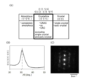
도 11의 (A)는 IGZO의 결정 구조의 분류를 설명하는 도면이다. 도 11의 (B)는 CAAC-IGZO막의 XRD 스펙트럼을 설명하는 도면이다. 도 11의 (C)는 CAAC-IGZO막의 극미 전자선 회절 패턴을 설명하는 도면이다.
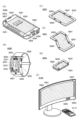
도 12의 (A) 내지 (D)는 전자 기기의 일례를 나타낸 도면이다.
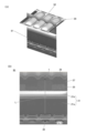
도 13의 (A) 내지 (F)는 전자 기기의 일례를 나타낸 도면이다.
도 14는 시뮬레이션에 사용한 표시 장치의 모식도이다.
도 15는 시뮬레이션에 사용한 발광 소자의 배광 특성을 나타낸 그래프이다.
도 16은 시뮬레이션 결과를 나타낸 그래프이다.
도 17의 (A) 및 (B)는 표시 장치의 전자 현미경 화상이다.
도 18은 시뮬레이션에 사용한 표시 장치의 모식도이다.
도 19는 본 실시예에 따른 표시 장치에서의 방사 휘도의 실측 결과와 시뮬레이션 결과를 나타낸 그래프이다.1(A) is a cross-sectional view showing a configuration example of a display device. 1(B) is a diagram showing an example of the traveling direction of light.
2(A) and (B) are cross-sectional views showing a configuration example of the display device.
3 is a cross-sectional view showing a configuration example of a display device.
4(A) is a cross-sectional view showing a configuration example of the display device. 4(B) is a diagram showing an example of the traveling direction of light.
5(A) is a cross-sectional view showing a configuration example of the display device. 5(B) is a diagram showing an example of the traveling direction of light.
6(A) and (B) are cross-sectional views showing a configuration example of the display device.
7(A) and (B) are cross-sectional views showing an example of a manufacturing method of a display device.
8(A) and (B) are cross-sectional views showing an example of a manufacturing method of a display device.
9 is a cross-sectional view showing a configuration example of a display device.
Fig. 10(A) is a top view showing an example of a transistor. 10(B) to (D) are cross-sectional views showing an example of a transistor.
(A) of FIG. 11 is a figure explaining the classification of the crystal structure of IGZO. (B) of FIG. 11 is a figure explaining the XRD spectrum of a CAAC-IGZO film. Fig. 11(C) is a diagram explaining a very fine electron beam diffraction pattern of a CAAC-IGZO film.
12(A) to (D) are views showing an example of an electronic device.
13(A) to (F) are views showing an example of an electronic device.
14 is a schematic diagram of a display device used in simulation.
15 is a graph showing light distribution characteristics of light emitting devices used in simulation.
16 is a graph showing simulation results.
17(A) and (B) are electron microscope images of the display device.
18 is a schematic diagram of a display device used in simulation.
19 is a graph showing a result of measurement and simulation of radiation luminance in a display device according to an exemplary embodiment.
이하에서, 실시형태에 대해서 도면을 참조하면서 설명한다. 다만 실시형태는 많은 상이한 형태로 실시할 수 있고, 취지 및 그 범위에서 벗어남이 없이 그 형태 및 자세한 사항을 다양하게 변경할 수 있다는 것은 통상의 기술자라면 용이하게 이해할 수 있다. 따라서 본 발명은 이하의 실시형태의 기재 내용에 한정하여 해석되는 것은 아니다.EMBODIMENT OF THE INVENTION Below, embodiment is described, referring drawings. However, those skilled in the art can easily understand that the embodiment can be implemented in many different forms, and that the form and details can be changed in various ways without departing from the spirit and scope thereof. Therefore, the present invention is not construed as being limited to the description of the following embodiments.
또한 이하에 설명하는 발명의 구성에서, 동일 부분 또는 같은 기능을 가지는 부분에는 동일한 부호를 상이한 도면 간에 공통적으로 사용하고, 그 반복 설명은 생략한다. 또한 같은 기능을 가지는 부분을 가리키는 경우에는, 해치 패턴을 동일하게 하고, 특별히 부호를 붙이지 않는 경우가 있다.In the configuration of the invention described below, the same reference numerals are commonly used in different drawings for the same parts or parts having the same functions, and repeated explanations thereof are omitted. In addition, in the case of designating parts having the same function, the same hatch pattern may be used and no special code is attached.
또한 본 명세서에서 설명하는 각 도면에 있어서, 각 구성 요소의 크기, 층의 두께, 또는 영역은 명료화를 위하여 과장되어 있는 경우가 있다. 따라서 반드시 그 스케일에 한정되는 것은 아니다.In addition, in each drawing described in this specification, the size of each component, the thickness of a layer, or an area may be exaggerated for clarity. Therefore, it is not necessarily limited to that scale.
또한 본 명세서 등에서의 "제 1", "제 2" 등의 서수사는 구성 요소의 혼동을 피하기 위하여 붙이는 것이며, 수적으로 한정하는 것이 아니다.In addition, ordinal numbers such as "first" and "second" in this specification and the like are added to avoid confusion among constituent elements, and are not limited to numbers.
또한 이하에서 "위", "아래" 등의 방향을 나타내는 표현은 기본적으로 도면의 방향에 맞추어 사용하는 것으로 한다. 그러나, 설명을 용이하게 하는 등의 목적으로 명세서 중의 "위" 또는 "아래"가 의미하는 방향이 도면과 일치하지 않는 경우가 있다. 일례로서는, 적층체 등의 적층 순서(또는 형성 순서) 등을 설명하는 경우에, 도면에서 상기 적층체가 제공되는 측의 면(피형성면, 지지면, 접착면, 평탄면 등)이 상기 적층체보다 위쪽에 위치하여도, 그 방향을 아래, 이와 반대의 방향을 위 등이라고 표현하는 경우가 있다.In addition, below, expressions indicating directions such as "above" and "down" are basically used according to the direction of the drawings. However, for the purpose of facilitating explanation, there are cases in which the direction indicated by "above" or "below" in the specification does not coincide with the drawing. As an example, in the case of explaining the order of lamination (or the order of formation) of a laminate or the like, the surface on the side on which the laminate is provided in the drawing (formation surface, support surface, adhesive surface, flat surface, etc.) is the laminate Even if it is located higher, there are cases where the direction is expressed as down, and the opposite direction is expressed as up.
또한 본 명세서에서 EL층이란 발광 소자의 한 쌍의 전극 사이에 제공되고, 적어도 발광성 물질을 포함하는 층(발광층이라고도 부름) 또는 발광층을 포함하는 적층체를 나타내는 것으로 한다.In this specification, the EL layer is provided between a pair of electrodes of a light emitting element and refers to a layer containing at least a light emitting material (also referred to as a light emitting layer) or a laminate containing a light emitting layer.
(실시형태 1)(Embodiment 1)
본 실시형태에서는 본 발명의 일 형태의 표시 장치의 구성예 등에 대하여 설명한다.In this embodiment, a configuration example of a display device according to one embodiment of the present invention and the like will be described.
[구성예 1][Configuration Example 1]
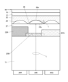
도 1의 (A)는 본 발명의 일 형태의 표시 장치인 표시 장치(10)의 구성예를 나타낸 단면도이다. 표시 장치(10)는 화소(15R)와, 화소(15G)와, 화소(15B)를 가진다. 여기서 화소(15R), 화소(15G), 및 화소(15B)는 표시 장치(10)의 표시면에 제공된다. 상기 표시면은 화소(15R), 화소(15G), 및 화소(15B)가 각각 매트릭스로 배열된 구성으로 할 수 있다. 또한 화소(15R)와, 화소(15G)와, 화소(15B)에 의하여 하나의 화소가 구성되고, 상기 화소가 표시 장치(10)의 표시면에 매트릭스로 배열된다고 할 수 있다. 이 경우, 화소(15R)와, 화소(15G)와, 화소(15B)는 각각 부 화소라고 할 수 있다.1(A) is a cross-sectional view showing a configuration example of a
표시 장치(10)는 기판(11)과, 트랜지스터(52)와, 절연층(13)과, 발광 소자(30)와, 격벽(14)과, 절연층(63)과, 절연층(21)과, 착색층(25R)과, 착색층(25G)과, 착색층(25B)과, 평탄화층(27)과, 렌즈(29)와, 수지층(33)과, 기판(12)을 가진다. 발광 소자(30) 및 렌즈(29)는 화소(15R), 화소(15G), 및 화소(15B)에 각각 하나씩 제공된다. 또한 착색층(25R)은 화소(15R)에 제공되고, 착색층(25G)은 화소(15G)에 제공되고, 착색층(25B)은 화소(15B)에 제공된다.The
본 명세서 등에서 발광 소자는 발광 디바이스라고 할 수 있다. 또한 표시 소자는 표시 디바이스라고 할 수 있다.In this specification and the like, a light emitting element may be referred to as a light emitting device. Also, the display element may be referred to as a display device.
도 1의 (A)에 나타낸 표시 장치(10)에서 화소(15G)는 화소(15R) 및 화소(15B)와 인접된다. 여기서 인접된 화소에 제공되는 발광 소자(30)들, 착색층들, 및 렌즈(29)들은 각각 서로 인접되어 있다고 할 수 있다. 예를 들어 도 1의 (A)에 나타낸 화소(15R)에 제공되는 발광 소자(30)와, 화소(15G)에 제공되는 발광 소자(30)는 인접되어 있다고 할 수 있다. 또한 도 1의 (A)에 나타낸 착색층(25R)과 착색층(25G)은 인접되어 있다고 할 수 있다. 또한 도 1의 (A)에 나타낸 화소(15R)에 제공되는 렌즈(29)와, 화소(15G)에 제공되는 렌즈(29)는 인접되어 있다고 할 수 있다. 또한 도 1의 (A)에서는 화소(15R)와 화소(15B)는 인접되지 않았지만, 화소(15R)와 화소(15B)가 인접되어도 좋다.In the
절연층(13) 및 트랜지스터(52)는 기판(11) 위에 제공된다. 발광 소자(30)는 절연층(13) 위에 제공된다. 절연층(63)은 발광 소자(30) 위에 제공된다. 절연층(21)은 절연층(63) 위에 제공된다. 착색층(25R), 착색층(25G), 및 착색층(25B)은 절연층(21) 위에 제공된다. 평탄화층(27)은 착색층(25R) 위, 착색층(25G) 위, 및 착색층(25B) 위에 제공된다. 렌즈(29)는 평탄화층(27) 위에 제공된다. 수지층(33)은 렌즈(29) 위에 제공된다. 기판(12)은 수지층(33) 위에 제공된다. 여기서 도 1의 (A)에서 절연층(13)의 상면은 평탄화되었지만, 평탄화되지 않아도 된다.An insulating
본 명세서 등에서 예를 들어 "A 위의 B"라고 하는 경우, A의 적어도 일부와 B의 적어도 일부가 중첩되어 있으면 A와 B가 접하는 영역을 가지지 않아도 된다.In this specification and the like, for example, in the case of "B on A", as long as at least a part of A and at least a part of B overlap, A and B need not have a contact area.
기판(11)으로서 유리 기판, 석영 기판, 사파이어 기판, 세라믹 기판 등의 절연성 기판, 또는 실리콘 또는 탄소화 실리콘 등을 재료로 한 단결정 반도체 기판, 다결정 반도체 기판, 실리콘 저마늄 등으로 이루어지는 화합물 반도체 기판, SOI 기판 등의 반도체 기판을 사용할 수 있다. 또한 기판(11)으로서 가요성을 가지는 기판을 사용하고, 기판(12)도 가요성을 가지는 기판으로 함으로써 표시 장치(10)를 플렉시블 표시 장치로 할 수 있다.As the
절연층(13) 및 절연층(21)으로서 예를 들어 유기 절연막을 사용하는 것이 바람직하다. 유기 절연막으로서는 예를 들어 아크릴 수지, 폴리이미드 수지, 에폭시 수지, 폴리아마이드 수지, 폴리이미드아마이드 수지, 실록세인 수지, 벤조사이클로뷰텐 수지, 페놀 수지, 및 이들 수지의 전구체 등이 있다. 또한 절연층(63)으로서는 예를 들어 무기 절연막을 사용하는 것이 바람직하다. 무기 절연막으로서는 예를 들어 질화 실리콘막, 산화질화 실리콘막, 산화 실리콘막, 질화산화 실리콘막, 산화 알루미늄막, 질화 알루미늄막 등을 사용할 수 있다. 또한 산화 하프늄막, 산화질화 하프늄막, 질화산화 하프늄막, 산화 이트륨막, 산화 지르코늄막, 산화 갈륨막, 산화 탄탈럼막, 산화 마그네슘막, 산화 란타넘막, 산화 세륨막, 및 산화 네오디뮴막 등을 사용하여도 좋다. 또한 상술한 절연막을 2개 이상 적층하여 사용하여도 좋다. 또한 절연층(13) 또는 절연층(21)으로서 무기 절연막을 사용하여도 좋고, 절연층(63)으로서 유기 절연막을 사용하여도 좋다. 표시 장치(10)에 포함되는 다른 절연층도 절연층(13), 절연층(63), 또는 절연층(21)으로서 사용할 수 있는 재료와 마찬가지의 재료를 사용할 수 있다.As the insulating
또한 본 명세서 등에서 산화질화 실리콘이란, 그 조성으로서 산소의 함유량이 질소의 함유량보다 많은 것을 가리킨다. 또한 질화산화 실리콘이란, 그 조성으로서 질소의 함유량이 산소의 함유량보다 많은 것을 가리킨다.In this specification and the like, silicon oxynitride refers to a composition in which the content of oxygen is greater than the content of nitrogen. Further, silicon nitride oxide refers to a composition in which the content of nitrogen is greater than the content of oxygen.
도 1의 (A)에 나타낸 바와 같이 착색층(25R)과, 착색층(25G)과, 착색층(25B)은 각각 상이한 발광 소자(30) 위에 제공된다. 또한 착색층(25R) 위, 착색층(25G) 위, 착색층(25B) 위에는 각각 상이한 렌즈(29)가 제공된다. 따라서 발광 소자(30)와, 착색층(25R)과, 렌즈(29)는 서로 중첩되는 영역을 가지도록 제공된다. 또한 발광 소자(30)와, 착색층(25G)과, 렌즈(29)는 서로 중첩되는 영역을 가지도록 제공된다. 또한 발광 소자(30)와, 착색층(25B)과, 렌즈(29)는 서로 중첩되는 영역을 가지도록 제공된다.As shown in FIG. 1(A), the
도 1의 (A)에서는 2종류의 착색층이 중첩되는 영역을 가지는 구성을 점선으로 나타내었다. 또한 도 1의 (A)에서는 렌즈(29)가 서로 이격되어 제공되는 구성을 나타내었다. 또한 착색층들이 중첩되지 않아도 좋고, 인접된 화소에 제공되는 렌즈(29)가 서로 접하는 영역을 가져도 좋다.In (A) of FIG. 1, a configuration having a region in which two types of colored layers overlap is indicated by a dotted line. Also, in (A) of FIG. 1, a configuration in which
발광 소자(30)는 도전층(42)과, 발광층(31)과, 도전층(60)을 적층한 구성을 가진다. 여기서 도전층(42)은 발광 소자(30)의 화소 전극으로 할 수 있고, 도전층(60)은 발광 소자(30)의 공통 전극으로 할 수 있다.The
발광 소자(30)는 예를 들어 백색광을 방출할 수 있다. 구체적으로는 발광층(31)으로부터 백색광을 방출할 수 있다. 발광 소자(30)로서 OLED(Organic Light Emitting Diode), 또는 QLED(Quantum-dot Light Emitting Diode) 등의 EL 소자를 사용할 수 있다. 또한 발광 소자(30)로서 마이크로 LED를 사용할 수 있다.The
발광 소자(30)로서 백색 발광의 발광 소자를 적용하는 경우에는, 발광층(31)에 2종류 이상의 발광 물질을 포함하는 구성으로 하는 것이 바람직하다. 예를 들어, 2개 이상의 발광 물질 각각의 발광이 보색의 관계가 되도록 발광 물질을 선택함으로써, 백색 발광을 얻을 수 있다. 예를 들어, 각각 R(적색), G(녹색), B(청색), Y(황색), O(주황색) 등의 발광을 나타내는 발광 물질 또는 R, G, B 중 2개 이상의 색의 스펙트럼 성분을 포함하는 발광을 나타내는 발광 물질 중 2개 이상을 포함하는 것이 바람직하다. 또한 발광 소자로부터의 발광의 스펙트럼이 가시광 영역의 파장(예를 들어, 350nm 내지 750nm)의 범위 내에 2개 이상의 피크를 가지는 발광 소자를 적용하는 것이 바람직하다. 또한 황색의 파장 영역에 피크를 가지는 재료의 발광 스펙트럼은, 녹색 및 적색의 파장 영역에도 스펙트럼 성분을 가지는 재료인 것이 바람직하다.When a white light emitting element is used as the
발광층(31)은 하나의 색을 발광하는 발광 재료를 포함하는 발광층과, 다른 색을 발광하는 발광 재료를 포함하는 발광층이 적층된 구성으로 하는 것이 바람직하다. 예를 들어, 발광층(31)에서의 복수의 발광층은 서로 접하여 적층되어 있어도 좋고, 어느 발광 재료도 포함하지 않는 영역을 개재(介在)하여 적층되어 있어도 좋다. 예를 들어, 형광 발광층과 인광 발광층 사이에 상기 형광 발광층 또는 인광 발광층과 동일한 재료(예를 들어 호스트 재료, 어시스트 재료)를 포함하며, 어느 발광 재료도 포함하지 않는 영역을 제공하는 구성으로 하여도 좋다. 이에 의하여 발광 소자(30)의 제작이 제작이 용이해지고, 또한 구동 전압이 저감된다. 또한 발광 소자(30)를, 복수의 발광층(31)이 적층된 구성으로 하는 경우, 상기 복수의 발광층(31)은 전하 발생층을 개재하여 적층되어도 좋다.The light-emitting
도전층(42)은 절연층(13)에 제공된, 트랜지스터(52)에 도달하는 개구를 통하여 트랜지스터(52)와 전기적으로 접속될 수 있다. 예를 들어, 도전층(42)은 트랜지스터(52)의 소스 또는 드레인과 전기적으로 접속될 수 있다.The
격벽(14)은 상이한 발광 소자(30)에 포함되는 도전층(42)을 전기적으로 절연("전기적으로 분리"라고도 함)하는 기능을 가진다. 도전층(42)의 단부는 격벽(14)으로 덮인다.The
격벽(14)으로서 무기 절연막을 사용하는 것이 바람직하다. 예를 들어 격벽(14)으로서 절연층(63) 등에 사용할 수 있는 재료와 마찬가지의 재료를 사용할 수 있다. 또한 격벽(14)으로서 유기 절연막을 사용하여도 좋다. 격벽(14)은 가시광을 투과하는 층이다. 격벽(14) 대신에 가시광을 차단하는 격벽을 제공하여도 좋다.As the
절연층(63)은 발광 소자(30)를 덮도록 제공할 수 있다. 절연층(63)은 물 또는 수소 등의 불순물을 투과시키기 어려운 막으로 구성되는 것이 바람직하다. 물 또는 수소 등의 불순물을 투과시키기 어려운 막으로 구성된 절연층(63)을, 발광 소자(30)를 덮도록 제공함으로써, 발광 소자(30)에 물 또는 수소 등의 불순물이 들어가는 것을 억제할 수 있다. 이에 의하여, 발광 소자(30)의 신뢰성을 높일 수 있다. 따라서 절연층(63)은 발광 소자(30)에 대한 보호층으로서 기능한다. 또한 절연층(63)을 제공하지 않아도 된다. 이 경우, 절연층(21)에, 상술한 보호층으로서의 기능을 가지게 하는 것이 바람직하다.The insulating
상술한 바와 같이, 발광 소자(30) 위에 절연층(21)을 제공하고, 절연층(21) 위에 착색층(25R), 착색층(25G), 및 착색층(25B)을 제공할 수 있다. 예를 들어, 절연층(21)의 상면과 접하도록 착색층(25R), 착색층(25G), 및 착색층(25B)을 제공할 수 있다. 여기서 도 1의 (A)에 나타낸 바와 같이 절연층(21)의 상면을 평탄화하면 착색층(25R)과, 착색층(25G)과, 착색층(25B)을 평탄면 위에 제공할 수 있다.As described above, the insulating
착색층(25R)은 예를 들어 적색의 광을 투과시키는 기능을 가진다. 착색층(25G)은 예를 들어 녹색의 광을 투과시키는 기능을 가진다. 착색층(25B)은 예를 들어 청색의 광을 투과시키는 기능을 가진다. 이 경우, 화소(15R)로부터는 적색의 광이 사출되고, 화소(15G)로부터는 녹색의 광이 사출되고, 화소(15B)로부터는 청색의 광이 사출된다. 또한 착색층(25R), 착색층(25G), 또는 착색층(25B)은 시안, 마젠타, 황색 등의 광을 투과시키는 기능을 가져도 좋다. 또한 도 1의 (A)에서는 3종류의 착색층을 나타내었지만 표시 장치(10)는 4종류 이상의 착색층을 가져도 좋다.The
착색층(25R), 착색층(25G), 및 착색층(25B)으로서는 금속 재료, 수지 재료, 안료, 또는 염료가 포함된 수지 재료 등을 사용할 수 있다.As the
발광 소자(30)와 중첩되는 영역을 가지도록 착색층을 제공함으로써, 발광층(31)을 구분하여 형성할 필요가 없어진다. 이에 의하여, 발광 소자(30)가 제공되는 화소를, 미세한 것으로 할 수 있다.By providing the colored layer to have a region overlapping with the
여기서 인접되는 화소에 제공되는 착색층은, 그 일부가 서로 중첩될 수 있다. 도 1의 (A)에 나타낸 예에서는 착색층(25R)과 착색층(25G)은 서로 중첩되는 영역을 가질 수 있다. 또한 착색층(25G)과 착색층(25B)은 서로 중첩되는 영역을 가질 수 있다. 이에 의하여 착색층(25R), 착색층(25G), 및 착색층(25B)을 예를 들어 포토리소그래피 및 에칭에 의하여 형성하는 경우, 예를 들어 포토리소그래피에서 사용하는 마스크의 얼라인먼트 정밀도가 낮아도 착색층(25R), 착색층(25G), 및 착색층(25B)을 형성할 수 있다. 따라서 발광 소자(30)가 제공되는 화소를 미세한 것으로 할 수 있다.In this case, portions of the colored layers provided to adjacent pixels may overlap each other. In the example shown in FIG. 1(A), the
여기서 착색층(25R)의 두께와, 착색층(25G)의 두께와, 착색층(25B)의 두께는 상이하게 할 수 있다. 이에 의하여 예를 들어 착색층을 투과한 광의 색 순도와, 착색층에 의한 광의 흡수율의 밸런스를, 색마다 원하는 것으로 할 수 있다. 따라서 표시 장치(10)는 고품질의 화상을 표시할 수 있다. 또한 착색층(25R)의 두께와, 착색층(25G)의 두께와, 착색층(25B)의 두께를 서로 동일하여도 좋다.Here, the thickness of the
상술한 바와 같이 착색층(25R) 위, 착색층(25G) 위, 및 착색층(25B) 위에 평탄화층(27)이 제공된다. 예를 들어, 착색층(25R), 착색층(25G), 및 착색층(25B)과 접하도록 평탄화층(27)을 제공할 수 있다. 구체적으로는 착색층(25R), 착색층(25G), 및 착색층(25B)의 상면 및 측면과 접하도록 평탄화층(27)을 제공할 수 있다.As described above, the
평탄화층(27)으로서 예를 들어 절연층(21)에 사용할 수 있는 재료와 마찬가지의 재료를 사용할 수 있다.As the
상술한 바와 같이 평탄화층(27) 위에 렌즈(29)가 제공된다. 여기서 렌즈(29)는 평탄부(29a)와 볼록부(29b)를 가지는 평볼록 렌즈로 할 수 있다. 렌즈(29)는 평탄부(29a)가 기판(11) 측을 향하고, 볼록부(29b)가 기판(12) 측을 향하도록 제공할 수 있다. 예를 들어, 평탄부(29a)가 평탄화층(27)의 상면과 접하도록 렌즈(29)를 제공할 수 있다.A
상술한 바와 같이 착색층(25R)의 두께와, 착색층(25G)의 두께와, 착색층(25B)의 두께는 각각 상이한 것으로 할 수 있다. 이와 같은 경우에도 착색층(25R) 위, 착색층(25G) 위, 및 착색층(25B) 위에 평탄화층(27)을 제공하고, 평탄화층(27) 위에 렌즈(29)를 제공함으로써, 각 렌즈(29)의 평탄부(29a)를 서로 동일 평면 위에 제공할 수 있다. 이에 의하여, 발광 소자(30)의 발광층(31)에서 렌즈(29)의 평탄부(29a)까지의 거리 L을 서로 같게 할 수 있다. 구체적으로는 착색층(25R)과 중첩되는 발광층(31)에서 평탄부(29a)까지의 거리와, 착색층(25G)과 중첩되는 발광층(31)에서 평탄부(29a)까지의 거리와, 착색층(25B)과 중첩되는 발광층(31)에서 평탄부(29a)까지의 거리를 서로 같게 할 수 있다.As described above, the thickness of the
렌즈(29)의 볼록부(29b)와 접하도록 수지층(33)이 제공된다. 또한 수지층(33)의 상면과 접하도록 기판(12)이 제공된다. 수지층(33)에 의하여 렌즈(29)와 기판(12)을 접합할 수 있다.A
수지층(33)으로서 에폭시 수지, 아크릴 수지, 실리콘 수지, 페놀 수지, 폴리이미드 수지, 이미드 수지, PVC(폴리바이닐클로라이드) 수지, PVB(폴리바이닐뷰티랄) 수지, EVA(에틸렌바이닐 아세테이트) 수지 등을 사용할 수 있다. 또한 2액 혼합형 수지를 사용하여도 좋다. 자세한 내용은 후술하지만, 여기서는 수지층(33)의 굴절률을 렌즈(29)의 굴절률보다 낮게 하는 것이 바람직하다.Epoxy resin, acrylic resin, silicone resin, phenol resin, polyimide resin, imide resin, PVC (polyvinyl chloride) resin, PVB (polyvinyl butyral) resin, EVA (ethylene vinyl acetate) resin as the
도 1의 (A)에서는 수지층(33)에 의하여 렌즈(29)와 기판(12)을 접합한 것을 나타내었지만, 본 발명의 일 형태는 이에 한정되지 않는다. 예를 들어, 렌즈(29)와 기판(12) 사이를 진공으로 함으로써 접합할 수 있다. 이 경우, 수지층(33)을 제공하지 않는 구성으로 할 수 있다.In FIG. 1(A), it is shown that the
기판(12)으로서 투광성을 가지는 기판을 사용한다. 기판(12)으로서 예를 들어 유리 기판, 석영 기판, 사파이어 기판 등을 사용할 수 있다. 또한 기판(12)으로서 기판(11)과 함께 가요성을 가지는 기판을 사용함으로써, 표시 장치(10)를 플렉시블 표시 장치로 할 수 있다.As the
도 1의 (B)는 도 1의 (A)에 나타낸 단면도 중, 일점쇄선 A1-A2를 따라 절단한 도면이다. 도 1의 (B)에서는 발광 소자(30)가 방출하는 광을, 광(43)으로 나타내었다.Fig. 1(B) is a cross-sectional view shown in Fig. 1(A), taken along the dashed-dotted line A1-A2. In FIG. 1(B) , light emitted from the
본 명세서 등에서 광이라는 용어는, 광속으로 환언할 수 있는 경우가 있다.In this specification and the like, the term light may be translated into light flux in some cases.
발광 소자(30)는 정면 방향뿐만 아니라, 비스듬한 방향으로도 광(43)을 방출한다. 비스듬한 방향으로 방출된 광(43)이 그 각도를 유지한 채 화소로부터 사출된다면, 예를 들어 표시 장치(10)의 사용자가 표시 장치(10)의 표시면의 정면에서 상기 표시면을 본 경우, 표시 장치(10)의 사용자는 비스듬한 방향으로 방출된 광(43)을 시인할 수 없는 경우가 있다. 여기서 발광 소자(30)가 방출하는 광은 렌즈(29)의 평탄부(29a)에 입사하기 때문에 상술한 바와 같이 수지층(33)의 굴절률을 렌즈(29)의 굴절률보다 낮게 하면, 스넬의 법칙(Snell’s law)에 의하여 도 1의 (B)에 나타낸 바와 같이 비스듬한 방향으로 방출된 광을 정면 방향으로 집광할 수 있다. 이에 의하여 예를 들어 표시 장치(10)의 사용자가 표시 장치(10)의 표시면의 정면에서 상기 표시면을 본 경우, 표시 장치(10)의 사용자가 시인하는 광(43)의 광량을 크게 할 수 있다. 따라서 표시 장치(10)의 사용자는 밝은 화상을 시인할 수 있다. 또한 발광 소자(30)의 발광 광도를 작게 할 수 있어, 표시 장치(10)는 소비 전력이 작은 표시 장치로 할 수 있고, 또한 신뢰성이 높은 표시 장치로 할 수 있다.The
여기서 렌즈(29)의 굴절률은 예를 들어 1.5 이상 1.8 이하로 할 수 있고, 예를 들어 1.5 이상 1.6 이하로 할 수 있고, 예를 들어 1.56으로 할 수 있다. 또한 수지층(33)의 굴절률은 예를 들어 1.2 이상 1.5 이하로 할 수 있고, 예를 들어 1.3 이상 1.5 미만으로 할 수 있고, 예를 들어 1.40으로 할 수 있다. 또한 수지층(33)을 제공하지 않고, 렌즈(29)와 기판(12) 사이를 진공으로 함으로써 접합하는 경우에는 렌즈(29)의 굴절률은 1보다 크게 하면 좋다.Here, the refractive index of the
또한 식(1)에 나타내는 관계가 성립하도록, 거리 L을 설정하는 것이 바람직하다. 여기서 R1은 볼록부(29b)의 곡률 반경을 나타내고, N1은 렌즈(29)의 굴절률을 나타내고, N2는 수지층(33)의 굴절률을 나타내고, N3은 평탄화층(27)의 굴절률을 나타낸다. 또한 렌즈(29)의 초점 거리는 "R1×N3/(N1-N2)"이다.Moreover, it is preferable to set the distance L so that the relationship shown by Formula (1) may be established. Here, R1 represents the radius of curvature of the
0.1×R1×N3/(N1-N2) ≤ L ≤ 5×R1×N3/(N1-N2): (1)0.1×R1×N3/(N1-N2) ≤ L ≤ 5×R1×N3/(N1-N2): (1)
여기서 상술한 바와 같이 착색층(25R)의 두께와, 착색층(25G)의 두께와, 착색층(25B)의 두께는 상이한 것으로 할 수 있다. 따라서 평탄화층(27)을 제공하지 않고 착색층(25R) 위, 착색층(25G) 위, 및 착색층(25B) 위에 렌즈(29)를 제공하면 화소마다 거리 L이 상이하다. 화소마다 거리 L이 상이하면 식(1)에 따라 화소마다 볼록부(29b)의 곡률 반경 R1 또는 렌즈(29)의 굴절률 N1을 변경할 필요가 생길 경우가 있다. 이 경우, 화소마다 렌즈(29)를 따로 형성하게 되어 표시 장치의 제작 공정이 복잡화된다. 한편으로 표시 장치(10)에서는 평탄화층(27) 위에 렌즈(29)를 제공하기 때문에 화소마다 거리 L을 같게 할 수 있다. 이에 의하여 표시 장치(10)의 제작 공정을 간이하게 할 수 있다. 따라서 표시 장치(10)의 제작 비용을 적게 하여 표시 장치(10)를 저렴한 것으로 할 수 있다.As described above, the thickness of the
[구성예 2][Configuration Example 2]
도 2의 (A)는 도 1의 (A)에 나타낸 표시 장치(10)의 변형예이다. 도 2의 (A)에 나타낸 표시 장치(10)는 발광층(31) 대신에 발광층(51)이 제공되고, 착색층(25R), 착색층(25G), 및 착색층(25B) 대신에 파장 변환층(55R) 및 파장 변환층(55G)이 제공되는 점이 도 1의 (A)에 나타낸 표시 장치(10)와 다르다.FIG. 2(A) is a modified example of the
발광층(51)은 예를 들어 청색의 광을 방출하는 기능을 가진다. 화소(15R)에 제공되는 파장 변환층(55R)은 발광층(51)이 방출하는 광을 적색의 광으로 변환하는 기능을 가진다. 화소(15G)에 제공되는 파장 변환층(55G)은 발광층(51)이 방출하는 광을 녹색의 광으로 변환하는 기능을 가진다. 여기서 발광층(51)이 청색의 광을 방출하는 경우, 화소(15B)에는 파장 변환층을 제공하지 않아도 된다. 또한 발광층(51)은 자외광을 방출하는 기능을 가져도 좋다. 이 경우, 발광층(51)이 방출하는 광을 청색의 광으로 변환하는 기능을 가지는 파장 변환층을 화소(15B)에 제공함으로써 화소(15B)는 청색의 광을 사출할 수 있다.The
파장 변환층(55R) 및 파장 변환층(55G)으로서 형광 재료 또는 퀀텀닷(QD: Quantum dot)을 포함하는 것이 바람직하다. 특히, 퀀텀닷은 발광 스펙트럼의 피크 폭이 좁고, 변환 효율이 높고, 색 순도가 높은 발광을 얻을 수 있다. 이에 의하여, 표시 장치(10)의 색 재현성을 높은 것으로 할 수 있기 때문에, 표시 장치(10)는 고품질의 화상을 표시할 수 있다.It is preferable to include a fluorescent material or a quantum dot (QD) as the
파장 변환층(55R) 및 파장 변환층(55G)으로서 유기 수지 내로 형광체 또는 퀀텀닷을 분산시킨 형태로 할 수 있다. 유기 수지로서는, 발광층(51)이 방출하는 광 및 파장 변환층(55R) 또는 파장 변환층(55G)이 방출하는 광에 대하여 투광성을 가지는, 경화성 재료를 사용할 수 있다.As the
파장 변환층(55R) 및 파장 변환층(55G)은 예를 들어 액적 토출법(예를 들어 잉크젯법), 도포법, 임프린트법, 각종 인쇄법(스크린 인쇄, 오프셋 인쇄) 등을 사용하여 형성할 수 있다. 또한 유기 수지로서 감광성 수지 재료를 사용함으로써 유기 수지를 스핀 코팅법 등으로 도포한 후에 노광 처리, 현상 처리를 거쳐 임의의 형상으로 가공함으로써 형성하여도 좋다.The
퀀텀닷을 구성하는 재료로서는 특별한 한정은 없고, 예를 들어 14족 원소, 15족 원소, 16족 원소, 복수의 14족 원소로 이루어지는 화합물, 4족 내지 14족에 속하는 원소와 16족 원소의 화합물, 2족 원소와 16족 원소의 화합물, 13족 원소와 15족 원소의 화합물, 13족 원소와 17족 원소의 화합물, 14족 원소와 15족 원소의 화합물, 11족 원소와 17족 원소의 화합물, 산화 철류, 산화 타이타늄류, 칼코게나이드스피넬류, 반도체 클러스터 등을 들 수 있다.There is no particular limitation as a material constituting the quantum dot, and examples include a
구체적으로는 셀레늄화 카드뮴, 황화 카드뮴, 텔루륨화 카드뮴, 셀레늄화 아연, 산화 아연, 황화 아연, 텔루륨화 아연, 황화 수은, 셀레늄화 수은, 텔루륨화 수은, 비소화 인듐, 인화 인듐, 비소화 갈륨, 인화 갈륨, 질화 인듐, 질화 갈륨, 안티모니화 인듐, 안티모니화 갈륨, 인화 알루미늄, 비소화 알루미늄, 안티모니화 알루미늄, 셀레늄화 납, 텔루륨화 납, 황화 납, 셀레늄화 인듐, 텔루륨화 인듐, 황화 인듐, 셀레늄화 갈륨, 황화 비소, 셀레늄화 비소, 텔루륨화 비소, 황화 안티모니, 셀레늄화 안티모니, 텔루륨화 안티모니, 황화 비스무트, 셀레늄화 비스무트, 텔루륨화 비스무트, 실리콘, 탄소화 실리콘, 저마늄, 주석, 셀레늄, 텔루륨, 붕소, 탄소, 인, 질화 붕소, 인화 붕소, 비소화 붕소, 질화 알루미늄, 황화 알루미늄, 황화 바륨, 셀레늄화 바륨, 텔루륨화 바륨, 황화 칼슘, 셀레늄화 칼슘, 텔루륨화 칼슘, 황화 베릴륨, 셀레늄화 베릴륨, 텔루륨화 베릴륨, 황화 마그네슘, 셀레늄화 마그네슘, 황화 저마늄, 셀레늄화 저마늄, 텔루륨화 저마늄, 황화 주석, 셀레늄화 주석, 텔루륨화 주석, 산화 납, 플루오린화 구리, 염화 구리, 브로민화 구리, 아이오딘화 구리, 산화 구리, 셀레늄화 구리, 산화 니켈, 산화 코발트, 황화 코발트, 산화 철, 황화 철, 산화 망가니즈, 황화 몰리브데넘, 산화 바나듐, 산화 텅스텐, 산화 탄탈럼, 산화 타이타늄, 산화 지르코늄, 질화 실리콘, 질화 저마늄, 산화 알루미늄, 타이타늄산 바륨, 셀레늄과 아연과 카드뮴의 화합물, 인듐과 비소와 인의 화합물, 카드뮴과 셀레늄과 황의 화합물, 카드뮴과 셀레늄과 텔루륨의 화합물, 인듐과 갈륨과 비소의 화합물, 인듐과 갈륨과 셀레늄의 화합물, 인듐과 셀레늄과 황의 화합물, 구리와 인듐과 황의 화합물, 및 이들의 조합 등을 들 수 있다. 또한 조성이 임의의 비율로 나타내어지는, 소위 합금형 퀀텀닷을 사용하여도 좋다.Specifically, cadmium selenide, cadmium sulfide, cadmium telluride, zinc selenide, zinc oxide, zinc sulfide, zinc telluride, mercury sulfide, mercury selenide, mercury telluride, indium arsenide, indium phosphide, gallium arsenide, Gallium phosphide, indium nitride, gallium nitride, indium antimonide, gallium antimonide, aluminum phosphide, aluminum arsenide, aluminum antimonide, lead selenide, lead telluride, lead sulfide, indium selenide, indium telluride, Indium sulfide, gallium selenide, arsenic sulfide, arsenic selenide, arsenic telluride, antimony sulfide, antimony selenide, antimony telluride, bismuth sulfide, bismuth selenide, bismuth telluride, silicon, silicon carbide, zerma ium, tin, selenium, tellurium, boron, carbon, phosphorus, boron nitride, boron phosphide, boron arsenide, aluminum nitride, aluminum sulfide, barium sulfide, barium selenide, barium telluride, calcium sulfide, calcium selenium, tellurium Calcium iumide, beryllium sulfide, beryllium selenide, beryllium tellurium, magnesium sulfide, magnesium selenium, germanium sulfide, germanium selenide, germanium telluride, tin sulfide, tin selenide, tin telluride, lead oxide, fluoride Copper fluoride, copper chloride, copper bromide, copper iodide, copper oxide, copper selenide, nickel oxide, cobalt oxide, cobalt sulfide, iron oxide, iron sulfide, manganese oxide, molybdenum sulfide, vanadium oxide, oxide Tungsten, tantalum oxide, titanium oxide, zirconium oxide, silicon nitride, germanium nitride, aluminum oxide, barium titanate, compounds of selenium, zinc and cadmium, compounds of indium, arsenic and phosphorus, compounds of cadmium, selenium and sulfur, cadmium and A compound of selenium and tellurium, a compound of indium, gallium and arsenic, a compound of indium, gallium and selenium, a compound of indium, selenium and sulfur, a compound of copper, indium and sulfur, and combinations thereof. Also, so-called alloy-type quantum dots, in which the composition is expressed in an arbitrary ratio, may be used.
퀀텀닷의 구조로서는, 코어형, 코어-셸형, 코어-멀티셸형 등을 들 수 있다. 또한 퀀텀닷은 표면 원자의 비율이 높기 때문에 반응성이 높고, 응집이 일어나기 쉽다. 그러므로, 퀀텀닷의 표면에는 보호제가 부착되어 있거나, 또는 보호기가 제공되어 있는 것이 바람직하다. 상기 보호제가 부착되어 있거나, 또는 보호기가 제공되어 있으면 응집을 방지할 수 있고, 용매에 대한 용해성을 높일 수 있다. 또한 반응성을 저감하여 전기적 안정성을 향상시킬 수도 있다.Examples of quantum dot structures include core type, core-shell type, and core-multishell type. In addition, since quantum dots have a high ratio of surface atoms, they are highly reactive and prone to aggregation. Therefore, it is preferable that a protective agent is attached to the surface of the quantum dot or provided with a protective group. When the protecting agent is attached or provided, aggregation can be prevented and solubility in a solvent can be increased. In addition, electrical stability can be improved by reducing reactivity.
퀀텀닷은 크기가 작아질수록 밴드 갭이 넓어지기 때문에, 원하는 파장의 광이 얻어지도록 그 크기를 적절히 조정한다. 결정의 크기가 작아질수록, 퀀텀닷의 발광은 청색 쪽으로, 즉 고에너지 쪽으로 시프트하기 때문에, 퀀텀닷의 크기를 변경함으로써 자외선 영역, 가시광선 영역, 적외선 영역의 스펙트럼의 파장 영역에 걸쳐, 그 발광 파장을 조정할 수 있다. 퀀텀닷의 크기(직경)는 예를 들어 0.5nm 이상 20nm 이하, 바람직하게는 1nm 이상 10nm 이하이다. 퀀텀닷은 그 크기 분포가 좁을수록, 발광 스펙트럼이 더 협선화(狹線化)하기 때문에, 색 순도가 양호한 발광을 얻을 수 있다. 또한 퀀텀닷의 형상은 구체 형상으로 한정되지 않고, 막대기 모양, 원반상, 그 외의 형상이어도 좋다.Since the band gap of a quantum dot widens as its size decreases, its size is appropriately adjusted to obtain light of a desired wavelength. As the size of the crystal becomes smaller, the emission of quantum dots shifts to the blue side, that is, to the higher energy side. Wavelength can be adjusted. The size (diameter) of the quantum dot is, for example, 0.5 nm or more and 20 nm or less, preferably 1 nm or more and 10 nm or less. The narrower the size distribution of quantum dots, the narrower the luminescence spectrum, so that luminescence with good color purity can be obtained. Also, the shape of a quantum dot is not limited to a spherical shape, but may be a rod shape, a disk shape, or other shapes.
여기서 파장 변환층(55R) 및 파장 변환층(55G)으로 퀀텀닷을 분산시키는 경우, 파장 변환층(55R)이 방출하는 광 및 파장 변환층(55G)이 방출하는 광의 지향성은 낮게 된다. 그러나 표시 장치(10)에서는 렌즈(29)의 평탄부(29a)가 파장 변환층(55R) 및 파장 변환층(55G) 측을 향하고, 볼록부(29b)가 기판(12) 측을 향한다. 또한 표시 장치(10)에서 수지층(33)의 굴절률은 렌즈(29)의 굴절률보다 낮다. 따라서 파장 변환층(55R)이 방출하는 광 및 파장 변환층(55G)이 방출하는 광의 지향성이 낮은 경우에도 렌즈(29)에 의하여 상기 광을 정면 방향으로 집광할 수 있다. 이에 의하여, 예를 들어 표시 장치(10)의 사용자가 표시 장치(10)의 표시면의 정면에서 상기 표시면을 본 경우, 표시 장치(10)의 사용자가 시인하는 광(43)의 광량을 크게 할 수 있다. 따라서 표시 장치(10)의 사용자는 밝은 화상을 시인할 수 있다. 또한 발광 소자(30)의 발광 광도를 작게 할 수 있기 때문에 표시 장치(10)는 소비 전력이 작은 표시 장치로 할 수 있고, 또한 신뢰성이 높은 표시 장치로 할 수 있다.Here, when quantum dots are dispersed by the
도 2의 (A)에 나타낸 표시 장치(10)에서 화소(15R) 및 화소(15G)에는 파장 변환층이 제공되지만, 화소(15B)에는 파장 변환층이 제공되지 않는다. 그러나 평탄화층(27)을 제공하고, 그 위에 렌즈(29)를 제공함으로써, 화소(15R) 또는 화소(15G)에 제공되는 렌즈(29)의 평탄부(29a)와, 화소(15B)에 제공되는 렌즈(29)의 평탄부(29a)를 동일 평면 위에 제공할 수 있다. 이에 의하여 발광 소자(30)의 발광층에서 렌즈(29)의 평탄부(29a)까지의 거리 L을 서로 같게 할 수 있고, 표시 장치(10)의 제작 공정을 간이하게 할 수 있다.In the
[구성예 3][Configuration Example 3]
도 2의 (B)는 도 2의 (A)에 나타낸 표시 장치(10)의 변형예이다. 도 2의 (B)에 나타낸 표시 장치(10)는 착색층(25R) 및 착색층(25G)이 제공되는 점이 도 2의 (A)에 나타낸 표시 장치(10)와 다르다.FIG. 2(B) is a modified example of the
착색층(25R)은 파장 변환층(55R) 위에 제공된다. 착색층(25G)은 파장 변환층(55G) 위에 제공된다.The
발광층(51)으로부터 파장 변환층(55R) 또는 파장 변환층(55G)에 입사하는 광 중, 일부가 파장 변환되지 않는 경우가 있다. 이로 인하여 예를 들어 발광층(51)이 청색의 광을 방출하는 경우, 파장 변환층(55R)이 방출하는 적색의 광, 또는 파장 변환층(55G)이 방출하는 녹색의 광과, 발광층(51)이 방출하는 청색의 광이 혼색되어 색 순도가 저하되는 경우가 있다. 그러므로 파장 변환층(55R) 또는 파장 변환층(55G)보다 기판(12) 측에 각각 착색층(25R) 및 착색층(25G)을 배치함으로써 파장 변환층(55R) 또는 파장 변환층(55G)을 투과한 청색의 광이 표시 장치(10)의 외부로 사출되는 것을 억제할 수 있다. 이에 의하여 화소(15R)로부터 사출되는 광 및 화소(15G)로부터 사출되는 광의 색 순도의 저하를 억제하고, 표시 장치(10)는 고품질의 화상을 표시할 수 있다.Some of the light entering the
[구성예 4][Configuration Example 4]
도 3은 표시 장치(10)의 다른 구성예를 나타낸 단면도이다. 도 3에 나타낸 표시 장치(10)는 절연층(21)보다 위층의 구성이 도 1의 (A)에 나타낸 표시 장치(10)와 다르다.3 is a cross-sectional view showing another configuration example of the
도 3에 나타낸 표시 장치(10)는, 절연층(21) 위에 렌즈(29)가 제공된다. 예를 들어, 절연층(21)의 상면과 접하도록 렌즈(29)의 평탄부(29a)를 제공할 수 있다. 또한 렌즈(29)의 볼록부(29b)와 접하도록 수지층(33)이 제공된다. 상술한 바와 같이 수지층(33)의 굴절률은 렌즈(29)의 굴절률보다 낮게 하는 것이 바람직하다.In the
수지층(33) 위에 착색층(25R), 착색층(25G), 및 착색층(25B)이 제공된다. 또한 착색층(25R) 위, 착색층(25G) 위, 및 착색층(25B) 위에 접착층(37)이 제공된다. 접착층(37)으로서 자외선 경화형 등의 광 경화형 접착제, 반응 경화형 접착제, 열 경화형 접착제, 혐기형 접착제 등의 각종 경화형 접착제를 사용할 수 있고, 예를 들어 수지층(33)에 사용할 수 있는 재료와 같은 재료를 사용할 수 있다.A
접착층(37) 위에 기판(12)이 제공된다. 접착층(37)에 의하여 착색층(25R), 착색층(25G), 및 착색층(25B)과, 기판(12)을 접합할 수 있다.A
도 3에 나타낸 표시 장치(10)에서는 렌즈(29)를 발광 소자(30)와 착색층(25R), 착색층(25G), 및 착색층(25B) 사이에 제공한다. 이에 의하여 발광 소자(30)의 발광층(31)에서 렌즈(29)의 평탄부(29a)까지의 거리 L을, 도 1의 (A) 등에 나타낸 표시 장치(10)보다 짧게 할 수 있다. 따라서 식(1)을 보면 알 수 있듯이 볼록부(29b)의 곡률 반경 R1을 작게 할 수 있다. 또한 렌즈(29)의 굴절률 N1을 크게 할 수 있다. 또한 수지층(33)의 굴절률 N2를 작게 할 수 있다. 또한 평탄화층(27)의 굴절률 N3을 작게 할 수 있다.In the
[구성예 5][Configuration Example 5]
도 4의 (A)는 표시 장치(10)의 다른 구성예를 나타낸 단면도이다. 도 4의 (A)에 나타낸 표시 장치(10)는 격벽(35)을 가지는 점이 도 1의 (A)에 나타낸 표시 장치(10)와 다르다.4(A) is a cross-sectional view showing another configuration example of the
격벽(35)은 화소의 경계에 제공될 수 있다. 예를 들어 도 4의 (A)에 나타낸 바와 같이 화소(15R)와 화소(15G)에 걸쳐 격벽(35)을 제공할 수 있다. 또한 화소(15G)와 화소(15B)에 걸쳐 격벽(35)을 제공할 수 있다.The
격벽(35)은 절연층(21) 위에 제공된다. 예를 들어, 절연층(21)의 상면과 접하도록 격벽(35)을 제공할 수 있다. 격벽(35)의 형상은 예를 들어 육면체로 할 수 있다.The
착색층(25R), 착색층(25G), 및 착색층(25B)은 격벽(35)의 측면과 접하도록 제공될 수 있다. 여기서 예를 들어 화소(15R)와 화소(15G)의 경계에 제공되는 격벽(35)에서 착색층(25R)이 접하는 격벽(35)의 측면의 대향면에 착색층(25G)이 접하는 구성으로 할 수 있다. 또한 예를 들어 화소(15G)와 화소(15B)의 경계에 제공되는 격벽(35)에서 착색층(25G)이 접하는 격벽(35)의 측면의 대향면에 착색층(25B)이 접하는 구성으로 할 수 있다.The
자세한 내용은 후술하지만, 여기서는 격벽(35)의 굴절률을, 착색층(25R), 착색층(25G), 및 착색층(25B)의 굴절률보다 낮게 하는 것이 바람직하다. 이와 같은 격벽(35)으로서 예를 들어 불소를 포함하는 폴리머를 사용하는 것이 바람직하다. 또한 격벽(35)으로서 아크릴 수지, 폴리이미드 수지, 에폭시 수지, 폴리아마이드 수지, 폴리이미드아마이드 수지, 실록세인 수지, 벤조사이클로뷰텐계 수지, 페놀 수지, 및 이들 수지의 전구체 등, 유기 절연막을 사용할 수 있다. 또한 격벽(35)으로서 무기 절연막을 사용하여도 좋다.Details will be described later, but it is preferable to make the refractive index of the
도 4의 (B)는 도 4의 (A)에 나타낸 단면도 중, 일점쇄선 A3-A4를 따라 절단한 도면이다. 도 4의 (B)에서는 발광 소자(30)가 방출하고 격벽(35)에 조사된 광을 광(47)으로 나타내었다.Fig. 4(B) is a view taken along the dashed-dotted line A3-A4 in the cross-sectional view shown in Fig. 4(A). In (B) of FIG. 4 , light emitted from the
격벽(35)의 굴절률을 착색층(25R)의 굴절률, 착색층(25G)의 굴절률, 및 착색층(25B)의 굴절률보다 낮게 하면, 격벽(35)과 착색층(도 4의 (B)에서는 착색층(25G))의 계면에서 광(47)이 전반사한다. 이에 의하여 2종류 이상의 착색층이 중첩된 부분에 광(47)이 입사하여 흡수되는 것을 억제할 수 있다. 따라서 도 4의 (A)에 나타낸 표시 장치(10)는 광 추출 효율이 높은 표시 장치로 할 수 있다. 따라서 도 4의 (A)에 나타낸 표시 장치(10)는 표시 장치(10)의 사용자가 밝은 화상을 시인할 수 있다. 또한 도 4의 (A)에 나타낸 표시 장치(10)는 소비 전력이 작은 표시 장치로 할 수 있고, 또한 신뢰성이 높은 표시 장치로 할 수 있다.When the refractive index of the
또한 도 4의 (A)에 나타낸 표시 장치(10)에서는 광(47)이 예를 들어 인접된 화소에 제공된 착색층에 입사하는 것을 억제할 수 있어, 색 순도를 향상시킬 수 있다. 따라서 표시 장치(10)는 고품질의 화상을 표시할 수 있다.Further, in the
또한 격벽(35)에 의한 광(47)의 반사는 전반사이기 때문에 예를 들어 격벽(35)에 금속 등의 반사 재료를 사용하는 경우와 비교하여, 광(47)이 격벽(35)에 흡수되는 것을 억제할 수 있다. 따라서 도 4의 (A)에 나타낸 표시 장치(10)는 광 추출 효율이 높은 표시 장치로 할 수 있다. 또한 격벽(35)에 의한 광(47)의 흡수가 허용 범위 내인 경우에 격벽(35)으로서 금속 등의 반사 재료를 사용하여도 좋다.In addition, since the reflection of the light 47 by the
여기서 격벽(35)의 테이퍼의 각도는, 광(47)을 전반사시키며, 전반사한 광(47)이 인접 화소에 입사하는 것을 억제할 수 있도록 조정하는 것이 바람직하다. 예를 들어, 테이퍼 각도가 작은, 즉 격벽(35)의 측면이 수직에 가까운 경우, 격벽(35)의 측면에서 전반사한 광(47)이 인접 화소에 입사하는 경우가 있다. 예를 들어, 격벽(35)에서 전반사한 광(47)이 인접 화소에 제공되는 렌즈(29)에 입사하는 경우가 있다. 한편으로 테이퍼 각도가 큰, 즉 격벽(35)의 측면이 수평에 가까운 경우, 격벽(35)과 착색층의 계면에서의 광(47)의 입사각이 작아져, 광(47)의 전반사가 발생하지 않는 경우가 있다. 상술한 것을 고려하여 격벽(35)의 테이퍼 각도를 조정하는 것이 바람직하다.Here, it is preferable to adjust the angle of the taper of the
또한 도 4의 (A)에서 격벽(35)의 두께는 착색층(25B)과 같은 것으로 하였지만 본 발명의 일 형태는 이에 한정되지 않는다. 격벽(35)의 두께는 착색층(25B)의 두께보다 얇아도 좋고, 두꺼워도 좋다. 또한 격벽(35)의 두께는 착색층(25G)의 두께보다 얇아도 좋고, 두꺼워도 좋다. 또한 격벽(35)의 두께는 착색층(25R)의 두께보다 얇아도 좋고, 두꺼워도 좋다. 격벽(35)을 두껍게 하면 발광 소자(30)가 방출하는 광 중, 격벽(35)에 입사되지 않고 인접 화소에 노출되는 광을 적게 할 수 있다. 한편으로 격벽(35)을 얇게 하면 격벽(35)의 종횡비를 작게 할 수 있어, 표시 장치(10)의 제작 공정 중에 격벽(35)이 무너지는 것을 억제할 수 있다.In Fig. 4(A), the
[구성예 6][Configuration Example 6]
도 5의 (A)는 도 4의 (A)에 나타낸 표시 장치(10)의 변형예이다. 도 5의 (A)에 나타낸 표시 장치(10)는 차광층(45)이 제공되는 점이 도 4의 (A)에 나타낸 표시 장치(10)와 다르다.FIG. 5(A) is a modified example of the
차광층(45)은 발광 소자(30)가 제공되는 층과 격벽(35)이 제공되는 층 사이에 제공될 수 있다. 도 5의 (A)에서는 절연층(21)의 상면과 접하도록 차광층(45)이 제공되고, 차광층(45)의 상면과 접하도록 격벽(35)이 제공되는 예를 나타내었다.The
도 5의 (B)는 도 5의 (A)에 나타낸 단면도 중, 일점쇄선 A5-A6을 따라 절단한 도면이다. 도 5의 (B)에서는 발광 소자(30)가 방출하고, 차광층(45)의 밑면에 조사된 광을 광(49)으로 나타내었다.Fig. 5(B) is a view taken along the dashed-dotted line A5-A6 in the cross-sectional view shown in Fig. 5(A). In (B) of FIG. 5 , light emitted from the
표시 장치(10)에 차광층(45)을 제공하지 않는 경우, 광(49)은 격벽(35)의 밑면에 조사된다. 격벽(35)의 굴절률이 절연층(21)의 굴절률보다 낮은 경우, 광(49)이 격벽(35)의 밑면과 절연층(21)의 상면과의 계면에서 전반사하는 경우가 있다. 이로 인하여 광(49)의 미광이 발생하고, 광(49)이 인접 화소에 노출되는 경우가 있다. 한편으로 차광층(45)을 제공함으로써 차광층(45)이 광(49)을 흡수할 수 있다. 따라서 광(49)이 인접 화소에 노출되는 것을 억제할 수 있다. 따라서 광(49)이 예를 들어 인접된 화소에 제공되는 착색층에 입사하는 것을 억제할 수 있기 때문에, 색 순도를 향상시킬 수 있다. 따라서 표시 장치(10)는 고품질의 화상을 표시할 수 있다.When the
도 5의 (A)에서는 격벽(35)이 차광층(45)의 측면을 덮는 구성을 나타내었다. 이에 의하여 차광층(45)이 없으면 격벽(35)의 측면에 입사하고, 착색층과의 계면에서 전반사하는 광이 차광층(45)의 측면에 조사되어 흡수되는 것을 억제할 수 있다. 또한 격벽(35)이 차광층(45)의 측면을 덮지 않고, 차광층(45)의 측면과 착색층이 접하여도 좋다.In (A) of FIG. 5 , a configuration in which the
차광층(45)으로서는 카본 블랙, 금속 산화물, 복수의 금속 산화물의 고용체를 포함하는 복합 산화물 등을 사용할 수 있다.As the light-
[구성예 7][Configuration Example 7]
도 6의 (A)는 표시 장치(10)의 다른 구성예를 나타낸 단면도이다. 도 6의 (A)에 나타낸 표시 장치(10)는 착색층(25R)과, 착색층(25G)과, 착색층(25B)이 서로 이격되어 제공되는 점이 도 1의 (A)에 나타낸 표시 장치(10)와 다르다. 또한 평탄화층(27) 대신에 평탄화층(57)이 제공되는 점이 도 1의 (A)에 나타낸 표시 장치(10)와 다르다.6(A) is a cross-sectional view showing another configuration example of the
도 6의 (A)에 나타낸 표시 장치(10)에서 평탄화층(57)의 굴절률을 착색층(25R), 착색층(25G), 및 착색층(25B)의 굴절률보다 낮게 하는 것이 바람직하다. 이에 의하여 발광 소자(30)가 방출하는 광을, 착색층(25R), 착색층(25G), 또는 착색층(25B)의 측면과 평탄화층(57)과의 계면에서 전반사시킬 수 있다. 이에 의하여 도 6의 (A)에 나타낸 표시 장치(10)는 도 4의 (A)에 나타낸 표시 장치(10)와 마찬가지로, 표시 장치(10)의 사용자가 밝은 화상을 시인할 수 있는 표시 장치로 할 수 있다. 또한 도 6의 (A)에 나타낸 표시 장치(10)는 소비 전력이 작은 표시 장치로 할 수 있고, 또한 신뢰성이 높은 표시 장치로 할 수 있다.In the
평탄화층(57)으로서 수지층(33)에 사용할 수 있는 재료와 같은 재료를 사용할 수 있다. 또한 평탄화층(57)으로서 격벽(35)에 사용할 수 있는 재료와 같은 재료를 사용할 수 있다.As the
상술한 바와 같이 도 6의 (A)에 나타낸 표시 장치(10)는 격벽(35)을 제공하지 않음에도 불구하고, 격벽(35)을 제공하는 경우와 같은 효과를 나타낼 수 있다. 따라서 도 6의 (A)에 나타낸 표시 장치(10)는 격벽(35)을 제공하지 않기 때문에 제작 공정을 간이하게 할 수 있다. 따라서 표시 장치(10)의 제작 비용을 작게 하여 표시 장치(10)를 저렴한 것으로 할 수 있다.As described above, the
[구성예 8][Configuration Example 8]
도 6의 (B)는 도 6의 (A)에 나타낸 표시 장치(10)의 변형예이다. 도 6의 (B)에 나타낸 표시 장치(10)는 차광층(45)이 제공되는 점이 도 6의 (A)에 나타낸 표시 장치(10)와 다르다.FIG. 6(B) is a modified example of the
표시 장치(10)를 착색층들이 중첩되지 않는 구성으로 하면, 발광 소자(30)가 방출하는 광의 일부가 인접 화소에 노출되고, 노출된 광이 상기 인접 화소에 제공되는 착색층에 입사하는 경우가 있다. 예를 들어, 화소(15G)에 제공되는 발광 소자(30)가 방출하는 광의 일부가, 착색층(25R) 또는 착색층(25B)에 입사하는 경우가 있다. 여기서 도 6의 (B)에 나타낸 바와 같이 차광층(45)을 제공함으로써 상기 광 노출을 억제할 수 있기 때문에 색 순도를 향상시킬 수 있다. 따라서 표시 장치(10)는 고품질의 화상을 표시할 수 있다.When the
또한 도 6의 (B)에 나타낸 표시 장치(10)에서는 차광층(45)이 착색층(25R), 착색층(25G), 및 착색층(25B)과 이격되어 제공되어 있다. 이에 의하여 차광층(45)이 착색층(25R), 착색층(25G), 또는 착색층(25B)의 일부와 중첩되는 경우와 비교하여 착색층(25R), 착색층(25G), 또는 착색층(25B)에 입사한 광 중 차광층(45)에 입사하는 광의 비율을 작게 할 수 있다. 또한 차광층(45)이 착색층(25R), 착색층(25G), 또는 착색층(25B)의 일부와 중첩되어도 좋다.In the
본 명세서에 나타내는 구성은 적절히 조합하여 실시할 수 있다. 예를 들어, 도 2의 (A) 또는 (B)에 나타낸 구성과, 도 3, 도 4의 (A), 도 5의 (A), 도 6의 (A) 또는 (B)에 나타낸 구성은 조합하여 실시할 수 있다. 구체적으로는 예를 들어 도 3, 도 4의 (A), 도 5의 (A), 도 6의 (A) 또는 (B)에 나타낸 구성에서 파장 변환층(55R) 및 파장 변환층(55G)을 제공하는 구성으로 할 수 있다.The structures shown in this specification can be implemented in appropriate combination. For example, the configuration shown in FIG. 2 (A) or (B) and the configuration shown in FIGS. 3, 4 (A), 5 (A), and 6 (A) or (B) It can be done in combination. Specifically, for example, the
[제작 방법 예][Example of production method]
이하에서는 표시 장치(10)의 제작 방법의 일례에 대하여, 도면을 참조하여 설명한다. 여기서는 도 1의 (A)에 나타낸 표시 장치(10)를 예로 들어 설명한다.Hereinafter, an example of a manufacturing method of the
또한 표시 장치를 구성하는 박막(절연막, 반도체막, 도전막, 착색막 등)은 스퍼터링법, 화학 기상 퇴적(CVD: Chemical Vapor Deposition)법, 진공 증착법, 펄스 레이저 퇴적(PLD: Pulsed Laser Deposition)법, 원자층 퇴적(ALD: Atomic Layer Deposition)법 등을 사용하여 형성할 수 있다. CVD법으로서는 플라스마 화학 기상 퇴적(PECVD)법, 또는 열 CVD법이어도 좋다. 열 CVD법의 예로서 유기 금속 화학 기상 퇴적(MOCVD: Metal Organic CVD)법을 사용하여도 좋다.In addition, thin films (insulating film, semiconductor film, conductive film, coloring film, etc.) constituting the display device are formed by sputtering, chemical vapor deposition (CVD), vacuum deposition, and pulsed laser deposition (PLD). , atomic layer deposition (ALD: Atomic Layer Deposition) method, and the like. As the CVD method, a plasma chemical vapor deposition (PECVD) method or a thermal CVD method may be used. As an example of the thermal CVD method, a metal organic CVD (MOCVD) method may be used.
또한 표시 장치를 구성하는 박막은 스핀 코팅, 딥, 스프레이 도포, 잉크젯, 디스펜스, 스크린 인쇄, 오프셋 인쇄, 닥터 나이프, 슬릿 코팅, 롤 코팅, 커튼 코팅, 나이프 코팅 등의 방법에 의하여 형성할 수 있다.In addition, the thin film constituting the display device may be formed by a method such as spin coating, dip coating, spray coating, ink jetting, dispensing, screen printing, offset printing, doctor knife coating, slit coating, roll coating, curtain coating, knife coating, or the like.
표시 장치를 구성하는 박막을 가공할 때에는, 리소그래피법 등을 사용하여 가공할 수 있다. 또는 차폐 마스크를 사용한 성막 방법에 의하여, 섬 형상의 박막을 형성하여도 좋다. 또는 나노 임프린트법, 샌드블라스트법, 리프트 오프법 등에 의하여 박막을 가공하여도 좋다. 포토리소그래피법으로서는 예를 들어 다음 2가지 방법이 있다. 하나는 가공하고자 하는 박막 위에 감광성 레지스트 재료를 도포하고 포토 마스크를 통하여 노광한 후, 현상함으로써 레지스트 마스크를 형성하고, 에칭 등에 의하여 상기 박막을 가공하고, 레지스트 마스크를 제거하는 방법이다. 다른 하나는 감광성을 가지는 박막을 성막한 후, 노광, 현상을 수행하여 상기 박막을 원하는 형상으로 가공하는 방법이다.When processing the thin film constituting the display device, it can be processed using a lithography method or the like. Alternatively, an island-like thin film may be formed by a film formation method using a shielding mask. Alternatively, the thin film may be processed by a nanoimprinting method, a sandblasting method, a lift-off method, or the like. As the photolithography method, there are, for example, the following two methods. One is a method of applying a photosensitive resist material on a thin film to be processed, exposing through a photo mask, forming a resist mask by developing, processing the thin film by etching, and removing the resist mask. Another method is to form a thin film having photosensitivity and then process the thin film into a desired shape by performing exposure and development.
리소그래피법에서 광을 사용하는 경우, 노광에 사용하는 광은 예를 들어 i선(파장 365nm), g선(파장 436nm), h선(파장 405nm), 또는 이들을 혼합시킨 광을 사용할 수 있다. 그 외에, 자외선, KrF 레이저 광, 또는 ArF 레이저 광 등을 사용할 수도 있다. 또한 액침 노광 기술에 의하여 노광을 수행하여도 좋다. 또한 노광에 사용하는 광으로서는 극단 자외(EUV: Extreme Ultra-violet)광 또는 X선을 사용하여도 좋다. 또한 노광에 사용하는 광 대신에, 전자 빔을 사용할 수도 있다. 극단 자외광, X선, 또는 전자 빔을 사용하면, 매우 미세한 가공을 수행할 수 있기 때문에 바람직하다. 또한 전자 빔 등의 빔을 주사함으로써 노광을 수행하는 경우에는 포토 마스크는 불필요하다.When light is used in the lithography method, light used for exposure may be, for example, i-line (wavelength: 365 nm), g-line (wavelength: 436 nm), h-line (wavelength: 405 nm), or a mixture of these. In addition, ultraviolet rays, KrF laser light, ArF laser light, or the like can also be used. Exposure may also be performed by an immersion lithography technique. Further, as light used for exposure, extreme ultraviolet (EUV) light or X-rays may be used. Also, an electron beam may be used instead of light used for exposure. The use of extreme ultraviolet light, X-rays, or electron beams is preferable because very fine processing can be performed. In addition, when exposure is performed by scanning a beam such as an electron beam, a photomask is unnecessary.
박막의 에칭에는 드라이 에칭법, 웨트 에칭법, 샌드 블라스트법 등을 사용할 수 있다.A dry etching method, a wet etching method, a sandblasting method or the like can be used for etching the thin film.
도 7의 (A)에 나타낸 바와 같이, 우선 기판(11) 위에 트랜지스터(52)를 형성한다. 다음으로 기판(11) 위 및 트랜지스터(52) 위에 절연층(13)을 형성한다. 그 후, 절연층(13)에 트랜지스터(52)까지 도달하는 개구를 형성한다. 다음으로 절연층(13) 위에 도전층(42)이 되는 도전막을 성막하고, 상기 도전막의 일부를 에칭함으로써 도전층(42)을 형성한다.As shown in FIG. 7(A), first, a
그 후, 도전층(42)의 단부를 덮도록 격벽(14)을 형성한다. 다음으로 발광층(31) 및 도전층(60)을 형성한다.After that,
발광층(31)은 증착법, 도포법, 인쇄법, 토출법 등의 방법으로 형성될 수 있다. 발광층(31)은 예를 들어 메탈 마스크를 사용하지 않는 증착법을 사용할 수 있다. 또한 도전층(60)은 증착법, 스퍼터링법 등의 방법으로 형성될 수 있다.The
그 후, 도전층(60) 위에 절연층(63)을 형성한다. 발광 소자(30)는 절연층(63)에 의하여 밀봉된다. 도전층(60)을 형성한 후에 대기에 노출시키지 않고 절연층(63)을 형성하는 것이 바람직하다.After that, an insulating
다음으로 절연층(63) 위에 절연층(21)을 성막한다. 예를 들어 스핀 코팅법 등에 의하여 유기 절연막을 성막한다. 스핀 코팅법 등에 의하여 유기 절연막을 성막함으로써 절연층(21)을 평탄화층으로 할 수 있다. 또한 절연층(21)의 상면은 평탄화되지 않아도 된다.Next, an insulating
그 후, 절연층(21) 위에 착색층(25R), 착색층(25G), 및 착색층(25B)을 형성한다(도 7의 (B)). 여기서 막 두께가 얇은 착색층으로부터 순차적으로 형성하는 것이 바람직하다. 따라서 도 7의 (B)에 나타낸 예에서는 착색층(25B)의 형성 후, 착색층(25G)을 형성하고, 그 다음에 착색층(25R)을 형성하는 것이 바람직하다.After that, a
예를 들어, 우선 착색층(25B)이 되는 착색막을 성막하고, 상기 착색막을 예를 들어 리소그래피법, 예를 들어 포토리소그래피법에 의하여 가공함으로써 착색층(25B)을 형성한다. 다음으로 착색층(25G)이 되는 착색막을 성막하고, 상기 착색막을 예를 들어 리소그래피법, 예를 들어 포토리소그래피법에 의하여 가공함으로써 착색층(25G)을 형성한다. 그 후, 착색층(25R)이 되는 착색막을 성막하고, 상기 착색막을 예를 들어 리소그래피법, 예를 들어 포토리소그래피법에 의하여 가공함으로써 착색층(25R)을 형성한다.For example, first, the
또한 도 4의 (A)에 나타낸 표시 장치(10)를 제작하는 경우에는 절연층(21)의 형성 후, 격벽(35)이 되는 막을 성막하고, 상기 막의 일부를 에칭함으로써 격벽(35)을 형성한다. 그 후, 착색층(25B), 착색층(25G), 및 착색층(25R)을 형성한다. 또한 도 5의 (A)에 나타낸 표시 장치(10)를 제작하는 경우에는 차광층(45)이 되는 막을 성막하고, 상기 막의 일부를 에칭하여 차광층(45)을 형성한 후, 격벽(35)이 되는 막을 성막하고, 상기 막의 일부를 에칭함으로써 격벽(35)을 형성한다.In the case of manufacturing the
그 후, 착색층(25R) 위, 착색층(25G) 위, 및 착색층(25B) 위에 평탄화층(27)이 되는 막을 성막한다. 예를 들어 스핀 코팅법 등에 의하여 유기 절연막을 성막한다(도 8의 (A)).Thereafter, a film to be the
다음으로 평탄화층(27) 위에 렌즈(29)를 형성한다(도 8의 (B)). 렌즈(29)는 예를 들어 리소그래피법에 의하여 레지스트패턴을 형성한 후, 기판(11)을 가열하여 레지스트를 리플로시킴으로써 형성할 수 있다.Next, a
그 후, 기판(12)을 준비하고, 기판(12) 위에 수지층(33)을 형성한다. 수지층(33)은 스크린 인쇄법 또는 디스펜싱법 등에 의하여 형성할 수 있다. 다음으로 렌즈(29)와 기판(12)을 수지층(33)에 의하여 접합한다. 상술한 바와 같이 도 1의 (B)에 나타낸 표시 장치(10)를 제작할 수 있다.After that, a
[구성예 9][Configuration Example 9]
도 9는 표시 장치(10)의 구성예를 나타낸 단면도이다. 도 9는 도 1에 나타낸 표시 장치(10)의 더 구체적인 구성예를 나타낸 것이다.9 is a cross-sectional view showing a configuration example of the
도 9에 나타낸 표시 장치(10)에는 기판(11) 위에 절연층(152), 트랜지스터(52), 절연층(162), 절연층(181), 절연층(182), 절연층(183), 절연층(185), 도전층(189a), 도전층(189b), 도전층(189c), 도전층(189d), 절연층(186), 및 절연층(187)이 제공된다. 또한 절연층(187) 위에는 도전층(190), 도전층(195), 발광 소자(30), 격벽(14), 절연층(63), 절연층(21), 착색층(25), 평탄화층(27), 렌즈(29), 수지층(33), 기판(12)이 제공된다. 상술한 바와 같이 발광 소자(30)는 도전층(42), 발광층(31), 및 도전층(60)을 가진다.The
트랜지스터(52)는 도전층(161), 절연층(163), 절연층(164), 금속 산화물층(165), 한 쌍의 도전층(166), 절연층(167), 도전층(168) 등을 가진다. 또한 트랜지스터(52) 등, 본 발명의 일 형태의 표시 장치에 사용할 수 있는 트랜지스터의 구체적인 예는 실시형태 2에서 자세히 설명한다.The
금속 산화물층(165)은 채널 형성 영역을 가진다. 금속 산화물층(165)은 한 쌍의 도전층(166) 중 한쪽과 중첩되는 제 1 영역과, 한 쌍의 도전층(166) 중 다른 쪽과 중첩되는 제 2 영역과, 상기 제 1 영역과 상기 제 2 영역 사이의 제 3 영역을 가진다.The
절연층(152) 위에 도전층(161) 및 절연층(162)이 제공되고, 도전층(161) 및 절연층(162)을 덮어 절연층(163) 및 절연층(164)이 제공되어 있다. 금속 산화물층(165)은 절연층(164) 위에 제공되어 있다. 도전층(161)은 게이트 전극으로서 기능하고, 절연층(163) 및 절연층(164)은 게이트 절연층으로서 기능한다. 도전층(161)은 절연층(163) 및 절연층(164)을 사이에 두고 금속 산화물층(165)과 중첩된다. 절연층(163)은 절연층(152)과 마찬가지로 배리어층으로서 기능하는 것이 바람직하다. 금속 산화물층(165)과 접하는 절연층(164)으로서는 산화 실리콘막 등의 산화물 절연막을 사용하는 것이 바람직하다.A
여기서, 도전층(161)의 상면의 높이는 절연층(162)의 상면의 높이와 실질적으로 일치한다. 이에 의하여 트랜지스터(52)의 크기를 작게 할 수 있다.Here, the height of the upper surface of the
한 쌍의 도전층(166)은 금속 산화물층(165) 위에 이격되어 제공되어 있다. 한 쌍의 도전층(166)은 소스 및 드레인으로서 기능한다. 금속 산화물층(165) 및 한 쌍의 도전층(166)을 덮어 절연층(181)이 제공되고, 절연층(181) 위에 절연층(182)이 제공되어 있다. 절연층(181) 및 절연층(182)에는 금속 산화물층(165)에 도달하는 개구가 제공되어 있고, 상기 개구의 내부에 절연층(167) 및 도전층(168)이 매립되어 있다. 상기 개구는 상기 제 3 영역과 중첩된다. 절연층(167)은 절연층(181)의 측면 및 절연층(182)의 측면과 중첩된다. 도전층(168)은 절연층(167)을 사이에 두고 절연층(181)의 측면 및 절연층(182)의 측면과 중첩된다. 도전층(168)은 게이트 전극으로서 기능하고, 절연층(167)은 게이트 절연층으로서 기능한다. 도전층(168)은 절연층(167)을 사이에 두고 금속 산화물층(165)과 중첩된다.A pair of
여기서, 도전층(168)의 상면의 높이는 절연층(182)의 상면의 높이와 실질적으로 일치한다. 이에 의하여 트랜지스터(52)의 크기를 작게 할 수 있다.Here, the height of the upper surface of the
절연층(182), 절연층(167), 및 도전층(168)의 상면을 덮어 절연층(183) 및 절연층(185)이 제공되어 있다.An insulating
절연층(152), 절연층(181), 및 절연층(183)은 물 또는 수소 등의 불순물이 금속 산화물층(165)에 침입하는 것 및 금속 산화물층(165)으로부터 산소가 이탈되는 것을 억제하는 배리어층으로서의 기능을 가진다. 또한 절연층(181)에 의하여 한 쌍의 도전층(166)을 덮음으로써, 절연층(182)에 포함된 산소로 인하여 한 쌍의 도전층(166)이 산화되는 것을 억제할 수 있다.The insulating
절연층(152), 절연층(181), 및 절연층(183)으로서 예를 들어 산화 알루미늄막, 산화 하프늄막, 질화 실리콘막 등의, 산화 실리콘막보다 수소 및 산소가 확산되기 어려운 막을 사용할 수 있다.As the insulating
한 쌍의 도전층(166)의 한쪽 및 도전층(189a)과 전기적으로 접속되는 플러그가 절연층(181), 절연층(182), 절연층(183), 및 절연층(185)에 제공된 개구 내에 매립되어 있다. 플러그는 상기 개구의 측면 및 한 쌍의 도전층(166) 중 한쪽의 상면과 접하는 도전층(184b)과, 상기 도전층(184b)보다 내측에 매립된 도전층(184a)을 가지는 것이 바람직하다. 이때, 도전층(184b)에는 수소 및 산소가 확산되기 어려운 도전 재료를 사용하는 것이 바람직하다.Openings provided in the insulating
절연층(185) 위에 도전층(189a) 및 절연층(186)이 제공되고, 도전층(189a) 위에 도전층(189b)이 제공되고, 절연층(186) 위에 절연층(187)이 제공되어 있다. 절연층(186)은 평탄화 기능을 가지는 것이 바람직하다. 여기서, 도전층(189b)의 상면의 높이는 절연층(187)의 상면의 높이와 실질적으로 일치한다. 절연층(187) 및 절연층(186)에는 도전층(189a)까지 도달하는 개구가 제공되어 있고, 상기 개구의 내부에 도전층(189b)이 매립되어 있다. 도전층(189b)은 도전층(189a)과 도전층(42)을 전기적으로 접속하는 플러그로서 기능한다.A
트랜지스터(52)의 한 쌍의 도전층(166) 중 한쪽은 도전층(184a), 도전층(184b), 도전층(189a), 및 도전층(189b)을 통하여 발광 소자(30)에 포함되는 도전층(42)과 전기적으로 접속된다.One of the pair of
절연층(186)은 산화 실리콘, 산화질화 실리콘, 질화산화 실리콘, 질화 실리콘, 산화 알루미늄, 산화 하프늄, 질화 타이타늄 등의 무기 절연 재료를 사용하여 형성하는 것이 바람직하다.The insulating
절연층(187)에는 예를 들어 산화 알루미늄막, 산화 하프늄막, 질화 실리콘막 등의, 산화 실리콘막보다 수소 및 산소가 확산되기 어려운 막을 사용할 수 있다. 절연층(187)은 트랜지스터(52)에 물 또는 수소 등의 불순물이 침입하는 것을 억제하는, 배리어층으로서의 기능을 가지는 것이 바람직하다.A film, such as an aluminum oxide film, a hafnium oxide film, or a silicon nitride film, in which hydrogen and oxygen are less diffused than a silicon oxide film can be used for the insulating
도전층(189c)은 도전층(189d), 도전층(190), 및 도전층(195)을 통하여 FPC와 전기적으로 접속되어 있다. 표시 장치(10)에는 FPC를 통하여 신호 및 전력이 공급된다.The
도전층(189c)은 도전층(189a)과 동일한 재료 및 동일한 공정으로 형성될 수 있다. 도전층(189d)은 도전층(189b)과 동일한 재료 및 동일한 공정으로 형성될 수 있다. 도전층(190)은 도전층(42)과 동일한 재료 및 동일한 공정으로 형성될 수 있다.The
도전층(195)으로서는 예를 들어 이방성 도전 필름(ACF: Anisotropic Conductive Film) 또는 이방성 도전 페이스트(ACP: Anisotropic Conductive Paste) 등을 사용할 수 있다.As the
본 실시형태는 적어도 그 일부를 본 명세서 중에 기재되는 다른 실시형태 또는 실시예와 적절히 조합하여 실시할 수 있다.This embodiment can be implemented by appropriately combining at least a part of it with other embodiments or Examples described in this specification.
(실시형태 2)(Embodiment 2)
본 실시형태에서는, 본 발명의 일 형태의 표시 장치에 사용할 수 있는 트랜지스터에 대하여 설명한다.In this embodiment, a transistor that can be used in the display device of one embodiment of the present invention will be described.
표시 장치에 포함되는 트랜지스터의 구조는 특별히 한정되지 않는다. 예를 들어 플레이너형 트랜지스터로 하여도 좋고, 스태거형 트랜지스터로 하여도 좋고, 역 스태거형 트랜지스터로 하여도 좋다. 또한 톱 게이트 구조 및 보텀 게이트 구조 중 어느 쪽의 트랜지스터 구조로 하여도 좋다. 또는 채널의 상하에 게이트 전극이 제공되어도 좋다.The structure of the transistor included in the display device is not particularly limited. For example, it may be a planar transistor, a staggered transistor, or an inverted staggered transistor. In addition, it is good also as a transistor structure of either a top-gate structure or a bottom-gate structure. Alternatively, gate electrodes may be provided above and below the channel.
표시 장치에 포함되는 트랜지스터로서는, 예를 들어 금속 산화물을 채널 형성 영역에 사용한 트랜지스터를 사용할 수 있다. 이에 의하여, 오프 전류가 매우 낮은 트랜지스터를 실현할 수 있다.As the transistor included in the display device, for example, a transistor in which a metal oxide is used in a channel formation region can be used. This makes it possible to realize a transistor with a very low off-state current.
표시 장치에 포함되는 트랜지스터로서 실리콘을 채널 형성 영역에 포함한 트랜지스터를 적용하여도 좋다. 상기 트랜지스터로서는 예를 들어 비정질 실리콘을 가지는 트랜지스터, 결정성 실리콘(대표적으로는 저온 폴리실리콘)을 가지는 트랜지스터, 단결정 실리콘을 가지는 트랜지스터 등이 있다. 예를 들어 금속 산화물을 채널 형성 영역에 사용한 트랜지스터와, 실리콘을 채널 형성 영역에 포함한 트랜지스터를 조합하여 사용하여도 좋다.As the transistor included in the display device, a transistor including silicon in a channel formation region may be used. Examples of the above transistor include a transistor including amorphous silicon, a transistor using crystalline silicon (typically low-temperature polysilicon), and a transistor using single crystal silicon. For example, a transistor using a metal oxide for the channel formation region and a transistor including silicon for the channel formation region may be used in combination.
또한 본 명세서 등에서 트랜지스터란 게이트와 드레인과 소스를 포함하는 적어도 3개의 단자를 가지는 소자이다. 그리고 드레인(드레인 단자, 드레인 영역, 또는 드레인 전극)과 소스(소스 단자, 소스 영역, 또는 소스 전극) 사이에 채널이 형성되는 영역(이하에서는 채널 형성 영역이라고도 함)을 가지고, 채널 형성 영역을 통하여 소스와 드레인 사이에 전류를 흘릴 수 있는 것이다. 또한 본 명세서 등에서 채널 형성 영역이란 전류가 주로 흐르는 영역을 말한다.Also, in this specification and the like, a transistor is an element having at least three terminals including a gate, a drain, and a source. and a region (hereinafter referred to as a channel forming region) in which a channel is formed between the drain (drain terminal, drain region, or drain electrode) and the source (source terminal, source region, or source electrode) through the channel forming region. Current can flow between source and drain. Also, in this specification and the like, a channel formation region refers to a region through which current mainly flows.
또한 소스 및 드레인의 기능은 상이한 극성의 트랜지스터를 채용하는 경우 또는 회로 동작에서 전류의 방향이 변화되는 경우 등에는 서로 바뀌는 경우가 있다. 그러므로 본 명세서 등에서는 소스 및 드레인이라는 용어는 서로 바꿔 사용할 수 있는 경우가 있다.In addition, the functions of the source and drain may be interchanged when transistors of different polarities are employed or when the direction of current is changed in circuit operation. Therefore, in this specification and the like, the terms source and drain may be used interchangeably.
또한 채널 길이란, 예를 들어 트랜지스터의 상면도에서, 반도체(또는 트랜지스터가 온 상태일 때 반도체 내에서 전류가 흐르는 부분)와 게이트 전극이 서로 중첩되는 영역 또는 채널이 형성되는 영역에서의 소스(소스 영역 또는 소스 전극)와 드레인(드레인 영역 또는 드레인 전극) 사이의 거리를 말한다. 또한 하나의 트랜지스터에서, 채널 길이가 모든 영역에서 동일한 값을 취한다고는 한정되지 않는다. 즉, 하나의 트랜지스터의 채널 길이는 하나의 값으로 정해지지 않는 경우가 있다. 따라서 본 명세서에서 채널 길이는 채널 형성 영역에서의 어느 하나의 값, 최댓값, 최솟값, 또는 평균값으로 한다.In addition, the channel length means, for example, in a top view of a transistor, a region where a semiconductor (or a portion in which current flows when the transistor is in an on state) and a gate electrode overlap each other or a source (source) in a region where a channel is formed. It refers to the distance between the region or source electrode) and the drain (drain region or drain electrode). Also, in one transistor, it is not limited that the channel length takes the same value in all regions. That is, there are cases in which the channel length of one transistor is not determined by one value. Therefore, in this specification, the channel length is any one value, maximum value, minimum value, or average value in the channel formation region.
채널 폭이란, 예를 들어 트랜지스터의 상면도에서, 반도체(또는 트랜지스터가 온 상태일 때 반도체 내에서 전류가 흐르는 부분)와 게이트 전극이 서로 중첩되는 영역, 또는 채널 형성 영역에서의 채널 길이 방향에 수직인 방향의 채널 형성 영역의 길이를 말한다. 또한 하나의 트랜지스터에서, 채널 폭이 모든 영역에서 같은 값을 취한다고 할 수는 없다. 즉, 하나의 트랜지스터의 채널 폭은 하나의 값으로 정해지지 않는 경우가 있다. 따라서 본 명세서에서 채널 폭은 채널 형성 영역에서의 어느 하나의 값, 최댓값, 최솟값, 또는 평균값으로 한다.The channel width is perpendicular to the channel length direction in the region where the semiconductor (or the part where the current flows when the transistor is on) and the gate electrode overlap each other in the top view of the transistor, for example, or in the channel formation region. refers to the length of the channel formation region in the phosphorus direction. Also, in one transistor, it cannot be said that the channel width takes the same value in all regions. That is, there are cases in which the channel width of one transistor is not determined by one value. Therefore, in this specification, the channel width is any one value, maximum value, minimum value, or average value in the channel formation region.
또한 본 명세서 등에서 트랜지스터의 구조에 따라서는, 실제로 채널이 형성되는 영역에서의 채널 폭(이하 "실효적인 채널 폭"이라고도 함)과 트랜지스터의 상면도에서 나타내는 채널 폭(이하 "외관상 채널 폭"이라고도 함)이 상이한 경우가 있다. 예를 들어 게이트 전극이 반도체의 측면을 덮는 경우, 실효적인 채널 폭이 외관상 채널 폭보다 커져, 그 영향을 무시할 수 없는 경우가 있다. 예를 들어 미세하고 게이트 전극이 반도체의 측면을 덮는 트랜지스터에서는, 반도체의 측면에 형성되는 채널 형성 영역의 비율이 커지는 경우가 있다. 이 경우에는 외관상 채널 폭보다 실효적인 채널 폭이 더 크다.Depending on the structure of the transistor in this specification and the like, the channel width in the region where the channel is actually formed (hereinafter also referred to as "effective channel width") and the channel width shown in a top view of the transistor (hereinafter also referred to as "apparent channel width") ) may be different. For example, when the gate electrode covers the side surface of the semiconductor, the effective channel width apparently becomes larger than the channel width, and the effect may not be ignored. For example, in a thin transistor in which the gate electrode covers the side surface of the semiconductor, the ratio of the channel formation region formed on the side surface of the semiconductor may increase. In this case, the effective channel width is larger than the apparent channel width.
이와 같은 경우, 실효적인 채널 폭의, 실측에 의한 어림잡기가 곤란해지는 경우가 있다. 예를 들어, 설곗값으로부터 실효적인 채널 폭을 어림잡기 위해서는, 반도체의 형상을 이미 알고 있다는 가정이 필요하다. 따라서, 반도체의 형상을 정확히 알 수 없는 경우에는, 실효적인 채널 폭을 정확히 측정하는 것은 곤란하다.In such a case, it may be difficult to estimate the effective channel width by actual measurement. For example, estimating the effective channel width from design values requires the assumption that the shape of the semiconductor is already known. Therefore, it is difficult to accurately measure the effective channel width when the shape of the semiconductor is not accurately known.
본 명세서에서 단순히 채널 폭이라고 기재한 경우에는 외관상 채널 폭을 가리키는 경우가 있다. 또는, 본 명세서에서 단순히 채널 폭이라고 기재한 경우에는, 실효적인 채널 폭을 가리키는 경우가 있다. 또한 채널 길이, 채널 폭, 실효적인 채널 폭, 외관상 채널 폭 등은 단면 TEM상 등을 해석하는 것 등에 의하여 값을 결정할 수 있다.In this specification, when simply described as a channel width, it may refer to a channel width in appearance. Alternatively, when simply described as a channel width in this specification, it may indicate an effective channel width. In addition, the channel length, channel width, effective channel width, apparent channel width, etc. can be determined by analyzing a cross-sectional TEM image or the like.
또한 본 명세서 등에서 "절연체"라는 용어를 절연막 또는 절연층이라고 환언할 수 있다. 또한 "도전체"라는 용어를 도전막 또는 도전층이라고 환언할 수 있다. 또한 "산화물"이라는 용어를 산화물막 또는 산화물층이라고 환언할 수 있다. 또한 "반도체"라는 용어를 반도체막 또는 반도체층이라고 환언할 수 있다.Also, in this specification and the like, the term “insulator” may be referred to as an insulating film or an insulating layer. Also, the term "conductor" can be rephrased as a conductive film or a conductive layer. Also, the term "oxide" can be rephrased as an oxide film or an oxide layer. Also, the term "semiconductor" can be rephrased as a semiconductor film or semiconductor layer.
도 10의 (A)는 트랜지스터(200)의 상면도를 나타낸 것이다. 또한 도 10의 (A)에서는 도면의 명료화를 위하여 일부의 요소를 도시하지 않았다. 도 10의 (B)에 도 10의 (A)에서의 일점쇄선 X1-X2를 따라 절단한 단면도를 나타내었다. 도 10의 (B)는 트랜지스터(200)의 채널 길이 방향의 단면도라고 할 수 있다. 도 10의 (C)에 도 10의 (A)에서의 일점쇄선 Y1-Y2를 따라 절단한 단면도를 나타내었다. 도 10의 (C)는 트랜지스터(200)의 채널 폭 방향의 단면도라고 할 수 있다. 도 10의 (D)에 도 10의 (A)에서의 일점쇄선 Y3-Y4를 따라 절단한 단면도를 나타내었다.10(A) shows a top view of the
도 10의 (A) 내지 (D)에 나타낸 반도체 장치는 기판(도시하지 않았음) 위의 절연체(212)와, 절연체(212) 위의 절연체(214)와, 절연체(214) 위의 트랜지스터(200)와, 트랜지스터(200) 위의 절연체(280)와, 절연체(280) 위의 절연체(282)와, 절연체(282) 위의 절연체(283)와, 절연체(283) 위의 절연체(285)를 포함한다. 절연체(212), 절연체(214), 절연체(280), 절연체(282), 절연체(283), 및 절연체(285)는 층간 절연막으로서 기능한다. 또한 트랜지스터(200)에 전기적으로 접속되고 플러그로서 기능하는 도전체(240)(도전체(240a) 및 도전체(240b))를 가진다. 또한 플러그로서 기능하는 도전체(240)의 측면에 접하여 절연체(241)(절연체(241a) 및 절연체(241b))가 제공된다. 또한 절연체(285) 위 및 도전체(240) 위에는 도전체(240)에 전기적으로 접속되고 배선으로서 기능하는 도전체(246)(도전체(246a) 및 도전체(246b))가 제공된다.The semiconductor device shown in (A) to (D) of FIG. 10 includes an
절연체(280), 절연체(282), 절연체(283), 절연체(285) 등의 개구의 내벽에 접하여 절연체(241a)가 제공되고, 절연체(241a)의 측면과 접하여 도전체(240a)의 제 1 도전체가 제공되고, 더 내측에 도전체(240a)의 제 2 도전체가 제공되어 있다. 또한 절연체(280), 절연체(282), 절연체(283), 및 절연체(285)의 개구의 내벽과 접하여 절연체(241b)가 제공되고, 절연체(241b)의 측면과 접하여 도전체(240b)의 제 1 도전체가 제공되고, 더 내측에 도전체(240b)의 제 2 도전체가 제공되어 있다. 여기서, 도전체(240)의 상면의 높이와, 도전체(246)와 중첩되는 영역의 절연체(285)의 상면의 높이는 같은 정도로 할 수 있다. 또한 트랜지스터(200)에서 도전체(240)가 제 1 도전체와 제 2 도전체의 적층 구성을 가지는 경우를 나타내었지만, 본 발명은 이에 한정되지 않는다. 예를 들어, 도전체(240)를 단층 구조, 또는 3층 이상의 적층 구조로 제공하는 구성으로 하여도 좋다. 구조체가 적층 구조를 가지는 경우, 형성 순서로 서수를 붙여 구별하는 경우가 있다.
[트랜지스터(200)][transistor 200]
도 10의 (A) 내지 (D)에 나타낸 바와 같이, 트랜지스터(200)는 절연체(214) 위의 절연체(216)와, 절연체(216)에 매립되도록 배치된 도전체(205)(도전체(205a), 도전체(205b), 및 도전체(205c))와, 절연체(216) 위 및 도전체(205) 위의 절연체(222)와, 절연체(222) 위의 절연체(224)와, 절연체(224) 위의 산화물(230a)과, 산화물(230a) 위의 산화물(230b)과, 산화물(230b) 위의 산화물(243)(산화물(243a) 및 산화물(243b))과, 산화물(243a) 위의 도전체(242a)와, 도전체(242a) 위의 절연체(271a)와, 산화물(243b) 위의 도전체(242b)와, 도전체(242b) 위의 절연체(271b)와, 산화물(230b) 위의 절연체(250)(절연체(250a) 및 절연체(250b))와, 절연체(250) 위에 위치하고, 산화물(230b)의 일부와 중첩되는 도전체(260)(도전체(260a) 및 도전체(260b))와, 절연체(222), 절연체(224), 산화물(230a), 산화물(230b), 산화물(243a), 산화물(243b), 도전체(242a), 도전체(242b), 절연체(271a), 및 절연체(271b)를 덮어 배치되는 절연체(275)를 가진다.As shown in (A) to (D) of FIG. 10 , the
또한 이하에서 산화물(230a)과 산화물(230b)을 통틀어 산화물(230)이라고 부르는 경우가 있다. 또한 도전체(242a)와 도전체(242b)를 통틀어 도전체(242)라고 부르는 경우가 있다. 또한 절연체(271a)와 절연체(271b)를 통틀어 절연체(271)라고 부르는 경우가 있다.Hereinafter, the
절연체(280) 및 절연체(275)에는 산화물(230b)에 도달하는 개구가 제공된다. 상기 개구 내에 절연체(250) 및 도전체(260)가 배치되어 있다. 또한 트랜지스터(200)의 채널 길이 방향에 있어서, 절연체(271a), 도전체(242a), 및 산화물(243a)과, 절연체(271b), 도전체(242b), 및 산화물(243b) 사이에 도전체(260) 및 절연체(250)가 제공되어 있다. 절연체(250)는 도전체(260)의 측면과 접하는 영역과, 도전체(260)의 밑면과 접하는 영역을 가진다.
산화물(230)은 절연체(224) 위에 배치된 산화물(230a)과, 산화물(230a) 위에 배치된 산화물(230b)을 가지는 것이 바람직하다. 산화물(230b) 아래에 산화물(230a)을 가짐으로써, 산화물(230a)보다 아래쪽에 형성된 구조물로부터 산화물(230b)로의 불순물의 확산을 억제할 수 있다.The
또한 트랜지스터(200)에서 산화물(230)이 산화물(230a)과 산화물(230b)의 2층이 적층되는 구성을 가지는 것으로 나타내어졌지만, 본 발명은 이에 한정되는 것은 아니다. 예를 들어, 산화물(230b)을 단층 구조로 하여도 좋고, 또는 3층 이상의 적층 구조로 하여도 좋고, 산화물(230a) 및 산화물(230b) 각각이 적층 구조를 가져도 좋다.In addition, although the
도전체(260)는 제 1 게이트(톱 게이트라고도 함) 전극으로서 기능하고, 도전체(205)는 제 2 게이트(백 게이트라고도 함) 전극으로서 기능한다. 또한 절연체(250)는 제 1 게이트 절연막으로서 기능하고, 절연체(224) 및 절연체(222)는 제 2 게이트 절연막으로서 기능한다. 또한 도전체(242a)는 소스 전극 및 드레인 전극 중 한쪽으로서 기능하고, 도전체(242b)는 소스 전극 및 드레인 전극 중 다른 쪽으로서 기능한다. 또한 산화물(230)에서 도전체(260)와 중첩되는 영역의 적어도 일부는 채널 형성 영역으로서 기능한다.The
산화물(230b)은 도전체(242a)와 중첩되는 영역에 소스 영역 및 드레인 영역 중 한쪽을 가지고, 도전체(242b)와 중첩되는 영역에 소스 영역 및 드레인 영역 중 다른 쪽을 가진다. 또한 산화물(230b)은 소스 영역과 드레인 영역 사이의 영역에 채널 형성 영역(도 10의 (B)에서 사선으로 나타낸 영역)을 포함한다.The
채널 형성 영역은 소스 영역 및 드레인 영역보다 산소 결손이 적거나, 또는 불순물 농도가 낮기 때문에, 캐리어 농도가 낮은 고저항 영역이다. 여기서, 채널 형성 영역의 캐리어 농도는 1×1018cm-3이하인 것이 바람직하고, 1×1017cm-3미만인 것이 더 바람직하고, 1×1016cm-3미만인 것이 더욱 바람직하고, 1×1013cm-3미만인 것이 더욱더 바람직하고, 1×1012cm-3미만인 것이 나아가 더욱더 바람직하다. 또한 채널 형성 영역의 캐리어 농도의 하한값은 특별히 한정되지 않고, 예를 들어 1×10 -9cm-3로 할 수 있다.Since the channel formation region has fewer oxygen vacancies or lower impurity concentration than the source region and the drain region, it is a high-resistance region with a low carrier concentration. Here, the carrier concentration in the channel formation region is preferably 1×10 18 cm -3 or less, more preferably less than 1×10 17 cm -3 , more preferably less than 1×10 16 cm -3 , and 1×10 It is even more preferably less than 13 cm -3 , and even more preferably less than 1×10 12 cm -3 . In addition, the lower limit of the carrier concentration in the channel formation region is not particularly limited, and can be, for example, 1×10 -9 cm -3 .
또한 위에서는 산화물(230b)에 채널 형성 영역, 소스 영역, 및 드레인 영역이 형성되는 예에 대하여 나타내었지만, 본 발명은 이에 한정되지 않는다. 예를 들어, 산화물(230a)에도 마찬가지로 채널 형성 영역, 소스 영역, 및 드레인 영역이 형성되는 경우가 있다.In addition, although an example in which a channel formation region, a source region, and a drain region are formed in the
트랜지스터(200)에서는, 채널 형성 영역을 포함하는 산화물(230)(산화물(230a) 및 산화물(230b))로서, 반도체로서 기능하는 금속 산화물(이하 산화물 반도체라고도 함)을 사용하는 것이 바람직하다.In the
반도체로서 기능하는 금속 산화물은 밴드 갭이 바람직하게는 2eV 이상이고, 더 바람직하게는 2.5eV 이상이다. 이와 같이 밴드 갭이 넓은 금속 산화물을 사용함으로써, 트랜지스터의 오프 전류를 저감할 수 있다.The metal oxide functioning as a semiconductor preferably has a band gap of 2 eV or more, more preferably 2.5 eV or more. By using a metal oxide having a wide band gap in this way, the off current of the transistor can be reduced.
산화물(230)로서 예를 들어 인듐, 원소 M, 및 아연을 포함하는 In-M-Zn 산화물(원소 M은 알루미늄, 갈륨, 이트륨, 주석, 구리, 바나듐, 베릴륨, 붕소, 타이타늄, 철, 니켈, 저마늄, 지르코늄, 몰리브데넘, 란타넘, 세륨, 네오디뮴, 하프늄, 탄탈럼, 텅스텐, 및 마그네슘 등 중에서 선택된 1종류 또는 복수 종류) 등의 금속 산화물을 사용하는 것이 좋다. 또한 산화물(230)로서 In-Ga 산화물, In-Zn 산화물, 인듐 산화물을 사용하여도 좋다.As the
여기서, 산화물(230b)에 사용하는 금속 산화물에서의 원소 M에 대한 In의 원자수비가 산화물(230a)에 사용하는 금속 산화물에서의 원소 M에 대한 In의 원자수비보다 큰 것이 바람직하다.Here, it is preferable that the atomic ratio of In to element M in the metal oxide used for the
구체적으로는 산화물(230a)로서 In:M:Zn=1:3:4[원자수비] 또는 그 근방의 조성 혹은 In:M:Zn=1:1:0.5[원자수비] 또는 그 근방의 조성의 금속 산화물을 사용하면 좋다. 또한 산화물(230b)로서 In:M:Zn=1:1:1[원자수비] 또는 그 근방의 조성 혹은 In:M:Zn=4:2:3[원자수비] 또는 그 근방의 조성의 금속 산화물을 사용하면 좋다. 또한 근방의 조성이란, 원하는 원자수비의 ±30%의 범위를 포함한 것이다. 또한 원소 M으로서 갈륨을 사용하는 것이 바람직하다.Specifically, as the
또한 금속 산화물을 스퍼터링법에 의하여 성막하는 경우, 상기 원자수비는 성막된 금속 산화물의 원자수비에 한정되지 않고, 금속 산화물의 성막에 사용하는 스퍼터링 타깃의 원자수비이어도 좋다.In addition, when forming a film of a metal oxide by the sputtering method, the said atomic number ratio is not limited to the atomic number ratio of the metal oxide formed into a film, It may be the atomic number ratio of the sputtering target used for film formation of a metal oxide.
이와 같이, 산화물(230b) 아래에 산화물(230a)을 배치함으로써, 산화물(230a)보다 아래쪽에 형성된 구조물로부터 산화물(230b)로의 불순물 및 산소의 확산을 억제할 수 있다.In this way, by disposing the
또한 산화물(230a) 및 산화물(230b)이 산소 이외에 공통된 원소를 가짐으로써(주성분으로 함으로써), 산화물(230a)과 산화물(230b) 사이의 계면에서의 결함 준위 밀도를 낮출 수 있다. 산화물(230a)과 산화물(230b)의 계면에서의 결함 준위 밀도를 낮출 수 있기 때문에 계면 산란으로 인한 캐리어 전도에 대한 영향이 작아 큰 온 전류를 얻을 수 있다.In addition, since the
산화물(230a) 및 산화물(230b)은 각각 결정성을 가지는 것이 바람직하다. 특히 산화물(230b)로서 CAAC-OS(c-axis aligned crystalline oxide semiconductor)를 사용하는 것이 바람직하다.Each of the
CAAC-OS는 결정성이 높고 치밀한 구조를 가지고, 불순물 및 결함(예를 들어 산소 결손(VO: oxygen vacancy라고도 함) 등)이 적은 금속 산화물이다. 특히 금속 산화물의 형성 후에, 금속 산화물이 다결정화되지 않을 정도의 온도(예를 들어 400℃ 이상 600℃ 이하)에서 가열 처리를 수행함으로써, 결정성이 더 높고 치밀한 구조를 가지는 CAAC-OS로 할 수 있다. 이러한 식으로 CAAC-OS의 밀도를 더 높임으로써, 상기 CAAC-OS에서의 불순물 또는 산소의 확산을 더 저감할 수 있다.CAAC-OS is a metal oxide having a highly crystalline and dense structure, and having few impurities and defects (eg, oxygen vacancies ( VO )). In particular, after the formation of the metal oxide, by performing a heat treatment at a temperature at which the metal oxide does not polycrystallize (for example, 400 ° C. or more and 600 ° C. or less), CAAC-OS having a higher crystallinity and a dense structure can be obtained. there is. By increasing the density of the CAAC-OS in this way, diffusion of impurities or oxygen in the CAAC-OS can be further reduced.
한편, CAAC-OS에서는 명확한 결정립계를 확인하기 어렵기 때문에, 결정립계에 기인하는 전자 이동도의 저하가 일어나기 어렵다고 할 수 있다. 따라서 CAAC-OS를 포함한 금속 산화물은 물리적 성질이 안정된다. 그러므로 CAAC-OS를 포함한 금속 산화물은 열에 강하고 신뢰성이 높다.On the other hand, since it is difficult to confirm clear grain boundaries in CAAC-OS, it can be said that the decrease in electron mobility due to grain boundaries is unlikely to occur. Therefore, metal oxides including CAAC-OS have stable physical properties. Therefore, metal oxides including CAAC-OS are resistant to heat and have high reliability.
절연체(212), 절연체(214), 절연체(271), 절연체(275), 절연체(282), 및 절연체(283) 중 적어도 하나는 물, 수소 등의 불순물이 기판 측으로부터, 또는 트랜지스터(200)의 위쪽으로부터 트랜지스터(200)로 확산되는 것을 억제하는 배리어 절연막으로서 기능하는 것이 바람직하다. 따라서, 절연체(212), 절연체(214), 절연체(271), 절연체(275), 절연체(282), 및 절연체(283) 중 적어도 하나는 수소 원자, 수소 분자, 물 분자, 질소 원자, 질소 분자, 산화 질소 분자(N2O, NO, NO2 등), 구리 원자 등의 불순물의 확산을 억제하는 기능을 가지는(상기 불순물이 투과하기 어려운) 절연성 재료를 사용하는 것이 바람직하다. 또는 산소(예를 들어 산소 원자, 산소 분자 등 중 적어도 하나)의 확산을 억제하는 기능을 가지는(상기 산소가 투과하기 어려운) 절연성 재료를 사용하는 것이 바람직하다.At least one of the
또한 본 명세서에서 배리어 절연막이란, 배리어성을 가지는 절연막을 가리킨다. 본 명세서에서 배리어성이란, 대응하는 물질의 확산을 억제하는 기능(투과성이 낮다고도 함)을 말한다. 또는 대응하는 물질을 포획 및 고착하는(게터링이라고도 함) 기능을 말한다.In this specification, a barrier insulating film refers to an insulating film having barrier properties. In this specification, barrier property refers to a function of suppressing diffusion of a corresponding substance (also referred to as low permeability). Or, it refers to the function of trapping and fixing (also called gettering) a corresponding substance.
절연체(212), 절연체(214), 절연체(271), 절연체(275), 절연체(282), 및 절연체(283)에는, 예를 들어 산화 알루미늄, 산화 마그네슘, 산화 하프늄, 산화 갈륨, 인듐 갈륨 아연 산화물, 질화 실리콘, 또는 질화산화 실리콘 등을 사용할 수 있다. 예를 들어, 절연체(212), 절연체(275), 및 절연체(283)로서는, 수소 배리어성이 더 높은 질화 실리콘 등을 사용하는 것이 바람직하다. 또한 예를 들어 절연체(214), 절연체(271), 및 절연체(282)에, 수소를 포획 및 고착하는 기능이 높은, 산화 알루미늄 또는 산화 마그네슘 등을 사용하는 것이 바람직하다. 이로써, 물, 수소 등의 불순물이 절연체(212) 및 절연체(214)를 통하여 기판 측으로부터 트랜지스터(200) 측으로 확산되는 것을 억제할 수 있다. 또는, 물, 수소 등의 불순물이 절연체(283)보다 외측에 배치되어 있는 층간 절연막 등으로부터 트랜지스터(200) 측으로 확산되는 것을 억제할 수 있다. 또는, 절연체(224) 등에 포함되는 산소가 절연체(212) 및 절연체(214)를 통하여 기판 측으로 확산되는 것을 억제할 수 있다. 또는 절연체(280) 등에 포함되는 산소가 절연체(282) 등을 통하여 트랜지스터(200)보다 위쪽으로 확산되는 것을 억제할 수 있다. 이와 같이, 트랜지스터(200)를 물, 수소 등의 불순물 및 산소의 확산을 억제하는 기능을 가지는 절연체(212), 절연체(214), 절연체(271), 절연체(275), 절연체(282), 및 절연체(283)로 둘러싸는 구조로 하는 것이 바람직하다.
여기서, 절연체(212), 절연체(214), 절연체(271), 절연체(275), 절연체(282), 및 절연체(283)에 비정질 구조를 가지는 산화물을 사용하는 것이 바람직하다. 예를 들어 AlOx(x는 0보다 큰 임의의 수) 또는 MgOy(y는 0보다 큰 임의의 수) 등의 금속 산화물을 사용하는 것이 바람직하다. 이와 같은 비정질 구조를 가지는 금속 산화물에서는, 산소 원자가 댕글링 본드(dangling bond)를 가지고, 상기 댕글링 본드로 수소를 포획 또는 고착하는 성질을 가지는 경우가 있다. 이와 같은 비정질 구조를 가지는 금속 산화물을 트랜지스터(200)의 구성 요소로서 사용하거나 또는 트랜지스터(200)의 주위에 제공함으로써, 트랜지스터(200)에 포함되는 수소 또는 트랜지스터(200)의 주위에 존재하는 수소를 포획 또는 고착할 수 있다. 특히 트랜지스터(200)의 채널 형성 영역에 포함되는 수소를 포획 또는 고착하는 것이 바람직하다. 비정질 구조를 가지는 금속 산화물을 트랜지스터(200)의 구성 요소로서 사용함으로써 또는 트랜지스터(200)의 주위에 제공함으로써, 양호한 특성을 가지고 신뢰성이 높은 트랜지스터(200) 및 반도체 장치를 제작할 수 있다.Here, it is preferable to use an oxide having an amorphous structure for the
또한 절연체(212), 절연체(214), 절연체(271), 절연체(275), 절연체(282), 및 절연체(283)는 비정질 구조인 것이 바람직하지만, 일부에 다결정 구조의 영역이 형성되어 있어도 좋다. 또한 절연체(212), 절연체(214), 절연체(271), 절연체(275), 절연체(282), 및 절연체(283)는 비정질 구조의 층과 다결정 구조의 층이 적층된 다층 구조이어도 좋다. 예를 들어 비정질 구조의 층 위에 다결정 구조의 층이 형성된 적층 구조이어도 좋다.The
절연체(212), 절연체(214), 절연체(271), 절연체(275), 절연체(282), 및 절연체(283)의 성막은 예를 들어 스퍼터링법을 사용하여 수행하면 좋다. 스퍼터링법은 성막 가스에 수소를 사용하지 않아도 되기 때문에, 절연체(212), 절연체(214), 절연체(271), 절연체(275), 절연체(282), 및 절연체(283)의 수소 농도를 저감할 수 있다. 또한 성막 방법은 스퍼터링법에 한정되지 않고, CVD법, MBE법, PLD법, ALD법 등을 적절히 사용하여도 좋다.The
또한 절연체(216), 절연체(280), 및 절연체(285)는 절연체(214)보다 유전율이 낮은 것이 바람직하다. 유전율이 낮은 재료를 층간 절연막으로 함으로써, 배선 사이에 생기는 기생 용량을 저감할 수 있다. 예를 들어, 절연체(216), 절연체(280), 및 절연체(285)로서 산화 실리콘, 산화질화 실리콘, 질화산화 실리콘, 질화 실리콘, 플루오린을 첨가한 산화 실리콘, 탄소를 첨가한 산화 실리콘, 탄소 및 질소를 첨가한 산화 실리콘, 공공(空孔)을 가지는 산화 실리콘 등을 적절히 사용하면 좋다.In addition, it is preferable that the
도전체(205)는 산화물(230) 및 도전체(260)와 중첩되도록 배치된다. 여기서 도전체(205)는 절연체(216)에 형성된 개구에 매립되어 제공되는 것이 바람직하다.
도전체(205)는 도전체(205a), 도전체(205b), 및 도전체(205c)를 가진다. 도전체(205a)는 상기 개구의 밑면 및 측벽과 접하여 제공된다. 도전체(205b)는 도전체(205a)에 형성된 오목부에 매립되도록 제공된다. 여기서, 도전체(205b)의 상면은 도전체(205a)의 상면 및 절연체(216)의 상면보다 낮다. 도전체(205c)는 도전체(205b)의 상면 및 도전체(205a)의 측면과 접하여 제공된다. 여기서, 도전체(205c)의 상면의 높이는 도전체(205a)의 상면의 높이 및 절연체(216)의 상면의 높이와 실질적으로 일치한다. 즉, 도전체(205b)는 도전체(205a) 및 도전체(205c)로 감싸이는 구성을 가진다.The
도전체(205a) 및 도전체(205c)에는 후술하는 도전체(260a)에 사용할 수 있는 도전성 재료를 사용하면 좋다. 또한 도전체(205b)에는 후술하는 도전체(260b)에 사용할 수 있는 도전성 재료를 사용하면 좋다. 또한 트랜지스터(200)에서 도전체(205)는 도전체(205a), 도전체(205b), 및 도전체(205c)를 적층하는 구성을 나타내었지만, 본 발명은 이에 한정되지 않는다. 예를 들어 도전체(205)는 단층 구조로 하여도 좋고, 2층 또는 4층 이상의 적층 구조로 하여도 좋다.For the
절연체(222) 및 절연체(224)는 게이트 절연막으로서 기능한다.The
절연체(222)는 수소(예를 들어 수소 원자, 수소 분자 등 중 적어도 하나)의 확산을 억제하는 기능을 가지는 것이 바람직하다. 또한 절연체(222)는 산소(예를 들어 산소 원자, 산소 분자 등 중 적어도 하나)의 확산을 억제하는 기능을 가지는 것이 바람직하다. 예를 들어 절연체(222)는 절연체(224)보다 수소 및 산소 중 한쪽 또는 양쪽의 확산을 억제하는 기능을 가지는 것이 바람직하다.The
절연체(222)에는 절연성 재료인 알루미늄 및 하프늄 중 한쪽 또는 양쪽의 산화물을 포함하는 절연체를 사용하는 것이 좋다. 상기 절연체로서 산화 알루미늄, 산화 하프늄, 알루미늄 및 하프늄을 포함한 산화물(하프늄 알루미네이트) 등을 사용하는 것이 바람직하다. 또한 절연체(222)로서는 상술한 절연체(214) 등으로서 사용할 수 있는 배리어 절연막을 사용하여도 좋다.It is preferable to use an insulator containing an oxide of one or both of aluminum and hafnium, which are insulating materials, for the
절연체(224)에는 산화 실리콘, 산화질화 실리콘 등을 적절히 사용하면 좋다. 산소를 포함하는 절연체(224)를 산화물(230)과 접하여 제공함으로써, 산화물(230) 내의 산소 결손을 저감하고 트랜지스터(200)의 신뢰성을 향상시킬 수 있다. 또한 절연체(224)는 산화물(230a)과 중첩되도록 섬 형상으로 가공되어 있는 것이 바람직하다. 이 경우, 절연체(275)가 절연체(224)의 측면 및 절연체(222)의 상면과 접하는 구성이 된다. 이에 의하여, 절연체(224)와 절연체(280)를 절연체(275)로 이격할 수 있기 때문에, 절연체(280)에 포함되는 산소가 절연체(224)로 확산되어 절연체(224) 내의 산소가 지나치게 많아지는 것을 억제할 수 있다.For the
또한 절연체(222) 및 절연체(224)가 2층 이상의 적층 구조를 가져도 좋다. 그 경우, 같은 재료로 이루어지는 적층 구조에 한정되지 않고, 상이한 재료로 이루어지는 적층 구조이어도 좋다. 또한 도 10의 (B) 등에서 절연체(224)가 산화물(230a)과 중첩되어 섬 형상으로 형성되는 구성에 대하여 나타내었지만, 본 발명은 이에 한정되는 것이 아니다. 절연체(224)에 포함되는 산소량을 적절히 조정할 수 있으면, 절연체(222)와 마찬가지로 절연체(224)를 패터닝하지 않는 구성으로 하여도 좋다.In addition, the
산화물(243a) 및 산화물(243b)이 산화물(230b) 위에 제공된다. 산화물(243a)과 산화물(243b)은 도전체(260)를 사이에 두고 이격되어 제공된다. 산화물(243)(산화물(243a) 및 산화물(243b))은 산소의 투과를 억제하는 기능을 가지는 것이 바람직하다. 소스 전극 또는 드레인 전극으로서 기능하는 도전체(242)와 산화물(230b) 사이에 산소의 투과를 억제하는 기능을 가지는 산화물(243)을 배치함으로써, 도전체(242)와 산화물(230b) 사이의 전기 저항이 저감되므로 바람직하다. 또한 도전체(242)와 산화물(230b) 사이의 전기 저항을 충분히 저감할 수 있는 경우, 산화물(243)을 제공하지 않는 구성으로 하여도 좋다.
산화물(243)로서 원소 M을 포함한 금속 산화물을 사용하여도 좋다. 특히 원소 M으로서는 알루미늄, 갈륨, 이트륨, 또는 주석을 사용하는 것이 좋다. 산화물(243)은 산화물(230b)보다 원소 M의 농도가 높은 것이 바람직하다. 또한 산화물(243)로서 산화 갈륨을 사용하여도 좋다. 또한 산화물(243)로서 In-M-Zn 산화물 등의 금속 산화물을 사용하여도 좋다. 구체적으로는 산화물(243)에 사용하는 금속 산화물에서 In에 대한 원소 M의 원자수비가, 산화물(230b)에 사용하는 금속 산화물에서의 In에 대한 원소 M의 원자수비보다 높은 것이 바람직하다. 또한 산화물(243)의 막 두께는 0.5nm 이상 5nm 이하가 바람직하고, 더 바람직하게는 1nm 이상 3nm 이하, 더욱 바람직하게는 1nm 이상 2nm 이하이다.As the oxide 243, a metal oxide containing element M may be used. In particular, it is preferable to use aluminum, gallium, yttrium or tin as the element M. The oxide 243 preferably has a higher concentration of element M than the
도전체(242a)는 산화물(243a)의 상면과 접하여 제공되고, 도전체(242b)는 산화물(243b)의 상면과 접하여 제공되는 것이 바람직하다. 도전체(242a) 및 도전체(242b)는 각각 트랜지스터(200)의 소스 전극 또는 드레인 전극으로서 기능한다.It is preferable that the
도전체(242)(도전체(242a) 및 도전체(242b))에는, 예를 들어 탄탈럼을 포함한 질화물, 타이타늄을 포함한 질화물, 몰리브데넘을 포함한 질화물, 텅스텐을 포함한 질화물, 탄탈럼 및 알루미늄을 포함한 질화물, 타이타늄 및 알루미늄을 포함한 질화물 등을 사용하는 것이 바람직하다. 본 발명의 일 형태에서는 탄탈럼을 포함한 질화물이 특히 바람직하다. 또한 예를 들어 산화 루테늄, 질화 루테늄, 스트론튬과 루테늄을 포함한 산화물, 란타넘과 니켈을 포함한 산화물 등을 사용하여도 좋다. 이들 재료는 산화되기 어려운 도전성 재료 또는 산소를 흡수하여도 도전성을 유지하는 재료이기 때문에 바람직하다.The conductors 242 (
또한 도전체(242)의 측면과 도전체(242)의 상면 사이에 만곡면이 형성되지 않는 것이 바람직하다. 상기 만곡면이 형성되지 않는 도전체(242)로 함으로써, 도 10의 (D)에 나타낸 바와 같은 채널 폭 방향의 단면에서의 도전체(242)의 단면적을 크게 할 수 있다. 이에 의하여, 도전체(242)의 도전율을 크게 하여 트랜지스터(200)의 온 전류를 크게 할 수 있다.In addition, it is preferable that no curved surface is formed between the side surface of the conductor 242 and the top surface of the conductor 242 . By using the conductor 242 without the curved surface, the cross-sectional area of the conductor 242 in the cross section in the channel width direction as shown in FIG. 10(D) can be increased. Accordingly, the on-state current of the
절연체(271a)는 도전체(242a)의 상면에 접하여 제공되고, 절연체(271b)는 도전체(242b)의 상면에 접하여 제공된다.The
절연체(275)는 절연체(222)의 상면, 절연체(224)의 측면, 산화물(230a)의 측면, 산화물(230b)의 측면, 산화물(243)의 측면, 도전체(242)의 측면, 절연체(271)의 측면 및 상면과 접하여 제공된다. 절연체(275)는 절연체(250) 및 도전체(260)가 제공되는 영역에 개구가 형성되어 있다.The
절연체(212)와 절연체(280) 사이의 영역 내에서 수소 등의 불순물을 포획하는 기능을 가지는, 절연체(214), 절연체(271), 및 절연체(275)를 제공함으로써 절연체(224) 또는 절연체(216) 등에 포함된 수소 등의 불순물을 포획하고, 상기 영역 내에서의 수소의 양을 일정값으로 할 수 있다. 이 경우에는, 절연체(214), 절연체(271), 및 절연체(275)에 비정질 구조의 산화 알루미늄이 포함되어 있는 것이 바람직하다.
절연체(250)는 절연체(250a)와, 절연체(250a) 위의 절연체(250b)를 가지고, 게이트 절연막으로서 기능한다. 또한 절연체(250a)는 산화물(230b)의 상면, 산화물(243)의 측면, 도전체(242)의 측면, 절연체(271)의 측면, 절연체(275)의 측면, 및 절연체(280)의 측면에 접하여 배치되는 것이 바람직하다. 또한 절연체(250)의 막 두께는 1nm 이상 20nm 이하로 하는 것이 바람직하다.The
절연체(250a)에는 산화 실리콘, 산화질화 실리콘, 질화산화 실리콘, 질화 실리콘, 플루오린을 첨가한 산화 실리콘, 탄소를 첨가한 산화 실리콘, 탄소 및 질소를 첨가한 산화 실리콘, 공공을 가지는 산화 실리콘 등을 사용할 수 있다. 특히, 산화 실리콘 및 산화질화 실리콘은 열에 대하여 안정적이기 때문에 바람직하다. 절연체(250a)는 절연체(224)와 마찬가지로, 절연체(250a) 내의 물, 수소 등의 불순물의 농도가 저감되어 있는 것이 바람직하다.The
절연체(250a)는 가열에 의하여 산소가 방출되는 절연체를 사용하여 형성되고, 절연체(250b)는 산소의 확산을 억제하는 기능을 가지는 절연체를 사용하여 형성되는 것이 바람직하다. 이와 같은 구성으로 함으로써, 절연체(250a)에 포함되는 산소가 도전체(260)로 확산되는 것을 억제할 수 있다. 즉 산화물(230)에 공급하는 산소량의 감소를 억제할 수 있다. 또한 절연체(250a)에 포함되는 산소로 인한 도전체(260)의 산화를 억제할 수 있다. 예를 들어, 절연체(250b)는 절연체(222)와 마찬가지의 재료를 사용하여 제공할 수 있다.Preferably, the
절연체(250b)로서 구체적으로는 하프늄, 알루미늄, 갈륨, 이트륨, 지르코늄, 텅스텐, 타이타늄, 탄탈럼, 니켈, 저마늄, 마그네슘 등 중에서 선택된 1종류 또는 2종류 이상이 포함된 금속 산화물, 또는 산화물(230)로서 사용할 수 있는 금속 산화물을 사용할 수 있다. 특히, 알루미늄 및 하프늄 중 한쪽 또는 양쪽의 산화물을 포함하는 절연체를 사용하는 것이 바람직하다. 상기 절연체로서 산화 알루미늄, 산화 하프늄, 알루미늄 및 하프늄을 포함한 산화물(하프늄 알루미네이트) 등을 사용하는 것이 바람직하다. 또한 절연체(250b)의 막 두께는 0.5nm 이상 3.0nm 이하가 바람직하고, 1.0nm 이상 1.5nm 이하가 더 바람직하다.As the
또한 도 10의 (B) 및 (C)에서는 절연체(250)를 2층의 적층 구조로 도시하였지만, 본 발명은 이에 한정되는 것이 아니다. 절연체(250)를 단층 구조 또는 3층 이상의 적층 구조로 하여도 좋다.In addition, in (B) and (C) of FIG. 10, the
도전체(260)는 절연체(250b) 위에 제공되어 있고, 트랜지스터(200)의 제 1 게이트 전극으로서 기능한다. 도전체(260)는 도전체(260a)와, 도전체(260a) 위에 배치된 도전체(260b)를 가지는 것이 바람직하다. 예를 들어 도전체(260a)는 도전체(260b)의 밑면 및 측면을 감싸도록 배치되는 것이 바람직하다. 또한 도 10의 (B) 및 (C)에 나타낸 바와 같이, 도전체(260)의 상면은 절연체(250)의 상면과 실질적으로 일치한다. 또한 도 10의 (B) 및 (C)에서는 도전체(260)는 도전체(260a)와 도전체(260b)의 2층 구조로 나타내었지만, 단층 구조이어도 좋고, 3층 이상의 적층 구조이어도 좋다.A
도전체(260a)에는 수소 원자, 수소 분자, 물 분자, 질소 원자, 질소 분자, 산화 질소 분자, 구리 원자 등의 불순물의 확산을 억제하는 기능을 가지는 도전성 재료를 사용하는 것이 바람직하다. 또는, 산소(예를 들어, 산소 원자, 산소 분자 등 중 적어도 하나)의 확산을 억제하는 기능을 가지는 도전성 재료를 사용하는 것이 바람직하다.It is preferable to use a conductive material having a function of suppressing diffusion of impurities such as hydrogen atoms, hydrogen molecules, water molecules, nitrogen atoms, nitrogen molecules, nitrogen oxide molecules, and copper atoms for the
또한 도전체(260a)가 산소의 확산을 억제하는 기능을 가짐으로써, 절연체(250)에 포함되는 산소로 인하여 도전체(260b)가 산화되어 도전율이 저하되는 것을 억제할 수 있다. 산소의 확산을 억제하는 기능을 가지는 도전성 재료로서는, 예를 들어 타이타늄, 질화 타이타늄, 탄탈럼, 질화 탄탈럼, 루테늄, 산화 루테늄 등을 사용하는 것이 바람직하다.In addition, since the
또한 도전체(260)는 배선으로서도 기능하기 때문에, 도전성이 높은 도전체를 사용하는 것이 바람직하다. 예를 들어 도전체(260b)에는 텅스텐, 구리, 또는 알루미늄을 주성분으로 하는 도전성 재료를 사용할 수 있다. 또한 도전체(260b)는 적층 구조를 가져도 좋고, 예를 들어 타이타늄 또는 질화 타이타늄과 상기 도전성 재료의 적층 구조를 가져도 좋다.In addition, since the
또한 트랜지스터(200)에서는 도전체(260)가 절연체(280) 등에 형성된 개구를 채우도록 자기 정합(self-aligned)적으로 형성된다. 도전체(260)를 이와 같이 형성함으로써, 도전체(242a)와 도전체(242b) 사이의 영역에 도전체(260)를 위치 맞춤 없이 확실하게 배치할 수 있다.Also, in the
또한 도 10의 (C)에 나타낸 바와 같이, 트랜지스터(200)의 채널 폭 방향에서 절연체(222)의 밑면을 기준으로 하였을 때 도전체(260)에서 산화물(230b)과 중첩되지 않는 영역의 밑면의 높이는 산화물(230b)의 밑면의 높이보다 낮은 것이 바람직하다. 게이트 전극으로서 기능하는 도전체(260)가 절연체(250) 등을 개재하여 산화물(230b)의 채널 형성 영역의 측면 및 상면을 덮는 구성으로 함으로써, 도전체(260)의 전계를 산화물(230b)의 채널 형성 영역 전체에 작용시키기 쉬워진다. 따라서 트랜지스터(200)의 온 전류를 증대시켜 주파수 특성을 향상시킬 수 있다. 절연체(222)의 밑면을 기준으로 한 경우의, 산화물(230a) 및 산화물(230b)과 도전체(260)가 중첩되지 않는 영역에서의 도전체(260)의 밑면의 높이와 산화물(230b)의 밑면의 높이의 차이는 0nm 이상 100nm 이하, 바람직하게는 3nm 이상 50nm 이하, 더 바람직하게는 5nm 이상 20nm 이하이다.In addition, as shown in FIG. 10(C), when the bottom of the
절연체(280)는 절연체(275) 위에 제공되고, 절연체(250) 및 도전체(260)가 제공되는 영역에 개구가 형성되어 있다. 또한 절연체(280)의 상면은 평탄화되어도 좋다. 이 경우, 절연체(280)의 상면은 절연체(250)의 상면 및 도전체(260)의 상면과 실질적으로 일치하는 것이 바람직하다.An
절연체(282)는 절연체(280)의 상면, 절연체(250)의 상면, 및 도전체(260)의 상면과 접하여 제공된다. 절연체(282)는 물, 수소 등의 불순물이 위쪽으로부터 절연체(280)로 확산되는 것을 억제하는 배리어 절연막으로서 기능하는 것이 바람직하고, 수소 등의 불순물을 포획하는 기능을 가지는 것이 바람직하다. 또한 절연체(282)는 산소의 투과를 억제하는 배리어 절연막으로서 기능하는 것이 바람직하다. 절연체(282)로서는, 예를 들어 산화 알루미늄 등의 절연체를 사용하면 좋다. 절연체(212)와 절연체(283)에 끼워진 영역 내에서, 수소 등의 불순물을 포획하는 기능을 가지는 절연체(282)를 절연체(280)와 접하여 제공함으로써, 절연체(280) 등에 포함되는 수소 등의 불순물을 포획하고, 상기 영역 내에서의 수소의 양을 일정값으로 할 수 있다. 특히 절연체(282)에 비정질 구조를 가지는 산화 알루미늄을 사용함으로써, 더 효과적으로 수소를 포획 또는 고착할 수 있는 경우가 있기 때문에 바람직하다. 이에 의하여, 양호한 특성을 가지고, 신뢰성이 높은 트랜지스터(200) 및 반도체 장치를 제작할 수 있다.The
도전체(240a) 및 도전체(240b)에는 텅스텐, 구리, 또는 알루미늄을 주성분으로 하는 도전성 재료를 사용하는 것이 바람직하다. 또한 도전체(240a) 및 도전체(240b)는 적층 구조로 하여도 좋다. 도전체(240)를 적층 구조로 하는 경우, 절연체(241)와 접하는 도전체에는 물, 수소 등의 불순물의 투과를 억제하는 기능을 가지는 도전성 재료를 사용하는 것이 바람직하다. 예를 들어 상술한 도전체(260a)에 사용할 수 있는 도전성 재료를 사용하면 좋다.It is preferable to use a conductive material containing tungsten, copper, or aluminum as a main component for the
절연체(241a) 및 절연체(241b)로서는 예를 들어 질화 실리콘, 산화 알루미늄, 질화산화 실리콘 등의 절연체를 사용하면 좋다. 절연체(241a) 및 절연체(241b)는 절연체(283), 절연체(282), 및 절연체(271)와 접하여 제공되기 때문에, 절연체(280) 등에 포함되는 물, 수소 등의 불순물이 도전체(240a) 및 도전체(240b)를 통하여 산화물(230)에 혼입되는 것을 억제할 수 있다.As the
또한 도전체(240a)의 상면 및 도전체(240b)의 상면과 접하여 배선으로서 기능하는 도전체(246)(도전체(246a) 및 도전체(246b))를 배치하여도 좋다. 도전체(246)에는 텅스텐, 구리, 또는 알루미늄을 주성분으로 하는 도전성 재료를 사용하는 것이 바람직하다. 또한 상기 도전체는 적층 구조로 하여도 좋고, 예를 들어 타이타늄 또는 질화 타이타늄과 상기 도전성 재료의 적층으로 하여도 좋다. 또한 상기 도전체는 절연체에 제공된 개구에 매립되도록 형성하여도 좋다.Alternatively, conductors 246 (
이러한 식으로, 전기 특성이 양호한 반도체 장치를 제공할 수 있다. 또한 신뢰성이 양호한 반도체 장치를 제공할 수 있다. 또한 미세화 또는 고집적화가 가능한 반도체 장치를 제공할 수 있다. 또한 소비 전력이 작은 반도체 장치를 제공할 수 있다.In this way, a semiconductor device having good electrical characteristics can be provided. Furthermore, a semiconductor device with good reliability can be provided. In addition, a semiconductor device capable of miniaturization or high integration can be provided. In addition, a semiconductor device with low power consumption can be provided.
[금속 산화물][metal oxide]
다음으로, 트랜지스터에 사용할 수 있는 금속 산화물(산화물 반도체라고도 함)에 대하여 설명한다.Next, metal oxides (also referred to as oxide semiconductors) that can be used in transistors will be described.
<결정 구조의 분류><Classification of crystal structure>
우선, 산화물 반도체에서의 결정 구조의 분류에 대하여 도 11의 (A)를 사용하여 설명한다. 도 11의 (A)는 산화물 반도체, 대표적으로는 IGZO(In과, Ga와, Zn을 포함한 금속 산화물)의 결정 구조의 분류를 설명하는 도면이다.First, classification of crystal structures in oxide semiconductors will be described using FIG. 11(A). Fig. 11(A) is a view explaining the classification of the crystal structure of an oxide semiconductor, typically IGZO (metal oxide containing In, Ga, and Zn).
도 11의 (A)에 나타낸 바와 같이 산화물 반도체는 크게 나누어 "Amorphous(무정형)"와, "Crystalline(결정성)"와, "Crystal(결정)"로 분류된다. 또한 "Amorphous"의 범주에는 completely amorphous가 포함된다. 또한 "Crystalline"의 범주에는 CAAC, nc(nanocrystalline), 및 CAC(cloud-aligned composite)가 포함된다. 또한 "Crystalline"의 분류에서는 single crystal, poly crystal, 및 completely amorphous는 제외된다. 또한 "Crystal"의 범주에는 single crystal 및 poly crystal이 포함된다.As shown in FIG. 11(A), oxide semiconductors are broadly classified into "Amorphous", "Crystalline", and "Crystal". The category of "Amorphous" also includes completely amorphous. Also included in the category of "Crystalline" are CAAC, nanocrystalline (nc), and cloud-aligned composite (CAC). Also, in the classification of "Crystalline", single crystal, poly crystal, and completely amorphous are excluded. Also, the category of "Crystal" includes single crystal and poly crystal.
또한 도 11의 (A)에 나타낸 굵은 테두리 내의 구조는 "Amorphous(무정형)"와 "Crystal(결정)" 사이의 중간 상태이고, 새로운 경계 영역(New crystalline phase)에 속하는 구조이다. 즉, 상기 구조는 에너지적으로 불안정한 "Amorphous(무정형)" 및 "Crystal(결정)"과는 전혀 다른 구조라고 할 수 있다.In addition, the structure in the bold frame shown in FIG. 11(A) is an intermediate state between “Amorphous” and “Crystal”, and is a structure belonging to a new boundary region (New crystalline phase). That is, the above structure can be said to be a completely different structure from "Amorphous" and "Crystal" which are energetically unstable.
또한 막 또는 기판의 결정 구조는 X선 회절(XRD: X-Ray Diffraction) 스펙트럼을 사용하여 평가할 수 있다. 여기서 "Crystalline"로 분류되는 CAAC-IGZO막의 GIXD(Grazing-Incidence XRD) 측정에 의하여 얻어지는 XRD 스펙트럼을 도 11의 (B)에 나타내었다. 또한 GIXD법은 박막법 또는 Seemann-Bohlin법이라고도 한다. 이하에서는, 도 11의 (B)에 나타낸 GIXD 측정에 의하여 얻어지는 XRD 스펙트럼을 단순히 XRD 스펙트럼이라고 기재한다. 또한 도 11의 (B)에 나타낸 CAAC-IGZO막의 조성은 In:Ga:Zn=4:2:3[원자수비] 근방이다. 또한 도 11의 (B)에 나타낸 CAAC-IGZO막의 두께는 500nm이다.In addition, the crystal structure of the film or substrate can be evaluated using an X-ray diffraction (XRD) spectrum. The XRD spectrum obtained by GIXD (Grazing-Incidence XRD) measurement of the CAAC-IGZO film classified as "Crystalline" is shown in FIG. 11(B). The GIXD method is also called the thin film method or the Seemann-Bohlin method. Hereinafter, the XRD spectrum obtained by the GIXD measurement shown in FIG. 11(B) is simply referred to as an XRD spectrum. The composition of the CAAC-IGZO film shown in FIG. 11(B) is around In:Ga:Zn=4:2:3 [atomic number ratio]. In addition, the thickness of the CAAC-IGZO film shown in FIG. 11(B) is 500 nm.
도 11의 (B)에 나타낸 바와 같이, CAAC-IGZO막의 XRD 스펙트럼에서는 명확한 결정성을 나타내는 피크가 검출된다. 구체적으로는, CAAC-IGZO막의 XRD 스펙트럼에서는 2θ=31° 근방에 c축 배향을 나타내는 피크가 검출된다. 또한 도 11의 (B)에 나타낸 바와 같이, 2θ=31° 근방의 피크는 피크 강도가 검출된 각도를 축으로 좌우 비대칭이다.As shown in FIG. 11(B), a peak showing clear crystallinity is detected in the XRD spectrum of the CAAC-IGZO film. Specifically, in the XRD spectrum of the CAAC-IGZO film, a peak showing c-axis orientation is detected near 2θ = 31°. Further, as shown in (B) of FIG. 11 , the peak around 2θ = 31° is asymmetrical about the angle at which the peak intensity is detected.
막 또는 기판의 결정 구조는 나노빔 전자 회절법(NBED: Nano Beam Electron Diffraction)에 의하여 관찰되는 회절 패턴(극미 전자선 회절 패턴이라고도 함)으로 평가할 수 있다. CAAC-IGZO막의 회절 패턴을 도 11의 (C)에 나타내었다. 도 11의 (C)는 기판에 대하여 평행하게 전자선을 입사하는 NBED에 의하여 관찰되는 회절 패턴을 나타낸 것이다. 또한 도 11의 (C)에 나타낸 CAAC-IGZO막의 조성은 In:Ga:Zn=4:2:3[원자수비] 근방이다. 또한 나노빔 전자 회절법에서는 프로브 직경을 1nm로 하여 전자선 회절이 수행된다.The crystal structure of the film or substrate can be evaluated by a diffraction pattern (also referred to as a microscopic electron diffraction pattern) observed by Nano Beam Electron Diffraction (NBED). The diffraction pattern of the CAAC-IGZO film is shown in FIG. 11(C). 11(C) shows a diffraction pattern observed by NBED in which an electron beam is incident in parallel to a substrate. In addition, the composition of the CAAC-IGZO film shown in Fig. 11(C) is around In:Ga:Zn = 4:2:3 [atomic number ratio]. Also, in the nanobeam electron diffraction method, electron diffraction is performed with a probe diameter of 1 nm.
도 11의 (C)에 나타낸 바와 같이, CAAC-IGZO막의 회절 패턴에서는 c축 배향을 나타내는 복수의 스폿이 관찰된다.As shown in FIG. 11(C), in the diffraction pattern of the CAAC-IGZO film, a plurality of spots showing c-axis orientation are observed.
[산화물 반도체의 구조][Structure of Oxide Semiconductor]
또한 산화물 반도체는 결정 구조에 착안한 경우, 도 11의 (A)와는 다르게 분류되는 경우가 있다. 예를 들어, 산화물 반도체는 단결정 산화물 반도체와 그 외의 비단결정 산화물 반도체로 나누어진다. 비단결정 산화물 반도체로서, 예를 들어 상술한 CAAC-OS 및 nc-OS가 있다. 또한 비단결정 산화물 반도체에는 다결정 산화물 반도체, a-like OS(amorphous-like oxide semiconductor), 비정질 산화물 반도체 등이 포함된다.Oxide semiconductors may be classified differently from FIG. 11(A) when attention is paid to the crystal structure. For example, oxide semiconductors are divided into single crystal oxide semiconductors and other non-single crystal oxide semiconductors. As the non-single crystal oxide semiconductor, there are, for example, the above-mentioned CAAC-OS and nc-OS. Further, non-single-crystal oxide semiconductors include polycrystal oxide semiconductors, a-like OS (amorphous-like oxide semiconductors), amorphous oxide semiconductors, and the like.
여기서, 상술한 CAAC-OS, nc-OS, 및 a-like OS의 자세한 내용에 대하여 설명한다.Here, details of the aforementioned CAAC-OS, nc-OS, and a-like OS will be described.
[CAAC-OS][CAAC-OS]
CAAC-OS는 복수의 결정 영역을 가지고, 상기 복수의 결정 영역은 c축이 특정 방향으로 배향되는 산화물 반도체이다. 또한 특정 방향이란, CAAC-OS막의 두께 방향, CAAC-OS막의 피형성면의 법선 방향, 또는 CAAC-OS막의 표면의 법선 방향을 말한다. 또한 결정 영역이란, 원자 배열에 주기성을 가지는 영역이다. 또한 원자 배열을 격자 배열로 간주하면, 결정 영역은 격자 배열이 정렬된 영역이기도 하다. 또한 CAAC-OS는 a-b면 방향에서 복수의 결정 영역이 연결되는 영역을 가지고, 상기 영역은 변형을 가지는 경우가 있다. 또한 변형이란 복수의 결정 영역이 연결되는 영역에서, 격자 배열이 정렬된 영역과 격자 배열이 정렬된 다른 영역 사이에서 격자 배열의 방향이 변화되는 부분을 가리킨다. 즉, CAAC-OS는 c축 배향을 가지고, a-b면 방향으로는 명확한 배향을 가지지 않는 산화물 반도체이다.The CAAC-OS has a plurality of crystal regions, and the plurality of crystal regions are oxide semiconductors in which the c-axis is oriented in a specific direction. Further, the specific direction refers to the thickness direction of the CAAC-OS film, the normal direction of the formed surface of the CAAC-OS film, or the normal direction of the surface of the CAAC-OS film. The crystal region is a region having periodicity in atomic arrangement. In addition, if the atomic arrangement is regarded as a lattice arrangement, the crystal region is also a region in which the lattice arrangement is arranged. Also, the CAAC-OS has a region in which a plurality of crystal regions are connected in the a-b plane direction, and the region may have deformation. Also, deformation refers to a portion in which a direction of a lattice array is changed between an area where a lattice array is aligned and another area where a lattice array is aligned in a region where a plurality of crystal regions are connected. That is, the CAAC-OS is an oxide semiconductor having a c-axis orientation and no clear orientation in the a-b plane direction.
또한 상기 복수의 결정 영역 각각은 하나 또는 복수의 미소한 결정(최대 직경이 10nm 미만인 결정)으로 구성된다. 결정 영역이 하나의 미소한 결정으로 구성되는 경우, 상기 결정 영역의 최대 직경은 10nm 미만이 된다. 또한 결정 영역이 다수의 미소한 결정으로 구성되는 경우, 상기 결정 영역의 크기는 수십nm 정도가 되는 경우가 있다.Further, each of the plurality of crystal regions is composed of one or a plurality of fine crystals (crystals having a maximum diameter of less than 10 nm). When the crystal region is composed of one microscopic crystal, the maximum diameter of the crystal region becomes less than 10 nm. Further, when the crystal region is composed of many fine crystals, the size of the crystal region may be on the order of several tens of nm.
In-M-Zn 산화물(원소 M은 알루미늄, 갈륨, 이트륨, 주석, 타이타늄 등에서 선택된 1종류 또는 복수 종류)에서, CAAC-OS는 인듐(In) 및 산소를 가지는 층(이하, In층)과, 원소 M, 아연(Zn), 및 산소를 가지는 층(이하 (M, Zn)층)이 적층된 층상의 결정 구조(층상 구조라고도 함)를 가지는 경향이 있다. 또한 인듐과 원소 M은 서로 치환될 수 있다. 따라서 (M,Zn)층에는 인듐이 포함되는 경우가 있다. 또한 In층에는 원소 M이 포함되는 경우가 있다. 또한 In층에는 Zn이 포함되는 경우도 있다. 상기 층상 구조는 예를 들어 고분해능 TEM 이미지에서, 격자상(格子像)으로 관찰된다.In an In—M—Zn oxide (element M is one or more types selected from aluminum, gallium, yttrium, tin, titanium, etc.), the CAAC-OS includes a layer containing indium (In) and oxygen (hereinafter referred to as an In layer); It tends to have a layered crystal structure (also referred to as a layered structure) in which layers containing element M, zinc (Zn), and oxygen (hereinafter referred to as (M, Zn) layer) are laminated. In addition, indium and element M may be substituted for each other. Therefore, the (M, Zn) layer may contain indium. In addition, element M may be contained in the In layer. In addition, Zn may be contained in the In layer. The layered structure is observed as a lattice in, for example, a high-resolution TEM image.
예를 들어, XRD 장치를 사용하여 CAAC-OS막의 구조 해석을 수행할 때, θ/2θ 스캔을 사용한 Out-of-plane XRD 측정에서는 c축 배향을 나타내는 피크가 2θ=31° 또는 그 근방에서 검출된다. 또한 c축 배향을 나타내는 피크의 위치(2θ의 값)는 CAAC-OS를 구성하는 금속 원소의 종류, 조성 등에 따라 변동되는 경우가 있다.For example, when structural analysis of a CAAC-OS film is performed using an XRD device, in out-of-plane XRD measurement using θ/2θ scans, a peak representing the c-axis orientation is detected at or near 2θ=31°. do. In addition, the position of the peak (2θ value) representing the c-axis orientation may vary depending on the type and composition of metal elements constituting the CAAC-OS.
또한 예를 들어 CAAC-OS막의 전자선 회절 패턴에서, 복수의 휘점(스폿)이 관측된다. 또한 어떤 스폿과 다른 스폿은 시료를 투과한 입사 전자선의 스폿(다이렉트 스폿이라고도 함)을 대칭 중심으로 하여 점대칭의 위치에서 관측된다.Also, in the electron diffraction pattern of the CAAC-OS film, for example, a plurality of bright spots (spots) are observed. Also, a spot different from a certain spot is observed at a point-symmetric position with the spot of the incident electron beam passing through the sample (also referred to as a direct spot) as the center of symmetry.
상기 특정 방향에서 결정 영역을 관찰한 경우, 상기 결정 영역 내의 격자 배열은 기본적으로 육방 격자이지만, 단위 격자는 정육각형에 한정되지 않고, 비정육각형인 경우가 있다. 또한 상기 변형에서 오각형, 칠각형 등의 격자 배열을 가지는 경우가 있다. 또한 CAAC-OS에서는 변형 근방에서도 명확한 결정립계(그레인 바운더리라고도 함)를 확인할 수 없다. 즉, 격자 배열의 변형에 의하여 결정립계의 형성이 억제되어 있는 것을 알 수 있다. 이는 CAAC-OS가 a-b면 방향에서 산소 원자의 배열이 조밀하지 않다는 것, 및 금속 원자가 치환됨으로써 원자 사이의 결합 거리가 변화되는 것 등에 의하여, 변형을 허용할 수 있기 때문이라고 생각된다.When the crystal region is observed from the specific direction, the lattice arrangement in the crystal region is basically a hexagonal lattice, but the unit lattice is not limited to a regular hexagon, but may be a non-regular hexagon. In addition, in the above variant, there is a case of having a grid arrangement such as a pentagon or heptagon. Also, in CAAC-OS, clear grain boundaries (also called grain boundaries) cannot be confirmed even in the vicinity of deformation. That is, it can be seen that the formation of grain boundaries is suppressed by the deformation of the lattice arrangement. This is considered to be because the CAAC-OS can tolerate deformation due to the fact that the arrangement of oxygen atoms in the a-b plane direction is not dense, and that the bond distance between atoms is changed by substitution of metal atoms.
또한 명확한 결정립계가 확인되는 결정 구조는 소위 다결정(polycrystal)이다. 결정립계는 재결합 중심이 되고, 캐리어가 포획되어 트랜지스터의 온 전류의 저하, 전계 효과 이동도의 저하 등을 일으킬 가능성이 높다. 따라서 명확한 결정립계가 확인되지 않는 CAAC-OS는 트랜지스터의 반도체층에 적합한 결정 구조를 가지는 결정성 산화물의 하나이다. 또한 CAAC-OS를 구성하기 위해서는 Zn을 포함하는 구성이 바람직하다. 예를 들어, In-Zn 산화물 및 In-Ga-Zn 산화물은 In 산화물보다 결정립계의 발생을 억제할 수 있기 때문에 적합하다.Also, a crystal structure in which clear grain boundaries are identified is a so-called polycrystal. The grain boundary becomes a recombination center, and carriers are captured, which is highly likely to cause a decrease in on-current and field effect mobility of the transistor. Therefore, CAAC-OS, in which no clear grain boundary is identified, is one of the crystalline oxides having a crystal structure suitable for a semiconductor layer of a transistor. In addition, in order to configure the CAAC-OS, a configuration including Zn is preferable. For example, In—Zn oxide and In—Ga—Zn oxide are more suitable because they can suppress generation of crystal grain boundaries than In oxide.
CAAC-OS는 결정성이 높고, 명확한 결정립계가 확인되지 않는 산화물 반도체이다. 따라서, CAAC-OS는 결정립계에 기인하는 전자 이동도의 저하가 일어나기 어렵다고 할 수 있다. 또한 산화물 반도체의 결정성은 불순물의 혼입 또는 결함의 생성 등으로 인하여 저하되는 경우가 있기 때문에, CAAC-OS는 불순물 및 결함(산소 결손 등)이 적은 산화물 반도체라고 할 수도 있다. 따라서 CAAC-OS를 가지는 산화물 반도체는 물리적 성질이 안정된다. 그러므로 CAAC-OS를 가지는 산화물 반도체는 열에 강하고 신뢰성이 높다. 또한 CAAC-OS는 제조 공정에서의 높은 온도(소위 thermal budget)에 대해서도 안정적이다. 따라서 OS 트랜지스터에 CAAC-OS를 사용하면, 제조 공정의 자유도를 넓힐 수 있다.CAAC-OS is an oxide semiconductor with high crystallinity and no clear grain boundaries. Therefore, it can be said that CAAC-OS is less prone to decrease in electron mobility due to grain boundaries. In addition, since the crystallinity of an oxide semiconductor may deteriorate due to contamination of impurities or generation of defects, CAAC-OS can also be said to be an oxide semiconductor with few impurities and defects (oxygen vacancies, etc.). Therefore, the oxide semiconductor having the CAAC-OS has stable physical properties. Therefore, an oxide semiconductor having a CAAC-OS is resistant to heat and has high reliability. CAAC-OS is also stable against high temperatures in the manufacturing process (so-called thermal budget). Therefore, if the CAAC-OS is used for the OS transistor, the degree of freedom in the manufacturing process can be widened.
[nc-OS][nc-OS]
nc-OS는 미소한 영역(예를 들어 1nm 이상 10nm 이하의 영역, 특히 1nm 이상 3nm 이하의 영역)에서 원자 배열에 주기성을 가진다. 환언하면, nc-OS는 미소한 결정을 가진다. 또한 상기 미소한 결정은 크기가 예를 들어 1nm 이상 10nm 이하, 특히 1nm 이상 3nm 이하이기 때문에 나노 결정이라고도 한다. 또한 nc-OS는 상이한 나노 결정 사이에서 결정 방위에 규칙성이 보이지 않는다. 따라서 막 전체에서 배향성이 보이지 않는다. 그러므로 nc-OS는 분석 방법에 따라서는 a-like OS 또는 비정질 산화물 반도체와 구별할 수 없는 경우가 있다. 예를 들어, XRD 장치를 사용하여 nc-OS막의 구조 해석을 수행할 때, θ/2θ 스캔을 사용한 Out-of-plane XRD 측정에서는 결정성을 나타내는 피크가 검출되지 않는다. 또한 나노 결정보다 큰 프로브 직경(예를 들어 50nm 이상)의 전자선을 사용하는 전자선 회절(제한 시야 전자선 회절이라고도 함)을 nc-OS막에 대하여 수행하면 헤일로 패턴과 같은 회절 패턴이 관측된다. 한편, nc-OS막에 대하여 나노 결정의 크기와 가깝거나 나노 결정보다 작은 프로브 직경(예를 들어 1nm 이상 30nm 이하)의 전자선을 사용하는 전자선 회절(나노빔 전자 회절이라고도 함)을 수행하면, 다이렉트 스폿을 중심으로 하는 링 형상의 영역 내에 복수의 스폿이 관측되는 전자선 회절 패턴이 취득되는 경우가 있다.The nc-OS has periodicity in atomic arrangement in a minute region (for example, a region of 1 nm or more and 10 nm or less, particularly a region of 1 nm or more and 3 nm or less). In other words, the nc-OS has micro-decisions. In addition, the microcrystals are also referred to as nanocrystals because the size is, for example, 1 nm or more and 10 nm or less, particularly 1 nm or more and 3 nm or less. In the nc-OS, there is no regularity in crystal orientation between different nanocrystals. Therefore, orientation is not seen in the entire film. Therefore, the nc-OS may be indistinguishable from a-like OS or amorphous oxide semiconductors depending on the analysis method. For example, when structural analysis of the nc-OS film is performed using an XRD device, no peak indicating crystallinity is detected in out-of-plane XRD measurement using θ/2θ scans. In addition, when electron diffraction (also referred to as limited field electron diffraction) is performed on the nc-OS film using an electron beam having a probe diameter larger than that of the nanocrystal (eg, 50 nm or more), a diffraction pattern like a halo pattern is observed. On the other hand, when electron beam diffraction (also called nanobeam electron diffraction) is performed on the nc-OS film using an electron beam having a probe diameter close to or smaller than the size of the nanocrystal (for example, 1 nm or more and 30 nm or less), direct In some cases, an electron diffraction pattern in which a plurality of spots are observed in a ring-shaped area centered on the spot is obtained.
[a-like OS][a-like OS]
a-like OS는 nc-OS와 비정질 산화물 반도체의 중간의 구조를 가지는 산화물 반도체이다. a-like OS는 공동(void) 또는 저밀도 영역을 가진다. 즉, a-like OS는 nc-OS 및 CAAC-OS에 비하여 결정성이 낮다. 또한 a-like OS는 nc-OS 및 CAAC-OS에 비하여 막 내의 수소 농도가 높다.The a-like OS is an oxide semiconductor having an intermediate structure between an nc-OS and an amorphous oxide semiconductor. The a-like OS has voids or low-density areas. That is, the a-like OS has lower crystallinity than the nc-OS and CAAC-OS. In addition, a-like OS has a higher hydrogen concentration in the membrane than nc-OS and CAAC-OS.
[산화물 반도체의 구성][Configuration of Oxide Semiconductor]
다음으로, 상술한 CAC-OS에 대하여 자세히 설명한다. 또한 CAC-OS는 재료 구성에 관한 것이다.Next, the above-described CAC-OS will be described in detail. CAC-OS is also about material composition.
[CAC-OS][CAC-OS]
CAC-OS란, 예를 들어 금속 산화물을 구성하는 원소가 0.5nm 이상 10nm 이하, 바람직하게는 1nm 이상 3nm 이하, 또는 그 근방의 크기로 편재한 재료의 한 구성이다. 또한 아래에서는 금속 산화물에 하나 또는 복수의 금속 원소가 편재하고, 상기 금속 원소를 가지는 영역이 0.5nm 이상 10nm 이하, 바람직하게는 1nm 이상 3nm 이하, 또는 그 근방의 크기로 혼합된 상태를 모자이크 패턴 또는 패치 패턴이라고도 한다.A CAC-OS is a configuration of a material in which elements constituting a metal oxide are unevenly distributed in a size of, for example, 0.5 nm or more and 10 nm or less, preferably 1 nm or more and 3 nm or less, or in the vicinity thereof. In addition, below, one or a plurality of metal elements are unevenly distributed in the metal oxide, and the region having the metal elements is 0.5 nm or more and 10 nm or less, preferably 1 nm or more and 3 nm or less, or a state in which a mixed state is formed in a mosaic pattern or Also called patch pattern.
또한 CAC-OS란, 재료가 제 1 영역과 제 2 영역으로 분리하여 모자이크 패턴을 형성하고, 상기 제 1 영역이 막 내에 분포된 구성(이하 클라우드상이라고도 함)이다. 즉, CAC-OS는 상기 제 1 영역과 상기 제 2 영역이 혼합된 구성을 가지는 복합 금속 산화물이다.In CAC-OS, a material is separated into a first region and a second region to form a mosaic pattern, and the first region is distributed in a film (hereinafter also referred to as a cloud shape). That is, the CAC-OS is a composite metal oxide having a mixture of the first region and the second region.
여기서, In-Ga-Zn 산화물에서의 CAC-OS를 구성하는 금속 원소에 대한 In, Ga, 및 Zn의 원자수비 각각을 [In], [Ga], 및 [Zn]으로 표기한다. 예를 들어 In-Ga-Zn 산화물에서의 CAC-OS에서, 제 1 영역은 [In]이 CAC-OS막의 조성에서의 [In]보다 큰 영역이다. 또한 제 2 영역은 [Ga]가 CAC-OS막의 조성에서의 [Ga]보다 큰 영역이다. 또는 예를 들어 제 1 영역은 [In]이 제 2 영역에서의 [In]보다 크고, [Ga]가 제 2 영역에서의 [Ga]보다 작은 영역이다. 또한 제 2 영역은 [Ga]가 제 1 영역에서의 [Ga]보다 크고, [In]이 제 1 영역에서의 [In]보다 작은 영역이다.Here, atomic number ratios of In, Ga, and Zn to metal elements constituting the CAC-OS in the In—Ga—Zn oxide are denoted as [In], [Ga], and [Zn], respectively. In CAC-OS on In-Ga-Zn oxide, for example, the first region is a region where [In] is greater than [In] in the composition of the CAC-OS film. Also, the second region is a region in which [Ga] is greater than [Ga] in the composition of the CAC-OS film. Alternatively, for example, the first region is a region in which [In] is greater than [In] in the second region and [Ga] is smaller than [Ga] in the second region. Also, the second region is a region in which [Ga] is greater than [Ga] in the first region and [In] is smaller than [In] in the first region.
구체적으로는, 상기 제 1 영역은 인듐 산화물, 인듐 아연 산화물 등이 주성분인 영역이다. 또한 상기 제 2 영역은 갈륨 산화물, 갈륨 아연 산화물 등이 주성분인 영역이다. 즉, 상기 제 1 영역을 In을 주성분으로 하는 영역이라고 환언할 수 있다. 또한 상기 제 2 영역을 Ga를 주성분으로 하는 영역이라고 환언할 수 있다.Specifically, the first region is a region mainly composed of indium oxide, indium zinc oxide, and the like. In addition, the second region is a region mainly composed of gallium oxide, gallium zinc oxide, and the like. That is, the first region may be referred to as a region containing In as a main component. Also, the second region may be referred to as a region containing Ga as a main component.
또한 상기 제 1 영역과 상기 제 2 영역 사이에서 명확한 경계를 관찰할 수 없는 경우가 있다.Also, there are cases in which a clear boundary cannot be observed between the first region and the second region.
예를 들어 In-Ga-Zn 산화물에서의 CAC-OS에서는 에너지 분산형 X선 분광법(EDX: Energy Dispersive X-ray spectroscopy)을 사용하여 취득한 EDX 매핑으로부터, In을 주성분으로 하는 영역(제 1 영역)과, Ga를 주성분으로 하는 영역(제 2 영역)이 편재되고 혼합된 구조를 가지는 것을 확인할 수 있다.For example, in CAC-OS in In—Ga—Zn oxide, from EDX mapping obtained using energy dispersive X-ray spectroscopy (EDX), a region (first region) containing In as the main component It can be confirmed that and a region (second region) containing Ga as a main component are unevenly distributed and have a mixed structure.
CAC-OS를 트랜지스터에 사용하는 경우에는 제 1 영역에 기인하는 도전성과 제 2 영역에 기인하는 절연성이 상보적으로 작용함으로써, 스위칭 기능(On/Off 기능)을 CAC-OS에 부여할 수 있다. 즉, CAC-OS는 재료의 일부에서는 도전성 기능을 가지고 재료의 다른 일부에서는 절연성 기능을 가지고, 재료의 전체로서는 반도체로서의 기능을 가진다. 도전성의 기능과 절연성의 기능을 분리함으로써, 양쪽의 기능을 최대한 높일 수 있다. 따라서 CAC-OS를 트랜지스터에 사용함으로써, 높은 온 전류(Ion), 높은 전계 효과 이동도(μ), 및 양호한 스위칭 동작을 실현할 수 있다.When the CAC-OS is used for a transistor, the conductivity due to the first region and the insulation due to the second region act complementaryly, so that a switching function (On/Off function) can be given to the CAC-OS. That is, the CAC-OS has a conductive function in a part of the material, an insulating function in another part of the material, and a semiconductor function as a whole. By separating the conductive function and the insulating function, both functions can be enhanced to the maximum extent. Therefore, by using the CAC-OS for the transistor, high on-current (I on ), high field effect mobility (μ), and good switching operation can be realized.
산화물 반도체는 다양한 구조를 가지고, 각각이 상이한 특성을 가진다. 본 발명의 일 형태의 산화물 반도체는 비정질 산화물 반도체, 다결정 산화물 반도체, a-like OS, CAC-OS, nc-OS, CAAC-OS 중 2종류 이상을 가져도 좋다.Oxide semiconductors have various structures, and each has different characteristics. The oxide semiconductor of one embodiment of the present invention may have two or more types of amorphous oxide semiconductor, polycrystalline oxide semiconductor, a-like OS, CAC-OS, nc-OS, and CAAC-OS.
<산화물 반도체를 가지는 트랜지스터><Transistor having an oxide semiconductor>
이어서, 상기 산화물 반도체를 트랜지스터에 사용하는 경우에 대하여 설명한다.Next, a case of using the oxide semiconductor for a transistor will be described.
상기 산화물 반도체를 트랜지스터에 사용함으로써, 전계 효과 이동도가 높은 트랜지스터를 실현할 수 있다. 또한 신뢰성이 높은 트랜지스터를 실현할 수 있다.By using the oxide semiconductor for a transistor, a transistor with high field effect mobility can be realized. Also, a highly reliable transistor can be realized.
트랜지스터에는 캐리어 농도가 낮은 산화물 반도체를 사용하는 것이 바람직하다. 예를 들어 산화물 반도체의 캐리어 농도는 1×1017cm-3 이하, 바람직하게는 1×1015cm-3 이하, 더 바람직하게는 1×1013cm-3 이하, 더욱 바람직하게는 1×1011cm-3 이하, 더욱 바람직하게는 1×1010cm-3 미만이고, 1×10⁻⁹cm-3 이상이다. 또한 산화물 반도체막의 캐리어 농도를 낮추는 경우에는 산화물 반도체막 내의 불순물 농도를 낮추고, 결함 준위 밀도를 낮추면 좋다. 본 명세서 등에서, 불순물 농도가 낮고, 결함 준위 밀도가 낮은 것을 고순도 진성 또는 실질적으로 고순도 진성이라고 한다. 또한 캐리어 농도가 낮은 산화물 반도체를 고순도 진성 또는 실질적으로 고순도 진성인 산화물 반도체라고 부르는 경우가 있다.It is preferable to use an oxide semiconductor having a low carrier concentration for the transistor. For example, the carrier concentration of the oxide semiconductor is 1×10 17 cm -3 or less, preferably 1×10 15 cm -3 or less, more preferably 1×10 13 cm -3 or less, and even more preferably 1×10 11 cm -3 or less, more preferably less than 1×10 10 cm -3 , and 1×10 -9 cm -3 or more. In addition, when the carrier concentration of the oxide semiconductor film is lowered, the impurity concentration in the oxide semiconductor film may be lowered and the density of defect states lowered. In this specification and the like, a state in which the impurity concentration is low and the density of defect states is low is referred to as highly purified intrinsic or substantially highly purified intrinsic. In some cases, an oxide semiconductor having a low carrier concentration is referred to as a highly purified intrinsic or substantially highly purified intrinsic oxide semiconductor.
또한 고순도 진성 또는 실질적으로 고순도 진성인 산화물 반도체막은 결함 준위 밀도가 낮기 때문에, 트랩 준위 밀도도 낮아지는 경우가 있다.Further, since the highly purified intrinsic or substantially highly purified intrinsic oxide semiconductor film has a low density of defect states, the density of trap states may also be low.
또한 산화물 반도체의 트랩 준위에 포획된 전하는 소실되는 데 걸리는 시간이 길어, 마치 고정 전하처럼 작용하는 경우가 있다. 그러므로 트랩 준위 밀도가 높은 산화물 반도체에 채널 형성 영역이 형성되는 트랜지스터는 전기 특성이 불안정해지는 경우가 있다.In addition, there are cases in which the charge trapped in the trap level of the oxide semiconductor takes a long time to dissipate and acts like a fixed charge. Therefore, a transistor in which a channel formation region is formed in an oxide semiconductor having a high density of trap states may have unstable electrical characteristics.
따라서 트랜지스터의 전기 특성을 안정시키기 위해서는 산화물 반도체 내의 불순물 농도를 저감하는 것이 유효하다. 또한 산화물 반도체 내의 불순물 농도를 저감하기 위해서는 근접한 막 내의 불순물 농도도 저감하는 것이 바람직하다. 불순물로서는 수소, 질소, 알칼리 금속, 알칼리 토금속, 철, 니켈, 실리콘 등이 있다.Therefore, it is effective to reduce the impurity concentration in the oxide semiconductor in order to stabilize the electrical characteristics of the transistor. In addition, in order to reduce the impurity concentration in the oxide semiconductor, it is preferable to also reduce the impurity concentration in adjacent films. Examples of impurities include hydrogen, nitrogen, alkali metals, alkaline earth metals, iron, nickel, and silicon.
<불순물><impurities>
여기서, 산화물 반도체 내에서의 각 불순물의 영향에 대하여 설명한다.Here, the influence of each impurity in the oxide semiconductor will be described.
산화물 반도체에 14족 원소 중 하나인 실리콘 또는 탄소가 포함되면, 산화물 반도체에서 결함 준위가 형성된다. 그러므로 산화물 반도체에서의 실리콘 또는 탄소의 농도와 산화물 반도체와의 계면 근방의 실리콘 또는 탄소의 농도(SIMS에 의하여 얻어지는 농도)를 2×10¹⁸atoms/cm3 이하, 바람직하게는 2×10¹⁷atoms/cm3 이하로 한다.When silicon or carbon, which is one of
산화물 반도체에 알칼리 금속 또는 알칼리 토금속이 포함되면, 결함 준위를 형성하고 캐리어를 생성하는 경우가 있다. 따라서 알칼리 금속 또는 알칼리 토금속이 포함되는 산화물 반도체를 사용한 트랜지스터는 노멀리 온 특성을 가지기 쉽다. 그러므로, SIMS에 의하여 얻어지는 산화물 반도체 내의 알칼리 금속 또는 알칼리 토금속의 농도를 1×10¹⁸atoms/cm3 이하, 바람직하게는 2×10¹⁶atoms/cm3 이하로 한다.When an alkali metal or alkaline earth metal is contained in an oxide semiconductor, a defect level may be formed and carriers may be generated. Therefore, a transistor using an oxide semiconductor containing an alkali metal or an alkaline earth metal tends to have a normally-on characteristic. Therefore, the concentration of alkali metal or alkaline earth metal in the oxide semiconductor obtained by SIMS is 1×10 18 atoms/cm 3 or less, preferably 2×10 16 atoms/cm 3 or less.
산화물 반도체에 질소가 포함되면, 캐리어인 전자가 발생하고 캐리어 농도가 증가되어 n형화되기 쉽다. 그러므로 질소가 포함되는 산화물 반도체를 반도체에 사용한 트랜지스터는 노멀리 온 특성을 가지기 쉽다. 또는 산화물 반도체에 질소가 포함되면, 트랩 준위가 형성되는 경우가 있다. 이 결과, 트랜지스터의 전기 특성이 불안정해지는 경우가 있다. 그러므로, SIMS에 의하여 얻어지는 산화물 반도체 내의 질소 농도를 5×10¹⁹atoms/cm3 미만, 바람직하게는 5×10¹⁸atoms/cm3 이하, 더 바람직하게는 1×10¹⁸atoms/cm3 이하, 더욱 바람직하게는 5×10¹⁷atoms/cm3 이하로 한다.When nitrogen is included in the oxide semiconductor, electrons as carriers are generated and the carrier concentration is increased to easily become n-type. Therefore, a transistor using an oxide semiconductor containing nitrogen as a semiconductor tends to have a normally-on characteristic. Alternatively, when nitrogen is contained in the oxide semiconductor, a trap state may be formed. As a result, the electrical characteristics of the transistor may become unstable. Therefore, the nitrogen concentration in the oxide semiconductor obtained by SIMS is less than 5×10 19 atoms/cm 3 , preferably 5×10 18 atoms/cm 3 or less, more preferably 1×10 18 atoms/cm 3 or less. Preferably, it is 5×10 17 atoms/cm 3 or less.
산화물 반도체에 포함되는 수소는 금속 원자와 결합되는 산소와 반응하여 물이 되기 때문에, 산소 결손을 형성하는 경우가 있다. 상기 산소 결손에 수소가 들어감으로써, 캐리어인 전자가 생성되는 경우가 있다. 또한 수소의 일부가 금속 원자와 결합되는 산소와 결합되어, 캐리어인 전자를 생성하는 경우가 있다. 따라서 수소가 포함되는 산화물 반도체를 사용한 트랜지스터는 노멀리 온 특성을 가지기 쉽다. 그러므로 산화물 반도체 내의 수소는 가능한 한 저감되어 있는 것이 바람직하다. 구체적으로는, 산화물 반도체에서 SIMS에 의하여 얻어지는 수소 농도를 1×10²⁰atoms/cm3 미만, 바람직하게는 1×10¹⁹atoms/cm3 미만, 더 바람직하게는 5×10¹⁸atoms/cm3 미만, 더 바람직하게는 1×10¹⁸atoms/cm3 미만으로 한다.Since hydrogen contained in the oxide semiconductor reacts with oxygen bonded to metal atoms to become water, oxygen vacancies may be formed. When hydrogen enters the oxygen vacancies, electrons serving as carriers may be generated. In addition, there is a case in which a part of hydrogen is combined with oxygen bonded to a metal atom to generate electrons as carriers. Therefore, a transistor using an oxide semiconductor containing hydrogen tends to have a normally-on characteristic. Therefore, it is desirable that hydrogen in the oxide semiconductor be reduced as much as possible. Specifically, the hydrogen concentration obtained by SIMS in the oxide semiconductor is less than 1×10 20 atoms/cm 3 , preferably less than 1×10 19 atoms/cm 3 , and more preferably less than 5×10 18 atoms/cm 3 . , more preferably less than 1×10 18 atoms/cm 3 .
불순물이 충분히 저감된 산화물 반도체를 트랜지스터의 채널 형성 영역에 사용함으로써, 안정된 전기 특성을 부여할 수 있다.Stable electrical characteristics can be imparted by using an oxide semiconductor in which impurities are sufficiently reduced in the channel formation region of the transistor.
본 실시형태는 적어도 그 일부를 본 명세서 중에 기재되는 다른 실시형태, 또는 실시예와 적절히 조합하여 실시할 수 있다.This embodiment can be implemented by appropriately combining at least a part of it with other embodiments or Examples described in this specification.
(실시형태 3)(Embodiment 3)
본 실시형태에서는 본 발명의 일 형태인 표시 장치를 가지는 전자 기기에 대하여 설명한다.In this embodiment, an electronic device having a display device, which is one embodiment of the present invention, will be described.
도 12의 (A)는 헤드 마운트 디스플레이(8200)의 외관을 나타낸 도면이다.12(A) is a diagram showing the appearance of the head mounted
헤드 마운트 디스플레이(8200)는, 장착부(8201), 렌즈(8202), 본체(8203), 표시면(8204), 및 케이블(8205) 등을 가진다. 또한 장착부(8201)에는, 배터리(8206)가 내장된다.The head mounted
케이블(8205)은 배터리(8206)로부터 본체(8203)에 전력을 공급한다. 본체(8203)는 무선 수신기 등을 가지고, 수신한 화상 데이터 등에 대응하는 화상을 표시면(8204)에 표시시킬 수 있다. 또한 본체(8203)에 제공된 카메라로 사용자의 안구 또는 눈꺼풀의 움직임을 파악하고, 그 정보를 바탕으로 사용자의 시선의 좌표를 산출함으로써 사용자의 시선을 입력 수단으로서 사용할 수 있다.
장착부(8201)에는 사용자에게 접하는 위치에 복수의 전극이 제공되어도 좋다. 본체(8203)는 사용자의 안구의 움직임에 따라 전극에 흐르는 전류를 검지함으로써, 사용자의 시선을 인식하는 기능을 가져도 좋다. 또한 상기 전극에 흐르는 전류를 검지함으로써, 사용자의 맥박을 모니터링하는 기능을 가져도 좋다. 또한 장착부(8201)는 온도 센서, 압력 센서, 가속도 센서 등 각종 센서를 가져도 좋고, 사용자의 생체 정보를 표시면(8204)에 표시하는 기능을 가져도 좋다. 또한 사용자의 머리의 움직임 등을 검출하여, 표시면(8204)에 표시하는 화상을 그 움직임에 맞추어 변화시켜도 좋다.A plurality of electrodes may be provided on the attaching
표시면(8204)에 본 발명의 일 형태의 표시 장치를 적용할 수 있다. 이에 의하여 헤드 마운트 디스플레이(8200)의 사용자는 밝은 화상을 시인할 수 있다. 또한 표시면(8204)에 미세한 화소를 제공할 수 있다.A display device of one embodiment of the present invention can be applied to the
도 12의 (B), (C), 및 (D)는 헤드 마운트 디스플레이(8300)의 외관을 나타낸 도면이다. 헤드 마운트 디스플레이(8300)는 하우징(8301)과, 표시면(8302)과, 밴드상의 장착부(8304)와, 한 쌍의 렌즈(8305)를 가진다. 또한 하우징(8301)에는 배터리(8306)가 내장되어 있고, 배터리(8306)로부터 표시면(8302) 등에 전력을 공급할 수 있다.12 (B), (C), and (D) are diagrams illustrating the appearance of the head mounted
사용자는 렌즈(8305)를 통하여 표시면(8302)의 표시를 시인할 수 있다. 또한 표시면(8302)을 만곡시켜 배치하는 것이 바람직하다. 표시면(8302)을 만곡시켜 배치함으로써, 사용자가 높은 현장감을 느낄 수 있다. 또한 본 실시형태에서는 표시면(8302)을 하나 제공하는 구성에 대하여 예시하였지만, 이에 한정되지 않고, 예를 들어 표시면(8302)을 2개 제공하는 구성으로 하여도 좋다. 이 경우 사용자의 한쪽 눈에 하나의 표시면이 배치되는 구성으로 하면, 시차를 사용한 3차원 표시 등을 수행하는 것도 가능해진다.A user can view the display on the
또한 표시면(8302)에 본 발명의 일 형태의 표시 장치를 적용할 수 있다. 이에 의하여 헤드 마운트 디스플레이(8300)의 사용자는 밝은 화상을 시인할 수 있다. 또한 표시면(8302)에 미세한 화소를 제공할 수 있다.Further, a display device of one embodiment of the present invention can be applied to the
다음으로 도 12의 (A) 내지 (D)에 나타낸 전자 기기와 상이한 전자 기기의 일례를, 도 13의 (A) 내지 (F)에 나타내었다.Next, an example of an electronic device different from the electronic device shown in FIG. 12 (A) to (D) is shown in FIG. 13 (A) to (F).
도 13의 (A) 내지 (F)에 나타낸 전자 기기는 하우징(9000), 표시면(9001), 스피커(9003), 조작 키(9005)(전원 스위치 또는 조작 스위치를 포함함), 접속 단자(9006), 센서(9007)(힘, 변위, 위치, 속도, 가속도, 각속도, 회전수, 거리, 광, 액체, 자기, 온도, 화학 물질, 음성, 시간, 경도(硬度), 전기장, 전류, 전압, 전력, 방사선, 유량, 습도, 경사도, 진동, 냄새, 또는 적외선을 측정하는 기능을 포함하는 것), 및 배터리(9009) 등을 가진다.The electronic device shown in (A) to (F) of FIG. 13 includes a
도 13의 (A) 내지 (F)에 나타낸 전자 기기는 다양한 기능을 가진다. 예를 들어, 다양한 정보(정지 화상, 동영상, 텍스트 화상 등)를 표시면에 표시하는 기능, 터치 패널 기능, 달력, 날짜, 또는 시각 등을 표시하는 기능, 다양한 소프트웨어(프로그램)에 의하여 처리를 제어하는 기능, 무선 통신 기능, 무선 통신 기능을 사용하여 다양한 컴퓨터 네트워크에 접속하는 기능, 무선 통신 기능을 사용하여 다양한 데이터의 송신 또는 수신을 수행하는 기능, 기록 매체에 기록되어 있는 프로그램 또는 데이터를 판독하여 표시면에 표시하는 기능 등을 가질 수 있다. 또한 도 13의 (A) 내지 (F)에 나타낸 전자 기기가 가질 수 있는 기능은 이들에 한정되지 않고, 다양한 기능을 가질 수 있다. 또한 도 13의 (A) 내지 (F)에는 나타내지 않았지만, 전자 기기에는 복수의 표시면을 가지는 구성으로 하여도 좋다. 또한 상기 전자 기기에 카메라 등을 제공하여 정지 화상을 촬영하는 기능, 동영상을 촬영하는 기능, 촬영한 화상을 기록 매체(외부 또는 카메라에 내장)에 저장하는 기능, 촬영한 화상을 표시면에 표시하는 기능 등을 가져도 좋다.The electronic devices shown in (A) to (F) of FIG. 13 have various functions. For example, a function to display various information (still images, moving images, text images, etc.) on the display surface, a touch panel function, a function to display a calendar, date, or time, etc., and control processing by various software (programs). function, wireless communication function, function to access various computer networks using wireless communication function, function to perform transmission or reception of various data using wireless communication function, function to read programs or data recorded on recording media It may have a function of displaying on a display surface. In addition, the functions that the electronic devices shown in (A) to (F) of FIG. 13 can have are not limited to these, and can have various functions. Although not shown in FIGS. 13(A) to (F), the electronic device may have a plurality of display surfaces. In addition, a function of providing a camera or the like to the electronic device to take a still image, a function to shoot a video, a function to store the captured image in a recording medium (external or built-in camera), and display the captured image on the display surface You may have a function, etc.
도 13의 (A) 내지 (F)에 나타낸 전자 기기의 자세한 내용에 대하여 이하에서 설명한다.Details of the electronic devices shown in (A) to (F) of FIG. 13 will be described below.
도 13의 (A)는 휴대 정보 단말기(9101)를 나타낸 사시도이다. 휴대 정보 단말기(9101)는, 예를 들어 전화기, 수첩, 또는 정보 열람 장치 등에서 선택된 하나 또는 복수의 기능을 가진다. 구체적으로는 스마트폰으로서 사용할 수 있다. 또한 휴대 정보 단말기(9101)는 문자 또는 화상을 그 복수의 면에 표시할 수 있다. 예를 들어 3개의 조작 버튼(9050)(조작 아이콘 또는 단순히 아이콘이라고도 함)을 표시면(9001) 중 한 면에 표시할 수 있다. 또한 파선의 직사각형으로 나타낸 정보(9051)를 표시면(9001)의 다른 면에 표시할 수도 있다. 또한 정보(9051)의 일례로서는 전자 메일, SNS(Social Networking Service), 전화 등의 착신을 알리는 표시, 전자 메일 또는 SNS 등의 제목, 전자 메일 또는 SNS 등의 송신자명, 일시, 시각, 배터리의 잔량, 안테나 수신의 강도 등이 있다. 또는, 정보(9051)가 표시되어 있는 위치에 정보(9051) 대신에 조작 버튼(9050) 등을 표시하여도 좋다.Fig. 13(A) is a perspective view showing the
휴대 정보 단말기(9101)에 본 발명의 일 형태의 표시 장치를 적용할 수 있다. 이에 의하여 휴대 정보 단말기(9101)는 고품질의 화상을 표시할 수 있다.A display device of one embodiment of the present invention can be applied to the
도 13의 (B)는 손목시계형 휴대 정보 단말기(9200)를 나타낸 사시도이다. 휴대 정보 단말기(9200)는 이동 전화, 전자 메일, 문장 열람 및 작성, 음악 재생, 인터넷 통신, 컴퓨터 게임 등의 다양한 애플리케이션을 실행할 수 있다. 또한 표시면(9001)은 그 표시면이 만곡되어 제공되고, 만곡된 표시면을 따라 표시를 할 수 있다. 도 13의 (B)에서는 시각(9251), 조작 버튼(9252)(조작 아이콘 또는 단순히 아이콘이라고도 함), 및 콘텐츠(9253)를 표시면(9001)에 표시하는 예를 나타내었다. 콘텐츠(9253)는 예를 들어 동영상으로 할 수 있다.13(B) is a perspective view showing a wristwatch type
또한 휴대 정보 단말기(9200)는 통신 규격된 근거리 무선 통신을 실행할 수 있다. 예를 들어 무선 통신 가능한 헤드세트와 상호 통신함으로써 핸즈프리 통화를 할 수 있다. 또한 휴대 정보 단말기(9200)는 접속 단자(9006)를 가지고, 커넥터를 통하여 다른 정보 단말기와 직접 데이터를 주고받을 수 있다. 또한 접속 단자(9006)를 통하여 충전을 수행할 수도 있다. 또한 충전 동작은 접속 단자(9006)를 통하지 않고, 무선 급전에 의하여 수행하여도 좋다.In addition, the
휴대 정보 단말기(9200)에 본 발명의 일 형태의 표시 장치를 적용할 수 있다. 이에 의하여 휴대 정보 단말기(9200)는 고품질의 화상을 표시할 수 있다.A display device of one embodiment of the present invention can be applied to the
도 13의 (C), (D), 및 (E)는 접을 수 있는 휴대 정보 단말기(9201)를 나타낸 사시도이다. 또한 도 13의 (C)가 휴대 정보 단말기(9201)를 펼친 상태의 사시도이고, 도 13의 (D)가 휴대 정보 단말기(9201)를 펼친 상태 및 접은 상태 중 한쪽으로부터 다른 쪽으로 변화되는 도중의 상태의 사시도이고, 도 13의 (E)가 휴대 정보 단말기(9201)를 접은 상태의 사시도이다. 휴대 정보 단말기(9201)는 접은 상태에서는 휴대성이 우수하고, 펼친 상태에서는 이음매가 없는 넓은 표시 영역으로 표시의 일람성이 우수하다. 휴대 정보 단말기(9201)에 포함되는 표시면(9001)은 힌지(9055)에 의하여 연결된 3개의 하우징(9000)으로 지지된다. 힌지(9055)를 통하여 2개의 하우징(9000) 사이를 굴곡시킴으로써, 휴대 정보 단말기(9201)를 펼친 상태로부터 접은 상태로 가역적으로 변형시킬 수 있다. 예를 들어, 휴대 정보 단말기(9201)는 곡률 반경 1mm 이상 150mm 이하로 구부릴 수 있다.13(C), (D), and (E) are perspective views illustrating the foldable personal
휴대 정보 단말기(9201)에 본 발명의 일 형태의 표시 장치를 적용할 수 있다. 이에 의하여 휴대 정보 단말기(9201)는 고품질의 화상을 표시할 수 있다.A display device of one embodiment of the present invention can be applied to the
도 13의 (F)는 텔레비전 장치(9100)를 나타낸 사시도이다. 텔레비전 장치(9100)에는 대화면, 예를 들어 50인치 이상 또는 100인치 이상의 표시면(9001)을 제공할 수 있다. 텔레비전 장치(9100)는 조작 키(9005) 외에 별체의 리모트 컨트롤러(9110)에 의하여 조작할 수 있다. 또는, 표시면(9001)에 터치 센서를 가져도 좋고, 손가락 등으로 표시면(9001)을 터치함으로써 텔레비전 장치(9100)를 조작하여도 좋다. 리모트 컨트롤러(9110)는, 상기 리모트 컨트롤러(9110)로부터 출력되는 정보를 표시하는 표시면을 가져도 좋다. 리모트 컨트롤러(9110)에 포함되는 조작 키 또는 터치 패널에 의하여, 채널 및 음량을 조작할 수 있기 때문에 표시면(9001)에 표시되는 영상을 조작할 수 있다.Fig. 13(F) is a perspective view showing the
텔레비전 장치(9100)에 본 발명의 일 형태의 표시 장치를 적용할 수 있다. 이에 의하여 텔레비전 장치(9100)는 고품질의 화상을 표시할 수 있다.A display device of one embodiment of the present invention can be applied to the
본 실시형태는 적어도 그 일부를 본 명세서 중에 기재되는 다른 실시형태, 또는 실시예와 적절히 조합하여 실시할 수 있다.This embodiment can be implemented by appropriately combining at least a part of it with other embodiments or Examples described in this specification.
(실시예 1)(Example 1)
본 실시예에서는 본 발명의 일 형태의 표시 장치에 대하여 광학 시뮬레이션(광선 추적)을 수행한 결과에 대하여 설명한다.In this embodiment, a result of optical simulation (ray tracing) for a display device of one embodiment of the present invention will be described.
도 14는 본 실시예에서 시뮬레이션에 사용한 표시 장치의 모식도이다. 도 14에 나타낸 바와 같이 발광 소자(30) 위에 층(71)이 제공되고, 층(71) 위에 착색층(25)이 제공되고, 착색층(25) 위에 층(77)이 제공되는 것으로 하였다. 또한 층(77) 위에 렌즈(29)가 제공되고, 렌즈(29)를 덮도록 수지층(33)이 제공되고, 수지층(33) 위에 기판(12)이 제공되고, 기판(12) 위에 층(79)이 제공되는 것으로 하였다.14 is a schematic diagram of a display device used for simulation in this embodiment. As shown in FIG. 14, a
발광 소자(30)는 상면에서 본 형상을 긴 변 1.9μm, 짧은 변 1.6μm의 타원형으로 하였다.The shape of the
또한 발광 소자(30)에 포함되는 발광층(31)은 청색의 광을 방출하는 발광층과, 황색의 광을 방출하는 발광층이 적층된 구성으로 하였다. 또한 발광 소자(30)의 배광 특성은 도 15에 나타낸 바와 같다. 도 15에서 정규화 광도는 배광 각도 0°에서의 광도를 1로 한 경우의 광도를 나타낸다. 즉 도 15는 발광 소자(30)의 각도 0°로 정규화한 배광 특성을 나타낸다.In addition, the
착색층(25)은 상면에서 본 형상을 긴 변 2.9μm, 짧은 변 2.8μm의 육각형으로 하였다. 또한 착색층(25)의 밑면에서 렌즈(29)의 평탄부(29a)까지의 거리는 2μm로 하였다.The shape of the
렌즈(29)의 평탄부(29a)는 상면에서 본 형상을 긴 변 3.1μm, 짧은 변 2.8μm의 타원형으로 하였다. 렌즈(29)는 평탄부(29a)를 밑면으로 한 반타원체로 하였다. 여기서 상면에서 보면, 발광 소자(30)의 중심과, 착색층(25)의 중심과, 렌즈(29)의 중심은 서로 중첩되는 것으로 하였다.The
층(71), 착색층(25), 층(77), 및 렌즈(29)의 굴절률은 1.56으로 하였다. 또한 수지층(33)의 굴절률은 1.40으로 하였다. 또한 기판(12)은 유리 기판으로 하고, 굴절률은 1.50으로 하였다. 또한 층(79)은 공기로 하고, 굴절률은 1.00으로 하였다. 또한 수지층(33)의 두께는 3μm로 하고, 기판(12)의 두께는 0.5μm로 하고, 층(79)의 두께는 400.5μm로 하였다. 여기서 층(79)의 상면을 평가면(80)으로 하였다.The refractive indices of the
도 16은 발광 소자(30)가 방출하는 광의, 평가면(80)에서의 정규화 방사 휘도와 거리 L의 관계의 시뮬레이션 결과를 나타낸 그래프이다. 여기서 렌즈(29)의 두께 t를 0.6μm, 0.8μm, 1.0μm, 1.2μm, 또는 1.4μm로 하였다. 각각의 두께 t에서의 평탄부(29a)의 짧은 변을 따른 단면의 곡률 반경 R1은 1.93μm, 1.63μm, 1.48μm, 1.42μm, 1.40μm로 하였다.FIG. 16 is a graph showing simulation results of the relationship between the distance L and the normalized radiant luminance of the light emitted from the
또한 평가면(80)에서의 드로 반지름(Draw radius)은 10μm로 하였다. 또한 발광 소자(30)의 정면에서의 방사 휘도를 시뮬레이션에 의하여 산출하였다. 도 16에서 정규화 방사 휘도는 렌즈(29)가 없는 경우에서의 평가면(80)에서의 방사 휘도를 1로 한 경우의 방사 휘도를 나타내었다. 구체적으로는 렌즈(29)가 없는 경우에서의 평가면(80)까지 도달한 광선의 개수를 1로 한 경우의 각 조건에서 평가면(80)까지 도달한 광선의 개수를 나타낸다.In addition, the draw radius on the
도 16을 보면 알 수 있듯이, 거리 L 및 렌즈(29)의 두께 t가 어느 값이어도 정규화 방사 휘도는 1.0 이상이 된다. 즉, 도 16은 발광 소자(30)가 방출하는 광이 렌즈(29)에 의하여 발광 소자(30)의 정면 방향으로 집광되는 것을 나타낸 것이다. 또한 도 16을 보면 알 수 있듯이, 거리 L이 짧은 경우, 예를 들어 6μm 이하인 경우에는 두께 t가 두꺼울수록(곡률 반경 R1이 작을수록) 방사 휘도가 높아지지만, 거리 L이 긴 경우, 예를 들어 6μm를 초과한 경우에는 두께 t가 얇을수록(곡률 반경 R1이 클수록) 방사 휘도가 높아진다. 예를 들어, 거리 L이 4μm인 경우에는 두께 t가 1.0μm인 경우에 방사 휘도가 가장 높아졌다. 한편으로 거리 L이 7μm인 경우에는 두께 t가 0.8μm인 경우에 방사 휘도가 가장 높아졌다.As can be seen from FIG. 16, the normalized radiant luminance becomes 1.0 or more regardless of the values of the distance L and the thickness t of the
본 실시예는 적어도 그 일부를 본 명세서 중에 기재되는 다른 실시형태 또는 실시예와 적절히 조합하여 실시할 수 있다.This embodiment can be implemented by appropriately combining at least a part of it with other embodiments or examples described in this specification.
(실시예 2)(Example 2)
본 실시예에서는 본 발명의 일 형태의 표시 장치를 제작하고, 방사 휘도를 측정한 결과에 대하여 설명한다.In this embodiment, a display device of one embodiment of the present invention is fabricated and the result of measuring the radiant luminance will be described.
본 실시예에서는 도 1의 (A)에 나타낸 구성의 표시 장치를 제작하였다. 여기서 렌즈(29)의 제작 시, 우선 렌즈(29)가 되는 감광성을 가지는 막을 도포하였다. 다음으로 노광 및 현상을 수행하여 렌즈(29)가 되는 막을 원하는 형상으로 가공하였다. 그 후, 블리칭(Bleaching) 노광을 수행함으로써 렌즈(29)가 되는 막을 탈색하였다. 탈색 후에 105℃에서 10분 동안 열 리플로를 수행함으로써 렌즈(29)가 되는 막에 구상화 처리를 수행하였다. 여기까지의 방법에 의하여 렌즈(29)를 제작하였다.In this embodiment, a display device having the configuration shown in FIG. 1(A) was fabricated. Here, when manufacturing the
도 17의 (A) 및 (B)는 제작한 표시 장치의 단면을 나타낸 전자 현미경 화상이다. 도 17의 (A)에는 화상(91)과 화상(92)을 나타내었다. 화상(92)은 화상(91)에 대하여 수직 방향의 단면을 나타낸 전자 현미경 화상이다. 화상(92)에는 렌즈(29)가 포함된다. 도 17의 (B)에는 화상(91)을 나타내었다.17(A) and (B) are electron microscope images showing a cross section of the fabricated display device. An
도 17의 (A) 및 (B)에 나타낸 바와 같이 발광 소자(30), 절연층(21), 착색층(25), 평탄화층(27), 및 렌즈(29) 등을 원하는 형상으로 제작할 수 있고, 화소가 제작할 수 있는 것이 확인되었다. 또한 발광 소자(30)에서 렌즈(29)의 평탄부까지의 거리 L은 약 7μm가 되었다. 또한 렌즈(29)의 두께 t는 약 0.59μm가 되었다. 또한 절연층(21)은 수지층(21a)과 보호층(21b)에 의하여 구성하였다.As shown in (A) and (B) of FIG. 17, the
다음으로 제작한 표시 장치에 포함되는 화소(15)로부터 사출되는 광의 방사 휘도를 측정하고, 광학 시뮬레이션 결과와 비교하였다.Next, the radiant luminance of light emitted from the pixels 15 included in the manufactured display device was measured and compared with the result of the optical simulation.
도 18은 본 실시예에서 광학 시뮬레이션에 사용한 표시 장치의 모식도이다. 도 18에 나타낸 바와 같이, 발광 소자(30) 위에 층(71)이 제공되고, 층(71) 위에 착색층(25R), 착색층(25B), 및 착색층(25G)이 제공되는 것으로 하였다. 또한 착색층(25R) 위, 착색층(25B) 위, 및 착색층(25G) 위에 평탄화층(27)이 제공되고, 평탄화층(27) 위에 렌즈(29)가 제공되는 것으로 하였다. 또한 렌즈(29)를 덮도록 수지층(33)이 제공되고, 수지층(33) 위에 기판(12)이 제공되고, 기판(12) 위에 층(79)이 제공되는 것으로 하였다. 여기서 착색층(25R)과, 착색층(25B)과, 착색층(25G)은 각각 상이한 발광 소자(30) 및 렌즈(29)와 중첩되는 영역을 가지는 것으로 하였다. 도 18에서 착색층(25R)과 중첩되는 발광 소자(30)를 발광 소자(30R)로 하고, 착색층(25B)과 중첩되는 발광 소자(30)를 발광 소자(30B)로 하고, 착색층(25G)과 중첩되는 발광 소자(30)를 발광 소자(30G)로 하였다.18 is a schematic diagram of a display device used for optical simulation in this embodiment. As shown in Fig. 18, a
여기서 발광 소자(30)의 발광층(31)에서 렌즈(29)의 평탄부(29a)까지의 거리 L은 도 17에 나타낸 실측값을 바탕으로 7μm로 하였다.Here, the distance L from the
발광 소자(30R)는 상면에서 본 형상을 긴 변 7.15μm, 짧은 변 1.95μm의 직사각형으로 하였다. 발광 소자(30B) 및 발광 소자(30G)는 상면에서 본 형상을 긴 변 7.10μm, 짧은 변 1.48μm의 직사각형으로 하였다. 또한 발광 소자(30R)에 포함되는 발광층(31), 발광 소자(30B)에 포함되는 발광층(31), 및 발광 소자(30G)에 포함되는 발광층(31)은 모두 청색의 광을 방출하는 발광층과, 황색의 광을 방출하는 발광층이 적층된 구성으로 하였다.The shape of the
착색층(25R)은 두께를 1.8μm로 하고, 폭을 3.2μm로 하였다. 착색층(25B)은 두께를 0.72μm로 하고, 폭을 2.9μm로 하였다. 착색층(25G)은 두께를 1.0μm로 하고, 폭을 2.9μm로 하였다. 또한 착색층(25R)은 굴절률을 1.768로 하고, 착색층(25B)은 굴절률을 1.635로 하고, 착색층(25G)은 굴절률을 1.623으로 하였다.The
렌즈(29)의 평탄부(29a)는 상면에서 본 형상을 긴 변 7.85μm, 짧은 변 2.2μm의 직사각형으로 하였다. 렌즈(29)의 두께 t는 도 17에 나타낸 실측값을 바탕으로 0.59μm로 하였다. 여기서 상면에서 보면, 렌즈(29)의 중심과, 발광 소자(30R), 발광 소자(30B), 또는 발광 소자(30G)의 중심은 긴 쪽 방향으로 0.4μm, 짧은 쪽 방향으로 0.2μm 어긋나 있는 것으로 하였다.The shape of the
층(71)의 굴절률, 평탄화층(27)의 굴절률, 및 렌즈(29)의 굴절률은 1.56으로 하였다. 또한 수지층(33)의 굴절률은 1.40으로 하였다. 또한 기판(12)은 유리 기판으로 하고, 굴절률을 1.50으로 하였다. 또한 층(79)은 공기로 하고, 굴절률을 1.00으로 하였다. 여기서 층(79)의 상면을 평가면(80)으로 하였다.The refractive index of the
본 실시예에서의 광학 시뮬레이션에서는 발광 소자(30R)가 방출하는 광, 발광 소자(30B)가 방출하는 광, 및 발광 소자(30G)가 방출하는 광 각각의 발광 소자의 정면에 있어서 평가면(80)에서의 방사 휘도를 산출하였다. 여기서는 층(79)의 두께를 400.5μm로 하고, 층(79)의 상면을 평가면(80)으로 하였다. 또한 평가면(80)에서의 드로 반지름은 10μm로 하였다.In the optical simulation in this embodiment, the light emitted by the
도 19는, 발광 소자(30R)가 방출하는 광, 발광 소자(30G)가 방출하는 광, 및 발광 소자(30B)가 방출하는 광의 정규화 방사 휘도의, 실측 결과와 시뮬레이션 결과를 나타낸 그래프이다. 여기서 정규화 방사 휘도는 렌즈(29)가 없는 경우에 있어서 평가면(80)에서의 방사 휘도를 1로 한 경우의, 평가면(80)에서의 방사 휘도를 나타낸다. 구체적으로는 렌즈(29)가 없는 경우에 있어서 평가면(80)까지 도달한 광선의 개수를 1로 한 경우의, 평가면(80)까지 도달한 광선의 개수를 나타낸다.19 is a graph showing actual measurement results and simulation results of the normalized radiance of light emitted from the
도 19에 나타낸 바와 같이, 발광 소자(30R)에 있어서 정규화 방사 휘도의 실측값은 1.26이 되고, 광학 시뮬레이션에 의한 계산값(시뮬레이션값)은 1.29가 되었다. 또한 발광 소자(30G)에 있어서 정규화 방사 휘도의 실측값은 1.54가 되고, 시뮬레이션값은 1.55가 되었다. 또한 발광 소자(30B)에서의 정규화 방사 휘도의 실측값은 1.45가 되고, 시뮬레이션값은 1.50이 되었다.As shown in Fig. 19, in the
따라서 발광 소자(30R), 발광 소자(30G), 및 발광 소자(30B)는 모두 정규화 방사 휘도가 1.0 이상이 되는 것이 확인되었다. 즉, 발광 소자(30)가 방출하는 광이 렌즈(29)에 의하여 집광되는 것이 확인되었다. 또한 정규화 방사 휘도의 실측값과 시뮬레이션값의 차이는 0.05 이하이고, 광학 시뮬레이션은 실측값을 재현하는 것이 확인되었다.Accordingly, it was confirmed that the normalized radiant luminance of light emitting
본 실시예는 적어도 그 일부를 본 명세서 중에 기재되는 다른 실시형태 또는 실시예와 적절히 조합하여 실시할 수 있다.This embodiment can be implemented by appropriately combining at least a part of it with other embodiments or examples described in this specification.
10: 표시 장치, 11: 기판, 12: 기판, 13: 절연층, 14: 격벽, 15: 화소, 15B: 화소, 15G: 화소, 15R: 화소, 21: 절연층, 21a: 수지층, 21b: 보호층, 25: 착색층, 25B: 착색층, 25G: 착색층, 25R: 착색층, 27: 평탄화층, 29: 렌즈, 29a: 평탄부, 29b: 볼록부, 30: 발광 소자, 30B: 발광 소자, 30G: 발광 소자, 30R: 발광 소자, 31: 발광층, 33: 수지층, 35: 격벽, 37: 접착층, 42: 도전층, 43: 광, 45: 차광층, 47: 광, 49: 광, 51: 발광층, 52: 트랜지스터, 55G: 파장 변환층, 55R: 파장 변환층, 57: 평탄화층, 60: 도전층, 63: 절연층, 71: 층, 77: 층, 79: 층, 80: 평가면, 91: 화상, 92: 화상, 152: 절연층, 161: 도전층, 162: 절연층, 163: 절연층, 164: 절연층, 165: 금속 산화물층, 166: 도전층, 167: 절연층, 168: 도전층, 181: 절연층, 182: 절연층, 183: 절연층, 184a: 도전층, 184b: 도전층, 185: 절연층, 186: 절연층, 187: 절연층, 189a: 도전층, 189b: 도전층, 189c: 도전층, 189d: 도전층, 190: 도전층, 195: 도전층, 200: 트랜지스터, 205: 도전체, 205a: 도전체, 205b: 도전체, 205c: 도전체, 212: 절연체, 214: 절연체, 216: 절연체, 222: 절연체, 224: 절연체, 230: 산화물, 230a: 산화물, 230b: 산화물, 240: 도전체, 240a: 도전체, 240b: 도전체, 241: 절연체, 241a: 절연체, 241b: 절연체, 242: 도전체, 242a: 도전체, 242b: 도전체, 243: 산화물, 243a: 산화물, 243b: 산화물, 246: 도전체, 246a: 도전체, 246b: 도전체, 250: 절연체, 250a: 절연체, 250b: 절연체, 260: 도전체, 260a: 도전체, 260b: 도전체, 271: 절연체, 271a: 절연체, 271b: 절연체, 275: 절연체, 280: 절연체, 282: 절연체, 283: 절연체, 285: 절연체, 8200: 헤드 마운트 디스플레이, 8201: 장착부, 8202: 렌즈, 8203: 본체, 8204: 표시면, 8205: 케이블, 8206: 배터리, 8300: 헤드 마운트 디스플레이, 8301: 하우징, 8302: 표시면, 8304: 장착부, 8305: 렌즈, 8306: 배터리, 9000: 하우징, 9001: 표시면, 9003: 스피커, 9005: 조작 키, 9006: 접속 단자, 9007: 센서, 9009: 배터리, 9050: 조작 버튼, 9051: 정보, 9055: 힌지, 9100: 텔레비전 장치, 9101: 휴대 정보 단말기, 9110: 리모트 컨트롤러, 9200: 휴대 정보 단말기, 9201: 휴대 정보 단말기, 9251: 시각, 9252: 조작 버튼, 9253: 콘텐츠10: display device, 11: substrate, 12: substrate, 13: insulating layer, 14: barrier rib, 15: pixel, 15B: pixel, 15G: pixel, 15R: pixel, 21: insulating layer, 21a: resin layer, 21b: 25: colored layer, 25B: colored layer, 25G: colored layer, 25R: colored layer, 27: flattening layer, 29: lens, 29a: flat portion, 29b: convex portion, 30: light emitting element, 30B: light emission Element, 30G: light emitting element, 30R: light emitting element, 31: light emitting layer, 33: resin layer, 35: barrier rib, 37: adhesive layer, 42: conductive layer, 43: light, 45: light blocking layer, 47: light, 49: light , 51: light emitting layer, 52: transistor, 55G: wavelength conversion layer, 55R: wavelength conversion layer, 57: planarization layer, 60: conductive layer, 63: insulating layer, 71: layer, 77: layer, 79: layer, 80: numerals 91: image, 92: image, 152: insulating layer, 161: conductive layer, 162: insulating layer, 163: insulating layer, 164: insulating layer, 165: metal oxide layer, 166: conductive layer, 167: insulation layer, 168: conductive layer, 181: insulating layer, 182: insulating layer, 183: insulating layer, 184a: conductive layer, 184b: conductive layer, 185: insulating layer, 186: insulating layer, 187: insulating layer, 189a: conductive layer, 189b: conductive layer, 189c: conductive layer, 189d: conductive layer, 190: conductive layer, 195: conductive layer, 200: transistor, 205: conductor, 205a: conductor, 205b: conductor, 205c: conductor , 212: insulator, 214: insulator, 216: insulator, 222: insulator, 224: insulator, 230: oxide, 230a: oxide, 230b: oxide, 240: conductor, 240a: conductor, 240b: conductor, 241: Insulator, 241a: Insulator, 241b: Insulator, 242: Conductor, 242a: Conductor, 242b: Conductor, 243: Oxide, 243a: Oxide, 243b: Oxide, 246: Conductor, 246a: Conductor, 246b: Conductor body, 250: insulator, 250a: insulator, 250b: insulator, 260: conductor, 260a: conductor, 260b: conductor, 271: insulator, 271a: insulator, 271b: insulator, 275: insulator, 280: insulator, 282 : insulator, 283: insulator, 285: insulator, 8200: head mounted display, 8201: mounting part, 8202: lens, 8203: main body, 8204: display surface, 8205: cable, 8206: battery, 8300: head mounted display, 8301: 8302: display surface, 8304: mounting part, 8305: lens, 8306: battery, 9000: housing, 9001: display surface, 9003: speaker, 9005: control key, 9006: connection terminal, 9007: sensor, 9009: battery, 9050: operation button, 9051: information, 9055: hinge, 9100: television device, 9101: mobile information terminal, 9110: remote controller, 9200: mobile information terminal, 9201: mobile information terminal, 9251: time, 9252: operation button, 9253: content
Claims (14)
제 1 발광 소자와, 제 1 착색층과, 제 1 렌즈와, 제 1 기판과, 제 2 기판과, 절연층과, 평탄화층과, 수지층을 가지고,
상기 제 1 렌즈는 제 1 평탄부와 제 1 볼록부를 가지고,
상기 제 1 발광 소자가 상기 제 1 기판 위에 제공되고,
상기 절연층이 상기 제 1 발광 소자 위에 제공되고,
상기 제 1 착색층이 상기 제 1 발광 소자와 중첩되는 영역을 가지도록 상기 절연층 위에 제공되고,
상기 평탄화층이 상기 제 1 착색층 위에 제공되고,
상기 제 1 평탄부가 상기 평탄화층과 접하고, 또한 상기 제 1 발광 소자와 중첩되는 영역을 가지도록 상기 제 1 렌즈가 제공되고,
상기 수지층이 상기 제 1 볼록부와 접하고,
상기 제 2 기판이 상기 수지층과 접하고,
상기 수지층의 굴절률은 상기 제 1 렌즈의 굴절률보다 낮은, 표시 장치.
As a display device,
A first light emitting element, a first colored layer, a first lens, a first substrate, a second substrate, an insulating layer, a flattening layer, and a resin layer;
The first lens has a first flat portion and a first convex portion,
The first light emitting element is provided on the first substrate,
The insulating layer is provided over the first light emitting element,
The first colored layer is provided on the insulating layer to have a region overlapping with the first light emitting element,
the planarization layer is provided over the first colored layer;
The first lens is provided such that the first flattening portion contacts the flattening layer and has a region overlapping the first light emitting element,
The resin layer is in contact with the first convex portion,
The second substrate is in contact with the resin layer,
A refractive index of the resin layer is lower than a refractive index of the first lens.
제 2 발광 소자와, 제 2 착색층과, 제 2 렌즈를 가지고,
상기 제 2 렌즈는 제 2 평탄부와 제 2 볼록부를 가지고,
상기 제 2 발광 소자가 상기 제 1 기판 위에 제공되고,
상기 절연층이 상기 제 2 발광 소자 위에 제공되고,
상기 제 2 착색층이 상기 제 2 발광 소자와 중첩되는 영역을 가지도록 상기 절연층 위에 제공되고,
상기 제 2 평탄부가 상기 평탄화층과 접하고, 또한 상기 제 2 발광 소자와 중첩되는 영역을 가지도록 상기 제 2 렌즈가 제공되고,
상기 수지층이 상기 제 2 볼록부와 접하고,
상기 수지층의 굴절률은 상기 제 2 렌즈의 굴절률보다 낮고,
상기 제 1 착색층과 상기 제 2 착색층은 상이한 색의 광을 투과하고,
상기 제 1 착색층의 두께와 상기 제 2 착색층의 두께가 상이한, 표시 장치.
According to claim 1,
a second light emitting element, a second colored layer, and a second lens;
The second lens has a second flat portion and a second convex portion,
the second light emitting element is provided on the first substrate;
The insulating layer is provided over the second light emitting element,
The second colored layer is provided on the insulating layer to have a region overlapping with the second light emitting element,
The second lens is provided such that the second flattening portion contacts the flattening layer and has a region overlapping the second light emitting element,
The resin layer is in contact with the second convex portion,
The refractive index of the resin layer is lower than the refractive index of the second lens,
The first colored layer and the second colored layer transmit light of different colors;
The display device, wherein a thickness of the first colored layer and a thickness of the second colored layer are different.
발광 소자와, 파장 변환층과, 렌즈와, 제 1 기판과, 제 2 기판과, 절연층과, 평탄화층과, 수지층을 가지고,
상기 렌즈는 평탄부와 볼록부를 가지고,
상기 발광 소자가 상기 제 1 기판 위에 제공되고,
상기 절연층이 상기 발광 소자 위에 제공되고,
상기 파장 변환층이 상기 발광 소자와 중첩되는 영역을 가지도록 상기 절연층 위에 제공되고,
상기 평탄화층이 상기 파장 변환층 위에 제공되고,
상기 평탄부가 상기 평탄화층과 접하고, 또한 상기 발광 소자와 중첩되는 영역을 가지도록 상기 렌즈가 제공되고,
상기 수지층이 상기 볼록부와 접하고,
상기 제 2 기판이 상기 수지층과 접하고,
상기 수지층의 굴절률은 상기 렌즈의 굴절률보다 낮은, 표시 장치.
As a display device,
A light emitting element, a wavelength conversion layer, a lens, a first substrate, a second substrate, an insulating layer, a planarization layer, and a resin layer,
The lens has a flat portion and a convex portion,
the light emitting element is provided on the first substrate;
The insulating layer is provided over the light emitting element,
The wavelength conversion layer is provided on the insulating layer to have a region overlapping the light emitting element,
the planarization layer is provided over the wavelength conversion layer;
The lens is provided so that the flattening portion is in contact with the flattening layer and has a region overlapping the light emitting element,
The resin layer is in contact with the convex portion,
The second substrate is in contact with the resin layer,
The refractive index of the resin layer is lower than the refractive index of the lens, the display device.
제 1 기판과, 제 1 발광 소자와, 제 2 발광 소자와, 절연층과, 제 1 착색층과, 제 2 착색층과, 격벽과, 제 1 렌즈와, 제 2 렌즈를 가지고,
상기 제 1 발광 소자와 상기 제 2 발광 소자가 상기 제 1 기판 위에 제공되고,
상기 절연층이 상기 제 1 발광 소자 위 및 상기 제 2 발광 소자 위에 제공되고,
상기 격벽이 상기 절연층 위에 제공되고,
상기 제 1 착색층이 상기 격벽의 측면과 접하고, 또한 상기 제 1 발광 소자와 중첩되는 영역을 가지도록 상기 절연층 위에 제공되고,
상기 제 2 착색층이 상기 격벽의 측면과 접하고, 또한 상기 제 2 발광 소자와 중첩되는 영역을 가지도록 상기 절연층 위에 제공되고,
상기 제 1 렌즈가 상기 제 1 착색층 위에 상기 제 1 발광 소자와 중첩되는 영역을 가지도록 제공되고,
상기 제 2 렌즈가 상기 제 2 착색층 위에 상기 제 2 발광 소자와 중첩되는 영역을 가지도록 제공되고,
상기 격벽의 굴절률은 상기 제 1 착색층의 굴절률 및 상기 제 2 착색층의 굴절률보다 낮은, 표시 장치.
As a display device,
A first substrate, a first light emitting element, a second light emitting element, an insulating layer, a first colored layer, a second colored layer, a barrier rib, a first lens, and a second lens;
The first light emitting element and the second light emitting element are provided on the first substrate,
The insulating layer is provided over the first light emitting element and over the second light emitting element,
the barrier rib is provided over the insulating layer;
The first colored layer is provided on the insulating layer so as to have a region in contact with the side surface of the barrier rib and overlap with the first light emitting element,
The second colored layer is provided on the insulating layer so as to have a region in contact with the side surface of the barrier rib and overlap with the second light emitting element,
The first lens is provided to have an area overlapping the first light emitting element on the first colored layer,
The second lens is provided to have an area overlapping the second light emitting element on the second colored layer,
A refractive index of the barrier rib is lower than a refractive index of the first colored layer and a refractive index of the second colored layer.
상기 표시 장치는 평탄화층을 가지고,
상기 제 1 렌즈는 제 1 평탄부와 제 1 볼록부를 가지고,
상기 제 2 렌즈는 제 2 평탄부와 제 2 볼록부를 가지고,
상기 평탄화층이 상기 제 1 착색층 위 및 상기 제 2 착색층 위에 제공되고,
상기 제 1 평탄부 및 상기 제 2 평탄부가 상기 평탄화층과 접하는, 표시 장치.
According to claim 4,
The display device has a planarization layer,
The first lens has a first flat portion and a first convex portion,
The second lens has a second flat portion and a second convex portion,
the planarization layer is provided over the first colored layer and over the second colored layer;
The display device, wherein the first flat portion and the second flat portion contact the planarization layer.
상기 제 1 착색층의 두께와 상기 제 2 착색층의 두께가 상이한, 표시 장치.
According to claim 4 or 5,
The display device, wherein a thickness of the first colored layer and a thickness of the second colored layer are different.
제 1 기판과, 제 1 발광 소자와, 제 2 발광 소자와, 절연층과, 파장 변환층과, 격벽과, 제 1 렌즈와, 제 2 렌즈를 가지고,
상기 제 1 발광 소자와 상기 제 2 발광 소자가 상기 제 1 기판 위에 제공되고,
상기 절연층이 상기 제 1 발광 소자 위 및 상기 제 2 발광 소자 위에 제공되고,
상기 격벽이 상기 절연층 위에 제공되고,
상기 파장 변환층이 상기 격벽의 측면과 접하고, 또한 상기 제 1 발광 소자와 중첩되는 영역을 가지도록 상기 절연층 위에 제공되고,
상기 제 1 렌즈가 상기 파장 변환층 위에 상기 제 1 발광 소자와 중첩되는 영역을 가지도록 제공되고,
상기 제 2 렌즈가 상기 제 2 발광 소자와 중첩되는 영역을 가지도록 제공되고,
상기 격벽의 굴절률은 상기 파장 변환층의 굴절률보다 낮은, 표시 장치.
As a display device,
A first substrate, a first light emitting element, a second light emitting element, an insulating layer, a wavelength conversion layer, a barrier rib, a first lens, and a second lens;
The first light emitting element and the second light emitting element are provided on the first substrate,
The insulating layer is provided over the first light emitting element and over the second light emitting element,
the barrier rib is provided over the insulating layer;
The wavelength conversion layer is provided on the insulating layer so as to have a region in contact with a side surface of the barrier rib and overlapping the first light emitting element,
The first lens is provided to have an area overlapping the first light emitting element on the wavelength conversion layer,
The second lens is provided to have an area overlapping the second light emitting element,
The refractive index of the barrier rib is lower than the refractive index of the wavelength conversion layer, the display device.
상기 표시 장치는 평탄화층을 가지고,
상기 제 1 렌즈는 제 1 평탄부와 제 1 볼록부를 가지고,
상기 제 2 렌즈는 제 2 평탄부와 제 2 볼록부를 가지고,
상기 평탄화층이 상기 파장 변환층 위에 제공되고,
상기 제 1 평탄부 및 상기 제 2 평탄부가 상기 평탄화층과 접하는, 표시 장치.
According to claim 7,
The display device has a planarization layer,
The first lens has a first flat portion and a first convex portion,
The second lens has a second flat portion and a second convex portion,
the planarization layer is provided over the wavelength conversion layer;
The display device, wherein the first flat portion and the second flat portion contact the planarization layer.
상기 표시 장치는 제 2 기판과 수지층을 가지고,
상기 수지층이 상기 제 1 볼록부 및 상기 제 2 볼록부와 접하고,
상기 제 2 기판이 상기 수지층과 접하고,
상기 수지층의 굴절률은 상기 제 1 렌즈의 굴절률 및 상기 제 2 렌즈의 굴절률보다 낮은, 표시 장치.
According to claim 5 or 8,
The display device has a second substrate and a resin layer,
The resin layer is in contact with the first convex portion and the second convex portion,
The second substrate is in contact with the resin layer,
A refractive index of the resin layer is lower than a refractive index of the first lens and a refractive index of the second lens.
상기 평탄화층이 상기 제 1 착색층의 상면 및 측면, 그리고 상기 제 2 착색층의 상면 및 측면과 접하고,
상기 평탄화층의 굴절률은 상기 제 1 착색층의 굴절률 및 상기 제 2 착색층의 굴절률보다 낮은, 표시 장치.
According to claim 2,
The planarization layer is in contact with the top and side surfaces of the first colored layer and the top and side surfaces of the second colored layer,
A refractive index of the planarization layer is lower than a refractive index of the first colored layer and a refractive index of the second colored layer.
상기 제 1 렌즈와 상기 제 2 렌즈는 인접하고,
상기 제 1 착색층과 상기 제 2 착색층은 이격되어 있는, 표시 장치.
According to claim 10,
The first lens and the second lens are adjacent,
The display device, wherein the first colored layer and the second colored layer are spaced apart.
상기 절연층은 평탄화된 층인, 표시 장치.
According to any one of claims 1 to 11,
The insulating layer is a planarized layer, the display device.
제 1 항 내지 제 12 항에 기재된 표시 장치와,
배터리를 가지는, 전자 기기.
As an electronic device,
The display device according to claims 1 to 12;
An electronic device with a battery.
제 1 항 내지 제 12 항에 기재된 표시 장치와,
장착부를 가지는, 헤드 마운트 디스플레이.As a head-mounted display,
The display device according to claims 1 to 12;
A head-mounted display having an attachment part.
Applications Claiming Priority (5)
| Application Number | Priority Date | Filing Date | Title |
|---|---|---|---|
| JPJP-P-2020-140132 | 2020-08-21 | ||
| JP2020140132 | 2020-08-21 | ||
| JPJP-P-2020-167184 | 2020-10-01 | ||
| JP2020167184 | 2020-10-01 | ||
| PCT/IB2021/057241 WO2022038452A1 (en) | 2020-08-21 | 2021-08-06 | Display device, electronic device and head-mounted display |
Publications (1)
| Publication Number | Publication Date |
|---|---|
| KR20230054664A true KR20230054664A (en) | 2023-04-25 |
Family
ID=80350450
Family Applications (1)
| Application Number | Title | Priority Date | Filing Date |
|---|---|---|---|
| KR1020237004846A KR20230054664A (en) | 2020-08-21 | 2021-08-06 | Display devices, electronic devices, and head-mounted displays |
Country Status (6)
| Country | Link |
|---|---|
| US (1) | US20230317894A1 (en) |
| JP (1) | JPWO2022038452A1 (en) |
| KR (1) | KR20230054664A (en) |
| CN (1) | CN115943330A (en) |
| TW (1) | TW202212914A (en) |
| WO (1) | WO2022038452A1 (en) |
Citations (1)
| Publication number | Priority date | Publication date | Assignee | Title |
|---|---|---|---|---|
| JP2019080354A (en) | 2015-08-11 | 2019-05-23 | 株式会社ソニー・インタラクティブエンタテインメント | Head-mounted display |
Family Cites Families (11)
| Publication number | Priority date | Publication date | Assignee | Title |
|---|---|---|---|---|
| JP2003086353A (en) * | 2001-09-11 | 2003-03-20 | Nissan Chem Ind Ltd | Transparent substrate for organic el element and organic element |
| JP2007207656A (en) * | 2006-02-03 | 2007-08-16 | Dainippon Printing Co Ltd | Organic el-display |
| US8884509B2 (en) * | 2011-03-02 | 2014-11-11 | Semiconductor Energy Laboratory Co., Ltd. | Optical device, display device, and lighting device |
| JP2013258021A (en) * | 2012-06-12 | 2013-12-26 | Canon Inc | Display device |
| JP2014165062A (en) * | 2013-02-26 | 2014-09-08 | Sharp Corp | Phosphor substrate and display device |
| KR102048924B1 (en) * | 2013-05-16 | 2019-11-27 | 삼성디스플레이 주식회사 | Organic light emitting display apparatus |
| WO2017037560A1 (en) * | 2015-08-28 | 2017-03-09 | Semiconductor Energy Laboratory Co., Ltd. | Display device |
| JP6843146B2 (en) * | 2016-09-30 | 2021-03-17 | 富士フイルム株式会社 | Structure, color filter, solid-state image sensor, image display device, method for manufacturing the structure, and composition for forming an organic substance layer. |
| JP7057147B2 (en) * | 2018-01-31 | 2022-04-19 | ソニーセミコンダクタソリューションズ株式会社 | Light emitting element and display device |
| KR102508724B1 (en) * | 2018-02-14 | 2023-03-14 | 삼성디스플레이 주식회사 | Fingerprint sensing unit and display device including the same |
| JPWO2019230328A1 (en) * | 2018-05-31 | 2021-07-26 | コニカミノルタ株式会社 | Display device and manufacturing method of display device |
-
2021
- 2021-08-06 US US18/041,839 patent/US20230317894A1/en active Pending
- 2021-08-06 KR KR1020237004846A patent/KR20230054664A/en unknown
- 2021-08-06 WO PCT/IB2021/057241 patent/WO2022038452A1/en active Application Filing
- 2021-08-06 JP JP2022543810A patent/JPWO2022038452A1/ja active Pending
- 2021-08-06 CN CN202180051209.9A patent/CN115943330A/en active Pending
- 2021-08-11 TW TW110129621A patent/TW202212914A/en unknown
Patent Citations (1)
| Publication number | Priority date | Publication date | Assignee | Title |
|---|---|---|---|---|
| JP2019080354A (en) | 2015-08-11 | 2019-05-23 | 株式会社ソニー・インタラクティブエンタテインメント | Head-mounted display |
Also Published As
| Publication number | Publication date |
|---|---|
| WO2022038452A1 (en) | 2022-02-24 |
| JPWO2022038452A1 (en) | 2022-02-24 |
| CN115943330A (en) | 2023-04-07 |
| US20230317894A1 (en) | 2023-10-05 |
| TW202212914A (en) | 2022-04-01 |
Similar Documents
| Publication | Publication Date | Title |
|---|---|---|
| US11710760B2 (en) | Display device, display module, electronic device, and manufacturing method of display device | |
| CN112639937B (en) | Display device, display module, electronic apparatus, and method for manufacturing display device | |
| US20220367775A1 (en) | Display unit, display module, electronic device, and method for manufacturing the display unit | |
| WO2021099880A1 (en) | Display device, display module, electronic device, and method for producing display device | |
| WO2021161126A1 (en) | Display device and electronic apparatus | |
| KR20230128008A (en) | display system | |
| KR20230054664A (en) | Display devices, electronic devices, and head-mounted displays | |
| KR20230131200A (en) | display device | |
| WO2023199153A1 (en) | Semiconductor device | |
| US11871600B2 (en) | Display device | |
| WO2022144666A1 (en) | Method for manufacturing display device | |
| WO2022137015A1 (en) | Display device, display module, and electronic apparatus | |
| WO2023227992A1 (en) | Semiconductor device | |
| WO2023199159A1 (en) | Semiconductor device | |
| WO2023228004A1 (en) | Semiconductor device | |
| KR20230119201A (en) | Display device, manufacturing method of display device, and electronic device | |
| TW202410385A (en) | Semiconductor device | |
| KR20230153404A (en) | Manufacturing method of display device | |
| KR20230132505A (en) | Semiconductor devices and electronic devices | |
| CN116529857A (en) | Semiconductor device, display module, and electronic apparatus | |
| CN116848952A (en) | Display device |