KR20220163243A - visible light emitting semiconductor laser device and method for manufacturing the same - Google Patents
visible light emitting semiconductor laser device and method for manufacturing the same Download PDFInfo
- Publication number
- KR20220163243A KR20220163243A KR1020220021037A KR20220021037A KR20220163243A KR 20220163243 A KR20220163243 A KR 20220163243A KR 1020220021037 A KR1020220021037 A KR 1020220021037A KR 20220021037 A KR20220021037 A KR 20220021037A KR 20220163243 A KR20220163243 A KR 20220163243A
- Authority
- KR
- South Korea
- Prior art keywords
- layer
- semiconductor laser
- semiconductor
- light emitting
- emitting structure
- Prior art date
- Legal status (The legal status is an assumption and is not a legal conclusion. Google has not performed a legal analysis and makes no representation as to the accuracy of the status listed.)
- Pending
Links
Images


Classifications
-
- H—ELECTRICITY
- H01—ELECTRIC ELEMENTS
- H01S—DEVICES USING THE PROCESS OF LIGHT AMPLIFICATION BY STIMULATED EMISSION OF RADIATION [LASER] TO AMPLIFY OR GENERATE LIGHT; DEVICES USING STIMULATED EMISSION OF ELECTROMAGNETIC RADIATION IN WAVE RANGES OTHER THAN OPTICAL
- H01S5/00—Semiconductor lasers
- H01S5/10—Construction or shape of the optical resonator, e.g. extended or external cavity, coupled cavities, bent-guide, varying width, thickness or composition of the active region
- H01S5/18—Surface-emitting [SE] lasers, e.g. having both horizontal and vertical cavities
- H01S5/183—Surface-emitting [SE] lasers, e.g. having both horizontal and vertical cavities having only vertical cavities, e.g. vertical cavity surface-emitting lasers [VCSEL]
- H01S5/18308—Surface-emitting [SE] lasers, e.g. having both horizontal and vertical cavities having only vertical cavities, e.g. vertical cavity surface-emitting lasers [VCSEL] having a special structure for lateral current or light confinement
-
- H—ELECTRICITY
- H01—ELECTRIC ELEMENTS
- H01S—DEVICES USING THE PROCESS OF LIGHT AMPLIFICATION BY STIMULATED EMISSION OF RADIATION [LASER] TO AMPLIFY OR GENERATE LIGHT; DEVICES USING STIMULATED EMISSION OF ELECTROMAGNETIC RADIATION IN WAVE RANGES OTHER THAN OPTICAL
- H01S5/00—Semiconductor lasers
- H01S5/10—Construction or shape of the optical resonator, e.g. extended or external cavity, coupled cavities, bent-guide, varying width, thickness or composition of the active region
- H01S5/18—Surface-emitting [SE] lasers, e.g. having both horizontal and vertical cavities
- H01S5/183—Surface-emitting [SE] lasers, e.g. having both horizontal and vertical cavities having only vertical cavities, e.g. vertical cavity surface-emitting lasers [VCSEL]
- H01S5/18361—Structure of the reflectors, e.g. hybrid mirrors
- H01S5/18363—Structure of the reflectors, e.g. hybrid mirrors comprising air layers
- H01S5/18366—Membrane DBR, i.e. a movable DBR on top of the VCSEL
-
- H—ELECTRICITY
- H01—ELECTRIC ELEMENTS
- H01S—DEVICES USING THE PROCESS OF LIGHT AMPLIFICATION BY STIMULATED EMISSION OF RADIATION [LASER] TO AMPLIFY OR GENERATE LIGHT; DEVICES USING STIMULATED EMISSION OF ELECTROMAGNETIC RADIATION IN WAVE RANGES OTHER THAN OPTICAL
- H01S5/00—Semiconductor lasers
- H01S5/10—Construction or shape of the optical resonator, e.g. extended or external cavity, coupled cavities, bent-guide, varying width, thickness or composition of the active region
- H01S5/18—Surface-emitting [SE] lasers, e.g. having both horizontal and vertical cavities
- H01S5/183—Surface-emitting [SE] lasers, e.g. having both horizontal and vertical cavities having only vertical cavities, e.g. vertical cavity surface-emitting lasers [VCSEL]
- H01S5/18397—Plurality of active layers vertically stacked in a cavity for multi-wavelength emission
-
- H—ELECTRICITY
- H01—ELECTRIC ELEMENTS
- H01S—DEVICES USING THE PROCESS OF LIGHT AMPLIFICATION BY STIMULATED EMISSION OF RADIATION [LASER] TO AMPLIFY OR GENERATE LIGHT; DEVICES USING STIMULATED EMISSION OF ELECTROMAGNETIC RADIATION IN WAVE RANGES OTHER THAN OPTICAL
- H01S5/00—Semiconductor lasers
- H01S5/10—Construction or shape of the optical resonator, e.g. extended or external cavity, coupled cavities, bent-guide, varying width, thickness or composition of the active region
- H01S5/18—Surface-emitting [SE] lasers, e.g. having both horizontal and vertical cavities
- H01S5/185—Surface-emitting [SE] lasers, e.g. having both horizontal and vertical cavities having only horizontal cavities, e.g. horizontal cavity surface-emitting lasers [HCSEL]
- H01S5/187—Surface-emitting [SE] lasers, e.g. having both horizontal and vertical cavities having only horizontal cavities, e.g. horizontal cavity surface-emitting lasers [HCSEL] using Bragg reflection
-
- H—ELECTRICITY
- H01—ELECTRIC ELEMENTS
- H01S—DEVICES USING THE PROCESS OF LIGHT AMPLIFICATION BY STIMULATED EMISSION OF RADIATION [LASER] TO AMPLIFY OR GENERATE LIGHT; DEVICES USING STIMULATED EMISSION OF ELECTROMAGNETIC RADIATION IN WAVE RANGES OTHER THAN OPTICAL
- H01S5/00—Semiconductor lasers
- H01S5/30—Structure or shape of the active region; Materials used for the active region
- H01S5/34—Structure or shape of the active region; Materials used for the active region comprising quantum well or superlattice structures, e.g. single quantum well [SQW] lasers, multiple quantum well [MQW] lasers or graded index separate confinement heterostructure [GRINSCH] lasers
- H01S5/343—Structure or shape of the active region; Materials used for the active region comprising quantum well or superlattice structures, e.g. single quantum well [SQW] lasers, multiple quantum well [MQW] lasers or graded index separate confinement heterostructure [GRINSCH] lasers in AIIIBV compounds, e.g. AlGaAs-laser, InP-based laser
Landscapes
- Physics & Mathematics (AREA)
- Condensed Matter Physics & Semiconductors (AREA)
- General Physics & Mathematics (AREA)
- Electromagnetism (AREA)
- Optics & Photonics (AREA)
- Semiconductor Lasers (AREA)
Abstract
개시된 반도체 레이저 장치는, 수직 공동 표면 발광 레이저 구조를 가지며 제1파장을 갖는 광을 방출하는 반도체 레이저 발광 구조와, 상기 제1파장의 광을 제2파장의 광으로 비선형적으로 변환하는 메타 표면을 구비하며 상기 반도체 레이저 발광 구조의 출광측에 상기 반도체 레이저 발광 구조와 일체로 통합되는 파장 변환기를 포함한다.The disclosed semiconductor laser device includes a semiconductor laser light emitting structure having a vertical cavity surface emitting laser structure and emitting light having a first wavelength, and a metasurface that nonlinearly converts light of the first wavelength into light of a second wavelength. and a wavelength converter integrally integrated with the semiconductor laser light emitting structure on a light emitting side of the semiconductor laser light emitting structure.
Description
가시광을 방출하는 반도체 레이저 장치 및 그 제조 방법이 개시된다.A semiconductor laser device emitting visible light and a manufacturing method thereof are disclosed.
서로 다른 파장의 레이저를 방출하는 반도체 레이저들이 다양한 기술 분야에서 널리 사용되고 있다. 방출하는 레이저의 파장에 따라서 활성 영역의 재료가 달라지기 때문에, 서로 다른 파장의 레이저를 방출하는 반도체 레이저들의 활성 영역들은 서로 다른 재료, 예를 들어 반도체 물질들로 형성된다. 따라서, 서로 다른 파장의 레이저를 방출하는 반도체 레이저들은 서로 다른 인자(parameter), 예를 들어 안정성, 방출 파워, 수명 등을 가진다. 예를 들어, 적외선 반도체 레이저는 안정적이고, 강력하며, 장수명을 가진다. 반면에 480~600nm 파장 범위의 녹색(green) 영역의 광을 방출하는 반도체 레이저는 안정적이지 않고, 강력하지 않으며, 활성 영역의 물질로서 질화물을 사용하기 때문에 장수명을 가지지 않는다는 불리한 점을 가진다. 예를 들어 InGaN, GaN과 같은 질화물에 기반하는 활성 영역들은 활성 영역 층의 성장 과정에서 형성되는 많은 결점을 포함할 수 있다. 결점들이 캐리어를 포집(capture)하여 활성 영역에서 전자와 홀의 재결합 효율을 감소시키고 그로 인하여 발광 구조의 전류 붕괴 문턱(threshould for current breakdown)을 크게 감소시켜서, 활성 영역에서 높은 캐리어 농도를 얻기 어려우며, 광자 방출을 감소시키고, 결과적으로 레이저 작동(laser operation)이 불안정하게 된다. 더하여, 질화물 기반의 활성 영역을 갖는 반도체 레이저를 전류로 펌핑하는 것은 반도체 레이저의 수명의 상당한 감소를 초래할 수 있다. Semiconductor lasers emitting lasers of different wavelengths are widely used in various technical fields. Since the material of the active region varies according to the wavelength of the emitting laser, active regions of semiconductor lasers emitting lasers of different wavelengths are formed of different materials, for example, semiconductor materials. Accordingly, semiconductor lasers emitting lasers of different wavelengths have different parameters, such as stability, emission power, and lifetime. For example, infrared semiconductor lasers are stable, powerful, and have a long lifetime. On the other hand, a semiconductor laser that emits light in a green region in a wavelength range of 480 to 600 nm is not stable, is not powerful, and has disadvantages of not having a long lifespan because it uses nitride as a material for an active region. For example, active regions based on nitrides such as InGaN and GaN may contain many defects formed during the growth of the active region layer. The defects capture carriers and reduce the recombination efficiency of electrons and holes in the active region, thereby greatly reducing the threshold for current breakdown of the light emitting structure, making it difficult to obtain a high carrier concentration in the active region, and photon reduces the emission and consequently the laser operation becomes unstable. Additionally, pumping a semiconductor laser with a current that has a nitride-based active region can result in a significant reduction in the lifetime of the semiconductor laser.
가시광을 방출하는 양자 도트(quantum dot) 기반의 수직 공동 표면 방출 레이저(VCSEL)와, 반도체 레이저와 레이저 방출을 원하는 파장의 가시광으로 변환하는 변환기를 포함하는 장치가 사용될 수 있다. 양자 도트 기반의 VCSEL은 방출 파워를 향상시키는 양자 도트들을 갖는 활성 영역을 구비한다. 그러나, 질화물 기반의 활성 영역을 구비하는 양자 도트 기반의 VCSEL은 적외선 VCSEL의 방출 파워보다 낮은 방출 파워를 갖는다.A device comprising a vertical cavity surface emitting laser (VCSEL) based on a quantum dot that emits visible light, a semiconductor laser, and a converter that converts laser emission into visible light of a desired wavelength may be used. A quantum dot based VCSEL has an active area with quantum dots to enhance the emission power. However, a quantum dot-based VCSEL having a nitride-based active region has lower emission power than an infrared VCSEL.
본 개시는 동작 안정성을 갖는 가시광 방출 반도체 레이저 장치를 제공한다.The present disclosure provides a visible light emitting semiconductor laser device having operational stability.
본 개시는 고 방출 파워를 갖는 가시광 방출 반도체 레이저 장치를 제공한다.The present disclosure provides a visible light emitting semiconductor laser device having high emission power.
본 개시는 장수명을 갖는 가시광 방출 반도체 레이저 장치를 제공한다.The present disclosure provides a visible light emitting semiconductor laser device having a long lifespan.
본 개시는 컴팩트하고 단일 칩으로 제조 가능한 가시광 방출 반도체 레이저 장치를 제공한다.The present disclosure provides a visible light emitting semiconductor laser device that is compact and can be manufactured with a single chip.
본 개시는 단일 웨이퍼 상에 다른 파장의 광을 방출하는 복수의 구조를 용이하게 제조할 수 있는 가시광 방출 반도체 레이저 장치를 제공한다.The present disclosure provides a visible light emitting semiconductor laser device capable of easily fabricating a plurality of structures emitting light of different wavelengths on a single wafer.
본 개시의 일 실시예에 따른 반도체 레이저 장치는, 수직 공동 표면 발광 레이저 구조를 가지며, 제1파장을 갖는 광을 방출하는 반도체 레이저 발광 구조; 상기 제1파장의 광을 제2파장의 광으로 비선형적으로 변환하는 메타 표면을 구비하며, 상기 반도체 레이저 발광 구조의 출광측에 상기 반도체 레이저 발광 구조와 일체로 통합되는 파장 변환기;를 포함한다.A semiconductor laser device according to an embodiment of the present disclosure includes a semiconductor laser light emitting structure having a vertical cavity surface emitting laser structure and emitting light having a first wavelength; A wavelength converter having a meta-surface for nonlinearly converting light of the first wavelength into light of the second wavelength and integrally integrated with the semiconductor laser light emitting structure on the light output side of the semiconductor laser light emitting structure.
일 실시예로서, 상기 반도체 레이저 발광 구조는 적외광을 방출하며, 상기 파장 변환기는 상기 적외광을 가시광으로 비선형적으로 변환할 수 있다.As an example, the semiconductor laser light emitting structure may emit infrared light, and the wavelength converter may nonlinearly convert the infrared light into visible light.
일 실시예로서, 상기 반도체 레이저 발광 구조와 상기 메타 표면은 III-V족 반도체 화합물을 포함할 수 있다.As an example, the semiconductor laser emission structure and the meta-surface may include a group III-V semiconductor compound.
일 실시예로서, 상기 메타 표면은 비대칭 단면 형상을 가진 복수의 나노 공진기의 배열을 포함할 수 있다.As an example, the metasurface may include an array of a plurality of nanoresonators having an asymmetric cross-sectional shape.
일 실시예로서, 상기 복수의 나노 공진기 각각은, 스페이서층과, 상기 스페이서층 상에 적층되는 반도체 화합물층을 포함할 수 있다.As an example, each of the plurality of nanoresonators may include a spacer layer and a semiconductor compound layer stacked on the spacer layer.
일 실시예로서, 상기 반도체 화합물층은 AIIIBV 반도체 화합물을 포함할 수 있다.As an example, the semiconductor compound layer may include an A III B V semiconductor compound.
일 실시예로서, 상기 스페이서층은 III-V족 반도체 화합물의 산화물을 포함할 수 있다.As an example, the spacer layer may include an oxide of a III-V semiconductor compound.
일 실시예로서, 상기 메타 표면은 스페이서층과 상기 스페이서층 상에 배치되는 상기 복수의 나노 공진기의 배열을 포함할 수 있다.As an example, the metasurface may include a spacer layer and an arrangement of the plurality of nanoresonators disposed on the spacer layer.
일 실시예로서, 상기 반도체 레이저 발광 구조는 활성 영역 층의 일측에 배치되는 하부 분산 브래그 반사기 층을 포함하며, 상기 메타 표면은 상기 활성 영역 층을 기준으로 하여 상기 하부 분산 브래그 반사기 층의 반대쪽에 위치될 수 있다.In one embodiment, the semiconductor laser light emitting structure includes a lower distributed Bragg reflector layer disposed on one side of an active region layer, and the metasurface is located on an opposite side of the lower distributed Bragg reflector layer with respect to the active region layer. It can be.
일 실시예로서, 상기 메타 표면은 상기 하부 분산 브래그 반사기 층과 짝을 이루는 상부 반사층으로서 기능할 수 있다.As an example, the metasurface may function as an upper reflective layer paired with the lower diffuse Bragg reflector layer.
일 실시예로서, 상기 반도체 레이저 장치는, 상기 메타 표면을 덮는 투명 유전체층; 상기 투명 유전체층 상에 배치되는 상부 분산 브래그 반사기 층;을 포함할 수 있다.In one embodiment, the semiconductor laser device may include a transparent dielectric layer covering the meta-surface; and an upper diffuse Bragg reflector layer disposed on the transparent dielectric layer.
일 실시예로서, 상기 메타 표면과 상기 반도체 레이저 발광 구조 사이에 에어 갭이 개재될 수 있다.As an example, an air gap may be interposed between the metasurface and the semiconductor laser light emitting structure.
일 실시예로서, 상기 반도체 레이저 장치는, 상기 반도체 레이저 발광 구조와 상기 파장 변환기가 통합된 복수의 서브 반도체 레이저 장치;를 포함하며, 상기 복수의 서브 반도체 레이저 장치는 서로 다른 파장의 가시광을 방출할 수 있다.As an example, the semiconductor laser device includes a plurality of sub-semiconductor laser devices in which the semiconductor laser light emitting structure and the wavelength converter are integrated, and the plurality of sub-semiconductor laser devices emit visible light of different wavelengths. can
본 개시의 일 실시예에 따른 반도체 레이저 장치는, 기판; 상기 기판 상에 순차로 적층되는 하부 분산 브래그 반사기 층, 제1형 도전성 반도체 컨택층, 활성 영역 층, 제2형 도전성 반도체 컨택층을 포함하며, 적외광을 방출하는 수직 공동 표면 발광 레이저 구조를 갖는 반도체 레이저 발광 구조; 비대칭 단면 형상을 갖는 복수의 나노 공진기의 배열을 구비하며, 상기 제2형 도전성 반도체 컨택층 상에 배치되어 상기 적외광을 기사광으로 비선형적으로 변환하는 메타 표면;을 포함하며, 상기 반도체 레이저 발광 구조와 상기 메타 표면은 III-V족 반도체 화합물을 포함하며, 상기 메타 표면은 상기 반도체 레이저 발광 구조와 일체로 통합될 수 있다.A semiconductor laser device according to an embodiment of the present disclosure includes a substrate; A vertical cavity surface emitting laser structure including a lower diffuse Bragg reflector layer, a type 1 conductive semiconductor contact layer, an active region layer, and a type 2 conductive semiconductor contact layer sequentially stacked on the substrate, and emitting infrared light semiconductor laser light emitting structures; and a metasurface having an array of a plurality of nanoresonators having an asymmetrical cross-sectional shape and disposed on the type 2 conductive semiconductor contact layer to nonlinearly convert the infrared light into radiation, wherein the semiconductor laser emits light. The structure and the meta-surface include a III-V semiconductor compound, and the meta-surface may be integrally integrated with the semiconductor laser light emitting structure.
일 실시예로서, 상기 복수의 나노 공진기 각각은, 스페이서층과, 상기 스페이서층 상에 적층되는 반도체 화합물층을 포함할 수 있다.As an example, each of the plurality of nanoresonators may include a spacer layer and a semiconductor compound layer stacked on the spacer layer.
일 실시예로서, 상기 반도체 화합물층은 AIIIBV 반도체 화합물을 포함하며, 상기 스페이서층은 III-V족 반도체 화합물의 산화물을 포함할 수 있다.As an example, the semiconductor compound layer may include an A III B V semiconductor compound, and the spacer layer may include an oxide of a III-V semiconductor compound.
일 실시예로서, 상기 메타 표면은 스페이서층과 상기 스페이서층 상에 배치되는 상기 복수의 나노 공진기의 배열을 포함할 수 있다.As an example, the metasurface may include a spacer layer and an arrangement of the plurality of nanoresonators disposed on the spacer layer.
일 실시예로서, 상기 메타 표면은 상기 하부 분산 브래그 반사기 층과 짝을 이루는 상부 반사층으로서 기능할 수 있다.As an example, the metasurface may function as an upper reflective layer paired with the lower diffuse Bragg reflector layer.
일 실시예로서, 상기 반도체 레이저 장치는, 상기 메타 표면을 덮는 투명 유전체층; 상기 투명 유전체층 상에 배치되는 상부 분산 브래그 반사기 층;을 포함할 수 있다.In one embodiment, the semiconductor laser device may include a transparent dielectric layer covering the meta-surface; and an upper diffuse Bragg reflector layer disposed on the transparent dielectric layer.
일 실시예로서, 상기 메타 표면과 상기 반도체 레이저 발광 구조 사이에 에어 갭이 개재될 수 있다.As an example, an air gap may be interposed between the metasurface and the semiconductor laser light emitting structure.
전술한 실시예들에 따르면, 동작 안정성을 갖는 가시광 방출 반도체 레이저 장치가 구현될 수 있다. According to the above embodiments, a visible light emitting semiconductor laser device having operational stability can be realized.
전술한 실시예들에 따르면, 고 방출 파워를 갖는 가시광 방출 반도체 레이저 장치가 구현될 수 있다.According to the above embodiments, a visible light emitting semiconductor laser device having high emission power can be implemented.
전술한 실시예들에 따르면, 장수명을 갖는 가시광 방출 반도체 레이저 장치가 구현될 수 있다.According to the above embodiments, a visible light emitting semiconductor laser device having a long lifespan can be realized.
전술한 실시예들에 따르면, 컴팩트하고 단일 칩으로 제조 가능한 가시광 방출 반도체 레이저 장치가 구현될 수 있다.According to the above embodiments, a visible light emitting semiconductor laser device that is compact and can be manufactured with a single chip can be implemented.
전술한 실시예들에 따르면, 단일 웨이퍼 상에 다른 파장의 광을 방출하는 복수의 구조를 용이하게 제조할 수 있는 가시광 방출 반도체 레이저 장치가 구현될 수 있다.According to the above embodiments, a visible light emitting semiconductor laser device capable of easily fabricating a plurality of structures emitting light of different wavelengths on a single wafer can be implemented.
도 1은 가시광 방출 반도체 레이저 장치의 일 예를 보여준다.
도 2는 메타 표면의 일 구현 예를 보여준다.
도 3은 메타 표면의 다른 구현를 보여준다.
도 4는 나노 공진기의 제2형 도전성 반도체 컨택층의 표면과 평행한 단면 형상의 일 예를 보여준다.
도 5는 나노 공진기의 제2형 도전성 반도체 컨택층의 표면과 평행한 단면 형상의 일 예를 보여준다.
도 6은 나노 공진기의 제2형 도전성 반도체 컨택층의 표면과 평행한 단면 형상의 일 예를 보여준다.
도 7은 나노 공진기의 제2형 도전성 반도체 컨택층의 표면과 평행한 단면 형상의 일 예를 보여준다.
도 8a 내지 도 8g는 가시광 방출 반도체 레이저 장치의 제조 방법의 일 실시예를 보여주는 도면들이다.
도 9는 가시광 방출 반도체 레이저 장치의 일 예를 보여준다.
도 10은 가시광 방출 반도체 레이저 장치의 다른 예를 보여준다.
도 11은 가시광 방출 반도체 레이저 장치의 또다른 예를 보여준다.
도 12a 내지 도 12d는 가시광 방출 반도체 레이저 장치의 제조 방법의 일 실시예를 보여주는 도면들이다.1 shows an example of a visible light emitting semiconductor laser device.
2 shows an example of an implementation of a meta surface.
Figure 3 shows another implementation of the metasurface.
4 shows an example of a cross-sectional shape parallel to the surface of a type 2 conductive semiconductor contact layer of a nanoresonator.
5 shows an example of a cross-sectional shape parallel to the surface of a type 2 conductive semiconductor contact layer of a nanoresonator.
6 shows an example of a cross-sectional shape parallel to the surface of a type 2 conductive semiconductor contact layer of a nanoresonator.
7 shows an example of a cross-sectional shape parallel to the surface of a type 2 conductive semiconductor contact layer of a nanoresonator.
8A to 8G are views showing an embodiment of a method of manufacturing a visible light emitting semiconductor laser device.
9 shows an example of a visible light emitting semiconductor laser device.
10 shows another example of a visible light emitting semiconductor laser device.
11 shows another example of a visible light emitting semiconductor laser device.
12A to 12D are views showing an embodiment of a method of manufacturing a visible light emitting semiconductor laser device.
도면을 참조한 이하의 기재는 청구항들에 의하여 정의되는 발명의 다양한 실시예들 및 그와 균등한 것들의 완전한 이해를 돕기 위하여 제공된다. 기재는 그러한 이해를 돕기 위한 다양한 특정한 세부 사항들을 포함하나, 이들 세부 사항들은 단지 예시적인 것으로 여겨져야 한다. 따라서, 당업자는 본 발명의 범위를 벗어나지 않거 이 출원에 기재된 다양한 실시예들의 다양한 변화와 수정이 가능함을 알 수 있을 것이다. 더하여, 잘 알려진 기능, 구조의 설명은 명확성과 간명성을 위하여 생략될 수 있다.The following description with reference to the drawings is provided to facilitate a thorough understanding of the various embodiments of the invention defined by the claims and their equivalents. The description includes various specific details intended to aid in such understanding, but these details are to be regarded as illustrative only. Accordingly, those skilled in the art will appreciate that various changes and modifications of the various embodiments described in this application may be made without departing from the scope of the present invention. In addition, descriptions of well-known functions and structures may be omitted for clarity and conciseness.
이하의 기재와 청구항들에서 사용된 용어와 형식은 서지적 의미에 제한되지 않으며, 단지 본 발명의 명확하고 일관된 이해를 제공하기 위하여 본 발명의 발명자들에 의하여 사용된다. 따라서, 당업자에게는 본 발명의 다양한 실시예에 관한 이하의 기재가 단지 예시적인 것이라는 점이 명확하다. The terms and forms used in the following description and claims are not limited to their bibliographic meaning, but are used by the inventors of the present invention only to provide a clear and consistent understanding of the present invention. Accordingly, it is clear to those skilled in the art that the following description of various embodiments of the present invention is illustrative only.
단수 표현은 문맥상 명확하게 명시되지 않은 한 복수를 포함하는 것으로 이해되어야 한다. 추가적으로, "포함한다", "포함하는", "구비한다", 및/또는 "구비하는" 등의 용어가 이 출원에서 사용되는 때에는 언급된 특징들, 값들, 동작들, 구성 요소들 및/또는 구성물들을 의미하며, 하나 또는 그 이상의 특징들, 값들, 동작들, 구성 요소들, 구성물들, 및/또는 그들의 그룹들의 존재나 추가를 배제하지 않는다. 이하에서, 본 발명의 다양한 실시예들을 도면을 참조하여 상세하게 설명한다.Singular expressions should be understood to include the plural unless the context clearly dictates otherwise. Additionally, when the terms "comprises", "comprising", "includes", and/or "including" are used in this application, the stated features, values, operations, elements and/or constituents, and does not preclude the presence or addition of one or more features, values, operations, elements, constituents, and/or groups thereof. Hereinafter, various embodiments of the present invention will be described in detail with reference to the drawings.
NECSEL(Novalux extended cavity surface emitting laser)는 적외광을 방출하는 VCSEL와 적외광을 녹색광으로 변환하는 변환기를 포함한다. 변환기는 주기적으로 분극된 리튬 니오븀산염 층(layer of periodically poled lithium niobate)과 체적 브래그 회절층(volumn Bragg grating layer)을 구비한다. 이 장치는 강력하며 긴 수명을 갖는다. 그러나, 이 장치는 크기가 커서 모바일 장치에 사용되기 어려울 수 있다. 또한, VCSEL의 제조에 사용되는 재료와는 다른 재료가 변환기의 제조에 사용되기 때문에, VCSEL과 변환기가 단일 제조 공정으로, 또 단일 칩으로 제조될 수 없다. 따라서, 후속 공정으로서 VCSEL과 변환기의 조립 공정이 요구된다. A Novalux extended cavity surface emitting laser (NECSEL) includes a VCSEL that emits infrared light and a converter that converts infrared light into green light. The converter has a layer of periodically poled lithium niobate and a volume Bragg grating layer. The device is robust and has a long service life. However, these devices are large and can be difficult to use in mobile devices. Also, since a material different from that used for manufacturing the VCSEL is used for manufacturing the converter, the VCSEL and the converter cannot be manufactured in a single manufacturing process and as a single chip. Therefore, as a subsequent process, an assembly process of the VCSEL and the converter is required.
변환기로서, 모드-고정 모듈레이터, 비선형 광학 재료와 주파수 선택성 시간 지연 요소를 구비하는 복합 구조를 적용하는 방안이 제시될 수 있다. 그러나, 이 방안에 따르더라도, 변환기의 크기가 모바일 장치에의 사용을 어렵게 할 수 있는 크기일 수 있다. 또한, 변환기와 VCSEL이 단일 제조 공정으로, 또 단일 칩으로 제조될 수 없어, VCSEL과 변환기의 추가적인 조립이 요구될 수 있다. 또한, 단일 웨이퍼 상에 다른 파장의 광을 방출하는 변환기와 VCSEL이 통합된 장치들 제조하기 어려울 수 있다.As a converter, a method of applying a composite structure comprising a mode-locked modulator, a nonlinear optical material and a frequency selective time delay element can be proposed. However, even with this approach, the size of the transducer may be such that it may make use with a mobile device difficult. Also, since the converter and the VCSEL cannot be manufactured in a single manufacturing process and on a single chip, additional assembly of the VCSEL and the converter may be required. In addition, it may be difficult to manufacture devices in which a VCSEL and a converter emitting light of different wavelengths are integrated on a single wafer.
적외광을 가시광으로 변환하는 비선형 광학 재료를 사용하는 변환기가 고려될 수 있다. 그러나, 이 방안 또한 비선형 광학 재료가 VCSEL의 제조에 사용되는 재료가 아니므로, 변환기와 VCSEL이 단일 제조 공정으로, 또 단일 칩으로 제조될 수 없어, VCSEL과 변환기의 추가적인 조립이 요구될 수 있다. 또한, 단일 웨이퍼 상에 다른 파장의 광을 방출하는 변환기와 VCSEL이 통합된 장치들 제조하기 어려울 수 있다.Converters using nonlinear optical materials that convert infrared light to visible light can be considered. However, since the nonlinear optical material is also not a material used for manufacturing the VCSEL in this scheme, the converter and the VCSEL cannot be manufactured in a single manufacturing process and as a single chip, and additional assembly of the VCSEL and the converter may be required. In addition, it may be difficult to manufacture devices in which a VCSEL and a converter emitting light of different wavelengths are integrated on a single wafer.
장치의 동작 안정성, 고 방출 파워, 장수명은 적외광을 방출하는 반도체 레이저 발광 구조, 예를 들어 적외광을 방출하는 수직 공동 표면 발광 레이저를 사용함으로써 구현될 수 있다. 컴팩트성, 단일 칩으로의 장치 구현, 장치 제조의 용이성, 단일의 웨이퍼 상에 다른 파장의 광을 방출하는 복수의 장치의 제조 용이성은 반도체 레이저 발광 구조의 제조에 사용되는 공정과 재료를 사용하여 반도체 레이저 발광 구조와 파장 변환기를 단일의 제조 공정으로 제조함으로써 구현될 수 있다. 장치의 컴팩트성은 파장 변환기로서 높이가 반도체 레이저 발광 구조에서 방출하는 광, 예를 들어 적외광의 파장을 초과하지 않는 나노 공진기들의 배열을 구비하는 메타 표면을 채용함으로써 구현될 수 있다. Operational stability, high emission power, and long lifespan of the device can be realized by using a semiconductor laser light emitting structure emitting infrared light, for example, a vertical cavity surface emitting laser emitting infrared light. Compactness, implementation of the device with a single chip, ease of manufacturing the device, and ease of manufacturing a plurality of devices emitting light of different wavelengths on a single wafer can be achieved by using the processes and materials used in manufacturing the semiconductor laser light emitting structure. It can be implemented by manufacturing the laser light emitting structure and the wavelength converter in a single manufacturing process. The compactness of the device can be realized by employing a metasurface having an array of nanoresonators whose height does not exceed the wavelength of light emitted by the semiconductor laser light emitting structure, for example, infrared light, as a wavelength converter.
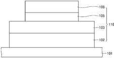
도 1은 본 개시의 일 실시예에 따른 가시광 방출 반도체 레이저 장치(100)를 개략적으로 보여준다. 도 1을 참조하면, 가시광 방출 반도체 레이저 장치(100)의 일 실시예는, 기판(101), 제1파장의 광(L1)을 방출하는 반도체 레이저 발광 구조(110), 및 반도체 레이저 발광 구조(110)의 출광측에 배치되어 제1파장의 광(L1)을 제2파장의 광(L2)으로 비선형적으로 변환하는 파장 변환기(120)를 포함할 수 있다. 반도체 레이저 발광 구조(110)는 수직 공동 표면 발광 레이저(VCSEL: vertical cavity surface emission laser)일 수 있다. 파장 변환기(120)는 메타 표면(121)을 포함할 수 있다. 메타 표면(121)은 제1파장의 광(L1)을 제2파장의 광(L2)으로 비선형적으로 변환한다. 메타 표면(121)은 2차 고조파 생성 구조를 가질 수 있다. 예를 들어, 메타 표면(121)은 2차 고조파 생성 구조의 일 예로서 나노 공진기(108)들의 배열을 포함할 수 있다. 나노 공진기(108)는 동작 파장보다 폼 팩터(form factors)를 갖는다. 예를 들어 나노 공진기(108)의 폼 펙터를 정의하는 인자(parameter) 중 적어도 하나가 동작 파장보다 작다. 메타 표면(121)은 반도체 레이저 발광 구조(110)를 형성하는 물질과 동일한 종류의 물질로 형성된다. 이에 의하여, 파장 변환기(120)는 반도체 레이저 발광 구조(110)를 제조하는 공정과 재료를 사용하여 반도체 레이저 발광 구조(110)와 일체로(monolithically) 형성될 수 있다. 광(L1)은 적외광일 수 있으며, 메타 표면(121)은 광(L1)을 가시 파장 대역의 광(L2)으로 비선형적으로 변환할 수 있다. 적외광을 방출하는 반도체 레이저 발광 구조(110)는 일반적으로 안정적이며, 강력하며, 장수명을 가진다. 반도체 레이저 발광 구조(110)와 적외광을 가시광으로 비선형적으로 변환하는 파장 변환기(120)의 일체 통합(monolithically integration)은 안정적이고, 강력하며, 장수명을 가진 가시광을 방출할 수 있는 반도체 레이저 장치(100)를 제공할 수 있다. 1 schematically shows a visible light emitting
일 실시예로서, 반도체 레이저 발광 구조(110)는 기판(101) 상에 배치된 하부 분산 브래그 반사기 층(102), 하부 분산 브래그 반사기 층(102) 상에 배치된 제1형 도전성 반도체 컨택층(103), 활성 영역 층(105), 제2형 도전성 반도체 컨택층(106)을 포함할 수 있다. 반도체 레이저 발광 구조(110)는 III-V 화합물 반도체 물질을 포함할 수 있다. 예를 들어, 반도체 레이저 발광 구조(110)는 GaAs계 화합물 반도체 물질을 포함할 수 있다. 예를 들어, 반도체 레이저 발광 구조(110)는 GaInP, AlGaInP, GaAs, GaInAs, AlGaAs, AlGaInAs 중 적어도 하나를 포함할 수 있다. As an embodiment, the semiconductor laser
일 실시예로서, 기판(101)은 반도체 기판일 수 있다. 예를 들어, 기판(101)으로서 Si 기판, GaAs 기판 등이 채용될 수 있다. 도면을 도시되지 않았지만, 필요에 따라서, 반도체 레이저 발광 구조(110)를 형성하는 물질과의 기판(101)과의 격자 정합을 위한 버퍼층과 씨드층이 기판(101)과 반도체 레이저 발광 구조(110) 사이에 개재될 수 있다. As an example, the
활성 영역 층(105)은 하나 이상의 양자 우물들 또는 양자 도트들을 포함할 수 있다. 예를 들어, 활성 영역 층(105)은 제1, 제2클래드층 사이에 다중 양자 우물 구조가 배치된 형태를 가질 수 있다. 다중 양자 우물 구조는 교대로 적층된 양자우물층과 양자장벽층을 포함할 수 있다. 예를 들어, 양자우물층과 양자장벽층은 GaAs, GaInxAs(0.05≤x≤0.35), GaInxP(0.3≤x≤0.7), AlyGaInxP(0.3≤x≤0.7, 0.05≤y≤0.95), AlyGaAs(0.05≤y≤0.95), GaAszP(0.4≤z≤0.95), AlAszP(0.4≤z≤0.95) 중 선택될 수 있다. 양자장벽층과 양자우물층을 형성하는 반도체 물질의 조성비와 양자장벽층과 양자우물층을 형성하는 반도체 물질의 조합에 의하여 광(L1)의 파장이 결정될 수 있다. 예를 들어, GaAs-양자우물층이 적용된 경우 약 850nm 파장을 갖는 광을 발생시킬 수 있다. 예를 들어, InGaAs-양자우물층이 적용된 경우 약 1040nm 파장을 갖는 광을 발생시킬 수 있다. GaInP-양자우물층이 적용된 경우 약 700nm 파장을 갖는 광을 발생시킬 수 있다. 양자우물층의 물질은 전술한 예에 의하여 한정되지 않으며, 소망하는 적외광 대역의 광을 발생시키기 위하여 다양한 조성비를 갖는 반도체 물질이 양자우물층으로서 적용될 수 있다.
제1 클래드층은 제1형 도전성을 갖는 반도체 물질층일 수 있다. 제1 클래드층은 제1형 도전성을 갖는 반도체 물질층일 수 있다. 제2 클래드층은 제2형 도전성을 갖는 반도체 물질층일 수 있다. 제1형 도전성은 n-형 도전성이고 제2형 도전성은 p-형 도전성일 수 있다. 제1형 도전성은 p-형 도전성이고 제2형 도전성은 n-형 도전성일 수도 있다. p-형 도전성 클래드층은 본질적인 반도체층(intrinsic semiconductor layer)을 억셉터(acceptor) 불순물로 도핑하여 얻을 수 있으며, n-형 도전성 클래드층은 본질적인 반도체층을 도우너(donor) 불순물로 도핑하여 얻을 수 있다. 일 실시예로서, 제1, 제2클래드층는 양자장벽층과 동일한 물질로 형성될 수 있다. 예를 들어, GaInP/AlGaInP 다중 양자 우물 구조가 적용된 경우, 제1, 제2클래드층은 AlGaInP로 형성될 수 있다. 예를 들어, GaAs/AlGaAs 다중 양자 우물 구조가 적용된 경우, 제1, 제2클래드층은 AlGaAs로 형성될 수 있다.The first cladding layer may be a semiconductor material layer having type 1 conductivity. The first cladding layer may be a semiconductor material layer having type 1 conductivity. The second cladding layer may be a semiconductor material layer having type 2 conductivity. The first type conductivity may be n-type conductivity and the second type conductivity may be p-type conductivity. The first type conductivity may be p-type conductivity and the second type conductivity may be n-type conductivity. The p-type conductive cladding layer can be obtained by doping an intrinsic semiconductor layer with an acceptor impurity, and the n-type conductive cladding layer can be obtained by doping an intrinsic semiconductor layer with a donor impurity. have. As an example, the first and second cladding layers may be formed of the same material as the quantum barrier layer. For example, when a GaInP/AlGaInP multi-quantum well structure is applied, the first and second cladding layers may be formed of AlGaInP. For example, when a GaAs/AlGaAs multi-quantum well structure is applied, the first and second cladding layers may be formed of AlGaAs.
활성 영역 층(105)은 양자 도트들을 포함할 수 있다. 발생되는 광(L1)의 파장은 양자 도트들의 크기와 양자 도트들을 구성하는 물질들의 조성에 의하여 결정될 수 있다.
제1형 도전성 반도체 컨택층(103)은 하부 분산 브래그 반사기 층(102) 상에 배치된다. 제1형 도전성 반도체 컨택층(103)은 하부 분산 브래그 반사기 층(102)과 활성 영역 층(105) 사이에 배치된다. 제2형 도전성 반도체 컨택층(106)은 활성 영역 층(105) 상에 배치된다. 제1형 도전성은 n-형 도전성이고 제2형 도전성은 p-형 도전성일 수 있으며, 또는 제1형 도전성은 p-형 도전성이고 제2형 도전성은 n-형 도전성일 수 있다. p-형 도전성 반도체 컨택층은 본질적인 반도체층(intrinsic semiconductor layer)을 억셉터(acceptor) 불순물로 도핑하여 얻을 수 있으며, n-형 도전성 반도체 컨택층은 본질적인 반도체층을 도우너(donor) 불순물로 도핑하여 얻을 수 있다. A type 1 conductive semiconductor contact layer (103) is disposed on the lower distributed Bragg reflector layer (102). A type 1 conductive semiconductor contact layer (103) is disposed between the lower diffuse Bragg reflector layer (102) and the active region layer (105). A type 2 conductive
제1컨택 패드(104)는 제1형 도전성 반도체 컨택층(103)의 일부에 배치된다. 활성 영역 층(105)은 제1형 도전성 반도체 컨택층(103) 상에 제1컨택 패드(104)에 의하여 점유되지 않은 영역에 배치된다. 제2컨택 패드(107)는 제2형 도전성 반도체 컨택층(106)의 일부에 배치된다. The
도 1에 도시된 반도체 레이저 발광 구조(110)는 예시적인 것이며, 도 1에 도시된 반도체 레이저 발광 구조(110)에 의하여 본 발명의 범위가 제한되지는 않는다. 반도체 레이저 발광 구조(110)는 도면으로 도시되지 않은 다양한 추가적인 구성 요소들/층들을 포함할 수 있다.The semiconductor laser
본 실시예의 반도체 레이저 장치(100)는 반도체 레이저 발광 구조(110)에서 발생되는 광(L1)을 다른 파장을 갖는 광(L2)으로 비선형적으로 변환하는 메타 표면(121)을 구비한다. 메타 표면(121)은 광(L1)의 2차 고조파(second harmonic wave)를 생성할 수 있는 구조를 갖는다. 2차 고조파 생성(SHG: second harmonic generation)은 동일한 주파수를 갖는 두 개의 광자(photon)가 비선형 구조 또는 물질과 상호 작용하여 2배의 에너지를 갖는 하나의 새로운 광자를 생성하는 비선형적인 광학적 과정(nonlinear optical process)이다. 따라서, 메타 표면(121)으로부터 출사되는 광(L2)의 주파수는 메타 표면(121)에 입사되는 광(L1)의 주파수의 2배가 된다. 예를 들어, 반도체 레이저 발광 구조(110)는 적외광을 발생시키는 수직 공동 표면 발광 반도체 레이저(VCSEL) 구조일 수 있다. 본 실시예의 메타 표면(121)은 적외광을 가시광으로 비선형적으로 변환할 수 있다. The
본 실시예에서, 메타 표면(121)을 포함하는 파장 변환기(120)는 활성 영역 층(105)을 기준으로 하여 출광측, 예를 들어 하부 분산 브래그 반사기 층(102)의 반대쪽에 배치된다. 본 실시예의 메타 표면(121)은 하부 분산 브래그 반사기 층(102)과 짝을 이루어 VCSEL의 캐배티(cavity)를 형성하는 상부 반사기 층으로서 기능할 수 있다. In this embodiment, the
메타 표면(121)는 다수의 나노 공진기들(108)의 배열을 포함할 수 있다. 나노 공진기들(108)의 배열은 예를 들어 제2형 도전성 반도체 컨택층(106) 상에 제2컨택 패드(107)에 의하여 점유되지 않은 영역에 배치될 수 있다. 메타 표면(121)은 또한 반도체 레이저 발광 구조(110), 즉 VCSEL 공동(cavity)의 피드백 기능(feedback function)을 수행할 수 있다. 메타 표면(121)은 반도체 레이저 발광 구조(110), 예를 들어 VCSEL을 제조하는 데에 사용되는 다양한 물질들로 형성될 수 있다. 예를 들어 메타 표면(121)은 III-V족 반도체 화합물, 예를 들어 GaAs, AlGaAs, InGaAs, InP 등을 포함할 수 있다. 이에 의하여, 반도체 레이저 발광 구조(110)와 파장 변환기(120)가 공통의 제조 공정, 설비, 재료를 이용하여 일체로(monolithically) 형성될 수 있다. 물질들에 따라서, 반도체 레이저 장치(100)의 동작 파장이 시프트(shift)될 수 있다. 메타 표면(121)과 VCSEL의 활성 영역 층(105)은 넓은 범위의 성능과 유연성을 제공하기 위하여 다양한 물질로 형성될 수 있다. The
도 2는 메타 표면(121)의 일 실시예를 도시한다. 도 2를 참조하면, 메타 표면(121)은 서로 이격되게 배치되는 복수의 나노 공진기(108)를 포함할 수 있다. 복수의 나노 공진기(108)는 나노 공진기(108)의 배열(array)을 형성할 수 있다. 복수의 나노 공진기(108) 각각은 적어도 하나의 물질층을 포함할 수 있다. 예를 들어, 복수의 나노 공진기(108) 각각은 복수의 물질층을 포함할 수 있다. 메타 표면(121)의 각 나노 공진기(108)는 제2형 도전성 반도체 컨택층(106) 상에 직접 위치될 수 있다. 예를 들어, 메타 표면(121)의 각 나노 공진기(108)는 제2형 도전성 반도체 컨택층(106) 상에 서로 이격되게 배치되는 스페이서층(108-1)과, 스페이서층(108-1) 상에 배치되는 반도체 화합물층(108-2)을 포함할 수 있다. 스페이서층(108-1)은 제2형 도전성 반도체 컨택층(106) 상에 제2컨택 패드(107)에 의하여 점유되지 않은 영역에 서로 이격되게 형성될 수 있다. 스페이서층(108-1)은 예를 들어 절연층일 수 있다. 스페이서층(108-1)은 예를 들어 산화물층일 수 있다. 스페이서층(108-1)은 반도체 레이저 발광 구조(110), 예를 들어 VCSEL을 제조하는 데에 사용되는 다양한 물질들의 산화물로 형성될 수 있다. 반도체 화합물층(108-2)은 반도체 레이저 발광 구조(110), 예를 들어 VCSEL을 제조하는 데에 사용되는 다양한 물질들로 형성될 수 있다. 예를 들어, 스페이서층(108-1)은 AlGaO층일 수 있으며, 반도체 화합물층(108-2)은 AlGaO층 상에 배치되는 AIIIBV 반도체 화합물층일 수 있다.2 shows one embodiment of a
도 2에 도시되지는 않았지만, 복수의 나노 공진기(108) 각각은 반도체 화합물층(108-2), 예를 들어 AIIIBV 반도체 화합물층 상에 배치되는 저굴절률 유전층을 더 포함할 수 있다. 저굴절률 유전체층은, 예를 들어, SiO2, PMMA(polymethylmethacrylate), BCB(benzocyclobutane) 등을 포함할 수 있다. 유전체층은 선택적(optional)이며, 나노 공진기(108)의 동작에 영향을 미치지 않는다. 유전체층은 나노 공진기(108)의 배열을 형성할 때에 마스크(mask)로 사용될 수 있으며, 반도체 레이저 장치(100)의 제조 공정을 간소화하기 위하여 나노 공진기(108)의 배열을 형성한 후에 제거되지 않을 수 있다. 유전체층은 언급된 예들로 제한되지 않으며, 나노 공진기(108)의 배열을 형성할 때에 식각 마스크로서 적절한 저굴절률 유전체 재료로 형성될 수 있다.Although not shown in FIG. 2 , each of the plurality of
반도체 화합물층(108-2)을 위한 AIIIBV 반도체 화합물은 결정 구조의 측면에서 제2형 도전성 반도체 컨택층(106)의 물질에 가까운 AIIIBV 반도체 화합물들로부터 선택될 수 있다. 이와 같은 구성에 의하면, 반도체 레이저 장치(100)의 제조 공정에서, 반도체 화합물층(108-2), 예를 들어 AIIIBV 반도체 화합물층, 스페이서층(108-1), 예를 들어 AlGaO층, 및 제2형 도전성 반도체 컨택층(106) 사이의 스트레스가 감소될 수 있으며, 파장 변환기(120)와 반도체 레이저 발광 구조(110)가 단일 프로세스(monolithic process)로 형성될 수 있다.The A III B V semiconductor compound for the semiconductor compound layer 108 - 2 may be selected from A III B V semiconductor compounds that are close to the material of the type 2 conductive
이와 같은 형태의 메타 표면(121)은 반도체 레이저 발광 구조(110)를 제조하는 공정과 유사한 공정에 의하여 형성될 수 있다. 예를 들어, VCSEL 구조를 갖는 반도체 레이저 발광 구조(110)의 출광측에 메타 표면(121)에 형성될 수 있다. 제2형 도전성 반도체 컨택층(106) 상에 제2컨택 패드(107)에 의하여 점유되지 않은 영역에 AlGaAs 층, GaAs층, SiO2층, PMMA층을 순차로 형성한다. PMMA층을 식각하여 나노 공진기(108)가 형성될 위치에 복수의 개구부를 형성한다. 복수의 개구부에 의하여 SiO2층이 부분적으로 노출된다. 그런 다음, 복수의 개구부에 금속층, 예를 들어 Ni층을 형성하고, PMMA층을 제거한다. 그런 다음, Ni층을 식각 마스크로 하여 SiO2층을 식각하여 복수의 SiO2 캡(cap)을 형성한다. 복수의 SiO2 캡(cap)을 식각 마스크로 하여 GaAs층과 AlGaAs 층을 식각한다. 이때, 식각 공정으로서 예를 들어 ICP(inductively coupled plasma) 식각 공정이 적용될 수 있다. 이에 의하여, 반도체 레이저 발광 구조(110)의 출광측에 3층 구조(AlGaAs/GaAs/SiO2)를 갖는 복수의 돌기가 형성된다. 다음으로, AlGaAs를 AlGaO로 산화시킨다. 이에 의하여, 반도체 레이저 발광 구조(110)의 출광측에 AlGaO층/GaAs층/SiO2층을 포함하는 복수의 나노 공진기(108)가 형성될 수 있다. AlGaO층, GaAs층, SiO2층은 각각 도 2에 도시된 실시예에서 스페이서층(108-1), 반도체 화합물층(108-2), 및 저굴절률 유전체층이다. SiO2층은 제거될 수도 있다.The
이와 같이, 반도체 레이저 발광 구조(110) 상에 메타 표면(121)을 포함하는 파장 변환기(120)를 일체로(monolithically) 형성할 수 있으며, 가시광 방출 반도체 레이저 장치(100)는 일체로 패키징될 수 있다. 또한, 메타 표면(121)을 형성하는 공정은 일반적인 VCSEL을 제조하는 공정과 유사하며, 새로운 물질이나 추가적인 특별한 공정을 요하지 않는다. 또한, 메타 표면(121)은 VCSEL의 스케일(scale) 내에서 다양한 형상과 크기로 형성될 수 있다. 즉, 메타 표면(121)을 형성하는 공정은 스케일러블(scalable)하므로, 반도체 레이저 장치(100)의 제조 비용이 절감될 수 있다. 또한, 다양한 파장의 광, 예를 들어 가시광을 방출할 수 있는 다양한 구조의 메타 표면(121)이 반도체 레이저 발광 구조(110)와 일체로(monothically) 제조될 수 있다.In this way, the
도 3은 메타 표면(121)의 다른 실시예를 도시한다. 도 3을 참조하면, 메타 표면(121)은 스페이서층(108-1)과, 스페이서층(108-1) 상에 서로 이격되게 배치되는 복수의 나노 공진기(108)를 포함할 수 있다. 복수의 나노 공진기(108)는 나노 공진기(108)의 배열(array)을 형성할 수 있다. 복수의 나노 공진기(108) 각각은 반도체 화합물층(108-2)을 포함할 수 있다. 스페이서층(108-1)은 제2형 도전성 반도체 컨택층(106) 상에 제2컨택 패드(107)에 의하여 점유되지 않은 영역에 전체적으로 적층되어 형성될 수 있다. 스페이서층(108-1)은 예를 들어 절연층일 수 있다. 스페이서층(108-1)은 예를 들어 산화물층일 수 있다. 스페이서층(108-1)은 반도체 레이저 발광 구조(110), 예를 들어 VCSEL을 제조하는 데에 사용되는 다양한 물질들의 산화물로 형성될 수 있다. 반도체 화합물층(108-2)은 반도체 레이저 발광 구조(110), 예를 들어 VCSEL을 제조하는 데에 사용되는 다양한 물질들로 형성될 수 있다. 예를 들어, 스페이서층(108-1)은 AlGaO을 포함할 수 있으며, 반도체 화합물층(108-2)은 AlGaO층 상에 서로 이격되게 배치되는 AIIIBV 반도체 화합물을 포함할 수 있다. 도 3에 도시되지는 않았지만, 도 2에 도시된 실시예와 마찬가지로, 복수의 나노 공진기(108) 각각은 반도체 화합물층(108-2), 예를 들어 AIIIBV 반도체 화합물층 상에 배치되는 저굴절률 유전체층을 더 포함할 수 있다. 3 shows another embodiment of the
이와 같은 형태의 메타 표면(121)은 반도체 레이저 발광 구조(110)를 제조하는 공정과 유사한 공정에 의하여 형성될 수 있다. 예를 들어, VCSEL 구조를 갖는 반도체 레이저 발광 구조(110)의 출광측에 메타 표면(121)에 형성될 수 있다. 제2형 도전성 반도체 컨택층(106) 상에 제2컨택 패드(107)에 의하여 점유되지 않은 영역에 AlGaAs 층을 형성한다. 그런 다음, AlGaAs층을 AlGaO층으로 산화시킨다. AlGaO층 상에 GaAs층, SiO2층, PMMA층을 순차로 형성한다. PMMA층을 식각하여 나노 공진기(108)가 형성될 위치에 복수의 개구부를 형성한다. 복수의 개구부에 의하여 SiO2층이 부분적으로 노출된다. 그런 다음, 복수의 개구부에 금속층, 예를 들어 Ni층을 형성하고, PMMA층을 제거한다. 그런 다음, Ni층을 식각 마스크로 하여 SiO2층을 식각하여 복수의 SiO2 캡(cap)을 형성한다. 복수의 SiO2 캡(cap)을 식각 마스크로 하여 GaAs층을 식각한다. 이때, 식각 공정으로서 예를 들어 ICP(inductively coupled plasma) 식각 공정이 적용될 수 있다. 이에 의하여, AlGaO층 상에 2층 구조(GaAs층/SiO2층)를 갖는 복수의 나노 공진기(108)가 형성될 수 있다. AlGaO층, GaAs층, SiO2층은 각각 도 3에 도시된 스페이서층(108-1), 반도체 화합물층(108-2), 및 저굴절률 유전체층이다. SiO2층은 제거될 수도 있다.The
나노 공진기(108)의 제2형 도전성 반도체 컨택층(106)의 표면과 평행한 단면 형상은 임의적일 수 있다. 나노 공진기(108)의 단면 형상은 비대칭적(asymmetric)일 수 있다. 나노 공진기(108)의 단면 형상은 예를 들어 정사각형, 직사각형, 삼각형, 원, 타원 등과 같은 평탄한 기하학적 도형의 적어도 둘 이상의 조합으로 형성된 형상을 가질 수 있다. 선택되는 둘 이상의 도형은 형상과 크기 중 적어도 하나가 다를 수 있다. 물론, 선택되는 둘 이상의 도형은 형상과 크기가 동일할 수도 있다.A cross-sectional shape parallel to the surface of the type 2 conductive
비대칭적 단면 형상을 갖는 나노 공진기(108)에 의하여 하이-Q 공진 모드(high-Q resonance mode)가 제공될 수 있으며, 이는 메타 표면(121)의 비선형 파장 변환 효율을 증가시킨다. 도 4 내지 도 7은 나노 공진기(108)의 단면 형상들의 예들을 보여준다. 도 4 내지 도 6에는 형상이 동일하고 크기가 다른 두 도형의 조합에 의하여 구현된 단면 형상을 갖는 나노 공진기(108)가 예시적으로 도시되어 있으며, 도 7에는 형상과 크기가 다른 두 도형의 조합에 의하여 구현된 단면 형상을 갖는 나노 공진기(108)가 예시적으로 도시되어 있다. 도 4를 참조하면, 나노 공진기(108)의 단면은 두 개의 정사각형이 조합된 형상이다. 도 5를 참조하면, 나노 공진기(108)의 단면은 두 개의 원이 조합된 형상이다. 도 6을 참조하면, 나노 공진기(108)는 두 개의 직사각형이 조합된 형상이다. 도 7을 참조하면, 나노 공진기(108)의 단면은 직사각형과 정사각형이 조합된 형상이다. 이러한 형태의 비대칭적 단면 형상을 갖는 나노 공진기(108)에 의하면, 특정 파장 대역에서 반사율 피크 또는 투과율 피크를 얻을 수 있으며, 이는 메타 표면(121)의 비선형 파장 변환 효율의 향상(enhancement)을 의미한다. 나노 공진기(108)의 단면 형상은 도 4 내지 도 7에 도시된 예에 한정되지 않는다. A high-Q resonance mode can be provided by the
일 예로서, 메타 표면(121)은 도 3에 도시된 바와 같이 AlGaO-스페이서층 상에 서로 이격되게 배치되는 복수의 나노 공진기(108)를 포함할 수 있다. 복수의 나노 공진기(108)는 GaAs-반도체 화합물층을 포함할 수 있다. GaAs-반도체 화합물층은 도 5에 도시된 단면 형상을 가질 수 있다. AlGaO-스페이서층의 두께를 h1, GaAs-반도체 화합물층의 두께를 h2, GaAs-반도체 화합물층의 피치를 p라 하면, 예시적인 시뮬레이션 결과에 따르면, As an example, the
r1 = 140nmr1 = 140 nm
r2 = 75nmr2 = 75 nm
x = 135nmx = 135 nm
h1 = 500nmh1 = 500 nm
h2 = 160nmh2 = 160 nm
p = 670nmp = 670 nm
인 경우, 높은 비선형 변환 효율을 얻을 수 있는 하이-Q 공진 모드(high-Q resonance mode)를 제공하며, 1040nm 파장에서 높은 반사율(반사율 피크)를 얻을 수 있다. In the case of , a high-Q resonance mode capable of obtaining high nonlinear conversion efficiency is provided, and a high reflectance (reflectance peak) can be obtained at a wavelength of 1040 nm.
일 예로서, 메타 표면(121)은 도 3에 도시된 바와 같이 AlGaO-스페이서층 상에 서로 이격되게 배치되는 복수의 나노 공진기(108)를 포함할 수 있다. 복수의 나노 공진기(108)는 GaAs-반도체 화합물층을 포함할 수 있다. 나노 공진기(108)는 도 6에 도시된 단면 형상을 가질 수 있다. AlGaO-스페이서층의 두께를 h1, GaAs-반도체 화합물층의 두께를 h2, 피치를 p3라 하면, 예시적인 시뮬레이션 결과에 따르면, As an example, the
S1 = 280nmS1 = 280 nm
S2 = 45.5nmS2 = 45.5 nm
S3 = 112nmS3 = 112 nm
h1 = 200nmh1 = 200nm
h2 = 300nmh2 = 300 nm
p = 504nmp = 504 nm
인 경우, 높은 비선형 변환 효율을 얻을 수 있는 하이-Q 공진 모드(high-Q resonance mode)를 제공한다.In the case of , a high-Q resonance mode capable of obtaining high nonlinear conversion efficiency is provided.
일 예로서, 메타 표면(121)은, 도 2에 도시된 바와 같이, AlGaO-스페이서층과, AlGaO-스페이서층 상에 적층된 GaAs-반도체 화합물층을 포함하는 복수의 나노 공진기(108)를 포함할 수 있다. 나노 공진기(108)는 도 7에 도시된 단면 형상을 가질 수 있다. AlGaO-스페이서층의 두께를 h1, GaAs-반도체 화합물층의 두께를 h2, SiO2층의 두께를 h3라 하면, 예시적인 시뮬레이션 결과에 따르면, As an example, the
S1 = 296nmS1 = 296 nm
S2 = 296nmS2 = 296 nm
S3 = 68nmS3 = 68 nm
h1 = 300nmh1 = 300 nm
h2 = 300nmh2 = 300 nm
h3 = 60nmh3 = 60nm
인 경우, 높은 비선형 변환 효율을 얻을 수 있는 하이-Q 공진 모드(high-Q resonance mode)를 제공하며, 1040nm 파장에서 높은 투과율(투과율 피크)을 얻을 수 있다. In the case of , a high-Q resonance mode capable of obtaining high nonlinear conversion efficiency is provided, and high transmittance (peak transmittance) can be obtained at a wavelength of 1040 nm.
전술한 시뮬레이션 결과들은 예시적이며, 발명의 범위를 제한하지 않는다. 메타 표면(121)을 형성하는 나노 공진기(108)의 폼 펙터들은 높은 비선형 변환 효율을 얻을 수 있는 하이-Q 공진 모드(high-Q resonance mode)를 제공할 수 있도록 다양하게 선택될 수 있다. The simulation results described above are illustrative and do not limit the scope of the invention. Form factors of the
나노 공진기(108)의 폼 펙터(form factor), 예를 들어 단면 형상과 두께를 정의하는 인자들(parameters)은 다양한 수치 최적화 기법을 이용하여 결정될 수 있다. 수치 최적화 기법은 예를 들어 FDTD(finite difference tie domain)법, FEM(finite element method), 등을 포함할 수 있다. 다만, 나노 공진기(108)의 인자들을 결정하는 방법은 전술한 방법들에 한정되지 않으며, 다른 적절한 방법에 의하여 수행될 수도 있다. 메타 표면(121)의 나노 공진기(108)들은 반도체 레이저 발광 구조(110), 예를 들어 VCSEL의 방출 파장 부근에서 가장 낮은 공명의 여기(excitation of lowest resonance)를 구현해낼 필요가 있다. 나노 공진기(108)의 인자들은, 나노 공진기(108)를 형성하는 물질을 굴절률을 고려하여, 나노 공진기(108)에 의한 방출 파장의 다중도(multiplicity)와 그 크기의 계산으로부터 얻어질 수 있다. 수치 최적화 기법에 의하여 원하는 파장의 광을 얻을 수 있도록 나노 공진기(108)의 인자들이 결정될 수 있다.A form factor of the
전술한 바와 같이, 메타 표면(121)은 반도체 레이저 발광 구조(110), 예를 들어 VCSEL 공동(cavity)의 피드백 기능을 수행할 수 있다. 다시 말하면, 메타 표면(121)은 반도체 레이저 발광 구조(110)의 하부 분산 브래그 반사기 층(102)과 쌍을 이루는 상부 반사기 층으로서 기능할 수 있다. 이를 위하여, 메타 표면(121)을 형성하는 나노 공진기들(108)의 인자들은 반도체 레이저 발광 구조(110)로부터 방출되는 광에 대하여 고반사 특성을 갖도록 선택될 수 있다. As described above, the
넌-펄스드 레이저(non-pulsed laser)와 동일한 평균 출력(power)을 갖는 펄스드 레이저(pulsed laser)는 더 높은 피크 에너지를 가지며, 이는 VCSEL로부터 출사되는 광의 가시광으로의 비선형 광학적 변환 효율을 증가시키는 데에 중요하다. 포화성 흡수체(saturable absorber)는 펄스드 레이저의 주요 요소 중 하나이다. 포화성 흡수체는 미러처럼 동작하며 충분한 에너지로 포화되면 광 펄스를 통과시킨다. 펄스드 VCSEL이 반도체 레이저 장치(100)의 반도체 레이저 발광 구조(110)에 사용되면, 나노 공진기(108)의 AIIIBV 반도체 화합물층(108-2) 내의 캐리어 주입 메커니즘으로 인하여, 메타 표면(121)은 추가적으로 포화성 흡수체로서 동작될 수 있으며, 이는 펄스드 모드에서 비선형 변환 효율을 증가시킨다. A pulsed laser with the same average power as a non-pulsed laser has a higher peak energy, which increases the efficiency of nonlinear optical conversion of light emitted from the VCSEL to visible light. important to do A saturable absorber is one of the main elements of a pulsed laser. The saturable absorber acts like a mirror and passes light pulses when saturated with sufficient energy. When the pulsed VCSEL is used in the semiconductor laser
도 8a 내지 도 8f는 반도체 레이저 장치(100)의 제조 방법의 일 실시예를 보여준다. 이하에서, 반도체 레이저 장치(100)의 제조 방법의 일 실시예를 설명한다.8A to 8F show an embodiment of a method of manufacturing the
먼저, 도 8a를 참조하면, 기판(101)을 준비하고, 기판(101) 상에 반도체 레이저 발광 구조(110)를 형성한다. 기판(101)은 예를 들어 반도체 기판일 수 있다. 본 실시예에서 GaAs 기판이 채용된다. 반도체 레이저 발광 구조(110)는 기판(101) 상에 III-V 화합물 반도체 물질을 성장시켜 형성될 수 있다. 반도체 레이저 발광 구조(110)는 예를 들어 GaInP, AlGaInP, GaAs, GaInAs, AlGaAs, AlGaInAs를 포함할 수 있다. 본 실시예의 반도체 레이저 발광 구조(110)는 수직 공동 표면 발광 레이저(VCSEL) 구조를 갖는다. VCSEL 반도체 레이저 발광 구조(110)를 형성하는 공정은 알려진 다양한 공정이 사용될 수 있으며, 이하에서 간략하게만 설명한다. First, referring to FIG. 8A , a
기판(101) 상에 하부 분산 브래그 반사기 층(102)을 형성한다. 하부 분산 브래그 반사기 층(102)은 기판(101) 상에 굴절률이 상대적으로 낮은 저굴절률층과 굴절률이 상대적으로 높은 고굴절률층을 교대로 적층하여 형성될 수 있다. 하부 분산 브래그 반사기 층(102)은 III-V족 반도체 화합물, 예를 들어 AlGaAs로 형성될 수 있다. A lower diffuse
하부 분산 브래그 반사기 층(102) 상에 제1형 도전성 반도체 컨택층(103)을 형성한다. 제1형 도전성 반도체 컨택층(103)은 III-V족 반도체 화합물로 형성될 수 있다. 제1형 도전성 반도체 컨택층(103)은 n-형 도전성 또는 p-형 도전성일 수 있으며, 본 실시예에서는 n-형 도전성이다. 제1형 도전성 반도체 컨택층(103)은 III-V족 반도체 화합물에 도우너(donor) 불순물로 도핑하여 얻을 수 있다. A type 1 conductive
제1형 도전성 반도체 컨택층(103) 상에 활성 영역 층(105)을 형성한다. 제1형 도전성 반도체 컨택층(103) 상에 III-V 화합물 반도체 물질을 결정 성장시켜 제1클래드층, 다중 양자 우물 구조, 제2클래드층을 순차로 형성하여 활성 영역 층(105)을 형성할 수 있다. 다중 양자 우물 구조를 형성하는 양자장벽층과 양자우물층의 III-V 화합물 반도체 물질과 조성비는 광(L1)의 파장에 따라서 적절히 선택될 수 있다. 일 예로서, 제1클래드층과 제2클래드층은 다중 양자 우물 구조의 양자장벽층과 동일한 물질로 형성될 수 있다.An
활성 영역 층(105) 상에 제2형 도전성 반도체 컨택층(106)을 형성한다. 제2형 도전성 반도체 컨택층(106)은 III-V족 반도체 화합물로 형성될 수 있다. 제2형 도전성 반도체 컨택층(106)은 n-형 도전성 또는 p-형 도전성일 수 있으며, 본 실시예에서는 p-형 도전성이다. 제1형 도전성 반도체 컨택층(103)은 III-V족 반도체 화합물에 억셉터(acceptor) 불순물로 도핑하여 얻을 수 있다. A second type conductive
다음으로, 반도체 레이저 발광 구조(110)의 출광측에 메타 표면(121)을 포함하는 파장 변환기(120)를 일체로(monothically) 형성하는 공정이 수행된다. Next, a process of integrally forming the
먼저, 도 8b를 참조하면, 제2형 도전성 반도체 컨택층(106) 상에 제1물질층(131), 제2물질층(132), 제2식각마스크층(EM2), 제1식각마스크층(EM1)을 순차로 형성한다. 제1물질층(131)과 제2물질층(132)은 반도체 레이저 발광 구조(110), 예를 들어 VCSEL을 제조하는 데에 사용되는 다양한 물질들로 형성될 수 있다. 제2물질층(132)은 AIIIBV 반도체 화합물층일 수 있다. 본 실시예에서, 제1물질층(131)은 AlGaAs층이며, 제2물질층(132)은 GaAs층이다. 제2식각마스크층(EM2)은 예를 들어 저귤절률 유전체로 형성될 수 있다. 예를 들어, 제2식각마스크층(EM2)과 제1식각마스크층(EM1)은 각각 SiO2층, PMMA층일 수 있다.First, referring to FIG. 8B , a
다음으로, 도 8c에 도시된 바와 같이, 제1식각마스크층(EM1)을 식각하여 제1식각마스크층(EM1)에 제2식각마스크층(EM2)을 노출시키는 복수의 개구부(133)를 형성한다. 이 공정은 예를 들어 전자빔 리소그래피(E-beam lithography)에 의하여 수행될 수 있다. 개구부(133)의 형상에 의하여 나노 공진기(108)의 단면 형상이 결정될 수 있다. 예시적으로, 개구부(133)의 형상은 도 4 내지 도 7에 도시된 형상을 가질 수 있다. Next, as shown in FIG. 8C, the first etch mask layer EM1 is etched to form a plurality of
그런 다음, 도 8d에 도시된 바와 같이, 복수의 개구부(133)에 금속, 예를 ㄷ들어 Ni를 적층하고, 제1식각마스크층(EM1)을 제거하여 서로 이격된 복수의 금속층(134)을 형성한다. 복수의 금속층(134)을 식각 마스크로 하여 제2식각마스크층(EM2)을 예를 들어 건식 식각한다. 금속층(134)을 제거하여, 도 8e에 도시된 바와 같이 제2물질층(132) 상에 서로 이격된 복수의 캡(135)을 형성한다. Then, as shown in FIG. 8D, metal, for example, Ni, is laminated on the plurality of
다음으로, 복수의 캡(135)을 식각 마스크로 하여 제2물질층(132)과 제1물질층(131)을 식각하여, 도 8f에 도시된 바와 같이 제2형 도전성 반도체 컨택층(106)의 상면에 제1물질층(131), 제2물질층(132), 캡(135)을 포함하며 서로 이격된 복수의 돌기를 형성한다. 식각 공정은 예를 들어 ICP(inductively coupled plasma) 식각 공정에 의하여 수행될 수 있다. 다음으로, 제1물질층(131)을 형성하는 AlGaAs를 AlGaO로 산화시킨다. 산화된 제1물질층(131), 제2물질층(132), 및 캡(135)은 각각 도 2에 도시된 나노 공진기(108)의 스페이서층(108-1), 반도체 화합물층(108-2), 및 저굴절률 유전체층에 대응된다. 캡(135)은 제거될 수도 있다. Next, the
다른 예로서, 복수의 캡(135)을 식각 마스크로 하여 제2물질층(132)을 식각하여, 도 8g에 도시된 바와 같이 제2형 도전성 반도체 컨택층(106)의 상면에 전체적으로 제1물질층(131) 상에 제2물질층(132)과 캡(135)을 포함하며 서로 이격된 복수의 돌기를 형성한다. 식각 공정은 예를 들어 ICP(inductively coupled plasma) 식각 공정에 의하여 수행될 수 있다. 다음으로, 제1물질층(131)을 형성하는 AlGaAs를 AlGaO로 산화시킨다. 산화된 제1물질층(131), 제2물질층(132), 및 캡(135)은 각각 도 3에 도시된 스페이서층(108-1), 및 나노 공진기(108)의 반도체 화합물층(108-2)과 저굴절률 유전체층에 대응된다. 캡(135)은 제거될 수도 있다. As another example, the
다음으로, 제1형 도전성 반도체 컨택층(103) 상에 활성 영역 층(105)에 의하여 점유되지 않은 영역에 제1컨택 패드(104)를 형성하고, 제2형 도전성 반도체 컨택층(106) 상에 메타 표면(121)에 의하여 점유되지 않은 영역에 제2컨택 패드(107)를 형성한다.Next, a
이에 의하여, 반도체 레이저 발광 구조(110)의 출광측에 복수의 나노 공진기(108)를 포함하는 메타 표면(121)을 포함하는 파장 변환기(120)가 일체로(monolithically) 형성된 도 1에 도시된 반도체 레이저 장치(100)가 제조될 수 있다. As a result, the semiconductor shown in FIG. 1 is integrally formed with a
전술한 제조 방법의 실시예는 예시적인 것이며, 나노 공진기들(108), 제1컨택 패드(104), 및 제2컨택 패드(107)의 형성 순서는 반도체 장치를 제조하는 기술에 적합하게 선택될 수 있다.The above-described embodiment of the manufacturing method is exemplary, and the formation order of the
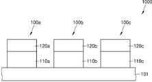
도 9는 반도체 레이저 장치(1000)의 일 실시예의 개략적인 구성도이다. 도 9를 참조하면, 반도체 레이저 장치(1000)는 기판(101) 상에 배열된 복수의 서브 반도체 레이저 장치를 포함할 수 있다. 예를 들어, 반도체 레이저 장치(1000)는 서브 반도체 레이저 장치(100a, 100b, 100c)를 포함할 수 있다. 서브 반도체 레이저 장치(100a, 100b, 100c) 각각은 도 1 내지 도 3에 도시된 바와 같이, 반도체 레이저 발광 구조(110)와 파장 변환기(120)가 일체로 형성된 구조를 갖는다. 9 is a schematic configuration diagram of an embodiment of a
서브 반도체 레이저 장치(100a, 100b, 100c)는 서로 다른 색상의 광을 방출할 수 있다. 예를 들어, 서브 반도체 레이저 장치(100a, 100b, 100c)는 서로 다른 색상의 가시광을 방출할 수 있다. 예를 들어, 서브 반도체 레이저 장치(100a, 100b, 100c)의 반도체 레이저 발광 구조(110a, 110b, 110c)는 서로 다른 파장의 적외광을 방출할 수 있다. 서브 반도체 레이저 장치(100a, 100b, 100c)의 파장 변환기(120a, 120b, 120c)는 반도체 레이저 발광 구조(110a, 110b, 110c)로부터 방출되는 서로 다른 파장의 적외광을 서로 다른 파장의 가시광으로 변환할 수 있다. 예를 들어, 반도체 레이저 발광 구조(110a, 110b, 110c)의 양자우물구조를 형성하는 물질을 각각 GaAs, InGaAs, GaInP로 선택함으로써 반도체 레이저 발광 구조(110a, 110b, 110c)은 각각 850nm, 1040nm, 700nm 파장의 적외광이 방출될 수 있다. 파장 변환기(120a, 120b, 120c)는 850nm, 1040nm, 700nm 파장의 적외광을 425nm, 520nm, 350nm 파장의 가시광으로 변환할 수 있다.The
이와 같은 구조의 반도체 레이저 장치(1000)에 따르면 서로 다른 파장의 가시광을 방출하는 복수의 서브 반도체 레이저 장치(100)가 단일의 기판 상에 예를 들어 배열(array)되도록 제조될 수 있다. 이러한 구조의 반도체 레이저 장치(1000)는 예를 들어 예를 들어, TVs, 스마트폰, 컴퓨터, 및 디스플레이 스크린을 포함하는 다른 장치들의 디스플레이 매트릭스로서 사용될 수 있다. According to the
도 10은 반도체 레이저 발광 구조(110)와 파장 변환기(120)가 통합된 반도체 레이저 장치(200)의 일 실시예를 개략적으로 보여준다. 도 10에 도시된 반도체 레이저 장치(200)의 일 실시예는 상부 반사기 층을 구비하며, 메타 표면(121)을 포함하는 파장 변환기(120)가 활성 영역 층(105)과 상부 반사기 층 사이에 배치되는 점에서 도 1에 도시된 반도체 레이저 장치(100)의 실시예와 차이가 있다. 이하에서, 차이점을 위주로 설명한다.10 schematically shows an embodiment of a
도 10을 참조하면, 반도체 레이저 장치(200)는 기판(101) 상에 형성되는 반도체 레이저 발광 구조(110)와, 반도체 레이저 발광 구조(110)의 출광측에 일체로 형성되는 파장 변환기(120)와, 파장 변환기(120)의 출광측에 배치되는 상부 분산 브래그 반사기 층(109)을 포함한다. Referring to FIG. 10 , the
반도체 레이저 발광 구조(110)는 하부 분산 브래그 반사기 층(102), 제1형 도전성 반도체 컨택층(103), 제1컨택 패드(104), 활성 영역 층(105), 제2형 도전성 반도체 컨택층(106), 제2컨택 패드(107)을 포함한다. 반도체 레이저 발광 구조(110)는 III-V족 반도체 화합물을 포함할 수 있다. 도 10에 도시된 반도체 레이저 발광 구조(110)는 예시적인 것이며, 도 10에 도시된 반도체 레이저 발광 구조(110)에 의하여 본 발명의 범위가 제한되지는 않는다. 반도체 레이저 발광 구조(110)는 도면으로 도시되지 않은 다양한 추가적인 구성 요소들/층들을 포함할 수 있다.The semiconductor laser
파장 변환기(120)는 광(L1)을 다른 파장의 광(L2)으로 비선형적으로 변환한다. 예를 들어, 파장 변환기(120)는 반도체 레이저 발광 구조(110)에서 방출되는 적외광을 가시광으로 비선형적으로 변환할 수 있다. 파장 변환기(120)는 메타 표면(121)을 포함한다. 메타 표면(121)은 나노 공진기들(108)의 배열(array)를 포함할 수 있다. 파장 변환기(120)의 구조는 도 1 내지 도 7에서 설명한 바와 동일할 수 있다. The
파장 변환기(120)는 활성 영역 층(105)을 기준으로 하여 하부 분산 브래그 반사기 층(102)의 반대쪽에 위치되며, 활성 영역 층(105)과 상부 브래그 반사기 층(109) 사이에 위치된다. 상부 브래그 반사기 층(109)은 굴절률이 상대적으로 낮은 저굴절률층과 굴절률이 상대적으로 높은 고굴절률층을 교대로 적층하여 형성될 수 있다. 상부 분산 브래그 반사기 층(109)은 메타 표면(121) 위에 위치될 수 있다. 파장 변환기(120)는 메타 표면(121)을 덮는 투명 유전체층(122)을 포함할 수 있다. 나노 공진기들(108) 사이의 공간은 투명 유전체층(122)에 의하여 채워질 수 있다. 메타 표면(121)은 투명 유전체층(122)에 묻힌 형태일 수 있다. 메타 표면(121)과 상부 브래그 반사기 층(109) 사이는 투명 유전체(210)에 의하여 채워질 수 있다. 상부 브래그 반사기 층(109)은 투명 유전체층(122) 상에 형성될 수 있다. 투명 유전체층(122)은 예를 들어, SiO2, PMMA(polymethylmethacrylate), BCB(benzocyclobutane) 등으로 형성될 수 있다. 투명 유전체층(122)을 형성하는 물질은 전술한 예들로 제한되지 않으며, 반도체 장치의 제조 공정에 사용할 수 있는 적절한 투명 유전체일 수 있다.The
나노 공진기들(108)의 폼 펙터(form factor), 예를 들어 단면 형상과 두께를 정의하는 인자들(parameters)은 다양한 수치 최적화 기법을 이용하여 결정될 수 있다. 수치 최적화 기법은 예를 들어 FDTD(finite difference tie domain)법, FEM(finite element method), 등을 포함할 수 있다. 다만, 나노 공진기(108)의 인자들을 결정하는 방법은 전술한 방법들에 한정되지 않으며, 다른 적절한 방법에 의하여 수행될 수도 있다. 나노 공진기들(108)의 인자들은 반도체 레이저 발광 구조(110), 예를 들어 VCSEL에서 방출되는 광(L1)에 대하여 높은 투과율을 제공하도록 선택될 수 있다. Form factors of the
반도체 레이저 발광 구조(110)가 펄스드 VCSEL인 경우, 반도체 레이저 장치(200)는 파장 변환기(120)와 상부 분산 브래그 반사기 층(109) 사이에 배치되는 포화성 흡수체(미도시)를 더 구비할 수 있다. When the semiconductor laser
도 10에 도시된 반도체 레이저 장치(200)의 제조 방법의 일 실시예를 간략하게 설명한다. 도 8a 내지 도 8g를 참조하여 전술한 바와 같이 기판(101) 상에 반도체 레이저 발광 구조(110)를 형성하고, 반도체 레이저 발광 구조(110)의 출광측에 메타 표면(121)을 형성한다. 그런 다음, 메타 표면(121) 상에 투명 유전체를 도포하여 투명 유전체층(122)을 형성한다. 투명 유전체는 나노 공진기들(108) 사이를 채울 수 있다. 투명 유전체층(122)의 두께는 나노 공진기들(108)의 두께보다 두꺼울 수 있다. 투명 유전체층(122)은 예를 들어, SiO2, PMMA(polymethylmethacrylate), BCB(benzocyclobutane) 등으로 형성될 수 있다. 투명 유전체층(122)을 형성하는 물질은 전술한 예들로 제한되지 않으며, 반도체 장치의 제조 공정에 사용할 수 있는 적절한 투명 유전체일 수 있다.An embodiment of a manufacturing method of the
다음으로, 투명 유전체층(122) 상에 상부 브래그 반사기 층(109)을 형성한다. 상부 브래그 반사기 층(109)은 굴절률이 상대적으로 낮은 저굴절률층과 굴절률이 상대적으로 높은 고굴절률층을 교대로 적층하여 형성될 수 있다. 다음으로, 제1형 도전성 반도체 컨택층(103) 상에 활성 영역 층(105)에 의하여 점유되지 않은 영역에 제1컨택 패드(104)를 형성하고, 제2형 도전성 반도체 컨택층(106) 상에 메타 표면(121)에 의하여 점유되지 않은 영역에 제2컨택 패드(107)를 형성한다. 이에 의하여, 도 10에 도시된 반도체 레이저 발광 구조(110)와 일체로 형성되는 파장 변환기(120)를 구비하는 반도체 레이저 장치(200)가 제조될 수 있다.Next, an upper
전술한 제조 방법의 실시예는 예시적인 것이며, 나노 공진기들(108), 제1컨택 패드(104), 및 제2컨택 패드(107)의 형성 순서는 반도체 장치를 제조하는 기술에 적합하게 선택될 수 있다.The above-described embodiment of the manufacturing method is exemplary, and the formation order of the
도 9에 도시된 서브 반도체 레이저 장치들(100a, 100b, 100c)은 도 10에 도시된 반도체 레이저 장치들(200)로 대체될 수 있다. 이 경우, 반도체 레이저 장치들(200)의 반도체 레이저 발광 구조들는 서로 다른 파장의 적외광을 방출할 수 있으며, 반도체 레이저 장치들(200)의 파장 변환기들은 반도체 레이저 발광 구조들로부터 방출되는 적외광을 서로 다른 파장의 기사광으로 변환할 수 있다. 이와 같은 구조의 반도체 레이저 장치(1000)에 따르면 서로 다른 파장의 가시광을 방출하는 복수의 서브 반도체 레이저 장치(200)가 단일의 기판 상에 예를 들어 배열(array)되도록 제조될 수 있다. 이러한 구조의 반도체 레이저 장치(1000)는 예를 들어 예를 들어, TVs, 스마트폰, 컴퓨터, 및 디스플레이 스크린을 포함하는 다른 장치들의 디스플레이 매트릭스로서 사용될 수 있다. The
도 11은 반도체 레이저 발광 구조(110)와 파장 변환기(120)가 통합된 반도체 레이저 장치(300)의 일 실시예를 개략적으로 보여준다. 도 11에 도시된 반도체 레이저 장치(300)의 일 실시예는 파장 변환기(120)를 형성하는 메타 표면(121)과 반도체 레이저 발광 구조(110) 사이에 에어 갭(125)이 개재된 점에서 도 1에 도시된 반도체 레이저 장치(100)의 실시예와 차이가 있다. 이하에서, 차이점을 위주로 설명한다. 도 11을 참조하면, 반도체 레이저 장치(300)는 기판(101) 상에 형성되는 반도체 레이저 발광 구조(110)와, 메타 표면(121)을 포함하며 반도체 레이저 발광 구조(110)의 출광측에 일체로 형성되는 파장 변환기(120)와, 메타 표면(121)과 반도체 레이저 발광 구조(110) 사이에 개재되는 에어 갭(125)을 포함할 수 있다. 11 schematically shows an embodiment of a
반도체 레이저 발광 구조(110)는 하부 분산 브래그 반사기 층(102), 제1형 도전성 반도체 컨택층(103), 제1컨택 패드(104), 활성 영역 층(105), 제2형 도전성 반도체 컨택층(106), 제2컨택 패드(107)을 포함한다. 반도체 레이저 발광 구조(110)는 III-V족 반도체 화합물을 포함할 수 있다. 도 11에 도시된 반도체 레이저 발광 구조(110)는 예시적인 것이며, 도 11에 도시된 반도체 레이저 발광 구조(110)에 의하여 본 발명의 범위가 제한되지는 않는다. 반도체 레이저 발광 구조(110)는 도면으로 도시되지 않은 다양한 추가적인 구성 요소들/층들을 포함할 수 있다.The semiconductor laser
파장 변환기(120)는 광(L1)을 다른 파장의 광(L2)으로 비선형적으로 변환한다. 예를 들어, 파장 변환기(120)는 반도체 레이저 발광 구조(110)에서 방출되는 적외광을 가시광으로 비선형적으로 변환할 수 있다. 파장 변환기(120)는 메타 표면(121)을 포함한다. 메타 표면(121)은 나노 공진기들(108)의 배열(array)를 포함할 수 있다. 파장 변환기(120)의 구조는 도 1 내지 도 7에서 설명한 바와 동일할 수 있다. 다만, 도 2와 도 3에서 에어 갭(125)이 스페이서층(108-1)을 대체할 수 있으므로, 스페이서층(108-1)이 생략될 수 있다.The
파장 변환기(120)는 제2형 도전성 반도체 컨택층(106)으로부터 이격되게 위치되는 메타 표면(121)과, 제2형 도전성 반도체 컨택층(106) 상에 위치되며 메타 표면(121)의 외곽에 위치되는 측벽(123)과, 메타 표면(121)의 나노 공진기들(108)과 측벽(123)을 연결하는 띠들(straps)(124)을 포함할 수 있다. 측벽(123)은 예를 들어 메타 표면(121)을 부분적으로 또는 전체적으로 에워싸는 형태일 수 있다. 측벽(123)은 제2형 도전성 반도체 컨택층(106) 상에 적층되어 형성될 수 있다. 측벽(123), 나노 공진기들(108)의 배열, 및 띠들(124)은 AIIIBV 반도체 화합물로 형성될 수 있다.The
나노 공진기들(108), 측벽(123), 및 띠들(124)을 위한 AIIIBV 반도체 화합물은 결정 구조가 제2형 도전성 반도체 컨택층(106)의 물질에 가까운 AIIIBV 반도체 화합물들로부터 선택될 수 있다. 이러한 물질의 선택은, 나노 공진기들(108), 측벽(123), 띠들(124), 및 제2형 도전성 반도체 컨택층(106)과 결정 구조가 가까운 물질의 사용이 AIIIBV 반도체 화합물층의 측벽들(309)과 제2형 도전성 반도체 컨택층(306) 사이의 스트레스를 줄이고 단일 구조를 형성할 수 있다는 점 때문이다.The A III B V semiconductor compounds for the
나노 공진기들(108)의 폼 펙터(form factor), 예를 들어 단면 형상과 두께를 정의하는 인자들(parameters)은 다양한 수치 최적화 기법을 이용하여 결정될 수 있다. 수치 최적화 기법은 예를 들어 FDTD(finite difference tie domain)법, FEM(finite element method), 등을 포함할 수 있다. 다만, 나노 공진기(108)의 인자들을 결정하는 방법은 전술한 방법들에 한정되지 않으며, 다른 적절한 방법에 의하여 수행될 수도 있다. 나노 공진기들(108)의 인자들은 반도체 레이저 발광 구조(110), 예를 들어 VCSEL에서 방출되는 광(L1)에 대하여 높은 투과율을 제공하도록 선택될 수 있다. Form factors of the
본 실시예의 메타 표면(121)은 하부 분산 브래그 반사기 층(102)과 짝을 이루어 VCSEL의 캐배티(cavity)를 형성하는 상부 반사기 층으로서 기능할 수 있다. 나노 공진기(108)들의 높이(두께)는 동일할 수 있다.The
도 12a 내지 도 12d는 반도체 레이저 장치(300)의 제조 방법의 일 실시예를 보여준다. 도 8a 및 도 12a 내지 도 12d를 참조하여 도 11에 도시된 반도체 레이저 장치(300)의 제조 방법의 일 실시예를 간략하게 설명한다. 12A to 12D show an embodiment of a method of manufacturing the
먼저, 도 8a를 참조하여 전술한 바와 같이 기판(101) 상에 반도체 레이저 발광 구조(110)를 형성한다. 다음으로, 반도체 레이저 발광 구조(110)의 출광측에 메타 표면(121)을 포함하는 파장 변환기(120)를 일체로(monothically) 형성하는 공정이 수행된다. First, as described above with reference to FIG. 8A , the semiconductor laser
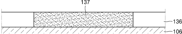
도 12a를 참조하면, 제2형 도전성 반도체 컨택층(106) 상에 물질층(136)을 형성한다. 물질층(136)은 반도체 레이저 발광 구조(110), 예를 들어 VCSEL을 제조하는 데에 사용되는 다양한 물질들로 형성될 수 있다. 물질층(136)은 AIIIBV 반도체 화합물층일 수 있다. 물질층(136)을 식각하여 제2형 도전성 반도체 컨택층(106)을 부분적으로 노출시킨다. 도 12b에 도시된 바와 같이 제2형 도전성 반도체 컨택층(106)의 노출된 표면에 희생층(137)을 적층한다. Referring to FIG. 12A , a
도 12c에 도시된 바와 같이 물질층(136)과 희생층(137) 상에 물질층(138)을 적층한다. 물질층(138)은 물질층(136)과 동일한 물질로 형성될 수 있다. 물질층(138)은 예를 들어 AIIIBV 반도체 화합물층일 수 있다. 다음으로, 물질층(138)을 패터닝하여 도 12d에 도시된 바와 같이 측벽(123), 나노 공진기들(108)의 배열, 및 띠들(124)을 형성한다. 이 공정은 식각 마스크를 이용한 식각 공정에 의하여 수행될 수 있다. As shown in FIG. 12C , a
제2형 도전성 반도체 컨택층(106)과 메타 표면(121) 사이의 희생층(137)을 제거한다. 이 공정은 예를 들어 습식 식각 공정에 의하여 수행될 수 있다. 이에 의하여, 도 11에 도시된 바와 같이 제2형 도전성 반도체 컨택층(106)과 메타 표면(121) 사이에 에어 갭(125)이 형성된 파장 변환기(120)가 제조될 수 있다. The
다음으로, 제1형 도전성 반도체 컨택층(103) 상에 활성 영역 층(105)에 의하여 점유되지 않은 영역에 제1컨택 패드(104)를 형성하고, 제2형 도전성 반도체 컨택층(106) 상에 메타 표면(121)에 의하여 점유되지 않은 영역에 제2컨택 패드(107)를 형성한다. 이에 의하여, 반도체 레이저 발광 구조(110)의 출광측에 에어 갭(125)을 개재하여 복수의 나노 공진기(108)를 포함하는 메타 표면(121)을 포함하는 파장 변환기(120)가 일체로(monolithically) 형성된 도 11에 도시된 반도체 레이저 장치(300)가 제조될 수 있다. Next, a
전술한 제조 방법의 실시예는 예시적인 것이며, 나노 공진기들(108), 측벽(123), 띠들(124), 제1컨택 패드(104), 및 제2컨택 패드(107)의 형성 순서는 반도체 장치를 제조하는 기술에 적합하게 선택될 수 있다.The above-described embodiment of the manufacturing method is exemplary, and the order of forming the
도 9에 도시된 서브 반도체 레이저 장치들(100a, 100b, 100c)은 도 11에 도시된 반도체 레이저 장치들(300)로 대체될 수 있다. 이 경우, 반도체 레이저 장치들(300)의 반도체 레이저 발광 구조들는 서로 다른 파장의 적외광을 방출할 수 있으며, 반도체 레이저 장치들(300)의 파장 변환기들은 반도체 레이저 발광 구조들로부터 방출되는 적외광을 서로 다른 파장의 기사광으로 변환할 수 있다. 이와 같은 구조의 반도체 레이저 장치(1000)에 따르면 서로 다른 파장의 가시광을 방출하는 복수의 서브 반도체 레이저 장치(200)가 단일의 기판 상에 예를 들어 배열(array)되도록 제조될 수 있다. 이러한 구조의 반도체 레이저 장치(1000)는 예를 들어 예를 들어, TVs, 스마트폰, 컴퓨터, 및 디스플레이 스크린을 포함하는 다른 장치들의 디스플레이 매트릭스로서 사용될 수 있다. The
메타 표면(121)과 반도체 레이저 발광 구조(110) 예를 들어 VCSEL과의 단일 통합(monolithic integration)은 추가적인 조립과 패키징을 요구하지 않으며, 전체 구조가 단일 제조 공정에 의하여 제조되며, 대량 생산이 가능하다. 또한, 메타 표면(121)은 새로운 물질이 필요없이 반도체 레이저 발광 구조(110)의 제조에 사용되는 물질로 제조된다. 이는 메타 표면(121)이 새로운 제조 설비를 필요로 하지 않으며, 반도체 레이저 발광 구조(110), 예를 들어 VCSEL의 제조 공정 설비를 사용하여 제조될 수 있다는 것을 의미한다. 따라서, 메타 표면(121)과 반도체 레이저 발광 구조(110) 예를 들어 VCSEL의 단일 통합(monolithic integration)에 의하여, 안정적이고 신뢰성 있는 가시광을 방출하는 반도체 레이저 장치(100, 200, 300)가 제공될 수 있다. 반도체 레이저 발광 구조(110), 예를 들어 VCSEL에 직접 마련되는 메타 표면(121)은 매우 얇으며, 이는 모바일 장치에 통합가능한 매우 컴팩트한 반도체 레이저 장치(100, 200, 300)의 제공을 가능하게 한다. 서로 다른 파장의 가시광을 방출하는 반도체 레이저 장치(100, 200, 300)의 배열은 칼라 디스플레이와 프로젝터에 사용될 수 있다. 즉, 본 발명의 실시예들에 따른 반도체 레이저 장치는 칼라 디스플레이, 다양한 프로젝터, 가상/증강 현실 안경, 망막 프로젝터, 모바일 장치 등에 적용될 수 있다.The monolithic integration of the
이상, 반도체 레이저 장치 및 제조 방법이 도면에 도시된 실시예들을 참고로 설명되었으나, 이는 예시적인 것에 불과하며, 당해 분야에서 통상적 지식을 가진 자라면 이로부터 다양한 변형 및 균등한 타 실시예가 가능하다는 점을 이해할 것이다. 따라서, 본 발명의 진정한 기술적 보호 범위는 첨부된 특허청구범위에 의해 정해져야 할 것이다.Although the above semiconductor laser device and manufacturing method have been described with reference to the embodiments shown in the drawings, this is only exemplary, and various modifications and equivalent other embodiments are possible from those having ordinary knowledge in the art. will understand Therefore, the true technical protection scope of the present invention should be defined by the appended claims.
100, 200, 300, 1000...반도체 레이저 장치
101...기판 102...하부 분산 브래그 반사기 층
103...제1형 도전성 반도체 컨택층 104...제1컨택 패드
105...활성 영역 층 106...제2형 도전성 반도체 컨택층
107...제2컨택 패드 108...나노 공진기
109...상부 분산 브래그 반사기 층 110...반도체 레이저 발광 구조
120...파장 변환기 121...메타 표면
122...투명 유전체층 123...측벽
124...띠들 125...게어 갭
131...제1물질층 132...제2물질층
133...개구부 134...금속층
135...캡 136, 138...물질층
137...희생층100, 200, 300, 1000...semiconductor laser device
101...
103... type 1 conductive
105...
107 ...
109 ... upper diffuse
120 ...
122 ... transparent
124 ... belt 125 ... gear gap
131 ...
133 ... opening 134 ... metal layer
135 ...
137... sacrificial floor
Claims (20)
상기 제1파장의 광을 제2파장의 광으로 비선형적으로 변환하는 메타 표면을 구비하며, 상기 반도체 레이저 발광 구조의 출광측에 상기 반도체 레이저 발광 구조와 일체로 통합되는 파장 변환기;를 포함하는 반도체 레이저 장치.a semiconductor laser light emitting structure having a vertical cavity surface emitting laser structure and emitting light having a first wavelength;
A semiconductor including a semiconductor having a metasurface for nonlinearly converting light of the first wavelength into light of a second wavelength, and a wavelength converter integrally integrated with the semiconductor laser light emitting structure on the light output side of the semiconductor laser light emitting structure. laser device.
상기 반도체 레이저 발광 구조는 적외광을 방출하며,
상기 파장 변환기는 상기 적외광을 가시광으로 비선형적으로 변환하는 반도체 레이저 장치.According to claim 1,
The semiconductor laser light emitting structure emits infrared light,
The semiconductor laser device of claim 1 , wherein the wavelength converter nonlinearly converts the infrared light into visible light.
상기 반도체 레이저 발광 구조와 상기 메타 표면은 III-V족 반도체 화합물을 포함하는 반도체 레이저 장치.According to claim 1,
The semiconductor laser light emitting structure and the metasurface include a III-V semiconductor compound.
상기 메타 표면은 비대칭 단면 형상을 가진 복수의 나노 공진기의 배열을 포함하는 반도체 레이저 장치.According to claim 1,
The metasurface is a semiconductor laser device comprising an array of a plurality of nanoresonators having an asymmetric cross-sectional shape.
상기 복수의 나노 공진기 각각은, 스페이서층과, 상기 스페이서층 상에 적층되는 반도체 화합물층을 포함하는 반도체 레이저 장치.According to claim 4,
The semiconductor laser device of claim 1 , wherein each of the plurality of nano resonators includes a spacer layer and a semiconductor compound layer stacked on the spacer layer.
상기 반도체 화합물층은 AIIIBV 반도체 화합물을 포함하는 반도체 레이저 장치.According to claim 5,
The semiconductor laser device of claim 1 , wherein the semiconductor compound layer includes an A III B V semiconductor compound.
상기 스페이서층은 III-V족 반도체 화합물의 산화물을 포함하는 반도체 레이저 장치.According to claim 5,
The spacer layer includes an oxide of a III-V semiconductor compound.
상기 메타 표면은 상기 복수의 나노 공진기의 배열의 아래에 위치되는 스페이서층을 포함하는 반도체 레이저 장치.According to claim 4,
The semiconductor laser device of claim 1 , wherein the metasurface includes a spacer layer positioned below the array of the plurality of nanoresonators.
상기 반도체 레이저 발광 구조는 활성 영역 층의 일측에 배치되는 하부 분산 브래그 반사기 층을 포함하며,
상기 메타 표면은 상기 활성 영역 층을 기준으로 하여 상기 하부 분산 브래그 반사기 층의 반대쪽에 위치되는 반도체 레이저 장치.According to claim 1,
The semiconductor laser light emitting structure includes a lower distributed Bragg reflector layer disposed on one side of an active region layer,
The metasurface is located on the opposite side of the lower diffuse Bragg reflector layer with respect to the active region layer.
상기 메타 표면은 상기 하부 분산 브래그 반사기 층과 짝을 이루는 상부 반사층으로서 기능하는 반도체 레이저 장치.According to claim 9,
The metasurface functions as an upper reflection layer paired with the lower diffuse Bragg reflector layer.
상기 메타 표면을 덮는 투명 유전체층;
상기 투명 유전체층 상에 배치되는 상부 분산 브래그 반사기 층;을 포함하는 반도체 레이저 장치.According to claim 9,
a transparent dielectric layer covering the meta surface;
A semiconductor laser device comprising: an upper diffuse Bragg reflector layer disposed on the transparent dielectric layer.
상기 메타 표면과 상기 반도체 레이저 발광 구조 사이에 에어 갭이 개재된 반도체 레이저 장치.According to claim 9,
A semiconductor laser device in which an air gap is interposed between the metasurface and the semiconductor laser light emitting structure.
상기 반도체 레이저 발광 구조와 상기 파장 변환기가 통합된 복수의 서브 반도체 레이저 장치;를 포함하며,
상기 복수의 서브 반도체 레이저 장치는 서로 다른 파장의 가시광을 방출하는 반도체 레이저 장치.According to claim 1,
A plurality of sub-semiconductor laser devices in which the semiconductor laser light emitting structure and the wavelength converter are integrated;
The plurality of sub-semiconductor laser devices emit visible light of different wavelengths.
상기 기판 상에 순차로 적층되는 하부 분산 브래그 반사기 층, 제1형 도전성 반도체 컨택층, 활성 영역 층, 제2형 도전성 반도체 컨택층을 포함하며, 적외광을 방출하는 수직 공동 표면 발광 레이저 구조를 갖는 반도체 레이저 발광 구조;
비대칭 단면 형상을 갖는 복수의 나노 공진기의 배열을 구비하며, 상기 제2형 도전성 반도체 컨택층 상에 배치되어 상기 적외광을 기사광으로 비선형적으로 변환하는 메타 표면;을 포함하며,
상기 반도체 레이저 발광 구조와 상기 메타 표면은 III-V족 반도체 화합물을 포함하며, 상기 메타 표면은 상기 반도체 레이저 발광 구조와 일체로 통합된 반도체 레이저 장치.Board;
A vertical cavity surface emitting laser structure including a lower diffuse Bragg reflector layer, a type 1 conductive semiconductor contact layer, an active region layer, and a type 2 conductive semiconductor contact layer sequentially stacked on the substrate, and emitting infrared light semiconductor laser light emitting structure;
A metasurface having an array of a plurality of nanoresonators having an asymmetrical cross-sectional shape and disposed on the type 2 conductive semiconductor contact layer to nonlinearly convert the infrared light into article light;
The semiconductor laser light emitting structure and the meta surface include a group III-V semiconductor compound, and the meta surface is integrally integrated with the semiconductor laser light emitting structure.
상기 복수의 나노 공진기 각각은, 스페이서층과, 상기 스페이서층 상에 적층되는 반도체 화합물층을 포함하는 반도체 레이저 장치.According to claim 14,
The semiconductor laser device of claim 1 , wherein each of the plurality of nano resonators includes a spacer layer and a semiconductor compound layer stacked on the spacer layer.
상기 반도체 화합물층은 AIIIBV 반도체 화합물을 포함하며,
상기 스페이서층은 III-V족 반도체 화합물의 산화물을 포함하는 반도체 레이저 장치.According to claim 15,
The semiconductor compound layer includes an A III B V semiconductor compound,
The spacer layer includes an oxide of a III-V semiconductor compound.
상기 메타 표면은 상기 복수의 나노 공진기의 배열의 아래에 위치되는 스페이서층을 포함하는 반도체 레이저 장치.According to claim 15,
The semiconductor laser device of claim 1 , wherein the metasurface includes a spacer layer positioned below the array of the plurality of nanoresonators.
상기 메타 표면은 상기 하부 분산 브래그 반사기 층과 짝을 이루는 상부 반사층으로서 기능하는 반도체 레이저 장치.According to claim 14,
The metasurface functions as an upper reflection layer paired with the lower diffuse Bragg reflector layer.
상기 메타 표면을 덮는 투명 유전체층;
상기 투명 유전체층 상에 배치되는 상부 분산 브래그 반사기 층;을 포함하는 반도체 레이저 장치.According to claim 14,
a transparent dielectric layer covering the meta surface;
A semiconductor laser device comprising: an upper diffuse Bragg reflector layer disposed on the transparent dielectric layer.
상기 메타 표면과 상기 반도체 레이저 발광 구조 사이에 에어 갭이 개재된 반도체 레이저 장치.According to claim 14,
A semiconductor laser device in which an air gap is interposed between the metasurface and the semiconductor laser light emitting structure.
Priority Applications (1)
| Application Number | Priority Date | Filing Date | Title |
|---|---|---|---|
| US17/824,526 US12308612B2 (en) | 2021-06-02 | 2022-05-25 | Visible light-emitting semiconductor laser device and method of manufacturing the same |
Applications Claiming Priority (2)
| Application Number | Priority Date | Filing Date | Title |
|---|---|---|---|
| RU2021115883A RU2761318C1 (en) | 2021-06-02 | 2021-06-02 | Emitting visible light semiconductor laser device and method for its manufacture |
| RU2021115883 | 2021-06-02 |
Publications (1)
| Publication Number | Publication Date |
|---|---|
| KR20220163243A true KR20220163243A (en) | 2022-12-09 |
Family
ID=79174362
Family Applications (1)
| Application Number | Title | Priority Date | Filing Date |
|---|---|---|---|
| KR1020220021037A Pending KR20220163243A (en) | 2021-06-02 | 2022-02-17 | visible light emitting semiconductor laser device and method for manufacturing the same |
Country Status (2)
| Country | Link |
|---|---|
| KR (1) | KR20220163243A (en) |
| RU (1) | RU2761318C1 (en) |
Families Citing this family (1)
| Publication number | Priority date | Publication date | Assignee | Title |
|---|---|---|---|---|
| CN118276311B (en) * | 2024-03-29 | 2025-05-13 | 浙江老鹰半导体技术有限公司 | Super-surface construction method, system, chip and preparation method for modulating angular energy distribution |
Family Cites Families (4)
| Publication number | Priority date | Publication date | Assignee | Title |
|---|---|---|---|---|
| RU2611555C1 (en) * | 2015-12-17 | 2017-02-28 | Федеральное государственное бюджетное учреждение науки Физико-технический институт им. А.Ф. Иоффе Российской академии наук | Semiconductor vertically-emitting laser with intracavity contacts |
| US10777970B2 (en) * | 2018-09-04 | 2020-09-15 | Samsung Electronics Co., Ltd. | Metamaterial-based reflector, optical cavity structure including the same and vertical cavity surface emitting laser |
| US11650403B2 (en) * | 2019-02-08 | 2023-05-16 | Meta Platforms Technologies, Llc | Optical elements for beam-shaping and illumination |
| RU197331U1 (en) * | 2019-12-24 | 2020-04-21 | федеральное государственное автономное образовательное учреждение высшего образования "Национальный исследовательский университет ИТМО" (Университет ИТМО) | VERTICAL-RADIATING LASER HETEROSTRUCTURE |
-
2021
- 2021-06-02 RU RU2021115883A patent/RU2761318C1/en active
-
2022
- 2022-02-17 KR KR1020220021037A patent/KR20220163243A/en active Pending
Also Published As
| Publication number | Publication date |
|---|---|
| RU2761318C1 (en) | 2021-12-07 |
Similar Documents
| Publication | Publication Date | Title |
|---|---|---|
| US5253262A (en) | Semiconductor laser device with multi-directional reflector arranged therein | |
| US6778581B1 (en) | Tunable vertical cavity surface emitting laser | |
| EP2686923B1 (en) | Surface-emitting laser element, atomic oscillator, and surface-emitting laser element testing method | |
| US20180108804A1 (en) | Photon source and a method of fabricating a photon source | |
| US20150010034A1 (en) | Short cavity surface emitting laser with double high contrast gratings with and without airgap | |
| CN101938083B (en) | Manufacture method of bi-distributed feedback laser double-amplifier based on gamma waveguide | |
| US11721952B2 (en) | Vertical-cavity surface-emitting laser (VCSEL) device and method of making the same | |
| JP5190038B2 (en) | Surface emitting laser | |
| CN113422295B (en) | A multi-junction distributed feedback semiconductor laser and its fabrication method | |
| JP5839852B2 (en) | Vertical light emitting device and manufacturing method thereof | |
| CN108471046A (en) | A kind of semiconductor laser and control method | |
| JP3219823B2 (en) | Semiconductor light emitting device | |
| US12308612B2 (en) | Visible light-emitting semiconductor laser device and method of manufacturing the same | |
| US7292613B2 (en) | Half-wavelength micropost microcavity with electric field maximum in the high-refractive-index material | |
| KR20220163243A (en) | visible light emitting semiconductor laser device and method for manufacturing the same | |
| JP4439199B2 (en) | Vertical cavity surface emitting semiconductor laser device, optical logic operation device, wavelength converter, optical pulse waveform shaping device, and optical transmission system using the same | |
| US7672350B2 (en) | Method and device for using optical feedback to overcome bandwidth limitations caused by relaxation oscillation in vertical cavity surface emitting lasers (VCSELs) | |
| JP2001320125A (en) | Semiconductor laser device | |
| EP4246741A1 (en) | Vertical emission cascade lasers | |
| CN116613630A (en) | Vertical Cavity Surface Emitting Laser | |
| CN215771900U (en) | Multi-junction distributed feedback semiconductor laser | |
| CN118872165A (en) | Distributed feedback laser and method of making such a laser | |
| CN113594852B (en) | Narrow-linewidth semiconductor device and preparation method thereof | |
| JP2017022344A (en) | Surface-emitting laser | |
| CN119765014B (en) | A semiconductor laser and a method for manufacturing the same |
Legal Events
| Date | Code | Title | Description |
|---|---|---|---|
| PA0109 | Patent application |
Patent event code: PA01091R01D Comment text: Patent Application Patent event date: 20220217 |
|
| PG1501 | Laying open of application | ||
| A201 | Request for examination | ||
| PA0201 | Request for examination |
Patent event code: PA02012R01D Patent event date: 20250203 Comment text: Request for Examination of Application |