KR20220160071A - Novel Precursors for Depositing Films with High Young's Modulus - Google Patents
Novel Precursors for Depositing Films with High Young's Modulus Download PDFInfo
- Publication number
- KR20220160071A KR20220160071A KR1020227037466A KR20227037466A KR20220160071A KR 20220160071 A KR20220160071 A KR 20220160071A KR 1020227037466 A KR1020227037466 A KR 1020227037466A KR 20227037466 A KR20227037466 A KR 20227037466A KR 20220160071 A KR20220160071 A KR 20220160071A
- Authority
- KR
- South Korea
- Prior art keywords
- dimethyl
- films
- film
- composition
- hydrido
- Prior art date
Links
Images


Classifications
-
- H—ELECTRICITY
- H01—ELECTRIC ELEMENTS
- H01L—SEMICONDUCTOR DEVICES NOT COVERED BY CLASS H10
- H01L21/00—Processes or apparatus adapted for the manufacture or treatment of semiconductor or solid state devices or of parts thereof
- H01L21/02—Manufacture or treatment of semiconductor devices or of parts thereof
- H01L21/02104—Forming layers
- H01L21/02107—Forming insulating materials on a substrate
- H01L21/02109—Forming insulating materials on a substrate characterised by the type of layer, e.g. type of material, porous/non-porous, pre-cursors, mixtures or laminates
- H01L21/02205—Forming insulating materials on a substrate characterised by the type of layer, e.g. type of material, porous/non-porous, pre-cursors, mixtures or laminates the layer being characterised by the precursor material for deposition
- H01L21/02208—Forming insulating materials on a substrate characterised by the type of layer, e.g. type of material, porous/non-porous, pre-cursors, mixtures or laminates the layer being characterised by the precursor material for deposition the precursor containing a compound comprising Si
- H01L21/02211—Forming insulating materials on a substrate characterised by the type of layer, e.g. type of material, porous/non-porous, pre-cursors, mixtures or laminates the layer being characterised by the precursor material for deposition the precursor containing a compound comprising Si the compound being a silane, e.g. disilane, methylsilane or chlorosilane
-
- H—ELECTRICITY
- H01—ELECTRIC ELEMENTS
- H01L—SEMICONDUCTOR DEVICES NOT COVERED BY CLASS H10
- H01L21/00—Processes or apparatus adapted for the manufacture or treatment of semiconductor or solid state devices or of parts thereof
- H01L21/02—Manufacture or treatment of semiconductor devices or of parts thereof
- H01L21/02104—Forming layers
- H01L21/02107—Forming insulating materials on a substrate
- H01L21/02109—Forming insulating materials on a substrate characterised by the type of layer, e.g. type of material, porous/non-porous, pre-cursors, mixtures or laminates
- H01L21/02112—Forming insulating materials on a substrate characterised by the type of layer, e.g. type of material, porous/non-porous, pre-cursors, mixtures or laminates characterised by the material of the layer
- H01L21/02123—Forming insulating materials on a substrate characterised by the type of layer, e.g. type of material, porous/non-porous, pre-cursors, mixtures or laminates characterised by the material of the layer the material containing silicon
- H01L21/02126—Forming insulating materials on a substrate characterised by the type of layer, e.g. type of material, porous/non-porous, pre-cursors, mixtures or laminates characterised by the material of the layer the material containing silicon the material containing Si, O, and at least one of H, N, C, F, or other non-metal elements, e.g. SiOC, SiOC:H or SiONC
-
- B—PERFORMING OPERATIONS; TRANSPORTING
- B05—SPRAYING OR ATOMISING IN GENERAL; APPLYING FLUENT MATERIALS TO SURFACES, IN GENERAL
- B05D—PROCESSES FOR APPLYING FLUENT MATERIALS TO SURFACES, IN GENERAL
- B05D1/00—Processes for applying liquids or other fluent materials
- B05D1/60—Deposition of organic layers from vapour phase
-
- B—PERFORMING OPERATIONS; TRANSPORTING
- B05—SPRAYING OR ATOMISING IN GENERAL; APPLYING FLUENT MATERIALS TO SURFACES, IN GENERAL
- B05D—PROCESSES FOR APPLYING FLUENT MATERIALS TO SURFACES, IN GENERAL
- B05D1/00—Processes for applying liquids or other fluent materials
- B05D1/62—Plasma-deposition of organic layers
-
- C—CHEMISTRY; METALLURGY
- C07—ORGANIC CHEMISTRY
- C07F—ACYCLIC, CARBOCYCLIC OR HETEROCYCLIC COMPOUNDS CONTAINING ELEMENTS OTHER THAN CARBON, HYDROGEN, HALOGEN, OXYGEN, NITROGEN, SULFUR, SELENIUM OR TELLURIUM
- C07F7/00—Compounds containing elements of Groups 4 or 14 of the Periodic System
- C07F7/02—Silicon compounds
- C07F7/08—Compounds having one or more C—Si linkages
- C07F7/18—Compounds having one or more C—Si linkages as well as one or more C—O—Si linkages
- C07F7/1804—Compounds having Si-O-C linkages
-
- C—CHEMISTRY; METALLURGY
- C23—COATING METALLIC MATERIAL; COATING MATERIAL WITH METALLIC MATERIAL; CHEMICAL SURFACE TREATMENT; DIFFUSION TREATMENT OF METALLIC MATERIAL; COATING BY VACUUM EVAPORATION, BY SPUTTERING, BY ION IMPLANTATION OR BY CHEMICAL VAPOUR DEPOSITION, IN GENERAL; INHIBITING CORROSION OF METALLIC MATERIAL OR INCRUSTATION IN GENERAL
- C23C—COATING METALLIC MATERIAL; COATING MATERIAL WITH METALLIC MATERIAL; SURFACE TREATMENT OF METALLIC MATERIAL BY DIFFUSION INTO THE SURFACE, BY CHEMICAL CONVERSION OR SUBSTITUTION; COATING BY VACUUM EVAPORATION, BY SPUTTERING, BY ION IMPLANTATION OR BY CHEMICAL VAPOUR DEPOSITION, IN GENERAL
- C23C16/00—Chemical coating by decomposition of gaseous compounds, without leaving reaction products of surface material in the coating, i.e. chemical vapour deposition [CVD] processes
- C23C16/22—Chemical coating by decomposition of gaseous compounds, without leaving reaction products of surface material in the coating, i.e. chemical vapour deposition [CVD] processes characterised by the deposition of inorganic material, other than metallic material
- C23C16/30—Deposition of compounds, mixtures or solid solutions, e.g. borides, carbides, nitrides
- C23C16/40—Oxides
- C23C16/401—Oxides containing silicon
-
- C—CHEMISTRY; METALLURGY
- C23—COATING METALLIC MATERIAL; COATING MATERIAL WITH METALLIC MATERIAL; CHEMICAL SURFACE TREATMENT; DIFFUSION TREATMENT OF METALLIC MATERIAL; COATING BY VACUUM EVAPORATION, BY SPUTTERING, BY ION IMPLANTATION OR BY CHEMICAL VAPOUR DEPOSITION, IN GENERAL; INHIBITING CORROSION OF METALLIC MATERIAL OR INCRUSTATION IN GENERAL
- C23C—COATING METALLIC MATERIAL; COATING MATERIAL WITH METALLIC MATERIAL; SURFACE TREATMENT OF METALLIC MATERIAL BY DIFFUSION INTO THE SURFACE, BY CHEMICAL CONVERSION OR SUBSTITUTION; COATING BY VACUUM EVAPORATION, BY SPUTTERING, BY ION IMPLANTATION OR BY CHEMICAL VAPOUR DEPOSITION, IN GENERAL
- C23C16/00—Chemical coating by decomposition of gaseous compounds, without leaving reaction products of surface material in the coating, i.e. chemical vapour deposition [CVD] processes
- C23C16/44—Chemical coating by decomposition of gaseous compounds, without leaving reaction products of surface material in the coating, i.e. chemical vapour deposition [CVD] processes characterised by the method of coating
- C23C16/50—Chemical coating by decomposition of gaseous compounds, without leaving reaction products of surface material in the coating, i.e. chemical vapour deposition [CVD] processes characterised by the method of coating using electric discharges
- C23C16/505—Chemical coating by decomposition of gaseous compounds, without leaving reaction products of surface material in the coating, i.e. chemical vapour deposition [CVD] processes characterised by the method of coating using electric discharges using radio frequency discharges
-
- H—ELECTRICITY
- H01—ELECTRIC ELEMENTS
- H01L—SEMICONDUCTOR DEVICES NOT COVERED BY CLASS H10
- H01L21/00—Processes or apparatus adapted for the manufacture or treatment of semiconductor or solid state devices or of parts thereof
- H01L21/02—Manufacture or treatment of semiconductor devices or of parts thereof
- H01L21/02104—Forming layers
- H01L21/02107—Forming insulating materials on a substrate
- H01L21/02109—Forming insulating materials on a substrate characterised by the type of layer, e.g. type of material, porous/non-porous, pre-cursors, mixtures or laminates
- H01L21/02205—Forming insulating materials on a substrate characterised by the type of layer, e.g. type of material, porous/non-porous, pre-cursors, mixtures or laminates the layer being characterised by the precursor material for deposition
- H01L21/02208—Forming insulating materials on a substrate characterised by the type of layer, e.g. type of material, porous/non-porous, pre-cursors, mixtures or laminates the layer being characterised by the precursor material for deposition the precursor containing a compound comprising Si
- H01L21/02214—Forming insulating materials on a substrate characterised by the type of layer, e.g. type of material, porous/non-porous, pre-cursors, mixtures or laminates the layer being characterised by the precursor material for deposition the precursor containing a compound comprising Si the compound comprising silicon and oxygen
- H01L21/02216—Forming insulating materials on a substrate characterised by the type of layer, e.g. type of material, porous/non-porous, pre-cursors, mixtures or laminates the layer being characterised by the precursor material for deposition the precursor containing a compound comprising Si the compound comprising silicon and oxygen the compound being a molecule comprising at least one silicon-oxygen bond and the compound having hydrogen or an organic group attached to the silicon or oxygen, e.g. a siloxane
-
- H—ELECTRICITY
- H01—ELECTRIC ELEMENTS
- H01L—SEMICONDUCTOR DEVICES NOT COVERED BY CLASS H10
- H01L21/00—Processes or apparatus adapted for the manufacture or treatment of semiconductor or solid state devices or of parts thereof
- H01L21/02—Manufacture or treatment of semiconductor devices or of parts thereof
- H01L21/02104—Forming layers
- H01L21/02107—Forming insulating materials on a substrate
- H01L21/02225—Forming insulating materials on a substrate characterised by the process for the formation of the insulating layer
- H01L21/0226—Forming insulating materials on a substrate characterised by the process for the formation of the insulating layer formation by a deposition process
- H01L21/02263—Forming insulating materials on a substrate characterised by the process for the formation of the insulating layer formation by a deposition process deposition from the gas or vapour phase
- H01L21/02271—Forming insulating materials on a substrate characterised by the process for the formation of the insulating layer formation by a deposition process deposition from the gas or vapour phase deposition by decomposition or reaction of gaseous or vapour phase compounds, i.e. chemical vapour deposition
- H01L21/02274—Forming insulating materials on a substrate characterised by the process for the formation of the insulating layer formation by a deposition process deposition from the gas or vapour phase deposition by decomposition or reaction of gaseous or vapour phase compounds, i.e. chemical vapour deposition in the presence of a plasma [PECVD]
-
- H—ELECTRICITY
- H01—ELECTRIC ELEMENTS
- H01L—SEMICONDUCTOR DEVICES NOT COVERED BY CLASS H10
- H01L21/00—Processes or apparatus adapted for the manufacture or treatment of semiconductor or solid state devices or of parts thereof
- H01L21/02—Manufacture or treatment of semiconductor devices or of parts thereof
- H01L21/02104—Forming layers
- H01L21/02107—Forming insulating materials on a substrate
- H01L21/02296—Forming insulating materials on a substrate characterised by the treatment performed before or after the formation of the layer
- H01L21/02318—Forming insulating materials on a substrate characterised by the treatment performed before or after the formation of the layer post-treatment
- H01L21/02345—Forming insulating materials on a substrate characterised by the treatment performed before or after the formation of the layer post-treatment treatment by exposure to radiation, e.g. visible light
- H01L21/02348—Forming insulating materials on a substrate characterised by the treatment performed before or after the formation of the layer post-treatment treatment by exposure to radiation, e.g. visible light treatment by exposure to UV light
Abstract
개선된 기계적 특성들을 갖는 조밀한 유기실리콘 막을 제조하기 위한 방법으로서, 반응 챔버 내에 기판을 제공하는 단계; 하이드리도-디메틸-알콕시실란을 포함하는 가스상 조성물을 반응 챔버 내로 도입하는 단계; 및 하이드리도-디메틸-알콕시실란을 포함하는 가스상 조성물의 반응을 유도하여 기판 상에 유기실리콘 막을 증착하기 위해, 반응 챔버에서 하이드리도-디메틸-알콕시실란을 포함하는 가스상 조성물에 에너지를 인가하는 단계를 포함하며, 유기실리콘 막은 ~2.70 내지 ~3.50의 유전 상수, ~6 내지 ~36 GPa의 탄성 계수, 및 XPS에 의해 측정한 경우 ~10 내지 ~36 원자% 탄소를 갖는 방법이 개시된다.A method for fabricating a dense organosilicon film with improved mechanical properties, comprising: providing a substrate within a reaction chamber; introducing a gaseous composition comprising hydrido-dimethyl-alkoxysilane into a reaction chamber; and applying energy to the gaseous composition comprising hydrido-dimethyl-alkoxysilane in the reaction chamber to induce a reaction of the gaseous composition comprising hydrido-dimethyl-alkoxysilane to deposit an organosilicon film on the substrate. wherein the organosilicon film has a dielectric constant of -2.70 to -3.50, a modulus of elasticity of -6 to -36 GPa, and -10 to -36 atomic percent carbon as measured by XPS.
Description
관련 출원에 대한 상호 참조문헌Cross references to related applications
[0001] 본 특허 출원은 2020년 3월 31일자로 출원된 미국 가특허 출원 제63/003,068호, 및 2020년 10월 22일자로 출원된 미국 가특허 출원 제63/104,440호를 우선권으로 주장한다. 이로써, 두 가출원들 모두는 전문이 본 특허 출원에 포함된다.[0001] This patent application claims priority to U.S. Provisional Patent Application No. 63/003,068, filed on March 31, 2020, and U.S. Provisional Patent Application No. 63/104,440, filed on October 22, 2020. . Both provisional applications are hereby incorporated in their entirety into this patent application.
[0002] 본원에는 막에 대한 전구체들로서 새로운 부류의 하이드리도-디메틸-알콕시실란들을 사용하여 조밀한 유기실리카 유전체 막을 형성하기 위한 조성물 및 방법이 기술된다. 더욱 상세하게는, 본원에는 유전 상수(k ≥ 2.7)를 갖는 조밀한 막을 형성하기 위한 조성물 및 화학 기상 증착(CVD) 방법으로서, 증착시 막은 동일한 값의 유전 상수에 대한 종래 기술 전구체로부터 제조된 막과 비교하여, 파괴 시 높은 전기장, 낮은 누설 전류, 및 플라즈마 유도 손상(PID)에 대한 강한 저항성, 및 높은 기계적 특성을 갖는 조성물 및 화학 기상 증착(CVD) 방법이 기술된다.[0002] Described herein are compositions and methods for forming dense organosilica dielectric films using a new class of hydrido-dimethyl-alkoxysilanes as precursors to the films. More specifically, disclosed herein are compositions and chemical vapor deposition (CVD) methods for forming dense films having a dielectric constant (k ≥ 2.7), wherein as deposited the film is a film made from a prior art precursor for the same value of dielectric constant. Compared to, a composition and chemical vapor deposition (CVD) method with high electric field at breakdown, low leakage current, and strong resistance to plasma induced damage (PID), and high mechanical properties are described.
[0003] 전자 산업은 집적 회로(IC) 및 연관된 전자 디바이스들의 회로들과 컴포넌트들 사이의 절연 층들로서 유전체 재료들을 활용한다. 마이크로전자 디바이스들(예를 들어, 컴퓨터 칩들)의 속도 및 메모리 저장 능력을 증가시키기 위해 라인 치수들이 감소되고 있다. 라인 치수들이 감소함에 따라, 층간 유전체(ILD; interlayer dielectric)에 대한 절연 요건들이 훨씬 더 엄격하게 된다. 간격의 축소는 RC 시간 상수를 최소화하기 위해 더 낮은 유전 상수를 요구하며, 여기서, R은 전도성 라인의 저항이며, C는 절연 유전체 중간층의 커패시턴스이다. 커패시턴스(C)는 간격에 반비례하고, 층간 유전체(ILD)의 유전 상수(k)에 비례한다. SiH4 또는 TEOS(Si(OCH2CH3)4, 테트라에틸오르토실리케이트) 및 O2로부터 생성된 종래의 실리카(SiO2) CVD 유전체 막들은 4.0 초과의 유전 상수(k)를 갖는다. 산업계에서, 더 낮은 유전 상수들을 갖는 실리카-기반 CVD 막들을 생성하려고 시도한 몇몇 방식들이 존재하며, 가장 성공적인 것은, 약 2.7 내지 약 3.5의 범위의 유전 상수들을 제공하는 유기 기들로 절연성 실리콘 산화물 막을 도핑하는 것이다. 이러한 유기실리카 유리(또는 저-k 막)는 통상적으로, 유기실리콘 전구체, 예컨대, 메틸실란 또는 실록산, 및 산화제, 예컨대, O2 또는 N2O로부터 조밀한 막(밀도 ~1.5 g/㎤)으로서 증착된다. 유기실리카 유리는 본원에서 OSG로 지칭될 것이다. 더 높은 디바이스 밀도들 및 더 작은 치수들에 따라 유전 상수 또는 "k" 값들이 2.7 아래로 떨어짐에 따라, 산업계는 조밀한 막들에 대해 적합한 저-k 조성물들의 대부분을 고갈시켰고, 개선된 절연 특성들을 위해 다양한 다공성 재료들로 눈을 돌렸다. 불행하게도, 유기 기들을 통합하고/하거나 실리콘 산화물 네트워크 내에 다공성을 도입하는 것이 유전 상수를 감소시키지만, 이는 또한 막의 기계적 특성들을 상당히 감소시킨다. 실제로, 미국 특허 제8,137,764호 및 미국 특허 제9,922,818호에 교시된 바와 같이, 저-k 실리콘 산화물-기반 네트워크에서의 유기 기들의 백분율이 증가됨에 따라, 조밀한 저-k 막의 기계적 특성들이 유전 상수보다 훨씬 더 빠르게 감소한다(도 1). 유사하게, 다공성 저-k 막의 기계적 특성들은, 저-k 실리콘 산화물 기반 네트워크에서의 다공성의 백분율이 증가됨에 따라, 유전 상수보다 훨씬 더 빠르게 감소한다. 그러나, 가장 진보된 기술 노드들의 경우, 백 엔드 오브 라인(back end of line)의 가장 낮은 레벨들에서, 가능한 가장 높은 기계적 특성들을 갖는 조밀한 저-k 재료들이 필요하다. 칩 패키징 및 CMP에 이익이 되는 것 외에도, 저-k 막들에서의 증가된 기계적 특성들은 패턴화된 피처들의 라인 에지 거칠기를 감소시키고, 패턴 붕괴를 감소시키고, 인터커넥트 내에 더 큰 내부 기계적 응력을 제공하여, 일렉트로마이그레이션(electromigration)으로 인한 고장들을 감소시킨다. 진보된 기술 노드들에서, 특히 백 엔드 오프 라인의 최하부 층들에 대해 피치가 감소함에 따라, 증가된 기계적 특성들에 대한 필요성이 더 중요해진다. 이러한 필요성은 비교적 높은 유전 상수들(k < 3.5) 및 가능한 가장 높은 기계적 특성들을 갖는 새로운 조밀한 저-k 막들에 대한 탐색을 유도하였다.[0003] The electronics industry utilizes dielectric materials as insulating layers between circuits and components of integrated circuits (ICs) and associated electronic devices. Line dimensions are being reduced to increase the speed and memory storage capacity of microelectronic devices (eg, computer chips). As line dimensions decrease, the insulation requirements for the interlayer dielectric (ILD) become even more stringent. The narrowing of the spacing requires a lower dielectric constant to minimize the RC time constant, where R is the resistance of the conductive line and C is the capacitance of the insulating dielectric interlayer. The capacitance (C) is inversely proportional to the spacing and proportional to the dielectric constant (k) of the interlayer dielectric (ILD). Conventional silica (SiO 2 ) CVD dielectric films made from SiH 4 or TEOS (Si(OCH 2 CH 3 ) 4 , tetraethylorthosilicate) and O 2 have dielectric constants (k) greater than 4.0. In the industry, there are several approaches that have attempted to create silica-based CVD films with lower dielectric constants, the most successful being doping an insulating silicon oxide film with organic groups providing dielectric constants in the range of about 2.7 to about 3.5. will be. These organosilica glasses (or low-k films) are typically prepared as dense films (density ˜1.5 g/cm 3 ) from an organosilicon precursor, such as methylsilane or siloxane, and an oxidizer, such as O 2 or N 2 O. deposited Organosilica glass will be referred to herein as OSG. As dielectric constant or "k" values fall below 2.7 with higher device densities and smaller dimensions, the industry has exhausted most of the low-k compositions suitable for dense films, providing improved dielectric properties. For this, we turned to various porous materials. Unfortunately, while incorporating organic groups and/or introducing porosity within the silicon oxide network reduces the dielectric constant, it also significantly reduces the mechanical properties of the film. Indeed, as taught in U.S. Pat. No. 8,137,764 and U.S. Pat. No. 9,922,818, as the percentage of organic groups in the low-k silicon oxide-based network increases, the mechanical properties of the dense low-k film decrease over the dielectric constant. decrease even more rapidly (Fig. 1). Similarly, the mechanical properties of porous low-k films decrease much faster than the dielectric constant as the percentage of porosity in the low-k silicon oxide based network increases. However, for the most advanced technology nodes, at the lowest levels of the back end of line, dense low-k materials with the highest possible mechanical properties are needed. In addition to benefiting chip packaging and CMP, the increased mechanical properties in low-k films reduce line edge roughness of patterned features, reduce pattern collapse, and provide greater internal mechanical stress within the interconnect to , which reduces failures due to electromigration. At advanced technology nodes, as the pitch decreases, especially for the bottom layers of the back end off line, the need for increased mechanical properties becomes more important. This need has driven the search for new dense low-k films with relatively high dielectric constants (k < 3.5) and the highest possible mechanical properties.
[0004] 저-k 막들의 기계적 특성들을 증가시키기 위한 다수의 방법들이 보고되었다. 이들은 열 처리(미국 특허 제6,846,515호), 광대역 자외선(UV) 경화(미국 특허 제8,951,342호), 및 경화 첨가제들의 사용(미국 특허 제8,137,764호)을 포함하지만, 이로 제한되지 않는다. 그러나, 기계적 특성들을 개선하기 위한 가장 간단한 방법은 본질적으로 우수한 기계적 특성들을 갖는 저-k 막들의 증착을 초래하는 저-k 전구체를 사용하는 것이다. 예를 들어, 미국 특허 제6,846,515호에서, 디에톡시메틸실란(DEMS®) 전구체가, 대안적인 전구체들인 트리메틸실란(TMS) 및 디메틸디메톡시실란(DMDMOS)과 비교하여, 영률 및 나노압입 경도(nanoindentation hardness)에 의해 나타낸 바와 같이 예기치 않게 우수한 기계적 특성들을 갖는, 3.5 이하의 k를 갖는 저-k 막들을 증착하는 것으로 나타났다. 이는, 동일한 값의 유전 상수에서 다른 막들에 비해 더 높은 산소 함량 및 더 낮은 탄소 함량을 갖는 DEMS® 기반 막들에 기인한 것이다. 증가된 산소 함량은 더 양호한 3차원 네트워크 연결성, 및 그에 따른 개선된 기계적 특성들을 야기할 가능성이 있다. 부가적인 증착 후 단계들 없이(즉, 증착된 막들로서) 우수한 기계적 특성들을 갖는 저-k 막들의 증착을 본질적으로 초래하는 단일 저-k 전구체의 사용은 또한, 처리량이 최대화되며(증착후 단계는 필요하지 않음) 추가적인 하드웨어(즉, UV 어닐 챔버)가 필요하지 않기 때문에, 가장 낮은 소유 비용을 갖는 단순화된 프로세스 방식을 초래한다.[0004] A number of methods for increasing the mechanical properties of low-k films have been reported. These include, but are not limited to, heat treatment (US Pat. No. 6,846,515), broadband ultraviolet (UV) curing (US Pat. No. 8,951,342), and the use of curing additives (US Pat. No. 8,137,764). However, the simplest way to improve mechanical properties is to use a low-k precursor that results in the deposition of low-k films with inherently good mechanical properties. For example, in U.S. Pat. No. 6,846,515, diethoxymethylsilane (DEMS ® ) precursors are compared to alternative precursors trimethylsilane (TMS) and dimethyldimethoxysilane (DMDMOS) for Young's modulus and nanoindentation hardness (nanoindentation). hardness) has been shown to deposit low-k films with a k of 3.5 or less, which have unexpectedly good mechanical properties. This is due to DEMS ® based films having higher oxygen content and lower carbon content compared to other films at the same value of dielectric constant. Increased oxygen content is likely to result in better three-dimensional network connectivity, and thus improved mechanical properties. The use of a single low-k precursor that essentially results in the deposition of low-k films with good mechanical properties without additional post-deposition steps (i.e., as deposited films) also maximizes throughput (the post-deposition step is Not required) Since no additional hardware (i.e. UV anneal chamber) is required, this results in a simplified process approach with the lowest cost of ownership.
[0005] 조밀한 저-k 막들의 경우, 또한 저-k 전구체 내의 실리콘-알콕시 기들(예를 들어, Si-OCH3, Si-OCH2CH3 등)의 수가 증가하고 전구체 내의 실리콘-탄소 결합(예를 들어, Si-CH3, Si-CH2CH3, 등)의 수가 감소함에 따라, 증착된 막의 유전 상수 및 기계적 특성은 증가하며, 막의 탄소 함량은 감소한다는 것이 인식된다. 따라서, 4개의 실리콘-알콕시 기들을 함유하고 전구체(예를 들어, TEOS) 내의 실리콘 원자 당 어떠한 실리콘-탄소 결합들도 함유하지 않는 전구체들을 사용하여 증착된 막들은, 실리콘 당 3개의 실리콘-알콕시 기 및 실리콘 당 최대 1개의 실리콘-탄소 결합을 함유하는 전구체(예를 들어, 트리에톡시실란 또는 TES 및 메틸-트리에톡시실란 또는 MTES)를 사용하여 증착된 막에 비해 더 높은 유전 상수, 더 큰 기계적 특성, 및 더 적은 탄소를 가지며, 이는 실리콘 당 2개의 실리콘-알콕시 기 및 1 또는 2개의 실리콘-탄소 결합을 함유한 전구체(예를 들어, DEMS® 및 DMDMOS)를 사용하여 증착된 막보다 더 높은 유전 상수, 더 높은 기계적 특성, 및 더 적은 탄소를 가지며, 이는 또한, 실리콘 당 단지 1개의 실리콘-알콕시 기 및 최대 3개의 실리콘-탄소 결합을 함유한 전구체(예를 들어, 디에틸-이소프로필-메틸실란 및 트리메틸실란)를 사용하여 증착된 막에 비해 더 높은 탄성률을 갖는다. 실제로, 미국 특허 제8,137,764호에서, 이러한 개념은 증착 프로세스 동안 2개의 상이한 전구체들의 제어된 혼합물을 사용하여 막들을 증착함으로써 조밀한 저-k 막들의 기계적 특성들을 향상시키기 위해 활용되었다. 막의 기계적 특성들을 증가시키도록 선택된 하나의 전구체(경화 첨가제)는 실리콘 원자 당 3개 내지 4개의 실리콘 산소 결합제를 함유하였고, 실리콘-탄소 결합들, 예컨대, TEOS 및 트리에톡시실란(TES)을 함유하지 않았다. 제2 전구체, 즉, 저-k 전구체는 하나 이상의 실리콘-탄소 결합들, 예컨대, DEMS® 또는 DMDMOS를 함유하였다. 대표적인 예는 TES(50%)와 DEMS®(50%)의 블렌드를 사용한 저-k 막의 증착일 것이다. TES와 DEMS®의 블렌드를 사용하여 증착된 얻어진 k = 3.17 막은 DEMS®만을 사용하여 증착된 유사한 유전 상수 값의 막(1.58 GPa)보다 더 높은 경도(1.76 GPa)를 가졌다. 블렌드(TES 및 DEMS®)로부터 증착된 저-k 막의 더 높은 경도는, DEMS®로부터만 증착된 막에 비해 이러한 막의 더 높은 산소 함유량, 및 아마도 더 낮은 탄소 함량에 기인한다. 증가된 산소 함량 및 감소된 탄소 함량은 더 양호한 3-차원 네트워크 연결성 및 그에 따른 개선된 기계적 특성들을 야기할 가능성이 있다.[0005] For dense low-k films, also the number of silicon-alkoxy groups (eg, Si-OCH 3 , Si-OCH 2 CH 3 , etc.) in the low-k precursor increases and the silicon-carbon bonds in the precursor It is recognized that as the number of (eg, Si-CH 3 , Si-CH 2 CH 3 , etc.) decreases, the dielectric constant and mechanical properties of the deposited film increase, and the carbon content of the film decreases. Thus, films deposited using precursors that contain four silicon-alkoxy groups and do not contain any silicon-carbon bonds per silicon atom in the precursor (e.g., TEOS) have three silicon-alkoxy groups per silicon. and higher dielectric constants, greater mechanical properties, and less carbon, which are better than films deposited using precursors containing two silicon-alkoxy groups and one or two silicon-carbon bonds per silicon (eg, DEMS ® and DMDMOS). It has a high dielectric constant, higher mechanical properties, and less carbon, which is also a precursor containing only one silicon-alkoxy group per silicon and up to three silicon-carbon bonds (e.g., diethyl-isopropyl -Methylsilane and trimethylsilane) have a higher elastic modulus compared to films deposited using Indeed, in U.S. Patent No. 8,137,764, this concept was utilized to improve the mechanical properties of dense low-k films by depositing the films using a controlled mixture of two different precursors during the deposition process. One precursor (curing additive) selected to increase the mechanical properties of the film contained 3 to 4 silicon oxygen linkers per silicon atom, and contained silicon-carbon bonds such as TEOS and triethoxysilane (TES). Did not do it. The second precursor, ie the low-k precursor, contained one or more silicon-carbon bonds, such as DEMS ® or DMDMOS. A representative example would be the deposition of a low-k film using a blend of TES (50%) and DEMS ® (50%). The resulting k = 3.17 film deposited using a blend of TES and DEMS ® had a higher hardness (1.76 GPa) than a film of similar dielectric constant value (1.58 GPa) deposited using DEMS ® alone. The higher hardness of the low-k films deposited from the blend (TES and DEMS ® ) is due to the higher oxygen content, and possibly lower carbon content, of these films compared to films deposited only from DEMS ® . Increased oxygen content and reduced carbon content are likely to result in better three-dimensional network connectivity and thus improved mechanical properties.
[0006] 실리콘 탄소 결합을 함유하는 저-k 전구체와 경화 첨가제의 조합을 사용하여 증착된 저-k 막들이 개선된 기계적 특성들을 갖지만, 이러한 전략은 막의 탄소 함량을 감소시키고, 더 큰 플라즈마 또는 프로세스 유도 손상(PID)을 초래한다. 저-k 막들에서의 플라즈마 또는 프로세스 유도 손상은 플라즈마 노출 동안, 특히 에칭 및 포토레지스트 스트립 프로세스들(예를 들어, NH3 기반 스트립 프로세스들) 동안 탄소의 제거에 의해 야기된다. 탄소 고갈은 플라즈마 손상 구역이 소수성에서 친수성으로 변화되게 한다. 희석된 HF-기반 습식 화학 포스트 플라즈마 처리들에 대한 친수성 플라즈마 손상 구역의 노출은, 이러한 손상된 구역의 신속한 용해 및 막의 k의 증가를 초래한다(소수성 손상 층은 수분 업데이트를 증가시킨다). (에칭 및 포토레지스트 스트립 프로세스들을 사용하여 생성된) 패턴화된 저-k 막들에서, 희석된 HF-기반 포스트 플라즈마 처리에 대한 노출은 프로파일 침식을 초래한다. 프로파일 침식은 오목한 피처들의 형성(금속화 결함들을 초래함) 및 금속 라인들 사이의 감소된 간격(증가된 커패시턴스를 초래함)을 초래할 수 있다. 이는 특히, 프로파일 침식의 깊이가 로직 ½ 피치의 상당한 부분(fraction)일 수 있는 어드밴스드 로직 디바이스들에서 문제가 된다. 일반적으로, 저-k 막의 탄소 함량이 더 클수록, PID의 깊이는 더 낮아진다. 저-k 막들에서의 프로세스 유도 손상 및 결과적인 프로파일 침식은, 특히 라인의 백 엔드 오브 라인의 가장 낮은 레벨들에 대해, ULSI 인터커넥트에 저-k 재료들을 통합할 때, 디바이스 제조자들이 극복해야 하는 중요한 문제이다. 따라서, 가능한 가장 높은 기계적 강도 및 PID에 대한 가장 큰 저항 둘 모두를 갖는 저-k 막들을 증착하는 것이 바람직하다. 불행하게도, 이들 2개의 인자들은 종종 서로 반대로 작용한다. 더 높은 탄소 함량을 갖는 막들이 PID에 대해 더 큰 저항성을 나타내지만, 더 높은 탄소 함량은 일반적으로, 산화물 네트워크 내에 더 많은 말단 실리콘 메틸 기들(Si-Me 또는 Si(CH3)x)의 혼입을 초래하여, 막들의 기계적 강도를 저하시킨다(도 1).[0006] Although low-k films deposited using a combination of a curing additive and a low-k precursor containing silicon-carbon bonds have improved mechanical properties, this strategy reduces the carbon content of the film and allows larger plasma or process It causes induced damage (PID). Plasma or process induced damage in low-k films is caused by removal of carbon during plasma exposure, particularly during etching and photoresist strip processes (eg, NH 3 based strip processes). Carbon depletion causes the plasma damaged zone to change from hydrophobic to hydrophilic. Exposure of the hydrophilic plasma damage zone to diluted HF-based wet chemical post plasma treatments results in rapid dissolution of this damaged zone and an increase in the k of the film (the hydrophobic damage layer increases moisture update). In patterned low-k films (created using etch and photoresist strip processes), exposure to a diluted HF-based post plasma treatment results in profile erosion. Profile erosion can result in the formation of concave features (resulting in metallization defects) and reduced spacing between metal lines (resulting in increased capacitance). This is particularly a problem in advanced logic devices where the depth of profile erosion can be a significant fraction of a logic ½ pitch. In general, the higher the carbon content of the low-k film, the lower the depth of PID. Process induced damage and consequent profile erosion in low-k films is an important problem that device manufacturers must overcome when integrating low-k materials into ULSI interconnects, especially for the lowest levels of the back end of line. It's a problem. Accordingly, it is desirable to deposit low-k films that have both the highest possible mechanical strength and the greatest resistance to PID. Unfortunately, these two factors often work against each other. Although films with higher carbon content exhibit greater resistance to PID, higher carbon content generally leads to incorporation of more terminal silicon methyl groups (Si-Me or Si(CH 3 ) x ) into the oxide network. resulting in a decrease in the mechanical strength of the membranes (FIG. 1).
[0007] 분자 역학(MD; Molecular dynamics) 시뮬레이션들은, 저-k 막(즉, SiOCH 매트릭스)에 혼입된 탄소의 타입이 그의 기계적 특성들에 상당히 영향을 미칠 수 있다는 것을 보여준다. 구체적으로, MD 시뮬레이션들은, 탄소가 브리징 메틸렌 기들(-SiCH2Si-)로서 혼입되는 저-k 막이, 탄소가 말단 메틸 기들(-SiCH3)로서 혼입되는 저-k 막들보다 더 높은 탄성 계수를 가질 것임을 보여준다. 브리징 탄소 원자들은 3차원 네트워크 연결성을 유지하는 반면, 말단 탄소 원자들은 3차원 네트워크 연결을 방해한다. 3-차원 네트워크 연결성을 방해하는 것은 저-k 막의 감소된 기계적 특성들을 초래한다. 미국 특허 제7,892,648호에는, -SiCH2Si- 또는 -SiCH2CH2Si-와 같은 브리징 탄소 기들을 저-k 막 내로 혼입하는 하나의 방식은, 플라즈마 강화 화학 기상 증착(PECVD) 프로세스를 통해 -SiCH2Si- 또는 SiCH2CH2Si- 작용기를 함유하는 카보실란 전구체들을 사용하여 저-k 막들을 증착하는 것이 교시되어 있다. 대안적으로, 브리징 카보실란 전구체들이 기존의 저-k PECVD 프로세스에 부가될 수 있다. 그러나, 이러한 접근법과 연관된 3개의 중요한 제한들이 있다. 제1 제한은, 카보실란 전구체들이 고가라는 것이다. 제2 제한은, 브리징된 카보실란 전구체들이 일반적으로, 2개의 실리콘 기들을 갖는 것으로 인한 증가된 분자량으로 인해, 매우 높은 비등점을 갖는다는 것이다. 증가된 비등점은, 증기 전달 라인 또는 프로세스 펌프 배기부에서 화학 전구체를 응축시키지 않으면서 가스상 시약으로서 반응 챔버 내로 화학 전구체를 전달하는 것을 어렵게 함으로써, 제조 프로세스에 악영향을 미칠 수 있다. 세 번째 제한은, 고가의 브리징된 카보실란 전구체를 기존의 증착 프로세스에 부가하는 것이 증착 프로세스의 복잡성을 증가시킨다는 것이다. 예를 들어, 이러한 접근법을 사용하여 다공성 저-k 막에서 -SiCH2Si- 또는 -SiCH2CH2Si- 기들의 밀도를 증가시키기 위해 PECVD 툴 상에서 3개의 액체 전달 라인들이 요구될 것이며, 하나의 액체 전달 라인은 구조 형성기에 요구될 것이며, 하나의 액체 전달 라인은 포로겐에 대해 요구될 것이며, 하나의 액체 전달 라인은 첨가된 카보실란에 대해 요구될 것이다. 상술된 바와 같이, 많은 카보실란들은 또한, 낮은 증기압들을 갖는 고분자량 화합물들이고, 말단 기들에 따라 극도로 가연성일 수 있다.[0007] Molecular dynamics (MD) simulations show that the type of carbon incorporated in a low-k film (ie, SiOCH matrix) can significantly affect its mechanical properties. Specifically, MD simulations show that low-k films in which carbon is incorporated as bridging methylene groups (-SiCH 2 Si-) have a higher elastic modulus than low-k films in which carbon is incorporated as terminal methyl groups (-SiCH 3 ). show that you will have Bridging carbon atoms maintain 3D network connectivity, while terminal carbon atoms disrupt 3D network connectivity. Disrupting the three-dimensional network connectivity results in reduced mechanical properties of the low-k film. In U.S. Patent No. 7,892,648, one way to incorporate bridging carbon groups such as -SiCH 2 Si- or -SiCH 2 CH 2 Si- into low-k films is through a plasma enhanced chemical vapor deposition (PECVD) process - It has been taught to deposit low-k films using carbosilane precursors containing SiCH 2 Si- or SiCH 2 CH 2 Si- functional groups. Alternatively, bridging carbosilane precursors can be added to an existing low-k PECVD process. However, there are three important limitations associated with this approach. The first limitation is that carbosilane precursors are expensive. A second limitation is that bridged carbosilane precursors generally have very high boiling points due to the increased molecular weight due to having two silicone groups. The increased boiling point can adversely affect manufacturing processes by making it difficult to deliver the chemical precursors as gaseous reagents into the reaction chamber without condensing the chemical precursors in the vapor delivery line or process pump exhaust. A third limitation is that adding expensive bridged carbosilane precursors to the existing deposition process increases the complexity of the deposition process. For example, three liquid delivery lines would be required on a PECVD tool to increase the density of -SiCH 2 Si- or -SiCH 2 CH 2 Si- groups in a porous low-k film using this approach, and one A liquid delivery line will be required for the structure former, one liquid delivery line will be required for the porogen and one liquid delivery line will be required for the added carbosilane. As noted above, many carbosilanes are also high molecular weight compounds with low vapor pressures and, depending on the end groups, can be extremely flammable.
[0008] 미국 특허출원 제2011/10113184호에는 PECVD 프로세스를 통해 ~ k = 2.4 내지 k = 2.8 범위의 유전 상수들 및 증가된 -SiCH2Si- 기들 밀도를 갖는 절연 막들을 증착하는 데 사용될 수 있는 한 부류의 저-k 전구체들이 개시된다. 미국 특허출원 제2011/10113184호는 Si 기반 전구체들을 사용하여 저-k 막들이 증착되며, 여기서 적어도 하나의 분지형 탄화수소 기(R)(예를 들어, 이소부틸, 이소펜틸, 네오펜틸, 또는 네오헥실 기)가 메틸렌 기(SiCH2R)을 통해 저-k 전구체의 실리콘 원자에 부착된다. 본 발명자들은, 증착 프로세스 동안, 분지형 탄화수소 기(R)를 SiCH2R 내의 메틸렌 기에 연결하는 결합의 플라즈마 해리(plasma dissociation)를 통해 막 내에 고밀도의 SiCH2Si 기들이 형성된다는 것을 주장한다. 이러한 접근법에는 3개의 중요한 제한들이 있다. 제1 제한은, 전구체에 큰 분지화 알킬 기들을 혼입하는 것은 고가라는 것이다. 제2 제한은, 전구체로의 하나 이상의 큰 분지형 알킬 기들의 혼입이 일반적으로, 큰 분지형 알킬 기들로부터의 증가된 분자량으로 인해 매우 높은 비등점을 갖는 전구체들을 초래한다는 것이다. 증가된 비등점은, 증기 전달 라인 또는 프로세스 펌프 배기부에서 화학 전구체를 응축시키지 않으면서 가스상 시약으로서 반응 챔버 내로 화학 전구체를 전달하는 것을 어렵게 함으로써, 제조 프로세스에 악영향을 미칠 수 있다. 세 번째 제한은, 미국 특허출원 제2011/10113184호에 보고된 저-k 막에 고밀도의 SiCH2Si 기가 증착된 막들이 UV 어닐링된 후에 형성되는 것으로 보인다는 것이다. 따라서, 이러한 특허출원에서 기술된 저-k 막들에서의 SiCH2Si 기들의 형성은 전구체 선택보다는 UV 경화(즉, 증착 프로세스 후 후처리)에 기인할 가능성이 높다. 자외선 조사에 대한 저-k 막의 노출 시의 SiCH2Si 기들의 밀도의 증가가 잘 문서화되어 있다는 것이 인식된다. 제4 제한은, 이러한 접근법에서 보고된 유전 상수의 값들 대부분이 낮거나, 2.8 이하이라는 것이다. 합리적인 기계적 특성들을 갖는 조밀한 저-k 막들에 대해 달성가능한 최저 유전 상수는 대략 2.7 내지 2.8이라는 것이 잘 확립되어 있다. 따라서, 미국 공보 제US201110113184A호에 개시된 접근법은 증착후 프로세싱(즉, UV 어닐링)의 부재 시의 고밀도 저-k 막들의 증착에 관한 것은 아니지만, 다공성 저-k 막들을 생성하기 위한 테더링된 포로겐 접근법과 더 유사하다.[0008] US Patent Application No. 2011/10113184 discloses dielectric constants ranging from ~ k = 2.4 to k = 2.8 and an increased -SiCH 2 Si- group density via a PECVD process that can be used to deposit insulating films. A class of low-k precursors is disclosed. US Patent Application No. 2011/10113184 discloses low-k films deposited using Si based precursors, wherein at least one branched hydrocarbon group (R) is present (e.g., isobutyl, isopentyl, neopentyl, or neopentyl). hexyl group) is attached to the silicon atom of the low-k precursor via a methylene group (SiCH 2 R). The inventors claim that during the deposition process, a high density of SiCH 2 Si groups is formed in the film through plasma dissociation of the bond linking the branched hydrocarbon group (R) to the methylene group in SiCH 2 R. There are three important limitations to this approach. The first limitation is that incorporating large branched alkyl groups into precursors is expensive. A second limitation is that the incorporation of one or more large branched alkyl groups into a precursor generally results in precursors with very high boiling points due to the increased molecular weight from the large branched alkyl groups. The increased boiling point can adversely affect manufacturing processes by making it difficult to deliver the chemical precursors as gaseous reagents into the reaction chamber without condensing the chemical precursors in the vapor delivery line or process pump exhaust. A third limitation is that the films in which high-density SiCH 2 Si groups are deposited in the low-k films reported in US Patent Application No. 2011/10113184 appear to be formed after UV annealing. Thus, the formation of SiCH 2 Si groups in the low-k films described in this patent application is most likely due to UV curing (ie post-deposition process post-treatment) rather than precursor selection. It is recognized that the increase in the density of SiCH 2 Si groups upon exposure of low-k films to ultraviolet radiation is well documented. A fourth limitation is that most of the values of the dielectric constant reported in this approach are low, or less than 2.8. It is well established that the lowest dielectric constant achievable for dense low-k films with reasonable mechanical properties is approximately 2.7 to 2.8. Thus, the approach disclosed in U.S. Publication No. US201110113184A does not relate to the deposition of high-density low-k films in the absence of post-deposition processing (ie, UV annealing), but a tethered porogen to create porous low-k films. approach is more like
[0009] 더 양호한 고유 전기 특성들, 예컨대, 파괴 시 더 높은 전기장 및 더 낮은 누설 전류 밀도를 갖는 저-k 막들이 진보된 집적 회로들을 제조하는 데 바람직하며; 최소 고유 전기 요건들은 통상적으로, 1 MV/cm의 전계 세기에서 1×10⁻⁹ A/㎠ 미만의 누설 전류 밀도 및 4 MV/cm 이상의 전기 파괴 전계를 포함한다. 치수들이 감소됨에 따라(즉, 디바이스들이 무어의 법칙에 따라 스케일링됨에 따라) 디바이스 구조들에서의 파괴 전계가 감소하기 때문에, 파괴 시에 가장 높은 가능한 전기장을 갖는 저-k 재료가 바람직하다(> 4 MV/cm). 이는, 작은 치수들이 높은 전기장 세기들을 초래할 수 있는 BEOL의 가장 낮은 레벨들에서 특히 중요하다. 또한, 낮은 누설 전류 레벨들이 집적 회로들에서 양호한 신뢰성을 보장한다는 것이 보고되었다. BEOL의 가장 낮은 레벨들의 작은 치수들이 높은 전기장 세기들을 초래할 수 있기 때문에, 저-k 막이 더 높은 전기장 세기들(≥ 4 MV/cm)에서 가장 낮은 가능한 누설 전류를 나타내는 것이 특히 중요하다. 불행하게도, 본질적으로 낮은 누설 전류 밀도를 갖는 저-k 막을 증착하는 것과 연관된 다수의 난제들이 있다. 예를 들어, 단일 구조 형성제 전구체의 사용은, 아마도 산소 결핍 관련 결함들의 형성으로 인해, 높은 누설 전류 밀도들을 초래하는 것으로 보고되었다. 추가로, 낮은 누설 전류 밀도는 또한, 증착 후 처리들, 예컨대 UV 어닐링에 의존한다. 예시하자면, 증착시 저-k 막들은 UV 어닐링 후에 동일한 막보다 항상 더 높은 누설 전류 밀도를 갖는다고 보고되었다. 이는 UV 어닐링이 장비 비용, 프로세스 복잡성을 증가시키고 처리량을 감소시키기 때문에 상당한 제한이다. 따라서, 증착시 단일 구조 형성제 전구체로부터 증착된 저-k 막들은, 특히 높은 전계 세기들(> 2 MV/cm)에서, 더 양호한 고유 전기적 특성들, 구체적으로는 가능한 가장 낮은 누설 전류 밀도, 및 가장 높은 가능한 파괴 전계(≥ 4 MV/cm)를 가질 필요가 있다.[0009] Low-k films with better intrinsic electrical properties, such as higher electric field at breakdown and lower leakage current density, are desirable for fabricating advanced integrated circuits; Minimum specific electrical requirements typically include a leakage current density of less than 1×10 −9 A/
[0010] 따라서, 특히, 백 앤드 오브 라인에서의 가장 낮은 레벨들의 경우, 높은 기계적 강도, 플라즈마 유도 손상에 대한 강한 저항성, 높은 전계 세기들(≥ 4 MV/cm)에서 1×10⁻⁹ A/㎠ 미만의 누설 전류 밀도, 및 제공된 값의 유전 상수(k ≤ 3.5)에서 높은 파괴 전압(> 5 MV/cm)을 갖는 조밀한 저-k 막을 증착시키기 위해 사용될 수 있는 휘발성 구조 형성제 저-k 전구체가 필요하다. 전구체들은 높은 증기압(저분자량)을 가져서, 증기 전달 라인 또는 프로세스 펌프 배기부에서 응축되지 않으면서 가스상 시약으로서 반응 챔버 내로의 전달을 가능하게 할 필요가 있다. 추가로, 그러한 전구체들로부터 증착된 막들은, 막들의 기계적 특성들 또는 막들의 전기적 특성들을 개선하기 위해, 증착 후 처리, 예컨대, UV 경화를 필요로 하지 않아야 한다. 즉, 증착시 막의 고유 특성들은 증착 후 단계들(즉, UV 경화)이 필요하지 않도록 집적 회로 제조에 대한 요건들을 충족해야 한다. [0010] Therefore, especially for the lowest levels at the back end of line, high mechanical strength, strong resistance to plasma induced damage, 1×10 −9 A/cm at high electric field strengths (≥ 4 MV/cm) Volatile structure former low-k that can be used to deposit dense low-k films with leakage current densities of less than
[0011] 본원에 기술된 방법 및 조성물은 상술된 하나 이상의 필요성들을 충족시킨다. 본원에 기술된 방법 및 조성물은, 증착 챔버로부터 제거 후에, 동일한 유전 상수 값에서 DEMS®와 같은 높은 기계적 강도의 종래 기술 구조 형성제로부터 증착된 막과 동등하거나 보다 큰 기계적 특성을 갖는 조밀한 저 유전체 막을 증착시키기 위해 구조 형성제로서, 디메틸-2차-부톡시실란(DMSBOS)과 같은 하이브리도--디메틸-알콕시실란 화합물(들)을 사용한다. 또한, 구조 형성제 전구체(들)로서 본원에 기술된 하이드리도-디메틸-알콕시실란 전구체들을 사용하여 증착된 막들은, 적외선 분광법에 의해 측정한 경우 디실릴메틸렌 기들로서 혼입된 비교적 많은 양의 탄소를 함유한다(적외선 분광기에 의해 측정한 경우 상대적인 SiCH2Si 밀도 > 10). 또한, XPS에 의해 측정한 경우 하이드리도-디메틸-알콕시실란 전구체들을 사용하여 증착된 막들의 총 탄소 함량은 비교적 낮다(< 약 25 원자%). 따라서, 하이드리도-디메틸-알콕시실란 전구체들을 사용하여 증착된 막들에서 디실릴메틸렌 기들로 구성된 총 탄소의 백분율은 다른 종래 기술의 구조 형성제 전구체들, 예컨대, DEMS® 및 1-메틸-1-이소프로폭시-1-실라사이클로펜탄(MIPSCP)과 비교하여 높다(막의 XPS 탄소 함량에 대해 적외선 분광법에 의해 측정한 경우 상대적 SiCH2Si 밀도의 비율로서 계산한 경우 > 0.65). 또한, 본원에 기술된 하이드리도-디메틸-알콕시실란 전구체들은, 본질적으로 2개의 실리콘 기를 가져서 더 높은 분자량(MW) 및 더 높은 비등점을 가져서 본원에 기술된 하이브리도-디메틸-알콕시실란 전구체를 프로세스에서, 예를 들어, 대량 제조 프로세스에서 더욱 편리하게 제조하는 브리징된 전구체들과 같은 다른 종래 기술의 구조 형성제 전구체들(예를 들어, 1,1,4,4-테트라에톡시-1,4-디실라부탄과 같은 카보실란 또는 헥사에톡시-디실록산과 같은 디실록산)에 비해 더 낮은 분자량을 갖는다.[0011] The methods and compositions described herein fulfill one or more of the needs described above. The methods and compositions described herein provide, after removal from a deposition chamber, a dense, low dielectric film having mechanical properties equal to or greater than those deposited from high mechanical strength prior art structure formers such as DEMS® at the same dielectric constant value. As a structure former to deposit the film, a hybrido-dimethyl-alkoxysilane compound(s) such as dimethyl-sec-butoxysilane (DMSBOS) is used. In addition, films deposited using the hydrido-dimethyl-alkoxysilane precursors described herein as structure former precursor(s) have relatively high amounts of carbon incorporated as disilylmethylene groups as measured by infrared spectroscopy. (relative SiCH 2 Si density > 10 as measured by infrared spectroscopy). Also, the total carbon content of films deposited using hydrido-dimethyl-alkoxysilane precursors is relatively low (< about 25 atomic %) as measured by XPS. Thus, the percentage of total carbon composed of disilylmethylene groups in films deposited using hydrido-dimethyl-alkoxysilane precursors is comparable to that of other prior art structure former precursors, such as DEMS® and 1-methyl-1- High compared to isopropoxy-1-silacyclopentane (MIPSCP) (>0.65 when calculated as the ratio of the relative SiCH 2 Si density as measured by infrared spectroscopy to the XPS carbon content of the film). In addition, the hybrido-dimethyl-alkoxysilane precursors described herein have essentially two silicone groups and thus have a higher molecular weight (MW) and higher boiling point, making the hybrido-dimethyl-alkoxysilane precursors described herein In the process, other prior art structure former precursors (e.g., 1,1,4,4-tetraethoxy-1, 1,1,4,4-tetraethoxy-1, It has a lower molecular weight than carbosilanes such as 4-disilabutane or disiloxanes such as hexaethoxy-disiloxane).
[0012] 본원에는 화학식 SivOwCxHy로 표현되는 재료를 포함하는 저 유전 상수 막이 기술되며, 여기서, v+w+x+y=100%이며, v는 10 내지 35 원자%이며, w는 10 내지 65 원자%이며, x는 5 내지 45 원자%이며, y는 10 내지 50 원자%이며, 여기서, 막은 약 2.70 내지 약 3.5의 유전 상수를 갖는다. 특정 구현예들에서, 막은, 동적 SIMS 깊이 프로파일링에 의해 결정된 탄소 함량을 조사함으로써 측정한 경우 예를 들어, O2 또는 NH3 플라즈마에 노출될 때, 감소된 탄소 제거 깊이를 나타낸다. 또한, 특정 구현예들에서, Hg 프로브에 의해 측정한 경우, 막은 4 MV/cm 이상의 전기장 세기 및 5 MV/cm 이상의 파괴 시 전기장에서 1×10⁻⁹ A/㎠ 미만의 누설 전류 밀도를 갖는다. 증착 후 처리 단계들, 예컨대 UV 경화에 대한 필요성 없이, 하이드리도-디메틸-알콕시실란 전구체들로부터 증착시 막들에서 원하는 막 특성들이 관찰된다.[0012] Described herein is a low dielectric constant film comprising a material represented by the formula Si v O w C x H y where v+w+x+y = 100% and v is from 10 to 35 atomic % , w is 10 to 65 atomic %, x is 5 to 45 atomic %, and y is 10 to 50 atomic %, wherein the film has a dielectric constant of about 2.70 to about 3.5. In certain implementations, the film exhibits reduced carbon removal depth when exposed to, for example, an O 2 or NH 3 plasma, as measured by examining the carbon content determined by dynamic SIMS depth profiling. Further, in certain embodiments, the film has a leakage current density of less than 1×10 −9 A/
[0013] 일 양태에서, 화학식 I로 제공된 화학식을 갖는 하이드리도-메틸-알콕시실란 화합물을 포함하는 조밀한 유전체 막의 기상 증착을 위한 조성물이 제공된다:[0013] In one aspect, a composition is provided for vapor deposition of dense dielectric films comprising a hydrido-methyl-alkoxysilane compound having the formula given by Formula I:
(1) H(Me)2SiOR(1) H(Me) 2 SiOR
상기 식에서, R은 분지형 또는 환형 C3 내지 C10 알킬, 예컨대, 이소-프로필, 2차-부틸, 이소-부틸, 3차-부틸, 2-펜틸, 3-펜틸, 3-메틸-2-펜틸, 3차-펜틸, 사이클로펜틸 또는 사이클로헥실이며, 여기서, 화합물은, 할라이드 화합물들, 물, 금속들, 산소-함유 불순물들, 질소-함유 불순물들, 및 이들의 조합들로 구성된 군으로부터 선택되는 하나 이상의 불순물들을 실질적으로 갖지 않는다.Wherein R is a branched or cyclic C 3 to C 10 alkyl such as iso-propyl, sec-butyl, iso-butyl, tert-butyl, 2-pentyl, 3-pentyl, 3-methyl-2- pentyl, tertiary-pentyl, cyclopentyl or cyclohexyl, wherein the compound is selected from the group consisting of halide compounds, water, metals, oxygen-containing impurities, nitrogen-containing impurities, and combinations thereof It is substantially free of one or more impurities that are
[0014] 추가 양태에서, 조밀한 유전체 막을 제조하기 위한 화학 기상 증착 방법으로서, 반응 챔버 내에 기판을 제공하는 단계; 가스상 시약들을 반응 챔버 내로 도입하는 단계로서, 가스상 시약들은, 하기 화학식 (1)로 제공된 구조를 갖는 하이드리도-디메틸-알콕시실란 화합물을 포함하는 구조 형성 전구체를 포함하는 단계; 및 기판 상에 유기실리콘 막을 증착하도록 하이드리도-디메틸-알콕시실란을 포함하는 가스상 조성물의 반응을 유도하기 위해 반응 챔버에서 하이드리도-디메틸-알콕시실란을 포함하는 가스상 조성물에 에너지를 인가하는 단계로서, 증착된 조밀한 유기실리칸 막이 약 2.70 내지 약 3.50의 유전 상수를 갖는 단계를 포함하는 방법이 제공된다: [0014] In a further aspect, a chemical vapor deposition method for producing a dense dielectric film, comprising: providing a substrate within a reaction chamber; introducing gaseous reagents into the reaction chamber, wherein the gaseous reagents include a structure forming precursor comprising a hydrido-dimethyl-alkoxysilane compound having a structure given by formula (1); and applying energy to the gaseous composition comprising hydrido-dimethyl-alkoxysilane in the reaction chamber to induce a reaction of the gaseous composition comprising hydrido-dimethyl-alkoxysilane to deposit an organosilicon film on the substrate. wherein the deposited dense organosilican film has a dielectric constant of about 2.70 to about 3.50:
(1) H(Me)2SiOR(1) H(Me) 2 SiOR
상기 식에서, R은 분지형 또는 환형 C3 내지 C10 알킬, 예컨대, 이소-프로필, 2차-부틸, 이소-부틸, 3차-부틸, 2-펜틸, 3-펜틸, 3-메틸-2-펜틸, 3차-펜틸, 사이클로펜틸, 또는 사이클로헥실이며, 바람직하게는, 여기서, 분자들의 비등점이 200℃ 미만, 바람직하게는 150℃ 미만이 되도록 알킬 기가 선택되며, SiO-R 결합의 균일 결합 해리(예를 들어, SiO-R → SiO· + R·, 여기서, R·는 2차 또는 3차 라디칼, 예컨대, 이소프로필 라디칼, 2차-부틸 라디칼, 3차-부틸 라디칼, 2차-펜틸 라디칼, 3차-펜틸 라디칼, 사이클로펜틸 라디칼, 또는 사이클로헥실 라디칼임) 시에 2차 또는 3차 라디칼을 형성하도록 R이 또한 선택될 수 있다.Wherein R is a branched or cyclic C 3 to C 10 alkyl such as iso-propyl, sec-butyl, iso-butyl, tert-butyl, 2-pentyl, 3-pentyl, 3-methyl-2- pentyl, tertiary-pentyl, cyclopentyl, or cyclohexyl, preferably wherein the alkyl group is selected such that the boiling point of the molecules is less than 200° C., preferably less than 150° C., and homogeneous bond dissociation of the SiO-R bond (e.g., SiO-R → SiO + R, where R is a secondary or tertiary radical, such as an isopropyl radical, a sec-butyl radical, a tertiary-butyl radical, a sec-pentyl radical , a tertiary-pentyl radical, a cyclopentyl radical, or a cyclohexyl radical) may also be selected to form a secondary or tertiary radical.
[0015] 도 1은, 재료의 모든 파라미터들이 SiO2의 파라미터들로 정규화되고, 모든 C가 실리콘에 부착된 메틸 기로서 재료에 혼입된다고 가정하여, 재료의 C/Si 비율이 증가될 때 유전 상수와 경도 사이의 예측된 관계를 예시한다.
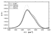
[0016] 도 2는 비교예 1 및 본 발명의 실시예 2, 본 발명의 실시예 4, 및 본 발명의 실시예 5에 대한 3500 cm-1 내지 500 cm-1의 IR 스펙트럼들을 도시한다. 흡광도들은 막 두께, 베어(bare) Si 웨이퍼에 대해 보정된 배경(background), 및 명확성을 위해 베이스라인 오프셋(baseline offset)으로 정규화되었다.
[0017] 도 3은 비교예 1 및 본 발명의 실시예 2, 본 발명의 실시예 4, 및 본 발명의 실시예 5에 대한 1390 cm-1 내지 1330 cm-1의 IR 스펙트럼들을 도시한다. 흡광도들은 막 두께, 베어 Si 웨이퍼에 대해 보정된 배경, 및 명확성을 위해 베이스라인 오프셋으로 정규화되었다.
[0018] 도 4는 비교예 1 및 본 발명의 실시예 2, 본 발명의 실시예 4, 및 본 발명의 실시예 5에 대한 1300 cm-1 내지 1240 cm-1의 IR 스펙트럼들을 도시한다. 흡광도들은 막 두께, 베어 Si 웨이퍼에 대해 보정된 배경, 및 명확성을 위해 베이스라인 오프셋으로 정규화되었다.
[0019] 도 5는 비교 화합물 DEMS®를 사용하여 증착된 일련의 저 유전체 막들에 대한, 본 발명의 화합물 DMTBOS를 사용하여 증착된 일련의 저 유전체 막들에 대한 유전 상수와 XPS 탄소 함량 사이의 관계를 도시한다.
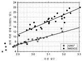
[0020] 도 6은 비교 화합물 DEMS®를 사용하여 증착된 일련의 저 유전체 막들에 대한, 본 발명의 화합물 DMTBOS를 사용하여 증착된 일련의 저 유전체 막들에 대한 적외선 분광법에 의해 결정된 상대적인 SiCH2Si 밀도와 유전 상수 사이의 관계를 도시한다.
[0021] 도 7은, 비교 화합물 DEMS®를 사용하여 증착된 일련의 저 유전체 막들에 대한, 본 발명의 화합물 DMTBOS를 사용하여 증착된 일련의 저 유전체 막들에 대한 유전 상수와 경도 사이의 관계를 도시한다.
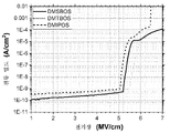
[0022] 도 8은 비교예 3 및 본 발명의 실시예 6에 대한 인가된 전기장 세기의 함수로써 측정된 전류 밀도를 도시한다.
[0023] 도 9는 본 발명의 실시예 1, 본 발명의 실시예 7, 및 본 발명의 실시예 8에 대해 인가된 전기장 세기의 함수로써 측정된 전류 밀도를 도시한다.
[0024] 도 10은, 막들이 NH3 플라즈마를 사용하여 손상된 후의 비교 막 1, 비교 막 2, 본 발명의 막 1 및 본 발명의 막 5의 탄소 제거에 대한 저항성을 입증한다.
[0025] 도 11은, 증착된 막 및 UV 어닐링된 막 둘 모두에 대해, 비교예 4에 대한 인가된 전기장 세기의 함수로써 측정된 전류 밀도를 도시한다.
[0026] 도 12는 증착된 막 및 UV 어닐링된 막 둘 모두에 대해 본 발명의 예 4에 대한 인가된 전기장 세기의 함수로써 측정된 전류 밀도를 도시한다.[0015] Figure 1 shows the dielectric constant when the C/Si ratio of the material is increased, assuming that all parameters of the material are normalized to those of SiO 2 and that all C is incorporated into the material as methyl groups attached to silicon. exemplifies the predicted relationship between x and longitude.
2 shows IR spectra from 3500 cm −1 to 500 cm −1 for Comparative Example 1 and Example 2, Example 4, and Example 5 of the present invention. Absorbances were normalized to film thickness, background corrected for a bare Si wafer, and baseline offset for clarity.
3 shows IR spectra from 1390 cm −1 to 1330 cm −1 for Comparative Example 1 and Example 2 of the present invention, Example 4 of the present invention, and Example 5 of the present invention. Absorbances were normalized to film thickness, background corrected for bare Si wafer, and baseline offset for clarity.
4 shows IR spectra from 1300 cm −1 to 1240 cm −1 for Comparative Example 1 and Example 2, Example 4, and Example 5 of the present invention. Absorbances were normalized to film thickness, background corrected for bare Si wafer, and baseline offset for clarity.
5 shows the relationship between dielectric constant and XPS carbon content for a series of low dielectric films deposited using the inventive compound DMTBOS versus a series of low dielectric films deposited using the comparative compound DEMS ® . show
6 shows the relative SiCH 2 Si density determined by infrared spectroscopy for a series of low dielectric films deposited using the inventive compound DMTBOS relative to a series of low dielectric films deposited using the comparative compound DEMS ® . Shows the relationship between and the dielectric constant.
[0021] Figure 7 shows the relationship between dielectric constant and hardness for a series of low dielectric films deposited using the inventive compound DMTBOS relative to a series of low dielectric films deposited using the comparative compound DEMS ® do.
8 shows the measured current density as a function of applied electric field strength for Comparative Example 3 and Example 6 of the present invention.
[0023] Figure 9 shows the measured current density as a function of applied electric field strength for Example 1 of the present invention, Example 7 of the present invention, and Example 8 of the present invention.
[0024] FIG. 10 demonstrates the resistance to carbon removal of
[0025] FIG. 11 shows the measured current density as a function of applied electric field strength for Comparative Example 4, for both as-deposited and UV annealed films.
[0026] FIG. 12 shows the measured current density as a function of applied electric field strength for Example 4 of the present invention for both as-deposited and UV annealed films.
[0027] 본원에는 조밀한 유기실리카 막을 제조하기 위한 화학 기상 증착 방법으로서, 반응 챔버 내에 기판을 제공하는 단계; 적어도 하나의 하이드리도-디메틸-알콕시실란 화합물, 예컨대, 디메틸-2차-부톡시실란(DMSBOS), 및 가스상 산화제, 예컨대, O2 또는 N2O, 및 불활성 가스, 예컨대, He를 포함하는 가스상 조성물을 도입하는 단계; 및 기판 상에 유기실리카 막을 증착하도록 가스상 반응물들의 반응을 유도하기 위해, 반응 챔버에서 하이드리도-디메틸-알콕시실란을 포함하는 가스상 조성물에 에너지를 인가하는 단계로서, 유기실리카 막은 약 2.70 내지 약 3.50의 유전 상수를 갖는 단계를 포함하는 방법이 기술된다. 원하는 막 특성들을 갖는 유기실리카 막들이 또한, 산화제를 포함하지 않는 가스상 조성을 사용하여 증착될 수 있다는 것이 인식된다.[0027] Disclosed herein is a chemical vapor deposition method for producing a dense organosilica film, comprising: providing a substrate in a reaction chamber; at least one hydrido-dimethyl-alkoxysilane compound, such as dimethyl-sec-butoxysilane (DMSBOS), and a gaseous oxidizing agent, such as O 2 or N 2 O, and an inert gas such as He; introducing a gaseous composition; and applying energy to a gaseous composition comprising hydrido-dimethyl-alkoxysilane in a reaction chamber to induce a reaction of the gaseous reactants to deposit an organosilica film on the substrate, wherein the organosilica film has a temperature of about 2.70 to about 3.50 A method comprising a step having a dielectric constant of It is recognized that organosilica films having the desired film properties can also be deposited using a gas phase composition that does not include an oxidant.
[0028] 본원에 기술되는 하이드리도-디메틸-알콕시실란 화합물들은, 다른 종래 기술의 구조 형성제 전구체들, 예컨대, 디에톡시메틸실란(DEMS®)을 사용하여 제조된 막들과 비교하여 비교적 낮은 유전 상수 및 높은 전계 세기(4 MV/cm)에서 놀랍게도 낮은 누출 전류 밀도를 갖는 조밀한 증착시 OSG 막을 증착하는 것을 가능하게 만드는 독특한 속성을 제공한다. 놀랍게도, 본원에 기술된 하이드리도-디메틸-알콕시실란 전구체들을 사용하여 제조된 증착된 막들의 파괴시 전기장(EBD)은 또한, DEMS®와 같은 다른 종래 기술의 구조 형성제 전구체들을 사용하여 제조된 증착된 막들보다 상당히 더 높다. [0028] The hydrido-dimethyl-alkoxysilane compounds described herein have relatively low dielectric properties compared to films made using other prior art structure former precursors, such as diethoxymethylsilane ( DEMS® ). It offers unique properties that make it possible to deposit OSG films in dense deposition with surprisingly low leakage current densities at constant and high field strengths (4 MV/cm). Surprisingly, the electric field at break (E BD ) of deposited films prepared using the hydrido-dimethyl-alkoxysilane precursors described herein is also similar to those prepared using other prior art structure former precursors such as DEMS ® . significantly higher than that of the deposited films.
[0029] 하이드리도-디메틸-알콕시실란 구조 형성제 전구체들로부터의 증착시 막들의 추가의 고유한 속성은, 막들이 비교적 낮은 총 탄소 함량(통상적으로, XPS에 의해 25 원자 퍼센트 미만)을 갖지만, NH3 또는 O2 플라즈마에 노출될 때 탄소 제거에 대한 특별히 높은 저항성을 나타낸다는 것이다. 유전체 막의 총 탄소 함량이 증가함에 따라 유전체 막으로부터의 탄소 제거에 대한 저항성이 증가한다는 것이 잘 확립되어 있다. 즉, 높은 총 탄소 함량을 갖는 막은, NH3 또는 O2 플라즈마에 노출될 때, 더 낮은 총 탄소 함량을 갖는 막보다 더 작은 탄소 제거의 깊이를 나타낼 것이다. 이는 미국 특허 제9,922,818호에서 예시되며, 여기서 36% 탄소(XPS, 원자%)를 함유하는 저-k 막에 대한 탄소 제거의 깊이가 23% 탄소(XPS, 원자%)를 함유하는 저-k 막보다 20% 더 작다(44 nm와 비교하여 35 nm). 따라서, 비교적 낮은 총 탄소 함량(XPS에 의해 측정한 경우, < 약 25%)을 함유하는 하이드리도-디메틸-알콕시실란 구조 형성제 전구체를 사용하여 제조된 유전체 막이 높은 총 탄소 함량(XPS에 의해 측정한 경우, > 약 25%)을 갖는 막을 증착하는 데 설계된 전구체를 사용하여 제조된 유전체 막으로서 NH3 또는 O2 플라즈마에 노출될 때 동일한 탄소 제거 깊이를 나타낼 수 있다는 것은 예상치 못한 것이다. 미국 특허 제9,922,818호에 개시된 바와 같이, 1-메틸-1-이소프로폭시-1-실라사이클로펜탄(MIPSCP)과 같은 전구체들은, 높은 총 탄소 함량(> 약 25%) 및 NH3 또는 O2 플라즈마에 노출될 때 탄소 제거에 대한 탁월한 저항성을 갖는 막들을 제조하는 데 사용될 수 있다.[0029] An additional unique property of films upon deposition from hydrido-dimethyl-alkoxysilane structure former precursors is that the films have a relatively low total carbon content (typically less than 25 atomic percent by XPS), but , exhibiting a particularly high resistance to carbon removal when exposed to NH 3 or O 2 plasma. It is well established that the resistance to carbon removal from a dielectric film increases as the total carbon content of the dielectric film increases. That is, a film with a high total carbon content, when exposed to an NH 3 or O 2 plasma, will exhibit a smaller depth of carbon removal than a film with a lower total carbon content. This is exemplified in U.S. Patent No. 9,922,818, where the depth of carbon removal relative to a low-k film containing 36% carbon (XPS, atomic %) is a low-k film containing 23% carbon (XPS, atomic %). 20% smaller (35 nm compared to 44 nm). Thus, dielectric films prepared using hydrido-dimethyl-alkoxysilane structure former precursors containing relatively low total carbon content (< about 25% as measured by XPS) have high total carbon content (by XPS). When measured, it is unexpected that a dielectric film made using a precursor designed to deposit a film having a >about 25%) can exhibit the same carbon removal depth when exposed to NH 3 or O 2 plasma. As disclosed in U.S. Patent No. 9,922,818, precursors such as 1-methyl-1-isopropoxy-1-silacyclopentane (MIPSCP) have high total carbon content (> about 25%) and NH 3 or O 2 plasmas. It can be used to make films with excellent resistance to carbon removal when exposed to
[0030] 화학식 (1)의 하이드리도-디메틸-알콕시실란 화합물들의 고유한 속성들은 또한, 조밀한 OSG 막에 대해 비교적 낮은 유전 상수를 달성하고, 그러한 막들이 놀랍게도 DEMS®와 같은, 높은 기계적 강도를 위해 설계된 종래 기술 구조 형성제 전구체로부터 증착된 막들과 동등하거나 더 큰 기계적 특성들을 나타내는 것을 가능하게 한다. 예를 들어, DEMS®는, 반응성 부위들의 균형을 제공하고 원하는 유전 상수를 유지하면서 더 기계적으로 견고한 막들의 형성을 가능하게 하는, 2개의 알콕시 기들, 하나의 메틸 및 하나의 수소화물을 갖는 혼합된 리간드 시스템을 제공한다. 조밀한 저 유전체 막들의 경우, 저-k 전구체에서 실리콘-알콕시 기들(예를 들어, Si-OCH3, Si-OCH2CH3 등)의 수가 증가하며, 전구체에서 실리콘-탄소 결합들의 수(예를 들어, Si-CH3, Si-CH2CH3 등)가 감소하며, 증착된 막의 유전 상수 및 기계적 특성들이 증가될 것이며, 막의 탄소 함량이 감소될 것이다. 따라서, 전구체 내의 실리콘 원자당 하나의 실리콘-탄소 결합 및 2개의 실리콘-알콕시 기들을 함유하는 전구체들을 사용하여 제조된 막들, 예컨대 높은 기계적 강도를 위해 설계된 종래 기술 DEMS® 구조 형성제는 예컨대, 화학식 (1)의 하이드리도-디메틸-알콕시실란 화합물과 같은, 실리콘 당 2개의 실리콘-탄소 결합 및 단 하나의 실리콘-알콕시 기를 함유하는 전구체를 사용하여 제조된 막보다 더 높은 기계적 특성 및 더 낮은 탄소 함량을 가질 것으로 예상될 것이다. 예상치 못하게, 화학식 (1)의 하이드리도-디메틸-알콕시실란 화합물들을 사용하여 제조된 막들은 동일한 유전 상수 값에서 DEMS® 구조 형성제를 사용하여 제조된 막들과 동등하거나 그보다 큰 기계적 특성들을 갖는다. 또한, 예기치 못하게, 화학식 (1)의 하이드리도-디메틸-알콕시실란 화합물들을 사용하여 제조된 막들은, 동일한 유전 상수 값에서 DEMS® 구조 형성제를 사용하여 제조된 막들의 총 탄소 함량과 비교하여, XPS에 의해 측정한 경우 유사한 총 탄소 함량을 갖는다. 일반 화학식 (1)로 표현되는 하이드리도-디메틸-알콕시실란 화합물의 바람직한 예들은, 그들의 대응하는 구조들을 갖는 하기 하이드리도-디메틸-알콕시실란 화합물들을 포함하지만, 이로 제한되지 않는다.[0030] The unique properties of hydrido-dimethyl-alkoxysilane compounds of formula (1) also achieve relatively low dielectric constants for dense OSG films, and such films surprisingly have high mechanical strength, such as DEMS ® . It makes it possible to exhibit mechanical properties equal to or greater than films deposited from prior art structure former precursors designed for For example, DEMS ® is a mixed compound having two alkoxy groups, one methyl and one hydride, which provides a balance of reactive sites and enables the formation of more mechanically robust films while maintaining a desired dielectric constant. A ligand system is provided. For dense low dielectric films, the number of silicon-alkoxy groups (eg, Si-OCH 3 , Si-

[0031] 본원에 기술된 하이드리도-디메틸-알콕시실란 화합물들은, 종래 기술의 구조 형성제 전구체들, 예컨대 디에톡시메틸실란(DEMS®) 및 MIPSCP와 비교하여, 유전체 막에서의 탄소 타입의 상이한 분포를 혼입시키는 것을 가능하게 하는 고유한 속성들을 제공한다. 예를 들어, 구조 형성제로서 DEMS®를 사용하여 증착된 조밀한 OSG 막들에서, 막 내의 탄소는 주로 말단 Si-Me 기들(Si(CH3))의 형태로 존재하며; 작은 밀도의 디실릴메텐 기들(SiCH2Si)이 또한 막에 존재할 수 있다. 본원에 기술된 하이드리도-디메틸-알콕시실란 전구체들, 예컨대, 디메틸-2차-부톡시실란(DMSBOS)이 제공된 유전 상수 값에서 DEMS® 기반 막들의 대략적으로 동일한 총 탄소 함량을 갖는 조밀한 OSG 막들을 증착하는 데 사용될 수 있지만, 하이드리도-디메틸-알콕시실란 전구체들을 사용하여 제조된 막들에서의 탄소의 분포는 상이하다. 하이드리도-디메틸-알콕시실란 전구체들을 사용하여 제조된 막들은 더 낮은 농도의 말단 Si-Me 기들(Si(CH3)) 및 훨씬 더 고농도의 브리징 SiCH2Si 기들을 갖는다. 즉, 종래 기술의 구조 형성제 DEMS®를 사용하여 제조된 막들의 총 탄소 함량이 본 발명의 하이드리도-디메틸-알콕시실란 전구체들을 사용하여 제조된 막들과 거의 동일하기 때문에, 본 발명의 하이드리도-디메틸-알콕시실란 전구체들로부터 증착된 막들 내의 더 큰 백분율의 총 탄소는 DEMS®와 같은 종래 기술의 구조 형성제 전구체들과 비교하여, 브리징 SiCH2Si 기들로서 혼입된다. [0031] The hydrido-dimethyl-alkoxysilane compounds described herein have different properties of carbon type in dielectric films compared to prior art structure former precursors such as diethoxymethylsilane ( DEMS® ) and MIPSCP. It provides unique properties that make it possible to incorporate distributions. For example, in dense OSG films deposited using DEMS ® as a structure former, the carbon in the film is primarily in the form of terminal Si-Me groups (Si(CH 3 )); A small density of disilylmethane groups (SiCH 2 Si) may also be present in the film. The hydrido-dimethyl-alkoxysilane precursors described herein, such as dimethyl-sec-butoxysilane (DMSBOS), provide dense OSG with approximately the same total carbon content of DEMS ® -based films at a given dielectric constant value. Although it can be used to deposit films, the distribution of carbon in films made using hydrido-dimethyl-alkoxysilane precursors is different. Films prepared using hydrido-dimethyl-alkoxysilane precursors have a lower concentration of terminal Si-Me groups (Si(CH 3 )) and a much higher concentration of bridging SiCH 2 Si groups. That is, since the total carbon content of the films prepared using the prior art structure former DEMS ® is almost the same as the films prepared using the hydrido-dimethyl-alkoxysilane precursors of the present invention, the hydridos of the present invention A larger percentage of total carbon in films deposited from do-dimethyl-alkoxysilane precursors is incorporated as bridging SiCH 2 Si groups, compared to prior art structure former precursors such as DEMS® .
[0032] 반면에, 종래 기술의 실리콘-함유 구조-형성 전구체들, 예를 들어, DEMS®는, 일단 반응 챔버에서 에너지 공급되면 중합하여, 폴리머 골격에서 -O- 결합(예를 들어, -Si-O-Si 또는 -Si-O-C-)을 갖는 구조를 형성하며, 하이드리도-디메틸-알콕시실란 화합물들, 예컨대, DMTBOS 분자는 골격 내의 -O- 브리지 중 일부가 -CH2-메틸렌 브리지로 대체된 구조를 형성하는 방식으로 중합한다. 탄소가 주로 말단 Si-Me 기들의 형태로 존재하는 구조 형성 전구체로서 DEMS®를 사용하여 증착된 막들에서, % Si-Me 대 기계적 강도 사이에는 관계가 존재하며, 예를 들어, 모든 C가 실리콘에 부착된 메틸 기들로서 재료에 혼입된다고 가정하면, 재료의 C/Si 비율과 경도 간의 예측된 관계가 증가하며, 여기서, 브리징 Si-O-Si 기의 2개의 말단 Si-Me 기들로의 대체는 네트워크 구조가 파괴되기 때문에 기계적 특성을 감소시킴을 참조한다. 이론으로 제한하고자 하는 것은 아니지만, 하이드리도-디메틸-알콕시실란 화합물들의 경우, 전구체 구조는, 구조 형성제에서 높은 백분율의 2개의 말단 Si-Me 기들(Si(CH3))을 구조(디실릴메틸렌, SiCH2Si)에서 브리징 메틸렌 기로 전환시키는 플라즈마에서의 반응을 용이하게 하는 것으로 여겨진다. 이러한 방식으로, 기계적 강도 관점에서, 막 내의 탄소 함량을 증가시킴으로써 네트워크 구조가 붕괴되지 않도록, 브리징 기의 형태로 탄소를 혼입할 수 있다. 이는 또한, 막에 탄소를 부가하여, 막의 에칭, 포토레지스트의 플라즈마 애싱(plasma ashing), 및 구리 표면들의 NH3 플라즈마 처리와 같은 프로세스들로부터의 탄소 고갈에 대해 막이 더 탄력적일 수 있게 한다. 화학식 (1)의 하이드리도-디메틸-알콕시실란 화합물들, 예컨대 DMSBOS를 사용하여 제조된 막들의 다른 고유한 속성은, 총 탄소 함량이 다소 낮고(< 25%), SiCH2Si 기들로 구성된 총 탄소 함량의 백분율은 DEMS® 및 MIPSCP와 같은 종래 기술의 구조 형성제들과 비교하여 높다.[0032] On the other hand, silicon-containing structure-forming precursors of the prior art, eg, DEMS ® , polymerize once energized in the reaction chamber, resulting in -O- linkages (eg, -Si) in the polymer backbone. -O-Si or -Si-OC-), and hydrido-dimethyl-alkoxysilane compounds, such as DMTBOS molecules, have some of the -O- bridges in the backbone as -CH 2 -methylene bridges. It polymerizes in such a way as to form a displaced structure. In films deposited using DEMS ® as a structure-forming precursor in which carbon is present primarily in the form of terminal Si-Me groups, a relationship exists between % Si-Me versus mechanical strength, e.g., all C is in silicon. Assuming that they are incorporated into the material as attached methyl groups, the predicted relationship between the material's C/Si ratio and hardness increases, where replacement of the bridging Si-O-Si groups by the two terminal Si-Me groups leads to a network Note that the mechanical properties are reduced because the structure is destroyed. Without wishing to be bound by theory, in the case of hydrido-dimethyl-alkoxysilane compounds, the precursor structure is a high percentage of the two terminal Si-Me groups (Si(CH 3 )) in the structure former structure (disilyl It is believed to facilitate the reaction in the plasma to convert methylene, SiCH 2 Si) to the bridging methylene group. In this way, in terms of mechanical strength, carbon can be incorporated in the form of a bridging group so that the network structure does not collapse by increasing the carbon content in the film. It also adds carbon to the film, making it more resilient to carbon depletion from processes such as etching of the film, plasma ashing of photoresist, and NH 3 plasma treatment of copper surfaces. Another unique property of films prepared using hydrido-dimethyl-alkoxysilane compounds of formula (1), such as DMSBOS, is that the total carbon content is rather low (<25%) and the total carbon content composed of SiCH 2 Si groups is The percentage of carbon content is high compared to prior art structure formers such as DEMS ® and MIPSCP.
[0033] 다른 종래 기술의 구조 형성제 전구체들, 예컨대, 1-메틸-1-이소프로폭시-1-실라실코펜탄(MIPSCP)은 고농도의 디실릴메틸렌 기들(SiCH2Si)을 갖는 조밀한 OSG 막들을 증착할 수 있다. 그러나, 고농도의 디실릴메틸렌 기들(SiCH2Si)을 함유하는, 디메틸-2차-부톡시실란(DMSBOS)과 같은 본원에 기술된 하이드리도-디메틸-알콕시실란 전구체로부터 증착된 조밀한 OSG 막과 비교하여 디실릴메틸렌 기로서 혼입되는 더 적은 백분율의 총 탄소를 초래한다. 본원에 기술되는 디메틸-알콕시실란 전구체들, 예컨대, 디메틸-2차-부톡시실란(DMSBOS)을 포함한다. 추가로, MIPSCP로부터 증착된 조밀한 OSG 막들은 또한, 고농도의 말단 Si-Me 기들(Si(CH3)x)을 함유한다. 도 1에서 도시된 바와 같이, 고농도의 말단 Si-Me 기들은 막들의 기계적 강도에 부정적으로 영향을 미쳐서, 궁극적으로, 구조 형성제로서 MIPSCP를 사용하여 달성가능한 최고 기계적 강도를 제한한다.[0033] Other prior art structure former precursors, such as 1-methyl-1-isopropoxy-1-silasilcopentane (MIPSCP), are dense OSGs with a high concentration of disilylmethylene groups (SiCH 2 Si). films can be deposited. However, dense OSG films deposited from hydrido-dimethyl-alkoxysilane precursors described herein, such as dimethyl-sec-butoxysilane (DMSBOS), contain high concentrations of disilylmethylene groups (SiCH 2 Si). results in a lower percentage of the total carbon incorporated as disilylmethylene groups compared to dimethyl-alkoxysilane precursors described herein, such as dimethyl-sec-butoxysilane (DMSBOS). Additionally, dense OSG films deposited from MIPSCP also contain a high concentration of terminal Si-Me groups (Si(CH 3 ) x ). As shown in Figure 1, high concentrations of terminal Si-Me groups negatively affect the mechanical strength of the films, ultimately limiting the highest mechanical strength achievable using MIPSCP as a structure former.
[0034] 하이드리도-디메틸-알콕시실란은, 조밀한 유기실리카 막에 대해 비교적 낮은 유전 상수를 달성하고, 놀랍게도 디에톡시메틸실란(DEMS) 및 1--에톡시-1-메틸실라사이클로펜탄(MESCP)과 같은 종래 기술 구조 형성제 전구체와 비교하여 우수한 기계적 특성을 나타내는 것을 가능하게 한다. 이론으로 제한하고자 하는 것은 아니지만, 본 발명에서의 하이드리도-디메틸-알콕시실란들은 R이 분지형 또는 환형 C3 내지 C10 알킬, 예컨대, 이소-프로필, 2차-부틸, 이소-부틸, 3차-부틸, 2차-펜틸, 2차-펜틸, 3차-펜틸, 사이클로펜틸, 또는 사이클로헥실로 구성된 군으로부터 선택될 때 플라즈마 강화 화학 기상 증착 동안 (하이드리도-디메틸-알콕시실란에서 알콕시 기에 따라) 안정한 라디칼들, 예컨대, (CH3)2CH, (CH3)(CH3CH2)HC, (CH3)3C, 2차-부틸, 이소-부틸, 3차-부틸, 2차-펜틸, 3차-펜틸, 사이클로펜틸, 또는 사이클로헥실를 제공한다. 안정한 라디칼들의 더 높은 밀도는 전구체 내의 말단 실리콘 메틸 기들 중 하나의 실리콘 메틸 기(Si-(CH3)2)로부터 수소 원자의 추출 가능성(SiCH2·를 형성함)을 증가시키고, 증착시 막에서 브리징 Si-CH2-Si 기들의 형성을 촉진한다. 추측컨대, HMe2SiOR의 경우, 전구체에서의 2개의 말단 실리콘 메틸 기들(실리콘 원자 당 2개)의 존재는, 실리콘 원자 당 단지 하나의 실리콘 메틸 기들을 함유하는 전구체들에 비해, 증착시 막에서 고밀도의 디실릴메틸렌 기들(Si-CH2-Si)의 형성에 유리하다. 추측컨대, HMe2SiOR의 경우, Si-H 결합의 존재는 전구체에서 실리콘 당 2개의 말단 메틸 기들로의 빠른 접근을 용이하게 하고, H 원자보다 더 큰 리간드를 함유하는 전구체에 비해 증착시 막에서 고밀도의 디실릴메틸렌 기들(Si-CH2-Si)의 형성에 유리하다.[0034] Hydrido-dimethyl-alkoxysilane achieves a relatively low dielectric constant for dense organosilica films and, surprisingly, diethoxymethylsilane (DEMS) and 1--ethoxy-1-methylsilacyclopentane ( MESCP) makes it possible to exhibit superior mechanical properties compared to prior art structure former precursors. Without wishing to be bound by theory, the hydrido-dimethyl-alkoxysilanes in the present invention are those in which R is a branched or cyclic C3 to C10 alkyl, such as iso-propyl, sec-butyl, iso-butyl, tertiary- during plasma enhanced chemical vapor deposition (depending on the alkoxy group in hydrido-dimethyl-alkoxysilane) when selected from the group consisting of butyl, sec-pentyl, sec-pentyl, tertiary-pentyl, cyclopentyl, or cyclohexyl Stable radicals such as (CH 3 ) 2 CH, (CH 3 )(CH 3 CH 2 )HC, (CH 3 ) 3 C, sec-butyl, iso-butyl, tert-butyl, sec-pentyl , tert-pentyl, cyclopentyl, or cyclohexyl. The higher density of stable radicals increases the possibility of extracting a hydrogen atom (forming SiCH 2 ) from the silicon methyl group (Si-(CH 3 ) 2 ) of one of the terminal silicon methyl groups in the precursor and, upon deposition, in the film. promotes the formation of bridging Si-CH 2 -Si groups. Presumably, for HMe 2 SiOR, the presence of two terminal silicon methyl groups (two per silicon atom) in the precursor, compared to precursors containing only one silicon methyl group per silicon atom, in the film upon deposition It is advantageous for the formation of high-density disilylmethylene groups (Si-CH 2 -Si). Presumably, for HMe 2 SiOR, the presence of Si-H bonds facilitates rapid access to the two terminal methyl groups per silicon in the precursor and, compared to precursors containing ligands larger than H atoms, in the film upon deposition, It is advantageous for the formation of high-density disilylmethylene groups (Si-CH 2 -Si).
[0035] 종래 기술의 비스-알콕시실란 기반 실리콘 전구체들을 사용하여 제조된 막들에 비해, 화학식 (1)의 하이드리도-디메틸-알콕시실란 화합물들을 사용하여 제조된 막들의 장점들 중 일부는 하기를 포함하지만, 이로 제한되지 않는다:[0035] Some of the advantages of films prepared using hydrido-dimethyl-alkoxysilane compounds of formula (1) over films prepared using prior art bis-alkoxysilane based silicon precursors include: Including, but not limited to:
● 높은 전기장 세기에서의 더 낮은 누설 전류 밀도● Lower leakage current density at high electric field strength
● 파괴시 높은 전기장● High electric field at break
● 플라즈마 유도 손상에 대한 더 높은 저항성 ● Higher resistance to plasma induced damage
● 동등한 또는 더 높은 기계적 특성들● Equivalent or higher mechanical properties
● 더 높은 브리징 SiCH2Si 밀도● Higher bridging SiCH 2 Si density
● 브리징 SiCH2Si 기들로 구성된 총 탄소 함량의 더 높은 백분율• higher percentage of total carbon content composed of bridging SiCH 2 Si groups
[0036] 본 발명에 따른 화학식 (1)을 갖는 하이드리도-디메틸-알콕시실란들은 바람직하게는 실질적으로 할로겐화물 이온들을 갖지 않는다. 본원에서 사용되는 바와 같이, "실질적으로 갖지 않는"이라는 용어는, 할로겐화물 이온들(또는 할로겐화물들), 예컨대, 염화물들(즉, 염화물-함유 종, 예컨대, HCl, 또는 적어도 하나의 Si-Cl 결합을 갖는 실리콘 화합물들) 및 불화물들, 브롬화물들 및 요오드화물들에 관한 것으로서 용어 "실질적으로 갖지 않는"은 이온 크로마토그래피(IC)에 의해 측정한 경우 (중량 기준으로) 5 ppm 미만, 바람직하게는 IC에 의해 측정한 경우 3 ppm 미만, 및 더욱 바람직하게는 IC에 의해 측정한 경우 1 ppm 미만, 및 가장 바람직하게는 IC에 의해 측정한 경우 0 ppm을 의미한다. 염화물들은 화학식 (1)을 갖는 실리콘 전구체 화합물들에 대한 분해 촉매들로서 작용하는 것으로 알려져 있다. 최종 생성물에서 상당한 레벨의 염화물은 실리콘 전구체 화합물을 분해시킬 수 있다. 실리콘 전구체 화합물들의 점진적인 분해는 막 증착 프로세스에 직접적으로 영향을 미쳐서, 반도체 제조자가 막 사양들을 충족시키는 것을 어렵게 할 수 있다. 또한, 저장 수명 또는 안정성은 실리콘 전구체 화합물들의 더 높은 분해율에 의해 악영향을 받아, 1 내지 2년의 저장 수명을 보장하는 것을 어렵게 만든다. 따라서, 실리콘 전구체 화합물들의 가속된 분해는 이러한 가연성 및/또는 발화성 가스상 부산물들의 형성과 관련된 안전성 및 성능 문제들을 제시한다. 화학식 (1)을 갖는 하이드리도-디메틸-알콕시실란들은 바람직하게는, 금속 이온들, 예컨대, Li+, Na+, K+, Mg2+, Ca2+, Al3+, Fe2+, Fe2+, Fe3+, Ni2+, Cr3+를 실질적으로 갖지 않는다. 본원에서 사용되는 바와 같이, Li, Na, K, Mg, Ca, Al, Fe, Ni, Cr에 관한 바와 같은 "실질적으로 갖지 않는"이라는 용어는, ICP-MS에 의해 측정한 경우, (중량 기준으로) 5 ppm 미만, 바람직하게는 3 ppm 미만, 및 더욱 바람직하게는 1 ppm 미만, 가장 바람직하게는 0.1 ppm을 의미한다. 일부 구현예들에서, 화학식 (1)을 갖는 실리콘 전구체 화합물들은 금속 이온들, 예컨대, Li+, Na+, K+, Mg2+, Ca2+, Al3+, Fe2+, Fe2+, Fe3+, Ni2+, Cr3+가 존재하지 않는다. 본원에서 사용되는 바와 같이, 금속 불순물들이 "존재하지 않는"이라는 용어는, Li, Na, K, Mg, Ca, Al, Fe, Ni, Cr과 관련될 때, ICP-MS에 의해 측정한 경우 (중량 기준) 1 ppm 미만, 바람직하게는 0.1 ppm 미만, 가장 바람직하게는, ICP-MS 또는 다른 분석 방법에 의해 측정하는 경우, (중량 기준) 0.05 ppm을 의미한다. 또한, 화학식 (1)을 갖는 하이드리도-디메틸-알콕시실란들은 실리콘-함유 막을 증착하기 위한 전구체로서 사용할 때 GC에 의해 측정한 경우 바람직하게는 98 중량% 이상, 더욱 바람직하게는 99 중량% 이상의 순도를 갖는다. 중요하게는, 화학식 (1)을 갖는 하이드리도-디메틸-알콕시실란들은 바람직하게는, 합성 동안 사용되는 출발 재료들 또는 합성 동안 생성되는 부산물들로부터 유래하는 산소-함유 또는 질소-함유 불순물들을 실질적으로 갖지 않는다. 예들은, 테트라메틸디실록산, 테트라메틸디실라잔, 유기 아민들, 예컨대, 트리메틸아민, 트리에틸아민, 트리-n-부틸아민, N,N-디메틸아닐린, N,N-디에틸아닐린, 피리딘, 4-메틸피리딘, 3-메틸피리딘, 2-메틸피리딘, 2-메틸피리딘, 2,6-디메틸피리딘, 및 반응을 증진시키기 위해 사용되는 임의의 다른 유기 아민들을 포함하지만, 이로 제한되지 않는다. 본원에서 사용되는 바와 같이, 산소-함유 또는 질소-함유 불순물들이 "존재하지 않는"이라는 용어는, 테트라메틸디실록산, 테트라메틸디실라잔, 유기 아민들, 예컨대, 트리에틸아민, 피리딘, 및 임의의 다른 유기 아민들과 관련될 때, GC에 의해 측정한 경우, 1000 ppm 이하, 바람직하게는 GC에 의해 측정한 경우 500 ppm 이하(중량 기준), 가장 바람직하게는 GC 또는 검정을 위한 다른 분석 방법에 의해 측정한 경우 100 ppm 이하(중량 기준)를 의미한다. 본원에 정의된 바와 같은 산소-함유 불순물들은 적어도 하나의 산소 원자를 갖는 화합물들이고, 출발 재료들로부터 유래하거나 또는 화학식 (1)을 갖는 하이드리도-디메틸-알콕시실란들의 합성으로부터 생성된다. 그러한 산소-함유 불순물들은 화학식 (1)을 갖는 하이드리도-디메틸-알콕시실란들과 유사한 비등점을 가질 수 있고, 그에 따라, 정제 후에 생성물에 잔류할 수 있다. 마찬가지로, 본원에서 정의된 바와 같은 질소-함유 불순물들은 적어도 하나의 질소 원자를 갖는 화합물들이고, 출발 재료들로부터 유래하거나 또는 하이드리도-디메틸-알콕시실란들의 합성으로부터 생성된다. 그러한 질소-함유 불순물들은 또한, 화학식 I을 갖는 하이드리도-디메틸-알콕시실란 화합물들에 가까운 비등점을 가져서, 정제 후에 생성물에 남아 있을 수 있다.[0036] The hydrido-dimethyl-alkoxysilanes having formula (1) according to the present invention are preferably substantially free of halide ions. As used herein, the term “substantially free” refers to halide ions (or halides), such as chlorides (i.e., chloride-containing species such as HCl, or at least one Si- silicon compounds with Cl bonds) and fluorides, bromides and iodides, the term "substantially free" is less than 5 ppm (by weight) as determined by ion chromatography (IC), preferably Preferably less than 3 ppm as measured by IC, and more preferably less than 1 ppm as measured by IC, and most preferably 0 ppm as measured by IC. Chlorides are known to act as decomposition catalysts for silicon precursor compounds having formula (1). Significant levels of chloride in the final product can decompose the silicon precursor compound. The gradual decomposition of silicon precursor compounds can directly affect the film deposition process, making it difficult for semiconductor manufacturers to meet film specifications. In addition, shelf life or stability is adversely affected by the higher decomposition rate of silicon precursor compounds, making it difficult to ensure a shelf life of 1 to 2 years. Accordingly, the accelerated decomposition of silicon precursor compounds presents safety and performance issues associated with the formation of these flammable and/or pyrophoric gaseous byproducts. Hydrido-dimethyl-alkoxysilanes having formula (1) preferably contain metal ions such as Li + , Na + , K + , Mg 2+ , Ca 2+ , Al 3+ , Fe 2+ , It has substantially no Fe 2+ , Fe 3+ , Ni 2+ , or Cr 3+ . As used herein, the term "substantially free" as it relates to Li, Na, K, Mg, Ca, Al, Fe, Ni, Cr, as measured by ICP-MS, (by weight) to) less than 5 ppm, preferably less than 3 ppm, and more preferably less than 1 ppm, most preferably 0.1 ppm. In some embodiments, the silicon precursor compounds having formula (1) contain metal ions such as Li + , Na + , K + , Mg 2+ , Ca 2+ , Al 3+ , Fe 2+ , Fe 2+ , Fe 3+ , Ni 2+ , and Cr 3+ do not exist. As used herein, the term “free of” metal impurities, when related to Li, Na, K, Mg, Ca, Al, Fe, Ni, Cr, as measured by ICP-MS ( less than 1 ppm by weight, preferably less than 0.1 ppm, most preferably less than 0.05 ppm (by weight) as measured by ICP-MS or other analytical methods. In addition, hydrido-dimethyl-alkoxysilanes having the formula (1) are preferably 98% by weight or more, more preferably 99% by weight or more as measured by GC when used as a precursor for depositing a silicon-containing film. have purity Importantly, hydrido-dimethyl-alkoxysilanes having formula (1) preferably substantially free from oxygen-containing or nitrogen-containing impurities originating from starting materials used during synthesis or by-products produced during synthesis. do not have Examples are tetramethyldisiloxane, tetramethyldisilazane, organic amines such as trimethylamine, triethylamine, tri-n-butylamine, N,N-dimethylaniline, N,N-diethylaniline, pyridine , 4-methylpyridine, 3-methylpyridine, 2-methylpyridine, 2-methylpyridine, 2,6-dimethylpyridine, and any other organic amines used to promote the reaction. As used herein, the term “free of” oxygen-containing or nitrogen-containing impurities includes tetramethyldisiloxane, tetramethyldisilazane, organic amines such as triethylamine, pyridine, and any < 1000 ppm as measured by GC, preferably < 500 ppm by weight (by weight) as measured by GC, most preferably by GC or other analytical method for assay, when related to other organic amines of means less than or equal to 100 ppm (by weight) as measured by Oxygen-containing impurities, as defined herein, are compounds having at least one oxygen atom, derived from starting materials or resulting from the synthesis of hydrido-dimethyl-alkoxysilanes having formula (1). Such oxygen-containing impurities may have similar boiling points to hydrido-dimethyl-alkoxysilanes having formula (1) and thus may remain in the product after purification. Likewise, nitrogen-containing impurities as defined herein are compounds having at least one nitrogen atom, derived from starting materials or resulting from the synthesis of hydrido-dimethyl-alkoxysilanes. Such nitrogen-containing impurities also have boiling points close to hydrido-dimethyl-alkoxysilane compounds having formula (I), and may remain in the product after purification.
[0037] 저-k 유전체 막들은 유기실리카 유리("OSG") 막들 또는 재료들이다. 유기실리케이트들은 예를 들어, 저-k 재료들로서 전자 산업에서 이용된다. 재료 특성들은 막의 화학 조성 및 구조에 따라 좌우된다. 유기실리콘 전구체의 유형이 막 구조 및 조성에 대해 강한 영향을 미치기 때문에, 원하는 유전 상수에 도달하기 위해 필요한 양의 다공도의 부가가 기계적으로 부적절한 막들을 생성하지 않음을 보장하기 위해, 요구되는 막 특성들을 제공하는 전구체들을 사용하는 것이 유익하다. 본원에 기술된 방법 및 조성물은, 전기적 특성과 기계적 특성의 요망되는 균형뿐만 아니라 다른 유익한 막 특성, 예컨대, 개선된 통합 플라즈마 저항성을 제공하는 막에서 탄소의 유형의 분포와 함께 비교적 낮은 총 탄소 함량을 갖는 저-k 유전체 막을 생성하기 위한 수단을 제공한다.[0037] Low-k dielectric films are organosilica glass ("OSG") films or materials. Organosilicates are used, for example, in the electronics industry as low-k materials. Material properties depend on the chemical composition and structure of the film. Since the type of organosilicon precursor has a strong influence on film structure and composition, the required film properties must be determined to ensure that the addition of the required amount of porosity to reach the desired dielectric constant does not result in mechanically unsuitable films. It is advantageous to use the precursors provided. The methods and compositions described herein achieve a relatively low total carbon content with a distribution of types of carbon in the film that provide the desired balance of electrical and mechanical properties as well as other beneficial film properties, such as improved integrated plasma resistance. It provides a means for creating a low-k dielectric film with
[0038] 본원에 기술되는 방법 및 조성물의 특정 구현예들에서, 실리콘-함유 유전체 재료의 층이 반응 챔버를 이용하는 화학 기상 증착(CVD) 프로세스를 통해 기판의 적어도 일부 상에 증착된다. 따라서, 방법은, 반응 챔버 내에 기판을 제공하는 단계를 포함한다. 적합한 기판들은 반도체 재료들, 예컨대 갈륨 아르세나이드("GaAs"), 실리콘, 및 실리콘을 함유하는 조성물들, 예컨대 결정질 실리콘, 폴리실리콘, 비정질 실리콘, 에피택셜 실리콘, 실리콘 이산화물("SiO2"), 실리콘 유리, 실리콘 질화물, 용융 실리카, 유리, 석영, 보로실리케이트 유리, 및 이들의 조합들을 포함하지만, 이로 제한되지 않는다. 다른 적합한 재료들은 반도체, 집적 회로들, 평판 디스플레이, 및 플렉서블 디스플레이 애플리케이션들에서 일반적으로 사용되는 크롬, 몰리브덴 및 다른 금속들을 포함한다. 기판은 부가적인 층들, 예컨대, 실리콘, SiO2, 유기실리케이트 유리(OSG), 플루오르화 실리케이트 유리(FSG), 붕소 탄질화물, 실리콘 탄화물, 수소화된 실리콘 탄화물, 실리콘 질화물, 수소화된 실리콘 질화물, 실리콘 탄질화물, 수소화된 실리콘 탄질화물, 보로질화물, 유기-무기 복합 재료들, 포토레지스트들, 유기 폴리머들, 다공성 유기 및 무기 재료들 및 복합체들, 금속 산화물들, 예컨대 알루미늄 산화물, 및 게르마늄 산화물을 가질 수 있다. 또 다른 층들은 또한, 게르마노실리케이트들, 알루미노실리케이트들, 구리 및 알루미늄, 및 확산 장벽 재료들, 예컨대(비제한적으로), TiN, Ti(C)N, TaN, Ta(C)N, Ta, W, 또는 WN일 수 있다.[0038] In certain implementations of the methods and compositions described herein, a layer of silicon-containing dielectric material is deposited on at least a portion of a substrate via a chemical vapor deposition (CVD) process using a reaction chamber. Accordingly, the method includes providing a substrate within a reaction chamber. Suitable substrates include semiconductor materials such as gallium arsenide (“GaAs”), silicon, and compositions containing silicon such as crystalline silicon, polysilicon, amorphous silicon, epitaxial silicon, silicon dioxide (“SiO 2 ”) , silicon glass, silicon nitride, fused silica, glass, quartz, borosilicate glass, and combinations thereof. Other suitable materials include chromium, molybdenum and other metals commonly used in semiconductor, integrated circuits, flat panel display, and flexible display applications. The substrate may contain additional layers such as silicon, SiO 2 , organosilicate glass (OSG), fluorinated silicate glass (FSG), boron carbonitride, silicon carbide, hydrogenated silicon carbide, silicon nitride, hydrogenated silicon nitride, silicon carbonitride. oxides, hydrogenated silicon carbonitride, borositride, organic-inorganic composite materials, photoresists, organic polymers, porous organic and inorganic materials and composites, metal oxides such as aluminum oxide, and germanium oxide. have. Other layers may also include germanosilicates, aluminosilicates, copper and aluminum, and diffusion barrier materials such as (but not limited to) TiN, Ti(C)N, TaN, Ta(C)N, Ta , W, or WN.
[0039] 반응 챔버는 통상적으로, 예를 들어, 열 CVD 또는 플라즈마 강화 CVD 반응기 또는 다양한 방식들의 배치 노 타입 반응기이다. 일 구현예에서, 액체 전달 시스템이 활용될 수 있다. 액체 전달 포뮬레이션들에서, 본원에 기술된 전구체들은 순수 액체 형태로 전달될 수 있거나, 또는 대안적으로, 이를 포함하는 용매 포뮬레이션들 또는 조성물들에서 사용될 수 있다. 따라서, 특정 구현예들에서, 전구체 포뮬레이션들은, 기판 상에 막을 형성하기 위해 주어진 최종 사용 애플리케이션에서 바람직하고 유리할 수 있는 적합한 특성의 용매 성분(들)을 포함할 수 있다.[0039] The reaction chamber is typically, for example, a thermal CVD or plasma enhanced CVD reactor or a batch furnace type reactor in various ways. In one implementation, a liquid delivery system may be utilized. In liquid delivery formulations, the precursors described herein can be delivered in pure liquid form or, alternatively, can be used in solvent formulations or compositions containing them. Thus, in certain implementations, precursor formulations may include solvent component(s) of suitable characteristics that may be desirable and advantageous in a given end-use application to form a film on a substrate.
[0040] 본원에 개시된 방법은, 하이드리도-디메틸-알콕시실란을 포함하는 가스상 조성물을 반응 챔버 내에 도입하는 단계를 포함한다. 일부 구현예들에서, 조성물은 부가적인 반응물들, 예컨대, 산소-함유 종, 예컨대, O2, O3, 및 N2O, 가스상 또는 액체 유기 물질들, 알코올들, CO2, 또는 CO를 포함할 수 있다. 일 특정 구현예에서, 반응 챔버 내로 도입되는 반응 혼합물은, O2, N2O, NO, NO2, CO2, 물, H2O2, 오존, 및 이들의 조합들로 구성된 군으로부터 선택되는 적어도 하나의 산화제를 포함한다. 대안적인 구현예에서, 반응 혼합물은 산화제를 포함하지 않는다. [0040] A method disclosed herein includes introducing a gaseous composition comprising hydrido-dimethyl-alkoxysilane into a reaction chamber. In some embodiments, the composition includes additional reactants, such as oxygen-containing species such as O 2 , O 3 , and N 2 O, gaseous or liquid organic materials, alcohols, CO 2 , or CO. can do. In one particular embodiment, the reaction mixture introduced into the reaction chamber is selected from the group consisting of O 2 , N 2 O, NO, NO 2 , CO 2 , water, H 2 O 2 , ozone, and combinations thereof Contains at least one oxidizing agent. In an alternative embodiment, the reaction mixture does not include an oxidizing agent.
[0041] 본원에 기술되는 유전체 막을 증착하기 위한 조성물은 약 40 내지 약 100 중량 퍼센트의 하이드리도-디메틸-알콕시실란을 포함한다.[0041] A composition for depositing a dielectric film described herein includes about 40 to about 100 weight percent hydrido-dimethyl-alkoxysilane.
[0042] 구현예들에서, 하이드리도-디메틸-알콕시실란을 포함하는 가스상 조성물은, 증착시 막들의 탄성 계수를 추가로 증가시키기 위해, 경화 첨가제들과 함께 사용될 수 있다. [0042] In embodiments, a gaseous composition comprising hydrido-dimethyl-alkoxysilane may be used in conjunction with curing additives to further increase the modulus of elasticity of films upon deposition.
[0043] 구현예들에서, 하이드리도-디메틸-알콕시실란을 포함하는 가스상 조성물은 할로겐화물들, 예컨대, 염화물들이 실질적으로 존재하지 않나 또는 존재하지 않는다.[0043] In embodiments, the gaseous composition comprising hydrido-dimethyl-alkoxysilane is substantially free or free of halides, such as chlorides.
[0044] 하이드리도-디메틸-알콕시실란에 부가하여, 증착 반응 전에, 증착 반응 동안, 및/또는 증착 반응 후에, 부가적인 재료들이 반응 챔버 내에 도입될 수 있다. 그러한 재료들은, 예컨대, 불활성 가스(예를 들어, He, Ar, N2, Kr, Xe 등, 이는 더 적은 휘발성 전구체들을 위한 캐리어 가스로서 이용될 수 있고/거나 증착시 재료의 경화를 촉진시키고 원하는 경우, 잠재적으로 더욱 안정한 최종 막을 제공할 수 있음)를 포함한다.[0044] In addition to the hydrido-dimethyl-alkoxysilane, additional materials may be introduced into the reaction chamber before, during, and/or after the deposition reaction. Such materials may be, for example, an inert gas (eg, He, Ar, N 2 , Kr, Xe, etc., which may be used as a carrier gas for less volatile precursors and/or promote curing of the material upon deposition and achieve the desired if used, potentially providing a more stable final membrane).
[0045] 하이드리도-디메틸-알콕시실란을 포함하여, 이용되는 임의의 시약은 별개의 소스들과 별개로 또는 혼합물로서 반응기에 운반될 수 있다. 시약들은 임의의 수의 수단에 의해, 바람직하게는 프로세스 반응기로의 액체의 전달을 가능하게 하기 위해 적절한 밸브들 및 피팅(fitting)들이 피팅(fitted)된 가압 가능한 스테인리스 강 용기를 사용하여, 반응기 시스템에 전달될 수 있다. 바람직하게는, 전구체는 가스로서 프로세스 진공 챔버 내로 전달되는데, 즉, 액체는, 액체가 프로세스 챔버 내로 전달되기 전에 기화되어야 한다.[0045] Any reagents utilized, including hydrido-dimethyl-alkoxysilane, may be delivered to the reactor separately from separate sources or as a mixture. Reagents may be introduced into the reactor system by any number of means, preferably using a pressurizable stainless steel vessel fitted with appropriate valves and fittings to enable delivery of the liquid to the process reactor. can be passed on. Preferably, the precursor is delivered into the process vacuum chamber as a gas, ie the liquid must be vaporized before the liquid is delivered into the process chamber.
[0046] 본원에서 개시되는 방법은, 하이드리도-디메틸-알콕시실란을 포함하는 가스상 조성물의 반응을 유도하여, 기판 상에 유기실리카 막을 증착하기 위해, 반응 챔버에서 하이드리도-디메틸-알콕시실란을 포함하는 가스상 조성물에 에너지를 인가하는 단계를 포함하며, 여기서, 유기실리카 막은 일부 구현예들에서 약 2.70 내지 약 3.50, 다른 구현예들에서 2.70 내지 3.30, 및 더욱 바람직한 구현예들에서 2.80 내지 3.20의 유전 상수, 약 6 내지 약 36 GPa의 탄성 계수, 및 XPS에 의해 측정한 경우 약 10 내지 약 45 원자%의 탄소를 갖는다. 하이드리도-디메틸-알콕시실란 및 다른 반응물들(존재하는 경우)이 반응하고 기판 상에 막을 형성하도록 유도하기 위해, 가스상 시약들에 에너지가 인가된다. 그러한 에너지는, 예를 들어, 플라즈마, 펄스형 플라즈마, 헬리콘 플라즈마, 고밀도 플라즈마, 유도 결합 플라즈마, 원격 플라즈마, 고온 필라멘트, 및 열(즉, 비-필라멘트) 방법들에 의해 제공될 수 있다. 기판 표면에서의 플라즈마 특성들을 변경하기 위해 2차 rf 주파수 소스가 사용될 수 있다. 바람직하게는, 막은 플라즈마 강화 화학 기상 증착("PECVD")에 의해 형성된다.[0046] A method disclosed herein is directed to reacting a gaseous composition comprising hydrido-dimethyl-alkoxysilane in a reaction chamber to deposit an organosilica film on a substrate. applying energy to a gaseous composition comprising: wherein the organosilica film has a pH of from about 2.70 to about 3.50 in some embodiments, from 2.70 to 3.30 in other embodiments, and from 2.80 to 3.20 in more preferred embodiments. a dielectric constant of about 6 to about 36 GPa, and about 10 to about 45 atomic percent carbon as measured by XPS. Energy is applied to the gaseous reagents to cause hydrido-dimethyl-alkoxysilane and other reactants (if present) to react and form a film on the substrate. Such energy may be provided by plasma, pulsed plasma, helicon plasma, high-density plasma, inductively coupled plasma, remote plasma, hot filament, and thermal (ie, non-filament) methods, for example. A second order rf frequency source can be used to change the plasma properties at the substrate surface. Preferably, the film is formed by plasma enhanced chemical vapor deposition ("PECVD").
[0047] 가스상 시약들 각각에 대한 유량은 바람직하게는, 단일 300 mm 웨이퍼당 10 내지 5000 sccm, 더욱 바람직하게는 30 내지 3000 sccm의 범위이다. 필요한 실제 유량들은 웨이퍼 크기 및 챔버 구성에 따라 달라질 수 있고, 300 mm 웨이퍼들 또는 단일 웨이퍼 챔버들로 결코 제한되지 않는다.[0047] The flow rate for each of the gaseous reagents is preferably in the range of 10 to 5000 sccm, more preferably 30 to 3000 sccm per single 300 mm wafer. Actual flow rates required may vary depending on wafer size and chamber configuration, and are by no means limited to 300 mm wafers or single wafer chambers.
[0048] 특정 구현예들에서, 막은 분당 약 ~ 5 내지 ~ 400 나노미터(nm)의 증착률로 증착된다. 다른 구현예들에서, 막은 분당 약 30 내지 200 나노미터(nm)의 증착률로 증착된다.[0048] In certain implementations, the film is deposited at a deposition rate of about -5 to -400 nanometers (nm) per minute. In other implementations, the film is deposited at a deposition rate of about 30 to 200 nanometers (nm) per minute.
[0049] 증착 동안의 반응 챔버 내의 압력은 통상적으로, 약 0.01 내지 약 600 torr 또는 약 1 내지 15 torr의 범위이다.[0049] The pressure in the reaction chamber during deposition typically ranges from about 0.01 to about 600 torr or about 1 to 15 torr.
[0050] 막은 바람직하게는 0.001 내지 500 마이크론의 두께까지 증착되지만, 두께는 요구되는 바에 따라 달라질 수 있다. 패턴화되지 않은 표면 상에 증착된 블랭킷 막은, 합리적인 에지 배제와 함께 기판에 걸쳐 1 표준 편차에 걸쳐 3% 미만의 두께 변동으로 우수한 균일성을 가지며, 여기서, 예를 들어, 기판의 5 mm 최외측 에지는 균일성의 통계적 계산에 포함되지 않는다.[0050] The film is preferably deposited up to a thickness of 0.001 to 500 microns, but the thickness may vary as desired. A blanket film deposited on an unpatterned surface has excellent uniformity with less than 3% thickness variation over 1 standard deviation across the substrate with reasonable edge exclusion, where, for example, the outermost 5 mm of the substrate Edges are not included in the statistical calculation of uniformity.
[0051] 본 발명의 OSG 제품들에 부가하여, 본 발명은, 제품들이 제조되는 프로세스, 제품들을 사용하는 방법들, 및 제품들을 준비하는 데 유용한 화합물들 및 조성물들을 포함한다. 예를 들어, 반도체 디바이스 상에 집적 회로를 제조하기 위한 프로세스는 미국 특허 제4,004,452호에 개시되어 있으며, 이러한 문헌은 본원에 참조로 포함된다.[0051] In addition to the OSG products of the present invention, the present invention includes processes by which the products are made, methods of using the products, and compounds and compositions useful in preparing the products. For example, a process for fabricating integrated circuits on semiconductor devices is disclosed in US Pat. No. 4,004,452, incorporated herein by reference.
[0052] 개시된 방법들에 의해 생성된 조밀한 유기실리카 막들은, 특히 에칭 및 포토레지스트 스트립 프로세스들 동안, 플라즈마 유도 손상에 대해 우수한 저항성을 나타낸다.[0052] Dense organosilica films produced by the disclosed methods exhibit excellent resistance to plasma induced damage, particularly during etch and photoresist strip processes.
[0053] 개시된 방법들에 의해 생성된 조밀한 유기실리카 막들은, 동일한 유전 상수를 갖지만 모노알콕시실란이 아닌 전구체를 사용하여 제조된 조밀한 유기실리카 막들에 비해, 주어진 유전 상수에 대해 우수한 기계적 특성들을 나타낸다. (증착 시) 얻어진 유기실리카 막은 통상적으로, 일부 구현예들에서 ~2.70 내지 ~3.50, 다른 구현예들에서 ~2.80 내지 ~3.20, 및 또 다른 구현예들에서 ~2.70 내지 ~3.10의 유전 상수, ~6 내지 ~36 GPa의 탄성 계수, 및 XPS에 의해 측정한 경우 ~10 내지 ~45 원자% 탄소를 갖는다. 다른 구현예들에서, 얻어진 유기실리카 막은 일부 구현예들에서 ~2.70 내지 ~3.50, 다른 구현예들에서 ~2.80 내지 ~3.20, 및 또 다른 구현예들에서 ~2.80 내지 ~3.10의 유전 상수, ~6 내지 ~36 GPa의 탄성 계수, 및 XPS에 의해 측정한 경우 ~12 내지 ~43 원자%의 탄소를 갖는다. 일부 구현예들에서, 질소 함량은 XPS 또는 SIMS 또는 RBS 또는 임의의 다른 분석적 수단에 의해 측정한 경우 0.1 원자% 이하, 바람직하게는 0.1 원자% 이하, 가장 바람직하게는 0.001 원자%이다. 일부 구현예들에서, 질소의 혼입이 잠재적으로 조밀한 유기실리카 막들의 유전체를 증가시킬 수 있다고 여겨지므로, 질소 함량은 XPS, SIMS 또는 RBS 또는 임의의 분석 방법들에 의해 측정한 경우 0.1 원자% 이하, 바람직하게는 0.1 원자% 이하, 가장 바람직하게는, 0.01 원자% 이하일 것으로 예상된다. 또한, 유기실리카 막은 ~1 내지 ~30, 또는 ~5 내지 ~30, 또는 ~10 내지 ~30 또는 ~1 내지 ~20의 상대 디실릴메틸렌 밀도를 갖는다. 유기실리카 막은 ~ 5 nm/분 내지 ~2000 nm/분, 또는 ~ 5 nm/분 내지 ~1000 nm/분, 또는 ~ 50 nm/분 내지 ~1000 nm/분 또는 ~100 nm/분 내지 ~2000 nm/분의 레이트로 증착되는 것으로 예상된다.[0053] Dense organosilica films produced by the disclosed methods exhibit superior mechanical properties for a given dielectric constant compared to dense organosilica films having the same dielectric constant but prepared using a precursor other than monoalkoxysilane. indicate The resulting organosilica film (as deposited) typically has a dielectric constant of -2.70 to -3.50 in some embodiments, -2.80 to -3.20 in other embodiments, and -2.70 to -3.10 in still other embodiments; An elastic modulus of 6 to 36 GPa, and 10 to 45 atomic % carbon as measured by XPS. In other embodiments, the resulting organosilica film has a dielectric constant of -2.70 to -3.50 in some embodiments, -2.80 to -3.20 in other embodiments, and -2.80 to -3.10 in still other embodiments, -6 to -36 GPa, and -12 to -43 atomic % carbon as measured by XPS. In some embodiments, the nitrogen content is less than or equal to 0.1 atomic %, preferably less than or equal to 0.1 atomic %, and most preferably less than or equal to 0.001 atomic % as measured by XPS or SIMS or RBS or any other analytical means. In some embodiments, since it is believed that the incorporation of nitrogen can potentially increase the dielectric of dense organosilica films, the nitrogen content is less than or equal to 0.1 atomic % as measured by XPS, SIMS or RBS or any analytical methods. , preferably less than or equal to 0.1 atomic %, and most preferably, less than or equal to 0.01 atomic %. In addition, the organosilica film has a relative disilylmethylene density of -1 to -30, or -5 to -30, or -10 to -30, or -1 to -20. The organosilica film is ~5 nm/min to ~2000 nm/min, or ~5 nm/min to ~1000 nm/min, or ~50 nm/min to ~1000 nm/min or ~100 nm/min to ~2000 nm /minute is expected to be deposited.
[0054] 얻어진 조밀한 유기실리카 막들은 또한, 일단 증착되면 후 처리 프로세스를 거칠 수 있다. 따라서, 본원에서 사용되는 바와 같은 "후-처리"라는 용어는, 재료 특성들을 추가로 향상시키기 위해, 에너지(예컨대, 열, 플라즈마, 광자, 전자, 마이크로파 등) 또는 화학물들로 막을 처리하는 것을 나타낸다. [0054] The resulting dense organosilica films may also be subjected to a post treatment process once deposited. Thus, the term “post-treatment” as used herein refers to treating a film with energy (eg, heat, plasma, photons, electrons, microwaves, etc.) or chemicals to further enhance material properties. .
[0055] 후-처리가 수행되는 조건들은 크게 변할 수 있다. 예를 들어, 후-처리는 고압 하에서 또는 진공 분위기 하에서 수행될 수 있다.[0055] The conditions under which post-processing is performed can vary greatly. For example, post-treatment may be performed under high pressure or under a vacuum atmosphere.
[0056] UV 어닐링은 하기 조건들 하에서 수행되는 바람직한 방법이다.[0056] UV annealing is a preferred method performed under the following conditions.
[0057] 환경은 불활성(예를 들어, 질소, CO2, 희가스들(He, Ar, Ne, Kr, Xe) 등), 산화(예를 들어, 산소, 공기, 희석 산소 환경들, 풍부한 산소 환경들, 오존, 아산화 질소, 등) 또는 환원(희석 또는 농축된 수소, 탄화수소들(포화, 불포화, 선형 또는 분지형, 방향족들) 등) 환경일 수 있다. 압력은 바람직하게는 약 1 Torr 내지 약 1000 Torr이다. 그러나, 열적 어닐링뿐만 아니라 임의의 다른 후-처리 수단을 위해서는 진공 분위기가 바람직하다. 온도는 바람직하게는 200 내지 500℃이며, 온도 램프 레이트는 0.1 내지 100℃/분이다. 총 UV 어닐링 시간은 바람직하게는 0.01분 내지 12시간이다.[0057] The environment may be inert (eg, nitrogen, CO 2 , noble gases (He, Ar, Ne, Kr, Xe), etc.), oxidizing (eg, oxygen, air, dilute oxygen environments, oxygen rich environment field, ozone, nitrous oxide, etc.) or reducing (diluted or enriched hydrogen, hydrocarbons (saturated, unsaturated, linear or branched, aromatics), etc.) environment. The pressure is preferably from about 1 Torr to about 1000 Torr. However, a vacuum atmosphere is preferred for thermal annealing as well as any other post-treatment means. The temperature is preferably 200 to 500°C, and the temperature ramp rate is 0.1 to 100°C/min. The total UV annealing time is preferably from 0.01 min to 12 hours.
[0058] 본 발명은 하기 구현예들을 참조하여 더욱 상세히 예시될 것이지만, 본 발명이 이에 제한되는 것으로 간주되지 않는다는 것이 이해되어야 한다. 또한, 본 발명에서 기술된 전구체들은, 기존의 다공성 저-k 막들에 비해 유사한 프로세스 이점들(즉, 주어진 유전 상수 값에 대해 더 높은 탄성 계수 및 플라즈마 유도 손상에 대한 더 큰 저항성)을 갖는 다공성 저-k 막들을 증착하는 데 사용될 수 있다는 것이 또한 인식된다.[0058] The invention will be illustrated in more detail with reference to the following embodiments, but it should be understood that the invention is not to be considered limited thereto. In addition, the precursors described herein have similar process advantages over existing porous low-k films (i.e., higher modulus for a given dielectric constant value and greater resistance to plasma induced damage). It is also appreciated that it can be used to deposit -k films.
실시예Example
[0059] 모든 실험들을 2개의 웨이퍼들 상에 막들을 동시에 증착하는 300 mm AMAT Producer® SE 상에서 수행하였다. 따라서, 전구체 및 가스 유량들은 동시에 2개의 웨이퍼들 상에 막들을 증착하는 데 요구되는 유량들에 대응한다. 각각의 웨이퍼 프로세싱 스테이션이 그 자신의 독립적인 RF 전력 공급부를 갖기 때문에, 명시된 웨이퍼 당 RF 전력은 정확하다. 명시된 증착 압력은 정확한데, 그 이유는 웨이퍼 프로세싱 스테이션들 둘 모두가 동일한 압력으로 유지되기 때문이다. 증착 후에, 일부 막들이 UV 어닐링을 겪었다. 300 mm AMAT Producer® Nanocure™ UV 경화 모듈 상에서 UV 어닐링을 수행하였으며, 웨이퍼를 10 Torr 미만의 하나 이상의 압력들에서 및 400℃와 동일하거나 그 미만의 하나 이상의 온도들에서 헬륨 가스 유동 하에 유지하였다.[0059] All experiments were performed on a 300 mm AMAT Producer ® SE depositing films on two wafers simultaneously. Thus, the precursor and gas flow rates correspond to the flow rates required to deposit films on two wafers simultaneously. Because each wafer processing station has its own independent RF power supply, the RF power specified per wafer is accurate. The specified deposition pressure is correct because both wafer processing stations are maintained at the same pressure. After deposition, some films were subjected to UV annealing. UV annealing was performed on a 300 mm AMAT Producer® Nanocure™ UV curing module, holding the wafer under a helium gas flow at one or more pressures less than 10 Torr and at one or more temperatures equal to or less than 400°C.
[0060] 특정 특별한 구현예들 및 실시예들을 참조하여 상기에서 예시되고 설명되었지만, 그럼에도 불구하고, 본 발명은 도시된 세부사항들로 제한되도록 의도되지 않는다. 오히려, 청구항들의 등가물들의 범위 및 범위 내에서 및 본 발명의 사상을 벗어나지 않으면서 세부사항들에서 다양한 변경들이 이루어질 수 있다. 예를 들어, 본 문헌에서 광범위하게 인용된 모든 범위들은, 더 넓은 범위들 내에 속하는 모든 더 좁은 범위들을 그들의 범위 내에 포함하는 것으로 명백히 의도된다. 또한, 본 발명에 개시된 하이드리도-디메틸-알콕시실란들이, 높은 기계적 강도, 플라즈마 유도 손상에 대한 강한 내성, 누설 전류 밀도, 및 유전 상수(k < 3.5)의 주어진 값에서 높은 파괴 전압을 갖는 다공성 저-k 막의 증착을 위한 구조 형성제로서 사용될 수 있다.[0060] Although illustrated and described above with reference to certain particular implementations and embodiments, the invention is nevertheless not intended to be limited to the details shown. Rather, various changes may be made in the details within the scope and range of equivalents of the claims and without departing from the spirit of the invention. For example, all ranges broadly recited in this document are expressly intended to include within their scope all narrower ranges falling within the broader ranges. In addition, the hydrido-dimethyl-alkoxysilanes disclosed in the present invention have high mechanical strength, strong resistance to plasma induced damage, leakage current density, and porosity with high breakdown voltage at a given value of dielectric constant (k < 3.5). It can be used as a structure former for the deposition of low-k films.
[0061] 두께 및 굴절률은 울람(Woollam) 모델 M2000 분광 엘립소미터 상에서 측정되었다. 중간-저항률(mid-resistivity) p-형 웨이퍼들(범위 8 내지 12 ohm-cm) 상에서 Hg 프로브 기법을 사용하여 유전 상수들을 결정하였다. FTIR 스펙트럼들을, 12-인치 웨이퍼들을 핸들링하기 위해 질소 퍼징된 Pike Technologies 맵300이 피팅된 서모 피셔 사이언티픽 모델 iS50 분광계를 사용하여 측정하였다. 막에서 브리징 디실릴메틸렌 기들의 상대 밀도를 계산하기 위해 FTIR 스펙트럼들을 사용하였다. 적외선 분광법에 의해 결정한 경우 막 내의 브리징 디실릴메틸렌 기들의 상대 밀도(즉, SiCH2Si 밀도)는 1E4 곱하기 1360 cm-1 근처에 중심이 있는 SiCH2Si 적외선 대역의 면적을 대략 1250 cm-1 내지 920 cm-1의 SiOx 대역들의 면적으로 나눈 것으로 정의되었다. 기계적 특성들을 KLA iNano 나노 압자를 사용하여 결정하였다.[0061] Thickness and refractive index were measured on a Woollam model M2000 spectroscopic ellipsometer. Dielectric constants were determined using the Hg probe technique on mid-resistivity p-type wafers (range 8-12 ohm-cm). FTIR spectra were measured using a Thermo Fisher Scientific Model iS50 spectrometer fitted with a nitrogen purged Pike Technologies Map300 for handling 12-inch wafers. FTIR spectra were used to calculate the relative density of bridging disilylmethylene groups in the membrane. The relative density of bridging disilylmethylene groups in the film (ie, SiCH 2 Si density), as determined by infrared spectroscopy, ranges from approximately 1250 cm −1 to approximately 1250 cm −1 area of the SiCH 2 Si infrared band centered around
[0062] 조성 데이터를 PHI 5600(73560, 73808) 또는 Thermo K-Alpha(73846) 상에서 XPS(x-ray photoelectron spectroscopy)에 의해 획득하였으며, 원자 중량 퍼센트로 제공한다. 표에 보고된 원자 중량 퍼센트(%) 값들은 수소를 포함하지 않는다.[0062] Compositional data were obtained by x-ray photoelectron spectroscopy (XPS) on a PHI 5600 (73560, 73808) or Thermo K-Alpha (73846) and are given as atomic weight percent. Atomic weight percent (%) values reported in the tables do not include hydrogen.
[0063] 블랭킷 저-k 막들을 Applied Materials Producer® SE 상의 TEOS/FSG 챔버에서 용량 결합 암모니아 플라즈마에 대한 노출에 의해 손상시켰다. 블랭킷 저-k 막들을 손상시키기 위해 사용된 프로세스 파라미터들은 모든 블랭킷 저-k 막들에 대해 동일하였다: 암모니아 유량 = 900 sccm(standard cubic cm per min), 6.0 Torr의 챔버 압력, 300℃의 페디스털 온도, 300 와트(13.56 MHz)의 RF 전력, 및 25초의 노출 시간.[0063] Blanket low-k films were damaged by exposure to capacitively coupled ammonia plasma in a TEOS/FSG chamber on an Applied Materials Producer ® SE. The process parameters used to damage the blanket low-k films were the same for all blanket low-k films: ammonia flow rate = 900 sccm (standard cubic cm per min), chamber pressure of 6.0 Torr, pedestal of 300 °C. temperature, RF power of 300 Watts (13.56 MHz), and exposure time of 25 seconds.
[0064] 스퍼터링에 의해 저-k 막들의 표면으로부터 재료를 제거하기 위해 저 에너지 Cs+ 이온들의 연속적인 포커싱된 빔을 사용하여 동적 SIMS 프로파일들을 획득하였다. 충돌 캐스케이드들로 인한 원자 혼합을 감소시키고 깊이 분해능을 최대화하기 위해, 저 에너지 Cs+ 이온들을 사용하였다. 스퍼터 레이트들은, 막-웨이퍼 계면에 매우 가깝게 스퍼터링한 다음, 스타일러스 프로파일로미터(stylus profilometer)로 스퍼터링된 깊이를 측정함으로써 교정되었다. 분석되는 것들과 유사한 조밀한 저-k 막들의 RBS/HFS 데이터가 SIMS 프로파일들을 정량화하는 데 사용되었다. 동적 SIMS 깊이 프로파일들을 획득하기 위해 사용된 파라미터들은 조사된 모든 플라즈마 손상된 저-k 막들에 대해 동일하였다.[0064] Dynamic SIMS profiles were obtained using a continuous focused beam of low energy Cs+ ions to remove material from the surface of low-k films by sputtering. To reduce atomic mixing due to collision cascades and maximize depth resolution, low energy Cs+ ions were used. Sputter rates were calibrated by sputtering very close to the film-wafer interface and then measuring the sputtered depth with a stylus profilometer. RBS/HFS data of dense low-k films similar to those analyzed were used to quantify the SIMS profiles. The parameters used to obtain dynamic SIMS depth profiles were the same for all plasma damaged low-k films investigated.
[0065] 하기에 열거된 실시예들에서의 각각의 전구체에 대해, 증착 조건들은 목표된 유전 상수에서 높은 기계적 강도를 갖는 막들을 산출하도록 최적화되었다.[0065] For each precursor in the examples listed below, deposition conditions were optimized to yield films with high mechanical strength at the desired dielectric constant.
[0066] 비교예 1: 디에톡시메틸실란(DEMS®)으로부터의 조밀한 OSG 막의 증착.[0066] Comparative Example 1: Deposition of Dense OSG Films from Diethoxymethylsilane (DEMS®).
[0067] 300 mm 프로세싱을 위해 하기 프로세스 조건들을 사용하여 조밀한 DEMS® 기반 막을 증착하였다. DEMS® 전구체를 1250 표준 sccm He 캐리어 가스 유동, 25 sccm O2, 380 밀리-인치 샤워헤드/가열된 페데스탈 간격, 350℃ 페데스탈 온도, 615 와트 13.56 MHz 플라즈마가 인가된 7.5 Torr 챔버 압력을 사용하여 2500 mg/분의 유량으로 직접 액체 주입(DLI)을 통해 반응 챔버에 전달하였다. 막의 다양한 속성들(예를 들어, 유전 상수(k), 굴절률, 탄성 계수 및 경도, 적외선 스펙트럼들에 의한 Si(CH3)x 및 SiCH2Si의 상대 밀도들, 및 XPS에 의한 원자 조성(원자 퍼센트 탄소, 원자 퍼센트 산소, 및 원자 퍼센트 실리콘))을 상기에 기술된 바와 같이 획득하였고, 표 1, 표 2, 및 표 5에 제공하였다.[0067] Dense DEMS® based films were deposited using the following process conditions for 300 mm processing. The DEMS® precursor was 2500 °C using 1250 standard sccm He carrier gas flow, 25 sccm O 2 , 380 milli-inch showerhead/heated pedestal spacing, 350°C pedestal temperature, 7.5 Torr chamber pressure applied with 615 watt 13.56 MHz plasma. It was delivered to the reaction chamber via direct liquid injection (DLI) at a flow rate of mg/min. Various properties of the film (eg, dielectric constant (k), refractive index, elastic modulus and hardness, relative densities of Si(CH 3 ) x and SiCH 2 Si by infrared spectra, and atomic composition by XPS (atomic Percent carbon, atomic percent oxygen, and atomic percent silicon) were obtained as described above and are provided in Tables 1, 2, and 5.
[0068] 비교예 2: 1-메틸-1-이소프로폭시-1-실라사이클로페난(MIPSCP)으로부터의 조밀한 OSG 막의 증착.[0068] Comparative Example 2: Deposition of Dense OSG Films from 1-Methyl-1-isopropoxy-1-silacyclophenane (MIPSCP).
[0069] 300 mm 프로세싱을 위해 하기 프로세스 조건들을 사용하여 조밀한 1-메틸-1-이소프로폭시-1-실라사이클로페난(MIPSCP) 기반 막을 증착하였다. 1-메틸-1-이소프로폭시-1-실라사이클로페난 전구체를 750 표준 sccm(standard cubic centimeters per minute) He 캐리어 가스 유동, 8 sccm O2, 380 밀리-인치 샤워헤드/가열된 페디스털 간격, 390℃ 페데스탈 온도, 275 와트 13.56 MHz 플라즈마가 가해진 7.5 Torr 챔버 압력을 사용하여 850 mg/분의 유량으로 직접 액체 주입(DLI)을 통해 반응 챔버에 전달하였다. 막의 다양한 속성들(예를 들어, 유전 상수(k), 굴절률, 탄성 계수 및 경도, 적외선 스펙트럼들에 의한 Si(CH3)x 및 SiCH2Si의 상대 밀도들, 및 XPS에 의한 원자 조성(원자 퍼센트 탄소, 원자 퍼센트 산소, 및 원자 퍼센트 실리콘))을 상술된 바와 같이 획득하였고, 표 1 및 표 5에 제공하였다.[0069] A dense 1-methyl-1-isopropoxy-1-silacyclophenan (MIPSCP) based film was deposited using the following process conditions for 300 mm processing. The 1-methyl-1-isopropoxy-1-silacyclophenane precursor was mixed with 750 standard cubic centimeters per minute (sccm) He carrier gas flow, 8 sccm O 2 , 380 milli-inch showerhead/heated pedestal spacing. , 390° C. pedestal temperature, 275 Watt 13.56 MHz plasma was delivered to the reaction chamber via direct liquid injection (DLI) at a flow rate of 850 mg/min using an applied 7.5 Torr chamber pressure. Various properties of the film (eg, dielectric constant (k), refractive index, elastic modulus and hardness, relative densities of Si(CH 3 ) x and SiCH 2 Si by infrared spectra, and atomic composition by XPS (atomic Percent carbon, atomic percent oxygen, and atomic percent silicon) were obtained as described above and are provided in Tables 1 and 5.
[0070] 비교예 3: DEMS®로부터의 조밀한 OSG 막의 증착.[0070] Comparative Example 3: Deposition of Dense OSG Films from DEMS ® .
[0071] 300 mm 프로세싱을 위해 하기 프로세스 조건들을 사용하여 조밀한 DEMS® 기반 막을 증착하였다. DEMS® 전구체를 1500 표준 sccm(standard cubic centimeters per minute) He 캐리어 가스 유동, 25 sccm O2, 380 밀리-인치 샤워헤드/가열된 페데스탈 간격, 400℃ 페데스탈 온도, 217 와트 13.56 MHz 플라즈마가 인가된 7.5 Torr 챔버 압력을 사용하여 2000 mg/분의 유량으로 직접 액체 주입(DLI)을 통해 반응 챔버에 전달하였다. 막의 다양한 속성들(예를 들어, 유전 상수(k), 굴절률, 탄성 계수 및 경도, 적외선 스펙트럼들에 의한 Si(CH3)x 및 SiCH2Si의 상대 밀도들, 및 XPS에 의한 원자 조성(원자 퍼센트 탄소, 원자 퍼센트 산소, 및 원자 퍼센트 실리콘))을 상술된 바와 같이 획득하였고 표 3에 제공하였다.[0071] Dense DEMS® based films were deposited using the following process conditions for 300 mm processing. DEMS ® precursor was mixed with 1500 standard cubic centimeters per minute (sccm) He carrier gas flow, 25 sccm O 2 , 380 milli-inch showerhead/heated pedestal spacing, 400°C pedestal temperature, 7.5°C with 217 watt 13.56 MHz plasma applied. It was delivered to the reaction chamber via direct liquid injection (DLI) at a flow rate of 2000 mg/min using Torr chamber pressure. Various properties of the film (eg, dielectric constant (k), refractive index, elastic modulus and hardness, relative densities of Si(CH 3 ) x and SiCH 2 Si by infrared spectra, and atomic composition by XPS (atomic Percent carbon, atomic percent oxygen, and atomic percent silicon) were obtained as described above and are provided in Table 3.
[0072] 비교예 4: DEMS®로부터의 조밀한 OSG 막의 증착. [0072] Comparative Example 4: Deposition of Dense OSG Films from DEMS ® .
[0073] 300 mm 프로세싱을 위해 하기 프로세스 조건들을 사용하여 조밀한 DEMS® 기반 막을 증착하였다. DEMS® 전구체를 750 표준 sccm(standard cubic centimeters per minute) He 캐리어 가스 유동, 90 sccm O2, 380 밀리-인치 샤워헤드/가열된 페데스탈 간격, 345℃ 페데스탈 온도, 400 와트 13.56 MHz 플라즈마가 인가된 10 Torr 챔버 압력을 사용하여 875 mg/분의 유량으로 직접 액체 주입(DLI)을 통해 반응 챔버에 전달하였다. 이후에, 일부 경우들에서, 얻어진 막을 UV 어닐링하였다. 증착 및 UV 어닐링된 막들의 다양한 속성들(예를 들어, 유전 상수(k), 굴절률, 탄성 계수 및 경도, 적외선 스펙트럼들에 의한 Si(CH3)x 및 SiCH2Si의 상대 밀도들, 및 XPS(원자 퍼센트 탄소)에 의한 원자 조성(원자 퍼센트 산소, 및 규소 원자 퍼센트))을 상술된 바와 같이 획득하였고, 표 6에 제공하였다.[0073] Dense DEMS® based films were deposited using the following process conditions for 300 mm processing. DEMS ® precursor was mixed with 750 standard cubic centimeters per minute (sccm) He carrier gas flow, 90 sccm O 2 , 380 milli-inch showerhead/heated pedestal spacing, 345° C. It was delivered to the reaction chamber via direct liquid injection (DLI) at a flow rate of 875 mg/min using Torr chamber pressure. Afterwards, in some cases, the obtained film was UV annealed. Various properties of the deposited and UV annealed films (eg, dielectric constant (k), refractive index, elastic modulus and hardness, relative densities of Si(CH 3 ) x and SiCH 2 Si by infrared spectra, and XPS The atomic composition (atomic percent oxygen, and atomic percent silicon) by (atomic percent carbon) was obtained as described above and is provided in Table 6.
[0074] 실시예 1: 디메틸-2차-부톡시실란(DMSBOS)으로부터의 조밀한 OSG 막의 증착.[0074] Example 1: Deposition of Dense OSG Films from Dimethyl-sec-butoxysilane (DMSBOS).
[0075] 300 mm 프로세싱을 위해 하기 프로세스 조건들을 사용하여 조밀한 디메틸-2차-부티옥시실란 기반 막을 증착하였다. 디메틸-2차-부틸옥시실란 전구체를 975 표준 분당 입방 센티미터(sccm) He 캐리어 가스 유동, O2 = 53 sccm, 380 밀리-인치 샤워헤드/가열식 페디스털 간격, 400℃ 페디스털 온도, 6.1 Torr 챔버 압력(390 와트 13.56 MHz 플라즈마가 적용됨)을 사용하여 1289 mg/분의 유량으로 직접 액체 주입(DLI)을 통해 반응 챔버에 전달하였다. 막의 다양한 속성들(예를 들어, 유전 상수(k), 굴절률, 탄성 계수 및 경도, 적외선 스펙트럼들에 의한 Si(CH3)x 및 SiCH2Si의 상대 밀도들, 및 XPS에 의한 원자 조성(원자 퍼센트 탄소, 원자 퍼센트 산소, 및 원자 퍼센트 실리콘))을 상술된 바와 같이 획득하였고, 표 1, 표 4, 및 표 5에 제공하였다.[0075] Dense dimethyl-sec-butyoxysilane based films were deposited using the following process conditions for 300 mm processing. The dimethyl-sec-butyloxysilane precursor was prepared at 975 standard cubic centimeters per minute (sccm) He carrier gas flow, O 2 = 53 sccm, 380 milli-inch showerhead/heated pedestal spacing, 400° C. pedestal temperature, 6.1 Torr chamber pressure (390 watt 13.56 MHz plasma applied) was delivered to the reaction chamber via direct liquid injection (DLI) at a flow rate of 1289 mg/min. Various properties of the film (eg, dielectric constant (k), refractive index, elastic modulus and hardness, relative densities of Si(CH 3 ) x and SiCH 2 Si by infrared spectra, and atomic composition by XPS (atomic Percent carbon, atomic percent oxygen, and atomic percent silicon) were obtained as described above and are provided in Tables 1, 4, and 5.
[0076] 실시예 2: 디메틸-이소프록시실란(DMIPOS)으로부터의 조밀한 OSG 막의 증착.[0076] Example 2: Deposition of Dense OSG Films from Dimethyl-isoproxoxysilane (DMIPOS).
[0077] 300 mm 프로세싱을 위해 하기 프로세스 조건들을 사용하여 조밀한 디메틸-이소프록시실란 기반 막을 증착하였다. 디메틸-이소프록시실란 전구체를 750 표준 sccm(standard cubic centimeters per minute) He 캐리어 가스 유동, O2 = 40 sccm, 380 밀리-인치 샤워헤드/가열 페디스털 간격, 400℃ 페디스털 온도, 6.5 Torr 챔버 압력, 400 와트 13.56 MHz 플라즈마가 인가된 6.5 Torr 챔버 압력을 사용하여 1100 mg/분의 유량으로 직접 액체 주입(DLI)을 통해 반응 챔버로 전달하였다. 막의 다양한 속성들(예를 들어, 유전 상수(k), 굴절률, 탄성 계수 및 경도, 적외선 스펙트럼들에 의한 Si(CH3)x 및 SiCH2Si의 상대 밀도들, 및 XPS에 의한 원자 조성(원자 퍼센트 탄소, 원자 퍼센트 산소, 및 원자 퍼센트 실리콘))을 상술된 바와 같이 획득하였고, 표 1 및 표 2에 제공하였다.[0077] Dense dimethyl-isoproxoxysilane based films were deposited using the following process conditions for 300 mm processing. The dimethyl-isoproxoxysilane precursor was prepared at 750 standard cubic centimeters per minute (sccm) He carrier gas flow, O 2 = 40 sccm, 380 milli-inch showerhead/heating pedestal spacing, 400° C. pedestal temperature, 6.5 Torr. Chamber pressure, 400 Watt 13.56 MHz plasma was delivered to the reaction chamber via direct liquid injection (DLI) at a flow rate of 1100 mg/min using an applied 6.5 Torr chamber pressure. Various properties of the film (eg, dielectric constant (k), refractive index, elastic modulus and hardness, relative densities of Si(CH 3 ) x and SiCH 2 Si by infrared spectra, and atomic composition by XPS (atomic Percent carbon, atomic percent oxygen, and atomic percent silicon) were obtained as described above and are provided in Tables 1 and 2.
[0078] 실시예 3: 디메틸-3차-부톡시실란(DMTBOS)으로부터의 조밀한 OSG 막의 증착.[0078] Example 3: Deposition of dense OSG films from dimethyl-tert-butoxysilane (DMTBOS).
[0079] 300 mm 프로세싱을 위해 하기 프로세스 조건들을 사용하여 조밀한 디메틸-3차-부톡시실란 기반 막을 증착하였다. 디메틸-3차-부톡시실란 전구체를 975 표준 분당 입방 센티미터(sccm) He 캐리어 가스 유동, O2 = 19 sccm, 380 밀리-인치 샤워헤드/가열식 페디스털 간격, 400℃ 페디스털 온도, 350 와트 13.56 MHz 플라즈마가 인가된 6.7 Torr 챔버 압력을 사용하여 1500 mg/분의 유량으로 직접 액체 주입(DLI)을 통해 반응 챔버에 전달하였다. 막의 다양한 속성들(예를 들어, 유전 상수(k), 굴절률, 탄성 계수 및 경도, 적외선 스펙트럼들에 의한 Si(CH3)x 및 SiCH2Si의 상대 밀도들, 및 XPS에 의한 원자 조성(원자 퍼센트 탄소, 원자 퍼센트 산소, 및 원자 퍼센트 실리콘))을 상술된 바와 같이 획득하였고 표 1에 제공하였다.[0079] Dense dimethyl-tert-butoxysilane based films were deposited using the following process conditions for 300 mm processing. Dimethyl-tert-butoxysilane precursor was mixed at 975 standard cubic centimeters per minute (sccm) He carrier gas flow, O 2 = 19 sccm, 380 milli-inch showerhead/heated pedestal spacing, 400° C. pedestal temperature, 350 A Watt 13.56 MHz plasma was delivered to the reaction chamber via direct liquid injection (DLI) at a flow rate of 1500 mg/min using an applied 6.7 Torr chamber pressure. Various properties of the film (eg, dielectric constant (k), refractive index, elastic modulus and hardness, relative densities of Si(CH 3 ) x and SiCH 2 Si by infrared spectra, and atomic composition by XPS (atomic Percent carbon, atomic percent oxygen, and atomic percent silicon) were obtained as described above and provided in Table 1.
[0080] 실시예 4: 디메틸-2차-부톡시실란(DSBOS)으로부터의 조밀한 OSG 막의 증착.[0080] Example 4: Deposition of dense OSG films from dimethyl-sec-butoxysilane (DSBOS).
[0081] 300 mm 프로세싱을 위해 하기 프로세스 조건들을 사용하여 조밀한 디메틸-2차-부톡시실란 기반 막을 증착하였다. 디메틸-2차-부톡시실란 전구체를 975 표준 분당 입방 센티미터(sccm) He 캐리어 가스 유동, O2 = 45 sccm, 380 밀리-인치 샤워헤드/가열식 페디스털 간격, 400℃ 페데스탈 온도, 390 와트 13.56 MHz 플라즈마가 인가된 6.5 Torr 챔버 압력을 사용하여 1200 mg/분의 유량으로 직접 액체 주입(DLI)을 통해 반응 챔버에 전달하였다. 이후, 일부 경우들에서, 얻어진 막을 UV 어닐링하였다. 증착 및 UV 어닐링된 막들의 다양한 속성들(예를 들어, 유전 상수(k), 굴절률, 탄성 계수 및 경도, 적외선 스펙트럼들에 의한 Si(CH3)x 및 SiCH2Si의 상대 밀도들, 및 XPS(원자 퍼센트 탄소)에 의한 원자 조성(원자 퍼센트 산소, 및 규소 원자 퍼센트))을 상술된 바와 같이 획득하였고, 표 2 및 표 6에 제공하였다.[0081] Dense dimethyl-sec-butoxysilane based films were deposited using the following process conditions for 300 mm processing. Dimethyl-sec-butoxysilane precursor at 975 standard cubic centimeters per minute (sccm) He carrier gas flow, O2 = 45 sccm, 380 milli-inch showerhead/heated pedestal spacing, 400°C pedestal temperature, 390 watts 13.56 MHz plasma was delivered to the reaction chamber via direct liquid injection (DLI) at a flow rate of 1200 mg/min using an applied 6.5 Torr chamber pressure. Then, in some cases, the obtained film was subjected to UV annealing. Various properties of the deposited and UV annealed films (eg, dielectric constant (k), refractive index, elastic modulus and hardness, relative densities of Si(CH 3 ) x and SiCH 2 Si by infrared spectra, and XPS The atomic composition (atomic percent oxygen, and atomic percent silicon) by (atomic percent carbon) was obtained as described above and is provided in Tables 2 and 6.
[0082] 실시예 5: 디메틸-3차-부톡시실란(DMTBOS)으로부터의 조밀한 OSG 막의 증착.[0082] Example 5: Deposition of dense OSG films from dimethyl-tert-butoxysilane (DMTBOS).
[0083] 300 mm 프로세싱을 위해 하기 프로세스 조건들을 사용하여 조밀한 디메틸-3차-부톡시실란 기반 막을 증착하였다. 디메틸-3차-부톡시실란 전구체를 975 표준 분당 입방 센티미터(sccm) He 캐리어 가스 유동, O2 = 19 sccm, 380 밀리-인치 샤워헤드/가열식 페디스털 간격, 400℃ 페디스털 온도, 425 와트 13.56 MHz 플라즈마가 인가된 6.7 Torr 챔버 압력을 사용하여 1300 mg/분의 유량으로 직접 액체 주입(DLI)을 통해 반응 챔버에 전달하였다. 막의 다양한 속성들(예를 들어, 유전 상수(k), 굴절률, 탄성 계수 및 경도, 적외선 스펙트럼들에 의한 Si(CH3)x 및 SiCH2Si의 상대 밀도들, 및 XPS에 의한 원자 조성(원자 퍼센트 탄소, 원자 퍼센트 산소, 및 원자 퍼센트 실리콘))을 상술된 바와 같이 획득하였고 표 2에 제공히였다.[0083] Dense dimethyl-tert-butoxysilane based films were deposited using the following process conditions for 300 mm processing. Dimethyl-tert-butoxysilane precursor was mixed at 975 standard cubic centimeters per minute (sccm) He carrier gas flow, O 2 = 19 sccm, 380 milli-inch showerhead/heated pedestal spacing, 400° C. pedestal temperature, 425 A Watt 13.56 MHz plasma was delivered to the reaction chamber via direct liquid injection (DLI) at a flow rate of 1300 mg/min using an applied 6.7 Torr chamber pressure. Various properties of the film (eg, dielectric constant (k), refractive index, elastic modulus and hardness, relative densities of Si(CH 3 ) x and SiCH 2 Si by infrared spectra, and atomic composition by XPS (atomic Percent carbon, atomic percent oxygen, and atomic percent silicon) were obtained as described above and are provided in Table 2.
[0084] 실시예 6: 디메틸-2차-부톡시실란(DSBOS)으로부터의 조밀한 OSG 막의 증착.[0084] Example 6: Deposition of dense OSG films from dimethyl-sec-butoxysilane (DSBOS).
[0085] 300 mm 프로세싱을 위해 하기 프로세스 조건들을 사용하여 조밀한 디메틸-2차-부톡시실란 기반 막을 증착하였다. 디메틸-2차-부톡시실란 전구체를 850 표준 sccm(standard cubic centimeter per minute) He 캐리어 가스 유동, O2 = 24 sccm, 380 밀리-인치 샤워헤드/가열식 페디스털 간격, 400℃ 페디스털 온도, 300 와트 13.56 MHz 플라즈마가 인가된 7.0 Torr 챔버 압력을 사용하여 1100 mg/분의 유량으로 직접 액체 주입(DLI)을 통해 반응 챔버에 전달하였다. 막의 다양한 속성들(예를 들어, 유전 상수(k), 굴절률, 탄성 계수 및 경도, 적외선 스펙트럼들에 의한 Si(CH3)x 및 SiCH2Si의 상대 밀도들, 및 XPS에 의한 원자 조성(원자 퍼센트 탄소, 원자 퍼센트 산소, 및 원자 퍼센트 실리콘))을 상술된 바와 같이 획득하였고 표 3에 제공하였다.[0085] Dense dimethyl-sec-butoxysilane based films were deposited using the following process conditions for 300 mm processing. Dimethyl-sec-butoxysilane precursor at 850 standard cubic centimeter per minute (sccm) He carrier gas flow, O 2 = 24 sccm, 380 milli-inch showerhead/heated pedestal spacing, 400° C. pedestal temperature , a 300 watt 13.56 MHz plasma was delivered to the reaction chamber via direct liquid injection (DLI) at a flow rate of 1100 mg/min using an applied 7.0 Torr chamber pressure. Various properties of the film (eg, dielectric constant (k), refractive index, elastic modulus and hardness, relative densities of Si(CH 3 ) x and SiCH 2 Si by infrared spectra, and atomic composition by XPS (atomic Percent carbon, atomic percent oxygen, and atomic percent silicon) were obtained as described above and are provided in Table 3.
[0086] 실시예 7: 디메틸-3차-부톡시실란(DMTBOS)으로부터의 조밀한 OSG 막의 증착.[0086] Example 7: Deposition of dense OSG films from dimethyl-tert-butoxysilane (DMTBOS).
[0087] 300 mm 프로세싱을 위해 하기 프로세스 조건들을 사용하여 조밀한 디메틸-3차-부톡시실란 기반 막을 증착하였다. 디메틸-3차-부톡시실란 전구체를 975 표준 분당 입방 센티미터(sccm) He 캐리어 가스 유동, O2 = 8 sccm, 380을 사용하여 1300 mg/분의 유량으로 직접 액체 주입(DLI)을 통해 반응 챔버에 전달하였다. 밀리-인치 샤워헤드/가열식 페디스털 간격, 400℃ 페디스털 온도, 350 와트 13.56 MHz 플라즈마가 인가된 6.7 Torr 챔버 압력을 사용하여 1300 mg/분의 유량으로 직접 액체 주입(DLI)을 통해 반응 챔버로 전달하였다. 막의 다양한 속성들(예를 들어, 유전 상수(k), 굴절률, 탄성 계수 및 경도, 적외선 스펙트럼들에 의한 Si(CH3)x 및 SiCH2Si의 상대 밀도들, 및 XPS에 의한 원자 조성(원자 퍼센트 탄소, 원자 퍼센트 산소, 및 원자 퍼센트 실리콘))을 상술된 바와 같이 획득하였고 표 4에 제공하였다.[0087] Dense dimethyl-tert-butoxysilane based films were deposited using the following process conditions for 300 mm processing. Dimethyl-tert-butoxysilane precursor was introduced into the reaction chamber via direct liquid injection (DLI) at a flow rate of 1300 mg/min using 975 standard cubic centimeters per minute (sccm) He carrier gas flow, O 2 = 8 sccm, 380 forwarded to. Response via direct liquid injection (DLI) at a flow rate of 1300 mg/min using milli-inch showerhead/heated pedestal spacing, 400°C pedestal temperature, 6.7 Torr chamber pressure with 350 watt 13.56 MHz plasma applied delivered to the chamber. Various properties of the film (eg, dielectric constant (k), refractive index, elastic modulus and hardness, relative densities of Si(CH 3 ) x and SiCH 2 Si by infrared spectra, and atomic composition by XPS (atomic Percent carbon, atomic percent oxygen, and atomic percent silicon) were obtained as described above and are provided in Table 4.
[0088] 실시예 8: 디메틸-이소-프로폭시실란(DMIPOS)으로부터의 조밀한 OSG 막의 증착.[0088] Example 8: Deposition of Dense OSG Films from Dimethyl-iso-propoxysilane (DMIPOS).
[0089] 300 mm 프로세싱을 위해 하기 프로세스 조건들을 사용하여 조밀한 디메틸-이소-프로폭시실란 기반 막을 증착하였다. 디메틸-이소-프로폭시실란 전구체를 750 표준 sccm(standard cubic centimeters per minute) He 캐리어 가스 유동, O2 = 40 sccm, 380 밀리-인치 샤워헤드/가열식 페디스털 간격, 400℃ 페디스털 온도, 400 와트 13.56 MHz 플라즈마가 인가된 6.5 Torr 챔버 압력을 사용하여 1100 mg/분의 유량으로 직접 액체 주입(DLI)을 통해 반응 챔버에 전달하였다. 막의 다양한 속성들(예를 들어, 유전 상수(k), 굴절률, 탄성 계수 및 경도, 적외선 스펙트럼들에 의한 Si(CH3)x 및 SiCH2Si의 상대 밀도들, 및 XPS에 의한 원자 조성(원자 퍼센트 탄소, 원자 퍼센트 산소, 및 원자 퍼센트 실리콘))을 상술된 바와 같이 획득하였고 표 4에 제공하였다.[0089] Dense dimethyl-iso-propoxysilane based films were deposited using the following process conditions for 300 mm processing. The dimethyl-iso-propoxysilane precursor was mixed with 750 standard cubic centimeters per minute (sccm) He carrier gas flow, O 2 = 40 sccm, 380 milli-inch showerhead/heated pedestal spacing, 400° C. pedestal temperature, A 400 watt 13.56 MHz plasma was delivered to the reaction chamber via direct liquid injection (DLI) at a flow rate of 1100 mg/min using an applied 6.5 Torr chamber pressure. Various properties of the film (eg, dielectric constant (k), refractive index, elastic modulus and hardness, relative densities of Si(CH 3 ) x and SiCH 2 Si by infrared spectra, and atomic composition by XPS (atomic Percent carbon, atomic percent oxygen, and atomic percent silicon) were obtained as described above and are provided in Table 4.
실시예 9: 디메틸-2차-부톡시실란 및 다른 하이드리도-디메틸-알콕시실란 전구체들의 합성 Example 9: Synthesis of dimethyl-sec-butoxysilane and other hydrido-dimethyl-alkoxysilane precursors
[0090] 214 g(2.88 mol)의 2-부탄올을 환류 하에 300 mL 펜탄 중 300 g(3.17 mol) 클로로디메틸실란에 적가하였다. HCl을 퍼징하기 위해 질소 퍼지를 도입하였다. 첨가가 완료된 후, 환류를 1 시간 동안 계속한 다음, 반응물을 실온으로 냉각시켰다. 반응을 완료시키기 위해 유기아민을 첨가하였다. 얻어진 반응 슬러리를 여과하고, 용매를 대기압에서 증류에 의해 제거하였다. 98℃/760 mmHg에서의 진공 증류는 GC에 의해 측정된 바와 같이 99.5%의 순도를 갖는 175 g의 디메틸-2차-부톡시실란을 생성하였다. GC는 또한, 일부 불순물들, 예컨대, 테트라메틸디실록산을 나타낸다. 수율은 46%였다.[0090] 214 g (2.88 mol) of 2-butanol was added dropwise to 300 g (3.17 mol) of chlorodimethylsilane in 300 mL of pentane under reflux. A nitrogen purge was introduced to purge the HCl. After the addition was complete, reflux was continued for 1 hour and then the reaction was cooled to room temperature. An organic amine was added to complete the reaction. The resulting reaction slurry was filtered and the solvent was removed by distillation at atmospheric pressure. Vacuum distillation at 98° C./760 mmHg produced 175 g of dimethyl-sec-butoxysilane with a purity of 99.5% as determined by GC. GC also shows some impurities, such as tetramethyldisiloxane. The yield was 46%.
디메틸-이소-프로폭시실란, 디메틸-3차-부톡시실란, 디메틸-3차-펜톡시실란, 디메틸-사이클로펜톡시실란, 및 디메틸-사이클로헥스옥시실란은 실시예 9와 유사한 방식을 통해 제조되었고, GC-MS에 의해 특징 분석하였다. 이들의 식별을 확인하기 위해, 각각의 화합물의 분자량(MW), 구조, 및 대응하는 주요 MS 단편화 피크들이 하기에 제공된다.Dimethyl-iso-propoxysilane, dimethyl-tert-butoxysilane, dimethyl-tert-pentoxysilane, dimethyl-cyclopentoxysilane, and dimethyl-cyclohexoxysilane were prepared in a manner similar to Example 9. and characterized by GC-MS. To confirm their identification, the molecular weight (MW), structure, and corresponding major MS fragmentation peaks of each compound are provided below.

[0091] 도 1은, 증가하는 양들의 메틸 기들이 첨가된 비-다공성 SiO2 막에 대한 예측된 경도 및 유전 상수의 예시를 제공한다. 경도는 원자들보다는 메틸 기들에 Boolchand 등의 이론을 적용하고(P. Boolchand, M. Zhang, B. GOODMAN, PHYS. B, 53 11488, 1996), 기계적 특성들에 대한 말단 메틸 기들의 효과를 조사함으로써 예측될 수 있다. 유전 상수는, 폴리머들 및 3-차원적으로 연결된 비정질 재료들에 대한 유전 상수를 예측하는 기 기여 방법을 통해 예측될 수 있다. (탄성 모듈러스에 비례하는 것으로 가정되는) 경도 및 유전 상수는 3.8의 유전 상수 및 72 GPa의 모듈러스로서 하이드록실-부재 실리카의 것으로 정규화될 수 있다. 이들 값들을 사용하여, 도 1은, 막의 C/Si 비율이 0으로부터 대략 0.6까지 증가될 때 유전 상수가 19% 떨어지며, 이는 경도의 66% 감소에 해당함을 도시한다. 그러나, C/Si 비율을 1까지 추가로 증가시키는 것은 유전 상수의 추가적인 4% 감소만을 초래하는 한편, 경도는 0에 접근한다. 따라서, 말단 메틸 기들로 치환된 Si 원자들의 백분율을 제한하는 수단을 갖는 것이 바람직하며, 그 이유는 이것이 주어진 유전 상수에 대한 기계적 특성들을 최대화할 수 있기 때문이다. SiCH2Si 브리징 기들의 형태로 막에 탄소를 첨가하는 수단을 갖는 것이 훨씬 더 바람직하다. 브리징 기의 형태로 탄소를 혼입시키는 것은, 기계적 강도 관점에서, 탄소 함량을 증가시킴으로써 네트워크 구조가 붕괴되지 않으며, 막에 동일한 양의 탄소를 말단 Si(CH3)x 기들의 형태로 혼입하는 것에 비해 더 높은 기계적 강도들이 달성될 수 있기 때문에 바람직하다. SiCH2Si 브리징 기들의 형태로 막에 탄소를 첨가하는 것은 또한, 막의 에칭, 포토레지스트의 플라즈마 애싱, 및 구리 표면들의 NH3 플라즈마 처리와 같은 프로세스들로부터의 OSG 막의 탄소 고갈에 대해 막이 더 탄력적일 수 있게 한다. OSG 막들에서의 탄소 고갈은 막의 유효 유전 상수의 증가들, 습식 세정 단계들 동안의 막 에칭 및 피처 휨에 대한 문제들, 및/또는 구리 확산 장벽들을 증착할 때의 통합 문제들을 야기할 수 있다.[0091] FIG. 1 provides an example of the predicted hardness and dielectric constant for a non-porous SiO 2 film with increasing amounts of methyl groups added thereto. Hardness applies Boolchand et al.'s theory to methyl groups rather than atoms (P. Boolchand, M. Zhang, B. GOODMAN, PHYS. B, 53 11488, 1996) and investigates the effect of terminal methyl groups on mechanical properties. can be predicted by The dielectric constant can be predicted through a group contribution method that predicts the dielectric constant for polymers and three-dimensionally linked amorphous materials. The hardness and dielectric constant (assumed to be proportional to the elastic modulus) can be normalized to that of hydroxyl-free silica with a dielectric constant of 3.8 and a modulus of 72 GPa. Using these values, FIG. 1 shows that the dielectric constant drops by 19% when the C/Si ratio of the film is increased from 0 to approximately 0.6, which corresponds to a 66% reduction in hardness. However, further increasing the C/Si ratio to 1 only results in a further 4% decrease in dielectric constant, while the hardness approaches zero. Accordingly, it is desirable to have a means of limiting the percentage of Si atoms substituted with terminal methyl groups, since this can maximize mechanical properties for a given dielectric constant. It is even more desirable to have a means of adding carbon to the film in the form of SiCH 2 Si bridging groups. The incorporation of carbon in the form of a bridging group does not collapse the network structure by increasing the carbon content, in terms of mechanical strength, compared to incorporation of the same amount of carbon in the form of terminal Si(CH 3 ) x groups in the film. This is desirable because higher mechanical strengths can be achieved. Adding carbon to the film in the form of SiCH 2 Si bridging groups will also make the film more resilient to carbon depletion of the OSG film from processes such as etching of the film, plasma ashing of photoresist, and NH 3 plasma treatment of copper surfaces. make it possible Carbon depletion in OSG films can cause increases in the effective dielectric constant of the film, problems with film etching and feature warping during wet clean steps, and/or integration problems when depositing copper diffusion barriers.
[0092] 표 1은, 본 발명에서 설명된 하이드리도-디메틸-알콕시실란 전구체들, DMSBOS, DMIPOS, 및 DMTBOS를 구조 형성제로서 사용하여 제조된 막들이 유사한 유전 상수에 있는 DEMS® 구조 형성제 또는 MIPSCP 구조 형성제를 사용하여 제조된 필름들에 비해 동등하거나 더 큰 기계적 강도를 갖는다는 것을 나타낸다. 예를 들어, 본 발명의 DMSBOS 기반 막의 탄성 계수는 비교 DEMS® 기반 막의 탄성 계수보다 60% 더 크다. 추가로, 하이드리도-디메틸-알콕시실란 전구체들을 사용하여 제조된 막들은, XPS에 의해 측정한 경우 총 탄소 함량을 가지며, 이는 DEMS® 구조 형성제(~20% C)를 사용하여 제조된 필름들과 유사하지만, MIPSCP 구조 형성제를 사용하여 제조된 막들의 총 탄소 함량(~34% C)보다 상당히 더 적다. 가장 중요하게, IR 분광법에 의해 결정된 바와 같은 디실릴메틸렌 기들의 상대 밀도 대 XPS(예를 들어, DEMS® 기반의 경우, 비율은 6/18 = 0.33임)는 DEMS® 구조 형성제 또는 MIPSCP 구조 형성제를 사용하여 제조된 것들보다 훨씬 더 높은데, 즉, 비는 DMSBOS, DMIPOS, DMTBOS는 표 1에 도시된 바와 같다. 표 1은 또한, DMSBOS 구조 형성제를 사용하여 증착된 막이 2개의 다른 본 발명의 하이드리도-디메틸-알콕시실란 화합물들, DMIPOS 및 DMTBOS로부터 증착된 막들에 대해 고유한 특성들을 나타낸다는 것을 예시한다. DMSBOS 구조 형성제를 사용하여 증착된 막은 DMIPOS 및 DMTBOS 구조 형성제 전구체들로부터 증착된 막들에 비해 상당히 더 높은 기계적 특성들을 갖는다. 예를 들어, DMSBOS 구조 형성제를 사용하여 증착된 막의 탄성 계수 및 경도는 DMIPOS 구조 형성제를 사용하여 증착된 막의 탄성 계수 및 경도보다 각각 14% 및 41% 더 크다. 유사하게, DMSBOS 구조 형성제를 사용하여 증착된 막의 탄성 계수 및 경도는 DMTBOS 구조 형성제를 사용하여 증착된 막의 탄성 계수 및 경도보다 각각 19% 및 37% 더 크다.[0092] Table 1 shows the DEMS ® structure formers in which films prepared using the hydrido-dimethyl-alkoxysilane precursors described herein, DMSBOS, DMIPOS, and DMTBOS, as structure formers, have similar dielectric constants. or have equivalent or greater mechanical strength compared to films prepared using MIPSCP structure formers. For example, the elastic modulus of the DMSBOS-based membrane of the present invention is 60% greater than that of the comparative DEMS ® based membrane. Additionally, films prepared using hydrido-dimethyl-alkoxysilane precursors have a total carbon content as measured by XPS, which is comparable to films prepared using DEMS ® structure former (~20% C). , but significantly lower than the total carbon content (~34% C) of films prepared using the MIPSCP structure former. Most importantly, the relative density of disilylmethylene groups as determined by IR spectroscopy versus XPS (e.g., for DEMS ® based, the ratio is 6/18 = 0.33) is the DEMS ® structure former or MIPSCP structure forming agent. ie, the ratios are as shown in Table 1 for DMSBOS, DMIPOS, and DMTBOS. Table 1 also illustrates that films deposited using the DMSBOS structure former exhibit properties unique to films deposited from two other inventive hydrido-dimethyl-alkoxysilane compounds, DMIPOS and DMTBOS. . Films deposited using DMSBOS structure former have significantly higher mechanical properties compared to films deposited from DMIPOS and DMTBOS structure former precursors. For example, the Young's modulus and hardness of a film deposited using the DMSBOS structure former are 14% and 41% greater than the Young's modulus and hardness of a film deposited using the DMIPOS structure former, respectively. Similarly, the Young's modulus and hardness of the film deposited using the DMSBOS structure former are 19% and 37% greater than the Young's modulus and hardness of the film deposited using the DMTBOS structure former, respectively.
[0093] 표 1. DEMS®, MIPSCP, DMSBOS, DMIPOS, 및 DMTBOS를 사용하여 증착된 조밀한 OSG 막들에 대한 비교 막 특성들.Table 1. Comparative film properties for dense OSG films deposited using DEMS ® , MIPSCP, DMSBOS, DMIPOS, and DMTBOS.

[0094] 도 2에는 본 발명에 기술된 하이드리도-디메틸-알콕시실란 전구체들, DMSBOS, DMIPOS, 및 DMTBOS를 구조 형성제로서 사용하여 제조된 막들 및 DEMS® 구조 형성제를 사용하여 제조된 막에 대해 3500 cm-1 내지 500 cm-1의 투과 적외선 스펙트럼이 도시되어 있다. 4개의 막들 모두는 3.0 내지 3.1의 유전 상수를 갖는다(표 2). 도 3은 모든 4개의 막들에 대해 1360 cm-1 근처에 중심이 있는 디실릴메틸렌(SiCH2Si) 적외선 대역의 확대된 이미지를 도시한다. DMSBOS, DMIPOS, 및 DMTBOS 구조 형성제 전구체들을 사용하여 제조된 막들에 대한 SiCH2Si 밴드의 피크 흡광도는 DEMS® 구조 형성제 전구체를 사용하여 제조된 막에 대한 SiCH2Si 밴드의 피크 흡광도보다 적어도 2배 더 크다. 도 4는 모든 4개의 막들에 대해 1273 cm-1 근처에 중심을 둔 말단 실리콘 메틸 적외선 대역들(Si(CH3)x)의 확대된 이미지를 도시한다. DMSBOS, DMIPOS, 및 DMTBOS 구조 형성제 전구체들을 사용하여 제조된 막들에 대한 Si(CH3)x 적외선 대역들의 피크 흡광도는, DEMS® 구조 형성제 전구체를 사용하여 제조된 막에 대한 Si(CH3)x 적외선 대역의 피크 흡광도보다 20% 내지 24% 더 작다. 따라서, 적외선 스펙트럼들은, DMSBOS, DMIPOS, 및 DMTBOS 구조 형성제 전구체들을 사용하여 제조된 막들이 DEMS® 구조 형성제 전구체를 사용하여 제조된 막들에 비해 더 고농도의 SiCH2Si 기들 및 더 낮은 농도의 Si(CH3)x 기들을 갖는다는 것을 나타낸다.[0094] Figure 2 shows films prepared using the hydrido-dimethyl-alkoxysilane precursors described herein, DMSBOS, DMIPOS, and DMTBOS as structure formers, and films prepared using DEMS ® structure formers. The transmission infrared spectrum from 3500 cm -1 to 500 cm -1 for is shown. All four films have dielectric constants between 3.0 and 3.1 (Table 2). 3 shows an enlarged image of the disilylmethylene (SiCH 2 Si) infrared band centered around 1360 cm −1 for all four films. The peak absorbance of the SiCH 2 Si band for films prepared using the DMSBOS, DMIPOS, and DMTBOS structure former precursors is at least 2 times greater than the peak absorbance of the SiCH 2 Si band for films prepared using the DEMS ® structure former precursor. times bigger 4 shows an enlarged image of the terminal silicon methyl infrared bands (Si(CH 3 ) x ) centered around 1273 cm −1 for all four films. The peak absorbance in the Si(CH 3 ) x infrared bands for films prepared using DMSBOS, DMIPOS, and DMTBOS structure former precursors is Si(CH 3 ) for films prepared using DEMS ® structure former precursors. x 20% to 24% smaller than the peak absorbance in the infrared band. Thus, infrared spectra show that films prepared using DMSBOS, DMIPOS, and DMTBOS structure former precursors exhibit higher concentrations of SiCH 2 Si groups and lower concentrations of Si compared to films prepared using DEMS ® structure former precursors. (CH 3 ) x groups.
[0095] 도 2에서의 본 발명의 조밀한 OSG 막 및 비교 조밀한 OSG 막의 특성들이 표 2에 제공된다. 4개의 막들 모두는 3.0 내지 3.1의 유전 상수를 갖는다. 표 2에 도시된 바와 같이, 본 발명의 DMSBOS, DMIPOS, 및 DMTBOS 구조 형성 전구체들을 사용하여 제조된 막들에 대한 (그들의 적외선 스펙트럼들로부터 결정된) 상대적 SiCH2Si 밀도들은, DEMS® 구조 형성제를 사용하여 제조된 막의 상대적 SiCH2Si 밀도보다 167% 내지 250% 더 크다. 디실릴메틸렌(SiCH2Si) 기들로 구성되는, 이들 막들에서 총 탄소의 상대적인 백분율을 계산함으로써, DMSBOS, DMIPOS, 및 DMTBOS 구조 형성 전구체들을 사용하여 제조된 막들에서의 고유한 탄소 분포에 대한 추가의 통찰력이 획득될 수 있다. 디실릴메틸렌(SiCH2Si) 기들로 구성되는 총 탄소의 상대적인 백분율은, (XPS에 의해 측정한 경우) 막 내의 총 탄소 함량에 대한 (IR 분광법에 의해 결정된) 상대 SiCH2Si 밀도의 비율로서 계산될 수 있다. 표 2에서 보여지는 바와 같이, 본 발명의 DMSBOS, DMIPOS, 및 DMTBOS 구조 형성 전구체들을 사용하여 제조된 막들에 대한, 디실릴메틸렌(SiCH2Si) 기들로 구성된 총 탄소의 상대적인 백분율은 총 탄소의 상대적인 백분율보다 131% 내지 160% 더 크다. DEMS® 구조 형성제를 사용하여 제조된 막의 디실릴메틸렌(SiCH2Si) 기들로 구성된다. [0095] The properties of the inventive densified OSG film in FIG. 2 and the comparative densified OSG film are provided in Table 2. All four films have dielectric constants between 3.0 and 3.1. As shown in Table 2, the relative SiCH 2 Si densities (determined from their infrared spectra) for films prepared using the DMSBOS, DMIPOS, and DMTBOS structure forming precursors of the present invention were obtained using the DEMS ® structure former. 167% to 250% greater than the relative SiCH 2 Si density of the films prepared by Further analysis of the unique carbon distribution in films made using DMSBOS, DMIPOS, and DMTBOS structure forming precursors was obtained by calculating the relative percentage of total carbon in these films, composed of disilylmethylene (SiCH 2 Si) groups. Insights can be gained. The relative percentage of total carbon composed of disilylmethylene (SiCH 2 Si) groups is calculated as the ratio of the relative SiCH 2 Si density (determined by IR spectroscopy) to the total carbon content in the film (as measured by XPS). It can be. As shown in Table 2, the relative percentage of total carbon composed of disilylmethylene (SiCH 2 Si) groups for films prepared using the DMSBOS, DMIPOS, and DMTBOS structure forming precursors of the present invention is the relative percentage of total carbon 131% to 160% greater than percentage. It consists of disilylmethylene (SiCH 2 Si) groups in a film prepared using DEMS ® structure former.
[0096] 표 2. 도 2, 도 3 및 도 4에 도시된, 비교 및 본 발명의 조밀한 OSG 막들의 막 특성들. [0096] Table 2. Film properties of the comparative and inventive dense OSG films shown in Figures 2, 3 and 4.

[0097] 조밀한 저-k 유전체 막들의 일련의 증착들은 225 내지 550 와트 플라즈마 전력, 5.5 내지 10 Torr 챔버 압력, 345 내지 400℃ 기판 온도, 0 내지 60 sccm O2 가스 유동, 750 내지 2250 sccm He 캐리어 가스 유동, 0.750 내지 2.500 g/분의 전구체 액체 유동, 및 0.380 인치 전극 간격의 다양한 프로세스 조건 하에서 300 mm PECVD 반응기 상에 저-k 전구체로서 DMSBOS 또는 DEMS®를 사용하여 증착되었다. 탄소의 원자 백분율은 본원에 기술된 바와 같이 XPS에 의해 측정되었다. 도 5는 상이한 유전 상수들을 갖는 DEMS® 및 DMSBOS를 사용하여 제조된 조밀한 OSG 막들에 대한 XPS 탄소 함량(원자%) 사이의 관계를 도시한다. 도 5가 도시하는 바와 같이, 종래 기술의 전구체 DEMS®를 사용하여 제조된 막들은, 유전 상수가 약 2.9로부터 약 2.9 내지 약 3.3으로 증가됨에 따라 동일한 값의 유전 상수에서, DMSOS 전구체를 사용하여 제조된 필름들과 약간 더 낮지만 유사한 XPS 탄소 함량을 갖는다. 막들 둘 모두에 대해, XPS 탄소 함량은 비교적 좁은 범위: ~19.5 ± 3% 내에 속한다. [0097] A series of depositions of dense low-k dielectric films were performed with 225 to 550 Watt plasma power, 5.5 to 10 Torr chamber pressure, 345 to 400 °C substrate temperature, 0 to 60 sccm O 2 gas flow, 750 to 2250 sccm He It was deposited using DMSBOS or DEMS ® as a low-k precursor on a 300 mm PECVD reactor under various process conditions of carrier gas flow, precursor liquid flow from 0.750 to 2.500 g/min, and electrode spacing of 0.380 inches. The atomic percentage of carbon was determined by XPS as described herein. 5 shows the relationship between XPS carbon content (atomic %) for dense OSG films prepared using DEMS ® and DMSBOS with different dielectric constants. As Figure 5 shows, films prepared using the prior art precursor DEMS® were prepared using the DMSOS precursor at the same value of dielectric constant as the dielectric constant increased from about 2.9 to about 2.9 to about 3.3. It has a slightly lower but similar XPS carbon content to the For both membranes, the XPS carbon content falls within a relatively narrow range: -19.5 ± 3%.
[0098] 조밀한 저-k 유전체 막들의 일련의 증착들을 225 내지 550 와트 플라즈마 전력, 5.5 내지 10 Torr 챔버 압력, 345 내지 400℃ 기판 온도, 0 내지 60 sccm O2 가스 유동, 750 내지 2250 sccm He 캐리어 가스 유동, 0.750 내지 2.500 g/분의 전구체 액체 유동, 및 0.380 인치 전극 간격의 다양한 프로세스 조건 하에서 300 mm PECVD 반응기 상에 저-k 전구체로서 DMSBOS 또는 DEMS®를 사용하여 증착하였다. 본원에 기술된 바와 같이, 각각의 막에 대한 적외선 스펙트럼들로부터 SiCH2Si 기들의 밀도를 계산하였다. 도 6은, 상이한 유전 상수들을 갖는 DEMS® 전구체와 DMSBOS 전구체를 사용하여 제조된 조밀한 OSG 막들의 SiCH2Si 기들의 밀도 사이의 관계를 도시한다. 도 6은, 종래 기술 또는 DEMS® 저-k 막들은, 유전 상수가 약 2.9로부터 약 3.3으로 증가됨에 따라, DMSBOS 기반 막들에 비해 동일한 값의 유전 상수에서 훨씬 더 낮은 밀도의 SiCH2Si 기들을 갖는다는 것을 도시한다. 이는, 유사한 유전 상수 값에 대한 것인 조밀한 저-k 유전체 막을 증착하기 위해, 화학식 (1)의 하이드리도-디메틸-알콕시실란 화합물들, 예컨대, DMSBOS를 사용하는 것의 중요한 이점들 중 하나를 예시하며, 이는 하이드리도-디메틸-알콕시실란 전구체 DMSBOS가 다른 종래 기술의 구조 형성제들만큼 높거나 또는 더 높은 SiCH2Si 기들의 밀도를 갖는 막들을 증착하는 데 사용될 수 있다. 이러한 방식으로, 기계적 강도 관점에서, 막 내의 탄소 함량을 증가시킴으로써 네트워크 구조가 붕괴되지 않도록, 브리징 기의 형태로 탄소를 혼입할 수 있다. 이는 또한, 막에 탄소를 첨가하여, 막의 에칭, 포토레지스트의 플라즈마 애싱, 및 구리 표면들의 NH3 플라즈마 처리와 같은 프로세스들로부터의 탄소 고갈에 대해 막이 더 탄력적일 수 있게 한다. 그러나, 예컨대 DMSBOS와 같은 화학식 (1)의 하이드리도-디메틸-알콕시실란 화합물들을 사용하여 제조된 막들의 고유한 속성들 중 하나는, 총 탄소 함량이 다소 낮고(< 25%), SiCH2Si 기들로 구성된 총 탄소 함량은 DEMS® 및 MIPSCP와 같은 종래 기술의 구조 형성제들과 비교하여 높다.[0098] A series of depositions of dense low-k dielectric films were performed at 225 to 550 Watt plasma power, 5.5 to 10 Torr chamber pressure, 345 to 400 °C substrate temperature, 0 to 60 sccm O 2 gas flow, 750 to 2250 sccm He It was deposited using DMSBOS or DEMS ® as a low-k precursor on a 300 mm PECVD reactor under various process conditions of carrier gas flow, precursor liquid flow from 0.750 to 2.500 g/min, and electrode spacing of 0.380 inches. As described herein, the density of SiCH 2 Si groups was calculated from the infrared spectra for each film. 6 shows the relationship between the density of SiCH 2 Si groups in dense OSG films prepared using a DEMS ® precursor and a DMSBOS precursor with different dielectric constants. 6 shows that prior art or DEMS ® low-k films have a much lower density of SiCH 2 Si groups at the same value of dielectric constant compared to DMSBOS based films, as the dielectric constant increases from about 2.9 to about 3.3. shows that This is one of the important advantages of using hydrido-dimethyl-alkoxysilane compounds of formula (1), such as DMSBOS, to deposit dense low-k dielectric films for similar dielectric constant values. Illustratively, it can be used to deposit films in which the hydrido-dimethyl-alkoxysilane precursor DMSBOS has a density of SiCH 2 Si groups as high as or higher than other prior art structure formers. In this way, in terms of mechanical strength, carbon can be incorporated in the form of a bridging group so that the network structure does not collapse by increasing the carbon content in the film. It also adds carbon to the film, making it more resilient to carbon depletion from processes such as etching of the film, plasma ashing of photoresist, and NH 3 plasma treatment of copper surfaces. However, one of the inherent properties of films prepared using hydrido-dimethyl-alkoxysilane compounds of formula (1), such as DMSBOS, is that the total carbon content is rather low (<25%), SiCH 2 Si The total carbon content of the groups is high compared to prior art structure formers such as DEMS ® and MIPSCP.
[0099] 조밀한 저-k 유전체 막들의 일련의 증착들을 225 내지 550 와트 플라즈마 전력, 5.5 내지 10 Torr 챔버 압력, 345 내지 400℃ 기판 온도, 0 내지 60 sccm O2 가스 유동, 750 내지 2250 sccm He 캐리어 가스 유동, 0.750 내지 2.500 g/분의 전구체 액체 유동, 및 0.380 인치 전극 간격의 다양한 프로세스 조건 하에서 300 mm PECVD 반응기 상에서 저-k 전구체로서 DMSBOS 또는 DEMS®를 사용하여 증착하였다. 막들의 경도를 본원에 기술된 바와 같은 나노인덴테이션에 의해 측정하였다. 도 7은, 상이한 유전 상수들을 갖는 DEMS® 전구체와 DMSBOS 전구체를 사용하여 제조된 조밀한 OSG 막들의 경도 사이의 관계를 도시한다. 도 7은, 종래 기술 또는 DEMS® 저-k 막들은, 유전 상수가 약 2.9로부터 약 3.3으로 증가됨에 따라, DMSBOS 기반 막들에 비해 동일한 값의 유전 상수에서 더 낮은 경도를 갖는다는 것을 도시한다. 이는, 유사한 유전 상수 값에 대한 것인 조밀한 저-k 유전체 막을 증착하기 위해 화학식 (1)의 하이드리도-디메틸-알콕시실란 화합물들, 예컨대, DMSBOS를 사용하는 것의 중요한 속성들 중 하나를 예시하며, 화학식 (1)의 하이드리도-디메틸-알콕시실란 화합물들, 예컨대, DMSBOS를 사용하여 증착된 막은 다른 종래 기술의 구조 형성제 전구체들, 심지어, 높은 기계적 특성을 갖는 막들을 증착하도록 특수하게 설계된 종래 기술의 구조 형성제, 예컨대, DEMS® 구조 형성제 전구체만큼 높거나 더 높은 경도를 갖는 막들을 증착하기 위해 사용될 수 있다.[0099] A series of depositions of dense low-k dielectric films were performed with 225 to 550 Watt plasma power, 5.5 to 10 Torr chamber pressure, 345 to 400 °C substrate temperature, 0 to 60 sccm O 2 gas flow, 750 to 2250 sccm He It was deposited using DMSBOS or DEMS ® as a low-k precursor on a 300 mm PECVD reactor under various process conditions of carrier gas flow, precursor liquid flow from 0.750 to 2.500 g/min, and electrode spacing of 0.380 inches. The hardness of the membranes was measured by nanoindentation as described herein. Figure 7 shows the relationship between the hardness of dense OSG films prepared using a DEMS ® precursor and a DMSBOS precursor with different dielectric constants. 7 shows that prior art or DEMS ® low-k films have lower hardness at the same value of dielectric constant compared to DMSBOS based films, as the dielectric constant increases from about 2.9 to about 3.3. This illustrates one of the important attributes of using hydrido-dimethyl-alkoxysilane compounds of formula (1), such as DMSBOS, to deposit dense low-k dielectric films that are for similar dielectric constant values. and films deposited using hydrido-dimethyl-alkoxysilane compounds of formula (1), such as DMSBOS, are specifically designed to deposit other prior art structure former precursors, even films with high mechanical properties. It can be used to deposit films having a hardness as high as or higher than a designed prior art structure former, such as a DEMS® structure former precursor.
[00100] 도 8은, 1 MV/cm 내지 7 MV/cm의 전기장 세기의 함수로써, DEMS® 구조 형성제를 사용하여 제조된 및 DMSBOS 구조 형성제로부터 제조된 조밀한 OSG 막들에 대한 누설 전류 밀도를 도시한다. 파괴 시의 전기장은 적어도 2X의 누설 전류 밀도의 갑작스러운 상승으로 정의된다. 따라서, DMSBOS 전구체를 사용하여 제조된 막의 파괴 시의 전기장은 5.3 MV/cm의 전기장 세기에서 발생하는 반면, DEMS® 전구체를 사용하여 만들어진 막의 브레이크다운 시의 전기장은 4.6 MV/cm의 전기장 세기에서 발생한다. 파괴 시에 가장 높은 가능한 전기장을 갖는 낮은 유전 상수 막(> 4 MV/cm)이 집적 회로 제조에 바람직한데, 그 이유는 치수들이 감소됨에 따라 디바이스 구조들에서의 절연파괴 전계(breakdown field)가 감소되기 때문이다. 파괴 시의 더 높은 전기장 세기들은, 작은 치수들이 높은 전기장 세기들을 초래할 수 있는 BEOL의 가장 낮은 레벨들에서 특히 중요하다. 도 8은, DMSBOS와 같은 화학식 (1)의 하이드리도-디메틸-알콕시실란 화합물들을 사용하여 제조된 막들이 DEMS®와 같은 종래 기술의 구조 형성제들을 사용하여 제조된 막들에 비해 파괴시 더 높은 전기장을 가지고, 따라서 집적 회로 제조에 바람직할 것임을 예시한다. 낮은 누설 전류 밀도들을 갖는 낮은 유전 상수 막들은 집적 회로들에서 증가된 신뢰성을 초래한다. 낮은 누설 전류 밀도는, 디바이스 치수들이 계속 축소됨에 따라, 4 MV/cm 이상의 높은 전기장 세기들에서 특히 중요하다. 도 8에 도시된 바와 같이, DMSBOS 전구체를 사용하여 제조된 막의 4 MV/cm의 전기장 세기에서의 누설 전류 밀도는 0.27×10⁻⁹ A/㎠로서, 이는 동일한 전계 세기(1.24×10⁻⁹ A/㎠)에서 DEMS® 전구체를 사용하여 제조된 막의 누설 전류 밀도보다 78% 더 낮은 것이다. 이러한 실시예는, DMSBOS와 같은 화학식 (1)의 하이드리도-디메틸-알콕시실란 화합물들을 사용하여 제조된 막들이 DEMS®와 같은 종래 기술의 구조 형성제들을 사용하여 제조된 필름들에 비해 높은 전기장 세기들(≥ 4 MV/cm)에서 더 낮은 누설 전류 밀도를 가지고, 이에 따라, 집적 회로 제조에 바람직할 것임을 예시한다.[00100] Figure 8 shows leakage current density for dense OSG films prepared using and from DMSBOS structure former as a function of electric field strength from 1 MV/cm to 7 MV/cm. shows The electric field at breakdown is defined as a sudden rise in leakage current density of at least 2X. Thus, the electric field upon breakdown of the film prepared using the DMSBOS precursor occurs at an electric field strength of 5.3 MV/cm, whereas the electric field upon breakdown of the film produced using the DEMS® precursor occurs at an electric field strength of 4.6 MV/cm. do. Low dielectric constant films with the highest possible electric field at breakdown (>4 MV/cm) are desirable for integrated circuit fabrication because the breakdown field in device structures decreases as dimensions are reduced. because it becomes Higher electric field strengths at breakdown are particularly important at the lowest levels of BEOL where small dimensions can result in high electric field strengths. FIG. 8 shows that membranes prepared using hydrido-dimethyl-alkoxysilane compounds of formula (1), such as DMSBOS, have higher failure upon failure compared to membranes prepared using prior art structure formers, such as DEMS ® . It has an electric field and thus illustrates that it would be desirable for integrated circuit fabrication. Low dielectric constant films with low leakage current densities result in increased reliability in integrated circuits. Low leakage current density is especially important at high electric field strengths above 4 MV/cm as device dimensions continue to shrink. As shown in FIG. 8, the leakage current density of the film prepared using the DMSBOS precursor at an electric field strength of 4 MV/cm is 0.27×10 -9 A/
[00101] 도 8에 도시된 2개의 막들의 특성들이 표 3에 도시된다. 막들 둘 모두는 3.0의 유전 상수를 갖는다. DMSBOS 구조 형성제를 사용하여 제조된 막은 DEMS® 구조 형성제를 사용하여 제조된 막보다 더 높은 기계적 특성들을 가지며, 그의 탄성 계수 및 경도는 DEMS® 구조 형성제를 사용하여 제조된 막보다 각각 27% 및 48% 더 크다. DMSBOS 구조 형성제를 사용하여 제조된 막의, IR 분광법에 의해 결정된 바와 같은 상대적 디실릴메틸렌(SiCH2Si) 밀도는 DEMS® 구조 형성제를 사용하여 제조된 막의 상대적 디실릴메틸렌 밀도보다 260% 더 크다. 디실릴메틸렌 기들로서 혼입된 총 탄소의 백분율은 DEMS® 구조 형성제를 사용하여 제조된 막에 비해 DMSBOS 구조 형성제를 사용하여 제조된 막에 대해 183% 더 크다. 따라서, 화학식 (1)의 하이드리도-디메틸-알콕시실란 화합물들, 예컨대 DMSBOS를 사용하여 제조된 막들은, 유리한 막 특성들, 즉, DMES®와 같은 종래 기술의 저-k 구조 형성제로부터 증착된 막들에 비해 예상외로 높은 기계적 특성들, 예상외로 높은 파괴 시의 전기장(≥ 5 MV), 및 높은 전기장 세기(≥ 4 MV/cm)에서 예상외로 낮은 누설 전류 밀도의 고유한 조합을 초래하는 고유한 속성들을 갖는다. 이론으로 제한하고자 하는 것은 아니지만, 이러한 고유한 막 특성들은 이들 막들에서의 탄소의 고유한 분포에 기인한다: 비교적 낮은 총 탄소 함량(< 25 %), 높은 밀도의 디실릴메틸렌 기들(> 10), 및 디실릴메틸렌 기로 구성된 높은 총 탄소 함량의 백분율(> 0.65). 그러한 고유의 막들은, 예를 들어, DMSBOS와 같은, 화학식 (1)에 기술된 본 발명의 하이드리도-디메틸-알콕시실란 화합물들을 사용하여 증착될 수 있다. [00101] The properties of the two films shown in FIG. 8 are shown in Table 3. Both films have a dielectric constant of 3.0. Membranes prepared using DMSBOS structure formers have higher mechanical properties than membranes prepared using DEMS ® structure formers, and their elastic modulus and hardness are each 27% higher than membranes prepared using DEMS ® structure formers. and 48% greater. The relative disilylmethylene (SiCH 2 Si) density of films prepared using DMSBOS structure former, as determined by IR spectroscopy, is 260% greater than the relative disilylmethylene density of films prepared using DEMS ® structure former. . The percentage of total carbon incorporated as disilylmethylene groups is 183% greater for membranes prepared using DMSBOS structure former compared to membranes prepared using DEMS ® structure former. Thus, films prepared using hydrido-dimethyl-alkoxysilane compounds of formula (1), such as DMSBOS, exhibit advantageous film properties, i.e., deposition from prior art low-k structure formers such as DMES® . unique properties that result in a unique combination of unexpectedly high mechanical properties, unexpectedly high electric field at breakdown (≥ 5 MV), and unexpectedly low leakage current density at high electric field strength (≥ 4 MV/cm) compared to conventional films. have Without wishing to be bound by theory, these unique film properties are due to the unique distribution of carbon in these films: relatively low total carbon content (<25%), high density of disilylmethylene groups (>10), and a high percentage of total carbon content consisting of disilylmethylene groups (> 0.65). Such proprietary films may be deposited using, for example, the hydrido-dimethyl-alkoxysilane compounds of the present invention described in formula (1), such as DMSBOS.
표 3. 도 8에 도시된, 비교 조밀한 OSG 막 및 본 발명의 조밀한 OSG 막의 막 특성들.Table 3. Film properties of comparative dense OSG films and inventive dense OSG films, shown in FIG. 8 .

[00102] 도 9는, 1 MV/cm 내지 7 MV/cm의 전기장 세기의 함수로써, 3개의 상이한 본 발명의 하이드리도-디메틸-알콕시실란 화합물들, DMIPOS, DMSBOS, 및 DMTBOS를 사용하여 제조된 조밀한 OSG 막들에 대한 누설 전류 밀도를 도시한다. 3개의 막들 모두는 > 5 MV/cm의 파괴 시에 예상외로 높은 전기장을 갖는다. 추가로, 3개의 막들 모두는 4 MV/cm에서 1×10⁻⁹ A/㎠ 미만의 예상외로 낮은 누설 전류 밀도를 갖는다. 도 9는 또한, DMSBOS 구조 형성제를 사용하여 증착된 막이 2개의 다른 본 발명의 하이드리도-디메틸-알콕시실란 화합물들, DMIPOS 및 DMTBOS로부터 증착된 막들에 대해 고유한 특성들을 나타내는 것을 예시한다. DMSBOS 구조 형성제를 사용하여 증착된 막은 DMIPOS 및 DMTBOS 구조 형성제 전구체들로부터 증착된 막들에 비해 높은 전계 세기(> 4 MV/cm)에서 더 낮은 누설 전류 밀도를 갖는다. [00102] Figure 9 is a function of electric field strength from 1 MV/cm to 7 MV/cm prepared using three different inventive hydrido-dimethyl-alkoxysilane compounds, DMIPOS, DMSBOS, and DMTBOS. leakage current densities for dense OSG films. All three membranes have unexpectedly high electric fields at breakdown of >5 MV/cm. Additionally, all three membranes have unexpectedly low leakage current densities of less than 1×10 −9 A/
[00103] 본 발명의 DMIPOS, DMSBOS, 및 DMTBOS 구조 형성제 전구체들을 사용하여 제조된 3개의 조밀한 OSG 막들의 특성들이 표 4에 나타낸다. 3개의 막들 모두의 유전 상수는 3.1 내지 3.2의 범위로 유사하다. 3개의 막들 모두는, 동일한 유전 상수 값에서 예를 들어, DEMS®와 같은 높은 기계적 강도를 갖는 막들을 초래하도록 설계된 종래 기술의 저-k 구조 형성제로부터 증착된 막들만큼 높거다 더 높은 기계적 특성들을 갖는다(예컨대, 표 3 및 표 7의 DEMS® 구조 형성제를 사용하여 증착된 막들의 막 특성들을 참조). 또한, DMIPOS, DMSBOS, 및 DMTBOS 구조 형성제 전구체들을 사용하여 제조된 모든 3개의 조밀한 OSG 막들은 DEMS® 구조 형성제 전구체를 사용하여 증착된 막들에 비해 고밀도의 디실릴메틸렌(SiCH2Si) 기들(> 10)을 갖는다. 또한, DMIPOS, DMSBOS, 및 DMTBOS 구조 형성제 전구체들을 사용하여 제조된 3개의 조밀한 OSG 막들은 모두, DEMS® 구조 형성제 전구체를 사용하여 증착된 막들에 비해 디실릴메틸렌(SiCH2Si) 기들로 구성된 이들의 총 탄소 함량 백분율(> 0.65)을 갖는다. 따라서, 화학식 (1)의 하이드리도-디메틸-알콕시실란 화합물들, 예컨대, DMIPOS, DMSBOS, 및 DMTBOS를 사용하여 제조된 막들은 종래 기술의 저-k 구조 형성제들, 예컨대 DEMS®로부터 증착된 막들에 비해 예상외로 높은 기계적 특성들, 파괴시 예상외로 높은 전기장(≥ 5 MV/ cm), 및 높은 전기장 세기들(≥ 4 MV/cm)에서 예상외로 낮은 누설 전류 밀도를 갖는다. 이론으로 제한하고자 하는 것은 아니지만, 이러한 고유한 막 특성들은 이들 막들에서의 탄소의 고유한 분포에 기인한다: 비교적 낮은 총 탄소 함량(< 25 %), 높은 밀도의 디실릴메틸렌 기들(> 10), 및 디실릴메틸렌 기들로 구성된 높은 총 탄소 함량의 백분율(> 0.65). 또한, DMSBOS 구조 형성제를 사용하여 증착된 막은 2개의 다른 본 발명의 하이드리도-디메틸-알콕시실란 화합물들, DMIPOS 및 DMTBOS로부터 증착된 막들에 비해 고유한 특성들을 나타낸다. 구체적으로, DMSBOS 구조 형성제를 사용하여 증착된 막은 DMIPOS 및 DMTBOS 구조 형성제 전구체들로부터 증착된 막들에 비해 높은 전계 세기(> 4 MV/cm)에서 더 낮은 누설 전류 밀도를 갖는다. [00103] The properties of three dense OSG films prepared using the DMIPOS, DMSBOS, and DMTBOS structure former precursors of the present invention are shown in Table 4. The dielectric constants of all three films are similar, ranging from 3.1 to 3.2. All three films have higher mechanical properties that are as high as films deposited from prior art low-k structure formers designed to result in films with high mechanical strength, eg DEMS ® , at the same dielectric constant value. (See, eg, film properties of films deposited using DEMS ® structure former in Tables 3 and 7). In addition, all three dense OSG films prepared using the DMIPOS, DMSBOS, and DMTBOS structure former precursors had a higher density of disilylmethylene (SiCH 2 Si) groups compared to films deposited using the DEMS ® structure former precursor. (> 10). In addition, all three dense OSG films prepared using the DMIPOS, DMSBOS, and DMTBOS structure former precursors had disilylmethylene (SiCH 2 Si) groups compared to films deposited using the DEMS ® structure former precursor. their total carbon content percentage (> 0.65). Thus, films prepared using hydrido-dimethyl-alkoxysilane compounds of formula (1), such as DMIPOS, DMSBOS, and DMTBOS, are deposited from prior art low-k structure formers, such as DEMS ® . It has unexpectedly high mechanical properties compared to membranes, unexpectedly high electric field at breakdown (≧5 MV/cm), and unexpectedly low leakage current density at high electric field strengths (≧4 MV/cm). Without wishing to be bound by theory, these unique film properties are due to the unique distribution of carbon in these films: relatively low total carbon content (<25%), high density of disilylmethylene groups (>10), and a high percentage of total carbon content (>0.65) consisting of disilylmethylene groups. In addition, films deposited using the DMSBOS structure former exhibit unique properties compared to films deposited from the two other inventive hydrido-dimethyl-alkoxysilane compounds, DMIPOS and DMTBOS. Specifically, films deposited using DMSBOS structure formers have lower leakage current densities at high field strengths (>4 MV/cm) compared to films deposited from DMIPOS and DMTBOS structure former precursors.
표 4. 도 9에 도시된 본 발명의 조밀한 OSG 막들의 막 특성들.Table 4. Film properties of the inventive dense OSG films shown in FIG. 9.

[00104] 도 10은 막들이 NH3 플라즈마를 사용하여 손상된 후 비교예 막 1(DEMS® 구조 형성제를 사용하여 증착됨), 비교예 막 2(MIPSCP 구조 형성제를 사용하여 증착됨), 본 발명의 막 1(DMSBOS 구조 형성제를 사용하여 증착됨) 및 본 발명의 막 5(DMTBOS 구조 형성제를 사용하여 증착됨)의 동적 SIMS 프로파일들을 도시한다. DMTBOS 구조 형성기를 사용하여 증착되었다. 통합에서 보여지는 플라즈마 손상 조건들을 모델링하기 위해, 4개의 막들 모두를 300 W 플라즈마 전력에서 25초 NH3 플라즈마에 노출하였다. 탄소 제거의 깊이(플라즈마 유도 손상의 깊이로서 또한 표시됨)는, 동적 SIMS 깊이 프로파일링에 의해 표시된 바와 같이, 막으로부터 탄소가 제거된 깊이에 의해 표시된다. [00104] FIG. 10 shows Comparative Example Film 1 (deposited using DEMS® structure former), Comparative Example Film 2 (deposited using MIPSCP structure former), after the films were damaged using NH 3 plasma. Dynamic SIMS profiles of inventive film 1 (deposited using DMSBOS structure former) and inventive film 5 (deposited using DMTBOS structure former) are shown. It was deposited using a DMTBOS structure former. To model the plasma damage conditions seen in integration, all four films were exposed to 25 sec NH 3 plasma at 300 W plasma power. The depth of carbon removal (also denoted as the depth of plasma induced damage) is indicated by the depth at which carbon is removed from the film, as indicated by dynamic SIMS depth profiling.
[00105] 도 10의 4개의 막들의 특성들이 표 5에 나타나 있다. 막들의 유전 상수들은 3.0 내지 3.1이다. 하이드리도-디메틸-알콕시실란 구조 형성제 전구체들, DMSBOS 및 DMTBOS를 사용하여 증착된 막들의 기계적 강도는 종래 기술의 구조 형성제 전구체들(DEMS® 및 MIPSCP)을 사용하여 증착된 막들의 기계적 강도보다 훨씬 더 크다. DMSBOS, DMTBOS, 및 MIPSCP 구조 형성제 전구체들을 사용하여 증착된 막들의 IR 분광법에 의해 결정된 바와 같은 상대적인 SiCH2Si 밀도는 모두 높은(> 10) 반면, DEMS® 구조 형성제 전구체를 사용하여 증착된 막의 상대적인 SiCH2Si 밀도는 낮다(6). 종래 기술의 구조 형성제 MIPSCP를 사용하여 증착된 막은, 이의 SIMS 깊이 프로파일로부터 결정된 바와 같은 가장 높은 총 탄소 함량(원자% 탄소 = 34%) 및 가장 높은 상대적 SiCH2Si 밀도(19) 둘 모두를 갖는다. 유사하게, 종래 기술의 구조 형성제 DEMS®를 사용하여 증착된 막은, 그의 SIMS 깊이 프로파일로부터 결정된 바와 같이 가장 낮은 총 탄소 함량(원자 % 탄소 = 16 %), 및 가장 낮은 SiCH2Si 밀도(6)를 갖는다. 표 5에서 정의된, SiCH2Si 기들로 구성되는 총 탄소의 백분율은, DMSBOS 및 DMTBOS 구조 형성제 전구체들을 사용하여 증착된 막들에 대해 가장 크고, 종래 기술의 구조 형성제들 DEMS® 및 MIPSCP를 사용하여 증착된 막들에 대해 가장 작다. [00105] The properties of the four films of FIG. 10 are shown in Table 5. The dielectric constants of the films are between 3.0 and 3.1. The mechanical strength of films deposited using the hydrido-dimethyl-alkoxysilane structure former precursors, DMSBOS and DMTBOS, is comparable to the mechanical strength of films deposited using prior art structure former precursors ( DEMS® and MIPSCP). much bigger than The relative SiCH 2 Si densities as determined by IR spectroscopy of the films deposited using the DMSBOS, DMTBOS, and MIPSCP structure former precursors are all high (>10), whereas the films deposited using the DEMS ® structure former precursor The relative SiCH 2 Si density is low (6). The film deposited using the prior art structure former MIPSCP has both the highest total carbon content (atomic % carbon = 34%) and the highest relative SiCH 2 Si density (19) as determined from its SIMS depth profile. . Similarly, films deposited using the prior art structure former DEMS® have the lowest total carbon content (atomic % carbon = 16%), as determined from their SIMS depth profile, and the lowest SiCH Si density (6). . The percentage of total carbon composed of SiCH 2 Si groups, defined in Table 5, is highest for films deposited using DMSBOS and DMTBOS structure former precursors, using prior art structure formers DEMS ® and MIPSCP. is the smallest for the deposited films.
표 5. 도 10에 도시된, 비교 조밀한 OSG 막 및 본 발명의 조밀한 OSG 막의 막 특성들. Table 5. Film properties of the comparative dense OSG film and the inventive dense OSG film shown in FIG. 10.

[00106] 유전체 막의 총 탄소 함량이 증가함에 따라 유전체 막으로부터의 탄소 제거에 대한 저항성이 증가한다는 것이 잘 확립되어 있다. 예를 들어, 본 발명자가 아는 한 종래 기술의 전구체 MIPSCP 또는 이의 유도체들, 예컨대, 1-메틸-1-에톡시-1-실라사이클로펜탄 또는 MIPSCP를 사용하여 제조된 막들은 지금까지 증착된 조밀한 저-k 막(미국특허 제9,922,818호)의 NH3 플라즈마에 노출될 때 탄소 제거에 대한 가장 강한 저항성을 갖는다. 이는 미국 특허 제9,922,818호에 예시되어 있으며, 여기서, 36% 탄소(XPS, 원자%)를 함유한 MIPSCP 구조 형성제 전구체와 사이클로옥탄의 조합을 사용하여 제조된 저-k 막에 대한 NH3 플라즈마에 노출 후 탄소 제거의 깊이가 23% 탄소(XPS, 원자%)를 함유한 DEMS® 구조 형성제 전구체와 사이클로옥탄의 조합을 사용하여 제조된 저-k 막보다 20% 더 낮다(44 nm와 비교하여 35 nm임). 23 % 탄소(XPS, 원자 %)를 함유하는 사이클로옥탄과 DEMS® 구조 형성제 전구체의 조합을 사용하여 제조된 저-k 막보다 (44 nm와 비교하여 35 nm). 또한, 막 내의 브리징 SiCH2Si 기들의 농도가 증가함에 따라, 유전체 막으로부터의 탄소 제거에 대한 저항성이 증가하는 것으로 보고되었다. 따라서, 표 5에 열거된 4개의 막들에 대해, MIPSCP 구조 형성제를 사용하여 증착된 막 전구체는 NH3 플라즈마에 노출될 때 탄소 제거에 대한 가장 큰 저항성을 가져야 하는 반면, DEMS® 구조 형성제 전구체를 사용하여 증착된 막이 NH3 플라즈마에 노출될 때의 탄소 제거에 대한 최소 저항성을 가져야 한다.[00106] It is well established that the resistance to carbon removal from a dielectric film increases as the total carbon content of the dielectric film increases. For example, films prepared using the prior art precursor MIPSCP or derivatives thereof, such as 1-methyl-1-ethoxy-1-silacyclopentane or MIPSCP, to the best of the inventor's knowledge, have hitherto deposited dense Low-k films (U.S. Patent No. 9,922,818) have the strongest resistance to carbon removal when exposed to NH 3 plasma. This is exemplified in U.S. Patent No. 9,922,818, where a MIPSCP structure former precursor containing 36% carbon (XPS, atomic %) was used in combination with cyclooctane in an NH 3 plasma for a low-k film prepared. The depth of carbon removal after
[00107] NH3 플라즈마에 대한 노출 후 탄소 제거의 깊이는 SIMS 깊이 프로파일링에 의해 측정한 경우, DMSBOS, DMTBOS, 및 MIPSCP 구조 형성제 전구체들을 사용하여 제조된 막들에 대해, 대략 15 nm인 한편, NH3 플라즈마에 대한 노출 후 탄소 제거의 깊이는 DEMS® 구조 형성제 전구체를 사용하여 제조된 막에 대해 훨씬 더 높은, 대략 24 nm이다. DEMS® 구조 형성제 전구체를 사용하여 제조된 막에 대한 높은 탄소 제거 깊이가 예상되는데, 이는 이러한 막이 가장 낮은 총 탄소 함량 및 가장 낮은 밀도의 SiCH2Si 기들을 갖기 때문이다. 예상치 못하게, MIPSCP를 사용하여 제조된 막으로부터의 탄소 제거의 깊이는, MIPSCP 기반 막이 가장 큰 탄소 함량(이의 SIMS 깊이 프로파일로부터 결정된 바와 같이 34 원자%의 탄소) 및 가장 높은 밀도의 SiCH2Si 기들(IR = 19에 의한 상대 SiCH2Si 밀도)을 갖는다. 더욱 놀랍게도, 화학식 (1)로 설명된 하이드리도-디메틸-알콕시실란 화합물들, 예를 들어 DMSBOS 및 DMTBOS를 사용하여 제조된 2개의 막들은, SIMS 깊이 프로파일링에 의해 결정된 바와 같이, 종래 기술의 MIPSCP 구조 형성제를 사용하여 제조된 막과 동일한 작은 탄소 제거의 깊이를 갖는다. 이는, DMSBOS 및 DMTBOS 구조 형성제 화합물들을 사용하여 제조된 막들이 MIPSCP 구조 형성제를 사용하여 제조된 막에 비해 이들의 SIMS 깊이 프로파일들로부터 결정된 바와 같이 더 낮은 총 탄소 함량(각각 41% 및 38% 더 적은 탄소) 및 더 낮은 SiCH2Si 기의 밀도(각각 16% 및 5% 미만) 둘 모두를 갖기 때문에, 상당히 예상치 못한 것이다. 이는, 화학식 (1)에서 기술된 하이드리도-디메틸-알콕시실란 화합물들, 예컨대, DMSBOS 및 DMTBOS을 사용하여 제조된 막들의 다른 고유한 속성이며, 이는 화학식 (1)에서 기술된 하이드리도-디메틸-알콕시실란 화합물들을 사용하여 제조된 막들이 NH3 플라즈마에 노출될 때의 탄소 제거에 대한 저항성은, 비교적 낮은 총 탄소 함량(< ~25 원자%)을 갖는 막들에 대해 예상되는 것보다 훨씬 더 높다. 이론으로 제한하고자 하는 것은 아니지만, 이러한 고유한 막 특성은 이들 막들에서의 탄소의 고유한 분포에 기인한다: 비교적 낮은 총 탄소 함량(< 25%), 높은 밀도의 디실릴메틸렌 기들(IR 분광법에 의해 결정될 때, > 10) 및 디실릴메틸렌 기들로 구성된 높은 총 탄소 함량의 백분율(IR 분광기와 XPS의 조합에 의해 결정한 경우 > 0.65). 예시하자면, 표 5의 DMSBOS 및 DMTBOS 구조 형성제 전구체들을 사용하여 제조된 막들은 둘 모두 종래 기술의 구조 형성제들인 MIPSCP(0.56) 및 DEMS®(0.33)를 사용하여 제조된 막들에 비해 디실릴메틸렌 기들로 구성된 총 탄소 함량의 가장 높은 백분율(각각 0.84 및 0.91)를 갖는다. 실제로, 종래 기술의 구조 형성제 MIPSCP는 NH3 플라즈마에 대한 노출 후에 탄소 제거에 대한 강한 저항성을 제공하기 위해 높은 백분율의 탄소를 갖는 막들을 증착하도록 특별히 설계되었다. 이러한 막은 높은 총 탄소 백분율(이의 SIMS 깊이 프로파일로부터 측정된 바와 같이 34 원자%) 및 이의 적외선 스펙트럼들에 의해 결정되는 높은 밀도의 SiCH2Si 기들을 함유하지만, 이는 또한 고밀도의 다른 형태들의 탄소, 예컨대, 말단 메틸 기들을 함유한다. 따라서, 저-k 유전체 막 내의 더 높은 총 탄소 함량이 NH3 플라즈마에 노출될 때의 탄소 제거에 대한 높은 저항성을 제공할 수 있지만, 막 내의 탄소의 타입이 또한 중요한 역할을 한다. 구체적으로, 도 10 및 표 5에 도시된 바와 같이, 비교적 낮은 총 탄소 함량(< 25%), 높은 밀도의 디실릴메틸렌 기들(>10, IR 분광법에 의해 측정한 경우), 및 디실릴메틸렌 기로 구성된 높은 총 탄소 함량의 백분율(>0.65, IR 분광법과 XPS의 조합으로부터 측정한 경우)을 갖는 막은 종래 기술 구조 형성제 전구체들, 예컨대, MIPSP, 즉, 상세하게는 NH3 플라즈마에 노출될 때 높은 탄소 제거에 대한 저항성을 제공하도록 설계된 구조 형성제 전구체를 사용하여 제조된 훨씬 더 높은 총 탄소 함량을 갖는 막들과 동일한, NH3 플라즈마에 대한 노출 시에 탄소 제거에 대한 저항성을 나타낸다.[00107] The depth of carbon removal after exposure to NH 3 plasma is approximately 15 nm for films prepared using DMSBOS, DMTBOS, and MIPSCP structure former precursors, as measured by SIMS depth profiling, while The depth of carbon removal after exposure to NH 3 plasma is much higher, approximately 24 nm, for films prepared using the DEMS ® structure former precursor. A high carbon removal depth is expected for films made using the DEMS ® structure former precursor, as these films have the lowest total carbon content and lowest density of SiCH 2 Si groups. Unexpectedly, the depth of carbon removal from films prepared using MIPSCP was such that MIPSCP-based films had the highest carbon content (34 atomic percent carbon as determined from its SIMS depth profile) and the highest density of SiCH 2 Si groups ( relative SiCH 2 Si density by IR = 19). Even more surprisingly, two films prepared using hydrido-dimethyl-alkoxysilane compounds described by formula (1), for example DMSBOS and DMTBOS, are of the prior art, as determined by SIMS depth profiling. It has the same small depth of carbon removal as films prepared using the MIPSCP structure former. This indicates that the films prepared using the DMSBOS and DMTBOS structure former compounds had lower total carbon content (41% and 38%, respectively) as determined from their SIMS depth profiles compared to films prepared using the MIPSCP structure former. less carbon) and lower densities of SiCH 2 Si groups (less than 16% and 5%, respectively), which is quite unexpected. This is another unique property of membranes prepared using hydrido-dimethyl-alkoxysilane compounds described in formula (1), such as DMSBOS and DMTBOS, which are described in formula (1). The resistance of films prepared using dimethyl-alkoxysilane compounds to carbon removal when exposed to NH 3 plasma is much better than expected for films with relatively low total carbon content (< ˜25 atomic %). high. Without wishing to be bound by theory, these unique film properties are due to the unique distribution of carbon in these films: relatively low total carbon content (<25%), high density of disilylmethylene groups (by IR spectroscopy). >10 when determined) and a percentage of high total carbon content composed of disilylmethylene groups (>0.65 as determined by a combination of IR spectroscopy and XPS). To illustrate, the films prepared using the DMSBOS and DMTBOS structure former precursors in Table 5 both had disilylmethylene compared to films prepared using the prior art structure formers MIPSCP (0.56) and DEMS ® (0.33). It has the highest percentage of total carbon content composed of groups (0.84 and 0.91, respectively). Indeed, the prior art structure former MIPSCP is specifically designed to deposit films with a high percentage of carbon to provide strong resistance to carbon removal after exposure to NH 3 plasma. This film contains a high total carbon percentage (34 atomic % as determined from its SIMS depth profile) and a high density of SiCH 2 Si groups as determined by its infrared spectra, but it also contains a high density of other forms of carbon, such as , containing terminal methyl groups. Thus, while a higher total carbon content in a low-k dielectric film can provide high resistance to carbon removal when exposed to an NH 3 plasma, the type of carbon in the film also plays an important role. Specifically, as shown in FIG. 10 and Table 5, a relatively low total carbon content (<25%), a high density of disilylmethylene groups (>10, as measured by IR spectroscopy), and disilylmethylene groups. Films with a high percentage of total carbon content formed (>0.65, as determined from a combination of IR spectroscopy and XPS) are those with prior art structure former precursors, such as MIPSP, specifically when exposed to a NH 3 plasma. Shows resistance to carbon removal upon exposure to NH 3 plasma equal to films with much higher total carbon content prepared using structure former precursors designed to provide resistance to carbon removal.
[00108] 도 11은, 1 MV/cm 내지 7 MV/cm의 전계 세기의 함수로써, UV 어닐링 전 및 후 둘 모두에 DEMS® 구조 형성제 전구체(비교예 4)를 사용하여 제조된 조밀한 OSG 막들의 누설 전류 밀도를 도시한다. UV 어닐링 전후 둘 모두에서 DEMS® 구조 형성제를 사용하여 제조된 조밀한 OSG 막들의 특성들이 표 6에 도시된다. 증착 직후의 막은 3.5 MV/cm의 파괴 시 전기장 및 4 MV/cm의 전계 세기에서 259×10-9 A/㎠의 높은 누설 전류 밀도를 갖는다. UV 어닐링 후에, 막은 4 MV/cm의 전계 세기에서 4.2 MV/cm의 파괴 시 전기장 및 7.9×10⁻⁹ A/㎠의 누설 전류 밀도를 갖는다. 따라서, 도 11에 도시된 바와 같이, 비교예 4의 경우, UV 어닐링은 파괴 시 전기장을 증가시키고(+20%), 누설 전류 밀도를 감소시킨다(전계 세기 4 MV/cm에서 97% 더 적음). 도 11의 구조 형성제 전구체 DEMS®를 사용하여 만들어진 막의 전기적 거동은 종래 기술의 구조 형성제들을 사용하여 만들어진 막들을 나타낸다. 단일 구조 형성제 전구체를 사용하여 제조된 막들은 높은 누설 전류 밀도를 초래하는 것으로 보고되었다. 또한, 낮은 누설 전류 밀도는 증착 후 처리들, 예컨대 UV 어닐링에 의존한다. 예시하자면, 증착 시 저-k 막들은 UV 어닐링 후에 동일한 막보다 항상 더 높은 누설 전류 밀도를 갖는다고 보고되었다. 이는, UV 어닐링이 장비 비용, 프로세스 복잡성을 증가시키고, 처리량을 감소시키며, 플라즈마 유도 손상에 대한 막들의 내성을 감소시키기 때문에, 단일 구조 형성 전구체 전구체로부터 증착되는 조밀한 OSG 막들의 상당한 제한이다.[00108] FIG. 11 shows dense OSG fabricated using a DEMS ® structure former precursor (Comparative Example 4) both before and after UV annealing as a function of field strength from 1 MV/cm to 7 MV/cm. Shows the leakage current density of the films. The properties of the dense OSG films prepared using the DEMS® structure former both before and after UV annealing are shown in Table 6. The film as-deposited had a high leakage current density of 259×10 −9 A/
표 6. 도 11 및 도 12에 도시된, 비교 조밀한 OSG 막 및 본 발명의 조밀한 OSG 막의 막 특성들. Table 6. Film properties of comparative dense OSG films and inventive dense OSG films, shown in FIGS. 11 and 12.

[00110] 도 12는, 1 MV/cm 내지 7 MV/cm의 전기장 세기의 함수로써, UV 어닐링 전과 후에 본 발명의 DMSBOS 구조 형성제 전구체(본 발명의 실시예 4)를 사용하여 제조된 조밀한 OSG 막들의 누설 전류 밀도를 도시한다. UV 어닐링 전 및 후에 DMSBOS 구조 형성제를 사용하여 제조된 조밀한 OSG 막들의 특성들이 표 6에 도시된다. 증착 직후의 막 및 UV 어닐링된 막들 둘 모두는 5.1 MV/cm의 파괴 시 전기장을 갖는다. 즉, UV 어닐링은 파괴 시 전기장에 영향을 미치지 않는다. 또한, 증착 직후의 막과 UV 어닐링된 막 사이의 누설 전류 밀도의 차이가 거의 없다. 예를 들어, 4 MV/cm의 전계 세기에서, 증착된 막의 누설 전류 밀도는 0.39×10⁻⁹ A/㎠이고, UV 어닐링 후에, 막의 누설 전류 밀도는 0.57×10⁻⁹ A/㎠이다. UV 경화 후에 누설 전류 밀도가 약간 증가하지만, 누설 전류 밀도는 높은 전계 세기들(≥ 4 MV/cm)에서 여전히 낮다(< 1×10⁻⁹ A/㎠). 이는, 화학식 (1)에서 설명된 하이드리도-디메틸-알콕시실란 화합물들, 예컨대, DMSBOS를 사용하여 제조된 막들의 다른 고유한 속성을 예시하며, 이는 화학식 (1)에서 기술된 하이드리도-디메틸-알콕시실란 화합물들을 사용하여 제조된 증착 시 막들로서, UV 어닐링과 같은, 증착후 단계에 대한 필요성과 함께, 전기장 세기(≥ 4 MV/cm) 및 파괴 시 높은 전기장(≥ 5 MV/cm)에서의 낮은 누설 전류 밀도(< 1×10⁻⁹ A/㎠)를 갖는다. 즉, UV 어닐링에 대한 필요성 없이, 화학식 (1)에 기술된 하이드리도-디메틸-알콕시실란 화합물들로부터 증착시 막들에서 원하는 전기 막 특성들이 관찰된다.[00110] FIG. 12 shows a dense structure fabricated using the inventive DMSBOS structure former precursor (Inventive Example 4) before and after UV annealing as a function of electric field strength from 1 MV/cm to 7 MV/cm. The leakage current density of OSG films is shown. The properties of the dense OSG films prepared using DMSBOS structure former before and after UV annealing are shown in Table 6. Both the as-deposited film and the UV annealed films have an electric field at breakdown of 5.1 MV/cm. That is, UV annealing has no effect on the electric field upon breakdown. Also, there is little difference in leakage current density between the film immediately after deposition and the film subjected to UV annealing. For example, at a field strength of 4 MV/cm, the leakage current density of the deposited film is 0.39×10 −9 A/
[00111] 따라서, 화학식 (1)로 주어진 하이드리도-디메틸-알콕시실란 화합물들은, 집적 회로 제조에서, 특히 백 앤드 오브 라인에서의 가장 낮은 레벨들에 대해, 고밀도로서 증착된 저-k 재료들에 대한 긴급한 필요성을 충족시킨다. 화학식 (1)로 제공된 하이드리도-디메틸-알콕시실란 화합물들, 예컨대, DMSBOS, DMIPOS, 및 DMTBOS는, 높은 기계적 강도, 강한 플라즈마 유도 손상에 대한 저항성, 높은 전계 세기들(≥ 4 MV/cm)에서 1×10⁻⁹ A/㎠ 미만의 누설 전류 밀도, 및 제공된 유전 상수 값(k ≤ 3.5)에서 높은 파괴 전압(> 5 MV/cm)을 갖는 조밀한 저-k 막들을 증착하기 위해 사용될 수 있는 휘발성 구조 형성제 저-k 전구체들이다. 플라즈마 유도 손상에 대한 내성, 높은 전계 세기들(≥ 4 MV/cm)에서 1×10⁻⁹ A/㎠ 미만의 누설 전류 밀도, 및 유전체의 주어진 값에서 높은 항복 전압(> 5 MV/cm) 상수(k ≤ 3.5). 이러한 전구체들은 높은 증기압(저분자량)을 가져서, 증기 전달 라인 또는 프로세스 펌프 배기부에서 응축되지 않으면서 가스 상 시약으로서 반응 챔버 내로의 전달을 가능하게 한다. 추가로, 그러한 전구체들로부터 증착된 막들은, 막들의 기계적 특성들 또는 막들의 전기적 특성들을 개선하기 위한 증착 후 처리, 예컨대, UV 경화를 필요로 하지 않는다. 즉, 증착 시 막의 고유 특성들은 증착 후 단계들(즉, UV 경화)이 필요하지 않도록 집적 회로 제조에 대한 요건들을 충족해야 한다. 추가로, DMSBOS 구조 형성제 전구체는 화학식 (1)로 제공된 하이드리도-디메틸-알콕시실란 화합물들의 부류 내에서 고유한 속성들을 나타낸다. 구체적으로, DMSBOS 구조 형성제 전구체를 사용하여 증착된 막들은, 화학식 (1)로 주어진 하이드리도-디메틸-알콕시실란 화합물들, 예컨대, DMIPOS 및 DMTBOS를 사용하여 증착된 다른 막들에 비해, 높은 전기장들(4 MV/cm)에서 가장 높은 기계적 특성들 및 가장 낮은 누설 전류 밀도를 갖는다.[00111] Thus, the hydrido-dimethyl-alkoxysilane compounds given by formula (1) are low-k materials deposited at high densities in integrated circuit fabrication, especially for the lowest levels in the back end of line. meet the urgent need for Hydrido-dimethyl-alkoxysilane compounds, such as DMSBOS, DMIPOS, and DMTBOS, provided by formula (1), have high mechanical strength, resistance to strong plasma induced damage, high electric field strengths (≥ 4 MV/cm) can be used to deposit dense low-k films with leakage current densities of less than 1×10 −9 A/
Claims (31)
반응 챔버 내에 기판을 제공하는 단계;
상기 반응 챔버 내에 하기 화학식 (1)로 제공된 구조를 갖는 하이드리도-디메틸-알콕시실란을 포함하는 가스상 조성물을 도입하는 단계; 및
상기 하이드리도-디메틸-알콕시실란의 반응을 유도하고 이로써 상기 기판 상에 상기 유기실리카 막을 증착하기 위해, 상기 반응 챔버에서 가스상 조성물에 에너지를 인가하는 단계를 포함하는 방법:
(1) H(Me)2SiOR
[상기 식에서, R은 이소-프로필, 2차-부틸, 3차-부틸, 2-펜틸, 3-펜틸, 3-메틸-2-부틸, 3차-펜틸, 사이클로펜틸, 및 사이클로헥실로 구성된 군으로부터 선택됨].A method for depositing an organosilica film, the method comprising:
providing a substrate within the reaction chamber;
introducing into the reaction chamber a gaseous composition comprising a hydrido-dimethyl-alkoxysilane having a structure given by formula (1); and
applying energy to a gaseous composition in the reaction chamber to induce a reaction of the hydrido-dimethyl-alkoxysilane and thereby deposit the organosilica film on the substrate;
(1) H(Me) 2 SiOR
[Wherein, R is the group consisting of iso-propyl, sec-butyl, tert-butyl, 2-pentyl, 3-pentyl, 3-methyl-2-butyl, tert-pentyl, cyclopentyl, and cyclohexyl selected from].
(1) H(Me)2SiOR
[상기 식에서, R은 이소-프로필, 2차-부틸, 3차-부틸, 2-펜틸, 3-펜틸, 3-메틸-2-부틸, 3차-펜틸, 사이클로펜틸, 및 사이클로헥실로 구성된 군으로부터 선택됨].A composition for vapor deposition of a dielectric film comprising a hydrido-dimethyl-alkoxysilane having the structure given by formula (1):
(1) H(Me) 2 SiOR
[Wherein, R is the group consisting of iso-propyl, sec-butyl, tert-butyl, 2-pentyl, 3-pentyl, 3-methyl-2-butyl, tert-pentyl, cyclopentyl, and cyclohexyl selected from].
Applications Claiming Priority (5)
| Application Number | Priority Date | Filing Date | Title |
|---|---|---|---|
| US202063003068P | 2020-03-31 | 2020-03-31 | |
| US63/003,068 | 2020-03-31 | ||
| US202063104440P | 2020-10-22 | 2020-10-22 | |
| US63/104,440 | 2020-10-22 | ||
| PCT/US2021/024581 WO2021202335A1 (en) | 2020-03-31 | 2021-03-29 | New precursors for depositing films with high elastic modulus |
Publications (1)
| Publication Number | Publication Date |
|---|---|
| KR20220160071A true KR20220160071A (en) | 2022-12-05 |
Family
ID=77928328
Family Applications (1)
| Application Number | Title | Priority Date | Filing Date |
|---|---|---|---|
| KR1020227037466A KR20220160071A (en) | 2020-03-31 | 2021-03-29 | Novel Precursors for Depositing Films with High Young's Modulus |
Country Status (7)
| Country | Link |
|---|---|
| US (1) | US20230103933A1 (en) |
| EP (1) | EP4110969A4 (en) |
| JP (1) | JP2023521607A (en) |
| KR (1) | KR20220160071A (en) |
| CN (1) | CN115516129A (en) |
| TW (1) | TWI821645B (en) |
| WO (1) | WO2021202335A1 (en) |
Family Cites Families (18)
| Publication number | Priority date | Publication date | Assignee | Title |
|---|---|---|---|---|
| US3478078A (en) * | 1967-09-18 | 1969-11-11 | Dow Corning | Thermolysis of alkoxy disilanes in the presence of alcohols to provide hydrogen-substituted alkoxymonosilanes |
| JPH08191104A (en) | 1995-01-11 | 1996-07-23 | Hitachi Ltd | Semiconductor integrated circuit device and manufacturing method thereof |
| TWI234787B (en) * | 1998-05-26 | 2005-06-21 | Tokyo Ohka Kogyo Co Ltd | Silica-based coating film on substrate and coating solution therefor |
| US6022812A (en) * | 1998-07-07 | 2000-02-08 | Alliedsignal Inc. | Vapor deposition routes to nanoporous silica |
| US6846515B2 (en) | 2002-04-17 | 2005-01-25 | Air Products And Chemicals, Inc. | Methods for using porogens and/or porogenated precursors to provide porous organosilica glass films with low dielectric constants |
| US8951342B2 (en) | 2002-04-17 | 2015-02-10 | Air Products And Chemicals, Inc. | Methods for using porogens for low k porous organosilica glass films |
| US8137764B2 (en) | 2003-05-29 | 2012-03-20 | Air Products And Chemicals, Inc. | Mechanical enhancer additives for low dielectric films |
| TW200518831A (en) * | 2003-09-17 | 2005-06-16 | Tokyo Electron Ltd | Production of insulating film with low dielectric constant |
| US7892648B2 (en) | 2005-01-21 | 2011-02-22 | International Business Machines Corporation | SiCOH dielectric material with improved toughness and improved Si-C bonding |
| TWI385523B (en) | 2009-11-06 | 2013-02-11 | Phison Electronics Corp | Data backup method for a flash memory and controller and storage system using the same |
| WO2015108065A1 (en) * | 2014-01-15 | 2015-07-23 | 東京エレクトロン株式会社 | Film forming method and heat treatment apparatus |
| US20150275355A1 (en) * | 2014-03-26 | 2015-10-01 | Air Products And Chemicals, Inc. | Compositions and methods for the deposition of silicon oxide films |
| US9922818B2 (en) | 2014-06-16 | 2018-03-20 | Versum Materials Us, Llc | Alkyl-alkoxysilacyclic compounds |
| US9564312B2 (en) * | 2014-11-24 | 2017-02-07 | Lam Research Corporation | Selective inhibition in atomic layer deposition of silicon-containing films |
| KR102624608B1 (en) * | 2016-01-19 | 2024-01-16 | 삼성전자주식회사 | Method for forming low k dielectric layer and method for manufacturing semiconductor device using the same |
| US10464953B2 (en) * | 2016-10-14 | 2019-11-05 | Versum Materials Us, Llc | Carbon bridged aminosilane compounds for high growth rate silicon-containing films |
| US10872762B2 (en) * | 2017-11-08 | 2020-12-22 | Taiwan Semiconductor Manufacturing Company, Ltd. | Methods of forming silicon oxide layer and semiconductor structure |
| WO2019241763A1 (en) * | 2018-06-15 | 2019-12-19 | Versum Materials Us, Llc | Siloxane compositions and methods for using the compositions to deposit silicon containing films |
-
2021
- 2021-03-29 KR KR1020227037466A patent/KR20220160071A/en unknown
- 2021-03-29 CN CN202180032535.5A patent/CN115516129A/en active Pending
- 2021-03-29 WO PCT/US2021/024581 patent/WO2021202335A1/en unknown
- 2021-03-29 US US17/907,236 patent/US20230103933A1/en active Pending
- 2021-03-29 EP EP21781234.6A patent/EP4110969A4/en active Pending
- 2021-03-29 JP JP2022559705A patent/JP2023521607A/en active Pending
- 2021-03-30 TW TW110111455A patent/TWI821645B/en active
Also Published As
| Publication number | Publication date |
|---|---|
| WO2021202335A1 (en) | 2021-10-07 |
| US20230103933A1 (en) | 2023-04-06 |
| CN115516129A (en) | 2022-12-23 |
| TW202140153A (en) | 2021-11-01 |
| EP4110969A4 (en) | 2023-10-18 |
| EP4110969A1 (en) | 2023-01-04 |
| TWI821645B (en) | 2023-11-11 |
| JP2023521607A (en) | 2023-05-25 |
Similar Documents
| Publication | Publication Date | Title |
|---|---|---|
| US7332445B2 (en) | Porous low dielectric constant compositions and methods for making and using same | |
| KR100602469B1 (en) | Mechanical enhancer additives for low dielectric films | |
| KR20030082479A (en) | Porogens, porogenated precursors and methods for using the same to provide porous organosilica glass films with low dielectric constants | |
| KR20220061161A (en) | Monoalkoxysilane and dialkoxysilane and high-density organosilica film prepared therefrom | |
| KR20220061162A (en) | Monoalkoxysilane and high-density organosilica film prepared therefrom | |
| KR20220160071A (en) | Novel Precursors for Depositing Films with High Young's Modulus | |
| TWI798884B (en) | Alkoxydisiloxanes and dense organosilica films made therefrom | |
| TWI822044B (en) | Composition for vapor deposition of dielectric film and method for depositing organosilica film | |
| US20220388033A1 (en) | Precursors for depositing films with high elastic modulus | |
| KR102373339B1 (en) | Silicon compound and method for depositing film using same | |
| TWI744727B (en) | 1-methyl-1-iso-propoxy-silacycloalkanes and dense organosilica films made therefrom | |
| KR20230072493A (en) | Additives to improve the properties of dielectric films | |
| EP4325548A2 (en) | Silicon compounds and methods for depositing films using same |