KR20220141330A - Electrodes, uses of electrodes, battery and electrode production methods - Google Patents
Electrodes, uses of electrodes, battery and electrode production methods Download PDFInfo
- Publication number
- KR20220141330A KR20220141330A KR1020227031407A KR20227031407A KR20220141330A KR 20220141330 A KR20220141330 A KR 20220141330A KR 1020227031407 A KR1020227031407 A KR 1020227031407A KR 20227031407 A KR20227031407 A KR 20227031407A KR 20220141330 A KR20220141330 A KR 20220141330A
- Authority
- KR
- South Korea
- Prior art keywords
- layer
- porous silicon
- electrode
- porous
- silicon substrate
- Prior art date
Links
- 238000004519 manufacturing process Methods 0.000 title claims abstract description 10
- 229910021426 porous silicon Inorganic materials 0.000 claims abstract description 122
- RYGMFSIKBFXOCR-UHFFFAOYSA-N Copper Chemical compound [Cu] RYGMFSIKBFXOCR-UHFFFAOYSA-N 0.000 claims abstract description 109
- 229910052802 copper Inorganic materials 0.000 claims abstract description 102
- 239000010949 copper Substances 0.000 claims abstract description 102
- HBBGRARXTFLTSG-UHFFFAOYSA-N Lithium ion Chemical compound [Li+] HBBGRARXTFLTSG-UHFFFAOYSA-N 0.000 claims abstract description 11
- 229910001416 lithium ion Inorganic materials 0.000 claims abstract description 11
- XUIMIQQOPSSXEZ-UHFFFAOYSA-N Silicon Chemical compound [Si] XUIMIQQOPSSXEZ-UHFFFAOYSA-N 0.000 claims description 129
- 229910052710 silicon Inorganic materials 0.000 claims description 129
- 239000010703 silicon Substances 0.000 claims description 129
- 239000000758 substrate Substances 0.000 claims description 129
- PXHVJJICTQNCMI-UHFFFAOYSA-N Nickel Chemical compound [Ni] PXHVJJICTQNCMI-UHFFFAOYSA-N 0.000 claims description 75
- 238000000151 deposition Methods 0.000 claims description 61
- 230000008021 deposition Effects 0.000 claims description 54
- 238000005530 etching Methods 0.000 claims description 51
- 238000000034 method Methods 0.000 claims description 51
- 229910052759 nickel Inorganic materials 0.000 claims description 34
- 239000011148 porous material Substances 0.000 claims description 26
- WHXSMMKQMYFTQS-UHFFFAOYSA-N Lithium Chemical compound [Li] WHXSMMKQMYFTQS-UHFFFAOYSA-N 0.000 claims description 21
- 229910052744 lithium Inorganic materials 0.000 claims description 19
- 230000008569 process Effects 0.000 claims description 19
- 238000010438 heat treatment Methods 0.000 claims description 12
- 230000015572 biosynthetic process Effects 0.000 claims description 11
- 238000007740 vapor deposition Methods 0.000 claims description 8
- 238000010924 continuous production Methods 0.000 claims description 5
- 238000006073 displacement reaction Methods 0.000 claims 1
- 230000032258 transport Effects 0.000 description 22
- 238000012545 processing Methods 0.000 description 18
- 229910052751 metal Inorganic materials 0.000 description 17
- 239000002184 metal Substances 0.000 description 17
- 229910000040 hydrogen fluoride Inorganic materials 0.000 description 13
- KRHYYFGTRYWZRS-UHFFFAOYSA-N Fluorane Chemical compound F KRHYYFGTRYWZRS-UHFFFAOYSA-N 0.000 description 12
- QAOWNCQODCNURD-UHFFFAOYSA-N Sulfuric acid Chemical compound OS(O)(=O)=O QAOWNCQODCNURD-UHFFFAOYSA-N 0.000 description 8
- 239000007789 gas Substances 0.000 description 8
- MHAJPDPJQMAIIY-UHFFFAOYSA-N Hydrogen peroxide Chemical compound OO MHAJPDPJQMAIIY-UHFFFAOYSA-N 0.000 description 6
- KWYUFKZDYYNOTN-UHFFFAOYSA-M Potassium hydroxide Chemical compound [OH-].[K+] KWYUFKZDYYNOTN-UHFFFAOYSA-M 0.000 description 6
- 230000004913 activation Effects 0.000 description 6
- 229910000365 copper sulfate Inorganic materials 0.000 description 6
- ARUVKPQLZAKDPS-UHFFFAOYSA-L copper(II) sulfate Chemical compound [Cu+2].[O-][S+2]([O-])([O-])[O-] ARUVKPQLZAKDPS-UHFFFAOYSA-L 0.000 description 6
- 238000004070 electrodeposition Methods 0.000 description 6
- OKTJSMMVPCPJKN-UHFFFAOYSA-N Carbon Chemical compound [C] OKTJSMMVPCPJKN-UHFFFAOYSA-N 0.000 description 5
- HEMHJVSKTPXQMS-UHFFFAOYSA-M Sodium hydroxide Chemical compound [OH-].[Na+] HEMHJVSKTPXQMS-UHFFFAOYSA-M 0.000 description 5
- 229910002804 graphite Inorganic materials 0.000 description 5
- 239000010439 graphite Substances 0.000 description 5
- IJGRMHOSHXDMSA-UHFFFAOYSA-N Atomic nitrogen Chemical compound N#N IJGRMHOSHXDMSA-UHFFFAOYSA-N 0.000 description 4
- GRYLNZFGIOXLOG-UHFFFAOYSA-N Nitric acid Chemical compound O[N+]([O-])=O GRYLNZFGIOXLOG-UHFFFAOYSA-N 0.000 description 4
- 230000002378 acidificating effect Effects 0.000 description 4
- 239000000654 additive Substances 0.000 description 4
- 238000010923 batch production Methods 0.000 description 4
- 238000011161 development Methods 0.000 description 4
- 230000018109 developmental process Effects 0.000 description 4
- 229910017604 nitric acid Inorganic materials 0.000 description 4
- 238000000926 separation method Methods 0.000 description 4
- CBENFWSGALASAD-UHFFFAOYSA-N Ozone Chemical compound [O-][O+]=O CBENFWSGALASAD-UHFFFAOYSA-N 0.000 description 3
- 238000010521 absorption reaction Methods 0.000 description 3
- 238000013461 design Methods 0.000 description 3
- 238000005498 polishing Methods 0.000 description 3
- 238000001953 recrystallisation Methods 0.000 description 3
- 239000004094 surface-active agent Substances 0.000 description 3
- 238000003631 wet chemical etching Methods 0.000 description 3
- VEXZGXHMUGYJMC-UHFFFAOYSA-N Hydrochloric acid Chemical compound Cl VEXZGXHMUGYJMC-UHFFFAOYSA-N 0.000 description 2
- VYPSYNLAJGMNEJ-UHFFFAOYSA-N Silicium dioxide Chemical compound O=[Si]=O VYPSYNLAJGMNEJ-UHFFFAOYSA-N 0.000 description 2
- 238000006243 chemical reaction Methods 0.000 description 2
- 239000013078 crystal Substances 0.000 description 2
- 230000006378 damage Effects 0.000 description 2
- 238000003487 electrochemical reaction Methods 0.000 description 2
- 239000007772 electrode material Substances 0.000 description 2
- 229910000041 hydrogen chloride Inorganic materials 0.000 description 2
- IXCSERBJSXMMFS-UHFFFAOYSA-N hydrogen chloride Substances Cl.Cl IXCSERBJSXMMFS-UHFFFAOYSA-N 0.000 description 2
- 238000003780 insertion Methods 0.000 description 2
- 230000037431 insertion Effects 0.000 description 2
- 238000009434 installation Methods 0.000 description 2
- 230000002687 intercalation Effects 0.000 description 2
- 238000009830 intercalation Methods 0.000 description 2
- 150000002500 ions Chemical class 0.000 description 2
- LGQLOGILCSXPEA-UHFFFAOYSA-L nickel sulfate Chemical compound [Ni+2].[O-]S([O-])(=O)=O LGQLOGILCSXPEA-UHFFFAOYSA-L 0.000 description 2
- KERTUBUCQCSNJU-UHFFFAOYSA-L nickel(2+);disulfamate Chemical compound [Ni+2].NS([O-])(=O)=O.NS([O-])(=O)=O KERTUBUCQCSNJU-UHFFFAOYSA-L 0.000 description 2
- 229910000363 nickel(II) sulfate Inorganic materials 0.000 description 2
- 229910052757 nitrogen Inorganic materials 0.000 description 2
- 229920001296 polysiloxane Polymers 0.000 description 2
- 230000005855 radiation Effects 0.000 description 2
- 238000004544 sputter deposition Methods 0.000 description 2
- JPVYNHNXODAKFH-UHFFFAOYSA-N Cu2+ Chemical compound [Cu+2] JPVYNHNXODAKFH-UHFFFAOYSA-N 0.000 description 1
- 208000032953 Device battery issue Diseases 0.000 description 1
- DGAQECJNVWCQMB-PUAWFVPOSA-M Ilexoside XXIX Chemical compound C[C@@H]1CC[C@@]2(CC[C@@]3(C(=CC[C@H]4[C@]3(CC[C@@H]5[C@@]4(CC[C@@H](C5(C)C)OS(=O)(=O)[O-])C)C)[C@@H]2[C@]1(C)O)C)C(=O)O[C@H]6[C@@H]([C@H]([C@@H]([C@H](O6)CO)O)O)O.[Na+] DGAQECJNVWCQMB-PUAWFVPOSA-M 0.000 description 1
- ZVLDJSZFKQJMKD-UHFFFAOYSA-N [Li].[Si] Chemical compound [Li].[Si] ZVLDJSZFKQJMKD-UHFFFAOYSA-N 0.000 description 1
- 230000002411 adverse Effects 0.000 description 1
- 230000004888 barrier function Effects 0.000 description 1
- 238000007664 blowing Methods 0.000 description 1
- 229910052799 carbon Inorganic materials 0.000 description 1
- 238000003486 chemical etching Methods 0.000 description 1
- 238000005229 chemical vapour deposition Methods 0.000 description 1
- 150000001875 compounds Chemical class 0.000 description 1
- 229910001431 copper ion Inorganic materials 0.000 description 1
- 238000005520 cutting process Methods 0.000 description 1
- 239000008367 deionised water Substances 0.000 description 1
- 229910021641 deionized water Inorganic materials 0.000 description 1
- 230000001419 dependent effect Effects 0.000 description 1
- 238000005137 deposition process Methods 0.000 description 1
- 230000001627 detrimental effect Effects 0.000 description 1
- 238000005516 engineering process Methods 0.000 description 1
- 238000000265 homogenisation Methods 0.000 description 1
- -1 hydrogen fluoride ions Chemical class 0.000 description 1
- 238000007654 immersion Methods 0.000 description 1
- 230000006698 induction Effects 0.000 description 1
- 239000011261 inert gas Substances 0.000 description 1
- 238000000608 laser ablation Methods 0.000 description 1
- 150000002641 lithium Chemical class 0.000 description 1
- 230000000873 masking effect Effects 0.000 description 1
- 238000002844 melting Methods 0.000 description 1
- 230000008018 melting Effects 0.000 description 1
- 238000002156 mixing Methods 0.000 description 1
- 239000000203 mixture Substances 0.000 description 1
- 238000012986 modification Methods 0.000 description 1
- 230000004048 modification Effects 0.000 description 1
- 239000006259 organic additive Substances 0.000 description 1
- 239000007800 oxidant agent Substances 0.000 description 1
- 230000003647 oxidation Effects 0.000 description 1
- 238000007254 oxidation reaction Methods 0.000 description 1
- 238000010979 pH adjustment Methods 0.000 description 1
- 238000001020 plasma etching Methods 0.000 description 1
- 230000001681 protective effect Effects 0.000 description 1
- 238000005096 rolling process Methods 0.000 description 1
- 238000007650 screen-printing Methods 0.000 description 1
- 239000000377 silicon dioxide Substances 0.000 description 1
- 235000012239 silicon dioxide Nutrition 0.000 description 1
- 239000000126 substance Substances 0.000 description 1
- XLYOFNOQVPJJNP-UHFFFAOYSA-N water Chemical compound O XLYOFNOQVPJJNP-UHFFFAOYSA-N 0.000 description 1
- 238000009736 wetting Methods 0.000 description 1
Images


Classifications
-
- H—ELECTRICITY
- H01—ELECTRIC ELEMENTS
- H01M—PROCESSES OR MEANS, e.g. BATTERIES, FOR THE DIRECT CONVERSION OF CHEMICAL ENERGY INTO ELECTRICAL ENERGY
- H01M4/00—Electrodes
- H01M4/02—Electrodes composed of, or comprising, active material
- H01M4/13—Electrodes for accumulators with non-aqueous electrolyte, e.g. for lithium-accumulators; Processes of manufacture thereof
- H01M4/139—Processes of manufacture
- H01M4/1395—Processes of manufacture of electrodes based on metals, Si or alloys
-
- C—CHEMISTRY; METALLURGY
- C01—INORGANIC CHEMISTRY
- C01B—NON-METALLIC ELEMENTS; COMPOUNDS THEREOF; METALLOIDS OR COMPOUNDS THEREOF NOT COVERED BY SUBCLASS C01C
- C01B33/00—Silicon; Compounds thereof
- C01B33/02—Silicon
-
- C—CHEMISTRY; METALLURGY
- C25—ELECTROLYTIC OR ELECTROPHORETIC PROCESSES; APPARATUS THEREFOR
- C25D—PROCESSES FOR THE ELECTROLYTIC OR ELECTROPHORETIC PRODUCTION OF COATINGS; ELECTROFORMING; APPARATUS THEREFOR
- C25D3/00—Electroplating: Baths therefor
- C25D3/02—Electroplating: Baths therefor from solutions
- C25D3/12—Electroplating: Baths therefor from solutions of nickel or cobalt
-
- C—CHEMISTRY; METALLURGY
- C25—ELECTROLYTIC OR ELECTROPHORETIC PROCESSES; APPARATUS THEREFOR
- C25D—PROCESSES FOR THE ELECTROLYTIC OR ELECTROPHORETIC PRODUCTION OF COATINGS; ELECTROFORMING; APPARATUS THEREFOR
- C25D3/00—Electroplating: Baths therefor
- C25D3/02—Electroplating: Baths therefor from solutions
- C25D3/38—Electroplating: Baths therefor from solutions of copper
-
- C—CHEMISTRY; METALLURGY
- C25—ELECTROLYTIC OR ELECTROPHORETIC PROCESSES; APPARATUS THEREFOR
- C25D—PROCESSES FOR THE ELECTROLYTIC OR ELECTROPHORETIC PRODUCTION OF COATINGS; ELECTROFORMING; APPARATUS THEREFOR
- C25D5/00—Electroplating characterised by the process; Pretreatment or after-treatment of workpieces
- C25D5/10—Electroplating with more than one layer of the same or of different metals
- C25D5/12—Electroplating with more than one layer of the same or of different metals at least one layer being of nickel or chromium
-
- C—CHEMISTRY; METALLURGY
- C25—ELECTROLYTIC OR ELECTROPHORETIC PROCESSES; APPARATUS THEREFOR
- C25D—PROCESSES FOR THE ELECTROLYTIC OR ELECTROPHORETIC PRODUCTION OF COATINGS; ELECTROFORMING; APPARATUS THEREFOR
- C25D7/00—Electroplating characterised by the article coated
- C25D7/12—Semiconductors
-
- C—CHEMISTRY; METALLURGY
- C25—ELECTROLYTIC OR ELECTROPHORETIC PROCESSES; APPARATUS THEREFOR
- C25F—PROCESSES FOR THE ELECTROLYTIC REMOVAL OF MATERIALS FROM OBJECTS; APPARATUS THEREFOR
- C25F3/00—Electrolytic etching or polishing
- C25F3/02—Etching
- C25F3/12—Etching of semiconducting materials
-
- H—ELECTRICITY
- H01—ELECTRIC ELEMENTS
- H01M—PROCESSES OR MEANS, e.g. BATTERIES, FOR THE DIRECT CONVERSION OF CHEMICAL ENERGY INTO ELECTRICAL ENERGY
- H01M10/00—Secondary cells; Manufacture thereof
- H01M10/05—Accumulators with non-aqueous electrolyte
- H01M10/052—Li-accumulators
- H01M10/0525—Rocking-chair batteries, i.e. batteries with lithium insertion or intercalation in both electrodes; Lithium-ion batteries
-
- H—ELECTRICITY
- H01—ELECTRIC ELEMENTS
- H01M—PROCESSES OR MEANS, e.g. BATTERIES, FOR THE DIRECT CONVERSION OF CHEMICAL ENERGY INTO ELECTRICAL ENERGY
- H01M4/00—Electrodes
- H01M4/02—Electrodes composed of, or comprising, active material
- H01M4/04—Processes of manufacture in general
- H01M4/0402—Methods of deposition of the material
-
- H—ELECTRICITY
- H01—ELECTRIC ELEMENTS
- H01M—PROCESSES OR MEANS, e.g. BATTERIES, FOR THE DIRECT CONVERSION OF CHEMICAL ENERGY INTO ELECTRICAL ENERGY
- H01M4/00—Electrodes
- H01M4/02—Electrodes composed of, or comprising, active material
- H01M4/04—Processes of manufacture in general
- H01M4/0438—Processes of manufacture in general by electrochemical processing
- H01M4/044—Activating, forming or electrochemical attack of the supporting material
- H01M4/0445—Forming after manufacture of the electrode, e.g. first charge, cycling
-
- H—ELECTRICITY
- H01—ELECTRIC ELEMENTS
- H01M—PROCESSES OR MEANS, e.g. BATTERIES, FOR THE DIRECT CONVERSION OF CHEMICAL ENERGY INTO ELECTRICAL ENERGY
- H01M4/00—Electrodes
- H01M4/02—Electrodes composed of, or comprising, active material
- H01M4/04—Processes of manufacture in general
- H01M4/0438—Processes of manufacture in general by electrochemical processing
- H01M4/045—Electrochemical coating; Electrochemical impregnation
- H01M4/0452—Electrochemical coating; Electrochemical impregnation from solutions
-
- H—ELECTRICITY
- H01—ELECTRIC ELEMENTS
- H01M—PROCESSES OR MEANS, e.g. BATTERIES, FOR THE DIRECT CONVERSION OF CHEMICAL ENERGY INTO ELECTRICAL ENERGY
- H01M4/00—Electrodes
- H01M4/02—Electrodes composed of, or comprising, active material
- H01M4/04—Processes of manufacture in general
- H01M4/0471—Processes of manufacture in general involving thermal treatment, e.g. firing, sintering, backing particulate active material, thermal decomposition, pyrolysis
-
- H—ELECTRICITY
- H01—ELECTRIC ELEMENTS
- H01M—PROCESSES OR MEANS, e.g. BATTERIES, FOR THE DIRECT CONVERSION OF CHEMICAL ENERGY INTO ELECTRICAL ENERGY
- H01M4/00—Electrodes
- H01M4/02—Electrodes composed of, or comprising, active material
- H01M4/04—Processes of manufacture in general
- H01M4/049—Manufacturing of an active layer by chemical means
- H01M4/0492—Chemical attack of the support material
-
- H—ELECTRICITY
- H01—ELECTRIC ELEMENTS
- H01M—PROCESSES OR MEANS, e.g. BATTERIES, FOR THE DIRECT CONVERSION OF CHEMICAL ENERGY INTO ELECTRICAL ENERGY
- H01M4/00—Electrodes
- H01M4/02—Electrodes composed of, or comprising, active material
- H01M4/13—Electrodes for accumulators with non-aqueous electrolyte, e.g. for lithium-accumulators; Processes of manufacture thereof
- H01M4/134—Electrodes based on metals, Si or alloys
-
- H—ELECTRICITY
- H01—ELECTRIC ELEMENTS
- H01M—PROCESSES OR MEANS, e.g. BATTERIES, FOR THE DIRECT CONVERSION OF CHEMICAL ENERGY INTO ELECTRICAL ENERGY
- H01M4/00—Electrodes
- H01M4/02—Electrodes composed of, or comprising, active material
- H01M4/36—Selection of substances as active materials, active masses, active liquids
- H01M4/362—Composites
- H01M4/366—Composites as layered products
-
- H—ELECTRICITY
- H01—ELECTRIC ELEMENTS
- H01M—PROCESSES OR MEANS, e.g. BATTERIES, FOR THE DIRECT CONVERSION OF CHEMICAL ENERGY INTO ELECTRICAL ENERGY
- H01M4/00—Electrodes
- H01M4/02—Electrodes composed of, or comprising, active material
- H01M4/36—Selection of substances as active materials, active masses, active liquids
- H01M4/38—Selection of substances as active materials, active masses, active liquids of elements or alloys
- H01M4/386—Silicon or alloys based on silicon
-
- H—ELECTRICITY
- H01—ELECTRIC ELEMENTS
- H01M—PROCESSES OR MEANS, e.g. BATTERIES, FOR THE DIRECT CONVERSION OF CHEMICAL ENERGY INTO ELECTRICAL ENERGY
- H01M4/00—Electrodes
- H01M4/02—Electrodes composed of, or comprising, active material
- H01M4/64—Carriers or collectors
- H01M4/66—Selection of materials
- H01M4/661—Metal or alloys, e.g. alloy coatings
-
- H—ELECTRICITY
- H01—ELECTRIC ELEMENTS
- H01M—PROCESSES OR MEANS, e.g. BATTERIES, FOR THE DIRECT CONVERSION OF CHEMICAL ENERGY INTO ELECTRICAL ENERGY
- H01M4/00—Electrodes
- H01M4/02—Electrodes composed of, or comprising, active material
- H01M2004/026—Electrodes composed of, or comprising, active material characterised by the polarity
- H01M2004/027—Negative electrodes
-
- H—ELECTRICITY
- H01—ELECTRIC ELEMENTS
- H01M—PROCESSES OR MEANS, e.g. BATTERIES, FOR THE DIRECT CONVERSION OF CHEMICAL ENERGY INTO ELECTRICAL ENERGY
- H01M4/00—Electrodes
- H01M4/02—Electrodes composed of, or comprising, active material
- H01M2004/026—Electrodes composed of, or comprising, active material characterised by the polarity
- H01M2004/028—Positive electrodes
-
- Y—GENERAL TAGGING OF NEW TECHNOLOGICAL DEVELOPMENTS; GENERAL TAGGING OF CROSS-SECTIONAL TECHNOLOGIES SPANNING OVER SEVERAL SECTIONS OF THE IPC; TECHNICAL SUBJECTS COVERED BY FORMER USPC CROSS-REFERENCE ART COLLECTIONS [XRACs] AND DIGESTS
- Y02—TECHNOLOGIES OR APPLICATIONS FOR MITIGATION OR ADAPTATION AGAINST CLIMATE CHANGE
- Y02E—REDUCTION OF GREENHOUSE GAS [GHG] EMISSIONS, RELATED TO ENERGY GENERATION, TRANSMISSION OR DISTRIBUTION
- Y02E60/00—Enabling technologies; Technologies with a potential or indirect contribution to GHG emissions mitigation
- Y02E60/10—Energy storage using batteries
Abstract
본 발명은 전극(21), 보다 구체적으로는 리튬 이온 배터리(28a; 28b)를 위한 전극에 관한 것이다. 본 발명에 따르면, 전극(21)은 적어도 하나의 다공성 실리콘층(12a, 12b, 12c, 12d) 및 구리층(15)을 구비한다. 본 발명은 추가로 이러한 유형의 전극(21)을 가진 배터리(28a; 28b), 이러한 유형의 전극(21)을 생산하는 방법 및 이러한 유형의 전극(21)을 배터리(28a; 28b)에서 사용하는 용도에 관한 것이다.The present invention relates to an electrode (21), and more particularly to an electrode for a lithium ion battery (28a; 28b). According to the present invention, the electrode 21 comprises at least one porous silicon layer 12a, 12b, 12c, 12d and a copper layer 15 . The invention further relates to a battery 28a; 28b with this type of electrode 21, a method for producing this type of electrode 21 and the use of this type of electrode 21 in the battery 28a; 28b. It's about use.
Description
본 발명은 전극, 특히 리튬 이온 배터리를 위한 전극 및 그의 용도에 관한 것이다. 또한, 본 발명은 배터리 및 전극을 생산하는 방법에 관한 것이다.The present invention relates to electrodes, in particular electrodes for lithium ion batteries and their use. The invention also relates to a method for producing a battery and an electrode.
리튬 이온 배터리는 널리 사용되는 배터리 유형이며 다수의 디바이스, 특히 이동식 디바이스 또는 전기 자동차에서 사용된다.Lithium-ion batteries are a widely used type of battery and are used in many devices, particularly mobile devices or electric vehicles.
리튬 이온 배터리에서, 흑연을 포함하는 전극은 종종 양극으로 사용된다. 흑연의 상대적으로 낮은 리튬 흡수 용량으로 인해서, 이러한 전극은 최대 500㎃h/g의 제한된 비전하 용량만을 갖는다.In lithium ion batteries, an electrode comprising graphite is often used as the positive electrode. Due to graphite's relatively low lithium absorption capacity, these electrodes have only a limited specific charge capacity of up to 500 mAh/g.
전극 재료로서 흑연의 대안은 실리콘이다. 실리콘 기반 전극을 이용하여 이론적으로 4200㎃h/g의 비전하 용량을 획득할 수 있다. 그러나 실리콘은 흑연과 비교하여 리튬의 삽입이 실리콘 부피의 상당한 팽창을 발생시키는 단점을 가진다. 리튬 이온 배터리에 실리콘 기반 전극이 사용되는 경우, 실리콘의 상당한 부피 팽창이 수 회의 충전 주기 후에 배터리의 파손을 발생시킬 수 있다.An alternative to graphite as an electrode material is silicon. A specific charge capacity of 4200 mAh/g can be theoretically obtained using a silicon-based electrode. However, compared to graphite, silicon has a disadvantage that insertion of lithium causes significant expansion of the silicon volume. When silicon-based electrodes are used in lithium-ion batteries, the significant volumetric expansion of the silicon can cause battery failure after several charge cycles.
본 발명의 목적은 높은 비전하 용량 및 긴 수명을 획득할 수 있는 전극을 제공하며, 이러한 전극의 생산 방법을 명시하는 것이다.An object of the present invention is to provide an electrode capable of obtaining a high specific charge capacity and a long service life, and to specify a production method for such an electrode.
전극과 관련하여, 본 발명은 청구범위 제 1 항에 청구된 바와 같은 전극에 의해서 이러한 목적을 달성한다. 방법과 관련하여, 본 발명은 청구범위 제 6 항에 청구된 바와 같은 방법에 의해서 이러한 목적을 달성한다.With regard to electrodes, the invention achieves this object by means of an electrode as claimed in
본 발명의 다른 목적은 높은 비전하 용량 및 긴 서비스 수명을 획득할 수 있는 배터리를 제공하는 것이다.Another object of the present invention is to provide a battery capable of achieving high specific charge capacity and long service life.
본 발명은 청구범위 제 16 항에 청구된 바와 같은 용도 및 청구범위 제 17 항에 청구된 바와 같은 배터리에 의해 각각 이러한 목적을 달성한다.The invention achieves this object by means of a use as claimed in
본 발명의 바람직한 추가 개발은 추가적인 특허 청구의 주제이다.Preferred further developments of the invention are the subject of further claims.
본 발명의 전극은 적어도 하나의 다공성 실리콘층 및 하나의 구리층을 구비한다.The electrode of the present invention has at least one porous silicon layer and one copper layer.
전극 재료로서 실리콘을 사용함으로써 높은 비전하 용량을 획득하는 것이 가능하며, 이것은 특히 흑연의 리튬 흡수 용량에 비해 실리콘의 높은 리튬 흡수 용량의 결과이다.It is possible to obtain a high specific charge capacity by using silicon as the electrode material, which is particularly a result of the high lithium absorption capacity of silicon compared to the lithium absorption capacity of graphite.
예를 들어 리튬의 삽입으로 인한 부피 팽창의 경우, 적어도 하나의 실리콘층의 기공은 실리콘이 기공에 의해 형성된 공동 내로 확장되도록 한다. 이것은 실리콘이 손상되지 않고 부피 팽창을 견딜 수 있게 하여, 전극이 긴 서비스 수명을 달성할 수 있게 한다.For example, in the case of volume expansion due to insertion of lithium, the pores of the at least one silicon layer allow the silicon to expand into the cavities formed by the pores. This allows the silicone to withstand volume expansion without damage, allowing the electrode to achieve a long service life.
또한, 적어도 하나의 다공성 실리콘층이 낮은 비용으로 생산될 수 있다. 예를 들어 생산 중에 마스킹 단계 및/또는 다단계 에칭 프로세스를 생략하는 것이 가능하다. 낮은 비용으로 적어도 하나의 다공성 실리콘층을 생산하는 능력은 유리하게는 낮은 비용으로 전체 전극을 생산하는 것을 가능하게 한다.In addition, the at least one porous silicon layer can be produced at low cost. For example, it is possible to omit a masking step and/or a multi-step etching process during production. The ability to produce at least one porous silicon layer at low cost advantageously makes it possible to produce the entire electrode at low cost.
적어도 하나의 다공성 실리콘층은 바람직하게는 스펀지형 구조의 형태를 취한다. 적어도 하나의 다공성 실리콘층의 기공은 유리하게는 적어도 10㎚의 기공 크기를 가진다. 이는 손상되지 않고 부피의 팽창을 견딜 수 있도록 충분히 큰 공동을 실리콘에 제공하는 것을 가능하게 한다. 특히 더 큰 기공이 잠재적으로 적어도 하나의 다공성 실리콘층의 안정성에 불리한 영향을 미칠 수 있기 때문에, 기공이 10,000㎚ 이하의 기공 크기를 갖는 경우에 더 유리하다.The at least one porous silicon layer preferably takes the form of a sponge-like structure. The pores of the at least one porous silicon layer advantageously have a pore size of at least 10 nm. This makes it possible to provide the silicone with a cavity large enough to withstand the expansion of the volume without being damaged. It is particularly advantageous when the pores have a pore size of 10,000 nm or less, as larger pores can potentially adversely affect the stability of the at least one porous silicon layer.
또한, 적어도 하나의 다공성 실리콘층은 구리층에 적어도 부분적으로 매립될 수 있다. 즉, 구리층은 적어도 하나의 다공성 실리콘층의 기공 중 적어도 일부로 연장하도록 형성될 수 있다.Also, the at least one porous silicon layer may be at least partially embedded in the copper layer. That is, the copper layer may be formed to extend to at least a portion of the pores of the at least one porous silicon layer.
바람직한 방식에서, 구리층은 적어도 하나의 다공성 실리콘층 상에, 특히 적어도 하나의 다공성 실리콘층 상에 직접 배치된다.In a preferred manner, the copper layer is disposed directly on the at least one porous silicon layer, in particular on the at least one porous silicon layer.
구리층이 적어도 1㎛, 바람직하게는 적어도 2㎛의 층 두께를 갖는 경우에 유리하다. 특히 구리층의 이러한 최소 층 두께가 실리콘 기판으로부터 적어도 하나의 다공성 실리콘층과 함께 구리층을 제거하는 것을 보다 용이하게 만들기 때문에, 구리층이 이러한 최소 층 두께를 갖는 경우 생산 공정에 유리하다. 또한, 특히 구리층의 층 두께가 20㎛를 초과하면 잠재적으로 전극의 기계적 유연성에 불리할 수 있기 때문에, 구리층의 층 두께가 20㎛ 이하, 바람직하게는 12㎛ 이하인 경우가 유리하다.It is advantageous if the copper layer has a layer thickness of at least 1 μm, preferably of at least 2 μm. It is advantageous for the production process when the copper layer has such a minimum layer thickness, in particular because this minimum layer thickness of the copper layer makes it easier to remove the copper layer together with the at least one porous silicon layer from the silicon substrate. In addition, it is advantageous when the layer thickness of the copper layer is 20 mu m or less, preferably 12 mu m or less, especially because the layer thickness of the copper layer exceeds 20 mu m, which can potentially be detrimental to the mechanical flexibility of the electrode.
본 발명의 유리한 추가 개발에서, 전극은 바람직하게는 서로 위아래로 배치된 복수의 다공성 실리콘층으로 구성된 다중층 시스템을 포함하고, 적어도 하나의 다공성 실리콘층은 이들 층 중 하나이다. 상기 층은 예를 들어 다공성 실리콘층 각각이 서로 다른 기공도 및/또는 서로 다른 기공 크기 및/또는 서로 다른 기공 형태를 갖는다는 점에서 서로 상이할 수 있다.In an advantageous further development of the invention, the electrode preferably comprises a multilayer system consisting of a plurality of porous silicon layers disposed one above the other, wherein at least one porous silicon layer is one of these layers. The layers may be different from each other, for example, in that each of the porous silicon layers has a different porosity and/or a different pore size and/or a different pore morphology.
전극이 이러한 다중층 시스템을 포함하는 경우, 전극의 구리층은 바람직하게는 다중층 시스템의 다공성 실리콘층 중 하나에, 특히 다중층 시스템의 다공성 실리콘층 중 하나에 직접 배치된다.If the electrode comprises such a multilayer system, the copper layer of the electrode is preferably disposed directly on one of the porous silicon layers of the multilayer system, in particular on one of the porous silicon layers of the multilayer system.
전극이 필름, 특히 롤링 가능한 필름으로 설계될 때 유리하다. 전극을 롤링 가능한 필름 형태로 설계하는 것은, 예를 들어 원통형 구조를 갖는 배터리에서 롤업된 상태의 전극을 사용할 수 있게 한다. 대안으로 또는 추가로, 필름은 폴딩 가능할 수 있다. 이는 예를 들어 직사각형 베이스를 갖는 구조를 가진 전극을 구현하는 것을 가능하게 한다.It is advantageous when the electrode is designed as a film, in particular a rollable film. Designing the electrode in the form of a rollable film makes it possible to use the electrode in a rolled-up state in, for example, a battery having a cylindrical structure. Alternatively or additionally, the film may be foldable. This makes it possible, for example, to realize an electrode having a structure with a rectangular base.
본 발명의 바람직한 실시예에서, 리튬은 전극의 적어도 하나의 다공성 실리콘층에 삽입된다. 전극이 복수의 다공성 실리콘층으로 이루어진 다중층 시스템을 가질 때, 리튬은 다중층 시스템의 하나보다 많은 다공성 실리콘층, 특히 다공성 실리콘층 모두에 삽입될 수 있다.In a preferred embodiment of the present invention, lithium is embedded in at least one porous silicon layer of the electrode. When the electrode has a multilayer system consisting of a plurality of porous silicon layers, lithium may be intercalated in more than one porous silicon layer of the multilayer system, in particular all of the porous silicon layers.
본 발명의 전극을 생산하기 위한 본 발명의 방법은:The method of the present invention for producing the electrode of the present invention comprises:
- 실리콘 기판을 에칭하여 적어도 하나의 다공성 실리콘층을 형성하는 단계;- etching the silicon substrate to form at least one porous silicon layer;
- 적어도 하나의 다공성 실리콘층 상에 구리층을 증착하는 단계를 포함한다.- depositing a copper layer on the at least one porous silicon layer.
적어도 하나의 다공성 실리콘층을 형성하기 위해, 실리콘 기판은 예를 들어 습식 화학적 에칭될 수 있다. 즉, 실리콘 기판의 에칭은 특히 습식 화학적 에칭일 수 있다.To form the at least one porous silicon layer, the silicon substrate may be wet chemically etched, for example. That is, the etching of the silicon substrate may in particular be a wet chemical etching.
적어도 하나의 다공성 실리콘층을 형성하기 위한 실리콘 기판의 에칭은 원칙적으로 예를 들어 침지 배스(immersion bath)에서 실리콘 기판을 에칭함으로써, 배치(batch) 공정으로 알려진 공정에서 발생할 수 있다. 본 발명의 유리한 실시예에서, 적어도 하나의 다공성 실리콘층을 형성하기 위한 에칭은 예를 들어 짧은 시간 내에 낮은 비용으로 본 발명의 다수의 전극을 생산하는 것을 가능하게 하는 연속 공정에서 발생한다.The etching of the silicon substrate to form the at least one porous silicon layer may in principle take place in a process known as a batch process, for example by etching the silicon substrate in an immersion bath. In an advantageous embodiment of the invention, the etching to form the at least one porous silicon layer takes place in a continuous process which makes it possible, for example, to produce a plurality of electrodes of the invention at low cost in a short time.
바람직한 방식으로, 실리콘 기판은 하나의 면에 에칭된 적어도 하나의 다공성 실리콘층을 형성하기 위한 것이다. 예를 들어, 실리콘 기판의 밑면만 에칭된 경우일 수 있다.In a preferred manner, the silicon substrate is for forming at least one porous silicon layer etched on one side. For example, it may be the case that only the bottom surface of the silicon substrate is etched.
본 발명의 유리한 실시예는, 적어도 하나의 다공성 실리콘층을 형성하기 위해 실리콘 기판이 전기화학적으로 에칭되는 경우이다.An advantageous embodiment of the present invention is when the silicon substrate is electrochemically etched to form at least one porous silicon layer.
실리콘 기판은 예를 들어 각각이 에칭 매체로 채워지고 각각에 전극이 배치된, 운송 방향으로 서로 앞뒤로 배치된 복수의 처리 탱크를 통해 운송 방향을 따라서 운송될 수 있다. 처리 탱크를 통한 운송 중에, 실리콘 기판은 바람직하게는 각각의 처리 탱크 내에 존재하는 에칭 매체와 기판 밑면 상에서 접촉된다. 처리 탱크에 배치된 전극의 극성이 운송 방향으로 교번하는 경우 더 유리하다.The silicon substrate may be transported along the transport direction, for example, through a plurality of treatment tanks disposed back and forth to each other in the transport direction, each filled with an etching medium and having an electrode disposed thereon. During transport through the process tanks, the silicon substrate is preferably contacted on the underside of the substrate with the etching medium present in each process tank. It is more advantageous if the polarities of the electrodes arranged in the treatment tank alternate in the transport direction.
처리 탱크에 배치된 전극 극성의 운송 방향으로 번갈아 변화하는 특징은 양전하를 띤 전극이 운송 방향에서 음전하를 띤 전극으로 이어지며 음전하를 띤 전극이 운송 방향에서 양전하를 띤 전극으로 이어짐을 의미하는 것으로 이해될 수 있으며, 이러한 극성 전환은 운송 방향에서 3개보다 많은 연속 처리 탱크가 존재하는 경우 상응하게 반복된다. 유사한 상황이 제 1 전극이 음으로 하전된 전극일 때 적용된다.The alternating characteristic of the transport direction of the electrode polarity placed in the treatment tank is understood to mean that the positively charged electrode leads to the negatively charged electrode in the transport direction and the negatively charged electrode leads to the positively charged electrode in the transport direction. This polarity changeover is correspondingly repeated if there are more than three continuous treatment tanks in the transport direction. A similar situation applies when the first electrode is a negatively charged electrode.
2개의 처리 탱크 사이에 각각의 경우에 기체 노즐이 배치될 수 있으며, 이를 통해 예를 들어 공기인 기체 또는 기체 혼합물이 기판의 밑면에 존재하는 에칭 매체를 제거하기 위해 기판의 밑면에 분사된다. 기체 노즐은 특히 에어 나이프로 알려진 형태를 취할 수 있다. 불활성 기체 또는 보호 기체, 특히 질소가 기체 노즐에 의해서 기판의 밑면에 불어오는 것이 바람직하다. 이는 기판의 산화 증가 및 연관된 더 큰 파손 위험을 방지하는 것을 가능하게 한다.A gas nozzle can in each case be arranged between the two treatment tanks, through which a gas or gas mixture, for example air, is sprayed on the underside of the substrate in order to remove the etching medium present on the underside of the substrate. The gas nozzle may in particular take the form known as an air knife. Preferably, an inert gas or a protective gas, in particular nitrogen, is blown onto the underside of the substrate by means of a gas nozzle. This makes it possible to avoid increased oxidation of the substrate and the associated greater risk of breakage.
전기화학적 에칭의 경우, 바람직하게는 적어도 0.5 ㎃/㎠, 특히 적어도 1 ㎃/㎠의 전류 밀도가 실리콘 기판에 인가된다. 추가로 전기화학적 에칭 중에 실리콘 기판에 인가되는 전류 밀도는 200 ㎃/㎠ 이하, 특히 120 ㎃/㎠ 이하인 것이 바람직하다.In the case of electrochemical etching, a current density of preferably at least 0.5 mA/
처리 탱크를 채우는 에칭 매체는 바람직하게는 불화수소를 포함한다. 에칭 매체는 특히 수성 불화수소 용액일 수 있다. 선택적으로, 에칭 매체는 계면활성제 및/또는 첨가제를 포함할 수 있다.The etching medium filling the treatment tank preferably comprises hydrogen fluoride. The etching medium may in particular be an aqueous hydrogen fluoride solution. Optionally, the etching medium may include surfactants and/or additives.
또한, 에칭은 적어도 하나의 다공성 실리콘층을 형성하기 위한 목적으로 특히 금속 촉매화 화학적 에칭 공정(전문 분야에서는 "금속 보조 에칭"으로도 알려짐)의 형태로 실행될 수 있다.The etching may also be carried out in particular in the form of a metal-catalyzed chemical etching process (also known in the art as "metal assisted etching") for the purpose of forming at least one porous silicon layer.
적어도 하나의 다공성 실리콘층 상의 구리층의 증착은 서로 다른 방식들로 수행될 수 있다. 예를 들어, 구리층은 ("이온 스퍼터링(ion sputtering)"으로도 알려진) 이온에 의한 구리 타겟의 스퍼터링에 의해서 적어도 하나의 다공성 실리콘층 상에 증착될 수 있다. 대안적으로, 구리층은 예를 들어 스크린-프린팅 및/또는 롤링 공정에 의해 적어도 하나의 다공성 실리콘층 상에 구리 페이스트를 도포함으로써 증착될 수 있다. 화학적 증착 공정에 의해 적어도 하나의 다공성 실리콘층 상에 구리층을 증착하는 것도 가능하다.The deposition of the copper layer on the at least one porous silicon layer can be performed in different ways. For example, a copper layer may be deposited on the at least one porous silicon layer by sputtering of a copper target with ions (also known as “ion sputtering”). Alternatively, the copper layer may be deposited by applying a copper paste on the at least one porous silicon layer by, for example, a screen-printing and/or rolling process. It is also possible to deposit a copper layer on the at least one porous silicon layer by a chemical vapor deposition process.
구리층은 특히 2-단계 공정으로 증착될 수 있다. 예를 들어, 구리층의 제 1 부분은 제 1 증착 단계에서 갈바닉 전위에 의해 적어도 하나의 다공성 실리콘층 상에 증착될 수 있다. 제 2 증착 단계에서, 그 다음 구리층의 제 2 부분이 전기화학적 증착에 의해서 구리층의 제 1 부분 상에 증착될 수 있다. 이러한 유형의 2-단계 공정은 균질하고 견고한 구리층이 형성될 수 있게 한다. 제 1 증착 단계는 특히 전기화학적 증착 중에 적어도 하나의 다공성 실리콘층 또는 다중층 시스템의 높은 전기 저항의 결과로 발달할 수 있으며 불균질한 구리층을 발생시킬 수 있는 구리 섬의 형성을 방지하는 것을 가능하게 한다. 각각의 경우에 증착 단계는 배치 공정 또는 연속 공정으로 실현될 수 있다.The copper layer can be deposited in particular in a two-step process. For example, a first portion of the copper layer may be deposited on the at least one porous silicon layer by galvanic potential in a first deposition step. In a second deposition step, a second portion of the copper layer may then be deposited on the first portion of the copper layer by electrochemical vapor deposition. This type of two-step process allows a homogeneous and robust copper layer to be formed. The first deposition step makes it possible to avoid the formation of copper islands, which can develop as a result of the high electrical resistance of the at least one porous silicon layer or multilayer system, especially during electrochemical deposition, which can lead to inhomogeneous copper layers. make it The deposition step in each case can be realized as a batch process or a continuous process.
대안적인 공정 변형에서, 니켈층이 적어도 하나의 다공성 실리콘층 상에 제 1 증착 단계에서 증착된다. 그 다음, 이어지는 제 2 증착 단계에서 니켈층 상에 구리층이 증착된다. 니켈층은 니켈층에 이어지는 구리층의 실리콘층에 대한 개선된 접착력을 획득하는 것을 가능하게 한다. 제 1 증착 단계에서 적어도 하나의 다공성 실리콘층 상에 니켈층을 증착하는 것은 적어도 하나의 다공성 실리콘층 상의 구리층의 증착과 관련하여 이미 전술된 공정에 따라서 수행될 수 있다. 바람직하게는, 니켈층은 전기화학적 증착에 의해서 적어도 하나의 다공성 실리콘층 상에 증착된다. 실리콘 기판 상의 니켈층의 전기화학적 증착에서, 바람직하게는 적어도 0.5 ㎃/㎠의 전류 밀도, 특히 적어도 10 ㎃/㎠의 전류 밀도가 실리콘 기판에 인가된다. 니켈층을 형성할 목적으로, 150㎃/㎠ 이하, 바람직하게는 100㎃/㎠ 이하의 전류 밀도를 적용하는 것이 유리하다. 또한, 니켈층이 적어도 0.1㎛, 바람직하게는 적어도 0.5㎛의 층 두께를 가질 때 유리한 것으로 밝혀졌다. 니켈층의 층 두께가 3㎛ 이하, 바람직하게는 1.5㎛ 이하인 것이 더욱 유리하다. 제 2 증착 단계에서, 구리층은 전기화학적 증착에 의해 니켈층 상에 증착될 수 있다. 각각의 경우에 증착 단계는 배치 공정 또는 연속 공정으로 실현될 수 있다.In an alternative process variant, a nickel layer is deposited in a first deposition step on the at least one porous silicon layer. A copper layer is then deposited on the nickel layer in a subsequent second deposition step. The nickel layer makes it possible to obtain an improved adhesion of the copper layer followed by the nickel layer to the silicon layer. Depositing the nickel layer on the at least one porous silicon layer in the first deposition step may be performed according to the process already described above with respect to the deposition of the copper layer on the at least one porous silicon layer. Preferably, the nickel layer is deposited on the at least one porous silicon layer by electrochemical vapor deposition. In the electrochemical deposition of a nickel layer on a silicon substrate, a current density of preferably at least 0.5 mA/
갈바닉 전위는 자가-제한 프로세스이다. 이것은 유리하게는 구리층 또는 니켈층의 제 1 부분이 수백 나노미터의 얇은 층 두께를 갖는 결과를 갖는다. 구리층 또는 니켈층의 제 1 부분은 특히 전기 전도성 시드 층으로서, 즉 전기화학적 증착에 의해 제 2 증착 단계에서 증착되는 구리층의 제 2 부분의 형성을 위한 전도성 베이스로서의 역할을 할 수 있다.Galvanic potential is a self-limiting process. This advantageously results in the first part of the copper or nickel layer having a thin layer thickness of several hundred nanometers. The first part of the copper or nickel layer can serve in particular as an electrically conductive seed layer, ie as a conductive base for the formation of a second part of the copper layer which is deposited in a second deposition step by means of electrochemical deposition.
갈바니 전위에서, 즉 제 1 증착 단계에서, 실리콘 기판은 바람직하게는 특히 수성 증착 용액인 증착 용액과 접촉된다. 증착 용액은 구리층의 제 1 부분의 증착의 경우 예를 들어 황산구리를 포함할 수 있으며, 니켈층의 증착의 경우 예를 들어 황산니켈 또는 술파민산 니켈을 포함할 수 있다. 증착 용액은 불화수소를 추가로 포함할 수 있다. 선택적으로, 증착 용액은 첨가제, 특히 실리콘 기판 표면의 보다 우수한 습윤, pH 조정 및/또는 증착 용액의 균질화를 위한 유기 첨가제를 포함할 수 있다.At a galvanic potential, ie in a first deposition step, the silicon substrate is contacted with a deposition solution, which is preferably an aqueous deposition solution in particular. The deposition solution may comprise, for example, copper sulfate for the deposition of the first portion of the copper layer and, for example, nickel sulfate or nickel sulfamate for the deposition of a nickel layer. The deposition solution may further include hydrogen fluoride. Optionally, the deposition solution may contain additives, in particular organic additives for better wetting of the silicon substrate surface, pH adjustment and/or homogenization of the deposition solution.
전기화학적 증착에서, 즉 제 2 증착 단계에서, 실리콘 기판은 유리하게는 증착 용액으로 적셔진다. 증착 용액은 바람직하게는 황산구리를 포함한다. 또한, 실리콘 기판과 후자의 증착 용액 사이에 전류가 인가될 때 유리하다.In electrochemical deposition, ie in a second deposition step, the silicon substrate is advantageously wetted with a deposition solution. The deposition solution preferably contains copper sulfate. It is also advantageous when an electric current is applied between the silicon substrate and the latter deposition solution.
바람직하게는, 적어도 0.5 ㎃/㎠, 특히 적어도 1 ㎃/㎠의 전류 밀도가 구리층의 제 2 부분의 증착을 위해서 실리콘 기판 상에 증착된 황산구리의 제 1 부분에 적용된다. 150 ㎃/㎠ 이하, 특히 100 ㎃/㎠ 이하의 전류 밀도가 구리층의 제 2 부분을 형성하기 위해 실리콘 기판에 증착된 황산구리의 제 1 부분에 인가될 때 더욱 바람직하다. 구리층이 니켈층 상에 증착되는 전술된 설계 변형에서, 언급된 전류 밀도는 구리층을 증착할 목적으로 니켈층에 적용될 수 있다.Preferably, a current density of at least 0.5 mA/
구리층 또는 구리층의 제 2 부분을 증착할 목적으로 구리층 또는 니켈층의 제 1 부분에 적용되는 전류 밀도는 전류 밀도가 시간에 걸쳐 일정하도록 조정될 수 있다. 대안적으로, 전류 밀도는 전류 밀도가 지정된 램프에 따라 증가하거나 시간에 걸쳐 교번하도록 조정될 수 있다. 후자는 예를 들어 구리층에서 보다 나은 균질성을 달성하기 위해 증가 또는 교번하는 증착 속도로 니켈층 상의 구리층 또는 구리층의 제 2 부분의 증착을 허용한다.The current density applied to the first portion of the copper layer or nickel layer for the purpose of depositing the copper layer or the second portion of the copper layer may be adjusted such that the current density is constant over time. Alternatively, the current density may be adjusted such that the current density increases with a specified ramp or alternates over time. The latter allows the deposition of a copper layer or a second portion of the copper layer on the nickel layer, for example at increasing or alternating deposition rates to achieve better homogeneity in the copper layer.
본 발명의 바람직한 추가 발전에서, 실리콘 기판의 에칭은 복수의 다공성 실리콘층으로 이루어진 다중층 시스템의 형성을 발생시키며, 여기서 적어도 하나의 다공성 실리콘층은 다중층 시스템의 복수의 다공성 실리콘층 중 하나이다. 다공성 실리콘층은, 예를 들어 다공성 실리콘층의 각각이 서로 다른 기공도 및/또는 서로 다른 기공 크기 및/또는 서로 다른 기공 형태를 갖는다는 점에서 서로 상이할 수 있다.In a preferred further development of the invention, etching of the silicon substrate results in the formation of a multilayer system consisting of a plurality of porous silicon layers, wherein at least one porous silicon layer is one of the plurality of porous silicon layers of the multilayer system. The porous silicon layers may be different from each other, for example, in that each of the porous silicon layers has a different porosity and/or a different pore size and/or a different pore shape.
다중층 시스템의 개별 다공성 실리콘층은 서로 다른 기능을 가질 수 있다. 다중층 시스템의 실리콘층 중 하나는 예를 들어 분리층으로 의도될 수 있다. 다중층 시스템의 하나 이상의 실리콘층은 예를 들어 리튬의 삽입을 위한 역할을 할 수 있다. 차례로, 다중층 시스템의 다른 실리콘층은 증착될 구리층에 대한 장벽층으로서 의도될 수 있다.The individual porous silicon layers of a multilayer system can have different functions. One of the silicon layers of the multilayer system may be intended, for example, as a separating layer. One or more silicon layers of the multilayer system may serve, for example, for the intercalation of lithium. In turn, the other silicon layer of the multilayer system may be intended as a barrier layer to the copper layer to be deposited.
가장 큰 기공도를 갖는 다중층 시스템의 다공성 실리콘층이 실리콘 기판의 비다공화 부분에 바로 인접하도록 다중층 시스템이 형성되는 경우에 특히 유리하다. 가장 큰 기공도를 갖는 다중층 시스템의 다공성 실리콘층은 바람직하게는 분리 층으로서의 역할을 하고, 즉 실리콘 기판의 비다공화 부분으로부터 다중층 시스템의 적어도 일부를 분리하는 역할을 한다.It is particularly advantageous if the multilayer system is formed such that the porous silicon layer of the multilayer system having the greatest porosity is directly adjacent to the non-porous portion of the silicon substrate. The porous silicon layer of the multilayer system, which has the greatest porosity, preferably serves as a separating layer, ie at least part of the multilayer system separates from the non-porous portion of the silicon substrate.
적어도 하나의 다공성 실리콘층은 실리콘 기판의 비다공화 부분으로부터 구리층과 함께 유리하게 제거된다.The at least one porous silicon layer is advantageously removed along with the copper layer from the non-porous portion of the silicon substrate.
다중층 시스템이 복수의 다공성 실리콘으로부터 형성될 때, 다중층 시스템의 복수의 층, 특히 모든 층이 실리콘 기판의 비다공화 부분으로부터 구리층과 함께 제거되는 것이 유리하다.When the multilayer system is formed from a plurality of porous silicon, it is advantageous if a plurality of layers of the multilayer system, in particular all layers, are removed together with the copper layer from the non-porous portion of the silicon substrate.
적어도 하나의 다공성 실리콘층과 구리층을 함께 제거하기 위해, 실리콘 기판은 바람직하게는 열처리를 거친다. 열처리는 예를 들어 오븐, 특히 연속 오븐에 의한 것일 수 있다.In order to remove the at least one porous silicon layer and the copper layer together, the silicon substrate is preferably subjected to a heat treatment. The heat treatment can be, for example, by means of an oven, in particular a continuous oven.
열처리는 예를 들어 적어도 하나의 다공성 실리콘층의 기공 벽의 적어도 일부 및/또는 가능하게는 다중층 시스템의 다른 다공성 실리콘층 중 하나의 기공 벽의 적어도 일부, 특히 가장 큰 기공도를 갖는 다공성 실리콘층의 기공 벽의 붕괴를 가져올 수 있으며, 그 결과 실리콘 기판의 비다공화 부분으로부터 구리층과 함께 적어도 하나의 다공성 실리콘층을 저렴하게 제거하는 것이 가능하다.The heat treatment is for example at least part of the pore wall of the at least one porous silicon layer and/or possibly at least part of the pore wall of one of the other porous silicon layers of the multilayer system, in particular the porous silicon layer with the greatest porosity. It is possible to inexpensively remove at least one porous silicon layer together with the copper layer from the non-porous portion of the silicon substrate.
열처리에서, 실리콘 기판과 그 주변부 사이에 온도 구배가 유리하게 생성된다. 온도 구배는 예를 들어 핫플레이트에 의한 및/또는 적외선 램프에 의한 및/또는 재순환 가열에 의한 및/또는 유도 가열에 의한 서로 다른 방식으로 생성될 수 있다.In the heat treatment, a temperature gradient is advantageously created between the silicon substrate and its periphery. The temperature gradient can be created in different ways, for example by means of hotplates and/or by infrared lamps and/or by recirculation heating and/or by induction heating.
바람직한 방식에서, 온도 구배는 적어도 20℃, 특히 적어도 30℃이다. 또한, 특히 적어도 하나의 다공성 실리콘층의 다공성 구조의 파괴를 피하기 위해, 열처리에서 실리콘 기판의 온도가 실리콘의 용융 온도 미만으로 유지되는 것이 편리하다.In a preferred manner, the temperature gradient is at least 20°C, in particular at least 30°C. In addition, it is convenient for the temperature of the silicon substrate to be kept below the melting temperature of the silicon in the heat treatment, particularly in order to avoid destruction of the porous structure of the at least one porous silicon layer.
적어도 하나의 다공성 실리콘층과 구리층을 함께 제거하기 위해, 원칙적으로 열처리 대신 다른 방법, 특히 기계적 제거 방법을 사용하는 것이 가능하다.To remove the at least one porous silicon layer and the copper layer together, it is in principle possible to use other methods instead of heat treatment, in particular mechanical removal methods.
본 발명의 바람직한 추가 발전에서, 리튬은 적어도 하나의 다공성 실리콘층에 삽입된다. 다중층 시스템이 복수의 다공성 실리콘층으로부터 형성될 때, 리튬은 특히 다중층 시스템의 하나보다 많은 다공성 실리콘층 또는 모든 다공성 실리콘층에 삽입될 수 있다.In a preferred further development of the invention, lithium is intercalated in at least one porous silicon layer. When the multilayer system is formed from a plurality of porous silicon layers, lithium may be particularly intercalated in more than one or all of the porous silicon layers of the multilayer system.
리튬은 원소 형태, 예를 들어 리튬 클러스터 형태로 및/또는 화학적 화합물의 일부로서, 예를 들어 리튬-실리콘 혼합 결정 형태로 삽입될 수 있다.Lithium may be intercalated in elemental form, for example in the form of lithium clusters and/or as part of a chemical compound, for example in the form of lithium-silicon mixed crystals.
리튬의 삽입은 바람직하게는 적어도 하나의 다공성 실리콘층 및 존재하는 임의의 다른 다공성 실리콘층이 실리콘 기판의 비다공화 부분으로부터 구리층과 함께 제거된 후에 발생한다.The intercalation of lithium preferably occurs after the at least one porous silicon layer and any other porous silicon layers present are removed along with the copper layer from the non-porous portion of the silicon substrate.
실리콘 기판의 비다공화 부분으로부터 적어도 하나의 다공성 실리콘층 및 구리층을 함께 제거한 후, 구리 잔류물 또는 니켈 잔류물과 같은 임의의 금속 잔류물 및/또는 다공성 구조의 임의의 잔여물, 예를 들어 돌출된 절단단이 남아있는 실리콘 기판으로부터 제거될 수 있다. 이것은 남아있는 실리콘 기판이 재활용되도록 한다. 예를 들어, 남아있는 실리콘 기판은 구리 잔류물 또는 니켈 잔류물과 같은 임의의 금속 잔류물 및/또는 다공성 구조의 임의의 잔여물을 제거한 후, 특히 전술된 단계들의 반복을 통해 추가 전극의 생산에 사용될 수 있다.After removal of the at least one porous silicon layer and the copper layer together from the non-porous portion of the silicon substrate, any metal residues such as copper residues or nickel residues and/or any residues of the porous structure, for example protrusions The cut edge can be removed from the remaining silicon substrate. This allows the remaining silicon substrate to be recycled. For example, the remaining silicon substrate may be subjected to the production of additional electrodes, in particular through repetition of the steps described above, after removal of any metal residues such as copper residues or nickel residues and/or any residues of the porous structure. can be used
다공성 구조의 임의의 잔여물 및/또는 구리 잔류물 또는 니켈 잔류물과 같은 임의의 금속 잔류물의 제거는, 예를 들어 특히 배치 공정으로서 또는 연속 공정으로서 실행될 수 있는 습식 화학적 에칭 공정에 의해서 수행될 수 있다.The removal of any residues of the porous structure and/or of any metal residues such as copper residues or nickel residues can be carried out, for example, by a wet chemical etching process which can be carried out in particular as a batch process or as a continuous process. have.
다공성 구조물의 잔여물뿐 아니라 구리 잔류물, 니켈 잔류물과 같은 금속 잔류물을 제거해야 하는 경우, 바람직하게는 남아있는 실리콘 기판이 에칭 매체로 채워진 제 1 처리 탱크에서 처리된 다음 다른 에칭 매체로 채워진 제 2 처리 탱크에서 처리되는 2-단계 에칭 공정에 의해서 제거되어야만 한다. 바람직한 방식으로, 구리 잔류물 또는 니켈 잔류물과 같은 금속 잔류물은 제 1 단계에서 제거되고 다공성 구조의 잔여물은 제 2 단계에서 제거된다.When it is necessary to remove metal residues such as copper residues, nickel residues as well as residues of porous structures, preferably the remaining silicon substrate is treated in a first treatment tank filled with an etching medium and then filled with another etching medium. It must be removed by a two-step etching process that is carried out in a second treatment tank. In a preferred manner, metal residues such as copper residues or nickel residues are removed in a first step and residues of the porous structure are removed in a second step.
구리 잔류물 또는 니켈 잔류물과 같은 금속 잔류물의 제거를 위해, 바람직하게는 산성 에칭 매체가 사용된다. 이것은 예를 들어 불화수소 및/또는 염화수소 및/또는 질산 및/또는 황산 및/또는 산화제, 예를 들어 과산화수소 및/또는 오존을 포함할 수 있다.For the removal of metal residues such as copper residues or nickel residues, an acidic etching medium is preferably used. It may comprise, for example, hydrogen fluoride and/or hydrogen chloride and/or nitric acid and/or sulfuric acid and/or an oxidizing agent, for example hydrogen peroxide and/or ozone.
다공성 구조의 잔여물을 제거하기 위해, 알칼리성 에칭 매체 또는 산성 에칭 매체가 사용될 수 있다. 전자는 예를 들어 수산화나트륨 및/또는 수산화칼륨을 포함할 수 있다. 후자는 예를 들어 불화수소 및/또는 질산 및/또는 황산을 포함할 수 있다.To remove the residue of the porous structure, an alkaline etching medium or an acidic etching medium may be used. The former may include, for example, sodium hydroxide and/or potassium hydroxide. The latter may comprise, for example, hydrogen fluoride and/or nitric acid and/or sulfuric acid.
대안으로 또는 추가로, 다공성 구조의 임의의 잔여물 및/또는 구리 잔류물 또는 니켈 잔류물과 같은 임의의 금속 잔류물의 제거는, 예를 들어 기계적 연마 및/또는 폴리싱 및/또는 플라즈마 에칭 및/또는 레이저 삭마에 의한 다른 방식으로 수행될 수 있다.Alternatively or additionally, the removal of any residues of the porous structure and/or of any metal residues, such as copper residues or nickel residues, for example mechanical polishing and/or polishing and/or plasma etching and/or It can be done in other ways by laser ablation.
도입에서 언급된 바와 같이, 본 발명은 특히 전극의 용도 및 배터리에 관한 것이다.As mentioned in the introduction, the present invention relates in particular to the use of electrodes and batteries.
본 발명의 전극의 본 발명에 따른 용도에서, 전극은 바람직하게는 배터리에서 양극으로서 사용되도록 의도된다. 특히 유리하게는, 전극은 리튬 이온 배터리에서 양극으로서 사용될 수 있다.In the use according to the invention of the electrode of the invention, the electrode is preferably intended for use as a positive electrode in a battery. Particularly advantageously, the electrode can be used as a positive electrode in a lithium ion battery.
배터리 내에 전극을 설치한 후에, 예를 들어 배터리에 대한 복수의 충전-방전 사이클을 수행함으로써 전극의 활성화가 이어진다. 충전-방전 사이클은 특히 하나 이상의 명시된 전류-전압 곡선에 따라 수행될 수 있다. 전극의 활성화는 특히 실리콘의 자가-조직화된 재결정화의 결과로서, 섬 구조가 적어도 하나의 다공성 실리콘층에 형성되는 것을 가능하게 하며, 이것은 수 회의 사이클 후에 추가로 발달하지 않으며 추가의 주기에 걸쳐 대체로 안정하게 유지된다. 전극의 적어도 하나의 실리콘층이 비다공성인 경우, 전극은 충전-방전 사이클을 수행하는 동안 파손될 것이다.After installing the electrodes in the battery, activation of the electrodes is followed, for example by performing multiple charge-discharge cycles on the battery. The charge-discharge cycle may in particular be carried out according to one or more specified current-voltage curves. Activation of the electrode enables an island structure to be formed in the at least one porous silicon layer, in particular as a result of self-organized recrystallization of silicon, which does not develop further after several cycles and is generally over a further cycle. remains stable. If at least one silicon layer of the electrode is non-porous, the electrode will break during the charge-discharge cycle.
전극의 활성화를 통한 섬 구조의 형성에 대한 대안으로 또는 추가로, 전극을 배터리 내에 설치하기 전에 전극을 구조화하는 방법 단계가 수행될 수 있다. 전극의 구조화는 예를 들어 네거티브 몰드, 특히 마스크, 롤러 및/또는 실린더에 의한 기계적 구조화의 형태로 및/또는 레이저 구조화의 형태로 발생될 수 있다.Alternatively or in addition to the formation of an island structure through activation of the electrode, a method step of structuring the electrode may be performed prior to installation of the electrode in the battery. The structuring of the electrode can take place, for example, in the form of a negative mould, in particular a mechanical structuring by means of a mask, rollers and/or cylinders and/or in the form of a laser structuring.
본 발명의 배터리에는 본 발명의 전극이 장착된다. 바람직하게는, 배터리는 리튬 이온 배터리이다.The battery of the present invention is equipped with the electrode of the present invention. Preferably, the battery is a lithium ion battery.
유리한 설계 변형에서, 상기 전극은 롤링 가능한 필름으로서 형성된다. 롤링 가능한 필름은 함께 용접 또는 접합되는 다수의 섹션으로부터 형성될 수 있다. 전극은 배터리의 추가적인 구성요소, 예를 들어 추가의 전극 및/또는 분리기와 함께 축을 중심으로 롤링되거나 감길 수 있다. 배터리의 추가적인 구성요소는 여기서 마찬가지로 롤링 가능한 필름으로서 형성될 수 있다. 이것은 원통형 구조를 갖는 배터리를 구현하는 것을 가능하게 한다.In an advantageous design variant, the electrode is formed as a rollable film. A rollable film may be formed from multiple sections that are welded or bonded together. The electrodes may be rolled or wound about an axis with additional components of the battery, for example additional electrodes and/or separators. A further component of the battery can here likewise be formed as a rollable film. This makes it possible to realize a battery having a cylindrical structure.
대안적으로, 배터리에는 폴딩된 전극이 장착될 수 있다. 적층을 형성하기 위해 전극 사이에서 배터리의 추가 구성요소를 폴딩하도록 폴딩 기술이 사용될 수 있다. 배터리의 추가 구성요소는 여기서 개별 섹션 및/또는 폴딩 가능한 필름으로서 형성될 수 있다. 배터리의 추가 구성요소가 폴딩 가능한 필름으로 설계되면, 필름 형태의 전극과 교번하는 적층으로 Z-폴딩 기술을 통해 폴딩될 수 있다. Z-폴딩 기술에서 폴딩은 임의의 횟수, 그러나 각각의 경우 이전 폴딩 방향과 반대 방향으로 적어도 2회 발생할 수 있다. 따라서 배터리의 구성, 예를 들어 직육면체 구성을 위한 다수의 실시예 옵션이 있다. 배터리가 적층 구성, 특히 직육면체 적층 구성을 갖는 것도 가능하며, 전극 및 배터리의 추가 구성요소의 단면, 특히 직사각형 단면이 각각 서로 분리되어 적층된다.Alternatively, the battery may be equipped with folded electrodes. Folding techniques may be used to fold additional components of the battery between the electrodes to form a stack. Further components of the battery may here be formed as individual sections and/or as foldable films. If additional components of the battery are designed as foldable films, they can be folded via Z-folding technology into alternating stacks of electrodes in the form of films. In the Z-folding technique the folding may occur any number of times, but in each case at least twice in the opposite direction to the previous folding direction. Thus, there are a number of embodiment options for the configuration of the battery, for example a cuboid configuration. It is also possible for the battery to have a stacked configuration, in particular a cuboidal stacked configuration, wherein the cross-sections of the electrodes and the further components of the battery, in particular the rectangular cross-sections, are each stacked separately from one another.
본 발명은 본 발명의 바람직한 작업 예와 관련된 도면을 참조하여 아래에 보다 상세하게 설명된다. 적절한 경우, 동일한 요소 또는 동일한 기능을 갖는 요소에는 동일한 참조번호가 부여된다. 본 발명은 기능적 특징을 포함하여 도면에 도시된 설계로 제한되지 않는다. 지금까지의 설명과 이어지는 도면의 설명은 일부 경우에 종속 청구항에서 하나보다 많은 것으로 결합되는 다수의 특징을 포함한다. 그러나 당업자는 이러한 특징을 개별적으로 고려하고 이들을 유용한 추가 조합으로 결합할 것이다. 보다 구체적으로, 이들 특징은 각각이 개별적으로 그리고 본 발명의 전극 및/또는 본 발명의 방법 및/또는 본 발명에 따른 용도 및/또는 본 발명의 배터리와의 임의의 적절한 조합으로 결합될 수 있다.The present invention is explained in more detail below with reference to the drawings associated with preferred working examples of the present invention. Where appropriate, identical elements or elements having identical functions are assigned identical reference numerals. The invention is not limited to the designs shown in the drawings, including functional features. The description thus far and the description of the drawings that follow include in some cases a number of features which are combined into more than one in the dependent claims. However, those skilled in the art will consider these features individually and combine them into useful further combinations. More specifically, these features may each be combined individually and in any suitable combination with the inventive electrode and/or the inventive method and/or the inventive battery and/or the inventive battery.
도면은 개략적인 도면으로 실제 축척대로 도시되지 않았다.
도면에서:
도 1은 기판의 처리를 위한 처리 디바이스를 도시하고;
도 2는 도 1의 처리 디바이스를 사용하여 처리된, 복수의 다공성 실리콘층으로 이루어진 다중층 시스템을 구비하는 실리콘 기판의 단면도를 도시하고;
도 3은 아래에서 본 도 2의 실리콘 기판을 도시하고;
도 4는 제 1 증착 단계에서의 실리콘 기판 및 실리콘 기판 상에 증착된 구리층의 제 1 부분을 단면도로 도시하고;
도 5는 제 2 증착 단계에서의 실리콘 기판 및 실리콘 기판 상에 증착된 구리층의 단면도를 도시하고;
도 6은 실리콘 기판의 비다공화 부분으로부터 복수의 다공성 실리콘층과 구리층을 함께 제거한 후의 실리콘 기판 및 실리콘 기판 상에 증착된 구리층의 단면도를 도시하고;
도 7은 분리된 구리층, 분리된 다공성 실리콘층 및 다공성 실리콘층 내에 삽입된 리튬에 의해 형성된 배터리를 위한 전극의 단면도를 도시하고;
도 8은 전극의 활성화 후의 도 7의 전극의 다공성 실리콘층 중 하나의 단면도를 도시하고;
도 9는 실리콘 기판의 비다공화 부분 및 실리콘 기판의 비다공화 부분 상에 존재하는 다공성 구조의 금속 잔류물 및 잔여물의 측면도를 도시하고;
도 10은 처리 탱크에서 금속 잔류물을 제거하는 동안의 실리콘 기판의 비다공화 부분을 도시하고;
도 11은 금속 잔류물의 제거 후에, 다공성 구조의 잔여물을 제거하기 위한 추가 처리 탱크 내에 존재하는 실리콘 기판의 비다공화 부분을 도시하고;
도 12는 도 7의 전극이 장착된 리튬 이온 배터리를 부분 단면도로 도시하고;
도 13은 도 7의 전극을 갖는 배터리의 대안적인 구성을 도시하고;
도 14는 도 7의 전극의 대안적인 가능한 구성을 도시한다.The drawings are schematic drawings and are not drawn to scale.
From the drawing:
1 shows a processing device for processing a substrate;
FIG. 2 shows a cross-sectional view of a silicon substrate having a multilayer system comprising a plurality of porous silicon layers, processed using the processing device of FIG. 1 ;
Fig. 3 shows the silicon substrate of Fig. 2 viewed from below;
Fig. 4 shows, in cross section, a silicon substrate in a first deposition step and a first portion of a copper layer deposited on the silicon substrate;
5 shows a cross-sectional view of a silicon substrate and a copper layer deposited on the silicon substrate in a second deposition step;
6 shows a cross-sectional view of a silicon substrate and a copper layer deposited on the silicon substrate after removal of the plurality of porous silicon layers and copper layers together from the non-porous portion of the silicon substrate;
7 shows a cross-sectional view of an electrode for a battery formed by a separated copper layer, a separated porous silicon layer, and lithium interposed in the porous silicon layer;
Fig. 8 shows a cross-sectional view of one of the porous silicon layers of the electrode of Fig. 7 after activation of the electrode;
9 shows a side view of a non-porous portion of a silicon substrate and a metal residue and residue of a porous structure present on the non-porous portion of the silicon substrate;
10 shows a non-porous portion of a silicon substrate during removal of metal residues from a processing tank;
Figure 11 shows the non-porous portion of the silicon substrate present in a further treatment tank for removing the residue of the porous structure, after removal of the metal residue;
Fig. 12 shows the electrode-mounted lithium ion battery of Fig. 7 in a partial cross-sectional view;
Fig. 13 shows an alternative configuration of the battery with the electrodes of Fig. 7;
14 shows an alternative possible configuration of the electrode of FIG. 7 .
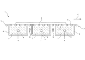
도 1은 기판의 처리를 위한, 특히 하나의 면 상의 기판의 전기화학적 에칭을 위한 처리 디바이스(1)를 도시한다. 또한, 도 1은 처리 디바이스(1)에 의해 처리될 실리콘 기판(2)을 도시한다.1 shows a
처리 디바이스(1)는 운송 방향(4)을 따라 처리될 실리콘 기판(2)을 운송하도록 설정된 운송 디바이스(3)를 포함한다. 본 작업 예에서, 운송 디바이스(3)는 복수의 운송 롤러(5)를 구비하는 롤러 컨베이어의 형태를 취한다.The
처리 디바이스(1)는 각각이 에칭 매체(7)로 채워지고 각각에 전극(8)이 배치되는, 운송 방향(4)으로 차례로 배치된 복수의 처리 탱크(6)를 더 포함한다. 도 1에서, 3개의 처리 탱크(6)가 예시로서 도시되었다. 처리 디바이스(1)는 원칙적으로 더 많거나 더 적은 수의 처리 탱크(6)를 가질 수 있다.The
에칭 매체(7)는 바람직하게는 불화수소 수용액이다. 선택적으로, 에칭 매체(7)는 첨가제 및/또는 계면활성제를 포함할 수 있다. 각각의 전극(8)은 그에 전위를 인가하였으며, 이때 전극(8)의 극성이 운송 방향(4)으로 교대로 변화한다.The
운송 디바이스(3)는 처리 탱크(6)를 통해 운송 방향(4)을 따라 실리콘 기판(2)을 운송하며, 여기서 실리콘 기판(2)은 기판 밑면(9) 상에서만 처리 탱크(6)에 존재하는 에칭 매체(7)와 접촉된다.The
처리 탱크(6)를 통한 실리콘 기판(2)의 운송 중에, 전류 밀도의 국부적인 불균일이 에칭 피크 및 트로프(trough)가 발생하게 하는 전기화학적 반응이 일어나고, 이는 기판 밑면(9) 상에 기공의 형성을 초래하며, 그 결과 다공성 구조가 기판 밑면(9)에 형성된다.During the transport of the
전기화학적 반응은 전극(8)의 전위를 통해 조절될 수 있으며, 이는 처리 탱크(6) 내의 전류 밀도에 영향을 미친다. 반응은 첨가제 및/또는 계면활성제를 혼합하여 추가로 조절될 수 있다.The electrochemical reaction can be controlled via the potential of the
불화수소를 포함하는 에칭 매체가 에칭 매체(7)로서 사용될 때, 다음의 반응: Si + 6F- + 4h+ → SiF6 2-이 특히 기판 밑면(9) 상에서 발생한다. 전류는 실리콘 기판(2)의 표면에 전자 정공(electron holes)(h+)을 공급하고 불화수소는 용액 내에 불화수소 이온(F-)을 발생시킨다.When an etching medium containing hydrogen fluoride is used as the
처리 탱크(6) 상의 전류 밀도는 실리콘 기판(2)의 다공성 구조가 실리콘 기판(2)의 깊이에 걸쳐 눈금이 매겨지도록 조정될 수 있으며, 그 결과 기공도 및/또는 기공 크기 및/또는 기공 형태가 서로 상이한 복수의 다공성 실리콘층이 기판 밑면(9) 상에 형성된다.The current density on the
각각의 처리 탱크(6) 사이의 처리 디바이스(1)에는 (도면에 도시되지 않은) 에어 나이프가 추가로 존재하며, 이것을 이용하여 기판 밑면(9) 상에 존재하는 임의의 에칭 매체(7)를 불어내기 위한 질소의 기체 스트림(10)이 생성된다.There is additionally an air knife (not shown) in the
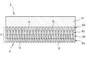
도 2는 도 1의 처리 디바이스(1)의 도움으로 처리된 실리콘 기판(2)의 단면도를 도시한다.FIG. 2 shows a cross-sectional view of a
처리된 실리콘 기판(2)은 기판 밑면(9) 상에 서로 위아래로 배치된 복수의 다공성 실리콘층(12a, 12b, 12c, 12d)으로 이루어진 다중층 시스템(11)을 갖는다. 도 2에서, 4개의 다공성 실리콘층(12a, 12b, 12c, 12d)이 예로서 도시되었고, 원칙적으로 처리 디바이스(1)의 도움으로 처리 중에 실리콘 기판(2)의 기판 밑면(9) 상에 더 많거나 더 적은 수의 다공성 실리콘층을 형성하는 것이 가능하다.The treated
다공성 실리콘층(12a, 12b, 12c, 12d)은 기공(13)의 크기 및/또는 기공(13)의 형태 및/또는 기공도에 있어서 상이하며, 이에 의해 가장 큰 기공도를 가진 다중층 시스템(11)의 다공성 실리콘층(12d)은 실리콘 기판(2)의 비다공화 부분(14)에 바로 인접한다. 이러한 다공성 실리콘층(12d)은 실리콘 기판(2)의 비다공화 부분(14)으로부터 다중층 시스템(11)을 이후에 제거하기 위한 분리 층의 역할을 한다(도 6 참조).The
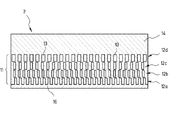
도 3은 아래에서 본 도 2의 실리콘 기판(2)을 도시한다.3 shows the
도 3에서, 다양한 형태 및 크기의 복수의 기공(13)을 실리콘 기판(2)의 기판 밑면(9) 상에서 볼 수 있다.In FIG. 3 , a plurality of
다중층 시스템(11)의 형성 후에, 구리층(15)은 2-단계 증착 프로세스에서 다중층 시스템(11) 상에 증착된다(도 4 및 5 참조).After formation of the
제 1 증착 단계에서, 구리층(15)의 제 1 부분(16)은 갈바닉 전위에 의해 다중층 시스템(11) 상에 증착된다. 이 증착 단계에서, 실리콘 기판(2)은 불화수소 및 황산구리를 포함하는 수성 증착 용액과 기판 밑면(9) 상에서 접촉된다. 불화수소는 실리콘 기판(2)의 기판 밑면(9)으로부터 이산화규소를 용해시켜 기판 밑면(9) 상에 산화되지 않은 실리콘을 남기며, 실리콘과 구리 사이의 화학적 전위 때문에 이것은 증착 용액 내에 존재하는 구리 이온에 끌린다.In a first deposition step, a
갈바닉 전위는 극도로 다공성인 실리콘층(12a)이 구리로 완전히 커버될 때 자체적으로 중단하는 자가-제한 프로세스이다. 제 1 증착 단계의 끝에서, 구리층(15)의 상기 제 1 부분(16)은 매우 다공성인 실리콘층(12a)이 구리층(15)의 제 1 부분(16)에 매립되도록 형성된다.Galvanic dislocation is a self-limiting process that stops itself when the extremely
제 2 증착 단계에서, 구리층(15)의 제 2 부분(17)은 전기화학적 증착에 의해 구리층(15)의 제 1 부분(16) 상에 증착된다. 구리층(15)의 제 1 부분(16)은 구리층(15)의 제 2 부분(17)의 형성을 위한 전기 전도성 시드 층으로서의 역할을 한다.In a second deposition step, a
제 2 증착 단계에서, 실리콘 기판(2)은 황산구리를 포함하는 증착 용액으로 기판 밑면(9) 상에서 습윤되고 전류가 인가된다. 실리콘 기판(2)은 전기화학적 증착에서 음으로 하전된 전극으로서의 역할을 하는 반면, 증착 용액은 양으로 하전된 반대 전극으로서의 역할을 한다.In the second deposition step, the
도 4는 다중층 시스템(11) 상에 구리층(15)의 제 1 부분(16)을 증착한 후의 실리콘 기판(2)의 단면도를 도시한다.4 shows a cross-sectional view of a
도 5는 구리층(15)의 제 1 부분(16) 상에 구리층(15)의 제 2 부분(17)을 증착한 후의 실리콘 기판(2)의 단면도를 도시한다.FIG. 5 shows a cross-sectional view of the
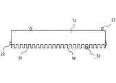
구리층(15)의 증착 후, 실리콘 기판(2)은 열처리를 거친다(도 6 참조). 이것은 예를 들어 연속 오븐(도면에 도시되지 않음)에서 발생할 수 있다.After deposition of the
열처리에서, 열복사(18)는 분리층으로서의 역할을 하는 다공성 실리콘층(12d)의 기공벽의 붕괴를 유발하도록 사용되며(도 2, 4 및 5 참조), 이것은 한편으로는 다공성 실리콘층(12a, 12b, 12c) 그리고 다른 한편으로는 다공성 실리콘층(12d) 사이의 팽창 열 계수의 차에 기인한다. 이것은 다중층 시스템(11)의 다공성 실리콘층(12a, 12b, 12c)과 함께 구리층(15)이 실리콘 기판(2)의 비다공화 부분(14)으로부터 분리되는 것을 가능하게 한다.In the heat treatment,
열처리 후에, 분리층으로서 작용하는 다공성 실리콘층(12d)의 모든 잔여물은 가느다란 절단단(19)이다. 이들은 각각 실리콘 기판(2)의 비다공화 부분(14) 또는 이전에 분리층에 인접하는 다중층 시스템(11)의 다공성 실리콘층(12c)에 인접한다.After the heat treatment, all residues of the
도 6은 실리콘 기판(2)의 비다공화 부분(14)으로부터 구리층(15) 및 다공성 실리콘층(12a, 12b, 12c)을 함께 제거한 후의 실리콘 기판(2) 및 실리콘 기판(2) 상에 증착된 구리층(15)을 단면도로 도시한다.Figure 6 shows the deposition on the
실리콘 기판(2)의 비다공화 부분(14)으로부터 구리층(15) 및 다공성 실리콘층(12a, 12b, 12c)을 함께 제거한 후에, 리튬(20)이 분리된 다공성 실리콘층(12a, 12b, 12c) 내에 삽입된다(도 7 참조).After removing the
도 7은 롤링 가능한 필름으로 설계된 배터리를 위한 혁신적인 전극(21)의 작업 예의 단면도를 도시한다.7 shows a cross-sectional view of a working example of an
이러한 전극(21)은 다공질 실리콘층(12a, 12b, 12c), 구리층(15) 및 다공질 실리콘층(12a, 12b, 12c)에 삽입된 리튬(20)에 의해서 형성된다.The
전극(21)을 배터리에 설치한 것에 이어 배터리에 대한 복수의 충전-방전 사이클을 수행함으로써 전극(21)을 활성화한다.The
전극(21)의 활성화는 다공성 실리콘층(12a, 12b, 12c)에 수 회의 사이클 후에 추가로 발달하지 않는 섬 구조의 형성을 발생시키며 추가 사이클에 걸쳐 대체로 안정하게 유지된다(도 8 참조). 전극(21)의 실리콘이 비다공성이면, 실리콘의 무질서한 재결정화의 결과로서 충전-방전 사이클의 수행 중에 전극(21)이 파괴될 것이다. 그러나 이 경우에 실리콘의 다공성 구조는 구리층(15)에 매립된 실리콘 부분이 시드 결정으로서의 역할을 하는 실리콘의 자가-조직화된 재결정화를 발생시킨다.Activation of
도 8은 전극(21)의 활성화 후에 도 7의 전극(21)의 다공성 실리콘층(12a, 12b, 12c) 중 하나의 단면도를 도시한다.FIG. 8 shows a cross-sectional view of one of the
복수의 직사각형 영역(22)으로부터 형성된, 도시된 다공성 실리콘층의 섬 구조를 도 8에서 볼 수 있다.An island structure of the illustrated porous silicon layer formed from a plurality of
도 8에 도시된 다공성 실리콘층의 기공(13)과 달리, 도시된 다공성 실리콘층에 삽입된 리튬(20)은 더 나은 명확성을 위해 도 8에서 생략되었다.Unlike the
대안적인 작업 예에서, 도 1 내지 8과 관련하여 전술된 제 1 작업 예와 대조적으로, 구리층은 대안적인 프로세스 변형에 의해서 도 2와 관련하여 기술된 다중층 시스템(11)에 해당하는 다중층 시스템 상에 증착된다. 이러한 대안적인 공정 변형예에서, 구리층(15)의 제 1 부분(16) 대신에, 니켈층은 제 1 증착 단계에서 다중층 시스템 상에 증착된다. 다중층 시스템 상의 니켈층의 증착은 전기화학 증착에 의해서 발생된다. 기판 밑면 상에 다중층 시스템을 갖는 실리콘 기판 상에 니켈층을 증착하기 위해, 실리콘 기판이 황산 니켈 또는 술파민산 니켈을 포함하는 증착 용액으로 기판 밑면 상에서 적셔지고 전류가 인가된다.In an alternative working example, in contrast to the first working example described above in relation to FIGS. 1 to 8 , the copper layer is a multilayer corresponding to the
니켈층의 증착은 도 4에 의해 예시될 수 있다. 그 표현에서, 참조번호 16은 이러한 대안적인 작업 예에서 니켈층을 지칭할 것이다. 다른 모든 측면에서, 대안적인 작업 예의 요소는 도 4에 도시된 요소와 일치한다.The deposition of the nickel layer can be illustrated by FIG. 4 . In that expression,
니켈층의 증착에 이은 제 2 증착 단계에서, 대안적인 작업 예에서 전기화학적 증착에 의해 구리층이 니켈층 상에 증착된다. 여기서 니켈층은 구리층의 형성을 위한 전기 전도성 시드 층으로서의 역할을 하고 니켈층 상에 적용된 구리층의 다공성 실리콘층에 대한 향상된 접착력을 제공한다. 니켈층 상의 구리층 증착의 예시를 위해, 도 5를 참조할 수 있다. 그 표현에서, 참조번호 16은 이러한 대안적인 작업 예에서 니켈층을 지칭하며 참조번호 17은 니켈층 상에 증착된 구리층을 지칭한다.In a second deposition step following the deposition of the nickel layer, a copper layer is deposited on the nickel layer by electrochemical vapor deposition in an alternative working example. Here the nickel layer serves as an electrically conductive seed layer for the formation of the copper layer and provides improved adhesion of the copper layer applied on the nickel layer to the porous silicon layer. For an illustration of a copper layer deposition on a nickel layer, reference may be made to FIG. 5 . In that expression,
도 9 내지 14와 관련하여 아래에 기술되는 사실 및 특징은 도 1 내지 8에 도시된 작업 예를 참조한다. 달리 언급되지 않는 한, 이들은 또한 전술된 대안적인 작업 예와 제한 없이 결합될 수 있다.Facts and features described below with respect to FIGS. 9 to 14 refer to the working examples shown in FIGS. 1 to 8 . Unless otherwise stated, they may also be combined without limitation with the alternative working examples described above.
도 9는 실리콘 기판(2)의 비다공화 부분(14)을 측면도로 도시한다.9 shows the
또한 도 9에는 가느다란 절단단(19)에 의해 형성된 실리콘 기판(2)의 비다공화 부분(14)에 인접한 다공성 구조의 잔여물 및 실리콘 기판(2)의 비다공화 부분(14) 상에 존재하는 금속 잔류물(23)이 도시되었으며, 이로 인해 도 1 내지 8과 관련하여 기술된 제 1 작업 예에 따른 구리층(15)의 증착 시에 또는 대안적인 작업 예에 따른 니켈층 및 구리층의 증착 시에 실리콘 기판(2)의 비다공화 부분(14)이 오염될 것이다.Also shown in FIG. 9 is the residue of the porous structure adjacent to the
실리콘 기판(2)의 비다공화 부분(14)을 재활용할 수 있도록, 절단단(19) 및 금속 잔류물(23)은 2-단계 습식 화학적 에칭 공정에서 제거된다(도 9 및 10 참조). 이것은 실리콘 기판(2)의 비다공화 부분(14)이 예를 들어 특히 전술된 공정 단계들의 반복을 통해서 전술된 유형의 추가 전극의 생산을 위해 사용될 수 있게 한다.In order to be able to recycle the
도 10은 실리콘 기판(2)의 비다공화 부분(14), 인접한 절단단(19), 상기 금속 잔류물(23) 및 처리 탱크(24)를 도시한다.FIG. 10 shows the
처리 탱크(24)는 제 1 작업 예의 경우에 구리의 형태인 또는 대안적인 작업 예의 경우에 구리 및 니켈의 형태인 금속 잔류물(23)을 제거하는 역할을 하는 산성 에칭 매체(25)로 채워진다. 에칭 매체(25)는 예를 들어 불화수소 및/또는 염화수소 및/또는 질산 및/또는 황산 및/또는 과산화수소 및/또는 오존을 포함할 수 있다.The
도 10에 도시된 것은 실리콘 기판(2)의 비다공화 부분(14)이 에칭 매체(25)에 담그어지고 상기 금속 잔류물(23)이 에칭 매체(25)에 용해된 상태이다.10 is a state in which the
도 11은 실리콘 기판(2)의 비다공화 부분(14) 및 추가 처리 탱크(26)를 도시한다.11 shows the
도 11의 처리 탱크(26)는 위에서 언급된 절단단(19)의 제거를 위한 역할을 하는 에칭 매체(27)로 채워진다. 이러한 에칭 매체(27)는 알칼리성 에칭 매체 또는 산성 에칭 매체일 수 있다. 전자의 경우, 에칭 매체(27)는 예를 들어 탈이온수 및 또한 수산화나트륨 및/또는 수산화칼륨을 포함할 수 있다. 후자의 경우, 에칭 매체(27)는 예를 들어 불화수소 및/또는 질산 및/또는 황산 및/또는 과산화수소 및/또는 오존을 포함할 수 있다.The
도 11에 도시된 것은 실리콘 기판(2)의 비다공화 부분(14)이 처리 탱크(26)에 존재하는 에칭 매체(27)에 담그어진 상태이다. 에칭 매체(27)는 실리콘 기판(2)의 표면 연마를 일으켜, 이 상태에서 실리콘 기판(2)의 비다공화 부분(14)으로부터 전술된 절단단(19)을 제거하고 실리콘 기판(2)의 비다공화 부분(14)이 전술된 유형의 전극의 추가 생산을 위해 사용될 수 있게 한다.11 is a state in which the
도 12는 본 발명의 배터리(28a)의 작업 예를 부분적인 단면도로 도시한다.12 shows a working example of the
배터리(28a)는 본 발명의 작업 예에서 원통형 구조의 리튬 이온 배터리이다.The
배터리(28a)는 원통형 하우징(29a)을 포함한다. 또한, 배터리(28a)는 음극(30a), 양극(31a) 및 음극(30a)과 양극(31a) 사이에 배치된 분리기(32a)를 포함한다. 음극(30a), 양극(31a) 및 분리기(32a)는 각각 롤업 필름으로서 형성되며 배터리(28a)의 하우징(29a) 내에 배치된다.The
배터리(28a)의 양극(31a)은 전술된 전극(21)이다(도 7 및 8 참조). 즉, 전술된 전극(21)은 배터리(28a)의 양극(31a)으로서 사용된다.The positive electrode 31a of the
도 13은 도 12와 관련하여 기술된 배터리의 대안적인 작업 예를 부분적인 단면도로 도시한다. 도 13에 도시된 작업 예에서, 배터리(28b)는 직사각형 베이스를 갖는 대안적인 구성을 갖는다.FIG. 13 shows, in partial cross-section, an alternative working example of the battery described in relation to FIG. 12 ; In the working example shown in FIG. 13 , the
배터리(28b)는 대안적인 구성에서 직육면체 하우징(29b)을 포함한다. 또한, 배터리(28b)는 음극(30b), 양극(31b) 및 음극(30b)과 양극(31b) 사이에 배치된 분리기(32b)를 포함한다. 음극(30b), 양극(31b) 및 분리기(32b)는 직사각형 단면으로서 형성되고 배터리(28b)의 하우징(29b) 내부에서 사전정의된 순서로 서로 위아래로 적층되어 배치된다.
배터리(28b)의 양극(31b)은 전술된 전극(21)이다(도 7 및 8 참조). 다시 말해, 전술된 전극(21)은 직사각형 단면의 형태로 배터리(28b)에서 양극(31b)으로서 사용된다.The positive electrode 31b of the
도 14는 도 13과 관련하여 기술된 배터리(28b)의 대안적인 작업 예를 위한 직육면체 스택 형태의 음극(30b), 양극(31b) 및 분리기(32b)의 대안적인 가능한 배치를 도시한다. 여기서 양극(31b)은 접을 수 있는 필름으로서 형성된다. 이러한 대안적인 가능한 배치에서, 음극(30b) 및 분리기(32b)는 Z-폴딩 기술에 의해 양극(31b) 사이에서 폴딩된다. 음극(30b) 및 분리기(32b)는 여기에서 쌍을 이루는 방식으로 직사각형 섹션으로서 형성될 수 있다. 바람직하게는, 음극(30b) 및 분리기(32b)는 접을 수 있는 필름으로서 형성된다. 이는 오버레이된 Z-폴딩 기술이 적용되는 것을 가능하게 한다. 이것에 의해, 양극(31b), 음극(30b) 및 분리기(32b)가 직육면체 스택으로 폴딩될 수 있도록 교대로 폴딩하는 단계가 가능하다. 예를 들어, 음극(30b) 및 분리기(32b)는 제 1 접힘 단계에서 양극(31b) 사이에서 폴딩될 수 있다. 제 2 폴딩 단계에서, 양극(31b)은 음극(30b)과 쌍을 이루는 방식으로 배치된 분리기(32b) 사이에서 폴딩될 수 있다. 제 2 폴딩 단계 후에, 제 1 폴딩 단계가 새로 실행할 수 있다. 이것은 낮은 비용으로 및/또는 자동화된 방식으로 직육면체 구조를 갖는 배터리(28b)를 생산하는 것을 가능하게 한다.FIG. 14 shows an alternative possible arrangement of the
본 발명은 도시된 작업 예를 참조하여 상세하게 설명되었다. 그러나 본 발명은 개시된 예로서 제한되지 않는다. 본 발명의 기초가 되는 사상을 벗어나지 않으면서, 당업자에 의해 이러한 작업 예로부터 다른 변형예가 파생될 수 있다.The invention has been described in detail with reference to the illustrated working examples. However, the present invention is not limited to the disclosed examples. Other modifications may be derived from these working examples by those skilled in the art without departing from the spirit underlying the present invention.
1 처리 디바이스
2 실리콘 기판
3 운송 디바이스
4 운송 방향
5 운송 롤러
6 처리 탱크
7 에칭 매체
8 전극
9 기판 밑면
10 기체 스트림
11 다중층 시스템
12a 다공성 실리콘층
12b 다공성 실리콘층
12c 다공성 실리콘층
12d 다공성 실리콘층
13 기공
14 실리콘 기판의 비다공화 부분
15 구리층
16 구리층의 제 1 부분
17 구리층의 제 2 부분
18 열복사
19 절단단(stump)
20 리튬
21 전극
22 직사각형 영역
23 금속 잔류물
24 처리 탱크
25 에칭 매체
26 처리 탱크
27 에칭 매체
28a 배터리
28b 배터리
29a 하우징
29b 하우징
30a 음극
30b 음극
31a 양극
31b 양극
32a 분리기
32b 분리기1 processing device
2 silicon substrate
3 transport device
4 transport direction
5 transport roller
6 treatment tank
7 Etching medium
8 electrodes
9 Bottom of the board
10 gas stream
11 multi-layer system
12a porous silicon layer
12b porous silicon layer
12c porous silicon layer
12d porous silicon layer
13 Qigong
14 Non-porous part of silicon substrate
15 copper layer
16 first portion of copper layer
17 second part of copper layer
18 thermal radiation
19 stump
20 lithium
21 electrode
22 rectangular area
23 Metal Residue
24 treatment tank
25 Etching medium
26 treatment tank
27 Etching medium
28a battery
28b battery
29a housing
29b housing
30a cathode
30b cathode
31a anode
31b anode
32a separator
32b Separator
Claims (17)
적어도 하나의 다공성 실리콘층(12a, 12b, 12c, 12d) 상의 구리층(15)은 바람직하게는 상기 적어도 하나의 다공성 실리콘층(12a, 12b, 12c, 12d) 상에 직접 배치되는 것으로 특징지어지는, 전극.The method of claim 1,
A copper layer (15) on at least one porous silicon layer (12a, 12b, 12c, 12d) is preferably characterized in that it is disposed directly on said at least one porous silicon layer (12a, 12b, 12c, 12d) , electrode.
다공성 실리콘층(12a, 12b, 12c, 12d)의 각각이 서로 다른 기공도 및/또는 서로 다른 기공 크기 및/또는 서로 다른 기공 형태를 갖는다는 점에서 서로 상이한, 바람직하게는 서로 위아래로 배치되는 복수의 다공성 실리콘층(12a, 12b, 12c, 12d)으로 이루어진 다중층 시스템(11)에 의해서 특징지어지고, 적어도 하나의 다공성 실리콘층(12a, 12b, 12c, 12d)은 상기 다중층 시스템(11)의 복수의 다공성 실리콘층(12a, 12b, 12c, 12d) 중 하나인, 전극.3. The method of claim 1 or 2,
A plurality of porous silicon layers 12a, 12b, 12c, 12d differ from each other in that each of them has a different porosity and/or a different pore size and/or a different pore shape, preferably disposed above and below each other. characterized by a multilayer system (11) consisting of porous silicon layers (12a, 12b, 12c, 12d) of at least one porous silicon layer (12a, 12b, 12c, 12d) One of the plurality of porous silicon layers (12a, 12b, 12c, 12d) of the electrode.
상기 전극(21)은 필름, 특히 롤링 가능한(rollable) 필름으로 설계되는 것으로 특징지어지는, 전극.4. The method according to any one of claims 1 to 3,
The electrode (21) is characterized in that it is designed as a film, in particular a rollable film.
상기 적어도 하나의 다공성 실리콘층(12a, 12b, 12c, 12d) 내에 리튬(20)이 삽입되는 것으로 특징지어지는, 전극.5. The method according to any one of claims 1 to 4,
An electrode, characterized in that lithium (20) is inserted in the at least one porous silicon layer (12a, 12b, 12c, 12d).
- 실리콘 기판(2)을 에칭함으로써 적어도 하나의 다공성 실리콘층(12a, 12b, 12c, 12d)을 형성하는 단계;
- 상기 적어도 하나의 다공성 실리콘층(12a, 12b, 12c, 12d) 상에 구리층(15)을 증착하는 단계를 포함하는, 방법.A method for producing an electrode (21) according to any one of claims 1 to 5, comprising:
- forming at least one porous silicon layer (12a, 12b, 12c, 12d) by etching the silicon substrate (2);
- depositing a copper layer (15) on said at least one porous silicon layer (12a, 12b, 12c, 12d).
적어도 하나의 다공성 실리콘층(12a, 12b, 12c, 12d)을 형성하기 위해, 상기 실리콘 기판(2)은 바람직하게는 연속 공정에서, 습식 화학적 에칭되는 것으로 특징지어지는, 방법.7. The method of claim 6,
Method, characterized in that for forming at least one porous silicon layer (12a, 12b, 12c, 12d), the silicon substrate (2) is wet chemically etched, preferably in a continuous process.
적어도 하나의 다공성 실리콘층(12a, 12b, 12c, 12d)을 형성하기 위해, 상기 실리콘 기판(2)은 하나의 면에 에칭되는 것으로 특징지어지는, 방법.8. The method of claim 6 or 7,
Method, characterized in that the silicon substrate (2) is etched on one side to form at least one porous silicon layer (12a, 12b, 12c, 12d).
적어도 하나의 다공성 실리콘층(12a, 12b, 12c, 12d)을 형성하기 위해, 상기 실리콘 기판(2)은 전기화학적 에칭되고,
- 상기 실리콘 기판(2)은, 각각이 에칭 매체(7)로 채워지고 각각에 전극(8)이 배치되는, 운송 방향(4)으로 앞뒤로 나란히 배치된 복수의 처리 탱크(6)를 통해서 운송 방향(4)을 따라 운송되고,
- 상기 처리 탱크(6)를 통한 운송 중에, 상기 실리콘 기판(2)은 기판 밑면(9) 상에서 각각의 처리 탱크(6) 내에 존재하는 에칭 매체(7)와 접촉되며,
- 상기 처리 탱크(6) 내에 배치된 전극(8)의 극성은 상기 운송 방향(4)에서 교대로 변하는 것으로 특징지어지는, 방법.9. The method according to any one of claims 6 to 8,
To form at least one porous silicon layer (12a, 12b, 12c, 12d), the silicon substrate (2) is electrochemically etched,
- the silicon substrate 2 is transported through a plurality of treatment tanks 6 arranged side by side in a transport direction 4, each filled with an etching medium 7 and on which an electrode 8 is disposed. (4) transported according to,
- during transport through the treatment tanks (6), the silicon substrates (2) are brought into contact with the etching medium (7) present in the respective treatment tanks (6) on the underside (9) of the substrates,
- the method, characterized in that the polarity of the electrodes (8) arranged in the treatment tank (6) changes alternately in the transport direction (4).
상기 구리층(15)은 2-단계 공정으로 증착되며,
- 제 1 증착 단계에서 구리층(15)의 제 1 부분(16)이 갈바닉 전위(galvanic displacement)에 의해 적어도 하나의 다공성 실리콘층(12a, 12b, 12c, 12d) 상에 증착되고,
- 제 2 증착 단계에서 구리층(15)의 제 2 부분(17)이 전기화학적 증착에 의해 상기 구리층(15)의 제 1 부분(16) 상에 증착되는 것으로 특징지어지는, 방법.10. The method according to any one of claims 6 to 9,
The copper layer 15 is deposited in a two-step process,
- in a first deposition step a first portion 16 of the copper layer 15 is deposited on the at least one porous silicon layer 12a, 12b, 12c, 12d by galvanic displacement,
- a method, characterized in that in a second deposition step a second part (17) of the copper layer (15) is deposited on the first part (16) of the copper layer (15) by electrochemical vapor deposition.
- 제 1 증착 단계에서 니켈층이 전기화학적 증착에 의해 적어도 하나의 다공성 실리콘층 상에 증착되고,
- 제 2 증착 단계에서 구리층이 전기화학적 증착에 의해 상기 니켈층 상에 증착되는 것으로 특징지어지는, 방법.10. The method according to any one of claims 6 to 9,
- a nickel layer is deposited on the at least one porous silicon layer by electrochemical vapor deposition in a first deposition step;
- a method, characterized in that in a second deposition step a copper layer is deposited on the nickel layer by electrochemical vapor deposition.
- 상기 실리콘 기판(2)의 에칭은 다공성 실리콘층(12a, 12b, 12c, 12d)의 각각이 서로 다른 기공도 및/또는 서로 다른 기공 크기 및/또는 서로 다른 기공 형태를 갖는다는 점에서 서로 상이한 복수의 다공성 실리콘층(12a, 12b, 12c, 12d)으로 이루어진 다중층 시스템(11)의 형성을 발생시키고, 상기 적어도 하나의 다공성 실리콘층(12a, 12b, 12c, 12d)은 상기 다중층 시스템(11)의 복수의 다공성 실리콘층(12a, 12b, 12c, 12d) 중 하나이며;
- 상기 다중층 시스템(11)은 가장 큰 기공도를 갖는 다중층 시스템(11)의 다공성 실리콘층(12d)이 실리콘 기판(2)의 비다공화 부분(14)에 바로 인접하도록 형성되는 것으로 특징지어지는, 방법.12. The method according to any one of claims 6 to 11,
- the etching of the silicon substrate 2 is different from each other in that each of the porous silicon layers 12a, 12b, 12c, 12d has a different porosity and/or a different pore size and/or a different pore shape resulting in the formation of a multilayer system 11 consisting of a plurality of porous silicon layers 12a, 12b, 12c, 12d, said at least one porous silicon layer 12a, 12b, 12c, 12d comprising said multilayer system ( 11) one of the plurality of porous silicon layers 12a, 12b, 12c, 12d;
- the multilayer system (11) is characterized in that the porous silicon layer (12d) of the multilayer system (11) having the greatest porosity is formed directly adjacent to the non-porous portion (14) of the silicon substrate (2) How to lose.
적어도 하나의 다공성 실리콘층(12a, 12b, 12c, 12d)이 구리층(15)과 함께 실리콘 기판(2)의 비다공화 부분(14)으로부터 제거되는 것으로 특징지어지는, 방법.13. The method according to any one of claims 6 to 12,
A method, characterized in that at least one porous silicon layer (12a, 12b, 12c, 12d) is removed from the non-porous portion (14) of the silicon substrate (2) together with the copper layer (15).
적어도 하나의 다공성 실리콘층(12a, 12b, 12c, 12d)과 구리층(15)을 함께 제거하기 위해, 상기 실리콘 기판(2)이 바람직하게는 오븐에 의한, 특히 연속 오븐에 의한 열처리를 거치는 것으로 특징지어지는, 방법.14. The method of claim 13,
In order to remove the at least one porous silicon layer 12a, 12b, 12c, 12d together with the copper layer 15, the silicon substrate 2 is preferably subjected to heat treatment by means of an oven, in particular by means of a continuous oven. Characterized method.
바람직하게는 적어도 하나의 다공성 실리콘층(12a, 12b, 12c, 12d)이 구리층(15)과 함께 실리콘 기판(2)의 비다공화 부분(14)으로부터 제거된 후에, 적어도 하나의 다공성 실리콘층(12a, 12b, 12c, 12d) 내에 리튬(20)이 삽입되는 것으로 특징지어지는, 방법.15. The method according to any one of claims 6 to 14,
Preferably after the at least one porous silicon layer 12a, 12b, 12c, 12d is removed from the non-porous portion 14 of the silicon substrate 2 together with the copper layer 15, the at least one porous silicon layer ( 12a, 12b, 12c, 12d) characterized in that lithium (20) is inserted.
Applications Claiming Priority (3)
| Application Number | Priority Date | Filing Date | Title |
|---|---|---|---|
| DE102020103531.4A DE102020103531A1 (en) | 2020-02-11 | 2020-02-11 | Electrode, its use, accumulator and method for producing an electrode |
| DE102020103531.4 | 2020-02-11 | ||
| PCT/DE2021/100137 WO2021160222A2 (en) | 2020-02-11 | 2021-02-11 | Electrode, use thereof, battery and method for producing an electrode |
Publications (1)
| Publication Number | Publication Date |
|---|---|
| KR20220141330A true KR20220141330A (en) | 2022-10-19 |
Family
ID=74844630
Family Applications (1)
| Application Number | Title | Priority Date | Filing Date |
|---|---|---|---|
| KR1020227031407A KR20220141330A (en) | 2020-02-11 | 2021-02-11 | Electrodes, uses of electrodes, battery and electrode production methods |
Country Status (8)
| Country | Link |
|---|---|
| US (1) | US20230077095A1 (en) |
| EP (1) | EP4104218A2 (en) |
| JP (1) | JP2023512730A (en) |
| KR (1) | KR20220141330A (en) |
| CN (1) | CN115066765A (en) |
| DE (1) | DE102020103531A1 (en) |
| TW (1) | TW202131541A (en) |
| WO (1) | WO2021160222A2 (en) |
Families Citing this family (2)
| Publication number | Priority date | Publication date | Assignee | Title |
|---|---|---|---|---|
| WO2023016607A1 (en) * | 2021-08-11 | 2023-02-16 | RENA Technologies GmbH | Electrode, rechargeable battery, and manufacturing processes |
| WO2023229299A1 (en) * | 2022-05-24 | 2023-11-30 | 주식회사 엘지화학 | Electrode for lithium secondary battery, manufacturing method therefor, and lithium secondary battery comprising same |
Family Cites Families (5)
| Publication number | Priority date | Publication date | Assignee | Title |
|---|---|---|---|---|
| DE102009008152A1 (en) * | 2009-02-09 | 2010-08-19 | Nb Technologies Gmbh | Silicon solar cell |
| DE102009035745A1 (en) | 2009-08-01 | 2011-02-17 | Christian-Albrechts-Universität Zu Kiel | Electrode for lithium-ion batteries |
| US20150364754A1 (en) | 2014-05-22 | 2015-12-17 | Paideia LLC | Silicene nanocomposite anode for lithium ion battery |
| DE102015120879A1 (en) | 2015-12-02 | 2017-06-08 | Institut Für Solarenergieforschung Gmbh | Process for producing a silicon-based porous electrode for a battery, in particular a lithium-ion battery |
| KR20190116266A (en) * | 2017-02-09 | 2019-10-14 | 레나 테크놀로지스 게엠베하 | Methods of texturing surfaces of semiconductor materials and apparatus for performing such methods |
-
2020
- 2020-02-11 DE DE102020103531.4A patent/DE102020103531A1/en active Pending
-
2021
- 2021-02-01 TW TW110103627A patent/TW202131541A/en unknown
- 2021-02-11 JP JP2022548401A patent/JP2023512730A/en active Pending
- 2021-02-11 EP EP21708916.8A patent/EP4104218A2/en active Pending
- 2021-02-11 WO PCT/DE2021/100137 patent/WO2021160222A2/en unknown
- 2021-02-11 CN CN202180013453.6A patent/CN115066765A/en active Pending
- 2021-02-11 US US17/799,135 patent/US20230077095A1/en active Pending
- 2021-02-11 KR KR1020227031407A patent/KR20220141330A/en active Search and Examination
Also Published As
| Publication number | Publication date |
|---|---|
| JP2023512730A (en) | 2023-03-28 |
| CN115066765A (en) | 2022-09-16 |
| US20230077095A1 (en) | 2023-03-09 |
| WO2021160222A2 (en) | 2021-08-19 |
| DE102020103531A1 (en) | 2021-08-12 |
| TW202131541A (en) | 2021-08-16 |
| EP4104218A2 (en) | 2022-12-21 |
| WO2021160222A3 (en) | 2021-10-07 |
Similar Documents
| Publication | Publication Date | Title |
|---|---|---|
| US10256500B2 (en) | Three-dimensional batteries and methods of manufacturing the same | |
| CN108352508B (en) | Microporous battery substrate | |
| US20190386291A1 (en) | Electrode structures | |
| KR102659783B1 (en) | Separators for three-dimensional batteries | |
| US10014517B2 (en) | Three dimensional batteries and methods of manufacturing the same | |
| US8187740B2 (en) | 3-D microbatteries based on interlaced micro-container structures | |
| KR101728875B1 (en) | Compressed powder 3d battery electrode manufacturing | |
| KR102372990B1 (en) | A device and method of manufacturing high-aspect ratio structures | |
| KR20220141330A (en) | Electrodes, uses of electrodes, battery and electrode production methods | |
| TWI517486B (en) | Energy storage device and manufacturing method thereof | |
| US10916761B2 (en) | Low melting temperature metal purification and deposition | |
| CN102263233A (en) | Power storage device and method for manufacturing the same | |
| TW201539850A (en) | Porous silicon-based anode active material, method for preparing the same, and lithium secondary battery comprising the same | |
| US20160351886A1 (en) | Scaffold-free 3d porous electrode and method of making a scaffold-free 3d porous electrode | |
| US20230006194A1 (en) | Lithium ion battery with thin anode | |
| US20160240882A1 (en) | Microstructured substrate | |
| KR101615827B1 (en) | Reduced graphene oxide/graphene composite film, Energy Storage Device Having the Same, and Method for Fabricating the composite film | |
| KR101850645B1 (en) | Aluminum foil for cathode current collector in lithium ion battery, method of manufacturing the same, lithium ion battery having the same | |
| KR20240018807A (en) | Anode for magnesium battery and method for manufacturing the same | |
| WO2023016607A1 (en) | Electrode, rechargeable battery, and manufacturing processes | |
| KR101351252B1 (en) | Manufacturing Process for Anode Active Material having Multi-Diameter Structure and Lithium Secondary Battery using the Same |
Legal Events
| Date | Code | Title | Description |
|---|---|---|---|
| A201 | Request for examination |