KR20220130142A - antenna device - Google Patents
antenna device Download PDFInfo
- Publication number
- KR20220130142A KR20220130142A KR1020227025930A KR20227025930A KR20220130142A KR 20220130142 A KR20220130142 A KR 20220130142A KR 1020227025930 A KR1020227025930 A KR 1020227025930A KR 20227025930 A KR20227025930 A KR 20227025930A KR 20220130142 A KR20220130142 A KR 20220130142A
- Authority
- KR
- South Korea
- Prior art keywords
- antenna
- antenna device
- transparent cover
- antenna element
- transparent
- Prior art date
Links
- 239000000758 substrate Substances 0.000 claims abstract description 88
- 239000004020 conductor Substances 0.000 claims description 33
- 230000005540 biological transmission Effects 0.000 claims description 17
- 238000000034 method Methods 0.000 claims description 16
- 238000002834 transmittance Methods 0.000 claims description 8
- 230000005404 monopole Effects 0.000 claims description 2
- 239000011521 glass Substances 0.000 abstract description 4
- 239000011347 resin Substances 0.000 abstract description 4
- 229920005989 resin Polymers 0.000 abstract description 4
- 239000010410 layer Substances 0.000 description 65
- 238000010586 diagram Methods 0.000 description 61
- 238000004088 simulation Methods 0.000 description 19
- 230000005672 electromagnetic field Effects 0.000 description 18
- 239000012790 adhesive layer Substances 0.000 description 15
- 238000005452 bending Methods 0.000 description 14
- 230000009467 reduction Effects 0.000 description 5
- 238000010295 mobile communication Methods 0.000 description 4
- 239000000463 material Substances 0.000 description 3
- RYGMFSIKBFXOCR-UHFFFAOYSA-N Copper Chemical compound [Cu] RYGMFSIKBFXOCR-UHFFFAOYSA-N 0.000 description 2
- 238000004891 communication Methods 0.000 description 2
- 229910052802 copper Inorganic materials 0.000 description 2
- 239000010949 copper Substances 0.000 description 2
- 239000003989 dielectric material Substances 0.000 description 2
- 238000005401 electroluminescence Methods 0.000 description 2
- 210000000887 face Anatomy 0.000 description 2
- 230000010365 information processing Effects 0.000 description 2
- 230000004048 modification Effects 0.000 description 2
- 238000012986 modification Methods 0.000 description 2
- BASFCYQUMIYNBI-UHFFFAOYSA-N platinum Chemical compound [Pt] BASFCYQUMIYNBI-UHFFFAOYSA-N 0.000 description 2
- 238000012545 processing Methods 0.000 description 2
- 239000007787 solid Substances 0.000 description 2
- QNRATNLHPGXHMA-XZHTYLCXSA-N (r)-(6-ethoxyquinolin-4-yl)-[(2s,4s,5r)-5-ethyl-1-azabicyclo[2.2.2]octan-2-yl]methanol;hydrochloride Chemical compound Cl.C([C@H]([C@H](C1)CC)C2)CN1[C@@H]2[C@H](O)C1=CC=NC2=CC=C(OCC)C=C21 QNRATNLHPGXHMA-XZHTYLCXSA-N 0.000 description 1
- VYZAMTAEIAYCRO-UHFFFAOYSA-N Chromium Chemical compound [Cr] VYZAMTAEIAYCRO-UHFFFAOYSA-N 0.000 description 1
- 239000004642 Polyimide Substances 0.000 description 1
- BQCADISMDOOEFD-UHFFFAOYSA-N Silver Chemical compound [Ag] BQCADISMDOOEFD-UHFFFAOYSA-N 0.000 description 1
- 229910052782 aluminium Inorganic materials 0.000 description 1
- XAGFODPZIPBFFR-UHFFFAOYSA-N aluminium Chemical compound [Al] XAGFODPZIPBFFR-UHFFFAOYSA-N 0.000 description 1
- 230000008859 change Effects 0.000 description 1
- 229910052804 chromium Inorganic materials 0.000 description 1
- 239000011651 chromium Substances 0.000 description 1
- 238000013461 design Methods 0.000 description 1
- 230000000694 effects Effects 0.000 description 1
- 230000005684 electric field Effects 0.000 description 1
- 239000005357 flat glass Substances 0.000 description 1
- 230000006870 function Effects 0.000 description 1
- PCHJSUWPFVWCPO-UHFFFAOYSA-N gold Chemical compound [Au] PCHJSUWPFVWCPO-UHFFFAOYSA-N 0.000 description 1
- 229910052737 gold Inorganic materials 0.000 description 1
- 239000010931 gold Substances 0.000 description 1
- 238000009434 installation Methods 0.000 description 1
- 239000004973 liquid crystal related substance Substances 0.000 description 1
- 229910052751 metal Inorganic materials 0.000 description 1
- 239000002184 metal Substances 0.000 description 1
- 230000000149 penetrating effect Effects 0.000 description 1
- 238000007747 plating Methods 0.000 description 1
- 229910052697 platinum Inorganic materials 0.000 description 1
- 229920001721 polyimide Polymers 0.000 description 1
- 230000001902 propagating effect Effects 0.000 description 1
- 230000005855 radiation Effects 0.000 description 1
- 229910052709 silver Inorganic materials 0.000 description 1
- 239000004332 silver Substances 0.000 description 1
- 239000002356 single layer Substances 0.000 description 1
- 238000009751 slip forming Methods 0.000 description 1
- 230000002195 synergetic effect Effects 0.000 description 1
- 230000009466 transformation Effects 0.000 description 1
Images


Classifications
-
- H—ELECTRICITY
- H01—ELECTRIC ELEMENTS
- H01Q—ANTENNAS, i.e. RADIO AERIALS
- H01Q1/00—Details of, or arrangements associated with, antennas
- H01Q1/12—Supports; Mounting means
- H01Q1/22—Supports; Mounting means by structural association with other equipment or articles
- H01Q1/24—Supports; Mounting means by structural association with other equipment or articles with receiving set
- H01Q1/241—Supports; Mounting means by structural association with other equipment or articles with receiving set used in mobile communications, e.g. GSM
- H01Q1/242—Supports; Mounting means by structural association with other equipment or articles with receiving set used in mobile communications, e.g. GSM specially adapted for hand-held use
- H01Q1/243—Supports; Mounting means by structural association with other equipment or articles with receiving set used in mobile communications, e.g. GSM specially adapted for hand-held use with built-in antennas
-
- H—ELECTRICITY
- H01—ELECTRIC ELEMENTS
- H01Q—ANTENNAS, i.e. RADIO AERIALS
- H01Q1/00—Details of, or arrangements associated with, antennas
- H01Q1/08—Means for collapsing antennas or parts thereof
- H01Q1/085—Flexible aerials; Whip aerials with a resilient base
-
- H—ELECTRICITY
- H01—ELECTRIC ELEMENTS
- H01Q—ANTENNAS, i.e. RADIO AERIALS
- H01Q1/00—Details of, or arrangements associated with, antennas
- H01Q1/36—Structural form of radiating elements, e.g. cone, spiral, umbrella; Particular materials used therewith
- H01Q1/364—Structural form of radiating elements, e.g. cone, spiral, umbrella; Particular materials used therewith using a particular conducting material, e.g. superconductor
-
- H—ELECTRICITY
- H01—ELECTRIC ELEMENTS
- H01Q—ANTENNAS, i.e. RADIO AERIALS
- H01Q1/00—Details of, or arrangements associated with, antennas
- H01Q1/36—Structural form of radiating elements, e.g. cone, spiral, umbrella; Particular materials used therewith
- H01Q1/38—Structural form of radiating elements, e.g. cone, spiral, umbrella; Particular materials used therewith formed by a conductive layer on an insulating support
-
- H—ELECTRICITY
- H01—ELECTRIC ELEMENTS
- H01Q—ANTENNAS, i.e. RADIO AERIALS
- H01Q1/00—Details of, or arrangements associated with, antennas
- H01Q1/44—Details of, or arrangements associated with, antennas using equipment having another main function to serve additionally as an antenna, e.g. means for giving an antenna an aesthetic aspect
-
- H—ELECTRICITY
- H01—ELECTRIC ELEMENTS
- H01Q—ANTENNAS, i.e. RADIO AERIALS
- H01Q19/00—Combinations of primary active antenna elements and units with secondary devices, e.g. with quasi-optical devices, for giving the antenna a desired directional characteristic
- H01Q19/28—Combinations of primary active antenna elements and units with secondary devices, e.g. with quasi-optical devices, for giving the antenna a desired directional characteristic using a secondary device in the form of two or more substantially straight conductive elements
- H01Q19/30—Combinations of primary active antenna elements and units with secondary devices, e.g. with quasi-optical devices, for giving the antenna a desired directional characteristic using a secondary device in the form of two or more substantially straight conductive elements the primary active element being centre-fed and substantially straight, e.g. Yagi antenna
-
- H—ELECTRICITY
- H01—ELECTRIC ELEMENTS
- H01Q—ANTENNAS, i.e. RADIO AERIALS
- H01Q11/00—Electrically-long antennas having dimensions more than twice the shortest operating wavelength and consisting of conductive active radiating elements
- H01Q11/02—Non-resonant antennas, e.g. travelling-wave antenna
- H01Q11/10—Logperiodic antennas
- H01Q11/105—Logperiodic antennas using a dielectric support
-
- H—ELECTRICITY
- H01—ELECTRIC ELEMENTS
- H01Q—ANTENNAS, i.e. RADIO AERIALS
- H01Q13/00—Waveguide horns or mouths; Slot antennas; Leaky-waveguide antennas; Equivalent structures causing radiation along the transmission path of a guided wave
- H01Q13/08—Radiating ends of two-conductor microwave transmission lines, e.g. of coaxial lines, of microstrip lines
- H01Q13/085—Slot-line radiating ends
-
- H—ELECTRICITY
- H01—ELECTRIC ELEMENTS
- H01Q—ANTENNAS, i.e. RADIO AERIALS
- H01Q13/00—Waveguide horns or mouths; Slot antennas; Leaky-waveguide antennas; Equivalent structures causing radiation along the transmission path of a guided wave
- H01Q13/10—Resonant slot antennas
- H01Q13/106—Microstrip slot antennas
-
- H—ELECTRICITY
- H01—ELECTRIC ELEMENTS
- H01Q—ANTENNAS, i.e. RADIO AERIALS
- H01Q9/00—Electrically-short antennas having dimensions not more than twice the operating wavelength and consisting of conductive active radiating elements
- H01Q9/04—Resonant antennas
- H01Q9/06—Details
- H01Q9/065—Microstrip dipole antennas
-
- H—ELECTRICITY
- H01—ELECTRIC ELEMENTS
- H01Q—ANTENNAS, i.e. RADIO AERIALS
- H01Q9/00—Electrically-short antennas having dimensions not more than twice the operating wavelength and consisting of conductive active radiating elements
- H01Q9/04—Resonant antennas
- H01Q9/30—Resonant antennas with feed to end of elongated active element, e.g. unipole
Abstract
전자 기기의 투명 커버의 외측으로부터 보이는 위치에 배치 가능한 투명한 안테나 엘리먼트를 포함하는 안테나 장치를 제공한다. 안테나 장치는, 전자 기기의 유리제 또는 수지제의 투명 커버의 외표면과는 반대의 내표면 측에 마련되는 투명한 플렉시블 기판과, 상기 플렉시블 기판 중 상기 투명 커버의 외측으로부터 보이는 위치에 마련되어, 상기 전자 기기의 외측을 향하는 지향성을 갖는 투명한 안테나 엘리먼트를 포함한다.An antenna device including a transparent antenna element that can be disposed at a position visible from the outside of a transparent cover of an electronic device is provided. The antenna device includes a transparent flexible substrate provided on an inner surface side opposite to the outer surface of a glass or resin transparent cover of an electronic device, and a position visible from the outside of the transparent cover among the flexible substrates, and a transparent antenna element having outward directivity.

Description
본 발명은 안테나 장치에 관한 것이다.The present invention relates to an antenna device.
종래부터, 스마트폰 등의 전자 기기에 사용하는 안테나 장치로서, 그라운드 플레인과, 상기 그라운드 플레인에 간격을 두고 대향하는 부위를 갖는 판상 도체와, 상기 그라운드 플레인을 접지 기준으로 하는 급전점에 접속된 급전 소자와, 상기 판상 도체에 접속된 긴 선형의 방사 소자를 구비하고, 상기 방사 소자는, 상기 급전 소자에 의해 비접촉으로 급전되어 방사 도체로서 기능하는, 안테나 장치가 있다(예를 들어, 특허문헌 1 참조).BACKGROUND ART Conventionally, as an antenna device used in electronic devices such as smartphones, a ground plane, a plate-shaped conductor having portions opposed to the ground plane at a distance from the ground plane, and a power feeding point connected to a feeding point using the ground plane as a ground reference There is an antenna device comprising an element and a long linear radiating element connected to the plate-shaped conductor, wherein the radiating element is fed non-contactly by the power supply element and functions as a radiating conductor (for example, Patent Document 1) Reference).
그런데, 종래의 안테나 장치는, 전자 기기의 투명 커버의 외측으로부터 보이는 위치에 배치하면, 디스플레이 패널의 표시를 방해하기 때문에, 투명 커버의 외측으로부터 보이는 위치에의 배치에는 적합하지 않다.However, the conventional antenna device is not suitable for arrangement in a position visible from the outside of the transparent cover, since the display of the display panel is obstructed when the antenna device is disposed at a position visible from the outside of the transparent cover of the electronic device.
그래서, 전자 기기의 투명 커버의 외측으로부터 보이는 위치에 배치 가능한 투명한 안테나 엘리먼트를 포함하는 안테나 장치를 제공하는 것을 목적으로 한다.Therefore, an object of the present invention is to provide an antenna device including a transparent antenna element that can be disposed at a position visible from the outside of a transparent cover of an electronic device.
본 발명의 실시 형태의 안테나 장치는, 전자 기기의 유리제 또는 수지제의 투명 커버의 외표면과는 반대의 내표면 측에 마련되는 투명한 플렉시블 기판과, 상기 플렉시블 기판 중 상기 투명 커버의 외측으로부터 보이는 위치에 마련되어, 상기 전자 기기의 외측을 향하는 지향성을 갖는 투명한 안테나 엘리먼트를 포함한다.An antenna device according to an embodiment of the present invention includes a transparent flexible substrate provided on an inner surface side opposite to the outer surface of a glass or resin transparent cover of an electronic device, and a position visible from the outside of the transparent cover among the flexible substrates It is provided in, and includes a transparent antenna element having a directivity toward the outside of the electronic device.
전자 기기의 투명 커버의 외측으로부터 보이는 위치에 배치 가능한 투명한 안테나 엘리먼트를 포함하는 안테나 장치를 제공할 수 있다.An antenna device including a transparent antenna element that can be disposed at a position visible from the outside of a transparent cover of an electronic device can be provided.
도 1은 안테나 장치(100)를 포함하는 전자 기기(200)의 단면의 일례를 도시하는 도면이다.
도 2는 전자 기기(200)의 단면의 일부를 확대하여 도시하는 도면이다.
도 3은 도 1의 점선부 A를 확대하여 도시하는 도면이다.
도 4는 안테나 장치(100)를 도시하는 도면이다.
도 5는 안테나 장치(100)를 도시하는 도면이다.
도 6은 투명 도체(300A)를 도시하는 도면이다.
도 7은 기판(101)에 형성된 도파관(300B)을 도시하는 도면이다.
도 8은 안테나 장치(100)의 S11 파라미터의 주파수 특성을 나타내는 도면이다.
도 9는 안테나 장치(100)의 공진 주파수를 28GHz로 설정하여 행한 전자계 시뮬레이션으로 구한 지향성을 나타낸다.
도 10은 전자 기기(200)의 예시적인 단면에 안테나 장치(100)의 지향성을 기술한 도면이다.
도 11은 실시 형태의 변형예의 전자 기기(200A)를 도시하는 단면도이다.
도 12는 안테나 장치(100M1)를 도시하는 도면이다.
도 13은 안테나 장치(100M1)를 도시하는 도면이다.
도 14는 안테나 장치(100M1)의 S11 파라미터의 주파수 특성을 나타내는 도면이다.
도 15는 안테나 장치(100M1)의 공진 주파수를 28GHz로 설정하여 행한 전자계 시뮬레이션으로 구한 지향성을 나타내는 도면이다.
도 16은 안테나 장치(100M2)를 도시하는 도면이다.
도 17은 안테나 장치(100M2)를 도시하는 도면이다.
도 18은 도파기(115)의 수와, 간격 G와, 지향성 및 게인의 관계를 나타내는 도면이다.
도 19는 도파기(115)가 1개이고 간격 G를 4mm로 설정한 안테나 장치(100M2)의 S11 파라미터의 주파수 특성을 나타내는 도면이다.
도 20은 도파기(115)가 1개이고 간격 G를 4mm로 설정한 안테나 장치(100M2)의 공진 주파수를 28GHz로 설정하여 행한 전자계 시뮬레이션으로 구한 지향성을 나타내는 도면이다.
도 21은 도파기(115)가 5개이고 간격 G를 1mm로 설정한 안테나 장치(100M2)의 S11 파라미터의 주파수 특성을 나타내는 도면이다.
도 22는 도파기(115)가 5개이고 간격 G를 1mm로 설정한 안테나 장치(100M2)의 공진 주파수를 28GHz로 설정하여 행한 전자계 시뮬레이션으로 구한 지향성을 나타내는 도면이다.
도 23은 전자 기기(200A)의 예시적인 단면에 안테나 장치(100M2)의 지향성을 기술한 도면이다.
도 24는 실시 형태의 변형예의 전자 기기(200B)를 도시하는 단면도이다.
도 25는 안테나 장치(100M2)를 도시하는 도면이다
도 26은 안테나 장치(100M2)를 절곡하는 방법을 설명하는 도면이다.
도 27은 안테나 장치(100M2)의 절곡 모델을 도시하는 도면이다.
도 28은 절곡 위치가 상이한 안테나 장치(100M2)의 지향성을 나타내는 도면이다.
도 29는 실시 형태의 변형예에 따른 안테나 장치(100M3)를 도시하는 도면이다.
도 30은 안테나 장치(100M3)의 모델을 도시하는 도면이다.
도 31은 Z=1mm의 위치에서 절곡된 안테나 장치(100M3)의 S11 파라미터의 주파수 특성을 나타내는 도면이다.
도 32는 Z=1mm의 위치에서 절곡된 안테나 장치(100M3)의 공진 주파수를 28GHz로 설정하여 행한 전자계 시뮬레이션으로 구한 지향성을 나타내는 도면이다.
도 33은 안테나 장치(100M4)를 도시하는 도면이다.
도 34는 안테나 장치(100M4)를 도시하는 도면이다.
도 35는 도파기(115)가 1개인 Sub6용의 안테나 장치(100M4)의 S11 파라미터의 주파수 특성을 나타내는 도면이다.
도 36은 도파기(115)가 1개인 Sub6용의 안테나 장치(100M4)의 공진 주파수를 3.5GHz로 설정하여 행한 전자계 시뮬레이션으로 구한 지향성을 나타내는 도면이다.
도 37은 실시 형태의 변형예의 전자 기기(200C)를 도시하는 도면이다.
도 38은 실시 형태의 변형예의 전자 기기(200D)를 도시하는 도면이다.FIG. 1 is a diagram illustrating an example of a cross section of an
FIG. 2 is an enlarged view of a part of a cross section of the
FIG. 3 is an enlarged view showing the dotted line portion A of FIG. 1 .
4 is a diagram illustrating the
5 is a diagram illustrating the
6 is a diagram showing the
7 is a diagram showing a
8 is a diagram illustrating a frequency characteristic of an S11 parameter of the
9 shows the directivity obtained by electromagnetic field simulation performed by setting the resonance frequency of the
FIG. 10 is a diagram illustrating the directivity of the
11 is a cross-sectional view showing an
12 is a diagram showing the antenna device 100M1.
13 is a diagram showing the antenna device 100M1.
14 is a diagram illustrating the frequency characteristic of the S11 parameter of the antenna device 100M1.
15 is a diagram showing the directivity obtained by electromagnetic field simulation performed by setting the resonance frequency of the antenna device 100M1 to 28 GHz.
16 is a diagram showing the antenna device 100M2.
17 is a diagram showing the antenna device 100M2.
18 is a diagram showing the relationship between the number of
19 is a diagram showing the frequency characteristics of the S11 parameter of the antenna device 100M2 with one
FIG. 20 is a diagram showing the directivity obtained by electromagnetic field simulation performed by setting the resonance frequency of the antenna device 100M2 having one
21 is a diagram showing the frequency characteristics of the S11 parameter of the antenna device 100M2 having five
FIG. 22 is a diagram showing the directivity obtained by electromagnetic field simulation performed with the resonance frequency of the antenna device 100M2 having 5
23 is a diagram illustrating the directivity of the antenna device 100M2 in an exemplary cross-section of the
24 is a cross-sectional view showing an
25 is a diagram showing the antenna device 100M2.
26 is a view for explaining a method of bending the antenna device 100M2.
27 is a diagram showing a bending model of the antenna device 100M2.
28 is a diagram showing the directivity of the antenna device 100M2 having different bending positions.
29 is a diagram showing an antenna device 100M3 according to a modification of the embodiment.
30 is a diagram showing a model of the antenna device 100M3.
FIG. 31 is a diagram showing the frequency characteristic of the S11 parameter of the antenna device 100M3 bent at the position of Z=1 mm.
FIG. 32 is a diagram showing the directivity obtained by electromagnetic field simulation performed by setting the resonance frequency of the antenna device 100M3 bent at the position of Z=1 mm to 28 GHz.
33 is a diagram showing the antenna device 100M4.
34 is a diagram showing the antenna device 100M4.
Fig. 35 is a diagram showing the frequency characteristic of the S11 parameter of the antenna device 100M4 for Sub6 having one
Fig. 36 is a diagram showing the directivity obtained by electromagnetic field simulation performed with the resonance frequency of the antenna device 100M4 for Sub6 having one
Fig. 37 is a diagram showing an
38 is a diagram showing an
이하, 본 발명의 안테나 장치를 적용한 실시 형태에 대하여 설명한다.EMBODIMENT OF THE INVENTION Hereinafter, embodiment to which the antenna apparatus of this invention is applied is demonstrated.
<실시 형태><Embodiment>
도 1은 안테나 장치(100)를 포함하는 전자 기기(200)의 단면의 일례를 도시하는 도면이다. 도 2는 전자 기기(200)의 단면의 일부를 확대하여 도시하는 도면이다. 이하에서는, XYZ 좌표계를 정의하여 설명한다. 또한, 이하에서는, 설명의 편의상, 평면으로 보았을 때란 YZ면을 보았을 때를 말하고, +X 방향 측을 상측, -X 방향 측을 하측으로 하는 상하 방향과, 상하 방향에 대한 횡방향(측방)을 사용하여 설명하지만, 보편적인 상하 방향과 횡방향을 나타내는 것은 아니다.FIG. 1 is a diagram illustrating an example of a cross section of an
또한, 평행, 직각, 직교, 수평, 수직, 상하, 좌우 등의 방향에는, 실시 형태에 있어서의 개시의 효과를 손상시키지 않는 정도의 어긋남이 허용된다. 또한, X 방향, Y 방향, Z 방향은, 각각, X축에 평행한 방향, Y축에 평행한 방향, Z축에 평행한 방향을 나타낸다. X 방향과 Y 방향과 Z 방향은, 서로 직교한다. XY 평면, YZ 평면, ZX 평면은, 각각, X 방향 및 Y 방향에 평행한 가상 평면, Y 방향 및 Z 방향에 평행한 가상 평면, Z 방향 및 X 방향에 평행한 가상 평면을 나타낸다.In addition, a shift|offset|difference of the degree which does not impair the effect of the indication in embodiment is permissible in directions, such as parallel, a right angle, orthogonal, horizontal, perpendicular|vertical, up-down, left-right. In addition, the X direction, the Y direction, and the Z direction respectively indicate a direction parallel to the X axis, a direction parallel to the Y axis, and a direction parallel to the Z axis. The X direction, the Y direction, and the Z direction are orthogonal to each other. The XY plane, the YZ plane, and the ZX plane represent an imaginary plane parallel to the X direction and the Y direction, an imaginary plane parallel to the Y direction and the Z direction, and an imaginary plane parallel to the Z direction and the X direction, respectively.
또한, 이하에서는, 실질적으로 동일한 구성에 대해서는, 동일한 번호를 부여함으로써 중복된 설명을 생략하는 경우가 있다.In addition, below, about the substantially same structure, the overlapping description may be abbreviate|omitted by attaching|subjecting the same number.
안테나 장치(100)는 마이크로파나 밀리미터파 등의 고주파대(예를 들어, 1GHz 초과 내지 300GHz)의 전파의 송수신에 적합하다. 안테나 장치(100)는, 일례로서, 제5 세대 이동 통신 시스템(5G) 또는 제6 세대 이동 통신 시스템(6G) 등에 적용 가능하지만, 적용 가능한 시스템은 이들에 한정되지는 않는다. 또한, 제5 세대 이동 통신 시스템(5G)에는, 예를 들어, 28GHz대와, 6GHz 미만의 대역(Sub 6)이 포함된다.The
도 1 및 도 2에는, 안테나 장치(100)의 부분(100A)과 부분(100B)을 나타낸다. 부분(100A)은 안테나 장치(100)의 제1 부분의 일례이고, 부분(100B)은 제2 부분의 일례이다. 부분(100A)과 부분(100B)의 위치를 알기 쉽게 하기 위해, 부분(100A)을 흰 바탕으로 나타내고, 부분(100B)을 그레이로 나타낸다.1 and 2, a
안테나 장치(100)의 상세한 구성에 대해서는 후술하지만, 안테나 장치(100)는, 예를 들어, 플렉시블 기판, 안테나 엘리먼트, 및 급전선로를 갖고, 절곡 가능하다. 도 1 및 도 2에서는, 안테나 장치(100)는 부분(100A)과 부분(100B) 사이에서 절첩되도록 절곡되어 있다. 또한, 부분(100B)은 수납부(210B)의 내부에서 더 절곡되어 있다.Although the detailed configuration of the
부분(100A)은 플렉시블 기판에 적어도 안테나 엘리먼트가 마련되는 부분이고, 안테나 엘리먼트에 더하여 급전선로의 일부가 마련되어 있어도 된다. 부분(100B)은 플렉시블 기판에 적어도 급전선로의 일부(급전선로의 전부 또는 부분(100A)에 마련되지 않은 급전선로의 나머지 부분)가 마련되는 부분이다.The
안테나 장치(100)의 부분(100A)은 표시 조작부(230)에 포함되는 디스플레이 패널의 상측(표시면 측)에 배치된다. 안테나 장치(100)의 부분(100A)은, 투명 커버(220)를 통해 전자 기기(200)의 외부로부터 보이기 때문에, 투명하다. 부분(100B)은 표시 조작부(230)의 이측에 배치되어, 전자 기기(200)의 외부로부터 보이지 않기 때문에, 투명하지 않아도 된다.The
도 1 및 도 2에서는, 설명의 편의상, 안테나 장치(100)의 부분(100A)을 투명 커버(220)와 표시 조작부(230) 사이에 도시하지만, 안테나 장치(100)의 부분(100A)은 표시 조작부(230)와 투명 커버(220) 사이에 한정되지 않고, 표시 조작부(230)에 포함되는 터치 패널, 편광판, 및 디스플레이 패널 사이의 어딘가에 배치해도 된다. 또한, 안테나 장치(100)의 부분(100A)과, 투명 커버(220)와, 표시 조작부(230)의 위치 관계에 대해서는 후술한다.1 and 2, for convenience of explanation, a
또한, 안테나 장치(100)는 전자 기기(200)의 외측을 향하는 지향성을 갖는다. 안테나 장치(100)의 지향성은, 메인 로브의 지향성이다. 외측을 향하는 지향성이란, 안테나 장치(100)의 메인 로브 지향성이, 전자 기기(200)의 하우징(210) 및 투명 커버(220)의 외측을 향하고 있는 것이다. 외측을 향하다란, 예를 들어, 전자 기기(200)의 내부로부터 볼 때, 투명 커버(220)의 +X 방향, 투명 커버(220)의 외측에서 YZ 평면에 평행한 방향, 또는 투명 커버(220)의 +X 방향과 투명 커버(220)의 외측에서 YZ 평면에 평행한 방향 사이의 방향 등을 향하고 있는 것을 말한다. 또한, 하우징(210)의 일부에 유전체 재료로 된 부분이 있는 경우에는, 유전체 재료로 된 부분을 통하여 하우징(210)의 외측을 향하고 있어도 된다.Also, the
전자 기기(200)는, 예를 들어, 스마트폰, 태블릿 컴퓨터, 노트북형 PC(Personal Computer) 등의 정보 처리 단말기이다. 또한, 전자 기기(200)는 이들에 한정되지는 않고, 예를 들어, 기둥이나 벽 등의 구조물, 디지털 사이니지, 전철 내의 디스플레이 패널을 포함하는 전자 기기, 또는 차량 안의 다양한 디스플레이 패널을 포함하는 전자 기기 등이어도 된다.The
전자 기기(200)는 안테나 장치(100) 외에, 하우징(210), 투명 커버(220), 표시 조작부(230), 배선 기판(240), 전자 부품(250A, 250B), 및 배터리(260) 등을 포함한다. 표시 조작부(230)는 디스플레이 패널을 갖는다. 이와 같이, 전자 기기(200)는 전자 기기(200)는 하우징(210), 투명 커버(220), 및 디스플레이 패널을 포함하는 전자 기기이면 된다.In addition to the
하우징(210)은, 예를 들어 금속제 및/또는 수지제의 케이스이고, 전자 기기(200)의 하면측 및 측면측을 덮고 있다. 하우징(210)은 상측에 개구부(210A)를 갖고, 개구부(210A)에는, 투명 커버(220)가 설치되어 있다. 하우징(210)은 개구부(210A)에 연통하는 내부 공간인 수납부(210B)를 갖고, 수납부(210B)에는, 배선 기판(240), 전자 부품(250A, 250B), 및 배터리(260) 등이 수납되어 있다.The
투명 커버(220)는 평면으로 보았을 때 직사각형 형상의 투명한 유리판이고, 평면으로 보았을 때 개구부(210A)에 맞추어진 사이즈를 갖는다. 투명 커버(220)는 일례로서 평판상의 유리판이다. 여기서는, 투명 커버(220)가 유리제인 형태에 대하여 설명하지만, 투명 커버(220)는 수지제여도 된다.The
투명 커버(220)가 하우징(210)의 개구부(210A)에 설치됨으로써, 하우징(210)의 수납부(210B)는 밀봉된다.Since the
투명 커버(220)의 상면은, 투명 커버(220)의 외표면의 일례이고, 투명 커버(220)의 하면은, 투명 커버(220)의 내표면의 일례이다. 투명 커버(220)의 내표면 측에는, 표시 조작부(230)가 마련된다. 전자 기기(200)의 외부로부터는, 투명 커버(220)를 통해 내부에 마련되는 표시 조작부(230)가 보인다.The upper surface of the
표시 조작부(230)는 터치 패널, 편광판, 및 디스플레이 패널 등을 겹친 구성물이다. 전자 기기(200)는 투명 커버(220)의 상면에 접촉함으로써, 표시 조작부(230)의 디스플레이 패널에 표시되는 GUI(Graphical User Interface)의 버튼 등을 조작할 수 있다. 이용자의 조작은, 표시 조작부(230)의 터치 패널에 의해 검출된다.The
표시 조작부(230)의 가장 하측에는 디스플레이 패널이 배치된다. 안테나 장치(100)가 존재하지 않는 부분에서는, 디스플레이 패널 상에, 터치 패널과 편광판이 겹쳐진다. 터치 패널과 편광판은, 어느 쪽이 위라도 된다. 안테나 장치(100)가 존재하는 부분에서는, 디스플레이 패널의 상측의 어딘가의 위치에, 안테나 장치(100)가 마련된다.A display panel is disposed at the lowermost side of the
배선 기판(240)에는, 전자 부품(250A, 250B)이 실장된다. 배선 기판(240)에는, 안테나 장치(100)의 부분(100B)의 급전선로 등이 접속된다. 배선 기판(240)과 부분(100B)은, 커넥터나 ACF(Anisotropic Conductive Film) 등을 사용하여 접속되어 있어도 되고, 기타의 구성 요소를 사용하여 접속되어 있어도 된다.
전자 부품(250A)은, 일례로서, 전자 기기(200)의 동작에 관련되는 정보 처리 등을 행하는 부품이고, 예를 들어, CPU(Central Processing Unit), RAM(Random Access Memory), ROM(Read Only Memory), HDD(Hard Disk Drive), 입출력 인터페이스, 및 내부 버스 등을 포함하는 컴퓨터에 의해 실현된다.The
전자 부품(250B)은, 일례로서, 배선 기판(240)의 배선을 통해 안테나 장치(100)의 부분(100B)에 접속되어 있고, 안테나 장치(100)를 통해 송신 또는 수신하는 신호의 처리를 행하는 통신 모듈이다.The
배터리(260)는 충전 가능한 이차 전지이고, 안테나 장치(100), 표시 조작부(230), 및 전자 부품(250A, 250B) 등의 동작에 필요한 전력을 공급한다.The
다음으로, 안테나 장치(100)와 표시 조작부(230)의 위치 관계에 대하여 설명한다. 도 3은 도 1의 점선부 A를 확대하여 도시하는 도면이다.Next, a positional relationship between the
표시 조작부(230)는 디스플레이 패널(231), 층(232), 층(233), 및 접착층(234)을 갖는다. 접착층(234)은 표시 조작부(230)를 투명 커버(220)에 접착하기 위해 마련되어 있는 접착제 층이다.The
디스플레이 패널(231)은, 예를 들어, 액정 디스플레이 패널, 유기 EL(Electro-luminescence), 또는 OLED(Organic Light Emitting Diode) 디스플레이 패널이고, 표시 조작부(230)의 가장 하측에 배치된다.The
층(232) 및 층(233)은, 적어도, 터치 패널과, 편광판과, 복수의 접착층을 포함한다. 층(232)에 터치 패널과 접착층이 포함되고, 층(233)에 편광판과 접착층이 포함되는 경우가 있다. 또한, 이와는 반대로, 층(232)에 편광판과 접착층이 포함되고, 층(233)에 터치 패널과 접착층이 포함되는 경우가 있다.The
도 3에서는, 일례로서, 안테나 장치(100)의 부분(100A)을 층(232) 및 층(233) 사이에 도시하지만, 부분(100A)은 층(233)과 접착층(234) 사이에 배치되어도 되고, 층(232)과 디스플레이 패널(231) 사이에 배치되어도 된다.In FIG. 3 , as an example,
또한, 안테나 장치(100)의 부분(100A)이 존재하지 않는 위치에서는, 투명 커버(220)와 표시 조작부(230)의 단면 구조는, 도 3으로부터 안테나 장치(100)의 부분(100A)을 제거한 구조이다.In addition, in the position where the
도 4 및 도 5는 안테나 장치(100)를 도시하는 도면이다. 도 4 및 도 5에는, 도 1 및 도 2에 도시하는 바와 같이 부분(100B)을 절곡하기 전의 상태를 YZ 평면에 평행하게 도시한다.4 and 5 are diagrams illustrating the
안테나 장치(100)는 기판(101), 안테나 엘리먼트(110) 및 마이크로스트립 라인(120)을 포함한다. 도 5의 (A)에는, 기판(101)과, 기판(101)의 +X 방향 측의 표면에 배치되는 구성 요소를 도시하고, 도 5의 (B)에는, 기판(101)의 +X 방향 측의 표면에 배치되는 구성 요소를 도시한다. 또한, 도 5의 (B)에는, 기판(101)의 위치를 파선으로 나타낸다.The
마이크로스트립 라인(120) 중의 부분(100A)에 포함되는 부분은, 일례로서, 마이크로스트립 라인(120)의 Z 방향에 있어서의 전체 중의 +Z 방향 측의 1/2 내지 3/4 정도이다. 이 때문에, 마이크로스트립 라인(120)의 Z 방향에 있어서의 전체 중의 부분(100B)에 포함되는 부분은, 일례로서, 1/4로부터 1/2 정도이다.The portion included in the
즉, 도 1 및 도 2에 도시하는 부분(100A)과 부분(100B)의 경계는, Z 방향에 있어서의 마이크로스트립 라인(120)의 +Z 방향 측의 단부로부터 1/2 내지 3/4 정도의 위치이다. 부분(100B)은, 도 3에 도시하는 디스플레이 패널(231) 상에 위치하므로, 표시를 방해하지 않도록 하기 위해 투명하면 된다. 부분(100B)은 투명하지 않아도 된다.That is, the boundary between the
도 4 및 도 5에서는, 일례로서, 부분(100A)과 부분(100B)의 경계가 Z 방향에 있어서의 마이크로스트립 라인(120)의 +Z 방향 측의 단부로부터 1/2인 구성을 나타낸다.4 and 5 show, as an example, a configuration in which the boundary between the
기판(101)은, 일례로서, 폴리이미드제의 플렉시블 기판이고, Z 방향 및/또는 Y 방향으로 절곡 가능하다. 기판(101)은 무색 투명하다.The
안테나 엘리먼트(110)는 다이폴형의 안테나이고, 엘리먼트(111) 및 엘리먼트(112)를 갖는다. 엘리먼트(111)는 기판(101)의 +X 방향 측의 표면에 마련되고, 급전점(111A), 절곡부(111B) 및 개방단(111C)을 갖는 L자형의 소자이다. 엘리먼트(111)는 급전점(111A)으로부터 절곡부(111B)를 향하여 +Z 방향으로 연장되어, 절곡부(111B)에서 +Y 방향으로 절곡되어, 개방단(111C)까지 연장되어 있다.The
엘리먼트(112)는 기판(101)의 -X 방향 측의 표면에 마련되고, 급전점(112A), 절곡부(112B), 및 개방단(112C)을 갖는 L자형의 소자이다. 급전점(112A)과 절곡부(112B) 사이의 구간은, 엘리먼트(111)의 급전점(112A)과 절곡부(112B) 사이의 구간과 평면으로 보았을 때 겹쳐서 배치되어 있고, 절곡부(112B)와 개방단(112C) 사이의 구간은, 엘리먼트(111)의 절곡부(111B)와 개방단(111C) 사이의 구간과는 반대 방향으로 -Y 방향으로 연장되어 있다. 또한, 개방단(111C)과 개방단(112C) 사이의 Y 방향의 길이는, 안테나 장치(100)의 공진 주파수에 있어서의 파장 λ의 전기장 λe의 약 1/2(λe/2)의 길이로 설정되어 있다.The
마이크로스트립 라인(120)은 전송로(121)와 접지층(122)을 갖는 급전선로이다. 전송로(121)는 기판(101)의 +X 방향 측의 표면에 마련되고, 엘리먼트(111)의 급전점(111A)에 접속되어 있다.The
접지층(122)은 기판(101)의 -X 방향 측의 표면에 있어서 평면으로 보았을 때 전송로(121)와 겹쳐서 마련되어 있다. 접지층(122)의 +Z 방향 측의 단부변은, 엘리먼트(112)의 급전점(112A)에 접속되어 있다.The
이러한 구성을 갖는 안테나 장치(100) 중, Z 방향에 있어서 안테나 엘리먼트(110)와, 마이크로스트립 라인(120) 중 +Z 방향 측의 부분이 마련되는 구간은, 도 1 및 도 2에 도시하는 부분(100A)이다. 또한, 안테나 장치(100) 중, Z 방향에 있어서 마이크로스트립 라인(120)의 나머지 부분이 마련되는 구간은, 도 1 및 도 2에 도시하는 부분(100B)이다.In the
안테나 장치(100)는, 도 1 및 도 2에 도시하는 부분(100A)과 부분(100B) 사이에서 절곡되어 있기 때문에, 안테나 장치(100)의 기판(101)은 안테나 엘리먼트(110)의 선단측과, 접지층(122)의 안테나 엘리먼트(110)에 대하여 먼 측의 단부 사이에서 절곡되어 있다.Since the
도 6은 투명 도체(300A)를 도시하는 도면이다. 투명 도체(300A)는 투명한 기판(101)의 표면에 형성되어 있고, 일례로서, 도 4 및 도 5에 도시하는 부분(100A)에 포함되는 안테나 엘리먼트(110) 및 마이크로스트립 라인(120)으로서 사용되는 것이다. 투명 도체(300A)는 인간의 시력으로는 확인이 어려울 정도로 광투과성이 높은 도체이다.6 is a diagram showing the
이러한 투명 도체(300A)는 광투과성을 높게 하기 위해, 일례로서 메쉬상으로 형성되어 있는 도전선로이다. 여기서, 메쉬란, 투명 도체(300A)에 그물눈 형상의 관통 구멍(301)이 빈 상태를 말한다.The
투명 도체(300A)가 메쉬상으로 형성되는 경우, 메쉬의 눈은 사각형이어도 되고, 마름모형이어도 된다. 메쉬의 눈을 사각형으로 형성하는 경우, 메쉬의 눈은 정사각형이 바람직하고, 의장성이 좋다. 또한, 메쉬의 눈은, 자기 조직화법에 의한 랜덤 형상이어도 되고, 그렇게 함으로써 무아레를 억제할 수 있다. 메쉬의 선 폭 w1, w2는, 1 내지 10㎛가 바람직하다. 또한, 메쉬의 선 간격 p1, p2는, 300 내지 500㎛가 바람직하다.When the
투명 도체(300A)의 개구율은, 80% 이상이 바람직하고, 90% 이상이 보다 바람직하다. 개구율은, 투명 도체(300A)의 개구부(관통 구멍(301))를 포함한 면적당 개구부의 면적 비율이다. 투명 도체(300A)의 개구율을 크게 할수록, 투명 도체(300A)의 가시광 투과율을 높게 할 수 있다.80 % or more is preferable and, as for the opening ratio of 300 A of transparent conductors, 90 % or more is more preferable. The opening ratio is an area ratio of the openings per area including the openings (through holes 301) of the
투명 도체(300A)의 두께는, 가시광 투과율을 높게 하기 위해 400nm 이하가 바람직하고, 300nm 이하가 보다 바람직하다. 투명 도체(300A)의 두께의 하한은 특별히 한정되지는 않지만, 방사 특성을 향상시키기 위해 2nm 이상이어도 되고, 10nm 이상이어도 되고, 30nm 이상이어도 된다.In order to make visible light transmittance high, 400 nm or less is preferable, and, as for the thickness of the
또한, 투명 도체(300A)가 메쉬상으로 형성되는 경우, 투명 도체(300A)의 두께는, 1 내지 40㎛여도 된다. 투명 도체(300A)가 메쉬상으로 형성됨으로써, 투명 도체(300A)가 두꺼워도, 가시광 투과율을 높게 할 수 있다. 투명 도체(300A)의 두께는, 5㎛ 이상이 보다 바람직하고, 8㎛ 이상이 더욱 바람직하다. 또한, 투명 도체(300A)의 두께는, 30㎛ 이하가 보다 바람직하고, 20㎛ 이하가 더욱 바람직하고, 15㎛ 이하가 특히 바람직하다.In addition, when the
또한, 투명 도체(300A)의 도체 재료로서는 구리를 들 수 있지만, 그 밖에도, 금, 은, 백금, 알루미늄, 크롬 등을 사용할 수 있고, 또한 이들 재료에 한정되지는 않는다.Moreover, although copper is mentioned as a conductor material of 300A of transparent conductors, Gold, silver, platinum, aluminum, chromium, etc. can be used in addition, Moreover, It is not limited to these materials.
안테나 장치(100)의 부분(100A)은 디스플레이 패널(231)(도 3 참조) 상에 위치하므로, 부분(100A)에 포함되는 도체(안테나 엘리먼트(110) 및 마이크로스트립 라인(120) 등)는, 일례로서, 투명 도체(300A)로 실현하면 된다.Since the
투명 도체(300A)로 실현되는 안테나 엘리먼트(110)와, 마이크로스트립 라인(120)의 일부분은, 투명하며, 인간의 시력으로는 확인이 어려울 정도로 광투과성이 높은 안테나 엘리먼트 및 급전선로이다.The
또한, 안테나 장치(100)의 부분(100B)에 포함되는 마이크로스트립 라인(120)의 나머지 부분은, 디스플레이 패널(231)(도 3 참조)의 이측에 위치하기 때문에, 투명할 필요는 없고, 구리 등의 솔리드 패턴(베타 패턴)이어도 된다.In addition, since the remaining part of the
또한, 부분(100B)에 포함되는 마이크로스트립 라인(120)의 나머지 부분에 대해서는, 도 7에 도시한 바와 같은 도파관(300B)을 사용해도 된다. 도 7은 기판(101)에 형성된 도파관(300B)을 도시하는 도면이다. 도 7의 (A)는 도파관(300B)을 평면으로 보아 나타내고, 도 7의 (B)는 도 7의 (A)에 있어서의 A-A 화살표 방향으로 보았을 때의 단면을 도시한다. 또한, 도 7에서는, 일례로서 도시한 바와 같이 XYZ 좌표계를 정의한다.In addition, for the remaining part of the
도파관(300B)은 기판(101)에 형성되어 있고, 도전층(301B) 및 도전층(302B)과, TH(Through Hole)(303B)를 포함한다. 도파관(300B)은 단층의 기판(101)의 양면에 마련되는 도전층(301B) 및 도전층(302B)과, TH(303B)를 포함하는, 소위 SIW(Substrate Integrated Waveguide)이다.The
도전층(301B) 및 도전층(302B)은 기판(101)의 -X 방향 측의 표면과, +X 방향 측의 표면의 일부의 영역 내에 형성되어 있는 솔리드 패턴(베타 패턴)이다. 도전층(301B) 및 도전층(302B)은 평면으로 보았을 때의 사이즈가 동등하고, 서로 위치를 맞춘 상태로 기판(101)의 양면에 마련되어 있다.The
TH(303B)는, 기판(101)을 X 방향으로 관통하는 관통 구멍의 내측에, 도금 처리 등으로 형성되는 원기둥 형상 또는 원통 형상의 도체이다. TH(303B)는, 도전층(301B) 및 도전층(302B)을 접속한다. TH(303B)는, 전파의 전파 방향(여기서는 일례로서 +Z 방향)을 따라, 도전층(301B) 및 도전층(302B)의 양측에 등간격으로 마련되어 있다. 인접하는 TH(303B)끼리의 Z 방향에 있어서의 간극은, 전파되는 전파의 파장 미만으로 설정되어 있다. 이에 의해, 도전층(301B) 및 도전층(302B)과 TH(303B)로 둘러싸인 공간을 실드할 수 있다.The
이러한 도전층(301B) 및 도전층(302B)과 TH(303B)로 둘러싸인 공간은, 실드된 전송로이고, 전파를 트랩하여 Z 방향으로 전파 가능하다. 이러한 도파관(300B)을 안테나 장치(100)의 부분(100B)(도 1 및 도 2 참조)에 있어서의 급전선로로서, 마이크로스트립 라인(120)의 나머지 부분 대신에 사용해도 된다.The space surrounded by the
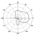
도 8은 안테나 장치(100)의 S11 파라미터의 주파수 특성을 나타내는 도면이다. 도 8에는, 안테나 장치(100)의 공진 주파수를 28GHz로 설정하여 행한 전자계 시뮬레이션으로 구한 S11 파라미터의 주파수 특성을 나타낸다. S11 파라미터가 28GHz 전후의 광범위에 걸쳐 -5dB 이하가 되는 양호한 특성이 얻어졌다.8 is a diagram illustrating a frequency characteristic of an S11 parameter of the
도 9는 안테나 장치(100)의 공진 주파수를 28GHz로 설정하여 행한 전자계 시뮬레이션으로 구한 지향성을 나타낸다. 도 9에 나타내는 지향성은, 안테나 장치(100)의 메인 로브 지향성이다. 또한, 0도의 방향은 +Z 방향에 상당하고, 90도의 방향은 +X 방향에 상당한다. 도 9에 도시하는 바와 같이, +Z 방향(0도의 방향)의 지향성이 얻어지고 있는 것을 알 수 있다.9 shows the directivity obtained by electromagnetic field simulation performed by setting the resonance frequency of the
도 10은 전자 기기(200)의 예시적인 단면에 안테나 장치(100)의 지향성을 기술한 도면이다. 도 9에 나타내는 지향성은, 도 10에서는 (1)로 나타내는 방향으로 전파를 방사 가능하고, (1)로 나타내는 방향의 전파를 수신 가능한 것을 나타낸다. (1)로 나타내는 방향은, 전자 기기(200)의 투명 커버(220)의 표면(전자 기기(200)의 표면)으로부터, 투명 커버(220)의 표면을 따라 방사되는 방향이다. 이러한 방향(1)을 향하는 지향성을 가지므로, 안테나 장치(100)는 전자 기기(200)의 외부의 통신기와 통신하기 쉽다.FIG. 10 is a diagram illustrating the directivity of the
이상과 같이, 안테나 장치(100)는 투명한 기판(101)에 투명한 안테나 엘리먼트(110)를 마련한 구성을 갖는다. 투명한 안테나 엘리먼트(110)는 투명 커버(220)의 외측으로부터 보이는 위치에 마련되어 있고, 디스플레이 패널(231)(도 3 참조)에 겹쳐서 마련되어 있다.As described above, the
따라서, 전자 기기(200)의 투명 커버(220)의 외측으로부터 보이는 위치에 배치 가능한 투명한 안테나 엘리먼트(110)와, 마이크로스트립 라인(120) 중의 부분(100A)에 포함되는 투명한 부분과, 투명한 기판(101)을 포함하는 안테나 장치(100)를 제공할 수 있다.Accordingly, the
또한, 다이폴형의 안테나 엘리먼트(110) 마이크로스트립 라인(120)은, 매우 얇게 형성할 수 있다. 예를 들어, 안테나 장치(100)에 허용되는 두께가 100㎛ 이하와 같이 제약이 큰 경우에는, 패치 안테나와 같이 접지층에 어느 정도의 두께가 필요한 안테나 장치를 사용하는 것은 곤란하다. 그 점에 있어서, 매우 얇게 형성 가능한 다이폴형의 안테나 엘리먼트(110)와 마이크로스트립 라인(120)을 포함하는 안테나 장치(100)는 박형화의 관점에서 매우 유리하다.In addition, the
또한, 이상에서는, 전자 기기(200)의 투명 커버(220)가 평판상인 형태에 대하여 설명했지만, 투명 커버(220)는 만곡되어 있어도 된다.In addition, in the above, although the
또한, 이상에서는, 안테나 엘리먼트(110)가 다이폴형의 안테나인 형태에 대하여 설명했지만, 모노폴 안테나, 테이퍼 슬롯 안테나, 슬롯 안테나, 또는 로그페리 안테나여도 된다.In addition, although the form in which the
또한, 안테나 장치(100)는 안테나 엘리먼트(110)를 통해 급전되는 하나 또는 복수의 무급전 소자를 더 포함해도 된다. 이 경우에, 안테나 엘리먼트(110)와 하나 또는 복수의 무급전 소자의 위치 관계를 조정함으로써, 전자 기기(200)의 외측을 향하는 지향성을 실현하도록 해도 된다.In addition, the
도 11은 실시 형태의 변형예의 전자 기기(200A)를 도시하는 단면도이다. 도 11에는, 도 1에 대응하는 단면을 도시한다. 전자 기기(200A)는, 도 1에 도시하는 전자 기기(200)의 평판상의 투명 커버(220) 및 표시 조작부(230) 대신에, 평면으로 보았을 때의 단부가 만곡된 투명 커버(220A) 및 표시 조작부(230A)를 포함한다. 부분(100A)과 부분(100B)의 위치를 알기 쉽게 하기 위해, 부분(100A)을 흰 바탕으로 나타내고, 부분(100B)을 그레이로 나타낸다.11 is a cross-sectional view showing an
투명 커버(220)는, XZ 단면으로 보았을 때는, Z 방향의 양단이 -X 방향으로 만곡되어 있다. 이는 YZ 단면에 있어서도 마찬가지이다. 표시 조작부(230A)는 일례로서 디스플레이 패널로서 OLED를 포함하고 있고, 투명 커버(220A)와 마찬가지로 만곡된 형상을 갖는다.Both ends of the
도 11에서는, 안테나 장치(100)의 부분(100A)은 투명 커버(220A)의 평탄한 상면의 부분과 만곡된 부분에 걸쳐 마련되어 있다.In Fig. 11, the
도 11에서는, 설명의 편의상, 안테나 장치(100)의 부분(100A)을 투명 커버(220A)와 표시 조작부(230A) 사이에 도시하지만, 안테나 장치(100)의 부분(100A)은 표시 조작부(230A)와 투명 커버(220A) 사이에 한정되지 않고, 도 3에 도시하는 층(232) 및 층(233) 사이, 층(233)과 접착층(234) 사이, 또는 층(232)과 디스플레이 패널(231) 사이에 배치해도 된다.In FIG. 11 , for convenience of explanation, a
또한, 전자 기기(200 또는 200A)는, 도 4 및 도 5에 도시하는 안테나 장치(100) 대신에, 도 12 및 도 13에 도시하는 안테나 장치(100M1)를 포함해도 된다. 도 12 및 도 13은 안테나 장치(100M1)를 도시하는 도면이다.Further, the
도 12 및 도 13은 안테나 장치(100M1)를 도시하는 도면이다. 도 12 및 도 13에는, 절곡하기 전의 상태의 안테나 장치(100M1)를 YZ 평면에 평행하게 도시한다. 안테나 장치(100M1)는 부분(100M1A) 및 부분(100M1B)을 포함한다. 부분(100M1A) 및 부분(100M1B)은 도 1, 도 2, 도 4, 및 도 5에 도시하는 부분(100A) 및 부분(100B)과 마찬가지이고, 부분(100M1A)은 전자 기기(200 또는 200A)의 투명 커버(220 또는 220A)를 통해 전자 기기(200 또는 200A)의 외부로부터 보이는 부분이고, 부분(100M1B)은 표시 조작부(230 또는 230A)의 이측에 배치되어, 전자 기기(200 또는 200A)의 외부로부터 보이지 않는 부분이다.12 and 13 are diagrams showing the antenna device 100M1. 12 and 13 show the antenna device 100M1 in a state before bending parallel to the YZ plane. The antenna device 100M1 includes a portion 100M1A and a portion 100M1B. The part 100M1A and the part 100M1B are the same as the
도 12 및 도 13에서는, 일례로서, 부분(100M1A)과 부분(100M1B)의 경계가 Z 방향에 있어서의 마이크로스트립 라인(120M1)의 +Z 방향 측의 단부로부터 1/2인 구성을 나타낸다.12 and 13 show, as an example, a configuration in which the boundary between the portion 100M1A and the portion 100M1B is 1/2 from the end of the microstrip line 120M1 in the Z direction on the +Z direction side.
안테나 장치(100M1)는 기판(101), 안테나 엘리먼트(110M1), 및 마이크로스트립 라인(120M1)을 포함한다. 도 13의 (A)에는, 기판(101)과, 기판(101)의 +X 방향 측의 표면에 배치되는 구성 요소를 도시하고, 도 13의 (B)에는, 기판(101)의 +X 방향 측의 표면에 배치되는 구성 요소를 도시한다. 또한, 도 13의 (B)에는, 기판(101)의 위치를 파선으로 나타낸다.The antenna device 100M1 includes a
안테나 엘리먼트(110M1)는, Vivaldi형의 안테나이고, 엘리먼트(111M1) 및 엘리먼트(112M1)를 갖는다. 안테나 엘리먼트(110M1)는, 투명 도체(300A)(도 6 참조)에 의해 실현된다.The antenna element 110M1 is a Vivaldi type antenna, and has an element 111M1 and an element 112M1. The antenna element 110M1 is realized by the
엘리먼트(111M1)는, 기판(101)의 +X 방향 측의 표면에 마련되고, 급전점(111M1A) 및 개방단(111M1C)을 갖는다. 엘리먼트(111M1)는, 급전점(111M1A)으로부터 개방단(111M1C)까지 연장되어 있다.The element 111M1 is provided on the surface of the
엘리먼트(112M1)는, 기판(101)의 -X 방향 측의 표면에 마련되고, 급전점(112M1A) 및 개방단(112M1C)을 갖는다. 급전점(112M1A)은 엘리먼트(111M1)의 급전점(111M1A)과 평면으로 보았을 때 겹쳐서 배치되어 있다. 엘리먼트(112M1)를 -X 방향으로 본 형상, 사이즈, 및 기판(101)에 대한 위치는, 엘리먼트(111M1)를 +X 방향으로 본 형상, 사이즈, 및 기판(101)에 대한 위치와 동등하다.The element 112M1 is provided on the surface of the
마이크로스트립 라인(120M1)은, 전송로(121M1A, 121M1B)와 접지층(122M1A, 122M1B)을 갖는다. 전송로(121M1A) 및 전송로(121M1B)는 기판(101)의 +X 방향 측의 표면에 마련된다. 전송로(121M1A)는 접지층(122M1A)과 겹쳐서 마련된다. 전송로(121M1B)는 전송로(121M1A)의 +Z 방향 측에 접속되고, 접지층(122M1B)과 겹쳐서 마련되고, 엘리먼트(111M1)의 급전점(111M1A)에 접속되어 있다.The microstrip line 120M1 has transmission paths 121M1A and 121M1B and ground layers 122M1A and 122M1B. The transmission path 121M1A and the transmission path 121M1B are provided on the surface of the
접지층(122M1A)은 기판(101)의 -X 방향 측의 표면에 있어서 평면으로 보았을 때 전송로(121M1A)와 겹쳐서 마련되어 있는 직사각형 형상의 접지 패턴이다. 접지층(122M1B)은 접지층(122M1A)의 +Z 방향 측에 연속적으로 형성되어 있고, +Z 방향 측으로 감에 따라 Y 방향의 폭이 점차 좁아지고 있다. 접지층(122M1B)의 +Z 방향 측의 단부는, 기판(101)의 Y 방향의 중앙에 위치하고, 접지층(122M1B)의 +Z 방향 측의 단부의 Y 방향의 폭은, 엘리먼트(112M1)의 급전점(112M1A)의 Y 방향의 폭과 동등하다. 접지층(122M1B)의 +Z 방향 측의 단부는, 엘리먼트(112M1)의 급전점(112M1A)에 접속되어 있다.The ground layer 122M1A is a rectangular ground pattern provided to overlap the transmission path 121M1A in a plan view on the surface of the
이러한 구성을 갖는 안테나 장치(100M1) 중, Z 방향에 있어서 안테나 엘리먼트(110M1)와, 마이크로스트립 라인(120M1)의 +Z 방향 측의 일부분이 마련되는 부분은, 도 1 및 도 2에 도시하는 부분(100A)이다. 또한, 안테나 장치(100M1) 중, 마이크로스트립 라인(120M1) 중 나머지 부분이 마련되는 구간은, 도 1 및 도 2에 도시하는 부분(100B)이다. 부분(100A)은, 도 3에 도시하는 디스플레이 패널(231) 상에 위치하므로, 표시를 방해하지 않도록 하기 위해 투명하면 된다.Of the antenna device 100M1 having such a configuration, the portion in which the antenna element 110M1 in the Z direction and a part of the microstrip line 120M1 on the +Z direction side are provided is shown in FIGS. 1 and 2 . (100A). In addition, the section in which the remaining part of the microstrip line 120M1 of the antenna device 100M1 is provided is the
도 14는 안테나 장치(100M1)의 S11 파라미터의 주파수 특성을 나타내는 도면이다. 도 14에는, 안테나 장치(100M1)의 공진 주파수를 28GHz로 설정하여 행한 전자계 시뮬레이션으로 구한 S11 파라미터의 주파수 특성을 나타낸다. S11 파라미터가 28GHz 전후에서 -5dB 이하가 되는 양호한 대역이 얻어졌다. 또한, 약 41GHz 전후에 있어서의 -5dB 이하의 대역은, 의도치 않게 발생한 것이다.14 is a diagram illustrating the frequency characteristic of the S11 parameter of the antenna device 100M1. Fig. 14 shows the frequency characteristics of the S11 parameters obtained by electromagnetic field simulation performed by setting the resonance frequency of the antenna device 100M1 to 28 GHz. A good band in which the S11 parameter becomes -5 dB or less around 28 GHz was obtained. In addition, the band of -5 dB or less in about 41 GHz is unintentionally generated.
도 15는 안테나 장치(100M1)의 공진 주파수를 28GHz로 설정하여 행한 전자계 시뮬레이션으로 구한 지향성을 나타내는 도면이다. 도 15에 나타내는 지향성은, 안테나 장치(100M1)의 메인 로브 지향성이다. 또한, 0도의 방향은 +Z 방향에 상당하고, 90도의 방향은 +X 방향에 상당한다. 도 15에 도시하는 바와 같이, +Z 방향(0도의 방향)의 지향성이 얻어지고 있는 것을 알 수 있다.15 is a diagram showing the directivity obtained by electromagnetic field simulation performed by setting the resonance frequency of the antenna device 100M1 to 28 GHz. The directivity shown in FIG. 15 is the main lobe directivity of the antenna device 100M1. In addition, the direction of 0 degrees corresponds to the +Z direction, and the direction of 90 degrees corresponds to the +X direction. As shown in FIG. 15, it turns out that the directivity of the +Z direction (direction of 0 degree|times) is obtained.
전자 기기(200)에 안테나 장치(100M1)를 설치했을 경우의 지향성은, 도 10에 도시하는 바와 같이 전자 기기(200)에 안테나 장치(100)를 설치했을 경우의 지향성과 대략 마찬가지로 될 것으로 생각된다.It is thought that the directivity when the antenna device 100M1 is installed in the
안테나 장치(100M1)는, 안테나 장치(100)와 마찬가지로, 투명한 기판(101)에 투명한 안테나 엘리먼트(110M1)를 마련한 구성을 갖는다. 투명한 안테나 엘리먼트(110M1)는, 투명 커버(220)의 외측으로부터 보이는 위치에 마련되어 있고, 디스플레이 패널(231)(도 3 참조)에 겹쳐서 마련되어 있다.The antenna device 100M1 has a configuration in which a transparent antenna element 110M1 is provided on a
따라서, 전자 기기(200)의 투명 커버(220)의 외측으로부터 보이는 위치에 배치 가능한 투명한 안테나 엘리먼트(110M1)와, 마이크로스트립 라인(120M1) 중 +Z 방향 측의 투명한 부분과, 투명한 기판(101)을 포함하는 안테나 장치(100M1)를 제공할 수 있다.Accordingly, the transparent antenna element 110M1 that can be disposed at a position visible from the outside of the
또한, Vivaldi형의 안테나 엘리먼트(110M1)와 마이크로스트립 라인(120M1)은, 매우 얇게 형성할 수 있다. 예를 들어, 안테나 장치(100M1)에 허용되는 두께가 100㎛ 이하와 같이 제약이 큰 경우에는, 패치 안테나와 같이 접지층에 어느 정도의 두께가 필요한 안테나 장치를 사용하는 것은 곤란하다. 그 점에 있어서, 매우 얇게 형성 가능한 Vivaldi형의 안테나 엘리먼트(110M1)와 마이크로스트립 라인(120M1)을 포함하는 안테나 장치(100M1)는 박형화의 관점에서 매우 유리하다.In addition, the Vivaldi type antenna element 110M1 and the microstrip line 120M1 can be formed very thinly. For example, when the allowable thickness of the antenna device 100M1 is large, such as 100 μm or less, it is difficult to use an antenna device that requires a certain thickness for the ground layer, such as a patch antenna. In this regard, the antenna device 100M1 including the Vivaldi-type antenna element 110M1 and the microstrip line 120M1 that can be formed very thinly is very advantageous in terms of thickness reduction.
도 16 및 도 17은, 안테나 장치(100M2)를 도시하는 도면이다. 도 16 및 도 17에는, 절곡하기 전의 상태의 안테나 장치(100M2)를 YZ 평면에 평행하게 도시한다. 안테나 장치(100M2)는 부분(100M2A) 및 부분(100M2B)를 포함한다. 부분(100M2A) 및 부분(100M2B)는 도 1, 도 2, 도 4, 및 도 5에 도시하는 부분(100A) 및 부분(100B)과 마찬가지이고, 부분(100M2A)은 전자 기기(200 또는 200A)의 투명 커버(220 또는 220A)를 통해 전자 기기(200 또는 200A)의 외부로부터 보이는 부분이고, 부분(100M2B)은 표시 조작부(230 또는 230A)의 이측에 배치되어, 전자 기기(200 또는 200A)의 외부로부터 보이지 않는 부분이다.16 and 17 are diagrams showing the antenna device 100M2. 16 and 17 show the antenna device 100M2 in a state before bending parallel to the YZ plane. The antenna device 100M2 includes a portion 100M2A and a portion 100M2B. The part 100M2A and the part 100M2B are the same as the
도 16 및 도 17에서는, 일례로서, 부분(100M2A)과 부분(100M2B)의 경계가 Z 방향에 있어서의 마이크로스트립 라인(120)의 +Z 방향 측의 단부로부터 1/2인 구성을 나타낸다.16 and 17 show, as an example, a configuration in which the boundary between the portion 100M2A and the portion 100M2B is 1/2 from the end of the
안테나 장치(100M2)는 기판(101), 안테나 엘리먼트(110), 도파기(115), 및 마이크로스트립 라인(120)을 포함한다. 안테나 장치(100M2)는 도 4 및 도 5에 도시하는 안테나 장치(100)에 도파기(115)를 추가한 야기우다 안테나이다The antenna device 100M2 includes a
도파기(115)는, 안테나 엘리먼트(110)와 마찬가지로, 투명 도체(300A)(도 6 참조)에 의해 실현된다. 또한, 전송로(121) 및 접지층(122)을 갖는 마이크로스트립 라인(120)의 Z 방향의 길이는, 도 4 및 도 5에 도시하는 안테나 장치(100)의 마이크로스트립 라인(120)의 Z 방향의 길이보다도 짧지만, 구성은 마찬가지이다.The
도 17의 (A)에는, 기판(101)과, 기판(101)의 +X 방향 측의 표면에 배치되는 구성 요소를 도시하고, 도 17의 (B)에는, 기판(101)의 +X 방향 측의 표면에 배치되는 구성 요소를 도시한다. 또한, 도 17의 (B)에는, 기판(101)의 위치를 파선으로 나타낸다.FIG. 17A shows the
도파기(115)는 2개의 도파기(115A, 115B)를 갖는다. 이하에서는, 2개의 도파기(115A, 115B)를 구별하지 않는 경우에는, 단순히 도파기(115)라고 칭한다. 도 16 및 도 17에는, 도파기(115)가 2개의 도파기(115A, 115B)를 갖는 구성을 도시하지만, 도파기(115)의 수는, 1개여도 되고, 3개 이상이어도 된다.The
도파기(115A, 115B)의 Y 방향의 길이는, 안테나 엘리먼트(110)의 개방단(111C)과 개방단(112C) 사이의 길이보다도 조금 짧다. 도파기(115A)와 도파기(115B)의 Z 방향의 간격 G는, 안테나 엘리먼트(110)의 개방단(111C) 및 개방단(112C) 사이의 구간과, 도파기(115A)의 Z 방향의 간격 G와 동등하다.The length of the
이러한 구성을 갖는 안테나 장치(100M2) 중, Z 방향에 있어서 안테나 엘리먼트(110)와 도파기(115)와, 마이크로스트립 라인(120) 중 +Z 방향 측의 일부분이 마련되는 부분은, 도 1 및 도 2에 도시하는 부분(100A)이다. 또한, 안테나 장치(100M2) 중, 마이크로스트립 라인(120)의 나머지 부분이 마련되는 부분은, 도 1 및 도 2에 도시하는 부분(100B)이다. 부분(100A)은, 도 3에 도시하는 디스플레이 패널(231) 상에 위치하므로, 표시를 방해하지 않도록 하기 위해 투명하면 된다.Of the antenna device 100M2 having such a configuration, a portion in which the
도 18은 도파기(115)의 수와, 간격 G와, 지향성 및 게인의 관계를 나타내는 도면이다. 도 18의 (A)에는, 간격 G에 대한 지향성의 특성을 나타낸다. 도 18의 (B)에는, 간격 G에 대한 게인의 특성을 나타낸다. 도파기(115)의 수는, 0개, 1개, 3개, 5개이다. 도파기(115)가 0개인 경우는, 안테나 엘리먼트(110)는 다이폴 안테나(Dipole)이고, 도파기(115)가 1개, 3개, 5개인 경우는, 안테나 엘리먼트(110)는 야기우다 안테나이다. 또한, 지향성은 메인 로브의 각도(deg.)를 나타내고, 게인은 메인 로브의 게인(dBi)을 나타낸다.18 is a diagram showing the relationship between the number of
도 18의 (A)에 도시하는 바와 같이, 간격 G가 1mm와 2mm인 경우에는, 도파기(115)가 1개, 3개, 5개의 어느 경우에도 90도 전후의 지향성이 얻어졌다. 이는, 도 16 및 도 17에 있어서 +X 방향의 지향성이 얻어지고 있는 것을 의미한다.As shown in FIG. 18A , when the spacing G is 1 mm and 2 mm, directivity of around 90 degrees is obtained in any case of one, three, or five
또한, 도파기(115)가 1개인 경우는, 간격 G를 3mm 이상으로 하면, 약 10도 전후의 지향성이 얻어졌다. 도파기(115)가 3개인 경우는, 간격 G를 3mm와 4mm로 하면, 약 10도 전후의 지향성이 얻어지고, 5mm 이상이면, 약 90도 또는 그 이상의 지향성이 얻어졌다. 도파기(115)가 5개인 경우는, 간격 G를 3으로 하면, 약 10도 전후의 지향성이 얻어지고, 4mm 이상이면, 약 75도 또는 그 이상의 지향성이 얻어졌다.In the case where there is only one
다이폴 안테나의 지향성은 약 35도라는 점에서, 도파기(115)의 수와 개수를 선택함으로써, 지향성을 조절할 수 있다는 것을 알 수 있었다.Since the directivity of the dipole antenna is about 35 degrees, it can be seen that the directivity can be adjusted by selecting the number and number of
또한, 도 18의 (B)에 도시하는 바와 같이, 도파기(115)가 1개인 경우는, 간격 G를 1mm에서 4mm까지 넓히면, 게인이 약 2dBi에서 약 5dBi까지 증대되고, 간격 G가 5mm 이상이면, 게인은 약 3.5dBi로 저하되는 특성이 얻어졌다.Further, as shown in FIG. 18B, when there is one
도파기(115)가 3개와 5개인 경우는, 간격 G가 1mm와 2mm인 경우에는, 약 4.5dBi의 게인이 얻어지고, 간격 G를 3mm 이상에서 5mm까지 넓히면, 게인이 약 2dBi까지 점차 저하되고, 간격 G가 6mm가 되면, 다시 게인은 조금 증대되는 특성이 얻어졌다.In the case of three and five
도파기(115)의 개수가 어느 것인 경우에도, 간격 G를 선택함으로써, 다이폴 안테나의 게인(약 3.7dBi) 이상의 게인이 얻어지는 것을 확인할 수 있었다.Even when the number of
도 19는 도파기(115)가 1개이고 간격 G를 4mm로 설정한 안테나 장치(100M2)의 S11 파라미터의 주파수 특성을 나타내는 도면이다. 도파기(115)가 1개이고 간격 G를 4mm로 설정한 안테나 장치(100M2)는 도파기(115)가 1개인 경우에 최대의 게인이 얻어진 구성이다(도 18의 (B) 참조).19 is a diagram showing the frequency characteristics of the S11 parameter of the antenna device 100M2 with one
도 19에는, 안테나 장치(100M2)의 공진 주파수를 28GHz로 설정하여 행한 전자계 시뮬레이션으로 구한 S11 파라미터의 주파수 특성을 나타낸다. S11 파라미터가 28GHz 전후에서 -5dB 이하가 되는 양호한 대역이 얻어졌다.19 shows the frequency characteristics of the S11 parameters obtained by electromagnetic field simulation performed by setting the resonance frequency of the antenna device 100M2 to 28 GHz. A good band in which the S11 parameter becomes -5 dB or less around 28 GHz was obtained.
도 20은 도파기(115)가 1개이고 간격 G를 4mm로 설정한 안테나 장치(100M2)의 공진 주파수를 28GHz로 설정하여 행한 전자계 시뮬레이션으로 구한 지향성을 나타내는 도면이다. 도 20에 나타내는 지향성은, 안테나 장치(100M2)의 메인 로브 지향성이다. 또한, 0도의 방향은 +Z 방향에 상당하고, 90도의 방향은 +X 방향에 상당한다. 도 20에 도시하는 바와 같이, +Z 방향(0도의 방향)의 지향성이 얻어지고 있는 것을 알 수 있다.FIG. 20 is a diagram showing the directivity obtained by electromagnetic field simulation performed by setting the resonance frequency of the antenna device 100M2 having one
전자 기기(200)에 도파기(115)가 1개이고 간격 G를 4mm로 설정한 안테나 장치(100M2)를 설치했을 경우의 지향성은, 도 10에 도시하는 바와 같이 전자 기기(200)에 안테나 장치(100)를 설치했을 경우의 지향성과 대략 마찬가지로 될 것으로 생각된다.When the
도 21은 도파기(115)가 5개이고 간격 G를 1mm로 설정한 안테나 장치(100M2)의 S11 파라미터의 주파수 특성을 나타내는 도면이다. 도파기(115)가 5개이고 간격 G를 1mm로 설정한 안테나 장치(100M2)는 도파기(115)가 5개인 경우에 최대의 게인이 얻어진 구성이다(도 18의 (B) 참조).21 is a diagram showing the frequency characteristics of the S11 parameter of the antenna device 100M2 having five
도 21에는, 안테나 장치(100M2)의 공진 주파수를 28GHz로 설정하여 행한 전자계 시뮬레이션으로 구한 S11 파라미터의 주파수 특성을 나타낸다. S11 파라미터가 28GHz 전후에서 -5dB 이하가 되는 양호한 대역이 얻어졌다.Fig. 21 shows the frequency characteristic of the S11 parameter obtained by electromagnetic field simulation performed by setting the resonance frequency of the antenna device 100M2 to 28 GHz. A good band in which the S11 parameter becomes -5 dB or less around 28 GHz was obtained.
도 22는 도파기(115)가 5개이고 간격 G를 1mm로 설정한 안테나 장치(100M2)의 공진 주파수를 28GHz로 설정하여 행한 전자계 시뮬레이션으로 구한 지향성을 나타내는 도면이다. 도 22에 나타내는 지향성은, 안테나 장치(100M2)의 메인 로브 지향성이다. 도 22에 도시하는 바와 같이, +X 방향(90도의 방향)의 지향성이 얻어지고 있는 것을 알 수 있다.FIG. 22 is a diagram showing the directivity obtained by electromagnetic field simulation performed with the resonance frequency of the antenna device 100M2 having 5
전자 기기(200)에 도파기(115)가 5개이고 간격 G를 1mm로 설정한 안테나 장치(100M2)를 설치했을 경우의 지향성은, 전자 기기(200)의 투명 커버(220)로부터 연직 상방을 향하는 지향성이 된다.When the antenna device 100M2 having 5
도 23은 전자 기기(200A)의 예시적인 단면에 안테나 장치(100M2)의 지향성을 기술한 도면이다. 부분(100M2A)과 부분(100M2B)의 위치를 알기 쉽게 하기 위해, 부분(100M2A)을 흰 바탕으로 나타내고, 부분(100M2B)을 그레이로 나타낸다.23 is a diagram illustrating the directivity of the antenna device 100M2 in an exemplary cross-section of the
도 23에서는, 투명 커버(220A)의 상면부(220A1)와 -Z 방향 측의 만곡부(220A2)에 걸쳐, 안테나 장치(100M2)의 부분(100M2A)이 마련되어 있다. 부분(100M2A)은 도 16 및 도 17에 도시하는 안테나 엘리먼트(110)와, 도파기(115)와, 마이크로스트립 라인(120) 중 +Z 방향 측의 일부분이 마련되어 있는 부분이고, 투명한 부분이다. 또한, 안테나 장치(100M2)의 부분(100M2B)은 표시 조작부(230A)의 이측에 마련되어 있다. 부분(100M2B)은 도 16 및 도 17에 도시하는 마이크로스트립 라인(120) 중의 부분(100A)에 포함되지 않는 나머지 부분이 마련되어 있는 부분이고, 투명하지 않은 부분이다.In FIG. 23 , a portion 100M2A of the antenna device 100M2 is provided over the upper surface portion 220A1 of the
도 23에서는, 설명의 편의상, 안테나 장치(100M2)의 부분(100M2A)을 투명 커버(220A)와 표시 조작부(230A) 사이에 도시하지만, 안테나 장치(100M2)의 부분(100M2A)은 표시 조작부(230A)와 투명 커버(220A) 사이에 한정되지 않고, 도 3에 도시하는 층(232) 및 층(233) 사이, 층(233)과 접착층(234) 사이, 또는 층(232)과 디스플레이 패널(231) 사이에 배치해도 된다.In Fig. 23, for convenience of explanation, a portion 100M2A of the antenna device 100M2 is shown between the
이와 같이 안테나 장치(100M2)를 포함하는 전자 기기(200A)에 있어서, 도 22에 나타내는 지향성은, 도 23에서는 (2)로 나타내는 방향이 된다. 즉, 안테나 장치(100M2)는 (2)로 나타내는 방향으로 전파를 방사 가능하고, (2)로 나타내는 방향의 전파를 수신 가능하다. (2)로 나타내는 방향은, 전자 기기(200A)의 투명 커버(220A)의 상면부(220A1)의 법선 방향을 따라서 방사되는 방향이다. 투명 커버(220A)의 상면부(220A1)는, 투명 커버(220A)의 표면의 일부이고, 전자 기기(200A)의 표면의 일부이다. 이러한 방향(2)을 향하는 지향성을 가지므로, 안테나 장치(100)는 전자 기기(200)의 외부의 통신기와 통신하기 쉽다.As described above, in the
안테나 장치(100M2)는 안테나 장치(100)에, 도파기(115)를 추가한 구성을 갖는다. 투명한 안테나 엘리먼트(110)와, 도파기(115)와, 마이크로스트립 라인(120) 중의 부분(100M2A)에 포함되는 부분은, 투명 커버(220)의 외측으로부터 보이는 위치에 마련되어 있고, 디스플레이 패널(231)(도 3 참조)에 겹쳐서 마련되어 있다.The antenna device 100M2 has a configuration in which a
따라서, 전자 기기(200)의 투명 커버(220)의 외측으로부터 보이는 위치에 배치 가능한 투명한 안테나 엘리먼트(110)와, 투명한 도파기(115)와, 마이크로스트립 라인(120) 중의 부분(100M2A)에 포함되는 투명한 부분과, 투명한 기판(101)을 포함하는 안테나 장치(100M2)를 제공할 수 있다.Accordingly, the
또한, 안테나 엘리먼트(110)와, 도파기(115)와, 마이크로스트립 라인(120)은, 매우 얇게 형성할 수 있다. 예를 들어, 안테나 장치(100M2)에 허용되는 두께가 100㎛ 이하와 같이 제약이 큰 경우에는, 패치 안테나와 같이 접지층에 어느 정도의 두께가 필요한 안테나 장치를 사용하는 것은 곤란하다. 그 점에 있어서, 매우 얇게 형성 가능한 안테나 엘리먼트(110)와, 도파기(115)와, 마이크로스트립 라인(120)을 포함하는 안테나 장치(100M2)는 박형화의 관점에서 매우 유리하다.In addition, the
도 24는 실시 형태의 변형예의 전자 기기(200B)를 도시하는 단면도이다. 도 24에는, 도 11에 대응하는 단면을 도시한다. 전자 기기(200B)는 안테나 장치(100)와 안테나 장치(100M2)를 포함한다. 안테나 장치(100) 및 안테나 장치(100M2)는, 도 4, 도 5, 도 16, 및 도 17에 도시하는 기판(101) 대신에, 공통의 기판(101B)을 포함한다. 안테나 장치(100) 및 안테나 장치(100M2)는 서로 공진 주파수가 다른 구성을 갖고 있어도 된다.24 is a cross-sectional view showing an
기판(101B)은 평면으로 보았을 때 표시 조작부(230A)보다도 크고, 투명 커버(220A)와 표시 조작부(230A) 사이의 전체에 걸쳐 마련되어 있다. 기판(101B)의 단부(101B1, 101B2)는 절곡되어 표시 조작부(230A)의 이측에 위치하고 있고, 배선 기판(240)에 접속되어 있다. 안테나 장치(100)는 -Z 방향 측의 상면부(220A1)와 만곡부(220A2)에 마련되어 있다. 안테나 장치(100M2)는 +Z 방향 측의 상면부(220A1)와 만곡부(220A3)에 마련되어 있다. 이 때문에, Z 방향에 있어서 안테나 장치(100) 및 안테나 장치(100M2)가 마련되어 있지 않은 부분에서는, 투명 커버(220A)와 표시 조작부(230A) 사이에 기판(101B)만이 마련되어 있다.The board|
기판(101B)을 평면으로 보았을 때 표시 조작부(230A)보다도 크게 하여, 기판(101B)의 단부(101B1, 101B2)를 표시 조작부(230A)의 이측에 위치시킨 것은, 기판(101B)의 단부(101B1, 101B2)가 눈에 띄는 경우를 고려하여, 단부(101B1, 101B2)가 투명 커버(220A)의 외측으로부터 보이지 않도록 하기 위함이다.The
이 때문에, 단부(101B1, 101B2)는 디스플레이 패널(231)(도 3 참조)을 포함하는 표시 조작부(230A)의 이측에 위치하고 있으면 되고, 도 24에 도시하는 바와 같이 배선 기판(240)에 접속되어 있지 않아도 된다.For this reason, the ends 101B1 and 101B2 should just be located on the back side of the
또한, 기판(101B)의 단부는, XY 단면에 있어서도, 절곡되어 표시 조작부(230A)의 이측에 위치하고 있다. 기판(101B)의 단부가 투명 커버(220A)의 외측으로부터 보이지 않도록 하기 위함이다.In addition, the edge part of the board|
도 24에서는, 안테나 장치(100)의 부분(100A)은 투명 커버(220A)의 평탄한 상면부(220A1)와 만곡부(220A2)에 걸쳐 마련되어 있다. 부분(100A)의 범위는, 도 11과 마찬가지이다. 또한, 부분(100B)의 범위도 도 11과 마찬가지이다. 도 24에서는, 설명의 편의상, 안테나 장치(100)의 부분(100A)을 투명 커버(220A)와 표시 조작부(230A) 사이에 도시하지만, 안테나 장치(100)의 부분(100A)은 표시 조작부(230A)와 투명 커버(220A) 사이에 한정되지 않고, 도 3에 도시하는 층(232) 및 층(233) 사이, 층(233)과 접착층(234) 사이, 또는 층(232)과 디스플레이 패널(231) 사이에 배치해도 된다.In Fig. 24, the
또한, 도 24에서는, 투명 커버(220A)의 +Z 방향 측의 만곡부(220A3)와 상면부(220A1)에 걸쳐, 안테나 장치(100M2)의 부분(100M2A)이 마련되어 있다. 도 24에서는, 설명의 편의상, 안테나 장치(100M2)의 부분(100M2A)을 투명 커버(220A)와 표시 조작부(230A) 사이에 도시하지만, 안테나 장치(100M2)의 부분(100M2A)은 표시 조작부(230A)와 투명 커버(220A) 사이에 한정되지 않고, 도 3에 도시하는 층(232) 및 층(233) 사이, 층(233)과 접착층(234) 사이, 또는 층(232)과 디스플레이 패널(231) 사이에 배치해도 된다.In addition, in FIG. 24 , a portion 100M2A of the antenna device 100M2 is provided over the curved portion 220A3 on the +Z direction side of the
안테나 장치(100) 및 안테나 장치(100M2)는 표시 조작부(230A)보다도 큰 기판(101B)을 갖고, 기판(101B)의 단부(101B1, 101B2)를 표시 조작부(230A)의 이측에 위치시키고 있다.The
이 때문에, 기판(101B)의 단부(101B1, 101B2)가 투명 커버(220A)의 외측으로부터 보이지 않는 의장제가 높은 안테나 장치(100) 및 안테나 장치(100M2)를 제공할 수 있다.For this reason, it is possible to provide the
또한, 여기서는, 전자 기기(200B)가 안테나 장치(100) 및 안테나 장치(100M2)를 포함하는 형태에 대하여 설명했지만, 안테나 장치(100) 및 안테나 장치(100M2) 중 어느 1개를 포함하는 구성이어도 된다. 또한, 전자 기기(200B)는 안테나 장치(100) 및 안테나 장치(100M2) 이외의 안테나 장치를 포함하고 있어도 되고, 3개 이상의 안테나 장치를 포함하고 있어도 된다.In addition, although the form in which the
전자 기기(200B)가 공진 주파수가 상이한 복수의 안테나 장치를 포함하는 경우에는, 복수의 통신 대역에서 통신 가능한 전자 기기(200B)를 제공할 수 있다.When the
도 25는 안테나 장치(100M2)를 도시하는 도면이다. 안테나 장치(100M2)는 기판(101), 안테나 엘리먼트(110), 도파기(115), 및 마이크로스트립 라인(120)을 포함한다. 안테나 엘리먼트(110)는 엘리먼트(111) 및 엘리먼트(112)를 갖고, 마이크로스트립 라인(120)은 전송로(121) 및 접지층(122)을 갖는다.25 is a diagram showing the antenna device 100M2. The antenna device 100M2 includes a
여기서는, Z 방향에 있어서의 급전점(111A)에 있어서, 안테나 장치(100M2)를 절곡한 모델에 대하여 검토를 행한다. 도 26은 안테나 장치(100M2)를 절곡하는 방법을 설명하는 도면이다. 도 26의 (A), (B)에는, 예시적인 부분(100M2A, 100M2B)을 도시한다.Here, a model in which the antenna device 100M2 is bent at the
도 26의 (A)에는, 절곡되어 있지 않는 상태의 안테나 장치(100M2)를 도시하고, 도 26의 (B)에는 절곡된 상태의 안테나 장치(100M2)를 도시한다. 이러한 안테나 장치(100M2)의 절곡은, 시뮬레이션의 모델을 사용하여 행하는 것이지만, 여기서는 설명을 알기 쉽게 하기 위해, 가상적인 지그(105)를 사용하여 안테나 장치(100M2)의 절곡에 대하여 설명한다.Fig. 26A shows the antenna device 100M2 in an unbent state, and Fig. 26B shows the antenna device 100M2 in a bent state. Although such bending of the antenna apparatus 100M2 is performed using a model of a simulation, in order to make the explanation easy to understand, the bending of the antenna apparatus 100M2 is demonstrated using the
또한, 안테나 장치(100M2)의 모델은, 도 26의 (A), (B)에 도시하는 바와 같이, 커버(102) 및 커버(103)를 포함한다. 커버(102) 및 커버(103)는, 각각, 접착층(102A) 및 접착층(103A)으로 안테나 장치(100M2)의 +X 방향 측과 -X 방향 측의 표면에 첩부되어 있다. 또한, 커버(102) 및 커버(103)의 사이즈는, 기판(101)의 사이즈와 동등하다.Further, the model of the antenna device 100M2 includes a
지그(105)는 XZ 단면에 있어서 반경 1mm으로 만곡되고, Y 방향으로 긴 단부(105A)를 갖는다. 도 26의 (A)에 도시하는 바와 같이, 단부(105A)를 안테나 장치(100M2)의 -X 방향 측의 표면에 밀어 붙인다. 단부(105A)의 Z 방향에 있어서의 위치가 Z=0mm인 때, 단부(105A)는 급전점(111A)의 위치에 있다. 즉, 단부(105A)의 Z 방향에 있어서의 위치가 Z=0mm인 때, 단부(105A)의 Z 방향에 있어서의 위치는, 안테나 엘리먼트(110)와 마이크로스트립 라인(120)의 경계 위치와 동등하다.The
도 26의 (B)에 도시하는 바와 같이, 안테나 장치(100M2)의 안테나 엘리먼트(110) 측을 마이크로스트립 라인(120) 측에 대하여 도 26의 (B)에 있어서의 시계 방향의 방향으로 90도 절곡된다. 이때, XYZ 좌표도 마찬가지로 90도 회전시킨다. 즉, 절곡된 후에도 +Z 방향은 안테나 엘리먼트(110)의 엔드파이어의 방향이 된다.As shown in FIG. 26B, the
이러한 안테나 장치(100M2)의 절곡을 지그(105)의 위치를 Z=0mm, Z=2mm, Z=4mm의 3종류의 위치로 설정하여 행한 바, 도 27의 (A) 내지 (C)에 도시하는 모델을 얻었다. 도 27은 안테나 장치(100M2)의 절곡 모델을 도시하는 도면이다.The bending of the antenna device 100M2 is performed by setting the position of the
도 27의 (A)에 도시하는 모델은, Z=0mm의 위치에서 절곡된 안테나 장치(100M2)의 모델이다. 도 27의 (B)에 도시하는 모델은, Z=2mm의 위치에서 절곡된 안테나 장치(100M2)의 모델이다. 도 27의 (C)에 도시하는 모델은, Z=4mm의 위치에서 절곡된 안테나 장치(100M2)의 모델이다.The model shown in FIG. 27A is a model of the antenna device 100M2 bent at the position of Z=0 mm. The model shown in FIG. 27B is a model of the antenna device 100M2 bent at the position of Z=2 mm. The model shown in FIG. 27C is a model of the antenna device 100M2 bent at the position of Z=4 mm.
지그(105)의 위치가 Z=0mm로부터, Z=2mm, Z=4mm가 되면, 지그(105)의 위치는, 안테나 엘리먼트(110)와 마이크로스트립 라인(120)의 경계보다도 +Z 방향 측으로 시프트된다. 이 때문에, Z=2mm, Z=4mm의 경우에는, 안테나 엘리먼트(110)의 도중에서 절곡되게 된다.When the position of the
도 28은 절곡 위치가 상이한 안테나 장치(100M2)의 지향성을 나타내는 도면이다. 도 28에는, 절곡 위치가 Z=0mm, Z=2mm, Z=4mm, Z=6mm인 4종류의 안테나 장치(100M2)의 모델로 얻은 지향성을 나타낸다.28 is a diagram showing the directivity of the antenna device 100M2 having different bending positions. Fig. 28 shows the directivity obtained by the model of four types of antenna devices 100M2 whose bending positions are Z = 0 mm, Z = 2 mm, Z = 4 mm, and Z = 6 mm.
Z=0mm에서는, 180도의 방향(-Z 방향)의 백파이어 방향의 지향성을 나타내는 것에 반하여, Z=2mm, 4mm, 6mm에서는, 90도의 방향(+X 방향)의 연직 상향의 지향성을 나타내는 것을 알 수 있다.It can be seen that Z = 0 mm shows directivity in the backfire direction in the 180 degree direction (-Z direction), whereas Z = 2 mm, 4 mm, and 6 mm shows the directivity vertically upward in the 90 degree direction (+X direction). can
이와 같이, 절곡 위치를 변화시킴으로써, 안테나 장치(100M2)의 지향성을 조절할 수 있다는 것을 알 수 있었다.As described above, it was found that the directivity of the antenna device 100M2 can be adjusted by changing the bending position.
도 29는 실시 형태의 변형예에 따른 안테나 장치(100M3)를 도시하는 도면이다. 안테나 장치(100M3)는 기판(101), 안테나 엘리먼트(110), 반사기(116), 및 마이크로스트립 라인(120)을 포함한다. 안테나 장치(100M3)는 도 16 및 도 17에 도시하는 안테나 장치(100M2)의 도파기(115) 대신에 반사기(116)를 포함하는 구성을 갖는다. 반사기(116)는, 안테나 엘리먼트(110)와 마찬가지로, 투명 도체(300A)(도 6 참조)에 의해 실현된다.29 is a diagram showing an antenna device 100M3 according to a modification of the embodiment. The antenna device 100M3 includes a
안테나 장치(100M3)는 부분(100M3A) 및 부분(100M3B)을 포함한다. 부분(100M3A) 및 부분(100M3B)은 도 1, 도 2, 도 4, 및 도 5에 도시하는 부분(100A) 및 부분(100B)과 마찬가지이고, 부분(100M3A)은 전자 기기(200 또는 200A)에 설치했을 경우에, 전자 기기(200 또는 200A)의 투명 커버(220 또는 220A)를 통해 전자 기기(200 또는 200A)의 외부로부터 보이는 부분이고, 부분(100M3B)은 표시 조작부(230 또는 230A)의 이측에 배치되어, 전자 기기(200 또는 200A)의 외부로부터 보이지 않는 부분이다.The antenna device 100M3 includes a portion 100M3A and a portion 100M3B. The part 100M3A and the part 100M3B are the same as the
도 29에서는, 일례로서, 부분(100M3A)과 부분(100M3B)의 경계가 Z 방향에 있어서의 마이크로스트립 라인(120)의 +Z 방향 측의 단부로부터 1/2인 구성을 나타낸다.In FIG. 29, as an example, the structure where the boundary of the part 100M3A and the part 100M3B is 1/2 from the edge part on the +Z direction side of the
반사기(116)의 Y 방향의 길이는, 안테나 엘리먼트(110)의 개방단(111C)과 개방단(112C) 사이의 Y 방향의 길이보다도 조금 길다.The Y-direction length of the
도 30은 안테나 장치(100M3)의 모델을 도시하는 도면이다. 도 30에 도시하는 안테나 장치(100M3)는 Z=1mm의 위치에서 절곡되어 있다. Z=1mm의 위치는, 급전점(111A)보다도 +Z 방향 측으로 1mm의 위치이다.30 is a diagram showing a model of the antenna device 100M3. The antenna device 100M3 shown in Fig. 30 is bent at a position of Z = 1 mm. The position of Z = 1 mm is a position of 1 mm in the +Z direction from the
도 31은 Z=1mm의 위치에서 절곡된 안테나 장치(100M3)의 S11 파라미터의 주파수 특성을 나타내는 도면이다. 도 31에는, 안테나 장치(100M3)의 공진 주파수를 28GHz로 설정하여 행한 전자계 시뮬레이션으로 구한 S11 파라미터의 주파수 특성을 나타낸다. S11 파라미터가 28GHz 전후에서 -5dB 이하가 되는 양호한 대역이 얻어졌다. 또한, 약 41GHz 전후에 있어서의 -5dB 이하의 대역은, 의도치 않게 발생한 것이다.FIG. 31 is a diagram showing the frequency characteristic of the S11 parameter of the antenna device 100M3 bent at the position of Z=1 mm. Fig. 31 shows the frequency characteristics of the S11 parameters obtained by electromagnetic field simulation performed by setting the resonance frequency of the antenna device 100M3 to 28 GHz. A good band in which the S11 parameter becomes -5 dB or less around 28 GHz was obtained. In addition, the band of -5 dB or less in about 41 GHz is unintentionally generated.
도 32는 Z=1mm의 위치에서 절곡된 안테나 장치(100M3)의 공진 주파수를 28GHz로 설정하여 행한 전자계 시뮬레이션으로 구한 지향성을 나타내는 도면이다. 도 32에 나타내는 지향성은, 안테나 장치(100M3)의 메인 로브 지향성이다. 또한, 0도의 방향은 +Z 방향(엔드파이어의 방향)에 상당하고, 90도의 방향은 +X 방향에 상당하고, 180도는 -Z 방향(백파이어의 방향)에 상당한다. 도 32에 도시하는 바와 같이, -Z 방향(백파이어의 방향)의 지향성이 얻어지고 있는 것을 알 수 있다.FIG. 32 is a diagram showing the directivity obtained by electromagnetic field simulation performed by setting the resonance frequency of the antenna device 100M3 bent at the position of Z=1 mm to 28 GHz. The directivity shown in FIG. 32 is the main lobe directivity of the antenna device 100M3. In addition, a direction of 0 degrees corresponds to the +Z direction (direction of endfire), a direction of 90 degrees corresponds to a direction of +X, and 180 degrees corresponds to a -Z direction (direction of backfire). As shown in Fig. 32, it can be seen that the directivity in the -Z direction (direction of the backfire) is obtained.
이와 같이 백파이어의 방향의 지향성이 얻어진 것은, 안테나 장치(100M3)가 반사기(116)를 포함하는 것과, 접지층(122)이 안테나 엘리먼트(110)에 대하여 90도 절곡되어 안테나 엘리먼트(110)의 백파이어 방향으로부터 어긋난 것의 상승 효과인 것으로 생각된다.As such, the directivity of the backfire is obtained because the antenna device 100M3 includes the
안테나 장치(100M3)는, 안테나 장치(100)에, 반사기(116)를 추가하여 절곡한 구성을 갖는다. 투명한 안테나 엘리먼트(110) 및 반사기(116)는 투명 커버(220)의 외측으로부터 보이는 위치에 마련할 수 있다.The antenna device 100M3 has a structure in which a
따라서, 전자 기기(200)의 투명 커버(220)의 외측으로부터 보이는 위치에 배치 가능한 투명한 안테나 엘리먼트(110)와, 투명한 반사기(116)와, 마이크로스트립 라인(120) 중 +Z 방향 측의 투명한 일부분과, 투명한 기판(101)을 포함하는 안테나 장치(100M3)를 제공할 수 있다.Accordingly, a transparent portion of the
또한, 안테나 엘리먼트(110)와, 반사기(116)와, 마이크로스트립 라인(120)은, 매우 얇게 형성할 수 있다. 예를 들어, 안테나 장치(100M3)에 허용되는 두께가 100㎛ 이하와 같이 제약이 큰 경우에는, 패치 안테나와 같이 접지층에 어느 정도의 두께가 필요한 안테나 장치를 사용하는 것은 곤란하다. 그 점에 있어서, 매우 얇게 형성 가능한 안테나 엘리먼트(110)와, 반사기(116)와, 마이크로스트립 라인(120)을 포함하는 안테나 장치(100M3)는 박형화의 관점에서 매우 유리하다.In addition, the
도 33 및 도 34는 안테나 장치(100M4)를 도시하는 도면이다. 안테나 장치(100M4)는 기판(101), 안테나 엘리먼트(110), 도파기(115), 및 마이크로스트립 라인(120)을 포함한다. 안테나 장치(100M4)는 야기우다 안테나이고, 제5 세대 이동 통신 시스템(5G)의 6GHz 미만의 대역(Sub6)용의 구성을 갖는다.33 and 34 are diagrams showing the antenna device 100M4. The antenna device 100M4 includes a
안테나 장치(100M4)는 부분(100M4A) 및 부분(100M4B)을 포함한다. 부분(100M4A) 및 부분(100M4B)은 도 1, 도 2, 도 4, 및 도 5에 도시하는 부분(100A) 및 부분(100B)과 마찬가지이고, 부분(100M4A)은 전자 기기(200 또는 200A)에 설치했을 경우에, 전자 기기(200 또는 200A)의 투명 커버(220 또는 220A)를 통해 전자 기기(200 또는 200A)의 외부로부터 보이는 부분이고, 부분(100M4B)은 표시 조작부(230 또는 230A)의 이측에 배치되어, 전자 기기(200 또는 200A)의 외부로부터 보이지 않는 부분이다.The antenna device 100M4 includes a portion 100M4A and a portion 100M4B. The part 100M4A and the part 100M4B are the same as the
도 33 및 도 34에서는, 일례로서, 부분(100M4A)과 부분(100M4B)의 경계가 Z 방향에 있어서의 마이크로스트립 라인(120)의 +Z 방향 측의 단부로부터 1/2인 구성을 나타낸다.33 and 34 show, as an example, a configuration in which the boundary between the portion 100M4A and the portion 100M4B is 1/2 from the end of the
도 34의 (A)에는, 기판(101)과, 기판(101)의 +X 방향 측의 표면에 배치되는 구성 요소를 도시하고, 도 34의 (B)에는, 기판(101)의 +X 방향 측의 표면에 배치되는 구성 요소를 도시한다. 또한, 도 34의 (B)에는, 기판(101)의 위치를 파선으로 나타낸다.FIG. 34A shows the
안테나 장치(100M4)가 포함하는 도파기(115)는 일례로서 1개이다.The
도 35는 도파기(115)가 1개인 Sub6용의 안테나 장치(100M4)의 S11 파라미터의 주파수 특성을 나타내는 도면이다. 도 35에는, 안테나 장치(100M4)의 공진 주파수를 3.5GHz로 설정하여 행한 전자계 시뮬레이션으로 구한 S11 파라미터의 주파수 특성을 나타낸다. S11 파라미터가 3.5GHz 전후에서 -5dB 이하가 되는 양호한 대역이 얻어졌다.Fig. 35 is a diagram showing the frequency characteristic of the S11 parameter of the antenna device 100M4 for Sub6 having one
도 36은 도파기(115)가 1개인 Sub6용의 안테나 장치(100M4)의 공진 주파수를 3.5GHz로 설정하여 행한 전자계 시뮬레이션으로 구한 지향성을 나타내는 도면이다. 도 36에 나타내는 지향성은, 안테나 장치(100M4)의 메인 로브 지향성이다. 또한, 0도의 방향은 +Z 방향에 상당하고, 90도의 방향은 +X 방향에 상당한다. 도 36에 도시하는 바와 같이, +Z 방향(0도의 방향)의 지향성이 얻어지고 있는 것을 알 수 있다.Fig. 36 is a diagram showing the directivity obtained by electromagnetic field simulation performed with the resonance frequency of the antenna device 100M4 for Sub6 having one
전자 기기(200)에 도파기(115)가 1개인 Sub6용의 안테나 장치(100M4)를 설치했을 경우의 지향성은, 도 10에 도시하는 바와 같이 전자 기기(200)에 안테나 장치(100)를 설치했을 경우의 지향성과 대략 마찬가지로 될 것으로 생각된다.The directivity when the antenna device 100M4 for Sub6 having one
안테나 장치(100M4)는, 안테나 장치(100)에, 도파기(115)를 추가하여 Sub6용의 사이즈로 한 구성을 갖는다. 투명한 안테나 엘리먼트(110) 및 도파기(115)는 투명 커버(220)의 외측으로부터 보이는 위치에 마련되어 있고, 디스플레이 패널(231)(도 3 참조)에 겹쳐서 마련되어 있다.The antenna device 100M4 has a configuration in which the size for Sub6 is obtained by adding a
따라서, 전자 기기(200)의 투명 커버(220)의 외측으로부터 보이는 위치에 배치 가능한 투명한 안테나 엘리먼트(110)와, 투명한 도파기(115)와, 마이크로스트립 라인(120) 중 +Z 방향 측의 투명한 일부분과, 투명한 기판(101)을 포함하는 안테나 장치(100M4)를 제공할 수 있다.Accordingly, the
또한, 안테나 엘리먼트(110)와, 도파기(115)와, 마이크로스트립 라인(120)은, 매우 얇게 형성할 수 있다. 예를 들어, 안테나 장치(100M4)에 허용되는 두께가 100㎛ 이하와 같이 제약이 큰 경우에는, 패치 안테나와 같이 접지층에 어느 정도의 두께가 필요한 안테나 장치를 사용하는 것은 곤란하다. 그 점에 있어서, 매우 얇게 형성 가능한 안테나 엘리먼트(110)와, 도파기(115)와, 마이크로스트립 라인(120)을 포함하는 안테나 장치(100M4)는 박형화의 관점에서 매우 유리하다.In addition, the
도 37은 실시 형태의 변형예의 전자 기기(200C)를 도시하는 도면이다. 전자 기기(200C)는, 도 11에 도시하는 전자 기기(200A)의 안테나 장치(100) 대신에, 백파이어의 방향의 지향성을 갖는 안테나 장치(100M3)(도 29 참조)를 포함한다.Fig. 37 is a diagram showing an
안테나 장치(100M3)는, 투명 커버(220A)의 -Z 방향 측의 만곡부(220A2)의 이측에, 안테나 장치(100M3)의 절곡된 부분이 위치하도록 배치되어 있고, (3)으로 나타내는 방향으로 전파를 방사 가능하고, (3)으로 나타내는 방향의 전파를 수신 가능하다. (3)으로 나타내는 방향은, 전자 기기(200A)의 투명 커버(220)의 만곡부(220A2)로부터, 전자 기기(200A)의 외측을 향하여 방사되는 방향이다. 이러한 방향(3)을 향하는 지향성을 가지므로, 안테나 장치(100M3)는 전자 기기(200A)의 외부의 통신기와 통신하기 쉽다.The antenna device 100M3 is arranged so that the bent portion of the antenna device 100M3 is located on the back side of the curved portion 220A2 on the -Z direction side of the
이와 같이, 백파이어의 방향의 지향성을 갖는 안테나 장치(100M3)를 투명 커버(220A)의 만곡부(220A2)의 이측에 배치하면, 투명 커버(220)나 하우징(210)으로부터 보다 이격되어 외측을 향하는 지향성을 얻을 수 있다.In this way, when the antenna device 100M3 having the directivity of the backfire direction is disposed on the back side of the curved portion 220A2 of the
도 38은 실시 형태의 변형예의 전자 기기(200D)를 도시하는 도면이다. 전자 기기(200D)는 도 37에 도시하는 전자 기기(200C)의 안테나 장치(100M3)를 도 4 및 도 5에 도시하는 안테나 장치(100)로 변경한 것이다. 안테나 장치(100)는 엔드파이어의 방향의 지향성을 갖는다.Fig. 38 is a diagram showing an
안테나 장치(100)는, 투명 커버(220A)의 -Z 방향 측의 만곡부(220A2)의 이측에 있어서, 부분(100A)과 부분(100B) 사이에서 완만하게 절곡되어 배치되어 있고, (4)로 나타내는 방향으로 전파를 방사 가능하고, (4)로 나타내는 방향의 전파를 수신 가능하다. (4)로 나타내는 방향은, 전자 기기(200A)의 투명 커버(220)의 상면부(220A1) 및 만곡부(220A2)로부터, 전자 기기(200A)의 외측을 향하여 방사되는 방향이다. 이러한 방향(4)을 향하는 지향성을 가지므로, 안테나 장치(100M3)는 전자 기기(200A)의 외부의 통신기와 통신하기 쉽다.The
이와 같이, 엔드파이어의 방향의 지향성을 갖는 안테나 장치(100)를 투명 커버(220A)의 만곡부(220A2)의 이측에 배치하면, 투명 커버(220)나 하우징(210)으로부터 보다 이격되어 외측을 향하는 지향성을 얻을 수 있다.In this way, when the
이상, 본 발명의 예시적인 실시 형태의 안테나 장치에 대하여 설명했지만, 본 발명은 구체적으로 개시된 실시 형태에 한정되는 것은 아니며, 특허 청구 범위로부터 일탈하지 않고, 다양한 변형이나 변경이 가능하다.As mentioned above, although the antenna apparatus of the exemplary embodiment of this invention has been described, this invention is not limited to the specifically disclosed embodiment, and various deformation|transformation and change are possible without deviating from the scope of the claims.
또한, 본 국제 출원은, 2020년 2월 3일에 출원한 일본 특허 출원 제2020-016621호에 기초한 우선권을 주장하는 것이며, 그 전체 내용은 본 국제 출원에 여기서의 참조에 의해 원용되는 것으로 한다.In addition, this international application claims the priority based on Japanese Patent Application No. 2020-016621 for which it applied on February 3, 2020, The whole content shall be used for this international application by reference here.
100, 100M1, 100M2, 100M3, 100M4: 안테나 장치
101, 101B: 기판
110, 110M1: 안테나 엘리먼트
111, 111M1, 112, 112M1: 엘리먼트
120, 120M1: 마이크로스트립 라인
121: 전송로
122: 접지층
200, 200A, 200B, 200C, 200D: 전자 기기
210: 하우징
220: 투명 커버
230: 표시 조작부100, 100M1, 100M2, 100M3, 100M4: antenna unit
101, 101B: substrate
110, 110M1: antenna element
111, 111M1, 112, 112M1: element
120, 120M1: microstrip line
121: transmission path
122: ground layer
200, 200A, 200B, 200C, 200D: Electronic devices
210: housing
220: transparent cover
230: display control unit
Claims (15)
상기 플렉시블 기판 중 상기 투명 커버의 외측으로부터 보이는 위치에 마련되어, 상기 전자 기기의 외측을 향하는 지향성을 갖는 투명한 안테나 엘리먼트
를 포함하는, 안테나 장치.A transparent flexible substrate provided on the inner surface side opposite to the outer surface of the glass-made or resin-made transparent cover of an electronic device;
A transparent antenna element provided at a position visible from the outside of the transparent cover among the flexible substrates and having directivity toward the outside of the electronic device
Including, the antenna device.
상기 안테나 엘리먼트는, 소정값 이상의 투과율을 갖는, 메쉬상의 도전선로에 의해 실현되는, 안테나 장치.According to claim 1,
The antenna element is realized by a mesh-like conductive line having a transmittance of a predetermined value or more.
상기 안테나 엘리먼트의 지향성은, 엔드파이어 방향이고, 당해 엔드파이어 방향은, 상기 전자 기기의 외측을 향하고 있는, 안테나 장치.3. The method of claim 1 or 2,
A directivity of the antenna element is an end fire direction, and the end fire direction faces an outside of the electronic device.
상기 플렉시블 기판에 마련되는 접지층 및 전송로를 갖고, 소정의 특성 임피던스를 갖는 급전선로로서, 상기 안테나 엘리먼트에 급전하는 급전선로를 더 포함하고,
상기 플렉시블 기판은, 상기 안테나 엘리먼트의 선단측과, 상기 접지층의 상기 안테나 엘리먼트에 대하여 먼 측의 단부 사이에서 절곡되어 있고,
상기 엔드파이어 방향은, 상기 투명 커버의 외표면으로부터 방사되는 방향인, 안테나 장치.4. The method of claim 3,
A feed line having a ground layer and a transmission line provided on the flexible substrate and having a predetermined characteristic impedance, further comprising a feed line for feeding power to the antenna element,
the flexible substrate is bent between a front end side of the antenna element and an end of the ground layer on a side farther from the antenna element;
The end fire direction is a direction radiating from the outer surface of the transparent cover, the antenna device.
상기 안테나 엘리먼트의 지향성은, 백파이어 방향이고, 당해 백파이어 방향은, 상기 전자 기기의 외측을 향하고 있는, 안테나 장치.3. The method of claim 1 or 2,
A directivity of the antenna element is a backfire direction, and the backfire direction faces an outside of the electronic device.
상기 플렉시블 기판에 마련되는 접지층 및 전송로를 갖고, 소정의 특성 임피던스를 갖는 급전선로로서, 상기 안테나 엘리먼트에 급전하는 급전선로를 더 포함하고,
상기 플렉시블 기판은, 상기 안테나 엘리먼트의 선단측과, 상기 접지층의 상기 안테나 엘리먼트에 대하여 먼 측의 단부 사이에서 절곡되어 있고,
상기 백파이어 방향은, 상기 투명 커버의 외표면으로부터 방사되는 방향인, 안테나 장치.6. The method of claim 5,
A feed line having a ground layer and a transmission line provided on the flexible substrate and having a predetermined characteristic impedance, further comprising a feed line for feeding power to the antenna element,
the flexible substrate is bent between a front end side of the antenna element and an end of the ground layer on a side farther from the antenna element;
The backfire direction is a direction radiating from the outer surface of the transparent cover, the antenna device.
상기 투명 커버는, 3차원적으로 만곡된 만곡부를 갖고,
상기 전자 기기는, 상기 만곡된 투명 커버의 내표면을 따라 만곡된 디스플레이 패널을 포함하고,
상기 플렉시블 기판이 절곡되어 있는 부분은, 상기 디스플레이 패널의 만곡부의 이측에 마련되는, 안테나 장치.7. The method of claim 4 or 6,
The transparent cover has a three-dimensionally curved curved portion,
The electronic device includes a display panel curved along the inner surface of the curved transparent cover,
The portion in which the flexible substrate is bent is provided on the back side of the curved portion of the display panel.
상기 안테나 엘리먼트의 지향성은, 상기 플렉시블 기판의 표면으로부터 방사되는 방향인, 안테나 장치.3. The method of claim 1 or 2,
The directivity of the antenna element is a direction radiated from the surface of the flexible substrate.
상기 플렉시블 기판 중 상기 안테나 엘리먼트가 마련되는 구간은, 상기 투명 커버의 내표면을 따르고 있고,
상기 안테나 엘리먼트의 지향성은, 상기 투명 커버의 외표면으로부터 방사되는 방향인, 안테나 장치.9. The method of claim 8,
A section of the flexible substrate in which the antenna element is provided is along the inner surface of the transparent cover,
The directivity of the antenna element is a direction radiated from the outer surface of the transparent cover.
상기 급전선로 중 상기 투명 커버의 외측으로부터 보이는 위치에 마련되는 구간은 투명한, 안테나 장치.7. The method of claim 4 or 6,
A section provided at a position visible from the outside of the transparent cover of the feed line is transparent, the antenna device.
상기 급전선로 중 상기 투명 커버의 외측으로부터 보이는 위치에 마련되는 구간은, 소정값 이상의 투과율을 갖는 메쉬상의 도전선로에 의해 실현되는, 안테나 장치.11. The method of claim 10,
A section provided at a position visible from the outside of the transparent cover among the feed lines is realized by a mesh-like conductive line having a transmittance of a predetermined value or more.
상기 급전선로 중 상기 투명 커버의 외측으로부터 보이지 않는 위치에 마련되는 구간은, 상기 플렉시블 기판의 양면에 마련되는 한 쌍의 도전층과, 상기 플렉시블 기판을 관통하여 상기 한 쌍의 도전층을 접속하는 복수의 원기둥 형상 또는 원통 형상의 도체를 갖고, 상기 한 쌍의 도전층과, 상기 복수의 원기둥 형상 또는 원통 형상의 도체로 실드된 전송선로로 구성되는, 안테나 장치.12. The method of any one of claims 4, 6, 10 and 11,
A section provided at a position invisible from the outside of the transparent cover of the power supply line includes a pair of conductive layers provided on both surfaces of the flexible substrate, and a plurality of conductive layers passing through the flexible substrate and connecting the pair of conductive layers An antenna device comprising: a transmission line having a cylindrical or cylindrical conductor of
상기 투명 커버는, 3차원적으로 만곡된 만곡부를 갖고,
상기 전자 기기는, 상기 만곡된 투명 커버의 내표면을 따라 만곡된 디스플레이 패널을 포함하고,
상기 플렉시블 기판은, 상기 투명 커버와 상기 디스플레이 패널 사이에 마련되고, 상기 디스플레이 패널의 표시면의 전체를 덮고 있고,
상기 플렉시블 기판의 단부변은, 상기 투명 커버의 외표면으로부터 볼 때, 상기 디스플레이 패널의 이측에 마련되는, 안테나 장치.13. The method according to any one of claims 1 to 12,
The transparent cover has a three-dimensionally curved curved portion,
The electronic device includes a display panel curved along the inner surface of the curved transparent cover,
The flexible substrate is provided between the transparent cover and the display panel, and covers the entire display surface of the display panel,
The end side of the flexible substrate is provided on the back side of the display panel when viewed from the outer surface of the transparent cover.
상기 안테나 엘리먼트는, 다이폴 안테나, Vivaldi 안테나, 야기우다 안테나, 모노폴 안테나, 테이퍼 슬롯 안테나, 슬롯 안테나, 또는 로그페리 안테나인, 안테나 장치.14. The method according to any one of claims 1 to 13,
The antenna element is a dipole antenna, a Vivaldi antenna, a Yagiuda antenna, a monopole antenna, a tapered slot antenna, a slot antenna, or a log ferry antenna.
상기 안테나 엘리먼트로부터 급전되는 하나 또는 복수의 무급전 소자를 더 포함하고,
상기 안테나 엘리먼트와 상기 하나 또는 복수의 무급전 소자에 의해, 상기 전자 기기의 외측을 향하는 지향성이 실현되는, 안테나 장치.14. The method according to any one of claims 1 to 13,
Further comprising one or a plurality of non-powered elements fed from the antenna element,
Directivity toward the outside of the electronic device is realized by the antenna element and the one or a plurality of non-powered elements.
Applications Claiming Priority (3)
| Application Number | Priority Date | Filing Date | Title |
|---|---|---|---|
| JPJP-P-2020-016621 | 2020-02-03 | ||
| JP2020016621 | 2020-02-03 | ||
| PCT/JP2021/000849 WO2021157303A1 (en) | 2020-02-03 | 2021-01-13 | Antenna device |
Publications (1)
| Publication Number | Publication Date |
|---|---|
| KR20220130142A true KR20220130142A (en) | 2022-09-26 |
Family
ID=77200004
Family Applications (1)
| Application Number | Title | Priority Date | Filing Date |
|---|---|---|---|
| KR1020227025930A KR20220130142A (en) | 2020-02-03 | 2021-01-13 | antenna device |
Country Status (6)
| Country | Link |
|---|---|
| US (1) | US20220352620A1 (en) |
| EP (1) | EP4080680A4 (en) |
| JP (1) | JPWO2021157303A1 (en) |
| KR (1) | KR20220130142A (en) |
| CN (1) | CN114930642B (en) |
| WO (1) | WO2021157303A1 (en) |
Families Citing this family (3)
| Publication number | Priority date | Publication date | Assignee | Title |
|---|---|---|---|---|
| JP7415943B2 (en) * | 2018-11-22 | 2024-01-17 | Agc株式会社 | antenna system |
| TWI779339B (en) * | 2020-08-25 | 2022-10-01 | 香港商南京矽力微電子(香港)有限公司 | Wireless electronic tag and its system |
| KR102396443B1 (en) * | 2021-02-16 | 2022-05-09 | 동우 화인켐 주식회사 | Antenna structure and image display device including the same |
Citations (1)
| Publication number | Priority date | Publication date | Assignee | Title |
|---|---|---|---|---|
| WO2014203976A1 (en) | 2013-06-21 | 2014-12-24 | 旭硝子株式会社 | Antenna and wireless device provided therewith |
Family Cites Families (10)
| Publication number | Priority date | Publication date | Assignee | Title |
|---|---|---|---|---|
| BE469469A (en) * | 1945-06-05 | |||
| NL251575A (en) * | 1959-05-11 | 1964-02-25 | ||
| JP4754601B2 (en) * | 2005-01-31 | 2011-08-24 | 富士通コンポーネント株式会社 | Antenna device |
| JPWO2013157420A1 (en) * | 2012-04-18 | 2015-12-21 | コニカミノルタ株式会社 | Translucent conductive pattern member and translucent electromagnetic shielding / antenna member using the same |
| KR20160080444A (en) * | 2014-12-29 | 2016-07-08 | 삼성전자주식회사 | Antenna device and electronic device with the same |
| WO2017152780A1 (en) * | 2016-03-10 | 2017-09-14 | 昆山维信诺科技有限公司 | Display device having nfc communication function |
| JP2017175338A (en) * | 2016-03-23 | 2017-09-28 | Smk株式会社 | Conductive film and touch panel with the same |
| US10775490B2 (en) * | 2017-10-12 | 2020-09-15 | Infineon Technologies Ag | Radio frequency systems integrated with displays and methods of formation thereof |
| JP7180170B2 (en) | 2018-07-27 | 2022-11-30 | 三菱電機株式会社 | Output correction method of TMR sensor |
| KR102057315B1 (en) * | 2018-10-18 | 2019-12-18 | 주식회사 센서뷰 | Low loss and Flexible Transmission line integrated antenna for mmWave band |
-
2021
- 2021-01-13 CN CN202180008451.8A patent/CN114930642B/en active Active
- 2021-01-13 KR KR1020227025930A patent/KR20220130142A/en active Search and Examination
- 2021-01-13 WO PCT/JP2021/000849 patent/WO2021157303A1/en unknown
- 2021-01-13 EP EP21751015.5A patent/EP4080680A4/en active Pending
- 2021-01-13 JP JP2021575680A patent/JPWO2021157303A1/ja active Pending
-
2022
- 2022-07-15 US US17/812,849 patent/US20220352620A1/en active Pending
Patent Citations (1)
| Publication number | Priority date | Publication date | Assignee | Title |
|---|---|---|---|---|
| WO2014203976A1 (en) | 2013-06-21 | 2014-12-24 | 旭硝子株式会社 | Antenna and wireless device provided therewith |
Also Published As
| Publication number | Publication date |
|---|---|
| US20220352620A1 (en) | 2022-11-03 |
| CN114930642B (en) | 2024-01-12 |
| WO2021157303A1 (en) | 2021-08-12 |
| EP4080680A1 (en) | 2022-10-26 |
| EP4080680A4 (en) | 2024-01-17 |
| JPWO2021157303A1 (en) | 2021-08-12 |
| CN114930642A (en) | 2022-08-19 |
Similar Documents
| Publication | Publication Date | Title |
|---|---|---|
| KR20220130142A (en) | antenna device | |
| CN110785893B (en) | Antenna module and communication device | |
| CN111628275B (en) | Electronic device with probe-fed dielectric resonator antenna | |
| US11817638B2 (en) | Patch antenna | |
| CN113540804A (en) | Electronic device having dielectric resonator antenna with parasitic patch | |
| CN112306299B (en) | Touch panel integrated with antenna and electronic equipment | |
| US20230063968A1 (en) | Transparent antenna, antenna array, and display module | |
| WO2022045084A1 (en) | Transparent antenna and display module | |
| CN112929475B (en) | Electronic equipment | |
| US11664601B2 (en) | Electronic devices with coexisting antennas | |
| US20170054197A1 (en) | Antenna device and communication module | |
| US11909101B2 (en) | Electronic devices with bent dielectric resonator antennas | |
| TWI734061B (en) | Multi-antenna system and electronic device thereof | |
| JP2024025192A (en) | Antenna device and display device with antenna | |
| US11901650B2 (en) | Antenna device, wireless terminal, and wireless module | |
| EP4333204A1 (en) | Display apparatus and electronic device | |
| CN220253466U (en) | Antenna structure, motion recognition sensor, radar sensor, and image display device | |
| CN219917610U (en) | Antenna structure, motion recognition sensor, radar sensor and display device | |
| US11824257B2 (en) | Electronic devices with dielectric resonator antennas having conductive walls | |
| TWI755754B (en) | Antenna module | |
| US20230275362A1 (en) | Antenna structure and display device including the same | |
| JP2009188988A (en) | Antenna and communication device | |
| US20240106128A1 (en) | Multi-Layer Dielectric Resonator Antennas with Parasitic Elements | |
| CN111342242B (en) | Multi-antenna system and electronic device thereof | |
| WO2021161803A1 (en) | Antenna device |
Legal Events
| Date | Code | Title | Description |
|---|---|---|---|
| A201 | Request for examination |