KR20220123069A - Film thickness estimation from machine learning based processing of substrate images - Google Patents
Film thickness estimation from machine learning based processing of substrate images Download PDFInfo
- Publication number
- KR20220123069A KR20220123069A KR1020227026309A KR20227026309A KR20220123069A KR 20220123069 A KR20220123069 A KR 20220123069A KR 1020227026309 A KR1020227026309 A KR 1020227026309A KR 20227026309 A KR20227026309 A KR 20227026309A KR 20220123069 A KR20220123069 A KR 20220123069A
- Authority
- KR
- South Korea
- Prior art keywords
- substrate
- die
- color image
- polishing
- instructions
- Prior art date
Links
Images


Classifications
-
- G—PHYSICS
- G06—COMPUTING; CALCULATING OR COUNTING
- G06T—IMAGE DATA PROCESSING OR GENERATION, IN GENERAL
- G06T7/00—Image analysis
- G06T7/0002—Inspection of images, e.g. flaw detection
- G06T7/0004—Industrial image inspection
- G06T7/001—Industrial image inspection using an image reference approach
-
- B—PERFORMING OPERATIONS; TRANSPORTING
- B24—GRINDING; POLISHING
- B24B—MACHINES, DEVICES, OR PROCESSES FOR GRINDING OR POLISHING; DRESSING OR CONDITIONING OF ABRADING SURFACES; FEEDING OF GRINDING, POLISHING, OR LAPPING AGENTS
- B24B37/00—Lapping machines or devices; Accessories
- B24B37/005—Control means for lapping machines or devices
- B24B37/013—Devices or means for detecting lapping completion
-
- G—PHYSICS
- G06—COMPUTING; CALCULATING OR COUNTING
- G06N—COMPUTING ARRANGEMENTS BASED ON SPECIFIC COMPUTATIONAL MODELS
- G06N20/00—Machine learning
-
- G—PHYSICS
- G06—COMPUTING; CALCULATING OR COUNTING
- G06T—IMAGE DATA PROCESSING OR GENERATION, IN GENERAL
- G06T7/00—Image analysis
- G06T7/0002—Inspection of images, e.g. flaw detection
- G06T7/0004—Industrial image inspection
-
- G—PHYSICS
- G06—COMPUTING; CALCULATING OR COUNTING
- G06T—IMAGE DATA PROCESSING OR GENERATION, IN GENERAL
- G06T7/00—Image analysis
- G06T7/60—Analysis of geometric attributes
-
- G—PHYSICS
- G06—COMPUTING; CALCULATING OR COUNTING
- G06T—IMAGE DATA PROCESSING OR GENERATION, IN GENERAL
- G06T7/00—Image analysis
- G06T7/60—Analysis of geometric attributes
- G06T7/62—Analysis of geometric attributes of area, perimeter, diameter or volume
-
- G—PHYSICS
- G06—COMPUTING; CALCULATING OR COUNTING
- G06T—IMAGE DATA PROCESSING OR GENERATION, IN GENERAL
- G06T2207/00—Indexing scheme for image analysis or image enhancement
- G06T2207/10—Image acquisition modality
- G06T2207/10024—Color image
-
- G—PHYSICS
- G06—COMPUTING; CALCULATING OR COUNTING
- G06T—IMAGE DATA PROCESSING OR GENERATION, IN GENERAL
- G06T2207/00—Indexing scheme for image analysis or image enhancement
- G06T2207/20—Special algorithmic details
- G06T2207/20021—Dividing image into blocks, subimages or windows
-
- G—PHYSICS
- G06—COMPUTING; CALCULATING OR COUNTING
- G06T—IMAGE DATA PROCESSING OR GENERATION, IN GENERAL
- G06T2207/00—Indexing scheme for image analysis or image enhancement
- G06T2207/20—Special algorithmic details
- G06T2207/20081—Training; Learning
-
- G—PHYSICS
- G06—COMPUTING; CALCULATING OR COUNTING
- G06T—IMAGE DATA PROCESSING OR GENERATION, IN GENERAL
- G06T2207/00—Indexing scheme for image analysis or image enhancement
- G06T2207/20—Special algorithmic details
- G06T2207/20084—Artificial neural networks [ANN]
-
- G—PHYSICS
- G06—COMPUTING; CALCULATING OR COUNTING
- G06T—IMAGE DATA PROCESSING OR GENERATION, IN GENERAL
- G06T2207/00—Indexing scheme for image analysis or image enhancement
- G06T2207/30—Subject of image; Context of image processing
- G06T2207/30108—Industrial image inspection
- G06T2207/30148—Semiconductor; IC; Wafer
Abstract
신경망은, 복수의 위치들에서 캘리브레이션 기판의 최상부 층의 실측 정보 두께 측정치들을 획득함으로써 기판 두께 측정 시스템에서 사용하기 위해 훈련되고, 각각의 위치는 기판 상에 제조되는 다이를 위한 정의된 위치에 있다. 캘리브레이션 기판의 복수의 컬러 이미지가 획득되고, 각각의 컬러 이미지는 기판 상에 제조되는 다이를 위한 구역에 대응한다. 신경망은 인라인 기판 이미저로부터의 다이 구역들의 컬러 이미지들을 다이 구역의 최상부 층에 대한 두께 측정치들로 변환하도록 훈련된다. 훈련은 복수의 컬러 이미지들 및 실측 정보 두께 측정치들을 포함하는 훈련 데이터를 사용하여 수행되고, 각각의 컬러 이미지 각각은 개별 컬러 이미지와 연관된 다이 구역에 대한 실측 정보 두께 측정치와 쌍을 이룬다.A neural network is trained for use in a substrate thickness measurement system by obtaining ground-based thickness measurements of the top layer of a calibration substrate at a plurality of locations, each location being a defined location for a die being fabricated on the substrate. A plurality of color images of the calibration substrate are acquired, each color image corresponding to a region for a die being fabricated on the substrate. The neural network is trained to convert color images of die regions from the inline substrate imager into thickness measurements for the top layer of the die region. Training is performed using training data comprising a plurality of color images and ground truth thickness measurements, each color image paired with a ground truth thickness measure for a die region associated with the respective color image.

Description
본 개시내용은 예를 들어 머신 러닝 접근법을 이용하여 기판 상의 층의 두께를 검출하기 위한 광학 계측에 관한 것이다.The present disclosure relates to optical metrology for detecting the thickness of a layer on a substrate using, for example, a machine learning approach.
집적 회로는 전형적으로, 실리콘 웨이퍼 상에서의 전도성, 반전도성 또는 절연성 층들의 순차적 증착에 의해 기판 상에 형성된다. 기판 표면의 평탄화는 충전재 층의 제거를 위해 또는 집적 회로의 제조 동안 포토리소그래피를 위해 평탄도를 개선하기 위해 요구될 수 있다.Integrated circuits are typically formed on a substrate by sequential deposition of conductive, semiconducting or insulating layers on a silicon wafer. Planarization of the substrate surface may be required for removal of a filler layer or to improve planarity for photolithography during the fabrication of integrated circuits.
화학 기계적 연마(CMP)는 평탄화의 하나의 용인된 방법이다. 이 평탄화 방법은 전형적으로, 기판이 캐리어 또는 연마 헤드 상에 장착되는 것을 요구한다. 기판의 노출된 표면은 전형적으로, 회전 연마 패드에 맞닿게 배치된다. 캐리어 헤드는 연마 패드에 맞닿게 기판을 밀기 위해 기판 상에 제어가능한 부하를 제공한다. 연마제 연마 슬러리가 전형적으로 연마 패드의 표면에 공급된다.Chemical mechanical polishing (CMP) is one accepted method of planarization. This planarization method typically requires that the substrate be mounted on a carrier or polishing head. The exposed surface of the substrate is typically placed against a rotating polishing pad. The carrier head provides a controllable load on the substrate to push the substrate against the polishing pad. An abrasive polishing slurry is typically applied to the surface of the polishing pad.
기판 층의 연마 전 및 연마 후의 두께를, 예를 들어, 인라인 또는 독립형 계측 스테이션에서 측정하기 위해, 다양한 광학 계측 시스템들, 예를 들어, 분광사진 또는 타원계측이 사용될 수 있다.Various optical metrology systems, eg, spectrophotometry or ellipsography, may be used to measure the thickness before and after grinding of a substrate layer, eg, in an in-line or stand-alone metrology station.
병행적 이슈로서, 그래픽 처리 유닛들(GPU) 및 텐서 처리 유닛들(TPU)과 같은 하드웨어 자원들의 발전들은 딥 러닝 알고리즘들 및 그 응용들에서 방대한 개선을 가져왔다. 딥 러닝의 진화하는 분야들 중 하나는 컴퓨터 비전 및 이미지 인식이다. 이러한 컴퓨터 비전 알고리즘들은 주로 이미지 분류 또는 세그먼트화를 위해 설계된다.As a parallel issue, advances in hardware resources such as graphics processing units (GPU) and tensor processing units (TPU) have resulted in vast improvements in deep learning algorithms and their applications. One of the evolving fields of deep learning is computer vision and image recognition. These computer vision algorithms are primarily designed for image classification or segmentation.
일 양태에서, 기판 두께 측정 시스템에서 사용하기 위한 신경망을 훈련시키는 방법은, 복수의 위치들에서 캘리브레이션 기판의 최상부 층의 실측 정보 두께 측정치들을 획득하는 단계를 포함하고, 각각의 위치는 기판 상에 제조되는 다이의 정의된 위치에 있다. 캘리브레이션 기판의 복수의 컬러 이미지가 획득되고, 각각의 컬러 이미지는 기판 상에 제조되는 다이를 위한 구역에 대응한다. 신경망은 인라인 기판 이미저로부터의 다이 구역들의 컬러 이미지들을 다이 구역의 최상부 층에 대한 두께 측정치들로 변환하도록 훈련된다. 훈련은 복수의 컬러 이미지들 및 실측 정보 두께 측정치들을 포함하는 훈련 데이터를 사용하여 수행되고, 각각의 컬러 이미지 각각은 개별 컬러 이미지와 연관된 다이 구역에 대한 실측 정보 두께 측정치와 쌍을 이룬다.In one aspect, a method of training a neural network for use in a substrate thickness measurement system includes obtaining ground-ground information thickness measurements of a top layer of a calibration substrate at a plurality of locations, each location being fabricated on a substrate. at a defined location on the die. A plurality of color images of the calibration substrate are acquired, each color image corresponding to a region for a die being fabricated on the substrate. The neural network is trained to convert color images of die regions from the inline substrate imager into thickness measurements for the top layer of the die region. Training is performed using training data comprising a plurality of color images and ground truth thickness measurements, each color image paired with a ground truth thickness measure for a die region associated with the respective color image.
다른 양태에서, 연마를 제어하는 방법은 연마 시스템의 인라인 모니터링 스테이션에서 제1 기판의 제1 컬러 이미지를 획득하는 단계, 각각의 제2 컬러 이미지가 제1 기판 상에 제조되고 있는 다이를 위한 구역에 대응하도록 다이 마스크를 이용하여 제1 컬러 이미지를 복수의 제2 컬러 이미지로 분할하는 단계; 하나 이상의 위치에 대한 두께 측정치들을 생성하는 단계; 및 두께 측정치들에 기초하여 제1 기판 또는 후속 제2 기판에 대한 연마 파라미터를 결정하는 단계를 포함한다. 하나 이상의 위치들의 각각의 위치 각각은 제1 기판 상에 제조되는 다이에 대한 각각의 구역에 대응한다. 구역에 대한 두께 측정치들을 생성하기 위해, 구역에 대응하는 제2 컬러 이미지는 캘리브레이션 기판의 다이들의 복수의 제3 컬러 이미지 및 캘리브레이션 기판의 실측 정보 두께 측정치들을 포함한 훈련 데이터를 이용하여 훈련된 신경망을 통해 처리되고, 각각의 제3 컬러 이미지 각각은 각각의 제3 컬러 이미지와 연관된 다이 구역에 대한 실측 정보 두께 측정치와 쌍을 이룬다.In another aspect, a method of controlling polishing includes acquiring a first color image of a first substrate at an in-line monitoring station of a polishing system, each second color image in a region for a die being fabricated on the first substrate. dividing the first color image into a plurality of second color images correspondingly using the die mask; generating thickness measurements for one or more locations; and determining a polishing parameter for the first substrate or the subsequent second substrate based on the thickness measurements. Each of the one or more locations corresponds to a respective region for a die fabricated on the first substrate. To generate thickness measurements for the region, a second color image corresponding to the region is passed through a neural network trained using training data including a plurality of third color images of dies of the calibration substrate and ground truth thickness measurements of the calibration substrate. processed, and each of the respective third color images is paired with a ground truth thickness measurement for the die region associated with the respective third color image.
구현들은 이하의 잠재적 장점들 중 하나 이상을 포함할 수 있다. 기판 상의 복수의 다이에 대한 두께가 신속하게 측정될 수 있다. 예를 들어, 인라인 계측 시스템은 처리량에 영향을 주지 않고 기판의 컬러 이미지들에 기초하여 기판에 대한 두께들을 결정할 수 있다. 추정된 두께는 다변수 런-투-런 제어 방식에서 직접 사용될 수 있다.Implementations may include one or more of the following potential advantages. Thicknesses for multiple dies on a substrate can be quickly measured. For example, an inline metrology system can determine thicknesses for a substrate based on color images of the substrate without affecting throughput. The estimated thickness can be used directly in a multivariate run-to-run control scheme.
설명된 접근법은, 실제 막 두께의 5% 미만의 오차로 두께 측정치들을 생성하기 위해 모델을 훈련시키는 데에 사용될 수 있다. 두께 측정치들이 3개의 컬러 채널들을 갖는 컬러 이미지로부터 추출될 수 있지만, 하이퍼스펙트럼 카메라가 기판 이미저 시스템에 추가되어, 모델에 더 높은 차원의 특징 입력을 제공할 수 있다. 이는 막 스택의 더 많은 물리적 속성들을 이해하기 위해 더 복잡한 모델의 훈련을 용이하게 할 수 있다.The described approach can be used to train a model to produce thickness measurements with an error of less than 5% of the actual film thickness. Although thickness measurements can be extracted from a color image with three color channels, a hyperspectral camera can be added to the substrate imager system to provide a higher dimensional feature input to the model. This may facilitate training of more complex models to understand more physical properties of the membrane stack.
계측 시스템에서의 딥 러닝은 높은 추론 속도를 가질 수 있고, 기판 상의 두께 프로파일의 고분해능 측정을 여전히 달성할 수 있다. 이는 계측 시스템이 큰 두께 정확도를 갖는 메모리 응용들을 위한 빠르고 저비용의 계측 전 및 계측 후 측정 도구가 될 수 있게 한다.Deep learning in metrology systems can have high inference rates and still achieve high-resolution measurements of thickness profiles on substrates. This enables the metrology system to become a fast, low-cost pre- and post-measurement measurement tool for memory applications with great thickness accuracy.
하나 이상의 구현의 세부사항들은 첨부한 도면들 및 아래의 설명에서 기재된다. 다른 양태들, 특징들 및 장점들은 설명 및 도면들로부터 그리고 청구항들로부터 명백할 것이다.The details of one or more implementations are set forth in the accompanying drawings and the description below. Other aspects, features and advantages will be apparent from the description and drawings and from the claims.
도 1은 인라인 광학 측정 시스템의 예의 도면을 예시한다.
도 2a는 모델 훈련을 위해 이용되는 기판의 예시적인 이미지의 예를 도시한다.
도 2b는 컴퓨터 데이터 저장 시스템의 개략도이다.
도 3은 연마 장치에 대한 제어기의 일부로서 사용되는 신경망을 예시한다.
도 4는 딥 러닝 접근법을 이용하여 기판 상의 층의 두께를 검출하는 방법에 대한 흐름도를 예시한다.
다양한 도면들에서 유사한 참조 부호들은 유사한 요소들을 나타낸다.1 illustrates a diagram of an example of an inline optical measurement system.
2A shows an example of an exemplary image of a substrate used for model training.
2B is a schematic diagram of a computer data storage system.
3 illustrates a neural network used as part of a controller for a polishing apparatus.
4 illustrates a flow diagram for a method of detecting the thickness of a layer on a substrate using a deep learning approach.
Like reference signs in the various drawings indicate like elements.
CMP 프로세스들에서 발생하는 연마 속도의 변동성 때문에 건식 계측 시스템들로부터의 박막 두께 측정치들이 CMP 처리에서 이용된다. 이러한 건식 계측 측정 기술들은 종종, 막 스택의 광학 모델에서의 변수들이 수집된 측정들에 피팅되는 분광사진 또는 타원계측 접근법을 이용한다. 그러한 측정 기술들은 전형적으로 모델이 수집된 측정들에 적용가능한 것을 보장하기 위해 기판의 측정 스폿에 대한 센서의 정밀한 정렬을 요구한다. 그러므로, 기판 상의 다수의 지점을 측정하는 것은 시간 소모적일 수 있고, 고분해능 두께 프로파일을 수집하는 것이 불가능하다.Thin film thickness measurements from dry metrology systems are used in the CMP process because of the variability of the polishing rate that occurs in CMP processes. These dry metrology measurement techniques often use a spectrophotometric or ellipsometric approach in which parameters in the optical model of the film stack are fitted to the collected measurements. Such measurement techniques typically require precise alignment of the sensor to the measurement spot on the substrate to ensure that the model is applicable to the collected measurements. Therefore, measuring multiple points on the substrate can be time consuming and it is impossible to collect high resolution thickness profiles.
그러나, 머신 러닝을 이용하면 감소된 시간으로 기판 상의 막의 두께의 측정을 가능하게 할 수 있다. 기판으로부터의 다이들의 컬러 이미지들 및 다른 신뢰가능한 계측 시스템들에 의한 연관된 두께 측정치들을 이용하여 심층 신경망을 훈련시킴으로써, 입력 이미지를 신경망에 적용함으로써 다이들의 막 두께들이 측정될 수 있다. 이 시스템은, 예를 들어, 저비용 메모리 응용을 위한 높은 처리량 및 경제적 해결책으로서 이용될 수 있다. 두께 추론들 외에도, 이 기술은 이미지 세그먼트화를 이용하여 기판 상의 잔류물의 수준들을 분류하기 위해 이용될 수 있다.However, using machine learning may allow measurement of the thickness of the film on the substrate in reduced time. By training a deep neural network using color images of the dies from the substrate and associated thickness measurements by other reliable metrology systems, the film thicknesses of the dies can be measured by applying an input image to the neural network. This system can be used, for example, as a high throughput and economical solution for low cost memory applications. In addition to thickness inferences, this technique can be used to classify levels of residue on a substrate using image segmentation.
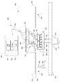
도 1을 참조하면, 연마 장치(100)는 하나 이상의 캐리어 헤드(126)를 포함하고, 그 각각은 기판(10), 하나 이상의 연마 스테이션(106), 및 기판을 캐리어 헤드에 로딩하고 캐리어 헤드로부터 기판을 언로딩하기 위한 이송 스테이션을 운반하도록 구성된다. 각각의 연마 스테이션(106)은 플래튼(120) 상에 지지된 연마 패드(130)를 포함한다. 연마 패드(130)는 외측 연마 층 및 더 연성인 후면 층을 갖는 2층 연마 패드일 수 있다.Referring to FIG. 1 , a
캐리어 헤드들(126)은 지지부(128)로부터 현수될 수 있고, 연마 스테이션들 간에 이동가능할 수 있다. 일부 구현에서, 지지부(128)는 오버헤드 트랙이고, 각각의 캐리어 헤드(126)는 트랙에 장착되는 캐리지(108)에 결합되고, 각각의 캐리지(108)는 연마 스테이션(124)과 이송 스테이션 사이에서 선택적으로 이동될 수 있다. 대안적으로, 일부 구현들에서 지지부(128)는 회전가능한 캐러셀이고, 캐러셀의 회전은 캐리어 헤드들(126)을 원형 경로를 따라 동시에 이동시킨다.The
연마 장치(100)의 각각의 연마 스테이션(106)은, 연마액(136), 예컨대, 연마 슬러리를 연마 패드(130) 상에 분배하기 위해, 예를 들어, 암(134)의 단부에 포트를 포함할 수 있다. 연마 장치(100)의 각각의 연마 스테이션(106)은 또한, 연마 패드(130)를 일관된 연마 상태로 유지하기 위해 연마 패드(130)를 연마하기 위한 패드 컨디셔닝 장치를 포함할 수 있다.Each
각각의 캐리어 헤드(126)는 기판(10)을 연마 패드(130)에 맞닿게 유지하도록 동작가능하다. 각각의 캐리어 헤드(126)는 각각의 기판 각각과 연관된 연마 파라미터들, 예를 들어, 압력의 독립적 제어를 구비할 수 있다. 특히, 각각의 캐리어 헤드(126)는 가요성 멤브레인(144) 아래에 기판(10)을 유지하기 위해 리테이닝 링(142)을 포함할 수 있다. 각각의 캐리어 헤드(126)는 또한, 멤브레인에 의해 형성된 복수의 독립적으로 제어가능한 가압가능 챔버들, 예를 들어, 3개의 챔버들(146a-146c)을 포함하며, 이 챔버들은 독립적으로 제어가능한 압력들을 가요성 멤브레인(144) 상의 연관된 구역들에, 그리고 따라서 기판(10) 상에 인가할 수 있다. 예시의 편의를 위해, 도 1에 단지 3개의 챔버들만이 예시되어 있지만, 1개 또는 2개의 챔버들, 또는 4개 이상의 챔버들, 예를 들어, 5개의 챔버들이 있을 수 있다.Each
각각의 캐리어 헤드(126)는 지지부(128)로부터 현수되며, 캐리어 헤드가 축(127)을 중심으로 회전할 수 있도록, 구동 샤프트(154)에 의해 캐리어 헤드 회전 모터(156)에 연결된다. 선택적으로, 각각의 캐리어 헤드(126)는, 예를 들어, 캐리지(108)를 트랙 상에서 구동함으로써, 또는 캐러셀 자체의 회전 진동에 의해 측방향으로 진동할 수 있다. 동작 시에, 플래튼은 그 중심 축을 중심으로 회전되고, 각각의 캐리어 헤드는 그 중심 축(127)에 대하여 회전되고, 연마 패드의 최상부 표면에 걸쳐 측방향으로 병진된다.Each
제어기(190), 예컨대, 프로그램가능 컴퓨터는, 플래튼(120) 및 캐리어 헤드들(126)의 회전 속도를 독립적으로 제어하기 위해, 각각의 모터에 연결된다. 제어기(190)는 중앙 처리 유닛(CPU)(192), 메모리(194) 및 지원 회로들(196), 예를 들어, 입력/출력 회로, 전원들, 클록 회로들, 캐시 등을 포함할 수 있다. 메모리는 CPU(192)에 연결된다. 메모리는 비일시적 컴퓨터블 판독가능 매체이고, RAM(random access memory), ROM(read-only memory), 플로피 디스크, 하드 디스크, 또는 다른 형태의 디지털 저장소와 같은 하나 이상의 용이하게 이용가능한 메모리일 수 있다. 추가적으로, 단일 컴퓨터로서 예시되어 있지만, 제어기(190)는, 예를 들어, 다수의 독립적으로 작동하는 프로세서들 및 메모리들을 포함하는 분산형 시스템일 수 있다.A
연마 장치(100)는 또한 인라인(인-시퀀스라고도 지칭됨) 광학 계측 시스템(160)을 포함한다. 인라인 광학 계측 시스템(160)의 컬러 이미징 시스템은 연마 장치(100) 내에 위치되지만, 연마 동작 동안 측정들을 수행하지 않으며, 오히려, 연마 동작들 사이에서, 예를 들어 기판이 하나의 연마 스테이션으로부터 다른 연마 스테이션으로 이동되고 있는 동안, 또는 연마 전 또는 연마 후 사이에서, 예를 들어 기판이 이송 스테이션으로부터 연마 스테이션으로 또는 그 반대로 이동되고 있는 동안, 측정치들이 수집된다. 추가로, 인라인 광학 계측 시스템(160)은, 기판이 카세트로부터 추출된 후이지만 기판이 연마 유닛으로 이동되기 전에 또는 기판이 세정된 후이지만 기판이 카세트로 복귀되기 전에 기판을 측정하기 위해, 팹 인터페이스 유닛 또는 팹 인터페이스 유닛으로부터 액세스가능한 모듈 내에 위치될 수 있다.The polishing
인라인 광학 계측 시스템(160)은 기판(10)의 컬러 이미징을 제공하는 센서 조립체(161)를 포함한다. 센서 조립체(161)는 광원(162), 광 검출기(164), 및 제어기(190)와 광원(162) 및 광 검출기(164) 사이에 신호들을 전송하고 수신하기 위한 회로(166)를 포함할 수 있다.The inline
광원(162)은 백색광을 방출하도록 동작가능할 수 있다. 일 구현에서, 방출된 백색광은 200-800 나노미터의 파장들을 갖는 광을 포함한다. 적합한 광원은 백색광 발광 다이오드들(LED들)의 어레이, 또는 크세논 램프 또는 크세논 수은 램프이다. 광원(162)은 광(168)을 기판(10)의 노출된 표면 상으로 0이 아닌 입사 각도(α)로 유도하도록 배향된다. 입사 각도(α)는, 예를 들어, 약 30° 내지 75°, 예를 들어, 50°일 수 있다.The
광원은 기판(10)의 폭에 걸쳐 있는 실질적으로 선형인 세장형 구역을 조명할 수 있다. 예를 들어, 광원(162)은, 광원으로부터의 광을 세장형 구역으로 확산시키기 위해, 광학계, 예를 들어, 빔 확장기를 포함할 수 있다. 대안적으로 또는 추가적으로, 광원(162)은 광원들의 선형 어레이를 포함할 수 있다. 광원(162) 자체, 및 기판 상에 조명된 구역은 세장형일 수 있고, 기판의 표면에 평행한 길이방향 축을 가질 수 있다.The light source may illuminate a substantially linear elongate region spanning the width of the
확산기(170)가 광(168)의 경로에 배치될 수 있거나, 또는 광원(162)은 광이 기판(10)에 도달하기 전에 광을 확산시키기 위한 확산기를 포함할 수 있다.A
검출기(164)는 광원(162)으로부터의 광에 민감한 컬러 카메라이다. 카메라는 검출기 요소들의 어레이를 포함한다. 예를 들어, 카메라는 CCD 어레이를 포함할 수 있다. 일부 구현들에서, 어레이는 검출기 요소들의 단일 행이다. 예를 들어, 카메라는 라인-스캔 카메라일 수 있다. 검출기 요소들의 행은, 광원(162)에 의해 조명되는 세장형 구역의 길이방향 축에 평행하게 연장될 수 있다. 광원(162)이 발광 요소들의 행을 포함하는 경우, 검출기 요소들의 행은 광원(162)의 길이방향 축에 평행한 제1 축을 따라 연장될 수 있다. 검출기 요소들의 행은 1024개 이상의 요소들을 포함할 수 있다.
카메라(164)는 기판의 시야를 검출기 요소들의 어레이 상에 투영하기 위해 적절한 집속 광학계(172)를 갖도록 구성된다. 시야는 기판(10)의 전체 폭, 예를 들어, 150 내지 300 mm 길이를 관찰하기에 충분히 길 수 있다. 연관된 광학계(172)를 포함하는 카메라(164)는, 개별 픽셀들이, 약 0.5 mm 이하의 길이를 갖는 구역에 대응하도록 구성될 수 있다. 예를 들어, 시야가 약 200 mm 길이이고 검출기(164)가 1024개의 요소들을 포함한다고 가정하면, 이때, 라인-스캔 카메라에 의해 생성된 이미지는 약 0.5 mm의 길이를 갖는 픽셀들을 가질 수 있다. 이미지의 길이 분해능을 결정하기 위해, 시야(FOV)의 길이는 FOV를 이미징되는 픽셀들의 수로 나눔으로써 길이 분해능이 도출될 수 있다.The
카메라(164)는 또한, 픽셀 폭이 픽셀 길이와 비슷하도록 구성될 수 있다. 예를 들어, 라인-스캔 카메라의 이점은, 그 매우 빠른 프레임 레이트이다. 프레임 레이트는 적어도 5 kHz일 수 있다. 프레임 레이트는, 이미징된 영역이 기판(10)에 걸쳐 스캔될 때, 픽셀 폭이 픽셀 길이와 비슷하고, 예를 들어, 약 0.3 mm 이하이도록하는 주파수로 설정될 수 있다.
광원(162) 및 광 검출기(164)는 스테이지(180) 상에 지지될 수 있다. 광 검출기(164)가 라인-스캔 카메라인 경우, 광원(162) 및 카메라(164)는 이미징된 영역이 기판의 길이에 걸쳐 스캐닝할 수 있도록 기판(10)에 대해 이동가능하다. 특히, 상대 운동은 기판(10)의 표면에 평행하고 라인-스캔 카메라(164)의 검출기 요소들의 행에 수직인 방향일 수 있다.The
일부 구현들에서, 스테이지(182)는 고정식이고, 기판을 위한 지지체가 이동한다. 예를 들어, 캐리어 헤드(126)는 예를 들어 캐리지(108)의 운동에 의해 또는 캐러셀의 회전 진동에 의해 이동할 수 있거나, 팩토리 인터페이스 유닛에서 기판을 유지하는 로봇 암이 기판(10)을 라인-스캔 카메라(182)를 지나쳐 이동시킬 수 있다. 일부 구현들에서, 이미지 취득을 위해 캐리어 헤드 또는 로봇 암이 고정 상태로 유지되는 동안 스테이지(180)가 이동할 수 있다. 예를 들어, 스테이지(180)가 선형 액추에이터(182)에 의해 레일(184)을 따라 이동가능할 수 있다. 어느 경우에서든, 이는, 스캐닝되고 있는 영역이 기판(10)을 가로질러 이동하므로, 광원(162)과 카메라(164)가 서로에 대해 고정된 위치에 머무르는 것을 허용한다.In some implementations, the
기판을 가로질러 함께 이동하는 라인-스캔 카메라 및 광원을 갖는 것의 가능한 이점은, 예를 들어, 종래의 2D 카메라와 비교하여, 광원과 카메라 사이의 상대 각도가, 웨이퍼에 걸친 상이한 위치들에 대해 일정하게 유지된다는 점이다. 결과적으로, 시야각의 변동에 의해 야기되는 인공적인 부작용들이 감소되거나 제거될 수 있다. 추가적으로, 종래의 2D 카메라는 내재된 원근 왜곡을 나타내고, 이때 이를 이미지 변환에 의해 보정해야 하는 반면에, 라인-스캔 카메라는 원근 왜곡을 제거할 수 있다.A possible advantage of having a line-scan camera and light source moving together across the substrate is that the relative angle between the light source and camera is constant for different positions across the wafer, for example compared to a conventional 2D camera. that it is maintained. As a result, artificial side effects caused by variations in the viewing angle can be reduced or eliminated. Additionally, conventional 2D cameras exhibit inherent perspective distortion, which must then be corrected by image transformation, whereas line-scan cameras can eliminate perspective distortion.
센서 조립체(161)는 기판(10)과 광원(162) 및 검출기(164) 사이의 수직 거리를 조정하기 위한 메커니즘을 포함할 수 있다. 예를 들어, 센서 조립체(161)는 스테이지(180)의 수직 위치를 조정하기 위한 액추에이터를 포함할 수 있다.The
선택적으로, 광의 경로에, 예를 들어, 기판(10)과 검출기(164) 사이에 편광 필터(174)가 위치될 수 있다. 편광 필터(174)는 원형 편광자(CPL)일 수 있다. 전형적인 CPL은 선형 편광자와 1/4 파장판의 조합이다. 편광 필터(174)의 편광 축의 적절한 배향은 이미지의 흐림(haze)을 감소시키고 바람직한 시각적 특징들을 선명화하거나 증진시킬 수 있다.Optionally, a
기판 상의 최외측 층이 반투명 층, 예를 들어, 유전체 층이라고 가정하면, 검출기(164)에서 검출되는 광의 컬러는, 예를 들어, 기판 표면의 조성, 기판 표면 평활도, 및/또는 기판 상의 하나 이상의 층(예를 들어, 유전체 층)의 상이한 계면들로부터 반사된 광 사이의 간섭의 양에 따라 달라진다. 위에서 언급된 바와 같이, 광원(162) 및 광 검출기(164)는 그들의 동작을 제어하고 그들의 신호들을 수신하도록 동작가능한 컴퓨팅 디바이스, 예를 들어, 제어기(190)에 연결될 수 있다. 컬러 이미지를 두께 측정치로 변환하기 위해 다양한 기능들을 수행하는 컴퓨팅 디바이스는 계측 시스템(160)의 일부로 고려될 수 있다.Assuming that the outermost layer on the substrate is a translucent layer, eg, a dielectric layer, the color of light detected by the
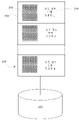
도 2a를 참조하면, 인라인 광학 계측 시스템(160)으로 수집된 기판(10)의 이미지(202)의 예가 도시되어 있다. 인라인 광학 계측 시스템(160)은 고분해능 컬러 이미지(202), 예를 들어 적어도 3개의 컬러 채널, 예를 들어 RGB 채널을 갖는 적어도 720 x 1080 픽셀의 이미지, 예를 들어 적어도 2048 x 2048 픽셀의 이미지를 생성한다. 임의의 특정 픽셀에서의 컬러는 픽셀에 대응하는 기판의 영역에서, 최상부 층을 포함하는 하나 이상의 층의 두께에 따라 달라진다Referring to FIG. 2A , an example of an
이미지(202)는 하나 이상의 구역(208)으로 분할되고, 각각의 구역은 기판 상에 제조되는 다이(206)에 대응한다. 구역(208)을 제공하는 이미지의 부분은 이미지 내의 미리 결정된 영역일 수 있거나, 또는 구역(208)을 제공하는 부분은 이미지에 기초한 알고리즘에 의해 자동으로 결정될 수 있다.The
이미지 내의 미리 결정된 영역의 예로서, 제어기(190)는 각각의 구역(208)에 대한 이미지 내의 위치 및 영역을 식별하는 다이 마스크를 저장할 수 있다. 예를 들어, 직사각형 구역들에 대해, 영역은 이미지 내의 우상 및 좌하 좌표들에 의해 정의될 수 있다. 따라서, 마스크는 각각의 직사각형 구역에 대한 우상 및 좌하 좌표의 쌍을 포함하는 데이터 파일일 수 있다. 구역들이 비-직사각형인 다른 경우들에서, 더 복잡한 함수들이 사용될 수 있다.As an example of a predetermined region within the image, the
일부 구현들에서, 기판의 배향 및 위치가 결정될 수 있고, 다이 마스크는 이미지에 대해 정렬될 수 있다. 기판 배향은, 예를 들어, 이미지에서 새김선(scribe line)들의 각도를 결정하기 위해 컬러 이미지(202)를 이미지 처리함으로써 또는 노치 파인더에 의해 결정될 수 있다. 기판 위치는 또한 컬러 이미지(202)의 이미지 처리에 의해, 예를 들어, 원형 기판 에지를 검출한 다음 원의 중심을 결정함으로써 결정될 수 있다.In some implementations, the orientation and position of the substrate can be determined and the die mask can be aligned with respect to the image. The substrate orientation can be determined, for example, by image processing the
구역(208)을 자동으로 결정하는 예로서, 이미지 처리 알고리즘은 이미지(202)를 분석하고 새김선들을 검출할 수 있다. 이미지(202)는 이후 식별된 새김선들 사이의 구역들로 분할될 수 있다.As an example of automatically determining the
초기 컬러 이미지를 분할함으로써, 개별 구역들(208)의 복수의 컬러 이미지(204)가 기판(10)으로부터 수집될 수 있다. 앞서 언급한 바와 같이, 각각의 컬러 이미지(204)는 기판 상에 제조되는 다이(206)에 대응한다. 수집된 컬러 이미지들은 PNG 이미지들로서 내보내질 수 있지만, 많은 다른 포맷들, 예를 들어, JPEG 등이 가능하다.By segmenting the initial color image, a plurality of
컬러 이미지들(204)은 컬러 이미지(204)에 나타난 다이에 대한 두께 측정치를 생성하기 위해 이미지 처리 알고리즘에 공급될 수 있다. 이미지는 컬러 이미지에 기초하여 층 두께를 추정하기 위해, 예를 들어, 지도 딥 러닝 접근법에 의해 훈련된 이미지 처리 알고리즘에 대한 입력 데이터로서 사용된다. 지도 딥 러닝 기반 알고리즘은 컬러 이미지들과 두께 측정치들 사이의 모델을 확립한다. 이미지 처리 알고리즘은 딥 러닝 기반 알고리즘으로서 신경망을 포함할 수 있다.The
컬러 이미지(204)의 각각의 픽셀의 각각의 컬러 채널에 대한 강도 값이 이미지 처리 알고리즘에, 예를 들어 신경망의 입력 뉴런들에 입력된다. 이 입력 데이터에 기초하여, 컬러 이미지에 대한 층 두께 측정치가 계산된다. 따라서, 이미지 처리 알고리즘으로의 컬러 이미지(204)의 입력은 추정된 두께의 출력을 생성한다. 이 시스템은, 예를 들어, 저비용 메모리 응용을 위한 고처리량 및 경제적 해결책으로서 이용될 수 있다. 두께 추론들 외에도, 이 기술은 이미지 세그먼트화를 이용하여 기판 상의 잔류물의 수준들을 분류하기 위해 이용될 수 있다.An intensity value for each color channel of each pixel of the
지도 딥 러닝 접근법을 이용하여 이미지 처리 알고리즘, 예를 들어 신경망을 훈련하기 위해, 하나 이상의 캘리브레이션 기판으로부터의 다이들의 캘리브레이션 이미지들이 위에서 논의된 바와 같이 획득될 수 있다. 즉, 각각의 캘리브레이션 기판은 초기 캘리브레이션 이미지를 생성하기 위해 인라인 광학 계측 시스템(160)의 라인-스캔 카메라에 의해 스캐닝될 수 있고, 초기 캘리브레이션 이미지는 캘리브레이션 기판 상의 개별 구역들의 복수의 컬러 이미지로 분할될 수 있다.To train an image processing algorithm, eg, a neural network, using a supervised deep learning approach, calibration images of dies from one or more calibration substrates may be obtained as discussed above. That is, each calibration substrate may be scanned by a line-scan camera of the inline
초기 컬러 캘리브레이션 이미지가 수집되기 전 또는 후에, 고정밀 계측 시스템, 예를 들어 인라인 또는 독립형 계측 시스템을 이용하여 캘리브레이션 기판 상의 다수의 위치에서 실측 정보 두께 측정치들이 수집된다. 고정밀 계측 시스템은 건식 광학 계측 시스템일 수 있다. 실측 정보 측정은 오프라인 반사계측, 타원계측, 산란계측 또는 더 진보된 TEM 측정들로부터 얻어질 수 있지만, 다른 기술들이 적합할 수 있다. 그러한 시스템들은 노바 메저링 인스트루먼츠사(Nova Measuring Instruments Inc.) 또는 나노메트릭스사(Nanometrics, Inc.)로부터 입수 가능하다. 각각의 위치는 제조되는 다이들 중 하나에, 즉 개별 구역들 중 하나에 대응한다.Before or after the initial color calibration image is collected, ground truth thickness measurements are collected at multiple locations on the calibration substrate using a high precision metrology system, eg, an inline or standalone metrology system. The high-precision metrology system may be a dry optical metrology system. The ground truth measurement may be obtained from offline reflectometry, ellipsometrics, scatterometry or more advanced TEM measurements, although other techniques may be suitable. Such systems are available from Nova Measuring Instruments Inc. or Nanometrics, Inc. Each location corresponds to one of the dies being fabricated, ie to one of the individual zones.
예를 들어, 도 2b를 참조하면, 각각의 캘리브레이션 기판 상의 각각의 개별 구역에 대해, 컬러 캘리브레이션 이미지(212)가 광학 계측 시스템(160)의 인라인 센서로 수집된다. 각각의 컬러 캘리브레이션 이미지는 캘리브레이션 기판 상의 대응하는 다이에 대한 실측 정보 두께 측정치(214)와 연관된다. 이미지들(212) 및 연관된 실측 정보 두께 측정치들(214)은 데이터베이스(220)에 저장될 수 있다. 예를 들어, 데이터는 캘리브레이션 이미지(212) 및 실측 정보 두께 측정치(214)를 포함하는 각각의 레코드를 갖는 레코드들(210)로서 저장될 수 있다.For example, referring to FIG. 2B , for each individual region on each calibration substrate, a
딥 러닝 기반 알고리즘, 예를 들어, 신경망은 이후 조합된 데이터 세트(218)를 사용하여 훈련된다. 건식 계측 도구로부터 측정된 다이의 중심에 대응하는 두께 측정치들은 모델을 훈련하는 동안 입력 이미지에 대한 라벨로서 사용된다. 예를 들어, 모델은 넓은 범위의 포스트 두께들을 갖는 기판 상의 5개의 다이로부터 수집된 약 50,000개의 이미지에 대해 훈련될 수 있다.A deep learning based algorithm, eg, a neural network, is then trained using the combined
도 3은 연마 장치(100)를 위한 제어기(190)의 일부로서 이용되는 신경망(320)을 도시한다. 신경망(320)은 기판의 구역의 컬러 이미지에 기초하여 그 구역의 층 두께를 예측하기 위한 모델을 생성하기 위해, 캘리브레이션 기판으로부터의 입력 이미지들의 RGB 강도 값들 및 실측 정보 두께 측정치들의 회귀 분석을 위해 개발된 심층 신경망일 수 있다.3 shows a
신경망(320)은 복수의 입력 노드들(322)을 포함한다. 신경망(320)은 입력 컬러 이미지의 각각의 픽셀과 연관된 각각의 컬러 채널에 대한 입력 노드, 복수의 은닉 노드들(324)(아래에서 "중간 노드들"이라고도 불림), 및 층 두께 측정치 값을 생성할 출력 노드(326)를 포함할 수 있다. 단일 계층의 은닉 노드들을 갖는 신경망에서, 각각의 은닉 노드(324)는 각각의 입력 노드(322)에 결합될 수 있고, 출력 노드(326)는 각각의 은닉 노드(320)에 결합될 수 있다. 그러나, 실용적인 문제로서, 이미지 처리를 위한 신경망은 많은 계층의 은닉 노드들(324)을 가질 가능성이 있다.The
일반적으로, 은닉 노드(324)는 입력 노드들(322) 또는 은닉 노드(324)가 연결되는 은닉 노드들의 이전 계층들로부터의 값들의 가중 합의 비선형 함수인 값을 출력한다.In general, the hidden
예를 들어, 노드 k로 지정된 제1 계층 내의 은닉 노드(324)의 출력은 다음과 같이 표현될 수 있다:For example, the output of the hidden
![]()
![]()
여기서, tanh는 쌍곡선 탄젠트이고, a kx 는 k번째 중간 노드와 (M개의 입력 노드들 중) x번째 입력 노드 사이의 연결에 대한 가중치이고, IM는 M번째 입력 노드에서의 값이다. 그러나, 다른 비선형 함수들, 예컨대, 정류 선형 유닛(ReLU) 함수 및 그의 변형들이 tanh 대신에 사용될 수 있다.Here, tanh is the hyperbolic tangent, a kx is the weight for the connection between the k-th intermediate node and the x-th input node (out of M input nodes), and I M is the value at the M-th input node. However, other non-linear functions, such as the Rectified Linear Unit (ReLU) function and variants thereof, may be used instead of tanh.
따라서, 신경망(320)은, 예를 들어, J개의 픽셀들 및 K개의 컬러 채널들이 존재하는 경우, 입력 컬러 이미지의 각각의 픽셀과 연관된 각각의 컬러 채널에 대한 입력 노드(322)를 포함하고, 이때, L=J*K는 입력 컬러 이미지 내의 강도 값들의 수이고, 신경망(320)은 적어도 입력 노드들 N1, N2 ... NL을 포함할 것이다.Thus,
따라서, 입력 노드들의 수가 컬러 이미지의 강도 값들의 수에 대응하는 경우, 노드 k로 지정된 은닉 노드(324)의 출력 Hk는 다음과 같이 표현될 수 있다:Thus, when the number of input nodes corresponds to the number of intensity values of the color image, the output H k of the hidden
![]()
![]()
측정된 컬러 이미지(S)가 열 행렬(i 1 , i 2 , ..., i L )에 의해 표현된다고 가정하면, 노드 k로 지정된 중간 노드(324)의 출력은 다음과 같이 표현될 수 있다:Assuming that the measured color image S is represented by column matrices i 1 , i 2 , ..., i L , the output of the
![]()
![]()
여기서, V는 가중치들의 값(v1, v2, ..., vL)이고, Vx는 컬러 이미지로부터의 L 강도 값들 중 x번째 강도 값에 대한 가중치이다.Here, V is the value of the weights (v 1 , v 2 , ..., v L ), and V x is the weight for the x-th intensity value among L intensity values from the color image.
출력 노드(326)는 은닉 노드들의 출력들의 가중 합인 특성 값(CV), 예를 들어 두께를 생성할 수 있다. 예를 들어, 이는 다음과 같이 표현될 수 있다:The
![]()
![]()
여기서, Ck는 k번째 은닉 노드의 출력에 대한 가중치이다.Here, C k is the weight for the output of the k-th hidden node.
그러나, 신경망(320)은 다른 데이터를 수신하기 위해 하나 이상의 다른 입력 노드, 예를 들어, 노드(322a)를 선택적으로 포함할 수 있다. 이러한 다른 데이터는, 인-시튜 모니터링 시스템에 의한 기판의 이전 측정으로부터의 것, 예를 들어, 기판의 처리의 더 이전으로부터 수집된 픽셀 강도 값들, 이전 기판의 측정으로부터의 것, 예를 들어, 다른 기판의 처리 동안 수집된 픽셀 강도 값들, 연마 시스템의 다른 센서로부터의 것, 예를 들어, 온도 센서에 의한 패드 또는 기판의 온도의 측정, 연마 시스템을 제어하는 데에 사용되는 제어기에 의해 저장된 연마 레시피로부터의 것, 예를 들어, 기판을 연마하는 데에 사용되는 연마 파라미터, 예컨대, 캐리어 헤드 압력 또는 플래튼 회전 속도, 제어기에 의해 추적된 변수로부터의 것, 예를 들어, 패드가 바뀐 때부터의 기판들의 수, 또는 연마 시스템의 일부가 아닌 센서로부터의 것, 예를 들어, 계측 스테이션에 의한 기저 막들의 두께의 측정일 수 있다. 이는 신경망(320)이 층 두께 측정치 값의 계산에서 다른 처리 또는 환경 변수들을 고려하는 것을 허용한다.However,
출력 노드(326)에서 생성된 두께 측정치는 프로세스 제어 모듈(330)에 공급된다. 프로세스 제어 모듈은 하나 이상의 구역의 두께 측정치들에 기초하여 처리 파라미터들, 예를 들어 캐리어 헤드 압력, 플래튼 회전 속도 등을 조정할 수 있다. 조정은 기판 또는 후속 기판에 대해 수행될 연마 프로세스에 대해 수행될 수 있다.The thickness measurements generated at the
예를 들어 기판 측정들을 위해 사용되기 전에, 신경망(320)은 구성될 필요가 있다.Before being used for example for substrate measurements, the
구성 절차의 일부로서, 제어기(190)는 복수의 캘리브레이션 이미지를 수신할 수 있다. 각각의 캘리브레이션 이미지는 캘리브레이션 이미지의 각각의 픽셀에 대해 다수의 강도 값, 예를 들어 각각의 컬러 채널에 대한 강도 값을 갖는다. 제어기는 또한 각각의 캘리브레이션 이미지에 대한 특성화 값, 예를 들어 두께를 수신한다. 예를 들어, 컬러 캘리브레이션 이미지는 하나 이상의 캘리브레이션 또는 테스트 기판 상에 제조되는 특정 다이에서 측정될 수 있다. 또한, 특정 다이 위치들에서의 두께의 실측 정보 측정들은 건식 계측 장비, 예를 들어, 접촉 프로필로미터(profilometer) 또는 타원계측기(ellipsometer)를 이용하여 수행될 수 있다. 따라서, 실측 정보 두께 측정치는 기판 상의 동일한 다이 위치로부터의 컬러 이미지와 연관될 수 있다. 복수의 컬러 캘리브레이션 이미지는 위에서 논의된 바와 같이 캘리브레이션 기판들의 이미지들을 분할함으로써, 예를 들어 5개 내지 10개의 캘리브레이션 기판으로부터 생성될 수 있다. 신경망(320)에 대한 구성 절차에서, 신경망(320)은 캘리브레이션 기판 상에 제조된 각각의 다이에 대한 컬러 이미지 및 특성 값을 사용하여 훈련된다.As part of the configuration procedure, the
V는 컬러 이미지들 중 하나에 대응하고 따라서 특성 값과 연관된다. 신경망(320)이 역전파 모드와 같은 훈련 모드에서 동작하는 동안, 값들(v1, v2, ..., vL)은 각각의 입력 노드들(N1), N2 ... NL에 공급되고, 특성 값(CV)이 출력 노드(326)에 공급된다. 이는 각각의 행에 대해 반복될 수 있다. 이 프로세스는 상기 수학식 1 또는 2에서 ak1 등에 대한 값들을 설정한다.V corresponds to one of the color images and is thus associated with a characteristic value. While the
시스템은 이제 동작 준비가 되었다. 인라인 모니터링 시스템(160)을 사용하여 기판으로부터 컬러 이미지가 측정된다. 측정된 컬러 이미지는 열 행렬 S=(i 1 , i 2 , ..., i L )에 의해 표현될 수 있고, 여기서 i j 는 L개의 강도 값들 중 j번째 강도 값에서의 강도 값을 나타내고, 이미지가 총 n 픽셀들을 포함하고 각각의 픽셀이 3개의 컬러 채널을 포함할 때 L=3n이다.The system is now ready for operation. A color image is measured from the substrate using an
신경망(320)이 추론 모드에서 사용되는 동안, 이러한 값들(S 1 , S 2 , ..., S L )은 각각의 입력 노드들(N1, N2, ... NL)에 입력들로서 공급된다. 그 결과, 신경망(320)은 출력 노드(326)에서 특성 값, 예를 들어, 층 두께를 생성한다.While the
신경망(320)의 아키텍처는 깊이 및 폭이 달라질 수 있다. 예를 들어, 신경망(320)이 중간 노드들(324)의 단일 열로 도시되지만, 이는 다수의 열을 포함할 수 있다. 중간 노드들(324)의 수는 입력 노드들(322)의 수 이상일 수 있다.The architecture of the
위에서 언급된 바와 같이, 제어기(190)는 다양한 컬러 이미지들을 기판 상의 상이한 다이들(도 2 참조)과 연관시킬 수 있다. 각각의 신경망(320)의 출력은 이미지가 수집될 때 기판 상의 센서의 위치에 기초하여 다이들 중 하나에 속하는 것으로서 분류될 수 있다. 이는 제어기(190)가 각각의 다이에 대한 측정 값들의 별개의 시퀀스를 생성하는 것을 허용한다.As noted above, the
일부 구현들에서, 제어기(190)는 다수의 상이한 유형의 빌딩 블록들로 구성된 신경망 모델 구조를 갖도록 구성될 수 있다. 예를 들어, 신경망은 그의 아키텍처에 잔차 블록 특징을 포함하는 잔차 신경망이다. 잔차 신경망은 스킵 연결들 또는 숏컷들을 이용하여 일부 계층들을 점프할 수 있다. 잔차 신경망은, 예를 들어, ResNet 모델로 구현될 수 있다. 잔차 신경망들에 관련하여, 비-잔차 네트워크는 플레인 네트워크(plain network)로서 설명될 수 있다.In some implementations, the
일부 구현들에서, 신경망은 계산들 동안 스택으로부터의 기저 층 두께를 고려하도록 훈련될 수 있으며, 이는 두께 측정치들의 기저 변동으로 인한 오류들을 개선할 수 있다. 막 스택에서의 기저 두께 변동의 영향은, 모델의 성능을 개선하기 위해, 기저 층들의 두께들의 컬러 이미지들의 강도 값들을 추가 입력들로서 모델에 공급함으로써 완화될 수 있다.In some implementations, the neural network may be trained to take into account the underlying layer thickness from the stack during calculations, which may improve errors due to underlying variation in thickness measurements. The effect of base thickness variation in the film stack can be mitigated by supplying the model as additional inputs with intensity values of color images of the thicknesses of the base layers to improve the performance of the model.
계산된 두께 측정치들의 신뢰성은, 이들을 측정된 값들과 비교한 다음, 계산된 값들과 원래의 측정된 값들 사이의 차이를 결정함으로써 평가될 수 있다. 그 다음, 이러한 딥 러닝 모델은 새로운 테스트 기판이 스캐닝된 직후에, 추론 모드에서 두께를 예측하기 위해 사용될 수 있다. 이러한 새로운 접근법은 전체 시스템의 처리량을 향상시키고, 두께 측정치가 로트 내의 모든 기판들에 대해 수행되는 것을 가능하게 한다.The reliability of the calculated thickness measurements can be evaluated by comparing them to the measured values and then determining the difference between the calculated values and the original measured values. This deep learning model can then be used to predict the thickness in inference mode, immediately after a new test substrate is scanned. This new approach improves the throughput of the overall system and enables thickness measurements to be performed for all substrates in a lot.
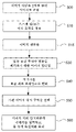
도 4를 참조하면, 기판 두께 측정 시스템에서 사용하기 위한 머신 러닝 기술들에 의해 생성된 이미지 처리 알고리즘의 방법이 도시된다. 그러한 이미지 처리 알고리즘은 통합된 라인-스캔 카메라 검사 시스템으로부터 수집된 RGB 이미지들을 수신할 수 있고, 훨씬 더 빠른 속도로 막 두께 추정들을 가능하게 한다. 약 2000개의 측정 지점에 대한 추론 시간은 건식 계측에서의 2시간과 비교하여 약 수 초이다.4 , a method of an image processing algorithm generated by machine learning techniques for use in a substrate thickness measurement system is shown. Such an image processing algorithm can receive RGB images collected from an integrated line-scan camera inspection system, enabling film thickness estimations at a much faster rate. The inference time for about 2000 measurement points is about a few seconds compared to 2 hours for dry metering.
이 방법은 제어기가 광 검출기(164)로부터의 개별 이미지 라인들을 2차원 컬러 이미지로 조립하는 단계(500)를 포함한다. 제어기는 각각의 컬러 채널에서 이미지의 강도 값들에 오프셋 및/또는 이득 조정을 적용할 수 있다(510). 각각의 컬러 채널은 상이한 오프셋 및/또는 이득을 가질 수 있다. 선택적으로, 이미지는 정규화될 수 있다(515). 예를 들어, 측정된 이미지와 표준의 미리 정의된 이미지 사이의 차이가 계산될 수 있다. 예를 들어, 제어기는 적색, 녹색 및 청색 컬러 채널들 각각에 대한 배경 이미지를 저장할 수 있고, 배경 이미지는, 각각의 컬러 채널에 대해, 측정된 이미지로부터 감산될 수 있다. 대안적으로, 측정된 이미지는 표준의 미리 정의된 이미지로 나누어질 수 있다. 이미지는 낮은 주파수 공간 변동들을 제거하기 위해 필터링될 수 있다(530). 일부 구현에서, 휘도 채널은 필터를 생성하는데 이용되고, 이어서, 이는 적색, 녹색 및 청색 이미지들에 적용된다.The method includes the controller assembling (500) individual image lines from the photodetector (164) into a two-dimensional color image. The controller may apply an offset and/or gain adjustment to the intensity values of the image in each color channel ( 510 ). Each color channel may have a different offset and/or gain. Optionally, the image may be normalized ( 515 ). For example, the difference between a measured image and a predefined image of a standard may be calculated. For example, the controller may store a background image for each of the red, green, and blue color channels, and the background image, for each color channel, may be subtracted from the measured image. Alternatively, the measured image may be divided into standard predefined images. The image may be filtered 530 to remove low frequency spatial variations. In some implementations, the luminance channel is used to create a filter, which is then applied to the red, green and blue images.
이미지는 표준 이미지 좌표 프레임으로 변환, 예를 들어 스케일링 및/또는 회전 및/또는 병진된다(540). 예를 들어, 이미지는 다이 중심이 이미지의 중심점에 있도록 병진될 수 있고/있거나, 이미지는 기판의 에지가 이미지의 에지에 있도록 스케일링될 수 있고, 및/또는 이미지는 이미지의 x축과 기판 중심과 기판 배향 특징부를 연결하는 방사상 세그먼트 사이에 0°각도가 존재하도록 회전될 수 있다.The image is transformed (eg, scaled and/or rotated and/or translated 540) into a standard image coordinate frame. For example, the image may be translated such that the die center is at the center point of the image, the image may be scaled such that the edge of the substrate is at the edge of the image, and/or the image may be aligned with the x-axis of the image and the center of the substrate It can be rotated such that there is a 0° angle between the radial segments connecting the substrate orientation features.
기판 상의 하나 이상의 구역이 선택되고, 각각의 선택된 구역에 대해 이미지가 생성된다(550). 이는 전술한 기술들을 이용하여 수행될 수 있는데, 예를 들어 구역들은 미리 결정된 영역들일 수 있거나, 또는 구역(208)을 제공하는 부분은 알고리즘에 의해 자동으로 결정될 수 있다.One or more regions on the substrate are selected, and an image is generated 550 for each selected region. This may be done using the techniques described above, for example the zones may be predetermined areas, or the
이미지의 각각의 픽셀에 대해 각각의 컬러 채널에 의해 제공되는 강도 값들은 지도 딥 러닝 훈련 이미지 처리 알고리즘에 대한 입력으로서 사용되는 것으로 간주된다. 이미지 처리 알고리즘은 특정 구역에 대한 층 두께 측정치를 출력한다(560).The intensity values provided by each color channel for each pixel of the image are considered to be used as input to the supervised deep learning training image processing algorithm. The image processing algorithm outputs ( 560 ) a layer thickness measurement for the specific region.
측정들에서의 오류들을 감소시킬 목적으로, 소형 다이 테스트 패터닝된 기판들에 대해 다양한 딥 모델 아키텍처들이 훈련되고 검증되었다. 기저 층의 특성들을 고려한 모델은 더 낮은 오차를 가진다. 또한, 하나의 도구 상에서 수집된 데이터로 모델을 훈련시키고 이를 사용하여 다른 도구들로부터의 데이터에 대해 추론함으로써 예비 도구간 매칭 검증이 수행되었다. 결과는 동일한 도구로부터의 데이터를 이용한 훈련 및 추론과 비슷하였다.For the purpose of reducing errors in measurements, various deep model architectures have been trained and validated on small die test patterned substrates. A model that considers the properties of the base layer has a lower error. In addition, preliminary inter-tool matching validation was performed by training a model with data collected on one tool and using it to infer on data from other tools. Results were comparable to training and inference using data from the same tool.
일반적으로, 데이터는 CMP 장치의 하나 이상의 동작 파라미터를 제어하는 데 사용될 수 있다. 동작 파라미터들은, 예를 들어, 플래튼 회전 속도, 기판 회전 속도, 기판의 연마 경로, 플레이트에 걸친 기판 속도, 기판에 가해진 압력, 슬러리 조성, 슬러리 유량, 및 기판 표면에서의 온도를 포함한다. 동작 파라미터들은 실시간으로 제어될 수 있고, 추가의 사람 개입의 필요 없이 자동으로 조정될 수 있다.In general, the data may be used to control one or more operating parameters of a CMP apparatus. Operating parameters include, for example, platen rotation speed, substrate rotation speed, polishing path of the substrate, substrate speed across the plate, pressure applied to the substrate, slurry composition, slurry flow rate, and temperature at the substrate surface. Operating parameters can be controlled in real time and can be adjusted automatically without the need for additional human intervention.
본 명세서에 사용될 때, 기판이라는 용어는, 예를 들어, (예를 들어, 다수의 메모리 또는 프로세서 다이들을 포함하는) 제품 기판, 테스트 기판, 베어 기판, 및 게이팅 기판을 포함할 수 있다. 기판은 집적 회로 제조의 다양한 스테이지들에 있을 수 있는데, 예를 들어 기판은 베어 웨이퍼일 수 있거나, 또는 하나 이상의 퇴적 및/또는 패터닝된 층을 포함할 수 있다. 기판이라는 용어는 원형 디스크들 및 직사각형 시트들을 포함할 수 있다.As used herein, the term substrate may include, for example, product substrates (eg, containing multiple memory or processor dies), test substrates, bare substrates, and gating substrates. The substrate may be at various stages of integrated circuit fabrication, for example the substrate may be a bare wafer or may include one or more deposited and/or patterned layers. The term substrate may include circular disks and rectangular sheets.
그러나, 위에서 설명된 컬러 이미지 처리 기술은 3D 수직 NAND(VNAND) 플래시 메모리에 관련하여 특히 유용할 수 있다. 특히, VNAND의 제조에 사용되는 층 스택은 너무 복잡하여 현재의 계측 방법들(예를 들어, 노바 스펙트럼 분석)은 부적절한 두께의 구역들을 검출하는 데에 충분한 신뢰성으로 수행되지 못할 수 있다. 대조적으로, 컬러 이미지 처리 기술은 이러한 응용에서 우수한 신뢰성을 가질 수 있다.However, the color image processing techniques described above may be particularly useful in the context of 3D vertical NAND (VNAND) flash memory. In particular, the layer stack used in the fabrication of VNANDs may be so complex that current metrology methods (eg, Nova spectrum analysis) may not perform with sufficient reliability to detect regions of inappropriate thickness. In contrast, color image processing techniques can have good reliability in these applications.
본 명세서에 설명된 본 발명의 실시예들 및 기능적 동작들 전부는, 디지털 전자 회로로, 본 명세서에 개시된 구조적 수단들 및 그의 구조적 등가물들을 포함하는, 컴퓨터 소프트웨어, 펌웨어, 또는 하드웨어로, 또는 그들의 조합들로 구현될 수 있다. 본 발명의 실시예들은, 하나 이상의 컴퓨터 프로그램 제품으로, 즉, 하나 이상의 컴퓨터 프로그램(데이터 처리 장치, 예를 들어, 프로그램가능 프로세서, 컴퓨터, 또는 다수의 프로세서들 또는 컴퓨터들에 의한 실행을 위해, 또는 그의 동작을 제어하기 위해, 비일시적 기계 판독가능 저장 매체에 유형적으로 구체화됨)으로 구현될 수 있다.All of the embodiments and functional operations of the invention described herein may be implemented in digital electronic circuitry, in computer software, firmware, or hardware, including the structural means disclosed herein and structural equivalents thereof, or combinations thereof. can be implemented with Embodiments of the present invention may be implemented as one or more computer program products, ie, one or more computer programs (for execution by a data processing apparatus, eg, a programmable processor, a computer, or a plurality of processors or computers, or to control its operation, tangibly embodied in a non-transitory machine-readable storage medium).
상대 위치에 관한 용어들은 반드시 중력에 기준한 것은 아니며, 서로에 대한 시스템의 컴포넌트들의 위치를 나타내기 위해 사용되고, 연마 표면 및 기판은 수직 배향 또는 일부 다른 배향들로 유지될 수 있음을 이해해야 한다.It should be understood that terms relating to relative position are not necessarily relative to gravity and are used to indicate the position of components of a system relative to one another, and that the polishing surface and substrate may be maintained in a vertical orientation or some other orientation.
다수의 구현들이 설명되었다. 그럼에도 불구하고, 다양한 수정들이 이루어질 수 있다는 점이 이해될 것이다. 예를 들어,A number of implementations have been described. Nevertheless, it will be understood that various modifications may be made. for example,
· 라인-스캔 카메라 대신에, 전체 기판을 이미지화하는 카메라가 사용될 수 있다. 이 경우, 기판에 대한 카메라의 운동은 필요하지 않다.· Instead of a line-scan camera, a camera that images the entire substrate can be used. In this case, no movement of the camera relative to the substrate is required.
· 카메라는 기판의 전체 폭 미만을 커버할 수 있다. 이 경우, 카메라는, 전체 기판을 스캔하기 위해, 2개의 수직 방향들의 운동이 적용되어야 하는, 예를 들어, X-Y 스테이지 상에서 지지될 필요가 있을 것이다.· The camera can cover less than the full width of the substrate. In this case, the camera will need to be supported, for example on an X-Y stage, to which motion in two vertical directions must be applied to scan the entire substrate.
· 광원은 전체 기판을 조명할 수 있다. 이 경우, 광원은 기판에 대해 이동할 필요가 없다.· The light source can illuminate the entire substrate. In this case, the light source does not need to move with respect to the substrate.
· 광 검출기는 컬러 카메라 대신 분광계일 수 있으며; 이때, 스펙트럼 데이터는 RGB 컬러 공간으로 감축될 수 있다.· The photo detector may be a spectrometer instead of a color camera; In this case, the spectral data may be reduced to an RGB color space.
· 센서 조립체는 연마 스테이션들 사이에 또는 연마 스테이션과 이송 스테이션 사이에 위치된 인라인 시스템일 필요는 없다. 예를 들어, 센서 조립체는 이송 스테이션 내에 위치되거나, 카세트 인터페이스 유닛에 위치되거나, 독립형 시스템일 수 있다.· The sensor assembly need not be an in-line system located between the polishing stations or between the polishing station and the transfer station. For example, the sensor assembly may be located within a transfer station, located in a cassette interface unit, or may be a standalone system.
· 균일성 분석 단계는 선택적이다. 예를 들어, 임계 변환을 적용함으로써 생성된 이미지가, 기판에 대한 나중의 처리 단계를 조정하기 위해 피드포워드 프로세스에, 또는 후속 기판에 대한 처리 단계를 조정하기 위해 피드백 프로세스에 공급될 수 있다.· The uniformity analysis step is optional. For example, an image generated by applying a threshold transform may be fed to a feedforward process to adjust a later processing step for a substrate, or a feedback process to adjust a processing step for a subsequent substrate.
이에 따라, 다른 구현들은 청구항들의 범위 내에 있다.Accordingly, other implementations are within the scope of the claims.
Claims (20)
복수의 위치에서 캘리브레이션 기판의 최상부 층의 실측 정보 두께 측정치들을 획득하고- 각각의 위치는 상기 기판 상에 제조되고 있는 다이에 대한 정의된 위치에 있음 -;
상기 캘리브레이션 기판의 복수의 컬러 이미지를 획득하고- 각각의 컬러 이미지는 상기 기판 상에 제조되는 다이를 위한 구역에 대응함 -; 및
인라인 기판 이미저로부터의 다이 구역들의 컬러 이미지들을 상기 다이 구역의 최상부 층에 대한 두께 측정치들로 변환하기 위해 신경망을 훈련하게 하고, 상기 신경망을 훈련하기 위한 명령어들은 상기 복수의 컬러 이미지 및 실측 정보 두께 측정치들을 포함하는 훈련 데이터를 사용하기 위한 명령어들을 포함하고, 각각의 컬러 이미지 각각은 상기 각각의 컬러 이미지와 연관된 상기 다이 구역에 대한 실측 정보 두께 측정치와 쌍을 이루는, 컴퓨터 판독가능 매체.A non-transitory computer-readable medium encoded with a computer program product comprising instructions, the instructions causing one or more processors to:
obtain ground-based thickness measurements of a top layer of the calibration substrate at a plurality of locations, each location being at a defined location relative to a die being fabricated on the substrate;
acquire a plurality of color images of the calibration substrate, each color image corresponding to a region for a die fabricated on the substrate; and
train a neural network to convert color images of die regions from an inline substrate imager to thickness measurements for a top layer of the die region, the instructions for training the neural network comprising: the plurality of color images and the ground truth thickness A computer-readable medium comprising instructions for using training data comprising measurements, each color image paired with a ground truth information thickness measurement for the die region associated with the respective color image.
상기 복수의 위치에서 상기 캘리브레이션 기판의 기저 층의 실측 정보 두께 측정치들을 획득하고;
상기 인라인 기판 이미저로부터의 다이 구역들의 컬러 이미지들을 상기 기저 층의 두께 측정치들로 변환하도록 상기 신경망을 훈련하기 위한 명령어들을 포함하는, 컴퓨터 판독가능 매체.According to claim 1,
obtain ground-based thickness measurements of a base layer of the calibration substrate at the plurality of locations;
instructions for training the neural network to convert color images of die regions from the inline substrate imager to thickness measurements of the base layer.
복수의 위치에서 캘리브레이션 기판의 최상부 층의 실측 정보 두께 측정치들을 획득하는 단계 - 상기 복수의 위치에서 각각의 위치는 상기 기판 상에 제조되는 다이에 대한 정의된 위치에 있음 -;
상기 캘리브레이션 기판의 복수의 컬러 이미지를 획득하는 단계 - 각각의 컬러 이미지는 상기 기판 상에 제조되는 다이를 위한 구역에 대응함 -; 및
인라인 기판 이미저로부터의 다이 구역들의 컬러 이미지들을 상기 다이 구역의 상부 층에 대한 두께 측정치들로 변환하도록 신경망을 훈련하는 단계 - 상기 훈련하는 단계는 상기 복수의 컬러 이미지들 및 실측 정보 두께 측정치들을 포함하는 훈련 데이터를 사용하여 수행되고, 각각의 컬러 이미지 각각은 상기 각각의 컬러 이미지와 연관된 상기 다이 구역에 대한 실측 정보 두께 측정치와 쌍을 이룸 -를 포함하는, 신경망 훈련 방법.A method of training a neural network for use in a substrate thickness measurement system, comprising:
obtaining ground-based thickness measurements of a top layer of a calibration substrate at a plurality of locations, each location in the plurality of locations being at a defined location relative to a die fabricated on the substrate;
acquiring a plurality of color images of the calibration substrate, each color image corresponding to a region for a die fabricated on the substrate; and
training a neural network to convert color images of die regions from an inline substrate imager to thickness measurements for an upper layer of the die region, wherein the training includes the plurality of color images and ground truth thickness measurements wherein each color image is paired with a ground truth thickness measure for the die region associated with the respective color image.
연마 시스템의 인라인 모니터링 스테이션으로부터 제1 기판의 제1 컬러 이미지를 수신하고;
각각의 제2 컬러 이미지가 상기 제1 기판 상에 제조되는 다이를 위한 구역에 대응하도록 다이 마스크를 사용하여 상기 제1 컬러 이미지를 복수의 제2 컬러 이미지로 분할하고;
하나 이상의 위치에 대한 두께 측정치들을 생성하고 - 상기 하나 이상의 위치의 각각의 위치 각각은 상기 제1 기판 상에 제조되는 다이에 대한 각각의 구역에 대응하고, 구역에 대한 상기 두께 측정치를 생성하기 위한 상기 명령어들은 캘리브레이션 기판의 다이들의 복수의 제3 컬러 이미지 및 상기 캘리브레이션 기판의 실측 정보 두께 측정치들을 포함한 훈련 데이터를 이용하여 훈련된 신경망을 통해 상기 구역에 대응하는 제2 컬러 이미지를 처리하기 위한 명령어들을 포함하고, 각각의 제3 컬러 이미지 각각은 상기 각각의 제3 컬러 이미지와 연관된 다이 구역에 대한 실측 정보 두께 측정치와 쌍을 이룸 -; 및
상기 두께 측정치들에 기초하여, 상기 제1 기판 또는 후속 제2 기판에 대한 연마 파라미터에 대한 값을 결정하게 하는, 컴퓨터 프로그램 제품.A computer program product comprising a non-transitory computer readable medium encoded with instructions, the instructions causing one or more processors to:
receive a first color image of the first substrate from an inline monitoring station of the polishing system;
dividing the first color image into a plurality of second color images using a die mask such that each second color image corresponds to an area for a die being fabricated on the first substrate;
generate thickness measurements for one or more locations, each location of the one or more locations corresponding to a respective zone for a die fabricated on the first substrate, the method for generating the thickness measurements for the zone The instructions include instructions for processing a second color image corresponding to the region via a neural network trained using training data including a plurality of third color images of dies of the calibration substrate and ground truth thickness measurements of the calibration substrate. and each of the third color images is paired with a ground truth thickness measurement for a die region associated with the respective third color image; and
determine a value for a polishing parameter for the first substrate or a subsequent second substrate based on the thickness measurements.
연마 패드를 지지하기 위한 플래튼, 및 상기 연마 패드에 맞닿게 제1 기판을 유지하기 위한 캐리어 헤드를 포함하는 연마 스테이션;
상기 제1 기판의 컬러 이미지를 생성하기 위한 컬러 카메라를 갖는 인라인 계측 스테이션; 및
제어 시스템을 포함하고, 상기 제어 시스템은
연마 시스템의 인라인 모니터링 스테이션으로부터 상기 제1 기판의 제1 컬러 이미지를 수신하고,
각각의 제2 컬러 이미지가 상기 제1 기판 상에 제조되는 다이를 위한 구역에 대응하도록 다이 마스크를 사용하여 상기 제1 컬러 이미지를 복수의 제2 컬러 이미지로 분할하고;
하나 이상의 위치에 대한 두께 측정치들을 생성하고 - 상기 하나 이상의 위치의 각각의 위치 각각은 상기 제1 기판 상에 제조되는 다이에 대한 각각의 구역에 대응하고, 구역에 대한 상기 두께 측정치를 생성하기 위한 상기 명령어들은 캘리브레이션 기판의 다이들의 복수의 제3 컬러 이미지 및 상기 캘리브레이션 기판의 실측 정보 두께 측정치들을 포함한 훈련 데이터를 이용하여 훈련된 신경망을 통해 상기 구역에 대응하는 제2 컬러 이미지를 처리하기 위한 명령어들을 포함하고, 각각의 제3 컬러 이미지 각각은 상기 각각의 제3 컬러 이미지와 연관된 다이 구역에 대한 실측 정보 두께 측정치와 쌍을 이룸 -,
상기 두께 측정치들에 기초하여 상기 제1 기판 또는 후속 제2 기판에 대한 연마 파라미터에 대한 값을 결정하고;
상기 연마 스테이션으로 하여금 상기 결정된 연마 파라미터를 이용하여 상기 제1 기판 또는 상기 후속 제2 기판을 연마하게 하도록 구성되는, 장치.a polishing device,
a polishing station comprising a platen for supporting a polishing pad and a carrier head for holding a first substrate against the polishing pad;
an inline metrology station having a color camera for generating a color image of the first substrate; and
A control system comprising:
receive a first color image of the first substrate from an inline monitoring station of a polishing system;
dividing the first color image into a plurality of second color images using a die mask such that each second color image corresponds to an area for a die being fabricated on the first substrate;
generate thickness measurements for one or more locations, each location of the one or more locations corresponding to a respective zone for a die fabricated on the first substrate, the method for generating the thickness measurements for the zone The instructions include instructions for processing a second color image corresponding to the region via a neural network trained using training data including a plurality of third color images of dies of the calibration substrate and ground truth thickness measurements of the calibration substrate. and each of the third color images is paired with a ground truth thickness measurement for a die region associated with the respective third color image;
determine a value for a polishing parameter for the first substrate or a subsequent second substrate based on the thickness measurements;
and cause the polishing station to polish the first substrate or the subsequent second substrate using the determined polishing parameter.
연마 시스템의 인라인 모니터링 스테이션에서 제1 기판의 제1 컬러 이미지를 획득하는 단계;
각각의 제2 컬러 이미지가 상기 제1 기판 상에 제조되는 다이를 위한 구역에 대응하도록 다이 마스크를 사용하여 상기 제1 컬러 이미지를 복수의 제2 컬러 이미지로 분할하는 단계;
하나 이상의 위치에 대한 두께 측정치들을 생성하는 단계 - 상기 하나 이상의 위치의 각각의 위치 각각은 상기 제1 기판 상에 제조되는 다이에 대한 각각의 구역에 대응하고, 구역에 대한 두께 측정치를 생성하는 단계는, 캘리브레이션 기판의 다이들의 복수의 제3 컬러 이미지 및 상기 캘리브레이션 기판의 실측 정보 두께 측정치들을 포함한 훈련 데이터를 이용하여 훈련된 신경망을 통해 상기 구역에 대응하는 제2 컬러 이미지를 처리하는 단계를 포함하고, 각각의 제3 컬러 이미지 각각은 상기 각각의 제3 컬러 이미지와 연관된 다이 구역에 대한 실측 정보 두께 측정치와 쌍을 이룸 -; 및
상기 두께 측정치들에 기초하여, 상기 제1 기판 또는 후속 제2 기판에 대한 연마 파라미터에 대한 값을 결정하는 단계를 포함하는, 연마를 제어하는 방법.A method of controlling polishing comprising:
acquiring a first color image of the first substrate at an inline monitoring station of the polishing system;
dividing the first color image into a plurality of second color images using a die mask such that each second color image corresponds to an area for a die being fabricated on the first substrate;
generating thickness measurements for one or more locations, each location of the one or more locations corresponding to a respective zone for a die fabricated on the first substrate, generating thickness measurements for the zone, , processing a second color image corresponding to the region through a trained neural network using training data including a plurality of third color images of dies of the calibration substrate and ground truth thickness measurements of the calibration substrate, each respective third color image paired with a ground truth thickness measurement for a die region associated with the respective third color image; and
determining a value for a polishing parameter for the first substrate or a subsequent second substrate based on the thickness measurements.
Applications Claiming Priority (3)
| Application Number | Priority Date | Filing Date | Title |
|---|---|---|---|
| US202063045782P | 2020-06-29 | 2020-06-29 | |
| US63/045,782 | 2020-06-29 | ||
| PCT/US2021/039247 WO2022005916A1 (en) | 2020-06-29 | 2021-06-25 | Film thickness estimation from machine learning based processing of substrate images |
Publications (1)
| Publication Number | Publication Date |
|---|---|
| KR20220123069A true KR20220123069A (en) | 2022-09-05 |
Family
ID=79032657
Family Applications (1)
| Application Number | Title | Priority Date | Filing Date |
|---|---|---|---|
| KR1020227026309A KR20220123069A (en) | 2020-06-29 | 2021-06-25 | Film thickness estimation from machine learning based processing of substrate images |
Country Status (7)
| Country | Link |
|---|---|
| US (4) | US11847776B2 (en) |
| EP (1) | EP4172560A1 (en) |
| JP (1) | JP2023516872A (en) |
| KR (1) | KR20220123069A (en) |
| CN (1) | CN115104001A (en) |
| TW (2) | TWI792370B (en) |
| WO (1) | WO2022005916A1 (en) |
Families Citing this family (3)
| Publication number | Priority date | Publication date | Assignee | Title |
|---|---|---|---|---|
| KR20220123069A (en) * | 2020-06-29 | 2022-09-05 | 어플라이드 머티어리얼스, 인코포레이티드 | Film thickness estimation from machine learning based processing of substrate images |
| CN114918817A (en) * | 2022-05-27 | 2022-08-19 | 河南科技学院 | Roll-to-Roll chemical mechanical polishing device and method |
| CN116086330B (en) * | 2023-02-17 | 2024-01-12 | 无锡星微科技有限公司 | Thickness detection platform for large-size wafer |
Family Cites Families (40)
| Publication number | Priority date | Publication date | Assignee | Title |
|---|---|---|---|---|
| US6614529B1 (en) | 1992-12-28 | 2003-09-02 | Applied Materials, Inc. | In-situ real-time monitoring technique and apparatus for endpoint detection of thin films during chemical/mechanical polishing planarization |
| US5985032A (en) | 1995-05-17 | 1999-11-16 | Matsushita Electric Industrial Co., Ltd. | Semiconductor manufacturing apparatus |
| US6075883A (en) | 1996-11-12 | 2000-06-13 | Robotic Vision Systems, Inc. | Method and system for imaging an object or pattern |
| US6390019B1 (en) | 1998-06-11 | 2002-05-21 | Applied Materials, Inc. | Chamber having improved process monitoring window |
| JP2000233369A (en) | 1999-02-15 | 2000-08-29 | Noritake Co Ltd | Grinding condition monitoring device and dressing condition monitoring device |
| JP2001287159A (en) | 2000-04-05 | 2001-10-16 | Nikon Corp | Surface condition measuring method and measuring device, polishing machine, and semiconductor device manufacturing method |
| US6924641B1 (en) | 2000-05-19 | 2005-08-02 | Applied Materials, Inc. | Method and apparatus for monitoring a metal layer during chemical mechanical polishing |
| US7374477B2 (en) | 2002-02-06 | 2008-05-20 | Applied Materials, Inc. | Polishing pads useful for endpoint detection in chemical mechanical polishing |
| US6966816B2 (en) | 2001-05-02 | 2005-11-22 | Applied Materials, Inc. | Integrated endpoint detection system with optical and eddy current monitoring |
| US6722946B2 (en) | 2002-01-17 | 2004-04-20 | Nutool, Inc. | Advanced chemical mechanical polishing system with smart endpoint detection |
| KR100979071B1 (en) | 2002-02-22 | 2010-08-31 | 에이저 시스템즈 인크 | Chemical mechanical polishing of dual orientation polycrystalline materials |
| US6937915B1 (en) | 2002-03-28 | 2005-08-30 | Lam Research Corporation | Apparatus and methods for detecting transitions of wafer surface properties in chemical mechanical polishing for process status and control |
| US6807503B2 (en) | 2002-11-04 | 2004-10-19 | Brion Technologies, Inc. | Method and apparatus for monitoring integrated circuit fabrication |
| WO2004090502A2 (en) | 2003-04-01 | 2004-10-21 | Filmetrics, Inc. | Whole-substrate spectral imaging system for cmp |
| US7001243B1 (en) | 2003-06-27 | 2006-02-21 | Lam Research Corporation | Neural network control of chemical mechanical planarization |
| US7076320B1 (en) | 2004-05-04 | 2006-07-11 | Advanced Micro Devices, Inc. | Scatterometry monitor in cluster process tool environment for advanced process control (APC) |
| US20060025048A1 (en) | 2004-07-28 | 2006-02-02 | 3M Innovative Properties Company | Abrasive article detection system and method |
| US7764377B2 (en) | 2005-08-22 | 2010-07-27 | Applied Materials, Inc. | Spectrum based endpointing for chemical mechanical polishing |
| US7409260B2 (en) | 2005-08-22 | 2008-08-05 | Applied Materials, Inc. | Substrate thickness measuring during polishing |
| JP5534672B2 (en) | 2005-08-22 | 2014-07-02 | アプライド マテリアルズ インコーポレイテッド | Apparatus and method for spectrum-based monitoring of chemical mechanical polishing |
| US20070077671A1 (en) | 2005-10-03 | 2007-04-05 | Applied Materials | In-situ substrate imaging |
| JP2007266235A (en) | 2006-03-28 | 2007-10-11 | Ebara Corp | Polishing device |
| KR20080013059A (en) | 2006-08-07 | 2008-02-13 | 삼성전자주식회사 | Equipment and method for checking wafer of chemical mechanical polishing process device trereof |
| JP5361299B2 (en) | 2008-09-12 | 2013-12-04 | 株式会社東京精密 | Polishing completion prediction / detection method and apparatus |
| US9248544B2 (en) | 2012-07-18 | 2016-02-02 | Applied Materials, Inc. | Endpoint detection during polishing using integrated differential intensity |
| US9095952B2 (en) | 2013-01-23 | 2015-08-04 | Applied Materials, Inc. | Reflectivity measurements during polishing using a camera |
| US10012494B2 (en) | 2013-10-25 | 2018-07-03 | Applied Materials, Inc. | Grouping spectral data from polishing substrates |
| US9490182B2 (en) | 2013-12-23 | 2016-11-08 | Kla-Tencor Corporation | Measurement of multiple patterning parameters |
| WO2017021968A1 (en) | 2015-08-04 | 2017-02-09 | Nova Measuring Instruments Ltd. | Hybrid measurement system and method for measuring in thin films |
| US10565701B2 (en) * | 2015-11-16 | 2020-02-18 | Applied Materials, Inc. | Color imaging for CMP monitoring |
| US11205119B2 (en) * | 2015-12-22 | 2021-12-21 | Applied Materials Israel Ltd. | Method of deep learning-based examination of a semiconductor specimen and system thereof |
| TWI784719B (en) * | 2016-08-26 | 2022-11-21 | 美商應用材料股份有限公司 | Method of obtaining measurement representative of thickness of layer on substrate, and metrology system and computer program product |
| US11580398B2 (en) | 2016-10-14 | 2023-02-14 | KLA-Tenor Corp. | Diagnostic systems and methods for deep learning models configured for semiconductor applications |
| TWI779986B (en) | 2016-11-30 | 2022-10-01 | 美商應用材料股份有限公司 | Spectrographic monitoring using a neural network |
| US10989652B2 (en) | 2017-09-06 | 2021-04-27 | Lam Research Corporation | Systems and methods for combining optical metrology with mass metrology |
| JP2021528861A (en) | 2018-06-28 | 2021-10-21 | アプライド マテリアルズ インコーポレイテッドApplied Materials,Incorporated | Generation of training spectra for machine learning systems for spectroscopic image monitoring |
| JP7472111B2 (en) | 2018-09-24 | 2024-04-22 | アプライド マテリアルズ インコーポレイテッド | Machine Vision as Input to CMP Process Control Algorithms |
| US11100628B2 (en) * | 2019-02-07 | 2021-08-24 | Applied Materials, Inc. | Thickness measurement of substrate using color metrology |
| KR20220123069A (en) * | 2020-06-29 | 2022-09-05 | 어플라이드 머티어리얼스, 인코포레이티드 | Film thickness estimation from machine learning based processing of substrate images |
| US20220284562A1 (en) * | 2021-03-04 | 2022-09-08 | Applied Materials, Inc. | Region classification of film non-uniformity based on processing of substrate images |
-
2021
- 2021-06-25 KR KR1020227026309A patent/KR20220123069A/en unknown
- 2021-06-25 CN CN202180014115.4A patent/CN115104001A/en active Pending
- 2021-06-25 US US17/359,345 patent/US11847776B2/en active Active
- 2021-06-25 WO PCT/US2021/039247 patent/WO2022005916A1/en unknown
- 2021-06-25 US US17/359,307 patent/US11836913B2/en active Active
- 2021-06-25 EP EP21834628.6A patent/EP4172560A1/en active Pending
- 2021-06-25 JP JP2022544271A patent/JP2023516872A/en active Pending
- 2021-06-29 TW TW110123728A patent/TWI792370B/en active
- 2021-06-29 TW TW112101712A patent/TW202321970A/en unknown
-
2023
- 2023-10-27 US US18/496,303 patent/US20240054634A1/en active Pending
- 2023-11-02 US US18/500,811 patent/US20240062364A1/en active Pending
Also Published As
| Publication number | Publication date |
|---|---|
| CN115104001A (en) | 2022-09-23 |
| US11836913B2 (en) | 2023-12-05 |
| US20240054634A1 (en) | 2024-02-15 |
| EP4172560A1 (en) | 2023-05-03 |
| US11847776B2 (en) | 2023-12-19 |
| JP2023516872A (en) | 2023-04-21 |
| US20210407066A1 (en) | 2021-12-30 |
| US20240062364A1 (en) | 2024-02-22 |
| WO2022005916A1 (en) | 2022-01-06 |
| TW202211072A (en) | 2022-03-16 |
| TW202321970A (en) | 2023-06-01 |
| US20210407065A1 (en) | 2021-12-30 |
| TWI792370B (en) | 2023-02-11 |
Similar Documents
| Publication | Publication Date | Title |
|---|---|---|
| KR102495894B1 (en) | Substrate thickness measurement using color metrology | |
| US11847776B2 (en) | System using film thickness estimation from machine learning based processing of substrate images | |
| TWI814980B (en) | Thickness measurement of substrate using color metrology | |
| KR20180071292A (en) | Color imaging for CMP monitoring | |
| TW202336697A (en) | Non-transitory computer readable medium, method, and polishing system for pixel and region classification of film non-uniformity based on processing of substrate images | |
| TWI837057B (en) | Thickness measurement of substrate using color metrology | |
| CN113518691B (en) | Thickness measurement of substrates using color metrology |