KR20210146447A - Multilayer Capacitors with Open Mode Electrode Configuration and Flexible Terminations - Google Patents
Multilayer Capacitors with Open Mode Electrode Configuration and Flexible Terminations Download PDFInfo
- Publication number
- KR20210146447A KR20210146447A KR1020217038225A KR20217038225A KR20210146447A KR 20210146447 A KR20210146447 A KR 20210146447A KR 1020217038225 A KR1020217038225 A KR 1020217038225A KR 20217038225 A KR20217038225 A KR 20217038225A KR 20210146447 A KR20210146447 A KR 20210146447A
- Authority
- KR
- South Korea
- Prior art keywords
- multilayer ceramic
- forming
- electrodes
- monolithic body
- polymer composition
- Prior art date
Links
- 239000003990 capacitor Substances 0.000 title claims description 47
- 239000003985 ceramic capacitor Substances 0.000 claims abstract description 42
- 239000000203 mixture Substances 0.000 claims abstract description 28
- 229920001940 conductive polymer Polymers 0.000 claims abstract description 27
- 238000007747 plating Methods 0.000 claims description 59
- 238000000034 method Methods 0.000 claims description 50
- 239000003822 epoxy resin Substances 0.000 claims description 19
- 229920000647 polyepoxide Polymers 0.000 claims description 19
- 239000004020 conductor Substances 0.000 claims description 15
- 239000002245 particle Substances 0.000 claims description 14
- 229910052751 metal Inorganic materials 0.000 claims description 10
- 239000002184 metal Substances 0.000 claims description 10
- 238000007667 floating Methods 0.000 claims description 8
- 229910052709 silver Inorganic materials 0.000 claims description 8
- 239000004332 silver Substances 0.000 claims description 8
- PXHVJJICTQNCMI-UHFFFAOYSA-N Nickel Chemical compound [Ni] PXHVJJICTQNCMI-UHFFFAOYSA-N 0.000 description 24
- 239000000463 material Substances 0.000 description 13
- 239000010949 copper Substances 0.000 description 12
- 229910052759 nickel Inorganic materials 0.000 description 12
- KDLHZDBZIXYQEI-UHFFFAOYSA-N palladium Substances [Pd] KDLHZDBZIXYQEI-UHFFFAOYSA-N 0.000 description 11
- RYGMFSIKBFXOCR-UHFFFAOYSA-N Copper Chemical compound [Cu] RYGMFSIKBFXOCR-UHFFFAOYSA-N 0.000 description 10
- 229910052802 copper Inorganic materials 0.000 description 10
- 230000004913 activation Effects 0.000 description 9
- 229920000642 polymer Polymers 0.000 description 9
- BQCADISMDOOEFD-UHFFFAOYSA-N Silver Chemical compound [Ag] BQCADISMDOOEFD-UHFFFAOYSA-N 0.000 description 6
- 238000004140 cleaning Methods 0.000 description 6
- 229910052763 palladium Inorganic materials 0.000 description 6
- ATJFFYVFTNAWJD-UHFFFAOYSA-N Tin Chemical compound [Sn] ATJFFYVFTNAWJD-UHFFFAOYSA-N 0.000 description 5
- 230000008021 deposition Effects 0.000 description 5
- 238000007772 electroless plating Methods 0.000 description 5
- 238000009713 electroplating Methods 0.000 description 5
- PCHJSUWPFVWCPO-UHFFFAOYSA-N gold Chemical compound [Au] PCHJSUWPFVWCPO-UHFFFAOYSA-N 0.000 description 5
- 229910052737 gold Inorganic materials 0.000 description 5
- 239000010931 gold Substances 0.000 description 5
- 229910052718 tin Inorganic materials 0.000 description 5
- 239000000654 additive Substances 0.000 description 4
- 150000002739 metals Chemical class 0.000 description 4
- 230000035882 stress Effects 0.000 description 4
- 230000003213 activating effect Effects 0.000 description 3
- 238000005452 bending Methods 0.000 description 3
- 239000002019 doping agent Substances 0.000 description 3
- 229920003986 novolac Polymers 0.000 description 3
- 239000011135 tin Substances 0.000 description 3
- UFWIBTONFRDIAS-UHFFFAOYSA-N Naphthalene Chemical compound C1=CC=CC2=CC=CC=C21 UFWIBTONFRDIAS-UHFFFAOYSA-N 0.000 description 2
- RTAQQCXQSZGOHL-UHFFFAOYSA-N Titanium Chemical compound [Ti] RTAQQCXQSZGOHL-UHFFFAOYSA-N 0.000 description 2
- 229910052782 aluminium Inorganic materials 0.000 description 2
- XAGFODPZIPBFFR-UHFFFAOYSA-N aluminium Chemical compound [Al] XAGFODPZIPBFFR-UHFFFAOYSA-N 0.000 description 2
- 230000015572 biosynthetic process Effects 0.000 description 2
- IISBACLAFKSPIT-UHFFFAOYSA-N bisphenol A Chemical compound C=1C=C(O)C=CC=1C(C)(C)C1=CC=C(O)C=C1 IISBACLAFKSPIT-UHFFFAOYSA-N 0.000 description 2
- PXKLMJQFEQBVLD-UHFFFAOYSA-N bisphenol F Chemical compound C1=CC(O)=CC=C1CC1=CC=C(O)C=C1 PXKLMJQFEQBVLD-UHFFFAOYSA-N 0.000 description 2
- 239000000919 ceramic Substances 0.000 description 2
- 229910010293 ceramic material Inorganic materials 0.000 description 2
- ZSWFCLXCOIISFI-UHFFFAOYSA-N cyclopentadiene Chemical compound C1C=CC=C1 ZSWFCLXCOIISFI-UHFFFAOYSA-N 0.000 description 2
- ZUOUZKKEUPVFJK-UHFFFAOYSA-N diphenyl Chemical compound C1=CC=CC=C1C1=CC=CC=C1 ZUOUZKKEUPVFJK-UHFFFAOYSA-N 0.000 description 2
- LNEPOXFFQSENCJ-UHFFFAOYSA-N haloperidol Chemical compound C1CC(O)(C=2C=CC(Cl)=CC=2)CCN1CCCC(=O)C1=CC=C(F)C=C1 LNEPOXFFQSENCJ-UHFFFAOYSA-N 0.000 description 2
- 238000010438 heat treatment Methods 0.000 description 2
- 238000007654 immersion Methods 0.000 description 2
- 238000012986 modification Methods 0.000 description 2
- 230000004048 modification Effects 0.000 description 2
- 150000004767 nitrides Chemical class 0.000 description 2
- QWVGKYWNOKOFNN-UHFFFAOYSA-N o-cresol Chemical compound CC1=CC=CC=C1O QWVGKYWNOKOFNN-UHFFFAOYSA-N 0.000 description 2
- 239000003973 paint Substances 0.000 description 2
- 239000002243 precursor Substances 0.000 description 2
- 239000010936 titanium Substances 0.000 description 2
- 229910052719 titanium Inorganic materials 0.000 description 2
- OBMBUODDCOAJQP-UHFFFAOYSA-N 2-chloro-4-phenylquinoline Chemical compound C=12C=CC=CC2=NC(Cl)=CC=1C1=CC=CC=C1 OBMBUODDCOAJQP-UHFFFAOYSA-N 0.000 description 1
- QTWJRLJHJPIABL-UHFFFAOYSA-N 2-methylphenol;3-methylphenol;4-methylphenol Chemical compound CC1=CC=C(O)C=C1.CC1=CC=CC(O)=C1.CC1=CC=CC=C1O QTWJRLJHJPIABL-UHFFFAOYSA-N 0.000 description 1
- 239000004640 Melamine resin Substances 0.000 description 1
- 229920000877 Melamine resin Polymers 0.000 description 1
- ISWSIDIOOBJBQZ-UHFFFAOYSA-N Phenol Chemical compound OC1=CC=CC=C1 ISWSIDIOOBJBQZ-UHFFFAOYSA-N 0.000 description 1
- 229920001807 Urea-formaldehyde Polymers 0.000 description 1
- 239000002253 acid Substances 0.000 description 1
- 239000012190 activator Substances 0.000 description 1
- 238000007792 addition Methods 0.000 description 1
- GZCGUPFRVQAUEE-SLPGGIOYSA-N aldehydo-D-glucose Chemical compound OC[C@@H](O)[C@@H](O)[C@H](O)[C@@H](O)C=O GZCGUPFRVQAUEE-SLPGGIOYSA-N 0.000 description 1
- 239000004844 aliphatic epoxy resin Substances 0.000 description 1
- 239000000956 alloy Substances 0.000 description 1
- 229910045601 alloy Inorganic materials 0.000 description 1
- PNEYBMLMFCGWSK-UHFFFAOYSA-N aluminium oxide Inorganic materials [O-2].[O-2].[O-2].[Al+3].[Al+3] PNEYBMLMFCGWSK-UHFFFAOYSA-N 0.000 description 1
- 238000000137 annealing Methods 0.000 description 1
- 239000010953 base metal Substances 0.000 description 1
- 239000004305 biphenyl Substances 0.000 description 1
- 235000010290 biphenyl Nutrition 0.000 description 1
- 238000005336 cracking Methods 0.000 description 1
- 229930003836 cresol Natural products 0.000 description 1
- 125000004122 cyclic group Chemical group 0.000 description 1
- 238000010586 diagram Methods 0.000 description 1
- 239000003989 dielectric material Substances 0.000 description 1
- 238000005516 engineering process Methods 0.000 description 1
- 230000002708 enhancing effect Effects 0.000 description 1
- 238000010304 firing Methods 0.000 description 1
- 239000011521 glass Substances 0.000 description 1
- -1 glycidyl ester Chemical class 0.000 description 1
- 125000000623 heterocyclic group Chemical group 0.000 description 1
- 238000013532 laser treatment Methods 0.000 description 1
- 239000011159 matrix material Substances 0.000 description 1
- 229910000480 nickel oxide Inorganic materials 0.000 description 1
- KERTUBUCQCSNJU-UHFFFAOYSA-L nickel(2+);disulfamate Chemical compound [Ni+2].NS([O-])(=O)=O.NS([O-])(=O)=O KERTUBUCQCSNJU-UHFFFAOYSA-L 0.000 description 1
- 229910000510 noble metal Inorganic materials 0.000 description 1
- 230000006911 nucleation Effects 0.000 description 1
- 238000010899 nucleation Methods 0.000 description 1
- 239000006259 organic additive Substances 0.000 description 1
- 125000002524 organometallic group Chemical group 0.000 description 1
- AFEQENGXSMURHA-UHFFFAOYSA-N oxiran-2-ylmethanamine Chemical compound NCC1CO1 AFEQENGXSMURHA-UHFFFAOYSA-N 0.000 description 1
- GNRSAWUEBMWBQH-UHFFFAOYSA-N oxonickel Chemical compound [Ni]=O GNRSAWUEBMWBQH-UHFFFAOYSA-N 0.000 description 1
- 150000002940 palladium Chemical class 0.000 description 1
- 150000002941 palladium compounds Chemical class 0.000 description 1
- 239000005011 phenolic resin Substances 0.000 description 1
- 238000005498 polishing Methods 0.000 description 1
- 239000004645 polyester resin Substances 0.000 description 1
- 229920001225 polyester resin Polymers 0.000 description 1
- 229920001721 polyimide Polymers 0.000 description 1
- 239000009719 polyimide resin Substances 0.000 description 1
- 229920005749 polyurethane resin Polymers 0.000 description 1
- 229920005989 resin Polymers 0.000 description 1
- 239000011347 resin Substances 0.000 description 1
- 238000007650 screen-printing Methods 0.000 description 1
- 238000005245 sintering Methods 0.000 description 1
- 239000011343 solid material Substances 0.000 description 1
- 239000000126 substance Substances 0.000 description 1
- 230000008646 thermal stress Effects 0.000 description 1
- 229920005992 thermoplastic resin Polymers 0.000 description 1
- 229920001187 thermosetting polymer Polymers 0.000 description 1
- 238000011282 treatment Methods 0.000 description 1
- 238000003466 welding Methods 0.000 description 1
Images

Classifications
-
- H—ELECTRICITY
- H01—ELECTRIC ELEMENTS
- H01G—CAPACITORS; CAPACITORS, RECTIFIERS, DETECTORS, SWITCHING DEVICES OR LIGHT-SENSITIVE DEVICES, OF THE ELECTROLYTIC TYPE
- H01G4/00—Fixed capacitors; Processes of their manufacture
- H01G4/002—Details
- H01G4/228—Terminals
- H01G4/248—Terminals the terminals embracing or surrounding the capacitive element, e.g. caps
-
- H—ELECTRICITY
- H01—ELECTRIC ELEMENTS
- H01G—CAPACITORS; CAPACITORS, RECTIFIERS, DETECTORS, SWITCHING DEVICES OR LIGHT-SENSITIVE DEVICES, OF THE ELECTROLYTIC TYPE
- H01G4/00—Fixed capacitors; Processes of their manufacture
- H01G4/002—Details
- H01G4/228—Terminals
- H01G4/232—Terminals electrically connecting two or more layers of a stacked or rolled capacitor
- H01G4/2325—Terminals electrically connecting two or more layers of a stacked or rolled capacitor characterised by the material of the terminals
-
- H—ELECTRICITY
- H01—ELECTRIC ELEMENTS
- H01G—CAPACITORS; CAPACITORS, RECTIFIERS, DETECTORS, SWITCHING DEVICES OR LIGHT-SENSITIVE DEVICES, OF THE ELECTROLYTIC TYPE
- H01G4/00—Fixed capacitors; Processes of their manufacture
- H01G4/002—Details
- H01G4/005—Electrodes
- H01G4/012—Form of non-self-supporting electrodes
-
- H—ELECTRICITY
- H01—ELECTRIC ELEMENTS
- H01G—CAPACITORS; CAPACITORS, RECTIFIERS, DETECTORS, SWITCHING DEVICES OR LIGHT-SENSITIVE DEVICES, OF THE ELECTROLYTIC TYPE
- H01G4/00—Fixed capacitors; Processes of their manufacture
- H01G4/002—Details
- H01G4/018—Dielectrics
- H01G4/06—Solid dielectrics
- H01G4/08—Inorganic dielectrics
- H01G4/12—Ceramic dielectrics
-
- H—ELECTRICITY
- H01—ELECTRIC ELEMENTS
- H01G—CAPACITORS; CAPACITORS, RECTIFIERS, DETECTORS, SWITCHING DEVICES OR LIGHT-SENSITIVE DEVICES, OF THE ELECTROLYTIC TYPE
- H01G4/00—Fixed capacitors; Processes of their manufacture
- H01G4/002—Details
- H01G4/228—Terminals
- H01G4/232—Terminals electrically connecting two or more layers of a stacked or rolled capacitor
-
- H—ELECTRICITY
- H01—ELECTRIC ELEMENTS
- H01G—CAPACITORS; CAPACITORS, RECTIFIERS, DETECTORS, SWITCHING DEVICES OR LIGHT-SENSITIVE DEVICES, OF THE ELECTROLYTIC TYPE
- H01G4/00—Fixed capacitors; Processes of their manufacture
- H01G4/30—Stacked capacitors
Abstract
적층 세라믹 커패시터는 모놀리식 본체, 및 모놀리식 본체의 제1 및 제2 단부 각각으로부터 모놀리식 본체의 대향 단부를 향해 연장되는 인터리빙된 제1 및 제2 복수의 전극들을 포함할 수 있다. 전극들과 모놀리식 본체의 양단들 사이에는 각각 제1 마진 거리 및 제2 마진 거리가 형성될 수 있다. 제1 외부 종단 및 제2 외부 종단은 모놀리식 본체의 제1 단부 및 제2 단부를 따라 각각 배치될 수 있고 제1 및 제2 복수의 전극들과 각각 연결될 수 있다. 모놀리식 본체의 길이와 제1 마진 거리 및/또는 제2 마진 거리 사이의 마진 비율은 약 10 미만일 수 있다. 제1 외부 종단 또는 제2 외부 종단 중 적어도 하나는 전도성 중합체 조성물을 포함할 수 있다.The multilayer ceramic capacitor may include a monolithic body and a plurality of interleaved first and second electrodes extending from each of the first and second ends of the monolithic body toward opposite ends of the monolithic body. A first margin distance and a second margin distance may be formed between the electrodes and both ends of the monolithic body, respectively. The first outer end and the second outer end may be respectively disposed along the first end and the second end of the monolithic body and may be connected to the first and second plurality of electrodes, respectively. A margin ratio between the length of the monolithic body and the first margin distance and/or the second margin distance may be less than about 10. At least one of the first outer end or the second outer end may comprise a conductive polymer composition.
Description
관련 출원Related applications
본 출원은 2019년 4월 25일에 출원된 미국 가출원 일련 번호 62/838,406에 대한 우선권을 주장하며, 이 가출원은 참조로 전체가 여기에 포함된다.This application claims priority to U.S. Provisional Application Serial No. 62/838,406, filed on April 25, 2019, which provisional application is incorporated herein by reference in its entirety.
발명의 분야field of invention
본 발명은 일반적으로 적층 세라믹 커패시터에 관한 것이다. 보다 구체적으로, 본 발명은 개방 모드 전극 구성 및 가요성 종단들을 갖는 적층 커패시터에 관한 것이다. [0001] The present invention relates generally to multilayer ceramic capacitors. More particularly, the present invention relates to multilayer capacitors having an open mode electrode configuration and flexible terminations.
많은 현대 전자 부품들은 모놀리식 장치로 패키징되며 단일 칩 패키지 내에 단일 구성 요소 또는 여러 구성 요소를 포함할 수 있다. 이러한 모놀리식 장치의 하나의 특정 예는 적층 커패시터 또는 커패시터 어레이이고, 개시된 기술과 관련하여 특히 관심 있는 것은 맞물린 내부 전극 층들 및 대응하는 전극 탭들을 갖는 적층 커패시터이다. Many modern electronic components are packaged as monolithic devices and may contain a single component or multiple components within a single chip package. One specific example of such a monolithic device is a multilayer capacitor or capacitor array, and of particular interest with respect to the disclosed technology is a multilayer capacitor having interdigitated inner electrode layers and corresponding electrode tabs.
적층 커패시터는 미리 준비된 연장된 길이의 세라믹 재료 또는 테이프에서 절단된 세라믹 유전체의 개별 시트를 제공하여 형성되었다. 개별 시트는 여러 세트의 전극 패턴들을 통해 전극 잉크로 스크린 인쇄된다. 그런 다음 인쇄된 시트들은 여러 층으로 쌓이고 종종 패드라고 하는 단단한 층으로 적층된다. 그 다음, 패드는 개별 적층 컴포넌트들로 절단될 수 있고, 적층 컴포넌트들의 추가 처리, 예를 들어 패드의 소결 및 개별 컴포넌트들의 종단이 수행될 수 있다. 컴포넌트들의 종단은 금속 페인트 종단 재료를 커패시터에 고정하기 위해 이전에 스크린 페인팅된 전극 중 선택된 전극과 접촉하도록 금속 페인트를 도포한 후 다른 소성을 포함할 수 있다.Multilayer capacitors were formed by providing individual sheets of ceramic dielectric material cut from tapes or extended lengths of ceramic material prepared in advance. Individual sheets are screen printed with electrode ink through several sets of electrode patterns. The printed sheets are then stacked in multiple layers and laminated in a rigid layer often referred to as a pad. The pad may then be cut into individual laminated components, and further processing of the laminated components may be performed, such as sintering the pad and terminating the individual components. Termination of the components may include another firing after applying the metallic paint to contact selected ones of the previously screen painted electrodes to secure the metallic paint termination material to the capacitor.
커패시터와 같은 적층 컴포넌트들은 열 응력 및/또는 굽힘으로 인한 기계적 응력으로 인해 균열이 발생할 수 있다. 이러한 균열들은 커패시터의 가장자리 근처에서 전극과 교차할 수 있으며, 이는 잠재적으로 반대 종단들로 연결된 전극들 사이에 원치 않는 전기 연결을 유발할 수 있다. 그때, 커패시터의 종단들 사이에 단락이 발생할 수 있다. Stacked components, such as capacitors, can crack due to thermal stress and/or mechanical stress due to bending. These cracks can cross the electrode near the edge of the capacitor, potentially causing unwanted electrical connections between the electrodes connected with opposite ends. Then, a short may occur between the ends of the capacitor.
본 발명의 일 실시예에 따르면, 적층 세라믹 커패시터는 길이 방향 및 측면 방향 각각에 수직인 Z 방향으로 적층된 복수의 유전체 층들을 포함하는 모놀리식 본체를 포함할 수 있다. 상기 모놀리식 본체는 제1 단부 및 상기 길이 방향으로 상기 제1 단부로부터 이격되는 제2 단부를 가질 수 있다. 제1 복수의 전극들은 상기 모놀리식 본체의 제1 단부로부터 제2 단부를 향해 연장할 수 있다. 상기 제1 복수의 전극들은 제1 마진 거리만큼 상기 모놀리식 본체의 제2 단부로부터 이격될 수 있다. 제2 복수의 전극들은 상기 모놀리식 본체의 제2 단부로부터 제1 단부를 향해 연장할 수 있다. 상기 제2 복수의 전극들은 제2 마진 거리만큼 상기 모놀리식 본체의 제1 단부로부터 이격될 수 있다. 제1 외부 종단은 상기 제1 단부를 따라 배치되고 상기 제1 복수의 전극들과 연결될 수 있다. 제2 외부 종단은 상기 제2 단부를 따라 배치되고 상기 제2 복수의 전극들과 연결될 수 있다. 상기 모놀리식 본체는 상기 제1 단부와 상기 제2 단부 사이의 길이 방향 거리에서 본체 길이를 가질 수 있다. 상기 본체 길이와 상기 제1 마진 거리 또는 상기 제2 마진 거리 중 적어도 하나 사이의 마진 비율은 약 10 미만일 수 있다. 상기 제1 외부 종단 또는 상기 제2 외부 종단 중 적어도 하나는 전도성 중합체 조성물을 포함할 수 있다.According to an embodiment of the present invention, the multilayer ceramic capacitor may include a monolithic body including a plurality of dielectric layers stacked in a Z direction perpendicular to each of a longitudinal direction and a lateral direction. The monolithic body may have a first end and a second end spaced apart from the first end in the longitudinal direction. A first plurality of electrodes may extend from a first end toward a second end of the monolithic body. The first plurality of electrodes may be spaced apart from the second end of the monolithic body by a first margin distance. A second plurality of electrodes may extend from a second end toward a first end of the monolithic body. The second plurality of electrodes may be spaced apart from the first end of the monolithic body by a second margin distance. A first external end may be disposed along the first end and may be connected to the first plurality of electrodes. A second external end may be disposed along the second end and be connected to the second plurality of electrodes. The monolithic body may have a body length at a longitudinal distance between the first end and the second end. A margin ratio between the length of the body and at least one of the first margin distance or the second margin distance may be less than about 10. At least one of the first outer end or the second outer end may comprise a conductive polymer composition.
본 발명의 다른 양태에 따르면, 적층 세라믹 커패시터를 형성하는 방법은 제1 복수의 유전체 층들 상에 각각 제1 복수의 전극들을 형성하는 단계 및 제2 복수의 유전체 층들 상에 제2 복수의 전극들을 형성하는 단계를 포함할 수 있다. 상기 방법은 모놀리식 본체를 형성하기 위해 길이 방향에 수직인 Z-방향으로 상기 제1 복수의 유전체 층들 및 상기 제2 복수의 유전체 층을 적층하여, 상기 제1 복수의 전극들이 상기 모놀리식 본체의 제1 단부로부터 연장되고 상기 모놀리식 본체의 제2 단부로부터 상기 길이 방향으로 제1 마진 거리만큼 이격되도록 하는 단계를 포함할 수 있다. 상기 방법은 상기 제1 복수의 전극들과 연결된 모놀리식 본체의 제1 단부를 따라 제1 외부 종단을 형성하는 단계 및 상기 제2 복수의 전극들과 연결된 모놀리식 본체의 제2 단부를 따라 제2 외부 종단을 형성하는 단계를 포함할 수 있다. 상기 모놀리식 본체는 상기 제1 단부와 상기 제2 단부 사이의 길이 방향 거리에서 본체 길이를 가질 수 있다. 상기 본체 길이와 상기 제1 마진 거리 또는 상기 제2 마진 거리 중 적어도 하나 사이의 마진 비율은 약 10 미만일 수 있다. 상기 제1 외부 종단 또는 상기 제2 외부 종단 중 적어도 하나는 전도성 중합체 조성물을 포함할 수 있다.According to another aspect of the present invention, a method of forming a multilayer ceramic capacitor includes forming a first plurality of electrodes on a first plurality of dielectric layers, respectively, and forming a second plurality of electrodes on a second plurality of dielectric layers. may include the step of The method stacks the first plurality of dielectric layers and the second plurality of dielectric layers in a Z-direction perpendicular to the longitudinal direction to form a monolithic body such that the first plurality of electrodes form the monolithic body. extending from the first end of the body and spaced apart from the second end of the monolithic body by a first marginal distance in the longitudinal direction. The method includes forming a first outer end along a first end of the monolithic body coupled with the first plurality of electrodes and along a second end of the monolithic body coupled with the second plurality of electrodes. forming a second outer termination. The monolithic body may have a body length at a longitudinal distance between the first end and the second end. A margin ratio between the length of the body and at least one of the first margin distance or the second margin distance may be less than about 10. At least one of the first outer end or the second outer end may comprise a conductive polymer composition.
본 발명의 다른 특징들 및 양태들은 아래서 더 상세히 설명된다.Other features and aspects of the invention are described in greater detail below.
당해 기술 분야의 통상의 기술자를 대상으로 하는 본 발명의 최선의 형태를 포함하여 본 발명의 완전하고 가능한 개시가 첨부된 도면을 참조하는 명세서에 기재되어 있다.
도 1은 본 발명의 양태들에 따른 순응성 층을 포함하는 적층 커패시터의 일 실시예의 단면도를 나타낸다.
도 2는 본 발명의 양태들에 따른 앵커 탭들을 포함하는 적층 커패시터의 다른 실시예의 단면도를 나타낸다.
도 3은 본 발명의 양태들에 따른 플로팅 전극들을 포함하는 적층 커패시터의 다른 실시예의 단면도를 나타낸다.
도 4는 본 발명의 양태들에 따른 적층 세라믹 커패시터의 형성 방법을 나타내는 순서도이다.
본 명세서 및 첨부된 도면들 전체에 걸쳐 참조 문자들의 반복 사용은 본 발명의 동일하거나 유사한 특징들 또는 요소들을 나타내도록 의도된다.BRIEF DESCRIPTION OF THE DRAWINGS A complete and possible disclosure of the present invention, including the best mode for those skilled in the art, is set forth in the specification with reference to the accompanying drawings.
1 illustrates a cross-sectional view of one embodiment of a multilayer capacitor including a compliant layer in accordance with aspects of the present invention.
2 illustrates a cross-sectional view of another embodiment of a multilayer capacitor including anchor tabs in accordance with aspects of the present invention.
3 illustrates a cross-sectional view of another embodiment of a multilayer capacitor including floating electrodes in accordance with aspects of the present invention.
4 is a flowchart illustrating a method of forming a multilayer ceramic capacitor according to aspects of the present invention.
Repeat use of reference characters throughout this specification and the appended drawings is intended to represent the same or similar features or elements of the invention.
본 논의는 단지 예시적인 실시예들의 설명일 뿐이고, 더 넓은 양태들이 예시적인 구성으로 구현되는 본 발명의 더 넓은 양태들을 제한하는 것으로 의도되지 않는다는 것이 당업자에 의해 이해되어야 한다. It should be understood by those skilled in the art that this discussion is merely a description of exemplary embodiments and is not intended to limit the broader aspects of the invention in which the broader aspects are implemented in the exemplary configuration.
일반적으로 말해서, 본 발명은 균열의 위험을 줄이거나 방지하도록 구성된 특징들의 조합을 사용하는 적층 세라믹 커패시터에 관한 것이다. 첫째, 외부 종단들은 컴포넌트에 의해 경험되는 응력을 감소시키기 위해 전도성 중합체 조성물(예를 들어, 순응성 층으로서)을 포함할 수 있다. 전도성 중합체 조성물은 중합체 및 분산된 전도성 입자들을 포함할 수 있다. 둘째, 적층 세라믹 커패시터의 마진 거리가 클 수 있다. 균열들은 일반적으로 종단들 근처에서 전파되기 때문에, 큰 마진 거리는 균열이 발생할 경우 전극들과 교차할 가능성을 줄일 수 있다. 따라서, 큰 마진 거리들과 순응하는 외부 종단들의 조합은, 컴포넌트가 장착되는 표면의 굴곡으로 인해 발생하는 열 및/또는 기계적 응력들을 포함하여 응력들에 대해 보다 견고하고 탄력적인 컴포넌트를 생성한다. Generally speaking, the present invention relates to a multilayer ceramic capacitor using a combination of features configured to reduce or prevent the risk of cracking. First, the outer terminations may include a conductive polymer composition (eg, as a compliant layer) to reduce stress experienced by the component. The conductive polymer composition may include a polymer and dispersed conductive particles. Second, the margin distance of the multilayer ceramic capacitor may be large. Because cracks generally propagate near the terminations, a large margin distance can reduce the likelihood of intersecting the electrodes when a crack occurs. Thus, the combination of large margin distances and compliant outer terminations creates a component that is more robust and resilient to stresses, including thermal and/or mechanical stresses resulting from curvature of the surface on which the component is mounted.
특히, 본 발명은 단일 모노리식 본체 내에 교번하는 유전층들 및 전극층들을 포함하는 적층 세라믹 커패시터에 관한 것이다. 커패시터의 모놀리식 본체는 상부 표면 및 상부 표면 반대편의 하부 표면을 포함할 수 있다. 모놀리식 본체는 또한 상부 표면과 하부 표면 사이에서 연장되는 적어도 하나의 측면을 포함할 수 있다. 모놀리식 본체는 상부 표면과 하부 표면 사이에서 연장되는 적어도 4개의 측면들을 포함할 수 있다. 일 실시예에서, 모놀리식 본체는 적어도 6개의 총 표면들(예를 들어, 하나의 상부, 하나의 하부, 네 개의 측면들)을 포함한다. 예를 들어, 커패시터의 모놀리식 본체는 직육면체 형상과 같은 평행육면체 형상을 가질 수 있다. More particularly, the present invention relates to a multilayer ceramic capacitor comprising alternating dielectric and electrode layers in a single monolithic body. The monolithic body of the capacitor may include an upper surface and a lower surface opposite the upper surface. The monolithic body may also include at least one side extending between the upper surface and the lower surface. The monolithic body may include at least four sides extending between the upper surface and the lower surface. In one embodiment, the monolithic body includes at least six total surfaces (eg, one top, one bottom, four sides). For example, the monolithic body of the capacitor may have a parallelepiped shape, such as a rectangular parallelepiped shape.
커패시터는 모놀리식 본체의 제1 단부로부터 제2 단부를 향해 연장하는 제1 복수의 전극들을 포함할 수 있다. 제1 복수의 전극들은 제1 마진 거리만큼 모놀리식 본체의 제2 단부로부터 이격될 수 있다. 커패시터는 모놀리식 본체의 제2 단부로부터 제1 단부를 향해 연장되고 복수의 제1 전극들과 인터리브된 제2 복수의 전극들을 포함할 수 있다. 제2 복수의 전극들은 모놀리식 본체의 제1 단부로부터 제2 마진 거리만큼 이격될 수 있다. 상기 적층 세라믹 커패시터는 상기 제1 단부와 상기 제2 단부 사이의 길이방향 거리만큼 커패시터 길이를 가질 수 있다. 커패시터 길이와 제1 마진 거리 또는 제2 마진 거리 중 적어도 하나 사이에는 마진 비율이 형성될 수 있다. 일부 실시예들에서, 마진 비율은 약 10 미만, 일부 실시예들에서 약 9 미만, 일부 실시예들에서 약 8 미만, 일부 실시예들에서 약 7 미만, 일부 실시예들에서 약 6 미만, 일부 실시예들에서 약 5 미만, 일부 실시예들에서 약 4 미만일 수 있다. 일부 실시예들에서, 마진 비율은 약 15 미만, 일부 실시예들에서 약 20 미만, 일부 실시예들에서 약 30 미만, 일부 실시예들에서 약 50 미만, 일부 실시예들에서 약 70 미만, 및 일부 실시예들에서 약 90 미만일 수 있다.The capacitor may include a first plurality of electrodes extending from a first end toward a second end of the monolithic body. The first plurality of electrodes may be spaced apart from the second end of the monolithic body by a first margin distance. The capacitor may include a second plurality of electrodes extending from a second end toward the first end of the monolithic body and interleaved with the first plurality of electrodes. The second plurality of electrodes may be spaced apart from the first end of the monolithic body by a second marginal distance. The multilayer ceramic capacitor may have a capacitor length equal to a lengthwise distance between the first end and the second end. A margin ratio may be formed between the capacitor length and at least one of the first margin distance or the second margin distance. In some embodiments, the margin ratio is less than about 10, in some embodiments less than about 9, in some embodiments less than about 8, in some embodiments less than about 7, in some embodiments less than about 6, some It may be less than about 5 in embodiments and less than about 4 in some embodiments. In some embodiments, the margin ratio is less than about 15, in some embodiments less than about 20, in some embodiments less than about 30, in some embodiments less than about 50, in some embodiments less than about 70, and may be less than about 90 in some embodiments.
이러한 구성은 과도한 굴곡을 받을 때 커패시터의 고장 모드와 관련하여 "개방 모드"라고 할 수 있다. 보다 구체적으로, 캐패시터가 파손될 때까지 휘어졌을 때, 캐패시터의 "마진 영역"에 균열이 형성될 수 있어 균열이 전극과 교차하지 않는다. 그 결과, 커패시터는 "페일 오픈(fail open)"될 수 있어, 제1 복수의 전극들이 제2 복수의 전극들로부터 전기적으로 분리된 상태를 유지한다. 이것은 제1 복수의 전극들 및 제2 복수의 전극들 사이의 전기적 연결 또는 "단락"을 방지할 수 있다. This configuration can be referred to as "open mode" with respect to the failure mode of the capacitor when subjected to excessive bending. More specifically, when a capacitor bends until it breaks, a crack may form in the "margin region" of the capacitor so that the crack does not intersect the electrode. As a result, the capacitor may "fail open", such that the first plurality of electrodes remain electrically isolated from the second plurality of electrodes. This may prevent an electrical connection or “short circuit” between the first plurality of electrodes and the second plurality of electrodes.
상기 지시된 바와 같이, 하나 이상의 외부 종단은 전도성 중합체 조성물을 포함할 수 있다. 전도성 중합체 조성물은 하나 이상의 적합한 중합체 재료를 포함할 수 있다. 예를 들어, 에폭시 수지, 폴리이미드 수지, 멜라민 수지, 요소-포름알데히드 수지, 폴리우레탄 수지, 페놀 수지, 폴리에스테르 수지 등이 있다. 에폭시 수지가 특히 적합하다. 적합한 에폭시 수지의 예는, 예를 들어, 비스페놀 A형 에폭시 수지, 비스페놀 F형 에폭시 수지, 페놀 노볼락형 에폭시 수지, 오르토크레졸 노볼락형 에폭시 수지, 브롬화 에폭시 수지 및 비페닐형 에폭시 수지, 환형 지방족 에폭시 수지, 글리시딜 에스테르형 에폭시 수지, 글리시딜아민형 에폭시 수지, 크레졸 노볼락형 에폭시 수지, 나프탈렌형 에폭시 수지, 페놀아랄킬형 에폭시 수지, 시클로펜타디엔형 에폭시 수지, 복소환형 에폭시 수지 등을 포함한다. 중합체는 열경화성 수지 또는 열가소성 수지를 포함할 수 있다. As indicated above, the one or more external terminations may include a conductive polymer composition. The conductive polymer composition may include one or more suitable polymeric materials. For example, an epoxy resin, a polyimide resin, a melamine resin, a urea-formaldehyde resin, a polyurethane resin, a phenol resin, a polyester resin, etc. are mentioned. Epoxy resins are particularly suitable. Examples of suitable epoxy resins include, for example, bisphenol A type epoxy resin, bisphenol F type epoxy resin, phenol novolak type epoxy resin, orthocresol novolac type epoxy resin, brominated epoxy resin and biphenyl type epoxy resin, cyclic aliphatic Epoxy resin, glycidyl ester type epoxy resin, glycidylamine type epoxy resin, cresol novolak type epoxy resin, naphthalene type epoxy resin, phenol aralkyl type epoxy resin, cyclopentadiene type epoxy resin, heterocyclic type epoxy resin, etc. include The polymer may include a thermosetting resin or a thermoplastic resin.
전도성 중합체 조성물은 중합체 내에 (예를 들어, 중합체 매트릭스로서) 분산될 수 있고 순응성 층의 전기 전도도를 개선할 수 있는 전도성 입자를 포함할 수 있다. 전도성 입자는 은, 금, 구리 등과 같은 금속이거나 이를 포함할 수 있다. 예를 들어, 전도성 입자는 은, 구리, 금, 니켈, 주석, 티타늄, 또는 다른 전도성 금속이거나 이를 포함할 수 있다. 따라서, 일부 실시예들에서, 순응성 층은 은 충전 폴리머, 니켈 충전 폴리머, 구리 충전 폴리머 등을 포함할 수 있다.The conductive polymer composition can include conductive particles that can be dispersed within the polymer (eg, as a polymer matrix) and can improve the electrical conductivity of the compliant layer. The conductive particles may be or include a metal such as silver, gold, copper, or the like. For example, the conductive particles may be or include silver, copper, gold, nickel, tin, titanium, or other conductive metals. Accordingly, in some embodiments, the compliant layer may include a silver filled polymer, a nickel filled polymer, a copper filled polymer, or the like.
그러나, 다른 실시예들에서, 전도성 입자들은 알루미늄의 산화물(예를 들어, 알루미나) 및/또는 알루미늄의 질화물 등과 같은 전도성 세라믹 재료를 포함할 수 있다. 추가적인 예들은 티타늄과 같은 다른 금속들의 산화물 또는 질화물을 포함한다. 일부 실시예들에서, 전도성 입자들은 베이스 재료 위에 전도성 재료의 층을 포함할 수 있다. 예를 들어, 전도성 입자들은 기본 금속(예: 구리) 위에 귀금속(예: 은, 금 등) 층을 포함할 수 있다. However, in other embodiments, the conductive particles may include a conductive ceramic material, such as an oxide of aluminum (eg, alumina) and/or a nitride of aluminum. Additional examples include oxides or nitrides of other metals such as titanium. In some embodiments, the conductive particles may include a layer of conductive material over a base material. For example, the conductive particles may include a layer of a noble metal (eg silver, gold, etc.) on top of a base metal (eg copper).
전도성 입자들은 약 10 W/(m·K)보다 크고, 일부 실시예들에서 약 20 W/(m·K)보다 크고, 일부 실시예들에서 약 50 W/(m·K)보다 크고, 일부 실시예들에서는 약 100 W/(m·K)보다 크고, 일부 실시예들에서는 약 200 W/(m·K)보다 큰 열전도율을 가질 수 있다.The conductive particles are greater than about 10 W/(m-K), in some embodiments greater than about 20 W/(m-K), in some embodiments greater than about 50 W/(m-K), and some It may have a thermal conductivity greater than about 100 W/(m·K) in embodiments and greater than about 200 W/(m·K) in some embodiments.
순응성 층은 약 23°C 및 20% 상대 습도에서 ASTM D638-14에 따라 테스트된 바와 같이 약 3GPa 보다 적은, 일부 실시예들에서 약 1GPa 보다 적은, 일부 실시예들에서 약 500 MPa 보다 적은, 일부 실시예들에서 약 100 MPa 보다 적은, 일부 실시예들에서 약 50 MPa 보적 적은, 그리고 일부 실시예들에서 약 15 MPa 보다 적은 영률을 가질 수 있다.The compliant layer is less than about 3 GPa, in some embodiments less than about 1 GPa, in some embodiments less than about 500 MPa, some as tested according to ASTM D638-14 at about 23°C and 20% relative humidity. may have a Young's modulus less than about 100 MPa in embodiments, less than about 50 MPa in some embodiments, and less than about 15 MPa in some embodiments.
순응층은 낮은 전기 저항을 나타낼 수 있다. 예를 들어, 순응성 층은 ASTM B193-16에 따라 테스트될 때 약 0.01ohm-cm 보다 적은, 일부 실시예들에서는 약 0.001ohm-cm 보다 적은, 일부 실시예들에서는 약 0.0001ohm-cm 보다 적은 체적 저항률을 나타낼 수 있다. The compliant layer may exhibit low electrical resistance. For example, the compliant layer has a volume of less than about 0.01 ohm-cm, in some embodiments less than about 0.001 ohm-cm, and in some embodiments less than about 0.0001 ohm-cm, when tested according to ASTM B193-16. resistivity can be expressed.
외부 단자들의 순응성 층은 모놀리식 본체를 전도성 중합체 조성물 용액에 침지하여 전도성 중합체 조성물의 후막 층을 형성함으로써 형성될 수 있다.The compliant layer of the external terminals may be formed by immersing the monolithic body in a solution of the conductive polymer composition to form a thick film layer of the conductive polymer composition.
외부 종단들은 모놀리식 본체와 순응성 층 사이에 형성된 베이스 층들을 포함할 수 있다. 예를 들어, 베이스 층들은 모놀리식 본체의 각 단부 위에 형성될 수 있고, 순응성 층들은 각각의 베이스 층들 위에 형성될 수 있다. 베이스 층들은 다양한 적합한 전도성 재료들을 포함할 수 있다. 예를 들어, 베이스 층들은 구리, 니켈, 주석, 은, 금 등을 포함할 수 있다. 베이스 층들은 모놀리식 본체를 용액에 침지하여 베이스 층 재료의 후막 층을 형성함으로써 형성될 수 있다. 그러나, 다른 실시예들에서, 베이스 층들은 예를 들어 후술하는 바와 같이 적절한 도금 공정을 사용하여 형성될 수 있다. The outer terminations may include base layers formed between the monolithic body and the compliant layer. For example, base layers may be formed over each end of the monolithic body, and compliant layers may be formed over respective base layers. The base layers may include a variety of suitable conductive materials. For example, the base layers may include copper, nickel, tin, silver, gold, or the like. The base layers may be formed by immersing the monolithic body in a solution to form a thick layer of base layer material. However, in other embodiments, the base layers may be formed using a suitable plating process, for example as described below.
순응층 위에 형성된 하나 이상의 도금층이 형성된다. 예를 들어, 일부 실시예들에서, 제1 도금층이 순응성 층 위에 형성될 수 있다. 제1 도금층 위에 제2 도금층이 형성될 수 있다. 제1 도금층 및 제2 도금층은 니켈, 주석, 구리 등과 같은 다양한 적합한 전도성 금속을 포함할 수 있다. 예를 들어, 일 실시예에서, 제1 도금층은 니켈을 포함할 수 있다. 제2 도금층은 주석을 포함할 수 있다.One or more plating layers formed over the compliant layer are formed. For example, in some embodiments, a first plating layer may be formed over the compliant layer. A second plating layer may be formed on the first plating layer. The first plating layer and the second plating layer may include various suitable conductive metals such as nickel, tin, copper, and the like. For example, in one embodiment, the first plating layer may include nickel. The second plating layer may include tin.
도금층들은 전기도금 및 무전해 도금을 비롯한 다양한 도금 기술들에 의해 형성될 수 있다. 예를 들어, 무전해 도금이 먼저 재료의 초기 층을 증착하기 위해 사용될 수 있다. 그 다음, 도금 기술은 재료의 더 빠른 축적을 허용할 수 있는 전기화학적 도금 시스템으로 전환될 수 있다. The plating layers may be formed by various plating techniques including electroplating and electroless plating. For example, electroless plating may be used to first deposit an initial layer of material. The plating technique can then be converted to an electrochemical plating system that can allow for a faster build-up of material.
도금 용액은 전도성 금속과 같은 전도성 재료를 포함하고 도금된 종단을 형성하는 데 사용된다. 이러한 전도성 재료는 전술한 재료들 중 임의의 것이거나 당업계에 일반적으로 알려진 임의의 것일 수 있다. 예를 들어, 도금 용액은 도금층 및 외부 종단이 니켈을 포함하도록 하는 니켈 설파메이트 배스 용액 또는 다른 니켈 용액일 수 있다. 대안적으로, 도금 용액은 도금층 및 외부 종단이 구리를 포함하도록 구리 산욕 또는 다른 적절한 구리 용액일 수 있다.A plating solution includes a conductive material, such as a conductive metal, and is used to form a plated termination. Such conductive material may be any of the materials described above or any generally known in the art. For example, the plating solution may be a nickel sulfamate bath solution or other nickel solution such that the plating layer and the outer termination contain nickel. Alternatively, the plating solution may be a copper acid bath or other suitable copper solution such that the plating layer and the outer termination include copper.
부가적으로, 도금 용액은 당업계에 일반적으로 알려진 다른 첨가제들을 포함할 수 있음을 이해해야 한다. 예를 들어, 첨가제는 도금 공정을 도울 수 있는 다른 유기 첨가제들 및 매체를 포함할 수 있다. 또한, 원하는 pH에서 도금액을 사용하기 위해 첨가제들이 사용될 수 있다. 일 실시예에서, 저항-감소 첨가제들은 완전한 도금 커버리지 및 커패시터에 대한 도금 재료의 결합 및 리드 탭들의 노출된 리딩 에지들을 보조하기 위해 용액에 사용될 수 있다. Additionally, it should be understood that the plating solution may include other additives commonly known in the art. For example, additives may include other organic additives and media that may aid in the plating process. In addition, additives may be used to use the plating solution at a desired pH. In one embodiment, resistance-reducing additives may be used in the solution to aid in full plating coverage and bonding of the plating material to the capacitor and exposed leading edges of the lead tabs.
커패시터는 일정 시간 동안 도금액에 노출되거나, 잠기거나, 침지될 수 있다. 이러한 노출 시간은 반드시 제한되는 것은 아니지만 도금된 종단을 형성하기 위해 충분한 도금 재료가 증착되도록 충분한 시간되어야 할 수 있다. 이와 관련하여, 교번하는 유전층들 및 전극층들 세트 내에서 각각의 전극층의 주어진 극성을 갖는 리드 탭들의 원하는 노출된 인접 선단 에지들 사이에 연속적인 연결을 형성할 수 있도록 시간이 충분해야 한다.The capacitor may be exposed to, immersed in, or immersed in a plating solution for a certain period of time. This exposure time is not necessarily limited, but may be sufficient to allow sufficient plating material to be deposited to form a plated termination. In this regard, sufficient time should be allowed to form a continuous connection between the desired exposed adjacent leading edges of the lead tabs of the given polarity of each electrode layer within the set of alternating dielectric layers and electrode layers.
일반적으로, 전해 도금과 무전해 도금의 차이점은 전해 도금은 외부 전원을 사용하는 등의 전기적 바이어스를 사용한다는 점이다. 전해 도금 용액은 일반적으로 고전류 밀도 범위, 예를 들어 10 내지 15 amp/ft2(9.4볼트 정격)에 노출될 수 있다. 도금된 종단들의 형성을 필요로 하는 커패시터에 대한 음의 연결 및 동일한 도금 용액에서 고체 재료(예를 들어, Cu 도금 용액의 Cu)에 대한 양의 연결로 연결이 형성될 수 있다. 즉, 커패시터는 도금액과 반대 극성으로 바이어스된다. 이러한 방법을 이용하여, 도금액의 전도성 재료는 전극층들의 리드 탭들의 노출된 선단 에지들의 금속에 흡인된다.In general, the difference between electrolytic plating and electroless plating is that electrolytic plating uses an electrical bias such as using an external power source. Electrolytic plating solutions can generally be exposed to a high current density range, for example 10 to 15 amp/ft 2 (rated at 9.4 volts). A connection can be formed with a negative connection to a capacitor requiring the formation of plated terminations and a positive connection to a solid material (eg, Cu in Cu plating solution) in the same plating solution. That is, the capacitor is biased with a polarity opposite to that of the plating solution. Using this method, the conductive material of the plating solution is attracted to the metal of the exposed leading edges of the lead tabs of the electrode layers.
캐패시터를 도금 용액에 담그거나 처리하기 전에 다양한 전처리 단계들이 사용할 수 있다. 이러한 단계들은 촉매화, 가속화 및/또는 리드 탭들의 선단 에지들에 대한 도금 재료들의 접착력을 개선하는 것을 포함하는 다양한 목적들을 위해 수행될 수 있다.Various pretreatment steps may be used prior to immersing or treating the capacitor in the plating solution. These steps may be performed for a variety of purposes including catalyzing, accelerating, and/or improving adhesion of the plating materials to the leading edges of the lead tabs.
또한, 도금 또는 기타 전처리 단계 전에 초기 세척 단계를 사용할 수 있다. 이러한 단계는 전극층들의 노출된 리드 탭들 상에 형성되는 임의의 산화물 축적물을 제거하기 위해 사용될 수 있다. 이 세척 단계는 내부 전극들 또는 기타 전도성 요소들이 니켈로 형성될 때 축적된 니켈 산화물을 제거하는 데 특히 도움이 될 수 있다. 컴포넌트 세척은 산 세척제가 포함된 세척조와 같은 사전 세척 세척조에 완전히 담가서 수행할 수 있다. 일 실시예에서, 노출은 약 10분 정도와 같이 미리 결정된 시간 동안일 수 있다. 세척은 대안적으로 화학적 연마 또는 하퍼라이징(harperizing) 단계에 의해 수행될 수도 있다.In addition, an initial cleaning step may be used prior to plating or other pretreatment steps. This step can be used to remove any oxide build-up that forms on the exposed lead tabs of the electrode layers. This cleaning step can be particularly helpful in removing nickel oxide that has accumulated when the internal electrodes or other conductive elements are formed of nickel. Component cleaning can be accomplished by immersion in a pre-cleaning bath, such as a cleaning bath with acid detergent. In one embodiment, the exposure may be for a predetermined amount of time, such as on the order of about 10 minutes. Cleaning may alternatively be performed by a chemical polishing or harperizing step.
또한, 전극층들의 리드 탭들의 노출된 금속 선단 에지들을 활성화하는 단계를 수행하여 전도성 재료들의 증착을 용이하게 할 수 있다. 활성화는 팔라듐 염들, 포토 패턴화된 팔라듐 유기금속 전구체들(마스크 또는 레이저를 통해), 스크린 인쇄 또는 잉크젯 증착 팔라듐 화합물들 또는 전기영동 팔라듐 증착에 침지하여 달성할 수 있다. 팔라듐 기반 활성화는 현재 니켈 또는 그 합금으로 형성된 노출된 탭 부분들에 대한 활성화와 종종 잘 작동하는 활성화 용액들의 예로서 현재 개시되어 있음을 이해해야 한다. 그러나, 다른 활성화 용액들도 활용될 수 있음을 이해해야 한다.Further, the step of activating the exposed metal leading edges of the lead tabs of the electrode layers may be performed to facilitate deposition of conductive materials. Activation can be achieved by immersion in palladium salts, photo patterned palladium organometallic precursors (via a mask or laser), screen printing or inkjet deposition palladium compounds or electrophoretic palladium deposition. It should be understood that palladium-based activation is currently disclosed as an example of activation solutions that often work well with activation for exposed tab portions formed of nickel or an alloy thereof. However, it should be understood that other activation solutions may be utilized.
또한, 전술한 활성화 단계 대신에 또는 추가로, 커패시터의 전극층을 형성할 때 활성화 도펀트가 전도성 재료에 도입될 수 있다. 예를 들어, 전극층이 니켈을 포함하고 활성화 도펀트가 팔라듐을 포함하는 경우, 팔라듐 도펀트는 전극층들을 형성하는 니켈 잉크 또는 조성물에 도입될 수 있다. 이렇게 하면 팔라듐 활성화 단계가 제거될 수 있다. 유기금속 전구체들과 같은 상기 활성화 방법들 중 일부는 또한 커패시터의 일반적으로 세라믹 본체에 대한 접착력을 증가시키기 위해 유리 형성제들의 동시 증착에 적합하다는 것이 추가로 이해되어야 한다. 활성화 단계가 전술한 바와 같이 취해질 때, 활성제 재료의 흔적들은 종종 종단 도금 전후에 노출된 전도성 부분에 남을 수 있다.Also, instead of or in addition to the activation step described above, an activating dopant may be introduced into the conductive material when forming the electrode layer of the capacitor. For example, if the electrode layer comprises nickel and the activating dopant comprises palladium, the palladium dopant may be incorporated into the nickel ink or composition forming the electrode layers. This can eliminate the palladium activation step. It should be further understood that some of the above activation methods, such as organometallic precursors, are also suitable for the simultaneous deposition of glass formers to increase the adhesion of the capacitor to the ceramic body in general. When the activation step is taken as described above, traces of the activator material can often remain on the exposed conductive portions before and after termination plating.
추가적으로, 도금 후의 후처리 단계들이 또한 사용될 수 있다. 이러한 단계들은 재료들의 접착력 향상 및/또는 개선을 포함하는 다양한 목적을 위해 수행될 수 있다. 예를 들어, 도금 단계를 수행한 후에 가열(또는 어닐링) 단계가 사용될 수 있다. 이러한 가열은 베이킹, 레이저 처리, UV 노출, 마이크로파 노출, 아크 용접 등을 통해 수행될 수 있다.Additionally, post-plating post-treatment steps may also be used. These steps may be performed for a variety of purposes, including enhancing and/or improving the adhesion of materials. For example, a heating (or annealing) step may be used after performing the plating step. Such heating may be performed through baking, laser treatment, UV exposure, microwave exposure, arc welding, or the like.
외부 종단들은 약 25㎛ 이상, 예를 들어 약 35㎛ 이상, 예를 들어 약 50㎛ 이상, 예를 들어 약 75㎛ 이상의 총 평균 두께를 가질 수 있다. 예를 들어, 외부 종단들은 약 25㎛ 내지 약 150㎛, 예를 들어 약 35㎛ 내지 약 125㎛, 예를 들어 약 50㎛ 내지 약 100㎛의 평균 두께를 가질 수 있다. The outer terminations may have a total average thickness of at least about 25 μm, such as at least about 35 μm, such as at least about 50 μm, such as at least about 75 μm. For example, the outer terminations may have an average thickness of from about 25 μm to about 150 μm, such as from about 35 μm to about 125 μm, such as from about 50 μm to about 100 μm.
외부 종단들은 약 150㎛ 이하, 예를 들어 약 125㎛ 이하, 약 100㎛ 이하, 예를 들어 약 80㎛ 이하의 최대 두께를 가질 수 있다. 외부 종단들은 약 25㎛ 이상, 예를 들어 약 35㎛ 이상, 예를 들어 약 50㎛ 이상, 예를 들어 약 75㎛ 이상의 최대 두께를 가질 수 있다. 예를 들어, 외부 종단들은 약 25㎛ 내지 약 150㎛, 예를 들어 약 35㎛ 내지 약 125㎛, 예를 들어 약 50㎛ 내지 약 100㎛의 최대 두께를 가질 수 있다.The outer terminations may have a maximum thickness of about 150 μm or less, such as about 125 μm or less, about 100 μm or less, such as about 80 μm or less. The outer terminations may have a maximum thickness of at least about 25 μm, such as at least about 35 μm, such as at least about 50 μm, such as at least about 75 μm. For example, the outer terminations may have a maximum thickness of about 25 μm to about 150 μm, such as about 35 μm to about 125 μm, such as about 50 μm to about 100 μm.
외부 종단들의 베이스 층은 평균 두께가 약 3㎛ 내지 약 125㎛, 또는 그 이상, 일부 실시예들에서는 약 5㎛ 내지 약 100㎛, 일부 실시예에서는 약 10㎛ 내지 약 80㎛ 범위일 수 있다. 순응성 층은 약 3㎛ 내지 약 125㎛, 또는 그 이상, 일부 실시예들에서는 약 5㎛ 내지 약 100㎛, 일부 실시예들에서는 약 10㎛ 내지 약 80㎛ 범위의 평균 두께를 가질 수 있다.The base layer of the outer terminations may have an average thickness ranging from about 3 μm to about 125 μm, or more, in some embodiments from about 5 μm to about 100 μm, and in some embodiments from about 10 μm to about 80 μm. The compliant layer may have an average thickness ranging from about 3 μm to about 125 μm, or more, in some embodiments from about 5 μm to about 100 μm, and in some embodiments from about 10 μm to about 80 μm.
일부 실시예들에서, 순응성 층들의 최대 두께에 대한 마진 거리의 비는 약 5 초과, 일부 실시예들에서 약 10 초과, 일부 실시예들에서 약 15 초과, 일부 실시예들에서 약 20 초과, 및 일부 실시예들에서 약 40 초과일 수 있다. In some embodiments, the ratio of the margin distance to the maximum thickness of the compliant layers is greater than about 5, in some embodiments greater than about 10, in some embodiments greater than about 15, in some embodiments greater than about 20, and may be greater than about 40 in some embodiments.
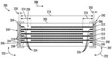
이제 적층 커패시터의 예시적인 실시예들을 상세히 참조할 것이다. 이제 도면들을 참조하면, 도 1은 본 발명의 양태들에 따른 적층 커패시터(100)의 일 실시예의 단면도를 예시한다. 커패시터(100)는 제1 단부(104) 및 길이 방향(108)으로 제1 단부(104)로부터 이격된 제2 단부(106)를 갖는 모놀리식 본체(102)를 포함할 수 있다. 모놀리식 본체(102)는 모놀리식 본체(102)의 제1 단부(104)로부터 제2 단부(106)를 향해 연장하는 제1 복수의 전극들(110)을 포함할 수 있다. 제1 복수의 전극들(110)은 제1 마진 거리(114)만큼 모놀리식 본체의 제2 단부(106)로부터 이격될 수 있다. 제2 복수의 전극들(112)은 제2 단부(106)로부터 모놀리식 본체(102)의 제1 단부(104)를 향해 연장될 수 있다. 복수의 제2 전극들(112)은 복수의 제1 전극들(110)과 인터리브될 수 있다. 제2 복수의 전극들(112)은 제2 마진 거리(116)만큼 모놀리식 본체(102)의 제1 단부(104)로부터 이격될 수 있다. 모놀리식 본체(102)는 제1 단부(104)와 제2 단부(106) 사이의 길이방향 거리(108)에서 본체 길이(118)를 가질 수 있다. 본체 길이(118)와 제1 마진 거리(114) 또는 제2 마진 거리(116) 중 적어도 하나 사이에 마진 비율이 정의될 수 있다. 일부 실시예들에서, 마진 비율은 약 10 미만일 수 있다. Reference will now be made in detail to exemplary embodiments of the multilayer capacitor. Referring now to the drawings, FIG. 1 illustrates a cross-sectional view of one embodiment of a
균열(120)이 커패시터의 (예를 들어 화살표(122)로 예시된 바와 같이) 구부러짐으로 인해 발생하는 경우, 균열(120)은 제1 마진 거리 또는 제2 마진 거리(114, 116) 내에 제한될 것이다. 균열(120)은 제1 복수의 전극들(110) 및 제2 복수의 전극들(120) 모두와 교차하지 않을 것이고, 제1 복수의 전극들(110)과 제2 복수의 전극들(120) 사이의 접촉을 방지하며, 그렇지 않으면 그 사이에 전기적 연결(예를 들어, "단락")이 초래될 수 있다.If
커패시터(100)는 제1 단부(104)를 따라 배치되고 제1 복수의 전극들(110)과 연결된 제1 외부 종단(140)을 포함할 수 있다. 커패시터(100)는 제2 단부(106)를 따라 배치되고 제2 복수의 전극들(112)과 연결된 제2 외부 종단(142)을 포함할 수 있다. 제1 외부 종단(140)은 제1 순응층(144)을 포함할 수 있다. 제1 순응성 층(144)은 제1 베이스 층(146) 위에 형성될 수 있다. 제1 외부 종단(140)의 제1 베이스 층(146)은 제1 복수의 전극들(110)과 전기적으로 연결될 수 있다. The
커패시터(100)는 제2 단부(106)를 따라 배치되고 제2 복수의 전극들(112)과 연결된 제2 외부 종단(142)을 포함할 수 있다. 제2 외부 종단(142)은 제2 순응층(145)을 포함할 수 있다. 제2 순응성 층(145)은 제2 베이스 층(147) 위에 형성될 수 있다. 제2 외부 단자(142)의 제2 베이스 층(147)은 제2 복수의 전극들(112)과 전기적으로 연결될 수 있다. The
순응성 층들(144, 145)은 전도성 중합체 조성물을 포함할 수 있으며, 이는 예를 들어 전술한 바와 같이 중합체 및 전도성 입자들을 포함할 수 있다. 일부 실시예들에서, 중합체는 에폭시 수지이거나 이를 포함할 수 있다. 전도성 입자들은 은, 금, 구리 등과 같은 금속이거나 이를 포함할 수 있다.The
일부 실시예들에서, 베이스 층들(146, 147)은 후막 층들을 형성하기 위해 모놀리식 본체(102)를 침지함으로써 형성될 수 있다. 다른 실시예들에서, 베이스 층들(146, 147)은 (예를 들어, 전해 또는 무전해 도금을 사용하여) 도금될 수 있다. In some embodiments, base layers 146 , 147 may be formed by immersing
하나 이상의 도금층(148)이 순응성 층들(146, 147) 위에 형성될 수 있다. 예를 들어, 제1 외부 종단(140)의 도금층(148)은 순응성 층들(146, 147) 위에 형성된 제1 도금층 및 제1 도금층 위에 형성된 제2 도금층을 포함할 수 있다. 제1 도금층 및 제2 도금층(존재하는 경우)은 다양한 적합한 금속들로 형성될 수 있다. 예를 들어, 제1 도금층은 니켈을 포함할 수 있다. 제2 도금층은 주석을 포함할 수 있다. One or more plating layers 148 may be formed over the
순응성 층들(144, 145)은 길이 방향(108)으로 각각의 두께(150, 152)를 가질 수 있다. 제1 순응성 층(144)의 두께(150)에 대한 제1 마진 거리(114)의 비는 약 5보다 클 수 있다. 제2 순응성 층(145)의 두께(152)에 대한 제2 마진 거리(116)의 비는 약 5보다 클 수 있다.The
도 2는 본 발명의 양태들에 따른 적층 커패시터(200)의 다른 실시예의 단면도를 예시한다. 적층 커패시터(200)는 일반적으로 도 1의 적층 커패시터(100)와 같이 구성될 수 있다. 도 2의 참조 번호들은 일반적으로 도 1의 참조 번호들과 대응할 수 있다. 적층 커패시터(200)는 모놀리식 본체(202)의 제1 단부(204)에 제1 복수의 앵커 탭들(254) 및/또는 모놀리식 본체(202)의 제2 단부(206)에 제2 복수의 앵커 탭들(256)을 추가로 포함할 수 있다.2 illustrates a cross-sectional view of another embodiment of a
앵커 탭들(254, 256)은 베이스 층들(246, 247)에 대한 도금(예를 들어, 무전해 도금)을 위한 핵형성 지점들로서 작용할 수 있다. 예를 들어, 앵커 탭들(254, 256)은 안전하고 신뢰할 수 있는 외부 도금의 형성을 용이하게 할 수 있다. 일반적으로 내부 전기 연결을 제공하지 않는 앵커 탭들은 향상된 외부 종단 연결, 더 나은 기계적 무결성 및 도금 재료의 증착을 위해 제공될 수 있다.
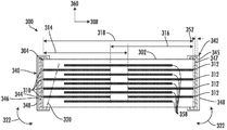
도 3은 본 발명의 양태들에 따른 적층 커패시터(300)의 다른 실시예의 단면도를 예시한다. 도 3의 참조 번호들은 일반적으로 도 1의 참조 번호들과 대응할 수 있다. 적층 커패시터(300)는 하나 이상의 플로팅 전극(358)을 추가로 포함할 수 있다. 예를 들어, 제1 복수의 전극들(310)은 일반적으로 제2 복수의 전극들(312)의 각각의 전극(312)과 Z-방향(360)으로 정렬될 수 있다. 플로팅 전극들(358)은 전극들(310, 312)의 각각의 정렬된 쌍과 인터리브될 수 있다.3 illustrates a cross-sectional view of another embodiment of a
제1 마진 거리(314)는 제1 복수의 전극들(310)과 모놀리식 본체(302)의 제2 단부(306) 사이의 길이 방향(308)으로 정의될 수 있다. 제2 마진 거리(316)는 제2 복수의 전극들(312)과 모놀리식 본체(302)의 제1 단부(304) 사이에 정의될 수 있다. 그러나, 일부 실시예들에서, 커패시터에는 플로팅 전극들이 없을 수 있다는 것을 이해해야 한다. The
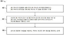
도 4는 본 발명의 양태들에 따른 적층 세라믹 커패시터를 형성하기 위한 방법(400)의 흐름도이다. 일반적으로, 방법(400)은 도 1 내지 도 3를 참조하여 위에서 서술된 적층 커패시터들(100, 200, 300)을 참조하여 여기에서 서술될 것이다. 그러나, 개시된 방법(400)은 임의의 적절한 적층 커패시터로 구현될 수 있음을 이해해야 한다. 또한, 비록 도 4는 예시 및 논의를 위해 특정 순서로 수행되는 단계를 도시하지만, 여기에서 논의된 방법들은 특정 순서나 배열로 제한되지 않는다. 본 명세서에 제공된 개시내용을 사용하여, 본 기술분야의 통상의 기술자는 본 발명의 범위를 벗어나지 않고 다양한 방식들로 본 명세서에 개시된 방법들의 다양한 단계들이 생략, 재배열, 결합 및/또는 적응될 수 있음을 이해할 것이다.4 is a flow diagram of a
방법(400)은, 402에서, 예를 들어, 도 1 내지 도 3을 참조하여 위에서 서술된 바와 같이, 제1 복수의 유전층들 상에 각각 제1 복수의 전극들을 형성하고, 제2 복수의 유전층들 상에 제2 복수의 전극들을 형성하는 단계를 포함한다.The
방법(400)은, 404에서, 예를 들어, 도 1 내지 도 3을 참조하여 위에서 서술된 바와 같이, 각각의 제1 복수의 전극 및 제2 복수의 전극이 각각 제1 마진 거리 및 제2 마진 거리만큼 모놀리식 본체의 대향 단부로부터 이격되도록 유전체 층들을 적층하는 단계를 포함할 수 있다. 보다 구체적으로, 상기 제1 복수의 전극들은 상기 모놀리식 본체의 제1 단부로부터 연장되고, 상기 모놀리식 본체의 제2 단부로부터 길이 방향으로 제1 마진 거리만큼 이격될 수 있다. 제2 복수의 전극들은 모놀리식 본체의 제2 단부로부터 연장될 수 있고, 모놀리식 본체의 제1 단부로부터 길이 방향으로 제2 마진 거리만큼 이격될 수 있다. 몸체 길이와 제1 마진 거리 및/또는 제2 마진 거리 사이의 마진 비율은 약 10 미만일 수 있다.The
방법(400)은, 406에서, 제1 복수의 전극들 및 제2 복수의 전극들과 각각 연결된 모놀리식 본체의 각각의 단부를 따라 외부 종단들을 형성하는 단계를 포함할 수 있다. 외부 종단들 중 적어도 하나는, 예를 들어, 도 1 내지 도 3을 참조하여 위에서 서술된 바와 같이 전도성 중합체 조성물을 포함할 수 있다.
본 발명의 주제가 그 특정 실시예들과 관련하여 상세하게 서술되었지만, 본 기술분야의 통상의 기술자는 전술한 내용을 이해하면 이러한 실시예들에 대한 변경들, 변형들 및 등가물들을 용이하게 생성할 수 있음을 이해할 것이다. 따라서, 본 발명의 범위는 제한이 아니라 예시이며, 본 발명은 본 기술분야의 통상의 기술자에게 용이하게 명백한 바와 같이 본 대상에 대한 그러한 수정들, 변형들 및/또는 추가들의 포함을 배제하지 않는다. Although the subject matter of the present invention has been described in detail with reference to specific embodiments thereof, those skilled in the art will readily be able to create changes, modifications and equivalents to these embodiments upon understanding the foregoing. will understand that Accordingly, the scope of the present invention is illustrative rather than limiting, and the present invention does not exclude the inclusion of such modifications, variations and/or additions to the subject matter as would be readily apparent to one of ordinary skill in the art.
Claims (30)
길이 방향에 수직인 Z 방향으로 적층된 복수의 유전체 층들을 포함하는 모놀리식 본체 - 상기 모놀리식 본체는 제1 단부 및 상기 길이 방향으로 상기 제1 단부로부터 이격되는 제2 단부를 가짐 - 와;
상기 모놀리식 본체의 제1 단부로부터 제2 단부를 향해 연장하는 제1 복수의 전극들 - 상기 제1 복수의 전극들은 제1 마진 거리만큼 상기 모놀리식 본체의 제2 단부로부터 이격됨 - 과;
상기 모놀리식 본체의 제2 단부로부터 제1 단부를 향해 연장하는 제2 복수의 전극들 - 상기 제2 복수의 전극들은 제2 마진 거리만큼 상기 모놀리식 본체의 제1 단부로부터 이격됨 - 과;
상기 제1 단부를 따라 배치되고 상기 제1 복수의 전극들과 연결된 제1 외부 종단과; 그리고
상기 제2 단부를 따라 배치되고 상기 제2 복수의 전극들과 연결된 제2 외부 종단을 포함하고,
상기 모놀리식 본체는 상기 제1 단부와 상기 제2 단부 사이의 길이 방향 거리에서 본체 길이를 가지고, 상기 본체 길이와 상기 제1 마진 거리 또는 상기 제2 마진 거리 중 적어도 하나 사이의 마진 비율은 약 10 미만이고; 그리고
상기 제1 외부 종단 또는 상기 제2 외부 종단 중 적어도 하나는 전도성 중합체 조성물을 포함하는 것을 특징으로 하는
적층 세라믹 커패시터.A multilayer ceramic capacitor comprising:
a monolithic body comprising a plurality of dielectric layers stacked in a Z direction perpendicular to the longitudinal direction, the monolithic body having a first end and a second end spaced apart from the first end in the longitudinal direction; ;
a first plurality of electrodes extending from a first end toward a second end of the monolithic body, the first plurality of electrodes being spaced apart from the second end of the monolithic body by a first margin distance; ;
a second plurality of electrodes extending from a second end toward a first end of the monolithic body, the second plurality of electrodes being spaced apart from the first end of the monolithic body by a second margin distance; ;
a first outer end disposed along the first end and connected to the first plurality of electrodes; and
a second outer end disposed along the second end and connected to the second plurality of electrodes;
wherein the monolithic body has a body length at a longitudinal distance between the first end and the second end, wherein a ratio of a margin between the body length and at least one of the first margin distance or the second margin distance is about less than 10; and
at least one of said first outer end or said second outer end comprises a conductive polymer composition
Multilayer ceramic capacitors.
상기 전도성 중합체 조성물은 에폭시 수지를 포함하는 것을 특징으로 하는
적층 세라믹 커패시터.According to claim 1,
wherein the conductive polymer composition comprises an epoxy resin
Multilayer ceramic capacitors.
상기 전도성 중합체 조성물은 전도성 입자들을 포함하는 것을 특징으로 하는
적층 세라믹 커패시터.According to claim 1,
wherein the conductive polymer composition comprises conductive particles.
Multilayer ceramic capacitors.
상기 전도성 입자들은 은을 포함하는 것을 특징으로 하는
적층 세라믹 커패시터.4. The method of claim 3,
The conductive particles are characterized in that they contain silver.
Multilayer ceramic capacitors.
상기 전도성 중합체 조성물은 약 23℃ 및 20% 상대 습도에서 ASTM D638-14에 따라 시험한 영률이 약 3GPa 미만인 것을 특징으로 하는
적층 세라믹 커패시터.According to claim 1,
wherein the conductive polymer composition has a Young's modulus of less than about 3 GPa as tested according to ASTM D638-14 at about 23° C. and 20% relative humidity.
Multilayer ceramic capacitors.
상기 전도성 중합체 조성물은 약 23℃ 및 20% 상대 습도에서 ASTM B193-16에 따라 시험한 체적 저항률이 약 0.01ohm-cm 미만인 것을 특징으로 하는
적층 세라믹 커패시터.According to claim 1,
wherein the conductive polymer composition has a volume resistivity of less than about 0.01 ohm-cm as tested according to ASTM B193-16 at about 23° C. and 20% relative humidity.
Multilayer ceramic capacitors.
상기 제1 외부 종단은 상기 모놀리식 본체의 제1 단부 위에 형성된 베이스 층 및 상기 베이스 층 위에 형성된 순응성 층(compliant layer)을 더 포함하고, 상기 순응성 층은 상기 전도성 중합체 조성물을 포함하는 것을 특징으로 하는
적층 세라믹 커패시터.According to claim 1,
wherein the first outer end further comprises a base layer formed over the first end of the monolithic body and a compliant layer formed over the base layer, the compliant layer comprising the conductive polymer composition. doing
Multilayer ceramic capacitors.
상기 모놀리식 본체 내부와 상기 모놀리식 본체의 제1 단부에 배치되고, 상기 베이스층과 연결되는 복수의 앵커 탭들을 더 포함하는 것을 특징으로 하는
적층 세라믹 커패시터.8. The method of claim 7,
and a plurality of anchor tabs disposed inside the monolithic body and at the first end of the monolithic body and connected to the base layer.
Multilayer ceramic capacitors.
상기 베이스층은 도전성 금속을 포함하는 것을 특징으로 하는
적층 세라믹 커패시터.8. The method of claim 7,
The base layer is characterized in that it comprises a conductive metal
Multilayer ceramic capacitors.
상기 제1 외부 종단은 순응성 층 및 상기 순응성 층 위에 형성된 적어도 하나의 도금층을 더 포함하고, 상기 순응성 층은 상기 전도성 중합체 조성물을 포함하는 것을 특징으로 하는
적층 세라믹 커패시터.According to claim 1,
wherein said first outer termination further comprises a compliant layer and at least one plating layer formed over said compliant layer, said compliant layer comprising said conductive polymer composition.
Multilayer ceramic capacitors.
상기 적어도 하나의 도금층은 제1 전도성 재료를 포함하는 제1 도금층 및 제2 전도성 재료를 포함하는 제2 도금층을 포함하고, 상기 제2 전도성 재료는 상기 제1 전도성 재료와 상이한 것을 특징으로 하는
적층 세라믹 커패시터.11. The method of claim 10,
wherein the at least one plating layer comprises a first plating layer comprising a first conductive material and a second plating layer comprising a second conductive material, wherein the second conductive material is different from the first conductive material.
Multilayer ceramic capacitors.
상기 제1 외부 종단 및 제2 외부 종단 각각과 전기적으로 연결되지 않은 플로팅 전극을 더 포함하는 것을 특징으로 하는
적층 세라믹 커패시터.According to claim 1,
and a floating electrode not electrically connected to each of the first and second external ends.
Multilayer ceramic capacitors.
상기 커패시터는 플로팅 전극들을 포함하지 않는 것을 특징으로 하는
적층 세라믹 커패시터.According to claim 1,
wherein the capacitor does not include floating electrodes.
Multilayer ceramic capacitors.
상기 제1 외부 종단은 길이 방향으로 약 25㎛ 내지 약 150㎛ 범위의 총 평균 두께를 갖는 것을 특징으로 하는
적층 세라믹 커패시터.According to claim 1,
wherein the first outer end has a total average thickness in the longitudinal direction ranging from about 25 μm to about 150 μm.
Multilayer ceramic capacitors.
상기 제1 외부 종단은 상기 전도성 중합체 조성물을 포함하는 순응층을 더 포함하고, 상기 순응성 층은 약 3㎛ 내지 약 125㎛ 범위의 평균 두께를 갖는 것을 특징으로 하는
적층 세라믹 커패시터.According to claim 1,
wherein the first outer termination further comprises a compliant layer comprising the conductive polymer composition, wherein the compliant layer has an average thickness in the range of about 3 μm to about 125 μm.
Multilayer ceramic capacitors.
상기 제1 복수의 전극들과 상기 제2 복수의 전극들은 인터리브된 것을 특징으로 하는
적층 세라믹 커패시터. According to claim 1,
wherein the first plurality of electrodes and the second plurality of electrodes are interleaved
Multilayer ceramic capacitors.
제1 복수의 유전체 층들 상에 각각 제1 복수의 전극들을 형성하는 단계와;
제2 복수의 유전체 층들 상에 제2 복수의 전극들을 형성하는 단계와;
모놀리식 본체를 형성하기 위해 길이 방향에 수직인 Z-방향으로 상기 제1 복수의 유전체 층들 및 상기 제2 복수의 유전체 층을 적층하여, 상기 제1 복수의 전극들이 상기 모놀리식 본체의 제1 단부로부터 연장되고 상기 모놀리식 본체의 제2 단부로부터 상기 길이 방향으로 제1 마진 거리만큼 이격되도록 하고, 그리고 상기 제2 복수의 전극들이 상기 모놀리식 본체의 제2 단부로부터 연장되고 상기 모놀리식 본체의 제1 단부로부터 상기 길이 방향으로 제2 마진 거리만큼 이격되도록 하는 단계와;
상기 제1 복수의 전극들과 연결된 모놀리식 본체의 제1 단부를 따라 제1 외부 종단을 형성하는 단계와;
상기 제2 복수의 전극들과 연결된 모놀리식 본체의 제2 단부를 따라 제2 외부 종단을 형성하는 단계를 포함하고,
상기 모놀리식 본체는 상기 제1 단부와 상기 제2 단부 사이의 길이 방향 거리에서 본체 길이를 가지고, 상기 본체 길이와 상기 제1 마진 거리 또는 상기 제2 마진 거리 중 적어도 하나 사이의 마진 비율은 약 10 미만이고; 그리고
상기 제1 외부 종단 또는 상기 제2 외부 종단 중 적어도 하나는 전도성 중합체 조성물을 포함하는 것을 특징으로 하는
적층 세라믹 커패시터를 형성하는 방법.A method of forming a multilayer ceramic capacitor, comprising:
forming a first plurality of electrodes each on the first plurality of dielectric layers;
forming a second plurality of electrodes on the second plurality of dielectric layers;
stacking the first plurality of dielectric layers and the second plurality of dielectric layers in a Z-direction perpendicular to the longitudinal direction to form a monolithic body, such that the first plurality of electrodes form a first portion of the monolithic body extending from a first end and spaced apart from a second end of the monolithic body by a first marginal distance in the longitudinal direction, and wherein the second plurality of electrodes extend from a second end of the monolithic body and spaced apart from the first end of the tactile body by a second marginal distance in the longitudinal direction;
forming a first outer termination along a first end of the monolithic body connected with the first plurality of electrodes;
forming a second outer termination along a second end of the monolithic body connected with the second plurality of electrodes;
wherein the monolithic body has a body length at a longitudinal distance between the first end and the second end, wherein a ratio of a margin between the body length and at least one of the first margin distance or the second margin distance is about less than 10; and
at least one of said first outer end or said second outer end comprises a conductive polymer composition
A method of forming a multilayer ceramic capacitor.
상기 전도성 중합체 조성물은 에폭시 수지를 포함하는 것을 특징으로 하는
적층 세라믹 커패시터를 형성하는 방법.18. The method of claim 17,
wherein the conductive polymer composition comprises an epoxy resin
A method of forming a multilayer ceramic capacitor.
상기 전도성 중합체 조성물은 전도성 입자들을 포함하는 것을 특징으로 하는
적층 세라믹 커패시터를 형성하는 방법.18. The method of claim 17,
wherein the conductive polymer composition comprises conductive particles.
A method of forming a multilayer ceramic capacitor.
상기 전도성 입자들은 은을 포함하는 것을 특징으로 하는
적층 세라믹 커패시터를 형성하는 방법.18. The method of claim 17,
The conductive particles are characterized in that they contain silver.
A method of forming a multilayer ceramic capacitor.
상기 전도성 중합체 조성물은 약 23℃ 및 20% 상대 습도에서 ASTM D638-14에 따라 시험한 영률이 약 3GPa 미만인 것을 특징으로 하는
적층 세라믹 커패시터를 형성하는 방법.18. The method of claim 17,
wherein the conductive polymer composition has a Young's modulus of less than about 3 GPa as tested according to ASTM D638-14 at about 23° C. and 20% relative humidity.
A method of forming a multilayer ceramic capacitor.
상기 전도성 중합체 조성물은 약 23℃ 및 20% 상대 습도에서 ASTM B193-16에 따라 시험한 체적 저항률이 약 0.01ohm-cm 미만인 것을 특징으로 하는
적층 세라믹 커패시터를 형성하는 방법.18. The method of claim 17,
wherein the conductive polymer composition has a volume resistivity of less than about 0.01 ohm-cm as tested according to ASTM B193-16 at about 23° C. and 20% relative humidity.
A method of forming a multilayer ceramic capacitor.
상기 제1 외부 종단을 형성하는 단계는, 상기 모놀리식 본체의 제1 단부 위에 형성된 베이스 층을 형성하는 단계 및 상기 베이스 층 위에 상기 전도성 중합체 조성물을 포함하는 순응성 층을 형성하는 단계를 포함하는 것을 특징으로 하는
적층 세라믹 커패시터를 형성하는 방법.18. The method of claim 17,
wherein forming the first outer end comprises forming a base layer formed over a first end of the monolithic body and forming a conformable layer comprising the conductive polymer composition over the base layer characterized
A method of forming a multilayer ceramic capacitor.
상기 모놀리식 본체 내부와 상기 모놀리식 본체의 제1 단부에 배치되고, 상기 베이스층과 연결되는 복수의 앵커 탭들을 형성하는 단계를 더 포함하는 것을 특징으로 하는
적층 세라믹 커패시터를 형성하는 방법.24. The method of claim 23,
and forming a plurality of anchor tabs disposed within the monolithic body and at a first end of the monolithic body and connected to the base layer.
A method of forming a multilayer ceramic capacitor.
상기 제1 외부 종단을 형성하는 단계는, 상기 순응성 층 위에 적어도 하나의 도금층을 도금하는 단계를 포함하는 것을 특징으로 하는
적층 세라믹 커패시터를 형성하는 방법.24. The method of claim 23,
wherein forming the first outer termination comprises plating at least one plating layer over the compliant layer.
A method of forming a multilayer ceramic capacitor.
상기 적어도 하나의 도금층을 도금하는 단계는, 제1 전도성 재료를 포함하는 제1 도금층을 도금하는 단계 및 제2 전도성 재료를 포함하는 제2 도금층을 도금하는 단계를 포함하고, 상기 제2 전도성 재료는 상기 제1 전도성 재료와 상이한 것을 특징으로 하는
적층 세라믹 커패시터를 형성하는 방법.26. The method of claim 25,
The plating of the at least one plating layer includes plating a first plating layer comprising a first conductive material and plating a second plating layer comprising a second conductive material, wherein the second conductive material comprises: different from the first conductive material
A method of forming a multilayer ceramic capacitor.
상기 모놀리식 본체 내에 플로팅 전극을 형성하는 단계를 더 포함하고, 상기 플로팅 전극은 상기 제1 외부 종단 및 상기 제2 외부 종단 각각과 전기적으로 연결되지 않는 것을 특징으로 하는
적층 세라믹 커패시터를 형성하는 방법.18. The method of claim 17,
forming a floating electrode within the monolithic body, wherein the floating electrode is not electrically connected to each of the first outer end and the second outer end
A method of forming a multilayer ceramic capacitor.
상기 제1 외부 종단은 길이 방향으로 약 25㎛ 내지 약 150㎛ 범위의 총 평균 두께를 갖는 것을 특징으로 하는
적층 세라믹 커패시터를 형성하는 방법.18. The method of claim 17,
wherein the first outer end has a total average thickness in the longitudinal direction ranging from about 25 μm to about 150 μm.
A method of forming a multilayer ceramic capacitor.
상기 제1 외부 종단을 형성하는 단계는 상기 전도성 중합체 조성물을 포함하는 순응층을 형성하는 단계를 포함하고, 상기 순응성 층은 약 3㎛ 내지 약 125㎛ 범위의 평균 두께를 갖는 것을 특징으로 하는
적층 세라믹 커패시터를 형성하는 방법.18. The method of claim 17,
wherein forming the first outer termination comprises forming a compliant layer comprising the conductive polymer composition, wherein the compliant layer has an average thickness in the range of about 3 μm to about 125 μm.
A method of forming a multilayer ceramic capacitor.
상기 제1 복수의 유전체 층들 및 상기 제2 복수의 유전체 층을 적층하는 단계는, 상기 제1 복수의 전극들과 상기 제2 복수의 전극들을 인터리빙하는 단계를 포함하는 것을 특징으로 하는
적층 세라믹 커패시터를 형성하는 방법.18. The method of claim 17,
wherein said step of stacking said first plurality of dielectric layers and said second plurality of dielectric layers comprises interleaving said first plurality of electrodes and said second plurality of electrodes.
A method of forming a multilayer ceramic capacitor.
Applications Claiming Priority (3)
| Application Number | Priority Date | Filing Date | Title |
|---|---|---|---|
| US201962838406P | 2019-04-25 | 2019-04-25 | |
| US62/838,406 | 2019-04-25 | ||
| PCT/US2020/028737 WO2020219354A1 (en) | 2019-04-25 | 2020-04-17 | Multilayer capacitor having open mode electrode configuration and flexible terminations |
Publications (1)
| Publication Number | Publication Date |
|---|---|
| KR20210146447A true KR20210146447A (en) | 2021-12-03 |
Family
ID=72917256
Family Applications (1)
| Application Number | Title | Priority Date | Filing Date |
|---|---|---|---|
| KR1020217038225A KR20210146447A (en) | 2019-04-25 | 2020-04-17 | Multilayer Capacitors with Open Mode Electrode Configuration and Flexible Terminations |
Country Status (7)
| Country | Link |
|---|---|
| US (1) | US11705280B2 (en) |
| JP (1) | JP2022541365A (en) |
| KR (1) | KR20210146447A (en) |
| CN (1) | CN113678216A (en) |
| DE (1) | DE112020002053T5 (en) |
| TW (1) | TW202109576A (en) |
| WO (1) | WO2020219354A1 (en) |
Families Citing this family (9)
| Publication number | Priority date | Publication date | Assignee | Title |
|---|---|---|---|---|
| CN114899009A (en) | 2019-01-28 | 2022-08-12 | 京瓷Avx元器件公司 | Multilayer ceramic capacitor with ultra-wideband performance |
| US11195656B2 (en) | 2019-01-28 | 2021-12-07 | Avx Corporation | Multilayer ceramic capacitor having ultra-broadband performance |
| WO2020159813A1 (en) | 2019-01-28 | 2020-08-06 | Avx Corporation | Multilayer ceramic capacitor having ultra-broadband performance |
| WO2020159809A1 (en) | 2019-01-28 | 2020-08-06 | Avx Corporation | Multilayer ceramic capacitor having ultra-broadband performance |
| US11270842B2 (en) | 2019-01-28 | 2022-03-08 | KYOCERA AVX Components Corporation | Multilayer ceramic capacitor having ultra-broadband performance |
| WO2022164747A1 (en) * | 2021-02-01 | 2022-08-04 | KYOCERA AVX Components Corporation | Varistor having flexible terminations |
| DE112022001440T5 (en) * | 2021-03-11 | 2024-01-11 | KYOCERA AVX Components Corporation | Varistor array including customized varistors |
| US20230215630A1 (en) * | 2021-12-31 | 2023-07-06 | Samsung Electro-Mechanics Co., Ltd. | Multlayer electronic component |
| WO2023189678A1 (en) * | 2022-03-29 | 2023-10-05 | 株式会社村田製作所 | Solid-state battery and electronic device |
Family Cites Families (58)
| Publication number | Priority date | Publication date | Assignee | Title |
|---|---|---|---|---|
| JP2852372B2 (en) | 1989-07-07 | 1999-02-03 | 株式会社村田製作所 | Multilayer ceramic capacitors |
| JP2890985B2 (en) | 1992-06-16 | 1999-05-17 | 株式会社村田製作所 | Bandpass filter |
| US5719539A (en) | 1993-08-24 | 1998-02-17 | Matsushita Electric Industrial Co., Ltd. | Dielectric filter with multiple resonators |
| JP3201466B2 (en) | 1997-03-31 | 2001-08-20 | 日本電気株式会社 | Conductive polymer terminals and solid electrolytic capacitors |
| US6191933B1 (en) | 1998-01-07 | 2001-02-20 | Tdk Corporation | Ceramic capacitor |
| JP2002343677A (en) | 2001-05-14 | 2002-11-29 | Murata Mfg Co Ltd | Laminated electronic component with built-in capacitor |
| JP3885938B2 (en) | 2002-03-07 | 2007-02-28 | Tdk株式会社 | Ceramic electronic component, paste coating method and paste coating apparatus |
| US7177137B2 (en) | 2002-04-15 | 2007-02-13 | Avx Corporation | Plated terminations |
| US7463474B2 (en) | 2002-04-15 | 2008-12-09 | Avx Corporation | System and method of plating ball grid array and isolation features for electronic components |
| US6816356B2 (en) | 2002-05-17 | 2004-11-09 | Daniel Devoe | Integrated broadband ceramic capacitor array |
| US6587327B1 (en) | 2002-05-17 | 2003-07-01 | Daniel Devoe | Integrated broadband ceramic capacitor array |
| US6900708B2 (en) | 2002-06-26 | 2005-05-31 | Georgia Tech Research Corporation | Integrated passive devices fabricated utilizing multi-layer, organic laminates |
| US7675729B2 (en) | 2003-12-22 | 2010-03-09 | X2Y Attenuators, Llc | Internally shielded energy conditioner |
| US20050248908A1 (en) | 2004-05-06 | 2005-11-10 | Gunther Dreezen | Termination coating |
| US7334981B2 (en) | 2004-10-29 | 2008-02-26 | General Electric Company | Counter-rotating gas turbine engine and method of assembling same |
| TWI277988B (en) | 2004-11-18 | 2007-04-01 | Tdk Corp | Multilayer capacitor |
| JP4462194B2 (en) | 2006-01-17 | 2010-05-12 | Tdk株式会社 | Multilayer feedthrough capacitor array |
| US7336475B2 (en) | 2006-02-22 | 2008-02-26 | Vishay Vitramon, Inc. | High voltage capacitors |
| US8238075B2 (en) | 2006-02-22 | 2012-08-07 | Vishay Sprague, Inc. | High voltage capacitors |
| JP4374041B2 (en) | 2007-07-09 | 2009-12-02 | Tdk株式会社 | Multilayer capacitor |
| DE112008003104B4 (en) | 2007-11-22 | 2014-09-25 | Murata Mfg. Co., Ltd. | Ceramic multilayer component |
| US8446705B2 (en) | 2008-08-18 | 2013-05-21 | Avx Corporation | Ultra broadband capacitor |
| CN102016314A (en) * | 2008-08-26 | 2011-04-13 | 松下电器产业株式会社 | Fluid transport using conductive polymer |
| WO2011002982A2 (en) | 2009-07-01 | 2011-01-06 | Kemet Electronics Corporation | High capacitance multilayer with high voltage capability |
| US9299476B2 (en) * | 2010-10-22 | 2016-03-29 | Newsouth Innovations Pty Limited | Polymeric material |
| KR20120068622A (en) | 2010-12-17 | 2012-06-27 | 삼성전기주식회사 | Paste compound for termination electrode and multilayer ceramic capacitor comprising the same and manufacturing method thereof |
| JP5267548B2 (en) | 2010-12-24 | 2013-08-21 | Tdk株式会社 | Multilayer capacitor |
| JP5353911B2 (en) | 2011-01-28 | 2013-11-27 | 株式会社村田製作所 | Electronic components and board modules |
| KR20130042924A (en) | 2011-10-19 | 2013-04-29 | 삼성전기주식회사 | Multilayer ceramic electronic component |
| US20130107419A1 (en) | 2011-10-28 | 2013-05-02 | Kemet Electronics Corporation | Multilayered ceramic capacitor with improved lead frame attachment |
| KR101761936B1 (en) | 2012-03-13 | 2017-07-26 | 삼성전기주식회사 | Multilayered ceramic capacitor |
| DE112013001679B4 (en) | 2012-03-26 | 2023-03-09 | Kemet Electronics Corporation | Asymmetric high voltage capacitor |
| KR101525652B1 (en) * | 2012-05-04 | 2015-06-03 | 삼성전기주식회사 | Conductive resin composition, multi layer ceramic capacitor having the same and manufacturing method thereof |
| KR101462754B1 (en) * | 2013-01-24 | 2014-11-17 | 삼성전기주식회사 | Multi-layered ceramic electronic parts and fabricating method thereof |
| KR101462798B1 (en) * | 2013-07-16 | 2014-11-20 | 삼성전기주식회사 | Conductive paste composition for external electrode and multilayer ceramic components using the same |
| JP2015070144A (en) | 2013-09-30 | 2015-04-13 | 京セラ株式会社 | Multilayer capacitor and flash light emitting device |
| KR102089694B1 (en) | 2014-04-30 | 2020-03-16 | 삼성전기주식회사 | Multi-layered ceramic electronic component |
| KR102089700B1 (en) | 2014-05-28 | 2020-04-14 | 삼성전기주식회사 | Multi-layered ceramic capacitor, manufacturing method of the same and board having the same mounted thereon |
| US9997295B2 (en) | 2014-09-26 | 2018-06-12 | Murata Manufacturing Co., Ltd. | Electronic component |
| US10083795B2 (en) | 2014-09-30 | 2018-09-25 | Murata Manufacturing Co., Ltd. | Multilayer ceramic capacitor and mounted structure with multilayer ceramic capacitor |
| US9443656B2 (en) | 2014-09-30 | 2016-09-13 | Murata Manufacturing Co., Ltd. | Tensile stress resistant multilayer ceramic capacitor |
| KR102048098B1 (en) | 2014-11-04 | 2019-11-22 | 삼성전기주식회사 | Multi-layered chip component and board having the same mounted thereon |
| KR102029497B1 (en) | 2014-11-04 | 2019-11-08 | 삼성전기주식회사 | Multi-layered chip component and board for mounting the same |
| US10117333B2 (en) * | 2015-01-31 | 2018-10-30 | Murata Manufacturing Co., Ltd. | Multilayer ceramic capacitor, mounting structure of multilayer ceramic capacitor, and taped electronic component array |
| JP2016146469A (en) * | 2015-01-31 | 2016-08-12 | 株式会社村田製作所 | Multilayer ceramic capacitor, mounting structure of multilayer ceramic capacitor, and taping electronic component series |
| US9847173B2 (en) | 2015-06-26 | 2017-12-19 | Murata Manufacturing Co., Ltd. | Mounting substrate |
| JP6860995B2 (en) | 2016-08-29 | 2021-04-21 | 太陽誘電株式会社 | Multilayer ceramic capacitors |
| JP6822155B2 (en) * | 2017-01-12 | 2021-01-27 | 株式会社村田製作所 | Multilayer ceramic capacitors and their mounting structures |
| US20180374646A1 (en) | 2017-06-26 | 2018-12-27 | Vishay Israel Ltd. | Wideband coupling capacitor |
| KR102463330B1 (en) * | 2017-10-17 | 2022-11-04 | 삼성전기주식회사 | Coil Electronic Component |
| CN114709075A (en) | 2018-03-06 | 2022-07-05 | 京瓷Avx元器件公司 | Multilayer ceramic capacitor with ultra-wideband performance |
| WO2019173302A1 (en) | 2018-03-06 | 2019-09-12 | Avx Corporation | Multilayer ceramic capacitor having ultra-broadband performance |
| JP6780673B2 (en) * | 2018-03-30 | 2020-11-04 | 株式会社村田製作所 | Multilayer ceramic capacitors and their mounting structure |
| WO2020159813A1 (en) | 2019-01-28 | 2020-08-06 | Avx Corporation | Multilayer ceramic capacitor having ultra-broadband performance |
| WO2020159809A1 (en) | 2019-01-28 | 2020-08-06 | Avx Corporation | Multilayer ceramic capacitor having ultra-broadband performance |
| US11195656B2 (en) | 2019-01-28 | 2021-12-07 | Avx Corporation | Multilayer ceramic capacitor having ultra-broadband performance |
| US11270842B2 (en) | 2019-01-28 | 2022-03-08 | KYOCERA AVX Components Corporation | Multilayer ceramic capacitor having ultra-broadband performance |
| CN114899009A (en) | 2019-01-28 | 2022-08-12 | 京瓷Avx元器件公司 | Multilayer ceramic capacitor with ultra-wideband performance |
-
2020
- 2020-04-16 US US16/850,132 patent/US11705280B2/en active Active
- 2020-04-17 JP JP2021562984A patent/JP2022541365A/en active Pending
- 2020-04-17 WO PCT/US2020/028737 patent/WO2020219354A1/en active Application Filing
- 2020-04-17 KR KR1020217038225A patent/KR20210146447A/en not_active Application Discontinuation
- 2020-04-17 DE DE112020002053.3T patent/DE112020002053T5/en active Pending
- 2020-04-17 CN CN202080028169.1A patent/CN113678216A/en active Pending
- 2020-04-24 TW TW109113741A patent/TW202109576A/en unknown
Also Published As
| Publication number | Publication date |
|---|---|
| TW202109576A (en) | 2021-03-01 |
| US20200343046A1 (en) | 2020-10-29 |
| WO2020219354A1 (en) | 2020-10-29 |
| DE112020002053T5 (en) | 2022-01-27 |
| JP2022541365A (en) | 2022-09-26 |
| CN113678216A (en) | 2021-11-19 |
| US11705280B2 (en) | 2023-07-18 |
Similar Documents
| Publication | Publication Date | Title |
|---|---|---|
| KR20210146447A (en) | Multilayer Capacitors with Open Mode Electrode Configuration and Flexible Terminations | |
| US10347426B2 (en) | Chip-shaped electronic component | |
| US9082557B2 (en) | Multilayer ceramic capacitor and method of manufacturing the same | |
| JP4996036B2 (en) | Plating terminal | |
| US7576968B2 (en) | Plated terminations and method of forming using electrolytic plating | |
| CN104575937B (en) | Chip electronic component and its manufacturing method | |
| JP4425688B2 (en) | Plating termination | |
| WO2008023496A1 (en) | Laminated electronic component and method for manufacturing laminated electronic component | |
| CN110800076B (en) | Surface-mounted multilayer coupling capacitor and circuit board including the same | |
| JP2023110018A (en) | Multilayer electronic device having improved connectivity and method for making the same | |
| CN110622267A (en) | Multilayer capacitor and circuit board including the same | |
| JP2009224802A (en) | Method for forming electroless plating termination | |
| JPWO2018159023A1 (en) | Flexible printed wiring board, method for manufacturing connector, and connector | |
| CN113424280B (en) | Multilayer ceramic capacitor including conductive path | |
| CN108695066B (en) | Multilayer ceramic capacitor and method of manufacturing the same | |
| US20220246334A1 (en) | Varistor Having Flexible Terminations | |
| CN117976411A (en) | Multilayer electronic device with improved connectivity and method of manufacturing the same | |
| CN117981022A (en) | Multilayer ceramic capacitor | |
| JP2006100546A (en) | Wiring board having many wiring areas, package for storing electronic component, and electronic device | |
| JPH04133449U (en) | Package cage for storing semiconductor elements |
Legal Events
| Date | Code | Title | Description |
|---|---|---|---|
| E902 | Notification of reason for refusal |