KR20210132176A - Optical Absorption Filters for Integrated Devices - Google Patents
Optical Absorption Filters for Integrated Devices Download PDFInfo
- Publication number
- KR20210132176A KR20210132176A KR1020217031341A KR20217031341A KR20210132176A KR 20210132176 A KR20210132176 A KR 20210132176A KR 1020217031341 A KR1020217031341 A KR 1020217031341A KR 20217031341 A KR20217031341 A KR 20217031341A KR 20210132176 A KR20210132176 A KR 20210132176A
- Authority
- KR
- South Korea
- Prior art keywords
- semiconductor
- layer
- optical
- filter
- assembly
- Prior art date
Links
Images


Classifications
-
- G—PHYSICS
- G02—OPTICS
- G02B—OPTICAL ELEMENTS, SYSTEMS OR APPARATUS
- G02B5/00—Optical elements other than lenses
- G02B5/20—Filters
- G02B5/22—Absorbing filters
-
- G—PHYSICS
- G01—MEASURING; TESTING
- G01N—INVESTIGATING OR ANALYSING MATERIALS BY DETERMINING THEIR CHEMICAL OR PHYSICAL PROPERTIES
- G01N21/00—Investigating or analysing materials by the use of optical means, i.e. using sub-millimetre waves, infrared, visible or ultraviolet light
- G01N21/62—Systems in which the material investigated is excited whereby it emits light or causes a change in wavelength of the incident light
- G01N21/63—Systems in which the material investigated is excited whereby it emits light or causes a change in wavelength of the incident light optically excited
- G01N21/64—Fluorescence; Phosphorescence
- G01N21/645—Specially adapted constructive features of fluorimeters
- G01N21/6452—Individual samples arranged in a regular 2D-array, e.g. multiwell plates
- G01N21/6454—Individual samples arranged in a regular 2D-array, e.g. multiwell plates using an integrated detector array
-
- G—PHYSICS
- G01—MEASURING; TESTING
- G01N—INVESTIGATING OR ANALYSING MATERIALS BY DETERMINING THEIR CHEMICAL OR PHYSICAL PROPERTIES
- G01N21/00—Investigating or analysing materials by the use of optical means, i.e. using sub-millimetre waves, infrared, visible or ultraviolet light
- G01N21/62—Systems in which the material investigated is excited whereby it emits light or causes a change in wavelength of the incident light
- G01N21/63—Systems in which the material investigated is excited whereby it emits light or causes a change in wavelength of the incident light optically excited
- G01N21/64—Fluorescence; Phosphorescence
- G01N21/645—Specially adapted constructive features of fluorimeters
- G01N21/648—Specially adapted constructive features of fluorimeters using evanescent coupling or surface plasmon coupling for the excitation of fluorescence
-
- G—PHYSICS
- G01—MEASURING; TESTING
- G01N—INVESTIGATING OR ANALYSING MATERIALS BY DETERMINING THEIR CHEMICAL OR PHYSICAL PROPERTIES
- G01N21/00—Investigating or analysing materials by the use of optical means, i.e. using sub-millimetre waves, infrared, visible or ultraviolet light
- G01N21/62—Systems in which the material investigated is excited whereby it emits light or causes a change in wavelength of the incident light
- G01N21/63—Systems in which the material investigated is excited whereby it emits light or causes a change in wavelength of the incident light optically excited
- G01N21/64—Fluorescence; Phosphorescence
- G01N21/6486—Measuring fluorescence of biological material, e.g. DNA, RNA, cells
-
- G—PHYSICS
- G02—OPTICS
- G02B—OPTICAL ELEMENTS, SYSTEMS OR APPARATUS
- G02B5/00—Optical elements other than lenses
- G02B5/003—Light absorbing elements
-
- G—PHYSICS
- G02—OPTICS
- G02B—OPTICAL ELEMENTS, SYSTEMS OR APPARATUS
- G02B5/00—Optical elements other than lenses
- G02B5/20—Filters
- G02B5/207—Filters comprising semiconducting materials
-
- B—PERFORMING OPERATIONS; TRANSPORTING
- B01—PHYSICAL OR CHEMICAL PROCESSES OR APPARATUS IN GENERAL
- B01L—CHEMICAL OR PHYSICAL LABORATORY APPARATUS FOR GENERAL USE
- B01L2200/00—Solutions for specific problems relating to chemical or physical laboratory apparatus
- B01L2200/12—Specific details about manufacturing devices
-
- G—PHYSICS
- G01—MEASURING; TESTING
- G01N—INVESTIGATING OR ANALYSING MATERIALS BY DETERMINING THEIR CHEMICAL OR PHYSICAL PROPERTIES
- G01N21/00—Investigating or analysing materials by the use of optical means, i.e. using sub-millimetre waves, infrared, visible or ultraviolet light
- G01N21/62—Systems in which the material investigated is excited whereby it emits light or causes a change in wavelength of the incident light
- G01N21/63—Systems in which the material investigated is excited whereby it emits light or causes a change in wavelength of the incident light optically excited
- G01N21/64—Fluorescence; Phosphorescence
- G01N21/645—Specially adapted constructive features of fluorimeters
- G01N2021/6463—Optics
- G01N2021/6471—Special filters, filter wheel
-
- G—PHYSICS
- G01—MEASURING; TESTING
- G01N—INVESTIGATING OR ANALYSING MATERIALS BY DETERMINING THEIR CHEMICAL OR PHYSICAL PROPERTIES
- G01N21/00—Investigating or analysing materials by the use of optical means, i.e. using sub-millimetre waves, infrared, visible or ultraviolet light
- G01N21/62—Systems in which the material investigated is excited whereby it emits light or causes a change in wavelength of the incident light
- G01N21/63—Systems in which the material investigated is excited whereby it emits light or causes a change in wavelength of the incident light optically excited
- G01N21/64—Fluorescence; Phosphorescence
- G01N21/6408—Fluorescence; Phosphorescence with measurement of decay time, time resolved fluorescence
Abstract
샘플 분석에 사용되는 통합 디바이스 내의 센서(1-122)에 입사하는 여기 복사를 감쇠시키는 것에 관한 장치들 및 방법들이 설명된다. 기판(1-105) 상에 형성된 통합 디바이스 내의 도파관(1-115)과 센서(1-122) 사이에, 선택된 재료 및 결정 모폴로지의 적어도 하나의 반도체 필름(1-336)이 위치된다. 반도체 재료(1-135)의 단일 층에 대해 40㎚ 떨어져 있는 여기 및 방출 파장들에 대해 100 이상의 제거율이 획득될 수 있다.Apparatus and methods are described for attenuating excitation radiation incident on a sensor 1-122 in an integrated device used for sample analysis. Between the sensor 1-122 and the waveguide 1-115 in the integrated device formed on the substrate 1-105 is positioned at least one semiconductor film 1-336 of a selected material and crystal morphology. Removal rates of 100 or more can be obtained for excitation and emission wavelengths that are 40 nm apart for a single layer of semiconductor material 1-135.

Description
관련 출원Related applications
본 출원은 35 U.S.C.§119(e) 하에서, 2019년 3월 5일자로 출원되고 발명의 명칭이 "통합 디바이스를 위한 반도체 광학 흡수 필터(SEMICONDUCTOR OPTICAL ABSORPTION FILTER FOR AN INTEGRATED DEVICE)"인 미국 가출원 제62/813,997호, 및 2019년 4월 9일자로 출원되고 발명의 명칭이 "통합 디바이스를 위한 반도체 광학 흡수 필터(SEMICONDUCTOR OPTICAL ABSORPTION FILTER FOR AN INTEGRATED DEVICE)"인 미국 가출원 제62/831,237호의 우선권을 주장하며, 그것들 각각의 전체내용은 여기에 참조로 포함된다.This application is filed under 35 USC §119(e) on March 5, 2019 and is entitled "SEMICONDUCTOR OPTICAL ABSORPTION FILTER FOR AN INTEGRATED DEVICE," U.S. Provisional Application No. 62. /813,997, and U.S. Provisional Application No. 62/831,237, filed April 9, 2019, entitled "SEMICONDUCTOR OPTICAL ABSORPTION FILTER FOR AN INTEGRATED DEVICE," , the entire contents of each of which are incorporated herein by reference.
기술분야 technical field
본 출원은 광학 흡수 필터로, 샘플들을 분석하기 위해 사용되는 통합 디바이스에서 원하지 않는 복사를 감소시키는 것에 관한 것이다.This application relates to reducing unwanted radiation in an integrated device used to analyze samples with an optical absorption filter.
샘플들의 분석에 사용되는 기기의 영역에서, (하나 이상의 샘플에 포함되는) 다수의 분석물 또는 시료를 병렬로 분석하기 위해, 미세 가공 칩들(microfabricated chips)이 사용될 수 있다. 일부 경우들에서, 광학 여기 복사(optical excitation radiation)는 별개의 분석들이 수행되는 칩 상의 복수의 개별 사이트에 전달된다. 여기 복사는 각각의 사이트에 있는 시료, 시료에 부착된 형광단(fluorophore), 또는 시료와의 상호작용에 관여하는 형광단을 여기시킬 수 있다. 여기에 응답하여, 센서에 의해 검출되는 복사가 사이트로부터 방출될 수 있다. 사이트에 대한 방출된 복사로부터 획득된 정보, 또는 방출된 복사의 결여는 해당 사이트에서의 시료의 특성을 결정하기 위해 사용될 수 있다.In the realm of an instrument used for analysis of samples, microfabricated chips may be used to analyze multiple analytes or samples (in one or more samples) in parallel. In some cases, optical excitation radiation is delivered to a plurality of distinct sites on the chip where separate analyzes are performed. The excitation radiation may excite a sample at each site, a fluorophore attached to the sample, or a fluorophore involved in an interaction with the sample. In response to this, radiation detected by the sensor may be emitted from the site. Information obtained from emitted radiation for a site, or lack of emitted radiation, can be used to determine the characteristics of a sample at that site.
통합 디바이스(예를 들어, 샘플 분석에 사용되는 디바이스) 내의 센서에 입사하는 여기 복사 또는 다른 원하지 않는 복사를 감쇠시키는 것에 관한 장치들 및 방법들이 설명된다. 일부 실시예들에서, 선택된 재료 및 결정 모폴로지의 반도체 필름은 기판 상의 재료들의 스택 내에 형성되고, 통합 디바이스의 픽셀 내의 센서와 도파관 사이에 위치된다. 반도체 재료 및 결정 모폴로지는 픽셀 내의 반응 챔버로부터 방출되는 복사의 75% 초과를 센서에 통과시키면서 여기 복사를 크게 감쇠시키도록 선택된다. 40㎚ 또는 대략 40㎚만큼 분리된 파장들에 대해 100 이상인 파장-판별비(wavelength-discrimination ratio)("제거율(rejection ratio)" 또는 "소광비(extinction ratio)"라고도 지칭됨)가 획득될 수 있다. 일부 구현들에서, 다층 스택은 유전체 재료의 층들에 의해 분리된 흡수 재료의 층들을 포함한다. 스택은 상이한 두께들을 갖는 적어도 3개 또는 4개의 층을 포함할 수 있다. 이러한 스택들은 110㎚ 또는 대략 110㎚만큼 분리된 파장들에 대해 수직 내지 80도(또는 이러한 각도들 내의 임의의 하위-범위)의 입사각들의 범위에 걸쳐 10,000보다 큰 제거율들을 제공할 수 있다.Apparatus and methods are described for attenuating excitation or other undesired radiation incident on a sensor in an integrated device (eg, a device used for sample analysis). In some embodiments, a semiconductor film of a selected material and crystal morphology is formed in a stack of materials on a substrate and positioned between a sensor and a waveguide within a pixel of an integrated device. The semiconductor material and crystal morphology are selected to greatly attenuate the excitation radiation while passing more than 75% of the radiation emitted from the reaction chamber within the pixel to the sensor. A wavelength-discrimination ratio (also referred to as “rejection ratio” or “extinction ratio”) of 100 or greater for wavelengths separated by 40 nm or approximately 40 nm can be obtained. . In some implementations, the multilayer stack includes layers of absorbent material separated by layers of dielectric material. The stack may include at least three or four layers having different thicknesses. Such stacks may provide removal rates greater than 10,000 over a range of angles of incidence from normal to 80 degrees (or any sub-range within these angles) for wavelengths separated by 110 nm or approximately 110 nm.
일부 실시예들은 복수의 반도체 흡수체 층; 및 다층 스택을 형성하기 위해 복수의 반도체 흡수체를 분리하는 복수의 유전체 재료 층을 포함하고, 다층 스택 내에 적어도 3개의 상이한 층 두께가 존재하는 다층 반도체 흡수체 필터에 관한 것이다. Some embodiments include a plurality of semiconductor absorber layers; and a plurality of layers of dielectric material separating the plurality of semiconductor absorbers to form a multilayer stack, wherein there are at least three different layer thicknesses in the multilayer stack.
일부 실시예들은 다층 반도체 흡수체 필터를 형성하는 방법에 관한 것이다. 방법은 복수의 반도체 흡수체 층을 퇴적하는 단계; 및 다층 스택을 형성하기 위해 복수의 반도체 흡수체를 분리하는 복수의 유전체 재료 층을 퇴적하는 단계를 포함할 수 있고, 다층 스택 내에 적어도 3개의 상이한 층 두께가 퇴적된다.Some embodiments relate to a method of forming a multilayer semiconductor absorber filter. The method includes depositing a plurality of semiconductor absorber layers; and depositing a plurality of layers of dielectric material separating the plurality of semiconductor absorbers to form the multilayer stack, wherein at least three different layer thicknesses are deposited in the multilayer stack.
일부 실시예들은 광 검출기가 형성된 기판; 형광 분자를 수용하도록 배열된 반응 챔버; 광 검출기와 반응 챔버 사이에 배치된 광 도파관; 및 반도체 재료의 층을 포함하고 광 검출기와 반응 챔버 사이에 배치되는 광학 흡수 필터를 포함하는 형광 검출 어셈블리에 관한 것이다.Some embodiments include a substrate on which a photodetector is formed; a reaction chamber arranged to receive a fluorescent molecule; an optical waveguide disposed between the photodetector and the reaction chamber; and an optical absorption filter comprising a layer of semiconductor material and disposed between the photodetector and the reaction chamber.
일부 실시예들은 기판 상의 비-평면 토포그래피 위에 형성되는 반도체 층을 포함하는 광학 흡수 필터에 관한 것이다.Some embodiments relate to an optical absorption filter comprising a semiconductor layer formed over a non-planar topography on a substrate.
일부 실시예들은 기판 상의 통합 디바이스 내에 형성된 삼원 Ⅲ-V 반도체를 포함하는 광학 흡수 필터에 관한 것이다.Some embodiments relate to an optical absorption filter comprising a ternary III-V semiconductor formed in an integrated device on a substrate.
일부 실시예들은 형광 검출 디바이스를 형성하기 위한 방법으로서, 기판 상에 광 검출기를 형성하는 단계; 기판 상의 광 검출기 위에 반도체 광학 흡수 필터를 형성하는 단계; 기판 상의 광 검출기 위에 광 도파관을 형성하는 단계; 및 광학 흡수 필터 및 광 도파관 위에 형광 분자를 수용하도록 구성되는 반응 챔버를 형성하는 단계를 포함하는 방법에 관한 것이다.Some embodiments provide a method for forming a fluorescence detection device, comprising: forming a photodetector on a substrate; forming a semiconductor optical absorption filter over the photodetector on the substrate; forming an optical waveguide over a photodetector on a substrate; and forming a reaction chamber configured to receive the fluorescent molecule over the optical absorption filter and the optical waveguide.
본 교시들의 전술한 및 다른 양태들, 구현들, 동작들, 기능성들, 특징들 및 실시예들은 첨부 도면들과 함께 이하의 설명으로부터 더욱 완전하게 이해될 수 있다.BRIEF DESCRIPTION OF THE DRAWINGS The foregoing and other aspects, implementations, operations, functionalities, features and embodiments of the present teachings may be more fully understood from the following description in conjunction with the accompanying drawings.
통상의 기술자는 본 명세서에 설명된 도면이 단지 예시 목적임을 이해할 것이다. 일부 경우들에서, 본 발명의 이해를 용이하게 하기 위해 본 발명의 다양한 양태가 과장되거나 확대되어 보여질 수 있음을 이해해야 한다. 도면들에서, 유사한 참조 문자들은 일반적으로 다양한 도면들 전체에 걸쳐 유사한 특징들, 기능적으로 유사한 및/또는 구조적으로 유사한 요소들을 지칭한다. 도면들은 반드시 비례에 맞는 것은 아니며, 대신에 교시의 원리들을 설명하는 데 중점을 둔다. 도면들은 어떤 식으로든 본 교시의 범위를 제한하도록 의도되지 않는다.
도 1-1은 일부 실시예들에 따른 통합 디바이스의 픽셀에서의 구조의 예를 도시한다.
도 1-2는 일부 실시예들에 따른 통합 디바이스의 픽셀에서의 구조의 예를 도시한다.
도 1-3은 일부 실시예들에 따른 통합 디바이스의 픽셀에서의 구조의 예를 도시한다.
도 2-1은 일부 실시예들에 따른 예시적인 반도체 흡수체 구조를 도시한다.
도 2-2는 일부 실시예들에 따른 ZnTe 반도체 흡수 층에 대한 파장의 함수로서의 광학 투과를 플로팅한다.
도 2-3은 일부 실시예들에 따른 InGaN 반도체 흡수 층에 대한 두께의 함수로서의 제거율 Rr을 플로팅한다.
도 2-4는 예시적인 반도체 흡수 층의 투과 전자 현미경 사진이다.
도 2-5는 일부 실시예들에 따른 다층 반도체 흡수체에 입사하는 복사에 대한 파장의 함수로서의 투과를 플로팅한다.
도 2-6A는 일부 실시예들에 따른 다층 흡수체 필터의 예를 도시한다.
도 2-6B는 일부 실시예들에 따른 다층 반도체 흡수체에 입사하는 복사에 대한 파장의 함수로서의 투과의 다른 예를 플로팅한다.
도 2-6C는 일부 실시예들에 따른 다층 반도체 흡수체에 입사하는 s-편광 복사에 대한 각도의 함수로서의 반사, 흡수 및 투과를 플로팅한다.
도 2-7은 일부 실시예들에 따른 다층 흡수체 필터의 다른 예를 도시한다.
도 3-1은 일부 실시예들에 따라 토포그래피 위에 형성된 예시적인 흡수체를 도시한다.
도 3-2는 일부 실시예들에 따라 토포그래피 위에 형성된 예시적인 흡수체를 도시한다.
도 3-3은 일부 실시예들에 따라 토포그래피 위에 형성된 예시적인 흡수체를 도시한다.
도 3-4A는 일부 실시예들에 따라 토포그래피 위에 반도체 흡수체를 형성하기 위해 사용될 수 있는 패터닝된 레지스트 층들을 도시한다.
도 3-4B는 일부 실시예들에 따라 토포그래피 위에 반도체 흡수체를 형성하는 것에 연관된 구조를 도시한다.
도 3-4C는 일부 실시예들에 따라 토포그래피 위에 반도체 흡수체를 형성하는 것에 연관된 구조를 도시한다.
도 3-4D는 일부 실시예들에 따라 토포그래피 위에 반도체 흡수체를 형성하는 것에 연관된 구조를 도시한다.
도 3-4E는 일부 실시예들에 따라 토포그래피 위에 반도체 흡수체를 형성하는 것에 연관된 구조를 도시한다.
도 4는 일부 실시예들에 따른 통합 디바이스의 일부의 절단 사시도를 도시한다.
도 5-1A는 일부 실시예들에 따른 컴팩트한 모드 고정 레이저 모듈을 포함하는 분석 기기의 블록도 도시이다.
도 5-1B는 일부 실시예들에 따른 분석 기기에 통합된 컴팩트한 모드 고정 레이저 모듈을 도시한다.
도 5-2는 일부 실시예들에 따른 광학 펄스들의 트레인을 도시한다.
도 5-3은 일부 실시예들에 따라, 하나 이상의 도파관을 통해 펄스형 레이저에 의해 광학적으로 여기될 수 있는 병렬 반응 챔버들의 예를 도시하고, 각각의 챔버에 대한 대응하는 검출기들을 더 보여준다.
도 5-4는 일부 실시예들에 따라, 도파관으로부터의 반응 챔버의 광학적 여기를 도시한다.
도 5-5는 일부 실시예들에 따른 통합된 반응 챔버, 광 도파관, 및 타임 비닝 광 검출기의 추가 세부사항을 도시한다.
도 5-6은 일부 실시예들에 따라 반응 챔버 내에서 발생할 수 있는 생물학적 반응의 예를 도시한다.
도 5-7은 상이한 감쇠 특성들을 갖는 두 개의 상이한 형광단에 대한 방출 확률 곡선들을 도시한다.
도 5-8은 일부 실시예들에 따른 형광 방출의 타임 비닝 검출(time-binning detection)을 도시한다.
도 5-9는 일부 실시예들에 따른 타임 비닝 광 검출기를 도시한다.
도 5-10A는 일부 실시예들에 따라 반응 챔버로부터의 형광 방출의 펄스 여기 및 타임 비닝 검출을 도시한다.
도 5-10B는 일부 실시예들에 따라 분석물의 반복된 펄스 여기 후의 다양한 타임 빈들(time bins)에서 축적된 형광 광자 카운트의 히스토그램을 도시한다.
도 5-11A 내지 도 5-11D는 일부 실시예들에 따라 4개의 뉴클레오티드(T, A, C, G) 또는 뉴클레오티드 유사체에 대응할 수 있는 상이한 히스토그램들을 도시한다.
본 발명의 특징들 및 장점들은 도면들과 관련하여 취해질 때 아래에 제시된 상세한 설명으로부터 더욱 명백해질 것이다. 도면들을 참조하여 실시예들을 설명할 때, 방향 참조들("위", "아래", "최상부", "최하부", "좌측", "우측", "수평", "수직" 등)이 사용될 수 있다. 이러한 참조들은 독자가 정상적인 방향으로 도면을 보는 데 도움을 주기 위한 것으로서만 의도된다. 이러한 방향 참조들은 구현된 디바이스의 특징들의 선호되는 또는 유일한 배향을 설명하도록 의도된 것이 아니다. 디바이스는 다른 배향들을 사용하여 구현될 수 있다.Those skilled in the art will understand that the drawings described herein are for illustrative purposes only. It should be understood that in some instances, various aspects of the present invention may be shown exaggerated or enlarged in order to facilitate understanding of the present invention. In the drawings, like reference characters generally refer to like features, functionally similar, and/or structurally similar elements throughout the various figures. The drawings are not necessarily to scale, emphasis is instead placed on illustrating the principles of the teachings. The drawings are not intended to limit the scope of the present teachings in any way.
1-1 shows an example of a structure in a pixel of an integrated device in accordance with some embodiments.
1-2 show examples of structures in a pixel of an integrated device in accordance with some embodiments.
1-3 show examples of structures in a pixel of an integrated device in accordance with some embodiments.
2-1 illustrates an exemplary semiconductor absorber structure in accordance with some embodiments.
2-2 plots optical transmission as a function of wavelength for a ZnTe semiconductor absorbing layer in accordance with some embodiments.
2-3 plots the removal rate R r as a function of thickness for an InGaN semiconductor absorber layer in accordance with some embodiments.
2-4 are transmission electron micrographs of an exemplary semiconductor absorber layer.
2-5 plots transmission as a function of wavelength for radiation incident on a multilayer semiconductor absorber in accordance with some embodiments.
2-6A illustrate an example of a multilayer absorber filter in accordance with some embodiments.
2-6B plot another example of transmission as a function of wavelength for radiation incident on a multilayer semiconductor absorber in accordance with some embodiments.
2-6C plot reflection, absorption, and transmission as a function of angle for s-polarized radiation incident on a multilayer semiconductor absorber in accordance with some embodiments.
2-7 illustrate another example of a multilayer absorber filter in accordance with some embodiments.
3-1 illustrates an exemplary absorber formed over a topography in accordance with some embodiments.
3-2 illustrates an exemplary absorber formed over a topography in accordance with some embodiments.
3-3 depict an exemplary absorber formed over a topography in accordance with some embodiments.
3-4A illustrate patterned resist layers that may be used to form a semiconductor absorber over a topography in accordance with some embodiments.
3-4B illustrate structures involved in forming a semiconductor absorber over a topography in accordance with some embodiments.
3-4C illustrate structures involved in forming a semiconductor absorber over a topography in accordance with some embodiments.
3-4D illustrate structures involved in forming a semiconductor absorber over a topography in accordance with some embodiments.
3-4E illustrate structures involved in forming a semiconductor absorber over a topography in accordance with some embodiments.
4 shows a cut-away perspective view of a portion of an integrated device in accordance with some embodiments.
5-1A is a block diagram illustration of an analysis instrument including a compact mode locked laser module in accordance with some embodiments.
5-1B illustrates a compact mode locked laser module integrated into an analytical instrument in accordance with some embodiments.
5-2 illustrates a train of optical pulses in accordance with some embodiments.
5-3 illustrates an example of parallel reaction chambers that may be optically excited by a pulsed laser through one or more waveguides, further showing corresponding detectors for each chamber, in accordance with some embodiments.
5-4 illustrate optical excitation of a reaction chamber from a waveguide, in accordance with some embodiments.
5-5 show additional details of an integrated reaction chamber, optical waveguide, and time binning photo detector in accordance with some embodiments.
5-6 illustrate examples of biological reactions that may occur within a reaction chamber in accordance with some embodiments.
5-7 show emission probability curves for two different fluorophores with different attenuation properties.
5-8 illustrate time-binning detection of fluorescence emission in accordance with some embodiments.
5-9 illustrate a time binning photo detector in accordance with some embodiments.
5-10A show pulsed excitation and time binning detection of fluorescence emission from a reaction chamber in accordance with some embodiments.
5-10B show histograms of accumulated fluorescence photon counts at various time bins after repeated pulse excitation of an analyte in accordance with some embodiments.
5-11A-D show different histograms that may correspond to 4 nucleotides (T, A, C, G) or nucleotide analogs in accordance with some embodiments.
The features and advantages of the present invention will become more apparent from the detailed description given below when taken in conjunction with the drawings. When describing embodiments with reference to the drawings, directional references (“top”, “bottom”, “top”, “bottom”, “left”, “right”, “horizontal”, “vertical”, etc.) will be used. can These references are intended only to assist the reader in viewing the drawings in their normal orientation. These directional references are not intended to describe a preferred or unique orientation of features of an implemented device. The device may be implemented using other orientations.
I. 반도체 흡수체를 갖는 통합 I. Integration with Semiconductor Absorber 디바이스device
샘플들을 분석하기 위한 기기들은 계속 개선되고 있으며, 기기의 전체 크기를 감소시키는 데 도움이 될 수 있는 미세 가공 컴포넌트들(예를 들어, 전자 칩들, 미세 유체 칩들)을 통합할 수 있다. 분석될 샘플들은 공기(예를 들어, 유해 가스 누출, 연소 부산물, 또는 독성 화학 성분에 대한 감지), 물 또는 다른 섭취 가능한 액체들, 식품 샘플들, 및 대상체로부터 채취된 생물학적 샘플들(혈액, 소변 등)을 포함할 수 있다. 일부 경우들에서, 기술자 또는 의료 인력들이 서비스가 수행될 수 있고 샘플이 빠르고 정확하게 분석되어야 하는 현장으로 기기를 쉽게 운반할 수 있도록, 샘플들을 분석하기 위한 휴대용 핸드핼드 기기들을 갖는 것이 바람직하다. 임상 세팅들에서, 인간 유전자의 시퀀싱 또는 일반 혈액 검사 분석과 같은 더 복잡한 샘플 분석을 위해, 데스크탑 크기의 기기가 요구될 수 있다.Instruments for analyzing samples continue to improve and may incorporate microfabricated components (eg, electronic chips, microfluidic chips) that may help reduce the overall size of the instrument. Samples to be analyzed include air (eg, detection for noxious gas leaks, combustion by-products, or toxic chemicals), water or other ingestible liquids, food samples, and biological samples taken from the subject (blood, urine). etc.) may be included. In some cases, it is desirable to have portable handheld instruments for analyzing samples so that technicians or medical personnel can easily transport the instrument to a site where a service can be performed and the sample is to be analyzed quickly and accurately. In clinical settings, for more complex sample analysis, such as sequencing of human genes or analysis of routine blood tests, a desktop-sized instrument may be required.
둘 다가 여기에 참조로 포함되는 미국 특허 공개 제2015/0141267호 및 미국 특허 제9,617,594호에 설명된 것들과 같은 고급 분석 기기에서, 일회용 통합 디바이스(간결함을 위해 "칩" 및 "일회용 칩"으로 지칭될 수 있음)는 대규모 병렬 샘플 분석들을 수행하기 위해 사용될 수 있다. 일회용 통합 디바이스는 하나의 샘플 또는 상이한 샘플들의 병렬 분석들을 위한 반응 챔버들을 갖는 다수의 픽셀이 존재할 수 있는 패키징된 생체 광전자 칩(bio-optoelectronic chip)을 포함할 수 있다. 예를 들어, 생체 광전자 칩 상의 반응 챔버들을 갖는 픽셀들의 수는 일부 경우들에는 약 10,000개 내지 약 10,000,000개, 그리고 일부 경우들에서는 100,000개 내지 약 100,000,000개일 수 있다. 일부 실시예들에서, 일회용 칩은 고급 분석 기기의 리셉터클 내에 장착될 수 있고, 기기의 광학 및 전자 컴포넌트들과 인터페이스할 수 있다. 일회용 칩은 각각의 새로운 샘플 분석을 위해 사용자에 의해 쉽게 교체될 수 있다.In advanced analytical instruments, such as those described in U.S. Patent Publication No. 2015/0141267 and U.S. Patent No. 9,617,594, both of which are incorporated herein by reference, disposable integrated devices (referred to as "chips" and "disposable chips" for brevity) can be used) can be used to perform massively parallel sample analyzes. A disposable integrated device may comprise a packaged bio-optoelectronic chip in which there may be multiple pixels with reaction chambers for parallel analysis of one sample or different samples. For example, the number of pixels having reaction chambers on a biooptoelectronic chip may be from about 10,000 to about 10,000,000 in some cases, and from 100,000 to about 100,000,000 in some cases. In some embodiments, the disposable chip may be mounted within a receptacle of an advanced analytical instrument and may interface with the optical and electronic components of the instrument. The disposable chip can be easily replaced by the user for each new sample analysis.
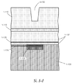
도 1-1은 생체 광전자 칩의 픽셀에 포함될 수 있는 일부 컴포넌트들을 도시하는 단순화된 도면이다. 픽셀은 기판(1-105) 상에 형성된 반응 챔버(1-130), 광 도파관(1-115), 반도체 흡수체(1-135), 및 센서(1-122)를 포함할 수 있다. 도파관(1-115)은 원격 광학 소스로부터 픽셀로 광학 에너지를 전송할 수 있고, 여기 복사를 반응 챔버(1-130)에 제공할 수 있다. 여기 복사는 반응 챔버(1-130)에 존재하는 하나 이상의 형광단을 여기시킬 수 있다. 형광단(들)으로부터 방출된 복사는 센서(1-122)에 의해 검출될 수 있다. 센서(1-122)로부터의 신호 또는 그것의 결여는 반응 챔버(1-130) 내의 분석물의 존재 또는 부재에 관한 정보를 제공할 수 있다. 일부 구현들에서, 센서(1-122)로부터의 신호는 반응 챔버에 존재하는 분석물의 유형을 식별할 수 있다.1-1 is a simplified diagram illustrating some components that may be included in a pixel of a biooptoelectronic chip. The pixel may include a reaction chamber 1-130 formed on a substrate 1-105 , an optical waveguide 1-115 , a semiconductor absorber 1-135 , and a sensor 1-122 . Waveguides 1-115 may transmit optical energy from a remote optical source to a pixel and may provide excitation radiation to reaction chambers 1-130. The excitation radiation may excite one or more fluorophores present in reaction chambers 1-130. Radiation emitted from the fluorophore(s) may be detected by sensors 1-122. Signals from, or lack thereof, sensors 1-122 can provide information regarding the presence or absence of analytes in reaction chambers 1-130. In some implementations, a signal from sensors 1 - 122 can identify the type of analyte present in the reaction chamber.
샘플 분석을 위해, 하나 이상의 분석물을 포함하는 샘플이 반응 챔버(1-130) 위에 퇴적될 수 있다. 예를 들어, 샘플은 반응 챔버(1-130) 위의 저장소 또는 미세유체 채널에 배치될 수 있다. 일부 경우들에서, 샘플은 반응 챔버(1-130)를 포함하는 처리된 표면 상에 액적으로서 인쇄될 수 있다. 샘플 분석 동안, 분석될 샘플로부터의 적어도 하나의 분석물이 반응 챔버(1-130)에 들어갈 수 있다. 일부 구현들에서, 분석물 자체가 도파관(1-115)으로부터 전달된 여기 복사에 의해 여기될 때 형광을 발할 수 있다. 일부 경우들에서, 분석물은 하나 이상의 링크된 형광 분자를 지닐 수 있다. 또 다른 경우들에서, 분석물은 반응 챔버(1-130) 내에 이미 존재하는 형광단을 켄칭할 수 있다. 형광 개체가 반응 챔버에 들어가고 여기 복사에 의해 여기될 때, 형광 개체는 여기 복사와는 다른 파장에서 복사를 방출할 수 있으며, 이는 결국 센서(1-122)에 의해 검출된다. 반도체 흡수체(1-135)는 여기 복사를, 반응 챔버(1-130)로부터의 방출 복사보다 훨씬 더 많이 우선적으로 감쇠시킬 수 있다.For sample analysis, a sample comprising one or more analytes may be deposited over reaction chamber 1 - 130 . For example, the sample may be placed in a reservoir or microfluidic channel above the reaction chamber 1-130. In some cases, the sample may be printed as a droplet onto a treated surface comprising the reaction chamber 1-130. During sample analysis, at least one analyte from the sample to be analyzed may enter the reaction chamber 1 - 130. In some implementations, the analyte itself may fluoresce when excited by excitation radiation transmitted from the waveguide 1 - 115. In some cases, an analyte may have one or more linked fluorescent molecules. In still other cases, the analyte may quench a fluorophore already present in the reaction chamber 1-130. When the fluorescent object enters the reaction chamber and is excited by the excitation radiation, the fluorescent object may emit radiation at a different wavelength than the excitation radiation, which is eventually detected by the sensors 1-122. The semiconductor absorber 1-135 may preferentially attenuate the excitation radiation much more than the emission radiation from the reaction chamber 1-130.
더 상세하게는, 반응 챔버(1-130)는 투명 또는 반투명 층(1-110)으로 형성될 수 있다. 일부 실시예들에 따르면, 반응 챔버는 50㎚ 내지 1㎛의 깊이를 가질 수 있다. 일부 실시예들에서, 반응 챔버(1-130)의 최소 직경은 50㎚ 내지 300㎚일 수 있다. 반응 챔버(1-130)가 제로 모드 도파관으로서 형성된다면, 일부 경우들에서, 최소 직경은 50㎚보다도 작을 수 있다. 큰 분석물이 분석되어야 하는 경우, 최소 직경은 300㎚보다 클 수 있다. 반응 챔버는 반응 챔버의 바닥이 도파관(1-115)의 최상부보다 최대 500㎚ 높을 수 있도록 광 도파관(1-115) 위에 위치될 수 있다. 일부 경우들에서, 반응 챔버(1-130)의 바닥은 도파관 내에 위치되거나 도파관(1-115)의 최상부 표면에 위치될 수 있다. 일부 실시예들에 따르면, 광 도파관(1-115)으로부터의 여기 복사, 및 반응 챔버(1-130)로부터의 방출 복사가 예를 들어 10% 넘게 감쇠되지 않고서 투명 또는 반투명 층(1-110)을 통과하도록, 투명 또는 반투명 층(1-110)은 산화물 또는 질화물로 형성될 수 있다.More specifically, the reaction chamber 1-130 may be formed of a transparent or translucent layer 1-110. According to some embodiments, the reaction chamber may have a depth of 50 nm to 1 μm. In some embodiments, the minimum diameter of the reaction chamber 1-130 may be between 50 nm and 300 nm. If the reaction chamber 1-130 is formed as a zero mode waveguide, in some cases, the minimum diameter may be less than 50 nm. If large analytes are to be analyzed, the minimum diameter may be greater than 300 nm. The reaction chamber may be positioned above the optical waveguides 1-115 such that the bottom of the reaction chamber may be up to 500 nm higher than the top of the waveguides 1-115. In some cases, the bottom of the reaction chamber 1-130 may be located within the waveguide or may be located on the top surface of the waveguide 1-115. In accordance with some embodiments, the excitation radiation from the optical waveguide 1-115, and the emission radiation from the reaction chamber 1-130 are not attenuated by, for example, more than 10% of the transparent or translucent layer 1-110 To pass through, the transparent or translucent layer 1-110 may be formed of an oxide or nitride.
일부 구현들에서, 기판(1-105) 상에 형성되고 기판과 광 도파관(1-115) 사이에 위치되는 하나 이상의 추가 투명 또는 반투명 층(1-137)이 존재할 수 있다. 이러한 추가 층들은 산화물 또는 질화물로 형성될 수 있고, 일부 구현들에서 투명 또는 반투명 층(1-110)과 동일한 유형의 재료일 수 있다. 반도체 흡수체(1-135)는 도파관(1-115)과 센서(1-122) 사이의 이러한 추가 층들(1-137) 내에 형성될 수 있다. 광 도파관(1-115)의 바닥으로부터 센서(1-122)까지의 거리는 500㎚ 내지 10㎛일 수 있다.In some implementations, there may be one or more additional transparent or translucent layers 1-137 formed on the substrate 1-105 and positioned between the substrate and the optical waveguide 1-115. These additional layers may be formed of an oxide or nitride, and in some implementations may be of the same type of material as the transparent or translucent layer 1-110. A semiconductor absorber 1-135 may be formed in these additional layers 1-137 between the waveguide 1-115 and the sensor 1-122. The distance from the bottom of the optical waveguide 1-115 to the sensor 1-122 may be 500 nm to 10 μm.
다양한 실시예들에서, 기판(1-105)은 실리콘(Si)과 같은 반도체 기판을 포함할 수 있다. 그러나, 일부 실시예들에서, 다른 반도체 재료들이 사용될 수 있다. 센서(1-122)는 기판(1-105) 상에 패터닝되고 형성되는 반도체 포토다이오드를 포함할 수 있다. 센서(1-122)는 상호연결부들(1-170)을 통해 기판 상의 다른 상보성 금속 산화물 반도체(complementary metal-oxide-semiconductor)(CMOS) 회로에 연결될 수 있다.In various embodiments, the substrates 1-105 may include a semiconductor substrate such as silicon (Si). However, in some embodiments, other semiconductor materials may be used. Sensors 1-122 may include semiconductor photodiodes that are patterned and formed on substrate 1-105. Sensors 1-122 may be coupled to other complementary metal-oxide-semiconductor (CMOS) circuitry on the substrate via interconnects 1-170.
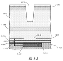
통합 디바이스의 픽셀에 포함될 수 있는 구조의 다른 예가 도 1-2에 도시되어 있다. 일부 구현들에 따르면, 층(1-110) 위에 하나 이상의 차광 층(1-250)이 형성될 수 있고, 그 안에 반응 챔버(1-230)가 형성될 수 있다. 일부 구현들에서, 반응 챔버의 에칭 프로세스는 반응 챔버(1-230)의 최상부가 될 하나 이상의 차광 층에서 애퍼처를 여는 것으로 시작할 수 있다. 차광 층들(1-250)은 하나 이상의 금속 층으로 형성될 수 있다. 일부 경우들에서, 차광 층들(1-250)은 반도체 및/또는 산화물 층을 포함할 수 있다. 차광 층들(1-250)은 광 도파관(1-115)으로부터의 여기 복사가 반응 챔버(1-230) 위의 샘플 내로 이동하고 샘플 내의 분석물을 여기시키는 것을 감소시키거나 방지할 수 있다. 추가적으로, 차광 층들(1-250)은 반응 챔버 위로부터의 외부 복사가 센서(1-122)까지 통과하는 것을 방지할 수 있다. 반응 챔버 외부로부터의 방출은 원치 않는 배경 복사 및 신호 잡음에 기여할 수 있다.Another example of a structure that may be included in a pixel of an integrated device is shown in FIGS. 1-2 . According to some implementations, one or more light blocking layers 1-250 may be formed over the layers 1-110, and a reaction chamber 1-230 may be formed therein. In some implementations, the etching process of the reaction chamber may begin by opening an aperture in one or more light blocking layers that will be the top of the reaction chamber 1-230. The light blocking layers 1-250 may be formed of one or more metal layers. In some cases, light blocking layers 1-250 may include a semiconductor and/or oxide layer. Light-shielding layers 1-250 may reduce or prevent excitation radiation from the optical waveguide 1-115 from traveling into the sample above the reaction chamber 1-230 and exciting analytes in the sample. Additionally, light blocking layers 1-250 may prevent external radiation from above the reaction chamber from passing to sensors 1-122. Emissions from outside the reaction chamber can contribute to unwanted background radiation and signal noise.
일부 실시예들에서, 하나 이상의 조리개 층(1-240)이 센서(1-122) 위에 형성될 수 있다. 조리개 층(1-240)은 반응 챔버(1-230)로부터의 방출이 센서(1-122)까지 통과하도록 허용하는 한편, 다른 방향들로부터의(예를 들어, 인접 픽셀들로부터의 또는 산란 여기 복사로부터의) 방출 또는 복사를 차단하는 개구(1-242)를 포함할 수 있다. 예를 들어, 조리개 층(1-240)은 넓은 입사각들에서 산란된 여기 복사가 센서(1-122)를 타격하고 배경 잡음에 기여하는 것을 차단할 수 있는 차광 재료로 형성될 수 있다.In some embodiments, one or more aperture layers 1-240 may be formed over sensors 1-122. The diaphragm layer 1-240 allows emission from the reaction chamber 1-230 to pass to the sensor 1-122, while from other directions (eg, from adjacent pixels or scattered excitation). openings 1-242 to block radiation or emission (from radiation). For example, stop layer 1-240 may be formed of a light-shielding material that can block excitation radiation scattered at wide angles of incidence from hitting sensor 1-122 and contributing to background noise.
일부 경우들에서, 조리개 층(1-240)은 전도성 재료로 형성될 수 있고, 기판(1-105) 상에 또는 그 위에 형성된 회로에 대한 전위 기준 평면 또는 접지 평면을 제공할 수 있다. 일부 구현들에 따르면, 수직 전도성 상호연결부 또는 비아(1-260)가 전도성일 수 있는 반도체 흡수체(1-235)와 접촉하지 않고서 조리개 층(1-240)에 연결될 수 있도록, 비아 또는 홀(1-237)이 반도체 흡수체(1-235)(및 반도체 흡수 층과 접촉하는 캡핑 층들이 있다면 그러한 캡핑 층들) 내에 형성될 수 있다. 일부 경우들에서, 반도체 흡수체(1-235)는 기판(1-105) 상에 또는 그 위에 형성된 회로에 대한 전위 기준 평면 또는 접지 평면으로서 사용될 수 있으며, 수직 상호연결부는 반도체 흡수체(1-235)에 연결될 수 있고, 조리개 층(1-240)에 연결되지 않을 수 있다. 일부 경우들에서, 홀(1-237)은 전도성 비아(1-260)와 반도체 흡수 층(1-235) 사이의 전기적 접촉을 방지하는 전기 절연성 재료(예를 들어, 산화물)를 포함할 수 있다. 일부 구현들에서, 반도체 흡수 층(1-235)은 높은 저항을 가질 수 있고, 홀(1-237)은 반도체 흡수 층을 통한 전기적 연결을 제공하기 위해 전도성 재료로 채워질 수 있다. 실시예들에서, 각각의 픽셀에서 기판(1-105) 상의 센서와 함께 형성된 저장소 및 판독 전자장치(1-224)와 같은 추가 전자 컴포넌트들이 존재할 수 있다. 판독 전자장치들은 예를 들어 신호 취득을 제어하고 각각의 센서(1-122)에 저장된 전하를 판독하는 데 사용될 수 있다. 일부 실시예들에서, 반도체 흡수체(1-235)(및 캡핑 층들) 내의 홀(1-237)은 반도체 층을 통한 전기적 연결, 예를 들어 와이어 본딩, 플립-칩 본딩, 또는 다른 방법들을 통한 외부 회로에 대한 집적 회로의 연결을 용이하게 할 수 있다.In some cases, stop layer 1-240 may be formed of a conductive material and may provide a potential reference plane or ground plane for circuitry formed on or over substrate 1-105 . According to some implementations, a via or
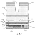
일부 경우들에서, 도 1-3에 도시된 바와 같이, 반도체 흡수 재료의 복수의 층이 존재할 수 있다. 예를 들어, 반도체 흡수체(1-335)는 중간 재료 층들(1-334)에 의해 이격되는 반도체 흡수 재료(1-336)의 2개, 3개 또는 그 이상의 층을 포함할 수 있다. 중간 층들(1-334)은 반도체 흡수 재료(1-336)와는 상이한 굴절률을 가질 수 있다. 추가적으로 또는 대안적으로, 중간 층들(1-334)은 반도체 흡수 재료(1-336)와는 상이한 투과율을 가질 수 있다. 일부 경우들에서, 반도체 흡수 재료(1-336)의 상이한 층들의 두께는 본질적으로 동일하고 중간 층들(1-334)의 두께들과는 다를 수 있지만, 일부 경우들에서 반도체 흡수 재료(1-336)의 층들은 적어도 두 개의 상이한 두께를 가질 수 있다. 일부 실시예들에서, 실리콘계 흡수 재료 및 515㎚ 내지 540㎚의 여기 특징 파장에 대해 반도체 흡수 재료(1-336)의 두께들은 75㎚ 내지 90㎚일 수 있다. 다른 흡수 재료들 및 여기 파장들에 대해 다른 두께들이 사용될 수 있다. 일부 경우들에서, 중간 층들(1-334)의 두께는 본질적으로 동일하고 반도체 흡수 재료(1-336)의 층들의 두께들과 다를 수 있지만, 일부 경우들에서, 중간 층들(1-334)은 적어도 두 개의 상이한 두께를 가질 수 있다. 일부 실시예들에서, 실리콘 산화물 및 515㎚ 내지 540㎚의 여기 특징 파장에 대해 중간 층들(1-334)의 두께들은 50㎚ 내지 150㎚일 수 있다. 다른 중간 층 재료들 및 여기 파장들에 대해 다른 두께들이 사용될 수 있다. In some cases, as shown in FIGS. 1-3 , there may be multiple layers of semiconductor absorbing material. For example, semiconductor absorber 1 -335 may include two, three or more layers of semiconductor absorbent material 1 -336 spaced apart by intermediate material layers 1 - 334 . The intermediate layers 1-334 may have a different refractive index than the semiconductor absorbing material 1 -336. Additionally or alternatively, the intermediate layers 1-334 may have a different transmittance than the semiconductor absorbing material 1 -336. In some cases, the thickness of the different layers of semiconductor absorbing material 1 -336 is essentially the same and may be different from the thicknesses of intermediate layers 1-334 , although in some cases the thickness of semiconductor absorbing material 1 -336 is The layers may have at least two different thicknesses. In some embodiments, the thicknesses of the semiconductor absorbing material 1 -336 may be between 75 nm and 90 nm for a silicon-based absorbing material and an excitation feature wavelength between 515 nm and 540 nm. Other thicknesses may be used for other absorbing materials and excitation wavelengths. In some cases, the thickness of the intermediate layers 1-334 is essentially the same and may be different from the thicknesses of the layers of semiconductor absorbing material 1 -336 , although in some cases the intermediate layers 1-334 may be It may have at least two different thicknesses. In some embodiments, the thicknesses of the intermediate layers 1-334 may be 50 nm to 150 nm for silicon oxide and an excitation feature wavelength of 515 nm to 540 nm. Other thicknesses may be used for other intermediate layer materials and excitation wavelengths.
도 1-3에 도시된 바와 같이, 반도체 흡수 재료(1-336)의 복수의 층을 사용함으로써, 층들 사이의 광학 간섭 효과들은 반도체 흡수체의 밴드 에지(band-edge)의 급격함(abruptness)을 효과적으로 첨예화(sharpen)하고, 반도체 흡수체(1-335)에 대한 제거율을 향상시킬 수 있다. 밴드 에지의 간섭 예리화(interferometric sharpening)는 반도체 흡수 재료(1-336)의 더 낮은 품질의 결정도(crystallinity)를 허용할 수 있다. 일부 구현들에서, 다결정질 또는 비정질 반도체 재료(예를 들어, 비정질 실리콘, 비정질 실리콘 탄화물, 비정질 ZnTe, 비정질 InGaN 등)는 반도체 흡수 재료(1-336)의 복수의 층을 갖는 반도체 흡수체(1-335)에서 사용될 수 있다.1-3, by using multiple layers of semiconductor absorber material 1-336, optical interference effects between the layers reduce the abruptness of the band-edge of the semiconductor absorber. It can be effectively sharpened and the removal rate for the semiconductor absorber 1 -335 can be improved. Interferometric sharpening of the band edges may allow for lower quality crystallinity of the semiconductor absorbing material 1 -336. In some implementations, a polycrystalline or amorphous semiconductor material (eg, amorphous silicon, amorphous silicon carbide, amorphous ZnTe, amorphous InGaN, etc.) 335) can be used.
반도체 흡수체(2-135)의 추가 세부사항은 도 2-1에 도시되어 있다. 다양한 실시예들에서, 반도체 흡수체(2-135)는 반도체 흡수 층(2-210)을 포함한다. 도 2-1에 도시된 구조는 반도체 흡수 재료의 단 하나의 층을 갖는 반도체 흡수체에서 구현될 수 있거나, 반도체 흡수 재료의 복수의 층을 갖는 반도체 흡수체 내의 하나 이상의 층에 사용될 수 있다. 반도체 흡수 층은 밴드갭을 갖는 반도체 재료로 형성될 수 있다. 예를 들어, 반도체 흡수 층은 광학 스펙트럼의 가시 범위에 대응하는 밴드갭을 갖는 화합물 반도체 재료들로 형성될 수 있다. 예시적인 재료들은 아연 텔루라이드, 인듐-갈륨 질화물, 갈륨 인화물, 바나듐 산화물, 탄탈륨 질화물, 알루미늄 비화물, 마그네슘 규화물, 알루미늄 안티몬화물, 실리콘 비화물, 및 인듐 비화물을 포함하지만 이에 제한되지 않는다. 일부 응용들에 적합할 수 있는 추가 재료들은 실리콘 탄화물, 실리콘 탄소 수소, 카드뮴 황화물, 카드뮴 산화물 및 아연 셀렌화물을 포함한다. 이러한 예시적인 재료들은 다양한 화학량론적 비율들로 구현될 수 있다. 반도체 흡수 층(2-210)은 일부 실시예에서 다결정질일 수 있고, 또는 일부 실시예들에서 단결정질일 수 있다. 일부 경우들에서, 다결정질 반도체 흡수 층(2-210)에 대한 평균 입자 크기는 횡방향의 면내 방향으로 측정했을 때 20㎚ 이상일 수 있다. 일부 경우들에서, 다결정질 반도체 흡수 층(2-210)에 대한 평균 입자 크기는 횡방향의 면내 방향으로 측정했을 때 1㎛ 이상일 수 있다. 일부 실시예들에서, 반도체 흡수 층(2-210)은 비정질 반도체 재료를 포함할 수 있다. 일부 실시예들에 따르면, 반도체 흡수 층(2-210)의 두께는 200㎚ 내지 5㎛일 수 있다. 일부 경우들에서, 반도체 흡수 층(2-210)의 두께는 1㎛ 내지 2㎛일 수 있다.Further details of the semiconductor absorber 2-135 are shown in FIG. 2-1. In various embodiments, the semiconductor absorber 2-135 includes a semiconductor absorber layer 2-210. The structure shown in FIG. 2-1 may be implemented in a semiconductor absorber having only one layer of semiconductor absorbent material, or may be used in one or more layers in a semiconductor absorber having multiple layers of semiconductor absorbent material. The semiconductor absorbing layer may be formed of a semiconductor material having a bandgap. For example, the semiconductor absorbing layer may be formed of compound semiconductor materials having a bandgap corresponding to the visible range of the optical spectrum. Exemplary materials include, but are not limited to, zinc telluride, indium-gallium nitride, gallium phosphide, vanadium oxide, tantalum nitride, aluminum arsenide, magnesium silicide, aluminum antimonide, silicon arsenide, and indium arsenide. Additional materials that may be suitable for some applications include silicon carbide, silicon carbon hydrogen, cadmium sulfide, cadmium oxide and zinc selenide. These exemplary materials may be implemented in various stoichiometric ratios. The semiconductor absorber layer 2-210 may be polycrystalline in some embodiments, or may be monocrystalline in some embodiments. In some cases, the average particle size for the polycrystalline semiconductor absorber layer 2-210 may be greater than or equal to 20 nm as measured in the transverse in-plane direction. In some cases, the average particle size for the polycrystalline semiconductor absorber layer 2-210 may be greater than or equal to 1 μm, measured in the transverse in-plane direction. In some embodiments, the semiconductor absorbing layer 2 - 210 may include an amorphous semiconductor material. According to some embodiments, the thickness of the semiconductor absorption layer 2-210 may be 200 nm to 5 μm. In some cases, the thickness of the semiconductor absorbing layer 2-210 may be between 1 μm and 2 μm.
반도체 흡수 층(2-210)에 사용되는 반도체 재료의 유형은 여기 복사에 대한 원하는 흡수, 및 반응 챔버(1-230)로부터 방출된 복사에 대한 투과를 제공하도록 선택되거나 맞춤화될 수 있다. 예를 들어, 반도체 재료는, 밴드갭보다 큰 광자 에너지들을 갖는 여기 복사는 반도체 재료에 의해 대부분 흡수되고 밴드갭 미만의 광자 에너지들을 갖는 반응 챔버(1-230)로부터의 형광단 방출은 반도체 재료에 의해 대부분 투과되게끔 밴드갭을 갖도록 선택되거나 맞춤화될 수 있다. 실시예들에서, 밴드갭은 흡수되는 파장들과 투과되는 파장들 사이의 천이가 광 도파관(1-115)에 의해 제공된 여기 복사와 반응 챔버(1-230)로부터 방출된 형광 방출 사이에 놓이도록 선택되거나 맞춤화된다. 반도체 흡수 층(2-210)의 밴드갭은 반도체의 조성을 변경함으로써 맞춤화될 수 있다(예를 들어, InxGa1 - xN 내의 In 및 Ga의 화학량론적 비율을 변경함으로써, 여기서 x는 0<x<1에 따른 값의 범위를 가짐).The type of semiconductor material used for the semiconductor absorbing layer 2-210 may be selected or customized to provide a desired absorption for the excitation radiation, and transmission for the radiation emitted from the reaction chamber 1-230. For example, a semiconductor material may be such that excitation radiation with photon energies greater than the bandgap is mostly absorbed by the semiconductor material and fluorophore emission from reaction chamber 1-230 with photon energies below the bandgap is absorbed by the semiconductor material. It can be selected or customized to have a bandgap that is mostly transmissive by In embodiments, the bandgap is such that the transition between absorbed and transmitted wavelengths lies between the excitation radiation provided by the optical waveguide 1-115 and the fluorescence emission emitted from the reaction chamber 1-230. selected or customized. The bandgap of the semiconductor absorber layer 2-210 can be customized by changing the composition of the semiconductor (eg, by changing the stoichiometric ratio of In and Ga in In x Ga 1 - x N, where x is 0< has a range of values according to x<1).
ZnTe로 형성된 반도체 흡수 층(2-210)에 대한 예시적인 투과 곡선이 도 2-2에 도시되어 있다. 일부 실시예들에서, 여기 복사는 532㎚의 특징 파장을 가질 수 있고, 형광 방출은 560㎚ 내지 580㎚의 특징 파장 값을 가질 수 있다. 여기 복사가 대략 532㎚의 특징 파장을 갖는 도시된 예에 대해, 반도체 흡수 층(2-210)은 (예를 들어 센서(1-122)를 향해) 여기 복사보다 대략 400배 더 많은 방출 복사를 투과시킨다(제거율 Rr~400). 일부 구현들에서, 여기 복사는 500㎚ 내지 540㎚의 특징 파장을 가질 수 있고, 방출 복사는 560㎚ 내지 650㎚의 특징 파장을 가질 수 있다. 일부 경우들에서, 제거율은 더 높을 수 있다(예를 들어, 400 내지 800, 800 내지 1000, 또는 1000 내지 3000). 일부 실시예들에 따르면, 반도체 흡수체는 원하는 검출된 복사(예를 들어, 반응 챔버로부터의 방출 복사)를 5% 내지 85% 감쇠시키는 한편, 원하지 않는 복사를 이 양보다 훨씬 더 많이 감쇠시킬 수 있다.An exemplary transmission curve for a semiconductor absorption layer 2-210 formed of ZnTe is shown in FIG. 2-2. In some embodiments, the excitation radiation may have a characteristic wavelength of 532 nm, and the fluorescence emission may have a characteristic wavelength value of between 560 nm and 580 nm. For the illustrated example where the excitation radiation has a characteristic wavelength of approximately 532 nm, the semiconductor absorbing layer 2-210 emits approximately 400 times more emitted radiation than the excitation radiation (eg towards the sensors 1-122). Permeate (removal rate R r ~400). In some implementations, the excitation radiation can have a characteristic wavelength between 500 nm and 540 nm, and the emission radiation can have a characteristic wavelength between 560 nm and 650 nm. In some cases, the removal rate may be higher (eg, 400 to 800, 800 to 1000, or 1000 to 3000). According to some embodiments, the semiconductor absorber may attenuate desired detected radiation (eg, emitted radiation from a reaction chamber) by 5% to 85%, while attenuating undesired radiation much more than this amount. .
본 발명자들은 필터 컷오프의 급격함, 및 컷오프보다 짧은 파장들에서의 흡수된 복사에 대한, 컷오프보다 긴 파장들에서의 투과된 복사의 비는, 반도체 흡수 층(들)(2-210)의 두께, 반도체 흡수 층들의 수, 반도체 흡수 층(들)의 결정 품질, 및 여기 및 방출 특징 파장들의 분리에 의존하고, 이들 파라미터 각각은 어느 정도 수정될 수 있음을 인식하고 이해했다. 반도체 흡수 층(2-210)의 두께는 예를 들어 반도체 흡수 재료에 대한 퇴적 시간의 길이를 조절함으로써 제어될 수 있다.We found that the steepness of the filter cutoff, and the ratio of transmitted radiation at wavelengths longer than the cutoff to absorbed radiation at wavelengths shorter than the cutoff, is the thickness of the semiconductor absorbing layer(s) 2-210 , the number of semiconductor absorbing layers, the crystal quality of the semiconductor absorbing layer(s), and the separation of the excitation and emission characteristic wavelengths, each of which may be modified to some extent. The thickness of the semiconductor absorbing layer 2-210 can be controlled, for example, by adjusting the length of deposition time for the semiconductor absorbing material.
일부 구현들에서, 퇴적 프로세스의 유형(예를 들어, 금속-유기 화학 기상 증착, 분자 빔 에피택시, 또는 물리적 기상 증착)은 반도체 흡수 층(2-210)의 결정 품질을 개선하도록 선택될 수 있다. 일부 경우들에서, 후속 퇴적된 반도체 흡수 층(2-210)의 결정 품질을 개선하기 위해, 상이한 재료의 시드 층이 하부 층 상에 먼저 퇴적될 수 있다. 일부 구현들에서, 반도체 흡수 층(2-210)의 결정 품질을 개선하기 위해 퇴적-후 어닐링 단계가 수행될 수 있다. 일부 실시예들에서, 반도체 흡수 층(2-210)은 층의 평면에서 측정될 때 20㎚ 이상인 평균 결정 입자 크기를 가질 수 있다. 일부 경우들에서, 평균 결정 입자 크기는 50㎚ 이상이다. 일부 경우들에서, 평균 결정 입자 크기는 100㎚ 이상이다. 일부 경우들에서, 평균 결정 입자 크기는 500㎚ 이상이다. 일부 경우들에서, 평균 결정 입자 크기는 40㎚ 내지 100㎚이다. 일부 경우들에서, 평균 결정 입자 크기는 100㎚ 내지 500㎚이다. 일부 경우들에서, 평균 결정 입자 크기는 100㎚ 내지 1㎛이다. 일부 경우들에서, 평균 결정 입자 크기는 1㎛ 내지 3㎛이다. 일부 경우들에서, 평균 결정 입자 크기는 2㎛ 내지 5㎛이다. 일부 경우들에서, 평균 결정 입자 크기는 5㎛ 내지 10㎛이다. 일부 구현들에 따르면, 반도체 흡수 층(2-210)은 더 큰 결정 입자 크기를 가질 수 있거나 본질적으로 단결정일 수 있다. 예를 들어, 반도체 흡수 층(2-210)은 핸들 웨이퍼를 사용하여 성장된 단결정 웨이퍼로부터 박리 및 전사될 수 있고, 기판(1-105) 상의 하부 층에 본딩함으로써 퇴적될 수 있다.In some implementations, the type of deposition process (eg, metal-organic chemical vapor deposition, molecular beam epitaxy, or physical vapor deposition) can be selected to improve the crystalline quality of the semiconductor absorber layer 2 - 210 . . In some cases, to improve the crystal quality of the subsequently deposited semiconductor absorber layer 2-210, a seed layer of a different material may be first deposited on the underlying layer. In some implementations, a post-deposition annealing step may be performed to improve the crystal quality of the semiconductor absorber layer 2 - 210 . In some embodiments, the semiconductor absorbing layer 2-210 may have an average crystal grain size of 20 nm or greater as measured in the plane of the layer. In some cases, the average crystal grain size is at least 50 nm. In some cases, the average crystal grain size is greater than or equal to 100 nm. In some cases, the average crystal grain size is at least 500 nm. In some cases, the average crystal grain size is between 40 nm and 100 nm. In some cases, the average crystal grain size is between 100 nm and 500 nm. In some cases, the average crystal grain size is between 100 nm and 1 μm. In some cases, the average crystal grain size is between 1 μm and 3 μm. In some cases, the average crystal grain size is between 2 μm and 5 μm. In some cases, the average crystal grain size is between 5 μm and 10 μm. According to some implementations, the semiconductor absorbing layer 2-210 may have a larger grain size or may be monocrystalline in nature. For example, the semiconductor absorber layer 2-210 can be exfoliated and transferred from a grown single crystal wafer using a handle wafer, and deposited by bonding to an underlying layer on the substrate 1-105.
일부 구현들에서, 반도체 흡수 층(2-210)은 섬유상, 원통형 또는 팬케이크와 같은 특정 결정질 모폴로지를 가질 수 있다. 섬유상 모폴로지는 반도체 흡수 층(2-210)에서 수직으로 배향된 섬유형 또는 키가 큰 주상(columnar) 결정들을 나타낼 수 있다. 섬유상 결정들의 예는 도 2-4의 투과-전자 현미경 이미지에 도시되어 있다. 긴 주상 결정들은 높은 종횡비들(예를 들어, 10:1보다 큰 길이-대-직경 비)를 가지며, 수직으로 배향되고 아연 텔루라이드 층 내에 형성된다. 원통형 모폴로지는 0.5:1 내지 10:1의 길이-대-직경 비를 갖는 결정 입자들을 가질 수 있다. 팬케이크 모폴로지는 0.5:1 미만의 길이-대-직경 비를 갖는 결정 입자들을 가질 수 있다.In some implementations, the semiconductor absorbent layer 2-210 may have a specific crystalline morphology, such as fibrous, cylindrical, or pancake. The fibrous morphology may exhibit vertically oriented fibrous or tall columnar crystals in the semiconductor absorbent layer 2-210. An example of fibrous crystals is shown in the transmission-electron microscopy image of FIGS. 2-4 . The long columnar crystals have high aspect ratios (eg, a length-to-diameter ratio greater than 10:1), are vertically oriented, and are formed in the zinc telluride layer. The cylindrical morphology may have crystal grains having a length-to-diameter ratio of 0.5:1 to 10:1. The pancake morphology may have crystal grains having a length-to-diameter ratio of less than 0.5:1.
일부 경우들에서, 반도체 흡수 층(2-210)은 비정질 반도체 재료로 형성될 수 있다. 예를 들어, 본 명세서에 설명된 반도체 재료들 중 임의의 것은 스퍼터링, e-빔 증발, 또는 플라즈마 강화 화학 기상 증착(PECVD)과 같은 화학 기상 증착 프로세스에 의해 비정질 재료로서 퇴적될 수 있다. 예시적인 비정질 반도체 재료들은 비정질 실리콘, 비정질 실리콘 탄화물, 비정질 실리콘 질화물, 비정질 실리콘 산화물, 비정질 ZnTe, 비정질 InGaN, 및 이들의 합금을 포함하지만 이에 제한되지 않는다. 일부 구현들에서, 비정질 반도체 재료 또는 합금은 수소화될 수 있다(예를 들어, 비정질 수소화된 실리콘, 비정질 수소화된 실리콘 탄화물 등). 일부 구현들에서, 질소는 퇴적 동안, 예를 들어, 화학 기상 증착 프로세스 동안 비정질 반도체 재료 또는 합금에 첨가될 수 있다. 일부 경우들에서, 질소 및/또는 다른 원소(들)는 굴절률 n 및 소광 계수 k를 관심 파장의 투과 및 차단에 요구되는 값들로 튜닝하기 위해 퇴적 동안 비정질 실리콘과 같은 재료에 첨가될 수 있다. 일부 실시예들에서, 퇴적된 비정질 반도체 재료는 비정질 반도체 재료 전체에 분산된 나노결정들 또는 마이크로결정들을 포함할 수 있다. 비정질 반도체 흡수 층(2-210)은 본 명세서에 설명된 반도체 흡수체 구조들 중 임의의 것에서 사용될 수 있다. 실제로, 비정질 반도체 흡수 층(2-210)은 기존의 파운드리 도구들 및 프로세스들을 사용하여 기판 상에 제조하는 데에 더 쉽고 비용이 적게 들 수 있다. 일부 경우들에서, 비정질 반도체 또는 다른 재료의 퇴적은 예를 들어 CMOS 프로세스와 호환되는 더 낮은 온도(예를 들어, 500℃ 미만)에서 달성될 수 있다. 비정질 반도체 재료는 동일한 유형의 다결정질 또는 결정질 반도체 재료만큼 급격한 밴드 에지를 제공하지 않을 수 있지만, 특성 여기 및 방출 파장의 차이가 큰 경우에는 그러한 밴드 에지로 충분할 수 있다. 그러나, 일부 미세가공 프로세스들은 다결정질 또는 결정질 반도체 재료들이 CMOS 구조들과 호환되는 방식으로 사용되는 것을 가능하게 할 수 있다.In some cases, the semiconductor absorbing layer 2 - 210 may be formed of an amorphous semiconductor material. For example, any of the semiconductor materials described herein may be deposited as an amorphous material by a chemical vapor deposition process such as sputtering, e-beam evaporation, or plasma enhanced chemical vapor deposition (PECVD). Exemplary amorphous semiconductor materials include, but are not limited to, amorphous silicon, amorphous silicon carbide, amorphous silicon nitride, amorphous silicon oxide, amorphous ZnTe, amorphous InGaN, and alloys thereof. In some implementations, the amorphous semiconductor material or alloy can be hydrogenated (eg, amorphous hydrogenated silicon, amorphous hydrogenated silicon carbide, etc.). In some implementations, nitrogen may be added to the amorphous semiconductor material or alloy during deposition, eg, during a chemical vapor deposition process. In some cases, nitrogen and/or other element(s) may be added to a material such as amorphous silicon during deposition to tune the refractive index n and extinction coefficient k to values required for transmission and blocking of the wavelength of interest. In some embodiments, the deposited amorphous semiconductor material may include nanocrystals or microcrystals dispersed throughout the amorphous semiconductor material. The amorphous semiconductor absorber layer 2-210 may be used in any of the semiconductor absorber structures described herein. Indeed, the amorphous semiconductor absorber layer 2-210 may be easier and less expensive to fabricate on a substrate using existing foundry tools and processes. In some cases, the deposition of an amorphous semiconductor or other material may be achieved at a lower temperature (eg, less than 500° C.) compatible with, for example, a CMOS process. Amorphous semiconductor materials may not provide as sharp band edges as polycrystalline or crystalline semiconductor materials of the same type, but such band edges may be sufficient for large differences in characteristic excitation and emission wavelengths. However, some microfabrication processes may enable polycrystalline or crystalline semiconductor materials to be used in a manner compatible with CMOS structures.
반도체 흡수 층(2-210)과 같은 흡수 층의 장점은 다층 유전체 필터들과 같은 다른 유형들의 파장 필터들보다 더 높은 각도 허용오차를 가질 수 있다는 점이다. 유전체 필터에서, 층들 각각은 무시할 수 있는 양의 복사(예를 들어, 입사 복사의 1% 미만)을 흡수한다. 예를 들어, 두께가 약 2 미크론인 다층 유전체 필터(예를 들어, 분산 브래그 반사기)는 수직 입사에서 약 800의 제거율 Rr을 제공할 수 있다. 제거율 Rr은 여기 파장(예시적인 구조에 대해 532㎚)에서의 투과 강도에 대한 방출 파장(예시적인 구조에 대해 572㎚)에서의 투과 강도의 비율이다. 30도 입사각에서 제거율 Rr은 110으로 떨어진다. 대조적으로, 2.0 미크론 두께의 ZnTe 반도체 흡수 층(2-210)은 모든 입사각들에서 800을 초과하는 제거율 Rr을 제공한다. 따라서, 미크론 규모의 박막 흡수 층 또는 반도체 흡수 층(2-210)은 각도 허용 오차 측면에서 미크론 규모의 박막 다층 유전체 필터보다 성능이 뛰어날 수 있고, 추가로 널리 이용가능한 CMOS 처리 장비와도 호환가능할 수 있다. 예를 들어, 반도체 흡수 층(2-210)은 다층 유전체 필터에 요구되는 엄격한 치수 허용오차를 갖지 않을 수 있는 하나 또는 몇 개의 층을 포함할 수 있다.An advantage of an absorbing layer, such as the semiconductor absorbing layer 2-210, is that it can have a higher angular tolerance than other types of wavelength filters, such as multilayer dielectric filters. In a dielectric filter, each of the layers absorbs a negligible amount of radiation (eg, less than 1% of the incident radiation). For example, a multilayer dielectric filter (eg, a diffuse Bragg reflector) that is about 2 microns thick can provide a rejection ratio R r of about 800 at normal incidence. The rejection R r is the ratio of the transmission intensity at the emission wavelength (572 nm for the exemplary structure) to the transmission intensity at the excitation wavelength (532 nm for the exemplary structure). At an angle of incidence of 30 degrees, the removal rate R r drops to 110. In contrast, a 2.0 micron thick ZnTe semiconductor absorber layer 2-210 provides a removal rate R r greater than 800 at all angles of incidence. Thus, the micron-scale thin-film absorber layer or semiconductor absorber layer 2-210 can outperform micron-scale thin-film multilayer dielectric filters in terms of angular tolerance, and additionally be compatible with widely available CMOS processing equipment. have. For example, the semiconductor absorbing layer 2-210 may include one or several layers that may not have the tight dimensional tolerances required for a multilayer dielectric filter.
일부 실시예들에 따르면, 반도체 흡수 층(2-210)은 넓은 범위에 걸쳐 밴드갭의 튜닝가능성을 제공할 수 있는 InGaN으로 형성될 수 있다. 예를 들어, In과 Ga의 농도 비율을 변경함으로써, 밴드갭은 0.8 eV로부터 3.4 eV로 튜닝될 수 있고, 그에 의해 전체 가시 파장 범위를 커버할 수 있다. InGaN은 결정질 기판 상에 단결정 재료로서 에피택시 성장될 수 있거나, 유기 금속 화학 기상 증착(metallorganic chemical vapor deposition)(MOCVD), 분자 빔 에피택시(molecular beam epitaxy)(MBE), 스퍼터링, 반응성 스퍼터링, 및 다른 확립된 방법들을 포함하는 다양한 화학적 및 물리적 퇴적 방법들에 의해 다결정질 형태로 퇴적될 수 있다. 일부 구현들에서, 밴드갭은 이원 반도체를 제3의 Ⅱ족 및/또는 Ⅵ족 원소와 합금화하거나 달리 조합함으로써 튜닝될 수 있다. 일부 예시적인 결과적인 ZnTe 반도체 조성물은 ZnTeO 및 CdZnTe를 포함하지만 이에 제한되지는 않는다.According to some embodiments, the semiconductor absorber layer 2-210 may be formed of InGaN, which may provide tunability of the bandgap over a wide range. For example, by changing the concentration ratio of In and Ga, the bandgap can be tuned from 0.8 eV to 3.4 eV, thereby covering the entire visible wavelength range. InGaN may be epitaxially grown as a single crystal material on a crystalline substrate, or may be subjected to metallorganic chemical vapor deposition (MOCVD), molecular beam epitaxy (MBE), sputtering, reactive sputtering, and It can be deposited in polycrystalline form by a variety of chemical and physical deposition methods, including other established methods. In some implementations, the bandgap can be tuned by alloying or otherwise combining the binary semiconductor with a third Group II and/or VI element. Some exemplary resulting ZnTe semiconductor compositions include, but are not limited to, ZnTeO and CdZnTe.
단결정 InGaN의 모델링은 1.5 미크론의 층 두께에 대해 3000보다 큰 제거율 Rr(572㎚/532㎚)이 획득될 수 있음을 시사한다. 일부 실시예들에서, 반도체 흡수체(2-135)는 InGaN으로 형성된 반도체 흡수 층(2-210)을 포함할 수 있다. 흡수 층의 두께는 200㎚ 내지 3 미크론일 수 있고, 층에 대한 제거율 Rr은 20 내지 100,000일 수 있다. 층 두께의 함수로서 단결정 InGaN에 대해 계산된 제거율 Rr의 곡선이 도 2-3에 플로팅된다. Modeling of single-crystal InGaN suggests that removal rates greater than 3000 R r (572 nm/532 nm) can be obtained for a layer thickness of 1.5 microns. In some embodiments, the semiconductor absorber 2-135 may include a semiconductor absorber layer 2-210 formed of InGaN. The thickness of the absorbing layer may be between 200 nm and 3 microns and the removal rate R r for the layer may be between 20 and 100,000. A curve of the calculated removal rate R r for single crystal InGaN as a function of layer thickness is plotted in FIGS. 2-3 .
일부 실시예들에서, 하나 이상의 캡핑 층(2-220)이 반도체 흡수 층(2-210)에 인접하게 형성될 수 있다. 일부 경우들에서, 반도체 흡수 층(2-210)의 일면에 하나의 캡핑 층(2-220)이 있을 수 있다. 다른 경우들에서, 반도체 흡수 층(2-210)의 각각의 면, 예를 들어 상부면 및 하부면 상에 캡핑 층이 있을 수 있다. 일부 실시예들에 따르면, 캡핑 층(2-220)은 20㎚ 내지 100㎚ 두께의 적어도 하나의 얇은 층을 포함할 수 있지만, 일부 경우에는 더 두꺼운 층들이 사용될 수 있다. 일부 구현들에서, 반도체 흡수 층(2-210)의 한 면 상의 캡핑 층(2-220)은 상이한 재료들의 복수의 층을 포함할 수 있다. 캡핑 층(2-220)에 대해 사용될 수 있는 예시적인 재료들은 실리콘 질화물, 알루미늄 산화물, 티타늄 산화물, 하프늄 산화물, 및 탄탈륨 산화물을 포함하지만 이에 제한되지 않는다.In some embodiments, one or more capping layers 2-220 may be formed adjacent to the semiconductor absorber layer 2-210. In some cases, there may be one capping layer 2-220 on one side of the semiconductor absorbing layer 2-210. In other cases, there may be a capping layer on each side of the semiconductor absorbing layer 2-210, eg, a top surface and a bottom surface. According to some embodiments, capping layer 2-220 may include at least one thin layer between 20 nm and 100 nm thick, although thicker layers may be used in some cases. In some implementations, the capping layer 2-220 on one side of the semiconductor absorbing layer 2-210 may include a plurality of layers of different materials. Exemplary materials that may be used for capping layer 2-220 include, but are not limited to, silicon nitride, aluminum oxide, titanium oxide, hafnium oxide, and tantalum oxide.
하나 이상의 캡핑 층(2-220)은 반도체 흡수 층(2-210)이 인접한 재료로 확산되는 것을 방지하거나 반도체 흡수 재료가 환경으로 방출되는 것을 방지하기 위해 포함될 수 있다. 일부 구현들에서, 캡핑 층(2-220)은 추가적으로 또는 대안적으로, 반도체 흡수 층(2-210) 단독에 의해 제공되는 것에 비해, 바로 인접한 층에 대한 개선된 접착력을 제공할 수 있다. 일부 구현들에서, 하나 이상의 캡핑 층(2-220)은 반도체 흡수 층(2-210)에서 스트레스를 감소시키거나 유도할 수 있고/있거나 반도체 흡수 층(2-210)의 결정도를 개선할 수 있다. 일부 경우들에서, 캡핑 층(2-220)은 보상 유형의 스트레스(예를 들어, 반도체 흡수 층이 압축 스트레스를 갖는 경우의 인장 스트레스)를 제공함으로써 어셈블리 내의 반도체 흡수 층(2-210)으로부터의 스트레스를 감소시킬 수 있다.One or more capping layers 2-220 may be included to prevent diffusion of semiconductor absorbing layer 2-210 into adjacent materials or release of semiconductor absorbing material into the environment. In some implementations, capping layer 2-220 may additionally or alternatively provide improved adhesion to an immediately adjacent layer as compared to that provided by semiconductor absorbing layer 2-210 alone. In some implementations, the one or more capping layers 2-220 can reduce or induce stress in the semiconductor absorber layer 2-210 and/or improve the crystallinity of the semiconductor absorber layer 2-210 . In some cases, the capping layer 2-220 provides a compensating type of stress (eg, tensile stress when the semiconductor absorber layer has compressive stress) thereby providing a compensating stress from the semiconductor absorber layer 2-210 in the assembly. It can reduce stress.
추가적으로 또는 대안적으로, 일부 실시예들에서, 반도체 흡수 층(2-210)으로부터의 광학 반사를 감소시키기 위해 캡핑 층이 형성될 수 있다. 일부 경우들에서, 반도체 흡수 층(2-210)은 인접 층들과는 상당히 다른 굴절률을 가질 수 있으며, 이는 반도체 흡수 층(2-210)과 인접 층 사이의 계면으로부터 상당한 양의 반사된 복사를 유발할 수 있다. 이와 관련하여, 하나 이상의 캡핑 층(2-220)은 반도체 흡수 층(2-210)에 대한 반사 방지 코팅(들)으로서 형성될 수 있고, 파장 범위에 걸쳐 하나 이상의 파장에서 광학 반사를 감소시킬 수 있다. 예를 들어, 캡핑 층(2-220)은 반응 챔버(1-230)로부터의 방출 복사 및/또는 여기 복사의 반사를 감소시킬 수 있다. ZnTe로 형성되고 인접 실리콘 산화물 층들을 갖는 반도체 흡수 층(2-210)에 대해, 532㎚ 및 572㎚에서의 반사는 각각 대략 14% 및 10%일 수 있다. 63㎚ 두께의 실리콘 질화물 캡핑 층(2-220)을 추가하면, 이러한 반사를 1% 미만으로 감소시킬 수 있다. 일부 실시예들에 따르면, 반도체 흡수 층에 인접하게 형성된 산화물 또는 질화물 캡핑 층은 산화물 또는 질화물 캡핑 층이 존재하지 않는 경우에 비해 500㎚ 내지 750㎚의 가시 파장에 대해 반도체 흡수 층으로부터의 광학 반사를 감소시킨다. 산화물 또는 질화물 캡핑 층의 두께는 원하는 파장에 대한 광학 반사를 감소시키도록 선택될 수 있다.Additionally or alternatively, in some embodiments, a capping layer may be formed to reduce optical reflection from the semiconductor absorbing layer 2 - 210 . In some cases, the semiconductor absorbing layer 2-210 may have a significantly different refractive index than the adjacent layers, which may cause a significant amount of reflected radiation from the interface between the semiconductor absorbing layer 2-210 and the adjacent layer. have. In this regard, the one or more capping layers 2-220 may be formed as anti-reflective coating(s) for the semiconductor absorbing layer 2-210 and may reduce optical reflection at one or more wavelengths over a range of wavelengths. have. For example, capping layer 2-220 may reduce reflection of excitation radiation and/or emitted radiation from reaction chamber 1-230. For a semiconductor absorbing layer 2-210 formed of ZnTe and having adjacent silicon oxide layers, the reflections at 532 nm and 572 nm may be approximately 14% and 10%, respectively. Adding a 63 nm thick silicon nitride capping layer 2-220 can reduce this reflection to less than 1%. According to some embodiments, the oxide or nitride capping layer formed adjacent the semiconductor absorbing layer provides optical reflection from the semiconductor absorbing layer for visible wavelengths between 500 nm and 750 nm compared to the absence of the oxide or nitride capping layer. Reduce. The thickness of the oxide or nitride capping layer may be selected to reduce optical reflection for a desired wavelength.
일부 구현들에 따르면, 예를 들어 도 1-3에 도시된 바와 같이, 반도체 흡수 층(2-210)은 그 자체만으로 또는 하나 이상의 캡핑 층(2-220)과 함께, 반도체 흡수 층(2-210)과는 상이한 광학 속성들을 갖는 하나 이상의 유전체 층을 포함하는 스택 내로 통합될 수 있다. 하나 이상의 유전체 층, 반도체 흡수 층(2-210), 및 하나 이상의 캡핑 층(2-220)(존재하는 경우)의 두께는 여기 복사 및/또는 방출 복사의 광학적 간섭을 제공하도록 선택될 수 있다. 이와 같이, 반도체 흡수 층(2-210) 및 하나 이상의 유전체 층은 반도체 흡수체(1-235) 단독에 대한 제거율 Rr과 비교하여 스택에 대한 제거율 Rr을 더 증가시킬 수 있는 하이브리드 흡수-간섭 필터를 형성할 수 있다. 일부 경우들에서, 그러한 다층 스택은 다결정질 또는 비정질 반도체 재료로 형성된 하나 이상의 반도체 흡수 층(2-210)을 포함할 수 있다. 일부 경우들에서, 다층 스택은 반도체가 아닌 다결정질 또는 비정질 재료로 형성된 하나 이상의 흡수 층을 포함할 수 있다.According to some implementations, for example, as shown in FIGS. 1-3 , the semiconductor absorber layer 2 - 210 by itself or in combination with one or more capping layers 2 - 220 , the semiconductor absorber layer 2 - 210) may be incorporated into a stack comprising one or more dielectric layers having different optical properties. The thickness of the one or more dielectric layers, the semiconductor absorbing layer 2-210, and the one or more capping layers 2-220 (if present) may be selected to provide optical interference of the excitation radiation and/or the emission radiation. As such, the semiconductor absorber layer 2-210 and one or more dielectric layers are hybrid absorption-interference filters that can further increase the removal rate R r for the stack compared to the removal rate R r for the semiconductor absorber 1-235 alone. can form. In some cases, such a multilayer stack may include one or more semiconductor absorbing layers 2 - 210 formed of polycrystalline or amorphous semiconductor material. In some cases, the multilayer stack may include one or more absorbing layers formed of a polycrystalline or amorphous material that is not semiconductor.
본 발명자들은 방출 복사가 덱스터 에너지 전달(Dexter energy transfer)(DET) 및/또는 포스터 공명 에너지 전달(![]()
![]()
일반적으로, 여기 파장과 방출 파장 사이의 분리가 큰 형광단을 사용하는 것이 바람직하다. 형광단에서의 단일 전자 천이에 대해, 이러한 분리는 "스톡스 편이"라고 지칭된다. 일부 실시예들에서, 여기 파장과 방출 파장 사이의 더 큰 분리를 달성하기 위해, 위의 FRET 또는 DET 접근법에서 설명된 바와 같이 복수의 형광단이 사용될 수 있다. 복수의 형광단들의 사용으로부터 초래되는 여기 파장과 방출 파장 사이의 이러한 더 큰 분리는 본 명세서에서 "유효 스톡스 편이"로 지칭된다.In general, it is preferable to use a fluorophore with a large separation between the excitation and emission wavelengths. For a single electron transition in a fluorophore, this separation is referred to as a “Stokes shift”. In some embodiments, multiple fluorophores may be used as described in the FRET or DET approaches above to achieve greater separation between excitation and emission wavelengths. This greater separation between the excitation and emission wavelengths resulting from the use of multiple fluorophores is referred to herein as "effective Stokes shift".
도 2-5는 5가지 상이한 입사각에 대한 파장의 함수로서 다층 반도체 흡수체에 대해 계산된 투과 결과들을 플로팅한다. 다층 반도체 흡수체는 각각 대략 110㎚ 두께인 3개의 실리콘 산화물 층으로 분리되어 있는, 각각 대략 85㎚ 두께인 4개의 비정질 실리콘 층으로 구성된다. 다층 반도체 흡수체는 실리콘 산화물에 내장되어 있다. 비정질 실리콘의 굴절률은 복사의 파장에 따라 의존하는 값으로, 532㎚의 파장에서 대략 4.3이며, 실리콘 산화물의 굴절률은 또한 반도체 흡수체에 입사하는 복사의 파장에 의존하는 값으로, 532㎚의 파장에서 대략 1.5이다. 이러한 계산을 위해, 여기 복사는 약 532㎚의 특징 파장을 가지며, 2개의 형광단은 위에서 설명된 바와 같이 방출 특징 파장을 620㎚ 내지 690㎚ 범위의 값으로 편이시키기 위해 사용된다. 계산에 따르면, 다층 반도체 흡수체의 사용으로 1000보다 큰 제거율을 획득될 수 있음이 보여진다.2-5 plot the calculated transmission results for a multilayer semiconductor absorber as a function of wavelength for five different angles of incidence. The multilayer semiconductor absorber consists of four layers of amorphous silicon each approximately 85 nm thick, separated by three silicon oxide layers each approximately 110 nm thick. The multilayer semiconductor absorber is embedded in silicon oxide. The refractive index of amorphous silicon is a value dependent on the wavelength of radiation, which is approximately 4.3 at a wavelength of 532 nm, and the refractive index of silicon oxide is also a value dependent on the wavelength of radiation incident on the semiconductor absorber, which is approximately 4.3 at a wavelength of 532 nm. 1.5. For these calculations, the excitation radiation has a characteristic wavelength of about 532 nm, and two fluorophores are used to shift the emission characteristic wavelength to values ranging from 620 nm to 690 nm as described above. Calculations show that removal rates greater than 1000 can be obtained with the use of a multilayer semiconductor absorber.
도 2-5에 플로팅된 결과들은 또한 일부 경우들에서 비-수직 입사각들에 대해 제거율이 유지되거나 심지어 더 높다는 것을 나타낸다. 이러한 거동은 비-수직 입사각들에 대해 제거율이 크게 감소할 수 있는 다층 유전체 대역통과 필터의 각도 의존성과는 다르다. 큰 입사각들에 걸쳐 높은 제거율들을 유지하는 것은 복수의 픽셀을 포함하는 통합 디바이스에서 유리할 수 있다. 예를 들어, 큰 입사각들에 걸쳐 높은 제거율을 갖는 필터는 픽셀들이 더 밀접하게 함께 패킹되는 것을 허용할 수 있는데, 왜냐하면 필터는 그것이 없었다면 센서(1-122)에 의해 크로스토크 잡음으로서 검출되었을 인접 픽셀들로부터의 비스듬한 복사를 더 잘 차단하거나 감소시킬 수 있기 때문이다.The results plotted in FIGS. 2-5 also show that the removal rate is maintained or even higher for non-normal incidence angles in some cases. This behavior differs from the angular dependence of a multilayer dielectric bandpass filter where the rejection rate can be greatly reduced for non-normal incidence angles. Maintaining high rejection rates over large angles of incidence can be advantageous in an integrated device comprising a plurality of pixels. For example, a filter with high rejection over large angles of incidence may allow pixels to be packed more closely together, because the filter would otherwise have detected an adjacent pixel as crosstalk noise by sensor 1-122. This is because oblique radiation from fields can be better blocked or reduced.
일부 경우들에서, 큰 비-수직 입사각들에서 여기 복사의 높은 제거를 유지하는 것만으로도 픽셀 밀도를 증가시키는 데 충분할 수 있다. 예를 들어, 도 2-5에서, 532㎚의 특징 파장을 갖는 여기 복사는 최대 60도 이상의 비-수직 각도들에서 점점 더 제거된다. 이러한 거동은 인접 픽셀들로부터의 여기 복사의 제거를 개선할 수 있다. 일부 구현들에서, 큰 비-수직 입사각들에서의 방출 복사의 제거를 증가시키는 반도체 흡수체가 더 이로울 수 있다. 도 2-5의 결과들은 60도에서의 방출 복사가 35도에서의 방출 복사보다 더 많이 감쇠됨을 나타낸다. 이러한 거동은 인접 픽셀들로부터의 방출 복사의 제거를 개선할 수 있다. 일부 실시예들에 따르면, 통합 디바이스 내의 복수의 픽셀에 대한 중심-대-중심 픽셀 간격은 2 미크론 내지 50 미크론 범위의 값을 가질 수 있지만, 일부 경우들에서는 더 작거나 더 큰 간격들이 가능할 수 있다.In some cases, maintaining high rejection of excitation radiation at large non-normal angles of incidence may be sufficient to increase pixel density. For example, in Figures 2-5, excitation radiation with a characteristic wavelength of 532 nm is increasingly removed at non-normal angles of up to 60 degrees or more. This behavior can improve the removal of excitation radiation from adjacent pixels. In some implementations, a semiconductor absorber that increases rejection of the emission radiation at large non-normal angles of incidence may be advantageous. The results in Figures 2-5 show that the emitted radiation at 60 degrees is attenuated more than the emitted radiation at 35 degrees. This behavior may improve the removal of emission radiation from adjacent pixels. According to some embodiments, the center-to-center pixel spacing for a plurality of pixels in an integrated device may have a value in the range of 2 microns to 50 microns, although smaller or larger spacings may be possible in some cases. .
다층 반도체 흡수체 필터(2-600)의 다른 예가 도 2-6A에 도시되어 있다. 반도체 흡수체 필터(2-600)는 유전체 재료(2-620)의 복수의 층에 의해 분리되는 반도체 흡수체들(2-630)의 복수의 층을 포함할 수 있다. 도시된 예에서, 다층 반도체 흡수체 필터(2-600)는 유전체 재료(2-620)의 6개의 층에 의해 분리되는 반도체 흡수체들(2-630)의 7개의 층 또는 박막을 포함한다. 반도체 흡수체들(2-630)의 층들은 유전체 재료(2-620)의 층들보다 훨씬 더 많은 복사(예를 들어, 적어도 2배 더 많은 복사)를 흡수할 수 있다. 예로서, 반도체 흡수체들(2-630)은 질소 도핑된 비정질 실리콘으로 형성될 수 있고, 유전체 재료(2-620)의 층들은 실리콘 이산화물과 같은 산화물을 포함할 수 있다. 이러한 맥락에서의 "도핑"은 흡수체의 광학 속성들(예를 들어, 굴절률, 소광 계수)을 조정하기 위해 불순물을 첨가하는 것을 지칭한다. 다층 반도체 흡수체 필터(2-600)는 기판 상의 주변 재료들(2-610, 2-640)의 스택에 더 통합될 수 있다. 주변 재료들은 유전체 재료(2-620)의 층들과 동일한 재료이거나 상이한 재료들일 수 있다. 일부 구현들에서, 도 2-6A에 도시된 것에 비해 더 적거나 더 많은 반도체 흡수체들(2-630)의 층들이 사용될 수 있다.Another example of a multilayer semiconductor absorber filter 2-600 is shown in Figs. 2-6A. The semiconductor absorber filter 2-600 may include a plurality of layers of semiconductor absorbers 2-630 separated by a plurality of layers of dielectric material 2-620 . In the example shown, multilayer semiconductor absorber filter 2-600 includes seven layers or thin films of semiconductor absorbers 2-630 separated by six layers of dielectric material 2-620. The layers of semiconductor absorbers 2 - 630 can absorb much more radiation (eg, at least twice as much radiation) than the layers of dielectric material 2 - 620 . As an example, semiconductor absorbers 2-630 may be formed of nitrogen-doped amorphous silicon, and layers of dielectric material 2-620 may include an oxide such as silicon dioxide. "Doping" in this context refers to the addition of impurities to adjust the optical properties (eg refractive index, extinction coefficient) of an absorber. The multilayer semiconductor absorber filter 2-600 may be further incorporated into the stack of peripheral materials 2-610, 2-640 on the substrate. The surrounding materials may be the same material as the layers of dielectric material 2 - 620 or different materials. In some implementations, fewer or more layers of semiconductor absorbers 2-630 than shown in FIGS. 2-6A may be used.
도 2-6A에 도시된 예시적인 필터는 반도체 흡수체를 포함하지만, 다른 실시예들에서 다른 재료들이 사용될 수 있다. 예를 들어, 도핑된 유리들, 산화물들 또는 질화물들이 흡수 층들로서 사용될 수 있다. 일부 경우들에서, 반도체 흡수체는 특정 파장 아래에서 더 강한 광학 흡수를 가질 수 있고, 따라서 일부 응용들에서 선호될 수 있다. 일부 흡수 재료들은 530㎚ 부근에서 광학 흡수에서의 급격한 천이를 가질 수 있다. 비정질 재료들은 그들의 광학 흡수 곡선들에서 넓은 천이들을 가질 수 있다. 비정질 실리콘은 광학 흡수에서 넓은 천이를 갖는 반도체 재료이다. 질소 또는 다른 원소들을 도펀트로서 비정질 실리콘 또는 선택된 흡수 재료에 도입함으로써 광학 속성들(예를 들어, 굴절률, 소광 계수, 흡수)을 조절하는 것이 유리할 수 있다. 일부 경우들에서, 결과적인 재료는 흡수 재료와 도펀트 또는 도펀트 화합물(예를 들어, 비정질 실리콘 및 실리콘 질화물)의 비정질 합금을 형성한다. 여기서 합금화 프로세스는 "도핑"이라고 지칭되지만, 도펀트가 반드시 반도체 도펀트로서 거동하는 것은 아님을 이해할 것이다. 일부 실시예들에서, 결과적인 합금의 전기적 거동은 반도체 대신에 유전체 흡수 재료로서 특징지어질 수 있다. 본 실시예들의 다층 흡수체 필터들에 대해, 흡수 층들은 중간 유전체 층들보다 적어도 2배 더 많은 광학 흡수를 나타내고, 중간 층들로부터 10%가 넘는 굴절률 차이를 더 포함할 수 있거나, Δn ≥ 0.1이다.The exemplary filter shown in FIGS. 2-6A includes a semiconductor absorber, although other materials may be used in other embodiments. For example, doped glasses, oxides or nitrides may be used as absorber layers. In some cases, a semiconductor absorber may have stronger optical absorption below a certain wavelength, and thus may be preferred in some applications. Some absorbing materials may have a sharp transition in optical absorption around 530 nm. Amorphous materials can have wide transitions in their optical absorption curves. Amorphous silicon is a semiconductor material with a wide transition in optical absorption. It may be advantageous to control optical properties (eg, refractive index, extinction coefficient, absorption) by introducing nitrogen or other elements into the amorphous silicon or selected absorbing material as a dopant. In some cases, the resulting material forms an amorphous alloy of the absorbent material and a dopant or dopant compound (eg, amorphous silicon and silicon nitride). Although the alloying process is referred to herein as “doping,” it will be understood that the dopant does not necessarily behave as a semiconductor dopant. In some embodiments, the electrical behavior of the resulting alloy can be characterized as a dielectric absorbing material instead of a semiconductor. For the multilayer absorber filters of the present embodiments, the absorber layers exhibit at least twice as much optical absorption as the intermediate dielectric layers and may further comprise a refractive index difference of more than 10% from the intermediate layers, or Δn≧0.1.
다수의 종래의 다층 유전체 필터들에서, 필터 스택 내의 층들은 1/4 파장 층이며, 스택 전체에 걸쳐 각각의 재료에 대해 동일한 두께가 사용되어, 스택은 매우 규칙적이고 반복적인 구조(예를 들어, t1, t2, t1, t2, t1, t2, t1, t2)를 가지며, 여기서 t1은 스택 내의 제1 유전체 재료의 두께이고, t2는 스택 내의 제2 유전체 재료의 두께이다. 다층 반도체 흡수체 필터(2-600)에 대해, 본 발명자들은 1/4 파장 이외의 층 두께 및 불균일한 두께가 필터 특성들을 개선할 수 있음을 발견했다. 예를 들어, 반도체 흡수체들(2-630)의 층들은 모두 동일한 두께 ta를 가질 수 있고, 유전체 재료(2-620)의 층들은 1/4 파장보다 큰 상이한 두께들을 가질 수 있다. 흡수 층들의 두께가 1/4 파장보다 크고 1/4 파장의 배수가 아닌 경우에도 개선이 얻어질 수 있다. 일부 경우들에서, 스택 내에 적어도 3개 또는 4개의 상이한 두께들의 층들이 있을 수 있다. 예를 들어, 두께 t1은 두께 t2와 상이할 수 있고, 두께들 둘 다는 도 2-6A의 도시에 도시된 바와 같이 두께 t3와 상이할 수 있다. 다른 경우들에서, 도 2-7의 다층 반도체 흡수체 필터(2-700)에 도시된 바와 같이, 반도체 흡수체들(2-630)의 두께들 ts1, ts2, … ts8, 및 유전체 재료(2-620)의 층들의 두께 td1, td2, … td8 둘 다는 스택 내에서 달라질 수 있다. 또한, 층 두께들 중 일부는 필터가 차단하거나 통과시키도록 설계된 복사의 1/4 파장에 대응하지 않을 수 있다. 1/4 파장 두께는 층의 굴절률을 고려하여 층 내에서 결정된다. 스택 내의 동일한 재료에 대한 및/또는 상이한 재료들에 대한 두께의 변동은 일부 경우들에서는 20% 이상일 수 있고, 일부 경우들에서는 50% 이상일 수 있고, 일부 경우들에서는 100% 이상일 수 있지만, 인수 10보다는 작을 수 있다.In many conventional multilayer dielectric filters, the layers in the filter stack are quarter-wave layers, and the same thickness is used for each material throughout the stack, so that the stack has a very regular and repeating structure (e.g., t 1 , t 2 , t 1 , t 2 , t 1 , t 2 , t 1 , t 2 ), where t1 is the thickness of the first dielectric material in the stack and t2 is the thickness of the second dielectric material in the stack am. For the multilayer semiconductor absorber filter 2-600, the present inventors have found that a layer thickness other than 1/4 wavelength and a non-uniform thickness can improve the filter properties. For example, the layer of the semiconductor absorption body (2-630) are able to have the same thickness t a both, a layer of dielectric material (2-620) can have a large different thickness than the quarter wavelength. An improvement can be obtained even if the thickness of the absorbing layers is greater than a quarter wavelength and not a multiple of a quarter wavelength. In some cases, there may be at least three or four layers of different thicknesses in the stack. For example, thickness t 1 can be different from thickness t 2 , and both thicknesses can be different from thickness t 3 as shown in the illustration of FIGS. 2-6A . In other cases, the thicknesses of the semiconductor absorbers 2-630 t s1 , t s2 , . . . t s8 , and the thickness of the layers of dielectric material 2-620 t d1 , t d2 , . t d8 both can vary within the stack. Also, some of the layer thicknesses may not correspond to a quarter wavelength of the radiation the filter is designed to block or pass through. The quarter-wave thickness is determined within the layer taking into account the refractive index of the layer. The variation in thickness for the same material and/or for different materials in a stack may in some cases be 20% or more, in some
일부 실시예들에 따르면, 반도체 흡수체들(2-630)의 두께들은 다층 반도체 흡수체 필터에서 20㎚ 내지 300㎚일 수 있다. 유전체 재료(2-620)의 층들의 두께들은 40㎚ 내지 300㎚일 수 있다. 일부 경우들에서, 반도체 흡수체들(2-630)은 도핑되거나 합금된 비정질 실리콘 또는 위에서 설명된 다른 반도체 재료들로 형성될 수 있다. 비정질 실리콘을 사용하는 것의 이점은 다른 CMOS 프로세스들(예를 들어, 백엔드 금속화를 형성하기 위한 프로세스)와 호환될 수 있을 만큼 충분히 낮은 온도들에서 퇴적될 수 있다는 것이다. 일부 구현들에서, 질소가 도펀트 또는 첨가제로서 사용될 수 있지만, 다른 도펀트들 또는 첨가제들(예를 들어, 탄소, 인, 게르마늄, 비소 등)이 일부 흡수체들에서 사용될 수 있다. 질소 도핑된 비정질 실리콘의 경우에 대해, 비정질 실리콘의 퇴적 동안 첨가되는 질소의 양은 0 내지 40 원자 퍼센트일 수 있다. 이러한 범위의 도핑 레벨들은 2.6 내지 4.3의 굴절률 값들의 범위, 및 0.01 내지 0.5의 소광 계수 값들의 범위를 생성할 수 있다. 다른 실시예들에서, 특정 파장 범위(예를 들어, 녹색, 청색 또는 자외선 파장 또는 적외선 파장)에 대한 상이한 굴절률 및 소광 계수 값을 획득하기 위해, 다른 도펀트들, 반도체 재료들, 및 도핑 범위들이 사용될 수 있다.According to some embodiments, the thicknesses of the semiconductor absorbers 2 - 630 may be between 20 nm and 300 nm in the multilayer semiconductor absorber filter. The thicknesses of the layers of dielectric material 2 - 620 may be between 40 nm and 300 nm. In some cases, semiconductor absorbers 2 - 630 may be formed of doped or alloyed amorphous silicon or other semiconductor materials described above. An advantage of using amorphous silicon is that it can be deposited at temperatures low enough to be compatible with other CMOS processes (eg, a process for forming backend metallization). In some implementations, nitrogen may be used as a dopant or additive, although other dopants or additives (eg, carbon, phosphorus, germanium, arsenic, etc.) may be used in some absorbers. For the case of nitrogen-doped amorphous silicon, the amount of nitrogen added during deposition of amorphous silicon may be 0 to 40 atomic percent. Doping levels in this range can produce a range of refractive index values of 2.6 to 4.3, and a range of extinction coefficient values of 0.01 to 0.5. In other embodiments, different dopants, semiconductor materials, and doping ranges may be used to obtain different refractive index and extinction coefficient values for a particular wavelength range (eg, green, blue or ultraviolet wavelength or infrared wavelength). can
도 2-6B는 도 2-6A에 도시된 것과 같은 다층 반도체 흡수체(2-600)에 대한 계산된 투과 결과들을 5개의 상이한 입사각에 대한 파장의 함수로서 플로팅한다. 다층 반도체 흡수체는 질소 도핑된 비정질 실리콘 흡수체들(2-630)의 7개 층으로 구성된다. 이러한 예에서, 반도체 흡수체(2-630)의 각각의 층은 대략 30㎚ 두께이다. 유전체 재료(2-620)의 가장 바깥쪽 층의 두께 t1는 대략 67㎚이다. 스택의 중심을 향해 이동하는 유전체 재료(2-620)의 다음 층들의 두께 t2는 대략 108㎚이다. 유전체 재료(2-620)의 가장 안쪽 층들의 두께 t3는 대략 95㎚이다. 다층 반도체 흡수체 필터(2-600)는 실리콘 산화물에 내장된다. 도핑된 비정질 실리콘의 굴절률은 복사의 파장에 의존하는 값으로, 532㎚의 파장에서 대략 3.6이다. 도핑된 비정질 실리콘에 대한 소광 계수 k는 532㎚의 파장에서 대략 0.2이고, 파장 의존성을 갖는다. 실리콘 산화물의 굴절률은 또한 반도체 흡수체에 입사하는 복사의 파장에 의존하는 값으로, 532㎚의 파장에서 대략 1.5이다.Figures 2-6B plot the calculated transmission results for a multilayer semiconductor absorber 2-600 such as that shown in Figures 2-6A as a function of wavelength for five different angles of incidence. The multilayer semiconductor absorber consists of seven layers of nitrogen-doped amorphous silicon absorbers 2-630. In this example, each layer of semiconductor absorber 2-630 is approximately 30 nm thick. The thickness t 1 of the outermost layer of dielectric material 2-620 is approximately 67 nm. The thickness t 2 of the next layers of dielectric material 2-620 moving towards the center of the stack is approximately 108 nm. The thickness t 3 of the innermost layers of dielectric material 2-620 is approximately 95 nm. The multilayer semiconductor absorber filter 2-600 is embedded in silicon oxide. The refractive index of doped amorphous silicon is a value dependent on the wavelength of radiation, and is approximately 3.6 at a wavelength of 532 nm. The extinction coefficient k for doped amorphous silicon is approximately 0.2 at a wavelength of 532 nm and is wavelength dependent. The refractive index of silicon oxide is also a value dependent on the wavelength of the radiation incident on the semiconductor absorber, which is approximately 1.5 at a wavelength of 532 nm.
도 2-6B에 도시된 결과들에 대한 필터 설계는 대략 532㎚의 특징 파장을 갖는 여기 복사에 대한 것이다(그래프에서 왼쪽 음영 막대로 표시됨). 추가적으로, FRET 및/또는 DET 프로세스들에 의한 유효 스톡스 편이를 증가시키고 방출 특징 파장을 640㎚ 내지 700㎚ 범위 내의 값으로 편이시키기 위해, 위에서 설명된 바와 같이 2개의 형광단이 사용된다(그래프에서 오른쪽 음영 영역으로 표시됨). 결과들은 1/4 파장 두께가 아닌 층들을 흡수 필터 내에 포함할 때 24,000보다 큰 제거율이 획득될 수 있음을 시사한다. 결과들은 또한 최대 60도의 입사각에 대해 유지되는 높은 제거율과 함께 필터의 매우 우수한 각도 의존성을 보여준다.The filter design for the results shown in Figures 2-6B is for excitation radiation with a characteristic wavelength of approximately 532 nm (indicated by the left shaded bar in the graph). Additionally, two fluorophores are used as described above to increase the effective Stokes shift by FRET and/or DET processes and shift the emission characteristic wavelength to a value in the range of 640 nm to 700 nm (right in the graph). shown as shaded areas). The results suggest that removal rates greater than 24,000 can be obtained when layers other than quarter wavelength thick are included in the absorption filter. The results also show a very good angular dependence of the filter with a high rejection rate maintained for angles of incidence up to 60 degrees.
도 2-6B에 관련하여 설명된 다층 반도체 흡수체 필터(2-600)에 대해, 각도 의존성에 대한 추가 세부사항이 도 2-6C에 도시된다. 플로팅된 곡선들은 다양한 각도들에서 필터에 입사하는 532㎚의 특징 파장을 갖는 s-편광 복사에 대한 것이다. p-편광 복사에 대한 결과들은 더 작은 각도 허용오차들을 보여준다. 상부 트레이스는 입사 복사의 반사율 R을 플로팅한다. 중간 트레이스는 입사 복사의 흡수율 A를 플로팅하고 하부 트레이스는 입사 복사의 투과율 T를 플로팅한다. s-편광 복사에 대한 각도 허용오차는 약 80도까지 우수하며, 이는 종래의 다층 유전체 필터로는 불가능하다. 예를 들어, 0도 내지 80도의 입사각에 대해 제거율은 10000보다 높게 유지된다. 일부 실시예들에서, 필터의 반사율은 동일한 입사각 범위에 걸쳐 그 평균값의 20% 미만만큼 변할 수 있다. 불균일한 두께들의 층들을 포함하는 스택에서 이러한 높은 제거율들 및 넓은 각도 허용오차는 발명자들에 의해 처음에 예상되지 않았다.For the multilayer semiconductor absorber filter 2-600 described with respect to Figures 2-6B, additional details about the angular dependence are shown in Figures 2-6C. The plotted curves are for s-polarized radiation with a characteristic wavelength of 532 nm incident on the filter at various angles. Results for p-polarized radiation show smaller angular tolerances. The upper trace plots the reflectance R of the incident radiation. The middle trace plots the absorptance A of the incident radiation and the lower trace plots the transmittance T of the incident radiation. The angular tolerance for s-polarized radiation is excellent up to about 80 degrees, which is not possible with conventional multilayer dielectric filters. For example, for angles of incidence between 0 and 80 degrees, the removal rate remains above 10000. In some embodiments, the reflectivity of the filter may vary by less than 20% of its average value over the same range of angles of incidence. Such high removal rates and wide angle tolerances in a stack containing layers of non-uniform thickness were not initially expected by the inventors.
필터의 성능은 필터를 둘러싸는 재료(예를 들어, 도 1-3에 도시된 바와 같이 기판에 통합될 때 필터 위와 아래에 위치함)에 따라 다를 수 있음을 이해할 수 있다. 예를 들어, 기판에 있는 다른 재료의 반사는 기판 상에 통합될 때, 도 2-6B 및 도 2-6C에 도시된 것들과 같은 계산 결과들로부터 필터의 반사율, 흡수 및 투과 특성을 변경할 수 있다.It will be appreciated that the performance of the filter may vary depending on the material surrounding the filter (eg, located above and below the filter when incorporated into a substrate as shown in FIGS. 1-3 ). For example, the reflection of another material on a substrate can change the reflectivity, absorption and transmission properties of the filter from calculation results such as those shown in FIGS. 2-6B and 2-6C when incorporated on the substrate. .
도 2-7은 다층 반도체 흡수체 필터(2-700)의 다른 예를 도시한다. 이러한 필터 설계는 반도체 흡수체들(2-630)의 층들과 유전체 재료(2-620)의 층들 둘 다의 두께 변동들을 포함한다. 예시적인 실시예에서, 반도체 흡수체들(2-630)의 층들의 두께는 (각각 ts1으로부터 ts8까지) 대략 32㎚, 대략 153㎚, 대략 145㎚, 대략 32㎚, 대략 145㎚, 대략 32㎚, 약 145㎚ 및 대략 133㎚이다. 구현된 디바이스에서, 두께들은 나열된 값 그대로일 수 있거나 이러한 값의 ±5㎚ 이내일 수 있다. 유전체 재료(2-620)의 층들의 두께들은 (각각 td1으로부터 td7까지) 대략 56㎚, 대략 100㎚, 대략 79㎚, 대략 100㎚, 대략 100㎚, 대략 79㎚, 및 대략 100㎚이다. 구현된 디바이스에서, 두께들은 나열된 값 그대로일 수 있거나 이러한 값의 ±5㎚ 이내일 수 있다. 도 2-7에 도시된 필터 설계는 단일 형광단들이 사용되는 응용들(예를 들어, FRET 또는 DET가 사용되지 않는 경우)에 유용할 수 있다.2-7 show another example of the multilayer semiconductor absorber filter 2-700. This filter design includes thickness variations of both the layers of semiconductor absorbers 2-630 and the layers of dielectric material 2-620. In an exemplary embodiment, the thickness of the layers of semiconductor absorbers 2-630 (each t s1 to t s8 ) is approximately 32 nm, approximately 153 nm, approximately 145 nm, approximately 32 nm, approximately 145 nm, approximately 32 nm nm, about 145 nm and about 133 nm. In an implemented device, the thicknesses may be at the listed values or may be within ±5 nm of these values. The thicknesses of the layers of dielectric material 2 - 620 (each from t d1 to t d7 ) are approximately 56 nm, approximately 100 nm, approximately 79 nm, approximately 100 nm, approximately 100 nm, approximately 79 nm, and approximately 100 nm . In an implemented device, the thicknesses may be at the listed values or may be within ±5 nm of these values. The filter design shown in FIGS. 2-7 may be useful in applications where single fluorophores are used (eg, where FRET or DET are not used).
다층 흡수체 필터는 흡수 재료 및 유전체 재료의 순차적인 시간적 퇴적들에 의해 형성될 수 있다. 퇴적들은 각각의 층에 대해 원하는 두께들을 달성하도록 시간이 정해질 수 있다. 화학 기상 증착 프로세스들이 사용될 수 있다. 바람직한 퇴적 방법은 플라즈마 강화 화학 기상 증착(PECVD)이다. 퇴적되는 흡수 층들의 수는 일부 실시예들에서 20개 미만, 일부 실시예들에서 10개 미만, 또한 일부 실시예들에서 5개 미만일 수 있다. 일부 실시예들에 따르면, 흡수 층은 여기 복사에 대해 스택 내의 전기장의 하나 이상의 피크의 부분들을 포함하는, 통합된 스택 내의 영역들에 위치될 수 있다. 일부 경우들에서, 흡수 층들은 방출 복사에 대한 전기장 내의 피크들로부터 멀리에 위치될 수 있다.A multilayer absorber filter may be formed by sequential temporal depositions of an absorbent material and a dielectric material. Depositions can be timed to achieve desired thicknesses for each layer. Chemical vapor deposition processes may be used. The preferred deposition method is plasma enhanced chemical vapor deposition (PECVD). The number of absorbing layers deposited may be less than 20 in some embodiments, less than 10 in some embodiments, and less than 5 in some embodiments. According to some embodiments, the absorbing layer may be located in regions within the integrated stack that include portions of one or more peaks of an electric field in the stack for excitation radiation. In some cases, the absorbing layers may be located away from peaks in the electric field for the emitted radiation.
도 1-2에서는 반도체 흡수체(1-235)가 평면층으로 도시되어 있지만, 본 발명은 평면 반도체 흡수체들에만 제한되지 않는다. 일부 경우들에서, 이제 도 3-1을 참조하면, 반도체 흡수체(3-135)가 제1 층(3-110) 상에 토포그래피 구조를 갖도록 형성될 수 있다. 일부 실시예들에 따르면, 토포그래피 구조의 높이 h는 100㎚ 내지 2000㎚일 수 있다. 일부 경우들에서, 높이 h는 반도체 흡수체의 두께 t의 1½배 내지 3배일 수 있다. 일부 실시예들에 따르면, 토포그래피 구조 내의 함몰부(3-113) 또는 돌출부(3-114)의 폭 w는 50㎚ 내지 500 미크론의 임의의 값을 가질 수 있다. 제2 층(3-112)은 도 3-1에 도시된 바와 같이, 토포그래피를 채우도록 반도체 흡수체 위에 퇴적될 수 있다.Although the semiconductor absorbers 1-235 are shown as a planar layer in FIG. 1-2, the present invention is not limited to planar semiconductor absorbers. In some cases, referring now to FIG. 3-1 , a semiconductor absorber 3 - 135 may be formed to have a topographical structure on the first layer 3 - 110 . According to some embodiments, the height h of the topographic structure may be between 100 nm and 2000 nm. In some cases, the height h may be 1½ to 3 times the thickness t of the semiconductor absorber. According to some embodiments, the width w of the depressions 3-113 or the protrusions 3-114 in the topographic structure may have any value between 50 nm and 500 microns. A second layer 3-112 may be deposited over the semiconductor absorber to fill the topography, as shown in FIG. 3-1 .
반도체 흡수체(3-135) 내의 토포그래피는 반도체 흡수체(3-135)의 면내 스트레스를 완화하기 위해 포함될 수 있다. 일부 경우들에서, 반도체 흡수 재료는 퇴적 프로세스의 결과로서 면내 스트레스를 축적할 수 있다. 그러한 스트레스는 충분히 심각할 경우 기판의 뒤틀림을 유발할 수 있으며, 일부 경우들에서 반도체 층의 균열 및/또는 박리를 유발할 수 있다. 토포그래피는 스트레스가 완화되는 것을 허용하고, 뒤틀림, 균열 및 박리를 방지할 수 있다. 일부 실시예들에서, 반응 챔버(1-230)와 대응하는 센서(1-122) 사이에 있는 반도체 흡수체(3-135)의 영역 내에 하나 이상의 토포그래피 특징형상(topographical feature)이 있을 수 있다. 일부 경우들에서, 반응 챔버(1-230)와 센서(1-122) 사이에 토포그래피가 없을 수 있고, 토포그래피는 픽셀들 내부 또는 픽셀들 사이의 인접 영역들 내에 있을 수 있다. 일부 구현들에서, 반도체 흡수체(3-135) 내의 토포그래피 특징형상들은 500 미크론보다 큰 거리(예를 들어, 최대 1밀리미터 이상)만큼 분리될 수 있으며, 일부 경우들에서, 토포그래피 특징형상들은 픽셀 영역 외부에 위치될 수 있고, 픽셀 영역에 대한 스트레스를 완화하기에 충분하다.Topography within the semiconductor absorber 3 -135 may be included to relieve in-plane stress of the semiconductor absorber 3 -135 . In some cases, the semiconductor absorbing material may accumulate in-plane stress as a result of the deposition process. Such stresses, if severe enough, may cause warpage of the substrate and in some cases may cause cracking and/or delamination of the semiconductor layer. Topography allows stress to be relieved and can prevent warping, cracking and delamination. In some embodiments, there may be one or more topographical features in the region of the semiconductor absorber 3-135 between the reaction chamber 1-230 and the corresponding sensor 1-122. In some cases, there may be no topography between the reaction chamber 1-230 and the sensor 1-122, and the topography may be within pixels or in adjacent areas between pixels. In some implementations, topographic features within the semiconductor absorber 3 - 135 may be separated by a distance greater than 500 microns (eg, up to 1 millimeter or greater), and in some cases, the topographic features may be It can be located outside the area, sufficient to relieve stress on the pixel area.
일부 경우들에서, 반도체 흡수체(3-135) 내의 토포그래피는 추가적인 개선들을 제공할 수 있다. 예를 들어, 토포그래피는 필터의 전체 흡수를 증가시킬 수 있는데, 왜냐하면 흡수체를 통과하는 더 긴 경로들이 소정의 입사 복사에 제시되기 때문이다. 추가적으로, 퇴적된 반도체 흡수 층의 결정도는 토포그래피에 의해(예를 들어, 필름 스트레스를 유도하거나 완화함으로써) 개선될 수 있으며, 이는 더 급격한 필터 컷오프 및 더 나은 제거율을 야기한다.In some cases, the topography within the semiconductor absorber 3 - 135 may provide additional improvements. For example, topography can increase the overall absorption of a filter because longer paths through the absorber are presented for a given incident radiation. Additionally, the crystallinity of the deposited semiconductor absorber layer can be improved by topography (eg, by inducing or alleviating film stress), which results in sharper filter cutoff and better removal rates.
일부 경우들에서, 토포그래피를 포함하는 반도체 흡수체(3-135)는 도 3-2에 도시된 바와 같이 반도체 흡수체를 통해 하나 이상의 절연 비아(3-210)를 형성하기 위해 퇴적 후에 에치백될 수 있다. 이 예에서, 수직 상호연결부(2-160)는 반도체 흡수 흡수체(3-135)에 전기적으로 연결되지 않고서 절연 비아(3-210)를 통과할 수 있다. 픽셀 내에 하나 이상의 절연 비아(3-210) 및 수직 상호연결부(2-160)가 존재할 수 있다. 수직 상호연결부는 반도체 흡수체(3-135)의 위 및/또는 아래의 다른 평면-내 상호연결부들(2-170) 또는 전위 기준 평면들에 연결될 수 있다. 일부 실시예들에서, 반도체 흡수체(3-135) 내의 함몰된 영역들을 채우기 위해, 충전 재료(3-230)가 추가될 수 있다. 충전 재료(3-230)는 나머지 반도체 흡수체(3-135) 위에 형성된 제2 층(3-112)과 동일한 재료이거나 상이한 재료일 수 있다.In some cases, the semiconductor absorber 3-135 comprising the topography may be etched back after deposition to form one or more insulating vias 3-210 through the semiconductor absorber as shown in FIG. 3-2 . have. In this example, vertical interconnects 2-160 may pass through insulating vias 3-210 without being electrically connected to semiconductor absorbent absorbers 3-135. There may be one or more insulating vias 3 - 210 and vertical interconnects 2 - 160 within a pixel. The vertical interconnect may be connected to other in-plane interconnects 2 - 170 or potential reference planes above and/or below the semiconductor absorber 3 - 135 . In some embodiments, a filling material 3 - 230 may be added to fill the recessed regions within the semiconductor absorber 3 - 135 . The filling material 3 - 230 may be the same material as the second layer 3 - 112 formed over the remaining semiconductor absorber 3 - 135 or a different material.
일부 구현들에서, 픽셀 내에 수직 상호연결부가 존재하지 않을 수 있다. 대신에, 반도체 흡수체(1-235, 3-135)를 통해, 그리고 절연 비아(3-210) 내부에 홀이 개방되어, 반도체 흡수체(3-135) 아래의 접촉 패드에 대해 와이어 본드가 만들어질 수 있다. 와이어 본드는 예를 들어 픽셀 영역 외부에 위치될 수 있다. 와이어 본드를 위한 홀은 포토레지스트 또는 하드 마스크를 패터닝하고 포토레지스트 또는 하드 마스크에 의해 커버되지 않은 노출된 영역에서 반도체 흡수체를 에칭함으로써 개방될 수 있다. 에칭된 반도체 흡수체는 에칭 전에 토포그래피 구조를 가질 수도 있고 갖지 않을 수도 있다.In some implementations, there may not be a vertical interconnect within a pixel. Instead, holes are opened through the semiconductor absorbers 1-235, 3-135 and inside the insulating vias 3-210 to make wire bonds to the contact pads under the semiconductor absorbers 3-135. can The wire bond may be located outside the pixel area, for example. Holes for wire bonds can be opened by patterning the photoresist or hard mask and etching the semiconductor absorber in exposed areas not covered by the photoresist or hard mask. The etched semiconductor absorber may or may not have a topographical structure prior to etching.
도 3-3은 제1 층(3-110) 위에 토포그래피 구조를 갖도록 형성되는 반도체 흡수체(3-135)의 다른 실시예를 도시한다. 이 실시예에서, 절연 비아(3-310)는 수직 상호연결부(2-160)가 통과하는 영역들에만 형성된다. 인접 영역들은 도 3-2에 도시된 구조와 달리 반도체 흡수체(3-135)에서 파손 없이 토포그래피를 포함할 수 있다. 이 실시예에 따르면, 절연 비아(3-310)에 인접한 반도체 흡수체들의 영역 위에 제2 층(3-312)이 형성될 수 있다. 제2 층(3-312)은 제2 층(3-312) 상에 형성된 제3 층(3-314)과 동일한 재료이거나 상이한 재료일 수 있다. 실시예들에서, 제1 층(3-110), 제2 층(3-312), 및 제3 층(3-314)은 도 1-1과 관련하여 위에서 설명된 바와 같이 투명 또는 반투명 재료를 포함할 수 있다.3-3 shows another embodiment of the semiconductor absorber 3 - 135 formed to have a topographic structure on the first layer 3 - 110 . In this embodiment, insulating vias 3-310 are formed only in regions through which vertical interconnects 2-160 pass. Unlike the structure shown in FIG. 3-2 , the adjacent regions may include topography without breakage in the semiconductor absorber 3 -135 . According to this embodiment, the second layer 3 - 312 may be formed over the region of the semiconductor absorbers adjacent to the insulating via 3 - 310 . The second layer 3 - 312 may be the same material as the third layer 3 - 314 formed on the second layer 3 - 312 , or may be a different material. In embodiments, the first layer 3-110, the second layer 3-312, and the third layer 3-314 may be formed of a transparent or translucent material as described above with respect to FIG. 1-1. may include
토포그래피 및 단일 절연 비아(3-310)를 갖는 반도체 흡수체(3-135)를 형성하기 위한 예시적인 방법에 연관된 구조가 도 3-4A 내지 도 3-4E에 도시되어 있다. 일부 실시예들에 따르면, 제1 레지스트(3-410)는 투명 또는 반투명 재료의 제1 층(3-110) 상에 퇴적되고 패터닝될 수 있다. 제1 패터닝된 레지스트(3-410)는 단일 절연 비아(3-310)가 형성될 곳에 위치될 수 있다. 일부 실시예들에서, 제1 패터닝된 레지스트(3-410)는 폴리머 레지스트와 같은 소프트 레지스트일 수 있다. 일부 구현들에 따르면, 제2 레지스트(3-420)가 제1 층(3-310) 상에 퇴적되고 패터닝될 수 있다. 제2 패터닝된 레지스트(3-420)의 일부는 노광 및 현상 후에 제1 패터닝된 레지스트(3-410) 위에 남을 수 있다. 제1 패터닝된 레지스트(3-410) 위에 놓인 제2 패터닝된 레지스트(3-420)는 형성될 절연 비아(3-310)의 크기 및 위치를 정의할 수 있다. 일부 실시예들에 따르면, 제2 패터닝된 레지스트는 질화물, 산화물 또는 금속 레지스트 층과 같은 하드 레지스트일 수 있다. 일부 실시예들에 따르면, 제2 레지스트(3-420)는 제1 레지스트(3-410) 및 아래의 제1 층(3-110)에 대해 에칭 선택성을 나타낸다. 제1 레지스트(3-410) 및 제2 레지스트(3-420)를 패터닝한 후의 구조는 도 3-4A에 도시된 바와 같이 나타날 수 있다.Structures related to topography and exemplary methods for forming semiconductor absorbers 3-135 with single insulating vias 3-310 are shown in FIGS. 3-4A-E. According to some embodiments, a first resist 3 - 410 may be deposited and patterned on the first layer 3 - 110 of a transparent or translucent material. A first patterned resist 3 - 410 may be located where a single insulating via 3 - 310 is to be formed. In some embodiments, the first patterned resist 3 - 410 may be a soft resist, such as a polymer resist. According to some implementations, a second resist 3 - 420 may be deposited and patterned on the first layer 3 - 310 . A portion of the second patterned resist 3 - 420 may remain over the first patterned resist 3 - 410 after exposure and development. A second patterned resist 3 -420 overlying the first patterned resist 3 -410 may define the size and location of the insulating via 3 -310 to be formed. According to some embodiments, the second patterned resist may be a hard resist, such as a layer of nitride, oxide or metal resist. According to some embodiments, the second resist 3 - 420 exhibits etch selectivity to the first resist 3 -410 and the underlying first layer 3 - 110 . The structure after patterning the first resist 3-410 and the second resist 3-420 may appear as shown in FIG. 3-4A.
프로세스의 후속 단계에서, 제1 패터닝된 레지스트(3-410) 및 제2 패터닝된 레지스트(3-420)에 의해 커버되지 않은 제1 층(3-110)의 영역을 에칭 제거하기 위해 에칭 단계가 수행될 수 있다. 일부 경우들에서, 제2 패터닝된 레지스트(3-420)에 의해 커버되지 않은 제1 패터닝된 레지스트(3-410)의 부분을 에칭 제거하기 위해 예비 에칭이 수행될 수 있다. 에칭은 도 3-4B에 도시된 바와 같이 캐비티 벽들(3-435)을 갖는 에칭 캐비티들(3-430)을 생성할 수 있다. 에칭 후에, 제1 층(3-110)의 상부 표면(3-437)의 일부는 에칭되지 않는다.In a subsequent step of the process, an etching step is performed to etch away areas of the first layer 3 - 110 not covered by the first patterned resist 3 -410 and the second patterned resist 3 -420 . can be performed. In some cases, a pre-etch may be performed to etch away a portion of the first patterned resist 3 - 410 that is not covered by the second patterned resist 3 - 420 . Etching may create etch cavities 3-430 having cavity walls 3-435 as shown in FIGS. 3-4B . After etching, a portion of the upper surface 3-437 of the first layer 3 - 110 is not etched.
후속 프로세스 단계에서, 제2 패터닝된 레지스트(3-420)는 제1 패터닝된 레지스트(3-410)를 남기고 제거된다. 다음으로, 도 3-4C에 도시된 바와 같이 제1 층(3-110)을 추가로 에칭하기 위해 제2 에칭 단계가 수행될 수 있다. 이러한 제2 에칭에서, 에칭 캐비티들(3-430) 및 제1 층(3-437)의 상부 표면 둘 다는 제1 패터닝된 레지스트(3-410) 아래에 있는 기둥(3-440)의 상부 표면을 에칭하지 않고서 에치백된다. 제2 에칭 완료 후의 결과적인 기둥(3-440)은 주변 토포그래피보다 더 높을 수 있다.In a subsequent process step, the second patterned resist 3 - 420 is removed leaving the first patterned resist 3 - 410 . Next, a second etching step may be performed to further etch the first layer 3 - 110 as shown in FIGS. 3-4C . In this second etch, both the etch cavities 3-430 and the top surface of the first layer 3-437 are the top surface of the pillar 3-440 underlying the first patterned resist 3-410. is etched back without etching. The resulting pillars 3 - 440 after completion of the second etch may be higher than the surrounding topography.
제1 층(3-110) 내로 토포그래피를 에칭한 후, 제1 패터닝된 레지스트(3-410)는 제1 층(3-110)으로부터 제거될 수 있고, 층의 표면은 반도체 흡수체(3-135)의 퇴적을 위한 준비로 세정될 수 있다. 다음으로, 반도체 흡수체(3-135)의 하나 이상의 층이 제1 층(3-110)의 토포그래피 위에 퇴적될 수 있다. 일부 경우들에서, 퇴적은 형상추종성일 수 있고, 그에 의해 형상추종 층들은 접촉 표면에 수직하게 측정될 때 제1 층(3-110)의 수평 및 경사진 표면들에서 (10% 이내로) 균일한 두께를 갖게 된다. 반도체 흡수체(3-135)는 예를 들어 플라즈마 퇴적 프로세스 또는 원자층 퇴적 프로세스 또는 임의의 다른 적절한 퇴적 프로세스에 의해 퇴적될 수 있다. 반도체 흡수체(3-135)의 하나 이상의 층을 퇴적하는 데 사용될 수 있는 다른 예시적인 퇴적 프로세스들은 스퍼터링, 분자빔 에피택시, 펄스 레이저 퇴적, 폐쇄 공간 승화, 전자빔 증발, 기상 증착, 화학 기상 증착, 플라즈마 강화 화학 기상 증착, 전착(electrodeposition), 및 금속-유기 화학 기상 증착을 포함하지만 이에 제한되지는 않는다. 반도체 흡수체(1-235)가 평면인 일부 구현들에서, 반도체 흡수체는 웨이퍼 이송에 의해 퇴적될 수 있다. 반도체 흡수체(3-135)가 토포그래피를 갖는 일부 구현들에서, 반도체 흡수체 및 하나 이상의 인접 층은 웨이퍼 이송에 의해 퇴적될 수 있다. 일부 경우들에서, 반도체 흡수체 층(3-135)은 반도체 흡수체의 결정도를 개선하기 위해 퇴적 후에 어닐링될 수 있다. 후속하여, 제2 층(3-312)이 반도체 흡수체(3-135) 위에 퇴적되어 도 3-4D에 도시된 바와 같은 구조를 만들어낼 수 있다. 제2 층(3-312)은 반도체 흡수체(3-135) 및 제1 층(3-110)의 토포그래피 h의 변동보다 큰 두께를 가질 수 있다. 위에서 언급된 바와 같이, 제2 층(3-312)은 제1 층(3-110)과 동일한 유형, 예를 들어 산화물 또는 질화물과 같은 반투명 재료일 수 있다.After etching the topography into the first layer 3 - 110 , the first patterned resist 3 - 410 can be removed from the first layer 3 - 110 , and the surface of the layer is made of a semiconductor absorber 3 - 135) can be cleaned in preparation for deposition. Next, one or more layers of semiconductor absorber 3 - 135 may be deposited over the topography of first layer 3 - 110 . In some cases, the deposition may be shape-following, whereby the shape-following layers are uniform (within 10%) on the horizontal and inclined surfaces of the first layer 3 - 110 when measured perpendicular to the contact surface. have a thickness. The semiconductor absorber 3 - 135 may be deposited by, for example, a plasma deposition process or an atomic layer deposition process or any other suitable deposition process. Other exemplary deposition processes that may be used to deposit one or more layers of semiconductor absorber 3 - 135 include sputtering, molecular beam epitaxy, pulsed laser deposition, closed space sublimation, electron beam evaporation, vapor deposition, chemical vapor deposition, plasma. including, but not limited to, enhanced chemical vapor deposition, electrodeposition, and metal-organic chemical vapor deposition. In some implementations where the semiconductor absorber 1-235 is planar, the semiconductor absorber may be deposited by wafer transfer. In some implementations where the semiconductor absorber 3 - 135 has a topography, the semiconductor absorber and one or more adjacent layers may be deposited by wafer transfer. In some cases, the semiconductor absorber layer 3 - 135 may be annealed after deposition to improve the crystallinity of the semiconductor absorber. Subsequently, a second layer 3 -312 may be deposited over the semiconductor absorber 3 -135 to create a structure as shown in FIGS. 3-4D . The second layer 3 - 312 may have a thickness greater than a variation in topography h of the semiconductor absorber 3 -135 and the first layer 3 - 110 . As mentioned above, the second layer 3 - 312 may be of the same type as the first layer 3 - 110 , for example a translucent material such as an oxide or nitride.
화학적 기계적 연마(CMP)는 도 3-4E에 도시된 바와 같이 구조를 평탄화하기 위해 사용될 수 있다. 이 단계에서, 연마는 제2 층(3-312)의 일부 및 반도체 흡수체(3-135)의 가장 높은 특징형상을 제거하여, 도 3-4E에 도시된 바와 같이 절연 비아(3-310)를 개방할 수 있다. 절연 비아를 통해 전도성 수직 상호연결부를 형성하기 위해 추가적인 리소그래피 단계들이 사용될 수 있다. 도 3-3에 도시된 구조를 형성하기 위해 제3 층(3-314)이 제2 층(3-312) 위에 퇴적될 수 있다. 도 3-2에 도시된 구조를 얻기 위해, 제1 레지스트(3-410)는 사용되지 않는다.Chemical mechanical polishing (CMP) can be used to planarize the structure as shown in Figures 3-4E. In this step, polishing removes a portion of the second layer 3-312 and the highest features of the semiconductor absorber 3-135, thereby removing the insulating vias 3-310 as shown in Figs. 3-4E. can be opened Additional lithography steps may be used to form conductive vertical interconnects through insulating vias. A third layer 3-314 may be deposited over the second layer 3-312 to form the structure shown in FIG. 3-3 . To obtain the structure shown in Fig. 3-2, the first resist 3-410 is not used.
일부 실시예들에 따라, 일회용 칩에 대한 예시적인 구조(4-100)가 도 4에 도시되어 있다. 일회용 칩 구조(4-100)는 반도체 기판(4-105)을 갖고 기판 상에 형성된 복수의 픽셀(4-140)을 포함하는 생체 광전자 칩(4-110)을 포함할 수 있다. 각각의 픽셀(4-140)은 도 1-1 내지 도 3-4E와 관련하여 위에서 설명된 바와 같은 반도체 흡수체의 구조 및 실시예를 가질 수 있다. 실시예들에서, 픽셀들(4-140)의 행 또는 열에 여기 복사를 제공하는 행 및 열 도파관들(4-115)이 있을 수 있다. 여기 복사는 예를 들어 광학 포트(4-150)를 통해 도파관들에 결합될 수 있다. 일부 실시예들에서, 집속된 빔으로부터의 여기 복사를 복수의 도파관(4-115)에 연결되는 하나 이상의 수신 도파관 내로 결합하기 위해, 격자 결합기가 생체 광전자 칩(4-110)의 표면에 형성될 수 있다.An exemplary structure 4-100 for a disposable chip is shown in FIG. 4 , in accordance with some embodiments. The disposable chip structure 4-100 may include a biooptoelectronic chip 4-110 having a semiconductor substrate 4-105 and including a plurality of pixels 4-140 formed on the substrate. Each pixel 4-140 may have the structure and embodiment of a semiconductor absorber as described above with respect to FIGS. 1-1 through 3-4E. In embodiments, there may be row and column waveguides 4 - 115 that provide excitation radiation to a row or column of pixels 4 - 140 . The excitation radiation may be coupled to the waveguides via an optical port 4-150, for example. In some embodiments, a grating coupler may be formed on the surface of the biooptoelectronic chip 4 - 110 to couple the excitation radiation from the focused beam into one or more receive waveguides coupled to the plurality of waveguides 4 - 115 . can
일회용 칩 구조(4-100)는 생체 광전자 칩(4-110) 상의 픽셀 영역 주위에 형성되는 벽들(4-120)을 더 포함할 수 있다. 벽들(4-120)은 생체 광전자 칩(4-110)을 지지하는 플라스틱 또는 세라믹 케이싱의 일부일 수 있다. 벽들(4-120)은 그 안에 적어도 하나의 샘플이 배치되고 생체 광전자 칩(4-110)의 표면 상의 반응 챔버들(1-130)과 직접 접촉할 수 있는 적어도 하나의 저장소(4-130)를 형성할 수 있다. 벽들(4-120)은 예를 들어 저장소(4-130)의 샘플이 격자 결합기 및 광학 포트(4-150)를 포함하는 영역에 유입되는 것을 방지할 수 있다. 일부 실시예들에서, 일회용 칩 구조(4-100)는 일회용 칩의 외부 표면 상의 전기 접촉부 및 패키지 내의 상호연결부들을 더 포함할 수 있고, 그에 의해 생체 광전자 칩(4-110) 상의 회로와 일회용 칩이 장착된 기기 내의 회로 사이에 전기적 연결들이 이루어질 수 있다.The disposable chip structure 4-100 may further include walls 4-120 formed around a pixel area on the biooptoelectronic chip 4-110. The walls 4-120 may be part of a plastic or ceramic casing that supports the biooptoelectronic chip 4-110. The walls 4 - 120 are at least one reservoir 4 - 130 in which at least one sample is disposed and in direct contact with the reaction chambers 1 - 130 on the surface of the biooptoelectronic chip 4 - 110 . can form. The walls 4-120 may prevent, for example, sample of the reservoir 4-130 from entering the area comprising the grating coupler and the optical port 4-150. In some embodiments, the disposable chip structure 4 - 100 may further include electrical contacts on the outer surface of the disposable chip and interconnects in the package, thereby enabling circuitry on the biooptoelectronic chip 4 - 110 and the disposable chip. Electrical connections may be made between circuitry within this mounted device.
일부 실시예들에서, 반도체 흡수체(2-135)는 도 4에 도시된 것과 같은 일회용 칩 구조 내의 각각의 픽셀에 통합될 수 있지만, 반도체 흡수체(2-135)는 여기에 도시되고 설명된 어셈블리들에만 통합되는 것으로 제한되지 않는다. 본 실시예들의 반도체 흡수체들은 또한 광 도파관들을 포함하지 않을 수 있고/있거나 반응 챔버들을 포함하지 않을 수 있는 다른 반도체 디바이스들에 통합될 수 있다. 예를 들어, 본 실시예들의 반도체 흡수체들은 범위에 걸친 하나 또는 복수의 파장의 제거가 요구될 수 있는 광학 센서들에 통합될 수 있다. 일부 구현들에서, 본 실시예들의 반도체 흡수체들은 CCD 및/또는 CMOS 이미징 어레이들에 통합될 수 있다. 예를 들어, 반도체 흡수체가 이미징 어레이 내의 하나 이상의 픽셀에서 포토다이오드 위에 형성될 수 있고, 그에 의해 흡수체는 포토다이오드(들)에 의해 수신되는 복사를 필터링할 수 있다. 이러한 이미징 어레이들은 예를 들어 여기 복사가 반도체 흡수체에 의해 우선적으로 감쇠되는 형광 현미경 이미징에 사용될 수 있다. 이러한 이미징 어레이들은 야간 투시경들에서 사용될 수 있는데, 여기서 LED와 같은 밝은 가시 광원에 의한 고글의 블라인딩을 방지하기 위해, 적외선 복사가 통과되는 동안 가시 복사가 우선적으로 감쇠된다.In some embodiments, the semiconductor absorber 2-135 may be incorporated into each pixel in a disposable chip structure such as that shown in FIG. 4 , although the semiconductor absorber 2-135 may be incorporated into the assemblies shown and described herein. It is not limited to being incorporated only in The semiconductor absorbers of the present embodiments may also be incorporated into other semiconductor devices that may not include optical waveguides and/or may not include reaction chambers. For example, the semiconductor absorbers of the present embodiments may be incorporated into optical sensors where removal of one or multiple wavelengths over a range may be required. In some implementations, the semiconductor absorbers of the present embodiments may be integrated into CCD and/or CMOS imaging arrays. For example, a semiconductor absorber may be formed over the photodiode at one or more pixels in the imaging array, whereby the absorber may filter radiation received by the photodiode(s). Such imaging arrays can be used, for example, for fluorescence microscopy imaging in which excitation radiation is preferentially attenuated by a semiconductor absorber. Such imaging arrays may be used in night vision goggles, where the visible radiation is preferentially attenuated while the infrared radiation passes through to prevent blinding of the goggles by a bright visible light source such as an LED.
일부 구현들에 따르면, 어셈블리에 통합된 반도체 흡수체(2-135)에 대한 제거율 Rr은 10 내지 100의 값을 가질 수 있다. 일부 구현들에서, 제거율 Rr은 100 내지 500의 값을 가질 수 있다. 일부 경우들에서, 제거율 Rr은 500 내지 1000의 값을 가질 수 있다. 일부 구현들에서, 제거율 Rr은 1000 내지 2000의 값을 가질 수 있다. 일부 구현들에서, 제거율 Rr은 2000 내지 5000의 값을 가질 수 있다. 반도체 흡수체의 이점은 도 2-3에서 볼 수 있는 바와 같이 반도체 흡수 층의 두께를 선택함으로써 다층 필터보다 더 쉽게 제거율 Rr을 선택할 수 있다는 것이다. 반도체 흡수체의 또 다른 장점은 산란 여기 복사가 (다층 필터에 대한 경우에서처럼) 반사되기보다 흡수될 수 있어서, 픽셀 간의 크로스토크를 감소시킬 수 있다는 것이다. 또 다른 이점은 반도체 흡수 층의 표면에 대한 법선으로부터 멀리 떨어진 각도들에서 입사하는 광선들에 대해, 반도체 흡수체의 유효 두께가 반도체 흡수 층의 실제 두께보다 훨씬 더 클 수 있다는 점이다. 또한, 위에서 언급한 바와 같이, 다층 필터의 성능이 구성 층 두께들에 의존하기 때문에, 반도체 흡수체의 성능은 미세가공 허용오차들로 인한 반도체 흡수 층의 두께 변화들에 전혀 민감하지 않다. According to some implementations, the removal rate R r for the semiconductor absorber 2 -135 incorporated into the assembly may have a value of 10-100. In some implementations, the removal rate R r can have a value between 100 and 500. In some cases, the removal rate R r can have a value between 500 and 1000. In some implementations, the removal rate R r can have a value between 1000 and 2000. In some implementations, the removal rate R r can have a value between 2000 and 5000. The advantage of the semiconductor absorber is that it is easier to select the removal rate R r than a multilayer filter by choosing the thickness of the semiconductor absorber layer, as can be seen in FIGS. 2-3 . Another advantage of semiconductor absorbers is that the scattered excitation radiation can be absorbed rather than reflected (as is the case for multilayer filters), thereby reducing crosstalk between pixels. Another advantage is that for rays incident at angles far from normal to the surface of the semiconductor absorber, the effective thickness of the semiconductor absorber can be much greater than the actual thickness of the semiconductor absorber layer. Also, as mentioned above, since the performance of the multilayer filter depends on the constituent layer thicknesses, the performance of the semiconductor absorber is not at all sensitive to changes in the thickness of the semiconductor absorber layer due to microfabrication tolerances.
Ⅱ. 예시적인 생물 분석 응용II. Exemplary bioanalytical applications
고급 분석 기기에 사용되는 일회용 칩 상의 반응 챔버들로부터 방출되는 복사 검출을 개선하기 위해 통합 반도체 흡수체(1-135)가 사용될 수 있는 예시적인 생물 분석 응용이 설명된다. 예를 들어, 반도체 흡수체(1-135)는 센서(1-122)에 입사하는 여기 복사를 상당히 감소시킬 수 있고, 이에 의해, 그것이 없었다면 반응 챔버(1-130)로부터 방출된 복사를 압도했을 수 있는 검출된 배경 잡음을 상당히 감소시킬 수 있다. 일부 경우들에서, 위의 도 2-2와 관련하여 설명된 바와 같이, 여기 복사의 제거는 방출 복사의 감쇠보다 800배 더 클 수 있고, 이는 센서(1-122)로부터의 신호 대 잡음비의 상당한 개선으로 이어진다.An exemplary bioanalytical application is described in which the integrated semiconductor absorber 1-135 may be used to improve detection of radiation emitted from reaction chambers on disposable chips used in advanced analytical instruments. For example, the semiconductor absorber 1-135 can significantly reduce the excitation radiation incident on the sensor 1-122, thereby overwhelming the radiation emitted from the reaction chamber 1-130 without it. The detected background noise can be significantly reduced. In some cases, as described with respect to FIG. 2-2 above, the rejection of the excitation radiation can be 800 times greater than the attenuation of the emitted radiation, which is a significant fraction of the signal-to-noise ratio from sensors 1-122. lead to improvement
기구의 리셉터클에 장착될 때, 일회용 칩은 고급 분석 기기 내의 광학 및 전자 장치와 광학 및 전기 통신을 할 수 있다. 기기는 외부 인터페이스에 대한 하드웨어를 포함할 수 있고, 그에 의해 칩으로부터의 데이터가 외부 네트워크에 통신될 수 있다. 실시예들에서, 용어 "광학"은 자외선, 가시광선, 근적외선, 및 단파장 적외선 스펙트럼 대역을 지칭할 수 있다. 다양한 샘플들에 대해 다양한 유형의 분석이 수행될 수 있지만, 이하의 설명은 유전자 시퀀싱을 설명한다. 그러나, 본 발명은 유전자 시퀀싱을 위해 구성된 기기들로 제한되지 않는다.When mounted in the receptacle of an instrument, the disposable chip is capable of optical and electrical communication with optical and electronic devices in advanced analytical instruments. The device may include hardware for an external interface, whereby data from the chip may be communicated to an external network. In embodiments, the term “optical” may refer to the ultraviolet, visible, near infrared, and short wavelength infrared spectral bands. Although different types of analysis can be performed on different samples, the description below describes gene sequencing. However, the present invention is not limited to devices configured for gene sequencing.
개요에서, 그리고 도 5-1A를 참조하면, 휴대용 고급 분석 기기(5-100)는 기기(5-100) 내에 교체가능한 모듈로서 장착되거나 그에 다르게 결합된 하나 이상의 펄스형 광학 소스(5-108)를 포함할 수 있다. 휴대용 분석 기기(5-100)는 광학 결합 시스템(5-115) 및 분석 시스템(5-160)을 포함할 수 있다. 광학 결합 시스템(5-115)은 광학 컴포넌트들의 소정의 조합(예를 들어, 이하의 컴포넌트들 중의 하나 또는 하나 초과를 포함하거나 포함하지 않을 수 있음: 렌즈, 미러, 광학 필터, 감쇠기, 빔 조향 컴포넌트, 빔 성형 컴포넌트)을 포함할 수 있고, 펄스형 광학 소스(5-108)로부터 분석 시스템(5-160)으로 출력 광학 펄스들(5-122)을 조작 및/또는 결합하도록 구성된다. 분석 시스템(5-160)은 광학 펄스들을 샘플 분석을 위한 적어도 하나의 반응 챔버로 지향시키고, 적어도 하나의 반응 챔버로부터 하나 이상의 광학 신호(예를 들어, 형광, 후방 산란 복사)를 수신하고, 수신된 광학 신호들을 표현하는 하나 이상의 전기 신호를 생성하도록 배열된 복수의 컴포넌트를 포함할 수 있다. 일부 실시예들에서, 분석 시스템(5-160)은 하나 이상의 광 검출기를 포함할 수 있으며, 광 검출기들로부터의 전기 신호들을 처리하도록 구성된 신호 처리 전자장치(예를 들어, 하나 이상의 마이크로컨트롤러, 하나 이상의 필드 프로그래밍가능한 게이트 어레이, 하나 이상의 마이크로프로세서, 하나 이상의 디지털 신호 프로세서, 로직 게이트 등)를 또한 포함할 수 있다. 분석 시스템(5-160)은 또한 외부 디바이스들(예를 들어, 기기(5-100)가 하나 이상의 데이터 통신 링크를 통해 접속할 수 있는 네트워크 상의 하나 이상의 외부 디바이스)에 데이터를 전송하고 그들로부터 데이터를 수신하도록 구성된 데이터 전송 하드웨어를 포함할 수 있다. 일부 실시예들에서, 분석 시스템(5-160)은 분석될 하나 이상의 샘플을 유지하는 생체 광전자 칩(5-140)을 수용하도록 구성될 수 있다.In overview, and with reference to FIG. 5-1A , a portable advanced analysis instrument 5-100 includes one or more pulsed optical sources 5 - 108 mounted as replaceable modules within the instrument 5-100 or otherwise coupled thereto. may include. The portable analysis instrument 5-100 may include an optical coupling system 5 - 115 and an analysis system 5 - 160 . The optical coupling system 3 - 115 may or may not include any combination of optical components (eg, one or more than one of the following components: a lens, a mirror, an optical filter, an attenuator, a beam steering component) , beam shaping component), and is configured to manipulate and/or couple output optical pulses 3 - 122 from the pulsed optical source 3 - 108 to the analysis system 3 - 160 . The analysis system 3 - 160 directs optical pulses to at least one reaction chamber for sample analysis, receives one or more optical signals (eg, fluorescence, backscattered radiation) from the at least one reaction chamber, and receives and a plurality of components arranged to generate one or more electrical signals representative of the optical signals. In some embodiments, analysis system 3 - 160 may include one or more photo detectors, and signal processing electronics (eg, one or more microcontrollers, one one or more field programmable gate arrays, one or more microprocessors, one or more digital signal processors, logic gates, etc.). Analysis system 5 - 160 also sends data to and receives data from external devices (eg, one or more external devices on a network to which instrument 5 - 100 may connect via one or more data communication links). data transmission hardware configured to receive. In some embodiments, the assay system 3 - 160 may be configured to receive a biooptoelectronic chip 3 - 140 holding one or more samples to be analyzed.
도 5-1B는 컴팩트한 펄스형 광학 소스(5-108)를 포함하는 휴대용 분석 기기(5-100)의 더 상세한 예를 도시한다. 이 예에서, 펄스형 광학 소스(5-108)는 컴팩트한 수동 모드 고정 레이저 모듈(5-110)을 포함한다. 수동 모드 고정 레이저는 외부 펄스 신호의 적용 없이 광학 펄스들을 자율적으로 생성할 수 있다. 일부 구현들에서, 모듈은 기기 섀시 또는 프레임(5-102)에 장착될 수 있으며, 기기의 외부 케이싱 내부에 위치될 수 있다. 일부 실시예들에 따르면, 펄스형 광학 소스(5-108)는 광학 소스를 동작시키고 광학 소스(5-108)로부터의 출력 빔에 작용하도록 사용될 수 있는 추가 컴포넌트들을 포함할 수 있다. 모드 고정 레이저(5-110)는 레이저의 종방향 주파수 모드들의 위상 고정을 유도하는, 레이저 캐비티 내의 또는 레이저 캐비티에 결합된 요소(예를 들어, 포화 흡수기, 음향 광학 변조기, Kerr 렌즈)를 포함할 수 있다. 레이저 캐비티는 캐비티 엔드 미러들(cavity end mirrors)(5-111, 5-119)에 의해 부분적으로 정의될 수 있다. 주파수 모드들의 이러한 고정은 레이저의 펄스화된 동작을 초래하고(예를 들어, 캐비티 내 펄스(5-120)는 캐비티 엔드 미러들 사이에서 앞뒤로 바운스함), 부분적으로 투과성인 하나의 엔드 미러(5-111)로부터 출력 광학 펄스들(5-122)의 스트림을 생성한다.5-1B shows a more detailed example of a portable analysis instrument 5-100 that includes a compact pulsed optical source 5-108. In this example, the pulsed optical source 3 - 108 includes a compact passive mode locked laser module 3 - 110 . A passive mode locked laser can autonomously generate optical pulses without application of an external pulse signal. In some implementations, the module may be mounted to a device chassis or frame 3 - 102 and may be located inside an outer casing of the device. According to some embodiments, the pulsed optical source 3 - 108 may include additional components that may be used to operate the optical source and act on an output beam from the optical source 3 - 108 . Mode locked lasers 5 - 110 may include elements within or coupled to the laser cavity (eg, saturable absorbers, acousto-optic modulators, Kerr lenses) that induce phase locking of the longitudinal frequency modes of the laser. can The laser cavity may be defined in part by cavity end mirrors 5-111, 5-119. This fixation of frequency modes results in pulsed operation of the laser (eg, intra-cavity pulses 5 - 120 bounce back and forth between the cavity end mirrors), with one partially transmissive end mirror 5 -111) to generate a stream of output optical pulses 5-122.
일부 경우들에서, 분석 기기(5-100)는 제거가능한 패키징된 생체 광전자 또는 광전자 칩(5-140)("일회용 칩"이라고도 지칭됨)을 수용하도록 구성된다. 일회용 칩은 예를 들어 복수의 반응 챔버, 반응 챔버들에 광학 여기 에너지를 전달하도록 배열된 통합된 광학 컴포넌트, 및 반응 챔버들로부터의 형광 방출을 검출하도록 배열된 통합된 광 검출기를 포함하는, 도 4에 도시된 것과 같은 생체 광전자 칩(4-110)을 포함할 수 있다. 일부 구현들에서, 칩(5-140)은 단일 사용 후에 폐기될 수 있는 반면, 다른 구현들에서 칩(5-140)은 2회 이상 재사용될 수 있다. 칩(5-140)이 기기(5-100)에 의해 수용될 때, 그것은 펄스형 광학 소스(5-108)와 전기 및 광학 통신을 하고, 분석 시스템(5-160) 내의 장치와 전기 및 광학 통신을 할 수 있다. 예를 들어, 칩의 패키지 상의 전기 접촉부들을 통해 전기 통신이 이루어질 수 있다.In some cases, the assay device 5-100 is configured to receive a removable packaged biooptoelectronic or optoelectronic chip 5 - 140 (also referred to as a “disposable chip”). The disposable chip comprises, for example, a plurality of reaction chambers, an integrated optical component arranged to deliver optical excitation energy to the reaction chambers, and an integrated photodetector arranged to detect fluorescence emission from the reaction chambers; 4 may include a biooptoelectronic chip 4-110 as shown. In some implementations, chip 3 - 140 may be discarded after a single use, while in other implementations chip 3 - 140 may be reused two or more times. When chip 3 - 140 is received by instrument 5 - 100 , it is in electrical and optical communication with pulsed optical source 3 - 108 , and in electrical and optical communication with devices within analysis system 5 - 160 . can communicate. For example, electrical communication may be via electrical contacts on a package of a chip.
일부 실시예들에서, 도 5-1B를 참조하면, 일회용 칩(5-140)은 추가적인 기기 전자장치들을 포함할 수 있는 인쇄 회로 보드(PCB)와 같은 전자 회로 보드(5-130) 상에 (예를 들어, 소켓 접속을 통해) 장착될 수 있다. 예를 들어, PCB(5-130)는 전기 전력, 하나 이상의 클럭 신호, 및 제어 신호들을 칩(5-140)에 제공하도록 구성된 회로, 및 반응 챔버들로부터 검출된 형광 방출을 표현하는 신호들을 수신하도록 배열된 신호 처리 회로를 포함할 수 있다. 일부 구현들에서, 칩(5-140)으로부터 반환된 데이터는 부분적으로 또는 전체적으로 기기(5-100) 상의 전자장치에 의해 처리될 수 있지만, 데이터는 네트워크 접속을 통해 하나 이상의 원격 데이터 프로세서에 전송될 수 있다. PCB(5-130)는 또한 칩(5-140)의 도파관들에 결합된 광학 펄스들(5-122)의 광학 결합 및 전력 레벨들과 관련하여 칩으로부터 피드백 신호들을 수신하도록 구성된 회로를 포함할 수 있다. 피드백 신호들은 광학 펄스들(5-122)의 출력 빔의 하나 이상의 파라미터를 제어하기 위해 펄스형 광학 소스(5-108) 및 광학 시스템(5-115) 중 하나 또는 둘 다에 제공될 수 있다. 일부 경우들에서, PCB(5-130)는 광학 소스, 및 광학 소스(5-108) 내의 관련 회로를 동작시키기 위해 펄스형 광학 소스(5-108)에 전력을 제공하거나 라우팅할 수 있다.In some embodiments, with reference to FIG. 5-1B , a disposable chip 5 - 140 is placed on an electronic circuit board 5 - 130 , such as a printed circuit board (PCB), which may contain additional device electronics ( eg via a socket connection). For example, PCB 3 - 130 receives signals representative of detected fluorescence emission from circuitry configured to provide electrical power, one or more clock signals, and control signals to chip 3 - 140 , and reaction chambers. signal processing circuitry arranged to In some implementations, data returned from chip 3 - 140 may be partially or fully processed by electronics on device 5 - 100 , although the data may be transmitted to one or more remote data processors over a network connection. can The PCB 3 - 130 may also include circuitry configured to receive feedback signals from the chip regarding optical coupling and power levels of the optical pulses 3 - 122 coupled to the waveguides of the chip 3 - 140 . can The feedback signals may be provided to one or both of the pulsed optical source 3 - 108 and the optical system 3 - 115 to control one or more parameters of the output beam of the optical pulses 3 - 122 . In some cases, the PCB 3 - 130 may provide or route power to the pulsed optical source 3 - 108 to operate the optical source and associated circuitry within the optical source 3 - 108 .
일부 실시예들에 따르면, 펄스형 광학 소스(5-108)는 컴팩트한 모드 고정 레이저 모듈(5-110)을 포함한다. 모드 고정 레이저는 이득 매질(5-105)(일부 실시예들에서 고체 상태 재료일 수 있음), 출력 결합기(5-111), 및 레이저 캐비티 엔드 미러(5-119)를 포함할 수 있다. 모드 고정 레이저의 광학 캐비티는 출력 결합기(5-111) 및 엔드 미러(5-119)에 의해 바인딩될 수 있다. 레이저 캐비티의 광축(5-125)은 레이저 캐비티의 길이를 증가시키고 원하는 펄스 반복률을 제공하기 위해 하나 이상의 접힘(회전)을 가질 수 있다. 펄스 반복률은 레이저 캐비티의 길이(예를 들어, 광학 펄스가 레이저 캐비티 내에서 왕복하기 위한 시간)에 의해 결정된다.According to some embodiments, the pulsed optical source 3 - 108 includes a compact mode locked laser module 3 - 110 . The mode locked laser may include a gain medium 3 - 105 (which may be a solid state material in some embodiments), an output coupler 5 - 111 , and a laser cavity end mirror 3 - 119 . The optical cavity of the mode-locked laser may be bound by an output coupler (5-111) and an end mirror (5-119). The optical axis 5 - 125 of the laser cavity may have one or more folds (rotations) to increase the length of the laser cavity and provide a desired pulse repetition rate. The pulse repetition rate is determined by the length of the laser cavity (eg, the time for an optical pulse to reciprocate within the laser cavity).
일부 실시예들에서, 빔 성형, 파장 선택, 및/또는 펄스 형성을 위해 레이저 캐비티 내의 추가적인 광학 요소들이 존재할 수 있다(도 5-1B에 도시되지 않음). 일부 경우들에서, 엔드 미러(5-119)는 종방향 캐비티 모드들의 수동 모드 고정을 유도하고 모드 고정 레이저의 펄스형 동작을 초래하는 포화 흡수기 미러(saturable-absorber mirror)(SAM)를 포함한다. 모드 고정 레이저 모듈(5-110)은 이득 매질(5-105)을 여기시키기 위한 펌프 소스(예를 들어, 레이저 다이오드, 도 5-1B에 도시되지 않음)를 더 포함할 수 있다. 모드 고정 레이저 모듈(5-110)의 추가 세부사항은 2017년 12월 15일자로 출원된 미국 특허 출원 제15/844,469호("컴팩트한 모드 고정 레이저 모듈(Compact Mode-Locked Laser Module))"에서 찾을 수 있으며, 이 출원은 여기에 참조로 통합된다.In some embodiments, additional optical elements may be present in the laser cavity for beam shaping, wavelength selection, and/or pulse shaping (not shown in FIG. 5-1B ). In some cases, end mirror 3 - 119 includes a saturable-absorber mirror (SAM) that induces passive mode locking of longitudinal cavity modes and results in pulsed operation of the mode lock laser. The mode locked laser module 3 - 110 may further include a pump source (eg, a laser diode, not shown in FIG. 5 - 1B ) for exciting the gain medium 3 - 105 . Additional details of the mode-locked laser module (5-110) can be found in US Patent Application Serial No. 15/844,469, filed December 15, 2017 (“Compact Mode-Locked Laser Module).” may be found, this application being incorporated herein by reference.
레이저(5-110)가 모드 고정될 때, 캐비티 내 펄스(5-120)는 엔드 미러(5-119)와 출력 결합기(5-111) 사이를 순환할 수 있으며, 캐비티 내 펄스의 일부는 출력 펄스(5-122)로서 출력 결합기(5-111)를 통해 전송될 수 있다. 따라서, 도 5-2의 그래프에 도시된 바와 같이, 캐비티 내 펄스(5-120)가 레이저 캐비티의 출력 결합기(5-111)와 엔드 미러(5-119) 사이에서 앞뒤로 바운스됨에 따라, 출력 펄스들의 트레인(5-122)이 출력 결합기에서 검출될 수 있다.When the laser (5-110) is mode-locked, the intra-cavity pulses (5-120) may cycle between the end mirror (5-119) and the output combiner (5-111), and a portion of the intra-cavity pulses are output It may be transmitted as a pulse 5 - 122 through the output coupler 5 - 111 . Thus, as shown in the graph of Figure 5-2, as the intra-cavity pulses 5-120 bounce back and forth between the output coupler 5-111 and the end mirror 5-119 of the laser cavity, the output pulses A train 5 - 122 of these may be detected at the output coupler.
도 5-2는 출력 펄스들(5-122)의 시간적 강도 프로파일들을 도시하지만, 도시는 비례에 맞지 않는다. 일부 실시예들에서, 방출된 펄스들의 피크 강도 값들은 대략 동일할 수 있고, 프로파일들은 가우스 시간 프로파일을 가질 수 있지만, sech2 프로파일과 같은 다른 프로파일들이 가능할 수 있다. 일부 경우들에서, 펄스들은 대칭적인 시간 프로파일을 갖지 않을 수 있고, 다른 시간적 형상들을 가질 수 있다. 각각의 펄스의 지속시간은 도 5-2에 나타낸 바와 같이 반치전폭(FWHM) 값에 의해 특성화될 수 있다. 모드 고정 레이저의 일부 실시예들에 따르면, 초단 광학 펄스들은 100 피코초(ps) 미만의 FWHM 값들을 가질 수 있다. 일부 경우들에서, FWHM 값들은 약 5ps 내지 약 30ps일 수 있다.5-2 shows the temporal intensity profiles of the output pulses 5 - 122, but the drawing is not to scale. In some embodiments, the peak intensity values of the emitted pulses may be approximately the same, and the profiles may have a Gaussian time profile, although other profiles may be possible, such as a sech 2 profile. In some cases, the pulses may not have a symmetric temporal profile and may have other temporal shapes. The duration of each pulse can be characterized by a full width at half maximum (FWHM) value as shown in FIG. 5-2. According to some embodiments of the mode locked laser, the ultrashort optical pulses may have FWHM values of less than 100 picoseconds (ps). In some cases, the FWHM values may be between about 5 ps and about 30 ps.
출력 펄스들(5-122)은 일정한 간격들(T)에 의해 분리될 수 있다. 예를 들어, T는 출력 결합기(5-111)와 캐비티 엔드 미러(5-119) 사이의 왕복 이동 시간에 의해 결정될 수 있다. 일부 실시예들에 따르면, 펄스 분리 간격(T)은 약 1ns 내지 약 30ns일 수 있다. 일부 경우들에서, 펄스 분리 간격(T)은 약 0.7 미터 내지 약 3 미터 사이의 레이저 캐비티 길이(레이저 캐비티 내의 광축(5-125)의 대략적인 길이)에 대응하는 약 5ns 내지 약 20ns일 수 있다. 실시예들에서, 펄스 분리 간격은 레이저 캐비티에서의 왕복 이동 시간에 대응하므로, 3미터의 캐비티 길이(6미터의 왕복 거리)는 약 20ns의 펄스 분리 간격(T)을 제공한다.The output pulses 5 - 122 may be separated by regular intervals T. For example, T may be determined by the reciprocating travel time between the output coupler (5-111) and the cavity end mirror (5-119). According to some embodiments, the pulse separation interval T may be about 1 ns to about 30 ns. In some cases, the pulse separation interval T may be between about 5 ns and about 20 ns, corresponding to a laser cavity length (approximate length of optical axis 5 - 125 within the laser cavity) of between about 0.7 meters and about 3 meters. . In embodiments, the pulse separation interval corresponds to the round trip time in the laser cavity, so a cavity length of 3 meters (6 meters round trip distance) provides a pulse separation interval T of about 20 ns.
일부 실시예들에 따르면, 요구되는 펄스 분리 간격(T) 및 레이저 캐비티 길이는 칩(5-140) 상의 반응 챔버들의 수, 형광 방출 특성들, 및 칩(5-140)으로부터의 데이터를 판독하기 위한 데이터 핸들링 회로의 속도의 조합에 의해 결정될 수 있다. 상이한 형광단들이 그들의 상이한 형광 감쇠율 또는 특성 수명들에 의해 구별될 수 있다. 따라서, 선택된 형광단들에 대한 적절한 통계를 수집하여 그들의 상이한 감쇠율을 구별하기 위해, 충분한 펄스 분리 간격(T)이 있어야 한다. 추가로, 펄스 분리 간격(T)이 지나치게 짧으면, 데이터 핸들링 회로는 많은 수의 반응 챔버에 의해 수집되는 대량의 데이터를 따라갈 수 없다. 약 5ns 내지 약 20ns의 펄스 분리 간격(T)이 약 2ns까지의 감쇠율을 갖는 형광단들에 적합하고, 약 60,000 내지 10,000,000개의 반응 챔버로부터의 데이터를 핸들링하는 데 적합하다.According to some embodiments, the required pulse separation interval (T) and laser cavity length are the number of reaction chambers on the chip (5-140), fluorescence emission characteristics, and the reading data from the chip (5-140). It can be determined by the combination of the speed of the data handling circuit for Different fluorophores can be distinguished by their different fluorescence decay rates or characteristic lifetimes. Therefore, there must be sufficient pulse separation interval (T) to collect appropriate statistics for the selected fluorophores to distinguish their different attenuation rates. Additionally, if the pulse separation interval T is too short, the data handling circuit cannot keep up with the large amount of data collected by a large number of reaction chambers. A pulse separation interval (T) of about 5 ns to about 20 ns is suitable for fluorophores with attenuation rates up to about 2 ns, and is suitable for handling data from about 60,000 to 10,000,000 reaction chambers.
일부 구현들에 따르면, 빔 조향 모듈(5-150)은 펄스형 광학 소스(5-108)로부터 출력 펄스들을 수신할 수 있고, 적어도, 칩(5-140)의 광학 결합기(예를 들어, 격자 결합기) 상으로의 광학 펄스들의 위치 및 입사각들을 조절하도록 구성된다. 일부 경우들에서, 칩(5-140) 상의 광학 결합기에서의 빔 형상 및/또는 빔 회전을 추가적으로 또는 대안적으로 변경하기 위해, 펄스형 광학 소스(5-108)로부터의 출력 펄스들(5-122)이 빔 조향 모듈(5-150)에 의해 조작될 수 있다. 일부 구현들에서, 빔 조향 모듈(5-150)은 광학 결합기 상으로의 출력 펄스들의 빔의 포커싱 및/또는 편광 조절들을 더 제공할 수 있다. 빔 조향 모듈의 일례는 2016년 5월 20일자로 출원되고 발명의 명칭이 "펄스형 레이저 및 바이오 분석 시스템(Pulsed Laser and Bioanalytic System)"인 미국 특허 출원 제15/161,088호에 설명되어 있으며, 이것은 여기에 참조로 포함된다. 빔 조향 모듈의 다른 예는 2016년 12월 16일자로 출원되고 발명의 명칭이 "컴팩트한 빔 성형 및 조향 어셈블리(Compact Beam Shaping and Steering Assembly)"인 별도의 미국 특허 출원 제62/435,679호에 설명되어 있으며, 이것은 여기에 참조로 포함된다.According to some implementations, the beam steering module 2 - 150 may receive output pulses from the pulsed optical source 3 - 108 , at least the optical coupler (eg, grating) of the chip 3 - 140 . and adjust the position and angles of incidence of the optical pulses onto the coupler. In some cases, to additionally or alternatively change the beam shape and/or beam rotation at the optical combiner on the chip 2 - 140 , output pulses 5 - 108 from the pulsed optical source 3 - 108 . 122 may be manipulated by the beam steering module 3 - 150 . In some implementations, the beam steering module 3 - 150 may further provide focusing and/or polarization adjustments of the beam of output pulses onto the optical coupler. An example of a beam steering module is described in U.S. Patent Application Serial No. 15/161,088, filed May 20, 2016, entitled "Pulsed Laser and Bioanalytic System," which incorporated herein by reference. Another example of a beam steering module is described in separate U.S. Patent Application No. 62/435,679, filed December 16, 2016 and entitled "Compact Beam Shaping and Steering Assembly." , which is incorporated herein by reference.
도 5-3을 참조하면, 펄스형 광학 소스로부터의 출력 펄스들(5-122)은 예를 들어 일회용 생체 광전자 칩(5-140) 상의 하나 이상의 광 도파관(5-312)에 결합될 수 있다. 일부 실시예들에서, 광학 펄스들은 격자 결합기(5-310)를 통해 하나 이상의 도파관에 결합될 수 있지만, 일부 실시예에서는 칩(5-140) 상의 하나 이상의 광 도파관의 단부에 대한 결합이 사용될 수 있다. 일부 실시예들에 따르면, 쿼드 검출기(5-320)는 격자 결합기(5-310)에 대한 광학 펄스들(5-122)의 빔의 정렬을 돕기 위해 반도체 기판(5-305)(예를 들어, 실리콘 기판) 상에 위치될 수 있다. 하나 이상의 도파관(5-312), 및 반응 챔버들 또는 반응 챔버들(5-330)은 기판, 도파관, 반응 챔버들, 및 광 검출기들(5-322) 사이에 유전체 층들(예를 들어, 실리콘 이산화물 층들)을 개재하여 동일한 반도체 기판 상에 통합될 수 있다.5-3 , output pulses 5 - 122 from a pulsed optical source may be coupled to one or more optical waveguides 3 - 312 on a disposable biooptoelectronic chip 3 - 140, for example. . In some embodiments, optical pulses may be coupled to one or more waveguides via grating coupler 3 - 310 , although in some embodiments coupling to the ends of one or more optical waveguides on chip 3 - 140 may be used. have. According to some embodiments, the quad detector 3 - 320 is a semiconductor substrate 3 - 305 (eg, to aid in alignment of the beam of optical pulses 3 - 122 with respect to the grating combiner 3 - 310 ). , on a silicon substrate). One or more waveguides 3 - 312 , and reaction chambers or reaction chambers 3 - 330 are disposed between the substrate, waveguide, reaction chambers, and photodetectors 5 - 322 with dielectric layers (eg, silicon). oxide layers) can be integrated on the same semiconductor substrate.
각각의 도파관(5-312)은 도파관을 따라 반응 챔버들에 결합되는 광학 전력을 균등화하기 위해 반응 챔버들(5-330) 아래에 테이퍼링된 부분(5-315)을 포함할 수 있다. 감소 테이퍼는 도파관의 코어 외부에 더 많은 광학 에너지를 강제하여 반응 챔버들에 대한 결합을 증가시키고 반응 챔버들로의 복사 결합에 대한 손실을 포함하여 도파관을 따른 광학 손실을 보상할 수 있다. 제2 격자 결합기(5-317)는 광학 에너지를 통합된 포토다이오드(5-324)로 지향시키기 위해 각각의 도파관의 단부에 위치될 수 있다. 통합된 포토다이오드는 도파관 아래로 결합되는 전력량을 검출하고, 검출된 신호를 예를 들어 빔 조향 모듈(5-150)을 제어하는 피드백 회로에 제공할 수 있다.Each waveguide 3 - 312 may include a tapered portion 3 - 315 below the reaction chambers 3 - 330 to equalize the optical power coupled to the reaction chambers along the waveguide. The reducing taper forces more optical energy outside the core of the waveguide to increase coupling to the reaction chambers and can compensate for optical losses along the waveguide, including losses to radiative coupling to the reaction chambers. A second grating coupler 5-317 may be positioned at the end of each waveguide to direct optical energy to an integrated photodiode 5-324. An integrated photodiode may detect the amount of power coupled down the waveguide and provide the detected signal to a feedback circuit that controls, for example, the beam steering module 3 - 150 .
반응 챔버들(5-330) 또는 반응 챔버들(5-330)은 도파관의 테이퍼링된 부분(5-315)과 정렬될 수 있고, 터브(5-340) 내로 리세스될 수 있다. 각각의 반응 챔버(5-330)에 대해 반도체 기판(5-305) 상에 위치된 광 검출기들(5-322)이 존재할 수 있다. 일부 실시예들에서, 반도체 흡수체(도 5-5에서 광학 필터(5-530)로서 도시됨)는 각각의 픽셀에서 도파관과 광 검출기(5-322) 사이에 위치될 수 있다. 반응 챔버들 내에 있지 않은(예를 들어, 반응 챔버들 위의 용액 내에 분산된) 형광단들의 광학적 여기를 방지하기 위해, 금속 코팅 및/또는 다층 코팅(5-350)이 반응 챔버들의 주위에, 그리고 도파관 위에 형성될 수 있다. 금속 코팅 및/또는 다층 코팅(5-350)은 각각의 도파관의 입력 및 출력 단부들에서 도파관(5-312) 내의 광학 에너지의 흡수 손실들을 감소시키기 위해 터브(5-340)의 가장자리를 넘어 상승될 수 있다.The reaction chambers 3 - 330 or reaction chambers 3 - 330 may be aligned with the tapered portion 3 - 315 of the waveguide and may be recessed into the tub 3 - 340. For each reaction chamber 3 - 330 there may be photo detectors 5 - 322 located on the semiconductor substrate 3 - 305 . In some embodiments, a semiconductor absorber (shown as optical filter 3 - 530 in FIGS. 5 - 5 ) may be positioned between the waveguide and photo detector 5 - 322 in each pixel. To prevent optical excitation of fluorophores that are not in the reaction chambers (e.g., dispersed in solution above the reaction chambers), a metallic coating and/or a multilayer coating 3 - 350 is placed around the reaction chambers, and may be formed over the waveguide. A metallic coating and/or multilayer coating 3 - 350 is raised over the edge of the tub 3 - 340 to reduce absorption losses of optical energy within the waveguide 3 - 312 at the input and output ends of each waveguide. can be
칩(5-140) 상에 복수의 행의 도파관, 반응 챔버, 및 타임 비닝 광 검출기가 존재할 수 있다. 예를 들어, 일부 구현들에서, 총 65,536개의 반응 챔버에 대해, 각각 512개의 반응 챔버를 갖는 128개의 행이 있을 수 있다. 다른 구현들은 더 적거나 더 많은 반응 챔버를 포함할 수 있고, 다른 레이아웃 구성들을 포함할 수 있다. 펄스형 광학 소스(5-108)로부터의 광학 전력은 하나 이상의 스타 결합기 또는 다중 모드 간섭 결합기를 통해, 또는 칩(5-140)에 대한 광학 결합기(5-310)와 복수의 도파관(5-312) 사이에 위치된 임의의 다른 수단을 통해 복수의 도파관에 분산될 수 있다. There may be multiple rows of waveguides, reaction chambers, and time binning photodetectors on chip 3 - 140 . For example, in some implementations, for a total of 65,536 reaction chambers, there may be 128 rows with 512 reaction chambers each. Other implementations may include fewer or more reaction chambers, and may include other layout configurations. The optical power from the pulsed optical source (5-108) is transmitted through one or more star couplers or multimode interference couplers, or through the optical coupler (5-310) to the chip (5-140) and the plurality of waveguides (5-312). ) may be distributed across the plurality of waveguides through any other means located between them.
도 5-4는 도파관(5-315)의 테이퍼링된 부분 내의 광학 펄스(5-122)로부터 반응 챔버(5-330)로의 광학 에너지 결합을 도시한다. 도면은 도파관 치수들, 반응 챔버 치수들, 상이한 재료들의 광학 속성들, 및 반응 챔버(5-330)로부터 도파관(5-315)의 테이퍼링된 부분까지의 거리를 설명하는 광학 파장의 전자기장 시뮬레이션으로부터 생성되었다. 도파관은 예를 들어 실리콘 이산화물의 주변 매질(5-410) 내의 실리콘 질화물로 형성될 수 있다. 도파관, 주변 매질, 및 반응 챔버는 2015년 8월 7일자로 출원되고 발명의 명칭이 "분자들의 프로빙, 검출 및 분석을 위한 통합된 디바이스(Integrated Device for Probing, Detecting and Analyzing Molecules)"인 미국 특허 출원 제14/821,688호에 설명된 미세가공 프로세스들에 의해 형성될 수 있다. 일부 실시예들에 따르면, 소멸 광학 필드(evanescent optical field)(5-420)는 도파관에 의해 수송되는 광학 에너지를 반응 챔버(5-330)에 결합한다.5-4 shows optical energy coupling from optical pulses 5 - 122 to reaction chambers 3 - 330 within the tapered portion of waveguides 3 - 315. The figure is generated from an electromagnetic field simulation of an optical wavelength describing waveguide dimensions, reaction chamber dimensions, optical properties of different materials, and distance from reaction chamber 3 - 330 to tapered portion of waveguide 3 - 315 became The waveguide may be formed of, for example, silicon nitride in a surrounding medium 3 - 410 of silicon dioxide. The waveguide, ambient medium, and reaction chamber are a U.S. Patent, filed August 7, 2015, entitled "Integrated Device for Probing, Detecting and Analyzing Molecules" may be formed by the micromachining processes described in Application No. 14/821,688. According to some embodiments, an evanescent optical field 3 - 420 couples optical energy transported by the waveguide to the reaction chamber 3 - 330 .
반응 챔버(5-330)에서 발생하는 생물학적 반응의 비-제한적인 예가 도 5-5에 도시되어 있다. 이 예는 표적 핵산에 상보적인 성장 가닥으로의 뉴클레오티드 또는 뉴클레오티드 유사체의 서열적 통합(sequential incorporation)을 도시한다. 서열적 통합은 반응 챔버(5-330)에서 발생할 수 있으며, DNA 시퀀싱을 위해 고급 분석 기기에 의해 검출될 수 있다. 반응 챔버는 약 150㎚ 내지 약 250㎚의 깊이, 및 약 80㎚ 내지 약 160㎚의 직경을 가질 수 있다. 금속화 층(5-540)(예를 들어, 전기 기준 전위에 대한 금속화)은 인접한 반응 챔버들 및 다른 원하지 않는 복사 소스들로부터의 스트레이 복사(stray radiation)를 차단하는 애퍼처 또는 조리개를 제공하기 위해 광 검출기(5-322) 위에 패터닝될 수 있다. 일부 실시예들에 따르면, 중합 효소(5-520)가 반응 챔버(5-330) 내에 위치될 수 있다(예를 들어, 챔버의 베이스에 부착됨). 중합 효소는 표적 핵산(5-510)(예를 들어, DNA로부터 유래된 핵산의 일부)을 취하고, 성장하는 상보적인 핵산 가닥을 시퀀싱하여, 성장하는 DNA(5-512) 가닥을 생성할 수 있다. 상이한 형광단들로 표지된 뉴클레오티드들 또는 뉴클레오티드 유사체들은 반응 챔버 위의 및 반응 챔버 내부의 용액에 분산될 수 있다.A non-limiting example of a biological reaction occurring in reaction chamber 3 - 330 is shown in FIGS. 5 - 5 . This example depicts the sequential incorporation of nucleotides or nucleotide analogs into a growing strand complementary to a target nucleic acid. Sequence integration may occur in reaction chambers 3 - 330 and may be detected by advanced analytical instruments for DNA sequencing. The reaction chamber may have a depth of about 150 nm to about 250 nm, and a diameter of about 80 nm to about 160 nm. Metallization layer 5 - 540 (eg, metallization to an electrical reference potential) provides an aperture or stop that blocks stray radiation from adjacent reaction chambers and other unwanted radiation sources. can be patterned over the photodetector 5-322 to According to some embodiments, a polymerase 3 - 520 may be located within the reaction chamber 3 - 330 (eg, attached to the base of the chamber). A polymerase can take a target nucleic acid (5-510) (eg, a portion of a nucleic acid derived from DNA) and sequence the growing complementary nucleic acid strand to produce a growing DNA (5-512) strand. . Nucleotides or nucleotide analogs labeled with different fluorophores may be dispersed in solution above and inside the reaction chamber.
표지된 뉴클레오티드 또는 뉴클레오티드 유사체(5-610)가 도 5-6에 도시된 바와 같이 성장하는 상보적인 핵산 가닥에 통합될 때, 하나 이상의 부착된 형광단(5-630)은 도파관(5-315)으로부터 반응 챔버(5-330) 내로 결합된 광학 에너지의 펄스들에 의해 반복적으로 여기될 수 있다. 일부 실시예들에서, 형광단 또는 형광단들(5-630)은 임의의 적합한 링커(5-620)를 사용하여 하나 이상의 뉴클레오티드 또는 뉴클레오티드 유사체(5-610)에 부착될 수 있다. 통합 이벤트는 최대 약 100ms의 기간 동안 지속될 수 있다. 이 시간 동안, 모드 고정 레이저로부터의 펄스들에 의한 형광단(들)의 여기로 인한 형광 방출의 펄스들은 예를 들어 타임 비닝 광 검출기(5-322)로 검출될 수 있다. 일부 실시예들에서, 신호 핸들링(예를 들어, 증폭, 판독, 라우팅, 신호 전처리 등)을 위해 각각의 픽셀에 하나 이상의 추가 통합 전자 디바이스(5-323)가 존재할 수 있다. 일부 실시예들에 따르면, 각각의 픽셀은 형광 방출을 통과시키고 여기 펄스로부터의 복사의 투과를 감소시키는 적어도 하나의 광학 필터(5-530)(예를 들어, 반도체 흡수체)를 포함할 수 있다. 일부 구현들은 광학 필터(5-530)를 사용하지 않을 수 있다. 상이한 방출 특성들(예를 들어, 형광 감쇠율, 강도, 형광 파장)을 갖는 형광단들을 상이한 뉴클레오티드들(A, C, G, T)에 부착하고, 상이한 방출 특성을 검출하고 구별함으로써, DNA 가닥(5-512)이 핵산을 통합하는 동안, 성장하는 DNA 가닥의 유전자 서열의 결정을 가능하게 한다.When a labeled nucleotide or nucleotide analogue (5-610) is incorporated into a growing complementary nucleic acid strand as shown in FIGS. may be repeatedly excited by pulses of optical energy coupled into the reaction chamber 3 - 330 from the In some embodiments, the fluorophore or fluorophores 3-630 may be attached to one or more nucleotides or nucleotide analogs 5-610 using any suitable linker 5-620. The integration event can last for a period of up to about 100 ms. During this time, pulses of fluorescence emission due to excitation of the fluorophore(s) by pulses from the mode-locked laser can be detected, for example with a time binning photodetector 5 - 322 . In some embodiments, there may be one or more additional integrated electronic devices 5 - 323 in each pixel for signal handling (eg, amplification, readout, routing, signal preprocessing, etc.). According to some embodiments, each pixel may include at least one optical filter 3 - 530 (eg, a semiconductor absorber) that passes fluorescence emission and reduces transmission of radiation from the excitation pulse. Some implementations may not use optical filters 3 - 530 . The DNA strand ( 5-512) allows the determination of the gene sequence of the growing DNA strand while integrating nucleic acids.
일부 실시예들에 따르면, 형광 방출 특성들에 기초하여 샘플들을 분석하도록 구성되는 고급 분석 기기(5-100)는 상이한 형광 분자들 사이의 형광 수명들 및/또는 강도들의 차이, 및/또는 상이한 환경들에서의 동일한 형광 분자들의 수명들 및/또는 강도들 사이의 차이들을 검출할 수 있다. 설명을 위해, 도 5-7은 예를 들어 2개의 상이한 형광 분자들로부터의 형광 방출을 표현할 수 있는 2개의 상이한 형광 방출 확률 곡선(A 및 B)을 플로팅한다. 곡선 A(점선)를 참조하면, 짧은 또는 매우 짧은 광학 펄스에 의해 여기된 후, 제1 분자로부터의 형광 방출의 확률 ![]()
![]()
![]()
![]()
![]()
![]()
제2 형광 분자는 도 5-7에서 곡선 B에 대해 도시된 바와 같이, 지수적이지만 측정가능하게 상이한 수명 τ2를 갖는 감쇠 프로파일 ![]()
![]()
![]()
![]()
상이한 형광 분자들의 존재 또는 부재를 식별하고/하거나 형광 분자들이 종속되는 상이한 환경들 또는 조건들을 식별하기 위해 형광 방출 수명들의 차이들이 사용될 수 있다. 일부 경우들에서, (예를 들어, 방출 파장이 아닌) 수명에 기초하여 형광 분자들을 식별하는 것은 분석 기기(5-100)의 양태들을 단순화할 수 있다. 예를 들어, 수명에 기초하여 형광 분자들을 식별할 때, 파장 구별 광학계(예컨대, 파장 필터들, 각각의 파장에 대한 전용 검출기들, 상이한 파장들에서의 전용 펄스형 광학 소스들, 및/또는 회절 광학계)는 개수가 감소되거나 제거될 수 있다. 일부 경우들에서, 광학 스펙트럼의 동일한 파장 영역 내에서 방출하지만 측정가능하게 상이한 수명들을 갖는 상이한 형광 분자들을 여기시키기 위해, 단일 특징 파장에서 동작하는 단일 펄스형 광학 소스가 사용될 수 있다. 동일한 파장 영역에서 방출하는 상이한 형광 분자들을 여기시키고 식별하기 위해 상이한 파장들에서 동작하는 복수의 소스가 아닌 단일 펄스형 광학 소스를 사용하는 분석 시스템은 동작 및 유지 관리가 덜 복잡할 수 있고 더 컴팩트할 수 있으며 더 낮은 비용으로 제조될 수 있다.Differences in fluorescence emission lifetimes may be used to identify the presence or absence of different fluorescent molecules and/or different environments or conditions upon which the fluorescent molecules depend. In some cases, identifying fluorescent molecules based on lifetime (eg, rather than emission wavelength) may simplify aspects of analysis instrument 5 - 100 . For example, when identifying fluorescent molecules based on lifetime, wavelength discrimination optics (eg, wavelength filters, dedicated detectors for each wavelength, dedicated pulsed optical sources at different wavelengths, and/or diffraction) optics) may be reduced in number or eliminated. In some cases, a single pulsed optical source operating at a single characteristic wavelength can be used to excite different fluorescent molecules that emit within the same wavelength region of the optical spectrum but have measurably different lifetimes. An analysis system that uses a single pulsed optical source rather than multiple sources operating at different wavelengths to excite and discriminate different fluorescent molecules emitting in the same wavelength region may be less complex to operate and maintain and more compact. and can be manufactured at a lower cost.
형광 수명 분석에 기초하는 분석 시스템들은 특정 이점들을 가질 수 있지만, 분석 시스템에 의해 획득되는 정보의 양 및/또는 검출 정확도는 추가의 검출 기술들을 허용함으로써 증가될 수 있다. 예를 들어, 일부 분석 시스템들(5-160)은 형광 파장 및/또는 형광 강도에 기초하여 시료의 하나 이상의 속성을 식별하도록 추가로 구성될 수 있다.Although assay systems based on fluorescence lifetime analysis may have certain advantages, the amount of information obtained by the assay system and/or detection accuracy may be increased by allowing additional detection techniques. For example, some analysis systems 3 - 160 may be further configured to identify one or more properties of a sample based on fluorescence wavelength and/or fluorescence intensity.
다시 도 5-7을 참조하면, 일부 실시예들에 따라, 상이한 형광 수명들은 형광 분자의 여기 후에 형광 방출 이벤트들을 타임-비닝하도록 구성된 광 검출기로 구별될 수 있다. 타임 비닝은 광 검출기에 대한 단일 전하 축적 사이클 동안 발생할 수 있다. 전하 축적 사이클은 광 생성 캐리어들(photo-generated carriers)이 타임 비닝 광 검출기의 빈들에 축적되는, 판독 이벤트들 사이의 간격이다. 방출 이벤트들의 타임 비닝에 의해 형광 수명을 결정하는 개념은 도 5-8에서 그래프로 소개된다. t1 직전의 시간 te에서, 동일한 유형(예를 들어, 도 5-7의 곡선 B에 대응하는 유형)의 형광 분자 또는 형광 분자들의 앙상블은 짧은 또는 매우 짧은 광학 펄스에 의해 여기된다. 큰 분자 앙상블에 대해, 방출 강도는 도 5-8에 도시된 바와 같이 곡선 B와 유사한 시간 프로파일을 가질 수 있다.5-7, in accordance with some embodiments, different fluorescence lifetimes can be distinguished with a photodetector configured to time-bin fluorescence emission events after excitation of a fluorescent molecule. Time binning may occur during a single charge accumulation cycle for the photodetector. A charge accumulation cycle is the interval between read events, in which photo-generated carriers accumulate in the bins of a time binning photo detector. The concept of determining fluorescence lifetime by time binning of emission events is introduced graphically in FIGS. 5-8 . At time t e just before t 1 , a fluorescent molecule or ensemble of fluorescent molecules of the same type (eg, the type corresponding to curve B in FIGS. 5-7 ) is excited by a short or very short optical pulse. For large molecular ensembles, the emission intensity may have a time profile similar to curve B as shown in Figures 5-8.
그러나, 단일 분자 또는 적은 수의 분자에 대해, 본 예에 대해 도 5-7의 곡선 B의 통계에 따라 형광 광자들의 방출이 발생한다. 타임 비닝 광 검출기(5-322)는 방출 이벤트들로부터 생성된 캐리어들을 개별 타임 빈들에 축적할 수 있다. 도 5-8에는 3개의 빈이 나타나 있지만, 실시예들에서는 더 적은 수의 빈 또는 더 많은 수의 빈이 사용될 수 있다. 빈들은 형광 분자(들)의 여기 시간 te에 대하여 시간적으로 분리된다. 예를 들어, 제1 빈은 시간 te에서의 여기 이벤트 이후에 발생하는 시간 t1과 t2 사이의 간격 동안 생성된 캐리어들을 축적할 수 있다. 제2 빈은 시간 t2와 t3 사이의 간격 동안 생성된 캐리어들을 축적할 수 있고, 제3 빈은 시간 t3와 t4 사이의 간격 동안 생성된 캐리어를 축적할 수 있다. 많은 수의 방출 이벤트가 합산될 때, 타임 빈들에 축적되는 캐리어들은 도 5-8에 도시된 감쇠 강도 곡선에 근접할 수 있고, 비닝된 신호들은 상이한 형광 분자들, 또는 형광 분자가 위치된 상이한 환경들을 구별하기 위해 사용될 수 있다.However, for a single molecule or a small number of molecules, the emission of fluorescent photons occurs according to the statistics of curve B of Figures 5-7 for this example. The time binning photo detector 5 - 322 may accumulate carriers generated from emission events in individual time bins. Although three bins are shown in FIGS. 5-8 , fewer or more bins may be used in embodiments. The bins are temporally separated with respect to the excitation time t e of the fluorescent molecule(s). For example, the first bin may accumulate carriers generated during the interval between times t 1 and t 2 occurring after the excitation event at time t e . The second bin may accumulate carriers generated during the interval between times t 2 and t 3 , and the third bin may accumulate carriers generated during the interval between times t 3 and t 4 . When a large number of emission events are summed up, carriers accumulating in the time bins may approximate the attenuation intensity curve shown in FIGS. can be used to distinguish them.
타임-비닝 광 검출기(5-322)의 예들은 2015년 8월 7일자로 출원되고 발명의 명칭이 "수신된 광자들의 시간적 비닝을 위한 통합된 디바이스(Integrated Device for Temporal Binning of Received Photons)"인 미국 특허 출원 제14/821,656호, 및 2017년 12월 22일자로 출원되고 발명의 명칭이 "직접 비닝 픽셀을 갖는 통합된 광 검출기(Integrated Photodetector with Direct Binning Pixel)"인 미국 특허 출원 제15/852,571호에 설명되어 있으며, 이들 둘 다의 전체 내용은 참조에 의해 여기에 포함된다. 설명을 위해, 타임 비닝 광 검출기의 비-제한적 실시예가 도 5-9에 도시되어 있다. 단일 타임 비닝 광 검출기(5-322)는 광자 흡수/캐리어 생성 영역(5-902), 캐리어 방출 채널(5-906), 및 복수의 캐리어 저장 빈(5-908a, 5-908b)을 포함할 수 있고, 이들 모두는 반도체 기판 상에 형성된다. 캐리어 수송 채널들(5-907)은 광자 흡수/캐리어 생성 영역(5-902)과 캐리어 저장 빈들(5-908a, 5-908b) 사이에 접속될 수 있다. 도시된 예에서, 2개의 캐리어 저장 빈이 도시되어 있지만, 더 많거나 더 적을 수 있다. 캐리어 저장 빈들에 접속된 판독 채널(5-910)이 존재할 수 있다. 광자 흡수/캐리어 생성 영역(5-902), 캐리어 방출 채널(5-906), 캐리어 저장 빈(5-908a, 5-908b) 및 판독 채널(5-910)은 캐리어들의 광 검출 능력, 제한, 및 수송을 제공하기 위해 반도체를 국부적으로 도핑함으로써 및/또는 인접 절연 영역들을 형성함으로써 형성될 수 있다. 타임 비닝 광 검출기(5-322)는 또한 디바이스를 통해 캐리어들을 수송하기 위해 디바이스 내에 전기장들을 발생시키도록 구성되는, 기판 상에 형성된 복수의 전극(5-920, 5-921, 5-922, 5-923, 5-924)을 포함할 수 있다.Examples of time-binning photodetectors 5-322 are filed on August 7, 2015 and entitled "Integrated Device for Temporal Binning of Received Photons." U.S. Patent Application No. 14/821,656, and U.S. Patent Application No. 15/852,571, filed December 22, 2017, entitled "Integrated Photodetector with Direct Binning Pixel" No., the entire contents of both are incorporated herein by reference. For illustrative purposes, a non-limiting embodiment of a time binning photo detector is shown in Figures 5-9. A single time binning photo detector 5-322 may include a photon absorption/carrier generation region 5-902, a carrier emission channel 5-906, and a plurality of carrier storage bins 5-908a, 5-908b. and all of them are formed on a semiconductor substrate. Carrier transport channels 3 - 907 may be connected between the photon absorption/carrier generation region 5 - 902 and the carrier storage bins 3 - 908a, 5 - 908b. In the illustrated example, two carrier storage bins are shown, but there may be more or fewer. There may be read channels 3 - 910 connected to carrier storage bins. The photon absorption/carrier generation region 5-902, the carrier emission channel 5-906, the carrier storage bins 5-908a, 5-908b and the readout channel 5-910 are the light detection capabilities of carriers, limitations, and by locally doping the semiconductor to provide transport and/or by forming adjacent insulating regions. The time binning photo detector 5 - 322 is also configured to generate electric fields within the device to transport carriers through the device, a plurality of electrodes 5 - 920 , 5 - 921 , 5 - 922 , 5 formed on the substrate. -923, 5-924).
동작에서, 펄스형 광학 소스(5-108)(예를 들어, 모드 고정 레이저)로부터의 여기 펄스(5-122)의 일부는 타임 비닝 광 검출기(5-322)를 통해 반응 챔버(5-330)에 전달된다. 초기에, 일부 여기 복사 광자들(5-901)이 광자 흡수/캐리어 생성 영역(5-902)에 도착할 수 있고, 캐리어들(밝은 음영 원들로 보여짐)을 생성할 수 있다. 여기 복사 광자들(5-901)과 함께 도착하여 대응 캐리어들(어두운 음영 원들로 보여짐)을 생성하는 일부 형광 방출 광자들(5-903)이 또한 존재할 수 있다. 처음에, 여기 복사에 의해 생성된 캐리어들의 수가 형광 방출에 의해 생성된 캐리어들의 수에 비해 너무 클 수 있다. 시간 간격 │te-t1│ 동안 생성되는 초기 캐리어들은 예를 들어 제1 전극(5-920)을 사용하여 그것들을 캐리어 방출 채널(5-906) 내로 게이팅함으로써 제거될 수 있다.In operation, a portion of the excitation pulses 5 - 122 from the pulsed optical source 3 - 108 (eg, a mode locked laser) is passed through the time binning photo detector 5 - 322 to the reaction chamber 3 - 330 ) is transmitted to Initially, some excitation radiation photons 5 - 901 may arrive in the photon absorbing/carrier generating region 5 - 902 and may generate carriers (shown as light shaded circles). There may also be some fluorescence emission photons 5 - 903 that arrive with excitation radiation photons 5 - 901 and produce corresponding carriers (shown as dark shaded circles). Initially, the number of carriers generated by excitation radiation may be too large compared to the number of carriers generated by fluorescence emission. Initial carriers generated during the time interval |t e -t 1 | may be removed by gating them into the carrier emission channel 3 - 906 using, for example, the first electrode 2 - 920 .
나중에, 대부분의 형광 방출 광자들(5-903)은 광자 흡수/캐리어 생성 영역(5-902)에 도착하고 반응 챔버(5-330)로부터의 형광 방출을 표현하는 유용하고 검출가능한 신호를 제공하는 캐리어들(어두운 음영 원들로 표시됨)을 생성한다. 일부 검출 방법들에 따르면, 제2 전극(5-921) 및 제3 전극(5-923)은 나중에(예를 들어, 제2 시간 간격 │t1 - t2│ 동안) 생성된 캐리어들을 제1 캐리어 저장 빈(5-908a)에 지향시키도록 나중에 게이팅될 수 있다. 후속하여, 제4 전극(5-922) 및 제5 전극(5-924)은 캐리어들을 제2 캐리어 저장 빈(5-908b)으로 지향시키기 위해 나중에(예를 들어, 제3 시간 간격 │t2 - t3│ 동안) 게이팅될 수 있다. 각각의 캐리어 저장 빈(5-908a, 5-908b)에서 상당한 수의 캐리어들 및 신호 레벨들을 축적하기 위해, 많은 수의 여기 펄스들에 대해, 전하 축적이 여기 펄스 이후에 이러한 방식으로 계속될 수 있다. 나중에, 신호는 빈들로부터 판독될 수 있다. 일부 구현들에서, 각각의 저장 빈에 대응하는 시간 간격들은 서브 나노초 시간 스케일이지만, 일부 실시예들에서(예를 들어, 형광단들이 더 긴 감쇠 시간들을 갖는 실시예들에서) 더 긴 시간 스케일들이 사용될 수 있다.Later, most of the fluorescence emission photons 5-903 arrive at the photon absorption/carrier generation region 5-902 and provide a useful and detectable signal representative of the fluorescence emission from the reaction chamber 3-330. Create carriers (represented by dark shaded circles). According to some detection methods, the second electrode 5 - 921 and the third electrode 5 - 923 are later (eg, during the second time interval |t 1 - t 2 |) to the first It may later be gated to direct it to carrier storage bins 2 - 908a. Subsequently, the fourth electrode 5-922 and the fifth electrode 5-924 are later (eg, a third time interval |t 2 ) to direct carriers to the second carrier storage bin 5-908b. - during t 3 │) can be gated. In order to accumulate a significant number of carriers and signal levels in each carrier storage bin 5-908a, 5-908b, for a large number of excitation pulses, charge accumulation may continue in this way after the excitation pulse. have. Later, the signal can be read from the bins. In some implementations, the time intervals corresponding to each storage bin are sub-nanosecond time scales, although in some embodiments (eg, in embodiments where the fluorophores have longer decay times) longer time scales are used. can be used
여기 이벤트(예를 들어, 펄스형 광학 소스로부터의 여기 펄스) 후에 캐리어들을 생성하고 타임 비닝하는 프로세스는 단일 여기 펄스 후에 한 번 발생하거나, 타임 비닝 광 검출기(5-322)에 대한 단일 전하 축적 사이클 동안의 복수의 여기 펄스 후에 여러 번 반복될 수 있다. 전하 축적이 완료된 후, 캐리어들은 판독 채널(5-910)을 통해 저장 빈들로부터 판독될 수 있다. 예를 들어, 적절한 바이어싱 시퀀스가 전극들(5-923, 5-924) 및 적어도 전극(5-940)에 인가되어 저장 빈들(5-908a, 5-908b)로부터 캐리어들을 제거할 수 있다. 전하 축적 및 판독 프로세스들은 칩(5-140) 상에서 대규모 병렬 동작으로 발생하여 데이터 프레임들을 야기할 수 있다.The process of generating and time binning carriers after an excitation event (eg, an excitation pulse from a pulsed optical source) occurs once after a single excitation pulse, or a single charge accumulation cycle for the time binning photodetector 5 - 322 . may be repeated several times after a plurality of excitation pulses during After charge accumulation is complete, carriers can be read from the storage bins via read channels 3 - 910 . For example, an appropriate biasing sequence may be applied to electrodes 5 - 923 , 5 - 924 and at least electrode 5 - 940 to remove carriers from storage bins 5 - 908a , 5 -908b . Charge accumulation and read processes may occur in massively parallel operation on chip 3 - 140 resulting in data frames.
도 5-9와 관련하여 설명된 예는 복수의 전하 저장 빈(5-908a, 5-908b)을 포함하지만, 일부 경우들에서는 단일 전하 저장 빈이 대신 사용될 수 있다. 예를 들어, 타임 비닝 광 검출기(5-322)에는 bin1만이 존재할 수 있다. 그러한 경우에서, 단일 저장 빈(5-908a)은 상이한 여기 이벤트들 이후 상이한 시간 간격들에서 보기 위해 가변 시간 게이팅 방식으로 동작될 수 있다. 예를 들어, 제1의 일련의 여기 펄스들 내의 펄스들 후에, 저장 빈(5-908a)에 대한 전극들은 제1 시간 간격 동안(예를 들어, 제2 시간 간격 │t1 - t2│ 동안) 생성된 캐리어들을 수집하도록 게이트될 수 있으며, 축적된 신호는 제1의 미리 결정된 수의 펄스들 후에 판독될 수 있다. 동일한 반응 챔버에서의 후속하는 일련의 여기 펄스들 내의 펄스들 후, 저장 빈(5-908a)에 대한 동일한 전극들은 상이한 간격(예를 들어, 제3 시간 간격 │t2 - t3│) 동안 생성된 캐리어들을 수집하도록 게이팅될 수 있고, 축적된 신호는 제2의 미리 결정된 수의 펄스 후에 판독될 수 있다. 필요한 경우, 캐리어들은 유사한 방식으로 나중의 시간 간격들 동안 수집될 수 있다. 이러한 방식으로, 여기 펄스가 반응 챔버에 도착한 후의 상이한 기간들 동안의 형광 방출에 대응하는 신호 레벨들이 단일 캐리어 저장 빈을 사용하여 생성될 수 있다.Although the example described with respect to FIGS. 5-9 includes a plurality of charge storage bins 5-908a and 5-908b, in some cases a single charge storage bin may be used instead. For example, only bin1 may exist in the time binning photodetector 5-322. In such a case, a single storage bin 3 - 908a may be operated in a variable time gating manner to view at different time intervals after different excitation events. For example, after pulses in a first series of excitation pulses, the electrodes to storage bin 3 - 908a are connected for a first time interval (eg, during a second time interval | t 1 - t 2 | ) can be gated to collect the generated carriers, and the accumulated signal can be read out after a first predetermined number of pulses. After pulses in a subsequent series of excitation pulses in the same reaction chamber, the same electrodes for storage bin 3 - 908a are generated for different intervals (eg, third time interval |t 2 - t 3 |). may be gated to collect the accumulated carriers, and the accumulated signal may be read after a second predetermined number of pulses. If necessary, carriers may be collected during later time intervals in a similar manner. In this way, signal levels corresponding to fluorescence emission during different periods after the excitation pulse arrives at the reaction chamber can be generated using a single carrier storage bin.
여기 후의 상이한 시간 간격들 동안 전하 축적이 어떻게 수행되는지에 관계없이, 판독된 신호들은 예를 들어 형광 방출 감쇠 특성을 표현하는 빈들의 히스토그램을 제공할 수 있다. 반응 챔버들로부터의 형광 방출을 취득하기 위해 2개의 전하 저장 빈이 사용되는 예시적인 프로세스가 도 5-10A 및 도 5-10B에 도시되어 있다. 히스토그램의 빈들은 반응 챔버(5-330)에서 형광단(들)이 여기된 후 각각의 시간 간격 동안 검출되는 광자들의 수를 나타낼 수 있다. 일부 실시예들에서, 빈들에 대한 신호들은 도 5-10A에 도시된 바와 같이 많은 수의 여기 펄스 후에 축적될 것이다. 여기 펄스들은 펄스 간격 시간(T)에 의해 분리된 시간들(te1, te2, te3,… teN)에서 발생할 수 있다. 일부 경우들에서, 반응 챔버에서 관찰되는 단일 이벤트(예를 들어, DNA 분석에서의 단일 뉴클레오티드 통합 이벤트)에 대해 전자 저장 빈들에 신호들이 축적되는 동안 반응 챔버에 적용되는 105 내지 107개의 여기 펄스(5-122)(또는 그 일부)가 존재할 수 있다. 일부 실시예들에서, 하나의 빈(빈 0)은 각각의 광학 펄스와 함께 전달되는 여기 에너지의 진폭을 검출하도록 구성될 수 있으며, (예를 들어, 데이터를 정규화하기 위해) 기준 신호로서 사용될 수 있다. 다른 경우들에서, 여기 펄스 진폭은 안정적일 수 있고, 신호 취득 동안 1회 이상 결정될 수 있으며, 각각의 여기 펄스 후에는 결정되지 않고, 그에 의해 각각의 여기 펄스 후에는 bin0 신호 취득이 존재하지 않는다. 그러한 경우들에서, 여기 펄스에 의해 생성된 캐리어들은 도 5-9와 관련하여 위에서 설명된 바와 같이 광자 흡수/캐리어 생성 영역(5-902)으로부터 제거되고 폐기될 수 있다.Irrespective of how charge accumulation is performed during different time intervals after excitation, the read signals can provide, for example, a histogram of bins representing the fluorescence emission attenuation characteristic. An exemplary process in which two charge storage bins are used to acquire fluorescence emission from reaction chambers is shown in FIGS. 5-10A and 5-10B. The bins of the histogram may represent the number of photons detected during each time interval after the fluorophore(s) is excited in the reaction chamber 3 - 330 . In some embodiments, the signals for the bins will accumulate after a large number of excitation pulses as shown in Figures 5-10A. The excitation pulses may occur at times t e1 , t e2 , t e3 , ... t eN separated by a pulse interval time T. In some cases, 10 5 to 10 7 excitation pulses applied to the reaction chamber while signals accumulate in the electron storage bins for a single event observed in the reaction chamber (eg, a single nucleotide integration event in DNA analysis). (5-122) (or a portion thereof) may exist. In some embodiments, one bin (bin 0) may be configured to detect the amplitude of the excitation energy delivered with each optical pulse, and may be used as a reference signal (eg, to normalize data). have. In other cases, the excitation pulse amplitude may be stable and may be determined one or more times during signal acquisition, and not determined after each excitation pulse, whereby there is no bin0 signal acquisition after each excitation pulse. In such cases, carriers generated by the excitation pulse may be removed and discarded from the photon absorption/carrier generation region 5-902 as described above with respect to FIGS. 5-9 .
일부 구현들에서, 도 5-10A에 도시된 바와 같이, 여기 이벤트 후에 형광단으로부터 단일 광자만이 방출될 수 있다. 시간 te1에서의 제1 여기 이벤트 이후, 시간 tf1에서의 방출된 광자는 제1 시간 간격(예를 들어, 시간 t1과 t2 사이) 내에서 발생할 수 있고, 그에 의해 결과적인 전자 신호가 제1 전자 저장 빈에 축적된다(빈 1에 기여함). 시간 te2에서의 후속 여기 이벤트에서, 시간 tf2에서의 방출된 광자는 제2 시간 간격(예를 들어, 시간 t2와 t3 사이) 내에서 발생할 수 있고, 그에 의해 결과적인 전자 신호는 빈 2에 기여한다. 시간 te3에서의 다음 여기 이벤트 이후, 광자는 제1 시간 간격 내에서 발생하는 시간 tf3에서 방출될 수 있다. In some implementations, only a single photon may be emitted from the fluorophore after an excitation event, as shown in FIGS. 5-10A . After the first excitation event at time t e1 , the emitted photon at time t f1 may occur within a first time interval (eg, between times t 1 and t 2 ), whereby the resulting electronic signal is It accumulates in the first electron storage bin (contributes to bin 1). In a subsequent excitation event at time t e2 , the emitted photon at time t f2 may occur within a second time interval (eg, between times t 2 and t 3 ), whereby the resulting electronic signal is empty Contribute to 2. After the next excitation event at time t e3 , a photon may be emitted at time t f3 occurring within the first time interval.
일부 구현들에서, 반응 챔버(5-330)에서 수신된 각각의 여기 펄스 후에 방출 및/또는 검출된 형광 광자가 존재하지 않을 수 있다. 일부 경우들에서, 반응 챔버에 전달되는 10,000개의 여기 펄스마다 반응 챔버에서 검출되는 형광 광자는 1개 정도로 적을 수 있다. 펄스 여기 소스(5-108)로서 모드 고정 레이저(5-110)를 구현하는 것의 한 가지 이점은 모드 고정 레이저가 높은 펄스 반복률(예를 들어, 50㎒ 내지 250㎒)에서의 빠른 턴오프 시간들 및 높은 강도를 갖는 짧은 광학 펄스들을 생성할 수 있다는 것이다. 이러한 높은 펄스 반복률들을 이용하면, 10 밀리초 전하 축적 간격 내의 여기 펄스들의 수는 50,000 내지 250,000개일 수 있고, 그에 의해 검출가능한 신호가 축적될 수 있다.In some implementations, there may be no emitted and/or detected fluorescent photons after each excitation pulse received in reaction chamber 3 - 330 . In some cases, for every 10,000 excitation pulses delivered to the reaction chamber, the number of fluorescent photons detected in the reaction chamber may be as low as one. One advantage of implementing the mode-locked laser 5-110 as the pulsed excitation source 5-108 is that the mode-locked laser has fast turn-off times at high pulse repetition rates (eg, 50 MHz to 250 MHz). and short optical pulses with high intensity. Using such high pulse repetition rates, the number of excitation pulses within a 10 millisecond charge accumulation interval can be 50,000 to 250,000, whereby a detectable signal can be accumulated.
많은 수의 여기 이벤트 및 캐리어 축적 후, 타임 비닝 광 검출기(5-322)의 캐리어 저장 빈들이 판독되어, 반응 챔버에 대해 다중 값 신호(예를 들어, 두 개 이상의 값의 히스토그램, N차원 벡터 등)를 제공할 수 있다. 각각의 빈에 대한 신호 값들은 형광단의 감쇠율에 의존할 수 있다. 예를 들어, 다시 도 5-8을 참조하면, 감쇠 곡선 B를 갖는 형광단은 감쇠 곡선 A를 갖는 형광단에 비해 빈 1 대 빈 2의 신호 비율이 더 높을 것이다. 존재하는 특정 형광단을 결정하기 위해, 빈들로부터의 값들이 분석되고, 교정 값들과 및/또는 서로와 비교될 수 있다. 시퀀싱 응용을 위해, 형광단들을 식별하면, 예를 들어 성장하는 DNA 가닥에 통합되고 있는 뉴클레오티드 또는 뉴클레오티드 유사체를 결정할 수 있다. 다른 응용들에 대해, 형광단을 식별하면, 형광단에 링크되거나 형광단으로 표지될 수 있는 관심있는 분자 또는 시료의 정체를 결정할 수 있다.After a large number of excitation events and carrier accumulation, the carrier storage bins of the time binning photodetector 5 - 322 are read out to the reaction chamber for a multi-valued signal (e.g., a histogram of two or more values, an N-dimensional vector, etc.) ) can be provided. The signal values for each bin may depend on the decay rate of the fluorophore. For example, referring again to Figures 5-8, a fluorophore with decay curve B will have a higher ratio of
신호 분석을 이해하는 데 더 도움을 주기 위해, 축적된 다중 빈 값들은, 예를 들어 도 5-10B에 도시된 바와 같이 히스토그램으로서 플로팅될 수 있거나, N차원 공간 내의 벡터 또는 위치로서 기록될 수 있다. 교정 실행들(calibration runs)은 4개의 뉴클레오티드 또는 뉴클레오티드 유사체에 연결된 4개의 상이한 형광단에 대해 다중 값 신호들에 대한 교정 값들(예를 들어, 교정 히스토그램들)을 취득하기 위해 별개로 수행될 수 있다. 예로서, 교정 히스토그램들은 도 5-11A(T 뉴클레오티드에 연관된 형광 라벨), 도 5-11B(A 뉴클레오티드에 연관된 형광 라벨), 도 5-11C(C 뉴클레오티드에 연관된 형광 라벨), 및 도 5-11D(G 뉴클레오티드에 연관된 형광 라벨)에 도시된 바와 같이 나타날 수 있다. 측정된 다중 값 신호(도 5-10B의 히스토그램에 대응함)와 교정 다중 값 신호들의 비교는 성장하는 DNA 가닥에 통합되는 뉴클레오티드 또는 뉴클레오티드 유사체의 정체 "T"(도 5-11A)를 결정할 수 있다.To further help understand signal analysis, the accumulated multiple bin values can be plotted as a histogram, for example as shown in Figures 5-10B, or recorded as a vector or position in an N-dimensional space. . Calibration runs can be performed separately to obtain calibration values (e.g., calibration histograms) for multivalued signals for four different fluorophores linked to four nucleotides or nucleotide analogs. . By way of example, calibration histograms are shown in Figures 5-11A (fluorescent label associated with T nucleotides), Figures 5-11B (fluorescence label associated with A nucleotides), Figures 5-11C (fluorescence labels associated with C nucleotides), and Figures 5-11D (fluorescent label associated with G nucleotides). Comparison of the measured multivalued signal (corresponding to the histograms in Figures 5-10B) with the calibration multivalued signals can determine the identity "T" (Figures 5-11A) of a nucleotide or nucleotide analogue incorporated into the growing DNA strand.
일부 구현들에서, 상이한 형광단들을 구별하기 위해, 형광 강도가 추가적으로 또는 대안적으로 사용될 수 있다. 예를 들어, 일부 형광단들은 그들의 감쇠율이 유사하더라도 상당히 다른 강도들로 방출하거나 여기 확률들의 상당한 차이(예를 들어, 적어도 약 35%의 차이)를 가질 수 있다. 측정된 여기 에너지 및/또는 다른 취득된 신호에 대해 비닝된 신호들(빈들 5-3)을 참조함으로써, 강도 레벨들에 기초하여 상이한 형광단들을 구별하는 것이 가능할 수 있다.In some implementations, fluorescence intensity may additionally or alternatively be used to distinguish different fluorophores. For example, some fluorophores may emit at significantly different intensities or have significant differences in excitation probabilities (eg, a difference of at least about 35%) even though their decay rates are similar. By referring to the binned signals (bins 5-3) against the measured excitation energy and/or other acquired signal, it may be possible to distinguish different fluorophores based on intensity levels.
일부 실시예들에서, 동일한 유형의 상이한 개수의 형광단이 상이한 뉴클레오티드들 또는 뉴클레오티드 유사체들에 연결될 수 있고, 그에 의해 뉴클레오티드들이 형광단 강도에 기초하여 식별될 수 있다. 예를 들어, 2개의 형광단이 제1 뉴클레오티드(예를 들어, "C") 또는 뉴클레오티드 유사체에 연결될 수 있고, 4개 이상의 형광단이 제2 뉴클레오티드(예를 들어, "T") 또는 뉴클레오티드 유사체에 연결될 수 있다. 형광단의 수가 상이하기 때문에, 상이한 뉴클레오티드들에 연관된 상이한 여기 및 형광단 방출 확률들이 존재할 수 있다. 예를 들어, 신호 축적 간격 동안 "T" 뉴클레오티드 또는 뉴클레오티드 유사체에 대해 더 많은 방출 이벤트가 존재할 수 있고, 그에 의해 빈의 겉보기 강도는 "C" 뉴클레오티드 또는 뉴클레오티드 유사체에 대한 것보다 훨씬 더 높다.In some embodiments, different numbers of fluorophores of the same type can be linked to different nucleotides or nucleotide analogs, whereby nucleotides can be identified based on fluorophore intensity. For example, two fluorophores can be linked to a first nucleotide (eg, “C”) or nucleotide analogue, and four or more fluorophores can be linked to a second nucleotide (eg, “T”) or nucleotide analogue can be connected to Because the number of fluorophores is different, there can be different excitation and fluorophore emission probabilities associated with different nucleotides. For example, there may be more release events for a "T" nucleotide or nucleotide analog during the signal accumulation interval, whereby the apparent intensity of the bin is much higher than for a "C" nucleotide or nucleotide analog.
형광단 감쇠율들 및/또는 형광단 강도들에 기초하여 뉴클레오티드들 또는 임의의 다른 생물학적 또는 화학적 시료를 구별하는 것은 분석 기기(5-100)에서의 광학적 여기 및 검출 시스템의 단순화를 가능하게 한다. 예를 들어, 광학 여기는 단일 파장 소스(예를 들어, 복수의 소스가 아닌 하나의 특징 파장을 생성하는 소스, 또는 복수의 상이한 특징 파장에서 동작하는 소스)로 수행될 수 있다. 추가적으로, 파장 식별 광학계들 및 필터들은 상이한 파장들의 형광단들을 구별하기 위해 검출 시스템에서 필요하지 않을 수 있다. 또한, 상이한 형광단들로부터의 방출을 검출하기 위해, 각각의 반응 챔버에 대해 단일 광 검출기가 사용될 수 있다.Distinguishing nucleotides or any other biological or chemical sample based on fluorophore decay rates and/or fluorophore intensities allows for the simplification of the optical excitation and detection system in the analytical instrument 5-100. For example, optical excitation may be performed with a single wavelength source (eg, a source that generates one characteristic wavelength rather than a plurality of sources, or a source that operates at a plurality of different characteristic wavelengths). Additionally, wavelength discrimination optics and filters may not be needed in the detection system to distinguish between fluorophores of different wavelengths. Also, a single photodetector can be used for each reaction chamber to detect emission from different fluorophores.
문구 "특징 파장" 또는 "파장"은 제한된 복사 대역폭 내의 중심 또는 우세 파장(예를 들어, 펄스형 광학 소스에 의해 출력되는 20㎚ 대역폭 내의 중심 또는 피크 파장)을 지칭하기 위해 사용된다. 일부 경우들에서, "특징 파장" 또는 "파장"은 소스에 의해 출력되는 복사의 총 대역폭 내의 피크 파장을 지칭하기 위해 사용될 수 있다.The phrases “feature wavelength” or “wavelength” are used to refer to a central or dominant wavelength within a limited radiation bandwidth (eg, a central or peak wavelength within a 20 nm bandwidth output by a pulsed optical source). In some cases, “characteristic wavelength” or “wavelength” may be used to refer to a peak wavelength within the total bandwidth of radiation output by a source.
약 560㎚ 내지 약 900㎚ 범위의 방출 파장들을 갖는 형광단들이 타임 비닝 광 검출기(CMOS 프로세스들을 사용하여 실리콘 웨이퍼 상에 제조될 수 있음)에 의해 검출될 수 있는 적절한 양의 형광을 제공할 수 있다. 이러한 형광단들은 유전자 시퀀싱 응용을 위해 뉴클레오티드들 또는 뉴클레오티드 유사체들과 같은 관심 생물학적 분자들에 연결될 수 있다. 이 파장 범위의 형광 방출은 더 긴 파장의 형광에 비해 실리콘 기반 광 검출기에서 더 높은 반응성으로 검출될 수 있다. 추가적으로, 이러한 파장 범위 내의 형광단들 및 연관된 링커들은 성장하는 DNA 가닥들에 대한 뉴클레오티드 또는 뉴클레오티드 유사체의 통합을 방해하지 않을 수 있다. 일부 구현들에서, 약 560㎚ 내지 약 660㎚ 범위의 방출 파장들을 갖는 형광단들이 단일 파장 소스로 광학적으로 여기될 수 있다. 이 범위의 예시적인 형광단은 매사추세츠 주 월섬의 Thermo Fisher Scientific Inc.로부터 입수할 수 있는 Alexa Fluor 647이다. 약 560㎚ 내지 약 900㎚의 파장들에서 방출하는 형광단들을 여기시키기 위해, 더 짧은 파장(예를 들어, 약 500㎚ 내지 약 650㎚)에서의 여기 에너지가 사용될 수 있다. 일부 실시예들에서, 타임 비닝 광 검출기들은 예를 들어 Ge와 같은 다른 재료들을 광 검출기 활성 영역들에 통합함으로써, 반응 챔버들로부터의 더 긴 파장의 방출을 효율적으로 검출할 수 있다.Fluorophores having emission wavelengths in the range of about 560 nm to about 900 nm can provide an appropriate amount of fluorescence that can be detected by a time binning photo detector (which can be fabricated on a silicon wafer using CMOS processes). . These fluorophores can be linked to biological molecules of interest, such as nucleotides or nucleotide analogs, for gene sequencing applications. Fluorescence emission in this wavelength range can be detected with higher reactivity in silicon-based photodetectors compared to longer wavelength fluorescence. Additionally, fluorophores and associated linkers within this wavelength range may not interfere with the integration of the nucleotide or nucleotide analog into the growing DNA strands. In some implementations, fluorophores having emission wavelengths in the range of about 560 nm to about 660 nm can be optically excited with a single wavelength source. An exemplary fluorophore in this range is Alexa Fluor 647, available from Thermo Fisher Scientific Inc. of Waltham, Massachusetts. To excite fluorophores emitting at wavelengths between about 560 nm and about 900 nm, excitation energy at a shorter wavelength (eg, between about 500 nm and about 650 nm) may be used. In some embodiments, time binning photo detectors can efficiently detect longer wavelength emission from reaction chambers by incorporating other materials, such as Ge, into the photo detector active regions, for example.
아래에 더 설명되는 다양한 구성들에서, 흡수 필터들 및 관련 방법들의 실시예들이 가능하다. 예시적인 디바이스 구성들은 아래에 설명되는 것과 같은 구성들 (1) 내지 (8)의 조합들을 포함한다.In various configurations described further below, embodiments of absorption filters and related methods are possible. Exemplary device configurations include combinations of configurations (1) to (8) as described below.
(1) 다층 흡수체 필터로서, 반도체 흡수체들과 같은 흡수체들의 복수의 층; 및 다층 스택을 형성하기 위해 복수의 흡수체를 분리하는 복수의 유전체 재료 층을 포함하고, 다층 스택 내에 적어도 3개의 상이한 층 두께가 존재하는 필터. 흡수체들은 반도체 흡수체들일 수 있음.(1) a multilayer absorber filter comprising: a plurality of layers of absorbers, such as semiconductor absorbers; and a plurality of layers of dielectric material separating the plurality of absorbers to form a multilayer stack, wherein there are at least three different layer thicknesses in the multilayer stack. The absorbers may be semiconductor absorbers.
(2) 구성 (1)의 필터로서, 복수의 유전체 재료 층은 적어도 2개의 상이한 두께를 포함하는, 필터.(2) The filter of configuration (1), wherein the plurality of layers of dielectric material comprises at least two different thicknesses.
(3) 구성 (1) 또는 구성 (2)의 필터로서, 복수의 흡수체 층은 적어도 2개의 상이한 두께를 포함하는, 필터.(3) The filter of configuration (1) or configuration (2), wherein the plurality of absorber layers comprises at least two different thicknesses.
(4) 구성 (1) 내지 구성 (3) 중 어느 하나의 필터로서, 스택 내에 적어도 4개의 상이한 층 두께가 존재하는, 필터.(4) The filter of any one of configurations (1) to (3), wherein there are at least four different layer thicknesses in the stack.
(5) 구성 (1) 내지 구성 (4) 중 어느 하나의 필터로서, 스택 내의 두께들 중 일부는 필터가 차단하도록 설계된 복사의 1/4 파장에 대응하지 않는, 필터.(5) The filter of any one of configurations (1) through (4), wherein some of the thicknesses in the stack do not correspond to a quarter wavelength of radiation for which the filter is designed to block.
(6) 구성 (1) 내지 구성 (5) 중 어느 하나의 필터로서, 3개의 상이한 층 두께 중 적어도 2개는 50% 초과만큼 상이한, 필터.(6) The filter of any one of configurations (1) to (5), wherein at least two of the three different layer thicknesses differ by more than 50%.
(7) 구성 (1) 내지 구성 (6) 중 어느 하나의 필터로서, 흡수체 층들은 도핑된 실리콘을 포함하는, 필터.(7) The filter of any one of configurations (1) to (6), wherein the absorber layers comprise doped silicon.
(8) 구성 (1) 내지 구성 (7) 중 어느 하나의 필터로서, 흡수체 층들의 두께들은 20㎚ 내지 300㎚인, 필터.(8) The filter of any one of configurations (1) to (7), wherein the thicknesses of the absorber layers are from 20 nm to 300 nm.
흡수체 필터를 제조하기 위한 방법들은 다양한 프로세스들을 포함할 수 있다. 예시적인 방법들은 이하에 설명되는 프로세스들 (9) 내지 (13)의 조합들을 포함한다. 이러한 프로세스들은 적어도 부분적으로, 위에서 나열된 구성들의 흡수 필터를 제조하기 위해 사용될 수 있다.Methods for manufacturing an absorber filter may include a variety of processes. Exemplary methods include combinations of processes (9) to (13) described below. These processes may be used, at least in part, to fabricate an absorption filter of the configurations listed above.
(9) 다층 흡수체 필터를 형성하는 방법으로서, 복수의 흡수체 층을 퇴적하는 단계; 및 다층 스택을 형성하기 위해 복수의 흡수체를 분리하는 복수의 유전체 재료 층을 퇴적하는 단계를 포함하고, 다층 스택 내에 적어도 3개의 상이한 층 두께가 퇴적되는, 방법.(9) A method of forming a multilayer absorber filter, comprising: depositing a plurality of absorber layers; and depositing a plurality of layers of dielectric material separating the plurality of absorbers to form a multilayer stack, wherein at least three different layer thicknesses are deposited in the multilayer stack.
(10) (9)의 방법으로서, 복수의 흡수체 층을 퇴적하는 단계는 적어도 20%만큼 상이한 적어도 2개의 상이한 두께의 흡수체를 퇴적하는 단계를 포함하는, 방법.(10) The method of (9), wherein depositing the plurality of absorber layers comprises depositing absorber of at least two different thicknesses that differ by at least 20%.
(11) (9) 또는 (10)의 방법으로서, 복수의 흡수체 층을 퇴적하는 단계는 1/4 파장 두께가 아닌 흡수체들의 층들을 퇴적하는 단계를 포함하는, 방법.(11) The method of (9) or (10), wherein depositing the plurality of absorber layers comprises depositing layers of absorbers that are not ¼ wavelength thick.
(12) (9) 내지 (11) 중 어느 하나의 방법으로서, 복수의 유전체 재료 층을 퇴적하는 단계는 적어도 20%만큼 상이한 적어도 2개의 상이한 두께의 유전체 재료를 퇴적하는 단계를 포함하는, 방법.(12) The method of any one of (9) to (11), wherein depositing the plurality of layers of dielectric material comprises depositing at least two different thicknesses of dielectric material that differ by at least 20%.
(13) (9) 내지 (12) 중 어느 하나의 방법으로서, 복수의 유전체 재료 층을 퇴적하는 단계는 1/4 파장 두께가 아닌 유전체 재료 층들을 퇴적하는 단계를 포함하는, 방법.(13) The method of any one of (9) to (12), wherein depositing the plurality of layers of dielectric material comprises depositing layers of dielectric material that are not ¼ wavelength thick.
흡수 필터들의 실시예들은 형광 검출 어셈블리들 내에 포함될 수 있다. 그러한 실시예들의 예들은 구성들 (14) 내지 (42)에 나열된다.Embodiments of absorption filters may be included in fluorescence detection assemblies. Examples of such embodiments are listed in configurations ( 14 )- ( 42 ).
(14) 형광 검출 어셈블리로서, 광 검출기가 형성된 기판; 형광 분자를 수용하도록 배열된 반응 챔버; 광 검출기와 반응 챔버 사이에 배치된 광 도파관; 및 광 검출기와 반응 챔버 사이에 배치된 반도체 흡수 층을 포함하는 광학 흡수 필터를 포함하는 어셈블리.(14) a fluorescence detection assembly comprising: a substrate on which a photodetector is formed; a reaction chamber arranged to receive a fluorescent molecule; an optical waveguide disposed between the photodetector and the reaction chamber; and an optical absorption filter comprising a semiconductor absorption layer disposed between the photodetector and the reaction chamber.
(15) 구성 (14)의 어셈블리로서, 반응 챔버와 광 검출기 사이에 개구를 갖는 조리개 층; 반도체 흡수 층의 제1 면에 접촉하는 제1 캡핑 층; 제1 캡핑 층 및 반도체 흡수 층을 관통하는 홀; 및 홀을 통해 연장되는 전도성 상호연결부를 더 포함하는, 어셈블리.(15) the assembly of configuration (14), comprising: an aperture layer having an opening between the reaction chamber and the photo detector; a first capping layer in contact with a first side of the semiconductor absorber layer; a hole through the first capping layer and the semiconductor absorbing layer; and a conductive interconnect extending through the hole.
(16) 구성 (14) 또는 (15)의 어셈블리로서, 흡수-간섭 필터를 형성하기 위해 반도체 흡수 층과 스택으로 배열된 적어도 하나의 유전체 층을 더 포함하고, 스택에 대한 제거율은 반도체 흡수 층 단독에 대한 제거율보다 큰, 어셈블리.(16) The assembly of configuration (14) or (15), further comprising at least one dielectric layer arranged in a stack with the semiconductor absorption layer to form an absorption-interference filter, wherein the removal rate for the stack is the semiconductor absorption layer alone greater than the removal rate for the assembly.
(17) 구성 (14) 내지 (16) 중 어느 하나의 어셈블리로서, 흡수-간섭 필터를 형성하기 위해 반도체 흡수 층과 스택으로 배열된 적어도 하나의 유전체 층 및 적어도 하나의 추가 반도체 흡수 층을 더 포함하고, 스택에 대한 제거율은 반도체 흡수 층 단독에 대한 제거율보다 큰, 어셈블리.(17) The assembly of any one of configurations (14) to (16), further comprising at least one dielectric layer and at least one additional semiconductor absorption layer arranged in a stack with the semiconductor absorption layer to form an absorption-interference filter. and the removal rate for the stack is greater than the removal rate for the semiconductor absorber layer alone.
(18) 구성 (14) 내지 (17) 중 어느 하나의 어셈블리로서, 반도체 흡수 층은 반응 챔버로 지향되는 제1 파장의 여기 복사를 흡수하고 반응 챔버로부터의 제2 파장의 방출 복사를 투과시키기에 충분한 밴드갭을 포함하는, 어셈블리.(18) The assembly of any one of configurations (14) to (17), wherein the semiconductor absorbing layer is adapted to absorb excitation radiation of a first wavelength directed to the reaction chamber and transmit emitted radiation of a second wavelength from the reaction chamber. An assembly comprising sufficient bandgap.
(19) 구성 (18)의 어셈블리로서, 제1 파장은 가시 전자기 스펙트럼의 녹색 영역에 대응하고, 제2 파장은 가시 전자기 스펙트럼의 황색 영역 또는 적색 영역에 대응하는, 어셈블리.(19) The assembly of configuration (18), wherein the first wavelength corresponds to a green region of the visible electromagnetic spectrum and the second wavelength corresponds to a yellow region or a red region of the visible electromagnetic spectrum.
(20) 구성 (19)의 어셈블리로서, 제1 파장은 515 나노미터(㎚) 내지 540㎚의 범위 내에 있고, 제2 파장은 620㎚ 내지 650㎚의 범위 내에 있는, 어셈블리.(20) The assembly of configuration (19), wherein the first wavelength is in the range of 515 nanometers (nm) to 540 nm and the second wavelength is in the range of 620 nm to 650 nm.
(21) 구성 (19)의 어셈블리로서, 제1 파장은 대략 532㎚이고, 제2 파장은 대략 572 나노미터인, 어셈블리.(21) The assembly of configuration (19), wherein the first wavelength is approximately 532 nanometers and the second wavelength is approximately 572 nanometers.
(22) 구성 (18)의 어셈블리로서, 밴드갭은 2.2 eV 내지 2.3 eV의 범위 내에 있는, 어셈블리.(22) The assembly of configuration (18), wherein the bandgap is in the range of 2.2 eV to 2.3 eV.
(23) 구성 (14) 내지 (22) 중 어느 하나의 어셈블리로서, 반도체 흡수 층은 이원 Ⅱ-Ⅵ 반도체를 포함하는, 어셈블리.(23) The assembly of any one of configurations (14) to (22), wherein the semiconductor absorbing layer comprises a binary II-VI semiconductor.
(24) 구성 (23)의 어셈블리로서, 반도체 흡수 층은 아연 텔루라이드인, 어셈블리.(24) The assembly of configuration (23), wherein the semiconductor absorbing layer is zinc telluride.
(25) 구성 (23)의 어셈블리로서, 반도체 흡수 층은 Ⅱ족 또는 Ⅵ족으로부터의 제3 원소와 합금화되는, 어셈블리.(25) The assembly of configuration (23), wherein the semiconductor absorbing layer is alloyed with a third element from group II or group VI.
(26) 구성 (14) 내지 (22) 중 어느 하나의 어셈블리로서, 반도체 흡수 층은 삼원 Ⅲ-V 반도체를 포함하는, 어셈블리.(26) The assembly of any one of configurations (14) to (22), wherein the semiconductor absorbing layer comprises a ternary III-V semiconductor.
(27) 구성 (26)의 어셈블리로서, 반도체 흡수 층은 인듐 갈륨 질화물인, 어셈블리.(27) The assembly of configuration (26), wherein the semiconductor absorbing layer is indium gallium nitride.
(28) 구성 (14) 내지 (27) 중 어느 하나의 어셈블리로서, 반도체 흡수 층은 비정질인, 어셈블리.(28) The assembly of any one of configurations (14) to (27), wherein the semiconductor absorbing layer is amorphous.
(29) 구성 (14) 내지 (27) 중 어느 하나의 어셈블리로서, 반도체 흡수 층은 다결정질인, 어셈블리.(29) The assembly of any one of configurations (14) to (27), wherein the semiconductor absorbing layer is polycrystalline.
(30) 구성 (14) 내지 (27) 중 어느 하나의 어셈블리로서, 반도체 흡수 층은 20㎚ 이상의 평균 결정 입자 크기를 갖는, 어셈블리.(30) The assembly of any one of configurations (14) to (27), wherein the semiconductor absorbing layer has an average crystal grain size of at least 20 nm.
(31) 구성 (14) 내지 (27) 중 어느 하나의 어셈블리로서, 반도체 흡수 층은 본질적으로 단결정인, 어셈블리.(31) The assembly of any one of configurations (14) to (27), wherein the semiconductor absorbing layer is essentially single crystal.
(32) 구성 (14) 내지 (31) 중 어느 하나의 어셈블리로서, 반도체 흡수 층과 접촉하는 제1 캡핑 층을 더 포함하는, 어셈블리.(32) The assembly of any one of configurations (14)-(31), further comprising a first capping layer in contact with the semiconductor absorbing layer.
(33) 구성 (32)의 어셈블리로서, 캡핑 층은 반도체 흡수 층으로부터의 요소의 확산을 방지하는, 어셈블리.(33) The assembly of configuration (32), wherein the capping layer prevents diffusion of the element from the semiconductor absorber layer.
(34) 구성 (32) 또는 (33)의 어셈블리로서, 캡핑 층은 두께가 5㎚ 내지 200㎚인 내화성 금속 산화물을 포함하는, 어셈블리.(34) The assembly of configuration (32) or (33), wherein the capping layer comprises a refractory metal oxide having a thickness of between 5 nm and 200 nm.
(35) 구성 (34)의 어셈블리로서, 내화성 금속 산화물은 탄탈륨 산화물, 티타늄 산화물, 또는 하프늄 산화물을 포함하는, 어셈블리.(35) The assembly of configuration (34), wherein the refractory metal oxide comprises tantalum oxide, titanium oxide, or hafnium oxide.
(36) 구성 (32) 내지 (35) 중 어느 하나의 어셈블리로서, 캡핑 층은 500㎚ 내지 750㎚의 가시 파장에 대해 반도체 흡수 층으로부터의 광학 반사를 감소시키는, 어셈블리.(36) The assembly of any one of configurations (32) to (35), wherein the capping layer reduces optical reflection from the semiconductor absorbing layer for visible wavelengths between 500 nm and 750 nm.
(37) 구성 (32) 내지 (36) 중 어느 하나의 어셈블리로서, 캡핑 층은 어셈블리 내의 반도체 흡수 층의 증가된 부착을 제공하는, 어셈블리.(37) The assembly of any one of configurations (32)-(36), wherein the capping layer provides for increased adhesion of the semiconductor absorbing layer within the assembly.
(38) 구성 (32) 내지 (37) 중 어느 하나의 어셈블리로서, 캡핑 층은 어셈블리 내의 반도체 흡수 층으로부터의 면내 스트레스(in-plane stress)을 감소시키는, 어셈블리.(38) The assembly of any one of configurations (32) to (37), wherein the capping layer reduces in-plane stress from the semiconductor absorbing layer in the assembly.
(39) 구성 (14) 내지 (38) 중 어느 하나의 어셈블리로서, 광학 흡수 필터를 통해 형성되는 개구, 및 개구를 통해 연장되는 전기-전도성 연결부를 더 포함하는, 어셈블리.(39) The assembly of any one of configurations (14) to (38), further comprising an aperture formed through the optical absorbing filter, and an electrically-conductive connection extending through the aperture.
(40) 구성 (14) 내지 (39) 중 어느 하나의 어셈블리로서, 광학 흡수 필터는 비-평면 토포그래피 위에 형성되는, 어셈블리.(40) The assembly of any one of configurations (14) to (39), wherein the optical absorbing filter is formed over the non-planar topography.
(41) 구성 (40)의 어셈블리로서, 광학 흡수 필터를 통해 형성되는 개구, 및 개구를 통해 연장되는 전기 전도성 연결부를 더 포함하는, 어셈블리.(41) The assembly of configuration (40), further comprising an aperture formed through the optical absorbing filter, and an electrically conductive connection extending through the aperture.
(42) 구성 (41)의 어셈블리로서, 개구는 광학 흡수 필터와 인접 층 사이에서 반도체 흡수 층이 제거된 평탄화된 계면에 위치되는, 어셈블리.(42) The assembly of configuration (41), wherein the aperture is located at a planarized interface between the optical absorbing filter and the adjacent layer from which the semiconductor absorbing layer has been removed.
광학 흡수 필터의 추가 실시예들은 구성 (43) 내지 (54)에 설명된다.Additional embodiments of the optical absorption filter are described in configurations (43) to (54).
(43) 기판 상의 비-평면 토포그래피 위에 형성되는 반도체 흡수 층을 포함하는 광학 흡수 필터.(43) An optical absorption filter comprising a semiconductor absorption layer formed over a non-planar topography on a substrate.
(44) 구성 (43)의 광학 흡수 필터로서, 반도체 흡수 층의 적어도 일부는 평탄화에 의해 제거된, 광학 흡수 필터.(44) The optical absorption filter of configuration (43), wherein at least a portion of the semiconductor absorption layer has been removed by planarization.
(45) 구성 (44)의 광학 흡수 필터로서, 반도체 흡수 층의 제거된 부분에 의해 형성된 개구를 통해 연장되는 전기 전도성 연결부를 더 포함하는, 광학 흡수 필터.(45) The optical absorbing filter of configuration (44), further comprising an electrically conductive connection extending through the opening formed by the removed portion of the semiconductor absorbing layer.
(46) 구성 (43) 내지 (45) 중 어느 하나의 광학 흡수 필터로서, 반도체 흡수 층은 10% 이내로 균일한 두께를 가지며, 비-평면 토포그래피를 형상추종(conform)하는, 광학 흡수 필터.(46) The optical absorption filter of any one of configurations (43) to (45), wherein the semiconductor absorption layer has a uniform thickness within 10% and conforms to a non-planar topography.
(47) 구성 (46)의 광학 흡수 필터로서, 반도체 흡수 층의 부분들은 기판의 평면에 본질적으로 직교하여 연장되는, 광학 흡수 필터.(47) The optical absorption filter of configuration (46), wherein portions of the semiconductor absorption layer extend essentially orthogonal to the plane of the substrate.
(48) 기판 상의 통합 디바이스 내에 형성된 삼원 Ⅲ-V 반도체 흡수 층을 포함하는, 광학 흡수 필터.(48) An optical absorption filter comprising a ternary III-V semiconductor absorption layer formed in an integrated device on a substrate.
(49) 구성 (48)의 광학 흡수 필터로서, 삼원 Ⅲ-V 반도체 흡수 층은 단결정인, 광학 흡수 필터.(49) The optical absorption filter of configuration (48), wherein the ternary III-V semiconductor absorption layer is a single crystal.
(50) 구성 (48) 또는 (49)의 광학 흡수 필터로서, 삼원 Ⅲ-V 반도체 흡수 층은 인듐-갈륨 질화물인, 광학 흡수 필터.(50) The optical absorption filter of configuration (48) or (49), wherein the ternary III-V semiconductor absorption layer is indium-gallium nitride.
(51) 구성 (48) 내지 (50) 중 어느 하나의 광학 흡수 필터로서, 통합 디바이스는 광 검출기, 및 광학 흡수 필터의 양측에 위치되는 반응 챔버를 포함하는, 광학 흡수 필터.(51) The optical absorption filter of any one of configurations (48) to (50), wherein the integrated device comprises a light detector, and reaction chambers positioned on either side of the optical absorption filter.
(52) 구성 (51)의 광학 흡수 필터로서, 통합 디바이스는 광학 흡수 필터의, 반응 챔버와 동일한 측에 위치되는 광 도파관을 더 포함하는, 광학 흡수 필터.(52) The optical absorption filter of configuration (51), wherein the integrated device further comprises an optical waveguide positioned on the same side of the optical absorption filter as the reaction chamber.
(53) 구성 (48) 내지 (50) 중 어느 하나의 광학 흡수 필터로서, 통합 디바이스는 광 검출기, 및 광학 흡수 필터의 양측에 위치되는 광 도파관을 포함하는, 광학 흡수 필터.(53) The optical absorption filter of any one of configurations (48) to (50), wherein the integrated device comprises a light detector, and an optical waveguide positioned on either side of the optical absorption filter.
(54) 구성 (48) 내지 (53) 중 어느 하나의 광학 흡수 필터로서, 500㎚ 내지 750㎚의 가시 파장에 대해 반도체 흡수 층으로부터의 광학 반사를 감소시키도록 구성되는, 반도체 흡수 층에 인접하게 형성된 반사 방지 층을 더 포함하는, 광학 흡수 필터.(54) The optical absorption filter of any one of configurations (48) to (53), adjacent the semiconductor absorption layer, configured to reduce optical reflection from the semiconductor absorption layer for visible wavelengths between 500 nm and 750 nm. An optical absorption filter, further comprising a formed anti-reflection layer.
형광 검출 디바이스를 형성하기 위한 다양한 방법들이 가능하다. 예시적인 방법들은 이하에 설명되는 프로세스들 (55) 내지 (58)의 조합들을 포함한다. 이러한 프로세스들은 적어도 부분적으로, 위에서 나열된 구성들의 형광 검출 디바이스를 제조하기 위해 사용될 수 있다.Various methods are possible for forming a fluorescence detection device. Exemplary methods include combinations of processes ( 55 )- ( 58 ) described below. These processes may be used, at least in part, to fabricate a fluorescence detection device of the configurations listed above.
(55) 형광 검출 디바이스를 형성하기 위한 방법으로서, 기판 상에 광 검출기를 형성하는 단계; 기판 상의 광 검출기 위에 반도체 광학 흡수 필터를 형성하는 단계; 기판 상의 광 검출기 위에 광 도파관을 형성하는 단계; 및 광학 흡수 필터 및 광 도파관 위에 형광 분자를 수용하도록 구성되는 반응 챔버를 형성하는 단계를 포함하는 방법.(55) A method for forming a fluorescence detection device, comprising: forming a photodetector on a substrate; forming a semiconductor optical absorption filter over the photodetector on the substrate; forming an optical waveguide over a photodetector on a substrate; and forming a reaction chamber configured to receive the fluorescent molecule over the optical absorption filter and the optical waveguide.
(56) (55)의 방법으로서, 반도체 광학 흡수 필터를 형성하는 단계는 반도체 흡수 층을 비-평면 토포그래피 위에 형상추종하여 퇴적하는 단계를 포함하는, 방법.(56) The method of (55), wherein forming the semiconductor optical absorbing filter comprises pattern-following and depositing the semiconductor absorbing layer over the non-planar topography.
(57) (55) 또는 (56)의 방법으로서, 반도체 흡수 층으로부터의 요소의 확산을 방지하기 위해 반도체 흡수 층과 접촉하는 산화물 또는 질화물 캡핑 층을 형성하는 단계를 더 포함하는, 방법.(57) The method of (55) or (56), further comprising forming an oxide or nitride capping layer in contact with the semiconductor absorber layer to prevent diffusion of elements from the semiconductor absorber layer.
(58) (57)의 방법으로서, 반도체 흡수 층에 인접한 산화물 또는 질화물 캡핑 층을, 산화물 또는 질화물 캡핑 층이 존재하지 않는 경우에 비해, 500㎚ 내지 750㎚의 가시 파장에 대한 반도체 흡수 층으로부터의 광학 반사를 감소시키는 두께로 형성하는 단계를 더 포함하는, 방법.(58) The method of (57), wherein the oxide or nitride capping layer adjacent the semiconductor absorption layer is removed from the semiconductor absorption layer for a visible wavelength of 500 nm to 750 nm, compared to the case in which the oxide or nitride capping layer is not present. forming to a thickness that reduces optical reflection.
광 검출기를 위한 신호-대-잡음 비를 개선하기 위한 다양한 방법들이 가능하다. 예시적인 방법들은 아래에 설명되는 프로세스들 (59) 내지 (66)의 조합들을 포함한다.Various methods are possible for improving the signal-to-noise ratio for a photodetector. Exemplary methods include combinations of processes (59)-(66) described below.
(59) 광 검출기에 대한 신호 대 잡음을 개선하는 방법으로서, 광 도파관을 사용하여 여기 복사를 반응 챔버에 전달하는 단계 - 광 도파관 및 반응 챔버는 기판 상에 통합됨 - ; 반도체 흡수 층을 포함하는 광학 흡수 필터를 통해 반응 챔버로부터의 방출 복사를 통과시키는 단계; 광 검출기로, 반도체 흡수 층을 통과한 방출 복사를 검출하는 단계; 및 반도체 흡수 층으로, 광 검출기를 향하여 이동하는 여기 복사를 감쇠시키는 단계를 포함하는, 방법.(59) A method of improving signal-to-noise for a photodetector, comprising: using an optical waveguide to deliver excitation radiation to a reaction chamber, wherein the optical waveguide and the reaction chamber are integrated on a substrate; passing the emission radiation from the reaction chamber through an optical absorption filter comprising a semiconductor absorption layer; detecting, with a photo detector, emitted radiation passing through the semiconductor absorbing layer; and attenuating excitation radiation traveling towards the photodetector with a semiconductor absorbing layer.
(60) (59)의 방법으로서, 반도체 흡수 층으로, 광 검출기를 향해 이동하는 여기 복사를, 반도체 흡수 층을 통과한 방출 복사를 감쇠시키는 것보다 10배 내지 100배 더 감쇠시키는 단계를 더 포함하는, 방법.(60) The method of (59), further comprising attenuating, with the semiconductor absorbing layer, excitation radiation traveling towards the photodetector, by a factor of 10 to 100 times greater than attenuating emission radiation passing through the semiconductor absorbing layer. How to.
(61) (59)의 방법으로서, 반도체 흡수 층으로, 광 검출기를 향해 이동하는 여기 복사를, 반도체 흡수 층을 통과한 방출 복사를 감쇠시키는 것보다 100배 내지 1000배 더 감쇠시키는 단계를 더 포함하는, 방법.(61) The method of (59), further comprising attenuating, with the semiconductor absorbing layer, excitation radiation traveling towards the photodetector by 100 to 1000 times more than attenuating emission radiation passing through the semiconductor absorbing layer. How to.
(62) (59)의 방법으로서, 반도체 흡수 층으로, 광 검출기를 향해 이동하는 여기 복사를, 반도체 흡수 층을 통과한 방출 복사를 감쇠시키는 것보다 1000배 내지 3000배 더 감쇠시키는 단계를 더 포함하는, 방법.(62) The method of (59), further comprising attenuating, with the semiconductor absorbing layer, excitation radiation traveling towards the photodetector, from 1000 to 3000 times more than attenuating emitted radiation passing through the semiconductor absorbing layer. How to.
(63) (59) 내지 (62) 중 어느 하나의 방법으로서, 여기 복사는 500㎚ 내지 540㎚ 범위 내의 제1 특징 파장을 갖고, 방출 복사는 560㎚ 내지 690㎚ 범위 내의 제2 특징 파장을 갖는, 방법.(63) The method of any one of (59) to (62), wherein the excitation radiation has a first characteristic wavelength within the range of 500 nm to 540 nm and the emission radiation has a second characteristic wavelength within the range of 560 nm to 690 nm. , Way.
(64) (59) 내지 (63) 중 어느 하나의 방법으로서, 반도체 흡수 층과 접촉하는 제1 캡핑 층을 통해 방출 복사를 통과시키는 단계를 더 포함하는, 방법.(64) The method of any one of (59)-(63), further comprising passing the emission radiation through a first capping layer in contact with the semiconductor absorbing layer.
(65) (64)의 방법으로서, 제1 캡핑 층으로, 반도체 흡수 층으로부터의 방출 복사의 반사를 감소시키는 단계를 더 포함하는, 방법.(65) The method of (64), further comprising reducing reflection of the emitted radiation from the semiconductor absorbing layer with the first capping layer.
(66) (59) 내지 (65) 중 어느 하나의 방법으로서, 제1 캡핑 층은 5㎚ 내지 200㎚ 두께의 내화성 금속 산화물을 포함하는, 방법.(66) The method of any one of (59)-(65), wherein the first capping layer comprises a refractory metal oxide between 5 nm and 200 nm thick.
(67) (59) 내지 (66) 중 어느 하나의 방법으로서, 캡핑 층으로, 반도체 흡수 층으로부터의 면내 스트레스를 감소시키는 단계를 더 포함하는, 방법.(67) The method of any one of (59)-(66), further comprising reducing in-plane stress from the semiconductor absorber layer with a capping layer.
Ⅲ. 결론Ⅲ. conclusion
이와 같이, 고급 분석 시스템(5-100)에 대한 시스템 아키텍처의 여러 실시예의 여러 양태를 설명하였지만, 본 기술분야의 통상의 기술자에게는 다양한 변경, 수정 및 개선이 쉽게 떠오를 수 있다는 것을 알아야 한다. 이러한 변경들, 수정들 및 개선들은 본 개시내용의 일부로 의도되며, 본 발명의 사상 및 범위 내에 있도록 의도된다. 본 교시내용이 다양한 실시예 및 예와 함께 설명되었지만, 본 교시내용은 이러한 실시예들 또는 예들에 제한되는 것으로 의도되지 않는다. 반대로, 본 교시내용은 본 기술분야의 통상의 기술자에 의해 이해되는 바와 같이 다양한 대안, 수정 및 등가물을 포함한다.As such, although various aspects of various embodiments of the system architecture for the advanced analysis system 5-100 have been described, it should be appreciated that various changes, modifications, and improvements will readily occur to those skilled in the art. Such changes, modifications and improvements are intended to be a part of this disclosure and are intended to be within the spirit and scope of the present invention. Although the present teachings have been described in conjunction with various embodiments and examples, the present teachings are not intended to be limited to such embodiments or examples. On the contrary, the present teachings are intended to cover various alternatives, modifications, and equivalents as will be understood by one of ordinary skill in the art.
다양한 발명의 실시예가 설명되고 도시되었지만, 본 기술분야의 통상의 기술자들은 기능을 수행하고/하거나, 설명된 결과들 및/또는 하나 이상의 이점을 얻기 위한 다양한 다른 수단 및/또는 구조를 쉽게 구상할 것이고, 이러한 변형들 및/또는 수정들 각각은 설명된 본 발명의 실시예의 범위 내에 있는 것으로 고려된다. 더 일반적으로, 본 기술분야의 통상의 기술자는 설명된 모든 파라미터, 치수, 재료 및 구성이 예시로서 의도되고, 실제 파라미터들, 치수들, 재료들 및/또는 구성들이 본 발명의 교시가 사용되는 특정 응용 또는 응용들에 의존할 것임을 쉽게 알 것이다. 본 기술분야의 통상의 기술자는 설명된 구체적인 발명의 실시예들에 대한 다수의 등가물을 일상적인 실험을 넘어서지 않는 것을 사용하여 인식하거나 확인할 수 있을 것이다. 따라서, 전술한 실시예들은 단지 예로서 제시된 것이며, 첨부된 청구항들 및 그 균등물의 범위 내에서, 본 발명의 실시예들은 구체적으로 설명되고 청구된 것과 달리 실시될 수 있다는 것을 이해해야 한다. 본 개시내용의 발명의 실시예들은 설명된 각각의 개별적인 특징, 시스템, 시스템 업그레이드 및/또는 방법에 관한 것일 수 있다. 추가로, 그러한 특징, 시스템, 시스템 업그레이드 및/또는 방법이 상호 불일치하지 않는 경우, 2개 이상의 그러한 특징, 시스템 및/또는 방법의 임의의 조합이 본 개시내용의 발명의 범위 내에 포함된다.While various embodiments of the invention have been described and shown, those skilled in the art will readily envision various other means and/or structures for performing the functions and/or obtaining the described results and/or one or more advantages. , each of these variations and/or modifications is considered to be within the scope of the described embodiment of the invention. More generally, one of ordinary skill in the art will recognize that all parameters, dimensions, materials and configurations described are intended as examples and that the actual parameters, dimensions, materials and/or configurations are specific to the specific use in which the teachings of the present invention are used. It will be readily appreciated that it will depend on the application or applications. Those skilled in the art will recognize, or be able to ascertain using no more than routine experimentation, many equivalents to the specific embodiments of the invention described. Accordingly, it is to be understood that the foregoing embodiments have been presented by way of example only, and that, within the scope of the appended claims and their equivalents, embodiments of the present invention may be practiced otherwise than as specifically described and claimed. Inventive embodiments of the present disclosure may relate to each individual feature, system, system upgrade, and/or method described. Further, to the extent such features, systems, system upgrades, and/or methods are not mutually inconsistent, any combination of two or more such features, systems, and/or methods is included within the scope of the present disclosure.
또한, 본 발명의 일부 이점이 표시될 수 있지만, 본 발명의 모든 실시예가 설명된 모든 이점을 포함하는 것은 아님을 알아야 한다. 일부 실시예들은 유리한 것으로 설명된 임의의 특징들을 구현하지 않을 수 있다. 따라서, 전술한 설명 및 도면은 단지 예일 뿐이다.Further, while some advantages of the present invention may be indicated, it is to be understood that not all embodiments of the present invention are intended to include all advantages described. Some embodiments may not implement any features described as advantageous. Accordingly, the foregoing description and drawings are by way of example only.
특허, 특허 출원, 기사, 서적, 논문 및 웹 페이지를 포함하지만 이에 제한되지 않는 본 출원에서 인용된 모든 문헌 및 유사한 자료는, 그러한 문헌 및 유사한 자료의 형식에 관계없이 그 전체 내용이 참조에 의해 명시적으로 포함된다. 통합된 문헌 및 유사한 자료 중 하나 이상이 정의된 용어, 용어 사용, 설명된 기술 등을 포함하지만 이에 제한되지 않는 본 출원과 다르거나 모순되는 경우, 본 출원이 우선한다.All documents and similar materials cited in this application, including, but not limited to, patents, patent applications, articles, books, articles and web pages, regardless of the form of such documents and similar materials, are hereby expressly incorporated by reference in their entirety. included in the negative In the event that one or more of the incorporated literature and similar material differs from or contradicts this application, including but not limited to defined terms, term usage, described technology, etc., this application shall control.
사용된 섹션 제목들은 구성 목적으로만 사용되며, 어떤 식으로든 설명된 주제를 제한하는 것으로 해석되어서는 안된다.Section headings used are for organizational purposes only and should not be construed as limiting the subject matter described in any way.
또한, 설명된 기술은 방법으로서 구현될 수 있고, 그것의 적어도 하나의 예가 제공되어 있다. 방법의 일부로서 수행되는 동작들은 임의의 적절한 방식으로 순서가 정해질 수 있다. 따라서, 예시적인 실시예들에서 순차적인 동작들로 보여지더라도, 설명된 것과 상이한 순서로 동작들이 수행되는 실시예들이 구성될 수 있고, 이는 일부 동작들을 동시에 수행하는 것을 포함할 수 있다.Further, the described technique may be implemented as a method, of which at least one example is provided. The operations performed as part of the method may be ordered in any suitable manner. Accordingly, although shown as sequential operations in the exemplary embodiments, embodiments in which the operations are performed in an order different from that described may be configured, which may include performing some operations simultaneously.
정의되고 사용된 모든 정의들은 사전적 정의, 참조로 통합된 문서들에서의 정의, 및/또는 정의된 용어들의 일반적인 의미에 우선하는 것으로 이해되어야 한다.All definitions defined and used are to be understood as taking precedence over the dictionary definitions, definitions in the documents incorporated by reference, and/or the general meaning of the defined terms.
수치 값들 및 범위들은 대략적인 또는 정확한 값들 또는 범위들로서 명세서 및 청구항들에 설명될 수 있다. 예를 들어, 일부 경우들에서, 용어 "약", "대략" 및 "실질적으로"가 값과 관련하여 사용될 수 있다. 이러한 언급들은 언급된 값뿐만 아니라 값의 합리적 변동을 빼거나 더한 것을 포괄하도록 의도된 것이다. 예를 들어, 문구 "약 10 내지 약 20"은 일부 실시예들에서 "정확히 10 내지 정확히 20"은 물론, 일부 실시예들에서 "10 ± δ1 내지 20 ± δ2"를 의미하도록 의도된다. 값에 대한 변동량 δ1, δ2는 일부 실시예들에서 값의 5% 미만, 일부 실시예들에서 값의 10% 미만, 일부 실시예들에서 값의 20% 미만일 수 있다. 큰 범위의 값, 예를 들어 100배 이상을 포함하는 범위가 주어지는 실시예들에서, 값에 대한 변동량 δ1, δ2는 50% 정도로 높을 수 있다. 예를 들어, 동작가능한 범위가 2으로부터 200까지 확장되는 경우, "대략 80"은 40 내지 120의 값을 포함할 수 있으며, 범위는 1 내지 300으로 클 수 있다. 정확한 값들이 의도될 때, "정확히"라는 용어가 사용되고, 예를 들면 "정확히 2 내지 정확히 200"이다.Numerical values and ranges may be set forth in the specification and claims as approximate or precise values or ranges. For example, in some instances, the terms “about,” “approximately,” and “substantially” may be used in reference to a value. These statements are intended to cover the recited values as well as any addition or subtraction of reasonable variations in values. For example, the phrase “about 10 to about 20” is intended to mean “exactly 10 to exactly 20” in some embodiments, as well as “10 ± δ1 to 20 ± δ2” in some embodiments. The amount of variation δ1 , δ2 relative to a value may be less than 5% of the value in some embodiments, less than 10% of the value in some embodiments, and less than 20% of the value in some embodiments. In embodiments where a large range of values is given, for example a range encompassing 100 times or more, the amounts of variation δ1, δ2 for values can be as high as 50%. For example, if the operable range extends from 2 to 200, “approximately 80” may include values from 40 to 120, and the range may be as large as 1 to 300. When exact values are intended, the term "exactly" is used, for example "exactly 2 to exactly 200".
용어 "인접한"은 서로 매우 근접하게(예를 들어, 2개의 요소 중 더 큰 요소의 가로 또는 세로 치수의 약 1/5 미만의 거리 내에) 배열된 2개의 요소를 지칭할 수 있다. 일부 경우들에서, 인접한 요소들 사이에 중간 구조들 또는 층들이 존재할 수 있다. 일부 경우들에서, 인접한 요소들은 중간 구조물들 또는 요소들 없이 서로 바로 인접할 수 있다.The term “adjacent” may refer to two elements arranged in close proximity to each other (eg, within a distance of less than about one fifth of the transverse or longitudinal dimension of the larger of the two elements). In some cases, there may be intermediate structures or layers between adjacent elements. In some cases, adjacent elements may be directly adjacent to each other without intermediate structures or elements.
명세서 및 청구항들에서 사용될 때의 단수 표현(부정 관사 "a" 및 "an")은 반대로 명확하게 표시되지 않는 한, "적어도 하나"를 의미하는 것으로 이해되어야 한다.The singular expressions (the indefinite articles “a” and “an”) when used in the specification and claims are to be understood to mean “at least one” unless clearly indicated to the contrary.
명세서 및 청구항들에서 사용될 때의 문구 "및/또는"은 이렇게 결합된 요소들 중 "어느 하나 또는 둘 다"를 의미하는 것으로서, 즉 일부 경우들에서는 결합적으로 존재하고 다른 경우들에서는 분리되어 존재하는 요소들을 의미하는 것으로 이해되어야 한다. "및/또는"으로 나열된 복수의 요소는 동일한 방식으로, 즉 이렇게 결합된 요소들 중 "하나 이상"으로 해석되어야 한다. "및/또는"이라는 절에 의해 구체적으로 식별된 요소들 이외의 다른 요소들은, 구체적으로 식별된 요소들에 관련되는지 관련되지 않는지에 무관하게, 임의적으로 존재할 수 있다. 따라서, 비-제한적인 예로서, "포함하는"과 같은 개방형 언어와 함께 사용될 때, "A 및/또는 B"에 대한 언급은 일 실시예에서 A만을 지칭할 수 있고(임의적으로, B가 아닌 요소들을 포함함); 다른 실시예에서 B만을 지칭할 수 있고(임의적으로 A가 아닌 요소들을 포함함); 또 다른 실시예에서 A 및 B 둘 다를 지칭할 수 있는(임의적으로 다른 요소들을 포함함) 등이다.The phrase “and/or” as used in the specification and claims means “either or both” of the elements so combined, i.e., present in combination in some cases and separate in other cases. It should be understood as meaning the elements that A plurality of elements listed as “and/or” should be construed in the same way, ie, “one or more” of the elements so combined. Elements other than those specifically identified by the clause "and/or" may optionally be present, whether or not related to the specifically identified elements. Thus, as a non-limiting example, when used in conjunction with an open language such as "comprising," references to "A and/or B" may refer only to A (optionally not B) in one embodiment. elements); may refer to only B (optionally including elements other than A) in other embodiments; may refer to both A and B (optionally including other elements) in another embodiment; and so forth.
명세서들 및 청구항들에서 사용될 때, "또는"은 위에서 정의된 "및/또는"과 동일한 의미를 갖는 것으로 이해되어야 한다. 예를 들어, 목록 내의 항목들을 구분할 때, "또는" 또는 "및/또는"은 포함적인 것으로서, 즉, 다수의 요소 또는 요소들의 목록 중 적어도 하나는 물론, 하나보다 많이 포함하며, 나열되지 않은 추가의 항목들을 임의적으로 포함하는 것으로 해석되어야 한다. "~ 중 단 하나" 또는 "~ 중 정확히 하나", 또는 청구항들에서 사용될 때의 "~로 이루어진"과 같이 명확하게 반대로 표시된 용어들만이 다수의 요소 또는 요소들의 목록 중 정확히 하나의 요소의 포함을 지칭할 것이다. 일반적으로, 사용된 용어 "또는"은 "~ 중 어느 하나", "~ 중 하나", "~ 중 단 하나", 또는 "~ 중 정확히 하나"와 같은 배제의 용어가 후속할 때, 배제의 대안들(즉, "하나 또는 다른 하나, 그러나 둘 다는 아님")을 나타내는 것으로 해석되어야 한다. 청구항들에서 사용될 때, "본질적으로 ~로 이루어지는"은 특허법 분야에서 사용될 때 일반적인 의미를 가질 것이다.When used in the specification and claims, “or” should be understood to have the same meaning as “and/or” as defined above. For example, when separating items in a list, "or" or "and/or" is inclusive, i.e., includes at least one of a plurality of elements or lists of elements, as well as more than one, additional unlisted additions. It should be construed as including arbitrarily the items of Only terms clearly indicated to the contrary, such as "only one of" or "exactly one of", or "consisting of," when used in the claims, refer to the inclusion of exactly one element of a plurality or list of elements. will refer to In general, the term "or" as used is an alternative to exclusion when followed by a term of exclusion such as "any of", "one of", "only one of", or "exactly one of". (ie, "one or the other, but not both"). As used in the claims, “consisting essentially of” shall have its ordinary meaning when used in the field of patent law.
명세서 및 청구항들에서 사용될 때, 하나 이상의 요소의 목록을 참조하는 문구 "적어도 하나"는 요소들의 목록 내의 요소들 중 임의의 하나 이상으로부터 선택된 적어도 하나의 요소를 의미하지만, 요소들의 목록 내에 구체적으로 나열된 각각의 모든 요소 중 적어도 하나를 반드시 포함하지는 않고, 요소들의 목록 내의 요소들의 임의의 조합들을 배제하지 않음을 이해해야 한다. 이러한 정의는 또한 문구 "적어도 하나"가 참조하는 요소들의 목록 내에서 구체적으로 식별되는 요소들에 관련이 있는지 여부에 관계없이, 구체적으로 식별되는 그러한 요소들 외의 요소들이 임의적으로 존재하는 것을 허용한다. 따라서, 비-제한적인 예로서, "A 및 B 중 적어도 하나"(또는 동등하게, "A 또는 B 중 적어도 하나" 또는 동등하게 "A 및/또는 B 중 적어도 하나")는, 일 실시예에서는 B의 존재 없이(그리고, 임의적으로 B 외의 요소들을 포함하여) 적어도 하나 - 임의적으로 하나 초과를 포함함 - 의 A를 지칭할 수 있고; 다른 실시예에서는 A의 존재 없이(그리고, 임의적으로 A 외의 요소들을 포함하여) 적어도 하나 - 임의적으로 하나 초과를 포함함 - 의 B를 지칭할 수 있고; 또 다른 실시예에서는 적어도 하나 - 임의적으로 하나 초과를 포함함 - 의 A, 및 적어도 하나 - 임의적으로 하나 초과를 포함함 - 의 B(및 임의적으로 다른 요소들을 포함함)를 지칭할 수 있는 등이다.As used in the specification and claims, the phrase “at least one” in reference to a list of one or more elements means at least one element selected from any one or more of the elements in the list of elements, but not specifically listed in the list of elements. It should be understood that this does not necessarily include at least one of each and every element, and does not exclude any combinations of elements in a list of elements. This definition also allows for elements other than those specifically identified to be optionally present, whether or not the phrase "at least one" relates to the elements specifically identified within the list of elements to which they refer. Thus, as a non-limiting example, “at least one of A and B” (or equivalently, “at least one of A or B” or equivalently “at least one of A and/or B”) is, in one embodiment, may refer to A of at least one - optionally including more than one - without the presence of B (and optionally including elements other than B); in other embodiments it may refer to B in at least one - optionally including more than one - without the presence of A (and optionally including elements other than A); In yet another embodiment, it may refer to A of at least one, optionally including more than one, and B (and optionally including other elements) of at least one, optionally including more than one, etc. .
청구항들에서는 물론, 상기 명세서에서, "포함하는(comprising, including)", "지니는(carrying)", "갖는(having)", "함유하는(containing)", "수반하는(involving)", "보유하는(holding)", "이루어진(composed of)" 등과 같은 모든 전이 문구들은 개방형인 것으로, 즉 포함하지만 제한되지 않음을 의미하는 것으로 이해되어야 한다. 전이 문구들 "구성된(consisting of)" 및 "본질적으로 구성된(consisting essentially of)"만이 각각 폐쇄형 또는 반-폐쇄형 전이 문구들일 것이다.In the claims, as well as in the specification, “comprising, including,” “carrying,” “having,” “containing,” “involving,” “ All transitional phrases such as "holding", "composed of", etc. are to be understood as being open-ended, ie, meaning including, but not limited to. Only the transition phrases “consisting of” and “consisting essentially of” will be closed or semi-closed transition phrases, respectively.
청구항들은 그 효과에 대해 언급되지 않는 한 설명된 순서 또는 요소들로 제한되는 것으로 읽혀서는 안된다. 첨부된 청구항들의 사상 및 범위를 벗어나지 않고서, 본 기술분야의 통상의 기술자에 의해 형태 및 세부사항의 다양한 변경들이 이루어질 수 있음을 이해해야 한다. 이하의 청구항들 및 그것의 등가물들의 사상 및 범위 내에 있는 모든 실시예가 청구된다.The claims should not be read as limited to the described order or elements unless stated to their effect. It should be understood that various changes in form and detail may be made by those skilled in the art without departing from the spirit and scope of the appended claims. All embodiments falling within the spirit and scope of the following claims and their equivalents are claimed.
Claims (67)
복수의 흡수체 층; 및
다층 스택을 형성하기 위해 복수의 흡수체를 분리하는 복수의 유전체 재료 층
을 포함하고, 상기 다층 스택 내에 적어도 3개의 상이한 층 두께가 존재하는, 필터.A multi-layer absorber filter comprising:
a plurality of absorber layers; and
a plurality of layers of dielectric material separating a plurality of absorbers to form a multilayer stack
wherein there are at least three different layer thicknesses in the multilayer stack.
복수의 흡수체 층을 퇴적하는 단계; 및
다층 스택을 형성하기 위해 복수의 흡수체를 분리하는 복수의 유전체 재료 층을 퇴적하는 단계
를 포함하고, 상기 다층 스택 내에 적어도 3개의 상이한 층 두께가 퇴적되는, 방법.A method of forming a multilayer absorber filter, comprising:
depositing a plurality of absorber layers; and
depositing a plurality of layers of dielectric material separating the plurality of absorbers to form a multilayer stack;
wherein at least three different layer thicknesses are deposited within the multilayer stack.
광 검출기가 형성된 기판;
형광 분자를 수용하도록 배열된 반응 챔버;
상기 광 검출기와 상기 반응 챔버 사이에 배치된 광 도파관; 및
상기 광 검출기와 상기 반응 챔버 사이에 배치된 반도체 흡수 층을 포함하는 광학 흡수 필터
를 포함하는, 어셈블리.A fluorescence detection assembly comprising:
a substrate on which a photodetector is formed;
a reaction chamber arranged to receive a fluorescent molecule;
an optical waveguide disposed between the photodetector and the reaction chamber; and
an optical absorption filter comprising a semiconductor absorption layer disposed between the photodetector and the reaction chamber.
An assembly comprising:
상기 반응 챔버와 상기 광 검출기 사이에 개구를 갖는 조리개 층;
상기 반도체 흡수 층의 제1 면에 접촉하는 제1 캡핑 층;
상기 제1 캡핑 층 및 반도체 흡수 층을 관통하는 홀; 및
상기 홀을 통해 연장되는 전도성 상호연결부(conductive interconnect)
를 더 포함하는, 어셈블리.15. The method of claim 14,
an aperture layer having an opening between the reaction chamber and the photo detector;
a first capping layer in contact with a first side of the semiconductor absorbing layer;
a hole through the first capping layer and the semiconductor absorbing layer; and
a conductive interconnect extending through the hole
Further comprising, an assembly.
기판 상에 광 검출기를 형성하는 단계;
상기 기판 상의 상기 광 검출기 위에 반도체 광학 흡수 필터를 형성하는 단계;
상기 기판 상의 상기 광 검출기 위에 광 도파관을 형성하는 단계; 및
상기 광학 흡수 필터 및 상기 광 도파관 위에 형광 분자를 수용하도록 구성되는 반응 챔버를 형성하는 단계
를 포함하는, 방법.A method for forming a fluorescence detection device, comprising:
forming a photodetector on a substrate;
forming a semiconductor optical absorption filter over the photo detector on the substrate;
forming an optical waveguide over the photodetector on the substrate; and
forming a reaction chamber configured to receive fluorescent molecules above the optical absorption filter and the optical waveguide;
A method comprising
광 도파관을 사용하여 여기 복사를 반응 챔버에 전달하는 단계 - 상기 광 도파관 및 반응 챔버는 기판 상에 통합됨 - ;
반도체 흡수 층을 포함하는 광학 흡수 필터를 통해 상기 반응 챔버로부터의 방출 복사를 통과시키는 단계;
광 검출기로, 상기 반도체 흡수 층을 통과한 방출 복사를 검출하는 단계; 및
상기 반도체 흡수 층으로, 상기 광 검출기를 향하여 이동하는 여기 복사를 감쇠시키는 단계
를 포함하는, 방법.A method of improving signal-to-noise for a photodetector comprising:
delivering the excitation radiation to a reaction chamber using an optical waveguide, wherein the optical waveguide and the reaction chamber are integrated on a substrate;
passing the emission radiation from the reaction chamber through an optical absorption filter comprising a semiconductor absorption layer;
detecting, with a photo detector, emitted radiation passing through the semiconductor absorbing layer; and
attenuating, with the semiconductor absorbing layer, excitation radiation traveling towards the photodetector;
A method comprising
Applications Claiming Priority (5)
| Application Number | Priority Date | Filing Date | Title |
|---|---|---|---|
| US201962813997P | 2019-03-05 | 2019-03-05 | |
| US62/813,997 | 2019-03-05 | ||
| US201962831237P | 2019-04-09 | 2019-04-09 | |
| US62/831,237 | 2019-04-09 | ||
| PCT/US2020/020847 WO2020180899A1 (en) | 2019-03-05 | 2020-03-03 | Optical absorption filter for an integrated device |
Publications (1)
| Publication Number | Publication Date |
|---|---|
| KR20210132176A true KR20210132176A (en) | 2021-11-03 |
Family
ID=70155332
Family Applications (1)
| Application Number | Title | Priority Date | Filing Date |
|---|---|---|---|
| KR1020217031341A KR20210132176A (en) | 2019-03-05 | 2020-03-03 | Optical Absorption Filters for Integrated Devices |
Country Status (11)
| Country | Link |
|---|---|
| US (2) | US20200284957A1 (en) |
| EP (1) | EP3924723A1 (en) |
| JP (1) | JP2022523997A (en) |
| KR (1) | KR20210132176A (en) |
| CN (1) | CN113544493A (en) |
| AU (1) | AU2020231492A1 (en) |
| BR (1) | BR112021016310A2 (en) |
| CA (1) | CA3131274A1 (en) |
| MX (1) | MX2021010690A (en) |
| TW (1) | TW202107066A (en) |
| WO (1) | WO2020180899A1 (en) |
Families Citing this family (3)
| Publication number | Priority date | Publication date | Assignee | Title |
|---|---|---|---|---|
| US11604307B1 (en) * | 2019-09-24 | 2023-03-14 | United States Of America As Represented By The Administrator Of Nasa | Dark mirror optical stack and related systems |
| CN113740961B (en) * | 2021-08-26 | 2022-10-21 | 赛丽科技(苏州)有限公司 | Optical absorber and optical absorption chip of integrated medium optical waveguide |
| WO2023070093A1 (en) * | 2021-10-22 | 2023-04-27 | Illumina, Inc. | Semiconductor light sensing |
Family Cites Families (34)
| Publication number | Priority date | Publication date | Assignee | Title |
|---|---|---|---|---|
| DD227831A1 (en) * | 1984-08-02 | 1985-09-25 | Werk Fernsehelektronik Veb | METHOD FOR PRODUCING A LAYER WITH AREAS OF DIFFERENT OPTICAL TRANSMISSION |
| JPH04133004A (en) * | 1990-09-25 | 1992-05-07 | Matsushita Electric Works Ltd | Ultraviolet and infrared cut filter |
| IL106265A (en) * | 1992-07-13 | 1999-07-14 | Hughes Aircraft Co | Extrinsic semiconductor optical filter |
| JPH0812316A (en) * | 1994-06-29 | 1996-01-16 | A G Technol Kk | Sputtering film formation of silicon base thin film |
| AU5802698A (en) * | 1996-12-19 | 1998-07-15 | Energy Conversion Devices Inc. | Selective solar radiation control coatings for windows and plastic films characterized by an absence of silver |
| US6572975B2 (en) * | 2001-08-24 | 2003-06-03 | General Electric Company | Optically coated article and method for its preparation |
| US7135120B2 (en) * | 2002-06-04 | 2006-11-14 | Lake Shore Cryotronics, Inc. | Method of manufacturing a spectral filter for green and shorter wavelengths |
| US7045052B2 (en) * | 2002-10-16 | 2006-05-16 | Lake Shore Cryotronics, Inc. | Method of manufacturing a spectral filter for green and longer wavelengths |
| US7221455B2 (en) * | 2004-01-20 | 2007-05-22 | The Regents Of The Unversity Of California | Integrated, fluorescence-detecting microanalytical system |
| JP4481720B2 (en) * | 2004-05-14 | 2010-06-16 | 日本電産コパル株式会社 | ND filter and light quantity reduction device |
| US20050287040A1 (en) * | 2004-06-29 | 2005-12-29 | Molecular Devices Corporation | Fluorescence validation plate |
| JP4595687B2 (en) * | 2004-07-20 | 2010-12-08 | 住友金属鉱山株式会社 | Absorption-type multilayer ND filter |
| JP4613706B2 (en) * | 2004-11-24 | 2011-01-19 | 住友金属鉱山株式会社 | Absorption-type multilayer ND filter |
| JP2007012947A (en) * | 2005-06-30 | 2007-01-18 | Citizen Electronics Co Ltd | Semiconductor light-receiving device |
| US8449125B2 (en) * | 2006-02-14 | 2013-05-28 | Massachusetts Institute Of Technology | Light-absorbing structure and methods of making |
| US7903338B1 (en) * | 2006-07-08 | 2011-03-08 | Cirrex Systems Llc | Method and system for managing light at an optical interface |
| US8665520B2 (en) * | 2006-08-30 | 2014-03-04 | Canon Denshi Kabushiki Kaisha | Neutral density optical filter and image pickup apparatus |
| US7489402B2 (en) * | 2006-12-04 | 2009-02-10 | Finesse Solutions, Llc | Optical collection geometries for phase fluorimetry |
| TWI648561B (en) * | 2012-07-16 | 2019-01-21 | 美商唯亞威方案公司 | Optical filter and sensor system |
| US9727178B2 (en) * | 2013-09-05 | 2017-08-08 | Apple Inc. | Opaque white coating with non-conductive mirror |
| CN105917003A (en) * | 2013-11-17 | 2016-08-31 | 宽腾矽公司 | Active-source-pixel, integrated device for rapid analysis of biological and chemical speciments |
| WO2015168240A1 (en) * | 2014-05-01 | 2015-11-05 | Bio-Rad Laboratories, Inc. | Series absorbance glass and interference filters |
| AU2015300778B2 (en) * | 2014-08-08 | 2021-02-25 | Quantum-Si Incorporated | Optical system and assay chip for probing, detecting, and analyzing molecules |
| MX2017001808A (en) * | 2014-08-08 | 2018-02-08 | Quantum Si Inc | Integrated device with external light source for probing, detecting, and analyzing molecules. |
| TWI692633B (en) * | 2014-08-27 | 2020-05-01 | 美商加州太平洋生物科學公司 | Arrays of integrated analytical devices |
| KR101587643B1 (en) * | 2014-10-14 | 2016-01-25 | 광운대학교 산학협력단 | Non-iridescent Transmissive Structural Color Filter and manufacturing method thereof |
| US10908083B2 (en) * | 2015-02-02 | 2021-02-02 | Hitachi High-Tech Corporation | Multicolor fluorescence analysis device |
| EP3259626B1 (en) * | 2015-02-18 | 2021-04-21 | Materion Corporation | Near infrared optical interference filters with improved transmission |
| US10246742B2 (en) | 2015-05-20 | 2019-04-02 | Quantum-Si Incorporated | Pulsed laser and bioanalytic system |
| US9968927B2 (en) * | 2015-05-22 | 2018-05-15 | Taiwan Semiconductor Manufacturing Co., Ltd. | Optical biosensor device |
| WO2017010280A1 (en) * | 2015-07-13 | 2017-01-19 | コニカミノルタ株式会社 | Heat ray shielding film |
| US9518923B1 (en) * | 2015-12-07 | 2016-12-13 | International Business Machines Corporation | System and methods for fluorescence detection |
| US9864116B2 (en) * | 2015-12-28 | 2018-01-09 | Apple Inc. | Electronic devices having infrared-transparent window coatings |
| KR20200028474A (en) * | 2017-07-24 | 2020-03-16 | 퀀텀-에스아이 인코포레이티드 | Optical rejection photon structures |
-
2020
- 2020-03-03 MX MX2021010690A patent/MX2021010690A/en unknown
- 2020-03-03 AU AU2020231492A patent/AU2020231492A1/en active Pending
- 2020-03-03 CA CA3131274A patent/CA3131274A1/en active Pending
- 2020-03-03 BR BR112021016310-7A patent/BR112021016310A2/en not_active Application Discontinuation
- 2020-03-03 JP JP2021552700A patent/JP2022523997A/en active Pending
- 2020-03-03 WO PCT/US2020/020847 patent/WO2020180899A1/en unknown
- 2020-03-03 CN CN202080019075.8A patent/CN113544493A/en active Pending
- 2020-03-03 KR KR1020217031341A patent/KR20210132176A/en unknown
- 2020-03-03 EP EP20716610.9A patent/EP3924723A1/en active Pending
- 2020-03-05 TW TW109107225A patent/TW202107066A/en unknown
- 2020-03-05 US US16/809,785 patent/US20200284957A1/en active Pending
-
2021
- 2021-09-23 US US17/482,692 patent/US20220011486A1/en active Pending
Also Published As
| Publication number | Publication date |
|---|---|
| US20200284957A1 (en) | 2020-09-10 |
| MX2021010690A (en) | 2021-10-01 |
| EP3924723A1 (en) | 2021-12-22 |
| CA3131274A1 (en) | 2020-09-10 |
| US20220011486A1 (en) | 2022-01-13 |
| AU2020231492A1 (en) | 2021-09-16 |
| CN113544493A (en) | 2021-10-22 |
| BR112021016310A2 (en) | 2021-10-13 |
| JP2022523997A (en) | 2022-04-27 |
| WO2020180899A1 (en) | 2020-09-10 |
| TW202107066A (en) | 2021-02-16 |
Similar Documents
| Publication | Publication Date | Title |
|---|---|---|
| US20220011486A1 (en) | Optical absorption filter for an integrated device | |
| US11237326B2 (en) | Optical rejection photonic structures using two spatial filters | |
| AU2015300778B2 (en) | Optical system and assay chip for probing, detecting, and analyzing molecules | |
| US20200400568A1 (en) | Optical nanostructure rejecter for an integrated device and related methods | |
| KR20220025853A (en) | Elimination of optical and electrical secondary paths | |
| KR20220019286A (en) | Slice grating combiner with increased beam alignment sensitivity | |
| KR20220139892A (en) | Integrated sensor for lifetime characterization | |
| WO2023137051A2 (en) | Integrated sensor | |
| KR20220140523A (en) | Sensors for lifetime plus spectral characterization | |
| KR20220148273A (en) | Integrated sensor for multidimensional signal analysis | |
| US20240142378A1 (en) | Optical nanostructure rejecter for an integrated device and related methods | |
| KR20230116930A (en) | Integrated Circuits with Improved Charge Transfer Efficiency and Related Technologies | |
| Cohen et al. | Chip-scale fluorescence sensors |