KR20210027163A - Compound, light-emitting device, light-emitting apparatus, electronic device, and lighting device - Google Patents
Compound, light-emitting device, light-emitting apparatus, electronic device, and lighting device Download PDFInfo
- Publication number
- KR20210027163A KR20210027163A KR1020200108671A KR20200108671A KR20210027163A KR 20210027163 A KR20210027163 A KR 20210027163A KR 1020200108671 A KR1020200108671 A KR 1020200108671A KR 20200108671 A KR20200108671 A KR 20200108671A KR 20210027163 A KR20210027163 A KR 20210027163A
- Authority
- KR
- South Korea
- Prior art keywords
- light
- compound
- emitting device
- addition
- light emitting
- Prior art date
Links
- 0 CC(C)(C)C(C1)C=C(C(C)(C)C)C=C1Nc1cc(C(C2)=CC(C(C)(C)C3CC3)=CC2C(C)(C)*)cc(C(C2)C=C(C(C)(C)C)C=C2C(C)(C)C)c1 Chemical compound CC(C)(C)C(C1)C=C(C(C)(C)C)C=C1Nc1cc(C(C2)=CC(C(C)(C)C3CC3)=CC2C(C)(C)*)cc(C(C2)C=C(C(C)(C)C)C=C2C(C)(C)C)c1 0.000 description 7
- XHZNJICUDCDTJM-UHFFFAOYSA-N CC1(C)OB(C2C=CC(C3CCCCC3)=CC2)OC1(C)C Chemical compound CC1(C)OB(C2C=CC(C3CCCCC3)=CC2)OC1(C)C XHZNJICUDCDTJM-UHFFFAOYSA-N 0.000 description 1
Images


Classifications
-
- C—CHEMISTRY; METALLURGY
- C07—ORGANIC CHEMISTRY
- C07C—ACYCLIC OR CARBOCYCLIC COMPOUNDS
- C07C211/00—Compounds containing amino groups bound to a carbon skeleton
- C07C211/43—Compounds containing amino groups bound to a carbon skeleton having amino groups bound to carbon atoms of six-membered aromatic rings of the carbon skeleton
- C07C211/54—Compounds containing amino groups bound to a carbon skeleton having amino groups bound to carbon atoms of six-membered aromatic rings of the carbon skeleton having amino groups bound to two or three six-membered aromatic rings
-
- C—CHEMISTRY; METALLURGY
- C07—ORGANIC CHEMISTRY
- C07C—ACYCLIC OR CARBOCYCLIC COMPOUNDS
- C07C211/00—Compounds containing amino groups bound to a carbon skeleton
- C07C211/43—Compounds containing amino groups bound to a carbon skeleton having amino groups bound to carbon atoms of six-membered aromatic rings of the carbon skeleton
- C07C211/57—Compounds containing amino groups bound to a carbon skeleton having amino groups bound to carbon atoms of six-membered aromatic rings of the carbon skeleton having amino groups bound to carbon atoms of six-membered aromatic rings being part of condensed ring systems of the carbon skeleton
- C07C211/61—Compounds containing amino groups bound to a carbon skeleton having amino groups bound to carbon atoms of six-membered aromatic rings of the carbon skeleton having amino groups bound to carbon atoms of six-membered aromatic rings being part of condensed ring systems of the carbon skeleton with at least one of the condensed ring systems formed by three or more rings
-
- C—CHEMISTRY; METALLURGY
- C07—ORGANIC CHEMISTRY
- C07C—ACYCLIC OR CARBOCYCLIC COMPOUNDS
- C07C211/00—Compounds containing amino groups bound to a carbon skeleton
- C07C211/43—Compounds containing amino groups bound to a carbon skeleton having amino groups bound to carbon atoms of six-membered aromatic rings of the carbon skeleton
- C07C211/57—Compounds containing amino groups bound to a carbon skeleton having amino groups bound to carbon atoms of six-membered aromatic rings of the carbon skeleton having amino groups bound to carbon atoms of six-membered aromatic rings being part of condensed ring systems of the carbon skeleton
-
- C—CHEMISTRY; METALLURGY
- C07—ORGANIC CHEMISTRY
- C07F—ACYCLIC, CARBOCYCLIC OR HETEROCYCLIC COMPOUNDS CONTAINING ELEMENTS OTHER THAN CARBON, HYDROGEN, HALOGEN, OXYGEN, NITROGEN, SULFUR, SELENIUM OR TELLURIUM
- C07F7/00—Compounds containing elements of Groups 4 or 14 of the Periodic System
- C07F7/02—Silicon compounds
- C07F7/08—Compounds having one or more C—Si linkages
- C07F7/0803—Compounds with Si-C or Si-Si linkages
- C07F7/081—Compounds with Si-C or Si-Si linkages comprising at least one atom selected from the elements N, O, halogen, S, Se or Te
-
- C—CHEMISTRY; METALLURGY
- C09—DYES; PAINTS; POLISHES; NATURAL RESINS; ADHESIVES; COMPOSITIONS NOT OTHERWISE PROVIDED FOR; APPLICATIONS OF MATERIALS NOT OTHERWISE PROVIDED FOR
- C09K—MATERIALS FOR MISCELLANEOUS APPLICATIONS, NOT PROVIDED FOR ELSEWHERE
- C09K11/00—Luminescent, e.g. electroluminescent, chemiluminescent materials
- C09K11/06—Luminescent, e.g. electroluminescent, chemiluminescent materials containing organic luminescent materials
-
- H01L27/32—
-
- H01L51/0059—
-
- H01L51/0094—
-
- H01L51/5012—
-
- H—ELECTRICITY
- H10—SEMICONDUCTOR DEVICES; ELECTRIC SOLID-STATE DEVICES NOT OTHERWISE PROVIDED FOR
- H10K—ORGANIC ELECTRIC SOLID-STATE DEVICES
- H10K50/00—Organic light-emitting devices
- H10K50/10—OLEDs or polymer light-emitting diodes [PLED]
- H10K50/11—OLEDs or polymer light-emitting diodes [PLED] characterised by the electroluminescent [EL] layers
-
- H—ELECTRICITY
- H10—SEMICONDUCTOR DEVICES; ELECTRIC SOLID-STATE DEVICES NOT OTHERWISE PROVIDED FOR
- H10K—ORGANIC ELECTRIC SOLID-STATE DEVICES
- H10K59/00—Integrated devices, or assemblies of multiple devices, comprising at least one organic light-emitting element covered by group H10K50/00
-
- H—ELECTRICITY
- H10—SEMICONDUCTOR DEVICES; ELECTRIC SOLID-STATE DEVICES NOT OTHERWISE PROVIDED FOR
- H10K—ORGANIC ELECTRIC SOLID-STATE DEVICES
- H10K85/00—Organic materials used in the body or electrodes of devices covered by this subclass
- H10K85/40—Organosilicon compounds, e.g. TIPS pentacene
-
- H—ELECTRICITY
- H10—SEMICONDUCTOR DEVICES; ELECTRIC SOLID-STATE DEVICES NOT OTHERWISE PROVIDED FOR
- H10K—ORGANIC ELECTRIC SOLID-STATE DEVICES
- H10K85/00—Organic materials used in the body or electrodes of devices covered by this subclass
- H10K85/60—Organic compounds having low molecular weight
- H10K85/615—Polycyclic condensed aromatic hydrocarbons, e.g. anthracene
- H10K85/622—Polycyclic condensed aromatic hydrocarbons, e.g. anthracene containing four rings, e.g. pyrene
-
- H—ELECTRICITY
- H10—SEMICONDUCTOR DEVICES; ELECTRIC SOLID-STATE DEVICES NOT OTHERWISE PROVIDED FOR
- H10K—ORGANIC ELECTRIC SOLID-STATE DEVICES
- H10K85/00—Organic materials used in the body or electrodes of devices covered by this subclass
- H10K85/60—Organic compounds having low molecular weight
- H10K85/631—Amine compounds having at least two aryl rest on at least one amine-nitrogen atom, e.g. triphenylamine
- H10K85/633—Amine compounds having at least two aryl rest on at least one amine-nitrogen atom, e.g. triphenylamine comprising polycyclic condensed aromatic hydrocarbons as substituents on the nitrogen atom
-
- H—ELECTRICITY
- H10—SEMICONDUCTOR DEVICES; ELECTRIC SOLID-STATE DEVICES NOT OTHERWISE PROVIDED FOR
- H10K—ORGANIC ELECTRIC SOLID-STATE DEVICES
- H10K85/00—Organic materials used in the body or electrodes of devices covered by this subclass
- H10K85/791—Starburst compounds
-
- C—CHEMISTRY; METALLURGY
- C07—ORGANIC CHEMISTRY
- C07C—ACYCLIC OR CARBOCYCLIC COMPOUNDS
- C07C2601/00—Systems containing only non-condensed rings
- C07C2601/12—Systems containing only non-condensed rings with a six-membered ring
- C07C2601/14—The ring being saturated
-
- C—CHEMISTRY; METALLURGY
- C07—ORGANIC CHEMISTRY
- C07C—ACYCLIC OR CARBOCYCLIC COMPOUNDS
- C07C2603/00—Systems containing at least three condensed rings
- C07C2603/02—Ortho- or ortho- and peri-condensed systems
- C07C2603/04—Ortho- or ortho- and peri-condensed systems containing three rings
- C07C2603/22—Ortho- or ortho- and peri-condensed systems containing three rings containing only six-membered rings
- C07C2603/24—Anthracenes; Hydrogenated anthracenes
-
- C—CHEMISTRY; METALLURGY
- C07—ORGANIC CHEMISTRY
- C07C—ACYCLIC OR CARBOCYCLIC COMPOUNDS
- C07C2603/00—Systems containing at least three condensed rings
- C07C2603/02—Ortho- or ortho- and peri-condensed systems
- C07C2603/40—Ortho- or ortho- and peri-condensed systems containing four condensed rings
- C07C2603/42—Ortho- or ortho- and peri-condensed systems containing four condensed rings containing only six-membered rings
- C07C2603/50—Pyrenes; Hydrogenated pyrenes
-
- C—CHEMISTRY; METALLURGY
- C07—ORGANIC CHEMISTRY
- C07C—ACYCLIC OR CARBOCYCLIC COMPOUNDS
- C07C2603/00—Systems containing at least three condensed rings
- C07C2603/56—Ring systems containing bridged rings
- C07C2603/58—Ring systems containing bridged rings containing three rings
- C07C2603/70—Ring systems containing bridged rings containing three rings containing only six-membered rings
- C07C2603/74—Adamantanes
-
- C—CHEMISTRY; METALLURGY
- C09—DYES; PAINTS; POLISHES; NATURAL RESINS; ADHESIVES; COMPOSITIONS NOT OTHERWISE PROVIDED FOR; APPLICATIONS OF MATERIALS NOT OTHERWISE PROVIDED FOR
- C09K—MATERIALS FOR MISCELLANEOUS APPLICATIONS, NOT PROVIDED FOR ELSEWHERE
- C09K2211/00—Chemical nature of organic luminescent or tenebrescent compounds
- C09K2211/10—Non-macromolecular compounds
- C09K2211/1003—Carbocyclic compounds
- C09K2211/1011—Condensed systems
-
- C—CHEMISTRY; METALLURGY
- C09—DYES; PAINTS; POLISHES; NATURAL RESINS; ADHESIVES; COMPOSITIONS NOT OTHERWISE PROVIDED FOR; APPLICATIONS OF MATERIALS NOT OTHERWISE PROVIDED FOR
- C09K—MATERIALS FOR MISCELLANEOUS APPLICATIONS, NOT PROVIDED FOR ELSEWHERE
- C09K2211/00—Chemical nature of organic luminescent or tenebrescent compounds
- C09K2211/10—Non-macromolecular compounds
- C09K2211/1003—Carbocyclic compounds
- C09K2211/1014—Carbocyclic compounds bridged by heteroatoms, e.g. N, P, Si or B
-
- H—ELECTRICITY
- H10—SEMICONDUCTOR DEVICES; ELECTRIC SOLID-STATE DEVICES NOT OTHERWISE PROVIDED FOR
- H10K—ORGANIC ELECTRIC SOLID-STATE DEVICES
- H10K2101/00—Properties of the organic materials covered by group H10K85/00
- H10K2101/10—Triplet emission
-
- H—ELECTRICITY
- H10—SEMICONDUCTOR DEVICES; ELECTRIC SOLID-STATE DEVICES NOT OTHERWISE PROVIDED FOR
- H10K—ORGANIC ELECTRIC SOLID-STATE DEVICES
- H10K2101/00—Properties of the organic materials covered by group H10K85/00
- H10K2101/90—Multiple hosts in the emissive layer
-
- H—ELECTRICITY
- H10—SEMICONDUCTOR DEVICES; ELECTRIC SOLID-STATE DEVICES NOT OTHERWISE PROVIDED FOR
- H10K—ORGANIC ELECTRIC SOLID-STATE DEVICES
- H10K85/00—Organic materials used in the body or electrodes of devices covered by this subclass
- H10K85/30—Coordination compounds
- H10K85/341—Transition metal complexes, e.g. Ru(II)polypyridine complexes
- H10K85/342—Transition metal complexes, e.g. Ru(II)polypyridine complexes comprising iridium
Abstract
Description
본 발명의 일 형태는 화합물, 발광 디바이스, 발광 장치, 전자 기기, 및 조명 장치에 관한 것이다. 다만, 본 발명의 일 형태는 이들에 한정되지 않는다. 즉, 본 발명의 일 형태는 물건, 방법, 제작 방법, 또는 구동 방법에 관한 것이다. 또는, 본 발명의 일 형태는 공정(process), 기계(machine), 제품(manufacture), 또는 조성물(composition of matter)에 관한 것이다.One embodiment of the present invention relates to a compound, a light-emitting device, a light-emitting device, an electronic device, and a lighting device. However, one embodiment of the present invention is not limited to these. That is, one aspect of the present invention relates to an object, a method, a manufacturing method, or a driving method. Alternatively, one aspect of the present invention relates to a process, a machine, a manufacture, or a composition of matter.
근년, 일렉트로루미네선스(Electroluminescence: EL)를 이용한 발광 디바이스의 연구가 활발히 이루어지고 있다. 이들 발광 디바이스는 한 쌍의 전극 사이에 EL층(발광 물질을 포함함)을 끼운 구조를 가진다. 발광 디바이스는 한 쌍의 전극 사이에 전압을 인가함으로써, 각 전극으로부터 주입된 전자 및 정공이 EL층에서 재결합하여, EL층에 포함되는 발광 물질(유기 화합물)이 들뜬 상태가 되고, 그 들뜬 상태가 바닥 상태로 되돌아갈 때 발광한다. 또한 들뜬 상태의 종류로서는 단일항 들뜬 상태(S*)와 삼중항 들뜬 상태(T*)가 있고, 단일항 들뜬 상태로부터의 발광이 형광, 그리고 삼중항 들뜬 상태로부터의 발광이 인광이라고 불린다. 또한 발광 디바이스에서의 그들의 통계적인 생성 비율은 S*:T*=1:3인 것으로 생각된다. 그러므로, 삼중항 들뜬 상태의 에너지를 발광으로 변환할 수 있는 인광 발광 물질을 사용한 발광 디바이스는 높은 효율을 얻을 수 있기 때문에, 근년 개발이 활발히 이루어지고 있다.In recent years, research on light-emitting devices using electroluminescence (EL) has been actively conducted. These light-emitting devices have a structure in which an EL layer (including a light-emitting material) is sandwiched between a pair of electrodes. In the light-emitting device, by applying a voltage between a pair of electrodes, electrons and holes injected from each electrode recombine in the EL layer, and the light-emitting material (organic compound) contained in the EL layer becomes excited, and the excited state is reduced. It glows when it returns to the ground state. In addition, there are a singlet excited state (S * ) and a triplet excited state (T * ) as the types of the excited state, and the light emission from the singlet excited state is called fluorescence, and the light emission from the triplet excited state is called phosphorescence. It is also considered that their statistical production ratio in the light emitting device is S * :T * =1:3. Therefore, since a light-emitting device using a phosphorescent light-emitting material capable of converting energy in a triplet excited state into light emission can obtain high efficiency, development has been actively made in recent years.
삼중항 들뜬 상태의 에너지의 일부 또는 모두를 발광으로 변환할 수 있는 재료로서, 인광 발광 물질 외에, 열 활성화 지연 형광(Thermally Activated Delayed Fluorescence: TADF) 재료가 알려져 있다. TADF 재료는 역항간 교차에 의하여 삼중항 들뜬 상태로부터 단일항 들뜬 상태를 생성할 수 있다.As a material capable of converting some or all of the energy in the triplet excited state into light emission, a thermally activated delayed fluorescence (TADF) material is known in addition to a phosphorescent light emitting material. TADF materials can generate a singlet excited state from a triplet excited state by crossover between inverse terms.
TADF 재료를 사용한 발광 디바이스로서, 형광 발광 물질과 조합함으로써, TADF 재료의 단일항 들뜬 에너지를 형광 발광 물질로 이동시켜, 형광 발광 물질을 효율적으로 발광시키는 방법이 제안되어 있다(특허문헌 1 참조).As a light-emitting device using a TADF material, a method has been proposed in which, by combining with a fluorescent light-emitting material, the singlet excited energy of the TADF material is transferred to the fluorescent light-emitting material, and the fluorescent light-emitting material is efficiently emitted (refer to Patent Document 1).
또한, 발광 디바이스의 발광층에서의 호스트 재료로부터 게스트 재료로의 들뜬 에너지의 에너지 이동에 관하여, 일반적으로 푀르스터 기구에 의한 에너지 이동 효율을 높이기 위하여(에너지 이동 속도를 향상시키기 위하여), 호스트 재료에 대한 게스트 재료(형광 발광 물질)의 농도 비율을 높이는 것이 바람직하지만, 게스트 재료의 농도 비율을 높이면, 덱스터 기구에 의한 에너지 이동의 이동 속도가 향상되고, 결과적으로 발광 효율이 저하한다는 트레이드 오프의 관계를 가진다는 것이 알려져 있다. 따라서, 게스트 재료의 농도 비율을 높이는 것은 발광 효율을 향상시키기 위한 효과적인 수단이라고 할 수 없었다.In addition, with respect to the energy transfer of the excited energy from the host material to the guest material in the light emitting layer of the light emitting device, in general, in order to increase the energy transfer efficiency by the Förster mechanism (to improve the energy transfer speed), It is desirable to increase the concentration ratio of the guest material (fluorescent light-emitting substance), but if the concentration ratio of the guest material is increased, there is a trade-off relationship that the speed of energy transfer by the dexter mechanism is improved, and as a result, the luminous efficiency decreases. It is known that. Therefore, increasing the concentration ratio of the guest material cannot be said to be an effective means for improving the luminous efficiency.
본 발명의 일 형태에서는 신규 화합물을 제공한다. 또한, 발광 디바이스의 EL층에 있어서, 농도 비율을 높여도, 호스트 재료의 단일항 들뜬 상태(S*)로부터의 에너지(이하, 단일항 들뜬 에너지라고 함)를 효율적으로 받고, 호스트 재료의 삼중항 들뜬 상태(T*)로부터의 에너지(이하, 삼중항 들뜬 에너지라고 함) 이동이 일어나기 어려운(덱스터 기구에 의한 에너지 이동을 억제할 수 있는) 신규 화합물을 제공한다.In one aspect of the present invention, a novel compound is provided. Further, in the EL layer of the light emitting device, even if the concentration ratio is increased, energy from the singlet excited state (S * ) of the host material (hereinafter referred to as singlet excited energy) is efficiently received, and the triplet of the host material Provides a novel compound that is difficult to transfer energy from the excited state (T * ) (hereinafter referred to as triplet excited energy) (which can inhibit energy transfer by the dexter mechanism).
또한, 본 발명의 일 형태에서는 발광 디바이스에 사용할 수 있는 신규 화합물을 제공한다. 또한, 본 발명의 일 형태에서는 발광 디바이스의 EL층에 사용할 수 있는 신규 화합물을 제공한다. 또한, 본 발명의 일 형태인 신규 화합물을 사용한 발광 효율이 높은 신규 발광 디바이스를 제공한다. 또한, 신규 발광 장치, 신규 전자 기기, 또는 신규 조명 장치를 제공한다.Further, in one embodiment of the present invention, a novel compound that can be used in a light emitting device is provided. Further, in one embodiment of the present invention, a novel compound that can be used in the EL layer of a light emitting device is provided. Further, there is provided a novel light-emitting device having high luminous efficiency using the novel compound, which is one embodiment of the present invention. In addition, a new light emitting device, a new electronic device, or a new lighting device is provided.
또한 이들 과제의 기재는 다른 과제의 존재를 방해하는 것은 아니다. 또한 본 발명의 일 형태는 이들 과제 모두를 해결할 필요는 없는 것으로 한다. 또한 이들 외의 과제는 명세서, 도면, 청구항 등의 기재로부터 저절로 명백해지는 것이며 명세서, 도면, 청구항 등의 기재로부터 이들 외의 과제를 추출할 수 있다.In addition, description of these tasks does not interfere with the existence of other tasks. In addition, it is assumed that one embodiment of the present invention does not need to solve all of these problems. In addition, problems other than these will become apparent from description of the specification, drawings, claims, and the like, and other problems can be extracted from the description of the specification, drawings, claims, and the like.
본 발명의 일 형태는 형광 발광 물질이고, 하기 일반식(G1)으로 나타내어지는 화합물이다.One embodiment of the present invention is a fluorescent light emitting material, and is a compound represented by the following general formula (G1).
[화학식 1][Formula 1]

상기 일반식(G1)에서, A는 치환 또는 비치환된 탄소수 10 내지 30의 축합 방향족 고리 혹은 치환 또는 비치환된 탄소수 10 내지 30의 축합 헤테로 방향족 고리를 나타내고, Z1 내지 Z3은 각각 독립적으로 일반식(Z-1) 또는 일반식(Z-2)으로 나타내어지는 구조를 가진다. 일반식(Z-1)에서 X1 및 X2는 각각 독립적으로 탄소수 3 내지 10의 알킬기, 치환 또는 비치환된 탄소수 3 내지 10의 사이클로알킬기, 가교 구조를 가지는 탄소수 7 내지 10의 사이클로알킬기, 탄소수 3 내지 12의 트라이알킬실릴기 중 어느 하나를 나타낸다. 또한, Ar1 내지 Ar4는 각각 독립적으로 치환 또는 비치환된 탄소수 6 내지 13의 방향족 탄화수소기를 나타내고, 또한 Ar1 내지 Ar4 중 적어도 하나는 X1과 같은 치환기를 가진다.In the general formula (G1), A represents a substituted or unsubstituted fused aromatic ring having 10 to 30 carbon atoms or a substituted or unsubstituted fused heteroaromatic ring having 10 to 30 carbon atoms, and Z 1 to Z 3 are each independently It has a structure represented by general formula (Z-1) or general formula (Z-2). In general formula (Z-1), X 1 and X 2 are each independently an alkyl group having 3 to 10 carbon atoms, a substituted or unsubstituted cycloalkyl group having 3 to 10 carbon atoms, a cycloalkyl group having 7 to 10 carbon atoms having a crosslinked structure, and a carbon number. Represents any one of 3 to 12 trialkylsilyl groups. Further, Ar 1 to Ar 4 each independently represent a substituted or unsubstituted aromatic hydrocarbon group having 6 to 13 carbon atoms, and at least one of Ar 1 to Ar 4 has a substituent such as X 1.
또한, 본 발명의 다른 일 형태는 하기 일반식(G2)으로 나타내어지는 화합물이다.In addition, another aspect of the present invention is a compound represented by the following general formula (G2).
[화학식 2][Formula 2]

상기 일반식(G2)에서, A는 치환 또는 비치환된 탄소수 10 내지 30의 축합 방향족 고리 혹은 치환 또는 비치환된 탄소수 10 내지 30의 축합 헤테로 방향족 고리를 나타내고, Z1 및 Z2는 각각 독립적으로 일반식(Z-3) 또는 일반식(Z-4)으로 나타내어지는 구조를 가진다. 일반식(Z-3)에서 X1 및 X2는 각각 독립적으로 탄소수 3 내지 10의 알킬기, 치환 또는 비치환된 탄소수 3 내지 10의 사이클로알킬기, 가교 구조를 가지는 탄소수 7 내지 10의 사이클로알킬기, 탄소수 3 내지 12의 트라이알킬실릴기 중 어느 하나를 나타낸다. 또한, Ar1 내지 Ar6은 각각 독립적으로 치환 또는 비치환된 탄소수 6 내지 13의 방향족 탄화수소기를 나타내고, 또한 Ar1 내지 Ar6 중 적어도 하나는 X1과 같은 치환기를 가진다.In the general formula (G2), A represents a substituted or unsubstituted fused aromatic ring having 10 to 30 carbon atoms or a substituted or unsubstituted fused heteroaromatic ring having 10 to 30 carbon atoms, and Z 1 and Z 2 are each independently It has a structure represented by a general formula (Z-3) or a general formula (Z-4). In the general formula (Z-3), X 1 and X 2 are each independently an alkyl group having 3 to 10 carbon atoms, a substituted or unsubstituted cycloalkyl group having 3 to 10 carbon atoms, a cycloalkyl group having 7 to 10 carbon atoms having a crosslinked structure, and a carbon number. Represents any one of 3 to 12 trialkylsilyl groups. Further, Ar 1 to Ar 6 each independently represent a substituted or unsubstituted aromatic hydrocarbon group having 6 to 13 carbon atoms, and at least one of Ar 1 to Ar 6 has a substituent such as X 1.
또한, 본 발명의 다른 일 형태는 하기 일반식(G3)으로 나타내어지는 화합물이다.In addition, another aspect of the present invention is a compound represented by the following general formula (G3).
[화학식 3][Formula 3]

상기 일반식(G3)에서, Z1 내지 Z3은 각각 독립적으로 일반식(Z-1) 또는 일반식(Z-2)으로 나타내어지는 구조를 가진다. 일반식(Z-1)에서 X1 및 X2는 각각 독립적으로 탄소수 3 내지 10의 알킬기, 치환 또는 비치환된 탄소수 3 내지 10의 사이클로알킬기, 가교 구조를 가지는 탄소수 7 내지 10의 사이클로알킬기, 탄소수 3 내지 12의 트라이알킬실릴기 중 어느 하나를 나타낸다. 또한, Ar1 내지 Ar4는 각각 독립적으로 치환 또는 비치환된 탄소수 6 내지 13의 방향족 탄화수소기를 나타내고, 또한 Ar1 내지 Ar4 중 적어도 하나는 X1 또는 X2와 같은 치환기를 가진다. 또한, R1 내지 R8은 각각 독립적으로 수소, 탄소수 3 내지 10의 알킬기, 치환 또는 비치환된 탄소수 3 내지 10의 사이클로알킬기, 탄소수 3 내지 12의 트라이알킬실릴기, 치환 또는 비치환된 탄소수 6 내지 25의 아릴기 중 어느 하나를 나타낸다.In the general formula (G3), Z 1 to Z 3 each independently have a structure represented by the general formula (Z-1) or the general formula (Z-2). In general formula (Z-1), X 1 and X 2 are each independently an alkyl group having 3 to 10 carbon atoms, a substituted or unsubstituted cycloalkyl group having 3 to 10 carbon atoms, a cycloalkyl group having 7 to 10 carbon atoms having a crosslinked structure, and a carbon number. Represents any one of 3 to 12 trialkylsilyl groups. Further, Ar 1 to Ar 4 each independently represent a substituted or unsubstituted aromatic hydrocarbon group having 6 to 13 carbon atoms, and at least one of Ar 1 to Ar 4 has a substituent such as X 1 or X 2. In addition, R 1 to R 8 are each independently hydrogen, a
또한, 본 발명의 다른 일 형태는 일반식(G4)으로 나타내어지는 화합물이다.In addition, another aspect of the present invention is a compound represented by General Formula (G4).
[화학식 4][Formula 4]

상기 일반식(G4)에서, Z1 및 Z2는 각각 독립적으로 일반식(Z-3) 또는 일반식(Z-4)으로 나타내어지는 구조를 가진다. 일반식(Z-3)에서 X1 및 X2는 각각 독립적으로 탄소수 3 내지 10의 알킬기, 치환 또는 비치환된 탄소수 3 내지 10의 사이클로알킬기, 가교 구조를 가지는 탄소수 7 내지 10의 사이클로알킬기, 탄소수 3 내지 12의 트라이알킬실릴기 중 어느 하나를 나타낸다. 또한, Ar1 내지 Ar6은 각각 독립적으로 치환 또는 비치환된 탄소수 6 내지 13의 방향족 탄화수소기를 나타내고, 또한 Ar1 내지 Ar6 중 적어도 하나는 X1 또는 X2와 같은 치환기를 가진다. 또한, R4 내지 R11은 각각 독립적으로 수소, 탄소수 3 내지 10의 알킬기, 치환 또는 비치환된 탄소수 3 내지 10의 사이클로알킬기, 탄소수 3 내지 12의 트라이알킬실릴기, 치환 또는 비치환된 탄소수 6 내지 25의 아릴기 중 어느 하나를 나타낸다.In the general formula (G4), Z 1 and Z 2 each independently have a structure represented by the general formula (Z-3) or the general formula (Z-4). In the general formula (Z-3), X 1 and X 2 are each independently an alkyl group having 3 to 10 carbon atoms, a substituted or unsubstituted cycloalkyl group having 3 to 10 carbon atoms, a cycloalkyl group having 7 to 10 carbon atoms having a crosslinked structure, and a carbon number. Represents any one of 3 to 12 trialkylsilyl groups. In addition, Ar 1 to Ar 6 each independently represent a substituted or unsubstituted aromatic hydrocarbon group having 6 to 13 carbon atoms, and at least one of Ar 1 to Ar 6 has a substituent such as X 1 or X 2. In addition, R 4 to R 11 are each independently hydrogen, a
또한, 본 발명의 다른 일 형태는 구조식(100), 구조식(101), 및 구조식(102)에서 어느 하나로 나타내어지는 화합물이다.In addition, another aspect of the present invention is a compound represented by any one of structural formula (100), structural formula (101), and structural formula (102).
[화학식 5][Formula 5]

본 발명의 다른 일 형태는 상술한 본 발명의 일 형태인 화합물을 사용한 발광 디바이스이다. 또한, 한 쌍의 전극 사이에 가지는 EL층이나, EL층에 포함되는 발광층에 본 발명의 일 형태인 화합물을 사용하여 형성된 발광 디바이스도 본 발명에 포함되는 것으로 한다. 또한, 상기 발광 디바이스에 더하여, 전극과 접하여 유기 화합물을 가지는 층(예를 들어 캡층)을 가지는 경우도 발광 디바이스에 포함되고, 본 발명에 포함되는 것으로 한다. 또한, 발광 디바이스에 더하여, 트랜지스터, 기판 등을 가지는 발광 장치도 발명의 범주에 포함된다. 또한, 이들 발광 장치에 더하여, 마이크로폰, 카메라, 조작용 버튼, 외부 접속부, 하우징, 커버, 지지대, 또는 스피커 등을 가지는 전자 기기나 조명 장치도 발명의 범주에 포함된다.Another aspect of the present invention is a light emitting device using the compound of one aspect of the present invention described above. Also included in the present invention is an EL layer between a pair of electrodes and a light-emitting device formed by using a compound of one embodiment of the present invention in a light-emitting layer included in the EL layer. Further, in addition to the above light emitting device, a case in which a layer having an organic compound (for example, a cap layer) in contact with the electrode is included in the light emitting device and is also included in the present invention. Further, in addition to the light emitting device, a light emitting device having a transistor, a substrate, etc. is also included in the scope of the invention. In addition to these light emitting devices, electronic devices and lighting devices having a microphone, a camera, a button for operation, an external connection, a housing, a cover, a support, or a speaker are also included in the scope of the invention.
또한, 본 발명의 일 형태는 발광 디바이스를 가지는 발광 장치를 포함하고, 또한 발광 장치를 가지는 조명 장치도 범주에 포함된다. 따라서, 본 명세서에서 발광 장치란, 화상 표시 디바이스 또는 광원(조명 장치를 포함함)을 가리킨다. 또한, 발광 장치에, 예를 들어 FPC(Flexible printed circuit) 또는 TCP(Tape Carrier Package) 등의 커넥터가 장착된 모듈, TCP의 끝에 인쇄 배선판이 제공된 모듈, 또는 발광 디바이스에 COG(Chip On Glass) 방식에 의하여 IC(집적 회로)가 직접 실장된 모듈도 모두 발광 장치에 포함되는 것으로 한다.Further, one embodiment of the present invention includes a light-emitting device having a light-emitting device, and a lighting device having a light-emitting device is also included in the category. Therefore, in this specification, the light-emitting device refers to an image display device or a light source (including a lighting device). In addition, in the light emitting device, for example, a module equipped with a connector such as a flexible printed circuit (FPC) or a tape carrier package (TCP), a module provided with a printed wiring board at the end of the TCP, or a chip on glass (COG) method in the light emitting device Accordingly, all modules in which an IC (integrated circuit) is directly mounted are also included in the light emitting device.
본 발명의 일 형태에 의하여 신규 화합물을 제공할 수 있다. 또는, 본 발명의 일 형태에서는 발광 디바이스에 사용할 수 있는 신규 화합물을 제공할 수 있다. 또는, 본 발명의 일 형태에서는 발광 디바이스의 EL층에 사용할 수 있는 신규 화합물을 제공할 수 있다. 또는, 본 발명의 일 형태에 의하여 발광 효율이 높은 발광 디바이스를 제공할 수 있다. 또는, 본 발명의 일 형태에서는 신뢰성이 높은 발광 디바이스를 제공할 수 있다. 또는, 본 발명의 일 형태에서는 신규 발광 디바이스를 제공할 수 있다. 또는, 본 발명의 일 형태에서는 신규 발광 장치, 신규 전자 기기, 또는 신규 조명 장치를 제공할 수 있다.According to one embodiment of the present invention, a novel compound can be provided. Alternatively, in one embodiment of the present invention, a novel compound that can be used in a light emitting device can be provided. Alternatively, in one embodiment of the present invention, a novel compound that can be used for the EL layer of a light emitting device can be provided. Alternatively, according to one embodiment of the present invention, a light emitting device having high luminous efficiency can be provided. Alternatively, in one embodiment of the present invention, a highly reliable light emitting device can be provided. Alternatively, in one embodiment of the present invention, a novel light emitting device can be provided. Alternatively, in one embodiment of the present invention, a new light emitting device, a new electronic device, or a new lighting device can be provided.
또한 이들 효과의 기재는 다른 효과의 존재를 방해하는 것은 아니다. 또한 본 발명의 일 형태는 이들 과제 모두를 반드시 가질 필요는 없다. 또한 상술한 것 이외의 효과는 명세서, 도면, 청구항 등의 기재로부터 저절로 명백해지는 것이며, 명세서, 도면, 청구항 등의 기재로부터 상술한 것 외의 효과를 추출할 수 있다.In addition, the description of these effects does not interfere with the existence of other effects. In addition, one embodiment of the present invention does not necessarily have to have all of these problems. In addition, effects other than those described above are naturally apparent from the description of the specification, drawings, claims, and the like, and effects other than those described above can be extracted from the description of the specification, drawings, claims, and the like.
도 1의 (A)는 발광 디바이스의 구조를 나타낸 도면이다. 도 1의 (B)는 발광층을 설명하는 도면이다.
도 2의 (A)는 일반적인 게스트 재료와 호스트 재료의 에너지 이동의 개념도이다. 도 2의 (B)는 본 발명의 일 형태인 화합물(게스트 재료)과 호스트 재료의 에너지 이동의 개념도이다.
도 3의 (A)는 발광층에서의 화합물 간의 에너지 이동의 개념도이다. 도 3의 (B)는 발광층에서의 화합물 간의 에너지 이동의 개념도이다. 도 3의 (C)는 발광층에서의 화합물 간의 에너지 이동의 개념도이다.
도 4의 (A)는 발광층에서의 화합물 간의 에너지 이동의 개념도이다. 도 4의 (B)는 발광층에서의 화합물 간의 에너지 이동의 개념도이다. 도 4의 (C)는 발광층에서의 화합물 간의 에너지 이동의 개념도이다.
도 5의 (A)는 발광층에서의 화합물 간의 에너지 이동의 개념도이다. 도 5의 (B)는 발광층에서의 화합물 간의 에너지 이동의 개념도이다.
도 6의 (A) 및 (B)는 발광 디바이스의 구조에 대하여 설명하는 도면이다.
도 7의 (A), (B), 및 (C)는 발광 장치에 대하여 설명하는 도면이다.
도 8의 (A)는 발광 장치에 대하여 설명하는 상면도이다. 도 8의 (B)는 발광 장치에 대하여 설명하는 단면도이다.
도 9의 (A)는 모바일 컴퓨터에 대하여 설명하는 도면이다. 도 9의 (B)는 휴대형 화상 재생 장치에 대하여 설명하는 도면이다. 도 9의 (C)는 디지털 카메라에 대하여 설명하는 도면이다. 도 9의 (D)는 휴대 정보 단말기에 대하여 설명하는 도면이다. 도 9의 (E)는 휴대 정보 단말기에 대하여 설명하는 도면이다. 도 9의 (F)는 텔레비전 장치에 대하여 설명하는 도면이다. 도 9의 (G)는 휴대 정보 단말기에 대하여 설명하는 도면이다.
도 10의 (A), (B), 및 (C)는 접을 수 있는 휴대 정보 단말기에 대하여 설명하는 도면이다.
도 11의 (A) 및 (B)는 자동차에 대하여 설명하는 도면이다.
도 12는 조명 장치에 대하여 설명하는 도면이다.
도 13은 조명 장치에 대하여 설명하는 도면이다.
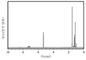
도 14는 구조식(100)에 나타낸 유기 화합물의 1H-NMR 차트이다.
도 15는 구조식(100)에 나타낸 유기 화합물의 자외·가시 흡수 스펙트럼 및 발광 스펙트럼이다.
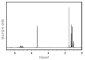
도 16은 구조식(101)에 나타낸 유기 화합물의 1H-NMR 차트이다.
도 17은 구조식(101)에 나타낸 유기 화합물의 자외·가시 흡수 스펙트럼 및 발광 스펙트럼이다.
도 18은 구조식(102)에 나타낸 유기 화합물의 1H-NMR 차트이다.
도 19는 구조식(102)에 나타낸 유기 화합물의 자외·가시 흡수 스펙트럼 및 발광 스펙트럼이다.
도 20은 구조식(103)에 나타낸 유기 화합물의 1H-NMR 차트이다.
도 21은 구조식(103)에 나타낸 유기 화합물의 자외·가시 흡수 스펙트럼 및 발광 스펙트럼이다.
도 22는 구조식(104)에 나타낸 유기 화합물의 1H-NMR 차트이다.
도 23은 구조식(104)에 나타낸 유기 화합물의 자외·가시 흡수 스펙트럼 및 발광 스펙트럼이다.
도 24는 발광 디바이스에 대하여 설명하는 도면이다.
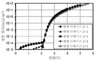
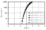
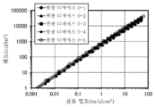
도 25는 발광 디바이스 1-1 내지 발광 디바이스 1-5의 전류 밀도-휘도 특성을 나타낸 도면이다.
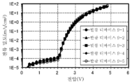
도 26은 발광 디바이스 1-1 내지 발광 디바이스 1-5의 전압-휘도 특성을 나타낸 도면이다.
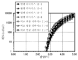
도 27은 발광 디바이스 1-1 내지 발광 디바이스 1-5의 휘도-전류 효율 특성을 나타낸 도면이다.
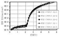
도 28은 발광 디바이스 1-1 내지 발광 디바이스 1-5의 전압-전류 밀도 특성을 나타낸 도면이다.
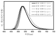
도 29는 발광 디바이스 1-1 내지 발광 디바이스 1-5의 전계 발광 스펙트럼을 나타낸 도면이다.
도 30은 발광 디바이스 1-1 내지 발광 디바이스 1-5의 신뢰성 측정 결과를 설명하는 도면이다.
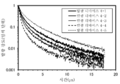
도 31은 발광 디바이스 1-1 내지 발광 디바이스 1-5의 발광 수명 측정 결과를 설명하는 도면이다.
도 32는 발광 디바이스 2-1 내지 발광 디바이스 2-5의 전류 밀도-휘도 특성을 나타낸 도면이다.
도 33은 발광 디바이스 2-1 내지 발광 디바이스 2-5의 전압-휘도 특성을 나타낸 도면이다.
도 34는 발광 디바이스 2-1 내지 발광 디바이스 2-5의 휘도-전류 효율 특성을 나타낸 도면이다.
도 35는 발광 디바이스 2-1 내지 발광 디바이스 2-5의 전압-전류 밀도 특성을 나타낸 도면이다.
도 36은 발광 디바이스 2-1 내지 발광 디바이스 2-5의 전계 발광 스펙트럼을 나타낸 도면이다.
도 37은 발광 디바이스 2-1 내지 발광 디바이스 2-5의 신뢰성 측정 결과를 설명하는 도면이다.
도 38은 발광 디바이스 2-1 내지 발광 디바이스 2-5의 발광 수명 측정 결과를 설명하는 도면이다.
도 39는 발광 디바이스 3-1 내지 발광 디바이스 3-5의 전류 밀도-휘도 특성을 나타낸 도면이다.
도 40은 발광 디바이스 3-1 내지 발광 디바이스 3-5의 전압-휘도 특성을 나타낸 도면이다.
도 41은 발광 디바이스 3-1 내지 발광 디바이스 3-5의 휘도-전류 효율 특성을 나타낸 도면이다.
도 42는 발광 디바이스 3-1 내지 발광 디바이스 3-5의 전압-전류 밀도 특성을 나타낸 도면이다.
도 43은 발광 디바이스 3-1 내지 발광 디바이스 3-5의 전계 발광 스펙트럼을 나타낸 도면이다.
도 44는 발광 디바이스 3-1 내지 발광 디바이스 3-5의 신뢰성 측정 결과를 설명하는 도면이다.
도 45는 발광 디바이스 3-1 내지 발광 디바이스 3-5의 발광 수명 측정 결과를 설명하는 도면이다.
도 46은 발광 디바이스 4-1 내지 발광 디바이스 4-5의 전류 밀도-휘도 특성을 나타낸 도면이다.
도 47은 발광 디바이스 4-1 내지 발광 디바이스 4-5의 전압-휘도 특성을 나타낸 도면이다.
도 48은 발광 디바이스 4-1 내지 발광 디바이스 4-5의 휘도-전류 효율 특성을 나타낸 도면이다.
도 49는 발광 디바이스 4-1 내지 발광 디바이스 4-5의 전압-전류 밀도 특성을 나타낸 도면이다.
도 50은 발광 디바이스 4-1 내지 발광 디바이스 4-5의 전계 발광 스펙트럼을 나타낸 도면이다.
도 51은 발광 디바이스 4-1 내지 발광 디바이스 4-5의 신뢰성 측정 결과를 설명하는 도면이다.
도 52는 발광 디바이스 4-1 내지 발광 디바이스 4-5의 발광 수명 측정 결과를 설명하는 도면이다.
도 53은 발광 디바이스 5-1 내지 발광 디바이스 5-5의 전류 밀도-휘도 특성을 나타낸 도면이다.
도 54는 발광 디바이스 5-1 내지 발광 디바이스 5-5의 전압-휘도 특성을 나타낸 도면이다.
도 55는 발광 디바이스 5-1 내지 발광 디바이스 5-5의 휘도-전류 효율 특성을 나타낸 도면이다.
도 56은 발광 디바이스 5-1 내지 발광 디바이스 5-5의 전압-전류 밀도 특성을 나타낸 도면이다.
도 57은 발광 디바이스 5-1 내지 발광 디바이스 5-5의 전계 발광 스펙트럼을 나타낸 도면이다.
도 58은 발광 디바이스 5-1 내지 발광 디바이스 5-5의 신뢰성 측정 결과를 설명하는 도면이다.
도 59는 발광 디바이스 6-1 내지 발광 디바이스 6-5의 전류 밀도-휘도 특성을 나타낸 도면이다.
도 60은 발광 디바이스 6-1 내지 발광 디바이스 6-5의 전압-휘도 특성을 나타낸 도면이다.
도 61은 발광 디바이스 6-1 내지 발광 디바이스 6-5의 휘도-전류 효율 특성을 나타낸 도면이다.
도 62는 발광 디바이스 6-1 내지 발광 디바이스 6-5의 전압-전류 밀도 특성을 나타낸 도면이다.
도 63은 발광 디바이스 6-1 내지 발광 디바이스 6-5의 전계 발광 스펙트럼을 나타낸 도면이다.
도 64는 발광 디바이스 6-1 내지 발광 디바이스 6-5의 신뢰성 측정 결과를 설명하는 도면이다.
도 65는 발광 디바이스 6-1 내지 발광 디바이스 6-5의 발광 수명 측정 결과를 설명하는 도면이다.
도 66은 발광 디바이스 7-1 내지 발광 디바이스 7-5의 전류 밀도-휘도 특성을 나타낸 도면이다.
도 67은 발광 디바이스 7-1 내지 발광 디바이스 7-5의 전압-휘도 특성을 나타낸 도면이다.
도 68은 발광 디바이스 7-1 내지 발광 디바이스 7-5의 휘도-전류 효율 특성을 나타낸 도면이다.
도 69는 발광 디바이스 7-1 내지 발광 디바이스 7-5의 전압-전류 밀도 특성을 나타낸 도면이다.
도 70은 발광 디바이스 7-1 내지 발광 디바이스 7-5의 전계 발광 스펙트럼을 나타낸 도면이다.
도 71은 발광 디바이스 8-1 내지 발광 디바이스 8-5의 전류 밀도-휘도 특성을 나타낸 도면이다.
도 72는 발광 디바이스 8-1 내지 발광 디바이스 8-5의 전압-휘도 특성을 나타낸 도면이다.
도 73은 발광 디바이스 8-1 내지 발광 디바이스 8-5의 휘도-전류 효율 특성을 나타낸 도면이다.
도 74는 발광 디바이스 8-1 내지 발광 디바이스 8-5의 전압-전류 밀도 특성을 나타낸 도면이다.
도 75는 발광 디바이스 8-1 내지 발광 디바이스 8-5의 전계 발광 스펙트럼을 나타낸 도면이다.
도 76은 구조식(124)에 나타낸 유기 화합물의 1H-NMR 차트이다.
도 77은 구조식(124)에 나타낸 유기 화합물의 자외·가시 흡수 스펙트럼 및 발광 스펙트럼이다.
도 78은 구조식(125)에 나타낸 유기 화합물의 1H-NMR 차트이다.
도 79는 구조식(125)에 나타낸 유기 화합물의 자외·가시 흡수 스펙트럼 및 발광 스펙트럼이다.
도 80은 구조식(128)에 나타낸 유기 화합물의 1H-NMR 차트이다.
도 81은 구조식(128)에 나타낸 유기 화합물의 자외·가시 흡수 스펙트럼 및 발광 스펙트럼이다.
도 82는 구조식(129)에 나타낸 유기 화합물의 1H-NMR 차트이다.
도 83은 구조식(129)에 나타낸 유기 화합물의 자외·가시 흡수 스펙트럼 및 발광 스펙트럼이다.
도 84는 발광 디바이스 7-1 내지 발광 디바이스 7-5의 신뢰성 측정 결과를 설명하는 도면이다.
도 85는 발광 디바이스 8-1 내지 발광 디바이스 8-5의 신뢰성 측정 결과를 설명하는 도면이다.
도 86은 발광 디바이스 9-1 내지 발광 디바이스 9-5의 전류 밀도-휘도 특성을 나타낸 도면이다.
도 87은 발광 디바이스 9-1 내지 발광 디바이스 9-5의 전압-휘도 특성을 나타낸 도면이다.
도 88은 발광 디바이스 9-1 내지 발광 디바이스 9-5의 휘도-전류 효율 특성을 나타낸 도면이다.
도 89는 발광 디바이스 9-1 내지 발광 디바이스 9-5의 전압-전류 밀도 특성을 나타낸 도면이다.
도 90은 발광 디바이스 9-1 내지 발광 디바이스 9-5의 전계 발광 스펙트럼을 나타낸 도면이다.
도 91은 발광 디바이스 10-1 내지 발광 디바이스 10-5의 전류 밀도-휘도 특성을 나타낸 도면이다.
도 92는 발광 디바이스 10-1 내지 발광 디바이스 10-5의 전압-휘도 특성을 나타낸 도면이다.
도 93은 발광 디바이스 10-1 내지 발광 디바이스 10-5의 휘도-전류 효율 특성을 나타낸 도면이다.
도 94는 발광 디바이스 10-1 내지 발광 디바이스 10-5의 전압-전류 밀도 특성을 나타낸 도면이다.
도 95는 발광 디바이스 10-1 내지 발광 디바이스 10-5의 전계 발광 스펙트럼을 나타낸 도면이다.
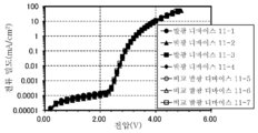
도 96은 발광 디바이스 11-1 내지 발광 디바이스 11-7의 전류 밀도-휘도 특성을 나타낸 도면이다.
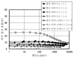
도 97은 발광 디바이스 11-1 내지 발광 디바이스 11-7의 전압-휘도 특성을 나타낸 도면이다.
도 98은 발광 디바이스 11-1 내지 발광 디바이스 11-7의 휘도-전류 효율 특성을 나타낸 도면이다.
도 99는 발광 디바이스 11-1 내지 발광 디바이스 11-7의 전압-전류 밀도 특성을 나타낸 도면이다.
도 100은 발광 디바이스 11-1 내지 발광 디바이스 11-7의 휘도-외부 양자 효율 특성을 나타낸 도면이다.
도 101은 발광 디바이스 11-1 내지 발광 디바이스 11-7의 전계 발광 스펙트럼을 나타낸 도면이다.
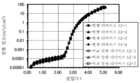
도 102는 발광 디바이스 12-1 내지 발광 디바이스 12-7의 전류 밀도-휘도 특성을 나타낸 도면이다.
도 103은 발광 디바이스 12-1 내지 발광 디바이스 12-7의 전압-휘도 특성을 나타낸 도면이다.
도 104는 발광 디바이스 12-1 내지 발광 디바이스 12-7의 휘도-전류 효율 특성을 나타낸 도면이다.
도 105는 발광 디바이스 12-1 내지 발광 디바이스 12-7의 전압-전류 밀도 특성을 나타낸 도면이다.
도 106은 발광 디바이스 12-1 내지 발광 디바이스 12-7의 휘도-외부 양자 효율 특성을 나타낸 도면이다.
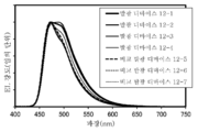
도 107은 발광 디바이스 12-1 내지 발광 디바이스 12-7의 전계 발광 스펙트럼을 나타낸 도면이다.1A is a diagram showing the structure of a light emitting device. 1B is a diagram illustrating a light emitting layer.
2A is a conceptual diagram of energy transfer between a general guest material and a host material. 2B is a conceptual diagram of energy transfer between a compound (guest material) and a host material, which is one embodiment of the present invention.
3A is a conceptual diagram of energy transfer between compounds in a light emitting layer. 3B is a conceptual diagram of energy transfer between compounds in a light emitting layer. 3C is a conceptual diagram of energy transfer between compounds in a light emitting layer.
4A is a conceptual diagram of energy transfer between compounds in a light emitting layer. 4B is a conceptual diagram of energy transfer between compounds in a light emitting layer. 4C is a conceptual diagram of energy transfer between compounds in a light emitting layer.
5A is a conceptual diagram of energy transfer between compounds in a light emitting layer. 5B is a conceptual diagram of energy transfer between compounds in a light emitting layer.
6A and 6B are diagrams for explaining the structure of a light emitting device.
7A, 7B, and 7C are views for explaining a light emitting device.
Fig. 8A is a top view illustrating a light emitting device. 8B is a cross-sectional view illustrating a light emitting device.
9A is a diagram illustrating a mobile computer. 9B is a diagram illustrating a portable image reproducing apparatus. 9C is a diagram illustrating a digital camera. 9D is a diagram illustrating a portable information terminal. 9(E) is a diagram explaining a portable information terminal. 9F is a diagram illustrating a television device. 9G is a diagram illustrating a portable information terminal.
10A, 10B, and 10C are diagrams for explaining a foldable portable information terminal.
11A and 11B are views for explaining a vehicle.
12 is a diagram illustrating a lighting device.
13 is a diagram illustrating a lighting device.
14 is a 1 H-NMR chart of an organic compound represented by Structural Formula (100).
15 is an ultraviolet/visible absorption spectrum and an emission spectrum of the organic compound represented by Structural Formula (100).
16 is a 1 H-NMR chart of the organic compound represented by Structural Formula (101).
17 is an ultraviolet/visible absorption spectrum and an emission spectrum of the organic compound represented by Structural Formula (101).
18 is a 1 H-NMR chart of the organic compound represented by Structural Formula (102).
19 is an ultraviolet/visible absorption spectrum and emission spectrum of the organic compound represented by Structural Formula (102).
20 is a 1 H-NMR chart of the organic compound represented by Structural Formula (103).
Fig. 21 is an ultraviolet/visible absorption spectrum and emission spectrum of the organic compound represented by Structural Formula (103).
22 is a 1 H-NMR chart of the organic compound represented by Structural Formula (104).
23 is an ultraviolet/visible absorption spectrum and emission spectrum of the organic compound represented by Structural Formula (104).
24 is a diagram illustrating a light emitting device.
Fig. 25 is a diagram showing current density-luminance characteristics of Light-Emitting Devices 1-1 to 1-5.
26 is a diagram showing voltage-luminance characteristics of Light-Emitting Devices 1-1 to 1-5.
Fig. 27 is a diagram showing luminance-current efficiency characteristics of Light-Emitting Devices 1-1 to 1-5.
28 is a diagram showing voltage-current density characteristics of Light-Emitting Devices 1-1 to 1-5.
Fig. 29 is a diagram showing an electroluminescence spectrum of Light-Emitting Devices 1-1 to 1-5.
Fig. 30 is a diagram for explaining the reliability measurement results of Light-Emitting Devices 1-1 to 1-5.
Fig. 31 is a diagram explaining the result of measuring the light emission lifetime of the light-emitting devices 1-1 to 1-5.
Fig. 32 is a diagram showing current density-luminance characteristics of Light-Emitting Devices 2-1 to 2-5.
33 is a diagram showing voltage-luminance characteristics of Light-Emitting Devices 2-1 to 2-5.
Fig. 34 is a diagram showing luminance-current efficiency characteristics of Light-Emitting Devices 2-1 to 2-5.
Fig. 35 is a diagram showing voltage-current density characteristics of Light-Emitting Devices 2-1 to 2-5.
Fig. 36 is a diagram showing electroluminescence spectra of Light-Emitting Device 2-1 to Light-Emitting Device 2-5.
37 is a diagram for explaining the reliability measurement results of the light-emitting device 2-1 to the light-emitting device 2-5.
38 is a diagram for explaining the result of measuring the light emission lifetime of the light-emitting device 2-1 to the light-emitting device 2-5.
39 is a diagram showing current density-luminance characteristics of Light-Emitting Devices 3-1 to 3-5.
40 is a diagram showing voltage-luminance characteristics of Light-Emitting Devices 3-1 to 3-5.
41 is a diagram showing luminance-current efficiency characteristics of Light-Emitting Devices 3-1 to 3-5.
42 is a diagram showing voltage-current density characteristics of Light-Emitting Device 3-1 to Light-Emitting Device 3-5.
43 is a diagram showing an electroluminescence spectrum of Light-Emitting Device 3-1 to Light-Emitting Device 3-5.
Fig. 44 is a diagram for explaining the reliability measurement results of the light-emitting device 3-1 to the light-emitting device 3-5.
Fig. 45 is a diagram explaining the result of measuring the light emission lifetime of the light-emitting device 3-1 to the light-emitting device 3-5.
Fig. 46 is a diagram showing current density-luminance characteristics of Light-Emitting Devices 4-1 to 4-5.
47 is a diagram showing voltage-luminance characteristics of Light-Emitting Devices 4-1 to 4-5.
48 is a diagram showing luminance-current efficiency characteristics of Light-Emitting Devices 4-1 to 4-5.
49 is a diagram showing voltage-current density characteristics of Light-Emitting Devices 4-1 to 4-5.
50 is a diagram showing an electroluminescence spectrum of Light-Emitting Device 4-1 to Light-Emitting Device 4-5.
51 is a diagram for explaining the reliability measurement results of the light-emitting device 4-1 to the light-emitting device 4-5.
Fig. 52 is a diagram explaining the result of measuring the light emission lifetime of the light-emitting device 4-1 to the light-emitting device 4-5.
Fig. 53 is a diagram showing current density-luminance characteristics of Light-Emitting Devices 5-1 to 5-5.
Fig. 54 is a diagram showing voltage-luminance characteristics of Light-Emitting Devices 5-1 to 5-5.
Fig. 55 is a diagram showing luminance-current efficiency characteristics of Light-Emitting Devices 5-1 to 5-5.
56 is a diagram showing voltage-current density characteristics of Light-Emitting Devices 5-1 to 5-5.
Fig. 57 is a diagram showing electroluminescence spectra of Light-Emitting Device 5-1 to Light-Emitting Device 5-5.
58 is a diagram for explaining the reliability measurement results of the light-emitting device 5-1 to the light-emitting device 5-5.
Fig. 59 is a diagram showing current density-luminance characteristics of Light-Emitting Devices 6-1 to 6-5.
60 is a diagram showing voltage-luminance characteristics of Light-Emitting Devices 6-1 to 6-5.
61 is a diagram showing luminance-current efficiency characteristics of Light-Emitting Devices 6-1 to 6-5.
62 is a diagram showing voltage-current density characteristics of Light-Emitting Devices 6-1 to 6-5.
63 is a diagram showing an electroluminescence spectrum of Light-Emitting Device 6-1 to Light-Emitting Device 6-5.
Fig. 64 is a diagram explaining the reliability measurement results of the light-emitting device 6-1 to the light-emitting device 6-5.
65 is a diagram for explaining the result of measuring the light emission lifetime of the light-emitting device 6-1 to the light-emitting device 6-5.
66 is a diagram showing current density-luminance characteristics of Light-Emitting Devices 7-1 to 7-5.
67 is a diagram showing voltage-luminance characteristics of Light-Emitting Devices 7-1 to 7-5.
68 is a diagram showing luminance-current efficiency characteristics of Light-Emitting Devices 7-1 to 7-5.
69 is a diagram showing voltage-current density characteristics of Light-Emitting Devices 7-1 to 7-5.
Fig. 70 is a diagram showing electroluminescence spectra of Light-Emitting Device 7-1 to Light-Emitting Device 7-5.
Fig. 71 is a diagram showing current density-luminance characteristics of Light-Emitting Devices 8-1 to 8-5.
72 is a diagram showing voltage-luminance characteristics of Light-Emitting Devices 8-1 to 8-5.
73 is a diagram showing luminance-current efficiency characteristics of Light-Emitting Devices 8-1 to 8-5.
74 is a diagram showing voltage-current density characteristics of Light-Emitting Devices 8-1 to 8-5.
75 is a diagram showing the electroluminescence spectra of Light-Emitting Device 8-1 to Light-Emitting Device 8-5.
76 is a 1 H-NMR chart of the organic compound represented by Structural Formula (124).
77 is an ultraviolet/visible absorption spectrum and an emission spectrum of the organic compound represented by Structural Formula (124).
78 is a 1 H-NMR chart of the organic compound represented by Structural Formula (125).
79 is an ultraviolet/visible absorption spectrum and emission spectrum of the organic compound represented by Structural Formula (125).
80 is a 1 H-NMR chart of the organic compound represented by Structural Formula (128).
81 is an ultraviolet/visible absorption spectrum and emission spectrum of the organic compound represented by Structural Formula (128).
82 is a 1 H-NMR chart of the organic compound represented by Structural Formula (129).
83 is an ultraviolet/visible absorption spectrum and emission spectrum of the organic compound represented by Structural Formula (129).
84 is a diagram for explaining the reliability measurement results of the light-emitting device 7-1 to the light-emitting device 7-5.
85 is a diagram for explaining the reliability measurement results of the light-emitting device 8-1 to the light-emitting device 8-5.
Fig. 86 is a diagram showing current density-luminance characteristics of Light-Emitting Devices 9-1 to 9-5.
87 is a diagram showing voltage-luminance characteristics of Light-Emitting Devices 9-1 to 9-5.
88 is a diagram showing luminance-current efficiency characteristics of Light-Emitting Devices 9-1 to 9-5.
89 is a diagram showing voltage-current density characteristics of Light-Emitting Devices 9-1 to 9-5.
90 is a diagram showing an electroluminescence spectrum of the light-emitting device 9-1 to the light-emitting device 9-5.
91 is a diagram showing current density-luminance characteristics of Light-Emitting Devices 10-1 to 10-5.
92 is a diagram showing voltage-luminance characteristics of Light-Emitting Devices 10-1 to 10-5.
93 is a diagram showing luminance-current efficiency characteristics of Light-Emitting Devices 10-1 to 10-5.
94 is a diagram showing voltage-current density characteristics of Light-Emitting Devices 10-1 to 10-5.
95 is a diagram showing an electroluminescence spectrum of the Light-Emitting Device 10-1 to the Light-Emitting Device 10-5.
96 is a diagram showing current density-luminance characteristics of Light-Emitting Devices 11-1 to 11-7.
97 is a diagram showing voltage-luminance characteristics of Light-Emitting Devices 11-1 to 11-7.
98 is a diagram showing luminance-current efficiency characteristics of Light-Emitting Devices 11-1 to 11-7.
99 is a diagram showing voltage-current density characteristics of Light-Emitting Devices 11-1 to 11-7.
100 is a diagram showing luminance-external quantum efficiency characteristics of Light-Emitting Devices 11-1 to 11-7.
101 is a diagram showing an electroluminescence spectrum of Light-Emitting Device 11-1 to Light-Emitting Device 11-7.
Fig. 102 is a diagram showing current density-luminance characteristics of Light-Emitting Devices 12-1 to 12-7.
103 is a diagram showing voltage-luminance characteristics of Light-Emitting Devices 12-1 to 12-7.
104 is a diagram showing luminance-current efficiency characteristics of Light-Emitting Devices 12-1 to 12-7.
105 is a diagram showing voltage-current density characteristics of Light-Emitting Devices 12-1 to 12-7.
Fig. 106 is a diagram showing luminance-external quantum efficiency characteristics of Light-Emitting Devices 12-1 to 12-7.
107 is a diagram showing electroluminescence spectra of Light-Emitting Device 12-1 to Light-Emitting Device 12-7.
이하에서 본 발명의 실시형태에 대하여 도면을 참조하여 자세히 설명한다. 다만, 본 발명은 이하의 설명에 한정되지 않고, 본 발명의 취지 및 그 범위에서 벗어남이 없이 그 형태 및 자세한 사항을 다양하게 변경할 수 있다. 따라서, 본 발명은 이하의 실시형태의 기재 내용에 한정하여 해석되는 것은 아니다.Hereinafter, embodiments of the present invention will be described in detail with reference to the drawings. However, the present invention is not limited to the following description, and its form and details can be variously changed without departing from the spirit and scope of the present invention. Therefore, the present invention is not interpreted as being limited to the description of the following embodiments.
또한 도면 등에 나타낸 각 구성의 위치, 크기, 범위 등은 이해하기 쉽게 하기 위하여 실제의 위치, 크기, 범위 등을 나타내지 않은 경우가 있다. 따라서, 개시(開示)하는 발명은 도면 등에 개시된 위치, 크기, 범위 등에 반드시 한정되는 것은 아니다.In addition, the location, size, range, etc. of each component shown in the drawings may not indicate the actual location, size, range, etc. for ease of understanding. Accordingly, the disclosed invention is not necessarily limited to the position, size, range, etc. disclosed in the drawings or the like.
또한 본 명세서 등에서 도면을 참조하여 발명의 구성을 설명하는 데 있어서, 같은 것을 가리키는 부호는 상이한 도면 간에서도 공통적으로 사용한다.In addition, in describing the configuration of the invention with reference to the drawings in the present specification and the like, reference numerals indicating the same are commonly used between different drawings.
또한, 본 명세서 등에서, 단일항 들뜬 상태(S*)란, 들뜬 에너지를 가지는 단일항 상태를 말한다. 또한, S1 준위는 단일항 들뜬 에너지 준위의 가장 낮은 준위이며, 가장 낮은 단일항 들뜬 상태(S1 상태)의 들뜬 에너지 준위를 말한다. 또한 삼중항 들뜬 상태(T*)는 들뜬 에너지를 가지는 삼중항 상태를 말한다. 또한, T1 준위는 삼중항 들뜬 에너지 준위의 가장 낮은 준위이며, 가장 낮은 삼중항 들뜬 상태(T1 상태)의 들뜬 에너지 준위를 말한다. 또한, 본 명세서 등에서, 단순히 단일항 들뜬 상태 및 단일항 들뜬 에너지 준위라고 표기한 경우에도, S1 상태 및 S1 준위를 나타내는 경우가 있다. 또한, 삼중항 들뜬 상태 및 삼중항 들뜬 에너지 준위라고 표기한 경우에도, T1 상태 및 T1 준위를 나타내는 경우가 있다.In addition, in this specification and the like, the singlet excited state (S * ) refers to a singlet state having excited energy. In addition, the S1 level is the lowest level of the singlet excited energy level, and refers to the excited energy level in the lowest singlet excited state (S1 state). In addition, the triplet excited state (T * ) refers to the triplet state with excited energy. In addition, the T1 level is the lowest level of the triplet excited energy level, and refers to the excited energy level in the lowest triplet excited state (T1 state). In addition, in this specification and the like, even when simply indicated as a singlet excited state and a singlet excited energy level, the S1 state and the S1 level may be indicated. In addition, even when expressed as a triplet excited state and a triplet excited energy level, the T1 state and the T1 level may be indicated.
또한, 본 명세서 등에서 형광 발광 물질이란, 단일항 들뜬 상태로부터 바닥 상태로 완화될 때 가시광 영역 또는 근적외 영역에 발광을 공여하는 화합물이다. 인광 발광 물질이란, 삼중항 들뜬 상태로부터 바닥 상태로 완화될 때, 실온에서 가시광 영역 또는 근적외 영역에 발광을 공여하는 화합물이다. 환언하면, 인광 발광 물질이란 삼중항 들뜬 에너지를 발광으로 변환할 수 있는 화합물의 하나이다.In addition, in the present specification and the like, the fluorescent light-emitting substance is a compound that provides light emission to the visible or near-infrared region when the singlet excited state is relaxed to the ground state. The phosphorescent light-emitting substance is a compound that provides light emission to the visible or near-infrared region at room temperature when the triplet excited state is relaxed to the ground state. In other words, a phosphorescent light-emitting substance is one of compounds capable of converting triplet excited energy into light emission.
(실시형태 1)(Embodiment 1)
본 실시형태에서는 본 발명의 일 형태인 화합물에 대하여 설명한다. 또한, 본 발명의 일 형태인 화합물은 하기 일반식(G1)으로 나타내어진다.In this embodiment, a compound which is one embodiment of the present invention will be described. In addition, a compound which is one embodiment of the present invention is represented by the following general formula (G1).
[화학식 6][Formula 6]

또한, 일반식(G1)에서, A는 치환 또는 비치환된 탄소수 10 내지 30의 축합 방향족 고리 혹은 치환 또는 비치환된 탄소수 10 내지 30의 축합 헤테로 방향족 고리를 나타내고, Z1 내지 Z3은 각각 독립적으로 일반식(Z-1) 또는 일반식(Z-2)으로 나타내어지는 구조를 가진다. 일반식(Z-1)에서 X1 및 X2는 각각 독립적으로 탄소수 3 내지 10의 알킬기, 치환 또는 비치환된 탄소수 3 내지 10의 사이클로알킬기, 가교 구조를 가지는 탄소수 7 내지 10의 사이클로알킬기, 탄소수 3 내지 12의 트라이알킬실릴기 중 어느 하나를 나타낸다. 또한, Ar1 내지 Ar4는 각각 독립적으로 치환 또는 비치환된 탄소수 6 내지 13의 방향족 탄화수소기를 나타내고, 또한 Ar1 내지 Ar4 중 적어도 하나는 X1과 같은 치환기를 가진다.In addition, in the general formula (G1), A represents a substituted or unsubstituted fused aromatic ring having 10 to 30 carbon atoms or a substituted or unsubstituted fused heteroaromatic ring having 10 to 30 carbon atoms, and Z 1 to Z 3 are each independently It has a structure represented by general formula (Z-1) or general formula (Z-2). In general formula (Z-1), X 1 and X 2 are each independently an alkyl group having 3 to 10 carbon atoms, a substituted or unsubstituted cycloalkyl group having 3 to 10 carbon atoms, a cycloalkyl group having 7 to 10 carbon atoms having a crosslinked structure, and a carbon number. Represents any one of 3 to 12 trialkylsilyl groups. Further, Ar 1 to Ar 4 each independently represent a substituted or unsubstituted aromatic hydrocarbon group having 6 to 13 carbon atoms, and at least one of Ar 1 to Ar 4 has a substituent such as X 1.
또한, 본 발명의 다른 일 형태는 하기 일반식(G2)으로 나타내어지는 화합물이다.In addition, another aspect of the present invention is a compound represented by the following general formula (G2).
[화학식 7][Formula 7]

또한, 일반식(G2)에서, A는 치환 또는 비치환된 탄소수 10 내지 30의 축합 방향족 고리 혹은 치환 또는 비치환된 탄소수 10 내지 30의 축합 헤테로 방향족 고리를 나타내고, Z1 및 Z2는 각각 독립적으로 일반식(Z-3) 또는 일반식(Z-4)으로 나타내어지는 구조를 가진다. 일반식(Z-3)에서 X1 및 X2는 각각 독립적으로 탄소수 3 내지 10의 알킬기, 치환 또는 비치환된 탄소수 3 내지 10의 사이클로알킬기, 가교 구조를 가지는 탄소수 7 내지 10의 사이클로알킬기, 탄소수 3 내지 12의 트라이알킬실릴기 중 어느 하나를 나타낸다. 또한, Ar1 내지 Ar6은 각각 독립적으로 치환 또는 비치환된 탄소수 6 내지 13의 방향족 탄화수소기를 나타내고, 또한 Ar1 내지 Ar6 중 적어도 하나는 X1과 같은 치환기를 가진다.In addition, in the general formula (G2), A represents a substituted or unsubstituted fused aromatic ring having 10 to 30 carbon atoms or a substituted or unsubstituted fused heteroaromatic ring having 10 to 30 carbon atoms, and Z 1 and Z 2 are each independently It has a structure represented by general formula (Z-3) or general formula (Z-4). In the general formula (Z-3), X 1 and X 2 are each independently an alkyl group having 3 to 10 carbon atoms, a substituted or unsubstituted cycloalkyl group having 3 to 10 carbon atoms, a cycloalkyl group having 7 to 10 carbon atoms having a crosslinked structure, and a carbon number. Represents any one of 3 to 12 trialkylsilyl groups. Further, Ar 1 to Ar 6 each independently represent a substituted or unsubstituted aromatic hydrocarbon group having 6 to 13 carbon atoms, and at least one of Ar 1 to Ar 6 has a substituent such as X 1.
또한, 본 발명의 다른 일 형태는 하기 일반식(G3)으로 나타내어지는 화합물이다.In addition, another aspect of the present invention is a compound represented by the following general formula (G3).
[화학식 8][Formula 8]

또한, 일반식(G3)에서, Z1 내지 Z3은 각각 독립적으로 일반식(Z-1) 또는 일반식(Z-2)으로 나타내어지는 구조를 가진다. 일반식(Z-1)에서 X1 및 X2는 각각 독립적으로 탄소수 3 내지 10의 알킬기, 치환 또는 비치환된 탄소수 3 내지 10의 사이클로알킬기, 가교 구조를 가지는 탄소수 7 내지 10의 사이클로알킬기, 탄소수 3 내지 12의 트라이알킬실릴기 중 어느 하나를 나타낸다. 또한, Ar1 내지 Ar4는 각각 독립적으로 치환 또는 비치환된 탄소수 6 내지 13의 방향족 탄화수소기를 나타내고, 또한 Ar1 내지 Ar4 중 적어도 하나는 X1 또는 X2와 같은 치환기를 가진다. 또한, R1 내지 R8은 각각 독립적으로 수소, 탄소수 3 내지 10의 알킬기, 치환 또는 비치환된 탄소수 3 내지 10의 사이클로알킬기, 탄소수 3 내지 12의 트라이알킬실릴기, 치환 또는 비치환된 탄소수 6 내지 25의 아릴기 중 어느 하나를 나타낸다.In addition, in General Formula (G3), Z 1 to Z 3 each independently have a structure represented by General Formula (Z-1) or General Formula (Z-2). In general formula (Z-1), X 1 and X 2 are each independently an alkyl group having 3 to 10 carbon atoms, a substituted or unsubstituted cycloalkyl group having 3 to 10 carbon atoms, a cycloalkyl group having 7 to 10 carbon atoms having a crosslinked structure, and a carbon number. Represents any one of 3 to 12 trialkylsilyl groups. In addition, Ar 1 to Ar 4 each independently represent a substituted or unsubstituted aromatic hydrocarbon group having 6 to 13 carbon atoms, and at least one of Ar 1 to Ar 4 has a substituent such as X 1 or X 2. In addition, R 1 to R 8 are each independently hydrogen, a
또한, 본 발명의 다른 일 형태는 일반식(G4)으로 나타내어지는 화합물이다.In addition, another aspect of the present invention is a compound represented by General Formula (G4).
[화학식 9][Formula 9]

또한, 일반식(G4)에서, Z1 및 Z2는 각각 독립적으로 일반식(Z-3) 또는 일반식(Z-4)으로 나타내어지는 구조를 가진다. 일반식(Z-3)에서 X1 및 X2는 각각 독립적으로 탄소수 3 내지 10의 알킬기, 치환 또는 비치환된 탄소수 3 내지 10의 사이클로알킬기, 가교 구조를 가지는 탄소수 7 내지 10의 사이클로알킬기, 탄소수 3 내지 12의 트라이알킬실릴기 중 어느 하나를 나타낸다. 또한, Ar1 내지 Ar6은 각각 독립적으로 치환 또는 비치환된 탄소수 6 내지 13의 방향족 탄화수소기를 나타내고, 또한 Ar1 내지 Ar6 중 적어도 하나는 X1 또는 X2와 같은 치환기를 가진다. 또한, R4 내지 R11은 각각 독립적으로 수소, 탄소수 3 내지 10의 알킬기, 치환 또는 비치환된 탄소수 3 내지 10의 사이클로알킬기, 탄소수 3 내지 12의 트라이알킬실릴기, 치환 또는 비치환된 탄소수 6 내지 25의 아릴기 중 어느 하나를 나타낸다.In addition, in General Formula (G4), Z 1 and Z 2 each independently have a structure represented by General Formula (Z-3) or General Formula (Z-4). In the general formula (Z-3), X 1 and X 2 are each independently an alkyl group having 3 to 10 carbon atoms, a substituted or unsubstituted cycloalkyl group having 3 to 10 carbon atoms, a cycloalkyl group having 7 to 10 carbon atoms having a crosslinked structure, and a carbon number. Represents any one of 3 to 12 trialkylsilyl groups. In addition, Ar 1 to Ar 6 each independently represent a substituted or unsubstituted aromatic hydrocarbon group having 6 to 13 carbon atoms, and at least one of Ar 1 to Ar 6 has a substituent such as X 1 or X 2. In addition, R 4 to R 11 are each independently hydrogen, a
본 발명의 일 형태인 화합물은 단일항 들뜬 에너지를 발광으로 변환하는 기능을 가지는 재료(형광 발광 물질)이기 때문에 게스트 재료로서, 발광 디바이스의 발광층에서 호스트 재료와 함께 사용할 수 있다. 본 발명의 일 형태인 화합물은 발광에 기여하는 발광단과, 호스트 재료로부터 상기 화합물로의 덱스터 기구에 의한 삼중항 들뜬 에너지 이동을 억제하는 보호기를 가진다. 또한, 본 발명의 일 형태인 화합물이 가지는 발광단은 축합 방향족 고리 또는 축합 헤테로 방향족 고리이고, 또한, 본 발명의 일 형태인 화합물이 가지는 보호기는 본 발명의 일 형태인 화합물이 가지는 2개 이상의 다이아릴아미노기에서, 아릴기 각각이 적어도 2개씩 가지는 기이고, 구체적으로는 탄소수 3 내지 10의 알킬기, 치환 또는 비치환된 탄소수 3 내지 10의 사이클로알킬기, 가교 구조를 가지는 탄소수 7 내지 10의 사이클로알킬기, 탄소수 3 내지 12의 트라이알킬실릴기 중 어느 것이다.Since the compound of one embodiment of the present invention is a material (fluorescent light emitting material) having a function of converting singlet excited energy into light emission, it can be used as a guest material and together with a host material in the light emitting layer of a light emitting device. The compound of one embodiment of the present invention has a luminophore that contributes to light emission and a protecting group that inhibits triplet excited energy transfer by the dexter mechanism from the host material to the compound. In addition, the luminophore of the compound of one embodiment of the present invention is a condensed aromatic ring or a condensed heteroaromatic ring, and the protecting group of the compound of one embodiment of the present invention is two or more diatoms of the compound of one embodiment of the present invention. In the rylamino group, each aryl group is a group having at least two, specifically an alkyl group having 3 to 10 carbon atoms, a substituted or unsubstituted cycloalkyl group having 3 to 10 carbon atoms, a cycloalkyl group having 7 to 10 carbon atoms having a crosslinked structure, Any of trialkylsilyl groups having 3 to 12 carbon atoms.
또한, 본 발명의 일 형태인 화합물은 발광단에 대하여 보호기를 가지는 2개 이상의 다이아릴아미노기가 대칭의 위치에 결합하는 구조로 함으로써, 양자 수율을 높일 수 있다. 또한, 본 발명의 일 형태인 화합물에서, 다이아릴아미노기를 사용함으로써, 분자량의 증대를 억제하고, 승화성을 유지할 수 있다.In addition, the compound of one embodiment of the present invention has a structure in which two or more diarylamino groups having a protecting group with respect to the luminophore are bonded to symmetrical positions, thereby increasing the quantum yield. Further, in the compound of one embodiment of the present invention, by using a diarylamino group, an increase in molecular weight can be suppressed and sublimation properties can be maintained.
또한, 본 발명의 일 형태인 화합물에서, 보호기는 발광단과 결합하는 다이아릴아미노기의 아릴기와 결합하는 구조를 가지기 때문에, 발광단을 덮도록 보호기를 배치할 수 있어, 호스트 재료로부터 발광단으로의 덱스터 기구에 의거한 에너지 이동이 일어나기 어려울 정도의 거리를 두고, 이들을 떨어지게 할 수 있다.In addition, in the compound of one embodiment of the present invention, since the protecting group has a structure that binds to the aryl group of the diarylamino group bonded to the luminophore, the protecting group can be disposed to cover the luminophore, thereby dexter from the host material to the luminophore. They can be separated at a distance such that it is difficult for the energy transfer to occur according to the device.
또한, 상기 일반식(G1) 및 일반식(G2)에서, 탄소수 10 내지 30의 축합 방향족 고리, 또는 탄소수 10 내지 30의 축합 헤테로 방향족 고리로서는, 예를 들어 페난트렌 골격, 스틸벤 골격, 아크리돈 골격, 페녹사진 골격, 페노싸이아진 골격 등을 들 수 있다. 또한, 형광 양자 수율을 더 높일 수 있는 나프탈렌 골격, 안트라센 골격, 플루오렌 골격, 크리센 골격, 트라이페닐렌 골격, 테트라센 골격, 피렌 골격, 페릴렌 골격, 쿠마린 골격, 퀴나크리돈 골격, 나프토비스벤조퓨란 골격 등을 들 수 있다.In addition, in the general formulas (G1) and (G2), as a condensed aromatic ring having 10 to 30 carbon atoms or a condensed heteroaromatic ring having 10 to 30 carbon atoms, for example, a phenanthrene skeleton, a stilbene skeleton, acri A money skeleton, a phenoxazine skeleton, and a phenothiazine skeleton. In addition, naphthalene skeleton, anthracene skeleton, fluorene skeleton, chrysene skeleton, triphenylene skeleton, tetracene skeleton, pyrene skeleton, perylene skeleton, coumarin skeleton, quinacridone skeleton, and naphthobis can further increase the fluorescence quantum yield. And a benzofuran skeleton.
또한, 상기 일반식(G1), 일반식(G2), 일반식(G3), 및 일반식(G4)에서, 탄소수 6 내지 13의 방향족 탄화수소기로서는, 페닐기, 바이페닐기, 나프틸기, 플루오렌일기 등을 들 수 있다.In addition, in the general formula (G1), general formula (G2), general formula (G3), and general formula (G4), examples of the aromatic hydrocarbon group having 6 to 13 carbon atoms include a phenyl group, a biphenyl group, a naphthyl group, and a fluorenyl group. Etc. are mentioned.
또한, 상기 일반식(G1), 일반식(G2), 일반식(G3), 및 일반식(G4)에서, 탄소수 3 내지 10의 알킬기의 구체적인 예로서는, 예를 들어 프로필기, 아이소프로필기, 뷰틸기, 아이소뷰틸기, sec-뷰틸기, tert-뷰틸기, 펜틸기, 헥실기, 데카닐기를 들 수 있다.In addition, in the general formula (G1), general formula (G2), general formula (G3), and general formula (G4), specific examples of an alkyl group having 3 to 10 carbon atoms include, for example, a propyl group, an isopropyl group, and a view. A butyl group, an isobutyl group, a sec-butyl group, a tert-butyl group, a pentyl group, a hexyl group, and a decanyl group are mentioned.
또한, 상기 일반식(G1), 일반식(G2), 일반식(G3), 및 일반식(G4)에서, 탄소수 3 내지 10의 사이클로알킬기의 구체적인 예로서는, 예를 들어 사이클로프로필기, 사이클로뷰틸기, 사이클로헥실기 등을 들 수 있다. 또한, 상기 사이클로알킬기가 치환기를 가지는 경우의 치환기의 구체적인 예로서는, 메틸기, 에틸기, 프로필기, 아이소프로필기, 뷰틸기, 아이소뷰틸기, sec-뷰틸기, tert-뷰틸기, 펜틸기, 헥실기와 같은 탄소수 1 내지 7의 알킬기, 사이클로펜틸기, 사이클로헥실기, 사이클로헵틸기, 8,9,10-트라이노보난일기와 같은 탄소수 5 내지 7의 사이클로알킬기, 페닐기, 나프틸기, 바이페닐기와 같은 탄소수 6 내지 12의 아릴기 등을 들 수 있다.In addition, in the general formula (G1), general formula (G2), general formula (G3), and general formula (G4), as a specific example of a cycloalkyl group having 3 to 10 carbon atoms, for example, a cyclopropyl group, a cyclobutyl group And a cyclohexyl group. In addition, as a specific example of the substituent when the cycloalkyl group has a substituent, a methyl group, an ethyl group, a propyl group, an isopropyl group, a butyl group, an isobutyl group, a sec-butyl group, a tert-butyl group, a pentyl group, a hexyl group C1-C7 alkyl group, cyclopentyl group, cyclohexyl group, cycloheptyl group, 8,9,10-trinobonanyl group, such as a cycloalkyl group having 5 to 7 carbon atoms, a phenyl group, a naphthyl group, a biphenyl group, and the like 6-12 aryl groups, etc. are mentioned.
또한, 상기 일반식(G1), 일반식(G2), 일반식(G3), 및 일반식(G4)에서, 가교 구조를 가지는 탄소수 7 내지 10의 사이클로알킬기의 구체적인 예로서는, 예를 들어 아다만틸기, 바이사이클로[2.2.1] 헵틸기, 트라이사이클로[5.2.1.02,6]데카닐기, 노르아다만틸기, 보닐기 등을 들 수 있다.In addition, in the general formula (G1), general formula (G2), general formula (G3), and general formula (G4), as a specific example of a cycloalkyl group having 7 to 10 carbon atoms having a crosslinked structure, for example, an adamantyl group , Bicyclo[2.2.1] heptyl group, tricyclo[5.2.1.0 2,6 ]decanyl group, noradamantyl group, bonyl group, and the like.
또한, 상기 일반식(G1), 일반식(G2), 일반식(G3), 및 일반식(G4)에서, 탄소수 3 내지 12의 트라이알킬실릴기의 구체적인 예로서는, 예를 들어 트라이메틸실릴기, 트라이에틸실릴기, tert-뷰틸다이메틸실릴기 등을 들 수 있다.In addition, in the general formula (G1), general formula (G2), general formula (G3), and general formula (G4), specific examples of a trialkylsilyl group having 3 to 12 carbon atoms include, for example, a trimethylsilyl group, Triethylsilyl group, tert-butyldimethylsilyl group, etc. are mentioned.
상기 일반식(G1), 일반식(G2), 일반식(G3), 및 일반식(G4)에서, 축합 방향족 고리, 축합 헤테로 방향족 고리, 탄소수 6 내지 13의 방향족 탄화수소기, 및 탄소수 3 이상 10 이하의 사이클로알킬기 중 어느 것이 치환기를 가지는 경우, 상기 치환기로서는 메틸기, 에틸기, 프로필기, 아이소프로필기, 뷰틸기, 아이소뷰틸기, sec-뷰틸기, tert-뷰틸기, 펜틸기, 헥실기와 같은 탄소수 1 내지 7의 알킬기나, 사이클로펜틸기, 사이클로헥실기, 사이클로헵틸기, 8,9,10-트라이노보난일기와 같은 탄소수 5 내지 7의 사이클로알킬기나, 페닐기, 나프틸기, 바이페닐기와 같은 탄소수 6 내지 12의 아릴기 등을 들 수 있다.In the general formula (G1), general formula (G2), general formula (G3), and general formula (G4), a condensed aromatic ring, a condensed heteroaromatic ring, an aromatic hydrocarbon group having 6 to 13 carbon atoms, and 3 or more 10 carbon atoms When any of the following cycloalkyl groups has a substituent, examples of the substituent include methyl group, ethyl group, propyl group, isopropyl group, butyl group, isobutyl group, sec-butyl group, tert-butyl group, pentyl group, and hexyl group. A cycloalkyl group having 5 to 7 carbon atoms, such as an alkyl group having 1 to 7 carbon atoms, a cyclopentyl group, a cyclohexyl group, a cycloheptyl group, an 8,9,10-trinobonanyl group, a phenyl group, a naphthyl group, or a biphenyl group. An aryl group having 6 to 12 carbon atoms, and the like.
상기 일반식(G3) 또는 일반식(G4)에서, 탄소수 6 내지 25의 아릴기의 구체적인 예로서는, 페닐기, 나프틸기, 바이페닐기, 플루오렌일기, 스파이로플루오렌일기 등을 들 수 있다. 또한, 상기 아릴기가 치환기를 가지는 경우, 상기 치환기로서는 상술한 탄소수 3 내지 10의 알킬기, 치환 또는 비치환된 탄소수 3 내지 10의 사이클로알킬기, 탄소수 3 내지 12의 트라이알킬실릴기를 들 수 있다.In the general formula (G3) or (G4), specific examples of the aryl group having 6 to 25 carbon atoms include a phenyl group, a naphthyl group, a biphenyl group, a fluorenyl group, and a spirofluorenyl group. Further, when the aryl group has a substituent, examples of the substituent include the aforementioned alkyl group having 3 to 10 carbon atoms, a substituted or unsubstituted cycloalkyl group having 3 to 10 carbon atoms, and a trialkylsilyl group having 3 to 12 carbon atoms.
다음으로, 상기 일반식(G1) 내지 일반식(G4)으로 나타내어지는 화합물의 구체적인 예를, 이하의 구조식(100) 내지 구조식(131)에 나타내었다. 또한, 일반식(G1) 내지 일반식(G4)으로 나타내어지는 화합물의 구체적인 예는 이들에 한정되지 않는다.Next, specific examples of the compounds represented by the general formulas (G1) to (G4) are shown in the following structural formulas (100) to (131). In addition, specific examples of the compound represented by General Formulas (G1) to (G4) are not limited to these.
[화학식 10][Formula 10]

[화학식 11][Formula 11]

[화학식 12][Formula 12]

[화학식 13][Formula 13]

[화학식 14][Formula 14]

[화학식 15][Formula 15]

[화학식 16][Formula 16]

[화학식 17][Formula 17]

다음으로, 하기 일반식(G1)으로 나타내어지는 화합물의 합성 방법에 대하여 설명한다.Next, a method for synthesizing a compound represented by the following general formula (G1) will be described.
[화학식 18][Formula 18]

상기 일반식(G1)에서 A는 치환 또는 비치환된 탄소수 10 내지 30의 축합 방향족 고리 혹은 치환 또는 비치환된 탄소수 10 내지 30의 축합 헤테로 방향족 고리를 나타내고, Z1 내지 Z3은 각각 독립적으로 일반식(Z-1) 또는 일반식(Z-2)으로 나타내어지는 구조를 가진다. 일반식(Z-1)에서 X1 및 X2는 각각 독립적으로 탄소수 3 내지 10의 알킬기, 치환 또는 비치환된 탄소수 3 내지 10의 사이클로알킬기, 가교 구조를 가지는 탄소수 7 내지 10의 사이클로알킬기, 탄소수 3 내지 12의 트라이알킬실릴기 중 어느 하나를 나타낸다. 또한, Ar1 내지 Ar4는 각각 독립적으로 치환 또는 비치환된 탄소수 6 내지 13의 방향족 탄화수소기를 나타내고, 또한 Ar1 내지 Ar4 중 적어도 하나는 X1 또는 X2와 같은 치환기를 가진다.In the general formula (G1), A represents a substituted or unsubstituted fused aromatic ring having 10 to 30 carbon atoms or a substituted or unsubstituted fused heteroaromatic ring having 10 to 30 carbon atoms, and Z 1 to Z 3 are each independently general It has a structure represented by formula (Z-1) or general formula (Z-2). In general formula (Z-1), X 1 and X 2 are each independently an alkyl group having 3 to 10 carbon atoms, a substituted or unsubstituted cycloalkyl group having 3 to 10 carbon atoms, a cycloalkyl group having 7 to 10 carbon atoms having a crosslinked structure, and a carbon number. Represents any one of 3 to 12 trialkylsilyl groups. In addition, Ar 1 to Ar 4 each independently represent a substituted or unsubstituted aromatic hydrocarbon group having 6 to 13 carbon atoms, and at least one of Ar 1 to Ar 4 has a substituent such as X 1 or X 2.
상기 일반식(G1)으로 나타내어지는 화합물은 예를 들어 하기 합성 스킴(S-1) 및 합성 스킴(S-2)으로 나타내는 방법으로 합성할 수 있다.The compound represented by the general formula (G1) can be synthesized by, for example, a method represented by the following synthesis scheme (S-1) and synthesis scheme (S-2).
우선, 화합물 1, 화합물 2(아닐린 화합물), 및 화합물 3(아닐린 화합물)을 커플링시킴으로써, 화합물 4(다이아민 화합물)를 얻을 수 있다(합성 스킴(S-1)).First, compound 4 (diamine compound) can be obtained by
[화학식 19][Formula 19]

이어서, 화합물 4(다이아민 화합물), 화합물 5(아릴 할라이드), 및 화합물 6(아릴 할라이드)을 커플링시킴으로써, 일반식(G1)으로 나타내어지는 화합물을 얻을 수 있다(합성 스킴(S-2)).Subsequently, by coupling compound 4 (diamine compound), compound 5 (aryl halide), and compound 6 (aryl halide), a compound represented by general formula (G1) can be obtained (synthetic scheme (S-2) ).
[화학식 20][Formula 20]

또한, 상기 일반식(G1)으로 나타내어지는 화합물은 하기 합성 스킴(S-3), 합성 스킴(S-4), 및 합성 스킴(S-5)으로 나타내는 방법으로 합성할 수도 있다.Further, the compound represented by the general formula (G1) can also be synthesized by a method represented by the following synthesis scheme (S-3), synthesis scheme (S-4), and synthesis scheme (S-5).
우선, 화합물 2(아닐린 화합물)와 화합물 5(아릴 할라이드)를 커플링시킴으로써, 화합물 7(아민 화합물)을 얻을 수 있다(합성 스킴(S-3)).First, compound 7 (amine compound) can be obtained by coupling compound 2 (aniline compound) and compound 5 (aryl halide) (synthetic scheme (S-3)).
[화학식 21][Formula 21]

또한, 화합물 3(아닐린 화합물)과 화합물 6(아릴 할라이드)을 커플링시킴으로써, 화합물 8(아민 화합물)을 얻을 수 있다(합성 스킴(S-4)).Further, compound 8 (amine compound) can be obtained by coupling compound 3 (aniline compound) and compound 6 (aryl halide) (synthetic scheme (S-4)).
[화학식 22][Formula 22]

이어서, 화합물 1, 화합물 7(아민 화합물), 및 화합물 8(아민 화합물)을 커플링시킴으로써, 일반식(G1)으로 나타내어지는 화합물을 얻을 수 있다(합성 스킴(S-5)).Next,
[화학식 23][Formula 23]

또한, 상기 합성 스킴(S-1) 내지 (S-5)에서, A는 치환 또는 비치환된 탄소수 10 내지 30의 축합 방향족 고리 혹은 치환 또는 비치환된 탄소수 10 내지 30의 축합 헤테로 방향족 고리를 나타내고, Z1 내지 Z3은 각각 독립적으로 일반식(Z-1) 또는 일반식(Z-2)으로 나타내어지는 구조를 가진다. 일반식(Z-1)에서 X1 및 X2는 각각 독립적으로 탄소수 3 내지 10의 알킬기, 가교 구조를 가지는 탄소수 7 내지 10의 사이클로알킬기, 치환 또는 비치환된 탄소수 3 내지 10의 사이클로알킬기, 탄소수 3 내지 12의 트라이알킬실릴기 중 어느 하나를 나타낸다. 또한, Ar1 내지 Ar4는 각각 독립적으로 치환 또는 비치환된 탄소수 6 내지 13의 방향족 탄화수소기를 나타내고, 또한 Ar1 내지 Ar4 중 적어도 하나는 X1 또는 X2와 같은 치환기를 가진다. 상기 축합 방향족 고리 또는 축합 헤테로 방향족 고리로서는, 크리센, 페난트렌, 스틸벤, 아크리돈, 페녹사진, 페노싸이아진, 피렌, 쿠마린, 퀴나크리돈, 페릴렌, 테트라센, 나프토비스벤조퓨란 등을 들 수 있고, 특히 안트라센이면 바람직하다.In addition, in the above synthesis schemes (S-1) to (S-5), A represents a substituted or unsubstituted fused aromatic ring having 10 to 30 carbon atoms or a substituted or unsubstituted fused heteroaromatic ring having 10 to 30 carbon atoms. , Z 1 to Z 3 each independently have a structure represented by a general formula (Z-1) or a general formula (Z-2). In general formula (Z-1), X 1 and X 2 are each independently an alkyl group having 3 to 10 carbon atoms, a cycloalkyl group having 7 to 10 carbon atoms having a crosslinked structure, a substituted or unsubstituted cycloalkyl group having 3 to 10 carbon atoms, and a carbon number. Represents any one of 3 to 12 trialkylsilyl groups. Further, Ar 1 to Ar 4 each independently represent a substituted or unsubstituted aromatic hydrocarbon group having 6 to 13 carbon atoms, and at least one of Ar 1 to Ar 4 has a substituent such as X 1 or X 2. Examples of the condensed aromatic ring or condensed heteroaromatic ring include chrysene, phenanthrene, stilbene, acridone, phenoxazine, phenothiazine, pyrene, coumarin, quinacridone, perylene, tetracene, naphthobisbenzofuran, etc. And anthracene is particularly preferable.
또한, 상기 합성 스킴(S-1) 내지 (S-5)에서, 팔라듐 촉매를 사용한 부흐발트 하트위그 반응을 수행하는 경우, X10 내지 X13은 할로젠기 또는 트라이플레이트기를 나타내고, 할로젠으로서는 아이오딘, 브로민, 또는 염소가 바람직하다. 상기 반응에서는 비스(다이벤질리덴아세톤)팔라듐(0), 아세트산 팔라듐(II) 등의 팔라듐 화합물과, 트라이(tert-뷰틸)포스핀, 트라이(n-헥실)포스핀, 트라이사이클로헥실포스핀, 다이(1-아다만틸)-n-뷰틸포스핀, 2-다이사이클로헥실포스피노-2',6'-다이메톡시-1,1'-바이페닐 등의 배위자를 사용할 수 있다. 또한, 소듐 tert-뷰톡사이드 등의 유기 염기나, 탄산 포타슘, 탄산 세슘, 탄산 소듐 등의 무기 염기 등을 사용할 수 있다. 또한, 용매로서, 톨루엔, 자일렌, 메시틸렌, 벤젠, 테트라하이드로퓨란, 다이옥세인 등을 사용할 수 있다. 또한, 상기 반응에서 사용할 수 있는 시약류는, 이들 시약류에 한정되지 않는다.In addition, in the synthesis schemes (S-1) to (S-5), when performing the Buchwald Hartwig reaction using a palladium catalyst, X 10 to X 13 represent a halogen group or a triflate group, and the halogen is Iodine, bromine, or chlorine are preferred. In the above reaction, palladium compounds such as bis(dibenzylideneacetone)palladium(0) and palladium(II) acetate, tri(tert-butyl)phosphine, tri(n-hexyl)phosphine, tricyclohexylphosphine , Di(1-adamantyl)-n-butylphosphine, 2-dicyclohexylphosphino-2',6'-dimethoxy-1,1'-biphenyl, and the like ligands can be used. In addition, organic bases such as sodium tert-butoxide, inorganic bases such as potassium carbonate, cesium carbonate, and sodium carbonate can be used. Further, as the solvent, toluene, xylene, mesitylene, benzene, tetrahydrofuran, dioxane, and the like can be used. In addition, reagents that can be used in the reaction are not limited to these reagents.
또한, 상기 합성 스킴(S-1) 내지 (S-5)에서 수행하는 반응은, 부흐발트 하트위그 반응에 한정되지 않고, 유기 주석 화합물을 사용한 Migita-Kosugi-Stille 커플링 반응, 그리냐르 시약을 사용한 커플링 반응, 구리 또는 구리 화합물을 사용한 울만 반응 등을 사용할 수 있다.In addition, the reactions performed in the synthesis schemes (S-1) to (S-5) are not limited to the Buchwald Hartwig reaction, and the Migita-Kosugi-Stille coupling reaction using an organotin compound, and the Grignard reagent. The coupling reaction used, the Ulmann reaction using copper or a copper compound, etc. can be used.
상기 합성 스킴(S-1)에서, 화합물 2와 화합물 3이 상이한 구조인 경우, 화합물 1에 화합물 2를 반응시켜 커플링체로 한 후, 얻어진 커플링체와 화합물 3을 반응시키는 것이 바람직하다. 또한, 화합물 1에 대하여 화합물 2 및 화합물 3을 단계적으로 반응시키는 경우에는, 화합물 1은 다이할로젠체인 것이 바람직하고, X10 및 X11은 상이한 할로젠을 사용하여 선택적으로 1개씩 아미노화 반응을 수행하는 것이 바람직하다.In the above synthesis scheme (S-1), when
또한, 합성 스킴(S-2)에서, 화합물 4와 화합물 5를 반응시켜 커플링체를 얻은 후, 얻어진 커플링체와 화합물 6을 반응시키는 것이 바람직하다.In addition, in the synthesis scheme (S-2), after reacting
또한, 합성 스킴(S-5)에서, 화합물 1과 화합물 7을 반응시켜 커플링체를 얻은 후, 얻어진 커플링체와 화합물 8을 반응시키는 것이 바람직하다.In addition, in the synthesis scheme (S-5), it is preferable to react
이상, 본 발명의 일 형태인 화합물의 합성법을 나타내었지만, 본 발명은 이에 한정되지 않고, 다른 합성 방법으로 합성하여도 좋다.As described above, a method for synthesizing the compound of one embodiment of the present invention has been described, but the present invention is not limited thereto, and may be synthesized by other synthetic methods.
(실시형태 2)(Embodiment 2)
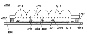
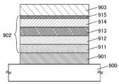
본 실시형태에서는 본 발명의 일 형태인 화합물을 사용하는 것이 바람직한 발광 디바이스의 일례에 대하여 설명한다. 또한, 발광 디바이스는 도 1의 (A)에 도시된 바와 같이, 제 1 전극(101)(도 1의 (A)에서는 양극의 경우를 나타내었음) 및 제 2 전극(102)(도 1의 (A)에서는 음극의 경우를 나타내었음)으로 이루어지는, 한 쌍의 전극 사이에 EL층(103)이 끼워진 구조를 가지고, EL층(103)은 적어도 발광층(113)을 가지고, 그 외에 정공(홀) 주입층(111), 정공(홀) 수송층(112), 전자 수송층(114), 전자 주입층(115) 등의 기능층을 제공할 수 있다.In this embodiment, an example of a light emitting device in which it is preferable to use the compound of one embodiment of the present invention will be described. In addition, as shown in FIG. 1(A), the light emitting device includes a first electrode 101 (in FIG. 1(A), an anode case is shown) and a second electrode 102 (( A) has a structure in which the
또한, 발광층(113)은 발광 물질(게스트 재료) 및 호스트 재료를 가진다. 발광 디바이스에서, 한 쌍의 전극 사이에 전압을 인가함으로써, 음극으로부터 전자가, 양극으로부터 정공(홀)이 각각 EL층(103)에 주입되고, 전류가 흐른다. 이때 발광층(113)에서 캐리어(전자 및 정공)가 재결합됨으로써 들뜬자가 생겨, 들뜬자의 들뜬 에너지가 발광으로 변환됨으로써, 발광 디바이스로부터 발광이 얻어진다. 또한, 본 실시형태에 나타낸 발광층(113)은 도 1의 (B)에 도시된 바와 같이, 에너지 억셉터이며 발광 물질(게스트 재료)로서 기능하는 화합물(132), 및 에너지 도너이며 호스트 재료로서 기능하는 화합물(131)을 가진다. 따라서, 본 실시형태에서는 본 발명의 일 형태인 화합물을 발광 물질(게스트 재료)로서 사용하는 경우에 대하여 설명한다. 또한, 발광층(113)에서, 호스트 재료로서 기능하는 화합물은 복수이어도 좋다.Further, the light-emitting
캐리어의 재결합에 의하여 생기는 들뜬자 중, 단일항 들뜬자가 생성되는 비율은 25%이고 삼중항 들뜬자가 생성되는 비율은 75%이기 때문에, 단일항 들뜬자에 더하여 삼중항 들뜬자를 발광에 기여시키는 것이 발광 디바이스의 발광 효율을 향상시키기 위해서는 바람직하다. 여기서, 발광층(113)에서, 게스트 재료와 호스트 재료 사이에서 생기는 에너지 이동의 개념에 대하여 도 2를 사용하여 설명한다. 또한, 도 2의 (A)에는 통상의 게스트 재료(형광 발광 물질)의 구성을 나타내고, 이를 사용한 경우의 게스트 재료와 호스트 재료 사이의 에너지 이동의 개념을 나타내었다. 또한, 도 2의 (B)에는 본 발명의 일 형태인 화합물(132)의 구성을 나타내고, 이를 게스트 재료로서 사용한 경우의 게스트 재료와 호스트 재료 사이의 에너지 이동의 개념을 나타내었다.Of the excitons generated by recombination of carriers, the rate of generation of singlet excitons is 25% and the rate of triplet excitons is 75%. Therefore, in addition to the singlet excitons, it is necessary to contribute triplet excitons to light emission. This is desirable in order to improve the luminous efficiency of the device. Here, in the
도 2의 (A)는 호스트 재료인 화합물(131)과 게스트 재료인 형광 발광 물질(124)이 존재하는 상태를 나타낸 것이다. 또한, 형광 발광 물질(124)은 일반적인 형광 발광 물질이고, 발광단(124a)을 가지지만 보호기를 가지지 않는 형광 발광 물질이다.2A shows a state in which a
또한, 도 2의 (B)는 호스트 재료인 화합물(131)과, 게스트 재료인 본 발명의 일 형태인 화합물(형광 발광 물질)(132)이 존재하는 상태를 나타낸 것이다. 또한, 화합물(132)은 발광 디바이스에서 에너지 억셉터로서 기능하는 형광 발광 물질이고, 발광단(132a)과 보호기(132b)를 가진다. 또한, 보호기(132b)는 화합물(호스트 재료)(131)로부터 발광단(132a)으로의 덱스터 기구에 의거한 에너지 이동이 일어나기 어려울 정도의 거리를 두고, 이들을 떨어지게 하는 기능을 가진다.In addition, FIG. 2B shows a state in which a
도 2의 (A) 및 (B)에 도시된 바와 같이, 발광층(113)에서 호스트 재료인 화합물(131)과, 게스트 재료인 형광 발광 물질(124) 및 화합물(형광 발광 물질)(132)은 모두 가까운 위치에 존재한다. 그러므로, 도 2의 (A)에 도시된 바와 같이, 형광 발광 물질(124)이 보호기를 가지지 않는 경우에는, 발광단(124a)과 화합물(131)의 거리가 가까워지기 때문에, 화합물(131)로부터 형광 발광 물질(124)로의 에너지 이동으로서, 푀르스터 기구에 의한 에너지 이동(도 2의 (A) 중의 경로 A6)과 덱스터 기구에 의한 에너지 이동(도 2의 (A) 중의 경로 A7)의 양쪽이 생길 수 있다. 덱스터 기구에 의한 호스트 재료로부터 게스트 재료로의 삼중항 들뜬 에너지의 에너지 이동이 생겨, 게스트 재료의 삼중항 들뜬 상태가 생성되어도, 게스트 재료가 형광 발광 물질인 경우에는 삼중항 들뜬 에너지가 무방사 실활되기 때문에, 발광 디바이스의 발광 효율 저하의 원인 중 하나가 된다.2A and 2B, in the
한편, 도 2의 (B)에서는, 게스트 재료인 화합물(형광 발광 물질)(132)이 보호기(132b)를 가지기 때문에, 발광단(132a)과 호스트 재료인 화합물(131)의 거리를 길게 할 수 있다. 이로써, 덱스터 기구에 의한 에너지 이동(경로 A7)을 억제할 수 있다.On the other hand, in (B) of FIG. 2, since the compound (fluorescent light emitting material) 132 as the guest material has the
여기서, 도 2의 (A)에 도시된 형광 발광 물질(124)이 가지는 발광단(124a)이나, 도 2의 (B)에 도시된 화합물(형광 발광 물질)(132)이 가지는 발광단(132a)에 대하여 설명한다. 발광단(124a, 132a)이란, 형광 발광 물질에 있어서, 발광의 원인이 되는 원자단(골격)을 가리킨다. 발광단(124a, 132a)은 일반적으로 π 결합을 가지고, 방향족 고리를 포함하는 것이 바람직하고, 축합 방향족 고리 또는 축합 헤테로 방향족 고리를 가지는 것이 더 바람직하다. 또한, 발광단(124a, 132a)이 가지는 축합 방향족 고리 또는 축합 헤테로 방향족 고리로서는, 예를 들어 페난트렌 골격, 스틸벤 골격, 아크리돈 골격, 페녹사진 골격, 페노싸이아진 골격 등을 들 수 있다. 특히 나프탈렌 골격, 안트라센 골격, 플루오렌 골격, 크리센 골격, 트라이페닐렌 골격, 테트라센 골격, 피렌 골격, 페릴렌 골격, 쿠마린 골격, 퀴나크리돈 골격, 나프토비스벤조퓨란 골격 등을 들 수 있다. 또한, 본 발명의 일 형태인 화합물(132)이 가지는 발광단(132a)으로서는, 특히 안트라센 골격이 바람직하다.Herein, the
또한, 도 2의 (B)에 도시된 화합물(형광 발광 물질)(132)이 가지는 보호기(132b)로서는, 발광단(132a) 및 호스트 재료인 화합물(131)의 T1 준위보다 높은 T1 준위를 가지는 것이 바람직하다. 또한, 본 발명의 일 형태인 화합물(132)이 가지는 보호기(132b)의 구체적인 예로서는 탄소수 3 내지 10의 알킬기, 치환 또는 비치환된 탄소수 3 내지 10의 사이클로알킬기, 탄소수 3 내지 12의 트라이알킬실릴기 등을 들 수 있다. 이와 같은 보호기(132b)를 가짐으로써, 부피가 큰 구조로 할 수 있기 때문에, 게스트 재료인 화합물(132)의 발광단(132a)과 호스트 재료인 화합물(131)의 거리를 길게 할 수 있다.In addition, as the
다음으로, 본 발명의 일 형태인 발광 디바이스의 발광층의 구성에 대하여 설명한다.Next, a configuration of a light emitting layer of a light emitting device according to an embodiment of the present invention will be described.
<발광층의 구성예 1><Configuration Example 1 of Light-Emitting Layer>
본 구성예에서, 발광 디바이스 중의 발광층(113)은 호스트 재료로서 기능하는 화합물(131)과 발광 물질(게스트 재료)로서 기능하는 화합물(132)을 가지고, 화합물(131)로서 TADF 재료를 사용하고, 발광 물질(게스트 재료)로서 기능하는 화합물(132)로서 형광 발광 물질을 사용하는 경우를 나타내었다. 따라서, 본 발명의 일 형태인 화합물을 형광 발광 물질인 화합물(132)로서 사용하는 것이 바람직하다. 또한, 본 구성예에서의 발광층(113)에서의 에너지 준위의 상관의 일례는 도 3의 (A)에 도시된 바와 같다. 또한, 도 3의 (A)에 도시된 표기 및 부호는 다음과 같다.In this configuration example, the light-emitting
·Host(131): 화합물(131)Host (131): Compound (131)
·Guest(132): 화합물(132)Guest (132): Compound (132)
·TC1: 화합물(131)의 T1 준위T C1 : T1 level of compound (131)
·SC1: 화합물(131)의 S1 준위S C1 : S1 level of compound (131)
·SG: 화합물(132)의 S1 준위S G : S1 level of compound (132)
·TG: 화합물(132)의 T1 준위T G : T1 level of compound (132)
본 구성예에서, 화합물(131)은 TADF를 가지는 재료이기 때문에, 삼중항 들뜬 에너지를 업컨버전에 의하여 단일항 들뜬 에너지로 변환하는 기능을 가진다(도 3의 (A) 중의 경로 A1). 화합물(131)이 가지는 단일항 들뜬 에너지는 화합물(132)로 빠르게 이동한다(도 3의 (A) 중의 경로 A2). 이때, 화합물(131)의 SC1과 화합물(132)의 SG의 관계는 SC1≥SG인 것이 바람직하다. 다만, SC1은 화합물(131)의 형광 스펙트럼의 단파장측의 꼬리에서 접선을 긋고 그 외삽선의 파장의 에너지로 한다. 또한, SG는 화합물(132)의 흡수 스펙트럼의 흡수단의 파장의 에너지로 한다.In the present configuration example,
이와 같이, 화합물(131)에서 생긴 삼중항 들뜬 에너지를 경로 A1 및 경로 A2를 거쳐 게스트 재료인 화합물(132)의 S1 준위로 에너지 이동시킴으로써, 화합물(132)을 효율적으로 발광시켜, 발광 디바이스의 발광 효율을 높일 수 있다. 또한, 경로 A2에서, 화합물(131)은 에너지 도너로서 기능하고, 화합물(132)은 에너지 억셉터로서 기능한다. 다만, 본 구성예에 나타내는 발광 디바이스의 발광층(113)에서는, 상기 외에 화합물(131)에서 생긴 삼중항 들뜬 에너지가 화합물(132)의 T1 준위로 이동하는 경로(도 3의 (A) 중의 경로 A3)와도 경합될 수 있다. 이와 같은 에너지 이동(경로 A3)이 생기는 경우, 형광 발광 물질인 화합물(132)은 삼중항 들뜬 에너지를 발광에 기여시킬 수 없기 때문에, 발광 디바이스의 발광 효율이 저하한다.In this way, the triplet excitation energy generated in the
일반적으로, 분자 간의 에너지 이동 기구로서 푀르스터 기구(쌍극자-쌍극자 상호 작용)와 덱스터 기구(전자 교환 상호 작용)가 알려져 있다. 또한, 덱스터 기구는 에너지 도너인 화합물과 에너지 억셉터인 화합물의 거리가 1nm 이하인 경우에 우위하게 생긴다. 그러므로 에너지 억셉터인 화합물의 농도가 높아지면 생기기 쉬워진다. 따라서, 본 구성예와 같이, 에너지 억셉터인 화합물(132)이 삼중항 들뜬 에너지 준위가 낮은 형광성 재료이고, 그 농도가 높아지면, 에너지 도너인 화합물(131)의 삼중항 들뜬 에너지는 덱스터 기구에 의한 경로 A3의 에너지 이동과, 그 후의 무방사 실활이 지배적이 된다. 그러므로, 경로 A3을 억제하기 위해서는, 덱스터 기구에 의한 에너지 이동이 일어나기 어려울 정도로 화합물(131)과 화합물(132)의 거리를 길게 하는 것이 중요하다.In general, as an energy transfer mechanism between molecules, the Förster mechanism (dipole-dipole interaction) and the Dexter mechanism (electron exchange interaction) are known. In addition, the Dexter mechanism is advantageously generated when the distance between the energy donor compound and the energy acceptor compound is 1 nm or less. Therefore, it becomes more likely to occur when the concentration of the compound as an energy acceptor increases. Therefore, as in this configuration example, when the
또한, 에너지 억셉터인 화합물(132)의 T1 준위(TG)는 화합물(132)이 가지는 발광단에서 유래되는 에너지 준위인 경우가 많다. 그러므로, 발광층(113)에서의 경로 A3을 억제하기 위하여, 화합물(131)과 화합물(132)이 가지는 발광단의 거리를 길게 하는 것이 중요하다.In addition, the T1 level (T G ) of the
에너지 도너와, 에너지 억셉터가 가지는 발광단의 거리를 길게 하기 위한 방법으로서, 일반적으로는 그 혼합막 내의 에너지 억셉터의 농도를 낮추는 것을 들 수 있다. 그러나, 에너지 억셉터의 농도를 낮추면, 에너지 도너로부터 에너지 억셉터로의 덱스터 기구에 의거한 에너지 이동뿐만 아니라, 푀르스터 기구에 의거한 에너지 이동도 억제된다. 그 경우, 경로 A2가 푀르스터 기구에 의거하기 때문에, 발광 디바이스의 발광 효율의 저하나 신뢰성의 저하와 같은 문제가 생긴다. 한편, 본 발명의 일 형태인 화합물은 그 구조의 일부에 발광단과 보호기를 가지고, 발광층(113)에서 에너지 억셉터로서 기능하는 경우에, 보호기는 다른 에너지 도너와 상기 발광단의 거리를 길게 하는 기능을 가진다. 따라서, 본 발명의 일 형태인 화합물을 본 구성의 화합물(132)로서 사용한 경우, 화합물(132)과 화합물(131)의 거리를 길게 할 수 있다. 또한, 에너지 도너와 에너지 억셉터의 거리가 1nm 이하에서는 덱스터 기구가 우세가 되고, 1nm 이상 10nm 이하에서는 푀르스터 기구가 우세가 된다. 그러므로, 보호기는 발광단으로부터 1nm 이상 10nm 이하의 범위로 퍼지는, 부피가 큰 치환기가 바람직하고, 본 발명의 일 형태의 화합물이 가지는 보호기로서는, 앞에서 든 보호기를 가지는 것이 바람직하다. 따라서, 본 발명의 일 형태인 화합물을 화합물(132)로서 사용함으로써, 화합물(132)의 농도를 높여도 덱스터 기구에 의한 에너지 이동을 억제하면서 푀르스터 기구에 의한 에너지 이동 속도를 높일 수 있다. 즉, 화합물(131)의 S1 준위(SC1)로부터 화합물(132)의 S1 준위(SG)로의 단일항 들뜬 에너지의 에너지 이동(경로 A2)이 일어나기 쉬워지는 한편, 화합물(131)로부터 화합물(132)의 T1 준위(TG)로의 삼중항 들뜬 에너지의 이동(경로 A3: 덱스터 기구에 의한 에너지 이동)을 일어나기 어렵게 할 수 있어, 경로 A3의 에너지 이동에 따른 발광 효율의 저하를 억제하면서 발광 디바이스의 발광 효율을 높일 수 있다. 또한, 푀르스터 기구에 의한 에너지 이동 속도를 높임으로써, 발광층 내의 에너지 억셉터의 여기 수명이 짧아지기 때문에, 발광 디바이스의 신뢰성을 향상시킬 수 있다. 구체적으로는, 발광층(113)에서의 화합물(132)의 농도는 에너지 도너인 화합물(131)에 대하여 2wt% 이상 50wt% 이하가 바람직하고, 더 바람직하게는 5wt% 이상 30wt% 이하, 더 바람직하게는 5wt% 이상 20wt% 이하로 한다.As a method for increasing the distance between the energy donor and the light emitting end of the energy acceptor, generally, lowering the concentration of the energy acceptor in the mixed film is exemplified. However, when the concentration of the energy acceptor is lowered, not only the energy transfer based on the Dexter mechanism from the energy donor to the energy acceptor but also the energy transfer based on the Förster mechanism is suppressed. In that case, since the path A 2 is based on the Förster mechanism, problems such as a decrease in luminous efficiency or a decrease in reliability of the light-emitting device occur. On the other hand, when the compound of one embodiment of the present invention has a luminous group and a protecting group in a part of its structure and functions as an energy acceptor in the light-emitting
<발광층의 구성예 2><Configuration Example 2 of Light-Emitting Layer>
본 구성예에서, 발광 디바이스 중의 발광층(113)은 화합물(131), 화합물(132), 및 화합물(133)을 가지고, 화합물(131) 및 화합물(133)은 들뜬 복합체를 형성하는 조합이고, 발광 물질(게스트 재료)로서 기능하는 화합물(132)로서 형광 발광 물질을 사용하는 경우(ExEF를 이용하는 경우)에 대하여 나타낸다. 따라서, 본 발명의 일 형태인 화합물은 형광 발광 물질인 화합물(132)로서 사용하는 것이 바람직하다. 또한, 본 구성예에서의 발광층(113)에서의 에너지 준위의 상관의 일례는 도 3의 (B)에 도시된 바와 같다. 또한, 도 3의 (B)에 도시된 표기 및 부호는 다음과 같다.In this configuration example, the
·Comp(131): 화합물(131)Comp (131): compound (131)
·Comp(133): 화합물(133)Comp (133): compound (133)
·Guest(132): 화합물(132)Guest (132): Compound (132)
·SC1: 화합물(131)의 S1 준위S C1 : S1 level of compound (131)
·TC1: 화합물(131)의 T1 준위T C1 : T1 level of compound (131)
·SC3: 화합물(133)의 S1 준위S C3 : S1 level of compound (133)
·TC3: 화합물(133)의 T1 준위T C3 : T1 level of compound (133)
·SG: 화합물(132)의 S1 준위S G : S1 level of compound (132)
·TG: 화합물(132)의 T1 준위T G : T1 level of compound (132)
·SE: 들뜬 복합체의 S1 준위S E : S1 level of the excited complex
·TE: 들뜬 복합체의 T1 준위·T E : T1 level of the excited complex
또한, 화합물(131)과 화합물(133)의 조합은 들뜬 복합체를 형성할 수 있는 조합이면 좋지만, 한쪽이 정공을 수송하는 기능(정공 수송성)을 가지는 화합물이고, 다른 쪽이 전자를 수송하는 기능(전자 수송성)을 가지는 화합물인 것이 더 바람직하다. 이 경우, 도너-억셉터(donor-acceptor)형 들뜬 복합체를 형성하기 쉬워져, 들뜬 복합체를 효율적으로 형성할 수 있다. 또한, 화합물(131)과 화합물(133)의 조합이 정공 수송성을 가지는 화합물과 전자 수송성을 가지는 화합물과의 조합인 경우, 그 혼합비에 의하여 캐리어 밸런스를 용이하게 제어할 수 있게 된다. 구체적으로는 정공 수송성을 가지는 화합물:전자 수송성을 가지는 화합물=1:9 내지 9:1(중량비)의 범위인 것이 바람직하다. 또한 상기 구성을 가짐으로써 캐리어 밸런스를 쉽게 제어할 수 있으므로 캐리어 재결합 영역도 간편하게 제어할 수 있다.In addition, the combination of
또한, 효율적으로 들뜬 복합체를 형성하는 호스트 재료의 조합으로서는, 화합물(131) 및 화합물(133) 중 한쪽의 HOMO 준위가 다른 쪽의 HOMO 준위보다 높고, 한쪽의 LUMO 준위가 다른 쪽의 LUMO 준위보다 높은 것이 바람직하다. 또한, 화합물(131)의 HOMO 준위가 화합물(133)의 HOMO 준위와 같거나, 또는 화합물(131)의 LUMO 준위가 화합물(133)의 LUMO 준위와 같아도 좋다.In addition, as a combination of host materials that efficiently form an excited complex, the HOMO level of one of the
또한, 화합물의 LUMO 준위 및 HOMO 준위는 사이클릭 볼타메트리(CV) 측정에 의하여 측정되는 화합물의 전기 화학 특성(환원 전위 및 산화 전위)으로부터 도출할 수 있다.In addition, the LUMO level and the HOMO level of the compound can be derived from the electrochemical properties (reduction potential and oxidation potential) of the compound measured by cyclic voltammetry (CV) measurement.
도 3의 (B)에 도시된 바와 같이, 화합물(131)과 화합물(133)에 의하여 형성되는 들뜬 복합체의 S1 준위(SE) 및 T1 준위(TE)는 서로 인접한 에너지 준위가 된다(도 3의 (B) 중의 경로 A6 참조).As shown in (B) of FIG. 3, the S1 level (S E ) and the T1 level (T E ) of the excited complex formed by the
들뜬 복합체의 들뜬 에너지 준위(SE 및 TE)는 들뜬 복합체를 형성하는 각 물질(화합물(131) 및 화합물(133))의 S1 준위(SC1 및 SC3)보다 낮기 때문에 더 낮은 들뜬 에너지로 들뜬 상태를 형성할 수 있게 된다. 이로써, 발광 디바이스의 구동 전압을 저감할 수 있다.Since the excited energy levels (S E and T E ) of the excited complex are lower than the S1 levels (S C1 and S C3 ) of each substance (
또한, 들뜬 복합체의 S1 준위(SE)와 T1 준위(TE)는 서로 인접한 에너지 준위이기 때문에 역항간 교차가 일어나기 쉽고, TADF성을 가진다. 그러므로, 들뜬 복합체는 삼중항 들뜬 에너지를 업컨버전에 의하여 단일항 들뜬 에너지로 변환하는 기능을 가진다(도 3의 (B) 중의 경로 A7). 들뜬 복합체가 가지는 단일항 들뜬 에너지는 화합물(132)로 빠르게 이동할 수 있다(도 3의 (B) 중의 경로 A8). 이때, SE≥SG인 것이 바람직하다. 경로 A8에서, 들뜬 복합체가 에너지 도너이고, 화합물(132)이 에너지 억셉터로서 기능한다. 구체적으로는, 들뜬 복합체의 형광 스펙트럼의 단파장측의 꼬리에서 접선을 긋고 그 외삽선의 파장의 에너지를 SE로 하고, 화합물(132)의 흡수 스펙트럼의 흡수단의 파장의 에너지를 SG로 하였을 때, SE≥SG인 것이 바람직하다.In addition, since the S1 level (S E ) and the T1 level (T E ) of the excited composite are adjacent energy levels, crossover between inverse terms is likely to occur and have TADF properties. Therefore, the excited complex has a function of converting triplet excited energy into singlet excited energy by up-conversion (path A 7 in Fig. 3(B)). (A path 8 in the Figure 3 (B)) singlet excited energy can quickly navigate to compound 132 is excited composite having. At this time, it is preferable that S E ≥S G. In path A 8 , the excited complex is the energy donor, and compound 132 functions as an energy acceptor. Specifically, when a tangent line is drawn from the tail on the short wavelength side of the fluorescence spectrum of the excited complex, the energy of the wavelength of the extrapolated line is S E , and the energy of the wavelength of the absorption edge of the absorption spectrum of the
또한, TADF성을 높이기 위해서는, 화합물(131) 및 화합물(133)의 양쪽의 T1 준위, 즉 TC1 및 TC3이 TE 이상인 것이 바람직하다. 이의 지표로서는, 화합물(131) 및 화합물(133)의 인광 스펙트럼의 가장 단파장측의 발광 피크 파장이 모두 들뜬 복합체의 최대 발광 피크 파장 이하인 것이 바람직하다. 또는, 들뜬 복합체의 형광 스펙트럼의 단파장측의 꼬리에서 접선을 긋고 그 외삽선의 파장의 에너지를 SE로 하고, 화합물(131) 및 화합물(133)의 인광 스펙트럼의 단파장측의 꼬리에서 각각 접선을 긋고 이들의 외삽선의 파장의 에너지를 각 화합물의 TC1 및 TC3으로 하였을 때, SE-TC1≤0.2eV, 또한 SE-TC3≤0.2eV인 것이 바람직하다.In addition, in order to increase the TADF property, it is preferable that the T1 levels of both the
발광층(113)에서 생긴 삼중항 들뜬 에너지를 경로 A6 및 경로 A8을 거쳐 게스트 재료인 화합물(132)의 S1 준위로 에너지 이동시킴으로써, 화합물(132)을 발광시킬 수 있다. 따라서, 발광층(113)에 들뜬 복합체를 형성하는 조합의 재료를 사용함으로써, 형광 발광 디바이스의 발광 효율을 높일 수 있다. 그러나, 발광층(113)에서 생긴 삼중항 들뜬 에너지가, 화합물(132)의 T1 준위로 에너지 이동하는 경로(도 3의 (B) 중의 경로 A9)가 경합되어 일어날 수 있다. 이와 같은 에너지 이동(경로 A9)이 생긴 경우, 형광 발광 물질인 화합물(132)은 삼중항 들뜬 에너지를 발광에 기여시킬 수 없기 때문에, 발광 디바이스의 발광 효율이 저하한다.The triplet excitation energy generated in the light-emitting
이와 같은 에너지 이동(도 3의 (B) 중의 경로 A9)을 억제하기 위해서는, 상기 구성예 1에서 설명한 바와 같이, 화합물(131) 및 화합물(133)에 의하여 형성된 들뜬 복합체와 화합물(132)의 거리, 및 들뜬 복합체와 화합물(132)이 가지는 발광단의 거리가 긴 것이 중요하다. In order to suppress such energy transfer (path A 9 in FIG. 3 (B)), as described in Configuration Example 1, the excitation complex formed by the
본 발명의 일 형태인 화합물은 그 구조의 일부에 발광단과 보호기를 가지고, 발광층(113)에서 에너지 억셉터로서 기능하는 경우에, 보호기는 다른 에너지 도너와 상기 발광단의 거리를 길게 하는 기능을 가진다. 따라서, 본 발명의 일 형태인 화합물을 본 구성의 화합물(132)로서 사용한 경우, 화합물(132)의 농도를 높여도 화합물(131) 및 화합물(133)에 의하여 형성된 들뜬 복합체와 화합물(132)의 거리를 길게 할 수 있어, 덱스터 기구에 의한 에너지 이동을 억제하면서 푀르스터 기구에 의한 에너지 이동 속도를 높일 수 있다. 따라서, 본 발명의 일 형태인 화합물을 화합물(132)로서 사용함으로써, 들뜬 복합체로부터 화합물(132)의 S1 준위(SG)로의 삼중항 들뜬 에너지의 에너지 이동(도 3의 (B) 중의 경로 A6 및 경로 A8)이 일어나기 쉬워지는 한편, 들뜬 복합체로부터 화합물(132)의 T1 준위(TG)로의 삼중항 들뜬 에너지의 이동(경로 A9: 덱스터 기구에 의한 에너지 이동)을 일어나기 어렵게 할 수 있어, 경로 A9의 에너지 이동에 따른 발광 효율의 저하를 억제하면서 발광 디바이스의 발광 효율을 높일 수 있다. 또한, 발광 디바이스의 신뢰성을 향상시킬 수 있다.In the case where the compound of one embodiment of the present invention has a luminophore and a protecting group in a part of its structure and functions as an energy acceptor in the light-emitting
또한, 본 명세서 중에서는, 상술한 경로 A6, 경로 A7, 및 경로 A8의 경로를, ExSET(Exciplex-Singlet Energy Transfer) 또는 ExEF(Exciplex-Enhanced Fluorescence)라고도 한다. 즉, 본 명세서 중의 발광층(113)에서, 들뜬 복합체로부터 형광성 재료로의 들뜬 에너지의 공여가 있다는 것을 나타낸다.In addition, in this specification, the paths of the above-described path A 6 , path A 7 , and path A 8 are also referred to as ExSET (Exciplex-Singlet Energy Transfer) or ExEF (Exciplex-Enhanced Fluorescence). That is, in the
<발광층의 구성예 3><Configuration Example 3 of Light-Emitting Layer>
본 구성예에서, 발광 디바이스 중의 발광층(113)은 화합물(131), 화합물(132), 및 화합물(133)을 가지고, 화합물(131) 및 화합물(133)은 들뜬 복합체를 형성하는 조합이고, 발광 물질(게스트 재료)로서 기능하는 화합물(132)로서 형광 발광 물질을 사용하는 경우(ExEF를 이용하는 경우)에 대하여 나타낸다. 또한, 화합물(133)이 인광성 재료인 점에서 상기 구성예 2와 상이하다. 또한, 본 발명의 일 형태인 화합물은 형광 발광 물질인 화합물(132)로서 사용하는 것이 바람직하다. 또한, 본 구성예에서의 발광층(113)에서의 에너지 준위의 상관의 일례는 도 3의 (C)에 도시된 바와 같다. 또한, 도 3의 (C)에 도시된 표기 및 부호는 도 3의 (B)와 공통되기 때문에, 기재를 생략한다.In this configuration example, the
본 구성예에서는 들뜬 복합체를 형성하는 화합물 중 한쪽에 중원자를 가지는 화합물을 사용한다. 그러므로, 단일항 상태와 삼중항 상태 사이의 항간 교차가 촉진된다. 따라서, 삼중항 들뜬 상태로부터 단일항 바닥 상태로의 전이가 가능한(즉 인광을 발할 수 있는) 들뜬 복합체를 형성할 수 있다. 이 경우, 통상의 들뜬 복합체와 달리, 들뜬 복합체의 삼중항 들뜬 에너지 준위(TE)가 에너지 도너의 준위가 되기 때문에, TE가 발광 재료인 화합물(132)의 단일항 들뜬 에너지 준위(SG) 이상인 것이 바람직하다. 구체적으로는, 중원자를 사용한 들뜬 복합체의 발광 스펙트럼의 단파장측의 꼬리에서 접선을 긋고 그 외삽선의 파장의 에너지를 TE로 하고, 화합물(132)의 흡수 스펙트럼의 흡수단의 파장의 에너지를 SG로 하였을 때, TE≥SG인 것이 바람직하다.In this configuration example, a compound having a heavy atom in one of the compounds forming the excited complex is used. Therefore, the inter-term crossover between the singlet state and the triplet state is promoted. Thus, it is possible to form an excited complex capable of transitioning from a triplet excited state to a singlet ground state (that is, capable of emitting phosphorescence). In this case, unlike a conventional excited composite, since the triplet excited energy level (T E ) of the excited composite becomes the level of the energy donor, T E is the singlet excited energy level (S G ) Or more is preferable. Specifically, a tangent line is drawn from the tail on the short wavelength side of the emission spectrum of the excited composite using heavy atoms, and the energy of the wavelength of the extrapolated line is T E , and the energy of the wavelength of the absorption end of the absorption spectrum of
이와 같은 에너지 준위의 상관으로 함으로써, 생성된 들뜬 복합체의 삼중항 들뜬 에너지는 들뜬 복합체의 삼중항 들뜬 에너지 준위(TE)로부터 화합물(132)의 단일항 들뜬 에너지 준위(SG)로 에너지 이동을 할 수 있다. 또한, 들뜬 복합체의 S1 준위(SE)와 T1 준위(TE)는 서로 인접한 에너지 준위이기 때문에, 발광 스펙트럼에서 형광과 인광을 명확히 구별하기 어려운 경우가 있다. 이 경우, 발광 수명에 따라 형광 또는 인광을 구별할 수 있는 경우가 있다.By correlating the energy levels as described above, the triplet excited energy of the generated excited complex is transferred from the triplet excited energy level (T E ) of the excited complex to the singlet excited energy level (S G ) of the compound (132). can do. In addition, since the S1 level (S E ) and the T1 level (T E ) of the excited complex are adjacent energy levels, it may be difficult to clearly distinguish between fluorescence and phosphorescence in the emission spectrum. In this case, fluorescence or phosphorescence may be distinguished according to the light emission lifetime.
또한, 상기 구성에서 사용하는 인광성 재료는 Ir, Pt, Os, Ru, Pd 등의 중원자를 포함하는 것이 바람직하다. 한편, 본 구성예에서는 인광성 재료는 에너지 도너로서 작용하기 때문에, 양자 수율은 높아도 좋고 낮아도 좋다. 즉, 들뜬 복합체가 가지는 삼중항 들뜬 에너지 준위로부터 게스트 재료의 단일항 들뜬 에너지 준위로의 에너지 이동이 허용 전이가 되면 좋다. 상술한 인광성 재료로 구성되는 들뜬 복합체나 인광성 재료로부터 게스트 재료로의 에너지 이동은 에너지 도너의 삼중항 들뜬 에너지 준위로부터 게스트 재료(에너지 억셉터)의 단일항 들뜬 에너지 준위로의 에너지 이동이 허용 전이가 되기 때문에 바람직한 구성이다.In addition, it is preferable that the phosphorescent material used in the above configuration contains heavy atoms such as Ir, Pt, Os, Ru, and Pd. On the other hand, in this configuration example, since the phosphorescent material acts as an energy donor, the quantum yield may be high or low. That is, the energy transfer from the triplet excited energy level of the excited composite to the singlet excited energy level of the guest material should be an allowable transition. Energy transfer from the above-described phosphorescent composite or phosphorescent material to the guest material allows energy transfer from the triplet excited energy level of the energy donor to the singlet excited energy level of the guest material (energy acceptor). It is a preferable configuration because it becomes a transition.
따라서, 도 3의 (C)에 도시된 바와 같이, 본 구성예에 나타내는 발광 디바이스의 발광층(113)에서, 들뜬 복합체의 삼중항 들뜬 에너지는 경로 A8의 경로로(도 3의 (C) 중의 경로 A7의 경로를 거치지 않고) 게스트 재료의 S1 준위(SG)로 이동한다. 즉, 경로 A6 및 경로 A8의 경로를 거쳐, 게스트 재료의 S1 준위로 삼중항 들뜬 에너지 및 단일항 들뜬 에너지를 이동시킬 수 있다. 또한, 경로 A8에서 들뜬 복합체는 에너지 도너이고, 화합물(132)은 에너지 억셉터로서 기능한다. 다만, 본 구성예에 나타내는 발광 디바이스의 발광층(113)에서는, 상기 외에 들뜬 복합체의 삼중항 들뜬 에너지가 화합물(132)의 T1 준위로 이동하는 경로(도 3의 (C) 중의 경로 A9)와도 경합될 수 있다. 이와 같은 에너지 이동(경로 A9)이 생기는 경우, 형광 발광 물질인 화합물(132)은 삼중항 들뜬 에너지를 발광에 기여시킬 수 없기 때문에, 발광 디바이스의 발광 효율이 저하한다.Thus, in as shown in (C) 3, in the
이와 같은 에너지 이동(경로 A9)을 억제하기 위해서는, 상기 구성예 1에서 설명한 바와 같이, 화합물(131)과 화합물(132)의 거리, 및 화합물(131)과 화합물(132)이 가지는 발광단의 거리가 긴 것이 중요하다.In order to suppress such energy transfer (path A 9 ), as described in Configuration Example 1, the distance between the
본 발명의 일 형태인 화합물은 그 구조의 일부에 발광단과 보호기를 가지고, 발광층(113)에서 에너지 억셉터로서 기능하는 경우에, 보호기는 다른 에너지 도너와 상기 발광단의 거리를 길게 하는 기능을 가진다. 따라서, 본 발명의 일 형태인 화합물을 본 구성의 화합물(132)로서 사용한 경우, 화합물(132)의 농도를 높여도 화합물(131) 및 화합물(133)에 의하여 형성된 들뜬 복합체와 화합물(132)의 거리를 길게 할 수 있어, 덱스터 기구에 의한 에너지 이동을 억제하면서 푀르스터 기구에 의한 에너지 이동 속도를 높일 수 있다. 따라서, 본 발명의 일 형태인 화합물을 화합물(132)로서 사용함으로써, 들뜬 복합체로부터 화합물(132)의 S1 준위(SG)로의 삼중항 들뜬 에너지의 에너지 이동(경로 A6 및 경로 A8)이 일어나기 쉬워지는 한편, 들뜬 복합체로부터 화합물(132)의 T1 준위(TG)로의 삼중항 들뜬 에너지의 이동(경로 A9: 덱스터 기구에 의한 에너지 이동)을 일어나기 어렵게 할 수 있어, 경로 A9의 에너지 이동에 따른 발광 효율의 저하를 억제하면서 발광 디바이스의 발광 효율을 높일 수 있다. 또한, 발광 디바이스의 신뢰성을 향상시킬 수 있다.In the case where the compound of one embodiment of the present invention has a luminophore and a protecting group in a part of its structure and functions as an energy acceptor in the light-emitting
<발광층의 구성예 4><Configuration Example 4 of Light-Emitting Layer>
본 구성예에서, 발광 디바이스 중의 발광층(113)은 3종류의 물질, 즉 화합물(131), 화합물(132), 및 화합물(133)을 가진다. 또한, 화합물(131) 및 화합물(133)은 들뜬 복합체를 형성하는 조합이고, 발광 물질(게스트 재료)로서 기능하는 화합물(132)로서 형광 발광 물질을 사용하는 경우(ExEF를 이용하는 경우)에 대하여 나타낸다. 따라서, 본 발명의 일 형태인 화합물은 형광 발광 물질인 화합물(132)로서 사용하는 것이 바람직하다. 또한, 본 구성예는, 화합물(133)이 TADF성을 가지는 재료인 점에서 상기 구성예 3과 상이하다. 또한, 본 구성예에서의 발광층(113)에서의 에너지 준위의 상관의 일례는 도 4의 (A)에 도시된 바와 같다. 또한, 도 4의 (A)에 도시된 표기 및 부호는 도 3의 (B)와 공통되기 때문에, 기재를 생략한다.In this configuration example, the
본 구성예에서, 화합물(133)은 TADF 재료이기 때문에, 들뜬 복합체를 형성하지 않는 화합물(133)은 삼중항 들뜬 에너지를 업컨버전에 의하여 단일항 들뜬 에너지로 변환하는 기능을 가진다(도 4의 (A) 중의 경로 A10). 따라서, 화합물(133)이 가지는 단일항 들뜬 에너지는 화합물(132)로 빠르게 이동한다(도 4의 (A) 중의 경로 A11). 이때, SC3≥SG인 것이 바람직하다.In this configuration example, since the
따라서, 본 구성예에 나타내는 발광 디바이스의 발광층(113)에서, 상기 구성예 3과 마찬가지로, 도 4의 (A) 중의 경로 A6 내지 경로 A8을 거쳐, 삼중항 들뜬 에너지가 게스트 재료인 화합물(132)로 이동하는 경로와, 도 4의 (A) 중의 경로 A10 및 경로 A11을 거쳐 화합물(132)로 이동하는 경로가 존재한다. 이와 같이, 삼중항 들뜬 에너지가 형광 발광 물질인 화합물(132)로 이동하는 경로가 복수 존재함으로써, 발광 효율을 더 높일 수 있다. 경로 A8에서, 들뜬 복합체가 에너지 도너이고, 화합물(132)이 에너지 억셉터로서 기능한다. 경로 A11에서, 화합물(133)이 에너지 도너이고, 화합물(132)이 에너지 억셉터로서 기능한다. 다만, 본 구성예에 나타내는 발광 디바이스의 발광층(113)에서는, 상기 외에 들뜬 복합체의 삼중항 들뜬 에너지가 화합물(132)의 T1 준위로 이동하는 경로(도 4의 (A) 중의 경로 A9)와도 경합될 수 있다. 이와 같은 에너지 이동(경로 A9)이 생기는 경우, 형광 발광 물질인 화합물(132)은 삼중항 들뜬 에너지를 발광에 기여시킬 수 없기 때문에, 발광 디바이스의 발광 효율이 저하한다.Therefore, in the
이와 같은 에너지 이동(경로 A9)을 억제하기 위해서는, 상기 구성예 1에서 설명한 바와 같이, 화합물(131) 및 화합물(133)에 의하여 형성되는 들뜬 복합체와 화합물(132)의 거리, 즉 화합물(131) 및 화합물(133)에 의하여 형성되는 들뜬 복합체와 화합물(132)이 가지는 발광단의 거리가 긴 것이 중요하다.In order to suppress such energy transfer (path A 9 ), as described in Configuration Example 1, the distance between the excitation complex formed by the
본 발명의 일 형태인 화합물은 그 구조의 일부에 발광단과 보호기를 가지고, 발광층(113)에서 에너지 억셉터로서 기능하는 경우에, 보호기는 다른 에너지 도너와 상기 발광단의 거리를 길게 하는 기능을 가진다. 따라서, 본 발명의 일 형태인 화합물을 본 구성의 화합물(132)로서 사용한 경우, 화합물(132)의 농도를 높여도 화합물(131) 및 화합물(133)에 의하여 형성된 들뜬 복합체와 화합물(132)의 거리를 길게 할 수 있어, 덱스터 기구에 의한 에너지 이동을 억제하면서 푀르스터 기구에 의한 에너지 이동 속도를 높일 수 있다. 따라서, 본 발명의 일 형태인 화합물을 화합물(132)로서 사용함으로써, 들뜬 복합체로부터 화합물(132)의 S1 준위(SG)로의 삼중항 들뜬 에너지의 에너지 이동(경로 A6 및 경로 A8)과 들뜬 복합체로부터 화합물(132)의 S1 준위(SG)로의 삼중항 들뜬 에너지의 이동(경로 A10 및 경로 A11)의 양쪽이 일어나기 쉬워지는 한편, 들뜬 복합체로부터 화합물(132)의 T1 준위(TG)로의 삼중항 들뜬 에너지의 이동(경로 A9: 덱스터 기구에 의한 에너지 이동)을 일어나기 어렵게 할 수 있어, 경로 A9의 에너지 이동에 따른 발광 효율의 저하를 억제하면서 발광 디바이스의 발광 효율을 높일 수 있다. 또한, 발광 디바이스의 신뢰성을 향상시킬 수 있다.In the case where the compound of one embodiment of the present invention has a luminophore and a protecting group in a part of its structure and functions as an energy acceptor in the light-emitting
<발광층의 구성예 5><Configuration Example 5 of Light-Emitting Layer>
본 구성예에서, 발광 디바이스 중의 발광층(113)은 4종류의 물질, 즉 화합물(131), 화합물(132), 화합물(133), 및 화합물(134)을 가진다. 또한, 화합물(133)은 삼중항 들뜬 에너지를 발광으로 변환할 수 있는 기능을 가지는 물질로서, 인광 발광 물질을 사용하는 경우에 대하여 설명한다. 또한, 화합물(131) 및 화합물(134)은 들뜬 복합체를 형성하는 조합이고, 발광 물질(게스트 재료)로서 기능하는 화합물(132)로서 형광 발광 물질을 사용하는 경우를 나타내었다. 따라서, 본 발명의 일 형태인 화합물은 형광 발광 물질인 화합물(132)로서 사용하는 것이 바람직하다. 또한, 본 구성예에서의 발광층(113)에서의 에너지 준위의 상관의 일례는 도 4의 (B)에 도시된 바와 같다. 또한, 도 4의 (B)에서의 표기 및 부호는 도 3의 (B)에 도시된 표기 및 부호와 마찬가지이고, 이 외는 다음과 같다.In this configuration example, the
·SC4: 화합물(134)의 S1 준위S C4 : S1 level of compound (134)
·TC4: 화합물(134)의 T1 준위T C4 : T1 level of compound (134)
본 구성예에서, 화합물(131)과 화합물(134)은 들뜬 복합체를 형성한다. 또한, 들뜬 복합체의 S1 준위(SE)와 들뜬 복합체의 T1 준위(TE)는 서로 인접한 에너지 준위가 된다(도 4의 (B) 중의 경로 A12 참조). 다만, 상기 경로로 2종류의 물질에 의하여 생성된 들뜬 복합체가 들뜬 에너지를 잃으면, 2종류의 물질은 원래의 별개의 물질로서 존재한다.In this configuration example,
들뜬 복합체의 들뜬 에너지 준위(SE 및 TE)는 들뜬 복합체를 형성하는 각 물질(화합물(131) 및 화합물(134))의 S1 준위(SC1 및 SC4)보다 낮기 때문에, 더 낮은 들뜬 에너지로 들뜬 상태를 형성할 수 있게 된다. 이로써, 발광 디바이스의 구동 전압을 저감할 수 있다.Since the excited energy levels (S E and T E ) of the excited complex are lower than the S1 levels (S C1 and S C4 ) of each substance (
또한, 화합물(133)은 인광성 재료이기 때문에, 단일항 상태와 삼중항 상태 사이의 항간 교차가 허용된다. 그러므로, 들뜬 복합체로부터, 단일항 들뜬 에너지 및 삼중항 들뜬 에너지의 양쪽이 빠르게 화합물(133)로 이동한다(경로 A13). 이때, TE≥TC3인 것이 바람직하다.In addition, since
또한, 화합물(133)이 가지는 삼중항 들뜬 에너지는 화합물(132)의 단일항 들뜬 에너지로 변환된다(경로 A14). 이때, 도 4의 (B)에 도시된 바와 같이, TE≥TC3≥SG인 것이 화합물(133)로부터 화합물(132)로의 에너지 이동이 효율적으로 수행되기 때문에 바람직하다. 더 구체적으로는, 화합물(133)의 인광 스펙트럼의 단파장측의 꼬리에서 접선을 긋고 그 외삽선의 파장의 에너지를 TC3으로 하고, 화합물(132)의 흡수 스펙트럼의 흡수단의 파장의 에너지를 SG로 하였을 때, TC3≥SG인 것이 바람직하다. 또한, 경로 A14에서, 화합물(133)은 에너지 도너로서, 화합물(132)은 에너지 억셉터로서 기능한다.In addition, the triplet excitation energy of
본 구성예에서, 화합물(131)과 화합물(134)의 조합은 들뜬 복합체를 형성할 수 있는 조합이면 좋지만, 한쪽이 정공 수송성을 가지는 화합물이고, 다른 쪽이 전자 수송성을 가지는 화합물인 것이 더 바람직하다.In this configuration example, the combination of the
또한, 효율적으로 들뜬 복합체를 형성하는 재료의 조합으로서는, 화합물(131) 및 화합물(134) 중 한쪽의 HOMO 준위가 다른 쪽의 HOMO 준위보다 높고, 한쪽의 LUMO 준위가 다른 쪽의 LUMO 준위보다 높은 것이 바람직하다.In addition, as a combination of materials that efficiently form an excited complex, one of
또한, 화합물(131)과 화합물(134)의 에너지 준위의 상관은 도 4의 (B)에 한정되지 않는다. 즉, 화합물(131)의 단일항 들뜬 에너지 준위(SC1)는 화합물(134)의 단일항 들뜬 에너지 준위(SC4)보다 높아도 좋고 낮아도 좋다. 또한, 화합물(131)의 삼중항 들뜬 에너지 준위(TC1)는 화합물(134)의 삼중항 들뜬 에너지 준위(TC4)보다 높아도 좋고 낮아도 좋다.In addition, the correlation between the energy levels of the
또한, 본 구성의 발광 디바이스에서, 화합물(131)은 π전자 부족 골격을 가지는 것이 바람직하다. 상기 구성으로 함으로써, 화합물(131)의 LUMO 준위가 낮아지고, 들뜬 복합체의 형성에 적합하게 된다.Further, in the light emitting device of this configuration, it is preferable that the
또한, 본 구성의 발광 디바이스에서, 화합물(131)은 π전자 과잉 골격을 가지는 것이 바람직하다. 상기 구성으로 함으로써, 화합물(131)의 HOMO 준위가 높아지고, 들뜬 복합체의 형성에 적합하게 된다.Further, in the light emitting device of the present configuration, it is preferable that the
본 발명의 일 형태인 화합물은 그 구조의 일부에 발광단과 보호기를 가지고, 발광층(113)에서 에너지 억셉터로서 기능하는 경우에, 보호기는 다른 에너지 도너와 상기 발광단의 거리를 길게 하는 기능을 가진다. 따라서, 본 발명의 일 형태인 화합물을 본 구성의 화합물(132)로서 사용한 경우, 화합물(133)과 화합물(132)의 거리를 길게 할 수 있다. 따라서, 본 발명의 일 형태인 화합물을 화합물(132)로서 사용함으로써, 화합물(133)로부터 화합물(132)의 S1 준위(SG)로의 삼중항 들뜬 에너지의 에너지 이동(경로 A14)이 일어나기 쉬워지는 한편, 화합물(133)로부터 화합물(132)의 T1 준위(TG)로의 삼중항 들뜬 에너지의 이동(경로 A15: 덱스터 기구에 의한 에너지 이동)을 일어나기 어렵게 할 수 있어, 경로 A15의 에너지 이동에 따른 발광 효율의 저하를 억제하면서 발광 디바이스의 발광 효율을 높일 수 있다.In the case where the compound of one embodiment of the present invention has a luminophore and a protecting group in a part of its structure and functions as an energy acceptor in the light-emitting
또한, 본 구성예에서, 에너지 억셉터인 화합물(132)의 농도를 높임으로써, 덱스터 기구에 의한 에너지 이동을 억제하면서 푀르스터 기구에 의한 에너지 이동 속도를 높일 수 있다. 또한, 푀르스터 기구에 의한 에너지 이동 속도를 높임으로써, 발광층 내의 에너지 억셉터의 여기 수명이 짧아지기 때문에, 발광 디바이스의 신뢰성을 향상시킬 수 있다. 구체적으로는, 발광층(113)에서의 화합물(132)의 농도는 에너지 도너인 화합물(133)에 대하여 2wt% 이상 50wt% 이하가 바람직하고, 더 바람직하게는 5wt% 이상 30wt% 이하, 더 바람직하게는 5wt% 이상 20wt% 이하로 한다.Further, in this configuration example, by increasing the concentration of the
또한, 본 명세서 중에서는, 상술한 경로 A12 및 경로 A13의 경로를 ExTET(Exciplex-Triplet Energy Transfer)라고도 한다. 즉, 본 명세서 중의 발광층(113)에서, 들뜬 복합체로부터 화합물(133)로의 들뜬 에너지의 공여가 있다는 것을 나타낸다.In addition, in this specification, the paths of the above-described path A 12 and path A 13 are also referred to as ExTET (Exciplex-Triplet Energy Transfer). That is, in the
<발광층의 구성예 6><Configuration Example 6 of Light-Emitting Layer>
본 구성예에서, 발광 디바이스 중의 발광층(113)은 4종류의 물질, 즉 화합물(131), 화합물(132), 화합물(133), 및 화합물(134)을 가진다. 또한, 화합물(133)은 삼중항 들뜬 에너지를 발광으로 변환할 수 있는 기능을 가지는 물질로서, 인광 발광 물질을 사용하는 경우에 대하여 설명한다. 또한, 화합물(131) 및 화합물(134)은 들뜬 복합체를 형성하는 조합이고, 발광 물질(게스트 재료)로서 기능하는 화합물(132)로서 형광 발광 물질을 사용하는 경우를 나타내었다. 따라서, 본 발명의 일 형태인 화합물은 형광 발광 물질인 화합물(132)로서 사용하는 것이 바람직하다. 또한, 본 구성예는, 화합물(134)이 TADF성을 가지는 재료인 점에서 상기 구성예 5와 상이하다. 또한, 본 구성예에서의 발광층(113)에서의 에너지 준위의 상관의 일례는 도 4의 (C)에 도시된 바와 같다. 또한, 도 4의 (C)에 도시된 표기 및 부호는 도 3의 (B) 및 도 4의 (B)와 공통되기 때문에, 기재를 생략한다.In this configuration example, the
여기서, 화합물(134)은 TADF 재료이기 때문에, 들뜬 복합체를 형성하지 않는 화합물(134)은 삼중항 들뜬 에너지를 업컨버전에 의하여 단일항 들뜬 에너지로 변환하는 기능을 가진다(도 4의 (C) 중의 경로 A16). 따라서, 화합물(134)이 가지는 단일항 들뜬 에너지는 화합물(132)로 빠르게 이동한다(도 4의 (C) 중의 경로 A17). 이때, SC4≥SG인 것이 바람직하다. 더 구체적으로는, 화합물(134)의 형광 스펙트럼의 단파장측의 꼬리에서 접선을 긋고 그 외삽선의 파장의 에너지를 SC4로 하고, 화합물(132)의 흡수 스펙트럼의 흡수단의 파장의 에너지를 SG로 하였을 때, SC4≥SG인 것이 바람직하다.Here, since the
따라서, 본 구성예에 나타내는 발광 디바이스의 발광층(113)에서, 상기 구성예 5와 마찬가지로, 도 4의 (C) 중의 경로 A12, 경로 A13, 및 경로 A14를 거쳐, 삼중항 들뜬 에너지가 게스트 재료인 화합물(132)로 이동하는 경로와, 도 4의 (C) 중의 경로 A16 및 경로 A17을 거쳐 화합물(132)로 이동하는 경로가 존재한다. 이와 같이, 삼중항 들뜬 에너지가 형광 발광 물질인 화합물(132)로 이동하는 경로가 복수 존재함으로써, 발광 효율을 더 높일 수 있다. 경로 A14에서, 화합물(133)은 에너지 도너로서, 화합물(132)은 에너지 억셉터로서 기능한다. 또한, 경로 A17에서, 화합물(134)은 에너지 도너로서, 화합물(132)은 에너지 억셉터로서 기능한다. 다만, 본 구성예에 나타내는 발광 디바이스의 발광층(113)에서는, 상기 외에 화합물(133)의 삼중항 들뜬 에너지가 화합물(132)의 T1 준위로 이동하는 경로(도 4의 (C) 중의 경로 A15)와도 경합될 수 있다. 이와 같은 에너지 이동(경로 A15)이 생기는 경우, 형광 발광 물질인 화합물(132)은 삼중항 들뜬 에너지를 발광에 기여시킬 수 없기 때문에, 발광 디바이스의 발광 효율이 저하한다.Therefore, in the
이와 같은 에너지 이동(경로 A15)을 억제하기 위해서는, 상기 구성예 1에서 설명한 바와 같이, 화합물(133)과 화합물(132)의 거리, 즉 화합물(133)과 화합물(132)이 가지는 발광단의 거리가 긴 것이 중요하다.In order to suppress such energy transfer (path A 15 ), as described in Configuration Example 1, the distance between the
본 발명의 일 형태인 화합물은 그 구조의 일부에 발광단과 보호기를 가지고, 발광층(113)에서 에너지 억셉터로서 기능하는 경우에, 보호기는 다른 에너지 도너와 상기 발광단의 거리를 길게 하는 기능을 가진다. 따라서, 본 발명의 일 형태인 화합물을 본 구성의 화합물(132)로서 사용한 경우, 화합물(132)의 농도를 높여도 화합물(133)과 화합물(132)의 거리를 길게 할 수 있어, 덱스터 기구에 의한 에너지 이동을 억제하면서 푀르스터 기구에 의한 에너지 이동 속도를 높일 수 있다. 따라서, 본 발명의 일 형태인 화합물을 화합물(132)로서 사용함으로써, 들뜬 복합체로부터 화합물(132)의 S1 준위(SG)로의 삼중항 들뜬 에너지의 에너지 이동(경로 A12, 경로 A13, 및 경로 A14)과 들뜬 복합체로부터 화합물(132)의 S1 준위(SG)로의 삼중항 들뜬 에너지의 이동(경로 A16 및 경로 A17)의 양쪽이 일어나기 쉬워지는 한편, 화합물(133)로부터 화합물(132)의 T1 준위(TG)로의 삼중항 들뜬 에너지의 이동(경로 A15: 덱스터 기구에 의한 에너지 이동)을 일어나기 어렵게 할 수 있어, 경로 A15의 에너지 이동에 따른 발광 효율의 저하를 억제하면서 발광 디바이스의 발광 효율을 높일 수 있다. 또한, 발광 디바이스의 신뢰성을 향상시킬 수 있다.In the case where the compound of one embodiment of the present invention has a luminophore and a protecting group in a part of its structure and functions as an energy acceptor in the light-emitting
<발광층의 구성예 7><Configuration Example 7 of Light-Emitting Layer>
본 구성예에서, 발광 디바이스 중의 발광층(113)은 화합물(131), 화합물(132), 및 화합물(133)을 가진다. 또한, 화합물(133)은 삼중항 들뜬 에너지를 발광으로 변환할 수 있는 기능을 가지는 물질로서, 인광 발광 물질을 사용하는 경우에 대하여 설명한다. 또한, 발광 물질(게스트 재료)로서 기능하는 화합물(132)로서 형광 발광 물질을 사용하는 경우를 나타내었다. 따라서, 본 발명의 일 형태인 화합물은 형광 발광 물질인 화합물(132)로서 사용하는 것이 바람직하다. 또한, 본 구성예에서의 발광층(113)에서의 에너지 준위의 상관의 일례는 도 5의 (A)에 도시된 바와 같다. 또한, 도 5의 (A)에서의 표기 및 부호는 다음과 같다.In this configuration example, the
·Comp(131): 화합물(131)Comp (131): compound (131)
·Comp(133): 화합물(133)Comp (133): compound (133)
·Guest(132): 화합물(132)Guest (132): Compound (132)
·SC1: 화합물(131)의 S1 준위S C1 : S1 level of compound (131)
·TC1: 화합물(131)의 T1 준위T C1 : T1 level of compound (131)
·TC3: 화합물(133)의 T1 준위T C3 : T1 level of compound (133)
·TG: 화합물(132)의 T1 준위T G : T1 level of compound (132)
·SG: 화합물(132)의 S1 준위S G : S1 level of compound (132)
본 구성예에서, 캐리어의 재결합이 주로 화합물(131)에서 생김으로써, 단일항 들뜬자 및 삼중항 들뜬자가 생긴다. 또한, 화합물(133)로서, TC3≤TC1이라는 관계를 가지는 인광 발광 물질을 선택함으로써, 화합물(131)에서 생긴 단일항 들뜬 에너지 및 삼중항 들뜬 에너지의 양쪽을 화합물(133)의 TC3 준위로 이동시킬 수 있다(도 5의 (A) 중의 경로 A18). 또한, 일부의 캐리어는 화합물(133)에서도 재결합할 수 있다.In this configuration example, recombination of carriers mainly occurs in
또한, 상기 구성에서 사용하는 인광 발광 물질은 Ir, Pt, Os, Ru, Pd 등의 중원자를 포함하는 것이 바람직하다. 발광 물질을 화합물(133)로서 사용한 경우, 에너지 도너의 삼중항 들뜬 에너지 준위로부터 게스트 재료(에너지 억셉터)의 단일항 들뜬 에너지 준위로의 에너지 이동은 허용 전이가 되기 때문에 바람직하다. 따라서, 화합물(133)의 삼중항 들뜬 에너지를 경로 A19의 경로에 의하여 게스트 재료의 S1 준위(SG)로 이동시킬 수 있다. 경로 A19에서, 화합물(133)은 에너지 도너로서, 화합물(132)은 에너지 억셉터로서 기능한다. 이 경우, TC3≥SG인 것이 화합물(133)의 들뜬 에너지가 효율적으로 게스트 재료인 화합물(132)의 단일항 들뜬 상태로 이동하기 때문에 바람직하다. 구체적으로는, 화합물(133)의 인광 스펙트럼의 단파장측의 꼬리에서 접선을 긋고 그 외삽선의 파장의 에너지를 TC3으로 하고, 화합물(132)의 흡수 스펙트럼의 흡수단의 파장의 에너지를 SG로 하였을 때, TC3≥SG인 것이 바람직하다. 다만, 본 구성예에 나타내는 발광 디바이스의 발광층(113)에서는, 상기 외에 화합물(133)의 삼중항 들뜬 에너지가 화합물(132)의 T1 준위로 이동하는 경로(도 5의 (A) 중의 경로 A20)와도 경합될 수 있다. 이와 같은 에너지 이동(경로 A20)이 생기는 경우, 형광 발광 물질인 화합물(132)은 삼중항 들뜬 에너지를 발광에 기여시킬 수 없기 때문에, 발광 디바이스의 발광 효율이 저하한다.In addition, it is preferable that the phosphorescent light emitting material used in the above configuration contains heavy atoms such as Ir, Pt, Os, Ru, and Pd. When a light-emitting substance is used as the
이와 같은 에너지 이동(경로 A20)을 억제하기 위해서는, 상기 구성예 1에서 설명한 바와 같이, 화합물(133)과 화합물(132)의 거리, 즉 화합물(133)과 화합물(132)이 가지는 발광단의 거리가 긴 것이 중요하다.In order to suppress such energy transfer (path A 20 ), as described in Configuration Example 1, the distance between the
본 발명의 일 형태인 화합물은 그 구조의 일부에 발광단과 보호기를 가지고, 발광층(113)에서 에너지 억셉터로서 기능하는 경우에, 보호기는 다른 에너지 도너와 상기 발광단의 거리를 길게 하는 기능을 가진다. 따라서, 본 발명의 일 형태인 화합물을 본 구성의 화합물(132)로서 사용한 경우, 화합물(132)의 농도를 높여도 화합물(133)과 화합물(132)의 거리를 길게 할 수 있어, 덱스터 기구에 의한 에너지 이동을 억제하면서 푀르스터 기구에 의한 에너지 이동 속도를 높일 수 있다. 따라서, 본 발명의 일 형태인 화합물을 화합물(132)로서 사용함으로써, 화합물(133)로부터 화합물(132)의 S1 준위(SG)로의 삼중항 들뜬 에너지의 에너지 이동(경로 A19)이 일어나기 쉬워지는 한편, 화합물(133)로부터 화합물(132)의 T1 준위(TG)로의 삼중항 들뜬 에너지의 이동(경로 A20: 덱스터 기구에 의한 에너지 이동)을 일어나기 어렵게 할 수 있어, 경로 A20의 에너지 이동에 따른 발광 효율의 저하를 억제하면서 발광 디바이스의 발광 효율을 높일 수 있다. 또한, 발광 디바이스의 신뢰성을 향상시킬 수 있다.In the case where the compound of one embodiment of the present invention has a luminophore and a protecting group in a part of its structure and functions as an energy acceptor in the light-emitting
<발광층의 구성예 8><Configuration Example 8 of Light-Emitting Layer>
본 구성예에서, 발광 디바이스 중의 발광층(113)은 화합물(131), 화합물(132), 및 화합물(133)을 가진다. 또한, 화합물(133)은 삼중항 들뜬 에너지를 발광으로 변환할 수 있는 기능을 가지는 물질로서, TADF성을 가지는 재료를 사용하는 경우에 대하여 설명한다. 또한, 발광 물질(게스트 재료)로서 기능하는 화합물(132)로서 형광 발광 물질을 사용하는 경우를 나타내었다. 따라서, 본 발명의 일 형태인 화합물은 형광 발광 물질인 화합물(132)로서 사용하는 것이 바람직하다. 또한, 본 구성예에서의 발광층(113)에서의 에너지 준위의 상관의 일례는 도 5의 (B)에 도시된 바와 같다. 또한, 도 5의 (B)에서의 표기 및 부호는 도 5의 (A)에 도시된 표기 및 부호와 마찬가지이고, 이 외는 다음과 같다.In this configuration example, the
·SC3: 화합물(133)의 S1 준위S C3 : S1 level of compound (133)
본 구성예에서, 캐리어의 재결합이 주로 화합물(131)에서 생김으로써, 단일항 들뜬자 및 삼중항 들뜬자가 생긴다. 또한, 화합물(133)로서, SC3≤SC1이고 TC3≤TC1인 관계를 가지는 TADF성을 가지는 재료를 선택함으로써, 화합물(131)에서 생긴 단일항 들뜬 에너지 및 삼중항 들뜬 에너지의 양쪽을 화합물(133)의 SC3 및 TC3 준위로 이동시킬 수 있다(도 5의 (B) 중의 경로 A21). 또한, 일부의 캐리어는 화합물(133)에서도 재결합할 수 있다.In this configuration example, recombination of carriers mainly occurs in
또한, 화합물(133)은 TADF성을 가지는 재료이기 때문에, 삼중항 들뜬 에너지를 업컨버전에 의하여 단일항 들뜬 에너지로 변환하는 기능을 가지는(도 5의 (B) 중의 경로 A22). 또한, 화합물(133)이 가지는 단일항 들뜬 에너지는 화합물(132)로 빠르게 이동할 수 있다(도 5의 (B) 중의 경로 A23). 이때, SC3≥SG인 것이 바람직하다. 더 구체적으로는, 화합물(133)의 형광 스펙트럼의 단파장측의 꼬리에서 접선을 긋고 그 외삽선의 파장의 에너지를 SC3으로 하고, 화합물(132)의 흡수 스펙트럼의 흡수단의 파장의 에너지를 SG로 하였을 때, SC3≥SG인 것이 바람직하다.Further, since the
따라서, 본 구성예에 나타내는 발광 디바이스의 발광층(113)에서, 도 5의 (B) 중의 경로 A21, 경로 A22, 및 경로 A23의 경로를 거침으로써, 화합물(133)에서 생긴 삼중항 들뜬 에너지를 화합물(132)의 형광 발광으로 변환할 수 있다. 경로 A23에서, 화합물(133)은 에너지 도너로서, 화합물(132)은 에너지 억셉터로서 기능한다. 다만, 본 구성예에 나타내는 발광 디바이스의 발광층(113)에서는, 상기 외에 화합물(133)의 삼중항 들뜬 에너지가 화합물(132)의 T1 준위로 이동하는 경로(도 5의 (B) 중의 경로 A24)와도 경합될 수 있다. 이와 같은 에너지 이동(경로 A24)이 생기는 경우, 형광 발광 물질인 화합물(132)은 삼중항 들뜬 에너지를 발광에 기여시킬 수 없기 때문에, 발광 디바이스의 발광 효율이 저하한다.Therefore, in the light-emitting
이와 같은 에너지 이동(경로 A24)을 억제하기 위해서는, 상기 구성예 1에서 설명한 바와 같이, 화합물(133)과 화합물(132)의 거리, 즉 화합물(133)과 화합물(132)이 가지는 발광단의 거리가 긴 것이 중요하다.In order to suppress such energy transfer (path A 24 ), as described in Configuration Example 1, the distance between the
본 발명의 일 형태인 화합물은 그 구조의 일부에 발광단과 보호기를 가지고, 발광층(113)에서 에너지 억셉터로서 기능하는 경우에, 보호기는 다른 에너지 도너와 상기 발광단의 거리를 길게 하는 기능을 가진다. 따라서, 본 발명의 일 형태인 화합물을 본 구성의 화합물(132)로서 사용한 경우, 화합물(132)의 농도를 높여도 화합물(133)과 화합물(132)의 거리를 길게 할 수 있어, 덱스터 기구에 의한 에너지 이동을 억제하면서 푀르스터 기구에 의한 에너지 이동 속도를 높일 수 있다. 따라서, 본 발명의 일 형태인 화합물을 화합물(132)로서 사용함으로써, 화합물(133)로부터 화합물(132)의 S1 준위(SG)로의 삼중항 들뜬 에너지의 에너지 이동(경로 A23)이 일어나기 쉬워지는 한편, 화합물(133)로부터 화합물(132)의 T1 준위(TG)로의 삼중항 들뜬 에너지의 이동(경로 A24: 덱스터 기구에 의한 에너지 이동)을 일어나기 어렵게 할 수 있기 때문에, 경로 A24의 에너지 이동에 따른 발광 효율의 저하를 억제하면서 발광 디바이스의 발광 효율을 높일 수 있다. 또한, 발광 디바이스의 신뢰성을 향상시킬 수 있다.In the case where the compound of one embodiment of the present invention has a luminophore and a protecting group in a part of its structure and functions as an energy acceptor in the light-emitting
(실시형태 3)(Embodiment 3)
본 실시형태에서는 본 발명의 일 형태인 발광 디바이스에 대하여 설명한다.In this embodiment, a light emitting device as an embodiment of the present invention will be described.
<발광 디바이스의 구성예><Configuration example of light emitting device>
도 6의 (A)에는 한 쌍의 전극 사이에 발광층을 포함하는 EL층을 가지는 발광 디바이스의 일례를 도시하였다. 구체적으로는, 제 1 전극(101)과 제 2 전극(102) 사이에 EL층(103)이 끼워진 구조를 가진다. 또한 EL층(103)은 예를 들어 제 1 전극(101)을 양극으로 한 경우, 정공(홀) 주입층(111), 정공(홀) 수송층(112), 발광층(113), 전자 수송층(114), 전자 주입층(115)이 기능층으로서 순차적으로 적층된 구조를 가진다. 또한, 발광층(113)은, 호스트 재료와 게스트 재료를 가지고, 호스트 재료로서 제 3 유기 화합물(123)을 사용하고, 게스트 재료로서 단일항 들뜬 에너지를 발광으로 변환하는 기능을 가지는 재료(형광 발광 물질)인 제 1 유기 화합물(121)과, 삼중항 들뜬 에너지를 발광으로 변환하는 기능을 가지는 재료(인광 발광 물질 또는 TADF 재료)인 제 2 유기 화합물(122)을 사용한다.Fig. 6A shows an example of a light emitting device having an EL layer including a light emitting layer between a pair of electrodes. Specifically, it has a structure in which the
또한 기타 발광 디바이스의 구조로서, 한 쌍의 전극 사이에 전하 발생층을 끼워 형성되는 복수의 EL층을 가지는 구성(탠덤 구조)으로 함으로써 저전압 구동이 가능한 발광 디바이스나, 한 쌍의 전극 사이에 미소광 공진기(마이크로캐비티) 구조를 형성함으로써 광학 특성을 향상시킨 발광 디바이스 등도 본 발명의 일 형태에 포함되는 것으로 한다. 또한 전하 발생층은 제 1 전극(101)과 제 2 전극(102)에 전압을 인가하였을 때, 인접한 EL층들 중 한쪽 EL층에 전자를 주입하고, 다른 쪽 EL층에 정공을 주입하는 기능을 가진다.In addition, as a structure of other light-emitting devices, a structure (tandem structure) having a plurality of EL layers formed by sandwiching a charge generation layer between a pair of electrodes enables low-voltage driving, or a microscopic light between a pair of electrodes. It is assumed that a light emitting device and the like in which optical properties are improved by forming a resonator (microcavity) structure are also included in one embodiment of the present invention. In addition, when a voltage is applied to the
또한 상기 발광 디바이스의 제 1 전극(101) 및 제 2 전극(102) 중 적어도 한쪽은 투광성을 가지는 전극(투명 전극, 반투과·반반사 전극 등)으로 한다. 투광성을 가지는 전극이 투명 전극인 경우, 투명 전극의 가시광 투과율은 40% 이상으로 한다. 또한 반투과·반반사 전극인 경우, 반투과·반반사 전극의 가시광 반사율은 20% 이상 80% 이하, 바람직하게는 40% 이상 70% 이하로 한다. 또한 이들 전극은 저항률이 1×10⁻²Ωcm 이하인 것이 바람직하다.In addition, at least one of the
또한 상술한 본 발명의 일 형태인 발광 디바이스에서 제 1 전극(101) 및 제 2 전극(102) 중 한쪽이 반사성을 가지는 전극(반사 전극)인 경우, 반사성을 가지는 전극의 가시광 반사율은 40% 이상 100% 이하, 바람직하게는 70% 이상 100% 이하로 한다. 또한 이 전극은 저항률이 1×10⁻²Ωcm 이하인 것이 바람직하다.In addition, when one of the
<제 1 전극 및 제 2 전극><First electrode and second electrode>
제 1 전극(101) 및 제 2 전극(102)을 형성하는 재료로서는, 상술한 양쪽 전극의 기능을 만족시킬 수 있으면 이하에 기재하는 재료를 적절히 조합하여 사용할 수 있다. 예를 들어, 금속, 합금, 전기 전도성 화합물, 및 이들의 혼합물 등을 적절히 사용할 수 있다. 구체적으로는, In-Sn 산화물(ITO라고도 함), In-Si-Sn 산화물(ITSO라고도 함), In-Zn 산화물, In-W-Zn 산화물을 들 수 있다. 그 외에 알루미늄(Al), 타이타늄(Ti), 크로뮴(Cr), 망가니즈(Mn), 철(Fe), 코발트(Co), 니켈(Ni), 구리(Cu), 갈륨(Ga), 아연(Zn), 인듐(In), 주석(Sn), 몰리브데넘(Mo), 탄탈럼(Ta), 텅스텐(W), 팔라듐(Pd), 금(Au), 백금(Pt), 은(Ag), 이트륨(Y), 네오디뮴(Nd) 등의 금속, 및 이들 금속 중 어느 것을 적절히 조합한 합금을 사용할 수도 있다. 그 외에, 위에서 예시하지 않은 원소 주기율표의 1족 또는 2족에 속하는 원소(예를 들어, 리튬(Li), 세슘(Cs), 칼슘(Ca), 스트론튬(Sr)), 유로퓸(Eu), 이터븀(Yb) 등의 희토류 금속, 및 이들 금속 중 어느 것을 적절히 조합한 합금, 그 외에 그래핀 등을 사용할 수 있다.As the material for forming the
또한 이들 전극의 제작에는 스퍼터링법이나 진공 증착법을 사용할 수 있다.In addition, sputtering or vacuum evaporation can be used to prepare these electrodes.
<정공 주입층><Hole injection layer>
정공 주입층(111)은 양극인 제 1 전극(101)으로부터 EL층(103)으로 정공(홀)을 주입하는 층이고, 유기 억셉터 재료나 정공 주입성이 높은 재료를 포함하는 층이다.The
유기 억셉터 재료는 그 LUMO 준위의 값과 가까운 HOMO 준위의 값을 가지는 다른 유기 화합물과 전하 분리시킴으로써, 상기 유기 화합물에 정공(홀)을 발생시킬 수 있는 재료이다. 따라서, 유기 억셉터 재료로서는 퀴노다이메테인 유도체나 클로라닐 유도체, 헥사아자트라이페닐렌 유도체 등 전자 흡인기(할로젠기나 사이아노기)를 가지는 화합물을 사용할 수 있다. 예를 들어, 7,7,8,8-테트라사이아노-2,3,5,6-테트라플루오로퀴노다이메테인(약칭: F4-TCNQ), 3,6-다이플루오로-2,5,7,7,8,8-헥사사이아노퀴노다이메테인, 클로라닐, 2,3,6,7,10,11-헥사사이아노-1,4,5,8,9,12-헥사아자트라이페닐렌(약칭: HAT-CN), 1,3,4,5,7,8-헥사플루오로테트라사이아노-나프토퀴노다이메테인(약칭: F6-TCNNQ) 등을 사용할 수 있다. 또한, 유기 억셉터 재료 중에서도, 특히 HAT-CN은 억셉터성이 높고, 열에 대하여 막질이 안정적이기 때문에 적합하다. 그 외에도, [3]라디알렌 유도체는 전자 수용성이 매우 높기 때문에 바람직하고, 구체적으로는 α,α',α''-1,2,3-사이클로프로페인트라이일리덴트리스[4-사이아노-2,3,5,6-테트라플루오로벤젠아세토나이트릴], α,α',α''-1,2,3-사이클로프로페인트라이일리덴트리스[2,6-다이클로로-3,5-다이플루오로-4-(트라이플루오로메틸)벤젠아세토나이트릴], α,α',α''-1,2,3-사이클로프로페인트라이일리덴트리스[2,3,4,5,6-펜타플루오로벤젠아세토나이트릴] 등을 사용할 수 있다.The organic acceptor material is a material capable of generating holes (holes) in the organic compound by separating charges from other organic compounds having a value of the HOMO level close to the value of the LUMO level. Therefore, as the organic acceptor material, a compound having an electron withdrawing group (halogen group or cyano group) such as a quinodimethane derivative, a chloranyl derivative, or a hexaazatriphenylene derivative can be used. For example, 7,7,8,8-tetracyano-2,3,5,6-tetrafluoroquinodimethane (abbreviation: F 4 -TCNQ), 3,6-difluoro-2, 5,7,7,8,8-hexacyanoquinodimethane, chloranyl, 2,3,6,7,10,11-hexacyano-1,4,5,8,9,12-hexa Azatriphenylene (abbreviation: HAT-CN), 1,3,4,5,7,8-hexafluorotetracyano-naphthoquinodimethane (abbreviation: F6-TCNNQ), and the like can be used. In addition, among organic acceptor materials, HAT-CN is particularly suitable because of its high acceptability and stable film quality against heat. In addition, the [3]radialene derivative is preferable because of its very high electron acceptability, specifically α,α',α"-1,2,3-cyclopropanetriylidenetris[4-cyano- 2,3,5,6-tetrafluorobenzeneacetonitrile], α,α',α''-1,2,3-cyclopropanetriylidenetris[2,6-dichloro-3,5 -Difluoro-4-(trifluoromethyl)benzeneacetonitrile], α,α',α''-1,2,3-cyclopropanetriylidenetris[2,3,4,5, 6-pentafluorobenzeneacetonitrile] and the like can be used.
또한 정공 주입성이 높은 재료로서는, 몰리브데넘 산화물이나 바나듐 산화물, 루테늄 산화물, 텅스텐 산화물, 망가니즈 산화물 등의 전이 금속 산화물을 들 수 있다. 그 외에 프탈로사이아닌(약칭: H2Pc)이나 구리 프탈로사이아닌(약칭: CuPc) 등의 프탈로사이아닌계 화합물 등을 사용할 수 있다.Further, examples of the material having high hole injection properties include transition metal oxides such as molybdenum oxide, vanadium oxide, ruthenium oxide, tungsten oxide, and manganese oxide. In addition, phthalocyanine compounds such as phthalocyanine (abbreviation: H 2 Pc) or copper phthalocyanine (abbreviation: CuPc) may be used.
또한, 상기 재료에 더하여, 저분자 화합물인 4,4',4''-트리스(N,N-다이페닐아미노)트라이페닐아민(약칭: TDATA), 4,4',4''-트리스[N-(3-메틸페닐)-N-페닐아미노]트라이페닐아민(약칭: MTDATA), 4,4'-비스[N-(4-다이페닐아미노페닐)-N-페닐아미노]바이페닐(약칭: DPAB), 4,4'-비스(N-{4-[N'-(3-메틸페닐)-N'-페닐아미노]페닐}-N-페닐아미노)바이페닐(약칭: DNTPD), 1,3,5-트리스[N-(4-다이페닐아미노페닐)-N-페닐아미노]벤젠(약칭: DPA3B), 3-[N-(9-페닐카바졸-3-일)-N-페닐아미노]-9-페닐카바졸(약칭: PCzPCA1), 3,6-비스[N-(9-페닐카바졸-3-일)-N-페닐아미노]-9-페닐카바졸(약칭: PCzPCA2), 3-[N-(1-나프틸)-N-(9-페닐카바졸-3-일)아미노]-9-페닐카바졸(약칭: PCzPCN1) 등의 방향족 아민 화합물 등을 사용할 수 있다.In addition to the above materials, 4,4',4''-tris(N,N-diphenylamino)triphenylamine (abbreviation: TDATA), 4,4',4''-tris[N -(3-Methylphenyl)-N-phenylamino]triphenylamine (abbreviation: MTDATA), 4,4'-bis[N-(4-diphenylaminophenyl)-N-phenylamino]biphenyl (abbreviation: DPAB ), 4,4'-bis(N-{4-[N'-(3-methylphenyl)-N'-phenylamino]phenyl}-N-phenylamino)biphenyl (abbreviation: DNTPD), 1,3, 5-tris[N-(4-diphenylaminophenyl)-N-phenylamino]benzene (abbreviation: DPA3B), 3-[N-(9-phenylcarbazol-3-yl)-N-phenylamino]- 9-phenylcarbazole (abbreviation: PCzPCA1), 3,6-bis[N-(9-phenylcarbazol-3-yl)-N-phenylamino]-9-phenylcarbazole (abbreviation: PCzPCA2), 3- Aromatic amine compounds such as [N-(1-naphthyl)-N-(9-phenylcarbazol-3-yl)amino]-9-phenylcarbazole (abbreviation: PCzPCN1) can be used.
또한 고분자 화합물(올리고머, 덴드리머, 폴리머 등)인, 폴리(N-바이닐카바졸)(약칭: PVK), 폴리(4-바이닐트라이페닐아민)(약칭: PVTPA), 폴리[N-(4-{N'-[4-(4-다이페닐아미노)페닐]페닐-N'-페닐아미노}페닐)메타크릴아마이드](약칭: PTPDMA), 폴리[N,N'-비스(4-뷰틸페닐)-N,N'-비스(페닐)벤지딘](약칭: Poly-TPD) 등을 사용할 수 있다. 또는 폴리(3,4-에틸렌다이옥시싸이오펜)/폴리(스타이렌설폰산)(약칭: PEDOT/PSS), 폴리아닐린/폴리(스타이렌설폰산)(약칭: PAni/PSS) 등의 산을 첨가한 고분자계 화합물 등을 사용할 수도 있다.In addition, poly(N-vinylcarbazole) (abbreviation: PVK), poly(4-vinyltriphenylamine) (abbreviation: PVTPA), poly(N-(4-{), which are high molecular compounds (oligomers, dendrimers, polymers, etc.) N'-[4-(4-diphenylamino)phenyl]phenyl-N'-phenylamino}phenyl)methacrylamide] (abbreviation: PTPDMA), poly[N,N'-bis(4-butylphenyl)- N,N'-bis(phenyl)benzidine] (abbreviation: Poly-TPD) and the like can be used. Or poly(3,4-ethylenedioxythiophene)/poly(styrenesulfonic acid) (abbreviation: PEDOT/PSS), polyaniline/poly(styrenesulfonic acid) (abbreviation: PAni/PSS) A system compound or the like can also be used.
또한 정공 주입성이 높은 재료로서는 정공 수송성 재료와 억셉터성 재료(전자 수용성 재료)를 포함하는 복합 재료를 사용할 수도 있다. 이 경우, 억셉터성 재료에 의하여 정공 수송성 재료로부터 전자가 추출되어 정공 주입층(111)에서 정공이 발생되고, 정공 수송층(112)을 통하여 발광층(113)에 정공이 주입된다. 또한 정공 주입층(111)은 정공 수송성 재료와 억셉터성 재료(전자 수용성 재료)를 포함하는 복합 재료로 이루어지는 단층으로 형성하여도 좋지만, 정공 수송성 재료와 억셉터성 재료(전자 수용성 재료)를 각각 다른 층으로 적층하여 형성하여도 좋다.Further, as a material having high hole injection properties, a composite material containing a hole transport material and an acceptor material (electron-accepting material) can also be used. In this case, electrons are extracted from the hole transport material by the acceptor material to generate holes in the
또한, 정공 수송성 재료로서는, 1×10⁻⁶cm2/Vs 이상의 정공 이동도를 가지는 물질이 바람직하다. 또한 전자보다 정공의 수송성이 높은 물질이면, 이들 외의 물질을 사용할 수 있다.Further, as the hole transport material, a material having a hole mobility of 1×10 -6 cm 2 /Vs or more is preferable. Further, materials other than these can be used as long as the material has higher hole transport properties than electrons.
정공 수송성 재료로서는, π전자 과잉형 헤테로 방향족 화합물(예를 들어 카바졸 유도체나 퓨란 유도체)이나 방향족 아민(방향족 아민 골격을 가지는 화합물) 등 정공 수송성이 높은 재료가 바람직하다.As the hole-transporting material, a material having high hole-transporting properties, such as a pi electron-excessive heteroaromatic compound (for example, a carbazole derivative or a furan derivative) or an aromatic amine (a compound having an aromatic amine skeleton), is preferable.
또한 상기 카바졸 유도체(카바졸 골격을 가지는 화합물)로서는, 바이카바졸 유도체(예를 들어, 3,3'-바이카바졸 유도체), 카바졸릴기를 가지는 방향족 아민 등을 들 수 있다.Further, examples of the carbazole derivative (a compound having a carbazole skeleton) include a bicarbazole derivative (eg, a 3,3'-bicarbazole derivative), an aromatic amine having a carbazolyl group, and the like.
또한, 상기 바이카바졸 유도체(예를 들어, 3,3'-바이카바졸 유도체)로서, 구체적으로는 3,3'-비스(9-페닐-9H-카바졸)(약칭: PCCP), 9,9'-비스(1,1'-바이페닐-4-일)-3,3'-바이-9H-카바졸, 9,9'-비스(1,1'-바이페닐-3-일)-3,3'-바이-9H-카바졸, 9-(1,1'-바이페닐-3-일)-9'-(1,1'-바이페닐-4-일)-9H,9'H-3,3'-바이카바졸(약칭: mBPCCBP), 9-(2-나프틸)-9'-페닐-9H,9'H-3,3'-바이카바졸(약칭: βNCCP) 등을 들 수 있다.In addition, as the bicarbazole derivative (eg, 3,3'-bicarbazole derivative), specifically, 3,3'-bis (9-phenyl-9H-carbazole) (abbreviation: PCCP), 9 ,9'-bis(1,1'-biphenyl-4-yl)-3,3'-bi-9H-carbazole, 9,9'-bis(1,1'-biphenyl-3-yl) -3,3'-bi-9H-carbazole, 9-(1,1'-biphenyl-3-yl)-9'-(1,1'-biphenyl-4-yl)-9H,9' H-3,3'-bicarbazole (abbreviation: mBPCCBP), 9-(2-naphthyl)-9'-phenyl-9H,9'H-3,3'-bicarbazole (abbreviation: βNCCP), etc. Can be mentioned.
또한, 상기 카바졸릴기를 가지는 방향족 아민으로서, 구체적으로는 4-페닐-4'-(9-페닐-9H-카바졸-3-일)트라이페닐아민(약칭: PCBA1BP), N-(4-바이페닐)-N-(9,9-다이메틸-9H-플루오렌-2-일)-9-페닐-9H-카바졸-3-아민(약칭: PCBiF), N-(1,1'-바이페닐-4-일)-N-[4-(9-페닐-9H-카바졸-3-일)페닐]-9,9-다이메틸-9H-플루오렌-2-아민(약칭: PCBBiF), 4,4'-다이페닐-4''-(9-페닐-9H-카바졸-3-일)트라이페닐아민(약칭: PCBBi1BP), 4-(1-나프틸)-4'-(9-페닐-9H-카바졸-3-일)트라이페닐아민(약칭: PCBANB), 4,4'-다이(1-나프틸)-4''-(9-페닐-9H-카바졸-3-일)트라이페닐아민(약칭: PCBNBB), 4-페닐다이페닐-(9-페닐-9H-카바졸-3-일)아민(약칭: PCA1BP), N,N'-비스(9-페닐카바졸-3-일)-N,N'-다이페닐벤젠-1,3-다이아민(약칭: PCA2B), N,N',N''-트라이페닐-N,N',N''-트리스(9-페닐카바졸-3-일)벤젠-1,3,5-트라이아민(약칭: PCA3B), 9,9-다이메틸-N-페닐-N-[4-(9-페닐-9H-카바졸-3-일)페닐]플루오렌-2-아민(약칭: PCBAF), N-페닐-N-[4-(9-페닐-9H-카바졸-3-일)페닐]스파이로-9,9'-바이플루오렌-2-아민(약칭: PCBASF), 3-[N-(9-페닐카바졸-3-일)-N-페닐아미노]-9-페닐카바졸(약칭: PCzPCA1), 3,6-비스[N-(9-페닐카바졸-3-일)-N-페닐아미노]-9-페닐카바졸(약칭: PCzPCA2), 3-[N-(1-나프틸)-N-(9-페닐카바졸-3-일)아미노]-9-페닐카바졸(약칭: PCzPCN1), 3-[N-(4-다이페닐아미노페닐)-N-페닐아미노]-9-페닐카바졸(약칭: PCzDPA1), 3,6-비스[N-(4-다이페닐아미노페닐)-N-페닐아미노]-9-페닐카바졸(약칭: PCzDPA2), 3,6-비스[N-(4-다이페닐아미노페닐)-N-(1-나프틸)아미노]-9-페닐카바졸(약칭: PCzTPN2), 2-[N-(9-페닐카바졸-3-일)-N-페닐아미노]스파이로-9,9'-바이플루오렌(약칭: PCASF), N-[4-(9H-카바졸-9-일)페닐]-N-(4-페닐)페닐아닐린(약칭: YGA1BP), N,N'-비스[4-(카바졸-9-일)페닐]-N,N'-다이페닐-9,9-다이메틸플루오렌-2,7-다이아민(약칭: YGA2F), 4,4',4''-트리스(카바졸-9-일)트라이페닐아민(약칭: TCTA) 등을 들 수 있다.In addition, as the aromatic amine having a carbazolyl group, specifically, 4-phenyl-4'-(9-phenyl-9H-carbazol-3-yl)triphenylamine (abbreviation: PCBA1BP), N-(4-bi Phenyl)-N-(9,9-dimethyl-9H-fluoren-2-yl)-9-phenyl-9H-carbazol-3-amine (abbreviation: PCBiF), N-(1,1'-bi Phenyl-4-yl)-N-[4-(9-phenyl-9H-carbazol-3-yl)phenyl]-9,9-dimethyl-9H-fluoren-2-amine (abbreviation: PCBBiF), 4,4'-diphenyl-4''-(9-phenyl-9H-carbazol-3-yl)triphenylamine (abbreviation: PCBBi1BP), 4-(1-naphthyl)-4'-(9- Phenyl-9H-carbazol-3-yl)triphenylamine (abbreviation: PCBANB), 4,4'-di(1-naphthyl)-4''-(9-phenyl-9H-carbazol-3-yl ) Triphenylamine (abbreviation: PCBNBB), 4-phenyldiphenyl-(9-phenyl-9H-carbazol-3-yl) amine (abbreviation: PCA1BP), N,N'-bis(9-phenylcarbazole- 3-yl)-N,N'-diphenylbenzene-1,3-diamine (abbreviation: PCA2B), N,N',N''-triphenyl-N,N',N''-tris(9 -Phenylcarbazol-3-yl)benzene-1,3,5-triamine (abbreviation: PCA3B), 9,9-dimethyl-N-phenyl-N-[4-(9-phenyl-9H-carbazole -3-yl)phenyl]fluoren-2-amine (abbreviation: PCBAF), N-phenyl-N-[4-(9-phenyl-9H-carbazol-3-yl)phenyl]spiro-9,9 '-Bifluoren-2-amine (abbreviation: PCBASF), 3-[N-(9-phenylcarbazol-3-yl)-N-phenylamino]-9-phenylcarbazole (abbreviation: PCzPCA1), 3 ,6-bis[N-(9-phenylcarbazol-3-yl)-N-phenylamino]-9-phenylcarbazole (abbreviation: PCzPCA2), 3-[N-(1-naphthyl)-N- (9-phenylcarbazol-3-yl)amino]-9-phenylcarbazole (abbreviation: PCzPCN1), 3-[N-(4-diphenylaminophenyl)-N-phenylamino]-9-phenylcarbazole (Abbreviation: PCzDPA1), 3,6-bis[N-(4-diphenylaminophenyl)-N-phenylamino]-9-phenylcarbazole (abbreviation: PCzDPA2), 3,6-bis[N-(4 -Diphenylaminophenyl)-N-(1-naphthyl)amino]-9-phenylcarbazole (abbreviation: PCzTPN2), 2-[N-(9-phenylcarbazol-3-yl)-N-phenylamino]spiro-9,9'-bifluorene (abbreviation: PCASF), N-[4-(9H-carbazole- 9-yl)phenyl]-N-(4-phenyl)phenylaniline (abbreviation: YGA1BP), N,N'-bis[4-(carbazol-9-yl)phenyl]-N,N'-diphenyl- 9,9-dimethylfluorene-2,7-diamine (abbreviation: YGA2F), 4,4',4''-tris (carbazol-9-yl) triphenylamine (abbreviation: TCTA), and the like. I can.
또한, 카바졸 유도체로서는, 상술한 것에 더하여, 3-[4-(9-페난트릴)-페닐]-9-페닐-9H-카바졸(약칭: PCPPn), 3-[4-(1-나프틸)-페닐]-9-페닐-9H-카바졸(약칭: PCPN), 1,3-비스(N-카바졸릴)벤젠(약칭: mCP), 4,4'-다이(N-카바졸릴)바이페닐(약칭: CBP), 3,6-비스(3,5-다이페닐페닐)-9-페닐카바졸(약칭: CzTP), 1,3,5-트리스[4-(N-카바졸릴)페닐]벤젠(약칭: TCPB), 9-[4-(10-페닐-9-안트라센일)페닐]-9H-카바졸(약칭: CzPA) 등을 들 수 있다.In addition, as carbazole derivatives, in addition to those described above, 3-[4-(9-phenanthryl)-phenyl]-9-phenyl-9H-carbazole (abbreviation: PCPPn), 3-[4-(1-naphs) Tyl)-phenyl]-9-phenyl-9H-carbazole (abbreviation: PCPN), 1,3-bis (N-carbazolyl) benzene (abbreviation: mCP), 4,4'-di (N-carbazolyl) Biphenyl (abbreviation: CBP), 3,6-bis(3,5-diphenylphenyl)-9-phenylcarbazole (abbreviation: CzTP), 1,3,5-tris[4-(N-carbazolyl) Phenyl]benzene (abbreviation: TCPB), 9-[4-(10-phenyl-9-anthracenyl)phenyl]-9H-carbazole (abbreviation: CzPA), and the like.
또한, 상기 퓨란 유도체(퓨란 골격을 가지는 화합물)로서, 구체적으로는 4,4',4''-(벤젠-1,3,5-트라이일)트라이(다이벤조싸이오펜)(약칭: DBT3P-II), 2,8-다이페닐-4-[4-(9-페닐-9H-플루오렌-9-일)페닐]다이벤조싸이오펜(약칭: DBTFLP-III), 4-[4-(9-페닐-9H-플루오렌-9-일)페닐]-6-페닐다이벤조싸이오펜(약칭: DBTFLP-IV) 등의 싸이오펜 골격을 가지는 화합물, 4,4',4''-(벤젠-1,3,5-트라이일)트라이(다이벤조퓨란)(약칭: DBF3P-II), 4-{3-[3-(9-페닐-9H-플루오렌-9-일)페닐]페닐}다이벤조퓨란(약칭: mmDBFFLBi-II) 등을 들 수 있다.In addition, as the furan derivative (a compound having a furan skeleton), specifically, 4,4',4''-(benzene-1,3,5-triyl)tri(dibenzothiophene) (abbreviation: DBT3P- II), 2,8-diphenyl-4-[4-(9-phenyl-9H-fluoren-9-yl)phenyl]dibenzothiophene (abbreviation: DBTFLP-III), 4-[4-(9 -Phenyl-9H-fluoren-9-yl)phenyl]-6-phenyldibenzothiophene (abbreviation: DBTFLP-IV) compounds having a thiophene skeleton, such as 4,4',4''-(benzene- 1,3,5-triyl)tri(dibenzofuran) (abbreviation: DBF3P-II), 4-{3-[3-(9-phenyl-9H-fluoren-9-yl)phenyl]phenyl}di Benzofuran (abbreviation: mmDBFFLBi-II), etc. are mentioned.
또한, 상기 방향족 아민으로서, 구체적으로는 4,4'-비스[N-(1-나프틸)-N-페닐아미노]바이페닐(약칭: NPB 또는 α-NPD), N,N'-비스(3-메틸페닐)-N,N'-다이페닐-[1,1'-바이페닐]-4,4'-다이아민(약칭: TPD), 4,4'-비스[N-(스파이로-9,9'-바이플루오렌-2-일)-N-페닐아미노]바이페닐(약칭: BSPB), 4-페닐-4'-(9-페닐플루오렌-9-일)트라이페닐아민(약칭: BPAFLP), 4-페닐-3'-(9-페닐플루오렌-9-일)트라이페닐아민(약칭: mBPAFLP), N-(9,9-다이메틸-9H-플루오렌-2-일)-N-{9,9-다이메틸-2-[N'-페닐-N'-(9,9-다이메틸-9H-플루오렌-2-일)아미노]-9H-플루오렌-7-일}페닐아민(약칭: DFLADFL), N-(9,9-다이메틸-2-다이페닐아미노-9H-플루오렌-7-일)다이페닐아민(약칭: DPNF), 2-[N-(4-다이페닐아미노페닐)-N-페닐아미노]스파이로-9,9'-바이플루오렌(약칭: DPASF), 2,7-비스[N-(4-다이페닐아미노페닐)-N-페닐아미노]-스파이로-9,9'-바이플루오렌(약칭: DPA2SF), 4,4',4''-트리스[N-(1-나프틸)-N-페닐아미노]트라이페닐아민(약칭: 1'-TNATA), 4,4',4''-트리스(N,N-다이페닐아미노)트라이페닐아민(약칭: TDATA), 4,4',4''-트리스[N-(3-메틸페닐)-N-페닐아미노]트라이페닐아민(약칭: m-MTDATA), N,N'-다이(p-톨릴)-N,N'-다이페닐-p-페닐렌다이아민(약칭: DTDPPA), 4,4'-비스[N-(4-다이페닐아미노페닐)-N-페닐아미노]바이페닐(약칭: DPAB), N,N'-비스{4-[비스(3-메틸페닐)아미노]페닐}-N,N'-다이페닐-(1,1'-바이페닐)-4,4'-다이아민(약칭: DNTPD), 1,3,5-트리스[N-(4-다이페닐아미노페닐)-N-페닐아미노]벤젠(약칭: DPA3B) 등을 들 수 있다.In addition, as the aromatic amine, specifically, 4,4'-bis[N-(1-naphthyl)-N-phenylamino]biphenyl (abbreviation: NPB or α-NPD), N,N'-bis( 3-Methylphenyl)-N,N'-diphenyl-[1,1'-biphenyl]-4,4'-diamine (abbreviation: TPD), 4,4'-bis[N-(spiro-9 ,9'-bifluoren-2-yl)-N-phenylamino]biphenyl (abbreviation: BSPB), 4-phenyl-4'-(9-phenylfluoren-9-yl) triphenylamine (abbreviation: BPAFLP), 4-phenyl-3'-(9-phenylfluoren-9-yl)triphenylamine (abbreviation: mBPAFLP), N-(9,9-dimethyl-9H-fluoren-2-yl)- N-{9,9-dimethyl-2-[N'-phenyl-N'-(9,9-dimethyl-9H-fluoren-2-yl)amino]-9H-fluoren-7-yl} Phenylamine (abbreviation: DFLADFL), N-(9,9-dimethyl-2-diphenylamino-9H-fluoren-7-yl) diphenylamine (abbreviation: DPNF), 2-[N-(4- Diphenylaminophenyl)-N-phenylamino]spiro-9,9'-bifluorene (abbreviation: DPASF), 2,7-bis[N-(4-diphenylaminophenyl)-N-phenylamino] -Spyro-9,9'-bifluorene (abbreviation: DPA2SF), 4,4',4''-tris[N-(1-naphthyl)-N-phenylamino]triphenylamine (abbreviation: 1 '-TNATA), 4,4',4''-tris(N,N-diphenylamino)triphenylamine (abbreviation: TDATA), 4,4',4''-tris(N-(3-methylphenyl) )-N-phenylamino]triphenylamine (abbreviation: m-MTDATA), N,N'-di(p-tolyl)-N,N'-diphenyl-p-phenylenediamine (abbreviation: DTDPPA), 4,4'-bis[N-(4-diphenylaminophenyl)-N-phenylamino]biphenyl (abbreviation: DPAB), N,N'-bis{4-[bis(3-methylphenyl)amino]phenyl }-N,N'-diphenyl-(1,1'-biphenyl)-4,4'-diamine (abbreviation: DNTPD), 1,3,5-tris[N-(4-diphenylaminophenyl )-N-phenylamino]benzene (abbreviation: DPA3B), and the like.
정공 수송성 재료로서는, 폴리(N-바이닐카바졸)(약칭: PVK), 폴리(4-바이닐트라이페닐아민)(약칭: PVTPA), 폴리[N-(4-{N'-[4-(4-다이페닐아미노)페닐]페닐-N'-페닐아미노}페닐)메타크릴아마이드](약칭: PTPDMA), 폴리[N,N'-비스(4-뷰틸페닐)-N,N'-비스(페닐)벤지딘](약칭: Poly-TPD) 등의 고분자 화합물을 사용할 수도 있다.As a hole-transporting material, poly(N-vinylcarbazole) (abbreviation: PVK), poly(4-vinyltriphenylamine) (abbreviation: PVTPA), poly[N-(4-{N'-[4-(4) -Diphenylamino)phenyl]phenyl-N'-phenylamino}phenyl)methacrylamide] (abbreviation: PTPDMA), poly[N,N'-bis(4-butylphenyl)-N,N'-bis(phenyl) ) Benzidine] (abbreviation: Poly-TPD) can also be used.
다만, 정공 수송성 재료는 상술한 것에 한정되지 않고 공지된 다양한 재료를 1종류로 또는 복수 종류를 조합하여 정공 수송성 재료로서 사용하여도 좋다.However, the hole-transporting material is not limited to the above, and various known materials may be used as a hole-transporting material in one type or in combination of a plurality of types.
정공 주입층(111)에 사용하는 억셉터성 재료로서는, 원소 주기율표에서 4족 내지 8족에 속하는 금속의 산화물을 사용할 수 있다. 구체적으로는, 산화 몰리브데넘, 산화 바나듐, 산화 나이오븀, 산화 탄탈럼, 산화 크로뮴, 산화 텅스텐, 산화 망가니즈, 산화 레늄을 들 수 있다. 그 중에서도, 산화 몰리브데넘은 대기 중에서도 안정적이고 흡습성이 낮으며 취급하기 쉽기 때문에 특히 바람직하다. 그 외에, 상술한 유기 억셉터를 사용할 수도 있다.As the acceptor material used for the
또한 정공 주입층(111)은 공지된 다양한 성막 방법을 사용하여 형성할 수 있지만, 예를 들어 진공 증착법을 사용하여 형성할 수 있다.In addition, the
<정공 수송층><Hole transport layer>
정공 수송층(112)은 정공 주입층(111)에 의하여 제 1 전극(101)으로부터 주입된 정공을 발광층(113)으로 수송하는 층이다. 또한 정공 수송층(112)은 정공 수송성 재료를 포함하는 층이다. 따라서, 정공 수송층(112)에는 정공 주입층(111)에 사용할 수 있는 정공 수송성 재료를 사용할 수 있다.The
또한, 본 발명의 일 형태인 발광 디바이스에서, 정공 수송층(112)과 같은 유기 화합물을 발광층(113)에 사용하는 것이 바람직하다. 이는, 정공 수송층(112)과 발광층(113)에 같은 유기 화합물을 사용함으로써, 정공 수송층(112)으로부터 발광층(113)으로의 정공의 수송이 효율적으로 수행되기 때문이다.Further, in the light emitting device of one embodiment of the present invention, it is preferable to use an organic compound such as the
<발광층><Emitting layer>
발광층(113)은 발광 물질을 포함하는 층이다. 본 발명의 일 형태인, 발광 디바이스에서의 발광층(113)은 호스트 재료와 게스트 재료를 가지고, 호스트 재료로서 제 3 유기 화합물(123)을 사용하고, 게스트 재료로서 단일항 들뜬 에너지를 발광으로 변환하는 기능을 가지는 재료(형광 발광 물질)인 제 1 유기 화합물(121)과, 삼중항 들뜬 에너지를 발광으로 변환하는 기능을 가지는 재료(인광 발광 물질 또는 TADF 재료)인 제 2 유기 화합물(122)을 사용한다. 또한, 발광층(113)에 사용할 수 있는 발광 물질로서는, 상기를 만족할 수 있으면 특별히 한정은 없고, 청색, 자색, 청자색, 녹색, 황록색, 황색, 주황색, 적색 등의 발광색을 발하는 물질을 적절히 사용할 수 있다.The light-emitting
다만, 발광층(113)에 사용하는 호스트 재료로서는, 복수 종류의 유기 화합물을 사용하여도 좋고, 또한 이들에 의하여 형성되는 들뜬 복합체이어도 좋다. 또한, 호스트 재료로서 사용하는 제 3 유기 화합물(123)은 게스트 재료로서 사용하는 제 1 유기 화합물(121)이나 제 2 유기 화합물(122)의 에너지 갭보다 큰 에너지 갭을 가지는 물질을 사용하는 것이 바람직하다. 또한, 제 3 유기 화합물(123)의 최저 단일항 들뜬 에너지 준위(S1 준위)는 제 1 유기 화합물(121)의 S1 준위보다 높고, 제 3 유기 화합물(123)의 최저 삼중항 들뜬 에너지 준위(T1 준위)는 제 1 유기 화합물(121)의 T1 준위보다 높은 것이 바람직하다. 또한, 제 3 유기 화합물(123)의 최저 삼중항 들뜬 에너지 준위(T1 준위)는 제 2 유기 화합물(122)의 T1 준위보다 높은 것이 바람직하다.However, as the host material used for the light-emitting
또한, 호스트 재료로서 사용하는 1종류 또는 복수 종류의 유기 화합물로서는, 발광층에 사용하는 호스트 재료로서의 조건을 만족시키면 상술한 정공 수송층(112)에 사용할 수 있는 정공 수송성 재료나, 후술하는 전자 수송층(114)에 사용할 수 있는 전자 수송성 재료 등의 유기 화합물을 들 수 있고, 복수 종류의 유기 화합물로 이루어지는 들뜬 복합체이어도 좋다. 또한, 복수 종류의 유기 화합물로 들뜬 상태를 형성하는 들뜬 복합체(엑사이플렉스, 엑시플렉스, 또는 Exciplex라고도 함)는 S1 준위와 T1 준위의 차이가 매우 작고, 삼중항 들뜬 에너지를 단일항 들뜬 에너지로 변환할 수 있는 TADF 재료로서의 기능을 가진다. 또한, 들뜬 복합체를 형성하는 복수 종류의 유기 화합물의 조합으로서는, 예를 들어 한쪽이 π전자 부족형 헤테로 방향족 고리를 가지고, 다른 쪽이 π전자 과잉형 헤테로 방향족 고리를 가지는 것이 바람직하다. 또한, 들뜬 복합체를 형성하는 조합으로서, 한쪽에 이리듐, 로듐, 또는 백금계의 유기 금속 착체, 또는 금속 착체 등의 인광 발광 물질을 사용하여도 좋다.In addition, as one type or a plurality of types of organic compounds used as a host material, a hole transport material that can be used for the
또한, 발광층(113)의 게스트 재료로서 사용하는 제 1 유기 화합물(121) 및 제 2 유기 화합물(122)은 각각 상이한 발광색을 발하는 구성으로 하는 것이 바람직하다. 또한, 보색의 관계에 있는 발광색을 조합하여 얻을 수 있는 백색 발광으로 하여도 좋다.In addition, it is preferable that the first organic compound 121 and the second organic compound 122 used as guest materials of the light-emitting
또한, 발광층(113)의 첫 번째의 게스트 재료이고, 단일항 들뜬 에너지를 발광으로 변환하는 기능을 가지는 재료인 제 1 유기 화합물(121)은 발광층에 사용하는 게스트 재료로서의 조건을 만족시키는 조합에서, 실시형태 2에 나타낸 재료를 사용할 수 있다. 또한, 발광층(113)의 두 번째의 게스트 재료이고, 삼중항 들뜬 에너지를 발광으로 변환하는 기능을 가지는 재료인 제 2 유기 화합물(122)로서는, 예를 들어 인광을 발하는 물질(인광 발광 물질)이나 열 활성화 지연 형광을 발하는 열 활성화 지연 형광(Thermally Activated Delayed Fluorescence: TADF) 재료를 들 수 있다. 이들도 마찬가지로 발광층에 사용하는 게스트 재료로서의 조건을 만족시키는 조합에서 사용할 수 있다. 또한, 제 1 유기 화합물(121)의 최저 단일항 들뜬 에너지 준위(S1 준위)는 제 2 유기 화합물(122)의 T1 준위보다 높다. 즉, 제 2 유기 화합물(122)로부터 얻어지는 발광은 제 1 유기 화합물(121)로부터 얻어지는 발광보다 발광 스펙트럼의 피크 파장이 장파장이다.In addition, the first organic compound 121, which is the first guest material of the light-emitting
인광 발광 물질이란, 저온(예를 들어 77K) 이상 실온 이하의 온도 범위(즉, 77K 이상 313K 이하)의 어느 온도에서, 인광을 발하고, 또한 형광을 발하지 않는 화합물을 가리킨다. 상기 인광 발광 물질로서는, 스핀 궤도 상호 작용이 큰 금속 원소를 가지면 바람직하고, 유기 금속 착체, 금속 착체(백금 착체), 희토류 금속 착체 등을 들 수 있다. 구체적으로는 전이 금속 원소가 바람직하고, 특히 백금족 원소(루테늄(Ru), 로듐(Rh), 팔라듐(Pd), 오스뮴(Os), 이리듐(Ir), 또는 백금(Pt))를 가지는 것이 바람직하고, 이들 중에서도 이리듐을 가짐으로써 단일항 바닥 상태와 삼중항 들뜬 상태 사이의 직접 전이에 따른 전이 확률을 높일 수 있어 바람직하다.The phosphorescent luminescent substance refers to a compound that emits phosphorescence and does not emit fluorescence at any temperature in a temperature range of low temperature (for example, 77 K) or more and room temperature or less (that is, 77 K or more and 313 K or less). As the phosphorescent light emitting material, it is preferable to have a metal element having a large spin orbital interaction, and examples thereof include organic metal complexes, metal complexes (platinum complexes), and rare earth metal complexes. Specifically, a transition metal element is preferable, and in particular, it is preferable to have a platinum group element (ruthenium (Ru), rhodium (Rh), palladium (Pd), osmium (Os), iridium (Ir), or platinum (Pt))). In addition, among these, having iridium is preferable because the probability of the transition due to the direct transition between the singlet ground state and the triplet excited state can be increased.
청색 또는 녹색을 발하고, 발광 스펙트럼의 피크 파장이 450nm 이상 570nm 이하인 인광 발광 물질로서는, 다음과 같은 물질을 들 수 있다.Examples of the phosphorescent light-emitting material emitting blue or green color and having a peak wavelength of 450 nm or more and 570 nm or less in the emission spectrum include the following materials.
예를 들어, 트리스{2-[5-(2-메틸페닐)-4-(2,6-다이메틸페닐)-4H-1,2,4-트라이아졸-3-일-κN2]페닐-κC}이리듐(III)(약칭: [Ir(mpptz-dmp)3]), 트리스(5-메틸-3,4-다이페닐-4H-1,2,4-트라이아졸레이토)이리듐(III)(약칭: [Ir(Mptz)3]), 트리스[4-(3-바이페닐)-5-아이소프로필-3-페닐-4H-1,2,4-트라이아졸레이토]이리듐(III)(약칭: [Ir(iPrptz-3b)3]), 트리스[3-(5-바이페닐)-5-아이소프로필-4-페닐-4H-1,2,4-트라이아졸레이토]이리듐(III)(약칭: [Ir(iPr5btz)3])과 같은 4H-트라이아졸 골격을 가지는 유기 금속 착체, 트리스[3-메틸-1-(2-메틸페닐)-5-페닐-1H-1,2,4-트라이아졸레이토]이리듐(III)(약칭: [Ir(Mptz1-mp)3]), 트리스(1-메틸-5-페닐-3-프로필-1H-1,2,4-트라이아졸레이토)이리듐(III)(약칭: [Ir(Prptz1-Me)3])과 같은 1H-트라이아졸 골격을 가지는 유기 금속 착체, fac-트리스[1-(2,6-다이아이소프로필페닐)-2-페닐-1H-이미다졸]이리듐(III)(약칭: [Ir(iPrpmi)3]), 트리스[3-(2,6-다이메틸페닐)-7-메틸이미다조[1,2-f]페난트리디네이토]이리듐(III)(약칭: [Ir(dmpimpt-Me)3])과 같은 이미다졸 골격을 가지는 유기 금속 착체, 비스[2-(4',6'-다이플루오로페닐)피리디네이토-N,C2']이리듐(III)테트라키스(1-피라졸릴)보레이트(약칭: FIr6), 비스[2-(4',6'-다이플루오로페닐)피리디네이토-N,C2']이리듐(III)피콜리네이트(약칭: Firpic), 비스{2-[3',5'-비스(트라이플루오로메틸)페닐]피리디네이토-N,C2'}이리듐(III)피콜리네이트(약칭: [Ir(CF3ppy)2(pic)]), 비스[2-(4',6'-다이플루오로페닐)피리디네이토-N,C2']이리듐(III)아세틸아세토네이트(약칭: FIr(acac))와 같은 전자 흡인기를 가지는 페닐피리딘 유도체를 배위자로 하는 유기 금속 착체 등을 들 수 있다.For example, tris{2-[5-(2-methylphenyl)-4-(2,6-dimethylphenyl)-4H-1,2,4-triazol-3-yl-κN2]phenyl-κC}iridium (III) (abbreviation: [Ir(mpptz-dmp) 3 ]), tris (5-methyl-3,4-diphenyl-4H-1,2,4-triazolato) iridium (III) (abbreviation: [ Ir(Mptz) 3 ]), tris[4-(3-biphenyl)-5-isopropyl-3-phenyl-4H-1,2,4-triazolato]iridium(III) (abbreviation: [Ir( iPrptz-3b) 3 ]), tris[3-(5-biphenyl)-5-isopropyl-4-phenyl-4H-1,2,4-triazolato]iridium(III) (abbreviation: [Ir( iPr5btz) 3 ]), an organometallic complex having a 4H-triazole skeleton, tris[3-methyl-1-(2-methylphenyl)-5-phenyl-1H-1,2,4-triazolato]iridium ( III) (abbreviation: [Ir(Mptz1-mp) 3 ]), tris(1-methyl-5-phenyl-3-propyl-1H-1,2,4-triazolato) iridium (III) (abbreviation: [ Organometallic complex having a 1H-triazole skeleton such as Ir(Prptz1-Me) 3 ]), fac-tris[1-(2,6-diisopropylphenyl)-2-phenyl-1H-imidazole]iridium ( III) (Abbreviation: [Ir(iPrpmi) 3 ]), tris[3-(2,6-dimethylphenyl)-7-methylimidazo[1,2-f]phenanthridineto]iridium(III) (Abbreviation: [Ir(dmpimpt-Me) 3 ]) Organometallic complex having an imidazole skeleton, bis[2-(4',6'-difluorophenyl )pyridinato-N,C 2' ]Iridium(III) tetrakis(1-pyrazolyl)borate (abbreviation: FIr6), bis[2-(4',6'-difluorophenyl)pyridinato-N,C 2' ]iridium(III ) Picolinate (abbreviation: Firpic), bis{2-[3',5'-bis(trifluoromethyl)phenyl]pyridinato-N,C 2' }iridium(III)picolinate (abbreviation : [Ir(CF 3 ppy) 2 (pic)]), bis[2-(4',6'-difluorophenyl)pyridinato-N,C 2' ]iridium(III)acetylacetonate ( Abbreviation: FIr(aca and organometallic complexes using a phenylpyridine derivative having an electron withdrawing group as described in c)) as a ligand.
녹색 또는 황색을 발하고, 발광 스펙트럼의 피크 파장이 495nm 이상 590nm 이하인 인광 발광 물질로서는, 다음과 같은 물질을 들 수 있다.Examples of the phosphorescent light emitting material which emits green or yellow color and has a peak wavelength of 495 nm or more and 590 nm or less in the emission spectrum include the following materials.
예를 들어, 트리스(4-메틸-6-페닐피리미디네이토)이리듐(III)(약칭: [Ir(mppm)3]), 트리스(4-t-뷰틸-6-페닐피리미디네이토)이리듐(III)(약칭: [Ir(tBuppm)3]), (아세틸아세토네이토)비스(6-메틸-4-페닐피리미디네이토)이리듐(III)(약칭: [Ir(mppm)2(acac)]), (아세틸아세토네이토)비스(6-tert-뷰틸-4-페닐피리미디네이토)이리듐(III)(약칭: [Ir(tBuppm)2(acac)]), (아세틸아세토네이토)비스[6-(2-노보닐)-4-페닐피리미디네이토]이리듐(III)(약칭: [Ir(nbppm)2(acac)]), (아세틸아세토네이토)비스[5-메틸-6-(2-메틸페닐)-4-페닐피리미디네이토]이리듐(III)(약칭: [Ir(mpmppm)2(acac)]), (아세틸아세토네이토)비스{4,6-다이메틸-2-[6-(2,6-다이메틸페닐)-4-피리미딘일-κN3]페닐-κC}이리듐(III)(약칭: [Ir(dmppm-dmp)2(acac)]), (아세틸아세토네이토)비스(4,6-다이페닐피리미디네이토)이리듐(III)(약칭: [Ir(dppm)2(acac)])과 같은 피리미딘 골격을 가지는 유기 금속 이리듐 착체, (아세틸아세토네이토)비스(3,5-다이메틸-2-페닐피라지네이토)이리듐(III)(약칭: [Ir(mppr-Me)2(acac)]), (아세틸아세토네이토)비스(5-아이소프로필-3-메틸-2-페닐피라지네이토)이리듐(III)(약칭: [Ir(mppr-iPr)2(acac)])과 같은 피라진 골격을 가지는 유기 금속 이리듐 착체, 트리스(2-페닐피리디네이토-N,C2')이리듐(III)(약칭: [Ir(ppy)3]), 비스(2-페닐피리디네이토-N,C2')이리듐(III)아세틸아세토네이트(약칭: [Ir(ppy)2(acac)]), 비스(벤조[h]퀴놀리네이토)이리듐(III)아세틸아세토네이트(약칭: [Ir(bzq)2(acac)]), 트리스(벤조[h]퀴놀리네이토)이리듐(III)(약칭: [Ir(bzq)3]), 트리스(2-페닐퀴놀리네이토-N,C2')이리듐(III)(약칭: [Ir(pq)3]), 비스(2-페닐퀴놀리네이토-N,C2')이리듐(III)아세틸아세토네이트(약칭: [Ir(pq)2(acac)]), 비스[2-(2-피리딘일-κN)페닐-κC][2-(4-페닐-2-피리딘일-κN)페닐-κC]이리듐(III)(약칭: [Ir(ppy)2(4dppy)]), 비스[2-(2-피리딘일-κN)페닐-κC][2-(4-메틸-5-페닐-2-피리딘일-κN)페닐-κC]와 같은 피리딘 골격을 가지는 유기 금속 이리듐 착체, 비스(2,4-다이페닐-1,3-옥사졸레이토-N,C2')이리듐(III)아세틸아세토네이트(약칭: [Ir(dpo)2(acac)]), 비스{2-[4'-(퍼플루오로페닐)페닐]피리디네이토-N,C2'}이리듐(III)아세틸아세토네이트(약칭: [Ir(p-PF-ph)2(acac)]), 비스(2-페닐벤조싸이아졸레이토-N,C2')이리듐(III)아세틸아세토네이트(약칭: [Ir(bt)2(acac)]) 등의 유기 금속 착체 외에 트리스(아세틸아세토네이토)(모노페난트롤린)터븀(III)(약칭: [Tb(acac)3(Phen)])과 같은 희토류 금속 착체를 들 수 있다.For example, tris (4-methyl-6-phenylpyrimidinato) iridium (III) (abbreviation: [Ir (mppm) 3 ]), tris (4-t-butyl-6-phenylpyrimidinato) Iridium (III) (abbreviation: [Ir (tBuppm) 3 ]), (acetylacetonato) bis (6-methyl-4-phenylpyrimidinato) iridium (III) (abbreviation: [Ir (mppm) 2 ( acac)]), (acetylacetonato) bis(6-tert-butyl-4-phenylpyrimidinato) iridium(III) (abbreviation: [Ir(tBuppm) 2 (acac)]), (acetylacetone To)bis[6-(2-nobonyl)-4-phenylpyrimidinato]iridium(III) (abbreviation: [Ir(nbppm) 2 (acac)]), (acetylacetonato)bis[5- Methyl-6-(2-methylphenyl)-4-phenylpyrimidinato]iridium(III) (abbreviation: [Ir(mpmppm) 2 (acac)]), (acetylacetonato)bis{4,6-di Methyl-2-[6-(2,6-dimethylphenyl)-4-pyrimidinyl-κN3]phenyl-κC}iridium(III) (abbreviation: [Ir(dmppm-dmp) 2 (acac)]), ( Organometallic iridium complex having a pyrimidine skeleton such as acetylacetonato)bis(4,6-diphenylpyrimidinato)iridium(III) (abbreviation: [Ir(dppm) 2 (acac)]), (acetyl Acetonato)bis(3,5-dimethyl-2-phenylpyrazinato)iridium(III) (abbreviation: [Ir(mppr-Me) 2 (acac)]), (acetylacetonato)bis(5 -Isopropyl-3-methyl-2-phenylpyrazinato) iridium (III) (abbreviation: [Ir(mppr-iPr) 2 (acac)]) organometallic iridium complex having the same pyrazine skeleton, tris (2- Phenylpyridinato-N,C 2' ) Iridium (III) (abbreviation: [Ir(ppy) 3 ]), Bis (2-phenylpyridinato-N,C 2' ) Iridium (III) acetylaceto Nate (abbreviation: [Ir(ppy) 2 (acac)]), bis(benzo[h]quinolinato)iridium(III)acetylacetonate (abbreviation: [Ir(bzq) 2 (acac)]), Tris (Benzo[h]quinolinato)iridium(III) (abbreviation: [Ir(bzq) 3 ]), tris(2-phenyl) Quinolinato-N,C 2' ) Iridium (III) (abbreviation: [Ir(pq) 3 ]), Bis (2-phenylquinolinato-N, C 2' ) Iridium (III) acetylacetonate (Abbreviation: [Ir(pq) 2 (acac)]), bis[2-(2-pyridinyl-κN)phenyl-κC][2-(4-phenyl-2-pyridinyl-κN)phenyl-κC] Iridium (III) (abbreviation: [Ir(ppy) 2 (4dppy)]), bis[2-(2-pyridinyl-κN)phenyl-κC][2-(4-methyl-5-phenyl-2-pyridine Organometallic iridium complex having a pyridine skeleton such as mono-κN)phenyl-κC], bis (2,4-diphenyl-1,3-oxazolato-N,C 2' ) iridium (III) acetylacetonate ( Abbreviation: [Ir(dpo) 2 (acac)]), bis{2-[4'-(perfluorophenyl)phenyl]pyridinato-N,C 2' }iridium(III)acetylacetonate (abbreviation : [Ir(p-PF-ph) 2 (acac)]), bis(2-phenylbenzothiazolato-N,C 2' ) iridium (III) acetylacetonate (abbreviation: [Ir(bt) 2 ( In addition to organometallic complexes such as acac)]), rare earth metal complexes such as tris(acetylacetonato)(monophenanthroline)terbium(III) (abbreviation: [Tb(acac) 3 (Phen)]) can be mentioned. .
황색 또는 적색을 발하고, 발광 스펙트럼의 피크 파장이 570nm 이상 750nm 이하인 인광 발광 물질로서는, 다음과 같은 물질을 들 수 있다.Examples of the phosphorescent light emitting material which emits yellow or red color and has a peak wavelength of 570 nm or more and 750 nm or less in the emission spectrum include the following materials.
예를 들어, (다이아이소뷰티릴메타네이토)비스[4,6-비스(3-메틸페닐)피리미디네이토]이리듐(III)(약칭: [Ir(5mdppm)2(dibm)]), 비스[4,6-비스(3-메틸페닐)피리미디네이토](다이피발로일메타네이토)이리듐(III)(약칭: [Ir(5mdppm)2(dpm)]), (다이피발로일메타네이토)비스[4,6-다이(나프탈렌-1-일)피리미디네이토]이리듐(III)(약칭: [Ir(d1npm)2(dpm)])과 같은 피리미딘 골격을 가지는 유기 금속 착체, (아세틸아세토네이토)비스(2,3,5-트라이페닐피라지네이토)이리듐(III)(약칭: [Ir(tppr)2(acac)]), 비스(2,3,5-트라이페닐피라지네이토)(다이피발로일메타네이토)이리듐(III)(약칭: [Ir(tppr)2(dpm)]), 비스{4,6-다이메틸-2-[3-(3,5-다이메틸페닐)-5-페닐-2-피라진일-κN]페닐-κC}(2,6-다이메틸-3,5-헵테인다이오네이토-κ2O,O')이리듐(III)(약칭: [Ir(dmdppr-P)2(dibm)]), 비스{4,6-다이메틸-2-[5-(4-사이아노-2,6-다이메틸페닐)-3-(3,5-다이메틸페닐)-2-피라진일-κN]페닐-κC}(2,2,6,6-테트라메틸-3,5-헵테인다이오네이토-κ2O,O')이리듐(III)(약칭: [Ir(dmdppr-dmCP)2(dpm)]), 비스[2-(5-(2,6-다이메틸페닐)-3-(3,5-다이메틸페닐)-2-피라진일-κN)-4,6-다이메틸페닐-κC](2,2',6,6'-테트라메틸-3,5-헵테인다이오네이토-κ2O,O')이리듐(III)(약칭: [Ir(dmdppr-dmp)2(dpm)]), (아세틸아세토네이토)비스[2-메틸-3-페닐퀴녹살리네이토-N,C2']이리듐(III)(약칭: [Ir(mpq)2(acac)]), (아세틸아세토네이토)비스(2,3-다이페닐퀴녹살리네이토-N,C2')이리듐(III)(약칭: [Ir(dpq)2(acac)]), (아세틸아세토네이토)비스[2,3-비스(4-플루오로페닐)퀴녹살리네이토]이리듐(III)(약칭: [Ir(Fdpq)2(acac)])과 같은 피라진 골격을 가지는 유기 금속 착체나, 트리스(1-페닐아이소퀴놀리네이토-N,C2')이리듐(III)(약칭: [Ir(piq)3]), 비스(1-페닐아이소퀴놀리네이토-N,C2')이리듐(III)아세틸아세토네이트(약칭: [Ir(piq)2(acac)]), 비스[4,6-다이메틸-2-(2-퀴놀린일-κN)페닐-κC](2,4-펜탄다이오네이토-κ2O,O')이리듐(III)(약칭: [Ir(dmpqn)2(acac)])과 같은 피리딘 골격을 가지는 유기 금속 착체, 2,3,7,8,12,13,17,18-옥타에틸-21H,23H-포르피린백금(II)(약칭: [PtOEP])과 같은 백금 착체, 트리스(1,3-다이페닐-1,3-프로페인다이오네이토)(모노페난트롤린)유로퓸(III)(약칭: [Eu(DBM)3(Phen)]), 트리스[1-(2-테노일)-3,3,3-트라이플루오로아세토네이토](모노페난트롤린)유로퓸(III)(약칭: [Eu(TTA)3(Phen)])과 같은 희토류 금속 착체를 들 수 있다.For example, (diisobutyrylmethanato)bis[4,6-bis(3-methylphenyl)pyrimidinato]iridium(III) (abbreviation: [Ir(5mdppm) 2 (dibm)]), bis [4,6-bis(3-methylphenyl)pyrimidinato](dipivaloylmethanato)iridium(III) (abbreviation: [Ir(5mdppm) 2 (dpm)]), (dipivaloyl meta Organometallic complex having a pyrimidine skeleton such as naito)bis[4,6-di(naphthalen-1-yl)pyrimidinato]iridium(III) (abbreviation: [Ir(d1npm) 2 (dpm)]) , (Acetylacetonato)bis(2,3,5-triphenylpyrazinato)iridium(III) (abbreviation: [Ir(tppr) 2 (acac)]), bis(2,3,5-triphenyl Pyrazinato) (dipivaloylmethanato) iridium (III) (abbreviation: [Ir(tppr) 2 (dpm)]), bis(4,6-dimethyl-2-[3-(3,5) -Dimethylphenyl)-5-phenyl-2-pyrazinyl-κN]phenyl-κC}(2,6-dimethyl-3,5-heptanedioneto-κ 2 O,O') iridium (III) ( Abbreviation: [Ir(dmdppr-P) 2 (dibm)]), bis(4,6-dimethyl-2-[5-(4-cyano-2,6-dimethylphenyl)-3-(3,5 -Dimethylphenyl)-2-pyrazinyl-κN]phenyl-κC}(2,2,6,6-tetramethyl-3,5-heptanedioneto-κ 2 O,O') iridium (III) ( Abbreviation: [Ir(dmdppr-dmCP) 2 (dpm)]), bis[2-(5-(2,6-dimethylphenyl)-3-(3,5-dimethylphenyl)-2-pyrazinyl-κN) -4,6-dimethylphenyl-κC](2,2',6,6'-tetramethyl-3,5-heptanedioneato-κ 2 O,O') iridium (III) (abbreviation: [Ir (dmdppr-dmp) 2 (dpm)]), (acetylacetonato)bis[2-methyl-3 -phenylquinoxalinato-N,C 2′ ]iridium(III) (abbreviation: [Ir(mpq) 2 (acac)]), (acetylacetonato) bis(2,3-diphenylquinoxalinato-N,C 2' ) iridium (III) (abbreviation: [Ir(dpq) 2 (acac)]) , (Acetylacetonato)bis[2,3-bis(4-fluorophenyl)quinoxalinato]iridium(III) (abbreviation: Organometallic complexes having a pyrazine skeleton such as [Ir(Fdpq) 2 (acac)]) or tris(1-phenylisoquinolinato-N,C 2′ )iridium(III) (abbreviation: [Ir(piq ) 3 ]), bis (1-phenylisoquinolinato-N,C 2' ) iridium (III) acetylacetonate (abbreviation: [Ir(piq) 2 (acac)]), bis[4,6- Dimethyl-2-(2-quinolinyl-κN)phenyl-κC](2,4-pentanedioneato-κ 2 O,O') iridium (III) (abbreviation: [Ir(dmpqn) 2 (acac) ]), an organometallic complex having a pyridine skeleton, such as 2,3,7,8,12,13,17,18-octaethyl-21H,23H-porphyrin platinum (II) (abbreviation: [PtOEP]) Complex, tris(1,3-diphenyl-1,3-propanedioneto)(monophenanthroline) europium(III) (abbreviation: [Eu(DBM) 3 (Phen)]), tris[1- Rare earth metal complexes such as (2-tenoyl)-3,3,3-trifluoroacetonato] (monophenanthroline) europium (III) (abbreviation: [Eu(TTA) 3 (Phen)])) Can be lifted.
또한, TADF 재료로서는, 이하에 나타내는 재료를 사용할 수 있다. TADF 재료란, S1 준위와 T1 준위의 차이가 작고(바람직하게는 0.2eV 이하), 삼중항 들뜬 상태를 미량의 열 에너지에 의하여 단일항 들뜬 상태로 업컨버트(역항간 교차)가 가능하고, 단일항 들뜬 상태로부터의 발광(형광)을 효율적으로 발하는 재료이다. 또한, 열 활성화 지연 형광이 효율적으로 얻어지는 조건으로서는, 삼중항 들뜬 에너지 준위와 단일항 들뜬 에너지 준위의 에너지 차이가 0eV 이상 0.2eV 이하, 바람직하게는 0eV 이상 0.1eV 이하인 것을 들 수 있다. 또한, TADF 재료에서의 지연 형광이란, 일반적인 형광과 마찬가지의 스펙트럼을 가지면서도 수명이 현저히 긴 발광을 말한다. 그 수명은 1×10⁻⁶초 이상, 바람직하게는 1×10⁻³초 이상이다.In addition, as the TADF material, materials shown below can be used. For TADF materials, the difference between the S1 level and the T1 level is small (preferably 0.2 eV or less), and the triplet excited state can be up-converted (crossover between inverse terms) to a singlet excited state by a trace amount of thermal energy. It is a material that efficiently emits light emission (fluorescence) from an anti-excited state. In addition, as a condition for efficiently obtaining thermally activated delayed fluorescence, the energy difference between the triplet excited energy level and the singlet excited energy level is 0 eV or more and 0.2 eV or less, preferably 0 eV or more and 0.1 eV or less. In addition, delayed fluorescence in the TADF material refers to light emission that has a spectrum similar to that of general fluorescence and has a significantly longer lifetime. Its lifetime is 1×10 -6 seconds or more, preferably 1×10 -3 seconds or more.
TADF 재료로서는, 예를 들어 풀러렌이나 그 유도체, 프로플라빈 등의 아크리딘 유도체, 에오신 등이 포함된다. 또한, 마그네슘(Mg), 아연(Zn), 카드뮴(Cd), 주석(Sn), 백금(Pt), 인듐(In), 또는 팔라듐(Pd) 등을 포함하는 금속 함유 포르피린을 들 수 있다. 금속 함유 포르피린으로서는, 예를 들어 프로토포르피린-플루오린화 주석 착체(약칭: SnF2(Proto IX)), 메소포르피린-플루오린화 주석 착체(약칭: SnF2(Meso IX)), 헤마토포르피린-플루오린화 주석 착체(약칭: SnF2(Hemato IX)), 코프로포르피린테트라메틸에스터-플루오린화 주석 착체(약칭: SnF2(Copro III-4Me)), 옥타에틸포르피린-플루오린화 주석 착체(약칭: SnF2(OEP)), 에티오포르피린-플루오린화 주석 착체(약칭: SnF2(Etio I)), 옥타에틸포르피린-염화 백금 착체(약칭: PtCl2OEP) 등을 들 수 있다.Examples of the TADF material include fullerene and its derivatives, acridine derivatives such as proflavin, and eosin. Further, metal-containing porphyrins including magnesium (Mg), zinc (Zn), cadmium (Cd), tin (Sn), platinum (Pt), indium (In), palladium (Pd), and the like may be mentioned. Examples of metal-containing porphyrins include protoporphyrin-tin fluoride complex (abbreviation: SnF 2 (Proto IX)), mesoporphyrin-tin fluoride complex (abbreviation: SnF 2 (Meso IX)), hematoporphyrin-fluorinated Tin complex (abbreviation: SnF 2 (Hemato IX)), coproporpyrintetramethylester-tin fluoride complex (abbreviation: SnF 2 (Copro III-4Me)), octaethylporphyrin-tin fluoride complex (abbreviation: SnF 2 (OEP)), an ethioporphyrin-tin fluoride complex (abbreviation: SnF 2 (Etio I)), an octaethyl porphyrin-platinum chloride complex (abbreviation: PtCl 2 OEP), and the like.
[화학식 24][Formula 24]

그 외에도, 2-(바이페닐-4-일)-4,6-비스(12-페닐인돌로[2,3-a]카바졸-11-일)-1,3,5-트라이아진(약칭: PIC-TRZ), 2-{4-[3-(N-페닐-9H-카바졸-3-일)-9H-카바졸-9-일]페닐}-4,6-다이페닐-1,3,5-트라이아진(약칭: PCCzPTzn), 2-[4-(10H-페녹사진-10-일)페닐]-4,6-다이페닐-1,3,5-트라이아진(약칭: PXZ-TRZ), 3-[4-(5-페닐-5,10-다이하이드로페나진-10-일)페닐]-4,5-다이페닐-1,2,4-트라이아졸(약칭: PPZ-3TPT), 3-(9,9-다이메틸-9H-아크리딘-10-일)-9H-크산텐-9-온(약칭: ACRXTN), 비스[4-(9,9-다이메틸-9,10-다이하이드로아크리딘)페닐]설폰(약칭: DMAC-DPS), 10-페닐-10H,10'H-스파이로[아크리딘-9,9'-안트라센]-10'-온(약칭: ACRSA), 4-(9'-페닐-3,3'-바이-9H-카바졸-9-일)벤조퓨로[3,2-d]피리미딘(약칭: 4PCCzBfpm), 4-[4-(9'-페닐-3,3'-바이-9H-카바졸-9-일)페닐]벤조퓨로[3,2-d]피리미딘(약칭: 4PCCzPBfpm), 9-[3-(4,6-다이페닐-1,3,5-트라이아진-2-일)페닐]-9'-페닐-2,3'-바이-9H-카바졸(약칭: mPCCzPTzn-02) 등의 π전자 과잉형 헤테로 방향족 고리 및 π전자 부족형 헤테로 방향족 고리를 가지는 헤테로 고리 화합물을 사용하여도 좋다.In addition, 2-(biphenyl-4-yl)-4,6-bis(12-phenylindolo[2,3-a]carbazol-11-yl)-1,3,5-triazine (abbreviation : PIC-TRZ), 2-{4-[3-(N-phenyl-9H-carbazol-3-yl)-9H-carbazol-9-yl]phenyl}-4,6-diphenyl-1, 3,5-triazine (abbreviation: PCCzPTzn), 2-[4-(10H-phenoxazine-10-yl)phenyl]-4,6-diphenyl-1,3,5-triazine (abbreviation: PXZ- TRZ), 3-[4-(5-phenyl-5,10-dihydrophenazine-10-yl)phenyl]-4,5-diphenyl-1,2,4-triazole (abbreviation: PPZ-3TPT ), 3-(9,9-dimethyl-9H-acridin-10-yl)-9H-xanthene-9-one (abbreviation: ACRXTN), bis[4-(9,9-dimethyl-9 ,10-dihydroacridine)phenyl]sulfone (abbreviation: DMAC-DPS), 10-phenyl-10H,10'H-spiro[acridine-9,9'-anthracene]-10'-one ( Abbreviation: ACRSA), 4-(9'-phenyl-3,3'-bi-9H-carbazol-9-yl)benzofuro[3,2-d]pyrimidine (abbreviation: 4PCCzBfpm), 4-[ 4-(9'-phenyl-3,3'-bi-9H-carbazol-9-yl)phenyl]benzofuro[3,2-d]pyrimidine (abbreviation: 4PCCzPBfpm), 9-[3-( Π electrons such as 4,6-diphenyl-1,3,5-triazin-2-yl)phenyl]-9'-phenyl-2,3'-bi-9H-carbazole (abbreviation: mPCCzPTzn-02) A heterocyclic compound having an excess heteroaromatic ring and a π electron deficient heteroaromatic ring may be used.
또한, π전자 과잉형 헤테로 방향족 고리와 π전자 부족형 헤테로 방향족 고리가 직접 결합된 물질은 π전자 과잉형 헤테로 방향족 고리의 도너성과 π전자 부족형 헤테로 방향족 고리의 억셉터성이 모두 강해져, 단일항 들뜬 상태와 삼중항 들뜬 상태의 에너지 차가 작아지기 때문에 특히 바람직하다.In addition, the material in which the π electron-excessive heteroaromatic ring and the π electron-deficient heteroaromatic ring are directly bonded to each other has strong donor properties of the π electron-excessive heteroaromatic ring and the acceptor property of the π electron-deficient heteroaromatic ring It is particularly preferable because the energy difference between the excited state and the triplet excited state becomes small.
[화학식 25][Formula 25]

또한, 상기 외에 삼중항 들뜬 에너지를 발광으로 변환하는 기능을 가지는 재료인 제 2 유기 화합물(122)로서는, 페로브스카이트 구조를 가지는 전이 금속 화합물의 나노 구조체를 들 수 있다. 특히 금속 할로젠 페로브스카이트류의 나노 구조체가 바람직하다. 상기 나노 구조체로서는, 나노 입자, 나노 막대가 바람직하다.In addition to the above, examples of the second organic compound 122, which is a material having a function of converting triplet excited energy into light emission, includes a nanostructure of a transition metal compound having a perovskite structure. In particular, nanostructures of metal halogen perovskites are preferred. As the nanostructure, nanoparticles and nanorods are preferable.
상기 이외에도, 발광층(113)에 사용할 수 있는 단일항 들뜬 에너지를 발광으로 변화시키는 발광 물질로서는, 이하에 나타내는 형광을 발하는 물질(형광 발광 물질)을 들 수 있다. 예를 들어, 피렌 유도체, 안트라센 유도체, 트라이페닐렌 유도체, 플루오렌 유도체, 카바졸 유도체, 다이벤조싸이오펜 유도체, 다이벤조퓨란 유도체, 다이벤조퀴녹살린 유도체, 퀴녹살린 유도체, 피리딘 유도체, 피리미딘 유도체, 페난트렌 유도체, 나프탈렌 유도체 등을 들 수 있다. 특히 피렌 유도체는 발광 양자 수율이 높아 바람직하다. 피렌 유도체의 구체적인 예로서는, N,N'-비스(3-메틸페닐)-N,N'-비스[3-(9-페닐-9H-플루오렌-9-일)페닐]피렌-1,6-다이아민(약칭: 1,6mMemFLPAPrn), (N,N'-다이페닐-N,N'-비스[4-(9-페닐-9H-플루오렌-9-일)페닐]피렌-1,6-다이아민)(약칭: 1,6FLPAPrn), N,N'-비스(다이벤조퓨란-2-일)-N,N'-다이페닐피렌-1,6-다이아민(약칭: 1,6FrAPrn), N,N'-비스(다이벤조싸이오펜-2-일)-N,N'-다이페닐피렌-1,6-다이아민(약칭: 1,6ThAPrn), N,N'-(피렌-1,6-다이일)비스[(N-페닐벤조[b]나프토[1,2-d]퓨란)-6-아민](약칭: 1,6BnfAPrn), N,N'-(피렌-1,6-다이일)비스[(N-페닐벤조[b]나프토[1,2-d]퓨란)-8-아민](약칭: 1,6BnfAPrn-02), N,N'-(피렌-1,6-다이일)비스[(6,N-다이페닐벤조[b]나프토[1,2-d]퓨란)-8-아민](약칭: 1,6BnfAPrn-03) 등을 들 수 있다.In addition to the above, as a light-emitting material that changes singlet excitation energy that can be used in the light-emitting
그 외에도, 5,6-비스[4-(10-페닐-9-안트릴)페닐]-2,2'-바이피리딘(약칭: PAP2BPy), 5,6-비스[4'-(10-페닐-9-안트릴)바이페닐-4-일]-2,2'-바이피리딘(약칭: PAPP2BPy), N,N'-비스[4-(9H-카바졸-9-일)페닐]-N,N'-다이페닐스틸벤-4,4'-다이아민(약칭: YGA2S), 4-(9H-카바졸-9-일)-4'-(10-페닐-9-안트릴)트라이페닐아민(약칭: YGAPA), 4-(9H-카바졸-9-일)-4'-(9,10-다이페닐-2-안트릴)트라이페닐아민(약칭: 2YGAPPA), N,9-다이페닐-N-[4-(10-페닐-9-안트릴)페닐]-9H-카바졸-3-아민(약칭: PCAPA), 4-(10-페닐-9-안트릴)-4'-(9-페닐-9H-카바졸-3-일)트라이페닐아민(약칭: PCBAPA), 4-[4-(10-페닐-9-안트릴)페닐]-4'-(9-페닐-9H-카바졸-3-일)트라이페닐아민(약칭: PCBAPBA), 페릴렌, 2,5,8,11-테트라-tert-뷰틸페릴렌(약칭: TBP), N,N''-(2-tert-뷰틸안트라센-9,10-다이일다이-4,1-페닐렌)비스[N,N',N'-트라이페닐-1,4-페닐렌다이아민](약칭: DPABPA), N,9-다이페닐-N-[4-(9,10-다이페닐-2-안트릴)페닐]-9H-카바졸-3-아민(약칭: 2PCAPPA), N-[4-(9,10-다이페닐-2-안트릴)페닐]-N,N',N'-트라이페닐-1,4-페닐렌다이아민(약칭: 2DPAPPA) 등을 사용할 수 있다.In addition, 5,6-bis[4-(10-phenyl-9-anthryl)phenyl]-2,2'-bipyridine (abbreviation: PAP2BPy), 5,6-bis[4'-(10-phenyl) -9-anthryl)biphenyl-4-yl]-2,2'-bipyridine (abbreviation: PAPP2BPy), N,N'-bis[4-(9H-carbazol-9-yl)phenyl]-N ,N'-diphenylstilbene-4,4'-diamine (abbreviation: YGA2S), 4-(9H-carbazol-9-yl)-4'-(10-phenyl-9-anthryl)triphenyl Amine (abbreviation: YGAPA), 4-(9H-carbazol-9-yl)-4'-(9,10-diphenyl-2-anthryl) triphenylamine (abbreviation: 2YGAPPA), N,9-di Phenyl-N-[4-(10-phenyl-9-anthryl)phenyl]-9H-carbazol-3-amine (abbreviation: PCAPA), 4-(10-phenyl-9-anthryl)-4'- (9-phenyl-9H-carbazol-3-yl)triphenylamine (abbreviation: PCBAPA), 4-[4-(10-phenyl-9-anthryl)phenyl]-4'-(9-phenyl-9H -Carbazol-3-yl)triphenylamine (abbreviation: PCBAPBA), perylene, 2,5,8,11-tetra-tert-butylperylene (abbreviation: TBP), N,N''-(2- tert-butylanthracene-9,10-diyldi-4,1-phenylene)bis[N,N',N'-triphenyl-1,4-phenylenediamine] (abbreviation: DPABPA), N, 9-diphenyl-N-[4-(9,10-diphenyl-2-anthryl)phenyl]-9H-carbazol-3-amine (abbreviation: 2PCAPPA), N-[4-(9,10- Diphenyl-2-anthryl)phenyl]-N,N',N'-triphenyl-1,4-phenylenediamine (abbreviation: 2DPAPPA), and the like can be used.
다음으로, 발광층(113)의 호스트 재료인 제 3 유기 화합물(123)로서, 예를 들어 안트라센 유도체, 테트라센 유도체, 페난트렌 유도체, 피렌 유도체, 크리센 유도체, 다이벤조[g,p]크리센 유도체 등의 축합 다환 방향족 화합물을 들 수 있다.Next, as the third organic compound 123 that is the host material of the
상기 화합물의 구체적인 예로서는, 9-페닐-3-[4-(10-페닐-9-안트릴)페닐]-9H-카바졸(약칭: PCzPA), 3,6-다이페닐-9-[4-(10-페닐-9-안트릴)페닐]-9H-카바졸(약칭: DPCzPA), 3-[4-(1-나프틸)-페닐]-9-페닐-9H-카바졸(약칭: PCPN), 9,10-다이페닐안트라센(약칭: DPAnth), N,N-다이페닐-9-[4-(10-페닐-9-안트릴)페닐]-9H-카바졸-3-아민(약칭: CzA1PA), 4-(10-페닐-9-안트릴)트라이페닐아민(약칭: DPhPA), YGAPA, PCAPA, N,9-다이페닐-N-{4-[4-(10-페닐-9-안트릴)페닐]페닐}-9H-카바졸-3-아민(약칭: PCAPBA), N-(9,10-다이페닐-2-안트릴)-N,9-다이페닐-9H-카바졸-3-아민(약칭: 2PCAPA), 6,12-다이메톡시-5,11-다이페닐크리센, N,N,N',N',N'',N'',N''',N'''-옥타페닐다이벤조[g,p]크리센-2,7,10,15-테트라아민(약칭: DBC1), 9-[4-(10-페닐-9-안트라센일)페닐]-9H-카바졸(약칭: CzPA), 7-[4-(10-페닐-9-안트릴)페닐]-7H-다이벤조[c,g]카바졸(약칭: cgDBCzPA), 6-[3-(9,10-다이페닐-2-안트릴)페닐]-벤조[b]나프토[1,2-d]퓨란(약칭: 2mBnfPPA), 9-페닐-10-{4-(9-페닐-9H-플루오렌-9-일)바이페닐-4'-일}안트라센(약칭: FLPPA), 9,10-비스(3,5-다이페닐페닐)안트라센(약칭: DPPA), 9,10-다이(2-나프틸)안트라센(약칭: DNA), 2-tert-뷰틸-9,10-다이(2-나프틸)안트라센(약칭: t-BuDNA), 9,9'-바이안트릴(약칭: BANT), 9,9'-(스틸벤-3,3'-다이일)다이페난트렌(약칭: DPNS), 9,9'-(스틸벤-4,4'-다이일)다이페난트렌(약칭: DPNS2), 1,3,5-트라이(1-피렌일)벤젠(약칭: TPB3), 5,12-다이페닐테트라센, 5,12-비스(바이페닐-2-일)테트라센 등을 들 수 있다.As a specific example of the compound, 9-phenyl-3-[4-(10-phenyl-9-anthryl)phenyl]-9H-carbazole (abbreviation: PCzPA), 3,6-diphenyl-9-[4- (10-phenyl-9-anthryl)phenyl]-9H-carbazole (abbreviation: DPCzPA), 3-[4-(1-naphthyl)-phenyl]-9-phenyl-9H-carbazole (abbreviation: PCPN ), 9,10-diphenylanthracene (abbreviation: DPAnth), N,N-diphenyl-9-[4-(10-phenyl-9-anthryl)phenyl]-9H-carbazole-3-amine (abbreviation : CzA1PA), 4-(10-phenyl-9-anthryl)triphenylamine (abbreviation: DPhPA), YGAPA, PCAPA, N,9-diphenyl-N-(4-[4-(10-phenyl-9) -Anthryl)phenyl]phenyl}-9H-carbazole-3-amine (abbreviation: PCAPBA), N-(9,10-diphenyl-2-anthryl)-N,9-diphenyl-9H-carbazole -3-amine (abbreviation: 2PCAPA), 6,12-dimethoxy-5,11-diphenylchrysene, N,N,N',N',N'',N'',N''', N''-octaphenyldibenzo[g,p]chrysene-2,7,10,15-tetraamine (abbreviation: DBC1), 9-[4-(10-phenyl-9-anthracenyl)phenyl] -9H-carbazole (abbreviation: CzPA), 7-[4-(10-phenyl-9-anthryl)phenyl]-7H-dibenzo[c,g]carbazole (abbreviation: cgDBCzPA), 6-[3 -(9,10-diphenyl-2-anthryl)phenyl]-benzo[b]naphtho[1,2-d]furan (abbreviation: 2mBnfPPA), 9-phenyl-10-{4-(9-phenyl -9H-fluoren-9-yl)biphenyl-4'-yl}anthracene (abbreviation: FLPPA), 9,10-bis(3,5-diphenylphenyl) anthracene (abbreviation: DPPA), 9,10- Di (2-naphthyl) anthracene (abbreviation: DNA), 2-tert-butyl-9,10-di (2-naphthyl) anthracene (abbreviation: t-BuDNA), 9,9'-Bianthryl (abbreviation : BANT), 9,9'-(stilbene-3,3'-diyl) diphenanthrene (abbreviation: DPNS), 9,9'-(stilbene-4,4'-diyl) diphenanthrene (Abbreviation: DPNS2), 1,3,5-tri(1-pyrenyl)benzene (abbreviation: TPB3), 5,12-diphenyltetracene, 5,12-bis(biphenyl-2-yl)tetracene And the like.
그 외에도, 발광층(113)의 호스트 재료인 제 3 유기 화합물(123)로서, 예를 들어 방향족 아민, 카바졸 유도체, 다이벤조싸이오펜 유도체, 다이벤조퓨란 유도체, 아연이나 알루미늄계의 금속 착체, 옥사다이아졸 유도체, 트라이아졸 유도체, 벤즈이미다졸 유도체, 퀴녹살린 유도체, 다이벤조퀴녹살린 유도체, 피리미딘 유도체, 피라진 유도체, 트라이아진 유도체, 피리딘 유도체, 바이피리딘 유도체, 페난트롤린 유도체 등을 사용할 수 있다.In addition, as the third organic compound 123 that is the host material of the
또한, 이들의 구체적인 예로서는, 2-(4-바이페닐릴)-5-(4-tert-뷰틸페닐)-1,3,4-옥사다이아졸(약칭: PBD), 1,3-비스[5-(p-tert-뷰틸페닐)-1,3,4-옥사다이아졸-2-일]벤젠(약칭: OXD-7), 9-[4-(5-페닐-1,3,4-옥사다이아졸-2-일)페닐]-9H-카바졸(약칭: CO11), 3-(4-바이페닐릴)-4-페닐-5-(4-tert-뷰틸페닐)-1,2,4-트라이아졸(약칭: TAZ), 3-(4-tert-뷰틸페닐)-4-(4-에틸페닐)-5-(4-바이페닐릴)-1,2,4-트라이아졸(약칭: p-EtTAZ) 등의 트라이아졸 유도체, 2,2',2''-(1,3,5-벤젠트라이일)트리스(1-페닐-1H-벤즈이미다졸)(약칭: TPBI), 2-[3-(다이벤조싸이오펜-4-일)페닐]-1-페닐-1H-벤즈이미다졸(약칭: mDBTBIm-II), 4,4'-비스(5-메틸벤즈옥사졸-2-일)스틸벤(약칭: BzOs), 바소페난트롤린(약칭: Bphen), 바소큐프로인(약칭: BCP), 2,9-비스(나프탈렌-2-일)-4,7-다이페닐-1,10-페난트롤린(약칭: NBphen), 2-[3-(다이벤조싸이오펜-4-일)페닐]다이벤조[f,h]퀴녹살린(약칭: 2mDBTPDBq-II), 2-[3'-(다이벤조싸이오펜-4-일)바이페닐-3-일]다이벤조[f,h]퀴녹살린(약칭: 2mDBTBPDBq-II), 2-[3'-(9H-카바졸-9-일)바이페닐-3-일]다이벤조[f,h]퀴녹살린(약칭: 2mCzBPDBq), 2-[4-(3,6-다이페닐-9H-카바졸-9-일)페닐]다이벤조[f,h]퀴녹살린(약칭: 2CzPDBq-III), 7-[3-(다이벤조싸이오펜-4-일)페닐]다이벤조[f,h]퀴녹살린(약칭: 7mDBTPDBq-II), 및 6-[3-(다이벤조싸이오펜-4-일)페닐]다이벤조[f,h]퀴녹살린(약칭: 6mDBTPDBq-II) 등의 퀴녹살린 유도체 또는 다이벤조퀴녹살린 유도체 등을 들 수 있다.Moreover, as specific examples of these, 2-(4-biphenylyl)-5-(4-tert-butylphenyl)-1,3,4-oxadiazole (abbreviation: PBD), 1,3-bis[5 -(p-tert-butylphenyl)-1,3,4-oxadiazol-2-yl]benzene (abbreviation: OXD-7), 9-[4-(5-phenyl-1,3,4-oxa Diazol-2-yl)phenyl]-9H-carbazole (abbreviation: CO11), 3-(4-biphenylyl)-4-phenyl-5-(4-tert-butylphenyl)-1,2,4 -Triazole (abbreviation: TAZ), 3-(4-tert-butylphenyl)-4-(4-ethylphenyl)-5-(4-biphenylyl)-1,2,4-triazole (abbreviation: Triazole derivatives such as p-EtTAZ), 2,2',2''-(1,3,5-benzenetriyl)tris(1-phenyl-1H-benzimidazole) (abbreviation: TPBI), 2- [3-(dibenzothiophen-4-yl)phenyl]-1-phenyl-1H-benzimidazole (abbreviation: mDBTBIm-II), 4,4'-bis(5-methylbenzoxazol-2-yl) )Stilbene (abbreviation: BzOs), vasophenanthroline (abbreviation: Bphen), vasocuproin (abbreviation: BCP), 2,9-bis(naphthalen-2-yl)-4,7-diphenyl-1 ,10-phenanthroline (abbreviation: NBphen), 2-[3-(dibenzothiophen-4-yl)phenyl]dibenzo[f,h]quinoxaline (abbreviation: 2mDBTPDBq-II), 2-[3 '-(Dibenzothiophen-4-yl)biphenyl-3-yl]dibenzo[f,h]quinoxaline (abbreviation: 2mDBTBPDBq-II), 2-[3'-(9H-carbazole-9- Yl)biphenyl-3-yl]dibenzo[f,h]quinoxaline (abbreviation: 2mCzBPDBq), 2-[4-(3,6-diphenyl-9H-carbazol-9-yl)phenyl]dibenzo [f,h]quinoxaline (abbreviation: 2CzPDBq-III), 7-[3-(dibenzothiophen-4-yl)phenyl]dibenzo[f,h]quinoxaline (abbreviation: 7mDBTPDBq-II), and And quinoxaline derivatives such as 6-[3-(dibenzothiophen-4-yl)phenyl]dibenzo[f,h]quinoxaline (abbreviation: 6mDBTPDBq-II) or dibenzoquinoxaline derivatives.
또한, 4,6-비스[3-(페난트렌-9-일)페닐]피리미딘(약칭: 4,6mPnP2Pm), 4,6-비스[3-(4-다이벤조싸이엔일)페닐]피리미딘(약칭: 4,6mDBTP2Pm-II), 9,9'-(피리미딘-4,6-다이일다이-3,1-페닐렌)비스(9H-카바졸)(약칭: 4,6mCzP2Pm) 등의 피리미딘 유도체, 2-{4-[3-(N-페닐-9H-카바졸-3-일)-9H-카바졸-9-일]페닐}-4,6-다이페닐-1,3,5-트라이아진(약칭: PCCzPTzn), 9-[3-(4,6-다이페닐-1,3,5-트라이아진-2-일)페닐]-9'-페닐-2,3'-바이-9H-카바졸(약칭: mPCCzPTzn-02) 등의 트라이아진 유도체, 3,5-비스[3-(9H-카바졸-9-일)페닐]피리딘(약칭: 35DCzPPy), 1,3,5-트라이[3-(3-피리딜)페닐]벤젠(약칭: TmPyPB) 등의 피리딘 유도체 등을 들 수 있다.Further, 4,6-bis[3-(phenanthren-9-yl)phenyl]pyrimidine (abbreviation: 4,6mPnP2Pm), 4,6-bis[3-(4-dibenzothienyl)phenyl]pyrimidine Midine (abbreviation: 4,6mDBTP2Pm-II), 9,9'-(pyrimidine-4,6-diyldi-3,1-phenylene) bis(9H-carbazole) (abbreviation: 4,6mCzP2Pm), etc. A pyrimidine derivative of 2-{4-[3-(N-phenyl-9H-carbazol-3-yl)-9H-carbazol-9-yl]phenyl}-4,6-diphenyl-1,3 ,5-triazine (abbreviation: PCCzPTzn), 9-[3-(4,6-diphenyl-1,3,5-triazin-2-yl)phenyl]-9'-phenyl-2,3'- Triazine derivatives such as bi-9H-carbazole (abbreviation: mPCCzPTzn-02), 3,5-bis[3-(9H-carbazol-9-yl)phenyl]pyridine (abbreviation: 35DCzPPy), 1,3, Pyridine derivatives, such as 5-tri[3-(3-pyridyl)phenyl]benzene (abbreviation: TmPyPB), etc. are mentioned.
또한 폴리(2,5-피리딘다이일)(약칭: PPy), 폴리[(9,9-다이헥실플루오렌-2,7-다이일)-co-(피리딘-3,5-다이일)](약칭: PF-Py), 폴리[(9,9-다이옥틸플루오렌-2,7-다이일)-co-(2,2'-바이피리딘-6,6'-다이일)](약칭: PF-BPy)과 같은 고분자 화합물을 사용할 수도 있다.Also poly(2,5-pyridindiyl) (abbreviation: PPy), poly[(9,9-dihexylfluorene-2,7-diyl)-co-(pyridin-3,5-diyl)] (Abbreviation: PF-Py), poly[(9,9-dioctylfluorene-2,7-diyl)-co-(2,2'-bipyridin-6,6'-diyl)] (abbreviation : Polymer compounds such as PF-BPy) may also be used.
<전자 수송층><Electron transport layer>
전자 수송층(114)은 후술하는 전자 주입층(115)에 의하여 제 2 전극(102)으로부터 주입된 전자를 발광층(113)으로 수송하는 층이다. 또한, 전자 수송층(114)은 전자 수송성 재료를 포함하는 층이다. 전자 수송층(114)에 사용하는 전자 수송성 재료로서는, 1×10⁻⁶cm2/Vs 이상의 전자 이동도를 가지는 물질이 바람직하다. 또한 정공보다 전자의 수송성이 높은 물질이라면, 이들 외의 물질을 사용할 수 있다. 또한 전자 수송층(114, 114a, 114b)은 단층으로도 기능하지만, 필요에 따라 2층 이상의 적층 구조로 함으로써 디바이스 특성을 향상시킬 수도 있다.The
전자 수송층(114)에 사용할 수 있는 유기 화합물로서는, 퓨로다이아진 골격의 퓨란 고리에 방향족 고리가 축합한 구조를 가지는 유기 화합물, 퀴놀린 골격을 가지는 금속 착체, 벤조퀴놀린 골격을 가지는 금속 착체, 옥사졸 골격을 가지는 금속 착체, 싸이아졸 골격을 가지는 금속 착체 등 외에, 옥사다이아졸 유도체, 트라이아졸 유도체, 이미다졸 유도체, 옥사졸 유도체, 싸이아졸 유도체, 페난트롤린 유도체, 퀴놀린 배위자를 가지는 퀴놀린 유도체, 벤조퀴놀린 유도체, 퀴녹살린 유도체, 다이벤조퀴녹살린 유도체, 피리딘 유도체, 바이피리딘 유도체, 피리미딘 유도체, 그 외에 질소 함유 헤테로 방향족 화합물을 포함하는 π전자 부족형 헤테로 방향족 화합물 등의 전자 수송성이 높은 재료(전자 수송성 재료)를 사용할 수 있다.Examples of organic compounds that can be used in the
또한, 전자 수송성 재료의 구체적인 예로서는, 2-[3'-(다이벤조싸이오펜-4-일)바이페닐-3-일]다이벤조[f,h]퀴녹살린(약칭: 2mDBTBPDBq-II), 2-[3'-(다이벤조싸이오펜-4-일)바이페닐-3-일]다이벤조[f,h]퀴녹살린(약칭: 2mDBTBPDBq-II), 5-[3-(4,6-다이페닐-1,3,5-트라이아진-2일)페닐]-7,7-다이메틸-5H,7H-인데노[2,1-b]카바졸(약칭: mINc(II)PTzn), 4-[3-(다이벤조싸이오펜-4-일)페닐]-8-(나프탈렌-2-일)-[1]벤조퓨로[3,2-d]피리미딘(약칭: 8βN-4mDBtPBfpm), 3,8-비스[3-(다이벤조싸이오펜-4-일)페닐]벤조퓨로[2,3-b]피라진(약칭: 3,8mDBtP2Bfpr), 4,8-비스[3-(다이벤조싸이오펜-4-일)페닐]-[1]벤조퓨로[3,2-d]피리미딘(약칭: 4,8mDBtP2Bfpm), 9-[(3'-다이벤조싸이오펜-4-일)바이페닐-3-일]나프토[1',2':4,5]퓨로[2,3-b]피라진(약칭: 9mDBtBPNfpr), 8-[3'-(다이벤조싸이오펜-4-일)(1,1'-바이페닐-3-일)]나프토[1',2':4,5]퓨로[3,2-d]피리미딘(약칭: 8mDBtBPNfpm), 8-[(2,2'-바이나프탈렌)-6-일]-4-[3-(다이벤조싸이오펜-4-일)페닐-[1]벤조퓨로[3,2-d]피리미딘(약칭: 8(βN2)-4mDBtPBfpm), 트리스(8-퀴놀리놀레이토)알루미늄(III)(약칭: Alq3), 트리스(4-메틸-8-퀴놀리놀레이토)알루미늄(약칭: Almq3), 비스(10-하이드록시벤조[h]퀴놀리네이토)베릴륨(약칭: BeBq2), 비스(2-메틸-8-퀴놀리놀레이토)(4-페닐페놀레이토)알루미늄(III)(약칭: BAlq), 비스(8-퀴놀리놀레이토)아연(II)(약칭: Znq) 등의 퀴놀린 골격 또는 벤조퀴놀린 골격을 가지는 금속 착체, 비스[2-(2-벤즈옥사졸릴)페놀레이토]아연(II)(약칭: ZnPBO), 비스[2-(2-벤조싸이아졸릴)페놀레이토]아연(II)(약칭: ZnBTZ) 등의 옥사졸 골격 또는 싸이아졸 골격을 가지는 금속 착체 등을 들 수 있다.In addition, as a specific example of the electron transporting material, 2-[3'-(dibenzothiophen-4-yl)biphenyl-3-yl]dibenzo[f,h]quinoxaline (abbreviation: 2mDBTBPDBq-II), 2 -[3'-(dibenzothiophen-4-yl)biphenyl-3-yl]dibenzo[f,h]quinoxaline (abbreviation: 2mDBTBPDBq-II), 5-[3-(4,6-di Phenyl-1,3,5-triazine-2yl)phenyl]-7,7-dimethyl-5H,7H-indeno[2,1-b]carbazole (abbreviation: mINc(II)PTzn), 4 -[3-(dibenzothiophen-4-yl)phenyl]-8-(naphthalen-2-yl)-[1]benzofuro[3,2-d]pyrimidine (abbreviation: 8βN-4mDBtPBfpm), 3,8-bis[3-(dibenzothiophen-4-yl)phenyl]benzofuro[2,3-b]pyrazine (abbreviation: 3,8mDBtP2Bfpr), 4,8-bis[3-(dibenzo Thiophen-4-yl)phenyl]-[1]benzofuro[3,2-d]pyrimidine (abbreviation: 4,8mDBtP2Bfpm), 9-[(3'-dibenzothiophen-4-yl)bi Phenyl-3-yl]naphtho[1',2':4,5]furo[2,3-b]pyrazine (abbreviation: 9mDBtBPNfpr), 8-[3'-(dibenzothiophen-4-yl) (1,1'-biphenyl-3-yl)]naphtho[1',2':4,5]furo[3,2-d]pyrimidine (abbreviation: 8mDBtBPNfpm), 8-[(2,2 '-Binaphthalene)-6-yl]-4-[3-(dibenzothiophen-4-yl)phenyl-[1]benzofuro[3,2-d]pyrimidine (abbreviation: 8(βN2) -4mDBtPBfpm), tris (8-quinolinolato) aluminum (III) (abbreviation: Alq 3 ), tris (4-methyl-8-quinolinolato) aluminum (abbreviation: Almq 3 ), bis (10-hydra) Roxybenzo[h]quinolinato)beryllium (abbreviation: BeBq 2 ), bis (2-methyl-8-quinolinolato) (4-phenylphenolato) aluminum (III) (abbreviation: BAlq), bis ( Metal complexes having a quinoline skeleton such as 8-quinolinolato) zinc (II) (abbreviation: Znq) or a benzoquinoline skeleton, bis[2-(2-benzoxazolyl)phenolato]zinc(II) (abbreviation: Oxazole skeletons such as ZnPBO), bis[2-(2-benzothiazolyl)phenolato]zinc(II) (abbreviation: ZnBTZ), and And metal complexes having a thiazole skeleton can be mentioned.
또한, 금속 착체 이외에도 PBD, OXD-7, CO11 등의 옥사다이아졸 유도체, TAZ, p-EtTAZ 등의 트라이아졸 유도체, TPBI, mDBTBIm-II 등의 이미다졸 유도체(벤즈이미다졸 유도체를 포함함)나, BzOs 등의 옥사졸 유도체, Bphen, BCP, NBphen 등의 페난트롤린 유도체, 2mDBTPDBq-II, 2mDBTBPDBq-II, 2mCzBPDBq, 2CzPDBq-III, 7mDBTPDBq-II, 및 6mDBTPDBq-II 등의 퀴녹살린 유도체, 또는 다이벤조퀴녹살린 유도체, 35DCzPPy, TmPyPB 등의 피리딘 유도체, 4,6mPnP2Pm, 4,6mDBTP2Pm-II, 4,6mCzP2Pm 등의 피리미딘 유도체, 또는 PCCzPTzn, mPCCzPTzn-02 등의 트라이아진 유도체를 사용할 수 있다.In addition to metal complexes, oxadiazole derivatives such as PBD, OXD-7, and CO11, triazole derivatives such as TAZ and p-EtTAZ, imidazole derivatives such as TPBI and mDBTBIm-II (including benzimidazole derivatives), , Oxazole derivatives such as BzOs, phenanthroline derivatives such as Bphen, BCP, and NBphen, quinoxaline derivatives such as 2mDBTPDBq-II, 2mDBTBPDBq-II, 2mCzBPDBq, 2CzPDBq-III, 7mDBTPDBq-II, and 6mDBTPDBq-II, or di Benzoquinoxaline derivatives, pyridine derivatives such as 35DCzPPy and TmPyPB, pyrimidine derivatives such as 4,6mPnP2Pm, 4,6mDBTP2Pm-II, 4,6mCzP2Pm, or triazine derivatives such as PCCzPTzn and mPCCzPTzn-02 may be used.
또한, PPy, PF-Py, PF-BPy와 같은 고분자 화합물을 사용할 수도 있다.In addition, polymer compounds such as PPy, PF-Py, and PF-BPy may be used.
<전자 주입층><Electron injection layer>
전자 주입층(115)은 제 2 전극(음극)(102)으로부터의 전자 주입 효율을 높이기 위한 층이고, 제 2 전극(음극)(102)에 사용하는 재료의 일함수의 값과, 전자 주입층(115)에 사용하는 재료의 LUMO 준위의 값을 비교하였을 때, 그 차이가 작은(0.5eV 이하) 재료를 사용하는 것이 바람직하다. 따라서, 전자 주입층(115)에는 리튬, 세슘, 플루오린화 리튬(LiF), 플루오린화 세슘(CsF), 플루오린화 칼슘(CaF2), 8-(퀴놀리놀레이토) 리튬(약칭: Liq), 2-(2-피리딜)페놀레이토 리튬(약칭: LiPP), 2-(2-피리딜)-3-피리디노레이토 리튬(약칭: LiPPy), 4-페닐-2-(2-피리딜)페놀레이토 리튬(약칭: LiPPP), 리튬 산화물(LiOx), 탄산 세슘 등과 같은 알칼리 금속, 알칼리 토금속, 또는 이들의 화합물을 사용할 수 있다. 또한 플루오린화 어븀(ErF3)과 같은 희토류 금속 화합물을 사용할 수 있다.The
또한, 도 6의 (B)에 도시된 발광 디바이스와 같이, 2개의 EL층(103a, 103b) 사이에 전하 발생층(104)을 제공함으로써, 복수의 EL층이 한 쌍의 전극 사이에 적층된 구조(탠덤 구조라고도 함)로 할 수도 있다. 또한, 본 실시형태에서 도 6의 (A)에서 설명하는 정공 주입층(111), 정공 수송층(112), 발광층(113), 전자 수송층(114), 전자 주입층(115) 각각은 도 6의 (B)에서 설명하는 정공 주입층(111a, 111b), 정공 수송층(112a, 112b), 발광층(113a, 113b), 전자 수송층(114a, 114b), 전자 주입층(115a, 115b) 각각과 기능이나 사용하는 재료가 공통된다.In addition, by providing a
<전하 발생층><Charge generation layer>
또한, 도 6의 (B)의 발광 디바이스에서의 전하 발생층(104)은 제 1 전극(양극)(101)과 제 2 전극(음극)(102) 사이에 전압을 인가한 경우에, EL층(103a)에 전자를 주입하고 EL층(103b)에 정공을 주입하는 기능을 가진다. 또한, 전하 발생층(104)은 정공 수송성 재료에 전자 수용체(억셉터)가 첨가된 구성이어도 좋고, 전자 수송성 재료에 전자 공여체(도너)가 첨가된 구성이어도 좋다. 또한 이들 양쪽 구성이 적층되어 있어도 좋다. 또한 상술한 재료를 사용하여 전하 발생층(104)을 형성함으로써, EL층이 적층된 경우의 구동 전압 상승을 억제할 수 있다.In addition, when a voltage is applied between the first electrode (anode) 101 and the second electrode (cathode) 102, the
전하 발생층(104)에서, 정공 수송성 재료에 전자 수용체가 첨가된 구성으로 하는 경우, 정공 수송성 재료로서는 본 실시형태에서 설명한 재료를 사용할 수 있다. 또한 전자 수용체로서는, 7,7,8,8-테트라사이아노-2,3,5,6-테트라플루오로퀴노다이메테인(약칭: F4-TCNQ), 클로라닐 등을 들 수 있다. 또한 원소 주기율표에서의 4족 내지 8족에 속하는 금속의 산화물을 들 수 있다. 구체적으로는 산화 바나듐, 산화 나이오븀, 산화 탄탈럼, 산화 크로뮴, 산화 몰리브데넘, 산화 텅스텐, 산화 망가니즈, 산화 레늄 등을 들 수 있다.In the case where the electron acceptor is added to the hole transport material in the
또한, 전하 발생층(104)에서, 전자 수송성 재료에 전자 공여체가 첨가된 구성으로 하는 경우, 전자 수송성 재료로서는 본 실시형태에 나타낸 재료를 사용할 수 있다. 또한 전자 공여체로서는 알칼리 금속, 알칼리 토금속, 희토류 금속, 또는 원소 주기율표에서 2족, 13족에 속하는 금속 및 그 산화물, 탄산염을 사용할 수 있다. 구체적으로는 리튬(Li), 세슘(Cs), 마그네슘(Mg), 칼슘(Ca), 이터븀(Yb), 인듐(In), 산화 리튬, 탄산 세슘 등을 사용하는 것이 바람직하다. 또한 테트라싸이아나프타센 등의 유기 화합물을 전자 공여체로서 사용하여도 좋다.In addition, in the case where the
또한, 도 6의 (B)에서는, EL층(103)이 2층 적층된 구성을 나타내었지만, 상이한 EL층 사이에 전하 발생층을 제공함으로써 3층 이상의 EL층의 적층 구조로 하여도 좋다.Further, in Fig. 6B, the structure in which the EL layers 103 are stacked in two layers is shown, but a stacked structure of three or more EL layers may be obtained by providing a charge generation layer between different EL layers.
<기판><Substrate>
본 실시형태에서 설명하는 발광 디바이스는 다양한 기판 위에 형성할 수 있다. 또한 기판의 종류는 특정한 것에 한정되지 않는다. 기판의 일례로서는 반도체 기판(예를 들어, 단결정 기판 또는 실리콘 기판), SOI 기판, 유리 기판, 석영 기판, 플라스틱 기판, 금속 기판, 스테인리스·스틸 기판, 스테인리스·스틸·포일을 가지는 기판, 텅스텐 기판, 텅스텐·포일을 가지는 기판, 가요성 기판, 접합 필름, 섬유상의 재료를 포함한 종이, 또는 기재 필름 등을 들 수 있다.The light emitting device described in this embodiment can be formed on various substrates. In addition, the type of the substrate is not limited to a specific one. Examples of the substrate include a semiconductor substrate (e.g., a single crystal substrate or a silicon substrate), an SOI substrate, a glass substrate, a quartz substrate, a plastic substrate, a metal substrate, a stainless steel substrate, a stainless steel foil substrate, a tungsten substrate, And a substrate having a tungsten foil, a flexible substrate, a bonding film, a paper containing a fibrous material, or a base film.
또한 유리 기판의 일례로서는, 바륨보로실리케이트 유리, 알루미노보로실리케이트 유리, 또는 소다석회 유리 등을 들 수 있다. 또한 가요성 기판, 접합 필름, 기재 필름 등의 일례로서는, 폴리에틸렌테레프탈레이트(PET), 폴리에틸렌나프탈레이트(PEN), 폴리에터설폰(PES)으로 대표되는 플라스틱, 아크릴 수지 등의 합성 수지, 폴리프로필렌, 폴리에스터, 폴리플루오린화바이닐, 폴리염화바이닐, 폴리아마이드, 폴리이미드, 아라미드 수지, 에폭시 수지, 무기 증착 필름, 또는 종이류 등을 들 수 있다.Moreover, as an example of a glass substrate, barium borosilicate glass, aluminoborosilicate glass, soda-lime glass, etc. are mentioned. In addition, examples of flexible substrates, bonding films, and base films include plastics typified by polyethylene terephthalate (PET), polyethylene naphthalate (PEN), polyethersulfone (PES), synthetic resins such as acrylic resins, and polypropylene. , Polyester, polyvinyl fluoride, polyvinyl chloride, polyamide, polyimide, aramid resin, epoxy resin, inorganic vapor deposition film, or paper.
또한 본 실시형태에서 설명하는 발광 디바이스의 제작에는, 증착법 등의 진공 프로세스, 또는 스핀 코팅법이나 잉크젯법 등의 용액 프로세스를 사용할 수 있다. 증착법을 사용하는 경우에는 스퍼터링법, 이온 플레이팅법, 이온 빔 증착법, 분자선 증착법, 진공 증착법 등의 물리 증착법(PVD법)이나, 화학 증착법(CVD법) 등을 사용할 수 있다. 특히, 발광 디바이스의 EL층에 포함되는 기능층(정공 주입층(111, 111a, 111b), 정공 수송층(112, 112a, 112b), 발광층(113, 113a, 113b), 전자 수송층(114, 114a, 114b), 전자 주입층(115, 115a, 115b)) 및 전하 발생층(104, 104a, 104b)에 대해서는, 증착법(진공 증착법 등), 도포법(딥 코팅법, 다이 코팅법, 바 코팅법, 스핀 코팅법, 스프레이 코팅법 등), 인쇄법(잉크젯법, 스크린(공판 인쇄)법, 오프셋(평판 인쇄)법, 플렉소 인쇄(철판 인쇄)법, 그라비어법, 마이크로 콘택트법, 나노 임프린트법 등) 등의 방법으로 형성할 수 있다.Further, for fabrication of the light emitting device described in the present embodiment, a vacuum process such as a vapor deposition method or a solution process such as a spin coating method or an inkjet method can be used. When a vapor deposition method is used, a physical vapor deposition method (PVD method) such as a sputtering method, an ion plating method, an ion beam vapor deposition method, a molecular beam vapor deposition method, a vacuum vapor deposition method, or a chemical vapor deposition method (CVD method) can be used. In particular, functional layers (hole injection layers 111, 111a, 111b),
또한, 본 실시형태에 나타낸 발광 디바이스의 EL층(103, 103a, 103b)을 구성하는 각 기능층(정공 주입층(111, 111a, 111b), 정공 수송층(112, 112a, 112b), 발광층(113, 113a, 113b), 전자 수송층(114, 114a, 114b), 전자 주입층(115, 115a, 115b))이나 전하 발생층(104, 104a, 104b)은 상술한 재료에 한정되지 않고, 이 외의 재료이어도 각 층의 기능을 만족시킬 수 있으면 조합하여 사용할 수 있다. 일례로서는, 고분자 화합물(올리고머, 덴드리머, 폴리머 등), 중분자 화합물(저분자와 고분자의 중간 영역의 화합물: 분자량 400 내지 4000), 무기 화합물(퀀텀닷(quantum dot) 재료 등) 등을 사용할 수 있다. 또한 퀀텀닷 재료로서는, 콜로이드상 퀀텀닷 재료, 합금형 퀀텀닷 재료, 코어·셸형 퀀텀닷 재료, 코어형 퀀텀닷 재료 등을 사용할 수 있다.In addition, each functional layer (hole injection layers 111, 111a, 111b) constituting the EL layers 103, 103a, 103b of the light emitting device shown in this embodiment,
본 실시형태에서 설명한 구성은 다른 실시형태에서 설명하는 구성과 적절히 조합하여 사용할 수 있다.The configuration described in this embodiment can be used in appropriate combination with the configuration described in the other embodiments.
(실시형태 4)(Embodiment 4)
본 실시형태에서는 본 발명의 일 형태인 발광 장치에 대하여 설명한다. 또한, 도 7의 (A)에 도시된 발광 장치는 제 1 기판(201) 위의 트랜지스터(FET)(202)와 발광 디바이스(203R, 203G, 203B, 203W)가 전기적으로 접속되는 액티브 매트릭스형 발광 장치이고, 복수의 발광 디바이스(203R, 203G, 203B, 203W)는 공통의 EL층(204)을 가지며, 각 발광 디바이스의 발광색에 따라 각 발광 디바이스의 전극 사이의 광학 거리가 조정된 마이크로캐비티 구조를 가진다. 또한 EL층(204)으로부터 얻어진 발광이, 제 2 기판(205)에 형성된 컬러 필터(206R, 206G, 206B)를 통하여 사출되는 톱 이미션형 발광 장치이다.In this embodiment, a light emitting device according to an embodiment of the present invention will be described. In addition, the light emitting device shown in FIG. 7A is an active matrix type light emission in which a transistor (FET) 202 on a
도 7의 (A)에 도시된 발광 장치에서, 제 1 전극(207)은 반사 전극으로서 기능하도록 형성된다. 또한 제 2 전극(208)은 광(가시광 또는 근적외광)에 대한 투과성 및 반사성의 양쪽 기능을 가지는 반투과·반반사 전극으로서 기능하도록 형성된다. 또한 제 1 전극(207) 및 제 2 전극(208)을 형성하는 전극 재료로서는 다른 실시형태의 기재를 참조하여 적절히 사용할 수 있다.In the light emitting device shown in Fig. 7A, the
또한, 도 7의 (A)에서, 예를 들어 발광 디바이스(203R)를 적색 발광 디바이스로, 발광 디바이스(203G)를 녹색 발광 디바이스로, 발광 디바이스(203B)를 청색 발광 디바이스로, 그리고 발광 디바이스(203W)를 백색 발광 디바이스로 하는 경우, 도 7의 (B)에 도시된 바와 같이 발광 디바이스(203R)는 제 1 전극(207)과 제 2 전극(208) 사이가 광학 거리(200R)가 되도록 조정되고, 발광 디바이스(203G)는 제 1 전극(207)과 제 2 전극(208) 사이가 광학 거리(200G)가 되도록 조정되고, 발광 디바이스(203B)는 제 1 전극(207)과 제 2 전극(208) 사이가 광학 거리(200B)가 되도록 조정된다. 또한, 도 7의 (B)에 도시된 바와 같이, 발광 디바이스(203R)에서 도전층(210R)을 제 1 전극(207)과 적층시키고, 발광 디바이스(203G)에서 도전층(210G)을 적층시킴으로써, 광학 조정을 수행할 수 있다.In Fig. 7A, for example, the light-emitting
제 2 기판(205)에는 컬러 필터(206R, 206G, 206B)가 형성되어 있다. 또한 컬러 필터는 가시광 중 특정 파장 영역의 광을 투과시키고 특정 파장 영역의 광을 막는 필터이다. 따라서, 도 7의 (A)에 도시된 바와 같이, 발광 디바이스(203R)와 중첩되는 위치에 적색의 파장 영역의 광만을 투과시키는 컬러 필터(206R)를 제공함으로써, 발광 디바이스(203R)로부터 적색 발광을 얻을 수 있다. 또한 발광 디바이스(203G)와 중첩되는 위치에 녹색의 파장 영역의 광만을 투과시키는 컬러 필터(206G)를 제공함으로써, 발광 디바이스(203G)로부터 녹색 발광을 얻을 수 있다. 또한 발광 디바이스(203B)와 중첩되는 위치에 청색의 파장 영역의 광만을 투과시키는 컬러 필터(206B)를 제공함으로써, 발광 디바이스(203B)로부터 청색 발광을 얻을 수 있다. 다만, 발광 디바이스(203W)는 컬러 필터를 제공하지 않아도 백색 발광을 얻을 수 있다. 또한 1종류의 컬러 필터의 단부에는 흑색층(블랙 매트릭스)(209)이 제공되어도 좋다. 또한 컬러 필터(206R, 206G, 206B)나 흑색층(209)은, 투명한 재료를 사용한 오버코트층으로 덮여 있어도 좋다.Color filters 206R, 206G, and 206B are formed on the
도 7의 (A)에서는 제 2 기판(205) 측으로 발광을 추출하는 구조(톱 이미션형)의 발광 장치를 나타내었지만, 도 7의 (C)에 도시된 바와 같이 FET(202)가 형성되어 있는 제 1 기판(201) 측으로 광을 추출하는 구조(보텀 이미션형)의 발광 장치로 하여도 좋다. 또한 보텀 이미션형 발광 장치의 경우에는, 제 1 전극(207)이 반투과·반반사 전극으로서 기능하도록 형성되고, 제 2 전극(208)이 반사 전극으로서 기능하도록 형성된다. 또한 제 1 기판(201)에는 적어도 투광성의 기판을 사용한다. 또한, 컬러 필터(206R', 206G', 206B')는 도 7의 (C)에 도시된 바와 같이 발광 디바이스(203R, 203G, 203B)보다 제 1 기판(201) 측에 제공하면 좋다.In Fig. 7A, a light emitting device having a structure (top emission type) for extracting light emission toward the
또한, 도 7의 (A)에서 발광 디바이스가 적색 발광 디바이스, 녹색 발광 디바이스, 청색 발광 디바이스, 백색 발광 디바이스인 경우에 대하여 나타내었지만, 본 발명의 일 형태인 발광 디바이스는 그 구성에 한정되지 않고, 황색의 발광 디바이스나 주황색의 발광 디바이스를 가지는 구성이어도 좋다. 또한 이들 발광 디바이스를 제작하기 위하여 EL층(발광층, 정공 주입층, 정공 수송층, 전자 수송층, 전자 주입층, 전하 발생층 등)에 사용하는 재료로서는, 다른 실시형태의 기재를 참조하여 적절히 사용하면 좋다. 또한 그 경우에는 발광 디바이스의 발광색에 따라 컬러 필터를 적절히 선택할 필요가 있다.In addition, although the case where the light-emitting device is a red light-emitting device, a green light-emitting device, a blue light-emitting device, and a white light-emitting device in FIG. 7A is shown, the light-emitting device as an embodiment of the present invention is not limited to its configuration, A configuration including a yellow light-emitting device or an orange light-emitting device may be used. In addition, as a material used for the EL layer (light emitting layer, hole injection layer, hole transport layer, electron transport layer, electron injection layer, charge generation layer, etc.) in order to manufacture these light emitting devices, referring to the description of other embodiments, it may be appropriately used. . Further, in that case, it is necessary to appropriately select a color filter according to the light emission color of the light emitting device.
상술한 구성으로 함으로써, 복수의 발광색을 발하는 발광 디바이스를 가지는 발광 장치를 얻을 수 있다.By setting it as the above-described configuration, it is possible to obtain a light-emitting device having a light-emitting device that emits a plurality of luminous colors.
또한 본 실시형태에서 설명한 구성은 다른 실시형태에서 설명하는 구성과 적절히 조합하여 사용할 수 있다.Further, the configuration described in the present embodiment can be used in appropriate combination with the configuration described in the other embodiments.
(실시형태 5)(Embodiment 5)
본 실시형태에서는 본 발명의 일 형태인 발광 장치에 대하여 설명한다.In this embodiment, a light emitting device according to an embodiment of the present invention will be described.
본 발명의 일 형태인 발광 디바이스의 디바이스 구성을 적용함으로써, 액티브 매트릭스형 발광 장치나 패시브 매트릭스형 발광 장치를 제작할 수 있다. 또한 액티브 매트릭스형 발광 장치는 발광 디바이스와 트랜지스터(FET)를 조합한 구성을 가진다. 따라서, 패시브 매트릭스형 발광 장치 및 액티브 매트릭스형 발광 장치는 양쪽 모두 본 발명의 일 형태에 포함된다. 또한 본 실시형태에서 설명하는 발광 장치에는, 다른 실시형태에서 설명한 발광 디바이스를 적용할 수 있다.By applying the device configuration of a light emitting device according to an embodiment of the present invention, an active matrix light emitting device or a passive matrix light emitting device can be manufactured. Further, the active matrix type light emitting device has a configuration in which a light emitting device and a transistor (FET) are combined. Accordingly, both the passive matrix type light emitting device and the active matrix type light emitting device are included in one embodiment of the present invention. Further, to the light emitting device described in this embodiment, the light emitting device described in the other embodiments can be applied.
본 실시형태에서는 액티브 매트릭스형 발광 장치에 대하여 도 8을 사용하여 설명한다.In this embodiment, an active matrix light emitting device will be described with reference to FIG. 8.
또한, 도 8의 (A)는 발광 장치를 도시한 상면도이고, 도 8의 (B)는 도 8의 (A)를 쇄선 A-A'를 따라 절단한 단면도이다. 액티브 매트릭스형 발광 장치는 제 1 기판(301) 위에 제공된 화소부(302), 구동 회로부(소스선 구동 회로)(303), 및 구동 회로부(게이트선 구동 회로)(304a, 304b)를 가진다. 화소부(302) 및 구동 회로부(303, 304a, 304b)는 실재(305)에 의하여 제 1 기판(301)과 제 2 기판(306) 사이에 밀봉된다.In addition, FIG. 8A is a top view showing a light emitting device, and FIG. 8B is a cross-sectional view taken along a chain line A-A' of FIG. 8A. The active matrix type light emitting device has a
또한 제 1 기판(301) 위에는 리드 배선(307)이 제공된다. 리드 배선(307)은 외부 입력 단자인 FPC(308)와 전기적으로 접속된다. 또한 FPC(308)는 구동 회로부(303, 304a, 304b)에 외부로부터의 신호(예를 들어, 비디오 신호, 클록 신호, 스타트 신호, 리셋 신호 등)나 전위를 전달한다. 또한 FPC(308)에는 인쇄 배선 기판(PWB)이 제공되어도 좋다. 또한 이들 FPC나 PWB가 제공된 상태는 발광 장치의 범주에 포함된다.In addition, a
다음으로, 도 8의 (B)에 단면 구조를 도시하였다.Next, a cross-sectional structure is shown in Fig. 8B.
화소부(302)는 FET(스위칭용 FET)(311), FET(전류 제어용 FET)(312), 및 FET(312)와 전기적으로 접속된 제 1 전극(313)을 가지는 복수의 화소에 의하여 형성된다. 또한 각 화소가 가지는 FET의 개수는 특별히 한정되지 않고, 필요에 따라 적절히 제공할 수 있다.The
FET(309, 310, 311, 312)는 특별히 한정되지 않고, 예를 들어 스태거형이나 역 스태거형 등의 트랜지스터를 적용할 수 있다. 또한 톱 게이트형이나 보텀 게이트형 등의 트랜지스터 구조이어도 좋다.The
또한 이들 FET(309, 310, 311, 312)에 사용할 수 있는 반도체의 결정성에 대해서는 특별히 한정되지 않고, 비정질 반도체, 결정성을 가지는 반도체(미결정 반도체, 다결정 반도체, 단결정 반도체, 또는 일부에 결정 영역을 가지는 반도체) 중 어느 것을 사용하여도 좋다. 또한 결정성을 가지는 반도체를 사용함으로써 트랜지스터 특성의 열화를 억제할 수 있어 바람직하다.In addition, the crystallinity of the semiconductor that can be used for these
또한 이들 반도체로서는 예를 들어 14족 원소, 화합물 반도체, 산화물 반도체, 유기 반도체 등을 사용할 수 있다. 대표적으로는, 실리콘을 포함하는 반도체, 갈륨 비소를 포함하는 반도체, 인듐을 포함하는 산화물 반도체 등을 적용할 수 있다.In addition, as these semiconductors, for example, group 14 elements, compound semiconductors, oxide semiconductors, organic semiconductors, and the like can be used. Typically, a semiconductor containing silicon, a semiconductor containing gallium arsenide, an oxide semiconductor containing indium, and the like can be applied.
구동 회로부(303)는 FET(309)와 FET(310)를 가진다. 또한 구동 회로부(303)는 단극성(N형 및 P형 중 어느 한쪽만)의 트랜지스터를 포함한 회로로 형성되어도 좋고, N형 트랜지스터와 P형 트랜지스터를 포함한 CMOS 회로로 형성되어도 좋다. 또한 외부에 구동 회로를 가지는 구성으로 하여도 좋다.The driving
제 1 전극(313)의 단부는 절연물(314)로 덮여 있다. 또한, 절연물(314)에는 네거티브형 감광성 수지 또는 포지티브형 감광성 수지(아크릴 수지) 등의 유기 화합물이나, 산화 실리콘, 산화질화 실리콘, 질화 실리콘 등의 무기 화합물을 사용할 수 있다. 절연물(314)의 상단부 또는 하단부에는, 곡률을 가지는 곡면이 형성되는 것이 바람직하다. 이로써, 절연물(314) 위에 형성되는 막의 피복성을 양호한 것으로 할 수 있다.The end of the
제 1 전극(313) 위에는 EL층(315) 및 제 2 전극(316)이 적층되어 형성된다. EL층(315)은 발광층, 정공 주입층, 정공 수송층, 전자 수송층, 전자 주입층, 전하 발생층 등을 가진다.An
또한 본 실시형태에서 설명하는 발광 디바이스(317)의 구성에는, 다른 실시형태에서 설명한 구성이나 재료를 적용할 수 있다. 또한, 여기서는 도시하지 않았지만, 제 2 전극(316)은 외부 입력 단자인 FPC(308)에 전기적으로 접속되어 있다.Further, to the configuration of the
또한, 도 8의 (B)에 도시된 단면도에서는 발광 디바이스(317)를 하나만 도시하였지만, 화소부(302)에서 복수의 발광 디바이스가 매트릭스상으로 배치되어 있는 것으로 한다. 화소부(302)에 3종류(R, G, B)의 발광이 얻어지는 발광 디바이스를 각각 선택적으로 형성함으로써, 풀 컬러 표시가 가능한 발광 장치를 형성할 수 있다. 또한 3종류(R, G, B)의 발광이 얻어지는 발광 디바이스에 한정되지 않고, 예를 들어 백색(W), 황색(Y), 마젠타(M), 시안(C) 등의 발광이 얻어지는 발광 디바이스를 형성하여도 좋다. 예를 들어, 3종류(R, G, B)의 발광이 얻어지는 발광 디바이스에 상술한 여러 종류의 발광이 얻어지는 발광 디바이스를 추가함으로써, 색 순도 향상, 소비전력 저감 등의 효과를 얻을 수 있다. 또한 컬러 필터와 조합함으로써 풀 컬러 표시가 가능한 발광 장치로 하여도 좋다. 또한 컬러 필터의 종류로서는 적색(R), 녹색(G), 청색(B), 시안(C), 마젠타(M), 황색(Y) 등을 사용할 수 있다.In addition, although only one light-emitting
제 1 기판(301) 위의 FET(309, 310, 311, 312)나 발광 디바이스(317)는, 제 2 기판(306)과 제 1 기판(301)을 실재(305)에 의하여 접합함으로써, 제 1 기판(301), 제 2 기판(306), 및 실재(305)로 둘러싸인 공간(318)에 제공된다. 또한 공간(318)에는 불활성 가스(질소나 아르곤 등)나 유기물(실재(305)를 포함함)이 충전되어 있어도 좋다.The
실재(305)에는 에폭시 수지나 유리 프릿을 사용할 수 있다. 또한 실재(305)에는, 수분이나 산소를 가능한 한 투과시키지 않는 재료를 사용하는 것이 바람직하다. 또한 제 2 기판(306)에는, 제 1 기판(301)에 사용할 수 있는 것을 마찬가지로 사용할 수 있다. 따라서, 다른 실시형태에서 설명한 다양한 기판을 적절히 사용할 수 있는 것으로 한다. 기판으로서는 유리 기판이나 석영 기판 외에, FRP(Fiber-Reinforced Plastics), PVF(폴리바이닐플루오라이드), 폴리에스터, 또는 아크릴 수지 등으로 이루어지는 플라스틱 기판을 사용할 수 있다. 실재로서 유리 프릿을 사용하는 경우에는, 접착성의 관점에서 제 1 기판(301) 및 제 2 기판(306)은 유리 기판인 것이 바람직하다.Epoxy resin or glass frit can be used for the
이로써, 액티브 매트릭스형 발광 장치를 얻을 수 있다.Thereby, an active matrix type light emitting device can be obtained.
또한 액티브 매트릭스형 발광 장치를 가요성 기판에 형성하는 경우, 가요성 기판 위에 FET와 발광 디바이스를 직접 형성하여도 좋지만, 박리층을 가지는 다른 기판에 FET와 발광 디바이스를 형성한 후에, 열, 힘을 가하거나 레이저 조사 등을 수행함으로써 FET와 발광 디바이스를 박리층에서 박리하여 가요성 기판으로 전치하여도 좋다. 또한 박리층으로서는 예를 들어, 텅스텐막과 산화 실리콘막의 무기막 적층이나, 폴리이미드 등의 유기 수지막 등을 사용할 수 있다. 또한 가요성 기판으로서는, 트랜지스터를 형성할 수 있는 기판 외에, 종이 기판, 셀로판 기판, 아라미드 필름 기판, 폴리이미드 필름 기판, 직물 기판(천연 섬유(비단, 솜, 삼), 합성 섬유(나일론, 폴리우레탄, 폴리에스터), 또는 재생 섬유(아세테이트, 큐프라, 레이온, 재생 폴리에스터) 등을 포함함), 피혁 기판, 또는 고무 기판 등을 들 수 있다. 이들 기판을 사용함으로써, 내구성이나 내열성이 우수해지고, 경량화 및 박형화를 도모할 수 있다.In addition, when the active matrix type light emitting device is formed on a flexible substrate, the FET and the light emitting device may be directly formed on the flexible substrate, but after forming the FET and the light emitting device on another substrate having a peeling layer, heat and power are applied. The FET and the light emitting device may be peeled off from the peeling layer by applying or performing laser irradiation or the like and transferred to a flexible substrate. In addition, as the release layer, for example, an inorganic film lamination of a tungsten film and a silicon oxide film, an organic resin film such as polyimide, or the like can be used. In addition, as a flexible substrate, in addition to a substrate on which a transistor can be formed, a paper substrate, a cellophane substrate, an aramid film substrate, a polyimide film substrate, a fabric substrate (natural fiber (silk, cotton, hemp), synthetic fiber (nylon, polyurethane) , Polyester), or recycled fibers (including acetate, cupra, rayon, recycled polyester), and the like), a leather substrate, or a rubber substrate. By using these substrates, durability and heat resistance become excellent, and weight reduction and thickness reduction can be achieved.
또한 액티브 매트릭스형 발광 장치가 가지는 발광 디바이스의 구동은 발광 디바이스를 펄스상(狀)(예를 들어 kHz, MHz 등의 주파수를 사용함)으로 발광시키고 표시에 사용하는 구성으로 하여도 좋다. 상기 유기 화합물을 사용하여 형성되는 발광 디바이스는 우수한 주파수 특성을 가지므로, 발광 디바이스를 구동하는 시간을 단축하여 소비전력을 저감할 수 있다. 또한 구동 시간 단축에 따라 발열이 억제되기 때문에, 발광 디바이스의 열화를 경감할 수도 있다.Further, the light emitting device of the active matrix type light emitting device may be driven in a configuration in which the light emitting device emits light in a pulsed form (for example, a frequency such as kHz or MHz is used) and used for display. Since the light emitting device formed using the organic compound has excellent frequency characteristics, it is possible to reduce the power consumption by shortening the time to drive the light emitting device. Further, since heat generation is suppressed as the driving time is shortened, deterioration of the light emitting device can also be reduced.
또한 본 실시형태에서 설명한 구성은 다른 실시형태에서 설명하는 구성과 적절히 조합하여 사용할 수 있다.Further, the configuration described in the present embodiment can be used in appropriate combination with the configuration described in the other embodiments.
(실시형태 6)(Embodiment 6)
본 실시형태에서는 본 발명의 일 형태인 발광 디바이스, 본 발명의 일 형태인 발광 디바이스를 가지는 발광 장치를 적용하여 완성시킨 다양한 전자 기기나 자동차의 일례에 대하여 설명한다. 또한 발광 장치는 본 실시형태에서 설명하는 전자 기기에서 주로 표시부에 적용될 수 있다.In this embodiment, examples of various electronic devices and automobiles completed by applying a light-emitting device as one embodiment of the present invention and a light-emitting device having a light-emitting device as one embodiment of the present invention will be described. Further, the light emitting device can be mainly applied to a display unit in the electronic device described in this embodiment.
도 9의 (A) 내지 (E)에 도시된 전자 기기는 하우징(7000), 표시부(7001), 스피커(7003), LED 램프(7004), 조작 키(7005)(전원 스위치 또는 조작 스위치를 포함함), 접속 단자(7006), 센서(7007)(힘, 변위, 위치, 속도, 가속도, 각속도, 회전수, 거리, 광, 액체, 자기, 온도, 화학 물질, 음성, 시간, 경도(硬度), 전기장, 전류, 전압, 전력, 방사선, 유량, 습도, 경사도, 진동, 냄새, 또는 적외선을 측정하는 기능을 포함하는 것), 마이크로폰(7008) 등을 가질 수 있다.The electronic devices shown in FIGS. 9A to 9E include a
도 9의 (A)는 모바일 컴퓨터를 도시한 것이며, 상술한 것 외에 스위치(7009), 적외선 포트(7010) 등을 가질 수 있다.9A illustrates a mobile computer, and may have a
도 9의 (B)는 기록 매체를 가지는 휴대형 화상 재생 장치(예를 들어, DVD 재생 장치)를 도시한 것이며, 상술한 것 외에 제 2 표시부(7002), 기록 매체 판독부(7011) 등을 가질 수 있다.9B shows a portable image reproducing apparatus (e.g., a DVD reproducing apparatus) having a recording medium, and has a
도 9의 (C)는 텔레비전 수상 기능을 가지는 디지털 카메라를 도시한 것이며, 상술한 것 외에 안테나(7014), 셔터 버튼(7015), 수상부(7016) 등을 가질 수 있다.FIG. 9C shows a digital camera having a television receiving function, and may have an
도 9의 (D)는 휴대 정보 단말기이다. 휴대 정보 단말기는 표시부(7001)의 3면 이상에 정보를 표시하는 기능을 가진다. 여기서는 정보(7052), 정보(7053), 정보(7054)가 각각 다른 면에 표시되어 있는 예를 도시하였다. 예를 들어, 사용자는 옷의 가슴 포켓에 휴대 정보 단말기를 수납한 상태에서, 휴대 정보 단말기 위쪽에서 볼 수 있는 위치에 표시된 정보(7053)를 확인할 수도 있다. 사용자는 휴대 정보 단말기를 포켓으로부터 꺼내지 않고 표시를 확인하고, 예를 들어 전화를 받을지 여부를 판단할 수 있다.9D is a portable information terminal. The portable information terminal has a function of displaying information on three or more surfaces of the
도 9의 (E)는 휴대 정보 단말기(스마트폰을 포함함)를 도시한 것이며, 하우징(7000)에 표시부(7001), 조작 키(7005) 등을 가질 수 있다. 또한 휴대 정보 단말기에는 스피커(7003), 접속 단자(7006), 센서(7007) 등을 제공하여도 좋다. 또한 휴대 정보 단말기는 문자나 화상 정보를 그 복수의 면에 표시할 수 있다. 여기서는 3개의 아이콘(7050)을 표시한 예를 도시하였다. 또한 파선의 직사각형으로 나타낸 정보(7051)를 표시부(7001)의 다른 면에 표시할 수도 있다. 정보(7051)의 예로서는 전자 메일, SNS, 전화 등의 착신의 알림, 전자 메일이나 SNS 등의 제목, 송신자명, 일시, 시각, 배터리의 잔량, 안테나 수신의 강도 등이 있다. 또는 정보(7051)가 표시되는 위치에는 아이콘(7050) 등을 표시하여도 좋다.9E shows a portable information terminal (including a smartphone), and may have a
도 9의 (F)는 대형 텔레비전 장치(텔레비전 또는 텔레비전 수신기라고도 함)를 도시한 것이며, 하우징(7000), 표시부(7001) 등을 가질 수 있다. 또한 여기서는 스탠드(7018)에 의하여 하우징(7000)을 지지한 구성을 나타낸다. 또한 텔레비전 장치의 조작은 별도의 리모트 컨트롤러(7111) 등에 의하여 수행할 수 있다. 또한 표시부(7001)에 터치 센서를 구비하여도 좋고, 손가락 등으로 표시부(7001)를 터치함으로써 조작하여도 좋다. 리모트 컨트롤러(7111)는 상기 리모트 컨트롤러(7111)로부터 출력되는 정보를 표시하는 표시부를 가져도 좋다. 리모트 컨트롤러(7111)가 구비하는 조작 키 또는 터치 패널에 의하여 채널 및 음량의 조작을 수행할 수 있고, 표시부(7001)에 표시되는 화상을 조작할 수 있다.FIG. 9F shows a large-sized television device (also referred to as a television or television receiver), and may have a
도 9의 (A) 내지 (F)에 도시된 전자 기기는 다양한 기능을 가질 수 있다. 예를 들어, 다양한 정보(정지 화상, 동영상, 텍스트 화상 등)를 표시부에 표시하는 기능, 터치 패널 기능, 달력, 날짜, 또는 시각 등을 표시하는 기능, 다양한 소프트웨어(프로그램)에 의하여 처리를 제어하는 기능, 무선 통신 기능, 무선 통신 기능을 사용하여 다양한 컴퓨터 네트워크에 접속하는 기능, 무선 통신 기능을 사용하여 다양한 데이터의 송신 또는 수신을 수행하는 기능, 기록 매체에 기록되어 있는 프로그램 또는 데이터를 판독하여 표시부에 표시하는 기능 등을 가질 수 있다. 또한 복수의 표시부를 가지는 전자 기기에서는, 하나의 표시부에 화상 정보를 주로 표시하고, 다른 하나의 표시부에 문자 정보를 주로 표시하는 기능, 또는 복수의 표시부에 시차(視差)를 고려한 화상을 표시함으로써 입체적인 화상을 표시하는 기능 등을 가질 수 있다. 또한 수상부를 가지는 전자 기기에서는, 정지 화상을 촬영하는 기능, 동영상을 촬영하는 기능, 촬영한 화상을 자동 또는 수동으로 보정하는 기능, 촬영한 화상을 기록 매체(카메라 내 또는 외부에 제공됨)에 저장하는 기능, 촬영한 화상을 표시부에 표시하는 기능 등을 가질 수 있다. 또한, 도 9의 (A) 내지 (F)에 도시된 전자 기기가 가질 수 있는 기능은 이들에 한정되지 않고, 다양한 기능을 가질 수 있다.The electronic devices illustrated in FIGS. 9A to 9F may have various functions. For example, a function to display various information (still images, moving pictures, text images, etc.) on a display unit, a touch panel function, a function to display a calendar, a date, or a time, etc. Function, wireless communication function, function to connect to various computer networks using wireless communication function, function to transmit or receive various data using wireless communication function, function to read programs or data recorded in recording medium and display unit It can have a function to display on. In addition, in an electronic device having a plurality of display units, image information is mainly displayed on one display unit, and character information is mainly displayed on the other display unit, or by displaying an image in consideration of parallax on a plurality of display units. It may have a function of displaying an image or the like. In addition, in an electronic device having a receiving unit, a function of shooting a still image, a function of shooting a video, a function of automatically or manually correcting a captured image, and a function of storing the captured image in a recording medium (provided inside or outside the camera). It may have a function, a function of displaying a captured image on a display unit, and the like. In addition, the functions that the electronic device shown in FIGS. 9A to 9F may have are not limited thereto, and may have various functions.
도 9의 (G)는 손목시계형 휴대 정보 단말기를 도시한 것이며, 예를 들어 시계형 전자 디바이스로서 사용할 수 있다. 이 손목시계형 휴대 정보 단말기는 하우징(7000), 표시부(7001), 조작용 버튼(7022, 7023), 접속 단자(7024), 밴드(7025), 마이크로폰(7026), 센서(7029), 스피커(7030) 등을 가진다. 표시부(7001)는 그 표시면이 만곡되며, 만곡된 표시면을 따라 표시를 수행할 수 있다. 또한 이 휴대 정보 단말기는 예를 들어 무선 통신이 가능한 헤드세트와의 상호 통신에 의하여 핸즈프리로 통화를 할 수 있다. 또한 접속 단자(7024)에 의하여 다른 정보 단말기와 서로 데이터를 주고받거나 충전할 수도 있다. 무선 급전에 의하여 충전할 수도 있다.Fig. 9G shows a wristwatch-type portable information terminal, which can be used as, for example, a watch-type electronic device. This wristwatch type portable information terminal includes a
베젤 부분을 겸하는 하우징(7000)에 탑재된 표시부(7001)는 비직사각형의 표시 영역을 가진다. 표시부(7001)는 시각을 나타내는 아이콘, 기타 아이콘 등을 표시할 수 있다. 또한 표시부(7001)는 터치 센서(입력 장치)를 탑재한 터치 패널(입출력 장치)이어도 좋다.The
또한, 도 9의 (G)에 도시된 시계형 전자 디바이스는 다양한 기능을 가질 수 있다. 예를 들어, 다양한 정보(정지 화상, 동영상, 텍스트 화상 등)를 표시부에 표시하는 기능, 터치 패널 기능, 달력, 날짜, 또는 시각 등을 표시하는 기능, 다양한 소프트웨어(프로그램)에 의하여 처리를 제어하는 기능, 무선 통신 기능, 무선 통신 기능을 사용하여 다양한 컴퓨터 네트워크에 접속하는 기능, 무선 통신 기능을 사용하여 다양한 데이터의 송신 또는 수신을 수행하는 기능, 기록 매체에 기록되어 있는 프로그램 또는 데이터를 판독하여 표시부에 표시하는 기능 등을 가질 수 있다.In addition, the watch-type electronic device illustrated in FIG. 9G may have various functions. For example, a function to display various information (still images, moving pictures, text images, etc.) on a display unit, a touch panel function, a function to display a calendar, a date, or a time, etc. Function, wireless communication function, function to connect to various computer networks using wireless communication function, function to transmit or receive various data using wireless communication function, function to read programs or data recorded in recording medium and display unit It can have a function to display on.
또한 하우징(7000) 내부에 스피커, 센서(힘, 변위, 위치, 속도, 가속도, 각속도, 회전수, 거리, 광, 액체, 자기, 온도, 화학 물질, 음성, 시간, 경도, 전기장, 전류, 전압, 전력, 방사선, 유량, 습도, 경사도, 진동, 냄새, 또는 적외선을 측정하는 기능을 포함하는 것), 마이크로폰 등을 가질 수 있다.In addition, the speaker and sensors (force, displacement, position, velocity, acceleration, angular velocity, rotational speed, distance, light, liquid, magnetism, temperature, chemical, voice, time, hardness, electric field, current, voltage) inside the housing (7000) , Power, radiation, flow rate, humidity, gradient, vibration, smell, or including the function of measuring infrared light), a microphone, and the like.
또한 본 발명의 일 형태인 발광 장치는 본 실시형태에서 설명하는 전자 기기의 각 표시부에 사용할 수 있고, 수명이 긴 전자 기기를 실현할 수 있다.Further, the light-emitting device as one embodiment of the present invention can be used in each display portion of the electronic device described in the present embodiment, and an electronic device having a long life can be realized.
또한, 발광 장치를 적용한 전자 기기로서, 도 10의 (A) 내지 (C)에 도시된 바와 같은 접을 수 있는 휴대 정보 단말기를 들 수 있다. 도 10의 (A)에는 펼친 상태의 휴대 정보 단말기(9310)를 도시하였다. 또한, 도 10의 (B)에는 펼친 상태로부터 접은 상태로, 또는 그 반대로 변화하는 도중의 상태의 휴대 정보 단말기(9310)를 도시하였다. 또한, 도 10의 (C)에는 접은 상태의 휴대 정보 단말기(9310)를 도시하였다. 휴대 정보 단말기(9310)는 접은 상태에서는 가반성이 우수하고, 펼친 상태에서는 이음매가 없고 넓은 표시 영역에 의하여 표시의 일람성이 우수하다.Further, as an electronic device to which a light emitting device is applied, a foldable portable information terminal as shown in Figs. 10A to 10C is exemplified. 10A shows the
표시부(9311)는 힌지(9313)로 연결된 3개의 하우징(9315)에 의하여 지지되어 있다. 또한 표시부(9311)는 터치 센서(입력 장치)가 탑재된 터치 패널(입출력 장치)이어도 좋다. 또한 표시부(9311)는 힌지(9313)를 개재(介在)하여 2개의 하우징(9315) 사이를 굴곡시킴으로써, 휴대 정보 단말기(9310)를 펼친 상태로부터 접은 상태로 가역적으로 변형시킬 수 있다. 또한 본 발명의 일 형태의 발광 장치는 표시부(9311)에 사용할 수 있다. 또한 수명이 긴 전자 기기를 실현할 수 있다. 표시부(9311)의 표시 영역(9312)은, 휴대 정보 단말기(9310)를 접은 상태로 하였을 때에 측면에 위치하는 표시 영역이다. 표시 영역(9312)에는 정보 아이콘, 사용 빈도가 높은 애플리케이션, 또는 프로그램의 바로가기 등을 표시시킬 수 있고, 정보의 확인이나 애플리케이션 등의 기동을 원활하게 수행할 수 있다.The
또한, 발광 장치를 적용한 자동차에 대하여 도 11의 (A) 및 (B)에 도시하였다. 즉, 발광 장치를 자동차와 일체로 하여 제공할 수 있다. 구체적으로는, 도 11의 (A)에 도시된 자동차 외측의 라이트(5101)(차체 뒷부분도 포함함), 타이어의 휠(5102), 도어(5103)의 일부 또는 전체 등에 적용할 수 있다. 또한, 도 11의 (B)에 도시된 자동차 내측의 표시부(5104), 핸들(5105), 시프트 레버(5106), 좌석 시트(5107), 백미러(inner rearview mirror)(5108), 앞유리(5109) 등에 적용할 수 있다. 그 외의 유리창의 일부에 적용하여도 좋다.In addition, a vehicle to which a light emitting device is applied is shown in Figs. 11A and 11B. That is, the light emitting device can be provided integrally with the automobile. Specifically, it can be applied to the light 5101 (including the rear part of the vehicle body) on the outside of the vehicle shown in FIG. 11A, the
이로써, 본 발명의 일 형태인 발광 장치를 적용한 전자 기기나 자동차를 얻을 수 있다. 또한 그 경우에는 수명이 긴 전자 기기를 실현할 수 있다. 또한 적용할 수 있는 전자 기기나 자동차는 본 실시형태에서 설명한 것에 한정되지 않고, 다양한 분야에서 적용할 수 있다.This makes it possible to obtain an electronic device or automobile to which the light emitting device of one embodiment of the present invention is applied. Further, in that case, an electronic device having a long life can be realized. Further, applicable electronic devices and automobiles are not limited to those described in the present embodiment, and can be applied in various fields.
또한 본 실시형태에서 설명한 구성은 다른 실시형태에서 설명하는 구성과 적절히 조합하여 사용할 수 있다.Further, the configuration described in the present embodiment can be used in appropriate combination with the configuration described in the other embodiments.
(실시형태 7)(Embodiment 7)
본 실시형태에서는 본 발명의 일 형태인 발광 장치 또는 그 일부인 발광 디바이스를 적용하여 제작되는 조명 장치의 구성에 대하여 도 12 및 도 13을 사용하여 설명한다.In this embodiment, a configuration of a lighting device manufactured by applying a light emitting device as one embodiment of the present invention or a light emitting device as a part thereof will be described with reference to FIGS. 12 and 13.
도 12 및 도 13은 조명 장치의 단면도의 일례를 도시한 것이다. 또한, 도 12는 기판 측으로 광을 추출하는 보텀 이미션형 조명 장치이고, 도 13은 밀봉 기판 측으로 광을 추출하는 톱 이미션형 조명 장치이다.12 and 13 show an example of a cross-sectional view of a lighting device. Further, FIG. 12 is a bottom emission type lighting device that extracts light toward a substrate, and FIG. 13 is a top emission type lighting device that extracts light toward a sealing substrate.
도 12에 도시된 조명 장치(4000)는 기판(4001) 위에 발광 디바이스(4002)를 가진다. 또한 기판(4001) 외측에, 요철을 가지는 기판(4003)을 가진다. 발광 디바이스(4002)는 제 1 전극(4004), EL층(4005), 및 제 2 전극(4006)을 가진다.The
제 1 전극(4004)은 전극(4007)과 전기적으로 접속되고, 제 2 전극(4006)은 전극(4008)과 전기적으로 접속된다. 또한 제 1 전극(4004)과 전기적으로 접속되는 보조 배선(4009)을 제공하여도 좋다. 또한 보조 배선(4009) 위에는 절연층(4010)이 형성된다.The
또한 기판(4001)과 밀봉 기판(4011)은 실재(4012)로 접착된다. 또한 밀봉 기판(4011)과 발광 디바이스(4002) 사이에는 건조제(4013)가 제공되는 것이 바람직하다. 또한, 기판(4003)은 도 12와 같은 요철을 가지기 때문에, 발광 디바이스(4002)에서 발생한 광의 추출 효율을 향상시킬 수 있다.In addition, the
도 13에 도시된 조명 장치(4200)는 기판(4201) 위에 발광 디바이스(4202)를 가진다. 발광 디바이스(4202)는 제 1 전극(4204), EL층(4205), 및 제 2 전극(4206)을 가진다.The
제 1 전극(4204)은 전극(4207)과 전기적으로 접속되고, 제 2 전극(4206)은 전극(4208)과 전기적으로 접속된다. 또한 제 2 전극(4206)과 전기적으로 접속되는 보조 배선(4209)을 제공하여도 좋다. 또한 보조 배선(4209) 하부에 절연층(4210)을 제공하여도 좋다.The
기판(4201)과, 요철을 가지는 밀봉 기판(4211)은 실재(4212)로 접착된다. 또한 밀봉 기판(4211)과 발광 디바이스(4202) 사이에 배리어막(4213) 및 평탄화막(4214)을 제공하여도 좋다. 또한, 밀봉 기판(4211)은 도 13과 같은 요철을 가지기 때문에, 발광 디바이스(4202)에서 발생한 광의 추출 효율을 향상시킬 수 있다.The
또한 이들 조명 장치의 응용예로서는 실내의 조명용인 천장등(ceiling light)을 들 수 있다. 천장등에는 천장 직부형이나 천장 매립형 등이 있다. 또한 이와 같은 조명 장치는 발광 장치를 하우징이나 커버와 조합함으로써 구성된다.Further, as an application example of these lighting devices, a ceiling light for indoor lighting can be exemplified. Ceiling lamps include direct ceiling type or recessed ceiling type. Further, such a lighting device is constituted by combining a light emitting device with a housing or a cover.
그 외에도 바닥에 빛을 조사하여 발밑의 안전성을 높일 수 있는 풋라이트(foot light) 등으로 응용할 수도 있다. 풋라이트는 예를 들어 침실, 계단, 또는 통로 등에 사용하는 것이 효과적이다. 그 경우, 방의 넓이나 구조에 따라 크기나 형상을 적절히 변경할 수 있다. 또한 발광 장치와 지지대를 조합하여 구성되는 거치형 조명 장치로 할 수도 있다.In addition, it can be applied as a foot light that can increase the safety of your feet by irradiating light on the floor. It is effective to use footlights, for example, in bedrooms, stairs, or passages. In that case, the size or shape can be appropriately changed according to the area or structure of the room. In addition, it may be a stationary lighting device configured by combining a light emitting device and a support.
또한 시트형의 조명 장치(시트형 조명)로서 응용할 수도 있다. 시트형 조명은 벽면에 부착시켜 사용하기 때문에 장소를 크게 차지하지 않고 폭넓은 용도에 사용할 수 있다. 또한 대면적화도 용이하다. 또한 곡면을 가지는 벽면이나 하우징에 사용할 수도 있다.It can also be applied as a sheet-shaped lighting device (sheet-shaped lighting). Since sheet-type lighting is attached to the wall, it can be used in a wide range of applications without taking up a large space. In addition, it is easy to increase the area. It can also be used on a wall or housing having a curved surface.
또한 상기 외에도 실내에 설치된 가구의 일부에 본 발명의 일 형태인 발광 장치, 또는 그 일부인 발광 디바이스를 적용하여 가구로서의 기능을 가지는 조명 장치로 할 수 있다.In addition, in addition to the above, a light-emitting device as one embodiment of the present invention or a light-emitting device as a part of the present invention can be applied to a part of furniture installed indoors to obtain a lighting device having a function as a furniture.
상술한 바와 같이, 발광 장치를 적용한 다양한 조명 장치를 얻을 수 있다. 또한 이들 조명 장치는 본 발명의 일 형태에 포함되는 것으로 한다.As described above, various lighting devices to which a light emitting device is applied can be obtained. In addition, it is assumed that these lighting devices are included in one embodiment of the present invention.
또한 본 실시형태에서 설명한 구성은 다른 실시형태에서 설명한 구성과 적절히 조합하여 사용할 수 있다.In addition, the configuration described in the present embodiment can be used in appropriate combination with the configuration described in the other embodiments.
(실시예 1)(Example 1)
<<합성예 1>><<Synthesis Example 1>>
본 실시예에서는, 실시형태 1의 구조식(100)으로 나타내어지는 본 발명의 일 형태인 화합물, N,N'-비스(3,5-다이-tert-뷰틸페닐)-N,N'-비스[3,5-비스(4-사이클로헥실페닐)페닐]-2-페닐안트라센-9,10-다이아민(약칭: 2Ph-mmchPtBuDPhA2Anth)의 합성 방법에 대하여 설명한다. 또한, 2Ph-mmchPtBuDPhA2Anth의 구조를 이하에 나타내었다.In this example, the compound which is one embodiment of the present invention represented by the structural formula (100) of the first embodiment, N,N'-bis(3,5-di-tert-butylphenyl)-N,N'-bis[ A method for synthesizing 3,5-bis(4-cyclohexylphenyl)phenyl]-2-phenylanthracene-9,10-diamine (abbreviation: 2Ph-mmchPtBuDPhA2Anth) will be described. In addition, the structure of 2Ph-mmchPtBuDPhA2Anth is shown below.
[화학식 26][Formula 26]

<단계 1: 3,5-비스(4-사이클로헥실페닐)-3',5'-다이-tert-뷰틸다이페닐아민의 합성><Step 1: Synthesis of 3,5-bis(4-cyclohexylphenyl)-3',5'-di-tert-butyldiphenylamine>
0.78g(2.9mmol)의 1-브로모-3,5-다이-tert-뷰틸벤젠, 1.2g(2.9mmol)의 3,5-비스(4-사이클로헥실페닐)아닐린, 및 0.56g(5.8mmol)의 소듐-tert-뷰톡사이드를 200mL의 3구 플라스크에 넣고, 플라스크 내를 질소 치환하였다. 이 혼합물에 15mL의 톨루엔을 첨가하고, 감압하에서 교반함으로써 탈기하였다. 이 혼합물에 0.3mL(0.13mmol)의 트라이-tert-뷰틸포스핀(10wt% 헥세인 용액)과 40mg(70μmol)의 비스(다이벤질리덴아세톤)팔라듐(0)을 첨가하고, 질소 기류하에 있어서, 90℃에서 1.5시간 교반하였다.0.78 g (2.9 mmol) 1-bromo-3,5-di-tert-butylbenzene, 1.2 g (2.9 mmol) 3,5-bis(4-cyclohexylphenyl)aniline, and 0.56 g (5.8 mmol) ) Of sodium-tert-butoxide was added to a 200 mL 3-neck flask, and the flask was purged with nitrogen. 15 mL of toluene was added to this mixture, and degassed by stirring under reduced pressure. To this mixture, 0.3 mL (0.13 mmol) of tri-tert-butylphosphine (10 wt% hexane solution) and 40 mg (70 μmol) of bis(dibenzylideneacetone) palladium (0) were added, and under a nitrogen stream And stirred at 90° C. for 1.5 hours.
교반 후, 얻어진 혼합물에 톨루엔 500mL를 첨가한 다음, 플로리실(Wako Pure Chemical Industries, Ltd., 카탈로그 번호: 066-05265), 셀라이트(Wako Pure Chemical Industries, Ltd., 카탈로그 번호: 537-02305), 알루미나를 통하여 흡인 여과하여 여과액을 얻었다. 얻어진 여과액을 농축하여 갈색 고체를 얻었다.After stirring, 500 mL of toluene was added to the obtained mixture, and then Florisil (Wako Pure Chemical Industries, Ltd., catalog number: 066-05265), Celite (Wako Pure Chemical Industries, Ltd., catalog number: 537-02305) Then, the filtrate was obtained by suction filtration through alumina. The obtained filtrate was concentrated to obtain a brown solid.
얻어진 고체를 실리카 겔크로마토그래피(전개 용매: 헥세인:톨루엔=4:1)에 의하여 정제하여 갈색을 띠는 백색 고체를 수량 1.4g, 수율 79%로 얻었다. 단계 1의 합성 스킴을 하기 식(a-1)에 나타내었다.The obtained solid was purified by silica gel chromatography (developing solvent: hexane:toluene=4:1) to obtain a brownish white solid in a yield of 1.4 g and a yield of 79%. The synthesis scheme of
[화학식 27][Formula 27]

또한, 상기 단계 1에서 얻어진 갈색을 띠는 백색 고체의 1H NMR에 의한 측정 결과를 이하에 나타내었다. 이 결과로부터, 3,5-비스(4-사이클로헥실페닐)-3',5'-다이-tert-뷰틸다이페닐아민이 얻어진 것을 알 수 있었다.In addition, the measurement results of the brownish white solid obtained in step 1 by 1 H NMR are shown below. From this result, it was found that 3,5-bis(4-cyclohexylphenyl)-3',5'-di-tert-butyldiphenylamine was obtained.
1H NMR(CD2Cl2, 300MHz):σ=7.57-7.55(m, 4H), 7.31-7.23(m, 7H), 7.08-7.07(m, 3H), 5.96(bs, 1H), 2.59-2.52(m, 2H), 1.91-1.74(m, 10H), 1.49-1.27(m, 28H). 1 H NMR (CD 2 Cl 2 , 300MHz): σ=7.57-7.55 (m, 4H), 7.31-7.23 (m, 7H), 7.08-7.07 (m, 3H), 5.96 (bs, 1H), 2.59- 2.52 (m, 2H), 1.91-1.74 (m, 10H), 1.49-1.27 (m, 28H).
<단계 2: 2Ph-mmchPtBuDPhA2Anth의 합성><Step 2: Synthesis of 2Ph-mmchPtBuDPhA2Anth>
0.47g(1.1mmol)의 9,10-다이브로모-2-페닐안트라센, 1.4g(2.3mmol)의 3,5-비스(4-사이클로헥실페닐)-3',5'-다이-tert-뷰틸다이페닐아민, 0.44g(4.6mmol)의 소듐-tert-뷰톡사이드, 및 60mg(0.15mmol)의 2-다이사이클로헥실포스피노-2',6'-다이메톡시바이페닐(약칭: Sphos)을 200mL의 3구 플라스크에 넣고, 플라스크 내를 질소 치환하였다. 이 혼합물에 15mL의 자일렌을 첨가하고, 감압하에서 교반함으로써 탈기하였다. 이 혼합물에 40mg(70μmol)의 비스(다이벤질리덴아세톤)팔라듐(0)을 첨가하고, 질소 기류하에 있어서, 150℃에서 2.5시간 교반하였다.0.47 g (1.1 mmol) of 9,10-dibromo-2-phenylanthracene, 1.4 g (2.3 mmol) of 3,5-bis(4-cyclohexylphenyl)-3',5'-di-tert-view Tyldiphenylamine, 0.44 g (4.6 mmol) sodium-tert-butoxide, and 60 mg (0.15 mmol) 2-dicyclohexylphosphino-2′,6′-dimethoxybiphenyl (abbreviation: Sphos) It was put into a 200 mL three-necked flask, and the inside of the flask was purged with nitrogen. 15 mL of xylene was added to this mixture, and degassed by stirring under reduced pressure. To this mixture, 40 mg (70 μmol) of bis(dibenzylideneacetone)palladium (0) was added, and the mixture was stirred at 150°C for 2.5 hours under a nitrogen stream.
교반 후, 얻어진 혼합물에 톨루엔 500mL를 첨가한 다음, 플로리실(Wako Pure Chemical Industries, Ltd., 카탈로그 번호: 066-05265), 셀라이트(Wako Pure Chemical Industries, Ltd., 카탈로그 번호: 537-02305), 알루미나를 통하여 흡인 여과하여 여과액을 얻었다. 얻어진 여과액을 농축하여 갈색 고체를 얻었다.After stirring, 500 mL of toluene was added to the obtained mixture, and then Florisil (Wako Pure Chemical Industries, Ltd., catalog number: 066-05265), Celite (Wako Pure Chemical Industries, Ltd., catalog number: 537-02305) Then, the filtrate was obtained by suction filtration through alumina. The obtained filtrate was concentrated to obtain a brown solid.
이 고체를 실리카 겔 칼럼 크로마토그래피(전개 용매: 헥세인:톨루엔=4:1)에 의하여 정제한 결과, 목적의 황색 고체를 얻었다. 얻어진 황색 고체를 아세트산 에틸과 에탄올을 사용하여 재결정한 결과, 목적의 황색 고체를 수량 0.47g, 수율 28%로 얻었다. 단계 2의 합성 스킴을 하기 식(a-2)에 나타내었다.This solid was purified by silica gel column chromatography (developing solvent: hexane:toluene=4:1) to obtain the target yellow solid. As a result of recrystallization of the obtained yellow solid using ethyl acetate and ethanol, the target yellow solid was obtained in a yield of 0.47 g and a yield of 28%. The synthesis scheme of
[화학식 28][Formula 28]

얻어진 황색 고체 0.47g을 트레인 서블리메이션법에 의하여 승화 정제하였다. 승화 정제는 압력 3.0Pa의 조건으로, 황색 고체를 340℃에서 15시간 가열하여 수행하였다. 승화 정제 후, 목적의 황색 고체를 수량 0.39g, 회수율 83%로 얻었다.0.47 g of the obtained yellow solid was subjected to sublimation purification by a train sublimation method. Sublimation purification was performed by heating a yellow solid at 340° C. for 15 hours under a pressure of 3.0 Pa. After sublimation purification, the target yellow solid was obtained in a yield of 0.39 g and a recovery rate of 83%.
또한, 상기 단계 2에서 얻어진 황색 고체의 1H NMR에 의한 측정 결과를 이하에 나타내었다. 또한, 1H NMR 차트를 도 14에 나타내었다. 이 결과로부터, 2Ph-mmchPtBuDPhA2Anth(구조식(100))가 얻어진 것을 알 수 있었다.In addition, the measurement results of the yellow solid obtained in step 2 by 1 H NMR are shown below. In addition, a 1 H NMR chart is shown in FIG. 14. From this result, it turned out that 2Ph-mmchPtBuDPhA2Anth (structural formula (100)) was obtained.
1H NMR(CD2Cl2, 300MHz):σ=8.54-8.51(m, 1H), 8.40-8.27(m, 3H), 7.72-7.69(m, 1H), 7.51-7.04(m, 35H), 2.52-2.45(m, 4H), 1.84-1.71(m, 20H), 1.43-1.35(m, 20H), 1.18-1.15(m, 36H). 1 H NMR (CD 2 Cl 2 , 300 MHz): σ=8.54-8.51 (m, 1H), 8.40-8.27 (m, 3H), 7.72-7.69 (m, 1H), 7.51-7.04 (m, 35H), 2.52-2.45 (m, 4H), 1.84-1.71 (m, 20H), 1.43-1.35 (m, 20H), 1.18-1.15 (m, 36H).
다음으로, 2Ph-mmchPtBuDPhA2Anth의 톨루엔 용액의 흡수 스펙트럼 및 발광 스펙트럼을 측정하였다. 자외 가시 흡수 스펙트럼(이하, 단순히 '흡수 스펙트럼'이라고 함) 및 발광 스펙트럼을 측정하였다. 흡수 스펙트럼의 측정에는 자외 가시 분광 광도계(JASCO Corporation 제조 V550형)를 사용하였다. 또한, 발광 스펙트럼의 측정에는 형광 광도계(Hamamatsu Photonics K.K. 제조, FS920)를 사용하였다. 얻어진 톨루엔 용액의 흡수 스펙트럼 및 발광 스펙트럼의 측정 결과를 도 15에 나타내었다. 가로축은 파장을, 세로축은 흡수 강도를 나타낸다.Next, the absorption spectrum and emission spectrum of the toluene solution of 2Ph-mmchPtBuDPhA2Anth were measured. The ultraviolet and visible absorption spectrum (hereinafter, simply referred to as'absorption spectrum') and emission spectrum were measured. For the measurement of the absorption spectrum, an ultraviolet-visible spectrophotometer (V550 type manufactured by JASCO Corporation) was used. In addition, a fluorescence photometer (manufactured by Hamamatsu Photonics K.K., FS920) was used to measure the emission spectrum. Fig. 15 shows the measurement results of the absorption spectrum and emission spectrum of the obtained toluene solution. The horizontal axis represents the wavelength and the vertical axis represents the absorption intensity.
도 15에 있어서, 2Ph-mmchPtBuDPhA2Anth의 톨루엔 용액은 475nm 부근에 흡수 피크가 보이고, 발광 파장의 피크는 529nm(여기 파장 460nm)이었다.In Fig. 15, in the toluene solution of 2Ph-mmchPtBuDPhA2Anth, an absorption peak was seen around 475 nm, and the peak of the emission wavelength was 529 nm (excitation wavelength 460 nm).
(실시예 2)(Example 2)
<<합성예 2>><<Synthesis Example 2>>
본 실시예에서는, 실시형태 1의 구조식(101)으로 나타내어지는 본 발명의 일 형태인 화합물, N,N'-비스(3,5-다이-tert-뷰틸페닐)-N,N'-비스[3,5-비스(4-사이클로헥실페닐)페닐]-2,6-다이페닐안트라센-9,10-다이아민(약칭: 2,6Ph-mmchPtBuDPhA2Anth)의 합성 방법에 대하여 설명한다. 또한, 2,6Ph-mmchPtBuDPhA2Anth의 구조를 이하에 나타내었다.In this example, the compound of one embodiment of the present invention represented by the structural formula (101) of the first embodiment, N,N'-bis(3,5-di-tert-butylphenyl)-N,N'-bis[ A method for synthesizing 3,5-bis(4-cyclohexylphenyl)phenyl]-2,6-diphenylanthracene-9,10-diamine (abbreviation: 2,6Ph-mmchPtBuDPhA2Anth) will be described. In addition, the structure of 2,6Ph-mmchPtBuDPhA2Anth is shown below.
[화학식 29][Formula 29]

<단계 1: 2,6Ph-mmchPtBuDPhA2Anth의 합성><Step 1: Synthesis of 2,6Ph-mmchPtBuDPhA2Anth>
0.39g(0.80mmol)의 9,10-다이브로모-2,6-다이페닐안트라센, 0.89g(1.5mmol)의 3,5-비스(4-사이클로헥실페닐)-3',5'-다이-tert-뷰틸다이페닐아민, 0.30g(3.1mmol)의 소듐-tert-뷰톡사이드, 및 60mg(0.15mmol)의 2-다이사이클로헥실포스피노-2',6'-다이메톡시바이페닐(약칭: Sphos)을 200mL의 3구 플라스크에 넣고, 플라스크 내를 질소 치환하였다. 이 혼합물에 10mL의 자일렌을 첨가하고, 감압하에서 교반함으로써 탈기하였다. 이 혼합물에 40mg(70μmol)의 비스(다이벤질리덴아세톤)팔라듐(0)을 첨가하고, 질소 기류하에 있어서, 150℃에서 6시간 교반하였다.0.39 g (0.80 mmol) of 9,10-dibromo-2,6-diphenylanthracene, 0.89 g (1.5 mmol) of 3,5-bis(4-cyclohexylphenyl)-3',5'-di- tert-butyldiphenylamine, 0.30 g (3.1 mmol) sodium-tert-butoxide, and 60 mg (0.15 mmol) 2-dicyclohexylphosphino-2′,6′-dimethoxybiphenyl (abbreviation: Sphos) was placed in a 200 mL 3-neck flask, and the inside of the flask was purged with nitrogen. To this mixture, 10 mL of xylene was added and degassed by stirring under reduced pressure. To this mixture, 40 mg (70 μmol) of bis(dibenzylideneacetone)palladium (0) was added, and the mixture was stirred at 150°C for 6 hours under a nitrogen stream.
교반 후, 얻어진 혼합물에 톨루엔 500mL를 첨가한 다음, 플로리실(Wako Pure Chemical Industries, Ltd., 카탈로그 번호: 066-05265), 셀라이트(Wako Pure Chemical Industries, Ltd., 카탈로그 번호: 537-02305), 알루미나를 통하여 흡인 여과하여 여과액을 얻었다. 얻어진 여과액을 농축하여 갈색 고체를 얻었다.After stirring, 500 mL of toluene was added to the obtained mixture, and then Florisil (Wako Pure Chemical Industries, Ltd., catalog number: 066-05265), Celite (Wako Pure Chemical Industries, Ltd., catalog number: 537-02305) Then, the filtrate was obtained by suction filtration through alumina. The obtained filtrate was concentrated to obtain a brown solid.
이 고체를 실리카 겔 칼럼 크로마토그래피(전개 용매: 헥세인:톨루엔=4:1)에 의하여 정제한 결과, 목적의 황색 고체를 얻었다. 얻어진 황색 고체를 아세트산 에틸과 에탄올을 사용하여 재결정한 결과, 목적의 황색 고체를 수량 0.26g, 수율 21%로 얻었다. 단계 1의 합성 스킴을 하기 식(b-1)에 나타내었다.This solid was purified by silica gel column chromatography (developing solvent: hexane:toluene=4:1) to obtain the target yellow solid. As a result of recrystallization of the obtained yellow solid using ethyl acetate and ethanol, the target yellow solid was obtained in a yield of 0.26 g and a yield of 21%. The synthesis scheme of
[화학식 30][Formula 30]

얻어진 황색 고체 0.26g을 트레인 서블리메이션법에 의하여 승화 정제하였다. 승화 정제는 압력 3.3Pa의 조건으로, 황색 고체를 360℃에서 15시간 가열하여 수행하였다. 승화 정제 후, 목적의 황색 고체를 수량 0.22g, 회수율 84%로 얻었다.0.26 g of the obtained yellow solid was subjected to sublimation purification by a train sublimation method. Sublimation purification was performed by heating a yellow solid at 360° C. for 15 hours under a pressure of 3.3 Pa. After sublimation purification, the target yellow solid was obtained in a yield of 0.22 g and a recovery rate of 84%.
또한, 상기 단계 1에서 얻어진 황색 고체의 1H NMR에 의한 측정 결과를 이하에 나타내었다. 또한, 1H NMR 차트를 도 16에 나타내었다. 이 결과로부터, 2,6Ph-mmchPtBuDPhA2Anth(구조식(101))가 얻어진 것을 알 수 있었다.In addition, the measurement results of the yellow solid obtained in step 1 by 1 H NMR are shown below. In addition, a 1 H NMR chart is shown in FIG. 16. From this result, it turned out that 2,6Ph-mmchPtBuDPhA2Anth (structural formula (101)) was obtained.
1H NMR(CD2Cl2, 300MHz):σ=8.55-8.53(m, 2H), 8.43-8.35(m, 2H), 7.73-7.70(m, 2H), 7.53-7.47(m, 4H), 7.40-7.08(m, 34H), 2.52-2.45(m, 4H), 1.84-1.72(m, 20H), 1.47-1.18(m, 56H). 1 H NMR (CD 2 Cl 2 , 300 MHz): σ=8.55-8.53 (m, 2H), 8.43-8.35 (m, 2H), 7.73-7.70 (m, 2H), 7.53-7.47 (m, 4H), 7.40-7.08 (m, 34H), 2.52-2.45 (m, 4H), 1.84-1.72 (m, 20H), 1.47-1.18 (m, 56H).
다음으로, 2,6Ph-mmchPtBuDPhA2Anth의 톨루엔 용액의 흡수 스펙트럼 및 발광 스펙트럼을 측정한 결과를 도 17에 나타내었다. 측정 방법은 실시예 1에 나타낸 방법과 마찬가지이다.Next, the absorption spectrum and emission spectrum of the toluene solution of 2,6Ph-mmchPtBuDPhA2Anth were measured and the results are shown in FIG. 17. The measurement method is the same as the method shown in Example 1.
도 17에 있어서, 2,6Ph-mmchPtBuDPhA2Anth의 톨루엔 용액은 487nm 부근에 흡수 피크가 보이고, 발광 파장의 피크는 541nm(여기 파장 485nm)이었다.In Fig. 17, in the toluene solution of 2,6Ph-mmchPtBuDPhA2Anth, an absorption peak was seen around 487 nm, and the peak of the emission wavelength was 541 nm (excitation wavelength 485 nm).
(실시예 3)(Example 3)
<<합성예 3>><<Synthesis Example 3>>
본 실시예에서는, 실시형태 1의 구조식(102)으로 나타내어지는 본 발명의 일 형태인 화합물, N,N'-비스(3,5-다이-tert-뷰틸페닐)-N,N'-비스[3,5-비스(3,5-다이-tert-뷰틸페닐)페닐]-2,6-다이페닐안트라센-9,10-다이아민(약칭: 2,6Ph-mmtBuDPhA2Anth-02)의 합성 방법에 대하여 설명한다. 또한, 2,6Ph-mmtBuDPhA2Anth-02의 구조를 이하에 나타내었다.In this example, the compound which is one embodiment of the present invention represented by the structural formula (102) of the first embodiment, N,N'-bis(3,5-di-tert-butylphenyl)-N,N'-bis[ About the synthesis method of 3,5-bis(3,5-di-tert-butylphenyl)phenyl]-2,6-diphenylanthracene-9,10-diamine (abbreviation: 2,6Ph-mmtBuDPhA2Anth-02) Explain. In addition, the structure of 2,6Ph-mmtBuDPhA2Anth-02 is shown below.
[화학식 31][Chemical Formula 31]

<단계 1: 2,6Ph-mmtBuDPhA2Anth-02의 합성><Step 1: Synthesis of 2,6Ph-mmtBuDPhA2Anth-02>
1.0g(2.1mmol)의 9,10-다이브로모-2,6-다이페닐안트라센, 2.7g(4.2mmol)의 3,5-비스(3,5-다이-tert-뷰틸페닐)-3',5'-다이-tert-뷰틸다이페닐아민, 0.93g(8.3mmol)의 소듐-tert-뷰톡사이드, 및 60mg(0.15mmol)의 2-다이사이클로헥실포스피노-2',6'-다이메톡시바이페닐(약칭: Sphos)을 200mL의 3구 플라스크에 넣고, 플라스크 내를 질소 치환하였다. 이 혼합물에 20mL의 자일렌을 첨가하고, 감압하에서 교반함으로써 탈기하였다. 이 혼합물에 40mg(70μmol)의 비스(다이벤질리덴아세톤)팔라듐(0)을 첨가하고, 질소 기류하에 있어서, 150℃에서 6시간 교반하였다.1.0 g (2.1 mmol) of 9,10-dibromo-2,6-diphenylanthracene, 2.7 g (4.2 mmol) of 3,5-bis(3,5-di-tert-butylphenyl)-3', 5′-di-tert-butyldiphenylamine, 0.93 g (8.3 mmol) sodium-tert-butoxide, and 60 mg (0.15 mmol) 2-dicyclohexylphosphino-2′,6′-dimethoxy Biphenyl (abbreviation: Sphos) was placed in a 200 mL 3-neck flask, and the inside of the flask was purged with nitrogen. To this mixture, 20 mL of xylene was added and degassed by stirring under reduced pressure. To this mixture, 40 mg (70 μmol) of bis(dibenzylideneacetone)palladium (0) was added, and the mixture was stirred at 150°C for 6 hours under a nitrogen stream.
교반 후, 얻어진 혼합물에 톨루엔 300mL를 첨가한 다음, 플로리실(Wako Pure Chemical Industries, Ltd., 카탈로그 번호: 066-05265), 셀라이트(Wako Pure Chemical Industries, Ltd., 카탈로그 번호: 537-02305), 알루미나를 통하여 흡인 여과하여 여과액을 얻었다. 얻어진 여과액을 농축하여 갈색 고체를 얻었다.After stirring, 300 mL of toluene was added to the obtained mixture, and then Florisil (Wako Pure Chemical Industries, Ltd., catalog number: 066-05265), Celite (Wako Pure Chemical Industries, Ltd., catalog number: 537-02305) Then, the filtrate was obtained by suction filtration through alumina. The obtained filtrate was concentrated to obtain a brown solid.
이 고체를 실리카 겔 칼럼 크로마토그래피(전개 용매: 헥세인:톨루엔=4:1)에 의하여 정제한 결과, 목적의 황색 고체를 얻었다. 얻어진 황색 고체를 고속 액체 크로마토그래피(약칭: HPLC)에 의하여 정제한 결과, 목적의 황색 고체를 수량 0.13g, 수율 4%로 얻었다. 단계 1의 합성 스킴을 하기 식(c-1)에 나타내었다.This solid was purified by silica gel column chromatography (developing solvent: hexane:toluene=4:1) to obtain the target yellow solid. The obtained yellow solid was purified by high performance liquid chromatography (abbreviation: HPLC) to obtain the target yellow solid in a yield of 0.13 g and a yield of 4%. The synthesis scheme of
[화학식 32][Formula 32]

얻어진 황색 고체 0.13g을 트레인 서블리메이션법에 의하여 승화 정제하였다. 승화 정제는 압력 3.4Pa의 조건으로, 황색 고체를 305℃에서 15시간 가열하여 수행하였다. 승화 정제 후, 목적의 황색 고체를 수량 0.10g, 회수율 77%로 얻었다.0.13 g of the obtained yellow solid was subjected to sublimation purification by a train sublimation method. Sublimation purification was performed by heating a yellow solid at 305° C. for 15 hours under a pressure of 3.4 Pa. After sublimation purification, the target yellow solid was obtained in a yield of 0.10 g and a recovery rate of 77%.
또한, 상기 단계 1에서 얻어진 황색 고체의 1H NMR에 의한 측정 결과를 이하에 나타내었다. 또한, 1H NMR 차트를 도 18에 나타내었다. 이 결과로부터, 2,6Ph-mmtBuDPhA2Anth-02(구조식(102))가 얻어진 것을 알 수 있었다.In addition, the measurement results of the yellow solid obtained in step 1 by 1 H NMR are shown below. In addition, a 1 H NMR chart is shown in FIG. 18. From this result, it turned out that 2,6Ph-mmtBuDPhA2Anth-02 (structural formula (102)) was obtained.
1H NMR(CD2Cl2, 300MHz):σ=8.60-8.52(m, 2H), 8.43-8.31(m, 2H), 7.76-7.67(m, 2H), 7.54-7.46(m, 4H), 7.36-7.21(m, 22H), 7.14-7.07(m, 8H), 1.37-1.01(m, 108H). 1 H NMR (CD 2 Cl 2 , 300 MHz): σ=8.60-8.52 (m, 2H), 8.43-8.31 (m, 2H), 7.76-7.67 (m, 2H), 7.54-7.46 (m, 4H), 7.36-7.21 (m, 22H), 7.14-7.07 (m, 8H), 1.37-1.01 (m, 108H).
다음으로, 2,6Ph-mmtBuDPhA2Anth-02의 톨루엔 용액의 흡수 스펙트럼 및 발광 스펙트럼을 측정한 결과를 도 19에 나타내었다. 측정 방법은 실시예 1에 나타낸 방법과 마찬가지이다.Next, the absorption spectrum and emission spectrum of the toluene solution of 2,6Ph-mmtBuDPhA2Anth-02 were measured and the results are shown in FIG. 19. The measurement method is the same as the method shown in Example 1.
도 19에 있어서, 2,6Ph-mmtBuDPhA2Anth-02의 톨루엔 용액은 495nm 부근에 흡수 피크가 보이고, 발광 파장의 피크는 540nm(여기 파장 440nm)이었다.In Fig. 19, in the toluene solution of 2,6Ph-mmtBuDPhA2Anth-02, an absorption peak was seen around 495 nm, and the peak of the emission wavelength was 540 nm (excitation wavelength 440 nm).
(실시예 4)(Example 4)
<<합성예 4>><<Synthesis Example 4>>
본 실시예에서는, 실시형태 1의 구조식(103)으로 나타내어지는 본 발명의 일 형태인 화합물, N,N'-비스(3,5-다이-tert-뷰틸페닐)-N,N'-비스[3,5-비스(3,5-다이-tert-뷰틸페닐)페닐]-2-페닐안트라센-9,10-다이아민(약칭: 2Ph-mmtBuDPhA2Anth-02)의 합성 방법에 대하여 설명한다. 또한, 2Ph-mmtBuDPhA2Anth-02의 구조를 이하에 나타내었다.In this example, the compound which is one embodiment of the present invention represented by the structural formula (103) of the first embodiment, N,N'-bis(3,5-di-tert-butylphenyl)-N,N'-bis[ A method for synthesizing 3,5-bis(3,5-di-tert-butylphenyl)phenyl]-2-phenylanthracene-9,10-diamine (abbreviation: 2Ph-mmtBuDPhA2Anth-02) will be described. In addition, the structure of 2Ph-mmtBuDPhA2Anth-02 is shown below.
[화학식 33][Formula 33]

<단계 1: 3,5-비스(3,5-다이-tert-뷰틸페닐)아닐린의 합성><Step 1: Synthesis of 3,5-bis(3,5-di-tert-butylphenyl)aniline>
2.5g(10mmol)의 3,5-다이브로모아닐린, 4.9g(21mmol)의 3,5-다이-tert-뷰틸페닐보론산, 및 0.27g(0.89mmol)의 트라이-오쏘-톨릴포스핀을 500mL 3구 플라스크에 넣고, 플라스크 내를 질소 치환하였다. 이 혼합물에 75mL의 톨루엔, 25mL의 에탄올, 및 20mL의 2M 탄산 포타슘 수용액을 첨가하고, 이 혼합물을 감압 탈기한 후, 혼합물에 40mg(0.18mmol)의 아세트산 팔라듐(II)을 첨가하고, 이 혼합물을 질소 기류하에 있어서, 90℃에서 7시간 교반하였다. 교반 후, 이 혼합물에 물을 첨가하여 수성층에 대하여 톨루엔으로 추출을 행하였다. 얻어진 추출 용액과 유기층을 합하여 물과 포화 식염수로 세정한 후, 황산 마그네슘으로 건조시켰다. 이 혼합물을 자연 여과에 의하여 분리하고, 여과액을 농축하여 갈색 유상 물질을 얻었다. 이 고체를 실리카 겔 칼럼 크로마토그래피(전개 용매: 톨루엔)에 의하여 정제한 결과, 목적의 갈색을 띠는 백색 고체를 수량 1.8g, 수율 37%로 얻었다. 단계 1의 합성 스킴을 하기 식(d-1)에 나타내었다.500 mL of 2.5 g (10 mmol) 3,5-dibromoaniline, 4.9 g (21 mmol) 3,5-di-tert-butylphenylboronic acid, and 0.27 g (0.89 mmol) tri-ortho-tolylphosphine. It was put into a three-necked flask, and the inside of the flask was purged with nitrogen. 75 mL of toluene, 25 mL of ethanol, and 20 mL of 2M potassium carbonate aqueous solution were added to the mixture, and after degassing the mixture under reduced pressure, 40 mg (0.18 mmol) of palladium (II) acetate was added to the mixture, and the mixture was In a nitrogen stream, the mixture was stirred at 90°C for 7 hours. After stirring, water was added to this mixture, and the aqueous layer was extracted with toluene. The obtained extraction solution and the organic layer were combined, washed with water and saturated brine, and then dried over magnesium sulfate. The mixture was separated by natural filtration, and the filtrate was concentrated to obtain a brown oily substance. This solid was purified by silica gel column chromatography (developing solvent: toluene) to obtain the target brownish white solid in a yield of 1.8 g and a yield of 37%. The synthesis scheme of
[화학식 34][Formula 34]

또한, 상기 단계 1에서 얻어진 갈색을 띠는 백색 고체의 1H NMR에 의한 측정 결과를 이하에 나타내었다. 이 결과로부터, 3,5-비스(3,5-다이-tert-뷰틸페닐)아닐린이 얻어진 것을 알 수 있었다.In addition, the measurement results of the brownish white solid obtained in step 1 by 1 H NMR are shown below. From this result, it was found that 3,5-bis(3,5-di-tert-butylphenyl)aniline was obtained.
1H NMR(CDCl3, 300MHz):σ=7.44-7.33(m, 6H), 7.19-7.18(m, 1H), 6.88(d, J=1.5Hz, 2H), 3.85(bs, 2H), 1.37(s, 36H). 1 H NMR (CDCl 3 , 300MHz): σ=7.44-7.33 (m, 6H), 7.19-7.18 (m, 1H), 6.88 (d, J=1.5Hz, 2H), 3.85 (bs, 2H), 1.37 (s, 36H).
<단계 2: 3,5-다이-tert-뷰틸-3',5'-비스(3,5-다이-tert-뷰틸페닐)다이페닐아민의 합성><Step 2: Synthesis of 3,5-di-tert-butyl-3',5'-bis(3,5-di-tert-butylphenyl)diphenylamine>
0.72g(2.7mmol)의 1-브로모-3,5-다이-tert-뷰틸벤젠, 1.3g(2.7mmol)의 3,5-비스(3,5-다이-tert-뷰틸페닐)아닐린, 및 0.50g(5.2mmol)의 소듐-tert-뷰톡사이드를 200mL의 3구 플라스크에 넣고, 플라스크 내를 질소 치환하였다. 이 혼합물에 30mL의 톨루엔을 첨가하고, 이 혼합물을 감압 탈기한 후, 혼합물에 0.30mL(97μmol)의 트라이-tert-뷰틸포스핀(10wt% 헥세인 용액)과 40mg(70μmol)의 비스(다이벤질리덴아세톤)팔라듐(0)을 첨가하고, 이 혼합물을 질소 기류하에 있어서, 90℃에서 3시간 교반하였다. 교반 후, 얻어진 혼합물에 톨루엔 300mL를 첨가한 다음, 플로리실, 셀라이트, 산화 알루미늄을 통하여 흡인 여과하여 여과액을 얻었다. 얻어진 여과액을 농축하여 갈색 고체를 얻었다. 이 고체를 실리카 겔 칼럼 크로마토그래피(전개 용매: 헥세인:톨루엔=17:3)에 의하여 정제한 결과, 목적의 갈색을 띠는 백색 고체를 수량 1.3g, 수율 71%로 얻었다. 단계 2의 합성 스킴을 하기 식(d-2)에 나타내었다.0.72 g (2.7 mmol) 1-bromo-3,5-di-tert-butylbenzene, 1.3 g (2.7 mmol) 3,5-bis(3,5-di-tert-butylphenyl)aniline, and 0.50 g (5.2 mmol) of sodium-tert-butoxide was placed in a 200 mL three-necked flask, and the inside of the flask was purged with nitrogen. 30 mL of toluene was added to the mixture, and the mixture was degassed under reduced pressure, and then 0.30 mL (97 μmol) of tri-tert-butylphosphine (10 wt% hexane solution) and 40 mg (70 μmol) of bis(dibene) were added to the mixture. Zylidene acetone) palladium (0) was added, and the mixture was stirred at 90°C for 3 hours under a nitrogen stream. After stirring, 300 mL of toluene was added to the obtained mixture, followed by suction filtration through Florisil, Celite, and aluminum oxide to obtain a filtrate. The obtained filtrate was concentrated to obtain a brown solid. This solid was purified by silica gel column chromatography (developing solvent: hexane:toluene=17:3) to obtain the target brownish white solid in a yield of 1.3 g and a yield of 71%. The synthesis scheme of
[화학식 35][Formula 35]

또한, 상기 단계 2에서 얻어진 갈색을 띠는 백색 고체의 1H NMR에 의한 측정 결과를 이하에 나타내었다. 이 결과로부터, 3,5-다이-tert-뷰틸-3',5'-비스(3,5-다이-tert-뷰틸페닐)다이페닐아민이 얻어진 것을 알 수 있었다.In addition, the measurement results of the brownish white solid obtained in step 2 by 1 H NMR are shown below. From this result, it was found that 3,5-di-tert-butyl-3',5'-bis(3,5-di-tert-butylphenyl)diphenylamine was obtained.
1H NMR(CDCl3, 300MHz):σ=7.44(s, 6H), 7.28-7.27(m, 1H), 7.22-7.21(m, 2H), 7.10-7.09(m, 2H), 7.06-7.05(m, 1H), 5.92(bs, 1H), 1.37(s, 36H), 1.34(s, 18H). 1 H NMR (CDCl 3 , 300MHz): σ=7.44 (s, 6H), 7.28-7.27 (m, 1H), 7.22-7.21 (m, 2H), 7.10-7.09 (m, 2H), 7.06-7.05 ( m, 1H), 5.92 (bs, 1H), 1.37 (s, 36H), 1.34 (s, 18H).
<단계 3: 2Ph-mmtBuDPhA2Anth-02의 합성><Step 3: Synthesis of 2Ph-mmtBuDPhA2Anth-02>
0.80g(1.9mmol)의 9,10-다이브로모-2-페닐안트라센, 1.3g(1.9mmol)의 3,5-다이-tert-뷰틸-3',5'-비스(3,5-다이-tert-뷰틸페닐)다이페닐아민, 0.36g(3.7mmol)의 소듐-tert-뷰톡사이드, 및 0.18g(0.44mmol)의 2-다이사이클로헥실포스피노-2',6'-다이메톡시바이페닐(약칭: Sphos)을 200mL의 3구 플라스크에 넣고, 플라스크 내를 질소 치환하였다. 이 혼합물에 10mL의 자일렌을 첨가하고, 이 혼합물을 감압 탈기한 후, 혼합물에 0.12g(0.21mmol)의 비스(다이벤질리덴아세톤)팔라듐(0)을 첨가하고, 이 혼합물을 질소 기류하에 있어서, 150℃에서 20시간 교반하였다. 교반 후, 얻어진 혼합물에 톨루엔 400mL를 첨가한 다음, 플로리실, 셀라이트, 산화 알루미늄을 통하여 흡인 여과하여 여과액을 얻었다. 얻어진 여과액을 농축하여 갈색 고체를 얻었다. 이 고체를 실리카 겔 칼럼 크로마토그래피(전개 용매: 헥세인:톨루엔=9:1)에 의하여 정제한 결과, 목적의 황색 고체를 얻었다. 얻어진 황색 고체를 헥세인과 메탄올을 사용하여 재결정한 결과, 목적의 황색 고체를 수량 0.30g, 수율 20%로 얻었다. 단계 3의 합성 스킴을 하기 식(d-3)에 나타내었다.0.80 g (1.9 mmol) of 9,10-dibromo-2-phenylanthracene, 1.3 g (1.9 mmol) of 3,5-di-tert-butyl-3′,5′-bis(3,5-di- tert-butylphenyl)diphenylamine, 0.36 g (3.7 mmol) sodium-tert-butoxide, and 0.18 g (0.44 mmol) 2-dicyclohexylphosphino-2′,6′-dimethoxybiphenyl (Abbreviation: Sphos) was put into a 200 mL 3-neck flask, and the inside of the flask was purged with nitrogen. 10 mL of xylene was added to the mixture, and after degassing the mixture under reduced pressure, 0.12 g (0.21 mmol) of bis (dibenzylideneacetone) palladium (0) was added to the mixture, and the mixture was added under a flow of nitrogen. Then, it stirred at 150 degreeC for 20 hours. After stirring, 400 mL of toluene was added to the obtained mixture, followed by suction filtration through Florisil, Celite, and aluminum oxide to obtain a filtrate. The obtained filtrate was concentrated to obtain a brown solid. This solid was purified by silica gel column chromatography (developing solvent: hexane:toluene = 9:1) to obtain the target yellow solid. As a result of recrystallization of the obtained yellow solid using hexane and methanol, the target yellow solid was obtained in a yield of 0.30 g and a yield of 20%. The synthesis scheme of
[화학식 36][Chemical Formula 36]

얻어진 황색 고체 0.30g을 트레인 서블리메이션법에 의하여 승화 정제하였다. 승화 정제는 압력 3.8Pa의 조건으로, 황색 고체를 295℃에서 15시간 가열하여 수행하였다. 승화 정제 후, 목적의 황색 고체를 수량 0.25g, 회수율 83%로 얻었다.0.30 g of the obtained yellow solid was subjected to sublimation purification by a train sublimation method. Sublimation purification was performed by heating a yellow solid at 295° C. for 15 hours under a pressure of 3.8 Pa. After sublimation purification, the target yellow solid was obtained in a yield of 0.25 g and a recovery rate of 83%.
또한, 상기 단계 3에서 얻어진 황색 고체의 1H NMR에 의한 측정 결과를 이하에 나타내었다. 또한, 1H NMR 차트를 도 20에 나타내었다. 이 결과로부터, 2Ph-mmtBuDPhA2Anth-02가 얻어진 것을 알 수 있었다.In addition, the measurement results of the yellow solid obtained in step 3 by 1 H NMR are shown below. In addition, a 1 H NMR chart is shown in FIG. 20. From this result, it was found that 2Ph-mmtBuDPhA2Anth-02 was obtained.
1H NMR(CD2Cl2, 300MHz):σ=8.56-8.52(m, 1H), 8.40-8.27(m, 3H), 7.76-7.69(m, 1H), 7.53-7.36(m, 7H), 7.33-7.11(m, 19H), 7.09-7.08(m, 3H), 7.00-6.91(m, 2H), 1.28-0.98(m, 108H). 1 H NMR (CD 2 Cl 2 , 300 MHz): σ=8.56-8.52 (m, 1H), 8.40-8.27 (m, 3H), 7.76-7.69 (m, 1H), 7.53-7.36 (m, 7H), 7.33-7.11 (m, 19H), 7.09-7.08 (m, 3H), 7.00-6.91 (m, 2H), 1.28-0.98 (m, 108H).
다음으로, 2Ph-mmtBuDPhA2Anth-02의 톨루엔 용액의 흡수 스펙트럼 및 발광 스펙트럼을 측정한 결과를 도 21에 나타내었다. 측정 방법은 실시예 1에 나타낸 방법과 마찬가지이다.Next, the absorption spectrum and emission spectrum of the toluene solution of 2Ph-mmtBuDPhA2Anth-02 were measured and the results are shown in FIG. 21. The measurement method is the same as the method shown in Example 1.
도 21에 있어서, 2Ph-mmtBuDPhA2Anth-02의 톨루엔 용액은 484nm, 392nm, 343nm 부근에 흡수 피크가 보이고, 발광 파장의 피크는 529nm(여기 파장 465nm)이었다.In Fig. 21, in the toluene solution of 2Ph-mmtBuDPhA2Anth-02, absorption peaks were observed around 484 nm, 392 nm, and 343 nm, and the peak of the emission wavelength was 529 nm (excitation wavelength 465 nm).
(실시예 5)(Example 5)
<<합성예 5>><<Synthesis Example 5>>
본 실시예에서는, 실시형태 1의 구조식(104)으로 나타내어지는 본 발명의 일 형태인 화합물, 2-페닐-N,N,N',N'-테트라키스[3,5-비스(4-사이클로헥실페닐)페닐]안트라센-9,10-다이아민(약칭: 2Ph-mmchPDPhA2Anth)의 합성 방법에 대하여 설명한다. 또한, 2Ph-mmchPDPhA2Anth의 구조를 이하에 나타내었다.In this example, the compound of one embodiment of the present invention represented by the structural formula (104) of the first embodiment, 2-phenyl-N,N,N',N'-tetrakis[3,5-bis(4-cyclo A method for synthesizing hexylphenyl)phenyl]anthracene-9,10-diamine (abbreviation: 2Ph-mmchPDPhA2Anth) will be described. In addition, the structure of 2Ph-mmchPDPhA2Anth is shown below.
[화학식 37][Chemical Formula 37]

<단계 1: 3,5-비스(4-사이클로헥실페닐)아닐린의 합성><Step 1: Synthesis of 3,5-bis(4-cyclohexylphenyl)aniline>
0.87g(3.5mmol)의 3,5-다이브로모아닐린, 2.0g(7.0mmol)의 4-사이클로헥실페닐보론산피나콜 에스터, 및 0.28g(0.92mmol)의 트라이-오쏘-톨릴포스핀을 200mL의 3구 플라스크에 넣고, 플라스크 내를 질소 치환하였다. 이 혼합물에 20mL의 톨루엔, 5mL의 에탄올, 및 7mL의 2M 탄산 포타슘 수용액을 첨가하고, 이 혼합물을 감압 탈기한 후, 혼합물에 40mg(0.18mmol)의 아세트산 팔라듐(II)을 첨가하고, 이 혼합물을 질소 기류하에 있어서, 90℃에서 9시간 교반하였다. 교반 후, 이 혼합물에 물을 첨가하여 수성층에 대하여 톨루엔으로 추출을 행하였다. 얻어진 추출 용액과 유기층을 합하여 물과 포화 식염수로 세정한 후, 황산 마그네슘으로 건조시켰다. 이 혼합물을 자연 여과에 의하여 분별하고, 여과액을 농축하여 갈색 유상 물질을 얻었다. 이 고체를 실리카 겔 칼럼 크로마토그래피(전개 용매: 톨루엔)에 의하여 정제한 결과, 목적의 갈색을 띠는 백색 고체를 수량 0.95g, 수율 67%로 얻었다. 단계 1의 합성 스킴을 하기 식(e-1)에 나타내었다.200 mL of 0.87 g (3.5 mmol) of 3,5-dibromoaniline, 2.0 g (7.0 mmol) of 4-cyclohexylphenylboronic acid pinacol ester, and 0.28 g (0.92 mmol) of tri-ortho-tolylphosphine The flask was placed in a three necked flask, and the inside of the flask was purged with nitrogen. To this mixture, 20 mL of toluene, 5 mL of ethanol, and 7 mL of 2M potassium carbonate aqueous solution were added, the mixture was degassed under reduced pressure, and then 40 mg (0.18 mmol) of palladium (II) acetate was added to the mixture. In a nitrogen stream, the mixture was stirred at 90°C for 9 hours. After stirring, water was added to this mixture, and the aqueous layer was extracted with toluene. The obtained extraction solution and the organic layer were combined, washed with water and saturated brine, and then dried over magnesium sulfate. The mixture was separated by natural filtration, and the filtrate was concentrated to obtain a brown oily substance. This solid was purified by silica gel column chromatography (developing solvent: toluene) to obtain the target brownish white solid in a yield of 0.95 g and a yield of 67%. The synthesis scheme of
[화학식 38][Formula 38]

또한, 상기 단계 1에서 얻어진 갈색을 띠는 백색 고체의 1H NMR에 의한 측정 결과를 이하에 나타내었다. 이 결과로부터, 3,5-비스(4-사이클로헥실페닐)아닐린이 얻어진 것을 알 수 있었다.In addition, the measurement results of the brownish white solid obtained in step 1 by 1 H NMR are shown below. From this result, it was found that 3,5-bis(4-cyclohexylphenyl)aniline was obtained.
1H NMR(CD2Cl2, 300MHz):σ=7.56-7.53(m, 4H), 7.30-7.27(m, 4H), 7.17-7.16(m, 1H), 6.86(d, J=1.5Hz, 2H), 3.87(bs, 2H), 2.59-2.51(m, 2H), 1.92-1.74(m, 10H), 1.50-1.23(m, 10H). 1 H NMR (CD 2 Cl 2 , 300MHz): σ=7.56-7.53(m, 4H), 7.30-7.27(m, 4H), 7.17-7.16(m, 1H), 6.86(d, J=1.5Hz, 2H), 3.87 (bs, 2H), 2.59-2.51 (m, 2H), 1.92-1.74 (m, 10H), 1.50-1.23 (m, 10H).
<단계 2: 1-클로로-3,5-비스(4-사이클로헥실페닐)벤젠의 합성><Step 2: Synthesis of 1-chloro-3,5-bis(4-cyclohexylphenyl)benzene>
1.4g(5.2mmol)의 1,3-다이브로모-5-클로로벤젠, 3.0g(10mmol)의 4-사이클로헥실페닐보론산피나콜 에스터, 및 0.28g(0.92mmol)의 트라이-오쏘-톨릴포스핀을 200mL의 3구 플라스크에 넣고, 플라스크 내를 질소 치환하였다. 이 혼합물에 30mL의 톨루엔, 10mL의 에탄올, 및 10mL의 2M 탄산 포타슘 수용액을 첨가하고, 이 혼합물을 감압 탈기한 후, 혼합물에 60mg(0.27mmol)의 아세트산 팔라듐(II)을 첨가하고, 이 혼합물을 질소 기류하에 있어서, 90℃에서 13시간 교반하였다. 교반 후, 이 혼합물에 물을 첨가하여 수성층에 대하여 톨루엔으로 추출을 행하였다. 얻어진 추출 용액과 유기층을 합하여 물과 포화 식염수로 세정한 후, 황산 마그네슘으로 건조시켰다. 이 혼합물을 자연 여과에 의하여 분별하고, 여과액을 농축하여 갈색 유상 물질을 얻었다. 이 유상 물질을 실리카 겔 칼럼 크로마토그래피(전개 용매: 헥세인)에 의하여 정제한 결과, 목적의 백색 고체를 수량 0.95g, 수율 43%로 얻었다. 단계 2의 합성 스킴을 하기 식(e-2)에 나타내었다.1.4 g (5.2 mmol) of 1,3-dibromo-5-chlorobenzene, 3.0 g (10 mmol) of 4-cyclohexylphenylboronic acid pinacol ester, and 0.28 g (0.92 mmol) of tri-ortho-tolylphos The pin was placed in a 200 mL 3-neck flask, and the inside of the flask was purged with nitrogen. To this mixture, 30 mL of toluene, 10 mL of ethanol, and 10 mL of 2M potassium carbonate aqueous solution were added, the mixture was degassed under reduced pressure, and then 60 mg (0.27 mmol) of palladium (II) acetate was added to the mixture. In a nitrogen stream, the mixture was stirred at 90°C for 13 hours. After stirring, water was added to this mixture, and the aqueous layer was extracted with toluene. The obtained extraction solution and the organic layer were combined, washed with water and saturated brine, and then dried over magnesium sulfate. The mixture was separated by natural filtration, and the filtrate was concentrated to obtain a brown oily substance. This oily substance was purified by silica gel column chromatography (developing solvent: hexane) to obtain the target white solid in a yield of 0.95 g and a yield of 43%. The synthesis scheme of
[화학식 39][Chemical Formula 39]

또한, 상기 단계 2에서 얻어진 백색 고체의 1H NMR에 의한 측정 결과를 이하에 나타내었다. 이 결과로부터, 1-클로로-3,5-비스(4-사이클로헥실페닐)벤젠이 얻어진 것을 알 수 있었다.In addition, the measurement results of the white solid obtained in step 2 by 1 H NMR are shown below. From this result, it was found that 1-chloro-3,5-bis(4-cyclohexylphenyl)benzene was obtained.
1H NMR(CDCl3, 300MHz):σ=7.65-7.64(m, 1H), 7.55-7.50(m, 6H), 7.31-7.29(m, 4H), 2.60-2.51(m, 2H), 1.94-1.73(m, 10H), 1.49-1.38(m, 10H). 1 H NMR (CDCl 3 , 300MHz): σ=7.65-7.64 (m, 1H), 7.55-7.50 (m, 6H), 7.31-7.29 (m, 4H), 2.60-2.51 (m, 2H), 1.94- 1.73 (m, 10H), 1.49-1.38 (m, 10H).
<단계 3: 비스[3,5-비스(사이클로헥실페닐)페닐]아민의 합성><Step 3: Synthesis of bis[3,5-bis(cyclohexylphenyl)phenyl]amine>
0.95g(2.2mmol)의 1-클로로-3,5-비스(4-사이클로헥실페닐)벤젠, 0.95g(2.3mmol)의 3,5-비스(4-사이클로헥실페닐)아닐린, 0.44g(4.6mmol)의 소듐-tert-뷰톡사이드, 및 50mg(0.14mmol)의 n-뷰틸다이아다만틸포스핀을 100mL 3구 플라스크에 넣고, 플라스크 내를 질소 치환하였다. 이 혼합물에 15mL의 톨루엔을 첨가하고, 이 혼합물을 감압 탈기한 후, 혼합물에 30mg(52μmol)의 비스(다이벤질리덴아세톤)팔라듐(0)을 첨가하고, 이 혼합물을 질소 기류하에 있어서, 120℃에서 4시간 교반하였다. 교반 후, 얻어진 혼합물에 톨루엔 500mL를 첨가한 다음, 플로리실, 셀라이트, 산화 알루미늄을 통하여 흡인 여과하여 여과액을 얻었다. 얻어진 여과액을 농축하여 갈색 고체를 얻었다. 이 고체를 실리카 겔 칼럼 크로마토그래피(전개 용매: 헥세인:톨루엔=3:2)에 의하여 정제한 결과, 목적의 백색 고체를 수량 1.4g, 수율 79%로 얻었다. 단계 3의 합성 스킴을 하기 식(e-3)에 나타내었다.0.95 g (2.2 mmol) 1-chloro-3,5-bis (4-cyclohexylphenyl) benzene, 0.95 g (2.3 mmol) 3,5-bis (4-cyclohexylphenyl) aniline, 0.44 g (4.6 mmol) sodium-tert-butoxide, and 50 mg (0.14 mmol) of n-butyldiamantylphosphine were added to a 100 mL 3-neck flask, and the flask was replaced with nitrogen. 15 mL of toluene was added to the mixture, and the mixture was degassed under reduced pressure, and then 30 mg (52 μmol) of bis(dibenzylideneacetone) palladium (0) was added to the mixture, and the mixture was added to 120 It was stirred at °C for 4 hours. After stirring, 500 mL of toluene was added to the obtained mixture, followed by suction filtration through Florisil, Celite, and aluminum oxide to obtain a filtrate. The obtained filtrate was concentrated to obtain a brown solid. When this solid was purified by silica gel column chromatography (developing solvent: hexane:toluene=3:2), the target white solid was obtained in a yield of 1.4 g and a yield of 79%. The synthesis scheme of
[화학식 40][Formula 40]

또한, 상기 단계 3에서 얻어진 갈색을 띠는 백색 고체의 1H NMR에 의한 측정 결과를 이하에 나타내었다. 이 결과로부터, 비스[3,5-비스(4-사이클로헥실페닐)페닐]아민이 얻어진 것을 알 수 있었다.In addition, the measurement results of the brownish white solid obtained in step 3 by 1 H NMR are shown below. From this result, it was found that bis[3,5-bis(4-cyclohexylphenyl)phenyl]amine was obtained.
1H NMR(CD2Cl2, 300MHz):σ=7.59-7.56(m, 8H), 7.39-7.38(m, 2H), 7.35-7.34(m, 4H), 7.32-7.28(m, 8H), 6.11(bs, 1H), 2.60-2.51(m, 4H), 1.93-1.73(m, 20H), 1.50-1.24(m, 20H). 1 H NMR (CD 2 Cl 2 , 300 MHz): σ=7.59-7.56 (m, 8H), 7.39-7.38 (m, 2H), 7.35-7.34 (m, 4H), 7.32-7.28 (m, 8H), 6.11 (bs, 1H), 2.60-2.51 (m, 4H), 1.93-1.73 (m, 20H), 1.50-1.24 (m, 20H).
<단계 4: 2Ph-mmchPDPhA2Anth의 합성><Step 4: Synthesis of 2Ph-mmchPDPhA2Anth>
0.35g(0.85mmol)의 9,10-다이브로모-2-페닐안트라센, 1.4g(1.8mmol)의 3,3',5,5'-테트라키스(4-사이클로헥실페닐)다이페닐아민, 0.34g(3.5mmol)의 소듐-tert-뷰톡사이드, 및 60mg(0.15mmol)의 2-다이사이클로헥실포스피노-2',6'-다이메톡시바이페닐(약칭: Sphos)을 200mL의 3구 플라스크에 넣고, 플라스크 내를 질소 치환하였다. 이 혼합물에 10mL의 자일렌을 첨가하고, 이 혼합물을 감압 탈기한 후, 혼합물에 40mg(70μmol)의 비스(다이벤질리덴아세톤)팔라듐(0)을 첨가하고, 이 혼합물을 질소 기류하에 있어서, 150℃에서 6시간 교반하였다. 교반 후, 얻어진 혼합물에 톨루엔 500mL를 첨가한 다음, 플로리실, 셀라이트, 산화 알루미늄을 통하여 흡인 여과하여 여과액을 얻었다. 얻어진 여과액을 농축하여 갈색 고체를 얻었다. 이 고체를 실리카 겔 칼럼 크로마토그래피(전개 용매: 헥세인:톨루엔=4:1)에 의하여 정제한 결과, 황색 고체-1을 얻었다. 얻어진 황색 고체-1을 톨루엔과 아세트산 에틸을 사용하여 재결정한 결과, 황색 고체-2를 얻었다. 얻어진 황색 고체-2를 HPLC(전개 용매: 클로로폼)에 의하여 정제한 결과, 목적의 황색 고체를 수량 0.68g, 수율 43%로 얻었다. 단계 3의 합성 스킴을 하기 식(e-4)에 나타내었다.0.35 g (0.85 mmol) of 9,10-dibromo-2-phenylanthracene, 1.4 g (1.8 mmol) of 3,3',5,5'-tetrakis(4-cyclohexylphenyl)diphenylamine, 0.34 g (3.5 mmol) of sodium-tert-butoxide, and 60 mg (0.15 mmol) of 2-dicyclohexylphosphino-2',6'-dimethoxybiphenyl (abbreviation: Sphos) in a 200 mL three-necked flask Into the flask, and the flask was purged with nitrogen. 10 mL of xylene was added to the mixture, and after degassing the mixture under reduced pressure, 40 mg (70 μmol) of bis(dibenzylideneacetone) palladium (0) was added to the mixture, and the mixture was subjected to a nitrogen stream, The mixture was stirred at 150° C. for 6 hours. After stirring, 500 mL of toluene was added to the obtained mixture, followed by suction filtration through Florisil, Celite, and aluminum oxide to obtain a filtrate. The obtained filtrate was concentrated to obtain a brown solid. This solid was purified by silica gel column chromatography (developing solvent: hexane:toluene=4:1) to obtain a yellow solid-1. The obtained yellow solid-1 was recrystallized using toluene and ethyl acetate to obtain a yellow solid-2. The obtained yellow solid-2 was purified by HPLC (developing solvent: chloroform) to obtain the target yellow solid in a yield of 0.68 g and a yield of 43%. The synthesis scheme of
[화학식 41][Formula 41]

또한, 상기 단계 4에서 얻어진 황색 고체의 1H NMR에 의한 측정 결과를 이하에 나타내었다. 또한, 1H NMR 차트를 도 22에 나타내었다. 이 결과로부터, 2Ph-mmchPDPhA2Anth가 얻어진 것을 알 수 있었다.In addition, the measurement results of the yellow solid obtained in step 4 by 1 H NMR are shown below. In addition, a 1 H NMR chart is shown in FIG. 22. From this result, it was found that 2Ph-mmchPDPhA2Anth was obtained.
1H NMR(CD2Cl2, 300MHz):σ=8.67(m, 1H), 8.48-8.40(m, 3H), 7.68-7.65(m, 1H), 7.48-7.36(m, 33H), 7.21-7.19(m, 2H), 7.13-7.09(m, 16H), 2.49-2.42(m, 8H), 1.83-1.71(m, 40H), 1.45-1.20(m, 40H). 1 H NMR (CD 2 Cl 2 , 300 MHz): σ=8.67 (m, 1H), 8.48-8.40 (m, 3H), 7.68-7.65 (m, 1H), 7.48-7.36 (m, 33H), 7.21- 7.19 (m, 2H), 7.13-7.09 (m, 16H), 2.49-2.42 (m, 8H), 1.83-1.71 (m, 40H), 1.45-1.20 (m, 40H).
다음으로, 2Ph-mmchPDPhA2Anth의 톨루엔 용액의 흡수 스펙트럼 및 발광 스펙트럼을 측정한 결과를 도 23에 나타내었다. 측정 방법은 실시예 1에 나타낸 방법과 마찬가지이다.Next, the absorption spectrum and emission spectrum of the toluene solution of 2Ph-mmchPDPhA2Anth were measured and the results are shown in FIG. 23. The measurement method is the same as the method shown in Example 1.
도 23에 있어서, 2Ph-mmchPDPhA2Anth의 톨루엔 용액은 467nm, 393nm, 351nm 부근에 흡수 피크가 보이고, 발광 파장의 피크는 526nm(여기 파장 455nm)이었다.In Fig. 23, in the toluene solution of 2Ph-mmchPDPhA2Anth, absorption peaks were observed in the vicinity of 467 nm, 393 nm, and 351 nm, and the peak of the emission wavelength was 526 nm (excitation wavelength 455 nm).
(실시예 6)(Example 6)
본 실시예에서는, 본 발명의 일 형태인 화합물을 사용하여 발광 디바이스를 제작하고, 동작 특성에 대하여 측정하였다. 본 실시예에 나타내는 발광 디바이스는 발광 디바이스 1-1, 발광 디바이스 1-2, 발광 디바이스 1-3, 발광 디바이스 1-4, 및 발광 디바이스 1-5이고, 이들 발광 디바이스는 도 24에 도시된 소자 구조를 가지고, 실시형태 2의 발광층의 구성예 5에서 설명한 구성을 가지고, 구체적으로는 표 1에 나타낸 구성을 가진다. 또한, 이들 발광 디바이스는 발광 디바이스의 발광층에 포함되는 본 발명의 일 형태인 화합물, N,N'-비스(3,5-다이-tert-뷰틸페닐)-N,N'-비스[3,5-비스(4-사이클로헥실페닐)페닐]-2-페닐안트라센-9,10-다이아민(약칭: 2Ph-mmchPtBuDPhA2Anth)(구조식(100))의 함유량이 상이하지만, 그 외의 구성은 마찬가지이다. 또한, 이들 발광 디바이스의 비교예로서, 발광 디바이스의 발광층에 포함되는 본 발명의 일 형태인 화합물, 2Ph-mmchPtBuDPhA2Anth 대신에 9,10-비스[N,N-다이-(p-톨릴)-아미노]안트라센(약칭: TTPA)을 사용한 발광 디바이스 1-a를 나타낸다. 또한, 본 실시예에서 사용하는 재료의 화학식을 이하에 나타내었다.In this example, a light-emitting device was fabricated using the compound of one embodiment of the present invention, and the operation characteristics were measured. The light-emitting devices shown in this embodiment are light-emitting device 1-1, light-emitting device 1-2, light-emitting device 1-3, light-emitting device 1-4, and light-emitting device 1-5, and these light-emitting devices are elements shown in FIG. It has a structure, has a configuration described in Configuration Example 5 of the light-emitting layer of
[표 1][Table 1]

[화학식 42][Formula 42]

<<발광 디바이스의 구성>><<Composition of light emitting device>>
본 실시예에 나타내는 발광 디바이스는 도 24에 도시된 바와 같이 기판(900) 위에 형성된 제 1 전극(901) 위에 정공 주입층(911), 정공 수송층(912), 발광층(913), 전자 수송층(914), 전자 주입층(915)이 순차적으로 적층되고, 전자 주입층(915) 위에 제 2 전극(903)이 적층된 구조를 가진다.As shown in FIG. 24, the light emitting device shown in this embodiment includes a
또한, 기판(900)에는 유리 기판을 사용하였다. 또한, 제 1 전극(901)은 산화 실리콘을 포함하는 인듐 주석 산화물(ITSO)막을 사용하고, 막 두께를 70nm로 하였다. 또한, 제 1 전극(901)의 전극 면적은 4mm2(2mm×2mm)이다.In addition, a glass substrate was used for the
정공 주입층(911)에는 4,4',4''-(벤젠-1,3,5-트라이일)트라이(다이벤조싸이오펜)(약칭: DBT3P-II)과 산화 몰리브데넘의 공증착막(DBT3P-II:산화 몰리브데넘=1:0.5(질량비))을 사용하고, 막 두께를 40nm로 하였다.In the
정공 수송층(912)에는 4,4'-다이페닐-4''-(9-페닐-9H-카바졸-3-일)트라이페닐아민(약칭: PCBBi1BP)을 사용하고, 막 두께를 20nm로 하였다.For the
발광 디바이스 1-1 내지 발광 디바이스 1-4의 발광층(913)에는 9-[3-(4,6-다이페닐-1,3,5-트라이아진-2-일)페닐]-9'-페닐-2,3'-바이-9H-카바졸(약칭: mPCCzPTzn-02), 3,3'-비스(9-페닐-9H-카바졸)(약칭: PCCP), [2-(4-메틸-5-페닐-2-피리딘일-κN)페닐-κC]비스[2-(2-피리딘일-κN)페닐-κC]이리듐(약칭: [Ir(ppy)2(mdppy)]), 및 2Ph-mmchPtBuDPhA2Anth를 가지는 막을 사용하고, 막 두께를 40nm로 하였다. 또한, 발광 디바이스 1-5의 발광층(913)에는 mPCCzPTzn-02, PCCP, 및 [Ir(ppy)2(mdppy)]를 가지고, 2Ph-mmchPtBuDPhA2Anth를 가지지 않는 막을 사용하고, 막 두께를 40nm로 하였다. 또한, 비교 발광 디바이스 1-a의 발광층(913)에는 mPCCzPTzn-02, PCCP, [Ir(ppy)2(mdppy)], 및 TTPA를 가지는 막을 사용하고, 막 두께를 40nm로 하였다. 또한, 각 발광 디바이스에서 상이한 발광층(913) 중의 중량비는, 표 1에 나타낸 바와 같다.In the light-emitting
전자 수송층(914)에는 막 두께가 20nm의 mPCCzPTzn-02와 막 두께가 10nm의 2,9-비스(나프탈렌-2-일)-4,7-다이페닐-1,10-페난트롤린(약칭: NBphen)의 적층막을 사용하였다.In the
전자 주입층(915)에는 플루오린화 리튬(LiF)을 사용하고, 막 두께를 1nm로 하였다.Lithium fluoride (LiF) was used for the
또한, 제 2 전극(903)에는 알루미늄을 사용하고, 막 두께를 200nm로 하였다. 또한 본 실시예에서 제 2 전극(903)은 음극으로서 기능한다.In addition, aluminum was used for the
<<발광 디바이스의 동작 특성>><<Operation characteristics of light emitting device>>
제작한 발광 디바이스의 동작 특성에 대하여 측정하였다. 휘도 및 색도(CIE 색도)의 측정에는 색채 휘도계(Topcon Technohouse Corporation 제조, BM-5A)를 사용하고, 전계 발광(EL) 스펙트럼의 측정에는 멀티 채널 분광기(Hamamatsu Photonics K.K. 제조, PMA-11)를 사용하였다. 또한, 측정은 실온(23℃로 유지된 분위기)에서 수행하였다.The operation characteristics of the produced light emitting device were measured. A color luminance meter (manufactured by Topcon Technohouse Corporation, BM-5A) was used to measure luminance and chromaticity (CIE chromaticity), and a multi-channel spectrometer (manufactured by Hamamatsu Photonics KK, PMA-11) was used to measure the electroluminescence (EL) spectrum. Was used. In addition, the measurement was performed at room temperature (an atmosphere maintained at 23°C).
본 실시예에서 제작한 발광 디바이스 1-1, 발광 디바이스 1-2, 발광 디바이스 1-3, 발광 디바이스 1-4, 및 발광 디바이스 1-5의 동작 특성의 결과로서, 전류 밀도-휘도 특성을 도 25에, 전압-휘도 특성을 도 26에, 휘도-전류 효율 특성을 도 27에, 전압-전류 밀도 특성을 도 28에 각각 나타내었다.As a result of the operating characteristics of the light-emitting device 1-1, light-emitting device 1-2, light-emitting device 1-3, light-emitting device 1-4, and light-emitting device 1-5 fabricated in this example, current density-luminance characteristics are plotted. In Fig. 25, the voltage-luminance characteristics are shown in Fig. 26, the luminance-current efficiency characteristics are shown in Fig. 27, and the voltage-current density characteristics are shown in Fig. 28, respectively.
또한, 각 발광 디바이스에 2.5mA/cm2의 전류 밀도로 전류를 흘렸을 때의 전계 발광 스펙트럼(EL 스펙트럼)을 도 29에 나타내었다.In addition, the electroluminescence spectrum (EL spectrum) when a current was passed through each light emitting device at a current density of 2.5 mA/cm 2 is shown in FIG. 29.
다음으로, 1000cd/m2 부근에서의 각 발광 디바이스의 주된 초기 특성값을 이하의 표 2에 나타내었다.Next, exhibited a major initial characteristic values of each light emitting device in 1000cd / m 2 vicinity in Table 2 below.
[표 2][Table 2]

발광 디바이스 1-1 내지 발광 디바이스 1-4는 발광 디바이스 1-5에 본 발명의 일 형태의 화합물인 2Ph-mmchPtBuDPhA2Anth를 추가한 소자이다. 도 29에 도시된 바와 같이, 발광 디바이스 1-5의 EL 스펙트럼은 피크 파장이 522nm인 [Ir(ppy)2(mdppy)]에서 유래되는 녹색 발광을 나타내었다. 또한, 발광 디바이스 1-1 내지 발광 디바이스 1-4의 EL 스펙트럼은 피크 파장이 534nm 부근인 2Ph-mmchPtBuDPhA2Anth에서 유래되는 녹색 발광을 나타내었다. 이로부터, 발광 디바이스 1-1 내지 발광 디바이스 1-4에서는, 형광 발광 물질인 2Ph-mmchPtBuDPhA2Anth가 들뜬 에너지를 받아 발광하는 것을 알 수 있다. 또한, 상기 결과로부터, 발광 디바이스 1-1 내지 발광 디바이스 1-5는 모두 15% 이상이라는 높은 외부 양자 효율을 나타내는 것을 알 수 있다. 한 쌍의 전극으로부터 주입된 캐리어(정공 및 전자)의 재결합에 의하여 생성되는 단일항 들뜬자의 생성 확률이 최대 25%이기 때문에, 외부로의 광 추출 효율을 30%로 한 경우, 형광 발광 디바이스의 외부 양자 효율은 최대 7.5%가 된다. 그러나, 발광 디바이스 1-1 내지 발광 디바이스 1-4에서는, 7.5%보다 높은 외부 양자 효율을 얻을 수 있었다. 이는, 한 쌍의 전극으로부터 주입된 캐리어(정공 및 전자)의 재결합에 의하여 생성된 단일항 들뜬자에서 유래되는 발광에 더하여, 삼중항 들뜬자로부터의 에너지 이동에서 유래되는 발광을 형광 발광 물질로부터 얻을 수 있기 때문이다.Light-emitting devices 1-1 to 1-4 are devices in which 2Ph-mmchPtBuDPhA2Anth, which is a compound of one embodiment of the present invention, is added to the light-emitting device 1-5. As shown in Fig. 29, the EL spectrum of Light-Emitting Devices 1-5 exhibited green light emission derived from [Ir(ppy) 2 (mdppy)] having a peak wavelength of 522 nm. Further, the EL spectra of Light-Emitting Devices 1-1 to 1-4 showed green light emission derived from 2Ph-mmchPtBuDPhA2Anth with a peak wavelength around 534 nm. From this, it can be seen that in the light-emitting devices 1-1 to 1-4, 2Ph-mmchPtBuDPhA2Anth, which is a fluorescent light-emitting material, emits light by receiving excited energy. Further, from the above results, it can be seen that all of the light-emitting devices 1-1 to 1-5 exhibit high external quantum efficiency of 15% or more. Since the probability of generating a singlet exciter generated by recombination of carriers (holes and electrons) injected from a pair of electrodes is at most 25%, when the light extraction efficiency to the outside is set to 30%, the outside of the fluorescent light emitting device Quantum efficiency is up to 7.5%. However, in the light-emitting device 1-1 to the light-emitting device 1-4, an external quantum efficiency higher than 7.5% was obtained. In addition to light emission from singlet exciters generated by recombination of carriers (holes and electrons) injected from a pair of electrodes, light emission derived from energy transfer from triplet excitons is obtained from fluorescent light-emitting materials. Because it can.
또한, 발광층에 포함되는 2Ph-mmchPtBuDPhA2Anth의 농도가 상이한 발광 디바이스 1-1 내지 발광 디바이스 1-5의 비교에 있어서, 모두 같은 정도의 외부 양자 효율을 나타내는 것을 알 수 있다. 따라서, 본 발명의 일 형태인 화합물, 2Ph-mmchPtBuDPhA2Anth는 발광 디바이스의 발광층에서 농도가 높은 경우에 특히 문제가 되는 삼중항 들뜬 에너지의 실활을 억제할 수 있어, 효율적으로 발광한다는 것이 제시되었다. 또한, 발광 디바이스 1-3과 비교 발광 디바이스 1-a의 비교에 있어서, 발광 디바이스의 발광층에 같은 농도의 TTPA를 포함하는 비교 발광 디바이스 1-a의 외부 양자 효율은 발광 디바이스 1-3의 외부 양자 효율에 비하여 절반 정도이었다. 이는, 발광 디바이스 1-3에 사용한 2Ph-mmchPtBuDPhA2Anth가 보호기를 가짐으로써, 비교 발광 디바이스 1-a에 사용한 보호기를 가지지 않는 TTPA보다, 덱스터 기구에 의한 호스트로부터의 삼중항 들뜬 에너지의 이동을 억제할 수 있어, 단일항 들뜬 에너지와 삼중항 들뜬 에너지의 양쪽을 효율적으로 발광으로 변환할 수 있기 때문에, 외부 양자 효율에 큰 영향을 미치는 것이 제시되어 있음을 의미한다.In addition, in the comparison of the light-emitting devices 1-1 to 1-5 with different concentrations of 2Ph-mmchPtBuDPhA2Anth contained in the light-emitting layer, it can be seen that all exhibit the same degree of external quantum efficiency. Accordingly, it has been suggested that the compound, 2Ph-mmchPtBuDPhA2Anth, which is one embodiment of the present invention, can suppress the deactivation of triplet excitation energy, which is particularly problematic when the concentration in the light emitting layer of the light emitting device is high, and emits light efficiently. In addition, in the comparison of the light-emitting device 1-3 and the comparative light-emitting device 1-a, the external quantum efficiency of the comparative light-emitting device 1-a containing TTPA of the same concentration in the light-emitting layer of the light-emitting device is the external quantum efficiency of the light-emitting device 1-3. It was about half of the efficiency. This is because the 2Ph-mmchPtBuDPhA2Anth used in the light emitting device 1-3 has a protecting group, so that the transfer of triplet excited energy from the host by the dexter mechanism can be suppressed compared to TTPA without the protecting group used in the comparative light emitting device 1-a. This means that since both singlet excited energy and triplet excited energy can be efficiently converted into light emission, it has been suggested that it has a great influence on the external quantum efficiency.
또한, 발광 디바이스 1-1 내지 발광 디바이스 1-5에 대하여 50mA/cm2에서의 정전류 밀도 구동 시험을 수행하였다. 그 결과를 도 30에 나타내었다. 이 결과로부터, 게스트인 2Ph-mmchPtBuDPhA2Anth의 농도를 높이면 신뢰성이 양호하게 되는 것을 알 수 있었다. 이는, 발광층에서의 게스트의 농도를 높임으로써, 발광층 내의 들뜬 에너지를 효율적으로 게스트의 발광으로 변환할 수 있음을 제시하는 것이다. 즉, 게스트의 농도를 높임으로써, 덱스터 기구에 의한 호스트로부터 게스트로의 에너지 이동을 억제하면서 푀르스터 기구에 의한 호스트로부터 게스트로의 에너지 이동 속도를 높일 수 있다는 것이 시사된다. 따라서, 본 발명의 일 형태인 화합물을 사용한 발광 디바이스는 발광 효율 및 신뢰성이 양호한 발광 디바이스라고 할 수 있다.Further, the light-emitting devices 1-1 to 1-5 were subjected to a constant current density driving test at 50 mA/cm 2. The results are shown in FIG. 30. From this result, it was found that the reliability was improved when the concentration of the guest 2Ph-mmchPtBuDPhA2Anth was increased. This suggests that by increasing the concentration of the guest in the light emitting layer, the excited energy in the light emitting layer can be efficiently converted into light emission of the guest. That is, it is suggested that by increasing the concentration of the guest, the energy transfer speed from the host to the guest by the Förster mechanism can be increased while suppressing the energy transfer from the host to the guest by the Dexter mechanism. Accordingly, it can be said that a light-emitting device using the compound of one embodiment of the present invention is a light-emitting device having good luminous efficiency and reliability.
또한, 발광 디바이스 1-1 내지 발광 디바이스 1-5에 대하여 농도에 따른 발광 속도의 차이에 대하여 조사하기 위하여 각 발광 디바이스의 형광 수명 측정을 수행하였다. 측정에는 피코초 형광 수명 측정 시스템(Hamamatsu Photonics K.K. 제조)을 사용하였다. 또한, 본 측정에서는, 발광 디바이스에서의 형광 발광의 수명을 측정하기 위하여, 발광 디바이스에 직사각형 펄스 전압을 인가하고, 그 전압의 하강으로부터 감쇠되어 가는 발광을 스트리크 카메라(streak camera)에 의하여 시간 분해 측정하였다. 펄스 전압은 10Hz 주기로 인가하고, 반복적으로 측정한 데이터를 적산함으로써 S/N비가 높은 데이터를 얻었다. 또한, 측정은 실온(300K)에서, 발광 디바이스의 휘도가 1000cd/m2 부근이 되도록 인가 펄스 전압을 3V 내지 4V 부근으로 인가하고, 인가 펄스 시간 폭이 100μs, 네거티브 바이어스 전압이 -5V(소자 구동이 OFF일 때), 측정 시간 범위가 10μs인 조건으로 수행하였다. 측정 결과를 도 31에 나타내었다. 또한, 도 31에서, 세로축은 정상적으로 캐리어가 주입되어 있는 상태(펄스 전압이 ON일 때)에서의 발광 강도로 정규화한 강도로 나타내었다. 또한, 가로축은 펄스 전압의 하강으로부터 경과한 시간을 나타낸다.Further, fluorescence lifetime measurements of each light-emitting device were performed in order to investigate the difference in the luminescence rate according to the concentration for the light-emitting devices 1-1 to 1-5. For the measurement, a picosecond fluorescence lifetime measurement system (manufactured by Hamamatsu Photonics KK) was used. In this measurement, in order to measure the lifetime of fluorescent light emission in the light-emitting device, a rectangular pulse voltage is applied to the light-emitting device, and the light attenuated from the voltage drop is time-resolved by a streak camera. It was measured. The pulse voltage was applied at a cycle of 10 Hz, and data having a high S/N ratio was obtained by integrating repeatedly measured data. In addition, at room temperature (300K), the applied pulse voltage was applied around 3V to 4V so that the luminance of the light emitting device was around 1000 cd/m 2 , the applied pulse time width was 100 μs, and the negative bias voltage was -5 V (device driving Is OFF), and the measurement time range was 10 μs. Fig. 31 shows the measurement results. In addition, in Fig. 31, the vertical axis represents the intensity normalized by the light emission intensity in a state in which carriers are normally injected (when the pulse voltage is ON). In addition, the horizontal axis represents the time elapsed from the fall of the pulse voltage.
도 31에 도시된 감쇠 곡선에 대하여, 지수 함수에 의하여 피팅을 한 결과, 발광 디바이스 1-1 내지 발광 디바이스 1-5로부터는, 1μs 이하의 빠른 형광 성분과 5μs 정도의 지연 형광 성분을 가지는 발광을 방출하는 것을 알 수 있었다. 또한, 게스트 재료로서 형광 발광 물질을 첨가하면, 형광 발광 물질의 농도가 높을수록 빠른 형광 성분의 수명이 짧아지는 것을 알 수 있었다. 이로부터, 게스트 재료로서 형광 발광 물질을 발광층에 첨가함으로써, 형광 발광 물질에서 유래되는 빠른 형광 성분의 비율이 증가하는 것을 알 수 있다. 여기서, 본 발명의 일 형태인 보호기를 가지는 게스트 재료를 사용한 발광 디바이스 1-1 내지 발광 디바이스 1-4에서는, 상술한 바와 같이 형광 발광 물질의 농도가 높은 발광 디바이스이어도 높은 외부 양자 효율을 나타내었다. 즉, 본 발명의 일 형태의 발광 디바이스에서는, 형광 발광 물질에서 유래되는 발광의 비율이 증가하여도, 높은 발광 효율을 나타내는 것을 알 수 있다. 따라서, 본 발명의 일 형태의 발광 디바이스에서는, 덱스터 기구에 의한 호스트 재료로부터 게스트 재료로의 삼중항 들뜬 에너지의 에너지 이동 및 삼중항 들뜬 에너지의 실활을 억제할 수 있기 때문에, 게스트 재료의 농도를 높임으로써, 푀르스터 기구에 의한 들뜬 에너지의 에너지 이동 효율을 향상시킬 수 있다는 것이 시사된다. 한편, 보호기를 가지지 않는 게스트 재료를 사용한 비교 발광 디바이스 1-a에서는, 덱스터 기구에 의한 호스트 재료로부터 게스트 재료로의 삼중항 들뜬 에너지의 에너지 이동 및 삼중항 들뜬 에너지의 실활의 영향이 크기 때문에, 형광 발광 물질에서 유래되는 발광의 비율이 증가하는 반면에, 발광 효율도 저하된다. 따라서, 본 발명의 일 형태의 발광 디바이스에서는, 단일항 들뜬 에너지와 삼중항 들뜬 에너지의 양쪽을 효율적으로 발광으로 이용할 수 있다.As a result of fitting the attenuation curve shown in FIG. 31 by an exponential function, light emission having a fast fluorescence component of 1 μs or less and a delayed fluorescence component of about 5 μs is obtained from the light emitting devices 1-1 to 1-5. I could see that it was emanating. In addition, it was found that when a fluorescent light-emitting material was added as a guest material, the higher the concentration of the fluorescent light-emitting material, the shorter the lifetime of the fast fluorescent component. From this, it can be seen that by adding a fluorescent light-emitting material as a guest material to the light-emitting layer, the proportion of the fast fluorescent component derived from the fluorescent light-emitting material increases. Here, in the light-emitting device 1-1 to light-emitting device 1-4 using a guest material having a protecting group, which is one embodiment of the present invention, as described above, even a light-emitting device having a high concentration of a fluorescent light-emitting material exhibited high external quantum efficiency. That is, it can be seen that the light emitting device of one embodiment of the present invention exhibits high luminous efficiency even when the ratio of light emission derived from the fluorescent light emitting material increases. Therefore, in the light emitting device of one embodiment of the present invention, since the energy transfer of triplet excited energy from the host material to the guest material by the dexter mechanism and deactivation of the triplet excited energy can be suppressed, the concentration of the guest material is increased. As a result, it is suggested that the energy transfer efficiency of the excited energy by the Förster mechanism can be improved. On the other hand, in the comparative light-emitting device 1-a using a guest material that does not have a protecting group, the effect of the energy transfer of triplet excited energy from the host material to the guest material by the dexter mechanism and the deactivation of the triplet excited energy is large. While the ratio of light emission derived from the luminescent material increases, the luminous efficiency also decreases. Therefore, in the light emitting device of one embodiment of the present invention, both singlet excited energy and triplet excited energy can be efficiently used for light emission.
(실시예 7)(Example 7)
본 실시예에서는, 본 발명의 일 형태인 화합물을 사용하여 발광 디바이스를 제작하고, 동작 특성에 대하여 측정하였다. 본 실시예에 나타내는 발광 디바이스는 발광 디바이스 2-1, 발광 디바이스 2-2, 발광 디바이스 2-3, 발광 디바이스 2-4, 및 발광 디바이스 2-5이고, 이들 발광 디바이스는 도 24에 도시된 소자 구조를 가지고, 실시형태 2의 발광층의 구성예 3에서 설명한 구성을 가지고, 구체적으로는 표 3에 나타낸 구성을 가진다. 또한, 이들 발광 디바이스는 발광 디바이스의 발광층에 포함되는 본 발명의 일 형태인 화합물, N,N'-비스(3,5-다이-tert-뷰틸페닐)-N,N'-비스[3,5-비스(4-사이클로헥실페닐)페닐]-2-페닐안트라센-9,10-다이아민(약칭: 2Ph-mmchPtBuDPhA2Anth)(구조식(100))의 함유량이 상이하지만, 그 외의 구성은 마찬가지이다. 또한, 이들 발광 디바이스의 비교예로서, 발광 디바이스의 발광층에 포함되는 본 발명의 일 형태인 화합물, 2Ph-mmchPtBuDPhA2Anth 대신에 9,10-비스[N,N-다이-(p-톨릴)-아미노]안트라센(약칭: TTPA)을 사용한 발광 디바이스 2-a를 나타낸다. 또한, 본 실시예에서 사용하는 재료의 화학식을 이하에 나타내었다.In this example, a light-emitting device was fabricated using the compound of one embodiment of the present invention, and the operation characteristics were measured. The light-emitting devices shown in this embodiment are light-emitting device 2-1, light-emitting device 2-2, light-emitting device 2-3, light-emitting device 2-4, and light-emitting device 2-5, and these light-emitting devices are elements shown in FIG. It has a structure, has a configuration described in Configuration Example 3 of the light-emitting layer of
[표 3][Table 3]

[화학식 43][Formula 43]

<<발광 디바이스의 구성>><<Composition of light emitting device>>
본 실시예에 나타내는 발광 디바이스는 실시예 6과 마찬가지로, 도 24에 나타낸 구조를 가진다. 실시예 6과 구성이 상이한 점은 발광 디바이스 2-1, 발광 디바이스 2-2, 발광 디바이스 2-3, 발광 디바이스 2-4, 및 발광 디바이스 2-5의 정공 수송층(912)에 사용한 3,3'-비스(9-페닐-9H-카바졸)(약칭: PCCP), 발광층에 사용한 트리스[2-(1H-피라졸-1-일-κN2)페닐-κC]이리듐(III)(약칭: [Ir(ppz)3]) 및 9,9'-(피리미딘-4,6-다이일다이-3,1-페닐렌)비스(9H-카바졸)(약칭: 4,6mCzP2Pm), 그리고 전자 수송층(914)에 사용한 4,6mCzP2Pm이다.The light emitting device shown in this embodiment has the structure shown in Fig. 24, similarly to the sixth embodiment. The difference in configuration from Example 6 is that 3 and 3 used for the
<<발광 디바이스의 동작 특성>><<Operation characteristics of light emitting device>>
제작한 발광 디바이스의 동작 특성에 대하여 측정하였다. 측정 방법은 실시예 6과 마찬가지이기 때문에 설명은 생략한다.The operation characteristics of the produced light emitting device were measured. Since the measurement method is the same as in Example 6, the description is omitted.
본 실시예에서 제작한 발광 디바이스 2-1, 발광 디바이스 2-2, 발광 디바이스 2-3, 발광 디바이스 2-4, 및 발광 디바이스 2-5의 동작 특성의 결과로서, 전류 밀도-휘도 특성을 도 32에, 전압-휘도 특성을 도 33에, 휘도-전류 효율 특성을 도 34에, 전압-전류 밀도 특성을 도 35에 각각 나타내었다.As a result of the operating characteristics of the light-emitting device 2-1, light-emitting device 2-2, light-emitting device 2-3, light-emitting device 2-4, and light-emitting device 2-5 fabricated in this example, the current density-luminance characteristics are plotted. In Fig. 32, the voltage-luminance characteristics are shown in Fig. 33, the luminance-current efficiency characteristics are shown in Fig. 34, and the voltage-current density characteristics are shown in Fig. 35, respectively.
또한, 각 발광 디바이스에 2.5mA/cm2의 전류 밀도로 전류를 흘렸을 때의 전계 발광 스펙트럼(EL 스펙트럼)을 도 36에 나타내었다.In addition, the electroluminescence spectrum (EL spectrum) when current was passed through each light emitting device at a current density of 2.5 mA/cm 2 is shown in FIG. 36.
다음으로, 1000cd/m2 부근에서의 각 발광 디바이스의 주된 초기 특성값을 이하의 표 4에 나타내었다.Next, the main initial characteristic values of each light emitting device in the vicinity of 1000 cd/m 2 are shown in Table 4 below.
[표 4][Table 4]

발광 디바이스 2-1 내지 발광 디바이스 2-4는 발광 디바이스 2-5에 본 발명의 일 형태의 화합물인 2Ph-mmchPtBuDPhA2Anth를 추가한 소자이다. 도 36에 도시된 바와 같이, 발광 디바이스 2-5의 EL 스펙트럼은 피크 파장이 531nm이고, 4,6mCzP2Pm과 [Ir(ppz)3] 각각의 발광 스펙트럼과 상이한, 4,6mCzP2Pm과 [Ir(ppz)3]의 들뜬 복합체에서 유래되는 녹색 발광을 나타내었다. 또한, 발광 디바이스 2-1 내지 발광 디바이스 2-4의 EL 스펙트럼은 피크 파장이 535nm 부근인 2Ph-mmchPtBuDPhA2Anth에서 유래되는 녹색 발광을 나타내었다. 이로부터, 발광 디바이스 2-1 내지 발광 디바이스 2-4에서는, 형광 발광 물질인 2Ph-mmchPtBuDPhA2Anth가 들뜬 에너지를 받아 발광하는 것을 알 수 있다. 또한, 상기 결과로부터, 발광 디바이스 2-1 내지 발광 디바이스 2-5는 모두 18% 이상이라는 높은 외부 양자 효율을 나타내는 것을 알 수 있다. 한 쌍의 전극으로부터 주입된 캐리어(정공 및 전자)의 재결합에 의하여 생성되는 단일항 들뜬자의 생성 확률이 최대 25%이기 때문에, 외부로의 광 추출 효율을 30%로 한 경우, 형광 발광 소자의 외부 양자 효율은 최대 7.5%가 된다. 그러나, 발광 디바이스 2-1 내지 발광 디바이스 2-4에서는, 7.5%보다 높은 외부 양자 효율을 얻을 수 있었다. 이는, 한 쌍의 전극으로부터 주입된 캐리어(정공 및 전자)의 재결합에 의하여 생성된 단일항 들뜬자에서 유래되는 발광에 더하여, 삼중항 들뜬자로부터의 에너지 이동에서 유래되는 발광, 또는 들뜬 복합체에서의 역항간 교차에 의하여 삼중항 들뜬자로부터 생성된 단일항 들뜬자에서 유래되는 발광을 형광 발광 물질로부터 얻을 수 있기 때문이다.Light-emitting device 2-1 to Light-emitting device 2-4 are devices in which 2Ph-mmchPtBuDPhA2Anth, which is a compound of one embodiment of the present invention, is added to the light-emitting device 2-5. As shown in Fig. 36, the EL spectrum of the light emitting device 2-5 has a peak wavelength of 531 nm, 4,6mCzP2Pm and [Ir(ppz), which are different from the respective emission spectra of 4,6mCzP2Pm and [Ir(ppz) 3] The green light emitted from the excited complex of 3] was shown. Further, the EL spectra of Light-Emitting Device 2-1 to Light-Emitting Device 2-4 showed green light emission derived from 2Ph-mmchPtBuDPhA2Anth whose peak wavelength is around 535 nm. From this, it is understood that in the light-emitting device 2-1 to the light-emitting device 2-4, 2Ph-mmchPtBuDPhA2Anth, which is a fluorescent light-emitting material, emits light by receiving excited energy. Further, from the above results, it can be seen that the light-emitting device 2-1 to the light-emitting device 2-5 all exhibit high external quantum efficiency of 18% or more. Since the probability of generation of singlet exciters generated by recombination of carriers (holes and electrons) injected from a pair of electrodes is at most 25%, when the light extraction efficiency to the outside is set to 30%, the outside of the fluorescent light emitting device Quantum efficiency is up to 7.5%. However, in the light-emitting device 2-1 to the light-emitting device 2-4, an external quantum efficiency higher than 7.5% was obtained. This is, in addition to light emission from singlet exciters generated by recombination of carriers (holes and electrons) injected from a pair of electrodes, light emission derived from energy transfer from triplet exciters, or in an excited complex. This is because light emission derived from a singlet exciter generated from a triplet exciter can be obtained from a fluorescent light emitting material by crossover between inverse terms.
또한, 발광층에 포함되는 2Ph-mmchPtBuDPhA2Anth의 농도가 상이한 발광 디바이스 2-1 내지 발광 디바이스 2-5의 비교에 있어서, 모두 같은 정도의 외부 양자 효율을 나타내는 것을 알 수 있다. 따라서, 본 발명의 일 형태인 화합물, 2Ph-mmchPtBuDPhA2Anth는 발광 디바이스의 발광층에서 농도가 높은 경우에 특히 문제가 되는 삼중항 들뜬 에너지의 실활을 억제할 수 있어, 효율적으로 발광한다는 것이 제시되었다. 또한, 발광 디바이스 2-3과 비교 발광 디바이스 2-a의 비교에 있어서, 발광 디바이스의 발광층에 같은 농도의 TTPA를 포함하는 비교 발광 디바이스 2-a의 외부 양자 효율은 발광 디바이스 2-3의 외부 양자 효율에 비하여 절반 정도이었다. 이는, 발광 디바이스 2-3에 사용한 2Ph-mmchPtBuDPhA2Anth가 보호기를 가짐으로써, 비교 발광 디바이스 2-a에 사용한 보호기를 가지지 않는 TTPA보다, 덱스터 기구에 의한 호스트로부터의 삼중항 들뜬 에너지의 이동을 억제할 수 있어, 단일항 들뜬 에너지와 삼중항 들뜬 에너지의 양쪽을 효율적으로 발광으로 변환할 수 있기 때문에, 외부 양자 효율에 큰 영향을 미치는 것이 제시되어 있음을 의미한다.In addition, in the comparison of the light-emitting devices 2-1 to 2-5 with different concentrations of 2Ph-mmchPtBuDPhA2Anth contained in the light-emitting layer, it can be seen that all exhibit the same degree of external quantum efficiency. Accordingly, it has been suggested that the compound, 2Ph-mmchPtBuDPhA2Anth, which is one embodiment of the present invention, can suppress the deactivation of triplet excitation energy, which is particularly problematic when the concentration in the light emitting layer of the light emitting device is high, and emits light efficiently. In addition, in the comparison between the light-emitting device 2-3 and the comparative light-emitting device 2-a, the external quantum efficiency of the comparative light-emitting device 2-a including the same concentration of TTPA in the light-emitting layer of the light-emitting device is the external quantum efficiency of the light-emitting device 2-3. It was about half of the efficiency. This is because the 2Ph-mmchPtBuDPhA2Anth used for light emitting device 2-3 has a protecting group, so that the transfer of triplet excited energy from the host by the dexter mechanism can be suppressed compared to TTPA without the protecting group used for the comparative light emitting device 2-a. This means that since both singlet excited energy and triplet excited energy can be efficiently converted into light emission, it has been suggested that it has a great influence on the external quantum efficiency.
또한, 발광 디바이스 2-1 내지 발광 디바이스 2-5에 대하여 50mA/cm2에서의 정전류 밀도 구동 시험을 수행하였다. 그 결과를 도 37에 나타내었다. 이 결과로부터, 게스트인 2Ph-mmchPtBuDPhA2Anth의 농도를 높이면 신뢰성이 양호하게 되는 것을 알 수 있었다. 이는, 발광층에서의 게스트의 농도를 높임으로써, 발광층 내의 들뜬 에너지를 효율적으로 게스트의 발광으로 변환할 수 있음을 제시하는 것이다. 즉, 게스트의 농도를 높임으로써, 덱스터 기구에 의한 호스트로부터 게스트로의 에너지 이동을 억제하면서 푀르스터 기구에 의한 호스트로부터 게스트로의 삼중항 들뜬 에너지의 에너지 이동 속도를 높일 수 있다는 것이 시사된다. 따라서, 본 발명의 일 형태인 화합물을 사용한 발광 디바이스는 발광 효율 및 신뢰성이 양호한 발광 디바이스라고 할 수 있다.Further, the light-emitting device 2-1 to the light-emitting device 2-5 were subjected to a constant current density driving test at 50 mA/cm 2. The results are shown in FIG. 37. From this result, it was found that the reliability was improved when the concentration of the guest 2Ph-mmchPtBuDPhA2Anth was increased. This suggests that by increasing the concentration of the guest in the light emitting layer, the excited energy in the light emitting layer can be efficiently converted into light emission of the guest. That is, it is suggested that by increasing the concentration of the guest, the energy transfer speed of triplet excited energy from the host to the guest by the Förster mechanism can be increased while suppressing the energy transfer from the host to the guest by the Dexter mechanism. Accordingly, it can be said that a light-emitting device using the compound of one embodiment of the present invention is a light-emitting device having good luminous efficiency and reliability.
또한, 발광 디바이스 2-1 내지 발광 디바이스 2-5에 대하여 농도에 따른 발광 속도의 차이에 대하여 조사하기 위하여 각 발광 디바이스의 형광 수명 측정을 수행하였다. 측정은 실시예 6과 마찬가지로 수행하였다. 측정 결과를 도 38에 나타내었다. 또한, 도 38에서, 세로축은 정상적으로 캐리어가 주입되어 있는 상태(펄스 전압이 ON일 때)에서의 발광 강도로 정규화한 강도로 나타내었다. 또한, 가로축은 펄스 전압의 하강으로부터 경과한 시간을 나타낸다.In addition, fluorescence lifetime measurements of each light-emitting device were performed in order to investigate the difference in the luminescence rate according to the concentration for the light-emitting devices 2-1 to 2-5. Measurement was carried out in the same manner as in Example 6. The measurement results are shown in FIG. 38. In addition, in Fig. 38, the vertical axis represents the intensity normalized by the light emission intensity in a state in which carriers are normally injected (when the pulse voltage is ON). In addition, the horizontal axis represents the time elapsed from the fall of the pulse voltage.
도 38에 도시된 감쇠 곡선에 대하여, 지수 함수에 의하여 피팅을 한 결과, 발광 디바이스 2-1 내지 발광 디바이스 2-5로부터는, 0.5μs 이하의 빠른 형광 성분과 2μs 정도의 지연 형광 성분을 가지는 발광을 방출하는 것을 알 수 있었다. 또한, 게스트 재료로서 형광 발광 물질을 첨가하면, 형광 발광 물질의 농도가 높을수록 빠른 형광 성분의 비율이 증가하는 것을 알 수 있었다. 이로부터, 게스트 재료로서 형광 발광 물질을 발광층에 첨가함으로써, 형광 발광 물질에서 유래되는 빠른 형광 성분의 비율이 증가하는 것을 알 수 있다. 여기서, 본 발명의 일 형태인 보호기를 가지는 게스트 재료를 사용한 발광 디바이스 2-1 내지 발광 디바이스 2-4에서는, 상술한 바와 같이 형광 발광 물질의 농도가 높은 발광 디바이스이어도 높은 외부 양자 효율을 나타내었다. 즉, 본 발명의 일 형태의 발광 디바이스에서는, 형광 발광 물질에서 유래되는 발광의 비율이 증가하여도, 높은 발광 효율을 나타내는 것을 알 수 있다. 따라서, 본 발명의 일 형태의 발광 디바이스에서는, 덱스터 기구에 의한 호스트 재료로부터 게스트 재료로의 삼중항 들뜬 에너지의 에너지 이동 및 삼중항 들뜬 에너지의 실활을 억제할 수 있기 때문에, 게스트 재료의 농도를 높임으로써, 푀르스터 기구에 의한 들뜬 에너지의 에너지 이동 효율을 향상시킬 수 있다는 것이 시사된다. 한편, 보호기를 가지지 않는 게스트 재료를 사용한 비교 발광 디바이스 2-a에서는, 덱스터 기구에 의한 호스트 재료로부터 게스트 재료로의 삼중항 들뜬 에너지의 에너지 이동 및 삼중항 들뜬 에너지의 실활의 영향이 크기 때문에, 형광 발광 물질에서 유래되는 발광의 비율이 증가하는 반면에, 발광 효율도 저하된다. 따라서, 본 발명의 일 형태의 발광 디바이스에서는, 단일항 들뜬 에너지와 삼중항 들뜬 에너지의 양쪽을 효율적으로 발광으로 이용할 수 있다.As a result of fitting the attenuation curve shown in FIG. 38 by an exponential function, light emission having a fast fluorescence component of 0.5 μs or less and a delayed fluorescence component of about 2 μs from Light-Emitting Devices 2-1 to 2-5 Was found to emit. In addition, it was found that when a fluorescent light-emitting material was added as a guest material, the higher the concentration of the fluorescent light-emitting material, the faster the proportion of the fluorescent component increased. From this, it can be seen that by adding a fluorescent light-emitting material as a guest material to the light-emitting layer, the proportion of the fast fluorescent component derived from the fluorescent light-emitting material increases. Here, in the light-emitting device 2-1 to the light-emitting device 2-4 using a guest material having a protecting group, which is one embodiment of the present invention, as described above, even a light-emitting device having a high concentration of a fluorescent light-emitting material exhibited high external quantum efficiency. That is, it can be seen that the light emitting device of one embodiment of the present invention exhibits high luminous efficiency even when the ratio of light emission derived from the fluorescent light emitting material increases. Therefore, in the light emitting device of one embodiment of the present invention, since the energy transfer of triplet excited energy from the host material to the guest material by the dexter mechanism and deactivation of the triplet excited energy can be suppressed, the concentration of the guest material is increased. As a result, it is suggested that the energy transfer efficiency of the excited energy by the Förster mechanism can be improved. On the other hand, in the comparative light-emitting device 2-a using a guest material that does not have a protecting group, the effect of the energy transfer of triplet excited energy from the host material to the guest material by the dexter mechanism and the deactivation of the triplet excited energy is large. While the ratio of light emission derived from the luminescent material increases, the luminous efficiency also decreases. Therefore, in the light emitting device of one embodiment of the present invention, both singlet excited energy and triplet excited energy can be efficiently used for light emission.
<<CV 측정 결과>><<CV measurement result>>
다음으로, 각 발광 디바이스의 발광층에 사용한 4,6mCzP2Pm 및 [Ir(ppz)3]의 전기 화학적 특성(산화 반응 특성 및 환원 반응 특성)을 사이클릭 볼타메트리(CV) 측정에 의하여 측정하였다. 측정 방법은 다음과 같다.Next, the electrochemical properties (oxidation reaction characteristics and reduction reaction characteristics) of 4,6mCzP2Pm and [Ir(ppz) 3 ] used in the light emitting layer of each light emitting device were measured by cyclic voltammetry (CV) measurement. The measurement method is as follows.
측정 장치에는 전기 화학 애널라이저(BAS Inc. 제조, 형식 번호: ALS 모델 600A 또는 600C)를 사용하였다. CV 측정에 사용되는 용액은 용매로서 탈수 다이메틸폼아마이드(DMF)(Sigma-Aldrich Inc. 제조, 99.8%, 카탈로그 번호; 22705-6)를 사용하여, 지지 전해질인 과염소산 테트라-n-뷰틸암모늄(n-Bu4NClO4)(Tokyo Chemical Industry Co., Ltd. 제조, 카탈로그 번호; T0836)을 100mmol/L의 농도가 되도록 용해시키고, 또한 측정 대상을 2mmol/L의 농도가 되도록 용해시켜 조제하였다. 또한 작용 전극으로서는 백금 전극(BAS Inc. 제조, PTE 백금 전극)을, 보조 전극으로서는 백금 전극(BAS Inc. 제조, VC-3용 Pt카운터 전극(5cm))을, 참조 전극으로서는 Ag/Ag+전극(BAS Inc. 제조, RE7 비수 용매계 참조 전극)을 각각 사용하였다. 또한, 측정은 실온(20℃ 내지 25℃)에서 수행하였다. 또한 CV 측정 시의 스캔 속도는 0.1V/sec로 통일하고, 참조 전극에 대한 산화 전위 Ea[V] 및 환원 전위 Ec[V]를 측정하였다. Ea는 산화-환원파의 중간 전위로 하고, Ec는 환원-산화파의 중간 전위로 하였다. 여기서, 본 실시예에서 사용하는 참조 전극의 진공 준위에 대한 퍼텐셜 에너지는 -4.94[eV]인 것이 알려져 있기 때문에, HOMO 준위[eV]=-4.94-Ea, LUMO 준위[eV]=-4.94-Ec라는 식으로부터 HOMO 준위 및 LUMO 준위를 각각 산출할 수 있다.An electrochemical analyzer (manufactured by BAS Inc., model number: ALS model 600A or 600C) was used for the measurement device. The solution used for CV measurement was dehydrated dimethylformamide (DMF) (manufactured by Sigma-Aldrich Inc., 99.8%, catalog number; 22705-6) as a solvent, and tetra-n-butylammonium perchlorate as a supporting electrolyte ( n-Bu 4 NClO 4 ) (manufactured by Tokyo Chemical Industry Co., Ltd., catalog number; T0836) was dissolved to a concentration of 100 mmol/L, and the measurement object was dissolved to a concentration of 2 mmol/L to prepare. In addition, a platinum electrode (manufactured by BAS Inc., PTE platinum electrode) as a working electrode, a platinum electrode (manufactured by BAS Inc., Pt counter electrode (5 cm) for VC-3) as an auxiliary electrode, and Ag/Ag + electrode as a reference electrode. (Manufactured by BAS Inc., RE7 non-aqueous solvent-based reference electrode) was used, respectively. In addition, the measurement was carried out at room temperature (20°C to 25°C). In addition, the scan rate at the time of CV measurement was unified at 0.1 V/sec, and the oxidation potential Ea[V] and reduction potential Ec[V] with respect to the reference electrode were measured. Ea was the intermediate potential of the oxidation-reduction wave, and Ec was the intermediate potential of the reduction-oxidation wave. Here, since it is known that the potential energy for the vacuum level of the reference electrode used in this embodiment is -4.94 [eV], HOMO level [eV] = -4.94-Ea, LUMO level [eV] = -4.94-Ec The HOMO level and the LUMO level can be calculated from the equation:
CV 측정의 결과, 4,6mCzP2Pm의 산화 전위는 0.95V, 환원 전위는 -2.06V이었다. 또한, CV 측정으로 산출한 4,6mCzP2Pm의 HOMO 준위는 -5.89eV, LUMO 준위는 -2.88eV이었다. 또한, [Ir(ppz)3]의 산화 전위는 0.45V, 환원 전위는 -3.17V이었다. 또한, CV 측정으로 산출한 Ir(ppz)3의 HOMO 준위는 -5.39eV, LUMO 준위는 -1.77eV이었다.As a result of CV measurement, the oxidation potential of 4,6mCzP2Pm was 0.95V and the reduction potential was -2.06V. In addition, the HOMO level of 4,6mCzP2Pm calculated by CV measurement was -5.89 eV, and the LUMO level was -2.88 eV. In addition, the oxidation potential of [Ir(ppz) 3 ] was 0.45 V, and the reduction potential was -3.17 V. In addition, the HOMO level of Ir(ppz) 3 calculated by CV measurement was -5.39 eV, and the LUMO level was -1.77 eV.
이상과 같이, 4,6mCzP2Pm의 LUMO 준위는 [Ir(ppz)3]의 LUMO 준위보다 낮고, [Ir(ppz)3]의 HOMO 준위는 4,6mCzP2Pm의 HOMO 준위보다 높다. 그러므로, 발광층에 상기 화합물을 사용한 경우, 전자 및 정공이 4,6mCzP2Pm과 [Ir(ppz)3]에 각각 효율적으로 주입되고, 4,6mCzP2Pm과 [Ir(ppz)3]으로 들뜬 복합체를 형성할 수 있다. 또한, 도 36에 나타낸 발광 디바이스 2-5의 EL 스펙트럼의 발광 에너지는 4,6mCzP2Pm의 HOMO 준위와 [Ir(ppz)3]의 LUMO 준위의 차의 에너지에 가깝다는 것으로부터도, 상기 발광이 4,6mCzP2Pm과 [Ir(ppz)3]으로 형성한 들뜬 복합체에서 유래되는 발광이라고 할 수 있다.As described above, LUMO level of the 4,6mCzP2Pm is lower than the LUMO level of [Ir (ppz) 3], the HOMO level of [Ir (ppz) 3] is higher than the HOMO level of 4,6mCzP2Pm. Therefore, when the compound is used in the emission layer, electrons and holes are efficiently injected into 4,6mCzP2Pm and [Ir(ppz) 3 ], respectively, and an excited complex can be formed with 4,6mCzP2Pm and [Ir(ppz) 3]. have. In addition, since the light emission energy of the EL spectrum of the light-emitting device 2-5 shown in FIG. 36 is close to the energy of the difference between the HOMO level of 4,6mCzP2Pm and the LUMO level of [Ir(ppz) 3 ], the light emission is 4 ,6mCzP2Pm and [Ir(ppz) 3 ].
(실시예 8)(Example 8)
본 실시예에서는, 본 발명의 일 형태인 화합물을 사용하여 발광 디바이스를 제작하고, 동작 특성에 대하여 측정하였다. 본 실시예에 나타내는 발광 디바이스는 발광 디바이스 3-1, 발광 디바이스 3-2, 발광 디바이스 3-3, 발광 디바이스 3-4, 및 발광 디바이스 3-5이고, 이들 발광 디바이스는 도 24에 도시된 소자 구조를 가지고, 실시형태 2의 발광층의 구성예 5에서 설명한 구성을 가지고, 구체적으로는 표 5에 나타낸 구성을 가진다. 또한, 이들 발광 디바이스는 발광 디바이스의 발광층에 포함되는 본 발명의 일 형태인 화합물, N,N'-비스(3,5-다이-tert-뷰틸페닐)-N,N'-비스[3,5-비스(4-사이클로헥실페닐)페닐]-2,6-다이페닐안트라센-9,10-다이아민(약칭: 2,6Ph-mmchPtBuDPhA2Anth)(구조식(101))의 함유량이 상이하지만, 그 외의 구성은 마찬가지이다. 또한, 이들 발광 디바이스의 비교예로서, 발광 디바이스의 발광층에 포함되는 본 발명의 일 형태인 화합물, 2,6Ph-mmchPtBuDPhA2Anth 대신에 9,10-비스[N,N-다이-(p-톨릴)-아미노]안트라센(약칭: TTPA)을 사용한 발광 디바이스 3-a를 나타낸다. 또한, 본 실시예에서 사용하는 재료의 화학식을 이하에 나타내었다.In this example, a light-emitting device was fabricated using the compound of one embodiment of the present invention, and the operation characteristics were measured. The light-emitting devices shown in this embodiment are light-emitting device 3-1, light-emitting device 3-2, light-emitting device 3-3, light-emitting device 3-4, and light-emitting device 3-5, and these light-emitting devices are elements shown in FIG. It has a structure, has a configuration described in Configuration Example 5 of the light-emitting layer of
[표 5][Table 5]

[화학식 44][Formula 44]

<<발광 디바이스의 구성>><<Composition of light emitting device>>
본 실시예에 나타내는 발광 디바이스는 실시예 6 및 실시예 7과 마찬가지로, 도 24에 나타낸 구조를 가진다. 실시예 6과 구성이 상이한 점은 발광 디바이스 3-1, 발광 디바이스 3-2, 발광 디바이스 3-3, 및 발광 디바이스 3-4의 발광층에 사용한 2,6Ph-mmchPtBuDPhA2Anth이다.The light emitting device shown in this embodiment has the structure shown in Fig. 24, similar to the sixth and seventh embodiments. The difference in the configuration from Example 6 is the 2,6Ph-mmchPtBuDPhA2Anth used for the light-emitting layer of the light-emitting device 3-1, the light-emitting device 3-2, the light-emitting device 3-3, and the light-emitting device 3-4.
<<발광 디바이스의 동작 특성>><<Operation characteristics of light emitting device>>
제작한 발광 디바이스의 동작 특성에 대하여 측정하였다. 측정 방법은 실시예 6과 마찬가지이기 때문에 설명은 생략한다.The operation characteristics of the produced light emitting device were measured. Since the measurement method is the same as in Example 6, the description is omitted.
본 실시예에서 제작한 발광 디바이스 3-1, 발광 디바이스 3-2, 발광 디바이스 3-3, 발광 디바이스 3-4, 및 발광 디바이스 3-5의 동작 특성의 결과로서, 전류 밀도-휘도 특성을 도 39에, 전압-휘도 특성을 도 40에, 휘도-전류 효율 특성을 도 41에, 전압-전류 밀도 특성을 도 42에 각각 나타내었다.As a result of the operating characteristics of the light-emitting device 3-1, light-emitting device 3-2, light-emitting device 3-3, light-emitting device 3-4, and light-emitting device 3-5 fabricated in this example, the current density-luminance characteristics are plotted. In Fig. 39, the voltage-luminance characteristics are shown in Fig. 40, the luminance-current efficiency characteristics are shown in Fig. 41, and the voltage-current density characteristics are shown in Fig. 42, respectively.
또한, 각 발광 디바이스에 2.5mA/cm2의 전류 밀도로 전류를 흘렸을 때의 전계 발광 스펙트럼(EL 스펙트럼)을 도 43에 나타내었다.In addition, the electroluminescence spectrum (EL spectrum) when current was passed through each light emitting device at a current density of 2.5 mA/cm 2 is shown in FIG. 43.
다음으로, 1000cd/m2 부근에서의 각 발광 디바이스의 주된 초기 특성값을 이하의 표 6에 나타내었다.Next, the main initial characteristic values of each light emitting device in the vicinity of 1000 cd/m 2 are shown in Table 6 below.
[표 6][Table 6]

발광 디바이스 3-1 내지 발광 디바이스 3-4는 발광 디바이스 3-5에 본 발명의 일 형태의 화합물인 2,6Ph-mmchPtBuDPhA2Anth를 추가한 소자이다. 도 43에 도시된 바와 같이, 발광 디바이스 3-5의 EL 스펙트럼은 피크 파장이 522nm인 [Ir(ppy)2(mdppy)]에서 유래되는 녹색 발광을 나타내었다. 또한, 발광 디바이스 3-1 내지 발광 디바이스 3-4의 EL 스펙트럼은 피크 파장이 543nm 부근인 2,6Ph-mmchPtBuDPhA2Anth에서 유래되는 녹색 발광을 나타내었다. 이로부터, 발광 디바이스 3-1 내지 발광 디바이스 3-4에서는, 형광 발광 물질인 2,6Ph-mmchPtBuDPhA2Anth가 들뜬 에너지를 받아 발광하는 것을 알 수 있다. 또한, 상기 결과로부터, 발광 디바이스 3-1 내지 발광 디바이스 3-5는 모두 19% 이상이라는 높은 외부 양자 효율을 나타내는 것을 알 수 있다. 한 쌍의 전극으로부터 주입된 캐리어(정공 및 전자)의 재결합에 의하여 생성되는 단일항 들뜬자의 생성 확률이 최대 25%이기 때문에, 외부로의 광 추출 효율을 30%로 한 경우, 형광 발광 소자의 외부 양자 효율은 최대 7.5%가 된다. 그러나, 발광 디바이스 3-1 내지 발광 디바이스 3-4에서는, 7.5%보다 높은 외부 양자 효율을 얻을 수 있었다. 이는, 한 쌍의 전극으로부터 주입된 캐리어(정공 및 전자)의 재결합에 의하여 생성된 단일항 들뜬자에서 유래되는 발광에 더하여, 삼중항 들뜬자로부터의 에너지 이동에서 유래되는 발광을 형광 발광 물질로부터 얻을 수 있기 때문이다.Light-emitting devices 3-1 to 3-4 are devices in which 2,6Ph-mmchPtBuDPhA2Anth, which is a compound of one embodiment of the present invention, is added to the light-emitting device 3-5. As shown in Fig. 43, the EL spectrum of the light emitting device 3-5 exhibited green light emission derived from [Ir(ppy) 2 (mdppy)] having a peak wavelength of 522 nm. Further, the EL spectra of Light-Emitting Device 3-1 to Light-Emitting Device 3-4 showed green light emission derived from 2,6Ph-mmchPtBuDPhA2Anth with a peak wavelength around 543 nm. From this, it can be seen that in the light-emitting device 3-1 to the light-emitting device 3-4, 2,6Ph-mmchPtBuDPhA2Anth, which is a fluorescent light-emitting material, emits light by receiving excited energy. Further, from the above results, it can be seen that the light-emitting device 3-1 to the light-emitting device 3-5 all exhibit high external quantum efficiency of 19% or more. Since the probability of generation of singlet exciters generated by recombination of carriers (holes and electrons) injected from a pair of electrodes is at most 25%, when the light extraction efficiency to the outside is set to 30%, the outside of the fluorescent light emitting device Quantum efficiency is up to 7.5%. However, in the light-emitting device 3-1 to the light-emitting device 3-4, an external quantum efficiency higher than 7.5% was obtained. In addition to light emission from singlet exciters generated by recombination of carriers (holes and electrons) injected from a pair of electrodes, light emission derived from energy transfer from triplet excitons is obtained from fluorescent light-emitting materials. Because it can.
또한, 발광층에 포함되는 2,6Ph-mmchPtBuDPhA2Anth의 농도가 상이한 발광 디바이스 3-1 내지 발광 디바이스 3-5의 비교에 있어서, 모두 같은 정도의 외부 양자 효율을 나타내는 것을 알 수 있다. 따라서, 본 발명의 일 형태인 화합물, 2,6Ph-mmchPtBuDPhA2Anth는 발광 디바이스의 발광층에서 농도가 높은 경우에 특히 문제가 되는 삼중항 들뜬 에너지의 실활을 억제할 수 있어, 효율적으로 발광한다는 것이 제시되었다. 또한, 발광 디바이스 3-3과 비교 발광 디바이스 3-a의 비교에 있어서, 발광 디바이스의 발광층에 같은 농도의 TTPA를 포함하는 비교 발광 디바이스 3-a의 외부 양자 효율은 발광 디바이스 3-3의 외부 양자 효율에 비하여 절반 이하이었다. 이는, 발광 디바이스 3-3에 사용한 2,6Ph-mmchPtBuDPhA2Anth가 보호기를 가짐으로써, 비교 발광 디바이스 3-a에 사용한 보호기를 가지지 않는 TTPA보다, 덱스터 기구에 의한 호스트로부터의 삼중항 들뜬 에너지의 이동을 억제할 수 있어, 단일항 들뜬 에너지와 삼중항 들뜬 에너지의 양쪽을 효율적으로 발광으로 변환할 수 있기 때문에, 외부 양자 효율에 큰 영향을 미치는 것이 제시되어 있음을 의미한다.In addition, in the comparison of the light-emitting device 3-1 to the light-emitting device 3-5 having different concentrations of 2,6Ph-mmchPtBuDPhA2Anth contained in the light-emitting layer, it can be seen that all exhibit the same degree of external quantum efficiency. Accordingly, it has been suggested that the compound, 2,6Ph-mmchPtBuDPhA2Anth, which is one embodiment of the present invention, can suppress the deactivation of triplet excitation energy, which is particularly problematic when the concentration is high in the light emitting layer of the light emitting device, and emits light efficiently. In addition, in the comparison of the light-emitting device 3-3 and the comparative light-emitting device 3-a, the external quantum efficiency of the comparative light-emitting device 3-a including the same concentration of TTPA in the light-emitting layer of the light-emitting device is the external quantum efficiency of the light-emitting device 3-3. It was less than half compared to the efficiency. This is because the 2,6Ph-mmchPtBuDPhA2Anth used in the light emitting device 3-3 has a protecting group, so that the transfer of triplet excited energy from the host by the dexter mechanism is suppressed compared to TTPA without the protecting group used in the comparative light emitting device 3-a. This means that since both singlet excited energy and triplet excited energy can be efficiently converted into light emission, it has been suggested that it has a great influence on the external quantum efficiency.
또한, 발광 디바이스 3-1 내지 발광 디바이스 3-5에 대하여 50mA/cm2에서의 정전류 밀도 구동 시험을 수행하였다. 그 결과를 도 44에 나타내었다. 이 결과로부터, 게스트인 2,6Ph-mmchPtBuDPhA2Anth의 농도를 높이면 신뢰성이 양호하게 되는 것을 알 수 있었다. 이는, 발광층에서의 게스트의 농도를 높임으로써, 발광층 내의 들뜬 에너지를 효율적으로 게스트의 발광으로 변환할 수 있음을 제시하는 것이다. 즉, 게스트의 농도를 높임으로써, 덱스터 기구에 의한 호스트로부터 게스트로의 에너지 이동을 억제하면서 푀르스터 기구에 의한 호스트로부터 게스트로의 삼중항 들뜬 에너지의 에너지 이동 속도를 높일 수 있다는 것이 시사된다. 따라서, 본 발명의 일 형태인 화합물을 사용한 발광 디바이스는 발광 효율 및 신뢰성이 양호한 발광 디바이스라고 할 수 있다.Further, the light-emitting device 3-1 to the light-emitting device 3-5 were subjected to a constant current density driving test at 50 mA/cm 2. The results are shown in FIG. 44. From this result, it was found that the reliability was improved by increasing the concentration of the
또한, 발광 디바이스 3-1 내지 발광 디바이스 3-5에 대하여 농도에 따른 발광 속도의 차이에 대하여 조사하기 위하여 각 발광 디바이스의 형광 수명 측정을 수행하였다. 측정은 실시예 6과 마찬가지로 수행하였다. 측정 결과를 도 45에 나타내었다. 또한, 도 45에서, 세로축은 정상적으로 캐리어가 주입되어 있는 상태(펄스 전압이 ON일 때)에서의 발광 강도로 정규화한 강도로 나타내었다. 또한, 가로축은 펄스 전압의 하강으로부터 경과한 시간을 나타낸다.In addition, fluorescence lifetime measurements of each light-emitting device were performed in order to investigate the difference in the luminescence rate according to the concentration for the light-emitting devices 3-1 to 3-5. Measurement was carried out in the same manner as in Example 6. The measurement results are shown in FIG. 45. Further, in Fig. 45, the vertical axis represents the intensity normalized by the light emission intensity in a state in which carriers are normally injected (when the pulse voltage is ON). In addition, the horizontal axis represents the time elapsed from the fall of the pulse voltage.
도 45에 도시된 감쇠 곡선에 대하여, 지수 함수에 의하여 피팅을 한 결과, 발광 디바이스 3-1 내지 발광 디바이스 3-5로부터는, 1μs 이하의 빠른 형광 성분과 5μs 정도의 지연 형광 성분을 가지는 발광을 방출하는 것을 알 수 있었다. 또한, 게스트 재료로서 형광 발광 물질을 첨가하면, 형광 발광 물질의 농도가 높을수록 빠른 형광 성분의 수명이 짧아지는 것을 알 수 있었다. 이로부터, 게스트 재료로서 형광 발광 물질을 발광층에 첨가함으로써, 형광 발광 물질에서 유래되는 빠른 형광 성분의 비율이 증가하는 것을 알 수 있다. 여기서, 본 발명의 일 형태인 보호기를 가지는 게스트 재료를 사용한 발광 디바이스 3-1 내지 발광 디바이스 3-4에서는, 상술한 바와 같이 형광 발광 물질의 농도가 높은 발광 디바이스이어도 높은 외부 양자 효율을 나타내었다. 즉, 본 발명의 일 형태의 발광 디바이스에서는, 형광 발광 물질에서 유래되는 발광의 비율이 증가하여도, 높은 발광 효율을 나타내는 것을 알 수 있다. 따라서, 본 발명의 일 형태의 발광 디바이스에서는, 덱스터 기구에 의한 호스트 재료로부터 게스트 재료로의 삼중항 들뜬 에너지의 에너지 이동 및 삼중항 들뜬 에너지의 실활을 억제할 수 있기 때문에, 게스트 재료의 농도를 높임으로써, 푀르스터 기구에 의한 들뜬 에너지의 에너지 이동 효율을 향상시킬 수 있다는 것이 시사된다. 한편, 보호기를 가지지 않는 게스트 재료를 사용한 비교 발광 디바이스 3-a에서는, 덱스터 기구에 의한 호스트 재료로부터 게스트 재료로의 삼중항 들뜬 에너지의 에너지 이동 및 삼중항 들뜬 에너지의 실활의 영향이 크기 때문에, 형광 발광 물질에서 유래되는 발광의 비율이 증가하는 반면에, 발광 효율도 저하된다. 따라서, 본 발명의 일 형태의 발광 디바이스에서는, 단일항 들뜬 에너지와 삼중항 들뜬 에너지의 양쪽을 효율적으로 발광으로 이용할 수 있다.As a result of fitting the attenuation curve shown in FIG. 45 by an exponential function, light emission having a fast fluorescence component of 1 μs or less and a delayed fluorescence component of about 5 μs is obtained from the light emitting devices 3-1 to 3-5. I could see that it was emanating. In addition, it was found that when a fluorescent light-emitting material was added as a guest material, the higher the concentration of the fluorescent light-emitting material, the shorter the lifetime of the fast fluorescent component. From this, it can be seen that by adding a fluorescent light-emitting material as a guest material to the light-emitting layer, the proportion of the fast fluorescent component derived from the fluorescent light-emitting material is increased. Here, in the light-emitting device 3-1 to light-emitting device 3-4 using a guest material having a protecting group, which is one embodiment of the present invention, as described above, even a light-emitting device having a high concentration of a fluorescent light-emitting material exhibited high external quantum efficiency. That is, it can be seen that the light emitting device of one embodiment of the present invention exhibits high luminous efficiency even when the ratio of light emission derived from the fluorescent light emitting material increases. Therefore, in the light emitting device of one embodiment of the present invention, since the energy transfer of triplet excited energy from the host material to the guest material by the dexter mechanism and deactivation of the triplet excited energy can be suppressed, the concentration of the guest material is increased. As a result, it is suggested that the energy transfer efficiency of the excited energy by the Förster mechanism can be improved. On the other hand, in the comparative light-emitting device 3-a using a guest material that does not have a protecting group, the effect of the energy transfer of triplet excited energy from the host material to the guest material by the dexter mechanism and the deactivation of the triplet excited energy is large. While the ratio of light emission derived from the light-emitting material increases, the luminous efficiency also decreases. Therefore, in the light emitting device of one embodiment of the present invention, both singlet excited energy and triplet excited energy can be efficiently used for light emission.
(실시예 9)(Example 9)
본 실시예에서는, 본 발명의 일 형태인 화합물을 사용하여 발광 디바이스를 제작하고, 동작 특성에 대하여 측정하였다. 본 실시예에 나타내는 발광 디바이스는 발광 디바이스 4-1, 발광 디바이스 4-2, 발광 디바이스 4-3, 발광 디바이스 4-4, 및 발광 디바이스 4-5이고, 이들 발광 디바이스는 도 24에 도시된 소자 구조를 가지고, 실시형태 2의 발광층의 구성예 3에서 설명한 구성을 가지고, 구체적으로는 표 7에 나타낸 구성을 가진다. 또한, 이들 발광 디바이스는 발광 디바이스의 발광층에 포함되는 본 발명의 일 형태인 화합물, N,N'-비스(3,5-다이-tert-뷰틸페닐)-N,N'-비스[3,5-비스(4-사이클로헥실페닐)페닐]-2,6-다이페닐안트라센-9,10-다이아민(약칭: 2,6Ph-mmchPtBuDPhA2Anth)(구조식(101))의 함유량이 상이하지만, 그 외의 구성은 마찬가지이다. 또한, 이들 발광 디바이스의 비교예로서, 발광 디바이스의 발광층에 포함되는 본 발명의 일 형태인 화합물, 2,6Ph-mmchPtBuDPhA2Anth 대신에 9,10-비스[N,N-다이-(p-톨릴)-아미노]안트라센(약칭: TTPA)을 사용한 발광 디바이스 4-a를 나타낸다. 또한, 본 실시예에서 사용하는 재료의 화학식을 이하에 나타내었다.In this example, a light-emitting device was fabricated using the compound of one embodiment of the present invention, and the operation characteristics were measured. The light-emitting devices shown in this embodiment are light-emitting device 4-1, light-emitting device 4-2, light-emitting device 4-3, light-emitting device 4-4, and light-emitting device 4-5, and these light-emitting devices are elements shown in FIG. It has a structure, has a configuration described in Configuration Example 3 of the light-emitting layer of
[표 7][Table 7]

[화학식 45][Formula 45]

<<발광 디바이스의 구성>><<Composition of light emitting device>>
본 실시예에 나타내는 발광 디바이스는 실시예 6 내지 실시예 8과 마찬가지로, 도 24에 나타낸 구조를 가진다. 실시예 8과 구성이 상이한 점은 발광 디바이스 4-1, 발광 디바이스 4-2, 발광 디바이스 4-3, 및 발광 디바이스 4-4의 정공 수송층(912)에 사용한 3,3'-비스(9-페닐-9H-카바졸)(약칭: PCCP), 발광층에 사용한 [Ir(ppz)3] 및 9,9'-(피리미딘-4,6-다이일다이-3,1-페닐렌)비스(9H-카바졸)(약칭: 4,6mCzP2Pm), 그리고 전자 수송층(914)에 사용한 4,6mCzP2Pm이다.The light emitting device shown in this embodiment has the structure shown in Fig. 24, similar to the sixth to eighth embodiments. The difference in configuration from Example 8 is that the 3,3'-bis(9-) used for the
<<발광 디바이스의 동작 특성>><<Operation characteristics of light emitting device>>
제작한 발광 디바이스의 동작 특성에 대하여 측정하였다. 측정 방법은 실시예 6과 마찬가지이기 때문에 설명은 생략한다.The operation characteristics of the produced light emitting device were measured. Since the measurement method is the same as in Example 6, the description is omitted.
본 실시예에서 제작한 발광 디바이스 4-1, 발광 디바이스 4-2, 발광 디바이스 4-3, 발광 디바이스 4-4, 및 발광 디바이스 4-5의 동작 특성의 결과로서, 전류 밀도-휘도 특성을 도 46에, 전압-휘도 특성을 도 47에, 휘도-전류 효율 특성을 도 48에, 전압-전류 밀도 특성을 도 49에 각각 나타내었다.As a result of the operating characteristics of the light-emitting device 4-1, light-emitting device 4-2, light-emitting device 4-3, light-emitting device 4-4, and light-emitting device 4-5 fabricated in this example, the current density-luminance characteristics are plotted. In 46, the voltage-luminance characteristics are shown in Fig. 47, the luminance-current efficiency characteristics are shown in Fig. 48, and the voltage-current density characteristics are shown in Fig. 49, respectively.
또한, 각 발광 디바이스에 2.5mA/cm2의 전류 밀도로 전류를 흘렸을 때의 전계 발광 스펙트럼(EL 스펙트럼)을 도 50에 나타내었다.In addition, the electroluminescence spectrum (EL spectrum) when current was passed through each light emitting device at a current density of 2.5 mA/cm 2 is shown in FIG. 50.
다음으로, 1000cd/m2 부근에서의 각 발광 디바이스의 주된 초기 특성값을 이하의 표 8에 나타내었다.Next, the main initial characteristic values of each light emitting device in the vicinity of 1000 cd/m 2 are shown in Table 8 below.
[표 8][Table 8]

발광 디바이스 4-1 내지 발광 디바이스 4-4는 발광 디바이스 4-5에 본 발명의 일 형태의 화합물인 2,6Ph-mmchPtBuDPhA2Anth를 추가한 소자이다. 도 50에 도시된 바와 같이, 발광 디바이스 4-5의 EL 스펙트럼은 피크 파장이 531nm이고, 4,6mCzP2Pm과 [Ir(ppz)3] 각각의 발광 스펙트럼과 상이한, 4,6mCzP2Pm과 [Ir(ppz)3]의 들뜬 복합체에서 유래되는 녹색 발광을 나타내었다. 또한, 발광 디바이스 4-1 내지 발광 디바이스 4-4의 EL 스펙트럼은 피크 파장이 543nm 부근인 2,6Ph-mmchPtBuDPhA2Anth에서 유래되는 녹색 발광을 나타내었다. 이로부터, 발광 디바이스 4-1 내지 발광 디바이스 4-4에서는, 형광 발광 물질인 2,6Ph-mmchPtBuDPhA2Anth가 들뜬 에너지를 받아 발광하는 것을 알 수 있다. 또한, 상기 결과로부터, 발광 디바이스 4-1 내지 발광 디바이스 4-5는 모두 17% 이상이라는 높은 외부 양자 효율을 나타내는 것을 알 수 있다. 한 쌍의 전극으로부터 주입된 캐리어(정공 및 전자)의 재결합에 의하여 생성되는 단일항 들뜬자의 생성 확률이 최대 25%이기 때문에, 외부로의 광 추출 효율을 30%로 한 경우, 형광 발광 소자의 외부 양자 효율은 최대 7.5%가 된다. 그러나, 발광 디바이스 4-1 내지 발광 디바이스 4-4에서는, 7.5%보다 높은 외부 양자 효율을 얻을 수 있었다. 이는, 한 쌍의 전극으로부터 주입된 캐리어(정공 및 전자)의 재결합에 의하여 생성된 단일항 들뜬자에서 유래되는 발광에 더하여, 삼중항 들뜬자로부터의 에너지 이동에서 유래되는 발광, 또는 들뜬 복합체에서의 역항간 교차에 의하여 삼중항 들뜬자로부터 생성된 단일항 들뜬자에서 유래되는 발광을 형광 발광 물질로부터 얻을 수 있기 때문이다.Light-emitting devices 4-1 to 4-4 are devices in which 2,6Ph-mmchPtBuDPhA2Anth, which is a compound of one embodiment of the present invention, is added to the light-emitting device 4-5. 50, the EL spectrum of the light emitting device 4-5 has a peak wavelength of 531 nm, 4,6mCzP2Pm and 4,6mCzP2Pm and [Ir(ppz) different from the respective emission spectra of 4,6mCzP2Pm and [Ir(ppz) 3] The green light emitted from the excited complex of 3] was shown. Further, the EL spectra of Light-Emitting Device 4-1 to Light-Emitting Device 4-4 showed green light emission derived from 2,6Ph-mmchPtBuDPhA2Anth whose peak wavelength is around 543 nm. From this, it can be seen that in the light-emitting device 4-1 to the light-emitting device 4-4, 2,6Ph-mmchPtBuDPhA2Anth, which is a fluorescent light-emitting material, emits light by receiving excited energy. Further, from the above results, it can be seen that all of the light-emitting devices 4-1 to 4-5 exhibit high external quantum efficiency of 17% or more. Since the probability of generation of singlet exciters generated by recombination of carriers (holes and electrons) injected from a pair of electrodes is at most 25%, when the light extraction efficiency to the outside is set to 30%, the outside of the fluorescent light emitting device Quantum efficiency is up to 7.5%. However, in the light-emitting device 4-1 to the light-emitting device 4-4, an external quantum efficiency higher than 7.5% was obtained. This is, in addition to light emission from singlet exciters generated by recombination of carriers (holes and electrons) injected from a pair of electrodes, light emission derived from energy transfer from triplet exciters, or in an excited complex. This is because light emission derived from a singlet exciter generated from a triplet exciter can be obtained from a fluorescent light emitting material by crossover between inverse terms.
또한, 발광층에 포함되는 2,6Ph-mmchPtBuDPhA2Anth의 농도가 상이한 발광 디바이스 4-1 내지 발광 디바이스 4-5의 비교에 있어서, 모두 같은 정도의 외부 양자 효율을 나타내는 것을 알 수 있다. 따라서, 본 발명의 일 형태인 화합물, 2,6Ph-mmchPtBuDPhA2Anth는 발광 디바이스의 발광층에서 농도가 높은 경우에 특히 문제가 되는 삼중항 들뜬 에너지의 실활을 억제할 수 있어, 효율적으로 발광한다는 것이 제시되었다. 또한, 발광 디바이스 4-3과 비교 발광 디바이스 4-a의 비교에 있어서, 발광 디바이스의 발광층에 같은 농도의 TTPA를 포함하는 비교 발광 디바이스 4-a의 외부 양자 효율은 발광 디바이스 4-3의 외부 양자 효율에 비하여 절반 정도이었다. 이는, 발광 디바이스 4-3에 사용한 2,6Ph-mmchPtBuDPhA2Anth가 보호기를 가짐으로써, 비교 발광 디바이스 4-a에 사용한 보호기를 가지지 않는 TTPA보다, 덱스터 기구에 의한 호스트로부터의 삼중항 들뜬 에너지의 이동을 억제할 수 있어, 단일항 들뜬 에너지와 삼중항 들뜬 에너지의 양쪽을 효율적으로 발광으로 변환할 수 있기 때문에, 외부 양자 효율에 큰 영향을 미치는 것이 제시되어 있음을 의미한다.In addition, in the comparison of the light-emitting devices 4-1 to 4-5 with different concentrations of 2,6Ph-mmchPtBuDPhA2Anth contained in the light-emitting layer, it can be seen that all of them exhibit the same degree of external quantum efficiency. Accordingly, it has been suggested that the compound, 2,6Ph-mmchPtBuDPhA2Anth, which is one embodiment of the present invention, can suppress the deactivation of triplet excitation energy, which is particularly problematic when the concentration is high in the light emitting layer of the light emitting device, and emits light efficiently. In addition, in the comparison of the light-emitting device 4-3 and the comparative light-emitting device 4-a, the external quantum efficiency of the comparative light-emitting device 4-a including TTPA of the same concentration in the light-emitting layer of the light-emitting device is It was about half of the efficiency. This is because the 2,6Ph-mmchPtBuDPhA2Anth used in the light emitting device 4-3 has a protecting group, so that the transfer of triplet excited energy from the host by the dexter mechanism is suppressed compared to TTPA which does not have the protecting group used in the comparative light emitting device 4-a. This means that since both singlet excited energy and triplet excited energy can be efficiently converted into light emission, it has been suggested that it has a great influence on the external quantum efficiency.
또한, 발광 디바이스 4-1 내지 발광 디바이스 4-5에 대하여 50mA/cm2에서의 정전류 밀도 구동 시험을 수행하였다. 그 결과를 도 51에 나타내었다. 이 결과로부터, 게스트인 2,6Ph-mmchPtBuDPhA2Anth의 농도를 높이면 신뢰성이 양호하게 되는 것을 알 수 있었다. 이는, 발광층에서의 게스트의 농도를 높임으로써, 발광층 내의 들뜬 에너지를 효율적으로 게스트의 발광으로 변환할 수 있음을 제시하는 것이다. 즉, 게스트의 농도를 높임으로써, 덱스터 기구에 의한 호스트로부터 게스트로의 에너지 이동을 억제하면서 푀르스터 기구에 의한 호스트로부터 게스트로의 삼중항 들뜬 에너지의 에너지 이동 속도를 높일 수 있다는 것이 시사된다. 따라서, 본 발명의 일 형태인 화합물을 사용한 발광 디바이스는 발광 효율 및 신뢰성이 양호한 발광 디바이스라고 할 수 있다.Further, the light-emitting device 4-1 to the light-emitting device 4-5 were subjected to a constant current density driving test at 50 mA/cm 2. The results are shown in Fig. 51. From this result, it was found that the reliability was improved by increasing the concentration of the
또한, 발광 디바이스 4-1 내지 발광 디바이스 4-5에 대하여 농도에 따른 발광 속도의 차이에 대하여 조사하기 위하여 각 발광 디바이스의 형광 수명 측정을 수행하였다. 측정은 실시예 6과 마찬가지로 수행하였다. 측정 결과를 도 52에 나타내었다. 또한, 도 52에서, 세로축은 정상적으로 캐리어가 주입되어 있는 상태(펄스 전압이 ON일 때)에서의 발광 강도로 정규화한 강도로 나타내었다. 또한, 가로축은 펄스 전압의 하강으로부터 경과한 시간을 나타낸다.In addition, fluorescence lifetime measurements of each light-emitting device were performed in order to investigate the difference in the luminescence rate according to the concentration for the light-emitting devices 4-1 to 4-5. Measurement was carried out in the same manner as in Example 6. 52 shows the measurement results. In Fig. 52, the vertical axis represents the intensity normalized by the light emission intensity in a state in which carriers are normally injected (when the pulse voltage is ON). In addition, the horizontal axis represents the time elapsed from the fall of the pulse voltage.
도 52에 도시된 감쇠 곡선에 대하여, 지수 함수에 의하여 피팅을 한 결과, 발광 디바이스 4-1 내지 발광 디바이스 4-5로부터는, 0.5μs 이하의 빠른 형광 성분과 2μs 정도의 지연 형광 성분을 가지는 발광을 방출하는 것을 알 수 있었다. 또한, 게스트 재료로서 형광 발광 물질을 첨가하면, 형광 발광 물질의 농도가 높을수록 빠른 형광 성분의 비율이 증가하는 것을 알 수 있었다. 이로부터, 게스트 재료로서 형광 발광 물질을 발광층에 첨가함으로써, 형광 발광 물질에서 유래되는 빠른 형광 성분의 비율이 증가하는 것을 알 수 있다. 여기서, 본 발명의 일 형태인 보호기를 가지는 게스트 재료를 사용한 발광 디바이스 4-1 내지 발광 디바이스 4-4에서는, 상술한 바와 같이 형광 발광 물질의 농도가 높은 발광 디바이스이어도 높은 외부 양자 효율을 나타내었다. 즉, 본 발명의 일 형태의 발광 디바이스에서는, 형광 발광 물질에서 유래되는 발광의 비율이 증가하여도, 높은 발광 효율을 나타내는 것을 알 수 있다. 따라서, 본 발명의 일 형태의 발광 디바이스에서는, 덱스터 기구에 의한 호스트 재료로부터 게스트 재료로의 삼중항 들뜬 에너지의 에너지 이동 및 삼중항 들뜬 에너지의 실활을 억제할 수 있기 때문에, 게스트 재료의 농도를 높임으로써, 푀르스터 기구에 의한 들뜬 에너지의 에너지 이동 효율을 향상시킬 수 있다는 것이 시사된다. 한편, 보호기를 가지지 않는 게스트 재료를 사용한 비교 발광 디바이스 4-a에서는, 덱스터 기구에 의한 호스트 재료로부터 게스트 재료로의 삼중항 들뜬 에너지의 에너지 이동 및 삼중항 들뜬 에너지의 실활의 영향이 크기 때문에, 형광 발광 물질에서 유래되는 발광의 비율이 증가하는 반면에, 발광 효율도 저하된다. 따라서, 본 발명의 일 형태의 발광 디바이스에서는, 단일항 들뜬 에너지와 삼중항 들뜬 에너지의 양쪽을 효율적으로 발광으로 이용할 수 있다.For the attenuation curve shown in FIG. 52, as a result of fitting by an exponential function, light emission having a fast fluorescence component of 0.5 μs or less and a delayed fluorescence component of about 2 μs from Light-Emitting Devices 4-1 to 4-5. Was found to emit. In addition, it was found that when a fluorescent light-emitting material was added as a guest material, the higher the concentration of the fluorescent light-emitting material, the faster the proportion of the fluorescent component increased. From this, it can be seen that by adding a fluorescent light-emitting material as a guest material to the light-emitting layer, the proportion of the fast fluorescent component derived from the fluorescent light-emitting material increases. Here, in the light-emitting device 4-1 to the light-emitting device 4-4 using a guest material having a protecting group, which is one embodiment of the present invention, as described above, even a light-emitting device having a high concentration of a fluorescent light-emitting material exhibited high external quantum efficiency. That is, it can be seen that the light emitting device of one embodiment of the present invention exhibits high luminous efficiency even when the ratio of light emission derived from the fluorescent light emitting material increases. Therefore, in the light emitting device of one embodiment of the present invention, since the energy transfer of triplet excited energy from the host material to the guest material by the dexter mechanism and deactivation of the triplet excited energy can be suppressed, the concentration of the guest material is increased. As a result, it is suggested that the energy transfer efficiency of the excited energy by the Förster mechanism can be improved. On the other hand, in the comparative light-emitting device 4-a using a guest material that does not have a protecting group, the effect of the energy transfer of triplet excited energy from the host material to the guest material by the dexter mechanism and the deactivation of the triplet excited energy is large. While the ratio of light emission derived from the luminescent material increases, the luminous efficiency also decreases. Therefore, in the light emitting device of one embodiment of the present invention, both singlet excited energy and triplet excited energy can be efficiently used for light emission.
(실시예 10)(Example 10)
본 실시예에서는, 본 발명의 일 형태인 화합물을 사용하여 발광 디바이스를 제작하고, 동작 특성에 대하여 측정하였다. 본 실시예에 나타내는 발광 디바이스는 발광 디바이스 5-1, 발광 디바이스 5-2, 발광 디바이스 5-3, 발광 디바이스 5-4, 및 발광 디바이스 5-5이고, 이들 발광 디바이스는 도 24에 도시된 소자 구조를 가지고, 실시형태 2의 발광층의 구성예 5에서 설명한 구성을 가지고, 구체적으로는 표 9에 나타낸 구성을 가진다. 또한, 이들 발광 디바이스는 발광 디바이스의 발광층에 포함되는 본 발명의 일 형태인 화합물, N,N'-비스(3,5-다이-tert-뷰틸페닐)-N,N'-비스[3,5-비스(3,5-다이-tert-뷰틸페닐)페닐]-2-페닐안트라센-9,10-다이아민(약칭: 2Ph-mmtBuDPhA2Anth-02)(구조식(104))의 함유량이 상이하지만, 그 외의 구성은 마찬가지이다. 또한, 이들 발광 디바이스의 비교예로서, 발광 디바이스의 발광층에 포함되는 본 발명의 일 형태인 화합물, 2Ph-mmtBuDPhA2Anth-02 대신에 9,10-비스[N,N-다이-(p-톨릴)-아미노]안트라센(약칭: TTPA)을 사용한 발광 디바이스 5-a를 나타낸다. 또한, 본 실시예에서 사용하는 재료의 화학식을 이하에 나타내었다.In this example, a light-emitting device was fabricated using the compound of one embodiment of the present invention, and the operation characteristics were measured. The light-emitting devices shown in this embodiment are light-emitting device 5-1, light-emitting device 5-2, light-emitting device 5-3, light-emitting device 5-4, and light-emitting device 5-5, and these light-emitting devices are elements shown in FIG. It has a structure, has a configuration described in Configuration Example 5 of the light-emitting layer of
[표 9][Table 9]

[화학식 46][Formula 46]

<<발광 디바이스의 구성>><<Composition of light emitting device>>
본 실시예에 나타내는 발광 디바이스는 실시예 6 내지 실시예 9와 마찬가지로, 도 24에 나타낸 구조를 가진다. 실시예 8과 구성이 상이한 점은 발광 디바이스 5-1, 발광 디바이스 5-2, 발광 디바이스 5-3, 및 발광 디바이스 5-4의 발광층에 사용한 2Ph-mmtBuDPhA2Anth-02이다.The light-emitting device shown in this embodiment has the structure shown in Fig. 24, similarly to the sixth to ninth embodiments. The difference in the configuration from Example 8 is 2Ph-mmtBuDPhA2Anth-02 used for the light emitting layer of the light-emitting device 5-1, the light-emitting device 5-2, the light-emitting device 5-3, and the light-emitting device 5-4.
<<발광 디바이스의 동작 특성>><<Operation characteristics of light emitting device>>
제작한 발광 디바이스의 동작 특성에 대하여 측정하였다. 측정 방법은 실시예 6과 마찬가지이기 때문에 설명은 생략한다.The operation characteristics of the produced light emitting device were measured. Since the measurement method is the same as in Example 6, the description is omitted.
본 실시예에서 제작한 발광 디바이스 5-1, 발광 디바이스 5-2, 발광 디바이스 5-3, 발광 디바이스 5-4, 및 발광 디바이스 5-5의 동작 특성의 결과로서, 전류 밀도-휘도 특성을 도 53에, 전압-휘도 특성을 도 54에, 휘도-전류 효율 특성을 도 55에, 전압-전류 밀도 특성을 도 56에 각각 나타내었다.As a result of the operating characteristics of the light-emitting device 5-1, light-emitting device 5-2, light-emitting device 5-3, light-emitting device 5-4, and light-emitting device 5-5 fabricated in this example, current density-luminance characteristics are plotted. In Fig. 53, the voltage-luminance characteristics are shown in Fig. 54, the luminance-current efficiency characteristics are shown in Fig. 55, and the voltage-current density characteristics are shown in Fig. 56, respectively.
또한, 각 발광 디바이스에 2.5mA/cm2의 전류 밀도로 전류를 흘렸을 때의 전계 발광 스펙트럼(EL 스펙트럼)을 도 57에 나타내었다.In addition, the electroluminescence spectrum (EL spectrum) when a current was passed through each light emitting device at a current density of 2.5 mA/cm 2 is shown in FIG. 57.
다음으로, 1000cd/m2 부근에서의 각 발광 디바이스의 주된 초기 특성값을 이하의 표 10에 나타내었다.Next, the main initial characteristic values of each light emitting device in the vicinity of 1000 cd/m 2 are shown in Table 10 below.
[표 10][Table 10]

발광 디바이스 5-1 내지 발광 디바이스 5-4는 발광 디바이스 5-5에 본 발명의 일 형태의 화합물인 2Ph-mmtBuDPhA2Anth-02를 추가한 소자이다. 도 57에 도시된 바와 같이, 발광 디바이스 5-5의 EL 스펙트럼은 피크 파장이 522nm인 [Ir(ppy)2(mdppy)]에서 유래되는 녹색 발광을 나타내었다. 또한, 발광 디바이스 5-1 내지 발광 디바이스 5-4의 EL 스펙트럼은 피크 파장이 530nm 부근인 2Ph-mmtBuDPhA2Anth-02에서 유래되는 녹색 발광을 나타내었다. 이로부터, 발광 디바이스 5-1 내지 발광 디바이스 5-4에서는, 형광 발광 물질인 2Ph-mmtBuDPhA2Anth-02가 들뜬 에너지를 받아 발광하는 것을 알 수 있다. 또한, 상기 결과로부터, 발광 디바이스 5-1 내지 발광 디바이스 5-5는 모두 13% 이상이라는 높은 외부 양자 효율을 나타내는 것을 알 수 있다. 한 쌍의 전극으로부터 주입된 캐리어(정공 및 전자)의 재결합에 의하여 생성되는 단일항 들뜬자의 생성 확률이 최대 25%이기 때문에, 외부로의 광 추출 효율을 30%로 한 경우, 형광 발광 소자의 외부 양자 효율은 최대 7.5%가 된다. 그러나, 발광 디바이스 5-1 내지 발광 디바이스 5-4에서는, 7.5%보다 높은 외부 양자 효율을 얻을 수 있었다. 이는, 한 쌍의 전극으로부터 주입된 캐리어(정공 및 전자)의 재결합에 의하여 생성된 단일항 들뜬자에서 유래되는 발광에 더하여, 삼중항 들뜬자로부터의 에너지 이동에서 유래되는 발광을 형광 발광 물질로부터 얻을 수 있기 때문이다.Light-emitting device 5-1 to Light-emitting device 5-4 are devices in which 2Ph-mmtBuDPhA2Anth-02, which is a compound of one embodiment of the present invention, is added to the light-emitting device 5-5. As shown in Fig. 57, the EL spectrum of the light-emitting device 5-5 showed green light emission derived from [Ir(ppy) 2 (mdppy)] having a peak wavelength of 522 nm. Further, the EL spectra of Light-Emitting Device 5-1 to Light-Emitting Device 5-4 showed green light emission derived from 2Ph-mmtBuDPhA2Anth-02 whose peak wavelength is around 530 nm. From this, it can be seen that in the light-emitting device 5-1 to the light-emitting device 5-4, 2Ph-mmtBuDPhA2Anth-02, which is a fluorescent light-emitting material, emits light by receiving excited energy. Further, from the above results, it can be seen that the light-emitting device 5-1 to the light-emitting device 5-5 all exhibit high external quantum efficiency of 13% or more. Since the probability of generation of singlet exciters generated by recombination of carriers (holes and electrons) injected from a pair of electrodes is at most 25%, when the light extraction efficiency to the outside is set to 30%, the outside of the fluorescent light emitting device Quantum efficiency is up to 7.5%. However, in the light-emitting device 5-1 to the light-emitting device 5-4, an external quantum efficiency higher than 7.5% was obtained. In addition to light emission from singlet exciters generated by recombination of carriers (holes and electrons) injected from a pair of electrodes, light emission derived from energy transfer from triplet excitons is obtained from fluorescent light-emitting materials. Because it can.
또한, 발광층에 포함되는 2Ph-mmtBuDPhA2Anth-02의 농도가 상이한 발광 디바이스 5-1 내지 발광 디바이스 5-5의 비교에 있어서, 모두 높은 외부 양자 효율을 나타내는 것을 알 수 있다. 따라서, 본 발명의 일 형태인 화합물, 2Ph-mmtBuDPhA2Anth-02는 발광 디바이스의 발광층에서 농도가 높은 경우에 특히 문제가 되는 삼중항 들뜬 에너지의 실활을 억제할 수 있어, 효율적으로 발광한다는 것이 제시되었다. 또한, 발광 디바이스 5-3과 비교 발광 디바이스 5-a의 비교에 있어서, 발광 디바이스의 발광층에 TTPA를 포함하는 비교 발광 디바이스 5-a는 발광 디바이스 5-3에 비하여 낮은 외부 양자 효율을 나타내었다. 이는, 발광 디바이스 5-3에 사용한 2Ph-mmtBuDPhA2Anth-02가 보호기를 가짐으로써, 비교 발광 디바이스 5-a에 사용한 보호기를 가지지 않는 TTPA보다, 덱스터 기구에 의한 호스트로부터의 삼중항 들뜬 에너지의 이동을 억제할 수 있어, 단일항 들뜬 에너지와 삼중항 들뜬 에너지의 양쪽을 효율적으로 발광으로 변환할 수 있기 때문에, 외부 양자 효율에 큰 영향을 미치는 것이 제시되어 있음을 의미한다.In addition, in the comparison of the light-emitting device 5-1 to the light-emitting device 5-5 with different concentrations of 2Ph-mmtBuDPhA2Anth-02 contained in the light-emitting layer, it can be seen that both exhibit high external quantum efficiency. Accordingly, it has been suggested that the compound, 2Ph-mmtBuDPhA2Anth-02, which is one embodiment of the present invention, can suppress the deactivation of triplet excitation energy, which is particularly problematic when the concentration in the light emitting layer of the light emitting device is high, and emits light efficiently. In addition, in comparison between the light-emitting device 5-3 and the comparative light-emitting device 5-a, the comparative light-emitting device 5-a including TTPA in the light-emitting layer of the light-emitting device showed a lower external quantum efficiency compared to the light-emitting device 5-3. This is because 2Ph-mmtBuDPhA2Anth-02 used for light-emitting device 5-3 has a protecting group, so that the transfer of triplet excited energy from the host by the dexter mechanism is suppressed compared to TTPA which does not have the protecting group used for comparative light-emitting device 5-a. This means that since both singlet excited energy and triplet excited energy can be efficiently converted into light emission, it has been suggested that it has a great influence on the external quantum efficiency.
또한, 발광 디바이스 5-1 내지 발광 디바이스 5-5에 대하여 50mA/cm2에서의 정전류 밀도 구동 시험을 수행하였다. 그 결과를 도 58에 나타내었다. 이 결과로부터, 게스트인 2Ph-mmtBuDPhA2Anth-02의 농도를 높이면 신뢰성이 양호하게 되는 것을 알 수 있었다. 이는, 발광층에서의 게스트의 농도를 높임으로써, 발광층 내의 들뜬 에너지를 효율적으로 게스트의 발광으로 변환할 수 있음을 제시하는 것이다. 즉, 게스트의 농도를 높임으로써, 덱스터 기구에 의한 호스트로부터 게스트로의 에너지 이동을 억제하면서 푀르스터 기구에 의한 호스트로부터 게스트로의 삼중항 들뜬 에너지의 에너지 이동 속도를 높일 수 있다는 것이 시사된다. 따라서, 본 발명의 일 형태인 화합물을 사용한 발광 디바이스는 발광 효율 및 신뢰성이 양호한 발광 디바이스라고 할 수 있다.Further, the light-emitting device 5-1 to the light-emitting device 5-5 were subjected to a constant current density driving test at 50 mA/cm 2. The results are shown in Figure 58. From this result, it was found that the reliability was improved by increasing the concentration of the guest 2Ph-mmtBuDPhA2Anth-02. This suggests that by increasing the concentration of the guest in the light emitting layer, the excited energy in the light emitting layer can be efficiently converted into light emission of the guest. That is, it is suggested that by increasing the concentration of the guest, the energy transfer speed of triplet excited energy from the host to the guest by the Förster mechanism can be increased while suppressing the energy transfer from the host to the guest by the Dexter mechanism. Accordingly, it can be said that a light-emitting device using the compound of one embodiment of the present invention is a light-emitting device having good luminous efficiency and reliability.
(실시예 11)(Example 11)
본 실시예에서는, 본 발명의 일 형태인 화합물을 사용하여 발광 디바이스를 제작하고, 동작 특성에 대하여 측정하였다. 본 실시예에 나타내는 발광 디바이스는 발광 디바이스 6-1, 발광 디바이스 6-2, 발광 디바이스 6-3, 발광 디바이스 6-4, 및 발광 디바이스 6-5이고, 이들 발광 디바이스는 도 24에 도시된 소자 구조를 가지고, 실시형태 2의 발광층의 구성예 3에서 설명한 구성을 가지고, 구체적으로는 표 11에 나타낸 구성을 가진다. 또한, 이들 발광 디바이스는 발광 디바이스의 발광층에 포함되는 본 발명의 일 형태인 화합물, N,N'-비스(3,5-다이-tert-뷰틸페닐)-N,N'-비스[3,5-비스(3,5-다이-tert-뷰틸페닐)페닐]-2-페닐안트라센-9,10-다이아민(약칭: 2Ph-mmtBuDPhA2Anth-02)(구조식(104))의 함유량이 상이하지만, 그 외의 구성은 마찬가지이다. 또한, 이들 발광 디바이스의 비교예로서, 발광 디바이스의 발광층에 포함되는 본 발명의 일 형태인 화합물, 2Ph-mmtBuDPhA2Anth-02 대신에 9,10-비스[N,N-다이-(p-톨릴)-아미노]안트라센(약칭: TTPA)을 사용한 발광 디바이스 6-a를 나타낸다. 또한, 본 실시예에서 사용하는 재료의 화학식을 이하에 나타내었다.In this example, a light-emitting device was fabricated using the compound of one embodiment of the present invention, and the operation characteristics were measured. The light-emitting devices shown in this embodiment are light-emitting device 6-1, light-emitting device 6-2, light-emitting device 6-3, light-emitting device 6-4, and light-emitting device 6-5, and these light-emitting devices are elements shown in FIG. It has a structure, has a configuration described in Configuration Example 3 of the light-emitting layer of
[표 11][Table 11]

[화학식 47][Chemical Formula 47]

<<발광 디바이스의 구성>><<Composition of light emitting device>>
본 실시예에 나타내는 발광 디바이스는 실시예 6 내지 실시예 10과 마찬가지로, 도 24에 나타낸 구조를 가진다. 실시예 10과 구성이 상이한 점은 발광 디바이스 6-1, 발광 디바이스 6-2, 발광 디바이스 6-3, 및 발광 디바이스 6-4의 정공 수송층(912)에 사용한 3,3'-비스(9-페닐-9H-카바졸)(약칭: PCCP), 발광층에 사용한 [Ir(ppz)3] 및 9,9'-(피리미딘-4,6-다이일다이-3,1-페닐렌)비스(9H-카바졸)(약칭: 4,6mCzP2Pm), 그리고 전자 수송층(914)에 사용한 4,6mCzP2Pm이다.The light-emitting device shown in this embodiment has the structure shown in Fig. 24, similar to the sixth to tenth embodiments. The difference in configuration from Example 10 is that the 3,3'-bis(9-) used for the
<<발광 디바이스의 동작 특성>><<Operation characteristics of light emitting device>>
제작한 발광 디바이스의 동작 특성에 대하여 측정하였다. 측정 방법은 실시예 6과 마찬가지이기 때문에 설명은 생략한다.The operation characteristics of the produced light emitting device were measured. Since the measurement method is the same as in Example 6, the description is omitted.
본 실시예에서 제작한 발광 디바이스 6-1, 발광 디바이스 6-2, 발광 디바이스 6-3, 발광 디바이스 6-4, 및 발광 디바이스 6-5의 동작 특성의 결과로서, 전류 밀도-휘도 특성을 도 59에, 전압-휘도 특성을 도 60에, 휘도-전류 효율 특성을 도 61에, 전압-전류 밀도 특성을 도 62에 각각 나타내었다.As a result of the operating characteristics of the light-emitting device 6-1, light-emitting device 6-2, light-emitting device 6-3, light-emitting device 6-4, and light-emitting device 6-5 fabricated in this example, current density-luminance characteristics are plotted. In Fig. 59, the voltage-luminance characteristics are shown in Fig. 60, the luminance-current efficiency characteristics are shown in Fig. 61, and the voltage-current density characteristics are shown in Fig. 62, respectively.
또한, 각 발광 디바이스에 2.5mA/cm2의 전류 밀도로 전류를 흘렸을 때의 전계 발광 스펙트럼(EL 스펙트럼)을 도 63에 나타내었다.In addition, the electroluminescence spectrum (EL spectrum) when current was passed through each light emitting device at a current density of 2.5 mA/cm 2 is shown in FIG. 63.
다음으로, 1000cd/m2 부근에서의 각 발광 디바이스의 주된 초기 특성값을 이하의 표 12에 나타내었다.Next, the main initial characteristic values of each light emitting device in the vicinity of 1000 cd/m 2 are shown in Table 12 below.
[표 12][Table 12]

발광 디바이스 6-1 내지 발광 디바이스 6-4는 발광 디바이스 6-5에 본 발명의 일 형태의 화합물인 2Ph-mmtBuDPhA2Anth-02를 추가한 소자이다. 도 63에 도시된 바와 같이, 발광 디바이스 6-5의 EL 스펙트럼은 피크 파장이 531nm이고, 4,6mCzP2Pm과 [Ir(ppz)3] 각각의 발광 스펙트럼과 상이한, 4,6mCzP2Pm과 [Ir(ppz)3]의 들뜬 복합체에서 유래되는 녹색 발광을 나타내었다. 또한, 발광 디바이스 6-1 내지 발광 디바이스 6-4의 EL 스펙트럼은 피크 파장이 530nm 부근인 2Ph-mmtBuDPhA2Anth-02에서 유래되는 녹색 발광을 나타내었다. 이로부터, 발광 디바이스 6-1 내지 발광 디바이스 6-4에서는, 형광 발광 물질인 2Ph-mmtBuDPhA2Anth-02가 들뜬 에너지를 받아 발광하는 것을 알 수 있다. 또한, 상기 결과로부터, 발광 디바이스 6-1 내지 발광 디바이스 6-5는 모두 20% 이상이라는 높은 외부 양자 효율을 나타내는 것을 알 수 있다. 한 쌍의 전극으로부터 주입된 캐리어(정공 및 전자)의 재결합에 의하여 생성되는 단일항 들뜬자의 생성 확률이 최대 25%이기 때문에, 외부로의 광 추출 효율을 30%로 한 경우, 형광 발광 소자의 외부 양자 효율은 최대 7.5%가 된다. 그러나, 발광 디바이스 6-1 내지 발광 디바이스 6-4에서는, 7.5%보다 높은 외부 양자 효율을 얻을 수 있었다. 이는, 한 쌍의 전극으로부터 주입된 캐리어(정공 및 전자)의 재결합에 의하여 생성된 단일항 들뜬자에서 유래되는 발광에 더하여, 삼중항 들뜬자로부터의 에너지 이동에서 유래되는 발광, 또는 들뜬 복합체에서의 역항간 교차에 의하여 삼중항 들뜬자로부터 생성된 단일항 들뜬자에서 유래되는 발광을 형광 발광 물질로부터 얻을 수 있기 때문이다.Light-emitting device 6-1 to Light-emitting device 6-4 are devices in which 2Ph-mmtBuDPhA2Anth-02, which is a compound of one embodiment of the present invention, is added to the light-emitting device 6-5. As shown in Fig. 63, the EL spectrum of the light emitting device 6-5 has a peak wavelength of 531 nm, 4,6mCzP2Pm and [Ir(ppz) different from the respective emission spectra of 4,6mCzP2Pm and [Ir(ppz) 3] The green light emitted from the excited complex of 3] was shown. In addition, the EL spectra of Light-Emitting Device 6-1 to Light-Emitting Device 6-4 showed green light emission derived from 2Ph-mmtBuDPhA2Anth-02 whose peak wavelength is around 530 nm. From this, it can be seen that in the light-emitting device 6-1 to the light-emitting device 6-4, 2Ph-mmtBuDPhA2Anth-02, which is a fluorescent light-emitting material, emits light by receiving excited energy. Further, from the above results, it can be seen that the light-emitting device 6-1 to the light-emitting device 6-5 all exhibit high external quantum efficiency of 20% or more. Since the probability of generation of singlet exciters generated by recombination of carriers (holes and electrons) injected from a pair of electrodes is at most 25%, when the light extraction efficiency to the outside is set to 30%, the outside of the fluorescent light emitting device Quantum efficiency is up to 7.5%. However, in the light-emitting device 6-1 to the light-emitting device 6-4, an external quantum efficiency higher than 7.5% was obtained. This is, in addition to light emission from singlet exciters generated by recombination of carriers (holes and electrons) injected from a pair of electrodes, light emission derived from energy transfer from triplet exciters, or in an excited complex. This is because light emission derived from a singlet exciter generated from a triplet exciter can be obtained from a fluorescent light emitting material by crossover between inverse terms.
또한, 발광층에 포함되는 2Ph-mmtBuDPhA2Anth-02의 농도가 상이한 발광 디바이스 6-1 내지 발광 디바이스 6-5의 비교에 있어서, 모두 같은 정도의 외부 양자 효율을 나타내는 것을 알 수 있다. 따라서, 본 발명의 일 형태인 화합물, 2Ph-mmtBuDPhA2Anth-02는 발광 디바이스의 발광층에서 농도가 높은 경우에 특히 문제가 되는 삼중항 들뜬 에너지의 실활을 억제할 수 있어, 효율적으로 발광한다는 것이 제시되었다. 또한, 발광 디바이스 6-3과 비교 발광 디바이스 6-a의 비교에 있어서, 발광 디바이스의 발광층에 TTPA를 포함하는 비교 발광 디바이스 6-a의 외부 양자 효율은 발광 디바이스 6-3의 외부 양자 효율에 비하여 절반 정도이었다. 이는, 발광 디바이스 6-3에 사용한 2Ph-mmtBuDPhA2Anth-02가 보호기를 가짐으로써, 비교 발광 디바이스 6-a에 사용한 보호기를 가지지 않는 TTPA보다, 덱스터 기구에 의한 호스트로부터의 삼중항 들뜬 에너지의 이동을 억제할 수 있어, 단일항 들뜬 에너지와 삼중항 들뜬 에너지의 양쪽을 효율적으로 발광으로 변환할 수 있기 때문에, 외부 양자 효율에 큰 영향을 미치는 것이 제시되어 있음을 의미한다.In addition, in the comparison of the light-emitting device 6-1 to the light-emitting device 6-5 with different concentrations of 2Ph-mmtBuDPhA2Anth-02 contained in the light-emitting layer, it can be seen that all exhibit the same degree of external quantum efficiency. Accordingly, it has been suggested that the compound, 2Ph-mmtBuDPhA2Anth-02, which is one embodiment of the present invention, can suppress the deactivation of triplet excitation energy, which is particularly problematic when the concentration in the light emitting layer of the light emitting device is high, and emits light efficiently. In addition, in the comparison of the light-emitting device 6-3 and the comparative light-emitting device 6-a, the external quantum efficiency of the comparative light-emitting device 6-a including TTPA in the light-emitting layer of the light-emitting device is compared to the external quantum efficiency of the light-emitting device 6-3. It was about half. This is because the 2Ph-mmtBuDPhA2Anth-02 used in the light emitting device 6-3 has a protecting group, so that the transfer of triplet excited energy from the host by the dexter mechanism is suppressed compared to TTPA without the protecting group used in the comparative light emitting device 6-a. This means that since both singlet excited energy and triplet excited energy can be efficiently converted into light emission, it has been suggested that it has a great influence on the external quantum efficiency.
또한, 발광 디바이스 6-1 내지 발광 디바이스 6-5에 대하여 50mA/cm2에서의 정전류 밀도 구동 시험을 수행하였다. 그 결과를 도 64에 나타내었다. 이 결과로부터, 게스트인 2Ph-mmtBuDPhA2Anth-02의 농도를 높이면 신뢰성이 양호하게 되는 것을 알 수 있었다. 이는, 발광층에서의 게스트의 농도를 높임으로써, 발광층 내의 들뜬 에너지를 효율적으로 게스트의 발광으로 변환할 수 있음을 제시하는 것이다. 즉, 게스트의 농도를 높임으로써, 덱스터 기구에 의한 호스트로부터 게스트로의 에너지 이동을 억제하면서 푀르스터 기구에 의한 호스트로부터 게스트로의 삼중항 들뜬 에너지의 에너지 이동 속도를 높일 수 있다는 것이 시사된다. 따라서, 본 발명의 일 형태인 화합물을 사용한 발광 디바이스는 발광 효율 및 신뢰성이 양호한 발광 디바이스라고 할 수 있다.Further, the light-emitting device 6-1 to the light-emitting device 6-5 were subjected to a constant current density driving test at 50 mA/cm 2. The results are shown in Figure 64. From this result, it was found that the reliability was improved by increasing the concentration of the guest 2Ph-mmtBuDPhA2Anth-02. This suggests that by increasing the concentration of the guest in the light emitting layer, the excited energy in the light emitting layer can be efficiently converted into light emission of the guest. That is, it is suggested that by increasing the concentration of the guest, the energy transfer speed of triplet excited energy from the host to the guest by the Förster mechanism can be increased while suppressing the energy transfer from the host to the guest by the Dexter mechanism. Accordingly, it can be said that a light-emitting device using the compound of one embodiment of the present invention is a light-emitting device having good luminous efficiency and reliability.
또한, 발광 디바이스 6-1 내지 발광 디바이스 6-5에 대하여 농도에 따른 발광 속도의 차이에 대하여 조사하기 위하여 각 발광 디바이스의 형광 수명 측정을 수행하였다. 측정은 실시예 6과 마찬가지로 수행하였다. 측정 결과를 도 65에 나타내었다. 또한, 도 65에서, 세로축은 정상적으로 캐리어가 주입되어 있는 상태(펄스 전압이 ON일 때)에서의 발광 강도로 정규화한 강도로 나타내었다. 또한, 가로축은 펄스 전압의 하강으로부터 경과한 시간을 나타낸다.Further, fluorescence lifetime measurements of each light-emitting device were performed in order to investigate the difference in the luminescence rate according to the concentration for the light-emitting device 6-1 to the light-emitting device 6-5. Measurement was carried out in the same manner as in Example 6. Figure 65 shows the measurement results. In addition, in Fig. 65, the vertical axis represents the intensity normalized by the light emission intensity in a state in which carriers are normally injected (when the pulse voltage is ON). In addition, the horizontal axis represents the time elapsed from the fall of the pulse voltage.
도 65에 도시된 감쇠 곡선에 대하여, 지수 함수에 의하여 피팅을 한 결과, 발광 디바이스 6-1 내지 발광 디바이스 6-5로부터는, 0.5μs 이하의 빠른 형광 성분과 2μs 정도의 지연 형광 성분을 가지는 발광을 방출하는 것을 알 수 있었다. 또한, 게스트 재료로서 형광 발광 물질을 첨가하면, 형광 발광 물질의 농도가 높을수록 빠른 형광 성분의 비율이 증가하는 것을 알 수 있었다. 이로부터, 게스트 재료로서 형광 발광 물질을 발광층에 첨가함으로써, 형광 발광 물질에서 유래되는 빠른 형광 성분의 비율이 증가하는 것을 알 수 있다. 여기서, 본 발명의 일 형태인 보호기를 가지는 게스트 재료를 사용한 발광 디바이스 6-1 내지 발광 디바이스 6-4에서는, 상술한 바와 같이 형광 발광 물질의 농도가 높은 발광 디바이스이어도 높은 외부 양자 효율을 나타내었다. 즉, 본 발명의 일 형태의 발광 디바이스에서는, 형광 발광 물질에서 유래되는 발광의 비율이 증가하여도, 높은 발광 효율을 나타내는 것을 알 수 있다. 따라서, 본 발명의 일 형태의 발광 디바이스에서는, 덱스터 기구에 의한 호스트 재료로부터 게스트 재료로의 삼중항 들뜬 에너지의 에너지 이동 및 삼중항 들뜬 에너지의 실활을 억제할 수 있기 때문에, 게스트 재료의 농도를 높임으로써, 푀르스터 기구에 의한 들뜬 에너지의 에너지 이동 효율을 향상시킬 수 있다는 것이 시사된다. 한편, 보호기를 가지지 않는 게스트 재료를 사용한 비교 발광 디바이스 6-a에서는, 덱스터 기구에 의한 호스트 재료로부터 게스트 재료로의 삼중항 들뜬 에너지의 에너지 이동 및 삼중항 들뜬 에너지의 실활의 영향이 크기 때문에, 형광 발광 물질에서 유래되는 발광의 비율이 증가하는 반면에, 발광 효율도 저하된다. 따라서, 본 발명의 일 형태의 발광 디바이스에서는, 단일항 들뜬 에너지와 삼중항 들뜬 에너지의 양쪽을 효율적으로 발광으로 이용할 수 있다.As a result of fitting the attenuation curve shown in FIG. 65 by an exponential function, light emission having a fast fluorescence component of 0.5 μs or less and a delayed fluorescence component of about 2 μs from Light-Emitting Devices 6-1 to 6-5 Was found to emit. In addition, it was found that when a fluorescent light-emitting material was added as a guest material, the higher the concentration of the fluorescent light-emitting material, the faster the proportion of the fluorescent component increased. From this, it can be seen that by adding a fluorescent light-emitting material as a guest material to the light-emitting layer, the proportion of the fast fluorescent component derived from the fluorescent light-emitting material increases. Here, in the light-emitting device 6-1 to the light-emitting device 6-4 using a guest material having a protecting group, which is one embodiment of the present invention, as described above, even a light-emitting device having a high concentration of a fluorescent light-emitting material exhibited high external quantum efficiency. That is, it can be seen that the light emitting device of one embodiment of the present invention exhibits high luminous efficiency even when the ratio of light emission derived from the fluorescent light emitting material increases. Therefore, in the light emitting device of one embodiment of the present invention, since the energy transfer of triplet excited energy from the host material to the guest material by the dexter mechanism and deactivation of the triplet excited energy can be suppressed, the concentration of the guest material is increased. As a result, it is suggested that the energy transfer efficiency of the excited energy by the Förster mechanism can be improved. On the other hand, in the comparative light-emitting device 6-a using a guest material that does not have a protecting group, the effect of the energy transfer of triplet excited energy from the host material to the guest material by the dexter mechanism and the deactivation of the triplet excited energy is large. While the ratio of light emission derived from the luminescent material increases, the luminous efficiency also decreases. Therefore, in the light emitting device of one embodiment of the present invention, both singlet excited energy and triplet excited energy can be efficiently used for light emission.
(실시예 12)(Example 12)
본 실시예에서는, 본 발명의 일 형태인 화합물을 사용하여 발광 디바이스를 제작하고, 동작 특성에 대하여 측정하였다. 본 실시예에 나타내는 발광 디바이스는 발광 디바이스 7-1, 발광 디바이스 7-2, 발광 디바이스 7-3, 발광 디바이스 7-4, 및 발광 디바이스 7-5이고, 이들 발광 디바이스는 도 24에 도시된 소자 구조를 가지고, 실시형태 2의 발광층의 구성예 5에서 설명한 구성을 가지고, 구체적으로는 표 13에 나타낸 구성을 가진다. 또한, 이들 발광 디바이스는 발광 디바이스의 발광층에 포함되는 본 발명의 일 형태인 화합물, N,N'-비스(3,5-다이-tert-뷰틸페닐)-N,N'-비스[3,5-비스(3,5-다이-tert-뷰틸페닐)페닐]-2,6-다이페닐안트라센-9,10-다이아민(약칭: 2,6Ph-mmtBuDPhA2Anth-02)(구조식(102))의 함유량이 상이하지만, 그 외의 구성은 마찬가지이다. 또한, 이들 발광 디바이스의 비교예로서, 발광 디바이스의 발광층에 포함되는 본 발명의 일 형태인 화합물, 2,6Ph-mmtBuDPhA2Anth-02 대신에 N,N,N',N'-테트라키스(4-메틸페닐)안트라센-9,10-다이아민(약칭: TTPA)을 사용한 발광 디바이스 7-a를 나타낸다. 또한, 본 실시예에서 사용하는 재료의 화학식을 이하에 나타내었다.In this example, a light-emitting device was fabricated using the compound of one embodiment of the present invention, and the operation characteristics were measured. The light-emitting devices shown in this embodiment are light-emitting device 7-1, light-emitting device 7-2, light-emitting device 7-3, light-emitting device 7-4, and light-emitting device 7-5, and these light-emitting devices are elements shown in FIG. It has a structure, has a configuration described in Configuration Example 5 of the light-emitting layer of
[표 13][Table 13]

[화학식 48][Formula 48]

<<발광 디바이스의 구성>><<Composition of light emitting device>>
본 실시예에 나타내는 발광 디바이스는 실시예 6과 마찬가지로, 도 24에 나타낸 구조를 가진다. 실시예 6과 구성이 상이한 점은 발광 디바이스 7-1, 발광 디바이스 7-2, 발광 디바이스 7-3, 발광 디바이스 7-4, 및 발광 디바이스 7-5의 발광층에 사용한 2,6Ph-mmtBuDPhA2Anth-02이다.The light emitting device shown in this embodiment has the structure shown in Fig. 24, similarly to the sixth embodiment. The difference in configuration from Example 6 is that the 2,6Ph-mmtBuDPhA2Anth-02 used for the light emitting layer of the light-emitting device 7-1, the light-emitting device 7-2, the light-emitting device 7-3, the light-emitting device 7-4, and the light-emitting device 7-5. to be.
<<발광 디바이스의 동작 특성>><<Operation characteristics of light emitting device>>
제작한 발광 디바이스의 동작 특성에 대하여 측정하였다. 휘도, 색도(CIE 색도), 및 전계 발광(EL) 스펙트럼의 측정에는 분광 방사계(Topcon Technohouse Corporation 제조, SR-UL1R)를 사용하였다. 또한, 측정은 실온(23℃로 유지된 분위기)에서 수행하였다.The operation characteristics of the produced light emitting device were measured. A spectroradiometer (manufactured by Topcon Technohouse Corporation, SR-UL1R) was used to measure the luminance, chromaticity (CIE chromaticity), and electroluminescence (EL) spectrum. In addition, the measurement was performed at room temperature (an atmosphere maintained at 23°C).
본 실시예에서 제작한 발광 디바이스 7-1, 발광 디바이스 7-2, 발광 디바이스 7-3, 발광 디바이스 7-4, 및 발광 디바이스 7-5의 동작 특성의 결과로서, 전류 밀도-휘도 특성을 도 66에, 전압-휘도 특성을 도 67에, 휘도-전류 효율 특성을 도 68에, 전압-전류 밀도 특성을 도 69에 각각 나타내었다.As a result of the operating characteristics of the light-emitting device 7-1, light-emitting device 7-2, light-emitting device 7-3, light-emitting device 7-4, and light-emitting device 7-5 fabricated in this example, current density-luminance characteristics are plotted. In 66, the voltage-luminance characteristics are shown in Fig. 67, the luminance-current efficiency characteristics are shown in Fig. 68, and the voltage-current density characteristics are shown in Fig. 69, respectively.
또한, 각 발광 디바이스에 2.5mA/cm2의 전류 밀도로 전류를 흘렸을 때의 전계 발광 스펙트럼(EL 스펙트럼)을 도 70에 나타내었다.Further, the electroluminescence spectrum (EL spectrum) when a current is passed through each light emitting device at a current density of 2.5 mA/cm 2 is shown in FIG. 70.
다음으로, 1000cd/m2 부근에서의 각 발광 디바이스의 주된 초기 특성값을 이하의 표 14에 나타내었다.Next, the main initial characteristic values of each light emitting device in the vicinity of 1000 cd/m 2 are shown in Table 14 below.
[표 14][Table 14]

발광 디바이스 7-1 내지 발광 디바이스 7-4는 발광 디바이스 7-5에 본 발명의 일 형태의 화합물인 2,6Ph-mmtBuDPhA2Anth-02를 추가한 소자이다. 도 70에 도시된 바와 같이, 발광 디바이스 7-5의 EL 스펙트럼은 피크 파장이 522nm인 [Ir(ppy)2(mdppy)]에서 유래되는 녹색 발광을 나타내었다. 또한, 발광 디바이스 7-1 내지 발광 디바이스 7-4의 EL 스펙트럼은 피크 파장이 540nm 부근인 2,6Ph-mmtBuDPhA2Anth-02에서 유래되는 녹색 발광을 나타내었다. 이로부터, 발광 디바이스 7-1 내지 발광 디바이스 7-4에서는, 형광 발광 물질인 2,6Ph-mmtBuDPhA2Anth-02가 들뜬 에너지를 받아 발광하는 것을 알 수 있다. 또한, 상기 결과로부터, 발광 디바이스 7-1 내지 발광 디바이스 7-5는 모두 17% 이상이라는 높은 외부 양자 효율을 나타내는 것을 알 수 있다. 한 쌍의 전극으로부터 주입된 캐리어(정공 및 전자)의 재결합에 의하여 생성되는 단일항 들뜬자의 생성 확률이 최대 25%이기 때문에, 외부로의 광 추출 효율을 30%로 한 경우, 형광 발광 소자의 외부 양자 효율은 최대 7.5%가 된다. 그러나, 발광 디바이스 7-1 내지 발광 디바이스 7-4에서는, 7.5%보다 높은 외부 양자 효율을 얻을 수 있었다. 이는, 한 쌍의 전극으로부터 주입된 캐리어(정공 및 전자)의 재결합에 의하여 생성된 단일항 들뜬자에서 유래되는 발광에 더하여, 삼중항 들뜬자로부터의 에너지 이동에서 유래되는 발광을 형광 발광 물질로부터 얻을 수 있기 때문이다.Light-emitting device 7-1 to Light-emitting device 7-4 are devices in which 2,6Ph-mmtBuDPhA2Anth-02, which is a compound of one embodiment of the present invention, is added to the light-emitting device 7-5. As shown in FIG. 70, the EL spectrum of the light-emitting device 7-5 showed green light emission derived from [Ir(ppy) 2 (mdppy)] having a peak wavelength of 522 nm. Further, the EL spectra of Light-Emitting Device 7-1 to Light-Emitting Device 7-4 showed green light emission derived from 2,6Ph-mmtBuDPhA2Anth-02 whose peak wavelength is around 540 nm. From this, it is understood that in the light-emitting device 7-1 to the light-emitting device 7-4, 2,6Ph-mmtBuDPhA2Anth-02, which is a fluorescent light-emitting material, emits light by receiving excited energy. Further, from the above results, it can be seen that the light-emitting device 7-1 to the light-emitting device 7-5 all exhibit high external quantum efficiency of 17% or more. Since the probability of generation of singlet exciters generated by recombination of carriers (holes and electrons) injected from a pair of electrodes is at most 25%, when the light extraction efficiency to the outside is set to 30%, the outside of the fluorescent light emitting device Quantum efficiency is up to 7.5%. However, in the light-emitting device 7-1 to the light-emitting device 7-4, an external quantum efficiency higher than 7.5% was obtained. In addition to light emission from singlet exciters generated by recombination of carriers (holes and electrons) injected from a pair of electrodes, light emission derived from energy transfer from triplet excitons is obtained from fluorescent light-emitting materials. Because it can.
또한, 발광층에 포함되는 2,6Ph-mmtBuDPhA2Anth-02의 농도가 상이한 발광 디바이스 7-1 내지 발광 디바이스 7-5의 비교에 있어서, 모두 같은 정도의 외부 양자 효율을 나타내는 것을 알 수 있다. 따라서, 본 발명의 일 형태인 화합물, 2,6Ph-mmtBuDPhA2Anth-02는 발광 디바이스의 발광층에서 농도가 높은 경우에 특히 문제가 되는 삼중항 들뜬 에너지의 실활을 억제할 수 있어, 효율적으로 발광한다는 것이 제시되었다. 또한, 발광 디바이스 7-3과 비교 발광 디바이스 7-a의 비교에 있어서, 발광 디바이스의 발광층에 같은 농도의 TTPA를 포함하는 비교 발광 디바이스 7-a의 외부 양자 효율은 발광 디바이스 7-3의 외부 양자 효율에 비하여 절반 이하이었다. 이는, 발광 디바이스 7-3에 사용한 2,6Ph-mmtBuDPhA2Anth-02가 보호기를 가짐으로써, 비교 발광 디바이스 7-a에 사용한 보호기를 가지지 않는 TTPA보다, 덱스터 기구에 의한 호스트로부터의 삼중항 들뜬 에너지의 이동을 억제할 수 있어, 단일항 들뜬 에너지와 삼중항 들뜬 에너지의 양쪽을 효율적으로 발광으로 변환할 수 있기 때문에, 외부 양자 효율에 큰 영향을 미치는 것이 제시되어 있음을 의미한다.In addition, in the comparison of the light-emitting devices 7-1 to 7-5 with different concentrations of 2,6Ph-mmtBuDPhA2Anth-02 contained in the light-emitting layer, it can be seen that all exhibit the same degree of external quantum efficiency. Therefore, it is suggested that the compound, 2,6Ph-mmtBuDPhA2Anth-02, which is one embodiment of the present invention, can suppress the deactivation of triplet excitation energy, which is a problem especially when the concentration is high in the light emitting layer of the light emitting device, and emit light efficiently. Became. In addition, in the comparison of the light-emitting device 7-3 and the comparative light-emitting device 7-a, the external quantum efficiency of the comparative light-emitting device 7-a including TTPA of the same concentration in the light-emitting layer of the light-emitting device is the external quantum efficiency of the light-emitting device 7-3. It was less than half compared to the efficiency. This is because the 2,6Ph-mmtBuDPhA2Anth-02 used in the light-emitting device 7-3 has a protecting group, so that the transfer of triplet excited energy from the host by the dexter mechanism is more than TTPA without the protecting group used in the comparative light-emitting device 7-a. This means that it is possible to suppress and effectively convert both singlet excited energy and triplet excited energy into light emission, which means that it has been suggested to have a great influence on the external quantum efficiency.
또한, 발광 디바이스 7-1 내지 발광 디바이스 7-5에 대하여 50mA/cm2에서의 정전류 밀도 구동 시험을 수행하였다. 그 결과를 도 84에 나타내었다. 이 결과로부터, 게스트인 2,6Ph-mmtBuDPhA2Anth-02의 농도를 높이면 신뢰성이 양호하게 되는 것을 알 수 있었다. 이는, 발광층에서의 게스트의 농도를 높임으로써, 발광층 내의 들뜬 에너지를 효율적으로 게스트의 발광으로 변환할 수 있음을 제시하는 것이다. 즉, 게스트의 농도를 높임으로써, 덱스터 기구에 의한 호스트로부터 게스트로의 에너지 이동을 억제하면서 푀르스터 기구에 의한 호스트로부터 게스트로의 삼중항 들뜬 에너지의 에너지 이동 속도를 높일 수 있다는 것이 시사된다. 따라서, 본 발명의 일 형태인 화합물을 사용한 발광 디바이스는 발광 효율 및 신뢰성이 양호한 발광 디바이스라고 할 수 있다.Further, the light-emitting device 7-1 to the light-emitting device 7-5 were subjected to a constant current density driving test at 50 mA/cm 2. The results are shown in FIG. 84. From this result, it was found that the reliability was improved by increasing the concentration of the
(실시예 13)(Example 13)
본 실시예에서는, 본 발명의 일 형태인 화합물을 사용하여 발광 디바이스를 제작하고, 동작 특성에 대하여 측정하였다. 본 실시예에 나타내는 발광 디바이스는 발광 디바이스 8-1, 발광 디바이스 8-2, 발광 디바이스 8-3, 발광 디바이스 8-4, 및 발광 디바이스 8-5이고, 이들 발광 디바이스는 도 24에 도시된 소자 구조를 가지고, 실시형태 2의 발광층의 구성예 3에서 설명한 구성을 가지고, 구체적으로는 표 15에 나타낸 구성을 가진다. 또한, 이들 발광 디바이스는 발광 디바이스의 발광층에 포함되는 본 발명의 일 형태인 화합물, N,N'-비스(3,5-다이-tert-뷰틸페닐)-N,N'-비스[3,5-비스(3,5-다이-tert-뷰틸페닐)페닐]-2,6-다이페닐안트라센-9,10-다이아민(약칭: 2,6Ph-mmtBuDPhA2Anth-02)(구조식(102))의 함유량이 상이하지만, 그 외의 구성은 마찬가지이다. 또한, 이들 발광 디바이스의 비교예로서, 발광 디바이스의 발광층에 포함되는 본 발명의 일 형태인 화합물, 2,6Ph-mmtBuDPhA2Anth-02 대신에 9,10-비스[N,N-다이-(p-톨릴)-아미노]안트라센(약칭: TTPA)을 사용한 발광 디바이스 8-a를 나타낸다. 또한, 본 실시예에서 사용하는 재료의 화학식을 이하에 나타내었다.In this example, a light-emitting device was fabricated using the compound of one embodiment of the present invention, and the operation characteristics were measured. The light-emitting devices shown in this embodiment are light-emitting device 8-1, light-emitting device 8-2, light-emitting device 8-3, light-emitting device 8-4, and light-emitting device 8-5, and these light-emitting devices are elements shown in FIG. It has a structure, has a configuration described in Configuration Example 3 of the light-emitting layer of
[표 15][Table 15]

[화학식 49][Formula 49]

<<발광 디바이스의 구성>><<Composition of light emitting device>>
본 실시예에 나타내는 발광 디바이스는 실시예 6 내지 실시예 12와 마찬가지로, 도 24에 나타낸 구조를 가진다. 실시예 12와 구성이 상이한 점은 발광 디바이스 8-1, 발광 디바이스 8-2, 발광 디바이스 8-3, 발광 디바이스 8-4, 및 발광 디바이스 8-5의 정공 수송층(912)에 사용한 3,3'-비스(9-페닐-9H-카바졸)(약칭: PCCP), 발광층에 사용한 [Ir(ppz)3] 및 9,9'-(피리미딘-4,6-다이일다이-3,1-페닐렌)비스(9H-카바졸)(약칭: 4,6mCzP2Pm), 그리고 전자 수송층(914)에 사용한 4,6mCzP2Pm이다.The light emitting device shown in this embodiment has the structure shown in Fig. 24, similar to the sixth to 12th embodiments. The difference in configuration from Example 12 is that 3 and 3 used for the
<<발광 디바이스의 동작 특성>><<Operation characteristics of light emitting device>>
제작한 발광 디바이스의 동작 특성에 대하여 측정하였다. 측정 방법은 실시예 12와 마찬가지이기 때문에 설명은 생략한다.The operation characteristics of the produced light emitting device were measured. Since the measurement method is the same as in Example 12, the description is omitted.
본 실시예에서 제작한 발광 디바이스 8-1, 발광 디바이스 8-2, 발광 디바이스 8-3, 발광 디바이스 8-4, 및 발광 디바이스 8-5의 동작 특성의 결과로서, 전류 밀도-휘도 특성을 도 71에, 전압-휘도 특성을 도 72에, 휘도-전류 효율 특성을 도 73에, 전압-전류 밀도 특성을 도 74에 각각 나타내었다.As a result of the operating characteristics of the light-emitting device 8-1, the light-emitting device 8-2, the light-emitting device 8-3, the light-emitting device 8-4, and the light-emitting device 8-5 fabricated in this example, the current density-luminance characteristics are plotted. In 71, the voltage-luminance characteristics are shown in Fig. 72, the luminance-current efficiency characteristics are shown in Fig. 73, and the voltage-current density characteristics are shown in Fig. 74, respectively.
또한, 각 발광 디바이스에 2.5mA/cm2의 전류 밀도로 전류를 흘렸을 때의 전계 발광 스펙트럼(EL 스펙트럼)을 도 75에 나타내었다.Further, the electroluminescence spectrum (EL spectrum) when a current was passed through each light emitting device at a current density of 2.5 mA/cm 2 is shown in FIG. 75.
다음으로, 1000cd/m2 부근에서의 각 발광 디바이스의 주된 초기 특성값을 이하의 표 16에 나타내었다.Next, the main initial characteristic values of each light emitting device in the vicinity of 1000 cd/m 2 are shown in Table 16 below.
[표 16][Table 16]

발광 디바이스 8-1 내지 발광 디바이스 8-4는 발광 디바이스 8-5에 본 발명의 일 형태의 화합물인 2,6Ph-mmtBuDPhA2Anth-02를 추가한 소자이다. 도 75에 도시된 바와 같이, 발광 디바이스 8-5의 EL 스펙트럼은 피크 파장이 531nm이고, 4,6mCzP2Pm과 [Ir(ppz)3] 각각의 발광 스펙트럼과 상이한, 4,6mCzP2Pm과 [Ir(ppz)3]의 들뜬 복합체에서 유래되는 녹색 발광을 나타내었다. 또한, 발광 디바이스 8-1 내지 발광 디바이스 8-4의 EL 스펙트럼은 피크 파장이 540nm 부근인 2,6Ph-mmtBuDPhA2Anth-02에서 유래되는 녹색 발광을 나타내었다. 이로부터, 발광 디바이스 8-1 내지 발광 디바이스 8-4에서는, 형광 발광 물질인 2,6Ph-mmtBuDPhA2Anth-02가 들뜬 에너지를 받아 발광하는 것을 알 수 있다. 또한, 상기 결과로부터, 발광 디바이스 8-1 내지 발광 디바이스 8-5는 모두 17% 이상이라는 높은 외부 양자 효율을 나타내는 것을 알 수 있다. 한 쌍의 전극으로부터 주입된 캐리어(정공 및 전자)의 재결합에 의하여 생성되는 단일항 들뜬자의 생성 확률이 최대 25%이기 때문에, 외부로의 광 추출 효율을 30%로 한 경우, 형광 발광 소자의 외부 양자 효율은 최대 7.5%가 된다. 그러나, 발광 디바이스 8-1 내지 발광 디바이스 8-4에서는, 7.5%보다 높은 외부 양자 효율을 얻을 수 있었다. 이는, 한 쌍의 전극으로부터 주입된 캐리어(정공 및 전자)의 재결합에 의하여 생성된 단일항 들뜬자에서 유래되는 발광에 더하여, 삼중항 들뜬자로부터의 에너지 이동에서 유래되는 발광, 또는 들뜬 복합체에서의 역항간 교차에 의하여 삼중항 들뜬자로부터 생성된 단일항 들뜬자에서 유래되는 발광을 형광 발광 물질로부터 얻을 수 있기 때문이다.Light-emitting device 8-1 to Light-emitting device 8-4 are devices in which 2,6Ph-mmtBuDPhA2Anth-02, which is a compound of one embodiment of the present invention, is added to the light-emitting device 8-5. 75, the EL spectrum of the light emitting device 8-5 has a peak wavelength of 531 nm, 4,6mCzP2Pm and [Ir(ppz), which are different from the respective emission spectra of 4,6mCzP2Pm and [Ir(ppz) 3] The green light emitted from the excited complex of 3] was shown. Further, the EL spectra of Light-Emitting Device 8-1 to Light-Emitting Device 8-4 showed green light emission derived from 2,6Ph-mmtBuDPhA2Anth-02 whose peak wavelength is around 540 nm. From this, it is understood that in the light-emitting device 8-1 to the light-emitting device 8-4, 2,6Ph-mmtBuDPhA2Anth-02, which is a fluorescent light-emitting material, emits light by receiving excited energy. Further, from the above results, it can be seen that the light-emitting device 8-1 to the light-emitting device 8-5 all exhibit high external quantum efficiency of 17% or more. Since the probability of generation of singlet exciters generated by recombination of carriers (holes and electrons) injected from a pair of electrodes is at most 25%, when the light extraction efficiency to the outside is set to 30%, the outside of the fluorescent light emitting device Quantum efficiency is up to 7.5%. However, in the light-emitting device 8-1 to the light-emitting device 8-4, an external quantum efficiency higher than 7.5% was obtained. This is, in addition to light emission from singlet exciters generated by recombination of carriers (holes and electrons) injected from a pair of electrodes, light emission derived from energy transfer from triplet exciters, or in an excited complex. This is because light emission derived from a singlet exciter generated from a triplet exciter can be obtained from a fluorescent light emitting material by crossover between inverse terms.
또한, 발광층에 포함되는 2,6Ph-mmtBuDPhA2Anth-02의 농도가 상이한 발광 디바이스 8-1 내지 발광 디바이스 8-5의 비교에 있어서, 모두 같은 정도의 외부 양자 효율을 나타내는 것을 알 수 있다. 따라서, 본 발명의 일 형태인 화합물, 2,6Ph-mmtBuDPhA2Anth-02는 발광 디바이스의 발광층에서 농도가 높은 경우에 특히 문제가 되는 삼중항 들뜬 에너지의 실활을 억제할 수 있어, 효율적으로 발광한다는 것이 제시되었다. 또한, 발광 디바이스 8-3과 비교 발광 디바이스 8-a의 비교에 있어서, 발광 디바이스의 발광층에 같은 농도의 TTPA를 포함하는 비교 발광 디바이스 8-a의 외부 양자 효율은 발광 디바이스 8-3의 외부 양자 효율에 비하여 절반 정도이었다. 이는, 발광 디바이스 8-3에 사용한 2,6Ph-mmtBuDPhA2Anth-02가 보호기를 가짐으로써, 비교 발광 디바이스 8-a에 사용한 보호기를 가지지 않는 TTPA보다, 덱스터 기구에 의한 호스트로부터의 삼중항 들뜬 에너지의 이동을 억제할 수 있어, 단일항 들뜬 에너지와 삼중항 들뜬 에너지의 양쪽을 효율적으로 발광으로 변환할 수 있기 때문에, 외부 양자 효율에 큰 영향을 미치는 것이 제시되어 있음을 의미한다.In addition, in the comparison of the light-emitting devices 8-1 to 8-5 with different concentrations of 2,6Ph-mmtBuDPhA2Anth-02 contained in the light-emitting layer, it can be seen that all exhibit the same degree of external quantum efficiency. Therefore, it is suggested that the compound, 2,6Ph-mmtBuDPhA2Anth-02, which is one embodiment of the present invention, can suppress the deactivation of triplet excitation energy, which is a problem especially when the concentration is high in the light emitting layer of the light emitting device, and emit light efficiently. Became. In addition, in the comparison of the light-emitting device 8-3 and the comparative light-emitting device 8-a, the external quantum efficiency of the comparative light-emitting device 8-a containing TTPA of the same concentration in the light-emitting layer of the light-emitting device is the external quantum efficiency of the light-emitting device 8-3. It was about half of the efficiency. This is because the 2,6Ph-mmtBuDPhA2Anth-02 used in the light-emitting device 8-3 has a protecting group, so that the transfer of triplet excited energy from the host by the dexter mechanism is more than TTPA without the protecting group used in the comparative light-emitting device 8-a. This means that it is possible to suppress and effectively convert both singlet excited energy and triplet excited energy into light emission, which means that it has been suggested to have a great influence on the external quantum efficiency.
또한, 발광 디바이스 8-1 내지 발광 디바이스 8-5에 대하여 50mA/cm2에서의 정전류 밀도 구동 시험을 수행하였다. 그 결과를 도 85에 나타내었다. 이 결과로부터, 게스트인 2,6Ph-mmtBuDPhA2Anth-02의 농도를 높이면 신뢰성이 양호하게 되는 것을 알 수 있었다. 이는, 발광층에서의 게스트의 농도를 높임으로써, 발광층 내의 들뜬 에너지를 효율적으로 게스트의 발광으로 변환할 수 있음을 제시하는 것이다. 즉, 게스트의 농도를 높임으로써, 덱스터 기구에 의한 호스트로부터 게스트로의 에너지 이동을 억제하면서 푀르스터 기구에 의한 호스트로부터 게스트로의 삼중항 들뜬 에너지의 에너지 이동 속도를 높일 수 있다는 것이 시사된다. 따라서, 본 발명의 일 형태인 화합물을 사용한 발광 디바이스는 발광 효율 및 신뢰성이 양호한 발광 디바이스라고 할 수 있다.Further, the light-emitting device 8-1 to the light-emitting device 8-5 were subjected to a constant current density driving test at 50 mA/cm 2. The results are shown in FIG. 85. From this result, it was found that the reliability was improved by increasing the concentration of the
(실시예 14)(Example 14)
<<합성예 6>><<Synthesis Example 6>>
본 실시예에서는, 실시형태 1의 구조식(124)으로 나타내어지는 본 발명의 일 형태인 화합물, N,N'-비스(3,5-다이-tert-뷰틸페닐)-N,N'-비스{3,5-비스[4-(1-아다만틸)페닐]페닐}-2-페닐안트라센-9,10-다이아민(약칭: 2Ph-mmAdPtBuDPhA2Anth)의 합성 방법에 대하여 설명한다. 또한, 2Ph-mmAdPtBuDPhA2Anth의 구조를 이하에 나타내었다.In this example, the compound which is one embodiment of the present invention represented by the structural formula (124) of the first embodiment, N,N'-bis(3,5-di-tert-butylphenyl)-N,N'-bis{ A method for synthesizing 3,5-bis[4-(1-adamantyl)phenyl]phenyl}-2-phenylanthracene-9,10-diamine (abbreviation: 2Ph-mmAdPtBuDPhA2Anth) will be described. In addition, the structure of 2Ph-mmAdPtBuDPhA2Anth is shown below.
[화학식 50][Formula 50]

상기 2Ph-mmAdPtBuDPhA2Anth는 실시예 1의 단계 1에 있어서 사용한, 3,5-비스(4-사이클로헥실페닐)아닐린 대신에, 하기의 합성 스킴(f-1)으로 얻어지는 3,5-비스[4-(1-아다만틸)페닐]아닐린을 사용하고, 하기 합성 스킴(f-2) 및 합성 스킴(f-3)으로 나타내는 방법을 사용함으로써, 마찬가지로 합성할 수 있다.The 2Ph-mmAdPtBuDPhA2Anth is 3,5-bis(4-cyclohexylphenyl)aniline, which is used in
<단계 1: 3,5-비스[4-(1-아다만틸)페닐]아닐린의 합성><Step 1: Synthesis of 3,5-bis[4-(1-adamantyl)phenyl]aniline>
2.4g(9.6mmol)의 3,5-다이브로모아닐린, 5.0g(20mmol)의 4-(1-아다만틸)페닐보론산, 및 0.81g(2.7mmol)의 트라이(오쏘-톨릴)포스핀을 300mL 3구 플라스크에 넣고, 플라스크 내를 질소 치환하였다. 이 혼합물에 50mL의 톨루엔, 15mL의 에탄올, 및 20mL의 2M 탄산 포타슘 수용액을 첨가하고, 이 혼합물을 감압 탈기한 후, 혼합물에 0.12g(0.53mmol)의 아세트산 팔라듐(II)을 첨가하고, 이 혼합물을 질소 기류하에 있어서, 90℃에서 22시간 교반하였다.2.4 g (9.6 mmol) 3,5-dibromoaniline, 5.0 g (20 mmol) 4-(1-adamantyl) phenylboronic acid, and 0.81 g (2.7 mmol) tri(ortho-tolyl)phosphine Was put into a 300 mL 3-neck flask, and the inside of the flask was purged with nitrogen. 50 mL of toluene, 15 mL of ethanol, and 20 mL of 2M potassium carbonate aqueous solution were added to the mixture, and after degassing the mixture under reduced pressure, 0.12 g (0.53 mmol) of palladium (II) acetate was added to the mixture, and the mixture Was stirred at 90° C. for 22 hours under a nitrogen stream.
교반 후, 이 혼합물에 물을 첨가하여 수성층에 대하여 톨루엔으로 추출을 행하였다. 얻어진 추출 용액과 유기층을 합하여 물과 포화 식염수로 세정한 후, 황산 마그네슘으로 건조시켰다. 이 혼합물을 자연 여과에 의하여 분별하고, 여과액을 농축하여 갈색 고체를 얻었다.After stirring, water was added to this mixture, and the aqueous layer was extracted with toluene. The obtained extraction solution and the organic layer were combined, washed with water and saturated brine, and then dried over magnesium sulfate. This mixture was separated by natural filtration, and the filtrate was concentrated to obtain a brown solid.
얻어진 고체를 실리카 겔 칼럼 크로마토그래피(전개 용매: 톨루엔)에 의하여 정제한 결과, 목적의 백색 고체를 수량 1.3g, 수율 27%로 얻었다. 단계 1의 합성 스킴을 하기 식(f-1)에 나타내었다.The obtained solid was purified by silica gel column chromatography (developing solvent: toluene) to obtain the target white solid in a yield of 1.3 g and a yield of 27%. The synthesis scheme of
[화학식 51][Formula 51]

또한, 상기 단계 1에서 얻어진 백색 고체의 1H NMR에 의한 측정 결과를 이하에 나타내었다. 이 결과로부터, 3,5-비스[4-(1-아다만틸)페닐]아닐린이 얻어진 것을 알 수 있었다.In addition, the measurement results of the white solid obtained in step 1 by 1 H NMR are shown below. From this result, it was found that 3,5-bis[4-(1-adamantyl)phenyl]aniline was obtained.
1H NMR(CDCl3, 300MHz):σ=7.58(m, 4H), 7.45(m, 4H), 7.22(m, 1H), 6.88(m, 2H), 3.81(bs, 2H), 2.12(m, 6H), 1.97(m, 12H), 1.80(m, 12H). 1 H NMR (CDCl 3 , 300MHz): σ=7.58 (m, 4H), 7.45 (m, 4H), 7.22 (m, 1H), 6.88 (m, 2H), 3.81 (bs, 2H), 2.12 (m , 6H), 1.97 (m, 12H), 1.80 (m, 12H).
<단계 2: 3,5-비스[4-(1-아다만틸)페닐]-3',5'-다이-tert-뷰틸다이페닐아민의 합성><Step 2: Synthesis of 3,5-bis[4-(1-adamantyl)phenyl]-3',5'-di-tert-butyldiphenylamine>
0.7g(2.6mmol)의 1-브로모-3,5-다이-tert-뷰틸벤젠, 1.3g(2.6mmol)의 3,5-비스[4-(1-아다만틸)페닐]아닐린, 및 0.50g(5.2mmol)의 소듐-tert-뷰톡사이드를 300mL 3구 플라스크에 넣고, 플라스크 내를 질소 치환하였다. 여기에 15mL의 톨루엔을 첨가하고, 이 혼합물을 감압 탈기한 후, 혼합물에 0.3mL(96μmol)의 트라이-tert-뷰틸포스핀과 40mg(70μmol)의 비스(다이벤질리덴아세톤)팔라듐(0)을 첨가하고, 이 혼합물을 질소 기류하에 있어서, 90℃에서 6시간 교반하였다.0.7 g (2.6 mmol) 1-bromo-3,5-di-tert-butylbenzene, 1.3 g (2.6 mmol) 3,5-bis[4-(1-adamantyl)phenyl]aniline, and 0.50 g (5.2 mmol) of sodium-tert-butoxide was added to a 300 mL 3-neck flask, and the flask was purged with nitrogen. 15 mL of toluene was added thereto, and the mixture was degassed under reduced pressure, and then 0.3 mL (96 μmol) of tri-tert-butylphosphine and 40 mg (70 μmol) of bis(dibenzylideneacetone)palladium (0) were added to the mixture. Was added, and the mixture was stirred at 90° C. for 6 hours under a nitrogen stream.
교반 후, 얻어진 혼합물에 톨루엔 500mL를 첨가한 다음, 플로리실(Wako Pure Chemical Industries, Ltd., 카탈로그 번호: 066-05265), 셀라이트(Wako Pure Chemical Industries, Ltd., 카탈로그 번호: 537-02305), 산화 알루미늄을 통하여 흡인 여과하여 여과액을 얻었다. 얻어진 여과액을 농축하여 적갈색 고체를 얻었다.After stirring, 500 mL of toluene was added to the obtained mixture, and then Florisil (Wako Pure Chemical Industries, Ltd., catalog number: 066-05265), Celite (Wako Pure Chemical Industries, Ltd., catalog number: 537-02305) , Filtered by suction through aluminum oxide to obtain a filtrate. The obtained filtrate was concentrated to obtain a reddish brown solid.
이 고체를 실리카 겔 칼럼 크로마토그래피(전개 용매: 헥세인:톨루엔=4:1)에 의하여 정제한 결과, 목적의 백색 고체를 수량 1.5g, 수율 79%로 얻었다. 단계 2의 합성 스킴을 하기 식(f-2)에 나타내었다.When this solid was purified by silica gel column chromatography (developing solvent: hexane:toluene=4:1), the target white solid was obtained in a yield of 1.5 g and a yield of 79%. The synthesis scheme of
[화학식 52][Formula 52]

또한, 상기 단계 2에서 얻어진 백색 고체의 1H NMR에 의한 측정 결과를 이하에 나타내었다. 이 결과로부터, 3,5-비스[4-(1-아다만틸)페닐]-3',5'-다이-tert-뷰틸다이페닐아민이 얻어진 것을 알 수 있었다.In addition, the measurement results of the white solid obtained in step 2 by 1 H NMR are shown below. From this result, it was found that 3,5-bis[4-(1-adamantyl)phenyl]-3',5'-di-tert-butyldiphenylamine was obtained.
1H NMR(CD2Cl2, 300MHz):σ=7.61(m, 4H), 7.45(m, 4H), 7.34(m, 1H), 7.25(m, 2H), 7.09-7.07(m, 3H), 5.96(bs, 1H), 2.11(m, 6H), 1.97(m, 12H), 1.81(m, 12H), 1.35(s, 18H). 1 H NMR (CD 2 Cl 2 , 300 MHz): σ=7.61 (m, 4H), 7.45 (m, 4H), 7.34 (m, 1H), 7.25 (m, 2H), 7.09-7.07 (m, 3H) , 5.96 (bs, 1H), 2.11 (m, 6H), 1.97 (m, 12H), 1.81 (m, 12H), 1.35 (s, 18H).
<단계 3: 2Ph-mmAdPtBuDPhA2Anth의 합성><Step 3: Synthesis of 2Ph-mmAdPtBuDPhA2Anth>
0.13g(0.99mmol)의 9,10-다이브로모-2-페닐안트라센, 0.45g(0.64mmol)의 3,5-비스[4-(1-아다만틸)페닐]-3',5'-다이-tert-뷰틸다이페닐아민, 0.10g(1.0mmol)의 소듐-tert-뷰톡사이드, 및 30mg(73μmol)의 2-다이사이클로헥실포스피노-2',6'-다이메톡시-1,1'-바이페닐(약칭: SPhos)을 50mL 3구 플라스크에 넣고, 플라스크 내를 질소 치환하였다. 이 혼합물에 5mL의 자일렌을 첨가하고, 이 혼합물을 감압 탈기한 후, 혼합물에 20mg(35μmol)의 비스(다이벤질리덴아세톤)팔라듐(0)을 첨가하고, 이 혼합물을 질소 기류하에 있어서, 150℃에서 5시간 교반하였다.0.13 g (0.99 mmol) of 9,10-dibromo-2-phenylanthracene, 0.45 g (0.64 mmol) of 3,5-bis[4-(1-adamantyl)phenyl]-3',5'- Di-tert-butyldiphenylamine, 0.10 g (1.0 mmol) of sodium-tert-butoxide, and 30 mg (73 μmol) of 2-dicyclohexylphosphino-2′,6′-dimethoxy-1,1 '-Biphenyl (abbreviation: SPhos) was put into a 50 mL three neck flask, and the inside of the flask was purged with nitrogen. 5 mL of xylene was added to the mixture, and after degassing the mixture under reduced pressure, 20 mg (35 μmol) of bis(dibenzylideneacetone) palladium (0) was added to the mixture, and the mixture was subjected to a flow of nitrogen, The mixture was stirred at 150° C. for 5 hours.
교반 후, 얻어진 혼합물에 톨루엔 500mL를 첨가한 다음, 플로리실(Wako Pure Chemical Industries, Ltd., 카탈로그 번호: 066-05265), 셀라이트(Wako Pure Chemical Industries, Ltd., 카탈로그 번호: 537-02305), 알루미나를 통하여 흡인 여과하여 여과액을 얻었다. 얻어진 여과액을 농축하여 갈색 고체를 얻었다.After stirring, 500 mL of toluene was added to the obtained mixture, and then Florisil (Wako Pure Chemical Industries, Ltd., catalog number: 066-05265), Celite (Wako Pure Chemical Industries, Ltd., catalog number: 537-02305) Then, the filtrate was obtained by suction filtration through alumina. The obtained filtrate was concentrated to obtain a brown solid.
이 고체를 실리카 겔 칼럼 크로마토그래피(전개 용매: 헥세인:톨루엔=9:1→3:1)에 의하여 정제한 결과, 목적의 황색 고체를 얻었다. 얻어진 황색 고체를 아세트산 에틸과 메탄올을 사용하여 재결정한 결과, 목적의 황색 고체를 수량 0.17g, 수율 33%로 얻었다. 단계 3의 합성 스킴을 하기 식(f-3)에 나타내었다.This solid was purified by silica gel column chromatography (developing solvent: hexane:toluene=9:1→3:1) to obtain the target yellow solid. As a result of recrystallization of the obtained yellow solid using ethyl acetate and methanol, the target yellow solid was obtained in a yield of 0.17 g and a yield of 33%. The synthesis scheme of
[화학식 53][Chemical Formula 53]

얻어진 황색 고체 0.4g을 트레인 서블리메이션법에 의하여 승화 정제하였다. 승화 정제는 압력 3.0×10⁻²Pa의 조건으로, 황색 고체를 440℃에서 15시간 가열하여 수행하였다. 승화 정제 후, 목적의 황색 고체를 수량 0.25g, 회수율 63%로 얻었다.0.4 g of the obtained yellow solid was subjected to sublimation purification by a train sublimation method. Sublimation purification was performed by heating a yellow solid at 440° C. for 15 hours under a pressure of 3.0×10 −2 Pa. After sublimation purification, the target yellow solid was obtained in a yield of 0.25 g and a recovery rate of 63%.
또한, 상기 단계 3에서 얻어진 황색 고체의 1H NMR에 의한 측정 결과를 이하에 나타내었다. 또한, 1H NMR 차트를 도 76에 나타내었다. 이 결과로부터, 2Ph-mmAdPtBuDPhA2Anth(구조식(124))가 얻어진 것을 알 수 있었다.In addition, the measurement results of the yellow solid obtained in step 3 by 1 H NMR are shown below. Further, a 1 H NMR chart is shown in FIG. 76. From this result, it turned out that 2Ph-mmAdPtBuDPhA2Anth (structural formula (124)) was obtained.
1H NMR(CD2Cl2, 300MHz):σ=8.53(m, 1H), 8.42-8.29(m, 3H), 7.73(m, 1H), 7.52-7.07(m, 35H), 2.08(m, 12H), 1.91-1.78(m, 48H), 1.20-1.17(m, 36H). 1 H NMR (CD 2 Cl 2 , 300 MHz): σ=8.53 (m, 1H), 8.42-8.29 (m, 3H), 7.73 (m, 1H), 7.52-7.07 (m, 35H), 2.08 (m, 12H), 1.91-1.78 (m, 48H), 1.20-1.17 (m, 36H).
다음으로, 2Ph-mmAdPtBuDPhA2Anth의 톨루엔 용액의 흡수 스펙트럼 및 발광 스펙트럼을 측정한 결과를 도 77에 나타내었다. 또한, 2Ph-mmAdPtBuDPhA2Anth의 톨루엔 용액 중의 흡수 스펙트럼의 측정에는 자외 가시 분광 광도계(JASCO Corporation 제조, V-550)를 사용하였다. 또한, 톨루엔 용액 중의 발광 스펙트럼의 측정에는 형광 광도계(JASCO Corporation 제조, FP-8600)를 사용하였다. 또한, 톨루엔 용액 중의 흡수 스펙트럼은 석영 셀에 톨루엔만을 넣어 측정한 흡수 스펙트럼을 빼어 산출한 것이다. 도 77에 있어서, 가로축은 파장을, 세로축은 흡수 강도 및 발광 강도를 나타낸다.Next, the absorption spectrum and emission spectrum of the toluene solution of 2Ph-mmAdPtBuDPhA2Anth were measured and the results are shown in FIG. 77. In addition, an ultraviolet-visible spectrophotometer (manufactured by JASCO Corporation, V-550) was used to measure the absorption spectrum of 2Ph-mmAdPtBuDPhA2Anth in a toluene solution. In addition, a fluorescence photometer (manufactured by JASCO Corporation, FP-8600) was used to measure the emission spectrum in a toluene solution. In addition, the absorption spectrum in the toluene solution was calculated by subtracting the absorption spectrum measured by putting only toluene in a quartz cell. In Fig. 77, the horizontal axis represents wavelength, and the vertical axis represents absorption intensity and emission intensity.
도 77에 있어서, 2Ph-mmAdPtBuDPhA2Anth의 톨루엔 용액은 476nm 부근에 흡수 피크가 보이고, 발광 파장의 피크는 529nm(여기 파장 450nm)이었다.In Fig. 77, in the toluene solution of 2Ph-mmAdPtBuDPhA2Anth, an absorption peak was observed around 476 nm, and the peak of the emission wavelength was 529 nm (
(실시예 15)(Example 15)
<<합성예 7>><<Synthesis Example 7>>
본 실시예에서는, 실시형태 1의 구조식(125)으로 나타내어지는 본 발명의 일 형태인 화합물, N,N'-비스(3,5-다이-tert-뷰틸페닐)-N,N'-비스{3,5-비스[4-(1-아다만틸)페닐]페닐}-2,6-다이페닐안트라센-9,10-다이아민(약칭: 2,6Ph-mmAdPtBuDPhA2Anth)의 합성 방법에 대하여 설명한다. 또한, 2,6Ph-mmAdPtBuDPhA2Anth의 구조를 이하에 나타내었다.In this example, the compound which is one embodiment of the present invention represented by the structural formula (125) of the first embodiment, N,N'-bis(3,5-di-tert-butylphenyl)-N,N'-bis{ The synthesis method of 3,5-bis[4-(1-adamantyl)phenyl]phenyl}-2,6-diphenylanthracene-9,10-diamine (abbreviation: 2,6Ph-mmAdPtBuDPhA2Anth) will be described. . In addition, the structure of 2,6Ph-mmAdPtBuDPhA2Anth is shown below.
[화학식 54][Chemical Formula 54]

상기 2,6Ph-mmAdPtBuDPhA2Anth는 실시예 14의 합성 스킴(f-1) 및 합성 스킴(f-2)으로 나타내는 방법으로 얻어진, 3,5-비스[4-(1-아다만틸)페닐]-3',5'-다이-tert-뷰틸다이페닐아민과 9,10-다이브로모-2,6-다이페닐안트라센을 사용함으로써, 하기의 합성 스킴(g-1)으로 나타낸 바와 같이 합성할 수 있다.The 2,6Ph-mmAdPtBuDPhA2Anth is 3,5-bis[4-(1-adamantyl)phenyl]- obtained by the method shown in the synthesis scheme (f-1) and synthesis scheme (f-2) of Example 14. By using 3',5'-di-tert-butyldiphenylamine and 9,10-dibromo-2,6-diphenylanthracene, it can be synthesized as shown by the following synthesis scheme (g-1). .
[화학식 55][Chemical Formula 55]

또한, 상기 2,6Ph-mmAdPtBuDPhA2Anth는 합성 스킴(g-1)에서 2-다이사이클로헥실포스피노-2',6'-다이메톡시-1,1'-바이페닐(약칭: SPhos)을 트라이-tert-뷰틸포스핀으로 변경하여도 합성할 수 있다.In addition, the 2,6Ph-mmAdPtBuDPhA2Anth is tri-dicyclohexylphosphino-2',6'-dimethoxy-1,1'-biphenyl (abbreviation: SPhos) in the synthesis scheme (g-1). It can also be synthesized by changing to tert-butylphosphine.
<단계 1: 2,6Ph-mmAdPtBuDPhA2Anth의 합성><Step 1: Synthesis of 2,6Ph-mmAdPtBuDPhA2Anth>
0.34g(0.70mmol)의 9,10-다이브로모-2,6-다이페닐안트라센, 1.0g(1.4mmol)의 3,5-비스[4-(1-아다만틸)페닐]-3',5'-다이-tert-뷰틸다이페닐아민, 및 0.20g(2.1mmol)의 소듐-tert-뷰톡사이드를 200mL의 3구 플라스크에 넣고, 플라스크 내를 질소 치환하였다. 이 혼합물에 10mL의 자일렌을 첨가하고, 이 혼합물을 감압 탈기한 후, 혼합물에 0.3mL(96μmol)의 트라이-tert-뷰틸포스핀과 20mg(35μmol)의 비스(다이벤질리덴아세톤)팔라듐(0)을 첨가하고, 이 혼합물을 질소 기류하에 있어서, 150℃에서 5시간 교반하였다.0.34 g (0.70 mmol) of 9,10-dibromo-2,6-diphenylanthracene, 1.0 g (1.4 mmol) of 3,5-bis[4-(1-adamantyl)phenyl]-3', 5'-di-tert-butyldiphenylamine, and 0.20 g (2.1 mmol) of sodium-tert-butoxide were placed in a 200 mL three-necked flask, and the flask was purged with nitrogen. 10 mL of xylene was added to the mixture, and the mixture was degassed under reduced pressure, and then 0.3 mL (96 μmol) of tri-tert-butylphosphine and 20 mg (35 μmol) of bis(dibenzylideneacetone) palladium ( 0) was added, and the mixture was stirred at 150°C for 5 hours under a nitrogen stream.
교반 후, 얻어진 혼합물에 톨루엔 500mL를 첨가한 다음, 플로리실(Wako Pure Chemical Industries, Ltd., 카탈로그 번호: 066-05265), 셀라이트(Wako Pure Chemical Industries, Ltd., 카탈로그 번호: 537-02305), 알루미나를 통하여 흡인 여과하여 여과액을 얻었다. 얻어진 여과액을 농축하여 갈색 고체를 얻었다.After stirring, 500 mL of toluene was added to the obtained mixture, and then Florisil (Wako Pure Chemical Industries, Ltd., catalog number: 066-05265), Celite (Wako Pure Chemical Industries, Ltd., catalog number: 537-02305) Then, the filtrate was obtained by suction filtration through alumina. The obtained filtrate was concentrated to obtain a brown solid.
이 고체를 실리카 겔 칼럼 크로마토그래피(전개 용매: 헥세인:톨루엔=4:1)에 의하여 정제한 결과, 목적의 황색 고체를 얻었다. 얻어진 황색 고체를 고속 액체 크로마토그래피(약칭: HPLC)에 의하여 정제한 결과, 목적의 황색 고체를 수량 0.27g, 수율 22%로 얻었다.This solid was purified by silica gel column chromatography (developing solvent: hexane:toluene=4:1) to obtain the target yellow solid. The obtained yellow solid was purified by high performance liquid chromatography (abbreviation: HPLC) to obtain the target yellow solid in a yield of 0.27 g and a yield of 22%.
또한, 상기 단계 1에서 얻어진 황색 고체의 1H NMR에 의한 측정 결과를 이하에 나타내었다. 또한, 1H NMR 차트를 도 78에 나타내었다. 이 결과로부터, 2,6Ph-mmAdPtBuDPhA2Anth(구조식(125))가 얻어진 것을 알 수 있었다.In addition, the measurement results of the yellow solid obtained in step 1 by 1 H NMR are shown below. Further, a 1 H NMR chart is shown in FIG. 78. From this result, it turned out that 2,6Ph-mmAdPtBuDPhA2Anth (structural formula (125)) was obtained.
1H NMR(CD2Cl2, 300MHz):σ=8.54(m, 2H), 8.38(m, 2H), 7.73(m, 2H), 7.53-7.50(m, 4H), 7.41-7.09(m, 34H), 2.08(m, 12H), 1.90-1.77(m, 48H), 1.19(s, 36H). 1 H NMR (CD 2 Cl 2 , 300 MHz): σ=8.54 (m, 2H), 8.38 (m, 2H), 7.73 (m, 2H), 7.53-7.50 (m, 4H), 7.41-7.09 (m, 34H), 2.08 (m, 12H), 1.90-1.77 (m, 48H), 1.19 (s, 36H).
다음으로, 2,6Ph-mmAdPtBuDPhA2Anth의 톨루엔 용액의 흡수 스펙트럼 및 발광 스펙트럼을 측정한 결과를 도 79에 나타내었다. 또한, 2,6Ph-mmAdPtBuDPhA2Anth의 톨루엔 용액 중의 흡수 스펙트럼의 측정에는 자외 가시 분광 광도계(JASCO Corporation 제조, V-550)를 사용하였다. 또한, 톨루엔 용액 중의 발광 스펙트럼의 측정에는 형광 광도계(JASCO Corporation 제조, FP-8600)를 사용하였다. 또한, 톨루엔 용액 중의 흡수 스펙트럼은 석영 셀에 톨루엔만을 넣어 측정한 흡수 스펙트럼을 빼어 산출한 것이다. 도 79에 있어서, 가로축은 파장을, 세로축은 흡수 강도 및 발광 강도를 나타낸다.Next, the absorption spectrum and emission spectrum of the toluene solution of 2,6Ph-mmAdPtBuDPhA2Anth were measured and the results are shown in FIG. 79. In addition, an ultraviolet-visible spectrophotometer (manufactured by JASCO Corporation, V-550) was used to measure the absorption spectrum of 2,6Ph-mmAdPtBuDPhA2Anth in a toluene solution. In addition, a fluorescence photometer (manufactured by JASCO Corporation, FP-8600) was used to measure the emission spectrum in a toluene solution. In addition, the absorption spectrum in the toluene solution was calculated by subtracting the absorption spectrum measured by putting only toluene in a quartz cell. In Fig. 79, the horizontal axis represents wavelength, and the vertical axis represents absorption intensity and emission intensity.
도 79에 있어서, 2,6Ph-mmAdPtBuDPhA2Anth의 톨루엔 용액은 487nm 부근에 흡수 피크가 보이고, 발광 파장의 피크는 541nm(여기 파장 460nm)이었다.In Fig. 79, in the toluene solution of 2,6Ph-mmAdPtBuDPhA2Anth, an absorption peak was seen around 487 nm, and the peak of the emission wavelength was 541 nm (excitation wavelength 460 nm).
(실시예 16)(Example 16)
<<합성예 8>><<Synthesis Example 8>>
본 실시예에서는, 실시형태 1의 구조식(128)으로 나타내어지는 본 발명의 일 형태인 화합물, N,N'-비스(3,5-다이-tert-뷰틸페닐)-N,N'-비스[3,5-비스(3,5-다이-tert-뷰틸페닐)페닐]피렌-1,6-다이아민(약칭: 1,6mmtBuDPhAPrn-02)의 합성 방법에 대하여 설명한다. 또한, 1,6mmtBuDPhAPrn-02의 구조를 이하에 나타내었다.In this example, the compound of one embodiment of the present invention represented by the structural formula (128) of the first embodiment, N,N'-bis(3,5-di-tert-butylphenyl)-N,N'-bis[ A method for synthesizing 3,5-bis(3,5-di-tert-butylphenyl)phenyl]pyrene-1,6-diamine (abbreviation: 1,6mmtBuDPhAPrn-02) will be described. In addition, the structure of 1,6mmtBuDPhAPrn-02 is shown below.
[화학식 56][Chemical Formula 56]

<단계 1: 1,6mmtBuDPhAPrn-02의 합성><Step 1: Synthesis of 1,6mmtBuDPhAPrn-02>
0.45g(1.2mmol)의 1,6-다이브로모피렌, 2.0g(3.0mmol)의 3,5-다이-tert-뷰틸-3',5'-비스(3,5-다이-tert-뷰틸페닐)다이페닐아민, 및 0.60g(6.2mmol)의 소듐-t-뷰톡사이드를 200mL의 3구 플라스크에 넣고, 플라스크 내를 질소 치환하였다. 이 혼합물에 12mL의 자일렌을 첨가하고, 감압하에서 교반함으로써 탈기하였다. 이 혼합물에 0.5mL(0.16mmol)의 트라이-tert-뷰틸포스핀(10wt% 헥세인 용액)과 40mg(70μmol)의 비스(다이벤질리덴아세톤)팔라듐(0)을 첨가하고, 질소 기류하에 있어서, 150℃에서 6시간 교반하였다.0.45 g (1.2 mmol) 1,6-dibromopyrene, 2.0 g (3.0 mmol) 3,5-di-tert-butyl-3',5'-bis(3,5-di-tert-butylphenyl) ) Diphenylamine, and 0.60 g (6.2 mmol) of sodium-t-butoxide were placed in a 200 mL three-necked flask, and the flask was purged with nitrogen. To this mixture, 12 mL of xylene was added and degassed by stirring under reduced pressure. To this mixture, 0.5 mL (0.16 mmol) of tri-tert-butylphosphine (10 wt% hexane solution) and 40 mg (70 μmol) of bis(dibenzylideneacetone) palladium (0) were added, and under a nitrogen stream And stirred at 150° C. for 6 hours.
교반 후, 얻어진 혼합물에 가열된 톨루엔 600mL를 첨가한 다음, 플로리실(Wako Pure Chemical Industries, Ltd., 카탈로그 번호: 066-05265), 셀라이트(Wako Pure Chemical Industries, Ltd., 카탈로그 번호: 537-02305), 알루미나를 통하여 흡인 여과하여 여과액을 얻었다. 얻어진 여과액을 농축하여 황색 고체를 얻었다.After stirring, 600 mL of heated toluene was added to the obtained mixture, and then Florisil (Wako Pure Chemical Industries, Ltd., catalog number: 066-05265), Celite (Wako Pure Chemical Industries, Ltd., catalog number: 537- 02305), suction filtered through alumina to obtain a filtrate. The obtained filtrate was concentrated to obtain a yellow solid.
얻어진 고체를 실리카 겔 칼럼 크로마토그래피(전개 용매: 헥세인:톨루엔=4:1)에 의하여 정제한 결과, 목적의 황색 고체를 얻었다. 얻어진 고체를 톨루엔을 사용하여 재결정한 결과, 목적의 황색 고체를 수량 1.3g, 수율 68%로 얻었다. 단계 1의 합성 스킴을 하기 식(h-1)에 나타내었다.The obtained solid was purified by silica gel column chromatography (developing solvent: hexane:toluene=4:1) to obtain the target yellow solid. As a result of recrystallization of the obtained solid using toluene, the target yellow solid was obtained in a yield of 1.3 g and a yield of 68%. The synthesis scheme of
[화학식 57][Chemical Formula 57]

얻어진 황색 고체 0.97g을 트레인 서블리메이션법에 의하여 승화 정제하였다. 승화 정제는 압력 7.1Pa의 조건으로, 황색 고체를 350℃에서 15시간 가열하여 수행하였다. 승화 정제 후, 목적의 황색 고체를 수량 0.86g, 회수율 89%로 얻었다.0.97 g of the obtained yellow solid was subjected to sublimation purification by a train sublimation method. Sublimation purification was performed by heating a yellow solid at 350° C. for 15 hours under a pressure of 7.1 Pa. After sublimation purification, the target yellow solid was obtained in a yield of 0.86 g and a recovery rate of 89%.
또한, 상기 단계 1에서 얻어진 황색 고체의 1H NMR에 의한 측정 결과를 이하에 나타내었다. 또한, 1H NMR 차트를 도 80에 나타내었다. 이 결과로부터, 1,6mmtBuDPhAPrn-02(구조식(128))가 얻어진 것을 알 수 있었다.In addition, the measurement results of the yellow solid obtained in step 1 by 1 H NMR are shown below. Further, a 1 H NMR chart is shown in FIG. 80. From this result, it turned out that 1,6mmtBuDPhAPrn-02 (structural formula (128)) was obtained.
1H NMR(CD2Cl2, 300MHz):σ=8.28(d, J=9.2Hz, 2H), 8.17(d, J=8.1Hz, 2H), 8.04(d, J=9.2Hz, 2H), 7.89(d, J=8.1Hz, 2H), 7.29-7.28(m, 8H), 7.24-7.22(m, 2H), 7.18-7.17(m, 10H), 6.97(m, 4H), 1.28(s, 36H), 1.16(s, 72H). 1 H NMR (CD 2 Cl 2 , 300MHz): σ=8.28(d, J=9.2Hz, 2H), 8.17(d, J=8.1Hz, 2H), 8.04(d, J=9.2Hz, 2H), 7.89(d, J=8.1Hz, 2H), 7.29-7.28(m, 8H), 7.24-7.22(m, 2H), 7.18-7.17(m, 10H), 6.97(m, 4H), 1.28(s, 36H), 1.16 (s, 72H).
다음으로, 1,6mmtBuDPhAPrn-02의 톨루엔 용액의 흡수 스펙트럼 및 발광 스펙트럼을 측정한 결과를 도 81에 나타내었다. 또한, 1,6mmtBuDPhAPrn-02의 톨루엔 용액 중의 흡수 스펙트럼의 측정에는 자외 가시 분광 광도계(JASCO Corporation 제조, V-550)를 사용하였다. 또한, 톨루엔 용액 중의 발광 스펙트럼의 측정에는 형광 광도계(JASCO Corporation 제조, FP-8600)를 사용하였다. 또한, 톨루엔 용액 중의 흡수 스펙트럼은 석영 셀에 톨루엔만을 넣어 측정한 흡수 스펙트럼을 빼어 산출한 것이다. 도 81에 있어서, 가로축은 파장을, 세로축은 흡수 강도 및 발광 강도를 나타낸다.Next, the absorption spectrum and emission spectrum of the toluene solution of 1,6mmtBuDPhAPrn-02 were measured, and the results are shown in FIG. 81. In addition, an ultraviolet-visible spectrophotometer (manufactured by JASCO Corporation, V-550) was used to measure the absorption spectrum of 1,6 mmtBuDPhAPrn-02 in a toluene solution. In addition, a fluorescence photometer (manufactured by JASCO Corporation, FP-8600) was used to measure the emission spectrum in a toluene solution. In addition, the absorption spectrum in the toluene solution was calculated by subtracting the absorption spectrum measured by putting only toluene in a quartz cell. In Fig. 81, the horizontal axis represents wavelength, and the vertical axis represents absorption intensity and light emission intensity.
도 81에 있어서, 1,6mmtBuDPhAPrn-02의 톨루엔 용액은 439nm 부근에 흡수 피크가 보이고, 발광 파장의 피크는 465nm(여기 파장 410nm)이었다.In Fig. 81, in the toluene solution of 1,6 mmtBuDPhAPrn-02, an absorption peak was observed around 439 nm, and the peak of the emission wavelength was 465 nm (excitation wavelength 410 nm).
(실시예 17)(Example 17)
<<합성예 9>><<Synthesis Example 9>>
본 실시예에서는, 실시형태 1의 구조식(129)으로 나타내어지는 본 발명의 일 형태인 화합물, N,N'-비스(3,5-다이-트라이메틸실릴페닐)-N,N'-비스[3,5-비스(3,5-다이-tert-뷰틸페닐)페닐]피렌-1,6-다이아민(약칭: 1,6mmtBuTMSDPhAPrn-02)의 합성 방법에 대하여 설명한다. 또한, 1,6mmtBuTMSDPhAPrn-02의 구조를 이하에 나타내었다.In this example, the compound of one embodiment of the present invention represented by the structural formula (129) of the first embodiment, N,N'-bis(3,5-di-trimethylsilylphenyl)-N,N'-bis[ A method for synthesizing 3,5-bis(3,5-di-tert-butylphenyl)phenyl]pyrene-1,6-diamine (abbreviation: 1,6mmtBuTMSDPhAPrn-02) will be described. In addition, the structure of 1,6mmtBuTMSDPhAPrn-02 is shown below.
[화학식 58][Chemical Formula 58]

<단계 1: 3,5-다이-트라이메틸실릴-3',5'-비스(3,5-다이-tert-뷰틸페닐)다이페닐아민의 합성><Step 1: Synthesis of 3,5-di-trimethylsilyl-3',5'-bis(3,5-di-tert-butylphenyl)diphenylamine>
2.0g(4.3mmol)의 3,5-(3,5-다이-tert-뷰틸페닐)아닐린, 1.2g(4.0mmol)의 1-브로모-3,5-다이-트라이메틸실릴벤젠, 및 0.80g(8.3mmol)의 소듐-t-뷰톡사이드를 200mL의 3구 플라스크에 넣고, 플라스크 내를 질소 치환하였다. 여기에 20mL의 톨루엔을 첨가하고, 감압하에서 교반함으로써 탈기하였다. 이 혼합물에 0.3mL(96μmol)의 트라이-tert-뷰틸포스핀과 40mg(70μmol)의 비스(다이벤질리덴아세톤)팔라듐(0)을 첨가하고, 질소 기류하에 있어서, 90℃에서 6시간 교반하였다.2.0 g (4.3 mmol) 3,5-(3,5-di-tert-butylphenyl)aniline, 1.2 g (4.0 mmol) 1-bromo-3,5-di-trimethylsilylbenzene, and 0.80 g (8.3 mmol) of sodium-t-butoxide was added to a 200 mL 3-neck flask, and the flask was purged with nitrogen. Toluene of 20 mL was added thereto, and degassed by stirring under reduced pressure. To this mixture, 0.3 mL (96 μmol) of tri-tert-butylphosphine and 40 mg (70 μmol) of bis(dibenzylideneacetone) palladium (0) were added, followed by stirring at 90° C. for 6 hours under a nitrogen stream. .
교반 후, 얻어진 혼합물에 톨루엔 600mL를 첨가한 다음, 플로리실(Wako Pure Chemical Industries, Ltd., 카탈로그 번호: 066-05265), 셀라이트(Wako Pure Chemical Industries, Ltd., 카탈로그 번호: 537-02305), 알루미나를 통하여 흡인 여과하여 여과액을 얻었다. 얻어진 여과액을 농축하여 갈색 고체를 얻었다.After stirring, 600 mL of toluene was added to the obtained mixture, and then Florisil (Wako Pure Chemical Industries, Ltd., catalog number: 066-05265), Celite (Wako Pure Chemical Industries, Ltd., catalog number: 537-02305) Then, the filtrate was obtained by suction filtration through alumina. The obtained filtrate was concentrated to obtain a brown solid.
얻어진 고체를 실리카 겔 칼럼 크로마토그래피(전개 용매: 헥세인:톨루엔=4:1)에 의하여 정제한 결과, 목적의 백색 고체를 수량 2.3g, 수율 82%로 얻었다. 단계 1의 합성 스킴을 하기 식(i-1)에 나타내었다.The obtained solid was purified by silica gel column chromatography (developing solvent: hexane:toluene=4:1) to obtain the target white solid in a yield of 2.3 g and a yield of 82%. The synthesis scheme of
[화학식 59][Chemical Formula 59]

또한, 상기 단계 1에서 얻어진 백색 고체의 1H NMR에 의한 측정 결과를 이하에 나타내었다. 이 결과로부터, 3,5-다이-트라이메틸실릴-3',5'-비스(3,5-다이-tert-뷰틸페닐)다이페닐아민이 얻어진 것을 알 수 있었다.In addition, the measurement results of the white solid obtained in step 1 by 1 H NMR are shown below. From this result, it was found that 3,5-di-trimethylsilyl-3',5'-bis(3,5-di-tert-butylphenyl)diphenylamine was obtained.
1H NMR(CDCl3, 300MHz):σ=7.46-7.44(m, 6H), 7.36-7.35(m, 2H), 7.31-7.30(m, 1H), 7.28-7.27(m, 1H), 7.23-7.22(m, 2H), 6.00(bs, 1H), 1.37(s, 36H), 0.28(s, 18H). 1 H NMR (CDCl 3 , 300MHz): σ=7.46-7.44 (m, 6H), 7.36-7.35 (m, 2H), 7.31-7.30 (m, 1H), 7.28-7.27 (m, 1H), 7.23- 7.22 (m, 2H), 6.00 (bs, 1H), 1.37 (s, 36H), 0.28 (s, 18H).
<단계 2: 1,6mmtBuTMSDPhAPrn-02의 합성><Step 2: Synthesis of 1,6mmtBuTMSDPhAPrn-02>
0.50g(1.4mmol)의 1,6-다이브로모피렌, 2.3g(3.3mmol)의 3,5-다이-트라이메틸실릴-3',5'-비스(3,5-다이-tert-뷰틸페닐)다이페닐아민, 및 0.60g(6.2mmol)의 소듐-t-뷰톡사이드를 200mL의 3구 플라스크에 넣고, 플라스크 내를 질소 치환하였다. 이 혼합물에 12mL의 자일렌을 첨가하고, 감압하에서 교반함으로써 탈기하였다. 이 혼합물에 0.5mL(0.16mmol)의 트라이-tert-뷰틸포스핀(10wt% 헥세인 용액)과 40mg(70μmol)의 비스(다이벤질리덴아세톤)팔라듐(0)을 첨가하고, 질소 기류하에 있어서, 150℃에서 3시간 교반하였다.0.50 g (1.4 mmol) of 1,6-dibromopyrene, 2.3 g (3.3 mmol) of 3,5-di-trimethylsilyl-3',5'-bis(3,5-di-tert-butylphenyl) ) Diphenylamine, and 0.60 g (6.2 mmol) of sodium-t-butoxide were placed in a 200 mL three-necked flask, and the flask was purged with nitrogen. To this mixture, 12 mL of xylene was added and degassed by stirring under reduced pressure. To this mixture, 0.5 mL (0.16 mmol) of tri-tert-butylphosphine (10 wt% hexane solution) and 40 mg (70 μmol) of bis(dibenzylideneacetone) palladium (0) were added, and under a nitrogen stream And stirred at 150° C. for 3 hours.
교반 후, 얻어진 혼합물에 가열된 톨루엔 500mL를 첨가한 후, 플로리실(Wako Pure Chemical Industries, Ltd., 카탈로그 번호: 066-05265), 셀라이트(Wako Pure Chemical Industries, Ltd., 카탈로그 번호: 537-02305), 산화 알루미늄을 통하여 흡인 여과하여 여과액을 얻었다. 얻어진 여과액을 농축하여 황색 고체를 얻었다.After stirring, 500 mL of heated toluene was added to the obtained mixture, and then Florisil (Wako Pure Chemical Industries, Ltd., catalog number: 066-05265), Celite (Wako Pure Chemical Industries, Ltd., catalog number: 537- 02305), suction filtered through aluminum oxide to obtain a filtrate. The obtained filtrate was concentrated to obtain a yellow solid.
얻어진 고체를 실리카 겔 칼럼 크로마토그래피(전개 용매: 헥세인:톨루엔=4:1)에 의하여 정제한 결과, 목적의 황색 고체를 얻었다. 얻어진 고체를 톨루엔을 사용하여 재결정한 결과, 목적의 황색 고체를 수량 1.2g, 수율 57%로 얻었다. 단계 2의 합성 스킴을 하기 식(i-2)에 나타내었다.The obtained solid was purified by silica gel column chromatography (developing solvent: hexane:toluene=4:1) to obtain the target yellow solid. As a result of recrystallization of the obtained solid using toluene, the target yellow solid was obtained in a yield of 1.2 g and a yield of 57%. The synthesis scheme of
[화학식 60][Chemical Formula 60]

얻어진 황색 고체 1.1g을 트레인 서블리메이션법에 의하여 승화 정제하였다. 승화 정제는 압력 7.1Pa의 조건으로, 황색 고체를 320℃에서 15시간 가열하여 수행하였다. 승화 정제 후, 목적의 황색 고체를 수량 0.97g, 회수율 87%로 얻었다.1.1 g of the obtained yellow solid was subjected to sublimation purification by a train sublimation method. Sublimation purification was performed by heating a yellow solid at 320° C. for 15 hours under a pressure of 7.1 Pa. After sublimation purification, the target yellow solid was obtained in a yield of 0.97 g and a recovery rate of 87%.
또한, 상기 단계 2에서 얻어진 황색 고체의 1H NMR에 의한 측정 결과를 이하에 나타내었다. 또한, 1H NMR 차트를 도 82에 나타내었다. 이 결과로부터, 1,6mmtBuTMSDPhAPrn-02(구조식(129))가 얻어진 것을 알 수 있었다.In addition, the measurement results of the yellow solid obtained in step 2 by 1 H NMR are shown below. In addition, a 1 H NMR chart is shown in FIG. 82. From this result, it was found that 1,6mmtBuTMSDPhAPrn-02 (structural formula (129)) was obtained.
1H NMR(CD2Cl2, 300MHz):σ=8.30(d, J=9.2Hz, 2H), 8.17(d, J=8.1Hz, 2H), 8.05(d, J=9.2Hz, 2H), 7.89(d, J=8.1Hz, 2H), 7.53(m, 4H), 7.43-7.42(m, 2H), 7.29-7.28(m, 4H), 7.22-7.21(m, 2H), 7.18-7.17(m, 8H), 6.99-6.98(m, 4H), 1.17(s, 72H), 0.20(s, 36H). 1 H NMR (CD 2 Cl 2 , 300MHz): σ=8.30(d, J=9.2Hz, 2H), 8.17(d, J=8.1Hz, 2H), 8.05(d, J=9.2Hz, 2H), 7.89(d, J=8.1Hz, 2H), 7.53(m, 4H), 7.43-7.42(m, 2H), 7.29-7.28(m, 4H), 7.22-7.21(m, 2H), 7.18-7.17( m, 8H), 6.99-6.98 (m, 4H), 1.17 (s, 72H), 0.20 (s, 36H).
다음으로, 1,6mmtBuTMSDPhAPrn-02의 톨루엔 용액의 흡수 스펙트럼 및 발광 스펙트럼을 측정한 결과를 도 83에 나타내었다. 또한, 1,6mmtBuTMSDPhAPrn-02의 톨루엔 용액 중의 흡수 스펙트럼의 측정에는 자외 가시 분광 광도계(JASCO Corporation 제조, V-550)를 사용하였다. 또한, 톨루엔 용액 중의 발광 스펙트럼의 측정에는 형광 광도계(JASCO Corporation 제조, FP-8600)를 사용하였다. 또한, 톨루엔 용액 중의 흡수 스펙트럼은 석영 셀에 톨루엔만을 넣어 측정한 흡수 스펙트럼을 빼어 산출한 것이다. 도 83에 있어서, 가로축은 파장을, 세로축은 흡수 강도 및 발광 강도를 나타낸다.Next, the absorption spectrum and emission spectrum of the toluene solution of 1,6mmtBuTMSDPhAPrn-02 were measured and the results are shown in FIG. 83. In addition, an ultraviolet-visible spectrophotometer (manufactured by JASCO Corporation, V-550) was used to measure the absorption spectrum of 1,6 mmtBu TM SDPhAPrn-02 in a toluene solution. In addition, a fluorescence photometer (manufactured by JASCO Corporation, FP-8600) was used to measure the emission spectrum in a toluene solution. In addition, the absorption spectrum in the toluene solution was calculated by subtracting the absorption spectrum measured by putting only toluene in a quartz cell. In Fig. 83, the horizontal axis represents wavelength, and the vertical axis represents absorption intensity and emission intensity.
도 83에 있어서, 1,6mmtBuTMSDPhAPrn-02의 톨루엔 용액은 436nm 부근에 흡수 피크가 보이고, 발광 파장의 피크는 464nm(여기 파장 410nm)이었다.In Fig. 83, in the toluene solution of 1,6 mmtBuTMSDPhAPrn-02, an absorption peak was observed around 436 nm, and the peak of the emission wavelength was 464 nm (excitation wavelength 410 nm).
(실시예 18)(Example 18)
본 실시예에서는, 본 발명의 일 형태인 화합물을 사용하여 발광 디바이스를 제작하고, 동작 특성에 대하여 측정하였다. 본 실시예에 나타내는 발광 디바이스는 발광 디바이스 9-1, 발광 디바이스 9-2, 발광 디바이스 9-3, 발광 디바이스 9-4, 및 발광 디바이스 9-5이고, 이들 발광 디바이스는 도 24에 도시된 소자 구조를 가지고, 실시형태 1의 발광층의 구성예 5에서 설명한 구성을 가지고, 구체적으로는 표 17에 나타낸 구성을 가진다. 또한, 이들 발광 디바이스는 발광 디바이스의 발광층에 포함되는 본 발명의 일 형태인 화합물, N,N'-비스(3,5-다이-tert-뷰틸페닐)-N,N'-비스{3,5-비스[4-(1-아다만틸)페닐]페닐}-2-페닐안트라센-9,10-다이아민(약칭: 2Ph-mmAdPtBuDPhA2Anth)(구조식(124))의 함유량이 상이하지만, 그 외의 구성은 마찬가지이다. 또한, 본 실시예에서 사용하는 재료의 화학식을 이하에 나타내었다.In this example, a light-emitting device was fabricated using the compound of one embodiment of the present invention, and the operation characteristics were measured. The light-emitting devices shown in this embodiment are light-emitting device 9-1, light-emitting device 9-2, light-emitting device 9-3, light-emitting device 9-4, and light-emitting device 9-5, and these light-emitting devices are elements shown in FIG. It has a structure, has the configuration described in Configuration Example 5 of the light-emitting layer of
[표 17][Table 17]

[화학식 61][Chemical Formula 61]

<<발광 디바이스의 구성>><<Composition of light emitting device>>
본 실시예에 나타내는 발광 디바이스는 실시예 12와 마찬가지로, 도 24에 나타낸 구조를 가진다. 실시예 12와 구성이 상이한 점은 발광 디바이스 9-1, 발광 디바이스 9-2, 발광 디바이스 9-3, 발광 디바이스 9-4, 및 발광 디바이스 9-5의 발광층에 사용한 2Ph-mmAdPtBuDPhA2Anth이다.The light emitting device shown in this embodiment has the structure shown in Fig. 24 similarly to the twelfth embodiment. The difference in the configuration from Example 12 is 2Ph-mmAdPtBuDPhA2Anth used for the light emitting layer of the light-emitting device 9-1, the light-emitting device 9-2, the light-emitting device 9-3, the light-emitting device 9-4, and the light-emitting device 9-5.
<<발광 디바이스의 동작 특성>><<Operation characteristics of light emitting device>>
제작한 발광 디바이스의 동작 특성에 대하여 측정하였다. 휘도, 색도(CIE 색도), 및 전계 발광(EL) 스펙트럼의 측정에는 분광 방사계(Topcon Technohouse Corporation 제조, SR-UL1R)를 사용하였다. 또한, 측정은 실온(23℃로 유지된 분위기)에서 수행하였다.The operation characteristics of the produced light emitting device were measured. A spectroradiometer (manufactured by Topcon Technohouse Corporation, SR-UL1R) was used to measure the luminance, chromaticity (CIE chromaticity), and electroluminescence (EL) spectrum. In addition, the measurement was performed at room temperature (an atmosphere maintained at 23°C).
본 실시예에서 제작한 발광 디바이스 9-1, 발광 디바이스 9-2, 발광 디바이스 9-3, 발광 디바이스 9-4, 및 발광 디바이스 9-5의 동작 특성의 결과로서, 전류 밀도-휘도 특성을 도 86에, 전압-휘도 특성을 도 87에, 휘도-전류 효율 특성을 도 88에, 전압-전류 밀도 특성을 도 89에 각각 나타내었다.As a result of the operating characteristics of the light-emitting device 9-1, the light-emitting device 9-2, the light-emitting device 9-3, the light-emitting device 9-4, and the light-emitting device 9-5 fabricated in this example, the current density-luminance characteristics are plotted. In 86, the voltage-luminance characteristics are shown in Fig. 87, the luminance-current efficiency characteristics are shown in Fig. 88, and the voltage-current density characteristics are shown in Fig. 89, respectively.
또한, 각 발광 디바이스에 2.5mA/cm2의 전류 밀도로 전류를 흘렸을 때의 전계 발광 스펙트럼(EL 스펙트럼)을 도 90에 나타내었다.Further, the electroluminescence spectrum (EL spectrum) when a current was passed through each light emitting device at a current density of 2.5 mA/cm 2 is shown in FIG. 90.
다음으로, 1000cd/m2 부근에서의 각 발광 디바이스의 주된 초기 특성값을 이하의 표 18에 나타내었다.Next, the main initial characteristic values of each light emitting device in the vicinity of 1000 cd/m 2 are shown in Table 18 below.
[표 18][Table 18]

발광 디바이스 9-1 내지 발광 디바이스 9-4는 발광 디바이스 9-5에 본 발명의 일 형태의 화합물인 2Ph-mmAdPtBuDPhA2Anth를 추가한 소자이다. 도 90에 도시된 바와 같이, 발광 디바이스 9-5의 EL 스펙트럼은 피크 파장이 522nm인 [Ir(ppy)2(mdppy)]에서 유래되는 녹색 발광을 나타내었다. 또한, 발광 디바이스 9-1 내지 발광 디바이스 9-4의 EL 스펙트럼은 피크 파장이 539nm 부근인 2Ph-mmAdPtBuDPhA2Anth에서 유래되는 녹색 발광을 나타내었다. 이로부터, 발광 디바이스 9-1 내지 발광 디바이스 9-4에서는, 형광 발광 물질인 2Ph-mmAdPtBuDPhA2Anth가 들뜬 에너지를 받아 발광하는 것을 알 수 있다. 또한, 상기 결과로부터, 발광 디바이스 9-1 내지 발광 디바이스 9-5는 모두 13% 이상이라는 높은 외부 양자 효율을 나타내는 것을 알 수 있다. 한 쌍의 전극으로부터 주입된 캐리어(정공 및 전자)의 재결합에 의하여 생성되는 단일항 들뜬자의 생성 확률이 최대 25%이기 때문에, 외부로의 광 추출 효율을 30%로 한 경우, 형광 발광 소자의 외부 양자 효율은 최대 7.5%가 된다. 그러나, 발광 디바이스 9-1 내지 발광 디바이스 9-4에서는, 7.5%보다 높은 외부 양자 효율을 얻을 수 있었다. 이는, 한 쌍의 전극으로부터 주입된 캐리어(정공 및 전자)의 재결합에 의하여 생성된 단일항 들뜬자에서 유래되는 발광에 더하여, 삼중항 들뜬자로부터의 에너지 이동에서 유래되는 발광을 형광 발광 물질로부터 얻을 수 있기 때문이다.Light-emitting device 9-1 to Light-emitting device 9-4 are devices in which 2Ph-mmAdPtBuDPhA2Anth, which is a compound of one embodiment of the present invention, is added to the light-emitting device 9-5. As shown in FIG. 90, the EL spectrum of the light-emitting device 9-5 exhibited green light emission derived from [Ir(ppy) 2 (mdppy)] having a peak wavelength of 522 nm. Further, the EL spectra of Light-Emitting Device 9-1 to Light-Emitting Device 9-4 showed green light emission derived from 2Ph-mmAdPtBuDPhA2Anth whose peak wavelength is around 539 nm. From this, it can be seen that in the light-emitting device 9-1 to the light-emitting device 9-4, 2Ph-mmAdPtBuDPhA2Anth, which is a fluorescent light-emitting material, emits light by receiving excited energy. Further, from the above results, it can be seen that the light-emitting device 9-1 to the light-emitting device 9-5 all exhibit high external quantum efficiency of 13% or more. Since the probability of generation of singlet exciters generated by recombination of carriers (holes and electrons) injected from a pair of electrodes is at most 25%, when the light extraction efficiency to the outside is set to 30%, the outside of the fluorescent light emitting device Quantum efficiency is up to 7.5%. However, in the light-emitting device 9-1 to the light-emitting device 9-4, an external quantum efficiency higher than 7.5% was obtained. In addition to light emission from singlet exciters generated by recombination of carriers (holes and electrons) injected from a pair of electrodes, light emission derived from energy transfer from triplet excitons is obtained from fluorescent light-emitting materials. Because it can.
또한, 발광층에 포함되는 2Ph-mmAdPtBuDPhA2Anth의 농도가 상이한 발광 디바이스 9-1 내지 발광 디바이스 9-5의 비교에 있어서, 모두 높은 외부 양자 효율을 나타내는 것을 알 수 있다. 따라서, 본 발명의 일 형태인 화합물, 2Ph-mmAdPtBuDPhA2Anth는 발광 디바이스의 발광층에서 농도가 높은 경우에 특히 문제가 되는 삼중항 들뜬 에너지의 실활을 억제할 수 있어, 효율적으로 발광한다는 것이 제시되었다.In addition, in the comparison of the light-emitting devices 9-1 to 9-5 with different concentrations of 2Ph-mmAdPtBuDPhA2Anth contained in the light-emitting layer, it can be seen that both exhibit high external quantum efficiency. Therefore, it has been suggested that the compound, 2Ph-mmAdPtBuDPhA2Anth, which is one embodiment of the present invention, can suppress the deactivation of triplet excitation energy, which is a problem especially when the concentration is high in the light emitting layer of the light emitting device, and emits light efficiently.
(실시예 19)(Example 19)
본 실시예에서는, 본 발명의 일 형태인 화합물을 사용하여 발광 디바이스를 제작하고, 동작 특성에 대하여 측정하였다. 본 실시예에 나타내는 발광 디바이스는 발광 디바이스 10-1, 발광 디바이스 10-2, 발광 디바이스 10-3, 발광 디바이스 10-4, 및 발광 디바이스 10-5이고, 이들 발광 디바이스는 도 24에 도시된 소자 구조를 가지고, 실시형태 1의 발광층의 구성예 3에서 설명한 구성을 가지고, 구체적으로는 표 19에 나타낸 구성을 가진다. 또한, 이들 발광 디바이스는 발광 디바이스의 발광층에 포함되는 본 발명의 일 형태인 화합물, N,N'-비스(3,5-다이-tert-뷰틸페닐)-N,N'-비스{3,5-비스[4-(1-아다만틸)페닐]페닐}-2-페닐안트라센-9,10-다이아민(약칭: 2Ph-mmAdPtBuDPhA2Anth)(구조식(124))의 함유량이 상이하지만, 그 외의 구성은 마찬가지이다. 또한, 본 실시예에서 사용하는 재료의 화학식을 이하에 나타내었다.In this example, a light-emitting device was fabricated using the compound of one embodiment of the present invention, and the operation characteristics were measured. The light-emitting devices shown in this embodiment are light-emitting device 10-1, light-emitting device 10-2, light-emitting device 10-3, light-emitting device 10-4, and light-emitting device 10-5, and these light-emitting devices are elements shown in FIG. It has a structure, has a configuration described in Configuration Example 3 of the light-emitting layer of
[표 19][Table 19]

[화학식 62][Formula 62]

<<발광 디바이스의 구성>><<Composition of light emitting device>>
본 실시예에 나타내는 발광 디바이스는 실시예 18과 마찬가지로, 도 24에 나타낸 구조를 가진다. 실시예 18과 구성이 상이한 점은 발광 디바이스 10-1, 발광 디바이스 10-2, 발광 디바이스 10-3, 발광 디바이스 10-4, 및 발광 디바이스 10-5의 정공 수송층(912)에 사용한 3,3'-비스(9-페닐-9H-카바졸)(약칭: PCCP), 발광층에 사용한 [Ir(ppz)3] 및 9,9'-(피리미딘-4,6-다이일다이-3,1-페닐렌)비스(9H-카바졸)(약칭: 4,6mCzP2Pm), 그리고 전자 수송층(914)에 사용한 4,6mCzP2Pm이다.The light emitting device shown in this embodiment has the structure shown in Fig. 24, similarly to the eighteenth embodiment. The difference in configuration from Example 18 is that 3 and 3 used for the
<<발광 디바이스의 동작 특성>><<Operation characteristics of light emitting device>>
제작한 발광 디바이스의 동작 특성에 대하여 측정하였다. 측정 방법은 실시예 18과 마찬가지이기 때문에 설명은 생략한다.The operation characteristics of the produced light emitting device were measured. Since the measurement method is the same as in Example 18, the description is omitted.
본 실시예에서 제작한 발광 디바이스 10-1, 발광 디바이스 10-2, 발광 디바이스 10-3, 발광 디바이스 10-4, 및 발광 디바이스 10-5의 동작 특성의 결과로서, 전류 밀도-휘도 특성을 도 91에, 전압-휘도 특성을 도 92에, 휘도-전류 효율 특성을 도 93에, 전압-전류 밀도 특성을 도 94에 각각 나타내었다.As a result of the operating characteristics of the light-emitting device 10-1, the light-emitting device 10-2, the light-emitting device 10-3, the light-emitting device 10-4, and the light-emitting device 10-5 fabricated in this example, the current density-luminance characteristics are plotted. In 91, the voltage-luminance characteristics are shown in Fig. 92, the luminance-current efficiency characteristics are shown in Fig. 93, and the voltage-current density characteristics are shown in Fig. 94, respectively.
또한, 각 발광 디바이스에 2.5mA/cm2의 전류 밀도로 전류를 흘렸을 때의 전계 발광 스펙트럼(EL 스펙트럼)을 도 95에 나타내었다.Further, an electroluminescence spectrum (EL spectrum) when a current is passed through each light emitting device at a current density of 2.5 mA/cm 2 is shown in FIG. 95.
다음으로, 1000cd/m2 부근에서의 각 발광 디바이스의 주된 초기 특성값을 이하의 표 20에 나타내었다.Next, the main initial characteristic values of each light emitting device in the vicinity of 1000 cd/m 2 are shown in Table 20 below.
[표 20][Table 20]

발광 디바이스 10-1 내지 발광 디바이스 10-4는 발광 디바이스 10-5에 본 발명의 일 형태의 화합물인 2Ph-mmAdPtBuDPhA2Anth를 추가한 소자이다. 도 95에 도시된 바와 같이, 발광 디바이스 10-5의 EL 스펙트럼은 피크 파장이 531nm이고, 4,6mCzP2Pm과 [Ir(ppz)3] 각각의 발광 스펙트럼과 상이한, 4,6mCzP2Pm과 [Ir(ppz)3]의 들뜬 복합체에서 유래되는 녹색 발광을 나타내었다. 또한, 발광 디바이스 10-1 내지 발광 디바이스 10-4의 EL 스펙트럼은 피크 파장이 535nm 부근인 2Ph-mmAdPtBuDPhA2Anth에서 유래되는 녹색 발광을 나타내었다. 이로부터, 발광 디바이스 10-1 내지 발광 디바이스 10-4에서는, 형광 발광 물질인 2Ph-mmAdPtBuDPhA2Anth가 들뜬 에너지를 받아 발광하는 것을 알 수 있다. 또한, 상기 결과로부터, 발광 디바이스 10-1 내지 발광 디바이스 10-5는 모두 16% 이상이라는 높은 외부 양자 효율을 나타내는 것을 알 수 있다. 한 쌍의 전극으로부터 주입된 캐리어(정공 및 전자)의 재결합에 의하여 생성되는 단일항 들뜬자의 생성 확률이 최대 25%이기 때문에, 외부로의 광 추출 효율을 30%로 한 경우, 형광 발광 소자의 외부 양자 효율은 최대 7.5%가 된다. 그러나, 발광 디바이스 10-1 내지 발광 디바이스 10-4에서는, 7.5%보다 높은 외부 양자 효율을 얻을 수 있었다. 이는, 한 쌍의 전극으로부터 주입된 캐리어(정공 및 전자)의 재결합에 의하여 생성된 단일항 들뜬자에서 유래되는 발광에 더하여, 삼중항 들뜬자로부터의 에너지 이동에서 유래되는 발광, 또는 들뜬 복합체에서의 역항간 교차에 의하여 삼중항 들뜬자로부터 생성된 단일항 들뜬자에서 유래되는 발광을 형광 발광 물질로부터 얻을 수 있기 때문이다.Light-emitting device 10-1 to Light-emitting device 10-4 are devices in which 2Ph-mmAdPtBuDPhA2Anth, which is a compound of one embodiment of the present invention, is added to the light-emitting device 10-5. 95, the EL spectrum of the light emitting device 10-5 has a peak wavelength of 531 nm, 4,6mCzP2Pm and 4,6mCzP2Pm and [Ir(ppz) different from the respective emission spectra of 4,6mCzP2Pm and [Ir(ppz) 3] The green light emitted from the excited complex of 3] was shown. Further, the EL spectra of Light-Emitting Device 10-1 to Light-Emitting Device 10-4 showed green light emission derived from 2Ph-mmAdPtBuDPhA2Anth with a peak wavelength around 535 nm. From this, it can be seen that in the light-emitting device 10-1 to the light-emitting device 10-4, 2Ph-mmAdPtBuDPhA2Anth, which is a fluorescent light-emitting material, emits light by receiving excited energy. Further, from the above results, it can be seen that the light-emitting device 10-1 to the light-emitting device 10-5 all exhibit high external quantum efficiency of 16% or more. Since the probability of generation of singlet exciters generated by recombination of carriers (holes and electrons) injected from a pair of electrodes is at most 25%, when the light extraction efficiency to the outside is set to 30%, the outside of the fluorescent light emitting device Quantum efficiency is up to 7.5%. However, in the light-emitting device 10-1 to the light-emitting device 10-4, an external quantum efficiency higher than 7.5% could be obtained. This is, in addition to light emission from singlet exciters generated by recombination of carriers (holes and electrons) injected from a pair of electrodes, light emission derived from energy transfer from triplet exciters, or in an excited complex. This is because light emission derived from a singlet exciter generated from a triplet exciter can be obtained from a fluorescent light emitting material by crossover between inverse terms.
또한, 발광층에 포함되는 2Ph-mmAdPtBuDPhA2Anth의 농도가 상이한 발광 디바이스 10-1 내지 발광 디바이스 10-5의 비교에 있어서, 모두 16% 이상이라는 높은 외부 양자 효율을 나타내는 것을 알 수 있다. 따라서, 본 발명의 일 형태인 화합물, 2Ph-mmAdPtBuDPhA2Anth는 발광 디바이스의 발광층에서 농도가 높은 경우에 특히 문제가 되는 삼중항 들뜬 에너지의 실활을 억제할 수 있어, 효율적으로 발광한다는 것이 제시되었다.In addition, in the comparison of the light-emitting devices 10-1 to 10-5 with different concentrations of 2Ph-mmAdPtBuDPhA2Anth contained in the light-emitting layer, it can be seen that all of them exhibit high external quantum efficiency of 16% or more. Therefore, it has been suggested that the compound, 2Ph-mmAdPtBuDPhA2Anth, which is one embodiment of the present invention, can suppress the deactivation of triplet excitation energy, which is a problem especially when the concentration is high in the light emitting layer of the light emitting device, and emits light efficiently.
(실시예 20)(Example 20)
본 실시예에서는, 본 발명의 일 형태인 화합물을 사용하여 발광 디바이스를 제작하고, 동작 특성에 대하여 측정하였다. 본 실시예에 나타내는 발광 디바이스는 도 24에 도시된 소자 구조를 가지고, 실시형태 2의 발광층의 구성예 8에서 설명한 구성을 가지고, 구체적으로는 표 21에 나타낸 구성을 가진다. 또한, 발광 디바이스 11-1 및 발광 디바이스 11-2는 각 발광 디바이스의 발광층에 포함되는 본 발명의 일 형태인 화합물, N,N'-비스(3,5-다이-tert-뷰틸페닐)-N,N'-비스[3,5-비스(3,5-다이-tert-뷰틸페닐)페닐]피렌-1,6-다이아민(약칭: 1,6mmtBuDPhAPrn-02)(구조식(128))의 함유량만이 상이한 구성을 가진다. 또한, 발광 디바이스 11-3 및 발광 디바이스 11-4는 각 발광 디바이스의 발광층에 포함되는 본 발명의 일 형태인 화합물, N,N'-비스(3,5-다이-트라이메틸실릴)-N,N'-비스[3,5-비스(3,5-다이-tert-뷰틸페닐)페닐]피렌-1,6-다이아민(약칭: 1,6mmtBuTMSDPhAPrn-02)(구조식(129))의 함유량만이 상이한 구성을 가진다. 또한, 비교를 위하여 비교 발광 디바이스 11-5, 비교 발광 디바이스 11-6, 및 비교 발광 디바이스 11-7을 제작하였다. 비교 발광 디바이스 11-5, 비교 발광 디바이스 11-6, 및 발광 디바이스 11-7은 각 비교 발광 디바이스의 발광층에 포함되는 화합물, N,N,N',N'-테트라(3-메틸페닐)피렌-1,6-다이아민(약칭: 1,6mMeDPhAPrn)의 함유량만이 상이한 구성을 가진다. 또한, 본 실시예에서 사용하는 재료의 화학식을 이하에 나타내었다. 다만, 하기에서, 9-[4-(4,6-다이페닐-1,3,5-트라이아진-2-일)페닐]-9'-페닐-3,3'-바이-9H-카바졸을 PCCzPTzn(약칭)으로 표기하고, 9-[3-(9-페닐-9H-플루오렌-9-일)페닐]-9H-카바졸을 mCzFLP(약칭)로 표기한다.In this example, a light-emitting device was fabricated using the compound of one embodiment of the present invention, and the operation characteristics were measured. The light-emitting device shown in this embodiment has the element structure shown in Fig. 24, has the structure described in Structure Example 8 of the light-emitting layer of the second embodiment, and specifically has the structure shown in Table 21. In addition, the light-emitting device 11-1 and the light-emitting device 11-2 are a compound, N,N'-bis(3,5-di-tert-butylphenyl)-N, which is one embodiment of the present invention contained in the light-emitting layer of each light-emitting device. Content of ,N'-bis[3,5-bis(3,5-di-tert-butylphenyl)phenyl]pyrene-1,6-diamine (abbreviation: 1,6mmtBuDPhAPrn-02) (structural formula (128)) Only have different configurations. In addition, the light-emitting device 11-3 and the light-emitting device 11-4 are a compound, N,N'-bis(3,5-di-trimethylsilyl)-N, which is one embodiment of the present invention contained in the light-emitting layer of each light-emitting device, Only the content of N'-bis[3,5-bis(3,5-di-tert-butylphenyl)phenyl]pyrene-1,6-diamine (abbreviation: 1,6mmtBuTMSDPhAPrn-02) (structural formula (129)) It has a different configuration. Further, for comparison, a comparative light-emitting device 11-5, a comparative light-emitting device 11-6, and a comparative light-emitting device 11-7 were fabricated. Comparative light-emitting device 11-5, comparative light-emitting device 11-6, and light-emitting device 11-7 are compounds contained in the light-emitting layer of each comparative light-emitting device, N,N,N',N'-tetra(3-methylphenyl)pyrene- Only the content of 1,6-diamine (abbreviation: 1,6mMeDPhAPrn) has a different composition. In addition, the chemical formula of the material used in this example is shown below. However, in the following, 9-[4-(4,6-diphenyl-1,3,5-triazin-2-yl)phenyl]-9'-phenyl-3,3'-bi-9H-carbazole Is expressed as PCCzPTzn (abbreviation), and 9-[3-(9-phenyl-9H-fluoren-9-yl)phenyl]-9H-carbazole is expressed as mCzFLP (abbreviation).
[표 21][Table 21]

[화학식 63][Chemical Formula 63]

<<발광 디바이스의 구성>><<Composition of light emitting device>>
본 실시예에 나타내는 발광 디바이스는 실시예 11과 마찬가지로, 도 24에 나타낸 구조를 가진다. 실시예 11과 구성이 상이한 점은 발광 디바이스 11-1, 발광 디바이스 11-2, 및 발광 디바이스 11-3, 발광 디바이스 11-4의 각 정공 수송층에 사용한 재료와 각 발광층에 사용한 재료이다.The light emitting device shown in this embodiment has the structure shown in Fig. 24, similarly to the eleventh embodiment. The difference in the configuration from Example 11 is the material used for each hole transport layer of the light-emitting device 11-1, the light-emitting device 11-2, and the light-emitting device 11-3 and the light-emitting device 11-4, and the material used for each light-emitting layer.
<<발광 디바이스의 동작 특성>><<Operation characteristics of light emitting device>>
제작한 발광 디바이스의 동작 특성에 대하여 측정하였다. 휘도, 색도(CIE 색도), 및 전계 발광(EL) 스펙트럼의 측정에는 분광 방사계(Topcon Technohouse Corporation 제조, SR-UL1R)를 사용하였다. 또한, 측정은 실온(23℃로 유지된 분위기)에서 수행하였다.The operation characteristics of the produced light emitting device were measured. A spectroradiometer (manufactured by Topcon Technohouse Corporation, SR-UL1R) was used to measure the luminance, chromaticity (CIE chromaticity), and electroluminescence (EL) spectrum. In addition, the measurement was performed at room temperature (an atmosphere maintained at 23°C).
본 실시예에서 제작한 발광 디바이스 11-1, 발광 디바이스 11-2, 발광 디바이스 11-3, 발광 디바이스 11-4, 비교 발광 디바이스 11-5, 비교 발광 디바이스 11-6, 및 비교 발광 디바이스 11-7의 동작 특성의 결과로서, 전류 밀도-휘도 특성을 도 96에, 전압-휘도 특성을 도 97에, 휘도-전류 효율 특성을 도 98에, 전압-전류 밀도 특성을 도 99에, 휘도-외부 양자 효율 특성을 도 100에 각각 나타내었다.Light-emitting device 11-1, light-emitting device 11-2, light-emitting device 11-3, light-emitting device 11-4, comparative light-emitting device 11-5, comparative light-emitting device 11-6, and comparative light-emitting device 11- prepared in this example As a result of the operating characteristics of 7, the current density-luminance characteristics are shown in Fig. 96, the voltage-luminance characteristics are shown in Fig. 97, the luminance-current efficiency characteristics are shown in Fig. 98, the voltage-current density characteristics are shown in Fig. 99, and the luminance-external characteristics. Quantum efficiency characteristics are shown in Fig. 100, respectively.
또한, 각 발광 디바이스에 2.5mA/cm2의 전류 밀도로 전류를 흘렸을 때의 전계 발광 스펙트럼(EL 스펙트럼)을 도 101에 나타내었다.Further, the electroluminescence spectrum (EL spectrum) when a current is passed through each light emitting device at a current density of 2.5 mA/cm 2 is shown in FIG. 101.
발광 디바이스 11-1 및 발광 디바이스 11-2는 본 발명의 일 형태의 화합물인 1,6mmtBuDPhAPrn-02를 발광층에 포함하는 디바이스이고, 발광 디바이스 11-3 및 발광 디바이스 11-4는 본 발명의 일 형태의 화합물인 1,6mmtBuTMSDPhAPrn-02를 발광층에 포함하는 디바이스이다. 도 101에 도시된 바와 같이, 발광 디바이스 11-1 및 발광 디바이스 11-2의 EL 스펙트럼은 피크 파장이 471nm 부근인 1,6mmtBuDPhAPrn-02에서 유래되는 청색 발광을 나타내었다. 또한, 발광 디바이스 11-3 및 발광 디바이스 11-4의 EL 스펙트럼은 피크 파장이 470nm 부근인 1,6mmtBuTMSDPhAPrn-02에서 유래되는 청색 발광을 나타내었다. 또한, 비교 발광 디바이스 11-5 및 비교 발광 디바이스 11-6의 EL 스펙트럼은 피크 파장이 473nm 부근인 1,6mMeDPhAPrn에서 유래되는 청색 발광을 나타내었다. 이들로부터, 발광 디바이스 11-1 내지 발광 디바이스 11-4, 비교 발광 디바이스 11-5, 및 비교 발광 디바이스 11-6에서는, 형광 발광 물질인 1,6mmtBuDPhAPrn-02, 1,6mmtBuTMSDPhAPrn-02, 및 1,6mMeDPhAPrn이 각각 들뜬 에너지를 받아 발광하는 것을 알 수 있다. 한편, 비교 발광 디바이스 11-7의 EL 스펙트럼은 피크 파장이 485nm인 PCCzPTzn에서 유래되는 하늘색 발광을 나타내었다. 또한, PCCzPTzn은 열 활성화 지연 형광(TADF) 재료인 것이 알려져 있다(비특허문헌 1).Light-emitting device 11-1 and light-emitting device 11-2 are devices including 1,6mmtBuDPhAPrn-02, a compound of one embodiment of the present invention, in a light-emitting layer, and light-emitting device 11-3 and light-emitting device 11-4 are one embodiment of the present invention. It is a device comprising a compound of 1,6mmtBuTMSDPhAPrn-02 in the light emitting layer. As shown in Fig. 101, the EL spectra of Light-Emitting Device 11-1 and Light-Emitting Device 11-2 showed blue light emission derived from 1,6 mmtBuDPhAPrn-02 with a peak wavelength around 471 nm. In addition, the EL spectra of Light-Emitting Device 11-3 and Light-Emitting Device 11-4 showed blue light emission derived from 1,6 mmtBuTMSDPhAPrn-02 with a peak wavelength around 470 nm. In addition, the EL spectra of Comparative Light-Emitting Device 11-5 and Comparative Light-Emitting Device 11-6 showed blue light emission derived from 1,6mMeDPhAPrn with a peak wavelength around 473 nm. From these, in the light-emitting device 11-1 to the light-emitting device 11-4, the comparative light-emitting device 11-5, and the comparative light-emitting device 11-6, 1,6mmtBuDPhAPrn-02, 1,6mmtBuTMSDPhAPrn-02, and 1, which are fluorescent light-emitting materials, It can be seen that 6mMeDPhAPrn emits light by receiving each excited energy. On the other hand, the EL spectrum of Comparative Light-Emitting Device 11-7 showed light blue light emission derived from PCCzPTzn having a peak wavelength of 485 nm. Further, it is known that PCCzPTzn is a thermally activated delayed fluorescence (TADF) material (Non-Patent Document 1).
또한, 도 100에 도시된 바와 같이 본 발명의 일 형태의 화합물을 포함하는 발광 디바이스 11-1 및 발광 디바이스 11-3은 10%를 넘는 높은 외부 양자 효율을 나타내었다. 한편, 비교 발광 디바이스 11-5는 5% 정도의 외부 양자 효율을 나타내었다. 이로부터, 한 쌍의 전극으로부터 주입된 캐리어(정공 및 전자)의 재결합에 의하여 생성된 단일항 들뜬자에서 유래되는 발광에 더하여, 열 활성화 지연 형광 재료에서의 역항간 교차에 의하여 삼중항 들뜬자로부터 생성된 단일항 들뜬자에서 유래되는 발광을 본 발명의 일 형태의 화합물로부터 얻을 수 있다고 할 수 있다.In addition, as shown in FIG. 100, the light-emitting device 11-1 and the light-emitting device 11-3 including the compound of one embodiment of the present invention exhibited a high external quantum efficiency of more than 10%. On the other hand, the comparative light emitting device 11-5 exhibited an external quantum efficiency of about 5%. From this, in addition to light emission from singlet exciters generated by recombination of carriers (holes and electrons) injected from a pair of electrodes, triplet exciters are generated by inverse crossover in a thermally activated delayed fluorescent material. It can be said that light emission derived from the generated singlet exciter can be obtained from the compound of one embodiment of the present invention.
또한, 발광층에 포함되는 1,6mmtBuDPhAPrn-02의 농도가 높은 발광 디바이스 11-2 및 1,6mmtBuTMSDPhAPrn-02의 농도가 높은 발광 디바이스 11-4에 있어서, 1,6mMeDPhAPrn의 농도가 높은 비교 발광 디바이스 11-6과 비교하여 높은 외부 양자 효율을 나타내는 것을 알 수 있다. 따라서, 본 발명의 일 형태인 화합물, 1,6mmtBuDPhAPrn-02 및 1,6mmtBuTMSDPhAPrn-02는 발광 디바이스의 발광층에서 농도가 높은 경우에 특히 문제가 되는 삼중항 들뜬 에너지의 실활을 억제할 수 있어, 효율적으로 발광한다는 것이 제시되었다.In addition, in the light-emitting device 11-2 with a high concentration of 1,6mmtBuDPhAPrn-02 and the light-emitting device 11-4 with a high concentration of 1,6mmtBuTMSDPhAPrn-02 contained in the light-emitting layer, comparative light-emitting device 11- with a high concentration of 1,6mMeDPhAPrn It can be seen that it exhibits high external quantum efficiency compared to 6. Therefore, the compounds of one embodiment of the present invention, 1,6mmtBuDPhAPrn-02 and 1,6mmtBuTMSDPhAPrn-02, can suppress the deactivation of triplet excitation energy, which is a problem especially when the concentration is high in the light emitting layer of the light emitting device, and is efficiently It has been shown to emit light.
(실시예 21)(Example 21)
본 실시예에서는, 본 발명의 일 형태인 화합물을 사용하여 발광 디바이스를 제작하고, 동작 특성에 대하여 측정하였다. 본 실시예에 나타내는 발광 디바이스는 도 24에 도시된 소자 구조를 가지고, 실시형태 2의 발광층의 구성예 7에서 설명한 구성을 가지고, 구체적으로는 표 22에 나타낸 구성을 가진다. 또한, 발광 디바이스 12-1 및 발광 디바이스 12-2는 각 발광 디바이스의 발광층에 포함되는 본 발명의 일 형태인 화합물, N,N'-비스(3,5-다이-tert-뷰틸페닐)-N,N'-비스[3,5-비스(3,5-다이-tert-뷰틸페닐)페닐]피렌-1,6-다이아민(약칭: 1,6mmtBuDPhAPrn-02)(구조식(128))의 함유량이 상이한 구성을 가진다. 또한, 발광 디바이스 12-3 및 발광 디바이스 12-4는 각 발광 디바이스의 발광층에 포함되는 본 발명의 일 형태인 화합물, N,N'-비스(3,5-다이-트라이메틸실릴)-N,N'-비스[3,5-비스(3,5-다이-tert-뷰틸페닐)페닐]피렌-1,6-다이아민(약칭: 1,6mmtBuTMSDPhAPrn-02)(구조식(129))의 함유량만이 상이한 구성을 가진다. 또한, 비교를 위하여 비교 발광 디바이스 12-5, 비교 발광 디바이스 12-6, 및 비교 발광 디바이스 12-7을 제작하였다. 비교 발광 디바이스 12-5, 비교 발광 디바이스 12-6, 및 발광 디바이스 12-7은 각 비교 발광 디바이스의 발광층에 포함되는 화합물, 1,6mMeDPhAPrn(약칭)의 함유량만이 상이한 구성을 가진다. 또한, 본 실시예에서 사용하는 재료의 화학식을 이하에 나타내었다. 다만, 하기에서, 트리스{3-메틸-1-(2-메틸페닐)-5-페닐-1H-1,2,4-트라이아졸레이토}이리듐(III)을 [Ir(Mptz1-mp)3](약칭)으로 표기하고, 9-[3-(9-페닐-9H-플루오렌-9-일)페닐]-9H-카바졸을 mCzFLP(약칭)로 표기한다.In this example, a light-emitting device was fabricated using the compound of one embodiment of the present invention, and the operation characteristics were measured. The light-emitting device shown in this embodiment has the element structure shown in Fig. 24, has the structure described in Structure Example 7 of the light-emitting layer of the second embodiment, and specifically has the structure shown in Table 22. In addition, the light-emitting device 12-1 and the light-emitting device 12-2 are a compound, N,N'-bis(3,5-di-tert-butylphenyl)-N, which is one embodiment of the present invention contained in the light-emitting layer of each light-emitting device. Content of ,N'-bis[3,5-bis(3,5-di-tert-butylphenyl)phenyl]pyrene-1,6-diamine (abbreviation: 1,6mmtBuDPhAPrn-02) (structural formula (128)) It has a different configuration. In addition, the light-emitting device 12-3 and the light-emitting device 12-4 are a compound, N,N'-bis(3,5-di-trimethylsilyl)-N, which is one embodiment of the present invention contained in the light-emitting layer of each light-emitting device, Only the content of N'-bis[3,5-bis(3,5-di-tert-butylphenyl)phenyl]pyrene-1,6-diamine (abbreviation: 1,6mmtBuTMSDPhAPrn-02) (structural formula (129)) It has a different configuration. Further, for comparison, a comparative light-emitting device 12-5, a comparative light-emitting device 12-6, and a comparative light-emitting device 12-7 were fabricated. The comparative light-emitting device 12-5, the comparative light-emitting device 12-6, and the light-emitting device 12-7 have different configurations only in the content of the compound contained in the light-emitting layer of each comparative light-emitting device, 1,6mMeDPhAPrn (abbreviation). In addition, the chemical formula of the material used in this example is shown below. However, in the following, tris{3-methyl-1-(2-methylphenyl)-5-phenyl-1H-1,2,4-triazolato}iridium(III) was added to [Ir(Mptz1-mp) 3 ]( And 9-[3-(9-phenyl-9H-fluoren-9-yl)phenyl]-9H-carbazole as mCzFLP (abbreviation).
[표 22][Table 22]

[화학식 64][Formula 64]

<<발광 디바이스의 구성>><<Composition of light emitting device>>
본 실시예에 나타내는 발광 디바이스는 실시예 20과 마찬가지로, 도 24에 나타낸 구조를 가진다. 실시예 20과 구성이 상이한 점은 발광 디바이스 12-1, 발광 디바이스 12-2, 발광 디바이스 12-3, 및 발광 디바이스 12-4의 각 발광층에 사용한 재료이다.The light emitting device shown in this embodiment has the structure shown in Fig. 24, similarly to the
<<발광 디바이스의 동작 특성>><<Operation characteristics of light emitting device>>
제작한 발광 디바이스의 동작 특성에 대하여 측정하였다. 측정 방법은 실시예 20과 마찬가지이기 때문에 설명은 생략한다.The operation characteristics of the produced light emitting device were measured. Since the measurement method is the same as in Example 20, the description is omitted.
본 실시예에서 제작한 발광 디바이스 12-1, 발광 디바이스 12-2, 발광 디바이스 12-3, 발광 디바이스 12-4, 발광 디바이스 12-5, 발광 디바이스 12-6, 및 발광 디바이스 12-7의 동작 특성의 결과로서, 전류 밀도-휘도 특성을 도 102에, 전압-휘도 특성을 도 103에, 휘도-전류 효율 특성을 도 104에, 전압-전류 밀도 특성을 도 105에, 휘도-외부 양자 효율 특성을 도 106에 각각 나타내었다.Operation of light-emitting device 12-1, light-emitting device 12-2, light-emitting device 12-3, light-emitting device 12-4, light-emitting device 12-5, light-emitting device 12-6, and light-emitting device 12-7 fabricated in this example As a result of the characteristics, current density-luminance characteristics are shown in Fig. 102, voltage-luminance characteristics are shown in Fig. 103, luminance-current efficiency characteristics are shown in Fig. 104, voltage-current density characteristics are shown in Fig. 105, and luminance-external quantum efficiency characteristics are shown. Are shown in Fig. 106, respectively.
또한, 각 발광 디바이스에 2.5mA/cm2의 전류 밀도로 전류를 흘렸을 때의 전계 발광 스펙트럼(EL 스펙트럼)을 도 107에 나타내었다.Further, the electroluminescence spectrum (EL spectrum) when a current is passed through each light emitting device at a current density of 2.5 mA/cm 2 is shown in FIG. 107.
발광 디바이스 12-1 및 발광 디바이스 12-2는 본 발명의 일 형태의 화합물인 1,6mmtBuDPhAPrn-02를 발광층에 포함하는 디바이스이고, 발광 디바이스 12-3 및 발광 디바이스 12-4는 본 발명의 일 형태의 화합물인 1,6mmtBuTMSDPhAPrn-02를 발광층에 포함하는 디바이스이다. 도 107에 도시된 바와 같이, 발광 디바이스 12-1 및 발광 디바이스 12-2의 EL 스펙트럼은 피크 파장이 471nm 부근인 1,6mmtBuDPhAPrn-02에서 유래되는 청색 발광을 나타내었다. 또한, 발광 디바이스 12-3 및 발광 디바이스 12-4의 EL 스펙트럼은 피크 파장이 473nm 부근인 1,6mmtBuTMSDPhAPrn-02에서 유래되는 청색 발광을 나타내었다. 또한, 비교 발광 디바이스 12-5 및 비교 발광 디바이스 12-6의 EL 스펙트럼은 피크 파장이 473nm 부근인 1,6mMeDPhAPrn에서 유래되는 청색 발광을 나타내었다. 이들로부터, 발광 디바이스 12-1 내지 발광 디바이스 12-4, 비교 발광 디바이스 12-5, 및 비교 발광 디바이스 12-6에서는, 형광 발광 물질인 1,6mmtBuDPhAPrn-02, 1,6mmtBuTMSDPhAPrn-02, 및 1,6mMeDPhAPrn이 각각 들뜬 에너지를 받아 발광하는 것을 알 수 있다. 한편, 비교 발광 디바이스 12-7의 EL 스펙트럼은 피크 파장이 488nm인 [Ir(Mptz1-mp)3](약칭)에서 유래되는 청색 발광을 나타내었다. 또한, [Ir(Mptz1-mp)3]은 인광 발광 물질이다.Light-emitting device 12-1 and light-emitting device 12-2 are devices including 1,6mmtBuDPhAPrn-02, a compound of one embodiment of the present invention, in a light-emitting layer, and light-emitting device 12-3 and light-emitting device 12-4 are one embodiment of the present invention. It is a device comprising a compound of 1,6mmtBuTMSDPhAPrn-02 in the light emitting layer. As shown in Fig. 107, the EL spectra of Light-Emitting Device 12-1 and Light-Emitting Device 12-2 showed blue light emission originating from 1,6 mmtBuDPhAPrn-02 with a peak wavelength around 471 nm. Further, the EL spectra of Light-Emitting Device 12-3 and Light-Emitting Device 12-4 showed blue light emission derived from 1,6 mmtBuTMSDPhAPrn-02 with a peak wavelength around 473 nm. Further, the EL spectra of Comparative Light-Emitting Device 12-5 and Comparative Light-Emitting Device 12-6 showed blue light emission originating from 1,6mMeDPhAPrn whose peak wavelength is around 473 nm. From these, in the light-emitting device 12-1 to the light-emitting device 12-4, the comparative light-emitting device 12-5, and the comparative light-emitting device 12-6, fluorescent light-emitting
또한, 도 106에 도시된 바와 같이 본 발명의 일 형태의 화합물을 포함하는 발광 디바이스 12-1 및 발광 디바이스 12-3은 20%를 넘는 높은 외부 양자 효율을 나타내었다. 이로부터, 한 쌍의 전극으로부터 주입된 캐리어(정공 및 전자)의 재결합에 의하여 생성된 단일항 들뜬자에서 유래되는 발광에 더하여, 삼중항 들뜬자로부터의 에너지 이동에서 유래되는 발광을 본 발명의 일 형태의 화합물로부터 얻을 수 있다고 할 수 있다.Further, as shown in Fig. 106, the light-emitting device 12-1 and the light-emitting device 12-3 including the compound of one embodiment of the present invention exhibited high external quantum efficiency of more than 20%. From this, in addition to light emission derived from a singlet exciter generated by recombination of carriers (holes and electrons) injected from a pair of electrodes, light emission derived from energy transfer from a triplet exciter is one of the present invention. It can be said that it can be obtained from a type of compound.
또한, 발광층에 포함되는 1,6mmtBuDPhAPrn-02의 농도가 높은 발광 디바이스 12-2 및 1,6mmtBuTMSDPhAPrn-02의 농도가 높은 발광 디바이스 12-4에 있어서, 모두 10%를 넘는 높은 외부 양자 효율을 나타내는 것을 알 수 있다. 한편, 1,6mMeDPhAPrn의 농도가 높은 비교 발광 디바이스 12-6은 4% 정도의 외부 양자 효율을 나타내었다. 따라서, 본 발명의 일 형태인 화합물, 1,6mmtBuDPhAPrn-02 및 1,6mmtBuTMSDPhAPrn-02는 발광 디바이스의 발광층에서 농도가 높은 경우에 특히 문제가 되는 삼중항 들뜬 에너지의 실활을 억제할 수 있어, 효율적으로 발광한다는 것이 제시되었다.In addition, in the light-emitting device 12-2 with a high concentration of 1,6mmtBuDPhAPrn-02 and the light-emitting device 12-4 with a high concentration of 1,6mmtBuDPhAPrn-02 contained in the light-emitting layer, both exhibit high external quantum efficiency of more than 10%. Able to know. On the other hand, the comparative light emitting device 12-6 with a high concentration of 1,6mMeDPhAPrn exhibited an external quantum efficiency of about 4%. Therefore, the compounds of one embodiment of the present invention, 1,6mmtBuDPhAPrn-02 and 1,6mmtBuTMSDPhAPrn-02, can suppress the deactivation of triplet excitation energy, which is a problem especially when the concentration is high in the light emitting layer of the light emitting device, and is efficiently It has been shown to emit light.
101: 제 1 전극
102: 제 2 전극
103: EL층
103a, 103b: EL층
104: 전하 발생층
111, 111a, 111b: 정공 주입층
112, 112a, 112b: 정공 수송층
113, 113a, 113b: 발광층
114, 114a, 114b: 전자 수송층
115, 115a, 115b: 전자 주입층
121: 제 1 유기 화합물
122: 제 2 유기 화합물
123: 제 3 유기 화합물
124: 형광 발광 물질
130a, 130b: 발광단
131: 보호기
200R, 200G, 200B: 광학 거리
201: 제 1 기판
202: 트랜지스터(FET)
203R, 203G, 203B, 203W: 발광 디바이스
204: EL층
205: 제 2 기판
206R, 206G, 206B: 컬러 필터
206R', 206G', 206B': 컬러 필터
207: 제 1 전극
208: 제 2 전극
209: 흑색층(블랙 매트릭스)
210R, 210G: 도전층
301: 제 1 기판
302: 화소부
303: 구동 회로부(소스선 구동 회로)
304a, 304b: 구동 회로부(게이트선 구동 회로)
305: 실재
306: 제 2 기판
307: 리드 배선
308: FPC
309: FET
310: FET
311: FET
312: FET
313: 제 1 전극
314: 절연물
315: EL층
316: 제 2 전극
317: 발광 디바이스
318: 공간
900: 기판
901: 제 1 전극
902: EL층
903: 제 2 전극
911: 정공 주입층
912: 정공 수송층
913: 발광층
914: 전자 수송층
915: 전자 주입층
4000: 조명 장치
4001: 기판
4002: 발광 디바이스
4003: 기판
4004: 제 1 전극
4005: EL층
4006: 제 2 전극
4007: 전극
4008: 전극
4009: 보조 배선
4010: 절연층
4011: 밀봉 기판
4012: 실재
4013: 건조제
4015: 확산판
4200: 조명 장치
4201: 기판
4202: 발광 디바이스
4204: 제 1 전극
4205: EL층
4206: 제 2 전극
4207: 전극
4208: 전극
4209: 보조 배선
4210: 절연층
4211: 밀봉 기판
4212: 실재
4213: 배리어막
4214: 평탄화막
4215: 확산판
5101: 라이트
5102: 휠
5103: 도어
5104: 표시부
5105: 핸들
5106: 시프트 레버
5107: 좌석 시트
5108: 백미러(inner rearview mirror)
5109: 앞유리
7000: 하우징
7001: 표시부
7002: 제 2 표시부
7003: 스피커
7004: LED 램프
7005: 조작 키
7006: 접속 단자
7007: 센서
7008: 마이크로폰
7009: 스위치
7010: 적외선 포트
7011: 기록 매체 판독부
7012: 지지부
7013: 이어폰
7014: 안테나
7015: 셔터 버튼
7016: 수상부
7018: 스탠드
7020: 카메라
7021: 외부 접속부
7022, 7023: 조작용 버튼
7024: 접속 단자
7025: 밴드
7026: 마이크로폰
7027: 시각을 나타내는 아이콘
7028: 기타 아이콘
7029: 센서
7030: 스피커
7052, 7053, 7054: 정보
9310: 휴대 정보 단말기
9311: 표시부
9312: 표시 영역
9313: 힌지
9315: 하우징101: first electrode
102: second electrode
103: EL layer
103a, 103b: EL layer
104: charge generation layer
111, 111a, 111b: hole injection layer
112, 112a, 112b: hole transport layer
113, 113a, 113b: light emitting layer
114, 114a, 114b: electron transport layer
115, 115a, 115b: electron injection layer
121: first organic compound
122: second organic compound
123: third organic compound
124: fluorescent light-emitting material
130a, 130b: Luminophores
131: saver
200R, 200G, 200B: optical distance
201: first substrate
202: transistor (FET)
203R, 203G, 203B, 203W: light emitting device
204: EL layer
205: second substrate
206R, 206G, 206B: Color filter
206R', 206G', 206B': color filter
207: first electrode
208: second electrode
209: black layer (black matrix)
210R, 210G: conductive layer
301: first substrate
302: pixel portion
303: driving circuit unit (source line driving circuit)
304a, 304b: driving circuit portion (gate line driving circuit)
305: Reality
306: second substrate
307: lead wiring
308: FPC
309: FET
310: FET
311: FET
312: FET
313: first electrode
314: insulating material
315: EL layer
316: second electrode
317: light emitting device
318: space
900: substrate
901: first electrode
902: EL layer
903: second electrode
911: hole injection layer
912: hole transport layer
913: light-emitting layer
914: electron transport layer
915: electron injection layer
4000: lighting device
4001: substrate
4002: light emitting device
4003: substrate
4004: first electrode
4005: EL layer
4006: second electrode
4007: electrode
4008: electrode
4009: auxiliary wiring
4010: insulating layer
4011: sealing substrate
4012: Reality
4013: desiccant
4015: diffuser plate
4200: lighting device
4201: substrate
4202: light emitting device
4204: first electrode
4205: EL layer
4206: second electrode
4207: electrode
4208: electrode
4209: auxiliary wiring
4210: insulating layer
4211: sealing substrate
4212: Reality
4213: barrier membrane
4214: planarization film
4215: diffuser plate
5101: light
5102: wheel
5103: door
5104: display
5105: handle
5106: shift lever
5107: seat seat
5108: inner rearview mirror
5109: windshield
7000: housing
7001: display
7002: second display unit
7003: speaker
7004: LED lamp
7005: operation keys
7006: connection terminal
7007: sensor
7008: microphone
7009: switch
7010: infrared port
7011: recording medium reading unit
7012: support
7013: earphone
7014: antenna
7015: shutter button
7016: award
7018: stand
7020: camera
7021: external connection
7022, 7023: control button
7024: connection terminal
7025: band
7026: microphone
7027: time icon
7028: miscellaneous icons
7029: sensor
7030: speaker
7052, 7053, 7054: information
9310: portable information terminal
9311: display
9312: display area
9313: hinge
9315: housing
Claims (13)

A는 치환 또는 비치환된 탄소수 10 내지 30의 축합 방향 고리 또는 치환 또는 비치환된 탄소수 10 내지 30의 축합 헤테로 방향족 고리를 나타내고,
Z1 내지 Z3은 각각 독립적으로 일반식(Z-1) 또는 일반식(Z-2)으로 나타내어지는 구조를 가지고,
일반식(Z-1)에서 X1 및 X2는 각각 독립적으로 탄소수 3 내지 10의 알킬기, 치환 또는 비치환된 탄소수 3 내지 10의 사이클로알킬기, 가교 구조를 가지는 탄소수 7 내지 10의 사이클로알킬기, 및 탄소수 3 내지 12의 트라이알킬실릴기 중 어느 하나를 나타내고,
Ar1 내지 Ar4는 각각 독립적으로 치환 또는 비치환된 탄소수 6 내지 13의 방향족 탄화수소기를 나타내고,
Ar1 내지 Ar4 중 적어도 하나는 X1과 같은 치환기를 가지는, 화합물.As a compound represented by general formula (G1),
A represents a substituted or unsubstituted fused aromatic ring having 10 to 30 carbon atoms or a substituted or unsubstituted fused heteroaromatic ring having 10 to 30 carbon atoms,
Z 1 to Z 3 each independently have a structure represented by a general formula (Z-1) or a general formula (Z-2),
In the general formula (Z-1), X 1 and X 2 are each independently an alkyl group having 3 to 10 carbon atoms, a substituted or unsubstituted cycloalkyl group having 3 to 10 carbon atoms, a cycloalkyl group having 7 to 10 carbon atoms having a crosslinked structure, and Represents any one of a trialkylsilyl group having 3 to 12 carbon atoms,
Ar 1 to Ar 4 each independently represent a substituted or unsubstituted aromatic hydrocarbon group having 6 to 13 carbon atoms,
At least one of Ar 1 to Ar 4 has a substituent such as X 1 , a compound.

A는 치환 또는 비치환된 탄소수 10 내지 30의 축합 방향족 고리 또는 치환 또는 비치환된 탄소수 10 내지 30의 축합 헤테로 방향족 고리를 나타내고,
Z1 및 Z2는 각각 독립적으로 일반식(Z-3) 또는 일반식(Z-4)으로 나타내어지는 구조를 가지고,
일반식(Z-3)에서 X1 및 X2는 각각 독립적으로 탄소수 3 내지 10의 알킬기, 치환 또는 비치환된 탄소수 3 내지 10의 사이클로알킬기, 가교 구조를 가지는 탄소수 7 내지 10의 사이클로알킬기, 및 탄소수 3 내지 12의 트라이알킬실릴기 중 어느 하나를 나타내고,
Ar1 내지 Ar6은 각각 독립적으로 치환 또는 비치환된 탄소수 6 내지 13의 방향족 탄화수소기를 나타내고,
Ar1 내지 Ar6 중 적어도 하나는 X1과 같은 치환기를 가지는, 화합물.As a compound represented by general formula (G2),
A represents a substituted or unsubstituted fused aromatic ring having 10 to 30 carbon atoms or a substituted or unsubstituted fused heteroaromatic ring having 10 to 30 carbon atoms,
Z 1 and Z 2 each independently have a structure represented by a general formula (Z-3) or a general formula (Z-4),
In the general formula (Z-3), X 1 and X 2 are each independently an alkyl group having 3 to 10 carbon atoms, a substituted or unsubstituted cycloalkyl group having 3 to 10 carbon atoms, a cycloalkyl group having 7 to 10 carbon atoms having a crosslinked structure, and Represents any one of a trialkylsilyl group having 3 to 12 carbon atoms,
Ar 1 to Ar 6 each independently represent a substituted or unsubstituted aromatic hydrocarbon group having 6 to 13 carbon atoms,
At least one of Ar 1 to Ar 6 has a substituent such as X 1 , a compound.

Z1 내지 Z3은 각각 독립적으로 일반식(Z-1) 또는 일반식(Z-2)으로 나타내어지는 구조를 가지고,
일반식(Z-1)에서 X1 및 X2는 각각 독립적으로 탄소수 3 내지 10의 알킬기, 치환 또는 비치환된 탄소수 3 내지 10의 사이클로알킬기, 가교 구조를 가지는 탄소수 7 내지 10의 사이클로알킬기, 및 탄소수 3 내지 12의 트라이알킬실릴기 중 어느 하나를 나타내고,
Ar1 내지 Ar4는 각각 독립적으로 치환 또는 비치환된 탄소수 6 내지 13의 방향족 탄화수소기를 나타내고,
Ar1 내지 Ar4 중 적어도 하나는 X1 또는 X2와 같은 치환기를 가지고,
R1 내지 R8은 각각 독립적으로 수소, 탄소수 3 내지 10의 알킬기, 치환 또는 비치환된 탄소수 3 내지 10의 사이클로알킬기, 탄소수 3 내지 12의 트라이알킬실릴기, 및 치환 또는 비치환된 탄소수 6 내지 25의 아릴기 중 어느 하나를 나타내는, 화합물.As a compound represented by general formula (G3),
Z 1 to Z 3 each independently have a structure represented by a general formula (Z-1) or a general formula (Z-2),
In the general formula (Z-1), X 1 and X 2 are each independently an alkyl group having 3 to 10 carbon atoms, a substituted or unsubstituted cycloalkyl group having 3 to 10 carbon atoms, a cycloalkyl group having 7 to 10 carbon atoms having a crosslinked structure, and Represents any one of a trialkylsilyl group having 3 to 12 carbon atoms,
Ar 1 to Ar 4 each independently represent a substituted or unsubstituted aromatic hydrocarbon group having 6 to 13 carbon atoms,
At least one of Ar 1 to Ar 4 has a substituent such as X 1 or X 2,
R 1 to R 8 are each independently hydrogen, a C 3 to C 10 alkyl group, a substituted or unsubstituted C 3 to C 10 cycloalkyl group, a C 3 to C 12 trialkylsilyl group, and a substituted or unsubstituted C 6 to C A compound which represents any one of 25 aryl groups.

Z1 및 Z2는 각각 독립적으로 일반식(Z-3) 또는 일반식(Z-4)으로 나타내어지는 구조를 가지고,
일반식(Z-3)에서 X1 및 X2는 각각 독립적으로 탄소수 3 내지 10의 알킬기, 치환 또는 비치환된 탄소수 3 내지 10의 사이클로알킬기, 가교 구조를 가지는 탄소수 7 내지 10의 사이클로알킬기, 및 탄소수 3 내지 12의 트라이알킬실릴기 중 어느 하나를 나타내고,
Ar1 내지 Ar6은 각각 독립적으로 치환 또는 비치환된 탄소수 6 내지 13의 방향족 탄화수소기를 나타내고,
Ar1 내지 Ar6 중 적어도 하나는 X1 또는 X2와 같은 치환기를 가지고,
R4 내지 R11은 각각 독립적으로 수소, 탄소수 3 내지 10의 알킬기, 치환 또는 비치환된 탄소수 3 내지 10의 사이클로알킬기, 탄소수 3 내지 12의 트라이알킬실릴기, 및 치환 또는 비치환된 탄소수 6 내지 25의 아릴기 중 어느 하나를 나타내는, 화합물.As a compound represented by general formula (G4),
Z 1 and Z 2 each independently have a structure represented by a general formula (Z-3) or a general formula (Z-4),
In the general formula (Z-3), X 1 and X 2 are each independently an alkyl group having 3 to 10 carbon atoms, a substituted or unsubstituted cycloalkyl group having 3 to 10 carbon atoms, a cycloalkyl group having 7 to 10 carbon atoms having a crosslinked structure, and Represents any one of a trialkylsilyl group having 3 to 12 carbon atoms,
Ar 1 to Ar 6 each independently represent a substituted or unsubstituted aromatic hydrocarbon group having 6 to 13 carbon atoms,
At least one of Ar 1 to Ar 6 has a substituent such as X 1 or X 2,
R 4 to R 11 are each independently hydrogen, a C 3 to C 10 alkyl group, a substituted or unsubstituted C 3 to C 10 cycloalkyl group, a C 3 to C 12 trialkylsilyl group, and a substituted or unsubstituted C 6 to C A compound which represents any one of 25 aryl groups.

제 1 항에 따른 화합물을 포함하는, 발광 디바이스.As a light emitting device,
A light emitting device comprising the compound according to claim 1.
한 쌍의 전극 사이의 EL층을 포함하고,
상기 EL층은 제 1 항에 따른 화합물을 포함하는, 발광 디바이스.As a light emitting device,
Including an EL layer between a pair of electrodes,
A light emitting device, wherein the EL layer contains the compound according to claim 1.
한 쌍의 전극 사이의 EL층을 포함하고,
상기 EL층은 발광층을 포함하고,
상기 발광층은 제 1 항에 따른 화합물을 포함하는, 발광 디바이스.As a light emitting device,
Including an EL layer between a pair of electrodes,
The EL layer includes a light emitting layer,
A light-emitting device, wherein the light-emitting layer comprises the compound according to claim 1.
상기 발광층에 인광성 재료를 더 포함하는, 발광 디바이스.The method of claim 8,
The light-emitting device further comprising a phosphorescent material in the light-emitting layer.
상기 발광층에 TADF 재료를 더 포함하는, 발광 디바이스.The method of claim 8,
The light emitting device further comprising a TADF material in the light emitting layer.
제 6 항에 따른 발광 디바이스; 및
트랜지스터 및 기판 중 적어도 하나를 포함하는, 발광 장치.As a light emitting device,
The light emitting device according to claim 6; And
A light emitting device comprising at least one of a transistor and a substrate.
제 11 항에 따른 발광 장치; 및
마이크로폰, 카메라, 조작용 버튼, 외부 접속부, 및 스피커 중 적어도 하나를 포함하는, 전자 기기.As an electronic device,
The light emitting device according to claim 11; And
An electronic device comprising at least one of a microphone, a camera, a button for operation, an external connection, and a speaker.
제 6 항에 따른 발광 디바이스; 및
하우징, 커버, 또는 지지대 중 적어도 하나를 포함하는, 조명 장치.As a lighting device,
The light emitting device according to claim 6; And
A lighting device comprising at least one of a housing, a cover, or a support.
Applications Claiming Priority (2)
| Application Number | Priority Date | Filing Date | Title |
|---|---|---|---|
| JP2019157331 | 2019-08-29 | ||
| JPJP-P-2019-157331 | 2019-08-29 |
Publications (1)
| Publication Number | Publication Date |
|---|---|
| KR20210027163A true KR20210027163A (en) | 2021-03-10 |
Family
ID=74564719
Family Applications (1)
| Application Number | Title | Priority Date | Filing Date |
|---|---|---|---|
| KR1020200108671A KR20210027163A (en) | 2019-08-29 | 2020-08-27 | Compound, light-emitting device, light-emitting apparatus, electronic device, and lighting device |
Country Status (6)
| Country | Link |
|---|---|
| US (1) | US11572332B2 (en) |
| JP (1) | JP2021038208A (en) |
| KR (1) | KR20210027163A (en) |
| CN (1) | CN112441931A (en) |
| DE (1) | DE102020122459A1 (en) |
| TW (1) | TW202110791A (en) |
Citations (1)
| Publication number | Priority date | Publication date | Assignee | Title |
|---|---|---|---|---|
| JP2014045179A (en) | 2012-08-03 | 2014-03-13 | Semiconductor Energy Lab Co Ltd | Light-emitting element |
Family Cites Families (9)
| Publication number | Priority date | Publication date | Assignee | Title |
|---|---|---|---|---|
| JP2686418B2 (en) | 1994-08-12 | 1997-12-08 | 東洋インキ製造株式会社 | Diarylamine derivative, production method and use thereof |
| US8642190B2 (en) * | 2009-10-22 | 2014-02-04 | Semiconductor Energy Laboratory Co., Ltd. | Fluorene derivative, light-emitting element, light-emitting device, electronic device, and lighting device |
| KR20110070180A (en) * | 2009-12-18 | 2011-06-24 | 엘지디스플레이 주식회사 | Blue fluorescence compound and organic electroluminescence device using the same |
| KR101419246B1 (en) * | 2009-12-29 | 2014-07-16 | 엘지디스플레이 주식회사 | Organic Electroluminescence Device using Blue Fluorescence Compound |
| KR101995337B1 (en) | 2012-10-31 | 2019-09-30 | 엘지디스플레이 주식회사 | Organic light emitting display and fabricating method of the same |
| JP7218348B2 (en) * | 2018-03-07 | 2023-02-06 | 株式会社半導体エネルギー研究所 | Light-emitting elements, light-emitting devices, electronic devices and lighting devices |
| JPWO2020217129A1 (en) * | 2019-04-25 | 2020-10-29 | ||
| US20220267668A1 (en) * | 2019-05-10 | 2022-08-25 | Semiconductor Energy Laboratory Co., Ltd. | Light-emitting device, light-emitting appliance, display device, electronic appliance, and lighting device |
| US11930701B2 (en) * | 2019-08-29 | 2024-03-12 | Semiconductor Energy Laboratory Co., Ltd. | Compound, light-emitting device, light-emitting apparatus, electronic device, and lighting device |
-
2020
- 2020-08-24 TW TW109128839A patent/TW202110791A/en unknown
- 2020-08-26 US US17/002,900 patent/US11572332B2/en active Active
- 2020-08-27 JP JP2020143487A patent/JP2021038208A/en active Pending
- 2020-08-27 KR KR1020200108671A patent/KR20210027163A/en unknown
- 2020-08-27 DE DE102020122459.1A patent/DE102020122459A1/en active Pending
- 2020-08-31 CN CN202010900246.XA patent/CN112441931A/en active Pending
Patent Citations (1)
| Publication number | Priority date | Publication date | Assignee | Title |
|---|---|---|---|---|
| JP2014045179A (en) | 2012-08-03 | 2014-03-13 | Semiconductor Energy Lab Co Ltd | Light-emitting element |
Non-Patent Citations (1)
| Title |
|---|
| 제 61회 일본 응용물리학회 춘기학술공연회 (2014년) 예고집 18a-E3-5 |
Also Published As
| Publication number | Publication date |
|---|---|
| TW202110791A (en) | 2021-03-16 |
| US11572332B2 (en) | 2023-02-07 |
| US20210061753A1 (en) | 2021-03-04 |
| CN112441931A (en) | 2021-03-05 |
| JP2021038208A (en) | 2021-03-11 |
| DE102020122459A1 (en) | 2021-03-04 |
Similar Documents
| Publication | Publication Date | Title |
|---|---|---|
| JP7218348B2 (en) | Light-emitting elements, light-emitting devices, electronic devices and lighting devices | |
| JP7330176B2 (en) | Light-emitting elements, light-emitting devices, electronic devices and lighting devices | |
| CN112204033B (en) | Organic compound, light-emitting element, light-emitting device, electronic device, and lighting device | |
| JP2018100267A (en) | Organometallic complex, light-emitting element, light-emitting device, electronic apparatus, and lighting device | |
| JPWO2020095141A1 (en) | Light emitting device, light emitting device, display device, electronic device and lighting device | |
| JPWO2020026088A1 (en) | Light emitting elements, light emitting devices, electronic devices, and lighting devices | |
| WO2022003502A1 (en) | Compound, light-emitting device, light-emitting apparatus, electronic equipment, and lighting apparatus | |
| WO2020217129A1 (en) | Light emitting device, light emitting apparatus, electronic device and lighting device | |
| KR20210027144A (en) | Compound, light-emitting device, light-emitting apparatus, electronic device, and lighting device | |
| JPWO2018158659A1 (en) | Organic compounds, light-emitting elements, light-emitting devices, electronic devices, and lighting devices | |
| KR20210086513A (en) | Compound, light-emitting device, light-emitting apparatus, electronic device, and lighting device | |
| KR102567674B1 (en) | Organic compounds, light-emitting elements, light-emitting devices, electronic devices, and lighting devices | |
| JP7066499B2 (en) | Organic compounds, light emitting devices, light emitting devices, electronic devices, and lighting devices | |
| WO2020136496A1 (en) | Organic compound, light-emitting device, light-emitting apparatus, electronic instrument, and illumination apparatus | |
| CN112979669A (en) | Organic compound, optical device, light-emitting device, electronic device, and lighting device | |
| KR20210027163A (en) | Compound, light-emitting device, light-emitting apparatus, electronic device, and lighting device | |
| JP7287953B2 (en) | Organometallic complex, light-emitting device, light-emitting device, electronic device, and lighting device | |
| WO2021191720A1 (en) | Light-emitting device composition, light-emitting device, light-emitting apparatus, electronic device, and lighting apparatus | |
| JP2024059723A (en) | Light emitting element | |
| KR20210062002A (en) | Organic compounds, light-emitting devices, light-emitting devices, electronic devices, and lighting devices | |
| KR20200028401A (en) | Organic compounds, light-emitting elements, light-emitting devices, electronic devices, and lighting devices | |
| CN112673013A (en) | Organic compound, light-emitting element, light-emitting device, electronic device, and lighting device |