KR20200097832A - Display device - Google Patents
Display device Download PDFInfo
- Publication number
- KR20200097832A KR20200097832A KR1020190014687A KR20190014687A KR20200097832A KR 20200097832 A KR20200097832 A KR 20200097832A KR 1020190014687 A KR1020190014687 A KR 1020190014687A KR 20190014687 A KR20190014687 A KR 20190014687A KR 20200097832 A KR20200097832 A KR 20200097832A
- Authority
- KR
- South Korea
- Prior art keywords
- circuit board
- connection circuit
- disposed
- insulating layer
- pad
- Prior art date
- Legal status (The legal status is an assumption and is not a legal conclusion. Google has not performed a legal analysis and makes no representation as to the accuracy of the status listed.)
- Granted
Links
Images


Classifications
-
- G—PHYSICS
- G02—OPTICS
- G02F—OPTICAL DEVICES OR ARRANGEMENTS FOR THE CONTROL OF LIGHT BY MODIFICATION OF THE OPTICAL PROPERTIES OF THE MEDIA OF THE ELEMENTS INVOLVED THEREIN; NON-LINEAR OPTICS; FREQUENCY-CHANGING OF LIGHT; OPTICAL LOGIC ELEMENTS; OPTICAL ANALOGUE/DIGITAL CONVERTERS
- G02F1/00—Devices or arrangements for the control of the intensity, colour, phase, polarisation or direction of light arriving from an independent light source, e.g. switching, gating or modulating; Non-linear optics
- G02F1/01—Devices or arrangements for the control of the intensity, colour, phase, polarisation or direction of light arriving from an independent light source, e.g. switching, gating or modulating; Non-linear optics for the control of the intensity, phase, polarisation or colour
- G02F1/13—Devices or arrangements for the control of the intensity, colour, phase, polarisation or direction of light arriving from an independent light source, e.g. switching, gating or modulating; Non-linear optics for the control of the intensity, phase, polarisation or colour based on liquid crystals, e.g. single liquid crystal display cells
- G02F1/133—Constructional arrangements; Operation of liquid crystal cells; Circuit arrangements
- G02F1/1333—Constructional arrangements; Manufacturing methods
- G02F1/1345—Conductors connecting electrodes to cell terminals
-
- H01L27/32—
-
- G—PHYSICS
- G02—OPTICS
- G02F—OPTICAL DEVICES OR ARRANGEMENTS FOR THE CONTROL OF LIGHT BY MODIFICATION OF THE OPTICAL PROPERTIES OF THE MEDIA OF THE ELEMENTS INVOLVED THEREIN; NON-LINEAR OPTICS; FREQUENCY-CHANGING OF LIGHT; OPTICAL LOGIC ELEMENTS; OPTICAL ANALOGUE/DIGITAL CONVERTERS
- G02F1/00—Devices or arrangements for the control of the intensity, colour, phase, polarisation or direction of light arriving from an independent light source, e.g. switching, gating or modulating; Non-linear optics
- G02F1/01—Devices or arrangements for the control of the intensity, colour, phase, polarisation or direction of light arriving from an independent light source, e.g. switching, gating or modulating; Non-linear optics for the control of the intensity, phase, polarisation or colour
- G02F1/13—Devices or arrangements for the control of the intensity, colour, phase, polarisation or direction of light arriving from an independent light source, e.g. switching, gating or modulating; Non-linear optics for the control of the intensity, phase, polarisation or colour based on liquid crystals, e.g. single liquid crystal display cells
- G02F1/133—Constructional arrangements; Operation of liquid crystal cells; Circuit arrangements
- G02F1/136—Liquid crystal cells structurally associated with a semi-conducting layer or substrate, e.g. cells forming part of an integrated circuit
- G02F1/1362—Active matrix addressed cells
- G02F1/136286—Wiring, e.g. gate line, drain line
-
- H—ELECTRICITY
- H10—SEMICONDUCTOR DEVICES; ELECTRIC SOLID-STATE DEVICES NOT OTHERWISE PROVIDED FOR
- H10K—ORGANIC ELECTRIC SOLID-STATE DEVICES
- H10K59/00—Integrated devices, or assemblies of multiple devices, comprising at least one organic light-emitting element covered by group H10K50/00
-
- G—PHYSICS
- G02—OPTICS
- G02F—OPTICAL DEVICES OR ARRANGEMENTS FOR THE CONTROL OF LIGHT BY MODIFICATION OF THE OPTICAL PROPERTIES OF THE MEDIA OF THE ELEMENTS INVOLVED THEREIN; NON-LINEAR OPTICS; FREQUENCY-CHANGING OF LIGHT; OPTICAL LOGIC ELEMENTS; OPTICAL ANALOGUE/DIGITAL CONVERTERS
- G02F1/00—Devices or arrangements for the control of the intensity, colour, phase, polarisation or direction of light arriving from an independent light source, e.g. switching, gating or modulating; Non-linear optics
- G02F1/01—Devices or arrangements for the control of the intensity, colour, phase, polarisation or direction of light arriving from an independent light source, e.g. switching, gating or modulating; Non-linear optics for the control of the intensity, phase, polarisation or colour
- G02F1/13—Devices or arrangements for the control of the intensity, colour, phase, polarisation or direction of light arriving from an independent light source, e.g. switching, gating or modulating; Non-linear optics for the control of the intensity, phase, polarisation or colour based on liquid crystals, e.g. single liquid crystal display cells
- G02F1/133—Constructional arrangements; Operation of liquid crystal cells; Circuit arrangements
- G02F1/1333—Constructional arrangements; Manufacturing methods
- G02F1/1345—Conductors connecting electrodes to cell terminals
- G02F1/13452—Conductors connecting driver circuitry and terminals of panels
-
- G—PHYSICS
- G09—EDUCATION; CRYPTOGRAPHY; DISPLAY; ADVERTISING; SEALS
- G09G—ARRANGEMENTS OR CIRCUITS FOR CONTROL OF INDICATING DEVICES USING STATIC MEANS TO PRESENT VARIABLE INFORMATION
- G09G3/00—Control arrangements or circuits, of interest only in connection with visual indicators other than cathode-ray tubes
- G09G3/20—Control arrangements or circuits, of interest only in connection with visual indicators other than cathode-ray tubes for presentation of an assembly of a number of characters, e.g. a page, by composing the assembly by combination of individual elements arranged in a matrix no fixed position being assigned to or needed to be assigned to the individual characters or partial characters
- G09G3/22—Control arrangements or circuits, of interest only in connection with visual indicators other than cathode-ray tubes for presentation of an assembly of a number of characters, e.g. a page, by composing the assembly by combination of individual elements arranged in a matrix no fixed position being assigned to or needed to be assigned to the individual characters or partial characters using controlled light sources
- G09G3/30—Control arrangements or circuits, of interest only in connection with visual indicators other than cathode-ray tubes for presentation of an assembly of a number of characters, e.g. a page, by composing the assembly by combination of individual elements arranged in a matrix no fixed position being assigned to or needed to be assigned to the individual characters or partial characters using controlled light sources using electroluminescent panels
- G09G3/32—Control arrangements or circuits, of interest only in connection with visual indicators other than cathode-ray tubes for presentation of an assembly of a number of characters, e.g. a page, by composing the assembly by combination of individual elements arranged in a matrix no fixed position being assigned to or needed to be assigned to the individual characters or partial characters using controlled light sources using electroluminescent panels semiconductive, e.g. using light-emitting diodes [LED]
- G09G3/3208—Control arrangements or circuits, of interest only in connection with visual indicators other than cathode-ray tubes for presentation of an assembly of a number of characters, e.g. a page, by composing the assembly by combination of individual elements arranged in a matrix no fixed position being assigned to or needed to be assigned to the individual characters or partial characters using controlled light sources using electroluminescent panels semiconductive, e.g. using light-emitting diodes [LED] organic, e.g. using organic light-emitting diodes [OLED]
- G09G3/3225—Control arrangements or circuits, of interest only in connection with visual indicators other than cathode-ray tubes for presentation of an assembly of a number of characters, e.g. a page, by composing the assembly by combination of individual elements arranged in a matrix no fixed position being assigned to or needed to be assigned to the individual characters or partial characters using controlled light sources using electroluminescent panels semiconductive, e.g. using light-emitting diodes [LED] organic, e.g. using organic light-emitting diodes [OLED] using an active matrix
-
- G—PHYSICS
- G09—EDUCATION; CRYPTOGRAPHY; DISPLAY; ADVERTISING; SEALS
- G09G—ARRANGEMENTS OR CIRCUITS FOR CONTROL OF INDICATING DEVICES USING STATIC MEANS TO PRESENT VARIABLE INFORMATION
- G09G3/00—Control arrangements or circuits, of interest only in connection with visual indicators other than cathode-ray tubes
- G09G3/20—Control arrangements or circuits, of interest only in connection with visual indicators other than cathode-ray tubes for presentation of an assembly of a number of characters, e.g. a page, by composing the assembly by combination of individual elements arranged in a matrix no fixed position being assigned to or needed to be assigned to the individual characters or partial characters
- G09G3/34—Control arrangements or circuits, of interest only in connection with visual indicators other than cathode-ray tubes for presentation of an assembly of a number of characters, e.g. a page, by composing the assembly by combination of individual elements arranged in a matrix no fixed position being assigned to or needed to be assigned to the individual characters or partial characters by control of light from an independent source
- G09G3/36—Control arrangements or circuits, of interest only in connection with visual indicators other than cathode-ray tubes for presentation of an assembly of a number of characters, e.g. a page, by composing the assembly by combination of individual elements arranged in a matrix no fixed position being assigned to or needed to be assigned to the individual characters or partial characters by control of light from an independent source using liquid crystals
- G09G3/3611—Control of matrices with row and column drivers
- G09G3/3648—Control of matrices with row and column drivers using an active matrix
-
- H—ELECTRICITY
- H01—ELECTRIC ELEMENTS
- H01B—CABLES; CONDUCTORS; INSULATORS; SELECTION OF MATERIALS FOR THEIR CONDUCTIVE, INSULATING OR DIELECTRIC PROPERTIES
- H01B1/00—Conductors or conductive bodies characterised by the conductive materials; Selection of materials as conductors
- H01B1/02—Conductors or conductive bodies characterised by the conductive materials; Selection of materials as conductors mainly consisting of metals or alloys
-
- H01L51/5203—
-
- H—ELECTRICITY
- H10—SEMICONDUCTOR DEVICES; ELECTRIC SOLID-STATE DEVICES NOT OTHERWISE PROVIDED FOR
- H10K—ORGANIC ELECTRIC SOLID-STATE DEVICES
- H10K50/00—Organic light-emitting devices
- H10K50/80—Constructional details
- H10K50/805—Electrodes
-
- H—ELECTRICITY
- H10—SEMICONDUCTOR DEVICES; ELECTRIC SOLID-STATE DEVICES NOT OTHERWISE PROVIDED FOR
- H10K—ORGANIC ELECTRIC SOLID-STATE DEVICES
- H10K59/00—Integrated devices, or assemblies of multiple devices, comprising at least one organic light-emitting element covered by group H10K50/00
- H10K59/10—OLED displays
- H10K59/12—Active-matrix OLED [AMOLED] displays
- H10K59/131—Interconnections, e.g. wiring lines or terminals
Landscapes
- Physics & Mathematics (AREA)
- Engineering & Computer Science (AREA)
- Nonlinear Science (AREA)
- General Physics & Mathematics (AREA)
- Chemical & Material Sciences (AREA)
- Crystallography & Structural Chemistry (AREA)
- Optics & Photonics (AREA)
- Microelectronics & Electronic Packaging (AREA)
- Mathematical Physics (AREA)
- Computer Hardware Design (AREA)
- Theoretical Computer Science (AREA)
- Devices For Indicating Variable Information By Combining Individual Elements (AREA)
- Electroluminescent Light Sources (AREA)
Abstract
표시장치는 표시기판, 메인회로기판, 제1 및 제2 연결회로기판을 포함한다. 상기 표시기판은 베이스층, 상기 베이스층 상에 배치된 절연층, 상기 베이스층 상에 배치된 제1 신호라인, 상기 베이스층 상에 배치된 제2 신호라인, 상기 절연층으로부터 노출되고 상기 제1 신호라인에 연결된 제1 패드, 및 상기 제2 신호라인의 측면에 연결되며 상기 베이스층의 측면 및 하면 상에 배치된 제2 패드를 포함한다. 상기 제1 연결회로기판은 상기 제1 패드와 상기 메인회로기판을 전기적으로 연결하고, 상기 제2 연결회로기판은 상기 제2 패드와 상기 메인회로기판을 전기적으로 연결한다.The display device includes a display board, a main circuit board, and first and second connection circuit boards. The display substrate is exposed from a base layer, an insulating layer disposed on the base layer, a first signal line disposed on the base layer, a second signal line disposed on the base layer, and the first And a first pad connected to a signal line, and a second pad connected to a side surface of the second signal line and disposed on a side surface and a lower surface of the base layer. The first connection circuit board electrically connects the first pad and the main circuit board, and the second connection circuit board is The second pad and the main circuit board are electrically connected.
Description
본 발명은 표시장치에 관한 것으로, 좀 더 상세히는 슬림한 베젤영역을 구비한 표시장치에 관한 것이다.The present invention relates to a display device, and more particularly, to a display device having a slim bezel area.
일반적으로, 표시패널이 제조된 후 표시패널에 회로기판을 연결한다. 예컨대, TAB(Tape Automated Bonding) 실장 방식은 이방성 도전 필름(ACF: Anisotropic Conductive Film)을 이용하여 회로기판을 표시패널에 본딩한다. In general, after the display panel is manufactured, a circuit board is connected to the display panel. For example, in the TAB (Tape Automated Bonding) mounting method, a circuit board is bonded to the display panel by using an anisotropic conductive film (ACF).
최근 들어 베젤영역(또는 비표시영역)을 감소시키기 위한 표시패널의 설계안들이 다양히 연구되고 있다.In recent years, various designs of display panels for reducing the bezel area (or non-display area) have been studied.
본 발명은 본딩영역의 불량률이 낮은 표시장치를 제공하는 것을 목적으로 한다.An object of the present invention is to provide a display device having a low defect rate in a bonding area.
본 발명의 일 실시예에 따른 표시장치는 표시기판, 메인회로기판, 제1 및 제2 연결회로기판을 포함한다. 상기 표시기판은 베이스층, 상기 베이스층 상에 배치된 절연층, 상기 베이스층 상에 배치된 제1 신호라인, 상기 베이스층 상에 배치된 제2 신호라인, 상기 절연층으로부터 노출되고 상기 제1 신호라인에 연결된 제1 패드, 및 상기 제2 신호라인의 측면에 연결되며 상기 베이스층의 측면 및 하면 상에 배치된 제2 패드를 포함한다. 상기 제1 연결회로기판은 상기 제1 패드와 상기 메인회로기판을 전기적으로 연결하고, 상기 제2 연결회로기판은 상기 제2 패드와 상기 메인회로기판을 전기적으로 연결한다.A display device according to an embodiment of the present invention includes a display substrate, a main circuit board, and first and second connection circuit boards. The display substrate is exposed from a base layer, an insulating layer disposed on the base layer, a first signal line disposed on the base layer, a second signal line disposed on the base layer, and the first And a first pad connected to a signal line, and a second pad connected to a side surface of the second signal line and disposed on a side surface and a lower surface of the base layer. The first connection circuit board electrically connects the first pad and the main circuit board, and the second connection circuit board is The second pad and the main circuit board are electrically connected.
상기 제2 신호라인의 상기 측면은 상기 베이스층의 측면과 실질적으로 정렬될 수 있다.The side surface of the second signal line may be substantially aligned with the side surface of the base layer.
상기 제2 신호라인의 상기 측면은 상기 절연층의 측면과 실질적으로 정렬될 수 있다.The side surface of the second signal line may be substantially aligned with the side surface of the insulating layer.
상기 제1 패드는 상기 절연층을 관통하는 컨택홀을 통해서 상기 제1 신호라인에 접속될 수 있다.The first pad may be connected to the first signal line through a contact hole penetrating the insulating layer.
평면상에서 상기 제1 패드는 상기 절연층의 엣지와 이격될 수 있다.On a plane, the first pad may be spaced apart from the edge of the insulating layer.
상기 제1 신호라인과 상기 제2 신호라인은 동일한 층 상에 배치될 수 있다.The first signal line and the second signal line may be disposed on the same layer.
상기 제2 패드는 금속 페이스트를 포함할 수 있다.The second pad may include a metal paste.
상기 제1 패드는 은(Ag), 구리(Cu), 금(Au), 또는 알루미늄(Al)을 포함할 수 있다.The first pad may include silver (Ag), copper (Cu), gold (Au), or aluminum (Al).
상기 제1 연결회로기판과 상기 제2 연결회로기판은 상기 메인회로기판의 동일한 일면 상에 결합될 수 있다.The first connection circuit board and the second connection circuit board may be coupled on the same surface of the main circuit board.
본 발명의 일 실시예에 따른 표시장치는 상기 제1 연결회로기판 및 상기 제2 연결회로기판에 각각 실장된 구동칩을 더 포함할 수 있다.The display device according to an exemplary embodiment of the present invention may further include driving chips mounted on the first connection circuit board and the second connection circuit board, respectively.
상기 제1 연결회로기판의 상기 구동칩에 중첩하는 부분의 너비는 상기 제1 연결회로기판의 상기 제1 패드들에 중첩하는 부분의 너비보다 작을 수 있다.A width of a portion of the first connection circuit board overlapping the driving chip may be smaller than a width of a portion of the first connection circuit board overlapping the first pads.
평면상에서 상기 제1 연결회로기판과 상기 제2 연결회로기판은 부분적으로 중첩할 수 있다.In a plan view, the first connection circuit board and the second connection circuit board may partially overlap.
평면상에서 상기 제1 연결회로기판은 상기 제1 패드 및 상기 제2 패드에 중첩할 수 있다.On a plane, the first connection circuit board may overlap the first pad and the second pad.
본 발명의 일 실시예에 따른 표시장치는 상기 제1 연결회로기판과 상기 제1 패드를 결합하는 이방성 도전필름을 더 포함할 수 있다.The display device according to an embodiment of the present invention may further include an anisotropic conductive film bonding the first connection circuit board and the first pad.
본 발명의 일 실시예에 따른 표시장치는 상기 제1 연결회로기판과 상기 절연층 사이의 갭을 밀봉하는 실링부재를 더 포함할 수 있다.The display device according to the exemplary embodiment of the present invention may further include a sealing member sealing a gap between the first connection circuit board and the insulating layer.
본 발명의 일 실시예에 따른 표시장치는 표시기판, 메인회로기판, 제1 및 제2 연결회로기판을 포함한다. 상기 표시기판은 베이스층, 상기 베이스층 상에 배치된 절연층, 상기 베이스층 상에 배치된 복수 개의 제1 신호라인들, 상기 베이스층 상에 배치된 복수 개의 제2 신호라인들, 상기 복수 개의 제1 신호라인들에 각각 연결된 복수 개의 제1 패드들, 및 상기 베이스층의 측면 및 하면 상에 배치되고 상기 복수 개의 제2 신호라인들의 측면에 각각 연결된 복수 개의 제2 패드들을 포함할 수 있다.A display device according to an embodiment of the present invention includes a display substrate, a main circuit board, and first and second connection circuit boards. The display substrate includes a base layer, an insulating layer disposed on the base layer, a plurality of first signal lines disposed on the base layer, a plurality of second signal lines disposed on the base layer, and the plurality of A plurality of first pads respectively connected to the first signal lines, and a plurality of second pads disposed on side surfaces and lower surfaces of the base layer and connected to side surfaces of the plurality of second signal lines, respectively.
상기 복수 개의 제1 신호라인들과 상기 복수 개의 제2 신호라인들은 일 방향 내에서 교번하게 배치될 수 있다.The plurality of first signal lines and the plurality of second signal lines may be alternately disposed in one direction.
상기 절연층과 상기 제1 연결회로기판이 중첩하는 영역 내에서, 상기 복수 개의 제1 신호라인들 각각은 상기 복수 개의 제1 패드들 중 대응하는 제1 패드에 중첩하는 영역에서 상기 절연층으로부터 부분적으로 노출되며, 상기 절연층과 상기 제1 연결회로기판이 중첩하는 영역 내에서, 상기 복수 개의 제2 신호라인들은 상기 절연층으로부터 미-노출될 수 있다.In a region where the insulating layer and the first connection circuit board overlap, each of the plurality of first signal lines is partially from the insulating layer in a region overlapping a corresponding first pad among the plurality of first pads. And the plurality of second signal lines may be un-exposed from the insulating layer in a region where the insulating layer and the first connection circuit board overlap.
본 발명의 일 실시예에 따른 표시장치는 표시기판, 메인회로기판, 제1 및 제2 연결회로기판을 포함한다. 상기 표시기판은 베이스층, 상기 베이스층 상에 배치된 절연층, 상기 베이스층 상에 배치되고 상기 절연층에 정의된 컨택홀에 의해 일부분이 상기 절연층으로부터 노출된 제1 신호라인, 상기 베이스층 상에 배치된 제2 신호라인, 및 상기 제2 신호라인의 측면에 연결되며 상기 베이스층의 측면 및 하면 상에 배치된 패드를 포함할 수 있다.A display device according to an embodiment of the present invention includes a display substrate, a main circuit board, and first and second connection circuit boards. The display substrate includes a base layer, an insulating layer disposed on the base layer, a first signal line disposed on the base layer and partially exposed from the insulating layer by a contact hole defined in the insulating layer, and the base layer A second signal line disposed thereon and a pad connected to a side surface of the second signal line and disposed on a side surface and a bottom surface of the base layer may be included.
상기 제1 연결회로기판은 상기 표시기판의 상면 상에서 상에서 상기 표시기판에 결합되고, 상기 제2 회로기판은 상기 표시기판의 하면 상에서 상기 표시기판에 결합될 수 있다.The first connection circuit board may be coupled to the display substrate on an upper surface of the display substrate, and the second circuit board may be coupled to the display substrate on a lower surface of the display substrate.
상술한 바에 따르면, 제1 패드와 제2 패드가 다른 면 상에 배치됨으로써 본딩영역의 평면상 면적이 감소된다. 따라서 슬림한 베젤영역을 제공할 수 있다.As described above, since the first pad and the second pad are disposed on different surfaces, the area of the bonding area in plan view is reduced. Accordingly, a slim bezel area can be provided.
제1 패드와 제2 패드가 표시기판의 다른 면상에서 제1 연결 회로기판과 제2 연결 회로기판에 각각 본딩되기 때문에 제1 연결 회로기판과 제2 연결 회로기판 사이의 간섭이 감소된다. 제1 연결 회로기판과 제2 연결 회로기판이 직접적으로 적층되지 않기 때문에 제1 연결 회로기판과 제2 연결 회로기판 사이의 물리적 간섭이 감소된다. 이는 회로기판과 패드 사이의 결합력을 증가시키고, 회로기판과 패드 사이의 갭을 감소시킨다.Since the first pad and the second pad are bonded to the first connection circuit board and the second connection circuit board on the other side of the display board, respectively, interference between the first connection circuit board and the second connection circuit board is reduced. Since the first connection circuit board and the second connection circuit board are not directly stacked, physical interference between the first connection circuit board and the second connection circuit board is reduced. This increases the bonding force between the circuit board and the pad, and reduces the gap between the circuit board and the pad.
도 1a는 본 발명의 실시예에 따른 표시장치의 사시도이다.
도 1b 및 도 1c는 본 발명의 실시예에 따른 표시장치의 단면도이다.
도 2는 본 발명의 실시예에 따른 표시장치의 평면도이다.
도 3a 및 도 3b는 본 발명의 실시예에 따른 표시패널의 표시영역의 단면도이다.
도 4a는 본 발명의 실시예에 따른 표시장치의 확대된 평면도이다.
도 4b는 본 발명의 실시예에 따른 연결회로기판의 배면도이다.
도 4c는 본 발명의 실시예에 따른 표시장치의 단면도이다.
도 4d 및 도 4e는 도 4c의 확대된 단면도이다.
도 4f는 본 발명의 실시예에 따른 표시장치의 확대된 사시도이다.
도 5는 본 발명의 실시예에 따른 표시장치의 제조방법을 도시한 단면도이다.
도 6a는 본 발명의 실시예에 따른 표시장치의 확대된 평면도이다.
도 6b는 본 발명의 실시예에 따른 표시장치의 단면도이다.1A is a perspective view of a display device according to an exemplary embodiment of the present invention.
1B and 1C are cross-sectional views of a display device according to an exemplary embodiment of the present invention.
2 is a plan view of a display device according to an exemplary embodiment of the present invention.
3A and 3B are cross-sectional views of a display area of a display panel according to an exemplary embodiment of the present invention.
4A is an enlarged plan view of a display device according to an exemplary embodiment of the present invention.
4B is a rear view of a connection circuit board according to an embodiment of the present invention.
4C is a cross-sectional view of a display device according to an exemplary embodiment of the present invention.
4D and 4E are enlarged cross-sectional views of FIG. 4C.
4F is an enlarged perspective view of a display device according to an exemplary embodiment of the present invention.
5 is a cross-sectional view illustrating a method of manufacturing a display device according to an exemplary embodiment of the present invention.
6A is an enlarged plan view of a display device according to an exemplary embodiment of the present invention.
6B is a cross-sectional view of a display device according to an exemplary embodiment of the present invention.
본 발명은 다양한 변경을 가할 수 있고 여러 가지 형태를 가질 수 있는 바, 특정 실시예들을 도면에 예시하고 본문에 상세하게 설명하고자 한다. 그러나, 이는 본 발명을 특정한 개시 형태에 대해 한정하려는 것이 아니며, 본 발명의 사상 및 기술 범위에 포함되는 모든 변경, 균등물 내지 대체물을 포함하는 것으로 이해되어야 한다.In the present invention, various modifications may be made and various forms may be applied, and specific embodiments will be illustrated in the drawings and described in detail in the text. However, this is not intended to limit the present invention to a specific form disclosed, it should be understood to include all changes, equivalents, and substitutes included in the spirit and scope of the present invention.
각 도면을 설명하면서 유사한 참조부호를 유사한 구성요소에 대해 사용하였다. 첨부된 도면에 있어서, 구조물들의 치수는 본 발명의 명확성을 위하여 실제보다 확대 또는 축소하여 도시한 것이다. 제1, 제2 등의 용어는 다양한 구성요소들을 설명하는데 사용될 수 있지만, 상기 구성요소들은 상기 용어들에 의해 한정되어서는 안 된다. 상기 용어들은 하나의 구성요소를 다른 구성요소로부터 구별하는 목적으로만 사용된다. 예를 들어, 본 발명의 권리 범위를 벗어나지 않으면서 제1 구성요소는 제2 구성요소로 명명될 수 있고, 유사하게 제2 구성요소도 제1 구성요소로 명명될 수 있다. 단수의 표현은 문맥상 명백하게 다르게 뜻하지 않는 한, 복수의 표현을 포함한다.In describing each drawing, similar reference numerals have been used for similar elements. In the accompanying drawings, the dimensions of the structures are shown to be enlarged or reduced from the actual one for clarity of the present invention. Terms such as first and second may be used to describe various components, but the components should not be limited by the terms. These terms are used only for the purpose of distinguishing one component from another component. For example, without departing from the scope of the present invention, a first element may be referred to as a second element, and similarly, a second element may be referred to as a first element. Singular expressions include plural expressions unless the context clearly indicates otherwise.
본 출원에서, "포함하다" 또는 "가지다" 등의 용어는 명세서 상에 기재된 특징, 숫자, 단계, 동작, 구성요소, 부품 또는 이들을 조합한 것이 존재함을 지정하려는 것이지, 하나 또는 그 이상의 다른 특징들이나 숫자, 단계, 동작, 구성요소, 부분품 또는 이들을 조합한 것들 의 존재 또는 부가 가능성을 미리 배제하지 않는 것으로 이해되어야 한다. In the present application, terms such as "comprise" or "have" are intended to designate the presence of features, numbers, steps, actions, components, parts, or a combination thereof described in the specification, but one or more other features. It is to be understood that the possibility of the presence or addition of elements or numbers, steps, actions, components, parts, or combinations thereof is not preliminarily excluded.
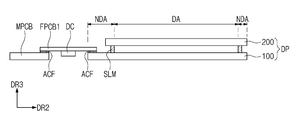
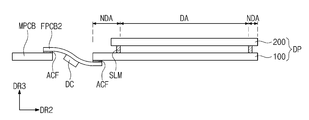
도 1a는 본 발명의 실시예에 따른 표시장치(DD)의 사시도이다. 도 1b 및 도 1c는 본 발명의 실시예에 따른 표시장치(DD)의 단면도이다. 도 2는 본 발명의 실시예에 따른 표시장치(DD)의 평면도이다. 1A is a perspective view of a display device DD according to an exemplary embodiment of the present invention. 1B and 1C are cross-sectional views of a display device DD according to an exemplary embodiment of the present invention. 2 is a plan view of a display device DD according to an exemplary embodiment of the present invention.
도 1a 내지 도 2를 참조하면, 표시장치(DD)는 표시패널(DP), 제1 및 제2 연결회로기판(FPCB1, FPCB2), 및 메인회로기판(MPCB)을 포함한다. 본 실시예에서 제1 및 제2 연결회로기판(FPCB1, FPCB2)에 구동칩(DC)이 실장된 것으로 도시되었으나, 본 발명은 이에 제한되지 않는다. 구동칩(DC)은 제1 및 제2 연결회로기판(FPCB1, FPCB2)에 실장되지 않을 수 있고, 표시패널(DP) 또는 메인회로기판(MPCB)에 실장될 수도 있다.1A through 2, the display device DD includes a display panel DP, first and second connection circuit boards FPCB1 and FPCB2, and a main circuit board MPCB. In the present embodiment, it is shown that the driving chip DC is mounted on the first and second connection circuit boards FPCB1 and FPCB2, but the present invention is not limited thereto. The driving chip DC may not be mounted on the first and second connection circuit boards FPCB1 and FPCB2, and may be mounted on the display panel DP or the main circuit board MPCB.
별도로 도시하지 않았으나, 표시장치(DD)는 샤시부재 또는 몰딩부재를 더 포함할 수 있고, 표시패널(DP)의 종류에 따라 백라이트 유닛을 더 포함할 수 있다.Although not shown separately, the display device DD may further include a chassis member or a molding member, and may further include a backlight unit according to the type of the display panel DP.
표시패널(DP)은 액정 표시 패널(liqid crystal display panel), 플라즈마 표시 패널(plasma display panel), 전기영동 표시 패널(electrophoretic display panel), MEMS 표시 패널(microelectromechanical system display panel) 및 일렉트로웨팅 표시 패널(electrowetting display panel), 및 발광표시패널(light emitting display panel) 중 어느 하나 일 수 있고, 특별히 제한되지 않는다.The display panel DP includes a liquid crystal display panel, a plasma display panel, an electrophoretic display panel, a microelectromechanical system display panel, and an electrowetting display panel. electrowetting display panel) and a light emitting display panel, and is not particularly limited.
표시패널(DP)은 제1 표시기판(100) 및 제1 표시기판(100)에 마주하며 이격된 제2 표시기판(200)을 포함할 수 있다. 제1 표시기판(100)과 제2 표시기판(200) 사이에는 소정의 셀갭이 형성될 수 있다. 셀갭은 제1 표시기판(100)과 제2 표시기판(200)을 결합하는 실런트(SLM)에 의해 유지될 수 있다. 제1 표시기판(100)과 제2 표시기판(200) 사이에는 이미지 생성을 위한 계조표시층이 배치될 수 있다. 계조표시층은 표시패널의 종류에 따라 액정층, 발광층, 전기영동층을 포함할 수 있다. The display panel DP may include a
도 1a에 도시된 것과 같이, 표시패널(DP)은 표시면(DP-IS)을 통해 이미지를 표시할 수 있다. 표시면(DP-IS)은 제1 방향축(DR1) 및 제2 방향축(DR2)이 정의하는 면과 평행한다. 표시면(DP-IS)은 표시영역(DA)과 비표시영역(NDA)을 포함할 수 있다. 비표시영역(NDA)은 표시면(DP-IS)의 테두리를 따라 정의된다. 표시영역(DA)은 비표시영역(NDA)에 의해 에워싸일수 있다. 본 발명의 일 실시예에서 비표시영역(NDA)은 일측 영역에만 배치될 수도 있다. 해당 영역에서 제1 및 제2 연결회로기판(FPCB2, FPCB2)이 제1 표시기판(100)에 본딩될 수 있다.As shown in FIG. 1A, the display panel DP may display an image through the display surface DP-IS. The display surface DP-IS is parallel to a surface defined by the first direction axis DR1 and the second direction axis DR2. The display surface DP-IS may include a display area DA and a non-display area NDA. The non-display area NDA is defined along the edge of the display surface DP-IS. The display area DA may be surrounded by the non-display area NDA. In an embodiment of the present invention, the non-display area NDA may be disposed only in one area. In the corresponding region, the first and second connection circuit boards FPCB2 and FPCB2 may be bonded to the
표시면(DP-IS)의 법선 방향, 즉 표시패널(DP)의 두께 방향은 제3 방향축(DR3)이 지시한다. 이하에서 설명되는 각 층들 또는 유닛들의 전면(또는 상면)과 배면(또는 하면)은 제3 방향축(DR3)에 의해 구분된다. 그러나, 본 실시예에서 도시된 제1 내지 제3 방향축들(DR1, DR2, DR3)은 예시에 불과하다. 이하, 제1 내지 제3 방향들은 제1 내지 제3 방향축들(DR1, DR2, DR3) 각각 이 지시하는 방향으로써 정의되고, 동일한 도면 부호를 참조한다. The third direction axis DR3 indicates the normal direction of the display surface DP-IS, that is, the thickness direction of the display panel DP. The front surface (or upper surface) and the rear surface (or lower surface) of each of the layers or units described below are divided by a third direction axis DR3. However, the first to third direction axes DR1, DR2, and DR3 illustrated in the present embodiment are only examples. Hereinafter, the first to third directions are defined as directions indicated by each of the first to third direction axes DR1, DR2, and DR3, and the same reference numerals are referred to.
본 발명의 일 실시예에서 평면형 표시면을 구비한 표시패널(DP)을 도시하였으나, 이에 제한되지 않는다. 표시장치(DD)는 곡면형 표시면 또는 입체형 표시면을 포함할 수도 있다. 입체형 표시면은 서로 다른 방향을 지시하는 복수 개의 표시영역들을 포함할 수도 있다. Although the display panel DP having a flat display surface is illustrated in an exemplary embodiment of the present invention, the present invention is not limited thereto. The display device DD may include a curved display surface or a three-dimensional display surface. The three-dimensional display surface may include a plurality of display areas indicating different directions.
메인회로기판(MPCB)에는 신호 제어부(SC)가 실장될 수 있다. 신호 제어부(SC)는 외부의 그래픽 제어부(미 도시)로부터 영상 데이터 및 제어신호를 수신한다. 신호 제어부(SC)는 표시패널(DP)에 제어신호를 제공할 수 있다.The signal controller SC may be mounted on the main circuit board MPCB. The signal controller SC receives image data and a control signal from an external graphic controller (not shown). The signal controller SC may provide a control signal to the display panel DP.
제1 및 제2 연결회로기판(FPCB2, FPCB2)은 표시패널(DP)과 메인회로기판(MPCB)을 전기적으로 연결한다. 제1 및 제2 연결회로기판(FPCB2, FPCB2)은 메인회로기판(MPCB)으로부터 구동칩(DC)에 신호를 전달하고, 구동칩(DC)으로부터 표시패널(DP)에 신호를 전달할 수 있다. 본 실시예에서 구동칩(DC)은 데이터 구동회로일 수 있다. 본 발명의 일 실시예에서 제1 및 제2 연결회로기판(FPCB2, FPCB2)은 신호 제어부(SC)로부터 표시패널(DP)에 신호를 전달할 수 있다.The first and second connection circuit boards FPCB2 and FPCB2 electrically connect the display panel DP and the main circuit board MPCB. The first and second connection circuit boards FPCB2 and FPCB2 may transmit signals from the main circuit board MPCB to the driving chip DC, and may transmit signals from the driving chip DC to the display panel DP. In this embodiment, the driving chip DC may be a data driving circuit. In an embodiment of the present invention, the first and second connection circuit boards FPCB2 and FPCB2 may transmit signals from the signal controller SC to the display panel DP.
제1 및 제2 연결회로기판(FPCB1, FPCB2)은 전도성 접착부재에 의해 표시패널(DP) 및 메인회로기판(MPCB) 각각에 본딩될 수 있다. 전도성 접착부재는 솔더볼, 솔더 페이스트, 또는 이방성 도전 필름을 포함할 수 있다. 이하, 이방성 도전 필름으로 설명된다. The first and second connection circuit boards FPCB1 and FPCB2 may be bonded to each of the display panel DP and the main circuit board MPCB by a conductive adhesive member. The conductive adhesive member may include a solder ball, a solder paste, or an anisotropic conductive film. Hereinafter, it demonstrates with an anisotropic conductive film.
도 1a에 도시된 것과 같이, 제1 표시기판(100)은 복수 개의 본딩영역들(BDA)을 포함할 수 있다. 복수 개의 본딩영역들(BDA)마다 제1 및 제2 연결회로기판(FPCB1, FPCB2)이 본딩된다. 1A, the
도 1b에 도시된 것과 같이, 제1 연결회로기판(FPCB1)은 제1 표시기판(100)의 상면(US) 상에 본딩된다. 도 1c에 도시된 것과 같이, 제2 연결회로기판(FPCB2)은 제1 표시기판(100)의 하면(LS) 상에 본딩된다. 도 1b 및 도 1c에서 전도성 접착부재로써 이방성 도전 필름(ACF)이 도시되었다.As shown in FIG. 1B, the first connection circuit board FPCB1 is bonded on the upper surface US of the
본 실시예에서 본딩영역(BDA)은 하부 표시기판에 배치되는 것으로 도시되었으나, 이에 제한되지 않는다. 본딩영역(BDA)은 신호라인 및 패드가 배치되는 표시기판에 배치되면 충분하고, 본 발명의 일 실시예에서 제1 표시기판(100)과 제2 표시기판(200)은 뒤집혀질 수 있고, 이때 본딩영역(BDA)은 상부 표시기판에 배치된다.In the present embodiment, the bonding area BDA is shown to be disposed on the lower display substrate, but is not limited thereto. It is sufficient if the bonding area BDA is disposed on the display substrate on which the signal lines and the pads are disposed, and in one embodiment of the present invention, the
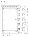
도 2는 신호라인들(GL1~GLn, DL1~DLm, PL-D1, PL-D2) 및 화소들(PX11~PXnm)의 평면상 배치관계를 도시하였다. 신호라인들(GL1~GLn, DL1~DLm, PL-D1, PL-D2)은 복수 개의 게이트 라인들(GL1~GLn), 복수 개의 데이터 라인들(DL1~DLm) 및 보조 신호라인들(PL-D1, PL-D2)을 포함할 수 있다. FIG. 2 illustrates an arrangement relationship of signal lines GL1 to GLn, DL1 to DLm, PL-D1, and PL-D2 and pixels PX11 to PXnm on a plane. The signal lines GL1 to GLn, DL1 to DLm, PL-D1, and PL-D2 include a plurality of gate lines GL1 to GLn, a plurality of data lines DL1 to DLm, and auxiliary signal lines PL- D1, PL-D2) may be included.
화소들(PX11~PXnm) 각각은 복수 개의 게이트 라인들(GL1~GLn) 중 대응하는 게이트 라인과 복수 개의 데이터 라인들(DL1~DLm) 중 대응하는 데이터 라인에 연결된다. 화소들(PX11~PXnm) 각각은 화소 구동회로 및 표시소자를 포함할 수 있다.Each of the pixels PX11 to PXnm is connected to a corresponding gate line among the plurality of gate lines GL1 to GLn and a corresponding data line among the plurality of data lines DL1 to DLm. Each of the pixels PX11 to PXnm may include a pixel driving circuit and a display device.
매트릭스 형태의 화소들(PX11~PXnm)을 예시적으로 도시하였으나, 이에 제한되지 않는다. 화소들(PX11~PXnm)은 펜타일 형태로 배치될 수 있다. 화소들(PX11~PXnm)은 다이아몬드 형태로 배치될 수 있다.The matrix-shaped pixels PX11 to PXnm are illustrated as an example, but are not limited thereto. The pixels PX11 to PXnm may be arranged in a pentile shape. The pixels PX11 to PXnm may be arranged in a diamond shape.
복수 개의 게이트 라인들(GL1~GLn)은 제1 방향(DR1)으로 연장되고 제2 방향(DR2)으로 나열되고, 복수 개의 데이터 라인들(DL1~DLm)은 복수 개의 게이트 라인들(GL1~GLn)과 절연 교차한다. 복수 개의 게이트 라인들(GL1~GLn)과 복수 개의 데이터 라인들(DL1~DLm)은 표시영역(DA)에 중첩하게 배치된다. 보조 신호라인들(PL-D1, PL-D2)은 비표시영역(NDA)에 중첩하게 배치되고, 복수 개의 데이터 라인들(DL1~DLm)에 연결된다.The plurality of gate lines GL1 to GLn extend in a first direction DR1 and are arranged in a second direction DR2, and the plurality of data lines DL1 to DLm are formed of a plurality of gate lines GL1 to GLn. ) And insulation cross. The plurality of gate lines GL1 to GLn and the plurality of data lines DL1 to DLm are disposed to overlap the display area DA. The auxiliary signal lines PL-D1 and PL-D2 are disposed to overlap the non-display area NDA and are connected to a plurality of data lines DL1 to DLm.
복수 개의 게이트 라인들(GL1~GLn)은 게이트 구동회로(GDC)에 연결된다. 게이트 구동회로(GDC)는 OSG(oxide silicon gate driver circuit) 또는 ASG(amorphose silicon gate driver circuit) 공정을 통해 표시패널(DP)에 집적화될 수 있다. The plurality of gate lines GL1 to GLn are connected to the gate driving circuit GDC. The gate driving circuit GDC may be integrated in the display panel DP through an oxide silicon gate driver circuit (OSG) or an amorphose silicon gate driver circuit (ASG) process.
보조 신호라인들(PL-D1, PL-D2)은 제1 패드들(PD1)에 연결되는 제1 보조 신호라인들(PL-D1) 및 제2 패드들(PD2)에 연결되는 제2 보조 신호라인들(PL-D2)을 포함할 수 있다. 표시패널(DP)의 해상도가 높아짐에 따라 화소들(PX11~PXnm)의 면적이 작아지고, 단위면적에 더 많은 개수의 화소들(PX11~PXnm)이 배치된다. 패드들이 일렬로만 배치된다면 더 큰 면적의 본딩영역(BDA)이 요구되며, 패드들 사이의 쇼트와 같은 불량이 발생할 수 있다. 이를 방지하기 위해 미세 피치의 패드 설계가 요구되고 이는 본딩 불량을 일으킬 수도 있다. 본 실시예에서 따르면, 제1 패드들(PD1) 및 제2 패드들(PD2)과 같이 2개의 그룹으로 패드들을 분리하여 배치함으로써 상술한 문제를 해결할 수 있다.The auxiliary signal lines PL-D1 and PL-D2 are first auxiliary signal lines PL-D1 connected to the first pads PD1 and a second auxiliary signal connected to the second pads PD2 It may include lines PL-D2. As the resolution of the display panel DP increases, the area of the pixels PX11 to PXnm decreases, and a larger number of pixels PX11 to PXnm are disposed in the unit area. If the pads are arranged only in a row, a larger area of the bonding area BDA is required, and defects such as a short between the pads may occur. In order to prevent this, a fine pitch pad design is required, which may cause bonding failure. According to the present embodiment, the above-described problem can be solved by separating and disposing the pads into two groups, such as the first pads PD1 and the second pads PD2.
제1 패드들(PD1)은 제1 방향(DR1)으로 배열되고, 제2 패드들(PD2)은 제1 패드들(PD1)과 다른 행을 이루며 제1 방향(DR1)으로 배열된다. 제1 보조 신호라인들(PL-D1)과 제2 보조 신호라인들(PL-D2)은 교번하게 배치될 수 있다.The first pads PD1 are arranged in a first direction DR1, and the second pads PD2 form a different row from the first pads PD1 and are arranged in a first direction DR1. The first auxiliary signal lines PL-D1 and the second auxiliary signal lines PL-D2 may be alternately disposed.
데이터 라인들(DL1~DLm)에 연결되는 제1 및 제2 보조 신호라인들(PL-D1, PL-D2)은 복수 개의 데이터 라인들(DL1~DLm)과 다른 층 상에 배치될 수 있다. 제1 및 제2 보조 신호라인들(PL-D1, PL-D2)은 서로 동일한 층 상에, 예컨대, 게이트 라인들(GL1~GLn)과 동일한 층 상에 배치될 수 있다. 제1 및 제2 보조 신호라인들(PL-D1, PL-D2)은 컨택홀(CH)을 통해 데이터 라인들(DL1~DLm)은 중 대응하는 신호라인에 전기적으로 연결될 수 있다. 컨택홀(CH)은 데이터 라인들(DL1~DLm)과 제1 및 제2 보조 신호라인들(PL-D1, PL-D2) 사이에 배치된 적어도 하나의 절연층을 관통한다. 도 2에는 2개의 컨택홀(CH)을 예시적으로 도시하였다.The first and second auxiliary signal lines PL-D1 and PL-D2 connected to the data lines DL1 to DLm may be disposed on a layer different from the plurality of data lines DL1 to DLm. The first and second auxiliary signal lines PL-D1 and PL-D2 may be disposed on the same layer as each other, for example, on the same layer as the gate lines GL1 to GLn. The first and second auxiliary signal lines PL-D1 and PL-D2 may be electrically connected to a corresponding one of the data lines DL1 to DLm through a contact hole CH. The contact hole CH penetrates through at least one insulating layer disposed between the data lines DL1 to DLm and the first and second auxiliary signal lines PL-D1 and PL-D2. In FIG. 2, two contact holes CH are illustrated by way of example.
본 발명의 일 실시예에서 컨택홀(CH)은 생략될 수 있다. 데이터 라인들(DL1~DLm)과 제1 및 제2 보조 신호라인들(PL-D1, PL-D2)은 동일한 층 상에 배치될 수도 있다. 이때, 데이터 라인들(DL1~DLm)과 제1 및 제2 보조 신호라인들(PL-D1, PL-D2)은 서로 구별되지 않고 하나의 신호라인으로 정의될 수도 있다. 이때 서로 연결된 데이터 라인과 보조 신호라인은 하나의 신호라인의 서로 다른 부분에 해당한다. 다시 말해, 본 실시예에서 제1 및 제2 보조 신호라인들(PL-D1, PL-D2)이 별도로 구비된 것으로 설명되었으나, 제1 및 제2 보조 신호라인들(PL-D1, PL-D2)은 생략되고 다른 신호라인의 일부분이 제1 및 제2 보조 신호라인들(PL-D1, PL-D2)을 대체할 수 있다.In an embodiment of the present invention, the contact hole CH may be omitted. The data lines DL1 to DLm and the first and second auxiliary signal lines PL-D1 and PL-D2 may be disposed on the same layer. In this case, the data lines DL1 to DLm and the first and second auxiliary signal lines PL-D1 and PL-D2 are not distinguished from each other and may be defined as one signal line. In this case, the data line and the auxiliary signal line connected to each other correspond to different portions of one signal line. In other words, although it has been described that the first and second auxiliary signal lines PL-D1 and PL-D2 are separately provided in the present embodiment, the first and second auxiliary signal lines PL-D1 and PL-D2 ) Is omitted, and a portion of the other signal line may replace the first and second auxiliary signal lines PL-D1 and PL-D2.
도 3a 및 도 3b은 본 발명의 실시예에 따른 표시패널(DP)의 표시영역(DA)의 단면도이다. 도 3a는 액정표시패널의 화소(PX)에 대응하는 단면을 도시하였고, 도 3b는 유기발광 표시패널의 화소(PX)에 대응하는 단면을 도시하였다.3A and 3B are cross-sectional views of the display area DA of the display panel DP according to the exemplary embodiment of the present invention. FIG. 3A illustrates a cross section corresponding to the pixel PX of the liquid crystal display panel, and FIG. 3B illustrates a cross section corresponding to the pixel PX of the organic light emitting display panel.
액정표시패널의 화소(PX)는 트랜지스터(TR), 액정 커패시터(Clc), 및 스토리지 커패시터(Cst)를 포함할 수 있다.The pixel PX of the liquid crystal display panel may include a transistor TR, a liquid crystal capacitor Clc, and a storage capacitor Cst.
트랜지스터(TR)는 게이트 라인(미 도시)에 연결된 제어전극(GE), 제어전극(GE)에 중첩하는 활성화부(AL), 데이터 라인에 연결된 입력전극(SE), 및 입력전극(SE)와 이격되어 배치된 출력전극(SE)을 포함한다. 액정 커패시터(Clc)는 화소전극(PE)과 공통전극(CE)을 포함한다. 스토리지 커패시터(Cst)는 화소전극(PE)과 화소전극(PE)에 중첩하는 스토리지 라인(STL)의 일부분을 포함한다.The transistor TR includes a control electrode GE connected to a gate line (not shown), an activation part AL overlapping the control electrode GE, an input electrode SE connected to the data line, and an input electrode SE. It includes an output electrode (SE) arranged to be spaced apart. The liquid crystal capacitor Clc includes a pixel electrode PE and a common electrode CE. The storage capacitor Cst includes the pixel electrode PE and a portion of the storage line STL overlapping the pixel electrode PE.
제1 베이스층(BS1)의 일면 상에 제어전극(GE) 및 스토리지 라인(STL)이 배치된다. 제1 베이스층(BS1)은 유리기판 또는 플라스틱기판일 수 있다. 제1 베이스층(BS1)의 일면 상에 적어도 하나의 절연층과 적어도 하나의 도전패턴이 배치된다.The control electrode GE and the storage line STL are disposed on one surface of the first base layer BS1. The first base layer BS1 may be a glass substrate or a plastic substrate. At least one insulating layer and at least one conductive pattern are disposed on one surface of the first base layer BS1.
제1 베이스층(BS1)의 일면 상에 상기 제어전극(GE) 및 스토리지 라인(STL)을 커버하는 제1 절연층(10)이 배치된다. 제1 절연층(10)은 무기물 및 유기물 중 적어도 어느 하나를 포함할 수 있다. 제1 절연층(10) 상에 제어전극(GE)과 중첩하는 활성화부(AL)가 배치된다. 활성화부(AL)는 반도체층(SCL)과 오믹 컨택층(OCL)을 포함할 수 있다. 제1 절연층(10) 상에 상기 반도체층(SCL)이 배치되고, 반도체층(SCL) 상에 상기 오믹 컨택층(OCL)이 배치된다.A first insulating
반도체층(SCL)은 아몰포스 실리콘 또는 폴리 실리콘을 포함할 수 있다. 또한, 반도체층(SCL)은 금속 산화물 반도체를 포함할 수 있다. 오믹 컨택층(OCL)은 반도체층보다 고밀도로 도핑된 도펀트를 포함할 수 있다. 오믹 컨택층(OCL)은 이격된 2개의 부분을 포함할 수 있다. 본 발명의 일 실시예에서 오믹 컨택층(OCL)은 일체의 형상을 가질 수 있다.The semiconductor layer SCL may include amorphous silicon or polysilicon. In addition, the semiconductor layer SCL may include a metal oxide semiconductor. The ohmic contact layer OCL may include a dopant doped with a higher density than the semiconductor layer. The ohmic contact layer OCL may include two spaced apart portions. In an embodiment of the present invention, the ohmic contact layer OCL may have an integral shape.
활성화부(AL) 상에 입력전극(DE)과 출력전극(SE)이 배치된다. 입력전극(DE)과 출력전극(SE)은 서로 이격되어 배치된다. 제1 절연층(10) 상에 활성화부(AL), 입력전극(DE), 및 출력전극(SE)을 커버하는 제2 절연층(20)이 배치된다. 제2 절연층(20) 상에 제3 절연층(30)이 배치된다 제2 절연층(20) 및 제3 절연층(30)은 무기물 및 유기물 중 적어도 어느 하나를 포함할 수 있다. 제2 절연층(20) 상에 제3 절연층(30)이 배치된다. 제3 절연층(30)은 평탄면을 제공하는 단층의 유기층일 수 있다. 본 실시예에서 제3 절연층(30)은 복수 개의 컬러필터들을 포함할 수 있다. 제3 절연층(30) 상에 제4 절연층(40)이 배치된다. 제4 절연층(40)은 컬러필터들을 커버하는 무기층일 수 있다. The input electrode DE and the output electrode SE are disposed on the activation part AL. The input electrode DE and the output electrode SE are disposed to be spaced apart from each other. A second insulating
도 3a에 도시된 것과 같이, 제4 절연층(40) 상에 화소전극(PE)이 배치된다. 화소전극(PE)은 제2 절연층(20), 제3 절연층(30), 및 제4 절연층(40)을 관통하는 컨택홀(CH10)을 통해 상기 출력전극(SE)에 연결된다. 제4 절연층(40) 상에 상기 화소전극(PE)을 커버하는 배향막(미 도시)이 배치될 수 있다.As shown in FIG. 3A, the pixel electrode PE is disposed on the fourth insulating
제2 베이스층(BS2)은 유리기판 또는 플라스틱기판일 수 있다. 제2 베이스층(BS2)의 하면 상에 블랙매트릭스층(BM)이 배치된다. 즉, 블랙매트릭스층(BM)에는 화소영역들에 대응하는 개구부들이 정의될 수 있다. 블랙매트릭스층(BM)에 중첩하게 스페이서(CS)가 배치될 수 있다.The second base layer BS2 may be a glass substrate or a plastic substrate. A black matrix layer BM is disposed on the lower surface of the second base layer BS2. That is, openings corresponding to the pixel regions may be defined in the black matrix layer BM. The spacers CS may be disposed to overlap the black matrix layer BM.
제2 베이스층(BS2)의 하면 상에 블랙매트릭스층(BM)을 커버하는 절연층들이 배치된다. 도 5a에는 평탄면을 제공하는 제5 절연층(50)이 예시적으로 도시되었다. 제5 절연층(50)은 유기물질을 포함할 수 있다. Insulation layers covering the black matrix layer BM are disposed on the lower surface of the second base layer BS2. 5A, a fifth insulating
도 3a에 도시된 것과 같이, 제2 베이스층(BS2)의 하면 상에 공통전극(CE)이 배치된다. 공통전극(CE)에는 공통 전압이 인가된다. 공통 전압과 화소 전압과 다른 레벨을 갖는다. As shown in FIG. 3A, the common electrode CE is disposed on the lower surface of the second base layer BS2. A common voltage is applied to the common electrode CE. It has a level different from the common voltage and the pixel voltage.
도 3a를 참조하여 VA(Vertical Alignment)모드의 액정 표시패널을 예시적으로 설명하였으나, 본 발명의 일 실시예에서 IPS(in-plane switching) 모드 또는 FFS(fringe-field switching) 모드, PLS(Plane to Line Switching) 모드, SVA(Super Vertical Alignment) 모드, SS-VA(Surface-Stabilized Vertical Alignment) 모드의 액정 표시패널이 적용될 수 있다. A liquid crystal display panel in a vertical alignment (VA) mode has been exemplarily described with reference to FIG. 3A, but in an embodiment of the present invention, an in-plane switching (IPS) mode, a fringe-field switching (FFS) mode, or a plane To Line Switching) mode, Super Vertical Alignment (SVA) mode, and Surface-Stabilized Vertical Alignment (SS-VA) mode liquid crystal display panel may be applied.
도 3b에 도시된 것과 같이, 발광표시패널의 화소(PX)는 스위칭 트랜지스터(T1), 구동 트랜지스터(T2), 및 발광소자(OLED)를 포함할 수 있다.As shown in FIG. 3B, the pixel PX of the light emitting display panel may include a switching transistor T1, a driving transistor T2, and a light emitting device OLED.
발광표시패널은 표시기판(100)과 봉지기판(200)을 포함한다. 표시기판(100)은 제1 베이스층(BS1), 제1 베이스층(BS1) 상에 배치된 회로 소자층(DP-CL), 및 회로 소자층(DP-CL) 상에 배치된 표시 소자층(DP-OLED)을 포함한다. 봉지기판(200)은 제2 베이스층(BS2), 제2 베이스층(BS2) 상에 배치된 블랙매트릭스층(BM) 및 컬러제어층(CCL)을 포함할 수 있다.The light emitting display panel includes a
제1 베이스층(BS1)은 합성수지기판 또는 유리기판을 포함할 수 있다. 회로 소자층(DP-CL)은 적어도 하나의 절연층과 회로 소자를 포함한다. 회로 소자는 신호라인, 화소의 구동회로 등을 포함한다. 코팅, 증착 등에 의한 절연층, 반도체층 및 도전층 형성공정과 포토리소그래피 공정에 의한 절연층, 반도체층 및 도전층층의 패터닝 공정을 통해 회로 소자층(DP-CL)이 형성될 수 있다.The first base layer BS1 may include a synthetic resin substrate or a glass substrate. The circuit element layer DP-CL includes at least one insulating layer and a circuit element. Circuit elements include signal lines, pixel driving circuits, and the like. The circuit device layer DP-CL may be formed through a process of forming an insulating layer, a semiconductor layer, and a conductive layer by coating or vapor deposition, and a patterning process of the insulating layer, semiconductor layer, and conductive layer layer by a photolithography process.
본 실시예에서 회로 소자층(DP-CL)은 버퍼막(BFL), 제1 절연층(10), 제2 절연층(20), 제3 절연층(30)을 포함할 수 있다. 제1 절연층(10) 및 제2 절연층(20)은 무기막이고, 제3 절연층(30)은 유기막일 수 있다.In this embodiment, the circuit device layer DP-CL may include a buffer layer BFL, a first insulating
도 3b에는 스위칭 트랜지스터(T1) 및 구동 트랜지스터(T2)를 구성하는 제1 반도체 패턴(OSP1), 제2 반도체 패턴(OSP2), 제1 제어전극(GE1), 제2 제어전극(GE2), 제1 입력전극(SE1), 제1 출력전극(DE1), 제2 입력전극(SE2), 제2 출력전극(DE2)의 배치관계가 예시적으로 도시되었다. 제1, 제2, 제3, 및 제4 관통홀(CH1, CH2, CH3, CH4) 역시 예시적으로 도시되었다.3B shows a first semiconductor pattern OSP1, a second semiconductor pattern OSP2, a first control electrode GE1, a second control electrode GE2, and a second control electrode GE2 constituting the switching transistor T1 and the driving transistor T2. An arrangement relationship between the first input electrode SE1, the first output electrode DE1, the second input electrode SE2, and the second output electrode DE2 is illustrated as an example. The first, second, third, and fourth through holes CH1, CH2, CH3, and CH4 are also illustrated by way of example.
표시 소자층(DP-OLED)은 발광소자(OLED)를 포함한다. 발광소자(OLED)는 발광 다이오드를 포함할 수 있다. 발광소자(OLED)는 유기 발광층을 포함하거나 양자점 발광층을 포함할 수 있다. 표시 소자층(DP-OLED)은 화소 정의막(PDL)을 포함한다. 예컨대, 화소 정의막(PDL)은 유기층일 수 있다. 표시 소자층(DP-OLED)은 발광소자(OLED) 상에 배치된 커버층(CL)을 더 포함할 수 있다.The display device layer DP-OLED includes a light emitting device OLED. The light emitting device (OLED) may include a light emitting diode. The light emitting device OLED may include an organic emission layer or a quantum dot emission layer. The display device layer DP-OLED includes a pixel defining layer PDL. For example, the pixel defining layer PDL may be an organic layer. The display device layer DP-OLED may further include a cover layer CL disposed on the light emitting device OLED.
제3 절연층(30) 상에 제1 전극(AE)이 배치된다. 제1 전극(AE)은 제3 절연층(30)을 관통하는 제5 관통홀(CH5)을 통해 제2 출력전극(SE2)에 연결된다. 화소 정의막(PDL)에는 개구부(OP)가 정의된다. 화소 정의막(PDL)의 개구부(OP)는 제1 전극(AE)의 적어도 일부분을 노출시킨다. The first electrode AE is disposed on the third insulating
도 3b에 도시된 것과 같이, 표시패널(DP)은 발광영역(PXA)과 발광영역(PXA)에 인접한 비발광영역(NPXA)을 포함할 수 있다. 비발광영역(NPXA)은 발광영역(PXA)을 에워싸을수 있다. 본 실시예에서 발광영역(PXA)은 개구부(OP)에 의해 노출된 제1 전극(AE)의 일부영역에 대응하게 정의되었다. As illustrated in FIG. 3B, the display panel DP may include an emission area PXA and a non-emission area NPXA adjacent to the emission area PXA. The non-emission area NPXA may surround the light-emitting area PXA. In the present embodiment, the light emitting area PXA is defined to correspond to a partial area of the first electrode AE exposed by the opening OP.
정공 제어층(HCL)은 발광영역(PXA)과 비발광영역(NPXA)에 공통으로 배치될 수 있다. 정공 제어층(HCL)은 정공 수송층을 포함하고, 정공 주입층을 더 포함할 수 있다. 정공 제어층(HCL) 상에 발광층(EML)이 배치된다. 발광층(EML)은 발광영역(PXA)과 비발광영역(NPXA)에 공통ㄹ으로 배치될 수 있다. 본 발명의 일시예에서 발광층(EML)은 발광영역(PXA)에 배치되고, 비발광영역(NPXA)에 미배치될 수 있다. 발광층(EML)은 유기물질 및/또는 무기물질을 포함할 수 있다. 발광층(EML)은 소정의 제1 색광 예컨대 블루광을 생성할 수 있다.The hole control layer HCL may be commonly disposed in the light-emitting area PXA and the non-emissive area NPXA. The hole control layer HCL may include a hole transport layer, and may further include a hole injection layer. The emission layer EML is disposed on the hole control layer HCL. The emission layer EML may be disposed in common between the emission area PXA and the non-emission area NPXA. In one embodiment of the present invention, the light emitting layer EML may be disposed in the light emitting area PXA and not disposed in the non-emissive area NPXA. The emission layer EML may include an organic material and/or an inorganic material. The emission layer EML may generate a predetermined first color light, such as blue light.
발광층(EML) 상에 전자 제어층(ECL)이 배치된다. 전자 제어층(ECL)은 전자 수송층을 포함하고, 전자 주입층을 더 포함할 수 있다. 정공 제어층(HCL)과 전자 제어층(ECL)은 오픈 마스크를 이용하여 복수 개의 화소들에 공통으로 형성될 수 있다. 전자 제어층(ECL) 상에 제2 전극(CCE)이 배치된다. 제2 전극(CCE)은 복수 개의 화소들에 공통적으로 배치된다. 제2 전극(CCE) 상에 제2 전극(CCE)을 보호하는 커버층(CL)이 배치될 수 있다. 커버층(CL)은 유기물질 또는 무기물질을 포함할 수 있다.The electron control layer ECL is disposed on the emission layer EML. The electron control layer ECL may include an electron transport layer and may further include an electron injection layer. The hole control layer HCL and the electron control layer ECL may be commonly formed in a plurality of pixels using an open mask. The second electrode CCE is disposed on the electronic control layer ECL. The second electrode CCE is commonly disposed on a plurality of pixels. A cover layer CL protecting the second electrode CCE may be disposed on the second electrode CCE. The cover layer CL may include an organic material or an inorganic material.
제2 베이스층(BS2)은 커버층(CL)과 이격되어 배치된다. 제2 베이스층(BS2)은 합성수지기판 또는 유리기판을 포함할 수 있다. 컬러제어층(CCL)은 화소(PX)에 따라 제1 색광을 투과시키거나, 제1 색광을 제2 색광 또는 제3 색광으로 변환시킬 수 있다. 컬러제어층(CCL)은 양자점을 포함할 수 있다. 화소들(PX11~PXnm, 도 2 참조)은 복수 개의 그룹으로 구분될 수 있다. 화소 그룹에 따라 컬러제어층(CCL)은 다르게 배치될 수 있다.The second base layer BS2 is disposed to be spaced apart from the cover layer CL. The second base layer BS2 may include a synthetic resin substrate or a glass substrate. The color control layer CCL may transmit the first color light or convert the first color light into a second color light or a third color light according to the pixel PX. The color control layer CCL may include quantum dots. The pixels PX11 to PXnm, see FIG. 2 may be divided into a plurality of groups. The color control layer CCL may be disposed differently depending on the pixel group.
본 발명의 일 실시예에서 봉지기판(200)은 박막 봉지층으로 대체될 수 있다. 이때, 블랙매트릭스층(BM) 및 컬러제어층(CCL)은 박막 봉지층 상에 배치될 수 있다. In one embodiment of the present invention, the
도 4a는 본 발명의 실시예에 따른 표시장치(DD)의 확대된 평면도이다. 도 4b는 본 발명의 실시예에 따른 연결회로기판(FPCB1)의 배면도이다. 도 4c는 본 발명의 실시예에 따른 표시장치(DD)의 단면도이다. 도 4d 및 도 4e는 도 4c의 확대된 단면도이다. 도 4f는 본 발명의 실시예에 따른 표시장치(DD)의 확대된 사시도이다.4A is an enlarged plan view of a display device DD according to an exemplary embodiment of the present invention. 4B is a rear view of the connection circuit board FPCB1 according to an embodiment of the present invention. 4C is a cross-sectional view of a display device DD according to an exemplary embodiment of the present invention. 4D and 4E are enlarged cross-sectional views of FIG. 4C. 4F is an enlarged perspective view of a display device DD according to an exemplary embodiment of the present invention.
도 4a에 도시된 것과 같이, 제1 연결회로기판(FPCB1)은 제1 패드들(PD1)에 연결되고, 제2 연결회로기판(FPCB2)은 제2 패드들(PD2)에 연결된다. 평면상에서 볼 때, 제1 패드들(PD1)은 제1 표시기판(100)의 엣지(E-DP)와 제2 방향(DR2)을 따라 이격된다. 평면상에서 제1 표시기판(100)의 엣지(E-DP)는 제1 표시기판(100)의 절연층들의 엣지와 실질적으로 동일할 수 있다.As shown in FIG. 4A, the first connection circuit board FPCB1 is connected to the first pads PD1, and the second connection circuit board FPCB2 is connected to the second pads PD2. When viewed in plan view, the first pads PD1 are spaced apart from the edge E-DP of the
평면상에서 제1 연결회로기판(FPCB1)은 제1 패드들(PD1) 및 제2 패드들(PD2)에 중첩한다. 제2 패드들(PD2)은 제1 패드들(PD1)보다 제1 표시기판(100)의 엣지(E-DP)에 더 인접하게 배치된다.On the plane, the first connection circuit board FPCB1 overlaps the first pads PD1 and the second pads PD2. The second pads PD2 are disposed closer to the edge E-DP of the
평면상에서 볼 때, 제2 패드들(PD2)의 엣지는 제1 표시기판(100)의 엣지(E-DP)와 정렬될 수 있다. 이는 표시패널(DP)의 제조공정에 있어서, 제2 패드들(PD2)의 측면이 노출되도록 제1 표시기판(100)의 측면을 연마했기 때문이다. When viewed in plan view, the edges of the second pads PD2 may be aligned with the edges E-DP of the
제1 연결회로기판(FPCB1)과 제2 연결회로기판(FPCB2)은 크기와 모양이 일부 상이하지만 매우 유사한 구조를 갖는다. 도 4b에 제1 연결회로기판(FPCB1)을 예시적으로 도시하였다. 이하, 제1 연결회로기판(FPCB1)을 중심으로 설명한다. Although the first connection circuit board FPCB1 and the second connection circuit board FPCB2 are partially different in size and shape, they have very similar structures. The first connection circuit board FPCB1 is illustrated in FIG. 4B by way of example. Hereinafter, a description will be given focusing on the first connection circuit board FPCB1.
제1 연결회로기판(FPCB1)은 절연층(미 도시), 복수 개의 패드들(CPD, P-O, P-I), 및 복수 개의 신호라인들(SL-F)을 포함한다. 복수 개의 패드들(CPD, P-O, P-I), 및 복수 개의 신호라인들(SL-F)은 절연층 상에 배치된다. 절연층은 폴리 이미드층을 포함할 수 있다.The first connection circuit board FPCB1 includes an insulating layer (not shown), a plurality of pads CPD, P-O, and P-I, and a plurality of signal lines SL-F. A plurality of pads CPD, P-O, and P-I, and a plurality of signal lines SL-F are disposed on the insulating layer. The insulating layer may include a polyimide layer.
복수 개의 패드들(CPD, P-O, P-I)은 구동칩(DC)의 접속 단자들에 접속되는 접속 패드들(CPD), 표시패널(DP)에 접속되는 제1 패드들(P-O, 이하 출력 패드들로 정의됨), 및 메인회로기판에 접속되는 제2 패드들(P-I, 이하 입력 패드들로 정의됨)을 포함할 수 있다. 복수 개의 신호라인들(SL-F)은 접속 패드들(CPD)과 출력 패드들(P-O)을 연결하고, 접속 패드들(CPD)과 입력 패드들(P-I)을 연결한다. 구동칩(DC)이 생략되는 경우, 신호라인들(SL-F)은 출력 패드들(P-O)과 입력 패드들(P-I)을 연결할 수 있다.The plurality of pads CPD, PO, PI are connection pads CPD connected to the connection terminals of the driving chip DC, and first pads PO connected to the display panel DP (hereinafter, output pads) ), and second pads (PI, hereinafter defined as input pads) connected to the main circuit board. The plurality of signal lines SL-F connects the connection pads CPD and the output pads P-O, and connects the connection pads CPD and the input pads P-I. When the driving chip DC is omitted, the signal lines SL-F may connect the output pads P-O and the input pads P-I.
제1 연결회로기판(FPCB1)의 복수 개의 패드들(CPD, P-O, P-I)은 외부에 노출된다. 복수 개의 패드들(CPD, P-O, P-I) 각각은 절연층을 관통하는 컨택홀을 통해 대응하는 신호라인(SL-F)에 연결된다.The plurality of pads CPD, P-O, and P-I of the first connection circuit board FPCB1 are exposed to the outside. Each of the plurality of pads CPD, P-O, and P-I is connected to a corresponding signal line SL-F through a contact hole penetrating through the insulating layer.
제1 연결회로기판(FPCB1)은 제1 방향(DR1)의 너비에 따라 구분되는 3개의 부분들을 포함할 수 있다. 출력 패드들(P-O)이 배치된 제1 부분(P1), 입력 패드들(P-I)이 배치된 제2 부분(P2) 및 제1 부분(P1)과 제2 부분(P2)을 연결하는 제3 부분(P3)을 포함할 수 있다. 제1 부분(P1)은 제2 부분(P2)보다 큰 너비를 갖는다. 제3 부분(P3)은 제1 부분(P1)으로부터 제2 부분(P2)으로 갈수록 너비가 감소될 수 있다. 제2 부분(P2)에 구동칩(DC)이 실장될 수 있다.The first connection circuit board FPCB1 may include three parts divided according to the width of the first direction DR1. The first part P1 in which the output pads PO are disposed, the second part P2 in which the input pads PI are disposed, and a third connecting the first part P1 and the second part P2 It may include a portion P3. The first portion P1 has a larger width than the second portion P2. The width of the third portion P3 may decrease from the first portion P1 to the second portion P2. The driving chip DC may be mounted on the second part P2.
제1 연결회로기판(FPCB1)은 출력 패드들(P-O), 입력 패드들(P-I), 및 접속 패드들(CPD)이 모두 제1 연결회로기판(FPCB1)의 배면을 향하여 외부에 노출된다. 그에 반하여 도 4a에 도시된 제2 연결회로기판(FPCB2)의 출력 패드들(P-O)은 제2 연결회로기판(FPCB2)의 전면을 향하여 외부에 노출되고, 제2 연결회로기판(FPCB2)의 입력 패드들(P-I), 및 접속 패드들(CPD)은 제2 연결회로기판(FPCB2)의 배면을 향하여 외부에 노출된다. 그에 따라 도 4a에 도시된 것과 같이, 제1 연결회로기판(FPCB1)과 제2 연결회로기판(FPCB2)은 메인회로기판(MPCB)의 동일한 일면 상에 결합될 수 있다. 메인회로기판(MPCB)에 대한 제1 연결회로기판(FPCB1) 및 제2 연결회로기판(FPCB2)의 본딩 구조는 이에 제한되지 않는다.In the first connection circuit board FPCB1, all of the output pads P-O, the input pads P-I, and the connection pads CPD are exposed to the outside toward the rear surface of the first connection circuit board FPCB1. On the other hand, the output pads PO of the second connection circuit board FPCB2 shown in FIG. 4A are exposed to the outside toward the front of the second connection circuit board FPCB2, and the input of the second connection circuit board FPCB2 The pads PI and the connection pads CPD are exposed to the outside toward the rear surface of the second connection circuit board FPCB2. Accordingly, as shown in FIG. 4A, the first connection circuit board FPCB1 and the second connection circuit board FPCB2 may be coupled on the same surface of the main circuit board MPCB. The bonding structure of the first connection circuit board FPCB1 and the second connection circuit board FPCB2 to the main circuit board MPCB is not limited thereto.
도 4a 및 도 4c에 도시된 것과 같이, 하나의 본딩영역(BDA)에 배치된 제1 연결회로기판(FPCB1)과 제2 연결회로기판(FPCB2)은 평면상에서 부분적으로 서로 중첩한다. 다만, 제1 연결회로기판(FPCB1)과 제2 연결회로기판(FPCB2)이 제1 표시기판(100)의 서로 다른 면상에서 제1 표시기판(100)에 결합됨으로써 제1 연결회로기판(FPCB1)과 제2 연결회로기판(FPCB2)의 물리적 간섭을 최소화할 수 있다. As shown in FIGS. 4A and 4C, the first connection circuit board FPCB1 and the second connection circuit board FPCB2 disposed in one bonding area BDA partially overlap each other on a plane. However, the first connection circuit board (FPCB1) and the second connection circuit board (FPCB2) are coupled to the
제1 연결회로기판(FPCB1)과 제2 연결회로기판(FPCB2) 각각이 영역에 따라 다른 너비를 갖는 형상을 가짐으로써 메인회로기판(MPCB)에 인접한 영역(도 4b의 제2 부분(P2))에서는, 평면상에서 볼 때, 제1 연결회로기판(FPCB1)과 제2 연결회로기판(FPCB2)이 비중첩할 수 있다. 이 또한, 제1 연결회로기판(FPCB1)과 제2 연결회로기판(FPCB2)의 물리적 간섭을 최소화할 수 있다. Each of the first and second connection circuit boards FPCB1 and FPCB2 has a shape having a different width depending on the region, so that the region adjacent to the main circuit board MPCB (second part P2 in FIG. 4B) In, when viewed in a plan view, the first connection circuit board FPCB1 and the second connection circuit board FPCB2 may be non-overlapping. In addition, it is possible to minimize the physical interference between the first connection circuit board (FPCB1) and the second connection circuit board (FPCB2).
도 4d는 도 4c의 AA영역을 확대 도시하였다. 도 4d에는 제1 절연층(IL-F1), 신호라인(SL-F), 제2 절연층(IL-F2), 및 출력 패드(P-O)를 포함하는 제1 연결회로기판(FPCB1)이 예시적으로 도시되었다. 도 4d에 도시된 것과 같이, 제1 패드(PD1)는 절연층으로부터 노출되고 신호라인에 연결된다. 제1 내지 제4 절연층(10 내지 40)을 관통하는 컨택홀(CH-P)을 통해 제1 보조 신호라인(PL-D1)에 연결된 제1 패드(PD1)를 예시적으로 도시하였다. 제1 패드(PD1)는 은(Ag), 구리(Cu), 금(Au), 또는 알루미늄(Al)을 포함할 수 있다.4D is an enlarged view of the AA area of FIG. 4C. 4D illustrates a first connection circuit board FPCB1 including a first insulating layer IL-F1, a signal line SL-F, a second insulating layer IL-F2, and an output pad PO. Was shown as an enemy. As illustrated in FIG. 4D, the first pad PD1 is exposed from the insulating layer and connected to the signal line. The first pad PD1 connected to the first auxiliary signal line PL-D1 through the contact hole CH-P penetrating the first to fourth insulating
제1 패드(PD1)는 이방성 도전 필름(ACF)을 통해 출력 패드(P-O)에 전기적으로 접속될 수 있다. 본 발명의 일 실시예에서 제1 패드(PD1)는 생략될 수 있다. 이때, 이방성 도전 필름(ACF)은 제1 보조 신호라인(PL-D1)에 직접적으로 연결될 수도 있다.The first pad PD1 may be electrically connected to the output pad P-O through the anisotropic conductive film ACF. In an embodiment of the present invention, the first pad PD1 may be omitted. In this case, the anisotropic conductive film ACF may be directly connected to the first auxiliary signal line PL-D1.
도 4e는 도 4c의 BB영역을 확대 도시하였다. 도 4e에는 제1 절연층(IL-F1), 신호라인(SL-F), 제2 절연층(IL-F2), 및 출력 패드(P-O)를 포함하는 제2 연결회로기판(FPCB2)이 예시적으로 도시되었다. 도 4e에 도시된 것과 같이, 제2 패드(PD2)는 신호라인의 측면에 연결되며 제1 베이스층(BS1)의 측면(BS1-SS) 및 하면(BS1-LS) 상에 배치된다. 도 4e에는 신호라인으로써 제2 보조 신호라인(PL-D2)이 예시적으로 도시되었다.4E is an enlarged view of an area BB of FIG. 4C. 4E illustrates a second connection circuit board FPCB2 including a first insulating layer IL-F1, a signal line SL-F, a second insulating layer IL-F2, and an output pad PO. Was shown as an enemy. As shown in FIG. 4E, the second pad PD2 is connected to the side surface of the signal line and is disposed on the side surface BS1-SS and the lower surface BS1-LS of the first base layer BS1. In FIG. 4E, a second auxiliary signal line PL-D2 is exemplarily illustrated as a signal line.
이방성 도전 필름(ACF)은 제2 패드(PD2)의 제1 베이스층(BS1)의 하면(BS1-LS) 상에 배치된 일부분에 결합될 수 있다.The anisotropic conductive film ACF may be coupled to a portion disposed on the lower surface BS1-LS of the first base layer BS1 of the second pad PD2.
제2 보조 신호라인들(PL-D2)의 측면은 제1 베이스층(BS1)의 측면(BS1-SS)과 실질적으로 정렬될 수 있다. 제2 보조 신호라인들(PL-D2)의 측면은 제1 내지 제4 절연층들(10 내지 40)의 측면과 실질적으로 정렬될 수 있다. 도 4e에는 제2 절연층(20)의 측면(20-SS)에 대해 도면 부호를 절연층들의 측면을 대표하여 표시하였다. The side surfaces of the second auxiliary signal lines PL-D2 may be substantially aligned with the side surfaces BS1-SS of the first base layer BS1. Side surfaces of the second auxiliary signal lines PL-D2 may be substantially aligned with side surfaces of the first to fourth insulating
본 발명의 일 실시예에서, 제1 내지 제4 절연층들(10 내지 40) 중 일부, 예컨대 유기 절연층의 측면은 다른 절연층들의 측면과 비정렬될 수도 있다. 반드시 모든 절연층들의 측면이 정렬될 필요는 없다.In one embodiment of the present invention, some of the first to fourth insulating
도 4f에 도시된 것과 같이, 복수 개의 제2 패드들(PD2)은 제1 표시기판(100)의 측면(100-SS)에서 소정의 간격으로 이격될 수 있다. 금속 페이스트를 제1 표시기판(100)의 측면(100-SS) 및 하면(미도시) 상에 인쇄한 후 패터닝하여 복수 개의 제2 패드들(PD2)을 형성할 수 있다. 금속 페이스트의 인쇄 및 패터닝 공정은 특별히 제한되지 않는다. 금속 페이스트는 실버 페이스트일 수 있다.As shown in FIG. 4F, the plurality of second pads PD2 may be spaced apart from the side surface 100-SS of the
도 4d와 도 4e를 비교하면, 절연층(예컨대 제4 절연층(40)),과 제1 연결회로기판(FPCB1)이 중첩하는 영역 내에서, 제1 보조 신호라인(PL-D1)은 컨택홀(CH-P)을 통해 제4 절연층(40)으로부터 부분적으로 노출되지만, 제2 보조 신호라인(PL-D2)은 제4 절연층(40)으로부터 노출되지 않는다. 본딩영역(BDA) 내에서 하나의 패드영역이 제1 표시기판(100)의 상면에 정의되고, 다른 하나의 패드영역이 제1 표시기판(100)의 하면에 정의된다.When comparing FIGS. 4D and 4E, the first auxiliary signal line PL-D1 is a contact in a region where the insulating layer (for example, the fourth insulating layer 40) and the first connection circuit board FPCB1 overlap. Although partially exposed from the fourth insulating
도 5는 본 발명의 실시예에 따른 표시장치(DD)의 제조방법을 도시한 단면도이다. 5 is a cross-sectional view illustrating a method of manufacturing a display device DD according to an exemplary embodiment of the present invention.
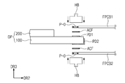
제1 패드들(PD1)과 제2 패드들(PD2)을 포함하는 표시패널(DP)을 제공한다. 또한, 이방성 도전 필름(ACF), 제1 연결회로기판(FPCB1), 및 제2 연결회로기판(FPCB2)을 제공한다. 이방성 도전 필름(ACF)을 제1 패드들(PD1)과 제1 연결회로기판(FPCB1) 사이에 배치시키고, 이방성 도전 필름(ACF)을 제2 패드들(PD2)과 제2 연결회로기판(FPCB2) 사이에 배치시킨다. A display panel DP including first pads PD1 and second pads PD2 is provided. In addition, an anisotropic conductive film (ACF), a first connection circuit board (FPCB1), and a second connection circuit board (FPCB2) are provided. An anisotropic conductive film (ACF) is disposed between the first pads (PD1) and the first connection circuit board (FPCB1), and the anisotropic conductive film (ACF) is disposed between the second pads (PD2) and the second connection circuit board (FPCB2). ).
이방성 도전 필름(ACF)을 제1 패드들(PD1) 또는 제1 연결회로기판(FPCB1) 중 어느 하나에 예비 접착시킬 수 있다. 이방성 도전 필름(ACF)을 제2 패드들(PD2) 또는 제2 연결회로기판(FPCB2) 중 어느 하나에 예비 접착시킬 수 있다. The anisotropic conductive film ACF may be pre-adhered to one of the first pads PD1 or the first connection circuit board FPCB1. The anisotropic conductive film ACF may be pre-adhered to either the second pads PD2 or the second connection circuit board FPCB2.
히팅블록(HB)으로 제1 연결회로기판(FPCB1) 및/또는 제2 연결회로기판(FPCB2)을 가압한다. 표시패널(DP)의 상/하측에 배치된 2개의 히팅블록(HB)을 예시적으로 도시하였다. 발열성 가압부재면 충분하고 그 종류는 제한되지 않는다. 열 압착된 이방성 도전 필름(ACF)은 제1 패드들(PD1)과 출력 패드들(P-O)을 전기적으로 연결시킨다.The first connection circuit board FPCB1 and/or the second connection circuit board FPCB2 are pressed with the heating block HB. Two heating blocks HB disposed above and below the display panel DP are illustrated as an example. An exothermic pressurizing member is sufficient, and the type is not limited. The thermally compressed anisotropic conductive film ACF electrically connects the first pads PD1 and the output pads P-O.
도 6a는 본 발명의 실시예에 따른 표시장치(DD)의 확대된 평면도이다. 도 6b는 본 발명의 실시예에 따른 표시장치(DD)의 단면도이다.6A is an enlarged plan view of a display device DD according to an exemplary embodiment of the present invention. 6B is a cross-sectional view of a display device DD according to an exemplary embodiment of the present invention.
도 6a 및 도 6b에 도시된 것과 같이, 제1 연결회로기판(FPCB1)과 절연층, 예컨대 도 6b의 제4 절연층(40), 사이의 갭을 밀봉하는 실링부재(SM)를 더 포함할 수 있다. 실링부재(SM)는 평면 상에서 제1 연결회로기판(FPCB1)의 에지의 제1 표시기판(100)에 중첩하는 영역에 중첩할 수 있다.6A and 6B, a sealing member SM for sealing a gap between the first connection circuit board FPCB1 and an insulating layer, for example, the fourth insulating
실링부재(SM)는 합성 수지를 포함할 수 있다. 실링부재(SM)는 내습성이 높은 실리콘 수지를 포함할 수 있다. 액상 합성수지를 제1 연결회로기판(FPCB1)의 에지부분에 주입하면, 액상 합성수지는 모세관 현상에 의해 제1 연결회로기판(FPCB1)과 절연층 사이의 갭으로 스며들 수 있다. 액상 합성수지를 경화시켜 실링부재(SM)를 형성한다.The sealing member SM may include synthetic resin. The sealing member SM may include a silicone resin having high moisture resistance. When the liquid synthetic resin is injected into the edge portion of the first connection circuit board FPCB1, the liquid synthetic resin may penetrate into the gap between the first connection circuit board FPCB1 and the insulating layer by a capillary phenomenon. The liquid synthetic resin is cured to form the sealing member SM.
별도로 도시하지 않았으나, 제2 연결회로기판(FPCB2)과 제1 베이스층(BS1)의 하면 사이의 갭을 밀봉하는 실링부재가 더 배치될 수도 있다. Although not shown separately, a sealing member for sealing a gap between the second connection circuit board FPCB2 and the lower surface of the first base layer BS1 may be further disposed.
이상에서는 본 발명의 바람직한 실시예를 참조하여 설명하였지만, 해당 기술 분야의 숙련된 당업자 또는 해당 기술 분야에 통상의 지식을 갖는 자라면, 후술될 특허청구범위에 기재된 본 발명의 사상 및 기술 영역으로부터 벗어나지 않는 범위 내에서 본 발명을 다양하게 수정 및 변경시킬 수 있음을 이해할 수 있을 것이다.Although the above has been described with reference to the preferred embodiments of the present invention, those skilled in the art or those of ordinary skill in the art will not depart from the spirit and scope of the present invention described in the claims to be described later. It will be understood that various modifications and changes can be made to the present invention within the scope of the invention.
따라서, 본 발명의 기술적 범위는 명세서의 상세한 설명에 기재된 내용으로 한정되는 것이 아니라 특허청구범위에 의해 정하여져야만 할 것이다.Therefore, the technical scope of the present invention should not be limited to the content described in the detailed description of the specification, but should be determined by the claims.
BS1
베이스층
BS1-SS
베이스층의 측면
BS1-LS
베이스층의 하면
PL-D1
제1 보조 신호라인
PL-D2
제2 보조 신호라인
PL-SS
제2 신호라인의 측면
10, 20, 30, 40
절연층
PD1
제1 패드
PD2
제2 패드
FPCB1
제1 연결회로기판
FPCB1
제2 연결회로기판
MPCB
메인회로기판
CH-P
컨택홀
DC
제1 구동칩, 제2 구동칩
ACF
이방성 도전필름
SM
실링부재BS1 base layer
Side of BS1-SS base layer
Bottom of BS1-LS base layer
PL-D1 1st auxiliary signal line
PL-D2 2nd auxiliary signal line
Side of PL-SS 2nd signal line
10, 20, 30, 40 insulation layer
PD1 first pad
PD2 2nd pad
FPCB1 1st connection circuit board
FPCB1 2nd connection circuit board
MPCB main circuit board
CH-P contact hole
DC first driving chip, second driving chip
ACF Anisotropic Conductive Film
SM sealing member
Claims (20)
메인회로기판;
상기 제1 패드와 상기 메인회로기판을 전기적으로 연결하는 제1 연결회로기판; 및
상기 제2 패드와 상기 메인회로기판을 전기적으로 연결하는 제2 연결회로기판을 포함하는 표시장치.A base layer, an insulating layer disposed on the base layer, a first signal line disposed on the base layer, a second signal line disposed on the base layer, and exposed from the insulating layer and connected to the first signal line A display substrate including a first pad and a second pad connected to a side surface of the second signal line and disposed on a side surface and a lower surface of the base layer;
Main circuit board;
A first connection circuit board electrically connecting the first pad and the main circuit board; And
A display device including a second connection circuit board electrically connecting the second pad and the main circuit board.
상기 제2 신호라인의 상기 측면은 상기 베이스층의 측면과 실질적으로 정렬된 표시장치.The method of claim 1,
The side surface of the second signal line is substantially aligned with the side surface of the base layer.
상기 제2 신호라인의 상기 측면은 상기 절연층의 측면과 실질적으로 정렬된 표시장치.The method of claim 1,
The side surface of the second signal line is substantially aligned with the side surface of the insulating layer.
상기 제1 패드는 상기 절연층을 관통하는 컨택홀을 통해서 상기 제1 신호라인에 접속된 표시장치.The method of claim 1,
The first pad is connected to the first signal line through a contact hole penetrating the insulating layer.
평면상에서 상기 제1 패드는 상기 절연층의 엣지와 이격된 표시장치.The method of claim 1,
In a plan view, the first pad is spaced apart from an edge of the insulating layer.
상기 제1 신호라인과 상기 제2 신호라인은 동일한 층 상에 배치된 표시장치.The method of claim 1,
The first signal line and the second signal line are disposed on the same layer.
상기 제2 패드는 금속 페이스트를 포함하는 표시장치.The method of claim 1,
The second pad includes a metal paste.
상기 제1 패드는 은(Ag), 구리(Cu), 금(Au), 또는 알루미늄(Al)을 포함하는 표시장치.The method of claim 7,
The first pad includes silver (Ag), copper (Cu), gold (Au), or aluminum (Al).
상기 제1 연결회로기판과 상기 제2 연결회로기판은 상기 메인회로기판의 동일한 일면 상에 결합된 표시장치.The method of claim 1,
The first connection circuit board and the second connection circuit board are coupled on the same surface of the main circuit board.
상기 제1 연결회로기판 및 상기 제2 연결회로기판에 각각 실장된 구동칩을 더 포함하는 표시장치.The method of claim 1,
A display device further comprising a driving chip mounted on the first connection circuit board and the second connection circuit board, respectively.
상기 제1 연결회로기판의 상기 구동칩에 중첩하는 부분의 너비는 상기 제1 연결회로기판의 상기 제1 패드들에 중첩하는 부분의 너비보다 작은 표시장치.The method of claim 10,
A display device having a width of a portion of the first connection circuit board overlapping the driving chip is smaller than a width of a portion of the first connection circuit board overlapping the first pads.
평면상에서 상기 제1 연결회로기판과 상기 제2 연결회로기판은 부분적으로 중첩하는 표시장치.The method of claim 1,
In a plan view, the first connection circuit board and the second connection circuit board partially overlap each other.
평면상에서 상기 제1 연결회로기판은 상기 제1 패드 및 상기 제2 패드에 중첩하는 표시장치.The method of claim 1,
In a plan view, the first connection circuit board overlaps the first pad and the second pad.
상기 제1 연결회로기판과 상기 제1 패드를 결합하는 이방성 도전필름을 더 포함하는 표시장치.The method of claim 1,
A display device further comprising an anisotropic conductive film coupling the first connection circuit board and the first pad.
상기 제1 연결회로기판과 상기 절연층 사이의 갭을 밀봉하는 실링부재를 더 포함하는 표시장치.The method of claim 1,
The display device further comprises a sealing member sealing a gap between the first connection circuit board and the insulating layer.
메인회로기판;
상기 복수 개의 제1 패드들과 상기 메인회로기판을 전기적으로 연결하는 제1 연결회로기판; 및
상기 복수 개의 제2 패드들과 상기 메인회로기판을 전기적으로 연결하는 제2 연결회로기판을 포함하는 표시장치.A base layer, an insulating layer disposed on the base layer, a plurality of first signal lines disposed on the base layer, a plurality of second signal lines disposed on the base layer, the plurality of first signal lines A display substrate including a plurality of first pads respectively connected to the fields, and a plurality of second pads disposed on side and bottom surfaces of the base layer and connected to side surfaces of the plurality of second signal lines, respectively;
Main circuit board;
A first connection circuit board electrically connecting the plurality of first pads and the main circuit board; And
A display device including a second connection circuit board electrically connecting the plurality of second pads and the main circuit board.
상기 복수 개의 제1 신호라인들과 상기 복수 개의 제2 신호라인들은 일 방향 내에서 교번하게 배치된 표시장치.The method of claim 16,
The plurality of first signal lines and the plurality of second signal lines are alternately arranged in one direction.
상기 절연층과 상기 제1 연결회로기판이 중첩하는 영역 내에서, 상기 복수 개의 제1 신호라인들 각각은 상기 복수 개의 제1 패드들 중 대응하는 제1 패드에 중첩하는 영역에서 상기 절연층으로부터 부분적으로 노출되며,
상기 절연층과 상기 제1 연결회로기판이 중첩하는 영역 내에서, 상기 복수 개의 제2 신호라인들은 상기 절연층으로부터 미-노출된 표시장치.The method of claim 16,
In a region where the insulating layer and the first connection circuit board overlap, each of the plurality of first signal lines is partially from the insulating layer in a region overlapping a corresponding first pad among the plurality of first pads. Is exposed as
In a region where the insulating layer and the first connection circuit board overlap, the plurality of second signal lines are un-exposed from the insulating layer.
메인회로기판;
상기 제1 신호라인과 상기 메인회로기판을 전기적으로 연결하는 제1 연결회로기판; 및
상기 패드와 상기 메인회로기판을 전기적으로 연결하는 제2 연결회로기판을 포함하는 표시장치.A base layer, an insulating layer disposed on the base layer, a first signal line disposed on the base layer and partially exposed from the insulating layer by a contact hole defined in the insulating layer, and disposed on the base layer A display substrate connected to a second signal line and a side surface of the second signal line and including a pad disposed on a side surface and a lower surface of the base layer;
Main circuit board;
A first connection circuit board electrically connecting the first signal line and the main circuit board; And
A display device including a second connection circuit board electrically connecting the pad and the main circuit board.
상기 제1 연결회로기판은 상기 표시기판의 상면 상에서 상에서 상기 표시기판에 결합되고, 상기 제2 회로기판은 상기 표시기판의 하면 상에서 상기 표시기판에 결합된 표시장치.The method of claim 19,
The first connection circuit board is coupled to the display substrate on an upper surface of the display substrate, and the second circuit board is coupled to the display substrate on a lower surface of the display substrate.
Priority Applications (4)
| Application Number | Priority Date | Filing Date | Title |
|---|---|---|---|
| KR1020190014687A KR102769352B1 (en) | 2019-02-08 | 2019-02-08 | Display device |
| US16/782,277 US11393891B2 (en) | 2019-02-08 | 2020-02-05 | Display device having reduced non-display area |
| CN202010081347.9A CN111552131B (en) | 2019-02-08 | 2020-02-06 | Display device |
| US17/866,561 US12127453B2 (en) | 2019-02-08 | 2022-07-18 | Display device having reduced non-display area |
Applications Claiming Priority (1)
| Application Number | Priority Date | Filing Date | Title |
|---|---|---|---|
| KR1020190014687A KR102769352B1 (en) | 2019-02-08 | 2019-02-08 | Display device |
Publications (2)
| Publication Number | Publication Date |
|---|---|
| KR20200097832A true KR20200097832A (en) | 2020-08-20 |
| KR102769352B1 KR102769352B1 (en) | 2025-02-19 |
Family
ID=71945194
Family Applications (1)
| Application Number | Title | Priority Date | Filing Date |
|---|---|---|---|
| KR1020190014687A Active KR102769352B1 (en) | 2019-02-08 | 2019-02-08 | Display device |
Country Status (3)
| Country | Link |
|---|---|
| US (2) | US11393891B2 (en) |
| KR (1) | KR102769352B1 (en) |
| CN (1) | CN111552131B (en) |
Cited By (1)
| Publication number | Priority date | Publication date | Assignee | Title |
|---|---|---|---|---|
| WO2022057375A1 (en) * | 2020-09-21 | 2022-03-24 | 昆山国显光电有限公司 | Array substrate, display panel and display module |
Families Citing this family (5)
| Publication number | Priority date | Publication date | Assignee | Title |
|---|---|---|---|---|
| US20200349336A1 (en) * | 2019-05-03 | 2020-11-05 | Innolux Corporation | Electronic device |
| CN111668622A (en) * | 2020-06-18 | 2020-09-15 | 京东方科技集团股份有限公司 | Electrical connection structure, display panel and display device |
| KR20220041293A (en) | 2020-09-24 | 2022-04-01 | 삼성디스플레이 주식회사 | Display device and connection circuit board |
| CN113690649B (en) * | 2021-08-25 | 2024-06-18 | 锐捷网络股份有限公司 | Connector assembly |
| TWI840976B (en) * | 2022-09-29 | 2024-05-01 | 海華科技股份有限公司 | Electromagnetic interference shielding package structure, manufacturing method thereof, and electronic assembly |
Citations (3)
| Publication number | Priority date | Publication date | Assignee | Title |
|---|---|---|---|---|
| JP2006018179A (en) * | 2004-07-05 | 2006-01-19 | Sharp Corp | Liquid crystal display module and liquid crystal display |
| KR20150074275A (en) * | 2013-12-23 | 2015-07-02 | 엘지디스플레이 주식회사 | Liquid crystal display device |
| KR20180004864A (en) * | 2016-07-04 | 2018-01-15 | 삼성디스플레이 주식회사 | Display device |
Family Cites Families (17)
| Publication number | Priority date | Publication date | Assignee | Title |
|---|---|---|---|---|
| KR100881183B1 (en) | 2006-11-21 | 2009-02-05 | 삼성전자주식회사 | Semiconductor chip having bumps of different heights and semiconductor package including the same |
| JP2009188202A (en) * | 2008-02-06 | 2009-08-20 | Sharp Corp | Substrate mounting structure, and liquid crystal display device |
| TWI387807B (en) * | 2008-08-11 | 2013-03-01 | Chunghwa Picture Tubes Ltd | Bonding pad, active device array substrate and liquid crystal display panel |
| KR101204570B1 (en) | 2010-12-01 | 2012-11-26 | 삼성전기주식회사 | Electronic paper display device and method for manufacturing thereof |
| JP2012194326A (en) * | 2011-03-16 | 2012-10-11 | Seiko Epson Corp | Manufacturing method and manufacturing apparatus for electro-optic substrate |
| KR20140038823A (en) * | 2012-09-21 | 2014-03-31 | 삼성디스플레이 주식회사 | Display panel and method of fabricating the same |
| US9209143B2 (en) * | 2013-09-26 | 2015-12-08 | Intel IP Corporation | Die edge side connection |
| KR102313861B1 (en) * | 2014-09-03 | 2021-10-18 | 엘지디스플레이 주식회사 | Wearable Device |
| CN105093729B (en) | 2015-09-17 | 2018-02-27 | 京东方科技集团股份有限公司 | Array base palte and preparation method thereof, display device |
| KR102652604B1 (en) | 2016-06-08 | 2024-04-02 | 삼성디스플레이 주식회사 | Display apparauts and manufacturing mehtod of the same |
| KR102626385B1 (en) * | 2016-06-08 | 2024-01-19 | 삼성디스플레이 주식회사 | Display device and method for manufacturing the same |
| KR102695728B1 (en) * | 2016-09-06 | 2024-08-16 | 삼성디스플레이 주식회사 | Display device |
| KR102612998B1 (en) * | 2016-12-30 | 2023-12-11 | 엘지디스플레이 주식회사 | Display apparatus and multi screen display apparatus using the same |
| JP2018128499A (en) * | 2017-02-06 | 2018-08-16 | セイコーエプソン株式会社 | Electrooptical device |
| TWI610281B (en) | 2017-03-09 | 2018-01-01 | 友達光電股份有限公司 | Display panel |
| KR102536655B1 (en) | 2018-02-08 | 2023-05-26 | 삼성디스플레이 주식회사 | Display device |
| US11119616B2 (en) * | 2018-11-01 | 2021-09-14 | Apple Inc. | Trace transfer techniques for touch sensor panels with flex circuits |
-
2019
- 2019-02-08 KR KR1020190014687A patent/KR102769352B1/en active Active
-
2020
- 2020-02-05 US US16/782,277 patent/US11393891B2/en active Active
- 2020-02-06 CN CN202010081347.9A patent/CN111552131B/en active Active
-
2022
- 2022-07-18 US US17/866,561 patent/US12127453B2/en active Active
Patent Citations (3)
| Publication number | Priority date | Publication date | Assignee | Title |
|---|---|---|---|---|
| JP2006018179A (en) * | 2004-07-05 | 2006-01-19 | Sharp Corp | Liquid crystal display module and liquid crystal display |
| KR20150074275A (en) * | 2013-12-23 | 2015-07-02 | 엘지디스플레이 주식회사 | Liquid crystal display device |
| KR20180004864A (en) * | 2016-07-04 | 2018-01-15 | 삼성디스플레이 주식회사 | Display device |
Cited By (2)
| Publication number | Priority date | Publication date | Assignee | Title |
|---|---|---|---|---|
| WO2022057375A1 (en) * | 2020-09-21 | 2022-03-24 | 昆山国显光电有限公司 | Array substrate, display panel and display module |
| US12334426B2 (en) | 2020-09-21 | 2025-06-17 | Kunshan Go-Visionox Opto-Electronics Co., Ltd | Array substrate, display panel and display module |
Also Published As
| Publication number | Publication date |
|---|---|
| CN111552131B (en) | 2025-05-13 |
| US20220352295A1 (en) | 2022-11-03 |
| CN111552131A (en) | 2020-08-18 |
| KR102769352B1 (en) | 2025-02-19 |
| US20200258971A1 (en) | 2020-08-13 |
| US11393891B2 (en) | 2022-07-19 |
| US12127453B2 (en) | 2024-10-22 |
Similar Documents
| Publication | Publication Date | Title |
|---|---|---|
| KR102675031B1 (en) | Display device | |
| KR102769352B1 (en) | Display device | |
| KR102562291B1 (en) | Display device and fabrecating mathod of the same | |
| US11304293B2 (en) | Display apparatus | |
| US11693458B2 (en) | Display apparatus | |
| KR102781747B1 (en) | Display apparatus | |
| KR20200101551A (en) | Display device | |
| US11410589B2 (en) | Display device | |
| US10811630B2 (en) | Display device | |
| KR102756713B1 (en) | Display apparatus | |
| KR102832988B1 (en) | Flexible curcuit board and display apparatus including the same | |
| US20220013613A1 (en) | Display device | |
| KR20210122401A (en) | Flexible curcuit board and display apparatus including the same |
Legal Events
| Date | Code | Title | Description |
|---|---|---|---|
| PA0109 | Patent application |
Patent event code: PA01091R01D Comment text: Patent Application Patent event date: 20190208 |
|
| PG1501 | Laying open of application | ||
| A201 | Request for examination | ||
| PA0201 | Request for examination |
Patent event code: PA02012R01D Patent event date: 20220203 Comment text: Request for Examination of Application Patent event code: PA02011R01I Patent event date: 20190208 Comment text: Patent Application |
|
| E902 | Notification of reason for refusal | ||
| PE0902 | Notice of grounds for rejection |
Comment text: Notification of reason for refusal Patent event date: 20240303 Patent event code: PE09021S01D |
|
| E701 | Decision to grant or registration of patent right | ||
| PE0701 | Decision of registration |
Patent event code: PE07011S01D Comment text: Decision to Grant Registration Patent event date: 20241118 |
|
| GRNT | Written decision to grant | ||
| PR0701 | Registration of establishment |
Comment text: Registration of Establishment Patent event date: 20250212 Patent event code: PR07011E01D |
|
| PR1002 | Payment of registration fee |
Payment date: 20250213 End annual number: 3 Start annual number: 1 |
|
| PG1601 | Publication of registration |