KR20200077477A - Display device - Google Patents
Display device Download PDFInfo
- Publication number
- KR20200077477A KR20200077477A KR1020200074109A KR20200074109A KR20200077477A KR 20200077477 A KR20200077477 A KR 20200077477A KR 1020200074109 A KR1020200074109 A KR 1020200074109A KR 20200074109 A KR20200074109 A KR 20200074109A KR 20200077477 A KR20200077477 A KR 20200077477A
- Authority
- KR
- South Korea
- Prior art keywords
- layer
- disposed
- electrode
- source
- semiconductor layer
- Prior art date
Links
Images


Classifications
-
- H01L27/3262—
-
- H—ELECTRICITY
- H10—SEMICONDUCTOR DEVICES; ELECTRIC SOLID-STATE DEVICES NOT OTHERWISE PROVIDED FOR
- H10K—ORGANIC ELECTRIC SOLID-STATE DEVICES
- H10K59/00—Integrated devices, or assemblies of multiple devices, comprising at least one organic light-emitting element covered by group H10K50/00
- H10K59/10—OLED displays
- H10K59/12—Active-matrix OLED [AMOLED] displays
- H10K59/121—Active-matrix OLED [AMOLED] displays characterised by the geometry or disposition of pixel elements
- H10K59/1213—Active-matrix OLED [AMOLED] displays characterised by the geometry or disposition of pixel elements the pixel elements being TFTs
-
- H01L27/3248—
-
- H01L27/3258—
-
- H01L27/3265—
-
- H—ELECTRICITY
- H10—SEMICONDUCTOR DEVICES; ELECTRIC SOLID-STATE DEVICES NOT OTHERWISE PROVIDED FOR
- H10K—ORGANIC ELECTRIC SOLID-STATE DEVICES
- H10K59/00—Integrated devices, or assemblies of multiple devices, comprising at least one organic light-emitting element covered by group H10K50/00
- H10K59/10—OLED displays
- H10K59/12—Active-matrix OLED [AMOLED] displays
- H10K59/121—Active-matrix OLED [AMOLED] displays characterised by the geometry or disposition of pixel elements
- H10K59/1216—Active-matrix OLED [AMOLED] displays characterised by the geometry or disposition of pixel elements the pixel elements being capacitors
-
- H—ELECTRICITY
- H10—SEMICONDUCTOR DEVICES; ELECTRIC SOLID-STATE DEVICES NOT OTHERWISE PROVIDED FOR
- H10K—ORGANIC ELECTRIC SOLID-STATE DEVICES
- H10K59/00—Integrated devices, or assemblies of multiple devices, comprising at least one organic light-emitting element covered by group H10K50/00
- H10K59/10—OLED displays
- H10K59/12—Active-matrix OLED [AMOLED] displays
- H10K59/123—Connection of the pixel electrodes to the thin film transistors [TFT]
-
- H—ELECTRICITY
- H10—SEMICONDUCTOR DEVICES; ELECTRIC SOLID-STATE DEVICES NOT OTHERWISE PROVIDED FOR
- H10K—ORGANIC ELECTRIC SOLID-STATE DEVICES
- H10K59/00—Integrated devices, or assemblies of multiple devices, comprising at least one organic light-emitting element covered by group H10K50/00
- H10K59/10—OLED displays
- H10K59/12—Active-matrix OLED [AMOLED] displays
- H10K59/124—Insulating layers formed between TFT elements and OLED elements
-
- Y—GENERAL TAGGING OF NEW TECHNOLOGICAL DEVELOPMENTS; GENERAL TAGGING OF CROSS-SECTIONAL TECHNOLOGIES SPANNING OVER SEVERAL SECTIONS OF THE IPC; TECHNICAL SUBJECTS COVERED BY FORMER USPC CROSS-REFERENCE ART COLLECTIONS [XRACs] AND DIGESTS
- Y02—TECHNOLOGIES OR APPLICATIONS FOR MITIGATION OR ADAPTATION AGAINST CLIMATE CHANGE
- Y02E—REDUCTION OF GREENHOUSE GAS [GHG] EMISSIONS, RELATED TO ENERGY GENERATION, TRANSMISSION OR DISTRIBUTION
- Y02E10/00—Energy generation through renewable energy sources
- Y02E10/50—Photovoltaic [PV] energy
- Y02E10/549—Organic PV cells
Abstract
Description
본 발명은 표시 장치에 관한 것으로, 특히 저소비전력을 구현할 수 있는 표시 장치에 관한 것이다.The present invention relates to a display device, and more particularly, to a display device capable of realizing low power consumption.
다양한 정보를 화면으로 구현해 주는 영상 표시 장치는 정보 통신 시대의 핵심 기술로 더 얇고 더 가볍고 휴대가 가능하면서도 고성능의 방향으로 발전하고 있다. 이에 음극선관(CRT)의 단점인 무게와 부피를 줄일 수 있는 평판 표시 장치가 각광받고 있다.A video display device that embodies various information as a screen is a key technology in the information and communication era, and is developing toward a thinner, lighter, more portable, and high-performance device. Accordingly, a flat panel display device that can reduce weight and volume, which is a disadvantage of a cathode ray tube (CRT), is in the spotlight.
이러한 평판표시장치로는 액정 표시장치(Liquid Crystal Display Device: LCD), 플라즈마 디스플레이 패널(Plasma Display Panel: PDP), 유기발광 표시장치(Organic Light Emitting Display Device: OLED), 그리고 전기영동 표시장치(Electrophoretic Display Device:ED) 등이 있다.Such flat panel display devices include a liquid crystal display device (LCD), a plasma display panel (PDP), an organic light emitting display device (OLED), and an electrophoretic display device. Display Device:ED).
이러한 평판 표시 장치는 개인용 전자기기의 개발이 활발해짐에 따라, 휴대성 및/또는 착용성이 우수한 제품으로 개발이 되고 있다. 이와 같이, 휴대용 혹은 웨어러블 장치에 적용하기 위해서는 저 소비 전력을 구현할 수 있는 표시장치가 필요하다. 그러나, 현재까지 개발된 표시 장치에 관련된 기술로는 저소비전력을 구현하는 데 어려움이 있다.As the development of personal electronic devices has been actively developed, such flat panel display devices have been developed as products with excellent portability and/or wearability. As described above, in order to apply to a portable or wearable device, a display device capable of realizing low power consumption is required. However, it is difficult to realize low power consumption with technologies related to display devices developed to date.
본 발명은 상기 문제점을 해결하기 위한 것으로서, 본 발명은 저소비전력을 구현할 수 있는 표시 장치를 제공하는 것이다.The present invention is to solve the above problems, and the present invention provides a display device capable of realizing low power consumption.
상기 목적을 달성하기 위하여, 본 발명은 액티브 영역에 다결정 반도체층을 가지는 제1 박막트랜지스터와; 산화물 반도체층을 가지는 제2 박막트랜지스터가 배치되므로 저소비전력을 구현할 수 있으며, 벤딩 영역에 배치되는 적어도 어느 하나의 개구부와 액티브 영역에 배치되는 다수의 컨택홀 중 어느 하나를 동일 공정으로 형성할 수 있어 공정을 단순화할 수 있으며, 제2 박막트랜지스터의 제2 소스 전극과 상기 제2 박막트랜지스터의 제2 게이트 전극이 상부 층간 절연막을 사이에 두고 중첩되어 제1 스토리지 커패시터를 이룬다.In order to achieve the above object, the present invention comprises a first thin film transistor having a polycrystalline semiconductor layer in the active region; Since a second thin film transistor having an oxide semiconductor layer is disposed, low power consumption can be realized, and any one of at least one opening disposed in the bending region and a plurality of contact holes disposed in the active region can be formed in the same process. The process can be simplified, and the second source electrode of the second thin film transistor and the second gate electrode of the second thin film transistor are overlapped with an upper interlayer insulating layer therebetween to form a first storage capacitor.
본 발명에서는 산화물 반도체층을 가지는 제2 박막트랜지스터를 각 서브화소의 구동 트랜지스터에 적용하고, 다결정 반도체층을 가지는 제1 박막트랜지스터를 각 서브 화소의 스위칭 소자로 적용함으로써 소비전력을 감소시킬 수 있다. 또한, 본 발명에서는 벤딩 영역에 배치되는 개구부를 액티브 영역에 배치되는 다수의 컨택홀과 동일 마스크 공정으로 형성되므로 개구부와 컨택홀이 동일 깊이로 형성된다. 이에 따라, 본 발명은 구조 및 제조 공정을 단순화할 수 있으므로 생산성을 향상시킬 수 있다. 또한, 본 발명에서는 고전위 공급 라인과 저전위 공급 라인 사이에는 무기 절연 재질의 보호막과, 유기 절연 재질의 제1 평탄화층이 배치된다. 이에 따라, 본 발명은 제1 평탄화층에 핀홀이 발생되더라도 보호막에 의해 고전위 공급 라인과 저전위 공급 라인이 쇼트되는 것을 방지할 수 있다. 뿐만 아니라, 본 발명에서는 제2 박막트랜지스터의 제2 소스 전극과 상기 제2 박막트랜지스터의 제2 게이트 전극이 상부 층간 절연막을 사이에 두고 중첩됨으로써 제1 스토리지 커패시터를 이루거나, 2개 또는 3개의 스토리지 커패시터가 병렬로 연결되어 스토리지 커패시터의 용량값을 증가시킬 수 있다.In the present invention, power consumption can be reduced by applying a second thin film transistor having an oxide semiconductor layer to a driving transistor of each sub-pixel, and applying a first thin film transistor having a polycrystalline semiconductor layer as a switching element of each sub pixel. In addition, in the present invention, since the openings disposed in the bending region are formed by the same mask process as the plurality of contact holes disposed in the active region, the openings and the contact holes are formed at the same depth. Accordingly, the present invention can simplify the structure and manufacturing process, thereby improving productivity. In addition, in the present invention, a protective film made of an inorganic insulating material and a first planarization layer made of an organic insulating material are disposed between the high potential supply line and the low potential supply line. Accordingly, the present invention can prevent the high potential supply line and the low potential supply line from being shorted by the protective film even if pinholes are generated in the first planarization layer. In addition, in the present invention, the second source electrode of the second thin film transistor and the second gate electrode of the second thin film transistor are overlapped with an upper interlayer insulating film therebetween to form a first storage capacitor, or two or three storages. Capacitors can be connected in parallel to increase the storage capacitor capacity.
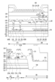
도 1은 본 발명에 따른 표시 장치를 나타내는 블럭도이다.
도 2는 도 1에서 선"I-I'"를 따라 절취한 표시 장치를 나타내는 단면도이다.
도 3a 및 도 3b는 도 1에 도시된 액티브 영역에 배치되는 서브 화소들을 나타내는 평면도이다.
도 4a 및 도 4b는 도 1에 도시된 벤딩 영역에 배치되는 신호 링크의 실시예들을 나타내는 평면도이다.
도 5a 및 도 5b는 도 1에 도시된 표시 장치의 각 서브 화소를 설명하기 위한 회로도들이다.
도 6은 도 5b에 도시된 서브 화소를 나타내는 평면도이다.
도 7은 도 6에서 선 Ⅱ-Ⅱ', Ⅲ-Ⅲ', Ⅳ-Ⅳ', Ⅴ-Ⅴ', Ⅵ-Ⅵ'를 따라 절취한 유기 발광 표시 장치를 나타내는 단면도이다.
도 8a 내지 도 8c는 도 7에 도시된 스토리지 커패시터의 다른 실시예들을 나타내는 단면도들이다.
도 9a 및 도 9b는 도 7에 도시된 벤딩 영역의 다른 실시예들을 나타내는 단면도들이다.
도 10a 내지 도 10m은 도 7에 도시된 유기 발광 표시 장치의 제조 방법을 설명하기 위한 단면도들이다.1 is a block diagram illustrating a display device according to the present invention.
FIG. 2 is a cross-sectional view of the display device taken along line “I-I'” in FIG. 1.
3A and 3B are plan views illustrating sub-pixels disposed in the active area illustrated in FIG. 1.
4A and 4B are plan views illustrating embodiments of a signal link disposed in the bending area shown in FIG. 1.
5A and 5B are circuit diagrams for describing each sub-pixel of the display device illustrated in FIG. 1.
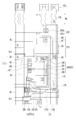
6 is a plan view illustrating the sub-pixel shown in FIG. 5B.
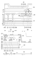
7 is a cross-sectional view illustrating an organic light emitting display device taken along lines II-II', III-III', IV-IV', V-V', and VI-VI' in FIG. 6.
8A to 8C are cross-sectional views illustrating other embodiments of the storage capacitor shown in FIG. 7.
9A and 9B are cross-sectional views illustrating other embodiments of the bending area illustrated in FIG. 7.
10A to 10M are cross-sectional views illustrating a method of manufacturing the organic light emitting display device illustrated in FIG. 7.
이하, 첨부된 도면을 참조하여 본 발명에 따른 실시 예를 상세하게 설명하기로 한다.Hereinafter, exemplary embodiments according to the present invention will be described in detail with reference to the accompanying drawings.
도 1은 본 발명에 따른 표시 장치를 나타내는 평면도이며, 도 2는 본 발명에 따른 표시 장치를 나타내는 단면도이다.1 is a plan view showing a display device according to the present invention, and FIG. 2 is a cross-sectional view showing a display device according to the present invention.
도 1 및 도 2에 도시된 표시 장치는 표시 패널(200)과, 게이트 구동부(202) 및 데이터 구동부(204)를 구비한다.The display device illustrated in FIGS. 1 and 2 includes a
표시 패널(200)은 기판(101) 상에 마련되는 액티브 영역(AA)과, 액티브 영역(AA)의 주변에 배치되는 비액티브 영역(NA)으로 구분된다. 기판(101)은 벤딩이 가능하도록 가요성(flexibility)을 가지는 플라스틱 재질로 형성된다. 예를 들어, 기판은 PI(Polyimide), PET(polyethylene terephthalate), PEN(polyethylene naphthalate), PC(polycarbonate), PES(polyethersulfone), PAR(polyarylate), PSF(polysulfone), COC(ciclic-olefin copolymer) 등의 재질로 형성된다.The
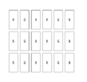
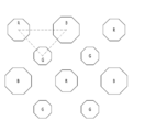
액티브 영역(AA)은 매트릭스 형태로 배열된 단위 화소를 통해 영상을 표시한다. 단위 화소는 적색(R), 녹색(G) 및 청색(B) 서브 화소로 구성되거나, 적색(R), 녹색(G), 청색(B) 및 백색(W) 서브 화소로 구성된다. 예를 들어, 도 3a에 도시된 바와 같이 적색(R), 녹색(G) 및 청색(B) 서브 화소가 가상의 동일 수평 라인에 일렬로 배열되거나, 도 3b에 도시된 바와 같이 적색(R), 녹색(G) 및 청색(B) 서브 화소가 서로 이격되게 배치되어 가상의 삼각형 구조로 배열된다.The active area AA displays an image through unit pixels arranged in a matrix form. The unit pixel is composed of red (R), green (G), and blue (B) sub-pixels, or red (R), green (G), blue (B), and white (W) sub-pixels. For example, as shown in FIG. 3A, red (R), green (G), and blue (B) sub-pixels are arranged in a line in a virtual identical horizontal line, or red (R) as shown in FIG. 3B. , Green (G) and blue (B) sub-pixels are spaced apart from each other and arranged in a virtual triangular structure.
각 서브 화소는 산화물 반도체층을 가지는 박막트랜지스터 및 다결정 반도체층을 가지는 박막트랜지스터 중 적어도 어느 하나를 포함한다. 이러한 산화물 반도체층을 가지는 박막트랜지스터 및 다결정 반도체층을 가지는 박막트랜지스터는 비정질 반도체층을 가지는 박막트랜지스터보다 전자 이동도가 높아 고해상도 및 저전력 구현이 가능해진다.Each sub-pixel includes at least one of a thin film transistor having an oxide semiconductor layer and a thin film transistor having a polycrystalline semiconductor layer. The thin film transistor having the oxide semiconductor layer and the thin film transistor having the polycrystalline semiconductor layer have higher electron mobility than the thin film transistor having the amorphous semiconductor layer, thereby realizing high resolution and low power.
비표시 영역(NA)에는 데이터 구동부(204) 및 게이트 구동부(202) 중 적어도 어느 하나가 배치될 수도 있다.At least one of the
스캔 구동부(202)는 표시 패널(200)의 스캔 라인을 구동한다. 이 스캔 구동부(202)는 산화물 반도체층을 가지는 박막트랜지스터 및 다결정 반도체층을 가지는 박막트랜지스터 중 적어도 어느 하나를 이용하여 구성된다. 이 때, 스캔 구동부(202)의 박막트랜지스터는 액티브 영역(AA)의 각 서브 화소에 배치된 적어도 하나의 박막트랜지스터와 동일 공정으로 동시에 형성된다.The
데이터 구동부(204)는 표시 패널(200)의 데이터 라인을 구동한다. 이 데이터 구동부(204)는 칩 형태로 기판(101) 상에 실장되거나, 신호 전송 필름(206) 상에 칩 형태로 실장되어 표시 패널(200)의 비액티브 영역(NA)에 부착된다. 이 신호 전송 필름(206)과 전기적으로 접속되기 위해 비액티브 영역(NA)에는 도 4a 및 도 4b에 도시된 바와 같이 다수의 신호 패드(PAD)가 배치된다. 이 신호 패드(PAD)를 통해 데이터 구동부(204), 스캔 구동부(202), 전원부(도시하지 않음) 및 타이밍 제어부(도시하지 않음)에서 생성된 구동 신호가 액티브 영역(AA)에 배치되는 신호 라인에 공급된다.The
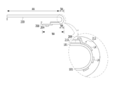
이러한 비액티브 영역(NA)은 표시 패널(200)을 구부리거나 접을 수 있는 벤딩 영역(BA)을 포함한다. 벤딩 영역(BA)은 신호 패드(PAD), 스캔 구동부(202) 및 데이터 구동부(204)와 같이 표시 기능을 하지 않는 영역을 액티브 영역(AA)의 배면으로 위치시키기 위해 벤딩되는 영역에 해당한다. 이 벤딩 영역(BA)은 도 1에 도시된 바와 같이 액티브 영역(AA)과 데이터 구동부(204) 사이에 해당하는 비액티브 영역(NA)의 상측 내에 배치된다. 이외에도 벤딩 영역(BA)은 비액티브 영역(NA)의 상하좌우측 중 적어도 한측 내에 배치될 수도 있다. 이에 따라, 표시 장치의 전체 화면에서 액티브 영역(AA)이 차지하는 면적이 최대화되고 비액티브 영역(NA)에 해당하는 면적이 최소화된다.The inactive area NA includes a bending area BA that can bend or fold the
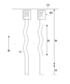
이러한 벤딩 영역(BA)에 배치되는 신호 링크(LK)는 신호 패드(PAD)와 액티브 영역(AA)에 배치되는 신호 라인을 접속시킨다. 이러한 신호 링크(LK)는 벤딩 방향(BD)을 따라 직선 형태로 형성되는 경우, 가장 큰 벤딩 스트레스를 받아 신호 링크(LK)에는 크랙 또는 단선이 발생될 수 있다. 따라서, 본 발명의 신호 링크(LK)는 벤딩 방향(BD)에 교차하는 방향으로 면적을 넓혀 벤딩 스트레스를 최소화하도록 한다. 이를 위해, 신호 링크(LK)는 도 4a에 도시된 바와 같이 지그재그 형태 또는 정현파 형태로 형성되거나, 도 4b에 도시된 바와 같이 중앙 영역이 빈 다수개의 마름모 형상이 일렬로 서로 연결된 형태로 형성된다.The signal link LK disposed in the bending area BA connects the signal pad PAD and the signal line arranged in the active area AA. When the signal link LK is formed in a linear shape along the bending direction BD, cracks or disconnections may occur in the signal link LK under the greatest bending stress. Therefore, the signal link LK of the present invention increases the area in a direction crossing the bending direction BD to minimize bending stress. To this end, the signal link LK is formed in a zigzag shape or a sinusoidal wave shape as shown in FIG. 4A, or a plurality of rhombus shapes having a central region as shown in FIG. 4B are formed in a row connected to each other.
이러한 벤딩 영역(BA)에 배치되는 신호 링크(LK)는 신호 패드(PAD)와 액티브 영역(AA)에 배치되는 신호 라인을 접속시킨다. 이러한 신호 링크(LK)는 벤딩 방향(BD)을 따라 직선 형태로 형성되는 경우, 가장 큰 벤딩 스트레스를 받아 신호 링크(LK)에는 크랙 또는 단선이 발생될 수 있다. 따라서, 본 발명의 신호 링크(LK)는 벤딩 방향(BD)에 교차하는 방향으로 면적을 넓혀 벤딩 스트레스를 최소화하도록 한다. 이를 위해, 신호 링크(LK)는 도 4a에 도시된 바와 같이 지그재그 형태 또는 정현파 형태로 형성되거나, 도 4b에 도시된 바와 같이 중앙 영역이 빈 다수개의 마름모 형상이 일렬로 서로 연결된 형태로 형성된다.The signal link LK disposed in the bending area BA connects the signal pad PAD and the signal line arranged in the active area AA. When the signal link LK is formed in a linear shape along the bending direction BD, cracks or disconnections may occur in the signal link LK under the greatest bending stress. Therefore, the signal link LK of the present invention increases the area in a direction crossing the bending direction BD to minimize bending stress. To this end, the signal link LK is formed in a zigzag shape or a sinusoidal wave shape as shown in FIG. 4A, or a plurality of rhombus shapes having a central region as shown in FIG. 4B are formed in a row connected to each other.
또한, 벤딩 영역(BA)에는 도 2에 도시된 바와 같이 벤딩 영역(BA)이 쉽게 벤딩되도록 적어도 하나의 개구부(212)가 배치된다. 이 개구부(212)는 벤딩 영역(BA)에 배치되는 크랙을 유발하는 다수의 무기 절연층(210)을 제거함으로써 형성된다. 구체적으로, 기판(101)이 벤딩되면, 벤딩 영역(BA)에 배치되는 무기 절연층(210)에는 지속적인 벤딩 스트레스가 가해지게 된다. 이 무기 절연층(210)은 유기 절연 재질에 비해 탄성력이 낮으므로, 무기 절연층(210)에는 크랙이 발생되기 쉽다. 무기 절연층(210)에 발생된 크랙은 무기 절연층(210)을 따라 액티브 영역(AA)으로 전파되어 라인 결함 및 소자 구동 불량이 발생된다. 따라서, 벤딩 영역(BA)에는 무기 절연층(210)보다 탄성력이 높은 유기 절연 재질로 이루어진 적어도 한 층의 평탄화층(208)이 배치된다. 이 평탄화층(208)은 기판(101)이 벤딩되면서 발생되는 벤딩 스트레스를 완화시키므로 크랙이 발생되는 것을 방지할 수 있다. 이러한 벤딩 영역(BA)의 개구부(212)는 액티브 영역(AA)에 배치되는 다수의 컨택홀 중 적어도 어느 하나의 컨택홀과 동일한 마스크 공정을 통해 형성되므로 구조 및 공정을 단순화할 수 있다.In addition, at least one
이와 같이 구조 및 공정을 단순화할 수 있는 표시 장치는 액정 표시 장치 또는 유기 발광 표시 장치 등 박막트랜지스터가 필요한 표시 장치에 적용될 수 있다. 이하에서는, 구조 및 공정을 단순화할 수 있는 표시 장치를 유기 발광 표시 장치에 적용한 본 발명의 실시 예를 설명하기로 한다.The display device capable of simplifying the structure and process as described above may be applied to a display device requiring a thin film transistor, such as a liquid crystal display device or an organic light emitting display device. Hereinafter, an embodiment of the present invention in which a display device capable of simplifying a structure and a process is applied to an organic light emitting display device will be described.
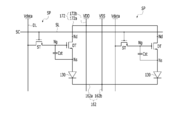
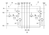
유기 발광 표시 장치의 각 서브 화소들(SP) 각각은 도 5a 및 도 5b에 도시된 바와 같이 화소 구동 회로와, 화소 구동 회로와 접속되는 발광 소자(130)를 구비한다.Each of the sub-pixels SP of the organic light-emitting display device includes a pixel driving circuit and a light-emitting
화소 구동 회로는 도 5a에 도시된 바와 같이 2개의 박막트랜지스터(ST,DT)와, 1개의 스토리지 커패시터(Cst)를 가지는 2T1C구조로 이루어지나, 도 5b및 도 6에 도시된 바와 같이 4개의 박막트랜지스터(ST1,ST2,ST3,DT)와, 1개의 스토리지 커패시터(Cst)를 가지는 4T1C 구조로 이루어진다. 여기서, 화소 구동 회로는 도 5a 및 도 5b의 구조에 한정되지 않고 다양한 구성의 화소 구동 회로가 이용될 수 있다.The pixel driving circuit consists of a 2T1C structure having two thin film transistors (ST, DT) and one storage capacitor (Cst) as shown in FIG. 5A, but four thin films as shown in FIGS. 5B and 6. It is made of a 4T1C structure having transistors ST1, ST2, ST3, DT and one storage capacitor Cst. Here, the pixel driving circuit is not limited to the structures of FIGS. 5A and 5B, and a pixel driving circuit having various configurations may be used.
도 5a에 도시된 화소 구동 회로의 스토리지 커패시터(Cst)는 게이트 노드(Ng)와 소스 노드(Ns) 사이에 접속되어 발광 기간 동안 게이트 노드(Ng)와 소스 노드(Ns) 간 전압을 일정하게 유지시킨다. 구동 트랜지스터(DT)는 게이트 노드(Ng)에 접속된 게이트 전극과, 드레인 노드(Nd)에 접속된 드레인 전극과, 발광 소자(130)에 접속된 소스 전극을 구비한다. 이 구동 트랜지스터(DT)는 게이트 노드(Ng)와 소스 노드(Ns) 간 전압에 따라 구동 전류의 크기를 제어한다. 스위칭 트랜지스터(ST)는 스캔 라인(SL)에 접속된 게이트 전극과, 데이터 라인(DL)에 접속된 드레인 전극과, 게이트 노드(Ng)에 접속된 소스 전극을 구비한다. 이 스위칭 트랜지스터(ST1)는 스캔 라인(SL1)으로부터의 스캔 제어 신호(SC)에 응답하여 턴온되어 데이터 라인(DL)으로부터의 데이터 전압(Vdata)을 게이트 노드(Ng)에 공급한다. 발광 소자(130)는 구동 트랜지스터(DT)의 소스 전극에 연결된 소스 노드(Ns)와 저전위 공급 라인(162) 사이에 접속되어 구동 전류에 따라 발광한다.The storage capacitor Cst of the pixel driving circuit shown in FIG. 5A is connected between the gate node Ng and the source node Ns to maintain a constant voltage between the gate node Ng and the source node Ns during the light emission period. Order. The driving transistor DT includes a gate electrode connected to the gate node Ng, a drain electrode connected to the drain node Nd, and a source electrode connected to the
도 5b에 도시된 화소 구동 회로는 도 5a에 도시된 화소 구동 회로와 대비하여, 데이터 라인(DL)과 접속된 제1 스위칭 트랜지스터(ST1)의 소스 전극이 소스 노드(Ns)에 연결되고, 제2 및 제3 스위칭 트랜지스터(ST2,ST3)를 더 구비하는 것을 제외하고는 실질적으로 동일한 구성을 구비한다. 따라서, 동일한 구성에 대한 상세한 설명은 생략하기로 한다.In the pixel driving circuit shown in FIG. 5B, the source electrode of the first switching transistor ST1 connected to the data line DL is connected to the source node Ns, in contrast to the pixel driving circuit shown in FIG. 5A. The second and third switching transistors ST2 and ST3 have substantially the same configuration, except that they are further provided. Therefore, detailed description of the same configuration will be omitted.
도 5b 및 도 6에 도시된 제1 스위칭 트랜지스터(ST1)은 제1 스캔 라인(SL1)에 접속된 게이트 전극(152)과, 데이터 라인(DL)에 접속된 드레인 전극(158)과, 소스 노드(Ns)에 접속된 소스 전극(156)과, 소스 및 드레인 전극(156,158) 사이에 채널을 형성하는 반도체층(154)을 구비한다. 이 제1 스위칭 트랜지스터(ST1)는 제1 스캔 라인(SL1)으로부터의 스캔 제어 신호(SC1)에 응답하여 턴온되어 데이터 라인(DL)으로부터의 데이터 전압(Vdata)을 소스 노드(Ns)에 공급한다.The first switching transistor ST1 illustrated in FIGS. 5B and 6 includes a
제2 스위칭 트랜지스터(ST2)는 제2 스캔 라인(SL2)에 접속된 게이트 전극(GE)과, 레퍼런스 라인(RL)에 접속된 드레인 전극(DE)과, 게이트 노드(Ng)에 접속된 소스 전극(SE)과, 소스 및 드레인 전극(SE,DE) 사이에 채널을 형성하는 반도체층(ACT)을 구비한다. 이 제2 스위칭 트랜지스터(ST2)는 제2 스캔 라인(SL2)으로부터의 스캔 제어 신호(SC2)에 응답하여 턴온되어 레퍼런스 라인(RL)으로부터의 레퍼런스 전압(Vref)을 게이트 노드(Ng)에 공급한다.The second switching transistor ST2 includes a gate electrode GE connected to the second scan line SL2, a drain electrode DE connected to the reference line RL, and a source electrode connected to the gate node Ng. A semiconductor layer ACT forming a channel between (SE) and the source and drain electrodes SE and DE is provided. The second switching transistor ST2 is turned on in response to the scan control signal SC2 from the second scan line SL2 to supply the reference voltage Vref from the reference line RL to the gate node Ng. .
제3 스위칭 트랜지스터(ST3)은 발광 제어 라인(EL)에 접속된 게이트 전극(GE)과, 고전위 공급 라인(172)에 접속된 드레인 전극(DE)과, 드레인 노드(Nd)에 접속된 소스 전극(SE), 소스 및 드레인 전극(SE,DE) 사이에 채널을 형성하는 반도체층(ACT)을 구비한다. 이 제3 스위칭 트랜지스터(ST3)는 발광 제어 라인(EL)으로부터의 발광 제어 신호(EN)에 응답하여 턴온되어, 고전위 공급 라인(172)으로부터의 고전위 전압(VDD)을 드레인 노드(Nd)에 공급한다.The third switching transistor ST3 includes a gate electrode GE connected to the emission control line EL, a drain electrode DE connected to the high
이와 같은 화소 구동 회로에 포함되는 고전위 공급 라인(172) 및 저전위 공급 라인(162) 각각은 적어도 2개의 서브 화소들이 공유하도록 메쉬 형태로 형성된다. 이를 위해, 고전위 공급 라인(172)은 서로 교차하는 제1 및 제2 고전위 공급 라인(172a,172b)을 구비하며, 저전위 공급 라인(162)은 서로 교차하는 제1 및 제2 저전위 공급 라인(162a,162b)을 구비한다.Each of the high
제2 고전위 공급 라인(172b) 및 제2 저전위 공급 라인(162b) 각각은 데이터 라인(DL)과 나란하게 배치되며 적어도 2개의 서브 화소 당 하나씩 형성된다. 이 제2 고전위 공급 라인(172b) 및 제2 저전위 공급 라인(162b)은 도 5a 및 도 5b에 도시된 바와 같이 좌우로 나란하게 배치되거나, 도 6에 도시된 바와 같이 서로 중첩되도록 상하로 나란하게 배치된다.Each of the second high
제1 고전위 공급 라인(172a)은 제2 고전위 공급 라인(172b)과 전기적으로 접속되며 스캔 라인(SL)과 나란하게 배치된다. 이 제1 고전위 공급 라인(172a)은 제2 고전위 공급 라인들(172b) 사이에서 제2 고전위 공급 라인(172b) 과 교차하도록 제2 고전위 공급 라인(172b) 에서 분기되어 형성된다. 이에 따라, 제1 고전위 공급 라인(172a)은 제2 고전위 공급 라인(172b)의 저항을 보상함으로써 고전위 공급 라인(172)의 전압 강하(IR drop)를 최소화할 수 있다.The first high
제1 저전위 공급 라인(162a)은 제2 저전위 공급 라인(162b) 과 전기적으로 접속되며 스캔 라인(SL)과 나란하게 배치된다. 이 제1 저전위 공급 라인(162a)은 제2 저전위 공급 라인들(162b) 사이에서 제2 저전위 공급 라인(162b) 과 교차하도록 제2 저전위 공급 라인(162b) 에서 분기되어 형성된다. 이에 따라, 제1 저전위 공급 라인(162a)은 제2 저전위 공급 라인(162b)의 저항을 보상함으로써 저전위 공급 라인(162)의 전압 강하(IR drop)를 최소화할 수 있다.The first low
이와 같이 고전위 공급 라인(172) 및 저전위 공급 라인(162)은 메쉬 형태로 형성되므로 수직 방향으로 배치되는 제2 고전위 공급 라인(172b) 및 제2 저전위 공급 라인(162b)의 개수를 저감할 수 있으며, 개수가 저감 된 만큼 더 많은 서브 화소를 배치할 수 있으므로 개구율 및 해상도가 높아진다.As described above, since the high
이와 같은 화소 구동 회로에 포함된 다수의 트랜지스터 중 어느 하나의 트랜지스터는 다결정 반도체층을 포함하고, 나머지 트랜지스터는 산화물 반도체층을 포함한다. 도 5a에 도시된 화소 구동 회로의 스위칭 트랜지스터(ST)는 도 7에 도시된 바와 같이 다결정 반도체층(154)을 가지는 제1 박막트랜지스터(150)로 형성되고, 구동트랜지스터(DT)는 산화물 반도체층(104)을 가지는 제2 박막트랜지스터(100)로 형성된다. 그리고, 도 5b 및 도 6에 도시된 화소 구동 회로의 제 1 및 제3 스위칭 트랜지스터(ST1,ST3)는 다결정 반도체층(154)을 가지는 1 박막트랜지스터(150)로 형성되고, 제2 스위칭 트랜지스터(ST2) 및 구동트랜지스터(DT)는 산화물 반도체층(104)을 가지는 제2 박막트랜지스터(100)로 형성된다. 이와 같이, 본 발명에서는 산화물 반도체층(104)을 가지는 제2 박막트랜지스터(100)를 각 서브화소의 구동 트랜지스터(DT)에 적용하고, 다결정 반도체층(154)을 가지는 제1 박막트랜지스터(150)를 각 서브 화소의 스위칭 소자(ST)로 적용함으로써 소비전력을 감소시킬 수 있다.Any one of the plurality of transistors included in the pixel driving circuit includes a polycrystalline semiconductor layer, and the remaining transistors include an oxide semiconductor layer. The switching transistor ST of the pixel driving circuit shown in FIG. 5A is formed of a first
도 6 및 도 7에 도시된 제1 박막트랜지스터(150)는 다결정 반도체층(154)과, 제1 게이트 전극(152)과, 제1 소스 전극(156)과, 제1 드레인 전극(158)을 구비한다.The first
다결정 반도체층(154)은 하부 버퍼층(112) 상에 형성된다. 이러한 다결정 반도체층(154)은 채널 영역, 소스 영역 및 드레인 영역를 구비한다. 채널 영역은 하부 게이트 절연막(114)을 사이에 두고 제1 게이트 전극(152)과 중첩되어 제1 소스 및 제1 드레인 전극(156,158) 사이의 채널영역을 형성한다. 소스 영역은 제1 소스 전극(156)과 제1 소스 컨택홀(160S)을 통해 전기적으로 접속된다. 드레인 영역은 제1 드레인 전극(158)과 제1 드레인 컨택홀(160D)을 통해 전기적으로 접속된다. 다결정 반도체층(154)은 비정질 반도체층 및 산화물 반도체층(104)보다 이동도가 높아, 에너지 소비 전력이 낮고 신뢰성이 우수하므로, 각 서브 화소의 스위칭 트랜지스터(ST), 스캔 라인(SL)을 구동하는 게이트 구동부(202)에 적용하기에 적합하다. 이러한 다결정 반도체층(154)과 기판(101) 사이에는 멀티 버퍼층(140)과, 하부 버퍼층(112)이 배치된다. 멀티 버퍼층(140)은 기판(101)에 침투한 수분 및/또는 산소가 확산되는 것을 지연시킨다. 이 멀티 버퍼층(140)은 질화실리콘(SiNx) 및 산화실리콘(SiOx)이 적어도 1회 교대로 적층되어 이루어진다. 하부 버퍼층(112)은 다결정 반도체층(154)을 보호하며, 기판(101)으로부터 유입되는 다양한 종류의 결함을 차단하는 기능을 수행한다. 이 하부 버퍼층(112)는 a-Si, 질화실리콘(SiNx) 또는 산화실리콘(SiOx) 등으로 형성될 수 있다.The
제1 게이트 전극(152)은 하부 게이트 절연막(114) 상에 형성된다. 이 제1 게이트 전극(152)은 하부 게이트 절연막(114)을 사이에 두고 다결정 반도체층(154)의 채널 영역과 중첩된다. 제1 게이트 전극(152)은 스토리지 하부 전극(182)과 동일 재질, 예를 들어, 몰리브덴(Mo), 알루미늄(Al), 크롬(Cr), 금(Au), 티타늄(Ti), 니켈(Ni), 네오디뮴(Nd) 및 구리(Cu) 중 어느 하나 또는 이들의 합금으로 이루어진 단일층 또는 다중층일 수 있으나, 이에 한정되지 않는다.The
다결정 반도체층(154) 상에 위치하는 제1 및 제2 하부 층간 절연막(116,118)은 상부 층간 절연막(124)에 비해 수소 입자 함유량이 높은 무기막으로 형성된다. 예를 들어, 제1 및 제2 하부 층간 절연막(116,118)은 NH3가스를 이용한 증착 공정으로 형성되는 질화 실리콘(SiNx)으로 이루어지고, 상부 층간 절연막(124)은 산화 실리콘(SiOx)로 형성된다. 제1 및 제2 하부 층간 절연막(116,118)에 포함된 수소 입자는 수소화 공정시 다결정 반도체층(154)으로 확산되어 다결정 반도체층(154) 내의 공극을 수소로 채워준다. 이에 따라, 다결정 반도체층(154)은 안정화를 이룰 수 있어 제1 박막트랜지스터(150)의 특성 저하를 방지할 수 있다.The first and second lower
제1 소스 전극(156)은 하부 게이트 절연막(114), 제1 및 제2 하부 층간 절연막(116,118), 상부 버퍼층(122) 및 상부 층간 절연막(124)을 관통하는 제1 소스 컨택홀(160S)을 통해 다결정 반도체층(154)의 소스 영역과 접속된다. 제1 드레인 전극(158)은 제1 소스 전극(156)과 마주하며, 하부 게이트 절연막(114), 제1 및 제2 하부 층간 절연막(116,118), 상부 버퍼층(122) 및 상부 층간 절연막(124)을 관통하는 제1 드레인 컨택홀(160D)을 통해 다결정 반도체층(154)의 드레인 영역과 접속된다. 이러한 제1 소스 및 제1 드레인 전극(156,158)은 스토리지 공급 라인(186)과 동일 평면 상에 동일 재질로 형성되므로, 제1 소스 및 제1 드레인 전극(156,158)은 스토리지 공급 라인(186)과 동일 마스크 공정으로 동시에 형성 가능하다.The
이러한 제1 박막트랜지스터(150)의 다결정 반도체층(154)의 활성화 및 수소화 공정 이후에 제2 박막트랜지스터(100)의 산화물 반도체층(104)이 형성된다. 즉, 산화물 반도체층(104)은 다결정 반도체층(154) 상부에 위치한다. 이에 따라, 산화물 반도체층(104)은 다결정 반도체층(154)의 활성화 및 수소화 공정의 고온 분위기에 노출되지 않으므로 산화물 반도체층(104)의 손상을 방지할 수 있어 신뢰성이 향상된다.After the activation and hydrogenation process of the
제2 박막트랜지스터(150)는 제1 박막트랜지스터(100)와 이격되도록 기판(101) 상에 배치된다. 이러한 제2 박막트랜지스터(100)는 제2 게이트 전극(102)과, 산화물 반도체층(104)과, 제2 소스 전극(106)과, 제2 드레인 전극(108)을 구비한다.The second
제2 게이트 전극(102)은 상부 게이트 절연 패턴(146)을 사이에 두고 산화물 반도체층(104)과 중첩된다. 이러한 제2 게이트 전극(102)은 제1 고전압 공급 라인(172a)과 동일 평면인 상부 게이트 절연 패턴(146) 상에서 제1 고전압 공급 라인(172a) 동일 재질로 형성된다. 이에 따라, 제2 게이트 전극(102) 및 제1 고전압 공급 라인(172a)은 동일 마스크 공정으로 형성 가능하므로 마스크 공정을 저감할 수 있다.The
산화물 반도체층(104)은 상부 버퍼층(122) 상에 제2 게이트 전극(102)과 중첩되게 형성되어 제2 소스 및 제2 드레인 전극(106,108) 사이에 채널을 형성한다. 이 산화물 반도체층(104)은 Zn, Cd, Ga, In, Sn, Hf, Zr 중 선택된 적어도 하나 이상의 금속을 포함하는 산화물로 형성된다. 이러한 산화물 반도체층(104)을 포함하는 제2 박막 트랜지스터(100)는 다결정 반도체층(154)을 포함하는 제1 박막 트랜지스터(150)보다 높은 전하 이동도 및 낮은 누설 전류 특성의 장점을 가지므로 온(On) 시간이 짧고 오프(Off) 시간을 길게 유지하는 스위칭 및 구동 박막트랜지스터(ST,DT)에 적용하는 것이 바람직하다.The
이러한 산화물 반도체층(104)의 상부 및 하부와 인접한 상부 층간 절연막(124) 및 상부 버퍼층(122)은 하부 층간 절연막(116,118)에 비해 수소 입자 함유량이 낮은 무기막으로 형성된다. 예를 들어, 상부 층간 절연막(124) 및 상부 버퍼층(122)은 산화 실리콘(SiOx)로 형성되고 하부 층간 절연막(116,118)은 질화실리콘(SiNx)로 형성된다. 이에 따라, 산화물 반도체층(104)의 열처리 공정시 하부 층간 절연막(116,118) 내의 수소 및 다결정 반도체층(154)의 수소들이 산화물 반도체층(104)으로 확산되는 것을 방지할 수 있다.The upper
제2 소스 및 제2 드레인 전극(106,108)은 상부 층간 절연막(124) 상에 몰리브덴(Mo), 알루미늄(Al), 크롬(Cr), 금(Au), 티타늄(Ti), 니켈(Ni), 네오디뮴(Nd) 및 구리(Cu) 중 어느 하나 또는 이들의 합금으로 이루어진 단일층 또는 다중층일 수 있으나, 이에 한정되지 않는다.The second source and
제2 소스 전극(106)은 상부 층간 절연막(124)을 관통하는 제2 소스 컨택홀(110S)을 통해 산화물 반도체층(104)의 소스 영역과 접속되며, 제2 드레인 전극(108)은 상부 층간 절연막(124)을 관통하는 제2 드레인 컨택홀(110D)을 통해 산화물 반도체층(104)의 드레인 영역과 접속된다. 그리고, 제2 소스 및 제2 드레인 전극(106,108)은 산화물 반도체층(104)의 채널영역을 사이에 두고 서로 마주보도록 형성된다.The
스토리지 커패시터(Cst)는 도 7에 도시된 바와 같이 상부 층간 절연막(124)을 사이에 두고 구동 트랜지스터의 게이트 전극(102)과, 구동 트랜지스터의 소스 전극(106)이 중첩됨으로써 형성된다.The storage capacitor Cst is formed by overlapping the
이외에도 스토리지 커패시터(Cst)는 도 8a 내지 도 8c에 도시된 바와 같이 병렬로 연결된 2개 이상의 스토리지 커패시터를 구비할 수도 있다.In addition, the storage capacitor Cst may include two or more storage capacitors connected in parallel as illustrated in FIGS. 8A to 8C.
도 8a에 도시된 스토리지 커패시터(Cst)는 병렬로 연결된 제1 및 제2 스토리지 커패시터(Cst1,Cst2)를 구비한다.The storage capacitor Cst shown in FIG. 8A includes first and second storage capacitors Cst1 and Cst2 connected in parallel.
제1 스토리지 커패시터(Cst1)는 상부 층간 절연막(124)을 사이에 두고 구동 트랜지스터의 게이트 전극(102)과, 구동 트랜지스터의 소스 전극(106)이 중첩됨으로써 형성된다.The first storage capacitor Cst1 is formed by overlapping the
제2 스토리지 커패시터(Cst2)는 제1 및 제2 하부 층간 절연막(116,118) 및 상부 버퍼층(122)을 사이에 두고 차광층(178) 및 구동 트랜지스터의 게이트 전극(102)이 중첩됨으로써 형성된다. 이 때, 차광층(178)은 구동 트랜지스터의 소스 전극(106)과 전기적으로 연결된다.The second storage capacitor Cst2 is formed by overlapping the
이에 따라, 제1 및 제2 스토리지 커패시터(Cst1,Cst2)의 일단은 구동 트랜지스터의 게이트 전극(102)에 접속되고, 타단은 구동 트랜지스터의 소스 전극(106)에 접속됨으로써 제1 및 제2 스토리지 커패시터(Cst1,Cst2)는 병렬로 접속된다. 이에 따라, 도 8a에 도시된 스토리지 커패시터의 총 용량값은 도 7에 도시된 스토리지 커패시터의 총용량값에 비해 증가시킬수 있다.Accordingly, one end of the first and second storage capacitors Cst1 and Cst2 is connected to the
도 8b에 도시된 스토리지 커패시터는 병렬로 연결된 제1 및 제2 스토리지 커패시터(Cst1,Cst2)를 구비한다.The storage capacitor illustrated in FIG. 8B includes first and second storage capacitors Cst1 and Cst2 connected in parallel.
제1 스토리지 커패시터(Cst1)는 상부 층간 절연막(124)을 사이에 두고 제2 게이트 전극(102)과, 제2 소스 전극(106)이 중첩됨으로써 형성된다.The first storage capacitor Cst1 is formed by overlapping the
제2 스토리지 커패시터(Cst2)는 보호막(166)을 사이에 두고 스토리지 전극(170) 및 제2 소스 전극(102)이 중첩됨으로써 형성된다. 이 때, 스토리지 전극(170)은 제2 게이트 전극(102)과 전기적으로 연결된다.The second storage capacitor Cst2 is formed by overlapping the
스토리지 전극(170)은 스토리지 홀(168)에 의해 노출된 보호막(166) 상에 배치됨으로써 스토리지 전극(170)은 보호막(166)만을 사이에 두고 제2 소스 전극(106)과 중첩된다. 이 스토리지 전극(170)은 화소 연결 전극(142)과 동일 재질로 이루어진다. 이러한 스토리지 전극(170)과 제2 소스 전극(106)이 한 층의 보호막(166)을 사이에 두고 중첩되는 도 8b에 도시된 제2 스토리지 커패시터(Cst2)는 도 8a에 도시된 제2 게이트 전극(102) 및 차광층(178)이 2층 이상의 절연막(116,118,122)을 사이에 두고 중첩되는 제2 스토리지 커패시터(Cst2)에 비해 용량값이 증가된다.The
이에 따라, 도 8b에 도시된 스토리지 커패시터의 총용량값은 도 8a에 도시된 스토리지 커패시터의 총용량값에 비해 증가된다.Accordingly, the total capacity value of the storage capacitor shown in FIG. 8B is increased compared to the total capacity value of the storage capacitor shown in FIG. 8A.
도 8c에 도시된 스토리지 커패시터는 병렬로 연결된 제1 내지 제3 스토리지 커패시터(Cst1,Cst2,Cst3)를 구비한다.The storage capacitor illustrated in FIG. 8C includes first to third storage capacitors Cst1, Cst2, and Cst3 connected in parallel.
제1 스토리지 커패시터(Cst1)는 상부 층간 절연막(124)을 사이에 두고 제2 게이트 전극(102)과, 제2 소스 전극(106)이 중첩됨으로써 형성된다.The first storage capacitor Cst1 is formed by overlapping the
제2 스토리지 커패시터(Cst2)는 보호막(166)을 사이에 두고 스토리지 전극(170) 및 제2 소스 전극(102)이 중첩됨으로써 형성된다. 이 때, 스토리지 전극(170)은 제2 게이트 전극(102)과 전기적으로 연결된다. 스토리지 전극(170)은 스토리지 홀(168)에 의해 노출된 보호막(166) 상에 배치됨으로써 스토리지 전극(170)은 보호막(166)만을 사이에 두고 제2 소스 전극(106)과 중첩된다.The second storage capacitor Cst2 is formed by overlapping the
제3 스토리지 커패시터(Cst3)는 제1 및 제2 하부 층간 절연막(116,118)과 상부 버퍼층(122)을 사이에 두고 차광층(178) 및 제2 게이트 전극(102)이 중첩됨으로써 형성된다. 이 때, 차광층(178)은 제2 소스 전극(106)과 전기적으로 연결된다.The third storage capacitor Cst3 is formed by overlapping the
이에 따라, 제1 내지 제3 스토리지 커패시터(Cst1,Cst2,Cst3)의 일단은 제2 게이트 전극(102)에 접속되고, 타단은 제2 소스 전극(106)에 접속됨으로써 제1 내지 제3 스토리지 커패시터(Cst1,Cst2,Cst3)는 병렬로 접속된다. 이에 따라, 도 8c에 도시된 스토리지 커패시터의 총 용량값은 도 7에 도시된 스토리지 커패시터의 총용량값에 비해 증가시킬 수 있다.Accordingly, one end of the first to third storage capacitors Cst1, Cst2, and Cst3 is connected to the
발광 소자(130)는 제2 박막 트랜지스터(150)의 제2 소스 전극(106)과 접속된 애노드 전극(132)과, 애노드 전극(132) 상에 형성되는 적어도 하나의 발광 스택(134)과, 발광 스택(134) 위에 형성된 캐소드 전극(136)을 구비한다.The
애노드 전극(132)은 평탄화층(128)을 관통하는 제2 화소 컨택홀(144)을 통해 노출된 화소 연결 전극(142)과 접속된다. 여기서, 화소 연결 전극(142)은 보호막(166) 및 제1 평탄화층(126)을 관통하는 제1 화소 컨택홀(120)을 통해 노출된 제2 소스 전극(106)과 접속된다.The
애노드 전극(132)은 투명 도전막 및 반사효율이 높은 불투명 도전막을 포함하는 다층 구조로 형성된다. 투명 도전막으로는 인듐-틴-옥사이드(ITO) 또는 인듐-징크-옥사이드(IZO)과 같은 일함수 값이 비교적 큰 재질로 이루어지고, 불투명 도전막으로는 Al, Ag, Cu, Pb, Mo, Ti 또는 이들의 합금을 포함하는 단층 또는 다층 구조로 이루어진다. 예를 들어, 애노드 전극(132)은 투명 도전막, 불투명 도전막 및 투명 도전막이 순차적으로 적층된 구조로 형성되거나, 투명 도전막 및 불투명 도전막이 순차적으로 적층된 구조로 형성된다. 이러한 애노드 전극(132)은 뱅크(138)에 의해 마련된 발광 영역뿐만 아니라 제1 및 제2 트랜지스터(150,100)와 스토리지 커패시터(180,Cst)가 배치된 회로 영역과 중첩되도록 제2 평탄화층(128) 상에 배치됨으로써 발광 면적이 증가된다.The
발광 스택(134)은 애노드 전극(132) 상에 정공 관련층, 유기 발광층, 전자 관련층 순으로 또는 역순으로 적층되어 형성된다. 이외에도 발광 스택(134)은 전하 생성층을 사이에 두고 대향하는 제1 및 제2 발광 스택들을 구비할 수도 있다. 이 경우, 제1 및 제2 발광 스택 중 어느 하나의 유기 발광층은 청색광을 생성하고, 제1 및 제2 발광 스택 중 나머지 하나의 유기 발광층은 노란색-녹색광을 생성함으로써 제1 및 제2 발광 스택을 통해 백색광이 생성된다. 이 발광스택(134)에서 생성된 백색광은 발광 스택(134) 상부에 위치하는 컬러 필터(도시하지 않음)에 입사되므로 컬러 영상을 구현할 수 있다. 이외에도 별도의 컬러 필터 없이 각 발광 스택(134)에서 각 서브 화소에 해당하는 컬러광을 생성하여 컬러 영상을 구현할 수도 있다. 즉, 적색(R) 서브 화소의 발광 스택(134)은 적색광을, 녹색(G) 서브 화소의 발광 스택(134)은 녹색광을, 청색(B) 서브 화소의 발광 스택(134)은 청색광을 생성할 수도 있다.The
뱅크(138)는 애노드 전극(132)을 노출시키도록 형성된다. 이러한 뱅크(138)는 인접한 서브 화소 간 광 간섭을 방지하도록 불투명 재질(예를 들어, 블랙)로 형성될 수도 있다. 이 경우, 뱅크(138)는 칼라 안료, 유기 블랙 및 카본 중 적어도 어느 하나로 이루어진 차광재질을 포함한다.The
캐소드 전극(136)은 발광 스택(134)을 사이에 두고 애노드 전극(132)과 대향하도록 발광 스택(134)의 상부면 및 측면 상에 형성된다. 이 캐소드 전극(136)은 전면 발광형 유기 발광 표시 장치에 적용되는 경우, 인듐-틴-옥사이드(ITO) 또는 인듐-징크-옥사이드(IZO)과 같은 투명 도전막으로 이루어진다.The
이러한 캐소드 전극(136)은 저전압 공급 라인(162)과 전기적으로 접속된다. 저전압 공급 라인(162)은 도 5b 및 도 6에 도시된 바와 같이 서로 교차하는 제1 및 제2 저전위 공급 라인(162a,162b)을 구비한다. 제1 저전위 공급 라인(162a)은 도 7에 도시된 바와 같이 제2 게이트 전극(102)과 동일층인 상부 게이트 절연 패턴(146) 상에, 제2 게이트 전극(102)과 동일 재질로 형성된다. 제2 저전위 공급 라인(162b)은 화소 연결 전극(142)과 동일층인 제1 평탄화층(126) 상에, 화소 연결 전극(142)과 동일 재질로 형성된다. 이 제2 저전위 공급 라인(162b)은 상부 층간 절연막(124), 보호막(166) 및 제1 평탄화층(126)을 관통하도록 형성된 제1 라인 컨택홀(164)을 통해 노출된 제1 저전위 공급 라인(162a)과 전기적으로 접속된다.The
이러한 저전압 공급 라인(162)을 통해 공급되는 저전위 전압(VSS)보다 높은 고전위 전압(VDD)을 공급하는 고전압 공급 라인(172)은 도 5b 및 도 6에 도시된 바와 같이 서로 교차하는 제1 및 제2 고전위 공급 라인(172a,172b)을 구비한다. 제1 고전위 공급 라인(172a)은 도 7에 도시된 바와 같이 제2 게이트 전극(102)과 동일층인 상부 게이트 절연 패턴(146) 상에, 제2 게이트 전극(102)과 동일 재질로 형성된다. 제2 고전위 공급 라인(172b)은 제2 소스 및 드레인 전극(106,108)과 동일층인 상부 층간 절연막(124) 상에, 제2 소스 및 드레인 전극(106,108)과 동일 재질로 형성된다. 이 제2 고전위 공급 라인(172b)은 상부 층간 절연막(124)을 관통하도록 형성된 제2 라인 컨택홀(174)을 통해 노출된 제1 고전위 공급 라인(172a)과 전기적으로 접속된다. 이러한 제2 고전위 공급 라인(172b)은 보호막(166) 및 제1 평탄화층(126)을 사이에 두고 제1 저전위 공급 라인(162b)와 중첩된다. 이 때, 유기 절연 재질의 제1 평탄화층(126) 내에 핀홀이 형성되더라도 무기 절연 재질의 보호막(166)에 의해 제2 고전위 공급 라인(172b)과 제1 저전위 공급 라인(162b)이 쇼트되는 것을 방지할 수 있다.The high
이와 같은 저전위 공급 라인(162), 고전위 공급 라인(172), 데이터 라인(DL), 스캔 라인(SL) 및 발광 제어 라인(EL) 중 적어도 어느 하나와 접속된 신호 링크(176)는 도 7에 도시된 바와 같이 상부 및 하부 개구부(192,194)가 형성된 벤딩 영역(BA)을 가로지르도록 배치된다. 상부 개구부(192)는 상부 층간 절연막(124)의 측면과 상부 버퍼층(122)의 상부면을 노출시킨다. 이 상부 개구부(192)는 상부 층간 절연막(124)을 관통하는 제1 소스 컨택홀(160S)의 상부 영역, 제2 드레인 컨택홀(160D)의 상부 영역, 제2 소스 컨택홀(110S) 및 제2 드레인 컨택홀(110D) 중 적어도 어느 하나와 동일한 깊이(d1)를 가지도록 형성된다. 하부 개구부(194)는 멀티 버퍼층(140), 하부 버퍼층(112), 하부 게이트 절연막(114), 제1 및 제2 하부 층간 절연막(116,118), 상부 버퍼층(122) 각각의 측면을 노출시키도록 형성된다. 이 하부 개구부(194)는 하부 게이트 절연막(114), 제1 및 제2 하부 층간 절연막(116,118), 상부 버퍼층(122)을 관통하는 제1 소스 컨택홀(160S)의 하부 영역 및 제1 드레인 컨택홀(160D)의 하부 영역 중 적어도 어느 하나보다 더 깊은 깊이(d2)를 가지도록 형성되거나, 동일한 깊이(d2)를 가지도록 형성된다. 이에 따라, 벤딩 영역(BA)에서는 상하로 중첩되게 배치되는 상부 및 하부 개구부(192,194)에 의해 멀티 버퍼층(140), 하부 버퍼층(112), 하부 게이트 절연막(114), 제1 및 제2 하부 층간 절연막(116,118), 상부 버퍼층(122) 및 상부 층간 절연막(124)이 제거된다. 즉, 벤딩 영역(BA)에는 크랙을 유발하는 다수의 무기 절연층(140,112,114,116,118,122,124)이 제거됨으로써 크랙 발생없이 기판(101)을 쉽게 벤딩할 수 있다.The
벤딩 영역(BA)에 배치되는 신호 링크(176)는 도 7에 도시된 바와 같이 화소 연결 전극(142)와 동일 마스크 공정으로 화소 연결 전극(142)과 함께 형성될 수 있다. 이 경우, 신호 링크(176)는 화소 연결 전극(142)과 동일 재질로 동일 평면, 즉 제1 평탄화층(126) 및 기판(101) 상에 형성된다. 이러한 제1 평탄화층(126) 및 기판(101) 상에 형성된 신호 링크(176)를 덮도록 신호 링크(176) 상에 제2 평탄화층(128)이 배치되거나, 제2 평탄화층(128)없이 봉지 필름, 또는 무기 및 유기 봉지층의 조합으로 이루어진 봉지 스택의 무기 봉지층이 배치된다.The
이외에도, 신호 링크(176)는 도 9a 및 도 9b에 도시된 바와 같이 소스 및 드레인 전극(106,156,108,158)과 동일 마스크 공정으로 소스 및 드레인 전극(106,156,108,158)과 함께 형성될 수 있다. 이 경우, 신호 링크(176)는 소스 및 드레인 전극(106,156,108,158)과 동일 재질로 동일 평면, 즉 상부 층간 절연막(124) 상에 형성됨과 아울러 기판(101)과 접촉하도록 기판(101) 상에 형성된다. 이 때, 신호 링크(176)는 상부 개구부(192)에 의해 노출된 상부 층간 절연막(124)의 측면과 상부 버퍼층(122)의 상부면에 형성됨과 아울러 하부 개구부(194)에 의해 노출된 멀티 버퍼층(140), 하부 버퍼층(112), 하부 게이트 절연막(114), 제1 및 제2 하부 층간 절연막(116,118), 상부 버퍼층(122)의 측면 상에 형성되므로 계단 형상으로 형성된다. 계단 형상으로 형성된 신호 링크(176)를 덮도록, 신호 링크(176) 상에 제1 및 제2 평탄화층(126,128) 중 적어도 하나가 배치되거나, 제1 및 제2 평탄화층(126,128)없이 봉지 필름 또는 무기 및 유기 봉지층의 조합으로 이루어진 봉지 스택의 무기 봉지층이 배치된다.In addition, the
이외에도 신호 링크(176)는 도 9a 및 도 9b에 도시된 바와 같이 멀티 버퍼층(140) 상에 배치될 수도 있다. 이 때, 신호 링크들(176) 사이에 배치되는 멀티 버퍼층(140)은 크랙 발생없이 벤딩이 용이해지도록 제거됨으로써 신호 링크들(176) 사이에는 기판(101)을 노출시키는 트렌치(196)가 형성된다.In addition, the
도 9a에 도시된 트렌치(196)는 신호 링크들(176) 사이의 멀티 버퍼층(140) 및 기판(101)의 일부를 관통하도록 형성된다. 이러한 신호 링크들(176) 상에는 제1 및 제2 평탄화층(126,128)이 배치된다. 도 9b에 도시된 트렌치(196)는 신호 링크들(176) 사이의 보호막(166), 멀티 버퍼층(140) 및 기판(101)의 일부를 관통하도록 형성된다. 이러한 신호 링크들(176) 상에는 보호막(166), 제1 및 제2 평탄화층(126,128)이 배치된다. 한편, 벤딩 영역(BA)에는 제1 및 제2 평탄화층(126,128)을 관통하는 적어도 하나의 수분 차단홀(도시하지 않음)이 배치될 수도 있다. 이 수분 차단홀은 신호 링크들(176) 사이, 및 신호 링크들(176) 상부 중 적어도 어느 하나에 형성된다. 이 수분 차단홀은 외부로부터의 수분이 신호 링크(176) 상에 배치되는 제1 및 제2 평탄화층(126,128) 중 적어도 어느 하나를 통해 액티브 영역(AA) 내부로 침투하는 것을 방지한다. 또한, 검사 공정시 이용되는 검사 라인(도시하지 않음)은 벤딩 영역(BA)에서 도 7, 도 9a 및 도 9b에 도시된 신호 링크(176) 중 어느 하나와 동일 구조로 형성된다.The
이와 같이, 벤딩 영역(BA)에는 상부 및 하부 개구부(192,194)에 의해 멀티 버퍼층(140), 하부 버퍼층(112), 하부 게이트 절연막(114), 제1 및 제2 하부 층간 절연막(116,118), 상부 버퍼층(122) 및 상부 층간 절연막(124)이 제거된다. 즉, 벤딩 영역(BA)에는 크랙을 유발하는 다수의 무기 절연층(140,112,114,116,118,122,124)이 제거됨으로써 벤딩 영역(BA)은 크랙 발생없이 기판(101)을 쉽게 벤딩할 수 있다.As described above, the
도 10a 내지 도 10m은 도 7에 도시된 유기 발광 표시 장치의 제조 방법을 설명하기 위한 단면도들이다.10A to 10M are cross-sectional views illustrating a method of manufacturing the organic light emitting display device illustrated in FIG. 7.
도 10a를 참조하면, 기판(101) 상에 멀티 버퍼층(140), 하부 버퍼층(112) 및 다결정 반도체층(154)이 순차적으로 형성된다.Referring to FIG. 10A, a
구체적으로, 기판(101) 상에 SiOx 및 SiNx이 적어도 1회 교번적으로 적층됨으로써 멀티 버퍼층(140)이 형성된다. 그런 다음, 멀티 버퍼층(140) 상에 SiOx 또는 SiNx이 전면 증착됨으로써 하부 버퍼층(112)이 형성된다. 그런 다음, 하부 버퍼층(112)이 형성된 기판(101) 상에 LPCVD(Low Pressure Chemical Vapor Deposition), PECVD(Plasma Enhanced Chemical Vapor Deposition) 등의 방법을 통해 비정질 실리콘 박막이 형성된다. 그런 다음, 비정질 실리콘 박막을 결정화함으로써 다결정 실리콘 박막으로 형성된다. 그리고, 다결정 실리콘 박막을 제1 마스크를 이용한 포토리소그래피 공정 및 식각 공정으로 패터닝함으로써 다결정 반도체층(154)이 형성된다.Specifically, a
도 10b를 참조하면, 다결정 반도체층(154)이 형성된 기판(101) 상에 게이트 절연막(114)이 형성되고, 그 게이트 절연막(114) 상에 제1 게이트 전극(152) 및 차광층(178)이 형성된다.Referring to FIG. 10B, a
구체적으로, 다결정 반도체층(154)이 형성된 기판(101) 상에 SiNx 또는 SiOx와 같은 무기 절연 물질이 전면 증착됨으로써 게이트 절연막(114)이 형성된다. 그런 다음, 게이트 절연막(114) 상에 제1 도전층이 전면 증착된 후 제2 마스크를 이용한 포토리소그래피 공정 및 식각 공정을 통해 제1 도전층이 패터닝됨으로써 제1 게이트 전극(152) 및 차광층(178)이 형성된다. 그런 다음, 제1 게이트 전극(152)을 마스크로 이용한 도핑 공정을 통해 다결정 반도체층(154)에 불순물이 도핑됨으로써 제1 게이트 전극(152)과 비중첩되는 소스 및 드레인 영역과, 제1 게이트 전극(152)과 중첩되는 채널 영역이 형성된다.Specifically, a
도 10c를 참조하면, 제1 게이트 전극(152) 및 차광층(178)이 형성된 기판(101) 상에 적어도 1층의 제1 하부 층간 절연막(116), 적어도 1층의 제2 하부 층간 절연막(118), 상부 버퍼층(122)이 순차적으로 형성되고, 그 상부 버퍼층(122) 상에 산화물 반도체층(104)이 형성된다.Referring to FIG. 10C, at least one first lower
구체적으로, 제1 게이트 전극(152) 및 차광층(178)이 형성된 기판(101) 상에 SiNx 또는 SiOx와 같은 무기 절연 물질이 전면 증착됨으로써 제1 하부 층간 절연막(116)이 형성된다. 그 제1 하부 층간 절연막(116) 상에 SiNx 또는 SiOx와 같은 무기 절연 물질이 전면 증착됨으로써 제2 하부 층간 절연막(118)이 형성된다. 그런 다음, 제2 하부 층간 절연막(118) 상에 SiNx 또는 SiOx와 같은 무기 절연 물질이 전면 증착됨으로써 상부 버퍼층(122)이 형성된다. 그런 다음, 상부 버퍼층(122) 상에 산화물 반도체층(104)이 전면 증착된 후 제3 마스크를 이용한 포토리소그래피 공정 및 식각 공정을 통해 패터닝됨으로써 차광층(178)과 중첩되는 산화물 반도체층(104)이 형성된다.Specifically, the first lower
도 10d를 참조하면, 산화물 반도체층(104)이 형성된 기판(101) 상에 상부 게이트 절연 패턴(146), 제2 게이트 전극(102), 제1 저전위 공급 라인(162a) 및 제1 고전위 공급 라인(172a)이 형성된다.Referring to FIG. 10D, an upper
구체적으로, 산화물 반도체층(104)이 형성된 기판(101) 상에 상부 게이트 절연막이 형성되고, 그 위에 스퍼터링 등의 증착 방법으로 제3 도전층이 형성된다. 상부 게이트 절연막으로는 SiOx 또는 SiNx 등과 같은 무기 절연 물질이 이용된다. 제3 도전층으로는 Mo, Ti, Cu, AlNd, Al 또는 Cr 또는 이들의 합금과 같이 금속 물질이 단일층으로 이용되거나, 또는 이들을 이용하여 다층 구조로 이용된다. 그런 다음, 제4 마스크를 이용한 포토리소그래피 공정 및 식각 공정을 통해 제3 도전층 및 상부 게이트 절연막을 동시에 패터닝함으로써 제2 게이트 전극(102), 제1 저전위 공급 라인(162a) 및 제1 고전위 공급 라인(172a) 각각과, 그들 각각의 하부에 상부 게이트 절연 패턴(146)이 동일 패턴으로 형성된다. 이 때, 상부 게이트 절연막의 건식 식각시 제2 게이트 전극(102)과 비중첩되는 산화물 반도체층(104)은 플라즈마에 의해 노출되며, 플라즈마에 의해 노출된 산화물 반도체층(104) 내의 산소는 플라즈마 가스와 반응하여 제거된다. 이에 따라, 제2 게이트 전극(102)과 비중첩되는 산화물 반도체층(104)은 도체화되어 소스 및 드레인 영역으로 형성된다.Specifically, an upper gate insulating film is formed on the
도 10e를 참조하면, 상부 게이트 절연 패턴(146), 제2 게이트 전극(102), 제1 저전위 공급 라인(162a) 및 제1 고전위 공급 라인(172a)이 형성된 기판(101) 상에 상부 개구부(192), 제1 소스 컨택홀(160S)의 상부 영역, 제2 소스 컨택홀(110S), 제1 드레인 컨택홀(160D)의 상부 영역, 제2 드레인 컨택홀(160D,110D), 제1 및 제2 라인 컨택홀(164,174)을 가지는 상부 층간 절연막(124)이 형성된다.Referring to FIG. 10E, the upper portion of the
구체적으로, 상부 게이트 절연 패턴(146), 제2 게이트 전극(102) 및 제1 고전위 공급 라인(172)이 형성된 기판(101) 상에 SiNx 또는 SiOx와 같은 무기 절연 물질이 전면 증착됨으로써 상부 층간 절연막(124)이 형성된다. 그런 다음, 상부 층간 절연막(124)이 제5 마스크를 이용한 포토리소그래피 공정 및 식각 공정을 통해 패터닝됨으로써 제1 소스 컨택홀(160S)의 상부 영역, 제2 소스 컨택홀(110S), 제1 드레인 컨택홀(160D)의 상부 영역, 제2 드레인 컨택홀(160D,110D), 제1 및 제2 라인 컨택홀(164,174)이 형성됨과 아울러 벤딩 영역(BA)의 상부 층간 절연막(124)이 제거됨으로써 상부 개구부(192)가 형성된다. 이 때, 제1 소스 컨택홀(160S)의 상부 영역, 제2 소스 컨택홀(110S), 제1 드레인 컨택홀(160D)의 상부 영역, 제2 드레인 컨택홀(160D,110D), 제1 및 제2 라인 컨택홀(164,174) 및 상부 개구부(192)는 상부 층간 절연막(124)을 관통하도록 형성된다. 이에 따라, 상부 개구부(192)는 제1 소스 컨택홀(160S)의 상부 영역, 제2 소스 컨택홀(110S), 제1 드레인 컨택홀(160D)의 상부 영역, 제2 드레인 컨택홀(160D,110D), 제1 및 제2 라인 컨택홀(164,174) 중 적어도 어느 하나와 동일한 깊이를 가진다.Specifically, an upper insulating
도 10f를 참조하면, 상부 층간 절연막(124)이 형성된 기판(101) 상에서 벤딩 영역(BA)에 하부 개구부(194)가 형성됨과 아울러 제1 소스 컨택홀(160S), 제1 드레인 컨택홀(160D) 내의 게이트 절연막(114), 제1 및 제2 하부 층간 절연막(116,118), 상부 버퍼층(122)이 제거된다.Referring to FIG. 10F, the
구체적으로, 상부 층간 절연막(124)이 형성된 기판(101) 상에 제6 마스크를 이용한 포토리소그래피 공정으로 형성된 포토레지스트 패턴을 마스크로 이용한 식각 공정을 통해 액티브 영역(AA)의 하부 게이트 절연막(114),제1 및 제2 하부 층간 절연막(116,118), 상부 버퍼층(122)이 제거됨으로써 제1 소스 컨택홀(160S)의 하부 영역 및 제1 드레인 컨택홀(160D)의 하부 영역이 형성된다. 이와 동시에, 벤딩 영역(BA)의 멀티 버퍼층(140), 하부 버퍼층(112), 하부 게이트 절연막(114), 제1 및 제2 하부 층간 절연막(116,118), 상부 버퍼층(122)이 제거됨으로써 하부 개구부(194)가 형성된다. 한편, 하부 개구부(194) 형성시 기판(101)의 일부도 제거될 수 있다.Specifically, the lower
도 10g를 참조하면, 하부 개구부(194)가 형성된 기판(101) 상에 제1 및 제2 소스 전극(156,106), 제1 및 제2 드레인 전극(158,108) 및 제2 고전위 공급 라인(172b)이 형성된다.Referring to FIG. 10G, the first and
구체적으로, 하부 개구부(194)가 형성된 기판(101) 상에 Mo, Ti, Cu, AlNd, Al 또는 Cr 또는 이들의 합금과 같은 제4 도전층이 전면 증착된다. 그런 다음, 제7 마스크를 이용한 포토리소그래피 공정 및 식각 공정을 통해 제4 도전층이 패터닝됨으로써 제1 및 제2 소스 전극(156,106), 제1 및 제2 드레인 전극(158,108), 및 제2 고전위 공급 라인(172b)이 형성된다.Specifically, a fourth conductive layer, such as Mo, Ti, Cu, AlNd, Al or Cr or alloys thereof, is deposited on the
도 10h를 참조하면, 제1 및 제2 소스 전극(156,106), 제1 및 제2 드레인 전극(158,108) 및 제2 고전위 공급 라인(172b)이 형성된 기판(101) 상에 제1 화소 컨택홀(120)을 가지는 보호막(166)이 형성된다.Referring to FIG. 10H, the first pixel contact hole is formed on the
구체적으로, 제1 및 제2 소스 전극(156,106), 제1 및 제2 드레인 전극(158,108) 및 제2 고전위 공급 라인(172b)이 형성된 기판(101) 상에 SiNx 또는 SiOx와 같은 무기 절연 물질이 전면 증착됨으로써 보호막(166)이 형성된다. 그런 다음, 보호막(166)이 제8 마스크를 이용한 포토리소그래피 공정 및 식각 공정을 통해 패터닝됨으로써 화소 컨택홀(120)이 형성됨과 아울러 제1 라인 컨택홀(164) 내의 보호막(166)이 제거된다.Specifically, inorganic insulating materials such as SiNx or SiOx on the
도 10i를 참조하면, 보호막(166)이 형성된 기판(101) 상에 제1 평탄화층(126)이 형성된다.Referring to FIG. 10I, a
구체적으로, 보호막(166)이 형성된 기판(101) 상에 아크릴계 수지와 같은 유기 절연 물질이 전면 증착됨으로써 제1 평탄화층(126)이 형성된다. 그런 다음, 제9 마스크를 이용한 포토리소그래피 공정을 통해 제1 화소 컨택홀(120) 및 제1 라인 컨택홀(164) 내의 제1 평탄화층(126)이 제거됨으로써 제1 화소 컨택홀(120) 및 제1 라인 컨택홀(164)은 제1 평탄화층(126)을 관통하도록 형성된다.Specifically, the
도 10j를 참조하면, 제1 평탄화층(126)이 형성된 기판(101) 상에 화소 연결 전극(142), 제2 저전위 공급 라인(162b), 및 신호 링크(176)가 형성된다.Referring to FIG. 10J, a
구체적으로, 제1 평탄화층(126)이 형성된 기판(101) 상에 Mo, Ti, Cu, AlNd, Al 또는 Cr 또는 이들의 합금과 같은 제5 도전층이 전면 증착된다. 그런 다음, 제10 마스크를 이용한 포토리소그래피 공정 및 식각 공정을 통해 제5 도전층이 패터닝됨으로써 화소 연결 전극(142), 제2 저전위 공급 라인(162b), 및 신호 링크(176)가 형성된다.Specifically, a fifth conductive layer, such as Mo, Ti, Cu, AlNd, Al or Cr, or an alloy thereof, is deposited on the
도 10k를 참조하면, 화소 연결 전극(142), 제2 저전위 공급 라인(162b), 및 신호 링크(176)가 형성된 기판(101) 상에 제2 화소 컨택홀(144)을 가지는 제2 평탄화층(128)이 형성된다.Referring to FIG. 10K, a second planarization having a second
구체적으로, 화소 연결 전극(142), 제2 저전위 공급 라인(162b), 및 신호 링크(176)가 형성된 기판(101) 상에 아크릴계 수지와 같은 유기 절연 물질이 전면 증착됨으로써 제2 평탄화층(128)이 형성된다. 그런 다음, 제11 마스크를 이용한 포토리소그래피 공정을 통해 제2 평탄화층(128)이 패터닝됨으로써 제2 화소 컨택홀(144)이 형성된다.Specifically, an organic insulating material, such as an acrylic resin, is entirely deposited on the
도 10l을 참조하면, 제2 화소 컨택홀(144)을 가지는 제2 평탄화층(128)이 형성된 기판(101) 상에 애노드 전극(132)이 형성된다.Referring to FIG. 10L, the
구체적으로, 제2 화소 컨택홀(144)을 가지는 제2 평탄화층(128)이 형성된 기판(101) 상에 제5 도전층이 전면 증착된다. 제5 도전층으로는 투명 도전막 및 불투명 도전막이 이용된다. 그런 다음, 제12 마스크를 이용한 포토리소그래피 공정과 식각 공정을 통해 제6 도전층이 패터닝됨으로써 애노드 전극(132)이 형성된다.Specifically, the fifth conductive layer is entirely deposited on the
도 10m을 참조하면, 애노드 전극(132)이 형성된 기판(101) 상에 뱅크(138), 유기 발광 스택(134) 및 캐소드 전극(136)이 순차적으로 형성된다.10M, the
구체적으로, 애노드 전극(132)이 형성된 기판(101) 상에 뱅크용 감광막을 전면 도포한 다음, 그 뱅크용 감광막을 제13 마스크를 이용한 포토리소그래피 공정을 통해 패터닝함으로써 뱅크(138)가 형성된다. 그런 다음, 새도우마스크를 이용한 증착 공정을 통해 비표시 영역(NA)을 제외한 표시 영역(AA)에 발광 스택(134) 및 캐소드 전극(136)이 순차적으로 형성된다.Specifically, the
이와 같이, 본 발명에서는 벤딩 영역의 상부 개구부(192)와, 제2 소스 및 드레인 컨택홀(110S,110D)과, 제1 소스 및 드레인 컨택홀(160S,160D)의 상부 영역이 동일한 하나의 마스크 공정을 통해 형성되고, 벤딩 영역의 하부 개구부(194)와, 제1 소스 및 드레인 컨택홀(160S,160D)의 하부 영역이 동일한 하나의 마스크 공정을 통해 형성되고, 제1 소스 및 제1 드레인 전극(156,158)과, 제2 소스 및 제2 드레인 전극(106,108)이 동일한 하나의 마스크 공정을 통해 형성되므로 종래에 비해 최소 3마스크 공정을 줄일 수 있다. 이에 따라, 본 발명에 따른 유기 발광 표시 장치는 종래보다 적어도 3회의 마스크 공정 수를 저감할 수 있어 구조 및 제조 공정을 단순화할 수 있으므로 생산성을 향상시킬 수 있다.As described above, in the present invention, the
이상의 설명은 본 발명을 예시적으로 설명한 것에 불과하며, 본 발명이 속하는 기술 분야에서 통상의 지식을 가진 자에 의해 본 발명의 기술적 사상에서 벗어나지 않는 범위에서 다양한 변형이 가능할 것이다. 따라서 본 발명의 명세서에 개시된 실시 예들은 본 발명을 한정하는 것이 아니다. 본 발명의 범위는 아래의 특허청구범위에 의해 해석되어야 하며, 그와 균등한 범위 내에 있는 모든 기술도 본 발명의 범위에 포함되는 것으로 해석해야 할 것이다.The above description is merely illustrative of the present invention, and various modifications may be made without departing from the technical spirit of the present invention by those skilled in the art to which the present invention pertains. Therefore, the embodiments disclosed in the specification of the present invention are not intended to limit the present invention. The scope of the present invention should be interpreted by the following claims, and all technologies within the scope equivalent thereto should be interpreted as being included in the scope of the present invention.
102, 152 : 게이트 전극
104 : 산화물 반도체층
106,156 : 소스 전극
108,110 : 드레인 전극
130 : 발광 소자
154 : 다결정 반도체층
162 : 저전위 공급 라인
172 : 고전위 공급 라인
176, LK : 신호 링크
180 : 스토리지 커패시터
192,194 : 개구102, 152: gate electrode 104: oxide semiconductor layer
106,156: source electrode 108,110: drain electrode
130: light-emitting element 154: polycrystalline semiconductor layer
162: low potential supply line 172: high potential supply line
176, LK: signal link 180: storage capacitor
192,194: opening
Claims (18)
상기 액티브 영역에 배치되며, 제1 반도체층, 제1 게이트 전극, 제1 소스 전극 및 제1 드레인 전극을 가지는 제1 박막트랜지스터와;
상기 액티브 영역에 배치되며, 제2 반도체층, 제2 게이트 전극, 제2 소스 전극 및 제2 드레인 전극을 가지는 제2 박막트랜지스터와;
상기 제1 소스 및 제1 드레인 전극과, 제2 소스 및 제2 드레인 전극 상에 배치되는 보호막;
제1 박막트랜지스터와 상기 제2 박막트랜지스터 상에 배치되는 발광 소자와;
상기 액티브 영역에 배치되는 다수의 절연층과;
상기 벤딩 영역에 배치되는 상기 다수의 절연층의 측면을 노출시키는 적어도 하나의 개구부를 가지는 표시장치.A substrate having an active region and a bending region;
A first thin film transistor disposed in the active region and having a first semiconductor layer, a first gate electrode, a first source electrode, and a first drain electrode;
A second thin film transistor disposed in the active region and having a second semiconductor layer, a second gate electrode, a second source electrode, and a second drain electrode;
A protective film disposed on the first source and first drain electrodes, and the second source and second drain electrodes;
A first thin film transistor and a light emitting element disposed on the second thin film transistor;
A plurality of insulating layers disposed in the active region;
A display device having at least one opening exposing side surfaces of the plurality of insulating layers disposed in the bending area.
상기 다수의 절연층은 상기 제1 게이트 전극과 상기 제1 반도체층 사이에 배치되는 하부 게이트 절연층과;
상기 제1 게이트 전극과 상기 제2 반도체층 사이에 배치되는 하부 층간절연층 및 상부 버퍼층과;
상기 제2 반도체층과 상기 제2 소스 전극 및 제2 드레인 전극 사이에 배치되는 상부 층간 절연층을 포함하는 표시장치.According to claim 1,
The plurality of insulating layers may include a lower gate insulating layer disposed between the first gate electrode and the first semiconductor layer;
A lower interlayer insulating layer and an upper buffer layer disposed between the first gate electrode and the second semiconductor layer;
And an upper interlayer insulating layer disposed between the second semiconductor layer and the second source electrode and the second drain electrode.
상기 제1 소스 및 제1 드레인 전극과, 제2 소스 및 제2 드레인 전극 상에 배치되는 보호막을 더 구비하며,
상기 다수의 절연층은
상기 다결정 반도체층과 상기 하부 층간 절연층 사이에 배치되는 하부 게이트 절연층을 더 포함하는 표시 장치.According to claim 1,
The first source and the first drain electrode, and further comprising a protective film disposed on the second source and the second drain electrode,
The plurality of insulating layers
And a lower gate insulating layer disposed between the polycrystalline semiconductor layer and the lower interlayer insulating layer.
상기 제2 반도체층과 중첩되며, 상기 하부 게이트 절연층 및 상기 상부 버퍼층을 사이에 두고 상기 제2 게이트 전극과 중첩되는 차광층을 더 구비하는 표시장치.According to claim 2,
A display device further comprising a light blocking layer overlapping the second semiconductor layer and overlapping the second gate electrode with the lower gate insulating layer and the upper buffer layer interposed therebetween.
상기 제2 게이트 전극은 상기 제2 소스 전극과 상기 상부 층간 절연층을 사이에 두고 중첩되어 제1 스토리지 커패시터를 이루며, 상기 제2 게이트 전극은 상기 차광층과 제2 스토리지 커패시터를 이루며,
상기 제1 및 제2 스토리지 커패시터는 병렬로 접속되는 표시장치.The method of claim 4,
The second gate electrode overlaps the second source electrode and the upper interlayer insulating layer to form a first storage capacitor, and the second gate electrode forms the light blocking layer and a second storage capacitor,
The first and second storage capacitors are connected in parallel.
상기 액티브 영역에 배치되는 다수의 컨택홀과;
상기 다수의 컨택홀은
상기 제1 소스 및 제1 드레인 전극 각각과 상기 제1 반도체층 사이에 배치되는 상기 하부 층간 절연층 및 상기 상부 버퍼층과 상기 상부 층간 절연층을 포함하는 다수의 절연층을 관통하여, 상기 제1 반도체층을 노출시키는 제1 소스 및 제1 드레인 컨택홀과;
상기 상부 층간 절연층을 관통하여 상기 제2 반도체층을 노출시키는 제2 소스 및 제2 드레인 컨택홀을 구비하는 표시장치.According to claim 2,
A plurality of contact holes disposed in the active area;
The plurality of contact holes
The first semiconductor may pass through a plurality of insulating layers including the lower interlayer insulating layer and the upper buffer layer and the upper interlayer insulating layer disposed between each of the first source and first drain electrodes and the first semiconductor layer. A first source and a first drain contact hole exposing the layer;
A display device having a second source and a second drain contact hole through the upper interlayer insulating layer to expose the second semiconductor layer.
상기 기판 상에 배치되는 멀티 버퍼층과;
상기 멀티 버퍼층 상에 배치되는 하부 버퍼층을 더 구비하며,
상기 개구부는 상기 벤딩 영역에 배치되는 상기 멀티 버퍼층, 상기 하부 버퍼층, 상기 하부 게이트 절연층, 상기 하부 층간 절연층 및 상기 상부 버퍼층을 관통하여,
상기 벤딩 영역의 기판은 상기 개구부에 의해 노출되는 표시장치.According to claim 2,
A multi-buffer layer disposed on the substrate;
Further comprising a lower buffer layer disposed on the multi-buffer layer,
The opening passes through the multi-buffer layer, the lower buffer layer, the lower gate insulating layer, the lower interlayer insulating layer and the upper buffer layer disposed in the bending region,
The display device of the bending area is exposed by the opening.
상기 발광소자와 상기 제1 내지 제2 박막트랜지스터 사이에 배치되는 평탄화층이 상기 개구부를 채우며,
상기 벤딩 영역의 기판은 상기 액티브 영역의 기판보다 두께가 얇은 표시장치.The method of claim 7,
A planarization layer disposed between the light emitting element and the first to second thin film transistors fills the opening,
The substrate of the bending region is thinner than the substrate of the active region.
상기 제1 및 제2 소스 전극은 상기 제1 및 제2 드레인 전극과 동일 평면인 상기 상부 층간 절연막 상에, 상기 제1 및 제2 드레인 전극과 동일 재질로 이루어진 표시 장치.According to claim 1,
The first and second source electrodes are formed of the same material as the first and second drain electrodes on the upper interlayer insulating layer that is coplanar with the first and second drain electrodes.
상기 발광 소자는 애노드 전극과 캐소드 전극을 더 포함하고,
상기 캐소드 전극과 접속되는 저전위 공급라인과;
상기 저전위 공급라인과 인접하게 배치되는 고전위 공급 라인을 더 구비하여,
상기 저전위 공급 라인 및 상기 고전위 공급 라인 중 적어도 어느 하나는 메쉬 형태로 배치되는 표시 장치.According to claim 1,
The light emitting device further includes an anode electrode and a cathode electrode,
A low potential supply line connected to the cathode electrode;
Further comprising a high potential supply line disposed adjacent to the low potential supply line,
At least one of the low-potential supply line and the high-potential supply line is disposed in a mesh form.
상기 적어도 하나의 개구부는 상기 다수의 절연층의 측면을 계단 형태로 노출시키는 표시 장치.According to claim 1,
The at least one opening exposes the side surfaces of the plurality of insulating layers in the form of stairs.
상기 적어도 하나의 개구부는 서로 수직하게 중첩되는 제1 및 제2 개구부를 구비하는 표시 장치.According to claim 1,
The at least one opening includes first and second openings vertically overlapping each other.
상기 제2 개구부는 상기 다수의 절연층 중 상기 제1 반도체층 하부에 배치되는 제1 절연층의 제1 측면을 노출시키며,
상기 제1 개구부는 상기 다수의 절연층 중 상기 제2 반도체층 상에 배치되는 제2 절연층의 제2 측면을 노출시키는 표시 장치.The method of claim 12,
The second opening exposes a first side of the first insulating layer disposed below the first semiconductor layer among the plurality of insulating layers,
The first opening is a display device that exposes a second side of the second insulating layer disposed on the second semiconductor layer among the plurality of insulating layers.
상기 제2 개구부에 의해 노출된 제1 측면은 상기 제2 측면보다 돌출되는 표시 장치.The method of claim 13,
A display device having a first side exposed by the second opening protrudes from the second side.
상기 제1 및 제2 박막트랜지스터와 상기 발광 소자 사이에 배치되는 평탄화층을 더 구비하는 표시 장치.According to claim 1,
And a planarization layer disposed between the first and second thin film transistors and the light emitting device.
상기 개구부는 상기 기판의 내측면을 노출시키며,
상기 평탄화층은 상기 기판의 내측면 상에 배치되는 표시 장치.The method of claim 15,
The opening exposes the inner surface of the substrate,
The flattening layer is a display device disposed on an inner surface of the substrate.
상기 평탄화층 상에 배치되는 신호 링크를 더 구비하는 표시 장치.The method of claim 15,
And a signal link disposed on the planarization layer.
상기 다수의 절연층 상에서, 상기 개구부에 의해 노출된 상기 다수의 절연층의 측면을 따라 배치되는 신호 링크를 더 구비하는 표시 장치.According to claim 1,
And a signal link disposed along side surfaces of the plurality of insulating layers exposed by the openings on the plurality of insulating layers.
Priority Applications (3)
| Application Number | Priority Date | Filing Date | Title |
|---|---|---|---|
| KR1020200074109A KR20200077477A (en) | 2020-06-18 | 2020-06-18 | Display device |
| KR1020210082519A KR102438783B1 (en) | 2020-06-18 | 2021-06-24 | Display device |
| KR1020220106901A KR20220124124A (en) | 2020-06-18 | 2022-08-25 | Display device |
Applications Claiming Priority (1)
| Application Number | Priority Date | Filing Date | Title |
|---|---|---|---|
| KR1020200074109A KR20200077477A (en) | 2020-06-18 | 2020-06-18 | Display device |
Related Parent Applications (1)
| Application Number | Title | Priority Date | Filing Date |
|---|---|---|---|
| KR1020170175054A Division KR102126552B1 (en) | 2017-12-19 | 2017-12-19 | Display device |
Related Child Applications (1)
| Application Number | Title | Priority Date | Filing Date |
|---|---|---|---|
| KR1020210082519A Division KR102438783B1 (en) | 2020-06-18 | 2021-06-24 | Display device |
Publications (1)
| Publication Number | Publication Date |
|---|---|
| KR20200077477A true KR20200077477A (en) | 2020-06-30 |
Family
ID=71121390
Family Applications (3)
| Application Number | Title | Priority Date | Filing Date |
|---|---|---|---|
| KR1020200074109A KR20200077477A (en) | 2020-06-18 | 2020-06-18 | Display device |
| KR1020210082519A KR102438783B1 (en) | 2020-06-18 | 2021-06-24 | Display device |
| KR1020220106901A KR20220124124A (en) | 2020-06-18 | 2022-08-25 | Display device |
Family Applications After (2)
| Application Number | Title | Priority Date | Filing Date |
|---|---|---|---|
| KR1020210082519A KR102438783B1 (en) | 2020-06-18 | 2021-06-24 | Display device |
| KR1020220106901A KR20220124124A (en) | 2020-06-18 | 2022-08-25 | Display device |
Country Status (1)
| Country | Link |
|---|---|
| KR (3) | KR20200077477A (en) |
Family Cites Families (14)
| Publication number | Priority date | Publication date | Assignee | Title |
|---|---|---|---|---|
| KR102397873B1 (en) * | 2014-02-24 | 2022-05-16 | 엘지디스플레이 주식회사 | Display device |
| KR102302362B1 (en) * | 2014-02-24 | 2021-09-15 | 엘지디스플레이 주식회사 | Thin Film Transistor Substrate And Display Using The Same |
| KR102180067B1 (en) * | 2014-08-07 | 2020-11-17 | 엘지디스플레이 주식회사 | Thin film transistor array substrate |
| KR102467574B1 (en) * | 2014-08-29 | 2022-11-18 | 엘지디스플레이 주식회사 | Thin Film Transistor Substrate And Display Using The Same |
| US9543370B2 (en) * | 2014-09-24 | 2017-01-10 | Apple Inc. | Silicon and semiconducting oxide thin-film transistor displays |
| US9356087B1 (en) * | 2014-12-10 | 2016-05-31 | Lg Display Co., Ltd. | Flexible display device with bridged wire traces |
| KR102405257B1 (en) * | 2015-01-28 | 2022-06-03 | 삼성디스플레이 주식회사 | Display device |
| KR102381285B1 (en) * | 2015-08-06 | 2022-03-31 | 삼성디스플레이 주식회사 | Flexible display device and manufacturing method thereof |
| KR102455318B1 (en) * | 2015-10-30 | 2022-10-18 | 삼성디스플레이 주식회사 | Organic light emitting display device |
| KR102611499B1 (en) * | 2015-12-15 | 2023-12-06 | 엘지디스플레이 주식회사 | Flexible display device |
| KR102387791B1 (en) * | 2015-12-31 | 2022-04-15 | 엘지디스플레이 주식회사 | Organic electroluminescenence display device and method for fabricating the same |
| KR102495844B1 (en) * | 2016-02-12 | 2023-02-07 | 삼성디스플레이 주식회사 | Display apparatus |
| KR102587229B1 (en) * | 2016-04-22 | 2023-10-12 | 삼성디스플레이 주식회사 | Display device |
| KR20180032731A (en) * | 2016-09-22 | 2018-04-02 | 삼성디스플레이 주식회사 | Display device and manufacturing method thereof |
-
2020
- 2020-06-18 KR KR1020200074109A patent/KR20200077477A/en not_active Application Discontinuation
-
2021
- 2021-06-24 KR KR1020210082519A patent/KR102438783B1/en active IP Right Grant
-
2022
- 2022-08-25 KR KR1020220106901A patent/KR20220124124A/en not_active Application Discontinuation
Also Published As
| Publication number | Publication date |
|---|---|
| KR20220124124A (en) | 2022-09-13 |
| KR102438783B1 (en) | 2022-08-31 |
| KR20210083226A (en) | 2021-07-06 |
Similar Documents
| Publication | Publication Date | Title |
|---|---|---|
| JP7140874B2 (en) | Display device | |
| KR102126552B1 (en) | Display device | |
| KR102104981B1 (en) | Display device | |
| JP7105847B2 (en) | Display device | |
| JP6709274B2 (en) | Display device | |
| KR102501143B1 (en) | Manufacturing method of the display device | |
| KR102438783B1 (en) | Display device | |
| KR102367823B1 (en) | Display device | |
| KR102414597B1 (en) | Display device |
Legal Events
| Date | Code | Title | Description |
|---|---|---|---|
| A107 | Divisional application of patent | ||
| E902 | Notification of reason for refusal | ||
| AMND | Amendment | ||
| E601 | Decision to refuse application | ||
| X091 | Application refused [patent] | ||
| E601 | Decision to refuse application | ||
| E801 | Decision on dismissal of amendment |