KR20200075868A - Linearized active radio frequency plasma ion source - Google Patents
Linearized active radio frequency plasma ion source Download PDFInfo
- Publication number
- KR20200075868A KR20200075868A KR1020207015119A KR20207015119A KR20200075868A KR 20200075868 A KR20200075868 A KR 20200075868A KR 1020207015119 A KR1020207015119 A KR 1020207015119A KR 20207015119 A KR20207015119 A KR 20207015119A KR 20200075868 A KR20200075868 A KR 20200075868A
- Authority
- KR
- South Korea
- Prior art keywords
- plasma
- chamber body
- ion source
- plasma chamber
- voltage
- Prior art date
Links
Images


Classifications
-
- H—ELECTRICITY
- H01—ELECTRIC ELEMENTS
- H01J—ELECTRIC DISCHARGE TUBES OR DISCHARGE LAMPS
- H01J37/00—Discharge tubes with provision for introducing objects or material to be exposed to the discharge, e.g. for the purpose of examination or processing thereof
- H01J37/32—Gas-filled discharge tubes
- H01J37/32009—Arrangements for generation of plasma specially adapted for examination or treatment of objects, e.g. plasma sources
- H01J37/32082—Radio frequency generated discharge
- H01J37/321—Radio frequency generated discharge the radio frequency energy being inductively coupled to the plasma
- H01J37/3211—Antennas, e.g. particular shapes of coils
-
- C—CHEMISTRY; METALLURGY
- C23—COATING METALLIC MATERIAL; COATING MATERIAL WITH METALLIC MATERIAL; CHEMICAL SURFACE TREATMENT; DIFFUSION TREATMENT OF METALLIC MATERIAL; COATING BY VACUUM EVAPORATION, BY SPUTTERING, BY ION IMPLANTATION OR BY CHEMICAL VAPOUR DEPOSITION, IN GENERAL; INHIBITING CORROSION OF METALLIC MATERIAL OR INCRUSTATION IN GENERAL
- C23C—COATING METALLIC MATERIAL; COATING MATERIAL WITH METALLIC MATERIAL; SURFACE TREATMENT OF METALLIC MATERIAL BY DIFFUSION INTO THE SURFACE, BY CHEMICAL CONVERSION OR SUBSTITUTION; COATING BY VACUUM EVAPORATION, BY SPUTTERING, BY ION IMPLANTATION OR BY CHEMICAL VAPOUR DEPOSITION, IN GENERAL
- C23C16/00—Chemical coating by decomposition of gaseous compounds, without leaving reaction products of surface material in the coating, i.e. chemical vapour deposition [CVD] processes
- C23C16/22—Chemical coating by decomposition of gaseous compounds, without leaving reaction products of surface material in the coating, i.e. chemical vapour deposition [CVD] processes characterised by the deposition of inorganic material, other than metallic material
- C23C16/26—Deposition of carbon only
-
- C—CHEMISTRY; METALLURGY
- C23—COATING METALLIC MATERIAL; COATING MATERIAL WITH METALLIC MATERIAL; CHEMICAL SURFACE TREATMENT; DIFFUSION TREATMENT OF METALLIC MATERIAL; COATING BY VACUUM EVAPORATION, BY SPUTTERING, BY ION IMPLANTATION OR BY CHEMICAL VAPOUR DEPOSITION, IN GENERAL; INHIBITING CORROSION OF METALLIC MATERIAL OR INCRUSTATION IN GENERAL
- C23C—COATING METALLIC MATERIAL; COATING MATERIAL WITH METALLIC MATERIAL; SURFACE TREATMENT OF METALLIC MATERIAL BY DIFFUSION INTO THE SURFACE, BY CHEMICAL CONVERSION OR SUBSTITUTION; COATING BY VACUUM EVAPORATION, BY SPUTTERING, BY ION IMPLANTATION OR BY CHEMICAL VAPOUR DEPOSITION, IN GENERAL
- C23C16/00—Chemical coating by decomposition of gaseous compounds, without leaving reaction products of surface material in the coating, i.e. chemical vapour deposition [CVD] processes
- C23C16/44—Chemical coating by decomposition of gaseous compounds, without leaving reaction products of surface material in the coating, i.e. chemical vapour deposition [CVD] processes characterised by the method of coating
- C23C16/455—Chemical coating by decomposition of gaseous compounds, without leaving reaction products of surface material in the coating, i.e. chemical vapour deposition [CVD] processes characterised by the method of coating characterised by the method used for introducing gases into reaction chamber or for modifying gas flows in reaction chamber
- C23C16/45563—Gas nozzles
- C23C16/45578—Elongated nozzles, tubes with holes
-
- C—CHEMISTRY; METALLURGY
- C23—COATING METALLIC MATERIAL; COATING MATERIAL WITH METALLIC MATERIAL; CHEMICAL SURFACE TREATMENT; DIFFUSION TREATMENT OF METALLIC MATERIAL; COATING BY VACUUM EVAPORATION, BY SPUTTERING, BY ION IMPLANTATION OR BY CHEMICAL VAPOUR DEPOSITION, IN GENERAL; INHIBITING CORROSION OF METALLIC MATERIAL OR INCRUSTATION IN GENERAL
- C23C—COATING METALLIC MATERIAL; COATING MATERIAL WITH METALLIC MATERIAL; SURFACE TREATMENT OF METALLIC MATERIAL BY DIFFUSION INTO THE SURFACE, BY CHEMICAL CONVERSION OR SUBSTITUTION; COATING BY VACUUM EVAPORATION, BY SPUTTERING, BY ION IMPLANTATION OR BY CHEMICAL VAPOUR DEPOSITION, IN GENERAL
- C23C16/00—Chemical coating by decomposition of gaseous compounds, without leaving reaction products of surface material in the coating, i.e. chemical vapour deposition [CVD] processes
- C23C16/44—Chemical coating by decomposition of gaseous compounds, without leaving reaction products of surface material in the coating, i.e. chemical vapour deposition [CVD] processes characterised by the method of coating
- C23C16/50—Chemical coating by decomposition of gaseous compounds, without leaving reaction products of surface material in the coating, i.e. chemical vapour deposition [CVD] processes characterised by the method of coating using electric discharges
- C23C16/505—Chemical coating by decomposition of gaseous compounds, without leaving reaction products of surface material in the coating, i.e. chemical vapour deposition [CVD] processes characterised by the method of coating using electric discharges using radio frequency discharges
- C23C16/507—Chemical coating by decomposition of gaseous compounds, without leaving reaction products of surface material in the coating, i.e. chemical vapour deposition [CVD] processes characterised by the method of coating using electric discharges using radio frequency discharges using external electrodes, e.g. in tunnel type reactors
-
- C—CHEMISTRY; METALLURGY
- C23—COATING METALLIC MATERIAL; COATING MATERIAL WITH METALLIC MATERIAL; CHEMICAL SURFACE TREATMENT; DIFFUSION TREATMENT OF METALLIC MATERIAL; COATING BY VACUUM EVAPORATION, BY SPUTTERING, BY ION IMPLANTATION OR BY CHEMICAL VAPOUR DEPOSITION, IN GENERAL; INHIBITING CORROSION OF METALLIC MATERIAL OR INCRUSTATION IN GENERAL
- C23C—COATING METALLIC MATERIAL; COATING MATERIAL WITH METALLIC MATERIAL; SURFACE TREATMENT OF METALLIC MATERIAL BY DIFFUSION INTO THE SURFACE, BY CHEMICAL CONVERSION OR SUBSTITUTION; COATING BY VACUUM EVAPORATION, BY SPUTTERING, BY ION IMPLANTATION OR BY CHEMICAL VAPOUR DEPOSITION, IN GENERAL
- C23C16/00—Chemical coating by decomposition of gaseous compounds, without leaving reaction products of surface material in the coating, i.e. chemical vapour deposition [CVD] processes
- C23C16/44—Chemical coating by decomposition of gaseous compounds, without leaving reaction products of surface material in the coating, i.e. chemical vapour deposition [CVD] processes characterised by the method of coating
- C23C16/54—Apparatus specially adapted for continuous coating
- C23C16/545—Apparatus specially adapted for continuous coating for coating elongated substrates
-
- H—ELECTRICITY
- H01—ELECTRIC ELEMENTS
- H01J—ELECTRIC DISCHARGE TUBES OR DISCHARGE LAMPS
- H01J37/00—Discharge tubes with provision for introducing objects or material to be exposed to the discharge, e.g. for the purpose of examination or processing thereof
- H01J37/32—Gas-filled discharge tubes
- H01J37/32009—Arrangements for generation of plasma specially adapted for examination or treatment of objects, e.g. plasma sources
- H01J37/32082—Radio frequency generated discharge
- H01J37/32174—Circuits specially adapted for controlling the RF discharge
-
- H—ELECTRICITY
- H01—ELECTRIC ELEMENTS
- H01J—ELECTRIC DISCHARGE TUBES OR DISCHARGE LAMPS
- H01J37/00—Discharge tubes with provision for introducing objects or material to be exposed to the discharge, e.g. for the purpose of examination or processing thereof
- H01J37/32—Gas-filled discharge tubes
- H01J37/32009—Arrangements for generation of plasma specially adapted for examination or treatment of objects, e.g. plasma sources
- H01J37/32357—Generation remote from the workpiece, e.g. down-stream
-
- H—ELECTRICITY
- H01—ELECTRIC ELEMENTS
- H01J—ELECTRIC DISCHARGE TUBES OR DISCHARGE LAMPS
- H01J37/00—Discharge tubes with provision for introducing objects or material to be exposed to the discharge, e.g. for the purpose of examination or processing thereof
- H01J37/32—Gas-filled discharge tubes
- H01J37/32009—Arrangements for generation of plasma specially adapted for examination or treatment of objects, e.g. plasma sources
- H01J37/32422—Arrangement for selecting ions or species in the plasma
-
- H—ELECTRICITY
- H01—ELECTRIC ELEMENTS
- H01J—ELECTRIC DISCHARGE TUBES OR DISCHARGE LAMPS
- H01J37/00—Discharge tubes with provision for introducing objects or material to be exposed to the discharge, e.g. for the purpose of examination or processing thereof
- H01J37/32—Gas-filled discharge tubes
- H01J37/32431—Constructional details of the reactor
- H01J37/32458—Vessel
- H01J37/32522—Temperature
-
- H—ELECTRICITY
- H01—ELECTRIC ELEMENTS
- H01J—ELECTRIC DISCHARGE TUBES OR DISCHARGE LAMPS
- H01J2237/00—Discharge tubes exposing object to beam, e.g. for analysis treatment, etching, imaging
- H01J2237/002—Cooling arrangements
-
- H—ELECTRICITY
- H01—ELECTRIC ELEMENTS
- H01J—ELECTRIC DISCHARGE TUBES OR DISCHARGE LAMPS
- H01J2237/00—Discharge tubes exposing object to beam, e.g. for analysis treatment, etching, imaging
- H01J2237/06—Sources
- H01J2237/061—Construction
-
- H—ELECTRICITY
- H01—ELECTRIC ELEMENTS
- H01J—ELECTRIC DISCHARGE TUBES OR DISCHARGE LAMPS
- H01J2237/00—Discharge tubes exposing object to beam, e.g. for analysis treatment, etching, imaging
- H01J2237/06—Sources
- H01J2237/08—Ion sources
-
- H—ELECTRICITY
- H01—ELECTRIC ELEMENTS
- H01J—ELECTRIC DISCHARGE TUBES OR DISCHARGE LAMPS
- H01J2237/00—Discharge tubes exposing object to beam, e.g. for analysis treatment, etching, imaging
- H01J2237/32—Processing objects by plasma generation
- H01J2237/33—Processing objects by plasma generation characterised by the type of processing
- H01J2237/332—Coating
- H01J2237/3321—CVD [Chemical Vapor Deposition]
Abstract
플라즈마 이온 소스는 플라즈마 챔버 바디의 내부에 공급 가스를 도입하기 위한 적어도 하나의 주입구를 가지는 플라즈마 챔버 바디를 포함한다. 플라즈마 챔버 바디는 플라즈마 챔버 바디에 부착된 진공 챔버로부터 전기적으로 격리된다. 플라즈마 챔버 바디의 내부의 유도 안테나가 여기에 공급된 RF 전압의 함수로서 전자기 에너지 소스를 공급하도록 배열된다. 플라즈마 이온 소스는 플라즈마 챔버 바디의 말단에서 배치된 추출 그리드를 포함한다. 추출 그리드와 플라즈마 챔버 바디 사이의 전압 차이는 플라즈마 방전 내의 하전된 종을 가속하여 출력 준-중성 플라스마 이온 빔을 생성시킨다. 플라즈마 챔버 바디에 적용된 바이어스 전압은 펄스 DC 전압과 결부된 안테나에 공급된 RF 전압의 부분을 포함한다.The plasma ion source includes a plasma chamber body having at least one inlet for introducing a supply gas into the interior of the plasma chamber body. The plasma chamber body is electrically isolated from the vacuum chamber attached to the plasma chamber body. An induction antenna inside the plasma chamber body is arranged to supply an electromagnetic energy source as a function of the RF voltage supplied thereto. The plasma ion source includes an extraction grid disposed at the end of the plasma chamber body. The voltage difference between the extraction grid and the plasma chamber body accelerates the charged species within the plasma discharge, producing an output quasi-neutral plasma ion beam. The bias voltage applied to the plasma chamber body includes the portion of the RF voltage supplied to the antenna associated with the pulsed DC voltage.

Description
관련 출원에 대한 상호 참조Cross reference to related applications
본 출원은 2017년 11월 13일에 제출된 "선형화된 활성 무선 주파수 유도 플라즈마 이온 소스"로 명명된 미국 가특허 출원 번호 62/585,126 및 2018년 11 월 8 일에 제출된 "선형화된 활성 무선 주파수 플라즈마 이온 소스"로 명명된 미국 가특허 출원 번호 16/184,177의 이익을 주장하며, 그 전체 내용이 모든 목적을 위해 전체적으로 참고로 본원에 명확히 혼입된다.This application was filed on November 13, 2017, entitled "Linearized Active Radio Frequency Induced Plasma Ion Source," US Provisional Patent Application No. 62/585,126 and filed "Linearized Active Radio Frequency" filed on November 8, 2018. Plasma ion source” claims the benefit of US Provisional Patent Application No. 16/184,177, the entire content of which is expressly incorporated herein by reference in its entirety for all purposes.
분야Field
본 발명은 일반적으로 전기, 전자 및 컴퓨터 기술, 보다 상세하게는 가스 방전 (플라즈마)의 생성을 위한 방법 및 장치에 관한 것이다.The present invention relates generally to electrical, electronic and computer technologies, and more particularly to methods and apparatus for the generation of gas discharges (plasma).
플라즈마 시스템은 다른 응용 중에서도 고상 물질의 생산, 공정 및 처리에 중요하다. 플라즈마 소스로도 알려진 플라즈마 반응기는 박막의 성장, 분산, 에칭 및 세정을 포함하지만 이에 제한되지 않는 많은 플라즈마 공정 응용에 사용될 수 있다. 플라즈마 소스는 일반적으로 플라즈마 강화 화학 기상 증착 (plasma-enhanced chemical vapor deposition, PECVD)에 의해 박막 재료의 증착을 위해 사용되는 반면, 이온 소스는 다른 응용 중에서도 통상적으로 표면의 처리에 채용되어 습윤성을 변경하고 오염 또는 잔류 세정 용매를 제거하며 코팅 및 박막 재료의 접착력을 향상시킨다.Plasma systems are important for the production, processing and processing of solid materials, among other applications. Plasma reactors, also known as plasma sources, can be used in many plasma process applications including, but not limited to, thin film growth, dispersion, etching and cleaning. Plasma sources are commonly used for the deposition of thin film materials by plasma-enhanced chemical vapor deposition (PECVD), while ion sources are typically employed for surface treatment, among other applications, to change wettability and It removes contamination or residual cleaning solvents and improves the adhesion of coatings and thin film materials.
화학 기상 증착(Chemical Vapor Deposition, CVD)은 박막 재료의 증착에 사용되는 공지된 기술이다. CVD는 통상적으로 가스 내에 기화되는 액체 화학 전구체를 채용한다. CVD는 대기압 또는 진공 조건 하에 수행 될 수 있다. 많은 종래의 CVD 공정에서, 기판 표면 상에 증착되는 화학 반응을 개시하기 위해 열적 에너지가 필요하다; 열적 에너지는 예를 들어, 저항성 히터 또는 복사 램프에 의해 공급 될 수 있다. 일반적으로, 기판은 수백 내지 수천 섭씨 온도로 가열되어야 하는데, 이는 전구체 가스가 화학적으로 반응하고 기판 표면 상에 박막 코팅을 형성하기 위함이다. 이 시나리오에서 가열된 기판은 CVD의 주요 에너지 원으로 작용한다. 표면 화학 반응은 막 증착의 주요 원인이다; 기체 상태에서의 기상 반응은 일반적으로 바람직하지 않으며, 종종 증착된 박막의 결함을 유도하는 입자의 형성을 유도한다.Chemical vapor deposition (CVD) is a known technique used for the deposition of thin film materials. CVD typically employs liquid chemical precursors that are vaporized in the gas. CVD can be performed under atmospheric or vacuum conditions. In many conventional CVD processes, thermal energy is required to initiate a chemical reaction deposited on the substrate surface; Thermal energy can be supplied, for example, by a resistive heater or a radiant lamp. Generally, the substrate must be heated to a temperature of hundreds to thousands of degrees Celsius, so that the precursor gas reacts chemically and forms a thin film coating on the substrate surface. In this scenario, the heated substrate serves as the primary energy source for CVD. Surface chemical reactions are a major cause of film deposition; Gas phase gas phase reactions are generally undesirable and often lead to the formation of particles that lead to defects in the deposited thin film.
대조적으로, 플라즈마 방전은 PECVD에서 1 차 에너지 소스로서 작용한다. 플라즈마는 주로 양으로 하전된 이온과 음으로 하전된 전자로 구성된 이온화된 가스이다. 플라즈마는 거의 완전히 이온화되면 "핫"으로 분류되고, 소량의 가스 분자 (예를 들어, 약 1 % 정도) 만 이온화되면 "콜드"로 분류된다. 일반적으로, PECVD에 사용되는 플라즈마는 "콜드" 저온 플라즈마이다. 그러나, "콜드" 플라즈마 내의 전자는 통상적으로 수십 전자 볼트 (eV) 정도의 에너지 (즉, 플라즈마 물리학의 맥락에서, 온도)를 갖는다. 플라즈마 내의 자유 전자는 가스 전구체 내에서 화학 반응을 개시하기에 충분한 에너지를 가져서 CVD에 비해 훨씬 낮은 기판 온도에서 기판 상에 증착되는 결과를 초래한다. 또한, 플라즈마 방전 내의 양이온은 기판을 충돌시키고 이들의 운동량을 성장하는 필름으로 전달한다. 그러나, 이 운동량 전달은 일반적으로 기판의 온도를 증가시키지 않는다. 또한, 이온은 일반적으로 수십 전자 볼트 정도의 낮은 에너지를 갖는다.In contrast, plasma discharge serves as the primary energy source in PECVD. Plasma is an ionized gas consisting mainly of positively charged ions and negatively charged electrons. Plasma is classified as “hot” when it is almost completely ionized, and “cold” when only a small amount of gas molecules (eg, about 1%) is ionized. Generally, the plasma used for PECVD is a "cold" low temperature plasma. However, electrons in a “cold” plasma typically have energy on the order of tens of electron volts (eV) (ie, in the context of plasma physics, temperature). Free electrons in the plasma have enough energy to initiate a chemical reaction in the gas precursor, resulting in deposition on the substrate at a much lower substrate temperature than CVD. In addition, cations in the plasma discharge impact the substrates and transfer their momentum to the growing film. However, this momentum transfer generally does not increase the temperature of the substrate. Also, ions generally have energy as low as tens of electron volts.
PECVD 공정에서, 증착 동안 기판 상에 충돌하는 이온의 에너지를 증가시켜 박막 코팅의 하나 이상의 특성을 맞추는 것이 바람직할 수 있다. PECVD를 위한 종래의 플라즈마 소스는 기판에 전압을 인가하지 않고 이온의 에너지를 증가시키는 능력이 부족하며, 통상적으로 기판 바이어싱이라 지칭한다. 기판 바이어싱은 정적 (즉, 정지) 소면적 (예를 들어, 약 1 제곱미터 미만) 기판에 효과적일 수 있지만, 이러한 기술은 대면적 기판이 (예컨대, 가요성 웹, 디스플레이 유리, 건축 유리, 차량 유리, 광전지 패널 등)은 코터를 통해 이동하는, 예를 들어 웹 또는 인라인 코팅기와 같은 산업용 진공 코팅기의 용도에 사용하기에는 실용적이지 않다.In a PECVD process, it may be desirable to increase the energy of ions impinging on the substrate during deposition to tailor one or more properties of the thin film coating. Conventional plasma sources for PECVD lack the ability to increase the energy of ions without applying a voltage to the substrate and are commonly referred to as substrate biasing. Substrate biasing can be effective for static (i.e., stationary) small area (e.g., less than about 1 square meter) substrates, but this technique allows large area substrates (e.g., flexible webs, display glass, architectural glass, vehicles) Glass, photovoltaic panels, etc.) are not practical for use in industrial vacuum coaters, such as web or inline coaters, which move through the coater.
요약summary
본 발명의 하나 이상의 구체예는 플라즈마 강화 화학 기상 증착 (plasma-enhanced chemical vapor deposition, PECVD)에 의해 넓은 영역에 박막 코팅을 증착시키는 기술을 포함하는데, 이는 이온 에너지 및 이온 전류 밀도 (즉, 이온 플럭스)가 서로 연속적이고 독립적으로 변할 수 있는 선형의 자기 중화 활성 플라즈마 이온 소스를 사용하는 방법이다. 하나 이상의 구체예에 따른 플라즈마 이온 소스는 이온 빔 보조 화학 기상 증착 (ion beam assisted chemical vapor deposition, IBACVD)에 적합하다; 구체적으로, 유리 및 중합체 기판 상에 다이아몬드형 탄소 (diamond-like carbon, DLC) 및 다이아몬드형 나노 복합체 (diamond-like nanocomposite, DLN) 박막과 같은 기계적 내구성 및 스크래치 저항성 코팅을 증착하기 위함이다.One or more embodiments of the present invention include a technique for depositing a thin film coating over a large area by plasma-enhanced chemical vapor deposition (PECVD), which involves ion energy and ion current density (ie, ion flux). ) Is a method using a linear, self-neutralizing active plasma ion source that can be continuously and independently changed from each other. Plasma ion sources according to one or more embodiments are suitable for ion beam assisted chemical vapor deposition (IBACVD); Specifically, to deposit mechanically durable and scratch resistant coatings such as diamond-like carbon (DLC) and diamond-like nanocomposite (DLN) thin films on glass and polymer substrates.
본 발명의 일 구체예에 따른 예시적인 선형화된 활성 플라즈마 이온 소스는, 플라즈마 챔버 바디가 부착되는 진공 챔버로부터 전기적으로 격리되는 플라즈마 챔버 바디를 포함하고, 플라즈마 챔버 바디는 플라즈마 이온 소스의 전극의 역할을 수행하고 여기에 적용된 바이어스 전압을 수신하도록 조절된다. 유도 안테나는 플라즈마 챔버 바디의 내부에 배치되고 플라즈마 챔버 바디의 내부에 전자기 에너지 소스를 공급하도록 배열된다. 안테나는 안테나에 공급된 무선 주파수 (RF) 전압의 함수로서 플라즈마 챔버 바디의 내부에 한정된 플라즈마 방전을 유지하도록 동작하며, 바이어스 전압은 플라즈마 챔버 바디에 적용되어 플라즈마 방전 내의 하전된 종에 정전기 전위를 공급한다. 플라즈마 이온 소스는 유도 안테나에 대향하는 플라즈마 챔버 바디의 말단에 배치된 추출 그리드를 더 포함한다. 추출 그리드는 진공 챔버와 동일한 전압 전위에 있으며, 추출 그리드 및 플라즈마 챔버 바디 사이의 전위 차이는 추출 그리드 외부로의 플라즈마 방전 내에서 하전된 종을 가속시키도록 배열되어 출력 준-중성 플라즈마 이온 빔을 생성한다. 바이어스 혼합기는 플라즈마 챔버 바디에 결부되며, 바이어스 혼합기는 안테나에 공급 된 RF 전압의 일부를 펄스 직류 (DC) 전압과 결합시켜 플라즈마 챔버 바디에 적용된 바이어스 전압을 생성한다.An exemplary linearized active plasma ion source according to one embodiment of the present invention includes a plasma chamber body that is electrically isolated from a vacuum chamber to which the plasma chamber body is attached, and the plasma chamber body serves as an electrode of the plasma ion source. It is adjusted to perform and receive the bias voltage applied to it. The induction antenna is arranged inside the plasma chamber body and is arranged to supply an electromagnetic energy source inside the plasma chamber body. The antenna operates to maintain a limited plasma discharge inside the plasma chamber body as a function of the radio frequency (RF) voltage supplied to the antenna, and a bias voltage is applied to the plasma chamber body to supply an electrostatic potential to charged species within the plasma discharge. do. The plasma ion source further includes an extraction grid disposed at the end of the plasma chamber body opposite the induction antenna. The extraction grid is at the same voltage potential as the vacuum chamber, and the potential difference between the extraction grid and the plasma chamber body is arranged to accelerate the charged species within the plasma discharge out of the extraction grid to produce an output quasi-neutral plasma ion beam. do. The bias mixer is attached to the plasma chamber body, and the bias mixer combines a portion of the RF voltage supplied to the antenna with a pulsed direct current (DC) voltage to generate a bias voltage applied to the plasma chamber body.
본원에서 사용될 수 있는 바와 같이, "가능하게 하는"은 동작을 수행하는 것, 동작을보다 쉽게하는 것, 동작을 수행하는 것을 돕는 것, 또는 동작이 수행되게 하는 것을 포함하는 행동이다. 따라서, 제한이 아닌 예시로서, 하나의 프로세서 상에서 실행되는 지시는 동작이 수행되게 하거나 보조하기 위해 적절한 데이터 또는 명령을 전송함으로써 원격 프로세서 상에서 실행되는 지시에 의해 수행되는 동작을 가능하게 할 수 있다. 의심의 여지를 피하기 위해, 동작기가 동작을 수행하는 것 이외의 액션을 가능하게 하는 경우, 동작은 일부 독립체 또는 독립체의 조합에 의해 수행된다.As can be used herein, “enabling” is an action that includes performing an action, making an action easier, helping performing an action, or allowing an action to be performed. Thus, as a non-limiting example, an instruction executed on one processor may enable an operation performed by an instruction executed on a remote processor by sending appropriate data or instructions to allow or assist the operation to be performed. For the avoidance of doubt, when an operator enables an action other than performing an action, the action is performed by some entity or combination of entities.
다양한 유닛, 회로, 모듈 또는 다른 구성 요소가 본원에서 특정 작업 또는 작업들을 수행하도록 "배열되는" 것으로 설명될 수 있다. 이러한 맥락에서, "배열된"이라는 용어는 일반적으로 동작 중 특정 작업 또는 작업들을 수행하는 “회로 또는 하드웨어를 갖는 것"을 의미하는 구조의 인용으로 광범위하게 이해되는 것으로 의도된다. 따라서, 유닛, 회로, 모듈 또는 구성 요소는 유닛, 회로, 모듈 또는 구성 요소가 현재 전력이 켜져 있지 않은 경우에도 대상 작업을 수행하도록 배열될 수 있다. 일반적으로, "배열된"에 대응하는 구조를 형성하는 회로 또는 하드웨어는 언급된 동작을 구현하기 위해 실행 가능한 하드웨어 회로 및/또는 메모리 저장 프로그램 지시를 포함할 수 있다. 유사하게, 다양한 유닛, 회로, 모듈 또는 구성요소는 설명의 편의를 위해 작업을 수행하는 것으로 설명될 수 있다. 이러한 설명은 어구 "배열되는 것"을 포함하는 것으로 해석되어야 한다. 하나 이상의 작업을 수행하도록 배열된 유닛, 회로, 모듈 또는 구성 요소를 인용하는 것은 명시적으로, 유닛, 회로, 모듈 또는 구성요소의 해석에 대한 35 U.S.C 112조 (f)항을 선포하는 것으로 의도되지 않는다.Various units, circuits, modules, or other components can be described herein as being “arranged” to perform a particular task or tasks. In this context, the term “arranged” is generally intended to be broadly understood as a reference to a structure that means “having circuitry or hardware” to perform a particular task or tasks during operation. , Modules or components may be arranged such that the unit, circuit, module, or component performs a targeted task even if the current power is not on.Generally, the circuit or hardware forming a structure corresponding to the "arranged" Can include executable hardware circuitry and/or memory storage program instructions to implement the mentioned operations. Similarly, various units, circuits, modules, or components may be described as performing tasks for convenience of explanation. These descriptions should be construed to include the phrase “arranged.” Citing a unit, circuit, module, or component arranged to perform one or more tasks is explicitly, unit, circuit, module or It is not intended to proclaim section 35(f) of 35 USC on the interpretation of the components.
본 발명의 구체예에 따른 기술은 실질적으로 유리한 기술적 효과를 제공한다. 단지 예시로서 그리고 제한없이, 본 발명의 하나 이상의 구체 예는 다른 이점들 중에서 다음 중 하나 이상을 달성한다:The technology according to embodiments of the present invention provides a substantially advantageous technical effect. By way of example only and without limitation, one or more embodiments of the invention achieve one or more of the following among other advantages:
* 이온 빔의 양의 공간 전하를 보상하기 위해 2차 또는 보조 전자 소스의 필요없이 자기 중화 이온 빔을 생성하는 RF 플라즈마 이온 소스;* An RF plasma ion source that generates a self-neutralizing ion beam without the need for a secondary or secondary electron source to compensate for the positive spatial charge of the ion beam;
* 이온 전류 밀도 (즉, 이온 플럭스) 및 이온 에너지를 독립적으로 제어 할 수있는 RF 플라즈마 이온 소스;* RF plasma ion source with independent control of ion current density (i.e. ion flux) and ion energy;
* 기판 바이어스의 필요 없이 활성 이온 빔을 생성시키도록 배열되고, 대면적 이동 기판 상에 막을 증착하기에 적합한 RF 플라즈마 이온 소스;* An RF plasma ion source arranged to produce an active ion beam without the need for substrate bias and suitable for depositing a film on a large area moving substrate;
* 스크래치 저항성, 경도, 소수성 등과 같은 유리한 특성을 제공하기 위해 필름 핵 생성 및 성장 동안 활성 이온 충격이 필요한 필름의 증착이 가능한 RF 플라즈마 이온 소스;* RF plasma ion source capable of depositing films that require active ion bombardment during film nucleation and growth to provide advantageous properties such as scratch resistance, hardness, hydrophobicity, etc.;
* 유지 보수 없이 연장된 작동 기간 (예 : 수십 시간 이상)에 걸쳐 전기 절연 코팅 또는 필름을 증착할 때 안정적인 작동이 가능한 RF 플라즈마 이온 소스.* RF plasma ion source for stable operation when depositing electrical insulating coatings or films over extended periods of maintenance-free operation (e.g. over tens of hours).
본 발명의 이들 및 다른 특징 및 장점은 첨부 도면과 관련하여 읽을 수 있는, 도시적인 구체예에 대한 다음의 상세한 설명으로부터 명백해질 것이다.These and other features and advantages of the present invention will become apparent from the following detailed description of illustrative embodiments, which may be read in conjunction with the accompanying drawings.
다음의 도면은 단지 예시로서 그리고 제한없이 제시되며, 여기서 유사한 참조 번호 (사용될 때)는 몇몇 도면에 걸쳐 대응하는 요소를 나타내고, 여기서:
도 1은 본 발명의 일 구체예에 따라 기판의 표면을 처리하기 위해 사용되는 선형화된 무선 주파수 (RF) 구동 플라즈마 이온 소스를 포함하는 예시적인 장치의 적어도 일부를 개념적으로 도시하는 사시도이다;
도 2는 본 발명의 일 구체예에 따른, 도 1에 도시된 예시적인 플라즈마 이온 소스를 구현하기에 적합한 예시적인 선형화된 RF 구동 플라즈마 이온 소스의 적어도 일부를 도시하는 등각도이다;
도 3은 본 발명의 일 구체예에 따른 예시적인 플라즈마 이온 소스 장치의 적어도 일부를 도시한 단면도이다;
도 4는 본 발명의 일 구체예에 따른 개선된 열 관리를 갖는 예시적인 플라즈마 이온 소스 장치의 적어도 일부를 도시하는 단면도이다;
도 5는 본 발명의 일 구체예에 따른 자기 강화를 갖는 예시적인 플라즈마 이온 소스 장치의 적어도 일부를 도시한 단면도이다;
도 6은 본 발명의 일 구체예에 따른 선형화된 RF 구동 플라즈마 이온 소스를 포함하는 예시적인 인라인 코터 또는 박스 코터 시스템의 적어도 일부를 개념적으로 도시한 블록도이다;
도 7은 본 발명의 일 구체예에 따른 도 6에 도시된 예시적인 플라즈마 이온 소스로부터 추출된 이온 전류 밀도에 대한 바이어스 전압의 영향 및 바이어스 전압의 펄스 주파수를 도시하는 그래프이다;
도 8은 본 발명의 일 구체예에 따른 도 6에 도시된 예시적인 플라즈마 이온 소스로부터의 이온 에너지에 대한 바이어스 전압의 영향을 나타내는 그래프이다.
도면의 요소는 단순성 및 명확성을 위해 도시되어 있음을 이해해야 한다. 상업적으로 실현 가능한 구체예에서 유용하거나 필요할 수 있는 일반적이지만 잘 이해되는 요소는 도시 된 구체예의 덜 방해되는 관점을 가능하게 하기 위해 도시되지 않을 수 있다.The following figures are presented by way of example only and without limitation, where similar reference numbers (when used) denote corresponding elements across several figures, where:
1 is a perspective view conceptually showing at least a portion of an exemplary apparatus comprising a linearized radio frequency (RF) driven plasma ion source used to treat a surface of a substrate in accordance with one embodiment of the present invention;
2 is an isometric view showing at least a portion of an exemplary linearized RF driven plasma ion source suitable for implementing the exemplary plasma ion source shown in FIG. 1, according to one embodiment of the present invention;
3 is a cross-sectional view showing at least a portion of an exemplary plasma ion source device according to an embodiment of the present invention;
4 is a cross-sectional view showing at least a portion of an exemplary plasma ion source device with improved thermal management according to one embodiment of the present invention;
5 is a cross-sectional view showing at least a portion of an exemplary plasma ion source device having self-enhancement according to one embodiment of the present invention;
6 is a block diagram conceptually illustrating at least a portion of an exemplary inline coater or box coater system including a linearized RF driven plasma ion source according to one embodiment of the present invention;
7 is a graph showing the effect of bias voltage and pulse frequency of the bias voltage on the ion current density extracted from the exemplary plasma ion source shown in FIG. 6 according to one embodiment of the present invention;
8 is a graph showing the effect of bias voltage on ion energy from the exemplary plasma ion source shown in FIG. 6 in accordance with one embodiment of the present invention.
It should be understood that elements of the drawings are shown for simplicity and clarity. Common but well-understood elements that may be useful or necessary in commercially feasible embodiments may not be shown in order to enable less disturbing aspects of the illustrated embodiments.
바람직한 구체예의 상세한 설명Detailed description of preferred embodiments
본 발명의 원리는 플라즈마 강화 화학 기상 증착 (PECVD)에 의해 박막 코팅을 증착하는 데 사용하기 위해 넓은 커버리지 영역에 걸쳐 무선 주파수 (RF) 하전된 이온의 준-중성 선형화된 활성 빔을 생성하기 위한 예시적 장치 및 방법과 관련하여 본원에 설명될 것이다. 하나 이상의 구체예에서, 소스 전극을 제공하는 플라즈마 챔버 바디에 결합된 펄스 직류 (DC) 및 RF 전압의 신규한 적용에 의해 이온 전류 밀도 및 이온 에너지의 독립적인 제어를 유리하도록 가능하게 하는 방법 및 장치가 제공된다. 그러나, 본 발명은 본원에 예시적으로 도시되고 설명된 특정 장치, 시스템 및/또는 방법으로 제한되지 않는다는 것이 이해되어야 한다. 더욱이, 본 원의 교시를 고려하여 통상의 기술자에게 청구된 발명의 범위 내에 있는 도시 된 구체예에 대해 많은 변형이 이루어질 수 있음이 명백할 것이다. 즉, 본원에 도시되고 설명된 구체예에 대한 어떠한 제한도 의도되거나 유추되어서는 안된다.The principle of the present invention is an example for generating a quasi-neutral linearized active beam of radio frequency (RF) charged ions over a large coverage area for use in depositing thin film coatings by plasma enhanced chemical vapor deposition (PECVD). It will be described herein in connection with a specific device and method. In one or more embodiments, methods and apparatus that enable independent control of ion current density and ion energy by novel application of pulsed direct current (DC) and RF voltage coupled to a plasma chamber body providing a source electrode Is provided. However, it should be understood that the invention is not limited to the specific apparatus, systems and/or methods illustrated and described herein by way of example. Moreover, it will be apparent that many modifications can be made to the illustrated embodiments within the scope of the invention claimed to those skilled in the art in view of the teachings herein. That is, no limitations to the embodiments shown and described herein should be intended or inferred.
예비적인 문제로서, 본 발명의 명확한 목적과 구체예를 명확하게 설명하기 위해, 하기 표는 용어가 본원에 사용된 바와 같이 특정 두문자 및 이에 상응하는 정의의 요약을 제공한다:As a preliminary matter, in order to clearly illustrate the clear objectives and embodiments of the present invention, the following table provides a summary of specific acronyms and corresponding definitions as the terms are used herein:
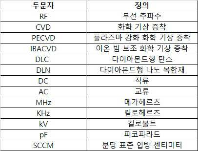
두문자 정의 표Acronym Definition Table
상세한 설명 전반에 걸쳐, 특정 용어가 사용되며, 그 정의는 명시적으로 제공될 수 있다. 본 원에서 용어가 명시적으로 정의되지 않은 경우, 해당 용어는 통상의 기술자가 이해할 수 있는 바와 같이 관련 기술 분야의 맥락에서 일반적으로 사용되므로 용어의 일반적인 의미가 의도된다.Throughout the detailed description, specific terms are used, and definitions may be provided explicitly. When terms are not explicitly defined herein, the general meaning of the terms is intended, as those terms are generally used in the context of the relevant technical field as understood by those skilled in the art.
예를 들어, 본 명세서에서 사용되는 용어 "플라즈마"는 광범위하게 이해되며 전체적인 전하를 거의 생성시키지 않는 비율로 양이온 및 자유 전자를 포함하는 이온화 또는 부분 이온화 가스를 포함하도록 의도된다. 다시 말해서, 플라즈마는 일반적으로 동일한 수의 양전하 및 음전하 및 상이한 수의 비-이온화된 중성 분자로 구성된다.For example, the term “plasma” as used herein is broadly understood and is intended to include ionized or partially ionized gases comprising cations and free electrons in proportions that produce little or no overall charge. In other words, the plasma is generally composed of the same number of positive and negative charges and different numbers of non-ionized neutral molecules.
본원에 사용된 용어 "기판"은 광범위하게 이해되고 코팅된 물질 또는 층을 포함하도록 의도된다. 기판은 강성 또는 가요성일 수 있고, 예를 들어 유리, 중합체, 금속, 반도체 또는 어떤 방식으로 코팅되거나 달리 변형될 수 있는 임의의 다른 재료를 포함할 수 있다.The term "substrate" as used herein is intended to encompass a broadly understood and coated material or layer. The substrate can be rigid or flexible, and can include, for example, glass, polymer, metal, semiconductor, or any other material that can be coated or otherwise modified in any way.
본원에서 사용되는 용어 "이온 빔 보조 화학 기상 증착 (IBACVD)"은 광범위하게 이해되고 활성 준-중성 이온 빔을 채용하는 화학 기상 증착 (CVD) 프로세스를 포함하도록 의도되는데 이들은 두 가지 별개의 것이지만 플라즈마-화학 프로세스와 관련된 것을 보조한다: The term "ion beam assisted chemical vapor deposition (IBACVD)" as used herein is broadly understood and is intended to include chemical vapor deposition (CVD) processes employing active quasi-neutral ion beams, which are two distinct but plasma- Assists with chemical processes:
1) 기판 재료 근처에 도입된 기체 전구체 증기의 단편화, 여기 및 이온화; 및 2) 연속적이고 치밀한 박막 코팅을 형성하기 위해 기판의 표면에서 응축되는 전구체 종의 치밀화, 변형 및 화학적 활성화.1) fragmentation, excitation and ionization of gaseous precursor vapor introduced near the substrate material; And 2) densification, modification and chemical activation of precursor species condensing on the surface of the substrate to form a continuous and dense thin film coating.
본원에 사용된 용어 "무선 주파수 (RF)"는 광범위하게 이해되고 신호 (예를 들어, 전압 및 전류)가 사인파(sinusoidal) 방식으로 일부 주파수에서 변화하는 무선 주파수 생성기로부터의 전력의 적용을 포함하도록 의도된다. 전압 변화는 일반적으로 음에서 양이다. 하나 이상의 개시된 구체예에서, 채용된 RF 신호의 주파수는 약 2 MHz이지만, 본 발명의 구체예는 임의의 특정 주파수로 제한되지 않는다. 예를 들어, 하나 이상의 다른 구체예에서, 4 MHz, 13.56 MHz, 27.12 MHz 및 40 MHz의 주파수를 갖는 상용 RF 플라즈마 생성기가 유사하게 채용될 수 있다.As used herein, the term “radio frequency (RF)” is widely understood and includes the application of power from radio frequency generators where signals (eg, voltage and current) change at some frequency in a sinusoidal manner. Is intended The voltage change is generally negative to positive. In one or more disclosed embodiments, the frequency of the RF signal employed is about 2 MHz, but embodiments of the present invention are not limited to any particular frequency. For example, in one or more other embodiments, commercial RF plasma generators having frequencies of 4 MHz, 13.56 MHz, 27.12 MHz, and 40 MHz can be similarly employed.
본원에 사용된 용어 "유도 안테나"는 광범위하게 이해되고 시간-변이 자기 (또는 유도) 장 형태의 전자기 또는 RF 에너지를 다른 바디 내에 결부시키는 수동 구성 요소를 포함하도록 의도된다. 하나 이상의 구체예에서, 의도된 바디는 이온화된 가스 종으로 구성된 플라즈마 방전이다. 하나 이상의 구체예에서, 유도 안테나는 직사각형, 정사각형 또는 실린더의 기하학적 형상을 갖는 다중 회전 수냉식 구리 튜빙으로 구성되며, 바람직하게는 길이보다 작은 폭을 갖는 직사각형 형상으로 구성된다. 본 발명의 구체예는 본원의 교시를 고려하여 통상의 기술자에게 명백한 바와 같이 유도 안테나의 임의의 특정 기하학적 형상 또는 치수로 제한되지 않는 것으로 이해되어야 한다.The term “inductive antenna” as used herein is broadly understood and is intended to include passive components that couple electromagnetic or RF energy in the form of a time-varying magnetic (or inductive) field into another body. In one or more embodiments, the intended body is a plasma discharge composed of ionized gas species. In one or more embodiments, the induction antenna consists of multiple rotating water-cooled copper tubing having a rectangular, square or cylindrical geometry, and preferably a rectangular shape with a width less than the length. It should be understood that embodiments of the invention are not limited to any particular geometric shape or dimension of the induction antenna, as will be apparent to those skilled in the art in view of the teachings herein.
본원에 사용된 용어 "패러데이 쉴드"는 광범위하게 이해되고 유도 안테나와 플라즈마 사이에 배치된 슬릿 또는 다른 개구 (즉, 조리개)를 갖는 전도성 메쉬 또는 인클로저(enclosure)를 포함하도록 의도되고 이의 플라즈마는 유도 안테나의 와인딩 및 플라즈마 사이의 용량성 결합(전기장)을 감소시킨다. 하나 이상의 구체예에서, 패러데이 쉴드는 예를 들어 알루미늄 또는 구리와 같은 높은 전기 전도성을 갖는 금속으로 구성된다. 또한, 하나 이상의 구체예에서, 패러데이 쉴드는 주기적 간격으로 유도 안테나 주위에 배치된 개별 요소로 구성된다. 본원의 교시를 고려하여 통상의 기술자에게 명백한 바와 같이 패러데이 쉴드의 다른 구체예가 유사하게 사용될 수있다.The term "Faraday shield" as used herein is broadly understood and is intended to include a conductive mesh or enclosure having a slit or other aperture (i.e. aperture) disposed between the inductive antenna and the plasma, the plasma of which is an inductive antenna Reduces the capacitive coupling (electric field) between winding and plasma. In one or more embodiments, the Faraday shield consists of a metal with high electrical conductivity, such as, for example, aluminum or copper. Also, in one or more embodiments, the Faraday shield consists of individual elements disposed around the inductive antenna at periodic intervals. Other embodiments of the Faraday shield can be similarly used as will be apparent to those skilled in the art in view of the teachings herein.
본원에 사용된 용어 "펄스 DC"는 광범위하게 이해되고, 파형이 반드시 사인파일 필요는 없으나(예 : 구형파, 펄스 트레인 등), 예를 들어 반파 정류기 또는 전파정류기로부터, 일반적으로 생성되는 직류 (DC) 전력으로부터의 전력의 응용을 포함하도록 의도된다. 펄스 DC 신호는 DC 및 교류 (AC) 신호의 특성을 모두 가지고 있다. DC 신호의 전압은 일반적으로 일정하지만 AC 신호의 전압은 사인파 방식으로 일부 주파수에서 변한다. AC 신호와 유사하게, 펄스 DC 신호는 연속적으로 변하지만, DC 신호와 유사한 방식으로 전압의 신호(sign)는 일반적으로 일정하다. 펄스 DC 신호의 전압 변화는 일반적으로 구형파와 유사하다. 다양한 펄스 DC 신호가 일반적으로 단극으로 지칭되는, 단극성 전압 출력 (양 또는 음) 및 일반적으로 바이폴라로 지칭되는, 양극 전압 출력 (양 및 음)과 함께 채용될 수있다. 양극성 신호의 경우, 펄스 DC 생성기는 양의 전압과 음의 전압의 크기가 같거나 (일반적으로 대칭이라 지칭함) 같지 않은 (일반적으로 비대칭이라 지칭함) 전압 출력을 전달한다. 본 발명의 하나 이상의 예시적인 구체예에서, 비대칭 바이폴라 펄스 DC 생성기는 약 5KHz 내지 350KHz의 주파수 범위로 채용된다.As used herein, the term "pulse DC" is widely understood, and waveforms are not necessarily sine-filed (eg, square waves, pulse trains, etc.), but generally generated direct current (DC), for example from a half-wave rectifier or full-wave rectifier ) It is intended to cover the application of power from power. Pulsed DC signals have both the characteristics of DC and alternating current (AC) signals. The voltage of the DC signal is generally constant, but the voltage of the AC signal varies at some frequency in a sine wave manner. Similar to the AC signal, the pulsed DC signal changes continuously, but in a manner similar to the DC signal, the signal of voltage is generally constant. The voltage change of the pulsed DC signal is generally similar to a square wave. Various pulsed DC signals can be employed with unipolar voltage output (positive or negative), generally referred to as unipolar, and bipolar voltage output (positive and negative), commonly referred to as bipolar. In the case of a bipolar signal, a pulsed DC generator delivers a voltage output that is equal in magnitude (generally referred to as symmetric) or not equal (generally referred to as asymmetric) to the magnitude of the positive and negative voltages. In one or more exemplary embodiments of the invention, an asymmetric bipolar pulsed DC generator is employed in a frequency range of about 5KHz to 350KHz.
본 명세서에서 사용되는 용어 "공급 가스"는 광범위하게 이해되고 플라즈마 이온 소스의 플라즈마 챔버 바디 내로 직접 도입되고 RF 유도 안테나에 의해 생성된 플라즈마 방전을 포함하는 가스를 포함하도록 의도된다. 본 발명의 하나 이상의 구체예에서, 공급 가스는 순수한 가스, 예를 들어 아르곤, 산소, 질소 및/또는 다른 이온화 가능한 가스, 또는 상기 언급 된 가스 중 하나 이상의 혼합물로 구성될 수 있지만, 이에 제한되지는 않는다. 본 발명의 구체예는 본원의 교시를 고려하여 통상의 기술자에게 명백한 바와 같이 임의의 특정 가스 또는 가스 혼합물로 제한되지 않음이 이해되어야 한다.As used herein, the term “supply gas” is broadly understood and is intended to include gas that is introduced directly into the plasma chamber body of a plasma ion source and comprises plasma discharge generated by an RF inductive antenna. In one or more embodiments of the present invention, the feed gas may consist of, but is not limited to, pure gas, such as argon, oxygen, nitrogen and/or other ionizable gases, or mixtures of one or more of the aforementioned gases. Does not. It should be understood that embodiments of the invention are not limited to any particular gas or gas mixture, as will be apparent to those skilled in the art in view of the teachings herein.
본원에 사용된 용어 "전구체 가스"는 광범위하게 이해되고 다른 화합물을 생성하는 화학 원소 또는 원소들을 포함하는 분자 형태의 가스를 포함하도록 의도된다. 하나 이상의 구체예에서, 화합물은 기판 상에 응축되고 통상의 기술자에 의해 박막 층 또는 층들로 지칭될 수 있는 고체 코팅을 형성한다.As used herein, the term "precursor gas" is broadly understood and is intended to include gases in the form of molecules that contain chemical elements or elements that produce other compounds. In one or more embodiments, the compound condenses on the substrate and forms a solid coating, which can be referred to as a thin film layer or layers by one skilled in the art.
전술한 바와 같이, PECVD 공정에서, 증착 동안 기판 상에 충돌하는 이온의 에너지를 증가시켜 박막 코팅의 하나 이상의 특성을 조정하는 것이 바람직할 수 있다. 그러나, 종래의 PECVD 플라즈마 소스는 기판 바이어싱을 채용하지 않고 (즉, 기판에 전압을 적용하지 않고) 이온 에너지를 증가시키는 능력이 부족하다. PECVD를 위한, 특히 유전체 박막의 증착을 위한, 대부분의 종래의 선형 플라즈마 소스는 플라즈마 소스의 동작에 부정적인 영향을 미치지 않으면서 이온 에너지를 독립적으로 증가시키는 능력이 제한되어있다. 이러한 종래의 선형 플라즈마 및 이온 소스는 양극 층 소스, 엔드 홀 소스, 그리드 이온 소스, 마그네트론 플라즈마 소스, 중공 음극 소스, 마이크로파 소스, RF 용량 및 유도 소스 및 폐쇄 드리프트 소스를 포함하지만 이에 제한되지 않는다. 이들 소스 중 일부는 플라즈마 처리 및 이온 보조 물리 기상 증착 응용에 성공적으로 사용되었지만, 내부 및 외부 구성요소 상의 절연막의 증착 및 이들의 길이에 걸친 이온 빔 공간 전하의 부적절한 중성화로 인해 불안정한 동작에 적어도 일부분으로 인해 기판의 PECVD 프로세싱에 덜 효과적이다. As described above, in a PECVD process, it may be desirable to increase the energy of ions impinging on the substrate during deposition to adjust one or more properties of the thin film coating. However, conventional PECVD plasma sources lack the ability to increase ion energy without employing substrate biasing (ie, without applying voltage to the substrate). Most conventional linear plasma sources for PECVD, especially for the deposition of dielectric thin films, have limited ability to independently increase ion energy without adversely affecting the operation of the plasma source. Such conventional linear plasma and ion sources include, but are not limited to, anode layer sources, end hole sources, grid ion sources, magnetron plasma sources, hollow cathode sources, microwave sources, RF capacitive and induced sources, and closed drift sources. Some of these sources have been successfully used in plasma processing and ion assisted physical vapor deposition applications, but at least in part for unstable operation due to deposition of insulating films on internal and external components and improper neutralization of ion beam space charges across their length. This makes it less effective for PECVD processing of substrates.
예를 들어, 양극 층 및 엔드 홀 소스는 작동하기 어렵고 적어도 상기 언급된 이유로 적용이 제한되어 왔다. RF (용량 타입 및 유도 타입) 소스는 주로 반도체 웨이퍼와 같은 소규모 기판에 사용되어 왔다. 그러나, 이러한 접근법은 다른 요인들 중에서도 임피던스 매칭의 복잡성 및 비용, 매우 느린 증착 속도 및 미립자의 생성으로 인해 광역 기판으로 스케일링 업하는 데 어려움을 겪어왔다. 마이크로파 소스 및 중공 캐소드 소스는 각각 광전지 패널 및 건축 유리의 처리에 이용되어 왔다. 그러나, 이들 소스는 일반적으로 저에너지 이온 (예를 들어, 약 15 내지 25 eV 미만)을 생성하고, 소스 장치는 독립적인 이온 가속 능력을 갖지 않는다. 마그네트론 플라즈마 소스 및 폐쇄 드리프트 타입 소스는 이온 에너지의 독립적 제어를 위한 제한된 능력을 갖는다. 일반적으로 이온 에너지는 소스의 방전 전압 및 작동 압력과 관련이 있다. 따라서, 이온 에너지를 조절하기 위한 제한된 공정 윈도우가 존재한다. 그리드 이온 소스는 일반적으로 물리적 증착 공정, 예를 들어 스퍼터링 또는 증발 동안 플라즈마 처리 또는 이온 보조에 사용된다. PECVD 공정을 위한 이들 소스의 적용은 추출 그리드 및/또는 소스 구성 요소 (내부 또는 외부) 상에 절연막의 증착으로 인한 소스의 불안정한 작동으로 인해 적어도 부분적으로 제한되어 왔다. 또한, 그리드 소스는 공간 전하 보상을 위한 점 전자 소스의 사용으로 적어도 부분적으로 인해 광역 기판에 고르지 않은 중화를 나타낸다.For example, anode layers and end hole sources are difficult to operate and their application has been limited, at least for the reasons mentioned above. RF (capacity type and induction type) sources have been used primarily for small substrates such as semiconductor wafers. However, this approach has had difficulty scaling up to a wide area substrate due to, among other factors, the complexity and cost of impedance matching, very slow deposition rates, and the generation of particulates. Microwave sources and hollow cathode sources have been used for the treatment of photovoltaic panels and architectural glass, respectively. However, these sources generally produce low energy ions (eg, less than about 15-25 eV), and the source device does not have independent ion acceleration capabilities. Magnetron plasma sources and closed drift type sources have limited ability for independent control of ion energy. In general, ion energy is related to the discharge voltage and operating pressure of the source. Thus, there are limited process windows for controlling ionic energy. Grid ion sources are commonly used for plasma deposition or ion assist during physical deposition processes, for example sputtering or evaporation. The application of these sources for PECVD processes has been limited, at least in part, due to the unstable operation of the source due to the deposition of insulating films on the extraction grid and/or source components (internal or external). In addition, the grid source exhibits uneven neutralization to the wide area substrate due at least in part to the use of a point electron source for spatial charge compensation.
본 발명의 양태는 이온 에너지 및 이온 전류 밀도가 연속적이고 독립적으로 변할 수 있도록 배열된 기하학적으로 선형이고 자기 중화 플라즈마 이온 소스를 사용하여 PECVD에 의해 대면적 (예를 들어, 약 0.4 미터 초과)에 걸쳐 박막 코팅을 증착하기 위한 장치 및 방법을 제공한다. 보다 구체적으로, 본 발명의 하나 이상의 구체예는 유도적으로 결합된 플라즈마 이온 소스를 채용하여 이온, 전자 및 중성 가스 입자의 고밀도 및 비열 플라즈마를 생성한다. 하나 이상의 구체예에서, 유도적으로 결합된 플라즈마는 전도성 물질로 구성된 바디의 내부에 배치된 RF 구동 안테나에 의해 생성되고 유지된다. 바디는 기계적으로 강성이고 진공 상태이며 제조 비용이 저렴한 플라즈마 챔버를 형성한다. 하나 이상의 구체예에서, 플라즈마 이온 소스는 장착 플랜지 또는 다른 부착 수단을 통해 약 10-6 내지 10-8 Torr의 압력이 바람직하게 유지되는 진공 챔버 상에 외부적으로 부착된다.Aspects of the invention span a large area (e.g., greater than about 0.4 meters) by PECVD using a geometrically linear, self-neutralizing plasma ion source arranged so that the ion energy and ion current density can be continuously and independently varied. Provided is an apparatus and method for depositing a thin film coating. More specifically, one or more embodiments of the present invention employ inductively coupled plasma ion sources to generate high density and non-thermal plasmas of ionic, electron and neutral gas particles. In one or more embodiments, the inductively coupled plasma is generated and maintained by an RF driven antenna disposed inside the body made of a conductive material. The body is mechanically rigid, vacuumed and forms a plasma chamber with low manufacturing costs. In one or more embodiments, the plasma ion source is externally attached on a vacuum chamber where a pressure of about 10 -6 to 10 -8 Torr is preferably maintained via a mounting flange or other attachment means.
본 발명의 구체예에 따른 플라즈마 이온 소스는 대면적 유리 및 폴리머 기판상에, 기계적으로 내구성이 있고 스크래치 저항성인 코팅, 예를 들어 다이아몬드형 탄소 (diamond-like carbon, DLC) 및 다이아몬드형 나노 복합체 (diamond-like nanocomposite, DLN) 박막을 증착할 수 있는 IBACVD 공정에 사용하기에 유리하게 적합하다. 산업 규모 공정의 경우, 본 발명의 구체예는 상당한 길이(예를 들어, 0.4 미터 초과)에 걸쳐 균일하고 안정적인 활성 준-중성 빔을 생성할 수 있다.Plasma ion sources according to embodiments of the present invention are mechanically durable and scratch resistant coatings on large area glass and polymer substrates, such as diamond-like carbon (DLC) and diamond-like nanocomposites ( It is advantageously suitable for use in IBACVD processes that can deposit diamond-like nanocomposite (DLN) thin films. For industrial scale processes, embodiments of the present invention can produce a uniform and stable active quasi-neutral beam over a considerable length (eg, greater than 0.4 meters).
도 1은 본 발명의 일 구체예에 따른, IBACVD 응용에 사용하기 위한 선형화된 RF 구동 플라즈마 이온 소스 102를 포함하는 예시적인 장치 100의 적어도 일부를 개념적으로 도시한 사시도이다. RF 구동 플라즈마 이온 소스 102는 번역 (즉, 이동 또는 고정되지 않은) 기판 104에 근접하여 위치한다. 하나 이상의 구체예에서, 기판 104는, 예를 들어 운송 메커니즘 106을 사용하는 것과 같이, 기판 104의 상부 표면을 향하는 플라즈마 이온 소스의 하부 표면과 실질적으로 평행한 방향으로, 플라즈마 이온 소스 102에 대해 바람직하게는 이동된다. 운송 메커니즘 106은 컨베이어 벨트, 테이블 및 테이블을 구동하도록 배열된 모터, 롤투롤(R2R)어셈블리 등을 포함하나 이에 제한되지 않는다. 플라즈마 이온 소스 102에 대한 기판 104를 번역하기 위한 다른 적절한 메커니즘 및 방법은 고정 기판과 함께 움직이는 플라즈마 이온 소스의 사용 등을 포함하여, 통상의 기술자에게 명백해질 것이다. 본 발명의 구체예와 함께 사용하기에 적합한 기판 104는 가요성 웹, 디스플레이 유리, 건축 유리, 차량 유리, 광전지 패널 등을 포함하나, 이에 제한되지 않는다.1 is a perspective view conceptually illustrating at least a portion of an
플라즈마 이온 소스 102는 플라즈마 챔버 바디 108을 포함하여 그 내부에 플라즈마 방전을 생성 및 유지시키도록 조절된다. 하나 이상의 구체예에서, 플라즈마 챔버 바디 108은 전기 전도성 재료 (예를 들어, 금속)로 형성되고 실질적으로 중공 직사각형 직육면체로 형성된다. 플라즈마 챔버 바디 108의 다른 형상 및 치수가 유사하게 고려된다 (예를 들어, 원통형).The
플라즈마 챔버 바디 108은 이온화되는 공급 가스 112가 도입되는 하나 이상의 주입구 110를 포함한다. 전구체 가스 113은 플라즈마 챔버 바디와 기판 104 사이에 끼어든, 매니 폴드 116 등을 사용하여 분배될 수 있는 하나 이상의 가스 주입구 114를 통해 도입된다. 매니폴드 116 및 대응하는 전구체 가스 주입구 114는 플라즈마 챔버 바디 108에 부착되거나 다른 수단을 사용하여 위치할 수 있다. 공급 가스 이온, 전자 및 중성 종으로 구성된 플라즈마 이온 빔 (명시적으로 도시되지 않았지만 암시됨)은 전구체 가스와 상호 작용하고 플라즈마 화학 반응을 개시하여 기판 104의 상부 표면 상에 박막 코팅 118을 증착시킨다. 하나 이상의 구체예에서, 다수의 매니폴드 116 및 대응하는 전구체 가스 주입구 114가 채용되어(예를 들어, 플라즈마 챔버 바디 108의 대향면에) 거기에 더욱 균일한 코팅 118을 제공하거나, IBACVD 공정에 걸쳐 더욱 정밀한 제어를 가능하게 한다. The
도 2는 본 발명의 구체예에 따른 도 1에 도시된 플라즈마 이온 소스 102를 구현하기에 적합한 예시적인 선형화된 RF 구동 플라즈마 이온 소스 200의 적어도 일부를 도시하는 등각도이다. 도 2를 참조하면, 도 1에 나타난 작동 위치로부터 반전된 플라즈마 이온 소스 200은 플라즈마 챔버 바디 202를 포함하여 여기에 플라즈마 방전을 생성시키고 유지시키도록 조절된다. 하나 이상의 구체예에서, 플라즈마 챔버 바디 202는 전도성 재료 (예를 들어, 금속)로 형성되고 중공 직사각형 직육면체로 형성된다. 플라즈마 챔버 바디 202의 다른 형상 및 치수가 유사하게 고려된다.2 is an isometric view showing at least a portion of an exemplary linearized RF driven
하나 이상의 구체예에서, 플라즈마 챔버 바디 202는 절연 진공 플랜지 204를 사용하여 플라즈마 이온 소스가 작동하는 진공 챔버(명시적으로 도시되지 않음)로부터 전기적으로 격리된다. 하나 이상의 구체예에서, 절연 진공 플랜지 204는 산화 알루미늄 또는 다른 강성 세라믹, ULTEM® (비정질 열가소성 폴리에테르이미드 (PEI) 재료, 중합체 재료, 유리 재료, 또는 기계 가공 가능하고 다른 특성들 중에서도, 높은 유전 강도(예를 들어, ULTEM®의 경우 약 1.0MHz에서 약 3.0, 산화 알루미늄의 경우 약 1.0 MHz에서 약 9.1), 낮은 RF 손실 계수 (예 : ULTEM®의 경우 1.0MHz에서 약 0.0015, 또는 알루미늄 산화물의 경우 1.0MHz에서 약 0.0007), 높은 기계적 강도 (예를 들어, ULTEM®의 경우 약 150 메가 파스칼 MPa 또는 산화 알루미늄의 경우 약 2,100MPa 초과의 압축 응력), 높은 서비스 가능한 온도 (예를 들어, 산화 알루미늄 또는 ULTEM®의 경우 약 1,700도 초과의 최대 사용 온도) 및 높은 전기 저항성 (예를 들어, 산화 알루미늄 또는 ULTEM®의 경우 약 1014 ohm-cm 초과의 부피 저항성)을 나타내는 임의의 다른 강성 재료로 구성된다. 하나 이상의 구체예에서, 진공 플랜지 204는 비정질 열가소성 폴리에테르이미드 물질을 포함한다. 폴리테트라플루오로에틸렌 및 산화 알루미늄과 같지만, 이에 제한되지 않는, 다양한 다른 재료가 진공 플랜지 204를 형성하는데 이용될 수있는 것으로 고려된다.In one or more embodiments, the
절연 진공 플랜지 204는 플라즈마 챔버 바디 202와 진공 챔버 정합 플랜지 206 사이에 끼어든다. 하나 이상의 구체예에서, 진공 챔버 정합 플랜지 206은 플라즈마 이온 소스 200을 진공 챔버와 결부 시키도록 구성되고 (명시적으로 도시되지 않음), 예를 들어 비-자성 스테인리스 스틸과 같은, 진공 호환 가능한 기계적 강성 및 비자성 금속으로 바람직하게 구성된다.The insulating
플라즈마 이온 소스 200은 그리드 추출 어셈블리 208를 더 포함한다. 하나 이상의 구체예에서, 그리드 추출 어셈블리 208은 바람직하게는 낮은 스퍼터 수율을 갖는 복수의 전기 전도성 로드 210으로 구성된다. 플라즈마 챔버 바디 202가 접지되는 본 발명의 구체예에서, 전도성 로드 210은 플라즈마 챔버 바디로부터 전기적으로 격리되어, 그리드 추출 어셈블리 및 플라즈마 챔버 바디 사이에 전압 전위차가 적용되어 여기에 이온 빔의 형태로 플라즈마 이온 소스 200으로부터 하전된 이온을 가속시킬 수 있다.The
하나 이상의 구체예에서, 전도성 로드 210은 금속 재료(예를 들어, 흑연)로 구성된다. 전도성 로드 210은 바람직하게는 주기적 간격으로 그리드 추출 어셈블리 208의 개구를 따라 배치된다. 단지 예로서 제한없이, 전도성 로드 210의 각각의 기하학적 중심 사이의 간격은 약 3mm 내지 7mm 사이에서 변한다. 선택적으로, 하나 이상의 구체예에서, 그리드 추출 어셈블리 208은 예를 들어 진공 정합 플랜지 206 내에 통합되거나 진공 챔버 도어 내에 통합된 진공 밀봉 수냉 회로(명시적으로 도시되지 않았지만 암시됨) 또는 방열판 등으로 냉각시켜, 플라즈마 이온 소스 200의 작동 중에 그리드 추출 어셈블리 208에서 생성된 열을 제거한다.In one or more embodiments, the
도 3은 본 발명의 일 구체예에 따른, 박막 코팅의 증착에 사용되는 예시적인 플라즈마 이온 소스 300의 적어도 일부를 도시한 단면도이다. 작동 동안, 플라즈마 이온 소스 300은 일반적으로 진공 챔버 (명시적으로 도시되지 않았지만 암시됨) 상에 장착되거나 진공 챔버 내에 배치된다. 도 2에 도시된 플라즈마 이온 소스 200과 일치하는 방식으로, 플라즈마 이온 소스 300은 플라즈마 챔버 바디 302를 포함하여 그 내부에서 플라즈마 방전을 생성 및 유지하도록 조절된다. 플라즈마 챔버 바디 302는 바람직하게는 전도성 재료 (예를 들어, 금속)로 형성되고 중공 직사각형 직육면체 형상이지만, 본 발명의 구체예는 임의의 특정 형상 및/또는 치수에 제한되지 않는다. 하나 이상의 구체예에서, 플라즈마 챔버 바디 302는 고 전기적이고 열적 전도성인 금속, 바람직하게는 알루미늄으로 구성되는데, 이는 장치의 진공 챔버로서 역할을 수행한다. 하나 이상의 구체예에서, 플라즈마 챔버는 진공 등급 알루미늄으로 제조되고 진공 밀봉(예를 들어, 엘라스토머 O-링)을 갖는다. 따라서, 플라즈마 챔버 자체는 진공 챔버로서 기능한다.3 is a cross-sectional view illustrating at least a portion of an exemplary
하나 이상의 구체예에서, 하나 이상의 냉각 채널 304 또는 대안적인 열 제거 메커니즘 (예를 들어, 방열판)은 외부 표면 (즉, 대기 측) 상에 (예를 들어, 용접 또는 다른 체결 수단에 의해) 배치되고, 플라즈마 이온 소스 300과 열적으로 접촉하며 플라즈마 챔버 바디 302가 과열되는 것을 방지하도록 배열된다. 플라즈마 이온 소스 300의 과열은 진공 밀봉 구성 요소 (예를 들어, 엘라스토머 O-링)의 열적 열화를 초래할 수 있어 진공 무결성이 손실될 수 있다. 본 발명의 개시된 구체예에서, 물은 장치에 바람직한 냉각 유체이나, 다른 냉각 유체 (예를 들어, 클로로플루오로카본 (CFC) 냉매, 에틸렌 글리콜, 프로필렌 글리콜, 암모니아 등)이 유사하게 채용될 수 있다. In one or more embodiments, one or
하나 이상의 구체예에서, 소스 플랜지 306은, 플루오로중합체 엘라스토머 또는 통상의 기술자에게 공지된 대안적인 체결 수단과 같으나 이에 제한되지 않는, 예를 들어, 고온 O-링 밀봉을 사용하여 플라즈마 챔버 본체 302에 고정된다. 하나 이상의 구체예에서, 소스 플랜지 306은 플라즈마 챔버 바디 302로부터 제거 가능하여 플라즈마 이온 소스 구성 요소 (예를 들어, 유도 안테나 등)의 유지 및/또는 수리와 같은, 플라즈마 챔버 바디의 내부로의 접근을 가능하게 한다. 선택적으로, 냉각 채널 308은 소스 플랜지 306에 형성된다(예를 들어, 기계 가공). 냉각 채널 308은 냉각 채널을 통해 순환하는, 예를 들어 액체 (예를 들어, 물) 또는 가스(예를 들어, 공기)로 플라즈마 이온 소스 300으로부터 열을 제거하도록 조절된다. 소스 플랜지 306은 이온화되는 공급 가스가 플라즈마 챔버 바디 302의 내부로 유입되는 하나 이상의 주입구 310을 더 포함한다.In one or more embodiments, the
플라즈마 이온 소스 300은 RF 신호가 안테나에 적용될 때 전자기 에너지 소스를 플라즈마 챔버 바디 302의 내부에 공급하도록 배열된 유도 안테나 312를 더 포함한다. 안테나 312는 통상의 기술자에게 명백한 바와 같이, 브래킷 등과 같은 적합한 장착 하드웨어를 사용하여 플라즈마 챔버 본체 302 내에 매다는 것이 바람직하다. 안테나 312는 플라즈마 챔버 바디 302로부터 전기적으로 절연되는 것이 바람직하다. 하나 이상의 구체예에서, 안테나 312는 소스 플랜지 306 상에 배치되며, 이는 소스 플랜지가 제거될 때 안테나의 용이한 제거를 가능하게 한다. 유도 안테나 312의 형상은 바람직하게는 플라즈마 챔버 바디 302의 형상과 일치하며; 이는, 하나 이상의 예시적인 구체예에서 직사각형 직육면체이다. 그러나, 본 발명의 구체예는 안테나 312의 임의의 특정 형상 또는 치수로 제한되지 않는 것으로 이해되어야 한다.The
안테나 312는 바람직하게는 전도성 와이어 또는 튜빙의 복수의 와인딩 (즉, 턴) 314를 포함한다; 더 많은 와인딩이 안테나를 형성하기 위해 사용될수록, 유도 결합이 더 효율적이므로 플라즈마 챔버 바디 302의 내부로 운송되는 전자기 에너지는 더 커진다. 하나 이상의 구체예에서, 안테나 312는 수냉식이다. 예를 들어, 안테나 312의 와인딩 314는 냉각수 또는 다른 액체가 통과하여 안테나로부터 열을 운송함으로써 플라즈마 이온 소스의 하나 이상의 구성 요소들에 대한 열적 손상을 방지하는, 중공 구리 튜빙으로 형성될 수 있다 (예를 들어, 진공 밀봉 등). 이러한 방식으로, 안테나 312는 높은 RF 전력 레벨 (예를 들어, 약 1000 와트 초과)에서 작동하도록 조절된다.
RF 신호가 외부 RF 생성기 (명시적으로 도시되지 않음)로부터와 같이, 안테나 312에적용될 때, 플라즈마 챔버 바디 302에 유도 결합된 RF 에너지는 공급 가스를 이온화하고 고밀도 플라즈마 방전 316을 형성한다. 플라즈마 방전 316은 안테나 312의 와인딩 314 사이의 내부 공간 내에 주로 포함된다. 하나 이상의 구체예에서, 안테나 312는 중공 알루미늄 산화물 (알루미나) 튜빙 318 또는 대안적인 전기 절연체로 형성된 튜빙을 포함하며, 이는 구리 와인딩 314를 둘러싼다. 대안적인 구체예에서, 전도성 와인딩 314의 적어도 일부는 전기 절연 재료의 층으로 코팅된다. 전기 절연체인 산화 알루미늄 튜빙 318은 플라즈마 방전 316에 노출 된 구리 와인딩 314의 일부가 기판의 표면 (예를 들어, 도 1의 104) 상에 스퍼터링되는 것을 방지하는 역할을 한다. 보호 알루미늄 산화 튜빙 318이 없으면, 구리 와인딩 314는 플라즈마 방전 316 내의 이온에 의해 스퍼터링 될 것이고, 이는 플라즈마 챔버 바디 302 및 진공 챔버 (진공 적으로 도시되지 않음) 내로 진공 및 물 누출을 초래할 것이다.When the RF signal is applied to the
안테나 와인딩 314의 일부는 플라즈마 챔버 바디 302의 외부에 배열되고 RF 생성기에 대한 전기적 연결 뿐만 아니라 냉각 액체 소스에 대한 연결 (명확성을 위해 명시적으로 도시되지 않음)을 제공한다. 예를 들어, 하나 이상의 구체예에서, 안테나 312의 구리 와인딩 314는 진공 피드스루 (명시적으로 도시되지 않았지만 암시됨)를 사용하여 플라즈마 챔버 바디 302 내에 배열된다. 진공 피드스루는 절연 재료 (예를 들어, 세라믹)로 형성되어 구리 와인딩 314가 바람직하게 전도성인 플라즈마 챔버 바디 302와 전기적으로 연결되지 않도록 한다. (따라서 안테나 312와 플라즈마 챔버 몸체 302 사이의 전기적 합선을 방지함)A portion of the antenna winding 314 is arranged outside the
계속하여 도 3을 참조하면, 하나 이상의 구체예에서, 선택적 냉각 채널 322를 갖는 진공 정합 플랜지 320은 플라즈마 챔버 바디 302 상에 배치되어(예를 들어, 용접되거나 고정된) 유전 진공 브레이크 324에 진공 정합 표면을 제공한다. 소스 플랜지 306 내에 형성된 냉각 채널 308의 형성과 일치하는 방식으로, 냉각 채널 322는 진공 정합 플랜지 320 내에 기계 가공되거나 또는 외부에 부착되거나, 예를 들어, 냉각 채널을 통해 액체 (예를 들어, 물) 또는 기체 (예를 들어, 공기)를 순환시킴과 같이, 플라즈마 이온 소스 300으로부터 열을 제거하도록 조절된다.With continued reference to FIG. 3, in one or more embodiments, a
유전체 진공 브레이크 324는 폴리머, 세라믹, 유리 또는 다른 유전체 재료와 같으나 이에 제한되지 않는 전기 절연 재료, 바람직하게는 진공 밀착성, 기계 가공성 및 기계적으로 강성인 전기 절연 재료로 구성된다. 하나 이상의 구체예에서, 유전체 진공 브레이크 324는 고온 열가소성 재료를 포함한다. 하나 이상의 구체예에서, 유전체 진공 브레이크 324는 플라즈마 챔버 바디 302와 진공 챔버 도어 326 사이에 배치된다. 선택적으로, 진공 챔버 도어 326는 냉각 채널 328을 갖도록 형성된다. 각각, 소스 플랜지 306 및 진공 플랜지 320 내에 형성된 냉각 채널 308 및 322의 형성과 일치하는 방식으로, 진공 챔버 도어 326 내에 기계 가공되거나 외부에 부착될 수 있는 냉각 채널 328은 예를 들어, 냉각 채널을 통해 액체 (예를 들어, 물) 또는 가스 (예를 들어, 공기)를 순환시켜 진공 챔버로부터 열을 제거하도록 조절된다. 진공 챔버 도어 326을 채용하는 것의 하나의 이점은 플라즈마 이온 소스 300을 세정하고 진공 챔버 내의 픽스처 (명시적으로 도시되지 않음) 상에 기판 (예를 들어, 도 1에 도시 된 104)을 배치하기 위한 접근 용이성을 제공한다는 것이다.
도 3에 도시된 예시적인 구체예에서, 플라즈마 챔버 바디 302는 유전체 진공 브레이크 324를 사용하여 진공 챔버 도어 326 및 진공 챔버 (명시적으로 도시되지 않았지만 암시됨)로부터 전기적으로 격리된다. 플라즈마 챔버 바디 302를 진공 챔버 도어 326 및 진공 챔버(도시되지 않음)로부터 전기적으로 분리함으로써, 전기적으로 접지되고 (바람직하게는 지면에 접지), 플라즈마 챔버 바디 302는 기판 바이어스 또는 플라즈마 챔버 바디 302 내부에 배치된 내부 소스 전극 (도시되지 않음)을 제공할 필요 없이 규정된 전압 레벨로 바이어스 될 수 있다. 따라서, 플라즈마 챔버 바디 302 자체는, 외부 바이어스 전압 공급 (명시적으로 도시되지 않음)을 사용하여 직접 바이어스되어, 전술한 바와 같이 소스 전극으로서 역할을 수행한다. 진공 챔버로부터 플라즈마 챔버 바디 302를 전기적으로 격리시키기 위한 다른 메커니즘이 통상의 기술자에게 명백한 바와 같이 유사하게 고려된다.In the exemplary embodiment shown in FIG. 3, the
플라즈마 이온 소스 300은 본원에서 패러데이 쉴드로 지칭되는, 정전기 쉴드 330의 배열을 포함하며, 이는 유도 안테나 312와 플라즈마 챔버 바디 302 사이에 배치되며, 안테나를 둘러싼다. 하나 이상의 구체예에서, 패러데이 쉴드 330는 그 안에 슬롯 또는 조리개를 갖도록 형성되고 직사각형 형상이거나, 그렇지 않으면 바람직하게는 플라즈마 챔버 바디 302의 형상과 일치한다. 패러데이 쉴드 330는, 적어도 부분적으로, 안테나 312의 와인딩 314 사이에서 생성하는 용량성 전압을 감소시키고 플라즈마 방전 316이 형성된 플라즈마 챔버 바디 302의 내부로 유도 장(field) 및 전압만이 유입되도록 기능한다. 또한, 패러데이 쉴드 330은 안테나 312와 플라즈마 방전 316 사이에 비교적 일정한 전기 임피던스를 제공하여, 플라즈마 챔버 바디 302 내부로 도입된 구동 (공급) 가스의 빠르고 반복적인 점화를 가능하게 한다. 패러데이 쉴드 330은 또한 물질 증착을 더 잘 제어하기 위해 이온 에너지를 감소시킨다. 하나 이상의 구체예에서, 유도 안테나 312, 플라즈마 챔버 바디 302 및 패러데이 쉴드 330은 플라즈마 이온 소스 300에 의해 생성된 준-중성 플라즈마 이온 빔을 형성하는데 사용되는 고밀도 플라즈마 방전 316을 생성 및 유지하도록 배열된 플라즈마 생성 유닛을 형성한다. 하나 이상의 구체예에서, 패러데이 쉴드 330은 전기 및 열적 전도성이 높은 금속 (예를 들어, 알루미늄 또는 구리)로 구성된다.The
고밀도 플라즈마 방전 316은 유도 안테나 312에 의해 생성되고 안테나에 대해 상대적으로 근접하게 존재한다. 잔광 플라즈마 332는 유도 안테나 312와 추출 그리드 334 사이에 배치된다. 잔광 플라즈마 332는 유도 안테나 312에 의해 생성된 고밀도 플라즈마 방전 316으로부터의 더 낮은 농도의 전자 및 이온으로 구성된다. 하나 이상의 구체예에서, 추출 그리드 334는 준-중성 플라즈마 빔의 추출을 가능하게 하도록 배열된 조리개 또는 개구 (예를 들어, 구멍, 슬릿 등)를 갖는 전도성 재료의 단일 그리드 또는 메쉬를 포함한다. 예를 들어 텅스텐, 몰리브덴, 흑연, 티타늄 및 이들의 합금을 포함하는, 다양한 전도성 (예를 들어, 금속성) 재료가 본 발명의 구체예에 의해 고려된다. 다수의 추출 그리드와 대조적으로, 단일 추출 그리드 334의 사용은 통상적으로 요구되는 바와 같이, 유리하게는 추출 그리드 서로의 정확한 배열에 대한 필요성을 제거한다.The high
바람직한 구체예에서, 추출 그리드 334는 도 2에 나타낸 그리드 추출 어셈블리 208과 일치하는 방식으로 형성된다. 구체적으로, 하나 이상의 구체예에서, 추출 그리드 334는 바람직하게는 낮은 스퍼터 수율을 갖는 복수의 전기 전도성 로드 (예를 들어, 도 2의 210)를 포함한다. 추출 그리드 334와 플라즈마 챔버 바디 302 사이에 인가된 전압 전위차는, 적어도 부분적으로, 이온 빔 336의 형태의 플라즈마 이온 소스 200의 외부에 하전된 이온의 가속을 제어한다. 하나 이상의 구체예에서, 추출 그리드 334를 형성하는 전도성 로드는 예를 들어 흑연과 같은 금속 재료로 구성된다. 도 2와 관련하여 설명된 바와 같이, 전도성 로드는 바람직하게는 약 3 mm 내지 7 mm의 인접한 로드의 기하학적 중심 사이의 간격을 갖는 것과 같이, 주기적 간격으로 추출 그리드 334의 개구를 따라 배치된다. 그러나, 본 발명의 구체예는 임의의 특정 전도성 재료 또는 추출 그리드 334의 배열로 제한되지 않는다는 것을 이해해야한다.In a preferred embodiment, the
추출 그리드 334는 그리드 어셈블리 338에 의해 제자리에 고정된다. 하나 이상의 구체예에서, 그리드 어셈블리 338은 프레임의 내부에 배치된 추출 그리드 334를 갖는 "픽처 프레임"으로 배열되며, 표준 부착 수단을 사용하는 것과 같이, 진공 챔버 도어 326 상에 부착된다. 잔광 플라즈마 332 내에 포함된 이온 및 전자는 진공 챔버 (도시되지 않음)에 전기적으로 연결되고 접지된(바람직하게는 지면에 접지) 추출 그리드 334를 통해 가속된다. 전술한 바와 같이, "바이어싱된" 플라즈마 챔버 바디 302와 전기적으로 접지된 추출 그리드 334 사이에 규정된 전압 전위차로 이온과 전자가 바이어스되어, IBACVD 응용에 사용하기 위한 플라즈마 이온 소스 300의 출력으로서 준-중성 플라즈마 이온 빔 336을 생성한다.The
앞서 설명한 바와 같이, 플라즈마 챔버 바디 302는 진공 챔버로부터 전기적으로 격리되며, 진공 챔버는 전기적으로 접지되고, 바람직하게는 지면 접지 전위로 접지된다. 플라즈마 챔버 바디 302의 내부는 추출 그리드 334의 표면적에 비해 상대적으로 더 큰 표면적을 갖도록 배열되며, 이는 진공 챔버 바디에 대한 기계적 부착을 통해 전기적으로 접지된다. 하나 이상의 구체예에서, 플라즈마 챔버 바디 302의 내부 표면적의 표면적 비는 추출 그리드 334의 표면적의 약 1.5 내지 5 배, 바람직하게는 적어도 3 내지 5 배이다. 이 표면적 비가 충족 될 때, RF 전압이 이에 적용될 때 양의 극성 자가-바이어스(positive polarity self-bias)가 플라즈마 챔버 바디 302 상에 발생한다.As described above, the
본원에서 더 상세히 설명될 바와 같이, 하나 이상의 구체예에서, 유도 안테나 312에적용된 RF 전압의 일부는 바람직하게는 약 5-1000 pF의 범위의 커패시턴스를 갖는 가변 커패시터를 통해 플라즈마 챔버 바디 302에 용량성으로 결합된다. 이러한 배열은 플라즈마 챔버 바디 302에 RF 전압을 적용하는 비용-효율적인 방법을 제공하여 단일 RF 전력 공급 장치 또는 생성기를 갖는 접지된 추출 그리드 334에 대해 상대적으로 플라즈마 전위의 선택적 제어를 제공한다. 양의 극성 자가-바이어스는 플라즈마 챔버 바디 302의 내부 표면을 스퍼터링하여 RF 유도 방전 316에 의해 생성된 양이온을 유리하게 반발시킨다. 또한, 유도 방전 316의 전자는 일반적으로 플라즈마 챔버 바디 302를 향해 가속된다; 그러나, 이들 전자의 일부는 플라즈마 챔버 바디 302에서 추출 그리드 334로 가속된다.As will be described in more detail herein, in one or more embodiments, a portion of the RF voltage applied to the
본 발명의 양태에 따르면, 그리드 334를 향해 가속된 전자의 충분한 분율이 추출 그리드 어셈블리의 전체 길이를 따라 추출된 양이온에 의해 생성된 양의 공간 전하를 보상 또는 중화시키기 위해 추출된다. 따라서, 고-전류 밀도, 준-중성, 선형 및 대면적 이온 빔이 플라즈마 이온 소스 300의 출력으로서 생성된다. 본 발명의 양태는 균형 잡힌 전하 밀도의 양이온 및 전자의 동시적이고 수반적인 추출을 제공하여 접지 표면, 픽스처 및 기판 상의 공간 전하 관련 아킹(arching)을 방지한다. According to an aspect of the present invention, a sufficient fraction of electrons accelerated towards
통상적으로, 점-전자 중화제 (예를 들어, 열이온성 필라멘트, 중공 음극 또는 플라즈마 다리 중화제)는 공간 전하를 중화시키기 위해 요구되며, 점-전자 중화제는 전형적으로 플라즈마 또는 이온 소스에 인접하여 배치된다. 이 방법은 소면적 기판에 충분할 수 있지만, 대면적 기판에 걸쳐 이러한 종래의 방법을 사용하여 균일한 공간 전하 중화를 달성하는 것이 어려웠다. 따라서, 생성된 이온 빔은 바람직하지 않게 불균일한 이온 전류 밀도를 나타낼 수 있으며, 이는 기판에 걸쳐 불균일한 표면 처리 및 열악한 필름 품질을 초래할 수 있다. 또한, 기판, 진공 하드웨어 및 플라즈마 이온 소스를 손상시킬 수있는 국지화된 공간 전하 아킹이 발생할 수있다.Typically, a point-electron neutralizer (eg, a thermoionic filament, hollow cathode or plasma bridge neutralizer) is required to neutralize the space charge, and the point-electron neutralizer is typically placed adjacent to the plasma or ion source. . This method may be sufficient for small area substrates, but it has been difficult to achieve uniform space charge neutralization using this conventional method across large area substrates. Thus, the resulting ion beam may undesirably exhibit a non-uniform ion current density, which can result in non-uniform surface treatment and poor film quality across the substrate. In addition, localized space charge arcing can occur that can damage the substrate, vacuum hardware, and plasma ion source.
도 4는 본 발명의 일 구체예에 따라, 향상된 열 관리를 갖는 예시적인 플라즈마 이온 소스 400의 적어도 일부를 도시하는 단면도이다. 구체적으로, 플라즈마 이온 소스 400은 플라즈마 챔버 바디의 하나 이상의 각 측벽 내에 통합된 하나 이상의 냉각 채널 404를 포함하는 플라즈마 챔버 바디 402를 포함한다. 냉각 채널 404는 예를 들어 냉각 채널을 통해 액체 (예를 들어, 물) 또는 가스 (예를 들어, 공기)를 순환시킴으로써 플라즈마 이온 소스 400으로부터 열을 제거하도록 조절된다. 냉각 채널을 플라즈마 챔버 바디 402 내에 통합하는 것은 플라즈마 챔버 바디 상의 외부에 배치된 냉각 채널에 대한 필요성을 제거한다 (예를 들어, 도 3의 304). 플라즈마 챔버 바디 402와 일체로 형성된 냉각 채널 404를 갖는 것은 플라즈마 이온 소스 400이 도 3에 도시 된 배열과 비교하여 우수한 열 관리 및 냉각 효율을 달성할 수 있게한다. 하나 이상의 구체예에서, 통상의 기술자에게 공지될 바와 같이, 다른 냉각 유체가 유사하게 고려되지만, 냉각 채널 404에 의해 전달되는 냉각 유체로서 물이 채용된다.4 is a cross-sectional view showing at least a portion of an exemplary
플라즈마 이온 소스 400은 추출 그리드 406을 더 포함하고, 이는 도 3에 나타난 추출 그리드 334와 일치하는 방식으로 형성될 수 있다. 추출 그리드 406의 열 냉각을 개선하기 위해, 추출 그리드 어셈블리 408은, 도 3과 관련하여 설명된 그리드 어셈블리 338과 일치하는 방식으로 형성될 수 있으며, 냉각 채널 322가 통합된 플라즈마 챔버 진공 정합 플랜지 320과 진공 챔버, 바람직하게는 통합된 냉각 채널 328을 갖는 진공 챔버 도어 326 사이에 배치되어 장치의 유지를 가능하게 한다.The
플라즈마 이온 소스 400에서, 추출 그리드 406으로부터의 열의 열전도는, 추출 그리드 어셈블리 408의 변형된 배열로 적어도 부분적으로 인해, 도 3에 도시된 예시적인 플라즈마 이온 소스 300과 비교하여 개선된다. 구체적으로, 그리드 어셈블리 408은 2개의 냉각된 요소 사이에 배치되며; 즉, 진공 정합 플랜지 320 및 진공 챔버 도어 326은 각각 통합된 냉각 채널 322 및 328을 갖는다. 도 3에 도시된 플라즈마 이온 소스 300과 같이, 도 4에 도시된 플라즈마 이온 소스 400은 진공 챔버 도어 326 및 진공 챔버로부터 플라즈마 챔버 바디 402를 전기적으로 분리하기 위해 진공 정합 플랜지 320과 그리드 어셈블리 408 사이에 배치된 유전체 진공 브레이크 324를 포함한다 (명시적으로 도시되지 않았지만 암시됨).In the
추출 그리드 (예를 들어, 도 4의 406 및 도 3의 334)는 플라즈마 이온 빔 (예를 들어, 도 3의 336)의 추출 동안 저항적으로 가열된다. 추출 그리드 406, 334의 가열은 열적 열화 및 기계적 뒤틀림을 초래할 수 있으며, 이는 플라즈마 이온 소스의 서비스 가능 수명을 감소시킬 수 있다. 따라서, 추출 그리드 406의 개선된 냉각은 유리하게도 플라즈마 이온 소스 400이 증가된 RF 전력 수준으로 작동하여 다른 중요한 이점들 중에서도, 더 높은 코팅 증착 속도를 달성할 수 있게 한다. 본 발명의 하나 이상의 구체예에서 그리드 어셈블리 408 내에 진공 밀봉이 제공된다. 개시된 구체예의 이점은 그리드 어셈블리 408 및 추출 그리드 406을 포함하는 플라즈마 이온 소스 400은 통합 어셈블리로서 진공 챔버 도어 326에 쉽게 장착될 수 있게 한다.The extraction grid (eg, 406 in FIG. 4 and 334 in FIG. 3) is resistively heated during extraction of the plasma ion beam (eg, 336 in FIG. 3 ). Heating the
도 5는 본 발명의 구체예에 따른, 자기 향상을 갖는 예시적인 플라즈마 이온 소스 500의 적어도 일부를 도시하는 단면도이다. 플라즈마 이온 소스 500은 도 4에 도시된 예시적인 플라즈마 이온 소스 400과 일치하는 방식으로 배열되나, 플라즈마 이온 소스 500이 증착 프로세스에 걸쳐 우수한 제어를 달성할 수 있게하는 자기 향상 특징을 포함하므로, 플라즈마 이온 소스 400에 대한 개선을 나타낸다. 구체적으로, 플라즈마 이온 소스 500은, 하나 이상의 구체 예에서, 플라즈마 챔버 바디 402의 주위에 배치된 전자석 502를 포함하여 플라즈마 이온 소스 500의 내부에서 자기장을 생성한다. 자기장 라인 504는 플라즈마 챔버 바디 402 밖으로 연장되어 추출 그리드 406를 통해 빠져나간다; 자기장 506의 엔벨로프도 도시되어 있다. 다른 구체예에서, 영구 자석 어레이 또는 전자석 및/또는 영구 자석의 조합이 사용될 수 있다.5 is a cross-sectional view showing at least a portion of an exemplary
전자석/영구 자석 어레이 502에 의해 생성된 자기장은 유도 안테나 312에 의해 생성된 플라즈마 방전 316의 플라즈마 밀도의 증가를 제공한다. 플라즈마 방전 316 내에 생성 된 전자는 자기장 라인 504를 가로질러 갈 수 없으며, 대신에 전자는 자기장 라인 504의 주위에서 및 이를 따라 회전한다. 전자는 플라즈마 방전 316에서 잔광 플라즈마 332까지 자기장 라인 504을 따라 사이클로이드 궤도로 이동한 후, 추출 그리드 406을 통과하여 플라즈마 이온 소스 500에 의해 생성된 플라즈마 이온 빔 338을 형성한다. 전자의 사이클로이드 운동의 하나의 결과는 전자에 대해 더 긴 경로 길이를 갖는다는 것인데 이는 하나 이상의 공급 가스 주입구 310을 통해 플라즈마 챔버 바디 402 내에 주입된 공급 가스와 상호 작용하기 위함이다. 전자를 위한 더 긴 경로 길이는 전자가 공급 가스 분자와 충돌하고 이온화 및/또는 여기시킬 증가된 가능성을 제공한다. 이러한 충돌은 유도 플라즈마 방전 316, 잔광 플라즈마 332 및 플라즈마 이온 빔 338에서 더 높은 플라즈마 밀도를 초래한다. 따라서, 플라즈마 이온 소스 500은 본 발명의 이전에 개시된 구체예와 비교하여 더 낮은 RF 전력 수준을 사용하여 더 높은 이온 전류 밀도를 생성하도록 유리하게 조절된다. 더 높은 이온 전류 밀도는 더 높은 증착 속도를 제공할 수 있다. RF 전력 소비 감소 외에도, 자기 향상을 갖는 플라즈마 이온 소스 500은 다른 이점들 중에서도 감소된 바이어스 전력, 감소된 공급 가스 및 전구체 가스 소비를 달성할 수 있다.The magnetic field generated by the electromagnet/
이제 도 6을 참조하면. 블록도는 본 발명의 구체예에 따라 선형화된 RF 구동 플라즈마 이온 소스 602를 포함하는 예시적인 인라인 코터 또는 박스 코터 시스템 600의 적어도 일부를 개념적으로 도시한다. 플라즈마 이온 소스 602는 도 3, 4 또는 5에 도시된 임의의 예시적인 플라즈마 이온 소스 300, 400 또는 500과 일치하는 방식으로 형성될 수 있다. 플라즈마 이온 소스 602는 유전체 진공 브레이크 정합 플랜지 608 또는 대안적인 격리 수단을 이용하여 진공 챔버 606으로부터 전기적으로 격리된 플라즈마 챔버 바디 604를 포함한다. 하나 이상의 구체예에서, 유전체 진공 브레이크 정합 플랜지 608은 폴리머, 세라믹, 유리 또는 다른 유전체 재료와 같은, 바람직하게는 진공이고 타이트하고, 기계 가공가능하고 기계적으로 강성인 전기 절연 재료로 구성되며, 하나 이상의 구체예에서, 유전체 진공 브레이크 정합 플랜지 608은 고온 열가소성 재료를 포함한다. 유전체 진공 브레이크 정합 플랜지 608은 도 3 및 도 4에 도시된 유전체 진공 브레이크 324와 일치하는 방식으로 형성될 수 있다. Referring now to FIG. 6. The block diagram conceptually illustrates at least a portion of an exemplary inline coater or
플라즈마 이온 소스 602는 RF 신호가 안테나에 적용될 때 플라즈마 챔버 바디 604의 내부에 전자기 에너지의 소스를 공급하도록 배열된 유도 안테나 610을 더 포함한다. 안테나 610은 바람직하게는 적절한 장착 수단을 사용하여 플라즈마 챔버 바디 604 내에 매달려 있고 도 3과 관련하여 설명된 유도 안테나 312와 일치하는 방식으로 형성된다. 구체적으로, 안테나 610은 전도성 와이어 또는 튜빙의 복수의 와인딩 (즉, 턴)을 포함하는 것이 바람직하다. 하나 이상의 구체예에서, 유도 안테나 610의 와인딩은 냉각된 액체 (예를 들어, 물)가 통과하여 안테나로부터 열을 전달하는 중공 구리 튜빙으로 형성된다. 하나 이상의 구체예에서, 유도 안테나 610은 플라즈마 챔버 바디 604로부터 전기적으로 격리된다.The
하나 이상의 구체예에서, 유도 안테나 610으로부터의 구리 튜빙 리드 612는 고온 플루오로폴리머 O-링 (명시적으로 도시되지 않았지만 암시됨)등을 갖는 대응하는 진공 봉인 614을 이용하여 플라즈마 챔버 바디 604를 통해 연장된다. 냉각 액체 연결은 절연성 폴리머 튜빙 (명시적으로 도시되지 않지만 암시됨)을 사용하여 안테나 튜빙 리드 612에 이루어지는데 이는 유도 안테나 610으로부터 플라즈마 챔버 바디 604의 전기적 격리를 유지하기 위함이다. 안테나 튜빙 리드 612 및 외부 RF 생성기 618 사이의 전기적 연결 616은, 예를 들어 구리 스트랩, 동축 케이블 또는 다른 연결 수단으로 구성된다. 매칭 네트워크 (명시적으로 도시되지 않음)는 RF 생성기 618과 선택적으로 결부되며, RF 생성기로부터 유도 안테나 610으로의 RF 전력의 전달 및 플라즈마 챔버 바디 604 내에서 생성된 플라즈마 방전을 개선하도록 배열된 용량성 요소로 구성된다.In one or more embodiments, the
하나 이상의 구체예에서, RF 생성기 618에 의해 안테나 610에 전달된 전력의 일부는 플라즈마 이온 소스 602를 바이어싱하기 위해 사용(예를 들어, 탭핑)된다. 이 구체예에서, 플라즈마 이온 소스 602는 플라즈마 챔버 바디 604에 바이어스 전압을 직접적으로 적용하여 바이어스된다. 이를 달성하기 위해, RF 전압 분배기 620은 RF 전압 분배기 및 플라즈마 챔버 바디 사이에 결합된 바이어스 혼합기 622를 통해 RF 생성기 618 및 플라즈마 챔버 바디 604 사이에 연결되는 것이 바람직하다. RF 전압 분배기 620은 차폐 동축 연결 624 또는 유사한 연결 장치를 사용하여 RF 생성기 618에 전기적으로 연결되는 것이 바람직하며, RF 전압 분배기 620은 차폐 동축 케이블 626 또는 대안적인 연결 장치를 사용하여 바이어스 혼합기 622에 전기적으로 연결되며, 바이어스 혼합기 622는 바람직하게는 차폐 동축 케이블 628 등을 사용하여 플라즈마 챔버 바디 604에 전기적으로 연결된다. 본 발명의 구체예는 다양한 RF 구성 요소 사이의 비-차폐 연결 (예를 들어, 구리 스트랩)의 사용을 고려하지만, 비 차폐 연결로부터 발생하는 RF 방사선에 의해 야기되는 전자기 간섭을 감소시키기 위해 차폐 연결을 사용하는 것이 바람직하다. 하나 이상의 구체예에서, RF 전압 분배기 620은 고전압 용량성 요소를 포함하며, 바람직하게는 약 3 내지 5 kV의 전압 범위에서 작동하며, 여기서 용량은 약 10 내지 1000 pF로 가변적이다. 관련 기술 분야의 통상의 기술자에게 명백할 바와 같이, 대안적인 전압 분배기 구조가 유사하게 고려된다.In one or more embodiments, a portion of the power delivered to
하나 이상의 구체예에서, 바이어스 혼합기 622는, 바이어스 혼합기와 결부된 바이어스 전력 공급기 630에 의해 전달된 바이어스 전압을 갖는 RF 전압 분배기 620으로부터 출력된 RF 전압의 일부를 결합하도록 배열된 필터링 및 감쇠 저-인덕턴스 RF 회로를 포함한다. 바이어스 전력 공급기 630은 차폐된 동축 케이블 632, 또는 대안적인 연결 장치를 사용하여 바이어스 혼합기 622에 전기적으로 연결된다. 바이어스 혼합기 622로부터 출력된 혼합 바이어스 전압은 유도 안테나 610에 의해 생성되는 공급 가스 플라즈마 방전으로부터의 이온 및 전자의 가속을 제공한다. 공급 가스는 가스 매니폴드 634 또는 배열 (예를 들어, 하나 이상의 가스 유입구)을 통해 플라즈마 챔버 바디 604 내로 도입된다. 본 발명의 구체예는 임의의 특정 바이어스 전압으로 제한되지 않음이 이해되어야 하지만, 하나 이상의 구체예에서, 바이어스 전압은 0 내지 600 V로 조정될 수 있다. 바이어스 전력 공급기 630에 의해 생성된 전압 신호는, 하나 이상의 구체예에서, 일정한 DC 전압, 또는 펄스 DC 신호로 본원에서 앞서 설명된 가변 DC 전압을 포함할 수 있다.In one or more embodiments, the
본 발명의 하나 이상의 양태에 따르면, 생성된 플라즈마 이온 빔의 이온 플럭스 (즉, 이온 전류 밀도) 및 이온 에너지는 명확하고 독립적으로 제어된다. 예를 들어, 이온 플럭스는 전압 분배기 620에 의해 유도 안테나 610으로부터 결합된 RF 전압에 주로 의존하는 반면, 이온 에너지는 바이어스 전력 공급기 630에 의해 생성된 바이어스 전압에 주로 의존한다. 이들 두 전압 성분은 바이어스 혼합기 622를 사용하여 고유하게 결합되고 플라즈마 챔버 바디 604에 공급된다.According to one or more aspects of the present invention, the ion flux (ie, ion current density) and ion energy of the resulting plasma ion beam are clearly and independently controlled. For example, the ion flux mainly depends on the RF voltage coupled from the
플라즈마 이온 소스 602에 의해 생성된 준-중성 이온 빔 636은 유도 안테나 610에 의해 생성된 공급 가스 플라즈마 방전으로부터의 활성 양이온, 여기된 중성 가스 입자 및 전자로 구성된다. 양이온은, 밀집 박막으로 코팅된 플라즈마 이온 소스 600 및 기판 640 사이의 영역 내로, 추출 그리도 어셈블리 638에 의해 가속되는데, 이는 바람직하게는 도 3에 도시된 추출 그리드 334 또는 도 4 및 5에 도시된 406과 일치하는 방식으로 형성된다. 하나 이상의 구체예에서, 플라즈마 이온 빔 636은 코팅될 기판 640 표면에 인접 및 전면에 배치된 분리된 전구체 가스 매니폴드 644를 통해 도입된 전구체 가스 642와 상호 작용한다. 플라즈마 이온 빔 636은 전구체 가스 642 내에서 비열 플라즈마 화학 반응을 개시하고 구동하여 기판 640 표면 상에 박막 코팅을 형성한다.The
본 발명의 하나 이상의 양태에서, 표준 플라즈마 이온 소스에 대한 하나의 개선은, 기판 640에 대한 추가적인 바이어스 전압 적용의 필요성 없이, 예를 들어 다이아몬드형 탄소 (DLC) 및 다이아몬드형 나노 복합체 (DLN)와 같은, 치밀한 고체 박막 재료를 증착시키는 능력이다. 대면적 기판에 대한 본 발명의 구체예의 적용은 많은 이점과 응용을 가지며, 이는 본원의 교시를 고려하여 통상의 기술자에게 명백할 것이다. 본 발명의 양태에 따른 IBACVD 방법은 보충 가열이 필요 없이 유리하게 수행되기 때문에, 용융 온도가 낮은 중합체를 포함하여 다양한 기판 재료가 사용될 수 있다.In one or more aspects of the present invention, one improvement to the standard plasma ion source is, for example, diamond-like carbon (DLC) and diamond-like nanocomposite (DLN), without the need for additional bias voltage application to the
본 발명의 양태에 따라 형성된 플라즈마 이온 소스는 많은 이점 및 응용을 갖는다. 예를 들어, 본 발명의 구체예에 따른 플라즈마 이온 소스로부터 나오는 플라즈마 이온 빔은 추출 그리드 (예를 들어, 도 6의 638)의 길이를 따라 자체 중화되며, 분리된 소스(예를 들어, 열이온성 필라멘트, 중공 음극 또는 플라즈마 브리지 중화제)로부터 전자 중화의 필요성을 제거한다. RF-구동 유도 방전의 사용으로 인해, 높은 이온 밀도 (예를 들어, 약 1011 cm-3 초과)를 갖는 고밀도 플라즈마가 플라즈마 이온 소스의 길이에 걸쳐 균일한 경향이 있도록 생성된다. 이러한 특성은 증착의 증착의 균일성, 표면 처리 또는 기타 용도가 요구되는 모든 응용 분야에 중요하다. 0.5 미터 이상의 기판 폭은 균일하게 코팅되거나 처리될 수 있다.Plasma ion sources formed in accordance with aspects of the present invention have many advantages and applications. For example, a plasma ion beam from a plasma ion source according to an embodiment of the present invention is self-neutralized along the length of the extraction grid (e.g., 638 in FIG. 6), and a separate source (e.g., heat) Eliminates the need for electron neutralization from ionic filaments, hollow cathodes or plasma bridge neutralizers. Due to the use of RF-driven induced discharge, high-density plasmas with high ionic density (eg, greater than about 10 11 cm -3 ) are created such that they tend to be uniform across the length of the plasma ion source. These properties are important for all applications where deposition uniformity of deposition, surface treatment, or other uses are required. Substrate widths of 0.5 meters or more can be uniformly coated or treated.
작동 동안, 이온 전류 밀도 및 이온 에너지는 기판의 폭에 걸쳐 균일하고, 전술한 바와 같이 상대적으로 서로에 대해 독립적으로 제어될 수 있다. 따라서, 본 발명의 구체예에 따른 플라즈마 이온 소스는 유리하게 넓은 프로세스 윈도우를 나타내는 경향이 있다. 플라즈마 이온 소스는 바람직하게는 약 5 mTorr 내지 30 mTorr이나 이제 제한되지 않는, 넓은 공정 압력 윈도우에 걸쳐 작동한다. 이러한 압력 범위는 복수의 공정을 갖는 생산 인라인, 배치 및 웹 코팅 진공 시스템을 갖는 독창적인 플라즈마 이온 소스의 통합을 가능하게 하는 소스를 스퍼터링하는 것과 유사하다.During operation, the ion current density and ion energy are uniform across the width of the substrate, and can be controlled relatively independently of each other as described above. Thus, plasma ion sources according to embodiments of the present invention tend to advantageously exhibit a wide process window. The plasma ion source preferably operates over a wide process pressure window, but not limited to about 5 mTorr to 30 mTorr. This pressure range is similar to sputtering a source that enables the integration of a unique plasma ion source with a production inline, batch and web coating vacuum system with multiple processes.
DLC 또는 DLN과 같은 전기 절연 IBACVD 막의 연속 증착은 시간에 따른 플라즈마 이온 소스의 공정 드리프트, 작동 불안정성, 아킹 또는 차단을 유발할 수 있다. 본 발명의 양태에 따르면, 추출 그리드 어셈블리 (예를 들어, 도 4 및 도 5의 406)는 전구체 가스 분자에 제한적인 컨덕턴스를 제공함으로써 플라즈마 이온 소스 내로 절연막을 증착하는 응축성 전구체의 흐름을 감소시킨다. 추가로, 플라즈마 이온 소스에 적용된 RF 바이어스는, 적어도 부분적으로, 플라즈마 이온 소스 내부의 절연막의 증착으로 인해 플라즈마 이온 소스의 작동에서 불리한 변화를 제어하기 위해 증착 동안 변화될 수 있다. 이러한 제어 기능은 플라즈마 이온 소스의 반복가능하고 일관된 작동을 유지하고 예정되고 예정되지 않은 유지 보수 활동을 확장하기 위한 유익한 방법을 제공한다. 기판 바이어싱에 대한 요구없이 우수한 광학 성능, 기계적 견고성 및 환경 내구성을 갖는 고밀도 고체 유전체 막을 제공하는 IBACVD 공정의 촉진을 위해 이온 에너지를 독립적으로 제어하는 유익하고 유용한 능력은, 예를 들어 다른 유용한 응용 분야 중에서도, 터치 스크린 디스플레이를 갖는 장치 내에 채용된 커버 유리를 위한 경질 반사 방지 필름과 같은, 다양한 산업적 응용의 대량 제조에 유리하다. Continuous deposition of electrically insulating IBACVD films such as DLC or DLN can cause process drift, operational instability, arcing or blocking of plasma ion sources over time. In accordance with aspects of the present invention, the extraction grid assembly (eg, 406 in FIGS. 4 and 5) reduces the flow of condensable precursors that deposit an insulating film into the plasma ion source by providing limited conductance to precursor gas molecules. . Additionally, the RF bias applied to the plasma ion source can be varied during deposition to control adverse changes in the operation of the plasma ion source, at least in part, due to deposition of an insulating film inside the plasma ion source. This control function provides a beneficial way to maintain repeatable and consistent operation of the plasma ion source and expand scheduled and unscheduled maintenance activities. The beneficial and useful ability to independently control ionic energy for the promotion of the IBACVD process providing a high density solid dielectric film with excellent optical performance, mechanical robustness and environmental durability without the need for substrate biasing is, for example, other useful applications Among other things, it is advantageous for mass production of various industrial applications, such as rigid anti-reflective films for cover glass employed in devices having a touch screen display.
실시예 1Example 1
단지 예로서 및 제한 없이, 도 3에 도시된 예시적인 플라즈마 이온 소스 300을 사용하여 유리 기판의 상부 표면 상에 형성되는 DLC 코팅은 이하 추가로 상세하게 설명한다. 이러한 예에서, 플라즈마 이온 소스 300은 총 길이가 약 635 mm이고 폭이 약 178 mm이고; 추출 그리드 334 및 유리 기판의 상부 표면 사이의 거리가 약 172 mm로 고정된 것으로 가정하였다. 아르곤 공급 가스를 세라믹 다중-보어 산화 알루미늄 공급 튜브 310을 통해 약 80 표준 입방 센티미터/분의 속도로 플라즈마 이온 소스 300에 공급하였다(seem). 전구체 가스를 길이가 약 431 mm이고 폭이 약 305 mm인 고정 비-자성 스테인레스 스틸 기판 홀더에 인접하여 배치된 약 483 mm의 길이를 갖는 전구체 가스 공급 튜브를 통해 진공 챔버에 공급하였다. 전구체 가스 공급 튜브는 기판 홀더의 상부 표면 전면의 약 83 mm의 거리에 배열되고 플라즈마 이온 소스 300의 추출 그리드 334 전면의 약 171 mm의 거리에 배치되고; 전구체 가스는 100% 부탄이었다.By way of example only and without limitation, the DLC coating formed on the top surface of the glass substrate using the exemplary
플라즈마 이온 소스의 추출 그리드는 직경이 약 3 mm이고 길이가 약 228 mm인 흑연 막대 (예를 들어, 도 2의 210)으로 구성되고; 추출 그리드 어레이는 전체 길이가 약 506 mm이다. DLC 코팅이 형성된 기판은 광학 보로실리케이트 크라운 유리 (BK-7 유리)로 구성된 현미경 슬라이드였다. 폴리이미드 테이프로 기판을 기판 홀더에 고정시켰다. 기판 홀더를 전기적으로 접지하였다. 사용된 RF 생성기 (예를 들어, 도 6의 618)는 Fort Collins 사의 Advanced Energy (Advanced Energy Litmas® RPS 1501)에 의해 제조된 원격 플라즈마 소스 (remote plasma source, RPS) 2 MHz RF 생성기였다. 사용된 바이어스 전력 (예를 들어, 도 6의 630)은 Advanced Energy (Advanced Energy Pinnacle Plus +)에 의해 제조 된 펄스 DC 전력 공급기였는데, 이는 양의 극성 출력을 갖도록 배열하였고 약 5-350 kHz의 출력 주파수 범위를 가졌다. 예시적인 코팅 공정의 결과를 하기 표 1에 도시하였다.The extraction grid of the plasma ion source consists of a graphite rod (eg, 210 in FIG. 2) about 3 mm in diameter and about 228 mm in length; The extraction grid array is about 506 mm in overall length. The substrate on which the DLC coating was formed was a microscope slide composed of optical borosilicate crown glass (BK-7 glass). The substrate was fixed to the substrate holder with polyimide tape. The substrate holder was electrically grounded. The RF generator used (e.g., 618 in FIG. 6) is Fort Collins's Advanced Energy (Advanced Energy Litmas RPS ® 1501) with a remote plasma source (remote plasma source, RPS) was prepared by the 2 MHz RF generator. The bias power used (e.g., 630 in FIG. 6) was a pulsed DC power supply manufactured by Advanced Energy (Advanced Energy Pinnacle Plus +), which was arranged to have a positive polarity output and output of about 5-350 kHz. It had a frequency range. The results of an exemplary coating process are shown in Table 1 below.
[표 1][Table 1]

상기 표 1에서 알 수 있는 바와 같이, DLC의 박막 코팅을 고정 유리 기판 상에 60 분 동안 증착하여 2,896 옹스트롬 두께의 DLC 박막을 제조하였다. 상부 표면에 새 면도날을 통과시키고 광학 현미경으로 표면을 검사하여 DLC 박막의 내 스크래치성을 정성적으로 평가 하였다. 검사 중에 필름 표면에 스크래치가 나타나지 않았다. 또한, 유리 기판 표면에 마스킹 테이프를 적용하고, 마스킹 테이프를 빼내고, 광학 현미경으로 검사함으로써 DLC 박막의 밀착성을 정성적으로 평가했다. 마스킹 테이프가 적용된 표면을 검사할 때 필름이 제거되지 않았다. As can be seen in Table 1, a thin film coating of DLC was deposited on a fixed glass substrate for 60 minutes to prepare a 2,896 Angstrom thick DLC thin film. The scratch resistance of the DLC thin film was qualitatively evaluated by passing a new razor blade through the upper surface and inspecting the surface with an optical microscope. No scratches appeared on the film surface during the inspection. Further, the adhesiveness of the DLC thin film was qualitatively evaluated by applying a masking tape to the surface of the glass substrate, removing the masking tape, and inspecting it with an optical microscope. The film was not removed when inspecting the surface to which the masking tape was applied.
이러한 예시적인 구체예가 위에서 언급된 특정 작동 파라미터 및 세부 사항을 참조하여 설명되었지만, 본 발명의 구체예는 제시된 특정 파라미터 및 세부 사항으로 제한되지 않으나, 본원의 교시가 주어진 통상의 기술자에게 명백해질 수 있는 다양한 변경 및 수정을 포함하는 것으로 이해되어야 한다. Although these exemplary embodiments have been described with reference to specific operating parameters and details mentioned above, embodiments of the invention are not limited to the specific parameters and details presented, but may be apparent to those skilled in the art given the teachings herein. It should be understood as including various changes and modifications.
실시예 2Example 2
도 7은 본 발명의 예시적인 구체예에 따른, 도 6에 도시된 예시적인 플라즈마 이온 소스 602로부터 추출된 이온 전류 밀도에 대한 바이어스 전압 및 바이어스 전압의 펄스 주파수의 영향을 도시하는 그래프 700이다. 도 7에 도시된 그래프 700에 의해 표현된 결과는 대략 4 인치의 거리에서 기판 (도 6의 640) 전방의 추출 그리드 어셈블리 (도 6의 638)의 하류에 배치된 패러데이 컵 프로브를 사용하여 획득하였다. 패러데이 컵은 플라즈마 이온 소스 (도 6의 602)로부터 추출된 이온 전류 밀도(μA/cm2)를 측정한다. 측정된 이온 전류 밀도를 도 7의 그래프 700 내에 도시된 바와 같이, 바이어스 전력 공급기의, 다수의 상이한 펄스 주파수(KHz), 즉 300 KHz, 200 KHz, 100 KHz, 50 KHz and 0 KHz (즉, DC)를 위한 바이어스 전압 수준 (볼트)에 대해 플롯팅하였다. 이러한 예시에서, 플라즈마 이온 소스 602는 공급 가스로서 아르곤으로 작동되었는데, 이는 가스 공급 튜브 634 (도 6)를 통해 전달되었다. RF 생성기 618 (예를 들어, Advanced Energy Litmas® RPS 1501)은 1,000 와트를 유도 안테나 610에 전달 하였다 (도 6). 패러데이 컵 전극에 의해 수집된 이온 전류 밀도를 진공 챔버의 외부에 배치된 전류계로 기록하다.7 is a
도 7에 도시된 예시적인 결과는 이온 전류 밀도가 바이어스 전압의 적용에 의해 변할 수 있고 약 0KHz (즉, DC) 내지 300KHz의 주파수 범위에 걸쳐, 약 100 볼트 내지 300 볼트 범위 내에서 다소 선형임을 도시한다. 통상의 기술자에게 있어서, 이러한 발견은 기판 상의 2 차 바이어싱을 요구하지 않고 필름 특성을 맞추기 위해 본 발명의 구체예에 따라 플라즈마 이온 소스에 의해 생성된 이온 에너지를 조절하는 능력을 입증한다.The exemplary results shown in FIG. 7 show that the ionic current density can be varied by application of a bias voltage and is somewhat linear within a range of about 100 volts to 300 volts, over a frequency range of about 0 KHz (ie DC) to 300 KHz. do. For those skilled in the art, this discovery demonstrates the ability to modulate the ionic energy generated by the plasma ion source in accordance with embodiments of the present invention to tailor film properties without requiring secondary biasing on the substrate.
실시예 3Example 3
도 8은 본 발명의 예시적인 구체예에 따라서, 도 6에 도시된 예시적인 플라즈마 이온 소스 602로부터의 이온 에너지에 대한 바이어스 전압의 영향을 도시한 그래프 800이다. 도 8에 도시된 그래프 800에 의해 나타낸 이온 에너지 분포 (dI/dE) 결과는 기판(도 6의 640) 전면의 추출 그리드 어셈블리(도 6의 638)의 하류에 배치된, 예를 들어 Impedans Ltd. of Dublin, Ireland에 의해 제조된, 지연 장 에너지 분석기를 사용하여 이온 에너지(eV)를 측정하여 얻었다. 플라즈마 이온 소스 602 (도 6)는 유도 안테나 610에 적용된 500 와트의 RF 전력으로 15 mTorr의 동작 압력에서 80 seem의 아르곤 공급 가스 유량으로 작동하였다 (도 6).8 is a
플라즈마 챔버 바디 604에 바이어스 전압이 적용되지 않은 경우 약 45 eV의 평균 이온 에너지가 측정되었고 (도 6) , 이온 에너지 분포는 도 8에 도시된 바와 같이 파형 802로 나타낸다. 바이어스 전력 공급기 630 (도 6)으로부터 100 볼트의 바이어스 전압을 적용한 후, RFEA에 의해 측정된 평균 이온 에너지는, 도 8에 도시된 이온 에너지 분포 파형 804에 지시된 바와 같이, 약 153 eV였다. 바이어스 전력 공급기 630 (도 6)은 150 볼트의 바이어스 전압으로 증가하였고 평균 이온 에너지는 도 8에 나타난 이온 에너지 분포 파형 806으로 나타난 바와 같이, 약 216 eV인 것으로 측정하였다.When no bias voltage was applied to the
도 8에 도시된 정보는 본 공보에 설명된 방법에 의해 이온 에너지를 선택적으로 제어하기 위한 본 발명의 능력을 입증한다. 구체적으로, 바이어스 전압을 적용하지 않고 (도 8에서 "바이어스 없음"으로 표시됨), 평균 이온 에너지를 이온 에너지 분포 파형 802에 도시된 바와 같이, 약 45 eV인 것으로 측정하였다. 100 V의 바이어스 전압의 적용에서, 이온 에너지 파형 804에 도시한 바와 같이, 평균 이온 에너지는 약 45 eV 내지 153 eV로 증가한다. 100 V 바이어스의 평균 이온 에너지와 바이어스 없음 (0V)의 총 차이는 약 108 eV이며, 이는 적용된 바이어스 전압 100 V와 본질적으로 동일하다. 150 V 바이어스 전압의 경우, 평균 이온 에너지 분포 파형 806에 도시된 바와 같이, 평균 이온 에너지는 약 216 eV 인 것으로 측정된다. 150 V의 바이어스와 바이어스 없음 (0 V) 사이의 총 차이는 171 eV인데, 이는 대략 150 eV와 같다. 종래의 이온 소스에 비해 본 발명의 구체예의 이점은 보조 중화제 또는 보다 복잡하고 고가의 다중 그리드 추출 시스템에 대한 요구 없이 추출된 이온의 평균 이온 에너지를 제어가능하게 조절하는 능력이다.The information shown in Figure 8 demonstrates the ability of the present invention to selectively control ion energy by the method described in this publication. Specifically, without applying a bias voltage (indicated as "no bias" in FIG. 8), the average ion energy was measured to be about 45 eV, as shown in the ion
지금까지의 논의를 고려하면, 본 발명의 구체예에 따른 예시적인 플라즈마 이온 소스는 플라즈마 챔버 바디가 부착된 진공 챔버로부터 전기적으로 격리된 플라즈마 챔버 바디를 포함한다는 것을 이해할 것이다. 플라즈마 챔버 바디는 플라즈마 이온 소스의 전극으로서 역할을 수행하고 그에 적용된 바이어스 전압을 수용하도록 조절된다. 유도 안테나는 플라즈마 챔버 바디의 내부에 배치되고 플라즈마 챔버 바디의 내부에 전자기 소스를 공급하도록 배열된다. 안테나는 안테나에 공급되는 RF 전압의 함수로서 그 내부에 한정된 플라즈마 방전을 유지한다. 플라즈마 챔버 바디에 적용된 바이어스 전압은 플라즈마 방전 내에서 하전된 종에 정전기 전위를 공급한다. 플라즈마 이온 소스는 유도 안테나 반대편의 플라즈마 챔버 바디의 말단에 배치된 추출 그리드를 더 포함한다. 추출 그리드는 진공 챔버와 동일한 전압 전위에 있다. 추출 그리드와 플라즈마 챔버 바디 사이의 전위차는 추출 그리드 외부의 플라즈마 방전 내에 하전된 종을 가속하도록 배열되어 여기에 출력 준-중성 플라즈마 이온 빔을 생성한다. 플라즈마 챔버 바디에 적용된 바이어스 전압은 펄스 DC 전압과 결합 된 안테나에 공급되는 RF 전압의 일부를 포함한다.In view of the discussion so far, it will be understood that an exemplary plasma ion source according to embodiments of the present invention includes a plasma chamber body that is electrically isolated from the vacuum chamber to which the plasma chamber body is attached. The plasma chamber body acts as an electrode of the plasma ion source and is adjusted to accommodate the bias voltage applied to it. The induction antenna is arranged inside the plasma chamber body and is arranged to supply an electromagnetic source inside the plasma chamber body. The antenna maintains a limited plasma discharge therein as a function of the RF voltage supplied to the antenna. The bias voltage applied to the plasma chamber body supplies an electrostatic potential to the charged species within the plasma discharge. The plasma ion source further includes an extraction grid disposed at the end of the plasma chamber body opposite the induction antenna. The extraction grid is at the same voltage potential as the vacuum chamber. The potential difference between the extraction grid and the plasma chamber body is arranged to accelerate the charged species within the plasma discharge outside the extraction grid, thereby producing an output quasi-neutral plasma ion beam. The bias voltage applied to the plasma chamber body contains part of the RF voltage supplied to the antenna combined with the pulsed DC voltage.
지금까지의 논의를 고려하면, 본 발명의 일 구체예에 따라, 대면적 기판 표면 상에 박막 코팅을 증착하기 위해 선형화된 활성 플라즈마 이온 빔을 생성하는 방법이 제공됨을 이해할 것이다. 상기 방법은 하기를 포함하는 플라즈마 이온 소스를 제공하는 단계를 포함한다: 플라즈마 챔버 바디가 부착된 진공 챔버로부터 전기적으로 격리된 플라즈마 챔버 바디로서, 플라즈마 챔버 바디는 플라즈마 이온 소스의 전극으로서 역할을 수행하고 여기에 적용된 바이어스 전압을 수신하도록 조절되고; 플라즈마 챔버 바디의 내부에 배치되고 플라즈마 챔버 바디의 내부에 전자기 에너지 소스를 공급하도록 배열된 유도 안테나로서, 안테나는 내부에 한정된 플라즈마 방전을 유지하고, 바이어스 전압은 플라즈마 방전 내에 하전된 종에 정전기 전위를 공급하는 플라즈마 챔버 바디에 적용된 바이어스 전압이고; 및 유도 안테나와 대향하는 플라즈마 챔버 바디의 말단에 배치되는 추출 그리드로서, 추출 그리드는 진공 챔버와 동일한 전압 전위에 있고, 추출 그리드와 플라즈마 챔버 바디 간의 전위 차이는 추출 그리드의 외부의 플라즈마 방전 내의 하전된 종을 가속하도록 배열되어 출력 준-중성 플라즈마 이온 빔을 생성한다. 상기 방법은 유도 안테나에 무선 주파수(RF) 전압을 적용하는 단계, 플라즈마 방전은 RF 전압의 수준의 함수로서 생성되고, 유도 안테나에 공급된 RF 전압의 일부를 펄스 직류(DC) 전압과 결합하여 플라즈마 챔버 바디에 적용된 바이어스 전압을 생성하는 단계, 및 플라즈마 이온 빔의 이온 전류 밀도 및 이온 에너지를 독립적으로 제어하는 단계를 더 포함한다. 이온 전류 밀도는 유도 안테나에 적용된 RF 전압의 수준의 함수로서 제어되고, 이온 에너지는 펄스 직류 전압의 수준의 함수로서 제어된다.In view of the discussion so far, it will be appreciated that according to one embodiment of the present invention, a method is provided for generating a linearized active plasma ion beam for depositing a thin film coating on a large area substrate surface. The method includes providing a plasma ion source comprising: a plasma chamber body electrically isolated from a vacuum chamber to which the plasma chamber body is attached, the plasma chamber body serving as an electrode of the plasma ion source and Adjusted to receive the bias voltage applied here; An inductive antenna disposed inside the plasma chamber body and arranged to supply an electromagnetic energy source to the inside of the plasma chamber body, the antenna maintains a limited plasma discharge therein, and a bias voltage applies an electrostatic potential to the charged species within the plasma discharge. A bias voltage applied to the plasma chamber body to be supplied; And an extraction grid disposed at an end of the plasma chamber body facing the induction antenna, wherein the extraction grid is at the same voltage potential as the vacuum chamber, and the potential difference between the extraction grid and the plasma chamber body is charged in plasma discharge outside the extraction grid. It is arranged to accelerate the species to produce an output quasi-neutral plasma ion beam. The method includes applying a radio frequency (RF) voltage to an induction antenna, plasma discharge is generated as a function of the level of the RF voltage, and plasma is obtained by combining a portion of the RF voltage supplied to the induction antenna with a pulsed direct current (DC) voltage. Generating a bias voltage applied to the chamber body, and independently controlling the ion current density and ion energy of the plasma ion beam. The ion current density is controlled as a function of the level of RF voltage applied to the induction antenna, and the ion energy is controlled as a function of the level of pulsed DC voltage.
지금까지의 논의를 고려하면, 본 발명의 일 구체예에 따라, PECVD에 의해 대면적에 박막 코팅을 증착하기 위한 장치는, 선형화된 활성 플라즈마 이온 소스, 플라즈마 이온 소스가 결부된 RF 생성기, 플라즈마 이온 소스가 결부된 바이어스 혼합기, 바이어스 혼합기가 결부된 바이어스 전력 공급기 및 플라즈마 이온 소스 및 코팅될 기판 표면 사이에 배치된 전구체 가스 매니폴드를 포함하는 것이 추가로 이해될 것이다.Considering the discussion so far, according to one embodiment of the present invention, an apparatus for depositing a thin film coating on a large area by PECVD includes a linearized active plasma ion source, an RF generator coupled with a plasma ion source, and plasma ions. It will be further understood that the source includes a bias mixer, a bias mixer coupled bias power supply and a precursor gas manifold disposed between the plasma ion source and the substrate surface to be coated.
플라즈마 이온 소스는 플라즈마 챔버 바디가 부착된 진공 챔버로부터 전기적으로 격리된 플라즈마 챔버 바디를 포함하고, 플라즈마 챔버 바디는 플라즈마 이온 소스의 전극으로서 역할을 수행하고 이에 적용되는 바이어스 전압을 여기에 수신하도록 조절된다. 유도 안테나는 플라즈마 챔버 바디 내부에 배치되고, 플라즈마 챔버 바디의 내부에 전자기 에너지 소스를 공급하도록 배열되며, 안테나는 안테나에 공급된 RF 전압의 함수로서 내부에 한정된 플라즈마 방전을 유지한다. 플라즈마 챔버 바디에 적용된 바이어스 전압은 플라즈마 방전 내에 하전된 종에 정전기 전위를 공급한다. 플라즈마 이온 소스는 유도 안테나와 대향하는 플라즈마 챔버 바디의 말단에 배치된 추출 그리드를 더 포함하고, 추출 그리드는 진공 챔버와 동일한 전압 전위에 존재한다. 추출 그리드와 플라즈마 챔버 바디 사이의 전위차는 추출 그리드의 외부에 플라즈마 방전 내에 하전된 종을 가속시키도록 배열되어 준-중성 플라즈마 이온 빔을 생성한다.The plasma ion source includes a plasma chamber body that is electrically isolated from the vacuum chamber to which the plasma chamber body is attached, and the plasma chamber body is regulated to act as an electrode of the plasma ion source and to receive a bias voltage applied thereto. . The induction antenna is disposed inside the plasma chamber body, arranged to supply an electromagnetic energy source inside the plasma chamber body, and the antenna maintains a limited plasma discharge therein as a function of the RF voltage supplied to the antenna. The bias voltage applied to the plasma chamber body supplies an electrostatic potential to the charged species within the plasma discharge. The plasma ion source further includes an extraction grid disposed at an end of the plasma chamber body facing the induction antenna, the extraction grid being at the same voltage potential as the vacuum chamber. The potential difference between the extraction grid and the plasma chamber body is arranged to accelerate the charged species within the plasma discharge outside the extraction grid to produce a quasi-neutral plasma ion beam.
장치 내의 RF 생성기는 유도 안테나에 공급되는 RF 전압을 생성하도록 배열된다. 장치의 바이어스 혼합기는 유도 안테나에 공급된 RF 전압의 일부를 펄스 DC 전압과 결합하도록 배열되어 플라즈마 챔버 바디에 적용된 바이어스 전압을 생성한다. 장치의 바이어스 전력 공급기는 바이어스 혼합기에 공급되는 펄스 DC 전압을 생성하도록 배열된다. 장치 내의 전구체 가스 매니폴드는 장치에 공급 된 전구체 가스를 수용하도록 조절되며, 전구체 가스는 플라즈마 이온 빔과 상호 작용하여 기판 표면 상에 박막 코팅을 증착시킨다.The RF generator in the device is arranged to generate the RF voltage supplied to the induction antenna. The bias mixer of the device is arranged to combine a portion of the RF voltage supplied to the induction antenna with the pulsed DC voltage to generate a bias voltage applied to the plasma chamber body. The bias power supply of the device is arranged to generate a pulsed DC voltage supplied to the bias mixer. The precursor gas manifold in the device is adjusted to receive the precursor gas supplied to the device, and the precursor gas interacts with the plasma ion beam to deposit a thin film coating on the substrate surface.
본원에 설명된 본 발명의 구체예의 예시는 다양한 구체예의 일반적인 이해를 제공하도록 의도되며, 이들은 본원에 설명된 기술을 사용하는 장치, 방법 및 시스템의 모든 요소 및 특징의 완전한 설명으로서 역할을 수행하도록 의도된 것은 아니다. 본원의 교시를 고려하여 많은 다른 구체예들이 통상의 기술자에게 명백할 것이다; 본 개시의 범위 및 사상을 벗어나지 않으면서 구조적 및 논리적 대체 및 변경이 이루어질 수 있도록 다른 구체예들이 이용되고 그로부터 도출된다. 도면은 또한 단지 표현일 뿐이며 축척대로 도시되지는 않았다. 따라서, 명세서 및 도면은 제한적인 의미가 아니라 예시적인 것으로 간주되어야 한다.The examples of embodiments of the invention described herein are intended to provide a general understanding of various embodiments, which are intended to serve as a complete description of all elements and features of devices, methods and systems using the techniques described herein. It is not done. Many other embodiments will be apparent to those skilled in the art in view of the teachings herein; Other embodiments are used and derived from which structural and logical substitutions and modifications can be made without departing from the scope and spirit of the present disclosure. The drawings are also merely representational and are not drawn to scale. Accordingly, the specification and drawings are to be regarded as illustrative rather than restrictive.
본 발명의 구체예들은 단지 편의상 "구체예"라는 용어에 의해 그리고 본 출원의 범위를 임의의 단일 구체예 또는 둘 이상이 실제로 도시되는 경우 본 발명의 개념을 제한하려는 의도없이 개별적으로 및/또는 집합적으로 여기에서 언급된다. 따라서, 특정 구체예가 본원에서 예시되고 설명되었지만, 동일한 목적을 달성하는 배열이 도시된 특정 구체예(들)로 대체될 수 있음을 이해해야 한다; 즉, 본 개시는 다양한 구체예의 임의의 및 모든 조절 또는 변형을 포함하도록 의도된다. 상기 구체예 및 본원에서 구체적으로 설명되지 않은 다른 구체예의 조합은 본원의 교시를 고려하여 통상의 기술자에게 명백해질 것이다.The embodiments of the present invention are individually and/or aggregated for convenience only by the term “specific examples” and without intending to limit the concept of the present invention, if any single embodiment or two or more of the scope of the present application are actually shown. It is mentioned here as an enemy. Thus, although specific embodiments have been illustrated and described herein, it should be understood that arrangements that achieve the same purpose may be replaced by the specific embodiment(s) shown; That is, this disclosure is intended to cover any and all adjustments or variations of various embodiments. Combinations of the above embodiments and other embodiments not specifically described herein will become apparent to those skilled in the art in view of the teachings herein.
본원에서 사용된 용어는 특정 구체예의 설명의 목적을 위한 것이며 본 발명을 제한하려는 의도는 아니다. 본원에 사용된, 단수 형태 “하나”, “한” 및 “상기”는 문맥상 명백하게 달리 지시하지 않는 한, 복수의 형태를 포함한다. 단수의 표현은 문맥 상 명백하게 다르게 뜻하지 않는 한, 복수의 표현을 포함한다. 본 명세서에서 사용될 때 "포함한다" 및/또는 "포함하는"이라는 용어는 언급된 특징, 단계, 작동, 요소 및/또는 구성 요소의 존재를 명시하지만 특징, 단계, 작동, 요소 및/또는 구성 요소의 이들의 군의 존재 또는 부가를 배제하지는 않는다는 것이 이해 될 것이다. "위", "상부", "아래", "하부", "전방" 및 "후방"과 같은 용어는 사용되는 경우, 요소의 절대 위치를 정의하는 것과는 달리, 특정 방식으로 이러한 요소들이 배향될 때 서로 요소 또는 구조의 상대적인 위치를 나타내는 것으로 의도된다. The terms used herein are for the purpose of describing specific embodiments and are not intended to limit the invention. As used herein, the singular forms “one”, “one” and “above” include plural forms unless the context clearly indicates otherwise. Singular expressions include plural expressions unless the context clearly indicates otherwise. As used herein, the terms “comprises” and/or “comprising” specify the presence of the stated features, steps, acts, elements and/or components, but features, steps, acts, elements and/or components It will be understood that it does not exclude the presence or addition of a group of these. Terms such as "top", "top", "bottom", "bottom", "front" and "rear", when used, are different when defining the absolute position of an element, when these elements are oriented in a certain way It is intended to indicate the relative position of elements or structures to each other.
사용될 수 있는 바와 같이, 하기 청구 범위 내의 모든 수단 또는 단계-플러스-기능 요소의 대응하는 구조, 재료, 동작 및 등가물은 구체적으로 청구된 바와 같이 다른 청구된 요소의 조합 내의 기능을 수행하기 위한 임의의 구조, 재료 또는 활동을 포함하는 것으로 의도된다. 다양한 구체예의 설명은 예시 및 설명의 목적으로 제시되었지만, 개시된 형태로 철저한 것이나 제한되는 것은 아니다. 본 발명의 범위 및 사상을 벗어나지 않고 많은 수정 및 변형이 통상의 기술자에게 명백할 것이다. 구체예는 본 발명의 원리 및 실제 적용을 가장 잘 설명하고 통상의 기술자가 고려된 특정 용도에 적합한 다양한 변형을 갖는 다양한 구체예를 이해할 수 있도록 하기 위해 선택되고 설명되었다.As can be used, all means or step-plus-functional elements, corresponding structures, materials, operations, and equivalents within the scope of the following claims are to be used to perform any function within a combination of other claimed elements as specifically claimed. It is intended to include structures, materials or activities. The description of various embodiments has been presented for purposes of illustration and description, but is not exhaustive or limiting in the form disclosed. Many modifications and variations will be apparent to those skilled in the art without departing from the scope and spirit of the invention. The embodiments have been selected and described in order to best explain the principles and practical application of the present invention and to enable those skilled in the art to understand various embodiments with various modifications suitable for the particular application under consideration.
37 C.F.R. § 1.72 (b)에 따라 요약이 제공되며, 이는 독자가 기술적인 개시의 본질을 신속하게 확인할 수 있게 할 요약을 요구한다. 청구 범위의 범위 또는 의미를 해석하거나 제한하는 데 사용되지 않을 것이라는 이해와 함께 제출된다. 또한, 전술한 상세한 설명에서, 본 개시의 간소화 목적을 위해 다양한 특징이 단일 구체예에서 함께 그룹화됨을 알 수 있다. 이러한 개시 방법은 청구된 구체예가 각 청구 범위에 명시적으로 언급된 것보다 더 많은 특징을 요구한다는 의도를 반영하는 것으로 해석되어서는 안된다. 오히려, 첨부된 청구 범위가 반영하는 바와 같이, 독창적인 주제는 단일 구체예의 모든 특징보다 적다. 따라서, 이하의 청구 범위는 상세한 설명 내에 혼입되며, 각 청구 범위는 그 자체로 개별적으로 청구된 주제로서 서 있다.37 C.F.R. A summary is provided in accordance with § 1.72 (b), which requires a summary that allows the reader to quickly identify the nature of the technical disclosure. It is submitted with the understanding that it will not be used to interpret or limit the scope or meaning of the claims. In addition, in the foregoing Detailed Description, it can be seen that various features are grouped together in a single embodiment for purposes of simplification of the present disclosure. This method of disclosure should not be construed as reflecting the intention that the claimed embodiments require more features than expressly recited in each claim. Rather, the original subject matter is less than all the features of a single embodiment, as the appended claims reflect. Accordingly, the following claims are incorporated within the detailed description, with each claim standing on its own as a separately claimed subject matter.
본원에 제공된 본 발명의 구체예의 교시를 고려하면, 통상의 기술자는 본 발명의 구체예의 기술의 다른 구현 및 응용을 고려할 수 있을 것이다. 본 발명의 예시적인 구체예가 첨부 도면을 참조하여 본원에서 설명되었지만, 본 발명의 구체예는 본원에 도시되고 설명된 정확한 구체예로 제한되지 않으며, 그에 의해 다양한 다른 변경 및 수정이 첨부된 청구 범위의 범주를 벗어나지 않고 통상의 기술자에 의해 행해질 수 있음을 이해해야 한다.In view of the teachings of embodiments of the invention provided herein, those skilled in the art will be able to contemplate other implementations and applications of the techniques of embodiments of the invention. Although exemplary embodiments of the present invention have been described herein with reference to the accompanying drawings, embodiments of the present invention are not limited to the precise embodiments shown and described herein, whereby various other changes and modifications of the claims are appended. It should be understood that it can be done by a skilled person without departing from the scope.
Claims (25)
플라즈마 챔버 바디가 부착된 진공 챔버로부터 전기적으로 격리된 플라즈마 챔버 바디로서, 플라즈마 챔버 바디는 플라즈마 이온 소스의 전극으로서 역할을 수행하고 여기에 적용된 바이어스 전압을 수신하도록 조절되고;
플라즈마 챔버 바디의 내부에 배치되고 플라즈마 챔버 바디의 내부에 전자기 에너지 소스를 공급하도록 배열된 유도 안테나로서,
안테나는 안테나에 공급된 무선 주파수 전압의 함수로서 내부에 한정된 플라즈마 방전을 유지하고,
바이어스 전압은 플라즈마 방전 내에 하전된 종에 정전기 전위를 공급하는 플라즈마 챔버 바디에 적용된 바이어스 전압이고; 및
유도 안테나와 대향하는 플라즈마 챔버 바디의 말단에 배치되는 추출 그리드로서, 추출 그리드는 진공 챔버와 동일한 전압 전위에 있고, 추출 그리드와 플라즈마 챔버 바디 간의 전위 차이는 추출 그리드의 외부의 플라즈마 방전 내의 하전된 종을 가속하도록 배열되어 출력 준-중성 플라즈마 이온 빔을 생성하고;
여기서, 플라즈마 챔버 내에 적용된 바이어스 전압은 펄스 직류 전압과 결합된 안테나에 공급된 RF 전압의 일부를 포함한다.Linearized active plasma ion source comprising:
A plasma chamber body electrically isolated from the vacuum chamber to which the plasma chamber body is attached, the plasma chamber body being adjusted to serve as an electrode of the plasma ion source and to receive a bias voltage applied thereto;
An inductive antenna disposed inside the plasma chamber body and arranged to supply an electromagnetic energy source inside the plasma chamber body,
The antenna maintains a limited plasma discharge therein as a function of the radio frequency voltage supplied to the antenna,
The bias voltage is a bias voltage applied to the plasma chamber body that supplies an electrostatic potential to the charged species within the plasma discharge; And
An extraction grid disposed at the end of the plasma chamber body facing the induction antenna, wherein the extraction grid is at the same voltage potential as the vacuum chamber, and the potential difference between the extraction grid and the plasma chamber body is a charged species within the plasma discharge outside the extraction grid. Arranged to accelerate the output to produce an output quasi-neutral plasma ion beam;
Here, the bias voltage applied in the plasma chamber includes a portion of the RF voltage supplied to the antenna combined with the pulsed DC voltage.
복수개의 전기 전도성 로드; 및
내부에 개구를 갖고 복수의 전기 전도성 로드를 지지하도록 조절된 추출 그리드 어셈블리를 포함하며,
복수의 전기 전도성 로드는 추출 그리드 어셈블리의 개구를 가로질러 분배되는 것인, 플라즈마 이온 소스.The method of claim 1, wherein the extraction grid
A plurality of electrically conductive rods; And
And an extraction grid assembly having an opening therein and adapted to support a plurality of electrically conductive rods,
A plasma ion source, wherein a plurality of electrically conductive rods are distributed across the opening of the extraction grid assembly.
하기를 포함하는, 선형화된 활성 플라즈마 이온 소스:
플라즈마 챔버 바디가 부착된 진공 챔버로부터 전기적으로 분리된 플라즈마 챔버 바디로서, 플라즈마 챔버 바디는 플라즈마 이온 소스의 전극으로서 역할을 하고 여기에 조절되는 바이어스 전압을 수신하도록 구성되며;
플라즈마 챔버 바디의 내부에 배치되고 플라즈마 챔버 바디의 내부에 전자기 에너지 소스를 공급하도록 배열되는 유도 안테나로서, 안테나는 안테나에 공급된 무선 주파수 전압의 함수로서 내부에 한정된 플라즈마 방전을 유지하고, 플라즈마 챔버 바디에 적용된 바이어스 전압은 플라즈마 방전 내에 하전된 종의 정전기 전위를 공급하며; 및
유도 안테나에 대향하는 플라즈마 챔버 바디의 단부에 배치되는 추출 그리드로서, 추출 그리드는 진공 챔버로서 동일한 전압 전위에 존재하고, 추출 그리드와 플라즈마 챔버 바디 사이의 전위차는 추출 그리드의 외부의 플라즈마 방전 내의 하전된 종을 가속시키도록 배열되어 준-중성 플라즈마 이온 빔을 생성하며;
플라즈마 이온 소스와 결부된 RF 생성기로서, RF 생성기는 유도 안테나에 공급되는 RF 전압을 생성시키며;
플라즈마 이온 소스와 결부된 바이어스 혼합기로서, 바이어스 혼합기는 유도 안테나에 공급된 RF 전압의 일부를 펄스 직류 전압과 결합시켜 플라즈마 챔버 바디에 적용된 바이어스 전압을 생성시키고;
바이어스 혼합기에 결부된 바이어스 전원 장치로서, 바이어스 전원 장치는 바이어스 혼합기에 공급된 펄스 DC 전압을 생성시키고; 및
플라즈마 이온 소스와 코팅되는 기판 표면 사이에 배치 된 전구체 가스 매니폴드로서, 전구체 가스 매니폴드는 장치에 공급되는 전구체 가스를 수용하도록 조절되고, 전구체 가스는 플라즈마 이온 빔과 상호 작용하여 기판 표면 상에 박막 코팅을 증착시킨다.Apparatus for depositing thin film coatings over a large area by plasma-enhanced chemical vapor deposition, including:
A linearized active plasma ion source comprising:
A plasma chamber body electrically isolated from the vacuum chamber to which the plasma chamber body is attached, the plasma chamber body is configured to serve as an electrode of the plasma ion source and receive a bias voltage regulated therein;
An inductive antenna disposed inside the plasma chamber body and arranged to supply an electromagnetic energy source inside the plasma chamber body, the antenna maintaining a limited plasma discharge therein as a function of radio frequency voltage supplied to the antenna, and the plasma chamber body The bias voltage applied to supplies the electrostatic potential of the charged species within the plasma discharge; And
An extraction grid disposed at the end of the plasma chamber body opposite the induction antenna, the extraction grid being at the same voltage potential as the vacuum chamber, and the potential difference between the extraction grid and the plasma chamber body is charged in the plasma discharge outside the extraction grid. Arranged to accelerate the species to produce a quasi-neutral plasma ion beam;
An RF generator coupled with a plasma ion source, the RF generator generating an RF voltage supplied to an induction antenna;
A bias mixer associated with a plasma ion source, the bias mixer combines a portion of the RF voltage supplied to the induction antenna with a pulsed DC voltage to generate a bias voltage applied to the plasma chamber body;
A bias power supply coupled to the bias mixer, the bias power supply generating a pulsed DC voltage supplied to the bias mixer; And
A precursor gas manifold disposed between the plasma ion source and the surface of the substrate to be coated, wherein the precursor gas manifold is adjusted to accommodate the precursor gas supplied to the device, and the precursor gas interacts with the plasma ion beam to form a thin film on the substrate surface The coating is deposited.
하기를 포함하는, 플라즈마 이온 소스를 제공하는 단계:
플라즈마 챔버 바디가 부착된 진공 챔버로부터 전기적으로 분리된 플라즈마 챔버 바디로서, 플라즈마 챔버 바디는 플라즈마 이온 소스의 전극으로서 역할을 하고 여기에 조절되는 바이어스 전압을 수신하도록 구성되며;
플라즈마 챔버 바디의 내부에 배치되고 플라즈마 챔버 바디의 내부에 전자기 에너지 소스를 공급하도록 배열되는 유도 안테나로서, 안테나는 내부에 한정된 플라즈마 방전을 유지시키고, 플라즈마 챔버 바디 내에 적용된 바이어스 전압은 플라즈마 방전 내에 하전된 종의 정전기 전위를 공급하고; 및
유도 안테나에 대향하는 플라즈마 챔버 바디의 단부에 배치되는 추출 그리드로서, 추출 그리드는 진공 챔버로서 동일한 전압 전위에 존재하고, 추출 그리드와 플라즈마 챔버 바디 사이의 전위차는 추출 그리드의 외부의 플라즈마 방전 내의 하전된 종을 가속시키도록 배열되어 준-중성 플라즈마 이온 빔을 생성하며;
유도 안테나에 무선 주파수 전압을 적용하는 단계로서, 플라즈마 방전은 RF 전압의 수준의 함수로서 생성되고;
유도 안테나에 공급된 RF 전압의 일부를 펄스 직류 전압과 결합하여 플라즈마 챔버 바디에 적용된 바이어스 전압을 생성하는 단계; 및
플라즈마 이온 빔의 이온 전류 밀도 및 이온 에너지를 독립적으로 제어하는 단계로서, 이온 전류 밀도는 유도 안테나에 적용된 RF 전압의 수준의 함수로서 제어되고, 이온 에너지는 펄스 직류 전압의 수준의 함수로서 제어된다.A method of generating a linearized active plasma ion beam for depositing a thin film coating on a large area substrate surface, comprising:
Providing a plasma ion source, comprising:
A plasma chamber body electrically isolated from the vacuum chamber to which the plasma chamber body is attached, the plasma chamber body configured to serve as an electrode of the plasma ion source and receive a bias voltage regulated therein;
An inductive antenna disposed inside the plasma chamber body and arranged to supply an electromagnetic energy source inside the plasma chamber body, the antenna maintains a plasma discharge defined therein, and a bias voltage applied within the plasma chamber body is charged within the plasma discharge. Supply the electrostatic potential of the species; And
An extraction grid disposed at the end of the plasma chamber body opposite the induction antenna, the extraction grid being at the same voltage potential as the vacuum chamber, and the potential difference between the extraction grid and the plasma chamber body is charged in the plasma discharge outside the extraction grid. Arranged to accelerate the species to produce a quasi-neutral plasma ion beam;
Applying a radio frequency voltage to the induction antenna, the plasma discharge being generated as a function of the level of the RF voltage;
Generating a bias voltage applied to the plasma chamber body by combining a portion of the RF voltage supplied to the induction antenna with a pulsed DC voltage; And
Independently controlling the ion current density and ion energy of the plasma ion beam, the ion current density is controlled as a function of the level of the RF voltage applied to the induction antenna, and the ion energy is controlled as a function of the level of the pulsed DC voltage.
Applications Claiming Priority (5)
| Application Number | Priority Date | Filing Date | Title |
|---|---|---|---|
| US201762585126P | 2017-11-13 | 2017-11-13 | |
| US62/585,126 | 2017-11-13 | ||
| US16/184,177 | 2018-11-08 | ||
| US16/184,177 US10815570B2 (en) | 2017-11-13 | 2018-11-08 | Linearized energetic radio-frequency plasma ion source |
| PCT/US2018/060728 WO2019094929A1 (en) | 2017-11-13 | 2018-11-13 | Linearized energetic radio-frequency plasma ion source |
Publications (2)
| Publication Number | Publication Date |
|---|---|
| KR20200075868A true KR20200075868A (en) | 2020-06-26 |
| KR102389512B1 KR102389512B1 (en) | 2022-04-22 |
Family
ID=66431263
Family Applications (1)
| Application Number | Title | Priority Date | Filing Date |
|---|---|---|---|
| KR1020207015119A KR102389512B1 (en) | 2017-11-13 | 2018-11-13 | Linearized Active Radio Frequency Plasma Ion Source |
Country Status (7)
| Country | Link |
|---|---|
| US (1) | US10815570B2 (en) |
| EP (1) | EP3711078B1 (en) |
| JP (1) | JP7206286B2 (en) |
| KR (1) | KR102389512B1 (en) |
| CN (1) | CN111247617B (en) |
| TW (1) | TWI699812B (en) |
| WO (1) | WO2019094929A1 (en) |
Families Citing this family (11)
| Publication number | Priority date | Publication date | Assignee | Title |
|---|---|---|---|---|
| US11037765B2 (en) * | 2018-07-03 | 2021-06-15 | Tokyo Electron Limited | Resonant structure for electron cyclotron resonant (ECR) plasma ionization |
| US11189464B2 (en) * | 2019-07-17 | 2021-11-30 | Beijing E-town Semiconductor Technology Co., Ltd. | Variable mode plasma chamber utilizing tunable plasma potential |
| CN110712094B (en) * | 2019-09-06 | 2021-07-23 | 中国兵器科学研究院宁波分院 | Method for reducing ion beam polishing optical element surface pollution |
| CN112899639B (en) * | 2019-12-04 | 2022-08-19 | 江苏菲沃泰纳米科技股份有限公司 | Diamond-like carbon film preparation device and preparation method |
| CN111741584B (en) * | 2020-05-26 | 2021-12-28 | 中国原子能科学研究院 | D+Ion source |
| CN113903644A (en) * | 2020-06-22 | 2022-01-07 | 江苏鲁汶仪器有限公司 | Stopper for ion beam etching cavity |
| KR20220069148A (en) * | 2020-11-19 | 2022-05-27 | 삼성전자주식회사 | manufacturing apparatus of the semiconductor device and manufacturing method of semiconductor device |
| CN113285223B (en) * | 2021-05-24 | 2023-10-10 | 中国科学院合肥物质科学研究院 | Discrete pi/2 phase difference ion cyclotron resonance heating antenna |
| US20230083497A1 (en) * | 2021-09-15 | 2023-03-16 | Applied Materials, Inc. | Uniform plasma linear ion source |
| US20230102972A1 (en) * | 2021-09-27 | 2023-03-30 | Applied Materials, Inc. | Active temperature control for rf window in immersed antenna source |
| KR102399398B1 (en) * | 2021-09-27 | 2022-05-18 | 아리온주식회사 | RF split adjusting system |
Citations (6)
| Publication number | Priority date | Publication date | Assignee | Title |
|---|---|---|---|---|
| US20020004309A1 (en) * | 1990-07-31 | 2002-01-10 | Kenneth S. Collins | Processes used in an inductively coupled plasma reactor |
| US20060019477A1 (en) * | 2004-07-20 | 2006-01-26 | Hiroji Hanawa | Plasma immersion ion implantation reactor having an ion shower grid |
| KR20120040128A (en) * | 2009-04-24 | 2012-04-26 | 이온 시스템즈, 인크. | Clean corona gas ionization for static charge neutralization |
| US20140124363A1 (en) * | 2011-07-20 | 2014-05-08 | Canon Anelva Corporation | Ion beam generator and ion beam plasma processing apparatus |
| US20160111241A1 (en) * | 2014-10-16 | 2016-04-21 | Varian Semiconductor Equipment Associates, Inc. | Ion Beam Uniformity Control |
| US20160233047A1 (en) * | 2014-03-07 | 2016-08-11 | Advanced Ion Beam Technology, Inc. | Plasma-based material modification with neutral beam |
Family Cites Families (16)
| Publication number | Priority date | Publication date | Assignee | Title |
|---|---|---|---|---|
| JPS6394546A (en) * | 1986-10-09 | 1988-04-25 | Hitachi Ltd | Ion source |
| US5036252A (en) | 1988-04-26 | 1991-07-30 | Hauzer Holding Bv | Radio frequency ion beam source |
| JP3529445B2 (en) * | 1994-09-13 | 2004-05-24 | 株式会社東芝 | Microwave ion source |
| US6071372A (en) | 1997-06-05 | 2000-06-06 | Applied Materials, Inc. | RF plasma etch reactor with internal inductive coil antenna and electrically conductive chamber walls |
| JP4032504B2 (en) * | 1998-05-11 | 2008-01-16 | 日新電機株式会社 | Sputtering equipment |
| JP3127892B2 (en) | 1998-06-30 | 2001-01-29 | 日新電機株式会社 | Hydrogen negative ion beam implantation method and implantation apparatus |
| JP5105775B2 (en) | 2006-06-05 | 2012-12-26 | キヤノン株式会社 | Insulating piping, plasma processing apparatus and method |
| CN102308358B (en) * | 2008-12-08 | 2015-01-07 | 通用等离子公司 | Closed drift magnetic field ion source apparatus containing self-cleaning anode and a process for substrate modification therewith |
| US8736177B2 (en) * | 2010-09-30 | 2014-05-27 | Fei Company | Compact RF antenna for an inductively coupled plasma ion source |
| JP2013069661A (en) | 2012-03-08 | 2013-04-18 | Nissin Ion Equipment Co Ltd | Electrode frame body |
| US9232628B2 (en) | 2013-02-20 | 2016-01-05 | Varian Semiconductor Equipment Associates, Inc. | Method and system for plasma-assisted ion beam processing |
| US9024282B2 (en) * | 2013-03-08 | 2015-05-05 | Varian Semiconductor Equipment Associates, Inc. | Techniques and apparatus for high rate hydrogen implantation and co-implantion |
| JP2016134519A (en) | 2015-01-20 | 2016-07-25 | 東京エレクトロン株式会社 | Etching method and etching device of group iii-v semiconductor |
| US9706634B2 (en) * | 2015-08-07 | 2017-07-11 | Varian Semiconductor Equipment Associates, Inc | Apparatus and techniques to treat substrates using directional plasma and reactive gas |
| US20170140900A1 (en) | 2015-11-13 | 2017-05-18 | Applied Materials, Inc. | Uniform low electron temperature plasma source with reduced wafer charging and independent control over radical composition |
| EP3399538A1 (en) * | 2017-05-03 | 2018-11-07 | AGC Glass Europe | Segmented hollow cathode |
-
2018
- 2018-11-08 US US16/184,177 patent/US10815570B2/en active Active
- 2018-11-13 EP EP18876928.5A patent/EP3711078B1/en active Active
- 2018-11-13 WO PCT/US2018/060728 patent/WO2019094929A1/en unknown
- 2018-11-13 JP JP2020544376A patent/JP7206286B2/en active Active
- 2018-11-13 CN CN201880068516.6A patent/CN111247617B/en active Active
- 2018-11-13 TW TW107140183A patent/TWI699812B/en active
- 2018-11-13 KR KR1020207015119A patent/KR102389512B1/en active IP Right Grant
Patent Citations (6)
| Publication number | Priority date | Publication date | Assignee | Title |
|---|---|---|---|---|
| US20020004309A1 (en) * | 1990-07-31 | 2002-01-10 | Kenneth S. Collins | Processes used in an inductively coupled plasma reactor |
| US20060019477A1 (en) * | 2004-07-20 | 2006-01-26 | Hiroji Hanawa | Plasma immersion ion implantation reactor having an ion shower grid |
| KR20120040128A (en) * | 2009-04-24 | 2012-04-26 | 이온 시스템즈, 인크. | Clean corona gas ionization for static charge neutralization |
| US20140124363A1 (en) * | 2011-07-20 | 2014-05-08 | Canon Anelva Corporation | Ion beam generator and ion beam plasma processing apparatus |
| US20160233047A1 (en) * | 2014-03-07 | 2016-08-11 | Advanced Ion Beam Technology, Inc. | Plasma-based material modification with neutral beam |
| US20160111241A1 (en) * | 2014-10-16 | 2016-04-21 | Varian Semiconductor Equipment Associates, Inc. | Ion Beam Uniformity Control |
Also Published As
| Publication number | Publication date |
|---|---|
| JP2021502688A (en) | 2021-01-28 |
| US20190145005A1 (en) | 2019-05-16 |
| EP3711078A1 (en) | 2020-09-23 |
| CN111247617B (en) | 2022-11-18 |
| CN111247617A (en) | 2020-06-05 |
| TW201931415A (en) | 2019-08-01 |
| WO2019094929A1 (en) | 2019-05-16 |
| US10815570B2 (en) | 2020-10-27 |
| TWI699812B (en) | 2020-07-21 |
| EP3711078B1 (en) | 2023-06-07 |
| EP3711078C0 (en) | 2023-06-07 |
| JP7206286B2 (en) | 2023-01-17 |
| KR102389512B1 (en) | 2022-04-22 |
| EP3711078A4 (en) | 2021-09-08 |
Similar Documents
| Publication | Publication Date | Title |
|---|---|---|
| KR102389512B1 (en) | Linearized Active Radio Frequency Plasma Ion Source | |
| JP3846970B2 (en) | Ionization sputtering equipment | |
| JP5567005B2 (en) | Microwave-assisted PVD with a rotatable target | |
| TWI485279B (en) | Coaxial microwave assisted deposition and etch systems | |
| US7880392B2 (en) | Plasma producing method and apparatus as well as plasma processing apparatus | |
| US6514390B1 (en) | Method to eliminate coil sputtering in an ICP source | |
| EP0840351A2 (en) | Method of reducing generation of particulate matter in a sputtering chamber | |
| US20100074807A1 (en) | Apparatus for generating a plasma | |
| JP2011179120A (en) | Apparatus and method of physical vapor deposition with multi-point clamp | |
| CA2401220C (en) | High frequency plasma beam source | |
| JP2011179119A (en) | Apparatus and method of physical vapor deposition with heat diffuser | |
| JP4890550B2 (en) | Method and apparatus for generating plasma | |
| US10731245B2 (en) | Vacuum arc deposition apparatus and deposition method | |
| JP5853487B2 (en) | Discharge electrode and discharge method | |
| JP7335495B2 (en) | Sputtering equipment | |
| CN112640028A (en) | Method for generating and processing uniform high density plasma sheets | |
| CN112955997A (en) | Apparatus and method for adjusting plasma distribution using phase control | |
| US20120111270A1 (en) | Plasma processing chamber having enhanced deposition uniformity | |
| JP5997417B1 (en) | Vacuum arc film forming apparatus and film forming method | |
| CN112602165A (en) | High density plasma processing apparatus | |
| CN114830289A (en) | Method and apparatus for generating plasma | |
| CN114868223A (en) | Method and apparatus for generating plasma |
Legal Events
| Date | Code | Title | Description |
|---|---|---|---|
| E902 | Notification of reason for refusal | ||
| E701 | Decision to grant or registration of patent right | ||
| GRNT | Written decision to grant |