KR20200066879A - Electroluminescent display device - Google Patents
Electroluminescent display device Download PDFInfo
- Publication number
- KR20200066879A KR20200066879A KR1020180153549A KR20180153549A KR20200066879A KR 20200066879 A KR20200066879 A KR 20200066879A KR 1020180153549 A KR1020180153549 A KR 1020180153549A KR 20180153549 A KR20180153549 A KR 20180153549A KR 20200066879 A KR20200066879 A KR 20200066879A
- Authority
- KR
- South Korea
- Prior art keywords
- pixel column
- groove
- pixels
- layer
- light emitting
- Prior art date
Links
Images


Classifications
-
- H01L27/3216—
-
- H—ELECTRICITY
- H10—SEMICONDUCTOR DEVICES; ELECTRIC SOLID-STATE DEVICES NOT OTHERWISE PROVIDED FOR
- H10K—ORGANIC ELECTRIC SOLID-STATE DEVICES
- H10K59/00—Integrated devices, or assemblies of multiple devices, comprising at least one organic light-emitting element covered by group H10K50/00
- H10K59/30—Devices specially adapted for multicolour light emission
- H10K59/35—Devices specially adapted for multicolour light emission comprising red-green-blue [RGB] subpixels
- H10K59/352—Devices specially adapted for multicolour light emission comprising red-green-blue [RGB] subpixels the areas of the RGB subpixels being different
-
- H—ELECTRICITY
- H10—SEMICONDUCTOR DEVICES; ELECTRIC SOLID-STATE DEVICES NOT OTHERWISE PROVIDED FOR
- H10K—ORGANIC ELECTRIC SOLID-STATE DEVICES
- H10K59/00—Integrated devices, or assemblies of multiple devices, comprising at least one organic light-emitting element covered by group H10K50/00
- H10K59/30—Devices specially adapted for multicolour light emission
- H10K59/35—Devices specially adapted for multicolour light emission comprising red-green-blue [RGB] subpixels
- H10K59/353—Devices specially adapted for multicolour light emission comprising red-green-blue [RGB] subpixels characterised by the geometrical arrangement of the RGB subpixels
-
- H01L27/3244—
-
- H01L27/3246—
-
- H01L51/5012—
-
- H—ELECTRICITY
- H10—SEMICONDUCTOR DEVICES; ELECTRIC SOLID-STATE DEVICES NOT OTHERWISE PROVIDED FOR
- H10K—ORGANIC ELECTRIC SOLID-STATE DEVICES
- H10K50/00—Organic light-emitting devices
- H10K50/10—OLEDs or polymer light-emitting diodes [PLED]
- H10K50/11—OLEDs or polymer light-emitting diodes [PLED] characterised by the electroluminescent [EL] layers
-
- H—ELECTRICITY
- H10—SEMICONDUCTOR DEVICES; ELECTRIC SOLID-STATE DEVICES NOT OTHERWISE PROVIDED FOR
- H10K—ORGANIC ELECTRIC SOLID-STATE DEVICES
- H10K59/00—Integrated devices, or assemblies of multiple devices, comprising at least one organic light-emitting element covered by group H10K50/00
- H10K59/10—OLED displays
- H10K59/12—Active-matrix OLED [AMOLED] displays
- H10K59/1201—Manufacture or treatment
-
- H—ELECTRICITY
- H10—SEMICONDUCTOR DEVICES; ELECTRIC SOLID-STATE DEVICES NOT OTHERWISE PROVIDED FOR
- H10K—ORGANIC ELECTRIC SOLID-STATE DEVICES
- H10K59/00—Integrated devices, or assemblies of multiple devices, comprising at least one organic light-emitting element covered by group H10K50/00
- H10K59/10—OLED displays
- H10K59/12—Active-matrix OLED [AMOLED] displays
- H10K59/121—Active-matrix OLED [AMOLED] displays characterised by the geometry or disposition of pixel elements
- H10K59/1213—Active-matrix OLED [AMOLED] displays characterised by the geometry or disposition of pixel elements the pixel elements being TFTs
-
- H—ELECTRICITY
- H10—SEMICONDUCTOR DEVICES; ELECTRIC SOLID-STATE DEVICES NOT OTHERWISE PROVIDED FOR
- H10K—ORGANIC ELECTRIC SOLID-STATE DEVICES
- H10K59/00—Integrated devices, or assemblies of multiple devices, comprising at least one organic light-emitting element covered by group H10K50/00
- H10K59/10—OLED displays
- H10K59/12—Active-matrix OLED [AMOLED] displays
- H10K59/122—Pixel-defining structures or layers, e.g. banks
-
- H—ELECTRICITY
- H10—SEMICONDUCTOR DEVICES; ELECTRIC SOLID-STATE DEVICES NOT OTHERWISE PROVIDED FOR
- H10K—ORGANIC ELECTRIC SOLID-STATE DEVICES
- H10K59/00—Integrated devices, or assemblies of multiple devices, comprising at least one organic light-emitting element covered by group H10K50/00
- H10K59/10—OLED displays
- H10K59/12—Active-matrix OLED [AMOLED] displays
- H10K59/123—Connection of the pixel electrodes to the thin film transistors [TFT]
-
- H—ELECTRICITY
- H10—SEMICONDUCTOR DEVICES; ELECTRIC SOLID-STATE DEVICES NOT OTHERWISE PROVIDED FOR
- H10K—ORGANIC ELECTRIC SOLID-STATE DEVICES
- H10K59/00—Integrated devices, or assemblies of multiple devices, comprising at least one organic light-emitting element covered by group H10K50/00
- H10K59/10—OLED displays
- H10K59/12—Active-matrix OLED [AMOLED] displays
- H10K59/131—Interconnections, e.g. wiring lines or terminals
-
- H—ELECTRICITY
- H10—SEMICONDUCTOR DEVICES; ELECTRIC SOLID-STATE DEVICES NOT OTHERWISE PROVIDED FOR
- H10K—ORGANIC ELECTRIC SOLID-STATE DEVICES
- H10K59/00—Integrated devices, or assemblies of multiple devices, comprising at least one organic light-emitting element covered by group H10K50/00
- H10K59/80—Constructional details
- H10K59/88—Dummy elements, i.e. elements having non-functional features
-
- H—ELECTRICITY
- H10—SEMICONDUCTOR DEVICES; ELECTRIC SOLID-STATE DEVICES NOT OTHERWISE PROVIDED FOR
- H10K—ORGANIC ELECTRIC SOLID-STATE DEVICES
- H10K71/00—Manufacture or treatment specially adapted for the organic devices covered by this subclass
- H10K71/10—Deposition of organic active material
- H10K71/12—Deposition of organic active material using liquid deposition, e.g. spin coating
- H10K71/13—Deposition of organic active material using liquid deposition, e.g. spin coating using printing techniques, e.g. ink-jet printing or screen printing
- H10K71/135—Deposition of organic active material using liquid deposition, e.g. spin coating using printing techniques, e.g. ink-jet printing or screen printing using ink-jet printing
Abstract
Description
본 발명은 전계발광 표시장치에 관한 것으로, 더욱 상세하게는 다수의 화소영역에 위치하는 발광층의 두께 균일도가 향상된 전계발광 표시장치에 관한 것이다.The present invention relates to an electroluminescent display device, and more particularly, to an electroluminescent display device having improved thickness uniformity of a light emitting layer positioned in a plurality of pixel areas.
새로운 평판디스플레이 중 하나인 전계발광 표시장치(electroluminescent display device)는 자체 발광형이기 때문에 액정표시장치(Liquid Crystal Display Device)에 비해 시야각, 대조비 등이 우수하며 백라이트가 필요하지 않기 때문에 경량박형이 가능하고, 소비전력 측면에서도 유리하다. Since one of the new flat panel displays, the electroluminescent display device is self-emissive, it has a better viewing angle and contrast ratio than a liquid crystal display device, and because it does not require a backlight, it can be lightweight and thin. It is also advantageous in terms of power consumption.
전계발광 표시장치는 발광다이오드를 포함하며, 발광다이오드는 서로 마주하는 제 1 전극 및 제 2 전극과, 이들 사이에 위치하는 발광층을 포함한다. The electroluminescent display device includes a light emitting diode, and the light emitting diode includes a first electrode and a second electrode facing each other, and a light emitting layer positioned between them.
일반적으로 발광층은 열증착 공정에 의해 형성된다. 그러나, 표시장치가 대형화됨에 따라 증착 공정에 의해 발광층을 형성하는데 한계가 있으며, 최근에는 용액 공정에 의해 발광층을 형성하는 방법이 제안되고 있다.In general, the light emitting layer is formed by a thermal deposition process. However, as the display device is enlarged, there is a limitation in forming a light emitting layer by a deposition process, and recently, a method of forming a light emitting layer by a solution process has been proposed.
그러나, 용액 공정에 의해 형성된 발광층의 경우 화소영역 별로 두께 불균일이 발생되며 이에 따라 전계발광 표시장치의 표시 품질이 저하되고 수명이 단축되는 문제가 야기되고 있다.However, in the case of the light-emitting layer formed by the solution process, thickness non-uniformity occurs in each pixel area, and accordingly, the display quality of the electroluminescent display device is deteriorated and the life is shortened.
본 발명은, 용액 공정에 의해 전계발광 표시장치의 발광층을 형성하는 경우 발생되는 발광층의 두께 불균일과 그에 따른 전계발광 표시장치의 표시 품질 저하와 수명 단축의 문제를 해결하고자 한다.The present invention seeks to solve the problem of a decrease in the display quality and a shortened lifespan of the light emitting layer, resulting in a non-uniform thickness of the light emitting layer generated when the light emitting layer of the electroluminescent display device is formed by a solution process.
본 발명은, 기판과; 상기 기판 상에 제 1 방향으로 배열된 다수의 화소를 포함하는 제 1 화소열과; 상기 기판 상에 상기 제 1 방향으로 배열된 다수의 화소를 포함하며 상기 제 1 화소열로부터 제 2 방향으로 이격된 제 2 화소열과; 상기 제 1 화소열과 상기 제 2 화소열 사이에 위치하는 제 1 홈과; 상기 제 1 화소열과 상기 제 2 화소열의 상기 다수의 화소 각각에 위치하는 발광다이오드를 포함하고, 상기 제 1 홈은, 상기 제 1 화소열의 일 끝에 대응되며 제 1 표면적을 갖는 제 1 부분, 상기 제 1 화소열의 타 끝에 대응되며 제 2 표면적을 갖는 제 2 부분과, 상기 제 1 부분과 상기 제 2 부분 사이에 위치하며 제 3 표면적을 갖는 제 3 부분을 포함하며, 상기 제 3 표면적은 상기 제 1 표면적보다 작고 상기 제 2 표면적보다 큰 전계발광 표시장치를 제공한다.The present invention, the substrate; A first pixel column including a plurality of pixels arranged in a first direction on the substrate; A second pixel column including a plurality of pixels arranged in the first direction on the substrate and spaced apart from the first pixel column in a second direction; A first groove positioned between the first pixel column and the second pixel column; A light emitting diode positioned in each of the plurality of pixels of the first pixel column and the second pixel column, wherein the first groove is a first portion corresponding to one end of the first pixel column and having a first surface area, the first A second portion corresponding to the other end of one pixel column and having a second surface area, and a third portion positioned between the first portion and the second portion and having a third surface area, wherein the third surface area is the first portion An electroluminescent display device smaller than a surface area and larger than the second surface area is provided.
본 발명의 전계발광 표시장치에 있어서, 상기 제 1 부분은 상기 제 2 방향으로 제 1 폭을 갖고, 상기 제 2 부분은 상기 제 2 방향으로 제 2 폭을 가지며, 상기 제 3 부분은 상기 제 2 방향으로 제 3 폭을 갖고, 상기 제 3 폭은 상기 제 1 폭보다 작고 상기 제 2 폭보다 클 수 있다.In the electroluminescent display device of the present invention, the first portion has a first width in the second direction, the second portion has a second width in the second direction, and the third portion is the second It has a third width in the direction, and the third width may be smaller than the first width and larger than the second width.
본 발명의 전계발광 표시장치에 있어서, 상기 제 1 홈의 폭은 상기 제 1 방향을 따라 점진적으로 감소할 수 있다.In the electroluminescent display device of the present invention, the width of the first groove may be gradually decreased along the first direction.
본 발명의 전계발광 표시장치에 있어서, 상기 제 1 내지 제 3 부분은 서로 연결될 수 있다.In the electroluminescent display device of the present invention, the first to third portions may be connected to each other.
본 발명의 전계발광 표시장치에 있어서, 상기 제 1 내지 제 3 부분은 서로 이격될 수 있다.In the electroluminescent display device of the present invention, the first to third portions may be spaced apart from each other.
본 발명의 전계발광 표시장치에 있어서, 상기 제 1 홈의 표면적은 상기 제 1 방향을 따라 점진적으로 감소할 수 있다.In the electroluminescent display device of the present invention, the surface area of the first groove may be gradually decreased along the first direction.
본 발명의 전계발광 표시장치는, 상기 제 1 방향으로 배열된 다수의 화소를 포함하며 상기 제 2 화소열로부터 상기 제 2 방향으로 이격된 제 3 화소열과; 상기 제 2 화소열과 상기 제 3 화소열 사이에 위치하는 제 2 홈을 더 포함하고, 상기 제 2 홈은, 상기 제 2 화소열의 일 끝에 대응되며 제 4 표면적을 갖는 제 4 부분, 상기 제 2 화소열의 타 끝에 대응되며 제 5 표면적을 갖는 제 5 부분과, 상기 제 4 부분과 상기 제 5 부분 사이에 위치하며 제 6 표면적을 갖는 제 6 부분을 포함하며, 상기 제 6 표면적은 상기 제 4 표면적보다 작고 상기 제 5 표면적보다 클 수 있다.The electroluminescent display device of the present invention includes: a third pixel column including a plurality of pixels arranged in the first direction and spaced apart from the second pixel column in the second direction; Further comprising a second groove located between the second pixel column and the third pixel column, the second groove, a fourth portion having a fourth surface area corresponding to one end of the second pixel column, the second pixel A fifth portion corresponding to the other end of the row and a fifth portion having a fifth surface area, and a sixth portion having a sixth surface area located between the fourth portion and the fifth portion, wherein the sixth surface area is greater than the fourth surface area It is small and can be larger than the fifth surface area.
본 발명의 전계발광 표시장치에 있어서, 상기 제 4 부분은 상기 제 2 방향으로 제 4 폭을 갖고, 상기 제 5 부분은 상기 제 2 방향으로 제 5 폭을 가지며, 상기 제 6 부분은 상기 제 2 방향으로 제 6 폭을 갖고, 상기 제 4 내지 제 6 폭 각각은 상기 제 1 내지 제 3 폭과 동일할 수 있다.In the electroluminescent display device of the present invention, the fourth portion has a fourth width in the second direction, the fifth portion has a fifth width in the second direction, and the sixth portion is the second It has a sixth width in the direction, and each of the fourth to sixth widths may be the same as the first to third widths.
본 발명의 전계발광 표시장치는, 상기 기판 상에, 상기 다수의 화소 각각에 위치하는 박막트랜지스터와; 상기 박막트랜지스터를 덮는 절연층과; 상기 절연층 상에 위치하며 상기 다수의 화소 각각을 둘러싸는 뱅크층을 더 포함하고, 상기 발광다이오드는, 제 1 전극과, 상기 제 1 전극 상에 위치하는 발광층과, 상기 발광층을 덮는 제 2 전극을 포함하며, 상기 제 1 홈은 상기 뱅크층에 형성될 수 있다.An electroluminescent display device of the present invention comprises: a thin film transistor positioned on each of the plurality of pixels on the substrate; An insulating layer covering the thin film transistor; Further comprising a bank layer on the insulating layer and surrounding each of the plurality of pixels, the light emitting diode, a first electrode, a light emitting layer positioned on the first electrode, and a second electrode covering the light emitting layer Including, the first groove may be formed in the bank layer.
본 발명의 전계발광 표시장치에 있어서, 상기 제 1 홈에 위치하는 물질패턴을 더 포함하고, 상기 물질패턴은 상기 절연층 및 상기 제 2 전극과 접촉할 수 있다.In the electroluminescent display device of the present invention, further comprising a material pattern located in the first groove, the material pattern may contact the insulating layer and the second electrode.
본 발명의 전계발광 표시장치에 있어서, 상기 제 1 홈에서 상기 제 2 전극은 상기 절연층과 접촉할 수 있다.In the electroluminescent display device of the present invention, the second electrode in the first groove may contact the insulating layer.
본 발명의 전계발광 표시장치에 있어서, 상기 뱅크층은 상기 제 1 화소열 내의 상기 화소 사이에서 제 1 두께를 갖는 제 1 뱅크층과 상기 제 1 화소열과 상기 제 2 화소열 사이에서 상기 제 1 두께보다 큰 제 2 두께를 갖는 제 2 뱅크층을 포함할 수 있다.In the electroluminescent display device of the present invention, the bank layer has the first thickness between the first bank layer having the first thickness between the pixels in the first pixel column and the first pixel column and the second pixel column. And a second bank layer having a greater second thickness.
본 발명의 전계발광 표시장치에 있어서, 상기 제 1 뱅크층은 단일층 구조를 갖고, 상기 제 2 뱅크층은 이중층 구조를 가질 수 있다.In the electroluminescent display device of the present invention, the first bank layer may have a single layer structure, and the second bank layer may have a double layer structure.
본 발명의 전계발광 표시장치에 있어서, 상기 제 1 화소열 내 상기 다수의 화소에서 상기 발광층은 서로 연결되고, 상기 제 1 화소열 내 상기 화소와 상기 제 2 화소열 내 상기 화소에서 상기 발광층은 서로 분리될 수 있다.In the electroluminescent display device of the present invention, the light emitting layers are connected to each other in the plurality of pixels in the first pixel column, and the light emitting layers in the pixels in the first pixel column and the pixels in the second pixel column are mutually Can be separated.
다른 관점에서, 본 발명은, 기판과; 상기 기판 상에 제 1 방향으로 배열된 다수의 제 1 화소를 포함하는 제 1 화소열과; 상기 기판 상에 상기 제 1 방향으로 배열된 다수의 제 2 화소를 포함하며 상기 제 1 화소열로부터 제 2 방향으로 이격된 제 2 화소열과; 상기 기판 상에 상기 제 1 방향으로 배열된 다수의 제 3 화소를 포함하며 상기 제 1 화소열과 상기 제 2 화소열 사이에 위치하는 제 3 화소열과; 상기 제 1 화소열과 상기 제 3 화소열 사이에 위치하는 제 1 홈과; 상기 제 2 화소열과 상기 제 3 화소열 사이에 위치하는 제 2 홈과; 상기 다수의 제 1 화소, 상기 다수의 제 2 화소 및 상기 다수의 제 3 화소 각각에 위치하는 발광다이오드를 포함하고, 상기 제 1 홈은 상기 제 2 홈보다 큰 표면적을 갖는 전계발광 표시장치를 제공한다.In another aspect, the present invention provides a substrate; A first pixel column including a plurality of first pixels arranged in a first direction on the substrate; A second pixel column including a plurality of second pixels arranged in the first direction on the substrate and spaced apart from the first pixel column in a second direction; A third pixel column including a plurality of third pixels arranged in the first direction on the substrate and positioned between the first pixel column and the second pixel column; A first groove positioned between the first pixel column and the third pixel column; A second groove positioned between the second pixel column and the third pixel column; A light emitting diode located in each of the plurality of first pixels, the plurality of second pixels, and the plurality of third pixels, wherein the first groove provides an electroluminescent display device having a larger surface area than the second groove do.
본 발명의 전계발광 표시장치에 있어서, 상기 제 2 방향에서, 상기 제 1 홈은 상기 제 2 홈보다 큰 폭을 가질 수 있다.In the electroluminescent display device of the present invention, in the second direction, the first groove may have a larger width than the second groove.
본 발명의 전계발광 표시장치에 있어서, 상기 제 1 홈은 상기 제 1 화소열과 동일한 길이를 갖고, 상기 제 2 홈은 상기 제 2 화소열과 동일한 길이를 가질 수 있다.In the electroluminescent display device of the present invention, the first groove may have the same length as the first pixel column, and the second groove may have the same length as the second pixel column.
본 발명의 전계발광 표시장치에 있어서, 상기 제 1 홈은 상기 다수의 제 1 화소 각각에 대응되며 서로 이격되는 다수의 제 1 홈 패턴을 포함하고, 상기 제 2 홈은 상기 다수의 제 2 화소 각각에 대응되며 서로 이격되는 다수의 제 2 홈 패턴을 포함할 수 있다.In the electroluminescent display device of the present invention, the first groove includes a plurality of first groove patterns corresponding to each of the plurality of first pixels and spaced apart from each other, and the second groove is each of the plurality of second pixels And may include a plurality of second groove patterns spaced apart from each other.
본 발명의 전계발광 표시장치는, 상기 제 1 방향으로 배열된 다수의 제 4 화소를 포함하며 상기 제 2 화소열로부터 상기 제 2 방향으로 이격된 제 4 화소열과; 상기 제 2 화소열과 상기 제 4 화소열 사이에 위치하는 제 3 홈을 더 포함하고, 상기 제 3 홈은 상기 제 2 홈보다 작은 폭을 가질 수 있다.The electroluminescent display device of the present invention includes: a fourth pixel column including a plurality of fourth pixels arranged in the first direction and spaced apart from the second pixel column in the second direction; The third groove may further include a third groove positioned between the second pixel column and the fourth pixel column, and the third groove may have a smaller width than the second groove.
본 발명의 전계발광 표시장치는, 상기 기판 상에, 상기 다수의 제 1 화소, 상기 다수의 제 2 화소, 상기 다수의 제 3 화소 각각에 위치하는 박막트랜지스터와; 상기 박막트랜지스터를 덮는 상기 절연층과; 상기 절연층 상에 위치하며 상기 다수의 제 1 화소, 상기 다수의 제 2 화소, 상기 다수의 제 3 화소 각각을 둘러싸는 뱅크층을 더 포함하고, 상기 발광다이오드는, 제 1 전극과, 상기 제 1 전극 상에 위치하는 발광층과, 상기 발광층을 덮는 제 2 전극을 포함하며, 상기 제 1 홈 및 상기 제 2 홈은 상기 뱅크층에 형성될 수 있다.An electroluminescent display device of the present invention, on the substrate, the plurality of first pixels, the plurality of second pixels, the plurality of third pixels located in each of the thin film transistor; The insulating layer covering the thin film transistor; Located on the insulating layer and further includes a bank layer surrounding each of the plurality of first pixels, the plurality of second pixels, and the plurality of third pixels, wherein the light emitting diode includes a first electrode and the first A light emitting layer positioned on one electrode and a second electrode covering the light emitting layer may be included, and the first groove and the second groove may be formed in the bank layer.
본 발명의 전계발광 표시장치는, 상기 제 1 홈 및 상기 제 2 홈에 위치하는 물질패턴을 더 포함하고, 상기 물질패턴은 상기 절연층 및 상기 제 2 전극과 접촉할 수 있다.The electroluminescent display device of the present invention further includes a material pattern positioned in the first groove and the second groove, and the material pattern can contact the insulating layer and the second electrode.
본 발명의 전계발광 표시장치에 있어서, 상기 제 1 홈 및 상기 제 2 홈에서 상기 제 2 전극은 상기 절연층과 접촉할 수 있다.In the electroluminescent display device of the present invention, the second electrode in the first groove and the second groove may contact the insulating layer.
본 발명의 전계발광 표시장치에 있어서, 상기 뱅크층은 상기 다수의 제 1 화소 사이에서 제 1 두께를 갖는 제 1 뱅크층과 상기 제 1 화소열과 상기 제 3 화소열 사이에서 상기 제 1 두께보다 큰 제 2 두께를 갖는 제 2 뱅크층을 포함할 수 있다.In the electroluminescent display device of the present invention, the bank layer is greater than the first thickness between the first bank layer having the first thickness between the plurality of first pixels and the first pixel column and the third pixel column. And a second bank layer having a second thickness.
본 발명의 전계발광 표시장치에 있어서, 상기 제 1 뱅크층은 단일층 구조를 갖고, 상기 제 2 뱅크층은 이중층 구조를 가질 수 있다.In the electroluminescent display device of the present invention, the first bank layer may have a single layer structure, and the second bank layer may have a double layer structure.
본 발명의 전계발광 표시장치에 있어서, 상기 다수의 제 1 화소의 상기 발광층은 서로 연결되고, 상기 제 1 화소와 상기 제 2 화소의 상기 발광층은 서로 분리될 수 있다.In the electroluminescent display device of the present invention, the emission layers of the plurality of first pixels may be connected to each other, and the emission layers of the first pixel and the second pixel may be separated from each other.
본 발명에 따른 전계발광 표시장치에서는, 발광층 형성을 위한 스캔 방향을 따라 그 평면적이 변하는 홈을 수평 화소열 또는 수직 화소열 사이에서 형성하고 홈에 발광층 형성 공정의 발광물질용액 또는 이의 용매를 코팅함으로써, 스캔 방향에 관계 없이 화소영역의 발광층 용액의 자연 건조 양이 동일해진다. In the electroluminescent display device according to the present invention, by forming a groove having a flat surface along a scan direction for forming a light emitting layer between horizontal pixel columns or vertical pixel columns and coating the grooves with a luminescent material solution or a solvent thereof in the light emitting layer forming process , Regardless of the scan direction, the amount of natural drying of the light emitting layer solution in the pixel region becomes the same.
따라서, 표시영역 전체에서 화소영역 내 발광층의 두께 균일도가 향상되고, 발광층 두께 불균일에 의해 발생하는 전계발광 표시장치의 표시 품질 저하와 수명 단축의 문제가 방지된다.Accordingly, the uniformity of the thickness of the light emitting layer in the pixel area in the entire display area is improved, and the problem of deterioration in display quality and shortening of life of the electroluminescent display device caused by non-uniformity in the thickness of the light emitting layer is prevented.
도 1은 발광층에서의 두께 불균일 문제를 설명하기 위한 도면이다.
도 2는 본 발명에 따른 전계발광 표시장치의 한 화소에 대한 회로도이다.
도 3은 본 발명의 제 1 실시예에 따른 전계발광 표시장치의 개략적인 평면도이다.
도 4는 도 3의 IV-IV 선을 따라 절단한 단면도이다.
도 5는 도 3의 V-V 선을 따라 절단한 단면도이다.
도 6은 도 3의 VI-VI 선을 따라 절단한 단면도이다.
도 7은 도 3의 VII-VII 선을 따라 절단한 단면도이다.
도 8은 본 발명의 제 2 실시예에 따른 전계발광 표시장치의 개략적인 평면도이다.
도 9는 본 발명의 제 3 실시예에 따른 전계발광 표시장치의 개략적인 평면도이다.
도 10은 도 9의 X-X 선을 따라 절단한 단면도이다.
도 11은 도 9의 XI-XI 선을 따라 절단한 단면도이다.
도 12는 본 발명의 제 4 실시예에 따른 전계발광 표시장치의 개략적인 평면도이다.
도 13은 도 12의 XIII-XIII 선을 따라 절단한 단면도이다.
도 14는 본 발명의 제 5 실시예에 따른 전계발광 표시장치의 개략적인 평면도이다.
도 15은 도 14의 XV-XV 선을 따라 절단한 단면도이다.1 is a view for explaining the problem of thickness non-uniformity in the light emitting layer.
2 is a circuit diagram of one pixel of the electroluminescent display device according to the present invention.
3 is a schematic plan view of an electroluminescent display device according to a first embodiment of the present invention.
4 is a cross-sectional view taken along line IV-IV of FIG. 3.
5 is a cross-sectional view taken along line VV of FIG. 3.
6 is a cross-sectional view taken along line VI-VI of FIG. 3.
7 is a cross-sectional view taken along line VII-VII of FIG. 3.
8 is a schematic plan view of an electroluminescent display device according to a second embodiment of the present invention.
9 is a schematic plan view of an electroluminescent display device according to a third embodiment of the present invention.
10 is a cross-sectional view taken along line XX of FIG. 9.
11 is a cross-sectional view taken along line XI-XI of FIG. 9.
12 is a schematic plan view of an electroluminescent display device according to a fourth embodiment of the present invention.
13 is a cross-sectional view taken along line XIII-XIII of FIG. 12.
14 is a schematic plan view of an electroluminescent display device according to a fifth embodiment of the present invention.
15 is a cross-sectional view taken along line XV-XV in FIG. 14.
전술한 바와 같이, 액체 상태의 용액 공정에 의해 발광층을 형성하는 경우 발광층의 두께 편차가 발생하며, 이는 화소영역의 위치에 따라 대기 중의 용매 농도가 다르기 때문이다. 이에 대하여 보다 자세히 설명한다.As described above, when the light-emitting layer is formed by a liquid solution process, a thickness variation of the light-emitting layer occurs because the concentration of the solvent in the atmosphere varies depending on the position of the pixel region. This will be described in more detail.
도 1은 발광층에서의 두께 불균일 문제를 설명하기 위한 도면이다.1 is a view for explaining the problem of thickness non-uniformity in the light emitting layer.
도 1을 참조하면, 전계발광 표시장치(1)는 표시영역(DA)과 표시영역(DA) 주변의 비표시영역(NDA)이 정의된 기판(미도시)을 포함하고, 기판의 표시영역(DA)에는 다수의 화소(P)가 제 1 방향(X) 및 제 2 방향(Y)으로 배열된다.Referring to FIG. 1, the
용액 공정에 의해 발광층이 형성되는 경우, 예를 들어 잉크젯 헤드는 제 1 방향(X)을 따라 일측 끝에서 타측 끝으로 스캔하며 발광물질용액을 각 화소(P)에 코팅한다. 예를 들어, 제 1 화소(P1)에서 코팅 공정이 시작되고 제 2 화소(P2)에서 코팅 공정이 끝나게 된다. When a light emitting layer is formed by a solution process, for example, the inkjet head scans from one end to the other along the first direction X and coats the light emitting material solution to each pixel P. For example, the coating process starts in the first pixel P1 and the coating process ends in the second pixel P2.
코팅 공정이 완료된 후, 진공 건조 공정을 위해 진공 건조 챔버로 이송된다. 이때, 기판이 진공 건조 챔버로 이송되기 전에, 제 1 화소(P1)는 제 1 기간 동안 자연 건조 상태에 놓이고 제 2 화소(P2)는 제 1 기간보다 작은 제 2 기간 동안 자연 건조 상태에 놓이게 된다.After the coating process is completed, it is transferred to a vacuum drying chamber for a vacuum drying process. At this time, before the substrate is transferred to the vacuum drying chamber, the first pixel P1 is placed in the natural drying state for a first period and the second pixel P2 is placed in the natural drying state for a second period smaller than the first period. do.
즉, 제 1 화소(P1)와 제 2 화소(P2)는 자연 건조 시간에서 차이를 갖고, 이에 따라 제 1 화소(P1)와 제 2 화소(P2)의 발광층 두께 프로파일에서 차이가 발생한다.That is, the first pixel P1 and the second pixel P2 have a difference in natural drying time, and accordingly, a difference occurs in the thickness profile of the light emitting layer between the first pixel P1 and the second pixel P2.
따라서, 전계발광 표시장치(1)에서 각 화소(P)의 발광층은 두께 편차를 가지며, 이에 따라 전계발광 표시장치(1)의 표시 품질이 저하되고 수명이 단축되는 문제가 발생한다.Therefore, in the
이하, 도면을 참조하여 본 발명의 실시예를 설명한다.Hereinafter, embodiments of the present invention will be described with reference to the drawings.
도 2는 본 발명에 따른 전계발광 표시장치의 개략적인 회로도이다.2 is a schematic circuit diagram of an electroluminescent display device according to the present invention.
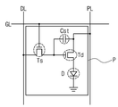
도 2에 도시한 바와 같이, 전계발광 표시장치에는, 서로 교차하여 화소영역(P)을 정의하는 게이트 배선(GL), 데이터 배선(DL) 및 파워 배선(PL)이 형성되고, 화소영역(P)에는, 스위칭 박막트랜지스터(Ts), 구동 박막트랜지스터(Td), 스토리지 커패시터(Cst), 발광다이오드(D)가 형성된다.As shown in FIG. 2, in the electroluminescent display device, gate lines GL, data lines DL and power lines PL that define a pixel area P crossing each other are formed, and the pixel area P ), a switching thin film transistor (Ts), a driving thin film transistor (Td), a storage capacitor (Cst), and a light emitting diode (D) are formed.
스위칭 박막트랜지스터(Ts)는 게이트 배선(GL) 및 데이터 배선(DL)에 연결되고, 구동 박막트랜지스터(Td) 및 스토리지 커패시터(Cst)는 스위칭 박막트랜지스터(Ts)와 파워 배선(PL) 사이에 연결된다. 발광다이오드(D)는 구동 박막트랜지스터(Td)에 연결된다. The switching thin film transistor Ts is connected to the gate wiring GL and the data wiring DL, and the driving thin film transistor Td and the storage capacitor Cst are connected between the switching thin film transistor Ts and the power wiring PL. do. The light emitting diode D is connected to the driving thin film transistor Td.
이러한 전계발광 표시장치에서는, 게이트 배선(GL)에 인가된 게이트 신호에 따라 스위칭 박막트랜지스터(Ts)가 턴-온(turn-on) 되면, 데이터 배선(DL)에 인가된 데이터 신호가 스위칭 박막트랜지스터(Ts)를 통해 구동 박막트랜지스터(Td)의 게이트 전극과 스토리지 커패시터(Cst)의 일 전극에 인가된다. In such an electroluminescent display device, when the switching thin film transistor Ts is turned on according to the gate signal applied to the gate wiring GL, the data signal applied to the data wiring DL is switched to the switching thin film transistor. It is applied to the gate electrode of the driving thin film transistor Td and one electrode of the storage capacitor Cst through (Ts).
구동 박막트랜지스터(Td)는 게이트 전극에 인가된 데이터 신호에 따라 턴-온 되며, 그 결과 데이터 신호에 비례하는 전류가 파워 배선(PL)으로부터 구동 박막트랜지스터(Td)를 통하여 발광다이오드(D)로 흐르게 되고, 발광다이오드(D)는 구동 박막트랜지스터(Td)를 통하여 흐르는 전류에 비례하는 휘도로 발광한다. The driving thin film transistor Td is turned on according to the data signal applied to the gate electrode, and as a result, a current proportional to the data signal is transferred from the power wiring PL to the light emitting diode D through the driving thin film transistor Td. The light emitting diode D emits light at a luminance proportional to the current flowing through the driving thin film transistor Td.
이때, 스토리지 커패시터(Cst)에는 데이터신호에 비례하는 전압으로 충전되어, 일 프레임(frame) 동안 구동 박막트랜지스터(Td)의 게이트 전극의 전압이 일정하게 유지되도록 한다. At this time, the storage capacitor Cst is charged with a voltage proportional to the data signal so that the voltage of the gate electrode of the driving thin film transistor Td is kept constant for one frame.
따라서, 전계발광 표시장치는 원하는 영상을 표시할 수 있다. Therefore, the electroluminescent display device can display a desired image.
-제 1 실시예--First Example-
도 3은 본 발명의 제 1 실시예에 따른 전계발광 표시장치의 개략적인 평면도이다.3 is a schematic plan view of an electroluminescent display device according to a first embodiment of the present invention.
도 3에 도시된 바와 같이, 본 발명의 제 1 실시예에 따른 전계발광 표시장치(100)는 표시영역(DA)과 표시영역(DA) 주변의 비표시영역(NDA)이 정의된 기판(미도시)을 포함한다. 기판의 표시영역(DA)에는, 제 1 방향(X)의 제 1 화소열에 다수의 화소(P11, P12, P13, P14)가 배열되고, 제 1 방향(X)의 제 2 화소열에 다수의 화소(P21, P22, P23)가 배열되며, 제 1 방향(X)의 제 3 화소열에 다수의 화소(P31, P32, P33)가 배열된다. 또한, 제 1 화소열과 제 2 화소열 사이에는 제 1 홈(182)이 구비되고, 제 2 화소열과 제 3 화소열 사이에는 제 2 홈(184)이 구비된다.As shown in FIG. 3, the
제 1 화소열은, 표시영역 일 끝에 위치하는 제 1 화소(P11)와, 표시영역 타 끝에 위치하는 제 2 화소(P12)와, 제 1 및 제 2 화소(P11, P12) 사이에 위치하는 제 3 화소(P13)을 포함한다. The first pixel column includes a first pixel P11 positioned at one end of the display area, a second pixel P12 positioned at the other end of the display area, and a first pixel positioned between the first and second pixels P11 and P12. It includes three pixels P13.
제 2 화소열은, 제 1 화소열로부터 제 2 방향(Y)으로 이격되고, 표시영역 일 끝에 위치하는 제 1 화소(P21)와, 표시영역 타 끝에 위치하는 제 2 화소(P22)와, 제 1 및 제 2 화소(P21, P22) 사이에 위치하는 제 3 화소(P23)을 포함한다. The second pixel column is spaced apart from the first pixel column in the second direction Y, and includes a first pixel P21 positioned at one end of the display area, a second pixel P22 positioned at the other end of the display area, and a second pixel column. And a third pixel P23 positioned between the first and second pixels P21 and P22.
제 3 화소열은, 표시영역 일 끝에 위치하는 제 1 화소(P31)와, 표시영역 타 끝에 위치하는 제 2 화소(P32)와, 제 1 및 제 2 화소(P31, P32) 사이에 위치하는 제 3 화소(P33)을 포함한다. 제 3 화소열은 제 2 화소열로부터 제 2 방향(Y)으로 이격됨으로써, 제 2 화소열이 제 1 화소열과 제 3 화소열 사이에 배치된다.The third pixel column includes a first pixel P31 positioned at one end of the display area, a second pixel P32 positioned at the other end of the display area, and a first pixel positioned between the first and second pixels P31 and P32. It includes three pixels P33. The third pixel column is spaced apart from the second pixel column in the second direction Y, so that the second pixel column is disposed between the first pixel column and the third pixel column.
도시하지 않았으나, 각 화소(P)에는 서로 마주하는 제 1 및 제 2 전극과 이들 사이에 배치되는 발광층을 포함하는 발광다이오드가 형성된다. Although not illustrated, light emitting diodes including first and second electrodes facing each other and a light emitting layer disposed therebetween are formed in each pixel P.
이때, 발광층은 액체 상태의 발광물질을 이용한 용액 공정(solution process)에 의해 형성된다. 즉, 용매에 녹아있는 발광물질 용액을 코팅한 후 용매를 건조하여 형성된다. 예를 들어, 용액 공정은 잉크젯 코팅(inkjet coating) 공정, 슬릿 코팅(slit coating) 공정, 스핀 코팅(spin coating) 공정, 프린팅 (printing) 공정, 드랍 코팅(drop coating) 공정 중 어느 하나일 수 있으나, 이에 한정되지 않는다.At this time, the light-emitting layer is formed by a solution process using a liquid-state light-emitting material. That is, it is formed by coating a solution of a luminescent material dissolved in a solvent and then drying the solvent. For example, the solution process may be any one of an inkjet coating process, a slit coating process, a spin coating process, a printing process, and a drop coating process. , But is not limited to this.
예를 들어, 잉크젯 헤드(미도시)가 제 1 방향(X)을 따라 이동하며 각 화소(P)에 발광물질 용액을 코팅한다. 제 1 화소열의 경우, 제 1 화소(P11)에서 제 2 화소(P12) 방향으로 코팅 공정이 진행된다.For example, an inkjet head (not shown) moves along the first direction X and coats the light emitting material solution to each pixel P. In the case of the first pixel column, the coating process is performed from the first pixel P11 to the second pixel P12.
제 1 및 제 2 홈(182, 184) 각각은 제 1 방향(X), 즉 용액 공정에서 잉크젯 헤드의 스캔 방향을 따라 그 표면적이 감소한다. 즉, 제 1 및 제 2 홈(182, 184) 각각은 스캔 시작 지점에서 제 2 방향(Y)으로 제 1 폭(w1)을 갖고 스캔 종료 지점에서 제 2 방향(Y)으로 제 1 폭(w1)보다 작은 제 2 폭(w2)을 가지며 스캔 시작 지점과 스캔 종료 지점 사이의 지점에서 제 2 방향(Y)으로 제 1 폭(w1)보다 작고 제 2 폭(w3)보다 큰 제 3 폭(w3)을 갖는다.Each of the first and
예를 들어, 제 1 홈(182)은 제 1 화소열의 일 끝에 위치하는 제 1 화소(P11)에 대응하여 제 2 방향(Y)으로 제 1 폭(w1)을 갖고 제 1 화소열의 타 끝에 위치하는 제 2 화소(P12)에 대응하여 제 2 방향(Y)으로 제 1 폭(w1)보다 작은 제 2 폭(w2)을 가지며 제 1 및 제 2 화소(P11, P12) 사이에 위치하는 제 3 화소(P13)에 대응하여 제 2 방향(Y)으로 제 1 폭(w1)보다 작고 제 2 폭(w3)보다 큰 제 3 폭(w3)을 갖는다.For example, the
다시 말해, 제 1 홈(182)은, 제 1 화소열의 일 끝에 대응되며 제 2 방향(Y)으로 제 1 폭(w1)을 갖는 제 1 부분, 제 1 화소열의 타 끝에 대응되며 제 2 방향(Y)으로 제 2 폭(w2)을 갖는 제 2 부분과, 제 1 부분과 제 2 부분 사이에 위치하며 제 2 방향(Y)으로 제 3 폭(w3)을 갖는 제 3 부분을 포함한다. 이에 따라, 제 1 홈(182)의 제 3 부분은 제 1 홈(182)의 제 1 부분보다 작고 제 1 홈(182)의 제 2 부분보다 큰 표면적을 갖는다.In other words, the
또한, 제 2 홈(184)은, 제 1 화소열의 일 끝에 대응되며 제 2 방향(Y)으로 제 1 폭(w1)을 갖는 제 1 부분, 제 1 화소열의 타 끝에 대응되며 제 2 방향(Y)으로 제 2 폭(w2)을 갖는 제 2 부분과, 제 1 부분과 제 2 부분 사이에 위치하며 제 2 방향(Y)으로 제 3 폭(w3)을 갖는 제 3 부분을 포함한다. 이에 따라, 제 2 홈(184)의 제 3 부분은 제 2 홈(184)의 제 1 부분보다 작고 제 2 홈(184)의 제 2 부분보다 큰 표면적을 갖는다.In addition, the
발광다이오드의 발광층을 액체 상태의 용액을 이용한 용액 공정(코팅 공정)에 의해 형성할 경우, 제 1 및 제 2 홈(182, 184)에 용매를 포함하는 발광물질 또는 용매가 코팅된다. When the light emitting layer of the light emitting diode is formed by a solution process using a liquid solution (coating process), a light emitting material or a solvent containing a solvent is coated on the first and
이때, 제 1 홈(182)는 스캔 방향인 제 1 방향(X)을 따라 표면적의 편차를 갖기 때문에, 용매의 증발 속도 역시 제 1 방향(X)을 따라 달라진다. 즉, 제 1 홈(182)에서의 용매 증발은, 제 1 화소(P11)에 대응하여 제 1 속도를 갖고 제 2 화소(P12)에 대응하여 제 2 속도를 가지며 제 3 화소(P13)에 대응하여 제 1 속도보다 작고 제 2 속도보다 큰 제 3 속도를 갖게 된다.At this time, since the
따라서, 제 3 화소(P13)에 대응된 영역에서 용매의 포화 속도가 제 1 화소(P11)에 대응된 영역에서 용매의 포화 속도보다 작고 제 2 화소(P12)에 대응된 영역에서 용매의 포화 속도보다 크게 된다.Therefore, the saturation rate of the solvent in the area corresponding to the third pixel P13 is less than the saturation rate of the solvent in the area corresponding to the first pixel P11 and the saturation rate of the solvent in the area corresponding to the second pixel P12. It becomes bigger.
전술한 바와 같이, 용액 공정에서는, 제 1 화소(P11), 제 2 화소(P12) 및 제 3 화소(P13)는 진공 건조 챔버로 이송되기까지 다른 자연 건조 기간을 갖게 된다. 그러나, 본 발명의 전계발광 표시장치(100)에서는, 그 폭을 달리하는 홈(182, 184)에 의해 제 1 내지 제 3 화소(P11, P12, P13)에 대응된 영역에서 용매의 포화 속도가 조절되므로 제 1 내지 제 3 화소(P11, P12, P13)의 자연 건조 기간을 균일하게 할 수 있다.As described above, in the solution process, the first pixel P11, the second pixel P12, and the third pixel P13 have different natural drying periods until they are transferred to the vacuum drying chamber. However, in the
따라서, 자연 건조 시간의 차이에 의해 발생되는 발광층의 두께 불균일 문제가 방지된다.Therefore, the problem of the thickness non-uniformity of the light emitting layer caused by the difference in the natural drying time is prevented.
도 4는 도 3의 IV-IV 선을 따라 절단한 단면도이고, 도 5는 도 3의 V-V 선을 따라 절단한 단면도이다. 도 6은 도 3의 VI-VI 선을 따라 절단한 단면도이고, 도 7은 도 3의 VII-VII 선을 따라 절단한 단면도이다.4 is a cross-sectional view taken along line IV-IV of FIG. 3, and FIG. 5 is a cross-sectional view taken along line V-V of FIG. 3. 6 is a cross-sectional view taken along line VI-VI of FIG. 3, and FIG. 7 is a cross-sectional view taken along line VII-VII of FIG. 3.
도 3과 함께 도 4 내지 도 7을 참조하면, 본 발명의 제 1 실시예에 따른 전계발광 표시장치(100)는, 제 1 방향(X)으로 배열되는 다수의 화소(P11, P12, P13)를 포함하는 제 1 화소열과, 제 1 화소열로부터 제 2 방향(Y)으로 이격되고 제 1 방향(X)으로 배열되는 다수의 화소(P21, P22, P23)를 포함하는 제 2 화소열과, 제 2 화소열로부터 제 2 방향(Y)으로 이격되고 제 1 방향(X)으로 배열되는 다수의 화소(P31, P32, P33)를 포함하는 제 3 화소열이 정의된 기판(110)과, 기판(110) 상에 위치하는 구동 박막트랜지스터(Td)와, 구동 박막트랜지스터(Td)에 연결되는 발광다이오드(D)와, 제 1 화소열과 제 2 화소열 사이에 위치하는 제 1 홈(182)과, 제 2 화소열과 제 3 화소열 사이에 위치하는 제 2 홈(184)을 포함한다.Referring to FIGS. 4 to 7 together with FIG. 3, the
기판(110) 상에는, 제 1 및 제 2 방향을 따라 각각 연장되는 게이트 배선(도 2의 GL) 및 데이터 배선(DL), 게이트 배선(GL) 및 데이터 배선(DL)에 연결되는 스위칭 박막트랜지스터(도 2의 Ts), 데이터 배선(DL)과 평행하게 이격하는 파워 배선(PL)이 형성될 수 있다. 이와 달리, 파워 배선(PL)은 게이트 배선(GL)과 평행하게 이격하며 형성될 수도 있다.On the
게이트 배선(GL)과 데이터 배선(DL)은 교차하여 다수의 화소(P)를 정의하며, 구동 박막트랜지스터(Td)는 스위칭 박막트랜지스터에 연결된다. 또한, 다수의 화소(P)에는 스토리지 캐패시터(도 3의 Cst)가 구비될 수 있다.The gate wiring GL and the data wiring DL cross to define a plurality of pixels P, and the driving thin film transistor Td is connected to the switching thin film transistor. In addition, a storage capacitor (Cst in FIG. 3) may be provided in the plurality of pixels P.
유리 또는 플라스틱으로 이루어지는 기판(110) 상에는 반도체층(120)이 형성된다. 반도체층(120)은 산화물 반도체 물질로 이루어지거나 다결정 실리콘으로 이루어질 수 있다.The
반도체층(120)은 산화물 반도체 물질로 이루어질 경우 반도체층(120) 하부에는 차광패턴(도시하지 않음) 이 형성될 수 있으며, 차광패턴은 반도체층(120)으로 빛이 입사되는 것을 방지하여 반도체층(120)이 빛에 의해 열화되는 것을 방지한다. 이와 달리, 반도체층(120)은 다결정 실리콘으로 이루어질 수도 있으며, 이 경우 반도체층(120)의 양 가장자리에 불순물이 도핑되어 있을 수 있다. When the
반도체층(120) 상에는 절연물질로 이루어진 게이트 절연막(122)이 기판(110) 전면에 형성된다. 게이트 절연막(122)은 산화 실리콘 또는 질화 실리콘과 같은 무기절연물질로 이루어질 수 있다.On the
게이트 절연막(122) 상에는 금속과 같은 도전성 물질로 이루어진 게이트 전극(130)이 반도체층(120)의 중앙에 대응하여 형성된다. 또한, 게이트 절연막(122) 상부에는 게이트 배선(GL)과 스토리지 캐패시터(Cst)의 제 1 캐패시터 전극(미도시)이 형성될 수 있다. 게이트 배선(GL)은 제1방향을 따라 연장되고, 제 1 캐패시터 전극은 게이트 전극(130)에 연결될 수 있다.A
도 4 내지 도 7에서, 게이트 절연막(122)이 기판(110) 전면에 형성되어 있으나, 게이트 절연막(122)은 게이트전극(130)과 동일한 모양으로 패터닝될 수도 있다. 4 to 7, the
게이트 전극(130) 상에는 절연물질로 이루어진 층간 절연막(136)이 기판(110) 전면에 형성된다. 층간 절연막(136)은 산화 실리콘이나 질화 실리콘과 같은 무기 절연물질로 형성되거나, 벤조사이클로부텐(benzocyclobutene)이나 포토 아크릴(photo-acryl)과 같은 유기 절연물질로 형성될 수 있다. An interlayer insulating
층간 절연막(136)은 반도체층(120)의 양측을 노출하는 제 1 및 제 2 콘택홀(137, 138)을 갖는다. 제 1 및 제 2 콘택홀(137, 138)은 게이트 전극(130)의 양측에 게이트 전극(130)과 이격되어 위치한다. The
도 4에서, 제 1 및 제 2 콘택홀(137, 138)은 게이트 절연막(122) 내에도 형성된다. 이와 달리, 게이트 절연막(122)이 게이트 전극(130)과 동일한 모양으로 패터닝될 경우, 제 1 및 제 2 콘택홀(137, 138)은 층간 절연막(136) 내에만 형성될 수도 있다. In FIG. 4, the first and second contact holes 137 and 138 are also formed in the
층간 절연막(136) 상에는 금속과 같은 도전성 물질로 이루어지는 소스 전극(140)과 드레인 전극(142)이 형성된다. 또한, 층간 절연막(136) 상에는 제 2 방향을 따라 연장되는 데이터 배선(DL)과 전원 배선(PL) 및 제 2 캐패시터 전극(미도시)이 형성될 수 있다. A
소스 전극(140)과 드레인 전극(142)은 게이트 전극(130)을 중심으로 이격되어 위치하며, 각각 제 1 및 제 2 콘택홀(137, 138)을 통해 반도체층(120)의 양측과 접촉한다. 데이터 배선(DL)은 제 2 방향을 따라 연장되어 게이트 배선(GL)과 교차함으로써 제 1 및 제 2 화소(P1, P2)을 정의하며, 파워 배선(PL)은 데이터 배선(DL)과 이격되어 위치한다. The
이와 달리, 파워 배선(PL)은 게이트 배선(GL)과 동일 층에 게이트 배선(GL)과 평행하게 이격하여 위치함으로써, 데이터 배선(DL)과 교차하도록 형성될 수도 있다. Alternatively, the power wiring PL may be formed to cross the data wiring DL by being spaced apart from the gate wiring GL in the same layer as the gate wiring GL.
제 2 캐패시터 전극은 소스 전극(140)과 연결되고 제 1 캐패시터 전극과 중첩함으로써, 제 1 및 제 2 캐패시터 전극 사이의 층간 절연막(136)을 유전체층으로 하여 스토리지 캐패시터(Cst)를 이룬다. The second capacitor electrode is connected to the
반도체층(120)과, 게이트전극(130), 소스 전극(140), 드레인전극(142)은 구동 박막트랜지스터(Td)를 이루며, 구동 박막트랜지스터(Td)는 반도체층(120)의 상부에 게이트 전극(130), 소스 전극(140) 및 드레인 전극(142)이 위치하는 코플라나(coplanar) 구조를 가진다. The
이와 달리, 구동 박막트랜지스터(Td)는 반도체층의 하부에 게이트 전극이 위치하고 반도체층의 상부에 소스 전극과 드레인 전극이 위치하는 역 스태거드(inverted staggered) 구조를 가질 수 있다. 이 경우, 반도체층은 비정질 실리콘으로 이루어질 수 있다. Alternatively, the driving thin film transistor Td may have an inverted staggered structure in which a gate electrode is positioned under the semiconductor layer and a source electrode and a drain electrode are positioned over the semiconductor layer. In this case, the semiconductor layer may be made of amorphous silicon.
전술한 바와 같이, 기판(110) 상에는 스위칭 박막트랜지스터(Ts)가 더 형성되는데, 스위칭 박막트랜지스터(Ts)는 구동 박막트랜지스터(Td)와 실질적으로 동일한 구조를 갖는다. As described above, the switching thin film transistor Ts is further formed on the
구동 박막트랜지스터(Td)의 게이트 전극(130)은 스위칭 박막트랜지스터(Ts)의 드레인 전극(미도시)에 연결되고 구동 박막트랜지스터(Td)의 소스 전극(140)은 파워 배선(PL)에 연결된다. 또한, 스위칭 박막트랜지스터(Ts)의 게이트 전극(미도시)과 소스 전극(미도시)은 게이트 배선(GL) 및 데이터 배선(DL)에 각각 연결된다. The
구동 박막트랜지스터(Td)의 드레인 전극(142)을 노출하는 드레인 콘택홀(152)을 갖는 보호층(150)이 구동 박막트랜지스터(Td)를 덮으며 형성된다. A
보호층(150) 상에는 드레인 콘택홀(152)을 통해 구동 박막트랜지스터(Td)의 드레인 전극(142)에 연결되는 제 1 전극(160)이 제 1 및 제 2 화소(P1, P2) 별로 분리되어 형성된다. 제 1 전극(160)은 애노드(anode)일 수 있으며, 일함수 값이 비교적 큰 도전성 물질로 이루어질 수 있다. 예를 들어, 제 1 전극(160)은 인듐-틴-옥사이드(indium-tin-oxide, ITO) 또는 인듐-징크-옥사이드(indium-zinc-oxide, IZO)와 같은 투명 도전성 물질로 이루어질 수 있다. The
한편, 본 발명의 전계발광 표시장치가 상부 발광 방식(top-emission type)인 경우, 제 1 전극(160) 하부에는 반사전극 또는 반사층이 더욱 형성될 수 있다. 예를 들어, 반사전극 또는 반사층은 알루미늄-팔라듐-구리(aluminum-palladium-copper: APC) 합금으로 이루어질 수 있다.Meanwhile, when the electroluminescent display device of the present invention is of a top-emission type, a reflective electrode or a reflective layer may be further formed under the
또한, 보호층(150) 상에는 제 1 전극(160)의 가장자리를 덮는 뱅크층(170)이 형성된다. 뱅크층(170)은 다수의 화소(P) 각각에 대응하여 개구(opening, OP)를 갖는다. 또한, 뱅크층(170)은 제 1 및 제 2 화소열 사이에 대응하여 제 1 홈(182)을 갖고 제 2 및 제 3 화소열 사이에 대응하여 제 2 홈(184)을 갖는다. In addition, the
한편, 뱅크층(170)은 제 1 화소열에 배열되는 화소(P11, P12, P13) 사이에서 홈 없이 평탄한 상부면을 갖는다. 즉, 뱅크층(170)은 제 1 방향(X)으로 인접한 화소(P), 예를 들어 제 1 화소열의 제 3 화소(P13) 및 제 4 화소(P14) 사이에서 평탄한 상부면을 갖고 제 2 방향(Y)으로 인접한 화소(P) 사이에서 오목한 상부면을 갖는다.Meanwhile, the
뱅크층(170)의 개구(OP)에 의해 제 1 전극(160)의 중앙이 노출되며, 뱅크층(170)의 홈(182, 184)에 의해 보호층(150)이 노출된다. 즉, 홈(182, 184) 각각의 깊이는 뱅크층(170)의 두께와 실질적으로 동일하다. 이와 달리, 뱅크층(170)의 일부만이 제거되어 홈(182, 184)이 형성됨으로써, 홈(182, 184) 각각의 깊이는 뱅크층(170)의 두께보다 작을 수 있다. 또한, 뱅크층(170) 전체와 보호층(150)의 전체 또는 일부가 제거되어 홈(182, 184)이 형성됨으로써, 홈(182, 184) 각각의 깊이는 뱅크층(170)의 두께보다 클 수 있다.The center of the
제 1 화소열과 제 2 화소열에 사이에 위치하는 제 1 홈(182)은, 제 1 화소열의 일 끝에 위치하는 제 1 화소(P11)에 대응하여 제 2 방향(Y)으로 제 1 폭(w1)을 갖고 제 1 화소열의 타 끝에 위치하는 제 2 화소(P12)에 대응하여 제 2 방향(Y)으로 제 1 폭(w1)보다 작은 제 2 폭(w2)을 가지며 제 1 및 제 2 화소(P11, P12) 사이에 위치하는 제 3 화소(P13)에 대응하여 제 2 방향(Y)으로 제 1 폭(w1)보다 작고 제 2 폭(w3)보다 큰 제 3 폭(w3)을 갖는다.The
다시 말해, 제 1 및 제 2 홈(182, 184) 각각은 각 화소열의 일 끝에 대응되며 제 2 방향(Y)으로 제 1 폭(w1)을 갖는 제 1 부분, 각 화소열의 타 끝에 대응되며 제 2 방향(Y)으로 제 2 폭(w2)을 갖는 제 2 부분과, 제 1 부분과 제 2 부분 사이에 위치하며 제 2 방향(Y)으로 제 3 폭(w3)을 갖는 제 3 부분을 포함한다. 이에 따라, 제 1 홈(182)의 제 3 부분은 제 1 홈(182)의 제 1 부분보다 작고 제 1 홈(182)의 제 2 부분보다 큰 표면적을 갖는다.In other words, each of the first and
제 1 및 제 2 홈(182, 184) 각각의 폭은 각 화소열의 일끝에서 타끝으로 갈수록 점진적으로 감소한다. 이와 달리, 제 1 및 제 2 홈(182, 184) 각각은, 각 화소열의 일 측에 위치하는 제 1 화소 그룹에 대응하여 제 1 폭을 갖고 각 화소열의 타 측에 위치하는 제 2 화소 그룹에 대응하여 제 2 폭을 가지며 제 1 및 제 2 화소 그룹 사이에 위치하는 제 3 화소 그룹에 대응하여 제 1 폭보다 작고 제 2 폭보다 큰 제 3 폭을 가질 수 있다.The width of each of the first and
제 1 전극(160) 상에는 발광층(162)이 형성된다. 발광층(162)은 액체 상태의 발광 물질을 이용한 용액 공정(solution process)에 의해 형성된다. 즉, 용매에 녹아있는 발광물질 용액을 코팅한 후 용매를 건조하여 형성된다. 예를 들어, 용액 공정은 잉크젯 코팅(inkjet coating) 공정, 슬릿 코팅(slit coating) 공정, 스핀 코팅(spin coating) 공정, 프린팅 (printing) 공정, 드랍 코팅(drop coating) 공정 중 어느 하나일 수 있으나, 이에 한정되지 않는다.The
뱅크층(170)은 경사진 측면을 가지며, 발광층(162)은 뱅크(170)의 경사진 측면을 따라 형성되어 그 가장자리가 경사지게 형성된다. 또한, 발광층(162)은 용액 공정에 의해 형성되기 때문에, 건조 공정에서의 커피-링 효과에 의해 발광층(162)의 가장자리는 중앙보다 큰 두께를 가질 수 있다.The
발광층(162)은 발광물질로 이루어지는 발광물질층(emitting material layer)의 단일층 구조일 수 있다. 또한, 발광 효율을 높이기 위해, 발광층(162)은 제 1 전극(160)과 발광물질층 사이에 순차적으로 위치하는 정공주입층(hole injection layer) 및 정공수송층(hole transporting layer)과, 발광물질층과 제 2 전극(164) 사이에 순차적으로 위치하는 전자수송층(electron transporting layer) 및 전자주입층(electron injection layer)를 더 포함할 수 있다. The
발광물질층은 양자점(quantum dot)과 같은 무기발광물질 또는 유기발광물질을 포함할 수 있다. 즉, 본 발명의 전계발광 표시장치(100)는 유기발광 표시장치(OLED) 또는 양자점발광 표시장치(QLED)일 수 있다. The light emitting material layer may include an inorganic light emitting material such as a quantum dot or an organic light emitting material. That is, the
홈(182, 184)에는 발광물질 용액의 용매가 코팅된 후 건조되어 증발된다. 따라서, 발광층(162)의 형성 공정 후에, 홈(182, 184)에는 아무런 구성 요소 없이 보호층(150)이 노출될 수 있다. The
이와 달리, 홈(182, 184)에 발광물질 용액이 코팅되는 경우, 홈(182, 184)에는 보조물질패턴(미도시)이 형성될 수도 있다.Alternatively, when the luminescent material solution is coated on the
발광물질 용액은 제 1 방향(X)의 일 끝(즉 도 3에서 좌측 끝)으로부터 타 끝(즉, 도 3에서 우측 끝)을 향해 잉크젯 헤드(미도시)가 이동하며 코팅된다. 예를 들어, 제 1 화소열의 제 1 화소(P11)과 이에 대응하는 제 1 홈(182)의 제 1 부분에서 발광물질 용액의 코팅 공정이 시작되고, 제 1 화소열의 제 2 화소(P12)과 이에 대응하는 제 1 홈(182)의 제 2 부분에서 발광물질 용액의 코팅 공정이 종료된다. 이후, 코팅 공정이 종료된 기판(110)은 진공 건조 챔버로 이송된다.The luminescent material solution is coated while the ink jet head (not shown) moves from one end in the first direction X (ie, the left end in FIG. 3) to the other end (ie, the right end in FIG. 3). For example, the coating process of the luminescent material solution starts in the first portion of the first pixel column P11 and the corresponding
이때, 제 1 화소(P11)는 제 2 및 제 3 화소(P12, P13)보다 긴 기간 동안 자연 증발 조건에 놓여지지만, 제 1 홈(182)의 제 1 부분이 제 2 및 제 3 부분보다 큰 폭(w1)을 갖기 때문에 제 1 홈(182)의 제 2 및 제 3 부분에서보다 제 1 홈(182)의 제 1 부분에서 용매가 빨리 증발한다. 따라서, 제 1 화소(P11) 부근에서 용매의 포화 속도가 제 2 및 제 3 화소(P12, P13) 부근에서 용매의 포화 속도보다 빠르게 된다.At this time, the first pixel P11 is subjected to natural evaporation conditions for a longer period than the second and third pixels P12 and P13, but the first portion of the
다시 말해, 제 1 내지 제 3 화소(P11, P12, P13)는 발광물질 용액 코팅 후 진공 건조 챔버로 이송되기까지 서로 다른 시간을 갖지만 용매의 포화 속도가 다르기 때문에, 동일한 자연 건조 기간을 갖는다. 따라서, 코팅 공정 방향에 따른 발광층의 두께 불균일 문제가 방지되거나 최소화된다.In other words, the first to third pixels P11, P12, and P13 have different times before being transferred to the vacuum drying chamber after coating the luminescent material solution, but have the same natural drying period because the saturation rate of the solvent is different. Therefore, the problem of the thickness non-uniformity of the light emitting layer according to the coating process direction is prevented or minimized.
제 1 및 제 2 홈(182, 184) 내의 보호층(150), 각 화소(P)의 발광층(162) 및 뱅크층(170) 상에 제 2 전극(164)이 형성된다. The
제 2 전극(164)은 기판(110)의 표시영역의 전면에 위치하며 일함수 값이 비교적 작은 도전성 물질로 이루어져 캐소드(cathode)로 이용될 수 있다. 예를 들어, 제 2 전극(164)은 알루미늄(Al), 마그네슘(Mg), 알루미늄-마그네슘 합금(AlMg) 중 어느 하나로 이루어질 수 있다. The
본 발명의 전계발광 표시장치(100)가 상부 발광 방식인 경우, 제 2 전극(164)은 빛이 투과되도록 비교적 얇은 두께를 가질 수 있다. 한편, 본 발명의 전계발광 표시장치(100)가 하부 발광 방식인 경우, 제 2 전극(164)은 반사전극으로 이용될 수 있다.When the
제 2 전극(164)은 각 화소(P)에서 발광층(162)와 접촉하고, 제 1 및 제 2 홈(182, 184)에서 제 2 전극(164)은 보호층(150)과 접촉한다.The
또한, 각 화소열의 화소(P) 사이에서 제 2 전극(164)은 뱅크층(170)과 접촉한다.Further, the
다시 말해, 기판(110)으로부터, 제 2 전극(164)은 제 1 및 제 2 화소(P1, P2) 각각에서 제 1 높이를 갖고 제 1 및 제 2 홈(182, 184)에서 제 1 높이보다 작은 제 2 높이를 갖는다. 또한, 기판(110)으로부터 제 2 전극(164)은 각 화소열의 화소(P) 사이에서 제 1 높이보다 큰 제 3 높이를 갖는다.In other words, from the
한편, 제 1 및 제 2 홈(182, 184)에 보조물질패턴(미도시)이 형성되는 경우, 제 2 전극(164)은 제 1 및 제 2 홈(182, 184)에서 보조물질패턴과 접촉하고 기판(110)으로부터 제 1 높이와 실질적으로 동일한 제 4 높이를 갖는다. 이때, 보조물질패턴은 제 1 전극(160)과 접촉하지 않기 때문에, 제 1 및 제 2 홈(182, 184)에 형성된 보조물질패턴에서는 발광이 일어나지 않는다.Meanwhile, when an auxiliary material pattern (not shown) is formed in the first and
제 1 전극(160)과, 제 1 전극(160)과 마주하는 제 2 전극(164)과, 제 1 및 제 2 전극(160, 164) 사이에 위치하는 발광층(162)은 발광다이오드(D)를 이룬다. The
도시하지 않았으나, 발광다이오드(D) 상부에는 인캡슐레이션 기판 또는 인캡슐레이션 필름이 더 형성될 수 있다.Although not illustrated, an encapsulation substrate or an encapsulation film may be further formed on the light emitting diode D.
예를 들어, 무기절연층, 유기절연층 및 무기절연층이 순차 적층되어 외부로부터의 수분 침투를 방지하고 발광다이오드를 보호하는 인캡슐레이션 필름이 발광다이오드(D)를 덮으며 형성될 수 있다.For example, an inorganic insulating layer, an organic insulating layer, and an inorganic insulating layer may be sequentially stacked to form an encapsulation film that prevents moisture penetration from the outside and protects the light emitting diode, covering the light emitting diode (D).
또한, 인캡슐레이션 필름 상에는 외부광 반사를 최소화하기 위한 편광판이 부착될 수 있다. 편광판은 원형 편광판일 수 있다.In addition, a polarizing plate for minimizing external light reflection may be attached on the encapsulation film. The polarizing plate may be a circular polarizing plate.
본 발명의 전계발광 표시장치(100)에 있어서, 발광층(162)은 용액 공정에 의해 형성되기 때문에, 제조 공정이 단순해지고 대면적 표시장치의 제조에도 적합하다.In the
또한, 용액 공정에서의 스캔 방향에 따라 각 화소열 사이에 형성된 홈(182, 184)이 표면적을 달리하고 용매 또는 발광물질 용액을 홈(182, 184)에 코팅함으로써, 스캔 방향에 따라 발생되는 발광층(162)의 두께 불균일 문제를 방지하거나 최소화할 수 있다. 따라서, 발광층(162)의 두께 불균일에 의한 전계발광 표시장치(100)의 표시 품질 저하 문제를 해소할 수 있다.In addition, the
-제 2 실시예--Second Example-
도 8은 본 발명의 제 2 실시예에 따른 전계발광 표시장치의 개략적인 평면도이다.8 is a schematic plan view of an electroluminescent display device according to a second embodiment of the present invention.
도 8에 도시된 바와 같이, 본 발명의 제 2 실시예에 따른 전계발광 표시장치(100)는 표시영역(DA)과 표시영역(DA) 주변의 비표시영역(NDA)이 정의된 기판(미도시)을 포함한다. 기판의 표시영역(DA)에는, 제 1 방향(X)의 제 1 화소열에 다수의 화소(P11, P12, P13)가 배열되고, 제 1 방향(X)의 제 2 화소열에 다수의 화소(P21, P22, P23)가 배열되며, 제 1 방향(X)의 제 3 화소열에 다수의 화소(P31, P32, P33)가 배열된다. 또한, 제 1 화소열과 제 2 화소열 사이에는 제 1 홈(182)이 구비되고, 제 2 화소열과 제 3 화소열 사이에는 제 2 홈(184)이 구비된다.As shown in FIG. 8, the
이때, 제 1 홈(182)은 제 1 화소열의 제 1 내지 제 3 화소(P11, P12, P13)에 각각 대응되는 제 1 내지 제 3 홈 패턴(182a, 182b, 182c)을 포함하고, 제 2 홈(184)은 제 2 화소열의 제 1 내지 제 3 화소(P21, P22, P23)에 각각 대응되는 제 1 내지 제 3 홈 패턴(184a, 184b, 184c)을 포함한다.In this case, the
즉, 제 1 실시예에 따른 전계발광 표시장치(100)와 달리, 제 2 실시예에 따른 전계발광 표시장치(100)의 제 1 홈(182)은 서로 이격된 섬 형상의 홈 패턴(182a, 182b, 182c)을 포함하고 제 2 홈(184)은 서로 이격된 섬 형상의 홈 패턴(184a, 184b, 184c)을 포함한다.That is, unlike the
각 화소열에 대응하여, 제 3 홈 패턴(182c, 184c)은 제 1 홈 패턴(182a, 184a)보다 작고 제 2 홈 패턴(182b, 184b)보다 큰 표면적을 갖는다. 즉, 각 화소열에 대응하여, 제 2 방향(Y)에 있어서, 제 3 홈 패턴(182c, 184c)은 제 1 홈 패턴(182a, 184a)보다 작고 제 2 홈 패턴(182b, 184b)보다 큰 폭을 갖는다. Corresponding to each pixel column, the
이와 달리, 제 3 홈 패턴(182c, 184c)은 제 2 방향(Y)을 따라 제 1 홈 패턴(182a, 184a) 및 제 2 홈 패턴(182b, 184b)과 동일한 폭을 갖고 제 1 방향(X)을 따라 제 1 홈 패턴(182a, 184a)보다 작고 제 2 홈 패턴(182b, 184b)보다 큰 길이를 가질 수도 있다.Alternatively, the
제 1 홈(182)에서, 제 1 홈 패턴(182a)로부터 제 2 홈 패턴(182b)을 향해 그 폭이 점진적으로 감소할 수 있다. 이와 달리, 제 1 홈(182)에서, 제 1 홈 패턴(182a)이 제 1 화소열의 일 측에 위치하는 제 1 화소 그룹에 대응되고, 제 2 홈 패턴(182b)이 제 1 화소열의 타 측에 위치하는 제 2 화소 그룹에 대응되며, 제 3 홈 패턴(182c)이 제 1 및 제 2 화소 그룹 사이에 위치하는 제 3 화소 그룹에 대응될 수 있다.In the
-제 3 실시예--Third Example-
도 9는 본 발명의 제 3 실시예에 따른 전계발광 표시장치의 개략적인 평면도이다. 9 is a schematic plan view of an electroluminescent display device according to a third embodiment of the present invention.
도 9에 도시된 바와 같이, 본 발명의 제 3 실시예에 따른 전계발광 표시장치(200)는 표시영역(DA)과 표시영역(DA) 주변의 비표시영역(NDA)이 정의된 기판(미도시)을 포함한다. 기판의 표시영역(DA)에는, 제 1 방향(X)을 따라 다수의 제 1 화소(P1)가 배열된 제 1 화소열, 제 1 화소열의 일측에 위치하고 제 1 방향(X)을 따라 다수의 제 2 화소(P2)가 배열된 제 2 화소열, 제 1 및 제 2 화소열 사이에 위치하며 제 1 방향(X)을 따라 다수의 제 3 화소(P3)가 배열된 제 3 화소열이 정의된다. 또한, 제 1 화소열과 제 3 화소열 사이에는 제 1 홈(282)이 구비되고, 제 2 화소열과 제 3 화소열 사이에는 제 2 홈(284)이 구비된다.As shown in FIG. 9, the
도시하지 않았으나, 각 화소(P)에는 서로 마주하는 제 1 및 제 2 전극과 이들 사이에 배치되는 발광층을 포함하는 발광다이오드가 형성된다. Although not illustrated, light emitting diodes including first and second electrodes facing each other and a light emitting layer disposed therebetween are formed in each pixel P.
이때, 발광층은 액체 상태의 발광물질을 이용한 용액 공정(solution process)에 의해 형성된다. 즉, 용매에 녹아있는 발광물질 용액을 코팅한 후 용매를 건조하여 형성된다. 예를 들어, 용액 공정은 잉크젯 코팅(inkjet coating) 공정, 슬릿 코팅(slit coating) 공정, 스핀 코팅(spin coating) 공정, 프린팅 (printing) 공정, 드랍 코팅(drop coating) 공정 중 어느 하나일 수 있으나, 이에 한정되지 않는다.At this time, the light-emitting layer is formed by a solution process using a liquid-state light-emitting material. That is, it is formed by coating a solution of a luminescent material dissolved in a solvent and then drying the solvent. For example, the solution process may be any one of an inkjet coating process, a slit coating process, a spin coating process, a printing process, and a drop coating process. , But is not limited to this.
예를 들어, 잉크젯 헤드(미도시)가 제 2 방향(Y)을 따라 이동하며 각 화소(P)에 발광물질 용액을 코팅한다. 제 1 화소열의 경우, 제 1 화소열에서 제 2 화소열 방향으로 코팅 공정이 진행된다.For example, an inkjet head (not shown) moves along the second direction Y and coats the light emitting material solution to each pixel P. In the case of the first pixel column, a coating process is performed from the first pixel column to the second pixel column.
제 1 홈(282)은 제 2 홈(284)보다 큰 표면적을 갖는다. 즉, 제 1 홈(282)은 제 2 방향(Y)을 따라 제 1 폭(w1)을 갖고, 제 2 홈(284)은 제 2 방향(Y)을 따라 제 1 폭(w1)보다 작은 제 2 폭(w2)을 갖는다. 이때, 제 1 홈(282)은 제 1 화소열 전체에 대응하여 균일한 폭을 갖고, 제 2 홈(284)은 제 2 화소열 전체에 대응하여 균일한 폭을 갖는다.The
한편, 도 9에서, 제 1 및 제 2 홈(282, 284)은 각 화소열에 대응되어 일체로 형성된다. 이와 달리, 제 1 및 제 2 홈(282, 284) 각각은 각 화소(P)에 대응하는 다수의 홈 패턴을 포함할 수 있다.Meanwhile, in FIG. 9, the first and
또한, 스캔 방향을 따라 홈의 표면적, 즉 폭이 점진적으로 감소하는 것이 보여지고 있다. 이와 달리, 둘 이상의 화소열을 포함하는 화소열 그룹 단위로 표면적이 변화될 수도 있다.It has also been shown that the surface area of the groove, ie the width, gradually decreases along the scan direction. Alternatively, the surface area may be changed in units of pixel column groups including two or more pixel columns.
발광다이오드의 발광층을 액체 상태의 용액을 이용한 용액 공정(코팅 공정)에 의해 형성할 경우, 제 1 및 제 2 홈(282, 284)에 용매를 포함하는 발광물질 또는 용매가 코팅된다.When the light emitting layer of the light emitting diode is formed by a solution process using a liquid solution (coating process), a light emitting material or a solvent containing a solvent is coated on the first and
이때, 스캔 방향인 제 2 방향(Y)에 배열된 제 1 및 제 2 홈(282, 284)은 표면적의 편차를 갖기 때문에, 용매의 증발 속도 역시 제 2 방향(Y)을 따라 달라진다. 즉, 용매의 증발은 제 1 홈(282)에서 제 1 속도를 갖고 제 2 홈(284)에서 제 1 속도보다 작은 제 2 속도를 갖는다.At this time, since the first and
따라서, 제 1 화소열에 대응된 영역에서 용매의 포화 속도가 제 2 화소열에 대응된 영역에서 용매의 포화 속도보다 증가한다.Therefore, the saturation rate of the solvent in the region corresponding to the first pixel column is increased than that of the solvent in the region corresponding to the second pixel row.
또한, 기판의 표시영역(DA)에는, 제 1 화소열의 타측에 위치하고 제 1 방향(X)을 따라 다수의 제 4 화소(P4)가 배열된 제 4 화소열과, 제 2 화소열로부터 제 2 방향(Y)으로 이격되고 제 1 방향(X)을 따라 다수의 제 5 화소(P5)가 배열된 제 5 화소열이 더 정의될 수 있다. 이 경우, 제 1 화소열과 제 4 화소열 사이에는 제 3 홈(286)이 구비되고, 제 2 화소열과 제 5 화소열 사이에는 제 4 홈(288)이 구비될 수 있다.In addition, a fourth pixel column in the display area DA of the substrate and arranged on the other side of the first pixel column and in which a plurality of fourth pixels P4 are arranged along the first direction X, and a second direction from the second pixel column A fifth pixel column spaced apart from (Y) and in which a plurality of fifth pixels P5 are arranged along the first direction X may be further defined. In this case, a
제 3 홈(286)의 표면적은 제 1 홈(282)의 표면적보다 크고, 제 4 홈(288)의 표면적은 제 2 홈(284)의 표면적보다 작다. 즉, 제 3 홈(286)은 제 1 폭(w1)보다 큰 제 3 폭(w3)을 갖고, 제 4 홈(288)은 제 2 폭(w2)보다 작은 제 4 폭(w4)을 갖는다.The surface area of the
따라서, 제 3 홈(286)에서의 용매의 증발은 제 1 속도보다 큰 제 3 속도를 갖고 제 4 화소열에 대응된 영역에서 용매의 포화 속도가 제 1 화소열에 대응된 영역에서 용매의 포화 속도보다 증가한다. 또한, 제 4 홈(288)에서의 용매의 증발은 제 2 속도보다 작은 제 4 속도를 가지며, 제 5 화소열에 대응된 영역에서 용매의 포화 속도가 제 2 화소열에 대응된 영역에서 용매의 포화 속도보다 감소한다.Therefore, the evaporation of the solvent in the
따라서, 스캔 방향에 따라 발생될 수 있는 발광층의 두께 불균일 문제가 방지된다.Therefore, the problem of the thickness non-uniformity of the light emitting layer that can be generated according to the scanning direction is prevented.
도 10은 도 9의 X-X 선을 따라 절단한 단면도이고, 도 11은 도 9의 XI-XI 선을 따라 절단한 단면도이다.10 is a cross-sectional view taken along the line X-X in FIG. 9, and FIG. 11 is a cross-sectional view taken along the line XI-XI in FIG.
도 9과 함께 도 10 및 도 11을 참조하면, 본 발명의 제 3 실시예에 따른 전계발광 표시장치(200)는, 제 1 방향(X)으로 배열되는 다수의 제 1 화소(P1)를 포함하는 제 1 화소열과, 제 1 화소열로부터 제 2 방향(Y)으로 이격되고 제 1 방향(X)으로 배열되는 다수의 제 2 화소(P2)를 포함하는 제 2 화소열과, 제 1 화소열과 제 2 화소열 사이에 위치하며 제 1 방향(X)으로 배열되는 다수의 화소(P3)를 포함하는 제 3 화소열이 정의된 기판(210)과, 기판(210) 상에 위치하는 구동 박막트랜지스터(Td)와, 구동 박막트랜지스터(Td)에 연결되는 발광다이오드(D)와, 제 1 화소열과 제 3 화소열 사이에 위치하는 제 1 홈(282)과, 제 2 화소열과 제 3 화소열 사이에 위치하는 제 2 홈(284)을 포함한다.Referring to FIGS. 10 and 11 together with FIG. 9, the
유리 또는 플라스틱으로 이루어지는 기판(210) 상에는 반도체층(220)이 형성되고, 반도체층(220) 상에는 게이트 절연막(222)이 형성된다.The semiconductor layer 220 is formed on the substrate 210 made of glass or plastic, and the gate insulating layer 222 is formed on the semiconductor layer 220.
게이트 절연막(222) 상에는 게이트 전극(230)이 반도체층(220)의 중앙에 대응하여 형성되고, 게이트 전극(230) 상에는 층간 절연막(236)이 형성된다. 이때, 층간 절연막(236)은 반도체층(220)의 양측을 노출하는 제 1 및 제 2 콘택홀(237, 238)을 갖는다.The gate electrode 230 is formed on the gate insulating layer 222 corresponding to the center of the semiconductor layer 220, and the interlayer insulating layer 236 is formed on the gate electrode 230. At this time, the interlayer insulating film 236 has first and second contact holes 237 and 238 exposing both sides of the semiconductor layer 220.
층간 절연막(236) 상에는 금속과 같은 도전성 물질로 이루어지는 소스 전극(240)과 드레인 전극(242)이 형성된다. 소스 전극(240)과 드레인 전극(242)은 게이트 전극(230)을 중심으로 이격되어 위치하며, 각각 제 1 및 제 2 콘택홀(237, 238)을 통해 반도체층(220)의 양측과 접촉한다. 또한, 층간 절연막(236) 상에는 제 2 방향을 따라 연장되는 데이터 배선(DL)과 전원 배선(PL)이 형성된다.A source electrode 240 and a drain electrode 242 made of a conductive material such as metal are formed on the interlayer insulating film 236. The source electrode 240 and the drain electrode 242 are spaced apart from the gate electrode 230 and contact both sides of the semiconductor layer 220 through the first and second contact holes 237 and 238, respectively. . In addition, a data line DL and a power line PL extending in the second direction are formed on the interlayer insulating layer 236.
반도체층(220)과, 게이트 전극(230), 소스 전극(240), 드레인 전극(242)은 구동 박막트랜지스터(Td)를 구성한다.The semiconductor layer 220, the gate electrode 230, the source electrode 240, and the drain electrode 242 constitute a driving thin film transistor Td.
구동 박막트랜지스터(Td)의 드레인 전극(242)을 노출하는 드레인 콘택홀(252)을 갖는 보호층(250)이 구동 박막트랜지스터(Td)를 덮으며 형성되고, 보호층(250) 상에는 드레인 콘택홀(252)을 통해 구동 박막트랜지스터(Td)의 드레인 전극(242)에 연결되는 제 1 전극(260)이 형성된다. 제 1 전극(260)은 애노드(anode)일 수 있으며, 일함수 값이 비교적 큰 도전성 물질로 이루어질 수 있다.A protective layer 250 having a drain contact hole 252 exposing the drain electrode 242 of the driving thin film transistor Td is formed while covering the driving thin film transistor Td, and the drain contact hole is formed on the protective layer 250. A first electrode 260 connected to the drain electrode 242 of the driving thin film transistor Td is formed through 252. The first electrode 260 may be an anode, and may be made of a conductive material having a relatively large work function value.
또한, 보호층(250) 상에는 제 1 전극(260)의 가장자리를 덮는 뱅크층(270)이 형성된다. 뱅크층(270)은 다수의 화소(P) 각각에 대응하여 개구(opening, OP)를 갖는다. 또한, 뱅크층(270)은 제 1 및 제 3 화소열 사이에 대응하여 제 1 홈(282)을 갖고 제 2 및 제 3 화소열 사이에 대응하여 제 2 홈(284)을 갖는다.In addition, the bank layer 270 covering the edge of the first electrode 260 is formed on the protective layer 250. The bank layer 270 has an opening (OP) corresponding to each of the plurality of pixels (P). Further, the bank layer 270 has a
한편, 뱅크층(270)은 각 화소열에 배열된 화소(P) 사이에서 홈 없이 평탄한 상부면을 갖는다. 예를 들어, 뱅크층(270)은 제 1 화소열에 배열된 제 1 화소(P1) 사이에서 평탄한 상부면을 갖는다. 즉, 뱅크층(270)은 제 1 방향(X)으로 인접한 화소(P) 사이에서 평탄한 상부면을 갖고 제 2 방향(Y)으로 인접한 화소(P) 사이에서 오목한 상부면을 갖는다.Meanwhile, the bank layer 270 has a flat upper surface without grooves between the pixels P arranged in each pixel column. For example, the bank layer 270 has a flat upper surface between the first pixels P1 arranged in the first pixel column. That is, the bank layer 270 has a flat upper surface between adjacent pixels P in the first direction X and a concave upper surface between adjacent pixels P in the second direction Y.
뱅크층(270)의 개구(OP)에 의해 제 1 전극(260)의 중앙이 노출되며, 뱅크층(270)의 홈(282, 284)에 의해 보호층(250)이 노출된다. 즉, 홈(282, 284) 각각의 깊이는 뱅크층(270)의 두께와 실질적으로 동일하다. 이와 달리, 뱅크층(270)의 일부만이 제거되어 홈(282, 284)이 형성됨으로써, 홈(282, 284) 각각의 깊이는 뱅크층(270)의 두께보다 작을 수 있다. 또한, 뱅크층(280) 전체와 보호층(250)의 전체 또는 일부가 제거되어 홈(282, 284)이 형성됨으로써, 홈(282, 284) 각각의 깊이는 뱅크층(280)의 두께보다 클 수 있다.The center of the first electrode 260 is exposed by the opening OP of the bank layer 270, and the protective layer 250 is exposed by the
제 1 화소열과 제 3 화소열에 사이에 위치하는 제 1 홈(282)은 제 2 방향(Y)을 따라 제 1 폭(w1)을 갖고, 제 2 화소열과 제 3 화소열에 사이에 위치하는 제 2 홈(284)은 제 2 방향(Y)을 따라 제 1 폭(w1)보다 작은 제 2 폭(w2)을 갖는다. 이에 따라, 제 1 홈(282)은 제 2 홈(284)보다 큰 표면적을 갖는다.The
제 1 전극(260) 상에는 발광층(262)이 형성된다. 발광층(262)은 액체 상태의 발광 물질을 이용한 용액 공정(solution process)에 의해 형성된다. 즉, 용매에 녹아있는 발광물질 용액을 코팅한 후 용매를 건조하여 형성된다. 예를 들어, 용액 공정은 잉크젯 코팅(inkjet coating) 공정, 슬릿 코팅(slit coating) 공정, 스핀 코팅(spin coating) 공정, 프린팅 (printing) 공정, 드랍 코팅(drop coating) 공정 중 어느 하나일 수 있으나, 이에 한정되지 않는다.A light emitting layer 262 is formed on the first electrode 260. The light emitting layer 262 is formed by a solution process using a liquid light emitting material. That is, it is formed by coating a solution of a luminescent material dissolved in a solvent and then drying the solvent. For example, the solution process may be any one of an inkjet coating process, a slit coating process, a spin coating process, a printing process, and a drop coating process. , But is not limited to this.
발광층(262)은 발광물질로 이루어지는 발광물질층(emitting material layer)의 단일층 구조일 수 있다. 또한, 발광 효율을 높이기 위해, 발광층(262)은 제 1 전극(260)과 발광물질층 사이에 순차적으로 위치하는 정공주입층(hole injection layer) 및 정공수송층(hole transporting layer)과, 발광물질층과 제 2 전극(264) 사이에 순차적으로 위치하는 전자수송층(electron transporting layer) 및 전자주입층(electron injection layer)를 더 포함할 수 있다. The light emitting layer 262 may be a single layer structure of a light emitting material layer made of a light emitting material. In addition, in order to increase luminous efficiency, the light emitting layer 262 includes a hole injection layer and a hole transporting layer and a light emitting material layer sequentially positioned between the first electrode 260 and the light emitting material layer. An electron transporting layer and an electron injection layer positioned sequentially between the second electrode 264 and the second electrode 264 may be further included.
발광물질층은 양자점(quantum dot)과 같은 무기발광물질 또는 유기발광물질을 포함할 수 있다. 즉, 본 발명의 전계발광 표시장치(200)는 유기발광 표시장치(OLED) 또는 양자점발광 표시장치(QLED)일 수 있다. The light emitting material layer may include an inorganic light emitting material such as a quantum dot or an organic light emitting material. That is, the
홈(282, 284)에는 발광물질 용액의 용매가 코팅된 후 건조되어 증발된다. 따라서, 발광층(262)의 형성 공정 후에, 홈(282, 284)에는 아무런 구성 요소 없이 보호층(250)이 노출될 수 있다. The
이와 달리, 홈(282, 284)에 발광물질 용액이 코팅되는 경우, 홈(282, 284)에는 보조물질패턴(미도시)이 형성될 수도 있다.Alternatively, when the luminescent material solution is coated on the
발광물질 용액은 제 2 방향(Y)의 일 끝(즉 도 9에서 상측 끝)으로부터 타 끝(즉, 도 9에서 하측 끝)을 향해 잉크젯 헤드(미도시)가 이동하며 코팅된다. 예를 들어, 제 4 화소열에서 발광물질 용액의 코팅 공정이 시작되고, 제 5 화소열에서 발광물질 용액의 코팅 공정이 종료된다. 이후, 코팅 공정이 종료된 기판(210)은 진공 건조 챔버로 이송된다.The luminescent material solution is coated while the inkjet head (not shown) moves from one end in the second direction Y (ie, the upper end in FIG. 9) to the other end (ie, the lower end in FIG. 9). For example, the coating process of the luminescent material solution is started in the fourth pixel column, and the coating process of the luminescent material solution is ended in the fifth pixel column. Thereafter, the substrate 210 where the coating process is completed is transferred to a vacuum drying chamber.
이때, 제 1 화소열은 제 2 및 제 3 화소열보다 긴 기간 동안 자연 증발 조건에 놓여지지만, 제 1 홈(282)이 제 2 홈(284)보다 큰 폭(w1)을 갖기 때문에 제 2 홈(284)에서보다 제 1 홈(282)에서 용매가 빨리 증발한다. 따라서, 제 1 화소열 부근에서 용매의 포화 속도가 제 2 화소열 부근에서 용매의 포화 속도보다 빠르게 된다.At this time, the first pixel column is placed under natural evaporation conditions for a longer period than the second and third pixel columns, but the second groove is because the
다시 말해, 제 1 내지 제 3 화소열의 화소(P1, P2, P3)는 발광물질 용액 코팅 후 진공 건조 챔버로 이송되기까지 서로 다른 시간을 갖지만 용매의 포화 속도가 다르기 때문에, 동일한 자연 건조 기간을 갖는다. 따라서, 코팅 공정 방향에 따른 발광층(262)의 두께 불균일 문제가 방지되거나 최소화된다.In other words, the pixels P1, P2, and P3 in the first to third pixel columns have different times until they are transferred to the vacuum drying chamber after coating the luminescent material solution, but have the same natural drying period because the saturation rate of the solvent is different. . Therefore, the problem of thickness non-uniformity of the light emitting layer 262 according to the coating process direction is prevented or minimized.
제 1 및 제 2 홈(282, 284) 내의 보호층(250), 각 화소(P)의 발광층(262) 및 뱅크층(270) 상에 제 2 전극(264)이 형성된다. 제 2 전극(264)은 기판(210)의 표시영역의 전면에 위치하며 일함수 값이 비교적 작은 도전성 물질로 이루어져 캐소드(cathode)로 이용될 수 있다.The second electrode 264 is formed on the protective layer 250 in the first and
제 2 전극(264)은 각 화소(P)에서 발광층(262)와 접촉하고, 제 1 및 제 2 홈(282, 284)에서 제 2 전극(264)은 보호층(250)과 접촉한다. 또한, 각 화소열의 화소(P) 사이에서 제 2 전극(264)은 뱅크층(270)과 접촉한다.The second electrode 264 contacts the light emitting layer 262 in each pixel P, and the second electrode 264 contacts the protective layer 250 in the first and
다시 말해, 기판(210)으로부터, 제 2 전극(264)은 화소(P) 각각에서 제 1 높이를 갖고 제 1 및 제 2 홈(282, 284)에서 제 1 높이보다 작은 제 2 높이를 갖는다. 또한, 기판(210)으로부터 제 2 전극(264)은 각 화소열의 화소(P) 사이에서 제 1 높이보다 큰 제 3 높이를 갖는다.In other words, from the substrate 210, the second electrode 264 has a first height in each of the pixels P and a second height smaller than the first height in the first and
한편, 제 1 및 제 2 홈(282, 284)에 보조물질패턴(미도시)이 형성되는 경우, 제 2 전극(264)은 제 1 및 제 2 홈(282, 284)에서 보조물질패턴과 접촉하고 기판(210)으로부터 제 1 높이와 실질적으로 동일한 제 4 높이를 갖는다. 이때, 보조물질패턴은 제 1 전극(260)과 접촉하지 않기 때문에, 제 1 및 제 2 홈(282, 284)에 형성된 보조물질패턴에서는 발광이 일어나지 않는다.Meanwhile, when an auxiliary material pattern (not shown) is formed in the first and
제 1 전극(260)과, 제 1 전극(260)과 마주하는 제 2 전극(264)과, 제 1 및 제 2 전극(260, 264) 사이에 위치하는 발광층(262)은 발광다이오드(D)를 이룬다. The first electrode 260, the second electrode 264 facing the first electrode 260, and the light emitting layer 262 positioned between the first and second electrodes 260 and 264 are light emitting diodes (D) Achieves.
도시하지 않았으나, 발광다이오드(D) 상부에는 인캡슐레이션 기판 또는 인캡슐레이션 필름이 더 형성될 수 있다. 또한, 인캡슐레이션 필름 상에는 외부광 반사를 최소화하기 위한 편광판이 부착될 수 있다. 편광판은 원형 편광판일 수 있다.Although not illustrated, an encapsulation substrate or an encapsulation film may be further formed on the light emitting diode D. In addition, a polarizing plate for minimizing external light reflection may be attached on the encapsulation film. The polarizing plate may be a circular polarizing plate.
본 발명의 전계발광 표시장치(200)에 있어서, 발광층(262)은 용액 공정에 의해 형성되기 때문에, 제조 공정이 단순해지고 대면적 표시장치의 제조에도 적합하다.In the
또한, 용액 공정에서의 스캔 방향에 따라 각 화소열 사이에 형성된 홈(282, 284)이 스캔 방향을 따라 표면적을 달리하고 용매 또는 발광물질 용액을 홈(282, 284)에 코팅함으로써, 스캔 방향에 따라 발생되는 발광층(262)의 두께 불균일 문제를 방지하거나 최소화할 수 있다. 따라서, 발광층(262)의 두께 불균일에 의한 전계발광 표시장치(200)의 표시 품질 저하 문제를 해소할 수 있다.In addition, the
-제 4 실시예--Fourth Example-
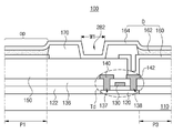
도 12는 본 발명의 제 4 실시예에 따른 전계발광 표시장치의 개략적인 평면도이고, 도 13은 도 12의 XIII-XIII 선을 따라 절단한 단면도이다.12 is a schematic plan view of an electroluminescent display device according to a fourth embodiment of the present invention, and FIG. 13 is a cross-sectional view taken along line XIII-XIII of FIG. 12.
도 12 및 도 13에 도시된 바와 같이, 본 발명의 제 4 실시예에 따른 전계발광 표시장치(300)는 표시영역(DA)과 표시영역(DA) 주변의 비표시영역(NDA)이 정의된 기판(310)을 포함한다. 기판(310)의 표시영역(DA)에는, 제 2 방향(Y)을 따라 다수의 제 1 화소(P1)가 배열된 제 1 화소열, 제 1 화소열의 일측에 위치하고 제 2 방향(Y)을 따라 다수의 제 2 화소(P2)가 배열된 제 2 화소열, 제 1 및 제 2 화소열 사이에 위치하며 제 2 방향(Y)을 따라 다수의 제 3 화소(P3)가 배열된 제 3 화소열이 정의된다. 12 and 13, in the
기판(310) 상에는, 각 화소(P)에 대응하는 구동 박막트랜지스터(도 4의 Td)와, 구동 박막트랜지스터(Td)에 연결되는 발광다이오드(D)와, 제 1 화소열과 제 3 화소열 사이에 위치하는 제 1 홈(382)과, 제 2 화소열과 제 3 화소열 사이에 위치하는 제 2 홈(384)이 형성된다.On the
도 3을 통해 설명한 바와 같이, 구동 박막트랜지스터(Td)는 반도체층, 게이트 전극, 소스 전극 및 드레인 전극을 포함한다.As described through FIG. 3, the driving thin film transistor Td includes a semiconductor layer, a gate electrode, a source electrode, and a drain electrode.
기판(310) 상에는, 게이트 절연막(322)과 층간 절연막(336)이 순차 적층되고, 층간 절연막(336) 상에는 데이터 배선(DL)과 파워 배선(PL)이 형성된다. 또한, 데이터 배선(DL)과 파워 배선(PL)을 덮는 보호층(350)이 형성된다.The
보호층(350) 상에는 구동 박막트랜지스터(Td)에 연결되는 제 1 전극(360)이 형성된다. 제 1 전극(360)은 애노드(anode)일 수 있으며, 일함수 값이 비교적 큰 도전성 물질로 이루어질 수 있다.The
또한, 보호층(350) 상에는 제 1 전극(360)의 가장자리를 덮는 뱅크층(370)이 형성된다. 뱅크층(370)은 다수의 화소(P) 각각에 대응하여 개구(opening, OP)를 갖는다. In addition, a
뱅크층(370)은 화소열 내 화소(P) 사이에 위치하는 제 1 뱅크층(372)과 화소열 사이에 위치하는 제 2 뱅크층(374)을 포함한다. 즉, 제 1 화소열에서 인접한 제 1 화소(P1, P1') 사이에 제 1 뱅크층(372)이 위치하고, 제 1 화소(P1)와 제 3 화소(P2) 사이에 제 2 뱅크층(374)이 위치한다.The
제 1 뱅크층(372)은 제 2 뱅크층(374)보다 작은 두께를 갖는다. 즉, 제 1 뱅크층(372)은 단일층 구조일 수 있고, 제 2 뱅크층(374)은 제 1 층(376)과 제 1 층(376) 상의 제 2 층(378)을 포함하는 이중층 구조일 수 있다. 이때, 제 1 뱅크층(372)은 제 2 뱅크층(374)의 제 1 층(376)과 동일물질로 이루어질 수 있다.The
또한, 제 2 뱅크층(374)의 제 2 층(378)은 제 1 및 제 3 화소열 사이에 대응하여 제 1 홈(382)을 갖고 제 2 및 제 3 화소열 사이에 대응하여 제 2 홈(384)을 갖는다.In addition, the
도 13에서, 제 1 홈(382)의 깊이는 제 2 뱅크층(374)의 제 2 층(378) 두께보다 작다. 이와 달리, 제 1 홈(382)의 깊이는 제 2 뱅크층(374)의 제 2 층(378) 두께와 같거나 이보다 클 수 있다.In FIG. 13, the depth of the
제 1 화소열과 제 3 화소열에 사이에 위치하는 제 1 홈(382)은 제 1 방향(X)을 따라 제 1 폭(w1)을 갖고, 제 2 화소열과 제 3 화소열에 사이에 위치하는 제 2 홈(384)은 제 1 방향(X)을 따라 제 1 폭(w1)보다 작은 제 2 폭(w2)을 갖는다. 이에 따라, 제 1 홈(382)은 제 2 홈(384)보다 큰 표면적을 갖는다.The
또한, 기판(310)의 표시영역(DA)에는, 제 1 화소열의 타측에 위치하고 제 2 방향(Y)을 따라 다수의 제 4 화소(P4)가 배열된 제 4 화소열과, 제 2 화소열로부터 제 1 방향(X)으로 이격되고 제 2 방향(Y)을 따라 다수의 제 5 화소(P5)가 배열된 제 5 화소열이 더 정의될 수 있다. 이 경우, 제 1 화소열과 제 4 화소열 사이에는 제 3 홈(386)이 구비되고, 제 2 화소열과 제 5 화소열 사이에는 제 4 홈(388)이 구비될 수 있다.Further, in the display area DA of the
제 3 홈(386)의 표면적은 제 1 홈(382)의 표면적보다 크고, 제 4 홈(388)의 표면적은 제 2 홈(384)의 표면적보다 작다. 즉, 제 3 홈(386)은 제 1 폭(w1)보다 큰 제 3 폭(w3)을 갖고, 제 4 홈(388)은 제 2 폭(w2)보다 작은 제 4 폭(w4)을 갖는다.The surface area of the
제 1 전극(360) 상에는 발광층(362)이 형성된다. 발광층(362)은 액체 상태의 발광 물질을 이용한 용액 공정(solution process)에 의해 형성된다. 즉, 용매에 녹아있는 발광물질 용액을 코팅한 후 용매를 건조하여 형성된다. 예를 들어, 용액 공정은 잉크젯 코팅(inkjet coating) 공정, 슬릿 코팅(slit coating) 공정, 스핀 코팅(spin coating) 공정, 프린팅 (printing) 공정, 드랍 코팅(drop coating) 공정 중 어느 하나일 수 있으나, 이에 한정되지 않는다.The
발광층(362)은 발광물질로 이루어지는 발광물질층(emitting material layer)의 단일층 구조일 수 있다. 또한, 발광 효율을 높이기 위해, 발광층(362)은 제 1 전극(360)과 발광물질층 사이에 순차적으로 위치하는 정공주입층(hole injection layer) 및 정공수송층(hole transporting layer)과, 발광물질층과 제 2 전극(364) 사이에 순차적으로 위치하는 전자수송층(electron transporting layer) 및 전자주입층(electron injection layer)를 더 포함할 수 있다. The
발광물질층은 양자점(quantum dot)과 같은 무기발광물질 또는 유기발광물질을 포함할 수 있다. 즉, 본 발명의 전계발광 표시장치(300)는 유기발광 표시장치(OLED) 또는 양자점발광 표시장치(QLED)일 수 있다. The light emitting material layer may include an inorganic light emitting material such as a quantum dot or an organic light emitting material. That is, the
전술한 바와 같이, 화소열 내 인접한 화소(P) 사이에 위치하는 제 1 뱅크층(372)은 비교적 작은 두께를 갖기 때문에, 각 화소열 내 다수의 화소(P)에서 발광층(362)은 서로 연결될 수 있다. 예를 들어, 제 1 화소열 내 다수의 제 1 화소(P1) 모두는 적색 화소, 녹색 화소 및 청색 화소 중 어느 하나일 수 있다.As described above, since the
홈(382, 384)에는 발광물질 용액의 용매가 코팅된 후 건조되어 증발된다. 따라서, 발광층(362)의 형성 공정 후에, 홈(382, 384)에는 아무런 구성 요소 없이 제 2 뱅크층(374)의 제 2 층(378) 일부가 노출될 수 있다. The
이와 달리, 홈(382, 384)에 발광물질 용액이 코팅되는 경우, 홈(382, 384)에는 보조물질패턴(미도시)이 형성될 수도 있다.Alternatively, when the luminescent material solution is coated on the
발광물질 용액은 제 1 방향(X)의 일 끝(즉 도 12에서 좌측 끝)으로부터 타 끝(즉, 도 12에서 우측 끝)을 향해 잉크젯 헤드(미도시)가 이동하며 코팅된다. 예를 들어, 제 4 화소열에서 발광물질 용액의 코팅 공정이 시작되고, 제 5 화소열에서 발광물질 용액의 코팅 공정이 종료된다. 이후, 코팅 공정이 종료된 기판(310)은 진공 건조 챔버로 이송된다.The luminescent material solution is coated while the inkjet head (not shown) moves from one end in the first direction X (ie, the left end in FIG. 12) to the other end (ie, the right end in FIG. 12). For example, the coating process of the luminescent material solution is started in the fourth pixel column, and the coating process of the luminescent material solution is ended in the fifth pixel column. Thereafter, the
이때, 제 1 화소열은 제 2 및 제 3 화소열보다 긴 기간 동안 자연 증발 조건에 놓여지지만, 제 1 홈(382)이 제 2 홈(384)보다 큰 폭(w1)을 갖기 때문에 제 2 홈(384)에서보다 제 1 홈(382)에서 용매가 빨리 증발한다. 따라서, 제 1 화소열 부근에서 용매의 포화 속도가 제 2 화소열 부근에서 용매의 포화 속도보다 빠르게 된다.At this time, the first pixel column is subjected to a natural evaporation condition for a longer period than the second and third pixel columns, but the second groove is because the
다시 말해, 제 1 내지 제 3 화소열의 화소(P1, P2, P3)는 발광물질 용액 코팅 후 진공 건조 챔버로 이송되기까지 서로 다른 시간을 갖지만 용매의 포화 속도가 다르기 때문에, 동일한 자연 건조 기간을 갖는다. 따라서, 코팅 공정 방향에 따른 발광층(362)의 두께 불균일 문제가 방지되거나 최소화된다.In other words, the pixels P1, P2, and P3 in the first to third pixel columns have different times until they are transferred to the vacuum drying chamber after coating the luminescent material solution, but have the same natural drying period because the saturation rate of the solvent is different. . Therefore, the problem of thickness non-uniformity of the
각 화소(P)의 발광층(362) 및 뱅크층(370) 상에 제 2 전극(364)이 형성된다. 제 2 전극(364)은 기판(310)의 표시영역의 전면에 위치하며 일함수 값이 비교적 작은 도전성 물질로 이루어져 캐소드(cathode)로 이용될 수 있다.The
제 2 전극(364)은 각 화소(P)에서 발광층(362)와 접촉하고, 제 1 및 제 2 홈(382, 384)에서 제 2 전극(364)은 제 2 뱅크층(374)의 제 2 층(378)과 접촉한다. 또한, 각 화소열의 화소(P) 사이에서 제 2 전극(364)은 제 1 뱅크층(372)과 접촉한다.The
한편, 제 1 및 제 2 홈(382, 384)에 보조물질패턴(미도시)이 형성되는 경우, 제 2 전극(364)은 제 1 및 제 2 홈(382, 384)에서 보조물질패턴과 접촉할 수 있다. 이때, 보조물질패턴은 제 1 전극(360)과 접촉하지 않기 때문에, 제 1 및 제 2 홈(382, 384)에 형성된 보조물질패턴에서는 발광이 일어나지 않는다.Meanwhile, when an auxiliary material pattern (not shown) is formed in the first and
제 1 전극(360)과, 제 1 전극(360)과 마주하는 제 2 전극(364)과, 제 1 및 제 2 전극(360, 364) 사이에 위치하는 발광층(362)은 발광다이오드(D)를 이룬다.The
도시하지 않았으나, 발광다이오드(D) 상부에는 인캡슐레이션 기판 또는 인캡슐레이션 필름이 더 형성될 수 있다. 또한, 인캡슐레이션 필름 상에는 외부광 반사를 최소화하기 위한 편광판이 부착될 수 있다. 편광판은 원형 편광판일 수 있다.Although not illustrated, an encapsulation substrate or an encapsulation film may be further formed on the light emitting diode D. In addition, a polarizing plate for minimizing external light reflection may be attached on the encapsulation film. The polarizing plate may be a circular polarizing plate.
본 발명의 전계발광 표시장치(300)에 있어서, 발광층(362)은 용액 공정에 의해 형성되기 때문에, 제조 공정이 단순해지고 대면적 표시장치의 제조에도 적합하다.In the
또한, 용액 공정에서의 스캔 방향에 따라 각 화소열 사이에 형성된 홈(382, 384)이 스캔 방향을 따라 표면적을 달리하고 용매 또는 발광물질 용액을 홈(382, 384)에 코팅함으로써, 스캔 방향에 따라 발생되는 발광층(362)의 두께 불균일 문제를 방지하거나 최소화할 수 있다. 따라서, 발광층(362)의 두께 불균일에 의한 전계발광 표시장치(300)의 표시 품질 저하 문제를 해소할 수 있다.In addition, the
-제 5 실시예--Fifth Example-
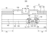
도 14는 본 발명의 제 5 실시예에 따른 전계발광 표시장치의 개략적인 평면도이고, 도 15은 도 14의 XV-XV 선을 따라 절단한 단면도이다.14 is a schematic plan view of an electroluminescent display device according to a fifth embodiment of the present invention, and FIG. 15 is a cross-sectional view taken along line XV-XV of FIG. 14.
도 14 및 도 15에 도시된 바와 같이, 본 발명의 제 5 실시예에 따른 전계발광 표시장치(400)는 표시영역(DA)과 표시영역(DA) 주변의 비표시영역(NDA)이 정의된 기판(미도시)을 포함한다. 기판(410)의 표시영역(DA)에는, 제 2 방향(Y)을 따라 다수의 화소(P11, P12, P13)가 배열된 제 1 화소열, 제 1 화소열로부터 제 1 방향(X)으로 이격되고 다수의 화소(P21, P22, P23)가 배열된 제 2 화소열, 제 2 화소열로부터 제 1 방향(X)으로 이격되고 다수의 화소(P31, P32, P33)가 배열된 제 3 화소열이 정의된다. 제 2 화소열은 제 1 화소열과 제 3 화소열 사이에 위치한다.14 and 15, in the
제 1 화소열은, 표시영역 일 끝에 위치하는 제 1 화소(P11)와, 표시영역 타 끝에 위치하는 제 2 화소(P12)와, 제 1 및 제 2 화소(P11, P12) 사이에 위치하는 제 3 화소(P13)을 포함한다. The first pixel column includes a first pixel P11 positioned at one end of the display area, a second pixel P12 positioned at the other end of the display area, and a first pixel positioned between the first and second pixels P11 and P12. It includes three pixels P13.
제 2 화소열은, 표시영역 일 끝에 위치하는 제 1 화소(P21)와, 표시영역 타 끝에 위치하는 제 2 화소(P22)와, 제 1 및 제 2 화소(P21, P22) 사이에 위치하는 제 3 화소(P23)을 포함한다. The second pixel column includes a first pixel P21 positioned at one end of the display area, a second pixel P22 positioned at the other end of the display area, and a first pixel positioned between the first and second pixels P21 and P22. It includes three pixels P23.
제 3 화소열은, 표시영역 일 끝에 위치하는 제 1 화소(P31)와, 표시영역 타 끝에 위치하는 제 2 화소(P32)와, 제 1 및 제 2 화소(P31, P32) 사이에 위치하는 제 3 화소(P33)을 포함한다. The third pixel column includes a first pixel P31 positioned at one end of the display area, a second pixel P32 positioned at the other end of the display area, and a first pixel positioned between the first and second pixels P31 and P32. It includes three pixels P33.
즉, 각 화소열에서 제 3 화소(P13, P23, P33)는 제 1 화소(P11, P21, P31)와 제 2 화소(P12, P22, P23) 사이에 배치된다.That is, in each pixel column, the third pixels P13, P23, and P33 are disposed between the first pixels P11, P21, and P31 and the second pixels P12, P22, and P23.
기판(410) 상에는, 각 화소(P)에 대응하는 구동 박막트랜지스터(도 4의 Td)와, 구동 박막트랜지스터(Td)에 연결되는 발광다이오드(D)와, 제 1 화소열과 제 2 화소열 사이에 위치하는 제 1 홈(482)과, 제 2 화소열과 제 3 화소열 사이에 위치하는 제 2 홈(484)이 형성된다.On the
도 3을 통해 설명한 바와 같이, 구동 박막트랜지스터(Td)는 반도체층, 게이트 전극, 소스 전극 및 드레인 전극을 포함한다.As described through FIG. 3, the driving thin film transistor Td includes a semiconductor layer, a gate electrode, a source electrode, and a drain electrode.
기판(410) 상에는, 게이트 절연막(422)이 형성되고, 게이트 절연막(422) 상에는 게이트 배선(GL)이 형성된다. 또한, 게이트 배선(GL) 상에는 층간 절연막(436)과 보호층(450)이 순차 적층된다. A
보호층(450) 상에는 구동 박막트랜지스터(Td)에 연결되는 제 1 전극(460)이 형성된다. 제 1 전극(460)은 애노드(anode)일 수 있으며, 일함수 값이 비교적 큰 도전성 물질로 이루어질 수 있다.The
또한, 보호층(450) 상에는 제 1 전극(460)의 가장자리를 덮는 뱅크층(470)이 형성된다. 뱅크층(470)은 다수의 화소(P) 각각에 대응하여 개구(opening, OP)를 갖는다. In addition, a
뱅크층(470)은 화소열 내 화소(P) 사이에 위치하는 제 1 뱅크층(472)과 화소열 사이에 위치하는 제 2 뱅크층(474)을 포함한다. 제 1 뱅크층(472)은 제 2 뱅크층(474)보다 작은 두께를 갖는다. 즉, 제 1 뱅크층(472)은 단일층 구조일 수 있고, 제 2 뱅크층(474)은 제 1 층(476)과 제 1 층(476) 상의 제 2 층(478)을 포함하는 이중층 구조일 수 있다. 이때, 제 1 뱅크층(472)은 제 2 뱅크층(474)의 제 1 층(476)과 동일물질로 이루어질 수 있다.The
또한, 제 2 뱅크층(474)의 제 2 층(478)은 제 1 및 제 2 화소열 사이에 대응하여 제 1 홈(482)을 갖고 제 2 및 제 3 화소열 사이에 대응하여 제 2 홈(484)을 갖는다.Further, the
도 15에서, 제 1 홈(482)의 깊이는 제 2 뱅크층(474)의 제 2 층(478) 두께보다 작다. 이와 달리, 제 1 홈(482)의 깊이는 제 2 뱅크층(474)의 제 2 층(478) 두께와 같거나 이보다 클 수 있다.In FIG. 15, the depth of the
제 1 및 제 2 홈(482, 484) 각각은 제 1 방향(X)을 따라 그 표면적이 감소한다. 즉, 제 1 및 제 2 홈(482, 484) 각각은, 제 1 화소(P11, P21, P31)에 대응하여 제 1 폭(w1)을 갖고, 제 2 화소(P12, P22, P32)에 대응하여 제 1 폭(w1)보다 작은 제 2 폭(w2)을 가지며, 제 3 화소(P13, P23, P33)에 대응하여 제 1 폭(w1)보다 작고 제 2 폭(w2)보다 큰 제 3 폭(w3)을 갖는다.Each of the first and
다시 말해, 제 1 홈(482)은, 제 1 화소열의 일 끝에 대응되며 제 1 방향(X)으로 제 1 폭(w1)을 갖는 제 1 부분, 제 1 화소열의 타 끝에 대응되며 제 1 방향(X)으로 제 2 폭(w2)을 갖는 제 2 부분과, 제 1 부분과 제 2 부분 사이에 위치하며 제 1 방향(X)으로 제 3 폭(w3)을 갖는 제 3 부분을 포함한다. 이에 따라, 제 1 홈(482)의 제 3 부분은 제 1 홈(482)의 제 1 부분보다 작고 제 1 홈(482)의 제 2 부분보다 큰 표면적을 갖는다.In other words, the
또한, 제 2 홈(484)은, 제 1 화소열의 일 끝에 대응되며 제 1 방향(X)으로 제 1 폭(w1)을 갖는 제 1 부분, 제 1 화소열의 타 끝에 대응되며 제 1 방향(X)으로 제 2 폭(w2)을 갖는 제 2 부분과, 제 1 부분과 제 2 부분 사이에 위치하며 제 1 방향(X)으로 제 3 폭(w3)을 갖는 제 3 부분을 포함한다. 이에 따라, 제 2 홈(484)의 제 3 부분은 제 2 홈(484)의 제 1 부분보다 작고 제 2 홈(484)의 제 2 부분보다 큰 표면적을 갖는다.Further, the
제 1 전극(460) 상에는 발광층(462)이 형성된다. 발광층(462)은 액체 상태의 발광 물질을 이용한 용액 공정(solution process)에 의해 형성된다. 즉, 용매에 녹아있는 발광물질 용액을 코팅한 후 용매를 건조하여 형성된다. 예를 들어, 용액 공정은 잉크젯 코팅(inkjet coating) 공정, 슬릿 코팅(slit coating) 공정, 스핀 코팅(spin coating) 공정, 프린팅 (printing) 공정, 드랍 코팅(drop coating) 공정 중 어느 하나일 수 있으나, 이에 한정되지 않는다.The
발광층(462)은 발광물질로 이루어지는 발광물질층(emitting material layer)의 단일층 구조일 수 있다. 또한, 발광 효율을 높이기 위해, 발광층(462)은 제 1 전극(460)과 발광물질층 사이에 순차적으로 위치하는 정공주입층(hole injection layer) 및 정공수송층(hole transporting layer)과, 발광물질층과 제 2 전극(464) 사이에 순차적으로 위치하는 전자수송층(electron transporting layer) 및 전자주입층(electron injection layer)를 더 포함할 수 있다. The
발광물질층은 양자점(quantum dot)과 같은 무기발광물질 또는 유기발광물질을 포함할 수 있다. 즉, 본 발명의 전계발광 표시장치(400)는 유기발광 표시장치(OLED) 또는 양자점발광 표시장치(QLED)일 수 있다.The light emitting material layer may include an inorganic light emitting material such as a quantum dot or an organic light emitting material. That is, the
전술한 바와 같이, 화소열 내 인접한 화소(P) 사이에 위치하는 제 1 뱅크층(472)은 비교적 작은 두께를 갖기 때문에, 각 화소열 내 다수의 화소(P)에서 발광층(462)은 서로 연결될 수 있다. 예를 들어, 제 1 화소열 내 다수의 화소(P11, P12, P13) 모두는 적색 화소, 녹색 화소 및 청색 화소 중 어느 하나일 수 있다.As described above, since the
홈(482, 484)에는 발광물질 용액의 용매가 코팅된 후 건조되어 증발된다. 따라서, 발광층(462)의 형성 공정 후에, 홈(482, 484)에는 아무런 구성 요소 없이 제 2 뱅크층(474)의 제 2 층(478) 일부가 노출될 수 있다. The
이와 달리, 홈(482, 484)에 발광물질 용액이 코팅되는 경우, 홈(482, 484)에는 보조물질패턴(미도시)이 형성될 수도 있다.Alternatively, when the luminescent material solution is coated on the
발광물질 용액은 제 2 방향(Y)의 일 끝(즉 도 12에서 상측 끝)으로부터 타 끝(즉, 도 12에서 하측 끝)을 향해 잉크젯 헤드(미도시)가 이동하며 코팅된다. 예를 들어, 제 1 화소(P11, P21, P31)에서 발광물질 용액의 코팅 공정이 시작되고, 제 2 화소(P12, P22, P23)에서 발광물질 용액의 코팅 공정이 종료된다. 이후, 코팅 공정이 종료된 기판(410)은 진공 건조 챔버로 이송된다.The luminescent material solution is coated while the inkjet head (not shown) moves from one end in the second direction Y (ie, the upper end in FIG. 12) to the other end (ie, the lower end in FIG. 12 ). For example, the coating process of the luminescent material solution is started in the first pixels P11, P21, and P31, and the coating process of the luminescent material solution is ended in the second pixels P12, P22, P23. Thereafter, the
이때, 제 1 화소(P11, P21, P31)는 제 2 화소(P12, P22, P23) 및 제 3 화소(P13, P23, P33)보다 긴 기간 동안 자연 증발 조건에 놓여지지만, 제 1 및 제 2 홈(482, 484)의 표면적이 제 2 방향(Y)을 따라 감소하기 때문에, 자연 건조 기간을 균일하게 할 수 있다.At this time, the first pixels P11, P21, and P31 are subjected to natural evaporation conditions for a longer period than the second pixels P12, P22, and P23, and the third pixels P13, P23, and P33, but the first and second pixels Since the surface areas of the
즉, 제 1 홈(482)에 있어, 제 3 부분의 제 3 폭(w3)이 제 1 부분의 제 1 폭(w1)보다 작고 제 2 부분의 제 2 폭(w2)보다 크기 때문에, 제 3 부분에서의 용매 증발속도는 제 1 부분에서보다 작고 제 2 부분에서보다 크다.That is, in the
따라서, 각 화소(P)는 스캔 방향에 상관 없이 동일한 자연 건조 기간을 갖게되며, 코팅 공정 방향에 따른 발광층(462)의 두께 불균일 문제가 방지되거나 최소화된다.Therefore, each pixel P has the same natural drying period regardless of the scan direction, and the thickness non-uniformity problem of the
각 화소(P)의 발광층(462) 및 뱅크층(470) 상에 제 2 전극(464)이 형성된다. 제 2 전극(464)은 기판(410)의 표시영역의 전면에 위치하며 일함수 값이 비교적 작은 도전성 물질로 이루어져 캐소드(cathode)로 이용될 수 있다.The
제 2 전극(464)은 각 화소(P)에서 발광층(462)와 접촉하고, 제 1 및 제 2 홈(482, 484)에서 제 2 전극(464)은 제 2 뱅크층(474)의 제 2 층(478)과 접촉한다. 또한, 각 화소열의 화소(P) 사이에서 제 2 전극(464)은 제 1 뱅크층(472)과 접촉한다.The
한편, 제 1 및 제 2 홈(482, 484)에 보조물질패턴(미도시)이 형성되는 경우, 제 2 전극(464)은 제 1 및 제 2 홈(482, 484)에서 보조물질패턴과 접촉할 수 있다. 이때, 보조물질패턴은 제 1 전극(460)과 접촉하지 않기 때문에, 제 1 및 제 2 홈(482, 484)에 형성된 보조물질패턴에서는 발광이 일어나지 않는다.Meanwhile, when an auxiliary material pattern (not shown) is formed in the first and
제 1 전극(460)과, 제 1 전극(460)과 마주하는 제 2 전극(464)과, 제 1 및 제 2 전극(460, 464) 사이에 위치하는 발광층(462)은 발광다이오드(D)를 이룬다.The
도시하지 않았으나, 발광다이오드(D) 상부에는 인캡슐레이션 기판 또는 인캡슐레이션 필름이 더 형성될 수 있다. 또한, 인캡슐레이션 필름 상에는 외부광 반사를 최소화하기 위한 편광판이 부착될 수 있다. 편광판은 원형 편광판일 수 있다.Although not illustrated, an encapsulation substrate or an encapsulation film may be further formed on the light emitting diode D. In addition, a polarizing plate for minimizing external light reflection may be attached on the encapsulation film. The polarizing plate may be a circular polarizing plate.
본 발명의 전계발광 표시장치(400)에 있어서, 발광층(462)은 용액 공정에 의해 형성되기 때문에, 제조 공정이 단순해지고 대면적 표시장치의 제조에도 적합하다.In the
또한, 용액 공정에서의 스캔 방향에 따라 각 화소열 사이에 형성된 홈(482, 484)이 스캔 방향을 따라 표면적을 달리하고 용매 또는 발광물질 용액을 홈(482, 484)에 코팅함으로써, 스캔 방향에 따라 발생되는 발광층(462)의 두께 불균일 문제를 방지하거나 최소화할 수 있다. 따라서, 발광층(462)의 두께 불균일에 의한 전계발광 표시장치(400)의 표시 품질 저하 문제를 해소할 수 있다.In addition, the
상기에서는 본 발명의 바람직한 실시예를 참조하여 설명하였지만, 해당 기술분야의 숙련된 기술자는 하기의 특허청구범위에 기재된 본 발명의 기술적 사상 및 영역으로부터 벗어나지 않는 범위 내에서 본 발명을 다양하게 수정 및 변경시킬 수 있음을 이해할 수 있을 것이다.Although described above with reference to preferred embodiments of the present invention, skilled artisans skilled in the art variously modify and change the present invention without departing from the spirit and scope of the present invention as set forth in the claims below. You can understand that you can.
100, 200, 300, 400: 전계발광 표시장치
110, 210, 310, 410: 기판
120, 220: 반도체층
122, 222, 322, 422: 게이트 절연막
130, 230: 게이트 전극
136, 236, 336, 436: 층간 절연막
140, 240: 소스 전극
142, 242: 드레인 전극
150, 250, 350, 450: 보호층
160, 260, 360, 460: 제 1 전극
162, 262, 362, 462: 발광층
164, 264, 364, 464: 제 2 전극
170, 270, 370, 470: 뱅크층
182, 184, 282, 284, 286, 288, 382, 384, 482, 484: 홈
Td: 구동 박막트랜지스터
D: 발광 다이오드100, 200, 300, 400: electroluminescent display device
110, 210, 310, 410:
122, 222, 322, 422:
136, 236, 336, 436:
142, 242:
160, 260, 360, 460:
164, 264, 364, 464:
182, 184, 282, 284, 286, 288, 382, 384, 482, 484: Home
Td: driving thin film transistor D: light emitting diode
Claims (25)
상기 기판 상에 제 1 방향으로 배열된 다수의 화소를 포함하는 제 1 화소열과;
상기 기판 상에 상기 제 1 방향으로 배열된 다수의 화소를 포함하며 상기 제 1 화소열로부터 제 2 방향으로 이격된 제 2 화소열과;
상기 제 1 화소열과 상기 제 2 화소열 사이에 위치하는 제 1 홈과;
상기 제 1 화소열과 상기 제 2 화소열의 상기 다수의 화소 각각에 위치하는 발광다이오드를 포함하고,
상기 제 1 홈은, 상기 제 1 화소열의 일 끝에 대응되며 제 1 표면적을 갖는 제 1 부분, 상기 제 1 화소열의 타 끝에 대응되며 제 2 표면적을 갖는 제 2 부분과, 상기 제 1 부분과 상기 제 2 부분 사이에 위치하며 제 3 표면적을 갖는 제 3 부분을 포함하며,
상기 제 3 표면적은 상기 제 1 표면적보다 작고 상기 제 2 표면적보다 큰 전계발광 표시장치.
A substrate;
A first pixel column including a plurality of pixels arranged in a first direction on the substrate;
A second pixel column including a plurality of pixels arranged in the first direction on the substrate and spaced apart from the first pixel column in a second direction;
A first groove positioned between the first pixel column and the second pixel column;
And a light emitting diode positioned in each of the plurality of pixels in the first pixel column and the second pixel column,
The first groove may include a first portion corresponding to one end of the first pixel column and having a first surface area, a second portion having a second surface area corresponding to the other end of the first pixel column, and the first portion and the first A third portion located between the two portions and having a third surface area,
The third surface area is smaller than the first surface area and greater than the second surface area electroluminescent display device.
상기 제 1 부분은 상기 제 2 방향으로 제 1 폭을 갖고, 상기 제 2 부분은 상기 제 2 방향으로 제 2 폭을 가지며, 상기 제 3 부분은 상기 제 2 방향으로 제 3 폭을 갖고,
상기 제 3 폭은 상기 제 1 폭보다 작고 상기 제 2 폭보다 큰 전계발광 표시장치.
According to claim 1,
The first portion has a first width in the second direction, the second portion has a second width in the second direction, and the third portion has a third width in the second direction,
The third width is less than the first width and greater than the second width of the electroluminescent display device.
상기 제 1 홈의 폭은 상기 제 1 방향을 따라 점진적으로 감소하는 전계발광 표시장치.
According to claim 2,
The width of the first groove is an electroluminescent display device that gradually decreases along the first direction.
상기 제 1 내지 제 3 부분은 서로 연결된 전계발광 표시장치.
According to claim 1,
The first to third portions are electroluminescent display devices connected to each other.
상기 제 1 내지 제 3 부분은 서로 이격된 전계발광 표시장치.
According to claim 1,
The first to third portions are electroluminescent display devices spaced apart from each other.
상기 제 1 홈의 표면적은 상기 제 1 방향을 따라 점진적으로 감소하는 전계발광 표시장치.
According to claim 1,
An electroluminescent display device having a surface area of the first groove gradually decreasing along the first direction.
상기 제 1 방향으로 배열된 다수의 화소를 포함하며 상기 제 2 화소열로부터 상기 제 2 방향으로 이격된 제 3 화소열과;
상기 제 2 화소열과 상기 제 3 화소열 사이에 위치하는 제 2 홈을 더 포함하고,
상기 제 2 홈은, 상기 제 2 화소열의 일 끝에 대응되며 제 4 표면적을 갖는 제 4 부분, 상기 제 2 화소열의 타 끝에 대응되며 제 5 표면적을 갖는 제 5 부분과, 상기 제 4 부분과 상기 제 5 부분 사이에 위치하며 제 6 표면적을 갖는 제 6 부분을 포함하며,
상기 제 6 표면적은 상기 제 4 표면적보다 작고 상기 제 5 표면적보다 큰 전계발광 표시장치.
According to claim 1,
A third pixel column including a plurality of pixels arranged in the first direction and spaced apart from the second pixel column in the second direction;
Further comprising a second groove located between the second pixel column and the third pixel column,
The second groove may include a fourth portion having a fourth surface area corresponding to one end of the second pixel column, a fifth portion having a fifth surface area corresponding to the other end of the second pixel column, and the fourth portion and the second A sixth part located between the five parts and having a sixth surface area,
The sixth surface area is smaller than the fourth surface area and larger than the fifth surface area.
상기 제 4 부분은 상기 제 2 방향으로 제 4 폭을 갖고, 상기 제 5 부분은 상기 제 2 방향으로 제 5 폭을 가지며, 상기 제 6 부분은 상기 제 2 방향으로 제 6 폭을 갖고,
상기 제 4 내지 제 6 폭 각각은 상기 제 1 내지 제 3 폭과 동일한 전계발광 표시장치.
The method of claim 7,
The fourth portion has a fourth width in the second direction, the fifth portion has a fifth width in the second direction, and the sixth portion has a sixth width in the second direction,
Each of the fourth to sixth widths has the same electroluminescent display device as the first to third widths.
상기 기판 상에, 상기 다수의 화소 각각에 위치하는 박막트랜지스터와;
상기 박막트랜지스터를 덮는 절연층과;
상기 절연층 상에 위치하며 상기 다수의 화소 각각을 둘러싸는 뱅크층을 더 포함하고,
상기 발광다이오드는, 제 1 전극과, 상기 제 1 전극 상에 위치하는 발광층과, 상기 발광층을 덮는 제 2 전극을 포함하며,
상기 제 1 홈은 상기 뱅크층에 형성되는 전계발광 표시장치.
According to claim 1,
A thin film transistor positioned on each of the plurality of pixels on the substrate;
An insulating layer covering the thin film transistor;
A bank layer positioned on the insulating layer and surrounding each of the plurality of pixels,
The light emitting diode includes a first electrode, a light emitting layer positioned on the first electrode, and a second electrode covering the light emitting layer,
The first groove is an electroluminescent display device formed on the bank layer.
상기 제 1 홈에 위치하는 물질패턴을 더 포함하고,
상기 물질패턴은 상기 절연층 및 상기 제 2 전극과 접촉하는 전계발광 표시장치.
The method of claim 9,
Further comprising a material pattern located in the first groove,
The material pattern is an electroluminescent display device in contact with the insulating layer and the second electrode.
상기 제 1 홈에서 상기 제 2 전극은 상기 절연층과 접촉하는 전계발광 표시장치.
The method of claim 9,
An electroluminescent display device in which the second electrode contacts the insulating layer in the first groove.
상기 뱅크층은 상기 제 1 화소열 내의 상기 화소 사이에서 제 1 두께를 갖는 제 1 뱅크층과 상기 제 1 화소열과 상기 제 2 화소열 사이에서 상기 제 1 두께보다 큰 제 2 두께를 갖는 제 2 뱅크층을 포함하는 전계발광 표시장치.
The method of claim 9,
The bank layer has a first bank layer having a first thickness between the pixels in the first pixel column, and a second bank having a second thickness greater than the first thickness between the first pixel column and the second pixel column. An electroluminescent display device comprising a layer.
상기 제 1 뱅크층은 단일층 구조를 갖고, 상기 제 2 뱅크층은 이중층 구조를 갖는 전계발광 표시장치.
The method of claim 12,
The first bank layer has a single layer structure, and the second bank layer has a double layer structure.
상기 제 1 화소열 내 상기 다수의 화소에서 상기 발광층은 서로 연결되고, 상기 제 1 화소열 내 상기 화소와 상기 제 2 화소열 내 상기 화소에서 상기 발광층은 서로 분리된 전계발광 표시장치.
The method of claim 12,
The light emitting layer is connected to each other in the plurality of pixels in the first pixel column, and the light emitting layers in the pixels in the first pixel column and the pixels in the second pixel column are separated from each other.
상기 기판 상에 제 1 방향으로 배열된 다수의 제 1 화소를 포함하는 제 1 화소열과;
상기 기판 상에 상기 제 1 방향으로 배열된 다수의 제 2 화소를 포함하며 상기 제 1 화소열로부터 제 2 방향으로 이격된 제 2 화소열과;
상기 기판 상에 상기 제 1 방향으로 배열된 다수의 제 3 화소를 포함하며 상기 제 1 화소열과 상기 제 2 화소열 사이에 위치하는 제 3 화소열과;
상기 제 1 화소열과 상기 제 3 화소열 사이에 위치하는 제 1 홈과;
상기 제 2 화소열과 상기 제 3 화소열 사이에 위치하는 제 2 홈과;
상기 다수의 제 1 화소, 상기 다수의 제 2 화소 및 상기 다수의 제 3 화소 각각에 위치하는 발광다이오드를 포함하고,
상기 제 1 홈은 상기 제 2 홈보다 큰 표면적을 갖는 전계발광 표시장치.
A substrate;
A first pixel column including a plurality of first pixels arranged in a first direction on the substrate;
A second pixel column including a plurality of second pixels arranged in the first direction on the substrate and spaced apart from the first pixel column in a second direction;
A third pixel column including a plurality of third pixels arranged in the first direction on the substrate and positioned between the first pixel column and the second pixel column;
A first groove positioned between the first pixel column and the third pixel column;
A second groove positioned between the second pixel column and the third pixel column;
And a light emitting diode located in each of the plurality of first pixels, the plurality of second pixels, and the plurality of third pixels,
The first groove has an electroluminescent display having a larger surface area than the second groove.
상기 제 2 방향에서, 상기 제 1 홈은 상기 제 2 홈보다 큰 폭을 갖는 전계발광 표시장치.
The method of claim 15,
In the second direction, the first groove has an electroluminescence display having a width greater than the second groove.
상기 제 1 홈은 상기 제 1 화소열과 동일한 길이를 갖고, 상기 제 2 홈은 상기 제 2 화소열과 동일한 길이를 갖는 전계발광 표시장치.
The method of claim 15,
The first groove has the same length as the first pixel column, and the second groove has the same length as the second pixel column.
상기 제 1 홈은 상기 다수의 제 1 화소 각각에 대응되며 서로 이격되는 다수의 제 1 홈 패턴을 포함하고,
상기 제 2 홈은 상기 다수의 제 2 화소 각각에 대응되며 서로 이격되는 다수의 제 2 홈 패턴을 포함하는 전계발광 표시장치.
The method of claim 15,
The first groove corresponds to each of the plurality of first pixels and includes a plurality of first groove patterns spaced apart from each other,
The second groove corresponds to each of the plurality of second pixels and includes a plurality of second groove patterns spaced apart from each other.
상기 제 1 방향으로 배열된 다수의 제 4 화소를 포함하며 상기 제 2 화소열로부터 상기 제 2 방향으로 이격된 제 4 화소열과;
상기 제 2 화소열과 상기 제 4 화소열 사이에 위치하는 제 3 홈을 더 포함하고,
상기 제 3 홈은 상기 제 2 홈보다 작은 폭을 갖는 전계발광 표시장치.
The method of claim 15,
A fourth pixel column including a plurality of fourth pixels arranged in the first direction and spaced apart from the second pixel column in the second direction;
Further comprising a third groove located between the second pixel column and the fourth pixel column,
The third groove has an electroluminescence display having a width smaller than that of the second groove.
상기 기판 상에, 상기 다수의 제 1 화소, 상기 다수의 제 2 화소, 상기 다수의 제 3 화소 각각에 위치하는 박막트랜지스터와;
상기 박막트랜지스터를 덮는 상기 절연층과;
상기 절연층 상에 위치하며 상기 다수의 제 1 화소, 상기 다수의 제 2 화소, 상기 다수의 제 3 화소 각각을 둘러싸는 뱅크층을 더 포함하고,
상기 발광다이오드는, 제 1 전극과, 상기 제 1 전극 상에 위치하는 발광층과, 상기 발광층을 덮는 제 2 전극을 포함하며,
상기 제 1 홈 및 상기 제 2 홈은 상기 뱅크층에 형성되는 전계발광 표시장치.
The method of claim 15,
A thin film transistor positioned on each of the plurality of first pixels, the plurality of second pixels, and the plurality of third pixels;
The insulating layer covering the thin film transistor;
A bank layer positioned on the insulating layer and surrounding each of the plurality of first pixels, the plurality of second pixels, and the plurality of third pixels,
The light emitting diode includes a first electrode, a light emitting layer positioned on the first electrode, and a second electrode covering the light emitting layer,
The first groove and the second groove are electroluminescent display devices formed on the bank layer.
상기 제 1 홈 및 상기 제 2 홈에 위치하는 물질패턴을 더 포함하고,
상기 물질패턴은 상기 절연층 및 상기 제 2 전극과 접촉하는 전계발광 표시장치.
The method of claim 20,
Further comprising a material pattern located in the first groove and the second groove,
The material pattern is an electroluminescent display device in contact with the insulating layer and the second electrode.
상기 제 1 홈 및 상기 제 2 홈에서 상기 제 2 전극은 상기 절연층과 접촉하는 전계발광 표시장치.
The method of claim 20,
An electroluminescent display device in which the second electrode in the first groove and the second groove contacts the insulating layer.
상기 뱅크층은 상기 다수의 제 1 화소 사이에서 제 1 두께를 갖는 제 1 뱅크층과 상기 제 1 화소열과 상기 제 3 화소열 사이에서 상기 제 1 두께보다 큰 제 2 두께를 갖는 제 2 뱅크층을 포함하는 전계발광 표시장치.
The method of claim 20,
The bank layer may include a first bank layer having a first thickness between the plurality of first pixels and a second bank layer having a second thickness greater than the first thickness between the first pixel column and the third pixel column. Electroluminescent display device comprising.
상기 제 1 뱅크층은 단일층 구조를 갖고, 상기 제 2 뱅크층은 이중층 구조를 갖는 전계발광 표시장치.
The method of claim 23,
The first bank layer has a single layer structure, and the second bank layer has a double layer structure.
상기 다수의 제 1 화소의 상기 발광층은 서로 연결되고, 상기 제 1 화소와 상기 제 2 화소의 상기 발광층은 서로 분리된 전계발광 표시장치.The method of claim 23,
The light emitting layers of the plurality of first pixels are connected to each other, and the light emitting layers of the first pixel and the second pixel are separated from each other.
Priority Applications (5)
| Application Number | Priority Date | Filing Date | Title |
|---|---|---|---|
| KR1020180153549A KR20200066879A (en) | 2018-12-03 | 2018-12-03 | Electroluminescent display device |
| CN201910744563.4A CN111261667A (en) | 2018-12-03 | 2019-08-13 | Electroluminescent display device |
| US16/557,010 US11289555B2 (en) | 2018-12-03 | 2019-08-30 | Electroluminescent display device comprising bank layer with grooves therein |
| DE102019132771.7A DE102019132771A1 (en) | 2018-12-03 | 2019-12-03 | Electroluminescent display device |
| US17/678,085 US11937462B2 (en) | 2018-12-03 | 2022-02-23 | Electroluminescent display device comprising bank layer with grooves therein |
Applications Claiming Priority (1)
| Application Number | Priority Date | Filing Date | Title |
|---|---|---|---|
| KR1020180153549A KR20200066879A (en) | 2018-12-03 | 2018-12-03 | Electroluminescent display device |
Publications (1)
| Publication Number | Publication Date |
|---|---|
| KR20200066879A true KR20200066879A (en) | 2020-06-11 |
Family
ID=70681017
Family Applications (1)
| Application Number | Title | Priority Date | Filing Date |
|---|---|---|---|
| KR1020180153549A KR20200066879A (en) | 2018-12-03 | 2018-12-03 | Electroluminescent display device |
Country Status (4)
| Country | Link |
|---|---|
| US (2) | US11289555B2 (en) |
| KR (1) | KR20200066879A (en) |
| CN (1) | CN111261667A (en) |
| DE (1) | DE102019132771A1 (en) |
Families Citing this family (1)
| Publication number | Priority date | Publication date | Assignee | Title |
|---|---|---|---|---|
| CN110752242B (en) * | 2019-10-31 | 2021-09-21 | 武汉天马微电子有限公司 | Display panel and display device |
Family Cites Families (6)
| Publication number | Priority date | Publication date | Assignee | Title |
|---|---|---|---|---|
| JP3788467B2 (en) * | 2003-05-28 | 2006-06-21 | セイコーエプソン株式会社 | Pattern forming method, device and device manufacturing method, electro-optical device, electronic apparatus, and active matrix substrate manufacturing method |
| TWI250653B (en) * | 2005-04-22 | 2006-03-01 | Ritdisplay Corp | Active matrix OLED array panel |
| KR102201827B1 (en) | 2014-09-16 | 2021-01-13 | 엘지디스플레이 주식회사 | Organic light emitting display device, organic light emitting display panel and method for fabricating the same |
| CN108074950B (en) | 2016-11-11 | 2021-11-23 | 乐金显示有限公司 | Electroluminescent display device and method of manufacturing the same |
| KR20180070367A (en) * | 2016-12-16 | 2018-06-26 | 엘지디스플레이 주식회사 | Electroluminescent display device |
| JP6688909B2 (en) * | 2017-01-10 | 2020-04-28 | 株式会社Joled | Organic EL display panel manufacturing method and ink drying apparatus |
-
2018
- 2018-12-03 KR KR1020180153549A patent/KR20200066879A/en not_active Application Discontinuation
-
2019
- 2019-08-13 CN CN201910744563.4A patent/CN111261667A/en active Pending
- 2019-08-30 US US16/557,010 patent/US11289555B2/en active Active
- 2019-12-03 DE DE102019132771.7A patent/DE102019132771A1/en active Pending
-
2022
- 2022-02-23 US US17/678,085 patent/US11937462B2/en active Active
Also Published As
| Publication number | Publication date |
|---|---|
| US20200176532A1 (en) | 2020-06-04 |
| DE102019132771A1 (en) | 2020-06-04 |
| CN111261667A (en) | 2020-06-09 |
| US11289555B2 (en) | 2022-03-29 |
| US20220181414A1 (en) | 2022-06-09 |
| US11937462B2 (en) | 2024-03-19 |
Similar Documents
| Publication | Publication Date | Title |
|---|---|---|
| US11024684B2 (en) | Display device | |
| US10170521B2 (en) | Organic light-emitting diode display device | |
| US11864425B2 (en) | Electroluminescent display device having large size and high definition | |
| JP6568188B2 (en) | Electroluminescent display device | |
| CN113130565B (en) | Electroluminescent display device | |
| JP6868676B2 (en) | Electroluminescent display device and its manufacturing method | |
| US11631724B2 (en) | Electroluminescent display device with uneven pattern in non-display area | |
| KR20200066959A (en) | Transparent Display Device | |
| US11018198B2 (en) | Electroluminescent display device | |
| KR102513510B1 (en) | Organic Light Emitting Display Device | |
| KR102577043B1 (en) | Electroluminescent display device | |
| US20210193761A1 (en) | Electroluminescent Display Device | |
| KR20210072451A (en) | Electroluminescent Device | |
| KR20200066879A (en) | Electroluminescent display device | |
| US11658205B2 (en) | Electroluminescent display device | |
| KR20220077635A (en) | Electroluminescent Display Device | |
| KR101744874B1 (en) | Organic light emitting diodes | |
| KR20210083679A (en) | Electroluminescent Display Device | |
| KR20190064011A (en) | Electroluminescent display device | |
| KR20180053220A (en) | Electroluminescent Display Device and Method of Fabricating the same | |
| KR102503745B1 (en) | Electroluminescent display device | |
| KR20210017016A (en) | Electroluminescent Device |
Legal Events
| Date | Code | Title | Description |
|---|---|---|---|
| A201 | Request for examination | ||
| E902 | Notification of reason for refusal |