KR20200066608A - VCSEL array with single chip serial connection - Google Patents
VCSEL array with single chip serial connection Download PDFInfo
- Publication number
- KR20200066608A KR20200066608A KR1020207005275A KR20207005275A KR20200066608A KR 20200066608 A KR20200066608 A KR 20200066608A KR 1020207005275 A KR1020207005275 A KR 1020207005275A KR 20207005275 A KR20207005275 A KR 20207005275A KR 20200066608 A KR20200066608 A KR 20200066608A
- Authority
- KR
- South Korea
- Prior art keywords
- vcsel
- region
- conductive
- array
- series
- Prior art date
Links
Images


Classifications
-
- H—ELECTRICITY
- H01—ELECTRIC ELEMENTS
- H01S—DEVICES USING THE PROCESS OF LIGHT AMPLIFICATION BY STIMULATED EMISSION OF RADIATION [LASER] TO AMPLIFY OR GENERATE LIGHT; DEVICES USING STIMULATED EMISSION OF ELECTROMAGNETIC RADIATION IN WAVE RANGES OTHER THAN OPTICAL
- H01S5/00—Semiconductor lasers
- H01S5/40—Arrangement of two or more semiconductor lasers, not provided for in groups H01S5/02 - H01S5/30
- H01S5/42—Arrays of surface emitting lasers
- H01S5/423—Arrays of surface emitting lasers having a vertical cavity
-
- H—ELECTRICITY
- H01—ELECTRIC ELEMENTS
- H01S—DEVICES USING THE PROCESS OF LIGHT AMPLIFICATION BY STIMULATED EMISSION OF RADIATION [LASER] TO AMPLIFY OR GENERATE LIGHT; DEVICES USING STIMULATED EMISSION OF ELECTROMAGNETIC RADIATION IN WAVE RANGES OTHER THAN OPTICAL
- H01S5/00—Semiconductor lasers
- H01S5/0014—Measuring characteristics or properties thereof
-
- H—ELECTRICITY
- H01—ELECTRIC ELEMENTS
- H01S—DEVICES USING THE PROCESS OF LIGHT AMPLIFICATION BY STIMULATED EMISSION OF RADIATION [LASER] TO AMPLIFY OR GENERATE LIGHT; DEVICES USING STIMULATED EMISSION OF ELECTROMAGNETIC RADIATION IN WAVE RANGES OTHER THAN OPTICAL
- H01S5/00—Semiconductor lasers
- H01S5/005—Optical components external to the laser cavity, specially adapted therefor, e.g. for homogenisation or merging of the beams or for manipulating laser pulses, e.g. pulse shaping
-
- H01S5/0224—
-
- H01S5/02272—
-
- H01S5/02276—
-
- H—ELECTRICITY
- H01—ELECTRIC ELEMENTS
- H01S—DEVICES USING THE PROCESS OF LIGHT AMPLIFICATION BY STIMULATED EMISSION OF RADIATION [LASER] TO AMPLIFY OR GENERATE LIGHT; DEVICES USING STIMULATED EMISSION OF ELECTROMAGNETIC RADIATION IN WAVE RANGES OTHER THAN OPTICAL
- H01S5/00—Semiconductor lasers
- H01S5/02—Structural details or components not essential to laser action
- H01S5/022—Mountings; Housings
- H01S5/0233—Mounting configuration of laser chips
- H01S5/0234—Up-side down mountings, e.g. Flip-chip, epi-side down mountings or junction down mountings
-
- H—ELECTRICITY
- H01—ELECTRIC ELEMENTS
- H01S—DEVICES USING THE PROCESS OF LIGHT AMPLIFICATION BY STIMULATED EMISSION OF RADIATION [LASER] TO AMPLIFY OR GENERATE LIGHT; DEVICES USING STIMULATED EMISSION OF ELECTROMAGNETIC RADIATION IN WAVE RANGES OTHER THAN OPTICAL
- H01S5/00—Semiconductor lasers
- H01S5/02—Structural details or components not essential to laser action
- H01S5/022—Mountings; Housings
- H01S5/0233—Mounting configuration of laser chips
- H01S5/02345—Wire-bonding
-
- H—ELECTRICITY
- H01—ELECTRIC ELEMENTS
- H01S—DEVICES USING THE PROCESS OF LIGHT AMPLIFICATION BY STIMULATED EMISSION OF RADIATION [LASER] TO AMPLIFY OR GENERATE LIGHT; DEVICES USING STIMULATED EMISSION OF ELECTROMAGNETIC RADIATION IN WAVE RANGES OTHER THAN OPTICAL
- H01S5/00—Semiconductor lasers
- H01S5/02—Structural details or components not essential to laser action
- H01S5/022—Mountings; Housings
- H01S5/0235—Method for mounting laser chips
- H01S5/02355—Fixing laser chips on mounts
- H01S5/0237—Fixing laser chips on mounts by soldering
-
- H—ELECTRICITY
- H01—ELECTRIC ELEMENTS
- H01S—DEVICES USING THE PROCESS OF LIGHT AMPLIFICATION BY STIMULATED EMISSION OF RADIATION [LASER] TO AMPLIFY OR GENERATE LIGHT; DEVICES USING STIMULATED EMISSION OF ELECTROMAGNETIC RADIATION IN WAVE RANGES OTHER THAN OPTICAL
- H01S5/00—Semiconductor lasers
- H01S5/02—Structural details or components not essential to laser action
- H01S5/024—Arrangements for thermal management
- H01S5/02469—Passive cooling, e.g. where heat is removed by the housing as a whole or by a heat pipe without any active cooling element like a TEC
-
- H—ELECTRICITY
- H01—ELECTRIC ELEMENTS
- H01S—DEVICES USING THE PROCESS OF LIGHT AMPLIFICATION BY STIMULATED EMISSION OF RADIATION [LASER] TO AMPLIFY OR GENERATE LIGHT; DEVICES USING STIMULATED EMISSION OF ELECTROMAGNETIC RADIATION IN WAVE RANGES OTHER THAN OPTICAL
- H01S5/00—Semiconductor lasers
- H01S5/04—Processes or apparatus for excitation, e.g. pumping, e.g. by electron beams
- H01S5/042—Electrical excitation ; Circuits therefor
- H01S5/0425—Electrodes, e.g. characterised by the structure
- H01S5/04256—Electrodes, e.g. characterised by the structure characterised by the configuration
- H01S5/04257—Electrodes, e.g. characterised by the structure characterised by the configuration having positive and negative electrodes on the same side of the substrate
-
- H—ELECTRICITY
- H01—ELECTRIC ELEMENTS
- H01S—DEVICES USING THE PROCESS OF LIGHT AMPLIFICATION BY STIMULATED EMISSION OF RADIATION [LASER] TO AMPLIFY OR GENERATE LIGHT; DEVICES USING STIMULATED EMISSION OF ELECTROMAGNETIC RADIATION IN WAVE RANGES OTHER THAN OPTICAL
- H01S5/00—Semiconductor lasers
- H01S5/06—Arrangements for controlling the laser output parameters, e.g. by operating on the active medium
- H01S5/062—Arrangements for controlling the laser output parameters, e.g. by operating on the active medium by varying the potential of the electrodes
- H01S5/06226—Modulation at ultra-high frequencies
-
- H—ELECTRICITY
- H01—ELECTRIC ELEMENTS
- H01S—DEVICES USING THE PROCESS OF LIGHT AMPLIFICATION BY STIMULATED EMISSION OF RADIATION [LASER] TO AMPLIFY OR GENERATE LIGHT; DEVICES USING STIMULATED EMISSION OF ELECTROMAGNETIC RADIATION IN WAVE RANGES OTHER THAN OPTICAL
- H01S5/00—Semiconductor lasers
- H01S5/10—Construction or shape of the optical resonator, e.g. extended or external cavity, coupled cavities, bent-guide, varying width, thickness or composition of the active region
- H01S5/18—Surface-emitting [SE] lasers, e.g. having both horizontal and vertical cavities
- H01S5/183—Surface-emitting [SE] lasers, e.g. having both horizontal and vertical cavities having only vertical cavities, e.g. vertical cavity surface-emitting lasers [VCSEL]
- H01S5/18308—Surface-emitting [SE] lasers, e.g. having both horizontal and vertical cavities having only vertical cavities, e.g. vertical cavity surface-emitting lasers [VCSEL] having a special structure for lateral current or light confinement
- H01S5/18311—Surface-emitting [SE] lasers, e.g. having both horizontal and vertical cavities having only vertical cavities, e.g. vertical cavity surface-emitting lasers [VCSEL] having a special structure for lateral current or light confinement using selective oxidation
-
- H—ELECTRICITY
- H01—ELECTRIC ELEMENTS
- H01S—DEVICES USING THE PROCESS OF LIGHT AMPLIFICATION BY STIMULATED EMISSION OF RADIATION [LASER] TO AMPLIFY OR GENERATE LIGHT; DEVICES USING STIMULATED EMISSION OF ELECTROMAGNETIC RADIATION IN WAVE RANGES OTHER THAN OPTICAL
- H01S5/00—Semiconductor lasers
- H01S5/10—Construction or shape of the optical resonator, e.g. extended or external cavity, coupled cavities, bent-guide, varying width, thickness or composition of the active region
- H01S5/18—Surface-emitting [SE] lasers, e.g. having both horizontal and vertical cavities
- H01S5/183—Surface-emitting [SE] lasers, e.g. having both horizontal and vertical cavities having only vertical cavities, e.g. vertical cavity surface-emitting lasers [VCSEL]
- H01S5/18344—Surface-emitting [SE] lasers, e.g. having both horizontal and vertical cavities having only vertical cavities, e.g. vertical cavity surface-emitting lasers [VCSEL] characterized by the mesa, e.g. dimensions or shape of the mesa
- H01S5/18347—Mesa comprising active layer
-
- H—ELECTRICITY
- H01—ELECTRIC ELEMENTS
- H01S—DEVICES USING THE PROCESS OF LIGHT AMPLIFICATION BY STIMULATED EMISSION OF RADIATION [LASER] TO AMPLIFY OR GENERATE LIGHT; DEVICES USING STIMULATED EMISSION OF ELECTROMAGNETIC RADIATION IN WAVE RANGES OTHER THAN OPTICAL
- H01S5/00—Semiconductor lasers
- H01S5/40—Arrangement of two or more semiconductor lasers, not provided for in groups H01S5/02 - H01S5/30
- H01S5/4018—Lasers electrically in series
-
- H—ELECTRICITY
- H01—ELECTRIC ELEMENTS
- H01S—DEVICES USING THE PROCESS OF LIGHT AMPLIFICATION BY STIMULATED EMISSION OF RADIATION [LASER] TO AMPLIFY OR GENERATE LIGHT; DEVICES USING STIMULATED EMISSION OF ELECTROMAGNETIC RADIATION IN WAVE RANGES OTHER THAN OPTICAL
- H01S2301/00—Functional characteristics
- H01S2301/17—Semiconductor lasers comprising special layers
- H01S2301/176—Specific passivation layers on surfaces other than the emission facet
-
- H—ELECTRICITY
- H01—ELECTRIC ELEMENTS
- H01S—DEVICES USING THE PROCESS OF LIGHT AMPLIFICATION BY STIMULATED EMISSION OF RADIATION [LASER] TO AMPLIFY OR GENERATE LIGHT; DEVICES USING STIMULATED EMISSION OF ELECTROMAGNETIC RADIATION IN WAVE RANGES OTHER THAN OPTICAL
- H01S5/00—Semiconductor lasers
- H01S5/02—Structural details or components not essential to laser action
- H01S5/0206—Substrates, e.g. growth, shape, material, removal or bonding
- H01S5/0208—Semi-insulating substrates
-
- H—ELECTRICITY
- H01—ELECTRIC ELEMENTS
- H01S—DEVICES USING THE PROCESS OF LIGHT AMPLIFICATION BY STIMULATED EMISSION OF RADIATION [LASER] TO AMPLIFY OR GENERATE LIGHT; DEVICES USING STIMULATED EMISSION OF ELECTROMAGNETIC RADIATION IN WAVE RANGES OTHER THAN OPTICAL
- H01S5/00—Semiconductor lasers
- H01S5/04—Processes or apparatus for excitation, e.g. pumping, e.g. by electron beams
- H01S5/042—Electrical excitation ; Circuits therefor
- H01S5/0425—Electrodes, e.g. characterised by the structure
- H01S5/04252—Electrodes, e.g. characterised by the structure characterised by the material
-
- H—ELECTRICITY
- H01—ELECTRIC ELEMENTS
- H01S—DEVICES USING THE PROCESS OF LIGHT AMPLIFICATION BY STIMULATED EMISSION OF RADIATION [LASER] TO AMPLIFY OR GENERATE LIGHT; DEVICES USING STIMULATED EMISSION OF ELECTROMAGNETIC RADIATION IN WAVE RANGES OTHER THAN OPTICAL
- H01S5/00—Semiconductor lasers
- H01S5/04—Processes or apparatus for excitation, e.g. pumping, e.g. by electron beams
- H01S5/042—Electrical excitation ; Circuits therefor
- H01S5/0425—Electrodes, e.g. characterised by the structure
- H01S5/04254—Electrodes, e.g. characterised by the structure characterised by the shape
-
- H—ELECTRICITY
- H01—ELECTRIC ELEMENTS
- H01S—DEVICES USING THE PROCESS OF LIGHT AMPLIFICATION BY STIMULATED EMISSION OF RADIATION [LASER] TO AMPLIFY OR GENERATE LIGHT; DEVICES USING STIMULATED EMISSION OF ELECTROMAGNETIC RADIATION IN WAVE RANGES OTHER THAN OPTICAL
- H01S5/00—Semiconductor lasers
- H01S5/10—Construction or shape of the optical resonator, e.g. extended or external cavity, coupled cavities, bent-guide, varying width, thickness or composition of the active region
- H01S5/18—Surface-emitting [SE] lasers, e.g. having both horizontal and vertical cavities
- H01S5/183—Surface-emitting [SE] lasers, e.g. having both horizontal and vertical cavities having only vertical cavities, e.g. vertical cavity surface-emitting lasers [VCSEL]
- H01S5/18361—Structure of the reflectors, e.g. hybrid mirrors
- H01S5/18375—Structure of the reflectors, e.g. hybrid mirrors based on metal reflectors
-
- H—ELECTRICITY
- H01—ELECTRIC ELEMENTS
- H01S—DEVICES USING THE PROCESS OF LIGHT AMPLIFICATION BY STIMULATED EMISSION OF RADIATION [LASER] TO AMPLIFY OR GENERATE LIGHT; DEVICES USING STIMULATED EMISSION OF ELECTROMAGNETIC RADIATION IN WAVE RANGES OTHER THAN OPTICAL
- H01S5/00—Semiconductor lasers
- H01S5/10—Construction or shape of the optical resonator, e.g. extended or external cavity, coupled cavities, bent-guide, varying width, thickness or composition of the active region
- H01S5/18—Surface-emitting [SE] lasers, e.g. having both horizontal and vertical cavities
- H01S5/183—Surface-emitting [SE] lasers, e.g. having both horizontal and vertical cavities having only vertical cavities, e.g. vertical cavity surface-emitting lasers [VCSEL]
- H01S5/18361—Structure of the reflectors, e.g. hybrid mirrors
- H01S5/18377—Structure of the reflectors, e.g. hybrid mirrors comprising layers of different kind of materials, e.g. combinations of semiconducting with dielectric or metallic layers
Abstract
직렬 연결된 단일 칩의 수직 공동 표면 방출 레이저(VCSEL) 어레이를 가능하게 하기 위한 방법, 디바이스, 및 시스템이 설명된다. 하나의 양태에서, 단일의 칩은, 복수의 전기적으로 분리된 전도성 영역을 생성하기 위해, 전도성 층 상에 하나 이상의 비전도성 영역을 포함한다. 각각의 전기적으로 분리된 영역은, 직렬로 연결되는 애노드 영역 및 캐소드 영역을 포함하는 복수의 VCSEL 엘리먼트를 구비할 수도 있다. 칩은 금속화 패턴을 갖는 서브마운트에 연결되는데, 금속화 패턴은 전도성 층 상의 각각의 전기적으로 분리된 영역을 직렬로 연결한다. 하나의 양태에서, 금속화 패턴은 제1 전기적으로 분리된 영역의 애노드 영역을 제2 전기적으로 분리된 영역의 캐소드 영역에 연결한다. 금속화 패턴은 또한, 각각의 전도성 층 영역 상의 애노드 및 캐소드 영역 사이의 전기적 분리를 유지하며, 에칭된 영역과 정렬되는 절단부를 포함할 수도 있다.A method, device, and system for enabling a vertical cavity surface emitting laser (VCSEL) array in a single chip connected in series is described. In one aspect, a single chip includes one or more non-conductive regions on the conductive layer to create a plurality of electrically isolated conductive regions. Each electrically separated region may include a plurality of VCSEL elements including an anode region and a cathode region connected in series. The chip is connected to a submount having a metallization pattern, the metallization pattern connecting each electrically separated area on the conductive layer in series. In one aspect, the metallization pattern connects the anode region of the first electrically isolated region to the cathode region of the second electrically isolated region. The metallization pattern also maintains electrical separation between the anode and cathode regions on each conductive layer region, and may include cuts aligned with the etched regions.

Description
관련 출원에 대한 교차 참조Cross reference to related applications
본 출원은 2017년 7월 25일자로 출원된 미국 특허 가출원 제62/536,918호의 이익을 주장한다.This application claims the benefit of U.S. Provisional Patent Application No. 62/536,918, filed July 25, 2017.
기술 분야Technical field
본 개시는 수직 공동 표면 방출 레이저(vertical-cavity surface-emitting laser; VCSEL) 어레이, 및 직렬 연결된 아키텍쳐에 관련되는 디바이스, 방법, 및 시스템에 관한 것이다.The present disclosure relates to vertical-cavity surface-emitting laser (VCSEL) arrays, and devices, methods, and systems related to series-connected architectures.
수직 공동 표면 방출 레이저(VCSEL)는, 단파장 멀티 모드 광섬유 통신 시스템을 비롯한, 다양한 통신 기술에서 사용된다. VCSEL은 또한 극한의 온도 및 방사선 환경에서 유효하고 견고하여, 조명 장치(illuminator) 및 산업용 열 프로세싱과 같은 애플리케이션에서 그들을 유용하게 만든다. 단일의 VCSEL 디바이스는, 특히 10Gb/s 이상의 데이터 레이트를 위해 설계되는 경우, 수 밀리 와트의 광학 출력 전력에서 일반적으로 동작한다. 공통 기판 상에서 또는 다수의 기판 상에서 VCSEL의 동시에 주소 지정된 어레이를 구축하는 것에 의해 더 큰 광학 출력 전력이 달성될 수도 있다.Vertical cavity surface emitting lasers (VCSELs) are used in a variety of communication technologies, including short wavelength multimode fiber optic communication systems. VCSELs are also effective and robust in extreme temperature and radiation environments, making them useful in applications such as illuminators and industrial thermal processing. A single VCSEL device typically operates at an optical output power of a few milliwatts, especially when designed for data rates of 10 Gb/s or higher. Greater optical output power may be achieved by building a simultaneously addressed array of VCSELs on a common substrate or on multiple substrates.
그러나, VCSEL은 전류 확산 손실 및 모달 속성(property)의 결과로서 적당한 개구 사이즈로 제한된다. VCSEL을 더 높은 전력으로 확장하기 위해, 일반적인 접근법은 공통 다이 상에서 VCSEL의 어레이를 생성하는 것이다. 배열된 디바이스는 병렬 또는 직렬로 종종 결합되며, 낮은 변조 대역폭을 위해 설계된다. 병렬 배열에서, 단일의 기판 상의 다수의 VCSEL은 통상적으로 웨이퍼를 통해 공통으로 연결되고, 레이저는 공통 캐소드 연결부와 병렬로 전기적으로 연결된다. 그러한 구성은, 예를 들면, 이면 방출(back-emitting) VCSEL 어레이의 병렬 구성을 설명하는 미국 특허 7,949,024 B2에서 발견될 수도 있다. 그러나, 추가적인 벌크 커패시턴스는 VCSEL의 병렬 동작에 대한 제한 요인이며, 병렬 배열은 고전류 펄스식 드라이버 회로에 대한 이상적인 임피던스 매칭이 아닐 수도 있다. [R. Carson, M. Warren, P. Dacha, T. Wilcox, J. Maynard, D. Abell, K. Otis, and J. Lot, "Progress in high-power high-speed VCSEL arrays," Proc. SPIE 9766, Vertical-Cavity Surface-Emitting Lasers XX, 97660B (18 March 2016)]는, 훨씬 더 높은 광학 전력이 다수의 다이를 직렬로 연결하는 것에 의해 획득될 수 있다는 것을 보여주었다. 개개의 다이의 각각은 병렬로 연결되는 다수의 VCSEL을 가지지만, 그 때, 다이가 플립 칩 본딩되는 서브마운트(sub-mount)는 다이를 직렬로 연결할 수 있다.However, VCSELs are limited to a suitable aperture size as a result of current spreading losses and modal properties. To extend VCSEL to higher power, a common approach is to create an array of VCSELs on a common die. Arrayed devices are often combined in parallel or in series, and are designed for low modulation bandwidth. In a parallel arrangement, multiple VCSELs on a single substrate are typically connected in common through a wafer, and the laser is electrically connected in parallel with a common cathode connection. Such a configuration may be found, for example, in US Pat. No. 7,949,024 B2, which describes a parallel configuration of a back-emitting VCSEL array. However, additional bulk capacitance is a limiting factor for the parallel operation of the VCSEL, and the parallel arrangement may not be the ideal impedance matching for a high current pulsed driver circuit. [R. Carson, M. Warren, P. Dacha, T. Wilcox, J. Maynard, D. Abell, K. Otis, and J. Lot, "Progress in high-power high-speed VCSEL arrays," Proc. SPIE 9766, Vertical-Cavity Surface-Emitting Lasers XX, 97660B (18 March 2016)] showed that much higher optical power can be obtained by connecting multiple dies in series. Each of the individual dies has multiple VCSELs connected in parallel, but at that time, a sub-mount where the dies are flip-chip bonded can connect the dies in series.
직렬 연결된 VCSEL 어레이는, 특히 저 듀티 사이클 펄스식 전류 소스(low duty-cycle pulsed current source)로부터 동작되는 경우, 단일의 병렬 연결된 VCSEL 어레이에 비해 주어진 전류에서 출력 광학 전력을 크게 향상시키는 것으로 나타났다. 그러한 고전력 펄스식 광원(pulsed light source)은 플래시 라이다(flash-LiDAR) 및 단거리 NIR 조명과 같은 애플리케이션에 대해 특히 유용하다.It has been shown that a series-connected VCSEL array significantly improves output optical power at a given current compared to a single parallel-connected VCSEL array, especially when operated from a low duty-cycle pulsed current source. Such high power pulsed light sources are particularly useful for applications such as flash-LiDAR and short-range NIR illumination.
많은 현재의 직렬 연결된 구성에서, 각각의 VCSEL 어레이는 단일의 칩, 또는 웨이퍼 상에 배열되는 병렬 VCSEL 엘리먼트 세트, 및 칩 상의 전도 층에 연결되는, 단락된 콘택(shorted contact)에 의해 형성되는 공통 캐소드 경로를 포함한다. 다수의 칩이 공통 서브마운트 상에서 본딩되어 직렬 연결을 형성하도록 배열된다. 플립 칩 배열에서, 각각의 칩의 애노드는 서브마운트 상의 공통의 전기 연결부에 연결되고, 각각의 칩 상의 공통 캐소드 연결부는 서브마운트 배열 상의 다음 칩의 애노드 연결부에 연결된다. 그러한 구성이 각각의 칩 상의 공통 캐소드 배열을 사용하기 때문에, 공통 서브마운트 상의 다수의 칩을 "타일화(tiling)"하는 것이 직렬 연결 구성을 실현하는 유일한 방식이었다.In many current series-connected configurations, each VCSEL array is a single chip, or a set of parallel VCSEL elements arranged on a wafer, and a common cathode formed by a shorted contact that connects to the conductive layer on the chip. Includes path. Multiple chips are arranged to bond on a common submount to form a series connection. In a flip chip arrangement, the anode of each chip is connected to a common electrical connection on the submount, and the common cathode connection on each chip is connected to the anode connection of the next chip on the submount arrangement. Since such a configuration uses a common cathode arrangement on each chip, "tiling" multiple chips on a common submount was the only way to realize a serial connection configuration.
"타일화"의 접근법은 설계 유연성의 관점에서 많은 이점을 갖는다. 그러나, 단일의 칩을 사용하는 것이 상당히 더 유리한 구성이 존재한다. 예를 들면, 마이크로 렌즈의 구획화된 그룹(segmented group)이 사용되는 레이저 어셈블리에서, 그들 렌즈 사이의 상대 정렬 정확도는, 타일화된 칩 사이의 상대적 각도 차이가 문제가 되도록, 중요하다. 다른 예는 직렬 연결과 관련되는 여분의 광학 전력으로부터 이익을 얻을 수 있는 낮은 값의 전류 소스가 존재하는 경우이지만, 그러나 다수의 다이를 타일화하는 데 필요한 여분의 반도체 다이 영역은 비용 및 패키징 문제를 야기한다.The "tiling" approach has many advantages in terms of design flexibility. However, there are significantly more advantageous configurations in which using a single chip. For example, in laser assemblies where segmented groups of micro lenses are used, the relative alignment accuracy between those lenses is important so that the relative angle difference between tiled chips is a problem. Another example is when there is a low value current source that can benefit from the extra optical power associated with a series connection, but the extra semiconductor die area required to tile multiple dies costs and packaging problems. Cause
타일화는 또한 여분의 공간(estate)을 필요로 하며, 다수의 칩은 증가된 비용 및 패키징 문제로 이어질 수 있다. 따라서, 몇몇 경우에, 그러한 사이즈, 비용 및 제조 요인은 직렬 연결과 관련되는 여분의 광학 전력의 이점을 능가한다. 더구나, 매칭된 속성이 동일한 칩 상에 장착되는 VCSEL 엘리먼트로부터 유래할 가능성이 더 높기 때문에, 직렬 연결에서 사용되는 VCSEL 엘리먼트가 거의 동일한 방출 속성을 갖는다는 것을 파장 제어 요건이 지시하는 경우 타일화는 바람직하지 않을 수도 있다.Tiled also requires extra estate, and multiple chips can lead to increased cost and packaging issues. Thus, in some cases, such size, cost, and manufacturing factors outweigh the benefits of the extra optical power associated with serial connections. Moreover, tiled is desirable if the wavelength control requirement indicates that the VCSEL elements used in a serial connection have almost the same emission properties, since the matched properties are more likely to come from VCSEL elements mounted on the same chip. You may not.
직렬 연결된 단일 칩의 수직 공동 표면 방출 레이저(VCSEL) 어레이에 대한 방법, 디바이스, 및 시스템이 설명된다. 직렬 연결 설계는, 병렬로 연결되는 단일의 어레이를 사용하여 획득될 수도 있는 것 보다, 주어진 전류 소스로부터 더 높은 피크 광학 전력을 가능하게 한다. 단일의 칩은 반도체 기판 및 전도성 층을 포함할 수도 있다. 전도성 층은, 전도성 층을 통한 에칭에 의해 또는 이온 주입에 의해 형성되는 하나 이상의 비전도성 영역을 포함하는데, 하나 이상의 비전도성 영역은 전도성 층 상에 복수의 전기적으로 분리된 영역을 생성한다. 각각의 전기적으로 분리된 영역은, 직렬로 연결되는 애노드 영역 및 캐소드 영역을 포함하는 복수의 VCSEL 엘리먼트를 구비할 수도 있다. 칩은 또한 금속화 패턴(metallization pattern)을 사용하여 서브마운트에 연결되는데, 금속화 패턴은 전도성 층 상의 전기적으로 분리된 영역 사이의 직렬 연결을 가능하게 한다. 하나의 실시형태에서, 금속화 패턴은 제1 전기적으로 분리된 영역의 캐소드 영역을 제2 전기적으로 분리된 영역의 애노드 영역에 연결한다. 금속화 패턴은 또한, 동일한 전기적으로 분리된 층 영역 상의 애노드 영역과 캐소드 영역 사이의 전기적 분리를 유지하는, 그리고 에칭된 영역과 정렬되는 절단부(cut)를 포함할 수도 있다.A method, device, and system for a vertically-coupled vertical cavity surface emitting laser (VCSEL) array in series is described. The series connection design allows for higher peak optical power from a given current source than may be achieved using a single array connected in parallel. A single chip may include a semiconductor substrate and a conductive layer. The conductive layer includes one or more non-conductive regions formed by etching through the conductive layer or by ion implantation, wherein the one or more non-conductive regions create a plurality of electrically separated regions on the conductive layer. Each electrically separated region may include a plurality of VCSEL elements including an anode region and a cathode region connected in series. The chip is also connected to the submount using a metallization pattern, which enables series connection between electrically separated regions on the conductive layer. In one embodiment, the metallization pattern connects the cathode region of the first electrically isolated region to the anode region of the second electrically isolated region. The metallization pattern may also include cuts that maintain electrical separation between the anode and cathode regions on the same electrically separated layer region, and are aligned with the etched regions.
몇몇 실시형태에서, 칩의 반도체 기판은 반절연성(semi-insulating) 또는 절연성(insulating) 재료일 수도 있다. 에칭된 영역은, 절단된 또는 다이싱된 에지를 갖는 에칭 패턴을 포함할 수 있으며, 또한, 일차원 또는 이차원일 수도 있다. 서브마운트 금속화 패턴은 또한, 전도성 층의 에칭된 영역 상의 하나 이상의 에칭 패턴과 매칭될 수 있다. 칩 및 서브마운트는 또한, 플립 칩 본딩 또는 유사한 방법을 통해 연결될 수도 있다. 다른 양태에서, 각각의 전기적으로 분리된 영역의 캐소드 영역은 동일한 전기적으로 분리된 영역에서 애노드 영역 주위에 배치된다. 또한, 각각의 캐소드 영역은 복수의 단락된 콘택을 포함한다. VCSEL 엘리먼트는 외부 드라이버 회로부(circuitry)에 전기적으로 연결 가능할 수도 있다.In some embodiments, the semiconductor substrate of the chip may be a semi-insulating or insulating material. The etched region may include an etched pattern with cut or diced edges, and may also be one-dimensional or two-dimensional. The submount metallization pattern can also be matched with one or more etch patterns on the etched region of the conductive layer. Chips and submounts may also be connected via flip chip bonding or similar methods. In another aspect, the cathode region of each electrically isolated region is disposed around the anode region in the same electrically isolated region. Also, each cathode region includes a plurality of shorted contacts. The VCSEL element may be electrically connectable to an external driver circuitry.
도면은 본원에서 설명되는 예시적인 실시형태를 예시하기 위해 제공되며 본 개시의 범위를 제한하도록 의도되지는 않는다.
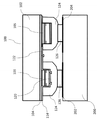
도 1은, 실시형태에 따른, 애노드 및 캐소드 콘택이 칩의 동일한 면(side) 상에 있도록, 전류 리턴 경로를 제공하는 단락된 VCSEL 구조와 쌍을 이루는 플립 칩 본딩식 직렬 VCSEL(flip-chip bonded, series VCSEL)을 예시하는 단순화된 단면도이다;
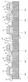
도 2는, 실시형태에 따른 단락용 메사 디바이스(shorting mesa device), 히트 싱크, 본딩 층, 및 다른 피쳐를 추가로 예시하는, 두 개의 직렬 연결된 VCSEL 어레이의 단순화된 단면도이다; 여기서 전기적으로 분리된 영역은 트렌치 분리 또는 이온 주입 영역을 통해 형성된다.
도 3은, 전기적으로 분리된 영역이 기판 방법을 통한 트렌치 분리 및 이온 주입을 통해 형성되는, 두 개의 직렬 연결된 VCSEL 어레이의 대안적인 실시형태이다.
도 4는, 전기적으로 분리된 영역이 전도성 층을 통한 에칭 및 반도체 기판 재료의 제거 및 절연성 지지 기판과의 대체에 의해 형성되는, 두 개의 직렬 연결된 VCSEL 어레이의 대안적인 실시형태이다.
도 5는 단일의 칩 또는 다이 상에서 직렬로 연결되는 세 개의 VCSEL 어레이의 예시적인 레이아웃의 상면도이다.
도 6은 예시적인 금속화 패턴을 갖는 서브마운트에 연결되는 도 5의 직렬 연결된 단일 칩 어레이를 예시한다.
도 7은 단일의 칩 또는 다이 상에서 직렬로 연결되는 네 개의 VCSEL 어레이의 예시적인 레이아웃의 상면도이다.
도 8은 예시적인 금속화 패턴을 갖는 서브마운트에 연결되는 도 7의 직렬 연결된 단일 칩 어레이를 예시한다.The drawings are provided to illustrate the exemplary embodiments described herein and are not intended to limit the scope of the present disclosure.
1 is a flip-chip bonded serial flip-chip bonded VCSEL paired with a shorted VCSEL structure that provides a current return path such that the anode and cathode contacts are on the same side of the chip, according to an embodiment. , series VCSEL).
2 is a simplified cross-sectional view of two series-connected VCSEL arrays, further illustrating the shorting mesa device, heat sink, bonding layer, and other features according to an embodiment; Here, the electrically isolated regions are formed through trench isolation or ion implantation regions.
3 is an alternative embodiment of two series-connected VCSEL arrays, in which electrically separated regions are formed through trench isolation and ion implantation through a substrate method.
4 is an alternative embodiment of two series-connected VCSEL arrays in which electrically isolated regions are formed by etching through a conductive layer and removal of semiconductor substrate material and replacement with an insulating support substrate.
5 is a top view of an exemplary layout of three VCSEL arrays connected in series on a single chip or die.
FIG. 6 illustrates the series-connected single chip array of FIG. 5 connected to a submount with an exemplary metallization pattern.
7 is a top view of an exemplary layout of four VCSEL arrays connected in series on a single chip or die.
8 illustrates the single chip array in series of FIG. 7 connected to a submount having an exemplary metallization pattern.
단일의 칩 상에서 수직 공동 표면 방출 레이저(VCSEL) 어레이의 다수의 직렬 연결을 가능하게 하기 위한 디바이스, 시스템, 및 방법이 본원에서 설명된다. 직렬 연결된 VCSEL 어레이는, 단일의 병렬 연결된 VCSEL 어레이에 비해, 주어진 연속하는(CW) 또는 펄스식 전류 소스로부터의 출력 광학 전력을 크게 향상시킨다. 향상된 피크 광학 전력은, 저 듀티 사이클 펄스식 전류원으로부터 동작되는 경우 특히 분명하다. 그러한 고전력 펄스식 광원은, 플래시 LiDAR 또는 근적외선 조명을 비롯한, 다양한 애플리케이션에 대해 특히 유용하다.Described herein are devices, systems, and methods for enabling multiple series connections of vertical cavity surface emitting laser (VCSEL) arrays on a single chip. The series-connected VCSEL array greatly improves the output optical power from a given continuous (CW) or pulsed current source, compared to a single parallel-connected VCSEL array. The improved peak optical power is particularly evident when operating from a low duty cycle pulsed current source. Such high power pulsed light sources are particularly useful for a variety of applications, including flash LiDAR or near infrared illumination.
단일의 칩 상에서 다양한 사이즈 및 구성을 갖는 직렬 연결되는 레이저 어레이 영역을 갖는 능력은, 영역당 출력을 최대화하기 위해, 구동 회로부, 레이저 구성, 및 출력 마이크로 광학기기(micro-optic)가 최적으로 매칭되는 것을 허용한다. 게다가, 유연성 및 다양한 VCSEL 어레이 설계는, 전체 광 빔 출력의 재단(tailoring)을 가능하게 한다. 실시형태가 서브마운트 상의 특정한 "타일화" 또는 다른 배열로 제한되지 않기 때문에, 제조 및 다른 비용은 감소될 수도 있다.The ability to have a series of laser array regions of various sizes and configurations on a single chip, the drive circuitry, laser configuration, and output micro-optic are optimally matched to maximize output per region. Allow. In addition, the flexibility and variety of VCSEL array designs enable tailoring of the overall light beam output. Manufacturing and other costs may be reduced, as embodiments are not limited to a particular "tiling" or other arrangement on the submount.
하기에서 설명되는 실시형태에서, 어레이 내의 VCSEL은, 애노드 및 캐소드 콘택 둘 모두가 웨이퍼의 활성 면(active side) 상에서 이루어지도록, 인터커넥트된다. 이 구성에서, 비전도성(도핑되지 않은) 웨이퍼를 디바이스 기판으로서 사용하는 것이 가능하고, 그 결과 VCSEL을 전기적으로 분리하는 것이 더 용이하다. 웨이퍼의 동일한 면에 캐소드 및 애노드 콘택을 행하는 성능은, 패키징 및 통합에 대한 큰 이점이다. 능동 집적 회로를 비롯한, 다양한 기판 상에서의 어셈블리를 위해, 단일의 플립 칩 본딩 단계가 사용될 수 있다. 와이어 본드가 없는 직접적인 상호 접속(direct interconnection)은 기생 인덕턴스를 최소화하여, 짧은 고전류 펄스 동작을 가능하게 한다.In the embodiments described below, the VCSELs in the array are interconnected such that both anode and cathode contacts are made on the active side of the wafer. In this configuration, it is possible to use a non-conductive (undoped) wafer as the device substrate, so that it is easier to electrically separate the VCSEL. The ability to make cathode and anode contacts on the same side of the wafer is a great advantage for packaging and integration. For assembly on various substrates, including active integrated circuits, a single flip chip bonding step can be used. Direct interconnection without wire bonds minimizes parasitic inductance, enabling short high current pulse operation.
한 실시형태에 따르면, 도 1은 다이의 동일한 면에 애노드 및 캐소드 콘택을 갖는 플립 칩 본딩식 VCSEL 어레이의 단순화된 개략적인 단면도를 도시한다. 도면은 단일의 레이저(103) 및 서브마운트 기판(200)과 접촉하는 단일의 단락된 메사(105)를 갖는 단일의 레이저 다이 또는 칩(100)을 도시한다. 그러나, 실제로, 단일의 칩은 많은 레이저 메사 및 단락된 메사를 가질 것이다. 발광 레이저는 서브마운트(202) 상의 애노드 콘택 패드와 접촉하는 메사이다. 캐소드 콘택 패드(204)와 접촉하는 메사는 레이저 메사와 유사하게 제조되지만, 그러나, 도금된 금속 층(124)은 레이저 구조체의 p 및 n 도핑 층과 접촉하여, 전기적 단락을 생성하고, 따라서, 접합부를 통해 어떠한 전류도 흐르지 않으며 어떠한 광도 방출되지 않는다. 대안적으로, 도금된 금속 층(124)은 유전체 코팅에 의해 p 도핑 층으로부터 분리될 수 있으며, n 도핑 재료와만 접촉하고 전류를 서브마운트(200) 상의 캐소드 콘택(204)으로 직접적으로 단락시킨다. 다시, 이 실시형태에서 접합부를 통해 어떠한 전류도 흐르지 않으며 어떠한 광도 방출되지 않는다.According to one embodiment, FIG. 1 shows a simplified schematic cross-sectional view of a flip chip bonded VCSEL array with anode and cathode contacts on the same side of the die. The figure shows a single laser die or
본원에서 개시되는 방법은, 발광 다이오드, 광검출기, 에지 방출 레이저, 변조기, 고 전자 이동도 트랜지스터, 공진 터널링 다이오드, 이종 접합 바이폴라 트랜지스터, 퀀텀 닷(quantum dot) 레이저 및 등등과 같은, 다른 반도체 디바이스의 어레이를 제조하기 위해 사용될 수 있다는 것이 이해될 것이다. 게다가, 실시형태에서의 VCSEL 어레이 디바이스(100)의 예시는 단지 예시적인 목적만을 위한 것이며, 어떤 방식으로든 본 발명의 범위를 제한하도록 의도되는 것은 아니다는 것이 이해될 것이다.The methods disclosed herein are of other semiconductor devices, such as light emitting diodes, photodetectors, edge emitting lasers, modulators, high electron mobility transistors, resonant tunneling diodes, heterojunction bipolar transistors, quantum dot lasers and the like. It will be understood that it can be used to manufacture an array. Moreover, it will be understood that the illustration of the
실시형태에서, VCSEL 어레이 디바이스는, 일반적으로 갈륨 비화물(GaAs)을 포함하는 기판(102)을 포함한다. 그러나, 인듐 인화물(InP), 인듐 인화물(InAs), 실리콘(Si), 에피택셜 성장 재료 및 등등과 같은 다른 재료가 기판(102)을 형성하기 위해 사용될 수 있을 것이다. 기판(102)은, 통상적으로, 후속하여 그 상에 성장되는 재료 층에서의 결함을 최소화하기 위해 선택되는 격자 상수를 포함한다. 또한, 조성 중 적어도 하나의 선택 및 후속하여 성장된 재료 층의 두께는, 동작의 소망되는 파장을 제공할 것이다는 것이 이해될 것이다. 후속 층은, 분자 빔 에피택시(Molecular Beam Epitaxy; MBE), 금속 유기 화학적 증착(Metal-Organo-Chemical Vapor Deposition; MOCVD), 및 등등을 사용한 에피택셜 성장을 통해 기판(102) 상에 퇴적된다.In an embodiment, the VCSEL array device generally includes a
몇몇 실시형태에서, 반도체 기판(102)은 전류 리턴 경로에 대한 추가적인 전도성 재료를 제공하기 위해 도핑된다. 이 추가적인 전도성 재료는 필수적인 것은 아니며, 반도체 기판(102)은 매우 낮은 전도성을 갖는 도핑되지 않은 또는 반절연성 재료일 수 있다. 그러한 경우에, 캐소드 콘택 층(104)은 어레이에서 레이저 사이의 핵심적인 전기 연결 층이다.In some embodiments,
층(104)은, VCSEL의 반도체 층 구조체에서, 기판(102)을 가로 지르는 횡방향 전도를 허용하는 도핑된 층이다. 금속 층(122)(도 2 참조)은, 전류 리턴 경로에 대한 전기 저항을 감소시키기 위해, 레이저 메사(103)에 근접한 층(104)에 접촉한다. 전도성 캐소드 층(104)은 단락된 메사(105)의 도금된 금속 구조체(124)에 연결된다. 한 실시형태에서, 층(104)은 VCSEL 메사(103)의 융기된 층 중 제1 층 및 단락용(shortcircuiting)/단락용(shorting)/접지용(grounding) 메사(105)를 형성하기 위해 기판(102) 상에 에피택셜하게 퇴적되는 격자 매칭된 하부(lattice-matched lower) 분산 브래그 반사기(Distributed Bragg Reflector; DBR)일 수도 있다. 하부 DBR(104)은 다양한(높은 및 낮은) 굴절률을 갖는 재료를 교대시키는 다수의 층으로부터, 또는 도파관에서 유효 굴절률의 주기적 변동으로 나타나는, 유전체 도파관의 높이와 같은 어떤 특성의 주기적인 변동에 의해 형성된다. 각각의 층 경계는 광파(optical wave)의 부분 반사를 야기하는데, 층의 결과적으로 나타나는 조합은 동작의 소망되는 파장에서 고품질 반사기로서 작용한다. 따라서, 하부 DBR(104)이 하나보다 더 많은 재료 층을 포함하지만, 그것은, 본원의 논의의 간략화 및 용이성을 위해, 도 1에서 단일의 층으로 구성되는 것으로 예시된다. 하부 DBR(104)의 일부는 또한, 전기적 콘택(도시되지 않음)이 VCSEL 어레이 디바이스에 대해 이루어는 것을 허용하도록 전도성으로 만들어질 수 있다.
한 실시형태에서, 활성 영역이 하부 DBR(104) 상에서 에피택셜하게 퇴적될 수도 있는데, 활성 영역은 클래딩(및/또는 도파(waveguiding)) 층, 장벽 층, 및 동작의 소망되는 파장에서 상당한 양의 광을 방출할 수 있는 활성 재료(active material)를 포함한다. 동작의 파장은 (GaAs 기판의 경우) 약 620 nm에서부터 약 1600 nm까지 대략적으로 주어지는 범위 내의 파장이다. 그러나, 다른 파장 범위가 소망될 수도 있고 애플리케이션에 의존할 것이다는 것이 이해될 것이다.In one embodiment, the active region may be epitaxially deposited on the
기술 분야의 숙련된 자에 의해 이해되는 바와 같이, 방출의 파장은, DBR 및 활성 영역을 생성하기 위해 사용되는 재료의 선택에 따라 실질적으로 결정된다. 게다가, 활성 영역은, 퀀텀 닷, 양자 우물, 또는 등등과 같은 다양한 발광 구조체를 포함할 수도 있다. 전기 전도성 상부(upper) DBR 영역은, 저항성 전기 연결(ohmic electrical connection)이 형성되는 것을 허용하기 위해(도시되지 않음), 활성 영역 상에 배치될 수도 있다. 몇몇 실시형태에서, 하부 DBR(104)은 n 도핑되고 상부 DBR은 p 도핑되지만, 그러나 이것은 반전될 수 있는데, 이 경우, 하부 DBR(104)은 p 도핑되고 상부 DBR은 n 도핑된다. 다른 실시형태에서, 전기 절연성 DBR이 활용될 수 있는데(도시되지 않음), 이것은 활성 영역에 가까운 층 및 공동 내 콘택(intracavity contact)을 활용한다. 게다가, 콘택 층(120) 상에 퇴적되는 금속에 대한 저항성 전기 연결을 용이하게 하기 위해, 도핑된 상부 미러 콘택 층(doped upper mirror contacting layer)(도시되지 않음)이 상부 DBR 상에 배치될 수 있다.As understood by those skilled in the art, the wavelength of the emission is substantially determined by the choice of DBR and the material used to create the active region. In addition, the active region may include various light emitting structures such as quantum dots, quantum wells, or the like. The electrically conductive upper DBR region may be disposed on the active region to allow a ohmic electrical connection to be formed (not shown). In some embodiments, the
리소그래피 및 에칭은 상기에서 설명되는 각각의 메사 및 그들의 구조를 정의하기 위해 사용될 수 있다. 이것은, 포지티브의 두꺼운 레지스트를 코팅, 노광, 및 현상하는 것과 같은, 일반적인 포토리소그래피 단계를 통해 에피택셜하게 성장된 층을 패턴화하는 것에 의해 달성될 수 있다. 레지스트의 두께는, 레지스트와 에피택셜 층 사이의 에칭 선택성, 및 소망되는 메사 지오메트리에 따라, 기술 분야에서 공지되어 있는 바와 같이 변할 수 있다.Lithography and etching can be used to define each mesa described above and their structure. This can be accomplished by patterning the epitaxially grown layer through common photolithography steps, such as coating, exposing, and developing a positive thick resist. The thickness of the resist can vary, as is known in the art, depending on the etch selectivity between the resist and the epitaxial layer, and the desired mesa geometry.
GaAs 기반의 재료의 경우, 에칭은 Cl2:BCl3과 같은 염소(Cl) 기반의 건식 에칭 플라즈마를 사용하여 달성되지만, 그러나 임의의 수의 가스 또는 그들의 혼합물이 사용될 수 있을 것이다. 에칭은 또한 많은 습식 에천트에 의해 달성될 수 있다. 이온 밀링 또는 반응성 이온 빔 에칭 및 등등과 같은 다른 형태의 에칭도 또한 사용될 수 있다. 에칭의 깊이는 어레이에서 메사의 활성 영역을 분리시키기에 충분한 깊이가 되도록 선택된다. 에칭은 N 미러(하부 DBR(104)) 상에서, N 미러(하부 DBR(104)) 내에, 또는 N 미러(하부 DBR(104))를 관통하여 기판(102) 안으로 형성되는 에칭 정지/콘택 층 상에서 멈춘다. 메사를 형성하기 위해 에칭한 이후, 나머지 포토레지스트가 제거된다. 이것은 습식 용매 세정 또는 건식 산소(O2) 에칭 또는 둘 모두의 조합을 사용하여 달성될 수 있다.For GaAs based materials, etching is accomplished using a chlorine (Cl) based dry etch plasma such as Cl 2 :BCl 3 , but any number of gases or mixtures thereof may be used. Etching can also be accomplished by many wet etchants. Other types of etching may also be used, such as ion milling or reactive ion beam etching and the like. The depth of the etch is chosen to be sufficient to separate the active regions of the mesa from the array. Etching is performed on the N mirror (lower DBR 104), in the N mirror (lower DBR 104), or on the etch stop/contact layer formed into the
도면에서 도시되는 실시형태에서, 광 생성 VCSEL의 메사 사이즈, 및 개구는 동일하며 균일한 간격을 갖는다. 그러나, 몇몇 실시형태에서, 어레이에서의 디바이스에 대한 개개의 VCSEL 메사 사이즈는 상이할 수 있다. 더구나, 어레이에서의 VCSEL 메사 간격은 상이할 수 있다. 몇몇 실시형태에서, 어레이(100)에서의 광 생성 VCSEL 메사의 분리는 대략 20 ㎛와 200 ㎛ 사이에 있다. 그러나, 더 큰 그리고 더 작은 분리도 또한 가능하다. VCSEL 메사 및 캐소드 메사는 둘 모두는 도면에서 원형으로서 도시되지만, 그러나 직사각형, 가늘고 긴 라인 또는 다른 임의의 형상일 수도 있다.In the embodiment shown in the figures, the mesa size, and openings of the light generating VCSELs are the same and have uniform spacing. However, in some embodiments, individual VCSEL mesa sizes for devices in the array may be different. Moreover, the VCSEL mesa intervals in the array can be different. In some embodiments, the separation of light generating VCSEL mesas in the
콘택 표면에 대한 개구를 정의하기 위해 유전체 퇴적이 사용 및 프로세싱될 수 있다. 유전체 층(114)은, 애노드 콘택(202)으로부터의 전류 흐름이 금속 층(126, 124 및 120)을 통해, 그 다음, 광이 방출되도록 반도체 접합부를 통해 흐르도록, 도금된 금속 피복 및 히트 싱크(124)로부터 레이저 메사(103)를 절연한다. 유전체 층(114)의 퇴적은 플라즈마 강화 화학적 증착(Plasma Enhanced Chemical Vapor Deposition; PECVD)에 의해 일반적으로 달성되지만, 그러나 원자 층 퇴적(Atomic Layer Deposition; ALD)과 같은 다른 기술이 사용될 수 있다. 실시형태에서, 유전체 코팅(114)은 (메사 측벽을 비롯한) 상부 표면 위에서의 컨포멀 코팅(conformal coating)이고, 후속하는 금속 층으로부터 핀홀을 통한 전류 누출을 방지하도록 충분히 두껍다.Dielectric deposition can be used and processed to define openings to the contact surface. The
이 막의 두께를 선택하는 동안 고려할 다른 속성은, 도금된 금속(124)(이것은 도 2를 참조하여 하기에서 추가로 설명되는 바와 같이 히트 싱크로서 동작함)과 기판(102)(접지) 사이에서 생성되는 커패시턴스 - 이 경우 유전체 층(114)은 더 두꺼운 것이 더 유리할 것임 - , 및 VCSEL(103)의 측벽 상의 유전체 층(114)이 활성 영역으로부터 히트 싱크(124)로 열을 전달할 필요성 - 이 경우 얇은 층이 유리할 것임 - 이다. 몇몇 실시형태에서, 이들 속성 둘 모두를 갖는 층을 달성하기 위해, 상이한 퇴적 기술을 사용한 다수의 퇴적이 사용될 수 있다. 이 기술의 예는, PECVD 실리콘 질화물(Si3N4)의 퇴적에 후속하여 Si3N4의 E 빔 퇴적을 계속하는 것이거나, 또는 더욱 지향성인 퇴적 레이트를 갖는 다른 유전체가 퇴적될 수 있고, 그에 의해, 입사 표면 상에 더 두꺼운 유전체 재료를 배치할 수 있다. 일단 유전체 층(114)이 형성되면, 그 다음, 포토 리소그래피 프로세스는, 상부 미러 콘택 층(120)에 대한 콘택이 만들어질 VCSEL 메사의 각각의 위의 유전체에서 개구를 정의하기 위해 사용된다. 유전체 층(114)은 또한, VCSEL 메사의 각각 사이의 기판(102) 위에서, 접지 메사(ground mesa)를 둘러싸는 기판(102) 위에서, 그리고 각각의 접지 메사의 상부 및 측면 위에서 제거된다.Another attribute to consider while choosing the thickness of this film is to create between plated metal 124 (which acts as a heat sink as described further below with reference to Figure 2) and substrate 102 (ground). The resulting capacitance-the
이들 예시적인 실시형태에서, 포토리소그래피 프로세스는, 유전체가 개구되는 상부 미러 위에 콘택을 정의하기 위해 사용될 수도 있고, 그 결과, 그 내부에 p 금속 층(120)이 후속하는 단계에서 형성될 수 있다. 실시형태에서, 포토레지스트의 개구된 영역은 유전체의 개구 보다 약간 더 큰데, 통상적으로는 대략 수 ㎛ 더 넓다. 다른 실시형태에서, 그것의 직경은 유전체 개구의 직경 보다 더 작을 수 있거나, 또는 나중의 단계에서 도금되는, 단락된 메사 위의 히트 싱크 재료의 직경만큼 클 수 있다. 유전체 코팅이 컨포멀하고 메사 베이스에서 N 미러 부분을 덮지 않는 한, 이 개구는 활성 광 생성 메사에서 메사 직경 보다 조금도 더 클 수 없거나, 또는 후속하는 금속은 p 및 n 전위를 단락시킬 것이다.In these exemplary embodiments, a photolithography process may be used to define the contact over the top mirror on which the dielectric is opened, and as a result,
일단 포토레지스트에서 개구된 영역이 정의되면, 개구된 영역 위에서, 통상적으로 p 형 금속을 통한 금속화가 수행될 수 있다. p 금속 콘택 층(120)은, 일반적으로, E 빔, 저항성 증착(resistive evaporation), 스퍼터, 또는 임의의 다른 금속 퇴적 기술에 의해 퇴적되는 다층 퇴적(multilayer deposition)이다. 다음 층의 접착을 위해, 얇은 티타늄(Ti) 층이 먼저 퇴적된다. 이 접착 층의 두께는 크게 변할 수 있지만, 그러나, Ti 막이 응력을 받고 후속하는 층 보다 저항성이 더 크기 때문에, 일반적으로 약 50 Å과 약 400 Å 사이에 있도록 선택된다. 한 실시형태에서, 접착 층은 대략 200 Å 두께이다. 크롬(Cr), 팔라듐(Pd), 니켈(Ni), 및 등등과 같은 다른 접착 성 금속 층이 이 층을 대신할 수 있다. 또한, 이 층은 콘택용 미러(contacting mirror)의 반사율을 증가시키기 위해 반사기 층으로서 역할을 할 수 있다.Once the open area is defined in the photoresist, metallization can be performed over the open area, typically through a p-type metal. The p
다음 층은 퇴적 동안 진공을 파괴하지 않으면서 접착 층의 상부 상에 직접적으로 퇴적된다. 많은 경우에, 이 층은 금(Au) 또는 다른 최고 금속이 본딩 단계에서의 과도한 가열로 인해 콘택 안으로 너무 멀리 확산하는 것을 방지하는 가드(확산 장벽)로서 역할을 한다. 선택되는 금속은 일반적으로 Pd, 백금(Pt), Ni, 텅스텐(W), 또는 다른 금속 또는 이 목적을 위해 선택되는 이들 금속의 조합이다. 선택되는 두께는 플립 칩 프로세스에 필요로 되는 특정한 본딩 온도에 의존해야 한다. 이 층의 두께는 통상적으로 약 1,000 Å과 약 10,000 Å 사이에 있다. 저온 본딩 프로세스가 사용되는 실시형태에서, 예를 들면, 인듐 본딩 프로세스에서, 확산 장벽 층은 옵션 사항일 수 있고, 금속 콘택 스택의 일부로서 퇴적되지 않을 수 있다.The next layer is deposited directly on top of the adhesive layer without breaking the vacuum during deposition. In many cases, this layer serves as a guard (diffusion barrier) that prevents gold (Au) or other top metal from diffusing too far into the contact due to excessive heating in the bonding step. The metal of choice is usually Pd, platinum (Pt), Ni, tungsten (W), or other metals or combinations of these metals selected for this purpose. The thickness chosen should depend on the specific bonding temperature required for the flip chip process. The thickness of this layer is typically between about 1,000
다음 층은 일반적으로 Au이지만 그러나 Pd 또는 Pt 또는 금 베릴륨(AuBe) 또는 금 아연(AuZn)과 같은 혼합물일 수 있다. 하기에서 설명되는 실시형태에서, 이 층의 두께는 대략 2,000 Å이다. 그러나, 그것은 일반적으로, 퇴적의 포토레지스트 속성 및 가열 특성에 따라 광범위한 두께를 가질 수 있다. 몇몇 실시형태에서, 이 때, 금속 두께를 증가시키기 위해 그리고 이 단계에서 금속 히트 싱크를 형성하기 위해, 다른 금속이 또한 퇴적될 수 있고, 그에 의해, 프로세싱 단계의 수를 감소시키지만, 그러나 이 기술은 필수적인 것은 아니며 하기에서 설명되는 실연 디바이스(demonstration device)에서 활용되지 않았다.The next layer is usually Au, but may be Pd or Pt or a mixture such as gold beryllium (AuBe) or gold zinc (AuZn). In the embodiments described below, the thickness of this layer is approximately 2,000
일반적으로, 표면 상에 퇴적되는 금속이 포토레지스트로 피복되는 표면의 영역으로부터 쉽게 분리될 수 있도록 이 포토리소그래피 프로세스에 대해 일반적인 리프트오프 기술(liftoff technique)이 선택되며, 그 결과, 포토레지스트 상의 임의의 금속은, 반도체에 접착하지 않으면서 또는 반도체에 대한 금속의 접착력에 영향을 끼치지 않으면서 제거된다. 상기에서 언급되는 바와 같이, 포토리소그래피 프로세스는, 그 다음, 유전체가 이전 단계에서 개구된, 기판(102)의 다양한 부분 및 단락된 n 콘택 메사(105) 위에 개구를 정의하기 위해 사용된다. 한 실시형태에서, n 금속 퇴적에 대응하는 포토레지스트에서의 개구된 영역은, n 금속에 대한 유전체 개구에서의 개구보다 약간 더 커야 한다. 그 다음, N 금속 층(122)이 퇴적되고, 하부 DBR(104)(n 미러인 경우), 일반적으로 하부 DBR(104) 내에 강하게 도핑되는 에칭 정지 및 콘택 층 중 어느 하나를 통해 기판(102)과의, 또는 기판(102) 그 자체에 대한 전기적 회로를 형성할 수 있다. n 금속 층(122)을 형성하기 위한 프로세스는 p 금속 층(120)에 대한 것과 유사하다. 금속 층은 Ni/Ge/Au, Ge/Au/Ni/Au의 조합, 또는 많은 그러한 조합을 포함하도록 선택될 수 있다.Generally, a liftoff technique common to this photolithography process is selected so that the metal deposited on the surface can be easily separated from the area of the surface covered with the photoresist, resulting in any on the photoresist. The metal is removed without adhering to the semiconductor or affecting the adhesion of the metal to the semiconductor. As mentioned above, the photolithography process is then used to define the openings over the shorted n contact mesas 105 and various portions of the
몇몇 실시형태에서, 제1 층 또는 층들은, 기판(102)의 n 도핑된 에피택셜 재료로의 확산에 의해 콘택 저항을 감소시키도록 선택된다. 다른 실시형태에서, 다층 금속 스택의 제1 층은 또한, 어닐링 프로세스에서 재료의 다양한 확산 속성에 기인하여 금속이 "응집하지" 않고 분리되도록, Ni와 같은 확산 제한 층으로서 선택될 수 있다. 이들 금속의 확산을 균일하게 분배하는 것이 소망되며, 콘택 저항을 낮추기 위해 사용될 수 있는데, 콘택 저항을 낮추는 것은 가열을 또한 감소시킨다. 이 다층 금속 스택의 두께는 크게 변할 수 있다. 설명될 실시형태에서, 각각, 400 Å/280 Å/2,000 Å의 두께를 갖는 Ni/Ge/Au 금속 스택이 사용되었다.In some embodiments, the first layer or layers are selected to reduce contact resistance by diffusion of the
그 다음, 콘택 저항을 낮추기 위해, 웨이퍼에 대해 급속 열 어닐(Rapid Thermal Anneal; RTA) 단계가 수행된다. 설명되는 실시형태의 경우, 프로세스 온도는 ~ 400 ℃까지 급격하게 상승되고, 약 30 초 동안 유지되고, 실온까지 하강된다. RTA 단계에 대한 온도 및 시간 조건은 금속화에 의존하며, 기술 분야에서 통상의 지식을 가진 자에게 공지되어 있는 바와 같이, 실험 계획법(Design Of Experiment; DOE)을 사용하여 결정될 수 있다.Then, to lower contact resistance, a rapid thermal annealing (RTA) step is performed on the wafer. In the case of the described embodiment, the process temperature rises rapidly to ˜400° C., holds for about 30 seconds, and falls to room temperature. The temperature and time conditions for the RTA step depend on metallization and can be determined using Design Of Experiment (DOE), as is known to those skilled in the art.
다른 실시형태에서, 이 단계는 프로세스 플로우의 초기 또는 나중 단계에서 수행될 수 있지만, 그러나 솔더 또는 접착제 금속의 산화를 감소시키기 위해 솔더가 퇴적되기 이전에 일반적으로 행해진다. 기판(102) 및 단락된 N 콘택 메사(105) 위의 콘택 개구, 및 히트 싱크 구조체가 도금되거나 또는 구축될 활성 메사(103)를 정의하기 위해, 포토리소그래피 프로세스(통상적으로 약 1 ㎛ 내지 3 ㎛인 포토레지스트의 얇은 층을 사용함)가 사용되고 개발된다. 다음 단계는 금속 씨드 층의 퇴적이며, 일반적으로 다층 퇴적이며, E 빔, 저항성 증착, 스퍼터 또는 임의의 다른 금속 퇴적 기술에 의해 퇴적된다. 20 Å/600 Å의 Ti/Au, 또는 제1 층 또는 층들이 접착 및 에칭 용이성을 위해 퇴적되고, 제2 층이 전도성 및 에칭 용이성을 위해 퇴적되는 많은 그러한 조합과 같은 금속 층이 선택될 수 있다. 이 기술이 히트 싱크를 구축하기 위해 사용되는 경우, 씨드 층은 도금을 위한 전기적 연결을 허용하면서 표면에 걸쳐 연속적이다.In other embodiments, this step can be performed at an early or later stage of the process flow, but is generally done before the solder is deposited to reduce oxidation of the solder or adhesive metal. A photolithography process (typically about 1 μm to 3 μm) to define the contact openings over the
한 실시형태에서, 그 다음, 두꺼운 금속이 도금에 의해 퇴적되어, 히트 싱크(124)를 형성한다. 그러나, 퇴적의 다른 방법이 또한 사용될 수 있는데, 이 경우, 금속 씨드 층이 필요로 되지 않는다. 도금을 위해, 포토 리소그래피 프로세스는 이전 씨드 층 레지스트와 함께 정의되는 개구 위에 개구를 정의하기 위해 사용된다. 포토레지스트는 퇴적이 발생할 영역에서 제거된다. 포토레지스트의 두께는, 두꺼운 금속이 정의된 이후 그것이 쉽게 들리도록 선택되어야 하며 통상적으로 두께에서 약 4 ㎛에서부터 약 12 ㎛까지의 범위에 이른다. O2, 또는 암모늄 수산화물(NH4OH)과 조합한 물을 사용한 플라즈마 세정이 수행되어, 금 씨드 층 상에 남겨진 임의의 레지스트를 제거한다. 다음에, 히트 싱크(124) 금속은 표준 도금 프로시져에 의해 도금된다. 설명되는 실시형태에서, 구리(Cu)는, 그것의 열 전도율 속성에 기인하여 도금을 위한 금속으로서 선택되었지만, 그러나 양호한 열 전도율을 제공하며 디바이스 신뢰도를 저하시키지 않는 계면을 제공하는, Au, Pd, Pt, 또는 등등과 같은 비산화성 금속(non-oxidizing metal)이 더욱 적절할 수 있을 것이다. 도금 두께는 변할 수 있다. 설명되는 실시형태에서, 대략 3 ㎛ 두께가 사용되었다.In one embodiment, thick metal is then deposited by plating to form a
다음으로, 웨이퍼 또는 샘플이 인듐(In) 도금과 같은 솔더 도금 용액에 배치되어 본딩 층(126)을 형성한다. 그들의 본딩 특성을 위해, 이 단계에서 다른 금속이 선택될 수 있다. 두께는 크게 변할 수 있다. 설명되는 실시형태에서, 대략 2 ㎛의 도금된 In이 히트 싱크 상에 퇴적되었다. 그러나, 금 주석(AuSn) 합금과 같은 다른 솔더가 또한 사용될 수 있고, 스퍼터링과 같은 대안적인 퇴적 기술이 또한 사용될 수 있다. 금속 퇴적이 완료된 이후, 포토레지스트는, 그 다음, 앞서 설명되는 바와 같이, 용매, 플라즈마 세정, 또는 둘 모두의 조합을 사용하여 제거되고, 씨드 층은 Au를 에칭하는 건식 또는 습식 에칭을 사용하여 에칭되고, 그 다음, Ti를 에칭하고 및/또는 TiO2를 제거하는 건식 또는 습식 에칭에서 에칭된다. 그 다음, 씨드 층 포토레지스트는 표준 레지스트 세정 방법을 사용하여 세정된다. 이 시점에서, VCSEL 어레이 기판이 완성되고 본딩 준비가 완료된다. 대안적으로, 솔더는, 레이저 다이 상의 메사 대신, 플립 칩 본딩 프로세스를 위해, 서브마운트 콘택 표면 상에 퇴적될 수도 있다.Next, a wafer or sample is placed in a solder plating solution such as indium (In) plating to form a
두꺼운 히트 싱크 재료를 갖는 메사의 완전한 봉입(encasement)은 실시형태의 중요한 양태이다. 메사의 활성 영역이 두꺼운 히트 싱크 재료가 형성되는 에지에 가장 가깝기 때문에, 우수한 열 전도율이 존재하고, 그에 의해, 실시형태의 설계가 그들 활성 영역에 의해 생성되는 열을 효율적이고 효과적으로 제거하는 것을 가능하게 한다. 앞서 언급되는 바와 같이, 이것은, 히트 싱크 재료를 메사의 상부에 배치하는 현존하는 VCSEL 어레이 디바이스 열 감소 기술과는 상당히 새로운 시도이다. 이들 현존하는 또는 이전의 설계는 일련의 더 높은 열 전도성 재료(미러) 또는 유전체를 통해 열이 이동하는 것을 요구하며, 그에 의해, 덜 효율적이고 덜 효과적인 열 전도로 나타난다.The complete encasement of the mesa with a thick heat sink material is an important aspect of the embodiment. Since the active area of the mesa is closest to the edge where the thick heat sink material is formed, excellent thermal conductivity is present, thereby enabling the design of the embodiments to efficiently and effectively remove the heat generated by their active area. do. As mentioned earlier, this is a fairly new attempt with existing VCSEL array device heat reduction techniques that place heat sink material on top of the mesa. These existing or previous designs require heat to travel through a series of higher thermally conductive materials (mirrors) or dielectrics, thereby resulting in less efficient and less effective thermal conduction.
몇몇 현존하는 설계가 히트 싱크 재료의 얇은 층을 갖는 메사를 포괄하지만, 열을 감소시키는 목적을 위해, 이들 설계는 결과적으로 나타나는 히트 싱크의 높이를 고려하지 않는다. 두꺼운 히트 싱크 층을 사용하고 히트 싱크 기판 상의 n 기판 접지 전위와 p 콘택 평면 사이의 거리에 추가하는 것에 의해, 본 실시형태는 히트 싱크 층의 높이가 증가됨에 따라 시스템의 기생 용량을 감소시킨다. 게다가, 열을 감소시키는 것에 추가하여, 추가적인 재료의 구축은 주파수 응답을 증가시킨다.Some existing designs cover a mesa with a thin layer of heat sink material, but for the purpose of reducing heat, these designs do not take into account the height of the resulting heat sink. By using a thick heat sink layer and adding to the distance between the n substrate ground potential on the heat sink substrate and the p contact plane, this embodiment reduces the parasitic capacity of the system as the height of the heat sink layer increases. Moreover, in addition to reducing heat, the construction of additional materials increases the frequency response.
다른 실시형태에서, 히트 싱크 재료가 모든 메사를 완전히 포괄하고, 히트 싱크의 개개의 메사 대신, 하나의 큰 히트 싱크 구조체를 형성할 수 있도록, 유전체 층(114)은 메사 주변의 전체 n 미러 또는 기판을 피복하며 개방되지 않는다. 이 경우, n 콘택은 단락된 메사로부터 기판까지 연장되기만 하면 될 것이다. 본 실시형태의 히트 싱크는 또한, 이웃하는 메사에 의해 생성되는 열의 양을 감소시키는 것에 의해, VCSEL 어레이의 동작을 향상시킨다. 대부분의 전기 디바이스 내의 열 저항에서의 감소는, 각각의 디바이스의 주파수 응답을 증가시킬 것이다. 본 디바이스의 VCSEL 어레이 디바이스의 열 성능을 향상시키는 것에 의해, VCSEL 어레이 디바이스의 고속 성능에서의 상당한 증가가 가능하게 된다. 더구나, 이 실시형태에서, 메사를 고려한 여분의 높이는, 현존하는 어레이 회로와 비교하여 두껍게 된 히트 싱크 구축으로 인해, 기판 접지 평면과 모든 활성 메사를 병렬로 연결하는 포지티브 콘택 플레이트 사이의 거리를 증가시키는 것에 의해 커패시턴스를 감소시킨다는 것이 또한 명백하다. 결과적으로 나타나는 효과는, 회로의 기생 임피던스에서의 감소이며, 이것은 또한 전체 어레이의 주파수 응답이 증가시킨다.In another embodiment, the
또한, 활성 영역을 둘러싸는 서브 어레이를 형성하는 단락된 메사 설계는, 다수의 와이어 본드를 형성하는 것의 사용 없이도, 제조된 VCSEL 기판으로부터 열 확산기 상의 접지 평면으로의 직접적인 전류 흐름을 허용한다. 본 실시형태의 이 양태는 제조의 복잡성을 감소시키고, 또한, 현존하는 어레이에서 나타난 다수의 와이어 본드로부터의 기생 인덕턴스를 감소시킨다. 단락된 메사 설계는, 열 확산기 기판으로 플립 칩 연결될(flipped chipped) 때, 어레이의 주파수 응답에 유리한 동일 평면 도파관을 형성한다. 이 설계 피쳐는 또한, 신뢰도 및 위치 결정에 또한 영향을 주는 융기된 와이어 본드를 필요로 하지 않는 더 단순한 패키징 설계를 가능하게 한다.In addition, the shorted mesa design forming a sub-array surrounding the active area allows direct current flow from the fabricated VCSEL substrate to the ground plane on the heat spreader without the use of forming multiple wire bonds. This aspect of this embodiment reduces manufacturing complexity and also reduces parasitic inductances from multiple wire bonds present in existing arrays. The shorted mesa design, when flipped chipped to the heat spreader substrate, forms a coplanar waveguide that favors the frequency response of the array. This design feature also enables simpler packaging designs that do not require raised wire bonds that also affect reliability and positioning.
층(126)은 서브마운트 기판(200)에 대한 접착을 제공하는 솔더 또는 다른 전도성 본딩 층이다. 층(126)은, 도금된 금속 층(124)의 상부, 애노드 및 캐소드 메사 상에, 다양한 방법에 의해 직접적으로 퇴적될 수 있다. 층(126)은 또한, 대신, 서브마운트 상의 애노드 및 캐소드 콘택 패드(202 및 204)에 도포될 수 있다. 층(120)은 VCSEL 반도체 층의 고도로 도핑된 표면에 대한 콘택이다. 캐소드 콘택(204)에서 접지로의 경로를 만들기 위해, 레이저 메사로부터 단락된 메사로의 전류 흐름은 캐소드 콘택 층(104)을 통과한다.
그러한 직렬 연결된 배열의 바람직한 레이아웃은 도 2의 단면도에서 도시되어 있다. 여기서, 레이저 어레이의 애노드(103) 및 단락된 캐소드(105)는, 앞서 도 1에서 도시되는 바와 같이 구성된다. 하나의 차이점은, 반도체 기판(102)이, 일반적으로 사용되는 고도로 도핑된 전도성 반도체 재료이기 보다는, 적어도 반절연성 재료(즉, 반절연성 또는 절연성)이다는 것이다. 이 반절연성 재료는 대부분의 VCSEL 설계에 대한 기초를 형성하는 GaAs 기판의 약하게 도핑된 버전이다. 또한, 공통 전도성 캐소드 층(104)은, 에칭된 영역(128)을 사용하여 분리되어 칩 상에 전기적으로 별개의 캐소드 영역을 생성한다.The preferred layout of such a series-connected arrangement is shown in the sectional view of FIG. 2. Here, the
대안적인 실시형태는, 에칭된 트렌치 대신, 영역(128)에서 분리 주입(isolation implant)을 사용한다. 주입은 도면에서의 메사가 에칭된 이후 수행될 것이고, 그 결과, 전체 레이저 구조체를 통해 주입하기 위해 필요할 것처럼, 주입 에너지가 극히 높을 필요는 없다. 분리 주입은 통상적으로 양성자를 사용하여 반도체 결정 구조를 어지럽혀 그것을 비전도성으로 만든다. 기술 분야의 숙련된 자에게 공지되어 있는 그러한 전기적 분리를 행하기 위해 종 및 에너지를 주입하는 많은 접근법이 존재한다. 분리 주입과 결합되는 영역(128)에서의 얕은 에칭 트렌치의 조합이 또한 사용될 수도 있다.An alternative embodiment uses an isolation implant in
도 3은 도 2와 유사한 직렬 연결된 배열을 묘사하지만, 그러나, VCSEL 어레이 사이의 분리는 트렌치 분리 방법을 통해 실현된다. 이 실시형태에서, 공통 전도성 캐소드 층 상에 전기적으로 분리된 전도성 영역을 생성하기 위해, 기판은 이면(back)으로부터 에칭된다. 영역(128)에서의 트렌치는 전체 기판(102)을 통과하지 않지만, 그러나, 영역(128)에서의 나머지 재료를 비전도성으로 만들기 위해 이온 주입의 사용을 허용할 만큼 충분히 깊다. 트렌치는 웨이퍼를 기계적으로 약화시킬 것이고, 따라서, 어떤 타입의 지지 기판이 필요로 될 수도 있다.Fig. 3 depicts a series connected arrangement similar to Fig. 2, however, separation between VCSEL arrays is realized through a trench separation method. In this embodiment, the substrate is etched from the back to create electrically isolated conductive regions on the common conductive cathode layer. The trench in
트렌치는, 기판(102)을 에칭하기 위해, 상기에서 설명되는 바와 같이, 리소그래피 기술을 사용하여 형성될 수도 있다. VCSEL 디바이스 및 기판(102)에 대해 사용되는 재료 및 본원에서 설명되는 다양한 실시형태에 따라, 소망되는 사이징 속성을 갖는 트렌치를 생성하기 위해, 실리콘의 국소적 산화(local silicon of silicon; LOCOS) 또는 얕은 트렌치 분리와 유사한 구조체를 생성하기 위해 폴리머 또는 스핀 온 글래스(spin-on glass)와 같은 유전체 재료로 트렌치를 채우는 것과 같은 일반적인 분리 기술이 구현될 수도 있다.The trench may be formed using lithography techniques, as described above, to etch the
일단 트렌치 영역(128)이 확립되면, 영역(128)이 비전도성인 것을 보장하기 위해 이온 주입 기술이 사용될 수도 있다. 이온 주입에서, 타겟 재료 내의 원자를 변위시키고, 구조적 변화를 야기하고, 수정된 물리적, 화학적, 및/또는 전기적 속성을 갖는 타겟 재료로 나타나게 하기 위해, 고 에너지 이온(~ 10 내지 200 KeV)이 기판 안으로 가속될 수도 있다. 붕소, 질소, 또는 인과 같은 도펀트 이온이 그러한 방법에서 활용될 수도 있지만, 소망되는 기판 속성 및 기판 재료에 따라, 다른 이온이 사용될 수도 있다.Once the
하나의 기술에서, 기술 분야에서 일반적으로 숙련된 자에게 알려져 있는 바와 같이, 이온 주입은 소망되는 원소 및 불활성 가스를 포함하는 이온화된 빔의 형성을 통해 구현될 수도 있다. 이온화된 빔은 진공에서 타겟 재료를 향해 높은 에너지로 가속되는데, 이온화된 원자는 타겟 재료 내의 원자를 변위시킬 수도 있다. 이 프로세스를 달성하기 위해, 기술 분야의 숙련된 자에게 일반적인 고 에너지 가속기 및 다른 기술이 활용될 수도 있다. 칩에 대해 급속 열 어닐(RTA) 단계가 또한 수행되어, 주입 프로세스 동안 도펀트 및 불순물에 의해 야기되는 결함 또는 손상을 제거할 수도 있다.In one technique, as is generally known to those skilled in the art, ion implantation may be implemented through the formation of an ionized beam comprising a desired element and an inert gas. The ionized beam is accelerated with a high energy towards the target material in vacuum, the ionized atoms may displace the atoms in the target material. To achieve this process, high energy accelerators and other techniques common to those skilled in the art may be utilized. A rapid thermal annealing (RTA) step may also be performed on the chip to eliminate defects or damage caused by dopants and impurities during the implantation process.
비전도성 트렌치 영역(128)을 생성하기 위해 이온 주입 기술이 바람직할 수도 있는데, 그 이유는 영역의 전기적 속성이 주입의 깊이 및 조사량(dosage)을 통해 정확하게 제어될 수도 있기 때문이다. 주입은 또한, 표면 타겟 재료의 경화 및 내부식성(corrosion resistance)에 기여하는데, 이것은 디바이스가 마모 및 다른 손상에 대해 더욱 내성이 있게 만든다.Ion implantation techniques may be desirable to create
(도 2에서 도시되는 바와 같이) VCSEL 구조체의 전도성 영역을 통한 그리고 부분적으로 (도 3에서 도시되는 바와 같이) 기판을 통한 트렌치 에칭의 조합은, 영역(128)의 나머지 재료로의 분리 주입과 결합되어, 도핑된(즉, 전도성) 기판의 사용이, 동일한 다이 상에서 VCSEL의 직렬 연결을 만드는 것을 또한 허용할 것이다.The combination of trench etching (as shown in FIG. 2) through the conductive region of the VCSEL structure and partially through the substrate (as shown in FIG. 3), combined with separate implantation of the
도 4는 직렬 연결을 위해 동일한 다이 상에서 VCSEL을 전기적으로 분리하는 제3의 접근법을 예시한다. 이 접근법에서, 기판(102)의 도핑은 무관한데, 그 이유는, 기판이 제거되고 VCSEL 어레이 구조체가, 원래의 갈륨 비화물 기판이, 상기에서 설명되는 바와 같이, 연마 작용, 선택적 화학적 에칭, 및/또는 리소그래피 방법의 조합에 의해 제거된 이후 VCSEL 어레이의 노광된 표면에 본딩되는 절연성 기판에 의해 지지되기 때문이다. 칩은 기판 제거 동안 칩의 에칭된 메사 면에 본딩되는 임시 백킹(backing) 또는 핸들 웨이퍼에 의해 기계적으로 지지된다. 일단 절연성 기판이 (접착제 또는 다른 칩 본딩 프로세스를 사용하여) 제자리에 본딩되면, 임시 백킹 칩은 제거된다. VCSEL 어레이는 그 다음 서로 전기적으로 분리된다.4 illustrates a third approach to electrically separating VCSELs on the same die for serial connection. In this approach, doping of the
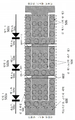
도 5는 단일의 칩 또는 다이 상에 직렬로 연결되는 다수의 VCSEL 어레이의 예시적인 상면도 레이아웃을 예시한다. 칩은 실선의 직사각형 윤곽선(500)에 의해 표현된다. 이 실시형태에서, 두 개의 영역(128)은, 칩의 공통 전도성 캐소드 층 상에 세 개의 연속적인 전기적으로 분리된 전도성 영역(502a, 502b, 및 502c)을 형성하도록, 칩에 걸쳐 연장된다. 분리된 영역(128)은, 영역을 비전도성으로 만들기 위해, 상기에서 설명되는 방법 중 임의의 것을 통해, 에칭 또는 이온 주입될 수도 있다. 각각의 전기적으로 분리된 전도성 영역(502)은 애노드 영역 및 캐소드 영역을 더 포함한다. 애노드 영역은, 더 작은 점선의 원에 의해 표현되는 복수의 애노드 콘택(504)을 포함한다. 캐소드 영역은 또한 더 큰 점선의 원에 의해 표현되는 복수의 캐소드 콘택(506)을 포함한다.5 illustrates an exemplary top view layout of multiple VCSEL arrays connected in series on a single chip or die. The chip is represented by a solid
이 실시형태에서, 애노드는 각각의 칩 영역(502)의 중심에서 함께 그룹화된다. 캐소드 콘택(504)은 복수의 애노드 콘택(504) 주위에 C자 형상을 형성하고 실질적으로 애노드 콘택의 세 개의 변을 둘러싼다. 그러나, 다른 캐소드 및 애노드 구성도 가능하며 현재의 예시적인 레이아웃으로 제한되지는 않는다. 애노드 콘택(504)은 동일한 전기적으로 분리된 전도성 영역 내에서 캐소드 콘택(506)과 전기적으로 연결된다. 칩이 서브마운트에 연결될 때, 캐소드 콘택은, 도 6에서 추가로 설명되는 바와 같이, 칩의 저부 면(bottom side) 상의 서브마운트의 금속화 패턴(도시되지 않음)을 통해 인접 영역의 애노드 콘택에 연결된다.In this embodiment, anodes are grouped together at the center of each chip region 502. The
칩(500)의 폭에 걸쳐 연장되는 에칭된 영역(128)은, 에칭된 영역(128)에 의해 인접한 영역 상의 캐소드 층으로부터 각각의 영역 상의 캐소드 서브마운트 층을 전기적으로 분리한다. 에칭된 영역은, 칩(500) 상에 하나 이상의 별개의 연결되지 않은 금속 층을 생성하기 위해, 상기에서 설명되는 것과 유사한 포토리소그래피 프로세스에 의해 달성되고 정의될 수도 있다. 에칭된 영역은 하나 또는 이차원 패턴, 또는 본원에서 설명되는 패턴의 임의의 변형을 포함할 수도 있고, 이온 주입된 영역 또는 에칭된 트렌치 영역과 이온 주입된 영역의 조합일 수도 있다.The
더구나, 칩(500)은 개시된 특징을 가능하게 하는 것과 부합하는 임의의 형상 또는 사이즈일 수도 있으며, 도 5에서의 묘사된 직사각형 실시형태로 제한되지는 않는다. 칩은, 절단, 다이싱, 레이저 싱귤레이션(laser singulation), 또는 그들의 프로세스 또는 유사한 프로세스의 임의의 조합에 의해 형성될 수도 있다. 마찬가지로, 각각의 칩 상에 생성되는 영역의 형상, 사이즈 및 수는, 설계 필요 및 유사한 고려 사항에 따라, 변경될 수 있다.Moreover, the
각각의 영역 상에서의 캐소드 및 애노드의 배열은, 설명된 연결 패턴을 달성하도록 변경될 수도 있다. 복수의 캐소드 솔더 범프(506)는 동일한 영역 상에서 복수의 애노드로부터 분리되는 층 상에 있다. 영역 사이의 캐소드 층은, 하나의 영역 상에서의 복수의 애노드와 인접한 영역 상에서의 복수의 캐소드 사이에서 영역간 연결(inter-region connection)이 발생하도록, 전기적으로 분리된다. 각각의 영역 내의 애노드(504)는, 공통 캐소드 콘택 층인 도 1에서의 층(124)을 통해 자신의 동일한 영역 내의 공통 캐소드 연결부(506)에 연결되고, 그 결과, 전류는 애노드(504) 및 레이저 다이오드 접합부(프로세스에서 광을 발광함)를 통해, 그 다음, 공통 캐소드 층(124)을 통해, 캐소드 콘택으로 흐른다.The arrangement of the cathode and anode on each region may be altered to achieve the described connection pattern. The plurality of cathode solder bumps 506 are on a layer separated from the plurality of anodes on the same area. The cathode layers between regions are electrically separated such that an inter-region connection occurs between a plurality of anodes on one region and a plurality of cathodes on adjacent regions. The
직렬 연결된 VCSEL 어레이 설계는, 도 5에서의 예시적인 레이아웃의 저면도를 묘사하는 도 6에서 추가로 예시된다. 이 실시형태에서, 패턴화된 서브마운트는 각각의 전기적으로 분리된 영역(502)의 직렬 연결을 구현하기 위해 사용된다. 구체적으로, 서브마운트의 금속화 패턴은, 별개의 칩 영역의 캐소드와 동일한 칩 영역(500)의 캐소드 및 애노드 사이의 전기적 분리를 유지하면서, 상이한 칩 영역의 애노드와 캐소드 사이에 전도성 전기 경로를 제공한다.The series-connected VCSEL array design is further illustrated in FIG. 6 depicting a bottom view of the exemplary layout in FIG. 5. In this embodiment, a patterned submount is used to implement a series connection of each electrically isolated area 502. Specifically, the metallization pattern of the submount provides a conductive electrical path between anodes and cathodes of different chip regions while maintaining electrical separation between cathodes of the
연결은 플립 칩 본딩을 통해 실현될 수도 있는데, 레이저 다이는, 도 2에서 설명되는 바와 같이, 서브마운트 기판 상으로 겉을 아래로 하여(face-down) 배치된다. 서브마운트 및 레이저 다이는 소망되는 전기적 연결 경로를 가능하게 하도록, 그리고 영역 사이의 적절한 전기적 분리를 유지하도록 정확하게 정렬된다. 플립 칩 본딩은 와이어 본딩 디바이스와 비교하여 수많은 이점을 제공한다. 주요 이점은, 연결에 대한 더 큰 잠재성이 있기 때문에, 설계 유연성이다. 와이어 본딩과 비교하여, 칩 영역당 더 많은 연결이 이루어질 수 있기 때문에, 더 작은 그리고 더 다양한 구성이 실현될 수도 있다. 또한 와이어 본딩과 비교하여, 상당히 더 적은 전자기 방출이 존재한다. 단락된 신호 경로, 및 연결부의 감소된 인덕턴스 및 커패시턴스는, 더 높은 속도를 비롯한, 디바이스의 향상된 전기적 성능으로 이어진다. 게다가, 플립 칩 본딩에서 히트 싱크가 칩(또는 다이)에 직접적으로 부착되기 때문에, 향상된 열 전달 특성이 실현될 수 있다. 이들 향상은, 경제적 이점, 및 재료, 제조 및 생산 비용에서의 감소로 이어질 수 있다.The connection may be realized through flip chip bonding, where the laser die is placed face-down onto the submount substrate, as described in FIG. 2. The submount and laser die are precisely aligned to enable a desired electrical connection path and to maintain proper electrical separation between regions. Flip chip bonding offers numerous advantages compared to wire bonding devices. The main advantage is design flexibility, since there is greater potential for connectivity. Smaller and more diverse configurations may be realized because more connections can be made per chip area compared to wire bonding. There is also significantly less electromagnetic emissions compared to wire bonding. Shorted signal paths, and reduced inductance and capacitance of the connections, lead to improved electrical performance of the device, including higher speeds. Moreover, since the heat sink is directly attached to the chip (or die) in flip chip bonding, improved heat transfer characteristics can be realized. These improvements can lead to economic benefits and reductions in materials, manufacturing and production costs.
플립 칩 프로세스에서, 칩은 접착을 위해 열적으로 경화된 에폭시 층을 사용하여 본딩될 수도 있다. 접착제는 설계, 간격, 또는 열적 고려 사항에 따라, 임의의 수의 재료일 수도 있다. 예를 들면, 이방성 전도성 재료 또는 비전도성 재료가 접착 본딩 프로세스를 위해 사용될 수도 있다. 칩이 서브마운트에 부착되고, 금속화 패턴이 정확하게 정렬되기 때문에, 금 콘택(gold contact)을 통해 전기적 연결이 실현될 수도 있다.In the flip chip process, the chip may be bonded using a thermally cured epoxy layer for adhesion. The adhesive may be any number of materials, depending on design, spacing, or thermal considerations. For example, an anisotropic conductive material or non-conductive material may be used for the adhesive bonding process. Since the chip is attached to the submount and the metallization pattern is precisely aligned, electrical connection may be realized through a gold contact.
묘사된 실시형태에서, 애노드(504) 및 캐소드(506)는 도 5의 칩 배열과 동일하게 배치된다. 음영 패턴 영역(600)은 서브마운트 금속화 패턴을 나타낸다. 점선에 의해 윤곽이 나타내어진 칩(500)은 서브마운트(600) 상으로 장착된다. 따라서, 각각의 영역 상의 캐소드 및 애노드 솔더 범프는 서브마운트와 접촉하는데, 그들은 서브마운트를 통해 전기적으로 연결될 수도 있다. 서브마운트(600)는, 연속하는 영역의 전기적 엘리먼트에 대한 연결을 제공하면서, 각각의 영역 내의 캐소드 및 애노드를 연결하는 것을 보조하도록 기능한다.In the depicted embodiment, the
예시되는 바와 같이, 영역 1의 애노드(504a)는, 공통 서브마운트 층을 통해, 영역 2의 캐소드(506b)에 연결된다. 마찬가지로, 영역 2의 애노드(504b)는 영역 3의 캐소드(504c)에 연결된다. 상기에서 설명되는 바와 같이, 동일한 영역 상의 캐소드 및 애노드는 캐소드 공통 콘택 층(124)에 의해 또한 연결되지만, 그러나 전류는, 상기에서 설명되는 바와 같이, 애노드 메사에서의 레이저 다이오드 접합부를 통해 흘러야만 한다.As illustrated, the
금속화 패턴(600)은, 각각의 영역 상의 애노드 및 캐소드를 분리하며, 레이저 다이(500) 상에서 에칭된 영역(128)과 밀접하게 정렬되는 갭(602)을 포함한다. 에칭된 영역(128)과 유사하게, 금속화 패턴 갭(602)은 캐소드 영역의 전기적 분리를 유지하는 역할을 한다. 그와 같이, 현재의 실시형태에서, 에칭된 영역(128)과 갭(602)의 조합은, 칩(500) 상에서 세 개의 전기적으로 분리된 영역을 생성한다. 각각의 영역 상에서의 애노드와 캐소드 사이의 설명된 연결부는, 다이오드의 세 개의 병렬 어레이의 직렬 연결로 나타난다. 이것은 도 6에서 세 개의 다이오드의 직렬 연결로서 묘사된다.The
본 예시적인 실시형태에서 하나의 칩이 묘사되지만, 다수의 칩, 또는 다이가 직렬로 연결될 수도 있다. 예를 들면, 도 5 및 도 6에 설명되는 것과 유사한 여러 칩이 연결될 수도 있다. 별개의 칩 상의 애노드가, 공통 서브마운트 금속화 패턴(600)을 통해, 본(present) 칩(500) 상에서 묘사되는 캐소드(506a)에 연결될 수도 있다. 마찬가지로, 본 칩 상의 애노드(504c)는 별개의 칩의 캐소드에 연결될 수도 있다. 더욱이, 복수의 VCSEL 중 개개의 것 또는 그 그룹은 외부 드라이버 회로부에 전기적으로 연결될 수도 있다.Although one chip is depicted in this exemplary embodiment, multiple chips, or die, may be connected in series. For example, several chips similar to those described in FIGS. 5 and 6 may be connected. An anode on a separate chip may be connected to the
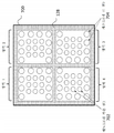
도 7은 직렬 연결된 VCSEL 어레이에 대한 대안적인 실시형태를 예시한다. 이 예에서, 네 개의 전기적으로 분리된 영역은, 두 개의 변이 전기적으로 별개의 전도성 영역에 인접하도록, 다이 상에 배치된다. 칩(700)은, 상기에서 논의되는 바와 같이, GaAs 또는 임의의 유사한 재료로 구성될 수도 있다.7 illustrates an alternative embodiment for a series connected VCSEL array. In this example, four electrically separated regions are placed on the die such that the two sides are adjacent electrically separated conductive regions. The
도 5 및 도 6에서의 배열과 유사하게, 애노드(702)는 더 작은 점선의 원에 의해 표현되고 함께 그룹화되어 각각의 정사각형 영역의 내부 부분에 배치된다. 더 큰 점선의 원에 의해 표현되는 캐소드(704)는 각각의 영역에서 복수의 애노드(702) 주위에 배치된다. 다시, 캐소드는 복수의 애노드 주위에서 C자 형상을 형성하고, 실질적으로 세 개의 변 상에서 애노드를 둘러싼다. 이 4 직렬 배열(four-in-series arrangement)에서, 영역 1 및 2에서의 C 자 형상의 캐소드 방위는 영역 3 및 4에서의 방위로부터 반전된다. 구체적으로, 복수의 캐소드의 개구 부분은 칩의 반대쪽을 향한다. 이 방위는, 도 8에 설명되는 예시적인 서브마운트 금속화 패턴 상에서의 플립 칩 배치에 유리하다.Similar to the arrangements in FIGS. 5 and 6, the
게다가, 캐소드 및 애노드 연결부 패턴은 도 5와 유사하다. 예를 들면, 영역 1 상의 캐소드(704)는 레이저 다이(700)에서의 레이저 다이오드 접합부를 통해 동일한 영역 상의 애노드(702)에 연결된다. 서브마운트(도시되지 않음)를 통해, 영역 1의 캐소드(704)는 전기적으로 분리된 영역 2의 애노드(702)에 연결된다. 마찬가지로, 영역 2 상의 캐소드 및 애노드는 레이저 다이오드 접합부를 통해 연결되고, 영역 3 상의 애노드는 서브마운트를 통해 영역 2 상의 캐소드에 연결된다. 칩(700) 상의 각각의 영역이 직렬로 연결되고, 따라서, 4 직렬 VCSEL 배열을 생성하도록, 영역 3 및 4 상에서 유사한 연결 패턴이 실현된다.Moreover, the cathode and anode connection patterns are similar to FIG. 5. For example,
이 실시형태에서, 각각의 영역을 전기적으로 분리하는 에칭된 영역(128)은 이차원으로 패턴화된다. 에칭된 영역은 칩의 길이 및 폭뿐만 아니라, 주변을 따라 연장되고, 그 결과, 네 개의 영역의 각각의 변이 칩(700) 상의 임의의 인접한 또는 다른 영역과 전기적으로 분리된다. 그러한 이차원 에칭 패턴은, 다이 상의 영역이 서로에 대해 임의적인 배열로 배치되는 것을 허용한다. 따라서, 많은 대안적인 직렬 연결 패턴을 생성하기 위한 다양한 영역 형상, 사이즈, 수 및 위치가 실현될 수도 있다. 따라서, 예시적인 실시형태가 VCSEL 어레이의 3 직렬 및 4 직렬 배열을 예시하지만, 본 발명은 그러한 예로 제한되지는 않는다는 것이 이해될 것이다.In this embodiment,
추가적으로, 각각의 영역 상에서의 캐소드 및 애노드의 배열은 묘사된 예시적인 배열로 제한되지는 않는다. 그들의 위치 및 그룹화는, 영역 및/또는 칩 사이즈, 위치, 서브마운트 금속화 패턴, 설계 목적, 또는 다른 유사한 고려 사항에 따라 변경될 수도 있다.Additionally, the arrangement of the cathode and anode on each region is not limited to the exemplary arrangement depicted. Their location and grouping may be varied depending on area and/or chip size, location, submount metallization pattern, design purpose, or other similar considerations.
도 8은, 도 7에 설명되는 네 개의 VCSEL 직렬 배열을 달성하기 위해, 서브마운트(800)에 대한 칩(700)의 연결 패턴 및 플립 칩 본딩의 저면도를 묘사한다. 서브마운트(800) 상의 금속화 패턴은 음영 영역으로 묘사되고, 3 직렬 배열에 대해 도 6에서 설명되는 금속화 서브마운트와 유사하게, 각각의 영역의 복수의 캐소드를 다음 영역의 복수의 애노드에 연결한다.FIG. 8 depicts a bottom view of a flip chip bonding and connection pattern of the
금속화 패턴은 네 개의 레이저 영역의 각각 상에서 복수의 애노드(702)와 캐소드(704) 사이에 갭(802)을 포함한다. 또한, 갭은, 각각의 영역의 캐소드 층이 다른 영역의 캐소드 층으로부터 전기적으로 분리된 상태를 유지하도록, 에칭된 영역(128)과 정렬된다. 금속화 패턴은 본 설계로 제한되지 않으며, 칩 사이즈, 형상 또는 설계, 실 공간(real estate), 또는 다른 고려 사항에 따라 변경될 수도 있다.The metallization pattern includes a
본 실시형태 및 설명된 연결 패턴은 또한 다수의 다른 배열로 확장될 수 있다. 그들은 다양한 펄스식 구동 회로와 매칭하기 위해 직렬로 연결되는 추가적인 레이저 접합부를 포함할 수도 있고, 단일 칩 접근법의 정렬 및 실 공간 이점을 유지한다. 전기적 및 기계적 연결을 위한 솔더(126)는, 도 2 내지 도 4에서와 같은 레이저 메사 상에, 또는 서브마운트 금속 패턴 상에 있을 수 있다.The embodiments and described connection patterns can also be extended to a number of other arrangements. They may include additional laser junctions connected in series to match various pulsed drive circuits, while maintaining the alignment and real space advantages of a single chip approach. The
본 개시가 본원에서 여러 가지 대안예의 관점에서 예시되고 설명되었지만, 본원에서 설명되는 기술은 다수의 추가적인 용도 및 애플리케이션을 가질 수 있다는 것이 이해되어야 한다. 따라서, 본 개시는, 단지, 본 개시의 원리의 하나 이상의 실시형태, 대안예 및 적용예를 예시하는 본 명세서에 포함되는 특정한 설명, 실시형태 및 다양한 도면으로만 제한되지는 않아야 한다.Although the present disclosure has been illustrated and described in terms of various alternatives herein, it should be understood that the techniques described herein can have many additional uses and applications. Accordingly, the present disclosure should not be limited only to the specific descriptions, embodiments and various drawings included in this specification, which illustrate one or more embodiments, alternatives and applications of the principles of the present disclosure.
Claims (36)
다이 - 상기 다이는:
반도체 기판 및 전도성 캐소드 층 - 상기 전도성 캐소드 층은, 복수의 전기적으로 분리된 전도성 영역을 형성하는 하나 이상의 비전도성 영역을 포함함 - ; 및
각각의 전기적으로 분리된 전도성 영역 상의 복수의 VCSEL 엘리먼트 - 상기 복수의 VCSEL 엘리먼트는 캐소드 영역과 직렬로 연결되는 애노드 영역을 포함함 -
를 포함함 - ; 및
제1 전기적으로 분리된 전도성 영역 상의 상기 애노드 영역을 제2 전기적으로 분리된 전도성 영역 상의 상기 캐소드 영역에 연결하도록, 상기 전도성 캐소드 층 상의 상기 전기적으로 분리된 전도성 영역 사이의 전기적 분리를 유지하도록, 그리고 상기 전도성 캐소드 층 상의 각각의 전기적으로 분리된 전도성 영역 상의 상기 애노드 영역 및 상기 캐소드 영역을 전기적으로 분리하도록 구성되는 금속화 패턴(metallization pattern)을 포함하는 서브마운트(sub-mount)를 포함하는, 직렬 연결된 수직 공동 표면 방출 레이저(VCSEL) 어레이.A series-connected vertical-cavity surface-emitting laser (VCSEL) array,
Die-The die is:
A semiconductor substrate and a conductive cathode layer, the conductive cathode layer comprising one or more non-conductive regions forming a plurality of electrically separated conductive regions; And
A plurality of VCSEL elements on each electrically isolated conductive region, wherein the plurality of VCSEL elements include an anode region connected in series with the cathode region.
Contains -; And
Connect the anode region on the first electrically isolated conductive region to the cathode region on a second electrically isolated conductive region, maintain electrical separation between the electrically separated conductive regions on the conductive cathode layer, and A series of sub-mounts comprising a metallization pattern configured to electrically separate the anode region and the cathode region on each electrically separated conductive region on the conductive cathode layer Connected vertical cavity surface emitting laser (VCSEL) array.
상기 반도체 기판은 적어도 반절연성(semi-insulating) 재료인, 직렬 연결된 수직 공동 표면 방출 레이저(VCSEL) 어레이.According to claim 1,
The semiconductor substrate is at least a semi-insulating material, a series connected vertical cavity surface emitting laser (VCSEL) array.
상기 하나 이상의 비전도성 영역은 상기 전도성 층 상에서 에칭 및 이온 주입 중 하나 이상에 의해 형성되는, 직렬 연결된 수직 공동 표면 방출 레이저(VCSEL) 어레이.According to claim 1,
The one or more non-conductive regions are formed by one or more of etching and ion implantation on the conductive layer, a series connected vertical cavity surface emission laser (VCSEL) array.
상기 하나 이상의 비전도성 영역은 절단된 또는 다이싱된 에지를 갖는 일차원 또는 이차원 에칭 패턴을 포함하는, 직렬 연결된 수직 공동 표면 방출 레이저(VCSEL) 어레이.According to claim 1,
The one or more non-conductive regions comprise a one-dimensional or two-dimensional etch pattern with cut or diced edges, a series connected vertical cavity surface emitting laser (VCSEL) array.
상기 금속화 패턴은 상기 일차원 또는 이차원 에칭 패턴과 매칭하는, 직렬 연결된 수직 공동 표면 방출 레이저(VCSEL) 어레이.The method of claim 4,
The metallization pattern matches the one-dimensional or two-dimensional etching pattern, a series connected vertical cavity surface emitting laser (VCSEL) array.
단일의 플립 칩 본드 단계(flip-chip bond step)를 통해 모든 전기적 연결을 만드는 것을 용이하게 하기 위해 상기 애노드 영역 및 상기 캐소드 영역에 대한 콘택이 상기 다이의 동일한 면 상에 형성되는, 직렬 연결된 수직 공동 표면 방출 레이저(VCSEL) 어레이.According to claim 1,
A series connected vertical cavity in which contacts to the anode region and the cathode region are formed on the same side of the die to facilitate making all electrical connections through a single flip-chip bond step Surface emitting laser (VCSEL) array.
상기 서브마운트 및 상기 다이는 플립 칩 본딩을 통해 연결되는, 직렬 연결된 수직 공동 표면 방출 레이저(VCSEL) 어레이.According to claim 1,
The submount and the die are connected via flip chip bonding, a series connected vertical cavity surface emitting laser (VCSEL) array.
제1 전도성 영역 내의 각각의 전도성 캐소드 영역의 상기 캐소드 영역은 상기 제1 전도성 영역 내의 상기 애노드 영역 주위에 배치되는, 직렬 연결된 수직 공동 표면 방출 레이저(VCSEL) 어레이.According to claim 1,
The cathode region of each conductive cathode region in the first conductive region is disposed around the anode region in the first conductive region, a series connected vertical cavity surface emitting laser (VCSEL) array.
상기 복수의 VCSELS 중의 개개의 VCSEL 또는 상기 복수의 VCSELS 중의 VCSEL의 그룹은 외부 드라이버 회로부에 전기적으로 연결 가능하되, 드라이버 집적 회로 기판에 대한 직접적인 본드(direct bond)를 통하는 것을 포함하는, 직렬 연결된 수직 공동 표면 방출 레이저(VCSEL) 어레이.According to claim 1,
Each of the VCSELs of the plurality of VCSELS or a group of VCSELs of the plurality of VCSELS is electrically connectable to an external driver circuit, but includes a vertically coupled vertical cavity, including through a direct bond to the driver integrated circuit board. Surface emitting laser (VCSEL) array.
각각의 애노드 영역 및 각각의 캐소드 영역은 복수의 단락된 콘택(shorted contact)을 포함하는, 직렬 연결된 수직 공동 표면 방출 레이저(VCSEL) 어레이.According to claim 1,
Each anode region and each cathode region comprises a plurality of shorted contacts, a series connected vertical cavity surface emitting laser (VCSEL) array.
상기 서브마운트는 인쇄 배선 기판 또는 패턴화된 회로인, 직렬 연결된 수직 공동 표면 방출 레이저(VCSEL) 어레이.According to claim 1,
The submount is a printed wiring board or a patterned circuit, a series connected vertical cavity surface emitting laser (VCSEL) array.
상기 서브마운트는, 상기 다이에 대한 전력, 온도 제어 또는 다른 전자적 기능을 제공하는 능동 집적 회로인, 직렬 연결된 수직 공동 표면 방출 레이저(VCSEL) 어레이.According to claim 1,
The submount is an active integrated circuit that provides power, temperature control or other electronic functions for the die, a series connected vertical cavity surface emitting laser (VCSEL) array.
다이를 형성하는 단계 - 상기 다이를 형성하는 단계는:
반도체 기판 상에, 하나 이상의 비전도성 영역 - 상기 하나 이상의 비전도성 영역은 복수의 전기적으로 분리된 전도성 영역을 형성함 - 을 포함하는 전도성 캐소드 층을 형성하는 단계; 및
각각의 전기적으로 분리된 전도성 영역 내에 복수의 VCSEL 엘리먼트 - 상기 복수의 VCSEL 엘리먼트는 애노드 영역 및 캐소드 영역을 포함함 - 를 형성하는 단계
를 포함함 - ; 및
제1 전기적으로 분리된 전도성 영역 상의 상기 애노드 영역을 제2 전기적으로 분리된 전도성 영역 상의 상기 캐소드 영역에 연결하도록, 상기 전도성 캐소드 층 상의 상기 전기적으로 분리된 전도성 영역 사이의 전기적 분리를 유지하도록, 그리고 상기 전도성 캐소드 층 상의 각각의 전기적으로 분리된 전도성 영역 내의 상기 애노드 영역 및 상기 캐소드 영역을 전기적으로 분리하도록 구성되는 금속화 패턴을 포함하는 서브마운트를 형성하는 단계를 포함하는, 수직 공동 표면 방출 레이저(VCSEL) 어레이를 직렬로 제조하기 위한 방법.A method for manufacturing a vertical cavity surface emitting laser (VCSEL) array in series,
Forming a Die-Forming the die comprises:
Forming a conductive cathode layer comprising, on the semiconductor substrate, one or more non-conductive regions, the one or more non-conductive regions forming a plurality of electrically separated conductive regions; And
Forming a plurality of VCSEL elements within each electrically separated conductive region, the plurality of VCSEL elements including an anode region and a cathode region.
Contains -; And
Connect the anode region on the first electrically isolated conductive region to the cathode region on a second electrically isolated conductive region, maintain electrical separation between the electrically separated conductive regions on the conductive cathode layer, and And forming a submount comprising a metallization pattern configured to electrically separate the anode region and the cathode region within each electrically separated conductive region on the conductive cathode layer. VCSEL) Method for manufacturing an array in series.
상기 반도체 기판은 적어도 반절연성 재료인, 수직 공동 표면 방출 레이저(VCSEL) 어레이를 직렬로 제조하기 위한 방법.The method of claim 13,
The semiconductor substrate is at least a semi-insulating material, a method for manufacturing a vertical cavity surface emitting laser (VCSEL) array in series.
상기 하나 이상의 비전도성 영역은 상기 전도성 캐소드 층 상에서 이온 주입 또는 절단된 또는 다이싱된 에지를 갖는 일차원 또는 이차원 패턴을 에칭하는 것에 의해 형성되는, 수직 공동 표면 방출 레이저(VCSEL) 어레이를 직렬로 제조하기 위한 방법.The method of claim 13,
The one or more non-conductive regions are formed by ion implantation on the conductive cathode layer or by etching a one-dimensional or two-dimensional pattern with a cut or diced edge to fabricate a vertical cavity surface emission laser (VCSEL) array in series. Way for.
상기 금속화 패턴은 상기 전도성 캐소드 층 상의 하나 이상의 에칭 패턴과 매칭하는, 수직 공동 표면 방출 레이저(VCSEL) 어레이를 직렬로 제조하기 위한 방법.The method of claim 15,
The method of manufacturing a vertical cavity surface emitting laser (VCSEL) array in series, wherein the metallization pattern matches one or more etch patterns on the conductive cathode layer.
단일의 플립 칩 본드 단계를 통해 모든 전기적 연결을 만드는 것을 용이하게 하기 위해 상기 애노드 영역 및 상기 캐소드 영역에 대한 콘택을 상기 다이의 동일한 면 상에 형성하는 단계를 더 포함하는, 수직 공동 표면 방출 레이저(VCSEL) 어레이를 직렬로 제조하기 위한 방법.The method of claim 13,
Further comprising forming contacts on the anode region and the cathode region on the same side of the die to facilitate making all electrical connections through a single flip chip bond step. VCSEL) Method for manufacturing an array in series.
상기 서브마운트를 상기 반도체 기판에 플립 칩 본딩하는 단계를 더 포함하는, 수직 공동 표면 방출 레이저(VCSEL) 어레이를 직렬로 제조하기 위한 방법.The method of claim 13,
A method for manufacturing a vertical cavity surface emitting laser (VCSEL) array in series, further comprising flip chip bonding the submount to the semiconductor substrate.
다이 - 상기 다이는:
반도체 기판 상의 전도성 층 내에 복수의 전기적으로 분리된 전도성 영역을 생성하는 하나 이상의 비전도성 영역; 및
각각의 전기적으로 분리된 전도성 영역 내의 복수의 직렬 연결된 VCSEL 엘리먼트 - 상기 복수의 직렬 연결된 VCSEL 엘리먼트는 애노드 영역 및 캐소드 영역을 포함함 -
를 포함함 - ; 및
상기 반도체 기판에 연결되는 서브마운트 - 상기 서브마운트는, 제1 전기적으로 분리된 전도성 영역 상의 상기 애노드 영역을 제2 전기적으로 분리된 전도성 영역의 상기 캐소드 영역에 연결하고, 상기 전도성 층 상의 전기적으로 분리된 전도성 영역 사이의 전기적 분리를 유지하며, 그리고 상기 전도성 캐소드 층 상의 각각의 전기적으로 분리된 전도성 영역 내의 상기 애노드 영역 및 상기 캐소드 영역을 전기적으로 분리하는 금속화 패턴을 포함함 - 를 포함하는, 수직 공동 표면 방출 레이저(VCSEL) 어레이를 직렬로 연결하기 위한 시스템.A system for connecting a vertical cavity surface emitting laser (VCSEL) array in series,
Die-The die is:
One or more non-conductive regions that create a plurality of electrically separated conductive regions in the conductive layer on the semiconductor substrate; And
A plurality of series-connected VCSEL elements in each electrically separated conductive region, the plurality of series-connected VCSEL elements comprising an anode region and a cathode region-
Contains -; And
Submount connected to the semiconductor substrate-the submount connects the anode region on the first electrically isolated conductive region to the cathode region of the second electrically separated conductive region, and electrically separates on the conductive layer And a metallization pattern that maintains electrical separation between the conductive regions and electrically separates the anode region and the cathode region within each electrically separated conductive region on the conductive cathode layer. A system for connecting a cavity surface emitting laser (VCSEL) array in series.
상기 반도체 기판은 적어도 반절연성 재료인, 수직 공동 표면 방출 레이저(VCSEL) 어레이를 직렬로 연결하기 위한 시스템.The method of claim 19,
The semiconductor substrate is at least a semi-insulating material, a system for connecting a vertical cavity surface emitting laser (VCSEL) array in series.
상기 하나 이상의 비전도성 영역은, 상기 전도성 캐소드 층 상에서 이온 주입, 및 절단된 또는 다이싱된 에지를 갖는 일차원 또는 이차원 에칭 패턴 중 하나 이상에 의해 형성되는, 수직 공동 표면 방출 레이저(VCSEL) 어레이를 직렬로 연결하기 위한 시스템.The method of claim 19,
The one or more non-conductive regions are in series with an ion implantation on the conductive cathode layer, and a vertical cavity surface emission laser (VCSEL) array formed by one or more of a one-dimensional or two-dimensional etching pattern with cut or diced edges. System to connect to.
상기 금속화 패턴은 상기 전도성 캐소드 층 상의 상기 일차원 또는 이차원 에칭 패턴 중 상기 하나 이상과 매칭하는, 수직 공동 표면 방출 레이저(VCSEL) 어레이를 직렬로 연결하기 위한 시스템.The method of claim 21,
Wherein the metallization pattern matches the one or more of the one-dimensional or two-dimensional etching patterns on the conductive cathode layer, a system for connecting a vertical cavity surface emitting laser (VCSEL) array in series.
단일의 플립 칩 본드 단계를 통해 모든 전기적 연결을 만드는 것을 용이하게 하기 위해 상기 애노드 영역 및 상기 캐소드 영역에 대한 콘택이 상기 다이의 동일한 면 상에 형성되는, 수직 공동 표면 방출 레이저(VCSEL) 어레이를 직렬로 연결하기 위한 시스템.The method of claim 19,
In order to facilitate making all electrical connections through a single flip chip bond step, a series of vertical cavity surface emitting laser (VCSEL) arrays are formed in which contacts to the anode region and the cathode region are formed on the same side of the die. System to connect to.
상기 서브마운트 및 반도체 기판은 플립 칩 본딩을 통해 연결되는, 수직 공동 표면 방출 레이저(VCSEL) 어레이를 직렬로 연결하기 위한 시스템.The method of claim 19,
The submount and semiconductor substrate are connected via flip chip bonding, a system for connecting a vertical cavity surface emitting laser (VCSEL) array in series.
다이 - 상기 다이는:
반도체 기판 및 전도성 애노드 층 - 상기 전도성 애노드 층은, 복수의 전기적으로 분리된 전도성 영역을 형성하는 하나 이상의 비전도성 영역을 포함함 - ; 및
각각의 전기적으로 분리된 전도성 영역 상의 복수의 VCSEL 엘리먼트 - 상기 복수의 VCSEL 엘리먼트는 애노드 영역과 직렬로 연결되는 캐소드 영역을 포함함 -
를 포함함 - ; 및
제1 전기적으로 분리된 전도성 영역 상의 상기 애노드 영역을 제2 전기적으로 분리된 전도성 영역 상의 상기 캐소드 영역에 연결하도록, 상기 전도성 캐소드 층 상의 상기 전기적으로 분리된 전도성 영역 사이의 전기적 분리를 유지하도록, 그리고 상기 전도성 캐소드 층 상의 각각의 전기적으로 분리된 전도성 영역 상의 상기 애노드 영역 및 상기 캐소드 영역을 전기적으로 분리하도록 구성되는 금속화 패턴을 포함하는 서브마운트를 포함하는, 직렬 연결된 수직 공동 표면 방출 레이저(VCSEL) 어레이.A series-connected vertical cavity surface emitting laser (VCSEL) array,
Die-The die is:
A semiconductor substrate and a conductive anode layer, the conductive anode layer comprising one or more non-conductive regions forming a plurality of electrically separated conductive regions; And
A plurality of VCSEL elements on each electrically isolated conductive region, wherein the plurality of VCSEL elements include a cathode region connected in series with the anode region.
Contains -; And
Connect the anode region on the first electrically isolated conductive region to the cathode region on a second electrically isolated conductive region, maintain electrical separation between the electrically separated conductive regions on the conductive cathode layer, and A vertically coupled vertical cavity surface emission laser (VCSEL) comprising a submount comprising a metallization pattern configured to electrically separate the anode region and the cathode region on each electrically separated conductive region on the conductive cathode layer. Array.
상기 반도체 기판은 적어도 반절연성 재료인, 직렬 연결된 수직 공동 표면 방출 레이저(VCSEL) 어레이.The method of claim 25,
The semiconductor substrate is at least a semi-insulating material, a series connected vertical cavity surface emitting laser (VCSEL) array.
상기 하나 이상의 비전도성 영역은 상기 전도성 층 상에서 에칭 및 이온 주입 중 하나 이상에 의해 형성되는, 직렬 연결된 수직 공동 표면 방출 레이저(VCSEL) 어레이.The method of claim 25,
The one or more non-conductive regions are formed by one or more of etching and ion implantation on the conductive layer, a series connected vertical cavity surface emission laser (VCSEL) array.
상기 하나 이상의 비전도성 영역은 절단된 또는 다이싱된 에지를 갖는 일차원 또는 이차원 에칭 패턴을 포함하는, 직렬 연결된 수직 공동 표면 방출 레이저(VCSEL) 어레이.The method of claim 25,
The one or more non-conductive regions comprise a one-dimensional or two-dimensional etch pattern with cut or diced edges, a series connected vertical cavity surface emitting laser (VCSEL) array.
상기 금속화 패턴은 상기 일차원 또는 이차원 에칭 패턴과 매칭하는, 직렬 연결된 수직 공동 표면 방출 레이저(VCSEL) 어레이.The method of claim 28,
The metallization pattern matches the one-dimensional or two-dimensional etching pattern, a series-connected vertical cavity surface emission laser (VCSEL) array.
단일의 플립 칩 본드 단계를 통해 모든 전기적 연결을 만드는 것을 용이하게 하기 위해 상기 애노드 영역 및 상기 캐소드 영역에 대한 콘택이 상기 다이의 동일한 면 상에 형성되는, 직렬 연결된 수직 공동 표면 방출 레이저(VCSEL) 어레이.The method of claim 25,
A series-connected vertical cavity surface emitting laser (VCSEL) array in which contacts to the anode region and the cathode region are formed on the same side of the die to facilitate making all electrical connections through a single flip chip bond step .
상기 서브마운트 및 상기 다이는 플립 칩 본딩을 통해 연결되는, 직렬 연결된 수직 공동 표면 방출 레이저(VCSEL) 어레이.The method of claim 25,
The submount and the die are connected via flip chip bonding, a series connected vertical cavity surface emitting laser (VCSEL) array.
제1 전도성 영역 내의 각각의 전도성 캐소드 영역의 상기 캐소드 영역은 상기 제1 전도성 영역 내의 상기 애노드 영역 주위에 배치되는, 직렬 연결된 수직 공동 표면 방출 레이저(VCSEL) 어레이.The method of claim 25,
The cathode region of each conductive cathode region in the first conductive region is disposed around the anode region in the first conductive region, a series connected vertical cavity surface emitting laser (VCSEL) array.
상기 복수의 VCSELS 중의 개개의 VCSEL 또는 상기 복수의 VCSELS 중의 VCSEL의 그룹은 외부 드라이버 회로부에 전기적으로 연결 가능하되, 드라이버 집적 회로 기판에 대한 직접적인 본드에 의한 것을 포함하는, 직렬 연결된 수직 공동 표면 방출 레이저(VCSEL) 어레이.The method of claim 25,
The individual VCSELs of the plurality of VCSELS or the group of VCSELs of the plurality of VCSELS are electrically connectable to external driver circuitry, including by direct bonding to a driver integrated circuit board, a series connected vertical cavity surface emitting laser ( VCSEL) array.
각각의 애노드 영역 및 각각의 캐소드 영역은 복수의 단락된 콘택을 포함하는, 직렬 연결된 수직 공동 표면 방출 레이저(VCSEL) 어레이.The method of claim 25,
Each anode region and each cathode region comprises a plurality of shorted contacts, a series connected vertical cavity surface emitting laser (VCSEL) array.
상기 서브마운트는 인쇄 배선 기판 또는 패턴화된 회로인, 직렬 연결된 수직 공동 표면 방출 레이저(VCSEL) 어레이.The method of claim 25,
The submount is a printed wiring board or a patterned circuit, a series connected vertical cavity surface emitting laser (VCSEL) array.
상기 서브마운트는, 상기 다이에 대한 전력, 온도 제어 또는 다른 전자적 기능을 제공하는 능동 집적 회로인, 직렬 연결된 수직 공동 표면 방출 레이저(VCSEL) 어레이.The method of claim 25,
The submount is an active integrated circuit that provides power, temperature control or other electronic functions for the die, a series connected vertical cavity surface emitting laser (VCSEL) array.
Applications Claiming Priority (3)
| Application Number | Priority Date | Filing Date | Title |
|---|---|---|---|
| US201762536918P | 2017-07-25 | 2017-07-25 | |
| US62/536,918 | 2017-07-25 | ||
| PCT/US2018/043786 WO2019023401A1 (en) | 2017-07-25 | 2018-07-25 | A single-chip series connected vcsel array |
Publications (2)
| Publication Number | Publication Date |
|---|---|
| KR20200066608A true KR20200066608A (en) | 2020-06-10 |
| KR102314308B1 KR102314308B1 (en) | 2021-10-18 |
Family
ID=65038943
Family Applications (1)
| Application Number | Title | Priority Date | Filing Date |
|---|---|---|---|
| KR1020207005275A KR102314308B1 (en) | 2017-07-25 | 2018-07-25 | VCSEL array in single-chip serial connection |
Country Status (8)
| Country | Link |
|---|---|
| US (2) | US10530128B2 (en) |
| EP (1) | EP3659188B1 (en) |
| JP (1) | JP7128259B2 (en) |
| KR (1) | KR102314308B1 (en) |
| CN (1) | CN111149226B (en) |
| CA (1) | CA3071264A1 (en) |
| TW (1) | TWI734922B (en) |
| WO (1) | WO2019023401A1 (en) |
Cited By (1)
| Publication number | Priority date | Publication date | Assignee | Title |
|---|---|---|---|---|
| KR20230091668A (en) * | 2021-12-16 | 2023-06-23 | 한국광기술원 | VCSEL Package with Gallium Nitride FET Driver |
Families Citing this family (33)
| Publication number | Priority date | Publication date | Assignee | Title |
|---|---|---|---|---|
| US10761195B2 (en) | 2016-04-22 | 2020-09-01 | OPSYS Tech Ltd. | Multi-wavelength LIDAR system |
| WO2018132521A1 (en) | 2017-01-16 | 2018-07-19 | Canthus Technologies Llc | Combining light-emitting elements of differing divergence on the same substrate |
| WO2018169758A1 (en) | 2017-03-13 | 2018-09-20 | OPSYS Tech Ltd. | Eye-safe scanning lidar system |
| US10530128B2 (en) * | 2017-07-25 | 2020-01-07 | Trilumina Corp. | Single-chip series connected VCSEL array |
| US11482835B2 (en) | 2017-07-25 | 2022-10-25 | Lumentum Operations Llc | VCSEL device with multiple stacked active regions |
| CN115015883A (en) | 2017-07-28 | 2022-09-06 | 欧普赛斯技术有限公司 | VCSEL array LIDAR transmitter with small angular divergence |
| JP7388720B2 (en) | 2017-11-15 | 2023-11-29 | オプシス テック リミテッド | Noise-adaptive solid-state LIDAR system |
| JP7324518B2 (en) | 2018-04-01 | 2023-08-10 | オプシス テック リミテッド | Noise adaptive solid-state lidar system |
| US10374386B1 (en) * | 2018-06-07 | 2019-08-06 | Finisar Corporation | Chip on carrier |
| CN113169518B (en) * | 2018-11-07 | 2023-07-28 | 深圳瑞识智能科技有限公司 | Vertical cavity surface emitting laser array |
| TW202034478A (en) * | 2019-02-04 | 2020-09-16 | 日商索尼半導體解決方案公司 | Electronic device |
| WO2020172077A1 (en) | 2019-02-21 | 2020-08-27 | Apple Inc. | Indium-phosphide vcsel with dielectric dbr |
| CN113924440B (en) | 2019-03-25 | 2023-11-07 | 朗美通经营有限责任公司 | Spatial multiplexing of lens arrays with surface emitting lasers for multi-zone illumination |
| JP7334439B2 (en) * | 2019-03-25 | 2023-08-29 | 富士フイルムビジネスイノベーション株式会社 | vertical cavity surface emitting laser element array chip, light emitting device, optical device and information processing device |
| US11418010B2 (en) | 2019-04-01 | 2022-08-16 | Apple Inc. | VCSEL array with tight pitch and high efficiency |
| US10992109B2 (en) * | 2019-04-01 | 2021-04-27 | Lumentum Operations Llc | Electrically isolating vertical-emitting devices |
| KR102634887B1 (en) | 2019-04-09 | 2024-02-08 | 옵시스 테크 엘티디 | Solid-state LIDAR transmitter with laser control |
| TWI731329B (en) | 2019-04-30 | 2021-06-21 | 晶智達光電股份有限公司 | Laser device and semiconductor device having the same |
| EP3739700B8 (en) * | 2019-05-16 | 2021-09-29 | Changchun Institute of Optics, Fine Mechanics and Physics, Chinese Academy of Sciences | Vertical-cavity surface-emitting laser |
| CN113906316A (en) | 2019-05-30 | 2022-01-07 | 欧普赛斯技术有限公司 | Eye-safe long-range LIDAR system using actuators |
| US11374381B1 (en) | 2019-06-10 | 2022-06-28 | Apple Inc. | Integrated laser module |
| KR102637658B1 (en) | 2019-06-10 | 2024-02-20 | 옵시스 테크 엘티디 | Eye-safe long-range solid-state LIDAR system |
| US20230128994A1 (en) * | 2019-10-09 | 2023-04-27 | Raysees Technology (Shenzhen) Co. Ltd. | Systems and methods for series-connected vcsel array |
| US20220247153A1 (en) * | 2019-11-06 | 2022-08-04 | Sony Semiconductor Solutions Corporation | Surface light-emission laser device |
| DE102019218864A1 (en) * | 2019-12-04 | 2021-06-10 | OSRAM Opto Semiconductors Gesellschaft mit beschränkter Haftung | OPTOELECTRONIC SEMICONDUCTOR COMPONENT WITH INDIVIDUALLY CONTROLLABLE CONTACT ELEMENTS AND METHOD FOR MANUFACTURING THE OPTOELECTRONIC SEMICONDUCTOR COMPONENT |
| CN111313234B (en) * | 2020-03-04 | 2021-09-24 | 常州纵慧芯光半导体科技有限公司 | Vertical cavity surface emitting laser array and manufacturing method and application thereof |
| WO2021221894A1 (en) * | 2020-04-27 | 2021-11-04 | Apple Inc. | An integrated vertical emitter structure having controlled wavelength |
| WO2021231772A1 (en) * | 2020-05-15 | 2021-11-18 | Lumileds Llc | Light-emitting device with configurable spatial distribution of emission intensity |
| CN111555112A (en) * | 2020-05-21 | 2020-08-18 | 常州纵慧芯光半导体科技有限公司 | Light-emitting device, manufacturing method thereof and laser equipment |
| JP2022045535A (en) * | 2020-09-09 | 2022-03-22 | ソニーセミコンダクタソリューションズ株式会社 | Surface emitting laser device, electronic device, and manufacturing method of surface emitting laser device |
| JP2022139943A (en) | 2021-03-12 | 2022-09-26 | 株式会社リコー | Surface light emitting laser array, light source module, and distance measuring device |
| US20230032341A1 (en) * | 2021-07-27 | 2023-02-02 | Fujifilm Business Innovation Corp. | Light-emitting element array, optical device, optical measurement device, and method for manufacturing light-emitting element array |
| US11827037B2 (en) * | 2021-08-23 | 2023-11-28 | Xerox Corporation | Semiconductor array imager for printing systems |
Citations (1)
| Publication number | Priority date | Publication date | Assignee | Title |
|---|---|---|---|---|
| US20150110140A1 (en) * | 2012-06-01 | 2015-04-23 | Robert Bosch Gmbh | Circuit system and manufacturing method for same |
Family Cites Families (25)
| Publication number | Priority date | Publication date | Assignee | Title |
|---|---|---|---|---|
| AU2003265308A1 (en) * | 2002-07-25 | 2004-02-16 | Jonathan S. Dahm | Method and apparatus for using light emitting diodes for curing |
| JP2005217147A (en) | 2004-01-29 | 2005-08-11 | Seiko Epson Corp | Light receiving and emitting element array, optical module, and optical transmission device |
| JP4772318B2 (en) | 2004-11-19 | 2011-09-14 | 富士通株式会社 | Optical device and manufacturing method thereof |
| JP2008523637A (en) | 2004-12-14 | 2008-07-03 | ソウル オプト−デバイス カンパニー リミテッド | Light emitting device having a plurality of light emitting cells and package mounting the same |
| US7343060B2 (en) * | 2005-03-04 | 2008-03-11 | Fuji Xerox Co., Ltd. | Light transmission and reception module, sub-mount, and method of manufacturing the sub-mount |
| WO2006095949A1 (en) * | 2005-03-11 | 2006-09-14 | Seoul Semiconductor Co., Ltd. | Led package having an array of light emitting cells coupled in series |
| JP2007027357A (en) * | 2005-07-15 | 2007-02-01 | Showa Denko Kk | Semiconductor light emitting device and substrate |
| JP2008007782A (en) * | 2006-06-27 | 2008-01-17 | Lumination Llc | Optoelectronic device |
| US7972875B2 (en) * | 2007-01-17 | 2011-07-05 | The Board Of Trustees Of The University Of Illinois | Optical systems fabricated by printing-based assembly |
| US7949024B2 (en) | 2009-02-17 | 2011-05-24 | Trilumina Corporation | Multibeam arrays of optoelectronic devices for high frequency operation |
| US10038304B2 (en) * | 2009-02-17 | 2018-07-31 | Trilumina Corp. | Laser arrays for variable optical properties |
| WO2011075609A1 (en) | 2009-12-19 | 2011-06-23 | Trilumina Corporation | System and method for combining laser arrays for digital outputs |
| WO2013054249A2 (en) | 2011-10-10 | 2013-04-18 | Koninklijke Philips Electronics N.V. | A method of assembling vcsel chips on a sub-mount |
| US8576885B2 (en) * | 2012-02-09 | 2013-11-05 | Princeton Optronics, Inc. | Optical pump for high power laser |
| US8675706B2 (en) * | 2011-12-24 | 2014-03-18 | Princeton Optronics Inc. | Optical illuminator |
| WO2013136205A2 (en) | 2012-03-14 | 2013-09-19 | Koninklijke Philips N.V. | Vcsel module and manufacture thereof. |
| DE102012209270A1 (en) * | 2012-06-01 | 2013-12-05 | Robert Bosch Gmbh | Method for manufacturing circuit arrangement with vertical cavity surface emitting laser arrays, involves applying wafer element on substrate arrangement, and separating wafer element after application for obtaining semiconductor components |
| JP6083194B2 (en) | 2012-11-06 | 2017-02-22 | 富士ゼロックス株式会社 | Surface emitting semiconductor laser array device, light source and light source module |
| CA2910202C (en) | 2013-04-22 | 2019-09-17 | Trilumina Corp. | Microlenses for multibeam arrays of optoelectronic devices for high frequency operation |
| CN105340090B (en) * | 2013-06-28 | 2018-11-09 | 亮锐控股有限公司 | LED device |
| WO2015011983A1 (en) * | 2013-07-22 | 2015-01-29 | 株式会社村田製作所 | Vertical-cavity surface-emitting laser array |
| CN112420816A (en) * | 2013-09-23 | 2021-02-26 | 量子半导体有限公司 | Superlattice materials and applications |
| US10186833B2 (en) | 2015-02-18 | 2019-01-22 | Ii-Vi Incorporated | Densely-spaced laser diode configurations |
| US10749312B2 (en) * | 2015-05-28 | 2020-08-18 | Vixar, Inc. | VCSELs and VCSEL arrays designed for improved performance as illumination sources and sensors |
| US10530128B2 (en) * | 2017-07-25 | 2020-01-07 | Trilumina Corp. | Single-chip series connected VCSEL array |
-
2018
- 2018-07-25 US US16/045,633 patent/US10530128B2/en active Active
- 2018-07-25 JP JP2020504029A patent/JP7128259B2/en active Active
- 2018-07-25 CA CA3071264A patent/CA3071264A1/en not_active Abandoned
- 2018-07-25 WO PCT/US2018/043786 patent/WO2019023401A1/en unknown
- 2018-07-25 CN CN201880062285.8A patent/CN111149226B/en active Active
- 2018-07-25 KR KR1020207005275A patent/KR102314308B1/en active IP Right Grant
- 2018-07-25 TW TW107125771A patent/TWI734922B/en active
- 2018-07-25 EP EP18839037.1A patent/EP3659188B1/en active Active
-
2020
- 2020-01-03 US US16/733,901 patent/US10756515B2/en active Active
Patent Citations (1)
| Publication number | Priority date | Publication date | Assignee | Title |
|---|---|---|---|---|
| US20150110140A1 (en) * | 2012-06-01 | 2015-04-23 | Robert Bosch Gmbh | Circuit system and manufacturing method for same |
Cited By (1)
| Publication number | Priority date | Publication date | Assignee | Title |
|---|---|---|---|---|
| KR20230091668A (en) * | 2021-12-16 | 2023-06-23 | 한국광기술원 | VCSEL Package with Gallium Nitride FET Driver |
Also Published As
| Publication number | Publication date |
|---|---|
| TW201921818A (en) | 2019-06-01 |
| US20200144791A1 (en) | 2020-05-07 |
| EP3659188A4 (en) | 2021-04-21 |
| US10530128B2 (en) | 2020-01-07 |
| CN111149226A (en) | 2020-05-12 |
| WO2019023401A1 (en) | 2019-01-31 |
| TWI734922B (en) | 2021-08-01 |
| US20190036308A1 (en) | 2019-01-31 |
| JP7128259B2 (en) | 2022-08-30 |
| CA3071264A1 (en) | 2019-01-31 |
| EP3659188B1 (en) | 2022-10-19 |
| EP3659188A1 (en) | 2020-06-03 |
| JP2020529128A (en) | 2020-10-01 |
| US10756515B2 (en) | 2020-08-25 |
| CN111149226B (en) | 2023-04-18 |
| KR102314308B1 (en) | 2021-10-18 |
Similar Documents
| Publication | Publication Date | Title |
|---|---|---|
| KR102314308B1 (en) | VCSEL array in single-chip serial connection | |
| US11482835B2 (en) | VCSEL device with multiple stacked active regions | |
| US11557879B2 (en) | Rigid high power and high speed lasing grid structures | |
| US8995485B2 (en) | High brightness pulsed VCSEL sources | |
| US7949024B2 (en) | Multibeam arrays of optoelectronic devices for high frequency operation | |
| US9065239B2 (en) | Multibeam array of top emitting VCSEL elements | |
| US7491565B2 (en) | III-nitride light emitting devices fabricated by substrate removal | |
| US11322910B2 (en) | Indium-phosphide VCSEL with dielectric DBR | |
| WO2014018684A1 (en) | Multibeam array of top emitting vcsel elements | |
| CN113872046B (en) | VCSEL device with multiple stacked active regions | |
| CN112290376A (en) | Surface emitting laser and method of manufacturing the same | |
| CN113872046A (en) | VCSEL device with multiple stacked active regions | |
| CN114128066A (en) | Optoelectronic semiconductor chip comprising contact elements and method for producing an optoelectronic semiconductor chip |
Legal Events
| Date | Code | Title | Description |
|---|---|---|---|
| E902 | Notification of reason for refusal | ||
| N231 | Notification of change of applicant | ||
| E701 | Decision to grant or registration of patent right | ||
| GRNT | Written decision to grant |