KR20200063243A - 공통 풀 관리 - Google Patents
공통 풀 관리 Download PDFInfo
- Publication number
- KR20200063243A KR20200063243A KR1020207014461A KR20207014461A KR20200063243A KR 20200063243 A KR20200063243 A KR 20200063243A KR 1020207014461 A KR1020207014461 A KR 1020207014461A KR 20207014461 A KR20207014461 A KR 20207014461A KR 20200063243 A KR20200063243 A KR 20200063243A
- Authority
- KR
- South Korea
- Prior art keywords
- memory
- physical
- partition
- host
- physical partition
- Prior art date
- Legal status (The legal status is an assumption and is not a legal conclusion. Google has not performed a legal analysis and makes no representation as to the accuracy of the status listed.)
- Abandoned
Links
Images


Classifications
-
- G—PHYSICS
- G06—COMPUTING OR CALCULATING; COUNTING
- G06F—ELECTRIC DIGITAL DATA PROCESSING
- G06F3/00—Input arrangements for transferring data to be processed into a form capable of being handled by the computer; Output arrangements for transferring data from processing unit to output unit, e.g. interface arrangements
- G06F3/06—Digital input from, or digital output to, record carriers, e.g. RAID, emulated record carriers or networked record carriers
- G06F3/0601—Interfaces specially adapted for storage systems
- G06F3/0628—Interfaces specially adapted for storage systems making use of a particular technique
- G06F3/0638—Organizing or formatting or addressing of data
- G06F3/0644—Management of space entities, e.g. partitions, extents, pools
-
- G—PHYSICS
- G06—COMPUTING OR CALCULATING; COUNTING
- G06F—ELECTRIC DIGITAL DATA PROCESSING
- G06F12/00—Accessing, addressing or allocating within memory systems or architectures
- G06F12/02—Addressing or allocation; Relocation
- G06F12/0223—User address space allocation, e.g. contiguous or non contiguous base addressing
- G06F12/023—Free address space management
- G06F12/0238—Memory management in non-volatile memory, e.g. resistive RAM or ferroelectric memory
- G06F12/0246—Memory management in non-volatile memory, e.g. resistive RAM or ferroelectric memory in block erasable memory, e.g. flash memory
-
- G—PHYSICS
- G06—COMPUTING OR CALCULATING; COUNTING
- G06F—ELECTRIC DIGITAL DATA PROCESSING
- G06F12/00—Accessing, addressing or allocating within memory systems or architectures
- G06F12/02—Addressing or allocation; Relocation
- G06F12/08—Addressing or allocation; Relocation in hierarchically structured memory systems, e.g. virtual memory systems
- G06F12/10—Address translation
-
- G—PHYSICS
- G06—COMPUTING OR CALCULATING; COUNTING
- G06F—ELECTRIC DIGITAL DATA PROCESSING
- G06F3/00—Input arrangements for transferring data to be processed into a form capable of being handled by the computer; Output arrangements for transferring data from processing unit to output unit, e.g. interface arrangements
- G06F3/06—Digital input from, or digital output to, record carriers, e.g. RAID, emulated record carriers or networked record carriers
- G06F3/0601—Interfaces specially adapted for storage systems
- G06F3/0602—Interfaces specially adapted for storage systems specifically adapted to achieve a particular effect
- G06F3/0604—Improving or facilitating administration, e.g. storage management
- G06F3/0605—Improving or facilitating administration, e.g. storage management by facilitating the interaction with a user or administrator
-
- G—PHYSICS
- G06—COMPUTING OR CALCULATING; COUNTING
- G06F—ELECTRIC DIGITAL DATA PROCESSING
- G06F3/00—Input arrangements for transferring data to be processed into a form capable of being handled by the computer; Output arrangements for transferring data from processing unit to output unit, e.g. interface arrangements
- G06F3/06—Digital input from, or digital output to, record carriers, e.g. RAID, emulated record carriers or networked record carriers
- G06F3/0601—Interfaces specially adapted for storage systems
- G06F3/0628—Interfaces specially adapted for storage systems making use of a particular technique
- G06F3/0629—Configuration or reconfiguration of storage systems
- G06F3/0631—Configuration or reconfiguration of storage systems by allocating resources to storage systems
-
- G—PHYSICS
- G06—COMPUTING OR CALCULATING; COUNTING
- G06F—ELECTRIC DIGITAL DATA PROCESSING
- G06F3/00—Input arrangements for transferring data to be processed into a form capable of being handled by the computer; Output arrangements for transferring data from processing unit to output unit, e.g. interface arrangements
- G06F3/06—Digital input from, or digital output to, record carriers, e.g. RAID, emulated record carriers or networked record carriers
- G06F3/0601—Interfaces specially adapted for storage systems
- G06F3/0628—Interfaces specially adapted for storage systems making use of a particular technique
- G06F3/0638—Organizing or formatting or addressing of data
-
- G—PHYSICS
- G06—COMPUTING OR CALCULATING; COUNTING
- G06F—ELECTRIC DIGITAL DATA PROCESSING
- G06F3/00—Input arrangements for transferring data to be processed into a form capable of being handled by the computer; Output arrangements for transferring data from processing unit to output unit, e.g. interface arrangements
- G06F3/06—Digital input from, or digital output to, record carriers, e.g. RAID, emulated record carriers or networked record carriers
- G06F3/0601—Interfaces specially adapted for storage systems
- G06F3/0628—Interfaces specially adapted for storage systems making use of a particular technique
- G06F3/0655—Vertical data movement, i.e. input-output transfer; data movement between one or more hosts and one or more storage devices
- G06F3/0658—Controller construction arrangements
-
- G—PHYSICS
- G06—COMPUTING OR CALCULATING; COUNTING
- G06F—ELECTRIC DIGITAL DATA PROCESSING
- G06F3/00—Input arrangements for transferring data to be processed into a form capable of being handled by the computer; Output arrangements for transferring data from processing unit to output unit, e.g. interface arrangements
- G06F3/06—Digital input from, or digital output to, record carriers, e.g. RAID, emulated record carriers or networked record carriers
- G06F3/0601—Interfaces specially adapted for storage systems
- G06F3/0628—Interfaces specially adapted for storage systems making use of a particular technique
- G06F3/0655—Vertical data movement, i.e. input-output transfer; data movement between one or more hosts and one or more storage devices
- G06F3/0659—Command handling arrangements, e.g. command buffers, queues, command scheduling
-
- G—PHYSICS
- G06—COMPUTING OR CALCULATING; COUNTING
- G06F—ELECTRIC DIGITAL DATA PROCESSING
- G06F3/00—Input arrangements for transferring data to be processed into a form capable of being handled by the computer; Output arrangements for transferring data from processing unit to output unit, e.g. interface arrangements
- G06F3/06—Digital input from, or digital output to, record carriers, e.g. RAID, emulated record carriers or networked record carriers
- G06F3/0601—Interfaces specially adapted for storage systems
- G06F3/0668—Interfaces specially adapted for storage systems adopting a particular infrastructure
- G06F3/0671—In-line storage system
- G06F3/0673—Single storage device
- G06F3/0679—Non-volatile semiconductor memory device, e.g. flash memory, one time programmable memory [OTP]
-
- G—PHYSICS
- G06—COMPUTING OR CALCULATING; COUNTING
- G06F—ELECTRIC DIGITAL DATA PROCESSING
- G06F2212/00—Indexing scheme relating to accessing, addressing or allocation within memory systems or architectures
- G06F2212/20—Employing a main memory using a specific memory technology
- G06F2212/202—Non-volatile memory
- G06F2212/2022—Flash memory
-
- G—PHYSICS
- G06—COMPUTING OR CALCULATING; COUNTING
- G06F—ELECTRIC DIGITAL DATA PROCESSING
- G06F2212/00—Indexing scheme relating to accessing, addressing or allocation within memory systems or architectures
- G06F2212/72—Details relating to flash memory management
- G06F2212/7201—Logical to physical mapping or translation of blocks or pages
Landscapes
- Engineering & Computer Science (AREA)
- Theoretical Computer Science (AREA)
- Physics & Mathematics (AREA)
- General Engineering & Computer Science (AREA)
- General Physics & Mathematics (AREA)
- Human Computer Interaction (AREA)
- Read Only Memory (AREA)
- Semiconductor Memories (AREA)
- Non-Volatile Memory (AREA)
Abstract
Description
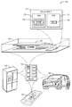
도 1은 메모리 디바이스를 포함하는 환경의 일 예를 예시한다.
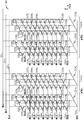
도 2 내지 도 3은 3D NAND 아키텍처 반도체 메모리 어레이의 일 예의 개략도들을 예시한다.
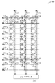
도 4는 메모리 모듈의 예시적인 블록도를 예시한다.
도 5는 본 개시의 일부 예들에 따른 물리적 파티션을 생성하기 위한 요청에 응답하여 논리적 파티션을 생성하기 위한 방법의 순서도를 예시한다.
도 6은, 본 개시의 일부 예들에 따른 논리적 파티션으로서 NAND에 의해 생성된 물리적 파티션으로 보내진 호스트 명령을 NAND 제어기가 프로세싱하는 방법의 순서도를 예시한다.
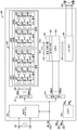
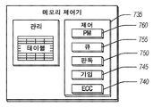
도 7은 본 개시의 일부 예들에 따른 메모리 제어기의 개략도를 도시한다.
도 8은, 하나 이상의 실시예들이 구현될 수 있는 기계의 일 예를 예시하는 블록도이다.
Claims (21)
- NAND 메모리 디바이스로서,
메모리의 제 1 풀(pool)을 포함하는 NAND 메모리 어레이;
제어기를 포함하며, 상기 제어기는, 상기 제어기가 하기의 동작들을 수행하게끔 하는 명령어들을 실행하고, 상기 동작들은:
상기 메모리의 제 1 풀의 물리적 파티션을 생성하기 위한 명령을 호스트로부터 수신하는 동작;
상기 물리적 파티션을 생성하는 대신에 상기 메모리의 제 1 풀을 사용하여 NAND-레벨 논리적 파티션을 생성하는 동작으로서, 상기 메모리의 제 1 풀은 제 2 논리적 파티션과 공유되는, 동작;
상기 물리적 파티션이 생성되었음을 나타내는 응답을 상기 호스트로 전송하는 동작;
상기 물리적 파티션 및 논리적 블록 어드레스(Logical Block Address; LBA)를 식별하는 상기 호스트로부터의 요청을 상기 메모리의 제 1 풀의 물리적 어드레스로 변환하는 동작; 및
상기 메모리의 제 1 풀의 상기 물리적 어드레스에 대하여 상기 요청을 실행하는 동작을 포함하는, NAND 메모리 디바이스. - 청구항 1에 있어서, 상기 물리적 파티션이 생성되었음을 나타내는 응답을 상기 호스트로 전송하는 동작은, 상기 물리적 파티션을 생성하기 위한 상기 호스트로부터의 상기 명령에 의해 제공된 크기에 기초하여 0과 어떤 수 사이의 LBA들의 범위 및 물리적 파티션 식별자를 제공하는 동작을 포함하는, NAND 메모리 디바이스.
- 청구항 2에 있어서, 상기 요청의 상기 물리적 파티션 및 논리적 블록 어드레스를 식별하는 상기 호스트로부터의 요청을 상기 제 1 풀의 물리적 어드레스로 변환하는 동작은 수신된 물리적 파티션 식별자 및 상기 LBA들의 범위 내의 LBA를 상기 메모리의 제 1 풀 내의 물리적 위치에 매핑하고, 상기 물리적 위치에 대하여 상기 호스트로부터의 요청을 수행하는 동작을 포함하는, NAND 메모리 디바이스.
- 청구항 2에 있어서, 상기 물리적 파티션은 논리적 유닛 식별자 번호(logical unit identifier number; LUN)에 의해 식별되는, NAND 메모리 디바이스.
- 청구항 1에 있어서, 상기 물리적 파티션을 서비스하기 위해 사용되는 상기 메모리의 제 1 풀로부터의 메모리 셀들은 상기 물리적 파티션을 생성하기 위한 상기 명령 내에서 상기 호스트에 의해 지정된 요건을 충족시키도록 구성되는, NAND 메모리 디바이스.
- 청구항 5에 있어서, 상기 요건은, 메모리 셀들이 단일 층 셀(Single Layer Cell; SLC)로서 구성된다는 것인, NAND 메모리 디바이스.
- 청구항 1에 있어서, 상기 NAND-레벨 논리적 파티션은 물리적 파티션으로서 상기 호스트에 나타나며, 상기 물리적 파티션이 생성되었음을 나타내는 응답을 상기 호스트로 전송하는 동작은 상기 물리적 파티션을 생성하지 않는, NAND 메모리 디바이스.
- 방법으로서,
NAND 메모리 디바이스 상의 메모리의 제 1 풀의 물리적 파티션을 생성하기 위한 명령을 호스트로부터 수신하는 단계;
상기 물리적 파티션을 생성하는 대신에 상기 메모리의 제 1 풀을 사용하여 NAND-레벨 논리적 파티션을 생성하는 단계로서, 상기 메모리의 제 1 풀은 제 2 논리적 파티션과 공유되는, 단계;
상기 물리적 파티션이 생성되었음을 나타내는 응답을 상기 호스트로 전송하는 단계;
상기 물리적 파티션 및 논리적 블록 어드레스(Logical Block Address; LBA)를 식별하는 상기 호스트로부터의 요청을 상기 메모리의 제 1 풀의 물리적 어드레스로 변환하는 단계; 및
상기 메모리의 제 1 풀의 상기 물리적 어드레스에 대하여 상기 요청을 실행하는 단계를 포함하는, 방법. - 청구항 8에 있어서, 상기 물리적 파티션이 생성되었음을 나타내는 응답을 상기 호스트로 전송하는 단계는, 상기 물리적 파티션을 생성하기 위한 상기 호스트로부터의 상기 명령에 의해 제공된 크기에 기초하여 0과 어떤 수 사이의 LBA들의 범위 및 물리적 파티션 식별자를 제공하는 단계를 포함하는, 방법.
- 청구항 9에 있어서, 상기 요청의 상기 물리적 파티션 및 논리적 블록 어드레스를 식별하는 상기 호스트로부터의 요청을 상기 제 1 풀의 물리적 어드레스로 변환하는 단계는 수신된 물리적 파티션 식별자 및 상기 LBA들의 범위 내의 LBA를 상기 메모리의 제 1 풀 내의 물리적 위치에 매핑하고, 상기 물리적 위치에 대하여 상기 호스트로부터의 요청을 수행하는 단계를 포함하는, 방법.
- 청구항 9에 있어서, 상기 물리적 파티션은 논리적 유닛 식별자 번호(logical unit identifier number; LUN)에 의해 식별되는, 방법.
- 청구항 8에 있어서, 상기 물리적 파티션을 서비스하기 위해 사용되는 상기 메모리의 제 1 풀로부터의 메모리 셀들은 상기 물리적 파티션을 생성하기 위한 상기 명령 내에서 상기 호스트에 의해 지정된 요건을 충족시키도록 구성되는, 방법.
- 청구항 12에 있어서, 상기 요건은, 메모리 셀들이 단일 층 셀(Single Layer Cell; SLC)로서 구성된다는 것인, 방법.
- 청구항 8에 있어서, 상기 NAND-레벨 논리적 파티션은 물리적 파티션으로서 상기 호스트에 나타나며, 상기 물리적 파티션이 생성되었음을 나타내는 응답을 상기 호스트로 전송하는 단계는 상기 물리적 파티션을 생성하지 않는, 방법.
- 실행될 때 기계가 하기의 동작들을 수행하게끔 하는 명령어들을 포함하는 기계-판독가능 매체로서, 상기 동작들은,
NAND 디바이스 상의 메모리의 제 1 풀의 물리적 파티션을 생성하기 위한 명령을 호스트로부터 수신하는 동작;
상기 물리적 파티션을 생성하는 대신에 상기 메모리의 제 1 풀을 사용하여 NAND-레벨 논리적 파티션을 생성하는 동작으로서, 상기 메모리의 제 1 풀은 제 2 논리적 파티션과 공유되는, 동작;
상기 물리적 파티션이 생성되었음을 나타내는 응답을 상기 호스트로 전송하는 동작;
상기 물리적 파티션 및 논리적 블록 어드레스(Logical Block Address; LBA)를 식별하는 상기 호스트로부터의 요청을 상기 메모리의 제 1 풀의 물리적 어드레스로 변환하는 동작; 및
상기 메모리의 제 1 풀의 상기 물리적 어드레스에 대하여 상기 요청을 실행하는 동작을 포함하는, 기계-판독가능 매체. - 청구항 15에 있어서, 상기 물리적 파티션이 생성되었음을 나타내는 응답을 상기 호스트로 전송하는 동작은, 상기 물리적 파티션을 생성하기 위한 상기 호스트로부터의 상기 명령에 의해 제공된 크기에 기초하여 0과 어떤 수 사이의 LBA들의 범위 및 물리적 파티션 식별자를 제공하는 동작을 포함하는, 기계-판독가능 매체.
- 청구항 16에 있어서, 상기 요청의 상기 물리적 파티션 및 논리적 블록 어드레스를 식별하는 상기 호스트로부터의 요청을 상기 제 1 풀의 물리적 어드레스로 변환하는 동작은 수신된 물리적 파티션 식별자 및 상기 LBA들의 범위 내의 LBA를 상기 메모리의 제 1 풀 내의 물리적 위치에 매핑하고, 상기 물리적 위치에 대하여 상기 호스트로부터의 요청을 수행하는 동작을 포함하는, 기계-판독가능 매체.
- 청구항 16에 있어서, 상기 물리적 파티션은 논리적 유닛 식별자 번호(logical unit identifier number; LUN)에 의해 식별되는, 기계-판독가능 매체.
- 청구항 15에 있어서, 상기 물리적 파티션을 서비스하기 위해 사용되는 상기 메모리의 제 1 풀로부터의 메모리 셀들은 상기 물리적 파티션을 생성하기 위한 상기 명령 내에서 상기 호스트에 의해 지정된 요건을 충족시키도록 구성되는, 기계-판독가능 매체.
- 청구항 19에 있어서, 상기 요건은, 메모리 셀들이 단일 층 셀(Single Layer Cell; SLC)로서 구성된다는 것인, 기계-판독가능 매체.
- 청구항 15에 있어서, 상기 NAND-레벨 논리적 파티션은 물리적 파티션으로서 상기 호스트에 나타나며, 상기 물리적 파티션이 생성되었음을 나타내는 응답을 상기 호스트로 전송하는 동작은 상기 물리적 파티션을 생성하지 않는, 기계-판독가능 매체.
Applications Claiming Priority (3)
| Application Number | Priority Date | Filing Date | Title |
|---|---|---|---|
| US15/799,508 | 2017-10-31 | ||
| US15/799,508 US10908832B2 (en) | 2017-10-31 | 2017-10-31 | Common pool management |
| PCT/US2018/055005 WO2019089195A1 (en) | 2017-10-31 | 2018-10-09 | Common pool management |
Publications (1)
| Publication Number | Publication Date |
|---|---|
| KR20200063243A true KR20200063243A (ko) | 2020-06-04 |
Family
ID=66243824
Family Applications (1)
| Application Number | Title | Priority Date | Filing Date |
|---|---|---|---|
| KR1020207014461A Abandoned KR20200063243A (ko) | 2017-10-31 | 2018-10-09 | 공통 풀 관리 |
Country Status (5)
| Country | Link |
|---|---|
| US (2) | US10908832B2 (ko) |
| KR (1) | KR20200063243A (ko) |
| CN (1) | CN111433751B (ko) |
| TW (1) | TWI696917B (ko) |
| WO (1) | WO2019089195A1 (ko) |
Families Citing this family (7)
| Publication number | Priority date | Publication date | Assignee | Title |
|---|---|---|---|---|
| US10908832B2 (en) | 2017-10-31 | 2021-02-02 | Micron Technology, Inc. | Common pool management |
| US20190258812A1 (en) * | 2018-02-20 | 2019-08-22 | Sensata Technologies, Inc. | Memory security for automotive functional safety compliance with independent downstream processes |
| TWI704456B (zh) * | 2018-11-22 | 2020-09-11 | 慧榮科技股份有限公司 | 資料儲存裝置與資料存取方法 |
| KR20220072357A (ko) * | 2020-11-25 | 2022-06-02 | 에스케이하이닉스 주식회사 | 컨트롤러, 및 이를 포함하는 메모리 시스템 및 데이터 처리 시스템 |
| US11893243B2 (en) * | 2021-10-06 | 2024-02-06 | Western Digital Technologies, Inc. | Storage system and method for program reordering to mitigate program disturbs |
| US12131787B2 (en) | 2022-08-19 | 2024-10-29 | Macronix International Co., Ltd. | Page buffer counting for in-memory search |
| US20240160561A1 (en) * | 2022-11-16 | 2024-05-16 | Western Digital Technologies, Inc. | Exposed Physical Partitions in Solid-State Storage Devices |
Family Cites Families (27)
| Publication number | Priority date | Publication date | Assignee | Title |
|---|---|---|---|---|
| US20070067366A1 (en) * | 2003-10-08 | 2007-03-22 | Landis John A | Scalable partition memory mapping system |
| US7631138B2 (en) * | 2003-12-30 | 2009-12-08 | Sandisk Corporation | Adaptive mode switching of flash memory address mapping based on host usage characteristics |
| US7457910B2 (en) | 2005-06-29 | 2008-11-25 | Sandisk Corproation | Method and system for managing partitions in a storage device |
| US7693811B2 (en) | 2006-02-28 | 2010-04-06 | International Business Machines Corporation | Generating unique identifiers for logical partitions |
| US8386744B2 (en) * | 2007-10-01 | 2013-02-26 | International Business Machines Corporation | Thin provisioning migration and scrubbing |
| US8407400B2 (en) | 2008-11-12 | 2013-03-26 | Micron Technology, Inc. | Dynamic SLC/MLC blocks allocations for non-volatile memory |
| US8566507B2 (en) * | 2009-04-08 | 2013-10-22 | Google Inc. | Data storage device capable of recognizing and controlling multiple types of memory chips |
| US9122579B2 (en) * | 2010-01-06 | 2015-09-01 | Intelligent Intellectual Property Holdings 2 Llc | Apparatus, system, and method for a storage layer |
| US9245653B2 (en) | 2010-03-15 | 2016-01-26 | Intelligent Intellectual Property Holdings 2 Llc | Reduced level cell mode for non-volatile memory |
| US8621141B2 (en) * | 2010-04-01 | 2013-12-31 | Intel Corporations | Method and system for wear leveling in a solid state drive |
| TWI437430B (zh) * | 2010-04-07 | 2014-05-11 | Phison Electronics Corp | 動態切換分割區方法、記憶卡控制器與記憶卡儲存系統及電腦程式產品 |
| US8429391B2 (en) * | 2010-04-16 | 2013-04-23 | Micron Technology, Inc. | Boot partitions in memory devices and systems |
| WO2012025793A1 (en) | 2010-08-26 | 2012-03-01 | Freescale Semiconductor, Inc. | Memory management unit for a microprocessor system, microprocessor system and method for managing memory |
| US9336139B2 (en) * | 2010-11-29 | 2016-05-10 | Cleversafe, Inc. | Selecting a memory for storage of an encoded data slice in a dispersed storage network |
| US8472274B2 (en) | 2011-03-02 | 2013-06-25 | Apple Inc. | Using temperature sensors with a memory device |
| US8886911B2 (en) | 2011-05-31 | 2014-11-11 | Micron Technology, Inc. | Dynamic memory cache size adjustment in a memory device |
| CN103597461B (zh) * | 2011-09-30 | 2016-04-27 | 株式会社日立制作所 | 闪存组件 |
| WO2013158817A1 (en) | 2012-04-20 | 2013-10-24 | Violin Memory, Inc. | Lun management with distributed raid controllers |
| US9141534B2 (en) * | 2012-12-14 | 2015-09-22 | Sandisk Technologies Inc. | Tracking read accesses to regions of non-volatile memory |
| US9203700B2 (en) | 2013-05-21 | 2015-12-01 | International Business Machines Corporation | Monitoring client information in a shared environment |
| US9466383B2 (en) | 2013-12-30 | 2016-10-11 | Sandisk Technologies Llc | Non-volatile memory and method with adaptive logical groups |
| US9652381B2 (en) * | 2014-06-19 | 2017-05-16 | Sandisk Technologies Llc | Sub-block garbage collection |
| US10552085B1 (en) * | 2014-09-09 | 2020-02-04 | Radian Memory Systems, Inc. | Techniques for directed data migration |
| US10430328B2 (en) * | 2014-09-16 | 2019-10-01 | Sandisk Technologies Llc | Non-volatile cache and non-volatile storage medium using single bit and multi bit flash memory cells or different programming parameters |
| US20160328179A1 (en) * | 2015-05-08 | 2016-11-10 | Micron Technology, Inc. | Multiple virtually over-provisioned, virtual storage devices created from a single physical storage device |
| US10282107B1 (en) * | 2015-12-31 | 2019-05-07 | EMC IP Holding Company LLC | Controlling I/O response time to meet service levels |
| US10908832B2 (en) | 2017-10-31 | 2021-02-02 | Micron Technology, Inc. | Common pool management |
-
2017
- 2017-10-31 US US15/799,508 patent/US10908832B2/en active Active
-
2018
- 2018-10-09 KR KR1020207014461A patent/KR20200063243A/ko not_active Abandoned
- 2018-10-09 CN CN201880078561.XA patent/CN111433751B/zh active Active
- 2018-10-09 WO PCT/US2018/055005 patent/WO2019089195A1/en not_active Ceased
- 2018-10-31 TW TW107138635A patent/TWI696917B/zh active
-
2021
- 2021-02-01 US US17/164,156 patent/US20210157501A1/en not_active Abandoned
Also Published As
| Publication number | Publication date |
|---|---|
| CN111433751A (zh) | 2020-07-17 |
| US10908832B2 (en) | 2021-02-02 |
| CN111433751B (zh) | 2023-11-14 |
| US20190129641A1 (en) | 2019-05-02 |
| WO2019089195A1 (en) | 2019-05-09 |
| TWI696917B (zh) | 2020-06-21 |
| TW201933117A (zh) | 2019-08-16 |
| US20210157501A1 (en) | 2021-05-27 |
Similar Documents
| Publication | Publication Date | Title |
|---|---|---|
| US11842054B2 (en) | Prioritized security | |
| US11720489B2 (en) | Scheme to improve efficiency of device garbage collection in memory devices | |
| US11726919B2 (en) | Dynamic L2P cache | |
| EP3676696B1 (en) | Managed nvm adaptive cache management | |
| TWI741425B (zh) | 儲存裝置中順序資料優化之子區域 | |
| US11735269B2 (en) | Secure erase for data corruption | |
| TWI696917B (zh) | 用於共同集用區管理之nand記憶體裝置、方法及機器可讀媒體 | |
| WO2019046230A1 (en) | ERASING PAGE CONTROL | |
| CN112817878B (zh) | 操作具有动态可变属性的存储器的系统和方法 | |
| US11163692B2 (en) | Memory constrained translation table management |
Legal Events
| Date | Code | Title | Description |
|---|---|---|---|
| PA0105 | International application |
St.27 status event code: A-0-1-A10-A15-nap-PA0105 |
|
| PA0201 | Request for examination |
St.27 status event code: A-1-2-D10-D11-exm-PA0201 |
|
| PG1501 | Laying open of application |
St.27 status event code: A-1-1-Q10-Q12-nap-PG1501 |
|
| E902 | Notification of reason for refusal | ||
| PE0902 | Notice of grounds for rejection |
St.27 status event code: A-1-2-D10-D21-exm-PE0902 |
|
| E13-X000 | Pre-grant limitation requested |
St.27 status event code: A-2-3-E10-E13-lim-X000 |
|
| P11-X000 | Amendment of application requested |
St.27 status event code: A-2-2-P10-P11-nap-X000 |
|
| P13-X000 | Application amended |
St.27 status event code: A-2-2-P10-P13-nap-X000 |
|
| E701 | Decision to grant or registration of patent right | ||
| PE0701 | Decision of registration |
St.27 status event code: A-1-2-D10-D22-exm-PE0701 |
|
| PC1904 | Unpaid initial registration fee |
St.27 status event code: A-2-2-U10-U14-oth-PC1904 St.27 status event code: N-2-6-B10-B12-nap-PC1904 |