KR20200063243A - Common pool management - Google Patents
Common pool management Download PDFInfo
- Publication number
- KR20200063243A KR20200063243A KR1020207014461A KR20207014461A KR20200063243A KR 20200063243 A KR20200063243 A KR 20200063243A KR 1020207014461 A KR1020207014461 A KR 1020207014461A KR 20207014461 A KR20207014461 A KR 20207014461A KR 20200063243 A KR20200063243 A KR 20200063243A
- Authority
- KR
- South Korea
- Prior art keywords
- memory
- physical
- partition
- host
- physical partition
- Prior art date
- Legal status (The legal status is an assumption and is not a legal conclusion. Google has not performed a legal analysis and makes no representation as to the accuracy of the status listed.)
- Abandoned
Links
Images


Classifications
-
- G—PHYSICS
- G06—COMPUTING OR CALCULATING; COUNTING
- G06F—ELECTRIC DIGITAL DATA PROCESSING
- G06F3/00—Input arrangements for transferring data to be processed into a form capable of being handled by the computer; Output arrangements for transferring data from processing unit to output unit, e.g. interface arrangements
- G06F3/06—Digital input from, or digital output to, record carriers, e.g. RAID, emulated record carriers or networked record carriers
- G06F3/0601—Interfaces specially adapted for storage systems
- G06F3/0628—Interfaces specially adapted for storage systems making use of a particular technique
- G06F3/0638—Organizing or formatting or addressing of data
- G06F3/0644—Management of space entities, e.g. partitions, extents, pools
-
- G—PHYSICS
- G06—COMPUTING OR CALCULATING; COUNTING
- G06F—ELECTRIC DIGITAL DATA PROCESSING
- G06F12/00—Accessing, addressing or allocating within memory systems or architectures
- G06F12/02—Addressing or allocation; Relocation
- G06F12/0223—User address space allocation, e.g. contiguous or non contiguous base addressing
- G06F12/023—Free address space management
- G06F12/0238—Memory management in non-volatile memory, e.g. resistive RAM or ferroelectric memory
- G06F12/0246—Memory management in non-volatile memory, e.g. resistive RAM or ferroelectric memory in block erasable memory, e.g. flash memory
-
- G—PHYSICS
- G06—COMPUTING OR CALCULATING; COUNTING
- G06F—ELECTRIC DIGITAL DATA PROCESSING
- G06F12/00—Accessing, addressing or allocating within memory systems or architectures
- G06F12/02—Addressing or allocation; Relocation
- G06F12/08—Addressing or allocation; Relocation in hierarchically structured memory systems, e.g. virtual memory systems
- G06F12/10—Address translation
-
- G—PHYSICS
- G06—COMPUTING OR CALCULATING; COUNTING
- G06F—ELECTRIC DIGITAL DATA PROCESSING
- G06F3/00—Input arrangements for transferring data to be processed into a form capable of being handled by the computer; Output arrangements for transferring data from processing unit to output unit, e.g. interface arrangements
- G06F3/06—Digital input from, or digital output to, record carriers, e.g. RAID, emulated record carriers or networked record carriers
- G06F3/0601—Interfaces specially adapted for storage systems
- G06F3/0602—Interfaces specially adapted for storage systems specifically adapted to achieve a particular effect
- G06F3/0604—Improving or facilitating administration, e.g. storage management
- G06F3/0605—Improving or facilitating administration, e.g. storage management by facilitating the interaction with a user or administrator
-
- G—PHYSICS
- G06—COMPUTING OR CALCULATING; COUNTING
- G06F—ELECTRIC DIGITAL DATA PROCESSING
- G06F3/00—Input arrangements for transferring data to be processed into a form capable of being handled by the computer; Output arrangements for transferring data from processing unit to output unit, e.g. interface arrangements
- G06F3/06—Digital input from, or digital output to, record carriers, e.g. RAID, emulated record carriers or networked record carriers
- G06F3/0601—Interfaces specially adapted for storage systems
- G06F3/0628—Interfaces specially adapted for storage systems making use of a particular technique
- G06F3/0629—Configuration or reconfiguration of storage systems
- G06F3/0631—Configuration or reconfiguration of storage systems by allocating resources to storage systems
-
- G—PHYSICS
- G06—COMPUTING OR CALCULATING; COUNTING
- G06F—ELECTRIC DIGITAL DATA PROCESSING
- G06F3/00—Input arrangements for transferring data to be processed into a form capable of being handled by the computer; Output arrangements for transferring data from processing unit to output unit, e.g. interface arrangements
- G06F3/06—Digital input from, or digital output to, record carriers, e.g. RAID, emulated record carriers or networked record carriers
- G06F3/0601—Interfaces specially adapted for storage systems
- G06F3/0628—Interfaces specially adapted for storage systems making use of a particular technique
- G06F3/0638—Organizing or formatting or addressing of data
-
- G—PHYSICS
- G06—COMPUTING OR CALCULATING; COUNTING
- G06F—ELECTRIC DIGITAL DATA PROCESSING
- G06F3/00—Input arrangements for transferring data to be processed into a form capable of being handled by the computer; Output arrangements for transferring data from processing unit to output unit, e.g. interface arrangements
- G06F3/06—Digital input from, or digital output to, record carriers, e.g. RAID, emulated record carriers or networked record carriers
- G06F3/0601—Interfaces specially adapted for storage systems
- G06F3/0628—Interfaces specially adapted for storage systems making use of a particular technique
- G06F3/0655—Vertical data movement, i.e. input-output transfer; data movement between one or more hosts and one or more storage devices
- G06F3/0658—Controller construction arrangements
-
- G—PHYSICS
- G06—COMPUTING OR CALCULATING; COUNTING
- G06F—ELECTRIC DIGITAL DATA PROCESSING
- G06F3/00—Input arrangements for transferring data to be processed into a form capable of being handled by the computer; Output arrangements for transferring data from processing unit to output unit, e.g. interface arrangements
- G06F3/06—Digital input from, or digital output to, record carriers, e.g. RAID, emulated record carriers or networked record carriers
- G06F3/0601—Interfaces specially adapted for storage systems
- G06F3/0628—Interfaces specially adapted for storage systems making use of a particular technique
- G06F3/0655—Vertical data movement, i.e. input-output transfer; data movement between one or more hosts and one or more storage devices
- G06F3/0659—Command handling arrangements, e.g. command buffers, queues, command scheduling
-
- G—PHYSICS
- G06—COMPUTING OR CALCULATING; COUNTING
- G06F—ELECTRIC DIGITAL DATA PROCESSING
- G06F3/00—Input arrangements for transferring data to be processed into a form capable of being handled by the computer; Output arrangements for transferring data from processing unit to output unit, e.g. interface arrangements
- G06F3/06—Digital input from, or digital output to, record carriers, e.g. RAID, emulated record carriers or networked record carriers
- G06F3/0601—Interfaces specially adapted for storage systems
- G06F3/0668—Interfaces specially adapted for storage systems adopting a particular infrastructure
- G06F3/0671—In-line storage system
- G06F3/0673—Single storage device
- G06F3/0679—Non-volatile semiconductor memory device, e.g. flash memory, one time programmable memory [OTP]
-
- G—PHYSICS
- G06—COMPUTING OR CALCULATING; COUNTING
- G06F—ELECTRIC DIGITAL DATA PROCESSING
- G06F2212/00—Indexing scheme relating to accessing, addressing or allocation within memory systems or architectures
- G06F2212/20—Employing a main memory using a specific memory technology
- G06F2212/202—Non-volatile memory
- G06F2212/2022—Flash memory
-
- G—PHYSICS
- G06—COMPUTING OR CALCULATING; COUNTING
- G06F—ELECTRIC DIGITAL DATA PROCESSING
- G06F2212/00—Indexing scheme relating to accessing, addressing or allocation within memory systems or architectures
- G06F2212/72—Details relating to flash memory management
- G06F2212/7201—Logical to physical mapping or translation of blocks or pages
Landscapes
- Engineering & Computer Science (AREA)
- Theoretical Computer Science (AREA)
- Physics & Mathematics (AREA)
- General Engineering & Computer Science (AREA)
- General Physics & Mathematics (AREA)
- Human Computer Interaction (AREA)
- Read Only Memory (AREA)
- Semiconductor Memories (AREA)
- Non-Volatile Memory (AREA)
Abstract
일부 예들에 있어서, 물리적 파티션을 생성하도록 요청될 때 논리적 파티션들을 생성하는 방법들, 시스템들, 기계-판독가능 매체들, 및 NAND 디바이스들이 개시된다. NAND 상의 제어기는 물리적 파티션을 요청했던 호스트 디바이스로 물리적 파티션의 생성을 모방한다. 따라서, 호스트 디바이스는 논리적 파티션을 물리적 파티션으로서 본다. 그럼에도 불구하고, NAND 별개의 파티션을 생성하는 메모리 저장부 비용을 초래하지 않으며, 추가적으로 NAND는 다른 파티션으로부터 오버프로비저닝을 위해 셀들을 빌릴 수 있다. 이러한 예들에 있어서, 호스트 디바이스 운영 시스템은 물리적 파티션이 생성되었다고 믿지만, NAND는 메모리를 자원들의 연속적인 풀로서 관리한다. 따라서, 논리적 파티션은 - 운영 시스템 레벨에서와는 대조적으로 - NAND 메모리 제어기 레벨에서 생성된다.In some examples, methods, systems, machine-readable media, and NAND devices for creating logical partitions when requested to create a physical partition are disclosed. The controller on the NAND mimics the creation of the physical partition with the host device that requested the physical partition. Thus, the host device views the logical partition as a physical partition. Nevertheless, it does not incur the memory storage cost of creating a separate NAND partition, and additionally NAND can borrow cells for over-provisioning from other partitions. In these examples, the host device operating system believes that a physical partition has been created, but NAND manages memory as a contiguous pool of resources. Thus, logical partitions are created at the NAND memory controller level-as opposed to at the operating system level.
Description
우선권 출원Priority application
본 출원은 2017년 10월 31일자로 출원된 미국 출원 일련번호 제15/799,508에 대한 우선권의 이익을 주장하며, 이러한 출원은 그 전체가 본원에 참조로서 포함된다.This application claims the benefit of priority over U.S. Application Serial No. 15/799,508 filed on October 31, 2017, the entirety of which is incorporated herein by reference.
메모리 디바이스들은 일반적으로 컴퓨터들 또는 다른 전자 디바이스들에서 내부 반도체의 집적 회로들로서 제공된다. 휘발성 및 비 휘발성 메모리를 포함하는 다수의 상이한 유형들의 메모리가 존재한다. Memory devices are generally provided as integrated circuits of an internal semiconductor in computers or other electronic devices. There are a number of different types of memory, including volatile and non-volatile memory.
휘발성 메모리는 그것의 데이터를 유지하기 위해 전력을 요구하며, 랜덤 액세스 메모리(random-access memory; RAM), 동적 랜덤 액세스 메모리(dynamic random access memory; DRAM), 또는 동기 동적 랜덤 액세스 메모리(synchronous dynamic random access memory; SDRAM)를 포함한다. Volatile memory requires power to maintain its data, random-access memory (RAM), dynamic random access memory (DRAM), or synchronous dynamic random access memory access memory (SDRAM).
비-휘발성 메모리는 전력이 공급되지 않을 때 저장된 데이터를 유지할 수 있으며, 다른 것들 중에서도 특히 플래시 메모리, 판독 전용 메모리(read only memory; ROM), 전기 소거가능 프로그램가능 ROM(Electrically Erasable Programmable ROM; EEPROM), 정적 램(static RAM; SRAM), 소거가능 프로그램가능 ROM(Erasable Programmable ROM; EPROM), 저항 가변 메모리, 예컨대 상 변화 랜덤 액세스 메모리(phase change random access memory; PCRAM), 저항성 랜덤 액세스 메모리(resistive random access memory; RRAM), 및 자기저항성 랜덤 액세스 메모리(magnetoresistive random access memory; MRAM), 또는 3D XPoint™ 메모리를 포함할 수 있다.Non-volatile memory can retain stored data when no power is supplied, among others flash memory, read only memory (ROM), and electrically erasable programmable ROM (EEPROM) , Static RAM (SRAM), erasable programmable ROM (EPROM), resistive variable memory, such as phase change random access memory (PCRAM), resistive random access memory access memory (RRAM), and magnetoresistive random access memory (MRAM), or 3D XPoint™ memory.
플래시 메모리는 광범위한 전자 애플리케이션들에 대한 비-휘발성 메모리로서 사용된다. 플래시 메모리 디바이스들은 전형적으로, 고 메모리 밀도들, 고 신뢰성, 및 저 전력 소비를 가능하게 하는 1-트랜지스터, 플로팅 게이트 또는 전하 트랩 메모리 셀들의 하나 이상의 그룹들을 포함한다. Flash memory is used as a non-volatile memory for a wide range of electronic applications. Flash memory devices typically include one or more groups of 1-transistor, floating gate or charge trap memory cells that enable high memory densities, high reliability, and low power consumption.
2개의 일반적인 유형들의 플래시 메모리 어레이 아키텍처들은 NAND 및 NOR 아키텍처들을 포함하며, 이들은 각각의 기본 메모리 셀 구성이 배열되는 논리 형태를 따라 명명되었다. 메모리 어레이의 메모리 셀들은 전형적으로 매트릭스로 배열된다. 일 예에 있어서, 어레이 내의 로우(row) 내의 각각의 플로팅 게이트 메모리 셀의 게이트들은 액세스 라인(예를 들어, 워드 라인)에 결합된다. NOR 아키텍처에서, 어레이의 컬럼(column) 내의 각각의 메모리 셀의 드레인들은 데이터 라인(예를 들어, 비트 라인)에 결합된다. NAND 아키텍처에서, 어레이의 스트링(string) 내의 각각의 메모리 셀의 드레인들은, 소스 라인과 비트 라인 사이에서, 소스 대 드레인으로, 함께 직렬로 결합된다. The two common types of flash memory array architectures include NAND and NOR architectures, which are named according to the logical form in which each basic memory cell configuration is arranged. Memory cells of a memory array are typically arranged in a matrix. In one example, the gates of each floating gate memory cell in a row in the array are coupled to an access line (eg, word line). In the NOR architecture, the drains of each memory cell in a column of the array are coupled to a data line (eg, bit line). In the NAND architecture, the drains of each memory cell in a string of an array are coupled in series together, source-to-drain, between a source line and a bit line.
NOR 및 NAND 아키텍처 반도체 메모리 어레이들 둘 모두, 그들의 게이트들에 결합된 워드 라인을 선택하여 특정 메모리 셀들을 활성화하는 디코더들을 통해 액세스된다. NOR 아키텍처 반도체 메모리 어레이에서, 일단 활성화되면, 선택된 메모리 셀들은 비트 라인들 상에 그들의 데이터 값들을 위치시키며, 이는 특정 셀이 프로그래밍된 상태에 따라 상이한 전류들이 흐르게끔 한다. NAND 아키텍처 반도체 메모리 어레이에서, 높은 바이어스 전압이 드레인-측 선택 게이트(drain-side select gate; SGD) 라인에 인가된다. 각각의 그룹의 선택되지 않은 메모리 셀들의 게이트들에 결합된 워드 라인들은 (예를 들어, 그들의 저장된 데이터 값들에 의해 제한되지 않는 방식으로 전류를 패스(pass)하기 위한) 패스 트랜지스터들로서 각각의 그룹의 선택되지 않은 메모리 셀들을 동작시키기 위해 지정된 패스 전압(예를 들어, Vpass)으로 드라이브된다. 그러면 전류는 소스 라인으로부터 오로지 각각의 그룹의 선택된 메모리 셀들에 의해서만 제한되는 각각의 직렬 결합된 그룹을 통해 비트 라인으로 흐르며, 이는 선택된 메모리 셀들의 인코딩된 데이터 값들을 비트 라인들 상에 위치시킨다.Both NOR and NAND architecture semiconductor memory arrays are accessed through decoders that select word lines coupled to their gates to activate specific memory cells. In a NOR architecture semiconductor memory array, once activated, selected memory cells place their data values on bit lines, which causes different currents to flow depending on the state in which a particular cell is programmed. In a NAND architecture semiconductor memory array, a high bias voltage is applied to the drain-side select gate (SGD) line. Word lines coupled to the gates of each group of unselected memory cells are pass transistors (eg, for passing current in a manner not limited by their stored data values) as each of the group's pass transistors. It is driven with a specified pass voltage (eg, Vpass) to operate unselected memory cells. The current then flows from the source line to the bit line through each series-coupled group, which is limited only by the selected memory cells of each group, which places the encoded data values of the selected memory cells on the bit lines.
NOR 또는 NAND 아키텍처 반도체 메모리 어레이 내의 각각의 플래시 메모리 셀은 하나 또는 복수의 프로그래밍된 상태들로 개별적으로 또는 집합적으로 프로그래밍될 수 있다. 예를 들어, 단일-레벨 셀(single-level cell; SLC)이 2개의 프로그래밍된 상태들 중 하나(예를 들어, 1 또는 0)을 나타낼 수 있으며, 이는 데이터의 하나의 비트를 나타낸다. Each flash memory cell in a NOR or NAND architecture semiconductor memory array can be individually or collectively programmed in one or multiple programmed states. For example, a single-level cell (SLC) can represent one of two programmed states (eg, 1 or 0), which represents one bit of data.
그러나, 플래시 메모리 셀들은 또한 2개를 초과하는 프로그래밍된 상태들 중 하나를 나타낼 수 있으며, 이는, 각각의 셀이 1개를 초과하는 2진 디지트(digit)(예를 들어, 1개를 초과하는 비트)를 나타낼 수 있음에 따라 메모리 셀들의 수를 증가시키지 않고 더 높은 밀도의 메모리들의 제조를 가능하게 한다. 이러한 셀들은 다중-상태 메모리 셀들, 다중-디지트 셀들, 또는 다중-레벨 셀(multi-level cell; MLC)들로서 지칭될 수 있다. 특정 예들에 있어서, MLC는 셀 당 데이터의 2개의 비트들(예를 들어, 4개의 프로그래밍된 상태들 중 하나)를 저장할 수 있는 메모리 셀을 지칭할 수 있으며, 3중-레벨 셀(triple-level cell; TLC)은 셀 당 데이터의 3개의 비트들(예를 들어, 8개의 프로그래밍된 상태들 중 하나)를 저장할 수 있는 메모리 셀을 지칭할 수고, 4중-레벨 셀(quad-level cell; QLC)은 셀 당 데이터의 4개의 비트들을 저장할 수 있다. MLC는 본원에서, 셀 당 데이터의 1개를 초과하는 비트를 저장할 수 있는(즉, 2개를 초과하는 프로그래밍된 상태들을 나타낼 수 있는) 임의의 메모리 셀을 지칭하기 위하여 그것의 더 광범위한 맥락에서 사용된다. However, flash memory cells can also represent one of more than two programmed states, each cell having more than one binary digit (eg, more than one) Bit), which allows the fabrication of higher density memories without increasing the number of memory cells. These cells may be referred to as multi-state memory cells, multi-digit cells, or multi-level cells (MLCs). In certain examples, MLC may refer to a memory cell capable of storing two bits of data per cell (eg, one of four programmed states), a triple-level cell cell (TLC) may refer to a memory cell capable of storing three bits of data per cell (eg, one of eight programmed states), and a quad-level cell (QLC) ) Can store 4 bits of data per cell. MLC is used herein in its broader context to refer to any memory cell capable of storing more than one bit of data per cell (ie, representing more than two programmed states). do.
전통적인 메모리 어레이들은 반도체 기판의 표면 상에 배열된 2-차원(2D) 구조체들이다. 주어진 면적에 대하여 메모리 용량을 증가시키기 위하여 그리고 비용을 감소시키기 위하여, 개별적인 메모리 셀들의 크기가 감소되어 왔다. 그러나, 개별적인 메모리 셀들의 크기의 감소에 대한 기술적인 한계가 존재하며, 따라서, 2D 메모리 어레이들의 메모리 밀도에 대한 기술적인 한계가 존재한다. 이에 응답하여, 3D NAND 아키텍처 반도체 메모리 디바이스들과 같은 3-차원(3D) 메모리 구조체들이 메모리 밀도를 더 증가시키고 메모리 비용을 더 낮추기 위하여 개발되고 있다. Traditional memory arrays are two-dimensional (2D) structures arranged on the surface of a semiconductor substrate. In order to increase memory capacity and reduce cost for a given area, the size of individual memory cells has been reduced. However, there are technical limits to the reduction in the size of individual memory cells, and thus, there are technical limits to the memory density of 2D memory arrays. In response, three-dimensional (3D) memory structures, such as 3D NAND architecture semiconductor memory devices, are being developed to further increase memory density and lower memory cost.
이러한 3D NAND 디바이스들은 흔히 소스에 인접한 하나 이상의 소스-측 선택 게이트(source-side select gate; SGS)들 사이에 직렬로 결합된(예를 들어, 드레인 대 소스) 저장 셀들의 스트링들, 및 비트 라인에 인접한 하나 이상의 드레인-측 선택 게이트(drain-side select gate; SGD)들을 포함한다. 일 예에 있어서, SGS들 또는 SGD들은 하나 이상의 전계-효과 트랜지스터(field-effect transistor; FET)들 또는 금속-산화물 반도체(metal-oxide semiconductor; MOS) 구조체 디바이스들 등을 포함할 수 있다. 일부 예들에 있어서, 스트링들은 개별적인 워드 라인들을 포함하는 다수의 수직으로 이격된 계층들을 통해 수직으로 연장할 것이다. 반도체 구조체(예를 들어, 폴리실리콘 구조체)는 스트링의 저장 셀들에 대한 채널을 형성하기 위하여 저장 셀들의 스트링에 인접하여 연장할 수 있다. 수직 스트링의 예에 있어서, 폴리실리콘 구조체는 수적으로 연장하는 필러(pillar)의 형태일 수 있다. 일부 예들에 있어서, 스트링은 "접힐(folded)" 수 있으며, 그에 따라서 U-형 필러에 대하여 배열될 수 있다. 다른 예들에 있어서, 다수의 수직 구조체들은 저장 셀 스트링들의 스택(stack)된 어레이들을 형성하기 위하여 서로 상에 스택될 수 있다.These 3D NAND devices are often strings of storage cells coupled in series (eg, drain to source) between one or more source-side select gates (SGS) adjacent to the source, and bit line And one or more drain-side select gates (SGDs) adjacent to it. In one example, SGS or SGDs may include one or more field-effect transistors (FETs) or metal-oxide semiconductor (MOS) structure devices, and the like. In some examples, strings will extend vertically through a number of vertically spaced layers containing individual word lines. The semiconductor structure (eg, polysilicon structure) can extend adjacent to the string of storage cells to form a channel for the storage cells of the string. In the example of a vertical string, the polysilicon structure can be in the form of a pillar that extends numerically. In some examples, the string can be “folded” and can thus be arranged for a U-shaped pillar. In other examples, multiple vertical structures can be stacked on each other to form stacked arrays of storage cell strings.
메모리 어레이들 또는 디바이스들은 메모리 시스템의 저장 볼륨, 예컨대 고체-상태 드라이브(solid-state drive; SSD), 범용 플래시 저장(Universal Flash Storage; UFS™) 디바이스, 멀티미디어카드(MultiMediaCard; MMC) 고체-상태 저장 디바이스, 내장형 MMC(embedded MMC; eMMC™) 디바이스 등을 형성하기 위하여 함께 결합될 수 있다. 다른 것들 중에서도 특히, SSD는, 예를 들어, 성능, 크기, 중량, 견고성, 동작 온도 범위, 및 전력 소비에 대하여 움직이는 부분을 갖는 통상적인 하드 드라이브들을 뛰어넘는 장점들을 갖는 컴퓨터의 메인 저장 디바이스로서 사용될 수 있다. 예를 들어, SSD는 감소된 탐색 시간, 레이턴시(latency), 또는 자기 디스크 드라이브들과 연관된(예를 들어, 전기계적 등) 다른 지연을 가질 수 있다. SSD들은 내부 배터리 공급 필요성들을 제거하기 위해 플래시 메모리 셀들과 같은 비-휘발성 메모리 셀들을 사용하며, 그에 따라서 드라이브를 더 다목적으로 그리고 더 콤팩트하게 만든다.Memory arrays or devices are storage volumes of a memory system, such as solid-state drives (SSDs), Universal Flash Storage (UFS™) devices, MultiMediaCard (MMC) solid-state storage It can be combined together to form a device, an embedded MMC (eMMC™) device or the like. In particular, SSDs, among other things, may be used as the main storage device of a computer with advantages over conventional hard drives with moving parts, for example, performance, size, weight, robustness, operating temperature range, and power consumption. Can be. For example, SSDs may have reduced seek times, latency, or other delays associated with magnetic disk drives (eg, electrical, etc.). SSDs use non-volatile memory cells, such as flash memory cells, to eliminate internal battery supply needs, thus making the drive more versatile and more compact.
SSD는 다수의 다이(die)들 또는 논리적 유닛들(예를 들어, 논리적 유닛 번호들 또는 LUN(logical unit number)들)을 포함하여 다수의 메모리 디바이스들을 포함할 수 있으며, 메모리 디바이스들을 동작시키기 위해 또는 외부 시스템들과 인터페이스하기 위해 요구되는 논리적 기능들을 수행하는 하나 이상의 프로세서들 또는 다른 제어기들을 포함할 수 있다. 이러한 SSD들은 그 위의 다수의 메모리 어레이들 및 주변 회로부(circuitry)를 포함하는 하나 이상의 플래시 메모리 다이를 포함할 수 있다. 플래시 메모리 어레이들은 복수의 물리적 페이지(page)들로 조직화된 메모리 셀들의 복수의 블록들을 포함할 수 있다. 다수의 예들에 있어서, SSD들은 또한 DRAM 또는 SRAM(또는 다른 형태의 메모리 다이 또는 다른 메모리 구조체들)을 포함할 것이다. SSD는, 메모리 디바이스들과 호스트 사이에서 데이터(예를 들어, 사용자 데이터 및 연관된 무결성 데이터, 예컨대 오류 데이터 및 어드레스 데이터 등)를 전송하기 위한 판독 또는 기입 동작들 또는 메모리 디바이스들로부터 데이터를 소거하기 위한 소거 동작들과 같은 메모리 동작들과 연관된 명령들을 호스트로부터 수신할 수 있다.An SSD can include multiple memory devices, including multiple dies or logical units (eg, logical unit numbers or logical unit numbers (LUNs)), to operate memory devices Or it may include one or more processors or other controllers that perform the logical functions required to interface with external systems. These SSDs may include one or more flash memory dies including multiple memory arrays and peripheral circuitry thereon. Flash memory arrays may include a plurality of blocks of memory cells organized into a plurality of physical pages. In many examples, SSDs will also include DRAM or SRAM (or other types of memory die or other memory structures). An SSD is used to erase data from memory devices or read or write operations to transfer data (eg, user data and associated integrity data, such as error data and address data, etc.) between memory devices and a host. Instructions associated with memory operations, such as erase operations, may be received from the host.
반드시 축적이 맞추어져야만 하는 것은 아닌 도면들 내에서, 유사한 번호들은 상이한 도면들에서 유사한 컴포넌트들을 기술하기 위하여 사용될 수 있다. 상이한 문자 접미사들을 갖는 유사한 번호들은 유사한 컴포넌트들의 상이한 사례들을 나타낼 수 있다. 도면들은, 예로서 그리고 비제한적으로, 본 문서에서 논의되는 다양한 실시예들을 전반적으로 예시한다.
도 1은 메모리 디바이스를 포함하는 환경의 일 예를 예시한다.
도 2 내지 도 3은 3D NAND 아키텍처 반도체 메모리 어레이의 일 예의 개략도들을 예시한다.
도 4는 메모리 모듈의 예시적인 블록도를 예시한다.
도 5는 본 개시의 일부 예들에 따른 물리적 파티션을 생성하기 위한 요청에 응답하여 논리적 파티션을 생성하기 위한 방법의 순서도를 예시한다.
도 6은, 본 개시의 일부 예들에 따른 논리적 파티션으로서 NAND에 의해 생성된 물리적 파티션으로 보내진 호스트 명령을 NAND 제어기가 프로세싱하는 방법의 순서도를 예시한다.
도 7은 본 개시의 일부 예들에 따른 메모리 제어기의 개략도를 도시한다.
도 8은, 하나 이상의 실시예들이 구현될 수 있는 기계의 일 예를 예시하는 블록도이다.Within the drawings, which does not necessarily have to be scaled up, similar numbers can be used to describe similar components in different drawings. Similar numbers with different character suffixes can represent different instances of similar components. The drawings generally illustrate, by way of example and not limitation, various embodiments discussed in this document.
1 illustrates an example of an environment including a memory device.
2 to 3 illustrate schematic diagrams of an example of a 3D NAND architecture semiconductor memory array.
4 illustrates an exemplary block diagram of a memory module.
5 illustrates a flowchart of a method for creating a logical partition in response to a request to create a physical partition according to some examples of the present disclosure.
6 illustrates a flowchart of a method for a NAND controller to process host commands sent to a physical partition generated by NAND as a logical partition according to some examples of the present disclosure.
7 shows a schematic diagram of a memory controller in accordance with some examples of the present disclosure.
8 is a block diagram illustrating an example of a machine in which one or more embodiments may be implemented.
모바일 전자 디바이스들(예를 들어, 스마트 폰들, 태블릿들 등), 자동차 애플리케이션에서 사용하기 위한 전자 디바이스들(예를 들어, 자동차 센서들, 제어 유닛들, 운전자-보조 시스템들, 승객 안전 또는 쾌적 시스템들 등) 및 인터넷-연결형 전기기기들 또는 디바이스들(예를 들어, 사물-인터넷(internet-of-things; IoT) 디바이스들 등)과 같은 전자 디바이스들은, 다른 것들 중에서도 특히, 전자 디바이스의 유형, 사용 환경, 성능 기대 등에 따라 다양한 저장 요구들을 갖는다. Mobile electronic devices (eg, smart phones, tablets, etc.), electronic devices for use in automotive applications (eg, automotive sensors, control units, driver-assisted systems, passenger safety or comfort systems) And electronic devices such as Internet-connected electrical appliances or devices (eg, internet-of-things (IoT) devices, etc.), among others, the type of electronic device, It has various storage requirements according to usage environment, performance expectations, and the like.
전자 디바이스들은 몇몇 메인 컴포넌트들: 프로세서(예를 들어, 중앙 프로세싱 유닛(central processing unit; CPU) 또는 다른 메인 프로세서); 메모리(예를 들어, 하나 이상의 휘발성 또는 비-휘발성 랜덤 액세스 메모리(RAM) 메모리 디바이스, 예컨대 동적 RAM(DRAM), 모바일 또는 저-전력 이중-데이터-레이트 동기식 DRAM(double-data-rate synchronous DRAM; DDR SDRAM) 등); 및 저장 디바이스(예를 들어, 비-휘발성 메모리(non-volatile memory; NVM) 디바이스, 예컨대 플래시 메모리, 판독-전용 메모리(ROM), SSD, MMC, 또는 다른 메모리 카드 구조체 또는 어셈블리 등)로 나누어질 수 있다. 특정 예들에 있어서, 전자 디바이스들은 사용자 인터페이스(예를 들어, 디스플레이, 터치-스크린, 키보드, 하나 이상의 버튼들 등), 그래픽 프로세싱 유닛(graphics processing unit; GPU), 전력 관리 회로, 기저대역 프로세서 또는 하나 이상의 트랜시버 회로 등을 포함할 수 있다. Electronic devices include several main components: a processor (eg, a central processing unit (CPU) or other main processor); Memory (eg, one or more volatile or non-volatile random access memory (RAM) memory devices, such as dynamic RAM (DRAM), mobile or low-power double-data-rate synchronous DRAM; DDR SDRAM), etc.); And storage devices (eg, non-volatile memory (NVM) devices such as flash memory, read-only memory (ROM), SSD, MMC, or other memory card structures or assemblies, etc.). Can be. In certain examples, the electronic devices may include a user interface (eg, display, touch-screen, keyboard, one or more buttons, etc.), graphics processing unit (GPU), power management circuitry, baseband processor, or one The above-described transceiver circuit may be included.
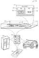
도 1은 통신 인터페이스를 통해 통신하도록 구성된 호스트 디바이스(105) 및 메모리 디바이스(110)를 포함하는 환경(100)의 일 예를 예시한다. 제품(150)의 프로세싱, 통신, 또는 제어를 지원하기 위하여 호스트 디바이스(105) 또는 메모리 디바이스(110)는 사물 인터넷(Internet of Things; IoT) 디바이스들(예를 들어, 냉장고 또는 다른 전기기기, 센서, 모터 또는 작동기)과 같은 다양한 제품들(150) 내에 포함될 수 있다. 1 illustrates an example of an
메모리 디바이스(110)는, 메모리 제어기(115) 및, 예를 들어, 복수의 개별적인 메모리 다이(예를 들어, 3-차원(3D) NAND 다이의 스택)를 포함하는 메모리 어레이(120)를 포함한다. 3D 아키텍처 반도체 메모리 기술품에 있어서, 수직 구조체들이 스택되며, 이는 계층들, 물리적 페이지들의 수를 증가시키고, 그에 따라서 메모리 디바이스(예를 들어, 저장 디바이스)의 밀도를 증가시킨다. 일 예에 있어서, 메모리 디바이스(110)는 호스트 디바이스(105)의 개별적인 메모리 또는 저장 디바이스 컴포넌트일 수 있다. 다른 예들에 있어서, 메모리 디바이스(110)는, 호스트 디바이스(105)의 하나 이상의 다른 컴포넌트들과 스택되거나 또는 이에 달리 포함된 집적 회로(예를 들어, 시스템 온 칩(system on a chip; SOC) 등)의 일 부분일 수 있다. The
직렬 고급 기술 부착(Serial Advanced Technology Attachment; SATA) 인터페이스, 주변 컴포넌트 상호연결 익스프레스(Peripheral Component Interconnect Express; PCIe) 인터페이스, 범용 직렬 버스(Universal Serial Bus; USB) 인터페이스, 범용 플래시 저장부(Universal Flash Storage; UFS) 인터페이스, eMMC™ 인터페이스, 또는 하나 이상의 다른 커넥터들 또는 인터페이스들과 같은 하나 이상의 통신 인터페이스들이 메모리 디바이스(110)와 호스트 디바이스(105)의 하나 이상의 다른 컴포넌트들 사이에서 데이터를 전송하기 위해 사용될 수 있다. 호스트 디바이스(105)는 호스트 시스템, 전자 디바이스, 프로세서, 메모리 카드 리더, 또는 메모리 디바이스(110) 외부의 하나 이상의 다른 전자 디바이스들을 포함할 수 있다. 일부 예들에 있어서, 호스트(105)는 도 8의 기계(800)를 참조하여 논의되는 컴포넌트들 중 일부 부분 또는 전부를 갖는 기계일 수 있다. Serial Advanced Technology Attachment (SATA) interface, Peripheral Component Interconnect Express (PCIe) interface, Universal Serial Bus (USB) interface, Universal Flash Storage; UFS) interface, eMMC™ interface, or one or more communication interfaces, such as one or more other connectors or interfaces, can be used to transfer data between the
메모리 제어기(115)는 호스트(105)로부터 명령어들을 수신할 수 있으며, 예컨대 메모리 어레이의 메모리 셀들, 평면들, 서브-블록들, 블록들 또는 페이지들 중 하나 이상으로 데이터를 전송(예를 들어, 기입 또는 소거)하거나 또는 이로부터 데이터를 전송(예를 들어, 판독)하기 위해서 메모리 어레이와 통신할 수 있다. 메모리 제어기(115)는, 다른 것들 중에서도 특히, 하나 이상의 컴포넌트들 또는 집적 회로들을 포함하는 회로부 또는 펌웨어를 포함할 수 있다. 예를 들어, 메모리 제어기(115)는 메모리 어레이(120)에 걸친 액세스를 제어하고 호스트(105)와 메모리 디바이스(110) 사이에 변환 계층(translation layer)을 제공하도록 구성된 하나 이상의 메모리 제어 유닛들, 회로들, 또는 컴포넌트들을 포함할 수 있다. 메모리 제어기(115)는 메모리 어레이(120)로 데이터를 전송하거나 또는 이로부터 데이터를 전송하기 위한 하나 이상의 입력/출력(input/output; I/O) 회로들, 라인들, 또는 인터페이스들을 포함할 수 있다. 메모리 제어기(115)는 메모리 관리자(125) 및 어레이 제어기(135)를 포함할 수 있다. The
메모리 관리자(125)는, 다른 것들 중에서도 특히, 다양한 메모리 관리 기능들과 연관된 복수의 컴포넌트들 또는 집적 회로들과 같은 회로부 또는 펌웨어를 포함할 수 있다. 본 설명의 목적들을 위하여, 예시적인 메모리 동작 및 관리 기능들이 NAND 메모리의 맥락에서 설명될 것이다. 당업자들은, 다른 형태들의 비-휘발성 메모리가 유사한 메모리 동작들 및 관리 기능들을 가질 수 있다는 것을 인식할 것이다. 이러한 NAND 관리 기능들은 마모 레벨링(wear leveling)(예를 들어, 가비지 콜렉션(garbage collection) 또는 재활용(reclamation)), 오류 검출 또는 정정, 블록 폐기(block retirement), 또는 하나 이상의 다른 메모리 관리 기능들을 포함한다. 메모리 관리자(125)는 어레이 제어기(135) 또는 메모리 디바이스(110)의 하나 이상의 다른 컴포넌트들에 대하여 호스트 명령들(예를 들어, 호스트로부터 수신된 명령들)을 디바이스 명령들(예를 들어, 메모리 어레이의 동작과 연관된 명령들 등)로 파싱(parse)하거나 또는 포맷할 수 있거나, 또는 (예를 들어, 다양한 메모리 관리 기능들을 달성하기 위하여) 디바이스 명령들을 생성할 수 있다. The
메모리 관리자(125)는 메모리 디바이스(110)의 하나 이상의 컴포넌트들과 연관된 다양한 정보(예를 들어, 메모리 제어기(115)에 결합된 하나 이상의 메모리 셀들 또는 메모리 어레이와 연관된 다양한 정보)를 유지하도록 구성된 관리 테이블들(130)의 세트를 포함할 수 있다. 예를 들어, 관리 테이블들(130)은 메모리 제어기(115)에 결합된 메모리 셀들의 하나 이상의 블록들에 대한 블록 나이, 블록 소거 카운트, 오류 이력, 또는 하나 이상의 오류 카운트들(예를 들어, 기입 동작 오류 카운트, 판독 비트 오류 카운트, 판독 동작 오류 카운트, 소거 오류 카운트 등)에 관한 정보를 포함할 수 있다. 특정 예들에 있어서, 오류 카운트들 중 하나 이상에 대하여 검출된 오류들의 수가 임계 이상인 경우, 비트 오류는 정정불능 비트 오류로서 지칭될 수 있다. 관리 테이블들(130)은, 다른 것들 중에서도 특히, 정정가능 또는 정정불능 비트 오류들의 카운트를 유지할 수 있다.The
어레이 제어기(135)는, 다른 것들 중에서도 특히, 메모리 제어기(115)에 결합된 메모리 디바이스(110)의 하나 이상의 메모리 셀들에 데이터를 기입하는 것, 이로부터 데이터를 판독하는 것, 또는 이를 소거하는 것과 연관된 메모리 동작들을 제어하도록 구성된 회로부 또는 컴포넌트들을 포함할 수 있다. 메모리 동작들은, 예를 들어, 호스트(105)로부터 수신된 호스트 명령들에 기초하거나 또는 (예를 들어, 마모 레벨링, 오류 검출 또는 정정 등과 연관되어) 메모리 관리자(125)에 의해 내부적으로 생성될 수 있다.The
어레이 제어기(135)는 오류 정정 코드(error correction code; ECC) 컴포넌트(140)를 포함할 수 있으며, 이는, 다른 것들 중에서도 특히, 메모리 제어기(115)에 결합된 메모리 디바이스(110)의 하나 이상의 메모리 셀들에 데이터를 기입하는 것 또는 이로부터 데이터를 판독하는 것과 연관된 오류들을 검출하거나 또는 정정하도록 구성된 ECC 엔진 또는 다른 회로부를 포함할 수 있다. 메모리 제어기(115)는, 호스트(105)와 메모리 디바이스(110) 사이에서 전송되는 데이터의 무결성을 유지하거나 또는 (예를 들어, 중복 RAID 저장부 등을 사용하여) 저장된 데이터의 무결성을 유지하면서 데이터의 다양한 동작들 또는 저장과 연관된 오류 발생들(예를 들어, 비트 오류들, 동작 오류들 등)을 능동적으로 검출하고 이를 복구하도록 구성될 수 있으며, 장래의 오류들을 방지하기 위하여 실패한 메모리 자원들(예를 들어, 메모리 셀들, 메모리 어레이들 페이지들, 블록들 등)을 제거(예를 들어, 폐기)할 수 있다. The
메모리 어레이(120)는, 예를 들어, 복수의 디바이스들, 평면들, 서브-블록들, 블록들 또는 페이지들로 배열된 몇몇 메모리 셀들을 포함할 수 있다. 일 예로서, 48 GB TLC NAND 메모리 디바이스는 페이지 당 18,592 바이트(B)(16,384 + 2208 바이트)의 데이터, 블록 당 1536개의 페이지들, 평면 당 548개의 블록들, 및 디바이스 당 4개 이상의 평면들을 포함할 수 있다. 다른 예로서, (셀 당 데이터의 2개의 비트들(즉, 4개의 프로그램가능 상태들)을 저장하는) 32 GB MLC 메모리 디바이스는 페이지 당 18,592 바이트(B)(16,384 + 2208 바이트)의 데이터, 블록 당 1024개의 페이지들, 평면 당 548개의 블록들, 및 디바이스 당 4애의 평면들을 포함할 수 있지만, 대응하는 TLC 메모리 디바이스에 비하여 절반의 필요 기입 시간 및 2배의 프로그램/소거(program/erase; P/E) 사이클들을 갖는다. 다른 예들은 다른 수들 또는 배열들을 포함할 수 있다. 일부 예들에 있어서, 메모리 디바이스 또는 이의 일 부분은 선택적으로 SLC 모드로 또는 (TLC, QLC, 등과 같은) 희망되는 MLC 모드로 동작될 수 있다. The
동작 시에, 데이터는 페이지로 NAND 메모리 디바이스(110)에 기입되거나 또는 판독되며, 블록으로 소거된다. 그러나, 하나 이상의 메모리 동작들(예를 들어, 판독, 기입, 소거 등)은 희망되는 바와 같이 더 크거나 또는 더 작은 메모리 셀들의 그룹들에 대하여 수행될 수 있다. NAND 메모리 디바이스(110)의 데이터 전송 크기는 전형적으로 페이지로서 지칭되며, 반면 호스트의 데이터 전송 크기는 전형적으로 섹터로서 지칭된다. In operation, data is written to or read from the
데이터의 페이지가 복수의 바이트의 사용자 데이터(예를 들어, 복수의 데이터 섹터들을 포함하는 데이터 페이로드(payload)) 및 그것의 대응하는 메타데이터를 포함할 수 있지만, 페이지의 크기는 통상적으로 오로지 사용자 데이터를 저장하기 위해 사용되는 바이트들의 수만을 지칭한다. 일 예로서, 4 KB의 페이지 크기를 갖는 데이터의 페이지는 4 KB의 사용자 데이터(예를 들어, 512 B의 섹터 크기를 가정할 때 8개의 섹터들)뿐만 아니라, 무결성 데이터(예를 들어, 오류 검출 또는 정정 코드 데이터), 어드레스 데이터(예를 들어, 논리적 어드레스 데이터 등), 또는 사용자 데이터와 연관된 다른 메타데이터와 같은 사용자 데이터에 대응하는 복수의 바이트(예를 들어, 32 B, 54 B, 224 B, 등)의 메타데이터를 포함할 수 있다.Although a page of data may contain multiple bytes of user data (eg, a data payload comprising multiple data sectors) and its corresponding metadata, the size of the page is typically solely for the user It only refers to the number of bytes used to store the data. As an example, a page of data having a page size of 4 KB may include 4 KB of user data (eg, 8 sectors assuming a sector size of 512 B), as well as integrity data (eg, error). Multiple bytes (e.g., 32 B, 54 B, 224) corresponding to user data, such as detection or correction code data), address data (e.g., logical address data, etc.), or other metadata associated with user data. B, etc.).
상이한 유형들의 메모리 셀들 또는 메모리 어레이들(120)은 상이한 페이지 크기들을 제공할 수 있거나, 또는 이와 연관된 상이한 양의 메타데이터를 요구할 수 있다. 예를 들어, 상이한 메모리 디바이스 유형들은, 데이터의 페이지의 무결성을 보장하기 위한 상이한 양의 메타데이터를 초래할 수 있는 상이한 비트 오류 레이트들을 가질 수 있다(예를 들어, 더 높은 비트 오류 레이트를 갖는 메모리 디바이스는 더 낮은 비트 오류 레이트를 갖는 메모리 디바이스보다 더 많은 바이트의 오류 정정 코드 데이터를 필요로 할 수 있다). 일 예로서, 다중-레벨 셀(multi-level cell; MLC) NAND 플래시 디바이스는 대응하는 단일-레벨 셀(single-level cell; SLC) NAND 플래시 디바이스보다 더 높은 비트 오류 레이트를 가질 수 있다. 이와 같이, MLC 디바이스는 대응하는 SLC 디바이스보다 오류 데이터에 대한 더 많은 메타데이터 바이트들을 필요로 할 수 있다. Different types of memory cells or
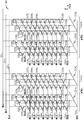
도 2는, 블록들(예를 들어, 블록 A(201A), 블록 B(201B) 등) 및 서브-블록들(예를 들어, 서브-블록 A0(201A0), 서브-블록 An(201An), 서브-블록 B0(201B0), 서브-블록 Bn(201Bn) 등)로 조직된, 메모리 셀들의 복수의 스트링들(예를 들어, 제 1 - 제 3 A0 메모리 스트링들(205A0-207A0), 제 1 - 제 3 An 메모리 스트링들(205An-207An), 제 1 - 제 3 B0 메모리 스트링들(205B0-207B0), 제 1 - 제 3 Bn 메모리 스트링들(205Bn-207Bn), 등)을 포함하는 3D NAND 아키텍처 반도체 메모리 어레이(200)의 예시적인 개략도를 예시한다. 메모리 어레이(200)는, 전형적으로 메모리 디바이스의 블록, 디바이스, 또는 다른 단위에서 발견될 더 큰 수의 유사한 구조체들의 일 부분을 나타낸다. 2 shows blocks (eg, block A 201A, block
메모리 셀들의 각각의 스트링은, 소스 라인(SRC)(235) 사이에 또는 소스-측 선택 게이트(SGS)(예를 들어, 제 1 - 제 3 A0 SGS(231A0-233A0), 제 1 - 제 3 An SGS(231An-233An), 제 1 - 제 3 B0 SGS(231B0-233B0), 제 1 - 제 3 Bn SGS(231Bn-233Bn), 등)와 드레인-측 선택 게이트(SGD)(예를 들어, 제 1 - 제 3 A0 SGD(226A0-228A0), 제 1 - 제 3 An SGD(226An-228An), 제 1 - 제 3 B0 SGD(226B0-228B0), 제 1 - 제 3 Bn SGD(226Bn-228Bn), 등) 사이에, 소스 대 드레인으로, Z 방향으로 스택된 전하 저장 트랜지스터들(예를 들어, 플로팅 게이트 트랜지스터들, 전하-트래핑 구조체들 등)의 복수의 계층들을 포함한다. 3D 메모리 어레이 내의 메모리 셀들의 각각의 스트링은 데이터 라인들(예를 들어, 비트 라인(BL)들 BL0-BL2(220-222))로서 X 방향을 따라서 그리고 물리적 페이지들로서 Y 방향을 따라서 배열될 수 있다. Each string of memory cells, the source line (SRC) (235) on or between the source-side select gate (SGS) (e.g., a first-second 3 A 0 SGS (231A 0 -233A 0), the first -3rd A n SGS (231A n -233A n ), 1st-3rd B 0 SGS (231B 0 -233B 0 ), 1st-3rd B n SGS (231B n -233B n ), etc.) and drain -Side selection gate (SGD) (e.g., 1st-3rd A 0 SGD(226A 0 -228A 0 ), 1st-3rd A n SGD(226A n -228A n ), 1st-3rd B Between 0 SGD(226B 0 -228B 0 ), 1st-3rd B n SGD(226B n -228B n ), etc.), charge storage transistors stacked in the Z direction, source to drain (e.g., Floating gate transistors, charge-trapping structures, etc.). Each string of memory cells in a 3D memory array can be arranged along the X direction as data lines (eg, bit lines BL) BL0-BL2 220-222 and along the Y direction as physical pages. have.
물리적 페이지 내에서, 각각의 계층은 메모리 셀들의 로우를 나타내며, 메모리 셀들의 각각의 스트링은 컬럼을 나타낸다. 서브-블록은 하나 이상의 물리적 페이지들을 포함할 수 있다. 블록은 복수의 서브-블록들(또는 물리적 페이지들)(예를 들어, 128, 256, 384, 등)을 포함할 수 있다. 2개의 블록들을 가지며, 각각의 블록이 2개의 서브-블록들을 가지고, 각각의 서브-블록은 단일 물리적 페이지를 가지며, 각각의 물리적 페이지는 메모리 셀들의 3개의 스트링들을 가지고, 각각의 스트링은 메모리 셀들의 8개의 계층들을 갖는 것으로서 본원에서 예시되지만, 다른 예들에 있어서, 메모리 어레이(200)는 더 많거나 또는 더 적은 블록들, 서브-블록들, 물리적 페이지들, 메모리 셀들의 스트링들, 메모리 셀들 또는 계층들을 포함할 수 있다. 예를 들어, 메모리 셀들의 각각의 스트링은 더 많거나 또는 더 적은 계층들(예를 들어, 16, 32, 64, 128, 등)뿐만 아니라, 희망되는 바와 같이, 전하 저장 트랜지스터들 위에 또는 아래에 반도체 재료의 하나 이상의 추가적인 계층들(예를 들어, 선택 게이트들, 데이터 라인들, 등)을 포함할 수 있다. 일 예로서, 48 GB TLC NAND 메모리 디바이스는 페이지 당 18,592 바이트(B)(16,384 + 2208 바이트)의 데이터, 블록 당 1536개의 페이지들, 평면 당 548개의 블록들, 및 디바이스 당 4개 이상의 평면들을 포함할 수 있다. Within a physical page, each layer represents a row of memory cells, and each string of memory cells represents a column. A sub-block can include one or more physical pages. A block may include a plurality of sub-blocks (or physical pages) (eg, 128, 256, 384, etc.). It has two blocks, each block has two sub-blocks, each sub-block has a single physical page, each physical page has three strings of memory cells, and each string is a memory cell Although illustrated herein as having eight layers of, in other examples,
메모리 어레이(200) 내의 각각의 메모리 셀은, 희망되는 바와 같이, 특정 계층 또는 계층의 일 부분에 걸쳐 제어 게이트(CG)들에 집합적으로 결합되는, 액세스 라인(예를 들어, 워드 라인(WL)들(WL00-WL70(210A-217A), WL01-WL71(210B-217B), 등)에 결합된(예를 들어, 전기적으로 또는 달리 이에 동작가능하게 연결된) 제어 게이트(CG)를 포함한다. 3D 메모리 어레이 내의 특정 계층들, 및 그에 따른 스트링 내의 특정 메모리 셀들은 개별적인 액세스 라인들을 사용하여 액세스되거나 또는 제어될 수 있다. 선택 게이트들의 그룹들은 다양한 선택 라인들을 사용하여 액세스될 수 있다. 예를 들어, 제 1 - 제 3 A0 SGD(226A0-228A0)는 A0 SGD 라인(SGDA0(225A0))을 사용하여 액세스될 수 있으며, 제 1 - 제 3 An SGD(226An-228An)는 An SGD 라인(SGDAn(225An))을 사용하여 액세스 될 수 있고, 제 1 - 제 3 B0 SGD(226B0-228B0)는 B0 SGD 라인(SGDB0(225B0))을 사용하여 액세스될 수 있으며, 제 1 - 제 3 Bn SGD(226Bn-228Bn)는 Bn SGD 라인(SGDBn(225Bn))을 사용하여 액세스될 수 있다. 제 1 - 제 3 A0 SGS(231A0-233A0) 및 제 1 - 제 3 An SGS(231An-233An)는 게이트 선택 라인(SGS0(230A))을 사용하여 액세스될 수 있으며, 제 1 - 제 3 B0 SGS(231B0-233B0) 및 제 1 - 제 3 Bn SGS(231Bn-233Bn)는 게이트 선택 라인(SGS1(230B))을 사용하여 액세스될 수 있다. Each memory cell in
일 예에 있어서, 메모리 어레이(200)는, 어레이의 개별적인 계층의 선택 게이트(또는 CG들 도는 선택 게이트들의 일 부분) 또는 각각의 메모리 셀의 제어 게이트(CG)들을 결합하도록 구성된 반도체 재료(예를 들어, 폴리실리콘, 등)의 복수의 레벨들을 포함할 수 있다. 어레이 내의 메모리 셀들의 특정 스트링들은 비트 라인(BL)들 및 선택 게이트들 등의 조합을 사용하여 액세스되거나, 선택되거나, 또는 제어될 수 있으며, 특정 스트링들 내의 하나 이상의 계층들에서의 특정 메모리 셀들은 하나 이상의 액세스 라인들(예를 들어, 워드 라인들)을 사용하여 액세스되거나, 선택되거나, 또는 제어될 수 있다. In one example,
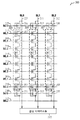
도 3은, 스트링들(예를 들어, 제 1 - 제 3 스트링들(305-307)) 및 (예를 들어, 개별적인 워드 라인(WL)들(WL0-WL7(310-317)), 드레인-측 선택 게이트(SGD) 라인(325), 소스-측 선택 게이트(SGS) 라인(330), 등으로서 예시된 바와 같은 ) 계층들의 2-차원 어레이로 배열된 복수의 메모리 셀들(302) 및 센싱 증폭기들 또는 디바이스들(360)을 포함하는 NAND 아키텍처 반도체 메모리 어레이(300)의 일 부분의 예시적인 개략도를 예시한다. 예를 들어, 메모리 어레이(300)는, 도 2에 예시된 것과 같은 3D NAND 아키텍처 반도체 메모리 디바이스의 메모리 셀들의 하나의 물리적 페이지의 일 부분의 예시적인 개략도를 예시할 수 있다. 3, strings (eg, first-third strings 305-307) and (eg, individual word lines WL (WL0-WL7 310-317), drain- A sensing amplifier and a plurality of
메모리 셀들의 각각의 스트링은 개별적인 소스-측 선택 게이트(SGS)(예를 들어, 제 1 - 제 3 SGS(331-333))를 사용하여 소스 라인(SRC)에 그리고 개별적인 드레인-측 선택 게이트(SGD)(예를 들어, 제 1 - 제 3 SGD(326-328))를 사용하여 개별적인 데이터 라인(예를 들어, 제 1 - 제 3 비트 라인(BL)들(BL0-BL2(320-322))에 결합된다. 도 3의 예에서 (예를 들어, 워드 라인(WL)들(WL0-WL7(310-317))을 사용하는) 8개의 계층들 및 3개의 데이터 라인들(BL0-BL2(326-328))을 가지고 예시되었지만, 다른 예들은 희망되는 바와 같이 더 많거나 또는 더 적은 계층들 또는 데이터 라인들을 갖는 메모리 셀들의 스트링들을 포함할 수 있다. Each string of memory cells uses a separate source-side select gate (SGS) (e.g., first to third SGS (331-333)) to the source line SRC and a separate drain-side select gate ( Individual data lines (e.g., first-third bit lines (BLs) BL0-BL2 (320-322)) using SGD (e.g., first-third SGD (326-328)) In the example of FIG. 3, 8 layers and 3 data lines BL0-BL2 (eg, using word lines WL (WL0-WL7 310-317)) 326-328)), but other examples may include strings of memory cells with more or fewer layers or data lines as desired.
예시적인 메모리 어레이(300)와 같은 NAND 아키텍처 반도체 메모리 어레이에 있어서, 선택된 메모리 셀(302)의 상태는 선택된 메모리 셀을 포함하는 특정 데이터 라인과 연관된 전류 또는 전압 변동을 센싱함으로써 액세스될 수 있다. 메모리 어레이(300)는 하나 이상의 드라이버들을 사용하여 (예를 들어, 제어 회로, 하나 이상의 프로세서들 디지털 로직 등에 의해) 액세스될 수 있다. 일 예에 있어서, 하나 이상의 드라이버들은, 특정 메모리 셀 또는 메모리 셀들의 세트에 대하여 수행되도록 희망되는 동작의 유형에 의존하여 하나 이상의 데이터 라인들(예를 들어, 비트 라인들(BL0-BL2)), 액세스 라인들(예를 들어, 워드 라인들(WL0-WL7)) 또는 선택 게이트들로 특정 전위를 드라이브함으로써 특정 메모리 셀 또는 메모리 셀들의 세트를 활성화할 수 있다. In a NAND architecture semiconductor memory array, such as the
메모리 셀을 프로그래밍하거나 또는 이에 데이터를 기입하기 위하여, 프로그래밍 전압(Vpgm)(예를 들어, 하나 이상의 프로그래밍 펄스들, 등)이 선택된 워드 라인들(예를 들어, WL4) 및 그에 따라서 선택된 워드 라인들에 결합된 각각의 메모리 셀의 제어 게이트(예를 들어, WL4에 결합된 메모리 셀들의 제 1 - 제 3 제어 게이트(CG)들(341-343))에 인가될 수 있다. 프로그래밍 펄스들은, 예를 들어, 15V로 또는 그 근처에서 시작할 수 있으며, 특정 예들에 있어서, 각각의 프로그래밍 펄스 인가 동안 크기가 증가할 수 있다. 프로그램 전압이 선택된 워드 라인들에 인가되는 동안, 접지 전위(예를 들어, Vss)와 같은 전위가 프로그래밍을 위해 목표된 메모리 셀들의 데이터 라인들(예를 들어, 비트 라인들) 및 기판들(그리고 그에 따라서 소스들과 드레인 사이의 채널들)에 인가될 수 있으며, 이는 채널들로부터 목표된 메모리 셀들의 플로팅 게이트들로의 전하 이동(예를 들어, 직접 주입 또는 파울러-노드하임(Fowler-Nordheim; FN) 터널링 등)을 야기할 수 있다. To program a memory cell or write data to it, the programming voltage Vpgm (eg, one or more programming pulses, etc.) is selected word lines (eg, WL4) and thus selected word lines A control gate of each memory cell coupled to (eg, first to third control gates (CG) 341-343 of memory cells coupled to WL4) may be applied. Programming pulses can start, for example, at or near 15V, and in certain examples, the magnitude can increase during each programming pulse application. While the program voltage is applied to the selected word lines, data lines (eg bit lines) and substrates (and data lines) of memory cells whose potential is targeted for programming, such as a ground potential (eg Vss). Accordingly, it can be applied to the channels between the sources and the drain), which transfer charges from the channels to the floating gates of the targeted memory cells (eg, direct injection or Fowler-Nordheim; FN) tunneling, etc.).
이와 대조적으로, 채널들로부터 이러한 비-목표된 메모리 셀들의 플로팅 게이트들로 전하가 이동하는 것을 방지하기 위하여, 패스 전압(Vpass)이 프로그래밍을 위해 목표되지 않은 메모리 셀들을 갖는 하나 이상의 워드 라인들에 인가될 수 있거나 또는 억제 전압(inhibit voltage)(예를 들어, Vcc)이 프로그래밍을 위해 목표되지 않은 메모리 셀들을 갖는 데이터 라인들(예를 들어, 비트 라인들)에 인가될 수 있다. 패스 전압은, 예를 들어, 프로그래밍을 위해 목표된 워드 라인에 인가되는 패스 전압들의 근접성에 의존하여 변화할 수 있다. 억제 전압은, 접지 전위(예를 들어, Vss)에 대한, 외부 소스 또는 공급부(예를 들어, 배터리, AC-대-DC 컨버터, 등)으로부터의 전압과 같은 공급 전압(Vcc)을 포함할 수 있다. In contrast, in order to prevent the transfer of charge from the channels to the floating gates of these non-targeted memory cells, the pass voltage Vpass is applied to one or more word lines with memory cells not targeted for programming. It can be applied or an inhibit voltage (eg, Vcc) can be applied to data lines (eg, bit lines) with memory cells not targeted for programming. The pass voltage can vary, for example, depending on the proximity of the pass voltages applied to the target word line for programming. The suppression voltage may include a supply voltage (Vcc), such as a voltage from an external source or supply (eg, a battery, AC-to-DC converter, etc.) to a ground potential (eg, Vss). have.
일 예로서, 프로그래밍 전압(예를 들어, 15V 또는 그 이상)이 WL4와 같은 특정 워드 라인에 인가되는 경우, 비-목표된 메모리 셀들의 프로그래밍을 억제하거나 또는 프로그래밍을 위해 목표되지 않은 이러한 메모리 셀들 상에 저장된 값들을 유지하기 위하여 10V의 패스 전압이 WL3, WL5, 등과 같은 하나 이상의 다른 워드 라인들에 인가될 수 있다. 인가된 프로그램 전압과 비-목표된 메모리 셀들 사이의 거리가 증가함에 따라, 비-목표된 메모리 셀들이 프로그래밍되는 것을 피하기 위해 요구되는 패스 전압이 감소할 수 있다. 예를 들어, 15V의 프로그래밍 전압이 WL4에 인가되는 경우, 10V의 패스 전압이 WL3 및 WL5에 인가될 수 있으며, 8V의 패스 전압이 WL2 및 WL6에 인가될 수 있고, 7V의 패스 전압이 WL1 및 WL7에 인가될 수 있는 등이다. 다른 예들에 있어서, 패스 전압들, 또는 워드 라인들의 수 등은 더 높거나 또는 더 낮을 수 있거나, 또는 더 많거나 또는 더 적을 수 있다. As an example, when a programming voltage (e.g., 15V or more) is applied to a particular word line, such as WL4, it suppresses the programming of non-targeted memory cells or on these memory cells that are not targeted for programming. A pass voltage of 10V may be applied to one or more other word lines such as WL3, WL5, etc. to maintain the values stored in the. As the distance between the applied program voltage and non-target memory cells increases, the pass voltage required to avoid programming non-target memory cells can decrease. For example, when a programming voltage of 15V is applied to WL4, a pass voltage of 10V can be applied to WL3 and WL5, a pass voltage of 8V can be applied to WL2 and WL6, and a pass voltage of 7V is applied to WL1 and And WL7. In other examples, the pass voltages, or the number of word lines, etc. can be higher or lower, or more or less.
데이터 라인들 중 하나 이상(예를 들어, 제 1, 제 2, 또는 제 3 비트 라인들(BL0-BL2(320-322)))에 결합된 센싱 증폭기들(360)은 특정 데이터 라인 상의 전압 또는 전류를 센싱함으로써 개별적인 데이터 라인들 내의 각각의 메모리 셀의 상태를 검출할 수 있다.
하나 이상의 프로그래밍 펄스들(예를 들어, Vpgm)의 인가들 사이에, 선택된 메모리 셀이 그것의 의도된 프로그래밍된 상태에 도달하였는 여부를 결정하기 위해 검증 동작이 수행될 수 있다. 선택된 메모리 셀이 그것의 의도된 프로그래밍된 상태에 도달한 경우, 이는 추가적인 프로그래밍이 억제될 수 있다. 선택된 메모리 셀이 그것의 의도된 프로그래밍된 상태에 도달하지 않은 경우, 추가적인 프로그래밍 펄스들이 인가될 수 있다. 특정 수(예를 들어, 최대 수)의 프로그래밍 펄스들 이후에 선택된 메모리 셀이 그것의 의도된 프로그래밍된 상태에 도달하지 않은 경우, 선택된 메모리 셀, 또는 이러한 선택된 메모리 셀과 연관된 스트링, 블록, 또는 페이지는 결함이 있는 것으로 마킹될 수 있다.Between the application of one or more programming pulses (eg, Vpgm), a verify operation can be performed to determine whether the selected memory cell has reached its intended programmed state. If the selected memory cell has reached its intended programmed state, this can inhibit further programming. Additional programming pulses can be applied if the selected memory cell has not reached its intended programmed state. If a selected memory cell has not reached its intended programmed state after a certain number (eg, maximum number) of programming pulses, the selected memory cell, or a string, block, or page associated with the selected memory cell Can be marked as defective.
메모리 셀 또는 메모리 셀들의 그룹(예를 들어, 소거는 전형적으로 블록들 또는 서브-블록들로 수행됨)을 소거하기 위하여, 목표된 메모리 셀들의 워드 라인들이 접지 전위(예를 들어, Vss)와 같은 전위로 유지되는 동안, (예를 들어, 하나 이상의 비트 라인들, 선택 게이트들 등을 사용하여) 소거를 위해 목표된 메모리 셀들의 기판들(및 그에 따라서 소스들과 드레인들 사이의 채널들)에 소거 전압(Vers)(예를 들어, 전형적으로 Vpgm)이 인가될 수 있으며, 이는 목표된 메모리 셀들의 플로팅 게이트들로부터 채널들로의 전하 이동(예를 들어, 직접 주입 또는 파울러-노드하임(Fowler-Nordheim; FN) 터널링 등)을 야기할 수 있다. To erase a memory cell or group of memory cells (e.g., erase is typically performed in blocks or sub-blocks), the word lines of the targeted memory cells are equal to the ground potential (e.g., Vss). While maintaining the potential, (e.g., using one or more bit lines, select gates, etc.) to the substrates of memory cells targeted for erase (and thus channels between sources and drains). An erase voltage Vers (eg, typically Vpgm) can be applied, which is the transfer of charge from the floating gates of the targeted memory cells to the channels (eg, direct injection or Fowler-Nordheim). -Nordheim (FN) tunneling, etc.).
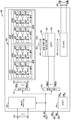
도 4는, 복수의 메모리 셀들(404)을 갖는 메모리 어레이(402), 및 메모리 어레이(402)와의 통신을 제공하거나, 또는 이에 대하여 하나 이상의 메모리 동작들을 수행하기 위한 하나 이상의 회로들 또는 컴포넌트들을 포함하는 메모리 디바이스(400)의 예시적인 블록도를 예시한다. 메모리 디바이스(400)는 로우 디코더(412), 컬럼 디코더(414), 센싱 증폭기들(420), 페이지 버퍼(422), 선택기(424), 입력/출력(I/O) 회로(426), 및 메모리 제어 유닛(430)을 포함할 수 있다. 4 includes a
메모리 어레이(402)의 메모리 셀들(404)은 제 1 및 제 2 블록들(402A, 402B)과 같이 블록들로 배열될 수 있다. 각각의 블록은 서브-블록들을 포함할 수 있다. 예를 들어, 제 1 블록(402A)은 제 1 및 제 2 서브-블록들(402A0, 402An)을 포함할 수 있으며, 제 2 블록(402B)은 제 1 및 제 2 서브-블록들(402B0, 402Bn)을 포함할 수 있다. 각각의 서브-블록은 복수의 물리적 페이지들을 포함할 수 있으며, 각각의 페이지는 복수의 메모리 셀들(404)을 포함한다. 2개의 블록들을 가지며, 각각의 블록은 2개의 서브-블록들을 가지고, 각각의 서브-블록은 다수의 메모리 셀들(404)을 갖는 것으로 본원에 예시되지만, 다른 예들에 있어서, 메모리 어레이(402)는 더 많거나 또는 더 적은 블록들, 서브-블록들, 메모리 셀들 등을 포함할 수 있다. 다른 예들에 있어서, 메모리 셀들(404)은 복수의 로우들, 컬럼들, 페이지들, 서브-블록들, 블록들 등으로 배열될 수 있으며, 예를 들어, 액세스 라인들(406), 제 1 데이터 라인들(410), 또는 하나 이상의 선택 게이트들, 소스 라인들 등을 사용하여 액세스될 수 있다.
메모리 제어 유닛(430)은, 예를 들어, 하나 이상의 어드레스 라인들(416) 상에서 수신된 어드레스 신호들(A0-AX) 또는 희망되는 동작(예를 들어, 기입, 판독, 소거, 등)을 나타내는 하나 이상의 제어 신호들 또는 클럭 신호들을 포함하는, 제어 라인들(432) 상에서 수신된 하나 이상의 신호들 또는 명령어들에 따라 메모리 디바이스(400)의 메모리 동작들을 제어할 수 있다. 메모리 디바이스(400) 외부의 하나 이상의 디바이스들은 제어 라인들(432) 상의 제어 신호들의 값들 또는 어드레스 라인(416) 상의 어드레스 신호들을 제어할 수 있다. 메모리 디바이스(400) 외부의 디바이스들의 예들은, 비제한적으로, 도 4에 예시되지 않은 호스트, 메모리 제어기, 프로세서, 또는 하나 이상의 회로들 또는 컴포넌트들을 포함할 수 있다. The
메모리 디바이스(400)는 메모리 셀들(404) 중 하나 이상으로 데이터를 전송(예를 들어, 기입 또는 소거) 또는 이로부터 데이터를 전송(예를 들어, 판독)하기 위해 액세스 라인들(406) 및 제 1 데이터 라인들(410)을 사용할 수 있다. 로우 디코더(412) 및 컬럼 디코더(414)는 어드레스 라인(416)으로부터 어드레스 신호들(A0-AX)을 수신하고 디코딩할 수 있으며, 메모리 셀들(404) 중 어느 것이 액세스될 것인지 결정할 수 있고, 이상에서 설명된 바와 같이, 액세스 라인들(406)(예를 들어, 복수의 워드 라인들(WL0-WLm) 중 하나 이상) 또는 제 1 데이터 라인들(410)(예를 들어, 복수의 비트 라인들(BL0-BLn) 중 하나 이상) 중 하나 이상으로 신호들을 제공할 수 있다. The
메모리 디바이스(400)는, 제 1 데이터 라인들(410)을 사용하여 메모리 셀들(404) 상의 데이터 값들을 결정(예를 들어, 판독)하거나 또는 이에 기입될 데이터의 값들을 결정하도록 구성된 센싱 증폭기들(420)과 같은 센싱 회로부를 포함할 수 있다. 예를 들어, 메모리 셀들(404)의 선택된 스트링에서, 센싱 증폭기들(420) 중 하나 이상은 메모리 어레이(402) 내에서 선택된 스트링을 통해 데이터 라인들(410)로 흐르는 판독 전류에 응답하여 선택된 메모리 셀(404) 내의 논리 레벨을 판독할 수 있다. The
메모리 디바이스(400) 외부의 하나 이상의 디바이스들은 I/O 라인들(DQ0-DQN)(408), 어드레스 라인들(416)(A0-AX), 또는 제어 라인들(432)을 사용하여 메모리 디바이스(400)와 통신할 수 있다. 입력/출력(I/O) 회로(426)는, 예를 들어, 제어 라인들(432) 및 어드레스 라인들(416)에 따라, I/O 라인들(408)을 사용하여, 메모리 디바이스(400) 안으로 또는 밖으로, 예컨대 페이지 버퍼(422) 또는 메모리 어레이(402) 안으로 또는 밖으로 데이터의 값들을 전송할 수 있다. 페이지 버퍼(422)는 데이터가 메모리 어레이(402)의 관련 부분들 내로 프로그래밍되기 이전에 메모리 디바이스(400) 외부의 하나 이상의 디바이스들로부터 수신된 데이터를 저장할 수 있거나, 또는, 데이터가 메모리 디바이스(400) 외부의 하나 이상의 디바이스들로 송신되기 이전에 메모리 어레이(402)로부터 판독된 데이터를 저장할 수 있다. One or more devices outside
컬럼 디코더(414)는 하나 이상의 어드레스 신호들(A0-AX)을 수신하고 이를 하나 이상의 컬럼 선택 신호들(CSEL1-CSELn)로 디코딩할 수 있다. 선택기(424)(예를 들어, 선택 회로)는 컬럼 선택 신호들(CSEL1-CSELn)을 수신하고, 메모리 셀들(404)로부터 판독될 또는 이로 프로그래밍될 데이터의 값들을 나타내는 페이지 버퍼(422) 내의 데이터를 선택할 수 있다. 선택된 데이터는 제 2 데이터 라인들(418)을 사용하여 페이지 버퍼(422)와 I/O 회로(426) 사이에서 전송될 수 있다. The
메모리 제어 유닛(430)은, 외부 소스 또는 공급부(예를 들어, 내부 또는 외부 배터리, AC-대-DC 컨버터, 등)으로부터, 공급 전압(Vcc)(434) 및 네거티브 공급(Vss)(436)(예를 들어, 접지 전위)과 같은 포지티브 및 네거티브 공급 신호들을 수신할 수 있다. 특정 예들에 있어서, 메모리 제어 유닛(430)은 내부적으로 포지티브 또는 네거티브 공급 신호들을 제공하기 위한 조절기(regulator)(428)를 포함할 수 있다. The
NAND 메모리 디바이스들을 그들의 디바이스들 내에 통합하는 컴퓨팅 디바이스 제조사들은 흔히 NAND 메모리 디바이스의 저장 공간이 "물리적 파티션"으로서 메모리의 2개 이상의 청크(chunk)들로 파티션될 것을 요구하며, 여기에서 NAND가 물리적 공간을 분할한다. 각각의 물리적 파티션은, NAND 상의 별개로 관리되는 물리적 어드레스 공간에 매핑되는 그 자체의 논리적 블록 어드레스들의 세트를 가지고 별개로 관리된다. 이러한 물리적 어드레스들에 대응하는 이러한 물리적 메모리 블록들은 (파티션 상의 데이터가 소거될 것을 요구하는 재파티션이 되지 않는 한) 항상 물리적 파티션에 속한다. 가비지 콜렉션 및 다른 동작들이 각각의 물리적 파티션에 대하여 개별적으로 수행된다. 본질적으로, NAND는 이것을 별개의 디바이스로서 관리한다. Computing device manufacturers integrating NAND memory devices into their devices often require that the storage space of the NAND memory device be partitioned into two or more chunks of memory as a "physical partition", where the NAND is a physical space. Divide. Each physical partition is managed separately with its own set of logical block addresses mapped to a separate managed physical address space on the NAND. These physical memory blocks corresponding to these physical addresses always belong to the physical partition (unless the partition on the partition requires re-partitioning to erase data). Garbage collection and other operations are performed individually for each physical partition. In essence, NAND manages this as a separate device.
파티션의 하나의 대안적인 유형은, 호스트 디바이스(예를 들어, 그 내부에 NAND가 설치된 디바이스)의 운영 시스템이 O/S 레벨에서 저장부의 풀(pool)을 파티션하는 논리적 파티션이다. O/S 위의 애플리케이션은 NAND 디바이스를 2개의 별개의 저장 풀들(예를 들어, 각각의 파티션)로서 보지만, 풀들 둘 모두에 의해 점유되는 전체 공간이 NAND 디바이스 자체에 의해 연속적으로 관리된다. 이러한 예들에 있어서, NAND 디바이스는 논리적 파티션의 존재에 대한 어떠한 지식도 갖지 않을 수 있다. One alternative type of partition is a logical partition where the operating system of the host device (eg, a device with NAND installed therein) partitions a pool of storage at the O/S level. The application on O/S sees the NAND device as two separate storage pools (e.g., each partition), but the total space occupied by both pools is continuously managed by the NAND device itself. In these examples, the NAND device may not have any knowledge of the existence of logical partitions.
특정 디바이스 제조사들은, 물리적 파티션들이 속도, 보안, 수명, 및 유사한 것과 같은 특정 성능 속성들을 더 양호하기 보장할 수 있다고 생각한다. 예를 들어, 디바이스 제조사들은, 보안 요건들, 파티션을 구성하는 메모리 셀들의 구성(예를 들어, 이들이 SLC, MLC, TLC, 또는 유사한 것인지 여부), 크기, 파티션의 오버프로비저닝(overprovisioning), 및 유사한 것을 지정하는 서비스 레벨 협약들을 가질 수 있다. Certain device manufacturers believe that physical partitions can better guarantee certain performance attributes such as speed, security, lifetime, and similar. For example, device manufacturers have security requirements, configuration of memory cells that make up a partition (eg, whether they are SLC, MLC, TLC, or similar), size, overprovisioning of the partition, and similar You can have service level agreements that specify things.
이러한 파티션들의 프로비저닝은 NAND 상에서 자원 집중적일 수 있다. 예를 들어, 다양한 관리 데이터는 NAND 메모리 디바이스 상의 파티션에 따라 물리적으로 저장되어야 할 필요가 있다. 이는, 그렇지 않았다면 사용자 데이터를 저장하기 위해 사용될 수 있었던 NAND 상의 공간을 차지한다. 일단 물리적 파티션이 생성되면, 파티션들 사이에서 메모리 셀들을 이동시킬 방법이 없다. 따라서, 예를 들어, 특정 물리적 파티션에 대한 높은 사용량이 그 파티션 내의 메모리 셀들이 정상 레이트보다 더 높은 레이트로 마모되는 것을 야기하는 경우, 너무 많은 메모리 셀들이 배드(bad)가 될 가능성이 발생할 수 있으며, 결과적으로, 파티션은 심지어 다른 파티션들 내의 공간이 이용가능한 경우에도 사용불능이 될 수 있다. 부트 파티션이 영향을 받는 경우, 이는 디바이스가 부팅하지 못하게 할 수 있다. 다른 파티션 내의 사용자 데이터가 양호할 수 있지만(그리고 실제로 다른 파티션 내에 이용가능 공간이 존재할 수 있지만), 디바이스는 부팅되지 못할 수 있으며, 사용자 데이터가 검색불가능할 수 있다. Provisioning of these partitions can be resource intensive on NAND. For example, various management data needs to be physically stored according to partitions on the NAND memory device. This takes up space on the NAND that could otherwise have been used to store user data. Once a physical partition is created, there is no way to move memory cells between partitions. Thus, for example, if high usage for a particular physical partition causes memory cells in that partition to wear out at a rate higher than the normal rate, the possibility of too many memory cells becoming bad may occur, and , Consequently, a partition can become unavailable even if space in other partitions is available. If the boot partition is affected, this can prevent the device from booting. Although user data in other partitions may be good (and there may actually be space available in other partitions), the device may fail to boot, and user data may be unsearchable.
일부 예들에 있어서, 요청된 물리적 파티션 대신에 NAND-레벨 논리적 파티션을 생성하는 방법들, 시스템들, 기계-판독가능 매체들, 및 NAND 디바이스들이 개시된다. NAND 디바이스는 이를 하나의 연속적인 메모리 풀로서 관리하지만, 호스트 디바이스 상의 운영 시스템은 이러한 NAND-레벨 논리적 파티션을 물리적 파티션으로 본다. 따라서, 예를 들어, 호스트 디바이스 상의 운영 시스템은 물리적 파티션에 대응하는 범위 내의 논리적 블록 어드레스(logical block address; LBA)를 갖는 (파티션 식별자를 제공하는) 물리적 파티션으로 호스트 명령들을 발행할 수 있지만, NAND 메모리 디바이스는 이러한 요청들을 다른 파티션들에 의해 공유되는 공통 풀 내의 물리적 어드레스들로 변환한다. NAND 제어기는, 서비스 레벨 보증(service level guarantee)들이 준수된다는 것을 보장할 수 있다. 예를 들어, 파티션에 물리적 블록들을 할당할 때, 물리적 파티션 서비스 레벨 보증들이 메모리가 SLC 셀일 것임을 지정하는 경우에, 만일 메모리 블록이 SLC이 아닌 경우, 제어기는 메모리를 (TLC, MLC, QLC, 및 유사한 것으로부터) SLC이 되도록 재구성할 수 있다.In some examples, methods, systems, machine-readable media, and NAND devices are disclosed that create a NAND-level logical partition instead of a requested physical partition. The NAND device manages it as a contiguous pool of memory, but the operating system on the host device sees this NAND-level logical partition as a physical partition. Thus, for example, an operating system on a host device can issue host commands to a physical partition (which provides a partition identifier) having a logical block address (LBA) within a range corresponding to the physical partition, but NAND The memory device translates these requests into physical addresses in a common pool shared by other partitions. The NAND controller can ensure that service level guarantees are followed. For example, when allocating physical blocks to a partition, if the physical partition service level guarantees specify that the memory will be an SLC cell, if the memory block is not an SLC, the controller may use memory (TLC, MLC, QLC, and From a similar one) to be SLC.
결과적으로, NAND는, 별개의 파티션을 생성하는 관리 부담들 및 메모리 저장 비용들을 초래하지 않고 운영 시스템이 요구하는 서비스 레벨 보증들을 운영 시스템에 제공할 수 있다. 따라서, 논리적 파티션은 - 운영 시스템 레벨에서와는 대조적으로 - NAND 메모리 제어기 레벨에서 생성된다. As a result, NAND can provide the operating system with the service level guarantees required by the operating system without incurring the administrative burdens and memory storage costs of creating a separate partition. Thus, logical partitions are created at the NAND memory controller level-as opposed to at the operating system level.
도 5는 본 개시의 일부 예들에 따른 물리적 파티션을 생성하기 위한 요청에 응답하여 논리적 파티션을 생성하기 위한 방법(500)의 순서도를 예시한다. 동작(510)에서, 제어기는 물리적 파티션을 생성하기 위한 명령을 호스트 디바이스로부터 호스트 인터페이스를 통해 수신할 수 있다. 예를 들어, 운영 시스템, 제조 프로세스 기계류, 또는 유사한 것. 명령은, 보안 요건들, 구성 요건들(예를 들어, SLC, TLC, MLC를 사용하지는 여부), 및 유사한 것과 같은 파티션에 대한 하나 이상의 서비스-레벨 요건들을 포함할 수 있다. 5 illustrates a flow diagram of a method 500 for creating a logical partition in response to a request to create a physical partition according to some examples of the present disclosure. In
동작(515)에서, NAND 디바이스는 그 대신에 논리적 NAND-레벨 파티션을 생성할 수 있다. 예를 들어, 디바이스는, 서비스 레벨 협약들이 충족됨을 보장하기 위하여 그리고 논리적 파티션을 추적하기 위하여 제어기에 의해 관리되는 NAND의 메모리 셀들 내에 저장되거나 또는 제어기에 의해 사용되는 NAND 자체 상의 휘발성 메모리 내의 하나 이상의 데이터 구조체들을 초기화할 수 있다. 제어기는 파티션에 대한 파티션 식별자 및 논리적 블록 어드레스(logical block address; LBA) 범위를 생성할 수 있으며, 이를 호스트 디바이스로 제공할 수 있다. 제어기는 또한, 파티션 식별자 및 그 파티션에 할당된 논리적 블록 어드레스 투플(tuple)을 나타내는 논리적 대 물리적(logical to physical; L2P) 테이블 및 명령 메모리 풀로부터의 대응하는 물리적 메모리 위치들을 업데이트할 수 있다. 호스트 디바이스가 이러한 파티션 상의 데이터를 판독하거나, 기입하거나 또는 소거하기를 희망할 때, 이는, 이것이 판독하거나, 기입하거나, 또는 소거하기를 희망하는 파티션 식별자 및 블록의 LBA를 제출한다. 그럼 다음, NAND는 이를 L2P 테이블을 사용하여 물리적 어드레스들로 변환할 수 있다.In
동작(520)에서, NAND는 호스트로 응답을 전송할 수 있다. 응답은 파티션 식별자(예를 들어, 명칭공간, 논리적 유닛 번호(Logical Unit Number; LUN), 및 유사한 것), 상태(파티션이 생성되었는지 여부), 및 LBA 범위를 포함할 수 있다. 동작(525)에서, NAND 디바이스는 물리적 파티션으로 보내지는 호스트 요청들을 그 대신에 논리적 파티션으로 보내지는 것으로 변환한다. 예를 들어, 호스트는 호스트 명령(예를 들어, 판독, 기입, 소거) 내에 파티션 ID 및 파티션-특정 LBA를 제공할 수 있다. NAND는 이러한 값들을, 그 후에 요청을 서비스하기 위해 사용되는 할당된 물리적 어드레스를 제공하는 테이블 내의 룩업(lookup)으로서 사용할 수 있다. In
일부 예들에 있어서, 파티션이 생성될 때, NAND 디바이스는 임의의 실제 물리적 자원들을 할당하지 않고 공간을 예약한다. 따라서, NAND 디바이스는 L2P 테이블 내의 특정 LBA들에 실제로 특정 물리적 어드레스들을 할당하지 않고 얼마나 많은 블록들이 각각의 파티션에 할당되는지에 대한 추적을 유지한다. 이는, 호스트 디바이스 운영 시스템이 합계로 NAND의 저장 용량을 초과하는 파티션들을 생성하는 것을 방지한다. 일단 호스트가 파티션에 기입하기 시작하면, NAND는 L2P 테이블을 통해 물리적 공간을 파티션에 할당한다. In some examples, when a partition is created, the NAND device reserves space without allocating any actual physical resources. Thus, the NAND device keeps track of how many blocks are allocated to each partition without actually assigning specific physical addresses to specific LBAs in the L2P table. This prevents the host device operating system from creating partitions that in total exceed NAND's storage capacity. Once the host starts writing to the partition, NAND allocates physical space to the partition through the L2P table.
예를 들어, 호스트 운영 시스템이 2개의 물리적 파티션들, 즉, 10 GB인 제 1 파티션 및 5 GB인 제 2 파티션을 요청하는 경우, NAND는 2개의 NAND-레벨 논리적 파티션들을 생성하고 제 1 파티션에 1의 논리적 유닛 번호를 할당하며 제 2 파티션에 2의 LUN을 할당할 수 있다. 각각의 LUN은 이것에 할당된 복수의 유효 LBA들을 가질 수 있다. 예를 들어, LUN 1은 0에서 시작하여 2047에서 종료하는 2048 LBA들을 가질 수 있다. LUN 2는 0에서 시작하여 1024에서 종료하는 1024 LBA들을 가질 수 있다. 생성 이후에, 이러한 LBA들 중 어느 것도 물리적 어드레스에 매핑되지 않을 수 있다. 그러나, NAND 메모리 디바이스는, 15 GB의 공간이 이미 2개의 파티션들에 약속되었음을 인식하며, 따라서, NAND의 총 용량이 25 GB인 경우, NAND는 15 GB의 제 3 파티션을 생성하기 위한 시도를 거부할 것이다. 일단 기입이 도착하면, NAND 디바이스는 물리적 어드레스를 LBA에 그리고 그에 따라서 특정 NAND-레벨 논리적 파티션에 할당할 수 있다. NAND 내에 저장된 값을 수정하기 위한 동작은 NAND가 메모리의 풀 내에서 자유 블록을 찾고 LBA를 그 자유 블록에 할당하게끔 할 수 있다. 그런 다음, 그 자유 블록이 그 논리적NAND-레벨 파티션에 할당되게 된다. 그러면, 오래된 블록은 무효로서 마킹된다. 일단 가비지 콜렉션이 발생하면, 오래된 블록(및 모든 다른 무효 블록들)은 이후의 NAND-레벨 파티션들 중 임의의 것에 대한 할당을 위해 풀로 복귀할 수 있다. 일부 예들에 있어서, 특정 메모리 셀을 파티션에 할당하기 위하여, NAND는 이를 제 1 구성(예를 들어, SLC, MLC, 또는 TLC)으로부터 상이한 구성(SLC, MLC, 또는 TLC)으로 재구성할 수 있다. For example, if the host operating system requests two physical partitions, a first partition that is 10 GB and a second partition that is 5 GB, NAND creates two NAND-level logical partitions and assigns them to the first partition. A logical unit number of 1 is assigned, and a LUN of 2 can be assigned to the second partition. Each LUN can have multiple effective LBAs assigned to it. For example,
언급된 바와 같이, NAND의 메모리 셀들은 공유된 풀로서 관리될 수 있으며, 논리적 파티션들 사이에서 동적으로 할당될 수 있다. 가비지 콜렉션은 (단일 파티션에 대해서가 아니라) 전체 디바이스에 걸쳐 이루어질 수 있으며, 오버프로비저닝이 또한 전체 풀에 걸칠 수 있다. As mentioned, NAND's memory cells can be managed as a shared pool and can be dynamically allocated among logical partitions. Garbage collection can occur across the entire device (not on a single partition), and over-provisioning can also span the entire pool.
도 6은 논리적 파티션으로서 NAND에 의해 생성된 물리적 파티션으로 보내진 호스트 명령을 NAND 제어기가 프로세싱하는 방법(600)의 순서도를 예시한다. 방법(600)은 도 5의 동작(525)의 일 예일 수 있다. 동작(615)에서, 제어기는 호스트로부터 동작을 위한 명령을 수신한다. 예를 들어, 명령은 UFS 인터페이스와 같은 호스트 인터페이스를 통해 수신될 수 있다. 동작(620)에서, 제어기는 파티션 ID 및 LBA를 L2P 테이블을 사용하여 물리적 어드레스로 변환할 수 있다. 파티션의 LBA가 이전에 결코 기입된 적이 없던 경우, 공통 풀 내의 페이지가 사용될 수 있으며, 그 LBA 및 그 파티션에 할당될 수 있다. 그런 다음, 제어기는 호스트 데이터를 그 물리적 페이지에 기입할 수 있다. 이전에 언급된 바와 같이, LBA가 이미 할당된 경우, 시스템은 그 (LBA, 파티션 ID) 투플에 현재 할당된 물리적 어드레스를 무효로 마킹하며, 공통 풀 내에서 자유 블록의 위치를 찾고, 그 자유 블록을 L2P 테이블 내에서 (LBA, 파티션 ID) 투플에 할당하며, 데이터를 그 블록에 기입할 수 있다. 호스트 명령이 소거인 경우, 그 (LBA, 파티션 ID) 투플에 대응하는 물리적 블록이 무효로서 마킹될 수 있다. 일단 그 블록이 가비지 콜렉션되면, 이는 임의의 파티션에 재할당될 수 있다. 동작(625)에서, 제어기는 물리적 어드레스를 사용하여 호스트 요청을 서비스할 수 있으며, 상태를 호스트로 반환할 수 있다. 예를 들어, 판독, 기입, 소거, 또는 유사한 것. FIG. 6 illustrates a flow diagram of a
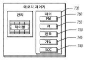
도 7은 본 개시의 일부 예들에 따른 메모리 제어기(715)의 개략도를 도시한다. 메모리 제어기(715)는 메모리 제어기(115)의 일 예이며, 메모리 관리자(725)는 메모리 관리자(125)의 일 예이고, 관리 테이블들(730)은 관리 테이블(130)의 일 예일 수 있다. 제어기(735) 및 ECC(740)는 도 1의 제어기(135) 및 ECC(140)의 일 예일 수 있다. 제어기(735)는, 물리적 파티션을 생성하기 위한 요청들에 응답하여 논리적 파티션들의 생성 및 관리를 핸들링할 수 있는 PM 컴포넌트(760)를 포함한다. 예를 들어, PM 컴포넌트(760)는 도 5 및 도 6의 방법들을 구현할 수 있다.7 shows a schematic diagram of a memory controller 715 according to some examples of the present disclosure. The memory controller 715 is an example of the
도 8은, 본원에서 논의되는 기술들(예를 들어, 방법론들) 중 임의의 하나 이상을 수행할 수 있는 예시적인 기계(800)의 블록도를 예시한다. 대안적인 실시예들에 있어서, 기계(800)는 독립형 디바이스로서 동작할 수 있거나 또는 다른 기계들에 연결(예를 들어, 네트워킹)될 수 있다. 네트워크화된 배치에서, 기계(800)는 클라이언트-서버 네트워크 환경에서 서버 기계, 클라이언트 기계, 또는 이들 둘 모두로서 동작할 수 있다. 일 예에 있어서, 기계(800)는 피어-투-피어(peer-to-peer; P2P)(또는 다른 분산형) 네트워크 환경에서 피어 기계로서 역할할 수 있다. 기계(800)는 개인용 컴퓨터(personal computer; PC), 태블릿 PC, 셋-탑 박스(set-top box; STB), 개인 디지털 보조장치(Personal Digital Assistant; PDA), 휴대 전화, 웹 전기기기, IoT 디바이스, 자동차 시스템, 또는 그 기계에 의해 취해질 액션들을 지정하는 (순차적으로 또는 달리) 명령어들을 실행할 수 있는 임의의 기계일 수 있다. 추가로, 단일 기계만이 예시되었지만, 용어 "기계"는 또한, 클라우드 컴퓨팅, 서비스형 소프트웨어(software as a service; SaaS), 다른 컴퓨터 클러스터 구성들과 같은 본원에서 논의된 방법론들 중 임의의 하나 이상의 방법론을 수행하기 위한 명령어들의 세트(또는 복수의 세트들)을 개별적으로 또는 함께 실행하는 기계들의 임의의 집합을 포함하는 것으로 고려되어야만 한다. 8 illustrates a block diagram of an
본원에서 설명되는 바와 같은 예들은, 로직, 컴포넌트들, 디바이스들, 패키지들, 또는 메커니즘들을 포함할 수 있거나, 또는 이에 의해 동작할 수 있다. 회로부는, 하드웨어(예를 들어, 간단한 회로들, 게이트들, 로직, 등)을 포함하는 유형적인 엔티티들로 구현된 회로들의 집합(예를 들어, 세트)이다. 회로부 멤버십은 시간 및 기초 하드웨어 가변성에 따라 유연할 수 있다. 회로부들은, 단독으로 또는 조합으로, 동작할 때 특정 태스크들을 수행할 수 있는 멤버들을 포함한다. 일 예에 있어서, 회로부의 하드웨어는 특정 동작으로 수행하도록 불변적으로(예를 들어, 하드와이어드(hardwired)로) 설계될 수 있다. 일 예에 있어서, 회로부의 하드웨어는, 특정 동작의 명령어들을 인코딩하기 위하여 물리적으로(예를 들어, 자기적으로, 전기적으로, 불변 밀집 입자(invariant massed particle)들의 이동가능 배치, 등) 수정된 컴퓨터 판독가능 매체를 포함하는 가변적으로 연결된 물리적 컴포넌트들(예를 들어, 실행 유닛들, 트랜지스터들, 간단한 회로들, 등)을 포함할 수 있다. 물리적 컴포넌트들을 연결함에 있어서, 하드웨어 구성물의 기초 전기적 속성들은, 예를 들어, 절연체로부터 전도체로 또는 이의 역으로 변화된다. 명령어들은, 참여 하드웨어(예를 들어, 실행 유닛들 또는 로딩 메커니즘)가 동작 시에 특정 태스크들의 부분들을 수행하기 위하여 가변적인 연결들을 통해 하드웨어로 회로부의 멤버들을 생성하는 것을 가능하게 한다. 따라서, 컴퓨터 판독가능 매체는, 디바이스가 동작할 때 회로부의 다른 컴포넌트들에 통신가능하게 결합된다. 일 예에 있어서, 물리적 컴포넌트들 중 임의의 것이 하나를 초과하는 회로부의 하나를 초과하는 멤버에서 사용될 수 있다. 예를 들어, 동작 하에서, 실행 유닛들은 하나의 시점에서 제 1 회로부의 제 1 회로에서 사용될 수 있으며, 상이한 시점에 제 1 회로부의 제 2 회로에 의해 또는 제 2 회로부의 제 3 회로에 의해 재사용될 수 있다.Examples as described herein may include, or operate on, logic, components, devices, packages, or mechanisms. A circuit portion is a set (eg, set) of circuits implemented with tangible entities including hardware (eg, simple circuits, gates, logic, etc.). Circuit membership can be flexible with time and basic hardware variability. The circuit parts, alone or in combination, include members capable of performing certain tasks when operating. In one example, the hardware of the circuitry can be designed invariably (eg, hardwired) to perform in a particular operation. In one example, the hardware of the circuitry is a computer that is physically modified (eg, magnetically, electrically, movable batch of invariant massed particles, etc.) to encode instructions of a particular operation. It may include variably connected physical components (eg, execution units, transistors, simple circuits, etc.) including a readable medium. In connecting physical components, the underlying electrical properties of the hardware component are changed, for example, from an insulator to a conductor or vice versa. The instructions make it possible for the participating hardware (eg, execution units or loading mechanism) to create members of the circuitry in hardware via variable connections to perform certain tasks in operation. Thus, the computer-readable medium is communicatively coupled to other components of the circuitry when the device is operating. In one example, any of the physical components can be used in more than one member of more than one circuit portion. For example, under operation, the execution units can be used in the first circuit of the first circuitry at one time, and reused by the second circuitry of the first circuitry or by the third circuitry of the second circuitry at different times. Can be.
기계(예를 들어, 컴퓨터 시스템)(800)(예를 들어, 호스트 디바이스(105), 메모리 디바이스(110), 등)는 하드웨어 프로세서(802)(예를 들어, 중앙 프로세싱 유닛(CPU), 그래픽 프로세싱 유닛(GPU), 하드웨어 프로세서 코어, 또는 이들의 임의의 조합, 예컨대 메모리 제어기(115), 등), 메인 메모리(804) 및 정적 메모리(806)를 포함할 수 있으며, 이들 중 일부 또는 전부는 인터링크(예를 들어, 버스)(808)를 통해 서로 통신할 수 잇다. 기계(800)는 추가로 디스플레이 유닛(810), 문자숫자 입력 디바이스(812)(예를 들어, 키보드), 및 사용자 인터페이스(UI) 네비게이션 디바이스(814)(예를 들어, 마우스)를 포함할 수 있다. 일 예에 있어서, 디스플레이 유닛(810), 입력 디바이스(812) 및 UI 네비게이션 디바이스(814)는 터치 스크린 디스플레이일 수 있다. 기계(800)는 추가적으로 저장 디바이스(예를 들어, 드라이브 유닛)(816), 신호 생성 디바이스(818)(예를 들어, 스피커), 네트워크 인터페이스 디바이스(820), 및 하나 이상의 센서들(816), 예컨대 전 지구 측위 시스템(global positioning system; GPS) 센서, 컴퍼스, 가속도계, 또는 다른 센서를 포함할 수 있다. 기계(800)는, 하나 이상의 주변 디바이스들(예를 들어, 프린터, 카드 리더, 등)을 제어하거나 또는 이와 통신하기 위한 출력 제어기(828), 예컨대 직렬(예를 들어, 범용 직렬 버스(USB)), 병렬, 또는 다른 유선 또는 무선(예를 들어, 적외선(IR), 근거리 무선 통신(near field communication; NFC), 등) 연결을 포함할 수 있다.A machine (e.g., computer system) 800 (e.g.,
저장 디바이스(816)는, 본원에서 설명된 기술들 또는 기능들 중 임의의 하나 이상을 구현하거나 또는 이에 의해 사용되는 명령어들(824)(예를 들어, 소프트웨어) 또는 데이터 구조체들의 하나 이상의 세트들이 저장된 기계 판독가능 매체(822)를 포함할 수 있다. 명령어들(824)은 또한, 기계(800)에 의한 그것의 실행 동안 메인 메모리(804) 내에, 정적 메모리(806) 내에, 또는 하드웨어 프로세서(802) 내에 완전히 또는 적어도 부분적으로 상주할 수 있다. 일 예에 있어서, 하드웨어 프로세서(802), 메인 메모리(804), 정적 메모리(806), 또는 저장 디바이스(816) 중 하나 또는 임의의 조합이 기계 판독가능 매체(822)를 구성할 수 있다.
기계 판독가능 매체(822)가 단일 매체로서 도시되었지만, 용어 "기계 판독가능 매체"는 하나 이상의 명령어들(824)을 저장하도록 구성된 단일 매체 또는 다수의 매체들(예를 들어, 집중형 또는 분산형 데이터베이스, 또는 연관된 캐시들 및 서버들)을 포함할 수 있다. Although machine-
용어 "기계 판독가능 매체"는, 기계(800)에 의한 실행을 위해 명령어를 저장하거나, 인코딩하거나, 또는 운반할 수 있는 그리고 기계(800)로 하여금 본 개시의 기술들 중 임의의 하나 이상의 기술을 수행하게끔 하거나, 또는 이러한 명령어들에 의해 사용되거나 또는 이와 연관되는 데이터 구조체들을 저장하거나, 인코딩하거나, 또는 운반할 수 있는 임의의 매체를 포함할 수 있다. 비-제한적인 기계 판독가능 매체의 예들은 고체-상태 메모리들, 및 광학 및 자기 매체를 포함할 수 있다. 일 예에 있어서, 대용량 기계 판독가능 매체는 불변성(예를 들어, 휴지) 질량을 갖는 복수의 입자들을 갖는 기계-판독가능 매체를 포함한다. 따라서, 대용량 기계-판독가능 매체는 일시적인 전파 신호들이 아니다. 대용량 기계 판독가능 매체의 특정 예들은: 비-휘발성 메모리, 예컨대 반도체 메모리 디바이스들(예를 들어, 전기 프로그램가능 판독-전용 메모리(Electrically Programmable Read-Only Memory; EPROM), 전기 소거가능 프로그램가능 판독-전용 메모리(Electrically Erasable Programmable Read-Only Memory; EEPROM)) 및 플래시 메모리 디바이스들; 자기 디스크들 예컨대 내부 하드 디스크들 및 착탈가능 디스크들; 자기-광학 디스크들; 및 CD-ROM 및 DVD-ROM 디스크들을 포함할 수 있다. The term “machine-readable medium” refers to a description of any one or more of the techniques of this disclosure that can store, encode, or transport instructions for execution by the
명령어들(824)(예를 들어, 소프트웨어, 프로그램, 운영 시스템(OS), 등) 또는 다른 데이터는 저장 디바이스(821) 상에 저장되며, 프로세서(802)에 의한 사용을 위해 메모리(804)에 의해 액세스될 수 있다. 메모리(804)(예를 들어, DRAM)는 전형적으로 빠르지만 휘발성이며, 따라서 저장 디바이스(821)와는 상이한 유형의 저장부(예를 들어, SSD)가 "오프" 상태에 있는 동안을 포함하여 장기간의 저장에 적절하다. 사용자 또는 기계(800)에 의해 사용 중인 명령어들(824) 또는 데이터는 전형적으로 프로세서(802)에 의한 사용을 위해 메모리(804) 내에 로딩된다. 메모리(804)가 가득 찰 때, 저장 디바이스(821)로부터의 가상 공간이 메모리(804)를 보충하기 위해 할당될 수 있지만; 그러나, 저장 디바이스(821)이 전형적으로 메모리(804)보다 더 느리고, 기입 속도가 판독 속도보다 적어도 2배 느리기 때문에, 가상 메모리의 사용은 (메모리(804), 예를 들어, DRAM에 비한) 저장 디바이스 레이턴시에 기인하여 사용자 경험을 크게 감소시킬 수 있다. 추가로, 가상 메모리를 위한 저장 디바이스(821)의 사용은 저장 디바이스(821)의 사용가능 수명을 크게 감소시킬 수 있다. Instructions 824 (eg, software, program, operating system (OS), etc.) or other data are stored on
가상 메모리와는 대조적으로, 가상 메모리 압축(예를 들어, Linux® 커널 특징부 “ZRAM”)은 저장 디바이스(821)에 대한 페이징(paging)을 회피하기 위하여 압축된 블록 저장부로서 메모리의 부분을 사용한다. 페이징은, 이것이 이러한 데이터를 저장 디바이스(821)에 기입할 필요가 있을 때까지 압축된 블록 유닛에서 발생한다. 가상 메모리 압축은 저장 디바이스(821)에 대한 마모를 감소시키면서 메모리(804)의 사용가능 크기를 증가시킨다.Virtual memory, as opposed to virtual memory compression (e. G., Linux ® kernel characterizing part "ZRAM") is the portion of the memory as a compressed block storage unit so as to avoid a paging (paging) for the
모바일 전자 디바이스들, 또는 모바일 저장부에 대하여 최적화된 저장 디바이스들은 전통적으로 MMC 고체-상태 디바이스들(예를 들어, 마이크로 보안 디지털(microSD™) 카드들, 등)을 포함한다. MMC 디바이스들은 호스트 디바이스와의 복수의 병렬 인터페이스들(예를 들어, 8-비트 병렬 인터페이스)를 포함하며, 보통 호스트 디바이스로부터 착탈가능하며 이와는 별개의 컴포넌트들이다. 대조적으로, eMMC™ 디바이스들은 회로 보드에 부착되며, SSD 디바이스들에 기반하는 직렬 ATA™(직렬 AT(고급 기술) 부착, 또는 SATA)와 필척하는 판독 속도를 갖는 호스트 디바이스의 컴포넌트로 간주된다. 그러나, 가상 또는 증강-현실 디바이스들을 완전히 가능하게 하는 것, 증가된 네트워크 속도를 사용하는 것 등과 같은 모바일 디바이스 성능에 대한 요구가 계속해서 증가하고 있다. 이러한 요구에 응답하여, 저장 디바이스들은 병렬로부터 직렬 통신 인터페이스들로 이동하였다. 제어기들 및 펌웨어를 포함하는 범용 플래시 저장(Universal Flash Storage; UFS) 디바이스들은 전용 판독/기입 경로들을 갖는 저-전력 차분 시그널링(low-voltage differential signaling; LVDS) 직렬 인터페이스를 사용하여 호스트 디바이스와 통신하며, 이는 추가로 더 큰 판독/기입 속도를 향상시킨다. Mobile electronic devices, or storage devices optimized for mobile storage, traditionally include MMC solid-state devices (eg, micro secure digital (microSD™) cards, etc.). MMC devices include a plurality of parallel interfaces (eg, 8-bit parallel interface) with the host device, and are usually separate components that are detachable from the host device. In contrast, eMMC™ devices are attached to a circuit board and are considered components of a host device with read speeds comparable to Serial ATA™ (Serial AT (Advanced Technology) Attachment, or SATA) based on SSD devices. However, there is an ever-increasing need for mobile device performance, such as making virtual or augmented-reality devices fully possible, using increased network speed, and the like. In response to this request, storage devices have moved from parallel to serial communication interfaces. Universal Flash Storage (UFS) devices, including controllers and firmware, communicate with the host device using a low-voltage differential signaling (LVDS) serial interface with dedicated read/write paths. , Which further improves the larger read/write speed.
명령어들(824)은 추가로, 복수의 전송 프로토콜들(예를 들어, 프레임 릴레이, 인터넷 프로토콜(internet protocol; IP), 전송 제어 프로토콜(transmission control protocol; TCP), 사용자 데이터그램 프로토콜(user datagram protocol; UDP), 하이퍼텍스트 전송 프로토콜(hypertext transfer protocol; HTTP), 등) 중 어느 하나를 사용하는 네트워크 인터페이스 디바이스(820)를 통해 송신 매체를 사용하여 통신 네트워크(826)를 통해 송신되거나 또는 수신될 수 있다. 예시적인 통신 네트워크들은, 다른 것들 중에서도 특히, 근거리 네트워크(LAN), 광역 네트워크(WAN), 패킷 데이터 네트워크(예를 들어, 인터넷), 모바일 전화 네트워크들(예를 들어, 셀룰러 네트워크들), 일반 전화기(POTS) 네트워크들, 및 무선 데이터 네트워크들(예를 들어, Wi-Fi®로서 알려진 표준들의 전기 전자 기술자 협회(IEEE) 802.11 패밀리, WiMax®로서 알려진 표준들의 IEEE 802.16 패밀리), 표준들의 IEEE 802.15.4 패밀리, 피어-투-피어(P2P) 네트워크들을 포함할 수 있다. 일 예에 있어서, 네트워크 인터페이스 디바이스(820)는 통신 네트워크(826)에 연결하기 위한 하나 이상의 물리적 잭(jack)들(예를 들어, 이더넷, 동축 또는 전화 잭들) 또는 하나 이상의 안테나들을 포함할 수 있다. 일 예에 있어서, 네트워크 인터페이스 디바이스(820)는 단일-입력 다중-출력(SIMO), 다중-입력 다중-출력(MIMO) 또는 다중-입력 단일-출력(MISO) 기술들 중 적어도 하나를 사용하여 무선으로 통신하기 위한 복수의 안테나들을 포함할 수 있다. 용어 "송신 매체"는 기계(800)에 의한 실행을 위한 명령어들을 저장하거나, 인코딩하거나, 또는 운반할 수 있는 임의의 유형적인 매체를 포함하며, 이러한 소프트웨어의 통신을 용이하게 하기 위한 디지털 또는 아날로그 통신 신호들 또는 다른 비유형적인 매체를 포함하는 것으로 간주되어야 한다.The
이상의 상세한 설명은 상세한 설명의 일 부분을 형성하는 첨부된 도면들에 대한 참조들을 포함한다. 도면들은, 예시를 통해, 본 발명이 실시될 수 있는 특정 측면들을 도시한다. 이러한 실시예들이 또한 본원에서 "예들"로서 지칭된다. 이러한 예들은 도시되거나 또는 설명된 엘리먼트들 이외의 엘리먼트들을 포함할 수 있다. 그러나, 본 발명은 또한, 오로지 이러한 도시되거나 또는 설명된 엘리먼트들만 제공되는 예들을 고려한다. 더욱이, 본 발명은 또한, 본원에서 도시되거나 또는 설명된 다른 예들(또는 이들의 하나 이상의 측면들)에 대하여 또는 특정 예(또는 이의 하나 이상의 측면들)에 대하여 이러한 도시되거나 또는 설명된 엘리먼트들(또는 이들의 하나 이상의 측면들)의 임의의 조합 또는 치환을 사용하는 예들을 고려한다.The above detailed description includes references to the accompanying drawings, which form a part of the detailed description. The drawings show, by way of example, certain aspects in which the invention may be practiced. These embodiments are also referred to herein as “examples”. Such examples may include elements other than those shown or described. However, the present invention also contemplates examples in which only those illustrated or described elements are provided. Moreover, the present invention also provides such illustrated or described elements (or for other examples (or one or more aspects thereof) shown or described herein or for a specific example (or one or more aspects thereof). Consider examples using any combination or substitution of one or more aspects of these).
본 문서에서, 용어 "일" 또는 "하나"는, 특허 문서에서 일반적인 것과 같이, "적어도 하나" 또는 "하나 이상"의 임의의 다른 경우들 또는 사용들과 무관하게, 하나 또는 2개 이상을 포괄하기 위하여 사용된다. 본 문서에서, 용어 "또는"은, 달리 명시되지 않는 한, "A 또는 B"가 "A이지만 B는 아닌", "B이지만 A는 아닌" 및 "A 및 B"를 포함할 수 있도록 비배타적인 또는을 지칭하기 위하여 사용된다. 첨부된 청구항들에서, 용어 "포함하는(including)" 및 "여기에서(in which)"는 개별적인 용어들 "포함하는(comprising)" 및 "여기에서(wherein)"의 평이한 영어의 동의어로서 사용된다. 또한, 다음의 청구항들에서, 용어들 "포함하는(including)" 및 "포함하는(comprising)"은 개방적이며, 즉, 청구항에서 이러한 용어 뒤에 열거되는 엘리먼트들 이외의 엘리먼트들을 포함하는 시스템, 디바이스, 물품, 또는 프로세스가 여전히 청구항의 범위 내에 속하는 것으로서 간주된다. 또한, 다음의 청구항들에서, 용어들 "제 1", "제 2", 및 "제 3" 등은 단지 라벨들로서 사용되며, 그들의 객체들에 대하여 수치적인 요건들을 도입하도록 의도되지 않는다.In this document, the term “one” or “one”, as is common in patent documents, encompasses one or two or more, regardless of any other cases or uses of “at least one” or “one or more”. Used to do In this document, the terms "or" are non-exclusive so that "A or B" can include "A but not B", "B but not A" and "A and B", unless otherwise specified. It is used to refer to phosphorus or. In the appended claims, the terms "including" and "in which" are used as plain English synonyms for the individual terms "comprising" and "wherein". . In addition, in the following claims, the terms “including” and “comprising” are open, that is, a system, device, comprising elements other than those listed after such a term in the claim, An article, or process, is still considered to be within the scope of the claims. Also, in the following claims, the terms "first", "second", "third", etc. are used only as labels, and are not intended to introduce numerical requirements for their objects.
다양한 예들에 있어서, 본원에서 설명되는 컴포넌트들, 제어기들, 프로세서들, 유닛들, 엔진들, 또는 테이블들은, 다른 것들 중에서도 특히, 물리적 회로부 또는 물리적 디바이스 상에 저장된 펌웨어를 포함할 수 있다. 본원에서 사용되는 바와 같은, "프로세서"는, 비제한적으로, 프로세서들 또는 다중-코어 디바이스들의 그룹을 포함하는, 마이크로프로세서, 마이크로제어기, 그래픽 프로세서, 디지털 신호 프로세서(DSP), 또는 임의의 다른 유형의 프로세서 또는 프로세싱 회로와 같은 임의의 유형의 계산 회로를 의미한다.In various examples, the components, controllers, processors, units, engines, or tables described herein may include firmware stored on a physical circuitry or physical device, among others. As used herein, “processor” is a microprocessor, microcontroller, graphics processor, digital signal processor (DSP), or any other type, including, but not limited to, a group of processors or multi-core devices. Refers to any type of computing circuit, such as a processor or processing circuit.
본 문서에서 사용되는 바와 같은 용어 "수평"은, 임의의 시점에서의 기판의 실제 배향과는 무관하게, 웨이퍼 또는 다이 아래에 있는 것과 같은 기판의 통상적인 평면 또는 표면에 평행한 평면으로서 정의된다. 용어 "수직"은 이상에서 정의된 바와 같은 수평에 수직인 방향을 나타낸다. "상에", "위에" 및 "아래에"와 같은 전치사들은, 기판의 배향과 무관하게, 기판의 상단 또는 노출된 표면 상에 있는 통상적인 평면 또는 표면에 대하여 정의되며; "상에"는 (반대되는 명백한 표시의 부재 시에) 이것이 "상에" 있는 다른 구조체에 대한 하나의 구조체의 직접 접촉을 제안하도록 의도되며; 반면 "위에" 및 "아래에"는, - 비제한적으로 - 이와 같이 구체적으로 식별되지 않는 한 식별된 구조체들 사이의 직접 접촉을 명백히 포함하는, 구조체들(또는 층들, 특징부들, 등)의 상대적 배치를 식별하도록 명백히 의도된다. 유사하게, 용어들 "위에" 및 "아래에"는, 구조체가, 이것이 어떤 시점에서 논의 중인 구성의 최외측 부분에 있는 경우, 심지어 이러한 구조체가 수평 배향이 아니라 참조된 구조체에 대하여 수직으로 연장하는 경우, 구조체가 참조된 구조체 "위에" 있을 있기 때문에, 수평 배향으로 한정되지 않는다.As used herein, the term "horizontal" is defined as a plane parallel to the surface or conventional plane of the substrate, such as under the wafer or die, regardless of the actual orientation of the substrate at any point in time. The term "vertical" refers to the direction perpendicular to the horizontal as defined above. Prepositions such as “on”, “above” and “below” are defined for a conventional plane or surface on the top or exposed surface of the substrate, regardless of the orientation of the substrate; "On" is intended to suggest a direct contact of one structure to another structure on which it is "on" (in the absence of an opposite explicit indication); Whereas “above” and “below” are relative of structures (or layers, features, etc.), which include, but are not limited to, direct contact between identified structures, unless specifically identified as such. It is expressly intended to identify the batch. Similarly, the terms "above" and "below", when the structure is at the outermost part of the configuration under discussion at some point, even if this structure is not horizontally oriented but extends perpendicular to the referenced structure In this case, the structure is not limited to horizontal orientation, since it is “on” the referenced structure.
용어들 "웨이퍼" 및 "기판"은 일반적으로, 그 위에 집적 회로들이 형성되는 임의의 구조체를 지칭하기 위하여 그리고 또한 집적 회로 제조의 다양한 스테이지들 동안 이러한 구조체들을 지칭하기 위해 본원에서 사용된다. 따라서, 다음의 상세한 설명은 제한적인 의미로 취해지지 않아야 하며, 다양한 실시예들의 범위는 오로지 첨부된 청구항들과 함께 이러한 청구범위가 부여되는 등가물들의 완전한 범위에 의해서만 정의된다.The terms “wafer” and “substrate” are generally used herein to refer to any structure on which integrated circuits are formed, and also to refer to such structures during various stages of integrated circuit manufacturing. Therefore, the following detailed description should not be taken in a limiting sense, and the scope of various embodiments is defined only by the full scope of equivalents to which such claims are entitled, along with the appended claims.
본원에서 설명된 본 개시에 따른 다양한 실시예들은 메모리 셀들의 수직 구조체(예를 들어, 메모리 셀들의 NAND 스트링들)을 사용하는 메모리를 포함한다. 본원에서 사용되는 바와 같은, 방향성 형용사들은 그 위에 메모리 셀들이 형성되는 기판의 표면에 대하여 취해질 것이다(즉, 수직 구조체는 기판 표면으로부터 멀어지도록 연장하는 것으로서 취해질 것이며, 수직 구조체의 하단 단부는 기판 표면에 가장 근접한 단부로서 취해질 것이고 수직 구조체의 상단 단부는 기판 표면에 가장 먼 단부로서 취해질 것이다). Various embodiments in accordance with the present disclosure described herein include memory that uses vertical structures of memory cells (eg, NAND strings of memory cells). As used herein, directional adjectives will be taken against the surface of the substrate on which memory cells are formed (ie, the vertical structure will be taken as extending away from the substrate surface, and the lower end of the vertical structure is attached to the substrate surface). Will be taken as the closest end and the top end of the vertical structure will be taken as the farthest end to the substrate surface).
본원에서 사용되는 바와 같은, 수평, 수직, 법선, 평행, 직각, 등과 같은 방향성 형용사들은, 달리 언급되지 않는 한, 상대적인 배향을 나타낼 수 있으며, 특정 기하학적 속성들에 대한 엄격한 준수를 요구하도록 의도되지 않는다. 예를 들어, 본원에서 사용되는 바와 같은, 수직 구조체는 기판의 표면에 엄격하게 수직일 필요는 없으며, 그 대신에 전반적으로 기판의 표면에 수직일 수 있고, (예를 들어, 60 도 내지 120 도 사이, 등의) 기판의 표면에 대한 예각을 형성할 수 있다.Directional adjectives, such as horizontal, vertical, normal, parallel, right angle, etc., as used herein, can indicate relative orientation, unless otherwise stated, and are not intended to require strict adherence to certain geometric properties. . For example, as used herein, a vertical structure need not be strictly perpendicular to the surface of the substrate, but instead can be generally perpendicular to the surface of the substrate (e.g., 60 degrees to 120 degrees) Between, etc.) can form an acute angle to the surface of the substrate.
본원에서 설명되는 일부 실시예들에 있어서, 상이한 도핑 구성들이 소스-측 선택 게이트(SGS), 제어 게이트(CG), 및 드레인-측 선택 게이트(SGD)에 적용될 수 있으며, 이러한 예에 있어서, 이들의 각각은, 이러한 계층들(예를 들어, 폴리실리콘, 등)이 에칭액에 노출될 때 상이한 에칭 레이트들을 가질 수 있는 결과를 갖도록 폴리실리콘으로 형성되거나 또는 적어도 폴리실리콘을 포함할 수 있다. 예를 들어, 3D 디바이스 내에 모놀리식 필러를 형성하는 프로세스에서, SGS 및 CG는 리세스들을 형성할 수 있으며, 반면 SGD는 덜 리세스된 채로 남아 있거나 또는 심지어 리세스되지 않을 수도 있다. 따라서, 이러한 도핑 구성은 에칭액(예를 들어, 테트라메틸암모늄 하이드록사이드(tetramethylammonium hydroxide; TMCH))를 사용함으로써 3D 반도체 디바이스 내에 별개의 계층들(예를 들어, SGS, CG, 및 SGD)로 선택적으로 에칭하는 것을 가능하게 할 수 있다. In some embodiments described herein, different doping configurations can be applied to the source-side select gate (SGS), control gate (CG), and drain-side select gate (SGD), in this example, these Each of the layers may be formed of polysilicon or include at least polysilicon such that these layers (eg, polysilicon, etc.) have the result that they may have different etch rates when exposed to the etchant. For example, in the process of forming a monolithic filler in a 3D device, SGS and CG may form recesses, whereas SGD may remain less recessed or may not even be recessed. Thus, this doping configuration is selective to distinct layers (eg, SGS, CG, and SGD) within the 3D semiconductor device by using an etchant (eg, tetramethylammonium hydroxide (TMCH)). It can be made to etch.
본원에서 사용되는 바와 같은 메모리 셀을 동작시키는 것은 메모리 셀로부터 판독하는 것, 이로 기입하는 것, 또는 이를 소거하는 것을 포함한다. 메모리 셀을 의도된 상태로 위치시키는 동작은 본원에서 "프로그래밍"으로서 지칭되며, 메모리 셀에 기입하는 것 또는 이를 소거하는 것 둘 모두를 포함할 수 있다(예를 들어, 메모리 셀은 소거된 상태로 프로그래밍될 수 있다).Operating a memory cell as used herein includes reading from, writing to, or erasing from the memory cell. The operation of placing a memory cell in its intended state is referred to herein as “programming” and may include writing to or erasing the memory cell (eg, the memory cell is in an erased state). Can be programmed).
본 개시의 하나 이상의 실시예들에 따르면, 메모리 디바이스 내부에 또는 외부에 위치된 메모리 제어기(예를 들어, 프로세서, 제어기, 펌웨어, 등)는 마모 사이클들의 양, 또는 마모 상태를 결정(예를 들어, 선택, 세팅, 조정, 컴퓨팅, 변경, 청소, 통신, 적응, 도출, 정의, 사용, 수정, 적용, 등)할 수 있다(예를 들어, 마모 사이클들을 기록하는 것, 이들이 발생할 때 메모리 디바이스의 동작들을 카운팅하는 것, 이것이 개시하는 메모리 디바이스의 동작들을 추적하는 것, 마모 상태에 대응하는 메모리 디바이스 특성들을 평가하는 것, 등).According to one or more embodiments of the present disclosure, a memory controller (eg, processor, controller, firmware, etc.) located inside or outside a memory device determines an amount of wear cycles, or a wear state (eg , Select, set, adjust, compute, change, clean, communicate, adapt, derive, define, use, modify, apply, etc. (e.g., record wear cycles, when the memory device's Counting actions, tracking the actions of the memory device it initiates, evaluating memory device characteristics corresponding to a wear condition, etc.).
본 개시의 하나 이상의 실시예들에 따르면, 메모리 액세스 디바이스는 각각의 메모리 동작과 함께 메모리 디바이스에 마모 사이클 정보를 제공하도록 구성될 수 있다. 메모리 디바이스 제어 회로부(예를 들어, 제어 로직)는 마모 사이클 정보에 대응하여 메모리 디바이스 성능 변화들을 보상하도록 프로그래밍될 수 있다. 메모리 디바이스는 마모 사이클 정보를 수신하고, 마모 사이클 정보에 응답하여 하나 이상의 동작 파라미터들(예를 들어, 값, 특성)을 결정할 수 있다.According to one or more embodiments of the present disclosure, a memory access device may be configured to provide wear cycle information to the memory device with each memory operation. The memory device control circuitry (eg, control logic) can be programmed to compensate for memory device performance changes in response to wear cycle information. The memory device can receive wear cycle information and determine one or more operating parameters (eg, value, characteristic) in response to the wear cycle information.
엘리먼트가 다른 엘리먼트 "상에", "이에 연결된", 또는 "이에 결합된" 것으로 언급될 때, 다른 엘리먼트 상에 직접, 이에 연결되거나, 이에 결합될 수 있거나, 또는 개재 엘리먼트들이 존재할 수 있다는 것이 이해될 것이다. 이와 대조적으로, 엘리먼트가 다른 엘리먼트 "상에 직접", "이에 직접 연결된", 또는 "이에 직접 결합된" 것으로 언급될 때, 개재 엘리먼트들 또는 층들이 존재하지 않는다. 2개의 엘리먼트들이 도면들에서 이들을 연결하는 라인과 함께 도시되는 경우, 2개의 엘리먼트들은, 달리 표시되지 않는 한, 결합되거나, 또는 직접 결합될 수 있다.When an element is referred to as “on”, “connected to”, or “coupled to” another element, it is understood that there may be intervening elements directly, connected to, coupled to, or coupled to the other element. Will be. In contrast, when an element is referred to as “directly on”, “directly connected to”, or “directly coupled to” another element, there are no intervening elements or layers. When two elements are shown in the figures along with a line connecting them, the two elements may be combined or directly combined unless indicated otherwise.
본원에서 설명되는 방법의 예들은, 적어도 부분적으로, 기계 또는 컴퓨터-구현될 수 있다. 일부 예들은, 이상의 예들에서 설명된 바와 같은 방법들을 수행하게끔 전자 디바이스를 구성하도록 동작할 수 있는 명령어들을 가지고 인코딩된 컴퓨터-판독가능 매체 또는 기계-판독가능 매체를 포함할 수 있다. 이러한 방법들의 구현예는 코드, 예컨대 마이크로코드, 어셈블리 언어 코드, 고-레벨 언어 코드, 또는 유사한 것을 포함할 수 있다. 이러한 코드는 다양한 방법들을 수행하기 위한 컴퓨터 판독가능 명령어들을 포함할 수 있다. 코드는 컴퓨터 프로그램 제품들의 부분들을 형성할 수 있다. 추가로, 코드는, 예컨대 실행 동안 또는 다른 시간들에, 하나 이상의 휘발성 또는 비-휘발성 유형적 컴퓨터-판독가능 매체 상에 유형적으로 저장될 수 있다. 이러한 유형적인 컴퓨터-판독가능 매체의 예들은, 비제한적으로, 하드 디스크들, 착탈가능 자기 디스크들, 착탈가능 광 디스크들(예를 들어, 콤팩트 디스크들 및 디지털 비디오 디스크들), 자기 카세트들, 메모리 카드들 또는 스틱들, 랜덤 액세스 메모리(RAM)들, 판독 전용 메모리(ROM)들, 고체 상태 드라이브(SSD)들, 범용 플래시 저장(UFS) 디바이스, 내장형 MMC(eMMC) 디바이스, 및 유사한 것을 포함할 수 있다.Examples of the methods described herein can be machine or computer-implemented, at least in part. Some examples may include computer-readable media or machine-readable media encoded with instructions operable to configure the electronic device to perform methods as described in the above examples. Implementations of these methods may include code, such as microcode, assembly language code, high-level language code, or the like. Such code can include computer readable instructions for performing various methods. Code can form portions of computer program products. Additionally, the code may be tangibly stored on one or more volatile or non-volatile tangible computer-readable media, such as during execution or at other times. Examples of this tangible computer-readable medium include, but are not limited to, hard disks, removable magnetic disks, removable optical disks (eg, compact disks and digital video disks), magnetic cassettes, Includes memory cards or sticks, random access memories (RAMs), read-only memories (ROMs), solid state drives (SSDs), universal flash storage (UFS) devices, embedded MMC (eMMC) devices, and the like can do.
이상의 설명은 예시적이고 비제한적으로 의도된다. 예를 들어, 이상에서 설명되는 예들(또는 이들의 하나 이상의 측면들)은 서로 조합되어 사용될 수 있다. 이상의 설명을 검토할 때 예컨대 당업자에 의해서 다른 실시예들이 사용될 수 있다. 이는, 이것이 청구항들의 범위 또는 의미를 해석하거나 또는 제한하기 위하여 사용되지 않을 것이라는 이해를 가지고 제출된다. 또한, 이상의 상세한 설명에서, 다양한 특징들이 본 개시를 합리화하기 위하여 함께 그룹화될 수 있다. 이는, 청구되지 않은 개시된 특징이 임의의 청구항에 본질적이라는 것을 의도하는 것으로서 해석되지 않아야만 한다. 오히려, 발명적인 내용은 특정한 개시된 실시예의 모든 특징들보다 더 적은 특징에 있을 수 있다. 따라서, 이로써 다음의 청구항들은 상세한 설명에 통합되며, 여기에서 각각의 청구항은 개별적인 실시예로서 그 자체로 존재하고, 이러한 실시예들이 다양한 조합들 또는 치환들로 서로 결합될 수 있다는 것이 고려된다. 본 발명의 범위는, 첨부된 청구항들과 함께 이러한 청구항들의 균등물들의 완전한 범위를 기준으로 하여 결정되어야만 한다. The above description is intended to be illustrative and non-limiting. For example, the examples described above (or one or more aspects thereof) may be used in combination with each other. Other embodiments may be used, for example, by those skilled in the art when reviewing the above description. It is submitted with the understanding that it will not be used to interpret or limit the scope or meaning of the claims. In addition, in the detailed description above, various features may be grouped together to streamline the present disclosure. This should not be construed as intended to mean that the disclosed features, not claimed, are essential to any claim. Rather, the invention may lie in fewer features than all features of a particular disclosed embodiment. Accordingly, it is contemplated that the following claims are hereby incorporated into the detailed description, where each claim exists on its own as a separate embodiment, and that these embodiments may be combined with each other in various combinations or permutations. The scope of the invention should be determined on the basis of the full scope of equivalents of these claims together with the appended claims.
다른 노트들 및 예들Other notes and examples
예 1은: 메모리의 제 1 풀(pool)을 포함하는 NAND 메모리 어레이; 제어기를 포함하며, 제어기는, 제어기가 하기의 동작들을 수행하게끔 하는 명령어들을 실행하고, 상기 동작들은: 상기 메모리의 제 1 풀의 물리적 파티션을 생성하기 위한 명령을 호스트로부터 수신하는 동작; 물리적 파티션을 생성하는 대신에 메모리의 제 1 풀을 사용하여 NAND-레벨 논리적 파티션을 생성하는 동작으로서, 메모리의 제 1 풀은 제 2 논리적 파티션과 공유되는, 동작; 물리적 파티션이 생성되었음을 나타내는 응답을 호스트로 전송하는 동작; 물리적 파티션 및 논리적 블록 어드레스(Logical Block Address; LBA)를 식별하는 호스트로부터의 요청을 메모리의 제 1 풀의 물리적 어드레스로 변환하는 동작; 및 메모리의 제 1 풀의 물리적 어드레스에 대하여 요청을 실행하는 동작을 포함하는, NAND 메모리 디바이스이다.Example 1 includes: a NAND memory array comprising a first pool of memory; Including a controller, the controller executing instructions that cause the controller to perform the following operations, the operations comprising: receiving an instruction from a host to create a physical partition of the first pool of memory; Creating a NAND-level logical partition using a first pool of memory instead of creating a physical partition, the first pool of memory being shared with a second logical partition; Sending a response to the host indicating that a physical partition has been created; Converting a request from a host that identifies a physical partition and logical block address (LBA) into a physical address in a first pool of memory; And issuing a request to the physical address of the first pool of memory.
예 2에 있어서, 예 1의 내용은 선택적으로, 물리적 파티션이 생성되었음을 나타내는 응답을 상기 호스트로 전송하는 동작은, 물리적 파티션을 생성하기 위한 호스트로부터의 명령에 의해 제공된 크기에 기초하여 0과 어떤 수 사이의 LBA들의 범위 및 물리적 파티션 식별자를 제공하는 동작을 포함한다는 것을 포함한다.In Example 2, the contents of Example 1, optionally, sending a response indicating that a physical partition has been created to the host may include 0 and some number based on the size provided by the command from the host to create the physical partition. And providing the physical partition identifier and range of LBAs between.
예 3에 있어서, 예 2의 내용은 선택적으로, 요청의 물리적 파티션 및 논리적 블록 어드레스를 식별하는 호스트로부터의 요청을 제 1 풀의 물리적 어드레스로 변환하는 동작은 수신된 물리적 파티션 식별자 및 LBA들의 범위 내의 LBA를 메모리의 제 1 풀 내의 물리적 위치에 매핑하고, 물리적 위치에 대하여 호스트로부터의 요청을 수행하는 동작을 포함한다는 것을 포함한다.In Example 3, the contents of Example 2, optionally, converting the request from the host identifying the physical partition and logical block address of the request to the physical address of the first pool is within the range of the received physical partition identifier and LBAs. And mapping the LBA to a physical location in the first pool of memory, and performing a request from the host for the physical location.
예 4에 있어서, 예 2 내지 예 3 중 임의의 하나 이상의 내용은 선택적으로, 물리적 파티션은 논리적 유닛 식별자 번호(logical unit identifier number; LUN)에 의해 식별된다는 것을 포함한다.In Example 4, the content of any one or more of Examples 2 to 3 optionally includes that the physical partition is identified by a logical unit identifier number (LUN).
예 5에 있어서, 예 1 내지 예 4 중 임의의 하나 이상의 내용은 선택적으로, 물리적 파티션을 서비스하기 위해 사용되는 메모리의 제 1 풀로부터의 메모리 셀들은 물리적 파티션을 생성하기 위한 명령 내에서 상기 호스트에 의해 지정된 요건을 충족시키도록 구성된다는 것을 포함한다.In Example 5, the contents of any one or more of Examples 1 to 4, optionally, memory cells from a first pool of memory used to service a physical partition are connected to the host within an instruction to create a physical partition. And is configured to meet the requirements specified by the.
예 6에 있어서, 예 5의 내용은 선택적으로, 요건은 메모리 셀들이 단일 층 셀(Single Layer Cell; SLC)로서 구성된다는 것임을 포함한다.In Example 6, the content of Example 5 optionally includes that the requirements are that the memory cells are configured as a Single Layer Cell (SLC).
예 7에 있어서, 예 1 내지 예 6 중 임의의 하나 이상의 내용은 선택적으로, NAND-레벨 논리적 파티션은 물리적 파티션으로서 호스트에 나타나며, 물리적 파티션이 생성되었음을 나타내는 응답을 호스트로 전송하는 동작은 물리적 파티션을 생성하지 않는다는 것을 포함한다.In Example 7, the contents of any one or more of Examples 1 to 6 are optionally, and the NAND-level logical partition appears to the host as a physical partition, and the operation of sending a response indicating that the physical partition has been created to the host sends the physical partition It does not generate.
예 8은: NAND 메모리 디바이스 상의 메모리의 제 1 풀의 물리적 파티션을 생성하기 위한 명령을 호스트로부터 수신하는 단계; 물리적 파티션을 생성하는 대신에 메모리의 제 1 풀을 사용하여 NAND-레벨 논리적 파티션을 생성하는 단계로서, 메모리의 제 1 풀은 제 2 논리적 파티션과 공유되는, 단계; 물리적 파티션이 생성되었음을 나타내는 응답을 호스트로 전송하는 단계; 물리적 파티션 및 논리적 블록 어드레스(Logical Block Address; LBA)를 식별하는 호스트로부터의 요청을 메모리의 제 1 풀의 물리적 어드레스로 변환하는 단계; 및 메모리의 제 1 풀의 상기 물리적 어드레스에 대하여 요청을 실행하는 단계를 포함하는, 방법이다.Example 8 includes: receiving a command from the host to create a physical partition of the first pool of memory on the NAND memory device; Creating a NAND-level logical partition using a first pool of memory instead of creating a physical partition, the first pool of memory being shared with a second logical partition; Sending a response to the host indicating that a physical partition has been created; Converting a request from a host identifying a physical partition and logical block address (LBA) to a physical address in a first pool of memory; And executing a request for the physical address of the first pool of memory.
예 9에 있어서, 예 8의 내용은 선택적으로, 물리적 파티션이 생성되었음을 나타내는 응답을 호스트로 전송하는 단계는, 물리적 파티션을 생성하기 위한 호스트로부터의 명령에 의해 제공된 크기에 기초하여 0과 어떤 수 사이의 LBA들의 범위 및 물리적 파티션 식별자를 제공하는 단계를 포함한다는 것을 포함한다.In Example 9, the contents of Example 8, optionally, sending a response indicating that the physical partition has been created to the host may include between 0 and some number based on the size provided by the command from the host to create the physical partition. And providing the physical partition identifier and the range of LBAs.
예 10에 있어서, 예 9의 내용은 선택적으로, 요청의 물리적 파티션 및 논리적 블록 어드레스를 식별하는 호스트로부터의 요청을 상기 제 1 풀의 물리적 어드레스로 변환하는 단계는 수신된 물리적 파티션 식별자 및 LBA들의 범위 내의 LBA를 메모리의 제 1 풀 내의 물리적 위치에 매핑하고, 물리적 위치에 대하여 호스트로부터의 요청을 수행하는 단계를 포함한다는 것을 포함한다.In Example 10, the contents of Example 9, optionally, converting a request from a host that identifies the physical partition and logical block address of the request to the physical address of the first pool includes the range of physical partition identifiers and LBAs received. And mapping the LBA in to a physical location in the first pool of memory, and making a request from the host for the physical location.
예 11에 있어서, 예 9 내지 예 10 중 임의의 하나 이상의 내용은 선택적으로, 물리적 파티션은 논리적 유닛 식별자 번호(logical unit identifier number; LUN)에 의해 식별된다는 것을 포함한다.In Example 11, the content of any one or more of Examples 9-10 includes, optionally, that the physical partition is identified by a logical unit identifier number (LUN).
예 12에 있어서, 예 8 내지 예 11 중 임의의 하나 이상의 내용은 선택적으로, 물리적 파티션을 서비스하기 위해 사용되는 메모리의 제 1 풀로부터의 메모리 셀들은 물리적 파티션을 생성하기 위한 명령 내에서 호스트에 의해 지정된 요건을 충족시키도록 구성되는 것을 포함한다.In Example 12, the contents of any one or more of Examples 8 to 11 is optionally, the memory cells from the first pool of memory used to service the physical partition by the host within the command to create the physical partition Includes being configured to meet specified requirements.
예 13에 있어서, 예 12의 내용은 선택적으로, 요건은 메모리 셀들이 단일 층 셀(Single Layer Cell; SLC)로서 구성된다는 것임을 포함한다.In Example 13, the content of Example 12 optionally includes that the requirements are that the memory cells are configured as a Single Layer Cell (SLC).
예 14에 있어서, 예 8 내지 예 13 중 임의의 하나 이상의 내용은 선택적으로, NAND-레벨 논리적 파티션은 물리적 파티션으로서 호스트에 나타나며, 상기 물리적 파티션이 생성되었음을 나타내는 응답을 상기 호스트로 전송하는 단계는 물리적 파티션을 생성하지 않는다는 것을 포함한다.In Example 14, the content of any one or more of Examples 8 to 13 is optionally, a NAND-level logical partition appears to the host as a physical partition, and the step of sending a response indicating that the physical partition has been created to the host is physical This includes not creating partitions.
예 15는 실행될 때 기계가 하기의 동작들을 수행하게끔 하는 명령어들을 포함하는 기계-판독가능 매체이며, 상기 동작들은: NAND 디바이스 상의 메모리의 제 1 풀의 물리적 파티션을 생성하기 위한 명령을 호스트로부터 수신하는 동작; 물리적 파티션을 생성하는 대신에 메모리의 제 1 풀을 사용하여 NAND-레벨 논리적 파티션을 생성하는 동작으로서, 메모리의 제 1 풀은 제 2 논리적 파티션과 공유되는, 동작; 물리적 파티션이 생성되었음을 나타내는 응답을 호스트로 전송하는 동작; 물리적 파티션 및 논리적 블록 어드레스(Logical Block Address; LBA)를 식별하는 호스트로부터의 요청을 메모리의 제 1 풀의 물리적 어드레스로 변환하는 동작; 및 메모리의 제 1 풀의 물리적 어드레스에 대하여 요청을 실행하는 동작을 포함한다.Example 15 is a machine-readable medium comprising instructions that, when executed, cause a machine to perform the following operations, the operations being: receiving an instruction from a host to create a physical partition of a first pool of memory on a NAND device. action; Creating a NAND-level logical partition using a first pool of memory instead of creating a physical partition, the first pool of memory being shared with a second logical partition; Sending a response to the host indicating that a physical partition has been created; Converting a request from a host that identifies a physical partition and logical block address (LBA) into a physical address in a first pool of memory; And issuing a request to the physical address of the first pool of memory.
예 16에 있어서, 예 15의 내용은 선택적으로, 물리적 파티션이 생성되었음을 나타내는 응답을 상기 호스트로 전송하는 동작은, 물리적 파티션을 생성하기 위한 호스트로부터의 상기 명령에 의해 제공된 크기에 기초하여 0과 어떤 수 사이의 LBA들의 범위 및 물리적 파티션 식별자를 제공하는 동작을 포함한다는 것을 포함한다.In Example 16, the contents of Example 15, optionally, sending a response indicating that a physical partition has been created to the host may include zero and some based on the size provided by the command from the host to create the physical partition. Includes the operation of providing a physical partition identifier and a range of LBAs between numbers.
예 17에 있어서, 예 16의 내용은 선택적으로, 요청의 물리적 파티션 및 논리적 블록 어드레스를 식별하는 호스트로부터의 요청을 제 1 풀의 물리적 어드레스로 변환하는 동작은 수신된 물리적 파티션 식별자 및 상기 LBA들의 범위 내의 LBA를 메모리의 제 1 풀 내의 물리적 위치에 매핑하고, 물리적 위치에 대하여 호스트로부터의 요청을 수행하는 동작을 포함한다는 것을 포함한다.In Example 17, the contents of Example 16, optionally, converting the request from the host identifying the physical partition and logical block address of the request to the physical address of the first pool includes the received physical partition identifier and the range of the LBAs And mapping the LBA within to a physical location within the first pool of memory, and performing a request from the host for the physical location.
예 18에 있어서, 예 16 내지 예 17 중 임의의 하나의 내용은 선택적으로, 물리적 파티션은 논리적 유닛 식별자 번호(logical unit identifier number; LUN)에 의해 식별된다는 것을 포함한다.In Example 18, the contents of any one of Examples 16-17 optionally includes that the physical partition is identified by a logical unit identifier number (LUN).
예 19에 있어서, 예 15 내지 예 18 중 임의의 하나의 내용은 선택적으로, 물리적 파티션을 서비스하기 위해 사용되는 메모리의 제 1 풀로부터의 메모리 셀들은 물리적 파티션을 생성하기 위한 명령 내에서 호스트에 의해 지정된 요건을 충족시키도록 구성된다는 것을 포함한다.In Example 19, the contents of any one of Examples 15-18 are optionally, by memory cells from the first pool of memory used to service the physical partition, by the host within the command to create the physical partition. Includes being configured to meet specified requirements.
예 20에 있어서, 예 19의 내용은 선택적으로, 상기 요건은 메모리 셀들이 단일 층 셀(Single Layer Cell; SLC)로서 구성된다는 것임을 포함한다.In Example 20, the content of Example 19 optionally includes that the requirement is that the memory cells are configured as a Single Layer Cell (SLC).
예 21에 있어서, 예 15 내지 예 20 중 임의의 하나의 내용은 선택적으로, NAND-레벨 논리적 파티션은 물리적 파티션으로서 호스트에 나타나며, 물리적 파티션이 생성되었음을 나타내는 응답을 호스트로 전송하는 동작은 물리적 파티션을 생성하지 않는다는 것을 포함한다.In Example 21, the contents of any one of Examples 15 to 20 is optionally, the NAND-level logical partition appears to the host as a physical partition, and the operation of sending a response indicating that the physical partition has been created to the host sends the physical partition It does not generate.
예 22는: NAND 메모리 디바이스 상의 메모리의 제 1 풀의 물리적 파티션을 생성하기 위한 명령을 호스트로부터 수신하기 위한 수단; 물리적 파티션을 생성하는 대신에 메모리의 제 1 풀을 사용하여 NAND-레벨 논리적 파티션을 생성하기 위한 수단으로서, 메모리의 제 1 풀은 제 2 논리적 파티션과 공유되는, 수단; 물리적 파티션이 생성되었음을 나타내는 응답을 호스트로 전송하기 위한 수단; 물리적 파티션 및 논리적 블록 어드레스(Logical Block Address; LBA)를 식별하는 호스트로부터의 요청을 메모리의 제 1 풀의 물리적 어드레스로 변환하기 위한 수단; 및 메모리의 제 1 풀의 상기 물리적 어드레스에 대하여 요청을 실행하기 위한 수단을 포함하는, 디바이스이다.Example 22 includes: means for receiving an instruction from a host to create a physical partition of a first pool of memory on a NAND memory device; Means for creating a NAND-level logical partition using a first pool of memory instead of creating a physical partition, the first pool of memory being shared with a second logical partition; Means for sending a response to the host indicating that the physical partition has been created; Means for converting a request from a host identifying a physical partition and a Logical Block Address (LBA) to a physical address in a first pool of memory; And means for executing a request for the physical address of the first pool of memory.
예 23에 있어서, 예 22의 내용은 선택적으로, 물리적 파티션이 생성되었음을 나타내는 응답을 상기 호스트로 전송하기 위한 수단은, 물리적 파티션을 생성하기 위한 호스트로부터의 명령에 의해 제공된 크기에 기초하여 0과 어떤 수 사이의 LBA들의 범위 및 물리적 파티션 식별자를 제공하기 위한 수단을 포함한다는 것을 포함한다.In Example 23, the content of Example 22 is, optionally, means for sending a response to the host indicating that a physical partition has been created, which is zero and some based on the size provided by the command from the host to create the physical partition. And means for providing a physical partition identifier and a range of LBAs between numbers.
예 24에 있어서, 예 23의 내용은 선택적으로, 요청의 물리적 파티션 및 논리적 블록 어드레스를 식별하는 호스트로부터의 요청을 제 1 풀의 물리적 어드레스로 변환하기 위한 수단은 수신된 물리적 파티션 식별자 및 LBA들의 범위 내의 LBA를 메모리의 제 1 풀 내의 물리적 위치에 매핑하고, 물리적 위치에 대하여 호스트로부터의 요청을 수행하기 위한 수단을 포함한다는 것을 포함한다.In Example 24, the content of Example 23 is optionally a means for converting a request from a host identifying the physical partition and logical block address of the request to the physical address of the first pool, the range of the received physical partition identifier and LBAs And including means for mapping the LBA within to a physical location in the first pool of memory and performing a request from the host for the physical location.
예 25에 있어서, 예 23 내지 예 24 중 임의의 하나 이상의 내용은 선택적으로, 물리적 파티션은 논리적 유닛 식별자 번호(logical unit identifier number; LUN)에 의해 식별된다는 것을 포함한다.In Example 25, the content of any one or more of Examples 23-24 optionally includes that the physical partition is identified by a logical unit identifier number (LUN).
예 26에 있어서, 예 22 내지 예 25 중 임의의 하나 이상의 내용은 선택적으로, 물리적 파티션을 서비스하기 위해 사용되는 메모리의 제 1 풀로부터의 메모리 셀들은 물리적 파티션을 생성하기 위한 명령 내에서 호스트에 의해 지정된 요건을 충족시키도록 구성되는 것을 포함한다.In Example 26, the contents of any one or more of Examples 22 to 25 is optionally, the memory cells from the first pool of memory used to service the physical partition by the host within the command to create the physical partition Includes being configured to meet specified requirements.
예 27에 있어서, 예 26의 내용은 선택적으로, 요건은 메모리 셀들이 단일 층 셀(Single Layer Cell; SLC)로서 구성된다는 것임을 포함한다.In Example 27, the content of Example 26 optionally includes that the requirements are that the memory cells are configured as a Single Layer Cell (SLC).
예 28에 있어서, 예 22 내지 예 27 중 임의의 하나 이상의 내용은 선택적으로, NAND-레벨 논리적 파티션은 물리적 파티션으로서 호스트에 나타나며, 물리적 파티션이 생성되었음을 나타내는 응답을 호스트로 전송하는 것은 물리적 파티션을 생성하지 않는다는 것을 포함한다.In Example 28, the content of any one or more of Examples 22-27 is optionally, a NAND-level logical partition appears to the host as a physical partition, and sending a response indicating that the physical partition has been created to the host creates a physical partition It does not.
Claims (21)
메모리의 제 1 풀(pool)을 포함하는 NAND 메모리 어레이;
제어기를 포함하며, 상기 제어기는, 상기 제어기가 하기의 동작들을 수행하게끔 하는 명령어들을 실행하고, 상기 동작들은:
상기 메모리의 제 1 풀의 물리적 파티션을 생성하기 위한 명령을 호스트로부터 수신하는 동작;
상기 물리적 파티션을 생성하는 대신에 상기 메모리의 제 1 풀을 사용하여 NAND-레벨 논리적 파티션을 생성하는 동작으로서, 상기 메모리의 제 1 풀은 제 2 논리적 파티션과 공유되는, 동작;
상기 물리적 파티션이 생성되었음을 나타내는 응답을 상기 호스트로 전송하는 동작;
상기 물리적 파티션 및 논리적 블록 어드레스(Logical Block Address; LBA)를 식별하는 상기 호스트로부터의 요청을 상기 메모리의 제 1 풀의 물리적 어드레스로 변환하는 동작; 및
상기 메모리의 제 1 풀의 상기 물리적 어드레스에 대하여 상기 요청을 실행하는 동작을 포함하는, NAND 메모리 디바이스.As a NAND memory device,
A NAND memory array comprising a first pool of memory;
Includes a controller, the controller executing instructions that cause the controller to perform the following actions, the actions being:
Receiving an instruction from a host to create a physical partition of the first pool of memory;
Creating a NAND-level logical partition using the first pool of memory instead of creating the physical partition, wherein the first pool of memory is shared with a second logical partition;
Transmitting a response indicating that the physical partition is created to the host;
Converting a request from the host that identifies the physical partition and logical block address (LBA) to a physical address of the first pool of memory; And
And executing the request for the physical address of the first pool of memory.
NAND 메모리 디바이스 상의 메모리의 제 1 풀의 물리적 파티션을 생성하기 위한 명령을 호스트로부터 수신하는 단계;
상기 물리적 파티션을 생성하는 대신에 상기 메모리의 제 1 풀을 사용하여 NAND-레벨 논리적 파티션을 생성하는 단계로서, 상기 메모리의 제 1 풀은 제 2 논리적 파티션과 공유되는, 단계;
상기 물리적 파티션이 생성되었음을 나타내는 응답을 상기 호스트로 전송하는 단계;
상기 물리적 파티션 및 논리적 블록 어드레스(Logical Block Address; LBA)를 식별하는 상기 호스트로부터의 요청을 상기 메모리의 제 1 풀의 물리적 어드레스로 변환하는 단계; 및
상기 메모리의 제 1 풀의 상기 물리적 어드레스에 대하여 상기 요청을 실행하는 단계를 포함하는, 방법.As a method,
Receiving an instruction from the host to create a physical partition of the first pool of memory on the NAND memory device;
Creating a NAND-level logical partition using the first pool of memory instead of creating the physical partition, wherein the first pool of memory is shared with a second logical partition;
Transmitting a response indicating that the physical partition is created to the host;
Converting a request from the host identifying the physical partition and logical block address (LBA) to a physical address of the first pool of memory; And
And executing the request on the physical address of the first pool of memory.
NAND 디바이스 상의 메모리의 제 1 풀의 물리적 파티션을 생성하기 위한 명령을 호스트로부터 수신하는 동작;
상기 물리적 파티션을 생성하는 대신에 상기 메모리의 제 1 풀을 사용하여 NAND-레벨 논리적 파티션을 생성하는 동작으로서, 상기 메모리의 제 1 풀은 제 2 논리적 파티션과 공유되는, 동작;
상기 물리적 파티션이 생성되었음을 나타내는 응답을 상기 호스트로 전송하는 동작;
상기 물리적 파티션 및 논리적 블록 어드레스(Logical Block Address; LBA)를 식별하는 상기 호스트로부터의 요청을 상기 메모리의 제 1 풀의 물리적 어드레스로 변환하는 동작; 및
상기 메모리의 제 1 풀의 상기 물리적 어드레스에 대하여 상기 요청을 실행하는 동작을 포함하는, 기계-판독가능 매체.A machine-readable medium comprising instructions that, when executed, cause a machine to perform the following operations, the operations being:
Receiving an instruction from the host to create a physical partition of the first pool of memory on the NAND device;
Creating a NAND-level logical partition using the first pool of memory instead of creating the physical partition, wherein the first pool of memory is shared with a second logical partition;
Transmitting a response indicating that the physical partition is created to the host;
Converting a request from the host that identifies the physical partition and logical block address (LBA) to a physical address of the first pool of memory; And
And executing the request on the physical address of the first pool of memory.
Applications Claiming Priority (3)
| Application Number | Priority Date | Filing Date | Title |
|---|---|---|---|
| US15/799,508 | 2017-10-31 | ||
| US15/799,508 US10908832B2 (en) | 2017-10-31 | 2017-10-31 | Common pool management |
| PCT/US2018/055005 WO2019089195A1 (en) | 2017-10-31 | 2018-10-09 | Common pool management |
Publications (1)
| Publication Number | Publication Date |
|---|---|
| KR20200063243A true KR20200063243A (en) | 2020-06-04 |
Family
ID=66243824
Family Applications (1)
| Application Number | Title | Priority Date | Filing Date |
|---|---|---|---|
| KR1020207014461A Abandoned KR20200063243A (en) | 2017-10-31 | 2018-10-09 | Common pool management |
Country Status (5)
| Country | Link |
|---|---|
| US (2) | US10908832B2 (en) |
| KR (1) | KR20200063243A (en) |
| CN (1) | CN111433751B (en) |
| TW (1) | TWI696917B (en) |
| WO (1) | WO2019089195A1 (en) |
Families Citing this family (7)
| Publication number | Priority date | Publication date | Assignee | Title |
|---|---|---|---|---|
| US10908832B2 (en) | 2017-10-31 | 2021-02-02 | Micron Technology, Inc. | Common pool management |
| US20190258812A1 (en) * | 2018-02-20 | 2019-08-22 | Sensata Technologies, Inc. | Memory security for automotive functional safety compliance with independent downstream processes |
| TWI704456B (en) * | 2018-11-22 | 2020-09-11 | 慧榮科技股份有限公司 | Data storage device and data access method |
| KR20220072357A (en) * | 2020-11-25 | 2022-06-02 | 에스케이하이닉스 주식회사 | Controller, and memory system and data processing system including the same |
| US11893243B2 (en) * | 2021-10-06 | 2024-02-06 | Western Digital Technologies, Inc. | Storage system and method for program reordering to mitigate program disturbs |
| US12131787B2 (en) | 2022-08-19 | 2024-10-29 | Macronix International Co., Ltd. | Page buffer counting for in-memory search |
| US20240160561A1 (en) * | 2022-11-16 | 2024-05-16 | Western Digital Technologies, Inc. | Exposed Physical Partitions in Solid-State Storage Devices |
Family Cites Families (27)
| Publication number | Priority date | Publication date | Assignee | Title |
|---|---|---|---|---|
| US20070067366A1 (en) * | 2003-10-08 | 2007-03-22 | Landis John A | Scalable partition memory mapping system |
| US7631138B2 (en) * | 2003-12-30 | 2009-12-08 | Sandisk Corporation | Adaptive mode switching of flash memory address mapping based on host usage characteristics |
| US7457910B2 (en) | 2005-06-29 | 2008-11-25 | Sandisk Corproation | Method and system for managing partitions in a storage device |
| US7693811B2 (en) | 2006-02-28 | 2010-04-06 | International Business Machines Corporation | Generating unique identifiers for logical partitions |
| US8386744B2 (en) * | 2007-10-01 | 2013-02-26 | International Business Machines Corporation | Thin provisioning migration and scrubbing |
| US8407400B2 (en) | 2008-11-12 | 2013-03-26 | Micron Technology, Inc. | Dynamic SLC/MLC blocks allocations for non-volatile memory |
| US8566507B2 (en) * | 2009-04-08 | 2013-10-22 | Google Inc. | Data storage device capable of recognizing and controlling multiple types of memory chips |
| US9122579B2 (en) * | 2010-01-06 | 2015-09-01 | Intelligent Intellectual Property Holdings 2 Llc | Apparatus, system, and method for a storage layer |
| US9245653B2 (en) | 2010-03-15 | 2016-01-26 | Intelligent Intellectual Property Holdings 2 Llc | Reduced level cell mode for non-volatile memory |
| US8621141B2 (en) * | 2010-04-01 | 2013-12-31 | Intel Corporations | Method and system for wear leveling in a solid state drive |
| TWI437430B (en) * | 2010-04-07 | 2014-05-11 | Phison Electronics Corp | Method of dynamically switching partitions, memory card controller and memory card storage system and computer program |
| US8429391B2 (en) * | 2010-04-16 | 2013-04-23 | Micron Technology, Inc. | Boot partitions in memory devices and systems |
| WO2012025793A1 (en) | 2010-08-26 | 2012-03-01 | Freescale Semiconductor, Inc. | Memory management unit for a microprocessor system, microprocessor system and method for managing memory |
| US9336139B2 (en) * | 2010-11-29 | 2016-05-10 | Cleversafe, Inc. | Selecting a memory for storage of an encoded data slice in a dispersed storage network |
| US8472274B2 (en) | 2011-03-02 | 2013-06-25 | Apple Inc. | Using temperature sensors with a memory device |
| US8886911B2 (en) | 2011-05-31 | 2014-11-11 | Micron Technology, Inc. | Dynamic memory cache size adjustment in a memory device |
| CN103597461B (en) * | 2011-09-30 | 2016-04-27 | 株式会社日立制作所 | flash components |
| WO2013158817A1 (en) | 2012-04-20 | 2013-10-24 | Violin Memory, Inc. | Lun management with distributed raid controllers |
| US9141534B2 (en) * | 2012-12-14 | 2015-09-22 | Sandisk Technologies Inc. | Tracking read accesses to regions of non-volatile memory |
| US9203700B2 (en) | 2013-05-21 | 2015-12-01 | International Business Machines Corporation | Monitoring client information in a shared environment |
| US9466383B2 (en) | 2013-12-30 | 2016-10-11 | Sandisk Technologies Llc | Non-volatile memory and method with adaptive logical groups |
| US9652381B2 (en) * | 2014-06-19 | 2017-05-16 | Sandisk Technologies Llc | Sub-block garbage collection |
| US10552085B1 (en) * | 2014-09-09 | 2020-02-04 | Radian Memory Systems, Inc. | Techniques for directed data migration |
| US10430328B2 (en) * | 2014-09-16 | 2019-10-01 | Sandisk Technologies Llc | Non-volatile cache and non-volatile storage medium using single bit and multi bit flash memory cells or different programming parameters |
| US20160328179A1 (en) * | 2015-05-08 | 2016-11-10 | Micron Technology, Inc. | Multiple virtually over-provisioned, virtual storage devices created from a single physical storage device |
| US10282107B1 (en) * | 2015-12-31 | 2019-05-07 | EMC IP Holding Company LLC | Controlling I/O response time to meet service levels |
| US10908832B2 (en) | 2017-10-31 | 2021-02-02 | Micron Technology, Inc. | Common pool management |
-
2017
- 2017-10-31 US US15/799,508 patent/US10908832B2/en active Active
-
2018
- 2018-10-09 KR KR1020207014461A patent/KR20200063243A/en not_active Abandoned
- 2018-10-09 CN CN201880078561.XA patent/CN111433751B/en active Active
- 2018-10-09 WO PCT/US2018/055005 patent/WO2019089195A1/en not_active Ceased
- 2018-10-31 TW TW107138635A patent/TWI696917B/en active
-
2021
- 2021-02-01 US US17/164,156 patent/US20210157501A1/en not_active Abandoned
Also Published As
| Publication number | Publication date |
|---|---|
| CN111433751A (en) | 2020-07-17 |
| US10908832B2 (en) | 2021-02-02 |
| CN111433751B (en) | 2023-11-14 |
| US20190129641A1 (en) | 2019-05-02 |
| WO2019089195A1 (en) | 2019-05-09 |
| TWI696917B (en) | 2020-06-21 |
| TW201933117A (en) | 2019-08-16 |
| US20210157501A1 (en) | 2021-05-27 |
Similar Documents
| Publication | Publication Date | Title |
|---|---|---|
| US11842054B2 (en) | Prioritized security | |
| US11720489B2 (en) | Scheme to improve efficiency of device garbage collection in memory devices | |
| US11726919B2 (en) | Dynamic L2P cache | |
| EP3676696B1 (en) | Managed nvm adaptive cache management | |
| TWI741425B (en) | Sequential data optimized sub-regions in storage devices | |
| US11735269B2 (en) | Secure erase for data corruption | |
| TWI696917B (en) | Nand memory devices, methods and machine-readable medium for common pool management | |
| WO2019046230A1 (en) | Erase page check | |
| CN112817878B (en) | System and method for operating memory with dynamically variable attributes | |
| US11163692B2 (en) | Memory constrained translation table management |
Legal Events
| Date | Code | Title | Description |
|---|---|---|---|
| PA0105 | International application |
St.27 status event code: A-0-1-A10-A15-nap-PA0105 |
|
| PA0201 | Request for examination |
St.27 status event code: A-1-2-D10-D11-exm-PA0201 |
|
| PG1501 | Laying open of application |
St.27 status event code: A-1-1-Q10-Q12-nap-PG1501 |
|
| E902 | Notification of reason for refusal | ||
| PE0902 | Notice of grounds for rejection |
St.27 status event code: A-1-2-D10-D21-exm-PE0902 |
|
| E13-X000 | Pre-grant limitation requested |
St.27 status event code: A-2-3-E10-E13-lim-X000 |
|
| P11-X000 | Amendment of application requested |
St.27 status event code: A-2-2-P10-P11-nap-X000 |
|
| P13-X000 | Application amended |
St.27 status event code: A-2-2-P10-P13-nap-X000 |
|
| E701 | Decision to grant or registration of patent right | ||
| PE0701 | Decision of registration |
St.27 status event code: A-1-2-D10-D22-exm-PE0701 |
|
| PC1904 | Unpaid initial registration fee |
St.27 status event code: A-2-2-U10-U14-oth-PC1904 St.27 status event code: N-2-6-B10-B12-nap-PC1904 |