KR20200057504A - Touch input apparatus and method for manufacturing the touch input apparatus - Google Patents
Touch input apparatus and method for manufacturing the touch input apparatus Download PDFInfo
- Publication number
- KR20200057504A KR20200057504A KR1020180142000A KR20180142000A KR20200057504A KR 20200057504 A KR20200057504 A KR 20200057504A KR 1020180142000 A KR1020180142000 A KR 1020180142000A KR 20180142000 A KR20180142000 A KR 20180142000A KR 20200057504 A KR20200057504 A KR 20200057504A
- Authority
- KR
- South Korea
- Prior art keywords
- substrate
- input device
- touch input
- pressure sensor
- touch
- Prior art date
- Legal status (The legal status is an assumption and is not a legal conclusion. Google has not performed a legal analysis and makes no representation as to the accuracy of the status listed.)
- Granted
Links
Images







Classifications
-
- G—PHYSICS
- G06—COMPUTING OR CALCULATING; COUNTING
- G06F—ELECTRIC DIGITAL DATA PROCESSING
- G06F3/00—Input arrangements for transferring data to be processed into a form capable of being handled by the computer; Output arrangements for transferring data from processing unit to output unit, e.g. interface arrangements
- G06F3/01—Input arrangements or combined input and output arrangements for interaction between user and computer
- G06F3/03—Arrangements for converting the position or the displacement of a member into a coded form
- G06F3/041—Digitisers, e.g. for touch screens or touch pads, characterised by the transducing means
- G06F3/0414—Digitisers, e.g. for touch screens or touch pads, characterised by the transducing means using force sensing means to determine a position
- G06F3/04142—Digitisers, e.g. for touch screens or touch pads, characterised by the transducing means using force sensing means to determine a position the force sensing means being located peripherally, e.g. disposed at the corners or at the side of a touch sensing plate
-
- G—PHYSICS
- G06—COMPUTING OR CALCULATING; COUNTING
- G06F—ELECTRIC DIGITAL DATA PROCESSING
- G06F3/00—Input arrangements for transferring data to be processed into a form capable of being handled by the computer; Output arrangements for transferring data from processing unit to output unit, e.g. interface arrangements
- G06F3/01—Input arrangements or combined input and output arrangements for interaction between user and computer
- G06F3/03—Arrangements for converting the position or the displacement of a member into a coded form
- G06F3/041—Digitisers, e.g. for touch screens or touch pads, characterised by the transducing means
- G06F3/0414—Digitisers, e.g. for touch screens or touch pads, characterised by the transducing means using force sensing means to determine a position
-
- G—PHYSICS
- G06—COMPUTING OR CALCULATING; COUNTING
- G06F—ELECTRIC DIGITAL DATA PROCESSING
- G06F3/00—Input arrangements for transferring data to be processed into a form capable of being handled by the computer; Output arrangements for transferring data from processing unit to output unit, e.g. interface arrangements
- G06F3/01—Input arrangements or combined input and output arrangements for interaction between user and computer
- G06F3/03—Arrangements for converting the position or the displacement of a member into a coded form
- G06F3/041—Digitisers, e.g. for touch screens or touch pads, characterised by the transducing means
- G06F3/0412—Digitisers structurally integrated in a display
-
- G—PHYSICS
- G06—COMPUTING OR CALCULATING; COUNTING
- G06F—ELECTRIC DIGITAL DATA PROCESSING
- G06F3/00—Input arrangements for transferring data to be processed into a form capable of being handled by the computer; Output arrangements for transferring data from processing unit to output unit, e.g. interface arrangements
- G06F3/01—Input arrangements or combined input and output arrangements for interaction between user and computer
- G06F3/03—Arrangements for converting the position or the displacement of a member into a coded form
- G06F3/041—Digitisers, e.g. for touch screens or touch pads, characterised by the transducing means
- G06F3/044—Digitisers, e.g. for touch screens or touch pads, characterised by the transducing means by capacitive means
-
- G—PHYSICS
- G06—COMPUTING OR CALCULATING; COUNTING
- G06F—ELECTRIC DIGITAL DATA PROCESSING
- G06F3/00—Input arrangements for transferring data to be processed into a form capable of being handled by the computer; Output arrangements for transferring data from processing unit to output unit, e.g. interface arrangements
- G06F3/01—Input arrangements or combined input and output arrangements for interaction between user and computer
- G06F3/03—Arrangements for converting the position or the displacement of a member into a coded form
- G06F3/041—Digitisers, e.g. for touch screens or touch pads, characterised by the transducing means
- G06F3/044—Digitisers, e.g. for touch screens or touch pads, characterised by the transducing means by capacitive means
- G06F3/0445—Digitisers, e.g. for touch screens or touch pads, characterised by the transducing means by capacitive means using two or more layers of sensing electrodes, e.g. using two layers of electrodes separated by a dielectric layer
-
- G—PHYSICS
- G06—COMPUTING OR CALCULATING; COUNTING
- G06F—ELECTRIC DIGITAL DATA PROCESSING
- G06F2203/00—Indexing scheme relating to G06F3/00 - G06F3/048
- G06F2203/041—Indexing scheme relating to G06F3/041 - G06F3/045
- G06F2203/04103—Manufacturing, i.e. details related to manufacturing processes specially suited for touch sensitive devices
-
- G—PHYSICS
- G06—COMPUTING OR CALCULATING; COUNTING
- G06F—ELECTRIC DIGITAL DATA PROCESSING
- G06F2203/00—Indexing scheme relating to G06F3/00 - G06F3/048
- G06F2203/041—Indexing scheme relating to G06F3/041 - G06F3/045
- G06F2203/04105—Pressure sensors for measuring the pressure or force exerted on the touch surface without providing the touch position
-
- G—PHYSICS
- G06—COMPUTING OR CALCULATING; COUNTING
- G06F—ELECTRIC DIGITAL DATA PROCESSING
- G06F2203/00—Indexing scheme relating to G06F3/00 - G06F3/048
- G06F2203/041—Indexing scheme relating to G06F3/041 - G06F3/045
- G06F2203/04107—Shielding in digitiser, i.e. guard or shielding arrangements, mostly for capacitive touchscreens, e.g. driven shields, driven grounds
Landscapes
- Engineering & Computer Science (AREA)
- General Engineering & Computer Science (AREA)
- Theoretical Computer Science (AREA)
- Human Computer Interaction (AREA)
- Physics & Mathematics (AREA)
- General Physics & Mathematics (AREA)
- Position Input By Displaying (AREA)
Abstract
본 발명의 실시예에 따른 터치입력장치는 커버층, 상기 커버층 하부에 배치되는 디스플레이 패널, 상기 디스플레이 패널의 하부에 배치되어 상기 커버층에 가해지는 객체에 의한 터치 압력을 검출하기 위한 압력 센서 및 상기 압력 센서의 하부에 배치되는 기판을 포함하고, 상기 기판은 상기 기판의 유전율을 향상시키기 위한 소정의 나노입자를 포함하며, 상기 기판의 유전율 변화에 따른 상기 압력 센서의 정전용량 변화량을 기초로 상기 터치 압력을 검출하는, 것을 특징으로 한다.A touch input device according to an embodiment of the present invention includes a cover layer, a display panel disposed under the cover layer, a pressure sensor disposed under the display panel to detect touch pressure caused by an object applied to the cover layer, and It includes a substrate disposed under the pressure sensor, the substrate includes a predetermined nanoparticle to improve the dielectric constant of the substrate, based on the amount of change in the capacitance of the pressure sensor according to the dielectric constant change of the substrate It is characterized by detecting the touch pressure.
Description
본 발명은 터치입력장치 및 터치입력장치 제조 방법에 관한 것으로, 보다 구체적으로 유전율을 향상시키기 위한 나노입자를 포함하는 기판을 배치하여 터치 압력 민감도를 향상시키기 위한, 터치입력장치 및 터치입력장치 제조 방법에 관한 것이다.The present invention relates to a touch input device and a method for manufacturing a touch input device, and more specifically, a touch input device and a method for manufacturing a touch input device for improving touch pressure sensitivity by arranging a substrate including nanoparticles for improving dielectric constant It is about.
컴퓨팅 시스템의 조작을 위해 다양한 종류의 입력 장치들이 이용되고 있다. 예컨대, 버튼(button), 키(key), 조이스틱(joystick) 및 터치 스크린과 같은 입력 장치가 이용되고 있다. 터치 스크린의 쉽고 간편한 조작으로 인해 컴퓨팅 시스템의 조작 시 터치 스크린의 이용이 증가하고 있다.Various types of input devices are used for the operation of computing systems. For example, input devices such as buttons, keys, joysticks and touch screens are used. Due to the easy and convenient operation of the touch screen, the use of the touch screen is increasing when the computing system is operated.
터치 스크린은, 터치-감응 표면(touch-sensitive surface)을 구비한 투명한 패널일 수 있는 터치 입력 장치(touch sensor panel)을 포함하는 터치 입력 장치의 터치 표면을 구성할 수 있다. 이러한 터치 입력 장치는 디스플레이 스크린의 전면에 부착되어 터치-감응 표면이 디스플레이 스크린의 보이는 면을 덮을 수 있다. 사용자가 손가락 등으로 터치 스크린을 단순히 터치함으로써 사용자가 컴퓨팅 시스템을 조작할 수 있도록 한다. 일반적으로, 컴퓨팅 시스템은 터치 스크린 상의 터치 및 터치 위치를 인식하고 이러한 터치를 해석함으로써 이에 따라 연산을 수행할 수 있다.The touch screen may constitute a touch surface of a touch input device including a touch sensor panel, which may be a transparent panel having a touch-sensitive surface. Such a touch input device can be attached to the front side of the display screen so that the touch-sensitive surface can cover the visible side of the display screen. It allows the user to operate the computing system by simply touching the touch screen with a finger or the like. In general, a computing system can perform operations accordingly by recognizing touches and touch locations on a touch screen and interpreting these touches.
최근에는 터치 스크린 상의 터치에 따른 터치 위치 뿐 아니라 터치의 압력 크기를 검출할 수 있는 터치 입력 장치가 등장하고 있다.Recently, a touch input device capable of detecting a pressure level of a touch as well as a touch position according to a touch on a touch screen has appeared.
터치 입력 장치는 터치 압력을 검출하기 위한 민감도 향상이라는 과제가 항상 남아있다. 더불어, 터치 입력 장치의 제조 단가를 낮추고자 하는 니즈(needs)가 항상 있어 왔다.In the touch input device, there is always a problem of improving sensitivity for detecting touch pressure. In addition, there has always been a need to lower the manufacturing cost of a touch input device.
본 발명은 전술한 니즈를 반영하여 도출된 것으로, 터치 입력 장치의 압력 검출 민감도를 향상시키고, 터치 입력 장치의 제조 단가를 낮추도록 한다. The present invention is derived by reflecting the above-described needs, and improves the sensitivity of pressure detection of the touch input device and lowers the manufacturing cost of the touch input device.
본 발명의 실시예에 따른 터치입력장치는 커버층, 상기 커버층 하부에 배치되는 디스플레이 패널, 상기 디스플레이 패널의 하부에 배치되어 상기 커버층에 가해지는 객체에 의한 터치 압력을 검출하기 위한 압력 센서 및 상기 압력 센서의 하부에 배치되는 기판을 포함하고, 상기 기판은 상기 기판의 유전율을 향상시키기 위한 소정의 나노입자를 포함하며, 상기 기판의 유전율 변화에 따른 상기 압력 센서의 정전용량 변화량을 기초로 상기 터치 압력을 검출하는 것을 특징으로 한다.A touch input device according to an embodiment of the present invention includes a cover layer, a display panel disposed under the cover layer, a pressure sensor disposed under the display panel to detect touch pressure caused by an object applied to the cover layer, and It includes a substrate disposed under the pressure sensor, the substrate includes a predetermined nanoparticle to improve the dielectric constant of the substrate, based on the amount of change in the capacitance of the pressure sensor according to the dielectric constant change of the substrate It is characterized by detecting the touch pressure.
본 발명의 다른 실시예에 따른 터치입력장치 제조 방법은 디스플레이 패널의 상면에 터치 압력을 검출하기 위한 압력 센서를 형성하는 단계, 유전율을 향상시키기 위한 소정의 나노입자를 포함하는 기판을 제조하는 단계, 상기 디스플레이 패널을 반전시키는 단계 및 상기 압력 센서 하부에 상기 기판을 배치하는 단계를 포함할 수 있다. According to another embodiment of the present invention, a method of manufacturing a touch input device includes forming a pressure sensor for detecting a touch pressure on an upper surface of a display panel, manufacturing a substrate including predetermined nanoparticles for improving dielectric constant, And inverting the display panel and disposing the substrate under the pressure sensor.
별도의 절연층 구성물이 생략되어 제작 단가를 상당히 낮출 수 있게 된다.Since a separate insulating layer component is omitted, the manufacturing cost can be significantly reduced.
에어갭으로 인해 기판이 압축되어 정전용량을 검출하기 위한 터치 압력의 민감도를 보다 향상시킬 수 있게 된다.The substrate is compressed due to the air gap, and thus the sensitivity of the touch pressure for detecting the capacitance can be further improved.
기판은 탄성 재질을 포함하여 압축되는 경우 압력 검출 민감도가 보다 향상될 수 있다.When the substrate is compressed by including an elastic material, the pressure detection sensitivity may be improved.
기판의 돌기 형상은 응력 집중 구조를 형성하며, 상기 응력 집중 구조를 통해 기판의 상면에서의 빛의 반사를 감소시켜 투과도를 향상시킬 수 있다.The protrusion shape of the substrate forms a stress concentration structure, and through the stress concentration structure, the reflection of light from the upper surface of the substrate can be reduced to improve the transmittance.
응력 집중 구조를 형성하며, 상기 응력 집중 구조를 통해 기판의 상면에서의 빛의 반사를 감소시켜 투과도를 향상시킬 수 있다.A stress concentration structure is formed, and through the stress concentration structure, reflection of light from an upper surface of the substrate may be reduced to improve transmittance.
도 1은 본 발명의 실시예에 따른 터치입력장치가 구동되는 기본 원리를 설명하기 위해 참조되는 도면이다.
도 2는 본 발명의 실시예에 따른 터치입력장치에 터치 압력이 가해진 경우, 향상된 삼투 효과(percolation effect)를 나타내기 위한 개략도이다.
도 3a는 도 1 및 도 2에서 전술한 원리가 적용된 터치입력장치를 설명하기 위한 터치입력장치의 단면도이다.
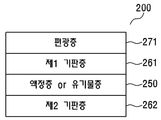
도 3b는 본 발명의 실시예에 따른 터치입력장치에 구비되는 디스플레이 패널의 단면도이다.
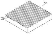
도 3c는 본 발명의 실시예에 따른 기판의 표면 구성을 설명하기 위해 참조되는 도면이다.
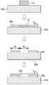
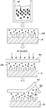
도 4는 본 발명의 실시예에 따른 터치입력장치 제조 방법에 대해 설명한다.
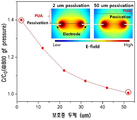
도 5는 보호층의 두께에 따른 정전용량 변화량을 나타내기 위한 모식도이고 도 6은 도 5의 원리가 나타난 그래프이다.
도 7은 압력 센서 사이의 거리 변화에 따른 정전용량 변화량을 나타내기 위한 모식도이고 도 8은 도 7의 원리가 나타난 그래프이다.
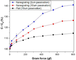
도 9는 본 발명의 실시예에 따라 나노 요철 구조의 기판을 이용하였을 경우, 민감도 향상을 나타내는 그래프이다.
도 10은 본 발명의 실시예에 따라 나노복합혼합물로 구성된 탄성 재질의 기판을 이용하였을 경우, 민감도 향상을 나타내는 그래프이다.
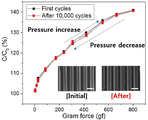
도 11은 본 발명의 실시예에 따른 기판을 포함하는 터치입력장치에 대해 가압을 반복적으로 수행하여 획득된 정전용량 값을 나타내는 그래프이다.1 is a view referred to for explaining the basic principle of driving a touch input device according to an embodiment of the present invention.
2 is a schematic diagram for showing an improved percolation effect when a touch pressure is applied to a touch input device according to an embodiment of the present invention.
3A is a cross-sectional view of a touch input device for describing a touch input device to which the above-described principle is applied in FIGS. 1 and 2.
3B is a cross-sectional view of a display panel provided in a touch input device according to an embodiment of the present invention.
3C is a view referred to for explaining the surface configuration of a substrate according to an embodiment of the present invention.
4 illustrates a method of manufacturing a touch input device according to an embodiment of the present invention.
5 is a schematic diagram for showing the amount of change in capacitance according to the thickness of the protective layer, and FIG. 6 is a graph showing the principle of FIG. 5.
FIG. 7 is a schematic diagram showing the amount of change in capacitance according to a change in distance between pressure sensors, and FIG. 8 is a graph showing the principle of FIG. 7.
9 is a graph showing an improvement in sensitivity when a nano-concave-structured substrate is used according to an embodiment of the present invention.
10 is a graph showing sensitivity improvement when a substrate made of an elastic material composed of a nanocomposite is used according to an embodiment of the present invention.
11 is a graph showing a capacitance value obtained by repeatedly performing pressurization on a touch input device including a substrate according to an embodiment of the present invention.
후술하는 본 발명에 대한 상세한 설명은, 본 발명이 실시될 수 있는 특정 실시예를 예시로서 도시하는 첨부 도면을 참조한다. 이들 실시예는 당업자가 본 발명을 실시할 수 있기에 충분하도록 상세히 설명된다. 본 발명의 다양한 실시예는 서로 다르지만 상호 배타적일 필요는 없음이 이해되어야 한다. 예를 들어, 여기에 기재되어 있는 특정 형상, 구조 및 특성은 일 실시예에 관련하여 본 발명의 정신 및 범위를 벗어나지 않으면서 다른 실시예로 구현될 수 있다. 또한, 각각의 개시된 실시예 내의 개별 구성요소의 위치 또는 배치는 본 발명의 정신 및 범위를 벗어나지 않으면서 변경될 수 있음이 이해되어야 한다. 따라서, 후술하는 상세한 설명은 한정적인 의미로서 취하려는 것이 아니며, 본 발명의 범위는, 적절하게 설명된다면, 그 청구항들이 주장하는 것과 균등한 모든 범위와 더불어 첨부된 청구항에 의해서만 한정된다. 도면에서 유사한 참조부호는 여러 측면에 걸쳐서 동일하거나 유사한 기능을 지칭한다.For a detailed description of the present invention, which will be described later, reference is made to the accompanying drawings that illustrate, by way of example, specific embodiments in which the invention may be practiced. These examples are described in detail enough to enable those skilled in the art to practice the present invention. It should be understood that the various embodiments of the present invention are different, but need not be mutually exclusive. For example, certain shapes, structures, and properties described herein may be implemented in other embodiments without departing from the spirit and scope of the invention in relation to one embodiment. In addition, it should be understood that the location or placement of individual components within each disclosed embodiment can be changed without departing from the spirit and scope of the invention. Therefore, the following detailed description is not intended to be taken in a limiting sense, and the scope of the present invention, if appropriately described, is limited only by the appended claims, along with all ranges equivalent to those claimed. In the drawings, similar reference numerals refer to the same or similar functions throughout several aspects.
이하, 첨부되는 도면을 참조하여 본 발명의 실시예에 따른 터치입력장치(1000)를 설명한다. 이하에서는 정전용량 방식의 터치 센서(미도시) 및 압력 센서(300)를 예시하나 임의의 방식으로 터치 위치 및/또는 터치 압력을 검출할 수 있는 터치 센서(미도시) 및 압력 센서(300)에도 본 발명이 동일/유사하게 적용될 수 있다.Hereinafter, a
도 1은 본 발명의 실시예에 따른 터치입력장치(1000)의 기본 원리를 설명하기 위해 참조되는 도면이다.1 is a view referred to for explaining the basic principle of the
도 1의 (a)에 도시한 바와 같이 일반적인 터치입력장치의 경우, 디스플레이 패널(200'), 디스플레이 패널(200')의 하부에 직접적으로 형성된 절연층(400B), 절연층(400B) 하부에 형성된 압력 센서(300')와 기판(400A)을 포함하여 구성될 수 있었다. 그리고 절연층(400B)은 유전율을 향상시키기 위한 나노 파티클(nano particle)들을 포함할 수 있었다. 그런데, 이런 구성에 따르면, 기판(400A)과 별도로 절연층(400B)이 구비되어야만 하므로 이는 터치입력장치의 제조 단가를 상승시키는 문제점이 있었다. 특히, 기판(400A)이 요철 구조이고 압력 센서(300')가 기판(400A)의 구조에 상응하여 동일한 요철 구조로 형성된 경우, 압력 센서(300')와 절연층(400B) 사이에는 별도의 에어갭이 존재하지 않음으로서, 디스플레이 패널에 대한 터치 압력 감도를 센싱하는 측면에서도 상대적으로 민감도가 떨어지는 문제점이 있었다. As shown in (a) of FIG. 1, in the case of a general touch input device, the display panel 200 ', the
따라서, 본 발명에서는 도 1의 (b)에 도시한 바와 같이, 절연층(400B)을 별도의 구성으로 배치하지 않고, 절연층(400B)을 구성하는 절연 물질과 나노 파티클등을 포함하는 구성물을 기판(400A)으로 통합함으로서 새로운 기판(400)을 제작하는 것을 주된 해결 과제로 하고자 한다. 새로운 기판(400)을 포함하는 본 발명의 실시예에 따른 터치입력장치(1000)에 따르면, 디스플레이 패널(200)의 하면에 압력 센서(300)가 직접적으로 부착되고, 압력 센서(300) 하부에 새로운 기판(400)이 부착되는 구성을 포함하는 것을 특징으로 한다. 이러한 터치입력장치(1000)에 따르면, 도 1의 (b)에 도시한 바와 같이, 별도의 절연층(400B) 구성물이 생략되어 제작 단가를 상당히 낮출 수 있을 뿐 아니라, 압력 센서(300)와 새로운 기판(400)사이(또는 디스플레이 패널(200)의 하면과 새로운 기판(400)사이)에는 별도의 에어갭이 존재할 수 있게 되어, 터치압력을 센싱하는 민감도가 향상될 수 있게 된다. 이는, 특히, 새로운 기판(400)이 요철 구조로 제작되고, 압력 센서(300)는 편평한 디스플레이 패널(200)의 하면에 형성된 것에 기인한 것으로서, 에어갭으로 인해 디스플레이 패널(200)에 가압 시 새로운 기판(400) 내부에 응력이 더욱 집중되고, 더 큰 변형이 가해질 수 있기 때문에, 새로운 기판(400)의 유연성이 커지고 민감도도 더욱 향상되는 효과를 가져올 수 있는 것이다. Accordingly, in the present invention, as shown in FIG. 1 (b), the
따라서, 이하에서는 도 1의 (b)와 같은 구조층을 갖는 터치입력장치(1000)에서 터치 압력을 센싱하는 원리와, 이러한 터치입력장치(1000)를 제조하는 방법에 대해 기술하고자 한다. 그리고, 이하에서는, 도 1의 (b)에 도시된 새로운 기판(400)을 기판(400)으로 정의하고자 한다.Therefore, hereinafter, the principle of sensing the touch pressure in the
도 2는 본 발명의 실시예에 따른 터치입력장치(1000)에 터치 압력이 가해진 경우, 향상된 삼투 효과(percolation effect)를 나타내기 위한 개략도이다. 2 is a schematic diagram for showing an improved percolation effect when a touch pressure is applied to the
도 2에 도시한 바와 같이, 디스플레이 패널(200)에 객체에 의한 터치 압력이 인가된 이후에는 디스플레이 패널(200)이 눌려지게 되므로 이에 따라 기판(400)도 변형되게 된다. 이 때, 기판(400)은 탄성 재질로 구성될 수 있으므로 비탄성 재질로 구성된 일반 기판에 비해 상대적으로 용이하게 변형될 수 있다. 변형된 기판(400)에 따르면, 기판(400) 내부의 단위 면적당 나노 파티클의 수가 증가된다. 이는 기판(400)의 유전율을 증가시키게 되고, 유전율이 증가되면 다수의 압력 센서(300) 중 서로 인접한 구동 센서와 수신 센서 사이의 정전용량이 증가시키게 된다. 기판(400)에 가해지는 외력의 크기가 커질수록 다수의 압력 센서(300) 중 서로 인접한 구동 센서와 수신 센서 사이의 정전용량도 증가하게 되는 것이다. As illustrated in FIG. 2, after the touch pressure by the object is applied to the
특히, 도 2에서는 디스플레이 패널(200)에 대한 가압으로 디스플레이 패널(200)과 기판(400)이 각각 수직 하강한 것을 도시하였으나, 본 발명의 권리범위는 이에 제한되지 않는다. 예를 들어, 동일한 터치 압력으로 디스플레이 패널(200)과 기판(400) 중 적어도 하나는 휘어질 수도 있으며, 또는, 동일한 터치 압력으로 디스플레이 패널(200)과 기판(400) 중 적어도 하나는 아래로 수직 하강할 수도 있다.In particular, in FIG. 2, the
도 3은 도 1 및 도 2에서 전술한 원리가 적용된 터치입력장치(1000)를 설명하기 위한 단면도이다.3 is a cross-sectional view illustrating the
도 3a에 도시한 바와 같이, 본 발명의 실시예에 따른 터치입력장치(1000)는 커버층(100), 디스플레이 패널(200), 그라운드층(G), 압력 센서(300), 보호층(310), 기판(400), 및 덮개층(410)을 포함할 수 있다.3A, the
커버층(100)은 유리 또는 플라스틱 재질일 수 있다. 커버층(100)은 투명 또는 반투명의 재질일 수 있으나, 이에 한정하는 것은 아니며 불투명한 재질일 수도 있다.The
커버층(100)의 상면으로 객체에 의한 터치 압력이 가해진다. 객체가 커버층(100)의 상면에 터치 압력을 인가하면, 커버층(100)은 상기 압력에 의해 휘어질 수 있다. 또는, 다른 실시예에 따라 아래로 수직 하강할 수도 있다.The touch pressure by the object is applied to the top surface of the
커버층(100)의 변형은 디스플레이 패널(200)의 변형을 야기한다. 또한, 이는 그라운드층(G)(뒤에서 상술하고자 한다) 및 기판(400) 중 적어도 하나의 변형을 야기한다. 그라운드층(G) 및 기판(400) 중 적어도 하나는 터치 압력에 의해 휘어지거나 아래로 수직 하강(또는 압축)할 수도 있다. 그리고, 커버층(100), 디스플레이 패널(200), 그라운드층(G), 및 기판(400) 중 적어도 하나는 각 표면의 일부 영역에 변형이 생길 수도 있고, 전체 영역에 변형이 생길 수도 있다.Deformation of the
즉, 가압으로 기판(400)이 압축되면, 기판(400)의 유전율을 향상시키게 되고, 기판(400)의 유전율 변화는 압력 센서(300)의 정전용량 값을 향상시키므로, 해당 변화량에 기초하여 민감도가 향상된 터치 압력을 검출할 수 있게 되는 것이다. 단, 이 때, 실시예에 따라 압력 센서(300)와 그라운드층(G) 사이의 거리 변화에 따른 정전용량 변화량 값은 '0'에 가깝도록 기판(400)의 두께를 두껍게 제조할 수 있다. 다시 말해, 본 발명에 따른 정전용량 변화량은 기판(400)의 유전율 변화에 의한 정전용량 변화량 값만으로 측정될 수 있다. That is, when the
디스플레이 패널(200)은 커버층(100) 하부에 배치된다. The
디스플레이 패널(200)은 액정표시장치(LCD: Liquid Crystal Display), PDP(Plasma Display Panel), 유기발광 표시장치(Organic Light Emitting Diode: OLED) 등으로 구현될 수 있다. The
예를 들어, 도 3b에 도시된 바와 같이, LCD 패널은 최상위층에 배치된 편광층(271) 및 최하위층에 배치된 제2기판(400)층(262)을 포함할 수 있다. 또한, LCD 패널인 디스플레이 패널(200)은 액정 셀(liquid crystal cell)을 포함하는 액정층(250), 액정층(250)의 상부에 배치되는 제1기판(400)층(261) 및 액정층(250)의 하부에 배치되는 제2기판(400)층(262)을 포함할 수 있다. 이때, 제1기판(400)층(261)은 컬러필터 글라스(color filter glass)일 수 있고, 제2기판(400)층(262)은 TFT 글라스(TFT glass)일 수 있다. 또한, 실시예에 따라 제1기판(400)층(261) 및 제2기판(400)층(262) 중 적어도 하나는 플라스틱과 같은 벤딩(bending) 가능한 물질로 형성될 수 있다. 도 3b에서 제2기판(400)층(262)은, 데이터 라인(data line), 게이트 라인(gate line), TFT, 공통 전극(Vcom: common electrode) 및 픽셀 전극(pixel electrode) 등을 포함하는 다양한 층으로 이루어질 수 있다.For example, as illustrated in FIG. 3B, the LCD panel may include a
또 다른 예로, 도 3b에 도시한 바와 같이, OLED 패널은 최상위층에 배치되는 편광층(271)을 포함할 수 있다. 또한, OLED(Organic Light-Emitting Diode)를 포함하는 유기물층(250), 유기물층(250)의 상부에 배치되는 제1기판(400)층(261) 및 유기물층(250) 하부에 배치되는 제2기판(400)층(262)을 포함할 수 있다. 이때, 제2기판(400)층(262)은 최하위층으로 배치될 수 있다. 제1기판(400)층(261)은 인캡 글라스(Encapsulation glass)일 수 있고, 제2기판(400)층(262)은 TFT 글라스(TFT glass)일 수 있다. 또한, 실시예에 따라 제1기판(400)층(261) 및 제2기판(400)층(262) 중 적어도 하나는 플라스틱과 같은 벤딩(bending) 가능한 물질로 형성될 수 있다. OLED 패널의 경우, 게이트 라인, 데이터 라인, 제1전원라인(ELVDD), 제2전원라인(ELVSS) 등의 디스플레이 패널(200)(200A)의 구동에 사용되는 전극을 포함할 수 있다. OLED(Organic Light-Emitting Diode) 패널은 형광 또는 인광 유기물 박막에 전류를 흘리면 전자와 정공이 유기물층에서 결합하면서 빛이 발생하는 원리를 이용한 자체 발광형 디스플레이 패널(200)로서, 발광층을 구성하는 유기물질이 빛의 색깔을 결정한다.As another example, as illustrated in FIG. 3B, the OLED panel may include a
도 3b의 디스플레이 패널(200)의 최하위층인 제2기판(400)층(262)는 유리 또는 플라스틱 재질일 수 있다.The
도 3b의 디스플레이 패널(200)이 OLED 패널인 경우, 제2기판(400)층(262)의 하면에 직접 압력 센서(300)를 형성할 수 있다. When the
도 3b의 디스플레이 패널(200)이 LCD 패널인 경우, 제2기판(400)층(262)의 하면에 직접 압력 센서(300)를 형성할 수 있다. 이 경우, LCD 패널을 구성하는 백라이트유닛(미도시)은 도 3a의 기판(400)이나 덮개층(410) 하부에 배치되도록 구현할 수도 있고, 또는 백라이트유닛(미도시)을 디스플레이 패널(200)의 최하위층으로 배치하여 압력 센서(300)가 백라이트유닛(미도시) 하면에 배치되도록 구현할 수도 있다. When the
디스플레이 패널(200)의 최하위층인 제2기판(400)층(262) 상에 압력 센서(300)를 형성하는 자세한 공정에 대해서는 후술한다.A detailed process of forming the
도 3a 및 도 3b에 도시하지 않았으나, 터치 센서(미도시)는 커버층(100), 디스플레이 패널(200)의 상부, 디스플레이 패널(200)의 내부 등에 형성되어 터치 위치를 감지할 수 있는 터치센서패널(미도시)을 구성할 수 있다.3A and 3B, a touch sensor (not shown) is formed on the
그라운드층(G)은 그라운드 전위를 갖는 층이다.The ground layer G is a layer having a ground potential.
그라운드층(G)은 다수의 압력 센서(300)로부터 소정 간격 이격되어 배치된다.The ground layer (G) is spaced apart from the
그라운드층(G)은 가압 객체가 손가락인 경우, 손가락으로 빠져나가는 전기장에 의해 베이스 정전용량이 변경될 수 있으므로, 터치 압력에 의한 정전용량 변화량만을 검출하려고 해도 일반 터치에 의한 영향까지 반영되어 검출값의 신뢰도가 떨어질 수 있는 문제점을 고려하여, 손가락에 의한 전기장 손실을 차단하는 역할을 할 수 있다.When the pressing object is a finger, the ground layer G may change the base capacitance by the electric field exiting with the finger, so even if only the amount of change in capacitance due to touch pressure is detected, the influence by the normal touch is reflected and detected. Considering a problem that the reliability of the device may be deteriorated, it may serve to block the loss of an electric field by a finger.
그라운드층(G)은 디스플레이 패널(200)에 배치될 수 있다. 구체적으로, 디스플레이 패널(200)의 상면이나 내부, 또는 하면에 배치될 수 있다. 또는, 다른 실시예에 따라 커버층(100)의 상면이나 내부, 또는 하면에 배치될 수도 있다. The ground layer G may be disposed on the
압력 센서(300)는 디스플레이 패널(200)의 하면에 형성될 수 있다. 구체적으로, 디스플레이 패널(200)을 구성하는 제2기판(400)층(262)의 하면에 직접 형성될 수 있다.The
복수의 압력 센서(300)는 디스플레이 패널(200)의 하면인 동일 평면에 형성될 수 있다.The plurality of
압력 센서(300)는 구동 신호가 입력되는 구동 센서와 감지 신호가 출력되는 수신 센서를 포함할 수 있다. 구동 센서와 수신 센서 사이의 상호 정전용량 변화량을 기초로 터치 압력을 검출할 수 있다. 다만, 다른 실시예에 따라 압력 센서(300)의 자기 정전용량 변화량을 기초로 터치 압력을 검출할 수도 있다. The
보호층(310)은 압력 센서(300)를 보호하기 위한 절연물질로 구성될 수 있다. The
보호층(310)은 압력 센서(300)를 전반적으로 커버하는 형태로 구현될 수 있다.The
보호층(310)은 압력 센서(300)의 산화를 방지할 수 있으며, 압력 센서(300)의 단차를 극복하기 위하여 압력 센서(300)를 전반적으로 커버하는 편평한 형태로 제작될 수 있다. The
보호층(310)은 디스플레이 패널(200)의 하면과 기판(400) 사이에 배치될 수 있다. The
압력 센서(300)와 보호층(310)은 편평한 디스플레이 패널(200)의 하면에 형성되어 편평한 형태로 제조될 수 있다.The
보호층(310)은 최대한 두께를 얇게 구현하는 것이 두껍게 구현하는 것보다 상대적으로 기판(400) 내부에 집적되는 전기장을 고밀도로 구현할 수 있게 한다. 따라서, 최대한 두께를 얇게 하는 것이 바람직하며, 바람직하게는 최소한의 두께가 500 nm 정도가 되도록 구현할 수 있다. 이는, 보호층의 두께가 500 nm 에도 미치지 못하면 보호층(310) 이 표면을 균일하게 덮지 못해 보호가 되지 못하는 영역이 있을 수도 있기 때문에, 이 점을 고려하여 최소한의 두께가 500nm 이상은 되어야 함을 의미한다. 이에 대한 상세한 설명은 후술한다.The
다만, 보호층(310)은 필수구성요소는 아니며, 실시예에 따라 보호층(310) 없이 터치입력장치(1000)가 제작될 수도 있다.However, the
기판(400)은 압력 센서(300)의 하부에 배치될 수 있다. 압력 센서(300)가 보호층(310)에 의해 커버되는 경우, 기판(400)은 보호층(310)의 하부에 배치될 수 있다. 보호층(310)과 기판(400)을 접착하기 위한 별도의 접착제가 포함될 수도 있다.The
기판(400)은 나노 파티클(nano particle)을 포함할 수 있다. 기판(400)은 베이스기판(400) 상에 소정의 나노 파티클과 인캡슐레이션(encapsulation) 물질로 구성된 나노복합혼합물을 침투시켜 제조될 수 있다. 인캡슐레이션(encapsulation) 물질은 PUA(Polyurethane Acrylate)일 수 있으나, 본 발명의 권리범위가 이에 제한되지는 않는다. 나노 파티클은 기판(400)의 유전율을 향상시키기 위한 은(Ag)등의 금속 물질일 수 있으나, 이에 제한되는 것은 아니다.The
기판(400)은 탄성 재질을 포함할 수 있다. 기판(400)은 터치 압력에 따라 플렉서블하게 변형될 수 있다. 탄성 재질을 포함하여 기판(400)이 압축되는 경우 보다 잘 변형이 되도록 하며 복원력도 우수하다. The
커버층(100)에 압력이 가해지면 기판(400)이 압축되기 때문에, 기판(400) 내부의 단위면적당 나노 파티클의 수가 증가된다. 이는 기판(400)의 유전율을 증가시키게 되고, 유전율이 증가되면 다수의 압력 센서(300) 중 서로 인접한 구동 센서와 수신 센서 사이의 정전용량이 증가된다. 기판(400)이 압축되는 정도가 클수록 다수의 압력 센서(300) 중 서로 인접한 구동 센서와 수신 센서 사이의 정전용량도 더욱 크게 증가한다. When the pressure is applied to the
기판(400)의 탄성력은 이러한 터치 압력을 감지하는 민감도를 더욱 향상시키게 된다.The elastic force of the
기판(400)의 상면은 돌출부(401)와 오목부(402)를 포함하는 요철 구조로 형성될 수 있다.The upper surface of the
기판(400)의 상면에 형성된 돌출부(401)의 폭이 나노미터 단위이고, 오목부(402)의 폭이 나노미터 단위일 수 있다. The width of the
도 3c와 같이 각 돌출부(401)와 각 오목부(402)는 동일 평면 상에서 동일 방향으로 연장되어 형성될 수 있다. As shown in Figure 3c, each
커버층(100)에 압력이 가해지는 경우, 돌출부(401)의 모서리 부분에서 응력(stress)이 증가할 수 있다. 돌출부(401)의 돌기 형상은 응력 집중 구조를 형성하며, 상기 응력 집중 구조를 통해 기판(400)의 상면에서의 빛의 반사를 감소시켜 투과도를 향상시킬 수 있다.When pressure is applied to the
기판(400)과 압력 센서(300) 사이에는 소정의 에어갭(air gap)이 형성될 수 있다. 이는 기판(400)이 요철 구조로 형성됨에 따른 것이며, 이러한 에어갭으로 인해 기판(400)이 압축되어 정전용량을 검출하기 위한 터치 압력의 민감도를 보다 향상시킬 수 있게 된다.A predetermined air gap may be formed between the
덮개층(410)은 기판(400)을 지지할 수 있다. The
덮개층(410)은 PET(polyethylene terephthalate) 으로 구성될 수 있다. 다만, 이에 한정되는 것은 아니다.The
이하, 도 4를 통해 본 발명의 실시예에 따른 터치입력장치(1000) 제조 방법에 대해 설명한다.Hereinafter, a method of manufacturing the
본 발명의 실시예에 따른 터치입력장치(1000)는 디스플레이 패널(200)의 상면에 압력 센서(300)를 형성하는 제1 공정을 수행하고, 이와 별도로 나노입자가 포함된 기판(400)을 제작하는 제2 공정을 수행하고, 디스플레이 패널(200)의 상면에 형성된 압력 센서(300)와 기판(400)을 서로 접착하는 제3 공정을 수행함으로서 제조될 수 있다.The
디스플레이 패널(200)의 상면에 압력 센서(300)를 형성하는 제1 공정은 스크린 인쇄(screen printing), 그라비아 코팅(gravure coating), 잉크젯 코팅(inkjet coating) 등을 이용하여 수행될 수 있다.The first process of forming the
도 4a는 스크린 인쇄를 예시한 것으로, 디스플레이 패널(200)의 상면에 마스크(mask)를 배치한 후, 롤러를 이용하여 전극을 도포하여 압력 센서(300)를 형성한 다음, 마스크를 제거한 이후 다시 압력 센서(300) 상에 보호층(310)(passivation layer)을 형성할 수 있다. 스크린 인쇄를 이용하여 압력 센서(300)를 형성할 경우, 압력 센서(300) 각각의 너비(W1)는 100㎛ 이상이 되도록 제작하고, 압력 센서(300)와 압력 센서(300) 사이의 간격(W2)은 5㎛ 이상이 되도록 제작할 수 있다.FIG. 4A illustrates screen printing, after placing a mask on the top surface of the
보호층(310)은 압력 센서(300)를 절연시키기 위한 절연 물질로 구성될 수 있다.The
보호층(310)은 압력 센서(300)의 산화를 방지할 수 있으며, 압력 센서(300)의 단차를 극복하기 위하여 압력 센서(300)를 전반적으로 커버하는 편평한 형태로 형성될 수 있다. The
나노입자가 포함된 기판(400)을 제작하는 제2 공정은 도 4b를 참조하여 설명한다.The second process of manufacturing the
(a) 우선, 인캡슐레이션 물질과 나노 파티클이 혼합된 나노복합화합물을 준비한다. (a) First, a nanocomposite compound in which an encapsulation material and nanoparticles are mixed is prepared.
(b) 그리고, 미리 준비한 베이스 기판(B) 상에 (a)에서 준비한 나노복합화합물을 침투시킨다. 베이스 기판(B)은 나노 요철 구조로 제작된 것일 수 있다. 베이스 기판(B)이 나노 요철 구조로 제작되어 있기 때문에, 베이스 기판(B)상면에 상응하여 형성된 나노복합화합물로 구성된 기판(400)도 나노 요철 구조로 제작될 수 있다. 베이스 기판(B)의 돌출부(401)는 기판(400)의 오목부(402)로 형성되고, 베이스 기판(B)의 오목부(402)는 기판(400)의 돌출부(401)로 형성되게 된다. (b) Then, the nanocomposite prepared in (a) is permeated on the previously prepared base substrate (B). The base substrate B may be made of a nano-concave-convex structure. Since the base substrate (B) is made of a nano-concave-convex structure, the
(c) 나노복합화합물로 구성된 기판(400) 상에 덮개층(410)을 형성하고 덮개층(410) 상에 UV 빔을 노출시켜 베이스 기판(B)으로부터 덮개층(410)을 분리시킨다. (c) The
제 1공정과 제2 공정이 각각 수행된 이후, 디스플레이 패널(200)을 반전시킨 다음, 디스플레이 패널(200)의 상면에 형성된 압력 센서(300)와 기판(400)을 서로 접착하는 제3 공정을 수행하여 도 3a와 같은 터치입력장치(1000)를 제조한다. 제3 공정을 통해 압력 센서(300)의 하부에 기판(400)이 배치된다. After the first process and the second process are respectively performed, the third process of inverting the
도 5는 보호층(310)의 두께에 따른 정전용량 변화량을 나타내기 위한 모식도이고 도 6은 도 5의 원리가 나타난 그래프이다.5 is a schematic diagram for showing the amount of change in capacitance according to the thickness of the
압력 센서(300) 사이에 형성되는 전기장은 압력 센서(300)가 형성된 디스플레이 패널(200)의 하면 근처에서 집중되고 하면에서 멀어질수록 전기장 세기가 약해지게 된다. 이 때, 도 5a와 같이 보호층(310)의 두께를 상대적으로 얇게 구현한 경우, 실질적으로 기판(400)을 통한 압력 센서(300) 사이의 전기장은 고밀도로 집적되게 되고, 이로서 압력에 따른 정전용량 변화량은 상대적으로 높아져 압력 검출 민감도가 향상되게 된다. 반면, 도 5b와 같이 보호층(310)의 두께를 상대적으로 두껍게 구현한 경우, 실질적으로 기판(400)을 통한 압력 센서(300) 사이의 전기장은 저밀도로 집적되게 되고, 이로서 압력에 따른 정전용량 변화량은 상대적으로 낮아져 압력 검출 민감도가 낮아지게 된다.The electric field formed between the
결과적으로, 보호층(310)이 없이 터치입력장치(1000)를 구현하는 것이 가장 바람직하다.As a result, it is most preferable to implement the
이는, 도 6의 그래프를 통해서도 확인할 수 있다.This can also be confirmed through the graph of FIG. 6.
즉, 보호층(310)의 두께가 얇을수록 상대적으로 높은 정전용량 변화량 값을 획득할 수 있고, 보호층(310)의 두께가 두꺼울수록 상대적으로 낮은 정전용량 변화량 값을 획득할 수 있게 된다.That is, as the thickness of the
다만, 보호층(310)은 전극을 보호하기 위해 필요할 수 있으므로, 터치입력장치(1000)에 배치되는 경우, 고민감도를 위해 약 500 nm 이상 약 2 μm 이하의 두께로 제작됨이 바람직하다. 다만, 본 발명의 권리범위가 이에 제한되지는 않는다. However, since the
도 7은 압력 센서(300) 사이의 거리 변화에 따른 정전용량 변화량을 나타내기 위한 모식도이고 도 8은 도 7의 원리가 나타난 그래프이다.7 is a schematic diagram for showing the amount of change in capacitance according to a change in distance between the
도 7a는 상대적으로 압력 센서(300) 사이의 거리가 짧은 것으로, 응력(stress)이 집중되는 디스플레이 패널(200)의 하면 근처(S)에서의 전기장 밀도가 상대적으로 높은 것을 알 수 있다. 반면 도 7b는 상대적으로 압력 센서(300) 사이의 거리가 먼 것으로, 이에 따르면, 응력(stress)이 집중되는 디스플레이 패널(200)의 하면 근처(S)에서의 전기장 밀도가 상대적으로 낮은 것을 알 수 있다.7A shows that the distance between the
즉, 도 7a와 같이 상대적으로 압력 센서(300) 사이의 거리를 짧게 구현하는 것이, 정전용량 변화량 검출 민감도를 향상시키는 것을 알 수 있다.That is, as shown in FIG. 7A, it can be seen that the relatively short distance between the
이는, 도 8의 그래프를 통해서도 확인할 수 있다.This can also be confirmed through the graph of FIG. 8.
도 8에 도시한 바와 같이, 동일한 압력(gramforce)을 인가한 경우, 압력 센서(300) 사이의 거리가 20㎛인 경우에 압력 센서(300) 사이의 거리가 300㎛인 경우보다 정전용량 변화량 검출 값이 보다 높은 것을 확인할 수 있다.As illustrated in FIG. 8, when the same pressure (gramforce) is applied, the amount of change in capacitance is detected when the distance between the
이 때, 압력 센서(300) 사이의 거리는 공정의 용이성을 고려하여 약 5 μm이상 약 300 
도 9는 본 발명의 실시예에 따라 나노 요철 구조의 기판(400)을 이용하였을 경우, 민감도 향상을 나타내는 그래프이다.9 is a graph showing an improvement in sensitivity when a
도 9에 도시한 바와 같이, 일반 편평한 기판(400)을 이용한 터치입력장치(1000)에 비해, 나노 요철 구조의 기판(400)을 이용한 터치입력장치(1000)의 경우, 정전용량 변화량 검출 값이 향상됨을 알 수 있다. 이는, 돌기부에 응력이 집중되기 때문이다. 또한, 이와 더불어, 전술한 바와 같이, 보호층(310)의 두께가 상대적으로 얇은 경우, 보호층(310)의 두께가 두꺼운 것에 비해 정전용량 변화량 검출 값이 향상됨을 알 수 있다.As shown in FIG. 9, in the case of the
도 10은 본 발명의 실시예에 따라 나노복합혼합물로 구성된 탄성 재질의 기판(400)을 이용하였을 경우, 민감도 향상을 나타내는 그래프이다.10 is a graph showing an improvement in sensitivity when a
도 10에 도시한 바와 같이, 일반 편평한 기판을 이용한 터치입력장치에 비해, 나노복합혼합물로 구성된 탄성 재질의 기판(400)을 이용한 터치입력장치(1000)의 경우, 정전용량 변화량 검출 값이 향상됨을 알 수 있다. 일반 편평한 기판은 단단하나 본 발명의 기판(400)은 영스 모듈(Young's Modulus)이 감소하게 되어 플렉서블하기 때문에 같은 터치 압력으로도 보다 더 잘 압축되기 때문이다. 또한, 전술한 바와 같이, 보호층(310)의 두께가 상대적으로 얇은 경우, 보호층(310)의 두께가 두꺼운 것에 비해 정전용량 변화량 검출 값이 향상됨을 알 수 있다.As shown in FIG. 10, in the case of the
이는 도 11과 같이 반복 테스트를 수행하여 획득된 정전용량 값을 기초로 또한 설명된다.This is also explained based on the capacitance value obtained by performing the repeat test as shown in FIG.
예를 들어, 도 11a와 같이 10000회 이상 반복하여 소정의 압력(예, 800gf)을 인가한 경우, 압력을 인가한 이후(Pressure)의 정전용량값과 압력을 해제한 이후(Release)의 정전용량값 각각은 소정의 낮은 오차범위(예를 들어 0.63% 미만) 내에서 획득되므로, 터치입력장치(1000)가 매우 안정적으로 구동됨을 알 수 있다.For example, when a predetermined pressure (eg, 800 gf) is applied repeatedly over 10000 times as shown in FIG. 11A, the capacitance value after pressure is applied (Pressure) and the capacitance after release of pressure (Release) Since each value is obtained within a predetermined low error range (for example, less than 0.63%), it can be seen that the
또한, 도 11b와 같이 소정의 압력(예, 800gf)을 인가하거나 해당 압력을 해제하는 작업을 10000회 이상 반복하였을 경우, 최초 싸이클과 비교하여 나노 요철 기판(400)의 형상이 거의 동일하게 유지되어 터치입력장치(1000)가 잘 동작함을 알 수 있다.In addition, when a predetermined pressure (eg, 800 gf) is applied or release of the pressure is repeated 10000 times or more, as shown in FIG. 11B, the shape of the nano-
결과적으로, 도 9 내지 도 11의 실험 결과 그래프를 통해, 본 발명의 터치입력장치(1000)의 압력 검출 민감도를 향상시키기 위해서는, 나노 요철 형상의 나노복합혼합물로 구성된 탄성 재질의 기판(400)을 이용하고, 상대적으로 얇은 두께의 보호층(310)을 이용하여 터치입력장치(1000)를 제조하는 것이 바람직함을 알 수 있다.As a result, through the experimental results graphs of FIGS. 9 to 11, in order to improve the pressure detection sensitivity of the
이상에서 실시예들에 설명된 특징, 구조, 효과 등은 본 발명의 하나의 실시예에 포함되며, 반드시 하나의 실시예에만 한정되는 것은 아니다. 나아가, 각 실시예에서 예시된 특징, 구조, 효과 등은 실시예들이 속하는 분야의 통상의 지식을 가지는 자에 의해 다른 실시예들에 대해서도 조합 또는 변형되어 실시 가능하다. 따라서 이러한 조합과 변형에 관계된 내용들은 본 발명의 범위에 포함되는 것으로 해석되어야 할 것이다.The features, structures, effects, etc. described in the above embodiments are included in one embodiment of the present invention, and are not necessarily limited to only one embodiment. Furthermore, features, structures, effects, and the like exemplified in each embodiment may be combined or modified for other embodiments by a person having ordinary knowledge in the field to which the embodiments belong. Therefore, the contents related to such combinations and modifications should be interpreted as being included in the scope of the present invention.
또한, 이상에서 실시예를 중심으로 설명하였으나 이는 단지 예시일 뿐 본 발명을 한정하는 것이 아니며, 본 발명이 속하는 분야의 통상의 지식을 가진 자라면 본 실시예의 본질적인 특성을 벗어나지 않는 범위에서 이상에 예시되지 않은 여러 가지의 변형과 응용이 가능함을 알 수 있을 것이다. 예를 들어, 실시예에 구체적으로 나타난 각 구성 요소는 변형하여 실시할 수 있는 것이다. 그리고 이러한 변형과 응용에 관계된 차이점들은 첨부된 청구 범위에서 규정하는 본 발명의 범위에 포함되는 것으로 해석되어야 할 것이다.In addition, although the embodiments have been mainly described above, these are merely examples and do not limit the present invention, and those skilled in the art to which the present invention pertains are exemplified above without departing from the essential characteristics of the present embodiment. It will be appreciated that various modifications and applications are possible. For example, each component specifically shown in the embodiments can be implemented by modification. And differences related to these modifications and applications should be construed as being included in the scope of the invention defined in the appended claims.
Claims (19)
상기 커버층 하부에 배치되는 디스플레이 패널;
상기 디스플레이 패널의 하부에 배치되어 상기 커버층에 가해지는 객체에 의한 터치 압력을 검출하기 위한 압력 센서; 및
상기 압력 센서의 하부에 배치되는 기판;을 포함하고,
상기 기판은 상기 기판의 유전율을 향상시키기 위한 소정의 나노입자를 포함하며,
상기 기판의 유전율 변화에 따른 상기 압력 센서의 정전용량 변화량을 기초로 상기 터치 압력을 검출하는,
터치입력장치.Cover layer;
A display panel disposed under the cover layer;
A pressure sensor disposed under the display panel to detect a touch pressure caused by an object applied to the cover layer; And
It includes; a substrate disposed under the pressure sensor;
The substrate includes predetermined nanoparticles to improve the dielectric constant of the substrate,
Detecting the touch pressure based on a change in capacitance of the pressure sensor according to a change in dielectric constant of the substrate,
Touch input device.
상기 압력 센서와 상기 기판 사이에는 소정의 에어갭(air gap)이 배치되는,
터치입력장치.According to claim 1,
A predetermined air gap is disposed between the pressure sensor and the substrate,
Touch input device.
상기 기판은 상기 터치 압력에 따라 플렉서블하게 변형되는 탄성 재질로 구현된,
터치입력장치.According to claim 1,
The substrate is made of an elastic material that is flexibly deformed according to the touch pressure,
Touch input device.
상기 터치 압력이 가해질 때 상기 객체에 의한 전기장 손실을 차단하기 위한 그라운드층을 더 포함하는,
터치입력장치.According to claim 1,
Further comprising a ground layer for blocking the electric field loss by the object when the touch pressure is applied,
Touch input device.
상기 터치 압력에 따라 상기 커버층, 상기 디스플레이 패널 및 상기 기판은 아래로 수직 하강하거나 휘어지는,
터치입력장치. According to claim 1,
According to the touch pressure, the cover layer, the display panel and the substrate vertically descend or bend downward,
Touch input device.
상기 기판은 상면이 돌출부와 오목부로 구성된 소정의 요철 형상으로 구현된,
터치입력장치.According to claim 1,
The substrate is implemented in a predetermined concavo-convex shape, the upper surface of which is composed of protrusions and recesses,
Touch input device.
상기 돌출부와 상기 오목부는 각 폭이 나노 미터 단위인,
터치입력장치.The method of claim 6,
Each of the protrusions and the recesses is nanometers in width.
Touch input device.
상기 압력 센서는 구동전극 및 수신전극을 포함하고,
상기 구동전극과 상기 수신전극 사이의 정전용량 변화량에 기초하여 상기 터치 압력을 검출하는,
터치입력장치.According to claim 1,
The pressure sensor includes a driving electrode and a receiving electrode,
Detecting the touch pressure based on the amount of change in capacitance between the driving electrode and the receiving electrode,
Touch input device.
유전율을 향상시키기 위한 소정의 나노입자를 포함하는 기판을 제조하는 단계;
상기 디스플레이 패널을 반전시키는 단계; 및
상기 압력 센서 하부에 상기 기판을 배치하는 단계;를 포함하는,
터치입력장치 제조 방법.Forming a pressure sensor for detecting a touch pressure on an upper surface of the display panel;
Manufacturing a substrate including predetermined nanoparticles for improving dielectric constant;
Inverting the display panel; And
Including; placing the substrate under the pressure sensor;
Method of manufacturing a touch input device.
상기 압력 센서 형성 단계는,
스크린 인쇄(screen printing), 그라비아 코팅(gravure coating), 잉크젯 코팅(inkjet coating) 등을 이용하여 상기 디스플레이 패널의 상면에 상기 압력 센서를 형성하는,
터치입력장치 제조 방법.The method of claim 9,
The pressure sensor forming step,
Forming the pressure sensor on the top surface of the display panel using screen printing, gravure coating, inkjet coating, etc.
Method of manufacturing a touch input device.
상기 압력 센서 형성 단계는,
상기 압력 센서 상에 상기 압력 센서를 절연시키기 위한 절연 물질로 구성된 보호층을 형성하는 단계;를 더 포함하는,
터치입력장치 제조 방법.The method of claim 10,
The pressure sensor forming step,
Further comprising a step of forming a protective layer made of an insulating material for insulating the pressure sensor on the pressure sensor;
Method of manufacturing a touch input device.
상기 기판 제조 단계는,
상기 기판과 다른 별도의 베이스기판 상에 상기 소정의 나노입자와 인캡슐레이션(encapsulation) 물질로 구성된 나노복합혼합물을 침투시켜 상기 기판을 형성하는 단계를 포함하고,
상기 기판 배치 단계는,
상기 기판 상에 덮개층을 접착하는 단계;
상기 베이스기판으로부터 상기 덮개층을 분리하는 단계; 및
상기 덮개층에 접착된 상기 기판을 상기 압력 센서 하부에 배치하는 단계;를 포함하는,
터치입력장치 제조 방법.The method of claim 9,
The substrate manufacturing step,
And forming a substrate by infiltrating the nanocomposite mixture composed of the predetermined nanoparticles and an encapsulation material on a separate base substrate from the substrate.
The substrate placement step,
Bonding a cover layer on the substrate;
Separating the cover layer from the base substrate; And
Including; placing the substrate bonded to the cover layer under the pressure sensor;
Method of manufacturing a touch input device.
상기 압력 센서와 상기 기판 사이에는 소정의 에어갭(air gap)이 배치되는,
터치입력장치 제조 방법.The method of claim 9,
A predetermined air gap is disposed between the pressure sensor and the substrate,
Method of manufacturing a touch input device.
상기 기판은 상기 터치 압력에 따라 변형되는 탄성 재질로 구현된,
터치입력장치 제조 방법.The method of claim 9,
The substrate is made of an elastic material that is deformed according to the touch pressure,
Method of manufacturing a touch input device.
상기 터치 압력이 가해질 때 상기 객체에 의한 전기장 손실을 차단하기 위한 그라운드층을 배치하는,
터치입력장치 제조 방법.The method of claim 9,
Arranging a ground layer for blocking electric field loss caused by the object when the touch pressure is applied,
Method of manufacturing a touch input device.
상기 터치 압력에 따라 상기 디스플레이 패널 및 상기 기판은 아래로 수직 하강하거나 휘어지는,
터치입력장치 제조 방법.The method of claim 9,
According to the touch pressure, the display panel and the substrate vertically descend or bend downward,
Method of manufacturing a touch input device.
상기 기판은 상면이 돌출부와 오목부로 구성된 소정의 요철 형상으로 구현된,
터치입력장치 제조 방법.The method of claim 9,
The substrate is implemented in a predetermined concavo-convex shape, the upper surface of which is composed of protrusions and recesses,
Method of manufacturing a touch input device.
상기 돌출부와 상기 오목부는 각 폭이 나노 미터 단위인,
터치입력장치 제조 방법.The method of claim 17,
Each of the protrusions and the recesses is nanometers in width.
Method of manufacturing a touch input device.
상기 압력 센서는 구동전극 및 수신전극을 포함하고,
상기 구동전극과 상기 수신전극 사이의 정전용량 변화량에 기초하여 상기 터치 압력을 검출하는,
터치입력장치 제조 방법.The method of claim 9,
The pressure sensor includes a driving electrode and a receiving electrode,
Detecting the touch pressure based on the amount of change in capacitance between the driving electrode and the receiving electrode,
Method of manufacturing a touch input device.
Priority Applications (1)
| Application Number | Priority Date | Filing Date | Title |
|---|---|---|---|
| KR1020180142000A KR102151986B1 (en) | 2018-11-16 | 2018-11-16 | Touch input apparatus and method for manufacturing the touch input apparatus |
Applications Claiming Priority (1)
| Application Number | Priority Date | Filing Date | Title |
|---|---|---|---|
| KR1020180142000A KR102151986B1 (en) | 2018-11-16 | 2018-11-16 | Touch input apparatus and method for manufacturing the touch input apparatus |
Publications (2)
| Publication Number | Publication Date |
|---|---|
| KR20200057504A true KR20200057504A (en) | 2020-05-26 |
| KR102151986B1 KR102151986B1 (en) | 2020-09-04 |
Family
ID=70915353
Family Applications (1)
| Application Number | Title | Priority Date | Filing Date |
|---|---|---|---|
| KR1020180142000A Active KR102151986B1 (en) | 2018-11-16 | 2018-11-16 | Touch input apparatus and method for manufacturing the touch input apparatus |
Country Status (1)
| Country | Link |
|---|---|
| KR (1) | KR102151986B1 (en) |
Citations (6)
| Publication number | Priority date | Publication date | Assignee | Title |
|---|---|---|---|---|
| KR20120006916A (en) * | 2010-07-13 | 2012-01-19 | 차승일 | Manufacturing method of printed circuit sticker and single layer metal touchpad |
| JP2012204170A (en) * | 2011-03-25 | 2012-10-22 | Sony Corp | Conductive element and its manufacturing method, wiring element, information input device, display device, electronic equipment, and stamper |
| US20140333579A1 (en) * | 2009-09-04 | 2014-11-13 | Peter Sleeman | Capacitive Control Panel |
| KR20160015924A (en) * | 2014-08-01 | 2016-02-15 | 주식회사 하이딥 | Touch input device |
| KR20170123961A (en) * | 2016-04-29 | 2017-11-09 | 박철 | Force Touch Glass with Pressure Sensitive Adhesive Film |
| KR20180058385A (en) * | 2016-11-24 | 2018-06-01 | 주식회사 하이딥 | Touch input device |
-
2018
- 2018-11-16 KR KR1020180142000A patent/KR102151986B1/en active Active
Patent Citations (6)
| Publication number | Priority date | Publication date | Assignee | Title |
|---|---|---|---|---|
| US20140333579A1 (en) * | 2009-09-04 | 2014-11-13 | Peter Sleeman | Capacitive Control Panel |
| KR20120006916A (en) * | 2010-07-13 | 2012-01-19 | 차승일 | Manufacturing method of printed circuit sticker and single layer metal touchpad |
| JP2012204170A (en) * | 2011-03-25 | 2012-10-22 | Sony Corp | Conductive element and its manufacturing method, wiring element, information input device, display device, electronic equipment, and stamper |
| KR20160015924A (en) * | 2014-08-01 | 2016-02-15 | 주식회사 하이딥 | Touch input device |
| KR20170123961A (en) * | 2016-04-29 | 2017-11-09 | 박철 | Force Touch Glass with Pressure Sensitive Adhesive Film |
| KR20180058385A (en) * | 2016-11-24 | 2018-06-01 | 주식회사 하이딥 | Touch input device |
Also Published As
| Publication number | Publication date |
|---|---|
| KR102151986B1 (en) | 2020-09-04 |
Similar Documents
| Publication | Publication Date | Title |
|---|---|---|
| KR102175810B1 (en) | Touch panel and manufacturing method thereof | |
| JP5689523B1 (en) | Touch panel with pressure detector | |
| EP2703963B1 (en) | Spacer-less input device | |
| JP5325646B2 (en) | Touch screen panel | |
| CN107145253B (en) | Force Sensing Architecture | |
| CN104423708B (en) | Touch window and touch device including touch window | |
| US9304630B2 (en) | Touch panel | |
| US10884557B2 (en) | Touch input device | |
| US10289224B2 (en) | Pressure sensing display and manufacturing method thereof | |
| US20120306777A1 (en) | Flexible touch screen panel | |
| US11449215B2 (en) | Touch input device having resizeable icons, and methods of using same | |
| KR20140062269A (en) | Flexible touch screen panel and flexible display device with the same | |
| KR20130008604A (en) | Methods and apparatus for a transparent and flexible force-sensitive touch panel | |
| CN106415462B (en) | touch window | |
| KR20170047426A (en) | Touch display device and method of manufacturing the same | |
| CN103902089A (en) | Touch structure and electronic product using same | |
| CN105320384B (en) | touch window | |
| KR20180007049A (en) | Display device | |
| KR102151986B1 (en) | Touch input apparatus and method for manufacturing the touch input apparatus | |
| KR20160018894A (en) | Touch screen panel having pressure sensor | |
| KR20120039884A (en) | Touch screen panel and fabricating method for the same | |
| KR20160092432A (en) | Touch window | |
| KR102330801B1 (en) | Touch input apparatus | |
| KR20150134010A (en) | Touch window | |
| KR20180113081A (en) | Touch panel |
Legal Events
| Date | Code | Title | Description |
|---|---|---|---|
| PA0109 | Patent application |
St.27 status event code: A-0-1-A10-A12-nap-PA0109 |
|
| PA0201 | Request for examination |
St.27 status event code: A-1-2-D10-D11-exm-PA0201 |
|
| R18-X000 | Changes to party contact information recorded |
St.27 status event code: A-3-3-R10-R18-oth-X000 |
|
| D13-X000 | Search requested |
St.27 status event code: A-1-2-D10-D13-srh-X000 |
|
| D14-X000 | Search report completed |
St.27 status event code: A-1-2-D10-D14-srh-X000 |
|
| PE0902 | Notice of grounds for rejection |
St.27 status event code: A-1-2-D10-D21-exm-PE0902 |
|
| E13-X000 | Pre-grant limitation requested |
St.27 status event code: A-2-3-E10-E13-lim-X000 |
|
| P11-X000 | Amendment of application requested |
St.27 status event code: A-2-2-P10-P11-nap-X000 |
|
| P13-X000 | Application amended |
St.27 status event code: A-2-2-P10-P13-nap-X000 |
|
| PN2301 | Change of applicant |
St.27 status event code: A-3-3-R10-R13-asn-PN2301 St.27 status event code: A-3-3-R10-R11-asn-PN2301 |
|
| PG1501 | Laying open of application |
St.27 status event code: A-1-1-Q10-Q12-nap-PG1501 |
|
| R18-X000 | Changes to party contact information recorded |
St.27 status event code: A-3-3-R10-R18-oth-X000 |
|
| E701 | Decision to grant or registration of patent right | ||
| PE0701 | Decision of registration |
St.27 status event code: A-1-2-D10-D22-exm-PE0701 |
|
| GRNT | Written decision to grant | ||
| PR0701 | Registration of establishment |
St.27 status event code: A-2-4-F10-F11-exm-PR0701 |
|
| PR1002 | Payment of registration fee |
St.27 status event code: A-2-2-U10-U11-oth-PR1002 Fee payment year number: 1 |
|
| PG1601 | Publication of registration |
St.27 status event code: A-4-4-Q10-Q13-nap-PG1601 |
|
| P22-X000 | Classification modified |
St.27 status event code: A-4-4-P10-P22-nap-X000 |
|
| R18-X000 | Changes to party contact information recorded |
St.27 status event code: A-5-5-R10-R18-oth-X000 |
|
| R18-X000 | Changes to party contact information recorded |
St.27 status event code: A-5-5-R10-R18-oth-X000 |
|
| PR1001 | Payment of annual fee |
St.27 status event code: A-4-4-U10-U11-oth-PR1001 Fee payment year number: 4 |
|
| PR1001 | Payment of annual fee |
St.27 status event code: A-4-4-U10-U11-oth-PR1001 Fee payment year number: 5 |
|
| PR1001 | Payment of annual fee |
St.27 status event code: A-4-4-U10-U11-oth-PR1001 Fee payment year number: 6 |
|
| U11 | Full renewal or maintenance fee paid |
Free format text: ST27 STATUS EVENT CODE: A-4-4-U10-U11-OTH-PR1001 (AS PROVIDED BY THE NATIONAL OFFICE) Year of fee payment: 6 |