KR20200050004A - Light emitting element structure and method of fabricating a light emitting element - Google Patents
Light emitting element structure and method of fabricating a light emitting element Download PDFInfo
- Publication number
- KR20200050004A KR20200050004A KR1020180131072A KR20180131072A KR20200050004A KR 20200050004 A KR20200050004 A KR 20200050004A KR 1020180131072 A KR1020180131072 A KR 1020180131072A KR 20180131072 A KR20180131072 A KR 20180131072A KR 20200050004 A KR20200050004 A KR 20200050004A
- Authority
- KR
- South Korea
- Prior art keywords
- layer
- rod
- light emitting
- semiconductor
- emitting device
- Prior art date
Links
Images


Classifications
-
- H—ELECTRICITY
- H01—ELECTRIC ELEMENTS
- H01L—SEMICONDUCTOR DEVICES NOT COVERED BY CLASS H10
- H01L33/00—Semiconductor devices with at least one potential-jump barrier or surface barrier specially adapted for light emission; Processes or apparatus specially adapted for the manufacture or treatment thereof or of parts thereof; Details thereof
- H01L33/005—Processes
- H01L33/0093—Wafer bonding; Removal of the growth substrate
-
- H—ELECTRICITY
- H01—ELECTRIC ELEMENTS
- H01L—SEMICONDUCTOR DEVICES NOT COVERED BY CLASS H10
- H01L33/00—Semiconductor devices with at least one potential-jump barrier or surface barrier specially adapted for light emission; Processes or apparatus specially adapted for the manufacture or treatment thereof or of parts thereof; Details thereof
- H01L33/005—Processes
- H01L33/0095—Post-treatment of devices, e.g. annealing, recrystallisation or short-circuit elimination
-
- H—ELECTRICITY
- H01—ELECTRIC ELEMENTS
- H01L—SEMICONDUCTOR DEVICES NOT COVERED BY CLASS H10
- H01L27/00—Devices consisting of a plurality of semiconductor or other solid-state components formed in or on a common substrate
- H01L27/15—Devices consisting of a plurality of semiconductor or other solid-state components formed in or on a common substrate including semiconductor components with at least one potential-jump barrier or surface barrier specially adapted for light emission
- H01L27/153—Devices consisting of a plurality of semiconductor or other solid-state components formed in or on a common substrate including semiconductor components with at least one potential-jump barrier or surface barrier specially adapted for light emission in a repetitive configuration, e.g. LED bars
- H01L27/156—Devices consisting of a plurality of semiconductor or other solid-state components formed in or on a common substrate including semiconductor components with at least one potential-jump barrier or surface barrier specially adapted for light emission in a repetitive configuration, e.g. LED bars two-dimensional arrays
-
- H—ELECTRICITY
- H01—ELECTRIC ELEMENTS
- H01L—SEMICONDUCTOR DEVICES NOT COVERED BY CLASS H10
- H01L33/00—Semiconductor devices with at least one potential-jump barrier or surface barrier specially adapted for light emission; Processes or apparatus specially adapted for the manufacture or treatment thereof or of parts thereof; Details thereof
- H01L33/0004—Devices characterised by their operation
- H01L33/0008—Devices characterised by their operation having p-n or hi-lo junctions
-
- H—ELECTRICITY
- H01—ELECTRIC ELEMENTS
- H01L—SEMICONDUCTOR DEVICES NOT COVERED BY CLASS H10
- H01L33/00—Semiconductor devices with at least one potential-jump barrier or surface barrier specially adapted for light emission; Processes or apparatus specially adapted for the manufacture or treatment thereof or of parts thereof; Details thereof
- H01L33/02—Semiconductor devices with at least one potential-jump barrier or surface barrier specially adapted for light emission; Processes or apparatus specially adapted for the manufacture or treatment thereof or of parts thereof; Details thereof characterised by the semiconductor bodies
- H01L33/20—Semiconductor devices with at least one potential-jump barrier or surface barrier specially adapted for light emission; Processes or apparatus specially adapted for the manufacture or treatment thereof or of parts thereof; Details thereof characterised by the semiconductor bodies with a particular shape, e.g. curved or truncated substrate
- H01L33/22—Roughened surfaces, e.g. at the interface between epitaxial layers
-
- H—ELECTRICITY
- H01—ELECTRIC ELEMENTS
- H01L—SEMICONDUCTOR DEVICES NOT COVERED BY CLASS H10
- H01L33/00—Semiconductor devices with at least one potential-jump barrier or surface barrier specially adapted for light emission; Processes or apparatus specially adapted for the manufacture or treatment thereof or of parts thereof; Details thereof
- H01L33/02—Semiconductor devices with at least one potential-jump barrier or surface barrier specially adapted for light emission; Processes or apparatus specially adapted for the manufacture or treatment thereof or of parts thereof; Details thereof characterised by the semiconductor bodies
- H01L33/20—Semiconductor devices with at least one potential-jump barrier or surface barrier specially adapted for light emission; Processes or apparatus specially adapted for the manufacture or treatment thereof or of parts thereof; Details thereof characterised by the semiconductor bodies with a particular shape, e.g. curved or truncated substrate
- H01L33/24—Semiconductor devices with at least one potential-jump barrier or surface barrier specially adapted for light emission; Processes or apparatus specially adapted for the manufacture or treatment thereof or of parts thereof; Details thereof characterised by the semiconductor bodies with a particular shape, e.g. curved or truncated substrate of the light emitting region, e.g. non-planar junction
-
- H—ELECTRICITY
- H01—ELECTRIC ELEMENTS
- H01L—SEMICONDUCTOR DEVICES NOT COVERED BY CLASS H10
- H01L33/00—Semiconductor devices with at least one potential-jump barrier or surface barrier specially adapted for light emission; Processes or apparatus specially adapted for the manufacture or treatment thereof or of parts thereof; Details thereof
- H01L33/44—Semiconductor devices with at least one potential-jump barrier or surface barrier specially adapted for light emission; Processes or apparatus specially adapted for the manufacture or treatment thereof or of parts thereof; Details thereof characterised by the coatings, e.g. passivation layer or anti-reflective coating
-
- H—ELECTRICITY
- H01—ELECTRIC ELEMENTS
- H01L—SEMICONDUCTOR DEVICES NOT COVERED BY CLASS H10
- H01L33/00—Semiconductor devices with at least one potential-jump barrier or surface barrier specially adapted for light emission; Processes or apparatus specially adapted for the manufacture or treatment thereof or of parts thereof; Details thereof
- H01L33/48—Semiconductor devices with at least one potential-jump barrier or surface barrier specially adapted for light emission; Processes or apparatus specially adapted for the manufacture or treatment thereof or of parts thereof; Details thereof characterised by the semiconductor body packages
- H01L33/50—Wavelength conversion elements
-
- H—ELECTRICITY
- H01—ELECTRIC ELEMENTS
- H01L—SEMICONDUCTOR DEVICES NOT COVERED BY CLASS H10
- H01L33/00—Semiconductor devices with at least one potential-jump barrier or surface barrier specially adapted for light emission; Processes or apparatus specially adapted for the manufacture or treatment thereof or of parts thereof; Details thereof
- H01L33/48—Semiconductor devices with at least one potential-jump barrier or surface barrier specially adapted for light emission; Processes or apparatus specially adapted for the manufacture or treatment thereof or of parts thereof; Details thereof characterised by the semiconductor body packages
- H01L33/52—Encapsulations
- H01L33/56—Materials, e.g. epoxy or silicone resin
-
- H—ELECTRICITY
- H01—ELECTRIC ELEMENTS
- H01L—SEMICONDUCTOR DEVICES NOT COVERED BY CLASS H10
- H01L25/00—Assemblies consisting of a plurality of individual semiconductor or other solid state devices ; Multistep manufacturing processes thereof
- H01L25/03—Assemblies consisting of a plurality of individual semiconductor or other solid state devices ; Multistep manufacturing processes thereof all the devices being of a type provided for in the same subgroup of groups H01L27/00 - H01L33/00, or in a single subclass of H10K, H10N, e.g. assemblies of rectifier diodes
- H01L25/04—Assemblies consisting of a plurality of individual semiconductor or other solid state devices ; Multistep manufacturing processes thereof all the devices being of a type provided for in the same subgroup of groups H01L27/00 - H01L33/00, or in a single subclass of H10K, H10N, e.g. assemblies of rectifier diodes the devices not having separate containers
- H01L25/075—Assemblies consisting of a plurality of individual semiconductor or other solid state devices ; Multistep manufacturing processes thereof all the devices being of a type provided for in the same subgroup of groups H01L27/00 - H01L33/00, or in a single subclass of H10K, H10N, e.g. assemblies of rectifier diodes the devices not having separate containers the devices being of a type provided for in group H01L33/00
- H01L25/0753—Assemblies consisting of a plurality of individual semiconductor or other solid state devices ; Multistep manufacturing processes thereof all the devices being of a type provided for in the same subgroup of groups H01L27/00 - H01L33/00, or in a single subclass of H10K, H10N, e.g. assemblies of rectifier diodes the devices not having separate containers the devices being of a type provided for in group H01L33/00 the devices being arranged next to each other
-
- H—ELECTRICITY
- H01—ELECTRIC ELEMENTS
- H01L—SEMICONDUCTOR DEVICES NOT COVERED BY CLASS H10
- H01L2933/00—Details relating to devices covered by the group H01L33/00 but not provided for in its subgroups
- H01L2933/0008—Processes
- H01L2933/0016—Processes relating to electrodes
-
- H—ELECTRICITY
- H01—ELECTRIC ELEMENTS
- H01L—SEMICONDUCTOR DEVICES NOT COVERED BY CLASS H10
- H01L2933/00—Details relating to devices covered by the group H01L33/00 but not provided for in its subgroups
- H01L2933/0008—Processes
- H01L2933/0025—Processes relating to coatings
-
- H—ELECTRICITY
- H01—ELECTRIC ELEMENTS
- H01L—SEMICONDUCTOR DEVICES NOT COVERED BY CLASS H10
- H01L2933/00—Details relating to devices covered by the group H01L33/00 but not provided for in its subgroups
- H01L2933/0008—Processes
- H01L2933/0033—Processes relating to semiconductor body packages
- H01L2933/005—Processes relating to semiconductor body packages relating to encapsulations
-
- H—ELECTRICITY
- H01—ELECTRIC ELEMENTS
- H01L—SEMICONDUCTOR DEVICES NOT COVERED BY CLASS H10
- H01L33/00—Semiconductor devices with at least one potential-jump barrier or surface barrier specially adapted for light emission; Processes or apparatus specially adapted for the manufacture or treatment thereof or of parts thereof; Details thereof
- H01L33/005—Processes
- H01L33/0062—Processes for devices with an active region comprising only III-V compounds
- H01L33/0066—Processes for devices with an active region comprising only III-V compounds with a substrate not being a III-V compound
- H01L33/007—Processes for devices with an active region comprising only III-V compounds with a substrate not being a III-V compound comprising nitride compounds
-
- H—ELECTRICITY
- H01—ELECTRIC ELEMENTS
- H01L—SEMICONDUCTOR DEVICES NOT COVERED BY CLASS H10
- H01L33/00—Semiconductor devices with at least one potential-jump barrier or surface barrier specially adapted for light emission; Processes or apparatus specially adapted for the manufacture or treatment thereof or of parts thereof; Details thereof
- H01L33/02—Semiconductor devices with at least one potential-jump barrier or surface barrier specially adapted for light emission; Processes or apparatus specially adapted for the manufacture or treatment thereof or of parts thereof; Details thereof characterised by the semiconductor bodies
- H01L33/16—Semiconductor devices with at least one potential-jump barrier or surface barrier specially adapted for light emission; Processes or apparatus specially adapted for the manufacture or treatment thereof or of parts thereof; Details thereof characterised by the semiconductor bodies with a particular crystal structure or orientation, e.g. polycrystalline, amorphous or porous
- H01L33/18—Semiconductor devices with at least one potential-jump barrier or surface barrier specially adapted for light emission; Processes or apparatus specially adapted for the manufacture or treatment thereof or of parts thereof; Details thereof characterised by the semiconductor bodies with a particular crystal structure or orientation, e.g. polycrystalline, amorphous or porous within the light emitting region
-
- H—ELECTRICITY
- H01—ELECTRIC ELEMENTS
- H01L—SEMICONDUCTOR DEVICES NOT COVERED BY CLASS H10
- H01L33/00—Semiconductor devices with at least one potential-jump barrier or surface barrier specially adapted for light emission; Processes or apparatus specially adapted for the manufacture or treatment thereof or of parts thereof; Details thereof
- H01L33/36—Semiconductor devices with at least one potential-jump barrier or surface barrier specially adapted for light emission; Processes or apparatus specially adapted for the manufacture or treatment thereof or of parts thereof; Details thereof characterised by the electrodes
- H01L33/38—Semiconductor devices with at least one potential-jump barrier or surface barrier specially adapted for light emission; Processes or apparatus specially adapted for the manufacture or treatment thereof or of parts thereof; Details thereof characterised by the electrodes with a particular shape
Abstract
Description
본 발명은 발광 소자의 제조방법에 관한 것으로, 더욱 상세하게는 발광 소자의 제조 시, 발광 소자가 식각액에 의해 손상되는 것을 방지하는 유기물 보호막을 포함하는 발광 소자 구조물 및 발광 소자의 제조방법 에 관한 것이다.The present invention relates to a method of manufacturing a light emitting device, and more particularly, to a light emitting device structure and a method of manufacturing the light emitting device including an organic protective film that prevents the light emitting device from being damaged by an etchant when manufacturing the light emitting device .
표시 장치는 멀티미디어의 발달과 함께 그 중요성이 증대되고 있다. 이에 부응하여 유기발광 표시 장치(Organic Light Emitting Display, OLED), 액정 표시 장치(Liquid Crystal Display, LCD) 등과 같은 여러 종류의 표시 장치가 사용되고 있다. The importance of the display device is increasing with the development of multimedia. In response to this, various types of display devices such as an organic light emitting display (OLED) and a liquid crystal display (LCD) have been used.
표시 장치의 화상을 표시하는 장치로서 유기 발광 표시 패널이나 액정 표시 패널과 같은 표시 패널을 포함한다. 그 중, 발광 표시 패널로써, 발광 소자를 포함할 수 있는데, 예를 들어 발광 다이오드(Light Emitting Diode, LED)의 경우, 유기물을 형광 물질로 이용하는 유기 발광 다이오드(OLED), 무기물을 형광물질로 이용하는 무기 발광 다이오드 등이 있다. A device for displaying an image of a display device includes a display panel such as an organic light emitting display panel or a liquid crystal display panel. Among them, as a light emitting display panel, a light emitting device may be included. For example, in the case of a light emitting diode (LED), an organic light emitting diode (OLED) using an organic material as a fluorescent material, and an inorganic material as a fluorescent material And inorganic light emitting diodes.
유기 발광 다이오드(OLED)의 경우, 발광 소자의 형광물질로 유기물을 이용하는 것으로, 제조공정이 간단하며 표시 소자가 플렉서블한 특성을 가질 수 있는 장점이 있다. 그러나, 유기물은 고온의 구동환경에 취약한 점, 청색 광의 효율이 상대적으로 낮은 것으로 알려져 있다. In the case of an organic light emitting diode (OLED), an organic material is used as a fluorescent material of a light emitting device, and the manufacturing process is simple and the display device has flexible characteristics. However, it is known that the organic material is vulnerable to a high-temperature driving environment, and the efficiency of blue light is relatively low.
반면에, 무기 발광 다이오드의 경우, 형광물질로 무기물 반도체를 이용하여, 고온의 환경에서도 내구성을 가지며, 유기 발광 다이오드에 비해 청색 광의 효율이 높은 장점이 있다. 또한, 기존의 무기 발광 다이오드 소자의 한계로 지적되었던 제조 공정에 있어서도, 유전영동(Dielectrophoresis, DEP)법을 이용한 전사방법이 개발되었다. 이에 유기 발광 다이오드에 비해 내구성 및 효율이 우수한 무기 발광 다이오드에 대한 연구가 지속되고 있다.On the other hand, in the case of an inorganic light emitting diode, an inorganic semiconductor is used as a fluorescent material, so it has durability even in a high temperature environment, and has an advantage of high blue light efficiency compared to an organic light emitting diode. In addition, in the manufacturing process, which was pointed out as a limitation of the existing inorganic light emitting diode device, a transfer method using a dielectrophoresis (DEP) method has been developed. Accordingly, research on inorganic light emitting diodes having superior durability and efficiency has been continued.
무기 발광 다이오드는 기판상에 n형 또는 p형으로 도핑(dopping)된 반도체층과 무기물 형광물질층을 성장시키고, 특정 형태를 가진 로드(rod)를 형성한 뒤 이를 분리하는 방법으로 제조될 수 있다. 다만, 로드를 분리할 때 화학적 분리방법(Chemical lift off, CLO)을 이용할 경우, 분리층을 제거하기 위한 식각액에 의해 로드의 외주면과 양 단의 전극이 손상되는 문제가 있었다. The inorganic light emitting diode can be manufactured by growing a semiconductor layer and an inorganic fluorescent material layer doped with n-type or p-type on a substrate, forming a rod having a specific shape, and separating it. . However, when using the chemical separation method (Chemical lift off, CLO) when separating the rod, there was a problem that the electrodes on both the outer circumferential surface of the rod and the electrode at both ends are damaged by an etchant for removing the separation layer.
따라서, 본 발명이 해결하고자 하는 과제는 반도체 로드의 외주면 또는 전극에 가해지는 손상을 최소화하는 발광 소자의 제조 방법을 제공하는 것이다. Accordingly, an object of the present invention is to provide a method of manufacturing a light emitting device that minimizes damage to an outer circumferential surface or an electrode of a semiconductor rod.
또한, 본 발명은 복수의 발광 소자를 포함하고, 발광 소자들이 외부와 접촉하지 않도록 이들을 보호하는 로드 보호층을 포함하는 발광 소자 구조물을 제공하는 것이다.In addition, the present invention provides a light emitting device structure including a plurality of light emitting devices, and a rod protection layer protecting the light emitting devices from contact with the outside.
본 발명의 과제들은 이상에서 언급한 과제로 제한되지 않으며, 언급되지 않은 또 다른 기술적 과제들은 아래의 기재로부터 당업자에게 명확하게 이해될 수 있을 것이다.The problems of the present invention are not limited to the problems mentioned above, and other technical problems that are not mentioned will be clearly understood by those skilled in the art from the following description.
상기 과제를 해결하기 위한 일 실시예에 따른 발광 소자의 제조 방법은 기판과 상기 기판 상에 형성되는 분리층을 포함하는 하부 기판 및 상기 분리층 상에 형성되는 적어도 하나의 반도체 로드를 준비하는 단계, 상기 분리층 상에서 상기 반도체 로드들을 감싸도록 형성되는 로드 보호층 및 상기 로드 보호층 상의 적어도 일부에 형성되는 보조층을 포함하는 로드 구조물을 형성하는 단계 및 상기 분리층을 제거하여 상기 로드 구조물을 상기 하부기판으로부터 분리한 뒤, 상기 로드 구조물에서 상기 반도체 로드를 분리하는 단계를 포함할 수 있다.A method of manufacturing a light emitting device according to an embodiment for solving the above problems includes preparing a lower substrate including a substrate and a separation layer formed on the substrate and at least one semiconductor rod formed on the separation layer, Forming a rod structure including a rod protective layer formed to surround the semiconductor rods on the separation layer and an auxiliary layer formed on at least a portion of the rod protection layer, and removing the separation layer to remove the load structure from the lower structure After separating from the substrate, the method may include separating the semiconductor rod from the rod structure.
상기 로드 구조물을 분리하는 단계에서, 상기 분리층은 분리용 식각액에 의해 식각되어 제거되되, 상기 로드 보호층은 상기 분리용 식각액과 반응하지 않을 수 있다.In the step of separating the rod structure, the separation layer is etched and removed by an etchant for separation, but the rod protection layer may not react with the etchant for separation.
상기 분리용 식각액은 불소(F)를 함유하는 물질을 포함하고, 상기 로드 보호층은 상기 분리용 식각액에 불용성인 유기물을 포함할 수 있다.The separation etchant may include a material containing fluorine (F), and the rod protective layer may include an organic material insoluble in the separation etchant.
상기 로드 구조물을 형성하는 단계에서, 상기 로드 보호층은 상기 반도체 로드 상에 상기 유기물을 코팅하여 형성될 수 있다.In the step of forming the rod structure, the rod protective layer may be formed by coating the organic material on the semiconductor rod.
상기 로드 보호층의 상기 유기물은 폴리메틸메타크릴레이트(Poly methyl methacrylate, PMMA), 포토레지스트(Photoresist, PR), 폴리(3,4-에틸렌디옥시싸이오펜) 폴리스티렌 설포네이트(Poly-(3,4-ethylenedioxy thiophene) polystyrene sulfonate, PEDOT:PSS) 중 적어도 어느 하나를 포함할 수 있다.The organic material of the rod protective layer is polymethyl methacrylate (PMMA), photoresist (PR), poly (3,4-ethylenedioxythiophene) polystyrene sulfonate (Poly- (3, 4-ethylenedioxy thiophene) polystyrene sulfonate, PEDOT: PSS).
상기 반도체 로드를 분리하는 단계는, 상기 보조층을 상기 로드 보호층으로부터 제거하는 단계, 상기 로드 보호층의 상기 유기물을 용매에 용해시키는 단계 및 상기 용매에 용해된 상기 유기물을 제거하는 단계를 포함할 수 있다.Separating the semiconductor rod may include removing the auxiliary layer from the rod protective layer, dissolving the organic substance in the rod protective layer in a solvent, and removing the organic substance dissolved in the solvent. Can be.
상기 용매에 용해된 유기물을 제거하는 단계는 상기 유기물을 열처리하여 휘발시키는 단계를 포함할 수 있다.The step of removing the organic substance dissolved in the solvent may include the step of volatilizing the organic substance by heat treatment.
상기 반도체 로드를 준비하는 단계에서, 상기 분리층은 일부 영역이 함몰된 적어도 하나의 홈부 및 상기 홈부가 이격되어 형성되는 돌출부를 포함하는 요철패턴이 형성될 수 있다.In the step of preparing the semiconductor rod, the separation layer may be formed with an uneven pattern including at least one groove portion in which a partial region is recessed and a protrusion formed by separating the groove portion.
상기 로드 구조물을 형성하는 단계에서, 상기 로드 보호층은 상기 분리층의 상기 돌출부을 감싸며 상기 홈부의 상면에 접촉하도록 형성될 수 있다.In the step of forming the rod structure, the rod protection layer may be formed to surround the protrusion of the separation layer and contact the upper surface of the groove.
상기 반도체 로드는 상기 로드 보호층 내에서 일 단부는 상기 로드 보호층의 일 면을 향하고, 상기 일 단부의 반대편 타 단부는 상기 로드 보호층의 상기 일 면에 대향하는 타 면을 향하도록 배열될 수 있다.The semiconductor rod may be arranged such that one end in the rod protective layer faces one side of the rod protective layer, and the other end opposite to the one end faces the other side opposite the one side of the rod protective layer. have.
상기 반도체 로드의 상기 타 단부는 상기 분리층의 상기 돌출부와 접촉할 수 있다.The other end of the semiconductor rod may contact the protrusion of the separation layer.
상기 적어도 하나의 반도체 로드들은 상기 로드 보호층의 상기 일 면에 수직한 방향으로 배열될 수 있다.The at least one semiconductor rod may be arranged in a direction perpendicular to the one surface of the rod protection layer.
상기 반도체 로드는, 제1 도전형 반도체, 활성층 및 상기 제1 도전형 반도체와 다른 극성을 갖는 제2 도전형 반도체를 포함하는 반도체 결정 및 상기 반도체 결정의 외주면을 둘러싸는 절연막을 포함할 수 있다.The semiconductor rod may include a first conductive semiconductor, an active layer, and a semiconductor crystal including a second conductive semiconductor having a different polarity from the first conductive semiconductor, and an insulating layer surrounding an outer peripheral surface of the semiconductor crystal.
상기 보조층은 상기 반도체 로드의 일 단부가 향하는 상기 일 면 상에 형성될 수 있다.The auxiliary layer may be formed on the one surface facing one end of the semiconductor rod.
상기 과제를 해결하기 위한 다른 실시예에 따른 발광 소자 구조물은 불소(F)를 함유하는 식각액에 불용성인 유기물을 포함하는 유기보호필름, 상기 유기보호필름 내에 배치되며 상기 유기보호필름의 일 면과 평행한 방향으로 서로 이격되어 배열되는 적어도 하나의 반도체 로드 및 상기 유기보호필름 상의 적어도 일부에 형성되는 보조층을 포함할 수 있다.The light emitting device structure according to another embodiment for solving the above problems is an organic protective film containing an organic material insoluble in an etchant containing fluorine (F), disposed in the organic protective film and parallel to one surface of the organic protective film It may include at least one semiconductor rod spaced apart from each other in one direction and an auxiliary layer formed on at least a portion of the organic protective film.
상기 유기보호필름의 상기 유기물은 폴리메틸메타크릴레이트(Poly methyl methacrylate, PMMA), 포토레지스트(Photoresist, PR), 폴리(3,4-에틸렌디옥시싸이오펜) 폴리스티렌 설포네이트(Poly-(3,4-ethylenedioxy thiophene) polystyrene sulfonate, PEDOT:PSS) 중 적어도 어느 하나를 포함할 수 있다.The organic material of the organic protective film is polymethyl methacrylate (PMMA), photoresist (PR), poly (3,4-ethylenedioxythiophene) polystyrene sulfonate (Poly- (3, 4-ethylenedioxy thiophene) polystyrene sulfonate, PEDOT: PSS).
상기 유기보호필름의 상기 일 면은 실질적으로 평탄하고, 상기 일 면에 대향하며 상기 보조층이 형성되지 않는 타 면은 상기 반도체 로드와 중첩되는 영역이 함몰되어 형성된 적어도 하나의 함몰부를 포함할 수 있다.The one surface of the organic protective film is substantially flat, and the other surface opposite to the one surface and on which the auxiliary layer is not formed may include at least one depression formed by depression of an area overlapping the semiconductor rod. .
상기 반도체 로드는 장축이 상기 유기보호필름의 상기 일 면과 수직한 방향으로 연장된 형태를 가질 수 있다.The semiconductor rod may have a shape in which a long axis extends in a direction perpendicular to the one surface of the organic protective film.
상기 반도체 로드는 일 단부가 상기 유기보호필름의 상기 일 면을 향하고, 타 단부가 상기 유기보호필름의 상기 타 면을 향하도록 배향되며, 상기 타 단부는 상기 함몰부와 부분적으로 접촉할 수 있다.The semiconductor rod is oriented such that one end faces the one surface of the organic protective film, and the other end faces the other surface of the organic protective film, and the other end may partially contact the depression.
상기 반도체 로드는, 제1 도전형 반도체, 상기 제1 도전형 반도체와 다른 극성을 갖는 제2 도전형 반도체 및 상기 제1 도전형 반도체와 상기 제2 도전형 반도체 사이에 배치되는 활성층을 포함하는 반도체 결정을 포함하고, 상기 반도체 결정은 상기 제1 도전형 반도체, 상기 활성층 및 상기 제2 도전형 반도체가 상기 장축이 연장된 방향으로 적층된 구조를 가질 수 있다.The semiconductor rod is a semiconductor including a first conductivity type semiconductor, a second conductivity type semiconductor having a different polarity from the first conductivity type semiconductor, and an active layer disposed between the first conductivity type semiconductor and the second conductivity type semiconductor. The semiconductor crystal may include a structure in which the first conductivity type semiconductor, the active layer, and the second conductivity type semiconductor are stacked in a direction in which the long axis extends.
기타 실시예의 구체적인 사항들은 상세한 설명 및 도면들에 포함되어 있다.Details of other embodiments are included in the detailed description and drawings.
일 실시예에 따른 발광 소자의 제조 방법에 의하면, 반도체 로드를 포함하는 로드 구조물을 형성하는 단계를 포함하여, 반도체 로드를 하부 기판에서 분리될 때, 분리층의 식각액에 의해 반도체 로드가 손상되는 것을 방지할 수 있다. 반도체 로드를 포함하는 로드 구조물은 상기 식각액에 반응하지 않는 로드 보호층과 로드 보호층 상에 형성되는 보조층을 포함하여 반도체 로드를 용이하게 보관하고 수송할 수 있다.According to a method of manufacturing a light emitting device according to an embodiment, including forming a rod structure including a semiconductor rod, when the semiconductor rod is separated from the lower substrate, the semiconductor rod is damaged by the etching solution of the separation layer Can be prevented. A rod structure including a semiconductor rod includes a rod protective layer that does not react with the etchant and an auxiliary layer formed on the rod protective layer to easily store and transport the semiconductor rod.
이에 따라 제조된 발광 소자는 전극층 또는 절연막의 손상없이 매끄러운 외면을 형성하고, 표시 장치의 접촉불량 또는 발광불량을 최소화할 수 있다.Accordingly, the manufactured light emitting device may form a smooth outer surface without damaging the electrode layer or insulating layer, and minimize contact defects or emission defects of the display device.
실시예들에 따른 효과는 이상에서 예시된 내용에 의해 제한되지 않으며, 더욱 다양한 효과들이 본 명세서 내에 포함되어 있다.The effects according to the embodiments are not limited by the contents exemplified above, and more various effects are included in the present specification.
도 1은 일 실시예에 따른 발광 소자의 개략도이다.
도 2는 일 실시예에 따른 발광 소자의 제조방법을 나타내는 순서도이다.
도 3 내지 도 9는 일 실시예에 따른 반도체 로드의 제조 방법을 나타내는 개략도들이다.
도 10은 일 비교예에 따른 발광 소자의 제조방법 중 일부를 도시하는 개략도이다.
도 11 내지 도 13은 일 실시예에 따른 로드 구조물을 형성하는 방법을 도시하는 개략도들이다.
도 14 및 도 15를 일 실시예에 따른 로드 구조물을 도시하는 개략도들이다.
도 16 내지 도 18은 일 실시예에 따른 로드 구조물로부터 반도체 로드를 분리하는 단계를 도시하는 개략도들이다.
도 19는 일 실시예에 따른 발광 소자를 포함하는 소자 잉크를 도시하는 개략도이다.
도 20은 일 실시예에 따른 표시 장치의 평면도이다.
도 21은 도 20의 I-I' 선, II-II' 선 및 III-III' 선을 따라 자른 단면도이다.1 is a schematic diagram of a light emitting device according to an embodiment.
2 is a flowchart illustrating a method of manufacturing a light emitting device according to an embodiment.
3 to 9 are schematic views showing a method of manufacturing a semiconductor rod according to an embodiment.
10 is a schematic diagram showing a part of a method of manufacturing a light emitting device according to a comparative example.
11 to 13 are schematic diagrams illustrating a method of forming a rod structure according to an embodiment.
14 and 15 are schematic diagrams showing a rod structure according to an embodiment.
16 to 18 are schematic diagrams illustrating a step of separating a semiconductor rod from a rod structure according to an embodiment.
19 is a schematic diagram showing a device ink including a light emitting device according to an embodiment.
20 is a plan view of a display device according to an exemplary embodiment.
21 is a cross-sectional view taken along line II ', II-II', and III-III 'of FIG. 20.
본 발명의 이점 및 특징, 그리고 그것들을 달성하는 방법은 첨부되는 도면과 함께 상세하게 후술되어 있는 실시예들을 참조하면 명확해질 것이다. 그러나 본 발명은 이하에서 개시되는 실시예들에 한정되는 것이 아니라 서로 다른 다양한 형태로 구현될 것이며, 단지 본 실시예들은 본 발명의 개시가 완전하도록 하며, 본 발명이 속하는 기술분야에서 통상의 지식을 가진 자에게 발명의 범주를 완전하게 알려주기 위해 제공되는 것이며, 본 발명은 청구항의 범주에 의해 정의될 뿐이다. Advantages and features of the present invention, and methods for achieving them will be clarified with reference to embodiments described below in detail together with the accompanying drawings. However, the present invention is not limited to the embodiments disclosed below, but will be implemented in various different forms, and only the embodiments allow the disclosure of the present invention to be complete, and the ordinary knowledge in the technical field to which the present invention pertains. It is provided to fully inform the holder of the scope of the invention, and the invention is only defined by the scope of the claims.
소자(elements) 또는 층이 다른 소자 또는 층의 "상(on)"으로 지칭되는 것은 다른 소자 바로 위에 또는 중간에 다른 층 또는 다른 소자를 개재한 경우를 모두 포함한다. 명세서 전체에 걸쳐 동일 참조 부호는 동일 구성 요소를 지칭한다.An element or layer being referred to as the "on" of another element or layer includes all cases in which another layer or other element is interposed immediately above or in between. The same reference numerals refer to the same components throughout the specification.
비록 제1, 제2 등이 다양한 구성요소들을 서술하기 위해서 사용되나, 이들 구성요소들은 이들 용어에 의해 제한되지 않음은 물론이다. 이들 용어들은 단지 하나의 구성요소를 다른 구성요소와 구별하기 위하여 사용하는 것이다. 따라서, 이하에서 언급되는 제1 구성요소는 본 발명의 기술적 사상 내에서 제2 구성요소일 수도 있음은 물론이다.Although the first, second, etc. are used to describe various components, it goes without saying that these components are not limited by these terms. These terms are only used to distinguish one component from another component. Therefore, it goes without saying that the first component mentioned below may be the second component within the technical spirit of the present invention.
이하, 첨부된 도면을 참고로 하여 실시예들에 대해 설명한다. Hereinafter, embodiments will be described with reference to the accompanying drawings.
도 1은 일 실시예에 따른 발광 소자의 개략도이다. 1 is a schematic diagram of a light emitting device according to an embodiment.
발광 소자(300)는 임의의 도전형(예컨대, p형 또는 n형) 불순물로 도핑된 반도체 결정을 포함할 수 있다. 반도체 결정은 외부의 전원으로부터 인가되는 전기 신호를 전달받고, 이를 특정 파장대의 광으로 방출할 수 있다. 후술하는 표시 장치(10, 도 20에 도시)는 각 화소(PX, 도 20에 도시)에 복수개의 발광 소자(300)들을 포함하여 발광 소자(300)가 방출하는 상기 광을 표시할 수 있다. The
발광 소자(300)는 발광 다이오드(Light Emitting diode)일 수 있으며, 구체적으로 발광 소자(300)는 마이크로 미터(micro-meter) 또는 나노미터(nano-meter) 단위의 크기를 가지고, 무기물로 이루어진 무기 발광 다이오드일 수 있다. 발광 소자(300)가 무기 발광 다이오드일 경우, 서로 대향하는 두 전극들 사이에 무기 결정 구조를 갖는 발광 물질을 배치하고 발광 물질에 특정 방향으로 전계를 형성하면, 무기 발광 다이오드가 특정 극성이 형성되는 상기 두 전극 사이에 정렬될 수 있다. 미세한 크기를 갖는 발광 소자(300)는 전계를 형성함으로써 표시 장치(10)의 전극 상에 정렬될 수 있다. 표시 장치(10)의 전극 상에 정렬된 발광 소자(300)는 상기 전극으로부터 전기 신호를 인가받아 특정 파장대의 광을 방출할 수 있다.The
도 1을 참조하면, 일 실시예에 따른 발광 소자(300)는 복수의 도전형 반도체(310, 320), 소자 활성층(330), 전극 물질층(370) 및 절연막(380)을 포함할 수 있다. 복수의 도전형 반도체(310, 320)는 발광 소자(300)로 전달되는 전기 신호를 소자 활성층(330)으로 전달하고, 소자 활성층(330)은 특정 파장대의 광을 방출할 수 있다. Referring to FIG. 1, the
구체적으로, 발광 소자(300)는 제1 도전형 반도체(310), 제2 도전형 반도체(320), 제1 도전형 반도체(310)와 제2 도전형 반도체(320) 사이에 배치되는 소자 활성층(330), 제2 도전형 반도체(320) 상에 배치되는 전극 물질층(370)과, 이들의 외주면을 둘러싸도록 배치되는 절연막(380)을 포함할 수 있다. 절연막(380)은 제1 도전형 반도체(310), 제2 도전형 반도체(320), 소자 활성층(330) 및 전극 물질층(370)과 접촉하며 이들의 외주면을 감싸도록 형성될 수 있다. 도 3의 발광 소자(300)는 제1 도전형 반도체(310), 소자 활성층(330), 제2 도전형 반도체(320) 및 전극 물질층(370)이 길이방향으로 순차적으로 형성된 구조를 도시하고 있으나, 이에 제한되지 않는다. 전극 물질층(370)은 생략될 수 있고, 몇몇 실시예에서는 제1 도전형 반도체(310) 및 제2 도전형 반도체(320)의 양 측면 중 적어도 어느 하나에 배치될 수도 있다. 이하에서는, 도 1의 발광 소자(300)를 예시하여 설명하기로 하며, 후술되는 발광 소자(300)에 관한 설명은 발광 소자(300)가 다른 구조를 더 포함하더라도 동일하게 적용될 수 있다.Specifically, the
제1 도전형 반도체(310)는 n형 반도체층일 수 있다. 일 예로, 발광 소자(300)가 청색 파장대의 광을 방출하는 경우, 제1 도전형 반도체(310)는 InxAlyGa1-x-yN(0≤x≤1,0≤y≤1, 0≤x+y≤1)의 화학식을 갖는 반도체 재료일 수 있다. 예를 들어, n형으로 도핑된 InAlGaN, GaN, AlGaN, InGaN, AlN 및 InN 중에서 어느 하나 이상일 수 있다. 제1 도전형 반도체(310)는 제1 도전성 도펀트가 도핑될 수 있으며, 일 예로 제1 도전성 도펀트는 Si, Ge, Sn 등일 수 있다. 제1 도전형 반도체(310)의 길이는 1.5㎛ 내지 5㎛의 범위를 가질 수 있으나, 이에 제한되는 것은 아니다.The first conductivity-
제2 도전형 반도체(320)는 p형 반도체층일 수 있다. 일 예로, 발광 소자(300)가 청색 파장대의 광을 방출하는 경우, 제2 도전형 반도체(320)는 InxAlyGa1-x-yN(0≤x≤1,0≤y≤1, 0≤x+y≤1)의 화학식을 갖는 반도체 재료일 수 있다. 예를 들어, p형으로 도핑된 InAlGaN, GaN, AlGaN, InGaN, AlN 및 InN 중에서 어느 하나 이상일 수 있다. 제2 도전형 반도체(320)는 제2 도전성 도펀트가 도핑될 수 있으며, 일 예로 제2 도전성 도펀트는 Mg, Zn, Ca, Se, Ba 등일 수 있다. 제2 도전형 반도체(320)의 길이는 0.08㎛ 내지 0.25㎛의 범위를 가질 수 있으나, 이에 제한되는 것은 아니다.The second conductivity-
한편, 도면에서는 제1 도전형 반도체(310)와 제2 도전형 반도체(320)가 하나의 층으로 구성된 것을 도시하고 있으나, 이에 제한되는 것은 아니다. 경우에 따라서는 후술하는 소자 활성층(330)의 물질에 따라 제1 도전형 반도체(310)와 제2 도전형 반도체(320)는 더 많은 수의 층을 포함할 수도 있다. On the other hand, the drawing shows that the first
소자 활성층(330)은 제1 도전형 반도체(310) 및 제2 도전형 반도체(320) 사이에 배치되며, 단일 또는 다중 양자 우물 구조의 물질을 포함할 수 있다. 소자 활성층(330)이 다중 양자 우물 구조의 물질을 포함하는 경우, 양자층(Quantum layer)와 우물층(Well layer)가 서로 교번적으로 복수개 적층된 구조일 수도 있다. 소자 활성층(330)은 제1 도전형 반도체(310) 및 제2 도전형 반도체(320)를 통해 인가되는 전기 신호에 따라 전자-정공 쌍의 결합에 의해 광을 발광할 수 있다. 일 예로, 소자 활성층(330)이 청색 파장대의 광을 방출하는 경우, AlGaN, AlInGaN 등의 물질을 포함할 수 있다. 특히, 소자 활성층(330)이 다중 양자 우물 구조로 양자층과 우물층이 교번적으로 적층된 구조인 경우, 양자층은 AlGaN 또는 AlInGaN, 우물층은 GaN 또는 AlGaN 등과 같은 물질을 포함할 수 있다. The device
다만, 이에 제한되는 것은 아니며, 소자 활성층(330)은 밴드갭(Band gap) 에너지가 큰 종류 반도체 물질과 밴드갭 에너지가 작은 반도체 물질들이 서로 교번적으로 적층된 구조일 수도 있고, 발광하는 광의 파장대에 따라 다른 3족 내지 5족 반도체 물질들을 포함할 수도 있다. 이에 따라, 소자 활성층(330)이 방출하는 광은 청색 파장대의 광으로 제한되지 않고, 경우에 따라 적색, 녹색 파장대의 광을 방출할 수도 있다. 소자 활성층(330)의 길이는 0.05㎛ 내지 0.25㎛의 범위를 가질 수 있으나, 이에 제한되는 것은 아니다.However, the present invention is not limited thereto, and the device
소자 활성층(330)에서 방출되는 광은 발광 소자(300)의 길이방향 외부면 뿐만 아니다, 양 측면으로 방출될 수 있다. 소자 활성층(330)에서 방출되는 광은 일 방향으로 방향성이 제한되지 않는다.The light emitted from the device
전극 물질층(370)은 오믹(ohmic) 접촉 전극일 수 있다. 다만, 이에 제한되지 않고, 쇼트키(Schottky) 접촉 전극일 수도 있다. 전극 물질층(370)은 전도성이 있는 금속을 포함할 수 있다. 예를 들어, 전극 물질층(370)은 알루미늄(Al), 티타늄(Ti), 인듐(In), 금(Au), 은(Ag), ITO(Indium Tin Oxide), IZO(Indium Zinc Oxide) 및 ITZO(Indium Tin-Zinc Oxide) 중에서 적어도 어느 하나를 포함할 수 있다. 전극 물질층(370)은 동일한 물질을 포함할 수 있고, 서로 다른 물질을 포함할 수도 있다. 다만, 이에 제한되는 것은 아니다.The
절연막(380)은 제1 도전형 반도체(310), 제2 도전형 반도체(320), 소자 활성층(330) 및 전극 물질층(370)의 외부에 형성되고, 이들을 보호하는 기능을 수행할 수 있다. 일 예로, 절연막(380)은 상기 부재들의 측면부를 둘러싸도록 형성되어, 발광 소자(300)의 길이방향의 양 단부, 예를 들어 제1 도전형 반도체(310) 및 전극 물질층(370)이 배치된 양 단부에는 형성되지 않을 수 있다. 다만, 이에 제한되지는 않는다. The insulating
절연막(380)은 절연특성을 가진 물질들, 예를 들어, 실리콘 산화물(Silicon oxide, SiOx), 실리콘 질화물(Silicon nitride, SiNx), 산질화 실리콘(SiOxNy), 질화알루미늄(Aluminum nitride, AlN), 산화알루미늄(Aluminum oxide, Al2O3) 등을 포함할 수 있다. 이에 따라 소자 활성층(330)이 발광 소자(300)가 전기 신호가 전달되는 전극과 직접 접촉하는 경우 발생할 수 있는 전기적 단락을 방지할 수 있다. 또한, 절연막(380)은 소자 활성층(330)을 포함하여 발광 소자(300)의 외주면을 보호하기 때문에, 발광 효율의 저하를 방지할 수 있다. The insulating
도면에서는 절연막(380)이 발광 소자(300)의 길이방향으로 연장되어 제1 도전형 반도체(310)부터 전극 물질층(370)까지 커버할 수 있도록 형성된 것을 도시하고 있으나, 이에 제한되지 않는다. 절연막(380)은 제1 도전형 반도체(310), 소자 활성층(330) 및 제2 도전형 반도체(320)만 커버하거나, 전극 물질층(370) 외면의 일부만 커버하여 전극 물질층(370)의 일부 외면이 노출될 수도 있다.In the drawing, the insulating
절연막(380)의 두께는 0.5 ㎛ 내지 1.5㎛의 범위를 가질 수 있으나, 이에 제한되는 것은 아니다.The thickness of the insulating
또한, 몇몇 실시예에서, 절연막(380)은 외주면이 표면처리될 수 있다. 발광 소자(300)는 후술하는 표시 장치(도 20에 도시)의 복수의 전극 사이에 정렬되어, 전극으로부터 전기신호를 인가받아 광을 방출할 수 있다. 발광 소자(300)는 소정의 잉크 내에서 분산된 상태로 전극 상에 분사되어 정렬될 수 있다. 여기서, 발광 소자(300)가 잉크 내에서 인접한 다른 발광 소자(300)와 응집되지 않고 분산된 상태를 유지하기 위해, 절연막(380)은 표면이 소수성 또는 친수성 처리될 수 있다. Also, in some embodiments, the insulating
발광 소자(300)는 일 방향으로 연장된 형상을 가질 수 있다. 발광 소자(300)는 나노 로드, 나노 와이어, 나노 튜브 등의 형상을 가질 수 있다. 예시적인 실시예에서, 발광 소자(300)는 원통형 또는 로드형(rod)일 수 있다. 다만, 발광 소자(300)의 형태가 이에 제한되는 것은 아니며, 정육면체, 직육면체, 육각기둥형 등 다양한 형태를 가질 수 있다. The
발광 소자(300)는 길이(l)가 1㎛ 내지 10㎛ 또는 2㎛ 내지 5㎛의 범위를 가질 수 있으며, 바람직하게는 4㎛ 내외의 길이를 가질 수 있다. 또한, 발광 소자(300)의 직경은 300nm 내지 700nm의 범위를 가질 수 있으며, 표시 장치(10)에 포함되는 복수의 발광 소자(300)들은 소자 활성층(330)의 조성 차이에 따라 서로 다른 직경을 가질 수도 있다. 바람직하게는 발광 소자(300)의 직경은 500nm 내외의 범위를 가질 수 있다. The
한편, 발광 소자(300)는 기판상에서 에픽택셜(Epitaxial) 성장법에 의해 제조될 수 있다. 기판상에 반도체층을 형성하기 위한 시드 결정(Seed crystal)층을 형성하고, 원하는 반도체 재료를 증착시켜 성장시킬 수 있다. 다만, 기판 상에서 성장된 반도체 결정을 포함하는 발광 소자(300)는 기판 상에서 분리할 때, 분리면이 매끄러운 형상을 갖도록 제조될 필요가 있다. 후술할 바와 같이, 발광 소자(300)의 양 단부는 표시 장치(10)의 전극과 접촉하여 전기 신호를 인가받을 수 있다. 발광 소자(300)의 양 단부를 매끄럽게 형성하기 위해, 발광 소자(300)는 화학적 분리방법(Chemical Lift Off, CLO)을 이용하여 제조할 수 있다. Meanwhile, the
화학적 분리방법을 이용하는 경우, 기판 상에 분리층을 형성하고, 그 상에 반도체 결정을 증착시킨다. 다만, 분리층을 제거하는데 사용되는 식각액은 경우에 따라서 발광 소자(300)의 재료들과 반응할 수도 있다. 즉, 분리층을 식각액으로 제거하여 발광 소자(300)를 기판 상에서 분리할 때, 상기 식각액에 의해 발광 소자(300)의 절연막(380) 또는 전극 물질층(370)이 손상될 수 있다. When a chemical separation method is used, a separation layer is formed on a substrate, and semiconductor crystals are deposited thereon. However, the etchant used to remove the separation layer may react with the materials of the
다만, 일 실시예에 따른 발광 소자(300)의 제조 방법은 상기 식각액에 의한 발광 소자(300)의 손상을 방지하여, 발광 소자(300)의 외면 및 단부면이 매끄러운 형상을 유지할 수 있다. 이에 따라, 표시 장치(10)는 전극 상에 정렬되는 발광 소자(300)에 의한 접촉 불량 또는 발광 불량을 최소화할 수 있다.However, the manufacturing method of the
도 2는 일 실시예에 따른 발광 소자의 제조 방법을 나타내는 순서도이다.2 is a flowchart illustrating a method of manufacturing a light emitting device according to an embodiment.
도 2를 참조하면, 일 실시예에 따른 발광 소자(300)의 제조 방법은 베이스 기판(2100), 베이스 기판(2100) 상에 형성되는 분리층(2300)을 포함하는 하부 기판(2000) 및 분리층(2300) 상에 형성되는 적어도 하나의 반도체 로드(ROD)를 준비하는 단계(S100), 분리층(2300) 상에 형성되고 반도체 로드(ROD)들을 감싸는 로드 보호층(1100) 및 로드 보호층(1100) 상에 형성되는 보조층(1200)을 포함하는 로드 구조물(1000)을 형성하는 단계(S200) 및 분리층(2300)을 제거하여 로드 구조물(1000)을 하부 기판(2000)으로부터 분리하고, 로드 구조물(1000)으로부터 반도체 로드(ROD)를 분리하는 단계를 포함할 수 있다. Referring to FIG. 2, a method of manufacturing a
일 실시예에 따른 발광 소자(300)의 제조 방법은, 분리층(2300)을 제거하는데 사용되는 식각액과 반응하지 않는 로드 보호층(1100)을 포함하는 로드 구조물(1000)을 형성하는 단계를 포함한다. 이에 따라, 반도체 로드(ROD), 즉 발광 소자(300)를 분리할 때, 발광 소자(300)의 일부 재료가 상기 식각액과 반응하여 손상되는 것을 방지할 수 있다. 이하에서는 다른 도면들을 참조하여 발광 소자(300)의 제조 방법에 대하여 자세하게 설명한다.The manufacturing method of the
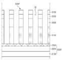
도 3 내지 도 9는 일 실시예에 따른 반도체 로드의 제조 방법을 나타내는 개략도들이다.3 to 9 are schematic views showing a method of manufacturing a semiconductor rod according to an embodiment.
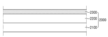
먼저, 도 3을 참조하면, 베이스 기판(2100), 베이스 기판(2100) 상에 형성된 버퍼 물질층(2200) 및 버퍼 물질층(2200) 상에 형성된 분리층(2300)을 포함하는 하부 기판(2000)을 준비한다. 도 3에 도시된 바와 같이, 하부 기판(2000)은 베이스 기판(2100), 버퍼물질층(1200) 및 분리층(2300)이 순차적으로 적층된 구조를 가질 수 있다.First, referring to FIG. 3, a
베이스 기판(2100)은 사파이어 기판(Al2O3) 및 유리와 같은 투명성 기판을 포함할 수 있다. 다만, 이에 제한되는 것은 아니며, GaN, SiC, ZnO, Si, GaP 및 GaAs 등과 같은 도전성 기판으로 이루어질 수도 있다. 이하에서는, 베이스 기판(2100)이 사파이어 기판(Al2O3)인 경우를 예시하여 설명한다. 베이스 기판(2100)의 두께는 특별히 제한되지 않으나, 일 예로 베이스 기판(2100)은 두께가 400㎛ 내지 1500㎛의 범위를 가질 수 있다. The
후술하는 단계에서, 베이스 기판(2100) 상에는 복수의 도전형 반도체층이 형성된다. 에피택셜법에 의해 성장되는 복수의 도전형 반도체층은 시드 결정을 형성하고, 그 위에 결정 재료를 증착하여 성장될 수 있다. 여기서, 도전형 반도체층은 전자빔 증착법, 물리적 기상 증착법(Physical vapor deposition, PVD), 화학적 기상 증착법(Chemical vapor deposition, CVD), 플라즈마 레이저 증착법(Plasma laser deposition, PLD), 이중형 열증착법(Dual-type thermal evaporation), 스퍼터링(Sputtering), 금속-유기물 화학기상 증착법(Metal organic chemical vapor deposition, MOCVD) 등일 수 있으며, 바람직하게는, 금속-유기물 화학기상 증착법(MOCVD)에 의해 형성될 수 있다. 다만, 이에 제한되지 않는다. In the steps described below, a plurality of conductivity type semiconductor layers are formed on the
복수의 도전형 반도체층을 형성하기 위한 전구체 물질은 대상 물질을 형성하기 위해 통상적으로 선택될 수 있는 범위 내에서 특별히 제한되지 않는다. 일 예로, 전구체 물질은 메틸기 또는 에틸기와 같은 알킬기를 포함하는 금속 전구체일 수 있다. 예를 들어, 트리메틸 갈륨(Ga(CH3)3), 트리메틸 알루미늄(Al(CH3)3), 트리에틸 인산염((C2H5)3PO4)과 같은 화합물일 수 있으나, 이에 제한되지 않는다. 이하에서는, 복수의 도전형 반도체층을 형성하는 방법이나 공정 조건 등에 대하여는 생략하여 설명하며, 발광 소자(300)의 제조방법의 순서나 적층 구조에 대하여 상세히 설명하기로 한다.The precursor material for forming the plurality of conductive type semiconductor layers is not particularly limited within a range that can be conventionally selected to form the target material. For example, the precursor material may be a metal precursor including an alkyl group such as a methyl group or an ethyl group. For example, it may be a compound such as trimethyl gallium (Ga (CH 3 ) 3 ), trimethyl aluminum (Al (CH 3 ) 3 ), triethyl phosphate ((C 2 H 5 ) 3 PO 4 ), but is not limited thereto. Does not. Hereinafter, a method of forming a plurality of conductive semiconductor layers, process conditions, and the like will be omitted, and the procedure of the method for manufacturing the
베이스 기판(2100) 상에는 버퍼 물질층(2200)이 형성된다. 도면에서는 버퍼 물질층(2200)이 한층 적층된 것을 도시하고 있으나, 이에 제한되지 않으며, 복수의 층을 형성할 수도 있다. 버퍼 물질층(2200)은 제1 도전형 반도체층(3100)과 베이스 기판(2100)의 격자 상수 차이를 줄이기 위해 배치될 수 있다. 후술하는 단계에서, 버퍼 물질층(2200)은 그 위에 형성되는 제1 도전형 반도체층(3100)의 결정이 원활하게 성장할 수 있도록 베이스 기판(2100)과의 격자 상수를 줄여주거나 시드 결정을 제공할 수도 있다. A
일 예로, 버퍼 물질층(2200)은 언도프드(Undoped) 반도체를 포함할 수 있으며, 실질적으로 제1 도전형 반도체층(3100)과 동일한 물질을 포함하되, n형 또는 p형으로 도핑되지 않은 물질일 수 있다. 예시적인 실시예에서, 버퍼 물질층(2200)은 도핑되지 않은 InAlGaN, GaN, AlGaN, InGaN, AlN 및 InN 중 적어도 어느 하나일 수 있으나, 이에 제한되지 않는다. As an example, the
한편, 몇몇 실시예에서 버퍼 물질층(2200) 상에는 복수의 층이 형성되고, 그 위에 분리층(2300)이 배치될 수 있다. 또한, 버퍼 물질층(2200)은 베이스 기판(2100)에 따라 생략될 수도 있다. 이하에서는, 베이스 기판(2100) 상에 언도프트 반도체 물질을 포함하는 버퍼 물질층(2200)이 형성된 경우를 예시하여 설명하기로 한다.Meanwhile, in some embodiments, a plurality of layers are formed on the
분리층(2300)은 그 위에 제1 도전형 반도체층(3100)이 형성될 수 있다. 분리층(2300)은 제1 도전형 반도체층(3100)의 결정이 원활하게 성장하는 재료를 포함할 수 있다. 분리층(2300)은 절연물질 및 전도성 물질 중 적어도 어느 하나를 포함할 수 있다. 일 예로, 분리층(2300)은 절연물질로써 실리콘 산화물(SiOx), 실리콘 질화물(SiNx), 실리콘 산질화물(SiOxNy) 등을 포함할 수 있으며, 전도성 물질로써 ITO, IZO, IGO, ZnO, 그래핀, 그래핀 산화물(Graphene oxide) 등을 포함할 수도 있다. 다만, 이에 제한되는 것은 아니다. The
분리층(2300)은 후술하는 단계에서 식각되어 제거됨으로써, 발광 소자(300)를 하부기판(1000)으로부터 분리하는 기능을 수행할 수도 있다. 분리층(2300)이 제거되는 단계는 상술한 바와 같이 화학적 분리방법(CLO)에 의해 수행될 수 있고, 이에 따라 발광 소자(300)의 단부면은 분리층(2300)의 표면과 실질적으로 동일한 형성을 가질 수 있다. 즉, 발광 소자(300)의 단부면은 평탄한 면을 가질 수 있다. The
또한, 분리층(2300)은 반도체 구조물(3000)을 식각하는 공정에서, 반도체 구조물(3000)과 버퍼 물질층(2200) 사이에서 에칭스토퍼(etching stopper)의 기능을 수행할 수도 있다. 즉, 반도체 구조물(3000)을 식각할 때, 하나의 공정에서 분리층(2300)을 동시에 패터닝할 수 있고, 서로 다른 공정에서 각각 패터닝할 수도 있다. In addition, in the process of etching the
다만, 이에 제한되는 것은 아니며, 분리층(2300)은 반도체 구조물(3000) 또는 하부기판(1000) 내에서 더 많은 수가 배치될 수도 있고, 버퍼 물질층(2200)과 제1 도전형 반도체층(3100) 사이의 계면 이외의 영역에도 배치될 수 있다. However, the present invention is not limited thereto, and the
다음으로, 도 4를 참조하면, 하부 기판(2000)의 분리층(2300) 상에 제1 도전형 반도체층(3100), 활성물질층(3300), 제2 도전형 반도체층(3200) 및 도전성 전극물질층(3700)을 포함하는 반도체 구조물(3000)을 형성한다.Next, referring to FIG. 4, the first conductive
반도체 구조물(3000)은 후술하는 단계에서 일부 식각되어 반도체 로드(ROD, 도 12에 도시)를 형성할 수 있다. 반도체 구조물(3000)에 포함되는 복수의 물질층들은 상술한 바와 같이 통상적인 공정을 수행하여 형성될 수 있다. 분리층(2300) 상에는 제1 도전형 반도체층(3100), 활성물질층(3300), 제2 도전형 반도체층(3200) 및 도전성 전극물질층(3700)을 순차적으로 형성될 수 있으며, 이들은 각각 발광 소자(300)의 제1 도전형 반도체(310) 소자 활성층(330), 제2 도전형 반도체(320) 및 전극 물질층(370)과 동일한 물질들을 포함할 수 있다. 즉, 반도체 구조물(3000)에 적층된 층들은 발광 소자(300)의 각 물질들에 대응될 수 있다. The
한편, 도면에서는 도시하지 않았으나, 반도체 구조물(3000)은 도전성 전극물질층(3700)이 생략되거나, 제1 도전형 반도체층(3100) 하부에 다른 도전성 전극물질층이 형성될 수도 있다. 상술한 바와 같이, 발광 소자(300)는 전극 물질층(370)이 생략되거나 제1 도전형 반도체(310)의 하부에 다른 전극 물질층(370)을 더 포함할 수도 있다. 즉, 반도체 구조물(3000)도 도 4와 다른 부재들을 더 포함할 수 있다. 다만, 이하에서는 반도체 구조물(3000)이 도전성 전극물질층(3700)을 포함하는 경우를 예시하여 설명하기로 한다. Meanwhile, although not illustrated in the drawings, the conductive
다음으로, 반도체 구조물(3000)의 적어도 일부를 하부 기판(2000)에 수직한 방향으로 식각하여 반도체 결정(3000')을 형성한다. Next, at least a portion of the
반도체 구조물(3000)을 수직으로 식각하여 반도체 결정(3000')을 형성하는 단계는 통상적으로 수행될 수 있는 패터닝 공정을 포함할 수 있다. 일 예로, 반도체 구조물(3000)을 식각하여 반도체 결정(3000')을 형성하는 단계는, 반도체 구조물(3000) 상에 식각 마스크층(1600) 및 식각 패턴층(1700)을 형성하는 단계, 식각 패턴층(1700)의 패턴에 따라 반도체 구조물(3000)을 식각하는 단계 및 식각 마스크층(1600)과 식각 패턴층(1700)을 제거하는 단계를 포함할 수 있다.The step of forming the
먼저, 도 5를 참조하면, 식각 마스크층(1600)은 반도체 구조물(3000)의 제1 도전형 반도체층(3100), 활성물질층(3300), 제2 도전형 반도체층(3200) 및 도전성 전극물질층(3700)의 연속적인 에칭을 위한 마스크의 역할을 수행할 수 있다. 식각 마스크층(1600)은 절연성 물질을 포함하는 제1 식각 마스크층(1610)과 금속을 포함하는 제2 식각 마스크층(1620)을 포함할 수도 있다.First, referring to FIG. 5, the
식각 마스크층(1600)의 제1 식각 마스크층(1610)에 포함되는 절연성 물질은 산화물 또는 질화물을 이용할 수 있다. 예를 들어, 실리콘 산화물(SiOx), 실리콘 질화물(SiNx), 실리콘 산질화물(SiOxNy) 등일 수 있다. 제1 식각 마스크층(1610)의 두께는 0.5㎛ 내지 1.5㎛의 범위를 가질 수 있으나, 이에 제한되는 것은 아니다.The insulating material included in the first
제2 식각 마스크층(1620)의 경우, 반도체 구조물(3000)의 연속적인 식각을 위해 마스크의 역할을 수행할 수 있는 통상적인 재료이면 특별히 제한되는 것은 아니다. 예를 들어, 제2 식각 마스크층(1620)은 크롬(Cr) 등을 포함할 수도 있다. 제2 식각 마스크층(1620)의 두께는 30nm 내지 150nm의 범위를 가질 수 있으나, 이에 제한되는 것은 아니다.The second
식각 마스크층(1600) 상에는 형성되는 식각 패턴층(1700)은 적어도 하나의 나노 패턴이 서로 이격되어 배치될 수 있다. 식각 패턴층(1700)은 반도체 구조물(3000)의 연속적인 식각을 위해 마스크의 역할을 수행할 수 있다. 식각 패턴층(1700)은 폴리머, 폴리스티렌 스피어, 실리카 스피어 등을 포함하여 패턴을 형성할 수 있는 방법이면 특별히 제한되지 않는다.The
일 예로, 식각 패턴층(1700)이 폴리머를 포함하는 경우, 폴리머를 이용하여 패턴을 형성할 수 있는 통상적인 방법이 채용될 수 있다. 예를 들어, 포토리소그래피, e-빔 리소그래피, 나노 임프린트 리소그래피 등의 방법으로 폴리머를 포함하는 식각 패턴층(1700)을 형성할 수 있다. For example, when the
특히, 식각 패턴층(1700)의 구조, 형태 및 이격된 간격은 최종적으로 제조되는 발광 소자(300)의 형태와 연관될 수 있다. 다만, 상술한 바와 같이, 발광 소자(300)의 형상이 다양할 수 있으므로, 식각 패턴층(1700)의 구조는 특별히 제한되지 않는다. 일 예로, 식각 패턴층(1700)이 서로 이격된 원형의 패턴을 가질 경우, 반도체 구조물(3000)을 수직으로 식각하여 제조되는 발광 소자(300)는 원통형을 가질 수 있다. In particular, the structure, shape, and spaced apart spacing of the
일 예로, 식각 패턴층(1700)은 하나의 나노 패턴을 중심으로 이를 감싸도록 다른 나노 패턴들이 배치될 수 있다. 여기서 하나의 나노 패턴은 이를 중심으로 외면을 감싸도록 6개의 다른 나노 패턴들이 배치되되, 6개의 나노 패턴들은 등 간격으로 나뉘어 배치될 수 있다. 즉, 복수의 나노 패턴들이 이루는 영역은 정육각형의 형상을 가질 수 있다. 다만, 이에 제한되지 않으며, 복수의 나노 패턴들이 이루는 영역은 원형, 다각형 등 다양할 수 있다.For example, the
또한, 복수의 나노 패턴들이 이격된 간격은 특별히 제한되지 않는다. 복수의 나노 패턴들이 이격된 간격은 각 나노 패턴의 직경보다 클 수 있다. 일 예로, 복수의 나노 패턴들이 이격된 간격은 각 나노 패턴의 직경의 2배 내지 4배, 또는 3배 내외의 범위를 가질 수 있다. 또한, 복수의 나노 패턴들은 서로 다른 크기의 직경을 가질 수도 있다.In addition, the spacing between the plurality of nano patterns is not particularly limited. The spacing between the plurality of nano patterns may be larger than the diameter of each nano pattern. For example, the spacing between the plurality of nano patterns may have a range of about 2 to 4 times or 3 times the diameter of each nano pattern. Further, the plurality of nano patterns may have different sizes of diameters.
예시적인 실시예에서, 식각 패턴층(1700)은 나노 임프린트 리소그래피로 형성될 수 있으며, 식각 패턴층(1700)의 나노 패턴은 나노 임프린트 수지를 포함할 수 있다. 상기 수지는 불화 단량체(Fluorinated monomer), 아크릴레이트 단량체(Acrylate monomer), 디펜타에리트리톨 헥사아크릴레이트(Dipentaerythritol hexaacrylate), 디프로필렌글리콜 디아크릴레이트(Dipropylene glycol diacrylate), 폴리에틸렌글리콜 페닐에터아크릴레이트(poly(ethylene glycol) phenyletheracrylate), 뷰틸레이트하이드록시톨루엔(Butylated hydroxy toluene, BHT), 1-하이드록시-사이클로헥실페닐케톤(1-hydroxy-cyclohexylphenylketone, Irgacure 184) 등을 포함할 수 있으나, 이에 제한되는 것은 아니다.In an exemplary embodiment, the
다음으로 도 6 및 도 7을 참조하면, 식각 패턴층(1700)의 나노 패턴을 따라 반도체 구조물(3000)을 식각하여 반도체 결정(3000')을 형성한다. 반도체 결정(3000')을 형성하는 단계는 식각 패턴층(1700)의 나노 패턴들이 이격된 영역을 수직으로 식각하여 식각 마스크층(1600) 및 도전성 전극 물질층(3700)을 패터닝하여 제1 홀(h1)을 형성하는 제1 식각 단계, 식각 패턴층(1700)을 제거하는 단계, 제1 홀(h1)을 따라 제2 도전형 반도체층(3200), 활성물질층(3300) 및 제1 도전형 반도체층(3100)을 식각하여 제2 홀(h2)을 형성하는 제2 식각 단계 및 식각 마스크층(1600)을 제거하는 단계를 포함할 수 있다.Next, referring to FIGS. 6 and 7, the
제1 홀(h1) 및 제2 홀(h2)을 형성하는 방법은 통상적인 방법으로 수행될 수 있다. 예를 들어, 식각공정은 건식식각법, 습식식각법, 반응성 이온 에칭법(Reactive ion etching, RIE), 유도 결합 플라즈마 반응성 이온 에칭법(Inductively coupled plasma reactive ion etching, ICP-RIE) 등일 수 있다. 건식 식각법의 경우 이방성 식각이 가능하여 수직 식각에 의한 홀(h)을 형성하기에 적합할 수 있다. 상술한 방법의 식각법을 이용할 경우, 식각 에천트(Etchant)는 Cl2 또는 O2 등일 수 있다. 다만, 이에 제한되는 것은 아니다. The method of forming the first hole h1 and the second hole h2 may be performed by a conventional method. For example, the etching process may be dry etching, wet etching, reactive ion etching (RIE), inductively coupled plasma reactive ion etching (ICP-RIE), or the like. In the case of the dry etching method, anisotropic etching is possible, so it may be suitable for forming a hole h by vertical etching. When using the etching method of the above-described method, the etching etchant may be Cl 2 or O 2 . However, it is not limited thereto.
몇몇 실시예에서, 반도체 구조물(3000)의 식각은 건식 식각법과 습식 식각법을 혼용하여 이루어질 수 있다. 예를 들어, 먼저 건식 식각법에 의해 깊이 방향의 식각을 한 후, 등방성 식각인 습식 식각법을 통해 식각된 측벽이 표면과 수직한 평면에 놓이도록 할 수 있다. In some embodiments, etching of the
도 6에 도시된 바와 같이, 제1 식각 단계를 수행하여, 식각 마스크층(1600) 및 도전성 전극 물질층(3700)을 식각하여 제1 홀(h1)을 형성한다. 그리고, 제1 홀(h1)을 따라 제2 도전형 반도체층(3200), 활성물질층(3300) 및 제1 도전형 반도체층(3100)을 식각하여 제2 홀(h2)을 형성하는 제2 식각 단계을 수행한다. 마지막으로 도 7에 도시된 바와 같이 식각된 반도체 구조물(3000)의 상부에 남아있는 식각 마스크층(1600) 또는 식각 패턴층(1700)을 제거하여 반도체 결정(3000')을 형성할 수 있다. 식각 마스크층(1600) 또는 식각 패턴층(1700)은 통상적인 방법, 예를 들어, 건식식각법, 습식식각법을 통해 제거될 수 있다. As illustrated in FIG. 6, a first hole h1 is formed by etching the
한편, 반도체 구조물(3000)을 식각하여 반도체 결정(3000')을 형성하는 단계는, 제1 식각 단계와 제2 식각 단계를 포함하여 서로 다른 패터닝 공정을 수행할 수 있고, 하나의 패터닝 공정을 수행하여 식각 패턴층(1700)을 따라 제1 도전형 반도체층(3100)까지 패터닝할 수도 있다. Meanwhile, the step of etching the
또한, 반도체 구조물(3000)을 식각할 때, 분리층(2300)의 적어도 일부를 함께 식각할 수 있고, 별도의 식각공정에서 분리층(2300)을 일부 식각할 수도 있다. 즉, 분리층(2300)은 반도체 구조물(3000)이 식각될 때, 동일한 식각 공정에서 함께 패터닝될 수 있고, 반도체 구조물(3000)이 식각될 때 에칭 스토퍼(etching stopper)의 기능을 수행하여 별개의 공정에서 패터닝될 수도 있다.In addition, when the
예를 들어, 도면에 도시된 바와 같이, 반도체 구조물(3000)을 패터닝할 때, 식각 에천트가 분리층(2300)을 제거하는 에천트를 포함하지 않는 경우, 반도체 구조물(3000)만이 식각되고, 분리층(2300)은 식각되지 않고 에칭 스토퍼의 기능을 수행할 수도 있다. 이에 따라, 반도체 결정(3000')은 형성되되, 분리층(2300)은 식각되지 않은 상태로 존재할 수 있다. 반면에, 도면에서는 도시하지 않았으나, 식각 에천트가 분리층(2300)을 제거하는 에천트를 포함하는 경우, 반도체 구조물(3000)과 분리층(2300)이 함께 식각될 수도 있다. For example, as shown in the drawing, when patterning the
다음으로, 반도체 결정(3000')의 외측면을 부분적으로 둘러싸는 절연피막(3800)을 형성하여 반도체 로드(ROD)를 형성한다.Next, an insulating
절연피막(3800)은 반도체 로드(ROD)의 외면에 형성되는 절연물질로서, 수직으로 식각된 반도체 결정(3000')의 외면에 절연물질을 도포하거나 침지시키는 방법 등을 이용하여 형성될 수 있다. 다만, 이에 제한되는 것은 아니다. 일 예로, 절연피막(3800)은 원자층 증착법(Atomic layer depsotion, ALD)으로 형성될 수 있다. 절연피막(3800)은 발광 소자(300)의 절연막(380)을 형성할 수 있다. 상술한 바와 같이 절연피막(3800)은 실리콘 산화물(SiOx), 실리콘 질화물(SiNx), 실리콘 산질화물(SiOxNy), 산화 알루미늄(Al2O3), 질화 알루미늄(AlN) 등일 수 있다. The insulating
도 8을 참조하면, 절연피막(3800)은 반도체 결정(3000')의 측면, 상면 및 반도체 결정(3000')이 이격되어 식각됨으로써 외부로 노출된 분리층(2300) 또는 버퍼 물질층(2200) 상에도 형성될 수 있다. 반도체 결정(3000')의 양 단부 측면을 노출시키기 위해, 반도체 결정(3000')의 상부 면에 형성된 절연피막(3800)은 제거될 필요가 있다. 따라서, 반도체 결정(3000')의 길이 방향과 수직한 방향, 다시 말해 하부 기판(2000)과 평행한 방향으로 형성된 절연피막(3800)은 일부 제거될 수 있다. 즉, 도 9에 도시된 바와 같이, 적어도 반도체 결정(3000')의 상면과, 분리층(2300) 상에 배치된 절연피막(3800)을 제거하여 반도체 결정(3000')의 상면을 노출할 수 있다. 이를 위해 이방성 식각인 건식 식각이나 에치백 등의 공정이 수행될 수 있다. 이에 따라, 반도체 결정(3000')의 외주면을 둘러싸는 절연피막(3800)이 부분적으로 제거되고, 반도체 결정(3000') 및 절연피막(3800)을 포함하는 반도체 로드(ROD)를 형성할 수 있다. 반도체 로드(ROD)는 후술하는 단계에서 하부 기판(2000)에서 분리됨으로써 발광 소자(300)를 형성할 수 있다.Referring to FIG. 8, the insulating
한편, 일 실시예에 따르면, 절연피막(3800)을 제거하는 단계에서, 분리층(2300)은 일부 영역이 함몰된 적어도 하나의 홈부(2300a)와 홈부(2300a)가 이격되어 형성되는 돌출부(2300b)를 포함하는 요철패턴(2300P)이 형성될 수 있다. Meanwhile, according to an embodiment, in the step of removing the insulating
절연피막(3800)과 분리층(2300)은 서로 다른 식각 선택비를 가지므로, 절연피막(3800)을 제거할 때 분리층(2300)도 부분적으로 제거될 수 있다. 절연피막(3800)을 부분적으로 제거하는 과정에서 분리층(2300)은 일부 영역이 함몰되어 홈부(2300a)가 형성될 수 있다. Since the insulating
도면에 도시된 바와 같이, 분리층(2300)은 반도체 로드(ROD)들이 이격된 제2 홀(h2)을 따라 부분적으로 식각될 수 있다. 상기 식각된 영역은 함몰되어 홈부(2300a)를 형성할 수 있다. 즉, 홈부(2300a)는 제2 홀(h2)이 분리층(2300)의 일부 영역까지 연장되어 형성된 것일 수 있다. 분리층(2300)은 복수의 홈부(2300a)가 형성되고, 홈부(2300a)가 서로 이격된 영역은 상대적으로 돌출되어 돌출부(2300b)가 형성될 수 있다. 돌출부(2300b)는 실질적으로 반도체 로드(ROD)에 의해 식각되지 않은 영역일 수 있다. 다시 말해, 반도체 로드(ROD)는 각 돌출부(2300b)상에 형성될 수 있다. As illustrated in the drawing, the
상술한 바와 같이, 분리층(2300)의 요철패턴(2300P)은 반도체 구조물(3000)을 하부 기판(2000)에 수직한 방향으로 식각하는 단계에서 형성되는 제2 홀(h2)을 따라 형성될 수 있다. 제2 홀(h2)은 식각 패턴층(1700)의 구조에 따라 형성될 수 있으므로, 분리층(2300)의 요철패턴(2300P)의 구조는 식각 패턴층(1700)에 따라 달라질 수 있다. 도면에서는 분리층(2300)의 요철패턴(2300P)이 복수의 홈부(2300a)가 동일한 직경을 갖고, 등 간격으로 이격된 것을 도시하고 있으나, 이에 제한되는 것은 아니다. 경우에 따라서는 서로 다른 직경을 갖는 발광 소자(300)들을 제조하기 위해, 식각 패턴층(1700)의 나노 패턴이 서로 다른 직경을 갖거나, 이격된 간격이 서로 다를 수 있다. As described above, the
이에 따라, 분리층(2300)의 요철패턴(2300P)은 홈부(2300a)가 서로 다른 직경을 갖거나 서도 다른 간격으로 이격될 수 있다. 즉, 요철패턴(2300P)의 복수의 홈부(2300a)와 돌출부(2300b)는 각각 서로 직경을 가질 수도 있다.Accordingly, the
한편, 경우에 따라서는 분리층(2300)은 요철패턴(2300P)을 포함하지 않고, 상면이 실질적으로 평탄한 형상을 가질 수도 있다.Meanwhile, in some cases, the
반도체 로드(ROD)는 하부 기판(2000)으로부터 분리되어 발광 소자(300)를 형성할 수 있다. 반도체 로드(ROD)를 분리하는 단계는 화학적 분리방법(CLO)에 의해 분리층(2300)을 제거하는 단계를 포함할 수 있다. 분리층(2300)을 제거하기 위해, 불산(HF) 또는 버퍼 산화 에칭(Buffered oxide etch, BOE) 등의 분리용 식각액을 이용하여 습식 식각공정을 수행할 수 있으나, 이에 제한되는 것은 아니다. The semiconductor rod ROD may be separated from the
여기서, 분리층(2300)을 제거하기 위한 분리용 식각액은 반도체 로드(ROD)의 도전성 전극 물질층(3700) 또는 절연막(3800)과 반응할 수도 있다. 이에 따라 제조되는 발광 소자(300)는 외주면이 거친 표면을 가지거나, 발광 소자(300)의 전극 물질층(370)이 일부 제거될 수 있다. Here, the separation etchant for removing the
도 10은 일 비교예에 따른 발광 소자의 제조방법 중 일부를 도시하는 개략도이다. 10 is a schematic diagram showing a part of a method of manufacturing a light emitting device according to a comparative example.
도 10을 참조하면, 하부 기판(2000) 상의 반도체 로드(ROD)를 직접 분리하는 경우, 분리층(2300)을 제거할 때 절연피막(3800)과 도전성 전극 물질층(3700)에 포함된 재료의 일부가 손상될 수 있다. 이에 따라 제조된 발광 소자(300')의 절연층 (380')은 표면이 거친 형태를 갖고, 전극 물질층(370')이 부분적으로 제거된 것을 알 수 있다. 이 경우, 발광 소자(300')의 도전형 반도체(310, 320) 또는 소자 활성층(330)의 일부가 노출되어 손상될 수 있고, 거친 표면을 가지는 절연층 (381')에 의해 발광 소자(300')와 표시 장치(10)의 전극과의 접촉불량이 발생할 수도 있다. Referring to FIG. 10, when directly separating the semiconductor rod ROD on the
일 실시예에 따른 발광 소자(300)의 제조 방법은 반도체 로드(ROD)들을 감싸는 로드 보호층(1100)을 포함하는 로드 구조물(1000)을 형성하는 단계(S200)를 포함한다. 로드 보호층(1100)은 분리층(2300)을 제거하기 위한 분리용 식각액과 반응하지 않는 유기물을 포함할 수 있다. 로드 보호층(1100)은 반도체 로드(ROD)가 분리용 식각액과 접촉하지 않도록 형성되고, 분리층(2300)을 제거할 때 반도체 로드(ROD)가 분리용 식각액에 의해 손상되는 것을 방지할 수 있다. The manufacturing method of the
도 11 내지 도 13은 일 실시예에 따른 로드 구조물을 형성하는 방법을 도시하는 개략도들이다. 11 to 13 are schematic diagrams illustrating a method of forming a rod structure according to an embodiment.
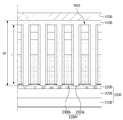
일 실시예에 따른 로드 구조물(1000)을 형성하는 단계는 반도체 로드(ROD)들을 감싸는 로드 보호층(1100)을 형성하는 단계, 로드 보호층(1100) 상에 보조층(1200)을 형성하는 단계 및 로드 구조물(1000)을 하부 기판(2000)에서 분리하는 단계를 포함한다. The forming of the
먼저, 도 11을 참조하면, 분리층(2300) 상에서 반도체 로드(ROD)들을 감싸는 로드 보호층(1100) 형성한다. First, referring to FIG. 11, a
로드 보호층(1100)은 분리층(2300) 상에서 반도체 로드(ROD)를 감싸도록 형성될 수 있다. 로드 보호층(1100)의 두께(dd)는 반도체 로드(ROD)의 상부면, 예컨대 도전성 전극 물질층(3700)의 상면을 덮을 수 있도록 반도체 로드(ROD)의 장축의 길이(l)보다 두꺼울 수 있다. 즉, 로드 보호층(1100)은 반도체 로드(ROD)가 로드 보호층(1100) 내에 배치되도록 형성될 수 있다. 일 예로, 반도체 로드(ROD)의 장축의 길이가 4 내지 7um인 경우, 로드 보호층(1100)의 두께는 6um 내지 10um일 수 있다. 다만 이에 제한되지 않는다. 로드 보호층(1100)은 일종의 필름형(film), 테이프(tape), 기판(substrate)의 형태를 가질 수도 있다.The
로드 보호층(1100)의 상면(1110)은 실질적으로 평탄하게 형성되어, 하부 기판(2000)과 평행한 면을 이룰 수 있다. 로드 보호층(1100)의 상면(1110)에는 후술할 바와 같이, 보조층(1200)이 형성될 수 있다. 보조층(1200)이 형성된 로드 보호층(1100)은 로드 구조물(1000)을 형성할 수 있다.The
로드 보호층(1100)의 하면(1120)은 분리층(2300)과 접촉하도록 형성될 수 있다. 상술한 바와 같이, 분리층(2300) 상에는 홈부(2300a)와 돌출부(2300b)를 포함하는 요철패턴(2300P)이 형성될 수 있으며, 분리층(2300)의 상면은 평탄하지 않을 수 있다. 로드 보호층(1100)의 하면(1120)은 분리층(2300)의 요철패턴(2300P)을 따라 형성될 수 있다. The
일 실시예에서, 로드 보호층(1100)은 하면(1120)이 분리층(2300)의 홈부(2300a) 상면과 접촉하고, 돌출부(2300b)의 측면을 둘러싸도록 형성될 수 있다. In one embodiment, the
로드 보호층(1100)은 돌출부(2300b) 상에 형성되는 반도체 로드(ROD)를 보호하기 위해 반도체 로드(ROD)의 상면과 측면을 둘러싸도록 형성된다. 여기서, 반도체 로드(ROD)의 측면과 하면 사이에 틈이 형성되는 경우, 분리층(2300)이 제거되면서 반도체 로드(ROD)의 하면이 분리용 식각액에 의해 손상될 수 있다. 이를 방지하기 위해, 로드 보호층(1100)은 반도체 로드(ROD)의 측면을 둘러싸되, 하면이 접촉하는 분리층(2300)의 돌출부(2300b)의 측면까지 둘러싸도록 배치될 수 있다. 따라서, 분리층(2300)의 요철패턴(2300P)을 따라 형성되는 로드 보호층(1100)의 하면(1120)은 적어도 일부 영역이 함몰되는 함몰부(1120P)가 형성될 수 있다. 이에 대한 보다 자세한 구조는 후술하기로 한다.The
한편, 로드 보호층(1100)은 반도체 로드(ROD) 상에 로드 보호층(1100)을 구성하는 재료를 도포 또는 분사하여 형성될 수 있다. 일 실시예에서, 로드 보호층(1100)은 분리층(2300) 상에서 잉크젯 프린팅법, 스핀 코팅법, 다이-슬롯 코팅법, 슬릿 코팅법 등을 통해 형성될 수 있다. 다만, 이에 제한되는 것은 아니다.Meanwhile, the
또한, 일 실시예에 따른 로드 보호층(1100)은 분리층(2300)을 제거하는 분리용 식각액에 불용성인 유기물을 포함할 수 있다. 로드 보호층(1100)은 일종의 유기보호필름일 수 있다. 후술하는 바와 같이, 로드 구조물(1000)을 하부 기판(2000)에서 분리할 때, 분리층(2300)을 분리용 식각액과 반응시켜 화학적으로 제거할 수 있다. 반면에 로드 보호층(1100)은 분리용 식각액과 반응하지 않는 재료를 포함하여 반도체 로드(ROD)들이 분리용 식각액에 손상되는 것을 방지할 수 있다. In addition, the
일 예로, 분리층(2300)은 불소(F)를 함유하는 분리용 식각액에 제거될 수 있고, 로드 보호층(1100)은 상기 분리용 식각액에 불용성인 유기물을 포함할 수 있다. 분리층(2300)을 제거하는 과정에서, 로드 보호층(1100)은 불소(F)를 함유하는 상기 분리용 식각액과 반응하지 않을 수 있다. 이에 따라, 로드 보호층(1100)은 반도체 로드(ROD)가 분리용 식각액과 접촉하는 것을 방지하고, 반도체 로드(ROD)를 보호할 수 있다.For example, the
로드 보호층(1100)의 상기 유기물은 분리용 식각액 이외의 다른 용매에 용해될 수 있다. 즉, 상기 유기물은 불소(F)를 함유하는 분리용 식각액에는 불용성이나, 다른 용매들, 예컨대 물, 아세톤(Acetone), 이소프로필알콜(Isopropyl alcohol, IPA) 등에 의해 용해될 수 있다. 따라서, 로드 보호층(1100)은 분리용 식각액에 녹지 않으나, 다른 용매에 의해 용해되어 반도체 로드(ROD)를 용이하게 분리할 수 있다.The organic material of the rod
예시적인 실시예에서, 로드 보호층(1100)의 상기 유기물은 폴리메틸메타크릴레이트(Poly methyl methacrylate, PMMA), 포토레지스트(Photoresist, PR), 폴리(3,4-에틸렌디옥시싸이오펜) 폴리스티렌 설포네이트(Poly-(3,4-ethylenedioxy thiophene) polystyrene sulfonate, PEDOT:PSS) 중 적어도 어느 하나를 포함할 수 있다. 예를 들어, 분리층(2300)은 불소(F)를 함유하는 식각액에 의해 제거되는 물질, 예컨대 실리콘산화물(SiOx)을 포함하고, 로드 보호층(1100)은 폴리(3,4-에틸렌디옥시싸이오펜) 폴리스티렌 설포네이트(Poly-(3,4-ethylenedioxy thiophene) polystyrene sulfonate, PEDOT:PSS)를 포함할 수 있다. 로드 구조물(1000)을 하부 기판(2000)에서 분리하는 단계에서, 불소(F)를 함유하는 식각액에 의해 분리층(2300)은 식각 또는 용해되어 제거되나, 로드 보호층(1100)의 PEDOT:PSS는 불소(F)에 의해 용해되지 않는다. 로드 보호층(1100)의 PEDOT:PSS는 물에 의해 용해되어 후술하는 단계에서 쉽게 제거될 수 있다. 다만, 이에 제한되는 것은 아니다.In an exemplary embodiment, the organic material of the rod
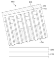
다음으로, 도 12를 참조하면, 로드 보호층(1100) 상에 보조층(1200)을 형성하여 로드 구조물(1000)을 형성한다. Next, referring to FIG. 12, the
보조층(1200)은 로드 보호층(1100) 상에 형성될 수 있으며, 도면에 도시된 바와 같이, 로드 보호층(1100)의 상면(1110)에 형성될 수 있다. 다만, 이에 제한되지 않으며 경우에 따라서는 로드 보호층(1100)의 측면에 형성될 수도 있다. The
보조층(1200)은 로드 보호층(1100)에 비해 경도가 높은 물질을 포함할 수 있다. 예시적인 실시예에서, 보조층(1200)은 열적분리테이프(Thermal release tape, TRT), 폴리에틸렌테레프탈레이트(Polyethylene terephthalate, PET), 플라스틱 필름(plastic film) 등일 수 있다. 다만 이에 제한되는 것은 아니다. The
로드 보호층(1100)은 보조층(1200)에 비해 유연한 유기물을 포함한다. 이에 따라, 슬릿 코팅법 등과 같은 방법을 통해 반도체 로드(ROD) 상에 형성될 수 있다. 이러한 로드 보호층(1100) 상에 비교적 단단한 물질을 포함하는 보조층(1200)을 형성함으로써 로드 구조물(1000)은 하부 기판(2000)에서 분리된 후에도 일정한 형태를 유지할 수 있다. 이에 따라, 로드 구조물(1000)은 복수의 반도체 로드(ROD)들을 용이하게 보관 및 수송할 수 있다.The rod
마지막으로, 도 13을 참조하면, 로드 구조물(1000)을 하부 기판(2000)에서 분리한다. 로드 구조물(1000)을 하부 기판(2000)에서 분리하는 단계는 상술한 바와 같이, 분리층(2300)을 분리용 식각액으로 용해 또는 식각함으로써 수행될 수 있다. Finally, referring to FIG. 13, the
일 실시예에 따른 로드 구조물(1000)은 로드 보호층(1100) 및 보조층(1200)을 포함하고, 로드 보호층(1100)은 복수의 반도체 로드(ROD)들이 배치될 수 있다. 로드 구조물(1000)은 분리층(2300)이 반응하는 분리용 식각액과 반응하지 않는 로드 보호층(1100)을 포함하여, 반도체 로드(ROD)들을 보호할 수 있다. 또한, 로드 보호층(1100) 상에 비교적 경도가 큰 재료를 포함하는 보조층(1200)을 형성함으로써, 복수의 반도체 로드(ROD)들을 용이하게 보관 및 수송할 수 있다. The
도 14 및 도 15를 일 실시예에 따른 로드 구조물을 도시하는 개략도들이다. 도 14는 로드 구조물(1000)을 상부에서 내려다본 사시도이고, 도 15는 로드 구조물(1000)을 하부에서 내려다본 사시도이다. 14 and 15 are schematic diagrams showing a rod structure according to an embodiment. 14 is a perspective view of the
도 14 및 도 15를 참조하면, 로드 구조물(1000)은 원기둥의 형태를 가질 수 있다. 하부 기판(2000)이 원형의 베이스 기판(2100)을 포함하는 경우, 로드 구조물(1000)은 원기둥의 형상을 가질 수 있으나, 이에 제한되는 것은 아니다. 도면에 도시된 로드 구조물(1000)은 하나의 예시에 불과하며, 로드 구조물(1000)의 형태는 다양할 수 있다.14 and 15, the
로드 구조물(1000)의 로드 보호층(1100)은 적어도 하나의 반도체 로드(ROD)들이 배치될 수 있다. At least one semiconductor rod (ROD) may be disposed on the
분리층(2300) 상에서 서로 이격되어 성장된 반도체 로드(ROD)들은 로드 보호층(1100) 내에서 배열될 수 있다. 도면에서는 하나의 반도체 로드(ROD)를 중심으로 이를 둘러싸며 6개의 반도체 로드(ROD)들이 서로 배열된 것을 도시하고 있다. 다만, 로드 보호층(1100)은 더 많은 수의 반도체 로드(ROD)들이 배열될 수 있다. 또한, 반도체 로드(ROD)들이 이격된 간격, 배열된 구조 등은 하부 기판(2000) 상에 반도체 로드(ROD)들이 형성되는 구조에 따라 달라질 수 있음은 자명하다.The semiconductor rods (RODs) spaced apart from each other on the
예시적인 실시예에서, 복수의 반도체 로드(ROD)들은 로드 보호층(1100)의 상면(1110)과 평행한 방향으로 서로 이격되어 배열될 수 있다. 또한, 로드 구조물(1000)에 배치된 반도체 로드(ROD)들은 장축이 로드 보호층(1100)의 상면(1110)과 수직한 방향으로 연장된 형태를 가질 수 있다. In an exemplary embodiment, the plurality of semiconductor rods ROD may be arranged spaced apart from each other in a direction parallel to the
상술한 바와 같이, 반도체 로드(ROD)들은 하부 기판(2000) 상에서 성장되고, 이들을 감싸도록 로드 보호층(1100)이 형성될 수 있다. 반도체 로드(ROD)들이 성장된 방향, 즉 제1 도전형 반도체층(3100), 활성물질층(3300), 제2 도전형 반도체층(3200)이 적층된 방향은 하부 기판(2000)에 수직한 방향과 평행하다. 이에 따라, 로드 보호층(1100)에 배치되는 반도체 로드(ROD)들은 장축(예컨대, 성장된 방향)이 로드 보호층(1100)의 상면(1110)과 수직한 방향으로 배향될 수 있다. As described above, the semiconductor rods RODs are grown on the
또한, 반도체 로드(ROD)들은 장축(예컨대, 성장된 방향)과 수직한 방향, 예컨대 하부 기판(2000)과 평행한 방향으로 이격되어 배치된다. 이에 따라 도면에 도시된 바와 같이, 반도체 로드(ROD)들은 로드 보호층(1100)의 상면(1110)과 평행한 방향으로 배열될 수 있다.Further, the semiconductor rods ROD are spaced apart in a direction perpendicular to a long axis (eg, a grown direction), for example, a direction parallel to the
한편, 일 실시예에서, 로드 구조물(1000)의 로드 보호층(1100)은 일 면은 실질적으로 평탄한 면을 가지고, 상기 일 면과 대향하는 타 면은 반도체 로드(ROD)와 중첩되는 영역이 함몰되어 형성된 적어도 하나의 함몰부(1120P)를 포함할 수 있다. On the other hand, in one embodiment, the rod
로드 보호층(1100)은 하부 기판(2000) 상에 성장된 반도체 로드(ROD)들을 감싸도록 하면(1120)이 분리층(2300)의 요철패턴(2300P)을 따라 형성될 수 있다. 분리층(2300)이 제거되어 하부 기판(2000)에서 분리된 로드 구조물(1000)은 하면(1120)이 부분적으로 함몰된 함몰부(1120P)가 형성된 로드 보호층(1100)을 포함한다. 반도체 로드(ROD)의 일 단부는 로드 보호층(1100)의 상면(1110)을 향해 배향되고, 타 단부는 로드 보호층(1100)의 하면(1120)에 형성된 함몰부(1120P)와 접촉할 수 있다. 이에 따라, 반도체 로드(ROD)는 로드 구조물(1000) 내에서 로드 보호층(1100)의 하면(1120)을 향하는 상기 타 단부가 부분적으로 노출될 수 있다. 다만, 분리층(2300)이 제거될 때, 로드 보호층(1100)에 의해 반도체 로드(ROD)가 보호되므로, 재료의 손상은 최소화할 수 있다. The
한편, 로드 구조물(1000)은 로드 보호층(1100) 상의 적어도 일부에 형성되는 보조층(1200)을 포함할 수 있다. 도면에서는 보조층(1200)이 로드 보호층(1100)의 상부면에 형성된 것을 도시하고 있으나, 이에 제한되는 것은 아니다. 다만, 보조층(1200)은 로드 보호층(1100)의 함몰부(1120P)가 형성된 상기 타 면에는 형성되지 않을 수 있다. Meanwhile, the
일 실시예에 따른 발광 소자(300)의 제조 방법은 로드 구조물(1000)을 형성하는 단계를 포함하여, 제조된 반도체 로드(ROD)들을 용이하게 보관하고 수송할 수 있다. 또한, 로드 구조물(1000)의 로드 보호층(1100)이 반도체 로드(ROD)의 손상을 방지할 수도 있다. The manufacturing method of the
반도체 로드(ROD), 일 예로 발광 소자(300)는 표시 장치(10)에 포함되어 특정 파장대의 광을 방출할 수 있다. 후술하는 바와 같이 발광 소자(300)는 소자 잉크(S, 도 18에 도시)에 분산된 상태로 표시 장치(10)의 전극 상에 분사될 수 있다. 다만, 반도체 물질을 포함하여 비중이 큰 발광 소자(300)들은 소자 잉크(S) 상에서 긴 시간동안 분산된 상태를 유지하지 못하고 침전될 수도 있다. The semiconductor rod (ROD), for example, the
반면에, 일 실시예에 따른 발광 소자(300)의 제조 방법은 로드 구조물(1000)을 형성하여 발광 소자(300)를 소자 잉크(S) 상에 분산하기 전 용이하게 보관이 가능하다. 즉, 에픽택셜법에 의해 제조된 발광 소자(300)들을 표시 장치(10)의 제조 전 장시간동안 보관이 가능하며, 필요에 따라 용이하게 수송이 가능하다.On the other hand, the manufacturing method of the
다음으로, 일 실시예에 따른 발광 소자(300)의 제조방법은 로드 구조물(1000)로부터 반도체 로드(ROD)를 분리하는 단계(S300)를 포함할 수 있다. 로드 구조물(1000)의 로드 보호층(1100)과 보조층(1200)을 제거하여, 반도체 로드(ROD), 즉 발광 소자(300)를 제조할 수 있다.Next, a method of manufacturing the
도 16 내지 도 18은 일 실시예에 따른 로드 구조물로부터 반도체 로드를 분리하는 단계를 도시하는 개략도들이다.16 to 18 are schematic diagrams illustrating a step of separating a semiconductor rod from a rod structure according to an embodiment.
먼저, 도 16을 참조하면, 로드 구조물(1000)의 보조층(1200)을 제거한다. 보조층(1200)은 상술한 재료들을 포함하여 로드 보호층(1100)로부터 분리될 수 있다. 일 예로, 보조층(1200)은 열적분리테이프를 포함하여, 로드 구조물(1000)을 일정 온도로 가열하는 공정을 수행하여 분리할 수 있다. 다만, 이에 제한되는 것은 아니다.First, referring to FIG. 16, the
다음으로 도 17을 참조하면, 보조층(1200)이 분리된 로드 보호층(1100)을 소정의 용매에 용해시킨다. 로드 보호층(1100)은 분리층(2300)을 제거하기 위해 사용되는 분리용 식각액과 반응하지 않으나, 소정의 용매, 예컨대 물, 아세톤, 이소프로필알콜에 용해될 수 있다. 도면에 도시된 바와 같이, 반도체 로드(ROD) 상에서 용매에 용해된 로드 보호층(1100')이 잔존하게 되고 반도체 로드(ROD)들은 분리될 수 있다. Next, referring to FIG. 17, the rod
마지막으로 도 18을 참조하면, 상기 용매에 용해된 로드 보호층(1100')을 휘발시켜 제거한다. 로드 보호층(1100)은 유기물을 포함할 수 있으므로, 용매에 용해된 로드 보호층(1100')은 반도체 로드(ROD)가 손상되지 않는 수준의 온도에서 휘발되어 제거될 수 있다. 이에 따라, 로드 구조물(1000)에서 반도체 로드(ROD)를 분리할 수 있으며, 분리된 반도체 로드(ROD)는 발광 소자(300)를 형성할 수 있다.Finally, referring to FIG. 18, the rod protective layer 1100 'dissolved in the solvent is volatilized and removed. Since the rod
이에 따라 화학적 분리방법(CLO)에 의해 제조된 발광 소자(300)는 절연막(380) 또는 전극 물질층(370)의 재료가 제거되지 않고 매끄러운 형상을 가질 수 있고, 동시에 복수의 발광 소자(300)들은 단부면의 균일성(uniformity)을 확보할 수도 있다. 또한, 발광 소자(300)는 후술하는 표시 장치(10) 상에서 전극과의 접촉 불량 및 발광 불량을 최소화하여 표시 장치(10)의 발광 신뢰도를 향상시킬 수 있다. Accordingly, the
한편, 상술한 방법을 통해 제조된 발광 소자(300)는 소정의 잉크에 분산된 상태로 제조될 수도 있다. Meanwhile, the
도 19는 일 실시예에 따른 발광 소자를 포함하는 소자 잉크를 도시하는 개략도이다.19 is a schematic diagram showing a device ink including a light emitting device according to an embodiment.
도 19를 참조하면, 발광 소자(300)는 소자 잉크(S) 상에 분산된 것을 알 수 있다. 소자 잉크(S)는 발광 소자(300)와 반응하지 않으며, 표시 장치(10)의 제조 과정에서 휘발될 수 있는 용매를 포함할 수 있다. 일 예로 프로필렌글리콜모노메틸에테르(Propyleneglycol monomethylether, PGME), 프로필렌글리콜모노메틸에테르 아세테이트(Propyleneglycol monomethylether acetate, PGMEA), 프로필렌글리콜(Propylene glycol, PG) 등일 수 있다. 다만, 이에 제한되는 것은 아니다.Referring to FIG. 19, it can be seen that the
또한, 도면에서는 도시하지 않았으나, 소자 잉크(S)는 반도체 물질을 을 포함하여 비중이 큰 발광 소자(300)를 분산시키기 위해 소자 분산제를 더 포함할 수도 있다.In addition, although not shown in the drawings, the device ink S may further include a device dispersant to disperse the
이에 따라, 발광 소자(300)는 소자 잉크(S) 상에 분산된 상태로 후술하는 표시 장치(10)를 제조할 때 전극 상에 분사될 수 있다. 이하에서는 발광 소자(300)를 포함하는 표시 장치(10)에 대하여 서술한다.Accordingly, the
한편, 일 실시예에 따른 표시 장치(10)는 상술한 방법을 통해 제조된 발광 소자(300)를 포함하여 다양한 색을 표시할 수 있다.Meanwhile, the display device 10 according to an exemplary embodiment may display various colors including the
도 20은 일 실시예에 따른 표시 장치의 평면도이다. 20 is a plan view of a display device according to an exemplary embodiment.
도 20을 참조하면, 표시 장치(10)는 화소(PX)로 정의되는 영역을 적어도 하나 포함할 수 있다. 복수의 화소(PX)들은 각각 특정 파장대의 광을 표시 장치(10)의 외부로 방출할 수 있다. 도 20에서는 3개의 화소(PX1, PX2, PX3)들을 예시적으로 도시하였으나, 표시 장치(10)는 더 많은 수의 화소(PX)를 포함할 수 있음은 자명하다. 도면에서는 평면상 일 방향, 예컨대 제1 방향(D1)으로만 배치되는 복수의 화소(PX)들을 도시하고 있으나, 복수의 화소(PX)들은 제1 방향(D1)과 교차하는 방향인 제2 방향(D2)으로도 배치될 수도 있다.Referring to FIG. 20, the display device 10 may include at least one area defined by a pixel PX. Each of the plurality of pixels PX may emit light of a specific wavelength band to the outside of the display device 10. Although three pixels PX1, PX2, and PX3 are exemplarily illustrated in FIG. 20, it is apparent that the display device 10 may include a larger number of pixels PX. Although the drawing shows a plurality of pixels PXs arranged only in one direction on the plane, for example, the first direction D1, the plurality of pixels PXs are in the second direction, which is a direction intersecting the first direction D1. It may also be arranged as (D2).
도면에서는 도시하지 않았으나, 표시 장치(10)는 표시영역과 비표시영역을 포함한다. 표시 영역은 복수의 화소(PX)들이 배치되고, 각 화소(PX)에는 복수의 전극(210, 220)과 이들 사이에 발광 소자(300)가 정렬될 수 있다. 이에 따라, 표시 영역에서는 발광 소자(300)가 특정 색의 광을 표시 장치(10)의 외부로 표시할 수 있다. Although not illustrated in the drawings, the display device 10 includes a display area and a non-display area. A plurality of pixels PX may be disposed in the display area, and a plurality of
비표시영역은 화소(PX)가 배치되지 않으며, 표시 장치(10)에서 표시 영역 이외의 영역으로 정의될 수 있다. 비표시영역은 표시 장치(10)의 외부에서 시인되지 않도록 특정 부재들에 의해 커버될 수 있다. 비표시영역에는 표시영역에 배치되는 발광 소자(300)를 구동하기 위한 다양한 부재들이 배치될 수 있다. 일 예로, 표시 장치(10)의 비표시영역에는 표시 영역으로 전기신호를 인가하기 위한 배선, 회로부, 구동부 등이 배치될 수 있으나, 이에 제한되는 것은 아니다. The pixel PX is not disposed in the non-display area, and may be defined as an area other than the display area in the display device 10. The non-display area may be covered by specific members so as not to be viewed from the outside of the display device 10. Various members for driving the
복수의 화소(PX)들은 특정 파장대의 광을 방출하는 발광 소자(300)를 하나 이상 포함하여 색을 표시할 수 있다. The plurality of pixels PX may display colors by including one or more light emitting
일 실시예에서, 서로 다른 색을 표시하는 화소(PX)는 각각 서로 다른 색을 발광하는 발광 소자(300)를 포함할 수 있다. 예를 들어, 적색을 표시하는 제1 화소(PX1)는 적색의 광을 발광하는 발광 소자(300)를 포함하고, 녹색을 표시하는 제2 화소(PX2)는 녹색의 광을 발광하는 발광 소자(300)를 포함하고, 청색을 표시하는 제3 화소(PX3)는 청색의 광을 방출하는 발광 소자(300)를 포함할 수 있다. 다만, 이에 제한되는 것은 아니다. In one embodiment, the pixels PX displaying different colors may include light emitting
표시 장치(10)는 복수의 전극(210, 220)들과 복수의 발광 소자(300)를 포함할 수 있다. 각 전극(210, 220)들의 적어도 일부는 각 화소(PX) 내에 배치되어, 발광 소자(300)와 전기적으로 연결되고, 발광 소자(300)가 특정 색을 발광하도록 전기신호를 인가할 수 있다. The display device 10 may include a plurality of
또한, 각 전극(210, 220)들의 적어도 일부는 발광 소자(300)를 정렬하기 위해, 화소(PX) 내에 전기장을 형성하는 데에 활용될 수 있다. 구체적으로 설명하면, 복수의 화소(PX)들에 발광 소자(300)를 정렬시킬 때, 화소(PX) 내에서 각 전극(210, 220) 사이에 발광 소자(300)를 정확하게 정렬시키는 것이 필요하다. 일 예로, 유전영동법을 이용하여 발광 소자(300)를 정렬시킬 때에는, 발광 소자(300)가 포함된 용액을 표시 장치(10)에 분사하고, 이에 교류 전원을 인가하여 전기장에 의한 커패시턴스를 형성함으로써 발광 소자(300)에 유전영동힘을 가해 정렬시킬 수 있다.Further, at least a portion of each of the
복수의 전극(210, 220)은 제1 전극(210) 및 제2 전극(220)을 포함할 수 있다. 예시적인 실시예에서, 제1 전극(210)은 각 화소(PX)마다 분리된 화소 전극이고, 제2 전극(220)은 복수의 화소(PX)를 따라 공통으로 연결된 공통 전극일 수 있다. 제1 전극(210)과 제2 전극(220) 중 어느 하나는 발광 소자(300)의 애노드 전극이고, 다른 하나는 발광 소자(300)의 캐소드 전극일 수 있다. 다만, 이에 제한되지 않고 그 반대의 경우일 수도 있다.The plurality of
제1 전극(210)과 제2 전극(220)은 각각 제1 방향(D1)으로 연장되어 배치되는 전극 줄기부(210S, 220S)와 전극 줄기부(210S, 220S)에서 제1 방향(D1)과 교차하는 방향인 제2 방향(D2)으로 연장되어 분지되는 적어도 하나의 전극 가지부(210B, 220B)를 포함할 수 있다. The
구체적으로, 제1 전극(210)은 제1 방향(D1)으로 연장되어 배치되는 제1 전극 줄기부(210S)와 제1 전극 줄기부(210S)에서 분지되되, 제2 방향(D2)으로 연장되는 적어도 하나의 제1 전극 가지부(210B)를 포함할 수 있다. 제1 전극 줄기부(210S)는 도면에서는 도시하지 않았으나 일 단부는 신호인가패드에 연결되고, 타 단부는 제1 방향(D1)으로 연장되되, 각 화소(PX) 사이에서 전기적으로 연결이 분리될 수 있다. 상기 신호인가패드는 표시 장치(10) 또는 외부의 전력원과 연결되어 제1 전극 줄기부(210S)에 전기신호를 인가하거나, 발광 소자(300)의 정렬시 정렬신호를 인가할 수 있다. Specifically, the
임의의 일 화소의 제1 전극 줄기부(210S)는 양 단이 각 화소(PX) 사이에서 이격되어 종지한다. 제1 전극 줄기부(210S)는 동일 행에 속하는(예컨대, 제1 방향(D1)으로 인접한) 이웃하는 화소의 제1 전극 줄기부(210S)와 실질적으로 동일한 연장선 상에 놓일 수 있다. 이에 따라, 각 화소(PX)에 배치되는 제1 전극 줄기부(210S)는 각 제1 전극 가지부(210B)에 서로 다른 전기 신호를 인가할 수 있고, 제1 전극 가지부(210B)는 각각 별개로 구동될 수 있다.The ends of the first
제1 전극 가지부(210B)는 제1 전극 줄기부(210S)의 적어도 일부에서 분지되고, 제2 방향(D2)으로 연장되어 배치되되, 제1 전극 줄기부(210S)에 대향되어 배치되는 제2 전극 줄기부(220S)와 이격된 상태에서 종지될 수 있다. 즉, 제1 전극 가지부(210B)는 일 단부가 제1 전극 줄기부(210S)와 연결되고, 타 단부는 제2 전극 줄기부(220S)와 이격된 상태로 화소(PX) 내에 배치될 수 있다. The first
또한, 제1 전극 가지부(210B)는 각 화소(PX)에 하나 이상 배치될 수 있다. 도 20에서는 두개의 제1 전극 가지부(210B)가 배치되고, 그 사이에 제2 전극 가지부(220B)가 배치된 것을 도시하고 있으나, 이에 제한되지 않으며, 더 많은 수의 제1 전극 가지부(210B)가 배치될 수 있다. Also, one or more first
제2 전극(220)은 제1 방향(D1)으로 연장되어 제1 전극 줄기부(210S)와 이격되어 대향하도록 배치되는 제2 전극 줄기부(220S)와 제2 전극 줄기부(220S)에서 분지되되, 제2 방향(D2)으로 연장되어 제1 전극 가지부(210B)와 이격되어 대향하도록 배치되는 적어도 하나의 제2 전극 가지부(220B)를 포함할 수 있다. 제2 전극 줄기부(220S)도 제1 전극 줄기부(210S)와 같이 일 단부는 신호인가패드(미도시)에 연결될 수 있다. 다만, 제2 전극 줄기부(220S)는 타 단부가 제1 방향(D1)으로 인접한 복수의 화소(PX)로 연장될 수 있다. 즉, 제2 전극 줄기부(220S)는 각 화소(PX) 사이에서 전기적으로 연결될 수 있다. 이에 따라, 임의의 일 화소 제2 전극 줄기부(220S)는 양 단이 각 화소(PX) 사이에서 이웃 화소의 제2 전극 줄기부(220S)의 일 단에 연결되어 각 화소(PX)에 동일한 전기 신호를 인가할 수 있다. The
제2 전극 가지부(220B)는 제2 전극 줄기부(220S)의 적어도 일부에서 분지되고, 제2 방향(D2)으로 연장되어 배치되되, 제1 전극 줄기부(210S)와 이격된 상태에서 종지될 수 있다. 즉, 제2 전극 가지부(220B)는 일 단부가 제2 전극 줄기부(220S)와 연결되고, 타 단부는 제1 전극 줄기부(210S)와 이격된 상태로 화소(PX) 내에 배치될 수 있다. The second
또한, 제2 전극 가지부(220B)는 제1 전극 가지부(210B)와 이격되어 대향하도록 배치될 수 있다. 여기서, 제1 전극 줄기부(210S)와 제2 전극 줄기부(220S)는 각 화소(PX)의 중앙을 기준으로 서로 반대방향에서 이격되어 대향하므로, 제1 전극 가지부(210B)와 제2 전극 가지부(220B)는 연장되는 방향이 반대일 수 있다. 다시 말해, 제1 전극 가지부(210B)와 제2 전극 가지부(220B)의 각 일 단부는 화소(PX)의 중앙을 기준으로 서로 반대방향에 배치될 수 있다. 다만, 이에 제한되지 않는다.Also, the second
제1 전극 가지부(210B)와 제2 전극 가지부(220B) 사이에는 복수의 발광 소자(300)가 정렬될 수 있다. 구체적으로, 복수의 발광 소자(300) 중 적어도 일부는 일 단부가 제1 전극 가지부(210B)와 전기적으로 연결되고, 타 단부가 제2 전극 가지부(220B)와 전기적으로 연결될 수 있다. A plurality of light emitting
복수의 발광 소자(300)들은 제2 방향(D2)으로 이격되고, 실질적으로 서로 평행하게 정렬될 수 있다. 발광 소자(300)들이 이격되는 간격은 특별히 제한되지 않는다. 경우에 따라서는 복수의 발광 소자(300)들이 인접하게 배치되어 무리를 이루고, 다른 복수의 발광 소자(300)들은 일정 간격 이격된 상태로 무리를 이룰 수도 있으며, 불균일한 밀집도를 가지되 일 방향으로 배향되어 정렬될 수도 있다.The plurality of light emitting
도 20에서는 도시하지 않았으나, 제1 전극 가지부(210B), 제2 전극 가지부(220B) 및 이들 사이에 이격된 간격을 부분적으로 덮도록 제1 절연성 물질층(510, 도 21에 도시)이 배치될 수 있다. 제1 절연성 물질층(510)은 각 전극(210, 220)을 보호함과 동시에 이들이 직접 접촉하지 않도록 절연시킬 수 있다. 또한, 제1 전극 가지부(210B)와 제2 전극 가지부(220B)가 이격된 공간에 배치되는 제1 절연성 물질층(510) 상에는 발광 소자(300)가 정렬될 수 있다. Although not illustrated in FIG. 20, the first insulating material layer 510 (shown in FIG. 21) partially covers the first
제1 전극 가지부(210B)와 제2 전극 가지부(220B) 상에는 각각 접촉 전극(260)이 배치될 수 있다. 접촉 전극(260)은 실질적으로 도 20에서 도시되지 않은 제1 절연성 물질층(510) 상에 배치될 수 있다. 즉, 접촉 전극(260)은 제1 절연성 물질층(510) 상에 배치되되, 제1 전극 가지부(210B) 및 제2 전극 가지부(220B)와 중첩되도록 배치될 수 있다.Contact
복수의 접촉 전극(260)은 제2 방향(D2)으로 연장되어 배치되되, 제1 방향(D1)으로 서로 이격되어 배치될 수 있다. 접촉 전극(260)은 발광 소자(300)의 적어도 일 단부와 컨택될 수 있으며, 접촉 전극(260)은 제1 전극(210) 또는 제2 전극(220)과 컨택되어 전기 신호를 인가받을 수 있다. 이에 따라, 접촉 전극(260)은 제1 전극(210)과 제2 전극(220)으로부터 전달되는 전기 신호를 발광 소자(300)에 전달할 수 있다.The plurality of
접촉 전극(260)은 각 전극 가지부(210B, 220B) 상에서 이들을 부분적으로 덮도록 배치되며, 발광 소자(300)의 일 단부 또는 타 단부와 접촉되는 제1 접촉 전극(261)과 제2 접촉 전극(262)을 포함할 수 있다.The
제1 접촉 전극(261)은 제1 전극 가지부(210B) 상에 배치되며, 발광 소자(300)의 제1 전극(210)과 전기적으로 연결되는 일 단부와 컨택될 수 있다. 제2 접촉 전극(262)은 제2 전극 가지부(220B) 상에 배치되며, 발광 소자(300)의 제2 전극(220)과 전기적으로 연결되는 타 단부와 컨택될 수 있다. The
몇몇 실시예에서, 제1 전극 가지부(210B) 또는 제2 전극 가지부(220B)와 전기적으로 연결되는 발광 소자(300)의 양 단부는 n형 또는 p형으로 도핑된 도전형 반도체층일 수 있다. 제1 전극 가지부(210B)와 전기적으로 연결되는 발광 소자(300)의 일 단부가 p형으로 도핑된 도전형 반도체층일 경우, 제2 전극 가지부(220B)와 전기적으로 연결되는 발광 소자(300)의 타 단부는 n형으로 도핑된 도전형 반도체층일 수 있다. 다만, 이에 제한되는 것은 아니며, 그 반대의 경우일 수도 있다.In some embodiments, both ends of the
한편, 도 20에 도시된 바와 같이, 제1 전극 줄기부(210S)와 제2 전극 줄기부(220S)는 각각 컨택홀, 예컨대 제1 전극 컨택홀(CNTD) 및 제2 전극 컨택홀(CNTS)을 통해 후술하는 박막 트랜지스터(120) 또는 전원 배선(161)과 전기적으로 연결될 수 있다. 도 20에서는 제1 전극 줄기부(210S)와 제2 전극 줄기부(220S) 상의 컨택홀은 각 서브 화소(PX) 별로 배치된 것을 도시하고 있으나, 이에 제한되는 것은 아니다.Meanwhile, as illustrated in FIG. 20, the first
또한, 도 20에서는 도시하지 않았으나, 표시 장치(10)는 각 전극(210, 220) 및 발광 소자(300)의 적어도 일부를 덮도록 배치되는 제2 절연성 물질층(520, 도 21에 도시), 제3 절연성 물질층(530, 도 21에 도시) 및 패시베이션층(550, 도 21에 도시)을 포함할 수 있다. 이들 간의 배치와 구조 등은 도 21을 참조하여 후술한다.In addition, although not shown in FIG. 20, the display device 10 includes a second insulating material layer 520 (shown in FIG. 21) disposed to cover at least a portion of each
도 21은 도 20의 Ⅰ-Ⅰ'선, Ⅱ-Ⅱ' 선 및 Ⅲ-Ⅲ' 선을 따라 자른 단면도이다. 도 21은 하나의 화소(PX)만을 도시하고 있으나, 다른 화소의 경우에도 동일하게 적용될 수 있다. 도 21은 임의의 발광 소자(300)의 일 단부와 타 단부를 가로지르는 단면을 도시한다.21 is a cross-sectional view taken along the line Ⅰ-Ⅰ ', Ⅱ-Ⅱ' and Ⅲ-Ⅲ 'of FIG. 20. Although only one pixel PX is illustrated in FIG. 21, the same may be applied to other pixels. 21 shows a cross section across one end and the other end of an arbitrary
도 20 및 도 21을 참조하면, 표시 장치(10)는 기판(110), 기판(110) 상에 배치된 박막 트랜지스터(120, 140), 박막 트랜지스터(120, 140) 상부에 배치된 전극(210, 220)들과 발광 소자(300)를 포함할 수 있다. 박막 트랜지스터는 제1 박막 트랜지스터(120)와 제2 박막 트랜지스터(140)를 포함할 수 있으며, 이들은 각각 구동 트랜지스터와 스위칭 트랜지스터일 수 있다. 20 and 21, the display device 10 includes a
구체적으로, 기판(110)은 절연 기판일 수 있다. 기판(110)은 유리, 석영, 또는 고분자 수지 등의 절연 물질로 이루어질 수 있다. 또한, 기판(110)은 리지드 기판일 수 있지만, 벤딩(bending), 폴딩(folding), 롤링(rolling) 등이 가능한 플렉시블(flexible) 기판일 수도 있다. Specifically, the
기판(110) 상에는 버퍼층(115)이 배치될 수 있다. 버퍼층(115)은 불순물 이온이 확산되는 것을 방지하고, 수분이나 외기의 침투를 방지하며, 표면 평탄화 기능을 수행할 수 있다. The
버퍼층(115) 상에는 반도체층이 배치된다. 반도체층은 제1 박막 트랜지스터(120)의 제1 활성층(126), 제2 박막 트랜지스터(140)의 제2 활성층(146) 및 보조층(163)을 포함할 수 있다. 반도체층은 다결정 실리콘, 단결정 실리콘, 산화물 반도체 등을 포함할 수 있다. A semiconductor layer is disposed on the
반도체층 상에는 제1 게이트 절연층(170)이 배치된다. 제1 게이트 절연층(170)은 반도체층을 덮는다. 제1 게이트 절연층(170)은 박막 트랜지스터의 게이트 절연막으로 기능할 수 있다. The first
제1 게이트 절연층(170) 상에는 제1 도전층이 배치된다. 제1 도전층은 제1 게이트 절연층(170)을 사이에 두고 제1 박막 트랜지스터(120)의 제1 활성층(126) 상에 배치된 제1 게이트 전극(121), 제2 박막 트랜지스터(140)의 제2 활성층(146) 상에 배치된 제2 게이트 전극(141) 및 보조층(163) 상에 배치된 전원 배선(161)을 포함할 수 있다. The first conductive layer is disposed on the first
제1 도전층 상에는 제2 게이트 절연층(180)이 배치된다. 제2 게이트 절연층(180)은 층간 절연막일 수 있다. The second
제2 게이트 절연층(180) 상에는 제2 도전층이 배치된다. 제2 도전층은 제2 게이트 절연층(180)을 사이에 두고 제1 게이트 전극(121) 상에 배치된 커패시터 전극(128)을 포함한다. 커패시터 전극(128)은 제1 게이트 전극(121)과 유지 커패시터를 이룰 수 있다. 제2 도전층은 상술한 제1 도전층과 동일한 종류의 물질을 포함할 수 있다. The second conductive layer is disposed on the second
제2 도전층 상에는 층간절연층(190)이 배치된다. 층간절연층(190)은 층간 절연막일 수 있다. 더 나아가, 층간절연층(190)은 표면 평탄화 기능을 수행할 수 있다. 층간절연층(190)은 유기 절연 물질을 포함할 수 있다. The interlayer insulating
층간절연층(190) 상에는 제3 도전층이 배치된다. 제3 도전층은 제1 박막 트랜지스터(120)의 제1 드레인 전극(123)과 제1 소스 전극(124), 제2 박막 트랜지스터(140)의 제2 드레인 전극(143)과 제2 소스 전극(144), 및 전원 배선(161) 상부에 배치된 전원 전극(162)을 포함한다.The third conductive layer is disposed on the
제1 소스 전극(124) 및 제1 드레인 전극(123)은 각각 층간절연층(190)과 제2 게이트 절연층(180)을 관통하는 제1 컨택홀(129)을 통해 제1 활성층(126)과 전기적으로 연결될 수 있다. 제2 소스 전극(144) 및 제2 드레인 전극(143)은 각각 층간절연층(190)과 제2 게이트 절연층(180)을 관통하는 제2 컨택홀(149)을 통해 제2 활성층(146)과 전기적으로 연결될 수 있다. 전원 전극(162)은 층간절연층(190)과 제2 게이트 절연층(180)을 관통하는 제3 컨택홀(169)을 통해 전원 배선(161)과 전기적으로 연결될 수 있다. The
제3 도전층 상에는 비아층(200)이 배치된다. 비아층(200)은 유기 물질로 이루어질 수 있다. 비아층(200)의 표면은 평탄할 수 있다. The via
비아층(200) 상에는 복수의 격벽(410, 420)이 배치될 수 있다. 복수의 격벽(410, 420)은 각 화소(PX) 내에서 서로 이격되어 대향하도록 배치되고, 서로 이격된 격벽(410, 420), 예컨대 제1 격벽(410) 및 제2 격벽(420) 상에는 각각 제1 전극(210)과 제2 전극(220)이 배치될 수 있다. 다만, 격벽(410, 420)의 수는 이에 제한되지 않는다. 예를 들어, 하나의 화소(PX) 내에 더 많은 수의 격벽(410, 420)이 배치되어 더 많은 수의 제1 전극(210)과 제2 전극(220)이 배치될 수도 있다. A plurality of
도 20에서는 하나의 화소(PX) 내에 3개의 격벽(410, 420), 구체적으로 2개의 제1 격벽(410)과 하나의 제2 격벽(420)이 배치되어, 각각 이들을 덮도록 제1 전극(210)과 제2 전극(220)이 배치되는 경우를 도시하고 있다. 도 21에서는 이들 중 하나의 제1 격벽(410)과 하나의 제2 격벽(420)의 단면만을 도시하고 있으며, 이들의 배치 구조는 도 21에서 도시되지 않은 다른 제1 격벽(410)의 경우에도 동일하게 적용될 수 있다.In FIG. 20, three
또한, 도면에서는 도시하지 않았으나, 상술한 바와 같이 제1 전극(210)과 제2 전극(220)은 각각 전극 줄기부(210S, 220S)와 전극 가지부(210B, 220B)를 포함할 수 있다. 도 21의 제1 격벽(410)과 제2 격벽(420) 상에는 각각 제1 전극 가지부(210B)와 제2 전극 가지부(220B)가 배치된 것으로 이해될 수 있다.In addition, although not shown in the drawing, as described above, the
복수의 격벽(410, 420)은 실질적으로 동일한 물질로 이루어져 하나의 공정에서 형성될 수 있다. 이 경우, 격벽(410, 420)은 하나의 격자형 패턴을 이룰 수도 있다. 격벽(410, 420)은 폴리이미드(PI)를 포함할 수 있다.The plurality of
복수의 격벽(410, 420)은 비아층(200)을 기준으로 적어도 일부가 돌출된 구조를 가질 수 있다. 격벽(410, 420)은 발광 소자(300)가 배치된 평면을 기준으로 상부로 돌출될 수 있고, 상기 돌출된 부분은 적어도 일부가 경사를 가질 수 있다. 경사를 가지고 돌출된 구조의 격벽(410, 420)은 그 위에 배치되는 반사층(211, 221)이 입사되는 광을 반사시킬 수 있다. 발광 소자(300)에서 반사층(211, 221)으로 향하는 광은 반사되어 표시 장치(10)의 외부 방향, 예를 들어, 격벽(410, 420)의 상부로 전달될 수 있다. 돌출된 구조의 격벽(410, 420)의 형상은 특별히 제한되지 않는다. 도면에서는 측면이 경사지고, 상면이 평탄하여 모서리가 각진 형태인 것을 도시하고 있으나, 이에 제한되지 않으며 곡선형으로 돌출된 구조일 수도 있다.The plurality of
복수의 격벽(410, 420) 상에는 반사층(211, 221)이 배치될 수 있다. The
제1 반사층(211)은 제1 격벽(410)을 덮으며, 일부는 비아층(200)을 관통하는 제4 컨택홀(319_1)을 통해 제1 박막 트랜지스터(120)의 제1 드레인 전극(123)과 전기적으로 연결된다. 제2 반사층(221)은 제2 격벽(420)을 덮으며, 일부는 비아층(200)을 관통하는 제5 컨택홀(319_2)을 통해 전원 전극(162)과 전기적으로 연결된다. The first
제1 반사층(211)은 화소(PX) 내에서 제4 컨택홀(319_1)을 통해 제1 박막 트랜지스터(120)의 제1 드레인 전극(123)과 전기적으로 연결될 수 있다. 따라서, 제1 박막 트랜지스터(120)는 화소(PX)와 중첩되는 영역에 배치될 수 있다. 도 6에서는 제1 전극 줄기부(210S)상에 배치된 제1 전극 컨택홀(CNTD)을 통해 제1 박막 트랜지스터(120)와 전기적으로 연결되는 것을 도시하고 있다. 즉, 제1 전극 컨택홀(CNTD)은 제4 컨택홀(319_1)일 수 있다.The first
제2 반사층(221)도 화소(PX) 내에서 제5 컨택홀(319_2)을 통해 전원 전극(162)과 전기적으로 연결될 수 있다. 도 21에서는 일 화소(PX) 내에서 제2 반사층(221)이 제5 컨택홀(319_2)을 통해 연결되는 것을 도시하고 있다. 도 20에서는 제2 전극 줄기부(220S) 상의 복수의 제2 전극 컨택홀(CNTS)을 통해 각 화소(PX)의 제2 전극(220)이 전원 배선(161)과 전기적으로 연결되는 것을 도시하고 있다. 즉, 제2 전극 컨택홀(CNTS)은 제5 컨택홀(319_2)일 수 있다. The second
상술한 바와 같이, 도 20에서는 제1 전극 컨택홀(CNTD)과 제2 전극 컨택홀(CNTS)은 각각 제1 전극 줄기부(210S)와 제2 전극 줄기부(220S)상에 배치된다. 이에 따라, 도 21은 표시 장치(10)의 단면도상, 제1 전극(210) 및 제2 전극(220)은 제1 전극 가지부(210B)와 제2 전극 가지부(220B)가 배치되는 격벽(410, 420)과 이격된 영역에서 각각 제4 컨택홀(319_1) 및 제5 컨택홀(319_2)을 통해 제1 박막 트랜지스터(120) 또는 전원 배선(161)과 전기적으로 연결되는 것을 도시하고 있다. 다만, 이에 제한되는 것은 아니다. As described above, in FIG. 20, the first electrode contact hole CNTD and the second electrode contact hole CNTS are disposed on the first
한편, 반사층(211, 221)은 발광 소자(300)에서 방출되는 광을 반사시키기 위해, 반사율이 높은 물질을 포함할 수 있다. 일 예로, 반사층(211, 221)은 은(Ag), 구리(Cu) 등과 같은 물질을 포함할 수 있으나, 이에 제한되는 것은 아니다. Meanwhile, the
제1 반사층(211) 및 제2 반사층(221) 상에는 각각 제1 전극층(212) 및 제2 전극층(222)이 배치될 수 있다. The
제1 전극층(212)은 제1 반사층(211)의 바로 위에 배치된다. 제1 전극층(212)은 제1 반사층(211)과 실질적으로 동일한 패턴을 가질 수 있다. 제2 전극층(222)은 제2 반사층(221)의 바로 위에 배치되되, 제1 전극층(212)과 이격되도록 배치된다. 제2 전극층(222)은 제2 반사층(221)과 실질적으로 동일한 패턴을 가질 수 있다. The
전극층(212, 222)은 투명성 전도성 물질을 포함할 수 있다. 일 예로, 전극층(212, 222)은 ITO(Indium Tin Oxide), IZO(Indium Zinc Oxide), ITZO(Indium Tin-Zinc Oxide) 등과 같은 물질을 포함할 수 있으나, 이에 제한되는 것은 아니다. 몇몇 실시예에서, 반사층(211, 221)과 전극층(212, 222)은 ITO, IZO, ITZO 등과 같은 투명도전층과 은, 구리와 같은 금속층이 각각 한층 이상 적층된 구조를 이룰 수 있다. 일 예로, 반사층(211, 221)과 전극층(212, 222)은 ITO/은(Ag)/ITO의 적층구조를 형성할 수도 있다.The electrode layers 212 and 222 may include a transparent conductive material. For example, the electrode layers 212 and 222 may include materials such as Indium Tin Oxide (ITO), Indium Zinc Oxide (IZO), and Indium Tin-Zinc Oxide (ITZO), but are not limited thereto. In some embodiments, the
제1 격벽(410) 상에 배치되는 제1 반사층(211)과 제1 전극층(212)은 제1 전극(210)을 이루고, 제2 격벽(420) 상에 배치되는 제2 반사층(221)과 제2 전극층(222)은 제2 전극(220)을 이룰 수 있다. 제1 전극층(212)과 제2 전극층(222)은 각각 제1 박막 트랜지스터(120) 또는 전원 전극(162)과 연결된 제1 반사층(211)과 제2 반사층(221)으로 전달되는 전기 신호를 후술할 접촉 전극(261, 262)들에 전달할 수 있다. 상기 전기 신호는 발광 소자(300)로 전달되고, 발광 소자(300)에 소정이 전류가 흐르면서 광을 방출할 수 있다.The first
제1 전극(210) 및 제2 전극(220) 상에는 이들을 부분적으로 덮는 제1 절연성 물질층(510)이 배치된다. 제1 절연성 물질층(510)은 제1 전극(210)과 제2 전극(220)의 상면을 대부분 덮도록 배치되되, 제1 전극(210)과 제2 전극(220)의 일부를 노출시킬 수 있다. 또한, 제1 절연성 물질층(510)은 제1 전극(210) 및 제2 전극(220) 사이의 공간 내에도 배치될 수 있다. 제1 절연성 물질층(510)은 평면상 제1 전극 가지부(210B) 및 제2 전극 가지부(220B) 사이의 공간을 따라 형성된 섬형 또는 선형 형상을 가질 수 있다. The first insulating
또한, 제1 절연성 물질층(510)은 제1 전극(210)과 제2 전극(220)이 서로 대향하는 각 측부의 반대 측부상에서도 이들을 부분적으로 덮도록 배치될 수 있다. 제1 절연성 물질층(510)은 각 전극(210, 220) 상의 일부 영역, 예컨대, 제1 전극(210)과 제2 전극(220)이 대향하는 방향으로 돌출된 영역 중 일부와 중첩될 수 있다. 또한, 격벽(410, 420)의 경사진 측면 및 평탄한 상면과 각 전극(210, 220)이 중첩되는 영역에도 제1 절연성 물질층(510)이 배치될 수 있다. In addition, the first insulating
제1 절연성 물질층(510) 상에는 발광 소자(300)가 배치된다. 제1 절연성 물질층(510)은 양 측면에서 각 전극(210, 220)과 접촉하여, 이들을 전기적으로 상호 절연시킬 수 있다. 이에 따라, 제1 절연성 물질층(510)은 각 전극(210, 220)과 중첩된 영역을 보호함과 동시에, 이들을 전기적으로 상호 절연시킬 수 있다. 또한, 발광 소자(300)의 제1 도전형 반도체(310) 및 제2 도전형 반도체(320)가 다른 기재와 직접 접촉하는 것을 방지하여 발광 소자(300)의 손상을 방지할 수 있다. The
다만, 이에 제한되지 않으며, 몇몇 실시예에서는 제1 절연성 물질층(510)이 제1 전극(210)과 제2 전극(220) 상의 영역 중에서 격벽(410, 420)의 경사진 측면과 중첩되는 영역에만 배치될 수도 있다. 이 경우, 제1 절연성 물질층(510)의 하면은 격벽(410, 420)의 경사진 측면에서 종지하고, 격벽(410, 420)의 경사진 측면 중 일부 상에 배치되는 각 전극(210, 220)은 노출되어 접촉 전극(260)과 컨택될 수 있다.However, it is not limited thereto, and in some embodiments, the first insulating
또한, 제1 절연성 물질층(510)은 발광 소자(300)의 양 단부는 노출되도록 배치될 수 있다. 이에 따라, 접촉 전극(260)은 상기 각 전극(210, 220)의 노출된 상부면과 발광 소자(300)의 양 단부와 접촉될 수 있고, 접촉 전극(260)은 제1 전극(210)과 제2 전극(220)으로 인가되는 전기 신호를 발광 소자(300)로 전달할 수 있다.In addition, the first insulating
발광 소자(300)는 제1 전극(210)과 제2 전극(220) 사이에 적어도 하나 배치될 수 있다. 도면에서는 단면상 제1 전극(210)과 제2 전극(220) 사이에 하나의 발광 소자(300)가 배치된 것을 도시하고 있으나, 도 20과 같이 평면상 다른 방향(예컨대, 제2 방향(D2))으로 복수의 발광 소자(300)들이 배치될 수 있음은 자명하다.The
구체적으로, 발광 소자(300)는 일 단부가 제1 전극(210)과 전기적으로 연결되고, 타 단부는 제2 전극(220)과 전기적으로 연결될 수 있다. 발광 소자(300)의 양 단부는 각각 제1 접촉 전극(261) 및 제2 접촉 전극(262)과 컨택될 수 있다. Specifically, one end of the
예시적인 실시예에서, 발광 소자(300)는 일 단부가 제1 도전형 불순물로 도핑되고, 타 단부가 제1 도전형 불순물과 다른 극성을 갖는 제2 도전형 불순물로 도핑된 반도체 나노 로드일 수 있다. 발광 소자(300)는 제1 도전형 반도체(310), 소자 활성층(330), 제2 도전형 반도체(320) 및 전극 물질층(370)이 순차적으로 형성되고, 이들의 외주면을 감싸는 절연막(380)을 포함할 수 있다. In an exemplary embodiment, the
발광 소자(300)는 비아층(200)에 수평한 방향으로 제1 도전형 반도체(310), 소자 활성층(330), 제2 도전형 반도체(320) 및 전극 물질층(370)이 배치될 수 있다. 다시 말해, 상기 복수의 층들이 형성된 발광 소자(300)는 비아층(200)과 수평한 가로방향으로 배치될 수 있다. 다만, 이에 제한되지 않으며, 발광 소자(300)는 제1 전극(210)과 제2 전극(220) 사이에서 상술한 적층 방향이 반대가 되도록 정렬될 수도 있다. In the
제2 절연성 물질층(520)은 발광 소자(300) 상의 적어도 일부 영역과 중첩되도록 배치될 수 있다. 제2 절연성 물질층(520)은 발광 소자(300)를 보호함과 동시에 제1 전극(210)과 제2 전극(220) 사이에서 발광 소자(300)를 고정시키는 기능을 수행할 수도 있다. The second
도면에서는 제2 절연성 물질층(520)이 단면도상 발광 소자(300)의 상부면에만 배치된 것을 도시하고 있으나, 제2 절연성 물질층(520)은 발광 소자(300)의 외면을 감싸도록 배치될 수 있다. 즉, 제1 절연성 물질층(510)과 같이 제2 절연성 물질층(520)은 평면상 제1 전극 가지부(210B)와 제2 전극 가지부(220B) 사이의 공간을 따라 제2 방향(D2)으로 연장되어 섬형 또는 선형의 형상을 갖도록 배치될 수 있다. Although the drawing shows that the second insulating
또한, 제2 절연성 물질층(520)의 재료 중 일부는 발광 소자(300)의 하면과 제1 절연성 물질층(510)이 접하는 영역에도 배치될 수 있다. 이는 표시 장치(10)의 제조 시, 제1 절연성 물질층(510) 상에 발광 소자(300)가 정렬되고 그 위에 제2 절연성 물질층(520)이 배치될 때 형성된 것일 수도 있다. In addition, some of the materials of the second insulating
제2 절연성 물질층(520)은 발광 소자(300)의 양 측면이 노출되도록 배치된다. 이 경우 후술하는 접촉 전극(261, 262)은 발광 소자(300)의 양 단부 측면과 원활하게 접촉이 이루어질 수 있다. 다만, 이에 제한되지 않으며, 제2 절연성 물질층(520)의 길이와 발광 소자(300)의 길이가 일치하여 양 측부들이 정렬될 수 있다. The second
제2 절연성 물질층(520) 상에는 제1 전극(210) 상에 배치되고, 제2 절연성 물질층(520)의 적어도 일부와 중첩되는 제1 접촉 전극(261), 제2 전극(220) 상에 배치되고, 제2 절연성 물질층(520)의 적어도 일부와 중첩되는 제2 접촉 전극(262)이 배치될 수 있다. The second
제1 접촉 전극(261)과 제2 접촉 전극(262)은 각각 제1 전극(210)과 제2 전극(220)의 상부면에 배치될 수 있다. 구체적으로, 제1 접촉 전극(261)과 제2 접촉 전극(262)은 제1 절연성 물질층(510)이 패터닝되어 제1 전극(210)과 제2 전극(220)의 일부가 노출되는 영역에서 각각 제1 전극층(212) 및 제2 전극층(222)과 접촉할 수 있다. 또한, 제1 접촉 전극(261)과 제2 접촉 전극(262)은 발광 소자(300)의 양 단부 측면, 예컨대 제1 도전형 반도체(310), 제2 도전형 반도체(320) 또는 전극 물질층(370)에 각각 접촉될 수 있다. 이에 따라, 제1 접촉 전극(261) 및 제2 접촉 전극(262)은 제1 전극층(212) 및 제2 전극층(222)에 인가된 전기 신호를 발광 소자(300)에 전달할 수 있다. The
제1 접촉 전극(261) 및 제2 접촉 전극(262)은 제2 절연성 물질층(520) 또는 제3 절연성 물질층(530) 상에서 서로 이격되어 배치될 수 있다. 이로 인해 제1 접촉 전극(261)과 제2 접촉 전극(262)은 각각 제1 박막 트랜지스터(120)와 전원 배선(161)에서 서로 다른 전원을 인가 받을 수 있다. The
접촉 전극(261, 262)은 전도성 물질을 포함할 수 있다. 예를 들어, ITO, IZO, ITZO, 알루미늄(Al) 등을 포함할 수 있다. 다만, 이에 제한되는 것은 아니다.The
제3 절연성 물질층(530)은 제1 접촉 전극(261)의 상부에 배치되어, 제1 접촉 전극(261)과 제2 접촉 전극(262)을 전기적으로 상호 절연시킬 수 있다. 제3 절연성 물질층(530)은 제1 접촉 전극(261)을 덮도록 배치되되, 발광 소자(300)가 제2 접촉 전극(262)과 컨택될 수 있도록 발광 소자(300)의 일부 영역에는 중첩되지 않도록 배치될 수 있다. The third
한편, 몇몇 실시예에서, 표시 장치(10)는 제3 절연성 물질층(530)이 생략될 수도 있다. 이에 따라, 제1 접촉 전극(261)과 제2 접촉 전극(262)은 실질적으로 동일한 평면상에 배치될 수 있고, 후술할 패시베이션층(550)에 의해 제1 접촉 전극(261)과 제2 접촉 전극(262)은 전기적으로 상호 절연될 수 있다.Meanwhile, in some embodiments, the third insulating
패시베이션층(550)은 제3 절연성 물질층(530) 및 제2 접촉 전극(262)의 상부에 형성되어, 외부 환경에 대하여 비아층(200) 상에 배치되는 부재들을 보호하는 기능을 할 수 있다. 제1 접촉 전극(261) 및 제2 접촉 전극(262)이 노출될 경우, 전극 손상에 의해 접촉 전극 재료의 단선 문제가 발생할 수 있기 때문에, 패시베이션층(550)으로 이들을 커버할 수 있다. 또한, 상술한 바와 같이, 제3 절연성 물질층(530)이 생략되는 경우, 패시베이션층(550)은 제1 접촉 전극(261)과 제2 접촉 전극(262)의 상부에 형성될 수 있다.The
상술한 제1 절연성 물질층(510), 제2 절연성 물질층(520), 제3 절연성 물질층(530) 및 패시베이션층(550) 각각은 무기물 절연성 물질을 포함할 수 있다. 예를 들어, 제1 절연성 물질층(510), 제2 절연성 물질층(520), 제3 절연성 물질층(530) 및 패시베이션층(550)은 실리콘 산화물(SiOx), 실리콘 질화물(SiNx), 실리콘 산질화물(SiOxNy), 산화 알루미늄(Al2O3), 질화 알루미늄(AlN)등과 같은 물질을 포함할 수 있다. 제1 절연성 물질층(510), 제2 절연성 물질층(520), 제3 절연성 물질층(530) 및 패시베이션층(550)은 동일한 물질로 이루어질 수도 있지만, 서로 다른 물질로 이루어질 수도 있다. Each of the first insulating
이상 첨부된 도면을 참조하여 본 발명의 실시예들을 설명하였지만, 본 발명이 속하는 기술분야에서 통상의 지식을 가진 자는 본 발명의 그 기술적 사상이나 필수적인 특징을 변경하지 않고서 다른 구체적인 형태로 실시될 수 있다는 것을 이해할 수 있을 것이다. 그러므로 이상에서 기술한 실시예들은 모든 면에서 예시적인 것이며 한정적이 아닌 것으로 이해해야만 한다.Although the embodiments of the present invention have been described with reference to the accompanying drawings, a person skilled in the art to which the present invention pertains may be implemented in other specific forms without changing the technical spirit or essential features of the present invention. You will understand. Therefore, it should be understood that the embodiments described above are illustrative in all respects and not restrictive.
10: 표시 장치
300: 발광 소자
1000: 로드 구조물
1100: 로드 보호층
1200: 보조층
2000: 하부기판
2100: 베이스 기판
2200: 버퍼 물질층
2300: 분리층
1600: 식각 마스크층
1700: 식각 패턴층
3000: 반도체 구조물
3100: 제1 도전형 반도체층
3200: 제2 도전형 반도체층
3300: 활성 물질층
3700: 도전성 전극물질층
3800: 절연피막10: display device
300: light emitting element
1000: rod structure
1100: rod protective layer 1200: auxiliary layer
2000: lower substrate
2100: base substrate 2200: buffer material layer 2300: separation layer
1600: etching mask layer 1700: etching pattern layer
3000: semiconductor structure
3100: first conductivity type semiconductor layer 3200: second conductivity type semiconductor layer
3300: active material layer 3700: conductive electrode material layer 3800: insulating film
Claims (20)
상기 분리층 상에서 상기 반도체 로드들을 감싸도록 형성되는 로드 보호층 및 상기 로드 보호층 상의 적어도 일부에 형성되는 보조층을 포함하는 로드 구조물을 형성하는 단계; 및
상기 분리층을 제거하여 상기 로드 구조물을 상기 하부기판으로부터 분리한 뒤, 상기 로드 구조물에서 상기 반도체 로드를 분리하는 단계를 포함하는 발광 소자의 제조방법.Preparing a lower substrate including a substrate and a separation layer formed on the substrate and at least one semiconductor rod formed on the separation layer;
Forming a rod structure including a rod protective layer formed to surround the semiconductor rods on the separation layer and an auxiliary layer formed on at least a portion of the rod protective layer; And
And removing the separation layer to separate the rod structure from the lower substrate, and then separating the semiconductor rod from the rod structure.
상기 로드 구조물을 분리하는 단계에서,
상기 분리층은 분리용 식각액에 의해 식각되어 제거되되, 상기 로드 보호층은 상기 분리용 식각액과 반응하지 않는 발광 소자의 제조방법.According to claim 1,
In the step of separating the rod structure,
The separation layer is etched and removed by an etchant for separation, and the rod protective layer is a method of manufacturing a light emitting device that does not react with the etchant for separation.
상기 분리용 식각액은 불소(F)를 함유하는 물질을 포함하고,
상기 로드 보호층은 상기 분리용 식각액에 불용성인 유기물을 포함하는 발광 소자의 제조방법.According to claim 2,
The separation etchant contains a substance containing fluorine (F),
The rod protective layer is a method of manufacturing a light emitting device containing an organic material insoluble in the etchant for separation.
상기 로드 구조물을 형성하는 단계에서,
상기 로드 보호층은 상기 반도체 로드 상에 상기 유기물을 코팅하여 형성되는 발광 소자의 제조방법.According to claim 3,
In the step of forming the rod structure,
The rod protective layer is a method of manufacturing a light emitting device formed by coating the organic material on the semiconductor rod.
상기 로드 보호층의 상기 유기물은 폴리메틸메타크릴레이트(Poly methyl methacrylate, PMMA), 포토레지스트(Photoresist, PR), 폴리(3,4-에틸렌디옥시싸이오펜) 폴리스티렌 설포네이트(Poly-(3,4-ethylenedioxy thiophene) polystyrene sulfonate, PEDOT:PSS) 중 적어도 어느 하나를 포함하는 발광 소자의 제조방법.According to claim 4,
The organic material of the rod protective layer is polymethyl methacrylate (PMMA), photoresist (PR), poly (3,4-ethylenedioxythiophene) polystyrene sulfonate (Poly- (3, 4-ethylenedioxy thiophene) polystyrene sulfonate, PEDOT: PSS) method of manufacturing a light emitting device comprising at least one of.
상기 반도체 로드를 분리하는 단계는,
상기 보조층을 상기 로드 보호층으로부터 제거하는 단계;
상기 로드 보호층의 상기 유기물을 용매에 용해시키는 단계 및
상기 용매에 용해된 상기 유기물을 제거하는 단계를 포함하는 발광 소자의 제조방법.According to claim 4,
The step of separating the semiconductor rod,
Removing the auxiliary layer from the rod protection layer;
Dissolving the organic material in the rod protective layer in a solvent, and
A method of manufacturing a light emitting device comprising the step of removing the organic substance dissolved in the solvent.
상기 용매에 용해된 유기물을 제거하는 단계는 상기 유기물을 열처리하여 휘발시키는 단계를 포함하는 발광 소자의 제조방법.The method of claim 6,
The step of removing the organic substance dissolved in the solvent includes a step of volatilizing the organic substance by heat treatment, thereby manufacturing the light emitting device.
상기 반도체 로드를 준비하는 단계에서,
상기 분리층은 일부 영역이 함몰된 적어도 하나의 홈부 및
상기 홈부가 이격되어 형성되는 돌출부를 포함하는 요철패턴이 형성되는 발광 소자의 제조방법.According to claim 1,
In the step of preparing the semiconductor rod,
The separation layer includes at least one groove portion in which some regions are recessed, and
A method of manufacturing a light emitting device in which a concave-convex pattern is formed including a protrusion formed by separating the groove.
상기 로드 구조물을 형성하는 단계에서,
상기 로드 보호층은 상기 분리층의 상기 돌출부을 감싸며 상기 홈부의 상면에 접촉하도록 형성되는 발광 소자의 제조방법.The method of claim 8,
In the step of forming the rod structure,
The rod protective layer is a method of manufacturing a light emitting device that surrounds the protrusion of the separation layer and is formed to contact the upper surface of the groove.
상기 반도체 로드는 상기 로드 보호층 내에서 일 단부는 상기 로드 보호층의 일 면을 향하고,
상기 일 단부의 반대편 타 단부는 상기 로드 보호층의 상기 일 면에 대향하는 타 면을 향하도록 배열되는 발광 소자의 제조방법.The method of claim 9,
The semiconductor rod has one end in the rod protective layer toward one surface of the rod protective layer,
The other end of the one end is a method of manufacturing a light emitting device that is arranged to face the other surface opposite to the one surface of the rod protective layer.
상기 반도체 로드의 상기 타 단부는 상기 분리층의 상기 돌출부와 접촉하는 발광 소자의 제조방법.The method of claim 10,
The other end of the semiconductor rod is a method of manufacturing a light emitting device that contacts the protrusion of the separation layer.
상기 적어도 하나의 반도체 로드들은 상기 로드 보호층의 상기 일 면에 수직한 방향으로 배열되는 발광 소자의 제조방법.The method of claim 11,
The at least one semiconductor rod is a method of manufacturing a light emitting device that is arranged in a direction perpendicular to the one surface of the rod protective layer.
상기 반도체 로드는,
제1 도전형 반도체, 활성층 및 상기 제1 도전형 반도체와 다른 극성을 갖는 제2 도전형 반도체를 포함하는 반도체 결정 및
상기 반도체 결정의 외주면을 둘러싸는 절연막을 포함하는 발광 소자의 제조방법.The method of claim 12,
The semiconductor rod,
A semiconductor crystal comprising a first conductivity type semiconductor, an active layer, and a second conductivity type semiconductor having a different polarity from the first conductivity type semiconductor and
A method of manufacturing a light emitting device including an insulating film surrounding an outer peripheral surface of the semiconductor crystal.
상기 보조층은 상기 반도체 로드의 일 단부가 향하는 상기 일 면 상에 형성되는 발광 소자의 제조방법.The method of claim 11,
The auxiliary layer is a method of manufacturing a light emitting device is formed on the one surface facing one end of the semiconductor rod.
상기 유기보호필름 내에 배치되며 상기 유기보호필름의 일 면과 평행한 방향으로 서로 이격되어 배열되는 적어도 하나의 반도체 로드; 및
상기 유기보호필름 상의 적어도 일부에 형성되는 보조층을 포함하는 발광 소자 구조물.An organic protective film containing an organic substance insoluble in an etchant containing fluorine (F);
At least one semiconductor rod disposed in the organic protective film and spaced apart from each other in a direction parallel to one surface of the organic protective film; And
A light emitting device structure including an auxiliary layer formed on at least a portion of the organic protective film.
상기 유기보호필름의 상기 유기물은 폴리메틸메타크릴레이트(Poly methyl methacrylate, PMMA), 포토레지스트(Photoresist, PR), 폴리(3,4-에틸렌디옥시싸이오펜) 폴리스티렌 설포네이트(Poly-(3,4-ethylenedioxy thiophene) polystyrene sulfonate, PEDOT:PSS) 중 적어도 어느 하나를 포함하는 발광 소자 구조물.The method of claim 15,
The organic material of the organic protective film is polymethyl methacrylate (PMMA), photoresist (PR), poly (3,4-ethylenedioxythiophene) polystyrene sulfonate (Poly- (3, 4-ethylenedioxy thiophene) polystyrene sulfonate, PEDOT: PSS) at least one of the light emitting device structure comprising.
상기 유기보호필름의 상기 일 면은 실질적으로 평탄하고,
상기 일 면에 대향하며 상기 보조층이 형성되지 않는 타 면은 상기 반도체 로드와 중첩되는 영역이 함몰되어 형성된 적어도 하나의 함몰부를 포함하는 발광 소자 구조물.The method of claim 16,
The one side of the organic protective film is substantially flat,
A light emitting device structure including at least one recessed portion formed by recessing an area overlapping the semiconductor rod on the other surface opposite to the one surface and on which the auxiliary layer is not formed.
상기 반도체 로드는 장축이 상기 유기보호필름의 상기 일 면과 수직한 방향으로 연장된 형태를 갖는 발광 소자 구조물.The method of claim 17,
The semiconductor rod is a light emitting device structure having a long axis extending in a direction perpendicular to the one surface of the organic protective film.
상기 반도체 로드는 일 단부가 상기 유기보호필름의 상기 일 면을 향하고, 타 단부가 상기 유기보호필름의 상기 타 면을 향하도록 배향되며,
상기 타 단부는 상기 함몰부와 부분적으로 접촉하는 발광 소자 구조물.The method of claim 18,
The semiconductor rod is oriented such that one end faces the one side of the organic protective film and the other end faces the other side of the organic protective film,
The other end portion is a light emitting device structure that partially contacts the depression.
상기 반도체 로드는,
제1 도전형 반도체;
상기 제1 도전형 반도체와 다른 극성을 갖는 제2 도전형 반도체; 및
상기 제1 도전형 반도체와 상기 제2 도전형 반도체 사이에 배치되는 활성층을 포함하는 반도체 결정을 포함하고,
상기 반도체 결정은 상기 제1 도전형 반도체, 상기 활성층 및 상기 제2 도전형 반도체가 상기 장축이 연장된 방향으로 적층된 구조를 갖는 발광 소자 구조물.The method of claim 19,
The semiconductor rod,
A first conductivity type semiconductor;
A second conductivity type semiconductor having a different polarity from the first conductivity type semiconductor; And
And a semiconductor crystal including an active layer disposed between the first conductivity type semiconductor and the second conductivity type semiconductor,
The semiconductor crystal has a structure in which the first conductivity type semiconductor, the active layer, and the second conductivity type semiconductor are stacked in a direction in which the long axis extends.
Priority Applications (5)
| Application Number | Priority Date | Filing Date | Title |
|---|---|---|---|
| KR1020180131072A KR102590984B1 (en) | 2018-10-30 | 2018-10-30 | Light emitting element structure and method of fabricating a light emitting element |
| US17/290,682 US11949045B2 (en) | 2018-10-30 | 2019-05-27 | Light emitting element structure and method of fabricating a light emitting element |
| EP19879092.5A EP3876292A4 (en) | 2018-10-30 | 2019-05-27 | Light-emitting diode structure and light-emitting diode manufacturing method |
| CN201980072494.5A CN113169249A (en) | 2018-10-30 | 2019-05-27 | Light emitting diode structure and light emitting diode manufacturing method |
| PCT/KR2019/006323 WO2020091171A1 (en) | 2018-10-30 | 2019-05-27 | Light-emitting diode structure and light-emitting diode manufacturing method |
Applications Claiming Priority (1)
| Application Number | Priority Date | Filing Date | Title |
|---|---|---|---|
| KR1020180131072A KR102590984B1 (en) | 2018-10-30 | 2018-10-30 | Light emitting element structure and method of fabricating a light emitting element |
Publications (2)
| Publication Number | Publication Date |
|---|---|
| KR20200050004A true KR20200050004A (en) | 2020-05-11 |
| KR102590984B1 KR102590984B1 (en) | 2023-10-18 |
Family
ID=70463816
Family Applications (1)
| Application Number | Title | Priority Date | Filing Date |
|---|---|---|---|
| KR1020180131072A KR102590984B1 (en) | 2018-10-30 | 2018-10-30 | Light emitting element structure and method of fabricating a light emitting element |
Country Status (5)
| Country | Link |
|---|---|
| US (1) | US11949045B2 (en) |
| EP (1) | EP3876292A4 (en) |
| KR (1) | KR102590984B1 (en) |
| CN (1) | CN113169249A (en) |
| WO (1) | WO2020091171A1 (en) |
Families Citing this family (5)
| Publication number | Priority date | Publication date | Assignee | Title |
|---|---|---|---|---|
| KR102299992B1 (en) * | 2018-04-25 | 2021-09-10 | 삼성디스플레이 주식회사 | Light emitting device, display device having the same, and fabricating method thereof |
| KR102600602B1 (en) * | 2018-07-09 | 2023-11-10 | 삼성디스플레이 주식회사 | Light emitting device, fabricating method thereof, and display device having the same |
| KR20210124564A (en) * | 2020-04-03 | 2021-10-15 | 삼성디스플레이 주식회사 | Display device |
| KR20220039931A (en) * | 2020-09-22 | 2022-03-30 | 삼성디스플레이 주식회사 | Light emitting element ink and method for manufacturing of a display device using the same |
| KR20220048505A (en) | 2020-10-12 | 2022-04-20 | 삼성디스플레이 주식회사 | Display device and method of fabricating the same |
Citations (4)
| Publication number | Priority date | Publication date | Assignee | Title |
|---|---|---|---|---|
| KR20090074091A (en) * | 2006-10-27 | 2009-07-03 | 캐논 가부시끼가이샤 | Semiconductor member, semiconductor article manufacturing method, and led array using the manufacturing method |
| KR101140096B1 (en) * | 2009-10-12 | 2012-04-30 | 전북대학교산학협력단 | Nanorod Light Emitting Diode and Method for Fabricating the Same |
| KR20120122160A (en) * | 2011-04-28 | 2012-11-07 | 국민대학교산학협력단 | Micro LED device bundle and manufacturing method thereof |
| KR20120122159A (en) * | 2011-04-28 | 2012-11-07 | 국민대학교산학협력단 | Micro LED device and manufacturing method thereof |
Family Cites Families (18)
| Publication number | Priority date | Publication date | Assignee | Title |
|---|---|---|---|---|
| JP4104154B2 (en) * | 2005-03-31 | 2008-06-18 | 東レエンジニアリング株式会社 | Liquid crystal polymer etching solution and liquid crystal polymer etching method. |
| JP2009094144A (en) | 2007-10-04 | 2009-04-30 | Canon Inc | Method of manufacturing light emitting device |
| JP4721017B2 (en) | 2008-04-07 | 2011-07-13 | ソニー株式会社 | Manufacturing method of semiconductor device |
| US8872214B2 (en) * | 2009-10-19 | 2014-10-28 | Sharp Kabushiki Kaisha | Rod-like light-emitting device, method of manufacturing rod-like light-emitting device, backlight, illuminating device, and display device |
| JP2011119617A (en) * | 2009-12-07 | 2011-06-16 | Sharp Corp | Method of manufacturing rod type light emitting device |
| KR20130093115A (en) * | 2010-09-01 | 2013-08-21 | 샤프 가부시키가이샤 | Light emitting element and production method for same, production method for light-emitting device, illumination device, backlight, display device, and diode |
| TWI447952B (en) * | 2011-08-22 | 2014-08-01 | Lextar Electronics Corp | Method for fabricating light-emitting diode device and light emitting semiconductor structure |
| WO2013101317A2 (en) | 2011-09-30 | 2013-07-04 | Microlink Devices, Inc. | Thin film inp-based solar cells using epitaxial lift-off |
| KR101373398B1 (en) | 2012-04-18 | 2014-04-29 | 서울바이오시스 주식회사 | Method for preparing high efficiency Light Emitting Diode thereof |
| KR20150094220A (en) | 2014-02-11 | 2015-08-19 | 포항공과대학교 산학협력단 | Method for manufacturing nano-imprint mold, method for manufacturing light emitting diode using the nano-imprint mold and light emitting diode by the method |
| WO2016046815A1 (en) * | 2014-09-22 | 2016-03-31 | Yissum Research Development Company Of The Hebrew University Of Jerusalem Ltd. | Lc-based optical display system |
| KR102250523B1 (en) * | 2014-10-20 | 2021-05-10 | 엘지이노텍 주식회사 | Light emitting device and lighting system |
| KR101672781B1 (en) * | 2014-11-18 | 2016-11-07 | 피에스아이 주식회사 | Nano-scale LED for horizontal arrayed assembly, method for manufacturing thereof and horizontal arrayed assembly comprising the same |
| KR20170008535A (en) * | 2015-07-14 | 2017-01-24 | 삼성전자주식회사 | Method for manufacturing light emitting diode |
| US20170076986A1 (en) | 2015-07-15 | 2017-03-16 | The Regents Of The University Of Michigan | Non-destructive epitaxial lift-off of large area iii-v thin-film grown by metal organic chemical vapor deposition and substrate reuse |
| US10460948B2 (en) | 2015-09-04 | 2019-10-29 | International Business Machines Corporation | Stress assisted wet and dry epitaxial lift off |
| US10325893B2 (en) * | 2016-12-13 | 2019-06-18 | Hong Kong Beida Jade Bird Display Limited | Mass transfer of micro structures using adhesives |
| KR20180071465A (en) * | 2016-12-19 | 2018-06-28 | 삼성디스플레이 주식회사 | Light emitting device and fabricating method thereof |
-
2018
- 2018-10-30 KR KR1020180131072A patent/KR102590984B1/en active IP Right Grant
-
2019
- 2019-05-27 CN CN201980072494.5A patent/CN113169249A/en active Pending
- 2019-05-27 WO PCT/KR2019/006323 patent/WO2020091171A1/en unknown
- 2019-05-27 EP EP19879092.5A patent/EP3876292A4/en active Pending
- 2019-05-27 US US17/290,682 patent/US11949045B2/en active Active
Patent Citations (4)
| Publication number | Priority date | Publication date | Assignee | Title |
|---|---|---|---|---|
| KR20090074091A (en) * | 2006-10-27 | 2009-07-03 | 캐논 가부시끼가이샤 | Semiconductor member, semiconductor article manufacturing method, and led array using the manufacturing method |
| KR101140096B1 (en) * | 2009-10-12 | 2012-04-30 | 전북대학교산학협력단 | Nanorod Light Emitting Diode and Method for Fabricating the Same |
| KR20120122160A (en) * | 2011-04-28 | 2012-11-07 | 국민대학교산학협력단 | Micro LED device bundle and manufacturing method thereof |
| KR20120122159A (en) * | 2011-04-28 | 2012-11-07 | 국민대학교산학협력단 | Micro LED device and manufacturing method thereof |
Also Published As
| Publication number | Publication date |
|---|---|
| KR102590984B1 (en) | 2023-10-18 |
| EP3876292A1 (en) | 2021-09-08 |
| CN113169249A (en) | 2021-07-23 |
| WO2020091171A1 (en) | 2020-05-07 |
| US20220013693A1 (en) | 2022-01-13 |
| US11949045B2 (en) | 2024-04-02 |
| EP3876292A4 (en) | 2022-07-27 |
Similar Documents
| Publication | Publication Date | Title |
|---|---|---|
| KR102568353B1 (en) | Light emitting element, Method of manufacturing the same and Display device comprising the Light emitting element | |
| KR102590984B1 (en) | Light emitting element structure and method of fabricating a light emitting element | |
| KR102581666B1 (en) | Light emitting element, Display device comprising the same and Method of manufacturing the display device | |
| KR102616377B1 (en) | Method of fabricating the light emitting element | |
| KR102557754B1 (en) | Light emitting element, Method of manufacturing the same and Display device comprising the Light emitting element | |
| KR20200088934A (en) | Light emitting element and display device comprising the same | |
| US20220367756A1 (en) | Light emitting element, manufacturing method therefor and display device including same | |
| KR102652501B1 (en) | Method of manufacturing a Light emitting element and Display device comprising the Light emitting element | |
| US20220376144A1 (en) | Light-emitting diode and display device comprising same | |
| KR102626452B1 (en) | Method for fabricating light emitting diode and display device comprising the light emitting diodes | |
| US20220254959A1 (en) | Light emitting element, manufacturing method thereof, and display device comprising the light emitting element | |
| KR102651789B1 (en) | Light emitting element structure and method of fabricating the same | |
| US20230317764A1 (en) | Display device and method of fabricating the same | |
| KR20210010694A (en) | Light emitting element, method for fabricating the same and display device | |
| KR20210022800A (en) | Light emitting element and display device comprising the same |
Legal Events
| Date | Code | Title | Description |
|---|---|---|---|
| A201 | Request for examination | ||
| E902 | Notification of reason for refusal | ||
| E701 | Decision to grant or registration of patent right | ||
| GRNT | Written decision to grant |