KR20200040079A - An electronic device comprising a shield member having a recess formed therein for receiving an adhesive material - Google Patents
An electronic device comprising a shield member having a recess formed therein for receiving an adhesive material Download PDFInfo
- Publication number
- KR20200040079A KR20200040079A KR1020180119911A KR20180119911A KR20200040079A KR 20200040079 A KR20200040079 A KR 20200040079A KR 1020180119911 A KR1020180119911 A KR 1020180119911A KR 20180119911 A KR20180119911 A KR 20180119911A KR 20200040079 A KR20200040079 A KR 20200040079A
- Authority
- KR
- South Korea
- Prior art keywords
- adhesive material
- substrate
- electronic device
- recess
- side wall
- Prior art date
Links
- 239000000463 material Substances 0.000 title claims abstract description 91
- 239000000853 adhesive Substances 0.000 title claims abstract description 88
- 230000001070 adhesive effect Effects 0.000 title claims abstract description 87
- 239000000758 substrate Substances 0.000 claims abstract description 103
- 238000000034 method Methods 0.000 claims description 20
- 229910000679 solder Inorganic materials 0.000 claims description 7
- 239000007769 metal material Substances 0.000 claims description 4
- 238000010586 diagram Methods 0.000 description 10
- 230000014509 gene expression Effects 0.000 description 5
- 230000009969 flowable effect Effects 0.000 description 4
- 230000006870 function Effects 0.000 description 4
- 239000007788 liquid Substances 0.000 description 4
- 229920000642 polymer Polymers 0.000 description 4
- 238000004891 communication Methods 0.000 description 3
- 229910052782 aluminium Inorganic materials 0.000 description 2
- XAGFODPZIPBFFR-UHFFFAOYSA-N aluminium Chemical compound [Al] XAGFODPZIPBFFR-UHFFFAOYSA-N 0.000 description 2
- 230000007423 decrease Effects 0.000 description 2
- 239000011521 glass Substances 0.000 description 2
- 229910052751 metal Inorganic materials 0.000 description 2
- 239000002184 metal Substances 0.000 description 2
- 238000012986 modification Methods 0.000 description 2
- 230000004048 modification Effects 0.000 description 2
- 229910001220 stainless steel Inorganic materials 0.000 description 2
- 239000010935 stainless steel Substances 0.000 description 2
- 229910052724 xenon Inorganic materials 0.000 description 2
- FHNFHKCVQCLJFQ-UHFFFAOYSA-N xenon atom Chemical compound [Xe] FHNFHKCVQCLJFQ-UHFFFAOYSA-N 0.000 description 2
- FYYHWMGAXLPEAU-UHFFFAOYSA-N Magnesium Chemical compound [Mg] FYYHWMGAXLPEAU-UHFFFAOYSA-N 0.000 description 1
- 230000001133 acceleration Effects 0.000 description 1
- 238000003491 array Methods 0.000 description 1
- 230000005540 biological transmission Effects 0.000 description 1
- 239000000919 ceramic Substances 0.000 description 1
- 239000011247 coating layer Substances 0.000 description 1
- 238000001816 cooling Methods 0.000 description 1
- 230000000694 effects Effects 0.000 description 1
- 238000005516 engineering process Methods 0.000 description 1
- 230000007613 environmental effect Effects 0.000 description 1
- 239000000446 fuel Substances 0.000 description 1
- 229910052749 magnesium Inorganic materials 0.000 description 1
- 239000011777 magnesium Substances 0.000 description 1
- 239000000155 melt Substances 0.000 description 1
- 229910052755 nonmetal Inorganic materials 0.000 description 1
- 230000003287 optical effect Effects 0.000 description 1
- 230000000149 penetrating effect Effects 0.000 description 1
- 230000002093 peripheral effect Effects 0.000 description 1
- 239000012466 permeate Substances 0.000 description 1
- 238000003825 pressing Methods 0.000 description 1
- 238000005476 soldering Methods 0.000 description 1
- 230000005236 sound signal Effects 0.000 description 1
- 239000000126 substance Substances 0.000 description 1
Images


Classifications
-
- H—ELECTRICITY
- H05—ELECTRIC TECHNIQUES NOT OTHERWISE PROVIDED FOR
- H05K—PRINTED CIRCUITS; CASINGS OR CONSTRUCTIONAL DETAILS OF ELECTRIC APPARATUS; MANUFACTURE OF ASSEMBLAGES OF ELECTRICAL COMPONENTS
- H05K9/00—Screening of apparatus or components against electric or magnetic fields
- H05K9/0007—Casings
- H05K9/002—Casings with localised screening
- H05K9/0022—Casings with localised screening of components mounted on printed circuit boards [PCB]
- H05K9/0024—Shield cases mounted on a PCB, e.g. cans or caps or conformal shields
- H05K9/0026—Shield cases mounted on a PCB, e.g. cans or caps or conformal shields integrally formed from metal sheet
- H05K9/0028—Shield cases mounted on a PCB, e.g. cans or caps or conformal shields integrally formed from metal sheet with retainers or specific soldering features
-
- H—ELECTRICITY
- H05—ELECTRIC TECHNIQUES NOT OTHERWISE PROVIDED FOR
- H05K—PRINTED CIRCUITS; CASINGS OR CONSTRUCTIONAL DETAILS OF ELECTRIC APPARATUS; MANUFACTURE OF ASSEMBLAGES OF ELECTRICAL COMPONENTS
- H05K9/00—Screening of apparatus or components against electric or magnetic fields
- H05K9/0007—Casings
- H05K9/002—Casings with localised screening
- H05K9/0022—Casings with localised screening of components mounted on printed circuit boards [PCB]
- H05K9/0024—Shield cases mounted on a PCB, e.g. cans or caps or conformal shields
-
- C—CHEMISTRY; METALLURGY
- C09—DYES; PAINTS; POLISHES; NATURAL RESINS; ADHESIVES; COMPOSITIONS NOT OTHERWISE PROVIDED FOR; APPLICATIONS OF MATERIALS NOT OTHERWISE PROVIDED FOR
- C09J—ADHESIVES; NON-MECHANICAL ASPECTS OF ADHESIVE PROCESSES IN GENERAL; ADHESIVE PROCESSES NOT PROVIDED FOR ELSEWHERE; USE OF MATERIALS AS ADHESIVES
- C09J9/00—Adhesives characterised by their physical nature or the effects produced, e.g. glue sticks
- C09J9/02—Electrically-conducting adhesives
-
- H—ELECTRICITY
- H04—ELECTRIC COMMUNICATION TECHNIQUE
- H04M—TELEPHONIC COMMUNICATION
- H04M1/00—Substation equipment, e.g. for use by subscribers
- H04M1/02—Constructional features of telephone sets
- H04M1/0202—Portable telephone sets, e.g. cordless phones, mobile phones or bar type handsets
- H04M1/026—Details of the structure or mounting of specific components
- H04M1/0266—Details of the structure or mounting of specific components for a display module assembly
-
- H—ELECTRICITY
- H04—ELECTRIC COMMUNICATION TECHNIQUE
- H04M—TELEPHONIC COMMUNICATION
- H04M1/00—Substation equipment, e.g. for use by subscribers
- H04M1/02—Constructional features of telephone sets
- H04M1/0202—Portable telephone sets, e.g. cordless phones, mobile phones or bar type handsets
- H04M1/026—Details of the structure or mounting of specific components
- H04M1/0277—Details of the structure or mounting of specific components for a printed circuit board assembly
-
- H—ELECTRICITY
- H05—ELECTRIC TECHNIQUES NOT OTHERWISE PROVIDED FOR
- H05K—PRINTED CIRCUITS; CASINGS OR CONSTRUCTIONAL DETAILS OF ELECTRIC APPARATUS; MANUFACTURE OF ASSEMBLAGES OF ELECTRICAL COMPONENTS
- H05K9/00—Screening of apparatus or components against electric or magnetic fields
- H05K9/0007—Casings
- H05K9/002—Casings with localised screening
- H05K9/0022—Casings with localised screening of components mounted on printed circuit boards [PCB]
- H05K9/0024—Shield cases mounted on a PCB, e.g. cans or caps or conformal shields
- H05K9/0032—Shield cases mounted on a PCB, e.g. cans or caps or conformal shields having multiple parts, e.g. frames mating with lids
-
- H—ELECTRICITY
- H05—ELECTRIC TECHNIQUES NOT OTHERWISE PROVIDED FOR
- H05K—PRINTED CIRCUITS; CASINGS OR CONSTRUCTIONAL DETAILS OF ELECTRIC APPARATUS; MANUFACTURE OF ASSEMBLAGES OF ELECTRICAL COMPONENTS
- H05K5/00—Casings, cabinets or drawers for electric apparatus
- H05K5/02—Details
- H05K5/03—Covers
Landscapes
- Engineering & Computer Science (AREA)
- Microelectronics & Electronic Packaging (AREA)
- Signal Processing (AREA)
- Chemical & Material Sciences (AREA)
- Organic Chemistry (AREA)
- Shielding Devices Or Components To Electric Or Magnetic Fields (AREA)
Abstract
Description
본 문서에서 개시되는 실시 예들은, 접착 물질을 수용하기 위한 리세스가 형성된 차폐 부재를 포함하는 전자 장치와 관련된다. Embodiments disclosed in this document relate to an electronic device including a shield member having a recess for receiving an adhesive material.
전자 장치는 내부에 전기 소자가 실장된 기판을 포함할 수 있다. 전기 소자는 노이즈를 발생시키거나, 또는 외부에서 발생된 노이즈에 특히 민감한 전기 소자를 포함할 수 있다. 전자 장치는 이러한 전기 소자들을 차폐시키기 위해 차폐 부재를 더 포함할 수 있다. 차폐 부재는 노이즈를 발생시키거나, 또는 노이즈에 약한 전기 소자들을 덮을 수 있다. 차폐 부재는 기판 상에 납땜됨으로써 기판에 고정될 수 있다. The electronic device may include a substrate on which an electric element is mounted. The electric element may include an electric element that generates noise or is particularly sensitive to externally generated noise. The electronic device may further include a shielding member to shield these electrical elements. The shielding member may generate noise or cover electrical elements that are susceptible to noise. The shield member can be fixed to the substrate by soldering it onto the substrate.
기판이나 차폐 부재에 외부 충격이 가해지는 경우 차폐 부재가 기판으로부터 이탈되는 문제가 있다. 기판은 솔더 물질이 형성되는 패드 영역과 전기 소자가 실장되는 실장 영역을 포함할 수 있다. 이 때, 기판과 차폐 부재 사이의 접착력을 증가시키기 위해 솔더 양을 증가시키는 경우, 상기 패드 영역이 지나치게 넓어져 전기 소자가 실장되는 실장 영역의 면적이 감소하는 문제가 있다. 또한, 패드 영역에 솔더 양이 지나치게 많아지는 경우 솔더 물질이 실장 영역으로 넘치면서(overflow) 인접한 전기 소자에 쇼트가 발생되는 문제가 있다.When an external impact is applied to the substrate or the shielding member, there is a problem that the shielding member detaches from the substrate. The substrate may include a pad region on which solder material is formed and a mounting region on which electrical elements are mounted. At this time, if the amount of solder is increased in order to increase the adhesion between the substrate and the shielding member, there is a problem that the area of the mounting area where the electrical element is mounted is reduced because the pad area is too wide. In addition, when the amount of solder in the pad region is excessively large, there is a problem in that a short circuit is generated in adjacent electrical elements while the solder material overflows into the mounting region.
본 문서에 개시된 실시 예들은, 기판의 실장 면적이 감소되지 않으면서 기판에 대한 충분한 접착력을 제공할 수 있는 차폐 부재를 포함하는 전자 장치를 제공하고자 한다.Embodiments disclosed in this document are intended to provide an electronic device including a shielding member capable of providing sufficient adhesion to a substrate without reducing the mounting area of the substrate.
다양한 실시 예에 따른 전자 장치는, 하우징, 상기 하우징 내부에 배치되며 제1 전기 소자, 및 접착 물질을 포함하는 기판, 및 상기 접착 물질에 의해 상기 기판에 고정되며 내부에 상기 제1 전기 소자가 배치된 차폐 공간을 형성하는 차폐 부재를 포함하고, 상기 차폐 부재는, 상기 기판과 마주보는 플레이트, 및 상기 플레이트와 상기 기판을 연결하도록 상기 플레이트와 상기 기판 사이에 형성되며 상기 차폐 공간을 둘러싸는 둘레 방향으로 연장되는 측벽을 포함하고, 상기 접착 물질은 상기 측벽의 적어도 일부를 감싸도록 상기 기판에 배치되고, 상기 측벽은 상기 차폐 공간을 향하는 외측면과, 상기 외측면에 대향하는 내측면과, 상기 기판과 마주보는 바닥면을 포함하고, 상기 접착 물질은 적어도 일부가 상기 외측면과 상기 내측면의 적어도 일부를 덮도록 형성되고, 상기 외측면 및 상기 내측면 중 적어도 하나에는 상기 접착 물질이 수용되는 리세스가 형성될 수 있다.An electronic device according to various embodiments of the present disclosure includes a housing, a first electrical element disposed inside the housing, and a substrate including an adhesive material, and fixed to the substrate by the adhesive material, and the first electrical element disposed therein And a shielding member forming a shielded space, the shielding member being formed between the plate facing the substrate, and the plate and the substrate to connect the plate and the substrate, and surrounding the shielding space. It includes a side wall extending to, the adhesive material is disposed on the substrate to surround at least a portion of the side wall, the side wall is an outer surface facing the shielding space, an inner surface facing the outer surface, and the substrate And a bottom surface facing each other, wherein the adhesive material has at least a portion of the outer surface and at least a portion of the inner surface. To be formed, at least one of the outer surface and the inner surface may be formed with a recess to which the adhesive substance is kept.
다양한 실시 예에 따른 전자 장치는, 제1 커버, 상기 제1 커버와 마주보는 제2 커버, 및 상기 제1 커버와 상기 제2 커버 사이의 공간을 둘러싸는 측면 부재를 포함하는 하우징 구조물, 상기 제1 커버와 상기 제2 커버 사이에 배치되는 디스플레이, 상기 디스플레이와 상기 제2 커버 사이에 배치되며 전기 소자가 실장된 인쇄 회로 기판, 및 상기 인쇄 회로 기판에 형성된 도전성 접착 물질에 의해 상기 인쇄 회로 기판에 고정되는 차폐 부재;를 포함하고, 상기 차폐 부재는, 상기 인쇄 회로 기판과 마주보는 플레이트 부분, 및 상기 플레이트 부분과 상기 인쇄 회로 기판 사이의 차폐 공간을 둘러싸는 측벽 부분을 포함하고, 상기 전기 소자는 상기 차폐 공간에 배치되고, 상기 측벽 부분은 상기 차폐 공간을 향하는 내측면, 상기 내측면에 대향하는 외측면, 및 상기 기판에 의해 지지되는 지지면을 포함하고, 상기 지지면에는 상기 접착 물질이 수용되는 하나 이상의 리세스가 형성되고, 상기 하나 이상의 리세스는 바닥면과 상기 바닥면의 양 단부에 연결되는 내측벽을 포함하고, 상기 내측벽 사이의 거리는 상기 바닥면으로부터 상기 인쇄 회로 기판을 향하는 방향으로 갈수록 작아질 수 있다.An electronic device according to various embodiments of the present disclosure includes a housing structure including a first cover, a second cover facing the first cover, and a side member surrounding a space between the first cover and the second cover. A display disposed between the first cover and the second cover, a printed circuit board disposed between the display and the second cover and mounted with an electric element, and a conductive adhesive material formed on the printed circuit board to the printed circuit board And a shielding member to be fixed, wherein the shielding member includes a plate portion facing the printed circuit board, and a sidewall portion surrounding a shielding space between the plate portion and the printed circuit board, wherein the electrical element comprises: Arranged in the shielding space, the side wall portion has an inner surface facing the shielding space, an outer surface facing the inner surface, and the It includes a support surface supported by a substrate, wherein the support surface is formed with at least one recess for receiving the adhesive material, the at least one recess has an inner wall connected to the bottom surface and both ends of the bottom surface Including, the distance between the inner walls may be smaller toward the direction toward the printed circuit board from the bottom surface.
본 문서에 개시되는 실시 예들에 따른 전자 장치는, 기판의 실장 면적이 감소되지 않으면서, 기판에 대한 충분한 접착력을 제공할 수 있는 차폐 부재를 포함할 수 있다. 이 외에, 본 문서를 통해 직접적 또는 간접적으로 파악되는 다양한 효과들이 제공될 수 있다.The electronic device according to the embodiments disclosed in the present document may include a shielding member capable of providing sufficient adhesion to the substrate without reducing the mounting area of the substrate. In addition, various effects that can be directly or indirectly identified through this document may be provided.
도 1은 일 실시 예에 따른 모바일 전자 장치의 전면의 사시도이다.
도 2는 도 1의 전자 장치의 후면의 사시도이다.
도 3은 도 1의 전자 장치의 분해 사시도이다.
도 4는 일 실시 예에 따른 전자 장치의 기판, 및 차폐 부재가 도시된다.
도 5은 일 실시 예에 따른 전자 장치의 차폐 부재를 도시한 도면이다.
도 6은 일 실시 예에 따른 전자 장치의 차폐 부재를 도시한 도면이다.
도 7은 일 실시 예에 따른 전자 장치의 차폐 부재를 도시한 도면이다.
도 8은 일 실시 예에 따른 전자 장치의 차폐 부재를 도시한 도면이다.
도 9는 일 실시 예에 따른 전자 장치의 차폐 부재를 도시한 도면이다.
도 10은 도 9에 도시된 패턴 영역의 확대도이다.
도면의 설명과 관련하여, 동일 또는 유사한 구성요소에 대해서는 동일 또는 유사한 참조 부호가 사용될 수 있다.1 is a perspective view of a front surface of a mobile electronic device according to an embodiment.
2 is a perspective view of the rear of the electronic device of FIG. 1.
3 is an exploded perspective view of the electronic device of FIG. 1.
4 illustrates a substrate of an electronic device and a shielding member according to an embodiment.
5 is a diagram illustrating a shielding member of an electronic device according to an embodiment.
6 is a diagram illustrating a shielding member of an electronic device according to an embodiment.
7 is a diagram illustrating a shielding member of an electronic device according to an embodiment.
8 is a diagram illustrating a shielding member of an electronic device according to an embodiment.
9 is a diagram illustrating a shielding member of an electronic device according to an embodiment.
10 is an enlarged view of the pattern area shown in FIG. 9.
In connection with the description of the drawings, the same or similar reference numerals may be used for the same or similar components.
이하, 본 발명의 다양한 실시 예가 첨부된 도면을 참조하여 기재된다. 그러나, 이는 본 발명을 특정한 실시 형태에 대해 한정하려는 것이 아니며, 본 발명의 실시 예의 다양한 변경(modification), 균등물(equivalent), 및/또는 대체물(alternative)을 포함하는 것으로 이해되어야 한다. Hereinafter, various embodiments of the present invention will be described with reference to the accompanying drawings. However, this is not intended to limit the present invention to specific embodiments, and it should be understood that the present invention includes various modifications, equivalents, and / or alternatives.
도 1 및 2를 참조하면, 일 실시 예에 따른 전자 장치(100)는, 제1 면(또는 전면)(110A), 제2 면(또는 후면)(110B), 및 제1 면(110A) 및 제2 면(110B) 사이의 공간을 둘러싸는 측면(110C)을 포함하는 하우징(110)을 포함할 수 있다. 다른 실시 예(미도시)에서는, 하우징은, 도 1의 제1 면(110A), 제2 면(110B) 및 측면(110C)들 중 일부를 형성하는 구조를 지칭할 수도 있다. 일 실시 예에 따르면, 제1 면(110A)은 적어도 일부분이 실질적으로 투명한 전면 플레이트(102)(예: 다양한 코팅 레이어들을 포함하는 글라스 플레이트, 또는 폴리머 플레이트)에 의하여 형성될 수 있다. 제2 면(110B)은 실질적으로 불투명한 후면 플레이트(111)에 의하여 형성될 수 있다. 상기 후면 플레이트(111)는, 예를 들어, 코팅 또는 착색된 유리, 세라믹, 폴리머, 금속(예: 알루미늄, 스테인레스 스틸(STS), 또는 마그네슘), 또는 상기 물질들 중 적어도 둘의 조합에 의하여 형성될 수 있다. 상기 측면(110C)은, 전면 플레이트(102) 및 후면 플레이트(111)와 결합하며, 금속 및/또는 폴리머를 포함하는 측면 베젤 구조 (또는 “측면 부재”)(118)에 의하여 형성될 수 있다. 어떤 실시 예에서는, 후면 플레이트(111) 및 측면 베젤 구조(118)는 일체로 형성되고 동일한 물질(예: 알루미늄과 같은 금속 물질)을 포함할 수 있다.1 and 2, the
도시된 실시 예에서는, 상기 전면 플레이트(102)는, 상기 제1 면(110A)으로부터 상기 후면 플레이트(111) 쪽으로 휘어져 심리스하게(seamless) 연장된 2개의 제1 영역(110D)들을, 상기 전면 플레이트(102)의 긴 엣지(long edge) 양단에 포함할 수 있다. 도시된 실시 예(도 2 참조)에서, 상기 후면 플레이트(111)는, 상기 제2 면(110B)으로부터 상기 전면 플레이트(102) 쪽으로 휘어져 심리스하게 연장된 2개의 제2 영역(110E)들을 긴 엣지 양단에 포함할 수 있다. 어떤 실시 예에서는, 상기 전면 플레이트(102)(또는 상기 후면 플레이트(111))가 상기 제1 영역(110D)들(또는 상기 제2 영역(110E)들) 중 하나 만을 포함할 수 있다. 다른 실시 예에서는, 상기 제1 영역(110D)들 또는 제2 영역(110E)들 중 일부가 포함되지 않을 수 있다. 상기 실시 예들에서, 상기 전자 장치(100)의 측면에서 볼 때, 측면 베젤 구조(118)는, 상기와 같은 제1 영역(110D)들 또는 제2 영역(110E)들이 포함되지 않는 측면 쪽에서는 제1 두께(또는 폭)을 가지고, 상기 제1 영역(110D)들 또는 제2 영역(110E)들을 포함한 측면 쪽에서는 상기 제1 두께보다 얇은 제2 두께를 가질 수 있다.In the illustrated embodiment, the
일 실시 예에 따르면, 전자 장치(100)는, 디스플레이(101), 오디오 모듈(103, 107, 114), 센서 모듈(104, 116, 119), 카메라 모듈(105, 112, 113), 키 입력 장치(117), 발광 소자(106), 및 커넥터 홀(108, 109) 중 적어도 하나 이상을 포함할 수 있다. 어떤 실시 예에서는, 전자 장치(100)는, 구성요소들 중 적어도 하나(예: 키 입력 장치(117), 또는 발광 소자(106))를 생략하거나 다른 구성요소를 추가적으로 포함할 수 있다.According to one embodiment, the
디스플레이(101)는, 예를 들어, 전면 플레이트(102)의 상당 부분을 통하여 노출될 수 있다. 어떤 실시 예에서는, 상기 제1 면(110A), 및 상기 측면(110C)의 제1 영역(110D)들을 형성하는 전면 플레이트(102)를 통하여 상기 디스플레이(101)의 적어도 일부가 노출될 수 있다. 어떤 실시 예에서는, 디스플레이(101)의 모서리를 상기 전면 플레이트(102)의 인접한 외곽 형상과 대체로 동일하게 형성할 수 있다. 다른 실시 예(미도시)에서는, 디스플레이(101)가 노출되는 면적을 확장하기 위하여, 디스플레이(101)의 외곽과 전면 플레이트(102)의 외곽간의 간격이 대체로 동일하게 형성될 수 있다.The
다른 실시 예(미도시)에서는, 디스플레이(101)의 화면 표시 영역의 일부에 리세스 또는 개구부(opening)을 형성하고, 상기 리세스 또는 상기 개구부(opening)와 정렬되는 오디오 모듈(114), 센서 모듈(104), 카메라 모듈(105), 및 발광 소자(106) 중 적어도 하나 이상을 포함할 수 있다. 다른 실시 예(미도시)에서는, 디스플레이(101)의 화면 표시 영역의 배면에, 오디오 모듈(114), 센서 모듈(104), 카메라 모듈(105), 지문 센서(116), 및 발광 소자(106) 중 적어도 하나 이상을 포함할 수 있다. 다른 실시 예(미도시)에서는, 디스플레이(101)는, 터치 감지 회로, 터치의 세기(압력)를 측정할 수 있는 압력 센서, 및/또는 자기장 방식의 스타일러스 펜을 검출하는 디지타이저와 결합되거나 인접하여 배치될 수 있다. 어떤 실시 예에서는, 상기 센서 모듈(104, 119)의 적어도 일부, 및/또는 키 입력 장치(117)의 적어도 일부가, 상기 제1 영역(110D)들, 및/또는 상기 제2 영역(110E)들에 배치될 수 있다. In another embodiment (not shown), a recess or opening is formed in a part of a screen display area of the
오디오 모듈(103, 107, 114)은, 마이크 홀(103) 및 스피커 홀(107, 114)을 포함할 수 있다. 마이크 홀(103)은 외부의 소리를 획득하기 위한 마이크가 내부에 배치될 수 있고, 어떤 실시 예에서는 소리의 방향을 감지할 수 있도록 복수개의 마이크가 배치될 수 있다. 스피커 홀(107, 114)은, 외부 스피커 홀(107) 및 통화용 리시버 홀(114)을 포함할 수 있다. 어떤 실시 예에서는 스피커 홀(107, 114)과 마이크 홀(103)이 하나의 홀로 구현 되거나, 스피커 홀(107, 114) 없이 스피커가 포함될 수 있다(예: 피에조 스피커). The
센서 모듈(104, 116, 119)은, 전자 장치(100)의 내부의 작동 상태, 또는 외부의 환경 상태에 대응하는 전기 신호 또는 데이터 값을 생성할 수 있다. 센서 모듈(104, 116, 119)은, 예를 들어, 하우징(110)의 제1 면(110A)에 배치된 제1 센서 모듈(104)(예: 근접 센서) 및/또는 제2 센서 모듈(미도시)(예: 지문 센서), 및/또는 상기 하우징(110)의 제2 면(110B)에 배치된 제3 센서 모듈(119)(예: HRM 센서) 및/또는 제4 센서 모듈(116) (예: 지문 센서)을 포함할 수 있다. 상기 지문 센서는 하우징(110)의 제1면(110A)(예: 디스플레이(101) 뿐만 아니라 제2면(110B)에 배치될 수 있다. 전자 장치(100)는, 도시되지 않은 센서 모듈, 예를 들어, 제스처 센서, 자이로 센서, 기압 센서, 마그네틱 센서, 가속도 센서, 그립 센서, 컬러 센서, IR(infrared) 센서, 생체 센서, 온도 센서, 습도 센서, 또는 조도 센서(104) 중 적어도 하나를 더 포함할 수 있다.The
카메라 모듈(105, 112, 113)은, 전자 장치(100)의 제1 면(110A)에 배치된 제1 카메라 장치(105), 및 제2 면(110B)에 배치된 제2 카메라 장치(112), 및/또는 플래시(113)를 포함할 수 있다. 상기 카메라 장치들(105, 112)은, 하나 또는 복수의 렌즈들, 이미지 센서, 및/또는 이미지 시그널 프로세서를 포함할 수 있다. 플래시(113)는, 예를 들어, 발광 다이오드 또는 제논 램프(xenon lamp)를 포함할 수 있다. 어떤 실시 예에서는, 2개 이상의 렌즈들(적외선 카메라, 광각 및 망원 렌즈) 및 이미지 센서들이 전자 장치(100)의 한 면에 배치될 수 있다.The
키 입력 장치(117)는, 하우징(110)의 측면(110C)에 배치될 수 있다. 다른 실시 예에서는, 전자 장치(100)는 상기 언급된 키 입력 장치(117) 중 일부 또는 전부를 포함하지 않을 수 있고 포함되지 않은 키 입력 장치(117)는 디스플레이(101) 상에 소프트 키 등 다른 형태로 구현될 수 있다. 어떤 실시 예에서, 키 입력 장치는 하우징(110)의 제2면(110B)에 배치된 센서 모듈(116)을 포함할 수 있다.The
발광 소자(106)는, 예를 들어, 하우징(110)의 제1 면(110A)에 배치될 수 있다. 발광 소자(106)는, 예를 들어, 전자 장치(100)의 상태 정보를 광 형태로 제공할 수 있다. 다른 실시 예에서는, 발광 소자(106)는, 예를 들어, 카메라 모듈(105)의 동작과 연동되는 광원을 제공할 수 있다. 발광 소자(106)는, 예를 들어, LED, IR LED 및 제논 램프를 포함할 수 있다.The
커넥터 홀(108, 109)은, 외부 전자 장치와 전력 및/또는 데이터를 송수신하기 위한 커넥터(예를 들어, USB 커넥터)를 수용할 수 있는 제1 커넥터 홀(108), 및/또는 외부 전자 장치와 오디오 신호를 송수신하기 위한 커넥터를 수용할 수 있는 제2 커넥터 홀(예를 들어, 이어폰 잭)(109)을 포함할 수 있다.The connector holes 108 and 109 include a
도 3을 참조하면, 전자 장치(100)는, 측면 베젤 구조(140)(예: 측면 부재), 제1 지지 부재(141)(예: 브라켓), 전면 플레이트(120), 디스플레이(130), 인쇄 회로 기판(150), 배터리(190), 제2 지지 부재(160)(예: 리어 케이스), 안테나(170), 및 후면 플레이트(180)를 포함할 수 있다. 어떤 실시 예에서는, 전자 장치(100)는, 구성요소들 중 적어도 하나(예: 제1 지지 부재(141), 또는 제2 지지 부재(160))를 생략하거나 다른 구성요소를 추가적으로 포함할 수 있다. 전자 장치(100)의 구성요소들 중 적어도 하나는, 도 1, 또는 도 2의 전자 장치(100)의 구성요소들 중 적어도 하나와 동일, 또는 유사할 수 있으며, 중복되는 설명은 이하 생략한다.Referring to FIG. 3, the
제1 지지 부재(141)는, 전자 장치(100) 내부에 배치되어 측면 베젤 구조(140)와 연결될 수 있거나, 측면 베젤 구조(140)와 일체로 형성될 수 있다. 제1 지지 부재(141)는, 예를 들어, 금속 재질 및/또는 비금속 (예: 폴리머) 재질로 형성될 수 있다. 제1 지지 부재(141)는, 일면에 디스플레이(130)가 결합되고 타면에 인쇄 회로 기판(150)이 결합될 수 있다. 인쇄 회로 기판(150)에는, 프로세서, 메모리, 및/또는 인터페이스가 장착될 수 있다. 프로세서는, 예를 들어, 중앙처리장치, 어플리케이션 프로세서, 그래픽 처리 장치, 이미지 시그널 프로세서, 센서 허브 프로세서, 또는 커뮤니케이션 프로세서 중 하나 또는 그 이상을 포함할 수 있다.The
메모리는, 예를 들어, 휘발성 메모리 또는 비휘발성 메모리를 포함할 수 있다. The memory may include, for example, volatile memory or nonvolatile memory.
인터페이스는, 예를 들어, HDMI(high definition multimedia interface), USB(universal serial bus) 인터페이스, SD카드 인터페이스, 및/또는 오디오 인터페이스를 포함할 수 있다. 인터페이스는, 예를 들어, 전자 장치(100)를 외부 전자 장치와 전기적 또는 물리적으로 연결시킬 수 있으며, USB 커넥터, SD 카드/MMC 커넥터, 또는 오디오 커넥터를 포함할 수 있다.The interface may include, for example, a high definition multimedia interface (HDMI), a universal serial bus (USB) interface, an SD card interface, and / or an audio interface. The interface may electrically or physically connect the
배터리(190)는 전자 장치(100)의 적어도 하나의 구성 요소에 전력을 공급하기 위한 장치로서, 예를 들면, 재충전 불가능한 1차 전지, 또는 재충전 가능한 2차 전지, 또는 연료 전지를 포함할 수 있다. 배터리(190)의 적어도 일부는, 예를 들어, 인쇄 회로 기판(150)과 실질적으로 동일 평면 상에 배치될 수 있다. 배터리(190)는 전자 장치(100) 내부에 일체로 배치될 수 있고, 전자 장치(100)와 탈부착 가능하게 배치될 수도 있다.The
안테나(170)는, 후면 플레이트(180)와 배터리(190) 사이에 배치될 수 있다. 안테나(170)는, 예를 들어, NFC(near field communication) 안테나, 무선 충전 안테나, 및/또는 MST(magnetic secure transmission) 안테나를 포함할 수 있다. 안테나(170)는, 예를 들어, 외부 장치와 근거리 통신을 하거나, 충전에 필요한 전력을 무선으로 송수신 할 수 있다. 다른 실시 예에서는, 측면 베젤 구조(140) 및/또는 상기 제1 지지 부재(141)의 일부 또는 그 조합에 의하여 안테나 구조가 형성될 수 있다.The
도 4는 일 실시 예에 따른 전자 장치의 기판, 및 차폐 부재가 도시된다. 여기서 기판은 도 3의 인쇄 회로 기판을 지칭할 수 있다. 4 illustrates a substrate of an electronic device and a shielding member according to an embodiment. Here, the substrate may refer to the printed circuit board of FIG. 3.
일 실시 예에서, 전자 장치(100)는 하나 이상의 전기 소자(151, 152)(예: 집적 회로(integrated circuit))가 배치된 기판(150)(예: 도 3의 인쇄 회로 기판(150))과, 하나 이상의 전기 소자 중 적어도 일부를 덮는 차폐 부재(200)를 포함할 수 있다. In one embodiment, the
도 4를 참조하면, 하나 이상의 전기 소자(151, 152)는 차폐 부재(200)에 의해 형성된 차폐 공간(290) 내부에 배치되는 제1 전기 소자(151)와, 차폐 공간(290) 외부에 배치되는 제2 전기 소자(152)를 포함할 수 있다. 차폐 공간(290) 내부에 배치되는 제1 전기 소자(151)는 복수의 전기 소자를 포함할 수 있다. Referring to FIG. 4, one or more
도시된 실시 예에서, 기판(150)은 전기 소자(151, 152)가 실장되는 실장 영역(1501), 및 실장 영역(1501)의 주변부의 적어도 일부를 둘러싸며 차폐 부재(200)를 고정시키기 위한 접착 물질(154)이 형성되는 패드 영역(1502)을 포함할 수 있다. 일례로, 접착 물질(154)은 솔더(solder) 물질을 포함할 수 있다. In the illustrated embodiment, the
도 4를 참조하면, 차폐 부재(200)는 플레이트(201)와, 플레이트(201)의 가장자리를 따라 연장되는 측벽(202)을 포함할 수 있다. 측벽(202)은 기판(150)에 형성된 접착 물질(154)에 의해 기판(150)에 고정될 수 있다.Referring to FIG. 4, the shielding
일 실시 예에서, 측벽(202)은 기판(150)을 향해 돌출되는 돌출 부분(210)과, 돌출 부분(210) 사이에 형성된 홈 부분(230)을 포함할 수 있다. 이 때, 기판(150)에 포함된 접착 물질(154)은 적어도 측벽(202)의 돌출 부분(210), 및 홈 부분(230)을 덮을 수 있다. In one embodiment, the
일례로, 접착 물질(154)은 하나 이상의 제1 전기 소자(151)를 둘러싸도록 기판(150)의 패드 영역(1502)에 도포되며, 차폐 부재(200)의 측벽(202)은 기판(150)의 패드 영역(1502)과 대응되도록 기판(150)에 배치될 수 있다. 측벽(202)은 패드 영역(1502)에 형성된 접착 물질(154)과 접촉될 수 있다. 이후 패드 영역(1502)에 형성된 접착 물질(154)에 열이 가해질 수 있다. 열이 가해진 접착 물질(154)은 적어도 일부가 유동 가능한 상태(예: 액체 상태)로 형성될 수 있다. 유동 가능한 접착 물질(154)은 측벽(202)의 양 측면에 부착될 수 있으며, 이후 접착 물질(154)이 식으면서(cooling down) 측벽(202)의 양 측면에 부착된 접착 물질(154)이 굳을 수 있다. 이로써, 접착 물질(154)은 측벽(202)과 기판(150)의 패드 영역(1502)을 고정시킬 수 있다. In one example, the
접착 물질(154)의 일부는 측벽(202)과 기판(150)(예: 패드 영역(1502)) 사이에 형성될 수 있으며, 일부는 측벽(202)의 양 측면에 형성될 수 있다. 이 때, 기판(150)과 차폐 부재(200) 사이의 접착력은 기판(150) 및 차폐 부재(200) 각각과 접촉하는 접착 물질(154)이 많을수록 증가할 수 있다. 하지만 접착 물질(154)이 많아지는 경우, 패드 영역(1502)의 면적이 증가하고 기판(150)의 실장 영역(1501)(예: 제1 전기 소자(151), 및 제2 전기 소자(152)가 배치된 영역)의 면적이 줄어드는 문제가 발생할 수 있다. A portion of the
일 실시 예에 따른 전자 장치(100)는, 기판(150)과 차폐 부재(200) 사이의 접착력을 높게 유지하되 기판(150)의 실장 영역을 효율적으로 활용할 수 있도록, 접착 물질(154)이 수용되는 리세스가 형성된 측벽(202)을 포함하는 차폐 부재(200)를 제공할 수 있다. 상기 리세스에는 적어도 일부가 용융(예: 융해, 녹음(melting))된 접착 물질(154)이 스며들고 식음(cooling down)으로써, 기판(150)과 차폐 부재(200)의 접착력을 향상시킬 수 있다.In the
이하, 일 실시 예에 따른 전자 장치의 차폐 부재(200)를 설명함에 있어서, 플레이트(201)와 기판(150) 사이의 차폐 공간(290)을 둘러싸는 방향(예: 측벽(202)의 연장 방향)을 둘레 방향으로 지칭하여 설명한다.Hereinafter, in describing the shielding
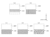
도 5은 일 실시 예에 따른 전자 장치의 차폐 부재를 도시한 도면이다. 5 is a diagram illustrating a shielding member of an electronic device according to an embodiment.
<501>을 참조하면, 차폐 부재(200)는 플레이트(201), 및 측벽(202)을 포함할 수 있다. 측벽(202)은 플레이트(201)에 대해 실질적으로 수직하게 연장될 수 있다. 측벽(202)은 플레이트(201)로부터 기판(150)에 포함된 접착 물질(154)까지 연장될 수 있다. 기판(150) 또는 접착 물질(154)과 접촉하는 측벽(202)의 단부(end portion)에는 돌출 부분(210)들과, 돌출 부분(210)들 사이에 홈 부분(230)이 형성될 수 있다.Referring to <501>, the shielding
도시된 실시 예에서, 돌출 부분(210)에는 하나 이상의 제1 리세스(221)이 형성될 수 있다. 제1 리세스(221)은 측벽(202)을 관통하며 기판(150)과 마주보는 방향으로 개방된 개구로 형성될 수 있다. In the illustrated embodiment, one or more
<502> 및 <503>을 참조하면, 측벽(202)은 차폐 공간(290)을 향하는 내측면(2202), 차폐 공간(290) 외측을 향하며 상기 내측면(2202)과 대향하는 외측면(2201), 및 상기 내측면(2202)과 상기 외측면(2201) 사이에 형성되며 상기 기판(150)과 마주보는 지지면(2203)을 포함할 수 있다. 돌출 부분(210)에 포함된 외측면(2201)과 내측면(2202)에는 접착 물질(154)이 접촉할 수 있다. 돌출 부분(210)에 포함된 지지면(2203)과 기판(150) 사이에는 접착 물질(154)의 적어도 일부가 형성될 수 있다. Referring to <502> and <503>, the
도시된 실시 예에서, 제1 리세스(221)은 지지면(2203)에 형성되며 측벽(202)의 외측면(2201)과 측벽(202)의 내측면(2202)을 관통하는 개구로 이루어질 수 있다. <501>에 도시된 확대도를 참조하면, 제1 리세스(221)은 기판(150)과 마주보는 지지면(2203)으로부터 플레이트(201)로 갈수록 넓어질 수 있다. 일례로, 제1 리세스(221)은 바닥면(2211), 및 바닥면(2211)의 양 측에 형성된 내측벽(2212)에 의해 형성될 수 있으며, 내측벽(2212)들 사이의 간격은, 지지면(2203)에서 제1 길이(L1)만큼 이격될 수 있으며, 바닥면(2211)은 제1 길이(L1)보다 긴 제2 길이(L2)로 연장될 수 있다. In the illustrated embodiment, the
다양한 실시 예에서, 제1 리세스(221)은 바닥면(2211)으로부터 기판(150)으로 갈수록 내측벽(2212) 사이의 간격이 감소하도록 형성될 수 있다. 이와 같은 내측벽(2212)들 사이에는 접착 물질(154)이 수용될 수 있으며, 차폐 부재(200)가 기판(150)으로부터 이탈되는 것을 방지할 수 있다. 구체적으로, 접착 물질(154)에 열이 가해지면서 접착 물질(154)은 유동 가능한 상태(예: 액체 상태)로 형성될 수 있으며, 유동 가능한 상태의 접착 물질(154)이 내측벽(2212)들 사이로 수용될 수 있다. 내측벽(2212)들 사이로 수용된 접착 물질(154)은 열이 식으면서(cooling down) 굳을 수 있다. 일례로, 차폐 부재(200)에 차폐 부재(200)가 기판(150)으로부터 멀어지는 방향(예: 도면에서 상부 측)으로 충격이 가해지는 경우, 제1 리세스(221)의 하부 측(예: 제1 리세스(221)의 바닥면(2211)으로부터 기판(150)을 향하는 방향)으로 갈수록 간격이 작아지는 제1 리세스(221)의 내측벽(2212)들에 의해 접착 물질(154)이 지지될 수 있다. 이로써 차폐 부재(200)가 기판(150)으로부터 이탈되는 것이 방지될 수 있다.In various embodiments, the
다양한 실시 예에서, 제1 리세스(221)은 지지면(2203)에 형성된 제1 부분과 측벽 내부에 형성된 제2 부분을 포함할 수 있으며, 제1 부분은 제2 부분보다 작게 형성될 수 있다.In various embodiments, the
도 6은 일 실시 예에 따른 전자 장치의 차폐 부재를 도시한 도면이다. 6 is a diagram illustrating a shielding member of an electronic device according to an embodiment.
<601>을 참조하면, 차폐 부재(200)는 플레이트(201), 및 측벽(202)을 포함할 수 있다. 측벽(202)은 플레이트(201)에 대해 실질적으로 수직하게 연장될 수 있다. Referring to <601>, the shielding
<602>을 참조하면, 측벽(202)은 플레이트(201)로부터 기판(150)에 포함된 접착 물질(154)까지 연장될 수 있다. 기판(150) 또는 접착 물질(154)과 접촉하는 측벽(202)의 단부(end portion)에는 돌출 부분(210)들과, 돌출 부분(210)들 사이에 홈 부분(230)이 형성될 수 있다. 홈 부분(230)은 기판(150)으로부터 제1 간격으로 이격되며 돌출 부분(210)은 기판(150)으로부터 제1 간격보다 큰 제2 간격으로 이격될 수 있다. 또는 돌출 부분(210)은 기판(150)에 접촉될 수 있다.Referring to <602>, the
<602>를 참조하면, 측벽(202)은 차폐 공간(290)을 향하는 내측면(2202), 차폐 공간(290) 외측을 향하며 상기 내측면(2202)과 대향하는 외측면(2201), 및 상기 내측면(2202)과 상기 외측면(2201) 사이에 형성되며 상기 기판(150)과 마주보는 지지면(2203)을 포함할 수 있다. 돌출 부분(210)에 포함된 외측면(2201)과 내측면(2202)에는 접착 물질(154)이 접촉할 수 있다. 돌출 부분(210)에 포함된 지지면(2203)과 기판(150) 사이에는 접착 물질(154)의 적어도 일부가 형성될 수 있다. Referring to <602>, the
도시된 실시 예에서, 돌출 부분(210)의 외측면(2201)에는 제2 리세스(223)가 형성될 수 있다. 제2 리세스(223)는 측벽(202)의 둘레 방향(예: 도 4에서 플레이트(201)와 기판(150) 사이의 차폐 공간(290)을 둘러싸는 측벽(202)의 연장 방향)을 따라 연장될 수 있다. In the illustrated embodiment, a
도시된 실시 예에서, 접착 물질(154)은 기판(150)으로부터 측벽(202)의 외측면(2201)과 측벽(202)의 내측면(2202)의 적어도 일부를 덮도록 연장될 수 있다. 외측면(2201)에 형성된 제2 리세스(223)에는 접착 물질(154)이 수용될 수 있다. <601> 및 <602>를 참조하면 제2 리세스(223)는 측벽(202)의 외측면(2201)에 형성되는 것으로 도시되나, 이에 한정되지 않으며 제2 리세스(223)는 측벽(202)의 내측면(2202), 또는 측벽(202)의 외측면(2201)과 내측면(2202) 모두에 형성될 수 있다. In the illustrated embodiment, the
<603>을 참조하면, 제2 리세스(223)는 측벽(202)의 외측면(2201) 및/또는 내측면(2202)에 복수로 형성될 수 있다. 복수의 제2 리세스(223)는 각각 측벽(202)의 둘레 방향을 따라 연장될 수 있다. <603>에 도시된 실시 예에서도, 접착 물질(154)은 기판(150)으로부터 측벽(202)의 외측면(2201)과 내측면(2202)의 적어도 일부를 덮도록 연장될 수 있다. 이 때, 접착 물질(154)은 복수의 제2 리세스(223) 모두에 수용될 수 있다.Referring to <603>, a plurality of
도 6에 도시된 실시 예들은, 측벽(202)에 형성된 리세스에 용융된 액체 상태의 접착 물질(154)이 스며듬으로써, 접착 물질(154)과 측벽(202)의 접촉 면적이 증가될 수 있다. 이로써 차폐 부재(200)와 접착 물질(154) 사이의 접착력이 향상되고 차폐 부재(200)가 기판(150)으로부터 쉽게 이탈되는 것이 방지될 수 있다.6, the contact area between the
도 7은 일 실시 예에 따른 전자 장치의 차폐 부재를 도시한 도면이다. 7 is a diagram illustrating a shielding member of an electronic device according to an embodiment.
<701> 및 <702>를 참조하면, 차폐 부재(200)는 플레이트(201), 및 측벽(202)을 포함할 수 있다. 측벽(202)은 플레이트(201)에 대해 실질적으로 수직하게 연장될 수 있다. Referring to <701> and <702>, the shielding
측벽(202)은 플레이트(201)로부터 기판(150)에 포함된 접착 물질(154)까지 연장될 수 있다. 기판(150) 또는 접착 물질(154)과 접촉하는 측벽(202)의 단부(end portion)에는 돌출 부분(210)들과, 돌출 부분(210)들 사이에 홈 부분(230)이 형성될 수 있다. 홈 부분(230)은 기판(150)으로부터 제1 간격으로 이격되며 돌출 부분(210)은 기판(150)으로부터 제1 간격보다 큰 제2 간격으로 이격될 수 있다. 또는 돌출 부분(210)은 기판(150)에 접촉될 수 있다.The
<702>를 참조하면, 측벽(202)은 차폐 공간(290)을 향하는 내측면(2202), 차폐 공간(290) 외측을 향하며 상기 내측면(2202)과 대향하는 외측면(2201), 및 상기 내측면(2202)과 상기 외측면(2201) 사이에 형성되며 상기 기판(150)과 마주보는 지지면(2203)을 포함할 수 있다. 돌출 부분(210)에 포함된 외측면(2201)과 내측면(2202)에는 접착 물질(154)이 접촉할 수 있다. 돌출 부분(210)에 포함된 지지면(2203)과 기판(150) 사이에는 접착 물질(154)의 적어도 일부가 형성될 수 있다. Referring to <702>, the
도시된 실시 예에서, 돌출 부분(210)의 외측면(2201)에는 제3 리세스(225)가 형성될 수 있다. 제3 리세스(225)는 측벽(202)의 둘레 방향(예: 도 4에서 플레이트(201)와 기판(150) 사이의 차폐 공간(290)을 둘러싸는 방향)을 따라 연장될 수 있다. In the illustrated embodiment, a
도시된 실시 예에서, 측벽(202)은 내측면(2202)이 차폐 공간(290) 내부를 향해 볼록하고 외측면(2201)이 오목하도록 만곡 형성될 수 있다. 제3 리세스(225)는 오목하게 형성된 외측면(2201)을 포함할 수 있다. 제3 리세스(225)는 도 6에 도시된 제2 리세스(223)와 달리 곡면을 포함할 수 있다. 제3 리세스(225)는 측벽(202)의 프레스 압착 공정에 의해 형성될 수 있다.In the illustrated embodiment, the
도시된 실시 예에서, 접착 물질(154)은 기판(150)으로부터 측벽(202)의 외측면(2201)과 측벽(202)의 내측면(2202)의 적어도 일부를 덮도록 연장될 수 있다. 외측면(2201)에 형성된 제3 리세스(225)에는 접착 물질(154)이 수용될 수 있다. In the illustrated embodiment, the
<701> 및 <702>를 참조하면 제3 리세스(225)는 측벽(202)의 외측면(2201)에 형성되는 것으로 도시되나, 이에 한정되지 않으며 제3 리세스(225)는 측벽(202)의 내측면(2202), 또는 측벽(202)의 외측면(2201)과 내측면(2202) 모두에 형성될 수 있다. Referring to <701> and <702>, the
도 7에 도시된 실시 예들은, 측벽(202)에 형성된 리세스에 적어도 일부가 용융된 액체 상태의 접착 물질(154)이 수용됨으로써, 접착 물질(154)과 측벽(202)의 접촉 면적이 증가될 수 있다. 이후 접착 물질(154)이 식음에 따라 리세스 내부에 수용된 접착 물질(154)이 굳어질 수 있다. 이로써 차폐 부재(200)와 기판(150)의 접착력이 증가하고 차폐 부재(200)가 기판(150)으로부터 쉽게 이탈되는 것이 방지될 수 있다.In the embodiments illustrated in FIG. 7, a contact area between the
도 8은 일 실시 예에 따른 전자 장치의 차폐 부재를 도시한 도면이다. 8 is a diagram illustrating a shielding member of an electronic device according to an embodiment.
<801> 및 <802>를 참조하면, 차폐 부재(200)는 플레이트(201), 및 측벽(202)을 포함할 수 있다. 측벽(202)은 플레이트(201)에 대해 실질적으로 수직하게 연장될 수 있다. Referring to <801> and <802>, the shielding
측벽(202)은 플레이트(201)로부터 기판(150)에 포함된 접착 물질(154)까지 연장될 수 있다. 기판(150) 또는 접착 물질(154)과 접촉하는 측벽(202)의 단부(end portion)에는 돌출 부분(210)들과, 돌출 부분(210)들 사이에 홈 부분(230)이 형성될 수 있다. 홈 부분(230)은 기판(150)으로부터 제1 간격으로 이격되며 돌출 부분(210)은 기판(150)으로부터 제1 간격보다 큰 제2 간격으로 이격될 수 있다. 또는 돌출 부분(210)은 기판(150)에 접촉될 수 있다.The
<802>를 참조하면, 측벽(202)은 차폐 공간(290)을 향하는 내측면(2202), 차폐 공간(290) 외측을 향하며 상기 내측면(2202)과 대향하는 외측면(2201), 및 상기 내측면(2202)과 상기 외측면(2201) 사이에 형성되며 상기 기판(150)과 마주보는 지지면(2203)을 포함할 수 있다. 돌출 부분(210)에 포함된 외측면(2201)과 내측면(2202)에는 접착 물질(154)이 접촉할 수 있다. 돌출 부분(210)에 포함된 지지면(2203)과 기판(150) 사이에는 접착 물질(154)의 적어도 일부가 형성될 수 있다. Referring to <802>, the
도시된 실시 예에서, 돌출 부분(210)의 외측면(2201)에는 하나 이상의 제4 리세스(227)가 형성될 수 있다. 복수의 제4 리세스(227)는 측벽(202)의 둘레 방향(예: 도 4에서 플레이트(201)와 기판(150) 사이의 차폐 공간(290)을 둘러싸는 방향)을 따라 서로 소정의 간격으로 이격 배치될 수 있다. In the illustrated embodiment, one or more
도시된 실시 예에서, 접착 물질(154)은 기판(150)으로부터 측벽(202)의 외측면(2201)과 측벽(202)의 내측면(2202)의 적어도 일부를 덮도록 연장될 수 있다. 외측면(2201)에 형성된 제4 리세스(227)에는 접착 물질(154)이 수용될 수 있다. In the illustrated embodiment, the
<801> 및 <802>를 참조하면, 제4 리세스(227a)는 측벽(202)의 외측면(2201)에 형성되는 것으로 도시되나, 이에 한정되지 않으며 제4 리세스(227a)는 측벽(202)의 내측면(2202), 또는 측벽(202)의 외측면(2201)과 내측면(2202) 모두에 형성될 수 있다. Referring to <801> and <802>, the
<801>에 도시된 바와 같이, 제4 리세스(227)는 원형의 단면을 가질 수 있다. 이 때, <802>에 도시된 바와 같이 제4 리세스(227a)는 원뿔 형상으로 형성될 수 있다. 또는 <803>에 도시된 바와 같이, 제4 리세스(227b)는 구 형상으로 형성될 수 있다. As shown in <801>, the
일례로, <802>에 도시된 제4 리세스(227)는 측벽(202)의 외측면(2201)으로부터 차폐 공간(290)을 향하는 방향으로 갈수록 직경이 점차 감소하도록 형성될 수 있다. 일례로, <803>에 도시된 제4 리세스(227b)는 측벽(202)의 외측면(2201)이 오목하게 함몰됨으로써 형성될 수 있다. For example, the
도시된 실시 예에서, 측벽(202)의 외측면(2201)에 형성된 제4 리세스(227)는 제4 리세스(227)를 형성하기 위해 이용된 툴의 형상에 따라 달라질 수 있다. <802> 및 <803>에 도시된 단면 형상은 일 예시이며, 본 발명의 일 실시 예에 따른 전자 장치(100)의 차폐 부재(200)는 다양한 단면 형상을 가지는 제4 리세스(227)를 포함할 수 있다.In the illustrated embodiment, the
도 8에 도시된 실시 예들은, 측벽(202)에 형성된 하나 이상의 제4 리세스(227)를 포함하고 접착 물질(154)이 제4 리세스(227) 내부에 수용됨으로써, 접착 물질(154)과 측벽(202)의 접촉 면적이 증가될 수 있다. 이로써 차폐 부재(200)와 기판(150) 사이의 접착력이 향상되고, 차폐 부재(200)가 기판(150)으로부터 쉽게 이탈되는 것이 방지될 수 있다.The embodiments illustrated in FIG. 8 include one or more
도 9는 일 실시 예에 따른 전자 장치(100)의 차폐 부재(200)를 도시한 도면이다. 도 10은 도 9에 도시된 패턴 영역(240)의 확대도이다. 9 is a diagram illustrating a shielding
도 9를 참조하면, 차폐 부재(200)의 측벽(202)은 돌출 부분(210)과 돌출 부분(210) 사이에 형성된 홈 부분(230)을 포함할 수 있다. 돌출 부분(210)은 차폐 공간(290)을 향하는 내측면(2202)과 내측면(2202)에 대향하는 외측면(2201)을 포함할 수 있다. 도시된 실시 예에서, 돌출 부분(210)은 돌출 부분(210)의 외측면(2201) 및 내측면(2202) 중 적어도 하나에 형성된 패턴 영역(240)이 형성될 수 있다. Referring to FIG. 9, the
도 10을 참조하면, 상기 패턴 영역(240)은 다양한 형태의 패턴을 포함할 수 있다. Referring to FIG. 10, the
도 10의 (a)를 참조하면, 상기 패턴 영역(240)은 측벽(202)의 둘레 방향(예: 도면에서 y축 방향)으로 연장된 제1 패턴(241)을 포함할 수 있다. 도 10의 (b)를 참조하면, 상기 패턴 영역(240)은 기판(150)으로부터 차폐 부재(200)의 플레이트(201)까지 연장되는 방향(예: 도면에서 z축 방향)으로 연장된 제2 패턴(242)을 포함할 수 있다. 도 10의 (c) 및 (d)를 참조하면, 상기 패턴 영역(240)은 y축 방향과 z축 방향 사이의 소정의 각도로 연장된 제3 패턴(243) 및 제4 패턴(244)을 포함할 수 있다. 도 10의 (e)를 참조하면, 상기 패턴 영역(240)은 무작위로 형성된 제5 패턴(245)을 포함할 수 있다. Referring to (a) of FIG. 10, the
도시된 실시 예에서, 패턴 영역(240)은 돌출 부분(210)의 외측면(2201)에 형성된 것으로 도시되나 반드시 이에 한정되지 않으며 돌출 부분(210)의 내측면(2202)에 형성될 수 있다.In the illustrated embodiment, the
다양한 실시 예에서, 패턴 영역(240)은 도 10에 도시된 제1 내지 제5 패턴(241, 242, 243, 244, 245) 중 적어도 하나의 패턴을 포함할 수 있다.In various embodiments, the
다양한 실시 예에 따른 전자 장치(100)의 차폐 부재(200)는, 도 10에 예시적으로 도시된 패턴들(241, 242, 243, 244, 245) 중 적어도 하나를 포함하고 열에 의해 적어도 일부가 용융된 접착 물질(154)이 패턴에 수용됨으로써, 접착 물질(154)과 차폐 부재(200)의 접촉 면적이 증가될 수 있다. 이로써 차폐 부재(200)가 기판(150)으로부터 쉽게 이탈되는 것이 방지될 수 있다.The shielding
본 문서의 다양한 실시 예들 및 이에 사용된 용어들은 본 문서에 기재된 기술을 특정한 실시 형태에 대해 한정하려는 것이 아니며, 해당 실시 예의 다양한 변경, 균등물, 및/또는 대체물을 포함하는 것으로 이해되어야 한다. 도면의 설명과 관련하여, 유사한 구성요소에 대해서는 유사한 참조 부호가 사용될 수 있다. 단수의 표현은 문맥상 명백하게 다르게 뜻하지 않는 한, 복수의 표현을 포함할 수 있다. 본 문서에서, "A 또는 B", "A 및/또는 B 중 적어도 하나", "A, B 또는 C" 또는 "A, B 및/또는 C 중 적어도 하나" 등의 표현은 함께 나열된 항목들의 모든 가능한 조합을 포함할 수 있다. "제1," "제2," "첫째," 또는 "둘째,"등의 표현들은 해당 구성요소들을, 순서 또는 중요도에 상관없이 수식할 수 있고, 한 구성요소를 다른 구성요소와 구분하기 위해 사용될 뿐 해당 구성요소들을 한정하지 않는다. 어떤(예: 제1) 구성요소가 다른(예: 제2) 구성요소에 "(기능적으로 또는 통신적으로) 연결되어" 있다거나 "접속되어" 있다고 언급된 때에는, 상기 어떤 구성요소가 상기 다른 구성요소에 직접적으로 연결되거나, 다른 구성요소(예: 제 3 구성요소)를 통하여 연결될 수 있다.It should be understood that various embodiments of the document and terms used therein are not intended to limit the technology described in this document to specific embodiments, and include various modifications, equivalents, and / or replacements of the embodiments. In connection with the description of the drawings, similar reference numerals may be used for similar components. Singular expressions may include plural expressions unless the context clearly indicates otherwise. In this document, expressions such as "A or B", "at least one of A and / or B", "A, B or C" or "at least one of A, B and / or C", etc. are all of the items listed together. Possible combinations may be included. Expressions such as "first," "second," "first," or "second," can modify the components, regardless of order or importance, to distinguish one component from another component It is used but does not limit the components. When it is stated that one (eg, first) component is “connected (functionally or communicatively)” to another (eg, second) component or is “connected,” the component is the other It may be directly connected to the component, or may be connected through another component (eg, the third component).
본 문서에서, "~하도록 설정된(adapted to or configured to)"은 상황에 따라, 예를 들면, 하드웨어적 또는 소프트웨어적으로 "~에 적합한," "~하는 능력을 가지는," "~하도록 변경된," "~하도록 만들어진," "~를 할 수 있는," 또는 "~하도록 설계된"과 상호 호환적으로(interchangeably) 사용될 수 있다. 어떤 상황에서는, "~하도록 구성된 장치"라는 표현은, 그 장치가 다른 장치 또는 부품들과 함께 "~할 수 있는" 것을 의미할 수 있다. 예를 들면, 문구 "A, B, 및 C를 수행하도록 설정된 (또는 구성된) 프로세서"는 해당 동작들을 수행하기 위한 전용 프로세서(예: 임베디드 프로세서), 또는 메모리 장치에 저장된 하나 이상의 프로그램들을 실행함으로써, 해당 동작들을 수행할 수 있는 범용 프로세서(예: CPU 또는 AP)를 의미할 수 있다.In this document, "adapted to or configured to" is changed to be "appropriate for," having the ability to "appropriate," for example, in hardware or software. It can be used interchangeably with "made to do," "to do," or "designed to do." In some situations, the expression "a device configured to" may mean that the device "can" with other devices or parts. For example, the phrase “processor configured (or configured) to perform A, B, and C” may be performed by executing a dedicated processor (eg, an embedded processor) to perform the corresponding operations, or one or more programs stored in a memory device, It may mean a general-purpose processor (eg, CPU or AP) capable of performing the corresponding operations.
본 문서에서 사용된 용어 "모듈"은 하드웨어, 소프트웨어 또는 펌웨어(firmware)로 구성된 유닛(unit)을 포함하며, 예를 들면, 로직, 논리 블록, 부품, 또는 회로 등의 용어와 상호 호환적으로 사용될 수 있다. "모듈"은, 일체로 구성된 부품 또는 하나 또는 그 이상의 기능을 수행하는 최소 단위 또는 그 일부가 될 수 있다. "모듈"은 기계적으로 또는 전자적으로 구현될 수 있으며, 예를 들면, 어떤 동작들을 수행하는, 알려졌거나 앞으로 개발될, ASIC(application-specific integrated circuit) 칩, FPGAs(field-programmable gate arrays), 또는 프로그램 가능 논리 장치를 포함할 수 있다.As used herein, the term "module" includes a unit composed of hardware, software, or firmware, and may be used interchangeably with terms such as, for example, logic, logic block, component, or circuit. You can. The "module" may be an integrally configured component or a minimum unit that performs one or more functions or a part thereof. The "module" may be implemented mechanically or electronically, for example, an application-specific integrated circuit (ASIC) chip, field-programmable gate arrays (FPGAs), that will be known or developed in the future, performing certain operations, or It may include a programmable logic device.
다양한 실시 예들에 따른 장치(예: 모듈들 또는 그 기능들) 또는 방법(예: 동작들)의 적어도 일부는 프로그램 모듈의 형태로 컴퓨터로 판독 가능한 저장 매체에 저장된 명령어로 구현될 수 있다. 상기 명령어가 프로세서에 의해 실행될 경우, 프로세서가 상기 명령어에 해당하는 기능을 수행할 수 있다. 컴퓨터로 판독 가능한 기록 매체는, 하드디스크, 플로피디스크, 마그네틱 매체(예: 자기테이프), 광기록 매체(예: CD-ROM, DVD, 자기-광 매체(예: 플롭티컬 디스크), 내장 메모리 등을 포함할 수 있다. 명령어는 컴파일러에 의해 만들어지는 코드 또는 인터프리터에 의해 실행될 수 있는 코드를 포함할 수 있다.At least a part of an apparatus (eg, modules or functions thereof) or a method (eg, operations) according to various embodiments may be implemented as instructions stored in a computer-readable storage medium in the form of program modules. When the instruction is executed by the processor, the processor may perform a function corresponding to the instruction. Computer-readable recording media include hard disks, floppy disks, magnetic media (eg magnetic tapes), optical recording media (eg CD-ROMs, DVDs, magnetic-optical media (eg floptical disks), internal memory, etc. The instructions may include code generated by a compiler or code that can be executed by an interpreter.
다양한 실시 예들에 따른 구성 요소(예: 모듈 또는 프로그램 모듈) 각각은 단수 또는 복수의 개체로 구성될 수 있으며, 전술한 해당 서브 구성 요소들 중 일부 서브 구성 요소가 생략되거나, 또는 다른 서브 구성 요소를 더 포함할 수 있다. 대체적으로 또는 추가적으로, 일부 구성 요소들(예: 모듈 또는 프로그램 모듈)은 하나의 개체로 통합되어, 통합되기 이전의 각각의 해당 구성 요소에 의해 수행되는 기능을 동일 또는 유사하게 수행할 수 있다. 다양한 실시 예들에 따른 모듈, 프로그램 모듈 또는 다른 구성 요소에 의해 수행되는 동작들은 순차적, 병렬적, 반복적 또는 휴리스틱(heuristic)하게 실행되거나, 적어도 일부 동작이 다른 순서로 실행되거나, 생략되거나, 또는 다른 동작이 추가될 수 있다.Each component (eg, a module or a program module) according to various embodiments may be composed of a singular or a plurality of entities, and some of the aforementioned sub-components may be omitted, or other sub-components may be omitted. It may further include. Alternatively or additionally, some components (eg, modules or program modules) can be integrated into one entity, performing the same or similar functions performed by each corresponding component before being integrated. Operations performed by a module, program module, or other component according to various embodiments may be sequentially, parallel, repetitively, or heuristically executed, or at least some operations may be executed in a different order, omitted, or other operations This can be added.
Claims (20)
하우징;
상기 하우징 내부에 배치되며 제1 전기 소자, 및 접착 물질을 포함하는 기판; 및
상기 접착 물질에 의해 상기 기판에 고정되며 내부에 상기 제1 전기 소자가 배치된 차폐 공간을 형성하는 차폐 부재;를 포함하고,
상기 차폐 부재는,
상기 기판과 마주보는 플레이트, 및
상기 플레이트와 상기 기판을 연결하도록 상기 플레이트와 상기 기판 사이에 형성되며 상기 차폐 공간을 둘러싸는 둘레 방향으로 연장되는 측벽을 포함하고,
상기 접착 물질은 상기 측벽의 적어도 일부를 감싸도록 상기 기판에 배치되고,
상기 측벽은 상기 차폐 공간을 향하는 외측면과, 상기 외측면에 대향하는 내측면과, 상기 기판과 마주보는 바닥면을 포함하고,
상기 접착 물질은 적어도 일부가 상기 외측면과 상기 내측면의 적어도 일부를 덮도록 형성되고,
상기 외측면 및 상기 내측면 중 적어도 하나에는 상기 접착 물질이 수용되는 리세스가 형성되는 전자 장치.In the electronic device,
housing;
A substrate disposed inside the housing and including a first electrical element and an adhesive material; And
It includes; a shielding member fixed to the substrate by the adhesive material and forming a shielding space in which the first electric element is disposed.
The shield member,
A plate facing the substrate, and
A sidewall formed between the plate and the substrate to connect the plate and the substrate and extending in a circumferential direction surrounding the shielding space,
The adhesive material is disposed on the substrate to surround at least a portion of the sidewall,
The side wall includes an outer surface facing the shielding space, an inner surface facing the outer surface, and a bottom surface facing the substrate,
The adhesive material is formed to cover at least a portion of the outer surface and at least a portion of the inner surface,
An electronic device having a recess in which the adhesive material is accommodated is formed on at least one of the outer surface and the inner surface.
상기 접착 물질은 도전성인 전자 장치.The method according to claim 1,
The adhesive material is a conductive electronic device.
상기 접착 물질은 솔더(solder)를 포함하는 전자 장치.The method according to claim 1,
The adhesive material is an electronic device comprising a solder (solder).
상기 플레이트는 실질적으로 제1 방향을 향하고,
상기 리세스는 상기 제1 방향에 수직한 방향으로 연장된 전자 장치.The method according to claim 1,
The plate is substantially facing the first direction,
The recess is an electronic device extending in a direction perpendicular to the first direction.
상기 리세스는 상기 둘레 방향을 따라 연장되는 제1 리세스를 포함하는 전자 장치.The method according to claim 1,
The recess is an electronic device including a first recess extending along the circumferential direction.
상기 제1 리세스는 상기 측벽의 상기 외측면에 형성되는 전자 장치.The method according to claim 5,
The first recess is an electronic device formed on the outer surface of the side wall.
상기 리세스는 상기 둘레 방향에 실질적으로 수직한 방향으로 연장되는 제2 리세스를 포함하는 전자 장치.The method according to claim 1,
The recess is an electronic device including a second recess extending in a direction substantially perpendicular to the circumferential direction.
상기 리세스는 상기 둘레 방향을 따라 소정의 간격으로 이격 형성되도록 복수개로 이루어지는 전자 장치.The method according to claim 1,
An electronic device comprising a plurality of recesses spaced apart at predetermined intervals along the circumferential direction.
상기 리세스는 상기 측벽의 상기 외측면에 형성되는 전자 장치.The method according to claim 8,
The recess is an electronic device formed on the outer surface of the side wall.
상기 측벽은 적어도 일부가 상기 차폐 공간을 향해 돌출되도록 만곡된 만곡 부분(curved portion)을 포함하고,
상기 리세스는 상기 만곡 부분에 포함된 외측면에 의해 형성되는 전자 장치. The method according to claim 1,
The side wall includes a curved portion that is curved such that at least a portion protrudes toward the shielding space,
The recess is an electronic device formed by an outer surface included in the curved portion.
상기 차폐 부재는 금속 물질을 포함하는 전자 장치.The method according to claim 1,
The shielding member is an electronic device comprising a metal material.
상기 측벽의 상기 외측면과 상기 내측면은 각각, 상기 도전성 접착 물질이 접촉되는 접촉 영역을 포함하고,The method according to claim 1,
Each of the outer surface and the inner surface of the sidewall includes a contact area to which the conductive adhesive material is contacted,
상기 접촉 영역은 상기 인쇄 회로 기판과 연결되고,
상기 접착 물질은 상기 기판으로부터 상기 접촉 영역까지 연장되는 전자 장치.The method according to claim 12,
The contact area is connected to the printed circuit board,
The adhesive material extends from the substrate to the contact area.
제1 커버, 상기 제1 커버와 마주보는 제2 커버, 및 상기 제1 커버와 상기 제2 커버 사이의 공간을 둘러싸는 측면 부재를 포함하는 하우징 구조물;
상기 제1 커버와 상기 제2 커버 사이에 배치되는 디스플레이;
상기 디스플레이와 상기 제2 커버 사이에 배치되며 전기 소자가 실장된 인쇄 회로 기판; 및
상기 인쇄 회로 기판에 형성된 도전성 접착 물질에 의해 상기 인쇄 회로 기판에 고정되는 차폐 부재;를 포함하고,
상기 차폐 부재는,
상기 인쇄 회로 기판과 마주보는 플레이트 부분, 및 상기 플레이트 부분과 상기 인쇄 회로 기판 사이의 차폐 공간을 둘러싸는 측벽 부분을 포함하고,
상기 전기 소자는 상기 차폐 공간에 배치되고,
상기 측벽 부분은 상기 차폐 공간을 향하는 내측면, 상기 내측면에 대향하는 외측면, 및 상기 기판에 의해 지지되는 지지면을 포함하고,
상기 지지면에는 상기 접착 물질이 수용되는 하나 이상의 리세스가 형성되고,
상기 하나 이상의 리세스는 바닥면과 상기 바닥면의 양 단부에 연결되는 내측벽을 포함하고,
상기 내측벽 사이의 거리는 상기 바닥면으로부터 상기 인쇄 회로 기판을 향하는 방향으로 갈수록 작아지는 전자 장치.In the electronic device,
A housing structure including a first cover, a second cover facing the first cover, and a side member surrounding a space between the first cover and the second cover;
A display disposed between the first cover and the second cover;
A printed circuit board disposed between the display and the second cover and having electrical elements mounted thereon; And
It includes; a shielding member fixed to the printed circuit board by a conductive adhesive material formed on the printed circuit board;
The shield member,
A plate portion facing the printed circuit board, and a side wall portion surrounding a shielding space between the plate portion and the printed circuit board,
The electrical element is disposed in the shielding space,
The side wall portion includes an inner surface facing the shielding space, an outer surface facing the inner surface, and a supporting surface supported by the substrate,
One or more recesses in which the adhesive material is accommodated are formed on the support surface,
The one or more recesses include a bottom surface and an inner wall connected to both ends of the bottom surface,
An electronic device having a smaller distance between the inner walls toward the printed circuit board from the bottom surface.
상기 도전성 접착 물질은 상기 측벽 부분의 상기 내측면 및 상기 측벽 부분의 상기 외측면 각각의 적어도 일부를 덮는 전자 장치.The method according to claim 14,
The conductive adhesive material covers at least a portion of each of the inner surface of the side wall portion and the outer surface of the side wall portion.
상기 하나 이상의 리세스는 상기 측벽 부분의 상기 내측면 및 상기 외측면을 관통하는 전자 장치.The method according to claim 14,
The one or more recesses pass through the inner surface and the outer surface of the side wall portion.
상기 측벽 부분의 상기 외측면과 상기 내측면은 각각, 상기 도전성 접착 물질이 접촉되는 접촉 영역을 포함하고,
상기 하나 이상의 리세스는 상기 접촉 영역을 관통하도록 형성되는 전자 장치.The method according to claim 14,
Each of the outer surface and the inner surface of the side wall portion includes a contact area to which the conductive adhesive material is contacted,
The one or more recesses are formed to penetrate the contact area.
상기 접촉 영역은 상기 인쇄 회로 기판과 연결되고,
상기 도전성 접착 물질은 상기 인쇄 회로 기판으로부터 상기 접촉 영역까지 연장되는 전자 장치.The method according to claim 14,
The contact area is connected to the printed circuit board,
The conductive adhesive material extends from the printed circuit board to the contact area.
상기 측벽 부분은 상기 기판을 향해 소정의 간격으로 돌출된 돌출 부분과 돌출 부분 사이에 형성된 홈 부분을 포함하고,
상기 하나 이상의 리세스는 상기 돌출 부분에 형성되는 전자 장치.The method according to claim 14,
The side wall portion includes a protruding portion protruding at a predetermined distance toward the substrate and a groove portion formed between the protruding portion,
The one or more recesses are formed in the protruding portion.
상기 차폐 부재는 금속 물질을 포함하는 전자 장치.The method according to claim 14,
The shielding member is an electronic device comprising a metal material.
Priority Applications (3)
| Application Number | Priority Date | Filing Date | Title |
|---|---|---|---|
| KR1020180119911A KR102552665B1 (en) | 2018-10-08 | 2018-10-08 | An electronic device comprising a shield member having a recess formed therein for receiving an adhesive material |
| US17/282,399 US20210352169A1 (en) | 2018-10-08 | 2019-10-08 | Electronic device comprising shielding member comprising recess for containing adhesive material |
| PCT/KR2019/013195 WO2020076054A1 (en) | 2018-10-08 | 2019-10-08 | Electronic device comprising shielding member comprising recess for containing adhesive material |
Applications Claiming Priority (1)
| Application Number | Priority Date | Filing Date | Title |
|---|---|---|---|
| KR1020180119911A KR102552665B1 (en) | 2018-10-08 | 2018-10-08 | An electronic device comprising a shield member having a recess formed therein for receiving an adhesive material |
Publications (2)
| Publication Number | Publication Date |
|---|---|
| KR20200040079A true KR20200040079A (en) | 2020-04-17 |
| KR102552665B1 KR102552665B1 (en) | 2023-07-10 |
Family
ID=70165029
Family Applications (1)
| Application Number | Title | Priority Date | Filing Date |
|---|---|---|---|
| KR1020180119911A KR102552665B1 (en) | 2018-10-08 | 2018-10-08 | An electronic device comprising a shield member having a recess formed therein for receiving an adhesive material |
Country Status (3)
| Country | Link |
|---|---|
| US (1) | US20210352169A1 (en) |
| KR (1) | KR102552665B1 (en) |
| WO (1) | WO2020076054A1 (en) |
Families Citing this family (1)
| Publication number | Priority date | Publication date | Assignee | Title |
|---|---|---|---|---|
| CN112469258B (en) * | 2020-10-28 | 2022-03-01 | 西安电子科技大学 | Double-gap electromagnetic shielding system, design method thereof and microwave circuit |
Citations (2)
| Publication number | Priority date | Publication date | Assignee | Title |
|---|---|---|---|---|
| KR20110090793A (en) * | 2010-02-03 | 2011-08-10 | 조인셋 주식회사 | Shield case for emi shielding with soldering easily |
| KR20180094831A (en) * | 2016-02-18 | 2018-08-24 | 삼성전자주식회사 | Electronic device with thermal spreader |
Family Cites Families (6)
| Publication number | Priority date | Publication date | Assignee | Title |
|---|---|---|---|---|
| DE10223170A1 (en) * | 2002-05-24 | 2003-12-18 | Siemens Ag | EMC shielding for electronic components and EMC housings |
| WO2004077898A2 (en) * | 2003-02-26 | 2004-09-10 | Wavezero Inc. | Methods and devices for connecting and grounding an emi shield to a printed circuit board |
| KR101658821B1 (en) * | 2009-12-24 | 2016-10-04 | 삼성전자주식회사 | Shield can of mobile terminal |
| US9179537B2 (en) * | 2012-12-13 | 2015-11-03 | Apple Inc. | Methods for forming metallized dielectric structures |
| JP6432737B2 (en) * | 2015-03-04 | 2018-12-05 | セイコーエプソン株式会社 | MEMS device, head, and liquid ejecting apparatus |
| US10856454B2 (en) * | 2019-08-08 | 2020-12-01 | Intel Corporation | Electromagnetic interference (EMI) shield for circuit card assembly (CCA) |
-
2018
- 2018-10-08 KR KR1020180119911A patent/KR102552665B1/en active IP Right Grant
-
2019
- 2019-10-08 WO PCT/KR2019/013195 patent/WO2020076054A1/en active Application Filing
- 2019-10-08 US US17/282,399 patent/US20210352169A1/en active Pending
Patent Citations (2)
| Publication number | Priority date | Publication date | Assignee | Title |
|---|---|---|---|---|
| KR20110090793A (en) * | 2010-02-03 | 2011-08-10 | 조인셋 주식회사 | Shield case for emi shielding with soldering easily |
| KR20180094831A (en) * | 2016-02-18 | 2018-08-24 | 삼성전자주식회사 | Electronic device with thermal spreader |
Also Published As
| Publication number | Publication date |
|---|---|
| KR102552665B1 (en) | 2023-07-10 |
| WO2020076054A1 (en) | 2020-04-16 |
| US20210352169A1 (en) | 2021-11-11 |
Similar Documents
| Publication | Publication Date | Title |
|---|---|---|
| KR102509085B1 (en) | An electronic device comprising a metal material | |
| KR102417625B1 (en) | Method and electronic device comprising camera device | |
| KR20200094950A (en) | An electronic device comprising a housing comprising a metallic materials | |
| US11233924B2 (en) | Electronic device including camera | |
| KR20210101440A (en) | PCB structure and electronic device including the same | |
| EP4020946A1 (en) | Antenna fixing structure and electronic device comprising same | |
| KR20200126570A (en) | Electronic device having waterproof structure for electronic component | |
| EP3681135B1 (en) | Electronic device including display assembly | |
| US11729918B2 (en) | Electronic device comprising removable adhesive member | |
| KR102650458B1 (en) | Electronic device comprising display | |
| KR102552665B1 (en) | An electronic device comprising a shield member having a recess formed therein for receiving an adhesive material | |
| KR102624300B1 (en) | An electronic device including a connection structure for electrically connecting a printed circuit board and a housing | |
| KR20220017322A (en) | An electronic device including a structure for fixing a substrate | |
| US11962067B2 (en) | Antenna clip and electronic device comprising same | |
| EP3913458B1 (en) | Electronic device comprising a display module | |
| US11696404B2 (en) | Electronic device including structure for stacking substrates | |
| EP3755133B1 (en) | Electronic device having shield can structure | |
| KR20210098722A (en) | Electronic device including printed circuit board | |
| KR102663691B1 (en) | A camera module including heat dissipating structure and an electronic device including the same | |
| US20220302756A1 (en) | Electronic device including battery | |
| KR20220131100A (en) | Electronic device including battery | |
| KR20210128842A (en) | Electronic device including a metal housing | |
| KR20220153919A (en) | Electronic device including housing structure | |
| KR20230026209A (en) | Interposer and electronic device including same | |
| KR20200117553A (en) | A camera module including heat dissipating structure and an electronic device including the same |
Legal Events
| Date | Code | Title | Description |
|---|---|---|---|
| A201 | Request for examination | ||
| E902 | Notification of reason for refusal | ||
| E701 | Decision to grant or registration of patent right | ||
| GRNT | Written decision to grant |