KR20200037763A - X-ray imaging device and driving method thereof - Google Patents
X-ray imaging device and driving method thereof Download PDFInfo
- Publication number
- KR20200037763A KR20200037763A KR1020200039931A KR20200039931A KR20200037763A KR 20200037763 A KR20200037763 A KR 20200037763A KR 1020200039931 A KR1020200039931 A KR 1020200039931A KR 20200039931 A KR20200039931 A KR 20200039931A KR 20200037763 A KR20200037763 A KR 20200037763A
- Authority
- KR
- South Korea
- Prior art keywords
- electron beam
- limiting
- electrode
- focusing
- anode
- Prior art date
Links
Images


Classifications
-
- H—ELECTRICITY
- H01—ELECTRIC ELEMENTS
- H01J—ELECTRIC DISCHARGE TUBES OR DISCHARGE LAMPS
- H01J9/00—Apparatus or processes specially adapted for the manufacture, installation, removal, maintenance of electric discharge tubes, discharge lamps, or parts thereof; Recovery of material from discharge tubes or lamps
- H01J9/02—Manufacture of electrodes or electrode systems
- H01J9/022—Manufacture of electrodes or electrode systems of cold cathodes
- H01J9/025—Manufacture of electrodes or electrode systems of cold cathodes of field emission cathodes
-
- H—ELECTRICITY
- H01—ELECTRIC ELEMENTS
- H01J—ELECTRIC DISCHARGE TUBES OR DISCHARGE LAMPS
- H01J1/00—Details of electrodes, of magnetic control means, of screens, or of the mounting or spacing thereof, common to two or more basic types of discharge tubes or lamps
- H01J1/02—Main electrodes
- H01J1/30—Cold cathodes, e.g. field-emissive cathode
- H01J1/304—Field-emissive cathodes
-
- B—PERFORMING OPERATIONS; TRANSPORTING
- B82—NANOTECHNOLOGY
- B82Y—SPECIFIC USES OR APPLICATIONS OF NANOSTRUCTURES; MEASUREMENT OR ANALYSIS OF NANOSTRUCTURES; MANUFACTURE OR TREATMENT OF NANOSTRUCTURES
- B82Y10/00—Nanotechnology for information processing, storage or transmission, e.g. quantum computing or single electron logic
-
- H—ELECTRICITY
- H01—ELECTRIC ELEMENTS
- H01J—ELECTRIC DISCHARGE TUBES OR DISCHARGE LAMPS
- H01J2201/00—Electrodes common to discharge tubes
- H01J2201/30—Cold cathodes
- H01J2201/304—Field emission cathodes
- H01J2201/30446—Field emission cathodes characterised by the emitter material
- H01J2201/30453—Carbon types
- H01J2201/30469—Carbon nanotubes (CNTs)
Landscapes
- Engineering & Computer Science (AREA)
- Manufacturing & Machinery (AREA)
- X-Ray Techniques (AREA)
Abstract
Description
본 발명은 엑스선 영상 장치 및 그의 구동 방법에 관한 것이다. 더욱 상세하게는, 본 발명은 선명한 엑스선 영상을 획득할 수 있는 엑스선 영상 장치 및 그의 구동 방법에 관한 것이다.The present invention relates to an X-ray imaging apparatus and a driving method thereof. More specifically, the present invention relates to an X-ray imaging apparatus capable of obtaining a clear X-ray image and a driving method thereof.
점전자원은 전자의 흐름이 한 점에서 시작되는 전자원을 의미한다. 다시 말하면, 점전자원은 점과 같이 매우 작은 면적에서 전자빔이 발생되는 전자원을 의미한다. 전자빔이 점과 같이 매우 작은 면적에서 발생되는 경우, 발생된 전자빔을 전자광학계를 이용하여 다시 매우 작은 면적으로 집속하는 것이 용이하여, 미세한 프로브빔(probe beam)을 상대적으로 쉽게 만들 수 있는 이점이 있다. 전자빔의 직경이 작은 경우 여러 응용 분야에서 매우 유용하게 사용될 수 있다. 예를 들면, SEM, TEM과 같은 전자현미경 등의 해상도를 향상시킬 수 있고, 엑스선의 포컬스팟을 줄일 수 있어 엑스선 영상의 해상도를 향상 시킬 수 있다. The point electron source means an electron source where the flow of electrons starts at one point. In other words, a point electron source means an electron source in which an electron beam is generated in a very small area such as a point. When the electron beam is generated in a very small area such as a point, it is easy to focus the generated electron beam to a very small area again using an electro-optical system, and thus has the advantage of making the probe beam relatively easy. . If the diameter of the electron beam is small, it can be very useful in various applications. For example, the resolution of an electron microscope such as SEM and TEM can be improved, and the focal spot of the X-ray can be reduced, thereby improving the resolution of the X-ray image.
본 발명은 복수개의 나노 에미터들을 가지면서도 선명한 영상을 획득할 수 있는 엑스선 영상 장치를 제공하는 것을 목적으로 한다.An object of the present invention is to provide an X-ray imaging apparatus capable of obtaining a clear image while having a plurality of nano emitters.
본 발명은 복수개의 나노 에미터들 및 캐소드를 포함하는 전자빔 발생부; 상기 전자빔 발생부에서 방출된 전자빔을 집속시키는 제1 집속 전극; 상기 제1 집속 전극에서 집속된 상기 전자빔을 편향시키는 편향기; 상기 편향기에서 편향된 상기 전자빔의 진행을 제한하는 제한 전극; 및 상기 전자빔이 조사되어 엑스선을 방출하는 아노드를 포함하고, 상기 제한 전극은 상기 전자빔이 통과할 수 있는 제한 개구를 포함하는 엑스선 영상 장치를 제공한다. The present invention is an electron beam generator comprising a plurality of nano-emitters and a cathode; A first focusing electrode focusing the electron beam emitted from the electron beam generator; A deflector for deflecting the electron beam focused at the first focusing electrode; A limiting electrode limiting the progress of the electron beam deflected by the deflector; And an anode that emits X-rays by irradiating the electron beam, and the limiting electrode provides an X-ray imaging apparatus including a limiting opening through which the electron beam can pass.
상기 나노 에미터들에 전계를 가하는 게이트 전극을 더 포함할 수 있다.A gate electrode for applying an electric field to the nano emitters may be further included.
상기 아노드에서 방출되는 엑스선을 이용하여 엑스선 영상을 획득하는 영상 획득부를 더 포함할 수 있다.The X-ray image emitted from the anode may further include an image acquisition unit to acquire an X-ray image.
상기 편향기는 상기 전자빔이 지나는 전자빔 경로를 사이에 두고 서로 이격되는 전극들, 및 상기 전극들에 전압을 인가하는 전압원을 포함할 수 있다.The deflector may include electrodes spaced apart from each other with an electron beam path through which the electron beam passes, and a voltage source that applies a voltage to the electrodes.
상기 편향기는 상기 전자빔이 지나는 전자빔 경로를 사이에 두고 서로 이격되는 코일들, 및 상기 코일들에 전류를 제공하는 전류원을 포함할 수 있다.The deflector may include coils spaced apart from each other with an electron beam path through which the electron beam passes, and a current source that provides current to the coils.
상기 제한 개구를 통과한 전자빔을 집속시키는 제2 집속 전극을 더 포함할 수 있다.A second focusing electrode for focusing the electron beam passing through the restriction opening may be further included.
상기 제한 전극은 상기 제한 전극에 흐르는 전류를 측정하는 전류계를 더 포함할 수 있다.The limiting electrode may further include an ammeter for measuring the current flowing through the limiting electrode.
본 발명은 전자빔 발생부에서 복수개의 전자빔들을 방출하는 전자빔 방출 단계; 제한 전극을 이용하여 상기 전자빔 발생부에서 방출된 전자빔들의 진행을 제한하는 전자빔 제한 단계; 및 상기 전자빔들 중 적어도 일부를 아노드에 조사하는 아노드 조사 단계를 포함하고, 상기 제한 전극은 상기 전자빔들이 통과할 수 있는 제한 개구를 포함하는 엑스선 영상 장치의 구동 방법을 제공한다.The present invention is an electron beam emission step of emitting a plurality of electron beams in the electron beam generator; An electron beam limiting step of limiting the progress of electron beams emitted from the electron beam generator using a limiting electrode; And an anode irradiation step of irradiating at least some of the electron beams to the anode, wherein the limiting electrode provides a driving method of the X-ray imaging apparatus including a limiting opening through which the electron beams can pass.
상기 전자빔 제한 단계는, 상기 전자빔 발생부에서 방출된 전자빔들 중 하나의 전자빔이 상기 제한 개구를 통과하는 것을 포함할 수 있다.The electron beam limiting step may include passing one electron beam of the electron beams emitted from the electron beam generator through the restriction opening.
상기 전자빔 제한 단계는, 제1 집속 전극을 이용하여 상기 전자빔 발생부에서 방출된 전자빔들을 집속하는 것을 포함할 수 있다.The electron beam limiting step may include focusing electron beams emitted from the electron beam generation unit using a first focusing electrode.
상기 전자빔 제한 단계는, 편향기를 이용하여 상기 제1 집속 전극에서 집속된 전자빔들을 편향시키는 것을 더 포함할 수 있다.The electron beam limiting step may further include deflecting the electron beams focused at the first focusing electrode using a deflector.
상기 전자빔 제한 단계는, 상기 제한 전극에 흐르는 전류를 측정하여 상기 제한 전극의 전류 강도맵을 획득하는 것을 더 포함할 수 있다.The electron beam limiting step may further include acquiring a current intensity map of the limiting electrode by measuring a current flowing through the limiting electrode.
상기 전자빔들을 집속하는 것은, 상기 전류 강도맵이 선명한지 판단하는 것, 및 상기 제1 집속 전극을 제어하여 상기 전자빔들의 집속을 조절하는 것을 포함할 수 있다.Focusing the electron beams may include determining whether the current intensity map is clear, and controlling the focusing of the electron beams by controlling the first focusing electrode.
상기 전자빔들의 집속을 조절하는 것은, 상기 제한 개구의 하면과 동일한 레벨에서 상기 전자빔들의 평면적 면적이 최소가 되도록 상기 전자빔들의 집속을 조절하는 것을 포함할 수 있다.Adjusting the focusing of the electron beams may include adjusting the focusing of the electron beams so that the planar area of the electron beams is minimized at the same level as the lower surface of the limiting opening.
상기 제1 집속 전극에서 집속된 전자빔들을 편향시키는 것은, 상기 전류 강도맵에서 가장 어두운 스팟에 대응되도록 상기 편향기를 제어하는 것을 포함할 수 있다.Deflecting the electron beams focused at the first focusing electrode may include controlling the deflector to correspond to the darkest spot in the current intensity map.
상기 편향기를 제어하는 것은, 상기 편향기의 전압원의 전압의 크기를 최적화하는 것을 포함할 수 있다.Controlling the deflector may include optimizing the magnitude of the voltage of the voltage source of the deflector.
상기 편향기를 제어하는 것은, 상기 편향기의 전류원의 전류의 크기를 최적화하는 것을 포함할 수 있다.Controlling the deflector may include optimizing the magnitude of the current in the current source of the deflector.
상기 아노드 조사 단계는, 제2 집속 전극을 이용하여 상기 하나의 전자빔을 집속하는 것을 포함할 수 있다. The anode irradiation step may include focusing the one electron beam using a second focusing electrode.
본 발명에 따른 엑스선 영상 장치는 편향기 및 제한 개구를 포함함으로써, 복수개의 나노 에미터들에서 발생한 전자빔들 중 전류의 크기가 가장 큰 하나의 전자빔이 아노드에 조사될 수 있고, 선명한 영상을 획득할 수 있다.The X-ray imaging apparatus according to the present invention includes a deflector and a limiting opening, so that one of the electron beams generated from a plurality of nano-emitters having the largest current magnitude can be irradiated to the anode and obtain a clear image. You can.
도 1a 및 도 1b는 나노 에미터에서 발생한 전자빔의 특성을 설명하기 위한 도면들이다.
도 2a는 본 발명의 비교예에 따른 엑스선 영상 장치를 설명하기 위한 도면이다.
도 2b는 도 2a의 A영역의 확대도이다.
도 3은 도 2a 및 도 2b에 따른 엑스선 영상 장치에 의해 획득된 엑스선 영상이다.
도 4는 본 발명의 실시예들에 따른 엑스선 영상 장치를 설명하기 위한 도면이다,
도 5a 및 도 5b는 편향기의 실시예들을 설명하기 위한 도면들이다.
도 6은 도 4에 따른 엑스선 영상 장치에 의해 획득된 엑스선 영상이다.
도 7은 제한 전극에서 측정된 전류의 강도맵을 설명하기 위한 도면이다.
도 8a 내지 도 8c는 제한 개구를 통과하는 전자빔의 형태를 설명하기 위한 도면들이다.
도 9a 및 도 9b는 제한 전극의 전류 강도맵의 실제 이미지들이다.
도 10은 본 발명의 실시예들에 따른 엑스선 영상 장치의 구동 방법을 설명하기 위한 순서도이다.
도 11은 본 발명의 실시예들에 따른 엑스선 영상 장치를 설명하기 위한 도면이다.1A and 1B are diagrams for describing characteristics of an electron beam generated in a nano emitter.
2A is a diagram illustrating an X-ray imaging apparatus according to a comparative example of the present invention.
2B is an enlarged view of region A of FIG. 2A.
3 is an X-ray image obtained by the X-ray imaging apparatus according to FIGS. 2A and 2B.
4 is a view for explaining an X-ray imaging apparatus according to embodiments of the present invention,
5A and 5B are diagrams for describing embodiments of the deflector.
6 is an X-ray image obtained by the X-ray imaging apparatus according to FIG. 4.
7 is a view for explaining the intensity map of the current measured at the limiting electrode.
8A to 8C are views for explaining the shape of the electron beam passing through the restriction opening.
9A and 9B are actual images of the current intensity map of the limiting electrode.
10 is a flowchart illustrating a method of driving an X-ray imaging apparatus according to embodiments of the present invention.
11 is a view for explaining an X-ray imaging apparatus according to embodiments of the present invention.
본 발명의 이점 및 특징, 그리고 그것들을 달성하는 방법은 첨부되는 도면과 함께 상세하게 후술되어 있는 실시예를 참조하면 명확해질 것이다. 그러나 본 발명은 이하에서 개시되는 실시예에 한정되는 것이 아니라 서로 다른 다양한 형태로 구현될 수 있으며, 단지 본 실시예는 본 발명의 개시가 완전하도록 하고, 본 발명이 속하는 기술분야에서 통상의 지식을 가진 자에게 발명의 범주를 완전하게 알려주기 위해 제공되는 것이며, 본 발명은 청구항의 범주에 의해 정의될 뿐이다. 명세서 전문에 걸쳐 동일 참조 부호는 동일 구성 요소를 지칭한다.Advantages and features of the present invention, and methods for achieving them will be clarified with reference to embodiments described below in detail together with the accompanying drawings. However, the present invention is not limited to the embodiments disclosed below, but may be implemented in various different forms, and only the present embodiments allow the disclosure of the present invention to be complete, and the general knowledge in the technical field to which the present invention pertains. It is provided to fully inform the holder of the scope of the invention, and the invention is only defined by the scope of the claims. The same reference numerals throughout the specification refer to the same components.
본 명세서에서 사용된 용어는 실시예들을 설명하기 위한 것이며 본 발명을 제한하고자 하는 것은 아니다. 본 명세서에서, 단수형은 문구에서 특별히 언급하지 않는 한 복수형도 포함한다. 명세서에서 사용되는 '포함한다(comprises)' 및/또는 '포함하는(comprising)'은 언급된 구성요소, 단계, 동작 및/또는 장치는 하나 이상의 다른 구성요소, 단계, 동작 및/또는 장치의 존재 또는 추가를 배제하지 않는다.The terminology used herein is for describing the embodiments and is not intended to limit the present invention. In this specification, the singular form also includes the plural form unless otherwise specified in the phrase. As used herein, 'comprises' and / or 'comprising' refers to the components, steps, operations and / or devices mentioned above are the presence of one or more other components, steps, operations and / or devices. Or do not exclude additions.
이하 본 발명의 실시예들에 대해 상세히 설명한다.Hereinafter, embodiments of the present invention will be described in detail.
도 1a 및 도 1b는 나노 에미터에서 발생한 전자빔의 특성을 설명하기 위한 도면들이다.1A and 1B are diagrams for describing characteristics of an electron beam generated in a nano emitter.
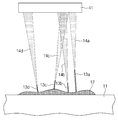
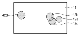
도 1a 및 도 1b를 참조하면, 캐소드(11), 캐소드(11) 상의 제1 내지 제4 나노 에미터들(13a-13d) 및 아노드 형광막(41)을 포함하는 전자빔 장치가 제공될 수 있다. 각각의 제1 내지 제4 나노 에미터들(13a-13d)은 각각의 제1 내지 제4 전자빔들(14a-14d)을 방출할 수 있다. 제1 내지 제4 전자빔들(14a-14b)은 아노드 형광막(41)에 조사될 수 있다. 제1 내지 제4 전자빔들(14a-14d)이 아노드 형광막(41)에 조사되어, 아노드 형광막(41)에 제1 내지 제4 전자빔 형광점들(42a-42d)이 형성될 수 있다. 제1 내지 제4 전자빔 형광점들(42a-42d)을 관측하여, 제1 내지 제4 전자빔들(14a-14d)의 특성을 파악할 수 있다. 제1 내지 제4 전자빔 형광점들(42a-42d) 각각은 제1 내지 제4 전자빔들(14a-14d) 각각의 포컬스팟에 대응되도록 형성될 수 있다. 포컬스팟은 아노드 형광막(41)에 조사되는 제1 내지 제4 전자빔들(14a-14d) 각각이 아노드 형광막(41) 표면에서 가지는 평면적 면적을 의미할 수 있다. 다시 말하면, 포컬스팟은 전자빔이 조사되는 물체의 표면에서 전자빔이 가지는 평면적 면적을 의미할 수 있다.1A and 1B, an electron beam device including a
아노드 형광막(41)과 캐소드(11) 사이의 전압차가 커질수록, 제1 내지 제4 전자빔 형광점들(42a-42d) 각각의 직경이 작아질 수 있다. 다시 말하면, 아노드 형광막(41)과 캐소드(11) 사이의 전압차가 커질수록, 아노드 형광막(41)에 조사되는 제1 내지 제4 전자빔들(14a-14d) 각각의 포컬스팟이 작아질 수 있다. 제1 내지 제4 전자빔 형광점들(42a-42d) 각각의 직경은 아노드 형광막(41)과 캐소드(11)의 거리가 멀어질수록 커질 수 있다. 제1 내지 제4 전자빔 형광점들(42a-42d) 사이의 거리는 아노드 형광막(41)과 캐소드(11)의 거리가 멀어질수록 커질 수 있다.The larger the voltage difference between the anode
도 2a는 본 발명의 비교예에 따른 엑스선 영상 장치를 설명하기 위한 도면이고, 도 2b는 도 2a의 A영역의 확대도이다.2A is a view for explaining an X-ray imaging apparatus according to a comparative example of the present invention, and FIG. 2B is an enlarged view of region A of FIG. 2A.
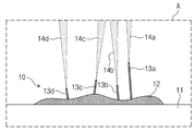
도 2a 및 도 2b를 참조하면, 엑스선 영상 장치는 전자빔 발생부(10), 게이트 전극(20), 집속 전극(30), 아노드(40) 및 영상 획득부(50)를 포함할 수 있다.2A and 2B, the X-ray imaging apparatus may include an
전자빔 발생부(10)는 캐소드(11), 접착층(12) 및 제1 내지 제4 나노 에미터들(13a-13d)을 포함할 수 있다. The
캐소드(11) 상에 제1 내지 제4 나노 에미터들(13a-13d)이 제공될 수 있다. 나노 에미터들(13a-13d)의 개수는 4개인 것으로 예시되었지만, 이에 한정되지 않을 수 있다. 캐소드(11)는 접지될 수 있다. 제1 내지 제4 나노 에미터들(13a-13d)은 접착층(12)에 의해 캐소드(11) 상에 부착될 수 있다. 제1 내지 제4 나노 에미터들(13a-13d) 및 접착층(12)은 페이스트 프린팅 공정을 통해 캐소드(11) 상에 부착될 수 있다. 제1 내지 제4 나노 에미터들(13a-13d)은 평면적으로 서로 이격될 수 있다. 제1 내지 제4 나노 에미터들(13a-13d) 사이의 최단거리는 1㎛ 내지 200㎛일 수 있다. 제1 내지 제4 나노 에미터들(13a-13d)은 도전성 물질을 포함할 수 있다. 일 예로, 제1 내지 제4 나노 에미터들(13a-13d) 각각은 탄소나노튜브(CNT)를 포함할 수 있다. 각각의 제1 내지 제4 나노 에미터들(13a-13d)의 길이는 서로 다를 수 있다. 각각의 제1 내지 제4 나노 에미터들(13a-13d)이 캐소드(11)의 상면과 이루는 각도는 서로 다를 수 있다. 다시 말하면, 각각의 제1 내지 제4 나노 에미터들(13a-13d)이 기울어진 정도는 서로 다를 수 있다.The first to
접착층(12)은 접착성 물질을 포함할 수 있다. 일 예로, 접착층(12)은 도전성 페이스트(Paste)를 포함할 수 있다.The
전자빔 발생부(10) 위에 게이트 전극(20)이 제공될 수 있다. 다시 말하면, 게이트 전극(20)은 전자빔 발생부(10)와 아노드(40) 사이에 제공될 수 있다. 게이트 전극(20)에는 양전압이 인가될 수 있다. 게이트 전극(20)은 게이트 개구(21)를 포함할 수 있다. 게이트 개구(21)의 직경은 1㎛ 내지 500㎛일 수 있다. 게이트 전극(20)과 전자빔 발생부(10) 사이의 최단거리는 1㎛ 내지 5000㎛일 수 있다. 게이트 전극(20)과 전자빔 발생부(10) 사이의 최단거리는 게이트 개구(21)의 직경의 0.1배 내지 10배일 수 있다.The
게이트 전극(20) 위에 집속 전극(30)이 제공될 수 있다. 다시 말하면, 집속 전극(30)은 게이트 전극(20)과 아노드(40) 사이에 제공될 수 있다. 다만, 집속 전극(30)의 위치는 이에 한정되지 않을 수 있다. 집속 전극(30)에는 양전압이 인가될 수 있다. 집속 전극(30)은 집속 개구(31)를 포함할 수 있다. 집속 전극(30)을 대신하여, 전자빔을 집속시킬 수 있는 광학 시스템(예를 들면, 정전 렌즈 또는 자기 렌즈)이 제공될 수 있다. The focusing
집속 전극(30) 위에 아노드(40)가 제공될 수 있다. 다시 말하면, 집속 전극(30)과 영상 획득부(50) 사이에 아노드(40)가 제공될 수 있다. 아노드(40)에는 양전압이 인가될 수 있다. 아노드(40)는 아노드 타겟 및 아노드 전극을 포함할 수 있다. 아노드 타겟은 전자빔 조사에 따라 엑스선을 방출하는 물질을 포함할 수 있다. 일 예로, 아노드 타겟은 텅스텐 또는 몰리브덴을 포함할 수 있다. 아노드 전극은 전기 전도도가 높은 물질을 포함할 수 있다. 일 예로, 아노드 전극은 구리를 포함할 수 있다.An
아노드(40) 위에 영상 획득부(50)가 제공될 수 있다. 영상 획득부(50)는 아노드(40)에서 방출된 엑스선을 이용하여 엑스선 영상을 획득할 수 있다.An
상기 엑스선 영상 장치의 구동 방법을 설명하면, 게이트 전극(20)에 양전압이 인가되어 게이트 전극(20)과 캐소드(11) 사이에 전압차가 발생할 수 있다. 게이트 전극(20)과 캐소드(11) 사이의 전압차에 의해, 각각의 제1 내지 제4 나노 에미터들(13a-13a)에서 각각의 제1 내지 제4 전자빔들(14a-14d)이 방출될 수 있다. 제1 내지 제4 전자빔들(14a-14d)은 제1 내지 제4 나노 에미터들(13a-13d) 각각의 단부에서 방출될 수 있다. 제1 내지 제4 나노 에미터들(13a-13d) 중 제1 나노 에미터(13a)의 길이가 가장 길 수 있고, 제4 나노 에미터(13d)의 길이가 가장 짧을 수 있다. 나노 에미터(13a-13d)의 길이가 길수록, 전자빔(14a-14d)이 방출되기 시작하는 게이트 전극(20)과 캐소드(11) 사이의 전압차가 작을 수 있다. 다시 말하면, 제1 나노 에미터(13a)에서 제1 전자빔(14a)이 방출되기 시작하는 게이트 전극(20)과 캐소드(11) 사이의 전압차는, 제4 나노 에미터(13d)에서 제4 전자빔(14d)이 방출되기 시작하는 게이트 전극(20)과 캐소드(11) 사이의 전압차보다 작을 수 있다. 나노 에미터(13a-13d)의 직경이 작을수록, 방출되는 전자빔(14a-14d)의 평면적 면적이 작을 수 있다.When explaining the driving method of the X-ray imaging apparatus, a positive voltage is applied to the
아노드(40)에 양전압이 인가되어 아노드(40)와 캐소드(11) 사이에 전압차가 발생할 수 있다. 나노 에미터들(13a-13d)에서 방출된 제1 내지 제4 전자빔들(14a-14d)은 아노드(40)와 캐소드(11)의 전압차에 의해 가속되어 아노드(40) 방향으로 진행할 수 있다. 제1 내지 제4 전자빔들(14a-14d) 각각의 진행 경로는 서로 다를 수 있다. 다시 말하면, 제1 내지 제4 전자빔들(14a-14d)이 나노 에미터들(13a-13d)에서 방출되어 아노드(40)에 도달하는 경로는 서로 다를 수 있다. 아노드(40) 방향으로 진행하면서, 제1 내지 제4 전자빔들(14a-14d)의 일부는 서로 중첩될 수 있고, 다른 일부는 서로 중첩되지 않을 수 있다. A positive voltage is applied to the
제1 내지 제4 전자빔들(14a-14d)은 게이트 전극(20)의 게이트 개구(21)를 통과할 수 있다. 게이트 개구(21)는 제1 내지 제4 전자빔들(14a-14d)이 통과하기에 충분한 크기를 가질 수 있다.The first to
게이트 개구(21)를 통과한 제1 내지 제4 전자빔들(14a-14d)은 집속 전극(30)의 집속 개구(31)를 통과할 수 있다. 집속 개구(31)는 제1 내지 제4 전자빔들(14a-14d)이 통과하기에 충분한 크기를 가질 수 있다. 집속 개구(31)를 통과하면서, 제1 내지 제4 전자빔들(14a-14d)은 집속될 수 있다. 제1 집속 전극(30)을 제어하여, 제1 내지 제4 전자빔들(14a-14d)의 포컬스팟이 아노드(40)의 표면에서 최소가 되도록 집속을 조절할 수 있다.The first to
집속 개구(31)를 통과한 제1 내지 제4 전자빔들(14a-14d)은 아노드(40)에 조사될 수 있다. 제1 내지 제4 전자빔들(14a-14d) 각각은 아노드(40)에 조사되는 위치가 다를 수 있다. 다시 말하면, 아노드(40)의 표면에서, 제1 내지 제4 전자빔들(14a-14d) 각각의 포컬스팟들은 서로 이격될 수 있다. 아노드(40)에 제1 내지 제4 전자빔들(14a-14d)이 조사되어, 아노드(40) 에서 제1 내지 제4 엑스선들(43a-43d)이 방출될 수 있다. 제1 내지 제4 엑스선들(43a-43d) 각각은 아노드(40)에서 방출되는 위치가 다를 수 있다. 다시 말하면, 아노드(40)의 표면에서, 제1 내지 제4 엑스선들(43a-43d)의 방출점들은 서로 이격될 수 있다. The first to
제1 내지 제4 엑스선들(43a-43d)은 아노드(40)에서 영상 획득부(50) 방향으로 진행할 수 있다. 제1 내지 제4 엑스선들(43a-43d)의 방출점들이 서로 이격됨에 따라, 영상 획득부(50) 방향으로 진행하면서, 제1 내지 제4 엑스선들(43a-43d) 각각의 진행 경로가 서로 다를 수 있다. 다시 말하면, 제1 내지 제4 엑스선들(43a-43d)의 일부는 서로 중첩될 수 있고, 다른 일부는 서로 중첩되지 않을 수 있다. 아노드(40)와 영상 획득부(50) 사이에 배치된 피사체(SJ)에 제1 내지 제4 엑스선들(43a-43d)이 조사될 수 있다.The first to
영상 획득부(50)에 제1 내지 제4 엑스선들(43a-43d)이 조사될 수 있다. 영상 획득부(50)에서 피사체(SJ)의 엑스선 영상을 획득할 수 있다. 방출점들이 서로 이격된 제1 내지 제4 엑스선들(43a-43d)에 의해 획득한 엑스선 영상은 선명하지 않을 수 있다. 다시 말하면, 상기 엑스선 영상은 복수개의 엑스선들(43a-43d)에 의해 획득되기 때문에, 서로 어긋나면서 겹쳐지는 복수개의 이미지들을 포함할 수 있다.The first to
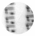
도 3은 도 2a 및 도 2b에 따른 엑스선 영상 장치에 의해 획득된 엑스선 영상이다.3 is an X-ray image obtained by the X-ray imaging apparatus according to FIGS. 2A and 2B.
도 3을 참조하면, 복수개의 엑스선들에 의해 획득된 엑스선 영상에서는 피사체가 선명하지 않게 나타나는 것을 확인할 수 있다.Referring to FIG. 3, it can be confirmed that an object is not clearly displayed in an X-ray image obtained by a plurality of X-rays.
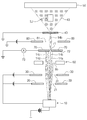
도 4는 본 발명의 실시예들에 따른 엑스선 영상 장치를 설명하기 위한 도면이고, 도 5a 및 도 5b는 편향기의 실시예들을 설명하기 위한 도면들이다. 도 2a 및 도 2b를 참조하여 설명된 동일한 구성요소에 대해서는 동일한 도면 부호를 사용하며, 중복되는 설명은 생략하기로 한다.4 is a diagram for describing an X-ray imaging apparatus according to embodiments of the present invention, and FIGS. 5A and 5B are diagrams for illustrating embodiments of the deflector. The same reference numerals are used for the same components described with reference to FIGS. 2A and 2B, and duplicate descriptions will be omitted.
도 4, 도 5a 및 도 5b를 참조하면, 엑스선 영상장치는 전자빔 발생부(10), 게이트 전극(20), 제1 집속 전극(30), 아노드(40), 영상 획득부(50), 편향기(60), 제한 전극(70) 및 제2 집속 전극(80)을 포함할 수 있다.4, 5A and 5B, the X-ray imaging apparatus includes an
편향기(60)는 제1 집속 전극(30) 위에 제공될 수 있다. 다시 말하면, 편향기(60)는 제1 집속 전극(30)과 아노드(40) 사이에 제공될 수 있다. 다만, 편향기(60)의 위치는 이에 한정되지 않을 수 있다. 편향기(60)는 제1 집속 전극(30)과 게이트 전극(20) 사이에 위치할 수도 있고, 게이트 전극(20)과 캐소드(11, 도 2b 참조) 사이에 위치할 수도 있다. 일 실시예로, 편향기(60)는 정전기형 편향기일 수 있다(도 5a 참조). 편향기(60)는 X축 전극들(61a), Y축 전극들(61b), X축 전압원(62a) 및 Y축 전압원(62b)을 포함할 수 있다. X축 전극들(61a) 및 Y축 전극들(61b)에 의해 전자빔 경로(65)가 정의될 수 있다. X축 전극들(61a)은 X축을 따라 전자빔 경로(65)의 양 측에 제공될 수 있다. Y축 전극들(61b)은 Y축을 따라 전자빔 경로(65)의 양 측에 제공될 수 있다. X축 전압원(62a)이 X축 전극들(61a)에 전압을 인가하여 X축 전극들(61a) 사이에 전압차가 발생할 수 있다. 이에 따라, X축 전극들(61a) 사이의 전자빔 경로(65)에 X축을 따라 전계가 발생할 수 있다. Y축 전압원(62b)이 Y축 전극들(61b)에 전압을 인가하여 Y축 전극들(61b) 사이에 전압차가 발생할 수 있다. 이에 따라, Y축 전극들(61b) 사이의 전자빔 경로(65)에 Y축을 따라 전계가 발생할 수 있다. X축 및 Y축을 따라 발생하는 전계에 의해, 전자빔 경로(65)를 지나는 전자빔이 편향될 수 있다. X축 전압원(62a)이 인가하는 전압을 X전압으로 정의할 수 있고, Y축 전압원(62b)이 인가하는 전압을 Y전압으로 정의할 수 있다. The
다른 실시예로, 편향기(60)는 자기장형 편향기일 수 있다(도 5b 참조). 편향기(60)는 X축 코일들(63a), Y축 코일들(63b), X축 전류원(64a) 및 Y축 전류원(64b)을 포함할 수 있다. X축 코일들(63a) 및 Y축 코일들(63b)에 의해 전자빔 경로(65)가 정의될 수 있다. X축 코일들(63a)은 X축을 따라 전자빔 경로(65)의 양 측에 제공될 수 있다. Y축 코일들(63b)은 Y축을 따라 전자빔 경로(65)의 양 측에 제공될 수 있다. X축 전류원(64a)이 X축 코일들(63a)에 전류를 제공하여 X축 코일들(63a)에서 자기장이 발생할 수 있다. Y축 전류원(64b)이 Y축 코일들(63b)에 전류를 제공하여 Y축 코일들(63b)에서 자기장이 발생할 수 있다. 상기 자기장은 전자빔 경로(65)를 지날 수 있다. X축 코일들(63a) 및 Y축 코일들(63b)에서 발생하는 자기장에 의해, 전자빔 경로(65)를 지나는 전자빔이 편향될 수 있다. X축 전류원(64a)이 제공하는 전류를 X전류로 정의할 수 있고, Y축 전류원(64b)이 제공하는 전류를 Y전류로 정의할 수 있다.In another embodiment, the
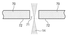
편향기(60) 위에 제한 전극(70)이 제공될 수 있다. 다시 말하면, 제한 전극(70)은 편향기(60)와 아노드(40) 사이에 제공될 수 있다. 제한 전극(70)에는 양전압이 인가될 수 있다. 제한 전극(70)은 제한 개구(71)를 포함할 수 있다. 제한 개구(71)의 직경은 1㎛ 내지 2000㎛일 수 있다. 전자빔 발생부(10)와 제한 전극(70) 사이의 최단거리는 0.1mm 내지 200mm일 수 있다. 제한 개구(71)의 직경은 전자빔 발생부(10)와 제한 전극(70) 사이의 최단거리에 따라 적절하게 결정될 수 있다. 예를 들어, 전자빔 발생부(10)와 제한 전극(70) 사이의 최단거리가 200mm인 경우, 제한 개구(71)의 직경은 2000㎛일 수 있다. 다른 예를 들어, 전자빔 발생부(10)와 제한 전극(70) 사이의 최단거리가 0.1mm인 경우, 제한 개구(71)의 직경은 1㎛일 수 있다. 제한 전극(70)은 캐소드(11)와 마주보는 하면(72)을 포함할 수 있다. 제한 전극(70)에는 전류계(73)가 연결될 수 있다. 제한 전극(70)은 텅스텐 또는 몰리브덴을 포함할 수 있다. A limiting
제한 전극(70) 위에 제2 집속 전극(80)이 제공될 수 있다. 다시 말하면, 제2 집속 전극(80)은 제한 전극(70)과 아노드(40) 사이에 제공될 수 있다. 제2 집속 전극(80)에는 양전압이 인가될 수 있다. 제2 집속 전극(80)은 제2 집속 전극 개구(81)를 포함할 수 있다.The second focusing
엑스선 영상 장치의 구동 방법을 설명하면, 캐소드(11) 상의 제1 내지 제4 나노 에미터들(13a-13d, 도 2b 참조)에서 제1 내지 제4 전자빔들(14a-14d)이 방출될 수 있다.When describing the driving method of the X-ray imaging apparatus, the first to
제1 내지 제4 나노 에미터들(13a-13d)에서 방출된 제1 내지 제4 전자빔들(14a-14d)은 아노드(40)와 캐소드(11)의 전압차에 의해 가속되어 아노드(40) 방향으로 진행할 수 있다. 제1 내지 제4 전자빔들(14a-14d) 각각의 진행 경로는 서로 다를 수 있다. The first to
제1 내지 제4 전자빔들(14a-14d)은 게이트 전극(20)의 게이트 개구(21)를 통과할 수 있다. The first to
게이트 개구(21)를 통과한 제1 내지 제4 전자빔들(14a-14d)은 제1 집속 전극(30)의 제1 집속 개구(31)를 통과할 수 있다. 제1 집속 개구(31)를 통과하면서, 제1 내지 제4 전자빔들(14a-14d)은 집속될 수 있다. The first to
제1 집속 개구(31)를 통과한 제1 내지 제4 전자빔들(14a-14d)은 편향기(60)에 의해 정의되는 전자빔 경로(65)를 통과할 수 있다. 전자빔 경로(65)를 통과하면서, 제1 내지 제4 전자빔들(14a-14d)은 X축 및 Y축을 따라 편향될 수 있다(도 5a 및 도 5b). 편향기(60)가 정전기형 편향기인 경우(도 5a), 전자빔 경로(65)에 발생하는 전계에 의해 전자빔 경로(65)를 통과하는 제1 내지 제4 전자빔들(14a-14d)이 편향될 수 있다. 편향기(60)가 자기장형 편향기인 경우(도 5b), 전자빔 경로(65)를 지나는 자기장에 의해 전자빔 경로(65)를 통과하는 제1 내지 제4 전자빔들(14a-14d)이 편향될 수 있다. 편향기(60)를 제어하여, 제1 내지 제4 전자빔들(14a-14d)의 편향을 조절할 수 있다.The first to
제한 전극(70)은 제1 내지 제4 전자빔들(14a-14d)의 진행을 제한할 수 있다. 전자빔 경로(65)를 통과한 제1 내지 제4 전자빔들(14a-14d) 중 하나만 제한 전극(70)의 제한 개구(71)를 통과할 수 있다. 일 예로, 제2 전자빔(14b)이 제한 개구(71)를 통과할 수 있다. 제2 전자빔(14b)이 제한 개구(71)를 통과하는 것으로 도시되었지만, 제1, 제3 및 제4 전자빔들(14a,14c,14d) 중 하나가 제한 개구(71)를 통과할 수도 있다. 제한 개구(71)는 하나의 전자빔만 통과할 수 있도록 적절한 크기를 가질 수 있다. 편향기(60)에 의한 제1 내지 제4 전자빔들(14a-14d)의 편향에 따라, 제한 개구(71)를 통과하는 전자빔이 결정될 수 있다. 편향기(60)에 의한 제1 내지 제4 전자빔들(14a-14d)의 편향에 따라, 제1 내지 제4 전자빔들(14a-14d) 모두 제한 개구(71)를 통과하지 않을 수 있다.The limiting
제2 전자빔(14b)이 제한 개구(71)를 통과하는 경우, 제1, 제3 및 제4 전자빔들(14a,14c,14d)은 제한 전극(70)의 하면(72) 상에 조사될 수 있다. 제한 전극(70)의 하면(72)에 조사되는 제1, 제3 및 제4 전자빔들(14a,14c,14d)에 의해 제한 전극(70)에 전류가 흐를 수 있다. 제한 전극(70)의 전류계(73)에서 제한 전극(70)에 흐르는 전류를 측정할 수 있다. When the
제한 개구(71)를 통과한 제2 전자빔(14b)은 제2 집속 전극(80)의 제2 집속 개구(81)를 통과할 수 있다. 제2 집속 개구(81)를 통과하면서, 제2 전자빔(14b)은 집속될 수 있다. 제2 집속 전극(80)을 제어하여, 제2 전자빔(14b)의 포컬스팟이 아노드(40)의 표면에서 최소가 되도록 집속을 조절할 수 있다.The
제2 집속 개구(81)를 통과한 제2 전자빔(14b)은 아노드(40)에 조사될 수 있다. 아노드(40)에 제2 전자빔(14b)이 조사되어, 아노드(40) 에서 엑스선(43)이 방출될 수 있다. 엑스선(43)은 아노드(40)에서 영상 획득부(50) 방향으로 진행할 수 있다. 아노드(40)와 영상 획득부(50) 사이에 배치된 피사체(SJ)에 엑스선(43)이 조사될 수 있다.The
영상 획득부(50)에 엑스선(43)이 조사될 수 있다. 영상 획득부(50)에서 피사체(SJ)의 엑스선 영상을 획득할 수 있다. 하나의 엑스선(43)에 의해 엑스선 영상이 획득되므로, 피사체(SJ)의 엑스선 영상은 선명할 수 있다. The
제한 개구(71)를 통과한 제2 전자빔(14b)의 전류의 크기가 클수록, 더 선명한 엑스선 영상이 획득될 수 있다.The larger the magnitude of the current of the
도 6은 도 4에 따른 엑스선 영상 장치에 의해 획득된 엑스선 영상이다.6 is an X-ray image obtained by the X-ray imaging apparatus according to FIG. 4.
도 6을 참조하면, 하나의 엑스선에 의해 획득된 엑스선 영상에서는 피사체가 선명하게 나타나는 것을 확인할 수 있다.Referring to FIG. 6, it can be confirmed that the subject appears clearly in the X-ray image obtained by one X-ray.
도 7은 제한 전극에서 측정된 전류의 강도맵을 설명하기 위한 도면이다.7 is a view for explaining the intensity map of the current measured at the limiting electrode.
도 4, 도 5a, 도 5b 및 도 7을 참조하면, 제한 전극(70)에 연결된 전류계(73)를 이용하여 제한 전극(70)에 흐르는 전류의 강도맵을 획득할 수 있다. 전류 강도맵은 정전기형 편향기(도 5a) 또는 자기장형 편향기(도 5b)를 기준으로 획득된 것일 수 있다. 이하의 설명에서는 정전기형 편향기를 기준으로 하는 경우(도 5a)로 예를 들어 설명한다. 자기장형 편향기를 기준으로 하는 경우(도 5b) 또한 이하의 설명과 유사할 수 있다.4, 5A, 5B, and 7, the intensity map of the current flowing through the limiting
전류 강도맵은 복수개의 픽셀들로 이루어질 수 있다. 전류 강도맵의 X축에는 편향기(60)의 X전압의 크기가 표시될 수 있고, 전류 강도맵의 Y축에는 편향기(60)의 Y전압의 크기가 표시될 수 있다. 각각의 픽셀들은 그에 대응되는 X전압의 크기 및 Y전압의 크기를 가질 수 있다. 예를 들면, 제1 픽셀(P1)에 대응되는 X전압의 크기는 X1이고, Y전압의 크기는 Y1이다. 다른 예를 들면, 제2 픽셀(P2)에 대응되는 X전압의 크기는 X2이고, Y전압의 크기는 Y2이다. 다시 말하면, 편향기(60)의 X전압의 크기가 X1이고, Y전압의 크기가 Y1인 경우, 제한 전극(70)에 흐르는 전류의 강도가 전류 강도맵의 제1 픽셀(P1)에 나타날 수 있다. 편향기(60)의 X전압의 크기가 X2이고, Y전압의 크기가 Y2인 경우, 제한 전극(70)에 흐르는 전류의 강도가 전류 강도맵의 제2 픽셀(P2)에 나타날 수 있다. 위와 같이, 전류 강도맵은 편향기(60)의 X전압의 크기 변화 및 Y전압의 크기 변화에 따라 제한 전극(70)에 흐르는 전류의 강도를 나타낼 수 있다.The current intensity map may consist of a plurality of pixels. The magnitude of the X voltage of the
전류 강도맵에서, 제한 전극(70)에 흐르는 전류의 강도가 클수록 각각의 픽셀의 밝기가 더 밝을 수 있다. 제1 픽셀(P1)과 제2 픽셀(P2)을 비교하면, 제1 픽셀(P1)의 밝기가 제2 픽셀(P2)의 밝기보다 더 밝으므로, 편향기(60)의 X전압이 X2이고 Y전압이 Y2인 경우보다 편향기(60)의 X전압이 X1이고 Y전압이 Y1인 경우 제한 전극(70)에 흐르는 전류의 강도가 더 클 수 있다.In the current intensity map, the greater the intensity of the current flowing through the limiting
전류 강도맵을 획득하는 것은, 편향기(60)의 X전압 크기 및 Y전압 크기를 특정 범위 내에서 변화시키는 것, 및 상기 범위 내의 X전압 크기 및 Y전압 크기에 따라 제한 전극(70)에 흐르는 전류의 강도를 측정하여 전류 강도맵의 픽셀들의 밝기를 표시하는 것을 포함할 수 있다. Obtaining the current intensity map, changing the X voltage magnitude and Y voltage magnitude of the
도 4와 같이 제1 내지 제4 전자빔들(14a-14d)이 제1 내지 제4 나노 에미터들(13a-13d)에서 방출되는 경우, 전류 강도맵에 제1 내지 제4 스팟들(SP1-SP4) 및 주변 영역(AR)이 형성될 수 있다. 제1 내지 제4 스팟들(SP1-SP4) 및 주변 영역(AR) 각각은 밝기가 동일한 픽셀들이 모여서 형성될 수 있다. 제1 내지 제4 스팟들(SP1-SP4)은 주변 영역(AR)에 비해 상대적으로 어두울 수 있다. 제1 스팟(SP1)보다 제2 스팟(SP2)이 밝을 수 있고, 제2 스팟(SP2)보다 제3 스팟(SP3)이 밝을 수 있고, 제3 스팟(SP3)보다 제4 스팟(SP4)이 밝을 수 있다.When the first to
편향기(60)가 제1 스팟(SP1) 내에 위치하는 픽셀들에 대응되는 X전압 및 Y전압을 가지는 경우, 제1 내지 제4 전자빔들(14a-14d) 중 전류의 크기가 가장 큰 전자빔이 제한 개구(71)를 통과할 수 있다.When the
편향기(60)가 제2 스팟(SP2) 내에 위치하는 픽셀들에 대응되는 X전압 및 Y전압을 가지는 경우, 제1 내지 제4 전자빔들(14a-14d) 중 전류의 크기가 2번째로 큰 전자빔이 제한 개구(71)를 통과할 수 있다.When the
편향기(60)가 제4 스팟(SP4) 내에 위치하는 픽셀들에 대응되는 X전압 및 Y전압을 가지는 경우, 제1 내지 제4 전자빔들(14a-14d) 중 전류의 크기가 가장 작은 전자빔이 제한 개구(71)를 통과할 수 있다.When the
편향기(60)가 주변 영역(AR)에 위치하는 픽셀들에 대응되는 X전압 및 Y전압을 가지는 경우, 제1 내지 제4 전자빔들(14a-14d) 모두 제한 개구(71)를 통과하지 않을 수 있다.When the
전류 강도맵을 확인하여, 편향기(60)의 X전압 및 Y전압의 크기가 제1 스팟(SP1) 내의 픽셀들에 대응되도록 편향기(60)를 제어하면, 제1 내지 제4 전자빔들(14a-14d) 중 전류의 크기가 가장 큰 전자빔이 제한 개구(71)를 통과할 수 있다. Checking the current intensity map, and controlling the
전류 강도맵에서, 제1 내지 제4 스팟들(SP1-SP4)은 제한 개구(71)의 형태를 반영할 수 있다. 다시 말하면, 제한 개구(71)가 평면적으로 원형인 경우, 제1 내지 제4 스팟들(SP1-SP4)이 원형으로 형성될 수 있고, 제한 개구(71)가 평면적으로 사각형인 경우, 제1 내지 제4 스팟들(SP1-SP4)이 사각형으로 형성될 수 있다.In the current intensity map, the first to fourth spots SP1-SP4 may reflect the shape of the limiting
도 8a 내지 도 8c는 제한 개구를 통과하는 전자빔의 형태를 설명하기 위한 도면들이다.8A to 8C are views for explaining the shape of the electron beam passing through the restriction opening.
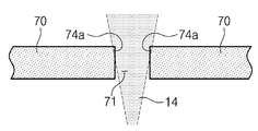
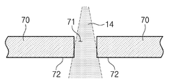
도 4, 도 7 및 도 8a를 참조하면, 제1 집속 전극(30)의 집속에 따라, 전자빔(14)은 제한 전극(70)의 하면(72)과 동일한 레벨에서 평면적 면적이 최소가 되도록 집속될 수 있다. 다시 말하면, 제한 전극(70)의 하면(72)과 동일한 레벨에 초점이 형성되도록 집속될 수 있다. 이 경우, 도 7의 전류 강도맵에서 제1 내지 제4 스팟들(SP1-SP4)이 상대적으로 선명하게 형성될 수 있다. 제1 집속 전극(30)을 제어하여, 제한 개구(71)의 하면(72)과 동일한 레벨에서 전자빔(14)의 평면적 면적이 최소가 되도록 전자빔(14)의 집속을 조절할 수 있다. 전류 강도맵의 선명도를 확인하여, 전자빔(14)이 제한 개구(71)의 하면(72)과 동일한 레벨에서 평면적 면적이 최소가 되었는지 확인할 수 있다.4, 7 and 8A, according to the focusing of the first focusing
도 4 및 도 8b를 참조하면, 제1 집속 전극(30)의 집속에 따라, 전자빔(14)은 제한 전극(70)의 제한 개구(71)를 통과하면서 발산하는 형태로 진행할 수 있다. 다시 말하면, 전자빔(14)이 제한 개구(71) 내에서 진행하면서, 그 평면적 면적이 점점 증가할 수 있다. 전자빔(14)은 제한 개구(71)의 상부 측벽들(74a)에 충돌할 수 있다. 전자빔(14)에 의해 제한 개구(71)의 상부 측벽들(74a)에서 엑스선들이 발생할 수 있다. 제한 개구(71)의 상부 측벽들(74a)에서 발생한 엑스선들은 아노드(40) 방향으로 진행할 수 있다. 상기 엑스선들은 피사체(SJ) 및 영상 획득부(50)에 조사될 수 있다. 상기 엑스선들에 의해, 영상 획득부(50)에서 획득하는 엑스선 영상의 선명도가 떨어질 수 있다. 4 and 8B, according to the focusing of the first focusing
도 4 및 도 8c를 참조하면, 제1 집속 전극(30)의 집속에 따라, 전자빔(14)은 제한 전극(70)의 제한 개구(71)를 통과하면서 수렴하는 형태로 진행할 수 있다. 다시 말하면, 전자빔(14)이 제한 개구(71) 내에서 진행하면서, 그 평면적 면적이 점점 감소할 수 있다. 전자빔(14)은 제한 개구(71)의 하면(72)에 충돌할 수 있다. 전자빔(14)에 의해 제한 개구(71)의 하면(72)에서 엑스선들이 발생할 수 있다. 상기 엑스선들은 제한 개구(71)에 의해 제한되어, 아노드(40) 방향으로 진행하지 않을 수 있다. 4 and 8C, according to the focusing of the first focusing
도 9a 및 도 9b는 제한 전극의 전류 강도맵의 실제 이미지들이다.9A and 9B are actual images of the current intensity map of the limiting electrode.
도 9a 및 도 9b를 참조하면, 도 9a의 전류 강도맵에서는 상대적으로 어두운 픽셀들이 모인 스팟들이 다른 부분들과 구분 가능하게 형성된 것을 확인할 수 있고, 도 9b에서는 스팟들이 다른 부분들과 구분 가능하게 형성되지 않은 것을 확인할 수 있다. 도 8a와 같이, 전자빔의 평면적 면적이 제한 개구의 하면과 동일한 레벨에서 최소가 되는 경우, 도 9a와 같은 전류 강도맵을 획득할 수 있다. 도 8a와 달리, 전자빔의 평면적 면적이 제한 개구의 하면과 동일한 레벨에서 제한 개구의 직경보다 클 경우, 도 9b와 같은 전류 강도맵을 획득할 수 있다. 제한 개구의 하면과 동일한 레벨에서 전자빔의 평면적 면적이 작을수록, 전류 강도맵의 선명도가 우수할 수 있다.9A and 9B, in the current intensity map of FIG. 9A, it can be seen that spots in which relatively dark pixels are collected can be distinguished from other parts, and in FIG. 9B, spots are formed to be distinguishable from other parts. You can see that it has not been done As shown in FIG. 8A, when the planar area of the electron beam becomes minimum at the same level as the lower surface of the limiting opening, a current intensity map as in FIG. 9A can be obtained. Unlike FIG. 8A, when the planar area of the electron beam is larger than the diameter of the limiting opening at the same level as the lower surface of the limiting opening, a current intensity map as shown in FIG. 9B can be obtained. The smaller the planar area of the electron beam at the same level as the lower surface of the limiting opening, the better the sharpness of the current intensity map may be.
도 10은 본 발명의 실시예들에 따른 엑스선 영상 장치의 구동 방법을 설명하기 위한 순서도이다.10 is a flowchart illustrating a method of driving an X-ray imaging apparatus according to embodiments of the present invention.
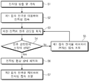
도 4 및 도 10을 참조하면, 게이트 전극(20)에 전압을 인가하여 제1 내지 제4 나노 에미터들(13a-13d)에서 제1 내지 제4 전자빔들(14a-14d)을 방출 시킬 수 있고, 아노드(40)에 전압을 인가하여 제1 내지 제4 전자빔들(14a-14d)을 가속시킬 수 있다(S1). 4 and 10, first to
제1 집속 전극(30)에 전압을 인가하여, 제1 내지 제4 전자빔들(14a-14d)을 집속시킬 수 있다(S2). A voltage may be applied to the first focusing
편향기(60) 및 전류계(73)를 이용하여 제1 내지 제4 전자빔들(14a-14d)에 의해 제한 전극(70)에 흐르는 전류 강도맵을 획득할 수 있다(S3).A current intensity map flowing through the limiting
전류 강도맵의 스팟들이 선명한지 판단하여(S4), 전류 강도맵의 스팟들이 선명하지 않게 획득되는 경우, 제1 집속 전극(30)을 제어하여 제1 내지 제4 전자빔들(14a-14d)의 집속을 조절할 수 있다(S5). 상기 집속을 조절하는 것은, 제한 개구(71)를 통과하는 전자빔이 제한 개구(71)의 하면(72)과 동일한 레벨에서 평면적 면적이 최소가 되도록 하는 것을 포함할 수 있다. 제1 내지 제4 전자빔들(14a-14d)의 집속을 조절하고, 다시 편향기(60) 및 전류계(73)를 이용하여 제1 내지 제4 전자빔들(14a-14d)에 의해 제한 전극(70)에 흐르는 전류 강도맵을 획득할 수 있다(S3). 전류 강도맵의 스팟들이 선명해질 때까지, 상기 과정을 반복할 수 있다.It is determined whether the spots of the current intensity map are clear (S4), and when the spots of the current intensity map are obtained unclear, the first focusing
전류 강도맵의 스팟들이 선명한지 판단하여(S4), 전류 강도맵의 스팟들이 선명하게 획득되는 경우, 전류 강도맵을 이용하여 제1 내지 제4 전자빔들(14a-14d)의 편향을 최적화할 수 있다(S6). 상기 편향 최적화는 전류 강도맵에서 가장 어두운 스팟을 확인하는 것, 및 상기 가장 어두운 스팟에 대응되도록 편향기(60)를 제어하여 제1 내지 제4 전자빔들(14a-14d)의 편향을 조절하는 것을 포함할 수 있다. 편향기(60)가 정전기형 편향기인 경우(도 5a), X축 전압원(62a) 및 Y축 전압원(62b)이 인가하는 전압의 크기를 최적화할 수 있고, 편향기(60)가 자기장형 편향기인 경우(도 5b), X축 전류원(64a) 및 Y축 전류원(64b)이 제공하는 전류의 크기를 최적화할 수 있다. 상기 편향 최적화에 따라, 제1 내지 제4 전자빔들(14a-14d) 중 가장 큰 전류값을 가지는 전자빔이 제한 개구(71)를 통과할 수 있다.By determining whether the spots of the current intensity map are clear (S4), when the spots of the current intensity map are clearly obtained, the deflection of the first to
제2 집속 전극(80)을 제어하여, 제한 개구(71)를 통과한 전자빔의 집속을 조절할 수 있다(S7). 이에 따라, 제한 개구(71)를 통과한 전자빔의 포컬스팟이 아노드(40) 표면에서 최소가 되도록 집속할 수 있다.By controlling the second focusing
도 11은 본 발명의 실시예들에 따른 엑스선 영상 장치를 설명하기 위한 도면이다. 도 4를 참조하여 설명된 동일한 구성요소에 대해서는 동일한 도면 부호를 사용하며, 중복되는 설명은 생략하기로 한다.11 is a view for explaining an X-ray imaging apparatus according to embodiments of the present invention. The same reference numerals are used for the same components described with reference to FIG. 4, and overlapping descriptions will be omitted.
도 11을 참조하면, 캐소드(11)에 음전압이 인가될 수 있고, 아노드(40)는 접지될 수 있다. 제한 전극(70)은 접지된 것으로 도시되었으나, 음전압 또는 양전압이 인가될 수도 있다.Referring to FIG. 11, a negative voltage may be applied to the
이상, 첨부된 도면을 참조하여 본 발명의 실시예를 설명하였지만, 본 발명이 속하는 기술분야에서 통상의 지식을 가진 자는 본 발명이 그 기술적 사상이나 필수적인 특징을 변경하지 않고서 다른 구체적인 형태로 실시될 수 있다는 것을 이해할 수 있을 것이다. 그러므로 이상에서 기술한 실시예에는 모든 면에서 예시적인 것이며 한정적이 아닌 것으로 이해해야만 한다.The embodiments of the present invention have been described above with reference to the accompanying drawings, but those of ordinary skill in the art to which the present invention pertains can implement the present invention in other specific forms without changing its technical spirit or essential features. You will understand that there is. Therefore, it should be understood that the embodiments described above are illustrative in all respects and not restrictive.
10: 전자빔 발생부
20: 게이트 전극
30: 제1 집속 전극
40: 아노드
50: 영상 획득부
60: 편향기
70: 제한 전극
80: 제2 집속 전극10: electron beam generator
20: gate electrode
30: first focusing electrode
40: anode
50: image acquisition unit
60: deflector
70: limiting electrode
80: second focusing electrode
Claims (3)
제1 집속 전극을 이용하여 상기 제1 및 제2 전자빔들의 각각을 집속시키는 제1 전자빔집속 단계;
편향기를 이용하여 집속된 상기 제1 및 제2 전자빔들의 각각을 편향시키는 편향 단계;
제한 개구를 포함하는 제한 전극을 이용하여 상기 제1 전자빔의 진행을 제한하고 상기 제2 전자빔을 상기 제한 개구로 통과시키는 전자빔 제한 단계; 및
상기 제한 개구를 통과한 상기 제1 전자빔을 아노드에 조사하는 아노드 조사 단계를 포함하는 엑스선 영상 장치의 구동 방법.An electron beam emitting step of generating electron beams from an electron beam generator, wherein the electron beam generator comprises a first nano-emitter generating a first electron beam and a second nano-emitter generating a second electron beam;
A first electron beam focusing step of focusing each of the first and second electron beams using a first focusing electrode;
A deflection step of deflecting each of the focused first and second electron beams using a deflector;
An electron beam limiting step of limiting the progress of the first electron beam by using a limiting electrode including a limiting opening and passing the second electron beam through the limiting opening; And
And an anode irradiation step of irradiating the anode with the first electron beam that has passed through the restriction opening.
상기 전자빔 제한 단계는 상기 제한 전극에 흐르는 전류를 측정하여 상기 제한 전극의 전류 강도맵을 획득하는 것을 더 포함하는 엑스선 영상 장치의 구동 방법.According to claim 1,
The electron beam limiting step further comprises obtaining a current intensity map of the limiting electrode by measuring a current flowing through the limiting electrode.
상기 전류 강도맵을 이용하여, 상기 제2 전자빔의 평면적 면적이 상기 제한 개구 내에서 최소가 되도록 상기 제1 집속 전극을 제어하는 것을 포함하는 엑스선 영상 장치의 구동 방법.According to claim 2,
And controlling the first focusing electrode such that the planar area of the second electron beam is minimized within the limited opening using the current intensity map.
Priority Applications (1)
| Application Number | Priority Date | Filing Date | Title |
|---|---|---|---|
| KR1020200039931A KR102396948B1 (en) | 2018-08-06 | 2020-04-01 | X-ray imaging device and driving method thereof |
Applications Claiming Priority (2)
| Application Number | Priority Date | Filing Date | Title |
|---|---|---|---|
| KR1020180091424A KR20190028279A (en) | 2017-09-08 | 2018-08-06 | X-ray imaging device and driving method thereof |
| KR1020200039931A KR102396948B1 (en) | 2018-08-06 | 2020-04-01 | X-ray imaging device and driving method thereof |
Related Parent Applications (1)
| Application Number | Title | Priority Date | Filing Date |
|---|---|---|---|
| KR1020180091424A Division KR20190028279A (en) | 2017-09-08 | 2018-08-06 | X-ray imaging device and driving method thereof |
Publications (2)
| Publication Number | Publication Date |
|---|---|
| KR20200037763A true KR20200037763A (en) | 2020-04-09 |
| KR102396948B1 KR102396948B1 (en) | 2022-05-16 |
Family
ID=81802857
Family Applications (1)
| Application Number | Title | Priority Date | Filing Date |
|---|---|---|---|
| KR1020200039931A KR102396948B1 (en) | 2018-08-06 | 2020-04-01 | X-ray imaging device and driving method thereof |
Country Status (1)
| Country | Link |
|---|---|
| KR (1) | KR102396948B1 (en) |
Citations (2)
| Publication number | Priority date | Publication date | Assignee | Title |
|---|---|---|---|---|
| KR20140106291A (en) * | 2013-02-26 | 2014-09-03 | 삼성전자주식회사 | X-ray imaging system having flat panel type X-ray generator, and X-ray generator, and electron emission device |
| US20170213688A1 (en) * | 2016-01-27 | 2017-07-27 | Hermes Microvision Inc. | Apparatus of Plural Charged-Particle Beams |
-
2020
- 2020-04-01 KR KR1020200039931A patent/KR102396948B1/en active IP Right Grant
Patent Citations (2)
| Publication number | Priority date | Publication date | Assignee | Title |
|---|---|---|---|---|
| KR20140106291A (en) * | 2013-02-26 | 2014-09-03 | 삼성전자주식회사 | X-ray imaging system having flat panel type X-ray generator, and X-ray generator, and electron emission device |
| US20170213688A1 (en) * | 2016-01-27 | 2017-07-27 | Hermes Microvision Inc. | Apparatus of Plural Charged-Particle Beams |
Also Published As
| Publication number | Publication date |
|---|---|
| KR102396948B1 (en) | 2022-05-16 |
Similar Documents
| Publication | Publication Date | Title |
|---|---|---|
| JP5281004B2 (en) | Emitter design method, electron beam generator, and device using the same | |
| US10566170B2 (en) | X-ray imaging device and driving method thereof | |
| JP4685115B2 (en) | Electron beam exposure method | |
| JP2007335125A (en) | Electron beam device | |
| US9799483B2 (en) | Charged particle beam device and detection method using said device | |
| JP6608367B2 (en) | Field emission device, system and method | |
| JP5364112B2 (en) | Charged particle beam equipment | |
| JP5849108B2 (en) | Electron beam equipment | |
| US8969801B2 (en) | Scanning electron microscope | |
| JP6403045B2 (en) | Multi-beam drawing method and multi-beam drawing apparatus | |
| US8968045B2 (en) | Cathode selection method | |
| US6538255B1 (en) | Electron gun and electron-beam optical systems and methods including detecting and adjusting transverse beam-intensity profile, and device manufacturing methods including same | |
| JP2004513477A (en) | SEM with adjustable final electrode for electrostatic objective | |
| JPH10302705A (en) | Scanning electron microscope | |
| US20220406558A1 (en) | Electron gun and electron microscope | |
| KR102396948B1 (en) | X-ray imaging device and driving method thereof | |
| KR20190028279A (en) | X-ray imaging device and driving method thereof | |
| US20230078510A1 (en) | Method for focusing and operating a particle beam microscope | |
| TWI751362B (en) | Electron beam apparatus, scanning electron microscope and electron beam method | |
| JP2007265917A (en) | X-ray tube and its control method | |
| CN206451682U (en) | A kind of electronics source generating device | |
| JP7396954B2 (en) | Charged particle beam device | |
| KR101324480B1 (en) | Micro focus x-ray tube | |
| WO2022137332A1 (en) | Electron gun and electron beam application device | |
| US10176964B2 (en) | Focused ion beam apparatus |
Legal Events
| Date | Code | Title | Description |
|---|---|---|---|
| A107 | Divisional application of patent | ||
| E902 | Notification of reason for refusal | ||
| E701 | Decision to grant or registration of patent right | ||
| GRNT | Written decision to grant |