KR20200035328A - Thin-film devices and fabrication - Google Patents
Thin-film devices and fabrication Download PDFInfo
- Publication number
- KR20200035328A KR20200035328A KR1020207008593A KR20207008593A KR20200035328A KR 20200035328 A KR20200035328 A KR 20200035328A KR 1020207008593 A KR1020207008593 A KR 1020207008593A KR 20207008593 A KR20207008593 A KR 20207008593A KR 20200035328 A KR20200035328 A KR 20200035328A
- Authority
- KR
- South Korea
- Prior art keywords
- conductive layer
- substrate
- bus bar
- edge
- tco
- Prior art date
Links
Images


Classifications
-
- G—PHYSICS
- G02—OPTICS
- G02F—OPTICAL DEVICES OR ARRANGEMENTS FOR THE CONTROL OF LIGHT BY MODIFICATION OF THE OPTICAL PROPERTIES OF THE MEDIA OF THE ELEMENTS INVOLVED THEREIN; NON-LINEAR OPTICS; FREQUENCY-CHANGING OF LIGHT; OPTICAL LOGIC ELEMENTS; OPTICAL ANALOGUE/DIGITAL CONVERTERS
- G02F1/00—Devices or arrangements for the control of the intensity, colour, phase, polarisation or direction of light arriving from an independent light source, e.g. switching, gating or modulating; Non-linear optics
- G02F1/01—Devices or arrangements for the control of the intensity, colour, phase, polarisation or direction of light arriving from an independent light source, e.g. switching, gating or modulating; Non-linear optics for the control of the intensity, phase, polarisation or colour
- G02F1/15—Devices or arrangements for the control of the intensity, colour, phase, polarisation or direction of light arriving from an independent light source, e.g. switching, gating or modulating; Non-linear optics for the control of the intensity, phase, polarisation or colour based on an electrochromic effect
- G02F1/153—Constructional details
- G02F1/155—Electrodes
-
- B—PERFORMING OPERATIONS; TRANSPORTING
- B32—LAYERED PRODUCTS
- B32B—LAYERED PRODUCTS, i.e. PRODUCTS BUILT-UP OF STRATA OF FLAT OR NON-FLAT, e.g. CELLULAR OR HONEYCOMB, FORM
- B32B17/00—Layered products essentially comprising sheet glass, or glass, slag, or like fibres
- B32B17/06—Layered products essentially comprising sheet glass, or glass, slag, or like fibres comprising glass as the main or only constituent of a layer, next to another layer of a specific material
- B32B17/10—Layered products essentially comprising sheet glass, or glass, slag, or like fibres comprising glass as the main or only constituent of a layer, next to another layer of a specific material of synthetic resin
- B32B17/10005—Layered products essentially comprising sheet glass, or glass, slag, or like fibres comprising glass as the main or only constituent of a layer, next to another layer of a specific material of synthetic resin laminated safety glass or glazing
- B32B17/10009—Layered products essentially comprising sheet glass, or glass, slag, or like fibres comprising glass as the main or only constituent of a layer, next to another layer of a specific material of synthetic resin laminated safety glass or glazing characterized by the number, the constitution or treatment of glass sheets
- B32B17/10082—Properties of the bulk of a glass sheet
- B32B17/10119—Properties of the bulk of a glass sheet having a composition deviating from the basic composition of soda-lime glass, e.g. borosilicate
-
- B—PERFORMING OPERATIONS; TRANSPORTING
- B32—LAYERED PRODUCTS
- B32B—LAYERED PRODUCTS, i.e. PRODUCTS BUILT-UP OF STRATA OF FLAT OR NON-FLAT, e.g. CELLULAR OR HONEYCOMB, FORM
- B32B17/00—Layered products essentially comprising sheet glass, or glass, slag, or like fibres
- B32B17/06—Layered products essentially comprising sheet glass, or glass, slag, or like fibres comprising glass as the main or only constituent of a layer, next to another layer of a specific material
- B32B17/10—Layered products essentially comprising sheet glass, or glass, slag, or like fibres comprising glass as the main or only constituent of a layer, next to another layer of a specific material of synthetic resin
- B32B17/10005—Layered products essentially comprising sheet glass, or glass, slag, or like fibres comprising glass as the main or only constituent of a layer, next to another layer of a specific material of synthetic resin laminated safety glass or glazing
- B32B17/10165—Functional features of the laminated safety glass or glazing
- B32B17/10431—Specific parts for the modulation of light incorporated into the laminated safety glass or glazing
- B32B17/10467—Variable transmission
- B32B17/10495—Variable transmission optoelectronic, i.e. optical valve
- B32B17/10513—Electrochromic layer
-
- B—PERFORMING OPERATIONS; TRANSPORTING
- B32—LAYERED PRODUCTS
- B32B—LAYERED PRODUCTS, i.e. PRODUCTS BUILT-UP OF STRATA OF FLAT OR NON-FLAT, e.g. CELLULAR OR HONEYCOMB, FORM
- B32B17/00—Layered products essentially comprising sheet glass, or glass, slag, or like fibres
- B32B17/06—Layered products essentially comprising sheet glass, or glass, slag, or like fibres comprising glass as the main or only constituent of a layer, next to another layer of a specific material
- B32B17/10—Layered products essentially comprising sheet glass, or glass, slag, or like fibres comprising glass as the main or only constituent of a layer, next to another layer of a specific material of synthetic resin
- B32B17/10005—Layered products essentially comprising sheet glass, or glass, slag, or like fibres comprising glass as the main or only constituent of a layer, next to another layer of a specific material of synthetic resin laminated safety glass or glazing
- B32B17/10807—Making laminated safety glass or glazing; Apparatus therefor
- B32B17/1099—After-treatment of the layered product, e.g. cooling
-
- C—CHEMISTRY; METALLURGY
- C23—COATING METALLIC MATERIAL; COATING MATERIAL WITH METALLIC MATERIAL; CHEMICAL SURFACE TREATMENT; DIFFUSION TREATMENT OF METALLIC MATERIAL; COATING BY VACUUM EVAPORATION, BY SPUTTERING, BY ION IMPLANTATION OR BY CHEMICAL VAPOUR DEPOSITION, IN GENERAL; INHIBITING CORROSION OF METALLIC MATERIAL OR INCRUSTATION IN GENERAL
- C23C—COATING METALLIC MATERIAL; COATING MATERIAL WITH METALLIC MATERIAL; SURFACE TREATMENT OF METALLIC MATERIAL BY DIFFUSION INTO THE SURFACE, BY CHEMICAL CONVERSION OR SUBSTITUTION; COATING BY VACUUM EVAPORATION, BY SPUTTERING, BY ION IMPLANTATION OR BY CHEMICAL VAPOUR DEPOSITION, IN GENERAL
- C23C14/00—Coating by vacuum evaporation, by sputtering or by ion implantation of the coating forming material
- C23C14/06—Coating by vacuum evaporation, by sputtering or by ion implantation of the coating forming material characterised by the coating material
- C23C14/08—Oxides
- C23C14/086—Oxides of zinc, germanium, cadmium, indium, tin, thallium or bismuth
-
- E—FIXED CONSTRUCTIONS
- E06—DOORS, WINDOWS, SHUTTERS, OR ROLLER BLINDS IN GENERAL; LADDERS
- E06B—FIXED OR MOVABLE CLOSURES FOR OPENINGS IN BUILDINGS, VEHICLES, FENCES OR LIKE ENCLOSURES IN GENERAL, e.g. DOORS, WINDOWS, BLINDS, GATES
- E06B9/00—Screening or protective devices for wall or similar openings, with or without operating or securing mechanisms; Closures of similar construction
- E06B9/24—Screens or other constructions affording protection against light, especially against sunshine; Similar screens for privacy or appearance; Slat blinds
-
- G—PHYSICS
- G02—OPTICS
- G02B—OPTICAL ELEMENTS, SYSTEMS OR APPARATUS
- G02B1/00—Optical elements characterised by the material of which they are made; Optical coatings for optical elements
- G02B1/10—Optical coatings produced by application to, or surface treatment of, optical elements
- G02B1/18—Coatings for keeping optical surfaces clean, e.g. hydrophobic or photo-catalytic films
-
- G—PHYSICS
- G02—OPTICS
- G02F—OPTICAL DEVICES OR ARRANGEMENTS FOR THE CONTROL OF LIGHT BY MODIFICATION OF THE OPTICAL PROPERTIES OF THE MEDIA OF THE ELEMENTS INVOLVED THEREIN; NON-LINEAR OPTICS; FREQUENCY-CHANGING OF LIGHT; OPTICAL LOGIC ELEMENTS; OPTICAL ANALOGUE/DIGITAL CONVERTERS
- G02F1/00—Devices or arrangements for the control of the intensity, colour, phase, polarisation or direction of light arriving from an independent light source, e.g. switching, gating or modulating; Non-linear optics
- G02F1/01—Devices or arrangements for the control of the intensity, colour, phase, polarisation or direction of light arriving from an independent light source, e.g. switching, gating or modulating; Non-linear optics for the control of the intensity, phase, polarisation or colour
- G02F1/15—Devices or arrangements for the control of the intensity, colour, phase, polarisation or direction of light arriving from an independent light source, e.g. switching, gating or modulating; Non-linear optics for the control of the intensity, phase, polarisation or colour based on an electrochromic effect
- G02F1/1514—Devices or arrangements for the control of the intensity, colour, phase, polarisation or direction of light arriving from an independent light source, e.g. switching, gating or modulating; Non-linear optics for the control of the intensity, phase, polarisation or colour based on an electrochromic effect characterised by the electrochromic material, e.g. by the electrodeposited material
- G02F1/1523—Devices or arrangements for the control of the intensity, colour, phase, polarisation or direction of light arriving from an independent light source, e.g. switching, gating or modulating; Non-linear optics for the control of the intensity, phase, polarisation or colour based on an electrochromic effect characterised by the electrochromic material, e.g. by the electrodeposited material comprising inorganic material
-
- G—PHYSICS
- G02—OPTICS
- G02F—OPTICAL DEVICES OR ARRANGEMENTS FOR THE CONTROL OF LIGHT BY MODIFICATION OF THE OPTICAL PROPERTIES OF THE MEDIA OF THE ELEMENTS INVOLVED THEREIN; NON-LINEAR OPTICS; FREQUENCY-CHANGING OF LIGHT; OPTICAL LOGIC ELEMENTS; OPTICAL ANALOGUE/DIGITAL CONVERTERS
- G02F1/00—Devices or arrangements for the control of the intensity, colour, phase, polarisation or direction of light arriving from an independent light source, e.g. switching, gating or modulating; Non-linear optics
- G02F1/01—Devices or arrangements for the control of the intensity, colour, phase, polarisation or direction of light arriving from an independent light source, e.g. switching, gating or modulating; Non-linear optics for the control of the intensity, phase, polarisation or colour
- G02F1/15—Devices or arrangements for the control of the intensity, colour, phase, polarisation or direction of light arriving from an independent light source, e.g. switching, gating or modulating; Non-linear optics for the control of the intensity, phase, polarisation or colour based on an electrochromic effect
- G02F1/153—Constructional details
- G02F1/1533—Constructional details structural features not otherwise provided for
-
- H—ELECTRICITY
- H01—ELECTRIC ELEMENTS
- H01B—CABLES; CONDUCTORS; INSULATORS; SELECTION OF MATERIALS FOR THEIR CONDUCTIVE, INSULATING OR DIELECTRIC PROPERTIES
- H01B13/00—Apparatus or processes specially adapted for manufacturing conductors or cables
-
- G—PHYSICS
- G02—OPTICS
- G02F—OPTICAL DEVICES OR ARRANGEMENTS FOR THE CONTROL OF LIGHT BY MODIFICATION OF THE OPTICAL PROPERTIES OF THE MEDIA OF THE ELEMENTS INVOLVED THEREIN; NON-LINEAR OPTICS; FREQUENCY-CHANGING OF LIGHT; OPTICAL LOGIC ELEMENTS; OPTICAL ANALOGUE/DIGITAL CONVERTERS
- G02F1/00—Devices or arrangements for the control of the intensity, colour, phase, polarisation or direction of light arriving from an independent light source, e.g. switching, gating or modulating; Non-linear optics
- G02F1/01—Devices or arrangements for the control of the intensity, colour, phase, polarisation or direction of light arriving from an independent light source, e.g. switching, gating or modulating; Non-linear optics for the control of the intensity, phase, polarisation or colour
- G02F1/15—Devices or arrangements for the control of the intensity, colour, phase, polarisation or direction of light arriving from an independent light source, e.g. switching, gating or modulating; Non-linear optics for the control of the intensity, phase, polarisation or colour based on an electrochromic effect
- G02F1/153—Constructional details
- G02F1/1533—Constructional details structural features not otherwise provided for
- G02F2001/1536—Constructional details structural features not otherwise provided for additional, e.g. protective, layer inside the cell
-
- G—PHYSICS
- G02—OPTICS
- G02F—OPTICAL DEVICES OR ARRANGEMENTS FOR THE CONTROL OF LIGHT BY MODIFICATION OF THE OPTICAL PROPERTIES OF THE MEDIA OF THE ELEMENTS INVOLVED THEREIN; NON-LINEAR OPTICS; FREQUENCY-CHANGING OF LIGHT; OPTICAL LOGIC ELEMENTS; OPTICAL ANALOGUE/DIGITAL CONVERTERS
- G02F1/00—Devices or arrangements for the control of the intensity, colour, phase, polarisation or direction of light arriving from an independent light source, e.g. switching, gating or modulating; Non-linear optics
- G02F1/01—Devices or arrangements for the control of the intensity, colour, phase, polarisation or direction of light arriving from an independent light source, e.g. switching, gating or modulating; Non-linear optics for the control of the intensity, phase, polarisation or colour
- G02F1/15—Devices or arrangements for the control of the intensity, colour, phase, polarisation or direction of light arriving from an independent light source, e.g. switching, gating or modulating; Non-linear optics for the control of the intensity, phase, polarisation or colour based on an electrochromic effect
- G02F1/153—Constructional details
- G02F1/155—Electrodes
- G02F2001/1552—Inner electrode, e.g. the electrochromic layer being sandwiched between the inner electrode and the support substrate---- this group, now to be changed, should already been created by implementation of a previous DOC14 ----
-
- Y—GENERAL TAGGING OF NEW TECHNOLOGICAL DEVELOPMENTS; GENERAL TAGGING OF CROSS-SECTIONAL TECHNOLOGIES SPANNING OVER SEVERAL SECTIONS OF THE IPC; TECHNICAL SUBJECTS COVERED BY FORMER USPC CROSS-REFERENCE ART COLLECTIONS [XRACs] AND DIGESTS
- Y10—TECHNICAL SUBJECTS COVERED BY FORMER USPC
- Y10T—TECHNICAL SUBJECTS COVERED BY FORMER US CLASSIFICATION
- Y10T29/00—Metal working
- Y10T29/49—Method of mechanical manufacture
- Y10T29/49002—Electrical device making
- Y10T29/49117—Conductor or circuit manufacturing
- Y10T29/49124—On flat or curved insulated base, e.g., printed circuit, etc.
- Y10T29/49126—Assembling bases
Landscapes
- Physics & Mathematics (AREA)
- Nonlinear Science (AREA)
- General Physics & Mathematics (AREA)
- Optics & Photonics (AREA)
- Chemical & Material Sciences (AREA)
- Engineering & Computer Science (AREA)
- Chemical Kinetics & Catalysis (AREA)
- Structural Engineering (AREA)
- Mechanical Engineering (AREA)
- Metallurgy (AREA)
- Organic Chemistry (AREA)
- Manufacturing & Machinery (AREA)
- Materials Engineering (AREA)
- Inorganic Chemistry (AREA)
- Architecture (AREA)
- Civil Engineering (AREA)
- Electrochromic Elements, Electrophoresis, Or Variable Reflection Or Absorption Elements (AREA)
- Laminated Bodies (AREA)
Abstract
박막 디바이스, 예를 들어, 윈도우를 위한 전기변색 디바이스, 및 그 제조 방법을 설명한다. 광학 디바이스들을 패터닝하는 방법들에 중점을 둔다. 예를 들어, 다양한 에지 삭제 및 분리 스크라이브를 수행하여, 광학 디바이스가 임의의 에지 결함으로부터 적절히 분리되는 것을 보장한다. 본 명세서에서 설명하는 방법들은, 2개의 박막 도전층 사이에 협지된 하나 이상의 물질층을 갖는 임의의 박막 디바이스에 적용된다. 설명하는 방법들은 신규한 광학 디바이스 구성을 생성한다.A thin film device, for example, an electrochromic device for a window, and a method of manufacturing the same are described. The focus is on methods of patterning optical devices. For example, various edge erasure and separation scribes are performed to ensure that the optical device is properly separated from any edge defects. The methods described herein apply to any thin film device having one or more layers of material sandwiched between two thin film conductive layers. The methods described create a new optical device configuration.
Description
관련 출원에 대한 상호 참조Cross reference to related applications
본 출원은, 2011년 12월 12일자로 가출원된 미국 가특허출원번호 제61/569,716호, 2012년 6월 26일자로 가출원된 미국 가특허출원번호 제61/664,638호, 및 2012년 10월 2일자로 가출원된 미국 가특허출원번호 제61/709,046호인 우선권을 주장하며, 그 전문들은 오로지 본 명세서에 참고로 원용된다.This application is filed on December 12, 2011, provisional US Provisional Patent Application No. 61 / 569,716, on June 26, 2012, provisional application provisional US Provisional Patent Application No. 61 / 664,638, and October 2012 2 The provisional priority of U.S. Provisional Patent Application No. 61 / 709,046, provisionally filed on a date, is hereby incorporated by reference in its entirety.
기술분야Technology field
본 명세서에서 개시하는 실시예들은, 일반적으로 광학 디바이스에 관한 것이며, 더욱 구체적으로는, 광학 디바이스를 제조하는 방법들에 관한 것이다.The embodiments disclosed herein generally relate to optical devices, and more particularly, to methods of manufacturing the optical device.
전기변색(electrochromism)은, 물질이 다른 전자 상태에 놓이는 경우에, 특히, 전압 변화를 겪는 경우에, 광학적 성질에 있어서 가역적 전기화학적 매개 변화를 나타내는 현상이다. 광학적 성질은 통상적으로 착색, 투과성, 흡수성, 및 반사성 중 하나 이상이다. 예를 들어, 널리 알려져 있는 한 가지 전기변색 물질은 산화텅스텐(WO3)이다. 산화텅스텐은, 착색화 천이, 즉, 소색(무색) 대 청색이 전자화학적 환원에 의해 발생하는 음극성 착색 전기변색 물질이다. 전자화학적 산화가 일어나면, 산화텅스텐은 청색으로부터 소색 상태로 천이된다.Electrochromism is a phenomenon that exhibits a reversible electrochemical mediated change in optical properties when a material is placed in a different electron state, especially when it undergoes a voltage change. Optical properties are typically one or more of coloration, transmission, absorbency, and reflectivity. For example, one well-known electrochromic material is tungsten oxide (WO 3 ). Tungsten oxide is a cathodic colored electrochromic material in which colored transitions, i.e., colorless (colorless) to blue, are caused by electrochemical reduction. When electrochemical oxidation occurs, tungsten oxide transitions from blue to a discolored state.
전기변색 물질은, 예를 들어, 가정용, 상업용, 및 기타 용도로 윈도우 내에 통합될 수 있다. 이러한 윈도우의 착색, 투과성, 흡수성, 및/또는 반사성은 전기변색 물질에 변화를 유도함으로써 변할 수 있으며, 다시 말해, 전기변색 윈도우는 전하 인가를 통해 어두워지고 역으로 밝아질 수 있는 윈도우이다. 윈도우의 전기변색 디바이스에 인가되는 작은 전압으로 인해 윈도우가 어두워지고, 전압을 역으로 인가함으로써 윈도우가 밝아진다. 이 능력은, 윈도우를 통과하는 광량을 제어할 수 있으며, 전기변색 윈도우가 에너지 절약 디바이스로서 사용되는 기회를 제시한다.The electrochromic material can be incorporated into windows for, for example, household, commercial, and other uses. The coloration, permeability, absorbency, and / or reflectivity of these windows can be changed by inducing a change in the electrochromic material, that is, the electrochromic window is a window that can be darkened and reverse brightened through the application of charge. The window darkens due to the small voltage applied to the electrochromic device of the window, and the window brightens by applying the voltage in reverse. This ability can control the amount of light passing through the window and presents an opportunity for an electrochromic window to be used as an energy saving device.
전기변색 현상은 1960년대에 발견되었지만, 전기변색 디바이스, 특히, 전기변색 윈도우는, 여전히 다양한 문제점들을 겪고 있으며, 전기변색 기술, 장치, 및 전기변색 디바이스를 제조 및/또는 사용하는 관련 방법에서의 최근의 많은 발달에도 불구하고, 전기변색 윈도우의 완전한 상업적 잠재성을 인식하지 못하였다.Although electrochromic phenomena were discovered in the 1960s, electrochromic devices, in particular electrochromic windows, still suffer from a variety of problems and have recently been in electrochromic technology, apparatus, and related methods of manufacturing and / or using electrochromic devices. Despite the many developments of, the full commercial potential of the electrochromic window has not been recognized.
박막 디바이스, 예를 들어, 윈도우를 위한 전기변색 디바이스, 및 그 제조 방법을 설명한다. 광학 디바이스를 패터닝하고 제조하는 방법들에 특히 중점을 둔다. 예를 들어, 다양한 에지 삭제(edge deletion) 및 분리 스크라이빙을 수행하여, 광학 디바이스가 임의의 에지 결함으로부터 적절히 분리될 뿐만 아니라 불필요한 착색 및 디바이스의 영역들에서의 전하 축적을 처리하는 것을 보장한다. 에지 처리를 제조 동안 광학 디바이스의 하나 이상의 층에 적용한다. 본 명세서에서 설명하는 방법들은 두 개의 박막 도전층 사이에 협지된 하나 이상의 물질층을 갖는 임의의 박막 디바이스에 적용한다. 설명하는 방법들은 신규한 광학 디바이스 구성을 생성한다.A thin film device, for example, an electrochromic device for a window, and a method of manufacturing the same are described. Particular emphasis is placed on methods of patterning and manufacturing optical devices. For example, various edge deletion and separation scribing are performed to ensure that the optical device is properly separated from any edge defects as well as handling unnecessary coloring and charge accumulation in areas of the device. . Edge treatment is applied to one or more layers of the optical device during manufacturing. The methods described herein apply to any thin film device having one or more layers of material sandwiched between two thin film conductive layers. The methods described create a new optical device configuration.
일 실시예는 광학 디바이스로서, 이 광학 디바이스는, (i) 기판의 영역보다 작은 영역을 포함하는 기판 상의 제1도전층으로서, 제1도전층은 제1도전층이 실질적으로 없는 기판의 둘레 영역에 의해 둘러싸인 것인, 제1도전층; (ii) 적어도 하나의 광학적 스위칭 가능 물질을 포함하고, 제1도전층의 적어도 하나의 노출 영역을 제외하고 제1도전층과 함께 연장 가능하고 기판의 둘레 영역 내에 있도록 구성된 하나 이상의 물질층으로서, 제1도전층의 적어도 하나의 노출 영역에는 하나 이상의 물질층이 없는 것인, 하나 이상의 물질층; 및 (iii) 하나 이상의 물질층 상에 있으며, 투명하고, 하나 이상의 물질층과 함께 연장 가능한 제2도전층을 포함하고, 하나 이상의 물질층과 제2도전층은, 제1도전층의 적어도 하나의 노출 영역을 제외하고 제1도전층을 돌출시킨다. 광학 디바이스는, 제2도전층과 함께 연장 가능한 기상 장벽층을 더 포함할 수 있다. 광학 디바이스는, 제1도전층과 기판 사이에 확산 장벽을 포함할 수 있다. 일부 실시예들에서, 광학 디바이스는, 분리 스크라이브를 포함하지 않으며, 즉, 스크라이브에 의해 분리되는 디바이스의 비활성 부분들이 없다.One embodiment is an optical device, the optical device comprising: (i) a first conductive layer on a substrate comprising an area smaller than the area of the substrate, the first conductive layer being a peripheral region of the substrate substantially free of the first conductive layer Surrounded by, a first conductive layer; (ii) at least one layer of material comprising at least one optically switchable material, the layer of material being extendable with the first conductive layer except for at least one exposed area of the first conductive layer and configured to be within a peripheral area of the substrate, wherein One or more material layers, wherein at least one exposed area of the first conductive layer is free of one or more material layers; And (iii) a second conductive layer on one or more material layers, which is transparent and extends with the one or more material layers, wherein the one or more material layers and the second conductive layer comprise at least one of the first conductive layers. The first conductive layer is protruded except for the exposed area. The optical device may further include a vapor barrier layer extendable with the second conductive layer. The optical device can include a diffusion barrier between the first conductive layer and the substrate. In some embodiments, the optical device does not include a separate scribe, that is, there are no inactive portions of the device separated by the scribe.
일부 실시예들에서, 적어도 하나의 광학적 스위칭 가능 물질은 전기변색 물질이다. 제1및 제2도전층들은 모두 투명할 수도 있지만, 적어도 하나는 투명하다. 일부 실시예들에서, 광학 디바이스는 완전한 고체 및 무기성(solid state and inorganic)을 갖는다. 기판은, 담금질 여부에 상관없이 플로트 글래스(float glass)일 수 있다.In some embodiments, the at least one optically switchable material is an electrochromic material. Both the first and second conductive layers may be transparent, but at least one is transparent. In some embodiments, the optical device is completely solid and inorganic. The substrate may be float glass, whether or not quenched.
일부 실시예들은, 본 명세서에서 설명하는 광학 디바이스들을 포함하는 절연 글래스 유닛(insulated glass unit; IGU)을 포함한다. 일부 실시예들에서, 제1도전층의 임의의 노출 영역들은 IGU의 일차 밀봉부 내에 있도록 구성된다. 일부 실시예들에서, 임의의 버스 바들도 IGU의 일차 밀봉부 내에 있도록 구성된다. 일부 실시예들에서, 임의의 분리부 또는 기타 스크라이브도 IGU의 일차 밀봉부 내에 있도록 구성된다. 본 명세서에서 설명하는 광학 디바이스들은, 임의의 형상일 수 있으며, 예를 들어, 직사각형, 원형이나 타원형, 삼각형, 사다리꼴 등의 정다각형, 또는 불규칙 형상일 수 있다.Some embodiments include an insulated glass unit (IGU) that includes the optical devices described herein. In some embodiments, any exposed areas of the first conductive layer are configured to be within the primary seal of the IGU. In some embodiments, any bus bars are configured to be within the primary seal of the IGU. In some embodiments, any separator or other scribe is configured to be within the primary seal of the IGU. The optical devices described herein may be of any shape, and may be, for example, a regular polygon, such as a rectangle, circle or oval, triangle, trapezoid, or irregular shape.
일부 실시예들은 본 명세서에서 설명하는 바와 같은 광학 디바이스들을 제조하는 방법들이다. 일 실시예는, 제1도전층과 제2도전층 사이에 협지된 하나 이상의 물질층을 포함하는 광학 디바이스를 제조하는 방법으로서, 이 방법은, (i) 제1도전층의 가공면을 위로 하여 제1도전층(예를 들어, 확산 장벽이 있는 또는 없는 기저 글래스층)을 포함하는 기판을 수용하는 단계; (ii) 제1도전층의 제1폭을 기판의 둘레의 약 10% 내지 약 90%로부터 제거하는 단계; (iii) 광학 디바이스의 하나 이상의 물질층과 제2도전층이 제1도전층을 피복하도록 그리고 (제1도전층이 제거되지 않은 기판의 부분을 제외하고) 가능하다면 제1도전층의 둘레 주위로 제1도전층을 넘어 연장되도록, 광학 디바이스의 하나 이상의 물질층과 제2도전층을 퇴적하는 단계; (iv) 기판의 대략 전체 둘레에 대하여 모든 층들의 제1폭보다 좁은 제2폭을 제거하는 단계로서, 제거 깊이는 적어도 제1도전층을 제거하도록 충분한 것인, 제2폭을 제거하는 단계; (v) 투명한 제2도전층의 적어도 일 부분과 그 아래의 광학 디바이스의 하나 이상의 층을 제거하여 제1도전층의 적어도 하나의 노출 부분을 드러내는 단계; 및 (vi) 전기적 접속부, 예를 들어, 버스 바를 투명한 제1도전층의 적어도 하나의 노출 부분에 부착하는 단계를 포함하고, 제1및 제2도전층 중 적어도 하나는 투명하다.Some embodiments are methods of manufacturing optical devices as described herein. One embodiment is a method of manufacturing an optical device including at least one layer of a material sandwiched between a first conductive layer and a second conductive layer, the method comprising: (i) the first conductive layer facing up Receiving a substrate comprising a first conductive layer (eg, a base glass layer with or without a diffusion barrier); (ii) removing the first width of the first conductive layer from about 10% to about 90% of the perimeter of the substrate; (iii) one or more layers of material and a second conductive layer of the optical device cover the first conductive layer and, if possible (apart from the portion of the substrate from which the first conductive layer has not been removed), around the perimeter of the first conductive layer if possible Depositing a second conductive layer and one or more material layers of the optical device to extend beyond the first conductive layer; (iv) removing a second width narrower than the first width of all the layers with respect to approximately the entire circumference of the substrate, wherein the removal depth is sufficient to remove at least the first conductive layer; (v) removing at least one portion of the transparent second conductive layer and one or more layers of the optical device underneath to expose at least one exposed portion of the first conductive layer; And (vi) attaching an electrical connection, eg, a bus bar, to at least one exposed portion of the transparent first conductive layer, wherein at least one of the first and second conductive layers is transparent.
일 실시예에서, (ii) 단계는, 기판의 둘레 주위의 약 50% 내지 약 75%로부터 제1도전층의 제1폭을 제거하는 단계를 포함한다. 일 실시예에서, 노출된 제1도전층의 적어도 하나의 노출 부분은, (ii) 단계에서 제1도전층이 제거되지 않은 기판의 변 또는 변들에 근접하는 광학 디바이스의 둘레 부분을 따라 제조된다. 방법들은, 적어도 하나의 추가 전기적 접속부(예를 들어, 제2버스 바)를 제2도전층에 부착하는 단계를 더 포함할 수 있다. 본 명세서에서 설명하는 방법들의 양태들은 완전 진공 집적 퇴적 장치(all vacuum integrated deposition apparatus)에서 수행될 수 있다. 방법들은, 본 명세서에서 설명하는 바와 같이 광학 디바이스를 이용하여 IGU를 제조하는 단계를 더 포함할 수 있다.In one embodiment, step (ii) includes removing the first width of the first conductive layer from about 50% to about 75% around the perimeter of the substrate. In one embodiment, at least one exposed portion of the exposed first conductive layer is fabricated along the circumferential portion of the optical device proximate the sides or sides of the substrate from which the first conductive layer was not removed in step (ii). The methods can further include attaching at least one additional electrical connection (eg, a second bus bar) to the second conductive layer. Aspects of the methods described herein can be performed in an all vacuum integrated deposition apparatus. The methods can further include manufacturing the IGU using an optical device as described herein.
일부 실시예들은, 제조 방법, 및 이에 따라 더욱 강건하고 더욱 양호한 성능의 디바이스를 생성하는 특정한 에지 처리를 받는 디바이스를 포함한다. 예를 들어, 전기변색 디바이스 층 또는 층들의 에지는 디바이스 구성물의 중첩 층들에서의 응력과 균열을 피하도록 테이퍼링될 수 있다. 다른 일 실시예에서는, 버스 바 응용을 위한 낮은 도전층 노출을 실시하여 전기변색 디바이스의 양호한 전기적 접촉 및 균일한 착색 전면(coloration front)을 보장한다. 일부 실시예들에서는, 가변 깊이 레이저 스크라이브를 이용하여, 디바이스 에지 처리, 분리 스크라이브 및 낮은 도전층 노출을 실시한다.Some embodiments include a manufacturing method, and a device subjected to a particular edge treatment, thus creating a more robust and better performing device. For example, the edge of the electrochromic device layer or layers can be tapered to avoid stress and cracking in the overlapping layers of the device component. In another embodiment, low conductive layer exposure for bus bar applications is performed to ensure good electrical contact and a uniform coloring front of the electrochromic device. In some embodiments, variable depth laser scribing is used to perform device edge processing, separation scribing and low conductive layer exposure.
이러한 특징과 장점 및 다른 특징과 장점을 이하에서 첨부 도면을 참조하여 더욱 상세히 설명한다. These and other features and advantages will be described in more detail below with reference to the accompanying drawings.
이하의 상세한 설명은 도면과 함께 파악하는 경우 더욱 완전하게 이해할 수 있다.
도 1a, 도 1b, 및 도 1c는 각각 글래스 기판 상에 제조된 전기변색 디바이스의 단면도, 단부도, 평면도;
도 1d는 도 1a에 도시한 단면의 상세 부분을 도시한 도면;
도 2a는 개시된 실시예들에 따른 기판 상의 개선된 전기변색 디바이스 아키텍처의 부분 단면도;
도 2b와 도 2c는 각각 도 2a에 관하여 설명한 것과 유사한 개선된 디바이스 아키텍처의 단면도 및 단부도;
도 2d와 도 2e는 각각 도 2a 내지 도 2c에 관하여 설명한 것과 유사한 아키텍처를 갖는 디바이스의 부분 단면도 및 평면도;
도 3은 확산 장벽이 하측 도전층과 함께 제거되어 있는 개선된 디바이스 아키텍처를 도시한 부분 단면도;
도 4a는 실시예들에 따라 전기변색 디바이스를 제조하는 방법의 양태들을 기술하는 공정 흐름도;
도 4b는 도 4a에 관하여 설명한 공정 흐름에서의 단계들을 도시한 평면도;
도 4c는 도 4b에 관하여 설명한 전기변색 라이트(electrochromic lite)를 도시한 도면;
도 4d는 둥근 기판 상에서의 제조 동안의 단계들을 개략적으로 도시한 평면도;
도 4e는 전기변색 디바이스의 제조 동안의 단계들을 개략적으로 도시한 평면도;
도 4f는 광학 디바이스를 갖는 IGU의 제조를 개략적으로 도시한 사시도;
도 4g는 도 4b에 관하여 설명한 것과 유사한 디바이스들의 개략적인 평면도;
도 4h와 도 4i는 도 4a에 관하여 설명한 바와 유사하며 코팅 후 절단 방법(coat then cut method)에 적용되는 경우에 대면적 기판에 대하여 실시되는 공정 흐름을 개략적으로 도시한 도면;
도 4j는 라미네이션이 유연한 메이트 라이트(mate lite)를 이용하는 전기변색 디바이스의 라미네이트를 형성하는 롤투롤(roll-to-roll) 처리를 도시한 도면;
도 5a는 제1및 제2도전층들의 각각에 대향하는 버스 바들을 갖는 광학 디바이스를 제조하는 방법의 양태들을 설명하는 공정 흐름도;
도 5b는 도 5a에 관하여 설명한 공정 흐름의 단계들을 개략적으로 도시한 평면도;
도 5c는 도 5b에 관하여 설명한 전기변색 라이트의 단면도;
도 5d와 도 5e는 전기변색 디바이스의 개략적인 평면도;
도 5f와 도 5g는, 도 5a에 관하여 설명한 바와 유사하며 실시예들에 따라 코팅후 절단 방법에 적용되는 경우에 대면적 기판에 대하여 실시되는 공정 흐름의 단계들을 개략적으로 도시한 도면;
도 6a는 선택 사항인 강성 기판을 갖는 라미네이션 및 유연한 기판 상의 전기변색 디바이스의 롤투롤 제조를 개략적으로 도시한 도면;
도 6b는 유연한 글래스 기판 상의 전기변색 디바이스들의 라미네이션 및 유연한 기판들을 갖는 라미네이션을 개략적으로 도시한 도면;
도 7은 도 4c에 관하여 설명한 디바이스와 유사한 전기변색 디바이스의 단면도로서, 본 명세서에서 설명하는 일부 실시예들에 의해 문제점들이 극복됨을 도시한, 단면도;
도 8a와 도 8b는 각각 후속하여 퇴적되는 중첩 층들에서의 응력을 피하도록 하측 도전층의 에지(들) 테이퍼링을 설명하는 전기변색 디바이스의 단면도 및 평면도;
도 9a와 도 9b는 버스 바 응용을 위한 하측 도전층의 노출에 관한 문제점들을 도시한 개략적인 도면;
도 10a 내지 도 10f는 개선된 버스 바 패드 노출부를 위한 실시예들을 도시한 도면.The following detailed description may be more fully understood when grasped with the drawings.
1A, 1B, and 1C are sectional views, end views, and plan views of electrochromic devices fabricated on glass substrates, respectively;
FIG. 1D shows a detail of the section shown in FIG. 1A;
2A is a partial cross-sectional view of an improved electrochromic device architecture on a substrate according to disclosed embodiments;
2B and 2C are cross-sectional and end views of an improved device architecture similar to that described with respect to FIG. 2A, respectively;
2D and 2E are partial cross-sectional and top views of a device having an architecture similar to that described with respect to FIGS. 2A-2C, respectively;
3 is a partial cross-sectional view showing an improved device architecture with the diffusion barrier removed along with the lower conductive layer;
4A is a process flow diagram describing aspects of a method of manufacturing an electrochromic device according to embodiments;
4B is a plan view showing the steps in the process flow described with respect to FIG. 4A;
FIG. 4C shows the electrochromic lite described with respect to FIG. 4B;
4D is a plan view schematically showing the steps during manufacture on a round substrate;
4E is a plan view schematically showing steps during the manufacture of an electrochromic device;
4F is a perspective view schematically showing the manufacture of an IGU with an optical device;
4G is a schematic plan view of devices similar to those described with respect to FIG. 4B;
4H and 4I are similar to those described with respect to FIG. 4A and schematically showing a process flow performed on a large area substrate when applied to a coat then cut method;
4J illustrates a roll-to-roll process in which lamination forms a laminate of an electrochromic device using flexible mate lite;
5A is a process flow diagram illustrating aspects of a method of manufacturing an optical device having bus bars opposite each of the first and second conductive layers;
5B is a plan view schematically showing the steps of the process flow described with respect to FIG. 5A;
5C is a cross-sectional view of the electrochromic light described with respect to FIG. 5B;
5D and 5E are schematic plan views of electrochromic devices;
5F and 5G are similar to those described with respect to FIG. 5A and schematically showing steps of a process flow performed on a large area substrate when applied to a post-coating cutting method according to embodiments;
6A schematically illustrates roll-to-roll fabrication of an electrochromic device on a flexible substrate and lamination with an optional rigid substrate;
6B schematically illustrates lamination of electrochromic devices on a flexible glass substrate and lamination with flexible substrates;
7 is a cross-sectional view of an electrochromic device similar to the device described with respect to FIG. 4C, showing that the problems are overcome by some embodiments described herein;
8A and 8B are cross-sectional and top views, respectively, of an electrochromic device illustrating edge (s) tapering of the lower conductive layer to avoid stress in overlapping layers that are subsequently deposited;
9A and 9B are schematic diagrams showing problems with exposure of the lower conductive layer for bus bar applications;
10A-10F illustrate embodiments for an improved bus bar pad exposure.
간결함을 위해, 실시예들을, 전기변색 디바이스 측면에서 설명하지만, 본 개시 내용의 범위가 이에 한정되는 것은 아니다. 당업자라면, 설명하는 방법들을 이용하여, 하나 이상의 층이 두 개의 박막 도전층 사이에 협지되는 사실상 임의의 박막 디바이스를 제조할 수 있음을 인식할 것이다. 일부 실시예들은 광학 디바이스, 즉, 적어도 하나의 투명 도전층을 갖는 박막 디바이스에 관한 것이다. 가장 간단한 형태로, 광학 디바이스는, 기판, 및 두 개의 도전층 사이에 협지된 하나 이상의 물질층을 포함하고, 이러한 두 개의 도전층 중 하나는 투명하다. 일 실시예에서, 광학 디바이스는 투명 기판 및 두 개의 투명 도전층을 포함한다. 다른 일 실시예에서, 광학 디바이스는, 투명 도전층(하측 도전층)이 위에 퇴적되는 투명 기판을 포함하고, 다른(상측) 도전층은 투명하지 않다. 또 다른 일 실시예에서, 기판은 투명하지 않으며, 그 도전층들 중 하나 또는 모두가 투명하다. 이러한 광학 디바이스의 예들은, 전기변색 디바이스, 평판 디스플레이, 광전지 디바이스, 부유 입자 디바이스(SPD), 액정 디바이스(LCD) 등을 포함한다. 문맥상, 이하에서는 전기변색 디바이스에 관한 설명을 제시한다. 편의상, 모든 고체 디바이스와 무기 전기변색 디바이스를 설명하지만, 실시예들이 이러한 방식으로 한정되지는 않는다.For brevity, embodiments are described in terms of electrochromic devices, but the scope of the present disclosure is not limited thereto. Those skilled in the art will recognize that, using the methods described, one or more layers can be fabricated virtually any thin film device sandwiched between two thin film conductive layers. Some embodiments relate to optical devices, that is, thin film devices having at least one transparent conductive layer. In its simplest form, the optical device includes a substrate and one or more layers of material sandwiched between two conductive layers, one of these two conductive layers being transparent. In one embodiment, the optical device includes a transparent substrate and two transparent conductive layers. In another embodiment, the optical device includes a transparent substrate on which a transparent conductive layer (lower conductive layer) is deposited, and the other (upper) conductive layer is not transparent. In another embodiment, the substrate is not transparent, and one or both of its conductive layers are transparent. Examples of such optical devices include electrochromic devices, flat panel displays, photovoltaic devices, floating particle devices (SPD), liquid crystal devices (LCD), and the like. In context, the following provides a description of the electrochromic device. For convenience, all solid devices and inorganic electrochromic devices are described, but embodiments are not limited in this way.
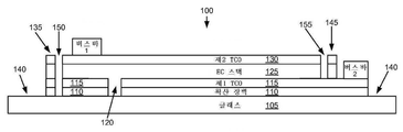
본 명세서에서 설명하는 실시예들을 예시하도록 전기변색 라이트의 구체적인 예를 도 1a 내지 도 1d를 참조하여 설명한다. 전기변색 라이트는 기판 상에 제조된 전기변색 디바이스를 포함한다. 도 1a는 글래스 시트(105)로 시작되어 제조된 전기변색 라이트(100)의 단면도이다(도 1c의 절단부 X-X' 참조). 도 1b는 전기변색 라이트(100)의 단부도이다(도 1c의 사시도 Y-Y' 참조). 도 1c는 전기변색 라이트(100)의 평면도이다.A specific example of the electrochromic light will be described with reference to FIGS. 1A to 1D to illustrate the embodiments described herein. The electrochromic light includes an electrochromic device manufactured on a substrate. 1A is a cross-sectional view of the
도 1a는 글래스 시트(105) 상에 제조되고 에지가 삭제되어 전기변색 라이트의 둘레 주위에 영역(140)을 형성한 후의 전기변색 라이트(100)를 도시한다. 에지 삭제는 기판의 일부 둘레 부분에 대하여 디바이스로부터 하나 이상의 물질층을 제거하는 것이다. 통상적으로, 필수적이진 않지만, 에지 삭제는, 하측 도전층(예를 들어, 도 1a 내지 도 1d에 도시한 예에서의 층(115))을 포함하여 하측 도전층에 이르기까지 물질을 제거하며, 임의의 확산 장벽층(들)을 기판 자체에 이르기까지 제거하는 것을 포함할 수 있다. 도 1a와 도 1b에서, 전기변색 라이트(100)는 또한 레이저 스크라이빙되었으며 버스 바들이 부착되어 있다. 글래스 라이트(105)는, 확산 장벽(110), 및 확산 장벽 상의 제1투명 도전성 산화물(TCO; 115)을 포함한다.1A shows the
이 예에서, 에지 삭제 공정은 TCO(115)와 확산 장벽(110) 모두를 제거하지만, 다른 실시예들에서는, TCO만이 제거되어, 확산 장벽은 온전한 상태로 남겨진다. TCO 층(115)은 글래스 시트 상에 제조되는 전기변색 디바이스의 전극들을 형성하는 데 사용되는 두 개의 도전층 중 제1도전층이다. 일부 예들에서, 글래스 시트는 기저 글래스 위에 형성되는 확산 장벽과 함께 미리 제조될 수 있다. 따라서, 확산 장벽이 형성된 후, 제1TCO(115), EC 스택(125)(예를 들어, 전기변색 층, 이온 도전층, 상대 전극층을 갖는 스택), 및 제2TCO(130)가 형성된다. 다른 예들에서, 글래스 시트는, 기저 글래스 위에 형성되는 확산 장벽과 제1TCO(115)와 함께 미리 제조될 수 있다.In this example, the edge erasure process removes both the
일부 실시예들에서, 하나 이상의 층은, 기판이 층(들)의 제조 동안의 어느 때라도 집적 퇴적 시스템(integrated deposition system)을 남겨 두지 않는 집적 퇴적 시스템에서 기판(예를 들어, 글래스 시트) 상에 형성될 수 있다. 일 실시예에서, EC 스택과 제2TCO를 포함하는 전기변색 디바이스는, 글래스가 층(들)의 제조 동안의 어느 때라도 집적 퇴적 시스템을 남겨 두지 않는 집적 퇴적 시스템에 제조될 수 있다. 일례로, 제1TCO 층도, 글래스가 EC 스택 및 TCO 층(들)의 퇴적 동안 집적 퇴적 시스템을 남겨 두지 않는 집적 퇴적 시스템을 이용하여 형성될 수 있다. 일 실시예에서, 모든 층들(예를 들어, 확산 장벽, 제1TCO, EC 스택, 및 제2TCO)은, 글래스가 퇴적 동안 집적 퇴적 시스템을 남겨 두지 않는 집적 퇴적 시스템에 퇴적된다. 이 예에서, EC 스택(125)의 퇴적 전에, 제1TCO(115)와 확산 장벽(110)을 통해 분리 트렌치(120)를 절단할 수 있다. 트렌치(120)는, 제조 완료 후 버스 바(1) 아래에 있게 될 제1TCO(115)의 영역을 전기적으로 분리하는 것을 고려하여 형성된다(도 1a). 트렌치(120)는 때때로 "L1" 스크라이브라 칭하며, 그 이유는 일부 공정들에서 제1레이저 스크라이브이기 때문이다. 이는, 바람직하지 않은, 버스 바 아래에서의 EC 디바이스의 전하 축적과 착색을 피하기 위한 것이다. 이러한 바람직하지 않은 결과는, 이하에서 더욱 상세히 설명되며 본 명세서에서 설명하는 일부 실시예들을 위한 자극이었다. 즉, 일부 실시예들은, 예를 들어, 레이저 분리 스크라이브 단계들을 감소시키거나 또는 심지어 제거함으로써 버스 바 아래에서의 전하 축적을 피하고 또한 디바이스 제조를 간략화하도록 트렌치(120) 등의 분리 트렌치의 필요성을 제거하려는 것이다.In some embodiments, one or more layers are deposited on a substrate (eg, glass sheet) in an integrated deposition system where the substrate does not leave an integrated deposition system at any time during the manufacture of the layer (s). Can be formed. In one embodiment, an electrochromic device comprising an EC stack and a second TCO can be fabricated in an integrated deposition system where the glass does not leave the integrated deposition system at any time during the manufacture of the layer (s). In one example, the first TCO layer may also be formed using an integrated deposition system where the glass does not leave the integrated deposition system during deposition of the EC stack and TCO layer (s). In one embodiment, all layers (eg, diffusion barrier, 1TCO, EC stack, and 2TCO) are deposited in an integrated deposition system where the glass does not leave the integrated deposition system during deposition. In this example, prior to deposition of the
EC 디바이스의 형성 후에, 에지 삭제 공정과 추가 레이저 스크라이브를 수행한다. 도 1a와 도 1b는, 이 예에서 레이저 스크라이브 트렌치들(150, 155, 160, 165)을 둘러싸는 둘레 영역으로부터 EC 디바이스가 제거된 영역들(140)을 도시한다. 레이저 스크라이브 트렌치들(150, 160, 165)은 때때로 "L2" 스크라이브라 칭하며, 그 이유는 일부 공정들에서 제2스크라이브이기 때문이다. 레이저 스크라이브(155)는 때때로 "L3"이라 칭하며, 그 이유는 일부 공정들에서 제3스크라이브이기 때문이다. L3 스크라이브는 제2TCO(130)를 통과하고 이 예에선 EC 스택(125)도 통과(필수 사항은 아님)하지만, 제1TCO(115)를 통과하지는 않는다. 레이저 스크라이브 트렌치들(150, 155, 160, 165)은, 에지 삭제 공정 동안 잠재적으로 손상된 EC 디바이스의 부분들(135, 145, 170, 175)을 동작 가능 EC 디바이스로부터 분리하도록 형성된 것이다. 일 실시예에서, 레이저 스크라이브 트렌치들(150, 160, 165)은, 디바이스의 분리를 보조하도록 제1TCO를 통과한다(레이저 스크라이브 트렌치(155)는 제1TCO를 통과하지 않으며, 통과하게 되면 제1TCO와 이에 따른 EC 스택과 버스 바(2) 간의 통전을 단절한다). 도 1a 내지 도 1D에 도시한 바와 같은 일부 실시예들에서, 레이저 스크라이브 트렌치들(150, 160, 165)은 확산 장벽도 통과할 수 있다.After the formation of the EC device, an edge erasure process and additional laser scribing are performed. 1A and 1B show
레이저 스크라이브 공정에 사용되는 레이저 또는 레이저들은, 통상적으로, 펄스형 레이저, 예를 들어, 다이오드 펌핑형 고체 레이저이지만, 필수 사항은 아니다. 예를 들어, 레이저 스크라이브 공정들은 적절한 레이저를 사용하여 수행될 수 있다. 적절한 레이저를 제공할 수 있는 공급사들의 일부 예로는, IPG Photonics Corp.(매사추세츠주의 옥스퍼드시에 소재), Ekspla(리투아니아의 빌니우스에 소재), TRUMPF Inc.(코네티컷주의 파밍턴시에 소재), SPI Lasers LLC(캘리포니아주의 산타 클라라시에 소재), Spectra-Physics Corp.(캘리포니아주의 산타 클라라시에 소재), nLIGHT Inc.(워싱턴주의 밴쿠버시에 소재), 및 Fianium Inc.(오레곤주의 유진시에 소재)이 있다. 일부 스크라이빙 단계들도 기계적으로 수행될 수 있으며, 예를 들어, 다이아몬드 팁 스크라이브에 의해 수행될 수 있지만, 일부 실시예들은 레이저로 잘 제어되는 스크라이브 또는 기타 물질 제거 처리 동안 깊이 제어를 설명한다. 예를 들어, 일 실시예에서는, 에지 삭제를 제1TCO의 깊이까지 수행하고, 다른 일 실시예에서는, 에지 삭제를 확산 장벽의 깊이까지 수행하고(제1TCO가 제거됨), 또 다른 일 실시예에서는, 에지 삭제를 기판의 깊이까지 수행한다(모든 물질층들이 기판에 이르기까지 제거됨). 일부 실시예들에서는, 다양한 깊이 스크라이브를 설명한다.The lasers or lasers used in the laser scribe process are usually pulsed lasers, for example diode pumped solid lasers, but are not required. For example, laser scribing processes can be performed using a suitable laser. Some examples of suppliers that can provide suitable lasers include IPG Photonics Corp. (Oxford, Massachusetts), Ekspla (Vilnius, Lithuania), TRUMPF Inc. (Parmington City, Connecticut), and SPI Lasers LLC, Santa Clara City, California, Spectra-Physics Corp., Santa Clara City, California, nLIGHT Inc., Vancouver City, Washington, and Fianium Inc., Eugene City, Oregon. There is this. Some scribing steps may also be performed mechanically, for example by diamond tip scribing, but some embodiments describe depth control during a laser controlled scribe or other material removal process. For example, in one embodiment, edge deletion is performed to the depth of the first TCO, in another embodiment edge deletion is performed to the depth of the diffusion barrier (the first TCO is removed), and in another embodiment, Edge erasure is performed to the depth of the substrate (all material layers are removed down to the substrate). In some embodiments, various depth scribes are described.
레이저 스크라이빙이 완료된 후, 버스 바들을 부착한다. 비통과 버스 바(1)를 제2TCO에 부착한다. 비통과 버스 바(2)를, (예를 들어, 디바이스 퇴적으로부터 제1TCO를 보호하는 마스크로부터) EC 스택과 제2TCO를 포함하는 디바이스가 퇴적되지 않은 영역에, 또는 이 예에서, 에지 삭제 공정(예를 들어, XY 또는 XYZ 검류계를 구비하는 장치를 이용한 레이저 절제)을 이용하여 물질을 제1TCO에 이르기까지 제거하는 영역에 부착한다. 이 예에서, 버스 바(1)와 버스 바(2) 모두는 비통과 버스 바들이다. 통과 버스 바는, 통상적으로 EC 스택의 하나 이상의 층의 하부에 또는 이러한 하나 이상의 층의 아래에 위치하는 TCO 등의 하측 도전층과 접촉하도록 하나 이상의 층으로 또는 이러한 층을 통해 가압(또는 솔더링)되는 것이다. 비통과 버스 바는, 층들 내로 통과하지 않으며 대신에 예를 들어 TCO 등의 도전층의 표면과 전기적으로 그리고 물리적으로 접촉하는 것이다. 비통과 버스 바의 통상적인 예는, 적절한 도전성 표면에 도포되는 실버계 잉크인 도전성 잉크이다.After laser scribing is complete, attach the bus bars. The
TCO 층들은, 비전통적 버스 바를 사용하여, 예를 들어, 스크린 및 리소그래피 패터닝 방법들로 제조된 버스 바를 사용하여 전기적으로 접속될 수 있다. 일 실시예에서, 통전은, 도전성 잉크의 열 경화 또는 소성이 후속하는, 도전성 잉크를 실크 스크리닝함으로써(또는 다른 패터닝 방법을 이용함으로써) 디바이스의 투명 도전층들과 확립된다. 전술한 디바이스 구성을 이용하는 장점으로는, 예를 들어, 더욱 간단한 제조, 및 통과 버스 바들을 사용하는 종래의 기술들보다 덜한 레이저 스크라이빙을 들 수 있다.The TCO layers can be electrically connected using a non-traditional bus bar, for example using a bus bar made with screen and lithographic patterning methods. In one embodiment, energization is established with the transparent conductive layers of the device by silk screening the conductive ink (or by using other patterning methods) followed by thermal curing or firing of the conductive ink. Advantages of using the device configuration described above include, for example, simpler manufacturing, and less laser scribing than conventional techniques using pass bus bars.
버스 바들이 제조된 후 또는 그외에는 하나 이상의 도전층에 부착된 후에, 전기변색 라이트를, 예를 들어 버스 바 등을 위한 와이어링을 포함하는 절연 글래스 유닛(IGU) 내에 집적할 수 있다. 일부 실시예들에서, 버스 바들 중 하나 또는 모두는 완성된 IGU 내에 있다. 구체적인 실시예들에서, 버스 바들 모두는 IGU의 글래스와 스페이서 사이에 있도록 구성되고(흔히 IGU의 일차 밀봉부라 칭함), 즉, 버스 바들은 IGU의 라이트들을 분리하는 데 사용되는 스페이서와 위치 정렬(register)된다. 영역(140)은, IGU를 형성하는 데 사용되는 스페이서의 일면과의 밀봉부를 적어도 부분적으로 형성하는 데 사용된다. 따라서, 버스 바들에 대한 와이어들 또는 기타 접속부는 스페이서와 글래스 사이에 이어진다. 많은 스페이서들은 도전성을 갖는 스테인리스 스틸 등의 금속으로 형성되므로, 버스 바와 이에 대한 커넥터 및 금속 스페이서 간의 통전으로 인한 단락을 피하는 단계들을 취하는 것이 바람직하다. 이를 달성하기 위한 구체적인 방법들과 장치는, 그 전문이 본 명세서에 참고로 원용되며 "Improved Spacers for Insulated glass Units"이라는 명칭으로 2011년 12월 6일자로 출원된 미국 특허출원번호 제13/312,057호에 개시되어 있다. 본 명세서에서 설명하는 다른 실시예들에서, 방법들 및 이에 따라 EC 디바이스의 둘레 에지를 갖는 IGU들, 버스 바들, 및 임의의 분리 스크라이브는 모두 IGU의 일차 밀봉부 내에 있다.After the bus bars have been manufactured or otherwise attached to one or more conductive layers, the electrochromic light can be integrated into an insulated glass unit (IGU) including wiring for, for example, a bus bar. In some embodiments, one or both of the bus bars are within the completed IGU. In specific embodiments, all of the bus bars are configured to be between the glass and spacer of the IGU (commonly referred to as the primary seal of the IGU), ie, the bus bars register with the spacer used to separate the lights of the IGU (register) )do.
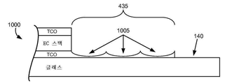
도 1d는 도 1a의 단면도의 일부를 도시하며, 그 일부를 확대하여 본 명세서에서 개시하는 일부 실시예들이 극복할 수 있는 사항을 예시하고 있다. TCO(115) 상에 EC 스택(125)을 제조하기 전에, 115/110 스택의 일부를 더욱 큰 영역으로부터 분리하도록 TCO(115)와 확산 장벽(110)을 통해 분리 트렌치(120)를 형성한다. 이러한 분리 트렌치는, 궁극적으로 버스 바(2)와 통전하는 하측 TCO(115)과, TCO(130) 상에 위치하며 전기 에너지를 TCO에 공급하는 버스 바(1)의 바로 아래에 있는 TCO(115)의 섹션 간의 통전을 단절하려는 것이다. 예를 들어, EC 디바이스의 착색 동안, 버스 바(1)와 버스 바(2)는 EC 디바이스에 걸쳐 전위를 인가하도록 에너지를 공급받으며, 예를 들어, TCO(115)는 음의 전하를 갖고 TCO(130)는 양의 전하를 갖고, 또는 그 반대로, 전하를 갖는다.FIG. 1D shows a part of the cross-sectional view of FIG. 1A and enlarges a part to illustrate a problem that some embodiments disclosed in this specification can overcome. Prior to manufacturing the
분리 트렌치(120)는 많은 이유 때문에 바람직하다. 때로는, 버스 바(1) 아래의 EC 디바이스가 착색되지 않는 것이 바람직할 수 있으며, 이는 이 영역을 최종 사용자가 볼 수 없기 때문이다(윈도우 프레임은 통상적으로 버스 바들과 분리 트렌치를 넘어 연장되고, 및/또는 이러한 특징부들은 전술한 바와 같이 스페이서 아래에 있다). 또한, 때때로, 영역(140)은 하측 TCO와 확산 장벽을 포함하고, 이러한 경우에는, 하측 TCO가 전하를 글래스의 에지에 전달하는 것이 바람직하지 못할 수 있으며, 이는 최종 사용자에겐 보이지 않는 영역들에서의 불필요한 전하 손실과 단락이 발생할 수 있기 때문이다. 또한, 버스 바의 바로 아래에 있는 EC 디바이스의 부분은 대부분의 전하 플럭스를 겪기 때문에, 디바이스의 이 영역이 결함, 예를 들어, 박리, 입자 이탈(팝오프 결함) 등을 형성하는 경향이 있으며, 이러한 결함은 관찰 가능 영역에서 보일 수 있는 비정상적인 영역 또는 착색 없는 영역을 야기할 수 있고 및/또는 디바이스 성능에 악영향을 끼칠 수 있다. 분리 트렌치(120)는 이러한 사항들을 다루도록 설계되었다. 이러한 소망 결과에도 불구하고, 제1버스 바 아래에서 착색화가 여전히 발생함을 알게 되었다. 이 현상을 도 1d의 하측 부분에서의 디바이스(100)의 확대 부분에 관하여 설명한다.
EC 스택(125)이 제1TCO(115) 상에 퇴적되면, EC 스택(125)을 이루고 있는 전기변색 물질이 분리 트렌치(120)를 채운다. 제1TCO(115)의 전기 경로가 트렌치(120)에 의해 단절되지만, 트렌치는, TCO만큼 도전성을 갖지는 않지만 전하를 전달할 수 있고 이온을 투과시킬 수 있는 물질로 채워진다. EC 라이트(100)의 동작 동안, 예를 들어, (도 1d에 도시한 바와 같이) 제1TCO(115)가 음의 전하를 가지면, 소량의 전하가 트렌치(120)를 가로질러 전달되어 제1TCO(115)의 분리된 부분에 입력된다. 이 전하 축적은 EC 라이트(100)의 착색과 소색의 여러 사이클에 걸쳐 발생할 수 있다. 일단 TCO(115)의 분리된 영역이 전하를 축적하게 되면, 영역(180)에서, 버스 바(1) 아래의 EC 스택(125)이 착색될 수 있다. 또한, 제1TCO(115)의 이 부분의 전하는, 일단 축적되면, 전하가 TCO(115)의 나머지 부분에서 정상적으로 있는 것만큼, 예를 들어, 반대 전하가 버스 바(2)에 인가되는 경우에, 효율적으로 배출되지 않는다. 분리 트렌치(120)에서의 다른 문제점은 확산 장벽이 트렌치의 베이스에서 위태롭게 될 수 있다는 점이다. 이는 나트륨 이온들이 글래스 기판으로부터 EC 스택(125) 내로 확산될 수 있게 한다. 이러한 나트륨 이온들은 전하 캐리어로서 기능할 수 있고 제1TCO(115)의 분리된 부분 상에서의 전하 축적을 향상시킬 수 있다. 또 다른 문제점은, 버스 바 아래에서의 전하 축적이 물질층들에 과도한 응력을 가할 수 있고 이 영역에서의 결함 형성을 촉진할 수 있다는 점이다. 마지막으로, 기판 상의 도전층에 분리 스크라이브를 제조함으로 인해 처리 단계들이 더욱 복잡해진다. 본 명세서에서 설명하는 실시예들은 이러한 문제점들 및 기타 문제점들을 극복할 수 있다.When the
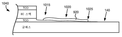
도 2a는 EC 디바이스(200)의 개선된 아키텍처를 도시한 부분 단면도이다. 예시한 본 실시예에서는, 버스 바(1) 아래로 연장되었을 제1TCO(115)의 일부가 EC 스택(125)의 제조 전에 제거되어 있다. 본 실시예에서, 확산 장벽(110)은 버스 바(1) 아래로 그리고 EC 디바이스의 에지까지 연장된다. 일부 실시예들에서, 확산 장벽은, 글래스(105)의 에지까지 연장되며, 즉, 영역(140)을 피복한다. 다른 실시예들에서는, 확산 장벽의 일부도 버스 바(1) 아래에서 제거될 수 있다. 전술한 실시예들에서, 버스 발(1) 아래에서의 선택적 TCO 제거는 EC 스택(125)의 제조 전에 수행된다. (예를 들어, 스페이서가 글래스와의 밀봉부를 형성하는 글래스의 둘레 주위에) 영역들(140)을 형성하기 위한 에지 삭제 공정들은 디바이스 제조 전에 또는 후에 수행될 수 있다. 일부 실시예들에서는, 영역(140)을 형성하기 위한 에지 삭제 공정이 예를 들어 단락 문제로 인해 거친 에지 또는 그 외에는 허용 불가한 에지를 생성한다면 분리 스크라이브 트렌치(150a)가 형성되고, 이에 따라 물질의 일부(135a)를 EC 디바이스의 나머지 부분으로부터 분리한다. 도 2a에 도시한 EC 디바이스(200)의 확대 부분으로 예시한 바와 같이, 버스 바(1) 아래에 TCO(115)의 어떠한 부분도 존재하지 않으므로, 불필요한 착색과 전하 축적 등의 전술한 문제점들을 피할 수 있다. 또한, 적어도 EC 스택(125)과 함께 연장 가능한 확산 장벽(110)이 온전한 상태로 남아 있으므로, 나트륨 이온들이 EC 스택(125) 내로 확산됨으로 인해 불필요한 도전성 문제나 기타 문제를 야기하는 것을 방지한다.2A is a partial cross-sectional view showing an improved architecture of the
일부 실시예들에서는, 일단 제조가 완료되면 버스 바(1)가 상주할 영역 아래의 TCO(115)의 밴드를 선택적으로 제거한다. 즉, 확산 장벽(110)과 제1TCO(115)가 영역(140) 상에 남아 있을 수 있지만, 제1TCO(115)의 폭은 버스 바(1) 아래에서 선택적으로 제거된다. 일 실시예에서, 제1TCO(115)의 제거된 밴드의 폭은, 일단 디바이스 제조가 완료되면 TCO의 제거된 밴드 위에 상주하는 버스 바(1)의 폭보다 클 수 있다. 본 명세서에서 설명하는 실시예들은, TCO(115)의 밴드를 선택적으로 제거한 도 2a에 관하여 설명하고 예시한 바와 같은 구성을 갖는 EC 디바이스를 포함한다. 일 실시예에서, 디바이스의 나머지 부분은 도 1a 내지 도 1c에 관하여 설명하고 예시한 바와 같다.In some embodiments, once manufacturing is completed, the band of
디바이스(200)와 유사한 디바이스가 도 2b와 도 2c에 도시되어 있으며, 레이저 분리 트렌치 등을 포함하는 디바이스 아키텍처를 도시하고 있다. 도 2b와 도 2c는 개시한 실시예들의 개선된 디바이스 아키텍처를 도시한다. 일부 실시예들에서는, 디바이스의 제조 동안 레이저 분리 트렌치들이 적거나 또는 없다. 이러한 실시예들은 이하에서 더욱 상세히 설명한다.Devices similar to
도 2d와 도 2e는, 디바이스(200)와 매우 유사한 아키텍처를 갖지만 기능하지 않는 디바이스의 레이저 분리 스크라이브(150a)나 분리 영역(135a)은 갖지 않는 전기변색 디바이스(205)를 도시한다. 일부 레이저 에지 삭제 공정들은 레이저 스크라이브(150a) 등이 필요 없도록 디바이스의 충분히 깨끗한 에지를 남긴다. 일 실시예는, 도 2d와 도 2e에 도시한 바와 같지만 분리 스크라이브들(160, 165)과 분리 부분들(170, 175)을 갖지 않는 광학 디바이스이다. 일 실시예는, 도 2d와 도 2e에 도시한 바와 같지만 분리 스크라이브(155)와 분리 부분(145)을 갖지 않는 광학 디바이스이다. 일 실시예는, 도 2d와 도 2e에 도시한 바와 같지만 분리 스크라이브들(160, 165, 또는 155)과 분리 부분들(145, 170, 175)을 갖지 않는 광학 디바이스이다. 일부 실시예들에서, 제조 방법들은 어떠한 레이저 분리 스크라이브도 포함하지 않으며, 따라서, 디바이스의 물리적으로 분리된 비기능적 부분이 없는 광학 디바이스를 제조한다.2D and 2E show an
더욱 상세히 후술하는 바와 같이, 일부 실시예들은, 디바이스의 하나 이상의 물질층과 제2(상측) 도전층이 제1(하측) 도전층과 함께 연장 가능하지 않은 디바이스를 포함하며, 구체적으로, 이러한 부분들은 제1도전층을 제1도전층의 영역의 둘레의 일부 부분 주위로 돌출시킨다. 이러한 돌출 부분들은 버스 바를 포함할 수도 있고 또는 포함하지 않을 수도 있다. 일례로, 도 2a 또는 도 3에 관하여 설명한 바와 같은 돌출 부분들은 제2도전층 상에 버스 바를 갖는다.As described in more detail below, some embodiments include a device in which one or more material layers of a device and a second (top) conductive layer are not extendable with a first (bottom) conductive layer, specifically, this portion These protrude the first conductive layer around a part of the perimeter of the area of the first conductive layer. These protruding parts may or may not include a bus bar. In one example, the projecting portions as described with respect to FIGS. 2A or 3 have a bus bar on the second conductive layer.
도 3은 개시한 실시예들의 개선된 전기변색 디바이스 아키텍처(300)를 도시한 부분 단면도이다. 예시한 본 실시예에서는, 버스 바(1) 아래로 연장되었을 TCO(115)와 확산 장벽(110)의 부분들이 EC 스택(125)의 제조 전에 제거되어 있다. 즉, 버스 바(1) 아래의 제1TCO와 확산 장벽 제거는 EC 스택(125)의 제조 전에 수행된다. (예를 들어, 스페이서가 글래스와의 밀봉부를 형성하는 글래스의 둘레 주위에) 영역들(140)을 형성하기 위한 에지 삭제 공정들은, 디바이스 제조 전에 (예를 들어, 확산 장벽을 제거한 후 마스크를 이용하여) 또는 디바이스 제조 후에 (모든 재료들을 글래스에 이르기까지 제거하여) 수행될 수 있다. 일부 실시예들에서, 영역들(140)을 형성하기 위한 에지 삭제 공정이 거친 에지를 생성하면 도 2a의 참조번호 (150a)와 마찬가지인 분리 스크라이브 트렌치가 형성되고, 이에 따라 물질의 일부(135a)(도 2a 참조)를 EC 디바이스의 나머지 부분으로부터 분리한다.3 is a partial cross-sectional view showing an improved
다시 도 3을 참조해 보면, 디바이스(300)의 확대 부분에 예시한 바와 같이, 버스 바(1) 아래에 TCO(115)의 어떠한 부분도 존재하지 않으므로, 불필요한 착색과 전하 축적 등의 전술한 문제점들을 피할 수 있다. 이 예에서는, 확산 장벽(110)도 제거되므로, 나트륨 이온들이 버스 바(1) 아래의 영역의 EC 스택 내로 확산할 수 있지만, 전하를 얻어 유지하기 위한 TCO(115)의 대응 부분이 없으므로, 착색과 기타 사항들이 덜 문제화된다. 일부 실시예들에서는, 버스 바(1)가 상주할 영역 아래의 TCO(115)와 확산 장벽(110)의 밴드를 선택적으로 제거하며, 즉, 영역(140) 상에 확산 장벽과 TCO가 남아 있을 수 있지만, TCO(115)와 확산 장벽(110)의 폭은 버스 바(1) 아래에서 선택적으로 제거되며 적어도 이러한 버스 바와 함께 연장 가능하다. 일 실시예에서, TCO와 확산 장벽의 제거된 밴드의 폭은, 일단 디바이스 제조가 완료되면 그 제거된 밴드 위에 상주하는 버스 바의 폭보다 크다. 본 명세서에서 설명하는 실시예들은, 도 3에 관하여 설명하고 예시한 바와 같은 구성을 갖는 EC 디바이스를 포함한다. 일 실시예에서, 디바이스의 나머지 부분은 도 1a 내지 도 1c에 관하여 설명하고 예시한 바와 같다. 일부 실시예들에서는, 디바이스 제조 동안 형성되는 레이저 분리 트렌치들이 적거나 또는 없다.Referring to FIG. 3 again, as illustrated in the enlarged portion of the
실시예들은, 도 3에 관하여 설명한 바와 같은 광학 디바이스를 포함하며, 나머지 부분은 도 2d와 도 2e에 관하여 설명한 디바이스(205)와 같다. 일 실시예는, 도 3에 도시한 바와 같은 광학 디바이스이지만, 도 2d와 도 2e에 도시한 바와 같은 분리 스크라이브들(160, 165)과 분리 부분들(170, 175)을 갖지 않는다. 일 실시예는, 도 3에 도시한 바와 같은 광학 디바이스이지만, 도 2d와 도 2e에 도시한 바와 같은 분리 스크라이브(155)와 분리 부분(145)을 갖지 않는다. 일 실시예는, 도 3에 도시한 바와 같은 광학 디바이스이지만, 도 2d와 도 2e에 도시한 바와 같은 분리 스크라이브들(160, 165, 또는 155)과 분리 부분들(145, 170, 175)을 갖지 않는다. 전술한 실시예들 중 어느 것이라도, 도 1a 내지 도 1d에 관하여 도시한 바와 같은 스크라이브(150)와 유사한 분리 스크라이브를 포함할 수 있지만, 스크라이브(120)와 유사한 분리 스크라이브는 포함하지 않을 수 있다. 본 명세서에서 설명하는 모든 실시예들은, 도 1a 내지 도 1d에 관하여 설명한 바와 같이 스크라이브(120)와 유사한 레이저 분리 스크라이브의 필요성을 배제한다. 또한, 목표는 필요한 레이저 분리 스크라이브들의 수를 감소시키는 것이지만, 예를 들어 사용되는 레이저나 디바이스 물질에 따라, 스크라이브(120)가 아닌 스크라이브가 필요할 수도 있고 또는 필요하지 않을 수도 있다.Embodiments include an optical device as described with respect to FIG. 3, the rest of which is the same as the
전술한 바와 같이, 일부 실시예들에서, 디바이스들은 레이저 분리 스크라이브를 사용하지 않고서 제조되며, 즉, 최종 디바이스가 비기능적인 분리 부분들을 갖지 않는다. 예시적인 제조 방법들을 분리 스크라이브를 갖지 않는 관점에서 후술하지만, 일 실시예는 후술하는 바와 같은 임의의 디바이스이며, 이 디바이스는 도 1a 내지 도 1d에 관하여 설명한 바와 같은 분리 스크라이브의 (디바이스의 형상에 따라) 기능적 균등부를 갖지만 분리 스크라이브(120)는 갖지 않는다는 점을 이해하기 바란다. 더욱 구체적으로, 일 실시예는, 후술하는 바와 같은 광학 디바이스이지만, 도 2d와 도 2e에 도시한 바와 같은 분리 스크라이브들(160, 165)을 갖지 않는다. 일 실시예는, 후술하는 바와 같은 광학 디바이스이지만, 도 2d와 도 2e에 도시한 바와 같은 분리 스크라이브(155)를 갖지 않는다. 일 실시예는, 후술하는 바와 같은 광학 디바이스이지만, 도 2d와 도 2e에 도시한 바와 같은 분리 스크라이브들(160, 165, 또는 155)을 갖지 않는다. 전술한 실시예들 중 어느 것이라도, 도 1a 내지 도 1d에 관하여 도시한 바와 같은 스크라이브(150)와 유사한 분리 스크라이브를 포함할 수도 있다.As described above, in some embodiments, the devices are manufactured without the use of a laser separation scribe, ie, the final device does not have non-functional separation parts. Exemplary manufacturing methods will be described later in terms of not having a separate scribe, but one embodiment is any device as described below, which device is based on the shape of the device (depending on the shape of the device) as described with respect to FIGS. 1A-1D. ) Please understand that it has a functional equality but does not have a
일 실시예는, 제1도전층(예를 들어, 제1TCO(115))과 제2도전층(예를 들어, 제2TCO(130) 사이에 협지된 하나 이상의 물질층을 포함하는 광학 디바이스를 제조하는 방법이다. 이 방법은, 제1도전층과 제2도전층 사이에 협지된 하나 이상의 물질층을 포함하는 광학 디바이스를 제조하는 방법으로서, (i) 제1도전층의 가공면을 위로 하여 제1도전층을 포함하는 기판을 수용하는 단계; (ii) 제1도전층의 제1폭을 기판의 둘레의 약 10% 내지 약 90%로부터 제거하는 단계; (iii) 광학 디바이스의 하나 이상의 물질층과 제2도전층이 제1도전층을 피복하고 가능하다면 제1도전층을 벗어나 제1도전층의 둘레 주위로 연장되도록 하나 이상의 물질층과 제2도전층을 퇴적하는 단계; (iv) 기판의 대략 전체 둘레의 주위로 모든 층들의 제2폭을 제거하는 단계로서, 제2폭은 제1폭보다 좁고, 제거 깊이는 적어도 제1도전층을 제거하도록 충분한 것인, 제2폭을 제거하는 단계; (v) 투명한 제2도전층의 적어도 일부분 및 적어도 일부분 아래의 광학 디바이스의 하나 이상의 물질층을 제거하여, 제1도전층의 적어도 하나의 노출 부분을 드러내는 단계; 및 (vi) 투명한 제1도전층의 적어도 하나의 노출 부분에 버스 바를 부착하는 단계를 포함하고, 제1도전층과 제2도전층 중 적어도 하나는 투명하다. 일 실시예에서, (ii) 단계는, 기판 둘레의 약 50% 내지 약 75%로부터 제1도전층의 제1폭을 제거하는 단계를 포함한다.One embodiment manufactures an optical device that includes one or more layers of material sandwiched between a first conductive layer (eg, the first TCO 115) and a second conductive layer (eg, the second TCO 130). This method is a method of manufacturing an optical device including at least one material layer sandwiched between a first conductive layer and a second conductive layer, (i) a first conductive layer with a working surface facing up; Receiving a substrate comprising a first conductive layer; (ii) removing a first width of the first conductive layer from about 10% to about 90% of the perimeter of the substrate; (iii) one or more material layers of the optical device And depositing at least one material layer and a second conductive layer so that the and second conductive layer cover the first conductive layer and extend around the periphery of the first conductive layer beyond the first conductive layer if possible; (iv) Removing the second width of all the layers around the entire circumference, the second width being narrower than the first width, Removing the second width, wherein the removal depth is sufficient to remove at least the first conductive layer; (v) removing at least a portion of the transparent second conductive layer and one or more layers of material of the optical device below the at least a portion, Revealing at least one exposed portion of the first conductive layer; and (vi) attaching a bus bar to at least one exposed portion of the transparent first conductive layer, wherein at least one of the first conductive layer and the second conductive layer is included. One is transparent In one embodiment, step (ii) includes removing a first width of the first conductive layer from about 50% to about 75% around the substrate.
일 실시예에서, (ii) 단계 후에 남아 있는 제1도전층의 에지의 일부는 더욱 상세히 후술하는 바와 같이 테이퍼링된다. 에지의 테이퍼링 부분은, (ii) 단계 후에 투명 도전층이 다각 형상이라면 1개, 2개, 또는 그 이상의 변을 포함할 수 있다. 일부 경우에, 제1도전층은 (ii) 단계 전에 연마된 후, 선택 사항으로 에지 테이퍼링된다. 다른 경우에, 제1도전층은 에지 테이퍼링에 상관없이 (ii) 단계 후에 연마된다. 후자의 경우에, 테이퍼링은 연마 전에 또는 연마 후에 행해질 수 있다.In one embodiment, a portion of the edge of the first conductive layer remaining after step (ii) is tapered as described in more detail below. The tapering portion of the edge may include one, two, or more sides if the transparent conductive layer has a polygonal shape after step (ii). In some cases, the first conductive layer is polished prior to step (ii) and then optionally tapered. In other cases, the first conductive layer is polished after step (ii) regardless of edge tapering. In the latter case, the tapering can be done before or after polishing.
일 실시예에서, 노출된 제1도전층의 적어도 하나의 노출 부분은, 제1도전층이 (ii) 단계에서 제거되지 않은 기판의 변 또는 변들에 근접하는 광학 디바이스의 둘레 부분을 따라 제조된다. 일부 실시예들에서, 제1도전층의 노출 부분은 하나 이상의 물질층과 제2도전층을 통한 애퍼처나 홀이 아니며, 오히려, 그 노출 부분은 기능적 디바이스 스택 층들의 에지 부분으로부터 돌출되는 영역이다. 이는 구체적인 예들을 참조하여 더욱 상세히 후술한다.In one embodiment, at least one exposed portion of the exposed first conductive layer is made along a peripheral portion of the optical device proximate sides or sides of the substrate where the first conductive layer was not removed in step (ii). In some embodiments, the exposed portion of the first conductive layer is not an aperture or hole through the one or more material layers and the second conductive layer, but rather, the exposed portion is an area protruding from the edge portion of the functional device stack layers. This will be described later in more detail with reference to specific examples.
방법은, 적어도 하나의 제2버스 바를 제2도전층에, 특히, 제1도전층을 피복하지 않는 부분에 부착하는 단계를 더 포함할 수 있다. 일 실시예에서, 광학 디바이스는 전기변색 디바이스이며, 완전한 고체 및 무기성일 수 있다. 기판은 플로트 글래스일 수 있으며, 제1도전층은 산화주석, 예를 들어, 플루오르화 산화주석을 포함할 수 있다. 일 실시예에서, (iii) 단계는 완전 진공 집적 퇴적 장치에서 수행된다. 일부 실시예들에서, 방법은 (iv) 단계 전에 제2도전층 상에 기상 장벽층을 증착하는 단계를 더 포함한다.The method may further include attaching at least one second bus bar to the second conductive layer, particularly to the portion not covering the first conductive layer. In one embodiment, the optical device is an electrochromic device, and may be completely solid and inorganic. The substrate may be float glass, and the first conductive layer may include tin oxide, for example, fluorinated tin oxide. In one embodiment, step (iii) is performed in a fully vacuum integrated deposition apparatus. In some embodiments, the method further comprises depositing a vapor barrier layer on the second conductive layer prior to step (iv).
일 실시예에서, 제1도전층의 적어도 하나의 노출 부분은, 광학 디바이스의 일 변의 길이를 따라 제조되며, 일 실시예에서는, (ii) 단계에서 제1도전층이 제거되지 않은 기판의 변에 근접하는 광학 디바이스의 일 변의 길이를 따라 제조된다. 일 실시예에서, 적어도 하나의 제2버스 바는, 제1도전층의 적어도 하나의 노출 부분의 반대측인 광학 디바이스의 일 변에 근접한 제2도전층에 부착된다. 기상 장벽이 부착되면, 적어도 하나의 제2버스 바의 부착을 위한 제2도전층을 노출하도록 일부가 제거된다. 이러한 방법들은 도 4a 내지 도 4d를 참조하여 특정 실시예들에 관하여 후술한다.In one embodiment, at least one exposed portion of the first conductive layer is manufactured along the length of one side of the optical device, and in one embodiment, on the side of the substrate where the first conductive layer is not removed in step (ii). It is manufactured along the length of one side of the adjacent optical device. In one embodiment, the at least one second bus bar is attached to a second conductive layer proximate one side of the optical device opposite the at least one exposed portion of the first conductive layer. When the vapor barrier is attached, a portion is removed to expose the second conductive layer for attachment of at least one second bus bar. These methods are described below with reference to certain embodiments with reference to FIGS. 4A-4D.
도 4a는, 전기변색 디바이스 또는 대향하는 버스 바들을 갖는 기타 광학 디바이스를 제조하는 방법의 양태들을 설명하는 공정 흐름도(400)로서, 각 버스 바는 광학 디바이스의 도전층들 중 하나에 부착된다. 점선들은 공정 흐름의 선택적인 단계들을 나타낸다. 도 4b와 도 4C에 관하여 설명하는 바와 같은 예시적인 디바이스(440)는 공정 흐름을 예시하는 데 사용된다. 도 4b는 도 4a에 관하여 설명한 바와 같은 공정 흐름(400)의 참조 번호들을 포함하는 디바이스(440)의 제조를 도시한 평면도를 도시한다. 도 4c는 도 4b에 관하여 설명하는 디바이스(440)를 포함하는 라이트의 단면도를 도시한다. 디바이스(440)는 직사각형 디바이스이지만, 공정 흐름(400)은 대향하는 버스 바들을 갖는 광학 디바이스의 임의의 형상에 적용되며, 각 버스 바는 도전층들 중 하나 상에 있다. 이 양태를 이하에서 예를 들어 (둥근 전기변색 디바이스의 제조에 관한 공정 흐름(400)을 도시한) 도 4d에 관하여 더욱 상세히 설명한다.4A is a process flow diagram 400 describing aspects of a method of manufacturing an electrochromic device or other optical device with opposing bus bars, each bus bar attached to one of the conductive layers of the optical device. Dotted lines represent optional steps in the process flow. An
도 4a와 도 4b를 참조해 보면, 제1도전층을 위에 갖는 기판을 수용한 후, 공정 흐름(400)은 선택 사항인 제1도전층의 연마로 시작되며, 참조번호 (401)을 참조한다. 일부 실시예들에서, 하측 투명한 도전층을 연마함으로써 그 위에 제조되는 EC 디바이스의 광학적 성질과 성능이 향상된다는 것을 알게 되었다. 투명한 도전층들을 그 위의 전기변색 디바이스의 제조 전에 연마하는 것은, 그 전문이 본 명세서에 참고로 원용되며 "Optical Device Fabrication"이라는 명칭으로 2012년 9월 27일에 출원된 국제출원번호 PCT/US 12/57606에 개시되어 있다. 연마는, 수행되는 경우, 에지 삭제 전에 행해질 수 있고, 참조번호 (405)를 참조하고, 또는, 공정 흐름에서 에지 삭제 후에 행해질 수 있다. 일부 실시예들에서, 하측 도전층은 에지 삭제 전과 후에 연마될 수 있다. 통상적으로, 하측 도전층은 한 번만 연마된다.4A and 4B, after receiving the substrate having the first conductive layer thereon, the
다시 도 4a를 참조해 보면, 연마(401)가 수행되지 않으면, 공정(400)은 기판의 둘레의 일부 주위로 제1폭을 삭제하는 에지 삭제로 시작되며, 참조번호 (405)를 참조한다. 에지 삭제는 제1도전층만을 제거할 수 있고 또는 확산 장벽이 존재한다면 확산 장벽도 제거할 수 있다. 일 실시예에서, 기판은 글래스이며, 나트륨 확산 장벽과 그 위의 투명한 도전층, 예를 들어, 산화주석계 투명 산화금속 도전층을 포함한다. 기판은 직사각형일 수 있다(예를 들어, 도 4b에 도시한 정사각형 기판을 참조). 도 4b의 점선 영역은 제1도전층을 나타낸다. 따라서, 공정(405)에 따른 에지 삭제 후에, 기판(430)의 둘레의 세 개의 변으로부터 폭 A를 제거한다. 이 폭은 통상적으로 균일한 폭이지만, 반드시 그러한 것은 아니다. 제2폭 B를 후술한다. 폭 A 및/또는 폭 B는 균일하지 않은 경우, 서로에 대한 이러한 폭들의 상대적 크기는 이들의 평균 폭의 관점으로 본다.Referring again to FIG. 4A, if polishing 401 is not performed,
참조번호 (405)에서 제1폭 A를 제거한 결과, 하측 도전층의 새롭게 노출된 에지가 존재한다. 일부 실시예들에서, 제1도전층의 이러한 에지의 적어도 일부는, 선택 사항으로, 테이퍼링될 수도 있으며, 참조번호 (407)과 (409)를 참조한다. 기저 확산 장벽층도 테이퍼링할 수 있다. 본 발명자들은, 하나 이상의 디바이스 층들의 에지를, 후속하는 층들의 제조 전에, 테이퍼링함으로써 디바이스 구조와 성능에 있어서 예상하지 못한 장점들이 있음을 발견하였다. 에지 테이퍼링 공정을 도 8a와 도 8b에 관하여 더욱 상세히 설명한다.As a result of removing the first width A from
일부 실시예들에서, 하측 도전층은, 에지 테이퍼링 후에, 선택 사항으로서 연마되며, 참조번호 (408)을 참조한다. 일부 디바이스 물질을 이용하는 경우에, 연마가 (전술한 바와 같이) 디바이스 성능을 개선할 수 있는 벌크 도전체 표면뿐만 아니라 에지 테이퍼링에 대하여 예상하지 못한 유익한 효과들을 가질 수 있으므로, 에지 테이퍼링 후에 하측 도전층을 연마하는 것이 유리할 수 있음을 발견하였다. 일부 실시예들에서는, 연마 단계(408) 후에 에지 테이퍼링을 수행하며, 참조번호 (409)를 참조한다. 에지 테이퍼링은 도 4a의 참조번호 (407)과 (409) 모두에 도시되어 있지만, 수행되는 경우, 에지 테이퍼링은 통상적으로 한번에 수행된다(예를 들어, 참조번호 (407) 또는 (409) 참조).In some embodiments, the lower conductive layer, after edge tapering, is optionally polished,
전술한 바와 같이 제1폭 A의 제거와 선택 사항인 연마 및/또는 선택 사항인 에지 테이퍼링 후에, EC 디바이스는 기판(430)의 표면 위에 퇴적되며, 참조번호 (410)을 참조한다. 이러한 퇴적은, 광학 디바이스의 하나 이상의 물질층과, 제2도전층, 예를 들어, 인듐 주석 산화물(ITO) 등의 투명한 도전층을 포함한다. 도시한 피복률은 전체 기판에 해당하지만, 글래스를 제 위치에 유지해야 하는 캐리어로 인해 일부 마스킹이 있을 수 있다. 일 실시예에서, 제1도전층의 나머지 부분의 전체 영역은, 이전에 제거된 제1폭 A에 대하여 제1도전층과 중첩되는 부분을 포함하여 피복된다. 이는, 더욱 상세히 후술하는 바와 같이 최종 디바이스 아키텍처의 중첩 영역들을 허용한다.After removal of the first width A and optional polishing and / or optional edge tapering as described above, the EC device is deposited on the surface of the
구체적인 실시예들에서는, 전기변색 방사를 이용하여, 에지 삭제를 수행하고 기판의 주변 영역을 제공하고, 예를 들어, 공정 단계에 따라, (상부 도전층과 이에 부착되는 임의의 기상 장벽까지 포함하는) 투명한 도전층 또는 그 이상의 층들을 제거한다. 일 실시예에서는, 에지 삭제를 수행하여 적어도 기판 상의 투명한 도전층을 포함하는 물질을 제거하고, 선택 사항으로, 확산 장벽이 존재하는 경우 확산 장벽도 제거한다. 일부 실시예들에서는, 에지 삭제를 이용하여, 기판의 표면 부분, 예를 들어, 플로트 글래스를 제거하고 압축 존의 두께를 초과하지 않는 깊이까지 제거할 수 있다. 에지 삭제를 수행하여, 예를 들어, IGU의 이차 밀봉부와 일차 밀봉부의 적어도 일부에 의한 밀봉을 위한 양호한 표면을 생성한다. 예를 들어, 투명한 도전층은, 때때로, 도전층이 이차 밀봉부가 존재하더라도 기판의 전체 영역을 잇고 이에 따라 노출된 에지를 갖는 경우에, 부착력을 잃을 수 있다. 또한, 산화금속 및 기타 기능층들이 이러한 노출된 에지들을 갖는 경우에, 이러한 노출된 에지들은, 습기가 벌크 디바이스에 진입하여 일차 및 이차 밀봉부들을 위태롭게 하는 경로로서 기능한다고 여겨진다.In specific embodiments, electrochromic radiation is used to perform edge erasure and provide a peripheral area of the substrate, e.g., according to the process steps, including the upper conductive layer and any vapor barriers attached thereto. ) Remove the transparent conductive layer or more layers. In one embodiment, edge erasure is performed to remove at least a material comprising a transparent conductive layer on the substrate, and optionally, a diffusion barrier, if present. In some embodiments, edge erasure may be used to remove the surface portion of the substrate, eg, float glass, and to a depth that does not exceed the thickness of the compression zone. Edge deletion is performed to create a good surface for sealing, for example, by at least a portion of the IGU's secondary and primary seals. For example, a transparent conductive layer can sometimes lose adhesion if the conductive layer continues to span the entire area of the substrate and thus has exposed edges even if a secondary seal is present. It is also believed that when the metal oxide and other functional layers have these exposed edges, these exposed edges serve as a path through which moisture enters the bulk device and jeopardizes the primary and secondary seals.
에지 삭제는 본 명세서에서 크기에 맞춰 미리 절단되어 있는 기판에 대하여 수행되는 것으로 설명된다. 그러나, 에지 삭제는, 다른 개시된 실시예들에서는 기판이 벌크 글래스 시트로부터 절단되기 전에 행해질 수 있다. 예를 들어, 담금질되지 않은 플로트 글래스는 EC 디바이스가 그 위에 패터닝된 후에 개별적인 라이트들로 절단될 수 있다. 본 명세서에서 설명하는 방법들은 벌크 시트에 대하여 수행될 수 있고 이어서 시트가 개별적인 EC 라이트들로 절단될 수 있다. 일부 실시예들에서, 에지 삭제는, EC 라이트들이 절단되기 전에 일부 에지 영역들에서 실행될 수 있고, 그리고 EC 라이트들이 벌크 시트로부터 절단된 후에 다시 실행될 수 있다. 일부 실시예들에서, 모든 에지 삭제는 벌크 시트로부터 라이트들을 잘라내기 전에 수행된다. 판유리들을 절단하기 전에 "에지 삭제"를 채용하는 실시예들에서는, 새롭게 형성된 EC 라이트들의 절단부들(및 이에 따른 에지들)이 존재할 곳을 예상하여 글래스 시트 상의 코팅의 일부들을 제거할 수 있다. 다시 말하면, 실제 기판 에지는 아직 없으며 에지를 생성하도록 절단부를 형성할 규정된 영역만이 존재한다. 따라서, "에지 삭제"는, 기판 에지가 존재할 것으로 예상되는 영역들에서 하나 이상의 물질층을 제거하는 것을 포함하는 것이다. 벌크 시트로부터의 절단에 의해 EC 라이트를 그 위의 EC 디바이스의 제조 후에 제조하는 방법들은, 2010년 11월 8일에 출원된 미국 특허출원번호 제12/941,882호(현재는, 미국 특허번호 제8,164,818호), 및 2012년 4월 25일에 출원된 미국 특허출원번호 제13/456,056호에 개시되어 있으며, 이들 문헌의 각각의 발명의 명칭은 "Electrochromic Window Fabrication Methods"이며, 각각의 전문은 본 명세서에서 참고로 원용된다. 당업자라면, 본 명세서에서 설명하는 방법들을, 벌크 글래스 시트에 대하여 실행한 후 그로부터 개별적인 라이트들을 절단하는 경우에는 일부 실시예들에서 마스크를 사용해야 할 수 있는 한편, 소망하는 최종 크기의 라이트에 대하여 실행하는 경우에는 마스크들이 선택 사항이라는 점을 인식할 것이다.Edge erasure is described herein as being performed on a substrate that has been pre-cut to size. However, edge erasure may be done in other disclosed embodiments before the substrate is cut from the bulk glass sheet. For example, the unquenched float glass can be cut into individual lights after the EC device is patterned thereon. The methods described herein can be performed on a bulk sheet and the sheet can then be cut into individual EC lights. In some embodiments, edge erasure may be performed in some edge regions before the EC lights are cut, and again after the EC lights are cut from the bulk sheet. In some embodiments, all edge erasure is performed before cutting lights from the bulk sheet. In embodiments employing “edge erasure” before cutting the panes, portions of the coating on the glass sheet can be removed in anticipation of the presence of cuts (and hence edges) of newly formed EC lights. In other words, there is no actual substrate edge yet, only a defined area to form the cut to create the edge. Thus, “edge erasure” includes removing one or more layers of material in areas where a substrate edge is expected to be present. Methods for manufacturing an EC light after cutting from a bulk sheet after manufacture of the EC device thereon are described in US Patent Application Serial No. 12 / 941,882 filed on November 8, 2010 (now US Patent No. 8,164,818) No. 13,456,056 filed on April 25, 2012, and the title of each invention in these documents is " Electrochromic Window Fabrication Methods " Is used as a reference in. Those skilled in the art may need to use a mask in some embodiments while performing the methods described herein on a bulk glass sheet and then cutting individual lights therefrom, while performing on a desired final sized light. In case, you will recognize that masks are optional.
예시적인 전기변색 방사는, UV, 레이저 등을 포함한다. 예를 들어, 물질은, 248nm, 355nm(UV), 1030nm(IR, 예를 들어, 디스크 레이저), 1064nm(예를 들어, Nd:YAG 레이저), 532nm(예를 들어, 그린 레이저) 파장들 중 하나를 갖는 제어되는 포커싱 에너지에 의해 제거될 수 있다. 예를 들어, 광섬유 또는 개방 빔 경로를 이용하여 레이저 방사를 기판에 전달한다. 기판 처리 장비와 구성 파라미터들의 선택에 따라 기판측 또는 EC 막측으로부터 절제를 수행할 수 있다. 막 두께를 절제하는 데 필요한 에너지 밀도는 레이저 빔을 광학 렌즈를 통해 전달함으로써 달성된다. 렌즈는 레이저 빔을 소망하는 형상과 크기로 포커싱한다. 일 실시예에서는, 예를 들어, 약 0.005㎟ 내지 약 2㎟의 포커스 영역을 갖는 "탑 햇"(top hat) 빔 구성을 이용한다. 일 실시예에서는, 빔의 포커싱 레벨을 이용하여 EC 막 스택을 절제하는 데 필요한 에너지 밀도를 달성한다. 일 실시예에서, 절제에 사용되는 에너지 밀도는 약 2J/㎠ 내지 약 6J/㎠이다.Exemplary electrochromic radiation includes UV, laser, and the like. For example, the material is one of the following wavelengths: 248 nm, 355 nm (UV), 1030 nm (IR, eg, disc laser), 1064 nm (eg, Nd: YAG laser), 532 nm (eg, green laser) It can be eliminated by one having a controlled focusing energy. For example, laser radiation is transmitted to the substrate using an optical fiber or an open beam path. Resection can be performed from the substrate side or the EC film side depending on the substrate processing equipment and the selection of configuration parameters. The energy density required to ablate the film thickness is achieved by passing the laser beam through an optical lens. The lens focuses the laser beam to the desired shape and size. In one embodiment, for example, a “top hat” beam configuration with a focus area of about 0.005
레이저 에지 삭제 공정 동안, 둘레를 따라 EC 디바이스의 표면에 걸쳐 레이저 스팟을 스캔한다. 일 실시예에서는, 스캐닝 F 세타 렌즈를 레이저 스팟을 스캔한다. 예를 들어, 스캐닝 동안 스팟들의 영역을 중첩함으로써 EC 막의 균질한 제거를 달성한다. 일 실시예에서, 중첩은, 약 5% 내지 약 100%이며, 다른 일 실시예에서는 약 10% 내지 약 90%이며, 또 다른 일 실시예에서는 약 10% 내지 약 80%이다. 다양한 스캐닝 패턴들을 사용할 수 있으며, 예를 들어, 직선, 곡선의 스캐닝, 및 다양한 패턴들을 스캐닝할 수 있고, 예를 들어, 주변 에지 삭제 영역을 집합적으로 생성하는 직사각형 또는 기타 형상의 섹션들을 스캐닝한다. 일 실시예에서, 스캐닝 라인들(또는 "펜", 즉, 정사각형, 원형 등의 인접하거나 중첩되는 레이저 스팟들에 의해 생성되는 라인들)은 스팟 중첩을 위해 전술한 레벨들에서 중첩된다. 즉, 이전에 스캐닝된 라인의 경로에 의해 규정되는 절제된 물질의 영역은 이후의 스캔 라인과 중첩되어 중첩이 존재한다. 즉, 중첩되거나 인접하는 레이저 스팟들에 의해 절제되는 패턴 영역은 후속 절제 패턴의 영역과 중첩된다. 중첩이 사용되는 실시예들에서는, 스팟, 라인 또는 패턴, 예를 들어 약 11KHz 내지 약 500KHz 범위의 고 주파수 레이저를 사용할 수 있다. 노출된 에지(열 영향부(heat affected zone) 즉 HAZ)에서의 EC 디바이스에 대한 열 관련 손상을 최소화하기 위해, 더욱 짧은 펄스 지속기간의 레이저를 사용한다. 일례로, 펄스 지속기간은 약 100fs(펨토초) 내지 약 100㎱(나노초)이고, 다른 일 실시예에서, 펄스 지속기간은 약 1㎰(피코초) 내지 약 50㎱이고, 또 다른 일 실시예에서, 펄스 지속기간은 약 20㎰ 내지 약 30㎱이다. 다른 실시예들에서는, 다른 범위의 펄스 지속기간을 사용할 수 있다.During the laser edge erasure process, the laser spot is scanned across the surface of the EC device along the perimeter. In one embodiment, the scanning F theta lens is scanned for a laser spot. For example, homogeneous removal of the EC film is achieved by overlapping areas of spots during scanning. In one embodiment, the overlap is from about 5% to about 100%, in another embodiment from about 10% to about 90%, in another embodiment from about 10% to about 80%. Various scanning patterns can be used, for example straight, curved scanning, and various patterns can be scanned, for example, rectangular or other shaped sections that collectively create a peripheral edge erasure area. . In one embodiment, scanning lines (or "pens", ie lines generated by adjacent or overlapping laser spots such as square, circular, etc.) are superimposed at the levels described above for spot superimposition. In other words, the area of the ablation material defined by the path of the previously scanned line overlaps with the subsequent scan line so that there is overlap. That is, the pattern region that is cut by overlapping or adjacent laser spots overlaps the region of the subsequent cut pattern. In embodiments where superposition is used, a spot, line or pattern, for example, a high frequency laser in the range of about 11 KHz to about 500 KHz can be used. To minimize heat-related damage to the EC device at the exposed edge (heat affected zone or HAZ), a laser with a shorter pulse duration is used. In one example, the pulse duration is from about 100 fs (femtoseconds) to about 100 ms (nanoseconds), in another embodiment, the pulse duration is from about 1 ms (picoseconds) to about 50 ms, in another embodiment , The pulse duration is about 20 ms to about 30 ms. In other embodiments, other ranges of pulse duration may be used.
다시 도 4a와 도 4b를 참조해 보면, 공정 흐름(400)은, 기판의 대략 전체 둘레에 대하여 제1폭 A보다 좁은 제2폭 B의 제거로 계속되며, 참조번호 (415)를 참조한다. 이는 물질을 글래스에 이르기까지 또는 확산 장벽이 존재하는 경우 확산 장벽에 이르기까지 제거하는 것을 포함할 수 있다. 공정 흐름(400)이 예를 들어 도 4b에 도시한 바와 같이 직사각형 기판에 대하여 단계(415)까지 완료된 후, 폭 B의 둘레 영역이 존재하며, 여기서는, 제1투명 도전층, 디바이스의 하나 이상의 물질층, 또는 제2도전층이 존재하지 않으며, 폭 B를 제거함으로써 확산 장벽 또는 기판을 노출시켰다. 이 둘레 영역 내에는, 하나 이상의 물질층과 제2도전층을 중첩함으로써 3면에서 둘러싸인 제1투명 도전층을 포함하는 디바이스 스택이 있다. 나머지 변(도 4b의 하부 변)에는, 하나 이상의 물질층과 제2도전층의 중첩 부분이 없다. 제1도전층의 일부(435)(버스 바 패드 노출부(bus bar pad expose), 즉, "BPE")를 노출하도록 하나 이상의 물질층과 제2도전층이 제거되는 것은 이러한 나머지 변(도 4b의 하부 변)에 가까운 곳에서이며, 참조번호 (420)을 참조한다. BPE(435)는, 그 변의 전체 길이에 걸쳐 이어질 필요가 없으며, 버스 바를 수용하고 제2도전층에서 단락이 발생하지 않도록 버스 바와 제2도전층 사이에 일부 공간을 남겨둘 정도로 길면 된다. 일 실시예에서, BPE(435)는 그 변에서의 제1도전층의 길이만큼 이어진다.Referring again to FIGS. 4A and 4B, the
전술한 바와 같이, 다양한 실시예들에서, BPE는, 버스 바가 부착되어 전극과 전기적으로 접촉하기 위한 표면을 생성하도록, 물질들의 일부가 하측 전극 또는 기타 도전층(예를 들어, 투명한 도전성 산화물층)에 이르기까지 제거되는 곳이다. 부착되는 버스 바는 솔더링된 버스 바, 잉크 버스 바 등일 수 있다. BPE는 통상적으로 직사각형 영역을 갖지만, 필수 사항은 아니며, BPE는 임의의 기하학적 형상 또는 불규칙적 형상을 가질 수 있다. 예를 들어, 필요에 따라, BPE는 원형, 삼각형, 타원형, 사다리꼴형, 및 기타 다각형일 수 있다. 형상은, EC 디바이스의 구성, EC 디바이스를 갖는 기판(예를 들어, 불규칙적 형상의 윈도우), 또는 심지어 예를 들어 (예를 들어, 물질 제거, 시간 등에 있어서) 더욱 효율적이며 형상을 생성하는 데 사용되는 레이저 절제 패턴에 의존할 수 있다. 일 실시예에서, BPE는 EC 디바이스의 일 변의 길이의 적어도 약 50%에 걸쳐 이어진다. 일 실시예에서, BPE는 EC 디바이스의 일 변의 길이의 적어도 약 80%에 걸쳐 이어진다. 통상적으로, 필수 사항은 아니지만, BPE는 버스 바를 수용할 정도로 넓지만, 활성 EC 디바이스 스택과 버스 바 사이에 적어도 일부 공간을 허용해야 한다. 일 실시예에서, BPE는 대략 직사각형이며, 길이는 EC 디바이스의 일 변에 근사하고, 폭은 약 5mm 내지 약 15mm이고, 다른 일 실시예에서는 약 5mm 내지 약 10mm이고, 또 다른 일 실시예에서는 약 7mm 내지 약 9mm이다. 전술한 바와 같이, 버스 바의 폭은 약 1mm 내지 약 5mm일 수 있고, 통상적으로는 약 3mm이다.As described above, in various embodiments, the BPE may be a portion of the material underneath the electrode or other conductive layer (eg, a transparent conductive oxide layer) such that the bus bar is attached to create a surface for electrical contact with the electrode. This is where it is removed. The attached bus bar can be a soldered bus bar, an ink bus bar, or the like. The BPE typically has a rectangular area, but is not required, and the BPE can have any geometric shape or irregular shape. For example, the BPE can be circular, triangular, elliptical, trapezoidal, and other polygonal, if desired. Shapes are more efficient and used to create shapes, such as the construction of an EC device, a substrate with an EC device (e.g., a window of irregular shape), or even, for example (e.g. in material removal, time, etc.) It can depend on the laser ablation pattern. In one embodiment, the BPE spans at least about 50% of the length of one side of the EC device. In one embodiment, the BPE spans at least about 80% of the length of one side of the EC device. Typically, although not required, the BPE is wide enough to accommodate the bus bar, but must allow at least some space between the active EC device stack and the bus bar. In one embodiment, the BPE is approximately rectangular, the length approximates one side of the EC device, the width is from about 5 mm to about 15 mm, in another embodiment from about 5 mm to about 10 mm, and in another embodiment it is about 7 mm to about 9 mm. As described above, the width of the bus bar can be from about 1 mm to about 5 mm, and is typically about 3 mm.
전술한 바와 같이, BPE는, 버스 바의 폭을 수용하고 또한 (버스 바가 하측 도전층하고만 접촉한다고 상정함으로써) 버스 바와 EC 디바이스 사이에 공간을 남겨둘 정도로 충분히 넓게 제조된다. 버스 바 폭은, 버스 바와 EC 디바이스 사이에 공간이 있기만 한다면, BPE의 폭을 초과할 수 있다(이에 따라, 영역(140) 상의 하측 도전층과 글래스 모두(및/또는 확산 장벽)와 접촉하는 버스 바 물질이 없다)(L3 분리 스크라이브가 있는 실시예들에서, 버스 바는 비활성화 부분과 접촉할 수 있으며, 도 1a의 참조번호 (145) 참조). BPE에 의해 버스 바 폭이 충분히 수용되는 실시예들에서, 즉, 버스 바가 하측 도전층 위에 완전히 있으며, 버스 바의 길이를 따른 외측 에지는 BPE의 외측 에지와 정렬될 수 있고, 또는, 약 1mm 내지 약 3mm만큼 삽입될 수 있다. 마찬가지로, 버스 바와 EC 디바이스 사이의 공간은, 약 1mm 내지 약 3mm이고, 다른 일 실시예에서는 약 1mm 내지 2mm이고, 또 다른 일 실시예에서는 약 1.5mm이다. BPE 형성은, TCO인 하측 전극을 갖는 EC 디바이스에 대하여 더욱 상세히 후술한다. 이는 편의상 그러한 것이며, 전극은 투명 여부에 상관없이 광학 디바이스를 위한 임의의 적절한 전극일 수 있다.As described above, the BPE is made wide enough to accommodate the width of the bus bar and also leave space between the bus bar and the EC device (by assuming that the bus bar only contacts the lower conductive layer). The bus bar width can exceed the width of the BPE as long as there is space between the bus bar and the EC device (thus, the bus contacting both the lower conductive layer and glass (and / or diffusion barrier) on the
BPE를 제조하기 위해, 버스 바가 TCO 상에 제조될 수 있도록 하부 TCO(예를 들어, 제1TCO)의 영역에서 퇴적된 물질을 제거한다. 일 실시예에서, 이는, 하부 TCO를 규정된 위치의 규정된 영역에 노출된 상태로 유지하면서 퇴적된 막 층들을 선택적으로 제거하는 레이저 처리에 의해 달성된다. 일 실시예에서는, 레이저 절제 동안 선택성을 얻도록, 즉, TCO 물질은 온전한 상태로 두면서 TCO 상의 EC 물질들을 선택적으로 제거하도록, 하부 전극과 퇴적된 층들의 흡수 특성을 이용한다. 일부 실시예들에서는, 예를 들어, 퇴적 동안 발생하였을 수 있는 TCO와 EC 물질들의 임의의 혼합물을 제거함으로써 버스 바의 양호한 전기적 접촉을 보장하도록 TCO 층의 상측 부분(깊이)도 제거한다. 일부 실시예들에서, 이러한 에지들에서의 손상을 최소화하도록 BPE 에지들이 레이저 기계 가공되면, 누설 전류를 제한하기 위한 L3 분리 스크라이브 라인이 필요하지 않을 수 있으며, 이는 공정 단계를 제거하면서 소망하는 디바이스 성능 결과를 달성하게 한다.To make BPE, the deposited material is removed from the region of the lower TCO (eg, first TCO) so that the bus bar can be made on the TCO. In one embodiment, this is achieved by laser treatment that selectively removes deposited film layers while keeping the underlying TCO exposed to a defined area at a defined location. In one embodiment, the absorption properties of the bottom electrode and deposited layers are utilized to achieve selectivity during laser ablation, ie to selectively remove EC materials on the TCO while leaving the TCO material intact. In some embodiments, the upper portion (depth) of the TCO layer is also removed to ensure good electrical contact of the bus bar, for example, by removing any mixture of TCO and EC materials that may have occurred during deposition. In some embodiments, if the BPE edges are laser machined to minimize damage at these edges, an L3 separation scribe line to limit leakage current may not be required, which results in the desired device performance while eliminating process steps. Let the results be achieved.
일부 실시예들에서, BPE를 제조하는 데 사용되는 전자기 방사는 에지 삭제를 수행하도록 전술한 바와 같다. (레이저) 방사는 광섬유 또는 개방 빔 경로를 이용하여 기판에 전달된다. 절제는, 전자기 방사 파장의 선택에 따라 글래스측으로부터 또는 막측으로부터 수행될 수 있다. 막 두께를 절제하는 데 필요한 에너지 밀도는 레이저 빔을 광학 렌즈를 통과시킴으로써 달성된다. 렌즈는, 레이저 빔을 소망하는 형상과 크기, 예를 들어, 전술한 치수를 갖는, 일 실시예에서는, 약 0.5J/㎠ 내지 약 4J/㎠인 에너지 밀도를 갖는 "탑 햇"으로 포커싱한다. 일 실시예에서, BPE를 위한 레이저 스캔 중첩은 레이저 에지 삭제를 위해 전술한 바와 같다. 일부 실시예들에서는, BPE 제조를 위해 가변 깊이 절제를 이용한다. 이에 대해서는 더욱 상세히 후술한다.In some embodiments, the electromagnetic radiation used to make the BPE is as described above to perform edge erasure. (Laser) radiation is transmitted to the substrate using an optical fiber or an open beam path. Ablation can be performed from the glass side or from the film side, depending on the choice of the electromagnetic radiation wavelength. The energy density required to ablate the film thickness is achieved by passing the laser beam through an optical lens. The lens focuses the laser beam into a “top hat” having an energy density of between about 0.5 J /
일부 실시예들에서, 예를 들어, EC 막에서의 흡수의 선택적 성질로 인해, 포커스면에서의 레이저 처리에 의해, 하측 도전층의 노출 영역 상에 남는 산화텅스텐 등의 잔여물의 일부 양(약 10nm 내지 약 100nm)이 발생한다. 많은 EC 물질들은 기저 도전층처럼 도전성을 갖지 않으므로, 이 잔여물 상에 제조되는 버스 바는 기저 도전층과 완전하게 접촉하지 못하며, 이에 따라 버스 바 양단에 걸쳐 하측 도전층 계면으로 전압 강하가 발생한다. 전압 강하는 디바이스의 착색에 영향을 주고 또한 하측 도전층에 대한 버스 바의 부착에 영향을 준다. 이러한 문제점을 극복하는 한 가지 방식은 막 제거에 사용되는 에너지의 양을 증가시키는 것이지만, 이 방안은 스팟 중첩부에 트렌치를 형성하게 되어, 하측 도전층을 허용하기 어려울 정도로 삭제하게 된다. 이 문제점을 극복하기 위해, 포커스 면 위에서 레이저 절제를 수행하며, 즉, 레이저 빔을 디포커싱한다. 일 실시예에서, 레이저 빔의 디포커싱 프로파일은 수정된 탑 햇, 즉, "쿼지 탑 햇"(quasi top hat)이다. 디포커싱 레이저 프로파일을 이용함으로써, 스팟 중첩 영역에서의 기저 TCO를 손상시키지 않고서 표면에 전달되는 플루엔스(fluence)가 증가될 수 있다. 이 방법은, 노출된 하측 도전층 상에 남아 있는 잔여물의 양을 최소화하며, 따라서, 하측 도전층에 대한 버스 바의 더욱 양호한 접촉을 가능하게 한다.In some embodiments, for example, due to the selective nature of absorption in the EC film, some amount of residue (about 10 nm), such as tungsten oxide, remaining on the exposed area of the lower conductive layer, by laser treatment at the focal plane To about 100 nm). Since many EC materials are not as conductive as the base conductive layer, the bus bar fabricated on this residue does not come into full contact with the base conductive layer, thus causing a voltage drop across the bus bar to the lower conductive layer interface. . The voltage drop affects the coloration of the device and also the adhesion of the bus bar to the lower conductive layer. One way to overcome this problem is to increase the amount of energy used to remove the film, but this approach creates a trench in the spot superimposition, which makes it difficult to allow the lower conductive layer to be removed. To overcome this problem, laser ablation is performed on the focus surface, that is, the laser beam is defocused. In one embodiment, the defocusing profile of the laser beam is a modified top hat, ie a “quasi top hat”. By using a defocusing laser profile, the fluence delivered to the surface can be increased without compromising the underlying TCO in the spot overlap area. This method minimizes the amount of residue remaining on the exposed lower conductive layer, thus allowing better contact of the bus bar to the lower conductive layer.
다시 도 4a와 도 4b를 참조해 보면, BPE를 형성한 후에, 버스 바들이 디바이스에 부착되는데, 하나의 버스 바는 제1도전층(예를 들어, 제1TCO)의 노출 영역(435) 상에, 다른 하나의 버스 바는, 디바이스의 반대측 상에, 즉, 제2도전층(예를 들어, 제2TCO) 상에, 즉, 제1도전층 위에 있지 않는 제2도전층의 일부 상에 부착되며, 참조번호 (425)를 참조한다. 제2도전층 상에 버스 바(1)를 이렇게 배치함으로써, (도 2a 또는 도 3에서의 버스 바(1)와 유사한) 버스 바 아래에서의 착색, 및 이 버스 바 아래에서의 기능적 디바이스에 연관된 기타 사항들을 피하게 된다. 이 예에서는, 디바이스의 제조시 필요한 레이저 분리 스크라이브가 없으며, 이는, 하나 이상의 분리 스크라이브가 비기능적 디바이스 부분들을 최종 구성물에 남겨 두는 종래의 제조 방법들로부터 근본적으로 벗어난 것이다.Referring back to FIGS. 4A and 4B, after forming the BPE, bus bars are attached to the device, one bus bar on the exposed
도 4b는 디바이스(440)의 Z-Z' 및 W-W' 단면 절단부를 도시한다. Z-Z' 및 W-W'에서의 디바이스(440)의 단면도는 도 4c에 도시되어 있다. 도시한 층과 치수는 일정한 비율로 된 것이 아니며, 구성을 기능적으로 나타내려는 것이다. 이 예에서, 확산 장벽은 폭 A와 폭 B가 제조되었을 때 제거되었다. 구체적으로, 둘레 영역(140)에는 제1도전층과 확산 장벽이 없으나, 일 실시예에서, 확산 장벽은, 하나 이상의 변 상의 둘레에 있어서 기판의 에지에 대하여 온전한 상태로 남겨져 있다. 다른 일 실시예에서, 확산 장벽은 하나 이상의 물질층 및 제2도전층과 함께 연장 가능하다(이에 따라, 폭 A가 확산 장벽에 대한 깊이로 제조되고, 폭 B가 확산 장벽을 제거하는 데 충분한 깊이로 제조된다). 이 예에서는, 기능적 디바이스의 3개의 변에 대하여 하나 이상의 물질층의 중첩 부분(445)이 존재한다. 이러한 중첩 부분들 중 하나 상에, 예를 들어, 제2TCO 상에, 버스 바(1)가 제조된다. 일 실시예에서, 기상 장벽층은 제2도전층과 함께 연장 가능하도록 제조된다. 기상 장벽은 통상적으로 매우 투명하며, 예를 들어, 알루미늄 산화아연, 산화주석, 이산화실리콘, 및 이들의 혼합물들, 비정질, 결정질, 또는 비정질-결정질의 혼합형이 있다. 본 실시예에서, 기상 장벽의 일부는 버스 바(1)를 위한 제2도전층을 노출하도록 제거된다. 노출된 부분은 영역(435)과 유사하며, 즉, 버스 바(2)를 위한 BPE와 유사하다. 일부 실시예들에서는, 기상 장벽층도 도전성을 갖고, 제2도전층의 노출을 수행할 필요가 없으며, 즉, 버스 바가 기상 장벽층 상에 제조될 수 있다. 예를 들어, 기상 장벽층은 비정질 ITO 등의 ITO일 수 있으며, 따라서, 이를 위해 충분한 도전성을 가질 수 있다. 기상 장벽층의 비정질 형태학은 결정질 형태학보다 높은 기밀성을 제공할 수 있다.4B shows Z-Z 'and W-W' cross-section cuts of
도 4c는 제1TCO 위에 있는 디바이스 층들, 구체적으로, 중첩 부분(445)을 도시한다. 제 비율로 되어 있지는 않지만, 예를 들어, 단면 Z-Z'는 중첩 부분(445)을 포함하는 제1TCO의 형상과 윤곽을 따르는 EC 스택의 층들과 제2TCO의 등각 성질을 도시한다. 단면 Z-Z'는 도 7에 도시되어 있으며 이러한 중첩 구성시 때때로 발생하는 문제점의 상세를 나타내도록 예시를 위해 수정되어 있다. 도 7을 참조해 보면, 예를 들어, 층들의 두께와 디바이스 물질에 따라 상측 디바이스 층들이 제1TCO의 에지 위에 놓이는 중첩부(445)로의 천이가, 확대 부분(좌측)에 도시한 바와 같이 틈(fissure; 700)을 형성할 수 있다. 이러한 틈들은 (이 예에서) 제1TCO의 에지에 걸친 급격한 천이를 따라야 하는 상측 디바이스 층들에 관한 응력으로 인한 것이라고 여겨진다. 틈들(700)은 아래의 층들이 이러한 급격한 에지들을 피복하는 디바이스의 에지들을 따라 형성될 수 있다. 이 틈들은, 제1TCO와 제2TCO 간에 노출 경로가 존재하므로, 단락을 야기할 수 있고, 이온들은, 이온 도전층(또는 기능적 균등물)이 틈에서 파괴되므로 디바이스를 단락시킬 수 있다. 이러한 단락은 전기변색 디바이스의 성능 열화와 착색 수차를 야기할 수 있다. 본 명세서의 실시예들은, 하측 디바이스 층, 구체적으로, 하측 투명한 도전층의 에지의 적어도 일부에 대하여 하측 디바이스 층들을 테이퍼링(슬로핑 또는 그외에는 수정)함으로써 이 문제점을 극복하며, 이에 따라 아래의 층들이 이러한 응력을 겪지 않는다. 이를 본 명세서에서는 "에지 테이퍼링"이라 칭한다. 에지 테이퍼링을 일부 실시예들에서 설명하지만, 에지 라운딩, 스텝핑, 베벨링 등의 다른 응력 완화 토폴로지를 이용할 수도 있다. 또한, 응력 완화 토폴로지의 조합을 이용할 수도 있다.4C shows device layers over the first TCO, specifically, overlapping
도 8a를 참조해 보면, 제1TCO의 에지 부분(800)(확산 장벽은 도시하지 않음)은, 예를 들어, 레이저 절제 의해 테이퍼링되어 있다. 따라서, 에지 부분(800)은 에지 테이퍼링의 일례이다. 이 예에서, 테이퍼링된 토폴로지는, 급격한 에지보다는 매끄러운 윤곽이 형성되도록 (전술한) 디포커싱 레이저에 의해 형성된다. 이 예에서, 테이퍼는 스텝형 윤곽이지만, 필수 사항은 아니다. 통상적이며 비제한적인 예로, 제1TCO의 두께는 약 0.25㎛ 내지 약 1㎛일 수 있다. 테이퍼링된 프로파일을 갖는 에지 부분(800)의 폭은, 약 0.25㎛ 내지 약 1000㎛, 다른 일 실시예에서는 약 0.5㎛ 내지 약 100㎛, 또 다른 일 실시예에서는 약 1㎛ 내지 약 10㎛일 수 있다. 도 4a와 도 4b에 관하여 설명한 바와 같이, 에지 테이퍼는 하측 도전층의 연마 전에 또는 후에 하측 도전층에 형성될 수 있다.Referring to FIG. 8A, the
다시 도 8a와 도 8b를 참조해 보면, (하향 화살표로 표시한 바와 같이) 디바이스 제조 후에, 전술한 바와 같은 전기변색 디바이스는 3개의 변 주위로 상측 도전층과 하나 이상의 물질층의 중첩 부분들을 갖는다. 상측 도전층의 일부(805)는 에지 부분(800)과 중첩된다. 에지 부분(800)의 경사성 때문에, 일부(805)에서의 아래의 디바이스 층들은, 급격한 에지 부분이 그 디바이스 층들 아래에 있는 경우에 발생하는 응력 레벨을 더 이상 겪지 않는다고 여겨진다. 일부(805)는, 글래스 기판 상에 있는 일부(810)로 점진적으로 천이한다(또는 도시하지 않은 확산 장벽 부분(810)은 도 4c의 부분(445)과 유사하다). 이 예에서, 에지 테이퍼(800)는 본 명세서에서 설명하는 제조 방법들에 따라 제1TCO의 세 개의 면 상에 제조되지만, (기판 에지를 따른 TCO의 에지 부분, 즉, 에지 삭제 의해 제거되지 않은 부분을 포함하여) 에지 삭제 후에 남아 있는 TCO의 둘레의 임의의 부분을 따라 제조될 수 있다. 일 실시예에서, 에지 테이퍼링은 에지 삭제에 의해 형성되는 TCO의 둘레 에지에 대해서만 수행된다. 일 실시예에서, 에지 테이퍼링은, 디바이스의 BPE와는 반대측이며 에지 삭제에 의해 형성되는 TCO의 둘레 에지의 그 부분만을 따라 수행된다.Referring again to FIGS. 8A and 8B, after device fabrication (as indicated by the down arrow), the electrochromic device as described above has overlapping portions of the upper conductive layer and one or more material layers around the three sides. . A
도 8a는 테이퍼링된 바와 같은 하측 도전층을 도시하고 있지만, 반드시 이러할 필요는 없다. 에지 테이퍼링은, 예를 들어, 전체 결과가 후속 퇴적된 층들의 응력을 낮추기만 한다면 하나 이상의 다른 층들이 하측 도전층 상에 퇴적된 후에, 행해질 수 있다. 일 실시예는, 하나 이상의 층들의 둘레 에지의 적어도 일부 상에 에지 테이퍼를 갖는, 최상위층 아래의 그 하나 이상의 층들을 갖는 전기변색 디바이스이다. 일 실시예는, 하나 이상의 층들의 둘레 에지의 적어도 일부 상에 응력 완화 토폴로지를 갖는, 최상위층 아래의 그 하나 이상의 층들을 갖는 전기변색 디바이스이다. 응력 완화 토폴로지는, 에지 테이퍼링, 에지 라운딩, 스텝핑 및/또는 베벨링을 포함할 수 있다.8A shows the lower conductive layer as tapered, but this is not necessary. Edge tapering can be done, for example, after one or more other layers have been deposited on the lower conductive layer as long as the overall result lowers the stress of the subsequently deposited layers. One embodiment is an electrochromic device having those one or more layers below the top layer, with an edge taper on at least a portion of the peripheral edge of the one or more layers. One embodiment is an electrochromic device having those one or more layers below the top layer, with a stress relaxation topology on at least a portion of the perimeter edge of the one or more layers. The stress relief topology can include edge tapering, edge rounding, stepping and / or beveling.
일 실시예는 광학 디바이스를 제조하는 방법으로서, 이 방법은, 중첩되는 층들을 기저 물질층 위에 제조하기 전에 기저 물질층의 하나 이상의 에지를 테이퍼링하는 단계를 포함한다. 일 실시예에서, 기저 물질층은 하측 도전층이다. 일 실시예에서, 하측 도전층의 하나 이상의 에지를 테이퍼링하는 단계는 레이저 절제를 포함한다. 일 실시예에서, 레이저는 테이퍼링된 에지 부분에 매끄러운 윤곽을 생성하도록 디포커싱된다. 일 실시예에서, 하측 도전층은 에지 테이퍼링 전에 연마된다. 일 실시예에서, 하측 도전층은 에지 테이퍼링 후에 연마된다.One embodiment is a method of manufacturing an optical device, the method comprising tapering one or more edges of the base material layer prior to fabricating overlapping layers over the base material layer. In one embodiment, the base material layer is a lower conductive layer. In one embodiment, tapering one or more edges of the lower conductive layer includes laser ablation. In one embodiment, the laser is defocused to create a smooth contour on the tapered edge portion. In one embodiment, the lower conductive layer is polished before edge tapering. In one embodiment, the lower conductive layer is polished after edge tapering.
전술한 바와 같이, 설계 허용오차, 물질 선택 등에 따라 하나 이상의 레이저 분리 스크라이브가 필요할 수 있다. 도 4g는 3개의 디바이스(440a, 440b, 440c)의 평면도를 도시하며, 각각은 도 4b와 도 4c에 도시한 바와 같은 디바이스(440)의 변형예이다. 디바이스(440a)는 디바이스(440)와 유사하지만, 버스 바들이 있는 변들에 직교하는 변들을 따라 EC 디바이스의 제1부분들을 분리하는 L2 스크라이브(위 참조)를 포함한다. 디바이스(440b)는 디바이스(440)와 유사하지만, 제1(하측) 도전층 상의 버스 바와 디바이스의 활성 영역 사이의 디바이스의 제2부분을 분리 및 비활성화하는 L3 스크라이브를 포함한다. 디바이스(440c)는 디바이스(440)와 유사하지만 L2 스크라이브와 L3 스크라이브 모두를 포함한다. 도 4g의 스크라이브 라인 변동예들을 디바이스들(440a, 440b, 440c)에 대하여 설명하고 있지만, 이러한 변동예들은 본 명세서에서 설명하는 실시예들의 광학 디바이스들과 라이트들 중 임의의 것에 대하여 사용될 수 있다. 예를 들어, 일 실시예는, 디바이스(440c)와 유사하지만 에지 삭제가 3개의 변에 걸쳐 이어지지 않고 오히려 상부 TCO 상의 버스 바가 있는 변(또는 버스 바를 수용할 정도로 충분히 긴 부분)에만 걸쳐 이어지는 디바이스이다. 본 실시예에서는, 버스 바들에 직교하는 2개 변(도시한 바와 같이 디바이스(440c)의 우측과 좌측)에 에지 삭제 부분이 없으므로, 가시 영역을 최대화하도록 L2 스크라이브들이 이러한 에지들에 더욱 가까울 수 있다. 디바이스 물질들, 공정 조건들, 제조 후에 발견되는 이상 결함들 등에 따라, 이러한 스크라이브들 중 하나 이상을 추가하여 전극들의 적절한 전기적 분리를 보장할 수 있고 이에 따라 디바이스 기능을 보장할 수 있다. 이러한 디바이스들 중 어느 것이라도 이러한 스크라이브들 중 하나 또는 모두 전에 또는 후에 부착되는 기상 장벽을 가질 수 있다. 후에 부착되는 경우, 기상 장벽은 실질적으로 도전성을 갖지 않으며, 그외에는 레이저 스크라이브 트렌치들을 채우는 경우에 디바이스의 전극들을 단락시킨다. 전술한 에지 테이퍼링은 이러한 스크라이브를 필요로 하지 않을 수 있다.As described above, one or more laser separation scribes may be required depending on design tolerances, material selection, and the like. 4G shows top views of three
다시 도 7을 참조해 보면, 도 7의 우측은 BPE 형성시 때때로 발생하는 문제점을 예시하는 단면 Z-Z'의 상세 부분을 포함한다. 구체적으로, 버스 바 패드 노출 영역의 레이저 절제 동안, 그 위의 버스 바(2)가 이 도에서 상주하고 있고, 레이저는 상부 층들을 절제하지 않을 수 있고 또는 하측 도전층(이 경우, 제1TCO)을 균일하게 절제하지 않을 수 있다. 따라서, 영역(705)에서의 버스 바와 하측 도전층 간의 적절한 통전성이 문제로 될 수 있다. 이러한 사항들은 도 9a와 도 9b를 참조하여 더욱 상세히 설명한다.Referring again to FIG. 7, the right side of FIG. 7 includes a detail portion of cross-section Z-Z 'illustrating the problem that sometimes occurs when BPE is formed. Specifically, during laser ablation of the exposed area of the bus bar pad, the
도 9a를 참조해 보면, 투명한 상부 도전층(905), 디바이스 스택(910), 및 투명한 하측 도전층(915)을 갖는 전기변색 디바이스(900)의 단면도가 도시되어 있다. 하측 도전층(915)의 BPE 상에는, 예를 들어, 실버 잉크 버스 바인 버스 바(920)가 있다. 도 9a의 하측 부분에는 층(915)의 BPE 부분의 문제점이 도시되어 있다. 디바이스 물질들, 레이저 설정, 디바이스 상태 등에 따라, BPE는 균일한 두께를 갖지 않을 수 있다. 이 예에서, 레이저 절제는 불균일하였으며, 도전층(915)이 완전히 제거된 영역들(930) 및 도전층(915)이 남아 있는 영역들(925)을 남겼다. 영역들(930)은 하측 TCO에서의 통전성 단절 때문에 디바이스 스택에 대한 도전성을 방지한다. 영역들(930)은 통상적으로 BPE의 전체는 아니더라도 일부 부분에 걸쳐 이어지며, 따라서, 문제로 될 수 있다. 도 9b는 발생할 수 있는 다른 문제점을 도시한다. 레이저가 이 예에서 디바이스 스택을 통해 충분히 깊게 절제하지 않으면, 하측 도전층(915)과 버스 바(920) 간의 통전성이 불량할 수 있다. 이 예에서, BPE 동안 디바이스 스택이 레이저에 의해 관통된 영역(935)에서는 버스 바(920)와 도전층(915) 간의 통전성이 있지만, 디바이스 스택의 대면적 부분이 영역(940)에서 버스 바(920)와 도전층(915) 사이에 남아 있다. 따라서, 도 9a에 도시한 바와 같이, 레이저는 매우 깊게 절제할 수 있고, 도 9b에 도시한 바와 같이, 레이저가 BPE의 전체 영역에 걸쳐 충분하게 절제하지 못할 수 있다. 이는, 예를 들어, 인트라 디바이스와 인터 디바이스 모두의 레이저 절제 동안 막 흡수 드리프트로 인해 발생할 수 있다. 본 명세서에서 설명하는 방법들은, 예를 들어, BPE 제조 동안 개별적인 스크라이브 라인들을 따라, 가변되는 레이저 절제 레벨들을 인가함으로써, 이러한 사항들을 극복한다. 이는 도 10a 내지 도 10f에 관하여 더욱 상세히 설명한다.Referring to FIG. 9A, a cross-sectional view of an
도 10a는 전기변색 디바이스(1000)의 단면도를 도시한다. 하측 TCO는 일 변을 따라 영역들(1005)에서 절제되어 BPE(435)가 형성된다. 이 예에서, 3개의 영역(1005)의 각각은 단면이 오목하도록 디포커싱 레이저로 절제된다. 이 예에서, 스크라이브 라인들의 각각은 동일한 레이저 플루엔스 레벨에서 형성된다. 또한, 레이저 절제는 중첩하지 않았으며, 이에 따라 인접하는 절제 라인들 사이에 남아 있는 TCO 물질의 상승 영역들(이 경우, 리지(ridge))이 존재한다. 이는, 복수의 개별적인 스크라이브를 따라 가변되는 레이저 절제 레벨들을 이용하여 상위 물질을 기저 도전층에 이르기까지 레이저로 절제하는 일례이다. 가변적인 절제 깊이를 달성하기 위한 본질적으로 3개의 "놉"(knob), 즉, 펄스 지속기간, 플루엔스 레벨, 및 레이저 스팟 및/또는 패턴(개별적인 스팟들을 위치 설정함으로써 형성되는 라인, 형상)의 중첩이 존재한다. 일부 실시예들에서는, 100% 중첩을 이용하며, 예를 들어, 단일 스팟 위치 상의 다수의 샷 또는 동일한 영역에 걸친 다수의 라인을 이용한다. 본 명세서에서 가변적인 절제 깊이를 달성하기 위한 실시예들은 이들 중 임의의 하나 또는 이들의 임의의 조합을 이용한다.10A shows a cross-sectional view of the
일 실시예는 BPE를 제조하는 방법으로서, 이 방법은, BPE의 제조 동안 복수의 개별적인 스크라이브 라인을 따라 가변되는 레이저 절제 레벨들을 이용하여 상위 물질을 기저 TCO 층에 이르기까지 레이저로 절제하는 단계를 포함한다. 일 실시예에서, 복수의 스크라이브 라인들의 개별적인 스크라이브 라인 각각은 동일한 플루엔스 레벨에서 쿼지 탑 햇을 이용하여 스크라이빙된다. 가변적인 절제 깊이만 존재한다면 라인들 외에 다른 패턴들을 이용할 수도 있다. 예를 들어, 가변적인 절제 깊이를 달성하도록 개별적인 스팟들이 서로 다른 펄스 시간들을 적용하는 인접하는 스팟들의 중첩에 상관없이 레이저 스팟을 체커보드 패턴으로 인가할 수 있다. 일부 실시예들에서는, 각 라인마다 다른 플루엔스 레벨을 이용하여 복수의 스크라이브 라인 중 적어도 2개의 개별적인 스크라이브 라인을 스크라이빙한다. 이러한 실시예들을 더욱 상세히 후술한다.One embodiment is a method of manufacturing a BPE, the method comprising laser ablation of a parent material down to a base TCO layer using laser ablation levels varying along a plurality of individual scribe lines during the production of the BPE. do. In one embodiment, each individual scribe line of a plurality of scribe lines is scribed using a quasi top hat at the same fluence level. Patterns other than lines may be used as long as a variable ablation depth exists. For example, a laser spot can be applied in a checkerboard pattern regardless of the overlap of adjacent spots where individual spots apply different pulse times to achieve a variable ablation depth. In some embodiments, at least two separate scribe lines of a plurality of scribe lines are scribed using different fluence levels for each line. These embodiments will be described in more detail below.
도 10b는 일 실시예의 전기변색 디바이스(1010)의 단면도를 도시한다. 전기변색 디바이스(1010)는, 디바이스의 하나의 에지를 따라 복수의 레이저 절제 라인(1015, 1020, 1025)을 따라 가변되는 절제 깊이를 이용하여 하측 TCO를 레이저로 절제함으로써 형성된 BPE(435)를 갖는다. 이 예에서, 라인들은 각 라인을 따라 중첩되는 레이저 스팟들에 의해 형성되지만, 각 라인은 개별적인 스팟들의 다른 중첩 퍼센트를 이용한다. 이 예에서는, 라인들의 중첩이 또한 존재하지만, 일부 실시예들에서는, 하나 이상의 라인 간에 중첩이 없다. 도 10c는 3개의 라인(1015, 1020, 1025)으로 형성된 BPE(435)의 평면도를 도시한다(도 10a 내지 도 10f에 관하여 설명한 바와 같이 본 명세서에서 설명하는 임의의 디바이스는 BPE를 가질 수 있다). 이러한 라인들 각각은, 나머지 라인들에 대하여 TCO 내로 가변되는 절제 깊이를 갖지만, 임의의 주어진 라인 내에서 대략 동일한 절제 깊이를 갖는다. 가변되는 절제 깊이를 이용함으로써, 예를 들어, 레이저 스팟의 서로 다른 플루엔스 레벨, 스팟들 또는 라인들의 중첩, 펄스 지속기간, 및 이들의 조합을 이용함으로써, BPE는 다수의 깊이 프로파일을 갖고, 레이저 절제 동안 막 흡수의 변동에 연관된 문제점들에 대처한다. 즉, 레이저가 충분히 깊게 절제하지 않거나 또는 너무 깊게 절제하더라도, 디바이스의 동작 동안 디바이스 에지를 따라 버스 바와의 양호한 전기적 접촉을 이루고 이에 따라 양호한 성능과 착색 전면을 달성하도록, 노출된 TCO의 충분한 양이 여전히 있다. 이 예에서, TCO는, 레이저가 각 라인으로부터 다음 라인으로 이동함에 따라 계속해서 더욱 깊게 절제되고, 이에 따라 BPE는 외측 에지에서 계속해서 얇아지고 디바이스 스택에 가까운 최내측 표면에서 두꺼워진다. 도 10b에 도시한 BPE는 라인들 간에 점진적으로 경사진 천이를 도시하여 레이저 절제 경로들이 부분적으로 중첩되었음을 나타낸다. 최종 BPE는 도시한 바와 같이 3개-단차 구성물이다. 가변되는 절제 깊이를 이용함으로써, 흡수 변동이 있더라도 버스 바와 BPE 간의 양호한 전기적 접촉이 보장되고, 절제 라인들 중 적어도 하나에 의해 하측 TCO로의 완전한 통과가 이루어진다.10B shows a cross-sectional view of an
일 실시예에서, 레이저 절제는, 다른 절제 깊이로 각 라인을 따라 EC 디바이스의 에지를 따라 적어도 2개의 라인으로부터 물질을 제거하는 데 사용된다. 일 실시예에서, 절제 깊이는 적어도 하측 TCO의 상위 10%, 적어도 하측 TCO의 상위 25%, 적어도 하측 TCO의 상위 50%, 및 적어도 하측 TCO의 상위 75%로부터 선택된다.In one embodiment, laser ablation is used to remove material from at least two lines along the edge of the EC device along each line with different ablation depths. In one embodiment, the ablation depth is selected from at least the top 10% of the bottom TCO, at least the top 25% of the bottom TCO, at least the top 50% of the bottom TCO, and at least the top 75% of the bottom TCO.
도 10d는 일 실시예의 전기변색 디바이스(1030)의 단면도를 도시한다. 도 10d를 참조해 보면, 하부 TCO 위의 물질들이 흡수 면에서 계산된 값으로부터 변동하더라도, 예를 들어, 레이저 절제는 일부 이유로 흡수 손실로 인해 계산된 만큼 스택 내로 깊게 들어가지 않으며, 서로 다른 깊이의 다수의 라인들이 있으므로, BPE 공정은 성공적이며, 즉, 버스 바(920)와의 양호한 통전성을 달성한다. 도 10d에 도시한 예에서, 레이저는 계산된 만큼 깊게 절제를 행하지 않았으며, 예를 들어, 라인(1015)은, BPE와 버스 바 간의 전기적 접촉에 간섭하는 남아 있는 일부 EC 스택 물질을 갖는다. 그러나, 라인들(1020, 1025)은 TCO에 이르기까지 아래로 관통되지 않았으므로, 버스 바(920)가 하측 TCO와 양호하게 전기적으로 접촉한다. 도 10e는 일 실시예의 전기변색 디바이스(1040)의 단면도를 도시한다. 도 10e는, 예를 들어, 물질층들의 흡수가 예상보다 증가된 상태로 드리프트되는 경우에 레이저가 계산된 것보다 깊게 통과하는 상황을 도시한다. 이 예에서, 라인(1025)은 적절한 도전성을 위해서는 불충분한 TCO 두께를 갖지만, 남아 있는 라인들(1015, 1020)이 버스 바(920)와 양호하게 통전할 수 있다.10D shows a cross-sectional view of an
도 10f는 일 실시예의 전기변색 디바이스(1050)의 단면도를 도시한다. 도 10f는, 레이저 라인이 BPE의 내측 부분으로부터 BPE의 외측 부분으로 이동하는 경우에 레이저 라인들의 가변 깊이가 작은 깊이로부터 큰 깊이로 필요가 없음을 도시한다. 이 예에서, 레이저 절제 깊이는, BPE가 EC 디바이스로부터 멀어질수록 두꺼워지고 디바이스 에지에 가까워질수록 얇아지도록 구성된다. 이 패턴은, 예를 들어, 디바이스 스택과 BPE 상에 버스 바가 제조되는 곳 사이에 스택 물질이 없음을 절대적으로 보장하는 것이 바람직할 때 장점으로 될 수 있다. 이는, EC 디바이스 근처의 라인(1015) 상에서 TCO 내로 더욱 깊게 통과함에 따라, 달성된다. 일 실시예에서, 레이저는 복수의 스크라이브 라인의 각각에서 기저 도전층을 더 많이 계속해서 제거하도록 구성되고, 각 스크라이브 라인의 절제 영역은 이전의 스크라이브 라인의 절제 영역과 적어도 부분적으로 중첩되고, 복수의 스크라이브 라인은, 디바이스 스택에 가장 가까운 기저 도전층이 대부분 제거되고 디바이스 스택으로부터 가장 멀리 있는 기저 도전층이 대부분 제거되지 않으면서 제조된다. 일 실시예에서, 레이저는 복수의 스크라이브 라인의 각각에서 기저 도전층을 더 많이 계속해서 제거하도록 구성되고, 적어도 2개의 스크라이브 라인의 절제 영역은 절제 영역과 적어도 부분적으로 중첩되고, 복수의 스크라이브 라인은, 디바이스 스택에 가장 가까운 기저 도전층이 대부분 남아 있고 디바이스 스택으로부터 가장 멀리 있는 기저 도전층이 대부분 제거되면서 제조된다.10F shows a cross-sectional view of an
BPE 제조에 관하여 레이저 절제 스팟들의 다양한 플루엔스 및/또는 중첩 및/또는 펄스 지속기간, 라인들 또는 패턴들을 설명하고 있지만, 이들은 본 명세서에서 설명하는 바와 같이 에지 테이퍼를 생성하는 데 사용될 수도 있다. 이러한 방법들은, 그러한 실시예들로 한정되지 않으며, 예를 들어, EC 디바이스의 하나의 섹션의 다른 섹션으로부터의 적절한 전기적(그리고 선택 사항으로 이온적) 분리를 보장하도록 서로 다른 깊이로 2개 이상의 라인이 절제되는 분리 트렌치들을 생성하는 데 사용될 수도 있다. 일 실시예에서는, 3L 스크라이브를 제조하는 데 2개 이상의 스크라이브 라인이 사용되며 라인들의 중첩에 상관없이 적어도 2개의 스크라이브 라인의 각각이 다른 절제 깊이를 갖는 L3 스크라이브를 제조한다.Although various fluences and / or superpositions and / or pulse durations, lines or patterns of laser ablation spots with respect to BPE manufacturing are described, they may also be used to create edge tapers as described herein. These methods are not limited to such embodiments, for example, two or more lines at different depths to ensure proper electrical (and optionally ionic) separation from one section of the EC device to another section. It can also be used to create isolated ablation trenches. In one embodiment, two or more scribe lines are used to make a 3L scribe and each of the at least two scribe lines, regardless of the overlap of the lines, produces an L3 scribe with a different ablation depth.
전술한 제조 방법들은 예를 들어 직사각형 EC 디바이스인 직사각형 광학 디바이스 면에서 설명하고 있다. 이는, 필수 사항이 아니며, 규칙적 또는 불규칙적인 다른 형상도 가능하다. 또한, BPE와 기타 특징부들 및 중첩 디바이스 층들의 배열은 필요에 따라 디바이스의 하나 이상의 변을 따를 수 있다. 실시예들의 범위를 더욱 충분하게 설명하도록, 이러한 특징부들을 다른 형상과 구성에 대하여 더욱 상세히 후술한다. 도 4a와 도 4b에 관하여 설명한 바와 같이, 후술하는 제조는, 하측 투명 도전층의 연마, 에지 테이퍼, 다중 깊이 절제된 BPE 등의 다른 특징부들을 포함할 수도 있다. 이러한 특징부들의 설명은 반복을 피하도록 제시된 것이 아니며, 일 실시예는 도 4a와 도 4b에 관하여 설명한 특징부들 중 하나 이상과 함께 후술하는 디바이스 구성들 중 하나이다.The aforementioned manufacturing methods are described in terms of a rectangular optical device, for example a rectangular EC device. This is not a requirement, and other regular or irregular shapes are possible. In addition, the arrangement of the BPE and other features and overlapping device layers can follow one or more sides of the device as needed. To more fully describe the scope of the embodiments, these features will be described in more detail below with respect to other shapes and configurations. As described with respect to FIGS. 4A and 4B, the fabrication described below may include other features such as polishing of the lower transparent conductive layer, edge taper, and multi-depth ablation BPE. The description of these features is not presented to avoid repetition, and one embodiment is one of the device configurations described below along with one or more of the features described with respect to FIGS. 4A and 4B.
도 4d는, 일 실시예에 따라, 둥근 기판 상에서의, 도 4b의 직사각형 기판에 관하여 설명한 바와 유사한 제조 단계들을 도시한 개략적인 평면도이다. 기판은 타원형일 수도 있다. 따라서, 전술한 바와 같이, 제1폭 A가 제거되며, 참조번호 (405)를 참조한다. 하나 이상의 물질층 및 제2도전층(및 선택 사항으로 기상 장벽)이 기판 위에 부착되며, 참조번호 (410)을 참조한다. 기판의 전체 둘레로부터 제2폭 B를 제거하며, 참조번호 (415)를 참조한다((140a)는 (140)과 유사함). BPE(435a)는 본 명세서에서 설명한 바와 같이 제조되며, 참조번호 (420)을 참조한다. 참조번호 (425)를 참조하여, 버스 바들을 부착하여 디바이스(440d)를 제조한다(따라서, 예를 들어, 전술한 방법들에 따라, 적어도 하나의 제2버스 바를, 제1도전층의 적어도 하나의 노출 부분의 반대측인 광학 디바이스의 일 변에 근접하는 제2도전층에 부착한다).4D is a schematic plan view showing manufacturing steps similar to those described with respect to the rectangular substrate of FIG. 4B on a round substrate, according to one embodiment. The substrate may be oval. Therefore, as described above, the first width A is removed, and
도 4e는, 일 실시예의 경사진 버스 바 부착을 제외하고는 도 4b의 직사각형 기판에 관하여 설명한 바와 유사한 제조를 도시한 개략적인 평면도이다. 따라서, 전술한 바와 같이, 이 예에서, 2개의 직교 변들로부터 제1폭 A를 제거하며, 참조번호 (405)를 참조한다(그 결과, 하측 TCO의 에지들 중 하나 또는 모두는 에지 테이퍼를 가질 수 있다). 하나 이상의 물질층과 제2도전층(및 선택 사항으로 기상 장벽)을 기판 위에 부착하며, 참조번호 (410)을 참조한다. 기판의 전체 둘레로부터 제2폭 B를 제거하며, 참조번호 (415)를 참조한다. BPE(435b)는 본 명세서에서 설명한 바와 같이 제조되며, 참조번호 (420)을 참조하고, 이 예에서는, 폭 A가 제거된 변의 반대측인 직교 변을 따라 제조된다. 참조번호 (425)를 참조하여, 버스 바들을 부착하여, 디바이스(440e)를 제조한다(따라서, 예를 들어, 전술한 방법들에 따라, 적어도 하나의 제2버스 바를, 제1도전층의 적어도 하나의 노출 부분의 반대측인 광학 디바이스 변에 근접하는 제2도전층에 부착한다). 경사진 버스 바들은, "Angled Bus Bar"라는 명칭으로 2012년 4월 20일에 출원된 미국 특허출원번호 제13/452,032호에 개시되어 있으며, 그 전문은 본 명세서에 참고로 원용된다. 경사진 버스 바들은, 더욱 균일한 천이뿐만 아니라 디바이스에서의 국부화된 전류 "핫 스팟"과 감소된 스위칭 속도라는 장점을 갖는다.FIG. 4E is a schematic plan view showing a fabrication similar to that described with respect to the rectangular substrate of FIG. 4B with the exception of the inclined bus bar attachment of one embodiment. Thus, as described above, in this example, the first width A is removed from the two orthogonal sides, and
디바이스의 형상에 상관없이, 디바이스는 절연 글래스 유닛 내에 통합될 수 있다. 바람직하게, 디바이스는 습기와 대기로부터 보호받도록 IGU 내에 구성된다. 도 4f는, 전기변색 디바이스 등의 광학 디바이스가 IGU 내에 밀봉되는 IGU 제조를 도시한다. IGU(460)는 대략 투명한 제1기판(445), 스페이서(450), 및 대략 투명한 제2기판(455)을 포함한다. 기판(445)은 제조된 전기변색 디바이스를 갖는다(버스 바들은 기판(445) 상에 어두운 수직 라인으로 도시되어 있다). 3개의 부품을 스페이서(450)를 사이에 협지하고 기판들(445, 455)과 위치 정렬한 채로 결합하면, IGU(460)가 형성된다. IGU는, 내측 영역을 기밀하게 밀봉하고 이에 따라 내부를 습기와 대기로부터 보호하도록, 기판들 사이의 부착 밀봉제와 접촉하는 기판들의 면들 및 스페이서의 내면들에 의해 규정되는 연관된 내측 공간을 갖는다. 이는 흔히 IGU의 일차 밀봉부라 칭한다. 이차 밀봉부는, 유리(혹은 글래스)의 판유리들 사이에 있으며 스페이서 주위로 부착되며 부착 밀봉제를 포함한다(스페이서는, 외측 에지로부터 스페이서로의 유리 기판들 사이에 일부 공간을 남겨두도록 기판들보다 작은 길이와 폭을 갖고, 이 공간은 밀봉제로 채워져 이차 밀봉부를 형성한다). 일부 실시예들에서, 제1도전층의 임의의 노출 영역들은 IGU의 일차 밀봉부 내에 있도록 구성된다. 일 실시예에서, 임의의 버스 바들도 IGU의 일차 밀봉부 내에 있도록 구성된다. 일 실시예에서, 제1도전층의 위에 있지 않는 제2도전층의 영역도 IGU의 일차 밀봉부 내에 있도록 구성된다. 종래의 전기변색 IGU들은, IGU의 가시 영역에서 스페이서 외부에(일차 밀봉부에) 또는 스페이서 내부에(IGU의 내측 체적에) 버스 바들을 구성한다(때로는 하나의 버스 바는 이차 밀봉부에 두고 다른 하나의 버스 바는 가시 영역에 둔다). 종래의 전기변색 IGU는, 또한, EC 디바이스 에지들을 기판 에지로 이어지도록 또는 스페이서 내에서(IGU의 내측 체적 내에서) 이어지도록 구성한다. 발명자들은, 스페이서 아래에서 버스 바, 레이저 스크라이브 등을 구성하면 가시 영역으로부터 보호할 수 있고 예를 들어 이차 밀봉부를 자유롭게 할 수 있어서 내부에 전기 부품들이 전술한 특징부들을 간섭하지 않아 유리하다는 것을 발견하였다. 이러한 IGU 구성은, "Electrochromic Window Fabrication Methods"라는 명칭으로 2012년 4월 25일에 출원된 미국 특허출원번호 제13/456,056호에 개시되어 있으며, 그 전문은 본 명세서에 참고로 원용된다. 이차 밀봉부 내에 끼워지는 제어기는, "Onboard Controllers for Multistate Windows"라는 명칭으로 2011년 3월 16일에 출원된 미국 특허번호 제8,213,074호에 개시되어 있으며, 그 전문은 본 명세서에 참고로 원용된다. 본 명세서에서 설명하는 방법들은, 제1도전층의 임의의 노출 영역, 디바이스의 에지, 또는 하나 이상의 물질층의 중첩 영역, 및 IGU의 일차 밀봉부의 제2도전층을 밀봉하는 단계를 포함한다. 산화실리콘, 실리콘 산화알루미늄, 산화질화실리콘 등의 기상 장벽층의 존재 여부에 상관없이, 이러한 밀봉 프로토콜은, 가시 영역을 최대화하면서 전기변색 디바이스를 보호하기 위한 뛰어난 내습성을 제공한다.Regardless of the shape of the device, the device can be integrated into an insulating glass unit. Preferably, the device is configured in an IGU to be protected from moisture and atmosphere. 4F shows IGU fabrication where an optical device, such as an electrochromic device, is sealed within the IGU. The
일부 실시예들에서, 본 명세서에서 설명하는 제조 방법들은, 대면적 플로트 글래스 기판을 사용하여 수행되며, 여기서, 복수의 EC 라이트는 단일 모노리식 기판 상에 제조된 후 기판이 개별적인 EC 라이트들로 절단된다. 마찬가지로, "코팅후 절단 방법"은 "Electrochromic Window Fabrication Methods"라는 명칭으로 2010년 11월 8일에 출원된 미국 특허번호 제8,164,818호에 개시되어 있으며, 그 전문은 본 명세서에 참고로 원용된다. 일부 실시예들에서, 이러한 제조 원리들은, 예를 들어, 도 4a 내지 도 4g에 관하여 설명한 방법들에 적용된다.In some embodiments, the manufacturing methods described herein are performed using a large area float glass substrate, where multiple EC lights are fabricated on a single monolithic substrate and then the substrate is cut into individual EC lights. do. Likewise, "post-coating cutting method" is disclosed in US Patent No. 8,164,818 filed on November 8, 2010 under the name "Electrochromic Window Fabrication Methods", the entirety of which is incorporated herein by reference. In some embodiments, these manufacturing principles apply, for example, to the methods described with respect to FIGS. 4A-4G.
도 4h와 도 4i는, 도 4a에 관하여 설명한 바와 유사하지만 실시예들에 따라 코팅후 절단 방법에 적용되는 경우에 대면적 기판에서 실행되는 EC 라이트 제조 공정 흐름을 도시한다. 이러한 제조 방법들은, 예를 들어, 본 명세서에서 설명하는 바와 같이 가변되는 형상의 EC 라이트들을 제조하는 데 이용될 수 있지만, 이 예에서는, 직사각형 EC 라이트들을 설명한다. 이 예에서, (예를 들어, 도 4a에 관하여 도시한 바와 같이, 투명한 도전성 산화물층으로 코팅된) 기판(430)은, 예를 들어, 가로 세로 각각 5피트 10피트로 된 글래스 시트인 플로트 글래스 등의 대면적 기판이다. 도 4a에 관하여 설명한 바와 같은 단계(405)와 유사하게, 제1폭 A의 에지 삭제를 수행한다. 에지 테이퍼링 및/또는 연마도 수행할 수 있다. 이 예에서, 복수의 EC 디바이스(이 예에선, 12개의 디바이스)가 대면적 기판 상에 제조되므로, 제1폭 A는 하나 이상의 성분을 가질 수 있다. 이 예에서는, 폭 A에 대하여 A1과 A2인 2개의 성분이 있다. 먼저, 폭 A1은 (도시한 바와 같이) 기판의 수직 에지를 따라 존재한다. 이웃하는 EC 디바이스들이 있으므로, 폭 A1은 폭 A1의 두 배인 코팅 제거시 반영된다. 다시 말하면, 개별적인 디바이스들이 벌크 시트로부터 절단되면, (도시한 바와 같이) 수직 치수를 따라 이웃하는 디바이스들 사이에 있는 절단부들은 코팅이 제거되는 영역을 균등하게 이등분한다. 따라서, 이러한 영역들에서의 "에지 삭제"는 글래스 절단 후 글래스 에지들이 결국 존재할 위치를 고려한다(예를 들어, 도 4i 참조). 두 번째로, 수평 치수를 따라, 제2A 폭 성분 A2가 사용된다. 일부 실시예들에서, 기판의 전체 둘레에 대하여 폭 A1이 사용되지만, 이 예에서는, 상부 투명 도전층 상에 제조될 버스 바를 수용하도록 더 큰 폭이 제공된다는 점에 주목한다(예를 들어, 도 4c의 버스 바(1) 참조). 이 예에서, 폭 A2는 기판의 상부와 하부 에지 모두에 있어서 그리고 이웃하는 EC 디바이스들 사이에서 동일하다. 이는, 제조가 도 4b에 관하여 설명한 바와 유사하기 때문이며, 즉, EC 디바이스들이 각 디바이스마다 투명 도전성 영역의 에지의 하부를 따라 기판으로부터 절단된다(도 4g 참조).4H and 4I are similar to those described with respect to FIG. 4A, but show an EC light manufacturing process flow executed on a large area substrate when applied to a post-coating cutting method according to embodiments. These manufacturing methods can be used, for example, to manufacture EC lights of variable shape as described herein, but in this example, rectangular EC lights are described. In this example, the substrate 430 (eg, coated with a transparent conductive oxide layer, as shown with respect to FIG. 4A) is, for example, float glass, which is a glass sheet of 5 feet to 10 feet each in width and height. It is a large area substrate. Similar to step 405 as described with respect to Fig. 4A, edge deletion of the first width A is performed. Edge tapering and / or polishing may also be performed. In this example, since a plurality of EC devices (12 devices in this example) are fabricated on a large area substrate, the first width A may have one or more components. In this example, there are two components A 1 and A 2 with respect to width A. First, the width A 1 exists (as shown) along the vertical edge of the substrate. Since there are neighboring EC devices, the width A 1 is reflected when removing the coating which is twice the width A1. In other words, if individual devices are cut from the bulk sheet, the cuts between neighboring devices along the vertical dimension (as shown) equally bisect the area where the coating is removed. Thus, “edge erasure” in these areas considers where the glass edges will eventually exist after glass cutting (see, eg, FIG. 4I). Secondly, along the horizontal dimension, the 2A width component A 2 is used. Note that in some embodiments, width A 1 is used for the entire perimeter of the substrate, but in this example, a larger width is provided to accommodate the bus bar to be fabricated on the upper transparent conductive layer (eg,
다음으로, 단계(410)에서, EC 디바이스의 나머지 층들은 (예를 들어, 클램프가 캐리어의 글래스를 유지할 수 있는 임의의 영역을 제외하고는) 전체 기판면에 걸쳐 퇴적된다. 기판은, 예를 들어, 에지 삭제로부터 오염물을 제거하도록, 단계(410) 전에 세척될 수 있다. 또한, TCO 영역들의 각각에 대하여 에지 테이퍼링을 수행할 수 있다. EC 디바이스의 나머지 층들은 기판 상의 투명 도전층의 분리된 영역들을 캡슐화하며, 그 이유는 그 층들이 (기판 또는 간섭하는 이온 장벽층에 대하여 상주하는 후면을 제외하고) 투명 도전층의 그러한 영역들을 둘러싸기 때문이다. 일 실시예에서, 단계(410)는 모든 대기 제어형 PVD 공정에서 수행되고, 여기서, 기판은 모든 층들이 퇴적될 때까지 코팅 장치를 남겨 두지 않거나 진공을 차단하지 않는다.Next, in
단계(415)에서는, 제1폭 A보다 좁은 제2폭 B의 에지 삭제를 수행한다. 이 예에서, 제2폭 B는 균일하다. 이웃하는 디바이스들 사이에서, 제2폭 B는, 2개의 디바이스 사이에서 라인들을 따라 기판을 균등하게 절단하고 이에 따라 IGU가 각 EC 디바이스로부터 제조될 때 스페이서가 글래스에 밀봉되도록 최종 디바이스들이 자신들에 대한 균일한 에지 삭제를 갖는 것을 고려하여 두 배로 된다. 도 4h에 도시한 바와 같이, 이러한 제2에지 삭제는 기판 상의 개별적인 EC 라이트들을 분리한다. 일부 실시예들에서, 제2폭 B는 IGU 제조를 위한 스페이서를 수용하는 데 필요한 폭보다 훨씬 작을 수 있다. 즉, EC 라이트는 다른 기판에 라미네이트될 수 있고, 이에 따라, 제2폭 B에서의 작은 에지 삭제가 필요하고 또는 일부 실시예들에서는 제2폭 B에서의 에지 삭제가 필요하지 않다.In
도 4i를 참조해 보면, 단계(420)는 BPE(435)를 제조하는 것을 포함하며, 여기서, EC 디바이스 층들의 일부는 기판에 근접한 하측 도전층을 노출하도록 제거된다. 이 예에서, 그 일부는, 각 EC 디바이스의 (도시한 바와 같은) 하부 에지를 따라 제거된다. 다음으로, 단계(425) 동안, 버스 바들이 각 디바이스에 부착된다. 일부 실시예들에서, EC 라이트들은 버스 바 부착 전에 기판으로부터 절단된다. 이제, 기판은 완성된 EC 디바이스들을 갖는다. 다음으로, 단계(470)에서 기판을 절단하여 복수의 EC 라이트(440)를 제조하며, 이 예에서는 12개의 EC 라이트를 제조한다. 이는, 버스 바들을 포함하여 완전히 기능적인 EC 디바이스들이 대면적 포맷 글래스 시트 상에 제조될 수 있는 종래의 코팅후 절단 방법들로부터 근본적으로 벗어난 것이다. 일부 실시예들에서, 개별적인 EC 라이트들은 테스트받고, 선택 사항으로, 대면적 포맷 시트를 절단하기 전에 임의의 결함들이 완화된다.Referring to Figure 4i,
코팅후 절단 방법들은, 단일 대면적 기판 상에 제조될 수 있고 또한 대면적 포맷 글래스 시트를 개별적인 라이트들로 절단하기 전에 테스트받고 결함이 완화되기 때문에 고 처리량 제조를 가능하게 한다. 일 실시예에서, 대면적 포맷 글래스 판유리는, 대면적 포맷 시트를 절단하기 전에 각 EC 디바이스와 위치 정렬된 개별적인 강화 판유리들로 라미네이트된다. 버스 바들은, 라미네이션 전에 부착될 수도 있고 부착되지 않을 수도 있으며, 예를 들어, 메이트 라이트는 후속 버스 바 부착을 위해 상부 및 하부 TCO들의 일부 노출 부분들을 허용하는 영역과 함께 연장될 수 있다. 다른 일 실시예에서, 메이트 라이트는 후술하는 얇고 유연한 글래스 등의 얇고 유연한 물질로서, EC 디바이스와 또는 전체 대면적 포맷 시트와 실질적으로 함께 연장 가능하다. 얇고 유연한 메이트 라이트를, 제1및 제2도전층들에 이르기까지 절제하고(그리고 이러한 영역들에 라미네이션 부착제가 존재하는 경우 라미네이션 부착하여) 전술한 바와 같이 버스 바들이 이들에 부착될 수 있다. 또 다른 일 실시예에서, 얇고 유연한 메이트 라이트는, 전체 대면적 포맷 시트 또는 개별적인 EC 디바이스들과 함께 연장 가능한지 여부에 상관없이, 라미네이션 동안 상부 도전층과 BPE와 위치 정렬된 애퍼처들로 구성된다. 버스 바들은 메이트 라이트와의 라미네이션 전에 또는 후에 부착되며, 어느 경우든 애퍼처들은 동작 순서를 허용한다. 라미네이션 및 버스 바 부착은, 대면적 시트의 절단 전에 또는 후에 별도로 수행될 수도 있다.Post-coating cutting methods enable high-throughput manufacturing because they can be fabricated on a single large area substrate and also tested before the large area format glass sheet is cut into individual lights and defects are alleviated. In one embodiment, the large area format glass panes are laminated with individual toughened panes aligned with each EC device prior to cutting the large area format sheet. The bus bars may or may not be attached prior to lamination, for example, the mate light may be extended with an area that allows some exposed portions of the upper and lower TCOs for subsequent bus bar attachment. In another embodiment, the mate light is a thin and flexible material, such as the thin and flexible glass described below, and is extensible substantially with an EC device or an entire large area format sheet. Bus bars can be attached to them as described above by ablation of thin and flexible mate light down to the first and second conductive layers (and lamination if a lamination adhesive is present in these areas). In another embodiment, the thin, flexible mate light is composed of apertures aligned with the BPE and the top conductive layer during lamination, regardless of whether it is extensible with the entire large area format sheet or individual EC devices. The bus bars are attached before or after lamination with the mate light, and in either case, the apertures allow a sequence of operations. Lamination and bus bar attachment may be performed separately before or after cutting of the large area sheet.
일부 실시예들에서, 라미네이션을 행할 때, 버스 바 잉크를 라미네이션 전에 도포할 수 있고, 이 잉크는 BPE와 상측 TCO에 도포된 후, 라미네이션을 행할 때 이러한 영역들 사이로부터, 예를 들어, 메이트 라이트의 애퍼처로 가압되거나 라미네이트의 에지 주위로 계속되어, 라미네이트된 영역 외부에 위치하는 지점에서 리드(lead) 부착이 가능하다. 다른 일 실시예에서는, 플랫 포일 테이프를 상측 도전층과 BPE에 부착하고, 포일 테이프는 라미네이트된 영역을 벗어나 연장되며, 와이어들이 라미네이션 후에 테이프에 솔더링될 수 있다. 이러한 실시예들에서, 절단은, 예를 들어, (예를 들어, 본 명세서의 롤투롤 실시예들에 관하여 설명한 바와 같이) 라미네이션 메이트 라이트들이 대면적 포맷 기판의 전체 표면을 피복하지 않는 한, 라미네이션보다 선행해야 한다.In some embodiments, when laminating, a bus bar ink may be applied prior to lamination, which is applied to the BPE and the upper TCO, and then from these areas when laminating, for example, mate light. Pressed into the aperture of or continued around the edge of the laminate, where it is possible to attach the lead at a point located outside the laminated region. In another embodiment, a flat foil tape is attached to the upper conductive layer and the BPE, the foil tape extends beyond the laminated area, and wires can be soldered to the tape after lamination. In these embodiments, the cutting is done, for example, unless the lamination mate lights cover the entire surface of the large area format substrate (eg, as described in relation to the roll-to-roll embodiments herein). It must be preceded.
라이트들(440)은, 라미네이트되었는지 여부에 상관없이, 예를 들어, 도 4f에 도시한 바와 같이, IGU 내에 통합될 수 있다. 일 실시예에서, 미국 특허번호 제8,164,818호에서 개시한 바와 같이 또는 본 명세서에서 설명한 바와 같이, 개별적인 EC 라이트들은 IGU 내에 통합되고 이어서, IGU의 EC 라이트들 중 하나 이상은 강화 판유리(메이트 라이트)로 라미네이트된다. 다른 실시예들에서, 예를 들어, 본 명세서에서 설명한 바와 같이, 라미네이션은 유연한 기판을 포함할 수 있고, 예를 들어, 메이트 라이트가 유연한 기판인 IGU의 전술한 라미네이션, 또는, 예를 들어, EC 라이트의 라미네이션이 바로 유연한 기판일 수 있다. 이러한 추가 실시예들은 도 4j에 관하여 설명한다.
도 4j는, 라미네이션이 유연한 메이트 라이트를 사용하는, 전기변색 디바이스들의 라미네이트를 형성하는 롤투롤 처리(475)를 도시한다. 기판(476)은, 이 예에서 컨베이어(477)를 포함하는 라미네이션 라인에 공급된다. 기판(476)은 적어도 하나의 EC 라이트가 통합되어 있는 IGU일 수 있고, 또는 기판(476)은 본 명세서에서 설명한 바와 같은 모노리식 EC 디바이스일 수 있고, 또는 기판(476)은 복수의 EC 라이트가 제조되어 있는 대면적 포맷 기판일 수 있다. 이 예에서, 얇고 유연한 기판(478), 이 경우, 글래스 기판은 롤로부터 라미네이션 라인으로 공급된다. 일 실시예에서, 하나 이상의 롤은, 예를 들어, 도 4i에 관하여 설명한 바와 같이 복수의 EC 디바이스를 포함하는 대면적 포맷 글래스 시트에 병렬로 부착된다. 예를 들어, 유연한 기판의 개별적이고 평행한 3개 롤은, EC 디바이스들의 3개 컬럼(도 4i의 상측 부분 참조) 각각이 유연한 기판으로 라미네이트되도록, 대면적 포맷 글래스 기판을 길이 방향으로 또는 폭 방향으로 라미네이트하는 라미네이션 라인에 공급된다. 따라서, 롤투롤 처리를 이용함으로써, 대면적 포맷 글래스 시트를 유연한 메이트 라이트 물질로 라미네이트할 수 있고 개별적인 EC 라이트들로 절단할 수 있다. 대면적 포맷 글래스 시트는, 각 행이 라미네이트될 때 또는 전체 시트가 라미네이트된 후에 절단될 수 있다. 일부 실시예들에서, 개별적인 EC 라이트들, 또는 이들을 포함하는 IGU들은 롤투롤 처리로 라미네이트된다. 롤투롤 처리의 더욱 상세를 후술한다.4J shows a roll-to-
예시적인 유연한 기판들은, New York, Corning에 소재하는 Corning, Incorporated에 의해 상업적으로 이용 가능한 (예를 들어, 약 0.5mm 내지 약 2.0mm 두께의) Gorilla® 글래스, 및 Willow™ 글래스 등의 얇고 내구성 있는 글래스 물질들을 포함한다. 일 실시예에서, 유연한 기판의 두께는 0.3mm 미만이고, 다른 일 실시예에서, 유연한 기판의 두께는 0.2mm 미만이고, 또 다른 일 실시예에서, 유연한 기판의 두께는 0.1mm이다. 이러한 기판들은 롤투롤 처리에서 사용될 수 있다. 다시 도 4j를 참조해 보면, 기판(476), 유연한 기판(478), 또는 이러한 기판 모두에 접착제를 부착한다. 롤러들(479)은 기판(476)과 유연한 기판(478) 간의 양호한 결합을 보장하도록 충분한 압력을 가한다. 유연한 기판(478)은, 예를 들어, 레이저(480)를 사용하여 자신의 라미네이션 파트너(476)와 일치하도록 절단된다. 최종 라미네이트 구조(481)를 얻는다. 이 롤투롤 방법을 이용함으로써, 모노리식 디바이스들, IGU들 또는 복수의 EC 라이트들을 갖는 대면적 포맷 글래스 시트들이 얇고 유연한 강화 판유리로 강화될 수 있다. 이러한 방법들은, 본 명세서에서 설명하거나 또는 그외에 해당하는 임의의 EC 기판에 적용된다. 일 실시예에서, 예를 들어, 대면적 기판으로부터 절단된, 도 4i에 도시한 바와 같은 모노리식 EC 라이트들은 유연한 기판과 라미네이트되도록 라미네이션 라인으로 공급된다. 다른 일 실시예에서, 복수의 EC 디바이스가 제조되어 있는 대면적 기판은, 대응하는 폭의 유연한 기판과 라미네이트되고, 라미네이션 후에, 이제 라미네이트되어 있는 개별적인 EC 디바이스들은, 예를 들어, 라미네이션이 종료될 때 또는 전체 대면적 포맷 시트의 라미네이션 후에 행 단위로 대면적 라미네이트로부터 절단된다. 또 다른 일 실시예에서, 복수의 EC 디바이스가 제조되어 있는 대면적 기판은 개별적인 EC 라이트들에 대응하는 폭이나 길이의 복수의 유연한 기판과 라미네이트되고, 라미네이션 후에, 이제 라미네이트되어 있는 EC 디바이스들은, 예를 들어, 개별적으로 또는 행(또는 열) 단위로 대면적 라미네이트로부터 절단된다.Exemplary flexible substrates, New York, Corning, commercially available by Corning Incorporated located at a (e. G., About 0.5mm to about 2.0mm thick) Gorilla ® glass, and Willow ™ in durability of thin glass, etc. Glass materials. In one embodiment, the flexible substrate has a thickness of less than 0.3 mm, in another embodiment, the flexible substrate has a thickness of less than 0.2 mm, and in another embodiment, the flexible substrate has a thickness of 0.1 mm. These substrates can be used in roll-to-roll processing. Referring again to FIG. 4J, adhesive is attached to the
예를 들어, 도 4a 내지 도 4e에 관하여 전술한 바와 같이, EC 디바이스들은 투명한 각 도전층마다 하나의 버스 바를 갖도록 2개의 버스 바를 가질 수 있다. 그러나, 본 명세서의 방법들은, 또한, 투명한 각 도전층마다 하나보다 많은 버스 바를 갖는 디바이스들의 제조를 포함하며, 특히, 제1및 제2도전층의 각각의 대향측들에 버스 바들을 갖는다. 이는, 더욱 많은 EC 디바이스들을 제조하는 경우에 매우 중요할 수 있으며, 다른 상황에서는 더욱 긴 스위칭 시간과 대면적 디바이스들을 가질 것을 필요로 한다.For example, as described above with respect to FIGS. 4A-4E, EC devices may have two bus bars to have one bus bar for each transparent conductive layer. However, the methods herein also include the fabrication of devices having more than one bus bar for each transparent conductive layer, in particular having bus bars on respective opposite sides of the first and second conductive layers. This can be very important when manufacturing more EC devices, and in other situations requires having longer switching times and larger area devices.
도 5a는, 실시예들에 따라 제1및 제2도전층의 각각 상에 대향하는 버스 바들을 갖는 광학 디바이스를 제조하는 공정 흐름(500)의 양태들을 도시한다. 예시를 위해, 도 5b는 직사각형 전기변색 디바이스의 제조에 관하여 도 5a의 공정 흐름을 나타내는 평면도를 도시한다. 도 5c는 도 5b에 관하여 설명하는 전기변색 라이트의 단면도를 도시한다.5A shows aspects of a
도 5a와 도 5b를 참조해 보면, 공정 흐름(500)은, 기판의 둘레에서 2개의 대향하는 변으로부터 제1도전층의 제1폭 A를 제거하는 단계로 시작하며, 참조번호 (505)를 참조한다. 전술한 바와 같이, 이는 확산 장벽의 제거를 포함할 수도 있고 포함하지 않을 수도 있다. 제1도전층(530)을 갖는 기판이 도시되어 있다. 단계(505) 후에, 기판(또는 확산 장벽)의 2개의 대향하는 에지 부분이 노출된다. 도 4a와 도 4b에 관하여 설명한 바와 같이 에지 테이퍼링 단계와 연마 단계를 수행할 수 있다. 디바이스의 하나 이상의 물질층과 제2도전층(그리고 선택 사항으로 습기 장벽)을 기판에 부착하며, 참조번호 (510)을 참조한다. 기판의 전체 둘레로부터 제2폭 B를 제거하며, 참조번호 (515)를 참조한다. 이 예에서는, 2개의 BPE(435)를 제조하며, 참조번호 (520)을 참조한다. 따라서, 전술한 방법들에 따르면, 제1도전층의 적어도 하나의 노출 부분은, 단계(505)에서 제1폭이 제거되지 않은 광학 디바이스의 대향하는 변들의 길이를 따라 제조되는 한 쌍의 노출 부분을 포함한다. 참조 번호 (525)를 참조하여, 버스 바들이 부착되어, 디바이스(540)가 제조된다(따라서, 전술한 방법들에 따르면, 적어도 하나의 제2버스 바를 제2도전층에 부착하는 것은 한 쌍의 제2버스 바를 부착하는 것을 포함하고, 한 쌍의 제2버스 바의 각각은, 단계(505)에서 제1도전층이 제거된 영역들 위의 제2도전층 위에 그리고 대향하는 길이 위에 있다). 도 5b는 디바이스(540)의 단면 C-C' 및 D-D'를 도시한다. C-C' 및 D-D'에서의 디바이스(540)의 단면도들은 도 5c에 더욱 상세히 도시되어 있다.5A and 5B, the
도 5c는 디바이스(540)의 단면 C-C' 및 D-D'를 도시한다. 이 예에서, 확산 장벽은 폭 A와 폭 B가 제거될 때 제거되었다. 구체적으로, 둘레 영역(140)에는 제1도전층과 확산 장벽이 없지만, 일 실시예에서, 확산 장벽은 하나 이상의 변의 둘레에 있어서 기판의 에지에 대하여 온전한 상태로 남겨져 있다. 다른 일 실시예에서, 확산 장벽은, 하나 이상의 물질층 및 제2도전층과 함께 연장 가능하다(따라서, 폭 A는 확산 장벽에 대한 깊이로 제조되고, 폭 B는 확산 장벽을 제거하는 데 충분한 깊이로 제조된다). 이 예에서는, 기능 디바이스의 대향 측들 상에만 하나 이상의 물질층의 중첩 부분(545)이 존재한다. 이러한 중첩 부분들 모두 상에, 제2TCO 상에, 버스 바들(1)이 제조된다. 일 실시예에서, 기상 장벽층은 제2도전층과함께 연장 가능하다. 본 실시예에서, 기상 장벽의 2개의 부분은 버스 바들(1)을 위한 제2도전층을 노출하도록 제거된다. 이러한 노출 부분들은, 버스 바들(2)을 위한 BPE들인 영역들(435)과 유사하다.5C shows cross sections C-C 'and D-D' of
도 5d는 직사각형 디바이스(540)와 유사한 전기변색 디바이스(540a)를 도시한다. 버스 바들(550)은 제1도전층 상에 있고, 버스 바들(555)은 제2도전층 상에 있다. 따라서, BPE들(435)은 원형 영역의 대향 측들 상에 제조되며, 유사한 대향 버스 바들이 제2도전층에 부착된다.5D shows an
도 5e는, 전기변색 디바이스(540b)를 도시하며, 이 예에서는, 삼각형 디바이스를 도시한다. 이 예에서, 영역(140b)은 전술한 디바이스들의 영역들(140, 140a)과 유사하다. 디바이스(540b)는 하나의 경사진 버스 바(570), 및 하나의 선형 버스 바(580)를 갖는다. 이 예에서, 경사진 버스 바(570)는, 제1도전층 위가 아닌 제2도전층의 영역(565) 상에 있고, 선형 버스 바(580)는 BPE(435) 상에 있다. 삼각형 광학 디바이스들은 이러한 특정한 구성으로 한정되지 않으며, 예를 들어, BPE는 2개의 직교 변들을 따를 수 있으며 경사진 버스 바를 가질 수 있고, 선형 버스 바는 제2도전층 상에 있을 수 있다. 요점은, 본 명세서에서 설명하는 방법들을 이용하여 사실상 임의의 형상의 광학 디바이스들을 제조할 수 있다는 점이다. 또한, 마스킹으로 인해 추가 단계들이 더해지지만, 다양한 마스킹 단계들을 이용하여 본 명세서에서 설명하는 바와 같은 디바이스들을 제조할 수 있다. 다른 실시예들은 광학 디바이스들을 포함한다.5E shows the
일 실시예는 광학 디바이스로서, 이 광학 디바이스는, (i) 기판 상의 제1도전층으로서, 기판의 영역보다 작은 영역을 포함하고, 제1도전층이 실질적으로 없는 기판의 둘레 영역에 의해 둘러싸인 것인, 제1도전층; (ii) 적어도 하나의 광학적 스위칭 가능 물질을 포함하고, 제1도전층의 적어도 하나의 노출 영역을 제외하고 기판의 둘레 영역 내에 있으며 제1도전층과 함께 연장 가능하도록 구성된 하나 이상의 물질층으로서, 제1도전층의 적어도 하나의 노출 영역에는 하나 이상의 물질층이 없는 것인, 하나 이상의 물질층; 및 (iii) 하나 이상의 물질층 상의 제2도전층으로서, 제2도전층은 투명하고 하나 이상의 물질층과 함께 연장 가능한 것인, 제2도전층을 포함하고, 하나 이상의 물질층과 제2도전층은, 제1도전층의 적어도 하나의 노출 영역을 제외하고 제1도전층을 돌출시킨다. 일 실시예에서, 광학 디바이스는 제2도전층과 함께 연장 가능한 기상 장벽층을 더 포함한다. 기판과 제1도전층 사이에 확산 장벽이 있을 수 있다. 기판의 둘레 영역은 이온 확산 장벽을 포함할 수 있다. 일 실시예에서, 적어도 하나의 광학적 스위칭 가능 물질은 전기변색 물질이다. 일 실시예에서는, 기판과 제1도전층도 투명하다. 일 실시예에서, 제1도전층의 적어도 하나의 노출 영역은 기판의 둘레 영역 근처에 스트립을 포함한다. 디바이스는 스트립의 영역 내에 그리고 스트립의 영역 상에 제1버스 바를 포함할 수 있다. 디바이스는, 또한, 제2도전층 상에 제2버스 바를 포함할 수 있고, 제2버스 바는, 제1도전층, 둘레 영역에 근접한 부분, 및 대향하는 제1버스 바를 피복하지 않는 제2도전층의 일부 상에 있도록 또는 배치되도록 구성된다. 일 실시예에서, 제1및 제2도전층과 하나 이상의 물질층은 완전한 고체이며 무기성을 갖는다. 일 실시예에서, 기판은 담금질 여부에 상관없이 플로트 글래스이며, 제1도전층은 플루오르화 산화주석 등의 산화주석을 포함한다. 일 실시예에서, 기판은 IGU의 제2기판과 위치 정렬된다. 일 실시예에서, 제1도전층의 임의의 다른 노출 영역들은 IGU의 일차 밀봉부 내에 있도록 구성되고, 버스 바들도 제1도전층 위에 있지 않는 제2도전층의 영역 및 IGU의 일차 밀봉부 내에 있도록 구성될 수 있다. 광학 디바이스는, 직사각형, 원형, 타원형, 삼각형 등일 수 있다.One embodiment is an optical device, the optical device comprising: (i) a first conductive layer on a substrate, comprising an area smaller than the area of the substrate and surrounded by a peripheral area of the substrate substantially free of the first conductive layer Phosphorus, first conductive layer; (ii) at least one layer of material comprising at least one optically switchable material, wherein the at least one layer of material is within the perimeter of the substrate except for at least one exposed area of the first conductive layer and is configured to extend with the first conductive layer, One or more material layers, wherein at least one exposed area of the first conductive layer is free of one or more material layers; And (iii) a second conductive layer on the one or more material layers, the second conductive layer being transparent and extendable with the one or more material layers, the second conductive layer comprising one or more material layers and the second conductive layer. Silver protrudes the first conductive layer except for at least one exposed area of the first conductive layer. In one embodiment, the optical device further includes a vapor barrier layer extendable with the second conductive layer. There may be a diffusion barrier between the substrate and the first conductive layer. The perimeter region of the substrate may include an ion diffusion barrier. In one embodiment, the at least one optically switchable material is an electrochromic material. In one embodiment, the substrate and the first conductive layer are also transparent. In one embodiment, at least one exposed area of the first conductive layer includes a strip near the perimeter area of the substrate. The device can include a first bus bar in the region of the strip and on the region of the strip. The device may also include a second bus bar on the second conductive layer, the second bus bar comprising a first conductive layer, a portion proximate to the perimeter region, and a second conductive that does not cover the opposing first bus bar It is configured to be on or to be part of a layer. In one embodiment, the first and second conductive layers and one or more layers of material are completely solid and inorganic. In one embodiment, the substrate is a float glass, whether or not quenched, and the first conductive layer comprises tin oxide, such as fluorinated tin oxide. In one embodiment, the substrate is aligned with the second substrate of the IGU. In one embodiment, any other exposed areas of the first conductive layer are configured to be within the primary seal of the IGU, and the bus bars are also within the primary seal of the IGU and the area of the second conductive layer that is not over the first conductive layer. Can be configured. The optical device can be rectangular, circular, oval, triangular, and the like.
일부 실시예들에서, 각 도전층 상의 대향하는 버스 바들을 사용한다. 일 실시예에서, 제1도전층의 적어도 하나의 노출 영역은 한 쌍의 스트립을 포함한다. 한 쌍의 스트립의 각 스트립은 투명 기판의 둘레 영역에 근접한 제1도전층의 대향 측들 상에 있다. 디바이스의 형상에 따라, 스트립들은 예를 들어 선형 또는 곡선형일 수 있다. 스트립들은 버스 바들의 제1쌍을 포함할 수 있고, 버스 바들의 제1쌍의 각각은 스트립들의 쌍의 각 스트립의 영역 내에 그리고 그 영역 상에 있다. 제2도전층 상의 버스 바들의 제2쌍이 포함될 수 있고, 버스 바들의 제2쌍의 각각은, 제1도전층을 피복하지 않는 제2도전층의 2개 부분의 각각 상에 있도록 또는 배치되도록 구성되고, 2개 부분의 각각은 둘레 영역에 근접하며 제2도전층의 대향 측들 상에 있다.In some embodiments, opposing bus bars on each conductive layer are used. In one embodiment, at least one exposed area of the first conductive layer includes a pair of strips. Each strip of the pair of strips is on opposite sides of the first conductive layer proximate the circumferential region of the transparent substrate. Depending on the shape of the device, the strips can be linear or curved, for example. The strips can include a first pair of bus bars, each of the first pair of bus bars being in and on the area of each strip of the pair of strips. A second pair of bus bars on the second conductive layer can be included, and each of the second pair of bus bars is configured to be or be disposed on each of the two portions of the second conductive layer that do not cover the first conductive layer Each of the two parts is close to the circumferential region and is on opposite sides of the second conductive layer.
본 명세서에서 설명하는 광학 디바이스들의 제1및 제2도전층과 하나 이상의 물질층은 완전한 고체이며 무기성일 수 있다. 일 실시예에서, 기판은, 담금질 여부에 상관없이, 플로트 글래스이며, 제1도전층은 플루오르화 산화주석 등의 산화주석을 포함한다. 기판은 추가 EC 디바이스와 IGU 내에서 위치 정렬될 수도 있고 위치 정렬되지 않을 수도 있다. 전술한 바와 같이, 버스 바, 임의의 레이저 스크라이브, 디바이스 에지, 및/또는 제1도전층의 노출 부분은 IGU의 일차 밀봉부 내에 밀봉될 수 있다. 듀얼 EC 디바이스 IGU들은, "Multi-pane Electrochromic Windows"라는 명칭으로 2010년 8월 5일자로 출원된 미국 특허출원번호 제12/851,514호(현재는, 미국특허번호 제8,270,059호)에 개시되어 있으며, 그 전문은 본 명세서에 참고로 원용된다. 일 실시예는, 본 명세서에서 설명하는 바와 같은 하나 이상의 EC 디바이스를 갖는, 그 문헌에서 개시한 바와 같은 다중 판유리 윈도우이다. 일 실시예는, 레이저 분리 스크라이브를 포함하지 않는, 본 명세서에서 설명하는 임의의 광학 디바이스이다. 일 실시예는, 광학 디바이스의 비활성 부분을 포함하지 않는, 본 명세서에서 설명하는 임의의 광학 디바이스이다.The first and second conductive layers and one or more material layers of the optical devices described herein can be completely solid and inorganic. In one embodiment, the substrate is float glass, whether or not quenched, and the first conductive layer comprises tin oxide, such as fluorinated tin oxide. The substrate may or may not be position aligned within the IGU with the additional EC device. As described above, the bus bar, any laser scribe, device edge, and / or exposed portion of the first conductive layer can be sealed within the primary seal of the IGU. Dual EC device IGUs are disclosed in U.S. Patent Application No. 12 / 851,514 (now U.S. Patent No. 8,270,059) filed on August 5, 2010 under the name "Multi-pane Electrochromic Windows", The entire text is incorporated herein by reference. One embodiment is a multiple pane glass window as disclosed in that document, having one or more EC devices as described herein. One embodiment is any optical device described herein that does not include a laser separation scribe. One embodiment is any optical device described herein that does not include an inactive portion of the optical device.
도 4h와 도 4i에 관하여 전술한 바와 같이, 일부 실시예들은 코팅후 절단 제조를 포함한다. 도 5f와 도 5g는, 도 5a에 관하여 설명한 바와 유사하며 개시된 실시예들의 코팅후 절단 방법들에 적용되는 경우 대면적 기판에서 실행되는 공정 흐름을 도시한다. 이는 투명한 도전층 각각 상에 2개의 대향하는 버스 바를 갖는 EC 디바이스를 제조하는 일례이다. 전술한 라미네이션 실시예들도 후술하는 코팅후 절단 실시예들에 적용한다.As described above with respect to FIGS. 4H and 4I, some embodiments include post-coating cut manufacturing. 5F and 5G are similar to those described with respect to FIG. 5A and illustrate the process flow performed on a large area substrate when applied to the post-coating cutting methods of the disclosed embodiments. This is an example of manufacturing an EC device with two opposing bus bars on each transparent conductive layer. The above-described lamination embodiments are also applied to the post-coating cutting embodiments described later.
도 5f를 참조해 보면, 대면적 기판(530)은 (점선 패턴으로 도시한 바와 같이) 투명한 도전층을 갖는다. 단계(505) 동안, 제1폭 A로 에지 삭제를 수행한다. 이웃하는 EC 디바이스들 사이에 있는 것에 대한 에지 삭제는 폭 A의 두 배로 행하여, 각 EC 디바이스가 균등한 에지 삭제 폭 A를 갖는다. 단계(510)에서, 남아 있는 EC 디바이스 층들을 부착한다. 다음으로, 참조번호 (515)를 참조하여, 폭 A보다 좁은 폭 B에서 에지 삭제를 수행한다. 이 예에서, 분리된 EC 디바이스 전구체들은 단계(515) 후의 도 5b에 도시한 것과 유사하다.Referring to FIG. 5F, the
도 5g를 참조해 보면, 단계(520)는 버스 바 패드 노출 영역들(435)을 생성하며, 이 예에서는, 각 EC 디바이스마다 2개를 생성한다. 단계(525)는 버스 바들의 부착을 포함하고, 투명한 도전층들의 각각에 대하여 2개를 부착한다. 단계(570)에서, 대면적 기판은, 이 예에서, 12개의 EC 디바이스(540)를 제조하도록 절단된다. 도 4h 내지 도 4j에 관하여 전술한 바와 같이, 이들은 IGU들 내에 통합될 수 있고, 또는, 예를 들어, 얇고 유연한 기판을 사용하여 바로 라미네이트될 수 있다.Referring to FIG. 5G,
전술한 바와 같이, 얇고 유연한 기판들은 EC 라이트, 예를 들어, 본 명세서에서 설명한 바와 같이 제조되는 EC 라이트를 위한 강화 판유리(메이트 라이트)로서 사용될 수 있다. 일부 실시예들에서, 얇고 유연한 기판들은 EC 라이트 제조 공정을 위한 기판으로서 사용된다. 예를 들어, 일 실시예는, 본 명세서에서 설명한 바와 같이 얇고 유연한 기판, 예를 들어, Gorilla® 글래스 또는 Willow™ 글래스에 대하여 수행되는, 본 명세서에서 설명한 EC 디바이스 제조 방법들 중 임의의 것을 포함한다. 일부 실시예들에서, 제조는 롤투롤 제조 기법을 이용하여 수행된다. 본 실시예의 예들은 도 6a와 도 6b에 관하여 후술한다.As mentioned above, thin and flexible substrates can be used as tempered panes (mate lights) for EC lights, for example EC lights manufactured as described herein. In some embodiments, thin and flexible substrates are used as substrates for the EC light manufacturing process. For example, one embodiment includes any of the EC device manufacturing methods described herein, performed on a thin and flexible substrate, such as Gorilla® glass or Willow ™ glass, as described herein. . In some embodiments, manufacturing is performed using a roll-to-roll manufacturing technique. Examples of this embodiment will be described later with reference to FIGS. 6A and 6B.
도 6a는 얇고 유연한 기판 상에서의 전기변색 디바이스들의 롤투롤 제조(600) 및 선택 사항인 강성 기판과의 라미네이션을 도시한다. 도 6a는 장치와 디바이스 특징부들의 기능적 설명을 포함하는 블록도와 차트형 공정 흐름의 혼합형이다. 설명한 제조를 수행하기 위한 실제 장치는, 임의의 배향으로 될 수 있지만, 일 실시예에서는, 유연한 기판이 수직인 것이 바람직하다. 다른 일 실시예에서, 기판은 수직이며, 공정 단계들은 "탑 다운" 포맷으로 수행되고, 여기서, 기판은 제1높이로부터 라인에 공급되고, 제조 공정을 통해 하향으로 전달되어, 제1높이보다 낮은 제2높이에서 종료된다. 이 예에서, (전술한 바와 같은) 얇고 유연한 기판(478a)은 투명한 도전성 산화물층을 포함한다. 이 기판의 일례는 Willow 글라스™이며, 이는, 뉴욕주의 코닝시에 Corning, Incorporated에 의해 상업적으로 이용 가능하다. 도 6a의 굵은 점선 화살표는 다양한 모듈들을 통한 유연한 기판의 이동 방향을 가리킨다.6A shows roll-to-
먼저, 유연한 기판을 에지 삭제 모듈(605)에 공급한다. 이 모듈에서, (본 명세서에서 설명한 바와 같은) 투명한 도전층으로부터 제1폭의 에지 삭제를 수행한다. 기판에서는, 선택 사항으로, 제1에지 삭제로부터 발생하는 임의의 오염물을 세척될 수 있다(도 6a에는 도시하지 않음). 또한, 예를 들어, 도 4a와 도 4b에 관하여 본 명세서에서 설명하는 실시예들에 따라, 투명 도전층에는 에지 테이퍼링 및/또는 연마 공정(도시하지 않음)이 제공될 수 있다. 다음으로, 얇고 유연한 기판은 코터(610)에 진입하고, 여기서, 이 예에서는, 진공 집적 완전-PVD 스퍼터 장치(vacuum integrated all-PVD sputter apparatus)를 사용하여 EC 디바이스의 나머지 층들이 퇴적된다. 이러한 장치는, "Fabrication of Low Defectivity Electrochromic Devices"라는 명칭으로 2011년 5월 11일 출원된 미국 특허번호 제8,243,357호에 개시되어 있으며, 그 전문은 본 명세서에서 참고로 원용된다. 유연한 기판이 EC 디바이스로 코팅된 후, (본 명세서에서 설명한 바와 같은) 제2에지 삭제를 실행하며, 이 예에서는, 모듈(615)에서 실행한다. 에지 삭제 후에는, 선택 사항으로, 에지 테이퍼링(도시하지 않음)이 후속할 수 있다. 다음은, BPE 제조(620) 단계이며, 이어서 버스 바들이 부착되며, 참조번호 (625)를 참조한다. 선택 사항으로, 유연한 기판은 예를 들어 도 4j에 관하여 설명한 바와 같이 메이트 라이트로 라미네이트될 수 있고, 참조번호 (630)을 참조한다. 메이트 라이트는 기판, 또는 어닐링된 글래스나 폴리머 기판 등의 강성 기판처럼 유연할 수 있다. 이 예에서, 유연한 기판은 어닐링된 글래스로 라미네이트된다. 이어서, 라미네이트된 EC 디바이스(640)를 제조하도록 (도시한 바와 같이) 라미네이트되는 강성 기판에 일치시키거나 유연한 모노리식 EC 디바이스(도시하지 않음)로서 기능하도록 유연한 기판을 절단한다. 후자의 실시예에서, 유연한 EC 디바이스는 벌크 물질로부터의 절단 전에 또는 후에 기상 장벽 및/또는 캡슐화 층으로 코팅될 수 있다.First, a flexible substrate is supplied to the
유연한 기판의 폭에 따라, 그 기판이 모듈/공정 흐름들(605 내지 635)을 통과함에 따라 유연한 기판의 폭을 따라 제조되는 하나 이상의 EC 디바이스가 있을 수 있다. 예를 들어, 유연한 기판이 본 명세서에서 설명한 바와 같이 대면적 플로트 글래스 기판만큼 넓다면, 대면적 기판의 라미네이션은 대응하는 대면적 라미네이트가 생성되게 한다. 개별적인 EC 라이트들은, 예를 들어, 전술한 바와 같이 대면적 라미네이트로부터 절단될 수 있다.Depending on the width of the flexible substrate, there may be one or more EC devices manufactured along the width of the flexible substrate as it passes through module / process flows 605-635. For example, if the flexible substrate is as wide as a large area float glass substrate as described herein, lamination of the large area substrate causes a corresponding large area laminate to be produced. Individual EC lights can be cut, for example, from a large area laminate as described above.
일부 실시예들에서는, 유연한 EC 디바이스 라미네이트가 필요하다. 일 실시예에서, 복수의 EC 디바이스를 갖는 유연한 기판은 자체적으로 다른 유연한 기판과 라미네이트된다. 도 6b는 유연한 글래스 기판 상의 전기변색 디바이스들의 제조(650) 및 유연한 기판과의 후속 라미네이션을 도시한다. 이 예에서, 투명한 도전층을 위에 갖는 (전술한 바와 같은) 유연한 기판(478a)은 도 6a에 관하여 전술한 바와 같이 제조 라인 공정들(605 내지 625)을 통해 공급된다. 이어서, 복수의 EC 디바이스를 위에 갖는 유연한 기판은, 라미네이션 부착제 및 롤러(630)의 적절한 적용을 통해, 다른 유연한 기판과, 이 예에서는, 전술한 바와 같은 기판(478)과 라미네이트된다. 새롭게 형성된 라미네이트는, 참조번호 (635)를 참조할 때, 예를 들어, 레이저를 통해 절단되어, 개별적인 유연한 EC 라미네이트들(665)이 형성되며, 이러한 라미네이트들은, 예를 들어, 추가 처리를 위해 컨베이어(477)를 따라 전달될 수 있다. 전술한 바와 같이, 유연한 기판인 "메이트 라이트"는, 라미네이트된 개별적인 EC 라이트들로 절단되기 전에 또는 후에, 버스 바들을 수용하도록 애퍼처들로 패터닝될 수 있고, 또는 라미네이션 후에 추가되는 버스 바들과 TCO를 드러내도록(단계(625)) 절제될 수 있다.In some embodiments, a flexible EC device laminate is needed. In one embodiment, a flexible substrate having a plurality of EC devices is itself laminated with another flexible substrate. 6B shows
전술한 실시예들은 이해가 쉽도록 일부 상세에 대하여 설명하였지만, 전술한 실시예들은 예시적으로 고려해야 하며 제한적인 것이 아니다. 당업자에게는, 전술한 설명과 청구범위의 범위 내에서 소정의 변경과 수정을 실시할 수 있다는 점이 명백할 것이다.Although the above-described embodiments have been described with respect to some details for ease of understanding, the above-described embodiments are to be considered as illustrative and not restrictive. It will be apparent to those skilled in the art that certain changes and modifications can be made within the scope of the foregoing description and claims.
Claims (1)
(i) 상기 제1도전층의 가공 면을 위로 하여 상기 제1도전층을 포함하는 기판을 수용하는 단계;
(ii) 기판의 둘레에서 상기 제1도전층의 제1폭을 상기 기판의 둘레를 따라 10% 내지 90% 제거하는 단계;
(iii) 상기 광학 디바이스의 하나 이상의 물질 층과 상기 제2도전층이 상기 제1도전층을 피복(cover)하고, 상기 제1도전층을 지나 기판의 둘레에서 제1폭으로 연장되도록 상기 하나 이상의 물질 층과 상기 제2도전층을 증착하는 단계;
(iv) 상기 기판의 전체 둘레를 따라 기판의 둘레에서 제2폭을 제거하며 상기 제2 폭이 제1 폭 보다 좁고, 제거 깊이는 적어도 상기 제1도전층을 제거하도록 충분한 것인, 상기 제2폭을 제거하는 단계;
(v) 상기 제2도전층 및 제 2 도전층 아래의 광학 디바이스의 하나 이상의 물질 층을 제거하여, 상기 제1도전층의 적어도 하나의 노출 부분을 드러내는 단계; 및
(vi) 제1 도전층을 피복하지 않는 부분 상에 있는 제2 도전층에 제1 버스 바를 부착하고, 상기 제1도전층의 상기 적어도 한 노출 부분에 제2버스 바를 부착하는 단계를 포함하되,
상기 제1도전층과 상기 제2도전층 중 적어도 하나는 투명한 것인, 광학 디바이스의 제조 방법. A method of manufacturing an optical device comprising at least one layer of material sandwiched between a first conductive layer and a second conductive layer,
(i) receiving a substrate including the first conductive layer with the first conductive layer facing up;
(ii) removing the first width of the first conductive layer from the perimeter of the substrate by 10% to 90% along the perimeter of the substrate;
(iii) the at least one material layer and the second conductive layer of the optical device cover the first conductive layer, and extend beyond the first conductive layer to a first width around the substrate. Depositing a material layer and the second conductive layer;
(iv) the second width is removed from the perimeter of the substrate along the entire perimeter of the substrate, the second width is narrower than the first width, and the removal depth is sufficient to remove at least the first conductive layer. Removing the width;
(v) removing one or more material layers of the optical device below the second conductive layer and the second conductive layer, revealing at least one exposed portion of the first conductive layer; And
(vi) attaching a first bus bar to a second conductive layer on a portion not covering the first conductive layer, and attaching a second bus bar to the at least one exposed portion of the first conductive layer,
A method of manufacturing an optical device, wherein at least one of the first conductive layer and the second conductive layer is transparent.
Priority Applications (1)
| Application Number | Priority Date | Filing Date | Title |
|---|---|---|---|
| KR1020227028353A KR20220120709A (en) | 2011-12-12 | 2012-12-10 | Thin-film devices and fabrication |
Applications Claiming Priority (7)
| Application Number | Priority Date | Filing Date | Title |
|---|---|---|---|
| US201161569716P | 2011-12-12 | 2011-12-12 | |
| US61/569,716 | 2011-12-12 | ||
| US201261664638P | 2012-06-26 | 2012-06-26 | |
| US61/664,638 | 2012-06-26 | ||
| US201261709046P | 2012-10-02 | 2012-10-02 | |
| US61/709,046 | 2012-10-02 | ||
| PCT/US2012/068817 WO2013090209A1 (en) | 2011-12-12 | 2012-12-10 | Thin-film devices and fabrication |
Related Parent Applications (1)
| Application Number | Title | Priority Date | Filing Date |
|---|---|---|---|
| KR1020147018018A Division KR102095605B1 (en) | 2011-12-12 | 2012-12-10 | Thin-film devices and fabrication |
Related Child Applications (1)
| Application Number | Title | Priority Date | Filing Date |
|---|---|---|---|
| KR1020227028353A Division KR20220120709A (en) | 2011-12-12 | 2012-12-10 | Thin-film devices and fabrication |
Publications (1)
| Publication Number | Publication Date |
|---|---|
| KR20200035328A true KR20200035328A (en) | 2020-04-02 |
Family
ID=48613100
Family Applications (3)
| Application Number | Title | Priority Date | Filing Date |
|---|---|---|---|
| KR1020207008593A KR20200035328A (en) | 2011-12-12 | 2012-12-10 | Thin-film devices and fabrication |
| KR1020227028353A KR20220120709A (en) | 2011-12-12 | 2012-12-10 | Thin-film devices and fabrication |
| KR1020147018018A KR102095605B1 (en) | 2011-12-12 | 2012-12-10 | Thin-film devices and fabrication |
Family Applications After (2)
| Application Number | Title | Priority Date | Filing Date |
|---|---|---|---|
| KR1020227028353A KR20220120709A (en) | 2011-12-12 | 2012-12-10 | Thin-film devices and fabrication |
| KR1020147018018A KR102095605B1 (en) | 2011-12-12 | 2012-12-10 | Thin-film devices and fabrication |
Country Status (11)
| Country | Link |
|---|---|
| US (4) | US9454053B2 (en) |
| EP (3) | EP2791733B1 (en) |
| KR (3) | KR20200035328A (en) |
| CN (2) | CN104011588B (en) |
| CA (1) | CA2859023C (en) |
| ES (1) | ES2657115T3 (en) |
| HK (2) | HK1202643A1 (en) |
| RU (2) | RU2017140197A (en) |
| SG (2) | SG11201402879XA (en) |
| TW (4) | TWI807720B (en) |
| WO (1) | WO2013090209A1 (en) |
Families Citing this family (70)
| Publication number | Priority date | Publication date | Assignee | Title |
|---|---|---|---|---|
| US8514476B2 (en) | 2008-06-25 | 2013-08-20 | View, Inc. | Multi-pane dynamic window and method for making same |
| US9664974B2 (en) | 2009-03-31 | 2017-05-30 | View, Inc. | Fabrication of low defectivity electrochromic devices |
| US9261751B2 (en) | 2010-04-30 | 2016-02-16 | View, Inc. | Electrochromic devices |
| US11187954B2 (en) | 2009-03-31 | 2021-11-30 | View, Inc. | Electrochromic cathode materials |
| US10852613B2 (en) | 2009-03-31 | 2020-12-01 | View, Inc. | Counter electrode material for electrochromic devices |
| US8582193B2 (en) | 2010-04-30 | 2013-11-12 | View, Inc. | Electrochromic devices |
| US10156762B2 (en) | 2009-03-31 | 2018-12-18 | View, Inc. | Counter electrode for electrochromic devices |
| WO2016085764A1 (en) | 2014-11-26 | 2016-06-02 | View, Inc. | Counter electrode for electrochromic devices |
| US10591795B2 (en) | 2009-03-31 | 2020-03-17 | View, Inc. | Counter electrode for electrochromic devices |
| US10261381B2 (en) | 2009-03-31 | 2019-04-16 | View, Inc. | Fabrication of low defectivity electrochromic devices |
| US10303035B2 (en) | 2009-12-22 | 2019-05-28 | View, Inc. | Self-contained EC IGU |
| US11314139B2 (en) | 2009-12-22 | 2022-04-26 | View, Inc. | Self-contained EC IGU |
| US9759975B2 (en) | 2010-04-30 | 2017-09-12 | View, Inc. | Electrochromic devices |
| US9958750B2 (en) | 2010-11-08 | 2018-05-01 | View, Inc. | Electrochromic window fabrication methods |
| US8164818B2 (en) | 2010-11-08 | 2012-04-24 | Soladigm, Inc. | Electrochromic window fabrication methods |
| EP3444664A1 (en) | 2010-12-08 | 2019-02-20 | View, Inc. | Improved spacers for insulated glass units |
| US9442339B2 (en) | 2010-12-08 | 2016-09-13 | View, Inc. | Spacers and connectors for insulated glass units |
| US11865632B2 (en) | 2011-12-12 | 2024-01-09 | View, Inc. | Thin-film devices and fabrication |
| US10802371B2 (en) | 2011-12-12 | 2020-10-13 | View, Inc. | Thin-film devices and fabrication |
| KR20200035328A (en) | 2011-12-12 | 2020-04-02 | 뷰, 인크. | Thin-film devices and fabrication |
| US11048137B2 (en) | 2011-12-12 | 2021-06-29 | View, Inc. | Thin-film devices and fabrication |
| US10739658B2 (en) | 2011-12-12 | 2020-08-11 | View, Inc. | Electrochromic laminates |
| US20210394489A1 (en) | 2011-12-12 | 2021-12-23 | View, Inc. | Thin-film devices and fabrication |
| US10606142B2 (en) | 2011-12-12 | 2020-03-31 | View, Inc. | Thin-film devices and fabrication |
| US10295880B2 (en) | 2011-12-12 | 2019-05-21 | View, Inc. | Narrow pre-deposition laser deletion |
| US11635666B2 (en) | 2012-03-13 | 2023-04-25 | View, Inc | Methods of controlling multi-zone tintable windows |
| US9341912B2 (en) | 2012-03-13 | 2016-05-17 | View, Inc. | Multi-zone EC windows |
| US9013778B2 (en) | 2013-03-06 | 2015-04-21 | Sage Electrochromics, Inc. | Laser cuts to reduce electrical leakage |
| JP2016520501A (en) | 2013-03-15 | 2016-07-14 | キネストラル テクノロジーズ,インク. | Laser cutting tempered glass |
| EP3008514B1 (en) | 2013-06-12 | 2023-08-02 | View, Inc. | Pretreatment of transparent conductive oxide (tco) thin films for improved electrical contact |
| CN105307864B (en) * | 2013-06-20 | 2018-03-30 | 肖特玻璃科技(苏州)有限公司 | The conjugant of thin glass on the support substrate and its production and use |
| US9152001B2 (en) * | 2013-07-25 | 2015-10-06 | Sage Electrochromics, Inc. | Electrochromic devices having improved structure for reducing current leakage across lower transparent conductor layers |
| US20150153622A1 (en) * | 2013-12-03 | 2015-06-04 | Sage Electrochromics, Inc. | Methods for producing lower electrical isolation in electrochromic films |
| US10884311B2 (en) | 2013-12-24 | 2021-01-05 | View, Inc. | Obscuring bus bars in electrochromic glass structures |
| US11906868B2 (en) | 2013-12-24 | 2024-02-20 | View, Inc. | Obscuring bus bars in electrochromic glass structures |
| CN110058471A (en) | 2013-12-24 | 2019-07-26 | 唯景公司 | Cover the busbar in electrochomeric glass structure |
| CN103744246B (en) * | 2014-01-01 | 2017-02-15 | 电子科技大学 | Mirror reflection type electrochromic device and preparation method thereof |
| TWI691772B (en) * | 2014-01-02 | 2020-04-21 | 美商唯景公司 | Thin-film devices and fabrication |
| US11891327B2 (en) | 2014-05-02 | 2024-02-06 | View, Inc. | Fabrication of low defectivity electrochromic devices |
| TWI826822B (en) * | 2014-07-03 | 2023-12-21 | 美商唯景公司 | Laser patterning electrochromic devices |
| WO2016019071A1 (en) | 2014-07-29 | 2016-02-04 | Gentex Corporation | Laser ablation with reduced visual effects |
| US10345671B2 (en) | 2014-09-05 | 2019-07-09 | View, Inc. | Counter electrode for electrochromic devices |
| US9895772B2 (en) | 2014-10-03 | 2018-02-20 | Gentex Corporation | Second surface laser ablation |
| WO2016100075A1 (en) * | 2014-12-15 | 2016-06-23 | View, Inc. | Seals for electrochromic windows |
| KR20230014842A (en) | 2014-12-19 | 2023-01-30 | 뷰, 인크. | Mitigating defects in an electrochromic device under a bus bar |
| CN107223216A (en) * | 2014-12-24 | 2017-09-29 | 唯景公司 | Membrane equipment and manufacture |
| KR20200093713A (en) | 2015-06-19 | 2020-08-05 | 젠텍스 코포레이션 | Second surface laser ablation |
| JP2018528461A (en) * | 2015-08-07 | 2018-09-27 | キネストラル・テクノロジーズ・インコーポレイテッドKinestral Technologies,Inc. | Electrochromic device assembly |
| CN108713256A (en) | 2016-02-24 | 2018-10-26 | 太阳能公司 | Solar panel |
| JPWO2017169243A1 (en) * | 2016-03-31 | 2019-02-28 | 株式会社村上開明堂 | Solid-type EC mirror and manufacturing method thereof |
| EP3446178A4 (en) | 2016-04-19 | 2020-01-22 | Sage Electrochromics, Inc. | Electrochromic device including a transparent conductive oxide layer and a bus bar and a process of forming the same |
| US10386688B1 (en) * | 2016-05-06 | 2019-08-20 | Kinestral Technologies, Inc. | Electrochromic devices with patterned electrically conductive layers |
| WO2017217420A1 (en) * | 2016-06-14 | 2017-12-21 | 大日本印刷株式会社 | Illuminating device, hologram element, and vehicle control method |
| US11623433B2 (en) * | 2016-06-17 | 2023-04-11 | View, Inc. | Mitigating defects in an electrochromic device under a bus bar |
| US10509291B2 (en) | 2017-02-27 | 2019-12-17 | Sage Electrochromics, Inc. | Electrical device including a substrate and a transparent conductive layer and a process of forming the same |
| CN110447309A (en) * | 2017-03-30 | 2019-11-12 | 夏普株式会社 | The manufacturing method of EL equipment and the manufacturing device of EL equipment |
| JP2020513118A (en) * | 2017-04-12 | 2020-04-30 | サン−ゴバン グラス フランス | Electrochromic structure and method for separating electrochromic structure |
| US11009760B2 (en) | 2017-05-05 | 2021-05-18 | Gentex Corporation | Interleaving laser ablation |
| CN111051978B (en) * | 2017-09-12 | 2023-04-18 | Sage电致变色显示有限公司 | Non-emissive variable transmission device and method of forming the same |
| US11156753B2 (en) | 2017-12-18 | 2021-10-26 | Viavi Solutions Inc. | Optical filters |
| RU2671362C1 (en) * | 2018-04-04 | 2018-10-30 | Федеральное государственное унитарное предприятие "Центральный научно-исследовательский институт химии и механики" (ФГУП "ЦНИИХМ") | Electrochromic film of tungsten trioxide and method for its preparation |
| TWI734299B (en) | 2018-12-31 | 2021-07-21 | 美商塞奇電致變色公司 | Apparatus to maintain a continuously graded transmission state |
| JP7254958B2 (en) * | 2019-03-20 | 2023-04-10 | セイジ・エレクトロクロミクス,インコーポレイテッド | Patterned transparent conductive layer for make-to-stock production |
| CN114096913A (en) | 2019-06-07 | 2022-02-25 | 唯景公司 | Electrochromic cathode material |
| WO2021127198A1 (en) * | 2019-12-19 | 2021-06-24 | Solutia Inc. | Electrochromic device with improved switching speed |
| US11947233B2 (en) | 2019-12-30 | 2024-04-02 | Sage Electrochromics, Inc. | Controlled randomization of electrochromic ablation patterns |
| FR3113958B1 (en) * | 2020-09-08 | 2023-03-31 | Univ Bordeaux | Electrochromic device |
| WO2022133407A1 (en) * | 2020-12-15 | 2022-06-23 | Sage Electrochromics, Inc. | Bus bar design of an igu with graded transmission state |
| EP4020066A1 (en) * | 2020-12-23 | 2022-06-29 | Essilor International | Optical device forming an electrochromic ophthalmic lens, spectacle glasses incorporating it and method for manufacturing the same |
| TWI821931B (en) * | 2022-03-03 | 2023-11-11 | 住華科技股份有限公司 | Optical film structure, display device, and method of manufacturing optical film structure |
Family Cites Families (292)
| Publication number | Priority date | Publication date | Assignee | Title |
|---|---|---|---|---|
| US3521941A (en) | 1967-02-07 | 1970-07-28 | American Cyanamid Co | Electro-optical device having variable optical density |
| US3568632A (en) | 1969-03-24 | 1971-03-09 | Gary F Cawthon | Lens coating apparatus |
| US3845286A (en) | 1973-02-05 | 1974-10-29 | Ibm | Manufacturing control system for processing workpieces |
| US4139275A (en) | 1976-03-02 | 1979-02-13 | Sharp Kabushiki Kaisha | Electrochromic display |
| JPS5335565A (en) | 1976-09-14 | 1978-04-03 | Sharp Corp | Electrochromic display device |
| JPS5588028A (en) | 1978-12-27 | 1980-07-03 | Nippon Kogaku Kk <Nikon> | Solid electrochromic element |
| US4274936A (en) | 1979-04-30 | 1981-06-23 | Advanced Coating Technology, Inc. | Vacuum deposition system and method |
| US4405435A (en) | 1980-08-27 | 1983-09-20 | Hitachi, Ltd. | Apparatus for performing continuous treatment in vacuum |
| US4524385A (en) | 1981-06-30 | 1985-06-18 | Ltv Aerospace And Defense Company | Predetection processing of optical information |
| US4421985A (en) | 1981-06-30 | 1983-12-20 | Vought Corporation | Dark field infrared telescope |
| JPS58209721A (en) | 1982-06-01 | 1983-12-06 | Asahi Glass Co Ltd | Electrochromic display material |
| JPS594744A (en) | 1982-06-30 | 1984-01-11 | 和広建設株式会社 | Member panel for house |
| JPS5930775Y2 (en) | 1982-07-28 | 1984-09-01 | 日信工業株式会社 | master cylinder |
| JPS5994744A (en) | 1982-11-24 | 1984-05-31 | Toshiba Corp | Whole solid-state electrochromic display element |
| SE8305006L (en) | 1983-09-19 | 1985-03-20 | David Lindqvist | METHOD OF LINE PRODUCTION AND PROCEDURE FOR IMPLEMENTATION OF THE PROCEDURE |
| JPS61105853A (en) | 1984-10-30 | 1986-05-23 | Anelva Corp | Autoloader |
| US4663009A (en) | 1985-02-08 | 1987-05-05 | Hewlett-Packard Company | System and method for depositing plural thin film layers on a substrate |
| JPS61182084U (en) | 1985-05-07 | 1986-11-13 | ||
| US4828346A (en) | 1985-10-08 | 1989-05-09 | The Boc Group, Inc. | Transparent article having high visible transmittance |
| US4864536A (en) | 1986-06-05 | 1989-09-05 | Quantex Corporation | Optical memory system and method of using the same |
| US4735840A (en) | 1985-11-12 | 1988-04-05 | Cyberdisk, Inc. | Magnetic recording disk and sputtering process and apparatus for producing same |
| US4835114A (en) | 1986-02-19 | 1989-05-30 | Hitachi, Ltd. | Method for LPCVD of semiconductors using oil free vacuum pumps |
| US4940310A (en) | 1986-03-19 | 1990-07-10 | Minolta Camera Kabushiki Kaisha | Optical scanning device using plural sources of differing wavelengths |
| JPS62236632A (en) | 1986-04-05 | 1987-10-16 | Mazda Motor Corp | Assembly device for parts |
| US4722298A (en) | 1986-05-19 | 1988-02-02 | Machine Technology, Inc. | Modular processing apparatus for processing semiconductor wafers |
| JPH0820638B2 (en) | 1986-08-08 | 1996-03-04 | 株式会社半導体エネルギ−研究所 | Liquid crystal device and manufacturing method thereof |
| US4858556A (en) | 1986-09-15 | 1989-08-22 | Siebert Jerome F | Method and apparatus for physical vapor deposition of thin films |
| JPS6366933U (en) | 1986-10-20 | 1988-05-06 | ||
| US5110249A (en) | 1986-10-23 | 1992-05-05 | Innotec Group, Inc. | Transport system for inline vacuum processing |
| US4951601A (en) | 1986-12-19 | 1990-08-28 | Applied Materials, Inc. | Multi-chamber integrated process system |
| DE3702775A1 (en) | 1987-01-30 | 1988-08-11 | Leybold Ag | DEVICE FOR QUASI-CONTINUOUS TREATMENT OF SUBSTRATES |
| USRE34469E (en) | 1987-06-18 | 1993-12-07 | Eic Laboratories, Inc. | Solid state electrochromic light modulator |
| DE3731444A1 (en) | 1987-09-18 | 1989-03-30 | Leybold Ag | DEVICE FOR COATING SUBSTRATES |
| US4830471A (en) | 1987-12-24 | 1989-05-16 | Ford Motor Company | Electrochromic material, method of making, and new electrochromic device |
| US4879644A (en) | 1987-12-30 | 1989-11-07 | The Boeing Company | Object positioning apparatus and method |
| US4851095A (en) | 1988-02-08 | 1989-07-25 | Optical Coating Laboratory, Inc. | Magnetron sputtering apparatus and process |
| JPH0618164B2 (en) | 1988-03-30 | 1994-03-09 | 大日本スクリーン製造株式会社 | Wafer processing equipment |
| US5024570A (en) | 1988-09-14 | 1991-06-18 | Fujitsu Limited | Continuous semiconductor substrate processing system |
| US4960324A (en) | 1988-10-05 | 1990-10-02 | Ford Motor Company | Electrochromic, oxygen deficient metal oxide films provided by pyrolytic deposition |
| US5536128A (en) | 1988-10-21 | 1996-07-16 | Hitachi, Ltd. | Method and apparatus for carrying a variety of products |
| FR2639441A1 (en) | 1988-11-21 | 1990-05-25 | Saint Gobain Vitrage | BACK-ELECTRODE FOR ELECTROCHROME SYSTEMS |
| US5019420A (en) | 1989-01-17 | 1991-05-28 | Eic Laboratories, Inc. | Process for forming a reduced electrochromic layer in contact with an ion conducting oxide |
| JPH0728098Y2 (en) | 1989-05-15 | 1995-06-28 | 有限会社クアジア | A display case for rectangular items |
| US5066111A (en) | 1989-09-13 | 1991-11-19 | Ppg Industries, Inc. | Electrochromic window with integrated bus bars |
| US5124832A (en) | 1989-09-29 | 1992-06-23 | Ppg Industries, Inc. | Laminated and sealed electrochromic window |
| EP0448223B1 (en) | 1990-02-19 | 1996-06-26 | Canon Kabushiki Kaisha | Process for forming metal deposited film containing aluminium as main component by use of alkyl aluminum hydride |
| JPH03253031A (en) | 1990-03-01 | 1991-11-12 | Hitachi Ltd | Cleaning treating apparatus |
| US5177628A (en) | 1990-04-24 | 1993-01-05 | The University Of Colorado Foundation, Inc. | Self-powered optically addressed spatial light modulator |
| DE4017888C1 (en) | 1990-06-02 | 1991-10-24 | Messer Griesheim Gmbh, 6000 Frankfurt, De | Flame cutting machine for simplifying signal processing - used for data transmitting signals through lines of local network for control, automatic control or data recording |
| US5215821A (en) | 1990-12-26 | 1993-06-01 | Ppg Industries, Inc. | Solid-state electrochromic device with proton-conducting polymer electrolyte and Prussian blue counterelectrode |
| US5209980A (en) | 1990-12-26 | 1993-05-11 | Ppg Industries, Inc. | Transparent counterelectrodes |
| US5291416A (en) | 1991-03-08 | 1994-03-01 | Software Algoritms Incorporated | Event feedback for numerically controlled machine tool and network implementation thereof |
| EP0577766B1 (en) | 1991-04-04 | 1999-12-29 | Seagate Technology, Inc. | Apparatus and method for high throughput sputtering |
| DE4111944A1 (en) | 1991-04-12 | 1992-10-15 | Battelle Institut E V | ELECTROCHROMIC SYSTEM |
| JP3128854B2 (en) | 1991-05-14 | 2001-01-29 | 富士通株式会社 | Semiconductor manufacturing equipment control system |
| EP0526995A3 (en) | 1991-07-18 | 1993-12-15 | Ford Motor Co | An electrochromic material |
| US5724177A (en) | 1991-09-04 | 1998-03-03 | Sun Active Glass Electrochromics, Inc. | Electrochromic devices and methods |
| JP3309997B2 (en) | 1991-09-05 | 2002-07-29 | 株式会社日立製作所 | Compound processing equipment |
| US5229194A (en) | 1991-12-09 | 1993-07-20 | Guardian Industries Corp. | Heat treatable sputter-coated glass systems |
| EP0725944B1 (en) | 1992-04-10 | 2002-09-25 | Sun Active Glass Electrochromics, Inc. | Electrochromic structures and methods |
| US5327281A (en) | 1992-04-23 | 1994-07-05 | Eic Laboratories | Solid polymeric electrolytes for electrochromic devices having reduced acidity and high anodic stability |
| JP3232646B2 (en) | 1992-05-07 | 2001-11-26 | 日本板硝子株式会社 | Method for producing transparent conductive glass for liquid crystal display element |
| DE4312931A1 (en) | 1992-05-08 | 1993-12-02 | Siemens Ag | Control process for automation system - has hierarchical structure with central unit coupled to group controller each handling number of machine controllers |
| FR2694820B1 (en) | 1992-08-12 | 1994-09-16 | Saint Gobain Vitrage Int | Supply of an electrochromic cell. |
| IT1261163B (en) | 1993-01-22 | 1996-05-09 | Siv Soc Italiana Vetro | ELECTROCHROMIC GLASS FOR CARS AND BUILDING. |
| FR2706639B1 (en) | 1993-06-11 | 1995-08-25 | Saint Gobain Vitrage Int | Electrochromic glazing. |
| JPH0714810A (en) | 1993-06-28 | 1995-01-17 | Canon Inc | Glass substrate cleaning device |
| US5657150A (en) | 1993-09-10 | 1997-08-12 | Eyeonics Corporation | Electrochromic edge isolation-interconnect system, process, and device for its manufacture |
| WO1995013562A1 (en) | 1993-11-12 | 1995-05-18 | Ppg Industries, Inc. | Iridium oxide film for electrochromic device |
| US6136161A (en) | 1993-11-12 | 2000-10-24 | Ppg Industries Ohio, Inc. | Fabrication of electrochromic device with plastic substrates |
| US5471554A (en) | 1993-11-12 | 1995-11-28 | Ppg Industries, Inc. | Primer for electrochromic device with plastic substrate |
| US5471338A (en) | 1993-11-12 | 1995-11-28 | Ppg Industries, Inc. | Electrochromic device with plastic substrate |
| JPH07240200A (en) | 1994-02-28 | 1995-09-12 | Fuji Photo Film Co Ltd | Nonaqueous secondary battery |
| US5532869A (en) | 1994-04-29 | 1996-07-02 | Tufts University | Transparent, electrically-conductive, ion-blocking layer for electrochromic windows |
| US5668663A (en) | 1994-05-05 | 1997-09-16 | Donnelly Corporation | Electrochromic mirrors and devices |
| DE4428136A1 (en) | 1994-08-09 | 1996-02-15 | Leybold Ag | In-line vacuum coating plant, |
| EP0776383A4 (en) | 1994-08-19 | 2000-02-23 | Optical Coating Laboratory Inc | Electrochromic materials and devices, and method |
| US5691062A (en) | 1995-02-16 | 1997-11-25 | Clemson University | Molecularly bonded inherently conductive polymers on substrates and shaped articles thereof |
| JPH09152634A (en) | 1995-03-03 | 1997-06-10 | Canon Inc | Electrochromic device and its production |
| JPH08254717A (en) | 1995-03-17 | 1996-10-01 | Asahi Glass Co Ltd | Electrochromic liquid control device |
| US5831851A (en) | 1995-03-21 | 1998-11-03 | Seagate Technology, Inc. | Apparatus and method for controlling high throughput sputtering |
| US5868966A (en) | 1995-03-30 | 1999-02-09 | Drexel University | Electroactive inorganic organic hybrid materials |
| WO1996034124A1 (en) | 1995-04-25 | 1996-10-31 | The Boc Group, Inc. | Sputtering system using cylindrical rotating magnetron electrically powered using alternating current |
| US5660114A (en) | 1995-05-10 | 1997-08-26 | Seagate Technology, Inc. | Transport system for thin film sputtering system |
| ES2214533T3 (en) | 1995-05-30 | 2004-09-16 | Koninklijke Philips Electronics N.V. | SWITCHING DEVICE AND USE OF THE SAME. |
| DE19617155B4 (en) | 1995-06-28 | 2007-07-26 | Oc Oerlikon Balzers Ag | Sputter coating station, method for producing sputter-coated workpieces and use of the station or the method for coating disc-shaped substrates |
| JPH0950992A (en) | 1995-08-04 | 1997-02-18 | Sharp Corp | Film forming device |
| US5777780A (en) | 1995-08-30 | 1998-07-07 | Canon Kabushiki Kaisha | Electrochromic device and method for manufacturing the same |
| US5666771A (en) | 1995-11-09 | 1997-09-16 | Saint-Gobain Vitrage | Electrochromic glazing pane |
| EP0862232B1 (en) | 1995-11-15 | 2008-02-13 | Asahi Kasei EMD Corporation | Hybrid polymeric electrolyte and non-aqueous electrochemical device comprising the same |
| US5830336A (en) | 1995-12-05 | 1998-11-03 | Minnesota Mining And Manufacturing Company | Sputtering of lithium |
| US5798860A (en) | 1996-01-16 | 1998-08-25 | Ppg Industries, Inc. | Iridium oxide film for electrochromic device |
| ATE209366T1 (en) | 1996-03-15 | 2001-12-15 | Ecole Polytech | ELECTROCHROMIC OR PHOTOELECTROCHROMIC DEVICE |
| FR2746934B1 (en) | 1996-03-27 | 1998-05-07 | Saint Gobain Vitrage | ELECTROCHEMICAL DEVICE |
| DE19612769A1 (en) | 1996-03-29 | 1997-10-02 | Basf Ag | Mixtures suitable as carrier material for solid electrolytes or separators for electrochemical cells |
| JP2000511568A (en) | 1996-05-15 | 2000-09-05 | ピーピージー インダストリーズ オハイオ,インコーポレイテッド | Laminating apparatus and method of operating the same |
| WO1998008139A1 (en) | 1996-08-22 | 1998-02-26 | Philips Electronics N.V. | Electro-optical switching device |
| JP3351501B2 (en) | 1996-09-04 | 2002-11-25 | 矢崎総業株式会社 | Telescopic structure of door circuit |
| ES2215228T3 (en) | 1996-09-05 | 2004-10-01 | Koninklijke Philips Electronics N.V. | OPTICAL SWITCHING DEVICE. |
| WO1998020389A1 (en) * | 1996-11-08 | 1998-05-14 | Optical Coating Laboratory, Inc. | Coated flexible glass films for visual display units |
| EP0898731A1 (en) | 1996-12-20 | 1999-03-03 | Koninklijke Philips Electronics N.V. | Furnace for rapid thermal processing |
| DE69715799T2 (en) | 1996-12-30 | 2003-08-14 | Centre Nat Rech Scient | Ionically conductive materials containing a malononitrile-derived ionic compound and their uses |
| US5724175A (en) | 1997-01-02 | 1998-03-03 | Optical Coating Laboratory, Inc. | Electrochromic device manufacturing process |
| JP2000510970A (en) | 1997-03-17 | 2000-08-22 | コーニンクレッカ フィリップス エレクトロニクス エヌ ヴィ | Optical switching device |
| US6356376B1 (en) | 1997-04-02 | 2002-03-12 | Gentex Corporation | Electrochromic rearview mirror incorporating a third surface metal reflector and a display/signal light |
| WO1998048440A1 (en) | 1997-04-18 | 1998-10-29 | Koninklijke Philips Electronics N.V. | Optical element and display device provided with said optical element |
| GB9708873D0 (en) | 1997-05-01 | 1997-06-25 | Johnson Matthey Plc | Improved hydrogen storage material |
| US5995271A (en) * | 1997-10-07 | 1999-11-30 | Optical Coating Laboratory, Inc. | Protective coating materials for electrochromic devices |
| US6094292A (en) | 1997-10-15 | 2000-07-25 | Trustees Of Tufts College | Electrochromic window with high reflectivity modulation |
| US6120891A (en) | 1997-10-29 | 2000-09-19 | Board Of Regemts. The University Of Texas System | Mesoporous transition metal oxide thin films and methods of making and uses thereof |
| US6173116B1 (en) | 1997-12-19 | 2001-01-09 | U.S. Philips Corporation | Furnace for rapid thermal processing |
| US5953150A (en) | 1997-12-22 | 1999-09-14 | Ppg Industries Ohio, Inc. | Edge design for electrochromic devices |
| US5969847A (en) | 1997-12-22 | 1999-10-19 | Ppg Industries Ohio, Inc. | Method for sealing a laminated electrochromic device edge |
| AU1950199A (en) | 1997-12-30 | 1999-07-19 | Board Of Regents, The University Of Texas System | Electroactive and electrochromic hydrocarbon polymers |
| US5995273A (en) | 1998-02-25 | 1999-11-30 | Ashwin-Ushas Corporation | Electrochromic display device |
| US6177130B1 (en) | 1998-03-02 | 2001-01-23 | Minnesota Mining And Manufacturing Company | Method of preparing lithiated vanadium oxide-coated substrates of optical quality |
| US6006582A (en) | 1998-03-17 | 1999-12-28 | Advanced Technology Materials, Inc. | Hydrogen sensor utilizing rare earth metal thin film detection element |
| US6214261B1 (en) | 1998-03-23 | 2001-04-10 | Ppg Industries Ohio, Inc. | Method for forming a molded edge seal |
| US6033518A (en) | 1998-03-23 | 2000-03-07 | Ppg Industries Ohio, Inc. | Method for laminating a composite device |
| US6010220A (en) | 1998-03-23 | 2000-01-04 | Ppg Industries Ohio, Inc. | Tab and bus bar application method |
| US6213602B1 (en) | 1998-04-30 | 2001-04-10 | Ppg Industries Ohio, Inc. | Metal bus bar and tab application method |
| US6110016A (en) | 1998-06-22 | 2000-08-29 | Ppg Industries Ohio, Inc. | Lens block and method of processing lenses |
| US6156154A (en) | 1998-06-24 | 2000-12-05 | Seagate Technology, Inc. | Apparatus for etching discs and pallets prior to sputter deposition |
| US6118572A (en) | 1998-07-01 | 2000-09-12 | The Regents Of The University Of California | Photochromic, electrochromic, photoelectrochromic and photovoltaic devices |
| FR2781084B1 (en) | 1998-07-10 | 2007-08-31 | Saint Gobain Vitrage | PROCESS FOR PROCESSING AN ELECTROCHEMICAL DEVICE |
| DE19839258A1 (en) | 1998-08-28 | 2000-03-02 | Delphi Automotive Systems Gmbh | Electrical connection |
| DE19840186C2 (en) | 1998-09-03 | 2003-03-13 | Daimler Chrysler Ag | Laminated glass with electrically controllable reflectance |
| JP2002525679A (en) | 1998-09-17 | 2002-08-13 | コーニンクレッカ フィリップス エレクトロニクス エヌ ヴィ | Optical switching device |
| US5978126A (en) | 1998-09-21 | 1999-11-02 | Ppg Industries Ohio, Inc. | Apparatus for controlling an electrochromic device |
| US5973819A (en) | 1998-09-21 | 1999-10-26 | Ppg Industries Ohio, Inc. | Method and apparatus for controlling an electrochromic device |
| US5973818A (en) | 1998-09-21 | 1999-10-26 | Ppg Industries Ohio, Inc. | Method and apparatus for controlling an electrochromic device |
| SE523711C2 (en) | 1998-09-22 | 2004-05-11 | Forskarpatent I Uppsala Ab | Electrochrome device comprising tandem layers of cathodic / anodic materials |
| US6165547A (en) | 1998-11-12 | 2000-12-26 | Ppg Industries Ohio, Inc. | Rolled edge seal for electrooptic device |
| JP2000155344A (en) | 1998-11-20 | 2000-06-06 | Murakami Corp | Electrochromic element |
| US6166849A (en) | 1998-12-15 | 2000-12-26 | Ppg Industries Ohio, Inc. | Aromatic glycidyl amine-based epoxy edge seals for electrooptic devices |
| US6099117A (en) | 1998-12-15 | 2000-08-08 | Ppg Industries Ohio, Inc. | Hinge with wire extending therethrough |
| US6265222B1 (en) | 1999-01-15 | 2001-07-24 | Dimeo, Jr. Frank | Micro-machined thin film hydrogen gas sensor, and method of making and using the same |
| JP2001051307A (en) | 1999-01-20 | 2001-02-23 | Sony Corp | Optical device, its producing, its drive method, and camera system |
| US6055089A (en) | 1999-02-25 | 2000-04-25 | Minnesota Mining And Manufacturing Company | Photovoltaic powering and control system for electrochromic windows |
| US6291096B1 (en) | 1999-04-16 | 2001-09-18 | The Gillette Company | Pass/fail battery indicator and tester |
| US6232782B1 (en) | 1999-04-16 | 2001-05-15 | The Gillette Company | On cell circumferential battery indicator |
| WO2000063745A2 (en) | 1999-04-20 | 2000-10-26 | Koninklijke Philips Electronics N.V. | Transflective display device |
| US6309516B1 (en) | 1999-05-07 | 2001-10-30 | Seagate Technology Llc | Method and apparatus for metal allot sputtering |
| CA2373441C (en) | 1999-05-18 | 2007-11-13 | Cardinal Ig Company | Hard, scratch-resistant coatings for substrates |
| US20030031928A1 (en) | 1999-05-20 | 2003-02-13 | Saint-Gobain Vitrage | Electrochemical device |
| JP4378790B2 (en) | 1999-05-28 | 2009-12-09 | 株式会社日立プラズマパテントライセンシング | Sputtering method and sputtering apparatus for glass substrate |
| JP2001051308A (en) | 1999-05-28 | 2001-02-23 | Sony Corp | Electro-optic element and its production, and image pickup device |
| US6198225B1 (en) | 1999-06-07 | 2001-03-06 | Symetrix Corporation | Ferroelectric flat panel displays |
| US6381169B1 (en) | 1999-07-01 | 2002-04-30 | The Regents Of The University Of California | High density non-volatile memory device |
| US6468405B1 (en) | 1999-07-15 | 2002-10-22 | Seagate Technology Llc | Sputtering target assembly and method for depositing a thickness gradient layer with narrow transition zone |
| US6290821B1 (en) | 1999-07-15 | 2001-09-18 | Seagate Technology Llc | Sputter deposition utilizing pulsed cathode and substrate bias power |
| US6328856B1 (en) | 1999-08-04 | 2001-12-11 | Seagate Technology Llc | Method and apparatus for multilayer film deposition utilizing rotating multiple magnetron cathode device |
| US6317531B1 (en) | 1999-09-17 | 2001-11-13 | Agilent Technologies, Inc. | Optical cross-connect utilizing metal/hydride mirrors |
| JP2001133816A (en) * | 1999-11-02 | 2001-05-18 | Murakami Corp | Method for forming electrically conductive film which diminishes scattered and reflected light |
| US6163926A (en) | 1999-11-12 | 2000-12-26 | Ppg Industries Ohio, Inc. | Split-pin hinge with wire extending therethrough |
| US6444100B1 (en) | 2000-02-11 | 2002-09-03 | Seagate Technology Llc | Hollow cathode sputter source |
| US6515787B1 (en) * | 2000-03-07 | 2003-02-04 | Eclipse Energy Systems, Inc. | Electrochromic layer |
| US6420071B1 (en) | 2000-03-21 | 2002-07-16 | Midwest Research Institute | Method for improving the durability of ion insertion materials |
| US6497799B1 (en) | 2000-04-14 | 2002-12-24 | Seagate Technology Llc | Method and apparatus for sputter deposition of multilayer films |
| US6795226B2 (en) | 2000-05-04 | 2004-09-21 | Schott Corporation | Chromogenic glazing |
| US6582572B2 (en) | 2000-06-01 | 2003-06-24 | Seagate Technology Llc | Target fabrication method for cylindrical cathodes |
| US6303476B1 (en) | 2000-06-12 | 2001-10-16 | Ultratech Stepper, Inc. | Thermally induced reflectivity switch for laser thermal processing |
| FR2811778B1 (en) | 2000-07-13 | 2003-06-20 | Saint Gobain | ELECTROCHEMICAL DEVICE OF THE ELECTROCHROMIC TYPE OR PHOTOVOLTAIC DEVICE AND ITS ELECTRICAL CONNECTION MEANS |
| US6407847B1 (en) | 2000-07-25 | 2002-06-18 | Gentex Corporation | Electrochromic medium having a color stability |
| US6471360B2 (en) | 2000-08-03 | 2002-10-29 | Ppg Industries Ohio, Inc. | Switchable electrochromic devices with uniform switching and preferential area shading |
| JP4171166B2 (en) * | 2000-08-31 | 2008-10-22 | 三洋電機株式会社 | Photovoltaic device and manufacturing method thereof |
| US6336999B1 (en) | 2000-10-11 | 2002-01-08 | Centre Luxembourgeois De Recherches Pour Le Verre Et Al Ceramique S.A. (C.R.V.C.) | Apparatus for sputter-coating glass and corresponding method |
| US6620342B1 (en) | 2000-10-23 | 2003-09-16 | Atofina Chemicals, Inc. | Narrow composition distribution polyvinylidene fluoride RECLT films, processes, articles of manufacture and compositions |
| CN1195321C (en) | 2000-10-24 | 2005-03-30 | 友达光电股份有限公司 | Thin film transistor planar display |
| EP1333316A4 (en) | 2000-11-10 | 2004-04-07 | Murakami Corp | Solid state electrochromic element and mirror device and crt display comprising it |
| CN1398360A (en) | 2000-11-27 | 2003-02-19 | 皇家菲利浦电子有限公司 | Optical switching device |
| US7255451B2 (en) | 2002-09-20 | 2007-08-14 | Donnelly Corporation | Electro-optic mirror cell |
| JP4704605B2 (en) | 2001-05-23 | 2011-06-15 | 淳二 城戸 | Continuous vapor deposition apparatus, vapor deposition apparatus and vapor deposition method |
| US6689253B1 (en) | 2001-06-15 | 2004-02-10 | Seagate Technology Llc | Facing target assembly and sputter deposition apparatus |
| US6859297B2 (en) | 2001-08-07 | 2005-02-22 | Midwest Research Institute | Electrochromic counter electrode |
| US6559411B2 (en) | 2001-08-10 | 2003-05-06 | First Solar, Llc | Method and apparatus for laser scribing glass sheet substrate coatings |
| DE10237311A1 (en) | 2001-08-14 | 2003-05-22 | Samsung Corning Co | Device and method for applying thin layers on a glass substrate |
| US6635194B2 (en) | 2001-08-28 | 2003-10-21 | Gentex Corporation | Electrochromic medium having a self-healing cross-linked polymer gel and associated electrochromic device |
| US6798555B2 (en) * | 2001-10-05 | 2004-09-28 | Murakami Corporation | Fully solid electrochromic element |
| US6844115B2 (en) | 2001-11-05 | 2005-01-18 | Wilson Greatbatch Technologies, Inc. | Highly conductive and stable nonaqueous electrolyte for lithium electrochemical cells |
| FR2833107B1 (en) | 2001-12-05 | 2004-02-20 | Saint Gobain | ELECTRODE OF ELECTROCHEMICAL / ELECTROCOMMANDABLE DEVICES |
| US6843892B1 (en) | 2002-02-19 | 2005-01-18 | Seagate Technology Llc | Apparatus and method for selectively and controllably electrically biasing a plurality of substrates on a pallet |
| US6815122B2 (en) | 2002-03-06 | 2004-11-09 | Valence Technology, Inc. | Alkali transition metal phosphates and related electrode active materials |
| US6749729B1 (en) | 2002-03-13 | 2004-06-15 | Seagate Technology Llc | Method and apparatus for workpiece biassing utilizing non-arcing bias rail |
| US6744549B2 (en) | 2002-03-19 | 2004-06-01 | Dow Global Technologies Inc. | Electrochromic display device |
| US6856444B2 (en) | 2002-05-10 | 2005-02-15 | Sage Electrochromics, Inc. | Inferential temperature measurement of an electrochromic device |
| US7042615B2 (en) | 2002-05-17 | 2006-05-09 | The Regents Of The University Of California | Electrochromic devices based on lithium insertion |
| US7242441B2 (en) | 2002-06-10 | 2007-07-10 | Seiko Epson Corporation | Method for manufacturing electro-optical device, and electro-optical device and electronic device manufactured with this manufacturing method |
| US7450292B1 (en) | 2003-06-20 | 2008-11-11 | Los Alamos National Security, Llc | Durable electrooptic devices comprising ionic liquids |
| TWI300157B (en) | 2002-09-10 | 2008-08-21 | Sipix Imaging Inc | Electrochromic or electrodeposition display and process for their preparation |
| AU2003278863A1 (en) | 2002-09-20 | 2004-04-08 | Donnelly Corporation | Mirror reflective element assembly |
| US7184190B2 (en) | 2002-09-20 | 2007-02-27 | Donnelly Corporation | Electro-optic reflective element assembly |
| US8169684B2 (en) * | 2002-09-30 | 2012-05-01 | Gentex Corporation | Vehicular rearview mirror elements and assemblies incorporating these elements |
| FR2845684B1 (en) | 2002-10-09 | 2006-12-15 | Saint Gobain | METHOD OF SUPPRESSING PUNCTUAL DEFECTS INCLUDED IN AN ELECTROCHEMICAL DEVICE |
| JP4101864B2 (en) | 2002-11-18 | 2008-06-18 | 株式会社村上開明堂 | Solid EC element |
| KR20040057144A (en) | 2002-12-24 | 2004-07-02 | 엘지.필립스 엘시디 주식회사 | Apparatus for treating substrate in in-line |
| JP4105537B2 (en) | 2002-12-24 | 2008-06-25 | 株式会社村上開明堂 | Electrochromic element |
| US7221363B2 (en) | 2003-02-12 | 2007-05-22 | Gentex Corporation | Vehicle information displays |
| JP3966294B2 (en) | 2003-03-11 | 2007-08-29 | セイコーエプソン株式会社 | Pattern forming method and device manufacturing method |
| CA2530368A1 (en) | 2003-06-23 | 2005-01-06 | Kestrel Wireless, Inc. | Method and apparatus for activating optical media |
| CN1492274A (en) * | 2003-08-26 | 2004-04-28 | 广州市光机电工程研究开发中心 | Full solid plastic electrochromism device and its preparing method |
| JP2005340425A (en) | 2004-05-26 | 2005-12-08 | Ulvac Japan Ltd | Vacuum treatment device |
| US7133181B2 (en) | 2004-07-23 | 2006-11-07 | Sage Electrochromics, Inc. | Control system for electrochromic devices |
| FR2874100B1 (en) | 2004-08-04 | 2006-09-29 | Saint Gobain | ELECTROCHEMICAL SYSTEM COMPRISING AT LEAST ONE PARTIAL MARGIN AREA |
| US7678198B2 (en) | 2004-08-12 | 2010-03-16 | Cardinal Cg Company | Vertical-offset coater |
| JP4333590B2 (en) | 2005-01-21 | 2009-09-16 | セイコーエプソン株式会社 | Pattern forming method, color filter manufacturing method, color filter, electro-optical device manufacturing method, and electro-optical device |
| KR20060092362A (en) | 2005-02-17 | 2006-08-23 | 주식회사 엘지화학 | Electrochromic device and process for fabricating the same |
| US7372610B2 (en) | 2005-02-23 | 2008-05-13 | Sage Electrochromics, Inc. | Electrochromic devices and methods |
| RU2007145200A (en) | 2005-05-06 | 2009-06-20 | Дэвид Х. СТАРК (US) | GLASS PACKAGES AND METHODS |
| FR2886419B1 (en) * | 2005-05-27 | 2009-07-31 | Saint Gobain | ELECTRODE OF ELECTROCHEMICAL DEVICES / ELECTROCOMMANDABLE |
| JP2007059209A (en) | 2005-08-24 | 2007-03-08 | Toyota Industries Corp | Electroluminescent panel and manufacturing method therefor |
| US7593154B2 (en) | 2005-10-11 | 2009-09-22 | Sage Electrochromics, Inc. | Electrochromic devices having improved ion conducting layers |
| US20070080925A1 (en) | 2005-10-11 | 2007-04-12 | Nokia Corporation | Power generating display device |
| FR2893427B1 (en) * | 2005-11-16 | 2008-01-04 | Saint Gobain | ELECTROCHEMICAL SYSTEM ON PLASTIC |
| TWI367385B (en) | 2006-01-09 | 2012-07-01 | Lg Chemical Ltd | Electrode comprising lithium nickel oxide layer, method for preparing the same, and electrochromic device comprising the same |
| CN101395521B (en) | 2006-03-03 | 2010-09-29 | 金泰克斯公司 | Improved thin-film coatings, electro-optic elements and assemblies incorporating these elements |
| EP2426552A1 (en) | 2006-03-03 | 2012-03-07 | Gentex Corporation | Electro-optic elements incorporating improved thin-film coatings |
| US7688495B2 (en) | 2006-03-03 | 2010-03-30 | Gentex Corporation | Thin-film coatings, electro-optic elements and assemblies incorporating these elements |
| JP5028837B2 (en) | 2006-03-29 | 2012-09-19 | 大日本印刷株式会社 | Substrate holder and film forming apparatus |
| US8128793B2 (en) | 2006-04-19 | 2012-03-06 | Ulvac, Inc. | Vertical substrate transfer apparatus and film-forming apparatus |
| US7265891B1 (en) | 2006-06-20 | 2007-09-04 | Eclipse Energy Systems | Electrochromic device with self-forming ion transfer layer and lithium-fluoro-nitride electrolyte |
| FR2904437B1 (en) * | 2006-07-28 | 2008-10-24 | Saint Gobain | ACTIVE DEVICE HAVING VARIABLE ENERGY / OPTICAL PROPERTIES |
| ATE513247T1 (en) * | 2006-07-28 | 2011-07-15 | Chromogenics Ab | PRODUCTION OF ELECTROCHROME DEVICES |
| FR2904704B1 (en) | 2006-08-04 | 2008-12-05 | Saint Gobain | ELECTROCHEMICAL DEVICE, AND / OR ELELCTROCOMMANDABLE OF THE GLAZING TYPE AND HAVING VARIABLE OPTICAL AND / OR ENERGY PROPERTIES |
| JP2008112847A (en) | 2006-10-30 | 2008-05-15 | Shin Etsu Chem Co Ltd | Process for manufacturing single crystal silicon solar cell and single crystal silicon solar cell |
| JP5232159B2 (en) | 2006-11-09 | 2013-07-10 | セイジ・エレクトロクロミクス,インコーポレイテッド | Method of making an ion-switching device without an independent lithiation step |
| EP1978407A1 (en) | 2007-03-28 | 2008-10-08 | CRF Societa'Consortile per Azioni | Method for obtaining a transparent conductive film |
| CN101641272B (en) | 2007-04-16 | 2011-11-16 | 株式会社爱发科 | Conveyor, and film-forming apparatus and maintenance method thereof |
| US8643930B2 (en) | 2007-08-31 | 2014-02-04 | Alliance For Sustainable Energy, Llc | Thin film lithium-based batteries and electrochromic devices fabricated with nanocomposite electrode materials |
| US20090057137A1 (en) | 2007-08-31 | 2009-03-05 | Midwest Research Institute | Synthesizing thin films of lithiated transition metal oxide for use in electrochemical and battery devices |
| KR101435196B1 (en) | 2007-10-11 | 2014-08-28 | 삼성전자주식회사 | Electrochromic Device using Polyphthalates and Preparing Method thereof |
| US8693079B2 (en) * | 2008-01-31 | 2014-04-08 | Ajjer, Llc | Sealants and conductive busbars for chromogenic devices |
| EP2255244A1 (en) | 2008-03-17 | 2010-12-01 | NV Bekaert SA | A light weight electrochromic mirror stack |
| US7922846B2 (en) | 2008-04-30 | 2011-04-12 | Howes Stephen E | Methods of making an insulated, impact resistant glass product |
| US8168265B2 (en) | 2008-06-06 | 2012-05-01 | Applied Materials, Inc. | Method for manufacturing electrochromic devices |
| US8514476B2 (en) | 2008-06-25 | 2013-08-20 | View, Inc. | Multi-pane dynamic window and method for making same |
| US7961375B2 (en) | 2008-06-25 | 2011-06-14 | Soladigm, Inc. | Multi-cell solid-state electrochromic device |
| US7715082B2 (en) | 2008-06-30 | 2010-05-11 | Soladigm, Inc. | Electrochromic devices based on lithium insertion |
| WO2010003138A1 (en) | 2008-07-03 | 2010-01-07 | Ajjer Llc | Novel electrochromic materials, devices and applications of the same |
| US7719751B2 (en) | 2008-09-17 | 2010-05-18 | Soladigm, Inc. | Electrical contact technique for electrochromic windows |
| US7710671B1 (en) | 2008-12-12 | 2010-05-04 | Applied Materials, Inc. | Laminated electrically tintable windows |
| US8071420B2 (en) | 2008-12-19 | 2011-12-06 | Applied Materials, Inc. | Edge film removal process for thin film solar cell applications |
| US7911674B2 (en) | 2008-12-29 | 2011-03-22 | Soladigm, Inc. | Electrochromic devices and methods for patterning such devices |
| EP2396697A4 (en) * | 2009-02-10 | 2012-08-22 | Applied Nanotech Holdings Inc | Electrochromic device |
| US9664974B2 (en) | 2009-03-31 | 2017-05-30 | View, Inc. | Fabrication of low defectivity electrochromic devices |
| US8764951B2 (en) | 2010-04-30 | 2014-07-01 | View, Inc. | Electrochromic devices |
| US8582193B2 (en) | 2010-04-30 | 2013-11-12 | View, Inc. | Electrochromic devices |
| US9007674B2 (en) | 2011-09-30 | 2015-04-14 | View, Inc. | Defect-mitigation layers in electrochromic devices |
| US8764950B2 (en) | 2010-04-30 | 2014-07-01 | View, Inc. | Electrochromic devices |
| US8300298B2 (en) | 2010-04-30 | 2012-10-30 | Soladigm, Inc. | Electrochromic devices |
| FR2944611B1 (en) | 2009-04-16 | 2011-05-06 | Saint Gobain | ELECTROCHROME DEVICE HAVING CONTROLLED TRANSPARENCY |
| FR2944610B1 (en) * | 2009-04-16 | 2011-06-24 | Saint Gobain | ELECTROCHROME DEVICE HAVING CONTROLLED TRANSPARENCY |
| KR101682575B1 (en) | 2009-08-24 | 2016-12-06 | 삼성전자주식회사 | Electrochromic device and method of manufacturing the same |
| US8289610B2 (en) * | 2009-08-27 | 2012-10-16 | Guardian Industries Corp. | Electrochromic devices, assemblies incorporating electrochromic devices, and/or methods of making the same |
| WO2011050291A2 (en) | 2009-10-23 | 2011-04-28 | Applied Materials, Inc. | Materials and device stack for market viable electrochromic devices |
| JP5479074B2 (en) | 2009-12-21 | 2014-04-23 | Hoya株式会社 | Optical element manufacturing method, optical element |
| EP2517332B1 (en) * | 2009-12-22 | 2018-09-26 | View, Inc. | Wireless powered electrochromic windows |
| US8213074B1 (en) | 2011-03-16 | 2012-07-03 | Soladigm, Inc. | Onboard controller for multistate windows |
| KR101708373B1 (en) | 2010-02-12 | 2017-02-21 | 삼성전자주식회사 | Active matrix electrochromic device array and method of manufacturing the same |
| US8228587B2 (en) * | 2010-04-22 | 2012-07-24 | Sage Electrochromics, Inc. | Series connected electrochromic devices |
| FR2962818B1 (en) | 2010-07-13 | 2013-03-08 | Saint Gobain | ELECTROCHEMICAL DEVICE HAVING ELECTRO - CONTROLLABLE OPTICAL AND / OR ENERGY TRANSMISSION PROPERTIES. |
| US8270059B2 (en) | 2010-08-05 | 2012-09-18 | Soladigm, Inc. | Multi-pane electrochromic windows |
| US8164818B2 (en) | 2010-11-08 | 2012-04-24 | Soladigm, Inc. | Electrochromic window fabrication methods |
| US20220032584A1 (en) | 2010-11-08 | 2022-02-03 | View, Inc. | Electrochromic window fabrication methods |
| US9958750B2 (en) | 2010-11-08 | 2018-05-01 | View, Inc. | Electrochromic window fabrication methods |
| US8643933B2 (en) | 2011-12-14 | 2014-02-04 | View, Inc. | Connectors for smart windows |
| EP3444664A1 (en) * | 2010-12-08 | 2019-02-20 | View, Inc. | Improved spacers for insulated glass units |
| US10429712B2 (en) | 2012-04-20 | 2019-10-01 | View, Inc. | Angled bus bar |
| EP2695019B1 (en) | 2011-04-06 | 2016-03-23 | ChromoGenics AB | Electrochromic device |
| US20220050348A1 (en) | 2011-12-12 | 2022-02-17 | View, Inc. | Narrow pre-deposition laser deletion |
| US20210394489A1 (en) | 2011-12-12 | 2021-12-23 | View, Inc. | Thin-film devices and fabrication |
| US11865632B2 (en) | 2011-12-12 | 2024-01-09 | View, Inc. | Thin-film devices and fabrication |
| US10802371B2 (en) | 2011-12-12 | 2020-10-13 | View, Inc. | Thin-film devices and fabrication |
| KR20200035328A (en) | 2011-12-12 | 2020-04-02 | 뷰, 인크. | Thin-film devices and fabrication |
| US10295880B2 (en) | 2011-12-12 | 2019-05-21 | View, Inc. | Narrow pre-deposition laser deletion |
| US20130222877A1 (en) | 2012-02-28 | 2013-08-29 | Sage Electrochromics, Inc. | Multi-zone electrochromic devices |
| CN110716362B (en) | 2012-04-25 | 2022-11-18 | 唯景公司 | Electrochromic window manufacturing method |
| US9013778B2 (en) | 2013-03-06 | 2015-04-21 | Sage Electrochromics, Inc. | Laser cuts to reduce electrical leakage |
| CA2909130C (en) | 2013-04-10 | 2021-06-08 | Cardinal Ig Company | Multilayer film with electrically switchable optical properties |
| EP3008514B1 (en) | 2013-06-12 | 2023-08-02 | View, Inc. | Pretreatment of transparent conductive oxide (tco) thin films for improved electrical contact |
| US20150153622A1 (en) | 2013-12-03 | 2015-06-04 | Sage Electrochromics, Inc. | Methods for producing lower electrical isolation in electrochromic films |
| CN110058471A (en) | 2013-12-24 | 2019-07-26 | 唯景公司 | Cover the busbar in electrochomeric glass structure |
| TWI691772B (en) | 2014-01-02 | 2020-04-21 | 美商唯景公司 | Thin-film devices and fabrication |
| EA032743B1 (en) | 2014-03-04 | 2019-07-31 | Сэн-Гобэн Гласс Франс | Method for cutting a laminated ultra-thin glass layer |
| CN106662788A (en) | 2014-06-17 | 2017-05-10 | Sage电致变色显示有限公司 | Moisture resistant electrochromic device |
| TWI826822B (en) | 2014-07-03 | 2023-12-21 | 美商唯景公司 | Laser patterning electrochromic devices |
| US9895772B2 (en) | 2014-10-03 | 2018-02-20 | Gentex Corporation | Second surface laser ablation |
| WO2016065340A1 (en) | 2014-10-24 | 2016-04-28 | Gentex Corporation | Reducing diffraction effects on an ablated surface |
| CN107223216A (en) | 2014-12-24 | 2017-09-29 | 唯景公司 | Membrane equipment and manufacture |
| CN109121433A (en) | 2016-05-09 | 2019-01-01 | Sage电致变色显示有限公司 | Comprising for preventing the device of Ion transfer electrochromic device and and forming method thereof |
| CN111051978B (en) | 2017-09-12 | 2023-04-18 | Sage电致变色显示有限公司 | Non-emissive variable transmission device and method of forming the same |
| CA3160556A1 (en) | 2019-12-10 | 2021-06-17 | Luis Vidal Ponce Cabrera | Laser methods for processing electrochromic glass |
-
2012
- 2012-12-10 KR KR1020207008593A patent/KR20200035328A/en active IP Right Grant
- 2012-12-10 CN CN201280061260.9A patent/CN104011588B/en active Active
- 2012-12-10 SG SG11201402879XA patent/SG11201402879XA/en unknown
- 2012-12-10 ES ES12857376.3T patent/ES2657115T3/en active Active
- 2012-12-10 WO PCT/US2012/068817 patent/WO2013090209A1/en active Application Filing
- 2012-12-10 RU RU2017140197A patent/RU2017140197A/en not_active Application Discontinuation
- 2012-12-10 US US14/362,863 patent/US9454053B2/en active Active
- 2012-12-10 CA CA2859023A patent/CA2859023C/en active Active
- 2012-12-10 SG SG10201608917QA patent/SG10201608917QA/en unknown
- 2012-12-10 EP EP12857376.3A patent/EP2791733B1/en active Active
- 2012-12-10 KR KR1020227028353A patent/KR20220120709A/en not_active Application Discontinuation
- 2012-12-10 EP EP21173523.8A patent/EP3919974A1/en active Pending
- 2012-12-10 KR KR1020147018018A patent/KR102095605B1/en active IP Right Grant
- 2012-12-10 EP EP17197774.7A patent/EP3330791B1/en active Active
- 2012-12-10 CN CN202110650732.5A patent/CN113359364A/en active Pending
- 2012-12-10 RU RU2014128536A patent/RU2637382C2/en not_active IP Right Cessation
- 2012-12-11 TW TW111111140A patent/TWI807720B/en active
- 2012-12-11 TW TW108117698A patent/TWI761678B/en active
- 2012-12-11 TW TW101146775A patent/TWI614825B/en active
- 2012-12-11 TW TW106146406A patent/TWI663459B/en active
-
2015
- 2015-03-27 HK HK15103111.1A patent/HK1202643A1/en unknown
- 2015-08-10 US US14/822,732 patent/US10114265B2/en active Active
-
2017
- 2017-04-19 US US15/491,869 patent/US10795232B2/en active Active
-
2018
- 2018-11-07 HK HK18114196.3A patent/HK1255068A1/en unknown
-
2020
- 2020-08-19 US US16/947,834 patent/US11559970B2/en active Active
Also Published As
Similar Documents
| Publication | Publication Date | Title |
|---|---|---|
| KR102095605B1 (en) | Thin-film devices and fabrication | |
| US20210001426A1 (en) | Thin-film devices and fabrication | |
| TWI691772B (en) | Thin-film devices and fabrication | |
| AU2020250303B2 (en) | Thin-film devices and fabrication | |
| US11426979B2 (en) | Thin-film devices and fabrication | |
| US20220241893A1 (en) | Thin-film devices and fabrication | |
| US11048137B2 (en) | Thin-film devices and fabrication |
Legal Events
| Date | Code | Title | Description |
|---|---|---|---|
| A107 | Divisional application of patent | ||
| AMND | Amendment | ||
| AMND | Amendment | ||
| E902 | Notification of reason for refusal | ||
| AMND | Amendment | ||
| E902 | Notification of reason for refusal | ||
| AMND | Amendment | ||
| E601 | Decision to refuse application | ||
| X091 | Application refused [patent] | ||
| E601 | Decision to refuse application | ||
| E801 | Decision on dismissal of amendment | ||
| J201 | Request for trial against refusal decision | ||
| J301 | Trial decision |
Free format text: TRIAL NUMBER: 2022101001486; TRIAL DECISION FOR APPEAL AGAINST DECISION TO DECLINE REFUSAL REQUESTED 20220819 Effective date: 20230303 |
|
| E902 | Notification of reason for refusal | ||
| GRNO | Decision to grant (after opposition) |