KR20200024499A - Stack package include bridge die - Google Patents
Stack package include bridge die Download PDFInfo
- Publication number
- KR20200024499A KR20200024499A KR1020180101256A KR20180101256A KR20200024499A KR 20200024499 A KR20200024499 A KR 20200024499A KR 1020180101256 A KR1020180101256 A KR 1020180101256A KR 20180101256 A KR20180101256 A KR 20180101256A KR 20200024499 A KR20200024499 A KR 20200024499A
- Authority
- KR
- South Korea
- Prior art keywords
- package
- sub
- semiconductor die
- bridge
- bridge die
- Prior art date
Links
Images


Classifications
-
- H—ELECTRICITY
- H01—ELECTRIC ELEMENTS
- H01L—SEMICONDUCTOR DEVICES NOT COVERED BY CLASS H10
- H01L23/00—Details of semiconductor or other solid state devices
- H01L23/52—Arrangements for conducting electric current within the device in operation from one component to another, i.e. interconnections, e.g. wires, lead frames
- H01L23/538—Arrangements for conducting electric current within the device in operation from one component to another, i.e. interconnections, e.g. wires, lead frames the interconnection structure between a plurality of semiconductor chips being formed on, or in, insulating substrates
- H01L23/5389—Arrangements for conducting electric current within the device in operation from one component to another, i.e. interconnections, e.g. wires, lead frames the interconnection structure between a plurality of semiconductor chips being formed on, or in, insulating substrates the chips being integrally enclosed by the interconnect and support structures
-
- H—ELECTRICITY
- H01—ELECTRIC ELEMENTS
- H01L—SEMICONDUCTOR DEVICES NOT COVERED BY CLASS H10
- H01L25/00—Assemblies consisting of a plurality of individual semiconductor or other solid state devices ; Multistep manufacturing processes thereof
- H01L25/03—Assemblies consisting of a plurality of individual semiconductor or other solid state devices ; Multistep manufacturing processes thereof all the devices being of a type provided for in the same subgroup of groups H01L27/00 - H01L33/00, or in a single subclass of H10K, H10N, e.g. assemblies of rectifier diodes
- H01L25/04—Assemblies consisting of a plurality of individual semiconductor or other solid state devices ; Multistep manufacturing processes thereof all the devices being of a type provided for in the same subgroup of groups H01L27/00 - H01L33/00, or in a single subclass of H10K, H10N, e.g. assemblies of rectifier diodes the devices not having separate containers
- H01L25/065—Assemblies consisting of a plurality of individual semiconductor or other solid state devices ; Multistep manufacturing processes thereof all the devices being of a type provided for in the same subgroup of groups H01L27/00 - H01L33/00, or in a single subclass of H10K, H10N, e.g. assemblies of rectifier diodes the devices not having separate containers the devices being of a type provided for in group H01L27/00
- H01L25/0652—Assemblies consisting of a plurality of individual semiconductor or other solid state devices ; Multistep manufacturing processes thereof all the devices being of a type provided for in the same subgroup of groups H01L27/00 - H01L33/00, or in a single subclass of H10K, H10N, e.g. assemblies of rectifier diodes the devices not having separate containers the devices being of a type provided for in group H01L27/00 the devices being arranged next and on each other, i.e. mixed assemblies
-
- H—ELECTRICITY
- H01—ELECTRIC ELEMENTS
- H01L—SEMICONDUCTOR DEVICES NOT COVERED BY CLASS H10
- H01L21/00—Processes or apparatus adapted for the manufacture or treatment of semiconductor or solid state devices or of parts thereof
- H01L21/02—Manufacture or treatment of semiconductor devices or of parts thereof
- H01L21/04—Manufacture or treatment of semiconductor devices or of parts thereof the devices having at least one potential-jump barrier or surface barrier, e.g. PN junction, depletion layer or carrier concentration layer
- H01L21/48—Manufacture or treatment of parts, e.g. containers, prior to assembly of the devices, using processes not provided for in a single one of the subgroups H01L21/06 - H01L21/326
- H01L21/4814—Conductive parts
- H01L21/4846—Leads on or in insulating or insulated substrates, e.g. metallisation
- H01L21/486—Via connections through the substrate with or without pins
-
- H—ELECTRICITY
- H01—ELECTRIC ELEMENTS
- H01L—SEMICONDUCTOR DEVICES NOT COVERED BY CLASS H10
- H01L23/00—Details of semiconductor or other solid state devices
- H01L23/28—Encapsulations, e.g. encapsulating layers, coatings, e.g. for protection
- H01L23/31—Encapsulations, e.g. encapsulating layers, coatings, e.g. for protection characterised by the arrangement or shape
- H01L23/3107—Encapsulations, e.g. encapsulating layers, coatings, e.g. for protection characterised by the arrangement or shape the device being completely enclosed
- H01L23/3114—Encapsulations, e.g. encapsulating layers, coatings, e.g. for protection characterised by the arrangement or shape the device being completely enclosed the device being a chip scale package, e.g. CSP
-
- H—ELECTRICITY
- H01—ELECTRIC ELEMENTS
- H01L—SEMICONDUCTOR DEVICES NOT COVERED BY CLASS H10
- H01L23/00—Details of semiconductor or other solid state devices
- H01L23/28—Encapsulations, e.g. encapsulating layers, coatings, e.g. for protection
- H01L23/31—Encapsulations, e.g. encapsulating layers, coatings, e.g. for protection characterised by the arrangement or shape
- H01L23/3107—Encapsulations, e.g. encapsulating layers, coatings, e.g. for protection characterised by the arrangement or shape the device being completely enclosed
- H01L23/3135—Double encapsulation or coating and encapsulation
-
- H—ELECTRICITY
- H01—ELECTRIC ELEMENTS
- H01L—SEMICONDUCTOR DEVICES NOT COVERED BY CLASS H10
- H01L23/00—Details of semiconductor or other solid state devices
- H01L23/48—Arrangements for conducting electric current to or from the solid state body in operation, e.g. leads, terminal arrangements ; Selection of materials therefor
- H01L23/481—Internal lead connections, e.g. via connections, feedthrough structures
-
- H—ELECTRICITY
- H01—ELECTRIC ELEMENTS
- H01L—SEMICONDUCTOR DEVICES NOT COVERED BY CLASS H10
- H01L23/00—Details of semiconductor or other solid state devices
- H01L23/48—Arrangements for conducting electric current to or from the solid state body in operation, e.g. leads, terminal arrangements ; Selection of materials therefor
- H01L23/488—Arrangements for conducting electric current to or from the solid state body in operation, e.g. leads, terminal arrangements ; Selection of materials therefor consisting of soldered or bonded constructions
- H01L23/498—Leads, i.e. metallisations or lead-frames on insulating substrates, e.g. chip carriers
- H01L23/49811—Additional leads joined to the metallisation on the insulating substrate, e.g. pins, bumps, wires, flat leads
-
- H—ELECTRICITY
- H01—ELECTRIC ELEMENTS
- H01L—SEMICONDUCTOR DEVICES NOT COVERED BY CLASS H10
- H01L23/00—Details of semiconductor or other solid state devices
- H01L23/48—Arrangements for conducting electric current to or from the solid state body in operation, e.g. leads, terminal arrangements ; Selection of materials therefor
- H01L23/488—Arrangements for conducting electric current to or from the solid state body in operation, e.g. leads, terminal arrangements ; Selection of materials therefor consisting of soldered or bonded constructions
- H01L23/498—Leads, i.e. metallisations or lead-frames on insulating substrates, e.g. chip carriers
- H01L23/49827—Via connections through the substrates, e.g. pins going through the substrate, coaxial cables
-
- H—ELECTRICITY
- H01—ELECTRIC ELEMENTS
- H01L—SEMICONDUCTOR DEVICES NOT COVERED BY CLASS H10
- H01L23/00—Details of semiconductor or other solid state devices
- H01L23/52—Arrangements for conducting electric current within the device in operation from one component to another, i.e. interconnections, e.g. wires, lead frames
- H01L23/522—Arrangements for conducting electric current within the device in operation from one component to another, i.e. interconnections, e.g. wires, lead frames including external interconnections consisting of a multilayer structure of conductive and insulating layers inseparably formed on the semiconductor body
- H01L23/5226—Via connections in a multilevel interconnection structure
-
- H—ELECTRICITY
- H01—ELECTRIC ELEMENTS
- H01L—SEMICONDUCTOR DEVICES NOT COVERED BY CLASS H10
- H01L23/00—Details of semiconductor or other solid state devices
- H01L23/52—Arrangements for conducting electric current within the device in operation from one component to another, i.e. interconnections, e.g. wires, lead frames
- H01L23/538—Arrangements for conducting electric current within the device in operation from one component to another, i.e. interconnections, e.g. wires, lead frames the interconnection structure between a plurality of semiconductor chips being formed on, or in, insulating substrates
- H01L23/5381—Crossover interconnections, e.g. bridge stepovers
-
- H—ELECTRICITY
- H01—ELECTRIC ELEMENTS
- H01L—SEMICONDUCTOR DEVICES NOT COVERED BY CLASS H10
- H01L24/00—Arrangements for connecting or disconnecting semiconductor or solid-state bodies; Methods or apparatus related thereto
- H01L24/01—Means for bonding being attached to, or being formed on, the surface to be connected, e.g. chip-to-package, die-attach, "first-level" interconnects; Manufacturing methods related thereto
- H01L24/02—Bonding areas ; Manufacturing methods related thereto
- H01L24/04—Structure, shape, material or disposition of the bonding areas prior to the connecting process
- H01L24/06—Structure, shape, material or disposition of the bonding areas prior to the connecting process of a plurality of bonding areas
-
- H—ELECTRICITY
- H01—ELECTRIC ELEMENTS
- H01L—SEMICONDUCTOR DEVICES NOT COVERED BY CLASS H10
- H01L24/00—Arrangements for connecting or disconnecting semiconductor or solid-state bodies; Methods or apparatus related thereto
- H01L24/01—Means for bonding being attached to, or being formed on, the surface to be connected, e.g. chip-to-package, die-attach, "first-level" interconnects; Manufacturing methods related thereto
- H01L24/02—Bonding areas ; Manufacturing methods related thereto
- H01L24/07—Structure, shape, material or disposition of the bonding areas after the connecting process
- H01L24/09—Structure, shape, material or disposition of the bonding areas after the connecting process of a plurality of bonding areas
-
- H—ELECTRICITY
- H01—ELECTRIC ELEMENTS
- H01L—SEMICONDUCTOR DEVICES NOT COVERED BY CLASS H10
- H01L24/00—Arrangements for connecting or disconnecting semiconductor or solid-state bodies; Methods or apparatus related thereto
- H01L24/01—Means for bonding being attached to, or being formed on, the surface to be connected, e.g. chip-to-package, die-attach, "first-level" interconnects; Manufacturing methods related thereto
- H01L24/10—Bump connectors ; Manufacturing methods related thereto
- H01L24/12—Structure, shape, material or disposition of the bump connectors prior to the connecting process
- H01L24/14—Structure, shape, material or disposition of the bump connectors prior to the connecting process of a plurality of bump connectors
-
- H—ELECTRICITY
- H01—ELECTRIC ELEMENTS
- H01L—SEMICONDUCTOR DEVICES NOT COVERED BY CLASS H10
- H01L24/00—Arrangements for connecting or disconnecting semiconductor or solid-state bodies; Methods or apparatus related thereto
- H01L24/01—Means for bonding being attached to, or being formed on, the surface to be connected, e.g. chip-to-package, die-attach, "first-level" interconnects; Manufacturing methods related thereto
- H01L24/10—Bump connectors ; Manufacturing methods related thereto
- H01L24/15—Structure, shape, material or disposition of the bump connectors after the connecting process
- H01L24/16—Structure, shape, material or disposition of the bump connectors after the connecting process of an individual bump connector
-
- H—ELECTRICITY
- H01—ELECTRIC ELEMENTS
- H01L—SEMICONDUCTOR DEVICES NOT COVERED BY CLASS H10
- H01L24/00—Arrangements for connecting or disconnecting semiconductor or solid-state bodies; Methods or apparatus related thereto
- H01L24/01—Means for bonding being attached to, or being formed on, the surface to be connected, e.g. chip-to-package, die-attach, "first-level" interconnects; Manufacturing methods related thereto
- H01L24/10—Bump connectors ; Manufacturing methods related thereto
- H01L24/15—Structure, shape, material or disposition of the bump connectors after the connecting process
- H01L24/17—Structure, shape, material or disposition of the bump connectors after the connecting process of a plurality of bump connectors
-
- H—ELECTRICITY
- H01—ELECTRIC ELEMENTS
- H01L—SEMICONDUCTOR DEVICES NOT COVERED BY CLASS H10
- H01L24/00—Arrangements for connecting or disconnecting semiconductor or solid-state bodies; Methods or apparatus related thereto
- H01L24/01—Means for bonding being attached to, or being formed on, the surface to be connected, e.g. chip-to-package, die-attach, "first-level" interconnects; Manufacturing methods related thereto
- H01L24/18—High density interconnect [HDI] connectors; Manufacturing methods related thereto
- H01L24/19—Manufacturing methods of high density interconnect preforms
-
- H—ELECTRICITY
- H01—ELECTRIC ELEMENTS
- H01L—SEMICONDUCTOR DEVICES NOT COVERED BY CLASS H10
- H01L24/00—Arrangements for connecting or disconnecting semiconductor or solid-state bodies; Methods or apparatus related thereto
- H01L24/01—Means for bonding being attached to, or being formed on, the surface to be connected, e.g. chip-to-package, die-attach, "first-level" interconnects; Manufacturing methods related thereto
- H01L24/18—High density interconnect [HDI] connectors; Manufacturing methods related thereto
- H01L24/20—Structure, shape, material or disposition of high density interconnect preforms
-
- H—ELECTRICITY
- H01—ELECTRIC ELEMENTS
- H01L—SEMICONDUCTOR DEVICES NOT COVERED BY CLASS H10
- H01L24/00—Arrangements for connecting or disconnecting semiconductor or solid-state bodies; Methods or apparatus related thereto
- H01L24/01—Means for bonding being attached to, or being formed on, the surface to be connected, e.g. chip-to-package, die-attach, "first-level" interconnects; Manufacturing methods related thereto
- H01L24/18—High density interconnect [HDI] connectors; Manufacturing methods related thereto
- H01L24/23—Structure, shape, material or disposition of the high density interconnect connectors after the connecting process
- H01L24/24—Structure, shape, material or disposition of the high density interconnect connectors after the connecting process of an individual high density interconnect connector
-
- H—ELECTRICITY
- H01—ELECTRIC ELEMENTS
- H01L—SEMICONDUCTOR DEVICES NOT COVERED BY CLASS H10
- H01L24/00—Arrangements for connecting or disconnecting semiconductor or solid-state bodies; Methods or apparatus related thereto
- H01L24/73—Means for bonding being of different types provided for in two or more of groups H01L24/10, H01L24/18, H01L24/26, H01L24/34, H01L24/42, H01L24/50, H01L24/63, H01L24/71
-
- H—ELECTRICITY
- H01—ELECTRIC ELEMENTS
- H01L—SEMICONDUCTOR DEVICES NOT COVERED BY CLASS H10
- H01L24/00—Arrangements for connecting or disconnecting semiconductor or solid-state bodies; Methods or apparatus related thereto
- H01L24/80—Methods for connecting semiconductor or other solid state bodies using means for bonding being attached to, or being formed on, the surface to be connected
- H01L24/82—Methods for connecting semiconductor or other solid state bodies using means for bonding being attached to, or being formed on, the surface to be connected by forming build-up interconnects at chip-level, e.g. for high density interconnects [HDI]
-
- H—ELECTRICITY
- H01—ELECTRIC ELEMENTS
- H01L—SEMICONDUCTOR DEVICES NOT COVERED BY CLASS H10
- H01L25/00—Assemblies consisting of a plurality of individual semiconductor or other solid state devices ; Multistep manufacturing processes thereof
- H01L25/03—Assemblies consisting of a plurality of individual semiconductor or other solid state devices ; Multistep manufacturing processes thereof all the devices being of a type provided for in the same subgroup of groups H01L27/00 - H01L33/00, or in a single subclass of H10K, H10N, e.g. assemblies of rectifier diodes
- H01L25/04—Assemblies consisting of a plurality of individual semiconductor or other solid state devices ; Multistep manufacturing processes thereof all the devices being of a type provided for in the same subgroup of groups H01L27/00 - H01L33/00, or in a single subclass of H10K, H10N, e.g. assemblies of rectifier diodes the devices not having separate containers
- H01L25/065—Assemblies consisting of a plurality of individual semiconductor or other solid state devices ; Multistep manufacturing processes thereof all the devices being of a type provided for in the same subgroup of groups H01L27/00 - H01L33/00, or in a single subclass of H10K, H10N, e.g. assemblies of rectifier diodes the devices not having separate containers the devices being of a type provided for in group H01L27/00
- H01L25/0655—Assemblies consisting of a plurality of individual semiconductor or other solid state devices ; Multistep manufacturing processes thereof all the devices being of a type provided for in the same subgroup of groups H01L27/00 - H01L33/00, or in a single subclass of H10K, H10N, e.g. assemblies of rectifier diodes the devices not having separate containers the devices being of a type provided for in group H01L27/00 the devices being arranged next to each other
-
- H—ELECTRICITY
- H01—ELECTRIC ELEMENTS
- H01L—SEMICONDUCTOR DEVICES NOT COVERED BY CLASS H10
- H01L25/00—Assemblies consisting of a plurality of individual semiconductor or other solid state devices ; Multistep manufacturing processes thereof
- H01L25/03—Assemblies consisting of a plurality of individual semiconductor or other solid state devices ; Multistep manufacturing processes thereof all the devices being of a type provided for in the same subgroup of groups H01L27/00 - H01L33/00, or in a single subclass of H10K, H10N, e.g. assemblies of rectifier diodes
- H01L25/04—Assemblies consisting of a plurality of individual semiconductor or other solid state devices ; Multistep manufacturing processes thereof all the devices being of a type provided for in the same subgroup of groups H01L27/00 - H01L33/00, or in a single subclass of H10K, H10N, e.g. assemblies of rectifier diodes the devices not having separate containers
- H01L25/065—Assemblies consisting of a plurality of individual semiconductor or other solid state devices ; Multistep manufacturing processes thereof all the devices being of a type provided for in the same subgroup of groups H01L27/00 - H01L33/00, or in a single subclass of H10K, H10N, e.g. assemblies of rectifier diodes the devices not having separate containers the devices being of a type provided for in group H01L27/00
- H01L25/0657—Stacked arrangements of devices
-
- H—ELECTRICITY
- H01—ELECTRIC ELEMENTS
- H01L—SEMICONDUCTOR DEVICES NOT COVERED BY CLASS H10
- H01L25/00—Assemblies consisting of a plurality of individual semiconductor or other solid state devices ; Multistep manufacturing processes thereof
- H01L25/03—Assemblies consisting of a plurality of individual semiconductor or other solid state devices ; Multistep manufacturing processes thereof all the devices being of a type provided for in the same subgroup of groups H01L27/00 - H01L33/00, or in a single subclass of H10K, H10N, e.g. assemblies of rectifier diodes
- H01L25/10—Assemblies consisting of a plurality of individual semiconductor or other solid state devices ; Multistep manufacturing processes thereof all the devices being of a type provided for in the same subgroup of groups H01L27/00 - H01L33/00, or in a single subclass of H10K, H10N, e.g. assemblies of rectifier diodes the devices having separate containers
- H01L25/105—Assemblies consisting of a plurality of individual semiconductor or other solid state devices ; Multistep manufacturing processes thereof all the devices being of a type provided for in the same subgroup of groups H01L27/00 - H01L33/00, or in a single subclass of H10K, H10N, e.g. assemblies of rectifier diodes the devices having separate containers the devices being of a type provided for in group H01L27/00
-
- H—ELECTRICITY
- H01—ELECTRIC ELEMENTS
- H01L—SEMICONDUCTOR DEVICES NOT COVERED BY CLASS H10
- H01L2224/00—Indexing scheme for arrangements for connecting or disconnecting semiconductor or solid-state bodies and methods related thereto as covered by H01L24/00
- H01L2224/01—Means for bonding being attached to, or being formed on, the surface to be connected, e.g. chip-to-package, die-attach, "first-level" interconnects; Manufacturing methods related thereto
- H01L2224/02—Bonding areas; Manufacturing methods related thereto
- H01L2224/023—Redistribution layers [RDL] for bonding areas
- H01L2224/0237—Disposition of the redistribution layers
-
- H—ELECTRICITY
- H01—ELECTRIC ELEMENTS
- H01L—SEMICONDUCTOR DEVICES NOT COVERED BY CLASS H10
- H01L2224/00—Indexing scheme for arrangements for connecting or disconnecting semiconductor or solid-state bodies and methods related thereto as covered by H01L24/00
- H01L2224/01—Means for bonding being attached to, or being formed on, the surface to be connected, e.g. chip-to-package, die-attach, "first-level" interconnects; Manufacturing methods related thereto
- H01L2224/10—Bump connectors; Manufacturing methods related thereto
- H01L2224/12—Structure, shape, material or disposition of the bump connectors prior to the connecting process
- H01L2224/13—Structure, shape, material or disposition of the bump connectors prior to the connecting process of an individual bump connector
- H01L2224/13001—Core members of the bump connector
- H01L2224/13099—Material
- H01L2224/131—Material with a principal constituent of the material being a metal or a metalloid, e.g. boron [B], silicon [Si], germanium [Ge], arsenic [As], antimony [Sb], tellurium [Te] and polonium [Po], and alloys thereof
- H01L2224/13101—Material with a principal constituent of the material being a metal or a metalloid, e.g. boron [B], silicon [Si], germanium [Ge], arsenic [As], antimony [Sb], tellurium [Te] and polonium [Po], and alloys thereof the principal constituent melting at a temperature of less than 400°C
-
- H—ELECTRICITY
- H01—ELECTRIC ELEMENTS
- H01L—SEMICONDUCTOR DEVICES NOT COVERED BY CLASS H10
- H01L2224/00—Indexing scheme for arrangements for connecting or disconnecting semiconductor or solid-state bodies and methods related thereto as covered by H01L24/00
- H01L2224/01—Means for bonding being attached to, or being formed on, the surface to be connected, e.g. chip-to-package, die-attach, "first-level" interconnects; Manufacturing methods related thereto
- H01L2224/10—Bump connectors; Manufacturing methods related thereto
- H01L2224/15—Structure, shape, material or disposition of the bump connectors after the connecting process
- H01L2224/16—Structure, shape, material or disposition of the bump connectors after the connecting process of an individual bump connector
- H01L2224/161—Disposition
- H01L2224/16151—Disposition the bump connector connecting between a semiconductor or solid-state body and an item not being a semiconductor or solid-state body, e.g. chip-to-substrate, chip-to-passive
- H01L2224/16221—Disposition the bump connector connecting between a semiconductor or solid-state body and an item not being a semiconductor or solid-state body, e.g. chip-to-substrate, chip-to-passive the body and the item being stacked
- H01L2224/16225—Disposition the bump connector connecting between a semiconductor or solid-state body and an item not being a semiconductor or solid-state body, e.g. chip-to-substrate, chip-to-passive the body and the item being stacked the item being non-metallic, e.g. insulating substrate with or without metallisation
-
- H—ELECTRICITY
- H01—ELECTRIC ELEMENTS
- H01L—SEMICONDUCTOR DEVICES NOT COVERED BY CLASS H10
- H01L2224/00—Indexing scheme for arrangements for connecting or disconnecting semiconductor or solid-state bodies and methods related thereto as covered by H01L24/00
- H01L2224/01—Means for bonding being attached to, or being formed on, the surface to be connected, e.g. chip-to-package, die-attach, "first-level" interconnects; Manufacturing methods related thereto
- H01L2224/18—High density interconnect [HDI] connectors; Manufacturing methods related thereto
- H01L2224/23—Structure, shape, material or disposition of the high density interconnect connectors after the connecting process
- H01L2224/24—Structure, shape, material or disposition of the high density interconnect connectors after the connecting process of an individual high density interconnect connector
- H01L2224/241—Disposition
- H01L2224/24151—Connecting between a semiconductor or solid-state body and an item not being a semiconductor or solid-state body, e.g. chip-to-substrate, chip-to-passive
- H01L2224/24221—Connecting between a semiconductor or solid-state body and an item not being a semiconductor or solid-state body, e.g. chip-to-substrate, chip-to-passive the body and the item being stacked
- H01L2224/24225—Connecting between a semiconductor or solid-state body and an item not being a semiconductor or solid-state body, e.g. chip-to-substrate, chip-to-passive the body and the item being stacked the item being non-metallic, e.g. insulating substrate with or without metallisation
- H01L2224/24227—Connecting between a semiconductor or solid-state body and an item not being a semiconductor or solid-state body, e.g. chip-to-substrate, chip-to-passive the body and the item being stacked the item being non-metallic, e.g. insulating substrate with or without metallisation the HDI interconnect not connecting to the same level of the item at which the semiconductor or solid-state body is mounted, e.g. the semiconductor or solid-state body being mounted in a cavity or on a protrusion of the item
-
- H—ELECTRICITY
- H01—ELECTRIC ELEMENTS
- H01L—SEMICONDUCTOR DEVICES NOT COVERED BY CLASS H10
- H01L2224/00—Indexing scheme for arrangements for connecting or disconnecting semiconductor or solid-state bodies and methods related thereto as covered by H01L24/00
- H01L2224/73—Means for bonding being of different types provided for in two or more of groups H01L2224/10, H01L2224/18, H01L2224/26, H01L2224/34, H01L2224/42, H01L2224/50, H01L2224/63, H01L2224/71
- H01L2224/732—Location after the connecting process
- H01L2224/73201—Location after the connecting process on the same surface
- H01L2224/73209—Bump and HDI connectors
-
- H—ELECTRICITY
- H01—ELECTRIC ELEMENTS
- H01L—SEMICONDUCTOR DEVICES NOT COVERED BY CLASS H10
- H01L2225/00—Details relating to assemblies covered by the group H01L25/00 but not provided for in its subgroups
- H01L2225/03—All the devices being of a type provided for in the same subgroup of groups H01L27/00 - H01L33/648 and H10K99/00
- H01L2225/10—All the devices being of a type provided for in the same subgroup of groups H01L27/00 - H01L33/648 and H10K99/00 the devices having separate containers
- H01L2225/1005—All the devices being of a type provided for in the same subgroup of groups H01L27/00 - H01L33/648 and H10K99/00 the devices having separate containers the devices being of a type provided for in group H01L27/00
- H01L2225/1011—All the devices being of a type provided for in the same subgroup of groups H01L27/00 - H01L33/648 and H10K99/00 the devices having separate containers the devices being of a type provided for in group H01L27/00 the containers being in a stacked arrangement
- H01L2225/1047—Details of electrical connections between containers
- H01L2225/1058—Bump or bump-like electrical connections, e.g. balls, pillars, posts
-
- H—ELECTRICITY
- H01—ELECTRIC ELEMENTS
- H01L—SEMICONDUCTOR DEVICES NOT COVERED BY CLASS H10
- H01L23/00—Details of semiconductor or other solid state devices
- H01L23/28—Encapsulations, e.g. encapsulating layers, coatings, e.g. for protection
- H01L23/31—Encapsulations, e.g. encapsulating layers, coatings, e.g. for protection characterised by the arrangement or shape
- H01L23/3107—Encapsulations, e.g. encapsulating layers, coatings, e.g. for protection characterised by the arrangement or shape the device being completely enclosed
- H01L23/3121—Encapsulations, e.g. encapsulating layers, coatings, e.g. for protection characterised by the arrangement or shape the device being completely enclosed a substrate forming part of the encapsulation
- H01L23/3128—Encapsulations, e.g. encapsulating layers, coatings, e.g. for protection characterised by the arrangement or shape the device being completely enclosed a substrate forming part of the encapsulation the substrate having spherical bumps for external connection
-
- H—ELECTRICITY
- H01—ELECTRIC ELEMENTS
- H01L—SEMICONDUCTOR DEVICES NOT COVERED BY CLASS H10
- H01L23/00—Details of semiconductor or other solid state devices
- H01L23/34—Arrangements for cooling, heating, ventilating or temperature compensation ; Temperature sensing arrangements
- H01L23/36—Selection of materials, or shaping, to facilitate cooling or heating, e.g. heatsinks
- H01L23/373—Cooling facilitated by selection of materials for the device or materials for thermal expansion adaptation, e.g. carbon
-
- H—ELECTRICITY
- H01—ELECTRIC ELEMENTS
- H01L—SEMICONDUCTOR DEVICES NOT COVERED BY CLASS H10
- H01L23/00—Details of semiconductor or other solid state devices
- H01L23/48—Arrangements for conducting electric current to or from the solid state body in operation, e.g. leads, terminal arrangements ; Selection of materials therefor
- H01L23/488—Arrangements for conducting electric current to or from the solid state body in operation, e.g. leads, terminal arrangements ; Selection of materials therefor consisting of soldered or bonded constructions
- H01L23/498—Leads, i.e. metallisations or lead-frames on insulating substrates, e.g. chip carriers
- H01L23/49811—Additional leads joined to the metallisation on the insulating substrate, e.g. pins, bumps, wires, flat leads
- H01L23/49816—Spherical bumps on the substrate for external connection, e.g. ball grid arrays [BGA]
-
- H—ELECTRICITY
- H01—ELECTRIC ELEMENTS
- H01L—SEMICONDUCTOR DEVICES NOT COVERED BY CLASS H10
- H01L2924/00—Indexing scheme for arrangements or methods for connecting or disconnecting semiconductor or solid-state bodies as covered by H01L24/00
- H01L2924/15—Details of package parts other than the semiconductor or other solid state devices to be connected
- H01L2924/181—Encapsulation
Abstract
Description
본 출원은 반도체 패키지 기술에 관한 것으로, 특히, 반도체 다이(semiconductor die)와 이격된 브리지 다이(bridge die)를 포함하는 스택 패키지(stack package)에 관한 것이다. TECHNICAL FIELD This application relates to semiconductor package technology, and more particularly, to a stack package including a bridge die spaced apart from a semiconductor die.
현재의 반도체 패키지는 고밀도(high density) 및 고속 동작(high speed)을 구현하도록 요구되고 있다. 또한, 반도체 패키지는 보다 작은 폼 팩터(form factor)의 구조를 가지도록 요구되고 있다. 이러한 반도체 패키지를 구현하기 위해 플립 칩 스택(flip chip stack) 기술이 시도되고 있다. 또한, 보다 얇은 두께의 패키지 구조를 위해서 웨이퍼 레벨 패키지(wafer level package) 기술이 시도되고 있다. Current semiconductor packages are required to achieve high density and high speed. In addition, semiconductor packages are required to have a smaller form factor structure. Flip chip stack technology has been attempted to implement such a semiconductor package. In addition, wafer level package technology has been attempted for a thinner package structure.
본 출원은 브리지 다이(bridge die)를 포함한 서브 패키지(sub package)들이 실질적으로 수직하게 서로 스택된 구조의 스택 패키지를 제시하고자 한다. The present application is directed to a stack package having a structure in which sub packages including a bridge die are stacked on each other substantially vertically.
본 출원의 일 관점은, 제1반도체 다이(die), 상기 제1반도체 다이에 이격되어 배치된 제1브리지 다이 몸체부(bridge die body), 상기 제1브리지 다이 몸체부를 관통하는 제1관통 비아(through via), 및 상기 제1관통 비아의 일 단부에 연결되고 상기 제1브리지 다이 몸체부 상측으로 돌출된 제1포스트 범프(post bump)를 포함하는 제1브리지 다이, 상기 제1반도체 다이 및 상기 제1브리지 다이를 덮고 상기 제1포스트 범프의 측면을 감싸고 상기 제1포스트 범프의 상면을 드러낸 내측 제1몰딩층(molding layer), 및 상기 제1관통 비아의 다른 단부를 상기 제1반도체 다이에 전기적으로 연결시키는 제1재배선 구조를 포함하는 제1서브 패키지(sub package); 상기 제1서브 패키지 상에 스택(stack)된 제2서브 패키지(sub package); 상기 제1포스트 범프에 상기 제2서브 패키지를 전기적으로 접속시키는 내측 커넥터(connector); 및 상기 제1서브 패키지와 상기 제2서브 패키지 사이에 도입되어 상기 제2서브 패키지를 지지하는 복수의 더미 볼(dummy ball)들;을 포함하는 스택 패키지를 제시할 수 있다. In one aspect of the present application, a first semiconductor die, a first bridge die body spaced apart from the first semiconductor die, and a first through via penetrating the first bridge die body part. a first bridge die, the first semiconductor die and a first post bump connected to one end of the first through via and protruding above the first bridge die body portion; An inner first molding layer covering the first bridge die, surrounding a side surface of the first post bump, and revealing a top surface of the first post bump, and the other end of the first through via; A first sub package including a first rewiring structure electrically connected to the first sub package; A second sub package stacked on the first sub package; An inner connector electrically connecting the second sub package to the first post bump; And a plurality of dummy balls introduced between the first sub package and the second sub package to support the second sub package.
본 출원의 일 관점은, 제1서브 패키지 상에 스택된 제2서브 패키지; 상기 제1서브 패키지와 상기 제2서브 패키지 사이에 개재되어 서로 전기적으로 접속시키는 내측 커넥터; 상기 제1서브 패키지와 상기 제2서브 패키지 사이에 도입되어 상기 제2서브 패키지를 지지하는 복수의 더미 볼들; 및 상기 제1서브 패키지에 전기적으로 접속된 외측 커넥터;를 포함하는 스택 패키지를 제시할 수 있다. One aspect of the present application, the second sub package stacked on the first sub package; An inner connector interposed between the first sub package and the second sub package to electrically connect with each other; A plurality of dummy balls introduced between the first sub package and the second sub package to support the second sub package; And an outer connector electrically connected to the first sub-package.
상기 제1서브 패키지는 제1반도체 다이; 상기 제1반도체 다이에 이격되어 배치된 제1브리지 다이 몸체부, 상기 제1브리지 다이 몸체부를 관통하는 제1관통 비아, 및 상기 제1관통 비아의 일 단부에 연결되고 상기 제1브리지 다이 몸체부 상측으로 돌출된 제1포스트 범프를 포함하는 제1브리지 다이; 상기 제1반도체 다이 및 상기 제1브리지 다이를 덮고 상기 제2서브 패키지의 측면 바깥으로 돌출되도록 확장된 내측 제1몰딩층; 상기 제1관통 비아의 다른 단부를 상기 제1반도체 다이에 전기적으로 연결시키는 내측 제1재배선 패턴; 및 상기 내측 제1재배선 패턴을 상기 외측 커넥터에 전기적으로 연결시키는 외측 재배선 패턴을 포함할 수 있다. The first sub package includes a first semiconductor die; A first bridge die body portion spaced apart from the first semiconductor die, a first through via penetrating the first bridge die body portion, and a first bridge die body portion connected to one end of the first through via A first bridge die comprising a first post bump protruding upward; An inner first molding layer covering the first semiconductor die and the first bridge die and extending to protrude out side surfaces of the second sub package; An inner first rewiring pattern electrically connecting the other end of the first through via to the first semiconductor die; And an outer redistribution pattern electrically connecting the inner first rewiring pattern to the outer connector.
본 출원의 실시예들에 따르면, 브리지 다이를 포함한 서브 패키지들이 실질적으로 수직하게 서로 스택된 구조의 스택 패키지를 제시할 수 있다. According to embodiments of the present application, it is possible to present a stack package having a structure in which sub-packages including a bridge die are stacked on each other substantially vertically.
도 1은 일 예에 따른 스택 패키지의 단면 구조를 보여주는 단면도이다.
도 2 내지 도 6은 도 1의 스택 패키지를 구성하는 제1서브 패키지를 보여주는 도면들이다.
도 7 내지 도 11은 도 1의 스택 패키지를 구성하는 제2서브 패키지를 보여주는 도면들이다.
도 12 내지 도 14은 일 예에 따른 스택 패키지에서 보이드(void) 현상이 억제되는 효과를 설명하기 위한 도면들이다.
도 15는 비교예에 따른 스택 패키지에서의 휨(bowing) 현상이 발생되는 것을 보여주는 단면도이다.
도 16은 일 예에 따른 스택 패키지에서 개선된 열방출 효과를 보여주는 단면도이다. 1 is a cross-sectional view showing a cross-sectional structure of a stack package according to an example.
2 to 6 are diagrams illustrating a first sub package constituting the stack package of FIG. 1.
7 to 11 are diagrams illustrating a second sub package constituting the stack package of FIG. 1.
12 to 14 are diagrams for describing an effect of suppressing a void phenomenon in a stack package according to an example.
15 is a cross-sectional view showing a bowing phenomenon in a stack package according to a comparative example.
16 is a cross-sectional view illustrating an improved heat dissipation effect in a stack package according to an example.
본 출원의 예의 기재에서 사용하는 용어들은 제시된 실시예에서의 기능을 고려하여 선택된 용어들로서, 그 용어의 의미는 기술 분야에서의 사용자, 운용자의 의도 또는 관례 등에 따라 달라질 수 있다. 사용된 용어의 의미는 본 명세서에 구체적으로 정의된 경우 정의된 정의에 따르며, 구체적인 정의가 없는 경우 당업자들이 일반적으로 인식하는 의미로 해석될 수 있다. 본 출원의 예의 기재에서 "제1" 및 "제2", "측면(side)", "상부(top)"및 "하부(bottom or lower)"와 같은 기재는 부재를 구분하기 위한 것이며, 부재 자체를 한정하거나 특정한 순서를 의미하는 것으로 사용된 것은 아니다.Terms used in the description of the examples of the present application are terms selected in consideration of functions in the exemplary embodiments, and the meaning of the terms may vary depending on the intention or custom of the user or operator in the technical field. The meanings of the terms used are defined according to the definitions defined in the present specification, and may be interpreted as meanings generally recognized by those skilled in the art in the absence of specific definitions. In the description of the examples of the present application, descriptions such as "first" and "second", "side", "top", and "bottom or lower" are used to distinguish members, and It is not intended to be exhaustive or to imply any particular order.
반도체 패키지는 반도체 다이 또는 반도체 칩과 같은 전자 소자들을 포함할 수 있으며, 반도체 다이 또는 칩은 전자 회로가 집적된 반도체 기판이 다이(die) 또는 칩 형태로 절단 가공된 형태를 포함할 수 있다. 반도체 칩은 DRAM이나 SRAM, NAND FLASH, NOR FLASH, MRAM, ReRAM, FeRAM 또는 PcRAM과 같은 메모리(memory) 집적회로가 집적된 메모리 칩이나, 또는 반도체 기판에 논리 회로가 집적된 로직(logic) 다이나 에이직(ASIC) 칩을 의미할 수 있다. 반도체 패키지는 휴대 단말기와 같은 정보통신 기기나, 바이오(bio)나 헬스케어(health care) 관련 전자 기기들, 인간에 착용 가능한(wearable) 전자 기기들에 적용될 수 있다.The semiconductor package may include electronic devices such as a semiconductor die or a semiconductor chip, and the semiconductor die or chip may include a form in which a semiconductor substrate in which an electronic circuit is integrated is cut into dies or chips. A semiconductor chip is a memory chip in which memory integrated circuits such as DRAM, SRAM, NAND FLASH, NOR FLASH, MRAM, ReRAM, FeRAM, or PcRAM are integrated, or a logic dynae in which logic circuits are integrated on a semiconductor substrate. It can mean an ASIC chip. The semiconductor package may be applied to information communication devices such as portable terminals, bio or health care related electronic devices, and wearable electronic devices.
명세서 전문에 걸쳐 동일한 참조 부호는 동일한 구성 요소를 지칭할 수 있다. 동일한 참조 부호 또는 유사한 참조 부호들은 해당 도면에서 언급 또는 설명되지 않았더라도, 다른 도면을 참조하여 설명될 수 있다. 또한, 참조 부호가 표시되지 않았더라도, 다른 도면들을 참조하여 설명될 수 있다. Like reference numerals refer to like elements throughout the specification. The same or similar reference numerals may be described with reference to other drawings even if they are not mentioned or described in the corresponding drawings. Also, although reference numerals are not indicated, they may be described with reference to other drawings.
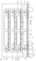
도 1은 일 예에 따른 스택 패키지(10)의 단면 구조를 보여준다. 1 shows a cross-sectional structure of a
도 1을 참조하면, 일 예에 의한 스택 패키지(10)는 제1서브 패키지(100) 상에 실질적으로 수직하게 스택(stack)된 제2서브 패키지(200)를 포함하여 구성될 수 있다. 내측 커넥터(inner connector: 510)들이 제1서브 패키지(100)와 제2서브 패키지(200) 사이에 개재되고, 제1서브 패키지(100)와 제2서브 패키지(200)을 서로 전기적으로 접속시킨다. 내측 커넥터(510)들은 솔더 볼(micro solder ball) 형태 또는 도전성 범프(bump) 형태의 접속 부재로 도입될 수 있다. Referring to FIG. 1, the
복수의 더미 볼(dummy ball: 550)들이 제1서브 패키지(100)와 제2서브 패키지(200) 사이에 도입된다. 더미 볼(550)들은 내측 커넥터(510)들과 이격된 위치에 배치되고, 내측 커넥터(510)들과는 전기적으로 격리(electrically isolated)된다. 더미 볼(550)들은 제1서브 패키지(100)와 제2서브 패키지(200) 사이에서 제2서브 패키지(200)를 지지하도록 도입될 수 있다. A plurality of
외측 커넥터(outer connector: 590)들이 제1서브 패키지(100)에 전기적으로 접속된다. 외측 커넥터(590)들은 스택 패키지(10)를 외부 기기 또는 다른 전자 모듈(module)에 전기적으로 접속시키는 접속 부재로 도입될 수 있다. 외측 커넥터(590)들은 솔더 볼 형태로 도입될 수 있다.
스택 패키지(10)는 제1 및 제2서브 패키지들(100, 200)이 수직하게 스택된 구조에, 추가적인 서브 패키지들(300, 400)이 더 스택된 구조로 구성될 수 있다. 예컨대, 제2서브 패키지(200) 상에 제3서브 패키지(300)가 실질적으로 수직하게 스택되고, 제3서브 패키지(300) 상에 제4서브 패키지(400)가 추가적으로 더 스택될 수 있다. 도시되지는 않았지만, 스택 패키지(10)의 제4서브 패키지(400) 상에 추가적인 서브 패키지들이 더 스택될 수도 있다. 제2서브 패키지(200)와 제3서브 패키지(300) 및 제4서브 패키지(400)들 사이에도 내측 커넥터(510)들 및 더미 볼(550)들이 도입될 수 있다. 제3 및 제4서브 패키지들(300, 400)은 제2서브 패키지(200)와 동일한 형태 및 동일한 기능을 하는 패키지 구조로 구성될 수 있다. The
스택 패키지(10)는 제1서브 패키지(100)와 제2서브 패키지(200) 사이의 갭(gap)을 채우도록 확장된 필링층(filling layer: 610)을 포함할 수 있다. 필링층(610)은 제1서브 패키지(100)와 제2서브 패키지(200) 사이를 전기적으로 격리시키는 유전 물질을 포함하여 구성될 수 있다. 필링층(610)은 언더필 물질(underfill material)을 포함하여 구성될 수 있다. 필링층(610)은 제2, 제3 및 제4서브 패키지들(200, 300, 400) 사이를 채우도록 확장될 수 있다. 필링층(610)은 제2, 제3 및 제4서브 패키지들(200, 300, 400)의 측면을 덮도록 확장될 수 있다. The
스택 패키지(10)는 제2, 제3 및 제4서브 패키지들(200, 300, 400)을 덮어 보호하는 외측 몰딩층(outer molding layer: 650)을 포함할 수 있다. 외측 몰딩층(650)은 제1서브 패키지(100)의 일부 부분을 덮고, 제2, 제3 및 제4서브 패키지들(200, 300, 400)을 덮어 봉지하는 층일 수 있다. 외측 몰딩층(650)은 제1서브 패키지(100)의 일부 부분을 덮고, 제2, 제3 및 제4서브 패키지들(200, 300, 400)을 덮어 봉지하는 층일 수 있다. 외측 몰딩층(650)은 에폭시 몰딩 컴파운드(EMC: Epoxy Molding Compound)와 같은 봉지 물질(encapsulant material)을 사용하는 몰딩 과정으로 제1서브 패키지(100) 상에 형성될 수 있다. The
도 1에서 필링층(610)과 외측 몰딩층(650) 구분되는 층들로 구성되는 경우를 예시하고 있지만, 몰디드 언더필(Molded Underfill)과 같은 봉지 공정을 이용할 경우에, 필링층(610)과 외측 몰딩층(650)은 하나의 몰디드 언더필층으로 통합될 수 있다. Although FIG. 1 illustrates a case in which the
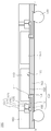
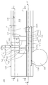
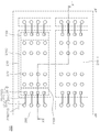
도 2는 도 1의 스택 패키지(10)의 제1서브 패키지(100)의 단면 구조를 보여주는 단면도이다. 도 3은 도 2의 제1서브 패키지(100)의 제1브리지 다이(120) 부분을 확대 도시한 단면도이다. 도 4는 도 3의 Z1-Z1' 절단선을 따르는 평면에 보여지는 제1재배선 패턴(151)의 배치 형상을 보여주는 평면도이다. 도 5는 도 3의 Z2-Z2' 절단선을 따르는 평면에 보여지는 제1브리지 다이(120)와 제1반도체 다이(110)의 배치 형상을 보여주는 평면도이다. 도 6은 도 3의 Z3-Z3' 절단선을 따르는 평면에 보여지는 제1포스트 범프(post bump: 125)와 제1반도체 다이(110)의 배치 형상을 보여주는 평면도이다. 도 2는 도 4의 X1-X1' 절단선을 따르는 단면 구조를 보여준다.FIG. 2 is a cross-sectional view illustrating a cross-sectional structure of the
도 2를 도 1과 함께 참조하면, 제1서브 패키지(100)는 스택 패키지(10)에서 상대적으로 아래에 배치된 하나의 패키지 단위(package unit)로 구성될 수 있다. 제1서브 패키지(100)는 제1반도체 다이(110)와 이를 덮어 보호하는 내측 제1몰딩층(160)을 포함하여 구성될 수 있다. 제1반도체 다이(110)는 제1재배선 구조(structure of redistribution layers: 150) 상에 배치된다. 제1브리지 다이(120)가 제1반도체 다이(110)와 이격되도록 제1재배선 구조(150) 상에 배치된다. 내측 제1몰딩층(160)은 제1재배선 구조(150) 상에 제1브리지 다이(120)와, 제1반도체 다이(110), 및 이들 사이 부분을 채우도록 몰딩된다. Referring to FIG. 2 together with FIG. 1, the
도 2를 도 3과 함께 참조하면, 제1반도체 다이(110)는 제1표면(119)이 제1재배선 구조(150)에 마주보도록 페이스 다운(face down) 형태로 제1재배선 구조(150) 상에 위치한다. 도 3에 제시된 것과 같이, 제1반도체 다이(110)는 제1표면(119)에 반대되는 측에 위치하는 제2표면(118)을 포함하고, 제1표면(119)으로부터 제2표면(118)까지 이어지는 측면(117)을 포함하는 형상을 가진다. 제1반도체 다이(110)의 제1표면(119)은 집적 회로 소자들이 집적된 활성면(active side)일 수 있다. 제1반도체 다이(110)의 제2표면(118)은 활성면에 반대되는 바닥면(bottom side) 또는 후면(back side)일 수 있다. 여기서, 제1 또는 제2 등의 기재는 특정한 순서를 의미하지 않고 부재의 구분을 위해 사용된다. Referring to FIG. 2 together with FIG. 3, the first semiconductor die 110 may have a first wiring structure having a face down such that the
제1반도체 다이(110)의 제1표면(119)에 제1접촉 패드(contact pad: 111)들이 배치될 수 있다. 제1접촉 패드(111)는 제1반도체 다이(110)를 외부 기기와 전기적으로 결합시키는 경로로 사용되는 도전 패턴일 수 있다. 제1접촉 패드(111)들은, 도 5의 평면도에 묘사된 것과 같이, 제1반도체 다이(110)의 양측 에지 영역(edge region) 내에 위치하는 에지 패드 형태로 배치될 수 있다.
도 2와 도 5를 함께 참조하면, 또 하나의 다른 제3반도체 다이(110-1)가 제1반도체 다이(110)와 나란하게 제1재배선 구조(150) 상에 배치될 수 있다. 제3반도체 다이(110-1)는 제1반도체 다이(110)와 실질적으로 동일한 형상 및 동일한 기능을 가지는 반도체 다이로 도입될 수 있다. 한편, 제3반도체 다이(110-1)는 제1반도체 다이(110)와 거울상(mirror image) 형상을 가질 수도 있다. 제3반도체 다이(110-1)와 제1반도체 다이(110)는 디램(DRAM)과 같은 메모리(memory) 반도체 다이로 도입될 수 있다. 2 and 5, another third semiconductor die 110-1 may be disposed on the
도 3 및 도 5에 제시된 것과 같이, 제1반도체 다이(110)의 측면(117)과 일정 간격 이격된 위치에 제1브리지 다이(120)가 배치된다. 제1브리 다이 몸체부(129)의 일 측면(127)이 제1반도체 다이(110)의 측면(117)과 마주보도록, 제1브리지 다이(120)가 제1재배선 구조(150) 상에 배치된다. As shown in FIGS. 3 and 5, the first bridge die 120 is disposed at a distance spaced from the
도 3을 참조하면, 제1브리지 다이(120)는 제1브리지 다이 몸체부(129)와 제1브리지 다이 몸체부(129)의 상측 표면(128) 상측으로 돌출된 제1포스트 범프(post bump: 125)를 포함하여 구성된다. 제1브리지 다이 몸체부(129)의 상측 표면(128)이 이웃하는 제1반도체 다이(110)의 제2표면(118)과 단차(H)를 가지도록 제1브리지 다이 몸체부(129)가 구성된다. 제1브리지 다이 몸체부(129)의 상측 표면(128)과 제1반도체 다이(110)의 제2표면(118)이 계단 형상을 이루도록, 제1브리지 다이(120)가 제1반도체 다이(110) 옆에 배치될 수 있다. 제1브리지 다이 몸체부(129)는 제1반도체 다이(110) 보다 얇은 두께를 가지는 반도체 다이로 구성될 수 있다. 제1브리지 다이 몸체부(129)는 제1반도체 다이(110)의 두께의 40% 내지 90%의 두께를 가질 수 있다. 제1브리지 다이 몸체부(129)는 제1반도체 다이(110)의 두께의 절반 내외의 작은 두께를 가질 수 있다. Referring to FIG. 3, the first bridge die 120 may include a first post bump protruding above the upper surface 128 of the first bridge die
제1브리지 다이(120)는 제1브리지 다이 몸체부(129)를 실질적으로 상하로 관통하는 제1관통 비아(through via: 123)들을 구비한다. 제1브리지 다이 몸체부(129)는 실리콘(Si)과 같은 반도체 물질로 구성될 수 있다. 제1브리지 다이 몸체부(129)가 반도체 물질로 구성되므로, 제1관통 비아(123)를 형성하는 과정에 반도체 공정(silicon process)이 적용될 수 있다. 이에 따라, 제1관통 비아(123)는 상대적으로 미세한 직경(D1)을 가지는 관통 실리콘 비아(TSV: Through Silicon Via) 구조로 형성될 수 있다. 제1관통 비아(123)은 도전성 금속 물질, 예컨대, 구리(Cu)를 포함하는 금속층으로 형성될 수 있다. The first bridge die 120 has first through
제1브리지 다이 몸체부(129)가 제1반도체 다이(110) 보다 상대적으로 얇은 두께를 가지므로, 제1브리지 다이 몸체부(129)를 상하로 실질적으로 관통하는 제1관통 비아(123)의 길이는 상대적으로 짧은 길이를 가질 수 있다. 예컨대, 제1반도체 다이(110)의 두께만큼 제1브리지 다이 몸체부의 두께가 두꺼울 경우, 제1브리지 다이 몸체부를 관통할 관통 비아는 제1관통 비아(123) 보다 더 긴 길이를 가져야 한다. 그렇지만, 제1관통 비아(123)는 더 얇은 제1브리지 다이 몸체부(129)를 관통하므로, 상대적으로 더 짧은 길이를 가지도록 형성될 수 있다. Since the first bridge die
제1관통 비아(123)가 상대적으로 작은 직경을 가지면서도 상대적으로 더 긴 길이를 가지려면 종횡비(aspect ratio)를 증가시켜야 한다. 그런데, 제1관통 비아(123)를 형성하는 공정에서의 제약에 의해서, 제1관통 비아(123)의 종횡비를 증가시키는 데에는 제약이 발생된다. 다시 말해서, 제1관통 비아(123)의 길이가 더 길어지면 그 직경 또한 커질 수 있다. 제1브리지 다이 몸체부(129)의 두께가 상대적으로 얇아 제1관통 비아(123)들이 상대적으로 더 짧은 길이를 가지므로, 제1관통 비아(123)들은 상대적으로 더 미세한 직경(D1)을 가지도록 형성될 수 있다. 제1관통 비아(123)들이 상대적으로 더 미세한 직경(D1)을 가질 수 있으므로, 제1브리지 다이 몸체부(129) 내에 상대적으로 더 많은 수의 제1관통 비아(123)들을 구비하는 것이 가능하다. In order for the first through via 123 to have a relatively small diameter and a relatively longer length, the aspect ratio must be increased. However, due to the restriction in the process of forming the first through via 123, a restriction is generated in increasing the aspect ratio of the first through via 123. In other words, the longer the length of the first through via 123, the larger its diameter may be. Since the first bridge die
도 3 및 도 6을 함께 참조하면, 도전성의 제1포스트 범프(125)는 제1관통 비아(123)의 상측 일 단부에 전기적으로 연결된다. 제1포스트 범프(125)는 제1관통 비아(123)에 중첩되도록 배치된다. 제1포스트 범프(125)의 측면 일부 부분(125S)이 제1반도체 다이(110)의 측면(117)의 상단 부분에 마주보도록, 제1포스트 범프(125)는 제1브리지 다이 몸체부(129)의 상측 표면(128)로부터 일정 높이까지 돌출된다. 제1서브 패키지(100)의 내측 제1몰딩층(160)은 제1브리지 다이 몸체부(129)의 상측 표면(128)을 덮고, 제1포스트 범프(125)의 측면을 감싸도록 형성된다. 내측 제1몰딩층(160)은 제1포스트 범프(125)의 측면을 직접적으로 덮고, 제1포스트 범프(125)의 상면(125T)을 드러내도록 형성된다. 내측 제1몰딩층(160)의 상측 표면(160T)과 제1브리지 다이 몸체부(129)의 상측 표면(129) 사이의 거리(L1)는 내측 제1몰딩층(160)의 상측 표면(160T)과 제1반도체 다이(110)의 상측 표면인 제2표면(118) 사이의 거리(L2) 보다 크게 된다. 3 and 6 together, the conductive
내측 제1몰딩층(160)에 의해 드러난 제1포스트 범프(125)의 상면(125T)에는, 도 1에 도시된 것과 같이, 내측 커넥터(510)가 본딩된다. 내측 커넥터(510)는 제1포스트 범프(125)를 제1서브 패키지(200)에 전기적으로 접속시킨다. 도 3에 도시된 것과 같이, 제1포스트 범프(125)는 내측 제1몰딩층(160)의 제1브리지 다이 몸체부(129)를 덮는 부분을 실질적으로 관통한다. 이에 따라, 제1포스트 범프(125)는 제1관통 비아(123)를 내측 제1몰딩층(160)의 상측 표면(160T) 위치까지 전기적으로 연장시키는 역할을 한다. An
내측 제1몰딩층(160)은 절연 물질을 포함하여 구성될 수 있다. 제1관통 비아(123)와 이웃하는 다른 제1관통 비아의 사이 부분은 실질적으로 반도체 물질, 예컨대 실리콘 물질이 채워질 수 있다. 제1포스트 범프(125)와 이웃하는 다른 제1포스트 범프 사이 부분에는 내측 제1몰딩층(160)을 구성하는 유전 물질, 예컨대 에폭시 몰딩 컴파운드(EMC)가 채워질 수 있다. 제1관통 비아(123)는 반도체 물질로 구성된 제1브리지 다이 몸체부(129)를 관통하므로, 유전 물질로 이루어진 기판이나 EMC를 관통할 때보다 임피던스(impedance)가 상대적으로 더 커질 수 있다. 또한, 한정된 공간 안에 여러 개의 제1관통 비아(123)들을 배치하게 되면, 제1관통 비아(123)와 이웃하는 다른 제1관통 비아 사이의 거리가 짧아져 크로스토크(crosstalk)와 같은 노이즈(noise) 현상이 상대적으로 더 크게 유발될 수 있다. 이러한 현상은 결국 고주파에서의 신호전달 특성 또는 신호무결성(signal integrity)에 좋지 않은 영향을 미칠 수 있다. 제1포스트 범프(125)와 이웃하는 다른 제1포스트 범프(125) 사이 부분에는 유전 물질, 예컨대 에폭시 몰딩 컴파운드(EMC)가 채워지므로, 반도체 물질로 구성된 제1브리지 다이 몸체부(129)보다 임피던스나 배선 간의 거리로 인한 크로스토크를 억제할 수 있다. 예컨대, 실온에서 1kHz 주파수에서의 유전율은 실리콘 재질이 11.68, 에폭시 몰딩 컴파운드 재질이 3.7정도의 값을 가지며, 이러한 유전율의 차이는 위와 같은 전기적 특성에 유의한 영향을 끼친다.The inner
제1포스트 범프(125)는 제1관통 비아(123)의 제1직경(D1)에 비해 더 큰 제2직경(D2)를 가질 수 있다. 제1관통 비아(123)의 제1직경(D1)이 이에 연결된 제1포스트 범프(125)의 제2직경(D2) 보다 상대적으로 더 작으므로, 제1포스트 범프(125)들 각각에 연결되는 제1관통 비아(123)들 사이의 이격 간격은 상대적으로 더 크게 확보될 수 있다. 제1관통 비아(123)들 사이의 이격 간격이 더 크게 확보되므로, 제1관통 비아(123)와 이웃하는 다른 제1관통 비아(123) 사이에서 신호 노이즈 현상이 더 억제될 수 있다. The
이와 같이, 신호 노이즈를 줄이기 위해서는 제1관통 비아(123)들 사이의 이격 간격이 더 크게 확보하는 것이 요구된다. 제1관통 비아(123)들 사이의 이격 간격을 더 크게 확보하기 위해서는, 제1관통 비아(123)의 제1직경(D1)을 상대적으로 더 작게 도입하는 것이 요구된다. 일정한 공정 능력, 예컨대, 종횡비(aspect ratio)가 주어질 때, 더 작은 제1직경(D1)을 가지는 제1관통 비아(123)들이 제1브리지 다이 몸체부(129)를 관통하기 위해서는, 제1브리지 다이 몸체부(129)의 두께가 보다 더 얇은 것이 요구된다. 제1브리지 다이 몸체부(129)의 두께가 제1반도체 다이(110)의 두께 보다 더 얇게 도입되므로, 제1브리지 다이 몸체부(129)를 관통하는 제1관통 비아(123)는 상대적으로 더 작은 제1직경(D1)을 가지는 TSV 구조로 형성될 수 있다. 이에 따라, 제1관통 비아(123)들 사이의 이격 간격은 보다 더 넓게 확보되고, 결국 제1관통 비아(123)들 사이의 신호 노이즈가 보다 더 억제될 수 있다. As such, in order to reduce signal noise, it is required to secure a larger separation distance between the first through
제1포스트 범프(125)는 구리(Cu)를 포함하는 금속 포스트 형상을 가질 수 있다. 제1포스트 범프(125)의 높이 또는 관통 길이는 대략 60㎛ 내외의 크기를 가질 수 있다. 제1포스트 범프(125)의 제2직경(D2)은 예컨대 대략 20 내지 30㎛ 내외의 크기를 가질 수 있다. 이에 비해 제1관통 비아(123)는 대략 0.5㎛ 내외의 제1직경(D1)을 가질 수 있다. 제1포스트 범프(125)는 상대적으로 큰 제2직경(D2)을 가지도록 형성되므로, 제1포스트 범프(125)의 드러난 상면(125T)에 내측 커넥터(도 1의 510), 예컨대, 솔더 볼이나 범프가 직접적으로 본딩되는 것이 가능하다. 따라서, 내측 커넥터(510)와의 본딩을 위해서, 접촉 면적을 확장하기 위한 별도의 도전 패드(pad)는 제1포스트 범프(125)의 드러난 상면(125T)으로부터 배제되고 생략될 수 있다. The
도 2를 다시 참조하면, 내측 제1몰딩층(160)은 제1브리지 다이(120)을 덮도록 형성되며, 제1재배선 구조(150) 상에 배치된다. 내측 제1몰딩층(160)은, 도 1에 도시된 것과 같이, 제1서브 패키지(100) 상에 스택된 제2서브 패키지(200)의 측면(200S) 바깥으로 돌출되도록 확장된 확장 부분(160E)을 가질 수 있다. 제1서브 패키지(100)의 내측 제1몰딩층(160)이 확장 부분(160E)을 가지므로, 제1서브 패키지(100)는 그 상에 스택된 제2서브 패키지(200) 보다 큰 크기를 가지는 패키지 단위로 도입될 수 있다. Referring back to FIG. 2, the inner
도 3을 도 4와 함께 참조하면, 제1서브 패키지(100)의 제1재배선 구조(150)는 제1재배선 패턴(151)과 제1재배선 패턴(151)을 확장시키는 외측 재배선 패턴(155)를 포함하도록 구성된다. 제1재배선 패턴(151)과 외측 재배선 패턴(155)은 알루미늄(Al), 구리(Cu) 또는 금(Au)과 같은 금속층을 포함하는 도전 패턴들로 형성될 수 있다. Referring to FIG. 3 along with FIG. 4, the
제1재배선 패턴(151)은 서로 이격된 제1브리지 다이(120)와 제1반도체 다이(110)를 전기적으로 연결시키는 도전 패턴으로 구비된다. 제1재배선 구조(150)는 제1반도체 다이(110)의 제1접촉 패드(111)와 제1브리지 다이 몸체부(129)의 비아 패드(via pad: 121)를 드러내는 제1유전층(152)을 포함한다. 제1재배선 패턴(151)은 제1유전층(152) 상에 배치된다. 제1재배선 패턴(151)의 제1중첩 부분(151D)는 제1유전층(152)에 의해 드러난 제1접촉 패드(111)에 중첩되어 전기적으로 연결된다. 제1재배선 패턴(151)의 제2중첩 부분(151B)는 제1유전층(152)에 의해 드러난 비아 패드(121)에 중첩되어 전기적으로 연결된다. 제1재배선 패턴(151)의 연결 부분(151C)은 제1중첩 부분(151D)으로부터 제2중첩 부분(151B)에까지 연장되는 도전 라인(line)으로 구비된다. The
제1브리지 다이 몸체부(129)의 비아 패드(121)는 제1관통 비아(123)와 제1재배선 패턴(151)의 제2중첩 부분(151B)의 계면 부분에 위치하도록, 제1브리지 다이 몸체부(129)의 바닥 표면에 형성될 수 있다. 구체적으로, 제1관통 비아(123) 위에 인터커넥션을 위해 비아 패드(121)를 형성하고, 비아 패드(121)와 중첩되는 영역에 제2중첩 부분(151B)를 형성할 수 있다. 비아 패드(121)는 제1관통 비아(123)와 연결되고 제1관통 비아(123)보다 큰 직경을 가지는 도전 패턴으로 구비될 수 있다. 비아 패드(121)는 제1관통 비아(123)를 제1재배선 패턴(151)에 전기적으로 및 물리적 기계적으로 연결시키는 접속 부재로 구비될 수 있다. 비아 패드(121)는 구리 또는 알루미늄 등과 같은 금속 재질로 구비될 수 있다. The via
제1재배선 구조(150)는 인접한 제1재배선 패턴(151)들을 서로 전기적으로 격리시키고, 제1재배선 패턴(151)의 일부 부분을 드러내는 제2유전층(153)을 더 구비할 수 있다. 제2유전층(153)에 의해서 드러난 제1재배선 패턴(151)의 일부 부분에 일단 단부가 중첩되고, 중첩 지점으로부터 이격된 다른 지점으로 확장되는 외측 재배선 패턴(155)이 구비된다. The
외측 재배선 패턴(155)은 제1재배선 패턴(151)과 서로 다른 층위(level)에 위치하도록 구비된다. 인접한 외측 재배선 패턴(155)들을 서로 전기적으로 격리하고, 외측 재배선 패턴(155)들의 일부 부분(155P)을 드러내는 제3유전층(154)이 더 구비될 수 있다. 제1 내지 제3유전층들(152, 153, 154)은 제1재배선 패턴(151) 및 외측 재배선 패턴(155)들을 서로 전기적으로 격리하는 유전층 구조를 제공한다. 외측 재배선 패턴(155) 중 제3유전층(154)에 의해 드러난 일부 부분(155P)에 외측 커넥터(590)가 결합되거나 본딩된다. 외측 재배선 패턴(155)은 제1재배선 패턴(151)을 외측 커넥터(590)에까지 전기적으로 연장 또는 확장시키는 도전 패턴으로 도입된다. The
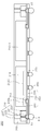
도 7은 도 1의 스택 패키지(10)의 제2서브 패키지(200)의 단면 구조를 보여주는 단면도이다. 도 8은 도 7의 제2서브 패키지(200)의 제2브리지 다이(220) 부분을 확대 도시한 단면도이다. 도 9는 도 8의 Z4-Z4' 절단선을 따르는 평면에 보여지는 제2재배선 패턴(251)의 배치 형상을 보여주는 평면도이다. 도 10은 도 8의 Z5-Z5' 절단선을 따르는 평면에 보여지는 제2브리지 다이(220)와 제2반도체 다이(210)의 배치 형상을 보여주는 평면도이다. 도 11은 도 8의 Z6-Z6' 절단선을 따르는 평면에 보여지는 제2포스트 범프(225)와 제2반도체 다이(210)의 배치 형상을 보여주는 평면도이다. 도 7은 도 9의 X1-X1' 절단선을 따르는 단면 구조를 보여준다.FIG. 7 is a cross-sectional view illustrating a cross-sectional structure of the
도 7을 도 1과 함께 참조하면, 제2서브 패키지(200)는 스택 패키지(10)에서 제1서브 패키지(100) 상에 실질적으로 수직하게 스택된 다른 패키지 단위로 구성될 수 있다. Referring to FIG. 7 together with FIG. 1, the
제2서브 패키지(200)는 제2재배선 구조(250) 상에 서로 이격되어 배치된 제2반도체 다이(210) 및 제2브리지 다이(220)를 포함한다. 이때, 제2반도체 다이(210)는 제1반도체 다이(도 1의 110)과 유사한 형상 및 기능을 가지는 반도체 다이로 도입될 수 있다. 도 1에 도시된 것과 같이, 제2반도체 다이(210)는 제1반도체 다이(110)과 실질적으로 동일한 형상 및 기능을 가지는 메모리 반도체 다이로 도입될 수 있다. 제2브리지 다이(220)는 제1브리지 다이(120)와 실질적으로 동일한 형상으로 도입될 수 있다. 제2반도체 다이(210)는 제1반도체 다이(110)에 중첩된 위치에 위치하고, 제2브리지 다이(220)는 제1브리지 다이(120)에 중첩된 위치에 위치할 수 있다. The
도 7 및 도 8을 함께 참조하면, 제2서브 패키지(200)는 제2재배선 구조(250) 상에 제2반도체 다이(210) 및 제2브리지 다이(220)를 덮어 보호하는 내측 제2몰딩층(260)을 포함하여 구성될 수 있다. 내측 제2몰딩층(260)은 내측 제1몰딩층(도 1의 160)을 이루는 몰딩 물질과 실질적으로 동일한 몰딩 물질로 몰딩될 수 있다. 내측 제2몰딩층(260)은 제2재배선 구조(250) 상에 제2브리지 다이(220)와, 제2반도체 다이(210) 사이 부분을 채우도록 몰딩된다. 제2몰딩층(260)은, 도 1에 제시된 것과 같이, 제2서브 패키지의 측면(200S) 바깥으로 제1몰딩층(160)의 확장 부분(160E)이 돌출되어 드러나도록, 제2몰딩층(260)은 제1몰딩층(160)은 보다 좁은 폭을 가지도록 몰딩된다. Referring to FIGS. 7 and 8, the second sub-package 200 covers the second semiconductor die 210 and the second bridge die 220 on the
도 7과 도 10을 함께 참조하면, 제1반도체 다이(도 1의 110)와 마찬가지로 제2반도체 다이(210)의 표면에 제2접촉 패드(211)들이 배치될 수 있다. 제2접촉 패드(211)들은 에지 패드 형태로 배치될 수 있다. 제4반도체 다이(210-1)가 제2반도체 다이(210)와 나란하게 제1재배선 구조(250) 상에 배치될 수 있다. 제4반도체 다이(210-1)는 제2반도체 다이(210)와 실질적으로 동일한 형상 및 동일한 기능을 가지는 반도체 다이로 도입될 수 있다. 한편, 제4반도체 다이(210-1)는 제2반도체 다이(210)와 거울상 형상을 가질 수도 있다. 제4반도체 다이(210-1)는 제2반도체 다이(210)와 마찬가지로 메모리 반도체 다이로 도입될 수 있다. Referring to FIGS. 7 and 10, the
도 8 및 도 11을 함께 참조하면, 제2반도체 다이(210)와 일정 간격 이격된 위치에 제2브리지 다이(220)가 배치된다. 제2브리지 다이(220)는 제2브리지 다이 몸체부(229)와 제2브리지 다이 몸체부(229) 상측으로 돌출된 제2포스트 범프(225)를 포함하여 구성된다. 도전성의 제2포스트 범프(225)는 제2관통 비아(223)의 상측 일 단부에 전기적으로 연결된다. 제2포스트 범프(225)는 제2관통 비아(223)에 중첩되도록 배치된다. 내측 제2몰딩층(260)은 제2브리지 다이 몸체부(229)의 상측 표면(228)을 덮고, 제2포스트 범프(225)의 측면을 감싸도록 형성된다. 내측 제2몰딩층(260)은 제2포스트 범프(225)의 상면(225T)을 드러내도록 형성된다. 8 and 11, the second bridge die 220 is disposed at a position spaced apart from the second semiconductor die 210 by a predetermined distance. The second bridge die 220 includes a second bridge die
도 8을 도 9와 함께 참조하면, 제2서브 패키지(200)의 제2재배선 구조(250)는 제2재배선 패턴(251)을 포함하여 구성될 수 있다. 제2재배선 패턴(251)은 서로 이격된 제2브리지 다이(220)와 제2반도체 다이(210)을 전기적으로 연결시키는 도전 패턴으로 구비된다. 제2재배선 구조(250)는 제2반도체 다이(210)의 제2접촉 패드(211)와 제2브리지 다이 몸체부(229)의 비아 패드(221)를 드러내는 제4유전층(252)을 포함한다. 제2브리지 다이 몸체부(229)의 비아 패드(221)는 제2관통 비아(223)와 제2재배선 패턴(251)의 제4중첩 부분(251B)의 계면 부분에 위치하도록, 제2브리지 다이 몸체부(229)의 바닥 표면에 형성될 수 있다. 구체적으로, 제2관통 비아(223) 위에 인터커넥션을 위해 비아 패드(221)를 형성하고, 비아 패드(221)와 중첩되는 영역에 제4중첩 부분(251B)를 형성할 수 있다. Referring to FIG. 8 together with FIG. 9, the
제2재배선 패턴(251)은 제4유전층(252) 상에 배치된다. 제2재배선 패턴(251)의 제3중첩 부분(251D)은 제4유전층(252)에 의해 드러난 제2접촉 패드(211)에 중첩되어 전기적으로 연결된다. 제2재배선 패턴(251)의 제4중첩 부분(251B)은 제4유전층(252)에 의해 드러난 비아 패드(221)에 중첩되어 전기적으로 연결된다. 제2재배선 패턴(251)의 연결 부분(251C)은 제3중첩 부분(251D)으로부터 제4중첩 부분(251B)에까지 연장되는 도전 라인으로 구비된다. The
제2재배선 구조(250)는 제2재배선 패턴(251)들을 서로 전기적으로 격리하고, 제2재배선 패턴(251)의 일부 부분(251P)을 드러내는 제5유전층(253)을 더 구비할 수 있다. 제5유전층(253)에 의해서 드러난 제2재배선 패드(251)의 일부 부분(251P)에 내측 커넥터(510)가 결합되거나 본딩된다. 제2포스트 범프(225), 제2관통 비아(223), 비아 패드(221). 제4중첩 부분(251B), 제2재배선 패턴(251)의 일부 부분(251P) 및 내측 커넥터(510)은 서로 중첩되도록 배치된다. 제2포스트 범프(225), 제2관통 비아(223), 비아 패드(221). 제4중첩 부분(251B), 제2재배선 패턴(251)의 일부 부분(251P) 및 내측 커넥터(510)이 서로 중첩되어, 실질적으로 수직한 전기적 경로를 구축할 수 있다. 이에 따라, 도 1에 제시된 것과 같이, 제2서브 패키지(200)가 제1서브 패키지(100) 상에 수직하게 적층되고, 또한, 제2서브 패키지(200) 상에 제3서브 패키지(300)가 수직하게 적층될 때, 제2포스트 범프(225), 제2관통 비아(223), 비아 패드(221). 제4중첩 부분(251B), 제2재배선 패턴(251)의 일부 부분(251P) 및 내측 커넥터(510)는 제1서브 패키지(도 1의 100)을 제3서브 패키지(도 1의, 300)에 전기적으로 연결시키는 수직 경로를 제공한다.The
제2재배선 패턴(251)과 이격된 위치에 복수의 더미 패드(dummy pad: 270)들이 배치된다. 각각의 더미 패드(270)는 제2재배선 패턴(251) 및 제2반도체 다이(210)와 전기적으로 격리된 도전 패턴으로 구비된다. 더미 패드(270)들은 제4유전층(252) 상에 배치되어, 제2반도체 다이(210)와 이격된다. 각각의 더미 패드(270)는 더미 볼(550)이 부착되거나 결합 또는 본딩되는 베이스(base)로 도입된다. 솔더는 금속 표면에 쉽게 웨팅(wetting)되며, 상대적으로 유전 물질 표면에는 잘 웨팅되지 않는 특성이 있다. 따라서 더미 볼(550)이 예컨대 솔더 볼 형태로 도입될 때, 제2서브 패키지(200)의 제5유전층(253)이나 제1서브 패키지(도 1의 100)의 제1몰딩층(도 1의 160)의 표면에 솔더 볼을 안정적으로 마운트(mount)하기 어려울 수 있다. 따라서, 솔더 볼을 본딩하기 위한 베이스 부재로 더미 패드(270)가 제4유전층(252) 상에 복수 개 도입될 수 있다. A plurality of
더미 패드(270)는 제2재배선 패턴(251)을 형성하는 과정, 예컨대, 구리 도금 과정에 함께 형성될 수 있다. 이에 따라, 더미 패드(270)는 제2재배선 패턴(251)과 동일한 층위(level)에 위치할 수 있다. 더미 패드(270)에 더미 볼(550)이 본딩될 수 있도록, 제5유전층(253)은 더미 패드(270)를 드러내도록 형성된다. The
도 8 및 도 1에 제시된 것과 같이, 제2서브 패키지(200)가 제1서브 패키지(100) 상에 스택될 때, 더미 볼(550)의 일 단부(551)는 드러난 더미 패드(270)에 웨팅되어 본딩된 상태이고, 더미 볼(555)의 반대측 다른 단부(552)는 제1서브 패키지(100)의 내측 제1몰딩층(160)의 상측 표면(160T)에 접촉하게 된다. 이때, 더미 패드(270)에 본딩된 더미 볼(550)은 내측 커넥터(510) 보다 작은 직경 크기를 가지는 볼 형태로 도입될 수 있다. As shown in FIGS. 8 and 1, when the second sub-package 200 is stacked on the first sub-package 100, one
내측 커넥터(510)는, 도 1에 도시된 것과 같이, 제1서브 패키지(100)의 제1포스트 범프(125)에 웨팅되어 본딩되므로, 본딩 후에는 그 높이가 초기 높이 보다 줄어들게 된다. 더미 볼(550)은 내측 제1몰딩층(160)에 실질적으로 웨팅되지 않으므로, 내측 커넥터(510)를 제1포스트 범프(125)에 본딩하는 공정을 진행한 이후에도 초기 높이가 실질적으로 유지된다. 본딩 공정 이후에 내측 커넥터(510)와 더미 볼(550)의 높이를 유사하게 맞추기 위해서, 더미 볼(550)은 내측 커넥터(510)의 직경 보다 작은 직경 크기를 가진다. 더미 볼(550)의 직경 크기는 더미 볼(550)의 높이를 의미하는 요소로 해석될 수 있다. 예컨대, 내측 커넥터(510)은 대략 30㎛ 내외의 직경을 가질 수 있고, 더미 볼(550)은 대략 20㎛ 내외의 직경을 가질 수 있다. As the
도 9를 참조하면, 더미 패드(270)들은 제2반도체 다이(210)에 중첩된 위치에 분포되도록 위치할 수 있다. 제2반도체 다이(210)의 제2접촉 패드(211)는, 도 8 및 도 7에서와 같이, 제2반도체 다이(210)의 양측 에지 영역(210E)들에 배치된다. 제2접촉 패드(211)의 배치가 에지 패드 형태를 가지므로, 더미 패드(270)들은 제2접촉 패드(211)가 배치되지 않은 제2반도체 다이(210)의 중앙 영역(210C)에 배치될 수 있다. 도 9를 참조하면, 더미 패드(270)와 더미 볼(550)은 제2반도체 다이(210) 또는 제4반도체 다이(210-1)와 중첩된 위치에 배치될 수 있다. 도 7 및 도 8에 도시된 것과 같이, 더미 볼(550)은 에지 패드인 제2접촉 패드(211)가 배치되지 않은 제2반도체 다이(210)의 중앙 영역(210C)에 배치될 수 있다. Referring to FIG. 9, the
도 12은 비교예에 따른 스택 패키지(11R)에서의 보이드(void: 610V) 발생을 보여주는 단면도이다. 도 13은 보이드(610V)가 발생되는 현상을 설명하기 위해 제시한 도면이다. 도 14은 일 예에 따른 스택 패키지에서 보이드 현상이 억제되는 것을 보여주는 평면도이다. 12 is a cross-sectional
도 12를 참조하면, 비교예에 따른 스택 패키지(11R)는 제1서브 패키지(100R) 상에 제2서브 패키지(200R)가 스택되고, 그 상에 제3 및 제4서브 패키지들(300R, 400R)이 스택되어 구성될 수 있다. 더미 볼(도 1의 550)들이 서브 패키지들(100R, 200R, 300R, 400R) 사이에 도입되지 않을 때, 서브 패키지들(100R, 200R, 300R, 400R) 사이를 필링층(610R)이 채우는 언더필(underfill) 채움 공정에서 보이드(610V)들이 유발되는 것을 확인할 수 있다. Referring to FIG. 12, in the
보이드(610V)들은 예컨대, 제1반도체 다이(110R)와 제2반도체 다이(210R)들이 중첩된 사이 부분에서 확인되고 있다. 제1서브 패키지(100R)와 제2서브 패키지(200R)는 제1브리지 다이(120R)와 제2브리지 다이(220R)들을 연결하는 내측 커넥터(510R)에 의해서 서로 결합되고 있다. 필링층(610R)을 이루는 필링 물질이 채워지지 않은 보이드(610V)는 내측 커넥터(510R)들 사이의 제1반도체 다이(110R)와 제2반도체 다이(210R)들이 서로 중첩되는 영역에 유발되고 있다. The
제1반도체 다이(110R)와 제2반도체 다이(210R)들이 서로 중첩되는 영역에서, 제1 및 제2서브 패키지들(100R, 200R) 사이에는 넓은 빈 공간이 위치한다. 이러한 넓은 빈 공간에, 도 13에 도시된 것과 같이, 필링층(610R)을 위한 언더필 물질이 유입될 때, 언더필 물질(611R)의 흐름이 영역별로 차이가 날 수 있다. 예컨대, 국부적인 영역들에서 상대적으로 빠른 속도로 언더필 물질(611R)이 유입되는 빠른 언더필 흐름(underfill flow)들과, 이들 빠른 언더필 흐름들 사이에 상대적으로 느린 언더필 흐름이 국부적으로 유도될 수 있다. 빠른 언더필 흐름들이 느린 언더필 흐름이 미쳐 언더필 물질(611R)을 채우지 못한 영역을 폐쇄(close)하면서, 언더필 흐름 내에 보이드(610V)가 트랩(trap)될 수 있다. In an area where the first semiconductor die 110R and the second semiconductor die 210R overlap each other, a wide empty space is positioned between the first and second sub packages 100R and 200R. As shown in FIG. 13, when the underfill material for the
이러한 보이드(610V)의 발생을 더미 볼(도 1의 550)들이 억제하는 효과가 유도될 수 있다. 도 14를 도 1과 함께 참조하면, 더미 볼(550)들은 제2서브 패키지(200)와 제1서브 패키지(100) 사이에 상대적으로 균일하게 분포되며 도입될 수 있다. 더미 볼(550)들은 제2서브 패키지(200)와 제1서브 패키지(100) 사이로 필링층(610)을 구성하기 위한 언더필 물질(611)이 유입될 때, 언더필 물질(611)의 흐름 속도가 영역별로 균일해지도록 유도하는 역할을 할 수 있다. 더미 볼(500)들이 배치되어 캐필러리 효과(capillary effect)를 유도하고, 캐필러리 효과에 의해서 언더필 흐름이 전체 영역에 걸쳐 상대적으로 더 균일하게 유도된다. 이에 따라, 국부 영역에 보이드(도 12의 610V)들이 트랩되는 현상이 억제될 수 있다. The effect of suppressing the occurrence of the void 610V by the
도 15는 비교예에 따른 스택 패키지(15R)에서의 휨(bowing) 현상이 발생되는 것을 보여주는 단면도이다. 15 is a cross-sectional view showing that a bowing phenomenon occurs in the
도 15를 참조하면, 비교예에 따른 스택 패키지(15R)는 제1서브 패키지(105R) 상에 제2서브 패키지(205R)가 스택되고, 그 상에 제3 및 제4서브 패키지들(305R, 405R)이 스택되어 구성될 수 있다. 더미 볼(도 1의 550)들이 서브 패키지들(105R, 205R, 305R, 405R) 사이에 도입되지 않을 때, 휨 현상 및 이에 따른 크랙(crack) 발생이 확인될 수 있다. 제2 내지 제4서브 패키지들(205R, 305R, 405R)를 덮는 외측 몰딩층(655R)을 형성할 때, 일정 몰딩 압력을 수반하는 몰딩 과정이 수행될 수 있다. 이때, 스택 패키지(15R)에 인가되는 몰딩 압력에 의해서, 제2 내지 제 4서브 패키지들(205R, 305R, 405R)이 휘어지는 휨 현상이 유발될 수 있다. Referring to FIG. 15, a
스택된 서브 패키지들(105R, 205R, 305R, 405R)은 내측 커넥터(555R)들에 의해서 서로 지지되고 있다. 내측 커넥터(555R)들은 제2 내지 제4서브 패키지들(205R, 305R, 405R)의 양측 에지 영역들에 중첩되도록 위치하고 있다. 예컨대 제1반도체 다이(115R)와 제2반도체 다이(215R)들이 중첩된 사이 부분에는 내측 커넥터(555R)에 의해 지지되지 못하고 있다. 이에 따라, 인가되는 몰딩 압력이 내측 커넥터(555R)들 사이의 제2 내지 제4서브 패키지들(205R, 305R, 405R)의 중간 부분에 집중될 수 있고, 이러한 압력의 집중에 의해서 제2 내지 제4서브 패키지들(205R, 305R, 405R)의 중간 부분들이 휘어지는 현상이 유발될 수 있다. 휘어지는 현상이 심화될 경우, 제2 내지 제4서브 패키지들(205R, 305R, 405R)의 중간 부분들에 크랙이 유발될 수 있다. The stacked subpackages 105R, 205R, 305R, and 405R are supported by each other by
이러한 휨 현상 및 크랙 발생을 더미 볼(도 1의 550)들이 억제하는 효과가 유도될 수 있다. 도 1에 제시된 것과 같이, 더미 볼(550)들은 서브 패키지들(100, 200, 300, 400) 사이에 상대적으로 균일하게 분포되며 도입되고 있다. 더미 볼(550)들은 제2 내지 제4서브 패키지들(200, 300, 400)의 중간 부분들을 지지하도록 분포되고 있다. 이에 따라, 더미 볼(550)들이 제2 내지 제4서브 패키지들(200, 300, 400)의 중간 부분들을 지지하고 있어, 인가된 몰딩 압력에 의해서 제2 내지 제4서브 패키지들(200, 300, 400)이 휘는 현상을 억제할 수 있다. The effect that the dummy balls (550 of FIG. 1) suppress such warpage and cracking can be induced. As shown in FIG. 1, the
도 16은 일 예에 따른 스택 패키지(10)에서 개선된 열방출 효과를 보여주는 단면도이다. 16 is a cross-sectional view illustrating an improved heat dissipation effect in the
도 16을 참조하면, 일 예에 따른 스택 패키지(10)는 서브 패키지들(100, 200, 300, 400)들 사이에 더미 볼(550)들이 분산되어 도입되고 있다. 더미 볼(550)들은 필링층(610) 보다 열전도도가 높은 열전도 물질(thermal conductive material), 예컨대, 금속 물질 또는 솔더 물질을 포함하여 구성될 수 있다. 더미 볼(500)들이 주위의 필링층(610) 보다 상대적으로 빠른 속도로 열을 전도할 수 있으므로, 더미 볼(500)들은 서브 패키지들(100, 200, 300, 400)들 사이에서 열을 전달하는 경로 또는 열을 방출 경로를 제공할 수 있다. 이에 따라, 더미 볼(500)들은 스택 패키지(10) 내부로부터 외측 몰딩층(650)의 상면(650T) 부분으로 열을 보다 빠른 속도로 배출시킬 수 있다. 따라서, 스택 패키지(10)의 열 방출 특성이 개선될 수 있다. 스택 패키지의 외측 몰딩층(650)의 상면(650T)에는, 도시되지는 않았지만, 히트 스프레더(heat spreader) 또는 히트 싱크(heat sink) 구조가 결합될 수도 있다. Referring to FIG. 16, in the
상술한 바와 같이 본 출원의 실시 형태들을 도면들을 예시하며 설명하지만, 이는 본 출원에서 제시하고자 하는 바를 설명하기 위한 것이며, 세밀하게 제시된 형상으로 본 출원에서 제시하고자 하는 바를 한정하고자 한 것은 아니다. 본 출원에서 제시한 기술적 사상이 반영되는 한 다양한 다른 변형예들이 가능할 것이다.As described above, the embodiments of the present application are illustrated and illustrated in the drawings, but this is for explaining what is intended to be presented in the present application and is not intended to limit what is intended to be presented in the present application in a detailed form. Various other modifications will be possible as long as the technical spirit suggested in the present application is reflected.
100, 200; 서브 패키지,
110, 210: 반도체 다이
120, 220: 브리지 다이,
550: 더미 볼. 100, 200; Sub package,
110, 210: semiconductor die
120, 220: bridge die,
550: Dummy ball.
Claims (40)
상기 제1반도체 다이에 이격되어 배치된 제1브리지 다이 몸체부(bridge die body), 상기 제1브리지 다이 몸체부를 관통하는 제1관통 비아(through via), 및 상기 제1관통 비아의 일 단부에 연결되고 상기 제1브리지 다이 몸체부 상측으로 돌출된 제1포스트 범프(post bump)를 포함하는 제1브리지 다이,
상기 제1반도체 다이 및 상기 제1브리지 다이를 덮고 상기 제1포스트 범프의 측면을 감싸고 상기 제1포스트 범프의 상면을 드러낸 내측 제1몰딩층(molding layer), 및
상기 제1관통 비아의 다른 단부를 상기 제1반도체 다이에 전기적으로 연결시키는 제1재배선 구조를 포함하는 제1서브 패키지(sub package);
상기 제1서브 패키지 상에 스택(stack)된 제2서브 패키지(sub package);
상기 제1포스트 범프에 상기 제2서브 패키지를 전기적으로 접속시키는 내측 커넥터(connector); 및
상기 제1서브 패키지와 상기 제2서브 패키지 사이에 도입되어 상기 제2서브 패키지를 지지하는 복수의 더미 볼(dummy ball)들을 포함하는 스택 패키지. First semiconductor die,
A first bridge die body spaced apart from the first semiconductor die, a first through via penetrating through the first bridge die body portion, and one end of the first through via A first bridge die connected to and including a first post bump protruding above the first bridge die body;
An inner first molding layer covering the first semiconductor die and the first bridge die and covering the side surface of the first post bump and exposing the top surface of the first post bump, and
A first sub package including a first rewiring structure electrically connecting the other end of the first through via to the first semiconductor die;
A second sub package stacked on the first sub package;
An inner connector electrically connecting the second sub package to the first post bump; And
The stack package includes a plurality of dummy balls introduced between the first sub package and the second sub package to support the second sub package.
상기 제2서브 패키지는
제2반도체 다이(die);
상기 제2반도체 다이에 이격되어 배치된 제2브리지 다이 몸체부, 상기 제2브리지 다이 몸체부를 관통하는 제2관통 비아, 및 상기 제2관통 비아의 일 단부에 연결되고 상기 제2브리지 다이 몸체부 상측으로 돌출된 제2포스트 범프를 포함하는 제2브리지 다이;
상기 제2반도체 다이 및 상기 제2브리지 다이를 덮고 상기 제2포스트 범프의 측면을 감싸고 상기 제2포스트 범프의 상면을 드러낸 내측 제2몰딩층; 및
상기 제2관통 비아의 다른 단부와 상기 제2반도체 다이를 전기적으로 연결시키는 제2재배선 구조를 포함하는 스택 패키지.The method of claim 1,
The second sub package is
A second semiconductor die;
A second bridge die body portion spaced apart from the second semiconductor die, a second through via penetrating the second bridge die body portion, and a second bridge die body portion connected to one end of the second through via; A second bridge die including a second post bump protruding upwardly;
An inner second molding layer covering the second semiconductor die and the second bridge die, covering a side surface of the second post bump, and exposing an upper surface of the second post bump; And
And a second rewiring structure electrically connecting the other end of the second through via to the second semiconductor die.
상기 제2서브 패키지는
상기 제2재배선 구조와 이격되고 상기 제2반도체 다이와 전기적으로 격리된 복수의 더미 패드(dummy pad)들을 더 포함하고,
상기 더미 볼들은 일단 단부들 각각이 상기 더미 패드들에 각각 본딩(bonding)되고, 반대측의 다른 단부들 각각이 상기 내측 제1몰딩층의 표면에 접촉하는 스택 패키지. The method of claim 2,
The second sub package is
A plurality of dummy pads spaced apart from the second wiring structure and electrically isolated from the second semiconductor die,
The dummy balls are once each of the ends are bonded to the dummy pads (bonding), each of the other end of the opposite side of the stack package in contact with the surface of the inner first molding layer.
상기 더미 볼들은
상기 제2반도체 다이에 중첩된 위치에 배치된 스택 패키지. The method of claim 2,
The dummy balls
And a stack package disposed at a position superimposed on the second semiconductor die.
상기 제2반도체 다이는 에지 영역에 배치된 접촉 패드를 포함하고,
상기 접촉 패드는 상기 제2재배선 구조와 전기적으로 연결되고,
상기 더미 볼들은
상기 에지 영역과 이격된 상기 제2반도체 다이에 중앙 영역에 배치된 스택 패키지.The method of claim 4, wherein
The second semiconductor die includes a contact pad disposed in an edge region,
The contact pad is electrically connected to the second rewiring structure,
The dummy balls
And a stack package disposed in a central region on the second semiconductor die spaced apart from the edge region.
상기 제2브리지 다이는
상기 제2관통 비아와 상기 제2재배선 구조의 중첩 부분의 계면에
상기 제2관통 비아와 연결되고 상기 제2관통 비아보다 큰 직경을 가지는 비아 패드(via pad)를 더 포함하는 스택 패키지.The method of claim 2,
The second bridge die
At an interface between an overlapping portion of the second through via and the second rewiring structure.
And a via pad connected to the second through via and having a diameter greater than that of the second through via.
상기 제2포스트 범프, 상기 제2관통 비아, 상기 비아 패드, 상기 제2재배선 구조의 일부 부분 및 상기 내측 커넥터는
서로 수직하게 중첩되도록 배치된 스택 패키지.The method of claim 6,
The second post bump, the second through via, the via pad, a portion of the second rewiring structure, and the inner connector may be
Stacked packages placed vertically on top of each other.
상기 더미 볼은
상기 내측 커넥터의 직경보다 작은 직경 크기를 가지는 스택 패키지. The method of claim 1,
The dummy ball is
A stack package having a diameter size smaller than the diameter of the inner connector.
상기 제1브리지 다이 몸체부는
상기 제1반도체 다이의 두께 보다 작은 두께를 가지는 스택 패키지. The method of claim 1,
The first bridge die body portion
And a stack package having a thickness less than the thickness of the first semiconductor die.
상기 내측 제1몰딩층의 상측 표면과 상기 제1브리지 다이 몸체부의 상측 표면 사이의 거리는
상기 내측 제1몰딩층의 상측 표면과 상기 제1반도체 다이의 상측 표면 사이의 거리 보다 큰 스택 패키지. The method of claim 1,
The distance between the upper surface of the inner first molding layer and the upper surface of the first bridge die body portion is
And a stack package greater than a distance between an upper surface of the inner first molding layer and an upper surface of the first semiconductor die.
상기 제1포스트 범프의 측면 일부 부분은 상기 제1반도체 다이의 측면을 마주보는 스택 패키지. The method of claim 1,
And a portion of the side surface of the first post bump faces the side of the first semiconductor die.
상기 제1포스트 범프는
상기 제1관통 비아의 직경 보다 큰 직경을 가지는 스택 패키지. The method of claim 1,
The first post bump is
And a stack package having a diameter greater than the diameter of the first through via.
상기 내측 제1몰딩층은 절연 물질을 포함하고, 상기 제1브리지 다이 몸체부는 실리콘을 포함하는 반도체 물질을 포함하는 스택 패키지. The method of claim 1,
The inner first molding layer includes an insulating material, and the first bridge die body portion includes a semiconductor material including silicon.
상기 제1서브 패키지와 상기 제2서브 패키지 사이를 채우도록 확장된 필링층(filling layer)을 더 포함하는 스택 패키지.The method of claim 1,
And a filling layer extended to fill between the first sub-package and the second sub-package.
상기 더미 볼은
상기 필링층 보다 열전도도가 높은 열전도 물질(thermal conductive material)을 포함하는 스택 패키지. The method of claim 14,
The dummy ball is
And a thermally conductive material having a higher thermal conductivity than the peeling layer.
상기 필링층은
언더필 물질(underfill material)을 포함하는 스택 패키지. The method of claim 14,
The peeling layer is
A stack package containing underfill material.
상기 필링층 상에
상기 제1 및 제2서브 패키지들을 덮는 외측 몰딩층을 더 포함하는 스택 패키지. The method of claim 14,
On the peeling layer
The stack package further includes an outer molding layer covering the first and second sub packages.
상기 제2서브 패키지 상에 순차적으로 스택된 제3 및 제4서브 패키지들; 및
상기 제2, 제3 및 제4서브 패키지들 사이에 도입된 지지를 위한 또 다른 더미 볼들을 더 포함하는 스택 패키지. The method of claim 1,
Third and fourth sub packages sequentially stacked on the second sub package; And
And further dummy balls for support introduced between the second, third and fourth sub-packages.
상기 제1서브 패키지와 상기 제2서브 패키지 사이에 개재되어 서로 전기적으로 접속시키는 내측 커넥터;
상기 제1서브 패키지와 상기 제2서브 패키지 사이에 도입되어 상기 제2서브 패키지를 지지하는 복수의 더미 볼들; 및
상기 제1서브 패키지에 전기적으로 접속된 외측 커넥터를 포함하고,
상기 제1서브 패키지는
제1반도체 다이;
상기 제1반도체 다이에 이격되어 배치된 제1브리지 다이 몸체부,
상기 제1브리지 다이 몸체부를 관통하는 제1관통 비아, 및
상기 제1관통 비아의 일 단부에 연결되고 상기 제1브리지 다이 몸체부 상측으로 돌출된 제1포스트 범프를 포함하는 제1브리지 다이;
상기 제1반도체 다이 및 상기 제1브리지 다이를 덮고 상기 제2서브 패키지의 측면 바깥으로 돌출되도록 확장된 내측 제1몰딩층;
상기 제1관통 비아의 다른 단부를 상기 제1반도체 다이에 전기적으로 연결시키는 내측 제1재배선 패턴; 및
상기 내측 제1재배선 패턴을 상기 외측 커넥터에 전기적으로 연결시키는 외측 재배선 패턴을 포함하는 스택 패키지.A second sub package stacked on the first sub package;
An inner connector interposed between the first sub package and the second sub package to electrically connect with each other;
A plurality of dummy balls introduced between the first sub package and the second sub package to support the second sub package; And
An outer connector electrically connected to the first sub-package,
The first sub package is
A first semiconductor die;
A first bridge die body portion spaced apart from the first semiconductor die,
A first through via penetrating the first bridge die body portion, and
A first bridge die connected to one end of the first through via and including a first post bump protruding above the first bridge die body portion;
An inner first molding layer covering the first semiconductor die and the first bridge die and extending to protrude out side surfaces of the second sub package;
An inner first rewiring pattern electrically connecting the other end of the first through via to the first semiconductor die; And
And an outer redistribution pattern electrically connecting the inner first rewiring pattern to the outer connector.
상기 제1몰딩층의 상기 돌출된 부분을 덮고
상기 제2서브 패키지를 덮도록 확장된 외측 몰딩층을 더 포함하는 스택 패키지. The method of claim 19,
Covering the protruding portion of the first molding layer
The stack package further includes an outer molding layer extended to cover the second sub package.
상기 내측 제1재배선 패턴과 상기 외측 재배선 패턴이 서로 다른 층위(level)에 위치하도록
상기 내측 제1재배선 패턴과 상기 외측 재배선 패턴을 덮는 유전층을 더 포함하는 스택 패키지. The method of claim 19,
The inner first rewiring pattern and the outer rewiring pattern may be positioned at different levels.
The stack package further comprising a dielectric layer covering the inner first rewiring pattern and the outer redistribution pattern.
상기 내측 제1몰딩층은
상기 제1포스트 범프의 측면을 감싸고 상기 제1포스트 범프의 상면을 드러내도록 형성된 스택 패키지. The method of claim 19,
The inner first molding layer is
A stack package formed to surround a side surface of the first post bump and to expose an upper surface of the first post bump.
상기 내측 커넥터는
상기 제1포스트 범프에 본딩된 스택 패키지. The method of claim 22,
The inner connector is
A stack package bonded to the first post bump.
상기 제2서브 패키지는
제2반도체 다이;
상기 제2반도체 다이에 이격되어 배치된 제2브리지 다이 몸체부, 상기 제2브리지 다이 몸체부를 관통하는 제2관통 비아, 및 상기 제2관통 비아의 일 단부에 연결되고 상기 제2브리지 다이 몸체부 상측으로 돌출된 제2포스트 범프를 포함하는 제2브리지 다이;
상기 제2반도체 다이 및 상기 제2브리지 다이를 덮고 상기 제2포스트 범프의 측면을 감싸고 상기 제2포스트 범프의 상면을 드러낸 내측 제2몰딩층; 및
상기 제2관통 비아의 다른 단부와 상기 제2반도체 다이를 전기적으로 연결시키는 내측 제2재배선 구조를 포함하는 스택 패키지.The method of claim 19,
The second sub package is
A second semiconductor die;
A second bridge die body portion spaced apart from the second semiconductor die, a second through via penetrating the second bridge die body portion, and a second bridge die body portion connected to one end of the second through via; A second bridge die including a second post bump protruding upwardly;
An inner second molding layer covering the second semiconductor die and the second bridge die, covering a side surface of the second post bump, and exposing an upper surface of the second post bump; And
And an inner second rewiring structure electrically connecting the other end of the second through via and the second semiconductor die.
상기 제2반도체 다이는
상기 제1반도체 다이에 중첩된 위치에 위치하고,
상기 제2브리지 다이는
상기 제1브리지 다이에 중첩된 위치에 위치하는 스택 패키지. The method of claim 24,
The second semiconductor die is
Located in a position overlapped with the first semiconductor die,
The second bridge die
And a stack package positioned at a position superimposed on the first bridge die.
상기 제2서브 패키지는
상기 제2재배선 구조와 이격되고 상기 제2반도체 다이와 전기적으로 격리된 복수의 더미 패드들을 더 포함하고,
상기 더미 볼들은 일단 단부들 각각이 상기 더미 패드들에 각각 본딩되고, 반대측의 다른 단부들 각각이 상기 내측 제1몰딩층의 표면에 접촉하여 지지된 스택 패키지. The method of claim 24,
The second sub package is
A plurality of dummy pads spaced apart from the second wiring structure and electrically isolated from the second semiconductor die,
And the dummy balls are once bonded to one end of each of the dummy pads, and the other ends of the opposite sides are supported in contact with the surface of the inner first molding layer.
상기 더미 볼들은
상기 제2반도체 다이에 중첩된 위치에 배치된 스택 패키지. The method of claim 24,
The dummy balls
And a stack package disposed at a position superimposed on the second semiconductor die.
상기 제2반도체 다이는 에지 영역에 배치된 접촉 패드를 포함하고,
상기 접촉 패드는 상기 제2재배선 구조와 전기적으로 연결되고,
상기 더미 볼들은
상기 에지 영역과 이격된 상기 제2반도체 다이에 중앙 영역에 배치된 스택 패키지.The method of claim 27,
The second semiconductor die includes a contact pad disposed in an edge region,
The contact pad is electrically connected to the second rewiring structure,
The dummy balls
And a stack package disposed in a central region on the second semiconductor die spaced apart from the edge region.
상기 제2브리지 다이는
상기 제2관통 비아와 상기 제2재배선 구조의 중첩 부분의 계면에
상기 제2관통 비아와 연결되고 상기 제2관통 비아보다 큰 직경을 가지는 비아 패드(via pad)를 더 포함하는 스택 패키지.The method of claim 24,
The second bridge die
At an interface between an overlapping portion of the second through via and the second rewiring structure.
And a via pad connected to the second through via and having a diameter greater than that of the second through via.
상기 제2포스트 범프, 상기 제2관통 비아, 상기 비아 패드, 상기 제2재배선 구조의 일부 부분 및 상기 내측 커넥터는
서로 수직하게 중첩되도록 배치된 스택 패키지.The method of claim 29,
The second post bump, the second through via, the via pad, a portion of the second rewiring structure, and the inner connector may be
Stacked packages placed vertically on top of each other.
상기 더미 볼은
상기 내측 커넥터의 직경보다 작은 직경 크기를 가지는 스택 패키지. The method of claim 19,
The dummy ball is
A stack package having a diameter size smaller than the diameter of the inner connector.
상기 제1브리지 다이 몸체부는
상기 제1반도체 다이의 두께 보다 작은 두께를 가지는 스택 패키지. The method of claim 19,
The first bridge die body portion
And a stack package having a thickness less than the thickness of the first semiconductor die.
상기 내측 제1몰딩층의 상측 표면과 상기 제1브리지 다이 몸체부의 상측 표면 사이의 거리는
상기 내측 제1몰딩층의 상측 표면과 상기 제1반도체 다이의 상측 표면 사이의 거리 보다 큰 스택 패키지. The method of claim 19,
The distance between the upper surface of the inner first molding layer and the upper surface of the first bridge die body portion is
And a stack package greater than a distance between an upper surface of the inner first molding layer and an upper surface of the first semiconductor die.
상기 제1포스트 범프의 측면 일부 부분은 상기 제1반도체 다이의 측면을 마주보는 스택 패키지. The method of claim 19,
And a portion of the side surface of the first post bump faces the side of the first semiconductor die.
상기 제1포스트 범프는
상기 제1관통 비아의 직경 보다 큰 직경을 가지는 스택 패키지. The method of claim 19,
The first post bump is
And a stack package having a diameter greater than the diameter of the first through via.
상기 내측 제1몰딩층은 절연 물질을 포함하고, 상기 제1브리지 다이 몸체부는 실리콘을 포함하는 반도체 물질을 포함하는 스택 패키지. The method of claim 19,
The inner first molding layer includes an insulating material, and the first bridge die body portion includes a semiconductor material including silicon.
상기 제1서브 패키지와 상기 제2서브 패키지 사이를 채우도록 확장된 필링층을 더 포함하는 스택 패키지.The method of claim 19,
The stack package further comprises a filling layer extended to fill between the first sub-package and the second sub-package.
상기 필링층은
언더필 물질을 포함하는 스택 패키지. The method of claim 37,
The peeling layer is
Stacked package containing underfill material.
상기 더미 볼은
상기 필링층 보다 열전도도가 높은 열전도 물질을 포함하는 스택 패키지. The method of claim 37,
The dummy ball is
A stack package comprising a thermally conductive material having a higher thermal conductivity than the peeling layer.
상기 제2서브 패키지 상에 순차적으로 스택된 제3 및 제4서브 패키지들; 및
상기 제2, 제3 및 제4서브 패키지들 사이에 도입된 지지를 위한 또 다른 더미 볼들을 더 포함하는 스택 패키지.
The method of claim 19,
Third and fourth sub packages sequentially stacked on the second sub package; And
And further dummy balls for support introduced between the second, third and fourth sub-packages.
Priority Applications (4)
| Application Number | Priority Date | Filing Date | Title |
|---|---|---|---|
| KR1020180101256A KR102556517B1 (en) | 2018-08-28 | 2018-08-28 | Stack package include bridge die |
| CN201811515828.5A CN110867434A (en) | 2018-08-28 | 2018-12-12 | Stack package including bridge die |
| US16/219,676 US10658332B2 (en) | 2018-08-28 | 2018-12-13 | Stack packages including bridge dies |
| TW107145890A TWI778197B (en) | 2018-08-28 | 2018-12-19 | Stack packages including bridge dies |
Applications Claiming Priority (1)
| Application Number | Priority Date | Filing Date | Title |
|---|---|---|---|
| KR1020180101256A KR102556517B1 (en) | 2018-08-28 | 2018-08-28 | Stack package include bridge die |
Publications (2)
| Publication Number | Publication Date |
|---|---|
| KR20200024499A true KR20200024499A (en) | 2020-03-09 |
| KR102556517B1 KR102556517B1 (en) | 2023-07-18 |
Family
ID=69640726
Family Applications (1)
| Application Number | Title | Priority Date | Filing Date |
|---|---|---|---|
| KR1020180101256A KR102556517B1 (en) | 2018-08-28 | 2018-08-28 | Stack package include bridge die |
Country Status (4)
| Country | Link |
|---|---|
| US (1) | US10658332B2 (en) |
| KR (1) | KR102556517B1 (en) |
| CN (1) | CN110867434A (en) |
| TW (1) | TWI778197B (en) |
Cited By (1)
| Publication number | Priority date | Publication date | Assignee | Title |
|---|---|---|---|---|
| US10971452B2 (en) | 2019-09-06 | 2021-04-06 | SK Hynix Inc. | Semiconductor package including electromagnetic interference shielding layer |
Families Citing this family (7)
| Publication number | Priority date | Publication date | Assignee | Title |
|---|---|---|---|---|
| US9825007B1 (en) | 2016-07-13 | 2017-11-21 | Taiwan Semiconductor Manufacturing Co., Ltd. | Chip package structure with molding layer and method for forming the same |
| US11469215B2 (en) * | 2016-07-13 | 2022-10-11 | Taiwan Semiconductor Manufacturing Co., Ltd. | Chip package structure with molding layer and method for forming the same |
| US11309226B2 (en) * | 2019-12-18 | 2022-04-19 | Taiwan Semiconductor Manufacturing Company, Ltd. | Three-dimensional integrated circuit structures and methods of forming the same |
| US11239217B2 (en) * | 2020-03-30 | 2022-02-01 | Nanya Technology Corporation | Semiconductor package including a first sub-package stacked atop a second sub-package |
| KR20220028741A (en) * | 2020-08-31 | 2022-03-08 | 에스케이하이닉스 주식회사 | Semiconductor package including stacked semiconductor chips |
| US11658158B2 (en) | 2020-09-03 | 2023-05-23 | Taiwan Semiconductor Manufacturing Company Ltd. | Die to die interface circuit |
| TWI786698B (en) * | 2021-06-25 | 2022-12-11 | 力晶積成電子製造股份有限公司 | Semiconductor package |
Citations (2)
| Publication number | Priority date | Publication date | Assignee | Title |
|---|---|---|---|---|
| KR20130132161A (en) * | 2012-05-25 | 2013-12-04 | 주식회사 네패스 | Semiconductor package and method of manufacturing the same |
| KR20180030391A (en) * | 2016-09-14 | 2018-03-22 | 타이완 세미콘덕터 매뉴팩쳐링 컴퍼니 리미티드 | Semiconductor packages having dummy connectors and methods of forming same |
Family Cites Families (17)
| Publication number | Priority date | Publication date | Assignee | Title |
|---|---|---|---|---|
| US7550857B1 (en) * | 2006-11-16 | 2009-06-23 | Amkor Technology, Inc. | Stacked redistribution layer (RDL) die assembly package |
| JP2010161102A (en) * | 2009-01-06 | 2010-07-22 | Elpida Memory Inc | Semiconductor device |
| US8035235B2 (en) * | 2009-09-15 | 2011-10-11 | Stats Chippac Ltd. | Integrated circuit packaging system with package-on-package and method of manufacture thereof |
| US8115293B2 (en) * | 2009-12-08 | 2012-02-14 | Stats Chippac Ltd. | Integrated circuit packaging system with interconnect and method of manufacture thereof |
| KR101719636B1 (en) * | 2011-01-28 | 2017-04-05 | 삼성전자 주식회사 | Semiconductor device and fabricating method thereof |
| KR101236798B1 (en) | 2011-02-16 | 2013-02-25 | 앰코 테크놀로지 코리아 주식회사 | wafer level stack package and method for manufacturing the same |
| JP2013183120A (en) * | 2012-03-05 | 2013-09-12 | Elpida Memory Inc | Semiconductor device |
| DE112013002672T5 (en) * | 2012-05-25 | 2015-03-19 | Nepes Co., Ltd | Semiconductor package, method of making the same and package on package |
| KR102190382B1 (en) * | 2012-12-20 | 2020-12-11 | 삼성전자주식회사 | Semiconductor package |
| KR20150025939A (en) * | 2013-08-30 | 2015-03-11 | 삼성전기주식회사 | Interposer and semiconductor package using the same, and method of manufacturing interposer |
| KR102287754B1 (en) * | 2014-08-22 | 2021-08-09 | 삼성전자주식회사 | Chip stacked semiconductor package |
| US20160365334A1 (en) * | 2015-06-09 | 2016-12-15 | Inotera Memories, Inc. | Package-on-package assembly and method for manufacturing the same |
| TWI611534B (en) * | 2015-09-03 | 2018-01-11 | 鈺橋半導體股份有限公司 | Interconnect substrate having cavity for stackable semiconductor assembly, manufacturing method thereof and vertically stacked semiconductor assembly using the same |
| KR102413441B1 (en) * | 2015-11-12 | 2022-06-28 | 삼성전자주식회사 | Semiconductor package |
| KR102579876B1 (en) * | 2016-02-22 | 2023-09-18 | 삼성전자주식회사 | Semiconductor package |
| US10529697B2 (en) * | 2016-09-16 | 2020-01-07 | Taiwan Semiconductor Manufacturing Company, Ltd. | Package structure and method of forming the same |
| KR102517464B1 (en) * | 2018-04-30 | 2023-04-04 | 에스케이하이닉스 주식회사 | Semiconductor package include bridge die spaced apart semiconductor die |
-
2018
- 2018-08-28 KR KR1020180101256A patent/KR102556517B1/en active IP Right Grant
- 2018-12-12 CN CN201811515828.5A patent/CN110867434A/en active Pending
- 2018-12-13 US US16/219,676 patent/US10658332B2/en active Active
- 2018-12-19 TW TW107145890A patent/TWI778197B/en active
Patent Citations (2)
| Publication number | Priority date | Publication date | Assignee | Title |
|---|---|---|---|---|
| KR20130132161A (en) * | 2012-05-25 | 2013-12-04 | 주식회사 네패스 | Semiconductor package and method of manufacturing the same |
| KR20180030391A (en) * | 2016-09-14 | 2018-03-22 | 타이완 세미콘덕터 매뉴팩쳐링 컴퍼니 리미티드 | Semiconductor packages having dummy connectors and methods of forming same |
Cited By (1)
| Publication number | Priority date | Publication date | Assignee | Title |
|---|---|---|---|---|
| US10971452B2 (en) | 2019-09-06 | 2021-04-06 | SK Hynix Inc. | Semiconductor package including electromagnetic interference shielding layer |
Also Published As
| Publication number | Publication date |
|---|---|
| US10658332B2 (en) | 2020-05-19 |
| CN110867434A (en) | 2020-03-06 |
| TW202010085A (en) | 2020-03-01 |
| TWI778197B (en) | 2022-09-21 |
| KR102556517B1 (en) | 2023-07-18 |
| US20200075542A1 (en) | 2020-03-05 |
Similar Documents
| Publication | Publication Date | Title |
|---|---|---|
| KR102556517B1 (en) | Stack package include bridge die | |
| US11961867B2 (en) | Electronic device package and fabricating method thereof | |
| KR102605617B1 (en) | Stacked semiconductor package | |
| JP4615189B2 (en) | Semiconductor device and interposer chip | |
| JP4934053B2 (en) | Semiconductor device and manufacturing method thereof | |
| TWI436469B (en) | Improved electrical connections for multichip modules | |
| TWI482261B (en) | Three-dimensional system-in-package package-on-package structure | |
| TWI496270B (en) | Semiconductor package and method of manufacture | |
| KR100890073B1 (en) | Vertically stacked semiconductor device | |
| KR20170075125A (en) | Semiconductor package and method for the same | |
| KR20100050750A (en) | Wafer level chip on chip package, package on package improving solder joint reliability but reducing mounting height and manufacturing method thereof | |
| TW201717343A (en) | Package-on-package assembly and method for manufacturing the same | |
| KR102517464B1 (en) | Semiconductor package include bridge die spaced apart semiconductor die | |
| US8361857B2 (en) | Semiconductor device having a simplified stack and method for manufacturing thereof | |
| TWI622153B (en) | System-in-package and method for fabricating the same | |
| CN111128914A (en) | Low-warpage multi-chip packaging structure and manufacturing method thereof | |
| TW201411785A (en) | Reconstituted wafer-level package DRAM | |
| CN117594566A (en) | Semiconductor package | |
| CN115708200A (en) | Semiconductor package | |
| JP4728079B2 (en) | Semiconductor device substrate and semiconductor device | |
| CN113451281A (en) | Semiconductor package | |
| KR20130050077A (en) | Stacked package and method of manufacturing the semiconductor package | |
| KR20210008780A (en) | Semiconductor package including bridge die | |
| KR102549402B1 (en) | Semiconductor package and method for fabricating the same | |
| KR100632476B1 (en) | Multichip Packages and Semiconductor Chips Used in the Package |
Legal Events
| Date | Code | Title | Description |
|---|---|---|---|
| E902 | Notification of reason for refusal | ||
| E701 | Decision to grant or registration of patent right | ||
| GRNT | Written decision to grant |