KR20190133609A - Chemical vapor deposition apparatus and coating film forming method - Google Patents
Chemical vapor deposition apparatus and coating film forming method Download PDFInfo
- Publication number
- KR20190133609A KR20190133609A KR1020190058560A KR20190058560A KR20190133609A KR 20190133609 A KR20190133609 A KR 20190133609A KR 1020190058560 A KR1020190058560 A KR 1020190058560A KR 20190058560 A KR20190058560 A KR 20190058560A KR 20190133609 A KR20190133609 A KR 20190133609A
- Authority
- KR
- South Korea
- Prior art keywords
- holding member
- substrate
- holding
- film
- chemical vapor
- Prior art date
Links
- 238000005229 chemical vapour deposition Methods 0.000 title claims abstract description 67
- 238000000034 method Methods 0.000 title claims abstract description 51
- 239000011248 coating agent Substances 0.000 title abstract description 23
- 238000000576 coating method Methods 0.000 title abstract description 23
- 239000000758 substrate Substances 0.000 claims abstract description 156
- 238000006243 chemical reaction Methods 0.000 claims abstract description 35
- 239000000126 substance Substances 0.000 claims abstract description 18
- 230000008569 process Effects 0.000 claims abstract description 16
- 239000000463 material Substances 0.000 claims description 99
- 230000015572 biosynthetic process Effects 0.000 claims description 33
- 230000008859 change Effects 0.000 claims description 7
- 238000001947 vapour-phase growth Methods 0.000 claims description 7
- 229910052799 carbon Inorganic materials 0.000 description 62
- OKTJSMMVPCPJKN-UHFFFAOYSA-N Carbon Chemical compound [C] OKTJSMMVPCPJKN-UHFFFAOYSA-N 0.000 description 61
- 238000005755 formation reaction Methods 0.000 description 32
- NFFIWVVINABMKP-UHFFFAOYSA-N methylidynetantalum Chemical compound [Ta]#C NFFIWVVINABMKP-UHFFFAOYSA-N 0.000 description 21
- 229910003468 tantalcarbide Inorganic materials 0.000 description 21
- 239000007789 gas Substances 0.000 description 20
- PZNSFCLAULLKQX-UHFFFAOYSA-N Boron nitride Chemical compound N#B PZNSFCLAULLKQX-UHFFFAOYSA-N 0.000 description 19
- 230000000052 comparative effect Effects 0.000 description 18
- HBMJWWWQQXIZIP-UHFFFAOYSA-N silicon carbide Chemical compound [Si+]#[C-] HBMJWWWQQXIZIP-UHFFFAOYSA-N 0.000 description 14
- 229910010271 silicon carbide Inorganic materials 0.000 description 12
- 239000002994 raw material Substances 0.000 description 10
- PMHQVHHXPFUNSP-UHFFFAOYSA-M copper(1+);methylsulfanylmethane;bromide Chemical compound Br[Cu].CSC PMHQVHHXPFUNSP-UHFFFAOYSA-M 0.000 description 9
- 150000001875 compounds Chemical class 0.000 description 8
- 238000010438 heat treatment Methods 0.000 description 6
- 238000012545 processing Methods 0.000 description 6
- 238000002230 thermal chemical vapour deposition Methods 0.000 description 6
- 238000010586 diagram Methods 0.000 description 5
- QGZKDVFQNNGYKY-UHFFFAOYSA-N Ammonia Chemical compound N QGZKDVFQNNGYKY-UHFFFAOYSA-N 0.000 description 4
- 238000004519 manufacturing process Methods 0.000 description 4
- VNWKTOKETHGBQD-UHFFFAOYSA-N methane Chemical compound C VNWKTOKETHGBQD-UHFFFAOYSA-N 0.000 description 4
- 150000001721 carbon Chemical group 0.000 description 3
- 238000005260 corrosion Methods 0.000 description 3
- 230000007797 corrosion Effects 0.000 description 3
- 230000003287 optical effect Effects 0.000 description 3
- 239000002296 pyrolytic carbon Substances 0.000 description 3
- -1 transition metal carbides Chemical class 0.000 description 3
- PIGFYZPCRLYGLF-UHFFFAOYSA-N Aluminum nitride Chemical compound [Al]#N PIGFYZPCRLYGLF-UHFFFAOYSA-N 0.000 description 2
- ATUOYWHBWRKTHZ-UHFFFAOYSA-N Propane Chemical compound CCC ATUOYWHBWRKTHZ-UHFFFAOYSA-N 0.000 description 2
- 229910021529 ammonia Inorganic materials 0.000 description 2
- 238000005336 cracking Methods 0.000 description 2
- 238000011156 evaluation Methods 0.000 description 2
- 238000009413 insulation Methods 0.000 description 2
- 238000012423 maintenance Methods 0.000 description 2
- 238000002844 melting Methods 0.000 description 2
- 230000008018 melting Effects 0.000 description 2
- 229910052751 metal Inorganic materials 0.000 description 2
- 239000002184 metal Substances 0.000 description 2
- 239000000203 mixture Substances 0.000 description 2
- 229910052757 nitrogen Inorganic materials 0.000 description 2
- 125000004433 nitrogen atom Chemical group N* 0.000 description 2
- 230000001590 oxidative effect Effects 0.000 description 2
- 239000012071 phase Substances 0.000 description 2
- 238000005268 plasma chemical vapour deposition Methods 0.000 description 2
- 230000009467 reduction Effects 0.000 description 2
- 239000004065 semiconductor Substances 0.000 description 2
- 230000035939 shock Effects 0.000 description 2
- 229910052715 tantalum Inorganic materials 0.000 description 2
- OEIMLTQPLAGXMX-UHFFFAOYSA-I tantalum(v) chloride Chemical compound Cl[Ta](Cl)(Cl)(Cl)Cl OEIMLTQPLAGXMX-UHFFFAOYSA-I 0.000 description 2
- FAQYAMRNWDIXMY-UHFFFAOYSA-N trichloroborane Chemical compound ClB(Cl)Cl FAQYAMRNWDIXMY-UHFFFAOYSA-N 0.000 description 2
- BLRPTPMANUNPDV-UHFFFAOYSA-N Silane Chemical compound [SiH4] BLRPTPMANUNPDV-UHFFFAOYSA-N 0.000 description 1
- XUIMIQQOPSSXEZ-UHFFFAOYSA-N Silicon Chemical group [Si] XUIMIQQOPSSXEZ-UHFFFAOYSA-N 0.000 description 1
- 238000005299 abrasion Methods 0.000 description 1
- 229910052782 aluminium Inorganic materials 0.000 description 1
- XAGFODPZIPBFFR-UHFFFAOYSA-N aluminium Chemical compound [Al] XAGFODPZIPBFFR-UHFFFAOYSA-N 0.000 description 1
- 230000003466 anti-cipated effect Effects 0.000 description 1
- 229910052796 boron Inorganic materials 0.000 description 1
- 239000000919 ceramic Substances 0.000 description 1
- 239000013078 crystal Substances 0.000 description 1
- 238000000151 deposition Methods 0.000 description 1
- 238000009792 diffusion process Methods 0.000 description 1
- 238000009826 distribution Methods 0.000 description 1
- 230000000694 effects Effects 0.000 description 1
- 238000005516 engineering process Methods 0.000 description 1
- 229910002804 graphite Inorganic materials 0.000 description 1
- 239000010439 graphite Substances 0.000 description 1
- 238000010191 image analysis Methods 0.000 description 1
- 238000003384 imaging method Methods 0.000 description 1
- 230000006872 improvement Effects 0.000 description 1
- 239000012535 impurity Substances 0.000 description 1
- 239000011261 inert gas Substances 0.000 description 1
- 239000003112 inhibitor Substances 0.000 description 1
- 238000005468 ion implantation Methods 0.000 description 1
- 230000005415 magnetization Effects 0.000 description 1
- 230000007246 mechanism Effects 0.000 description 1
- 150000002739 metals Chemical class 0.000 description 1
- 239000002245 particle Substances 0.000 description 1
- 230000000704 physical effect Effects 0.000 description 1
- 238000001556 precipitation Methods 0.000 description 1
- 239000001294 propane Substances 0.000 description 1
- 230000009257 reactivity Effects 0.000 description 1
- 229910000077 silane Inorganic materials 0.000 description 1
- 229910052710 silicon Inorganic materials 0.000 description 1
- 238000005245 sintering Methods 0.000 description 1
- GUVRBAGPIYLISA-UHFFFAOYSA-N tantalum atom Chemical compound [Ta] GUVRBAGPIYLISA-UHFFFAOYSA-N 0.000 description 1
- 239000013077 target material Substances 0.000 description 1
- 229910052723 transition metal Inorganic materials 0.000 description 1
- JLTRXTDYQLMHGR-UHFFFAOYSA-N trimethylaluminium Chemical compound C[Al](C)C JLTRXTDYQLMHGR-UHFFFAOYSA-N 0.000 description 1
- 238000012795 verification Methods 0.000 description 1
Images


Classifications
-
- C—CHEMISTRY; METALLURGY
- C23—COATING METALLIC MATERIAL; COATING MATERIAL WITH METALLIC MATERIAL; CHEMICAL SURFACE TREATMENT; DIFFUSION TREATMENT OF METALLIC MATERIAL; COATING BY VACUUM EVAPORATION, BY SPUTTERING, BY ION IMPLANTATION OR BY CHEMICAL VAPOUR DEPOSITION, IN GENERAL; INHIBITING CORROSION OF METALLIC MATERIAL OR INCRUSTATION IN GENERAL
- C23C—COATING METALLIC MATERIAL; COATING MATERIAL WITH METALLIC MATERIAL; SURFACE TREATMENT OF METALLIC MATERIAL BY DIFFUSION INTO THE SURFACE, BY CHEMICAL CONVERSION OR SUBSTITUTION; COATING BY VACUUM EVAPORATION, BY SPUTTERING, BY ION IMPLANTATION OR BY CHEMICAL VAPOUR DEPOSITION, IN GENERAL
- C23C16/00—Chemical coating by decomposition of gaseous compounds, without leaving reaction products of surface material in the coating, i.e. chemical vapour deposition [CVD] processes
- C23C16/44—Chemical coating by decomposition of gaseous compounds, without leaving reaction products of surface material in the coating, i.e. chemical vapour deposition [CVD] processes characterised by the method of coating
- C23C16/458—Chemical coating by decomposition of gaseous compounds, without leaving reaction products of surface material in the coating, i.e. chemical vapour deposition [CVD] processes characterised by the method of coating characterised by the method used for supporting substrates in the reaction chamber
- C23C16/4581—Chemical coating by decomposition of gaseous compounds, without leaving reaction products of surface material in the coating, i.e. chemical vapour deposition [CVD] processes characterised by the method of coating characterised by the method used for supporting substrates in the reaction chamber characterised by material of construction or surface finish of the means for supporting the substrate
-
- C—CHEMISTRY; METALLURGY
- C23—COATING METALLIC MATERIAL; COATING MATERIAL WITH METALLIC MATERIAL; CHEMICAL SURFACE TREATMENT; DIFFUSION TREATMENT OF METALLIC MATERIAL; COATING BY VACUUM EVAPORATION, BY SPUTTERING, BY ION IMPLANTATION OR BY CHEMICAL VAPOUR DEPOSITION, IN GENERAL; INHIBITING CORROSION OF METALLIC MATERIAL OR INCRUSTATION IN GENERAL
- C23C—COATING METALLIC MATERIAL; COATING MATERIAL WITH METALLIC MATERIAL; SURFACE TREATMENT OF METALLIC MATERIAL BY DIFFUSION INTO THE SURFACE, BY CHEMICAL CONVERSION OR SUBSTITUTION; COATING BY VACUUM EVAPORATION, BY SPUTTERING, BY ION IMPLANTATION OR BY CHEMICAL VAPOUR DEPOSITION, IN GENERAL
- C23C16/00—Chemical coating by decomposition of gaseous compounds, without leaving reaction products of surface material in the coating, i.e. chemical vapour deposition [CVD] processes
- C23C16/44—Chemical coating by decomposition of gaseous compounds, without leaving reaction products of surface material in the coating, i.e. chemical vapour deposition [CVD] processes characterised by the method of coating
- C23C16/458—Chemical coating by decomposition of gaseous compounds, without leaving reaction products of surface material in the coating, i.e. chemical vapour deposition [CVD] processes characterised by the method of coating characterised by the method used for supporting substrates in the reaction chamber
- C23C16/4582—Rigid and flat substrates, e.g. plates or discs
- C23C16/4587—Rigid and flat substrates, e.g. plates or discs the substrate being supported substantially vertically
- C23C16/4588—Rigid and flat substrates, e.g. plates or discs the substrate being supported substantially vertically the substrate being rotated
-
- C—CHEMISTRY; METALLURGY
- C23—COATING METALLIC MATERIAL; COATING MATERIAL WITH METALLIC MATERIAL; CHEMICAL SURFACE TREATMENT; DIFFUSION TREATMENT OF METALLIC MATERIAL; COATING BY VACUUM EVAPORATION, BY SPUTTERING, BY ION IMPLANTATION OR BY CHEMICAL VAPOUR DEPOSITION, IN GENERAL; INHIBITING CORROSION OF METALLIC MATERIAL OR INCRUSTATION IN GENERAL
- C23C—COATING METALLIC MATERIAL; COATING MATERIAL WITH METALLIC MATERIAL; SURFACE TREATMENT OF METALLIC MATERIAL BY DIFFUSION INTO THE SURFACE, BY CHEMICAL CONVERSION OR SUBSTITUTION; COATING BY VACUUM EVAPORATION, BY SPUTTERING, BY ION IMPLANTATION OR BY CHEMICAL VAPOUR DEPOSITION, IN GENERAL
- C23C16/00—Chemical coating by decomposition of gaseous compounds, without leaving reaction products of surface material in the coating, i.e. chemical vapour deposition [CVD] processes
- C23C16/22—Chemical coating by decomposition of gaseous compounds, without leaving reaction products of surface material in the coating, i.e. chemical vapour deposition [CVD] processes characterised by the deposition of inorganic material, other than metallic material
- C23C16/26—Deposition of carbon only
-
- C—CHEMISTRY; METALLURGY
- C23—COATING METALLIC MATERIAL; COATING MATERIAL WITH METALLIC MATERIAL; CHEMICAL SURFACE TREATMENT; DIFFUSION TREATMENT OF METALLIC MATERIAL; COATING BY VACUUM EVAPORATION, BY SPUTTERING, BY ION IMPLANTATION OR BY CHEMICAL VAPOUR DEPOSITION, IN GENERAL; INHIBITING CORROSION OF METALLIC MATERIAL OR INCRUSTATION IN GENERAL
- C23C—COATING METALLIC MATERIAL; COATING MATERIAL WITH METALLIC MATERIAL; SURFACE TREATMENT OF METALLIC MATERIAL BY DIFFUSION INTO THE SURFACE, BY CHEMICAL CONVERSION OR SUBSTITUTION; COATING BY VACUUM EVAPORATION, BY SPUTTERING, BY ION IMPLANTATION OR BY CHEMICAL VAPOUR DEPOSITION, IN GENERAL
- C23C16/00—Chemical coating by decomposition of gaseous compounds, without leaving reaction products of surface material in the coating, i.e. chemical vapour deposition [CVD] processes
- C23C16/22—Chemical coating by decomposition of gaseous compounds, without leaving reaction products of surface material in the coating, i.e. chemical vapour deposition [CVD] processes characterised by the deposition of inorganic material, other than metallic material
- C23C16/30—Deposition of compounds, mixtures or solid solutions, e.g. borides, carbides, nitrides
- C23C16/301—AIII BV compounds, where A is Al, Ga, In or Tl and B is N, P, As, Sb or Bi
- C23C16/303—Nitrides
-
- C—CHEMISTRY; METALLURGY
- C23—COATING METALLIC MATERIAL; COATING MATERIAL WITH METALLIC MATERIAL; CHEMICAL SURFACE TREATMENT; DIFFUSION TREATMENT OF METALLIC MATERIAL; COATING BY VACUUM EVAPORATION, BY SPUTTERING, BY ION IMPLANTATION OR BY CHEMICAL VAPOUR DEPOSITION, IN GENERAL; INHIBITING CORROSION OF METALLIC MATERIAL OR INCRUSTATION IN GENERAL
- C23C—COATING METALLIC MATERIAL; COATING MATERIAL WITH METALLIC MATERIAL; SURFACE TREATMENT OF METALLIC MATERIAL BY DIFFUSION INTO THE SURFACE, BY CHEMICAL CONVERSION OR SUBSTITUTION; COATING BY VACUUM EVAPORATION, BY SPUTTERING, BY ION IMPLANTATION OR BY CHEMICAL VAPOUR DEPOSITION, IN GENERAL
- C23C16/00—Chemical coating by decomposition of gaseous compounds, without leaving reaction products of surface material in the coating, i.e. chemical vapour deposition [CVD] processes
- C23C16/22—Chemical coating by decomposition of gaseous compounds, without leaving reaction products of surface material in the coating, i.e. chemical vapour deposition [CVD] processes characterised by the deposition of inorganic material, other than metallic material
- C23C16/30—Deposition of compounds, mixtures or solid solutions, e.g. borides, carbides, nitrides
- C23C16/32—Carbides
-
- C—CHEMISTRY; METALLURGY
- C23—COATING METALLIC MATERIAL; COATING MATERIAL WITH METALLIC MATERIAL; CHEMICAL SURFACE TREATMENT; DIFFUSION TREATMENT OF METALLIC MATERIAL; COATING BY VACUUM EVAPORATION, BY SPUTTERING, BY ION IMPLANTATION OR BY CHEMICAL VAPOUR DEPOSITION, IN GENERAL; INHIBITING CORROSION OF METALLIC MATERIAL OR INCRUSTATION IN GENERAL
- C23C—COATING METALLIC MATERIAL; COATING MATERIAL WITH METALLIC MATERIAL; SURFACE TREATMENT OF METALLIC MATERIAL BY DIFFUSION INTO THE SURFACE, BY CHEMICAL CONVERSION OR SUBSTITUTION; COATING BY VACUUM EVAPORATION, BY SPUTTERING, BY ION IMPLANTATION OR BY CHEMICAL VAPOUR DEPOSITION, IN GENERAL
- C23C16/00—Chemical coating by decomposition of gaseous compounds, without leaving reaction products of surface material in the coating, i.e. chemical vapour deposition [CVD] processes
- C23C16/44—Chemical coating by decomposition of gaseous compounds, without leaving reaction products of surface material in the coating, i.e. chemical vapour deposition [CVD] processes characterised by the method of coating
- C23C16/458—Chemical coating by decomposition of gaseous compounds, without leaving reaction products of surface material in the coating, i.e. chemical vapour deposition [CVD] processes characterised by the method of coating characterised by the method used for supporting substrates in the reaction chamber
- C23C16/4582—Rigid and flat substrates, e.g. plates or discs
- C23C16/4583—Rigid and flat substrates, e.g. plates or discs the substrate being supported substantially horizontally
- C23C16/4584—Rigid and flat substrates, e.g. plates or discs the substrate being supported substantially horizontally the substrate being rotated
-
- C—CHEMISTRY; METALLURGY
- C23—COATING METALLIC MATERIAL; COATING MATERIAL WITH METALLIC MATERIAL; CHEMICAL SURFACE TREATMENT; DIFFUSION TREATMENT OF METALLIC MATERIAL; COATING BY VACUUM EVAPORATION, BY SPUTTERING, BY ION IMPLANTATION OR BY CHEMICAL VAPOUR DEPOSITION, IN GENERAL; INHIBITING CORROSION OF METALLIC MATERIAL OR INCRUSTATION IN GENERAL
- C23C—COATING METALLIC MATERIAL; COATING MATERIAL WITH METALLIC MATERIAL; SURFACE TREATMENT OF METALLIC MATERIAL BY DIFFUSION INTO THE SURFACE, BY CHEMICAL CONVERSION OR SUBSTITUTION; COATING BY VACUUM EVAPORATION, BY SPUTTERING, BY ION IMPLANTATION OR BY CHEMICAL VAPOUR DEPOSITION, IN GENERAL
- C23C16/00—Chemical coating by decomposition of gaseous compounds, without leaving reaction products of surface material in the coating, i.e. chemical vapour deposition [CVD] processes
- C23C16/44—Chemical coating by decomposition of gaseous compounds, without leaving reaction products of surface material in the coating, i.e. chemical vapour deposition [CVD] processes characterised by the method of coating
- C23C16/54—Apparatus specially adapted for continuous coating
Landscapes
- Chemical & Material Sciences (AREA)
- General Chemical & Material Sciences (AREA)
- Chemical Kinetics & Catalysis (AREA)
- Engineering & Computer Science (AREA)
- Materials Engineering (AREA)
- Mechanical Engineering (AREA)
- Metallurgy (AREA)
- Organic Chemistry (AREA)
- Inorganic Chemistry (AREA)
- Chemical Vapour Deposition (AREA)
Abstract
Description
본 발명은 기재 표면 상에 기능성 피막 등을 형성하기 위한 화학 기상 성장 장치 및 피막 형성 방법에 관한 것이다.The present invention relates to a chemical vapor deposition apparatus and a film forming method for forming a functional film or the like on a substrate surface.
열분해 질화붕소(PBN), 열분해 탄소(PG), 탄화탄탈(TaC), 질화알루미늄(AlN), 탄화규소(SiC) 등의 재료를 기재 표면에 성막해서 내열성이나 내부식성 등의 기능을 부여한 부재는 반도체 제조 장치 등에 널리 사용되고 있다.The member which gave functions such as heat resistance and corrosion resistance by depositing materials such as pyrolytic boron nitride (PBN), pyrolytic carbon (PG), tantalum carbide (TaC), aluminum nitride (AlN) and silicon carbide (SiC) on the surface of the substrate It is widely used for semiconductor manufacturing apparatuses.
예를 들면, 카본 기재에 PBN을 코팅함으로써, 높은 절연성, 내열성을 갖고, 열충격에 강한 부재가 얻어진다. PBN은 화학 기상 성장(CVD)법에 의해 얻어지며, 고순도, 고강도, 이방 특성 및 고열전도율이라는 특성을 갖고, 질화 붕소(BN) 본래의 우수한 특성을 카본 기재에 부여할 수 있다. 또한, PBN은 많은 물질에 대해서 반응하기 어렵고, 저온 산화 분위기나 고온 불활성 가스 분위기에 있어서도 금속이나 화합물에 반응하지 않으므로, PBN을 코팅한 부재는 유기 금속 화학 기상 성장법(MOCVD) 장치의 히터나 서셉터 등으로서 사용되고 있다.For example, by coating PBN on a carbon substrate, a member having high insulation and heat resistance and resistant to thermal shock is obtained. PBN is obtained by chemical vapor deposition (CVD), has properties such as high purity, high strength, anisotropy, and high thermal conductivity, and can impart excellent properties inherent to boron nitride (BN) to the carbon substrate. In addition, since PBN is difficult to react with many substances and does not react with metals or compounds even in a low temperature oxidizing atmosphere or a high temperature inert gas atmosphere, the PBN-coated member is a heater of a metalorganic chemical vapor deposition (MOCVD) apparatus or a stand. It is used as a acceptor.
PG는 화학적으로 안정, 고순도이며, 열적 안정성도 높고, 불침투성이며, 열전도율이 높다. 카본 기재에 PG를 코팅한 부재는 고온 웨이퍼 서셉터, 캐소드, MOCVD 장치 부품, 이온 주입 장치 부품 등으로서 사용된다.PG is chemically stable, high purity, high thermal stability, impermeable, and high thermal conductivity. Members coated with PG on a carbon substrate are used as high temperature wafer susceptors, cathodes, MOCVD device components, ion implantation apparatus components, and the like.
TaC는 천이 금속 탄화물 중에서 융점이 가장 높고(약 3900℃), 화학적 안정성, 강도, 인성 및 내식성이 우수하다. 카본 기재나 TaC 소결체의 표면에 TaC막을 피복해서 얻어지는 탄화탄탈 피복 재료는 Si, SiC, GaN 등의 반도체 단결정 제조 장치에 부재로서 사용되고 있다. TaC 소결체에 CVD법으로 TaC막을 피복한 경우에는 소결 조제를 포함하지 않는 균질하고 순도가 높은 피막을 형성할 수 있고, 기능성을 향상시킬 수 있다.TaC has the highest melting point (about 3900 ° C.) among the transition metal carbides and is excellent in chemical stability, strength, toughness and corrosion resistance. Tantalum carbide coating materials obtained by coating a TaC film on the surface of a carbon base material or TaC sintered body are used as members in semiconductor single crystal manufacturing apparatuses such as Si, SiC, GaN and the like. In the case where the TaC film is coated with the TaC sintered body by the CVD method, a homogeneous, high purity film containing no sintering aid can be formed, and the functionality can be improved.
AlN은 절연성이나 열전도율이 높고, 비교적 경량인 세라믹스이다. 이 특성 때문에, AlN을 코팅한 카본 기재는 고열전도성 부재, 내열부품, 내식부품, 금속용해용의 용기 등에 사용된다.AlN is a relatively lightweight ceramic with high insulation and high thermal conductivity. Because of this property, carbon substrates coated with AlN are used for high thermal conductive members, heat resistant parts, corrosion resistant parts, containers for metal melting, and the like.
SiC를 코팅한 카본 기재는 카본이 갖는 특성에 추가해서 물리충격에 강해지고, 급속 국부 가열 내성도 갖는다. 또한 SiC를 코팅한 카본 기재는 약 700℃까지는 산화 분위기에서도 사용할 수 있고, 카본분 등의 파티클이 발생하기 어려운 점에서 에피택셜 성장 장치용 서셉터나 CVD용 서셉터나 히터 등에 사용된다.In addition to the properties of carbon, the carbon substrate coated with SiC is resistant to physical shock and has rapid local heating resistance. In addition, the SiC-coated carbon base material can be used in an oxidizing atmosphere up to about 700 ° C, and is used in susceptors for epitaxial growth devices, susceptors for CVD, heaters, and the like, since particles such as carbon powder are hardly generated.
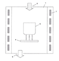
이러한 재료는 그 기능성을 충분히 발휘하기 위해서 기재 전면에 피복되는 경우가 많다. 그러나, 도 5에 나타내는 종래의 CVD 장치에 의해 기재 표면에 피막을 형성할 때에는 기재(6)와 기재유지부재(4)의 접촉하는 부분에는 피막이 형성되지 않는다. 이 때문에, 기재와 기재유지부재의 접촉하는 면적이 되도록이면 작아지도록 기재유지부재는 설계된다. 그러나, 그렇게 기재유지부재를 이용해도 기재에 있어서의 기재유지부재와 접촉하는 지지점에는 피막이 형성되지 않는다. 그 때문에 기재 전면을 피복하는 경우에는 지지점을 변경해서 복수회 성막하는 것이 필요해진다. 또한 이 경우에는 1회째에 성막된 막과 2회째의 성막된 막의 계면에 있어서 물성이 불연속으로 되는 등의 과제도 있다. 이에 대해서 현재까지 몇개의 제안이 이루어져 있다.Such materials are often coated on the entire substrate in order to fully exhibit their functionality. However, when the film is formed on the surface of the substrate by the conventional CVD apparatus shown in FIG. 5, the film is not formed in the contact portion between the
특허문헌 1에는 고주파 가열 코일을 가열함과 아울러 전자력에 의해 기재를 부상시키고, 기재 전면을 균일 성막하는 것이 기재되어 있다. 그러나, 이 방법에서는 많은 전력이 필요하며, 기재도 경량이며 소형인 것에 한정되므로, 양산 기술로서는 부적절하다.
특허문헌 2에서는, 성막 중에 지지점을 연속적으로 이동시킴으로써, 균질한 피막을 형성하는 기술이 제안되어 있다. 이 방법은 지지 레버에 기재의 관통구멍을 통과시켜서 현가함으로써 행해지므로, 기재의 형상이 한정된다고 하는 문제가 있다.In
특허문헌 3에서는, 열분해 탄소 또는 탄화규소가 피복되고, 폭 10mm 이하의 복수의 지지부를 갖는 지지대를 사용하는 것이 제안되어 있다. 이 방법에서는 지주흔은 감소하지만, 소멸하는 일은 없다.In
특허문헌 4에서는, 기재의 지지부재에 미소한 쇼크를 가해서 기재와 지지부재의 접촉 부위를 변위시키면서 코팅하는 것이 제안되어 있다. 이것에 의해, 1회의 성막으로 전면을 코팅하는 것이 가능해지지만, 기재와 지지부재의 마찰에 의해 기재나 피막의 마모나 갈라짐가 문제가 된다.In
그래서, 본 발명에서는 기재나 피막의 마모나 갈라짐이 일어나지 않고, 1회의 성막에 의해 기재 전면에 피막 형성 가능한 화학 기상 성장 장치 및 피막 형성 방법을 제공하는 것을 목적으로 한다.Therefore, an object of the present invention is to provide a chemical vapor deposition apparatus and a film forming method which can form a film on the entire surface of a substrate by one time of film formation without abrasion or cracking of the substrate or the film.
본 발명자들은, 예의 검토한 결과, 기재를 유지할 수 있는 제 1 유지부재와, 제 1 유지부재와는 독립하여 기재를 유지할 수 있는 제 2 유지부재를 화학 기상 성장 장치에 구비시키고, 또한, 제 1 유지부재 및 제 2 유지부재 중 적어도 한쪽의 유지부재를 상하방향으로 가동으로 함으로써 상기 과제를 해결할 수 있는 것을 찾아내어 본 발명을 완성시켰다. 본 발명의 요지는, 이하와 같다.MEANS TO SOLVE THE PROBLEM As a result of earnestly examining, the chemical vapor growth apparatus is equipped with the 1st holding member which can hold a base material, and the 2nd holding member which can hold a base material independently from a 1st holding member, By locating at least one holding member of the holding member and the second holding member in the vertical direction, it has been found that the above problems can be solved and the present invention has been completed. The gist of the present invention is as follows.
[1]반응 용기 내에 유지된 기재의 표면에 성막하기 위한 화학 기상 성장 장치로서, 반응 용기 내에는 1개 이상의 기재를 유지하기 위한 유지 장치가 설치되고, 유지 장치는 1개의 기재를 유지하기 위한 유지구조를 1개 이상 갖고 있고, 유지구조는 기재를 유지할 수 있는 제 1 유지부재와, 제 1 유지부재와는 독립하여 기재를 유지할 수 있는 제 2 유지부재를 적어도 갖고 있고, 제 1 유지부재 및 제 2 유지부재 중 적어도 한쪽의 유지부재는 상하방향으로 가동하는 것을 특징으로 하는 화학 기상 성장 장치.[1] A chemical vapor growth apparatus for forming a film on the surface of a substrate held in a reaction vessel, wherein a holding apparatus for holding one or more substrates is provided in the reaction vessel, and the holding apparatus is a holding for holding one substrate. It has at least one structure, The holding structure has at least the 1st holding member which can hold | maintain a base material, and the 2nd holding member which can hold | maintain a base material independently from a 1st holding member, The 1st holding member and 1st At least one holding member of the holding member is movable in the vertical direction.
[2]기재를 유지하고 있는 유지부재를 제 1 유지부재 및 제 2 유지부재 사이에서 변경 가능하게 하는 상기 [1]에 기재된 화학 기상 성장 장치.[2] The chemical vapor deposition apparatus according to the above [1], wherein the holding member holding the substrate can be changed between the first holding member and the second holding member.
[3]성막 중에 있어서 유지부재와 접촉하는 기재의 지지점의 위치가 변경 가능한 상기 [1] 또는 [2]에 기재된 화학 기상 성장 장치.[3] The chemical vapor deposition apparatus according to the above [1] or [2], wherein the position of the support point of the substrate in contact with the holding member can be changed during film formation.
[4]유지구조는 기재를 자전 가능하게 하는 상기 [1]∼[3] 중 어느 1개에 기재된 화학 기상 성장 장치.[4] The chemical vapor deposition apparatus according to any one of [1] to [3], wherein the holding structure enables the substrate to rotate.
[5]유지구조는 기재를 수평방향으로 이동 가능하게 하는 상기 [1]∼[4] 중 어느 1개에 기재된 화학 기상 성장 장치.[5] The chemical vapor deposition apparatus according to any one of [1] to [4], wherein the holding structure enables the substrate to move in the horizontal direction.
[6]제 1 유지부재 및 제 2 유지부재는 2개 이상의 지지점에 있어서 기재와 접촉하는 상기 [1]∼[5] 중 어느 1개에 기재된 화학 기상 성장 장치.[6] The chemical vapor deposition apparatus according to any one of [1] to [5], wherein the first holding member and the second holding member come into contact with the substrate at two or more supporting points.
[7]제 1 유지부재와 기재의 1개의 지지점당의 실효 접촉 면적 및 제 2 유지부재와 기재의 1개의 지지점당의 실효 접촉 면적이 각각 20㎟ 이하인 상기 [1]∼[6] 중 어느 1개에 기재된 화학 기상 성장 장치.[7] Any of the above [1] to [6], wherein the effective contact area per one supporting point of the first holding member and the substrate and the effective contact area per one supporting point of the second holding member and the substrate are each 20
[8]기재를 유지하는 제 1 유지부재와, 제 1 유지부재와는 독립하여 기재를 유지하는 제 2 유지부재를 적어도 구비한 반응 용기 내에서 화학 기상 성장에 의해 기재 표면에 피막을 형성하는 방법으로서, 제 1 유지부재에 의해 기재를 유지해서 기재 표면에 화학 기상 성장에 의해 피막을 형성하는 제 1 공정과, 제 1 유지부재 및 제 2 유지부재 중 적어도 한쪽의 유지부재가 상방향 및 하방향 중 적어도 한쪽의 방향으로 이동함으로써, 제 1 유지부재를 대신해서 제 2 유지부재에 의해 기재를 유지하는 제 2 공정과, 제 2 유지부재에 의해 유지된 기재의 표면에 화학 기상 성장에 의해 피막을 형성하는 제 3 공정을 포함하는 것을 특징으로 하는 피막 형성 방법.[8] a method of forming a film on the surface of a substrate by chemical vapor deposition in a reaction vessel having at least a first holding member for holding the substrate and a second holding member for holding the substrate independently of the first holding member A first step of holding a substrate by the first holding member to form a film on the surface of the substrate by chemical vapor deposition, and at least one holding member of the first holding member and the second holding member is directed upward and downward. By moving in at least one of the directions, the film is formed on the surface of the substrate held by the second holding member and the surface of the substrate held by the second holding member in place of the first holding member. And a third step of forming the film.
[9]제 1 공정부터 제 3 공정은 성막 중에 행해지는 상기 [8]에 기재된 피막 형성 방법.[9] The film forming method according to the above [8], wherein the first to third steps are performed during film formation.
(발명의 효과)(Effects of the Invention)
본 발명에 의하면, 1회의 성막에 의해 기재 전면에 피막 형성이 가능해지므로, 지지점을 변경한 복수회의 성막이 불필요하게 되어 생산성이 향상된다. 특히, 열 CVD법에 의해 복수회의 성막을 행하려고 하면, 성막시간 외에 비교적 고온의 반응온도에의 승온이나 강온을 위한 시간도 필요하다. 이 때문에, 본 발명에 의하면, 특히 열 CVD법의 경우, 크게 생산성이 향상된다.According to the present invention, since the film can be formed on the entire surface of the substrate by one film formation, a plurality of film formations having changed support points are unnecessary and the productivity is improved. In particular, when the film is to be formed a plurality of times by the thermal CVD method, in addition to the film forming time, a time for raising or lowering the reaction temperature at a relatively high temperature is also required. For this reason, according to this invention, especially in the case of thermal CVD method, productivity improves significantly.
도 1은 본 발명의 일실시형태의 CVD 장치에 있어서의 유지 장치의 일례를 나타내는 개략 모식도.
도 2는 본 발명의 일실시형태의 CVD 장치에 있어서의 반응 용기의 일례를 나타내는 개략 모식도.
도 3은 본 발명의 일실시형태의 CVD 장치에 있어서의 반응 용기의 일례를 나타내는 개략 모식도.
도 4는 실시예에서 사용한 CVD 장치에 있어서의 유지구조의 움직임을 나타내는 개략 모식도.
도 5는 종래의 CVD 장치에 있어서의 반응 용기의 일례를 나타내는 개략 모식도.BRIEF DESCRIPTION OF THE DRAWINGS It is a schematic schematic diagram which shows an example of the holding apparatus in the CVD apparatus of one Embodiment of this invention.
2 is a schematic diagram illustrating an example of a reaction vessel in a CVD apparatus according to one embodiment of the present invention.
3 is a schematic diagram showing an example of a reaction vessel in a CVD apparatus according to one embodiment of the present invention.
Fig. 4 is a schematic diagram showing the movement of the holding structure in the CVD apparatus used in the embodiment.
5 is a schematic diagram showing an example of a reaction vessel in a conventional CVD apparatus.
[화학 기상 성장 장치][Chemical Vapor Growth Devices]
본 발명의 일실시형태에 있어서의 화학 기상 성장 장치는 반응 용기 내에 유지된 기재의 표면에 성막하고, 반응 용기 내에는 1개 이상의 기재를 유지하기 위한 유지 장치가 설치되어 있다. 유지 장치는 1개의 기재를 유지하기 위한 유지구조를 1개 이상 갖고 있고, 유지구조는 기재를 유지할 수 있는 제 1 유지부재와, 제 1 유지부재와는 독립하여 기재를 유지할 수 있는 제 2 유지부재를 적어도 갖고 있다. 그리고, 제 1 유지부재 및 제 2 유지부재 중 적어도 한쪽의 유지부재는 상하방향으로 가동한다. 이것에 의해, 본 발명의 일실시형태에 있어서의 화학 기상 성장 장치는 1회의 성막에 의해 기재 전면에 피막 형성이 가능해진다. 그리고, 지지점을 변경한 복수회의 성막이 불필요하게 되어 생산성이 향상된다. 본 발명의 일실시형태에 있어서의 화학 기상 성장 장치를 이하에 상세하게 설명한다.The chemical vapor deposition apparatus in one embodiment of the present invention is formed on the surface of a substrate held in a reaction vessel, and a holding apparatus for holding one or more substrates is provided in the reaction vessel. The holding device has at least one holding structure for holding one substrate, and the holding structure has a first holding member capable of holding the substrate and a second holding member capable of holding the substrate independently of the first holding member. Has at least And at least one holding member of the first holding member and the second holding member is movable in the vertical direction. Thereby, the chemical vapor deposition apparatus in one embodiment of the present invention can form a film on the entire surface of the substrate by one film formation. In addition, a plurality of times of film formation having changed support points are unnecessary, and productivity is improved. The chemical vapor deposition apparatus in one embodiment of the present invention will be described in detail below.
본 발명의 일실시형태에 있어서의 화학 기상 성장 장치는, 예를 들면, 열분해 질화붕소(PBN), 열분해 탄소(PG), 탄화탄탈(TaC), 질화알루미늄(AlN), 탄화규소(SiC) 등의 재료를 반응 용기 내에 유지한 기재의 표면에 성막하기 위한 화학 기상 성장(CVD) 장치이다.The chemical vapor deposition apparatus in one embodiment of the present invention is, for example, pyrolytic boron nitride (PBN), pyrolytic carbon (PG), tantalum carbide (TaC), aluminum nitride (AlN), silicon carbide (SiC), or the like. Is a chemical vapor deposition (CVD) apparatus for forming a film on the surface of a substrate held in a reaction vessel.
본 발명의 일실시형태에 있어서의 CVD 장치에 있어서 성막하는 재료나 기재의 종류, 형상은 임의로 선택할 수 있다. 또한 본 발명의 일실시형태에 있어서의 CVD 장치에 있어서의 CVD의 종류는 특별히 한정되지 않고, 본 발명의 일실시형태에 있어서의 CVD 장치는 열 CVD나 플라즈마 CVD 등에도 적용할 수 있다.In the CVD apparatus in one embodiment of the present invention, the type and shape of the material and the substrate to be formed can be arbitrarily selected. Moreover, the kind of CVD in the CVD apparatus in one Embodiment of this invention is not specifically limited, The CVD apparatus in one Embodiment of this invention is applicable also to thermal CVD, plasma CVD, etc.
또, CVD법은 피복성이 우수하고, 균일하며 막두께 분포가 좋은 피막이 얻어진다. 또한 열 CVD법은 플라즈마 CVD법과 같이, 플라즈마에 의한 유지 장치의 손상의 우려도 없다.Moreover, the CVD method yields a coating which is excellent in coating property and uniform and has a good film thickness distribution. In addition, the thermal CVD method, like the plasma CVD method, has no fear of damaging the holding apparatus by the plasma.
상기 관점 및 생산성을 크게 향상시킬 수 있다고 하는 관점으로부터 본 발명의 일실시형태에 있어서의 CVD 장치는 열 CVD법에 의해 기재 표면에 피막을 형성하는 CVD 장치인 것이 바람직하다.It is preferable that the CVD apparatus in one Embodiment of this invention is a CVD apparatus which forms a film in the surface of a base material by a thermal CVD method from the viewpoint that the said viewpoint and productivity can be improved significantly.
본 발명의 일실시형태에 있어서의 CVD 장치의 반응 용기 내에는 1개 이상의 기재를 유지하기 위한 유지 장치가 설치된다. 생산 효율의 관점으로부터 유지 장치는 복수의 기재를 유지할 수 있는 것이 바람직하다.In the reaction vessel of the CVD apparatus according to one embodiment of the present invention, a holding apparatus for holding one or more substrates is provided. It is preferable that a holding | maintenance apparatus can hold | maintain a some base material from a viewpoint of a production efficiency.
유지 장치는 1개의 기재를 유지하기 위한 유지구조를 1개 이상 갖는다. 유지 장치가 복수의 기재를 유지하는 경우에는 유지 장치에는 복수의 유지구조가 설치된다.The holding device has one or more holding structures for holding one substrate. When the holding device holds a plurality of substrates, the holding device is provided with a plurality of holding structures.
또한, 유지구조는 기재를 유지할 수 있는 제 1 유지부재와, 제 1 유지부재와는 독립하여 기재를 유지할 수 있는 제 2 유지부재를 적어도 갖고 있다. 또, 「제 1 유지부재와는 독립하여 기재를 유지할 수 있는」이란 제 1 유지부재가 없어도, 제 2 유지부재로 기재를 유지할 수 있는 것을 의미한다. 또한 유지구조는 제 1 유지부재와 제 2 유지부재를 갖고 있으면, 제 1 유지부재 및 제 2 유지부재 이외의 유지부재를 갖고 있어도 좋다. 예를 들면, 유지구조는 기재를 유지할 수 있는 제 1 유지부재와, 제 1 유지부재와는 독립하여 기재를 유지할 수 있는 제 2 유지부재와, 제 1 유지부재 및 제 2 유지부재와는 독립하여 기재를 유지할 수 있는 제 3 유지부재를 가져도 좋다.Further, the holding structure has at least a first holding member capable of holding the substrate and a second holding member capable of holding the substrate independently of the first holding member. In addition, "the substrate can be held independently of the first holding member" means that the substrate can be held by the second holding member even without the first holding member. In addition, as long as the holding structure has a 1st holding member and a 2nd holding member, you may have holding members other than a 1st holding member and a 2nd holding member. For example, the holding structure includes a first holding member capable of holding a substrate, a second holding member capable of holding a substrate independently of the first holding member, and independent of the first holding member and the second holding member. You may have the 3rd holding member which can hold | maintain a base material.
제 1 유지부재 및 제 2 유지부재 중 적어도 한쪽의 유지부재는 상하방향으로 가동한다. 이것에 의해, 기재를 유지하고 있는 유지부재를 제 1 유지부재 및 제 2 유지부재 사이에서 변경할 수 있다. 그 결과, 성막 중에 유지부재와 접촉하는 기재의 지지점의 위치를 변경할 수 있으므로, 기재 표면 전체에 피막을 형성할 수 있다. 그리고, 지지점을 변경한 복수회의 성막이 불필요하게 되어 생산성이 향상된다.At least one holding member of the first holding member and the second holding member is movable in the vertical direction. Thereby, the holding member holding the base material can be changed between the first holding member and the second holding member. As a result, since the position of the support point of the base material which contacts the holding member during the film formation can be changed, a film can be formed on the entire surface of the base material. In addition, a plurality of times of film formation having changed support points are unnecessary, and productivity is improved.
도 1을 참조해서 본 발명의 일실시형태에 있어서의 CVD 장치에 설치된 유지 장치를 더 상세하게 설명한다. 도 1은 본 발명의 일실시형태에 있어서의 CVD 장치에 설치된 유지 장치의 일례를 나타내는 개략도이다. 여기에서는 제 2 유지부재(5)가 상방향으로 이동함으로써, 제 1 유지부재(4)가 유지하고 있던 기재(6)를 제 2 유지부재(5)가 유지한다.With reference to FIG. 1, the holding apparatus provided in the CVD apparatus in one Embodiment of this invention is demonstrated in more detail. 1 is a schematic view showing an example of a holding apparatus provided in a CVD apparatus according to one embodiment of the present invention. Here, the second holding
또한 제 2 유지부재(5)가 하방향으로 이동함으로써, 제 2 유지부재(5)가 유지하고 있던 기재(6)를 제 1 유지부재(4)가 유지한다.In addition, since the second holding
이렇게, 제 2 유지부재(5)가 상방향 및 하방향 중 적어도 한쪽의 방향으로 이동함으로써, 기재(6)를 유지하는 유지부재를 제 1 유지부재(4) 및 제 2 유지부재(5) 사이에서 변경할 수 있다.In this way, the second holding
또, 제 1 유지부재(4)가 상방향 및 하방향 중 적어도 한쪽의 방향으로 이동함으로써, 기재(6)를 유지하는 유지부재를 제 1 유지부재(4) 및 제 2 유지부재(5) 사이에서 변경할 수 있도록 해도 좋다. 또한 제 1 유지부재(4) 및 제 2 유지부재(5) 양쪽이 상방향 및 하방향 중 적어도 한쪽의 방향으로 이동함으로써, 기재(6)를 유지하는 유지부재를 제 1 유지부재(4) 및 제 2 유지부재(5) 사이에서 변경할 수 있도록 해도 좋다. 이렇게, 본 발명의 일실시형태에 있어서의 CVD 장치에서는 제 1 유지부재(4) 및 제 2 유지부재(5) 중 적어도 한쪽의 유지부재가 상방향 및 하방향 중 적어도 한쪽의 방향으로 이동함으로써, 기재(6)를 유지하고 있는 유지부재를 제 1 유지부재(4) 및 제 2 유지부재(5) 사이에서 변경할 수 있다.In addition, the first holding
여기에서, 「제 1 유지부재(4) 및 제 2 유지부재(5) 사이에서 변경 가능」이란 제 1 유지부재(4)로부터 제 2 유지부재(5)로 변경 가능한 것, 제 2 유지부재(5)로부터 제 1 유지부재(4)로 변경 가능한 것, 또는 제 1 유지부재(4)로부터 제 2 유지부재(5)로 변경 가능하며, 또한 제 2 유지부재(5)로부터 제 1 유지부재(4)로 변경 가능한 것을 의미한다.Here, "changeable between the 1st holding
또, 제 1 유지부재(4) 및 제 2 유지부재(5) 중 적어도 한쪽의 유지부재를 상하방향으로 가동으로 하기 위한 가동 기구에 대해서는 특별히 한정되지 않는다.Moreover, the movable mechanism for moving at least one holding member of the
이렇게 하면, 성막 중에 있어서 유지부재와 접촉하는 기재의 지지점을 변경할 수 있으므로, 기재 전면에 피막을 형성할 때에 복수회에 걸쳐 성막할 필요가 없다.In this way, since the support point of the base material which contacts the holding member can be changed during film formation, it is not necessary to form a film multiple times when forming a film on the entire surface of the base material.
제 1 유지부재 및 제 2 유지부재 중 적어도 한쪽의 유지부재에 있어서의 상방향 및 하방향 중 적어도 한쪽의 방향의 이동 및 그것에 의한 기재의 지지점의 변경은 성막 중에 있어서 복수회 행해지는 것이 바람직하다. 이것에 의해, 지지점 부근에 있어서의 피막의 불균일성을 억제할 수 있다.It is preferable that the movement of at least one of the upward direction and the downward direction in the at least one holding member of the first holding member and the second holding member and the change of the supporting point of the substrate thereby are performed a plurality of times during film formation. Thereby, the nonuniformity of the film in the support point vicinity can be suppressed.
또한 제 1 유지부재가 유지하고 있을 때의 기재의 위치와, 제 2 유지부재가 유지하고 있을 때의 기재의 위치가 상하방향에서 바뀌도록 해도 좋다. 기재의 위치를 상하시킴으로써 피막 전체의 균일성의 향상도 기대할 수 있다.The position of the substrate when the first holding member is held and the position of the substrate when the second holding member is held may be changed in the up and down direction. The improvement of the uniformity of the whole film can also be anticipated by raising and lowering the position of a base material.
PBN을 CVD법에 의해 성막할 때에 원료로서 사용되는 염화붕소와 암모니아는 상온에서도 반응할만큼 반응성이 높기 때문에, 원료 가스가 처음으로 기재에 접촉하는 개소의 근방에서 성막되기 쉬운 경향이 있고, 이면 등에는 가스가 유입되기 어려워 성막하기 어렵다.When PBN is formed by CVD, boron chloride and ammonia, which are used as raw materials, are highly reactive enough to react even at room temperature, and thus tend to be easily formed in the vicinity of the place where the source gas contacts the substrate for the first time. It is difficult to form a film because gas is difficult to flow.
한편, TaC에서는 원료의 반응성은 높지 않지만, 탄탈원이 되는 염화탄탈 등의 원자량이 큰 가스는 탄소원이 되는 메탄 등의 원자량이 작은 가스에 비해서 직진성이 높기 때문에, PBN과 마찬가지로 복잡형상 기재의 이면이나 공간이 좁은 지지점 근방에는 가스가 유입되기 어려워 성막하기 어렵다.On the other hand, in TaC, although the reactivity of the raw material is not high, gas having a high atomic weight such as tantalum chloride as a tantalum source has a higher straightness than gas having a small atomic weight such as methane as a carbon source. It is difficult to form a film because gas is hard to flow near a narrow support point.
성막 중에 기재를 상하방향으로 이동시킴으로써 가스의 흐름이나 기재와 가스의 접촉 위치가 변화되므로 피막 전체의 균일성이 향상된다. 이 때문에, 특히, PBN, TaC 등의 균일하게 성막하기 어려운 재료의 피막을 형성할 때, 성막 중에 기재를 상하방향으로 이동시키는 것이 바람직하다.By moving the substrate in the vertical direction during film formation, the flow of gas and the contact position of the substrate and the gas are changed, so that the uniformity of the entire film is improved. For this reason, especially when forming the film of the material which is hard to form uniformly, such as PBN and TaC, it is preferable to move a base material up and down during film-forming.
또한, 유지구조는 기재를 자전시켜도 좋고, 수평방향으로 이동시켜도 좋다. 또한 유지구조는 기재를 자전시키면서 수평방향으로 이동시켜도 좋다. 이것에 의해, 가스의 흐름을 변화시킬 수 있으므로, 피막 전체의 균일성을 더욱 향상시킬 수 있다. 예를 들면, 유지구조를 공전시킴으로써 기재를 수평방향으로 이동시킬 수 있다. 또한 피막 전체의 균일성을 더욱 향상시키기 위해서, 기재의 자전 및 기재의 상하방향의 이동, 기재의 수평방향의 이동 및 기재의 상하방향의 이동, 또는 기재의 자전, 기재의 수평방향의 이동 및 기재의 상하방향을 조합해도 좋다.In addition, the holding structure may rotate the substrate or move the substrate in the horizontal direction. In addition, the holding structure may be moved in the horizontal direction while rotating the substrate. Thereby, since gas flow can be changed, the uniformity of the whole film can be improved further. For example, the substrate can be moved in the horizontal direction by revolving the holding structure. Further, in order to further improve the uniformity of the entire coating, the rotation of the substrate and the vertical movement of the substrate, the horizontal movement of the substrate and the vertical movement of the substrate, or the rotation of the substrate, the horizontal movement of the substrate, and the substrate The up and down directions may be combined.
제 1 유지부재 및 제 2 유지부재는 기재를 유지할 수 있는 부재이면 특별히 한정되지 않는다. 상기 유지부재는, 예를 들면, 선단이 뾰족한 바늘형상의 지지부를 복수 갖고, 선단에서 기재와 접촉하도록 할 수 있다. 1개의 기재에 있어서 유지부재와 기재가 접촉하는 지지점의 수는 2개 이상인 것이 바람직하고, 3개 이상 4개 이하인 것이 보다 바람직하다. 지지점이 3개 이상이면, 보다 안정되게 기재를 유지할 수 있다. 한편, 지지점이 지나치게 많으면 성막할 수 없는 개소가 증가하여 바람직하지 못하다.The first holding member and the second holding member are not particularly limited as long as they can hold the substrate. For example, the holding member may have a plurality of needle-shaped support portions having a sharp tip, and may be in contact with the substrate at the tip. It is preferable that the number of the support points which a holding member and a base material contact in one base material is two or more, and it is more preferable that they are three or more and four or less. If the support point is three or more, the base material can be held more stably. On the other hand, when there are too many support points, the location which cannot form into a film increases and it is unpreferable.
제 1 유지부재와 기재의 1개의 지지점당의 실효 접촉 면적 및 제 2 유지부재와 기재의 1개의 지지점당의 실효 접촉 면적은 각각 20㎟ 이하인 것이 바람직하다. 이 실효 접촉 면적은 지지흔을 남기지 않으므로 되도록이면 작은 쪽이 바람직하다.It is preferable that the effective contact area per one support point of the first holding member and the substrate and the effective contact area per one support point of the second holding member and the substrate are each 20
여기에서, 실효 접촉 면적이란 지지점을 변경하지 않고, 기재 표면에 목적으로 하는 재료를 목적으로 하는 두께로 성막하고, 1개의 지지점에 대해서 지지흔이 되어 기재가 노출되는 면적이다.Here, an effective contact area is an area which does not change a support point, is formed into the thickness of the target material on the surface of a base material, and becomes a support mark with respect to one support point, and exposes a base material.
또한 1개의 지지점당의 실효 접촉 면적이 지나치게 작으면, 접촉 면적에 대해서 기재 및 유지부재에 가해지는 응력이 커지고, 기재가 변형되거나 유지부재가 마모되거나 할 우려가 있다. 그 때문에 1개의 지지점당의 실효 접촉 면적은 1㎟ 이상인 것이 보다 바람직하다.In addition, if the effective contact area per one support point is too small, the stress applied to the substrate and the holding member with respect to the contact area increases, and there is a fear that the substrate is deformed or the holding member is worn. Therefore, it is more preferable that the effective contact area per one support point is 1 mm <2> or more.
유지부재의 표면의 재료는 특별히 한정되지 않지만, 그 표면의 재료는 기재에 성막하는 재료 또는 기재를 구성하는 재료와 동일한 것이 바람직하다. 유지부재에 사용하는 재료가 상기 재료와 다르면, 유지부재와 원료 가스가 반응해서 형성되는 피막의 조성이 변화되거나, 유지부재로부터의 불순물 확산에 의해 기재나 피막이 오염되어지거나 할 우려가 있다.Although the material of the surface of a holding member is not specifically limited, It is preferable that the material of the surface is the same as the material which forms into a film, or the material which comprises a base material. If the material used for the holding member is different from the above material, there is a possibility that the composition of the coating film formed by the reaction between the holding member and the source gas is changed, or the substrate or coating may be contaminated by diffusion of impurities from the holding member.
본 발명의 일실시형태에 있어서의 CVD 장치는 유지부재, 유지구조를 포함하는 유지 장치 이외에 대해서는 특별히 한정되지 않고, 일반적인 CVD 장치와 동일하게 하면 좋고, 목적이나 필요에 따라서 임의로 설계하면 좋다.The CVD apparatus in one embodiment of the present invention is not particularly limited except for a holding apparatus including a holding member and a holding structure. The CVD apparatus may be the same as a general CVD apparatus, and may be arbitrarily designed according to the purpose and need.
본 발명의 일실시형태에 있어서의 CVD 장치는, 예를 들면, 외열형 감압 CVD 장치이어도 좋다. 도 2 및 3은 외열형 감압 CVD 장치의 일례를 나타낸 것이다. 반응 용기(1)는 원료 공급부(8)와 배기부(9)를 구비하고 있고, 또한 히터(7)가 설치되어 있다.The CVD apparatus in one embodiment of the present invention may be, for example, an external heat-type reduced pressure CVD apparatus. 2 and 3 show an example of an external thermal pressure reduction CVD apparatus. The
원료 공급부(8)로부터 성막하는 재료에 따른 원료 가스가 공급된다. 예를 들면, 피막의 재료가 PBN인 경우, 암모니아(NH3)와 같은 질소원자를 포함하는 화합물과 3염화붕소(BCl3)와 같은 할로겐화 붕소를 공급한다. 피막의 재료가 TaC인 경우, 메탄(CH4)과 같은 탄소원자를 포함하는 화합물과, 5염화탄탈(TaCl5)과 같은 할로겐화 탄탈을 공급한다. 피막의 재료가 PG인 경우, CH4와 같은 탄소원자를 포함하는 화합물을 단독으로 공급한다. 피막의 재료가 AlN인 경우, 트리메틸알루미늄(Al(CH3)3)과 같은 알루미늄을 포함하는 화합물과, NH3과 같은 질소원자를 포함하는 화합물을 공급한다. 피막의 재료가 SiC인 경우, 실란(SiH4)과 같은 규소원자를 포함하는 화합물과, 프로판(C3H8)과 같은 탄소원자를 포함하는 화합물을 공급한다.The raw material gas corresponding to the material to form into a film from the raw
공급된 원료 가스를 900∼1900℃, 1∼100Pa의 고온감압 하에서 열 CVD 반응시켜서 기재 표면에 PBN, TaC, PG, AlN, SiC 등의 기능성 재료를 성막한다.The supplied raw material gas is subjected to thermal CVD reaction under a high temperature reduction of 900 to 1900 ° C. and 1 to 100 Pa to form a functional material such as PBN, TaC, PG, AlN, and SiC on the surface of the substrate.
이상, 본 발명의 일실시형태에 있어서의 CVD 장치를 설명했지만, 본 발명의 CVD 장치는 본 발명의 일실시형태에 있어서의 CVD 장치에 한정되지 않는다.As mentioned above, although the CVD apparatus in one Embodiment of this invention was demonstrated, the CVD apparatus of this invention is not limited to the CVD apparatus in one Embodiment of this invention.
[피막 형성 방법][Film Formation Method]
본 발명의 피막 형성 방법은 기재를 유지하는 제 1 유지부재와, 상기 제 1 유지부재와는 독립하여 상기 기재를 유지하는 제 2 유지부재를 적어도 구비한 반응 용기 내에서 화학 기상 성장에 의해 기재 표면에 피막을 형성하는 방법이며,The film forming method of the present invention provides a substrate surface by chemical vapor growth in a reaction vessel including at least a first holding member for holding a substrate and a second holding member for holding the substrate independently of the first holding member. To form a film on the
제 1 유지부재에 의해 기재를 유지해서 기재 표면에 화학 기상 성장에 의해 피막을 형성하는 제 1 공정과,A first step of holding the substrate by the first holding member to form a film on the surface of the substrate by chemical vapor growth;
제 1 유지부재 및 제 2 유지부재 중 적어도 한쪽의 유지부재가 상방향 및 하방향 중 적어도 한쪽의 방향으로 이동함으로써, 제 1 유지부재를 대신해서 제 2 유지부재에 의해 기재를 유지하는 제 2 공정과,A second step of holding the substrate by the second holding member in place of the first holding member by moving the at least one holding member of the first holding member and the second holding member in at least one of the upward direction and the downward direction. and,
제 2 유지부재에 의해 유지된 기재의 표면에 화학 기상 성장에 의해 피막을 형성하는 제 3 공정을 포함한다. 이것에 의해, 1회의 성막에 의해 기재 전면에 피막 형성이 가능해진다. 그리고, 지지점을 변경한 복수회의 성막이 불필요하게 되어 생산성이 향상된다.And a third step of forming a film by chemical vapor deposition on the surface of the substrate held by the second holding member. Thereby, a film can be formed in the whole base material by one film formation. In addition, a plurality of times of film formation having changed support points are unnecessary, and productivity is improved.
(반응 용기)(Reaction vessel)
본 발명의 피막 형성 방법에 사용하는 반응 용기는 상기 제 1 공정으로부터 제 3 공정을 실시할 수 있는 반응 용기이면 특별히 한정되지 않는다. 본 발명의 피막 형성 방법에 사용하는 반응 용기로서, 예를 들면, 상술의 본 발명의 일실시형태에 있어서의 CVD 장치의 반응 용기를 사용할 수 있다. 이하, 상술의 본 발명의 일실시형태에 있어서의 CVD 장치의 반응 용기를 예로 들어 본 발명의 피막 형성 방법을 설명한다.The reaction container used for the film formation method of this invention will not be specifically limited if it is a reaction container which can implement a 3rd process from the said 1st process. As a reaction container used for the film formation method of this invention, the reaction container of the CVD apparatus in one Embodiment of this invention mentioned above can be used, for example. EMBODIMENT OF THE INVENTION Hereinafter, the film formation method of this invention is demonstrated taking the reaction container of the CVD apparatus in one Embodiment of this invention mentioned above as an example.
(제 1 공정)(First process)
제 1 공정에서는 제 1 유지부재에 의해 기재를 유지해서 기재 표면에 화학 기상 성장에 의해 피막을 형성한다. 또, 제 1 유지부재 및 기재 표면에 있어서의 화학 기상 성장에 대해서는 상술의 본 발명의 일실시형태에 있어서의 CVD 장치에서 설명한 것과 같으므로, 이들의 설명은 생략한다. In the first step, the substrate is held by the first holding member to form a film on the surface of the substrate by chemical vapor deposition. The chemical vapor phase growth on the surface of the first holding member and the substrate is the same as that described in the above-described CVD apparatus in one embodiment of the present invention, and the description thereof is omitted.
(제 2 공정)(Second process)
제 2 공정에서는 제 1 유지부재 및 제 2 유지부재 중 적어도 한쪽의 유지부재가 상방향 및 하방향 중 적어도 한쪽의 방향으로 이동함으로써, 제 1 유지부재 대신에 제 2 유지부재에 의해 기재를 유지한다. 이것에 의해, 유지부재와 접촉하는 기재의 지지점의 위치를 변경할 수 있다. 또, 제 1 유지부재 및 제 2 유지부재 중 적어도 한쪽의 유지부재에 있어서의 상방향 및 하방향 중 적어도 한쪽의 방향의 이동 및 제 2 유지부재에 대해서는 상술의 본 발명의 일실시형태에 있어서의 CVD 장치에서 설명한 것과 같으므로, 이들의 설명은 생략한다.In the second step, the holding member of at least one of the first holding member and the second holding member moves in at least one of the upward direction and the downward direction, thereby holding the substrate by the second holding member instead of the first holding member. . Thereby, the position of the support point of the base material which contacts a holding member can be changed. Moreover, about the movement of the at least one direction of the upward direction and the downward direction in the at least one holding member of a 1st holding member and a 2nd holding member, and a 2nd holding member in one Embodiment of this invention mentioned above Since it is the same as that described in the CVD apparatus, the description thereof is omitted.
(제 3 공정)(Third process)
제 3 공정에서는 제 2 유지부재에 의해 유지된 기재의 표면에 화학 기상 성장에 의해 피막을 형성한다. 이것에 의해, 유지부재와 접촉하는 기재의 지지점의 위치를 제 1 공정에 있어서의 유지부재와 접촉하는 기재의 지지점의 위치로부터 변경해서 기재 표면에 화학 기상 성장에 의해 피막을 형성할 수 있으므로, 기재 전면에 피막을 형성할 수 있다. 또, 기재 표면에 있어서의 화학 기상 성장에 대해서는 상술의 본 발명의 일실시형태에 있어서의 CVD 장치에서 설명한 것과 같으므로, 이 설명은 생략한다.In the third step, a film is formed on the surface of the substrate held by the second holding member by chemical vapor phase growth. As a result, since the position of the support point of the substrate in contact with the holding member can be changed from the position of the support point of the substrate in contact with the holding member in the first step, a film can be formed on the surface of the substrate by chemical vapor deposition. A film can be formed on the whole surface. The chemical vapor phase growth on the substrate surface is the same as that described in the above-described CVD apparatus in one embodiment of the present invention, and thus this description is omitted.
또, 제 1 공정부터 제 3 공정은 성막 중에 행해지는 것이 바람직하다. 이것에 의해, 1회의 성막에 의해 기재 전면에 피막 형성이 가능해지므로, 지지점을 변경한 복수회의 성막이 불필요하게 되어 생산성이 향상된다. 예를 들면, 화학 기상 성장에 의해 기재의 표면에 피막을 형성하면서 제 2 공정을 실시하는 것이 바람직하다.Moreover, it is preferable that a 1st process thru | or a 3rd process is performed during film-forming. As a result, the film can be formed on the entire surface of the substrate by one time of film formation, thus eliminating the need for multiple times of film formation having changed support points, thereby improving productivity. For example, it is preferable to perform a 2nd process, forming a film on the surface of a base material by chemical vapor deposition.
또한 1회의 성막 중에 제 1 공정으로부터 제 3 공정을 갖는 공정 사이클을 복수회 실시하는 것이 바람직하다. 이것에 의해, 지지점 부근에 있어서의 피막의 불균일성을 억제할 수 있다.Moreover, it is preferable to perform the process cycle which has a 3rd process from a 1st process in one film formation in multiple times. Thereby, the nonuniformity of the film in the support point vicinity can be suppressed.
이상, 본 발명의 피막 형성 방법에 사용하는 반응 용기로서 상술의 본 발명의 일실시형태에 있어서의 CVD 장치의 반응 용기를 예로 들어 본 발명의 피막 형성 방법을 설명했다. 그러나, 본 발명의 피막 형성 방법은 본 발명의 일실시형태에 있어서의 CVD 장치를 사용한 피막 형성 방법에 한정되지 않는다.As mentioned above, the film forming method of this invention was demonstrated to the example as the reaction container of the CVD apparatus in one Embodiment of this invention mentioned above as a reaction container used for the film forming method of this invention. However, the film formation method of this invention is not limited to the film formation method using the CVD apparatus in one Embodiment of this invention.
(실시예)(Example)
이하, 실시예를 나타내서 본 발명을 보다 구체적으로 설명하지만, 본 발명은 이들에 한정되는 것은 아니다.Hereinafter, although an Example is shown and this invention is demonstrated more concretely, this invention is not limited to these.
<실시예 1><Example 1>
우선, 냉간 등방압 가압법(CIP법)에 의해 성형된 등방성 흑연을 유저 원통형상으로 가공해서 6개의 탄소기재를 제작했다. 또, 탄소기재는 내경이 180mm이며, 외경이 186mm이며, 높이가 180mm였다.First, the isotropic graphite molded by the cold isotropic pressure press method (CIP method) was processed into a user cylindrical shape, and six carbon base materials were produced. In addition, the carbon substrate had an inner diameter of 180 mm, an outer diameter of 186 mm, and a height of 180 mm.
다음에 외열형 감압 CVD 장치의 반응 용기 내에 있는 유지 장치에 6개의 탄소기재를 적재했다. 이 유지 장치는 1개의 기재를 유지하기 위한 유지구조를 6개 갖고 있고, 각 유지구조에 1개씩 탄소기재를 적재했다.Next, six carbon substrates were loaded into the holding apparatus in the reaction vessel of the external heat-type reduced pressure CVD apparatus. This holding device has six holding structures for holding one base material, and one carbon base material is loaded in each holding structure.
또한 이 유지구조는 단독으로 기재를 유지할 수 있는 유지부재를 2개 갖고 있고, 그 중 1개의 유지부재(제 1 유지부재)에 탄소기재는 적재되어 있다. 또, 유지부재는 선단이 뾰족한 지지부를 3개 갖고 있고, 탄소기재는 지지부의 선단과 (지지점에서) 접촉해서 지지되어 있다.Moreover, this holding structure has two holding members which can hold | maintain a base material independently, The carbon base material is mounted in one holding member (1st holding member) among them. In addition, the holding member has three supporting portions having sharp tips, and the carbon base material is supported by contacting the tip of the supporting portion (at the supporting point).
또, 사전검증에 의해, 이 유지부재와 기재의 1개의 지지점당의 실효 접촉 면적은 10㎟인 것을 확인하고 있다.Moreover, by prior verification, it has confirmed that the effective contact area per one support point of this holding member and a base material is 10 mm <2>.
또한, 이들 유지부재는 상하방향으로 독립하여 역위상으로 이동하는 것이 가능하도록 되어 있다. 또, 「독립하여」란 이들 2개의 유지부재가 상하방향으로 상대적으로 다른 동작을 하는 것을 말한다. 또한 상하방향으로 독립하여 역위상으로 이동하는 2개의 유지부재는, 예를 들면, 기어 등을 통해 같은 회전계로부터 상하방향으로 이동하기 위한 구동력을 얻어도 좋다. 최초로 기재를 유지하는 유지부재(제 1 유지부재)는 하방향으로, 다른 한쪽의 유지부재(제 2 유지부재)는 상방향으로 이동함으로써, 제 1 유지부재로부터 제 2 유지부재로 탄소기재의 반송이 가능해진다. 그 후에 탄소기재를 수취한 유지부재(제 2 유지부재)는 하방향으로 최초로 탄소기재를 유지하고 있던 유지부재(제 1 유지부재)는 상방향으로 이동함으로써, 다시 제 1 유지부재에 탄소기재를 반송할 수 있다. 또, 제 1 및 제 2 유지부재의 상하방향의 이동거리는 50mm였다.In addition, these holding members can be moved in the reverse phase independently of each other in the vertical direction. In addition, "independently" means that these two holding members perform relatively different operation | movement in the up-down direction. In addition, the two holding members that move independently in the up and down directions and out of phase may obtain a driving force for moving in the up and down directions from the same rotation system through, for example, a gear or the like. The holding member (first holding member) holding the substrate for the first time is moved downward, and the other holding member (second holding member) moves upward, thereby conveying the carbon substrate from the first holding member to the second holding member. This becomes possible. Thereafter, the holding member (second holding member) receiving the carbon substrate is moved to the holding member (first holding member), which was first holding the carbon substrate in the downward direction, to move the carbon substrate to the first holding member again. You can return it. In addition, the moving distance of the 1st and 2nd holding member of the up-down direction was 50 mm.
여기에서, 제 1 유지부재의 기재와 접촉하는 개소 및 제 2 유지부재의 기재와 접촉하는 개소가 다르므로, 기재에 있어서의 지지점의 변경이 가능해진다.Here, since the point which contacts the base material of a 1st holding member and the point which contacts the base material of a 2nd holding member differ, the support point in a base material can be changed.
또, 도 4에 나타내듯이, 각 유지구조(3)는 자전 가능하게 되어 있고, 기재(6)를 자전시킨다. 또한 유지구조(3)는 유지 장치(2)의 중심을 지점으로 해서 공전하게 되어 있고, 기재(6)를 공전시킨다. In addition, as shown in FIG. 4, each holding
여기에서는, 유지구조의 공전 1회전에 대해서 자전을 1회전, 유지부재(4,5)의 상하동을 1회(탄소기재의 반송을 1회) 행하도록 설정했다. 또, 공전의 회전속도는 5rpm이었다.Here, it was set so that one rotation of rotation of the holding structure and one up / down movement of the holding
계속해서, 원료 공급부로부터 NH3 가스를 20SLM(standard/liter/minute(1atm, 0℃)), BCl3 가스를 5SLM 공급하고, 반응 용기 내의 압력을 100Pa, 온도를 1800℃로 했다. 화학 기상 성장에 의해, 탄소기재 전면에 막두께 1mm의 PBN 피막을 형성했다. 성막 개시부터 종료까지의 처리 시간(승온, 강온 시간을 포함한다)은 25시간이었다.Subsequently, 20 SLM (standard / liter / minute (1 atm, 0 ° C.)) of NH 3 gas and 5 SLM of BCl 3 gas were supplied from the raw material supply part, the pressure in the reaction vessel was 100 Pa, and the temperature was 1800 ° C. By chemical vapor phase growth, a PBN film having a film thickness of 1 mm was formed on the entire carbon substrate. The processing time (including the temperature rise and the temperature decrease time) from the film formation start to the end was 25 hours.
<실시예 2><Example 2>
유지구조의 자공전을 멈춘 것 이외는 실시예 1과 동일한 방법으로 PBN 피복 탄소기재를 제작했다.A PBN-coated carbon base material was produced in the same manner as in Example 1 except that the magnetization of the holding structure was stopped.
<실시예 3><Example 3>
유지부재와 기재의 실효 접촉 면적을 20㎟로 한 것 이외는, 실시예 1과 동일한 방법으로 PBN 피복 탄소기재를 제작했다.A PBN-coated carbon substrate was produced in the same manner as in Example 1, except that the effective contact area between the holding member and the substrate was 20
<실시예 4><Example 4>
실시예 4에서는 TaC 피복 탄소기재를 제작했다. 여기에서는, 유지부재와 기재의 실효 접촉 면적을 5㎟로 했다. 또한 원료 공급부로부터 CH4 가스를 0.5SLM, 도반 Ar 가스 1.5SLM과 함께 온도 170℃로 가열해서 기화시킨 TaCl5를 공급해서 반응 용기 내의 압력을 50Pa, 온도를 1100℃로 했다. 화학 기상 성장에 의해, 탄소기재 전면에 막두께 30㎛의 TaC 피막을 형성했다. 성막 개시부터 종료까지의 처리 시간(승온, 강온 시간을 포함한다)은 22시간이었다. 그 이외의 조작은 실시예 1과 같았다.In Example 4, a TaC coated carbon substrate was produced. Here, the effective contact area of the holding member and the base material was 5
<실시예 5>Example 5
유지부재와 기재의 실효 접촉 면적을 20㎟로 한 것 이외는, 실시예 4와 동일한 방법으로 TaC 피복 탄소기재를 제작했다.A TaC-covered carbon base material was produced in the same manner as in Example 4 except that the effective contact area between the holding member and the base material was 20
<실시예 6><Example 6>
유지구조의 자공전을 멈춘 것 이외는 실시예 4와 동일한 방법으로 TaC 피복 탄소기재를 제작했다.A TaC-coated carbon base material was produced in the same manner as in Example 4 except that self-rotation of the holding structure was stopped.
<실시예 7><Example 7>
실시예 7에서는 PG 피복 탄소기재를 제작했다. 여기에서는 유지부재와 기재의 실효 접촉 면적을 20㎟로 했다. 또한 원료 공급부로부터 CH4 가스를 5SLM 공급하고, 반응 용기 내의 압력을 200Pa, 온도를 1700℃로 했다. 화학 기상 성장에 의해, 탄소기재 전면에 막두께 50㎛의 PG 피막을 형성했다. 성막 개시부터 종료까지의 처리 시간(승온, 강온 시간을 포함한다)은 27시간이었다. 그 이외의 조작은 실시예 1과 같았다.In Example 7, a PG coated carbon substrate was produced. Here, the effective contact area of the holding member and the substrate was set to 20
<실시예 8><Example 8>
유지부재와 기재의 실효 접촉 면적을 5㎟로 한 것 이외는, 실시예 7과 동일한 방법으로 PG 피복 탄소기재를 제작했다.A PG-covered carbon base material was produced in the same manner as in Example 7 except that the effective contact area of the holding member and the base material was 5
<실시예 9>Example 9
실시예 9에서는 AlN 피복 탄소기재를 제작했다. 여기에서는, 유지부재와 기재의 실효 접촉 면적을 10㎟로 했다. 또한 원료 공급부로부터 NH3 가스를 0.5SLM, 도반 Ar 가스 2SLM과 함께 온도 30∼80℃로 가열해서 기화시킨 Al(CH3)3을 공급하고, 반응 용기 내의 압력을 50Pa, 온도를 900℃로 했다. 화학 기상 성장에 의해, 탄소기재 전면에 막두께 100㎛의 AlN 피막을 형성했다. 성막 개시부터 종료까지의 처리 시간(승온, 강온 시간을 포함한다)은 24시간이었다. 그 이외의 조작은 실시예 1과 같았다.In Example 9, an AlN coated carbon substrate was produced. Here, the effective contact area of the holding member and the substrate was 10
<실시예 10><Example 10>
유지부재와 기재의 실효 접촉 면적을 20㎟로 한 것 이외는, 실시예 9와 동일한 방법으로 AlN 피복 탄소기재를 제작했다.An AlN-covered carbon base material was produced in the same manner as in Example 9 except that the effective contact area between the holding member and the base material was 20
<실시예 11><Example 11>
실시예 11에서는 SiC 피복 탄소기재를 제작했다. 여기에서는, 유지부재와 기재의 실효 접촉 면적을 10㎟로 했다. 또한 원료 공급부로부터 카본 석출 억제제로서 H2 가스를 2SLM, 도반 Ar 가스 2SLM과 함께 온도 30∼60℃로 가열해서 기화시킨 CH3SiCl3을 공급하고, 반응 용기 내의 압력을 200Pa, 온도를 1100℃로 했다. 화학 기상 성장에 의해, 탄소기재 전면에 막두께 30㎛의 SiC 피막을 형성했다. 성막 개시부터 종료까지의 처리 시간(승온, 강온 시간을 포함한다)은 24시간이었다. 그 이외의 조작은, 실시예 1과 같았다.In Example 11, a SiC coated carbon substrate was produced. Here, the effective contact area of the holding member and the substrate was 10
<실시예 12><Example 12>
유지부재와 기재의 실효 접촉 면적을 20㎟로 한 것 이외는, 실시예 11과 동일한 방법으로 SiC 피복 탄소기재를 제작했다.A SiC-coated carbon base material was produced in the same manner as in Example 11 except that the effective contact area between the holding member and the base material was 20
<비교예 1>Comparative Example 1
유지부재가 1개이며, 상하동하지 않는 것 이외는 실시예 1과 동일한 방법으로 PBN 피복 탄소기재를 제작했다.A PBN-coated carbon base material was produced in the same manner as in Example 1 except that there was only one holding member and did not move up and down.
<비교예 2>Comparative Example 2
유지부재가 1개이며, 상하동하지 않는 것 이외는 실시예 4와 동일한 방법으로 TaC 피복 탄소기재를 제작했다.A TaC-coated carbon base material was produced in the same manner as in Example 4 except that there was only one holding member and did not move up and down.
<비교예 3>Comparative Example 3
유지부재가 1개이며, 상하동하지 않는 것 이외는 실시예 7과 동일한 방법으로 PG 피복 탄소기재를 제작했다.A PG-coated carbon base material was produced in the same manner as in Example 7, except that there was only one holding member and did not move up and down.
<비교예 4><Comparative Example 4>
유지부재가 1개이며, 상하동하지 않는 것 이외는 실시예 9와 동일한 방법으로 AlN 피복 탄소기재를 제작했다.An AlN-coated carbon base material was produced in the same manner as in Example 9 except that there was one holding member and did not move up and down.
<비교예 5>Comparative Example 5
유지부재가 1개이며, 상하동하지 않는 것 이외는 실시예 11과 동일한 방법으로 SiC 피복 탄소기재를 제작했다.A SiC-coated carbon base material was produced in the same manner as in Example 11 except that there was one holding member and did not move up and down.
<비교예 6>Comparative Example 6
비교예 1과 마찬가지로 제작한 PBN 피복 탄소기재에 대해서, 지지점을 변경해서 다시 성막을 행하고, PBN 피복 탄소기재를 완성시켰다.About the PBN coating carbon base material produced similarly to the comparative example 1, the support point was changed and film-forming was performed again, and the PBN coating carbon base material was completed.
<비교예 7>Comparative Example 7
비교예 2와 마찬가지로 제작한 TaC 피복 탄소기재에 대해서, 지지점을 변경해서 다시 성막을 행하고, TaC 피복 탄소기재를 완성시켰다.About the TaC coated carbon base material produced similarly to the comparative example 2, the support point was changed and film-forming was performed again and the TaC coated carbon base material was completed.
<비교예 8><Comparative Example 8>
비교예 3과 마찬가지로 제작한 PG 피복 탄소기재에 대해서, 지지점을 변경해서 다시 성막을 행하고, PG 피복 탄소기재를 완성시켰다.About the PG coated carbon base material produced similarly to the comparative example 3, the support point was changed and film-forming was performed again, and the PG coated carbon base material was completed.
<비교예 9>Comparative Example 9
비교예 4와 마찬가지로 제작한 AlN 피복 탄소기재에 대해서, 지지점을 변경해서 다시 성막을 행하고, AlN 피복 탄소기재를 완성시켰다.About the AlN coating carbon base material produced similarly to the comparative example 4, the support point was changed and film-forming was performed again, and the AlN coating carbon base material was completed.
<비교예 10>Comparative Example 10
비교예 5와 마찬가지로 제작한 SiC 피복 탄소기재에 대해서, 지지점을 변경해서 다시 성막을 행하고, SiC 피복 탄소기재를 완성시켰다.About the SiC coated carbon base material produced similarly to the comparative example 5, the support point was changed and film-forming was performed again, and the SiC coated carbon base material was completed.
이상과 같이 제작한 실시예 1∼12 및 비교예 1∼10의 피복 탄소기재에 대해서 이하의 평가를 행했다.The following evaluation was performed about the coating carbon base materials of Examples 1-12 and Comparative Examples 1-10 which were produced as mentioned above.
(기재의 노출 관찰)(Exposure observation of mention)
피복 탄소기재의 지지점 주변의 20mm×20mm의 영역에 대해서, 광학현미경(가부시키가이샤 키엔스제 VHX-200)에 의해 관찰하고, 촬영을 행했다. 그리고, 기재의 노출부의 유무를 조사했다.An area of 20 mm x 20 mm around the support point of the coated carbon substrate was observed with an optical microscope (VHX-200 manufactured by Keyence Co., Ltd.) and photographed. And the presence or absence of the exposed part of the base material was investigated.
(막두께 비율)(Film thickness ratio)
기재의 노출부가 없었던 피복 탄소기재에 대해서 막두께 비율의 평가를 행했다. 구체적으로는, 유저 원통 형상의 피복 탄소기재의 지지점 주변 이외에, 내측측면, 외측측면, 내측저면, 외측저면의 20mm×20mm의 영역을 잘라내서 단면 SEM 관찰을 행했다. 화상해석에 의해 얻어진 최대 막두께에 대한 최소 막두께의 비율을 산출해서 막두께 균일성의 평가를 행했다. 이 값이 1에 가까울수록 막두께 균일성이 우수하다.The film thickness ratio was evaluated about the coating carbon base material in which the exposed part of the base material did not exist. Specifically, 20 mm x 20 mm areas of the inner side surface, the outer side surface, the inner bottom surface, and the outer bottom surface were cut out in addition to the support point periphery of the user cylindrical cover carbon base material, and cross-sectional SEM observation was performed. The ratio of the minimum film thickness with respect to the maximum film thickness obtained by image analysis was computed, and film thickness uniformity was evaluated. The closer this value is to 1, the better the film thickness uniformity.
(피막색 관찰)(Film color observation)
피복 탄소기재의 지지점 주변의 20mm×20mm의 영역에 대해서, 광학현미경(가부시키가이샤 키엔스제 VHX-200)에 의해 관찰하고, 촬영을 행했다. 그리고, 기재의 노출부가 없었던 피복 탄소기재에 대해서 지지점 부근에 있어서도 전면 동색의 피막이 형성되었는지, 그렇지 않으면 색의 차이가 있는지를 조사했다. 또, 색의 차이는 약간 조성이 변화되어 있는 것에 의한 것이라고 생각된다.An area of 20 mm x 20 mm around the support point of the coated carbon substrate was observed with an optical microscope (VHX-200 manufactured by Keyence Co., Ltd.) and photographed. Then, it was examined whether a coating film of the same color as the entire surface was formed even in the vicinity of the supporting point with respect to the coated carbon substrate without the exposed portion of the substrate, or if there was a difference in color. In addition, the difference in color is considered to be due to the fact that the composition is slightly changed.
(명영역 면적 비율)(Light area area ratio)
지지점 부근에 있어서 색의 차이가 있던 피복 탄소기재에 대해서 명영역 면적 비율을 측정했다. 구체적으로는, 광학현미경에 의한 관찰 및 촬영을 행한 지지점 주변의 20mm×20mm의 영역에 대해서, 분광 색차계(비디오 제트 엑스라이트 가부시키가이샤제 RM200QC)를 이용하여 피막의 색공간 CIELAB값을 측정했다. 촬영한 화상과 실측한 CIELAB값을 컴퓨터 컬라 매칭에 의해 정합시켰다. 그 후에 ImageJ 소프트를 이용하여 그레이 스케일(8bit)로 변환하고, 또한 역치를 100으로 해서 2치화를 행했다. 그리고, 명영역의 면적 비율을 산출했다.The light area area ratio was measured with respect to the coated carbon base material with a color difference in the vicinity of a support point. Specifically, the color space CIELAB value of the film was measured using a spectrophotometer (RM200QC manufactured by Video Jet X-Light Co., Ltd.) for a 20 mm x 20 mm area around the support point where observation and imaging were performed by an optical microscope. . The captured image and the measured CIELAB value were matched by computer color matching. Thereafter, the image was converted to gray scale (8 bits) using ImageJ software, and the binarization was performed with a threshold value of 100. And the area ratio of the bright area was computed.
실시예 1∼12 및 비교예 1∼10의 평가 결과를 표 1에 나타낸다.Table 1 shows the evaluation results of Examples 1 to 12 and Comparative Examples 1 to 10.

이들 결과로부터 실시예 1∼12에서는 1회의 성막으로도 기재를 노출하지 않고 피막을 형성하는 것이 가능했다. 그 때문에 2회의 성막을 행해서 전면 피복하는 것 보다(비교예 6∼10), 대폭적인 처리 시간의 단축이 가능해졌다. 또한 막두께 균일성도 우수했다.From these results, in Examples 1-12, it was possible to form a film, without exposing a base material even in one film formation. Therefore, it is possible to significantly shorten the processing time, rather than performing two film formation and covering the entire surface (Comparative Examples 6 to 10). Moreover, the film thickness uniformity was also excellent.
TaC의 성막에 있어서는 명영역의 면적비율이 100%인 피막이 얻어지고, 보다 균질한 피막이 얻어진 것이라고 생각된다. 또한, 유지구조를 자공전시켜서 실효 접촉 면적을 보다 작게 함으로써, 막두께의 균일성이 향상되었다.In TaC film formation, it is thought that a film having an area ratio of bright areas of 100% is obtained, and a more homogeneous film is obtained. In addition, the uniformity of the film thickness was improved by rotating the holding structure to make the effective contact area smaller.
1: 반응 용기
2: 유지 장치
3: 유지구조
4: 제 1 유지부재(기재 유지부재)
5: 제 2 유지부재
6: 기재
7: 히터
8: 원료 공급부
9: 배기부
10: 지지점
11: 지지부1: reaction vessel
2: holding device
3: maintenance structure
4: first holding member (substrate holding member)
5: second holding member
6: description
7: heater
8: raw material supply
9: exhaust
10: support point
11: support
Claims (9)
상기 반응 용기 내에는 1개 이상의 기재를 유지하기 위한 유지 장치가 설치되고,
상기 유지 장치는 1개의 기재를 유지하기 위한 유지구조를 1개 이상 갖고 있고,
상기 유지구조는 상기 기재를 유지할 수 있는 제 1 유지부재와, 상기 제 1 유지부재와는 독립하여 상기 기재를 유지할 수 있는 제 2 유지부재를 적어도 갖고 있고,
상기 제 1 유지부재 및 상기 제 2 유지부재 중 적어도 한쪽의 유지부재는 상하방향으로 가동하는 것을 특징으로 하는 화학 기상 성장 장치.A chemical vapor deposition apparatus for forming a film on the surface of a substrate held in a reaction vessel,
A holding device for holding one or more substrates is provided in the reaction vessel,
The holding device has one or more holding structures for holding one substrate,
The holding structure has at least a first holding member capable of holding the substrate, and a second holding member capable of holding the substrate independently of the first holding member,
At least one holding member of the first holding member and the second holding member is movable in the vertical direction.
상기 기재를 유지하고 있는 유지부재를 상기 제 1 유지부재 및 상기 제 2 유지부재 사이에서 변경 가능하게 하는 화학 기상 성장 장치.The method of claim 1,
And a holding member holding the base material can be changed between the first holding member and the second holding member.
성막 중에 있어서 유지부재와 접촉하는 상기 기재의 지지점의 위치가 변경 가능한 화학 기상 성장 장치.The method according to claim 1 or 2,
The chemical vapor deposition apparatus which can change the position of the support point of the said base material which contacts with a holding member during film-forming.
상기 유지구조는 상기 기재를 자전 가능하게 하는 화학 기상 성장 장치.The method according to any one of claims 1 to 3,
And the holding structure enables the substrate to rotate.
상기 유지구조는 상기 기재를 수평방향으로 이동 가능하게 하는 화학 기상 성장 장치.The method according to any one of claims 1 to 4,
And the holding structure enables the substrate to move in a horizontal direction.
상기 제 1 유지부재 및 상기 제 2 유지부재는 2개 이상의 지지점에 있어서 상기 기재와 접촉하는 화학 기상 성장 장치.The method according to any one of claims 1 to 5,
And the first holding member and the second holding member are in contact with the substrate at two or more support points.
상기 제 1 유지부재와 상기 기재의 1개의 지지점당의 실효 접촉 면적 및 상기 제 2 유지부재와 상기 기재의 1개의 지지점당의 실효 접촉 면적이 각각 20㎟ 이하인 화학 기상 성장 장치.The method according to any one of claims 1 to 6,
An effective contact area per one support point of the first holding member and the substrate and an effective contact area per one support point of the second holding member and the substrate are each 20 mm 2 or less.
상기 제 1 유지부재에 의해 상기 기재를 유지해서 상기 기재 표면에 화학 기상 성장에 의해 피막을 형성하는 제 1 공정과,
상기 제 1 유지부재 및 상기 제 2 유지부재 중 적어도 한쪽의 유지부재가 상방향 및 하방향 중 적어도 한쪽의 방향으로 이동함으로써, 상기 제 1 유지부재를 대신해서 상기 제 2 유지부재에 의해 상기 기재를 유지하는 제 2 공정과,
상기 제 2 유지부재에 의해 유지된 상기 기재의 표면에 화학 기상 성장에 의해 피막을 형성하는 제 3 공정을 포함하는 것을 특징으로 하는 피막 형성 방법.A method of forming a film on the surface of a substrate by chemical vapor phase growth in a reaction vessel including at least a first holding member for holding the substrate and a second holding member for holding the substrate independently of the first holding member. ,
A first step of holding the substrate by the first holding member to form a film on the surface of the substrate by chemical vapor growth;
At least one holding member of the first holding member and the second holding member moves in at least one of an upward direction and a downward direction, thereby replacing the substrate by the second holding member in place of the first holding member. The second process to maintain,
And a third step of forming a film on the surface of the substrate held by the second holding member by chemical vapor phase growth.
상기 제 1 공정부터 제 3 공정은 성막 중에 행해지는 피막 형성 방법.The method of claim 8,
The film forming method, wherein the first step to the third step are performed during film formation.
Applications Claiming Priority (2)
| Application Number | Priority Date | Filing Date | Title |
|---|---|---|---|
| JPJP-P-2018-098575 | 2018-05-23 | ||
| JP2018098575 | 2018-05-23 |
Publications (1)
| Publication Number | Publication Date |
|---|---|
| KR20190133609A true KR20190133609A (en) | 2019-12-03 |
Family
ID=68615272
Family Applications (1)
| Application Number | Title | Priority Date | Filing Date |
|---|---|---|---|
| KR1020190058560A KR20190133609A (en) | 2018-05-23 | 2019-05-20 | Chemical vapor deposition apparatus and coating film forming method |
Country Status (5)
| Country | Link |
|---|---|
| US (2) | US20190360094A1 (en) |
| JP (1) | JP7321768B2 (en) |
| KR (1) | KR20190133609A (en) |
| CN (1) | CN110527983A (en) |
| TW (1) | TW202003912A (en) |
Families Citing this family (1)
| Publication number | Priority date | Publication date | Assignee | Title |
|---|---|---|---|---|
| WO2021095844A1 (en) | 2019-11-15 | 2021-05-20 | デンカ株式会社 | Ceramic substrate, composite substrate, circuit board, method for producing ceramic substrate, method for producing composite substrate, method for producing circuit board, and method for producing plurality of circuit boards |
Citations (4)
| Publication number | Priority date | Publication date | Assignee | Title |
|---|---|---|---|---|
| JPS5033184A (en) | 1973-07-27 | 1975-03-31 | ||
| JPS61124572A (en) | 1984-11-21 | 1986-06-12 | Hitachi Chem Co Ltd | Chemical vapor deposition method |
| JPS63134663A (en) | 1986-11-25 | 1988-06-07 | Tokai Carbon Co Ltd | Formation of film on carbon base material surface |
| JPH08100265A (en) | 1994-09-30 | 1996-04-16 | Kawasaki Steel Corp | Cvd apparatus and formation of cvd film |
Family Cites Families (35)
| Publication number | Priority date | Publication date | Assignee | Title |
|---|---|---|---|---|
| JPS58125608A (en) * | 1982-01-22 | 1983-07-26 | Nec Corp | Method for forming uniform sic film on surface of graphite plate and apparatus therefor |
| JPH01205076A (en) * | 1988-02-08 | 1989-08-17 | Sumitomo Metal Ind Ltd | Coating device for silicon carbide film |
| JPH04246176A (en) * | 1991-01-31 | 1992-09-02 | Kawasaki Steel Corp | Cvd device |
| JPH05206032A (en) * | 1992-01-29 | 1993-08-13 | Kawasaki Steel Corp | Cvd apparatus |
| JP2720420B2 (en) * | 1994-04-06 | 1998-03-04 | キヤノン販売株式会社 | Film formation / etching equipment |
| JPH08302474A (en) * | 1995-04-28 | 1996-11-19 | Anelva Corp | Heater for cvd apparatus |
| JP3604522B2 (en) * | 1995-11-28 | 2004-12-22 | 東京エレクトロン株式会社 | Heat treatment method and apparatus |
| JP3801730B2 (en) * | 1997-05-09 | 2006-07-26 | 株式会社半導体エネルギー研究所 | Plasma CVD apparatus and thin film forming method using the same |
| JP4110646B2 (en) | 1998-12-08 | 2008-07-02 | 旭硝子株式会社 | CVD equipment |
| US6444027B1 (en) * | 2000-05-08 | 2002-09-03 | Memc Electronic Materials, Inc. | Modified susceptor for use in chemical vapor deposition process |
| JP2002313900A (en) * | 2001-04-11 | 2002-10-25 | Sumitomo Electric Ind Ltd | Substrate holding structure and substrate processor |
| US6853953B2 (en) * | 2001-08-07 | 2005-02-08 | Tokyo Electron Limited | Method for characterizing the performance of an electrostatic chuck |
| JP2003213429A (en) * | 2002-01-21 | 2003-07-30 | Tokai Carbon Co Ltd | Cvd apparatus, and cvd film depositing method |
| JP4244555B2 (en) | 2002-02-25 | 2009-03-25 | 東京エレクトロン株式会社 | Support mechanism for workpiece |
| US20060017055A1 (en) * | 2004-07-23 | 2006-01-26 | Eastman Kodak Company | Method for manufacturing a display device with low temperature diamond coatings |
| JP3917994B2 (en) | 2004-08-24 | 2007-05-23 | 株式会社石井表記 | Coating film drying oven |
| JP2007201098A (en) | 2006-01-25 | 2007-08-09 | Sharp Corp | Device and method for vapor phase growth |
| KR100818842B1 (en) | 2006-12-27 | 2008-04-01 | 주식회사 실트론 | Wafer support pin in capable of preventing slip during thermal treatment to wafer and thermal treatment method to wafer |
| US7900579B2 (en) * | 2007-09-26 | 2011-03-08 | Tokyo Electron Limited | Heat treatment method wherein the substrate holder is composed of two holder constituting bodies that move relative to each other |
| WO2009069743A1 (en) * | 2007-11-30 | 2009-06-04 | Canon Anelva Corporation | Substrate processing apparatus and substrate processing method |
| KR101046068B1 (en) * | 2008-11-27 | 2011-07-01 | 삼성엘이디 주식회사 | Susceptor for chemical vapor deposition apparatus and chemical vapor deposition apparatus having same |
| WO2010061603A1 (en) * | 2008-11-28 | 2010-06-03 | キヤノンアネルバ株式会社 | Film forming apparatus and method of manufacturing electronic device |
| TWI465599B (en) * | 2008-12-29 | 2014-12-21 | K C Tech Co Ltd | Atomic layer deposition apparatus |
| JP5101567B2 (en) | 2009-06-23 | 2012-12-19 | シャープ株式会社 | Conveying apparatus and conveying method |
| KR101381832B1 (en) * | 2009-07-14 | 2014-04-18 | 캐논 아네르바 가부시키가이샤 | Substrate processing apparatus |
| DE102009044276A1 (en) * | 2009-10-16 | 2011-05-05 | Aixtron Ag | CVD reactor with multi-zone gas cushion substrate holder |
| KR101829669B1 (en) | 2011-01-04 | 2018-02-19 | 주식회사 원익아이피에스 | Method of depositing thin film and Apparatus for depositing thin film |
| JP2013028851A (en) * | 2011-07-29 | 2013-02-07 | Kobe Steel Ltd | Plasma cvd apparatus |
| DE102011055061A1 (en) * | 2011-11-04 | 2013-05-08 | Aixtron Se | CVD reactor or substrate holder for a CVD reactor |
| JP2013239579A (en) * | 2012-05-15 | 2013-11-28 | Japan Pionics Co Ltd | Vapor deposition device |
| JP5772941B2 (en) * | 2013-12-25 | 2015-09-02 | 東レ株式会社 | Plasma CVD equipment |
| JP6303592B2 (en) * | 2014-02-25 | 2018-04-04 | 東京エレクトロン株式会社 | Substrate processing equipment |
| US10770324B2 (en) * | 2014-11-26 | 2020-09-08 | VON ARDENNE Asset GmbH & Co. KG | Substrate holding device, substrate transport device, processing arrangement and method for processing a substrate |
| DE102015118215A1 (en) * | 2014-11-28 | 2016-06-02 | Aixtron Se | Substrate holding device with isolated support projections for supporting the substrate |
| JP6732483B2 (en) * | 2016-03-10 | 2020-07-29 | 大陽日酸株式会社 | Substrate holding member and vapor phase growth apparatus |
-
2019
- 2019-05-17 JP JP2019093324A patent/JP7321768B2/en active Active
- 2019-05-20 TW TW108117247A patent/TW202003912A/en unknown
- 2019-05-20 KR KR1020190058560A patent/KR20190133609A/en not_active Application Discontinuation
- 2019-05-21 US US16/418,142 patent/US20190360094A1/en not_active Abandoned
- 2019-05-21 CN CN201910423113.5A patent/CN110527983A/en active Pending
-
2022
- 2022-02-14 US US17/670,832 patent/US11885022B2/en active Active
Patent Citations (4)
| Publication number | Priority date | Publication date | Assignee | Title |
|---|---|---|---|---|
| JPS5033184A (en) | 1973-07-27 | 1975-03-31 | ||
| JPS61124572A (en) | 1984-11-21 | 1986-06-12 | Hitachi Chem Co Ltd | Chemical vapor deposition method |
| JPS63134663A (en) | 1986-11-25 | 1988-06-07 | Tokai Carbon Co Ltd | Formation of film on carbon base material surface |
| JPH08100265A (en) | 1994-09-30 | 1996-04-16 | Kawasaki Steel Corp | Cvd apparatus and formation of cvd film |
Also Published As
| Publication number | Publication date |
|---|---|
| CN110527983A (en) | 2019-12-03 |
| JP2019206751A (en) | 2019-12-05 |
| US11885022B2 (en) | 2024-01-30 |
| US20190360094A1 (en) | 2019-11-28 |
| JP7321768B2 (en) | 2023-08-07 |
| TW202003912A (en) | 2020-01-16 |
| US20220170153A1 (en) | 2022-06-02 |
Similar Documents
| Publication | Publication Date | Title |
|---|---|---|
| US8568531B2 (en) | Seed holder for crystal growth reactors | |
| EP2896718A1 (en) | Method for manufacturing heat resistant composite material and manufacturing device | |
| JP5394092B2 (en) | CVD equipment | |
| JP7083732B2 (en) | Tantalum Carbide Coated Carbon Material and Parts for Semiconductor Single Crystal Manufacturing Equipment | |
| CN109896515B (en) | Tantalum carbide-coated carbon material, method for producing same, and member for semiconductor single crystal production device | |
| KR20100091210A (en) | Synthetic method for anti-oxidation ceramic coatings on graphite substrates | |
| US11885022B2 (en) | Method of forming a film on a substrate by chemical vapor deposition | |
| CN113924387A (en) | Substrate support cover for high temperature corrosive environments | |
| TW201602429A (en) | Graphite crucible for single crystal pulling apparatus and method of manufacturing same | |
| US20010052324A1 (en) | Device for producing and processing semiconductor substrates | |
| JP2013004956A (en) | Rotation system for forming thin film and method for the same | |
| KR20110108350A (en) | Cvd apparatus | |
| TW483053B (en) | Chemical vapor deposition apparatus and chemical vapor deposition process | |
| KR102050369B1 (en) | Vapor deposition method | |
| JP6785545B2 (en) | Graphite crucible for manufacturing silicon carbide single crystal | |
| KR20210072455A (en) | Method of forming silicon carbide coating layer by chemical vapor reaction process | |
| JP2021031336A (en) | SiC CHEMICAL VAPOR DEPOSITION APPARATUS | |
| KR102136942B1 (en) | Cleaning method for SiC single crystal growth furnace | |
| JP2013235947A (en) | Rotary blade vapor deposition equipment | |
| KR102492343B1 (en) | Film formation device and film formation method | |
| JP6607716B2 (en) | Deposition equipment | |
| Yoon et al. | Kinetics of chemical vapor deposition of Si on Ni substrates from a SiCl4–H2 gas precursor mixture | |
| Klages et al. | Hot-filament deposition of diamond | |
| JP2015119049A (en) | Mechanism for rotating and revolving susceptor and chemical vapor phase growth method and chemical vapor growth device using the same | |
| JP2001015251A (en) | Complex layer ceramic heater and its manufacture |
Legal Events
| Date | Code | Title | Description |
|---|---|---|---|
| E902 | Notification of reason for refusal |