KR20190127731A - Method for producing composite sintered body, electrostatic chuck member, electrostatic chuck device and composite sintered body - Google Patents
Method for producing composite sintered body, electrostatic chuck member, electrostatic chuck device and composite sintered body Download PDFInfo
- Publication number
- KR20190127731A KR20190127731A KR1020197026987A KR20197026987A KR20190127731A KR 20190127731 A KR20190127731 A KR 20190127731A KR 1020197026987 A KR1020197026987 A KR 1020197026987A KR 20197026987 A KR20197026987 A KR 20197026987A KR 20190127731 A KR20190127731 A KR 20190127731A
- Authority
- KR
- South Korea
- Prior art keywords
- composite sintered
- silicon carbide
- metal oxide
- sintered compact
- particles
- Prior art date
Links
- 239000002131 composite material Substances 0.000 title claims abstract description 108
- 238000004519 manufacturing process Methods 0.000 title claims description 36
- 229910010271 silicon carbide Inorganic materials 0.000 claims abstract description 144
- HBMJWWWQQXIZIP-UHFFFAOYSA-N silicon carbide Chemical compound [Si+]#[C-] HBMJWWWQQXIZIP-UHFFFAOYSA-N 0.000 claims abstract description 116
- 239000013078 crystal Substances 0.000 claims abstract description 98
- 229910044991 metal oxide Inorganic materials 0.000 claims abstract description 71
- 150000004706 metal oxides Chemical class 0.000 claims abstract description 71
- 239000000919 ceramic Substances 0.000 claims abstract description 9
- 238000007667 floating Methods 0.000 claims abstract description 6
- 239000002245 particle Substances 0.000 claims description 158
- 238000000034 method Methods 0.000 claims description 58
- 239000002002 slurry Substances 0.000 claims description 45
- TWNQGVIAIRXVLR-UHFFFAOYSA-N oxo(oxoalumanyloxy)alumane Chemical group O=[Al]O[Al]=O TWNQGVIAIRXVLR-UHFFFAOYSA-N 0.000 claims description 40
- 230000008569 process Effects 0.000 claims description 32
- 238000001179 sorption measurement Methods 0.000 claims description 30
- 238000002156 mixing Methods 0.000 claims description 28
- 239000000463 material Substances 0.000 claims description 24
- 239000012298 atmosphere Substances 0.000 claims description 18
- 238000005245 sintering Methods 0.000 claims description 15
- 238000000465 moulding Methods 0.000 claims description 10
- 230000001590 oxidative effect Effects 0.000 claims description 9
- 239000002612 dispersion medium Substances 0.000 claims description 8
- 238000010438 heat treatment Methods 0.000 claims description 5
- SIWVEOZUMHYXCS-UHFFFAOYSA-N oxo(oxoyttriooxy)yttrium Chemical compound O=[Y]O[Y]=O SIWVEOZUMHYXCS-UHFFFAOYSA-N 0.000 claims description 3
- 238000003825 pressing Methods 0.000 claims description 3
- 238000005507 spraying Methods 0.000 claims 1
- 235000013339 cereals Nutrition 0.000 description 72
- 239000002585 base Substances 0.000 description 29
- 229910018072 Al 2 O 3 Inorganic materials 0.000 description 24
- 239000007789 gas Substances 0.000 description 24
- 230000000052 comparative effect Effects 0.000 description 23
- 229910052751 metal Inorganic materials 0.000 description 19
- 239000002184 metal Substances 0.000 description 19
- 239000010410 layer Substances 0.000 description 15
- 239000012535 impurity Substances 0.000 description 14
- 238000000635 electron micrograph Methods 0.000 description 13
- 230000003647 oxidation Effects 0.000 description 13
- 238000007254 oxidation reaction Methods 0.000 description 13
- 238000009413 insulation Methods 0.000 description 8
- 239000012790 adhesive layer Substances 0.000 description 7
- 239000006185 dispersion Substances 0.000 description 7
- 238000009826 distribution Methods 0.000 description 7
- 238000010298 pulverizing process Methods 0.000 description 7
- 239000012212 insulator Substances 0.000 description 6
- 238000012545 processing Methods 0.000 description 6
- 239000004065 semiconductor Substances 0.000 description 6
- 239000000758 substrate Substances 0.000 description 6
- OAICVXFJPJFONN-UHFFFAOYSA-N Phosphorus Chemical compound [P] OAICVXFJPJFONN-UHFFFAOYSA-N 0.000 description 5
- 239000004020 conductor Substances 0.000 description 5
- 239000000356 contaminant Substances 0.000 description 5
- 238000001816 cooling Methods 0.000 description 5
- 238000010586 diagram Methods 0.000 description 5
- 239000011810 insulating material Substances 0.000 description 5
- 239000007788 liquid Substances 0.000 description 5
- 239000003507 refrigerant Substances 0.000 description 5
- 239000011163 secondary particle Substances 0.000 description 5
- 238000007493 shaping process Methods 0.000 description 5
- 238000001694 spray drying Methods 0.000 description 5
- XKRFYHLGVUSROY-UHFFFAOYSA-N Argon Chemical compound [Ar] XKRFYHLGVUSROY-UHFFFAOYSA-N 0.000 description 4
- IJGRMHOSHXDMSA-UHFFFAOYSA-N Atomic nitrogen Chemical compound N#N IJGRMHOSHXDMSA-UHFFFAOYSA-N 0.000 description 4
- VEXZGXHMUGYJMC-UHFFFAOYSA-N Hydrochloric acid Chemical compound Cl VEXZGXHMUGYJMC-UHFFFAOYSA-N 0.000 description 4
- GRYLNZFGIOXLOG-UHFFFAOYSA-N Nitric acid Chemical compound O[N+]([O-])=O GRYLNZFGIOXLOG-UHFFFAOYSA-N 0.000 description 4
- NBIIXXVUZAFLBC-UHFFFAOYSA-N Phosphoric acid Chemical compound OP(O)(O)=O NBIIXXVUZAFLBC-UHFFFAOYSA-N 0.000 description 4
- QAOWNCQODCNURD-UHFFFAOYSA-N Sulfuric acid Chemical compound OS(O)(=O)=O QAOWNCQODCNURD-UHFFFAOYSA-N 0.000 description 4
- 239000000853 adhesive Substances 0.000 description 4
- 230000001070 adhesive effect Effects 0.000 description 4
- 230000002776 aggregation Effects 0.000 description 4
- 238000004220 aggregation Methods 0.000 description 4
- 229910052782 aluminium Inorganic materials 0.000 description 4
- XAGFODPZIPBFFR-UHFFFAOYSA-N aluminium Chemical compound [Al] XAGFODPZIPBFFR-UHFFFAOYSA-N 0.000 description 4
- 239000012300 argon atmosphere Substances 0.000 description 4
- 239000002270 dispersing agent Substances 0.000 description 4
- 230000005284 excitation Effects 0.000 description 4
- 238000000227 grinding Methods 0.000 description 4
- 125000005842 heteroatom Chemical group 0.000 description 4
- 238000009434 installation Methods 0.000 description 4
- 239000000203 mixture Substances 0.000 description 4
- 229910017604 nitric acid Inorganic materials 0.000 description 4
- 238000010979 pH adjustment Methods 0.000 description 4
- 239000000047 product Substances 0.000 description 4
- 229910052715 tantalum Inorganic materials 0.000 description 4
- 229910052721 tungsten Inorganic materials 0.000 description 4
- 239000010937 tungsten Substances 0.000 description 4
- XLYOFNOQVPJJNP-UHFFFAOYSA-N water Substances O XLYOFNOQVPJJNP-UHFFFAOYSA-N 0.000 description 4
- QTBSBXVTEAMEQO-UHFFFAOYSA-N Acetic acid Chemical compound CC(O)=O QTBSBXVTEAMEQO-UHFFFAOYSA-N 0.000 description 3
- ZOKXTWBITQBERF-UHFFFAOYSA-N Molybdenum Chemical compound [Mo] ZOKXTWBITQBERF-UHFFFAOYSA-N 0.000 description 3
- VYPSYNLAJGMNEJ-UHFFFAOYSA-N Silicium dioxide Chemical compound O=[Si]=O VYPSYNLAJGMNEJ-UHFFFAOYSA-N 0.000 description 3
- XUIMIQQOPSSXEZ-UHFFFAOYSA-N Silicon Chemical compound [Si] XUIMIQQOPSSXEZ-UHFFFAOYSA-N 0.000 description 3
- 230000002378 acidificating effect Effects 0.000 description 3
- PNEYBMLMFCGWSK-UHFFFAOYSA-N aluminium oxide Inorganic materials [O-2].[O-2].[O-2].[Al+3].[Al+3] PNEYBMLMFCGWSK-UHFFFAOYSA-N 0.000 description 3
- -1 aluminum tungsten oxide Chemical compound 0.000 description 3
- 239000002826 coolant Substances 0.000 description 3
- 238000005516 engineering process Methods 0.000 description 3
- 239000011521 glass Substances 0.000 description 3
- 238000003780 insertion Methods 0.000 description 3
- 230000037431 insertion Effects 0.000 description 3
- 239000002609 medium Substances 0.000 description 3
- 229910052750 molybdenum Inorganic materials 0.000 description 3
- 239000011733 molybdenum Substances 0.000 description 3
- 239000011347 resin Substances 0.000 description 3
- 229920005989 resin Polymers 0.000 description 3
- 238000007650 screen-printing Methods 0.000 description 3
- 239000010703 silicon Substances 0.000 description 3
- 229910052710 silicon Inorganic materials 0.000 description 3
- GUVRBAGPIYLISA-UHFFFAOYSA-N tantalum atom Chemical compound [Ta] GUVRBAGPIYLISA-UHFFFAOYSA-N 0.000 description 3
- WFKWXMTUELFFGS-UHFFFAOYSA-N tungsten Chemical compound [W] WFKWXMTUELFFGS-UHFFFAOYSA-N 0.000 description 3
- 238000001132 ultrasonic dispersion Methods 0.000 description 3
- 239000004925 Acrylic resin Substances 0.000 description 2
- 229920000178 Acrylic resin Polymers 0.000 description 2
- 239000002253 acid Substances 0.000 description 2
- 229940037003 alum Drugs 0.000 description 2
- 229910000147 aluminium phosphate Inorganic materials 0.000 description 2
- 229910052786 argon Inorganic materials 0.000 description 2
- 239000011324 bead Substances 0.000 description 2
- 230000033228 biological regulation Effects 0.000 description 2
- 230000015572 biosynthetic process Effects 0.000 description 2
- 239000011362 coarse particle Substances 0.000 description 2
- 239000000112 cooling gas Substances 0.000 description 2
- 239000010949 copper Substances 0.000 description 2
- 230000007423 decrease Effects 0.000 description 2
- 230000000694 effects Effects 0.000 description 2
- 239000003822 epoxy resin Substances 0.000 description 2
- 238000005530 etching Methods 0.000 description 2
- 238000011156 evaluation Methods 0.000 description 2
- 239000008187 granular material Substances 0.000 description 2
- 125000002887 hydroxy group Chemical group [H]O* 0.000 description 2
- 238000010191 image analysis Methods 0.000 description 2
- 239000011261 inert gas Substances 0.000 description 2
- 150000002500 ions Chemical class 0.000 description 2
- 150000002739 metals Chemical class 0.000 description 2
- 239000011259 mixed solution Substances 0.000 description 2
- 239000010955 niobium Substances 0.000 description 2
- 229910052757 nitrogen Inorganic materials 0.000 description 2
- 239000012299 nitrogen atmosphere Substances 0.000 description 2
- 150000007524 organic acids Chemical class 0.000 description 2
- 229920000647 polyepoxide Polymers 0.000 description 2
- 229920001721 polyimide Polymers 0.000 description 2
- 239000009719 polyimide resin Substances 0.000 description 2
- 230000031070 response to heat Effects 0.000 description 2
- 239000004576 sand Substances 0.000 description 2
- 229920002050 silicone resin Polymers 0.000 description 2
- 239000000126 substance Substances 0.000 description 2
- 238000012360 testing method Methods 0.000 description 2
- 239000010936 titanium Substances 0.000 description 2
- 238000012546 transfer Methods 0.000 description 2
- 235000020985 whole grains Nutrition 0.000 description 2
- 229910000838 Al alloy Inorganic materials 0.000 description 1
- 229910000980 Aluminium gallium arsenide Inorganic materials 0.000 description 1
- OKTJSMMVPCPJKN-UHFFFAOYSA-N Carbon Chemical compound [C] OKTJSMMVPCPJKN-UHFFFAOYSA-N 0.000 description 1
- ZAMOUSCENKQFHK-UHFFFAOYSA-N Chlorine atom Chemical compound [Cl] ZAMOUSCENKQFHK-UHFFFAOYSA-N 0.000 description 1
- RYGMFSIKBFXOCR-UHFFFAOYSA-N Copper Chemical compound [Cu] RYGMFSIKBFXOCR-UHFFFAOYSA-N 0.000 description 1
- 229910000881 Cu alloy Inorganic materials 0.000 description 1
- JOYRKODLDBILNP-UHFFFAOYSA-N Ethyl urethane Chemical compound CCOC(N)=O JOYRKODLDBILNP-UHFFFAOYSA-N 0.000 description 1
- 241000135309 Processus Species 0.000 description 1
- BQCADISMDOOEFD-UHFFFAOYSA-N Silver Chemical compound [Ag] BQCADISMDOOEFD-UHFFFAOYSA-N 0.000 description 1
- NINIDFKCEFEMDL-UHFFFAOYSA-N Sulfur Chemical compound [S] NINIDFKCEFEMDL-UHFFFAOYSA-N 0.000 description 1
- RTAQQCXQSZGOHL-UHFFFAOYSA-N Titanium Chemical compound [Ti] RTAQQCXQSZGOHL-UHFFFAOYSA-N 0.000 description 1
- OBOUWLBQUVHNJT-UHFFFAOYSA-N [O-2].[Y+3].[Mo+4] Chemical compound [O-2].[Y+3].[Mo+4] OBOUWLBQUVHNJT-UHFFFAOYSA-N 0.000 description 1
- 230000002159 abnormal effect Effects 0.000 description 1
- 238000010521 absorption reaction Methods 0.000 description 1
- 239000004840 adhesive resin Substances 0.000 description 1
- 229920006223 adhesive resin Polymers 0.000 description 1
- 238000005054 agglomeration Methods 0.000 description 1
- 229910052783 alkali metal Inorganic materials 0.000 description 1
- 150000001340 alkali metals Chemical class 0.000 description 1
- 229910045601 alloy Inorganic materials 0.000 description 1
- 239000000956 alloy Substances 0.000 description 1
- 230000008901 benefit Effects 0.000 description 1
- 238000009529 body temperature measurement Methods 0.000 description 1
- 229910010293 ceramic material Inorganic materials 0.000 description 1
- 230000008859 change Effects 0.000 description 1
- 239000000460 chlorine Substances 0.000 description 1
- 229910052801 chlorine Inorganic materials 0.000 description 1
- 238000000576 coating method Methods 0.000 description 1
- 229910052802 copper Inorganic materials 0.000 description 1
- 238000005336 cracking Methods 0.000 description 1
- 238000013461 design Methods 0.000 description 1
- 230000006866 deterioration Effects 0.000 description 1
- 229910003460 diamond Inorganic materials 0.000 description 1
- 239000010432 diamond Substances 0.000 description 1
- 238000010130 dispersion processing Methods 0.000 description 1
- 239000012153 distilled water Substances 0.000 description 1
- QNDQILQPPKQROV-UHFFFAOYSA-N dizinc Chemical compound [Zn]=[Zn] QNDQILQPPKQROV-UHFFFAOYSA-N 0.000 description 1
- 238000005553 drilling Methods 0.000 description 1
- 238000009472 formulation Methods 0.000 description 1
- 229910002804 graphite Inorganic materials 0.000 description 1
- 239000010439 graphite Substances 0.000 description 1
- 239000001307 helium Substances 0.000 description 1
- 229910052734 helium Inorganic materials 0.000 description 1
- SWQJXJOGLNCZEY-UHFFFAOYSA-N helium atom Chemical compound [He] SWQJXJOGLNCZEY-UHFFFAOYSA-N 0.000 description 1
- 230000006872 improvement Effects 0.000 description 1
- 230000001678 irradiating effect Effects 0.000 description 1
- 229910001607 magnesium mineral Inorganic materials 0.000 description 1
- CPLXHLVBOLITMK-UHFFFAOYSA-N magnesium oxide Inorganic materials [Mg]=O CPLXHLVBOLITMK-UHFFFAOYSA-N 0.000 description 1
- 239000000395 magnesium oxide Substances 0.000 description 1
- AXZKOIWUVFPNLO-UHFFFAOYSA-N magnesium;oxygen(2-) Chemical compound [O-2].[Mg+2] AXZKOIWUVFPNLO-UHFFFAOYSA-N 0.000 description 1
- 239000011159 matrix material Substances 0.000 description 1
- 238000005259 measurement Methods 0.000 description 1
- 238000002844 melting Methods 0.000 description 1
- 230000008018 melting Effects 0.000 description 1
- 239000007769 metal material Substances 0.000 description 1
- 239000002923 metal particle Substances 0.000 description 1
- 239000011707 mineral Substances 0.000 description 1
- 150000007522 mineralic acids Chemical class 0.000 description 1
- 229910052758 niobium Inorganic materials 0.000 description 1
- GUCVJGMIXFAOAE-UHFFFAOYSA-N niobium atom Chemical compound [Nb] GUCVJGMIXFAOAE-UHFFFAOYSA-N 0.000 description 1
- 235000005985 organic acids Nutrition 0.000 description 1
- 230000002093 peripheral effect Effects 0.000 description 1
- 238000000206 photolithography Methods 0.000 description 1
- 238000005268 plasma chemical vapour deposition Methods 0.000 description 1
- 238000009832 plasma treatment Methods 0.000 description 1
- 229920001296 polysiloxane Polymers 0.000 description 1
- 239000011148 porous material Substances 0.000 description 1
- 239000002244 precipitate Substances 0.000 description 1
- 239000011802 pulverized particle Substances 0.000 description 1
- 229910052761 rare earth metal Inorganic materials 0.000 description 1
- 239000002994 raw material Substances 0.000 description 1
- 230000004044 response Effects 0.000 description 1
- 239000010979 ruby Substances 0.000 description 1
- 229910001750 ruby Inorganic materials 0.000 description 1
- 229910052594 sapphire Inorganic materials 0.000 description 1
- 239000010980 sapphire Substances 0.000 description 1
- 238000001878 scanning electron micrograph Methods 0.000 description 1
- 229920002545 silicone oil Polymers 0.000 description 1
- 229910052709 silver Inorganic materials 0.000 description 1
- 239000004332 silver Substances 0.000 description 1
- 229910052708 sodium Inorganic materials 0.000 description 1
- 125000004436 sodium atom Chemical group 0.000 description 1
- 238000004544 sputter deposition Methods 0.000 description 1
- 239000010935 stainless steel Substances 0.000 description 1
- 229910001220 stainless steel Inorganic materials 0.000 description 1
- 239000007858 starting material Substances 0.000 description 1
- 239000011593 sulfur Substances 0.000 description 1
- 229910052717 sulfur Inorganic materials 0.000 description 1
- 229910052719 titanium Inorganic materials 0.000 description 1
- 238000010023 transfer printing Methods 0.000 description 1
- 238000002834 transmittance Methods 0.000 description 1
- 238000007740 vapor deposition Methods 0.000 description 1
- 230000000007 visual effect Effects 0.000 description 1
- 229910052984 zinc sulfide Inorganic materials 0.000 description 1
Images


Classifications
-
- H—ELECTRICITY
- H01—ELECTRIC ELEMENTS
- H01L—SEMICONDUCTOR DEVICES NOT COVERED BY CLASS H10
- H01L21/00—Processes or apparatus adapted for the manufacture or treatment of semiconductor or solid state devices or of parts thereof
- H01L21/67—Apparatus specially adapted for handling semiconductor or electric solid state devices during manufacture or treatment thereof; Apparatus specially adapted for handling wafers during manufacture or treatment of semiconductor or electric solid state devices or components ; Apparatus not specifically provided for elsewhere
- H01L21/683—Apparatus specially adapted for handling semiconductor or electric solid state devices during manufacture or treatment thereof; Apparatus specially adapted for handling wafers during manufacture or treatment of semiconductor or electric solid state devices or components ; Apparatus not specifically provided for elsewhere for supporting or gripping
- H01L21/6831—Apparatus specially adapted for handling semiconductor or electric solid state devices during manufacture or treatment thereof; Apparatus specially adapted for handling wafers during manufacture or treatment of semiconductor or electric solid state devices or components ; Apparatus not specifically provided for elsewhere for supporting or gripping using electrostatic chucks
- H01L21/6833—Details of electrostatic chucks
-
- C—CHEMISTRY; METALLURGY
- C04—CEMENTS; CONCRETE; ARTIFICIAL STONE; CERAMICS; REFRACTORIES
- C04B—LIME, MAGNESIA; SLAG; CEMENTS; COMPOSITIONS THEREOF, e.g. MORTARS, CONCRETE OR LIKE BUILDING MATERIALS; ARTIFICIAL STONE; CERAMICS; REFRACTORIES; TREATMENT OF NATURAL STONE
- C04B35/00—Shaped ceramic products characterised by their composition; Ceramics compositions; Processing powders of inorganic compounds preparatory to the manufacturing of ceramic products
- C04B35/01—Shaped ceramic products characterised by their composition; Ceramics compositions; Processing powders of inorganic compounds preparatory to the manufacturing of ceramic products based on oxide ceramics
- C04B35/10—Shaped ceramic products characterised by their composition; Ceramics compositions; Processing powders of inorganic compounds preparatory to the manufacturing of ceramic products based on oxide ceramics based on aluminium oxide
- C04B35/111—Fine ceramics
- C04B35/117—Composites
-
- C—CHEMISTRY; METALLURGY
- C04—CEMENTS; CONCRETE; ARTIFICIAL STONE; CERAMICS; REFRACTORIES
- C04B—LIME, MAGNESIA; SLAG; CEMENTS; COMPOSITIONS THEREOF, e.g. MORTARS, CONCRETE OR LIKE BUILDING MATERIALS; ARTIFICIAL STONE; CERAMICS; REFRACTORIES; TREATMENT OF NATURAL STONE
- C04B35/00—Shaped ceramic products characterised by their composition; Ceramics compositions; Processing powders of inorganic compounds preparatory to the manufacturing of ceramic products
- C04B35/50—Shaped ceramic products characterised by their composition; Ceramics compositions; Processing powders of inorganic compounds preparatory to the manufacturing of ceramic products based on rare-earth compounds
- C04B35/505—Shaped ceramic products characterised by their composition; Ceramics compositions; Processing powders of inorganic compounds preparatory to the manufacturing of ceramic products based on rare-earth compounds based on yttrium oxide
-
- C—CHEMISTRY; METALLURGY
- C04—CEMENTS; CONCRETE; ARTIFICIAL STONE; CERAMICS; REFRACTORIES
- C04B—LIME, MAGNESIA; SLAG; CEMENTS; COMPOSITIONS THEREOF, e.g. MORTARS, CONCRETE OR LIKE BUILDING MATERIALS; ARTIFICIAL STONE; CERAMICS; REFRACTORIES; TREATMENT OF NATURAL STONE
- C04B35/00—Shaped ceramic products characterised by their composition; Ceramics compositions; Processing powders of inorganic compounds preparatory to the manufacturing of ceramic products
- C04B35/622—Forming processes; Processing powders of inorganic compounds preparatory to the manufacturing of ceramic products
- C04B35/626—Preparing or treating the powders individually or as batches ; preparing or treating macroscopic reinforcing agents for ceramic products, e.g. fibres; mechanical aspects section B
- C04B35/62605—Treating the starting powders individually or as mixtures
- C04B35/62625—Wet mixtures
- C04B35/62635—Mixing details
-
- C—CHEMISTRY; METALLURGY
- C04—CEMENTS; CONCRETE; ARTIFICIAL STONE; CERAMICS; REFRACTORIES
- C04B—LIME, MAGNESIA; SLAG; CEMENTS; COMPOSITIONS THEREOF, e.g. MORTARS, CONCRETE OR LIKE BUILDING MATERIALS; ARTIFICIAL STONE; CERAMICS; REFRACTORIES; TREATMENT OF NATURAL STONE
- C04B35/00—Shaped ceramic products characterised by their composition; Ceramics compositions; Processing powders of inorganic compounds preparatory to the manufacturing of ceramic products
- C04B35/622—Forming processes; Processing powders of inorganic compounds preparatory to the manufacturing of ceramic products
- C04B35/626—Preparing or treating the powders individually or as batches ; preparing or treating macroscopic reinforcing agents for ceramic products, e.g. fibres; mechanical aspects section B
- C04B35/62605—Treating the starting powders individually or as mixtures
- C04B35/62645—Thermal treatment of powders or mixtures thereof other than sintering
- C04B35/6265—Thermal treatment of powders or mixtures thereof other than sintering involving reduction or oxidation
-
- C—CHEMISTRY; METALLURGY
- C04—CEMENTS; CONCRETE; ARTIFICIAL STONE; CERAMICS; REFRACTORIES
- C04B—LIME, MAGNESIA; SLAG; CEMENTS; COMPOSITIONS THEREOF, e.g. MORTARS, CONCRETE OR LIKE BUILDING MATERIALS; ARTIFICIAL STONE; CERAMICS; REFRACTORIES; TREATMENT OF NATURAL STONE
- C04B35/00—Shaped ceramic products characterised by their composition; Ceramics compositions; Processing powders of inorganic compounds preparatory to the manufacturing of ceramic products
- C04B35/622—Forming processes; Processing powders of inorganic compounds preparatory to the manufacturing of ceramic products
- C04B35/626—Preparing or treating the powders individually or as batches ; preparing or treating macroscopic reinforcing agents for ceramic products, e.g. fibres; mechanical aspects section B
- C04B35/628—Coating the powders or the macroscopic reinforcing agents
-
- C—CHEMISTRY; METALLURGY
- C04—CEMENTS; CONCRETE; ARTIFICIAL STONE; CERAMICS; REFRACTORIES
- C04B—LIME, MAGNESIA; SLAG; CEMENTS; COMPOSITIONS THEREOF, e.g. MORTARS, CONCRETE OR LIKE BUILDING MATERIALS; ARTIFICIAL STONE; CERAMICS; REFRACTORIES; TREATMENT OF NATURAL STONE
- C04B35/00—Shaped ceramic products characterised by their composition; Ceramics compositions; Processing powders of inorganic compounds preparatory to the manufacturing of ceramic products
- C04B35/622—Forming processes; Processing powders of inorganic compounds preparatory to the manufacturing of ceramic products
- C04B35/64—Burning or sintering processes
- C04B35/645—Pressure sintering
-
- H—ELECTRICITY
- H01—ELECTRIC ELEMENTS
- H01J—ELECTRIC DISCHARGE TUBES OR DISCHARGE LAMPS
- H01J37/00—Discharge tubes with provision for introducing objects or material to be exposed to the discharge, e.g. for the purpose of examination or processing thereof
- H01J37/32—Gas-filled discharge tubes
- H01J37/32431—Constructional details of the reactor
- H01J37/32715—Workpiece holder
-
- H—ELECTRICITY
- H01—ELECTRIC ELEMENTS
- H01L—SEMICONDUCTOR DEVICES NOT COVERED BY CLASS H10
- H01L21/00—Processes or apparatus adapted for the manufacture or treatment of semiconductor or solid state devices or of parts thereof
- H01L21/02—Manufacture or treatment of semiconductor devices or of parts thereof
- H01L21/04—Manufacture or treatment of semiconductor devices or of parts thereof the devices having potential barriers, e.g. a PN junction, depletion layer or carrier concentration layer
- H01L21/18—Manufacture or treatment of semiconductor devices or of parts thereof the devices having potential barriers, e.g. a PN junction, depletion layer or carrier concentration layer the devices having semiconductor bodies comprising elements of Group IV of the Periodic Table or AIIIBV compounds with or without impurities, e.g. doping materials
- H01L21/30—Treatment of semiconductor bodies using processes or apparatus not provided for in groups H01L21/20 - H01L21/26
- H01L21/302—Treatment of semiconductor bodies using processes or apparatus not provided for in groups H01L21/20 - H01L21/26 to change their surface-physical characteristics or shape, e.g. etching, polishing, cutting
- H01L21/306—Chemical or electrical treatment, e.g. electrolytic etching
- H01L21/3065—Plasma etching; Reactive-ion etching
-
- H—ELECTRICITY
- H01—ELECTRIC ELEMENTS
- H01L—SEMICONDUCTOR DEVICES NOT COVERED BY CLASS H10
- H01L21/00—Processes or apparatus adapted for the manufacture or treatment of semiconductor or solid state devices or of parts thereof
- H01L21/67—Apparatus specially adapted for handling semiconductor or electric solid state devices during manufacture or treatment thereof; Apparatus specially adapted for handling wafers during manufacture or treatment of semiconductor or electric solid state devices or components ; Apparatus not specifically provided for elsewhere
- H01L21/683—Apparatus specially adapted for handling semiconductor or electric solid state devices during manufacture or treatment thereof; Apparatus specially adapted for handling wafers during manufacture or treatment of semiconductor or electric solid state devices or components ; Apparatus not specifically provided for elsewhere for supporting or gripping
- H01L21/6831—Apparatus specially adapted for handling semiconductor or electric solid state devices during manufacture or treatment thereof; Apparatus specially adapted for handling wafers during manufacture or treatment of semiconductor or electric solid state devices or components ; Apparatus not specifically provided for elsewhere for supporting or gripping using electrostatic chucks
-
- H—ELECTRICITY
- H01—ELECTRIC ELEMENTS
- H01L—SEMICONDUCTOR DEVICES NOT COVERED BY CLASS H10
- H01L21/00—Processes or apparatus adapted for the manufacture or treatment of semiconductor or solid state devices or of parts thereof
- H01L21/67—Apparatus specially adapted for handling semiconductor or electric solid state devices during manufacture or treatment thereof; Apparatus specially adapted for handling wafers during manufacture or treatment of semiconductor or electric solid state devices or components ; Apparatus not specifically provided for elsewhere
- H01L21/683—Apparatus specially adapted for handling semiconductor or electric solid state devices during manufacture or treatment thereof; Apparatus specially adapted for handling wafers during manufacture or treatment of semiconductor or electric solid state devices or components ; Apparatus not specifically provided for elsewhere for supporting or gripping
- H01L21/687—Apparatus specially adapted for handling semiconductor or electric solid state devices during manufacture or treatment thereof; Apparatus specially adapted for handling wafers during manufacture or treatment of semiconductor or electric solid state devices or components ; Apparatus not specifically provided for elsewhere for supporting or gripping using mechanical means, e.g. chucks, clamps or pinches
- H01L21/68714—Apparatus specially adapted for handling semiconductor or electric solid state devices during manufacture or treatment thereof; Apparatus specially adapted for handling wafers during manufacture or treatment of semiconductor or electric solid state devices or components ; Apparatus not specifically provided for elsewhere for supporting or gripping using mechanical means, e.g. chucks, clamps or pinches the wafers being placed on a susceptor, stage or support
- H01L21/68757—Apparatus specially adapted for handling semiconductor or electric solid state devices during manufacture or treatment thereof; Apparatus specially adapted for handling wafers during manufacture or treatment of semiconductor or electric solid state devices or components ; Apparatus not specifically provided for elsewhere for supporting or gripping using mechanical means, e.g. chucks, clamps or pinches the wafers being placed on a susceptor, stage or support characterised by a coating or a hardness or a material
-
- H—ELECTRICITY
- H02—GENERATION; CONVERSION OR DISTRIBUTION OF ELECTRIC POWER
- H02N—ELECTRIC MACHINES NOT OTHERWISE PROVIDED FOR
- H02N13/00—Clutches or holding devices using electrostatic attraction, e.g. using Johnson-Rahbek effect
-
- C—CHEMISTRY; METALLURGY
- C04—CEMENTS; CONCRETE; ARTIFICIAL STONE; CERAMICS; REFRACTORIES
- C04B—LIME, MAGNESIA; SLAG; CEMENTS; COMPOSITIONS THEREOF, e.g. MORTARS, CONCRETE OR LIKE BUILDING MATERIALS; ARTIFICIAL STONE; CERAMICS; REFRACTORIES; TREATMENT OF NATURAL STONE
- C04B2235/00—Aspects relating to ceramic starting mixtures or sintered ceramic products
- C04B2235/02—Composition of constituents of the starting material or of secondary phases of the final product
- C04B2235/30—Constituents and secondary phases not being of a fibrous nature
- C04B2235/32—Metal oxides, mixed metal oxides, or oxide-forming salts thereof, e.g. carbonates, nitrates, (oxy)hydroxides, chlorides
- C04B2235/3217—Aluminum oxide or oxide forming salts thereof, e.g. bauxite, alpha-alumina
-
- C—CHEMISTRY; METALLURGY
- C04—CEMENTS; CONCRETE; ARTIFICIAL STONE; CERAMICS; REFRACTORIES
- C04B—LIME, MAGNESIA; SLAG; CEMENTS; COMPOSITIONS THEREOF, e.g. MORTARS, CONCRETE OR LIKE BUILDING MATERIALS; ARTIFICIAL STONE; CERAMICS; REFRACTORIES; TREATMENT OF NATURAL STONE
- C04B2235/00—Aspects relating to ceramic starting mixtures or sintered ceramic products
- C04B2235/02—Composition of constituents of the starting material or of secondary phases of the final product
- C04B2235/30—Constituents and secondary phases not being of a fibrous nature
- C04B2235/38—Non-oxide ceramic constituents or additives
- C04B2235/3817—Carbides
- C04B2235/3826—Silicon carbides
- C04B2235/3834—Beta silicon carbide
-
- C—CHEMISTRY; METALLURGY
- C04—CEMENTS; CONCRETE; ARTIFICIAL STONE; CERAMICS; REFRACTORIES
- C04B—LIME, MAGNESIA; SLAG; CEMENTS; COMPOSITIONS THEREOF, e.g. MORTARS, CONCRETE OR LIKE BUILDING MATERIALS; ARTIFICIAL STONE; CERAMICS; REFRACTORIES; TREATMENT OF NATURAL STONE
- C04B2235/00—Aspects relating to ceramic starting mixtures or sintered ceramic products
- C04B2235/02—Composition of constituents of the starting material or of secondary phases of the final product
- C04B2235/50—Constituents or additives of the starting mixture chosen for their shape or used because of their shape or their physical appearance
- C04B2235/54—Particle size related information
- C04B2235/5418—Particle size related information expressed by the size of the particles or aggregates thereof
- C04B2235/5445—Particle size related information expressed by the size of the particles or aggregates thereof submicron sized, i.e. from 0,1 to 1 micron
-
- C—CHEMISTRY; METALLURGY
- C04—CEMENTS; CONCRETE; ARTIFICIAL STONE; CERAMICS; REFRACTORIES
- C04B—LIME, MAGNESIA; SLAG; CEMENTS; COMPOSITIONS THEREOF, e.g. MORTARS, CONCRETE OR LIKE BUILDING MATERIALS; ARTIFICIAL STONE; CERAMICS; REFRACTORIES; TREATMENT OF NATURAL STONE
- C04B2235/00—Aspects relating to ceramic starting mixtures or sintered ceramic products
- C04B2235/02—Composition of constituents of the starting material or of secondary phases of the final product
- C04B2235/50—Constituents or additives of the starting mixture chosen for their shape or used because of their shape or their physical appearance
- C04B2235/54—Particle size related information
- C04B2235/5418—Particle size related information expressed by the size of the particles or aggregates thereof
- C04B2235/5454—Particle size related information expressed by the size of the particles or aggregates thereof nanometer sized, i.e. below 100 nm
-
- C—CHEMISTRY; METALLURGY
- C04—CEMENTS; CONCRETE; ARTIFICIAL STONE; CERAMICS; REFRACTORIES
- C04B—LIME, MAGNESIA; SLAG; CEMENTS; COMPOSITIONS THEREOF, e.g. MORTARS, CONCRETE OR LIKE BUILDING MATERIALS; ARTIFICIAL STONE; CERAMICS; REFRACTORIES; TREATMENT OF NATURAL STONE
- C04B2235/00—Aspects relating to ceramic starting mixtures or sintered ceramic products
- C04B2235/65—Aspects relating to heat treatments of ceramic bodies such as green ceramics or pre-sintered ceramics, e.g. burning, sintering or melting processes
- C04B2235/656—Aspects relating to heat treatments of ceramic bodies such as green ceramics or pre-sintered ceramics, e.g. burning, sintering or melting processes characterised by specific heating conditions during heat treatment
-
- C—CHEMISTRY; METALLURGY
- C04—CEMENTS; CONCRETE; ARTIFICIAL STONE; CERAMICS; REFRACTORIES
- C04B—LIME, MAGNESIA; SLAG; CEMENTS; COMPOSITIONS THEREOF, e.g. MORTARS, CONCRETE OR LIKE BUILDING MATERIALS; ARTIFICIAL STONE; CERAMICS; REFRACTORIES; TREATMENT OF NATURAL STONE
- C04B2235/00—Aspects relating to ceramic starting mixtures or sintered ceramic products
- C04B2235/70—Aspects relating to sintered or melt-casted ceramic products
- C04B2235/72—Products characterised by the absence or the low content of specific components, e.g. alkali metal free alumina ceramics
- C04B2235/725—Metal content
-
- C—CHEMISTRY; METALLURGY
- C04—CEMENTS; CONCRETE; ARTIFICIAL STONE; CERAMICS; REFRACTORIES
- C04B—LIME, MAGNESIA; SLAG; CEMENTS; COMPOSITIONS THEREOF, e.g. MORTARS, CONCRETE OR LIKE BUILDING MATERIALS; ARTIFICIAL STONE; CERAMICS; REFRACTORIES; TREATMENT OF NATURAL STONE
- C04B2235/00—Aspects relating to ceramic starting mixtures or sintered ceramic products
- C04B2235/70—Aspects relating to sintered or melt-casted ceramic products
- C04B2235/74—Physical characteristics
- C04B2235/78—Grain sizes and shapes, product microstructures, e.g. acicular grains, equiaxed grains, platelet-structures
- C04B2235/785—Submicron sized grains, i.e. from 0,1 to 1 micron
-
- C—CHEMISTRY; METALLURGY
- C04—CEMENTS; CONCRETE; ARTIFICIAL STONE; CERAMICS; REFRACTORIES
- C04B—LIME, MAGNESIA; SLAG; CEMENTS; COMPOSITIONS THEREOF, e.g. MORTARS, CONCRETE OR LIKE BUILDING MATERIALS; ARTIFICIAL STONE; CERAMICS; REFRACTORIES; TREATMENT OF NATURAL STONE
- C04B2235/00—Aspects relating to ceramic starting mixtures or sintered ceramic products
- C04B2235/70—Aspects relating to sintered or melt-casted ceramic products
- C04B2235/74—Physical characteristics
- C04B2235/78—Grain sizes and shapes, product microstructures, e.g. acicular grains, equiaxed grains, platelet-structures
- C04B2235/786—Micrometer sized grains, i.e. from 1 to 100 micron
-
- C—CHEMISTRY; METALLURGY
- C04—CEMENTS; CONCRETE; ARTIFICIAL STONE; CERAMICS; REFRACTORIES
- C04B—LIME, MAGNESIA; SLAG; CEMENTS; COMPOSITIONS THEREOF, e.g. MORTARS, CONCRETE OR LIKE BUILDING MATERIALS; ARTIFICIAL STONE; CERAMICS; REFRACTORIES; TREATMENT OF NATURAL STONE
- C04B2235/00—Aspects relating to ceramic starting mixtures or sintered ceramic products
- C04B2235/70—Aspects relating to sintered or melt-casted ceramic products
- C04B2235/80—Phases present in the sintered or melt-cast ceramic products other than the main phase
- C04B2235/87—Grain boundary phases intentionally being absent
-
- C—CHEMISTRY; METALLURGY
- C04—CEMENTS; CONCRETE; ARTIFICIAL STONE; CERAMICS; REFRACTORIES
- C04B—LIME, MAGNESIA; SLAG; CEMENTS; COMPOSITIONS THEREOF, e.g. MORTARS, CONCRETE OR LIKE BUILDING MATERIALS; ARTIFICIAL STONE; CERAMICS; REFRACTORIES; TREATMENT OF NATURAL STONE
- C04B2235/00—Aspects relating to ceramic starting mixtures or sintered ceramic products
- C04B2235/70—Aspects relating to sintered or melt-casted ceramic products
- C04B2235/96—Properties of ceramic products, e.g. mechanical properties such as strength, toughness, wear resistance
- C04B2235/9669—Resistance against chemicals, e.g. against molten glass or molten salts
-
- C—CHEMISTRY; METALLURGY
- C04—CEMENTS; CONCRETE; ARTIFICIAL STONE; CERAMICS; REFRACTORIES
- C04B—LIME, MAGNESIA; SLAG; CEMENTS; COMPOSITIONS THEREOF, e.g. MORTARS, CONCRETE OR LIKE BUILDING MATERIALS; ARTIFICIAL STONE; CERAMICS; REFRACTORIES; TREATMENT OF NATURAL STONE
- C04B35/00—Shaped ceramic products characterised by their composition; Ceramics compositions; Processing powders of inorganic compounds preparatory to the manufacturing of ceramic products
- C04B35/622—Forming processes; Processing powders of inorganic compounds preparatory to the manufacturing of ceramic products
- C04B35/626—Preparing or treating the powders individually or as batches ; preparing or treating macroscopic reinforcing agents for ceramic products, e.g. fibres; mechanical aspects section B
- C04B35/62605—Treating the starting powders individually or as mixtures
- C04B35/62645—Thermal treatment of powders or mixtures thereof other than sintering
- C04B35/62655—Drying, e.g. freeze-drying, spray-drying, microwave or supercritical drying
-
- H—ELECTRICITY
- H01—ELECTRIC ELEMENTS
- H01J—ELECTRIC DISCHARGE TUBES OR DISCHARGE LAMPS
- H01J2237/00—Discharge tubes exposing object to beam, e.g. for analysis treatment, etching, imaging
- H01J2237/20—Positioning, supporting, modifying or maintaining the physical state of objects being observed or treated
- H01J2237/2007—Holding mechanisms
-
- H—ELECTRICITY
- H01—ELECTRIC ELEMENTS
- H01J—ELECTRIC DISCHARGE TUBES OR DISCHARGE LAMPS
- H01J37/00—Discharge tubes with provision for introducing objects or material to be exposed to the discharge, e.g. for the purpose of examination or processing thereof
- H01J37/32—Gas-filled discharge tubes
- H01J37/32431—Constructional details of the reactor
- H01J37/32623—Mechanical discharge control means
- H01J37/32642—Focus rings
Landscapes
- Engineering & Computer Science (AREA)
- Chemical & Material Sciences (AREA)
- Manufacturing & Machinery (AREA)
- Ceramic Engineering (AREA)
- Organic Chemistry (AREA)
- Structural Engineering (AREA)
- Materials Engineering (AREA)
- Physics & Mathematics (AREA)
- Inorganic Chemistry (AREA)
- Computer Hardware Design (AREA)
- Power Engineering (AREA)
- Microelectronics & Electronic Packaging (AREA)
- General Physics & Mathematics (AREA)
- Condensed Matter Physics & Semiconductors (AREA)
- Plasma & Fusion (AREA)
- Composite Materials (AREA)
- Analytical Chemistry (AREA)
- Thermal Sciences (AREA)
- Container, Conveyance, Adherence, Positioning, Of Wafer (AREA)
Abstract
주상인 금속 산화물과, 부상인 탄화 규소를 포함하는 세라믹스의 복합 소결체이고, 상기 탄화 규소의 결정립은, 상기 금속 산화물의 결정립 내 및 상기 금속 산화물의 결정립계에 분산되어 있으며, 상기 금속 산화물의 결정립 내에 분산되어 있는 상기 탄화 규소의 결정립의 비율은, 탄화 규소의 결정립 전체에 대하여 면적비로 25% 이상인 복합 소결체.A composite sintered body of ceramics containing a main metal oxide and floating silicon carbide, wherein the crystal grains of the silicon carbide are dispersed in the crystal grains of the metal oxide and the grain boundaries of the metal oxide, and dispersed in the crystal grains of the metal oxide. The composite sintered compact in which the ratio of the said crystal grain of silicon carbide is 25% or more by area ratio with respect to the whole crystal grain of silicon carbide.
Description
본 발명은, 복합 소결체, 정전 척 부재, 정전 척 장치 및 복합 소결체의 제조 방법에 관한 것이다.TECHNICAL FIELD This invention relates to the manufacturing method of a composite sintered compact, an electrostatic chuck member, an electrostatic chuck apparatus, and a composite sintered compact.
본원은, 2017년 3월 30일에, 일본에 출원된 특허출원 2017-068710호에 근거하여 우선권을 주장하고, 그 내용을 여기에 원용한다.This application claims priority in March 30, 2017 based on Japanese Patent Application No. 2017-068710 for which it applied to Japan, and uses the content for it here.
플라즈마 공정을 실시하는 반도체 제조 장치에서는, 시료대에 간단히 판상 시료(웨이퍼)를 장착하여, 고정할 수 있음과 함께, 그 웨이퍼를 원하는 온도로 유지할 수 있는 정전 척 장치가 이용되고 있다. 정전 척 장치는, 일 주면(主面)이 웨이퍼를 재치하는 재치면인 기체와, 재치면에 재치한 웨이퍼와의 사이에 정전기력(쿨롱력)을 발생시키는 정전 흡착용 전극을 구비하고 있다(예를 들면, 특허문헌 1 참조). 기체는, 통상 세라믹스 소결체를 형성 재료로 하고 있다.In the semiconductor manufacturing apparatus which performs a plasma process, the electrostatic chuck apparatus which can attach and fix a plate-shaped sample (wafer) simply to a sample stand, and can hold | maintain the wafer at desired temperature is used. The electrostatic chuck device includes an electrode for electrostatic adsorption which generates an electrostatic force (coulomb force) between a substrate whose main surface is a mounting surface on which a wafer is placed and a wafer placed on the mounting surface (Example For example, refer patent document 1). The base | substrate uses the ceramic sintered compact as a formation material normally.
이와 같은 정전 척 장치에서는, 웨이퍼와 정전 흡착용 전극의 사이에 발생시킨 정전기력을 이용하여, 웨이퍼를 고정하고 있다. 구체적으로는, 정전 척 장치에 있어서는, 웨이퍼를 고정할 때에는, 정전 흡착용 전극에 전압을 인가하여, 웨이퍼와 정전 흡착용 전극의 사이에 정전기력을 발생시킨다. 한편, 정전 척 장치에 있어서 재치면에 고정한 웨이퍼를 분리할 때에는, 정전 흡착용 전극에 대한 전압 인가를 정지하여, 웨이퍼와 정전 흡착용 전극의 사이의 정전기력을 소실시킨다.In such an electrostatic chuck device, the wafer is fixed by using the electrostatic force generated between the wafer and the electrostatic adsorption electrode. Specifically, in the electrostatic chuck device, when the wafer is fixed, a voltage is applied to the electrostatic adsorption electrode to generate an electrostatic force between the wafer and the electrostatic adsorption electrode. On the other hand, when removing the wafer fixed to the mounting surface in the electrostatic chuck device, voltage application to the electrode for electrostatic adsorption is stopped, and the electrostatic force between the wafer and the electrostatic adsorption electrode is lost.
최근, 반도체를 이용한 디바이스는 고집적화되는 경향이 있다. 이로 인하여, 디바이스의 제조 시에는, 배선의 미세 가공 기술이나 3차원 실장 기술이 필요시되고 있다. 이와 같은 가공 기술을 실시함에 있어서, 반도체 제조 장치에는, (i) 웨이퍼의 면내 온도 분포(온도차)를 저감시킬 것이나, (ii) 심굴(深堀) 가공 기술을 확실히 실시 가능할 것이 요구된다.In recent years, devices using semiconductors tend to be highly integrated. For this reason, when manufacturing a device, the microfabrication technique of a wiring and the three-dimensional mounting technique are required. In carrying out such a processing technique, the semiconductor manufacturing apparatus is required to (i) reduce the in-plane temperature distribution (temperature difference) of the wafer, and (ii) be able to reliably implement the deep drilling technique.
본 명세서에 있어서는, "시료대에 재치한 웨이퍼의 면내 온도 분포(온도차)의 정도"를 "균열성(均熱性)"이라고 칭하는 경우가 있다. "균열성이 높다"란, 웨이퍼의 면내 온도 분포가 작은 것을 의미한다.In this specification, "the degree of in-plane temperature distribution (temperature difference) of the wafer mounted on the sample stand" may be called "crackability." "High crackability" means that the in-plane temperature distribution of the wafer is small.
정전 척 장치에 있어서는, (i) 웨이퍼의 면내 온도 분포(온도차)를 저감시키기 위하여, 시료대에 미세한 홈을 마련하고, 상기 홈에 기체의 냉매(예를 들면 헬륨)를 유동시킴으로써, 시료대에 재치한 웨이퍼를 냉각하는 기술이 알려져 있다. 이와 같은 정전 척 장치에 있어서 균열성을 높이기 위해서는, 냉매의 가스압을 높여 냉각 효율을 향상시키는 것이 생각된다. 한편, 냉매의 가스압을 높이는 경우, 냉매로부터 받는 압력에 의하여 웨이퍼가 탈리하지 않도록, 정전 척 장치에는 높은 흡착력이 요구된다. 높은 흡착력을 얻기 위해서는, 정전 척 장치의 기체의 유전율이 높은 것이 바람직하다.In the electrostatic chuck apparatus, (i) in order to reduce the in-plane temperature distribution (temperature difference) of the wafer, a fine groove is provided in the sample stage, and a gaseous refrigerant (for example, helium) is flowed into the groove, thereby The technique of cooling the mounted wafer is known. In order to increase cracking property in such an electrostatic chuck device, it is conceivable to increase the gas pressure of the refrigerant to improve the cooling efficiency. On the other hand, when raising the gas pressure of a refrigerant | coolant, high adsorption force is calculated | required by the electrostatic chuck apparatus so that a wafer may not detach | desorb by the pressure received from a refrigerant | coolant. In order to obtain a high adsorption force, it is preferable that the dielectric constant of the gas of the electrostatic chuck device is high.
한편, (ii) 심굴 가공 기술을 확실히 실시 가능하게 하기 위해서는, 에칭할 때의 입사 이온의 산란을 억제하여, 입사 이온을 원하는 위치에 입사할 것이 요구된다. 이로 인하여, 최근에는, 정전 척 장치를 이용하는 반도체 제조 장치에 있어서, 바이어스(RF) 전압의 저주파화가 진행되고 있다.On the other hand, in order to reliably implement the deep-refraction processing technique, scattering of incident ions at the time of etching is suppressed and incident incident ions are required to enter the desired position. For this reason, in recent years, in the semiconductor manufacturing apparatus using an electrostatic chuck apparatus, the low frequency of the bias (RF) voltage is advanced.
그러나, 바이어스 전압이 저주파화하면, 정전 척 장치에 있어서의 세라믹스 소결체제의 기체의 전기 특성이, 바이어스 전압이 고주파인 경우와 비교하여 변화한다. 구체적으로는, 저주파의 교류 전압을 인가하면, 기체의 전기 특성은, 체적 고유 저항값(단위: Ω·cm)의 영향을 강하게 받는다. 체적 고유 저항값이 작을수록, 체적 고유 저항값에 의존하는 유전 탄젠트는 커진다는 관계에 있다.However, when the bias voltage becomes low, the electrical characteristics of the base of the ceramic sintered body in the electrostatic chuck device change as compared with the case where the bias voltage is a high frequency. Specifically, when an alternating voltage of low frequency is applied, the electrical characteristics of the gas are strongly influenced by the volume specific resistance value (unit: OMEGA -cm). The smaller the volume resistivity value, the larger the dielectric tangent depending on the volume resistivity value.
기체의 유전 탄젠트가 커지면, 교류 전압의 인가 시에 기체가 발열하기 쉬워지기 때문에, 개선이 요구되고 있었다.When the dielectric tangent of a gas becomes large, since gas tends to generate heat at the time of application of an alternating voltage, improvement was calculated | required.
본 발명은 이와 같은 사정을 감안하여 이루어지며, 높은 유전율과 낮은 유전 탄젠트를 양립하는 정전 척용 복합 소결체를 제공하는 것을 목적으로 한다. 또, 이와 같은 복합 소결체를 이용한 정전 척 부재, 정전 척 장치를 제공하는 것을 아울러 목적으로 한다. 또한, 이와 같은 복합 소결체를 용이하게 제조 가능하게 하는 복합 소결체의 제조 방법을 제공하는 것을 아울러 목적으로 한다.This invention is made | formed in view of such a situation, and an object of this invention is to provide the composite sintered compact for electrostatic chucks which are compatible with high dielectric constant and low dielectric tangent. Moreover, it aims at providing an electrostatic chuck member and an electrostatic chuck apparatus using such a composite sintered compact. Moreover, it also aims at providing the manufacturing method of the composite sintered compact which makes it easy to manufacture such a composite sintered compact.
상기의 과제를 해결하기 위하여, 본 발명의 일 양태는, 주상(主相)인 금속 산화물과, 부상(副相)인 탄화 규소를 포함하는 세라믹스의 복합 소결체이고, 상기 탄화 규소의 결정립(結晶粒)은, 상기 금속 산화물의 결정립 내 및 상기 금속 산화물의 결정립계에 분산되어 있으며, 상기 금속 산화물의 결정립 내에 분산되어 있는 상기 탄화 규소의 결정립의 비율은, 상기 탄화 규소의 결정립 전체에 대하여 면적비로 25% 이상인 복합 소결체를 제공한다.MEANS TO SOLVE THE PROBLEM In order to solve the said subject, 1 aspect of this invention is the composite sintered compact of the ceramic containing the metal oxide which is a main phase, and the floating silicon carbide, The crystal grain of the said silicon carbide ) Is dispersed in the grains of the metal oxide and in the grain boundaries of the metal oxide, and the ratio of the grains of the silicon carbide dispersed in the grains of the metal oxide is 25% by area ratio with respect to the whole grains of the silicon carbide. The above composite sintered compact is provided.
본 발명의 일 양태에 있어서는, 상기 금속 산화물은, 산화 알루미늄 또는 산화 이트륨인 구성으로 해도 된다.In one aspect of the present invention, the metal oxide may be aluminum oxide or yttrium oxide.
본 발명의 일 양태에 있어서는, 상기 금속 산화물의 평균 결정 입경은, 1.2μm 이상 10μm 이하인 구성으로 해도 된다.In one aspect of the present invention, the average crystal grain size of the metal oxide may be 1.2 μm or more and 10 μm or less.
본 발명의 일 양태는, 상기의 복합 소결체를 형성 재료로 하고, 일 주면이 판상 시료를 재치하는 재치면인 판상의 기체와, 상기 기체의 상기 재치면과는 반대 측, 또는 상기 기체의 내부에 마련된 정전 흡착용 전극을 갖는 정전 척 부재를 제공한다.According to one aspect of the present invention, the composite sintered body is a forming material, and one main surface thereof is a mounting surface on which a plate-shaped sample is placed, and a side opposite to the mounting surface of the base or inside of the substrate. An electrostatic chuck member having the provided electrostatic adsorption electrode is provided.
본 발명의 일 양태는, 상기의 정전 척 부재를 구비하는 정전 척 장치를 제공한다.An aspect of the present invention provides an electrostatic chuck device including the electrostatic chuck member.
본 발명의 일 양태는, 금속 산화물 입자와 탄화 규소 입자를 혼합하는 공정과, 상기 혼합하는 공정에서 얻어진 슬러리에 대하여, 상기 슬러리 중의 상기 금속 산화물 입자의 표면 전하가 정(正)이 되고, 상기 슬러리 중의 상기 탄화 규소 입자의 표면 전하가 부(負)가 되는 범위로, 상기 슬러리의 pH를 조정하는 공정과, pH를 조정한 상기 슬러리로부터 분산매를 제거한 후, 성형하는 공정과, 얻어지는 성형체를, 비산화성 분위기하, 25MPa 이상의 압력으로 가압하여 고화시키면서 1600℃ 이상으로 가열하여 가압 소결하는 공정을 갖는 복합 소결체의 제조 방법을 제공한다.In one aspect of the present invention, the surface charge of the metal oxide particles in the slurry becomes positive with respect to the step of mixing the metal oxide particles and the silicon carbide particles and the slurry obtained in the mixing step, and the slurry The process of adjusting the pH of the said slurry, the process of shaping | molding after removing a dispersion medium from the said slurry which adjusted pH in the range which the surface charge of the said silicon carbide particle | grains becomes negative, scatters the obtained molded object, Provided is a method for producing a composite sintered body having a step of heating at 1600C or higher and pressurizing and sintering under a chemical atmosphere at a pressure of 25 MPa or more and solidifying.
본 발명의 일 양태에 있어서는, 상기 금속 산화물 입자와 탄화 규소 입자를 혼합하는 공정이, 금속 산화물 입자와 탄화 규소 입자를, 각각 고속으로 분사하여 서로 충돌시키면서 혼합하는 공정이어도 된다.In one aspect of the present invention, the step of mixing the metal oxide particles and the silicon carbide particles may be a step of mixing the metal oxide particles and the silicon carbide particles while jetting at high speed and colliding with each other.
본 발명의 일 양태에 있어서는, 상기 혼합하는 공정에 앞서, 상기 탄화 규소 입자의 표면을 산화 처리하는 공정을 갖는 제조 방법으로 해도 된다.In one aspect of the present invention, it may be a manufacturing method having a step of oxidizing the surface of the silicon carbide particles prior to the mixing step.
본 발명의 일 양태에 있어서는, 상기 pH를 조정하는 공정은, 상기 슬러리의 pH를 3 이상 7 이하로 하는 제조 방법으로 해도 된다.In one aspect of the present invention, the step of adjusting the pH may be a production method in which the pH of the slurry is 3 or more and 7 or less.
본 발명의 일 양태에 있어서는, 상기 금속 산화물 입자는, 금속 산화물의 함유량이 99.99% 이상인 제조 방법으로 해도 된다.In one aspect of the present invention, the metal oxide particles may be a production method in which the content of the metal oxide is 99.99% or more.
본 발명에 의하면, 높은 유전율과 낮은 유전 탄젠트를 양립하는 정전 척용 복합 소결체를 제공할 수 있다. 또, 이와 같은 복합 소결체를 이용한 정전 척 부재, 정전 척 장치를 제공할 수 있다. 또한, 이와 같은 복합 소결체를 용이하게 제조 가능하게 하는 복합 소결체의 제조 방법을 제공할 수 있다.According to the present invention, it is possible to provide a composite sintered body for an electrostatic chuck which has a high dielectric constant and a low dielectric tangent. Moreover, the electrostatic chuck member and the electrostatic chuck apparatus using such a composite sintered compact can be provided. Moreover, the manufacturing method of the composite sintered compact which makes it easy to manufacture such a composite sintered compact can be provided.
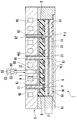
도 1은 본 실시형태의 정전 척 장치를 나타내는 단면도이다.
도 2는 슬러리 pH와 입자의 ζ전위와의 관계를 나타내는 그래프이다.
도 3은 본 실시형태의 복합 소결체의 제조 방법에 대하여 설명하는 설명도이다.
도 4는 본 실시형태의 복합 소결체의 제조 방법에 대하여 설명하는 설명도이다.
도 5는 본 실시형태의 복합 소결체의 제조 방법에 대하여 설명하는 설명도이다.
도 6은 본 실시형태의 복합 소결체의 제조 방법에 대하여 설명하는 설명도이다.
도 7은 본 실시형태의 복합 소결체의 제조 방법에 대하여 설명하는 설명도이다.
도 8은 본 실시형태의 복합 소결체의 제조 방법에 대하여 설명하는 설명도이다.
도 9는 실시예에서 체적 고유 저항값을 측정할 때의 소결체의 모습을 나타내는 모식도이다.1 is a cross-sectional view showing the electrostatic chuck device of the present embodiment.
2 is a graph showing the relationship between slurry pH and ζ potential of particles.
It is explanatory drawing explaining the manufacturing method of the composite sintered compact of this embodiment.
It is explanatory drawing explaining the manufacturing method of the composite sintered compact of this embodiment.
It is explanatory drawing explaining the manufacturing method of the composite sintered compact of this embodiment.
It is explanatory drawing explaining the manufacturing method of the composite sintered compact of this embodiment.
It is explanatory drawing explaining the manufacturing method of the composite sintered compact of this embodiment.
It is explanatory drawing explaining the manufacturing method of the composite sintered compact of this embodiment.
9 is a schematic view showing the state of the sintered compact when measuring the volume resistivity value in the Example.
이하, 도 1을 참조하면서, 본 실시형태에 관한 정전 척 장치에 대하여 설명한다. 이하의 모든 도면에 있어서는, 도면을 보기 쉽게 하기 위하여, 각 구성 요소의 치수나 비율 등은 적절히 다르게 하고 있다.EMBODIMENT OF THE INVENTION Hereinafter, the electrostatic chuck apparatus which concerns on this embodiment is demonstrated, referring FIG. In all the following drawings, in order to make drawing clear, a dimension, a ratio, etc. of each component are changed suitably.
[정전 척 장치][Electrostatic Chuck Device]
도 1은, 본 실시형태의 정전 척 장치를 나타내는 단면도이다. 본 실시형태의 정전 척 장치(1)는, 일 주면(상면) 측을 재치면으로 한 평면에서 보았을 때 원판상의 정전 척부(2)와, 이 정전 척부(2)의 하방에 마련되어 정전 척부(2)를 원하는 온도로 조정하는 두께가 있는 평면에서 보았을 때 원판상의 온도 조절용 베이스부(3)를 구비하고 있다. 또, 정전 척부(2)와 온도 조절용 베이스부(3)는, 정전 척부(2)와 온도 조절용 베이스부(3)의 사이에 마련된 접착제층(8)을 통하여 접착되어 있다.1 is a cross-sectional view showing the electrostatic chuck device of the present embodiment. The
이하, 순서대로 설명한다.Hereinafter, it demonstrates in order.
(정전 척부)(Electrostatic chuck)
정전 척부(2)는, 상면을 반도체 웨이퍼 등의 판상 시료(W)를 재치하는 재치면(11a)으로 한 재치판(11)과, 이 재치판(11)과 일체화되고 상기 재치판(11)의 바닥부 측을 지지하는 지지판(12)과, 이들 재치판(11)과 지지판(12)의 사이에 마련된 정전 흡착용 전극(13) 및 정전 흡착용 전극(13)의 주위를 절연하는 절연재층(14)을 갖고 있다. 재치판(11) 및 지지판(12)은, 본 발명에 있어서의 "기체"에 해당한다.The
재치판(11) 및 지지판(12)은, 중합한 면의 형상을 동일하게 하는 원판상의 부재이다. 재치판(11) 및 지지판(12)은, 기계적인 강도를 갖고, 또한 부식성 가스 및 그 플라즈마에 대한 내구성을 갖는 세라믹스 소결체로 이루어진다. 재치판(11) 및 지지판(12)의 형성 재료에 대하여, 자세하게는 후술한다.The
재치판(11)의 재치면(11a)에는, 직경이 판상 시료의 두께보다 작은 돌기부(11b)가 복수 소정의 간격으로 형성되고, 이들 돌기부(11b)가 판상 시료(W)를 지지한다.On the mounting
재치판(11), 지지판(12), 정전 흡착용 전극(13) 및 절연재층(14)을 포함시킨 전체의 두께, 즉, 정전 척부(2)의 두께는, 일례로서 0.7mm 이상 5.0mm 이하이다.The total thickness including the mounting
예를 들면, 정전 척부(2)의 두께가 0.7mm를 하회하면, 정전 척부(2)의 기계적 강도를 확보하는 것이 어려워진다. 정전 척부(2)의 두께가 5.0mm를 상회하면, 정전 척부(2)의 열용량이 커져, 재치되는 판상 시료(W)의 열응답성이 열화되고, 정전 척부의 횡방향의 열전달의 증가에 의하여, 판상 시료(W)의 면내 온도를 원하는 온도 패턴으로 유지하는 것이 어려워진다. 여기에서 설명한 각부의 두께는 일례이며, 상기 범위에 한정하는 것은 아니다.For example, when the thickness of the
정전 흡착용 전극(13)은, 전하를 발생시켜 정전 흡착력으로 판상 시료(W)를 고정하기 위한 정전 척용 전극으로서 이용되는 것이며, 그 용도에 따라, 그 형상이나, 크기가 적절히 조정된다.The
정전 흡착용 전극(13)은, 산화 알루미늄-탄화 탄탈럼(Al2O3-Ta4C5) 도전성 복합 소결체, 산화 알루미늄-텅스텐(Al2O3-W) 도전성 복합 소결체, 산화 알루미늄-탄화 규소(Al2O3-SiC) 도전성 복합 소결체, 질화 알루미늄-텅스텐(AlN-W) 도전성 복합 소결체, 질화 알루미늄-탄탈럼(AlN-Ta) 도전성 복합 소결체, 산화 이트륨-몰리브데넘(Y2O3-Mo) 도전성 복합 소결체 등의 도전성 세라믹스, 혹은 텅스텐(W), 탄탈럼(Ta), 몰리브데넘(Mo) 등의 고융점 금속에 의하여 형성되는 것이 바람직하다.The
정전 흡착용 전극(13)의 두께는, 특별히 한정되는 것은 아니지만, 예를 들면 0.1μm 이상 또한 100μm 이하의 두께를 선택할 수 있고, 5μm 이상 또한 20μm 이하의 두께가 보다 바람직하다.Although the thickness of the
정전 흡착용 전극(13)의 두께가 상기 하한값을 하회하면, 충분한 도전성을 확보하는 것이 어려워진다. 정전 흡착용 전극(13)의 두께가 상기 상한값을 초과하면, 정전 흡착용 전극(13)과 재치판(11) 및 지지판(12)과의 사이의 열팽창률차에 기인하여, 정전 흡착용 전극(13)과 재치판(11) 및 지지판(12)과의 접합 계면에 크랙이 들어가기 쉬워진다.When the thickness of the
이와 같은 두께의 정전 흡착용 전극(13)은, 스퍼터법이나 증착법 등의 성막법, 혹은 스크린 인쇄법 등의 도공법에 의하여 용이하게 형성할 수 있다.The
절연재층(14)은, 정전 흡착용 전극(13)의 주위를 둘러싸 부식성 가스 및 그 플라즈마로부터 정전 흡착용 전극(13)을 보호함과 함께, 재치판(11)과 지지판(12)과의 경계부, 즉 정전 흡착용 전극(13) 이외의 외주부 영역을 접합 일체화한다. 절연재층(14)은, 재치판(11) 및 지지판(12)을 구성하는 재료와 동일 조성 또는 주성분이 동일한 절연 재료에 의하여 구성되어 있다.The insulating
(온도 조정용 베이스부)(Base part for temperature adjustment)
온도 조절용 베이스부(3)는, 정전 척부(2)를 원하는 온도로 조정하고, 두께가 있는 원판상이다. 이 온도 조절용 베이스부(3)로서는, 예를 들면 그 내부에 냉매를 순환시키는 유로(3A)가 형성된 액랭 베이스 등이 적합하다.The
이 온도 조절용 베이스부(3)를 구성하는 재료로서는, 열전도성, 도전성, 가공성이 우수한 금속, 또는 이들 금속을 포함하는 복합재이면 특별히 제한은 없다. 예를 들면, 알루미늄(Al), 알루미늄 합금, 구리(Cu), 구리 합금, 스테인리스강(SUS) 등이 적합하게 이용된다. 이 온도 조절용 베이스부(3)의 적어도 플라즈마에 노출되는 면은, 알루마이트 처리가 실시되어 있거나, 혹은 알루미나 등의 절연막이 성막되어 있는 것이 바람직하다.There is no restriction | limiting in particular as a material which comprises this temperature
온도 조절용 베이스부(3)의 상면 측에는, 접착층(6)을 통하여 절연판(7)이 접착되어 있다. 접착층(6)은 폴리이미드 수지, 실리콘 수지, 에폭시 수지 등의 내열성, 및 절연성을 갖는 시트상 또는 필름상의 접착성 수지로 이루어진다. 접착층은 예를 들면 두께 5~100μm 정도로 형성된다. 절연판(7)은 폴리이미드 수지, 에폭시 수지, 아크릴 수지 등의 내열성을 갖는 수지의 박판, 시트 혹은 필름으로 이루어진다.The insulating
절연판(7)은, 수지 시트 대신에, 절연성의 세라믹판이어도 되고, 또 알루미나 등의 절연성을 갖는 용사막(溶射膜)이어도 된다.Instead of the resin sheet, the insulating
(포커스 링)(Focus ring)
포커스 링(10)은, 온도 조절용 베이스부(3)의 주연부에 재치되는 평면에서 보았을 때 원환상의 부재이다. 포커스 링(10)은, 예를 들면 재치면에 재치되는 웨이퍼와 동등한 전기 전도성을 갖는 재료를 형성 재료로 하고 있다. 이와 같은 포커스 링(10)을 배치함으로써, 웨이퍼의 주연부에 있어서는, 플라즈마에 대한 전기적인 환경을 웨이퍼와 대략 일치시킬 수 있고, 웨이퍼의 중앙부와 주연부에서 플라즈마 처리의 차나 편향을 발생하기 어렵게 할 수 있다.The
(그 외의 부재)(Other absence)
정전 흡착용 전극(13)에는, 정전 흡착용 전극(13)에 직류 전압을 인가하기 위한 급전용 단자(15)가 접속되어 있다. 급전용 단자(15)는, 온도 조절용 베이스부(3), 접착제층(8), 지지판(12)을 두께 방향으로 관통하는 관통 구멍(16)의 내부에 삽입되어 있다. 급전용 단자(15)의 외주 측에는, 절연성을 갖는 애자(15a)가 마련되고, 이 애자(15a)에 의하여 금속제의 온도 조절용 베이스부(3)에 대하여 급전용 단자(15)가 절연되어 있다.The
도면에서는, 급전용 단자(15)를 일체의 부재로서 나타내고 있지만, 복수의 부재가 전기적으로 접속하여 급전용 단자(15)를 구성하고 있어도 된다. 급전용 단자(15)는, 열팽창 계수가 서로 다른 온도 조절용 베이스부(3) 및 지지판(12)에 삽입되어 있기 때문에, 예를 들면 온도 조절용 베이스부(3) 및 지지판(12)에 삽입되어 있는 부분에 대하여, 각각 다른 재료로 구성하는 것으로 하면 된다.In the drawing, the
급전용 단자(15) 중, 정전 흡착용 전극(13)에 접속되고, 지지판(12)에 삽입되어 있는 부분(취출 전극)의 재료로서는, 내열성이 우수한 도전성 재료이면 특별히 제한되는 것은 아니지만, 열팽창 계수가 정전 흡착용 전극(13) 및 지지판(12)의 열팽창 계수에 근사한 것이 바람직하다. 예를 들면, Al2O3-TaC 등의 도전성 세라믹 재료로 이루어진다.The material of the portion (takeout electrode) connected to the
급전용 단자(15) 중, 온도 조절용 베이스부(3)에 삽입되어 있는 부분은, 예를 들면 텅스텐(W), 탄탈럼(Ta), 몰리브데넘(Mo), 나이오븀(Nb), 코바르 합금 등의 금속 재료로 이루어진다.The part inserted into the temperature
이들 2개의 부재는, 유연성과 내전성을 갖는 실리콘계의 도전성 접착제로 접속하면 된다.What is necessary is just to connect these two members with the silicone type electrically conductive adhesive which has flexibility and electric resistance.
정전 척부(2)의 하면 측에는, 히터 엘리먼트(5)가 마련되어 있다. 히터 엘리먼트(5)는, 일례로서 두께가 0.2mm 이하, 바람직하게는 0.1mm 정도의 일정한 두께를 갖는 비자성 금속 박판, 예를 들면 타이타늄(Ti) 박판, 텅스텐(W) 박판, 몰리브데넘(Mo) 박판 등을 포토리소그래피법이나 레이저 가공에 의하여 원하는 히터 형상, 예를 들면 띠상의 도전 박판을 사행시킨 형상의 전체 윤곽을 원환상으로 가공함으로써 얻어진다.The
이와 같은 히터 엘리먼트(5)는, 정전 척부(2)에 비자성 금속 박판을 접착한 후에, 정전 척부(2)의 표면에서 가공 성형함으로써 마련해도 되고, 정전 척부(2)와는 다른 위치에서 히터 엘리먼트(5)를 가공 성형한 것을, 정전 척부(2)의 표면에 전사 인쇄함으로써 마련해도 된다.Such a
히터 엘리먼트(5)는, 두께가 균일한 내열성 및 절연성을 갖는 시트상 또는 필름상의 실리콘 수지 또는 아크릴 수지로 이루어지는 접착층(4)에 의하여 지지판(12)의 바닥면에 접착·고정되어 있다.The
히터 엘리먼트(5)에는, 히터 엘리먼트(5)에 급전하기 위한 급전용 단자(17)가 접속되어 있다. 급전용 단자(17)를 구성하는 재료는 이전의 급전용 단자(15)를 구성하는 재료와 동등한 재료를 이용할 수 있다. 급전용 단자(17)는, 각각 온도 조절용 베이스부(3)에 형성된 관통 구멍(3b)을 관통하도록 마련되어 있다. 급전용 단자(17)의 외주 측에는, 절연성을 갖는 애자(18)가 마련되고, 이 애자(18)에 의하여 금속제의 온도 조절용 베이스부(3)에 대하여 급전용 단자(17)가 절연되어 있다.The
또, 히터 엘리먼트(5)의 하면 측에는 온도 센서(20)가 마련되어 있다. 본 실시형태의 정전 척 장치(1)에서는, 온도 조절용 베이스부(3)와 접착층(6)을 두께 방향으로 관통하도록 설치 구멍(21)이 형성되고, 이들 설치 구멍(21)의 최상부에 온도 센서(20)가 설치되어 있다. 온도 센서(20)는 가능한 한 히터 엘리먼트(5)에 가까운 위치에 설치하는 것이 바람직하기 때문에, 도면에 나타내는 구조로부터 접착제층(8) 측으로 더 돌출되도록 설치 구멍(21)을 연재하여 형성하고, 온도 센서(20)와 히터 엘리먼트(5)를 가깝게 하는 것으로 해도 된다.Moreover, the
온도 센서(20)는 일례로서 석영 유리 등으로 이루어지는 직육면체 형상의 투광체의 상면 측에 도시하지 않은 형광체층이 형성된 형광 발광형의 온도 센서이고, 이 온도 센서(20)가 투광성 및 내열성을 갖는 실리콘 수지계 접착제 등에 의하여 히터 엘리먼트(5)의 하면에 접착되어 있다.The
형광체층은, 히터 엘리먼트(5)로부터의 입열에 따라 형광을 발생하는 재료로 이루어진다. 형광체층의 형성 재료로서는, 발열에 따라 형광을 발생하는 재료이면 다종다양의 형광 재료를 선택할 수 있다. 형광체층의 형성 재료는, 일례로서 발광에 적절한 에너지 순위를 갖는 희토류 원소가 첨가된 형광 재료, AlGaAs 등의 반도체 재료, 산화 마그네슘 등의 금속 산화물, 루비나 사파이어 등의 광물을 들 수 있고, 이들 재료 중에서 적절히 선택하여 이용할 수 있다.The phosphor layer is made of a material that generates fluorescence in response to heat input from the
히터 엘리먼트(5)에 대응하는 온도 센서(20)는 각각 급전용 단자 등과 간섭하지 않는 위치로서 히터 엘리먼트(5)의 하면 둘레 방향의 임의의 위치에 각각 마련되어 있다.The
이들 온도 센서(20)의 형광으로부터 히터 엘리먼트(5)의 온도를 측정하는 온도 계측부(22)는, 일례로서 온도 조절용 베이스부(3)의 설치 구멍(21)의 외측(하측)에 상기 형광체층에 대하여 여기광을 조사하는 여기부(23)와, 형광체층으로부터 발해진 형광을 검출하는 형광 검출기(24)와, 여기부(23) 및 형광 검출기(24)를 제어함과 함께 상기 형광에 근거하여 주히터의 온도를 산출하는 제어부(25)로 구성되어 있다.The
또한, 정전 척 장치(1)는, 온도 조절용 베이스부(3)로부터 재치판(11)까지를 그들의 두께 방향으로 관통하도록 마련된 가스 구멍(28)을 갖고 있다. 가스 구멍(28)의 내주부에는 통상의 애자(29)가 마련되어 있다.In addition, the
이 가스 구멍(28)에는, 도시하지 않은 가스 공급 장치(냉각 수단)가 접속된다. 가스 공급 장치(27)로부터는, 가스 구멍(28)을 통하여 판상 시료(W)를 냉각하기 위한 냉각 가스(전열 가스)가 공급된다. 냉각 가스는, 가스 구멍을 통하여 재치판(11)의 상면에 있어서 복수의 돌기부(11b)의 사이에 형성되는 홈(19)에 공급되어, 판상 시료(W)를 냉각한다.The gas supply apparatus (cooling means) which is not shown in figure is connected to this
또한, 정전 척 장치(1)는, 온도 조절용 베이스부(3)로부터 재치판(11)까지를 그들의 두께 방향으로 관통하도록 마련된 도시하지 않은 핀 삽통 구멍을 갖고 있다. 핀 삽통 구멍은, 예를 들면 가스 구멍(28)과 동일한 구성을 채용할 수 있다. 핀 삽통 구멍에는, 판상 시료 이탈용 리프트 핀이 삽통된다.Moreover, the
정전 척 장치(1)는, 이상과 같은 구성으로 되어 있다.The
(복합 소결체)(Composite sintered body)
다음으로, 본 실시형태의 기체(재치판(11) 및 지지판(12))에 대하여, 상세하게 설명한다.Next, the base body (mounting
본 실시형태의 재치판(11) 및 지지판(12)은, 금속 산화물과 탄화 규소를 포함하는 세라믹스의 복합 소결체를 형성 재료로 하고 있다.The mounting
복합 소결체 중, 금속 산화물은 주상이다. 구체적으로는, 복합 소결체 전체에 있어서의 금속 산화물의 비율이, 92질량% 이상인 것이 바람직하고, 94질량%인 것이 보다 바람직하다.In the composite sintered body, the metal oxide is a main phase. It is preferable that it is 92 mass% or more specifically, and, as for the ratio of the metal oxide in the whole composite sintered compact, it is more preferable that it is 94 mass%.
복합 소결체 중, 탄화 규소는 부상이다. 구체적으로는, 복합 소결체 전체에 있어서의 탄화 규소의 비율이, 8질량% 이하인 것이 바람직하고, 6질량% 이하인 것이 보다 바람직하다.In the composite sintered body, silicon carbide is floating. It is preferable that it is 8 mass% or less specifically, and, as for the ratio of the silicon carbide in the whole composite sintered compact, it is more preferable that it is 6 mass% or less.
본 실시형태의 복합 소결체가 갖는 금속 산화물로서는, 산화 알루미늄, 산화 이트륨을 사용 가능하다.Aluminum oxide and yttrium oxide can be used as a metal oxide which the composite sintered compact of this embodiment has.
본 실시형태의 복합 소결체에 있어서, 금속 산화물의 평균 결정 입경은, 1.2μm 이상 10μm 이하인 것이 바람직하고, 1.3μm 이상 5μm 이하인 것이 보다 바람직하다.In the composite sintered body of the present embodiment, the average crystal grain size of the metal oxide is preferably 1.2 µm or more and 10 µm or less, and more preferably 1.3 µm or more and 5 µm or less.
복합 소결체에 있어서, 금속 산화물의 평균 결정 입경이 상기 하한값 이상이면, 금속 산화물의 입자 자체의 저항률이 너무 저하되는 일 없이, 충분한 절연 효과를 발현시킬 수 있다. 또, 금속 산화물의 평균 결정 입경이 상기 상한값 이하이면, 얻어지는 소결체의 기계적 강도가 충분히 높아져, 손상(치핑)이 발생하기 어려워진다.In the composite sintered compact, when the average crystal grain size of the metal oxide is equal to or more than the lower limit, a sufficient insulating effect can be expressed without excessively lowering the resistivity of the particles of the metal oxide itself. Moreover, when the average crystal grain size of a metal oxide is below the said upper limit, the mechanical strength of the sintered compact obtained will become high enough, and a damage (chipping) becomes difficult to produce.
복합 소결체에 있어서, 금속 산화물의 평균 결정 입경은, 소결 온도를 제어함으로써 조절 가능하다. 소결 온도가 높아지면, 금속 산화물의 평균 결정 입경이 커지는 경향이 있고, 소결 온도가 낮아지면, 금속 산화물의 평균 결정 입경이 작아지는 경향이 있다.In the composite sintered body, the average crystal grain size of the metal oxide can be adjusted by controlling the sintering temperature. When the sintering temperature is high, the average grain size of the metal oxide tends to be large, and when the sintering temperature is low, the average grain size of the metal oxide tends to be small.
또, 본 실시형태의 복합 소결체에 있어서, 탄화 규소의 결정립은, 금속 산화물의 결정립 내 및 금속 산화물의 결정립계에 분산되어 있다.Moreover, in the composite sintered compact of this embodiment, the crystal grain of silicon carbide is disperse | distributed in the crystal grain of a metal oxide, and the crystal grain boundary of a metal oxide.
또, 본 실시형태의 복합 소결체에 있어서, 금속 산화물의 결정립 내에 분산되어 있는 탄화 규소의 결정립의 비율은, 탄화 규소의 결정립 전체에 대하여 면적비로 25% 이상이다. 나머지의 탄화 규소의 결정립은, 금속 산화물의 결정립계에 존재하고 있다.Moreover, in the composite sintered compact of this embodiment, the ratio of the crystal grain of the silicon carbide dispersed in the crystal grain of a metal oxide is 25% or more by area ratio with respect to the whole crystal grain of silicon carbide. The remaining grains of silicon carbide exist in the grain boundaries of the metal oxides.
복합 소결체에 있어서, "탄화 규소의 결정립 전체"에 대한 "금속 산화물의 결정립 내에 분산되어 있는 탄화 규소의 결정립"의 비율이, 면적비로 25% 이상이면, 충분히 절연성을 향상시킬 수 있다. 절연성을 향상시키기 위해서는, 상기 비율은 클수록 바람직하고, 모든 탄화 규소의 결정립이 산화 알루미늄의 결정립 내에 분산되어 있는 상태가 특히 바람직하다.In the composite sintered body, insulation can be sufficiently improved if the ratio of "crystal grains of silicon carbide dispersed in crystal grains of metal oxide" to "the whole crystal grains of silicon carbide" is 25% or more in area ratio. In order to improve insulation, the said ratio is so preferable that it is large, and the state in which the crystal grains of all the silicon carbides are disperse | distributed in the crystal grains of aluminum oxide is especially preferable.
상기 비율이 25% 이상이면, 복합 소결체의 유전율이 높아진다. 또, 상기 비율이 25% 이상이면, 저주파에서의 유전 탄젠트가 작아진다.If the said ratio is 25% or more, the dielectric constant of a composite sintered compact will become high. Moreover, when the said ratio is 25% or more, the dielectric tangent in low frequency will become small.
본 발명에 있어서, 복합 소결체에 있어서의 "금속 산화물의 결정립 내에 분산되어 있는 탄화 규소의 결정립의 비율"은, 복합 소결체의 임의의 시야의 주사형 전자 현미경 사진으로부터 산출한다.In this invention, "the ratio of the crystal grain of the silicon carbide dispersed in the crystal grain of a metal oxide" in a composite sintered compact is computed from the scanning electron micrograph of the arbitrary visual field of a composite sintered compact.
즉, 무작위로 선택된 시야에서 확대 배율 10000배의 전자 현미경 사진을 촬영하여, 이 전자 현미경 사진에 찍힌 탄화 규소의 결정립의 총 면적을 "탄화 규소의 결정립 전체"의 면적으로 한다. 한편, 상기 전자 현미경 사진에 있어서 "금속 산화물의 결정립 내에 분산되어 있는 탄화 규소의 결정립"의 면적을 구한다. 이와 같이 하여 구해진 면적으로부터, "탄화 규소의 결정립 전체"에 대한 "금속 산화물의 결정립 내에 분산되어 있는 탄화 규소의 결정립"의 비율을 면적비로 구한다.That is, an electron microscope photograph with an enlarged magnification of 10,000 times is taken from a randomly selected field of view, and the total area of the grains of silicon carbide taken on this electron microscope photograph is made the area of "the whole grain of silicon carbide". On the other hand, the area of "crystal grain of silicon carbide dispersed in the crystal grain of a metal oxide" in the said electron micrograph is calculated | required. From the area thus obtained, the ratio of "crystal grains of silicon carbide dispersed in crystal grains of metal oxide" with respect to "the whole crystal grains of silicon carbide" is calculated | required as area ratio.
동일한 처리를 2개의 시야의 전자 현미경 사진에 있어서 행하여, 평균값을 "금속 산화물의 결정립 내에 분산되어 있는 탄화 규소의 결정립의 비율"을 나타내는 면적비로서 구한다.The same treatment is performed on the electron micrographs of the two fields of view, and the average value is obtained as the area ratio indicating the "ratio of crystal grains of silicon carbide dispersed in crystal grains of the metal oxide".
본 실시형태의 복합 소결체에 있어서, 탄화 규소의 결정립의 평균 결정 입경은, 0.03μm 이상 1μm 이하인 것이 바람직하고, 0.05μm 이상 0.25μm 이하인 것이 보다 바람직하다.In the composite sintered body of the present embodiment, the average grain size of the crystal grains of silicon carbide is preferably 0.03 µm or more and 1 µm or less, and more preferably 0.05 µm or more and 0.25 µm or less.
본 실시형태의 복합 소결체에 있어서, 금속 산화물의 결정립 내에 분산되어 있는 탄화 규소의 결정립의 평균 결정 입경은, 0.03μm 이상 0.7μm 이하인 것이 바람직하고, 0.05μm 이상 0.2μm 이하인 것이 보다 바람직하다.In the composite sintered body of the present embodiment, the average grain size of the crystal grains of silicon carbide dispersed in the crystal grains of the metal oxide is preferably 0.03 µm or more and 0.7 µm or less, and more preferably 0.05 µm or more and 0.2 µm or less.
본 실시형태의 복합 소결체에 있어서, 금속 산화물의 결정립계에 존재하고 있는 탄화 규소의 결정립의 평균 결정 입경은, 0.03μm 이상 1μm 이하인 것이 바람직하고, 0.05μm 이상 0.3μm 이하인 것이 보다 바람직하다.In the composite sintered body of the present embodiment, the average grain size of the crystal grains of silicon carbide existing in the grain boundaries of the metal oxide is preferably 0.03 µm or more and 1 µm or less, and more preferably 0.05 µm or more and 0.3 µm or less.
재치판(11) 및 지지판(12)의 형성 재료인 복합 소결체는, 상술과 동일한 구성인 것에 의하여, 높은 유전율과 높은 체적 고유 저항값, 즉, 높은 유전율과 낮은 유전 탄젠트를 양립할 수 있다.The composite sintered body which is the forming material of the mounting
즉, 본 실시형태의 복합 소결체를 구성하는 물질 중, 주상인 금속 산화물은 절연체이며, 부상인 탄화 규소는 도전체이다. 이로 인하여, 복합 소결체에 통전하고자 하면, 전자는, 도전체가 배치된 결정립계를 이동하기 쉽다.That is, among the materials constituting the composite sintered body of the present embodiment, the metal oxide as the main phase is an insulator, and the floating silicon carbide is a conductor. For this reason, if it is going to energize a composite sintered compact, an electron will move easily in the grain boundary in which the conductor was arrange | positioned.
이때, 종래 알려진 동일 조성의 복합 소결체에 있어서는, 금속 산화물의 결정립계에는, 탄화 규소의 결정립이 전체의 80% 이상 존재하고 있는 것이 알려져 있다.At this time, in the conventionally known composite sintered body having the same composition, it is known that 80% or more of the crystal grains of silicon carbide exist in the grain boundaries of the metal oxides.
이에 대하여, 본 실시형태의 복합 소결체에 있어서는, 금속 산화물의 결정립 내에 분산되어 있는 탄화 규소의 결정립의 비율은, 탄화 규소의 결정립 전체에 대하여 면적비로 25% 이상이다.On the other hand, in the composite sintered compact of this embodiment, the ratio of the crystal grains of the silicon carbide dispersed in the crystal grains of a metal oxide is 25% or more by area ratio with respect to the whole crystal grain of silicon carbide.
즉, 금속 산화물의 결정립계에는, 탄화 규소의 결정립이 전체의 75% 이하 존재하고 있다.That is, 75% or less of the crystal grains of silicon carbide exist in the crystal grain boundary of a metal oxide.
이로 인하여, 본 실시형태의 복합 소결체는, 전자가 이동하기 쉬운 결정립계에 존재하는 도전체(탄화 규소)의 양이 종래의 복합 소결체와 비교하여 적기 때문에, 전자가 이동하기 어렵고, 체적 고유 저항값이 높아진다고 생각된다.For this reason, in the composite sintered body of the present embodiment, since the amount of the conductor (silicon carbide) present in the grain boundary where electrons are easily moved is smaller than that of the conventional composite sintered body, the electrons are difficult to move, and the volume resistivity value is high. I think it is high.
또, 본 실시형태의 복합 소결체에서는, 금속 산화물의 결정립 내에 분산되는 탄화 규소의 양이 25% 이상으로 종래의 것보다 많다. 이와 같이 금속 산화물의 결정립 내에 분산되는 탄화 규소의 비율이 증가하면, 결정립 내에 있어서 도전체인 탄화 규소 입자 간의 거리가 짧아져, 전기 용량이 증가한다. 이로 인하여, 본 실시형태와 같은 복합 소결체에서는, 유전율이 높아지는 경향이 있다.Moreover, in the composite sintered compact of this embodiment, the quantity of the silicon carbide disperse | distributed in the crystal grain of a metal oxide is 25% or more, compared with the conventional one. As described above, when the proportion of silicon carbide dispersed in the crystal grains of the metal oxide increases, the distance between the silicon carbide particles which are the conductors in the crystal grains becomes short, and the electric capacity increases. For this reason, in the composite sintered body like this embodiment, there exists a tendency for dielectric constant to become high.
금속 산화물의 결정립 내에 분산되어 있는 탄화 규소의 결정립의 비율은, 탄화 규소의 결정립 전체에 대하여 면적비로 30% 이상인 것이 바람직하고, 40% 이상인 것이 보다 바람직하다.It is preferable that it is 30% or more by area ratio with respect to the whole crystal grain of silicon carbide, and, as for the ratio of the crystal grain of the silicon carbide dispersed in the crystal grain of a metal oxide, it is more preferable that it is 40% or more.
탄화 규소에는, 결정 구조가 다수 존재하는 것이 알려져 있으며, 입방정계로 3C형(섬아연광형(閃亞鉛鑛型))의 결정 구조를 갖는 것, 4H형, 6H형 등의 육방정계로 우르차이트(wurtzite)형의 결정 구조를 갖는 것, 능면체정계로 15R형의 결정 구조를 갖는 것을 들 수 있다. 이 중, 3C형의 결정 구조를 갖는 것을 "β-SiC"라고 칭한다. 또, 그 이외의 결정 구조를 갖는 것 모두를 "α-SiC"라고 칭한다.It is known that a large number of crystal structures exist in silicon carbide, and have a cubic crystal structure of 3C type (zinc-zinc type), and urethane in hexagonal systems such as 4H type and 6H type. and one having a (wurtzite) crystal structure, and one having a 15R type crystal structure in the rhombohedral system. Among these, those having a 3C type crystal structure are referred to as "β-SiC". In addition, all having a crystal structure other than that is called "(alpha) -SiC".
본 실시형태의 재치판(11) 및 지지판(12)은, 복합 소결체에 포함되는 SiC가 β-SiC인 것이 바람직하다. 또, 소결체에 있어서는, β-SiC의 결정립이, 매트릭스 재료인 금속 산화물의 결정립에 둘러싸이는 상태로 분산되어 존재하고 있는 것이 바람직하다. β-SiC의 체적 비율은, 복합 소결체 전체의 4체적% 이상 15체적% 이하가 바람직하고, 6체적% 이상 10체적% 이하가 보다 바람직하다.As for the mounting
β-SiC의 체적 비율이 상기 하한값보다 적으면, SiC 입자에 의한 전자 도전성의 발현 효과가 적다. 또, β-SiC의 체적 비율이 상기 상한값보다 많으면, SiC 입자끼리의 접촉을 발생시켜 SiC 입자를 통한 저항값 저하를 발생시킬 우려가 있다.When the volume ratio of β-SiC is less than the lower limit, the expression effect of electronic conductivity by SiC particles is small. Moreover, when the volume ratio of (beta) -SiC is more than the said upper limit, there exists a possibility that a contact of SiC particles may generate | occur | produce and the resistance value fall through SiC particle | grains.
또, 본 실시형태의 복합 소결체에 있어서는, 알루미늄 및 규소 이외의 금속 불순물 함유량이 100ppm 이하인 것이 바람직하다. 금속 불순물 함유량은, 50ppm 이하인 것이 바람직하고, 25ppm 이하인 것이 보다 바람직하다.Moreover, in the composite sintered compact of this embodiment, it is preferable that metal impurity content other than aluminum and silicon is 100 ppm or less. It is preferable that it is 50 ppm or less, and, as for metal impurity content, it is more preferable that it is 25 ppm or less.
[복합 소결체의 제조 방법][Manufacturing Method of Composite Sintered Body]
본 실시형태에 관한 복합 소결체의 제조 방법은,The manufacturing method of the composite sintered compact which concerns on this embodiment is
(a) 금속 산화물 입자와 탄화 규소 입자를, 각각 고속으로 분사하여 서로 충돌시키면서 혼합하는 공정과,(a) a step of injecting metal oxide particles and silicon carbide particles at high speed and mixing them while colliding with each other,
(b) 혼합하는 공정에서 얻어진 슬러리에 대하여, 슬러리 중의 금속 산화물 입자의 표면 전하가 정이 되고, 슬러리 중의 상기 탄화 규소 입자의 표면 전하가 부가 되는 범위로, 슬러리의 pH를 조정하는 공정과,(b) adjusting the pH of the slurry in a range in which the surface charge of the metal oxide particles in the slurry is positive and the surface charge of the silicon carbide particles in the slurry is added to the slurry obtained in the mixing step;
(c) pH를 조정한 상기 슬러리로부터 분산매를 제거한 후, 성형하는 공정과,(c) removing the dispersion medium from the slurry whose pH is adjusted and then molding;
(d) 얻어지는 성형체를, 비산화성 분위기하, 25MPa 이상의 압력으로 가압하여 고화시키면서 1600℃ 이상으로 가열하여 가압 소결하는 공정을 갖는다.(d) It has the process of heating and pressure-sintering the obtained molded object at 1600 degreeC or more, pressing and solidifying by pressure of 25 Mpa or more in non-oxidizing atmosphere.
본 실시형태에 있어서는, 금속 산화물로서 산화 알루미늄을 이용한 경우에 대하여 이하 설명한다.In this embodiment, the case where aluminum oxide is used as a metal oxide is demonstrated below.
본 실시형태에 관한 복합 소결체의 제조 방법에서는, 이용하는 산화 알루미늄 입자는, 산화 알루미늄의 함유량이 99.99% 이상인 것이 바람직하고, 99.9999 이상인 것이 보다 바람직하다. 이와 같은 고순도의 산화 알루미늄 입자는, 명반법을 이용함으로써 조정 가능하다. 명반법을 이용하여 조정한 산화 알루미늄 입자는, 예를 들면 바이어법을 이용하여 조정한 산화 알루미늄 입자와 비교하면, 금속 불순물인 나트륨 원자의 함유량을 큰폭으로 저감시키는 것이 가능하다. 또, 원하는 순도의 산화 알루미늄 입자가 얻어진다면, 다양한 방법을 채용 가능하다.In the manufacturing method of the composite sintered compact which concerns on this embodiment, it is preferable that content of aluminum oxide is 99.99% or more, and, as for the aluminum oxide particle to be used, it is more preferable that it is 99.9999 or more. Such high purity aluminum oxide particles can be adjusted by using the alum method. As compared with the aluminum oxide particle adjusted using the via method, for example, the aluminum oxide particle adjusted using the alum method can significantly reduce content of the sodium atom which is a metal impurity. Moreover, if the aluminum oxide particle of desired purity is obtained, various methods can be employ | adopted.
((a) 혼합하는 공정)((a) mixing step)
혼합하는 공정에 있어서는, 2류 입자 충돌형의 분쇄 혼합 장치를 이용하여, 분산매에 분산시킨 산화 알루미늄 입자와 탄화 규소 입자를 각각 가압함으로써 고속으로 분사하여 서로 충돌시키면서 혼합한다. 이로써, 산화 알루미늄 입자와 탄화 규소 입자가 분쇄되어, 이들 분쇄 입자를 포함하는 분산액(슬러리)이 얻어진다.In the step of mixing, the aluminum oxide particles and silicon carbide particles dispersed in the dispersion medium are pressurized at high speed by using a secondary particle collision type pulverizing mixing apparatus, and mixed while being collided with each other. Thereby, aluminum oxide particle and silicon carbide particle are grind | pulverized, and the dispersion liquid (slurry) containing these grind | pulverized particle is obtained.
산화 알루미늄 입자와 탄화 규소 입자를 충돌시킬 때, 큰 입자는, 충돌 시의 운동 에너지가 커서, 분쇄되기 쉽다. 한편, 작은 입자는, 충돌 시의 운동 에너지가 작아, 분쇄되기 어렵다. 이로 인하여, 상기 분쇄 혼합 장치를 이용하여 얻어지는 산화 알루미늄 입자와 탄화 규소 입자는, 조대(粗大) 입자나 과분쇄의 입자가 적은, 입도 분포폭이 좁은 입자가 된다. 따라서, 2류 입자 충돌형의 분쇄 혼합 장치를 이용하여 분쇄 혼합한 혼합 입자를 이용하면, 소결 공정에 있어서, 조대 입자를 핵으로 하는 이상 입성장(粒成長)을 억제할 수 있다.When colliding the aluminum oxide particles with the silicon carbide particles, the large particles have a large kinetic energy at the time of collision and are easily crushed. On the other hand, small particles have a small kinetic energy at the time of collision and are difficult to be crushed. For this reason, the aluminum oxide particle and silicon carbide particle obtained using the said grinding | mixing mixing apparatus become a particle | grains of narrow particle size distribution width with few coarse particle | grains and the particle | grains of hyperpulverization. Therefore, when the mixed particle pulverized and mixed using the secondary particle collision type grinding | pulverization mixing apparatus is used, abnormal grain growth which makes a coarse particle into a nucleus in a sintering process can be suppressed.
또, 이와 같은 분쇄 혼합 장치를 이용하여 분쇄 혼합하는 경우, 예를 들면 볼 밀이나 비즈 밀 등의 미디어를 이용하여 분쇄 혼합하는 방법과 비교하면, 각 미디어의 파손에 기인한 불순물의 혼입을 억제하는 것이 가능하다.In addition, when pulverizing and mixing using such a pulverizing mixing apparatus, compared with the method of pulverizing and mixing using a medium such as a ball mill or a bead mill, for example, it is possible to suppress mixing of impurities due to breakage of each medium. It is possible.
본 실시형태에 관한 복합 소결체의 제조 방법에서는, 이용하는 탄화 규소 입자에 대하여, 산화성 분위기하(예를 들면, 대기 분위기하)에서 가열 처리를 실시하고, 미리 탄화 규소 입자의 표면을 산화 처리하는 공정을 가지면 된다. 이하, 상기 산화 처리를 "프리(pre) 산화"라고 칭한다. 프리 산화는, 예를 들면 500℃에서 12시간 가열함으로써 행한다.In the manufacturing method of the composite sintered compact which concerns on this embodiment, the process of heat-processing in the oxidative atmosphere (for example, air | atmosphere atmosphere) with respect to the silicon carbide particle to be used, and previously oxidizing the surface of silicon carbide particle is carried out. You just have to. Hereinafter, the oxidation treatment is referred to as "pre oxidation". Free oxidation is performed by heating at 500 degreeC for 12 hours, for example.
탄화 규소 입자를 프리 산화 처리함으로써, 탄화 규소 입자의 친수성이 높아진다. 이로써, 슬러리 중에서의 탄화 규소 입자의 분산성이 향상된다.By preoxidizing the silicon carbide particles, the hydrophilicity of the silicon carbide particles is increased. This improves the dispersibility of the silicon carbide particles in the slurry.
((b) pH를 조정하는 공정)((b) adjusting the pH)
pH를 조정하는 공정에 있어서는, 슬러리 중의 산화 알루미늄 입자와 탄화 규소 입자와의 표면 전하를 고려하여 pH 조정을 행한다. 상기 혼합하는 공정에서 얻어지는 슬러리(pH 조정 전의 슬러리)는, 통상, pH11 정도의 염기성을 나타낸다.In the process of adjusting pH, pH adjustment is performed considering the surface charge of the aluminum oxide particle and silicon carbide particle in a slurry. The slurry (slurry before pH adjustment) obtained at the said mixing process usually shows basicity about pH11.
도 2는, 슬러리 중의 산화 알루미늄 입자와 탄화 규소 입자에 대하여, 슬러리 pH와 입자의 ζ전위와의 관계를 나타내는 그래프이다. 도면 중, 가로축은 슬러리의 pH를 나타내고, 세로축은, 각 입자의 ζ전위(단위: mV)를 나타낸다.2 is a graph showing the relationship between the slurry pH and the ζ potential of the particles for the aluminum oxide particles and the silicon carbide particles in the slurry. In the figure, the horizontal axis represents the pH of the slurry, and the vertical axis represents the ζ potential (unit: mV) of each particle.
도면에 나타내는 바와 같이, 계의 pH가 산성 측(pH<7)인 경우, 산화 알루미늄 입자와 같은 금속 산화물 입자는, ζ전위가 정이 된다. 이것은, 계의 pH가 산성 측인 경우, 금속 산화물 입자의 표면의 수산기가 프로톤(H+)화되어 표면이 정전하를 띠는 것에 의한다.As shown in the figure, when the pH of the system is the acidic side (pH <7), the zeta potential is positive for metal oxide particles such as aluminum oxide particles. This is because when the pH of the system is on the acidic side, the hydroxyl groups on the surface of the metal oxide particles are protonated (H + ) and the surface is electrostatically charged.
한편, 계의 pH가 염기성 측(pH>7)인 경우, 산화 알루미늄 입자와 같은 금속 산화물 입자는, ζ전위가 부가 된다. 이것은, 계의 pH가 염기성 측인 경우, 금속 산화물 입자의 표면의 수산기로부터 프로톤이 해리하여, 표면이 부전하를 띠는 것에 의한다.On the other hand, when the pH of the system is the basic side (pH> 7), the zeta potential is added to metal oxide particles such as aluminum oxide particles. This is because when the pH of the system is the basic side, protons dissociate from the hydroxyl groups on the surface of the metal oxide particles, and the surface is negatively charged.
이에 대하여, 탄화 규소 입자의 ζ전위의 거동은 다르다. 도면에 나타내는 바와 같이 탄화 규소 입자는, pH2~3 부근에서 ζ전위가 0이 되고, pH3 부근의 산성 영역으로부터, 염기성 영역까지의 넓은 범위에서 ζ전위가 부가 된다.In contrast, the behavior of ζ potential of silicon carbide particles is different. As shown in the figure, the zeta potential becomes zero at the
이와 같은 관계가 있는 2개의 입자가 동일한 슬러리에 공존하고 있는 경우, 계의 pH가 "슬러리 중의 산화 알루미늄 입자의 표면 전하가 정"이 되고, "슬러리 중의 탄화 규소 입자의 표면 전하가 부"가 되는 범위에서는, 양 입자가 응집하는, 이른바 헤테로 응집이 발생한다.When two particles having such a relationship coexist in the same slurry, the pH of the system becomes "the surface charge of the aluminum oxide particles in the slurry is positive", and the "surface charge of the silicon carbide particles in the slurry becomes negative". In the range, so-called hetero agglomeration occurs in which both particles aggregate.
이때, 산화 알루미늄 입자와 탄화 규소 입자가 침전하지 않도록, 슬러리 중에는, 적절히 분산제를 첨가해 두면 된다.At this time, what is necessary is just to add a dispersing agent in a slurry suitably so that an aluminum oxide particle and a silicon carbide particle may not precipitate.
계의 pH는, 3 이상 7 이하가 바람직하고, 5 이상 7 이하가 보다 바람직하며, 6 이상 7 이하가 더 바람직하다. pH 조정 후의 양 입자의 ζ전위끼리를 비교한 경우, ζ전위의 절댓값이 가까울수록 헤테로 응집하기 쉬워, 원하는 응집 상태가 된다.3 or more and 7 or less are preferable, as for pH of a system, 5 or more and 7 or less are more preferable, and 6 or more and 7 or less are more preferable. When the ζ potentials of both particles after pH adjustment are compared, the closer the absolute value of the ζ potential is, the easier it is to agglomerate hetero, resulting in a desired aggregation state.
pH의 조정은, 슬러리에 산을 첨가함으로써 행한다. 사용 가능한 산으로서는, 질산, 인산, 염산, 황산 등의 무기산, 아세트산 등의 유기산을 들 수 있다. 이 중, 염산, 황산 등은, 후술하는 소결하는 공정에 있어서 장치 내에서 염소나 황을 발생시켜, 장치 열화의 원인이 될 수 있다. 이로 인하여, pH의 조정에는, 질산, 인산, 유기산 등을 이용하는 것이 바람직하다.The pH is adjusted by adding an acid to the slurry. Examples of the acid that can be used include inorganic acids such as nitric acid, phosphoric acid, hydrochloric acid, and sulfuric acid, and organic acids such as acetic acid. Among these, hydrochloric acid, sulfuric acid, etc. may generate chlorine or sulfur in an apparatus in the sintering process mentioned later, and may cause a deterioration of an apparatus. For this reason, it is preferable to use nitric acid, phosphoric acid, an organic acid, etc. for adjustment of pH.
((c) 성형하는 공정)((c) molding step)
성형하는 공정에 있어서는, 먼저, pH 조정 후의 분산액을 스프레이 드라이함으로써, 산화 알루미늄 입자와 탄화 규소 입자와의 혼합 입자로 이루어지는 과립을 얻는다.In the process of shaping | molding, the granule which consists of mixed particles of an aluminum oxide particle and a silicon carbide particle is obtained by spray-drying the dispersion liquid after pH adjustment first.
이어서, 목적으로 하는 소결체의 형상에 따라, 얻어진 과립을 1축 성형(1축 프레스 성형)한다.Next, the obtained granules are uniaxially molded (uniaxial press-molded) according to the shape of the target sintered compact.
이어서, 얻어진 성형체를 불활성 가스 분위기하, 상압으로(프레스하지 않고) 예를 들면 500℃로 가열하여, 성형체에 포함되는 수분이나 분산매 등의 협잡물을 제거한다. 불활성 가스로서는, 질소 또는 아르곤을 이용할 수 있다. 이 조작에 있어서는, 성형체를 변성하지 않고 성형체로부터 협잡물을 제거할 수 있다면, 가열 온도는 500℃에 한정되지 않는다.Subsequently, the obtained molded object is heated to normal pressure (without press), for example, at 500 degreeC under an inert gas atmosphere, and removes contaminants, such as water and a dispersion medium contained in a molded object. Nitrogen or argon can be used as an inert gas. In this operation, the heating temperature is not limited to 500 ° C as long as the contaminants can be removed from the molded body without modifying the molded body.
또한, 협잡물을 제거한 성형체를, 대기중, 예를 들면 400℃로 가열하여 성형체를 구성하는 혼합 입자를, 산화 처리하는 산화 공정을 갖는 것이 바람직하다. 이와 같은 조작에 의하면, 산화 처리에 있어서 혼합 입자에 포함되는 탄화 규소 입자의 표면에는 산화막이 형성된다. 산화막에는, 혼합 입자에 포함되는 금속 불순물이 용출되기 쉽기 때문에, 혼합 입자에 포함되는 금속 불순물이 입자 표면에 치우쳐 존재하게 된다. 그러면, 후술하는 가압 소결하는 공정에 있어서, 금속 불순물을 제거하기 쉽기 때문에 바람직하다.Moreover, it is preferable to have the oxidation process which heat-processes the molded object which removed the contaminant in air | atmosphere, for example at 400 degreeC, and oxidizes the mixed particle which comprises a molded object. According to such an operation, an oxide film is formed on the surface of the silicon carbide particles contained in the mixed particles in the oxidation treatment. Since the metal impurities contained in the mixed particles are easily eluted in the oxide film, the metal impurities contained in the mixed particles are present on the particle surface. Then, in the process of pressure sintering mentioned later, since metal impurities are easy to remove, it is preferable.
((d) 가압 소결하는 공정)((d) process of pressure sintering)
가압 소성하는 공정에 있어서는, 먼저, 상술의 성형체를, 진공 분위기(제1 비산화성 분위기)에 있어서, 1600℃보다 낮은 온도 또한 상압으로(프레스하지 않고) 가열(예비 가열)한다. 이와 같은 조작에 의하면, 예비 가열 시의 온도를 적절히 설정함으로써, 혼합 입자에 포함되는 알칼리 금속 등의 금속 불순물이 증발하여, 금속 불순물을 용이하게 제거할 수 있다. 이로 인하여, 이와 같은 조작에 의하면, 혼합 입자의 순도를 향상시키기 쉬워져, 기체의 체적 저항값을 제어하기 쉬워진다.In the process of pressure baking, the above-mentioned molded object is first heated (preheated) in the vacuum atmosphere (1st non-oxidizing atmosphere) and the temperature lower than 1600 degreeC also to normal pressure (without press). According to such an operation, by appropriately setting the temperature at the time of preheating, metal impurities, such as alkali metal contained in a mixed particle, evaporate and metal impurities can be removed easily. For this reason, according to such an operation, it becomes easy to improve the purity of a mixed particle, and to control the volume resistance value of a gas easily.
또, 성형하는 공정에 있어서, 상술한 바와 같이 협잡물을 제거한 성형체에 대하여 산화 처리를 실시하면, 진공 분위기하에서 예비 가열함으로써, 입자 표면에 형성된 산화막이 휘발한다. 동시에, 산화막에 포함되는 금속 불순물이 증발한다. 이로 인하여, 성형체로부터 금속 불순물을 용이하게 제거할 수 있다. 따라서, 이와 같은 조작에 의하면, 혼합 입자의 순도를 향상시키기 쉬워져, 기체의 체적 저항값을 제어하기 쉬워진다.Moreover, in the process of shaping | molding, when an oxidation process is performed with respect to the molded object which removed the contaminant as mentioned above, the oxide film formed on the surface of a particle volatilizes by preheating in a vacuum atmosphere. At the same time, metallic impurities contained in the oxide film evaporate. For this reason, metal impurities can be easily removed from a molded object. Therefore, according to such operation, it becomes easy to improve the purity of a mixed particle, and to control the volume resistance value of a gas easily.
본 실시형태에 있어서 "진공"이란, "대기압보다 낮은 압력의 기체로 채워진 공간 내의 상태"이며, JIS 규격에 있어서 공업적으로 이용할 수 있는 압력으로서 정의된 상태를 가리킨다. 본 실시형태에 있어서는, 진공 분위기는, 저진공(100Pa 이상)이어도 되지만, 중진공(0.1Pa~100Pa)이면 바람직하고, 고진공(10-5Pa~0.1Pa)이면 보다 바람직하다.In this embodiment, "vacuum" means "state in the space filled with gas of pressure lower than atmospheric pressure", and refers to the state defined as industrially available pressure in JIS standard. In the present embodiment, the vacuum atmosphere may be low vacuum (100 Pa or more), but is preferably medium vacuum (0.1 Pa to 100 Pa), more preferably high vacuum (10 to 5 Pa to 0.1 Pa).
본 실시형태의 복합 소결체의 제조 방법에 있어서는, 예를 들면 진공 분위기하, 1200℃에서 4시간 이상 예비 가열한 후, 대기압까지 아르곤으로 기압을 되돌린다.In the manufacturing method of the composite sintered compact of this embodiment, after preheating at 1200 degreeC for 4 hours or more, for example in a vacuum atmosphere, atmospheric pressure is returned to argon to atmospheric pressure.
이어서, 예비 가열을 실시한 성형체를, 아르곤 분위기(제2 비산화성 분위기)에 있어서, 5MPa 이상의 압력으로 가압하여 고화시키면서 1600℃ 이상으로 가열하여 가압 소결한다. 이와 같은 조작에 의하면, 성형체에 포함되는 산화 알루미늄 입자나 탄화 규소 입자의 소결이 진행되어, 기공이 적은 치밀한 소결체가 얻어진다.Subsequently, the molded article subjected to preheating is heated to 1600 ° C. or higher and pressurized and sintered in an argon atmosphere (second non-oxidizing atmosphere) at a pressure of 5 MPa or more and solidified. According to such an operation, sintering of the aluminum oxide particles and silicon carbide particles contained in the molded body proceeds, whereby a dense sintered body having few pores is obtained.
본 실시형태의 복합 소결체의 제조 방법에 있어서는, 예를 들면 아르곤 분위기하, 1600℃ 이상 1850℃ 이하에서, 소결 압력 25MPa 이상 50MPa 이하의 범위에서 소결한다.In the manufacturing method of the composite sintered compact of this embodiment, it sinters in the range of 25 MPa or more and 50 MPa or less in 1600 degreeC or more and 1850 degrees C or less, for example in argon atmosphere.
이와 같은 방법으로 제조하여 얻어진 소결체는, 금속 불순물 함유량이 저감되어 고순도가 된다. 금속 불순물 함유량이 목푯값에 달하지 않은 경우에는, 예비 가열의 시간을 길게 하거나, 또는 예비 가열의 온도를 높게 하면 된다.The sintered compact produced by such a method reduces metal impurity content, and becomes high purity. When the metal impurity content does not reach the target value, the preheating time may be lengthened or the preheating temperature may be increased.
도 3~8은, 본 실시형태의 복합 소결체의 제조 방법에 대하여 설명하는 설명도이다.3-8 is explanatory drawing explaining the manufacturing method of the composite sintered compact of this embodiment.
도 3은, 예를 들면 pH11 정도의 슬러리에 있어서의 입자 상태를 나타내는 모식도이다. 도 4는, 도 3에서 나타낸 슬러리로부터 분산매를 제거했을 때의 입자 상태를 나타내는 모식도이다. 도 5는, 도 4에서 나타낸 입자를 이용하여 제작한 복합 소결체를 나타내는 모식도이다.3 is a schematic diagram showing particle states in a slurry of, for example, pH11. FIG. 4 is a schematic diagram showing a particle state when the dispersion medium is removed from the slurry shown in FIG. 3. FIG. 5: is a schematic diagram which shows the composite sintered compact produced using the particle | grains shown in FIG.
도 5에 있어서, 각 도면의 육각형은, 각각 주상인 산화 알루미늄의 결정립을 나타내고 있다. 또, 도 5에 있어서, 각 도면의 흑색 동그라미는, 각각 부상인 탄화 규소의 결정립을 나타내고, 흑색 동그라미의 크기는 탄화 규소의 결정립의 크기를 나타내고 있다.In FIG. 5, the hexagon in each figure has shown the crystal grain of the aluminum oxide which is columnar, respectively. In Fig. 5, the black circles in each drawing indicate the crystal grains of silicon carbide which are floating, respectively, and the size of the black circles indicates the size of the crystal grains of silicon carbide.
도 3에 있어서, 부호 A는 산화 알루미늄 입자, 부호 B는 탄화 규소 입자를 나타낸다. 상술의 도 2에서 나타낸 바와 같이, pH11 정도의 슬러리에 있어서는, 산화 알루미늄 입자 및 탄화 규소 입자의 모두가, 표면이 부에 대전하고 있기(ζ전위가 부이기) 때문에, 슬러리계 중에서 서로 반발한다.In FIG. 3, code | symbol A represents aluminum oxide particle, code | symbol B represents silicon carbide particle | grains. As shown in FIG. 2 described above, in the slurry having a pH of about 11, both of the aluminum oxide particles and the silicon carbide particles repel each other in the slurry system because the surface is negatively charged (ζ potential is negative).
이로써, 도 4에 나타내는 바와 같이, (c) 성형하는 공정에 있어서 분산매를 제거할 때, 이종(異種) 입자끼리가 균일하게 서로 섞이기 어렵고, 동종의 입자끼리가 응집하기 쉬운 상황이 발생한다.Thereby, as shown in FIG. 4, when removing a dispersion medium in the process of (c) shaping | molding, the situation arises that a heterogeneous particle is hard to mix uniformly, and the same kind of particle | grains tend to aggregate.
그 결과, (d) 소결하는 공정에 있어서, 탄화 규소 입자를 배제한 형태로 산화 알루미늄 입자끼리가 소결하기 쉬워진다.As a result, in the step of (d) sintering, the aluminum oxide particles are easily sintered in a form in which silicon carbide particles are removed.
이로 인하여, 도 5에 나타내는 바와 같이, 얻어지는 복합 소결체에서는, 탄화 규소의 결정립은, 산화 알루미늄의 결정립으로부터 배제되는 형태로 결정립계에 많이 존재한다. 또, 산화 알루미늄의 결정립 내에 존재하는 탄화 규소의 결정립은, 크게 성장하기 쉽고, 입자수도 적어지기 쉽다.For this reason, as shown in FIG. 5, in the composite sintered compact obtained, many crystal grains of a silicon carbide exist in a crystal grain boundary in the form excluded from the crystal grain of aluminum oxide. Moreover, the crystal grains of silicon carbide existing in the crystal grains of aluminum oxide tend to grow large, and the number of particles also tends to decrease.
한편, 도 6은, 예를 들면 도 3의 슬러리를 pH6.5 정도로 조정한 후의 상태를 나타내는 모식도이다. 도 6~8은 각각, 도 3~5에 대응하는 도이다.6 is a schematic diagram which shows the state after adjusting the slurry of FIG. 3 to pH6.5, for example. 6-8 is a figure corresponding to FIGS. 3-5, respectively.
도 6에 나타내는 바와 같이, pH6.5 정도의 슬러리에 있어서는, 산화 알루미늄 입자의 표면이 정에 대전하고(ζ전위가 정), 탄화 규소 입자의 표면이 부에 대전한다(ζ전위가 부).As shown in FIG. 6, in a slurry having a pH of about 6.5, the surface of the aluminum oxide particles is positively charged (ζ potential is positive), and the surface of the silicon carbide particles is negatively charged (ζ potential is negative).
이로 인하여, 슬러리계 중에서는 헤테로 응집하여, 상대적으로 큰 입자인 산화 알루미늄 입자의 표면에, 상대적으로 작은 입자인 탄화 규소 입자가 부착된다.For this reason, in a slurry type | system | group, it aggregates hetero and the silicon carbide particle | grains which are relatively small particle | grains adhere to the surface of the aluminum oxide particle | grains which are relatively large particle | grains.
한편, 본 실시형태의 복합 소결체의 제조 방법에 있어서, 슬러리의 pH를 6.5 정도로 조정하여 탄화 규소 입자의 ζ전위가 저하되면, 탄화 규소 입자끼리 응집(호모 응집)할 우려도 높아진다.On the other hand, in the manufacturing method of the composite sintered compact of this embodiment, when the pH of a slurry is adjusted to about 6.5 and the ζ potential of a silicon carbide particle falls, there exists also a possibility that silicon carbide particles may aggregate (homo aggregate).
이에 대하여, 상술과 같이 이용하는 탄화 규소 입자를 프리 산화하는 경우, 탄화 규소 입자의 분산성이 향상된다. 이로 인하여, 프리 산화 처리를 실시한 탄화 규소 입자를 이용하는 경우, 탄화 규소 입자의 호모 응집을 억제하여, 상기 헤테로 응집을 우위에 진행할 수 있다. 이로써, 원하는 응집 상태를 얻기 쉬워진다.On the other hand, when pre-oxidizing the silicon carbide particles used as described above, the dispersibility of the silicon carbide particles is improved. For this reason, when using the silicon carbide particle which performed the pre-oxidation process, the homo-aggregation of a silicon carbide particle can be suppressed and the said hetero aggregation can advance to an advantage. This makes it easy to obtain a desired aggregation state.
도 7에 나타내는 바와 같이, (c) 성형하는 공정에 있어서 분산매를 제거할 때에는, 이미 표면에 탄화 규소가 부착된 산화 알루미늄이 응집함으로써, 이종 입자끼리가 균일하게 서로 섞이기 쉬운 상황이 발생한다. 그 결과, (d) 소결하는 공정에 있어서, 탄화 규소 입자를 포함하면서 산화 알루미늄 입자끼리가 소결하기 쉬워진다.As shown in FIG. 7, when removing a dispersion medium in the process of (c) shaping | molding, since the aluminum oxide which silicon carbide has already adhered to the surface aggregates, the situation which a heterogeneous particle is easy to mix uniformly arises. As a result, in the step of (d) sintering, aluminum oxide particles are easily sintered while including silicon carbide particles.
이로 인하여, 도 8에 나타내는 바와 같이, 얻어지는 복합 소결체에서는, 산화 알루미늄이 많은 탄화 규소의 결정립을 포함하면서 성장한다. 이로 인하여, 산화 알루미늄의 결정립계에 있어서의 탄화 규소의 결정립은, 존재량이 적어진다. 또, 산화 알루미늄의 결정립 내에 있어서도 탄화 규소의 결정립은, 작아지기 쉽고, 입자수도 많아지기 쉽다.For this reason, as shown in FIG. 8, in the obtained composite sintered compact, aluminum oxide grows, containing many crystal grains of silicon carbide. For this reason, the amount of the crystal grains of silicon carbide in the grain boundaries of aluminum oxide decreases. In addition, even in the crystal grains of aluminum oxide, the crystal grains of silicon carbide tend to be small and the number of particles tends to increase.
이상과 같이 하여, 본 실시형태의 복합 소결체를 제조할 수 있다.As described above, the composite sintered body of the present embodiment can be produced.
얻어진 복합 소결체는, 계속되는 공정에 있어서 연삭함으로써, 원하는 기체로 할 수 있다. 기체의 재치면에 형성된 돌기에 대해서는, 공지의 방법에 의하여 적절히 형성 가능하다.The obtained composite sintered compact can be made into a desired base | substrate by grinding in a subsequent process. About the protrusion formed in the mounting surface of a base | substrate, it can form suitably by a well-known method.
이상과 같은 복합 소결체에 의하면, 높은 유전율과 낮은 유전 탄젠트를 양립할 수 있다.According to the composite sintered body as described above, high dielectric constant and low dielectric tangent can be compatible.
또, 이와 같은 복합 소결체를 이용한 정전 척부, 정전 척 장치에 의하면, 저주파 영역에 있어서 적합하게 이용할 수 있다.Moreover, according to the electrostatic chuck part and the electrostatic chuck apparatus which used such a composite sintered compact, it can use suitably in a low frequency area | region.
또, 이상과 같은 복합 소결체의 제조 방법에 의하면, 상술의 복합 소결체를 용이하게 제조 가능해진다.Moreover, according to the manufacturing method of the above composite sintered compact, the above-mentioned composite sintered compact can be manufactured easily.
또, 이상과 같은 정전 척부, 정전 척 장치에 의하면, 높은 웨이퍼 흡착력과 높은 내전압을 구비한 고성능이 된다.Moreover, according to the above-mentioned electrostatic chuck part and electrostatic chuck apparatus, it becomes high performance with high wafer adsorption force and high withstand voltage.
이상, 첨부 도면을 참조하면서 본 발명에 관한 적합한 실시형태예에 대하여 설명했지만, 본 발명은 이러한 예에 한정되지 않는다. 상술한 예에 있어서 나타낸 각 구성 부재의 제형상이나 조합 등은 일례이며, 본 발명의 주지로부터 벗어나지 않는 범위에 있어서 설계 요구 등에 근거하여 다양하게 변경 가능하다.As mentioned above, although the example of a preferred embodiment which concerns on this invention was described referring an accompanying drawing, this invention is not limited to this example. The formulation form, the combination, etc. of each structural member shown in the above-mentioned example are an example, and can be variously changed based on a design request etc. in the range which does not deviate from the main point of this invention.
실시예Example
이하에 본 발명을 실시예에 의하여 설명하지만, 본 발명은 이들 실시예에 한정되는 것은 아니다.Although an Example demonstrates this invention below, this invention is not limited to these Examples.
(체적 고유 저항값)(Volume specific resistance)
본 실시예에 있어서는, 직류 3단자법에 의하여 원반상의 소결체의 체적 고유 저항값을 측정했다.In the present Example, the volume specific resistance value of the disk shaped sintered compact was measured by the DC 3-terminal method.
(사용 기기)(Device)
스크린 인쇄기: MODEL MEC-2400형, 미타니 마이크로닉스 주식회사제Screen printing machine: MODEL MEC-2400 type, Mitani Micronics Corporation
저항률 측정 장치: 니시야마 세이사쿠쇼제Resistivity Measuring Device: Nishiyama Seisakusho
절연계: 디지털 절연계(형식 DSM-8103, 히오키 덴키 주식회사)Insulation system: Digital insulation system (model DSM-8103, Hioki Denki Corporation)
(측정 조건)(Measuring conditions)
온도: 실온(24℃), 50℃, 100℃, 150℃, 200℃, 250℃, 300℃Temperature: room temperature (24 ° C), 50 ° C, 100 ° C, 150 ° C, 200 ° C, 250 ° C, 300 ° C
분위기: 질소(순도 99.99995%, 유량 200ml/분)Atmosphere: Nitrogen (purity 99.99995%, flow rate 200 ml / min)
인가 전압: 0.5kV, 1kVApplied Voltage: 0.5kV, 1kV
(측정 방법)(How to measure)
스크린 인쇄기를 이용하여, 은페이스트(NP-4635, 주식회사 노리타케 컴퍼니 리미티드제)를 소결체의 상면 및 하면에 인쇄하여, 대기중 100℃에서 12시간 건조시킨 후, 대기중 450℃에서 1시간 인화, 주전극, 가드 전극, 상대 전극을 형성했다. 도 9는, 본 실시예에서 체적 고유 저항값을 측정할 때의 소결체의 모습을 나타내는 모식도이다. 도면에 있어서, 부호 100은 소결체, 부호 110은 주전극, 부호 120은 가드 전극, 부호 130은 상대 전극을 나타낸다.Using a screen printing machine, silver paste (NP-4635, manufactured by Noritake Co., Ltd.) was printed on the upper and lower surfaces of the sintered compact, dried at 100 ° C. for 12 hours, and then printed at 450 ° C. in air for 1 hour, The main electrode, guard electrode, and counter electrode were formed. 9 is a schematic diagram showing a state of the sintered compact when measuring the volume resistivity value in the present embodiment. In the drawing,
이때, 주전극 직경은 1.47cm이며, 가드 전극의 내경은 1.60cm였다.At this time, the main electrode diameter was 1.47 cm, and the inner diameter of the guard electrode was 1.60 cm.
상술과 같이 전극을 형성한 소결체에 대하여, 각 측정 온도에 있어서 직류 전압을 인가하고, 1분간 충전 후의 전류를 측정하여, 소결체의 체적 저항을 구했다. 그 후, 소결체의 두께, 및 전극 면적을 이용하여 하기 식 (1)로부터 체적 고유 저항값(ρv)을 산출했다.The DC voltage was applied at each measurement temperature with respect to the sintered compact in which the electrode was formed as mentioned above, the electric current after charging for 1 minute was measured, and the volume resistance of the sintered compact was calculated | required. Then, the volume specific resistance (ρv) was computed from following formula (1) using the thickness of an sintered compact, and electrode area.
ρv=S/t×Rv=S/t×V/I…(1)ρv = S / t × Rv = S / t × V / I... (One)
(S: 전극의 유효 면적(cm2), t: 소결체의 두께(cm), Rv: 체적 저항, V: 직류 전압(V), I: 전류(A))(S: effective area of electrode (cm 2 ), t: thickness of sintered body (cm), Rv: volume resistance, V: DC voltage (V), I: current (A))
(비유전율·유전 탄젠트)(Dielectric constant and dielectric tangent)
본 실시예에 있어서는, 프레시전·임피던스·애널라이저(Agilent Technologies사제, 상품 번호: 4294A), 및 유전체 테스트·픽스처(Agilent Technologies사제, 상품 번호: 16451B)를 이용하여, 평행 평판법으로 비유전율·유전 탄젠트를 측정했다.In this embodiment, a dielectric constant and dielectric tangent are obtained by a parallel plate method using a freshness impedance analyzer (manufactured by Agilent Technologies, product number: 4294A), and a dielectric test fixture (manufactured by Agilent Technologies, product number: 16451B). Was measured.
(내전압)(Withstand voltage)
본 실시예에 있어서는, 고압 전원(마쓰사다 프레시전사제, 상품 번호 HGR10-20P)을 이용하여, 소결체를 직경 20mm의 원주상 전극 사이에 둔 후, 실온의 실리콘유 중에서 승온 속도 1kV/초로 전압을 인가했을 때, 시험편에 1μA의 전류가 흐르는 전압(내전압)을 측정했다.In the present embodiment, a high-voltage power supply (manufactured by Matsusada Fresh Co., Ltd., product number HGR10-20P) was used to place a sintered body between the columnar electrodes having a diameter of 20 mm, and then the voltage was raised at a temperature of 1 kV / sec in room temperature silicone oil. When applied, the voltage (withstand voltage) through which a current of 1 μA flows was measured on the test piece.
(금속 산화물의 결정립 내에 분산되어 있는 탄화 규소의 결정립의 비율)(Ratio of crystal grains of silicon carbide dispersed in grains of the metal oxide)
본 실시예에 있어서는, 복합 산화물(소결체)의 표면을 3μm의 다이아몬드 페이스트로 경면 연마한 후, 아르곤 분위기하, 1400℃에서 30분 서멀 에칭을 실시했다.In the present Example, the surface of the complex oxide (sintered compact) was mirror-polished with a 3 micrometer diamond paste, and then thermal etching was performed at 1400 degreeC for 30 minutes in argon atmosphere.
얻어진 소결체의 표면을, 주사형 전자 현미경(히타치 하이테크놀로지 주식회사제, 상품 번호: S-4000)을 이용하여, 확대 배율 10000배로 조직 관찰을 행했다.The structure of the obtained sintered compact was observed with the magnification 10000 times using the scanning electron microscope (The Hitachi High-Technologies Corporation make, product number: S-4000).
얻어진 전자 현미경 사진을 화상 해석식 입도 분포 측정 소프트웨어(Mac-View Version4)에 도입하여, 200개 이상의 탄화 규소 입자의 면적을 산출시켰다. 전자 현미경 사진으로부터 각 탄화 규소 입자에 대하여 금속 산화물의 결정립 내에 존재하고 있는지 여부를 판단하여, 면적을 구한 탄화 규소 입자 전체에 대한, 금속 산화물의 결정립 내에 분산되어 있는 탄화 규소의 결정립의 비율을 구했다.The obtained electron micrograph was introduced into image analysis type particle size distribution measurement software (Mac-View Version 4), and the area of 200 or more silicon carbide particles was computed. From the electron micrograph, it was determined whether the silicon carbide particles were present in the crystal grains of the metal oxide, and the ratio of the crystal grains of the silicon carbide dispersed in the crystal grains of the metal oxide to the entire silicon carbide particles whose area was obtained was determined.
(금속 산화물의 결정립의 평균 결정 입경)(Average grain size of crystal grains of metal oxides)
상기 전자 현미경 사진을 화상 해석식 입도 분포 측정 소프트웨어(Mac-View Version4)에 도입하여, 200개 이상의 금속 산화물의 결정립의 장축경을 산출시켰다. 얻어진 각 결정립의 장축경의 산술 평균값을, 구하는 "평균 결정 입경"으로 했다.The electron micrograph was introduced into image analysis type particle size distribution measurement software (Mac-View Version 4) to calculate the long axis diameter of the crystal grains of 200 or more metal oxides. The arithmetic mean value of the long axis diameter of each obtained crystal grain was made into the "average crystal grain diameter" calculated | required.
(실시예 1)(Example 1)
출발 원료로서, 평균 입자경이 0.03μm이고 열플라즈마 CVD로 합성된 β-SiC형의 탄화 규소(β-SiC) 입자와, 평균 입자경이 0.1μm이며 금속 불순물 함유량이 95ppm인 산화 알루미늄(Al2O3) 입자를 이용했다.As starting materials, beta -SiC type silicon carbide (β-SiC) particles synthesized by thermal plasma CVD with an average particle diameter of 0.03 μm, and aluminum oxide (Al 2 O 3 with an average particle diameter of 0.1 μm and a metal impurity content of 95 ppm) ) Particles were used.
β-SiC 입자에 대해서는, 대기 분위기하, 500℃에서 12시간 가열 처리하여, 입자 표면을 산화시켰다. 이하, 상기 산화 처리를 "프리 산화"라고 칭한다. 이하의 공정에 있어서는, 프리 산화 처리를 실시한 β-SiC를 이용했다.About (beta) -SiC particle | grains, it heat-processed at 500 degreeC for 12 hours in air | atmosphere, and oxidized the particle surface. Hereinafter, the oxidation treatment is referred to as "free oxidation". In the following steps, β-SiC subjected to pre-oxidation treatment was used.
β-SiC 입자와 Al2O3 입자와의 전체량에 대하여, β-SiC 입자가 7질량%가 되도록 칭량하고, 분산제가 들어간 증류수에 투입했다. β-SiC 입자와 Al2O3 입자를 투입한 분산액에 대하여, 초음파 분산 장치에서 분산 처리 후, 2류 입자 충돌형의 분쇄 혼합 장치를 이용하여 분쇄 혼합했다.with respect to the total amount of the β-SiC particles and Al 2 O 3 particle, the β-SiC particles were weighed such that the 7% by weight and was placed in distilled water containing a dispersing agent. The dispersion liquid into which the β-SiC particles and the Al 2 O 3 particles were added was pulverized and mixed using a secondary particle collision type pulverization mixing apparatus after dispersion treatment in an ultrasonic dispersion device.
본 조작은, 본 발명에 있어서의 "혼합하는 공정"에 해당한다.This operation corresponds to the "mixing process" in the present invention.
얻어진 혼합 용액에 대하여, 슬러리에 질산을 첨가하고, 슬러리의 pH를 6.5로 조정했다.About the obtained mixed solution, nitric acid was added to the slurry, and the pH of the slurry was adjusted to 6.5.
본 조작은, 본 발명에 있어서의 "pH를 조정하는 공정"에 해당한다.This operation corresponds to the "step of adjusting pH" in the present invention.
pH를 조정한 슬러리를 스프레이 드라이 장치에서 분무 건조시켜, β-SiC와 Al2O3와의 혼합 입자로 했다.by spray-drying a slurry and adjusting the pH in the spray drying device, and a β-SiC particles and mixed with Al 2 O 3.
본 조작은, 본 발명에 있어서의 "성형하는 공정"의 일부에 해당한다.This operation corresponds to a part of the "process to mold" in this invention.
이어서, 혼합 입자를 질소 분위기하, 370℃까지 승온시켜, 수분 및 분산제(협잡물)를 제거했다.Subsequently, the mixed particles were heated to 370 ° C. under a nitrogen atmosphere to remove water and a dispersant (clumping material).
혼합 입자를 프레스압 8MPa로 1축 프레스 성형하여, 직경 320mm×15mm 두께의 성형체로 했다.The mixed particles were uniaxially press-molded at a press pressure of 8 MPa to form a molded article having a diameter of 320 mm x 15 mm.
본 조작은, 본 발명에 있어서의 "성형하는 공정"의 일부에 해당한다.This operation corresponds to a part of the "process to mold" in this invention.
얻어진 성형체를 흑연제의 몰드에 세팅하여, 가압 소결을 행했다. 먼저, 성형체를, 진공 분위기하, 프레스압을 가하지 않고 1200℃까지 승온시켰다. 그 후, 아르곤 분위기하, 프레스압 40MPa, 1800℃에서 소결을 행하여, 실시예 1의 복합 소결체를 얻었다.The obtained molded object was set to a mold made of graphite, and pressure sintering was performed. First, the molded body was heated up to 1200 ° C without applying a press pressure under a vacuum atmosphere. Then, it sintered by press pressure 40MPa and 1800 degreeC in argon atmosphere, and obtained the composite sintered compact of Example 1.
본 조작은, 본 발명에 있어서의 "가압 소결하는 공정"에 해당한다.This operation corresponds to the "pressing and sintering process" in the present invention.
또, 실시예 1의 복합 소결체에 대하여, 상술의 조건으로 전자 현미경 사진을 촬영했다. 얻어진 전자 현미경 사진으로부터 Al2O3의 평균 결정 입경을 구한바, 1.41μm였다. 또, SiC의 평균 결정 입경을 구한바, 0.22μm였다.Moreover, the electron micrograph was image | photographed about the composite sintered compact of Example 1 on the conditions mentioned above. Determination of the average crystal grain size of the Al 2 O 3 from the electron micrograph obtained, was 1.41μm. Moreover, it was 0.22 micrometer when the average crystal grain size of SiC was calculated | required.
Al2O3의 결정립 내에 분산되어 있는 SiC의 결정립의 비율은, 27%였다.The ratio of the crystal grains of SiC dispersed in the crystal grains of Al 2 O 3 was 27%.
(실시예 2)(Example 2)
β-SiC 입자와 Al2O3 입자와의 전체량에 대하여, β-SiC 입자를 5질량%로 한 것 이외에는, 실시예 1과 동일하게 하여, 실시예 2의 복합 소결체를 얻었다.with respect to the total amount of the β-SiC particles and Al 2 O 3 particles, other than the β-SiC particles was the 5% by weight, in the same manner as in Example 1, Example 2, to obtain a composite sintered body.
또, 실시예 2의 복합 소결체에 대하여, 상술의 조건으로 전자 현미경 사진을 촬영했다. 얻어진 전자 현미경 사진으로부터 Al2O3의 평균 결정 입경을 구한바, 1.44μm였다. 또, SiC의 평균 결정 입경을 구한바, 0.18μm였다.Moreover, the electron microscope photograph was image | photographed about the composite sintered compact of Example 2 on the conditions mentioned above. Determination of the average crystal grain size of the Al 2 O 3 from the electron micrograph obtained, was 1.44μm. Moreover, it was 0.18 micrometer when the average crystal grain size of SiC was calculated | required.
Al2O3의 결정립 내에 분산되어 있는 SiC의 결정립의 비율은, 41%였다.The ratio of the crystal grains of SiC dispersed in the crystal grains of Al 2 O 3 was 41%.
(실시예 3)(Example 3)
β-SiC 입자와 Al2O3 입자를 투입한 분산액에 대하여, 초음파 분산 장치에서 분산 처리 후, 2류 입자 충돌형의 분쇄 혼합 장치를 이용하여 분쇄 혼합하는 대신에, 샌드 밀을 이용하여 분산 처리 및 분쇄 혼합한 것 이외에는 실시예 2와 동일하게 하여, 실시예 3의 복합 소결체를 얻었다.The dispersion liquid into which the β-SiC particles and the Al 2 O 3 particles were added was dispersed by using a sand mill instead of being pulverized and mixed using a secondary particle collision type pulverized mixing device after dispersion treatment in an ultrasonic dispersion device. And the composite sintered compact of Example 3 was obtained like Example 2 except having grind | mixed and mixed.
상기의 샌드 밀을 이용한 분산 처리 및 분쇄 혼합의 공정에서는, 입경 φ0.1mm의 알루미나 비즈를 사용하여, 2500rpm으로 2시간 회전시켰다.In the process of dispersion processing and pulverization mixing using said sand mill, it rotated at 2500 rpm for 2 hours using the alumina beads of particle diameter (phi) 0.1mm.
(비교예 1)(Comparative Example 1)
β-SiC 입자와 Al2O3 입자와의 전체량에 대하여, β-SiC 입자가 8.5질량%가 되도록 원료를 칭량하고, 초음파 분산 장치에서 분산 처리 후, 2류 입자 충돌형의 분쇄 혼합 장치를 이용하여 분쇄 혼합했다.Based on the total amount of β-SiC particles and Al 2 O 3 particles, the raw materials are weighed so that the β-SiC particles are 8.5% by mass, and after dispersion treatment in an ultrasonic dispersion device, a secondary particle collision type grinding and mixing device is used. The mixture was ground and mixed.
얻어진 혼합 용액에 대하여, 슬러리에 질산을 첨가하여, 슬러리의 pH를 6.5로 조정했다.About the obtained mixed solution, nitric acid was added to the slurry and the pH of the slurry was adjusted to 6.5.
pH를 조정한 슬러리를 스프레이 드라이 장치에서 분무 건조시켜, β-SiC와 Al2O3와의 혼합 입자로 했다.by spray-drying a slurry and adjusting the pH in the spray drying device, and a β-SiC particles and mixed with Al 2 O 3.
혼합 입자를 프레스압 8MPa로 1축 프레스 성형하여, 직경 320mm×15mm 두께의 성형체로 했다.The mixed particles were uniaxially press-molded at a press pressure of 8 MPa to form a molded article having a diameter of 320 mm x 15 mm.
이어서, 성형체를 질소 분위기하, 프레스압을 가하지 않고 370℃까지 승온시켜, 수분 및 분산제(협잡물)를 제거했다. 그 후, 협잡물을 제거한 성형체를 대기중 370℃로 가열하여, 성형체에 포함되는 β-SiC 입자의 표면을 산화했다.Subsequently, the molded body was heated up to 370 degreeC without applying press pressure in nitrogen atmosphere, and the water | moisture content and the dispersing agent (cold matter) were removed. Then, the molded object from which the contaminant was removed was heated to 370 degreeC in air | atmosphere, and the surface of the β-SiC particle | grains contained in a molded object was oxidized.
얻어진 성형체에 대하여 실시예 1과 동일하게 소결을 행하여, 비교예 1의 복합 소결체를 얻었다.The obtained molded object was sintered in the same manner as in Example 1 to obtain a composite sintered body of Comparative Example 1.
비교예 1의 복합 소결체에 대하여, 상술의 조건으로 전자 현미경 사진을 촬영했다. 얻어진 전자 현미경 사진으로부터 Al2O3의 평균 결정 입경을 구한바, 0.94μm였다.About the composite sintered compact of the comparative example 1, the electron microscope photograph was taken on the conditions mentioned above. Determination of the average crystal grain size of the Al 2 O 3 from the electron micrograph obtained, was 0.94μm.
또, SiC의 평균 결정 입경을 구한바, 0.34μm였다.Moreover, it was 0.34 micrometer when the average crystal grain size of SiC was calculated | required.
Al2O3의 결정립 내에 분산되어 있는 SiC의 결정립의 비율은, 14%였다.The ratio of the crystal grains of SiC dispersed in the crystal grains of Al 2 O 3 was 14%.
(비교예 2)(Comparative Example 2)
β-SiC 입자와 Al2O3 입자와의 전체량에 대하여, β-SiC 입자를 4질량%로 한 것 이외에는, 비교예 1과 동일하게 하여, 비교예 2의 복합 소결체를 얻었다.with respect to the total amount of the β-SiC particles and Al 2 O 3 particles, other than the β-SiC particles was the 4% by weight, in the same manner as in Comparative Example 1, to obtain a composite sintered body of Comparative Example 2.
또, 비교예 2의 복합 소결체에 대하여, 상술의 조건으로 전자 현미경 사진을 촬영했다. 얻어진 전자 현미경 사진으로부터 Al2O3의 평균 결정 입경을 구한바, 1.05μm였다. 또, SiC의 평균 결정 입경을 구한바, 0.29μm였다.Moreover, the electron micrograph was image | photographed about the composite sintered compact of the comparative example 2 on the conditions mentioned above. Determination of the average crystal grain size of the Al 2 O 3 from the electron micrograph obtained, was 1.05μm. Moreover, it was 0.29 micrometer when the average crystal grain size of SiC was calculated | required.
Al2O3의 결정립 내에 분산되어 있는 SiC의 결정립의 비율은, 18%였다.The ratio of the crystal grains of SiC dispersed in the crystal grains of Al 2 O 3 was 18%.
(비교예 3)(Comparative Example 3)
β-SiC 입자와 Al2O3 입자와의 전체량에 대하여, β-SiC 입자를 12질량%로 한 것, 및 프레스 성형 후의 성형체에 포함되는 β-SiC 입자의 산화 처리의 온도를 500℃로 한 것 이외에는, 비교예 1과 동일하게 하여, 비교예 3의 복합 소결체를 얻었다.Regarding the total amount of the β-SiC particles and the Al 2 O 3 particles, the temperature of the oxidation treatment of the β-SiC particles contained in the molded article after press molding at 12 mass% and the temperature of 500 ° C A composite sintered body of Comparative Example 3 was obtained in the same manner as in Comparative Example 1 except for the one.
또, 비교예 3의 복합 소결체에 대하여, 상술의 조건으로 전자 현미경 사진을 촬영했다. 얻어진 전자 현미경 사진으로부터 Al2O3의 평균 결정 입경을 구한바, 0.85μm였다. 또, SiC의 평균 결정 입경을 구한바, 0.27μm였다.Moreover, about the composite sintered compact of the comparative example 3, the electron micrograph was image | photographed on the conditions mentioned above. Determination of the average crystal grain size of the Al 2 O 3 from the electron micrograph obtained, was 0.85μm. Moreover, it was 0.27 micrometer when the average crystal grain size of SiC was calculated | required.
Al2O3의 결정립 내에 분산되어 있는 SiC의 결정립의 비율은, 16%였다.The proportion of the grains of SiC dispersed in the grains of Al 2 O 3 was 16%.
실시예 1, 2, 비교예 1~3의 평가 결과를 표 1~3에 나타낸다.The evaluation results of Examples 1 and 2 and Comparative Examples 1 to 3 are shown in Tables 1 to 3.
처리 온도
(℃)Free oxidation
Processing temperature
(℃)
온도
(℃)Pattern oxidation treatment
Temperature
(℃)
(질량%)SiC addition amount
(mass%)
(μm)A1 2 O 3 particle size
(μm)
(μm)SiC particle size
(μm)
SiC 입내의 존재비(%)Within A1 2 O 3 particles
Abundance in SiC (%)
(Ω·cm)Volume resistivity
(Ωcm)
@1kHzpermittivity
@ 1 kHz
@1kHzOilfield Tangent
@ 1 kHz
평가의 결과, 실시예의 복합 소결체는, 비교예의 복합 소결체와 비교하여 유전율이 향상되어 있었다.As a result of evaluation, the composite sintered compact of the Example improved the dielectric constant compared with the composite sintered compact of the comparative example.
또, 실시예의 복합 소결체는, 비교예의 복합 소결체와 비교하여 유전 탄젠트가 큰폭으로 저하되어 있었다.Moreover, the dielectric tangent of the composite sintered compact of the Example was largely reduced compared with the composite sintered compact of the comparative example.
본 실시형태의 결과로부터, 본 발명의 복합 소결체는, 높은 유전율과 낮은 유전 탄젠트를 양립하는 것을 알 수 있고, 본 발명이 유용하다는 것을 알 수 있었다.From the results of this embodiment, it was found that the composite sintered body of the present invention was compatible with high dielectric constant and low dielectric tangent, and it was found that the present invention is useful.
산업상 이용가능성Industrial availability
높은 유전율과 낮은 유전 탄젠트를 양립하는 정전 척용 복합 소결체를 제공할 수 있다. 또, 이와 같은 복합 소결체를 이용한 정전 척 부재, 정전 척 장치를 제공할 수 있다. 또한, 이와 같은 복합 소결체를 용이하게 제조 가능하게 하는 복합 소결체의 제조 방법을 제공할 수 있다.It is possible to provide a composite sintered body for an electrostatic chuck which is compatible with high dielectric constant and low dielectric tangent. Moreover, the electrostatic chuck member and the electrostatic chuck apparatus using such a composite sintered compact can be provided. Moreover, the manufacturing method of the composite sintered compact which makes it easy to manufacture such a composite sintered compact can be provided.
1 정전 척 장치
2 정전 척부
3 온도 조정용 베이스부
3b 관통 구멍
4 접착층
5 히터 엘리먼트
6 접착층
7 절연판
8 접착제층
10 포커스 링
11 재치판(기체)
11a 재치면
11b 돌기부
12 지지판(기체)
13 정전 흡착용 전극
14 절연재층
15 급전용 단자
15a 유리
16 관통 구멍
17 급전용 단자
18 유리
19 홈
20 온도 센서
21 설치 구멍
22 온도 계측부
23 여기부
24 형광 검출기
25 제어부
28 가스 구멍
29 유리
100 소결체
110 주전극
120 가드 전극
130 상대 전극
A 산화 알루미늄 입자
B 탄화 규소 입자
3A 유로
W 판상 시료1 electrostatic chuck device
2 electrostatic chuck
3 base for temperature adjustment
3b through hole
4 adhesive layer
5 heater elements
6 adhesive layer
7 insulation plate
8 adhesive layer
10 focus ring
11 mounting plate (gas)
11a wit
11b projection
12 support plate (gas)
13 Electrostatic Absorption Electrode
14 insulation layer
Terminal for 15 feeding
15a glass
16 through hole
17 terminals for feeding
18 glass
19 home
20 temperature sensors
21 mounting holes
22 Temperature measuring unit
23 here
24 fluorescent detector
25 control unit
28 gas hole
29 glass
100 sintered body
110 main electrode
120 guard electrode
130 counter electrode
A aluminum oxide particle
B silicon carbide particles
3A Euro
W plate sample
Claims (10)
상기 탄화 규소의 결정립은, 상기 금속 산화물의 결정립 내 및 상기 금속 산화물의 결정립계에 분산되어 있으며,
상기 금속 산화물의 결정립 내에 분산되어 있는 상기 탄화 규소의 결정립의 비율은, 상기 탄화 규소의 결정립 전체에 대하여 면적비로 25% 이상인 복합 소결체.It is a composite sintered body of ceramics containing a main metal oxide and floating silicon carbide,
The crystal grains of the silicon carbide are dispersed in grains of the metal oxide and grain boundaries of the metal oxide,
The composite sintered compact whose ratio of the crystal grain of the said silicon carbide dispersed in the crystal grain of the said metal oxide is 25% or more by area ratio with respect to the whole crystal grain of the said silicon carbide.
상기 금속 산화물은, 산화 알루미늄 또는 산화 이트륨인 복합 소결체.The method of claim 1,
The said metal oxide is aluminum oxide or yttrium oxide, The composite sintered compact.
상기 금속 산화물의 평균 결정 입경은, 1.2μm 이상 10μm 이하인 복합 소결체.The method according to claim 1 or 2,
The average crystal grain size of the said metal oxide is 1.2 micrometers or more and 10 micrometers or less.
상기 기체의 상기 재치면과는 반대 측, 또는 상기 기체의 내부에 마련된 정전 흡착용 전극을 갖는 정전 척 부재.The base material which uses the composite sintered compact as described in any one of Claims 1-3 as a forming material, and whose main surface is a mounting surface which mounts a plate-shaped sample,
An electrostatic chuck member having an electrode for electrostatic adsorption provided on the side opposite to the mounting surface of the base or inside the base.
상기 혼합하는 공정에서 얻어진 슬러리에 대하여, 상기 슬러리 중의 상기 금속 산화물 입자의 표면 전하가 정이 되고, 상기 슬러리 중의 상기 탄화 규소 입자의 표면 전하가 부가 되는 범위로, 상기 슬러리의 pH를 조정하는 공정과,
pH를 조정한 상기 슬러리로부터 분산매를 제거한 후, 성형하는 공정과,
얻어지는 성형체를, 비산화성 분위기하, 25MPa 이상의 압력으로 가압하여 고화시키면서 1600℃ 이상으로 가열하여 가압 소결하는 공정을 갖는 복합 소결체의 제조 방법.Mixing the metal oxide particles and silicon carbide particles,
Adjusting the pH of the slurry in a range in which the surface charge of the metal oxide particles in the slurry is positive and the surface charge of the silicon carbide particles in the slurry is added to the slurry obtained in the mixing step;
removing the dispersion medium from the slurry whose pH is adjusted, followed by molding;
The manufacturing method of the composite sintered compact which has the process of heating and pressure-sintering at 1600 degreeC or more, pressing and solidifying the obtained molded object by the pressure of 25 Mpa or more in non-oxidizing atmosphere.
상기 금속 산화물 입자와 탄화 규소 입자를 혼합하는 공정이, 금속 산화물 입자와 탄화 규소 입자를, 각각 고속으로 분사하여 서로 충돌시키면서 혼합하는 공정인 복합 소결체의 제조 방법.The method of claim 6,
The manufacturing method of the composite sintered compact which is the process of mixing the said metal oxide particle and silicon carbide particle | grains is a process of mixing a metal oxide particle and silicon carbide particle, respectively, spraying at high speed and colliding with each other.
상기 혼합하는 공정에 앞서, 상기 탄화 규소 입자의 표면을 산화 처리하는 공정을 갖는 복합 소결체의 제조 방법.The method of claim 6,
The manufacturing method of the composite sintered compact which has a process of oxidizing the surface of the said silicon carbide particle before the process of mixing.
상기 pH를 조정하는 공정은, 상기 슬러리의 pH를 3 이상 7 이하로 하는 복합 소결체의 제조 방법.The method according to any one of claims 6 to 8,
The process of adjusting the said pH is a manufacturing method of the composite sintered compact which makes pH of the said slurry 3 or more and 7 or less.
상기 금속 산화물 입자는, 금속 산화물의 함유량이 99.99% 이상인 복합 소결체의 제조 방법.The method according to any one of claims 6 to 9,
The said metal oxide particle is a manufacturing method of the composite sintered compact whose content of a metal oxide is 99.99% or more.
Applications Claiming Priority (3)
| Application Number | Priority Date | Filing Date | Title |
|---|---|---|---|
| JP2017068710 | 2017-03-30 | ||
| JPJP-P-2017-068710 | 2017-03-30 | ||
| PCT/JP2018/012039 WO2018181130A1 (en) | 2017-03-30 | 2018-03-26 | Composite sintered body, electrostatic chuck member, electrostatic chuck device, and method for producing composite sintered body |
Publications (2)
| Publication Number | Publication Date |
|---|---|
| KR20190127731A true KR20190127731A (en) | 2019-11-13 |
| KR102582566B1 KR102582566B1 (en) | 2023-09-26 |
Family
ID=63675998
Family Applications (1)
| Application Number | Title | Priority Date | Filing Date |
|---|---|---|---|
| KR1020197026987A KR102582566B1 (en) | 2017-03-30 | 2018-03-26 | Composite sintered body, electrostatic chuck member, electrostatic chuck device, and manufacturing method of composite sintered body |
Country Status (5)
| Country | Link |
|---|---|
| US (1) | US20200027770A1 (en) |
| JP (1) | JP7063326B2 (en) |
| KR (1) | KR102582566B1 (en) |
| CN (1) | CN110461797A (en) |
| WO (1) | WO2018181130A1 (en) |
Families Citing this family (9)
| Publication number | Priority date | Publication date | Assignee | Title |
|---|---|---|---|---|
| JP6986360B2 (en) | 2017-04-05 | 2021-12-22 | 太陽誘電株式会社 | Multilayer ceramic capacitors and their manufacturing methods |
| JP6986361B2 (en) * | 2017-04-05 | 2021-12-22 | 太陽誘電株式会社 | Multilayer ceramic capacitors and their manufacturing methods |
| JP7259765B2 (en) * | 2017-12-28 | 2023-04-18 | 住友大阪セメント株式会社 | Electrostatic chuck device |
| CN111886213B (en) * | 2018-03-22 | 2022-12-09 | 住友大阪水泥股份有限公司 | Composite sintered body, electrostatic chuck member, electrostatic chuck device, and method for producing composite sintered body |
| JP6960390B2 (en) * | 2018-12-14 | 2021-11-05 | 東京エレクトロン株式会社 | Power supply structure and plasma processing equipment |
| CN113874336B (en) * | 2019-05-22 | 2023-03-28 | 住友大阪水泥股份有限公司 | Composite sintered body, electrostatic chuck member, electrostatic chuck device, and method for producing composite sintered body |
| KR102319079B1 (en) * | 2019-12-27 | 2021-11-03 | 한국재료연구원 | SiC composites and method for manufacturing thereof |
| JP7010313B2 (en) * | 2020-01-31 | 2022-01-26 | 住友大阪セメント株式会社 | Ceramic joint, electrostatic chuck device, manufacturing method of ceramic joint |
| JP7100778B1 (en) | 2022-04-18 | 2022-07-13 | 黒崎播磨株式会社 | Power supply unit for electrostatic chuck and electrostatic chuck |
Citations (4)
| Publication number | Priority date | Publication date | Assignee | Title |
|---|---|---|---|---|
| JPS5295352A (en) * | 1976-02-06 | 1977-08-10 | Nippon Steel Corp | Variable cooler |
| JPS6157140A (en) * | 1984-08-29 | 1986-03-24 | Fujitsu Ltd | Communication mode switching system |
| KR20030040066A (en) * | 2001-11-14 | 2003-05-22 | 스미토모 오사카 세멘토 가부시키가이샤 | Electrostatic chuck and manufacturing method thereof |
| JP2005306635A (en) * | 2004-04-19 | 2005-11-04 | National Institute Of Advanced Industrial & Technology | Coated alumina particle, alumina formed body, alumina sintered compact and method of manufacturing them |
Family Cites Families (7)
| Publication number | Priority date | Publication date | Assignee | Title |
|---|---|---|---|---|
| JPH05295352A (en) * | 1992-04-20 | 1993-11-09 | Noritake Co Ltd | Abrasive material or tool material comprising al2o3-based composite ceramic, and its production |
| JPH06157140A (en) * | 1992-11-18 | 1994-06-03 | Toshiba Ceramics Co Ltd | Ceramic slurry for casting silicon carbide |
| DE4411862A1 (en) * | 1994-04-06 | 1995-10-12 | Inst Neue Mat Gemein Gmbh | Process for the production of homogeneous multi-component dispersions and products derived from them |
| JP4758872B2 (en) * | 2006-11-22 | 2011-08-31 | 独立行政法人産業技術総合研究所 | Method for producing barium titanate powder |
| US7833924B2 (en) * | 2007-03-12 | 2010-11-16 | Ngk Insulators, Ltd. | Yttrium oxide-containing material, component of semiconductor manufacturing equipment, and method of producing yttrium oxide-containing material |
| KR101757793B1 (en) * | 2014-03-10 | 2017-07-14 | 스미토모 오사카 세멘토 가부시키가이샤 | Dielectric material and electrostatic chucking device |
| CN111886213B (en) * | 2018-03-22 | 2022-12-09 | 住友大阪水泥股份有限公司 | Composite sintered body, electrostatic chuck member, electrostatic chuck device, and method for producing composite sintered body |
-
2018
- 2018-03-26 JP JP2019509773A patent/JP7063326B2/en active Active
- 2018-03-26 WO PCT/JP2018/012039 patent/WO2018181130A1/en active Application Filing
- 2018-03-26 CN CN201880021173.8A patent/CN110461797A/en active Pending
- 2018-03-26 KR KR1020197026987A patent/KR102582566B1/en active IP Right Grant
- 2018-03-26 US US16/497,743 patent/US20200027770A1/en active Pending
Patent Citations (4)
| Publication number | Priority date | Publication date | Assignee | Title |
|---|---|---|---|---|
| JPS5295352A (en) * | 1976-02-06 | 1977-08-10 | Nippon Steel Corp | Variable cooler |
| JPS6157140A (en) * | 1984-08-29 | 1986-03-24 | Fujitsu Ltd | Communication mode switching system |
| KR20030040066A (en) * | 2001-11-14 | 2003-05-22 | 스미토모 오사카 세멘토 가부시키가이샤 | Electrostatic chuck and manufacturing method thereof |
| JP2005306635A (en) * | 2004-04-19 | 2005-11-04 | National Institute Of Advanced Industrial & Technology | Coated alumina particle, alumina formed body, alumina sintered compact and method of manufacturing them |
Also Published As
| Publication number | Publication date |
|---|---|
| US20200027770A1 (en) | 2020-01-23 |
| JP7063326B2 (en) | 2022-05-09 |
| CN110461797A (en) | 2019-11-15 |
| WO2018181130A1 (en) | 2018-10-04 |
| JPWO2018181130A1 (en) | 2020-02-06 |
| KR102582566B1 (en) | 2023-09-26 |
Similar Documents
| Publication | Publication Date | Title |
|---|---|---|
| KR102582566B1 (en) | Composite sintered body, electrostatic chuck member, electrostatic chuck device, and manufacturing method of composite sintered body | |
| JP6863352B2 (en) | Manufacturing method of electrostatic chuck device | |
| KR102543049B1 (en) | Composite sintered body, electrostatic chuck member, and electrostatic chuck device | |
| KR102391368B1 (en) | Composite sintered body, electrostatic chuck member and electrostatic chuck device | |
| JP6881676B2 (en) | Electrostatic chuck device and its manufacturing method | |
| WO2020235651A1 (en) | Composite sintered body, electrostatic chuck member, electrostatic chuck device, and method for manufacturing composite sintered body | |
| JP6860117B2 (en) | Manufacturing method of composite sintered body, electrostatic chuck member, electrostatic chuck device and composite sintered body | |
| KR20200133744A (en) | Electrostatic chuck device and manufacturing method of electrostatic chuck device | |
| JP2017183467A (en) | Electrostatic chuck device, and manufacturing method of electrostatic chuck device | |
| JP2017178663A (en) | Electrostatic chuck device |
Legal Events
| Date | Code | Title | Description |
|---|---|---|---|
| AMND | Amendment | ||
| A201 | Request for examination | ||
| AMND | Amendment | ||
| E902 | Notification of reason for refusal | ||
| AMND | Amendment | ||
| E601 | Decision to refuse application | ||
| AMND | Amendment | ||
| X701 | Decision to grant (after re-examination) | ||
| GRNT | Written decision to grant |