KR20190103201A - Gap filling dielectric material - Google Patents
Gap filling dielectric material Download PDFInfo
- Publication number
- KR20190103201A KR20190103201A KR1020197020559A KR20197020559A KR20190103201A KR 20190103201 A KR20190103201 A KR 20190103201A KR 1020197020559 A KR1020197020559 A KR 1020197020559A KR 20197020559 A KR20197020559 A KR 20197020559A KR 20190103201 A KR20190103201 A KR 20190103201A
- Authority
- KR
- South Korea
- Prior art keywords
- poly
- composition
- silsesquioxane
- weight
- methyl silsesquioxane
- Prior art date
Links
Images


Classifications
-
- H—ELECTRICITY
- H01—ELECTRIC ELEMENTS
- H01L—SEMICONDUCTOR DEVICES NOT COVERED BY CLASS H10
- H01L21/00—Processes or apparatus adapted for the manufacture or treatment of semiconductor or solid state devices or of parts thereof
- H01L21/70—Manufacture or treatment of devices consisting of a plurality of solid state components formed in or on a common substrate or of parts thereof; Manufacture of integrated circuit devices or of parts thereof
- H01L21/71—Manufacture of specific parts of devices defined in group H01L21/70
- H01L21/768—Applying interconnections to be used for carrying current between separate components within a device comprising conductors and dielectrics
- H01L21/76801—Applying interconnections to be used for carrying current between separate components within a device comprising conductors and dielectrics characterised by the formation and the after-treatment of the dielectrics, e.g. smoothing
- H01L21/76837—Filling up the space between adjacent conductive structures; Gap-filling properties of dielectrics
-
- C—CHEMISTRY; METALLURGY
- C09—DYES; PAINTS; POLISHES; NATURAL RESINS; ADHESIVES; COMPOSITIONS NOT OTHERWISE PROVIDED FOR; APPLICATIONS OF MATERIALS NOT OTHERWISE PROVIDED FOR
- C09D—COATING COMPOSITIONS, e.g. PAINTS, VARNISHES OR LACQUERS; FILLING PASTES; CHEMICAL PAINT OR INK REMOVERS; INKS; CORRECTING FLUIDS; WOODSTAINS; PASTES OR SOLIDS FOR COLOURING OR PRINTING; USE OF MATERIALS THEREFOR
- C09D183/00—Coating compositions based on macromolecular compounds obtained by reactions forming in the main chain of the macromolecule a linkage containing silicon, with or without sulfur, nitrogen, oxygen, or carbon only; Coating compositions based on derivatives of such polymers
- C09D183/04—Polysiloxanes
-
- C—CHEMISTRY; METALLURGY
- C09—DYES; PAINTS; POLISHES; NATURAL RESINS; ADHESIVES; COMPOSITIONS NOT OTHERWISE PROVIDED FOR; APPLICATIONS OF MATERIALS NOT OTHERWISE PROVIDED FOR
- C09D—COATING COMPOSITIONS, e.g. PAINTS, VARNISHES OR LACQUERS; FILLING PASTES; CHEMICAL PAINT OR INK REMOVERS; INKS; CORRECTING FLUIDS; WOODSTAINS; PASTES OR SOLIDS FOR COLOURING OR PRINTING; USE OF MATERIALS THEREFOR
- C09D7/00—Features of coating compositions, not provided for in group C09D5/00; Processes for incorporating ingredients in coating compositions
- C09D7/20—Diluents or solvents
-
- H—ELECTRICITY
- H01—ELECTRIC ELEMENTS
- H01L—SEMICONDUCTOR DEVICES NOT COVERED BY CLASS H10
- H01L21/00—Processes or apparatus adapted for the manufacture or treatment of semiconductor or solid state devices or of parts thereof
- H01L21/02—Manufacture or treatment of semiconductor devices or of parts thereof
- H01L21/02104—Forming layers
- H01L21/02107—Forming insulating materials on a substrate
- H01L21/02109—Forming insulating materials on a substrate characterised by the type of layer, e.g. type of material, porous/non-porous, pre-cursors, mixtures or laminates
- H01L21/02112—Forming insulating materials on a substrate characterised by the type of layer, e.g. type of material, porous/non-porous, pre-cursors, mixtures or laminates characterised by the material of the layer
- H01L21/02118—Forming insulating materials on a substrate characterised by the type of layer, e.g. type of material, porous/non-porous, pre-cursors, mixtures or laminates characterised by the material of the layer carbon based polymeric organic or inorganic material, e.g. polyimides, poly cyclobutene or PVC
-
- H—ELECTRICITY
- H01—ELECTRIC ELEMENTS
- H01L—SEMICONDUCTOR DEVICES NOT COVERED BY CLASS H10
- H01L21/00—Processes or apparatus adapted for the manufacture or treatment of semiconductor or solid state devices or of parts thereof
- H01L21/02—Manufacture or treatment of semiconductor devices or of parts thereof
- H01L21/02104—Forming layers
- H01L21/02107—Forming insulating materials on a substrate
- H01L21/02109—Forming insulating materials on a substrate characterised by the type of layer, e.g. type of material, porous/non-porous, pre-cursors, mixtures or laminates
- H01L21/02112—Forming insulating materials on a substrate characterised by the type of layer, e.g. type of material, porous/non-porous, pre-cursors, mixtures or laminates characterised by the material of the layer
- H01L21/02123—Forming insulating materials on a substrate characterised by the type of layer, e.g. type of material, porous/non-porous, pre-cursors, mixtures or laminates characterised by the material of the layer the material containing silicon
- H01L21/02126—Forming insulating materials on a substrate characterised by the type of layer, e.g. type of material, porous/non-porous, pre-cursors, mixtures or laminates characterised by the material of the layer the material containing silicon the material containing Si, O, and at least one of H, N, C, F, or other non-metal elements, e.g. SiOC, SiOC:H or SiONC
- H01L21/02137—Forming insulating materials on a substrate characterised by the type of layer, e.g. type of material, porous/non-porous, pre-cursors, mixtures or laminates characterised by the material of the layer the material containing silicon the material containing Si, O, and at least one of H, N, C, F, or other non-metal elements, e.g. SiOC, SiOC:H or SiONC the material comprising alkyl silsesquioxane, e.g. MSQ
-
- H—ELECTRICITY
- H01—ELECTRIC ELEMENTS
- H01L—SEMICONDUCTOR DEVICES NOT COVERED BY CLASS H10
- H01L21/00—Processes or apparatus adapted for the manufacture or treatment of semiconductor or solid state devices or of parts thereof
- H01L21/02—Manufacture or treatment of semiconductor devices or of parts thereof
- H01L21/02104—Forming layers
- H01L21/02107—Forming insulating materials on a substrate
- H01L21/02225—Forming insulating materials on a substrate characterised by the process for the formation of the insulating layer
- H01L21/0226—Forming insulating materials on a substrate characterised by the process for the formation of the insulating layer formation by a deposition process
- H01L21/02282—Forming insulating materials on a substrate characterised by the process for the formation of the insulating layer formation by a deposition process liquid deposition, e.g. spin-coating, sol-gel techniques, spray coating
-
- H—ELECTRICITY
- H01—ELECTRIC ELEMENTS
- H01L—SEMICONDUCTOR DEVICES NOT COVERED BY CLASS H10
- H01L21/00—Processes or apparatus adapted for the manufacture or treatment of semiconductor or solid state devices or of parts thereof
- H01L21/70—Manufacture or treatment of devices consisting of a plurality of solid state components formed in or on a common substrate or of parts thereof; Manufacture of integrated circuit devices or of parts thereof
- H01L21/71—Manufacture of specific parts of devices defined in group H01L21/70
- H01L21/768—Applying interconnections to be used for carrying current between separate components within a device comprising conductors and dielectrics
- H01L21/76801—Applying interconnections to be used for carrying current between separate components within a device comprising conductors and dielectrics characterised by the formation and the after-treatment of the dielectrics, e.g. smoothing
- H01L21/76819—Smoothing of the dielectric
-
- H—ELECTRICITY
- H01—ELECTRIC ELEMENTS
- H01L—SEMICONDUCTOR DEVICES NOT COVERED BY CLASS H10
- H01L21/00—Processes or apparatus adapted for the manufacture or treatment of semiconductor or solid state devices or of parts thereof
- H01L21/70—Manufacture or treatment of devices consisting of a plurality of solid state components formed in or on a common substrate or of parts thereof; Manufacture of integrated circuit devices or of parts thereof
- H01L21/71—Manufacture of specific parts of devices defined in group H01L21/70
- H01L21/768—Applying interconnections to be used for carrying current between separate components within a device comprising conductors and dielectrics
- H01L21/76801—Applying interconnections to be used for carrying current between separate components within a device comprising conductors and dielectrics characterised by the formation and the after-treatment of the dielectrics, e.g. smoothing
- H01L21/76822—Modification of the material of dielectric layers, e.g. grading, after-treatment to improve the stability of the layers, to increase their density etc.
- H01L21/76828—Modification of the material of dielectric layers, e.g. grading, after-treatment to improve the stability of the layers, to increase their density etc. thermal treatment
-
- H—ELECTRICITY
- H01—ELECTRIC ELEMENTS
- H01L—SEMICONDUCTOR DEVICES NOT COVERED BY CLASS H10
- H01L23/00—Details of semiconductor or other solid state devices
- H01L23/28—Encapsulations, e.g. encapsulating layers, coatings, e.g. for protection
- H01L23/29—Encapsulations, e.g. encapsulating layers, coatings, e.g. for protection characterised by the material, e.g. carbon
- H01L23/293—Organic, e.g. plastic
- H01L23/296—Organo-silicon compounds
-
- H—ELECTRICITY
- H01—ELECTRIC ELEMENTS
- H01L—SEMICONDUCTOR DEVICES NOT COVERED BY CLASS H10
- H01L23/00—Details of semiconductor or other solid state devices
- H01L23/28—Encapsulations, e.g. encapsulating layers, coatings, e.g. for protection
- H01L23/31—Encapsulations, e.g. encapsulating layers, coatings, e.g. for protection characterised by the arrangement or shape
- H01L23/3157—Partial encapsulation or coating
- H01L23/3178—Coating or filling in grooves made in the semiconductor body
-
- C—CHEMISTRY; METALLURGY
- C08—ORGANIC MACROMOLECULAR COMPOUNDS; THEIR PREPARATION OR CHEMICAL WORKING-UP; COMPOSITIONS BASED THEREON
- C08G—MACROMOLECULAR COMPOUNDS OBTAINED OTHERWISE THAN BY REACTIONS ONLY INVOLVING UNSATURATED CARBON-TO-CARBON BONDS
- C08G77/00—Macromolecular compounds obtained by reactions forming a linkage containing silicon with or without sulfur, nitrogen, oxygen or carbon in the main chain of the macromolecule
- C08G77/04—Polysiloxanes
Landscapes
- Engineering & Computer Science (AREA)
- Condensed Matter Physics & Semiconductors (AREA)
- General Physics & Mathematics (AREA)
- Computer Hardware Design (AREA)
- Microelectronics & Electronic Packaging (AREA)
- Power Engineering (AREA)
- Physics & Mathematics (AREA)
- Chemical & Material Sciences (AREA)
- Manufacturing & Machinery (AREA)
- Life Sciences & Earth Sciences (AREA)
- Materials Engineering (AREA)
- Wood Science & Technology (AREA)
- Organic Chemistry (AREA)
- Chemical Kinetics & Catalysis (AREA)
- Formation Of Insulating Films (AREA)
- Paints Or Removers (AREA)
- Silicon Polymers (AREA)
- Manufacture Of Macromolecular Shaped Articles (AREA)
- Compositions Of Macromolecular Compounds (AREA)
Abstract
반도체 디바이스 표면을 평탄화하기 위한 조성물은 폴리(메틸 실세스퀴옥산) 수지, 4차 암모늄 염과 아미노프로필트라이에톡시실란 염 중 적어도 하나, 및 적어도 하나의 용매를 포함한다. 폴리(메틸 실세스퀴옥산) 수지는 조성물의 1 중량% 내지 40 중량%의 범위이다. 폴리(메틸 실세스퀴옥산) 수지는 중량 평균 분자량이 500 Da 내지 5,000 Da이다. 4차 암모늄 염과 아미노프로필트라이에톡시실란 염 중 적어도 하나는 조성물의 0.01 중량% 내지 0.20 중량%의 범위이다. 적어도 하나의 용매는 조성물의 잔부를 구성한다.The composition for planarizing the semiconductor device surface comprises a poly (methyl silsesquioxane) resin, at least one of quaternary ammonium salts and aminopropyltriethoxysilane salts, and at least one solvent. Poly (methyl silsesquioxane) resins range from 1% to 40% by weight of the composition. Poly (methyl silsesquioxane) resins have a weight average molecular weight of 500 Da to 5,000 Da. At least one of the quaternary ammonium salt and aminopropyltriethoxysilane salt is in the range of 0.01% to 0.20% by weight of the composition. At least one solvent constitutes the balance of the composition.
Description
관련 출원의 상호 참조Cross Reference of Related Application
본 출원은 2017년 1월 20일자로 출원된 미국 가특허 출원 제62/448,488호에 대한 우선권을 주장하며, 이의 개시 내용은 전체적으로 본 명세서에 참고로 명백히 포함된다.This application claims the benefit of US Provisional Patent Application No. 62 / 448,488, filed January 20, 2017, the disclosure of which is expressly incorporated herein by reference in its entirety.
기술분야Field of technology
본 발명은 유전체 재료에 관한 것이며, 특히 반도체 제조를 위한 간극 충전 유전체 재료에 관한 것이다.The present invention relates to dielectric materials, and more particularly to gap fill dielectric materials for semiconductor manufacturing.
첨단 반도체 제조에서, 반도체 디바이스의 표면 상에 스핀-코팅되어 디바이스 구조체들 사이의 좁은 공간 또는 간극을 충전하여 후속 디바이스 층 가공에 적합한 비교적 평면인 표면을 제공할 수 있는 유전체 재료에 대한 필요성이 존재한다.In advanced semiconductor manufacturing, there is a need for dielectric materials that can be spin-coated onto the surface of semiconductor devices to fill narrow spaces or gaps between device structures to provide a relatively planar surface suitable for subsequent device layer processing. .
폭이 약 20 나노미터 이하인 간극을 갖는 첨단 반도체 디바이스에 평탄화(planarization)를 제공하기 위해서는 평탄화 유전체 재료의 개선이 필요하다. 그러한 유전체 재료는 공극(void)이 없고 유전체 재료를 통한 전류 유동(누설 전류)을 실질적으로 억제할 수 있는 것이 중요하다.Improvements in planarization dielectric materials are needed to provide planarization for advanced semiconductor devices with gaps of about 20 nanometers or less in width. It is important that such dielectric materials are void-free and capable of substantially suppressing current flow (leakage current) through the dielectric material.
반도체 디바이스 표면을 평탄화하기 위한 조성물은 폴리(메틸 실세스퀴옥산) 수지, 4차 암모늄 염과 아미노프로필트라이에톡시실란 염 중 적어도 하나, 및 적어도 하나의 용매를 포함한다. 폴리(메틸 실세스퀴옥산) 수지는 조성물의 1 중량% 내지 40 중량%의 범위이다. 폴리(메틸 실세스퀴옥산) 수지는 중량 평균 분자량이 500 Da 내지 5,000 Da이다. 4차 암모늄 염과 아미노프로필트라이에톡시실란 염 중 적어도 하나는 조성물의 0.01 중량% 내지 0.20 중량%의 범위이다. 적어도 하나의 용매는 조성물의 잔부를 구성한다.The composition for planarizing the semiconductor device surface comprises a poly (methyl silsesquioxane) resin, at least one of quaternary ammonium salts and aminopropyltriethoxysilane salts, and at least one solvent. Poly (methyl silsesquioxane) resins range from 1% to 40% by weight of the composition. Poly (methyl silsesquioxane) resins have a weight average molecular weight of 500 Da to 5,000 Da. At least one of the quaternary ammonium salt and aminopropyltriethoxysilane salt is in the range of 0.01% to 0.20% by weight of the composition. At least one solvent constitutes the balance of the composition.
다양한 실시 형태가 반도체 디바이스 표면을 평탄화하기 위한 조성물에 관련된다. 본 조성물은 폴리(메틸 실세스퀴옥산) 수지, 4차 암모늄 염과 아미노프로필트라이에톡시실란 염 중 적어도 하나, 및 적어도 하나의 용매를 포함한다. 폴리(메틸 실세스퀴옥산) 수지는 조성물의 1 중량% 내지 40 중량%의 범위이다. 폴리(메틸 실세스퀴옥산) 수지는 중량 평균 분자량이 500 Da 내지 5,000 Da이다. 4차 암모늄 염과 아미노프로필트라이에톡시실란 염 중 적어도 하나는 조성물의 0.01 중량% 내지 0.20 중량%의 범위이다. 적어도 하나의 용매는 조성물의 잔부를 구성한다. 일부 실시 형태에서, 4차 암모늄 염과 아미노프로필트라이에톡시실란 염 중 적어도 하나는 아미노프로필트라이에톡시실란 트라이플레이트를 포함한다. 일부 실시 형태에서, 적어도 하나의 용매는 프로필렌 글리콜 메틸 에테르 아세테이트 및 n-부틸 아세테이트를 포함하는 용매 혼합물이며, 이때 프로필렌 글리콜 메틸 에테르 아세테이트 대 n-부틸 아세테이트의 중량비는 0.5:1 내지 2:1의 범위이다. 일부 특정 실시 형태에서, 본 조성물은 조성물의 0.05 중량% 내지 5 중량% 범위의 고비점 용매를 추가로 포함하며, 고비점 용매는 비점이 154℃ 내지 274℃의 범위이다. 일부 추가의 실시 형태에서, 고비점 용매는 1-옥탄올, 벤질 알코올, 헥실 알코올, 에틸렌 글리콜, 다이프로필렌 글리콜, 다이프로필렌 글리콜 메틸 에테르, 다이프로필렌 글리콜 n-프로필 에테르, 트라이프로필렌 글리콜 n-부틸 에테르, 아니솔, 및 프로필렌 카르보네이트 중 적어도 하나를 포함한다. 일부 실시 형태에서, 본 조성물은 조성물의 0.05 중량% 내지 8 중량% 범위의 페닐 실세스퀴옥산을 추가로 포함한다. 일부 실시 형태에서, 본 조성물은 조성물의 0.25 중량% 내지 1 중량% 범위의 계면활성제를 추가로 포함한다. 일부 특정 실시 형태에서, 계면활성제는 폴리에테르-개질된 폴리다이메틸실록산 계면활성제를 포함한다. 일부 실시 형태에서, 폴리(메틸 실세스퀴옥산)은 중량 평균 분자량이 1,200 Da 내지 4,300 Da이다.Various embodiments relate to compositions for planarizing semiconductor device surfaces. The composition comprises a poly (methyl silsesquioxane) resin, at least one of quaternary ammonium salts and aminopropyltriethoxysilane salts, and at least one solvent. Poly (methyl silsesquioxane) resins range from 1% to 40% by weight of the composition. Poly (methyl silsesquioxane) resins have a weight average molecular weight of 500 Da to 5,000 Da. At least one of the quaternary ammonium salt and aminopropyltriethoxysilane salt is in the range of 0.01% to 0.20% by weight of the composition. At least one solvent constitutes the balance of the composition. In some embodiments, at least one of the quaternary ammonium salt and aminopropyltriethoxysilane salt comprises an aminopropyltriethoxysilane triplate. In some embodiments, the at least one solvent is a solvent mixture comprising propylene glycol methyl ether acetate and n-butyl acetate, wherein the weight ratio of propylene glycol methyl ether acetate to n-butyl acetate ranges from 0.5: 1 to 2: 1 to be. In some specific embodiments, the composition further comprises a high boiling point solvent in the range of 0.05% to 5% by weight of the composition, wherein the high boiling point solvent has a boiling point in the range of 154 ° C to 274 ° C. In some further embodiments, the high boiling solvent is 1-octanol, benzyl alcohol, hexyl alcohol, ethylene glycol, dipropylene glycol, dipropylene glycol methyl ether, dipropylene glycol n-propyl ether, tripropylene glycol n-butyl ether , At least one of anisole, and propylene carbonate. In some embodiments, the composition further comprises phenyl silsesquioxane in the range of 0.05% to 8% by weight of the composition. In some embodiments, the composition further comprises a surfactant in the range of 0.25% to 1% by weight of the composition. In some specific embodiments, the surfactant comprises a polyether-modified polydimethylsiloxane surfactant. In some embodiments, the poly (methyl silsesquioxane) has a weight average molecular weight of 1,200 Da to 4,300 Da.
다양한 실시 형태가 평탄화 조성물을 제조하기 위한 방법에 관련된다. 본 방법은 중량 평균 분자량이 500 Da 내지 5,000 Da인 폴리(메틸 실세스퀴옥산) 수지를 제공하는 단계, 하나 이상의 용매를 제공하는 단계, 폴리(메틸 실세스퀴옥산) 수지를 하나 이상의 용매에 용해시켜 폴리(메틸 실세스퀴옥산) 용액을 형성하는 단계, 및 4차 암모늄 염과 아미노프로필트라이에톡시실란 염 중 적어도 하나를 폴리(메틸 실세스퀴옥산) 용액에 용해시켜 평탄화 조성물을 형성하는 단계를 포함한다. 일부 실시 형태에서, 4차 암모늄 염과 아미노프로필트라이에톡시실란 염 중 적어도 하나는 아미노프로필트라이에톡시실란 트라이플레이트를 포함한다. 일부 실시 형태에서, 하나 이상의 용매를 제공하는 단계는 프로필렌 글리콜 메틸 에테르 아세테이트 및 n-부틸 아세테이트를 함께 블렌딩하는 단계를 포함하며, 프로필렌 글리콜 메틸 에테르 아세테이트 대 n-부틸 아세테이트의 중량비는 0.5:1 내지 2:1의 범위이다. 일부 특정 실시 형태에서, 하나 이상의 용매를 제공하는 단계는 고비점 용매를 프로필렌 글리콜 메틸 에테르 아세테이트 및 n-부틸 아세테이트와 함께 블렌딩하는 단계를 추가로 포함하며, 고비점 용매는 비점이 154℃ 내지 274℃의 범위이다. 일부 실시 형태에서, 본 방법은 페닐 실세스퀴옥산을 제공하는 단계, 페닐 실세스퀴옥산을 용매에 용해시켜 페닐 실세스퀴옥산 용액을 형성하는 단계, 및 페닐 실세스퀴옥산 용액을 폴리(메틸 실세스퀴옥산) 용액과 블렌딩하여 평탄화 조성물을 형성하는 단계를 추가로 포함한다. 일부 실시 형태에서, 본 방법은 폴리(메틸 실세스퀴옥산) 용액에 계면활성제를 용해시키는 단계를 추가로 포함한다. 일부 실시 형태에서, 본 방법은 일련의 2개 이상의 0.1 마이크로미터 필터를 통해 평탄화 조성물을 여과하는 단계를 추가로 포함한다.Various embodiments relate to a method for preparing a planarization composition. The method comprises providing a poly (methyl silsesquioxane) resin having a weight average molecular weight of 500 Da to 5,000 Da, providing at least one solvent, dissolving the poly (methyl silsesquioxane) resin in at least one solvent. To form a poly (methyl silsesquioxane) solution, and dissolving at least one of the quaternary ammonium salt and aminopropyltriethoxysilane salt in the poly (methyl silsesquioxane) solution to form a planarizing composition. It includes. In some embodiments, at least one of the quaternary ammonium salt and aminopropyltriethoxysilane salt comprises an aminopropyltriethoxysilane triplate. In some embodiments, providing one or more solvents comprises blending propylene glycol methyl ether acetate and n-butyl acetate together, wherein the weight ratio of propylene glycol methyl ether acetate to n-butyl acetate is from 0.5: 1 to 2 The range is: 1. In some specific embodiments, providing one or more solvents further comprises blending the high boiling solvent with propylene glycol methyl ether acetate and n-butyl acetate, wherein the high boiling solvent has a boiling point of 154 ° C. to 274 ° C. Range. In some embodiments, the method comprises providing phenyl silsesquioxane, dissolving phenyl silsesquioxane in a solvent to form a phenyl silsesquioxane solution, and phenyl silsesquioxane solution in poly (methyl Blending with a silsesquioxane) solution to form a planarization composition. In some embodiments, the method further comprises dissolving the surfactant in a poly (methyl silsesquioxane) solution. In some embodiments, the method further comprises filtering the planarization composition through a series of two or more 0.1 micron filters.
다양한 실시 형태가 반도체 디바이스를 위한 평탄화 필름을 포함한다. 필름은 중량 평균 분자량이 500 Da 내지 5,000 Da인 폴리(메틸 실세스퀴옥산) 중합체 사슬들로 형성된 경화된 폴리(메틸 실세스퀴옥산)을 포함한다. 일부 실시 형태에서, 평탄화 필름은 4차 암모늄 염과 아미노프로필트라이에톡시실란 염 중 적어도 하나의 잔류물을 추가로 포함한다. 특정 실시 형태에서, 4차 암모늄 염과 아미노프로필트라이에톡시실란 염 중 적어도 하나의 잔류물은 아미노프로필트라이에톡시실란 트라이플레이트의 잔류물을 포함한다. 일부 실시 형태에서, 평탄화 필름은 페닐 실세스퀴옥산의 잔류물을 추가로 포함한다.Various embodiments include planarization films for semiconductor devices. The film comprises cured poly (methyl silsesquioxane) formed from poly (methyl silsesquioxane) polymer chains having a weight average molecular weight of 500 Da to 5,000 Da. In some embodiments, the planarization film further comprises a residue of at least one of the quaternary ammonium salt and the aminopropyltriethoxysilane salt. In certain embodiments, the residue of at least one of the quaternary ammonium salt and aminopropyltriethoxysilane salt comprises a residue of the aminopropyltriethoxysilane triplate. In some embodiments, the planarization film further comprises a residue of phenyl silsesquioxane.
첨부 도면과 관련하여 취해진 본 발명의 실시 형태들의 하기의 설명을 참조함으로써, 본 발명의 전술한 그리고 다른 특징과, 이들을 성취하는 방식이 더욱 명백해질 것이고 본 발명 자체가 더 잘 이해될 것이다.By referring to the following description of embodiments of the invention taken in conjunction with the accompanying drawings, the foregoing and other features of the invention and the manner in which they are achieved will become more apparent and the invention itself will be better understood.
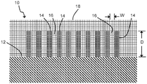
도 1은 평탄화될 표면 토포그래피(topography)를 예시하는 반도체 디바이스의 일부분의 개략 단면도이다.
도 2는 본 발명의 실시 형태에 따른 평탄화 필름에 의한 표면 토포그래피의 평탄화를 예시하는, 도 1의 반도체 디바이스의 일부분의 개략 단면도이다.
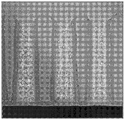
도 3은 고분자량 폴리(메틸 실세스퀴옥산) 수지로부터 형성된 평탄화 필름의 TEM 현미경 사진이다.
도 4는 본 발명의 실시 형태에 따라 형성된 평탄화 필름의 TEM 현미경 사진이다.
도 5는 본 발명의 실시 형태에 따라 형성된 다른 평탄화 필름의 TEM 현미경 사진이다.1 is a schematic cross-sectional view of a portion of a semiconductor device illustrating a surface topography to be planarized.
2 is a schematic cross-sectional view of a portion of the semiconductor device of FIG. 1 illustrating planarization of surface topography with a planarization film according to an embodiment of the present invention.
3 is a TEM micrograph of a flattening film formed from high molecular weight poly (methyl silsesquioxane) resin.
4 is a TEM micrograph of a flattening film formed in accordance with an embodiment of the invention.
5 is a TEM micrograph of another flattening film formed in accordance with an embodiment of the present invention.
본 발명의 실시 형태는, 반도체 디바이스 표면을 평탄화시키기 위해 반도체 디바이스의 표면 상에 스핀-코팅하기 위한 조성물에 폴리(메틸 실세스퀴옥산) 수지를 사용할 수 있다. 본 발명의 실시 형태에 따른 폴리(메틸 실세스퀴옥산) 조성물을 경화시킴으로써 형성된 평탄화 필름은 탁월한 유전 특성 및 낮은 누설 전류 수준을 나타내는 것으로 밝혀졌다. 평탄화 필름은 또한 질소 중에서 최대 450℃에서 열적으로 안정하고 치수적으로 안정성인 것으로 밝혀졌다.Embodiments of the invention may use poly (methyl silsesquioxane) resins in compositions for spin-coating on the surface of a semiconductor device to planarize the surface of the semiconductor device. Flattening films formed by curing the poly (methyl silsesquioxane) compositions according to embodiments of the present invention have been found to exhibit excellent dielectric properties and low leakage current levels. The planarization film has also been found to be thermally stable and dimensionally stable at up to 450 ° C. in nitrogen.
도 1은 평탄화될 표면 토포그래피를 예시하는 반도체 디바이스의 일부분의 개략 단면도이다. 도 1은 기재(substrate)(12) 및 복수의 핀(fin)(14)을 포함하는 디바이스(10)를 도시한다. 기재(12)는, 예를 들어, 이산화규소 또는 질화규소와 같은 절연 재료의 층일 수 있다. 기재(12)는 다른 디바이스 층(도시되지 않음) 위에 있을 수 있다. 복수의 핀(14)은, 예를 들어, 도핑된 규소, 구리, 또는 알루미늄과 같은 전도성 재료의 핀일 수 있다. 복수의 핀(14)은 복수의 간극(16)을 형성하며, 각각의 간극(16)은, 도 1에 나타난 바와 같이, 인접한 한 쌍의 핀(14)에 의해 한정된다. 도 1에 추가로 나타난 바와 같이, 각각의 간극(16)은 폭(W) 및 깊이(D)를 갖는 것으로 설명될 수 있다. 따라서, 각각의 간극(16)은 종횡비에 의해 추가로 한정될 수 있다. 본 발명의 목적상, 각각의 간극(16)의 종횡비는 종종 D:W로 표시되는 그의 깊이(D) 대 그의 폭(W)의 비이다. 4:1, 6:1, 8:1, 또는 10:1 이상과 같은 더 높은 종횡비를 갖는 간극은 평탄화 필름에 의해 완전히 또는 실질적으로 완전히 충전하기가 어려울 수 있다.1 is a schematic cross-sectional view of a portion of a semiconductor device illustrating a surface topography to be planarized. 1 shows a
도 2는 본 발명의 실시 형태에 따른 평탄화 필름에 의한 표면 토포그래피의 평탄화를 예시하는, 도 1의 반도체 디바이스(10)의 일부분의 개략 단면도이다. 도 2는 본 발명의 실시 형태에 따른 폴리(메틸 실세스퀴옥산) 조성물로부터 평탄화 필름(18)을 형성한 후의 디바이스(10)를 도시한다. 평탄화 필름(18)은 복수의 간극(16)의 각각을 충전하여 탁월한 유전 특성을 제공하고 인접한 핀(14)들 사이의 누설 전류를 최소화한다. 평탄화 필름은 또한 후속 디바이스 층(도시되지 않음)이 위에 형성될 수 있는 실질적으로 평면인 표면을 제공한다.2 is a schematic cross-sectional view of a portion of the
도 1 및 도 2는 본 발명의 실시 형태에 따른 평탄화 필름이 이용될 수 있는 한 가지 예를 예시한다. 본 발명의 실시 형태에 따른 평탄화 필름은 전도성, 비전도성, 및 반전도성 재료들의 다양한 배열을 수반하는 많은 다른 토포그래피에 이용될 수 있는 것으로 이해된다.1 and 2 illustrate one example where a flattening film according to an embodiment of the invention may be used. It is understood that planarization films according to embodiments of the present invention can be used in many other topography involving various arrangements of conductive, nonconductive, and semiconducting materials.
본 조성물 내의 폴리(메틸 실세스퀴옥산) 수지의 중량 평균 분자량(Mw)을 5,000 달톤(Da) 이하로 제한함으로써, 본 조성물은, 폭이 약 20 나노미터 이하이며 종횡비가 4:1 이상인 간극을 포함하는 토포그래피를 갖는 첨단 반도체 디바이스에 평탄화를 제공할 수 있다. 대조적으로, Mw가 10,000 Da 초과인 폴리(메틸 실세스퀴옥산) 수지를 포함하는 조성물은, 후속하여 경화된 필름에서의 공극을 포함한 상당한 결함 없이는, 종횡비가 4:1 이상인 20 나노미터 폭의 간극을 충전할 수 없는 것으로 밝혀졌다. 임의의 이론에 의해 구애되고자 함이 없이, 더 낮은 분자량의 폴리(메틸 실세스퀴옥산)에 의해 제공되는 더 낮은 점도는 20 나노미터 폭 및 높은 종횡비의 간극의 충전을 가능하게 하는 것으로 여겨진다.By limiting the weight average molecular weight (Mw) of the poly (methyl silsesquioxane) resin in the present composition to 5,000 Daltons (Da) or less, the present composition has a width of about 20 nanometers or less and an aspect ratio of 4: 1 or more. Planarization can be provided for advanced semiconductor devices having a topography that includes it. In contrast, compositions comprising poly (methyl silsesquioxane) resins with Mw greater than 10,000 Da have a 20 nanometer wide gap with an aspect ratio of at least 4: 1, without significant defects including voids in subsequently cured films. It turns out that it cannot be charged. Without wishing to be bound by any theory, it is believed that the lower viscosity provided by the lower molecular weight poly (methyl silsesquioxane) allows for the filling of gaps of 20 nanometers wide and high aspect ratios.
일부 실시 형태에서, 본 조성물 내의 폴리(메틸 실세스퀴옥산) 수지의 중량 평균 분자량(Mw)은 500 Da, 600 Da, 700 Da, 800 Da, 1,000 Da, 또는 1,200 Da만큼 낮거나, 1,600 Da, 2,100 Da, 2,600 Da, 3,400 Da, 4,300 Da, 또는 5,000 Da만큼 높거나, 또는 전술한 값들 중 임의의 2개의 값들에 의해 정의되는 임의의 범위 이내이다. 예를 들어, 일부 실시 형태에서, 본 조성물 내의 폴리(메틸 실세스퀴옥산) 수지의 Mw는 500 Da 내지 5,000 Da, 600 Da 내지 4,300 Da, 1,000 Da 내지 2,100 Da, 1,200 DA 내지 4,300 Da, 또는 1,200 Da 내지 1,600 Da의 범위이다. 일부 실시 형태에서, 조성물 내의 폴리(메틸 실세스퀴옥산) 수지의 Mw는 약 1,300 Da이다. Mw는 당업계에 공지된 바와 같이 겔 투과 크로마토그래피에 의해 측정될 수 있다.In some embodiments, the weight average molecular weight (Mw) of the poly (methyl silsesquioxane) resin in the composition is as low as 500 Da, 600 Da, 700 Da, 800 Da, 1,000 Da, or 1,200 Da, or 1,600 Da, As high as 2,100 Da, 2,600 Da, 3,400 Da, 4,300 Da, or 5,000 Da, or within any range defined by any two of the above values. For example, in some embodiments, the Mw of the poly (methyl silsesquioxane) resin in the composition is 500 Da to 5,000 Da, 600 Da to 4,300 Da, 1,000 Da to 2,100 Da, 1,200 DA to 4,300 Da, or 1,200 Da to 1,600 Da. In some embodiments, the Mw of the poly (methyl silsesquioxane) resin in the composition is about 1,300 Da. Mw can be measured by gel permeation chromatography as known in the art.
일부 실시 형태에서, 본 조성물 내의 폴리(메틸 실세스퀴옥산) 수지 내의 규소의 90% 이상은, 중량 평균 분자량이 5,000 Da 이하인 폴리(메틸 실세스퀴옥산) 중합체 사슬들에 존재하고, 본 조성물 내 폴리(메틸 실세스퀴옥산) 수지 내의 규소의 10% 미만은 중량 평균 분자량이 5,000 Da 초과인 폴리(메틸 실세스퀴옥산) 중합체 사슬들에 존재한다. 일부 실시 형태에서, 조성물 내의 폴리(메틸 실세스퀴옥산) 수지 내의 규소의 92%, 94%, 96%, 98%, 또는 99% 이상(또는 임의의 전술한 값들 사이의 임의의 값)은 중량 평균 분자량이 5,000 Da 이하인 폴리(메틸 실세스퀴옥산) 중합체 사슬들에 존재하고, 조성물 내의 폴리(메틸 실세스퀴옥산) 수지에 존재하는 규소의 8%, 6%, 4%, 2% 또는 1% 이하 (또는 임의의 전술한 값들 사이의 임의의 값)는 중량 평균 분자량이 5,000 Da 초과인 폴리(메틸 실세스퀴옥산) 중합체 사슬들에 존재한다.In some embodiments, at least 90% of the silicon in the poly (methyl silsesquioxane) resin in the composition is present in the poly (methyl silsesquioxane) polymer chains having a weight average molecular weight of 5,000 Da or less and in the composition Less than 10% of the silicon in the poly (methyl silsesquioxane) resin is present in poly (methyl silsesquioxane) polymer chains having a weight average molecular weight greater than 5,000 Da. In some embodiments, at least 92%, 94%, 96%, 98%, or 99% (or any value between any of the foregoing values) of silicon in the poly (methyl silsesquioxane) resin in the composition 8%, 6%, 4%, 2% or 1 of the silicon present in the poly (methyl silsesquioxane) polymer chains having an average molecular weight of 5,000 Da or less and present in the poly (methyl silsesquioxane) resin in the composition Up to% (or any value between any of the foregoing values) is present in the poly (methyl silsesquioxane) polymer chains having a weight average molecular weight greater than 5,000 Da.
본 조성물은 중량 평균 분자량이 500 Da 내지 5,000 Da인 폴리(메틸 실세스퀴옥산) 수지, 및 폴리(메틸 실세스퀴옥산)을 용액으로 만드는 적어도 하나의 용매를 포함할 수 있다. 일부 실시 형태에서, 적어도 하나의 용매는 단일 용매, 예를 들어 글리콜 에테르, 글리콜 에테르 아세테이트, n-부틸 아세테이트, 케톤, 또는 알코올을 포함할 수 있다. 글리콜 에테르는, 예를 들어 프로필렌 글리콜 프로필 에테르 또는 프로필렌 글리콜 메틸 에테르를 포함할 수 있다. 글리콜 에테르 아세테이트는, 예를 들어, 프로필렌 글리콜 메틸 에테르 아세테이트(PGMEA), 2-에톡시에틸 아세테이트, 또는 2-메톡시에틸 아세테이트를 포함할 수 있다. 케톤은, 예를 들어, 아세톤 또는 다이에틸 케톤을 포함할 수 있다. 알코올은, 예를 들어, 아이소프로필 알코올, 부탄올, 또는 에탄올을 포함할 수 있다. 다른 실시 형태에서, 적어도 하나의 용매는 전술한 용매들 중 둘 이상의 혼합물을 포함한다. 예를 들어, 일부 실시 형태에서, 적어도 하나의 용매는 PGMEA와 같은 상대적으로 온건한 비점을 갖는 용매와, n-부틸 아세테이트와 같은 상대적으로 낮은 비점을 갖는 다른 용매의 혼합물을 포함할 수 있다. PGMEA를 n-부틸 아세테이트와 블렌딩함으로써, 생성되는 평탄화 필름은 용매로서 PGMEA만을 포함하는 실시 형태와 비교할 때 더 적은 줄무늬(striation) 및 풍문(wind ripple) 결함을 나타내는 것으로 밝혀졌다.The composition may comprise a poly (methyl silsesquioxane) resin having a weight average molecular weight of 500 Da to 5,000 Da, and at least one solvent for making poly (methyl silsesquioxane) into a solution. In some embodiments, the at least one solvent may comprise a single solvent, such as glycol ether, glycol ether acetate, n-butyl acetate, ketone, or alcohol. Glycol ethers may include, for example, propylene glycol propyl ether or propylene glycol methyl ether. Glycol ether acetate may include, for example, propylene glycol methyl ether acetate (PGMEA), 2-ethoxyethyl acetate, or 2-methoxyethyl acetate. Ketones may include, for example, acetone or diethyl ketone. The alcohol can include, for example, isopropyl alcohol, butanol, or ethanol. In another embodiment, at least one solvent comprises a mixture of two or more of the aforementioned solvents. For example, in some embodiments, at least one solvent may comprise a mixture of a solvent having a relatively moderate boiling point, such as PGMEA, and another solvent having a relatively low boiling point, such as n-butyl acetate. By blending PGMEA with n-butyl acetate, the resulting flattened film was found to show less streaking and wind ripple defects as compared to embodiments comprising only PGMEA as solvent.
일부 실시 형태에서, PGMEA 대 n-부틸 아세테이트의 중량비는 0.5:1, 0.6:1, 0.7:1, 0.8:1 또는 0.9:1만큼 낮을 수 있거나, 1.1:1, 1.2:1, 1.4:1, 1.6:1, 1.8:1, 또는 2:1만큼 높을 수 있거나, 또는 전술한 값들 중 임의의 2개의 값들에 의해 정의되는 임의의 범위 이내일 수 있다. 예를 들어, 일부 실시 형태에서, PGMEA 대 n-부틸 아세테이트의 중량비는 0.5:1 내지 2:1, 0.6:1 내지 1.8:1, 0.7:1 내지 1.6:1, 0.8:1 내지 1.4:1 또는 0.9:1 내지 1.2:1의 범위이다. 일부 실시 형태에서, PGMEA 대 n-부틸 아세테이트의 중량비는 약 1:1이다. 일부 실시 형태에서, 적어도 하나의 용매는 임의의 전술한 비의 PGMEA 및 n-부틸 아세테이트로 이루어진다.In some embodiments, the weight ratio of PGMEA to n-butyl acetate can be as low as 0.5: 1, 0.6: 1, 0.7: 1, 0.8: 1 or 0.9: 1, or 1.1: 1, 1.2: 1, 1.4: 1, It can be as high as 1.6: 1, 1.8: 1, or 2: 1, or it can be within any range defined by any two of the above values. For example, in some embodiments, the weight ratio of PGMEA to n-butyl acetate is 0.5: 1 to 2: 1, 0.6: 1 to 1.8: 1, 0.7: 1 to 1.6: 1, 0.8: 1 to 1.4: 1 or In the range from 0.9: 1 to 1.2: 1. In some embodiments, the weight ratio of PGMEA to n-butyl acetate is about 1: 1. In some embodiments, at least one solvent consists of PGMEA and n-butyl acetate in any of the foregoing ratios.
일부 실시 형태에서, 본 조성물 내의 폴리(메틸 실세스퀴옥산) 수지의 농도는 조성물의 총 중량의 1 중량 퍼센트(중량%), 5 중량%, 10 중량%, 또는 15 중량%만큼 낮을 수 있거나, 25 중량%, 30 중량%, 35 중량%, 또는 40 중량%만큼 높을 수 있거나, 또는 전술한 값들 중 임의의 2개의 값들에 의해 정의되는 임의의 범위 이내일 수 있으며, 조성물의 잔부는 적어도 하나의 용매이다. 일부 실시 형태에서, 본 조성물 내의 폴리(메틸 실세스퀴옥산) 수지의 농도는 조성물의 총 중량의 1 중량% 내지 40 중량%, 5 중량% 내지 35 중량%, 10 중량% 내지 30 중량%, 또는 15 중량% 내지 25 중량%의 범위일 수 있으며, 조성물의 잔부는 적어도 하나의 용매이다.In some embodiments, the concentration of poly (methyl silsesquioxane) resin in the present composition may be as low as 1 weight percent, 5 weight percent, 10 weight percent, or 15 weight percent of the total weight of the composition, May be as high as 25%, 30%, 35%, or 40% by weight, or may be within any range defined by any two of the above values, with the balance of the composition being at least one Solvent. In some embodiments, the concentration of poly (methyl silsesquioxane) resin in the composition is 1 wt% to 40 wt%, 5 wt% to 35 wt%, 10 wt% to 30 wt%, or It may range from 15% to 25% by weight, the balance of the composition is at least one solvent.
일부 실시 형태에서, 본 조성물은 4차 암모늄 염 및/또는 아미노프로필트라이에톡시실란 염을 추가로 포함할 수 있다. 4차 암모늄 염, 예를 들어 테트라메틸 암모늄 니트레이트, 테트라부틸 암모늄 아세테이트, 테트라메틸 암모늄 아세테이트, 테트라부틸 암모늄 니트레이트, 및/또는 아미노프로필트라이에톡시실란 염, 예를 들어, 아미노프로필트라이에톡시실란 트라이플레이트를 첨가하는 것은, 조성물이 반도체 디바이스의 표면 상에 코팅된 후에 가열될 때 일어날 수 있는 조성물의 가스 방출(outgassing)을 감소시킬 수 있는 것으로 밝혀졌다. 그러한 가스 방출은 다양한 반도체 공정에 악영향을 줄 수 있고, 장기간 디바이스 신뢰성을 감소시키고, 반도체 디바이스를 제조하는 데 사용되는 장비의 유효 수명을 단축시킬 수 있다.In some embodiments, the compositions may further comprise quaternary ammonium salts and / or aminopropyltriethoxysilane salts. Quaternary ammonium salts such as tetramethyl ammonium nitrate, tetrabutyl ammonium acetate, tetramethyl ammonium acetate, tetrabutyl ammonium nitrate, and / or aminopropyltriethoxysilane salts such as aminopropyltriethoxy It has been found that adding silane triplates can reduce outgassing of the composition that can occur when heated after the composition is coated on the surface of the semiconductor device. Such gas emissions can adversely affect various semiconductor processes, reduce long-term device reliability, and shorten the useful life of the equipment used to manufacture semiconductor devices.
일부 실시 형태에서, 본 조성물 내의 4차 암모늄 염 및/또는 아미노프로필트라이에톡시실란 염의 농도는 0.01 중량%, 0.02 중량%, 0.04 중량%, 0.06 중량% 또는 0.08 중량%만큼 낮을 수 있거나, 0.12 중량%, 0.14 중량%, 0.16 중량%, 0.18 중량%, 또는 0.20 중량%만큼 높을 수 있거나, 또는 전술한 값들 중 임의의 2개의 값들에 의해 정의되는 임의의 범위 이내일 수 있다. 일부 실시 형태에서, 본 조성물 내의 4차 암모늄 염 및/또는 아미노프로필트라이에톡시실란 염의 농도는 조성물의 총 중량의 0.01 중량% 내지 0.20 중량%, 0.02 중량% 내지 0.18 중량%, 0.04 중량% 내지 0.16 중량%, 0.06 중량% 내지 0.14 중량%, 또는 0.08 중량% 내지 0.12 중량%의 범위일 수 있다. 일부 실시 형태에서, 본 조성물 내의 4차 암모늄 염 및/또는 아미노프로필트라이에톡시실란 염의 농도는 약 0.1 중량%일 수 있다.In some embodiments, the concentration of quaternary ammonium salts and / or aminopropyltriethoxysilane salts in the composition may be as low as 0.01 wt%, 0.02 wt%, 0.04 wt%, 0.06 wt%, or 0.08 wt%, or 0.12 wt% It may be as high as%, 0.14 wt%, 0.16 wt%, 0.18 wt%, or 0.20 wt%, or it may be within any range defined by any two of the above values. In some embodiments, the concentration of quaternary ammonium salt and / or aminopropyltriethoxysilane salt in the composition is 0.01% to 0.20%, 0.02% to 0.18%, 0.04% to 0.16% of the total weight of the composition. Weight percent, 0.06 weight percent to 0.14 weight percent, or 0.08 weight percent to 0.12 weight percent. In some embodiments, the concentration of quaternary ammonium salts and / or aminopropyltriethoxysilane salts in the composition may be about 0.1% by weight.
일부 실시 형태에서, 본 조성물은 고비점 용매를 추가로 포함할 수 있다. 고비점 용매의 첨가는 평탄화 필름의 간극 충전 및 평탄화 특성을 추가로 개선할 수 있는 것으로 밝혀졌다. 임의의 이론에 의해 구애되고자 함이 없이, 높은 증기압을 갖는 고비점 용매는 스핀-코팅 및 후속 베이킹 공정 동안 조성물 내에 더 오래 머무르는 경향이 있을 것으로 여겨진다. 고비점 용매는 조성물의 유체 특성을 개선하여, 높은 종횡비의 특징부들 사이의 간극을 레벨링하고 충전하는 조성물의 능력을 개선하는 것으로 여겨진다. 일부 실시 형태에서, 고비점 용매의 비점은 154℃, 170℃, 180℃, 또는 190℃만큼 낮을 수 있거나, 213℃, 230℃, 245℃, 또는 274℃만큼 높을 수 있거나, 또는 전술한 값들 중 임의의 2개의 값들 사이일 수 있다. 일부 실시 형태에서, 고비점 용매의 비점은 154℃ 내지 274℃, 170℃ 내지 245℃, 180℃ 내지 230℃, 또는 190℃ 내지 213℃의 범위일 수 있다. 고비점 용매의 예에는 1-옥탄올, 벤질 알코올, 헥실 알코올, 에틸렌 글리콜, 다이프로필렌 글리콜, 다이프로필렌 글리콜 메틸 에테르, 다이프로필렌 글리콜 n-프로필 에테르, 트라이프로필렌 글리콜 n-부틸 에테르, 아니솔, 및 프로필렌 카르보네이트가 포함된다.In some embodiments, the composition may further comprise a high boiling solvent. It has been found that the addition of high boiling solvents can further improve the gap filling and planarization properties of the planarization film. Without wishing to be bound by any theory, it is believed that high boiling solvents with high vapor pressure will tend to stay longer in the composition during spin-coating and subsequent baking processes. High boiling solvents are believed to improve the fluid properties of the composition, thereby improving the composition's ability to level and fill gaps between high aspect ratio features. In some embodiments, the boiling point of the high boiling solvent can be as low as 154 ° C, 170 ° C, 180 ° C, or 190 ° C, or as high as 213 ° C, 230 ° C, 245 ° C, or 274 ° C, or among the aforementioned values It can be between any two values. In some embodiments, the boiling point of the high boiling solvent may range from 154 ° C. to 274 ° C., 170 ° C. to 245 ° C., 180 ° C. to 230 ° C., or 190 ° C. to 213 ° C. Examples of high boiling solvents include 1-octanol, benzyl alcohol, hexyl alcohol, ethylene glycol, dipropylene glycol, dipropylene glycol methyl ether, dipropylene glycol n-propyl ether, tripropylene glycol n-butyl ether, anisole, and Propylene carbonate is included.
일부 실시 형태에서, 본 조성물 내의 고비점 용매의 농도는 조성물의 총 중량의 0.05 중량%, 0.07 중량%, 0.1 중량%, 또는 0.2 중량%만큼 낮을 수 있거나, 0.7 중량%, 1 중량%, 2 중량%, 또는 5 중량%만큼 높을 수 있거나, 또는 전술한 값들 중 임의의 2개의 값들에 의해 정의되는 임의의 범위 이내일 수 있다. 일부 실시 형태에서, 본 조성물 내의 고비점 용매의 농도는 조성물의 총 중량의 0.05 중량% 내지 5 중량%, 0.07 중량% 내지 2 중량%, 0.1 중량% 내지 1 중량%, 또는 0.2 중량% 내지 0.7 중량%의 범위일 수 있다. 일부 실시 형태에서, 본 조성물 내의 고비점 용매의 농도는 조성물의 총 중량의 약 0.5 중량%일 수 있다.In some embodiments, the concentration of the high boiling solvent in the composition may be as low as 0.05%, 0.07%, 0.1%, or 0.2% by weight, or 0.7%, 1%, 2% by weight of the total weight of the composition. %, Or as high as 5% by weight, or may be within any range defined by any two of the above values. In some embodiments, the concentration of the high boiling solvent in the composition is 0.05% to 5%, 0.07% to 2%, 0.1% to 1%, or 0.2% to 0.7% by weight of the total weight of the composition. It may be in the range of%. In some embodiments, the concentration of the high boiling solvent in the composition may be about 0.5% by weight of the total weight of the composition.
일부 실시 형태에서, 본 조성물은 페닐 실세스퀴옥산을 추가로 포함할 수 있다. 페닐 실세스퀴옥산은 가소제로서 작용하여, 조성물의 유체 특성을 추가로 개선할 수 있다. 일부 실시 형태에서, 본 조성물 내의 페닐 실세스퀴옥산의 농도는 조성물의 총 중량의 0.05 중량%, 0.1 중량%, 0.2 중량%, 또는 0.3 중량%만큼 낮을 수 있거나, 1 중량%, 2 중량%, 4 중량%, 또는 8 중량%만큼 높을 수 있거나, 또는 전술한 값들 중 임의의 2개의 값들에 의해 정의되는 임의의 범위 이내일 수 있다. 일부 실시 형태에서, 본 조성물 내의 페닐 실세스퀴옥산의 농도는 조성물의 총 중량의 0.05 중량% 내지 8 중량%, 0.1 중량% 내지 4 중량%, 0.2 중량% 내지 2 중량%, 또는 0.3 중량% 내지 1 중량%의 범위일 수 있다. 일부 실시 형태에서, 본 조성물 내의 페닐 실세스퀴옥산의 농도는 조성물의 총 중량의 약 0.5 중량%일 수 있다.In some embodiments, the composition may further comprise phenyl silsesquioxane. Phenyl silsesquioxane can act as a plasticizer, further improving the fluidic properties of the composition. In some embodiments, the concentration of phenyl silsesquioxane in the composition may be as low as 0.05 weight percent, 0.1 weight percent, 0.2 weight percent, or 0.3 weight percent of the total weight of the composition, or 1 weight percent, 2 weight percent, It may be as high as 4 weight percent, or 8 weight percent, or it may be within any range defined by any two of the above values. In some embodiments, the concentration of phenyl silsesquioxane in the composition is from 0.05% to 8%, 0.1% to 4%, 0.2% to 2%, or 0.3% by weight of the total weight of the composition. It may range from 1% by weight. In some embodiments, the concentration of phenyl silsesquioxane in the composition may be about 0.5% by weight of the total weight of the composition.
일부 실시 형태에서, 본 조성물은 계면활성제를 추가로 포함할 수 있다. 계면활성제는 줄무늬 및 풍문 결함을 추가로 감소시킬 수 있는 것으로 밝혀졌는데, 이는 조성물이 더 큰 직경의 반도체 디바이스 웨이퍼, 예를 들어 300 mm 직경 웨이퍼 상에 스핀-코팅되는 경우에 특히 유용할 수 있다. 일부 실시 형태에서, 계면활성제는 폴리에테르-개질된 폴리다이메틸실록산 계면활성제, 예를 들어 독일 베젤 소재의 비와이케이-케미(BYK-Chemie)로부터 입수가능한 BYK(등록상표)-306 또는 BYK(등록상표)-307일 수 있다.In some embodiments, the composition may further comprise a surfactant. Surfactants have been found to be able to further reduce streaks and weather vane defects, which can be particularly useful when the composition is spin-coated on larger diameter semiconductor device wafers, such as 300 mm diameter wafers. In some embodiments, the surfactant is a polyether-modified polydimethylsiloxane surfactant, such as BYK®-306 or BYK® available from BYK-Chemie, Bezel, Germany. Trademark) -307.
일부 실시 형태에서, 본 조성물 내의 계면활성제의 농도는 조성물의 총 중량의 0.25 중량%, 0.3 중량%, 0.4 중량%, 또는 0.5 중량%만큼 낮을 수 있거나, 또는 0.7 중량%, 0.8 중량%, 0.9 중량%, 또는 1 중량%만큼 높을 수 있거나, 또는 전술한 값들 중 임의의 2개의 값들에 의해 정의되는 임의의 범위 이내일 수 있다. 일부 실시 형태에서, 본 조성물 내의 계면활성제의 농도는 조성물의 총 중량의 0.25 중량% 내지 1 중량%, 0.30 중량% 내지 0.90 중량%, 0.40 중량% 내지 0.80 중량%, 또는 0.50 중량% 내지 0.70 중량%의 범위일 수 있다.In some embodiments, the concentration of surfactant in the composition may be as low as 0.25 weight percent, 0.3 weight percent, 0.4 weight percent, or 0.5 weight percent of the total weight of the composition, or 0.7 weight percent, 0.8 weight percent, 0.9 weight percent It may be as high as%, or 1% by weight, or it may be within any range defined by any two of the above values. In some embodiments, the concentration of surfactant in the composition is 0.25% to 1%, 0.30% to 0.90%, 0.40% to 0.80%, or 0.50% to 0.70% by weight of the total weight of the composition. It may be in the range of.
본 발명의 실시 형태에 따른 평탄화 조성물을 제조하기 위한 방법은 중량 평균 분자량이 500 Da 내지 5,000 Da인 폴리(메틸 실세스퀴옥산) 수지를 제공하는 단계, 및 전술한 실시 형태들 중 임의의 것에 따른 하나 이상의 용매를 제공하는 단계를 포함할 수 있다. 폴리(메틸 실세스퀴옥산) 수지를 하나 이상의 용매에 용해시켜 폴리(메틸 실세스퀴옥산) 용액을 형성할 수 있다. 전술한 실시 형태들 중 임의의 것에 따른 4차 암모늄 염 및/또는 아미노프로필트라이에톡시실란 염을 폴리(메틸 실세스퀴옥산) 용액에 용해시켜 평탄화 조성물을 형성할 수 있다.A method for preparing a flattening composition according to an embodiment of the present invention comprises the steps of providing a poly (methyl silsesquioxane) resin having a weight average molecular weight of 500 Da to 5,000 Da, and any of the foregoing embodiments. Providing one or more solvents. The poly (methyl silsesquioxane) resin can be dissolved in one or more solvents to form a poly (methyl silsesquioxane) solution. Quaternary ammonium salts and / or aminopropyltriethoxysilane salts according to any of the foregoing embodiments can be dissolved in a poly (methyl silsesquioxane) solution to form a planarization composition.
일부 실시 형태에서, 하나 이상의 용매를 제공하는 단계는 전술한 실시 형태들 중 임의의 것에 따른 비로 PGMEA 및 n-부틸 아세테이트를 함께 블렌딩하는 단계를 포함할 수 있다. 일부 실시 형태에서, 하나 이상의 용매를 제공하는 단계는 전술한 실시 형태들 중 임의의 것에 따른 고비점 용매 중에서 블렌딩하는 단계를 추가로 포함할 수 있다.In some embodiments, providing one or more solvents can include blending PGMEA and n-butyl acetate together in a ratio according to any of the foregoing embodiments. In some embodiments, providing one or more solvents may further comprise blending in a high boiling solvent according to any of the foregoing embodiments.
일부 실시 형태에서, 평탄화 조성물을 제조하기 위한 방법은 전술한 실시 형태들 중 임의의 실시 형태에 따른 페닐 실세스퀴옥산을 제공하는 단계를 추가로 포함할 수 있다. 페닐 실세스퀴옥산을 하나 이상의 용매에 용해시켜 페닐 실세스퀴옥산 용액을 형성할 수 있다. 하나 이상의 용매는 폴리(메틸 실세스퀴옥산)을 용해시키기 위해 제공되는 하나 이상의 용매와 동일하거나 상이할 수 있다. 예를 들어, 폴리(메틸 실세스퀴옥산)은 PGMEA와 n-부틸 아세테이트의 1:1 혼합물에 용해시킬 수 있고, 페닐 실세스퀴옥산은 PGMEA에 용해시킬 수 있다. 페닐 실세스퀴옥산 용액을 폴리(메틸 실세스퀴옥산) 용액과 블렌딩하여 평탄화 조성물을 형성할 수 있다.In some embodiments, the method for preparing the planarization composition may further comprise providing phenyl silsesquioxane according to any of the foregoing embodiments. Phenyl silsesquioxane can be dissolved in one or more solvents to form a phenyl silsesquioxane solution. One or more solvents may be the same or different than one or more solvents provided for dissolving poly (methyl silsesquioxane). For example, poly (methyl silsesquioxane) can be dissolved in a 1: 1 mixture of PGMEA and n-butyl acetate and phenyl silsesquioxane can be dissolved in PGMEA. The phenyl silsesquioxane solution can be blended with a poly (methyl silsesquioxane) solution to form a planarization composition.
일부 실시 형태에서, 평탄화 조성물을 제조하기 위한 방법은 전술한 실시 형태들 중 임의의 것에 따른 계면활성제를 제공하는 단계 및 계면활성제를 폴리(메틸 실세스퀴옥산) 용액에 용해시켜 평탄화 조성물을 형성하는 단계를 추가로 포함할 수 있다.In some embodiments, a method for preparing a planarization composition comprises providing a surfactant according to any of the foregoing embodiments and dissolving the surfactant in a poly (methyl silsesquioxane) solution to form the planarization composition. It may further comprise a step.
일부 실시 형태에서, 균질한 용액을 위해 평탄화 조성물을 롤러 혼합기에서 하룻밤 혼합할 수 있다. 일부 실시 형태에서, 일련의 2개 이상의 0.1 마이크로미터 필터를 통해 평탄화 조성물을 여과할 수 있다.In some embodiments, the flattening composition can be mixed overnight in a roller mixer for a homogeneous solution. In some embodiments, the planarization composition may be filtered through a series of two or more 0.1 micron filters.
사용 중에, 본 발명의 실시 형태에 따른 평탄화 조성물을 반도체 디바이스 웨이퍼의 표면 상에 스핀-코팅하여, 표면의 토포그래피를 평탄화시킬 수 있다. 이어서, 반도체 디바이스 웨이퍼를 120℃ 내지 280℃ 범위의 온도에서 1분 내지 5분 범위의 시간 동안 베이킹하여 평탄화 조성물로부터 하나 이상의 용매의 실질적으로 전부를 제거할 수 있다. 이어서, 반도체 디바이스 웨이퍼를 약 400℃ 내지 약 450℃ 범위의 온도에서 경화시켜 평탄화 필름을 형성할 수 있다. 평탄화 필름은 반도체 디바이스의 영구적인 부분일 수 있다.In use, a planarization composition according to an embodiment of the present invention may be spin-coated onto the surface of a semiconductor device wafer to planarize the topography of the surface. The semiconductor device wafer may then be baked at a temperature ranging from 120 ° C. to 280 ° C. for a time ranging from 1 minute to 5 minutes to remove substantially all of the one or more solvents from the planarization composition. The semiconductor device wafer may then be cured at a temperature ranging from about 400 ° C. to about 450 ° C. to form a planarization film. The planarization film may be a permanent part of the semiconductor device.
본 발명의 실시 형태에 따른 평탄화 필름은 중량 평균 분자량이 500 Da 내지 5,000 Da인 폴리(메틸 실세스퀴옥산) 중합체 사슬들로 형성된 경화된 폴리(메틸 실세스퀴옥산)을 포함할 수 있다. 일부 실시 형태에서, 평탄화 필름은 전술한 실시 형태들 중 임의의 것에 따른 4차 암모늄 염 및/또는 아미노프로필트라이에톡시실란 염, 예를 들어 아미노프로필트라이에톡시실란 트라이플레이트의 잔류물을 추가로 포함할 수 있다. 일부 실시 형태에서, 평탄화 필름은 전술한 실시 형태들 중 임의의 것에 따른 페닐 실세스퀴옥산의 잔류물을 추가로 포함할 수 있다. 일부 실시 형태에서, 평탄화 필름은, BYK(등록상표)-307과 같은, 폴리에테르-개질된 폴리다이메틸실록산 계면활성제를 포함하는, 전술한 실시 형태들 중 임의의 것에 따른 계면활성제의 잔류물을 추가로 포함할 수 있다.The planarization film according to an embodiment of the present invention may comprise cured poly (methyl silsesquioxane) formed of poly (methyl silsesquioxane) polymer chains having a weight average molecular weight of 500 Da to 5,000 Da. In some embodiments, the flattening film further comprises residues of quaternary ammonium salts and / or aminopropyltriethoxysilane salts, such as aminopropyltriethoxysilane triplates according to any of the foregoing embodiments. It may include. In some embodiments, the flattening film may further comprise a residue of phenyl silsesquioxane according to any of the foregoing embodiments. In some embodiments, the flattening film comprises a residue of a surfactant according to any of the preceding embodiments, including a polyether-modified polydimethylsiloxane surfactant, such as BYK®-307. It may further comprise.
본 발명이 예시적인 설계에 대해 기재되었지만, 본 발명은 본 발명의 사상 및 범주 내에서 추가로 변경될 수 있다. 또한, 본 출원은 본 발명이 속하는 기술 분야에서 공지된 또는 통상적인 관행 내에 있는 바와 같은 본 발명으로부터의 그러한 이탈(departure)을 포괄하도록 의도된다.Although the invention has been described with respect to exemplary designs, the invention may be further modified within the spirit and scope of the invention. In addition, the present application is intended to cover such departures from the present invention as come within known or customary practice in the art.
실시예Example
비교예 1Comparative Example 1
고분자량 폴리(메틸 실세스퀴옥산)High molecular weight poly (methyl silsesquioxane)
폴리(메틸 실세스퀴옥산) 수지 GR 650을 미국 오하이오주 페리스버그 소재의 테크네글라스(Techneglas)로부터 입수하였다. PGMEA와 n-부틸 아세테이트의 50/50 혼합물 중 45 중량% 폴리(메틸 실세스퀴옥산)의 용액을 제조하고, 이어서 이 용액을 0.1 마이크로미터 필터로 여과함으로써, 폴리(메틸 실세스퀴옥산)의 중량 평균 분자량(Mw)을 확인하였다. 이어서, Mw를 결정하기 위해 당업계에 공지된 바와 같이, 겔 투과 크로마토그래피(GPC)에 의해 여과된 용액을 분석하였다. 폴리(메틸 실세스퀴옥산)의 Mw는 10,223 Da인 것으로 나타났다.Poly (methyl silsesquioxane) resin GR 650 was obtained from Techneglas, Perrysburg, Ohio. A solution of 45% by weight poly (methyl silsesquioxane) in a 50/50 mixture of PGMEA and n-butyl acetate was prepared, and then the solution was filtered through a 0.1 micron filter to obtain a poly (methyl silsesquioxane) The weight average molecular weight (Mw) was confirmed. The filtered solution was then analyzed by gel permeation chromatography (GPC) as is known in the art to determine Mw. The Mw of the poly (methyl silsesquioxane) was found to be 10,223 Da.
100 그램(g)의 10,223 Da 폴리(메틸 실세스퀴옥산) 수지를 400 g의 프로필렌 글리콜 모노모에틸 에테르 아세테이트(PGMEA)에 첨가하였다. 조합물을 롤러 혼합기에서 하룻밤 혼합하여 균질성을 보장하였다. 생성된 용액을 일련의 2개의 0.1 마이크로미터 필터를 통해 여과하였다. 약 20 nm 폭 및 약 80 nm 내지 100 nm 깊이의 높은 종횡비의 특징부를 포함하는 200 mm 직경의 패턴화된 시험 웨이퍼 상에 용액을 스핀-코팅하였다. 캐스팅된 필름을 갖는 웨이퍼를 일련의 3개의 핫 플레이트 상에서 각각 60초 동안 베이킹하였는데, 핫 플레이트는 각각 140℃, 150℃, 및 210℃의 온도를 가졌다. 베이킹된 필름을 갖는 웨이퍼를 질소 환경에서 425℃의 핫 플레이트 상에서 5분 동안 경화시키고 냉각 플레이트 상에서 즉시 냉각시켰다. 패턴화된 웨이퍼를 터널링 전자 현미경(TEM) 분석에 의해 간극 충전에 대해 평가하였다. 도 3은 10,223 Da 폴리(메틸 실세스퀴옥산) 수지로부터 형성된 평탄화 필름의 TEM 현미경 사진을 나타낸다. 도 3에 도시된 바와 같이, 높은 종횡비의 특징부에서 많은 공극이 관찰되었다. 핫 플레이트 베이킹 동안 극심한 가스 방출이 관찰되었다.100 grams (g) of 10,223 Da poly (methyl silsesquioxane) resin was added to 400 g propylene glycol monomoethyl ether acetate (PGMEA). The combination was mixed overnight in a roller mixer to ensure homogeneity. The resulting solution was filtered through a series of two 0.1 micron filters. The solution was spin-coated onto a 200 mm diameter patterned test wafer containing high aspect ratio features about 20 nm wide and about 80 nm to 100 nm deep. The wafer with the cast film was baked on a series of three hot plates for 60 seconds each, the hot plates having temperatures of 140 ° C., 150 ° C., and 210 ° C., respectively. The wafer with the baked film was cured for 5 minutes on a 425 ° C. hot plate in a nitrogen environment and immediately cooled on a cold plate. Patterned wafers were evaluated for gap filling by tunneling electron microscopy (TEM) analysis. 3 shows a TEM micrograph of a flattening film formed from 10,223 Da poly (methyl silsesquioxane) resin. As shown in FIG. 3, many voids were observed in high aspect ratio features. Extreme gas release was observed during hot plate baking.
실시예 2Example 2
저분자량 폴리(메틸 실세스퀴옥산)Low Molecular Weight Poly (Methyl Silsesquioxane)
분자량이 약 1.5 K Da인 폴리(메틸 실세스퀴옥산) 수지 GR 650을 미국 오하이오주 페리스버그 소재의 테크네글라스로부터 입수하였다. PGMEA와 n-부틸 아세테이트의 50/50 혼합물 중 45 중량% 폴리(메틸 실세스퀴옥산)의 용액을 제조하고, 이어서 이 용액을 0.1 마이크로미터 필터로 여과함으로써, 폴리(메틸 실세스퀴옥산)의 실제 중량 평균 분자량(Mw)을 확인하였다. 이어서, Mw를 결정하기 위해 당업계에 공지된 바와 같이, 겔 투과 크로마토그래피(GPC)에 의해 여과된 용액을 분석하였다. 폴리(메틸 실세스퀴옥산)의 Mw는 1,323 Da인 것으로 나타났다.Poly (methyl silsesquioxane) resin GR 650 having a molecular weight of about 1.5 K Da was obtained from Techneglas, Perrysburg, Ohio. A solution of 45% by weight poly (methyl silsesquioxane) in a 50/50 mixture of PGMEA and n-butyl acetate was prepared, and then the solution was filtered through a 0.1 micron filter to obtain a poly (methyl silsesquioxane) The actual weight average molecular weight (Mw) was confirmed. The filtered solution was then analyzed by gel permeation chromatography (GPC) as is known in the art to determine Mw. The Mw of poly (methyl silsesquioxane) was found to be 1,323 Da.
100 g의 1,323 Da 폴리(메틸 실세스퀴옥산) 수지를 400 g의 프로필렌 글리콜 모노모에틸 에테르 아세테이트(PGMEA)에 첨가하였다. 조합물을 롤러 혼합기에서 하룻밤 혼합하여 균질성을 보장하였다. 생성된 용액을 일련의 2개의 0.1 마이크로미터 필터를 통해 여과하였다. 용액을 200 mm 직경의 블랭크 규소 웨이퍼 상에 스핀-코팅하였다. 캐스팅된 필름을 갖는 웨이퍼를 일련의 3개의 핫 플레이트 상에서 각각 60초 동안 베이킹하였는데, 핫 플레이트는 각각 140℃, 150℃, 및 210℃의 온도를 가졌다. 베이킹된 필름을 갖는 웨이퍼를 질소 환경에서 425℃의 핫 플레이트 상에서 5분 동안 경화시키고 냉각 플레이트 상에서 즉시 냉각시켰다. 200 mm 코팅된 웨이퍼를 50x 배율의 광학 현미경 하에서 필름 결함에 대해 평가하였다. 줄무늬 및 풍문 결함이 관찰되었다. 핫 플레이트 베이킹 동안 극심한 가스 방출이 또한 관찰되었다.100 g of 1,323 Da poly (methyl silsesquioxane) resin was added to 400 g propylene glycol monomoethyl ether acetate (PGMEA). The combination was mixed overnight in a roller mixer to ensure homogeneity. The resulting solution was filtered through a series of two 0.1 micron filters. The solution was spin-coated onto a blank silicon wafer of 200 mm diameter. The wafer with the cast film was baked on a series of three hot plates for 60 seconds each, the hot plates having temperatures of 140 ° C., 150 ° C., and 210 ° C., respectively. The wafer with the baked film was cured for 5 minutes on a 425 ° C. hot plate in a nitrogen environment and immediately cooled on a cold plate. 200 mm coated wafers were evaluated for film defects under an optical microscope at 50 × magnification. Stripes and rumor defects were observed. Extreme gas release was also observed during hot plate baking.
실시예 3Example 3
저분자량 폴리(메틸 실세스퀴옥산) 및 용매 블렌드Low Molecular Weight Poly (methyl Silsesquioxane) and Solvent Blends
210 g의 PGMEA 및 210 g의 n-부틸 아세테이트를 함께 블렌딩하여 용매 혼합물을 형성하였다. 100 g의 1,323 폴리(메틸 실세스퀴옥산) 수지를 420 g의 용매 혼합물과 조합하였다. 조합물을 롤러 혼합기에서 하룻밤 혼합하여 균질성을 보장하였다. 이 용액을 일련의 2개의 0.1 마이크로미터 필터를 통해 여과하였다.210 g of PGMEA and 210 g of n-butyl acetate were blended together to form a solvent mixture. 100 g of 1,323 poly (methyl silsesquioxane) resin was combined with 420 g of solvent mixture. The combination was mixed overnight in a roller mixer to ensure homogeneity. This solution was filtered through a series of two 0.1 micron filters.
용액을 200 mm 직경의 블랭크 규소 웨이퍼 상에 스핀-코팅하였다. 캐스팅된 필름을 갖는 웨이퍼를 일련의 3개의 핫 플레이트 상에서 각각 60초 동안 베이킹하였는데, 핫 플레이트는 각각 140℃, 150℃, 및 210℃의 온도를 가졌다. 베이킹된 필름을 갖는 웨이퍼를 질소 환경에서 425℃의 핫 플레이트 상에서 5분 동안 경화시키고 냉각 플레이트 상에서 즉시 냉각시켰다. 웨이퍼를 50x 배율의 광학 현미경 하에서 관찰하였다. 줄무늬 또는 풍문 결함이 관찰되지 않았다. 핫 플레이트 베이킹 동안 극심한 가스 방출이 관찰되었다.The solution was spin-coated onto a blank silicon wafer of 200 mm diameter. The wafer with the cast film was baked on a series of three hot plates for 60 seconds each, the hot plates having temperatures of 140 ° C., 150 ° C., and 210 ° C., respectively. The wafer with the baked film was cured for 5 minutes on a 425 ° C. hot plate in a nitrogen environment and immediately cooled on a cold plate. The wafer was observed under an optical microscope at 50 × magnification. No streaks or rumors were observed. Extreme gas release was observed during hot plate baking.
실시예 4Example 4
저분자량 폴리(메틸 실세스퀴옥산), 용매 블렌드, 아미노프로필트라이에톡시실란 염Low Molecular Weight Poly (methyl Silsesquioxane), Solvent Blends, Aminopropyltriethoxysilane Salts
210 g의 PGMEA 및 210 g의 n-부틸 아세테이트를 함께 블렌딩하여 용매 혼합물을 형성하였다. 100 g의 1,323 Da 폴리(메틸 실세스퀴옥산) 수지를 420 g의 용매 혼합물과 조합하였다. 조합물을 롤러 혼합기에서 하룻밤 혼합하여 균질성을 보장하였다. 생성된 용액을 일련의 2개의 0.1 마이크로미터 필터를 통해 여과하였다. 0.33 g의 아미노프로필트라이에톡시실란 트라이플레이트를 폴리(메틸 실세스퀴옥산)의 용액에 첨가하고 롤러 혼합기에서 1시간 동안 혼합하여 균질성을 보장하였고, 이어서 일련의 2개의 0.1 마이크로미터 필터를 통해 여과하였다.210 g of PGMEA and 210 g of n-butyl acetate were blended together to form a solvent mixture. 100 g of 1,323 Da poly (methyl silsesquioxane) resin was combined with 420 g of solvent mixture. The combination was mixed overnight in a roller mixer to ensure homogeneity. The resulting solution was filtered through a series of two 0.1 micron filters. 0.33 g of aminopropyltriethoxysilane triplate was added to a solution of poly (methyl silsesquioxane) and mixed for 1 hour in a roller mixer to ensure homogeneity, followed by filtration through a series of two 0.1 micron filters It was.
약 20 nm 폭 및 약 80 nm 내지 100 nm 깊이의 높은 종횡비의 특징부를 포함하는 200 mm 직경의 패턴화된 시험 웨이퍼 및 200 mm 직경의 블랭크 규소 웨이퍼 상에 용액을 스핀-코팅하였다. 캐스팅된 필름을 갖는 웨이퍼를 일련의 3개의 핫 플레이트 상에서 각각 60초 동안 베이킹하였는데, 핫 플레이트는 각각 140℃, 150℃, 및 210℃의 온도를 가졌다. 베이킹된 필름을 갖는 웨이퍼를 질소 환경에서 425℃의 핫 플레이트 상에서 5분 동안 경화시키고 냉각 플레이트 상에서 즉시 냉각시켰다. 코팅된 블랭크 규소 웨이퍼를 50x 배율의 광학 현미경 하에서 관찰하였다. 줄무늬 또는 풍문 결함이 관찰되지 않았다. 어떠한 핫 플레이트 베이크에서도 코팅된 블랭크 규소 웨이퍼에서의 가스 방출이 관찰되지 않았다. 패턴화된 시험 웨이퍼를 터널링 전자 현미경(TEM) 분석에 의해 간극 충전에 대해 평가하였다. 도 4는 1,323 Da 폴리(메틸 실세스퀴옥산) 수지로부터 형성된 평탄화 필름의 TEM 현미경 사진을 나타낸다. 도 4에 나타난 바와 같이, 평탄화 및 간극-충전이 우수하며, 높은 종횡비의 특징부에서 공극이 관찰되지 않는다.The solution was spin-coated on a 200 mm diameter patterned test wafer and a 200 mm diameter blank silicon wafer that included high aspect ratio features about 20 nm wide and about 80 nm to 100 nm deep. The wafer with the cast film was baked on a series of three hot plates for 60 seconds each, the hot plates having temperatures of 140 ° C., 150 ° C., and 210 ° C., respectively. The wafer with the baked film was cured for 5 minutes on a 425 ° C. hot plate in a nitrogen environment and immediately cooled on a cold plate. The coated blank silicon wafer was observed under an optical microscope at 50 × magnification. No streaks or rumors were observed. No gas release on the coated blank silicon wafer was observed in any hot plate bake. Patterned test wafers were evaluated for gap filling by tunneling electron microscopy (TEM) analysis. 4 shows a TEM micrograph of a flattening film formed from 1,323 Da poly (methyl silsesquioxane) resin. As shown in FIG. 4, planarization and gap-filling are excellent, and no voids are observed in high aspect ratio features.
실시예 5Example 5
저분자량 폴리(메틸 실세스퀴옥산), 용매 블렌드, 페닐 실세스퀴옥산Low Molecular Weight Poly (Methyl Silsesquioxane), Solvent Blend, Phenyl Silsesquioxane
410 g의 PGMEA 및 410 g의 n-부틸 아세테이트를 함께 블렌딩하여 용매 혼합물을 형성하였다. 100 g의 1,323 Da 폴리(메틸 실세스퀴옥산) 수지를 420 g의 용매 혼합물과 조합하였다. 조합물을 롤러 혼합기에서 하룻밤 혼합하여 균질성을 보장하였다. 생성된 용액을 일련의 2개의 0.1 마이크로미터 필터를 통해 여과하였다. 23 g의 페닐 실세스퀴옥산을 77 g의 PGMEA와 조합하여 페닐 실세스퀴옥산 용액을 형성하였다. 페닐 실세스퀴옥산 용액을 롤러 혼합기에서 하룻밤 혼합하여 균질성을 보장하였고, 이어서 일련의 2개의 0.1 마이크로미터 필터를 통해 여과하였다. 0.33 g의 아미노프로필트라이에톡시실란 트라이플레이트를 폴리(메틸 실세스퀴옥산)의 용액에 첨가하고 롤러 혼합기에서 1시간 동안 혼합하여 균질성을 보장하였고, 이어서 일련의 2개의 0.1 마이크로미터 필터를 통해 여과하였다.410 g of PGMEA and 410 g of n-butyl acetate were blended together to form a solvent mixture. 100 g of 1,323 Da poly (methyl silsesquioxane) resin was combined with 420 g of solvent mixture. The combination was mixed overnight in a roller mixer to ensure homogeneity. The resulting solution was filtered through a series of two 0.1 micron filters. 23 g of phenyl silsesquioxane was combined with 77 g of PGMEA to form a phenyl silsesquioxane solution. The phenyl silsesquioxane solution was mixed overnight in a roller mixer to ensure homogeneity and then filtered through a series of two 0.1 micron filters. 0.33 g of aminopropyltriethoxysilane triplate was added to a solution of poly (methyl silsesquioxane) and mixed for 1 hour in a roller mixer to ensure homogeneity, followed by filtration through a series of two 0.1 micron filters It was.
폴리(메틸 실세스퀴옥산) 용액을 3가지 비율로 페닐 실세스퀴옥산 용액과 조합하여 평가를 위한 3개의 별개의 배치(batch)를 생성하였다. 제1 배치에서는, 90 g의 폴리(메틸 실세스퀴옥산) 용액을 10 g의 페닐 실세스퀴옥산 용액과 조합하였다. 제2 배치에서, 80 g의 폴리(메틸 실세스퀴옥산) 용액을 20 g의 페닐 실세스퀴옥산 용액과 조합하였다. 제3 배치에서, 70 g의 폴리(메틸 실세스퀴옥산) 용액을 30 g의 페닐 실세스퀴옥산 용액과 조합하였다.The poly (methyl silsesquioxane) solution was combined with the phenyl silsesquioxane solution in three proportions to create three separate batches for evaluation. In a first batch, 90 g of poly (methyl silsesquioxane) solution was combined with 10 g of phenyl silsesquioxane solution. In a second batch, 80 g of poly (methyl silsesquioxane) solution was combined with 20 g of phenyl silsesquioxane solution. In a third batch, 70 g of poly (methyl silsesquioxane) solution was combined with 30 g of phenyl silsesquioxane solution.
각각의 용액을 3개의 상이한 200 mm 직경의 블랭크 규소 웨이퍼 상에 스핀 코팅하였다. 캐스팅된 필름을 갖는 웨이퍼를 일련의 3개의 핫 플레이트 상에서 각각 60초 동안 베이킹하였는데, 핫 플레이트는 각각 140℃, 150℃, 및 210℃의 온도를 가졌다. 베이킹된 필름을 갖는 웨이퍼를 질소 환경에서 425℃의 핫 플레이트 상에서 5분 동안 경화시키고 냉각 플레이트 상에서 즉시 냉각시켰다. 웨이퍼를 검사하였고, 평탄화 필름은 혼탁한 것으로 나타났다.Each solution was spin coated onto three different 200 mm diameter blank silicon wafers. The wafer with the cast film was baked on a series of three hot plates for 60 seconds each, the hot plates having temperatures of 140 ° C., 150 ° C., and 210 ° C., respectively. The wafer with the baked film was cured for 5 minutes on a 425 ° C. hot plate in a nitrogen environment and immediately cooled on a cold plate. The wafer was inspected and the planarization film appeared cloudy.
실시예 6Example 6
저분자량 폴리(메틸 실세스퀴옥산), 용매 블렌드, 계면활성제Low molecular weight poly (methyl silsesquioxane), solvent blends, surfactants
210 g의 PGMEA 및 210 g의 n-부틸 아세테이트를 함께 블렌딩하여 용매 혼합물을 형성하였다. 100 g의 1,323 Da 폴리(메틸 실세스퀴옥산) 수지를 420 g의 용매 혼합물과 조합하였다. 조합물을 롤러 혼합기에서 하룻밤 혼합하여 균질성을 보장하였다. 생성된 용액을 일련의 2개의 0.1 마이크로미터 필터를 통해 여과하였다.210 g of PGMEA and 210 g of n-butyl acetate were blended together to form a solvent mixture. 100 g of 1,323 Da poly (methyl silsesquioxane) resin was combined with 420 g of solvent mixture. The combination was mixed overnight in a roller mixer to ensure homogeneity. The resulting solution was filtered through a series of two 0.1 micron filters.
계면활성제인 BYK(등록상표)-307을 3가지 중량 백분율로 폴리(메틸렌 실세스퀴옥산)의 용액에 첨가하였다. 제1 배치에서는, 1.5 g의 계면활성제를 150 g의 폴리(메틸 실세스퀴옥산) 용액에 첨가하여, 계면활성제가 용액의 1 중량%가 되도록 하였다. 제2 배치에서는, 0.75 g의 계면활성제를 150 g의 폴리(메틸 실세스퀴옥산) 용액에 첨가하여, 계면활성제가 용액의 0.5 중량%가 되도록 하였다. 제3 배치에서는, 0.375 g의 계면활성제를 150 g의 폴리(메틸 실세스퀴옥산) 용액에 첨가하여, 계면활성제가 용액의 0.25 중량%가 되도록 하였다. 생성된 용액을 각각 롤러 혼합기에서 1시간 동안 혼합하여 균질성을 보장하였고, 이어서 일련의 2개의 0.1 마이크로미터 필터를 통해 여과하였다.Surfactant BYK®-307 was added to a solution of poly (methylene silsesquioxane) in three weight percentages. In the first batch, 1.5 g of surfactant was added to 150 g of poly (methyl silsesquioxane) solution so that the surfactant was 1% by weight of the solution. In a second batch, 0.75 g of surfactant was added to 150 g of poly (methyl silsesquioxane) solution to bring the surfactant to 0.5% by weight of the solution. In a third batch, 0.375 g of surfactant was added to 150 g of poly (methyl silsesquioxane) solution such that the surfactant was 0.25% by weight of the solution. The resulting solutions were mixed for 1 hour in a roller mixer each to ensure homogeneity and then filtered through a series of two 0.1 micron filters.
각각의 용액을 상이한 300 mm 직경의 블랭크 규소 웨이퍼 상에 스핀 코팅하였다. 캐스팅된 필름을 갖는 웨이퍼를 일련의 3개의 핫 플레이트 상에서 각각 60초 동안 베이킹하였는데, 핫 플레이트는 각각 140℃, 150℃, 및 210℃의 온도를 가졌다. 베이킹된 필름을 갖는 웨이퍼를 질소 환경에서 425℃의 핫 플레이트 상에서 5분 동안 경화시키고 냉각 플레이트 상에서 즉시 냉각시켰다. 코팅된 웨이퍼를 50x 배율의 광학 현미경 하에서 관찰하였다. 1 중량% 계면활성제 용액으로 코팅된 웨이퍼에서 줄무늬 및 풍문 결함이 관찰되었다. 0.5 중량% 용액 또는 0.25 중량% 용액으로 코팅된 웨이퍼에서는 줄무늬 또는 풍문 결함이 관찰되지 않았다.Each solution was spin coated onto different 300 mm diameter blank silicon wafers. The wafer with the cast film was baked on a series of three hot plates for 60 seconds each, the hot plates having temperatures of 140 ° C., 150 ° C., and 210 ° C., respectively. The wafer with the baked film was cured for 5 minutes on a 425 ° C. hot plate in a nitrogen environment and immediately cooled on a cold plate. The coated wafers were observed under an optical microscope at 50 × magnification. Stripes and rubella defects were observed on wafers coated with 1 wt% surfactant solution. No streaks or rubella defects were observed on wafers coated with 0.5 wt% solution or 0.25 wt% solution.
실시예 7Example 7
저분자량 폴리(메틸 실세스퀴옥산), 고비점 용매Low molecular weight poly (methyl silsesquioxane), high boiling point solvent
420 g의 PGMEA 및 420 g의 n-부틸 아세테이트를 함께 블렌딩하여 용매 혼합물을 형성하였다. 200 g의 1,323 Da 폴리(메틸 실세스퀴옥산) 수지를 840 g의 용매 혼합물과 조합하였다. 조합물을 롤러 혼합기에서 1시간 동안 혼합하여 용액을 형성하였다. 용액의 8개의 100 g 분액을 준비하였다. 0.5 g의 각각의 8가지 고비점 용매를 0.06 g의 아미노프로필트라이에톡시실란 트라이플레이트와 함께 8개의 100 g 분액 중 상이한 하나에 첨가하여 0.5 중량%의 고비점 용매를 함유하는 용액을 형성하였다. 생성된 분량을 각각 롤러 혼합기에서 30분 동안 혼합하고, 이어서 일련의 2개의 0.1 마이크로미터 필터를 통해 여과하였다. 사용된 8가지 고비점 용매는 1-옥탄올, 벤질 알코올, 헥실 알코올, 에틸렌 글리콜, 다이프로필렌 글리콜 메틸 에테르, 다이프로필렌 글리콜 n-프로필 에테르, 트라이프로필렌 글리콜 n-부틸 에테르, 및 아니솔이었다.420 g of PGMEA and 420 g of n-butyl acetate were blended together to form a solvent mixture. 200 g of 1,323 Da poly (methyl silsesquioxane) resin was combined with 840 g of solvent mixture. The combination was mixed for 1 hour in a roller mixer to form a solution. Eight 100 g aliquots of the solution were prepared. 0.5 g of each of the eight high boiling solvents was added together with 0.06 g of aminopropyltriethoxysilane triplate to the other one of the eight 100 g aliquots to form a solution containing 0.5% by weight of the high boiling solvent. The resulting portions were each mixed for 30 minutes in a roller mixer and then filtered through a series of two 0.1 micron filters. The eight high boiling solvents used were 1-octanol, benzyl alcohol, hexyl alcohol, ethylene glycol, dipropylene glycol methyl ether, dipropylene glycol n-propyl ether, tripropylene glycol n-butyl ether, and anisole.
첨가되는 고비점 용매의 양(1 g 및 5 g)을 증가시켜, 이 공정을 2회 반복하여 1 중량%의 고비점 용매를 함유하는 용액을 형성하는 8개의, 100 g 분액의 제2 세트 및 5 중량%의 고비점 용매를 함유하는 용액을 형성하는 8개의, 100 g 분액의 제3 세트를 생성하였다.A second set of eight, 100 g aliquots, increasing the amount of high boiling solvent added (1 g and 5 g) to form a solution containing 1 wt% high boiling solvent by repeating this process twice; and A third set of eight, 100 g aliquots was formed to form a solution containing 5 wt% high boiling solvent.
24개의 분액의 각각을 상이한 100 mm 직경의 블랭크 규소 웨이퍼 상에 스핀 코팅하였다. 캐스팅된 필름을 갖는 24개의 웨이퍼를 일련의 3개의 핫 플레이트 상에서 각각 60초 동안 베이킹하였는데, 핫 플레이트는 각각 140℃, 150℃, 및 210℃의 온도를 가졌다. 베이킹된 필름을 갖는 웨이퍼를 질소 환경에서 425℃의 핫 플레이트 상에서 5분 동안 경화시키고 냉각 플레이트 상에서 즉시 냉각시켰다. 코팅된 웨이퍼를 50x 배율의 광학 현미경 하에서 관찰하였다. 결과가 표 1에 나타나 있다. 표 1에 나타난 바와 같이, 0.5 중량%의 고비점 용매를 함유하는 용액으로 코팅된 웨이퍼의 모두에는 어떠한 결함도 부재하는 것으로 나타났다. 1 중량%의 고비점 용매를 함유하는 용액으로 코팅된 웨이퍼의 대부분에는 어떠한 결함도 부재하는 것으로 나타났다. 5 중량%의 고비점 용매를 함유하는 용액으로 코팅된 웨이퍼의 일부에는 어떠한 결함도 부재하는 것으로 나타났다.Each of the 24 aliquots was spin coated onto a blank 100 mm diameter blank silicon wafer. Twenty four wafers with cast film were baked on a series of three hot plates for 60 seconds each having hot temperatures of 140 ° C., 150 ° C., and 210 ° C., respectively. The wafer with the baked film was cured for 5 minutes on a 425 ° C. hot plate in a nitrogen environment and immediately cooled on a cold plate. The coated wafers were observed under an optical microscope at 50 × magnification. The results are shown in Table 1. As shown in Table 1, it was shown that all of the wafers coated with a solution containing 0.5 wt% high boiling solvent were free of any defects. Most of the wafers coated with a solution containing 1 wt% high boiling solvent were found to be free of any defects. Some defects were found to be absent in some of the wafers coated with a solution containing 5% by weight high boiling solvent.
[표 1]TABLE 1

실시예 8Example 8
저분자량 폴리(메틸 실세스퀴옥산), 용매 블렌드, 아미노프로필트라이에톡시실란 염Low Molecular Weight Poly (methyl Silsesquioxane), Solvent Blends, Aminopropyltriethoxysilane Salts
분자량이 약 5K Da인 폴리(메틸 실세스퀴옥산) 수지 GR 650을 미국 오하이오주 페리스버그 소재의 테크네글라스로부터 입수하였다. PGMEA와 n-부틸 아세테이트의 50/50 혼합물 중 45 중량% 폴리(메틸 실세스퀴옥산)의 용액을 제조하고, 이어서 이 용액을 0.1 마이크로미터 필터로 여과함으로써, 폴리(메틸 실세스퀴옥산)의 실제 중량 평균 분자량(Mw)을 확인하였다. 이어서, Mw를 결정하기 위해 당업계에 공지된 바와 같이, 겔 투과 크로마토그래피(GPC)에 의해 여과된 용액을 분석하였다. 폴리(메틸 실세스퀴옥산)의 Mw는 4,114 Da인 것으로 나타났다.Poly (methyl silsesquioxane) resin GR 650 having a molecular weight of about 5K Da was obtained from Techneglas, Perrysburg, Ohio. A solution of 45% by weight poly (methyl silsesquioxane) in a 50/50 mixture of PGMEA and n-butyl acetate was prepared, and then the solution was filtered through a 0.1 micron filter to obtain a poly (methyl silsesquioxane) The actual weight average molecular weight (Mw) was confirmed. The filtered solution was then analyzed by gel permeation chromatography (GPC) as is known in the art to determine Mw. The Mw of the poly (methyl silsesquioxane) was found to be 4,114 Da.
26 g의 PGMEA 및 26 g의 n-부틸 아세테이트를 함께 블렌딩하여 용매 혼합물을 형성하였다. 10 g의 4,114 Da 폴리(메틸 실세스퀴옥산) 수지를 52 g의 용매 혼합물 및 0.1 g의 아미노프로필트라이에톡시실란 트라이플레이트와 조합하였다. 조합물을 롤러 혼합기에서 30분 동안 혼합하여 균질성을 보장하였다. 생성된 용액을 일련의 2개의 0.1 마이크로미터 필터를 통해 여과하였다.26 g of PGMEA and 26 g of n-butyl acetate were blended together to form a solvent mixture. 10 g of 4,114 Da poly (methyl silsesquioxane) resin was combined with 52 g of solvent mixture and 0.1 g of aminopropyltriethoxysilane triplate. The combination was mixed for 30 minutes in a roller mixer to ensure homogeneity. The resulting solution was filtered through a series of two 0.1 micron filters.
약 20 nm 폭 및 약 80 nm 내지 100 nm 깊이의 높은 종횡비의 특징부를 포함하는 200 mm 직경의 패턴화된 시험 웨이퍼 및 200 mm 직경의 블랭크 규소 웨이퍼 상에 용액을 스핀-코팅하였다. 캐스팅된 필름을 갖는 웨이퍼를 일련의 3개의 핫 플레이트 상에서 각각 60초 동안 베이킹하였는데, 핫 플레이트는 각각 140℃, 150℃, 및 210℃의 온도를 가졌다. 베이킹된 필름을 갖는 웨이퍼를 질소 환경에서 425℃의 핫 플레이트 상에서 5분 동안 경화시키고 냉각 플레이트 상에서 즉시 냉각시켰다. 코팅된 블랭크 규소 웨이퍼를 50x 배율의 광학 현미경 하에서 관찰하였다. 줄무늬 또는 풍문 결함이 관찰되지 않았다. 어떠한 핫 플레이트 베이크에서도 코팅된 블랭크 규소 웨이퍼에서의 가스 방출이 관찰되지 않았다. 패턴화된 시험 웨이퍼를 터널링 전자 현미경(TEM) 분석에 의해 간극 충전에 대해 평가하였다. 도 5는 4,114 Da 폴리(메틸 실세스퀴옥산) 수지로부터 형성된 평탄화 필름의 TEM 현미경 사진을 나타낸다. 도 5에 나타난 바와 같이, 평탄화 및 간극-충전이 우수하며, 높은 종횡비의 특징부에서 공극이 관찰되지 않는다.The solution was spin-coated on a 200 mm diameter patterned test wafer and a 200 mm diameter blank silicon wafer that included high aspect ratio features about 20 nm wide and about 80 nm to 100 nm deep. The wafer with the cast film was baked on a series of three hot plates for 60 seconds each, the hot plates having temperatures of 140 ° C., 150 ° C., and 210 ° C., respectively. The wafer with the baked film was cured for 5 minutes on a 425 ° C. hot plate in a nitrogen environment and immediately cooled on a cold plate. The coated blank silicon wafer was observed under an optical microscope at 50 × magnification. No streaks or rumors were observed. No gas release on the coated blank silicon wafer was observed in any hot plate bake. Patterned test wafers were evaluated for gap filling by tunneling electron microscopy (TEM) analysis. 5 shows a TEM micrograph of a flattening film formed from 4,114 Da poly (methyl silsesquioxane) resin. As shown in FIG. 5, planarization and gap-filling are excellent, and no voids are observed in high aspect ratio features.
실시예 9Example 9
저분자량 폴리(메틸 실세스퀴옥산)Low Molecular Weight Poly (Methyl Silsesquioxane)
250 g의 PGMEA 및 250 g의 n-부틸 아세테이트를 함께 블렌딩하여 용매 혼합물을 형성하였다. 100 g의 1,323 Da 폴리(메틸 실세스퀴옥산) 수지를 500 g의 용매 혼합물에 첨가하였다. 탈이온수 중 2% 테트라메틸 암모늄 니트레이트 0.15 g을 폴리(메틸 실세스퀴옥산)의 용액과 조합하고, 조합물을 롤러 혼합기에서 하룻밤 혼합하여 균질성을 보장하였다. 생성된 용액을 일련의 2개의 0.1 마이크로미터 필터를 통해 여과하였다.250 g of PGMEA and 250 g of n-butyl acetate were blended together to form a solvent mixture. 100 g of 1,323 Da poly (methyl silsesquioxane) resin was added to 500 g of solvent mixture. 0.15 g of 2% tetramethyl ammonium nitrate in deionized water was combined with a solution of poly (methyl silsesquioxane) and the combination was mixed overnight in a roller mixer to ensure homogeneity. The resulting solution was filtered through a series of two 0.1 micron filters.
용액을 200 mm 직경의 블랭크 규소 웨이퍼 상에 스핀-코팅하였다. 캐스팅된 필름을 갖는 웨이퍼를 일련의 3개의 핫 플레이트 상에서 각각 60초 동안 베이킹하였는데, 핫 플레이트는 각각 100℃, 140℃, 및 210℃의 온도를 가졌다. 베이킹된 필름을 갖는 웨이퍼를 질소 환경에서 425℃의 핫 플레이트 상에서 5분 동안 경화시키고 냉각 플레이트 상에서 즉시 냉각시켰다. 200 mm 코팅된 웨이퍼를 50x 배율의 광학 현미경 하에서 필름 결함에 대해 평가하였다. 줄무늬 및 풍문 결함이 관찰되지 않았다. 핫 플레이트 베이킹 동안 가스 방출이 관찰되지 않았다.The solution was spin-coated onto a blank silicon wafer of 200 mm diameter. The wafer with the cast film was baked for 60 seconds each on a series of three hot plates, with the hot plates having temperatures of 100 ° C, 140 ° C, and 210 ° C, respectively. The wafer with the baked film was cured for 5 minutes on a 425 ° C. hot plate in a nitrogen environment and immediately cooled on a cold plate. 200 mm coated wafers were evaluated for film defects under an optical microscope at 50 × magnification. No streaks and rumors were observed. No gas evolution was observed during hot plate baking.
Claims (10)
상기 조성물의 1 중량% 내지 40 중량% 범위의, 중량 평균 분자량이 500 Da 내지 5,000 Da인 폴리(메틸 실세스퀴옥산) 수지;
상기 조성물의 0.01 중량% 내지 0.20 중량% 범위의, 4차 암모늄 염과 아미노프로필트라이에톡시실란 염 중 적어도 하나; 및
상기 조성물의 잔부를 구성하는 적어도 하나의 용매
를 포함하는, 조성물.A composition for planarizing a semiconductor device surface,
Poly (methyl silsesquioxane) resins having a weight average molecular weight of 500 Da to 5,000 Da, ranging from 1% to 40% by weight of the composition;
At least one of quaternary ammonium salts and aminopropyltriethoxysilane salts, ranging from 0.01% to 0.20% by weight of the composition; And
At least one solvent constituting the remainder of the composition
Containing, composition.
프로필렌 글리콜 메틸 에테르 아세테이트; 및
N-부틸 아세테이트
를 포함하는 용매 혼합물이며,
상기 프로필렌 글리콜 메틸 에테르 아세테이트 대 n-부틸 아세테이트의 중량비는 0.5:1 내지 2:1의 범위인, 조성물.The method of claim 1, wherein the at least one solvent,
Propylene glycol methyl ether acetate; And
N-butyl acetate
Is a solvent mixture containing,
Wherein the weight ratio of propylene glycol methyl ether acetate to n-butyl acetate is in the range of 0.5: 1 to 2: 1.
중량 평균 분자량이 500 Da 내지 5,000 Da인 폴리(메틸 실세스퀴옥산) 수지를 제공하는 단계;
하나 이상의 용매들을 제공하는 단계;
상기 폴리(메틸 실세스퀴옥산) 수지를 상기 하나 이상의 용매들에 용해시켜 폴리(메틸 실세스퀴옥산) 용액을 형성하는 단계; 및
4차 암모늄 염과 아미노프로필트라이에톡시실란 염 중 적어도 하나를 상기 폴리(메틸 실세스퀴옥산) 용액에 용해시켜 상기 평탄화 조성물을 형성하는 단계
를 포함하는, 방법.A method for preparing a planarization composition,
Providing a poly (methyl silsesquioxane) resin having a weight average molecular weight of 500 Da to 5,000 Da;
Providing one or more solvents;
Dissolving the poly (methyl silsesquioxane) resin in the one or more solvents to form a poly (methyl silsesquioxane) solution; And
Dissolving at least one of a quaternary ammonium salt and aminopropyltriethoxysilane salt in the poly (methyl silsesquioxane) solution to form the planarization composition
Including, the method.
페닐 실세스퀴옥산을 제공하는 단계;
상기 페닐 실세스퀴옥산을 용매에 용해시켜 페닐 실세스퀴옥산 용액을 형성하는 단계; 및
상기 페닐 실세스퀴옥산 용액을 상기 폴리(메틸 실세스퀴옥산) 용액과 블렌딩하여 상기 평탄화 조성물을 형성하는 단계
를 추가로 포함하는, 방법.The method of claim 5,
Providing phenyl silsesquioxane;
Dissolving the phenyl silsesquioxane in a solvent to form a phenyl silsesquioxane solution; And
Blending the phenyl silsesquioxane solution with the poly (methyl silsesquioxane) solution to form the planarization composition
Further comprising.
중량 평균 분자량이 500 Da 내지 5,000 Da인 폴리(메틸 실세스퀴옥산) 중합체 사슬들로 형성된 경화된 폴리(메틸 실세스퀴옥산)
을 포함하는, 평탄화 필름.As a planarization film for a semiconductor device,
Cured poly (methyl silsesquioxane) formed of poly (methyl silsesquioxane) polymer chains having a weight average molecular weight of 500 Da to 5,000 Da.
It comprises a flattening film.
Applications Claiming Priority (5)
| Application Number | Priority Date | Filing Date | Title |
|---|---|---|---|
| US201762448488P | 2017-01-20 | 2017-01-20 | |
| US62/448,488 | 2017-01-20 | ||
| US15/691,096 US10544330B2 (en) | 2017-01-20 | 2017-08-30 | Gap filling dielectric materials |
| US15/691,096 | 2017-08-30 | ||
| PCT/US2018/013745 WO2018136366A1 (en) | 2017-01-20 | 2018-01-15 | Gap filling dielectric materials |
Publications (2)
| Publication Number | Publication Date |
|---|---|
| KR20190103201A true KR20190103201A (en) | 2019-09-04 |
| KR102554660B1 KR102554660B1 (en) | 2023-07-13 |
Family
ID=62905749
Family Applications (1)
| Application Number | Title | Priority Date | Filing Date |
|---|---|---|---|
| KR1020197020559A KR102554660B1 (en) | 2017-01-20 | 2018-01-15 | gap filling dielectric material |
Country Status (7)
| Country | Link |
|---|---|
| US (1) | US10544330B2 (en) |
| EP (1) | EP3571714A4 (en) |
| JP (2) | JP2020507917A (en) |
| KR (1) | KR102554660B1 (en) |
| CN (1) | CN110192272A (en) |
| TW (1) | TWI756340B (en) |
| WO (1) | WO2018136366A1 (en) |
Families Citing this family (2)
| Publication number | Priority date | Publication date | Assignee | Title |
|---|---|---|---|---|
| CN109233294B (en) * | 2018-08-28 | 2020-04-24 | 淮阴工学院 | Organic silicon micro-porous ultralow dielectric film and preparation method thereof |
| US11499014B2 (en) | 2019-12-31 | 2022-11-15 | L'Air Liquide, Société Anonyme pour l'Etude et l'Exploitation des Procédés Georges Claude | Cureable formulations for forming low-k dielectric silicon-containing films using polycarbosilazane |
Citations (7)
| Publication number | Priority date | Publication date | Assignee | Title |
|---|---|---|---|---|
| EP0447611A2 (en) * | 1990-03-15 | 1991-09-25 | International Business Machines Corporation | Planarizing silsesquioxane copolymer coating |
| US20010051447A1 (en) * | 2000-05-16 | 2001-12-13 | Tatsuya Usami | Semiconductor device, semiconductor wafer, and methods of producing the same device and wafer |
| KR20020035594A (en) * | 1999-09-09 | 2002-05-11 | 크리스 로저 에이치 | Improved apparatus and methods for integrated circuit planarization |
| US20050089790A1 (en) * | 2003-09-02 | 2005-04-28 | Samsung Electronics Co., Ltd. | Photoresist composition for a spinless coater and method of forming a photoresist pattern using the same |
| US20110171447A1 (en) * | 2004-08-03 | 2011-07-14 | Ahila Krishnamoorthy | Compositions, layers and films for optoelectronic devices, methods of production and uses thereof |
| US20130209754A1 (en) * | 2012-02-09 | 2013-08-15 | Az Electronic Materials Usa Corp. | Low dielectric photoimageable compositions and electronic devices made therefrom |
| JP2015017195A (en) * | 2013-07-11 | 2015-01-29 | 日産化学工業株式会社 | Composition for forming reflow-type high refractive index film for solid-state imaging device |
Family Cites Families (28)
| Publication number | Priority date | Publication date | Assignee | Title |
|---|---|---|---|---|
| US5472488A (en) | 1990-09-14 | 1995-12-05 | Hyundai Electronics America | Coating solution for forming glassy layers |
| JPH07135212A (en) | 1993-11-11 | 1995-05-23 | Showa Denko Kk | Semiconductor insulating film or flatening film |
| JP2893243B2 (en) | 1994-11-25 | 1999-05-17 | 昭和電工株式会社 | Composition for semiconductor insulating film and planarizing film, and method for forming the film |
| JP3417464B2 (en) * | 1998-06-24 | 2003-06-16 | 東京応化工業株式会社 | Coating liquid for flattening film formation |
| US6420441B1 (en) | 1999-10-01 | 2002-07-16 | Shipley Company, L.L.C. | Porous materials |
| US6815371B2 (en) | 2000-06-08 | 2004-11-09 | Honeywell International Inc. | Edge bead removal for spin-on materials containing low volatility solvents using carbon dioxide cleaning |
| US6685983B2 (en) | 2001-03-14 | 2004-02-03 | International Business Machines Corporation | Defect-free dielectric coatings and preparation thereof using polymeric nitrogenous porogens |
| US7005390B2 (en) | 2002-10-09 | 2006-02-28 | Intel Corporation | Replenishment of surface carbon and surface passivation of low-k porous silicon-based dielectric materials |
| JP3668222B2 (en) | 2002-11-07 | 2005-07-06 | 株式会社東芝 | Manufacturing method of semiconductor device |
| US7345351B2 (en) | 2003-04-09 | 2008-03-18 | Lg Chem, Ltd. | Coating composition for insulating film production, preparation method of insulation film by using the same, insulation film for semi-conductor device prepared therefrom, and semi-conductor device comprising the same |
| US7622399B2 (en) | 2003-09-23 | 2009-11-24 | Silecs Oy | Method of forming low-k dielectrics using a rapid curing process |
| US8101015B2 (en) | 2003-10-07 | 2012-01-24 | Honeywell International Inc. | Coatings and hard mask compositions for integrated circuit applications methods of production and uses thereof |
| US7553769B2 (en) | 2003-10-10 | 2009-06-30 | Tokyo Electron Limited | Method for treating a dielectric film |
| JP4564735B2 (en) | 2003-10-22 | 2010-10-20 | 旭硝子株式会社 | Polishing slurry and method for manufacturing semiconductor integrated circuit |
| US8053159B2 (en) | 2003-11-18 | 2011-11-08 | Honeywell International Inc. | Antireflective coatings for via fill and photolithography applications and methods of preparation thereof |
| KR100621541B1 (en) | 2004-02-06 | 2006-09-14 | 삼성전자주식회사 | Method for fabricating dual damascene interconnection and etchant for stripping sacrificial fill material |
| US20050196974A1 (en) | 2004-03-02 | 2005-09-08 | Weigel Scott J. | Compositions for preparing low dielectric materials containing solvents |
| KR20060039628A (en) | 2004-11-03 | 2006-05-09 | 삼성코닝 주식회사 | Solvent diffusion controlled low k porous thin film |
| KR101067596B1 (en) | 2004-12-01 | 2011-09-27 | 삼성코닝정밀소재 주식회사 | Method for preparing low k porous film |
| WO2006134206A2 (en) | 2005-06-13 | 2006-12-21 | Silecs Oy | Functionalized silane monomers with bridging hydrocarbon group and siloxane polymers of the same |
| JP2008033016A (en) | 2006-07-28 | 2008-02-14 | Tokyo Ohka Kogyo Co Ltd | Positive resist composition for multilayer resist and pattern forming method using the same |
| US8158981B2 (en) | 2006-09-25 | 2012-04-17 | Hitachi Chemical Company, Ltd. | Radiation-sensitive composition, method of forming silica-based coating film, silica-based coating film, apparatus and member having silica-based coating film and photosensitizing agent for insulating film |
| JP5863266B2 (en) | 2011-04-12 | 2016-02-16 | メルクパフォーマンスマテリアルズIp合同会社 | Siloxane resin-containing coating composition |
| JP6007576B2 (en) * | 2012-05-09 | 2016-10-12 | 日立化成株式会社 | Manufacturing method of semiconductor device |
| JP2014198699A (en) * | 2013-03-29 | 2014-10-23 | 山本化成株式会社 | Anthraquinone-based compound and photocurable resin composition |
| US9738765B2 (en) | 2015-02-19 | 2017-08-22 | International Business Machines Corporation | Hybrid topographical and chemical pre-patterns for directed self-assembly of block copolymers |
| DE102015104439B4 (en) * | 2015-03-24 | 2019-02-21 | Bayerische Motoren Werke Aktiengesellschaft | Electrochromic element with improved electrolyte layer, process for its production, vehicle glazing and vehicle |
| JP2016188940A (en) * | 2015-03-30 | 2016-11-04 | Jnc株式会社 | Positive photosensitive composition |
-
2017
- 2017-08-30 US US15/691,096 patent/US10544330B2/en active Active
-
2018
- 2018-01-15 EP EP18741757.1A patent/EP3571714A4/en active Pending
- 2018-01-15 WO PCT/US2018/013745 patent/WO2018136366A1/en unknown
- 2018-01-15 KR KR1020197020559A patent/KR102554660B1/en active IP Right Grant
- 2018-01-15 JP JP2019538227A patent/JP2020507917A/en not_active Ceased
- 2018-01-15 CN CN201880006635.9A patent/CN110192272A/en active Pending
- 2018-01-18 TW TW107101809A patent/TWI756340B/en active
-
2022
- 2022-02-25 JP JP2022027584A patent/JP7289950B2/en active Active
Patent Citations (7)
| Publication number | Priority date | Publication date | Assignee | Title |
|---|---|---|---|---|
| EP0447611A2 (en) * | 1990-03-15 | 1991-09-25 | International Business Machines Corporation | Planarizing silsesquioxane copolymer coating |
| KR20020035594A (en) * | 1999-09-09 | 2002-05-11 | 크리스 로저 에이치 | Improved apparatus and methods for integrated circuit planarization |
| US20010051447A1 (en) * | 2000-05-16 | 2001-12-13 | Tatsuya Usami | Semiconductor device, semiconductor wafer, and methods of producing the same device and wafer |
| US20050089790A1 (en) * | 2003-09-02 | 2005-04-28 | Samsung Electronics Co., Ltd. | Photoresist composition for a spinless coater and method of forming a photoresist pattern using the same |
| US20110171447A1 (en) * | 2004-08-03 | 2011-07-14 | Ahila Krishnamoorthy | Compositions, layers and films for optoelectronic devices, methods of production and uses thereof |
| US20130209754A1 (en) * | 2012-02-09 | 2013-08-15 | Az Electronic Materials Usa Corp. | Low dielectric photoimageable compositions and electronic devices made therefrom |
| JP2015017195A (en) * | 2013-07-11 | 2015-01-29 | 日産化学工業株式会社 | Composition for forming reflow-type high refractive index film for solid-state imaging device |
Also Published As
| Publication number | Publication date |
|---|---|
| WO2018136366A1 (en) | 2018-07-26 |
| KR102554660B1 (en) | 2023-07-13 |
| JP7289950B2 (en) | 2023-06-12 |
| US10544330B2 (en) | 2020-01-28 |
| JP2020507917A (en) | 2020-03-12 |
| US20180208796A1 (en) | 2018-07-26 |
| EP3571714A4 (en) | 2020-11-11 |
| CN110192272A (en) | 2019-08-30 |
| JP2022068349A (en) | 2022-05-09 |
| EP3571714A1 (en) | 2019-11-27 |
| TW201831580A (en) | 2018-09-01 |
| TWI756340B (en) | 2022-03-01 |
Similar Documents
| Publication | Publication Date | Title |
|---|---|---|
| JP7289950B2 (en) | gapfill dielectric material | |
| US6780499B2 (en) | Ordered two-phase dielectric film, and semiconductor device containing the same | |
| Xu et al. | Dielectric property and microstructure of a porous polymer material with ultralow dielectric constant | |
| US8541301B2 (en) | Reduction of pore fill material dewetting | |
| JP7053139B2 (en) | Polymers, organic film compositions, and pattern forming methods | |
| US20020132496A1 (en) | Ultra low-k dielectric materials | |
| KR101546222B1 (en) | Processable inorganic and organic polymer formulations, methods of production and uses thereof | |
| Yang et al. | Solvent‐actuated self‐assembly of amphiphilic hole‐transporting polymer enables bottom‐surface passivation of perovskite film for efficient photovoltaics | |
| WO2005105894A2 (en) | SILOXANE EPOXY POLYMERS FOR LOW-κ DIELECTRIC APPLICATIONS | |
| JP6573876B2 (en) | Void-forming composition, semiconductor device having voids formed using the composition, and method for manufacturing a semiconductor device using the composition | |
| KR20170040271A (en) | Sacrificial film composition, method for preparing same, semiconductor device having voids formed using said composition, and method for manufacturing semiconductor device using said composition | |
| TW200916508A (en) | Organosilane polymer with improved gap-filling properties for semiconductor device and coating composition using the same | |
| US20030207595A1 (en) | Semiconductor device having a low dielectric constant dielectric material and process for its manufacture | |
| TWI573844B (en) | Gap-fill methods | |
| CN106356281B (en) | Dioxide dielectric method for manufacturing thin film | |
| US9564356B2 (en) | Self-forming metal barriers | |
| KR102092798B1 (en) | Method of producimg organic layer, and method of forming patterns | |
| US7910223B2 (en) | Planarization films for advanced microelectronic applications and devices and methods of production thereof | |
| JPH07122551A (en) | Deposition of insulation film or planarization film for semiconductor | |
| Shih et al. | CON-TACT planarization process of spin-on dielectrics for device fabrication | |
| KR20220142945A (en) | Substrate cleaning composition, method for cleaning substrate using the same, and method for fabricating semiconductor device using the same | |
| CN117801313A (en) | Block copolymer blending guiding self-assembly method and system | |
| Takei et al. | Development of developer-soluble gap fill materials for planarization in via-first dual damascene process |
Legal Events
| Date | Code | Title | Description |
|---|---|---|---|
| E902 | Notification of reason for refusal | ||
| E701 | Decision to grant or registration of patent right |