KR20190028362A - 광전자 디바이스 및 사용 방법들 - Google Patents
광전자 디바이스 및 사용 방법들 Download PDFInfo
- Publication number
- KR20190028362A KR20190028362A KR1020187029094A KR20187029094A KR20190028362A KR 20190028362 A KR20190028362 A KR 20190028362A KR 1020187029094 A KR1020187029094 A KR 1020187029094A KR 20187029094 A KR20187029094 A KR 20187029094A KR 20190028362 A KR20190028362 A KR 20190028362A
- Authority
- KR
- South Korea
- Prior art keywords
- optoelectronic
- light
- photocurrent
- layer
- elements
- Prior art date
- Legal status (The legal status is an assumption and is not a legal conclusion. Google has not performed a legal analysis and makes no representation as to the accuracy of the status listed.)
- Ceased
Links
Images


Classifications
-
- H01L51/426—
-
- G—PHYSICS
- G06—COMPUTING OR CALCULATING; COUNTING
- G06F—ELECTRIC DIGITAL DATA PROCESSING
- G06F3/00—Input arrangements for transferring data to be processed into a form capable of being handled by the computer; Output arrangements for transferring data from processing unit to output unit, e.g. interface arrangements
- G06F3/01—Input arrangements or combined input and output arrangements for interaction between user and computer
- G06F3/03—Arrangements for converting the position or the displacement of a member into a coded form
- G06F3/041—Digitisers, e.g. for touch screens or touch pads, characterised by the transducing means
- G06F3/042—Digitisers, e.g. for touch screens or touch pads, characterised by the transducing means by opto-electronic means
- G06F3/0421—Digitisers, e.g. for touch screens or touch pads, characterised by the transducing means by opto-electronic means by interrupting or reflecting a light beam, e.g. optical touch-screen
-
- H01L27/3227—
-
- H01L51/502—
-
- H—ELECTRICITY
- H10—SEMICONDUCTOR DEVICES; ELECTRIC SOLID-STATE DEVICES NOT OTHERWISE PROVIDED FOR
- H10K—ORGANIC ELECTRIC SOLID-STATE DEVICES
- H10K30/00—Organic devices sensitive to infrared radiation, light, electromagnetic radiation of shorter wavelength or corpuscular radiation
- H10K30/30—Organic devices sensitive to infrared radiation, light, electromagnetic radiation of shorter wavelength or corpuscular radiation comprising bulk heterojunctions, e.g. interpenetrating networks of donor and acceptor material domains
- H10K30/35—Organic devices sensitive to infrared radiation, light, electromagnetic radiation of shorter wavelength or corpuscular radiation comprising bulk heterojunctions, e.g. interpenetrating networks of donor and acceptor material domains comprising inorganic nanostructures, e.g. CdSe nanoparticles
-
- H—ELECTRICITY
- H10—SEMICONDUCTOR DEVICES; ELECTRIC SOLID-STATE DEVICES NOT OTHERWISE PROVIDED FOR
- H10K—ORGANIC ELECTRIC SOLID-STATE DEVICES
- H10K30/00—Organic devices sensitive to infrared radiation, light, electromagnetic radiation of shorter wavelength or corpuscular radiation
- H10K30/80—Constructional details
-
- H—ELECTRICITY
- H10—SEMICONDUCTOR DEVICES; ELECTRIC SOLID-STATE DEVICES NOT OTHERWISE PROVIDED FOR
- H10K—ORGANIC ELECTRIC SOLID-STATE DEVICES
- H10K50/00—Organic light-emitting devices
- H10K50/10—OLEDs or polymer light-emitting diodes [PLED]
- H10K50/11—OLEDs or polymer light-emitting diodes [PLED] characterised by the electroluminescent [EL] layers
- H10K50/115—OLEDs or polymer light-emitting diodes [PLED] characterised by the electroluminescent [EL] layers comprising active inorganic nanostructures, e.g. luminescent quantum dots
-
- H—ELECTRICITY
- H10—SEMICONDUCTOR DEVICES; ELECTRIC SOLID-STATE DEVICES NOT OTHERWISE PROVIDED FOR
- H10K—ORGANIC ELECTRIC SOLID-STATE DEVICES
- H10K59/00—Integrated devices, or assemblies of multiple devices, comprising at least one organic light-emitting element covered by group H10K50/00
- H10K59/60—OLEDs integrated with inorganic light-sensitive elements, e.g. with inorganic solar cells or inorganic photodiodes
-
- H—ELECTRICITY
- H10—SEMICONDUCTOR DEVICES; ELECTRIC SOLID-STATE DEVICES NOT OTHERWISE PROVIDED FOR
- H10K—ORGANIC ELECTRIC SOLID-STATE DEVICES
- H10K59/00—Integrated devices, or assemblies of multiple devices, comprising at least one organic light-emitting element covered by group H10K50/00
- H10K59/80—Constructional details
- H10K59/8791—Arrangements for improving contrast, e.g. preventing reflection of ambient light
- H10K59/8792—Arrangements for improving contrast, e.g. preventing reflection of ambient light comprising light absorbing layers, e.g. black layers
-
- H—ELECTRICITY
- H10—SEMICONDUCTOR DEVICES; ELECTRIC SOLID-STATE DEVICES NOT OTHERWISE PROVIDED FOR
- H10K—ORGANIC ELECTRIC SOLID-STATE DEVICES
- H10K65/00—Integrated devices, or assemblies of multiple devices, comprising at least one organic light-emitting element and at least one organic radiation-sensitive element, e.g. organic opto-couplers
-
- H—ELECTRICITY
- H10—SEMICONDUCTOR DEVICES; ELECTRIC SOLID-STATE DEVICES NOT OTHERWISE PROVIDED FOR
- H10K—ORGANIC ELECTRIC SOLID-STATE DEVICES
- H10K71/00—Manufacture or treatment specially adapted for the organic devices covered by this subclass
- H10K71/841—Applying alternating current [AC] during manufacturing or treatment
-
- G—PHYSICS
- G06—COMPUTING OR CALCULATING; COUNTING
- G06F—ELECTRIC DIGITAL DATA PROCESSING
- G06F2203/00—Indexing scheme relating to G06F3/00 - G06F3/048
- G06F2203/041—Indexing scheme relating to G06F3/041 - G06F3/045
- G06F2203/04109—FTIR in optical digitiser, i.e. touch detection by frustrating the total internal reflection within an optical waveguide due to changes of optical properties or deformation at the touch location
-
- H01L2251/564—
-
- H—ELECTRICITY
- H10—SEMICONDUCTOR DEVICES; ELECTRIC SOLID-STATE DEVICES NOT OTHERWISE PROVIDED FOR
- H10K—ORGANIC ELECTRIC SOLID-STATE DEVICES
- H10K30/00—Organic devices sensitive to infrared radiation, light, electromagnetic radiation of shorter wavelength or corpuscular radiation
- H10K30/10—Organic devices sensitive to infrared radiation, light, electromagnetic radiation of shorter wavelength or corpuscular radiation comprising heterojunctions between organic semiconductors and inorganic semiconductors
-
- Y—GENERAL TAGGING OF NEW TECHNOLOGICAL DEVELOPMENTS; GENERAL TAGGING OF CROSS-SECTIONAL TECHNOLOGIES SPANNING OVER SEVERAL SECTIONS OF THE IPC; TECHNICAL SUBJECTS COVERED BY FORMER USPC CROSS-REFERENCE ART COLLECTIONS [XRACs] AND DIGESTS
- Y02—TECHNOLOGIES OR APPLICATIONS FOR MITIGATION OR ADAPTATION AGAINST CLIMATE CHANGE
- Y02E—REDUCTION OF GREENHOUSE GAS [GHG] EMISSIONS, RELATED TO ENERGY GENERATION, TRANSMISSION OR DISTRIBUTION
- Y02E10/00—Energy generation through renewable energy sources
- Y02E10/50—Photovoltaic [PV] energy
- Y02E10/549—Organic PV cells
Landscapes
- Engineering & Computer Science (AREA)
- Physics & Mathematics (AREA)
- Chemical & Material Sciences (AREA)
- Inorganic Chemistry (AREA)
- General Engineering & Computer Science (AREA)
- Theoretical Computer Science (AREA)
- Nanotechnology (AREA)
- Crystallography & Structural Chemistry (AREA)
- Electromagnetism (AREA)
- General Physics & Mathematics (AREA)
- Human Computer Interaction (AREA)
- Life Sciences & Earth Sciences (AREA)
- Sustainable Development (AREA)
- Optics & Photonics (AREA)
- Manufacturing & Machinery (AREA)
- Light Receiving Elements (AREA)
- Electroluminescent Light Sources (AREA)
- Photo Coupler, Interrupter, Optical-To-Optical Conversion Devices (AREA)
- Led Devices (AREA)
Abstract
Description
Claims (9)
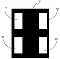
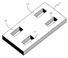
- 광-방출 광전자 요소 및 광전류-발생 광전자 요소를 포함하는 디바이스에 있어서,
상기 디바이스는 상기 광-방출 광전자 요소에 의해 방출된 광이 상기 디바이스 내에서의 경로를 통해 상기 광전류-발생 광전자 요소에 도달하는 것을 방지하는 불투명 요소(opaque element)를 더 포함하는, 디바이스. - 청구항 1에 있어서,
상기 광-방출 광전자 요소 및 상기 광전류-발생 광전자 요소는 동일한 조성을 가지며, 상기 광-방출 광전자 요소는 유효 순방향 바이어스 하에 있고, 상기 광전류-발생 광전자 요소는 유효 역방향 바이어스 하에 있는, 디바이스. - 청구항 1에 있어서,
상기 광-방출 광전자 요소는 방출 층을 포함하며, 상기 광전류-발생 광전자 요소는 흡수 층을 포함하는, 디바이스. - 청구항 3에 있어서,
상기 방출 층은 밴드 갭(E1)을 가지며, 상기 광전류-발생 층은 밴드 갭(E2)를 갖고, E1은 E2보다 큰, 디바이스. - 청구항 3에 있어서,
상기 방출 층은 유기 화합물을 포함하며, 상기 흡수 층은 유기 화합물을 포함하는, 디바이스. - 청구항 3에 있어서,
상기 방출 층은 양자 점들 또는 나노로드(nanorod)들로 이루어진 그룹으로부터 선택된 재료를 포함하며, 상기 흡수 층은 양자 점들 및 나노로드들로 이루어진 그룹으로부터 선택된 재료를 포함하는, 디바이스. - 청구항 3에 있어서,
상기 방출 층은 나노로드들을 포함하며, 상기 흡수 층은 나노로드들을 포함하는, 디바이스. - 청구항 3에 있어서,
상기 방출 층은 형광체(phosphor)들을 포함하며, 상기 흡수 층은 형광체들을 포함하는, 디바이스. - 청구항 1에 있어서,
상기 방출 층은 하나 이상의 이종접합들을 포함하며, 상기 흡수 층은 하나 이상의 이종접합들을 포함하는, 디바이스.
Priority Applications (1)
| Application Number | Priority Date | Filing Date | Title |
|---|---|---|---|
| KR1020217002885A KR102383500B1 (ko) | 2016-03-24 | 2017-03-23 | 광전자 디바이스 및 사용 방법들 |
Applications Claiming Priority (3)
| Application Number | Priority Date | Filing Date | Title |
|---|---|---|---|
| US201662312608P | 2016-03-24 | 2016-03-24 | |
| US62/312,608 | 2016-03-24 | ||
| PCT/US2017/023722 WO2017165592A1 (en) | 2016-03-24 | 2017-03-23 | Optoelectronic device and methods of use |
Related Child Applications (1)
| Application Number | Title | Priority Date | Filing Date |
|---|---|---|---|
| KR1020217002885A Division KR102383500B1 (ko) | 2016-03-24 | 2017-03-23 | 광전자 디바이스 및 사용 방법들 |
Publications (1)
| Publication Number | Publication Date |
|---|---|
| KR20190028362A true KR20190028362A (ko) | 2019-03-18 |
Family
ID=58489418
Family Applications (2)
| Application Number | Title | Priority Date | Filing Date |
|---|---|---|---|
| KR1020187029094A Ceased KR20190028362A (ko) | 2016-03-24 | 2017-03-23 | 광전자 디바이스 및 사용 방법들 |
| KR1020217002885A Expired - Fee Related KR102383500B1 (ko) | 2016-03-24 | 2017-03-23 | 광전자 디바이스 및 사용 방법들 |
Family Applications After (1)
| Application Number | Title | Priority Date | Filing Date |
|---|---|---|---|
| KR1020217002885A Expired - Fee Related KR102383500B1 (ko) | 2016-03-24 | 2017-03-23 | 광전자 디바이스 및 사용 방법들 |
Country Status (7)
| Country | Link |
|---|---|
| US (1) | US20210005668A1 (ko) |
| EP (1) | EP3433885A1 (ko) |
| JP (1) | JP6832364B2 (ko) |
| KR (2) | KR20190028362A (ko) |
| CN (1) | CN109564976A (ko) |
| TW (1) | TWI753890B (ko) |
| WO (1) | WO2017165592A1 (ko) |
Cited By (1)
| Publication number | Priority date | Publication date | Assignee | Title |
|---|---|---|---|---|
| US12219857B2 (en) | 2019-07-05 | 2025-02-04 | Semiconductor Energy Laboratory Co., Ltd. | Display apparatus, display module, and electronic device |
Families Citing this family (3)
| Publication number | Priority date | Publication date | Assignee | Title |
|---|---|---|---|---|
| KR102399447B1 (ko) * | 2017-10-16 | 2022-05-17 | 엘지디스플레이 주식회사 | 양자점과 이를 포함하는 양자점 발광다이오드 및 양자점 발광 표시장치 |
| KR20230043539A (ko) * | 2021-09-24 | 2023-03-31 | 삼성전자주식회사 | 광 다이오드 소자, 센서 및 전자 장치 |
| KR102874056B1 (ko) * | 2023-10-24 | 2025-10-20 | 한양대학교 에리카산학협력단 | 양자점 적층 방법, 이를 이용한 백색 발광 다이오드의 제조 방법 및 장치 |
Family Cites Families (11)
| Publication number | Priority date | Publication date | Assignee | Title |
|---|---|---|---|---|
| JPH05152603A (ja) * | 1991-11-28 | 1993-06-18 | Sharp Corp | 反射型光結合装置 |
| JP4911446B2 (ja) * | 2005-09-15 | 2012-04-04 | 富士フイルム株式会社 | エリアセンサ、画像入力装置、およびそれを組み込んだ電子写真装置等 |
| JP2009302252A (ja) * | 2008-06-12 | 2009-12-24 | Nissan Motor Co Ltd | 有機薄膜受光素子、有機薄膜受発光素子、有機薄膜受発光素子アレイ、これらを用いた脈拍センサ、およびこの脈拍センサを設けた車両 |
| US20120118368A1 (en) * | 2010-04-30 | 2012-05-17 | Board Of Regents Of The University Of Nebraska | Method for Increasing the Efficiency of Organic Photovoltaic Cells |
| US9632344B2 (en) | 2010-07-09 | 2017-04-25 | Lester F. Ludwig | Use of LED or OLED array to implement integrated combinations of touch screen tactile, touch gesture sensor, color image display, hand-image gesture sensor, document scanner, secure optical data exchange, and fingerprint processing capabilities |
| WO2012071107A1 (en) * | 2010-11-23 | 2012-05-31 | Qd Vision, Inc. | Device including semiconductor nanocrystals & method |
| JP5558446B2 (ja) * | 2011-09-26 | 2014-07-23 | 株式会社東芝 | 光電変換装置及びその製造方法 |
| WO2014088667A2 (en) * | 2012-09-14 | 2014-06-12 | Qd Vision, Inc. | Light emitting device including tandem structure |
| US20150243837A1 (en) * | 2013-03-15 | 2015-08-27 | Moonsub Shim | Multi-heterojunction nanoparticles, methods of manufacture thereof and articles comprising the same |
| DE102014221525B4 (de) * | 2014-05-16 | 2021-08-26 | Fraunhofer-Gesellschaft zur Förderung der angewandten Forschung e.V. | Messsystem |
| CN104409475A (zh) * | 2014-12-02 | 2015-03-11 | 京东方科技集团股份有限公司 | 一种有机电致发光显示器件、有机电致发光显示装置 |
-
2017
- 2017-03-15 TW TW106108609A patent/TWI753890B/zh not_active IP Right Cessation
- 2017-03-23 EP EP17715865.6A patent/EP3433885A1/en not_active Withdrawn
- 2017-03-23 JP JP2018549779A patent/JP6832364B2/ja not_active Expired - Fee Related
- 2017-03-23 US US16/087,384 patent/US20210005668A1/en not_active Abandoned
- 2017-03-23 WO PCT/US2017/023722 patent/WO2017165592A1/en not_active Ceased
- 2017-03-23 CN CN201780025724.3A patent/CN109564976A/zh active Pending
- 2017-03-23 KR KR1020187029094A patent/KR20190028362A/ko not_active Ceased
- 2017-03-23 KR KR1020217002885A patent/KR102383500B1/ko not_active Expired - Fee Related
Cited By (1)
| Publication number | Priority date | Publication date | Assignee | Title |
|---|---|---|---|---|
| US12219857B2 (en) | 2019-07-05 | 2025-02-04 | Semiconductor Energy Laboratory Co., Ltd. | Display apparatus, display module, and electronic device |
Also Published As
| Publication number | Publication date |
|---|---|
| CN109564976A (zh) | 2019-04-02 |
| KR20210013665A (ko) | 2021-02-04 |
| EP3433885A1 (en) | 2019-01-30 |
| TW201737511A (zh) | 2017-10-16 |
| WO2017165592A1 (en) | 2017-09-28 |
| JP6832364B2 (ja) | 2021-02-24 |
| US20210005668A1 (en) | 2021-01-07 |
| JP2019514200A (ja) | 2019-05-30 |
| TWI753890B (zh) | 2022-02-01 |
| KR102383500B1 (ko) | 2022-04-08 |
Similar Documents
| Publication | Publication Date | Title |
|---|---|---|
| KR102136075B1 (ko) | 광전자 디바이스 및 사용 방법들 | |
| US20080218068A1 (en) | Patterned inorganic led device | |
| US20140054540A1 (en) | Device including semiconductor nanocrystals & method | |
| JP2013506303A (ja) | 量子ドット−フラーレン接合ベースの光検出器 | |
| KR102383500B1 (ko) | 광전자 디바이스 및 사용 방법들 | |
| TWI744296B (zh) | 光電子裝置及使用方法 | |
| JP2020113542A (ja) | 光電子デバイス及び使用方法 | |
| Jiang | Light emitting diodes and photodetectors based on III-nitride and colloidal quantum dot materials |
Legal Events
| Date | Code | Title | Description |
|---|---|---|---|
| A201 | Request for examination | ||
| PA0105 | International application |
St.27 status event code: A-0-1-A10-A15-nap-PA0105 |
|
| PA0201 | Request for examination |
St.27 status event code: A-1-2-D10-D11-exm-PA0201 |
|
| R17-X000 | Change to representative recorded |
St.27 status event code: A-3-3-R10-R17-oth-X000 |
|
| T11-X000 | Administrative time limit extension requested |
St.27 status event code: U-3-3-T10-T11-oth-X000 |
|
| T11-X000 | Administrative time limit extension requested |
St.27 status event code: U-3-3-T10-T11-oth-X000 |
|
| P11-X000 | Amendment of application requested |
St.27 status event code: A-2-2-P10-P11-nap-X000 |
|
| P13-X000 | Application amended |
St.27 status event code: A-2-2-P10-P13-nap-X000 |
|
| PG1501 | Laying open of application |
St.27 status event code: A-1-1-Q10-Q12-nap-PG1501 |
|
| E902 | Notification of reason for refusal | ||
| PE0902 | Notice of grounds for rejection |
St.27 status event code: A-1-2-D10-D21-exm-PE0902 |
|
| AMND | Amendment | ||
| P11-X000 | Amendment of application requested |
St.27 status event code: A-2-2-P10-P11-nap-X000 |
|
| P13-X000 | Application amended |
St.27 status event code: A-2-2-P10-P13-nap-X000 |
|
| E601 | Decision to refuse application | ||
| PE0601 | Decision on rejection of patent |
St.27 status event code: N-2-6-B10-B15-exm-PE0601 |
|
| X091 | Application refused [patent] | ||
| R18-X000 | Changes to party contact information recorded |
St.27 status event code: A-3-3-R10-R18-oth-X000 |
|
| R18-X000 | Changes to party contact information recorded |
St.27 status event code: A-3-3-R10-R18-oth-X000 |
|
| AMND | Amendment | ||
| E13-X000 | Pre-grant limitation requested |
St.27 status event code: A-2-3-E10-E13-lim-X000 |
|
| P11-X000 | Amendment of application requested |
St.27 status event code: A-2-2-P10-P11-nap-X000 |
|
| P13-X000 | Application amended |
St.27 status event code: A-2-2-P10-P13-nap-X000 |
|
| PX0901 | Re-examination |
St.27 status event code: A-2-3-E10-E12-rex-PX0901 |
|
| E902 | Notification of reason for refusal | ||
| PE0902 | Notice of grounds for rejection |
St.27 status event code: A-1-2-D10-D21-exm-PE0902 |
|
| T11-X000 | Administrative time limit extension requested |
St.27 status event code: U-3-3-T10-T11-oth-X000 |
|
| AMND | Amendment | ||
| P11-X000 | Amendment of application requested |
St.27 status event code: A-2-2-P10-P11-nap-X000 |
|
| P13-X000 | Application amended |
St.27 status event code: A-2-2-P10-P13-nap-X000 |
|
| PX0601 | Decision of rejection after re-examination |
St.27 status event code: N-2-6-B10-B17-rex-PX0601 |
|
| X601 | Decision of rejection after re-examination | ||
| A107 | Divisional application of patent | ||
| PA0104 | Divisional application for international application |
St.27 status event code: A-0-1-A10-A18-div-PA0104 St.27 status event code: A-0-1-A10-A16-div-PA0104 |
|
| P22-X000 | Classification modified |
St.27 status event code: A-2-2-P10-P22-nap-X000 |
|
| P22-X000 | Classification modified |
St.27 status event code: A-2-2-P10-P22-nap-X000 |
|
| PN2301 | Change of applicant |
St.27 status event code: A-3-3-R10-R13-asn-PN2301 St.27 status event code: A-3-3-R10-R11-asn-PN2301 |
|
| P22-X000 | Classification modified |
St.27 status event code: A-2-2-P10-P22-nap-X000 |