KR20190024909A - Method for manufacturing high quality graphene on the surface of silicon carbide - Google Patents
Method for manufacturing high quality graphene on the surface of silicon carbide Download PDFInfo
- Publication number
- KR20190024909A KR20190024909A KR1020187037935A KR20187037935A KR20190024909A KR 20190024909 A KR20190024909 A KR 20190024909A KR 1020187037935 A KR1020187037935 A KR 1020187037935A KR 20187037935 A KR20187037935 A KR 20187037935A KR 20190024909 A KR20190024909 A KR 20190024909A
- Authority
- KR
- South Korea
- Prior art keywords
- graphene
- temperature
- silicon
- annealing
- silicon carbide
- Prior art date
Links
- OKTJSMMVPCPJKN-UHFFFAOYSA-N Carbon Chemical compound [C] OKTJSMMVPCPJKN-UHFFFAOYSA-N 0.000 title claims abstract description 76
- 229910021389 graphene Inorganic materials 0.000 title claims abstract description 75
- 238000000034 method Methods 0.000 title claims abstract description 52
- 229910010271 silicon carbide Inorganic materials 0.000 title claims abstract description 47
- HBMJWWWQQXIZIP-UHFFFAOYSA-N silicon carbide Chemical compound [Si+]#[C-] HBMJWWWQQXIZIP-UHFFFAOYSA-N 0.000 title claims abstract description 46
- 238000004519 manufacturing process Methods 0.000 title claims abstract description 16
- XUIMIQQOPSSXEZ-UHFFFAOYSA-N Silicon Chemical group [Si] XUIMIQQOPSSXEZ-UHFFFAOYSA-N 0.000 claims abstract description 54
- 238000000859 sublimation Methods 0.000 claims abstract description 16
- 230000008022 sublimation Effects 0.000 claims abstract description 16
- 238000000137 annealing Methods 0.000 claims description 33
- 229910052710 silicon Inorganic materials 0.000 claims description 29
- 239000010703 silicon Substances 0.000 claims description 24
- 239000013078 crystal Substances 0.000 claims description 14
- 238000000004 low energy electron diffraction Methods 0.000 claims description 8
- 230000007547 defect Effects 0.000 claims description 7
- 238000001228 spectrum Methods 0.000 claims description 7
- 238000005087 graphitization Methods 0.000 abstract description 16
- 150000001875 compounds Chemical class 0.000 abstract description 2
- 239000010410 layer Substances 0.000 description 21
- 230000008569 process Effects 0.000 description 18
- 238000002360 preparation method Methods 0.000 description 15
- 239000012535 impurity Substances 0.000 description 13
- 230000015572 biosynthetic process Effects 0.000 description 10
- 238000004002 angle-resolved photoelectron spectroscopy Methods 0.000 description 8
- 238000012360 testing method Methods 0.000 description 8
- 125000004432 carbon atom Chemical group C* 0.000 description 7
- 239000007789 gas Substances 0.000 description 7
- 230000001965 increasing effect Effects 0.000 description 7
- 239000000758 substrate Substances 0.000 description 7
- 239000006185 dispersion Substances 0.000 description 6
- 238000003786 synthesis reaction Methods 0.000 description 6
- 239000000463 material Substances 0.000 description 5
- 238000007872 degassing Methods 0.000 description 4
- 238000005086 pumping Methods 0.000 description 4
- 239000002356 single layer Substances 0.000 description 4
- XKRFYHLGVUSROY-UHFFFAOYSA-N Argon Chemical compound [Ar] XKRFYHLGVUSROY-UHFFFAOYSA-N 0.000 description 3
- 238000009826 distribution Methods 0.000 description 3
- IJGRMHOSHXDMSA-UHFFFAOYSA-N Atomic nitrogen Chemical compound N#N IJGRMHOSHXDMSA-UHFFFAOYSA-N 0.000 description 2
- 238000004458 analytical method Methods 0.000 description 2
- 239000002800 charge carrier Substances 0.000 description 2
- 238000006243 chemical reaction Methods 0.000 description 2
- 230000001939 inductive effect Effects 0.000 description 2
- 229910052751 metal Inorganic materials 0.000 description 2
- 239000002184 metal Substances 0.000 description 2
- 238000001000 micrograph Methods 0.000 description 2
- 230000005855 radiation Effects 0.000 description 2
- 238000004574 scanning tunneling microscopy Methods 0.000 description 2
- IUVCFHHAEHNCFT-INIZCTEOSA-N 2-[(1s)-1-[4-amino-3-(3-fluoro-4-propan-2-yloxyphenyl)pyrazolo[3,4-d]pyrimidin-1-yl]ethyl]-6-fluoro-3-(3-fluorophenyl)chromen-4-one Chemical compound C1=C(F)C(OC(C)C)=CC=C1C(C1=C(N)N=CN=C11)=NN1[C@@H](C)C1=C(C=2C=C(F)C=CC=2)C(=O)C2=CC(F)=CC=C2O1 IUVCFHHAEHNCFT-INIZCTEOSA-N 0.000 description 1
- AFCARXCZXQIEQB-UHFFFAOYSA-N N-[3-oxo-3-(2,4,6,7-tetrahydrotriazolo[4,5-c]pyridin-5-yl)propyl]-2-[[3-(trifluoromethoxy)phenyl]methylamino]pyrimidine-5-carboxamide Chemical compound O=C(CCNC(=O)C=1C=NC(=NC=1)NCC1=CC(=CC=C1)OC(F)(F)F)N1CC2=C(CC1)NN=N2 AFCARXCZXQIEQB-UHFFFAOYSA-N 0.000 description 1
- 229910052786 argon Inorganic materials 0.000 description 1
- 125000004429 atom Chemical group 0.000 description 1
- 230000009286 beneficial effect Effects 0.000 description 1
- 230000008901 benefit Effects 0.000 description 1
- 238000009529 body temperature measurement Methods 0.000 description 1
- 230000008859 change Effects 0.000 description 1
- 238000005229 chemical vapour deposition Methods 0.000 description 1
- 239000002131 composite material Substances 0.000 description 1
- 238000011109 contamination Methods 0.000 description 1
- 238000007796 conventional method Methods 0.000 description 1
- 238000001816 cooling Methods 0.000 description 1
- 238000000151 deposition Methods 0.000 description 1
- 238000003795 desorption Methods 0.000 description 1
- 239000002019 doping agent Substances 0.000 description 1
- 238000001941 electron spectroscopy Methods 0.000 description 1
- 238000000295 emission spectrum Methods 0.000 description 1
- 230000008020 evaporation Effects 0.000 description 1
- 238000001704 evaporation Methods 0.000 description 1
- 238000004299 exfoliation Methods 0.000 description 1
- 229910002804 graphite Inorganic materials 0.000 description 1
- 239000010439 graphite Substances 0.000 description 1
- 238000009499 grossing Methods 0.000 description 1
- 238000003384 imaging method Methods 0.000 description 1
- 230000006872 improvement Effects 0.000 description 1
- 239000007788 liquid Substances 0.000 description 1
- 238000005259 measurement Methods 0.000 description 1
- 229910052757 nitrogen Inorganic materials 0.000 description 1
- 230000003287 optical effect Effects 0.000 description 1
- 230000010355 oscillation Effects 0.000 description 1
- 239000002245 particle Substances 0.000 description 1
- 230000010287 polarization Effects 0.000 description 1
- 238000009417 prefabrication Methods 0.000 description 1
- 238000013441 quality evaluation Methods 0.000 description 1
- 238000004611 spectroscopical analysis Methods 0.000 description 1
- 230000007847 structural defect Effects 0.000 description 1
- 238000006467 substitution reaction Methods 0.000 description 1
- 239000002344 surface layer Substances 0.000 description 1
- 230000002194 synthesizing effect Effects 0.000 description 1
- 238000010189 synthetic method Methods 0.000 description 1
- 238000012546 transfer Methods 0.000 description 1
- 230000007704 transition Effects 0.000 description 1
- WFKWXMTUELFFGS-UHFFFAOYSA-N tungsten Chemical compound [W] WFKWXMTUELFFGS-UHFFFAOYSA-N 0.000 description 1
- 229910052721 tungsten Inorganic materials 0.000 description 1
- 239000010937 tungsten Substances 0.000 description 1
- 230000005641 tunneling Effects 0.000 description 1
Images


Classifications
-
- C—CHEMISTRY; METALLURGY
- C30—CRYSTAL GROWTH
- C30B—SINGLE-CRYSTAL GROWTH; UNIDIRECTIONAL SOLIDIFICATION OF EUTECTIC MATERIAL OR UNIDIRECTIONAL DEMIXING OF EUTECTOID MATERIAL; REFINING BY ZONE-MELTING OF MATERIAL; PRODUCTION OF A HOMOGENEOUS POLYCRYSTALLINE MATERIAL WITH DEFINED STRUCTURE; SINGLE CRYSTALS OR HOMOGENEOUS POLYCRYSTALLINE MATERIAL WITH DEFINED STRUCTURE; AFTER-TREATMENT OF SINGLE CRYSTALS OR A HOMOGENEOUS POLYCRYSTALLINE MATERIAL WITH DEFINED STRUCTURE; APPARATUS THEREFOR
- C30B1/00—Single-crystal growth directly from the solid state
- C30B1/02—Single-crystal growth directly from the solid state by thermal treatment, e.g. strain annealing
-
- C—CHEMISTRY; METALLURGY
- C01—INORGANIC CHEMISTRY
- C01B—NON-METALLIC ELEMENTS; COMPOUNDS THEREOF; METALLOIDS OR COMPOUNDS THEREOF NOT COVERED BY SUBCLASS C01C
- C01B32/00—Carbon; Compounds thereof
- C01B32/15—Nano-sized carbon materials
- C01B32/182—Graphene
- C01B32/184—Preparation
-
- C—CHEMISTRY; METALLURGY
- C01—INORGANIC CHEMISTRY
- C01B—NON-METALLIC ELEMENTS; COMPOUNDS THEREOF; METALLOIDS OR COMPOUNDS THEREOF NOT COVERED BY SUBCLASS C01C
- C01B32/00—Carbon; Compounds thereof
- C01B32/15—Nano-sized carbon materials
- C01B32/182—Graphene
- C01B32/184—Preparation
- C01B32/188—Preparation by epitaxial growth
-
- C—CHEMISTRY; METALLURGY
- C30—CRYSTAL GROWTH
- C30B—SINGLE-CRYSTAL GROWTH; UNIDIRECTIONAL SOLIDIFICATION OF EUTECTIC MATERIAL OR UNIDIRECTIONAL DEMIXING OF EUTECTOID MATERIAL; REFINING BY ZONE-MELTING OF MATERIAL; PRODUCTION OF A HOMOGENEOUS POLYCRYSTALLINE MATERIAL WITH DEFINED STRUCTURE; SINGLE CRYSTALS OR HOMOGENEOUS POLYCRYSTALLINE MATERIAL WITH DEFINED STRUCTURE; AFTER-TREATMENT OF SINGLE CRYSTALS OR A HOMOGENEOUS POLYCRYSTALLINE MATERIAL WITH DEFINED STRUCTURE; APPARATUS THEREFOR
- C30B1/00—Single-crystal growth directly from the solid state
- C30B1/10—Single-crystal growth directly from the solid state by solid state reactions or multi-phase diffusion
-
- C—CHEMISTRY; METALLURGY
- C30—CRYSTAL GROWTH
- C30B—SINGLE-CRYSTAL GROWTH; UNIDIRECTIONAL SOLIDIFICATION OF EUTECTIC MATERIAL OR UNIDIRECTIONAL DEMIXING OF EUTECTOID MATERIAL; REFINING BY ZONE-MELTING OF MATERIAL; PRODUCTION OF A HOMOGENEOUS POLYCRYSTALLINE MATERIAL WITH DEFINED STRUCTURE; SINGLE CRYSTALS OR HOMOGENEOUS POLYCRYSTALLINE MATERIAL WITH DEFINED STRUCTURE; AFTER-TREATMENT OF SINGLE CRYSTALS OR A HOMOGENEOUS POLYCRYSTALLINE MATERIAL WITH DEFINED STRUCTURE; APPARATUS THEREFOR
- C30B25/00—Single-crystal growth by chemical reaction of reactive gases, e.g. chemical vapour-deposition growth
- C30B25/02—Epitaxial-layer growth
- C30B25/18—Epitaxial-layer growth characterised by the substrate
-
- C—CHEMISTRY; METALLURGY
- C30—CRYSTAL GROWTH
- C30B—SINGLE-CRYSTAL GROWTH; UNIDIRECTIONAL SOLIDIFICATION OF EUTECTIC MATERIAL OR UNIDIRECTIONAL DEMIXING OF EUTECTOID MATERIAL; REFINING BY ZONE-MELTING OF MATERIAL; PRODUCTION OF A HOMOGENEOUS POLYCRYSTALLINE MATERIAL WITH DEFINED STRUCTURE; SINGLE CRYSTALS OR HOMOGENEOUS POLYCRYSTALLINE MATERIAL WITH DEFINED STRUCTURE; AFTER-TREATMENT OF SINGLE CRYSTALS OR A HOMOGENEOUS POLYCRYSTALLINE MATERIAL WITH DEFINED STRUCTURE; APPARATUS THEREFOR
- C30B29/00—Single crystals or homogeneous polycrystalline material with defined structure characterised by the material or by their shape
- C30B29/02—Elements
-
- C—CHEMISTRY; METALLURGY
- C30—CRYSTAL GROWTH
- C30B—SINGLE-CRYSTAL GROWTH; UNIDIRECTIONAL SOLIDIFICATION OF EUTECTIC MATERIAL OR UNIDIRECTIONAL DEMIXING OF EUTECTOID MATERIAL; REFINING BY ZONE-MELTING OF MATERIAL; PRODUCTION OF A HOMOGENEOUS POLYCRYSTALLINE MATERIAL WITH DEFINED STRUCTURE; SINGLE CRYSTALS OR HOMOGENEOUS POLYCRYSTALLINE MATERIAL WITH DEFINED STRUCTURE; AFTER-TREATMENT OF SINGLE CRYSTALS OR A HOMOGENEOUS POLYCRYSTALLINE MATERIAL WITH DEFINED STRUCTURE; APPARATUS THEREFOR
- C30B33/00—After-treatment of single crystals or homogeneous polycrystalline material with defined structure
- C30B33/02—Heat treatment
-
- H—ELECTRICITY
- H01—ELECTRIC ELEMENTS
- H01L—SEMICONDUCTOR DEVICES NOT COVERED BY CLASS H10
- H01L29/00—Semiconductor devices adapted for rectifying, amplifying, oscillating or switching, or capacitors or resistors with at least one potential-jump barrier or surface barrier, e.g. PN junction depletion layer or carrier concentration layer; Details of semiconductor bodies or of electrodes thereof ; Multistep manufacturing processes therefor
- H01L29/02—Semiconductor bodies ; Multistep manufacturing processes therefor
- H01L29/12—Semiconductor bodies ; Multistep manufacturing processes therefor characterised by the materials of which they are formed
- H01L29/16—Semiconductor bodies ; Multistep manufacturing processes therefor characterised by the materials of which they are formed including, apart from doping materials or other impurities, only elements of Group IV of the Periodic System
- H01L29/1606—Graphene
-
- B—PERFORMING OPERATIONS; TRANSPORTING
- B82—NANOTECHNOLOGY
- B82Y—SPECIFIC USES OR APPLICATIONS OF NANOSTRUCTURES; MEASUREMENT OR ANALYSIS OF NANOSTRUCTURES; MANUFACTURE OR TREATMENT OF NANOSTRUCTURES
- B82Y30/00—Nanotechnology for materials or surface science, e.g. nanocomposites
-
- B—PERFORMING OPERATIONS; TRANSPORTING
- B82—NANOTECHNOLOGY
- B82Y—SPECIFIC USES OR APPLICATIONS OF NANOSTRUCTURES; MEASUREMENT OR ANALYSIS OF NANOSTRUCTURES; MANUFACTURE OR TREATMENT OF NANOSTRUCTURES
- B82Y40/00—Manufacture or treatment of nanostructures
-
- C—CHEMISTRY; METALLURGY
- C01—INORGANIC CHEMISTRY
- C01B—NON-METALLIC ELEMENTS; COMPOUNDS THEREOF; METALLOIDS OR COMPOUNDS THEREOF NOT COVERED BY SUBCLASS C01C
- C01B2204/00—Structure or properties of graphene
- C01B2204/20—Graphene characterized by its properties
- C01B2204/22—Electronic properties
-
- C—CHEMISTRY; METALLURGY
- C01—INORGANIC CHEMISTRY
- C01B—NON-METALLIC ELEMENTS; COMPOUNDS THEREOF; METALLOIDS OR COMPOUNDS THEREOF NOT COVERED BY SUBCLASS C01C
- C01B2204/00—Structure or properties of graphene
- C01B2204/20—Graphene characterized by its properties
- C01B2204/24—Thermal properties
-
- C—CHEMISTRY; METALLURGY
- C01—INORGANIC CHEMISTRY
- C01B—NON-METALLIC ELEMENTS; COMPOUNDS THEREOF; METALLOIDS OR COMPOUNDS THEREOF NOT COVERED BY SUBCLASS C01C
- C01B2204/00—Structure or properties of graphene
- C01B2204/20—Graphene characterized by its properties
- C01B2204/26—Mechanical properties
-
- C—CHEMISTRY; METALLURGY
- C01—INORGANIC CHEMISTRY
- C01P—INDEXING SCHEME RELATING TO STRUCTURAL AND PHYSICAL ASPECTS OF SOLID INORGANIC COMPOUNDS
- C01P2002/00—Crystal-structural characteristics
- C01P2002/70—Crystal-structural characteristics defined by measured X-ray, neutron or electron diffraction data
- C01P2002/74—Crystal-structural characteristics defined by measured X-ray, neutron or electron diffraction data by peak-intensities or a ratio thereof only
-
- C—CHEMISTRY; METALLURGY
- C01—INORGANIC CHEMISTRY
- C01P—INDEXING SCHEME RELATING TO STRUCTURAL AND PHYSICAL ASPECTS OF SOLID INORGANIC COMPOUNDS
- C01P2006/00—Physical properties of inorganic compounds
- C01P2006/32—Thermal properties
-
- C—CHEMISTRY; METALLURGY
- C01—INORGANIC CHEMISTRY
- C01P—INDEXING SCHEME RELATING TO STRUCTURAL AND PHYSICAL ASPECTS OF SOLID INORGANIC COMPOUNDS
- C01P2006/00—Physical properties of inorganic compounds
- C01P2006/40—Electric properties
-
- H—ELECTRICITY
- H01—ELECTRIC ELEMENTS
- H01L—SEMICONDUCTOR DEVICES NOT COVERED BY CLASS H10
- H01L21/00—Processes or apparatus adapted for the manufacture or treatment of semiconductor or solid state devices or of parts thereof
- H01L21/02—Manufacture or treatment of semiconductor devices or of parts thereof
- H01L21/02104—Forming layers
- H01L21/02365—Forming inorganic semiconducting materials on a substrate
- H01L21/02367—Substrates
- H01L21/0237—Materials
- H01L21/02373—Group 14 semiconducting materials
- H01L21/02378—Silicon carbide
-
- H—ELECTRICITY
- H01—ELECTRIC ELEMENTS
- H01L—SEMICONDUCTOR DEVICES NOT COVERED BY CLASS H10
- H01L21/00—Processes or apparatus adapted for the manufacture or treatment of semiconductor or solid state devices or of parts thereof
- H01L21/02—Manufacture or treatment of semiconductor devices or of parts thereof
- H01L21/02104—Forming layers
- H01L21/02365—Forming inorganic semiconducting materials on a substrate
- H01L21/02367—Substrates
- H01L21/02433—Crystal orientation
-
- H—ELECTRICITY
- H01—ELECTRIC ELEMENTS
- H01L—SEMICONDUCTOR DEVICES NOT COVERED BY CLASS H10
- H01L21/00—Processes or apparatus adapted for the manufacture or treatment of semiconductor or solid state devices or of parts thereof
- H01L21/02—Manufacture or treatment of semiconductor devices or of parts thereof
- H01L21/02104—Forming layers
- H01L21/02365—Forming inorganic semiconducting materials on a substrate
- H01L21/02518—Deposited layers
- H01L21/02521—Materials
- H01L21/02524—Group 14 semiconducting materials
- H01L21/02527—Carbon, e.g. diamond-like carbon
Abstract
외부 승화 소스로부터 규소 원자의 스트림에서 화합물의 표면 흑연화에 의해 탄화규소의 표면 (0001) 상에 고품질 그래핀의 제조를 위한 방법이 개시된다.A method is disclosed for the production of high quality graphene on the surface (0001) of silicon carbide by surface graphitization of the compound in a stream of silicon atoms from an external sublimation source.
Description
본 발명은 외부 승화 소스로부터의 규소 원자의 스트림에서 화합물의 표면 흑연화(superficial graphitisation)에 의해 탄화규소의 표면 (0001) 상에서 고품질 그래핀의 제조를 위한 개선된 방법에 관한 것이다.The present invention relates to an improved method for the production of high quality graphene on the surface (0001) of silicon carbide by superficial graphitization of the compound in a stream of silicon atoms from an external sublimation source.
전하 캐리어의 매우 높은 이동도(규소에 대해 최대 200 000 ㎠ V-1s-1[1] 까지인 한편, 1400 ㎠ V-1s-1[2]과 비교하여); 전하 캐리어의 높은 포화 속도(약 5×10⁷ ㎝ s-1), 매우 높은 열전도(5000 W/mK까지)[3]; 기계적 강도[4]; 또는 실온에서 전기 전도의 거의 탄도 특성[5]과 같은 그 고유 특성으로 인하여, 그래핀은 규소 이외의 물질을 기반으로 하는, 미래 전자 기기에 적용되는 가장 중요한 물질들 중 하나이다.Very high mobility of charge carriers (up to 200 000 cm 2 V -1 s -1 [1] for silicon while 1400 cm 2 V -1 s -1 [2]); High saturation rate of charge carrier (about 5 × 10 7 cm s -1 ), very high thermal conductivity (up to 5000 W / mK) [3]; Mechanical strength [4]; Or due to its inherent properties such as the nearly trajectory properties of electrical conduction at room temperature [5], graphene is one of the most important materials applied to future electronic devices based on materials other than silicon.
큰 크기의 단결정 영역(single crystalline domain)과의 고품질 그래핀의 합성은 여전히 큰 도전 과제이다. 흑연의 화학 기상 증착, 기계적 박리, 일정 체적의 금속에 용해된 탄소 원자의 표면 배치(superficial ordering), 또는 화학 반응에 의한 합성과 같은 현재 사용되는 합성 방법은 매우 때때로 이론적으로 예측되는 특성보다 훨씬 나쁜 특성을 가지는 물질의 형성으로 이어진다. 추가적으로, 전자 기기에서 사용하기 위해 그래핀을 절연 기판 상으로 전사하는 필요성은 문제가 있다.The synthesis of high quality graphene with a large single crystalline domain is still a big challenge. Presently used synthetic methods such as chemical vapor deposition of graphite, mechanical exfoliation, superficial ordering of carbon atoms dissolved in a certain volume of metal, or synthesis by chemical reaction are sometimes very worse than theoretically predicted properties Followed by formation of a material having properties. Additionally, the need to transfer graphene onto an insulating substrate for use in electronic equipment is problematic.
절연 기판 상에 그래핀을 직접 합성하는 가장 유망한 방법 중 하나는 이미 1961년에 처음으로 관찰된 (0001) 결정학적 방향(crystallographic orientation)을 가지는 탄화규소 표면의 표면 흑연화이다[6]. 1100-1200℃의 온도에서, 초고도 진공(UHV) 하에서, 표면 SiC 층이 열분해된다. 보다 휘발성인 규소 원자는 탈착되고, 표면 상에 잔류하는 과잉 탄소 원자는 재조직되어 그래핀 층을 형성한다[7].One of the most promising methods for directly synthesizing graphene on insulating substrates is the surface graphitization of silicon carbide surfaces already having a (0001) crystallographic orientation, which was first observed in 1961 [6]. At a temperature of 1100-1200 ° C, under super-high vacuum (UHV), the surface SiC layer is pyrolyzed. The more volatile silicon atoms are desorbed, and the excess carbon atoms remaining on the surface are reorganized to form a graphene layer [7].
그래핀의 형성은 단차형 가장자리(step edge)에서 SiC 기판의 제1 표면 층에서부터 시작하여, 표면 상에서 물질 내로 더욱 깊숙이 진행된다[9]. 단분자층을 형성하도록, 탄화규소의 3개의 층이 평균적으로 분해되어야 한다. 형성된 단분자층 아래에 소위 버퍼 층이 형성되고, 버퍼 층에서, 탄소 원자는 보다 높은 그래핀 층에서와 같이 유사하게 배치되지만, 탄소 원자는 여전히 SiC 내부의 규소 원자와 공유 결합(covalent bond)을 형성한다. 이러한 층은 탄화규소의 재조직된 표면이며, 비전도성이다. 이러한 것은 또한 위에 놓인 그래핀의 n-형 도핑에 대한 책임이 있다[13]. 제1 단분자층의 형성 후에, 그래핀의 추가 성장은 그 결함에 의해 제한된다.The formation of graphene proceeds deeper into the material on the surface, starting from the first surface layer of the SiC substrate at the step edge [9]. In order to form a monolayer, the three layers of silicon carbide have to be decomposed on average. A so-called buffer layer is formed below the formed monolayer, and in the buffer layer, the carbon atoms are similarly arranged as in the higher graphene layer, but the carbon atoms still form a covalent bond with the silicon atoms in the SiC . This layer is the reorganized surface of silicon carbide and is nonconductive. This is also responsible for the n-type doping of the overlying graphene [13]. After the formation of the first monolayer, further growth of graphene is limited by the defect.
요약하면, 초고도 진공 조건 하에서, 흑연화는 비교적 낮은 온도에서 발생하며, 이러한 온도에서, 탄소 원자는 매우 낮은 이동도를 가지며 약 1 내지 약 6개의 단분자층의 가변적인 두께를 가지는 고도 결함의 그래핀 층을 형성한다.In summary, under ultra-high vacuum conditions, graphitization occurs at relatively low temperatures, at which carbon atoms have a very low mobility and have a variable thickness of about 1 to about 6 monolayers, .
특허 출원 US20140175458 A1은 온도 T1=810-900℃ 및 T2=1010-1100℃에서 이중 어닐링에 의해 연결된 탄화규소의 표면 상에 금속층을 침착시키는(depositing) 것으로 이루어진, 탄화규소의 표면 상에서의 그래핀 합성을 위한 방법이 기술되어 있다. 이러한 방법은 기판(순수 SiC 표면)으로부터 그래핀을 분리하는 금속-탄화규소 복합체의 층 상에 그래핀의 형성을 야기한다.The patent application US20140175458 A1 discloses a process for the preparation of graphene composites on the surface of silicon carbide consisting of depositing a metal layer on the surface of silicon carbide connected by double annealing at temperatures T1 = 810-900 ° C and T2 = 1010-1100 ° C. A method is described. This method causes the formation of graphene on the layer of the metal-silicon carbide composite separating the graphene from the substrate (pure SiC surface).
특허 US 9150417 B2는 탄화규소의 표면 흑연화에 의해 얻어진 그래핀의 품질의 향상에 관한 발명을 개시한다. 이러한 것은 약 600 mbar-1 bar의 압력 하에서 버퍼 가스 분위기(예를 들어, 아르곤)에서 흑연화를 수행하는 것으로 이루어진다. 이러한 조건 하에서, 규소 원자의 승화 속도는 탈착 후에, 규소 원자가 아르곤 원자와의 충돌의 결과로 표면 상으로의 복귀의 한정된 개연성을 가지기 때문에 상당히 감소되며[11]; 대안적으로 열역학적인 용어에 있어서 압력-체적 인자에 의한 이러한 천이(transition)의 엔탈피를 증가시킨 후에 증발 공정의 둔화(slowdown)로서 이해될 수 있다. 이러한 사실로 인해, 흑연화 공정은 약 1450-1500℃의 상당히 높은 온도에서 일어난다. 이러한 온도 범위에서, 탄소 원자는 보다 높은 이동도를 가지며, 고품질과 약 1-2 단분자층의 비교적 균일한 두께를 특징으로 하는 그래핀 층을 형성한다[10]. 이러한 공정에서 그래핀 품질은 기판의 표면의 품질에 크게 좌우된다.Patent US 9150417 B2 discloses an invention relating to an improvement in the quality of graphene obtained by surface graphitization of silicon carbide. This consists in carrying out the graphitization in a buffer gas atmosphere (for example argon) under a pressure of about 600 mbar- 1 bar. Under these conditions, the rate of sublimation of silicon atoms is significantly reduced after desorption, since silicon atoms have a limited likelihood of return to the surface as a result of collisions with argon atoms [11]; Alternatively, it can be understood as a slowdown of the evaporation process after increasing the enthalpy of such transition by the pressure-volumetric factor in thermodynamic terms. Due to this fact, the graphitization process takes place at a significantly high temperature of about 1450-1500 ° C. In this temperature range, carbon atoms have higher mobility and form a graphene layer characterized by a high quality and relatively uniform thickness of about 1-2 monolayers [10]. In such a process, graphene quality greatly depends on the quality of the surface of the substrate.
기술되는 공정에서 사용된 버퍼 가스가 최대 6N의 순도(10-6 불순물)를 특징으로할 수 있다는 것에 유의해야 한다. 약 1 bar의 반응 챔버에서의 가스 압력 하에서, 도판트의 분압은 약 1000 L/s(초당 불순물의 1000개의 층)의 거대한 체적을 가지는 불순물의 알려지지 않은 입자의 스트림에 대한 표면의 노출에 대응하는 약 10-3 mbar에 달한다.It should be noted that the buffer gas used in the process described may be characterized by a purity of up to 6N (10 < -6 > impurity). Under a gas pressure in a reaction chamber of about 1 bar, the partial pressure of the dopant corresponds to an exposure of the surface to a stream of unknown particles of impurities having a gigantic volume of about 1000 L / s (1000 layers of impurities per second) It reaches about 10 -3 mbar.
특허 출원 US20110223094 A1은 일부 예에서 2개의 결정체: 규소 및 탄화규소를 진공 챔버에 평행하게 배치하고, 그런 다음 진공 챔버로부터 약 1×10⁻⁶ mbar의 압력으로 공기를 펌핑하고, 약 1200℃의 온도로 규소 결정체의 어닐링하고, 1500℃, 1600℃ 및 1700℃의 온도로 탄화규소 결정체의 동시 어닐링하는 것에 의해 탄화 규소의 표면 상에서의 그래핀 합성으로 이루어진 발명을 기술하고 있다. The patent application US20110223094 A1 discloses, in some instances, two crystals: silicon and silicon carbide disposed in parallel to the vacuum chamber, then pumped air from the vacuum chamber at a pressure of about 1 x 10⁻⁶ mbar, Discloses an invention comprising graphene synthesis on the surface of silicon carbide by annealing the silicon crystal and simultaneously annealing the silicon carbide crystal at temperatures of 1500 占 폚, 1600 占 폚 and 1700 占 폚.
본 발명의 목적은 낮은 수준의 불순물 및 그래핀 결정질 격자의 기본적으로 무결함 구조, 즉 허니콤 구조를 구비하는 고품질 그래핀뿐만 아니라 고품질 그래핀을 얻기 위한 방법을 제공하는 것이다.It is an object of the present invention to provide a method for obtaining high-quality graphenes as well as high-quality graphenes having a low-level impurity and a substantially defect-free structure of graphene crystalline lattice, that is, a honeycomb structure.
놀랍게도, 본 발명에 따라서 달성되는 흑연화 처리되는 탄화규소의 표면의 부근에서의 규소 분압에서의 증가가 유익하게 규소 원자의 승화의 과정을 늦추어, 보다 양호하게 배치된 고품질 그래핀의 합성으로 이어지는 것이 알려졌다.Surprisingly, an increase in the silicon partial pressure near the surface of the graphitized silicon carbide achieved according to the present invention advantageously slows down the process of sublimation of silicon atoms, leading to the synthesis of better-quality graphene It was announced.
본 발명은 탄화규소 표면 상에서의 그래핀의 제조를 위한 방법에 관한 것으로서, 표면 (0001)의 결정학적 방향을 가지는 SiC 결정이 연속적으로:The present invention relates to a method for the production of graphene on a silicon carbide surface, characterized in that the SiC crystal with the crystallographic orientation of the surface (0001)
a) 1×10⁻⁹ mbar 보다 낮은 압력;a) a pressure less than 1 x 10 < -9 > mbar;
b) 선택적으로 1×10⁻⁸ mbar 보다 높지 않은 압력 하에서, 300℃ 내지 900℃의 온도에서 선택적으로 어닐링되고;b) optionally annealing at a temperature of from 300 DEG C to 900 DEG C under a pressure not higher than 1 x 10 < -8 > mbar;
c) 0.5 Å/min 내지 2.5 Å/min의 공칭 규소 성장 속도(nominal silicon growth rate)를 제공하는 외부 승화 소스로부터의 규소 원자의 스트림에서 900℃ 내지 1050℃의 온도에서 선택적으로 어닐링되고;c) optionally annealing at a temperature of 900 占 폚 to 1050 占 폚 in a stream of silicon atoms from an external sublimation source providing a nominal silicon growth rate of 0.5? / min to 2.5? / min;
d) 0.5 Å/min 내지 10 Å/min의 공칭 규소 성장 속도를 제공하는 외부 승화 소스로부터의 규소 원자 스트림에서, 5×10⁻⁷ mbar 보다 높지 않은 압력하에서, 1300℃ 내지 1800℃의 온도에서 선택적으로 어닐링되는 것을 특징으로 한다. d) a silicon atom stream from an external sublimation source providing a nominal silicon growth rate of from 0.5 A / min to 10 A / min, at a temperature not higher than 5 x 10⁻⁷ mbar, at a temperature between 1300 ° C and 1800 ° C . ≪ / RTI >
또한, 본 발명은 특히 SiC 결정의 표면 상에서의, 기본적으로 결정 결함이 없는 그래핀의 층에 관한 것으로, 상기 그래핀의 층이, 허니콤 구조를 가지는 결정 격자를 형성하는 1 내지 4개, 특히 1 내지 2개의 원자 층, 및 SiC 표면 (0001) 상의 그래핀에 전형적인 회절 패턴을 가지는 저에너지 전자 회절에 의해 얻어진 그 회절 스펙트럼을 포함하며, 그래핀과 연결된 2개의 연속적인 회절 최대값(diffraction maxima) 사이의 섹션에서 실온에서 측정된 최소 신호 강도에 대한 최대 신호 강도(SNR)의 비가 9보다 큰 것을 특징으로 한다. The present invention also relates in particular to a layer of graphene which is essentially free of crystal defects on the surface of a SiC crystal, characterized in that the layer of graphene comprises from 1 to 4, in particular One or two atomic layers, and its diffraction spectrum obtained by low energy electron diffraction with a typical diffraction pattern on graphene on the SiC surface (0001), and two consecutive diffraction maxima associated with graphene, The ratio of the maximum signal strength (SNR) to the minimum signal strength measured at room temperature is greater than 9 in the section between the signal strengths measured at room temperature.
바람직하게, 본 발명에 따른 그래핀은 본 발명에 따른 상기 한정된 방법에 의해 얻어진다. 바람직하게, 본 발명에 따른 그래핀은 그 SNR 값이 단계 d)에서 1501℃보다 높은 어닐링 온도에 대해 9.8보다 큰 것을 특징으로 한다. 바람직하게, SNR 값은 단계 d)에서 1501℃보다 낮은 어닐링 온도에 대해 11보다 크다. 특히 바람직하게, SNR 값은 단계 d)에서 1501℃보다 낮은 어닐링 온도에 대해 13보다 크며, 제조 방법은 상기 한정된 본 발명에 따른 방법의 단계 b)를 포함한다. 특히 바람직하게, SNR 값은 단계 d)에서 1501℃보다 낮은 어닐링 온도에 대해 17보다 크며, 상기 제조 방법은 상기 한정된 본 발명에 따른 방법의 단계 b) 및 c)를 포함한다.Preferably, the graphene according to the invention is obtained by the above defined method according to the invention. Preferably, the graphene according to the invention is characterized in that its SNR value is greater than 9.8 for an annealing temperature higher than 1501 DEG C in step d). Preferably, the SNR value is greater than 11 for an annealing temperature lower than 1501 캜 in step d). Particularly preferably, the SNR value is greater than 13 for an annealing temperature lower than 1501 캜 in step d), and the manufacturing method comprises step b) of the method according to the above defined inventive method. Particularly preferably, the SNR value is greater than 17 for an annealing temperature lower than 1501 캜 in step d), and the manufacturing method comprises steps b) and c) of the method according to the defined invention.
본 발명에 따르는 탄화규소의 표면 상의 고품질 그래핀 제조 방법은 낮은 수준의 불순물 및 그래핀 결정질 격자의 기본적 무결함 구조, 즉, 허니콤 구조를 구비하는 고품질 그래핀 뿐만아니라 고품질 그래핀을 얻을 수 있는 효과가 있다.The method for producing high quality graphene on the surface of silicon carbide according to the present invention is characterized in that not only high-quality graphene having a low-level impurity and basic defect-free structure of graphene crystalline lattice, that is, a honeycomb structure, It is effective.
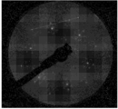
도 1과 도 2는 저에너지 전자 회절(LEED)을 이용하여 SiC 표면상의 그래핀에 대한 회절 패턴을 도시한 이미지이며,
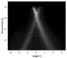
도 3은 도 2의 선을 따르는 신호 강도 프로파일을 도시한 그래프이며,
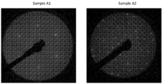
도 4는 샘플 A1과 A2의 전자 에너지에 대한 회절 패턴을 도시한 이미지이며,
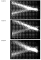
도 5는 샘플 B1 내지 B4의 전자 에너지에 대한 회절 패턴을 도시한 이미지이며,
도 6은 지점(K)의 부근에서 그래핀에서의 전자 분포를 나타내는 스펙트럼이며,
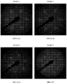
도 7은 예 1 내지 예 4의 전자 에너지에 대한 회절 패턴을 도시한 이미지이며,
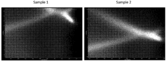
도 8은 예 1과 예 2에 대한 각도-분해 광전자 분광법에 의해 테스트된 전자 에너지에 대한 회절 패턴을 나타낸 이미지이며,
도 9a와 도 9b는 예 4에 대한 각도-분해 고아전자 분광법에 의해 분석된 ARPES 스펙트럼의 형태를 도시한 이미지이며,
도 10a와 도 10b는 예 4에 대한 주사 터널 현미경 이미지이다.1 and 2 are images showing a diffraction pattern for graphene on the surface of SiC using low energy electron diffraction (LEED)
Figure 3 is a graph showing the signal strength profile along the line of Figure 2,
4 is an image showing a diffraction pattern for the electron energy of samples A1 and A2,
5 is an image showing a diffraction pattern for the electron energy of the samples B1 to B4,
Fig. 6 is a spectrum showing electron distribution in graphene near the point K,
7 is an image showing a diffraction pattern for the electron energy of Examples 1 to 4,
8 is an image showing a diffraction pattern for the electron energy tested by angle-resolved photoelectron spectroscopy for Examples 1 and 2,
9A and 9B are images showing the form of the ARPES spectrum analyzed by the angle-decomposed oropharyngeal electron spectroscopy for Example 4,
10A and 10B are scanning tunnel microscope images for Example 4. Fig.
본 발명에 따른 그래핀의 제조 방법은 탄화규소의 표면으로부터의 규소 원자의 표면 승화를 늦추도록, 흑연화 동안 고순도의 외부 승화 소스로부터 기원하는 규소 원자의 스트림으로의 버퍼 가스의 치환에 기초한다. The process for preparing graphene according to the present invention is based on the substitution of a buffer gas into a stream of silicon atoms originating from a high purity external sublimation source during graphitization so as to slow the surface sublimation of silicon atoms from the surface of silicon carbide.
외부 승화 소스의 적용으로 인해, 불순물에 대한 표면의 노출은 상당히 감소되었다. 약 10-4 mbar의 빔상당압력(BEP, beam equivalent pressure)에 대하여. 불순물에 대한 BEP 값은 최악의 경우에 약 10-7 mbar에 달할 것이며, 즉 버퍼 가스의 적용의 경우보다도 4 자릿수가 작다. 추가적으로, 외부 승화 소스를 사용하는 동안, 규소 원자 스트림의 밀도는 기본적으로 임의의 값으로 설정될 수 있으며, 그러므로 흑연화 온도는 상당히 증가될 수 있다.Due to the application of external sublimation sources, surface exposure to impurities was significantly reduced. For beam equivalent pressure (BEP) of about 10 -4 mbar. The BEP value for the impurity will reach about 10 -7 mbar in the worst case, which is four orders of magnitude smaller than in the case of buffer gas application. Additionally, while using an external sublimation source, the density of the silicon atom stream can be basically set to any value, and therefore the graphitization temperature can be significantly increased.
탄화규소의 표면에 형성된 그래핀이 필요한 특성을 특징으로 하기 위해, 그 완벽한 결정학적 배치(crystallographic ordering)가 필요하며(원자는 공석(vacancy), 전위(dislocation) 또는 입계 경계(intergranular boundary)와 같은 낮은 농도의 결함을 구비한 허니콤 구조를 가지는 격자를 형성하여야만 한다), 고순도(낮은 농도의 불순물)이며, 결과적으로 비일관적인 분산의 결여와 관련된 이론적인 예측(역격자(reciprocal lattice)의 K 지점 근처에서의 전자 분산의 선형 관계)에 대응하는 전자 구조이다. In order to characterize the required properties of graphene formed on the surface of silicon carbide, its perfect crystallographic ordering is required (atoms can be vacancies, dislocations, or intergranular boundaries) (Low concentration of impurities), resulting in a theoretical prediction associated with a lack of inconsistent dispersion (a reciprocal lattice of K The linear relationship of the electron dispersion near the point).
본 발명에 따른 방법에서, 규소 원자 스트림의 밀도는 공정의 거의 평형 조건을 달성하도록 한정되었다. 이러한 조건 하에서, 표면으로부터 규소의 손실은 매우 느리게 일어난다. 이러한 사실로 인해, 충분히 높은 온도를 사용하는 동안, 표면 탄소 원자는 표면 시스템이 대부분의 모델 그래핀/SiC 상태로 재조직되는데 충분한 열 에너지 및 시간을 가진다. In the process according to the invention, the density of the silicon atom stream has been limited to achieve a nearly equilibrium condition of the process. Under these conditions, the loss of silicon from the surface occurs very slowly. Because of this fact, while using a sufficiently high temperature, the surface carbon atoms have sufficient heat energy and time to reorganize the surface system into most of the model graphene / SiC state.
놀랍게도, 본 발명에 따른 방법이 탄화규소의 절연 기판 상에 직접적인 결정질 결함이 없는 매우 고품질의 그래핀을 얻는 것으로 이어진다는 것이 알려졌다. 외부 승화 소스로부터의 규소 원자의 어닐링 시간 값 및 스트림의 추가 조정은 그래핀의 4개까지의 원자 층의 단일층의 합성을 가능하게 한다.Surprisingly, it has been found that the process according to the invention leads to obtaining very high quality graphene on the insulating substrate of silicon carbide without a direct crystalline defect. Further adjustment of the annealing time value and stream of silicon atoms from the external sublimation source enables the synthesis of a single layer of up to four atomic layers of graphene.
얻어진 그래핀의 품질 결정 방법Method for determining quality of graphene obtained
저에너지 전자 회절(LEED)은 제조된 그래핀의 품질 평가에 사용되었다. 도 1에 도시된 적합한 회절 패턴(156 eV의 전자 에너지에 대한 이미지)은 그래핀의 표면 상에서의 존재를 나타내는 파라미터를 구성한다. 본 발명에 따라서, 이러한 것은 SiC 표면 (0001) 상의 그래핀에 대해 전형적인 회절 패턴이다.Low energy electron diffraction (LEED) was used to evaluate the quality of the produced graphene. The appropriate diffraction pattern (image for electron energy of 156 eV) shown in Figure 1 constitutes a parameter representing the presence on the surface of the graphene. According to the present invention, this is a typical diffraction pattern for graphene on the SiC surface (0001).
회색 벡터는 기판의 표면(탄화규소)에 관련된 벡터이고, 백색 벡터는 합성되는 그래핀과 관련된 벡터이다. 탄화규소와 관련된 회절 최대값은 회색 육각형의 모서리에 위치되고, 그래핀과 관련된 최대값은 백색 육각형의 모서리에 위치된다. 탄화규소로부터 기원하는 가장 강한 회절 최대값은 낮은 강도의 6개의 최대값에 의해 둘러싸이는 반면에(가장 밝은 피크 주변의 육각형), 그래핀으로부터 기원하는 가장 강한 회절 최대값은 회절 이미지의 중심을 향해 위치된 가장 강한 2개의 최대값에 의해 둘러싸인다(그래핀과 관련되는 최대값과 2차 최대값은 삼각형을 형성한다). 또한 육각형을 형성하지만 항상 보이지 않는 추가적인 최대값은 그래핀과 관련된 최대값 주변에 위치될 수 있다.The gray vector is a vector associated with the surface of the substrate (silicon carbide), and the white vector is a vector associated with the graphene being synthesized. The diffraction maximum associated with silicon carbide is located at the edge of the gray hexagon, and the maximum value associated with graphene is located at the edge of the white hexagon. The strongest diffraction maximum originating from silicon carbide is surrounded by the six maximum values of low intensity (the hexagon around the brightest peak), while the strongest diffraction maximum originating from graphene is directed towards the center of the diffraction image It is surrounded by the strongest two maximum values located (the maximum and secondary maxima associated with graphene form a triangle). Additional maximum values that form a hexagon but are not always visible may be located around the maximum associated with graphene.
품질 및 결정학적 배치를 평가하는 것을 가능하게 하는 파라미터는 배경 레벨에 대한 회절 최대값의 강도의 비에 의해 구성된다. 본 발명에 따라서 수치적으로 이러한 양을 평가하기 위하여, 신호 분석은 예를 들어 도 2의 예에 예시된 바와 같이 그래핀과 관련된 2개의 연속적인 회절 최대값 사이에서 수행되어야 한다.The parameters that make it possible to evaluate the quality and crystallographic layout are constituted by the ratio of the intensity of the diffraction maximum to the background level. In order to numerically evaluate this amount in accordance with the present invention, signal analysis should be performed between two consecutive diffraction maximum values associated with graphene, for example as illustrated in the example of Fig.
이러한 선을 따르는 신호 강도 프로파일이 도 3에 도시되어 있다.The signal strength profile along this line is shown in FIG.
SNR(신호대 잡음비) 값은 한정된 프로파일에서 최대 신호 강도를 최소 강도로 나누는 것에 의해 얻어진다. 도시된 예에서, SNR 값은 SNR = 90/30 = 3이 된다.The SNR (Signal to Noise Ratio) value is obtained by dividing the maximum signal strength by the minimum intensity in a limited profile. In the example shown, the SNR value is SNR = 90/30 = 3.
연속적인 샘플의 회절 패턴을 유사한 분석으로 처리하는 것에 의해, 본 발명에 따른 그래핀 표면의 품질 평가가 수행된다.By treating the diffraction pattern of successive samples with a similar analysis, a quality evaluation of the graphene surface according to the present invention is performed.
A. SiC 표면의 예비 제조.A. Preliminary manufacture of SiC surface.
유익한 결과를 얻도록, 300℃ 내지 900℃의 온도에서 초고도 진공 하에서 어닐링하고, 그런 다음 900℃ 내지 1050℃의 온도에서 5×10⁻⁷ mbar의 보다 높은 진공 하에서 어닐링하여, 샘플 상으로의 규소 원자의 스트림을 유도하는 것과 조합되어, 0.5-2.5 Å/min의 공칭 규소 성장 속도을 유발하는 것에 의해 탄화규소의 시작 표면(이후에 흑연화 공정을 거치는)을 제조하는 것이 필요하다.Annealing under an ultra-high vacuum at a temperature of 300 ° C to 900 ° C to obtain beneficial results and then annealing at a temperature of 900 ° C to 1050 ° C under a higher vacuum of 5x10 -7 mbar to form silicon atoms It is necessary to produce the starting surface of silicon carbide (which is subsequently subjected to a graphitization process) by inducing a nominal silicon growth rate of 0.5-2.5 A / min.
시작 표면은 실온으로 냉각되어야 하며, 그 품질은 회절법(LEED)에 의해 검사되어야 한다. 제조 후에, 표면은 (3×3) 표면 재구성을 특징으로 하며, 이러한 것은 아래의 예(A)에서 보여진다.The starting surface should be cooled to room temperature and its quality should be checked by diffraction (LEED). After fabrication, the surface is characterized by (3x3) surface reconstruction, as shown in the following example (A).
예 A1.Example A1.
샘플 1의 제조 방법: 진공 챔버로의 도입, 1×10⁻⁹ mbar보다 낮은 압력으로 챔버를 펌핑, 100℃로부터 850℃로 점차적으로 증가되는 온도에서 샘플의 어닐링(탈가스), 시간 t=10 분 동안 진공(규소 원자의 스트림없이) 하에서 950℃의 온도에서 샘플의 어닐링.Method of preparation of sample 1: introduction into a vacuum chamber, pumping the chamber at a pressure of less than 1 x 10 < -9 > mbar, annealing (degassing) the sample at a temperature increasing gradually from 100 DEG C to 850 DEG C, Annealing the sample at a temperature of 950 DEG C under vacuum (without a stream of silicon atoms).
예 A2.Example A2.
샘플 2의 제조 방법: 진공 챔버로의 도입, 1×10⁻⁹ mbar보다 낮은 압력으로 챔버를 펌핑, 100℃로부터 850℃로 점차적으로 증가되는 온도에서 샘플의 어닐링(탈가스), 규소 원자의 스트림에서 950℃의 온도에서 샘플을 어닐링하여, 시간 t = 10 분 동안 0.5 내지 2.5 Å/min의 공칭 규소 성장 속도를 유발.
그런 다음, 얻어진 표면의 테스트를 행하였다. 그 결과가 도 4에서 보여진다. Then, the obtained surface was tested. The results are shown in FIG.
테스트는 예 A1 및 A2에 따라서 제조된 2개의 샘플을 사용하여 저에너지 전자 회절에 의해 수행되었다. 142 eV와 동등한 전자 에너지에 대한 회절 패턴의 형태를 하는 결과가 도 4에서 보여진다.The test was performed by low energy electron diffraction using two samples prepared according to Examples A1 and A2. The result in the form of a diffraction pattern for electron energy equivalent to 142 eV is shown in FIG.
규소 원자의 스트림에서 어닐링에 의해 제조된 시작 표면은 (3×3) 형태의 표면 재구성을 특징으로 한다. 또한, 이러한 표면은 거의 완벽한 결정학적 배치를 특징으로 하며, 이러한 것은 매우 많은 수의 관찰 가능한 회절 최대값, 그 작은 횡단 크기, 그 높은 밝기 및 낮은 밝기의 배경(배경 강도에 대한 신호 강도의 높은 비, 이러한 것은 적은 수의 결정학적 결함 및 표면의 비정질 영역을 입증한다)에 의해 입증된다. 진공 하에서 제조된 표면은 (1×1) 형태의 재구성 및 낮은 정도의 결정학적 배치를 특징으로 하며, 이러한 것은 매우 높은 강도의 배경, 비교적 낮은 강도의 회절 최대값 및 상기 최대값의 확산된 횡단 형상에 의해 입증된다. 10The starting surface prepared by annealing in a stream of silicon atoms is characterized by a (3x3) form of surface reconstruction. In addition, these surfaces are characterized by a nearly perfect crystallographic arrangement, which results in a very large number of observable diffraction maxima, its small cross-sectional size, its high brightness and background of low brightness (high ratio of signal intensity to background intensity , Which demonstrates a small number of crystallographic defects and amorphous regions of the surface). The surface produced under vacuum is characterized by a (1 x 1) form of reconstruction and a low degree of crystallographic arrangement, which is characterized by a very high intensity background, a diffraction maximum of a relatively low intensity and a diffused cross- ≪ / RTI > 10
B. 사전 제조된 SiC 표면의 흑연화.B. Graphitization of the pre-fabricated SiC surface.
상기한 방식으로 제조된 시작 표면은 5×10⁻⁷ mbar를 초과하지 않는 진공 챔버에서의 압력 하에서 0.5-10 Å/min의 규소층의 공칭 성장 속도에 대응하는, 외부 승화 소스로부터의 규소 원자의 스트림에서 1300 내지 1800℃의 온도에서 흑연화 공정이 수행되었다. 제조 후에, 고품질 그래핀(위에서 상세히 설명됨)이 표면에 형성되며, 이러한 것은 다음의 예(B)에서 보여진다:The starting surface prepared in such a manner has a silicon atom from an external sublimation source, corresponding to a nominal growth rate of the silicon layer of 0.5-10 A / min under pressure in a vacuum chamber not exceeding 5 x 10 < -7 & The graphitization process was carried out at a temperature of 1300 to 1800 캜 in the stream. After manufacture, high quality graphene (described in detail above) is formed on the surface, which is shown in the following example (B): <
예 B1.Example B1.
샘플 1의 제조 방법: 진공 챔버로의 도입, 1×10⁻⁹ mbar보다 낮은 압력으로 챔버를 펌핑, 100℃로부터 850℃로 점차적으로 증가되는 온도에서 샘플의 어닐링(탈가스, 시작 표면(3×3)의 제조없음), 시간 t=10 분 동안 1450℃의 온도에서 샘플의 어닐링(규소 원자의 스트림없이).Preparation of sample 1: introduction into a vacuum chamber, pumping the chamber at a pressure of less than 1 x 10 < -9 > mbar, annealing the sample at a gradually increasing temperature from 100 DEG C to 850 DEG C (degassing, 3)), annealing the sample (without a stream of silicon atoms) at a temperature of 1450 ° C for a time t = 10 minutes.
예 B2.Example B2.
샘플 2의 제조 방법: 진공 챔버로의 도입, 1×10⁻⁹ mbar보다 낮은 압력으로 챔버를 펌핑, 100℃로부터 850℃로 점차적으로 증가되는 온도에서 샘플의 어닐링(탈가스, 시작 표면(3×3)의 제조없음), 규소 원자의 스트림에서 1450℃의 온도에서 샘플을 어닐링하여, 시간 t = 10 분 동안 약 4 Å/min의 공칭 규소 성장 속도를 유발.Preparation of sample 2: introduction into a vacuum chamber, pumping the chamber at a pressure of less than 1 x 10 < -9 > mbar, annealing of the sample at a gradually increasing temperature from 100 DEG C to 850 DEG C (degassing, 3), the sample was annealed at a temperature of 1450 DEG C in a stream of silicon atoms to induce a nominal silicon growth rate of about 4 A / min for a time t = 10 minutes.
예 B3.Example B3.
샘플 3의 제조 방법: 상기된 바와 같이 (3×3) 표면 재구성을 특징으로 하는 시작 표면을 제조한 후에: 시간 t = 10분 동안 1450℃의 온도에서(규소 원자의 스트림없이) 샘플의 어닐링.Method for the preparation of sample 3: Annealing of the sample (without stream of silicon atoms) at a temperature of 1450 ° C for a time t = 10 minutes, after producing a starting surface characterized by (3x3) surface reconstruction as described above.
예 B4.Example B4.
샘플 4의 제조 방법: 상기한 바와 같이 (3×3) 표면 재구성을 특징으로 하는 시작 표면을 제조한 후에: 규소 원자의 스트림에서 1450℃의 온도에서 샘플을 어닐링하여, 시간 t = 10분 동안 약 4 Å/min의 공칭 규소 성장 속도를 유발.Method of preparing sample 4: After preparing a starting surface characterized by (3x3) surface reconstruction as described above: annealing the sample at a temperature of 1450 DEG C in a stream of silicon atoms, Inducing a nominal silicon growth rate of 4 A / min.
얻어진 샘플의 회절 연구Diffraction studies of the obtained samples
테스트는 예 B1 내지 B4에 따라서 제조된 2개의 샘플을 사용하여 실온에서 저에너지 전자 회절에 의해 수행되었다. 156 eV와 동등한 전자 에너지에 대해 회절 패턴의 형태를 하는 결과가 도 5에서 보여진다. The test was carried out by low energy electron diffraction at room temperature using two samples prepared according to Examples B1 to B4. The result in the form of a diffraction pattern for an electron energy equivalent to 156 eV is shown in Fig.
(3×3) 형태의 시작 표면의 제조 및 규소 원자의 스트림에서의 어닐링에 의해 제조된 표면은 명백하게 보다 양호한 결정학적 배치를 특징으로 한다는 것이 알려졌다. 회절 최대값은 잘 형성되고, 완벽한 형상과 높은 강도를 가지는 반면에, 배경은 사실상 보이지 않는다. 이러한 것은 높은 배치도(ordering degree) 및 샘플의 표면 상에서의 그래핀 층 및 비정질 영역에서의 모든 결함의 최소 집중의 증거이다.It has been found that the surface prepared by the preparation of the (3x3) type starting surface and the annealing in the stream of silicon atoms is apparently characterized by a better crystallographic layout. The diffraction maximum is well formed, has perfect shape and high intensity, while the background is virtually invisible. This is a high ordering degree and evidence of minimal concentration of all defects in the graphene and amorphous regions on the surface of the sample.
얻어진 샘플의 분광학 연구Spectroscopy studies of the obtained samples
테스트는 예 B1, B3 및 B4에 따라서 제조된 2개의 샘플을 사용하여 실온에서 UV-방사 범위(UV-ARPES)에서 각도-분해 광전자 분광법(angle-resolved photoemission spectroscopy)에 의해 수행되었다. UV 방사에 의해 스퍼터링된 광전자의 강도 분포 대 방사 각도(수직축) 및 물질의 전자 구조의 영상화를 가능하게 하는 운동 에너지(수평축)를 나타내는 스펙트럼의 형태를 하는 결과가 도 6에 도시되어 있다. The tests were carried out by angle-resolved photoemission spectroscopy at UV-radiation range (UV-ARPES) at room temperature using two samples prepared according to Examples B1, B3 and B4. The results are shown in FIG. 6, which shows the intensity distribution versus radiation angle (vertical axis) of the photoelectrons sputtered by UV radiation and the kinetic energy (horizontal axis) that allows imaging of the electronic structure of the material.
도 6의 스펙트럼은 지점(K)의 부근에서 그래핀에서의 전자 분포를 나타낸다. 이론적으로 예측되는 바와 같이, 분산 관계(샘플로부터 전자의 방사 각도(수직축)에 선형으로 비례하는 전자의 유사 운동량에 대한 에너지 의존성)는 이러한 지점 주위에서 선형이어야 하며(이는 모든 샘플에 대해 명백하다), 그러므로 그래핀이 모든 샘플의 표면 상에 형성되었다.The spectrum of FIG. 6 shows electron distribution in graphene near point K. FIG. As predicted theoretically, the dispersion relationship (the energy dependence of the similar momentum of electrons linearly proportional to the emission angle (vertical axis) of the electrons from the sample) must be linear around this point (which is obvious for all samples) , So graphene was formed on the surface of all samples.
광 방출 스펙트럼에서의 표면 배치의 영향을 결정하는 것을 가능하게 하는 파라미터는 배경 강도에 의해 구성된다. 가장 낮은 배경 강도(공식적으로 배경 강도에 대한 신호 강도의 비)는 샘플 B4에 대해 관찰되었다(선형 분산 관계의 2개의 분기 사이의 신호 강도가 주목할만 하다).The parameters that make it possible to determine the influence of the surface arrangement in the light emission spectrum are constituted by the background intensity. The lowest background intensity (formally the ratio of signal intensity to background intensity) was observed for sample B4 (the signal strength between the two branches of the linear dispersion relationship is notable).
본 발명에 따른 고품질 그래핀은 임계 파라미터, 특히 규소 원자의 흑연화 온도 및 스트림의 비교적 광범위한 범위의 값을 위하여 본 발명에 따른 방법에 의해 얻어질 수 있다. 이러한 것은 다음에 설명되는 바람직한 실시예에서 예시되었으며, 그러나 이러한 것은 청구된 본 발명의 전체 범위와 동일시되지 않아야 한다.The high-quality graphene according to the invention can be obtained by the process according to the invention for critical parameters, in particular for graphitization temperatures of silicon atoms and for a relatively broad range of values of the stream. These are illustrated in the preferred embodiments described below, but they should not be equated with the full scope of the claimed invention.
예 1.Example 1.
샘플 1의 제조 방법: 상기한 바와 같이 (3×3) 표면 재구성을 특징으로 하는 시작 표면의 제조 후에: 규소 원자의 스트림에서 1500℃의 온도에서 샘플을 어닐링하여, 시간 t = 10분 동안 약 1 Å/min의 공칭 규소 성장 속도를 유발.Method for the preparation of sample 1: After the preparation of the starting surface characterized by (3x3) surface reconstruction as described above: the sample is annealed at a temperature of 1500 DEG C in a stream of silicon atoms to form about 1 Resulting in a nominal silicon growth rate of Å / min.
예 2.Example 2.
샘플 2의 제조 방법: 상기한 바와 같이 (3×3) 표면 재구성을 특징으로 하는 시작 표면의 제조 후에: 규소 원자의 스트림에서 1500℃의 온도에서 샘플을 어닐링하여, 시간 t = 10분 동안 약 25 Å/min의 공칭 규소 성장 속도를 유발.Method 2: Preparation of sample 2: After the preparation of the starting surface characterized by (3x3) surface reconstruction as described above: The sample was annealed at a temperature of 1500 DEG C in a stream of silicon atoms to form about 25 Resulting in a nominal silicon growth rate of Å / min.
예 3.Example 3.
샘플 3의 제조 방법: 상기한 바와 같이 (3×3) 표면 재구성을 특징으로 하는 시작 표면의 제조 후에: 규소 원자의 스트림에서 1200℃의 온도에서 샘플을 어닐링하여, 시간 t = 10분 동안 약 1 Å/min의 공칭 규소 성장 속도를 유발.Method for the preparation of sample 3: After the preparation of the starting surface characterized by (3x3) surface reconstruction as described above: the sample is annealed at a temperature of 1200 DEG C in a stream of silicon atoms to form about 1 Resulting in a nominal silicon growth rate of Å / min.
예 4.Example 4.
샘플 4의 제조 방법: 상기한 바와 같이 (3×3) 표면 재구성을 특징으로 하는 시작 표면의 제조 후에: 규소 원자의 스트림에서 1700℃의 온도에서 샘플을 어닐링하여, 시간 t = 6분 동안 약 4 Å/min의 공칭 규소 성장 속도를 유발.Method for the preparation of sample 4: After the preparation of the starting surface characterized by (3x3) surface reconstruction as described above: the sample was annealed at a temperature of 1700 占 폚 in a stream of silicon atoms to form about 4 Resulting in a nominal silicon growth rate of Å / min.
예 1 내지 4에서 얻어진 그래핀 샘플의 품질 및 구조가 분석되었다.The quality and structure of the graphene samples obtained in Examples 1 to 4 were analyzed.
테스트 1
예 1-4(각각 샘플 1-4)에 따라서 얻어진 그래핀 샘플의 품질 및 구조가 실온에서 저에너지 전자 회절에 의해 테스트되었다. 156 eV에 동등한 전자 에너지에 대해 회절 패턴의 형태를 하는 결과가 도 7에 도시되어 있다.The quality and structure of the graphene samples obtained according to Examples 1-4 (samples 1-4 respectively) were tested by low energy electron diffraction at room temperature. The result of forming a diffraction pattern for electron energy equivalent to 156 eV is shown in Fig.
테스트 2
예 1-2(각각 샘플 1 및 2)에 따라서 얻어진 그래핀 샘플의 품질 및 구조가 실온에서 각도-분해 광전자 분광법에 의해 테스트되었다. 156 eV에 동등한 전자 에너지에 대해 회절 패턴의 형태를 하는 결과가 도 8에 도시되어 있다.The quality and structure of the graphene samples obtained according to Example 1-2 (
각각의 실시예에서, 고품질 그래핀은 샘플의 표면 상에 형성되었으며, 이러한 것은 회절 및 분광 테스트에 의해 확인되었다. 표면의 정확한 구조는 다양하지만, 이러한 것 모두는 매우 높은 결정학적 배치와 고품질의 전자 구조를 특징으로 한다.In each example, high quality graphene was formed on the surface of the sample, which was confirmed by diffraction and spectroscopic testing. The exact structure of the surface varies, but all of them feature a very high crystallographic layout and high quality electronic structure.
테스트 3
예 4에서 얻어진 그래핀 샘플은 액체 질소 온도(T = 78 K)에서 각도-분해 광전자 분광법에 의해 분석되었다. ARPES 스펙트럼의 형태를 하는 결과는 도 9a 및 도 9b에 도시되어 있다.The graphene samples obtained in Example 4 were analyzed by angle-resolved photoelectron spectroscopy at liquid nitrogen temperature (T = 78K). The results in the form of an ARPES spectrum are shown in Figs. 9A and 9B.
샘플 4는 매우 높은 품질의 표면을 특징으로 하며, 이러한 것은 분산 관계에서의 예리한 밴드와 매우 낮은 배경 레벨에 의해 입증된다. 추가적으로, 2개의 그래핀 층이 샘플 상에서 발생하며, 이러한 것은 분산 관계의 선형 분기의 분열(splitting)로서 ARPES 스펙트럼에서 입증된다. 이러한 사실은 본 발명에 따른 방법이 표면 상에 형성된 그래핀 층의 수를 제어할 수 있다는 것을 확인한다.
테스트 4
예 4에서 얻어진 그래핀 샘플은 진공 하의 실온에서 주사 터널 현미경에 의해 분석되었다(Omicron RT-STM/AFM 현미경, 에칭된 텅스텐으로 제조된 현미경 팁, 15 mV의 분극 전압, 100 pA의 터널링 전류). 현미경 이미지의 형태를 하는 결과는도 10a 및 도 10b에 도시되어 있다.The graphene samples obtained in Example 4 were analyzed by scanning tunneling microscopy at room temperature under vacuum (Omicron RT-STM / AFM microscope, microscope tip made of etched tungsten, polarization voltage of 15 mV, tunneling current of 100 pA). The results in the form of a microscope image are shown in Figures 10A and 10B.
현미경 이미지에서, 그래핀의 완벽한 결정학적 구조, 즉 허니콤 구조가 분명하다. 그래핀의 단위 셀은 단일의 작은 육각형이며; 배경 강도에서의 변화는 표층 지반(subsurface layer)(![]()
![]()
요약summary
그래핀 합성을 위해 제시된 방법은 특허 출원 US 20110223094 A1에 기술된 물리적 현상의 이점을 취한다. 두 경우 모두에서, 고품질의 그래핀은 탄화규소 표면의 가장 근접한 부근에서의 대기로 추가적인 외부 규소 원자를 도입하는 것에 의해 탄화규소 표면으로부터 규소 원자의 승화 속도의 감소에 의해 얻어진다. 그러나, 이러한 방법은 다수의 중요한 측면에서 다르다.The proposed method for graphene synthesis takes advantage of the physical phenomena described in patent application US 20110223094 A1. In both cases, high-quality graphene is obtained by reducing the sublimation rate of silicon atoms from the silicon carbide surface by introducing additional external silicon atoms into the atmosphere in the immediate vicinity of the silicon carbide surface. However, this method is different in many important aspects.
우선, 특허 출원 US 20110223094 A1에서, 탄화규소 표면의 흑연화 공정은 진공 챔버에서 수행되어, 약 1×10⁻⁶ Torr의 기준 압력을 보장한다(인용 문헌의도 1a 참조). 그러므로, 기재된 방법은, 규소 원자의 승화 속도가 버퍼 가스의 적용에 의해 감소되는 특허 US 9150417 B2에 기술된 방법과 동일한 상당한 순도 제한의 단점이 있다. 약 1×10⁻⁵ 내지 1×10⁻⁶ Torr의 기준 압력은 어닐링의 시작 전이라도 약 10-10 L/s의 알려지지 않은 불순물에 대한 표면의 노출에 대응한다. 이러한 것은 버퍼 가스를 사용하는 동안 얻은 값보다 양호한 값이지만, 이러한 것은 여전히 고도의 샘플 오염에 대응한다. 고온에서의 어닐링 동안, 챔버에서의 압력은 적어도 1 자릿수만큼 저하되며, 그러므로 불순물에 대한 노출은 적어도 10-100 L/s에 달한다.First, in the patent application US 20110223094 A1, the graphitization process of the silicon carbide surface is carried out in a vacuum chamber to ensure a reference pressure of about 1 x 10⁻⁶ Torr (see Figure 1a of the cited document). The described process therefore has the disadvantage of a considerable purity limitation which is the same as that described in patent US 9150417 B2, in which the rate of sublimation of silicon atoms is reduced by the application of buffer gas. A reference pressure of about 1 x 10 -5 to 1 x 10 -6 Torr corresponds to an exposure of the surface to an unknown impurity of about 10 -10 L / s even before the start of annealing. This is a better value than that obtained while using the buffer gas, but this still corresponds to a high degree of sample contamination. During annealing at high temperature, the pressure in the chamber is reduced by at least one order of magnitude, and thus exposure to impurities is at least 10 -100 L / s.
다른 한편으로, 본 발명에 따른 방법은, 초고도 진공의 레벨에서의 기준 압력 또는 약 1×10⁻¹⁰ mbar(약 0.0001 L/s의 노출)의 적용으로 인해 품질의 관점과 다른 결과를 산출할 뿐만 아니라, 어닐링 동안 챔버에서의 압력을 5×10⁻⁷ mbar(약 0.5 L/s의 노출, 또는 US 20110223094 Al로부터 공지된 방법에서보다 2 자릿수 낮은 노출)보다 양호한 레벨로 유지한다.On the other hand, the method according to the present invention produces a different result from the view of quality due to the application of the reference pressure at the level of the ultra-high vacuum or about 1 x 10 < -10 > mbar (exposure of about 0.0001 L / as well, to keep the pressure in the chamber during annealing in a good level greater than 5 × 10 -7 mbar (exposure of about 0.5 L / s, or two orders of magnitude lower than in the exposure methods known from US 20110223094 Al).
더욱이, 특허 출원 US 20110223094 A1에 기술된 방법은 결정들 사이의 거리를 증가시키는 것 외에 샘플의 바로 근처에서 규소 원자의 스트림(분압)의 값에 대한 정확한 제어를 계획하지 않는다.Moreover, the method described in patent application US 20110223094 A1 does not plan to precisely control the value of the stream of silicon atoms (partial pressure) in the immediate vicinity of the sample, in addition to increasing the distance between the crystals.
한편, 본 발명에 따른 방법은 탄화규소 결정체에 대한 어닐링 온도 및 시간에 의존하여 규소 원자의 스트림 값 및 그 변화의 정밀한 제어를 가능하게 한다. 공정 파라미터에 대한 정확한 제어로 인하여, 얻어진 결과는 이전에 공지된 방법으로 얻은 결과와 상당히 다르다.On the other hand, the method according to the present invention makes it possible to precisely control the stream value of silicon atoms and their changes depending on the annealing temperature and time for the silicon carbide crystals. Due to the precise control over the process parameters, the results obtained are significantly different from those obtained with previously known methods.
또한, 종래의 기술은 탄화규소 표면의 예비 제조를 제공하지 못한다.In addition, conventional techniques do not provide for pre-fabrication of silicon carbide surfaces.
한편, 본 발명에 따른 방법의 바람직한 실시예에서, 흑연화 처리되는 탄화규소의 시작 표면의 제조는 초고도 진공 하의 300℃-900℃의 온도에서 이를 어닐링하고, 이어서 초고도 진공 하에서 0.5-2.5 Å/min의 규소 성장의 공칭 속도에 대응하는, 규소 원자의 스트림에서 900-1100℃의 온도에서 이를 어닐링하고, 그런 다음 결정을 실온으로 냉각하는 것에 의해 수행된다. 예비 제조는, 그 동안 불순물이 결정의 내부로 확산될 뿐만 아니라 그래핀 층에서 구조적 결함을 형성하는 흑연화를 착수하기 전에 탄화규소의 표면으로부터 불순물의 제거를 유발하며, 또한 이러한 것은 고도의 결정학적 배치(표면의 (3×3) 재구성)의 형성 및 단차부 가장자리의 평활화(smoothing)를 유발한다. 제시된 결과는 표면의 예비 제조가 유익하게 흑연화 공정에서 얻어진 그래핀의 품질 및 구조에 영향을 미친다는 것을 확인한다.On the other hand, in a preferred embodiment of the process according to the invention, the preparation of the starting surface of graphitized silicon carbide is carried out by annealing it at a temperature of 300 ° C to 900 ° C under an ultra-high vacuum and then at 0.5-2.5 Å / min Lt; RTI ID = 0.0 > 900-1100 C < / RTI > in a stream of silicon atoms, corresponding to the nominal rate of silicon growth of silicon, and then cooling the crystal to room temperature. Preliminary manufacturing has also caused the removal of impurities from the surface of the silicon carbide prior to embarking on the graphitization, in which impurities diffuse into the crystal as well as form structural defects in the graphene layer, (3 x 3) reconstruction of the surface) and the smoothing of the step edges. The presented results confirm that the preliminary fabrication of the surface beneficially affects the quality and structure of the graphene obtained in the graphitization process.
또한, 공지된 방법은 탄화규소 표면의 온도에 대한 직접적인 제어를 배제한다.In addition, the known methods preclude direct control over the temperature of the silicon carbide surface.
다른 한편으로, 본 발명에 따른 방법은 샘플 상으로 안내된 광학 고온계를 사용하여 이러한 제어를 실행한다. 정밀한 온도 제어는 최적의 반복 가능한 결과를 얻기 위해 매우 중요하다.On the other hand, the method according to the present invention implements this control using an optical pyrometer guided over the sample. Precise temperature control is crucial for achieving optimal repeatable results.
종래의 기술로부터 공지된 방법으로 표면의 온도를 직접 측정의 결여는 결과의 반복성의 결여 및 인용된 문헌의 저자에 의해 보고된 결과의 낮은 신뢰성으로 이어지며, 어닐링된 SiC 결정의 후방 표면으로 유도된 열전대 또는 고온계에 의한 온도 측정을 위한 모든 직접적인 방법은 공정 동안 매우 높은 불확실성 및 가능한 온도 진동을 유발하여, 합성되는 그래핀의 품질을 손상시킨다.The lack of a direct measurement of the surface temperature in a manner known from the prior art leads to a lack of repeatability of the results and low reliability of the results reported by the authors of the cited documents, All direct methods for temperature measurement by thermocouples or pyrometers cause very high uncertainties and possible temperature oscillations during the process, impairing the quality of the graphene being synthesized.
Claims (7)
표면 (0001)의 결정학적 방향을 가지는 SiC 결정이 연속적으로:
a) 1×10⁻⁹ mbar 보다 낮은 압력;
b) 선택적으로 1×10⁻⁸ mbar 보다 높지 않은 압력 하에서, 300℃ 내지 900℃의 온도에서 선택적으로 어닐링되고;
c) 0.5 Å/min 내지 2.5 Å/min의 공칭 규소 성장 속도를 제공하는 외부 승화 소스로부터의 규소 원자의 스트림에서 900℃ 내지 1050℃의 온도에서 선택적으로 어닐링되고;
d) 0.5 Å/min 내지 10 Å/min의 공칭 규소 성장 속도를 제공하는 외부 승화 소스로부터의 규소 원자 스트림에서, 5×10⁻⁷ mbar 보다 높지 않은 압력하에서, 1300℃ 내지 1800℃의 온도에서 선택적으로 어닐링되는 것을 특징으로 하는, 방법.A method for the production of graphene on a silicon carbide surface,
The SiC crystals having the crystallographic orientation of the surface (0001) are successively:
a) a pressure less than 1 x 10 < -9 > mbar;
b) optionally annealing at a temperature of from 300 DEG C to 900 DEG C under a pressure not higher than 1 x 10 < -8 > mbar;
c) selectively annealing at a temperature of 900 占 폚 to 1050 占 폚 in a stream of silicon atoms from an external sublimation source providing a nominal silicon growth rate of 0.5? / min to 2.5? / min;
d) a silicon atom stream from an external sublimation source providing a nominal silicon growth rate of from 0.5 A / min to 10 A / min, at a temperature not higher than 5 x 10⁻⁷ mbar, at a temperature between 1300 ° C and 1800 ° C ≪ / RTI >
상기 그래핀의 층이, 허니콤 구조를 가지는 결정 격자를 형성하는 1 내지 4개, 특히 1 내지 2개의 원자 층, 및 SiC 표면 (0001) 상의 그래핀에 전형적인 회절 패턴을 가지는 저에너지 전자 회절에 의해 얻어진 그 회절 스펙트럼을 포함하며, 그래핀과 연결된 2개의 연속적인 회절 최대값 사이의 섹션에서 실온에서 측정된 최소 신호 강도에 대한 최대 신호 강도(SNR)의 비가 9보다 큰 것을 특징으로 하는, 그래핀의 층.Particularly in the layer of graphene, which is essentially free from crystal defects, on the surface of the SiC crystal,
Characterized in that the layer of graphene comprises at least one atomic layer which forms a crystal lattice with a honeycomb structure, in particular from 1 to 2 atomic layers, and low energy electron diffraction with a typical diffraction pattern on graphene on the SiC surface (0001) Characterized in that the ratio of the maximum signal intensity (SNR) to the minimum signal intensity measured at room temperature in a section between two consecutive diffraction maximums including the obtained diffraction spectrum is greater than 9, Layer.
Applications Claiming Priority (3)
| Application Number | Priority Date | Filing Date | Title |
|---|---|---|---|
| PL417804A PL417804A1 (en) | 2016-07-02 | 2016-07-02 | Method for synthesis of the high-grade graphene on the silicon carbide surface |
| PLP.417804 | 2016-07-02 | ||
| PCT/IB2017/053969 WO2018007918A1 (en) | 2016-07-02 | 2017-06-30 | Method for preparation of high-quality graphene on the surface of silicon carbide |
Publications (1)
| Publication Number | Publication Date |
|---|---|
| KR20190024909A true KR20190024909A (en) | 2019-03-08 |
Family
ID=59772660
Family Applications (1)
| Application Number | Title | Priority Date | Filing Date |
|---|---|---|---|
| KR1020187037935A KR20190024909A (en) | 2016-07-02 | 2017-06-30 | Method for manufacturing high quality graphene on the surface of silicon carbide |
Country Status (7)
| Country | Link |
|---|---|
| US (1) | US20190226115A1 (en) |
| EP (1) | EP3478634B1 (en) |
| JP (1) | JP2019524620A (en) |
| KR (1) | KR20190024909A (en) |
| ES (1) | ES2901235T3 (en) |
| PL (2) | PL417804A1 (en) |
| WO (1) | WO2018007918A1 (en) |
Families Citing this family (3)
| Publication number | Priority date | Publication date | Assignee | Title |
|---|---|---|---|---|
| PL241895B1 (en) * | 2019-09-23 | 2022-12-19 | Univ Jagiellonski | Method for preparing a surface carbide-graphene composite with controlled surface morphology, in particular a SiC-graphene composite and a carbide-graphene composite |
| CN112919456B (en) * | 2021-02-23 | 2023-09-22 | 南京大学 | Flat graphene growth method with uniform layer thickness and single-layer or double-layer graphene film |
| CN115849352B (en) * | 2023-02-27 | 2023-05-16 | 太原理工大学 | Method for efficiently preparing laminated graphene |
Citations (3)
| Publication number | Priority date | Publication date | Assignee | Title |
|---|---|---|---|---|
| US20110223094A1 (en) | 2010-03-12 | 2011-09-15 | The Regents Of The University Of California | Method for synthesis of high quality graphene |
| US20140175458A1 (en) | 2012-12-21 | 2014-06-26 | Samsung Electronics Co., Ltd. | Graphene structure, graphene device including same, and method of manufacturing graphene structure |
| US9150417B2 (en) | 2010-09-16 | 2015-10-06 | Graphensic Ab | Process for growth of graphene |
Family Cites Families (1)
| Publication number | Priority date | Publication date | Assignee | Title |
|---|---|---|---|---|
| JP5644175B2 (en) * | 2010-04-27 | 2014-12-24 | 和人 山内 | Graphene deposition method on SiC substrate |
-
2016
- 2016-07-02 PL PL417804A patent/PL417804A1/en unknown
-
2017
- 2017-06-30 WO PCT/IB2017/053969 patent/WO2018007918A1/en unknown
- 2017-06-30 ES ES17761570T patent/ES2901235T3/en active Active
- 2017-06-30 KR KR1020187037935A patent/KR20190024909A/en not_active Application Discontinuation
- 2017-06-30 EP EP17761570.5A patent/EP3478634B1/en active Active
- 2017-06-30 US US16/314,313 patent/US20190226115A1/en not_active Abandoned
- 2017-06-30 JP JP2018569161A patent/JP2019524620A/en active Pending
- 2017-06-30 PL PL17761570T patent/PL3478634T3/en unknown
Patent Citations (3)
| Publication number | Priority date | Publication date | Assignee | Title |
|---|---|---|---|---|
| US20110223094A1 (en) | 2010-03-12 | 2011-09-15 | The Regents Of The University Of California | Method for synthesis of high quality graphene |
| US9150417B2 (en) | 2010-09-16 | 2015-10-06 | Graphensic Ab | Process for growth of graphene |
| US20140175458A1 (en) | 2012-12-21 | 2014-06-26 | Samsung Electronics Co., Ltd. | Graphene structure, graphene device including same, and method of manufacturing graphene structure |
Also Published As
| Publication number | Publication date |
|---|---|
| EP3478634B1 (en) | 2021-10-27 |
| JP2019524620A (en) | 2019-09-05 |
| WO2018007918A1 (en) | 2018-01-11 |
| PL3478634T3 (en) | 2022-04-11 |
| PL417804A1 (en) | 2018-01-15 |
| US20190226115A1 (en) | 2019-07-25 |
| ES2901235T3 (en) | 2022-03-21 |
| EP3478634A1 (en) | 2019-05-08 |
Similar Documents
| Publication | Publication Date | Title |
|---|---|---|
| Virojanadara et al. | Homogeneous large-area graphene layer growth on 6 H-SiC (0001) | |
| US10072355B2 (en) | Methods of forming graphene single crystal domains on a low nucleation site density substrate | |
| KR20190024909A (en) | Method for manufacturing high quality graphene on the surface of silicon carbide | |
| JP2002329877A (en) | Cu(Ga AND/OR In)Se2 THIN FILM LAYER, Cu(InGa)(S, Se)2 THIN FILM LAYER, SOLAR BATTERY AND METHOD FOR FORMING Cu(Ga AND/OR In)Se2 THIN FILM LAYER | |
| Sun et al. | Characterization of 3C-SiC films grown on monocrystalline Si by reactive hydrogen plasma sputtering | |
| Luong et al. | Molecular-beam epitaxial growth of tensile-strained and n-doped Ge/Si (001) films using a GaP decomposition source | |
| Kwak et al. | In situ observations of gas phase dynamics during graphene growth using solid-state carbon sources | |
| Delachat et al. | Properties of silicon nanoparticles embedded in SiNx deposited by microwave-PECVD | |
| Khan et al. | Carbon-and crack-free growth of hexagonal boron nitride nanosheets and their uncommon stacking order | |
| Chen et al. | A graphite enclosure assisted synthesis of high-quality patterned graphene on 6H–SiC by ion implantation | |
| Upadhya et al. | Electronic structure of rare-earth semiconducting ErN thin films determined with synchrotron radiation photoemission spectroscopy and first-principles analysis | |
| Lebedev et al. | Low-temperature transport properties of multigraphene films grown on the SiC surface by sublimation | |
| Konakova et al. | Comparative characteristics of the Raman scattering spectra of graphene films on conductive and semi-insulating 6 H-SiC substrates | |
| Chen et al. | Microstructural and optical properties of high-quality ZnO epitaxially grown on a LiGaO 2 substrate | |
| CN106233430B (en) | Silicon carbide epitaxy chip and its manufacturing method | |
| Vasin et al. | Study of the processes of carbonization and oxidation of porous silicon by Raman and IR spectroscopy | |
| Zhang et al. | Annealing-induced tunable bandgap and photoluminescence of (InGa) 2O3 films deposited by magnetron sputtering | |
| Panigrahy et al. | Optical and structural characteristics of glancing angle deposition synthesized Er2O3 nanowires | |
| Riesz et al. | Thermal decomposition of bulk and heteroepitaxial (100) InP surfaces: A combined in situ scanning electron microscopy and mass spectrometric study | |
| Lee et al. | Epitaxial diamond on a Si/CaF2/Ir substrate | |
| Mishra et al. | Going beyond copper: Wafer-scale synthesis of graphene on sapphire | |
| US9994971B2 (en) | Method for fabricating carbon-based composite material | |
| Sun et al. | Morphology inducing selective plasma etching for AlN nanocone arrays: tip-size dependent photoluminescence and enhanced field emission properties | |
| Samavati et al. | Impact of annealing on surface morphology and photoluminescence of self-assembled Ge and Si quantum dots | |
| Kadowaki et al. | PEEM and micro PES study of graphene growth on Ni (110) substrate |
Legal Events
| Date | Code | Title | Description |
|---|---|---|---|
| A201 | Request for examination | ||
| E902 | Notification of reason for refusal | ||
| E601 | Decision to refuse application |