KR20190021184A - Seed layers for copper interconnects - Google Patents
Seed layers for copper interconnects Download PDFInfo
- Publication number
- KR20190021184A KR20190021184A KR1020180097909A KR20180097909A KR20190021184A KR 20190021184 A KR20190021184 A KR 20190021184A KR 1020180097909 A KR1020180097909 A KR 1020180097909A KR 20180097909 A KR20180097909 A KR 20180097909A KR 20190021184 A KR20190021184 A KR 20190021184A
- Authority
- KR
- South Korea
- Prior art keywords
- layer
- copper
- ruthenium
- substrate
- forming
- Prior art date
Links
- 239000010949 copper Substances 0.000 title claims abstract description 154
- RYGMFSIKBFXOCR-UHFFFAOYSA-N Copper Chemical compound [Cu] RYGMFSIKBFXOCR-UHFFFAOYSA-N 0.000 title claims abstract description 152
- 229910052802 copper Inorganic materials 0.000 title claims abstract description 150
- 238000000034 method Methods 0.000 claims abstract description 77
- KJTLSVCANCCWHF-UHFFFAOYSA-N Ruthenium Chemical compound [Ru] KJTLSVCANCCWHF-UHFFFAOYSA-N 0.000 claims abstract description 64
- 229910052707 ruthenium Inorganic materials 0.000 claims abstract description 64
- 239000000758 substrate Substances 0.000 claims description 44
- 230000008569 process Effects 0.000 claims description 35
- 239000000463 material Substances 0.000 claims description 32
- 238000000151 deposition Methods 0.000 claims description 31
- 230000004888 barrier function Effects 0.000 claims description 21
- 239000012713 reactive precursor Substances 0.000 claims description 15
- 229910052721 tungsten Inorganic materials 0.000 claims description 9
- UFHFLCQGNIYNRP-UHFFFAOYSA-N Hydrogen Chemical compound [H][H] UFHFLCQGNIYNRP-UHFFFAOYSA-N 0.000 claims description 8
- 239000001257 hydrogen Substances 0.000 claims description 8
- 229910052739 hydrogen Inorganic materials 0.000 claims description 8
- 239000002243 precursor Substances 0.000 claims description 8
- 239000010937 tungsten Substances 0.000 claims description 8
- -1 tungsten nitride Chemical class 0.000 claims description 7
- 125000002524 organometallic group Chemical group 0.000 claims description 6
- MZLGASXMSKOWSE-UHFFFAOYSA-N tantalum nitride Chemical compound [Ta]#N MZLGASXMSKOWSE-UHFFFAOYSA-N 0.000 claims description 5
- RTAQQCXQSZGOHL-UHFFFAOYSA-N Titanium Chemical compound [Ti] RTAQQCXQSZGOHL-UHFFFAOYSA-N 0.000 claims description 4
- NRTOMJZYCJJWKI-UHFFFAOYSA-N Titanium nitride Chemical compound [Ti]#N NRTOMJZYCJJWKI-UHFFFAOYSA-N 0.000 claims description 4
- IUYOGGFTLHZHEG-UHFFFAOYSA-N copper titanium Chemical compound [Ti].[Cu] IUYOGGFTLHZHEG-UHFFFAOYSA-N 0.000 claims description 4
- 229910052715 tantalum Inorganic materials 0.000 claims description 4
- GUVRBAGPIYLISA-UHFFFAOYSA-N tantalum atom Chemical group [Ta] GUVRBAGPIYLISA-UHFFFAOYSA-N 0.000 claims description 4
- 239000010936 titanium Substances 0.000 claims description 4
- 229910052719 titanium Inorganic materials 0.000 claims description 4
- MAKDTFFYCIMFQP-UHFFFAOYSA-N titanium tungsten Chemical compound [Ti].[W] MAKDTFFYCIMFQP-UHFFFAOYSA-N 0.000 claims description 4
- WFKWXMTUELFFGS-UHFFFAOYSA-N tungsten Chemical compound [W] WFKWXMTUELFFGS-UHFFFAOYSA-N 0.000 claims description 4
- 239000012691 Cu precursor Substances 0.000 claims 1
- 230000002401 inhibitory effect Effects 0.000 abstract description 2
- 238000005240 physical vapour deposition Methods 0.000 description 15
- 238000005229 chemical vapour deposition Methods 0.000 description 13
- 230000000694 effects Effects 0.000 description 11
- 238000000231 atomic layer deposition Methods 0.000 description 10
- XKRFYHLGVUSROY-UHFFFAOYSA-N Argon Chemical compound [Ar] XKRFYHLGVUSROY-UHFFFAOYSA-N 0.000 description 8
- 230000009471 action Effects 0.000 description 4
- 229910052786 argon Inorganic materials 0.000 description 4
- 230000008021 deposition Effects 0.000 description 4
- 238000009713 electroplating Methods 0.000 description 4
- 239000011261 inert gas Substances 0.000 description 4
- 230000008901 benefit Effects 0.000 description 3
- 238000004070 electrodeposition Methods 0.000 description 3
- 230000016615 flocculation Effects 0.000 description 3
- 238000005189 flocculation Methods 0.000 description 3
- 229910052751 metal Inorganic materials 0.000 description 3
- 239000002184 metal Substances 0.000 description 3
- 239000011148 porous material Substances 0.000 description 3
- 230000002829 reductive effect Effects 0.000 description 3
- KAKZBPTYRLMSJV-UHFFFAOYSA-N Butadiene Chemical compound C=CC=C KAKZBPTYRLMSJV-UHFFFAOYSA-N 0.000 description 2
- 229910017767 Cu—Al Inorganic materials 0.000 description 2
- 238000005054 agglomeration Methods 0.000 description 2
- 230000002776 aggregation Effects 0.000 description 2
- 230000015572 biosynthetic process Effects 0.000 description 2
- 238000010586 diagram Methods 0.000 description 2
- 238000005429 filling process Methods 0.000 description 2
- 239000007789 gas Substances 0.000 description 2
- 229910052748 manganese Inorganic materials 0.000 description 2
- 239000011572 manganese Substances 0.000 description 2
- 230000005012 migration Effects 0.000 description 2
- 238000013508 migration Methods 0.000 description 2
- 230000009467 reduction Effects 0.000 description 2
- PIZHFBODNLEQBL-UHFFFAOYSA-N 2,2-diethoxy-1-phenylethanone Chemical compound CCOC(OCC)C(=O)C1=CC=CC=C1 PIZHFBODNLEQBL-UHFFFAOYSA-N 0.000 description 1
- VZEZONWRBFJJMZ-UHFFFAOYSA-N 3-allyl-2-[2-(diethylamino)ethoxy]benzaldehyde Chemical compound CCN(CC)CCOC1=C(CC=C)C=CC=C1C=O VZEZONWRBFJJMZ-UHFFFAOYSA-N 0.000 description 1
- BLTHGIYPBPNNDK-UHFFFAOYSA-N C(C)N(CC)CCC(C)O[Cu]OC(C)CCN(CC)CC Chemical compound C(C)N(CC)CCC(C)O[Cu]OC(C)CCN(CC)CC BLTHGIYPBPNNDK-UHFFFAOYSA-N 0.000 description 1
- WXQYSWFGBBGRJM-UHFFFAOYSA-N CC(C(=C)C)=C.[Ru] Chemical compound CC(C(=C)C)=C.[Ru] WXQYSWFGBBGRJM-UHFFFAOYSA-N 0.000 description 1
- 229910017566 Cu-Mn Inorganic materials 0.000 description 1
- 229910017871 Cu—Mn Inorganic materials 0.000 description 1
- 102100027094 Echinoderm microtubule-associated protein-like 1 Human genes 0.000 description 1
- 101001057941 Homo sapiens Echinoderm microtubule-associated protein-like 1 Proteins 0.000 description 1
- PWHULOQIROXLJO-UHFFFAOYSA-N Manganese Chemical compound [Mn] PWHULOQIROXLJO-UHFFFAOYSA-N 0.000 description 1
- 101000653787 Mus musculus Protein S100-A11 Proteins 0.000 description 1
- 239000004952 Polyamide Substances 0.000 description 1
- 230000002411 adverse Effects 0.000 description 1
- WYEMLYFITZORAB-UHFFFAOYSA-N boscalid Chemical compound C1=CC(Cl)=CC=C1C1=CC=CC=C1NC(=O)C1=CC=CN=C1Cl WYEMLYFITZORAB-UHFFFAOYSA-N 0.000 description 1
- 229910017052 cobalt Inorganic materials 0.000 description 1
- 239000010941 cobalt Substances 0.000 description 1
- GUTLYIVDDKVIGB-UHFFFAOYSA-N cobalt atom Chemical compound [Co] GUTLYIVDDKVIGB-UHFFFAOYSA-N 0.000 description 1
- KCDRJCREJNEKCZ-UHFFFAOYSA-N copper;1-(dimethylamino)ethanolate Chemical compound [Cu+2].CC([O-])N(C)C.CC([O-])N(C)C KCDRJCREJNEKCZ-UHFFFAOYSA-N 0.000 description 1
- AOPSBLDLHFNEAG-UHFFFAOYSA-N copper;2-methoxyethanolate Chemical compound [Cu+2].COCC[O-].COCC[O-] AOPSBLDLHFNEAG-UHFFFAOYSA-N 0.000 description 1
- 230000001419 dependent effect Effects 0.000 description 1
- 238000009792 diffusion process Methods 0.000 description 1
- 239000002019 doping agent Substances 0.000 description 1
- 238000005516 engineering process Methods 0.000 description 1
- 150000002431 hydrogen Chemical class 0.000 description 1
- 230000000670 limiting effect Effects 0.000 description 1
- 229910001092 metal group alloy Inorganic materials 0.000 description 1
- 150000004767 nitrides Chemical class 0.000 description 1
- 229920002647 polyamide Polymers 0.000 description 1
- 229920000642 polymer Polymers 0.000 description 1
- 238000005389 semiconductor device fabrication Methods 0.000 description 1
- LIVNPJMFVYWSIS-UHFFFAOYSA-N silicon monoxide Chemical class [Si-]#[O+] LIVNPJMFVYWSIS-UHFFFAOYSA-N 0.000 description 1
- 229910052814 silicon oxide Inorganic materials 0.000 description 1
- 239000000126 substance Substances 0.000 description 1
- 238000010301 surface-oxidation reaction Methods 0.000 description 1
- 238000009736 wetting Methods 0.000 description 1
Images


Classifications
-
- H—ELECTRICITY
- H01—ELECTRIC ELEMENTS
- H01L—SEMICONDUCTOR DEVICES NOT COVERED BY CLASS H10
- H01L23/00—Details of semiconductor or other solid state devices
- H01L23/52—Arrangements for conducting electric current within the device in operation from one component to another, i.e. interconnections, e.g. wires, lead frames
- H01L23/522—Arrangements for conducting electric current within the device in operation from one component to another, i.e. interconnections, e.g. wires, lead frames including external interconnections consisting of a multilayer structure of conductive and insulating layers inseparably formed on the semiconductor body
- H01L23/532—Arrangements for conducting electric current within the device in operation from one component to another, i.e. interconnections, e.g. wires, lead frames including external interconnections consisting of a multilayer structure of conductive and insulating layers inseparably formed on the semiconductor body characterised by the materials
- H01L23/53204—Conductive materials
- H01L23/53209—Conductive materials based on metals, e.g. alloys, metal silicides
- H01L23/53228—Conductive materials based on metals, e.g. alloys, metal silicides the principal metal being copper
- H01L23/53238—Additional layers associated with copper layers, e.g. adhesion, barrier, cladding layers
-
- H—ELECTRICITY
- H01—ELECTRIC ELEMENTS
- H01L—SEMICONDUCTOR DEVICES NOT COVERED BY CLASS H10
- H01L21/00—Processes or apparatus adapted for the manufacture or treatment of semiconductor or solid state devices or of parts thereof
- H01L21/70—Manufacture or treatment of devices consisting of a plurality of solid state components formed in or on a common substrate or of parts thereof; Manufacture of integrated circuit devices or of parts thereof
- H01L21/71—Manufacture of specific parts of devices defined in group H01L21/70
- H01L21/768—Applying interconnections to be used for carrying current between separate components within a device comprising conductors and dielectrics
- H01L21/76838—Applying interconnections to be used for carrying current between separate components within a device comprising conductors and dielectrics characterised by the formation and the after-treatment of the conductors
- H01L21/76841—Barrier, adhesion or liner layers
- H01L21/76871—Layers specifically deposited to enhance or enable the nucleation of further layers, i.e. seed layers
- H01L21/76873—Layers specifically deposited to enhance or enable the nucleation of further layers, i.e. seed layers for electroplating
-
- H—ELECTRICITY
- H01—ELECTRIC ELEMENTS
- H01L—SEMICONDUCTOR DEVICES NOT COVERED BY CLASS H10
- H01L21/00—Processes or apparatus adapted for the manufacture or treatment of semiconductor or solid state devices or of parts thereof
- H01L21/70—Manufacture or treatment of devices consisting of a plurality of solid state components formed in or on a common substrate or of parts thereof; Manufacture of integrated circuit devices or of parts thereof
- H01L21/71—Manufacture of specific parts of devices defined in group H01L21/70
- H01L21/768—Applying interconnections to be used for carrying current between separate components within a device comprising conductors and dielectrics
- H01L21/76838—Applying interconnections to be used for carrying current between separate components within a device comprising conductors and dielectrics characterised by the formation and the after-treatment of the conductors
- H01L21/76877—Filling of holes, grooves or trenches, e.g. vias, with conductive material
-
- H—ELECTRICITY
- H01—ELECTRIC ELEMENTS
- H01L—SEMICONDUCTOR DEVICES NOT COVERED BY CLASS H10
- H01L21/00—Processes or apparatus adapted for the manufacture or treatment of semiconductor or solid state devices or of parts thereof
- H01L21/02—Manufacture or treatment of semiconductor devices or of parts thereof
- H01L21/04—Manufacture or treatment of semiconductor devices or of parts thereof the devices having at least one potential-jump barrier or surface barrier, e.g. PN junction, depletion layer or carrier concentration layer
- H01L21/18—Manufacture or treatment of semiconductor devices or of parts thereof the devices having at least one potential-jump barrier or surface barrier, e.g. PN junction, depletion layer or carrier concentration layer the devices having semiconductor bodies comprising elements of Group IV of the Periodic System or AIIIBV compounds with or without impurities, e.g. doping materials
- H01L21/28—Manufacture of electrodes on semiconductor bodies using processes or apparatus not provided for in groups H01L21/20 - H01L21/268
- H01L21/283—Deposition of conductive or insulating materials for electrodes conducting electric current
- H01L21/285—Deposition of conductive or insulating materials for electrodes conducting electric current from a gas or vapour, e.g. condensation
- H01L21/28506—Deposition of conductive or insulating materials for electrodes conducting electric current from a gas or vapour, e.g. condensation of conductive layers
- H01L21/28512—Deposition of conductive or insulating materials for electrodes conducting electric current from a gas or vapour, e.g. condensation of conductive layers on semiconductor bodies comprising elements of Group IV of the Periodic System
- H01L21/28556—Deposition of conductive or insulating materials for electrodes conducting electric current from a gas or vapour, e.g. condensation of conductive layers on semiconductor bodies comprising elements of Group IV of the Periodic System by chemical means, e.g. CVD, LPCVD, PECVD, laser CVD
- H01L21/28562—Selective deposition
-
- H—ELECTRICITY
- H01—ELECTRIC ELEMENTS
- H01L—SEMICONDUCTOR DEVICES NOT COVERED BY CLASS H10
- H01L21/00—Processes or apparatus adapted for the manufacture or treatment of semiconductor or solid state devices or of parts thereof
- H01L21/02—Manufacture or treatment of semiconductor devices or of parts thereof
- H01L21/02104—Forming layers
- H01L21/02107—Forming insulating materials on a substrate
- H01L21/02109—Forming insulating materials on a substrate characterised by the type of layer, e.g. type of material, porous/non-porous, pre-cursors, mixtures or laminates
- H01L21/02205—Forming insulating materials on a substrate characterised by the type of layer, e.g. type of material, porous/non-porous, pre-cursors, mixtures or laminates the layer being characterised by the precursor material for deposition
-
- H—ELECTRICITY
- H01—ELECTRIC ELEMENTS
- H01L—SEMICONDUCTOR DEVICES NOT COVERED BY CLASS H10
- H01L21/00—Processes or apparatus adapted for the manufacture or treatment of semiconductor or solid state devices or of parts thereof
- H01L21/02—Manufacture or treatment of semiconductor devices or of parts thereof
- H01L21/04—Manufacture or treatment of semiconductor devices or of parts thereof the devices having at least one potential-jump barrier or surface barrier, e.g. PN junction, depletion layer or carrier concentration layer
- H01L21/18—Manufacture or treatment of semiconductor devices or of parts thereof the devices having at least one potential-jump barrier or surface barrier, e.g. PN junction, depletion layer or carrier concentration layer the devices having semiconductor bodies comprising elements of Group IV of the Periodic System or AIIIBV compounds with or without impurities, e.g. doping materials
- H01L21/28—Manufacture of electrodes on semiconductor bodies using processes or apparatus not provided for in groups H01L21/20 - H01L21/268
- H01L21/283—Deposition of conductive or insulating materials for electrodes conducting electric current
- H01L21/285—Deposition of conductive or insulating materials for electrodes conducting electric current from a gas or vapour, e.g. condensation
- H01L21/28506—Deposition of conductive or insulating materials for electrodes conducting electric current from a gas or vapour, e.g. condensation of conductive layers
- H01L21/28512—Deposition of conductive or insulating materials for electrodes conducting electric current from a gas or vapour, e.g. condensation of conductive layers on semiconductor bodies comprising elements of Group IV of the Periodic System
- H01L21/2855—Deposition of conductive or insulating materials for electrodes conducting electric current from a gas or vapour, e.g. condensation of conductive layers on semiconductor bodies comprising elements of Group IV of the Periodic System by physical means, e.g. sputtering, evaporation
-
- H—ELECTRICITY
- H01—ELECTRIC ELEMENTS
- H01L—SEMICONDUCTOR DEVICES NOT COVERED BY CLASS H10
- H01L21/00—Processes or apparatus adapted for the manufacture or treatment of semiconductor or solid state devices or of parts thereof
- H01L21/70—Manufacture or treatment of devices consisting of a plurality of solid state components formed in or on a common substrate or of parts thereof; Manufacture of integrated circuit devices or of parts thereof
- H01L21/71—Manufacture of specific parts of devices defined in group H01L21/70
- H01L21/768—Applying interconnections to be used for carrying current between separate components within a device comprising conductors and dielectrics
- H01L21/76838—Applying interconnections to be used for carrying current between separate components within a device comprising conductors and dielectrics characterised by the formation and the after-treatment of the conductors
- H01L21/76841—Barrier, adhesion or liner layers
- H01L21/76843—Barrier, adhesion or liner layers formed in openings in a dielectric
- H01L21/76846—Layer combinations
-
- H—ELECTRICITY
- H01—ELECTRIC ELEMENTS
- H01L—SEMICONDUCTOR DEVICES NOT COVERED BY CLASS H10
- H01L21/00—Processes or apparatus adapted for the manufacture or treatment of semiconductor or solid state devices or of parts thereof
- H01L21/70—Manufacture or treatment of devices consisting of a plurality of solid state components formed in or on a common substrate or of parts thereof; Manufacture of integrated circuit devices or of parts thereof
- H01L21/71—Manufacture of specific parts of devices defined in group H01L21/70
- H01L21/768—Applying interconnections to be used for carrying current between separate components within a device comprising conductors and dielectrics
- H01L21/76838—Applying interconnections to be used for carrying current between separate components within a device comprising conductors and dielectrics characterised by the formation and the after-treatment of the conductors
- H01L21/76841—Barrier, adhesion or liner layers
- H01L21/7685—Barrier, adhesion or liner layers the layer covering a conductive structure
-
- H—ELECTRICITY
- H01—ELECTRIC ELEMENTS
- H01L—SEMICONDUCTOR DEVICES NOT COVERED BY CLASS H10
- H01L21/00—Processes or apparatus adapted for the manufacture or treatment of semiconductor or solid state devices or of parts thereof
- H01L21/70—Manufacture or treatment of devices consisting of a plurality of solid state components formed in or on a common substrate or of parts thereof; Manufacture of integrated circuit devices or of parts thereof
- H01L21/71—Manufacture of specific parts of devices defined in group H01L21/70
- H01L21/768—Applying interconnections to be used for carrying current between separate components within a device comprising conductors and dielectrics
- H01L21/76838—Applying interconnections to be used for carrying current between separate components within a device comprising conductors and dielectrics characterised by the formation and the after-treatment of the conductors
- H01L21/76841—Barrier, adhesion or liner layers
- H01L21/76871—Layers specifically deposited to enhance or enable the nucleation of further layers, i.e. seed layers
- H01L21/76876—Layers specifically deposited to enhance or enable the nucleation of further layers, i.e. seed layers for deposition from the gas phase, e.g. CVD
-
- H—ELECTRICITY
- H01—ELECTRIC ELEMENTS
- H01L—SEMICONDUCTOR DEVICES NOT COVERED BY CLASS H10
- H01L23/00—Details of semiconductor or other solid state devices
- H01L23/52—Arrangements for conducting electric current within the device in operation from one component to another, i.e. interconnections, e.g. wires, lead frames
- H01L23/538—Arrangements for conducting electric current within the device in operation from one component to another, i.e. interconnections, e.g. wires, lead frames the interconnection structure between a plurality of semiconductor chips being formed on, or in, insulating substrates
- H01L23/5386—Geometry or layout of the interconnection structure
-
- H—ELECTRICITY
- H01—ELECTRIC ELEMENTS
- H01L—SEMICONDUCTOR DEVICES NOT COVERED BY CLASS H10
- H01L2221/00—Processes or apparatus adapted for the manufacture or treatment of semiconductor or solid state devices or of parts thereof covered by H01L21/00
- H01L2221/10—Applying interconnections to be used for carrying current between separate components within a device
- H01L2221/1068—Formation and after-treatment of conductors
- H01L2221/1073—Barrier, adhesion or liner layers
- H01L2221/1084—Layers specifically deposited to enhance or enable the nucleation of further layers, i.e. seed layers
- H01L2221/1089—Stacks of seed layers
-
- H—ELECTRICITY
- H01—ELECTRIC ELEMENTS
- H01L—SEMICONDUCTOR DEVICES NOT COVERED BY CLASS H10
- H01L2924/00—Indexing scheme for arrangements or methods for connecting or disconnecting semiconductor or solid-state bodies as covered by H01L24/00
- H01L2924/01—Chemical elements
- H01L2924/01029—Copper [Cu]
-
- H—ELECTRICITY
- H01—ELECTRIC ELEMENTS
- H01L—SEMICONDUCTOR DEVICES NOT COVERED BY CLASS H10
- H01L2924/00—Indexing scheme for arrangements or methods for connecting or disconnecting semiconductor or solid-state bodies as covered by H01L24/00
- H01L2924/01—Chemical elements
- H01L2924/01044—Ruthenium [Ru]
Abstract
Description
본원에서 설명되는 실시예들은 일반적으로, 반도체 디바이스 제조 분야에 관한 것이며, 더 구체적으로, 구리 인터커넥트들을 위한 시드 층들을 형성하는 방법들에 관한 것이다.The embodiments described herein relate generally to the field of semiconductor device fabrication and, more particularly, to methods of forming seed layers for copper interconnects.
차세대 디바이스들을 위해 회로 밀도들이 증가하고 트랜지스터 치수들이 계속 축소됨에 따라, 와이어 인터커넥트들의 저항 및 전도율이, 전력 소모, 저항 용량(resistance-capacitance; RC) 지연, 및 신뢰성을 포함하는 주요 디바이스 성능 측정 기준에 대한 디바이스 성능을 지배하기 시작했다. 구리가 일반적으로, 비교적 낮은 저항률 및 높은 전도율을 보여주기 때문에, 구리는 진보된 USLI 및 VSLI 기술들에서의 와이어 인터커넥트들을 위해 사용되는 하나의 재료이다. 종종, 구리 인터커넥트들은, 벌크 구리를 구리 시드 층 상에 전기 도금하기 전에 또는 기판의 재료 표면에 형성된 개구부들 내로의 벌크 구리 리플로우 이전에, 구리 시드 층을 개구부들 내에 증착시킴으로써 형성된다.As circuit densities increase and transistor dimensions continue to shrink for next-generation devices, the resistance and conductivity of the wire interconnects are increasingly dependent on key device performance metrics, including power consumption, resistance-capacitance (RC) Has begun to dominate device performance. Copper is one material used for wire interconnects in advanced USLI and VSLI technologies because copper generally exhibits relatively low resistivity and high conductivity. Often, the copper interconnects are formed by depositing a copper seed layer within the openings, prior to electroplating the bulk copper onto the copper seed layer or prior to bulk copper reflow into openings formed in the material surface of the substrate.
전형적으로, 구리 시드 층은 후속 전기 도금 프로세스를 위해 요구되는 전류를 흐르게 하거나, 기판의 재료 표면에 형성된 개구부들 내로의 구리 리플로우를 촉진시키기 위해 습윤 층으로서 역할을 한다. 개구부들의 베이스 또는 벽들 상의 구리 시드 층의 적용 범위에서의 갭들은 인터커넥트 구조의 벌크 구리 재료에서의 바람직하지 않은 공극들로 이어질 것이다. 벌크 구리 재료에서의 공극들 또는 적용 범위 갭들은, 잠재적으로, 생성된 디바이스를 쓸모없게 만들거나 감소된 능력을 갖게 하는, 구리 구조들에서의 전자 이동 실패들을 초래한다. 구리 시드 층 적용 범위 갭들의 원인들은 구리 응집 또는 불연속 증착 중 하나 또는 둘 모두를 포함한다. 구리 응집은, 주위 영역들로부터 구리를 떼어내 끌어당기는 것에 의해 일부 영역들에서, 증착된 구리가 더 두꺼운 적용 범위 내로 합쳐질 때 발생한다. 개구부들의 벽들 상의 불연속 증착은 전형적으로, 일부 개구부 기하형상들에 대해, 구리 시드 물리 기상 증착(PVD) 프로세스에 내재된 음영 효과 때문이다.Typically, the copper seed layer acts as a wetting layer to flow the current required for a subsequent electroplating process, or to promote copper reflow into openings formed in the material surface of the substrate. Gaps in the application range of the copper seed layer on the bases or walls of the openings will lead to undesirable voids in the bulk copper material of the interconnect structure. Pores or coverage gaps in the bulk copper material result in electron migration failures in the copper structures, potentially making the resulting device useless or having reduced ability. The sources of the copper seed layer coverage gaps include one or both of copper flocculation or discontinuous deposition. Copper agglomeration occurs when, in some regions, the deposited copper is incorporated into a thicker application range by pulling and pulling copper away from the surrounding regions. Discontinuous deposition on the walls of the openings is typically due to the shadow effect inherent in the copper seed physical vapor deposition (PVD) process, for some aperture geometries.
구리 시드 층 상에 증착된 전도성 라이너들, 예컨대, 금속 라이너는 개구부들의 베이스 또는 벽들 상의 시드 층의 적용 범위에 있는 갭들을 충전하고, 이는 후속 전기 도금 프로세스 동안 벌크 구리 재료에서 공극들을 감소시킨다. 그러나, 구리 시드 층과 벌크 구리 층 사이에 배치된 전도성 라이너들은 바람직하지 않게, 구리 시드 층과 벌크 구리 층 사이에 계면 라이너/구리 층을 생성한다. 이 계면 층은 바람직하지 않게, 총 구리 라인 폭을 감소시키고 따라서, 바람직하지 않게, 후속으로 형성되는 구리 인터커넥트의 라인 저항률을 증가시킨다.Conductive liners, such as metal liners, deposited on the copper seed layer fill the gaps in the application range of the seed layer on the bases or walls of the openings, which reduces pores in the bulk copper material during the subsequent electroplating process. However, the conductive liner disposed between the copper seed layer and the bulk copper layer undesirably creates an interfacial liner / copper layer between the copper seed layer and the bulk copper layer. This interface layer undesirably reduces the total copper line width and thus undesirably increases the line resistivity of subsequently formed copper interconnects.
이에 따라, 관련 기술분야에서 필요한 것은 개선된 구리 시드 층들 및 개선된 구리 시드 층들을 형성하는 방법들이다.Accordingly, what is needed in the related art are improved copper seed layers and methods of forming improved copper seed layers.
본 개시내용은 일반적으로, 루테늄 도핑된 구리 시드 층(ruthenium doped copper seed layer)을 형성하는 방법들을 설명한다.The present disclosure generally describes methods for forming a ruthenium doped copper seed layer.
일 실시예에서, 인터커넥트 구조를 형성하는 방법이 제공된다. 방법은, 패터닝된 기판을 제1 처리 챔버에 위치시키는 단계 ― 패터닝된 기판은 기판의 재료 층에 형성된 개구부들을 가짐 ―, 및 시드 층을 개구부들의 벽들 상에 형성하는 단계를 포함한다. 시드 층을 개구부들의 벽들 상에 형성하는 단계는, 제1 구리 층을 형성하는 단계, 루테늄 층을 제1 구리 층 상에 형성하는 단계, 및 제2 구리 층을 루테늄 층 상에 형성하는 단계를 포함한다.In one embodiment, a method of forming an interconnect structure is provided. The method includes positioning a patterned substrate in a first process chamber, wherein the patterned substrate has openings formed in a material layer of the substrate, and forming a seed layer on the walls of the openings. Forming the seed layer on the walls of the openings comprises forming a first copper layer, forming a ruthenium layer on the first copper layer, and forming a second copper layer on the ruthenium layer do.
다른 실시예에서, 디바이스를 형성하는 방법은, 제1 구리 층을 패터닝된 기판 상에 증착시키는 단계 ― 패터닝된 기판은 재료 층 및 재료 층 상에 배치된 장벽 층을 포함하고, 재료 층은 재료 층에 형성된 개구부들을 가짐 ―, 루테늄 층을 제1 구리 층 상에 증착시키는 단계, 및 제2 구리 층을 루테늄 층 상에 증착시키는 단계를 포함한다. 일부 실시예들에서, 방법은, 전착 프로세스, 리플로우 갭 충전 프로세스, 또는 이들의 조합을 사용하여 구리 층을 개구부 내에 증착시키는 단계를 더 포함한다.In another embodiment, a method of forming a device includes depositing a first copper layer on a patterned substrate, the patterned substrate comprising a material layer and a barrier layer disposed on the material layer, , Depositing a ruthenium layer on the first copper layer, and depositing a second copper layer on the ruthenium layer. In some embodiments, the method further comprises depositing a copper layer in the opening using an electrodeposition process, a reflow gap filling process, or a combination thereof.
다른 실시예에서, 구리 인터커넥트를 형성하는 방법은, 패터닝된 기판을 처리 챔버에 위치시키는 단계 ― 패터닝된 기판은 기판의 재료 층에 형성된 개구부들을 가짐 ―, 및 시드 층을 개구부들의 벽들 상에 형성하는 단계를 포함한다. 시드 층을 개구부들의 벽들 상에 형성하는 단계는, 제1 구리 층을 패터닝된 기판 상에 증착시키는 단계, 루테늄 층을 제1 구리 층 상에 증착시키는 단계, 및 제2 구리 층을 루테늄 층 상에 증착시키는 단계를 포함한다. 제1 구리 층을 증착시키는 단계는, 패터닝된 기판을, 구리 함유 유기 금속을 포함하는 제1 반응성 전구체 및 수소를 포함하는 제2 반응성 전구체에 순차적으로 노출시키는 것을 포함한다. 루테늄 층을 증착시키는 단계는, 제1 구리 층을, 루테늄 함유 유기 금속을 포함하는 제3 반응성 전구체 및 수소를 포함하는 제4 반응성 전구체에 순차적으로 노출시키는 것을 포함한다. 제2 구리 층을 증착시키는 단계는, 루테늄 층을, 제1 반응성 전구체 및 제2 반응성 전구체에 순차적으로 노출시키는 것을 포함한다.In another embodiment, a method of forming a copper interconnect includes positioning a patterned substrate in a processing chamber, the patterned substrate having openings formed in a material layer of the substrate, and forming a seed layer on the walls of the openings . Forming a seed layer on the walls of the openings comprises depositing a first copper layer on the patterned substrate, depositing a ruthenium layer on the first copper layer, and depositing a second copper layer on the ruthenium layer . The step of depositing the first copper layer comprises sequentially exposing the patterned substrate to a first reactive precursor comprising a copper containing organometallic and a second reactive precursor comprising hydrogen. The step of depositing the ruthenium layer comprises sequentially exposing the first copper layer to a third reactive precursor comprising a ruthenium containing organometallic and a fourth reactive precursor comprising hydrogen. The step of depositing the second copper layer comprises sequentially exposing the ruthenium layer to the first reactive precursor and the second reactive precursor.
일부 실시예들에서, 본원에서 설명되는 방법들은, 전착 프로세스, 리플로우 갭 충전 프로세스, 또는 이들의 조합을 사용하여 구리 층을 개구부 내에 증착시키는 단계를 더 포함한다.In some embodiments, the methods described herein further comprise depositing a copper layer into the opening using an electrodeposition process, a reflow gap filling process, or a combination thereof.
다른 실시예에서, 디바이스는, 패터닝된 표면을 특징으로 하는 기판 ― 패터닝된 표면은 기판의 재료 층에 형성된 복수의 개구부들을 가짐 ―, 및 개구부들의 벽들 상에 배치된 시드 층을 포함한다. 여기서, 시드 층은 제1 구리 층, 제1 구리 층 상에 배치된 루테늄 층, 및 루테늄 층 상에 배치된 제2 구리 층을 포함한다.In another embodiment, the device comprises a seed-layer disposed on the walls of the openings, wherein the substrate-patterned surface characterized by the patterned surface has a plurality of openings formed in the material layer of the substrate. Wherein the seed layer comprises a first copper layer, a ruthenium layer disposed on the first copper layer, and a second copper layer disposed on the ruthenium layer.
위에서 언급된 본 개시내용의 특징들이 상세하게 이해될 수 있도록, 위에 간략하게 요약된 본 개시내용의 더 구체적인 설명이 실시예들을 참조하여 이루어질 수 있으며, 실시예들 중 일부는 첨부 도면들에 예시되어 있다. 그러나, 본 개시내용은 동등한 효과의 다른 실시예들을 허용할 수 있으므로, 첨부 도면들은 본 개시내용의 전형적인 실시예들만을 예시하며, 따라서 그것의 범위를 제한하는 것으로 간주되어서는 안 된다는 점에 주목해야 한다.
도 1은, 일 실시예에 따른, 루테늄 도핑된 구리 시드 층을 형성하는 방법을 설명하는 흐름도이다.
도 2a-2e는, 일 실시예에 따른, 도 1에서 설명된 방법의 요소를 예시한다.
이해를 용이하게 하기 위해, 가능한 경우에, 도면들에 공통인 동일한 요소들을 지시하는 데에 동일한 참조 번호들이 사용되었다. 일 실시예의 요소들 및 특징들이, 추가적인 언급 없이 다른 실시예들에 유익하게 포함될 수 있다는 것이 고려된다.In order that the features of the present disclosure referred to above may be more fully understood, a more particular description of the invention, briefly summarized above, may be had by reference to embodiments, some of which are illustrated in the accompanying drawings have. It should be noted, however, that the present disclosure may permit other embodiments of the same effect, and therefore, the appended drawings illustrate only typical embodiments of the present disclosure and are therefore not to be considered limiting of its scope do.
1 is a flow diagram illustrating a method for forming a ruthenium doped copper seed layer, according to one embodiment.
Figures 2A-2E illustrate elements of the method described in Figure 1, according to one embodiment.
To facilitate understanding, wherever possible, the same reference numbers have been used to denote the same elements that are common to the figures. It is contemplated that elements and features of one embodiment may be beneficially included in other embodiments without further recitation.
본 개시내용의 실시예들은 일반적으로, 구리 인터커넥트 구조를 형성하는 방법들, 특히, 복수의 구리 층들 및 구리 층들 사이에 배치된 적어도 하나의 루테늄 층을 포함하는 루테늄 도핑된 구리 시드 층을 형성하는 방법들을 설명한다. 본원에서 설명되는 방법은 물리 기상 증착(PVD) 처리 챔버, 화학 기상 증착(CVD) 처리 챔버, 원자 층 증착(ALD) 처리 챔버, 또는 이들의 조합들에서 수행될 수 있다. 일 실시예에서, PVD, CVD, 및 ALD 처리 챔버들은, 각각, 캘리포니아주 산타 클라라의 어플라이드 머티어리얼스, 인코포레이티드(Applied Materials, Inc.)로부터 모두 입수 가능한, 엔듀라®(ENDURA®) PVD 처리 챔버, 프로듀서®(PRODUCER®) CVD 처리 챔버, 및 올림피아®(OLYMPIA®) ALD 처리 챔버이다.Embodiments of the present disclosure generally relate to methods of forming a copper interconnect structure, particularly methods of forming a ruthenium doped copper seed layer comprising a plurality of copper layers and at least one ruthenium layer disposed between the copper layers . The methods described herein may be performed in a physical vapor deposition (PVD) processing chamber, a chemical vapor deposition (CVD) processing chamber, an atomic layer deposition (ALD) processing chamber, or combinations thereof. In one embodiment, the PVD, CVD, and ALD processing chambers are manufactured by ENDURA (R) @, which is available from Applied Materials, Inc., Santa Clara, Calif. ) PVD processing chamber, a PRODUCER® CVD processing chamber, and an OLYMPIA® ALD processing chamber.
본원에서 설명되는 방법들에 따라 형성된 루테늄 도핑된 시드 층은 인터커넥트 개구부들의 벽들에 걸쳐 연속적인 시드 층 적용 범위를 가능하게 하고, 라이너 두께들을 감소시키는 것을 용이하게 한다. 본원에서, 루테늄 도핑된 시드 층은 제1 구리 층과 제2 구리 층 사이에 증착된 적어도 하나의 루테늄 층을 포함한다. 전형적으로, 제1 및 제2 구리 층들은 PVD 프로세스, CVD 프로세스, 또는 ALD 프로세스를 사용하여 증착되고, 루테늄 층은 CVD 프로세스 또는 ALD 프로세스를 사용하여 증착된다. 구리와 루테늄은 일반적으로, 서로 혼화성(miscible)이 아니고, 따라서, 루테늄 층은 제1 층과 제2 층 중 어느 하나의 층의 구리를 이 층들 사이에 형성된 결정 입계들에 효과적으로 고정시키고, 바람직하게, 피처에서 구리를 소정의 위치에 고정시켜 구리의 전자 이동을 방지한다. 구리를 구리 층과 루테늄 층 사이에 형성된 결정 입계들에 고정시키는 것은, 구리 층들에 있는 구리가 이동하여 바람직하지 않은 구리 응집들을 형성하는 것을 방지한다. 추가로, 본원에서 설명되는 방법들을 사용하여 구리 전자 이동을 방지하는 것은, 이와 관련된 디바이스 고장들을 방지함으로써, 증가된 회로 밀도 및 개선된 신뢰성을 허용한다.The ruthenium doped seed layer formed in accordance with the methods described herein facilitates continuous seed layer coverage across the walls of the interconnect openings and facilitates reducing liner thicknesses. In the present application, the ruthenium-doped seed layer comprises at least one ruthenium layer deposited between the first copper layer and the second copper layer. Typically, the first and second copper layers are deposited using a PVD process, a CVD process, or an ALD process, and the ruthenium layer is deposited using a CVD process or an ALD process. Copper and ruthenium are generally not miscible with each other and thus the ruthenium layer is effective in effectively securing the copper of either the first or second layer to the grain boundaries formed between the layers, So as to fix the copper at a predetermined position in the feature to prevent electron movement of the copper. Fixing the copper to the grain boundaries formed between the copper and ruthenium layers prevents the copper in the copper layers from migrating to form undesirable copper aggregates. In addition, preventing copper electron movement using the methods described herein allows increased circuit density and improved reliability by preventing device failures associated therewith.
본원에서 제공되는 실시예들을 사용하여 구리 응집을 억제하는 것의 이점들은, 개구부가 내부에 형성된 유전체 층 상에 배치된 라이너 층의 두께의 감소를 가능하게 하는 것을 더 포함한다. 라이너 층의 감소된 두께는, 후속하여 형성되는 인터커넥트를 위한 벌크 구리 체적을 증가시킨다. 벌크 구리 체적에서의 이러한 증가는 바람직하게, 개구부에서의 라인 저항을 감소시킨다. 구리 층을 고정시키는 것은 바람직하게, 인터커넥트 피처 개구부들의 벽들 상의 적용 범위에 있는 갭들을 제거한다. 구리 이동에 의해 야기된 적용 범위 갭들을 제거하는 것은 바람직하게, 후속 전착 또는 리플로우/갭 충전 프로세스 동안 구리 인터커넥트의 벌크 구리 재료에 형성되는 공극들을 감소시키거나 제거한다. 유익하게, 루테늄은 다른 도펀트들, 예컨대, 코발트 또는 망가니즈보다 더 느리게 구리 내로 확산되므로, 시드 층에 루테늄을 사용함으로써, 벌크 구리 층의 라인 저항은 부정적으로 영향받지 않는다. 추가로, 설명되는 실시예들에 따라 형성된 루테늄 도핑된 시드 층들은, 후속 구리 리플로우/갭 충전 프로세스를 용이하게 하기 위해, 비교적 얇고 연속적인 표면을 제공한다.Advantages of suppressing copper flocculation using the embodiments provided herein further include enabling reduction of the thickness of the liner layer disposed on the dielectric layer in which the openings are formed. The reduced thickness of the liner layer increases the bulk copper volume for the subsequently formed interconnect. This increase in bulk copper volume preferably reduces line resistance at the openings. Fixing the copper layer preferably removes gaps in coverage over the walls of the interconnect feature openings. Removing the coverage gaps caused by copper migration preferably reduces or eliminates pores formed in the bulk copper material of the copper interconnect during a subsequent electrodeposition or reflow / gap fill process. Advantageously, by using ruthenium in the seed layer, the line resistance of the bulk copper layer is not adversely affected, since ruthenium diffuses into the copper more slowly than other dopants, such as cobalt or manganese. Additionally, the ruthenium doped seed layers formed in accordance with the described embodiments provide a relatively thin, continuous surface to facilitate a subsequent copper reflow / gap fill process.
도 1은, 일 실시예에 따른, 루테늄 도핑된 구리 시드 층을 형성하는 방법을 설명하는 흐름도이다. 도 2a-2e는, 도 1에 설명된 방법의 요소들을 예시한다.1 is a flow diagram illustrating a method for forming a ruthenium doped copper seed layer, according to one embodiment. Figures 2A-2E illustrate elements of the method described in Figure 1.
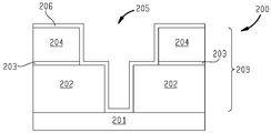
활동(110)에서, 방법(100)은 패터닝된 기판을 처리 챔버에 위치시키는 단계를 포함한다. 패터닝된 기판(200)은 도 2a에 예시되고, 이 기판은 기판(201), 기판(201) 상에 형성된 재료 층(209), 재료 층(209)에 형성된 하나 이상의 개구부들(205), 및 재료 층(209) 상에 배치되고 재료 층의 개구부들(205)을 라이닝하는 장벽 층(206)을 포함한다. 본원에서, 재료 층(209)은 하나 이상의 유전체 층들, 예컨대, 제1 유전체 층(202) 및 제2 유전체 층(204)을 포함한다. 전형적으로, 하나 이상의 유전체 층들(202, 204)은, 실리콘 산화물들, SiN, SiOC, SIC, 저-k 중합체들, 예컨대, 폴리아미드, 및 이들의 조합들로 구성된 군으로부터 선택된 재료로 형성된다.In
일부 실시예들에서, 재료 층(209)은 제1 유전체 층(202)과 제2 유전체 층(204) 사이에 배치된 식각 정지 층(203)을 더 포함한다. 재료 층(209) 상에 배치된 장벽 층(206)은, 후속하여 증착되는 구리 층들로부터 주위 유전체 층들(202, 204) 내로의 구리 원자들의 확산을 방지한다. 전형적으로, 장벽 층(206)은 금속, 금속 질화물, 금속 합금, 또는 이들의 조합 중 하나 이상을 포함한다. 일부 실시예들에서, 장벽 층(206)은 탄탈럼, 탄탈럼 질화물, 텅스텐, 티타늄, 티타늄 텅스텐, 티타늄 질화물, 텅스텐 질화물, 티타늄 구리, 및 이들의 조합들로 구성된 군으로부터 선택된다. 일부 실시예들에서, 장벽 층은 탄탈럼 질화물을 포함한다. 장벽 층(206)은 임의의 적합한 방법, 예컨대, 화학 기상 증착(CVD), 물리 기상 증착(PVD), 원자 층 증착(ALD), 또는 이들의 조합들을 사용하여 증착된다.In some embodiments, the
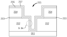
활동(120)에서, 방법(100)은 시드 층(207)을 장벽 층(206) 상에 형성하는 단계를 포함한다. 도 2b는, 패터닝된 기판(200)의 장벽 층(206) 상에 증착된 시드 층(207)을 예시한다. 도 2e는 도 2b의 일 부분의 근접 확대도이다.In
활동(130)에서, 방법(100)은 제1 구리 층(207a)을 패터닝된 기판(200)의 장벽 층(206) 상에 증착시키는 단계를 포함한다. 본원에서, 제1 구리 층(207a)은, 구리 막을 형성하기 위해, 패터닝된 기판(200)을, 구리 함유 유기 금속을 포함하는 제1 반응성 전구체에, 그리고 그 다음, 수소 함유 가스를 포함하는 제2 반응성 전구체에 순차적으로 노출시키는 것을 포함하는 원자 층 증착(ALD) 프로세스를 사용하여 증착된다. 구리 함유 유기 금속 가스들의 예들은 비스(디에틸아미노-2-n-부톡시)구리 (Cu(DEAB)2), 비스(에틸메틸아미노-2-n-부톡시)구리, 비스(디메틸아미노-2-프로폭시)구리 (Cu(DMAP)2), 비스(디메틸아미노-2-n-부톡시)구리 (Cu(DMAB)2), 비스(디메틸아미노-2-에톡시)구리, 비스(에틸메틸아미노-2-프로폭시)구리 (Cu(EMAP)2), 비스(디에틸아미노-2-에톡시)구리, 비스(에틸메틸아미노-2메틸-2-n-부톡시)구리, 비스(디메틸아미노-2-메틸-2-프로폭시)구리, 비스(디에틸아미노-2-프로폭시)구리 (Cu(DEAP)2), 비스(2-메톡시에톡시)구리, 비스(2,2,6,6-테트라메틸-3,5-헵탄디오네이트)구리, 비스(2,2,6,6-테트라메틸-3,5-헵탄케토이미네이트)구리, 비스(2-메톡시-2-프로폭시)구리, 및 2,2,6,6-테트라메틸-3,5-헵탄디오네이트 구리(TMVS), 및 이들의 조합들을 포함한다. 수소 함유 전구체의 예들은 H2, NH3, 및 이들의 조합들을 포함한다. 일부 실시예들에서, 처리 체적은 제1 및 제2 전구체들의 교번하는 노출들 간에 불활성 가스, 예컨대, 아르곤을 사용하여 퍼징된다.In
일부 실시예들에서, 제1 구리 층(207a)의 증착 동안, 처리 챔버는 약 1 Torr 내지 약 30 Torr의 압력에서 유지되고, 패터닝된 기판은 약 50 ℃ 내지 약 400 ℃의 온도로 유지된다. 제1 및 제2 반응성 전구체의 유량들은 전형적으로, 300 mm 직경 기판들을 처리하도록 구성된 처리 챔버에 대해 약 3000 sccm 내지 약 9000 sccm이고, 상이한 크기의 기판들에 대해서는 적절하게 비례된다. 일부 실시예들에서, 처리 챔버는, 처리 챔버에 배치된 전극이 플라즈마 전력 공급부에 커플링되는 플라즈마 강화 처리 챔버이다. 플라즈마 전력 공급부는, 전구체들을 처리 플라즈마로 점화시키고 유지하기 위해, 13.56 MHz의 주파수에서 약 100 W 내지 1000 W, 예컨대, 약 400 W를 제공한다. 일부 실시예들에서, 제1 구리 층(207a)은 약 99% 초과의 구리 순도를 갖는다. 다른 실시예들에서, 제1 구리 층은 물리 기상 증착(PVD) 또는 화학 기상 증착(CVD) 프로세스를 사용하여 증착된다. 예를 들어, 일 실시예에서, 제1 구리 층(207a)은, 타겟이 순수 구리 타겟 또는 구리 합금 타겟, 예컨대, 약 0.1% 내지 약 3% Al을 포함하는 Cu-Al 타겟 또는 약 0.1% 내지 약 3% Mn을 포함하는 Cu-Mn 타겟인 PVD 프로세스를 사용하여 증착된다. 이 실시예에서, 타겟은 약 20 kW 내지 약 40 kW의 DC 전력에 커플링되고, 기판은 약 50 W 내지 약 1500 W의 AC 바이어스 전력에 커플링된다. 다른 실시예에서, 제1 구리 층(207a)은 CVD 또는 PVD 프로세스를 사용하여 증착된다.In some embodiments, during the deposition of the first copper layer 207a, the processing chamber is maintained at a pressure of about 1 Torr to about 30 Torr, and the patterned substrate is maintained at a temperature of about 50 ° C to about 400 ° C. The flow rates of the first and second reactive precursors are typically from about 3000 sccm to about 9000 sccm for processing chambers configured to process 300 mm diameter substrates and are appropriately proportional to substrates of different sizes. In some embodiments, the processing chamber is a plasma enhanced processing chamber in which electrodes disposed in the processing chamber are coupled to a plasma power supply. The plasma power supply provides about 100 W to 1000 W, e.g., about 400 W, at a frequency of 13.56 MHz to ignite and maintain the precursors into the processing plasma. In some embodiments, the first copper layer 207a has a copper purity of greater than about 99%. In other embodiments, the first copper layer is deposited using a physical vapor deposition (PVD) or chemical vapor deposition (CVD) process. For example, in one embodiment, the first copper layer 207a may be a Cu-Al target, or a Cu-Al target containing from about 0.1% to about 3% Al, And is deposited using a PVD process that is a Cu-Mn target containing about 3% Mn. In this embodiment, the target is coupled to a DC power of about 20 kW to about 40 kW, and the substrate is coupled to an AC bias power of about 50 W to about 1500 W. In another embodiment, the first copper layer 207a is deposited using a CVD or PVD process.
활동(140)에서, 방법(100)은 루테늄 층(207b)을 제1 구리 층(207a) 상에 증착시키는 단계를 포함한다. 여기서, 루테늄 층(207b)은, 제1 구리 층(207a)을 증착시키는 데에 사용된 동일한 처리 챔버에서 증착된다. 전형적으로, 처리 챔버는 제1 구리 층(207a)을 증착시키는 단계와 루테늄 층을 증착시키는 단계 사이에서, 아르곤과 같은 불활성 가스를 사용하여 퍼징된다. 일부 실시예들에서, 루테늄 층(207b)은, 제1 구리 층(207a)이 상부에 증착된 패터닝된 기판(200)을, 루테늄 함유 유기 금속을 포함하는 제3 반응성 전구체에, 그리고 그 다음, 수소, 예컨대, 수소 가스를 포함하는 제4 반응성 전구체에 교번하여 순차적으로 노출시키는 것을 포함하는 ALD 프로세스를 사용하여 증착된다. 루테늄 함유 유기 금속들의 예들은, 메틸-시클로헥사딘 루테늄 트리카르보닐시클로헥사딘, 루테늄 트리카르보닐, 부타디엔 루테늄 트리카르보닐, 디메틸 부타디엔 루테늄 트리카르보닐, Ru(CO)3을 갖는 개질된 딘들(dines), 및 이들의 조합들을 포함한다.In
전형적으로, 루테늄 층(207b)의 증착 동안, 처리 챔버는 약 1 Torr 내지 약 50 Torr의 압력에서 유지되고, 패터닝된 기판은 약 100 ℃ 내지 약 400 ℃의 온도로 유지된다. 제3 및 제4 반응성 전구체들의 유량들은 300 mm 직경 기판들을 처리하도록 구성된 ALD 처리 챔버에 대해 약 3000 sccm 내지 약 9000 sccm이고, 상이한 크기의 기판들에 대해서는 적절하게 비례된다. 일부 실시예들에서, 처리 챔버에 배치된 전극은, 처리 챔버에 배치된 전구체 가스들의 처리 플라즈마를 점화시키고 유지하는, 13.56 MHz의 주파수에서 약 100 W 내지 1000 W, 예컨대, 약 400 W를 제공하는 플라즈마 전력 공급부에 커플링된다. 일부 실시예들에서, 처리 체적은 제3 및 제4 전구체들의 교번하는 노출들 간에 불활성 가스, 예컨대, 아르곤을 사용하여 퍼징된다. 다른 실시예들에서, 루테늄 층(207b)은 CVD 프로세스를 사용하여 증착되고/증착되거나, 제1 구리 층(207a)을 형성하는 데에 사용된 처리 챔버와 상이한 처리 챔버에서 증착된다. 다른 실시예들에서, 루테늄 층(207b)은 PVD 프로세스를 사용하여 증착된다.Typically, during the deposition of the
활동(150)에서, 방법(100)은 제2 구리 층(207c)을 루테늄 층(207b) 상에 증착시키는 단계를 포함한다. 일부 실시예들에서, 제2 구리 층(207c)은, 활동(130)에서 제1 구리 층(207a)을 그리고 활동(140)에서 루테늄 층(207b)을 형성하는 데에 사용되었던 동일한 처리 챔버에서 증착된다. 일부 실시예들에서, 제2 구리 층(207c)은, 활동(130)에서 제1 구리 층(207a)을 형성하는 데에 사용된 동일한 프로세스를 사용하여 증착된다. 전형적으로, ALD 처리 챔버는 루테늄 층(207b)을 증착시키는 단계와 제2 구리 층(207c)을 증착시키는 단계 사이에서, 아르곤과 같은 불활성 가스로 퍼징된다. 다른 실시예들에서, 제2 구리 층(207c)은, 제1 구리 층(207a) 및/또는 루테늄 층(207b)을 형성하는 데에 사용된 챔버와 상이한 챔버에서 PVD 프로세스 또는 CVD 프로세스를 사용하여 증착된다. 일부 실시예들에서, 장벽 층(206), 구리 층들(207a, 207c), 및/또는 루테늄 층(207b)을 형성하는 데에 사용되는 처리 챔버들은, 증착된 층들 상에 후속 층이 형성되기 전, 증착된 층들의 표면 산화를 방지하기 위해 대기압 미만의 압력들에서 유지되는 이송 챔버에 의해, 진공 또는 제어된 환경 하에서 함께 연결된다.In
본원에서, 장벽 층(206)은 약 0.5 nm 내지 약 20 nm, 예컨대, 약 1 nm 내지 약 5 nm, 예를 들어, 약 2 nm의 제1 두께(T(1))를 갖는다. 제1 구리 층(207a)은 약 0.5 nm 내지 약 20 nm, 예컨대, 약 0.5 nm 내지 약 10 nm, 이를 테면, 약 0.5 nm 내지 약 5 nm, 예를 들어, 약 4 nm의 제2 두께(T(2))를 갖는다. 루테늄 층(207b)은 약 1 옹스트롬(Å) 내지 약 20 Å, 예컨대, 약 1 Å 내지 약 15 Å, 이를 테면, 약 1 Å 내지 약 10 Å의 제3 두께(T(3))를 갖는다. 제2 구리 층(207c)은 약 0.5 nm 내지 약 200 nm, 예컨대, 약 1 nm 내지 약 20 nm, 또는 약 1 nm 내지 약 5 nm, 예를 들어, 약 2 nm의 제4 두께(T(4))를 갖는다. 전형적으로, 시드 층(207)에서 구리 대 루테늄의 비율은 약 99.9:1 내지 약 4:1이고, 각각의 구리 및 루테늄 층들(207a, 207b, 및 207c)의 두께들(T(2), T(3), 및 T(4))은 시드 층에서 루테늄의 농도를 증가시키거나 감소시키기 위해 조정된다.
일부 실시예들에서, 시드 층(207)을 형성하는 단계는, 제2 및 최종 구리 층(207c)을 증착시키기 이전에, 복수의 제1 구리 층들(207a) 및 루테늄 층들(207b)을 순차적으로 증착시키는 단계를 포함한다.In some embodiments, the step of forming the
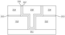
도 2d 및 2e는, 구리 인터커넥트의 형성을 더 예시한다. 도 2d는, 전기 도금 프로세스 또는 구리 리플로우/갭 충전 프로세스, 예컨대, 열 보조 리플로우 프로세스를 사용하여 시드 층 상에 증착된 벌크 구리 층(208)을 도시한다. 그 다음, 도 2d에 도시된 인터커넥트 구조와 같은 구리 인터커넥트 구조를 형성하기 위해, 벌크 구리 층(208)은 벌크 막 제거 프로세스, 예컨대, 화학적 기계적 평탄화(CMP)를 사용하여 기판의 표면으로부터 제거된다.Figures 2d and 2e further illustrate the formation of a copper interconnect. 2D illustrates the
본원에서 설명되는 방법들의 이점들은, 시드 층의 형성 동안 억제된 구리 응집, 그의 연속적인 적용 범위를 위해 요구되는 최소 시드 층 두께의 감소, 더 얇은 시드 층을 이용한 개선된 리플로우 충전, 및 상부에 형성된 구리 인터커넥트의 개선된 라인 및/또는 비아 저항을 포함한다. 추가로, 억제된 구리 응집에 부가하여, 본원의 실시예들의 이점은, 구리 전자 이동과 관련된 디바이스 고장들을 방지함으로써, 증가된 회로 밀도 및 개선된 신뢰성 및/또는 유효 수명을 허용하는 억제된 구리 전자 이동을 포함한다.Advantages of the methods described herein include reduced copper flocculation during formation of the seed layer, a reduction in the minimum seed layer thickness required for its continuous coverage, improved reflow charging with a thinner seed layer, Improved line and / or via resistance of the formed copper interconnect. Additionally, in addition to inhibited copper agglomeration, an advantage of embodiments herein is that by inhibiting device failures associated with copper electron movement, suppressed copper electrons, which allow increased circuit density and improved reliability and / Movement.
전술한 내용은 본 개시내용의 실시예들에 관한 것이지만, 이의 기본 범위로부터 벗어나지 않고 본 개시내용의 다른 실시예들 및 추가 실시예들이 고안될 수 있으며, 본 개시내용의 범위는 이하의 청구항들에 의해 결정된다.While the foregoing is directed to embodiments of the present disclosure, other and further embodiments of the present disclosure may be devised without departing from the basic scope thereof, and the scope of the present disclosure is defined by the following claims Lt; / RTI >
100
방법
110
활동
120
활동
130
활동
140
활동
150
활동
200
패터닝된 기판
201
기판
202
제1 유전체 층
203
식각 정지 층
204
제2 유전체 층
205
개구부
206
장벽 층
207
시드 층
207a
제1 구리 층
207b
루테늄 층
207c
제2 구리 층
208
벌크 구리 층
209
재료 층100 Methods
110 Activities
120 Activities
130 Activities
140 Activities
150 Activities
200 patterned substrate
201 substrate
202 first dielectric layer
203 etch stop layer
204 second dielectric layer
205 opening
206 barrier layer
207 seed layer
207a primary copper layer
207b ruthenium layer
207c second copper layer
208 bulk copper layer
209 Material layer
Claims (15)
기판을 제1 처리 챔버에 위치시키는 단계 ― 상기 기판은 상기 기판의 재료 층에 형성된 개구부들을 갖는 패터닝된 표면을 포함함 ―; 및
시드 층을 상기 개구부들의 벽들 상에 형성하는 단계를 포함하고,
상기 시드 층을 상기 개구부들의 벽들 상에 형성하는 단계는,
제1 구리 층을 상기 개구부들의 벽들 상에 형성하는 단계;
루테늄 층을 상기 제1 구리 층 상에 형성하는 단계; 및
제2 구리 층을 상기 루테늄 층 상에 형성하는 단계를 포함하는, 인터커넥트 구조를 형성하는 방법.A method of forming an interconnect structure,
Placing a substrate in a first processing chamber, the substrate including a patterned surface having openings formed in a material layer of the substrate; And
Forming a seed layer on the walls of the openings,
Wherein forming the seed layer on the walls of the openings comprises:
Forming a first copper layer on the walls of the openings;
Forming a ruthenium layer on the first copper layer; And
And forming a second copper layer on the ruthenium layer.
상기 루테늄 층을 형성하는 단계는, 상기 기판을 루테늄 전구체에 노출시키는 것과 상기 기판을 수소 함유 전구체에 노출시키는 것의 순차적 반복들을 포함하는, 인터커넥트 구조를 형성하는 방법.The method according to claim 1,
Wherein forming the ruthenium layer comprises sequential repeats of exposing the substrate to a ruthenium precursor and exposing the substrate to a hydrogen containing precursor.
상기 루테늄 층은, 상기 제1 구리 층을 형성하는 데에 사용된 상기 제1 처리 챔버와 상이한 제2 처리 챔버에서 형성되는, 인터커넥트 구조를 형성하는 방법.The method according to claim 1,
Wherein the ruthenium layer is formed in a second process chamber different from the first process chamber used to form the first copper layer.
상기 제1 구리 층, 상기 루테늄 층, 및 상기 제2 구리 층은, 상기 기판을 상기 제1 처리 챔버로부터 제거하지 않고 상기 제1 처리 챔버에서 형성되는, 인터커넥트 구조를 형성하는 방법.The method according to claim 1,
Wherein the first copper layer, the ruthenium layer, and the second copper layer are formed in the first processing chamber without removing the substrate from the first processing chamber.
상기 루테늄 층의 두께는 약 1 옹스트롬 내지 약 20 옹스트롬인, 인터커넥트 구조를 형성하는 방법.The method according to claim 1,
Wherein the thickness of the ruthenium layer is from about 1 Angstrom to about 20 Angstroms.
상기 패터닝된 표면은 상기 재료 층 상에 배치된 장벽 층을 더 포함하고, 상기 장벽 층은, 탄탈럼, 탄탈럼 질화물, 텅스텐, 티타늄, 티타늄 텅스텐, 티타늄 질화물, 텅스텐 질화물, 티타늄 구리, 및 이들의 조합들로 구성된 군으로부터 선택된 재료를 포함하며, 상기 제1 구리 층은 상기 장벽 층 상에 형성되는, 인터커넥트 구조를 형성하는 방법.The method according to claim 1,
Wherein the patterned surface further comprises a barrier layer disposed on the material layer and the barrier layer is selected from the group consisting of tantalum, tantalum nitride, tungsten, titanium, titanium tungsten, titanium nitride, tungsten nitride, titanium copper, Wherein the first copper layer is formed on the barrier layer. ≪ RTI ID = 0.0 > 11. < / RTI >
상기 장벽 층은 제2 처리 챔버에서 증착되고, 상기 제1 처리 챔버 및 상기 제2 처리 챔버는 이송 챔버에 의해 함께 연결되는, 인터커넥트 구조를 형성하는 방법.The method according to claim 6,
Wherein the barrier layer is deposited in a second processing chamber, and wherein the first processing chamber and the second processing chamber are connected together by a transfer chamber.
상기 제1 구리 층을 형성하는 단계는, 상기 기판을 구리 전구체에 노출시키는 것과 상기 기판을 수소 전구체에 노출시키는 것의 순차적 반복들을 포함하는, 인터커넥트 구조를 형성하는 방법.The method according to claim 1,
Wherein forming the first copper layer comprises sequential repeats of exposing the substrate to a copper precursor and exposing the substrate to a hydrogen precursor.
제1 구리 층을 패터닝된 기판 상에 증착시키는 단계 ― 상기 패터닝된 기판은 재료 층 및 상기 재료 층 상에 배치된 장벽 층을 포함하고, 상기 재료 층은 상기 재료 층에 형성된 개구부들을 가짐 ―;
루테늄 층을 상기 제1 구리 층 상에 증착시키는 단계; 및
제2 구리 층을 상기 루테늄 층 상에 증착시키는 단계를 포함하는, 디바이스를 형성하는 방법.A method of forming a device,
Depositing a first copper layer on a patterned substrate, the patterned substrate comprising a material layer and a barrier layer disposed on the material layer, the material layer having openings formed in the material layer;
Depositing a ruthenium layer on the first copper layer; And
And depositing a second copper layer on the ruthenium layer.
상기 재료 층은 유전체 층을 포함하는, 디바이스를 형성하는 방법.10. The method of claim 9,
Wherein the material layer comprises a dielectric layer.
상기 장벽 층은 탄탈럼, 탄탈럼 질화물, 텅스텐, 티타늄, 티타늄 텅스텐, 티타늄 질화물, 텅스텐 질화물, 티타늄 구리, 및 이들의 조합들로 구성된 군으로부터 선택된 재료를 포함하는, 디바이스를 형성하는 방법.11. The method of claim 10,
Wherein the barrier layer comprises a material selected from the group consisting of tantalum, tantalum nitride, tungsten, titanium, titanium tungsten, titanium nitride, tungsten nitride, titanium copper, and combinations thereof.
상기 제1 및 제2 구리 층들을 증착시키는 단계는, 상기 패터닝된 기판을, 구리 함유 유기 금속을 포함하는 제1 반응성 전구체 및 수소를 포함하는 제2 반응성 전구체에 순차적으로 노출시키는 것을 포함하는, 디바이스를 형성하는 방법.12. The method of claim 11,
Wherein depositing the first and second copper layers comprises sequentially exposing the patterned substrate to a first reactive precursor comprising a copper containing organometallic and a second reactive precursor comprising hydrogen, ≪ / RTI >
기판 ― 상기 기판은, 상기 기판의 재료 층에 형성된 복수의 개구부들을 갖는 패터닝된 표면을 포함함 ―; 및
상기 개구부들의 벽들 상에 배치된 시드 층을 포함하고,
상기 시드 층은:
제1 구리 층;
상기 제1 구리 층 상에 배치된 루테늄 층; 및
상기 루테늄 층 상에 배치된 제2 구리 층을 포함하는, 디바이스.As a device,
Substrate-the substrate includes a patterned surface having a plurality of openings formed in a material layer of the substrate; And
And a seed layer disposed on the walls of the openings,
The seed layer comprises:
A first copper layer;
A ruthenium layer disposed on the first copper layer; And
And a second copper layer disposed on the ruthenium layer.
상기 루테늄 층의 두께는 약 1 옹스트롬 내지 약 20 옹스트롬인, 디바이스.14. The method of claim 13,
Wherein the thickness of the ruthenium layer is from about 1 angstrom to about 20 angstroms.
상기 재료 층은 유전체 재료를 포함하고, 상기 디바이스는 상기 시드 층과 상기 개구부들의 벽들 사이에 개재된 장벽 층을 더 포함하며, 상기 장벽 층은 탄탈럼, 탄탈럼 질화물, 텅스텐, 티타늄, 티타늄 텅스텐, 티타늄 질화물, 텅스텐 질화물, 티타늄 구리, 및 이들의 조합들로 구성된 군으로부터 선택된 재료를 포함하는, 디바이스.14. The method of claim 13,
The device further comprising a barrier layer interposed between the seed layer and the walls of the openings, wherein the barrier layer is selected from the group consisting of tantalum, tantalum nitride, tungsten, titanium, titanium tungsten, A material selected from the group consisting of titanium nitride, tungsten nitride, titanium copper, and combinations thereof.
Applications Claiming Priority (4)
| Application Number | Priority Date | Filing Date | Title |
|---|---|---|---|
| US201762548604P | 2017-08-22 | 2017-08-22 | |
| US62/548,604 | 2017-08-22 | ||
| US16/102,533 | 2018-08-13 | ||
| US16/102,533 US10847463B2 (en) | 2017-08-22 | 2018-08-13 | Seed layers for copper interconnects |
Publications (1)
| Publication Number | Publication Date |
|---|---|
| KR20190021184A true KR20190021184A (en) | 2019-03-05 |
Family
ID=63350353
Family Applications (1)
| Application Number | Title | Priority Date | Filing Date |
|---|---|---|---|
| KR1020180097909A KR20190021184A (en) | 2017-08-22 | 2018-08-22 | Seed layers for copper interconnects |
Country Status (6)
| Country | Link |
|---|---|
| US (1) | US10847463B2 (en) |
| EP (1) | EP3447793B1 (en) |
| JP (2) | JP2019062190A (en) |
| KR (1) | KR20190021184A (en) |
| CN (1) | CN109461698B (en) |
| TW (1) | TWI803510B (en) |
Cited By (1)
| Publication number | Priority date | Publication date | Assignee | Title |
|---|---|---|---|---|
| WO2022005948A1 (en) * | 2020-06-28 | 2022-01-06 | Applied Materials, Inc. | Impurity removal in doped ald tantalum nitride |
Families Citing this family (1)
| Publication number | Priority date | Publication date | Assignee | Title |
|---|---|---|---|---|
| CN114664656A (en) | 2020-05-22 | 2022-06-24 | 北京屹唐半导体科技股份有限公司 | Workpiece processing using ozone gas and hydrogen radicals |
Family Cites Families (30)
| Publication number | Priority date | Publication date | Assignee | Title |
|---|---|---|---|---|
| US7910165B2 (en) * | 2002-06-04 | 2011-03-22 | Applied Materials, Inc. | Ruthenium layer formation for copper film deposition |
| US7101790B2 (en) | 2003-03-28 | 2006-09-05 | Taiwan Semiconductor Manufacturing Co., Ltd. | Method of forming a robust copper interconnect by dilute metal doping |
| JP2006097044A (en) * | 2004-09-28 | 2006-04-13 | L'air Liquide Sa Pour L'etude & L'exploitation Des Procede S Georges Claude | Precursor for film deposition, method for depositing ruthenium-containing film, method for depositing ruthenium film, method for depositing ruthenium oxide film and method for depositing ruthenate film |
| US7265048B2 (en) * | 2005-03-01 | 2007-09-04 | Applied Materials, Inc. | Reduction of copper dewetting by transition metal deposition |
| US20060246699A1 (en) * | 2005-03-18 | 2006-11-02 | Weidman Timothy W | Process for electroless copper deposition on a ruthenium seed |
| JP2008098449A (en) * | 2006-10-12 | 2008-04-24 | Ebara Corp | Substrate processing apparatus and substrate processing method |
| US20080164613A1 (en) | 2007-01-10 | 2008-07-10 | International Business Machines Corporation | ULTRA-THIN Cu ALLOY SEED FOR INTERCONNECT APPLICATION |
| US20080223287A1 (en) * | 2007-03-15 | 2008-09-18 | Lavoie Adrien R | Plasma enhanced ALD process for copper alloy seed layers |
| US20100200991A1 (en) * | 2007-03-15 | 2010-08-12 | Rohan Akolkar | Dopant Enhanced Interconnect |
| US7659204B2 (en) * | 2007-03-26 | 2010-02-09 | Applied Materials, Inc. | Oxidized barrier layer |
| US7737028B2 (en) | 2007-09-28 | 2010-06-15 | Applied Materials, Inc. | Selective ruthenium deposition on copper materials |
| JP2009116952A (en) * | 2007-11-06 | 2009-05-28 | Hitachi Global Storage Technologies Netherlands Bv | Perpendicular magnetic recording medium, and magnetic memory using the same |
| TW200951241A (en) | 2008-05-30 | 2009-12-16 | Sigma Aldrich Co | Methods of forming ruthenium-containing films by atomic layer deposition |
| US7964497B2 (en) * | 2008-06-27 | 2011-06-21 | International Business Machines Corporation | Structure to facilitate plating into high aspect ratio vias |
| US20090321935A1 (en) | 2008-06-30 | 2009-12-31 | O'brien Kevin | Methods of forming improved electromigration resistant copper films and structures formed thereby |
| US8084104B2 (en) | 2008-08-29 | 2011-12-27 | Asm Japan K.K. | Atomic composition controlled ruthenium alloy film formed by plasma-enhanced atomic layer deposition |
| JP2012074608A (en) * | 2010-09-29 | 2012-04-12 | Tokyo Electron Ltd | Wiring formation method |
| CN102332426A (en) * | 2011-09-23 | 2012-01-25 | 复旦大学 | Manufacturing method of copper diffusion impervious layers for nanometer ICs (integrated circuits) |
| US9142509B2 (en) * | 2012-04-13 | 2015-09-22 | Taiwan Semiconductor Manufacturing Company, Ltd. | Copper interconnect structure and method for forming the same |
| US9076661B2 (en) * | 2012-04-13 | 2015-07-07 | Applied Materials, Inc. | Methods for manganese nitride integration |
| CN102903699A (en) * | 2012-10-15 | 2013-01-30 | 复旦大学 | Copper interconnecting structure and preparation method thereof |
| US20140134351A1 (en) * | 2012-11-09 | 2014-05-15 | Applied Materials, Inc. | Method to deposit cvd ruthenium |
| CN103266304B (en) | 2013-05-31 | 2015-12-23 | 江苏科技大学 | A kind of high thermal stability is without the preparation method of diffusion impervious layer Cu (Ru) alloy material |
| US9984975B2 (en) * | 2014-03-14 | 2018-05-29 | Taiwan Semiconductor Manufacturing Company | Barrier structure for copper interconnect |
| JP6278827B2 (en) * | 2014-05-14 | 2018-02-14 | 株式会社Adeka | Copper compound, raw material for thin film formation, and method for producing thin film |
| US20160032455A1 (en) | 2014-07-31 | 2016-02-04 | Applied Materials, Inc. | High through-put and low temperature ald copper deposition and integration |
| US9768060B2 (en) * | 2014-10-29 | 2017-09-19 | Applied Materials, Inc. | Systems and methods for electrochemical deposition on a workpiece including removing contamination from seed layer surface prior to ECD |
| US10002834B2 (en) * | 2015-03-11 | 2018-06-19 | Applied Materials, Inc. | Method and apparatus for protecting metal interconnect from halogen based precursors |
| KR20160123793A (en) * | 2015-04-17 | 2016-10-26 | 포항공과대학교 산학협력단 | Resistive switching memory with double layered structure and method of fabricating the same |
| CN105355620B (en) * | 2015-12-17 | 2018-06-22 | 上海集成电路研发中心有限公司 | A kind of copper interconnection structure and its manufacturing method |
-
2018
- 2018-08-13 US US16/102,533 patent/US10847463B2/en active Active
- 2018-08-17 EP EP18189568.1A patent/EP3447793B1/en active Active
- 2018-08-21 JP JP2018154364A patent/JP2019062190A/en active Pending
- 2018-08-22 KR KR1020180097909A patent/KR20190021184A/en not_active Application Discontinuation
- 2018-08-22 TW TW107129279A patent/TWI803510B/en active
- 2018-08-22 CN CN201810960756.9A patent/CN109461698B/en active Active
-
2023
- 2023-09-25 JP JP2023159999A patent/JP2023182638A/en active Pending
Cited By (2)
| Publication number | Priority date | Publication date | Assignee | Title |
|---|---|---|---|---|
| WO2022005948A1 (en) * | 2020-06-28 | 2022-01-06 | Applied Materials, Inc. | Impurity removal in doped ald tantalum nitride |
| US11410881B2 (en) | 2020-06-28 | 2022-08-09 | Applied Materials, Inc. | Impurity removal in doped ALD tantalum nitride |
Also Published As
| Publication number | Publication date |
|---|---|
| TWI803510B (en) | 2023-06-01 |
| TW201920735A (en) | 2019-06-01 |
| CN109461698A (en) | 2019-03-12 |
| JP2019062190A (en) | 2019-04-18 |
| JP2023182638A (en) | 2023-12-26 |
| EP3447793B1 (en) | 2021-01-06 |
| US10847463B2 (en) | 2020-11-24 |
| US20190067201A1 (en) | 2019-02-28 |
| EP3447793A1 (en) | 2019-02-27 |
| CN109461698B (en) | 2024-04-12 |
Similar Documents
| Publication | Publication Date | Title |
|---|---|---|
| US9343402B2 (en) | Semiconductor device having Ti- and N-containing layer, and manufacturing method of same | |
| KR102036245B1 (en) | Doped tantalum nitride for copper barrier applications | |
| US6518167B1 (en) | Method of forming a metal or metal nitride interface layer between silicon nitride and copper | |
| KR20190050869A (en) | Doped optional metal cap to improve copper electron transfer with ruthenium liner | |
| TW201709293A (en) | Ruthenium metal feature fill for interconnects | |
| US10008448B2 (en) | Dielectric/metal barrier integration to prevent copper diffusion | |
| US8058164B2 (en) | Methods of fabricating electronic devices using direct copper plating | |
| US20120292767A1 (en) | Novel Approach for Reducing Copper Line Resistivity | |
| JP2023182638A (en) | Seed layers for copper interconnection | |
| JP2020536395A (en) | Ruthenium Metal Functional Filling for Interconnection | |
| US10373867B2 (en) | Cobalt contact and interconnect structures | |
| US20100244256A1 (en) | Semiconductor device and manufacturing method thereof | |
| KR100667905B1 (en) | Method of forming a copper wiring in a semiconductor device | |
| KR100622639B1 (en) | Method of manufacturing a semiconductor device | |
| KR101089249B1 (en) | Semiconductor device and a method of manufacturing the same | |
| KR20190081455A (en) | Method of manufacturing a cobalt-containing thin film | |
| JP2006147895A (en) | Manufacturing method of semiconductor device |
Legal Events
| Date | Code | Title | Description |
|---|---|---|---|
| A201 | Request for examination | ||
| E902 | Notification of reason for refusal | ||
| E902 | Notification of reason for refusal | ||
| E601 | Decision to refuse application |