KR20180124103A - Inductive power transmitter - Google Patents
Inductive power transmitter Download PDFInfo
- Publication number
- KR20180124103A KR20180124103A KR1020187030148A KR20187030148A KR20180124103A KR 20180124103 A KR20180124103 A KR 20180124103A KR 1020187030148 A KR1020187030148 A KR 1020187030148A KR 20187030148 A KR20187030148 A KR 20187030148A KR 20180124103 A KR20180124103 A KR 20180124103A
- Authority
- KR
- South Korea
- Prior art keywords
- predetermined
- frequency
- inductive power
- coil
- power transmitter
- Prior art date
Links
- 230000001939 inductive effect Effects 0.000 title claims abstract description 107
- 238000001514 detection method Methods 0.000 claims abstract description 163
- 239000000463 material Substances 0.000 claims abstract description 160
- 230000004044 response Effects 0.000 claims abstract description 72
- 238000012546 transfer Methods 0.000 claims abstract description 38
- 230000005284 excitation Effects 0.000 claims description 55
- 238000000034 method Methods 0.000 claims description 50
- 230000005540 biological transmission Effects 0.000 claims description 29
- 230000008859 change Effects 0.000 claims description 29
- 238000004891 communication Methods 0.000 claims description 18
- 239000003990 capacitor Substances 0.000 claims description 6
- 230000011664 signaling Effects 0.000 claims description 4
- 238000001228 spectrum Methods 0.000 claims description 3
- 230000000977 initiatory effect Effects 0.000 claims description 2
- 238000002847 impedance measurement Methods 0.000 claims 1
- 229910000859 α-Fe Inorganic materials 0.000 description 30
- 238000005259 measurement Methods 0.000 description 23
- 238000010586 diagram Methods 0.000 description 18
- 230000004907 flux Effects 0.000 description 15
- 239000000126 substance Substances 0.000 description 12
- 230000006870 function Effects 0.000 description 11
- 238000004804 winding Methods 0.000 description 11
- 238000004422 calculation algorithm Methods 0.000 description 10
- 239000004020 conductor Substances 0.000 description 7
- 230000008878 coupling Effects 0.000 description 7
- 238000010168 coupling process Methods 0.000 description 7
- 238000005859 coupling reaction Methods 0.000 description 7
- 239000002184 metal Substances 0.000 description 7
- 229910052751 metal Inorganic materials 0.000 description 7
- 230000035945 sensitivity Effects 0.000 description 7
- 230000009977 dual effect Effects 0.000 description 5
- 230000000694 effects Effects 0.000 description 5
- 230000001965 increasing effect Effects 0.000 description 5
- 238000003491 array Methods 0.000 description 4
- 238000004519 manufacturing process Methods 0.000 description 4
- 239000004065 semiconductor Substances 0.000 description 4
- 238000013459 approach Methods 0.000 description 3
- 230000006399 behavior Effects 0.000 description 3
- 230000008901 benefit Effects 0.000 description 3
- 230000003750 conditioning effect Effects 0.000 description 3
- 238000002474 experimental method Methods 0.000 description 3
- 230000001976 improved effect Effects 0.000 description 3
- 239000007769 metal material Substances 0.000 description 3
- 230000003071 parasitic effect Effects 0.000 description 3
- 230000008569 process Effects 0.000 description 3
- 230000003595 spectral effect Effects 0.000 description 3
- XEEYBQQBJWHFJM-UHFFFAOYSA-N Iron Chemical compound [Fe] XEEYBQQBJWHFJM-UHFFFAOYSA-N 0.000 description 2
- XUIMIQQOPSSXEZ-UHFFFAOYSA-N Silicon Chemical compound [Si] XUIMIQQOPSSXEZ-UHFFFAOYSA-N 0.000 description 2
- 230000004913 activation Effects 0.000 description 2
- 230000003466 anti-cipated effect Effects 0.000 description 2
- 230000033228 biological regulation Effects 0.000 description 2
- 239000002131 composite material Substances 0.000 description 2
- 238000005516 engineering process Methods 0.000 description 2
- 238000010438 heat treatment Methods 0.000 description 2
- 230000006698 induction Effects 0.000 description 2
- 239000000696 magnetic material Substances 0.000 description 2
- 150000002739 metals Chemical class 0.000 description 2
- 210000000056 organ Anatomy 0.000 description 2
- 230000010363 phase shift Effects 0.000 description 2
- 238000012545 processing Methods 0.000 description 2
- 230000009467 reduction Effects 0.000 description 2
- 229910052710 silicon Inorganic materials 0.000 description 2
- 239000010703 silicon Substances 0.000 description 2
- 239000000758 substrate Substances 0.000 description 2
- 230000006978 adaptation Effects 0.000 description 1
- 238000013475 authorization Methods 0.000 description 1
- 238000004364 calculation method Methods 0.000 description 1
- -1 coins Chemical class 0.000 description 1
- 230000006835 compression Effects 0.000 description 1
- 238000007906 compression Methods 0.000 description 1
- 239000012141 concentrate Substances 0.000 description 1
- 238000012790 confirmation Methods 0.000 description 1
- MPTQRFCYZCXJFQ-UHFFFAOYSA-L copper(II) chloride dihydrate Chemical compound O.O.[Cl-].[Cl-].[Cu+2] MPTQRFCYZCXJFQ-UHFFFAOYSA-L 0.000 description 1
- 239000013078 crystal Substances 0.000 description 1
- 230000003247 decreasing effect Effects 0.000 description 1
- 238000011161 development Methods 0.000 description 1
- 238000009826 distribution Methods 0.000 description 1
- 230000007613 environmental effect Effects 0.000 description 1
- 238000011156 evaluation Methods 0.000 description 1
- 239000000284 extract Substances 0.000 description 1
- 230000006872 improvement Effects 0.000 description 1
- 229910052742 iron Inorganic materials 0.000 description 1
- 230000002427 irreversible effect Effects 0.000 description 1
- 230000000670 limiting effect Effects 0.000 description 1
- 230000007246 mechanism Effects 0.000 description 1
- 238000012986 modification Methods 0.000 description 1
- 230000004048 modification Effects 0.000 description 1
- 230000000644 propagated effect Effects 0.000 description 1
- 230000001681 protective effect Effects 0.000 description 1
- 230000002829 reductive effect Effects 0.000 description 1
- 230000000630 rising effect Effects 0.000 description 1
- 238000005070 sampling Methods 0.000 description 1
- 238000000926 separation method Methods 0.000 description 1
- 238000004088 simulation Methods 0.000 description 1
- 238000011895 specific detection Methods 0.000 description 1
- 238000003860 storage Methods 0.000 description 1
- 238000010408 sweeping Methods 0.000 description 1
- 238000012360 testing method Methods 0.000 description 1
Images


Classifications
-
- H04B5/79—
-
- H—ELECTRICITY
- H02—GENERATION; CONVERSION OR DISTRIBUTION OF ELECTRIC POWER
- H02J—CIRCUIT ARRANGEMENTS OR SYSTEMS FOR SUPPLYING OR DISTRIBUTING ELECTRIC POWER; SYSTEMS FOR STORING ELECTRIC ENERGY
- H02J50/00—Circuit arrangements or systems for wireless supply or distribution of electric power
- H02J50/10—Circuit arrangements or systems for wireless supply or distribution of electric power using inductive coupling
-
- H—ELECTRICITY
- H02—GENERATION; CONVERSION OR DISTRIBUTION OF ELECTRIC POWER
- H02J—CIRCUIT ARRANGEMENTS OR SYSTEMS FOR SUPPLYING OR DISTRIBUTING ELECTRIC POWER; SYSTEMS FOR STORING ELECTRIC ENERGY
- H02J50/00—Circuit arrangements or systems for wireless supply or distribution of electric power
- H02J50/60—Circuit arrangements or systems for wireless supply or distribution of electric power responsive to the presence of foreign objects, e.g. detection of living beings
-
- H—ELECTRICITY
- H02—GENERATION; CONVERSION OR DISTRIBUTION OF ELECTRIC POWER
- H02J—CIRCUIT ARRANGEMENTS OR SYSTEMS FOR SUPPLYING OR DISTRIBUTING ELECTRIC POWER; SYSTEMS FOR STORING ELECTRIC ENERGY
- H02J50/00—Circuit arrangements or systems for wireless supply or distribution of electric power
- H02J50/80—Circuit arrangements or systems for wireless supply or distribution of electric power involving the exchange of data, concerning supply or distribution of electric power, between transmitting devices and receiving devices
-
- H—ELECTRICITY
- H04—ELECTRIC COMMUNICATION TECHNIQUE
- H04B—TRANSMISSION
- H04B1/00—Details of transmission systems, not covered by a single one of groups H04B3/00 - H04B13/00; Details of transmission systems not characterised by the medium used for transmission
- H04B1/02—Transmitters
- H04B1/04—Circuits
-
- H—ELECTRICITY
- H04—ELECTRIC COMMUNICATION TECHNIQUE
- H04B—TRANSMISSION
- H04B5/00—Near-field transmission systems, e.g. inductive loop type
- H04B5/0025—Near field system adaptations
- H04B5/0037—Near field system adaptations for power transfer
-
- H—ELECTRICITY
- H04—ELECTRIC COMMUNICATION TECHNIQUE
- H04B—TRANSMISSION
- H04B5/00—Near-field transmission systems, e.g. inductive loop type
- H04B5/0075—Near-field transmission systems, e.g. inductive loop type using inductive coupling
- H04B5/0081—Near-field transmission systems, e.g. inductive loop type using inductive coupling with antenna coils
-
- H04B5/24—
-
- H04B5/26—
-
- H—ELECTRICITY
- H04—ELECTRIC COMMUNICATION TECHNIQUE
- H04L—TRANSMISSION OF DIGITAL INFORMATION, e.g. TELEGRAPHIC COMMUNICATION
- H04L27/00—Modulated-carrier systems
- H04L27/10—Frequency-modulated carrier systems, i.e. using frequency-shift keying
- H04L27/12—Modulator circuits; Transmitter circuits
Abstract
코일을 갖는 송신 회로 - 송신 회로는 유도 전력 이송 또는 물질 검출을 위해 제1 주파수에서 또는 그 주위에서 동조, 적응, 또는 최적화됨 -; 제1 주파수에서 송신 회로를 구동하도록 동작가능한 인버터; 및 코일에 근접한 사전결정된 비-인가 디바이스로부터의 응답을 생성하기 위해, 인버터를 제어하여 더 높은 제2 주파수에서 송신 회로를 구동시키도록, 그리고 사전결정된 핸드세이크 신호에 따라 더 높은 제2 주파수에서의 신호를 변조하도록 배열된 제어기를 포함하는, 유도 전력 송신기가 제공된다.Transmitter circuit with a coil - The transmitter circuit is tuned, adapted, or optimized at or around the first frequency for inductive power transfer or material detection; An inverter operable to drive a transmit circuit at a first frequency; And to control the inverter to drive the transmitting circuit at a higher second frequency to produce a response from a predetermined non-application device in proximity to the coil, and to drive the transmitting circuit at a higher second frequency, An inductive power transmitter is provided, comprising a controller arranged to modulate the signal.
Description
본 발명은, 대체로, 유도 전력 송신기에 관한 것으로, 이 송신기는 구체적으로 유도 전력 이송(inductive power transfer, IPT) 시스템을 위한 것이지만 이로 한정되지 않는다.The present invention is generally directed to an inductive power transmitter, which is specifically, but not exclusively, for an inductive power transfer (IPT) system.
IPT 시스템들은 확립된 기술(예를 들어, 전동 칫솔들의 무선 충전) 및 개발 중인 기술(예를 들어, '충전 매트' 상에서의 핸드헬드 디바이스들의 무선 충전)의 잘 알려진 분야이다. 전형적으로, 전력 송신기는 송신 코일 또는 코일들로부터 시변 자기장을 생성한다. 이 자기장은 전력 수신기 내의 적합한 수신 코일에 교류 전류를 유도하고, 이는, 이어서, 배터리를 충전하거나 디바이스 또는 다른 부하에 전력을 공급하는 데 사용될 수 있다.IPT systems are well known areas of established technology (e.g., wireless charging of electric toothbrushes) and technologies under development (e.g., wireless charging of handheld devices on a 'charging mat'). Typically, the power transmitter produces a time-varying magnetic field from the transmitting coil or coils. This magnetic field induces an alternating current in a suitable receiving coil in the power receiver, which can then be used to charge the battery or to power the device or other load.
핸드헬드 디바이스들의 무선 충전을 위한 IPT 시스템들에 관하여, 특히, 무선 전력이 수신기 디바이스에만 이송되고 소위 이물질들 - 이들은, 충전 매트(예컨대, 인터페이스 표면) 상에 위치되지만 수신기 디바이스의 일부가 아닌 임의의 물질로서 정의될 수 있음 - 에는 이송되지 않는 것이 중요하다. 그러한 이물질들의 전형적인 예들은 동전, 열쇠, 종이클립 등과 같이 금속을 함유한 기생 요소들이다. 예를 들어, 기생 금속이 활성 IPT 영역에 가까이 있는 경우, 그것은 진동 자기장으로부터 비롯된 와전류들로 인해 전력 이송 동안 가열될 수 있다. 그러한 기생 금속의 온도가 허용불가능한 레벨들로 상승하는 것을 방지하기 위해, 전력 송신기는 전력 수신기들과 이물질들 사이를 판별하고 전력 이송을 시기적절하게 중단할 수 있어야 한다.With respect to IPT systems for wireless charging of handheld devices, in particular, the wireless power is transmitted only to the receiver device and the so-called foreign objects - which are located on a charging mat (e.g. interface surface) It is important not to be transported - which can be defined as material. Typical examples of such foreign objects are parasitic elements containing metals such as coins, keys, paper clips and the like. For example, if the parasitic metal is close to the active IPT region, it can be heated during power transfer due to eddy currents originating from the oscillating magnetic field. In order to prevent the temperature of such parasitic metal from rising to unacceptable levels, the power transmitter must be able to distinguish between power receivers and foreign matter and to stop power delivery in a timely manner.
인터페이스 표면 상의 이물질들의 가열을 검출하는 종래의 방식은 전력 손실 방법을 이용한다. 이 방법에서, 전력 송신기에 의해 생성된 자기장으로 인해 핸드헬드 디바이스에 포함된 전력 수신기 내에서 방산되는 전력의 총량을 나타내는 데 수신 전력(PPR)이 사용된다. 수신 전력은 전력 수신기의 출력으로부터 이용가능한 전력과 그 출력 전력을 생성할 시에 손실되는 임의의 전력의 합과 동일하다. 전력 수신기는 그의 PPR을 전력 송신기에 통신시켜서, 전력 송신기가, 전력 손실이 허용가능한 설정 한도 내에 있는지 여부를 판정할 수 있게 하며, 그렇지 않은 경우, 전력 송신기는, 이물질의 존재를 나타내고 전력 송신을 중단할 수 있는 이형적 거동을 결정한다. 그러나, 이 전력 손실 계산 방법은 자체적으로 이물질의 실제 검출을 제공하지는 않고, 예상되지 않은 거동의 발생만을 제공한다.Conventional approaches to detecting heating of foreign objects on the interface surface use a power loss method. In this method, the received power (PPR) is used to represent the total amount of power dissipated in the power receiver included in the handheld device due to the magnetic field generated by the power transmitter. The received power is equal to the sum of the available power from the output of the power receiver and any power lost in generating that output power. The power receiver communicates its PPR to the power transmitter so that the power transmitter can determine whether the power loss is within an acceptable set limit or the power transmitter will indicate the presence of a foreign object and stop power transmission Determine the possible heterogeneous behavior. However, this power loss calculation method does not itself provide the actual detection of foreign matter, but provides only the occurrence of unexpected behavior.
대조적으로, 국제 특허 공개 공보 WO2014/095722호는 송신기 내에서 일차 IPT 송신기 코일(들)과는 별개인 여자(excitation) 및 검출 코일들을 사용하는 이물질 검출의 방법을 제안한다. 그 경우, 검출 권선에서의 출력 전압의 변화 또는 검출 권선의 인덕턴스의 변화 중 어느 하나가 소정 물질의 존재 가능성을 판정하는 데 사용된다. 그러나, 이 시스템은 기본 인덕턴스를 알아내기 위해 복합한 교정을 필요로 한다. 그것은, 또한, 함철 또는 자성 물질들에 비해 금속 물질들에 둔감하고, 따라서, 이물질들과 우호 물질(friendly object)들, 예컨대 수신기 디바이스 사이를 판별하기 위한 수단을 제공하지 않는다. 검출에 대한 일차 IPT 자기장의 어떠한 바람직하지 못한 동작 영향들도 고려되거나 특성화되지 않으므로, 제안된 방법은 신뢰성이 없을 수도 있다.In contrast, International Patent Publication No. WO2014 / 095722 proposes a method of foreign matter detection using excitation and detection coils that are separate from the primary IPT transmitter coil (s) in the transmitter. In that case, either a change in the output voltage in the detection winding or a change in the inductance of the detection winding is used to determine the possibility of existence of a predetermined material. However, this system requires a complex calibration to determine the fundamental inductance. It is also insensitive to metallic materials compared to iron or magnetic materials and therefore does not provide means for distinguishing between foreign objects and friendly objects such as receiver devices. The proposed method may not be reliable since any undesirable operating effects of the primary IPT field for detection are not considered or characterized.
본 발명의 목적은, 개선된 유도 전력 송신기를 제공하거나 또는 대중에게 유용한 선택권을 제공하는 것이다.It is an object of the present invention to provide an improved inductive power transmitter or to provide options that are useful to the public.
하나의 예시적인 실시예에 따르면,According to one exemplary embodiment,
코일을 갖는 송신 회로 - 송신 회로는 유도 전력 이송 또는 물질 검출을 위해 제1 주파수에서 또는 그 주위에서 동조, 적응, 또는 최적화됨 -;Transmitter circuit with a coil - The transmitter circuit is tuned, adapted, or optimized at or around the first frequency for inductive power transfer or material detection;
제1 주파수에서 송신 회로를 구동시키도록 동작가능한 인버터; 및An inverter operable to drive a transmit circuit at a first frequency; And
코일에 근접한 사전결정된 비-인가 디바이스로부터의 응답을 생성하기 위해, 인버터를 제어하여 더 높은 제2 주파수에서 송신 회로를 구동시키도록, 그리고 사전결정된 핸드세이크(handshake) 신호에 따라 더 높은 제2 주파수에서의 신호를 변조하도록 배열된 제어기를 포함하는, 유도 전력 송신기가 제공된다.To generate a response from a predetermined non-application device in proximity to the coil, to control the inverter to drive the transmit circuit at a higher second frequency, and to drive the transmit circuit at a higher second frequency < RTI ID = 0.0 > And a controller arranged to modulate the signal at the output of the inductor.
제2 예시적인 실시예에 따르면,According to a second exemplary embodiment,
코일을 갖는 송신 회로;A transmitting circuit having a coil;
송신 회로를 구동시키도록 동작가능한 인버터; 및An inverter operable to drive a transmission circuit; And
코일에 근접한 사전결정된 비-인가 디바이스로부터의 응답을 생성하기 위해, 인버터를 제어하여 제1 핸드세이크 주파수에서 송신 회로를 구동시키도록, 그리고 사전결정된 핸드세이크 신호에 따라 제1 핸드세이크 주파수에서의 신호를 변조하도록 배열된 제어기를 포함하며,To generate a response from a predetermined non-application device in proximity to the coil, to control the inverter to drive the transmit circuit at a first handshake frequency and to generate a signal at a first handshake frequency in accordance with a predetermined handshake signal And a controller arranged to modulate the modulated signal,
사전결정된 비-인가 디바이스는 제1 핸드세이크 주파수보다 더 높은 캐리어 주파수를 갖는 특정된 핸드세이크 신호를 갖고,The predetermined non-application device has a specified handshake signal having a carrier frequency higher than the first handshake frequency,
사전결정된 핸드세이크 신호는 순차적인 일련의 폴링 커맨드(polling command)들을 포함하고, 특정된 핸드세이크 신호는 순차적인 일련의 폴링 커맨드들을 포함하고, 각각의 사전결정된 핸드세이크 신호 폴링 커맨드의 사이클들의 개수는 각각의 각자 특정된 핸드세이크 신호 폴링 커맨드의 사이클들의 개수와 동일한, 유도 전력 송신기가 제공된다.Wherein the predetermined handshake signal comprises a series of sequential polling commands, the specified handshake signal comprises a series of sequential polling commands, and the number of cycles of each predetermined handshake signal polling command is An inductive power transmitter is provided that is equal to the number of cycles of each respective specified handshake signal polling command.
제3 예시적인 실시예에 따르면,According to a third exemplary embodiment,
코일을 갖는 수신기 회로;A receiver circuit having a coil;
비-인가 공진 디바이스; 및A non-application resonant device; And
코일에서 유도 전력 송신기에 의해 전송된 디스에이블 신호를 검출하도록, 디스에이블 신호에 따라 비-인가 공진 디바이스를 디스에이블시키도록,To disable the non-applied resonant device in accordance with the disable signal to detect the disable signal transmitted by the inductive power transmitter at the coil,
그리고 송신기에게 전력 이송을 시작할 것을 명령하기 위해 코일 내의 신호를 변조하도록 배열된 제어기를 포함하는, 유도 전력 수신기가 제공된다.And a controller arranged to modulate the signal in the coil to command the transmitter to begin power transfer.
제4 예시적인 실시예에 따르면,According to a fourth exemplary embodiment,
코일을 갖는 송신기 회로;A transmitter circuit having a coil;
송신 회로를 구동시키도록 동작가능한 인버터; 및An inverter operable to drive a transmission circuit; And
인버터를 제어하여 제1 핑(ping) 주파수에서 송신 회로를 구동시키도록, 디스에이블 신호에 따라 제1 핑 주파수에서의 신호를 변조하여 인가된 수신기 내의 비-인가 공진 디바이스를 디스에이블시키도록, 그리고 코일 내의 개시(start-up) 신호를 검출하여 인가된 수신기로의 전력 이송을 시작하게 하도록 배열된 제어기를 포함하는, 유도 전력 송신기가 제공된다.Modulate the signal at the first ping frequency in accordance with the disable signal to disable the non-applied resonant device in the applied receiver to control the inverter to drive the transmit circuit at the first ping frequency, and And a controller arranged to detect a start-up signal in the coil and to begin power transfer to an applied receiver.
제5 예시적인 실시예에 따르면,According to the fifth exemplary embodiment,
적어도 하나의 다목적 코일; 및At least one multi-purpose coil; And
IPT 자기장 내의 또는 그에 인접한 물질들을 검출하도록 구성된 물질 검출 시스템을 포함하며,A material detection system configured to detect materials in or near the IPT magnetic field,
물질 검출 시스템은 다목적 코일을 기전(energise)시켜서, 사전결정된 비-인가 물질로부터의 응답을 생성하도록 구성된 핸드세이크 신호를 전송하며, 유효 응답을 수신한 것에 기초하여, 비-인가 물질을 검출하는, 유도 전력 송신기가 제공된다.The material detection system is configured to energize the multipurpose coil to transmit a handshake signal configured to generate a response from the predetermined non-applied material, and to detect a non-applied substance based on receiving the valid response, An inductive power transmitter is provided.
제6 예시적인 실시예에 따르면, 유도 전력 송신기에 대한 물질 검출 시스템으로서,According to a sixth exemplary embodiment, there is provided a material detection system for an inductive power transmitter,
인가된 유도 전력 수신기 및/또는 비-인가 물질과 연관된 사전결정된 시그너처들을 저장하도록 배열된 메모리를 포함하며,A memory arranged to store predetermined signatures associated with an applied inductive power receiver and / or non-application material,
물질 검출 시스템은,The material detection system comprises:
비-인가 물질과 연관된 사전결정된 시그너처들 중 하나 이상을 검출한 것;Detecting one or more predetermined signatures associated with the non-enforced substance;
및/또는 인가된 수신기와 연관된 사전결정된 시그너처들에 대응하지 않는 시그너처를 검출한 것에 응답하여, 비-인가 물질을 표시하도록 배열된, 물질 검출 시스템이 제공된다.And / or in response to detecting a signature that does not correspond to predetermined signatures associated with an authorized receiver, a substance detection system is provided.
제7 예시적인 실시예에 따르면,According to a seventh exemplary embodiment,
유도 전력 이송(IPT) 자기장을 생성하도록 구성된 적어도 하나의 전력 송신 코일; 및At least one power transmission coil configured to generate an inductive power transfer (IPT) magnetic field; And
IPT 자기장 내의 또는 그에 인접한 물질들을 검출하도록 구성된 물질 검출 시스템을 포함하며,A material detection system configured to detect materials in or near the IPT magnetic field,
물질 검출 시스템은 비-승인 공진 디바이스를 검출하도록 구성된, 유도 전력 송신기가 제공된다.The material detection system is configured to detect a non-approved resonant device.
제8 예시적인 실시예에 따르면, 유도 전력 송신기에 대한 물질 검출 시스템으로서,According to an eighth exemplary embodiment, there is provided a material detection system for an inductive power transmitter,
복수의 주파수들에서의 반사 임피던스를 판정하도록 배열된 코일 및 회로부; 및A coil and circuitry arranged to determine a reflection impedance at a plurality of frequencies; And
인가된 유도 전력 수신기와 연관된 사전결정된 주파수들 및/또는 비-인가 수신기와 연관된 사전결정된 주파수들을 저장하도록 배열된 메모리를 포함하며,A memory arranged to store predetermined frequencies associated with an authorized induction power receiver and / or predetermined frequencies associated with a non-authorizing receiver,
물질 검출 시스템은,The material detection system comprises:
비-인가 수신기와 연관된 사전결정된 주파수에서의 반사 임피던스의 사전결정된 증가 또는 감소를 검출한 것;Detecting a predetermined increase or decrease in the reflection impedance at a predetermined frequency associated with the non-authorized receiver;
및/또는 인가된 유도 전력 수신기와 연관되지 않은 주파수에서의 반사 임피던스의 사전결정된 증가를 검출한 것에 응답하여, 비-인가 수신기를 표시하도록 배열된, 물질 검출 시스템이 제공된다.And / or to detect a predetermined increase in the reflected impedance at a frequency not associated with the applied inductive power receiver.
제9 예시적인 실시예에 따르면, 유도 전력 송신기에 대한 물질 검출 시스템을 동작시키는 방법으로서, 물질 검출 시스템은 코일 및 회로부를 포함하고, 방법은, 제1 전력 레벨에서 코일을 구동시키고 제1 반사 임피던스를 판정하는 단계;According to a ninth exemplary embodiment, there is provided a method of operating a material detection system for an inductive power transmitter, the material detection system including a coil and a circuit, the method comprising: driving a coil at a first power level, ;
더 높은 제2 전력 레벨에서 코일을 구동시키고 제2 반사 임피던스를 판정하는 단계 - 제2 전력 레벨은 사전결정된 비-인가 수신기의 동작을 시작하게 하기에 충분하지만 제1 전력 레벨은 충분하지 않음 -; 및Driving the coil at a second higher power level and determining a second reflected impedance, the second power level being sufficient to start operation of the predetermined non-application receiver but not the first power level; And
제1 반사 임피던스와 제2 반사 임피던스 사이의 사전결정된 차이를 판정한 것에 응답하여 비-인가 수신기를 검출하는 단계를 포함하는, 방법이 제공된다.And detecting the non-application receiver in response to determining a predetermined difference between the first and second reflection impedances.
제10 예시적인 실시예에 따르면, 유도 전력 송신기에 대한 물질 검출 시스템을 동작시키는 방법으로서,According to a tenth exemplary embodiment, there is provided a method of operating a material detection system for an inductive power transmitter,
복수의 주파수들에서의 반사 임피던스들을 판정하는 단계; 및Determining reflection impedances at a plurality of frequencies; And
비-인가 수신기를 표시하는 단계로서,Displaying a non-authorized receiver,
비-인가 수신기와 연관된 사전결정된 주파수에서의 반사 임피던스의 사전결정된 증가 또는 감소를 검출한 것;Detecting a predetermined increase or decrease in the reflection impedance at a predetermined frequency associated with the non-authorized receiver;
및/또는 인가된 유도 전력 수신기와 연관되지 않은 주파수에서의 반사 임피던스의 사전결정된 증가를 검출한 것에 응답하여, 비-인가 수신기를 표시하는 단계를 포함하는, 방법이 제공된다.And / or displaying a non-authorized receiver in response to detecting a predetermined increase in the reflected impedance at a frequency not associated with the applied inductive power receiver.
제11 예시적인 실시예에 따르면,According to the eleventh exemplary embodiment,
코일을 갖는 송신 회로 - 송신 회로는 유도 전력 이송 또는 물질 검출을 위해 제1 주파수에 동조됨 -;A transmitting circuit having a coil, the transmitting circuit being tuned to a first frequency for inductive power transfer or material detection;
제1 주파수에서 송신 회로를 구동시키도록 동작가능한 인버터; 및An inverter operable to drive a transmit circuit at a first frequency; And
코일에 근접한 사전결정된 비-인가 디바이스로부터의 응답을 생성하기 위해, 인버터를 제어하여 더 높은 제2 주파수에서 송신 회로를 구동시키도록, 그리고 사전결정된 핸드세이크 신호에 따라 더 높은 제2 주파수를 변조하도록 배열된 제어기를 포함하는, 유도 전력 송신기가 제공된다.To generate a response from a predetermined non-application device in proximity to the coil, the inverter is controlled to drive the transmit circuit at a higher second frequency and to modulate the higher second frequency in accordance with the predetermined handshake signal An inductive power transmitter is provided that includes an arrayed controller.
제12 예시적인 실시예에 따르면, 유도 전력 송신기를 동작시키는 방법으로서,According to a twelfth exemplary embodiment, there is provided a method of operating an inductive power transmitter,
유도 전력 송신기는, 코일을 포함하고 제1 주파수에 동조되는 송신 회로, 및 제1 주파수에서 송신 회로를 구동시키도록 동작가능한 인버터를 포함하고, 방법은,The inductive power transmitter includes a transmission circuit including a coil and being tuned to a first frequency and an inverter operable to drive the transmission circuit at a first frequency,
코일에 근접한 임의의 사전결정된 비-인가 디바이스들을 검출하기 위해 더 높은 제2 주파수에서 송신 회로를 구동시키는 단계;Driving the transmit circuit at a higher second frequency to detect any predetermined non-application devices proximate to the coil;
비-인가 디바이스들에 의해 인식가능한 사전결정된 핸드세이크 신호에 따라 더 높은 제2 주파수를 변조하는 단계; 및Modulating a higher second frequency according to a predetermined handshake signal recognizable by the non-authorized devices; And
사전결정된 응답을 검출한 것에 응답하여 비-인가 디바이스의 존재를 표시하는 단계를 포함하는, 방법이 제공된다.And displaying the presence of the non-authorized device in response to detecting the predetermined response.
제13 예시적인 실시예에 따르면,According to the thirteenth exemplary embodiment,
코일을 갖는 송신 회로;A transmitting circuit having a coil;
송신 회로를 구동시키도록 동작가능한 인버터; 및An inverter operable to drive a transmission circuit; And
코일에 근접한 사전결정된 비-인가 디바이스로부터의 응답을 생성하기 위해, 인버터를 제어하여 제1 핸드세이크 주파수에서 송신 회로를 구동시키도록, 그리고 사전결정된 핸드세이크 신호에 따라 제1 핸드세이크 주파수에서의 신호를 변조하도록 배열된 제어기를 포함하며,To generate a response from a predetermined non-application device in proximity to the coil, to control the inverter to drive the transmit circuit at a first handshake frequency and to generate a signal at a first handshake frequency in accordance with a predetermined handshake signal And a controller arranged to modulate the modulated signal,
사전결정된 비-인가 디바이스는 제1 핸드세이크 주파수보다 더 높은 캐리어 주파수를 갖는 특정된 핸드세이크 신호를 갖고, 사전결정된 핸드세이크 신호는 순차적인 일련의 변조 상태들을 포함하고, 특정된 핸드세이크 신호는 순차적인 일련의 변조 상태들을 포함하고, 각각의 사전결정된 핸드세이크 신호의 일련의 변조 상태들의 사이클들의 개수는 각각의 각자 특정된 핸드세이크 신호의 일련의 변조 상태들의 사이클들의 개수와 동일한, 유도 전력 송신기가 제공된다.Wherein the predetermined non-application device has a specified handshake signal having a carrier frequency higher than the first handshake frequency, the predetermined handshake signal includes a sequence of sequential modulation states, and the specified handshake signal is sequential Wherein the number of cycles of a series of modulation states of each predetermined handshake signal is equal to the number of cycles of a series of modulation states of each respective handshake signal, / RTI >
용어들 "포함하다(comprise, comprises)" 및 "포함하는(comprising)"은 다양한 권한 하에서 배타적 의미 또는 포괄적 의미 중 어느 하나로 볼 수 있다는 것이 확인된다. 본 명세서의 목적을 위해, 그리고 달리 언급되지 않는다면, 이 용어들은 포괄적 의미를 갖는 것으로 의도된다 - 즉, 그들은, 사용이 직접적으로 언급된 열거된 컴포넌트들, 및 가능하게는, 또한, 다른 특정되지 않은 컴포넌트들 또는 요소들의 포함을 의미하는 것으로 취해질 것이다.The terms " comprise, " " comprises, " and " comprising " are to be understood as being either exclusive or inclusive meaning under various authorizations. For the purposes of this specification and unless otherwise stated, these terms are intended to have a generic meaning - that is, they are intended to encompass the enumerated components directly referred to in the use, and possibly also, Components " or " elements ".
본 명세서 내의 임의의 문헌에 대한 언급이, 그것이 종래 기술이라는 것 또는 그것이 보편적인 일반 지식의 일부를 형성한다는 입장을 구성하지는 않는다.References to any document herein do not constitute an admission that it is a prior art or that it forms part of a generic general knowledge.
명세서에 포함되고 그의 일부를 구성하는 첨부 도면은 본 발명의 실시예들을 예시하며, 상기에 주어진 본 발명의 대체적인 설명 및 하기에 주어지는 실시예들의 상세한 설명과 함께, 본 발명의 원리들을 설명하는 역할을 한다.
도 1은 유도 전력 이송 시스템의 개략도이다.
도 2는 물질 검출 시스템의 블록 다이어그램이다.
도 3은 이중 OD 코일의 개략도이다.
도 4는 단일 OD 코일의 개략도이다.
도 5는 다른 이중 OD 코일의 개략도이다.
도 6은 송신 코일 레이아웃의 개략도이다.
도 7은 OD 및 IPT 코일들이 페라이트 둘레에 인터리빙되어 있음을 도시한 개략도이다.
도 8은 PCB 기반 OD 코일의 단면도이다.
도 9는 IPT 페라이트를 사용하여 여자 코일에 의해 생성된 플럭스 라인들의 시뮬레이션이다.
도 10a는 검출 알고리즘의 흐름도이다.
도 10b는 다른 검출 알고리즘의 흐름도이다.
도 11은 여자 코일 구동기의 개략도이다.
도 12는 여자 코일 구동기의 회로도이다.
도 13은 검출기의 개략도이다.
도 14는 멀티플렉서의 회로도이다.
도 15는 혼합기의 회로도이다.
도 16은 추가 실시예의 개략도이다.
도 17은 다양한 공진 디바이스들의 임피던스의 그래프이다.
도 18a 및 도 18b는 다양한 공진 디바이스들의 실제 전력의 그래프들이다.
도 19a는 RFID/NFC 태그들과 같은 비-인가 공진 디바이스들을 검출하는 시그너처 방법의 흐름도이다.
도 19b는 상이한 캐리어 주파수들에서의 폴링 커맨드들의 그래프이다.
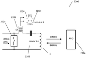
도 20은 1 ㎒에서 폴링 요청을 갖는 송신기의 회로도이다.
도 21은 폴링 커맨드들을 전송하여 RFID/NFC 태그들과 같은 비-인가 공진 디바이스들을 검출하는 방법의 흐름도이다.
도 22는 13.56 ㎒에서 폴링 요청을 갖는 송신기의 회로도이다.
도 23은 송신기로부터 신호들을 전송하여 유효 수신기에서 NFC 에뮬레이션을 디스에이블시키는 방법의 흐름도이다.
도 24는 송신기로부터 신호들을 수신하여 유효 수신기에서 NFC 에뮬레이션을 디스에이블시키는 방법의 흐름도이다.BRIEF DESCRIPTION OF THE DRAWINGS The accompanying drawings, which are incorporated in and constitute a part of the specification, illustrate embodiments of the invention and together with the description of the general inventive concept given above and the detailed description of the embodiments given below, serve to explain the principles of the invention .
1 is a schematic diagram of an inductive power delivery system.
2 is a block diagram of a material detection system.
Figure 3 is a schematic diagram of a dual OD coil.
4 is a schematic diagram of a single OD coil.
5 is a schematic diagram of another dual OD coil.
6 is a schematic view of the transmission coil layout.
Figure 7 is a schematic diagram showing that the OD and IPT coils are interleaved around the ferrite.
8 is a cross-sectional view of a PCB-based OD coil.
9 is a simulation of flux lines generated by excitation coils using IPT ferrite.
10A is a flow chart of the detection algorithm.
10B is a flow chart of another detection algorithm.
11 is a schematic view of an excitation coil driver.
12 is a circuit diagram of an excitation coil driver.
13 is a schematic view of the detector.
14 is a circuit diagram of a multiplexer.
15 is a circuit diagram of a mixer.
16 is a schematic diagram of a further embodiment.
17 is a graph of the impedance of various resonant devices.
18A and 18B are graphs of actual power of various resonant devices.
19A is a flow diagram of a signature method for detecting non-affirmed resonant devices, such as RFID / NFC tags.
19B is a graph of polling commands at different carrier frequencies.
20 is a circuit diagram of a transmitter having a polling request at 1 MHz;
Figure 21 is a flow diagram of a method for transmitting polling commands to detect non-affirmed resonant devices, such as RFID / NFC tags.
22 is a circuit diagram of a transmitter having a polling request at 13.56 MHz.
23 is a flow diagram of a method for transmitting signals from a transmitter to disable NFC emulation at a valid receiver.
24 is a flow diagram of a method for receiving signals from a transmitter and disabling NFC emulation at a valid receiver.
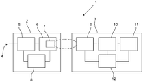
유도 전력 이송 (IPT) 시스템(1)이 도 1에 대체적으로 도시되어 있다. IPT 시스템은 유도 전력 송신기(2)와 유도 전력 수신기(3)를 포함한다. 유도 전력 송신기(2)는 적절한 전력 공급원(4)(예컨대, 주 전원 또는 배터리)에 접속된다. 유도 전력 송신기(2)는 컨버터(5), 예컨대 AC-DC 컨버터(사용된 전력 공급원의 타입에 따름), 및 예컨대 (존재한다면) 컨버터(5)에 접속되는 인버터(6) 중 하나 이상을 갖는 송신기 회로부를 포함할 수 있다. 인버터(6)는 송신 코일 또는 코일들(7)이 교류 자기장을 생성하도록 송신 코일 또는 코일들(7)에 AC 신호를 공급한다. 일부 구성들에서, 송신 코일(들)(7)은 또한 인버터(5)와는 별개인 것으로 간주될 수 있다. 송신 코일 또는 코일들(7)은 커패시터들(도시되지 않음)에 병렬 또는 직렬 중 어느 하나로 접속되어 공진 회로를 안출할 수 있다.An inductive power transfer (IPT)
제어기(8)가 유도 전력 송신기(2)의 각각의 부품에 접속될 수 있다. 제어기(8)는 유도 전력 송신기(2)의 각각의 부품으로부터 입력들을 수신하고, 각각의 부품의 동작을 제어하는 출력들을 생성한다. 제어기(8)는, 예를 들어 하기를 포함하는 그의 능력들에 따라, 유도 전력 송신기(2)의 다양한 태양들을 제어하도록 구성된 단일 유닛 또는 개별 유닛들로서 구현될 수 있다: 전력 흐름, 동조, 선택적 기전(energising) 송신 코일들, 유도 전력 수신기 검출 및/또는 통신. 제어기(8)는, 측정 및 계산된 데이터를 저장하기 위한 메모리를 내부적으로 포함할 수 있거나, 또는 그러한 목적을 위한 외부 메모리에 접속될 수 있다.A
유도 전력 수신기(3)는 전력 컨디셔닝 회로부(10)를 포함할 수 있는 수신기 회로부에 접속되는 수신 코일 또는 코일들(9)을 포함하고, 이 전력 컨디셔닝 회로부는, 이어서, 부하(11)에 전력을 공급한다. 유도 전력 송신기(2) 및 유도 전력 수신기(3)의 코일들이 적합하게 커플링된 경우, 송신 코일 또는 코일들(7)에 의해 생성된 교류 자기장이 수신 코일 또는 코일들(9)에 교류 전류를 유도한다. 전력 컨디셔닝 회로부(10)는 유도된 전류를 부하(11)에 적합한 형태로 변환하도록 구성되며, 예를 들어, 전력 정류기, 전력 조절 회로, 또는 양측 모두의 조합을 포함할 수 있다. 수신 코일 또는 코일들(9)은 커패시터들(도시되지 않음)에 병렬 또는 직렬 중 어느 하나로 접속되어 공진 회로를 안출할 수 있다. 일부 유도 전력 수신기들에서, 수신기는 제어기(12)를 포함할 수 있고, 이 제어기는 수신 코일 또는 코일들(9)의 동조, 전력 컨디셔닝 회로부(10)의 동작, 및/또는 통신을 제어할 수 있다.The
용어 "코일"은 전기 전류가 자기장을 생성하는 전기 전도성 구조물을 포함할 수 있다. 예를 들어, 유도 "코일들"은 3차원 형상 또는 2차원 평면 형상의 전기 전도성 와이어, PCB 기법들을 이용하여 복수의 PCB '층들' 위에 3차원 형상으로 제조된 전기 전도성 재료, 및 다른 코일형 형상들일 수 있다. 단수형이든 복수형이든 용어 "코일"의 사용은 이러한 의미에서 제한적인 것으로 의도되지 않는다. 응용예에 따라 다른 구성들이 사용될 수 있다.The term " coil " may include an electrically conductive structure in which an electrical current creates a magnetic field. For example, induction " coils " may include electrically conductive wires in a three-dimensional or two-dimensional planar shape, electrically conductive materials made in three-dimensional shapes on a plurality of PCB 'layers' using PCB techniques, . The use of the term " coil ", either singular or plural, is not intended to be limiting in this sense. Other configurations may be used depending on the application.
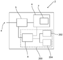
예시적인 송신기(2)가 도 2에 도시되어 있다. 인버터(6)는 송신 코일(7)에 전력을 공급하여 IPT 자기장을 생성한다. 물질 검출(object detection, OD) 회로(200)가, IPT 자기장과는 별개의 검출(OD) 자기장을 생성하는 여자 코일 또는 코일들(202), 및 송신기(2) 상에 또는 그에 인접한 물질들의 존재 및/또는 위치를 감지하는 데 사용되는 검출 코일 또는 코일들(204)을 포함한다. 송신기(2)의 제어기(8)는, 직접적으로 또는 별개의 제어 회로를 통해, 여자 코일(202)에 제공될 여자를 결정하도록 그리고 검출 코일(204)로부터의 출력 신호를 프로세싱하도록 구성될 수 있다.An
이것은, 응용물의 요건들에 따라, 단일 여자 코일 및 검출 코일들의 어레이, 여자 코일들의 어레이 및 단일 검출 코일, 여자 코일들의 어레이 및 검출 코일들의 어레이, 여자 및 검출 양측 모두를 위한 단일 코일을 사용하는 것, 및/또는 여자 코일(들)로서 IPT 코일(들)을 사용하는 것(그리고, IPT 주파수를 사용하는 것 또는 여자 신호를 IPT 자기장 상에 변조하는 것 중 어느 하나)을 수반할 수 있다.This may be achieved by using an array of single excitation coils and detection coils, an array of excitation coils and a single detection coil, an array of excitation coils and an array of detection coils, a single coil for both excitation and detection, depending on the requirements of the application , And / or using the IPT coil (s) as the exciting coil (s) (and using either the IPT frequency or modulating the excitation signal on the IPT magnetic field).
일 실시예에서, 검출 기법은 전력 수신기(또는 검출 자기장 내의 다른 통전 물질)로의 여자 신호의 송신에 의해 작동하는 자기 비전 시스템(magnetic vision system)의 형태로 간주될 수 있고, 이 여자 신호는, 이어서, 연속으로 또는 주기적으로 모니터링되는 센서들의 어레이로 다시 산란된다. 여자 신호의 후방 산란의 강도 및 지연이 측정되고, 어레이에 걸친 각각의 위치에서 개별적으로 분석될 수 있다. 이것은, 이어서, 물질들(우호적 물질 및 이물질 양측 모두)을 검출하는 데 이용될 수 있으며, IPT 자기장 내에서의 또는 송신기 표면 상에서의 다수의 수신기들과 같은 그러한 물질들의 위치 및/또는 이동을 추적할 수 있다. 그것은, 또한, 전력 수신기의 수신 코일(들)과 같은 우호적 물질들과 중첩하고 있는 이물질들을 검출하는 것이 가능할 수 있다.In one embodiment, the detection technique may be viewed in the form of a magnetic vision system that operates by transmission of an excitation signal to a power receiver (or other energizing material in the sensing field), which excitation signal is then , Again scattered back into an array of sensors that are continuously or periodically monitored. The intensity and delay of backscattering of the excitation signal can be measured and analyzed individually at each location across the array. This can then be used to detect materials (both friendly and foreign) and track the location and / or movement of such materials within the IPT magnetic field, such as multiple receivers on the transmitter surface . It may also be possible to detect foreign objects that overlap with friendly materials such as the receiving coil (s) of the power receiver.
검출 어레이는, 하나 이상의 전화기들, 또는 가능하게는, 태블릿 또는 휴대용 PC 또는 다른 휴대용 재충전가능 장비의 존재 및 위치를 식별할 수 있을 정도로 충분한 어퍼처(aperture)를 가지면서, 그의 분해능이 유의한 이물질들이 감지되거나 "보여지고" 위치확인되도록 하기에 충분하도록 구조화된다.The detection array has an aperture sufficient to identify the presence and location of one or more telephones, or possibly a tablet or portable PC or other portable rechargeable device, Are < / RTI > sensed or " seen "
하나 이상의 실시예들은 반사보다는 (물질로의 또는 여자 코일과 검출기 코일 사이로의) 에너지의 이송을 직접적으로 또는 간접적으로 결정하는 것에 의존할 수 있다. 다시 말해, 여자 코일, 물질, 및/또는 검출기 코일 사이의 커플링 계수는 물질, 예컨대 이물질(또는 우호 물질)의 본질 및/또는 위치를 판정하는 데 사용된다.One or more embodiments may rely on directly or indirectly determining the transfer of energy (either to the material or between the exciting coil and the detector coil) rather than the reflection. In other words, the coupling coefficient between the exciting coil, the material, and / or the detector coil is used to determine the nature and / or location of the material, e.g., foreign matter (or friendly material).
IPT 자기장으로부터의 디커플링Decoupling from the IPT magnetic field
OD 자기장은 물질들의 검출을 위해 사용되는 반면, IPT 자기장은 전자 디바이스들 사이에서 유의미한 레벨들의 전력을 무선으로 이송하는 데 사용된다.The OD magnetic field is used for the detection of materials while the IPT magnetic field is used to wirelessly transfer significant levels of power between electronic devices.
따라서, IPT 자기장의 전력은 OD 자기장보다 여러 자릿수 더 크므로, 전력 이송 동안 물질 검출 장치를 효과적으로 동작시키기 위해서는, IPT 자기장으로부터 OD 자기장을 실질적으로 디커플링하는 것이 바람직할 수 있다. 그러한 디커플링을 달성하는 다수의 방식들이 이제 기술된다. 이 방식으로, 검출에 대한 IPT 자기장의 임의의 바람직하지 못한 동작 효과들이 최소화되어, 이에 의해, 본 발명의 검출 방법을 더 신뢰할 수 있고 강건한 것이 되게 한다.Thus, since the power of the IPT magnetic field is several orders of magnitude larger than the OD magnetic field, it may be desirable to substantially decouple the OD magnetic field from the IPT magnetic field in order to operate the material detection device effectively during power transfer. A number of schemes for achieving such decoupling are now described. In this manner, any undesirable operational effects of the IPT magnetic field for detection are minimized, thereby making the detection method of the present invention more reliable and robust.
OD 자기장은 IPT 자기장을 위해 사용되는 것보다 유의하게 더 높은 또는 더 낮은 주파수를 갖도록 생성될 수 있다. 이것은, 물질에 공진이 설정된다는 가능성으로 인해, IPT 자기장으로부터의 주파수 분리뿐 아니라 동전과 같은 물리적으로 작은 물질들의 감도를 증가시키는 것을 허용할 수 있다. IPT 자기장이 약 110 ㎑ 내지 약 205 ㎑의 동작 주파수를 갖는 IPT의 공통 응용물에 대해, ㎒ 영역, 예컨대 약 1 ㎒에서 더 높거나, 또는 ㎑ 영역, 예컨대 약 5 ㎑에서 더 낮은 OD 자기장 주파수가 사용될 수 있다. 그러한 주파수들은, 또한, 소정 타입의 이물질들에 대한 향상된 감도를 제공할 수 있다. 이 방식으로, OD 자기장은 IPT 자기장으로부터 주파수-디커플링된다.The OD field may be generated to have a significantly higher or lower frequency than that used for the IPT magnetic field. This may allow to increase the sensitivity of physically small materials such as coins as well as frequency separation from the IPT magnetic field due to the possibility of resonance being set on the material. For common applications of IPT where the IPT magnetic field has an operating frequency of about 110 kHz to about 205 kHz, a lower OD field frequency in the ㎒ region, for example about 1 MHz, or a lower OD field frequency in the ㎑ region, for example about 5 kHz Can be used. Such frequencies may also provide enhanced sensitivity to certain types of foreign objects. In this way, the OD magnetic field is frequency-decoupled from the IPT magnetic field.
따라서, 일 실시예에서, OD 자기장의 구동은 하나의 OD 자기장 주파수가 물질 검출을 위해 사용되도록 구성되는데, 여기서 이 주파수는 IPT 자기장 주파수보다 더 낮거나 또는 더 높다(예컨대, 약 5 ㎑ 또는 약 1 ㎒). 대안의 실시예에서, OD 자기장의 구동은, 소위 주파수 "홉핑(hopping)" 또는 "스위핑(sweeping)"을 이용하여 소정 범위의 OD 자기장 주파수들이 사용되도록 구성된다. 물질 검출에 대한 측정이 이루어지는 이미 기술된 예시적인 레벨들을 중심으로 여러 개의 상이한 주파수들이 사용될 수 있다. 예를 들어, IPT 자기장 주파수보다 더 높은 OD 자기장 주파수들의 경우, 약 800 ㎑, 약 1 ㎒, 및 약 1.2 ㎒ 각각에서 측정이 이루어질 수 있고, IPT 자기장 주파수보다 더 낮은 OD 자기장 주파수들의 경우, 약 1 ㎑, 약 5 ㎑, 및 약 10 ㎑ 각각에서 측정이 이루어질 수 있다. 이 주파수 홉핑은, 유리하게는, 이물질과 우호 물질 사이의 판별을 증가시키는 능력을 제공한다. 예를 들어, 공진 회로의 일부로서의 수신기 코일(들)을 갖는 전력 수신기들의 경우, 비-공진 물질들, 예컨대 금속 또는 페라이트는 특정 OD 자기장 주파수에서 OD 자기장과 유사한 응답을 제공할 수 있다. 이것은, 예를 들어, 선택된 OD 자기장 주파수가 IPT 자기장 주파수의 고조파이기 때문에 발생할 수 있다. 그러나, 그러한 공진 수신기들은 상이한 OD 자기장 주파수들에서 상이한 응답을 제공할 것인 반면, 비-공진 물질들의 응답은 주파수와는 실질적으로 독립적이다.Thus, in one embodiment, the driving of the OD magnetic field is configured such that one OD magnetic field frequency is used for material detection, wherein the frequency is lower or higher than the IPT magnetic field frequency (e.g., about 5 kHz or about 1 / RTI > In an alternative embodiment, the driving of the OD magnetic field is configured to use a range of OD magnetic field frequencies using so-called frequency " hopping " or " sweeping ". A number of different frequencies can be used, centered on exemplary levels already described, in which measurements for material detection are made. For example, in the case of OD magnetic field frequencies higher than the IPT magnetic field frequency, measurements can be made at about 800 kHz, about 1 MHz, and about 1.2 MHz, respectively, and for OD field frequencies lower than the IPT magnetic field frequency, KHz, about 5 kHz, and about 10 kHz, respectively. This frequency hopping advantageously provides the ability to increase discrimination between foreign matter and friendly materials. For example, in the case of power receivers with receiver coil (s) as part of a resonant circuit, non-resonant materials, such as metal or ferrite, may provide a response similar to the OD field at a particular OD field frequency. This may occur, for example, because the selected OD magnetic field frequency is a harmonic of the IPT magnetic field frequency. However, such resonant receivers will provide different responses at different OD magnetic field frequencies, while the response of non-resonant materials is substantially independent of frequency.
여자 코일(들)(202) 및/또는 검출 코일(들)(204)(OD 코일들로 총칭됨)은 포지티브 IPT 플럭스 및 등가의 네거티브 IPT 플러스를 대략적으로 포괄하도록 배열될 수 있다. 이 방식으로, OD 자기장은 IPT 자기장으로부터 실질적으로 자기적으로 디커플링된다. 이것은 다수의 방식들로 달성될 수 있다. 예를 들어, 반대로 감긴(즉, 시계방향과 반시계방향) OD 코일들이, 각각의 반대로 감긴 OD 코일에 동일한 플럭스를 갖고서, 그 IPT 송신기 코일 또는 각각의 IPT 송신기 코일 내의 대칭 위치들에서 사용될 수 있다(즉, 그 코일의 수평면에 대해 그 코일 위에 또는 아래에 있는 하나의 송신 코일의 치수들 또는 '풋프린트' 내에 포함된다). 추가 예에서, 각각의 OD 코일의 부분들은 IPT 송신기 코일의 내측 및 외측일 수 있다. 다른 추가 예에서, 반대로 감긴 OD 코일들은 상이한 권선수들을 갖는 하나 이상의 송신기 코일들에 의해 생성된 IPT 자기장의 비대칭 부분들(즉, 시계방향으로 감긴 부분 대 반시계방향으로 감긴 부분)에서 사용될 수 있다.The excitation coil (s) 202 and / or the sensing coil (s) 204 (collectively referred to as OD coils) can be arranged to roughly encompass the positive IPT flux and the equivalent negative IPT plus. In this manner, the OD magnetic field is substantially magnetically decoupled from the IPT magnetic field. This can be accomplished in a number of ways. For example, oppositely wound (i.e., clockwise and counterclockwise) OD coils may be used at their IPT transmitter coils or at symmetric positions within each IPT transmitter coil, with the same flux to each of the oppositely wound OD coils (I. E., Contained within the dimensions or 'footprints' of one of the transmit coils above or below the coils relative to the horizontal plane of the coils). In a further example, portions of each OD coil may be inside and outside the IPT transmitter coil. In another further example, the reversely wound OD coils may be used in asymmetric portions of the IPT magnetic field produced by one or more transmitter coils with different winding forces (i. E., A clockwise winding portion to a counterclockwise winding portion) .
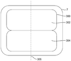
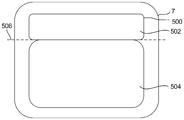
도 3은 이중 여자/검출 코일(300)의 일례를 도시한다. 코일(300)은 시계방향으로 감긴 부분(302) 및 반시계방향 부분(304)을 갖는다. 코일(300)은 전적으로 하나의 IPT 송신기 코일(7) 내에 위치되는데, 이때 시계방향 및 반시계방향 부분들(302, 304)은 송신기 코일(7)을 통한 대칭 라인(306)의 양쪽에 위치되어 동일한 양의 IPT 플럭스가 각각의 부분(302, 304)을 통과하게 한다. 이 예시적인 실시예에서, 반대로 감긴 부분들(302, 304)은 당업자에 의해 이해되는 방식으로 서로에게 커플링되는 별개의 권선들로서, 또는 (실질적으로 대칭인) "숫자 8"의 구성으로 감긴 단일 권선으로서 형성될 수 있다.Fig. 3 shows an example of a dual excitation /
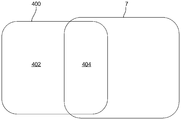
도 4는 단일 여자/검출 코일(400)의 일례를 도시한다. 코일(400)은 하나의 IPT 송신기 코일(7)에 대해 외측(제1) 부분(402) 및 내측(제2) 부분(404)을 갖는다. 즉, 코일(400)은 송신기 코일(7)과 중첩하도록 배열되어, 외측 부분(402)이 IPT 송신기 코일(7)의 외부에 배열되는 반면 내측 부분(404)이 IPT 송신기 코일(7)의 내부에 배열되어, 동일한 양의 (상반되는) IPT 플럭스가 각각의 부분(402, 404)을 통과하게 한다.Fig. 4 shows an example of a single excitation /
도 5는 다른 이중 여자/검출 코일(500)의 일례를 도시한다. 코일(500)은 시계방향으로 감긴 부분(502) 및 반시계방향 부분(504)을 갖는다. 코일(500)은 전적으로 하나의 IPT 송신기 코일(7) 내에 위치되는데, 이때 시계방향 및 반시계방향 부분들(502, 504)은 송신기 코일(7)을 통한 비대칭 라인(506)의 양쪽에 위치되어 상이한 양의 IPT 플럭스가 각각의 부분(502, 504)을 통과하게 한다. 이 예에서, 반대로 감긴 부분들(502, 504)을 통하는 IPT 플럭스는 코일 부분 권선들(502, 504)에서 IPT 플럭스 불균형을 실질적으로 보상하도록 계산된 상대적 크기(예컨대, 두께, 직경 등) 또는 전도도(예컨대, 상이한 전도성 재료들을 사용하는 것에 의함)를 구성하여 IPT 플럭스 불균형 또는 불균형 임피던스를 실질적으로 보상하도록 계산된 불균형 개수의 권선수를 각각의 부분(502, 504)에서 사용함으로써 균형맞춤될 수 있다. 도 3의 예와 마찬가지로, 반대로 감긴 부분들(502, 504)은 서로에게 커플링되는 별개의 권선들로서 또는 (실질적으로 비대칭인 또는 기울어진(skewed) "숫자 8"의 구성으로 감긴 단일 권선으로서 형성될 수 있다.Fig. 5 shows an example of another dual exciting / detecting
응용예에 따라 다른 형태의 디커플링이 사용될 수 있다. 송신기 코일 어레이 내의 다른 송신기 코일들로부터 생성되는 IPT 자기장으로부터의 디커플링을 제공하기 위해, 예를 들어, 송신기 코일(들)과는 별개인 하나 이상의 여자 코일들이 검출 자기장을 생성하기 위해 사용되는 실시예들에서는 전술된 플럭스-상쇄 방식으로 감기는 것이 여자 코일들인 반면, 하나 이상의 송신기 코일들이 검출 자기장을 생성하기 위해 사용되는 실시예들에서는 전술된 플럭스-상쇄 방식으로 감기는 것이 검출 코일들임에 유의한다.Other types of decoupling may be used depending on the application. To provide decoupling from the IPT magnetic field generated from other transmitter coils in the transmitter coil array, for example, embodiments in which one or more exciting coils, which are separate from the transmitter coils (s), are used to generate the sensing magnetic field It is noted that in the embodiments in which one or more of the transmitter coils are used to generate the detection magnetic field, it is the detection coils to be wound in the above-described flux-offset manner, while in the above-described flux-canceling manner it is the exciter coils.
여자 및 검출 코일들의 레이아웃Layout of exciter and detection coils
감도를 증가시키고/시키거나 제조 비용을 감소시키기 위해, OD 코일들 내의 여러 개의 특징부들이 제공될 수 있다.In order to increase the sensitivity and / or reduce the manufacturing cost, several features within the OD coils may be provided.
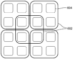
송신 코일들의 어레이의 일례가 도 6에 도시되어 있다. 각각의 송신 또는 IPT 코일(602)이 다수의 조직적으로 배열된 IPT 페라이트 요소들(코어들)(604) 둘레에 제공된다. IPT 코일들(602)은 직사각형 어레이 구조물에 배열되며, 선형(2D)일 수 있거나 (도 6에서와 같이) 중첩할 수 있거나 또는 3차원(3D)으로 배열될 수 있다. 코일 및 어레이 자체는 상이한 기하학적 또는 임의적 형상을 갖도록 배열될 수 있다. 페라이트 코어들(의 어레이)은 당업자에 의해 이해되는 방식으로 IPT 코일들(602)에 의해 생성된 IPT 자기장을 향상시키는 데 사용되며, 발명의 명칭이 "System and Method for Power Transfer"이고 2014년 8월 12일자로 출원되었고 그 전체 내용이 본 명세서에 참고로 명백히 포함된 미국 가특허 출원 제62/070,042호에서 설명된 바와 같이, 송신기 코일 어레이에 대해, 각각의 페라이트 요소의 (송신기 코일들의 평면에 직교하는 IPT 시스템의 z-축 - 이 축을 따라 소위 "z-높이"가 IPT 시스템의 송신 코일과 수신 코일 사이의 거리로서 정의됨 - 에 대한) 상부 표면이 IPT 코일들(602)로부터 돌출하도록 배열 및 치수화될 수 있거나, 또는 페라이트 요소들의 상부 표면이 송신 코일 표면의 최상부 평면과 동일 평면이거나 그 아래에 있도록 구성될 수 있다. 페라이트 요소들은 실질적으로 편평한 또는 둥근 상부 표면을 가질 수 있다. 하기에 기술되는 바와 같이, 그러한 페라이트 요소들이 IPT 어레이에 대해 존재하는 경우, 그들은, 또한, 유리하게도, 검출 자기장을 위해 사용될 수 있다.An example of an array of transmit coils is shown in Fig. Each transmission or
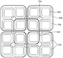
도 7은 예시적인 구성에서 도 6의 IPT 코일들(602)의 어레이가 검출 코일들(702)의 어레이와 인터리빙된 것을 도시한다. 각각의 IPT 코일(602)은 페라이트 코어들(604) 중 4개를 포함한다. 검출 코일들(702) 각각은 페라이트 코어들(604) 중 하나의 페라이트 코어의 상부 표면 위에(즉, 페라이트 요소의 상부 표면의 평면에 평행하지만 그보다는 들어올려져 있는 평면에) 배열되어, 도 7의 태양에서 알 수 있는 바와 같이, 단일 페라이트 코어가 각자의 검출 코일에 의해 둘러싸이거나 그 내에 봉입되게 한다. 이 배열에 의하면, 코어(604)의 페라이트 재료는, 검출 코일(702)이, IPT 자기장에서의 효과와 유사하게, OD 자기장의 향상을 통해 더 민감해지게 한다. 그러나, 페라이트 코어들(604)이 코어들의 위치에서 IPT 자기장의 자기 플럭스를 집중시키므로, 코어들 사이의 공간 내의 IPT 플럭스는 그에 상응하여 덜 조밀하다. 따라서, 일부 영역들은 낮지만 비-제로(non zero)인 IPT 플럭스를 갖는 IPT 자기장 널(null)들(704)을 형성할 수 있다. 유사하게, 검출 코일들(702)의 감도는 또한 페라이트 코어들(604) 사이에서 저하된다. 따라서, IPT 자기장 널들(704)과 더 낮은 감도의 OD 자기장 영역들의 정렬이 바람직할 수 있는데, 이는, 유사하게, 이 지점들에 전적으로 존재하는 어떠한 이물질도 IPT 플러스를 수신하고 있지 않아서, 이에 의해, 가열 위험을 감소시킬 것이기 때문이다.Fig. 7 shows that in an exemplary configuration the array of IPT coils 602 of Fig. 6 is interleaved with the array of detection coils 702. Fig. Each
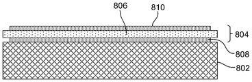
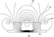
여자 코일(202)은 유사하게 송신 코일들(7)과 인터리빙될 수 있고, 페라이트 요소들(604)은 응용물 요건에 따라 여자 코일 어레이에 의해 생성된 OD 자기장 강도를 증가시키는 데 사용될 수 있다. 도 8은 인쇄 회로 보드(PCB)로서 구성된 OD 코일 어레이를 도시한다. PCB(804)의 베이스 층(802)이 페라이트 요소들 및 송신 코일들의 어레이를 가질 수 있다. PCB(804)는 기판 층(806)을 포함할 수 있는데, 이때 양쪽에는 2개의 구리 트레이스 층들(808, 801)이 있다. 하측 트레이스(808)(베이스 층(802)과 대면함)는 여자 코일들(202)을 포함할 수 있다. 상부 트레이스(810)는 검출 코일들(204)을 포함할 수 있다. 이 방식으로, OD 코일 어레이의 크기가 최소화될 수 있다.The
도 9는 여자 코일들이 (검출 코일들과 관련하여 앞서 논의된 방식으로) 각각의 페라이트 요소(604)를 둘러싸도록 배열된 도 8의 하측 트레이스(808)에 대한 예시적인 자기장 분포(900)를 도시한다. 검출 및/또는 여자 코일들은 전술된 바와 같은 IPT 송신기 코일 어레이의 페라이트 구조물을 사용하고, 자기장 라인들은 각각의 페라이트 요소(604)의 자극(pole)들(902)에 집중된다. 이 실시예에서, 페라이트 요소들(604)(및 그에 따른 PCB(804))이, 역시 페라이트인 베이스 또는 기판(백플레이트)(904) 상에 제공된다. 베이스 플레이트(904)는, 따라서, IPT 및 OD 코일 어레이들의 (전술된 차원 평면들과 관련하여) 하측들에 대한 차폐부로서 작용하여, 코일 어레이들 아래의 어떠한 금속 물질들도 가열되거나 잘못 검출되지 않게 한다. 이 방식으로, OD 회로(200)는 지향성이다.9 shows an exemplary
이 실시예에서, 페라이트 요소들은, 적합한 제조를 통해, 페라이트 백플레이트에 적용되거나 백플레이트와 일체형인 별개의 요소들일 수 있다. OD 코일들은, 대안으로, 별개의 페라이트 요소들/코어들을 포함하여, 응용물에 따라, 예컨대 IPT 코일 어레이가 그러한 요소들을 채용하지 않는 경우, 검출 감도를 증가시킬 수 있다.In this embodiment, the ferrite elements can be separate elements that are applied to the ferrite back plate or integral with the back plate, through suitable manufacture. The OD coils may alternatively include separate ferrite elements / cores to increase the detection sensitivity, depending on the application, e.g. if the IPT coil array does not employ such elements.
검출 HW 및 알고리즘Detection HW and Algorithm
위에서 언급된 바와 같이, 송신기(2)의 제어기(8)는 각각의 검출 코일로부터의 전압을 직접적으로 또는 간접적으로 제공받고, 시간 경과에 따라 각각의 위치에 대한 진폭 및 위상을 추출한다. 이 목적을 위해, 제어기(8)는 여자 코일 구동기 및 검출기 회로를 포함할 수 있다.As mentioned above, the
앞서 논의된 바와 같이, 이물질들과 우호 물질들, 예컨대 전력 수신기들 사이를 판별하기 위한 수단이 필요하다. 존재하는 물질의 종류를 판별하는 데 이용될 수 있는 한 가지 방법은, 여자(OD) 자기장에 영향을 미치고 있는, 송신 패드 위의 물질과 여자 코일들 사이의 커플링 인자의 측정이다. 본 출원인은, 주로 금속을 포함하는 물질들이 OD 자기장과의 커플링을 억압(더 낮은 전압 진폭 출력)하려는 경향이 있는 반면, 상대적으로 유의한 양의 페라이트를 갖는 물질이 커플링을 향상(더 높은 전압 진폭 출력)시키려는 경향이 있다는 것, 그리고 공진 픽업 또는 이차 회로들을 갖는 전력 수신기들과 같은 공진 구조물들이 후방 산란 신호의 위상 변이를 유도하려는 경향이 있다는 것을 발견하였다. 따라서, OD 자기장 거동에서의 이 특성들이 적합하게 판정되는 경우, 유도 픽업 코일의 페라이트 차폐부와 같은 '우호' 물질들을 동전과 같은 '이'물질들로부터 구별하는 것이 가능하다.As discussed above, there is a need for means to distinguish between foreign objects and friendly materials, e.g. power receivers. One method that can be used to determine the type of material present is to measure the coupling factor between the excitation coil and the material on the transmission pad, which is affecting the excitation (OD) field. Applicants have found that materials that primarily contain metals tend to suppress coupling with OD field (lower voltage amplitude output), while materials with a relatively significant amount of ferrite improve coupling Voltage amplitude output), and that resonant structures, such as power receivers with resonant pickups or secondary circuits, tend to induce phase shifts of the backscattered signal. Thus, if these properties in the OD field behavior are suitably determined, it is possible to distinguish 'friendly' materials such as ferrite shields of the inductive pickup coils from 'a' materials such as coins.
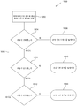
도 10a는 물질들을 검출하기 위한 예시적인 알고리즘(1000)을 도시한다. 제어기(8)는, 단계(1002)에서, OD 어레이 내의 각각의 위치에서의 전압 크기 및 위상을 판정한다. 임의의 위치에서, 위상이 변화한 경우(단계(1004)), 이 위치는 전력 수신기가 존재함을 나타내도록 단계(1006)에서 업데이트된다. 위상이 변화하지 않았지만 크기가 증가한 경우(단계(1008)), 이 위치는 자성 재료가 존재함을 나타내도록 단계(1010)에서 업데이트된다. 크기가 증가한 것이 아니라 감소한 경우(단계(1012)), 이 위치는 금속 재료가 존재함을 나타내도록 단계(1014)에서 업데이트된다. 판정은 OD 어레이 내의 각각의 위치에 대해 계속되고(단계(1016)), 이어서, 연속으로, 주기적으로, 또는 사전정의된 이벤트 또는 이벤트들의 발생 시에 반복된다.FIG. 10A illustrates an
도 10a의 알고리즘(1000)은 수신기들 및 이물질들의 검출이 상대적 크기 및 위상 변화들을 판정함으로써 상대적으로 간단하게 제공되는 일례를 도시한다. 이 변화들이 많은 다양한 시나리오들에서 존재하지만, 그 변화의 양은 환경 및/또는 회로부 전자 잡음과 구별하기 어려울 수 있다. 변화들은, 또한, 수신기 및 이물질 양측 모두가 존재하는 시나리오들에서 구별불가능할 수 있다. 도 10b는 그러한 상황들에서 물질들의 검출을 추가로 가능하게 하기 위한 다른 예시적인 알고리즘(1050)을 도시한다.
알고리즘(1050)은, 검출 코일들(702)의 소정 그룹에 걸친 주변(즉, 존재하는 물질들이 없음) 조건들에서의 측정에 약간의 변화가 있을 수 있음을 인식하고, 이 그룹들을 사용하여 표준 편차의 측정을 제공한다. 본 출원인은, 이 그룹들이 이웃 검출 코일들을 포함하고 코일 어레이의 일반적 토폴로지를 대체적으로 표현하며, 변화가 제조 프로세스들 및 공차들로 인한 것임을 발견하였다. 예를 들어, 어레이는 4개 초과의 에지들을 갖는 다각형을 표현할 수 있고, 이 다각형에 한정된 4개 이하의 에지들을 갖는 하위다각형들은 상이한 검출 코일 그룹들을 제공하는데, 예컨대, 어레이가 '십자형'(12-에지 다각형)인 경우, 각각의 그룹 내의 코일들이 그 그룹 내의 다른 코일들과는 실질적으로 일치하는 특성들을 갖지만 다른 그룹들의 코일들과는 상이한 특성들을 가질 수 있는 3개의 검출 코일 그룹들이 한정되도록 3개의 4-에지 다각형들이 정의될 수 있었다. 코일들의 이 그룹화는 그 그룹들 내의 코일들에 걸친 (크기 및/또는 위상) 측정치들의 차이들이 측정치들의 정확도에 합리적인 확실성을 갖고서 만들어져서, 이에 의해, 물질들의 신뢰할 수 있는 검출을 제공하게 한다.
따라서, 도 10b에서, 제어기(8)는, 당업자에 의해 이해되는 방식으로, 단계(1052)에서, OD 어레이의 각각의 그룹 내에서 전압 크기 및 위상에 의해 표현되는 자극 크기의 표준 편차를 판정한다. 표준 편차가 정상 파라미터들 내에 있는 경우, 제어기(8)는, 전술된 바와 같이, OD 어레이를 연속으로, 주기적으로, 또는 사전정의된 이벤트들 시에 계속해서 샘플링한다. 그러나, 임의의 그룹 내에서, 표준 편차가 소정 임계량(예컨대, 공지의 제조 공차들에 기초하여 사전결정됨)보다 큰 경우, 하나 이상의 물질들이 충전 표면의 근접지에 있는 것으로 판정된다(단계(1054)). 제어기(8)는, 이어서, 내부에 물질(들)이 있는 것으로 판정된 그룹 내의 각각의 검출 코일에 대해 또는 OD 어레이의 모든 검출 코일들에 대해, 수학식(1)에서와 같은 자극 크기의 현재(즉, t(n)) 측정치와 자극 크기의 이전(직전)(즉, t(n-1)) 측정치의 비율을 계산한다. 이 비율은 수학식(1)에서 설정된 위치에서의 표면 상의 변화를 표현한다.Thus, in Figure 10b, the
Ratiot(n) = Polar Magnitudet(n) / Polar Magnitudet(n-1) (1)Ratio t (n) = Polar Magnitude t (n) / Polar Magnitude t (n-1) (1)
제어기(8)는, 이어서, 계산된 비율에 기초하여 존재하는 물질(들)의 타입을 검출하기 위한 일련의 검사들을 실행한다. 단계(1056)에서, 그룹(또는 표면) 내에서의 최대 비율 증가가 수신기 검출 임계치보다 더 큰지 여부를 판정함으로써 수신기(들)에 대한 검사가 수행되며, '예(yes)'인 경우, 최대 비율 증가의 위치가 판정되고(단계(1058)), 판정된 검출 코일에서의 수신기의 위치는 IPT 어레이를 사용하여 전력 이송이 개시될 수 있도록 리포트된다(단계(1060)). 단계(1056)의 결과가 '아니오'인 경우, 단계(1062)에서, 그룹(또는 표면) 내에서의 최대 비율 감소가 이물질 검출 임계치보다 더 큰지 여부를 판정함으로써 이물질(들)에 대한 검사가 수행되고, '예'인 경우, 최대 비율 감소의 위치가 판정되고(단계(1064)), 판정된 검출 코일에서의 이물질의 위치는 IPT 어레이를 사용한 전력 이송이 인에이블되지 않도록 리포트된다(단계(1066)). 단계(1062)의 결과가 '아니오'인 경우, 단계(1068)에서, 미지의 물질이 존재하는 것으로 판정되어, IPT 어레이를 사용한 전력 이송이 인에이블되지 않게 한다. 이 '미지의' 물질은 수신기 및 이물질 임계치들의 적합한 선택에 의해 수신기와 이물질의 조합을 표현할 수 있다. 그러한 선택은 당업자에 의해 이해되는 방식으로 다양한 시나리오들의 측정 및 모델링을 통해 이루어질 수 있다.The
도 10a 및 도 10b에서 단계들의 예시 및 기술된 순차는 단지 예시적인 것일 뿐이고, 순차들은 병행 단계들로 적절하게 변경 또는 대체될 수 있음이 이해된다.It is understood that the illustrations and described sequences of steps in Figs. 10A and 10B are merely exemplary, and that the sequences may be suitably altered or replaced with concurrent steps.
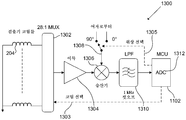
도 11은 여자 코일 구동기(1100)의 일례를 도시한다. MCU(1102)가 원하는 OD 자기장 주파수, 예컨대 5 ㎑/1 ㎒(또는 1 ㎑ 내지 10 ㎑/800 ㎑ 내지 1.2 ㎒의 주파수 범위)뿐 아니라 90° 위상 변이 신호(1105)에서 PWM(1103)을 제공한다. 양측 신호들 모두는 고조파를 제거함으로써 PWM 구형파로부터 사인파를 안출하도록 필터(1104)를 사용하여 저역통과필터링되고, 필터링된 신호들은 검출기(후술됨)에 제공된다. 전력 증폭기(1106)가 신호를 충분한 양만큼 여자 코일(202)로 스케일링하여, 과도한 전력을 사용하지 않으면서 양호한 신호대잡음비가 제공되게 한다.11 shows an example of the
도 12는 여자 코일 구동기 회로(1200)에 대한 다른 예시적인 회로를 도시한다. 2개의 동일한 신호 체인들이 사용된다 - 하나의 체인(1202)은 높은 구동 능력을 갖는 연산 증폭기(opamp)(1204)를 사용하여 여자 코일(202)을 구동시킨다. 다른 체인(1206)은 제어기(검출기)를 구동시킨다. MCU(1102)는 여자 체인(1202)에 대한 구동 신호의 위상을 검출기 체인(1206)으로 변화시킬 수 있다. 이 방식으로, 0° 또는 90° 기준이 검출기(후술됨)에 나타날 수 있다.12 shows another exemplary circuit for the excitation
대안으로, 실제 여자 출력이 위상 분할기(예컨대, R/C 및 C/R 회로망)에 공급되어, 서로에 대해 90° 위상의 2개의 신호들을 생성하며, 이어서, 전자 스위치가 하나 또는 다른 하나를 선택하는 데 사용된다.Alternatively, the actual excitation output may be provided to a phase splitter (e.g., R / C and C / R network) to generate two signals of phase 90 [deg.] With respect to each other, and then the electronic switch selects one or the other .
도 13은 검출 코일 어레이를 갖는 검출기(1300)의 일례를 도시한다. 각각의 검출 코일(204)은 멀티플렉서(1302)에 접속된다. 멀티플렉서(1302)는 모든 검출 코일들을 통해 순환하는 신호(1303)로 연속으로 또는 주기적으로 프로그래밍되거나, 또는 물질이 검출된 소정의 검출 코일들에 중점을 둘 수 있다. 멀티플렉서 출력은 증폭기(1304)에 의해 증폭되며, 전술된 여자 신호(전압)는 전술된 바와 같은 MCU(1102)에서 소프트웨어에 의해 스위치(1305)를 사용하여 위상-스위칭된다. 증폭된 멀티플렉서 출력은, 혼합기(1306)에 의해, 여자 구동기로부터의 2개의 상이한 위상-스위칭된 여자 전압들(1308)과 혼합된다(곱해진다). 대안으로, 혼합은 DSP 또는 마이크로프로세서에 의해 행해질 수 있었다. 혼합기의 출력은 필터(1310)에 의해 저역통과필터링되고, ADC(1312)에 의해 디지털 방식으로 샘플링된다. 필터(1310)의 응답이 검출 코일들이 스위칭될 수 있는 속도를 결정하므로, 정착 시간은 OD 자기장 샘플링의 분해능에 대한 응용물 요건에 따라 선택되어야 한다.13 shows an example of a
혼합 및/또는 멀티플렉싱의 이 구성은 가변 필터들을 필요로 하지 않으면서 여자의 주파수를 추적하는 이점을 갖는다. 또한, 위상 스위칭은 MCU(1102)가 디지털 신호로부터 진폭 및 위상 정보를 추출하게 한다. 여자 코일(들)로부터의 전압이 검출 코일(들)로부터의 전압과 동일한 주파수이기 때문에, 2개의 신호들을 승산하면, 주파수를 2배화(double)하도록 변이되는 하나의 신호, 및 DC에 있는 하나의 신호로 구성되는 하나의 복합 신호를 생성한다. 저역통과필터(1310)는 더 높은 주파수 신호를 필터링한다. 이어서, 여자 기준 전압을 90° 만큼 위상-변이시키고 DC 레벨의 제2 판독치를 취함으로써, 위상은, 이어서, 예를 들어 수학식(2)을 사용하여, 2개의 혼합기 DC 출력들의 크기들의 나누기의 역-탄젠트로서 계산될 수 있다:This configuration of mixing and / or multiplexing has the advantage of tracking the frequency of the excitation without the need for variable filters. The phase switching also allows the
![]()
![]()
도 14 및 도 15는 검출기에 대한 예시적인 회로를 도시한다. 모든 검출기 코일(204)의 출력은 직렬로 접속된 하나 이상의 멀티플렉서들(1402, 1404)의 입력들에 접속되고, 이때 궁극적인 출력(1406)이 opamp(1408)에 의해 증폭된다. opamp(1408)의 출력이 길버트 셀 혼합기(Gilbert cell mixer)(1502)로 전달된다. 이에 뒤이어 증폭기(1504)가 이득 및 DC 오프셋 양측 모두를 제공하여 ADC(1312)의 입력 범위에 맞춘다.Figures 14 and 15 illustrate exemplary circuits for the detector. The output of all detector coils 204 is connected to the inputs of one or
여자/검출 코일들은 연속적인 OD 자기장을 제공하도록 연속으로 구동될 수 있는데, 이는 전력 소비가 낮기 때문이다(약 10 mW). 대안으로, OD 자기장은 펄스화될 수 있는데, 이는 전력 소비를 심지어 더 많이 낮출 수 있다.The excitation / detection coils can be driven continuously to provide a continuous OD field, because of the low power consumption (about 10 mW). Alternatively, the OD magnetic field can be pulsed, which can even lower power consumption even more.
검출 자기장으로부터 절대 측정이 이루어짐에 따라, 그것이 IPT 자기장으로부터 디커플링되므로, 이물질이 개시 시에 송신기 '패드" 상에 이미 존재하는 경우, 이 이물질은 검출되는 것이 아니라 단지 주변 환경의 일부일 뿐이라는 것이 가능하다. 공지된 속성들의, 물리적인 교정 토큰(예컨대, 금속 디스크) 또는 디지털 교정 토큰(예컨대, 교정 인자)이, 설정된 위치들에 그것을 위치시킴으로써 그리고 위치 및 물질 타입이 정확하게 판정될 때까지 알고리즘 출력을 조절함으로써, 이를 피하기 위해 사용 전에 송신기를 교정하는 데 사용될 수 있다.As an absolute measurement is made from the sensing magnetic field, it is possible that it is not detected but only a part of the surrounding environment if it already exists on the transmitter 'pad' at the start, since it is decoupled from the IPT magnetic field (E.g., a metal disk) or a digital calibration token (e.g., a calibration factor) of known attributes, by locating it at the set locations and by adjusting the algorithm output until the position and material type are correctly determined , It can be used to calibrate the transmitter before use to avoid it.
대안으로, 사용 전에, 일차 코일, 여자 코일, 및 검출 코일 사이의 상대적 위상 및 진폭 측정치들은 개시 환경에서 흔하지 않은 무엇인가를 판정하기 위해 상대적 예상 값들과 비교될 수 있다. 이것은 환경을 수동으로 검사하기 위한 경고를 생성할 수 있거나, 또는 알고리즘을 조절하는 데 사용될 수 있다.Alternatively, prior to use, the relative phase and amplitude measurements between the primary coil, the exciting coil, and the sensing coil may be compared to the relative expected values to determine something unusual in the starting environment. This can generate an alert to manually test the environment, or it can be used to adjust the algorithm.
추가 대안예에서, 교정 인자는, 또한, 기존 코일들을 통해 또는 소정 간격에 있는 여분의 코일(들)을 통해 시스템 내에 공지의 신호를 주입함으로써 판정될 수 있다. 이것은 수동 교정 및/또는 시스템 외부의 교정 물질(예컨대, 교정 토큰)에 대한 필요성을 회피시킬 수 있다.In a further alternative, the calibration factor may also be determined by injecting a known signal into the system through the existing coils or through the extra coil (s) at a predetermined interval. This can avoid manual calibration and / or the need for calibration materials (e.g., calibration tokens) outside the system.
추가 실시예가 도 16과 관련하여 기술되며, 이는 전술한 특징부들의 일부 조합들을 포함한다. 단일 송신기 어레이로부터의 다수의 수신기들에 전력을 공급하는 것은, PRx(유도 전력 수신기) 전력 이송의 존재 시에 이물질 전력 방산을 검출하는 문제의 동적 범위를 증가시킨다. 이것은, 다수의 PRx 유닛들에 대한 지원이 연관된 총 PTx(유도 전력 송신기) 전력 이송 레벨을 실질적으로 증가시키기 때문이다.A further embodiment is described with reference to FIG. 16, which includes some combinations of the features described above. Powering multiple receivers from a single transmitter array increases the dynamic range of the problem of detecting foreign matter power dissipation in the presence of PRx (inductive power receiver) power transfer. This is because support for multiple PRx units substantially increases the total PTx (Inductive Power Transmitter) power transfer level to which they are associated.
(하나의 PRx를 근사화하는 공간으로 국부화된) 공간적 측정은 문제의 동적 범위를 제한하는 방식을 제공하는데, 이는 추가 전력 수신기들이 전력 송신기 제품에 추가되기 때문이다.Spatial measurements (localized into a space that approximates one PRx) provide a way to limit the dynamic range of the problem because additional power receivers are added to the power transmitter product.
인터페이스 영역(수신기들을 배치하기 위한 송신기 표면)에 걸쳐서 공간적으로 분포된 검출 코일들의 어레이 내의 각각의 검출기 코일 또는 셀에서의 커플링 인자의 측정 또는 복합 임피던스들의 평가가 하기의 유용한 표시를 제공할 수 있다:The measurement of the coupling factor or the evaluation of the complex impedances in each detector coil or cell in the array of detection coils spatially distributed over the interface region (the transmitter surface for placing receivers) can provide the following useful indication :
- 물질이 인터페이스 표면 상에 배치되는 시간(및 장소)에서의 물질 검출;- Material detection at the time (and place) at which the material is placed on the interface surface;
- 물질이 사실상 실질적으로 금속인지의 여부;- Whether the substance is substantially a metal;
- 물질이 페라이트를 함유하는지의 여부; 및- Whether the material contains ferrite; And
- 물질이 L-C 병렬 공진 탱크와 같은 공진 회로를 갖고 있는지의 여부.- Whether the material has a resonant circuit, such as an L-C parallel resonant tank.
본 명세서에 기술되는 실시예는 이물질 검출의 다른 방법들과는 독립적으로 또는 그와 함께 사용될 수 있다.The embodiments described herein may be used independently of or in conjunction with other methods of detecting foreign objects.
도 16을 참조하면, 물질 검출 시스템은 하기의 시스템 블록들을 포함한다:Referring to Figure 16, the material detection system includes the following system blocks:
a)
인터페이스 영역 또는 표면을 커버하도록 배치되어, 인가된 전류(들)가 인터페이스 영역의 평면을 통해 자기 플럭스를 생성하도록 하는 컨덕터 또는 컨덕터들의 어레이로 이루어진 FOD 여자 코일(1605)(이것은 일차 코일과는 별개이고 그로부터 디커플링될 수 있음). 컨덕터(들)는 '반대로 감긴 이중 루프(double counter wound loop)' 구성으로 배치되어, 일차 코일로부터의 (동일한 컨덕터의 반대로 감긴 섹션들에 대한) 플럭스 누설들이 순 유도 전압을 최소화하게 할 수 있음;a)
An
b)
인터페이스 표면에 걸쳐서 공간적으로 분포된 셀들의 어레이로 이루어진 FOD 검출 코일 어레이(1610). 각각의 셀은, 인터페이스 표면 상에 또는 그 근처에 배치된 물질과 연결되는(즉, 그를 통과하는) FOD 여자 코일에 의해 생성된 임의의 자기 플럭스가 또한 FOD 검출 코일 어레이의 적어도 하나의 셀 내의 컨덕터와 연결되도록 구성된 컨덕터(들)를 포함함;b)
An FOD
c)
FOD 여자 코일에 연속적인 또는 펄스화된 여자 전류를 인가하는 여자 코일 구동기(1615) 회로; 및c)
An
d) FOD 검출 코일 어레이의 각각의 셀에서의 복합 임피던스들을 측정 및 평가하는 물질 검출 유닛(1620). 전형적으로, 이것은 각각의 셀로부터의 신호들을 프로세싱하여 그들이 수치 계산 유닛에 의해 평가될 수 있도록 하는 측정 회로로 구성될 것이다.d) A material detection unit (1620) for measuring and evaluating complex impedances in each cell of the FOD detection coil array. Typically, this will consist of a measurement circuit that processes the signals from each cell so that they can be evaluated by the numerical computation unit.
또한, 이물질(1625) 및 유효 유도 전력 수신기(1630)가 도시되어 있다. (1635에서의) 여자 코일 및 (1630에서의) 수신기 각각에 대한 페라이트 차폐가 또한 도시되어 있고, 유리하게도, 유효 수신기(1630)를 검출하기 위해 채용된다.Also,
실시예는 각각의 셀의 출력 벡터 크기 또는 자극 크기를 복합 임피던스의 측정치로서 하기와 같이 평가할 수 있다:The embodiment may evaluate the output vector magnitude or the pole size of each cell as a measure of the complex impedance as follows:
1.
여자 코일 구동기를 인에이블시킴으로써 여자 전류(IFOD-excitation)를 인가한다. (시스템 구현 속성들과 함께) IFOD -excitation의 크기 및 주파수는 Φforeign, (각각의 셀에서의) ΦFOD -Detection-Coil-N, ΦPRx -Secondary-Coil에서 충분한 레벨들의 플럭스를 생성하여, 물질 검출 시스템이 2개의 상이한 물질 그룹들(이물질 또는 유효 수신기)의 복합 임피던스를 (복합 임피던스의 측정치를 판정함으로써), 그들 사이를 구별하기에 충분한 정확도로 평가할 수 있게 하도록 배열된다. IFOD-excitation의 주파수는, 전형적으로, PRx(1630) 내의 Ls, Cs, 및 Cd에 의해 형성된 공진 검출 주파수(fd)에 가깝지만 정확하게 동일한 것은 아닌 지점이다.1. Apply excitation current (I FOD-excitation ) by enabling excitation coil driver. The magnitude and frequency of the I FOD -excitation (along with the system implementation properties) produce a sufficient level of flux in Φ foreign , Φ FOD -Detection-Coil-N (in each cell), Φ PRx -Secondary-Coil , The material detection system is arranged to allow the composite impedance of two different groups of materials (foreign object or effective receiver) to be evaluated (by determining a measure of the complex impedance) to an accuracy sufficient to distinguish between them. The frequency of I FOD-excitation is typically close to but not exactly equal to the resonant detection frequency f d formed by L s , C s , and C d in
2.
FOD 검출 코일 어레이 내의 각각의 셀(1610)에 대해, 종단 임피던스를 적용하고, 복합 임피던스의 측정치로서 물질 검출 회로(1620)에 의해 구현되는 각각의 LFOD-Detection-Coil-N에서의 전압 신호의 진폭 및 위상을 측정한다.2. For each
3. 진폭은, 동위상(in-phase)이고 국부적 기준(예컨대, 여자 코일 구동기 출력)과 직각-위상(quadrature)인 셀 출력 신호의 성분들을 측정함으로써 평가될 수 있다. 벡터 또는 자극 크기는 측정된 동위상 및 직각-위상 성분들의 제곱의 합의 근(root)으로서 평가될 수 있다. 유사하게, 벡터 위상 각도는 직각-위상 성분으로 나뉘는 동위상 성분의 비율의 역-탄젠트 또는 아크-탄젠트를 계산함으로써 평가될 수 있다. 그러나, 이러한 측정치들을 판정하는 다른 방법들이 대안으로 이용될 수 있었다.3. The amplitude can be evaluated by measuring the components of the cell output signal that are in-phase and quadrature with the local reference (e.g., excitation coil driver output). The vector or stimulus magnitude can be evaluated as the root of the sum of squared measured in-phase and quadrature-phase components. Similarly, the vector phase angle can be evaluated by calculating the inverse-tangent or arc-tangent of the ratio of the in-phase component that is divided into a quadrature-phase component. However, other methods of determining these measurements could be used as an alternative.
검출 코일들에서의 복합 임피던스의 측정치를 이용한 물질의 존재 및 타입의 검출은 하기와 같이 수행될 수 있다:Detection of the presence and type of material using measurements of complex impedance in the detection coils can be performed as follows:
1. 인터페이스 표면 상에 어떠한 물질들도 없을 때 각각의 셀의 출력 벡터 크기를 평가함으로써 (예컨대, 송신기의 파워-온(power-on) 시) "엠프티 보드(empty board)" 테어(tare) 값들을 기록함;One. Quot; empty board " tare values (e.g., at power-on of the transmitter) by evaluating the output vector magnitude of each cell when there is no material on the interface surface Recording;
2. 어레이 내의 셀 출력 벡터 크기들(즉, 복합 임피던스들의 측정치들)의 통계학적 분산(즉, 표준 편차 제곱)으로서 σFOD-Detection-Coils 2를 주기적으로 계산함(각각의 셀에 대한 테어 값들을 감산한 후의 순 값을 사용함);2. Periodically calculate σ FOD-Detection-Coils 2 as the statistical variance (ie, the standard deviation squared) of the cell output vector sizes (ie, measurements of complex impedances) in the array (the tear value for each cell Lt; RTI ID = 0.0 > minus < / RTI >
3. σFOD-Detection-Coils 2가 임계치(karray_change)보다 작은 경우, 유휴 상태로 남아 있고, 단계(2)로 되돌아감. 임계치(karray_change)는 최종 시스템 구현을 이용한 종래의 실험에 의해 설정될 수 있음;3. If σ FOD-Detection-Coils 2 is less than the threshold (k array_change ), it remains idle and returns to step (2). The threshold k array_change may be set by conventional experiments using a final system implementation;
4. 해당 셀에 대한 이전 측정치로 나뉜 각각의 셀 출력 벡터 크기에 대한 비율(Nslope_cell_N)을 평가함;4. Evaluate the ratio (N slope_cell_N ) of each cell output vector size divided by the previous measurement for that cell;
5. Nslope_cell_N이 임계치(kslope_PRXfound_min)보다 큰 경우, 유효 PRx가 발견되었음. 임계치(kslope_PRXfound_min)는 최종 시스템 구현을 이용한 종래의 실험에 의해 설정될 수 있음;5. If N slope_cell_N is greater than the threshold (k slope_PRXfound_min ), a valid PRx is found. The threshold value (k slope_PRXfound_min ) may be set by conventional experiments using a final system implementation;
6. Nslope_cell_N이 임계치(kslope_PRXfound_max)보다 작은 경우, 이물질(또는 이물질 및 PRx 양측 모두)이 발견되었음. 임계치(kslope_PRXfound_max)는 최종 시스템 구현을 이용한 종래의 실험에 의해 설정될 수 있음;6. If N slope_cell_N is less than the threshold (k slope_PRXfound_max ), a foreign object (or foreign matter and both PRx) is found. The threshold value (k slope_PRXfound_max ) may be set by conventional experiments using a final system implementation;
7. 이 조사(survey)는 개선된 정확도를 위해 IFOD-excitation의 교호 주파수들에서 반복될 수 있다.7. This survey can be repeated at alternating frequencies of I FOD-excitation for improved accuracy.
대안의 배열예들에서, 송신기의 전력 코일은 또한 물질 검출 시스템의 여자 코일로서 사용될 수 있다. 유사하게, 여자 코일은 송신기의 별개의 전력 코일로부터 디커플링되지 않을 수도 있다. 검출 코일들의 어레이가 채용되었지만, 대안으로, 단일 검출 코일이 사용될 수 있다. 추가 대안예로서, 전력 코일들은 검출 코일들로서 채용될 수 있다. 게다가, 복합 임피던스의 상이한 측정치들이 이용될 수 있다. 또한, (수신기 및 이물질 외에도) 상이한 타입들이 복합 임피던스의 측정치들을 이용하여 검출될 수 있다.In alternative arrangements, the power coil of the transmitter may also be used as the excitation coil of the material detection system. Similarly, the exciting coils may not be decoupled from the separate power coils of the transmitter. Although an array of detection coils is employed, alternatively, a single detection coil may be used. As a further alternative, the power coils may be employed as detection coils. In addition, different measurements of complex impedance can be used. In addition, different types (besides the receiver and foreign matter) can be detected using measurements of the complex impedance.
본 실시예가 수신기 검출 임계치 초과의 자극 크기의 증가(즉, Nslope_cell_N > kslope_PRXfound_min)를 판정한 것에 응답하여 수신기 타입의 물질을 검출한 것으로 기술되었지만, 사전결정된 범위 내에서의 변화와 같은, 자극 크기에 대한 더 일반적인 관계가 이용될 수 있었다. 유사하게, 이물질 타입의 물질의 검출이 이물질 검출 임계치 초과의 자극 크기의 감소(즉, Nslope_cell_N < kslope_PRXfound_max)에 응답하는 것으로 기술되었지만, 제2 사전결정된 범위 내에서의 변화와 같은, 자극 크기에 대한 더 일반적인 관계가 이용될 수 있었다.Although this embodiment has been described as detecting a substance of the receiver type in response to determining an increase in stimulus magnitude beyond the receiver detection threshold (i.e., N slope_cell_N > k slope_PRXfound_min ) Could be used. Similarly, although detection of a foreign-matter type of material has been described as responding to a decrease in the stimulus size beyond the foreign matter detection threshold (i.e., N slope_cell_N <k slope_PRXfound_max ), a change in the stimulus size, such as a change within a second predetermined range A more general relationship could be used.
복합 임피던스의 측정치는 검출 코일(들)의 동위상 및 직각-위상 전압 성분들로부터 판정될 수 있다. 이것은 디지털 프로세싱과 아날로그 회로 컴포넌트들의 조합에 의해 판정될 수 있다 - 즉, 자극 크기.The measurement of the complex impedance can be determined from the in-phase and quadrature-phase voltage components of the detection coil (s). This can be determined by a combination of digital processing and analog circuit components - that is, the stimulus size.
물질 검출 알고리즘은, 코일들의 파라미터들의 차이들 및/또는 변화들을 실제로 처리하는 데 있어서의 정확도를 개선하기 위해 측정치들의 "유의한" 변화가 검출되는 경우에만 실행될 수 있다. 이것은, 검출 코일들(또는 이들의 서브그룹)에서의 복합 임피던스의 사전결정된 측정치(예컨대, "엠프티 보드" 값들)로부터의 변화의 계산된 통계학적 분산이 통계학적 분산 검출 임계치보다 클 때(즉, σFOD-Detection-Coils 2 > karray_change) 발생하도록 구성될 수 있다.The material detection algorithm can be executed only when a " significant " change in the measurements is detected to improve the accuracy in actually processing differences and / or variations in the parameters of the coils. This means that when the calculated statistical variance of the change from the predetermined measure of complex impedance in the sense coils (or subgroup thereof) (e.g., " empty board " values) is greater than the statistical variance detection threshold , σ FOD-Detection-Coils 2 > k array_change ).
이물질들의 개선된 검출Improved detection of foreign substances
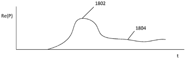
수신기 물질이 IPT 수신기 물질들의 예상되는 주파수 범위 내의 복합 임피던스의 예상되는 변화를 나타낼 수 있지만, 자신의 고유 공진 주파수에 가까운 주파수에서 복합 임피던스의 변화를 야기할 수 있는 다른 공진 디바이스들이 있을 수 있다. 일례는 RFID 태그이다. 수신기 디바이스가 RFID 태그와 함께 존재하는 경우, 주 IPT 자기장이 인에이블된다면, 그것은 RFID 태그를 번아웃(burn out)시킬 것이다. 이것은 바람직하지 않을 수 있다. 그들과 같은 물질들은 물질이 없는 조건(no-object-condition) 또는 수신기가 발견되는 잠재적 조건(potential receiver-found-condition)들과 구별불가능할 수 있다.Although the receiver material may represent the expected change in complex impedance within the expected frequency range of the IPT receiver materials, there may be other resonant devices that can cause a change in complex impedance at frequencies close to their natural resonant frequencies. An example is an RFID tag. If the receiver device is present with an RFID tag, if the primary IPT magnetic field is enabled, it will burn out the RFID tag. This may not be desirable. Materials such as these may be indistinguishable from no-object-conditions or potential receiver-found-conditions.
이물질(예컨대, RFID 태그)은 여자 코일과 검출 코일 사이의 커플링의 변화에 영향을 미칠 수 있는데, 이는, 또한, Qi 수신기에 의해 (또는, 어떠한 물질도 없이) 생성된 것과 유사하다. 물질 검출의 전술된 방법들 중 하나 이상은 이를, 선택된 감도의 레벨 및 구성(예컨대, 여자 주파수의 선택권)에 따라, 수신기 물질에 비해 명백한 검출 신호의 크기 및/또는 위상에 대한 유사한 변화로서 해석할 수 있다.A foreign object (e.g., an RFID tag) may affect the change in coupling between the exciting coil and the sensing coil, which is also similar to that produced by the Qi receiver (or without any material). One or more of the aforementioned methods of material detection may be interpreted as a similar change to the magnitude and / or phase of the detected signal relative to the receiver material, depending on the level and configuration of the selected sensitivity (e.g., the choice of excitation frequency) .
물질 검출의 전술된 방법들 중 하나 이상은 디지털 핑(Digital Ping)을 수행하여, 물질이 있는지 그리고 어떤 타입의 물질인지를 추가로 규명할 수 있다. 그러나, 디지털 핑(예컨대, MiFare 근접 교통 액세스 카드(MiFare proximity transport access card))의 그러한 실행이 전자 시스템들, 예컨대 버스 또는 기차 근접 티켓 카드들 또는 NFC 신용 카드들을 포함하는 소정 이물질들에 비가역적 손상을 야기할 수 있다는 것은 관심사이다. 추가로, 그러한 민감형 이물질(전자 시스템, 예컨대 RFID를 포함함)이 무선 충전가능 모바일 전화기와 동시에 놓이는 상황들에서, 물질 검출 시스템은 승인된 무선 충전가능 모바일 전화기의 존재로 인해 이 이물질을 성공적으로 검출하지 못할 수도 있다. 그러한 카드들이 종종 무선 충전가능 모바일 전화기에 대해 근접하게 제공되면(또는, 그와 동일 위치에, 예컨대 보호용 슬리브 또는 지갑에 위치되면), 이것은 차선일 수 있다.One or more of the aforementioned methods of material detection may perform a digital ping to further identify the presence of a substance and what type of substance it is. However, it should be appreciated that such an implementation of a digital ping (e.g., a MiFare proximity transport access card) may cause irreversible damage to certain foreign objects including electronic systems such as bus or train proximity ticket cards or NFC credit cards Is a concern. In addition, in situations where such sensitive foreign objects (including electronic systems, such as RFID) are placed simultaneously with the wireless rechargeable mobile telephone, the material detection system may be able to successfully It may not be detected. If such cards are often provided proximately (or at the same location, for example, in a protective sleeve or purse) for a wireless rechargeable mobile telephone, this may be a lane.
본 발명자는, 그것이, 충전 구역 내에서 물질들의 주파수 의존(예컨대, 공진) 속성들을 검출함으로써, 시스템(예컨대, 달리, 인근에 또한 유효 전력 수신기가 있는 동안의 비-물질(not-an-object)로서, 또는 잠재적 수신기로서 검출될 수 있는 RFID 태그들)이 전력 이송을 심지어 순간적으로 시도하는 것조차 방지하는 데 유용할 수 있는 것으로 판단했다.The inventor has found that it is possible to detect not-an-object (s) in the vicinity of a system (e. G., Otherwise, , Or RFID tags that can be detected as potential receivers) may be useful in preventing even instantaneous attempts to transfer power.
예를 들어, RFID 태그들은 특정 동작 주파수에서 공진하는 것으로 알려져 있으며, 시스템이 이 특정 주파수에서 스캔을 이행하는 경우에 검출기 코일에 대한 여자 코일의 커플링의 유의한 변화를 나타낼 것이다.For example, RFID tags are known to resonate at certain operating frequencies and will exhibit a significant change in the coupling of the excitation coil to the detector coil when the system performs a scan at this particular frequency.
다른 공진 디바이스들을 검출하기 위해, 한 가지 기법은 다양한 비-승인 디바이스들에 대한 예상된 주파수들에서의 응답을 판정하는 것이다. 이 상황에서, 비-승인 디바이스는, 송신기와 함께 사용하기 위해 승인되는, IPT 수신기 디바이스들을 제외한 임의의 디바이스를 의미한다. 승인된 디바이스들은 Qi 버전 1.1 이상의 호환 IPT 수신기들을 포함할 수 있다. 비-승인 디바이스들은 다른 공진 또는 비-공진 디바이스들을 포함할 수 있다. 예를 들어, RFID 태그들은, 예를 들어, 하기에서 공진하는 것으로 알려져 있다:To detect other resonant devices, one technique is to determine the response at the expected frequencies for various non-approved devices. In this situation, the non-approved device means any device other than IPT receiver devices, which are approved for use with the transmitter. Approved devices may include Qi version 1.1 or higher compatible IPT receivers. Non-approved devices may include other resonant or non-resonant devices. For example, RFID tags are known to resonate, for example, in the following:
120 내지 150 ㎑ (LF)120 to 150 kHz (LF)
13.56 ㎒ (HF) ISM 대역13.56 MHz (HF) ISM band
433 ㎒ (UHF)433 MHz (UHF)
865 내지 868 ㎒ (유럽)865 to 868 MHz (Europe)
860 내지 960 ㎒860 to 960 MHz
902 내지 928 ㎒ (북미) UHF ISM 대역902 to 928 MHz (North America) UHF ISM band
2.4 ㎓ (마이크로파) ISM 대역2.4 GHz (microwave) ISM band
5725 내지 5875 ㎒ (마이크로파) ISM 대역5725 to 5875 MHz (microwave) ISM band
24.125, 61.25, 122.5, 245 ㎓ ISM 대역들24.125, 61.25, 122.5, 245 GHz ISM bands
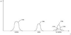
임계치 초과의 또는 미만의 임피던스가 이러한 RFID 주파수들 중 임의의 것에서 또는 그에 인접해서 판정되는 경우, 시스템은 비-승인 공진 디바이스의 존재를 판정할 것이고, IPT를 디스에이블시킬 것이다. 응용예에 따라 다른 비-승인 디바이스들이 포함될 수 있다. 예를 들어, 도 17에서, 시스템은 약 13.56 ㎒에서 임계치(1702) 초과의 또는 미만의 임피던스를 검사할 것이다. 비-승인 디바이스 주파수가 승인된 IPT 디바이스 공진 주파수에 가까운 경우, 그것은 매우 좁게 동조된 여자 및 검출 시스템을 필요로 할 수 있다.If an impedance above or below the threshold is determined at or near any of these RFID frequencies, the system will determine the presence of the non-acknowledged resonant device and disable the IPT. Other non-approved devices may be included depending on the application. For example, in FIG. 17, the system will check for impedances above or below
대안으로, 시스템은 주파수-홉핑할 수 있었거나, 또는 승인된 수신기 디바이스들에 대한 예상되는 주파수들에서가 아니라 임의의 익명의 응답을 찾는 일정 범위의 주파수들을 스캐닝할 수 있었다. 예를 들어, 승인된 IPT 디바이스들은 하기의 주파수들(이들은 응용물의 요건들에 따라 선택될 수 있음) 내에서 공진할 것으로 예상될 수 있다:Alternatively, the system could either frequency-hop or scan a range of frequencies looking for any anonymous response, not at the expected frequencies for the authorized receiver devices. For example, the approved IPT devices may be expected to resonate within the following frequencies, which may be selected according to the requirements of the application:
70 내지 150 ㎑, 예컨대, 100 ㎑ 또는 120 ㎑70 to 150 kHz, for example, 100 kHz or 120 kHz
900 ㎑ 내지 1.1 ㎒, 예컨대, 1 ㎒ (예를 들어, QI 1.1 사양에 따름)900 kHz to 1.1 MHz, for example, 1 MHz (for example, according to the QI 1.1 specification)
이 주파수들을 벗어난 임의의 주파수에서 임계치 미만의 또는 초과의 임피던스가 판정되는 경우, 시스템은 비-승인 공진 디바이스의 존재를 판정할 것이고, IPT를 디스에이블시킬 것이다. 예를 들어, 도 17에서, 시스템은 120 ㎑ 및 1 ㎒를 제외한 주파수들에서 임계치(1704, 1706) 미만의 또는 초과의 임피던스를 검사할 것이다.If an impedance below or above the threshold is determined at any frequency out of these frequencies, the system will determine the presence of the non-acknowledged resonant device and disable the IPT. For example, in FIG. 17, the system will check for impedances below or
이것은, OD 시스템(200)의 (스펙트럼) 주파수-임피던스 응답을 측정함으로써, 그리고 이 스펙트럼 응답이 공지의 바람직한 범위들 내에 있고 이에 의해 문제가 되는 이물질(예컨대, RFID 태그)이 존재해서는 안 된다는 것을 검사함으로써 구현될 수 있다. 일례는, 수신기들이 존재하는 것을 허용하는 범위 70 내지 150 ㎑ 내의 (상대적으로) 넓은 피크들에 대해 큰 허용가능 영역이 있을 것이지만, 좁은 스파이크가 120 내지 140 ㎑에서 발견된 경우, LF RFID 태그가 존재하는 것으로 간주될 수 있다는 것이다. 공진 응답의 폭은 물질이 승인되어 있는지 아닌지의 여부를 판정하는 데 사용될 수 있다. 이것은, 응답의 "Q" 또는 대역폭과 등가이다.This means that by measuring the (spectral) frequency-impedance response of the
RFID 태그들 및 다른 비-인가 디바이스들로부터의 이러한 예상되는 또는 사전결정된 반사 임피던스 응답들은 비-인가 디바이스들과 연관된 사전결정된 반사 임피던스 시그너처들로 간주될 수 있다. 이러한 시그너처들은 특정 주파수들 및 송신된 전력 레벨들과 연관될 수 있으며, 비-인가 디바이스의 존재를 검출하기 위해 물질 검출 시스템에 의해 저장될 수 있다. 물질 검출 시스템은, 추가로 또는 대안으로, 인가된 디바이스들과 연관된 사전결정된 반사 임피던스 시그너처들을 저장하여, 인가된 디바이스와 연관되지 않은 반사 임피던스 시그너처가 판정될 때 비-인가 디바이스가 검출될 수 있게 할 수 있다. 다양한 반사 임피던스 시그너처 예들이 하기에 더 상세히 기술된다.These anticipated or predetermined reflected impedance responses from the RFID tags and other non-authorized devices may be regarded as predetermined reflective impedance signatures associated with non-authorized devices. These signatures may be associated with specific frequencies and transmitted power levels and may be stored by the material detection system to detect the presence of a non-authorized device. The material detection system may additionally or alternatively store predetermined reflected impedance signatures associated with the authorized devices to enable detection of a non-authorized device when a reflected impedance signature that is not associated with an authorized device is determined . Various reflective impedance signature examples are described in further detail below.
추가 대안예에서, 시스템은, 일단 개시되면, RFID 칩과 연관된 임피던스의 2-단계 변화를 검출할 수 있다. 이것은, 승인된 IPT 디바이스의 공진 주파수와 가까운 공진 주파수를 갖는 비-승인 디바이스를 구별하는 것을 도울 수 있다. 도 17에 도시된 바와 같이, RFID 칩은, 초기에 제1 전력 레벨에서 스캐닝될 때, 약 13.56 ㎒에서 초기에 높은-Q 공진(1708)을 나타낼 것이다. 상이한 자기장 강도 레벨들 또는 여자의 지속기간에서, RFID 칩은 개시되어/개시되지 않아서, 이들 경우에 유의하게 상이한 양의 전력(즉, 나타난 임피던스)를 끌어낼 수 있다. RFID 태그는, 이어서, 스위칭-온할 것이고, 보다 낮은 Q-공진(1710)을 나타낼 것이다. 이러한 특성적 2-단계 임피던스 변화 또는 "압축 효과(compression effect)"가 검출될 수 있었고, IPT를 디스에이블시킬 수 있었다. 이 변화는, 또한, (증가하는) 입력 자극들에 따라 변화하는 관찰된 출력 응답들의 비례하는 감소로서 설명될 수 있다. 이것은 입력 자극(input stimulus)의 직렬 임피던스들로 구현되어 분압기 회로망(potential divider network)을 형성하는데, 그의 이득은 필터 커패시턴스가 충전됨에 따른 이러한 임피던스 변화에 따라 변화한다. 이 이득은, 이어서, 임계치들과 비교될 수 있는 비례 진폭 전압 신호를 생성하여 그러한 비-인가 디바이스가 존재하는지 여부를 평가하도록 채용될 수 있다.In a further alternative, the system may, once initiated, detect a two-step change in impedance associated with the RFID chip. This can help to distinguish a non-approved device having a resonant frequency close to the resonant frequency of an approved IPT device. As shown in FIG. 17, the RFID chip will initially exhibit high-
주어진 전력레벨 및 사전결정된 RFID 태그에 대해, 칩이 개시되기 전에 지속시간을 예상하는 것이 가능하다. 다시 말해, RFID 태그의 공진 주파수에서, 제1 임피던스, 이어서, 사전결정된 시간 뒤의 제2 임피던스로 구성된 "시그너처"가 RFID 태그를 더 신뢰성있게 검출하는 데 사용될 수 있다. 이 방법은, 또한, 서로 유사한 공진 주파수들을 갖는, RFID 태그와 인가된 수신기(예컨대, QI 수신기) 사이를 구별하는 데 유용할 수 있다.For a given power level and predetermined RFID tag, it is possible to predict the duration before the chip is started. In other words, at the resonant frequency of the RFID tag, a " signature " consisting of a first impedance followed by a second impedance after a predetermined time can be used to more reliably detect the RFID tag. This method may also be useful for distinguishing between an RFID tag and an authorized receiver (e.g., a QI receiver), with similar resonant frequencies.
2-단계 임피던스 변화 방법의 이용은 예상되는 공진 주파수들에서의 임피던스 변화들을 판정하는 방법과 함께 이용될 수 있다. 대안으로, 2-단계 임피던스 변화 방법은, 하기의 실시예에서 논의되는 바와 같이, RFID 태그들 또는 인가된 수신기들의 공진 주파수들에 대한 의존(recourse) 없이 이용될 수 있다.The use of a two-step impedance change method can be used with methods for determining impedance changes at expected resonant frequencies. Alternatively, the two-step impedance variation method may be used without recourse to the resonant frequencies of the RFID tags or the authorized receivers, as discussed in the following embodiments.
추가 대안예에서, 시스템은, 일단 RFID 칩과 같은 이물질의 공진 주파수에 있을 수 있거나 있지 않을 수도 있는 특성 반도체 접합부 임계 전압(예컨대, 실리콘 다이오드에 대하여 0.7 V)이 여자 자기장의 인가에 의해 초과되면, 정류기 다이오드들 또는 다른 반도체 디바이스들의 바이어싱과 연관된 임피던스의 2-단계 변화를 검출할 수 있다.In a further alternative, the system may be configured such that if a characteristic semiconductor junction threshold voltage (e.g., 0.7 V for a silicon diode) that may or may not be at a resonant frequency of an object such as an RFID chip is exceeded by application of an excitation field, Step change in impedance associated with biasing of rectifier diodes or other semiconductor devices.
예를 들어, 시스템은 사전결정된 주파수들에서의 비선형 또는 계단형 크기 변화들 또는 시간 응답을 관찰하여, 예컨대 900 ㎒ RFID 태그와 Qi 수신기의 1 ㎒ ± 10% 듀얼 공진 회로 사이를 구별할 수 있다. RFID 태그는 여자 레벨에 따라 현저하게 변화하는 응답을 나타낼 수 있고 - 그것은 낮은 여자 레벨들에서 좁은 응답(높은-Q)일 수 있음 -, 이어서, 여자 레벨이 증가되어 RFID 활성 회로를 자극함으로써 더 큰 전력(그와 션트인 낮은 등가 임피던스를 갖는 병렬 공진 탱크로 인한 넓은 대역폭 및 낮은 Q)을 인출하기 시작할 때 응답의 계단형 변화를 나타낼 수 있다.For example, the system can observe nonlinear or stepped magnitude changes or time responses at predetermined frequencies, for example, to distinguish between a 900 MHz RFID tag and a 1
추가로, RFID 활성 회로는, 초기에(t = 0 ms) 작은 부하(높은 임피던스)인 것으로 보일 수 있지만, 그의 내부 저장 커패시턴스들을 충전하거나 공진 수신기 회로에서의 공진을 증강시키거나 또는 접속된 회로(예컨대, RFID 칩) 내의 반도체 접합부들을 바이어싱하기에 충분한 시간(예컨대, t = 10 ms)을 갖게 되었을 시에 높은 부하(낮은 임피던스)가 될 수 있다.In addition, the RFID activation circuit may initially appear to be a small load (high impedance) at t = 0 ms, but it may be necessary to charge its internal storage capacitances, enhance resonance in the resonant receiver circuit, (Low impedance) when it has a sufficient time (e.g., t = 10 ms) to biased the semiconductor junctions in the semiconductor chip (e.g., an RFID chip).
임피던스의 변화는, RFID 주파수로부터 가깝게 이격된 주파수에서의 임피던스 크기에 대한 RFID 주파수에서의 임피던스 크기를 측정함으로써 검출될 수 있다. RFID 태그의 경우, 이것은 그것이 더 높은-Q 공진(1708)일 때 초기에 유의한 차이를 가져야 한다. RFID 주파수에서의 임피던스 크기와 가깝게 이격된 주파수에서의 임피던스 크기 사이의 차이(1710)가 감소한다는 것이 후속으로 측정되는 경우, 이것은, NFC PICC 카드/태그 물질의 존재를 확인하는 데 사용될 수 있다.The change in impedance can be detected by measuring the magnitude of the impedance at the RFID frequency to the magnitude of the impedance at a frequency closely spaced from the RFID frequency. In the case of RFID tags, this should initially be a significant difference when it is the higher-
RFID 태그들과 연관된 시그너처는, 또한, 실제 전력 시그너처를 사용하여 검출될 수 있다. 예를 들어, 도 18a에 도시된 바와 같이, 전력은 초기(1802)에, 커패시터가 충전 중인 동안에 상대적으로 높을 수 있다. 일단 충전되면, 전력은 유의하게 감소되는데(1804), 이는 상태 머신(state machine)에 대한 구동 전력이 최소이기 때문이다. 반면, 도 18b에서, Qi 수신기는 초기 전력 레벨을 갖고(1806), 이는 핸드세이크 후에만 증가한다(1808). Qi 수신기 내의 마이크로프로세서는 RFID 태그 내의 상태 머신보다 더 많은 전력을 사용한다.Signatures associated with RFID tags can also be detected using real power signatures. For example, as shown in FIG. 18A, power may be relatively high at initial 1802 while the capacitor is charging. Once charged, the power is significantly reduced (1804) because the drive power for the state machine is minimal. On the other hand, in Fig. 18B, the Qi receiver has an initial power level (1806), which increases (1808) only after a handshake. The microprocessor in the Qi receiver uses more power than the state machine in the RFID tag.
도 19a는 RFID 시그너처 방법(1900)과 관련된 흐름도를 도시한다. 송신기는 IPT 장기장 내의 물질에 관련된 제1 임피던스 또는 전력 레벨을 검출한다(1902). 송신기는 IPT 장기장 내의 물질에 관련된 제2 임피던스 또는 전력 레벨을 검출한다(1904). 송신기는, 이어서, 제1 및 제2 측정치들을 비-인가 물질들(예컨대, RFID/NFC 디바이스들) 및/또는 인가된 IPT 수신기들에 대한 공지의 시그너처들의 라이브러리와 매칭시킨다. 비-인가 물질이 검출되는 경우, IPT는 디스에이블된다(1908).19A shows a flow diagram associated with the
반사 임피던스 시그너처는 비-인가 디바이스로부터의 통신 활동과 연관될 수 있다. 예를 들어, 일부 RFID 태그들은 후방 산란 통신을 이용하고, 일부는 송신물을 생성한다(활성 태그들, 전형적으로, LF 120 ㎑ 또는 433, 848 ㎒의 것들). OD 시스템(200)은, 그것이 활성 상태가 될 때, RFID 칩에 의해 생성되고 있는 후방 산란 통신을 "판독"할 수 있었다. 그것은, 이 응답을 트리거하기 위해 RFID 칩을 채용할 필요가 없고, 그것은 RFID 태그를 웨이크업할 적합한 신호를 전송할 수 있었고, RFID 태그에 의한 유효 핸드세이크 응답을 구성하는 공지의 서브캐리어 변조를 모니터링할 수 있었다. 초기 신호는 Qi의 1 ㎒ 디지털 핑 주파수와 같은 RFID 판독기에 대한 표준 캐리어 주파수(예컨대, ISO/IEC 14443-2에 정의된 바와 같은 13.56 ㎒)보다 훨씬 더 낮은 주파수에 있을 수 있었다. OD 시스템(200)은 그것이 RFID 물질이 대기하도록 설계된 커맨드 시퀀스(예컨대, ISO/IEC 14443-3에 의해 명시된 바와 같은 "REQA", "WUPA", "REQB", "WUPB"의 순차적 전송)를 송신하지만 반드시 RFID 스킴(예컨대, NFC)에 의해 특정된 주파수에서 송신할 필요는 없는 폴링 프로세스를 이행하여, 전술된 변조 클록 또는 서브캐리어가 RFID 칩에 의해 생성되게 할 수 있다. OD 시스템(200)은 RFID 태그로부터의 사전결정된 통신 시퀀스, 예를 들어 RFID 태그와 RFID 판독기 사이에서 발생하는 일반 핸드세이킹 메시지들의 제1 또는 절단된(truncated) 부분을 검출하도록 구성될 수 있다. RFID 판독기의 전체 메시지 디코딩 능력 중 임의의 것, 단지 서브캐리어 변조 응답의 검출을 구현하는 것이 필요하지는 않다. 예를 들어, OD 시스템(200)은 다양한 RFID 시스템들에서 특정된 검출가능 서브캐리어 진폭 변조(예컨대, fc/128, fc/64, fc/32, fc/16, 여기서 fc는 타입 A 및 B의 경우에 ISO/IEC 14443-2에 의해, 타입 F의 경우에 JIS X 6319-4에 의해, 타입 V의 경우에 ISO/IEC 15693에 의해 특정된, 타입 A(On-Off 키잉 OOK, Miller 코딩), 타입 B(10% ASK Manchester 코딩), 타입 F(JIS X 6319-4에 대해 10% ASK Manchester 코딩) 또는 타입 V(BPSK NRZ-L)를 이용하여 폴링 요청이 전송되는 주파수에 독립적인 13.56 ㎒임)를 기대할 수 있다.The reflected impedance signature may be associated with communication activity from a non-authorized device. For example, some RFID tags use backscattering communications and some generate transmissions (active tags, typically those of LF 120 kHz or 433, 848 MHz). The
송신기에 의해 전송된 폴링 커맨드들이 더 낮은 주파수에서 전송되는 경우, 커맨드들은 표준 NFC 또는 RFID 태그가 그들을 인식하도록 하는 소정 적응을 필요로 할 수 있다. 폴링 커맨드들은 각각의 타입의 수신기에 대해 각자의 커맨드들을 통해 순환한다. 수신기가 그의 타입에 관한 커맨드를 검출하는 경우, 그것은 응답한다. 소정 타입의 RFID 태그들은, 덜 정밀한 국부적 오실레이터(예컨대, 카드/태그 내의 R-C 오실레이터 온-칩)을 인입 캐리어 주파수로 통제(disciplining)하거나 그와 동기화시킴으로써 국부적(즉, 카드/태그 PICC 물질 탑재(on-board)) 정밀 시간 기반(즉, 수정 또는 실리콘 MEMS 오실레이터와 같은 시간 기준)의 사용 없이 폴링 커맨드 변조 패턴을 검출한다. 그러한 통제된 국부적 오실레이터는, 이어서, 유효 폴링 커맨드를 검출하기 위해, 캐리어가 존재하지 않거나 또는 제2 상태(예컨대, -10% ASK 또는 -100% ASK의 변조 레벨, 즉 오프(Off))로서 그의 최저 진폭에 있는 것으로 발견되는 지속시간과 비교하여, 캐리어가 존재하거나 또는 제1 상태(예컨대, 0% ASK의 비변조 레벨)로서 그의 최고 진폭에 있는 것으로 발견되는 지속시간을 측정함으로써 2개의 변조 상태들을 검출하는 데 사용될 수 있다. 따라서, 사용되고 있는 캐리어 주파수가 표준 값보다 더 낮은 경우, 폴링 커맨드 내의 각각의 변조된 비트의 주기를 증가시켜서, 표준 캐리어 주파수보다 더 낮은 것을 사용하는 각각의 비트의 사이클들의 개수 또는 지속시간이 표준 캐리어 주파수에서 정의된 것과 같은 캐리어의 동일한 수의 사이클들과 매칭하게 하는 것이 필요할 수 있다. 이것은, 사이클 카운팅(또는, 시간 기준으로서 사용할 캐리어로부터의 클록 신호를 등가적으로 추출하는 것)이 예상되는 신호들을 검출하고 그들에 응답하기 위해 PICC 카드/태그에 대한 보조 또는 독립적 정밀 시간 기준을 필요로 하지 않는 간단한 메커니즘이기 때문에 사용된다. 그러나, 캐리어로부터 클록 신호를 추출함으로써, PICC 카드/태그는 13.56 ㎒의 표준 값으로 그의 주파수를 설정한 캐리어의 구현예에 전적으로 의존하며, 그로부터의 임의의 편차를 인지하지 않을 것이다. 따라서, 상기의 접근법은 RFID 물질을 자극하여 확인(ATQ-A/ ATQ-B, ATQ-C 등)으로 응답하도록 여전히 작동할 것이다.If the polling commands sent by the transmitter are transmitted at a lower frequency, the commands may require some adaptation to allow the standard NFC or RFID tag to recognize them. The polling commands cycle through their respective commands for each type of receiver. If the receiver detects a command on its type, it responds. Certain types of RFID tags can be localized (i.e., card / tag PICC material on) by disciplining or synchronizing with a less precise local oscillator (e.g., RC oscillator on-chip in a card / tag) -board) detects a polling command modulation pattern without using precision time based (i. e., a time reference such as a crystal or a silicon MEMS oscillator). Such a controlled local oscillator may then be used to detect a valid polling command if the carrier does not exist or is in a second state (e.g., a modulation level of -10% ASK or -100% ASK, i.e. Off) By measuring the duration that a carrier is present or is found to be at its peak amplitude as a first state (e.g., an unmodulated level of 0% ASK) compared to the duration found to be at the lowest amplitude, / RTI > Thus, if the carrier frequency being used is lower than the standard value, the period of each modulated bit in the polling command is increased so that the number or duration of each bit of the bit using a lower than standard carrier frequency is greater than the standard carrier It may be necessary to match the same number of cycles of the same carrier as defined in the frequency. This requires auxiliary or independent precision time reference for the PICC card / tag to detect and respond to the signals for which cycle counting (or equivalently extracting the clock signal from the carrier to use as a time reference) is anticipated It is used because it is a simple mechanism not to. However, by extracting the clock signal from the carrier, the PICC card / tag will depend entirely on the implementation of the carrier setting its frequency to a standard value of 13.56 MHz, and will not notice any deviation therefrom. Thus, the above approach will still work to stimulate the RFID material to respond with confirmation (ATQ-A / ATQ-B, ATQ-C, etc.).
예를 들어, 폴링 커맨드가 표 1에 나타낸 바와 같은 일련의 비트들을 포함하는 경우:For example, if the polling command includes a series of bits as shown in Table 1:
![]()
![]()
동일한 개수의 사이클들/비트들을 얻는 변조 주기는 표 2에 나타낸 바와 같이, 13 ㎒에 대한 것의 10배일 것이다:The modulation period for obtaining the same number of cycles / bits would be 10 times that for 13 MHz, as shown in Table 2:

도 19b는 1.3 ㎒에서의 폴링 커맨드(1912)에 비교되는 13.56 ㎒에서의 폴링 커맨드(1910)를 도시한다. 이것은 동일한 개수의 사이클들이 RFID 물질 응답을 트리거하도록 제공됨을 보장한다.19B shows the
PICC(NFC 카드/태그)로부터의 응답을 자극하는 RFID 폴링 요청은 앞서 기술된 바와 같은 IPT 송신 코일(7)에 의해 생성될 수 있다. 이에 대한 이점은 별개의 RFID/NFC 판독기 안테나 및 회로가 요구되지 않는다는 것이다. 전형적으로, 대부분의 IPT 송신기들은 수신기와 통신하는 ASK 후방 산란 통신 모듈을 포함할 것이다. 이것은, 전형적으로, 2 ㎑에서(이는 수신기가 IPT 자기장을 변조하는 주파수임)의 대역통과필터 및 변류기를 포함하거나, 또는 등가 전압 모드 검출이 이용될 수 있다. 이 경우, 송신기(2)는 도 20에 도시된 바와 같은 통신 모듈(2000)을 포함한다. 변조기(2002)가 코일(7)의 전압에 폴링 커맨드(2004)를 도입시킨다. 폴링 커맨드들은 범위 내에서 임의의 NFC 또는 RFID 태그들에 의해 수신되며, 일단 기전되면, 태그 진폭은 서브캐리어 주파수에서 IPT 신호를 변조한다. 이것은, 하나 이상의 대역통과필터들을 갖는 변류기로(또는 전압 측정을 통해) 검출된다. 필터(2008)는 RFIND/NFC 태그(2010)로부터의 응답에 대해 그의 확인 응답을 (즉, 212, 424, 또는 484 ㎑)(또는 예상되는 RFID/NFC 응답 주파수들을 중심으로 하는 대역통과필터들의 범위) 로 변조시키는 데 사용되는 예상되는 PICC (카드/태그) 서브캐리어 주파수에 중심을 둔다. 유효 응답이 수신된 경우, IPT는 디스에이블된다. 대역통과필터들은 전형적인 RFID/NFC 응답들을 포괄하는 적합한 대역폭, 예를 들어 106 내지 318, 424 내지 480, 847 내지 848 ㎑를 가질 수 있었다.An RFID polling request to stimulate a response from a PICC (NFC card / tag) may be generated by the IPT transmit
캐리어 주파수가 13.56 ㎒ 미만인 경우, 확인(ATQ-A/ ATQ-B, ATQ-C 등) 변조는 또한 주파수가 비례해서 더 낮을 수 있다. 그러한 경우, 대역통과필터들은 예상되는 더 낮은 주파수 RFID/NFC 응답에 대한 적합한 대역폭을 가질 수 있었다. 예를 들어, 8개의 캐리어 사이클들이 13.56 ㎒ 캐리어에 대해 848 ㎑의 서브캐리어 변조 사양에 의해 암시되는 경우, 등가적으로 1.356 ㎒ 캐리어를 사용함으로써, 자극된 카드/태그 PICC 응답은 84.8 ㎑의 서브캐리어일 것이다. 변조 검출 필터는, 이에 따라,If the carrier frequency is less than 13.56 MHz, the acknowledgment (ATQ-A / ATQ-B, ATQ-C, etc.) modulation may also be lower in proportion to the frequency. In such cases, bandpass filters could have the appropriate bandwidth for the expected lower frequency RFID / NFC response. For example, if eight carrier cycles are implied by a subcarrier modulation specification of 848 kHz for a 13.56 MHz carrier, by using an equivalent 1.356 MHz carrier, the stimulated card / tag PICC response will have a subcarrier of 84.8 kHz would. The modulation detection filter, therefore,
이러한 예상되는 범위의 주파수(본 예에서 84.8 ㎑)를 중심으로 두거나 그를 포함해야 한다.It should be centered or included in this expected range of frequencies (84.8 kHz in this example).
그러한 복조기 구현예의 로직 부분에 요구되는 대역폭을 감소시키기 위해, 신호를 d.c.로 변환하도록 정류기 및 커패시터 필터와 함께 병렬(노치 주파수에서 높은 임피던스) 또는 직렬(노치 주파수에서 낮은 임피던스) 공진 탱크를 포함하는 간단한 크기 검출기가, 저비용 마이크로제어기가 비교적 낮은 대역폭 ADC를 사용하여 크기 및 그에 따라 서브캐리어의 존재를 검출하게 하도록 채용될 수 있었다.To reduce the bandwidth required for the logic portion of such a demodulator implementation, a simple (or high-impedance) resonant tank comprising a parallel (high impedance at the notch frequency) or series (low impedance at the notch frequency) with a rectifier and capacitor filter to convert the signal to dc A size detector could be employed to allow the low cost microcontroller to detect the size and hence the presence of subcarriers using a relatively low bandwidth ADC.
일단 서브캐리어가 검출되었다면, 전력 송신기는 유휴 또는 슬립 상태로 되돌아갈 것이다. 물질들의 후속 검출 또는 물질들의 위치 변화는, 서브캐리어에 대한 상기의 탐색을 반복함으로써 NFC 물질의 존재에 대한 새로운 탐색을 초래할 것이다.Once the subcarrier is detected, the power transmitter will go back to idle or sleep state. Subsequent detection of materials or changes in the location of materials will result in a new search for the presence of NFC material by repeating the above search for subcarriers.
도 21은 RFID 서브캐리어 변조 기법(2100)에 관한 흐름도를 도시한다. 송신기는 (별개의 RFID/NFC 판독기 모듈과는 반대로) IPT 코일 또는 OD 코일을 사용하여 폴링 커맨드들을 전송한다(2102). 코일은 제1 주파수에 동조되고, 더 높은 제2 주파수에서 변조되어, 사전결정된 NFC/RFID 물질 폴링 커맨드를 에뮬레이트하게 한다. 범위 내의 임의의 RFID/NFC 태그들이 커맨드를 수신하고 응답을 전송한다(2104). 송신기는 RFID/NFC 물질의 사전결정된 응답에 대응하는 제3 주파수에서 임의의 유효 NFC/RFID 응답에 대해 검출한다(2106). 유효 응답이 제3 주파수에서 수신되는 경우, 이것은 NFC/RFID 물질의 존재를 나타내고, IPT는 디스에이블된다(2108).FIG. 21 shows a flow diagram of an RFID
대안으로, 폴링 커맨드들(2200)은, 도 22에 도시된 바와 같은 인버터(2201)에 의해, 예상되는 주파수 Fc, 예컨대 13.56 ㎒에서 전송될 수 있다. 이 경우, IPT 코일(7) 또는 OD 코일(202)은 유의하게 더 낮은 주파수에서 동조될 것이다(2202). RFID/NFC 태그(2202)는 848 ㎑에서 응답하는데, 이는 하나 이상의 대역통과필터들을 갖는 변류기(2206)로 검출된다. 제1 필터(2210)가 RFID/NFC 태그(2204)로부터의 응답에 대해 약 848 ㎑를 중심으로 둔다.Alternatively, the polling command in 2200, may be sent in, and the expected frequency F c, for example, 13.56 ㎒ by an
일부 경우에, 송신기 송신 회로는 동조 커패시터에 의해 100 ㎑에 동조되는 것이 아니라, 코일 인덕턴스 및 인버터 구동 전압의 선택에 의해 이 주파수로 적응 또는 최적화될 것이다. 예를 들어, 전력 이송 회로가 코일에 대해 10개의 권선들을 사용하여 10 마이크로-헨리의 인덕턴스를 가질 수 있다. 100 ㎑에서, 이것은, 대략 6 옴의 리액턴스를 초래하는 반면, 이 코일을 통해 13 ㎒를 구동하는 것은 대략 800 옴의 리액턴스가 유사한 크기의 전류를 구동하는 데 훨씬 더 높은 전압을 필요로 하게 할 것이다. 따라서, NFC 판독기 코일은 인버터가 합리적인 동작 파라미터들(예컨대, 5 V)로 더 높은 주파수에서 구동할 수 있게 하기 위해 더 적은 권선수, 더 큰 크기와 함께 훨씬 더 낮은 인덕턴스를 가질 것이다. 임의의 근접한 비-인가 디바이스들로부터의 응답을 자극하기 위해 훨씬 더 높은 주파수에서, 이를테면 110 ㎑에 대해 최적화된, IPT 회로를 구동시키는 것은, RFID 카드가 생성된 자기장을 검출하기에 충분한 전류를 갖도록 하기 위해 인버터가 더 높은 전압, 예컨대 20 V에서 구동되는 것을 요구할 수 있다.In some cases, the transmitter transmit circuit will not be tuned to 100 kHz by the tuning capacitor, but will be adapted or optimized at this frequency by the choice of coil inductance and inverter drive voltage. For example, a power delivery circuit may have an inductance of 10 micro-Henry using 10 windings for the coil. At 100 kHz, this results in a reactance of approximately 6 ohms, whereas driving 13 MHz through this coil will require a reactance of approximately 800 ohms to require much higher voltages to drive similar magnitude currents . Thus, the NFC reader coil will have a much lower inductance with less winding, larger size to allow the inverter to drive at a higher frequency with reasonable operating parameters (e.g., 5 V). Driving the IPT circuit at a much higher frequency, such as optimized for 110 kHz, to stimulate a response from any nearby non-application devices can be used to ensure that the RFID card has enough current to detect the generated magnetic field , The inverter may be required to be driven at a higher voltage, e.g., 20 volts.
인가된 수신기가 검출되는 이벤트에서, 인버터(2201)는 일반 IPT 신호를 코일(7)로 전송한다. 인버터(2201)는, 또한, 1 ㎒에서의 IPT 전압을 변조하여 수신기(3)와 통신할 것이다. 제2 필터(2208)는 IPT 수신기(3)로부터의 표준 ASK 후방 산란 통신 응답에 대해 2 ㎑를 중심으로 둔다.In the event that an authorized receiver is detected, the
전력 송신 코일은 대략 12 uH 인덕턴스일 수 있고 대략 100 ㎑에 대해 동조될 수 있다. 대부분의 RFID 구현예들은 1 내지 4 uH 이하를 사용하여 13.56 ㎒에서 동조되게 한다. 따라서, 폴링 요청은 다목적 코일로부터 전송된다. 즉, 코일은 IPT 전력 이송(예컨대, 코일) 또는 물질 검출(예컨대, 코일(202)) 중 어느 하나의 제1 목적을 갖는다. 제2 목적은 폴링 요청을 인근의 NFC/RFID 태그들과 같은 임의의 비-인가 물질들에 전송하는 것이다. 대조적으로, 별개의 NFC/RFID 태그 판독기 모듈을 통합하는 것은 단일 목적만을 갖는 판독기 코일을 포함할 것이다.The power transmission coil may be approximately 12 uH inductance and may be tuned for approximately 100 kHz. Most RFID implementations use 1 to 4 uH or less to be tuned at 13.56 MHz. Thus, the polling request is transmitted from the multipurpose coil. That is, the coil has a first purpose of either IPT power transfer (e.g., coil) or material detection (e.g., coil 202). The second purpose is to send a polling request to any non-authorized materials, such as nearby NFC / RFID tags. In contrast, incorporating separate NFC / RFID tag reader modules would include a reader coil with only a single purpose.
대안으로, 다른 비-인가 물질들에 대한 다른 통신 프로토콜들이 포함될 수 있고/있거나 비-인가 물질들에 대한 추가 타입들에 대한 시그너처들이 포함될 수 있다.Alternatively, other communication protocols for other non-permissive materials may be included and / or signatures for additional types of non-permissive materials may be included.
예를 들어, NFC-F(일본 철도 교통 수단에 사용되는 Sony Felica 카드들) 프로토콜은 서브캐리어를 생성하는 것으로 보이지 않지만, 그것은 212 kbit/초의 순 심볼 레이트(net symbol rate)로 PCD의 캐리어를 직접적으로 변조한다. 이 타입의 카드를 위한 대응하는 검출기는 대략 212 ㎑일 것이지만, 메시지 내용은 이 212 ㎑의 '중간' 심볼 레이트 근처에서 주파수 성분(즉, 측대역들)을 유의하게 분산시킬 것이다. 문헌에서는, Manchester 코딩의 전력 스펙트럼 밀도(psd)가 비트 속도의 0 내지 150%여서, 가능하게는, 최대 212 × 1.5 = 318 ㎑의 검출 대역폭을 특정한다는 것을 제안한다. 신호 전력의 대부분은 비트 속도의 50% 내지 100%에 놓일 것이고, 따라서, 가능하게는 212 × 0.5 = 106 ㎑ 내지 최대 212 ㎑이다.For example, NFC-F (Sony Felica cards used in Japanese railway transport) protocols do not appear to generate subcarriers, but it does not directly convey the carrier of the PCD with a net symbol rate of 212 kbit / . The corresponding detector for this type of card would be approximately 212 kHz, but the message content will significantly disperse the frequency components (i.e., sidebands) in the vicinity of this 'intermediate' symbol rate of 212 kHz. The literature proposes that the power spectral density psd of the Manchester coding is 0 to 150% of the bit rate, possibly specifying a detection bandwidth of up to 212 x 1.5 = 318 kHz. Most of the signal power will be in 50% to 100% of the bit rate and therefore, possibly 212 x 0.5 = 106 kHz to a maximum of 212 kHz.
OD 시스템(200)은 인가된 디바이스들과 상호작용하여 존재할 수 있는 임의의 RFID 태그들의 파괴를 피하도록 일반적으로 사용되는 전력 레벨들보다 더 낮은 전력 레벨들을 사용하여 비-인가 디바이스들 및/또는 인가된 디바이스들과 연관된 반사 임피던스 시그너처들의 검출을 구현할 수 있다. OD 시스템에 의한 그러한 디바이스들의 검출은, 이어서, 유도 전력 송신기에 의한 전력 이송을 디스에이블시킬 것이다. 상기의 실시예들을 이용하여 구현된 초기 이물질 검출 위상은 인가된 디바이스들을 검출하는 데 사용된 디지털 핑 위상 이전에 그리고 그보다 더 낮은 전력 레벨에서 실행될 수 있다. 예를 들어, 폴링 커맨드들은 디지털 핑의 전력의 50% 또는 20%에서 전송될 수 있다.The
인가된 Qi 수신기를 포함하는 제품이 카드/태그 (PICC) 에뮬레이션 모드에서 NFC 기능을 또한 포함하는 경우에 "위양성(false positive)" 결과를 방지하기 위해,To prevent " false positive " results when a product containing an authorized Qi receiver also includes NFC functionality in a card / tag (PICC) emulation mode,
수신기는, 먼저, 그것이, 충전할 잠재적 수신기의 검출을 위해 송신기에 의해 사용되는 것으로 알려지거나 선언된 Qi 핑, 예컨대 1 ㎒ 신호 또는 다른 임펄스 자극(예컨대, 175 ㎑ 버스트)를 검출할 때 그의 NFC PICC 에뮬레이션 기능을 디스에이블시킬 수 있다. 수신기가 또한 NFC 에뮬레이션 기능을 가질 때마다, 그것은, 그러한 송신기가 RFID 물질들에 대한 탐색을 실행할 때 위양성을 생성하지 않도록 하기 위해, 전력 이송 회로의 정류 전압(Vr)에서 임펄스가 검출될 때 일시적으로(예컨대, 5초) 그 기능을 디스에이블시켜야 한다.The receiver first detects the Qi-Ping, e.g., a 1 MHz signal, or other impulse stimulus (e.g., 175 kHz burst) that is known or known to be used by the transmitter for detection of a potential receiver to charge, The emulation function can be disabled. Whenever the receiver also has the NFC emulation function, it is temporarily disabled when the impulse is detected at the rectified voltage Vr of the power transfer circuit, so that such a transmitter does not produce false positives when performing a search for RFID materials (E. G., 5 seconds) to disable the function.
RFID 핑 또는 검출 탐색 동안 그러한 위양성을 더 신뢰성있게 제거하기 위해, Qi 송신기는, 그것이 Qi 송신기에 의해 막 프로빙되려고 하고 있음을 인가된 Qi 수신기에게 안내하는 약정(agreed upon) 신호, 예컨대 1 ㎒, 175 ㎑, 또는 110 ㎑에서의 톤 버스트(tone burst)를 방출해야 한다.To more reliably eliminate such false positives during an RFID ping or detection search, a Qi transmitter may transmit an agreement on signal to guide it to an authorized Qi receiver, e.g., 1 MHz, 175 , Or a tone burst at 110 kHz.
다른 공진 디바이스들의 이러한 검출 방법은 물질 검출을 위한 이전에 언급된 접근법들 중 임의의 접근법과 조합될 수 있다.This detection method of other resonant devices can be combined with any of the previously mentioned approaches for material detection.
송신기에 의해 채용되는 방법이 도 23에 도시되어 있다. 송신기는 아날로그 핑(2302)을 사용하여, 유효 수신기들, RFID를 포함한 이물질들과 같은 새롭게 배치된 물질들을 모니터링한다. 다양한 방법들이 아날로그 핑을 위해 채용되고, 이것은 Qi 사양에 의해 정의되지 않는다. 예를 들어, 이것은 IPT 송신기 코일에 대한 짧은 임펄스에 의해 구현될 수 있고, 임의의 반사 임피던스를 기대할 수 있다. 대안으로, 별개의 물질 검출 코일들이 사용될 수 있다.The method employed by the transmitter is shown in FIG. The transmitter uses the
아날로그 핑(2302)에는 수신기가 상이하게 거동하도록 시그널링하는 데 사용될 수 있는 사전결정된 신호인 RFID 핑이 보충될 수 있다. 이것은, 아날로그 핑을 검출하기 위해 수신기에 의존하는 것보다 더 강건할 수 있다. RFID 핑은 아날로그 핑에 대한 별개의 단계일 수 있거나, 또는 RFID 핑은 아날로그 핑을 대체하고 임의의 물질을 검출하는 데뿐 아니라 수신기에 시그널링하는 데 사용될 것이다.The
RFID 핑은 표준 전력 이송 주파수 범위에서 - 바람직하게는, 더 높은 단부에서 - 짧은 저전력 톤 버스트에 의해 구현될 수 있었는데, 이는, 이것이 전력 이득을 임의의 Qi 수신기에 이조(detune)시키고 더 일관된 유도 여자 레벨들을 부여하기 때문이다. 따라서, 175 ㎑의 신호가 사용될 수 있었는데, 이는 디지털 핑에 사용된 것과 동일하지만, 유럽 스펙트럼 규정들로 인해 더 양호한 주파수는 약 145 ㎑일 수 있다. RFID 핑은, 예를 들어 에너지가 12 암페어-권선수와 등가인 자기장 레벨들로 제한되고, 디지털 핑을 수신할 때 사용되는 tping + texpire = 65+90 = 155 ms의 최소 허용가능 비성공적 Qi 핑 위상 시간보다 작은 지속기간의 것으로서 디지털 핑과는 구별된다. 이것은, RFID 핑이, Qi 수신기가 핑 위상으로부터 진행하게 하지 않고 전력 이송이 시작하지 않게 하는 것을 보장한다.The RFID ping could be implemented by a short low-power tone burst in the standard power transfer frequency range-preferably at a higher end-because this would detune the power gain to any Qi receiver, Levels. Thus, a signal of 175 kHz could be used, which is the same as that used for digital ping, but a better frequency due to European spectrum regulations may be about 145 kHz. The RFID ping is limited, for example, to energy levels equal to 12 amperes - equivalent to magnetic field levels, and is used to receive the digital ping, t ping + t expire = 65 + 90 = It is distinguished from the digital ping with a duration less than the Qi ping phase time. This ensures that the RFID ping does not allow the Qi receiver to proceed from the ping phase and start power transfer.
송신기는, 이어서, 특정 RFID 검출 방법(2304) 및/또는 다른 더 일반적인 FOD 방법들을 수행할 수 있다. 임의의 NFC 카드/태그 에뮬레이션 기능이 Qi 수신기들에서 디스에이블되었음을 이제 알게 되면, RFID 탐색은 이제 "위양성" 결과를 산출하지 않을 것인데, 이는 임베드된 NFC 에뮬레이션 기능이 NFC REQA 신호 등에 응답하지 않을 것이기 때문이다. 그렇지 않다면, 그러한 응답은 NFC 에뮬레이션 기능에 의해 되돌아가는 경우, Qi 수신기 디바이스가, 그러한 RFID 보호와 함께, Qi 송신기에 의해 충전되는 것을 항상 방지할 것이다.The transmitter may then perform a specific
어떠한 FO/RFID도 발견되지 않음을 가정하면, 송신기는 디지털 핑(2306)으로 시작하는 Qi 개시 프로토콜로 이어지는데, 이 디지털 핑은 전형적으로 175 ㎑에서의 연속 톤이고, 전형적으로, RFID 핑이 온-보드 배터리들을 갖지 않는 수신기들의 전력공급을 인에이블시키는 것보다 더 높은 전력에 있을 것이다. 수신기로부터 송신기로의 통신은, 이어서, 톤의 부하 변조(load modulation)를 이용하여 통상적인 방식으로 확립된다.Assuming no FO / RFID is found, the transmitter goes to the Qi start protocol, which starts with a
수신기에 의해 채용되는 방법(2400)이 도 24에 도시되어 있다. 수신기가 (예컨대, 로열티 카드 등을 에뮬레이트하기 위한) NFC 에뮬레이션 기능을 갖는 스마트폰 또는 유사물이고 이러한 기능이 ON인 경우, 그것은 소정 RFID 검출 방법들을 혼란시킬 수 있고 전화기로의 전력 이송을 방지할 수 있다. 송신기 상에 배치된 모든 다른 물질들은 이 프로토콜에 의한 영향을 받지 않을 것이다.The
수신기는 RFID 핑(2402)(이는, 전술된 바와 같이, 아날로그 핑일 수 있음)에 대한 코일을 모니터링한다. RFID 핑은, 본질적으로, 수신기에게 그의 NFC 에뮬레이션 기능을 스위칭오프할 것을 시그널링하는 것이다. 송신기가 RFID 핑을 사용하고 있지 않고, 대신, 임펄스와 같은 기존 아날로그 핑을 사용하는 경우, 수신기가, 이를 검출하고 송신기가 그의 에뮬레이션 기능을 스위칭오프하도록 시그널링하고 있음을 선언하는 것이 여전히 가능할 수 있다.The receiver monitors the coil for an RFID ping 2402 (which may be an analog ping, as described above). RFID ping is essentially signaling the receiver to switch off its NFC emulation function. If the transmitter is not using RFID ping and instead uses a conventional analog ping such as an impulse, it may still be possible for the receiver to detect it and declare that the transmitter is signaling to switch its emulation function off.
수신기는, 이어서, 사전결정된 시간 동안(그것이 온인 경우) 그의 NFC 에뮬레이션 기능을 스위칭오프한다(2404). 사전결정된 시간은 송신기가 RFID 검출 방법을 실행하게 하기에 충분하다. 0.5초는 Qi 송신기가, 배치될 때, 수신기와의 전력 이송을 시작하기 위해 필요한 최소의 개시 시간으로, 적절한 주기일 것이다. 그것이 0.5초 내에 개시되지 않은 경우, 그것은 전력을 전혀 공급하지 않을 가능성(예컨대, FOD 금지)이 크다.The receiver then switches off its NFC emulation function for a predetermined time (if it is on) (2404). The predetermined time is sufficient for the transmitter to perform the RFID detection method. 0.5 seconds will be the appropriate period, with the minimum start time required for the Qi transmitter to begin power transfer with the receiver when deployed. If it is not started within 0.5 seconds, it has a high possibility of not supplying any power (for example, FOD prohibition).
기간의 말미에, 이어서, Rx는 Tx(2406)로부터 디지털 핑을 수신한 것에 응답하여, 특정된 Qi 개시 프로토콜을 따른다.At the end of the period, in response to receiving the digital ping from
물질 검출 시스템이 송신기 전력 코일과는 별개인 여자 및 수신기 코일들을 사용하는 실시예들이 기술되었지만, 대안의 배열예들에서, 물질 검출 시스템은 하나 이상의 송신기 전력 코일들, 또는 전력 송신기 코일들, 여자 및 수신기 코일들의 조합을 사용할 수 있다.Although embodiments have been described in which the material detection system uses exciter and receiver coils that are separate from the transmitter power coils, in alternative arrangements, the material detection system may include one or more transmitter power coils, or power transmitter coils, A combination of receiver coils can be used.
본 발명이 그의 실시예들에 대한 설명에 의해 예시되었고 그 실시예들이 상세히 기술되었지만, 첨부된 청구범위의 범주를 그러한 세부사항으로 한정하거나 어떤 방식으로든 제한하려는 것이 출원인의 의도는 아니다. 추가 이점들 및 변경들이 당업자에게 용이하게 나타날 것이다. 따라서, 본 발명은, 그의 더 넓은 태양들에서, 특정 세부사항들, 대표적인 장치 및 방법, 및 도시되고 기술된 예시적인 예들로 제한되지 않는다. 따라서, 출원인의 대체적인 발명 개념의 사상 또는 범주로부터 벗어남이 없이 그러한 세부사항들로부터 이탈이 이루어질 수 있다.While the invention has been illustrated by the description of its embodiments and the embodiments thereof have been described in detail, it is not the intention of the applicant to restrict or in any way limit the scope of the appended claims to such details. Additional advantages and modifications will readily appear to those skilled in the art. Accordingly, the invention in its broader aspects is not limited to the specific details, representative apparatus and method, and illustrative examples shown and described. Accordingly, departures may be made from such details without departing from the spirit or scope of applicant's alternative inventive concept.
Claims (78)
코일을 갖는 송신 회로 - 상기 송신 회로는 유도 전력 이송 또는 물질 검출을 위해 제1 주파수에서 또는 그 주위에서 동조, 적응, 또는 최적화됨 -;
상기 제1 주파수에서 상기 송신 회로를 구동시키도록 동작가능한 인버터; 및
상기 코일에 근접한 사전결정된 비-인가 디바이스로부터의 응답을 생성하기 위해, 상기 인버터를 제어하여 더 높은 제2 주파수에서 상기 송신 회로를 구동시키도록, 그리고 사전결정된 핸드세이크(handshake) 신호에 따라 상기 더 높은 제2 주파수에서의 신호를 변조하도록 배열된 제어기를 포함하는, 유도 전력 송신기.An inductive power transmitter comprising:
A transmission circuit having a coil, the transmission circuit being tuned, adapted, or optimized at or around a first frequency for inductive power transfer or material detection;
An inverter operable to drive the transmitting circuit at the first frequency; And
And to control the inverter to drive the transmitting circuit at a higher second frequency to generate a response from a predetermined non-application device in proximity to the coil, And a controller arranged to modulate the signal at a high second frequency.
코일을 갖는 송신 회로;
상기 송신 회로를 구동시키도록 동작가능한 인버터; 및
상기 코일에 근접한 사전결정된 비-인가 디바이스로부터의 응답을 생성하기 위해, 상기 인버터를 제어하여 핸드세이크 주파수에서 상기 송신 회로를 구동시키도록, 그리고 사전결정된 핸드세이크 신호에 따라 상기 핸드세이크 주파수에서의 신호를 변조하도록 배열된 제어기를 포함하고,
상기 사전결정된 비-인가 디바이스는 상기 핸드세이크 주파수보다 더 높은 캐리어 주파수를 갖는 특정된 핸드세이크 신호를 갖고,
상기 사전결정된 핸드세이크 신호는 순차적인 일련의 폴링 커맨드들을 포함하고, 상기 특정된 핸드세이크 신호는 순차적인 일련의 폴링 커맨드들을 포함하고, 각각의 사전결정된 핸드세이크 신호 폴링 커맨드의 사이클들의 개수는 각각의 각자 특정된 핸드세이크 신호 폴링 커맨드의 사이클들의 개수와 동일한, 유도 전력 송신기.An inductive power transmitter comprising:
A transmitting circuit having a coil;
An inverter operable to drive the transmission circuit; And
And to drive the transmitting circuit at a handshake frequency by controlling the inverter to generate a response from a predetermined non-application device in proximity to the coil and to generate a signal at the handshake frequency in accordance with a predetermined handshake signal And a controller arranged to modulate the modulated signal,
Wherein the predetermined non-application device has a specified handshake signal having a carrier frequency higher than the handshake frequency,
Wherein the predetermined handshake signal comprises a series of sequential polling commands, wherein the specified handshake signal comprises a sequential series of polling commands, and the number of cycles of each predetermined handshake signal polling command comprises Equal to the number of cycles of the respective specified handshake signal polling command.
코일을 갖는 수신기 회로;
비-인가 공진 디바이스; 및
상기 코일에서 유도 전력 송신기에 의해 전송된 디스에이블 신호를 검출하도록, 상기 디스에이블 신호에 따라 상기 비-인가 공진 디바이스를 디스에이블시키도록, 그리고 상기 송신기에게 전력 이송을 시작할 것을 명령하기 위해 상기 코일 내의 신호를 변조하도록 배열된 제어기를 포함하는, 유도 전력 수신기.As an inductive power receiver,
A receiver circuit having a coil;
A non-application resonant device; And
To disable the non-applied resonant device in accordance with the disable signal to detect the disable signal transmitted by the inductive power transmitter in the coil, and to instruct the transmitter to start power transfer And a controller arranged to modulate the signal.
코일을 갖는 송신기 회로;
상기 송신 회로를 구동시키도록 동작가능한 인버터; 및
상기 인버터를 제어하여 핑(ping) 주파수에서 상기 송신 회로를 구동시키도록, 디스에이블 신호에 따라 상기 핑 주파수에서의 신호를 변조하여 인가된 수신기 내의 비-인가 공진 디바이스를 디스에이블시키도록, 그리고 상기 코일 내의 개시(start-up) 신호를 검출하여 상기 인가된 수신기로의 전력 이송을 시작하게 하도록 배열된 제어기를 포함하는, 유도 전력 송신기.An inductive power transmitter comprising:
A transmitter circuit having a coil;
An inverter operable to drive the transmission circuit; And
Modulate the signal at the ping frequency in accordance with the disable signal to disable the non-applied resonant device in the applied receiver to control the inverter to drive the transmit circuit at the ping frequency, And a controller arranged to detect a start-up signal in the coil and to begin power transfer to the applied receiver.
적어도 하나의 다목적 코일; 및
IPT 자기장 내의 또는 그에 인접한 물질들을 검출하도록 구성된 물질 검출 시스템을 포함하고,
상기 물질 검출 시스템은 상기 다목적 코일을 기전(energise)시켜서, 사전결정된 비-인가 물질로부터의 응답을 생성하도록 구성된 핸드세이크 신호를 전송하며, 유효 응답을 수신한 것에 기초하여, 비-인가 물질이 검출된 경우에 유도 전력 이송을 디스에이블시키는, 유도 전력 송신기.An inductive power transmitter comprising:
At least one multi-purpose coil; And
A material detection system configured to detect materials in or near the IPT magnetic field,
Wherein the material detection system is configured to energize the multipurpose coil to transmit a handshake signal configured to generate a response from a predetermined non-applied material, and based on receiving the valid response, And disables the inductive power transfer, if any.
인가된 수신기에 의해 전송된 신호; 및
사전결정된 비-인가 물질에 의해 전송된 신호를 판정하도록 구성된 후방 산란 검출 회로를 추가로 포함하는, 유도 전력 송신기.24. The method of claim 23, further comprising measuring a voltage or current in the coil,
A signal transmitted by an authorized receiver; And
Further comprising a backscattering detection circuit configured to determine a signal transmitted by the predetermined non-application material.
인가된 유도 전력 수신기 및/또는 비-인가 물질과 연관된 사전결정된 시그너처들을 저장하도록 배열된 메모리를 포함하고,
상기 물질 검출 시스템은,
상기 비-인가 물질과 연관된 상기 사전결정된 시그너처들 중 하나 이상을 검출한 것;
및/또는 상기 인가된 수신기와 연관된 상기 사전결정된 시그너처들 중 하나 이상에 대응하지 않는 시그너처를 검출한 것에 응답하여, 비-인가 물질을 표시하도록 배열된, 물질 검출 시스템.A material detection system for an inductive power transmitter,
A memory arranged to store predetermined signatures associated with an applied inductive power receiver and / or non-application material,
The material detection system includes:
Detecting one or more of the predetermined signatures associated with the non-enforcing material;
And / or in response to detecting a signature that does not correspond to one or more of the predetermined signatures associated with the authorized receiver.
RFID 주파수에서의 크기가 제1 시간에 상기 RFID 주파수로부터 가깝게 이격된 주파수에서의 크기와 유사한 것; 및
상기 RFID 주파수에서의 크기가 후속 시간에 상기 가깝게 이격된 주파수에서의 크기보다 실질적으로 더 높은 것인, 물질 검출 시스템.34. The method of claim 33, wherein the non-application materials include an NFC or RFID tag, and the predetermined reflection impedance signatures associated with the non-
The size at the RFID frequency being similar in magnitude to the frequency at a distance from the RFID frequency at a first time; And
Wherein the magnitude at the RFID frequency is substantially higher than the magnitude at a frequency that is closely spaced at a subsequent time.
유도 전력 이송(IPT) 자기장을 생성하도록 구성된 적어도 하나의 전력 송신 코일; 및
상기 IPT 자기장 내의 또는 그에 인접한 물질들을 검출하도록 구성된 물질 검출 시스템을 포함하고,
상기 물질 검출 시스템이 비-승인 디바이스를 검출하도록 구성된, 유도 전력 송신기.An inductive power transmitter comprising:
At least one power transmission coil configured to generate an inductive power transfer (IPT) magnetic field; And
A material detection system configured to detect materials in or near the IPT magnetic field,
Wherein the material detection system is configured to detect a non-approved device.
복수의 주파수들에서의 반사 임피던스를 판정하도록 배열된 코일 및 회로부; 및
인가된 유도 전력 수신기와 연관된 사전결정된 주파수들 및/또는 비-인가 수신기와 연관된 사전결정된 주파수들을 저장하도록 배열된 메모리를 포함하고,
상기 물질 검출 시스템은,
상기 비-인가 수신기와 연관된 사전결정된 주파수에서의 반사 임피던스의 사전결정된 증가 또는 감소를 검출한 것;
및/또는 상기 인가된 유도 전력 수신기와 연관되지 않은 주파수에서의 반사 임피던스의 사전결정된 증가를 검출한 것에 응답하여, 상기 비-인가 수신기를 표시하도록 배열된, 물질 검출 시스템.A material detection system for an inductive power transmitter,
A coil and circuitry arranged to determine a reflection impedance at a plurality of frequencies; And
A memory arranged to store predetermined frequencies associated with an applied inductive power receiver and / or predetermined frequencies associated with a non-applied receiver,
The material detection system includes:
Detecting a predetermined increase or decrease in the reflection impedance at a predetermined frequency associated with the non-application receiver;
And to display the non-applied receiver in response to detecting a predetermined increase in the reflected impedance at a frequency not associated with the applied inductive power receiver.
상기 비-인가 수신기와 연관된 사전결정된 주파수에서의 반사 임피던스의 초기에 검출된 사전결정된 증가에 뒤이은 반사 임피던스의 변화를 검출한 것;
및/또는 상기 인가된 유도 전력 수신기와 연관되지 않은 주파수에서의 반사 임피던스의 초기에 검출된 사전결정된 증가에 뒤이은 반사 임피던스의 변화를 검출한 것에 응답하여, 상기 비-인가 수신기를 표시하도록 추가로 배열된, 물질 검출 시스템.66. The material detection system of claim 65,
Detecting a change in the reflected impedance subsequent to a predetermined increase detected initially in a reflected impedance at a predetermined frequency associated with the non-authorized receiver;
In response to detecting a change in the reflected impedance subsequent to a predetermined increase detected initially in the reflected impedance at a frequency not associated with the applied inductive power receiver and / ≪ / RTI >
상기 물질 검출 시스템은 코일 및 회로부를 포함하고,
상기 방법은,
제1 전력 레벨에서 상기 코일을 구동시키고 제1 반사 임피던스를 판정하는 단계;
더 높은 제2 전력 레벨에서 상기 코일을 구동시키고 제2 반사 임피던스를 판정하는 단계 - 상기 제2 전력 레벨은 사전결정된 비-인가 수신기의 동작을 시작하게 하기에 충분하지만, 상기 제1 전력 레벨은 충분하지 않음 -; 및
상기 제1 반사 임피던스와 상기 제2 반사 임피던스 사이의 사전결정된 차이를 판정한 것에 응답하여 비-인가 수신기를 검출하는 단계를 포함하는, 방법.CLAIMS What is claimed is: 1. A method of operating a material detection system for an inductive power transmitter,
Wherein the material detection system includes a coil and a circuit,
The method comprises:
Driving the coil at a first power level and determining a first reflected impedance;
Driving the coil at a second higher power level and determining a second reflected impedance, the second power level being sufficient to cause operation of the predetermined non-application receiver, but the first power level is sufficient Do not -; And
And detecting a non-application receiver in response to determining a predetermined difference between the first and second reflection impedances.
복수의 주파수들에서의 반사 임피던스들을 판정하는 단계; 및
비-인가 수신기를 표시하는 단계로서,
비-인가 수신기와 연관된 사전결정된 주파수에서의 반사 임피던스의 사전결정된 증가 또는 감소를 검출한 것;
및/또는 인가된 유도 전력 수신기와 연관되지 않은 주파수에서의 반사 임피던스의 사전결정된 증가를 검출한 것에 응답하여, 비-인가 수신기를 표시하는 단계를 포함하는, 방법.CLAIMS What is claimed is: 1. A method of operating a material detection system for an inductive power transmitter,
Determining reflection impedances at a plurality of frequencies; And
Displaying a non-authorized receiver,
Detecting a predetermined increase or decrease in the reflection impedance at a predetermined frequency associated with the non-authorized receiver;
And / or in response to detecting a predetermined increase in the reflected impedance at a frequency not associated with the applied inductive power receiver.
상기 유도 전력 송신기는, 코일을 포함하고 제1 주파수에 동조되는 송신 회로, 및 상기 제1 주파수에서 상기 송신 회로를 구동시키도록 동작가능한 인버터를 포함하고, 상기 방법은,
상기 코일에 근접한 임의의 사전결정된 비-인가 디바이스들을 검출하기 위해 더 높은 제2 주파수에서 상기 송신 회로를 구동시키는 단계;
상기 비-인가 디바이스들에 의해 인식가능한 사전결정된 핸드세이크 신호에 따라 상기 더 높은 제2 주파수를 변조하는 단계; 및
사전결정된 응답을 검출한 것에 응답하여 상기 비-인가 디바이스의 존재를 표시하는 단계를 포함하는, 방법.CLAIMS 1. A method of operating an inductive power transmitter,
The inductive power transmitter comprising a transmission circuit including a coil and being tuned to a first frequency and an inverter operable to drive the transmission circuit at the first frequency,
Driving the transmit circuit at a higher second frequency to detect any predetermined non-application devices proximate to the coil;
Modulating the higher second frequency according to a predetermined handshake signal recognizable by the non-application devices; And
And displaying the presence of the non-authorized device in response to detecting a predetermined response.
Applications Claiming Priority (7)
| Application Number | Priority Date | Filing Date | Title |
|---|---|---|---|
| US201662318133P | 2016-04-04 | 2016-04-04 | |
| US62/318,133 | 2016-04-04 | ||
| US201662355823P | 2016-06-28 | 2016-06-28 | |
| US62/355,823 | 2016-06-28 | ||
| US201762475813P | 2017-03-23 | 2017-03-23 | |
| US62/475,813 | 2017-03-23 | ||
| PCT/NZ2017/050038 WO2017176128A1 (en) | 2016-04-04 | 2017-04-04 | Inductive power transmitter |
Related Child Applications (1)
| Application Number | Title | Priority Date | Filing Date |
|---|---|---|---|
| KR1020207015165A Division KR102196897B1 (en) | 2016-04-04 | 2017-04-04 | Inductive power transmitter |
Publications (1)
| Publication Number | Publication Date |
|---|---|
| KR20180124103A true KR20180124103A (en) | 2018-11-20 |
Family
ID=60001346
Family Applications (2)
| Application Number | Title | Priority Date | Filing Date |
|---|---|---|---|
| KR1020207015165A KR102196897B1 (en) | 2016-04-04 | 2017-04-04 | Inductive power transmitter |
| KR1020187030148A KR20180124103A (en) | 2016-04-04 | 2017-04-04 | Inductive power transmitter |
Family Applications Before (1)
| Application Number | Title | Priority Date | Filing Date |
|---|---|---|---|
| KR1020207015165A KR102196897B1 (en) | 2016-04-04 | 2017-04-04 | Inductive power transmitter |
Country Status (7)
| Country | Link |
|---|---|
| US (2) | US10461813B2 (en) |
| JP (2) | JP6700470B2 (en) |
| KR (2) | KR102196897B1 (en) |
| CN (1) | CN109496380B (en) |
| AU (3) | AU2017248083B2 (en) |
| DE (1) | DE112017001839B4 (en) |
| WO (1) | WO2017176128A1 (en) |
Families Citing this family (40)
| Publication number | Priority date | Publication date | Assignee | Title |
|---|---|---|---|---|
| CN106160086B (en) * | 2016-07-14 | 2019-10-15 | 深圳市禾家欢科技有限公司 | A kind of wireless charging output device |
| US10594585B2 (en) * | 2017-03-20 | 2020-03-17 | Comcast Cable Communications, Llc | Methods and systems for polling devices |
| KR20190082483A (en) * | 2018-01-02 | 2019-07-10 | 엘지이노텍 주식회사 | Near Field Communication Signal Detection Method and Apparatus Therefor |
| KR102625423B1 (en) * | 2018-01-15 | 2024-01-16 | 삼성전자 주식회사 | Method for transmitting information of wireless charging stop reason and electronic device using the same |
| EP3579380B1 (en) | 2018-04-16 | 2023-09-06 | LG Electronics Inc. | Apparatus and method for performing power control in wireless power transmission system |
| US11005307B2 (en) | 2018-04-16 | 2021-05-11 | Lg Electronics Inc. | Apparatus and method for performing power control in wireless power transfer system |
| US10971954B2 (en) * | 2018-04-17 | 2021-04-06 | Avago Technologies International Sales Pte. Limited | Systems and methods for object detection |
| US10862347B2 (en) | 2018-04-17 | 2020-12-08 | Avago Technologies International Sales Pte. Limited | Systems and methods for object detection |
| JP7144192B2 (en) * | 2018-05-29 | 2022-09-29 | ローム株式会社 | Wireless power transmission device and its control circuit |
| WO2019240565A1 (en) * | 2018-06-15 | 2019-12-19 | 엘지전자 주식회사 | Wireless power transmitter and method for detecting rfid/nfc card |
| US11018530B2 (en) | 2018-08-31 | 2021-05-25 | Ge Hybrid Technologies, Llc | Wireless power transmission apparatus with multiple controllers |
| KR102527902B1 (en) | 2018-09-07 | 2023-05-03 | 삼성전자주식회사 | Method for identifying status information of wireless charging and electronic device thereof |
| US20200119586A1 (en) * | 2018-10-15 | 2020-04-16 | Avigilon Corporation | Wireless charging of depleted mobile device for access control |
| KR102629410B1 (en) * | 2018-10-26 | 2024-01-26 | 삼성전자주식회사 | Electronic device and method for transmitting or receiving power by wireless |
| US20200154275A1 (en) * | 2018-11-13 | 2020-05-14 | Apple Inc. | Wireless power transfer device authentication |
| US11916405B2 (en) | 2019-01-02 | 2024-02-27 | Ge Hybrid Technologies, Llc | Wireless power transmission apparatus with multiple controllers |
| US10425129B1 (en) * | 2019-02-27 | 2019-09-24 | Capital One Services, Llc | Techniques to reduce power consumption in near field communication systems |
| EP3996288A1 (en) * | 2019-04-11 | 2022-05-11 | Nexite Ltd. | Wireless dual-mode identification tag |
| FR3096190B1 (en) * | 2019-05-17 | 2021-04-16 | Continental Automotive | Method of inductive charging control of user equipment and associated charging device for motor vehicle |
| KR20220008916A (en) | 2019-05-21 | 2022-01-21 | 제네럴 일렉트릭 컴퍼니 | Wireless power transmitter with multiple primary and adjacent coil muting capabilities |
| US10601467B1 (en) * | 2019-06-13 | 2020-03-24 | Nxp B.V. | Near-field wireless device |
| CN110224506B (en) * | 2019-07-10 | 2022-10-28 | 哈尔滨工业大学 | Metal foreign matter detection system of series wireless power transmission system |
| US10819394B1 (en) * | 2019-10-04 | 2020-10-27 | Nxp B.V. | Detection of NFC proximity IC cards (PICCs) during wireless charging |
| US11874423B2 (en) * | 2019-10-25 | 2024-01-16 | Witricity Corporation | Circuit for object detection and vehicle position determination |
| KR20210054357A (en) * | 2019-11-05 | 2021-05-13 | 엘지전자 주식회사 | Wireless power transfer cooktop device and method |
| EP3836352A1 (en) * | 2019-12-10 | 2021-06-16 | Koninklijke Philips N.V. | Foreign object detection in a wireless power transfer system |
| KR20210101525A (en) * | 2020-02-10 | 2021-08-19 | 삼성전자주식회사 | Apparatus and method for stabilizing communication performance during wireless power transmission |
| US20220052565A1 (en) * | 2020-08-15 | 2022-02-17 | Aira, Inc. | Resonant Reflection Device Detection |
| US11444492B2 (en) | 2021-02-10 | 2022-09-13 | Nucurrent, Inc. | Wireless power transfer systems for kitchen appliances |
| US11923695B2 (en) * | 2021-02-10 | 2024-03-05 | Nucurrent, Inc. | Wireless power transmitters for virtual AC power signals |
| US11289952B1 (en) | 2021-02-10 | 2022-03-29 | Nucurrent, Inc. | Slotted communications in virtual AC power signal transfer with variable slot width |
| US11942797B2 (en) | 2021-02-10 | 2024-03-26 | Nucurrent, Inc. | Virtual AC power signal transfer using wireless power transfer system |
| US11764617B2 (en) | 2021-02-10 | 2023-09-19 | Nucurrent, Inc. | Wireless power receivers for virtual AC power signals |
| US11791663B2 (en) * | 2021-02-10 | 2023-10-17 | Nucurrent, Inc. | Slotted communications in virtual AC power signal transfer |
| WO2022269240A1 (en) * | 2021-06-21 | 2022-12-29 | Aston Vision Sciences Ltd | Wireless power and data transfer using a single pair of coils |
| GB2608110A (en) * | 2021-06-21 | 2022-12-28 | Aston Vision Sciences Ltd | Wireless power and data transfer |
| WO2023089504A1 (en) * | 2021-11-16 | 2023-05-25 | Auckland Uniservices Limited | Foreign object detection in a wireless charging pad |
| WO2024064013A1 (en) * | 2022-09-19 | 2024-03-28 | Apple Inc. | Foreign object detection during wireless power transmission |
| WO2024064000A1 (en) * | 2022-09-19 | 2024-03-28 | Apple Inc. | Friendly metal loss estimation |
| CN115833853B (en) * | 2023-02-14 | 2023-04-18 | 武汉大学 | Miniaturized low frequency radio communication electromagnetic signal transmitting system |
Family Cites Families (131)
| Publication number | Priority date | Publication date | Assignee | Title |
|---|---|---|---|---|
| JPH01157896A (en) | 1987-09-28 | 1989-06-21 | Mitsubishi Electric Corp | Noncontact type ic card and noncontact type card reader writer |
| ZA892468B (en) | 1988-04-11 | 1989-12-27 | Uniscan Ltd | Improvements in or relating to cutting elements foactuator and communication system r rotary drill bits |
| EP0788211B1 (en) | 1996-01-30 | 2002-08-28 | Sumitomo Wiring Systems, Ltd. | A connection system and a connection method |
| FR2765736B1 (en) | 1996-12-03 | 2000-04-28 | Jacques Patrick Andres | SYSTEM FOR THE SUPPLY OF ELECTRICAL ENERGY, PARTICULARLY OUTSIDE AND IN PUBLIC PLACES, CORRESPONDING TERMINAL AND BASE |
| US6061551A (en) * | 1998-10-21 | 2000-05-09 | Parkervision, Inc. | Method and system for down-converting electromagnetic signals |
| JP3786392B2 (en) | 1998-09-09 | 2006-06-14 | 本田技研工業株式会社 | Electric vehicle charging device |
| EP1324278A1 (en) | 2001-12-28 | 2003-07-02 | Mars Incorporated | Calibration of currency validators |
| GB2388716B (en) | 2002-05-13 | 2004-10-20 | Splashpower Ltd | Improvements relating to contact-less power transfer |
| US6844702B2 (en) | 2002-05-16 | 2005-01-18 | Koninklijke Philips Electronics N.V. | System, method and apparatus for contact-less battery charging with dynamic control |
| US7236057B2 (en) | 2003-08-26 | 2007-06-26 | Toshiba America Electronic Components, Inc. | Spread spectrum clock generator |
| US7233137B2 (en) | 2003-09-30 | 2007-06-19 | Sharp Kabushiki Kaisha | Power supply system |
| JP4238265B2 (en) * | 2004-04-15 | 2009-03-18 | パナソニック株式会社 | Semiconductor integrated circuit and non-contact information system equipped with the same |
| GB2414121B (en) | 2004-05-11 | 2008-04-02 | Splashpower Ltd | Controlling inductive power transfer systems |
| GB2414120B (en) | 2004-05-11 | 2008-04-02 | Splashpower Ltd | Controlling inductive power transfer systems |
| JP4188283B2 (en) | 2004-06-07 | 2008-11-26 | アンリツ産機システム株式会社 | Metal detector |
| US7748636B2 (en) * | 2004-11-16 | 2010-07-06 | Dpd Patent Trust Ltd. | Portable identity card reader system for physical and logical access |
| US7262700B2 (en) | 2005-03-10 | 2007-08-28 | Microsoft Corporation | Inductive powering surface for powering portable devices |
| US20070131505A1 (en) | 2005-07-16 | 2007-06-14 | Kim Bryan H J | Magnetic Induction Charging System for Vehicles |
| US8169185B2 (en) * | 2006-01-31 | 2012-05-01 | Mojo Mobility, Inc. | System and method for inductive charging of portable devices |
| US7952322B2 (en) | 2006-01-31 | 2011-05-31 | Mojo Mobility, Inc. | Inductive power source and charging system |
| KR100792308B1 (en) | 2006-01-31 | 2008-01-07 | 엘에스전선 주식회사 | A contact-less power supply, contact-less charger systems and method for charging rechargeable battery cell |
| WO2007095267A2 (en) | 2006-02-13 | 2007-08-23 | Powercast Corporation | Implementation of an rf power transmitter and network |
| US8339412B2 (en) | 2006-04-26 | 2012-12-25 | Panasonic Corporation | Video processing device, recording medium, video signal processing method, video signal processing program, and integrated circuit |
| US7948208B2 (en) | 2006-06-01 | 2011-05-24 | Mojo Mobility, Inc. | Power source, charging system, and inductive receiver for mobile devices |
| RU2009119727A (en) | 2006-10-26 | 2010-12-10 | Конинклейке Филипс Электроникс Н.В. (Nl) | INDUCTIVE POWER SYSTEM AND METHOD OF ITS WORK |
| US7793121B2 (en) | 2007-03-01 | 2010-09-07 | Eastman Kodak Company | Charging display system |
| JP4743173B2 (en) | 2007-06-29 | 2011-08-10 | セイコーエプソン株式会社 | Power transmission control device, power transmission device, non-contact power transmission system, and electronic device |
| JP2009027781A (en) | 2007-07-17 | 2009-02-05 | Seiko Epson Corp | Power reception controller, power receiver, contactless power transmitting system, charge controller, battery device, and electronic equipment |
| CN101772961B (en) | 2007-08-02 | 2012-07-11 | 索尼公司 | Image processor |
| JP2009038685A (en) | 2007-08-02 | 2009-02-19 | Sony Corp | Image signal output device, and image signal output method |
| GB0716679D0 (en) | 2007-08-28 | 2007-10-03 | Fells J | Inductive power supply |
| JP5072489B2 (en) | 2007-08-30 | 2012-11-14 | 株式会社ジャパンディスプレイウェスト | Display device, driving method thereof, and electronic apparatus |
| CN101809842A (en) | 2007-09-27 | 2010-08-18 | 松下电器产业株式会社 | Electronic device, recharger and recharging system |
| JP5242111B2 (en) | 2007-10-02 | 2013-07-24 | 株式会社ソニー・コンピュータエンタテインメント | Transmitting apparatus, image data transmitting method, receiving apparatus, and image display method in receiving apparatus |
| JP2009112137A (en) | 2007-10-31 | 2009-05-21 | Meleagros Corp | Power transmission device of power transmission apparatus |
| JP2009118587A (en) | 2007-11-02 | 2009-05-28 | Meleagros Corp | Power transmitter |
| KR101061661B1 (en) | 2008-01-09 | 2011-09-01 | 세이코 엡슨 가부시키가이샤 | Power transmission control device, power transmission device, contactless power transmission system, electronic equipment and power transmission control method |
| JP4637204B2 (en) * | 2008-04-30 | 2011-02-23 | フェリカネットワークス株式会社 | Communication apparatus and antenna characteristic control method |
| US20110050164A1 (en) * | 2008-05-07 | 2011-03-03 | Afshin Partovi | System and methods for inductive charging, and improvements and uses thereof |
| KR101247436B1 (en) * | 2008-08-26 | 2013-03-25 | 퀄컴 인코포레이티드 | Concurrent wireless power transmission and near-field communication |
| US20160087687A1 (en) * | 2008-09-27 | 2016-03-24 | Witricity Corporation | Communication in a wireless power transmission system |
| JP2012504387A (en) * | 2008-09-27 | 2012-02-16 | ウィトリシティ コーポレーション | Wireless energy transfer system |
| US9515494B2 (en) * | 2008-09-27 | 2016-12-06 | Witricity Corporation | Wireless power system including impedance matching network |
| JP2010118881A (en) | 2008-11-13 | 2010-05-27 | Panasonic Corp | Color management module, color management device, integrated circuit, and display device |
| JP5621203B2 (en) | 2009-03-30 | 2014-11-12 | 富士通株式会社 | Wireless power supply system and wireless power supply method |
| DE102009033237A1 (en) | 2009-07-14 | 2011-01-20 | Conductix-Wampfler Ag | Device for inductive transmission of electrical energy |
| EP2293411B1 (en) | 2009-09-03 | 2021-12-15 | TDK Corporation | Wireless power feeder and wireless power transmission system |
| CA2715706C (en) | 2009-09-24 | 2017-07-11 | Byrne Electrical Specialists, Inc. | Worksurface power transfer |
| US8575944B2 (en) | 2009-11-03 | 2013-11-05 | Robert Bosch Gmbh | Foreign object detection in inductive coupled devices |
| JP2011114985A (en) | 2009-11-27 | 2011-06-09 | Sanyo Electric Co Ltd | Apparatus with built-in battery and charging pad |
| US8620484B2 (en) | 2010-02-08 | 2013-12-31 | Access Business Group International Llc | Input parasitic metal detection |
| JP5051257B2 (en) | 2010-03-16 | 2012-10-17 | トヨタ自動車株式会社 | vehicle |
| JP5540897B2 (en) * | 2010-05-31 | 2014-07-02 | ソニー株式会社 | Information processing apparatus and reception method |
| JP5548075B2 (en) * | 2010-09-13 | 2014-07-16 | 株式会社東海理化電機製作所 | Communication output setting device |
| JP5508201B2 (en) * | 2010-09-16 | 2014-05-28 | Necトーキン株式会社 | Non-contact charging system, electronic device, and charging method of electronic device |
| WO2012045578A1 (en) | 2010-10-07 | 2012-04-12 | Mettlert-Toledo Safeline Limited | Method for operating a metal detection system and metal detection system |
| CN103348560B (en) * | 2010-12-29 | 2016-08-17 | 普罗秋斯数字健康公司 | Wireless energy source for integrated circuit |
| JP5658592B2 (en) | 2011-02-21 | 2015-01-28 | 国立大学法人埼玉大学 | Non-contact power feeding device for moving objects |
| DE102011050655A1 (en) | 2011-05-26 | 2012-11-29 | Conductix-Wampfler Gmbh | Method for detecting an electrically conductive foreign body and device for inductive transmission of electrical energy |
| JP6035711B2 (en) * | 2011-07-21 | 2016-11-30 | ソニー株式会社 | Detection device, power reception device, power transmission device, non-contact power transmission system, and detection method |
| US8823318B2 (en) | 2011-07-25 | 2014-09-02 | ConvenientPower HK Ltd. | System and method for operating a mobile device |
| KR101719994B1 (en) * | 2011-09-07 | 2017-03-27 | 엘지전자 주식회사 | Mobile terminal and method for controlling the same |
| ES2558182T3 (en) | 2011-09-09 | 2016-02-02 | Witricity Corporation | Detection of foreign objects in wireless energy transfer systems |
| US9252846B2 (en) * | 2011-09-09 | 2016-02-02 | Qualcomm Incorporated | Systems and methods for detecting and identifying a wireless power device |
| JP5794056B2 (en) | 2011-09-12 | 2015-10-14 | ソニー株式会社 | Power supply device and power supply system |
| EP2575084A1 (en) * | 2011-09-30 | 2013-04-03 | Nxp B.V. | Security token and authentication system |
| US9553485B2 (en) * | 2011-10-13 | 2017-01-24 | Integrated Device Technology, Inc. | Apparatus, system, and method for detecting a foreign object in an inductive wireless power transfer system based on input power |
| US9450648B2 (en) * | 2011-10-13 | 2016-09-20 | Integrated Device Technology, Inc. | Apparatus, system, and method for detecting a foreign object in an inductive wireless power transfer system |
| US20130097078A1 (en) * | 2011-10-17 | 2013-04-18 | Shoon Ping Wong | Mobile remote payment system |
| US20130104238A1 (en) * | 2011-10-24 | 2013-04-25 | Nokia Corporation | Method and apparatus for verifying proof of presence |
| US9118203B2 (en) | 2011-11-15 | 2015-08-25 | Qualcomm Incorporated | Systems and methods for induction charging with a closed magnetic loop |
| DE102011086904A1 (en) | 2011-11-23 | 2013-05-23 | Robert Bosch Gmbh | Device and method for inductive energy transmission |
| JP5838768B2 (en) | 2011-11-30 | 2016-01-06 | ソニー株式会社 | Sensing device, power receiving device, non-contact power transmission system, and sensing method |
| WO2013122483A1 (en) | 2012-02-16 | 2013-08-22 | Auckland Uniservices Limited | Multiple coil flux pad |
| KR20130099699A (en) | 2012-02-29 | 2013-09-06 | 주식회사 팬택 | Non-contact charging device, charged terminal and non-contact charging method |
| US20130257167A1 (en) * | 2012-03-29 | 2013-10-03 | Integrated Device Technology, Inc. | Apparatuses, systems, and methods for power transfer adjustment in wireless power transfer systems |
| JP5884610B2 (en) | 2012-04-10 | 2016-03-15 | ソニー株式会社 | Power receiving device, power receiving device control method, and power feeding system |
| EP2845290B1 (en) | 2012-05-03 | 2018-08-29 | Powermat Technologies Ltd. | System and method for triggering power transfer across an inductive power coupling and non resonant transmission |
| JP5948676B2 (en) | 2012-05-18 | 2016-07-06 | パナソニックIpマネジメント株式会社 | Non-contact power supply system, non-contact power supply device, and power supplied device |
| US10084350B2 (en) | 2012-05-29 | 2018-09-25 | Pioneer Corporation | Wireless power transmission system and method |
| CA2915901A1 (en) * | 2012-06-20 | 2013-12-27 | David Allen Brule | Wearable rfid storage devices |
| GB2503254B (en) | 2012-06-20 | 2014-12-17 | Dyson Technology Ltd | A cleaning appliance |
| CN103529297A (en) | 2012-07-06 | 2014-01-22 | 鸿富锦精密工业(深圳)有限公司 | Impedance testing device |
| EP2870677B1 (en) * | 2012-07-06 | 2018-09-05 | LG Electronics Inc. | Method and apparatus for periodically changing frequency in wireless power transfer |
| US9410823B2 (en) * | 2012-07-13 | 2016-08-09 | Qualcomm Incorporated | Systems, methods, and apparatus for detection of metal objects in a predetermined space |
| JP6079026B2 (en) | 2012-07-26 | 2017-02-15 | Tdk株式会社 | Coil unit and wireless power feeder using the same |
| CN103683523B (en) * | 2012-09-07 | 2018-04-13 | 捷通国际有限公司 | System and method for double-direction radio power transmission |
| JP6015265B2 (en) * | 2012-09-13 | 2016-10-26 | ヤマハ株式会社 | Proximity communication system |
| US9178361B2 (en) | 2012-09-27 | 2015-11-03 | ConvenientPower, Ltd. | Methods and systems for detecting foreign objects in a wireless charging system |
| US9190876B2 (en) | 2012-09-28 | 2015-11-17 | Qualcomm Incorporated | Systems and methods for detecting wireless charging transmit characteristics |
| US9236757B2 (en) | 2012-09-28 | 2016-01-12 | Broadcom Corporation | Wireless power transfer adaptation triggers |
| JP2014075858A (en) * | 2012-10-02 | 2014-04-24 | Tokai Rika Co Ltd | Wireless charger |
| JP2014075857A (en) * | 2012-10-02 | 2014-04-24 | Tokai Rika Co Ltd | Wireless charger |
| TW201415749A (en) | 2012-10-12 | 2014-04-16 | Espower Electronics Inc | Wireless power supply system for supporting multi remote devices |
| RU2639726C2 (en) | 2012-10-16 | 2017-12-22 | Конинклейке Филипс Н.В. | Wireless inductive power transmission |
| CN109969007A (en) | 2012-10-19 | 2019-07-05 | 韦特里西提公司 | External analyte detection in wireless energy transfer system |
| RU2658331C2 (en) | 2012-11-29 | 2018-06-20 | Конинклейке Филипс Н.В. | Wireless inductive power transfer |
| GB2508923A (en) | 2012-12-17 | 2014-06-18 | Bombardier Transp Gmbh | Inductive power transfer system having inductive sensing array |
| JP5910490B2 (en) | 2012-12-27 | 2016-04-27 | 株式会社デンソー | Metal object detection device |
| JP6164857B2 (en) | 2013-02-12 | 2017-07-19 | キヤノン株式会社 | Power feeding device, power feeding device control method, power receiving device, power receiving device control method, program |
| EP2961024B1 (en) * | 2013-02-20 | 2017-03-29 | Panasonic Intellectual Property Management Co., Ltd. | Non-contact charging device and non-contact charging method |
| JP2014187795A (en) * | 2013-03-22 | 2014-10-02 | Dexerials Corp | Transmission apparatus, transmission and reception apparatus, reception apparatus detection method, reception apparatus detection program, and semiconductor device |
| GB201403547D0 (en) * | 2014-02-28 | 2014-04-16 | Bombardier Transp Gmbh | Inductive power transfer pad, system for inductive power transfer and method of operating an inductive power transfer pad |
| JP6026354B2 (en) | 2013-05-14 | 2016-11-16 | 東光株式会社 | Wireless power transmission equipment |
| US9413175B2 (en) * | 2013-06-03 | 2016-08-09 | Lg Electronics Inc. | Wireless charging system for transferring power to receivers having different standards using coils of differing shapes |
| JP6087434B2 (en) * | 2013-06-19 | 2017-03-01 | ルネサスエレクトロニクス株式会社 | Power transmission device, non-contact power feeding system, and control method |
| JP2015008554A (en) | 2013-06-24 | 2015-01-15 | 三洋電機株式会社 | Non-contact power supply method |
| JP6122716B2 (en) | 2013-07-11 | 2017-04-26 | 株式会社東芝 | Image processing device |
| BR112015004957A2 (en) | 2013-07-12 | 2019-09-24 | Sony Corp | image processing device and method |
| JP6364625B2 (en) * | 2013-07-18 | 2018-08-01 | パナソニックIpマネジメント株式会社 | Non-contact charger, its program, and car equipped with it |
| JP2015027172A (en) * | 2013-07-26 | 2015-02-05 | パナソニック株式会社 | Contactless charger and vehicle having the same mounted therein |
| WO2015018868A1 (en) * | 2013-08-07 | 2015-02-12 | Koninklijke Philips N.V. | Wireless inductive power transfer |
| JP6387222B2 (en) | 2013-08-28 | 2018-09-05 | ソニー株式会社 | Power feeding device, power receiving device, power feeding system, and method for controlling power feeding device |
| US20150070094A1 (en) | 2013-09-10 | 2015-03-12 | Telefonaktiebolaget Lm Ericsson (Publ) | Doherty power amplifier with coupling mechanism independent of device ratios |
| US9496733B2 (en) | 2013-09-13 | 2016-11-15 | Boston Scientific Neuromodulation Corporation | Optical communications between an implantable medical device and external charger |
| JP6315382B2 (en) | 2013-12-19 | 2018-04-25 | パナソニックIpマネジメント株式会社 | Power transmission device, power reception device, and wireless power transmission system for wireless power transmission |
| US20150180264A1 (en) * | 2013-12-20 | 2015-06-25 | Cambridge Silicon Radio Limited | Antenna for wireless charging |
| US9913106B2 (en) | 2014-01-14 | 2018-03-06 | Lg Electronics Inc. | Apparatus for transmitting broadcast signals, apparatus for receiving broadcast signals, method for transmitting broadcast signals and method for receiving broadcast signals |
| WO2015119458A1 (en) * | 2014-02-07 | 2015-08-13 | Lg Electronics Inc. | Wireless power transfer and receive method, apparatus and system |
| KR101792140B1 (en) * | 2014-02-07 | 2017-11-02 | 엘지전자 주식회사 | Wireless power transfer and receive method, apparatus and system |
| US9939539B2 (en) | 2014-04-04 | 2018-04-10 | Texas Instruments Incorporated | Wireless power receiver and/or foreign object detection by a wireless power transmitter |
| US10177592B2 (en) * | 2014-04-11 | 2019-01-08 | Lg Electronics Inc. | Wireless power transmitter and wireless power transmission method |
| JP6859254B2 (en) | 2014-08-12 | 2021-04-21 | アップル インコーポレイテッドApple Inc. | Power transmission system and method |
| WO2016069698A1 (en) | 2014-10-31 | 2016-05-06 | Polyone Designed Structures And Solutions Llc | Nested packaging assemblies |
| US20170317536A1 (en) * | 2014-11-11 | 2017-11-02 | Powerbyproxi Limited | Inductive power transmitter |
| US9379841B2 (en) * | 2014-11-17 | 2016-06-28 | Empire Technology Development Llc | Mobile device prevention of contactless card attacks |
| JP6732779B2 (en) | 2015-03-04 | 2020-07-29 | アップル インコーポレイテッドApple Inc. | Inductive power transmitter |
| US10581281B2 (en) | 2015-10-23 | 2020-03-03 | Mediatek Inc. | In situ coil parameter measurements and foreign objects detection |
| WO2017217686A1 (en) * | 2016-06-16 | 2017-12-21 | Samsung Electronics Co., Ltd. | Wireless power transmitter, wireless power receiver, and control methods thereof |
| WO2018020876A1 (en) * | 2016-07-29 | 2018-02-01 | ソニーセミコンダクタソリューションズ株式会社 | Power-supplying device |
| WO2018056633A1 (en) | 2016-09-23 | 2018-03-29 | 엘지전자(주) | Wireless power transferring method and device therefor |
-
2017
- 2017-04-04 JP JP2019503190A patent/JP6700470B2/en active Active
- 2017-04-04 WO PCT/NZ2017/050038 patent/WO2017176128A1/en active Application Filing
- 2017-04-04 CN CN201780022132.6A patent/CN109496380B/en active Active
- 2017-04-04 AU AU2017248083A patent/AU2017248083B2/en active Active
- 2017-04-04 KR KR1020207015165A patent/KR102196897B1/en active IP Right Grant
- 2017-04-04 KR KR1020187030148A patent/KR20180124103A/en active Application Filing
- 2017-04-04 DE DE112017001839.0T patent/DE112017001839B4/en active Active
-
2018
- 2018-09-25 US US16/141,869 patent/US10461813B2/en active Active
-
2019
- 2019-07-24 US US16/521,289 patent/US10771114B2/en active Active
-
2020
- 2020-04-15 AU AU2020202550A patent/AU2020202550B2/en not_active Ceased
- 2020-04-30 JP JP2020079984A patent/JP2020129961A/en active Pending
-
2021
- 2021-01-29 AU AU2021200565A patent/AU2021200565A1/en not_active Abandoned
Also Published As
| Publication number | Publication date |
|---|---|
| US20190349028A1 (en) | 2019-11-14 |
| DE112017001839B4 (en) | 2023-07-27 |
| KR20200063268A (en) | 2020-06-04 |
| KR102196897B1 (en) | 2020-12-31 |
| AU2017248083B2 (en) | 2020-05-21 |
| CN109496380B (en) | 2022-04-05 |
| AU2021200565A1 (en) | 2021-03-04 |
| JP2020129961A (en) | 2020-08-27 |
| CN109496380A (en) | 2019-03-19 |
| WO2017176128A1 (en) | 2017-10-12 |
| AU2017248083A1 (en) | 2018-10-11 |
| JP2019520028A (en) | 2019-07-11 |
| US10461813B2 (en) | 2019-10-29 |
| JP6700470B2 (en) | 2020-05-27 |
| AU2020202550A1 (en) | 2020-05-07 |
| US10771114B2 (en) | 2020-09-08 |
| US20190028148A1 (en) | 2019-01-24 |
| AU2020202550B2 (en) | 2020-10-29 |
| DE112017001839T5 (en) | 2018-12-27 |
Similar Documents
| Publication | Publication Date | Title |
|---|---|---|
| AU2020202550B2 (en) | Inductive power transmitter | |
| US20170317536A1 (en) | Inductive power transmitter | |
| CN110266119B (en) | Detection apparatus, power supply system, and method of controlling detection apparatus | |
| KR102242819B1 (en) | Inductive power transmitter | |
| US11403502B2 (en) | Method for managing the operation of an object that is able to contactlessly communicate with a reader | |
| US20100127830A1 (en) | Portable card with an rfid coil | |
| CN112421802A (en) | Wireless power system with object detection | |
| US10074992B2 (en) | Battery device, battery management method, and electronic apparatus | |
| US9431847B2 (en) | Communication device, communication method, battery device, and electronic apparatus | |
| CN103502998B (en) | The fetch equipment of contactless communication is carried out with head-end unit | |
| JP4237578B2 (en) | Non-contact information medium, communication system using the same, medium identification method |
Legal Events
| Date | Code | Title | Description |
|---|---|---|---|
| A201 | Request for examination | ||
| AMND | Amendment | ||
| A302 | Request for accelerated examination | ||
| AMND | Amendment | ||
| E902 | Notification of reason for refusal | ||
| AMND | Amendment | ||
| E601 | Decision to refuse application | ||
| AMND | Amendment | ||
| X601 | Decision of rejection after re-examination | ||
| A107 | Divisional application of patent |