KR20180098661A - Electromagnetic field measurement system - Google Patents
Electromagnetic field measurement system Download PDFInfo
- Publication number
- KR20180098661A KR20180098661A KR1020187022018A KR20187022018A KR20180098661A KR 20180098661 A KR20180098661 A KR 20180098661A KR 1020187022018 A KR1020187022018 A KR 1020187022018A KR 20187022018 A KR20187022018 A KR 20187022018A KR 20180098661 A KR20180098661 A KR 20180098661A
- Authority
- KR
- South Korea
- Prior art keywords
- probe
- transmission line
- conductive
- substrate
- conductive strip
- Prior art date
- Legal status (The legal status is an assumption and is not a legal conclusion. Google has not performed a legal analysis and makes no representation as to the accuracy of the status listed.)
- Granted
Links
Images


Classifications
-
- G—PHYSICS
- G01—MEASURING; TESTING
- G01R—MEASURING ELECTRIC VARIABLES; MEASURING MAGNETIC VARIABLES
- G01R29/00—Arrangements for measuring or indicating electric quantities not covered by groups G01R19/00 - G01R27/00
- G01R29/08—Measuring electromagnetic field characteristics
- G01R29/0807—Measuring electromagnetic field characteristics characterised by the application
- G01R29/0814—Field measurements related to measuring influence on or from apparatus, components or humans, e.g. in ESD, EMI, EMC, EMP testing, measuring radiation leakage; detecting presence of micro- or radiowave emitters; dosimetry; testing shielding; measurements related to lightning
-
- G—PHYSICS
- G01—MEASURING; TESTING
- G01R—MEASURING ELECTRIC VARIABLES; MEASURING MAGNETIC VARIABLES
- G01R29/00—Arrangements for measuring or indicating electric quantities not covered by groups G01R19/00 - G01R27/00
- G01R29/08—Measuring electromagnetic field characteristics
- G01R29/0864—Measuring electromagnetic field characteristics characterised by constructional or functional features
- G01R29/0878—Sensors; antennas; probes; detectors
-
- G—PHYSICS
- G01—MEASURING; TESTING
- G01R—MEASURING ELECTRIC VARIABLES; MEASURING MAGNETIC VARIABLES
- G01R31/00—Arrangements for testing electric properties; Arrangements for locating electric faults; Arrangements for electrical testing characterised by what is being tested not provided for elsewhere
- G01R31/001—Measuring interference from external sources to, or emission from, the device under test, e.g. EMC, EMI, EMP or ESD testing
- G01R31/002—Measuring interference from external sources to, or emission from, the device under test, e.g. EMC, EMI, EMP or ESD testing where the device under test is an electronic circuit
Landscapes
- Physics & Mathematics (AREA)
- Electromagnetism (AREA)
- General Physics & Mathematics (AREA)
- Measuring Leads Or Probes (AREA)
- Tests Of Electronic Circuits (AREA)
Abstract
본 발명은 전자기장 측정 시스템에 관한 것으로, 이 시스템에서 프로브 기판(701) 및 전송 라인 기판(703)은 T형 구조체를 형성하고, 상기 프로브 기판(701)은 캡을 형성하며, 전송 라인 기판(703)은 T형 구조체의 스템(stem)을 형성한다. 상기 프로브 기판(701)은, 제 1 프로브 소자(709), 제 2 프로브 소자(710) 및 기준 평면(reference plane)(711)을 갖는 프로브(700)를 포함한다. 상기 제 1 프로브 소자(709)와 제 2 프로브 소자(710)는 상기 제 1 프로브 소자 및 제 2 프로브 소자 사이에 상기 전송 라인 기판(703)에 수직인 대칭 축(712)이 존재하도록 배치된다. 상기 전송 라인 기판(703)은 상기 프로브(700)에 결합된 전송 라인 구조체를 포함한다. 상기 전송 라인 구조체는 제 1 프로브 신호 및 제 2 프로브 신호를 기초한 측정 결과들을 제공할 수 있는 측정치 프로세싱 장치를 향해 제 1 프로브 신호 및 제 2 프로브 신호를 개별적으로 안내한다. The probe substrate 701 and the transmission line substrate 703 form a T-shaped structure. The probe substrate 701 forms a cap, and the transmission line substrate 703 ) Form the stem of the T-shaped structure. The probe substrate 701 includes a probe 700 having a first probe element 709, a second probe element 710, and a reference plane 711. The first probe element 709 and the second probe element 710 are disposed between the first probe element and the second probe element such that a symmetry axis 712 perpendicular to the transmission line substrate 703 is present. The transmission line substrate 703 includes a transmission line structure coupled to the probe 700. The transmission line structure separately guides the first probe signal and the second probe signal toward a measurement processing apparatus capable of providing measurement results based on the first probe signal and the second probe signal.
Description
본 발명은 전자기장 측정 시스템에 관한 것이다. 이 시스템은 예를 들어 전자파 흡수율(specific absorption rate)(SAR)을 측정하는 데 사용될 수 있다. 본 발명은 또한 그러한 시스템을 사용하여 전자기장을 측정하는 방법에 관한 것이다.The present invention relates to an electromagnetic field measurement system. This system can be used, for example, to measure the specific absorption rate (SAR). The invention also relates to a method of measuring an electromagnetic field using such a system.
특허 공보 WO 2011/080332에는 전자기장을 측정하는 시스템이 기재되어 있다. 상기 시스템은 평면 상에 배치된 안테나 장치를 포함한다. 안테나 장치는 전자기장의 한 쌍의 직교 성분들과 상응하는 한 쌍의 신호들을 제공하도록 배치된다. 신호 전송을 위한 인쇄 회로는 안테나 장치가 그 위에 배치되는 평면에 대해 직각으로 배치된다. 인쇄 회로는 안테나 장치에 의해 측정 모듈을 향하여 제공된 신호들의 쌍을 전송하기 위해 안테나 장치에 연결된 전송 라인을 포함한다.Patent Publication No. WO 2011/080332 describes a system for measuring electromagnetic fields. The system includes an antenna arrangement disposed on a plane. The antenna arrangement is arranged to provide a pair of signals corresponding to a pair of quadrature components of the electromagnetic field. The printed circuit for signal transmission is arranged at right angles to the plane on which the antenna device is placed. The printed circuit includes a transmission line coupled to the antenna device for transmitting a pair of signals provided by the antenna device toward the measurement module.
전자기장을 보다 정확하게 측정할 수 있는 해결책이 필요하다. There is a need for a solution that can more accurately measure the electromagnetic field.
이러한 필요를 보다 잘 해결하기 위해, 다음 사항들이 고려되었다. WO 2011/080332에 개시된 것과 같은, 전자기장 측정을 위한 시스템에서, 전자기장의 산란(scattering)이 발생할 수 있다. 특히, 신호 전송 라인들을 포함하는 기판은 그러한 산란을 야기할 수 있다. 산란된 전자기장은 이러한 기판으로부터 발산되어, 심지어 기판 내로 진입할 수도 있다. 산란된 전자기장은 시스템 내에서 간섭 신호들(interfering signals)을 유도할 수 있다.To better address this need, the following points have been considered: In a system for electromagnetic field measurement, such as that disclosed in WO 2011/080332, scattering of electromagnetic fields can occur. In particular, substrates containing signal transmission lines can cause such scattering. The scattered electromagnetic field may emanate from such a substrate and even enter into the substrate. The scattered electromagnetic field can induce interfering signals in the system.
간섭 신호는 신호 전송 라인들을 포함하는 기판과 평행한 전자기장의 성분을 나타내는 측정 신호에 특히 영향을 줄 수 있다. 이러한 기판의 존재는 프로브를 상기 기판에 수직인 성분보다 전자기장의 이러한 성분에 덜 민감하게 할 수 있다. 프로브는 이러한 전자기장 성분을 나타내는 신호 성분을 제공하지만, 이러한 신호 성분은 상대적으로 약할 수 있다. 따라서, 이러한 신호 성분에 중첩되는 간섭 신호는 상대적으로 큰 범위로 측정의 정밀도에 영향을 줄 수 있다.The interference signal may particularly affect a measurement signal representing a component of an electromagnetic field parallel to the substrate comprising the signal transmission lines. The presence of such a substrate can make the probe less sensitive to this component of the electromagnetic field than the component perpendicular to the substrate. The probe provides a signal component representative of this electromagnetic field component, but such a signal component may be relatively weak. Thus, interference signals superimposed on these signal components can affect the accuracy of measurement in a relatively large range.
본 발명의 일 측면에 따르면, 상세한 설명에 첨부되는 청구항 1에 정의된 바와 같은 전자기장 측정 시스템이 제공된다. 본 발명의 또 다른 측면은 청구항 1에 정의된 바와 같은 시스템을 포함하는 제 15 항에 정의된 바와 같은 전자기장 측정 방법에 관한 것이다.According to an aspect of the invention, there is provided an electromagnetic field measurement system as defined in claim 1 appended to the detailed description. Another aspect of the invention relates to a method of measuring an electromagnetic field as defined in
본 발명에 따른 시스템 내에서, 2 개의 프로브 소자들은 이러한 프로브 소자들 사이에 대칭 축이 존재하도록 배치되며, 대칭 축은 전송 라인들을 포함하는 기판에 수직이다. 하나의 프로브 소자는 상기 기판과 평행한 전자기장 성분을 나타내는 비교적 약한 성분을 포함하는 신호를 제공할 수 있다. 다른 프로브 소자는 이와 동일한 비교적 약한 성분을 포함하지만 반대 부호인 신호를 제공할 수 있다. 상기 기판으로부터 방출되는 산란된 전자기장에 의해 유도된 간섭 신호들은 동일한 부호를 가질 것이다. 이러한 부호들의 관계는 신호 전송 라인들을 포함하는 기판과 평행한 전자기장 성분에 관한 간섭 상쇄 효과(interference cancellation effect)를 가능하게 한다. 따라서, 보다 정확한 전자기장의 측정이 달성될 수 있다.In the system according to the invention, the two probe elements are arranged such that there is a symmetry axis between these probe elements, the axis of symmetry being perpendicular to the substrate comprising the transmission lines. One probe element may provide a signal comprising a relatively weak component representing an electromagnetic field component parallel to the substrate. Other probe elements may provide signals that contain the same relatively weak components but opposite signs. Interference signals induced by scattered electromagnetic fields emitted from the substrate will have the same sign. The relationship of these codes enables an interference cancellation effect on the electromagnetic field components parallel to the substrate including the signal transmission lines. Thus, a more accurate measurement of the electromagnetic field can be achieved.
본 발명의 일 실시형태는 종속 항들에 정의된 하나 이상의 부가적인 특징들을 포함할 수 있으며, 부가적인 특징들은 상세한 설명에 첨부된다.One embodiment of the invention may include one or more additional features as defined in the dependent claims, with additional features appended to the detailed description.
예시를 위해, 본 발명의 일부 실시예들에 대한 상세한 설명이 첨부된 도면들을 참조하여 제공된다.For purposes of illustration, a detailed description of some embodiments of the invention is provided with reference to the accompanying drawings.
도 1은 전자기장 측정 시스템의 블록도이다.
도 2는 전자기장 측정 시스템 내의 프로브 모듈의 개략적인 측면도이다.
도 3은 프로브 모듈의 개략적인 평면도이다.
도 4는 프로브 모듈의 개략적인 정면도이다.
도 5는 프로브 모듈의 개략적인 배면도이다.
도 6은 도 4 및 도 5에서 A-A 선으로 나타낸 평면을 따라 절단했을 때의 프로브 모듈의 상부의 개략적인 단면도이다.
도 7은 프로브 모듈 내의 프로브 기판 상의 프로브의 개략적인 평면도이다.
도 8은 프로브 모듈 내의 전송 라인 기판 내의 전송 라인 구조체의 개략적인 반투명 상면도이다.
도 9는 도 8에서 B-B 선으로 나타낸 평면을 따라 절단했을 때의 전송 라인 구조체 내에서의 프로브 결합부(probe coupling section)의 개략적인 단면도이다.
도 10은 도 8에서 C-C 선으로 나타낸 평면을 따라 절단했을 때의 전송 라인 구조체 내에서의 헤드부(head section)의 개략적인 단면도이다.
도 11은 도 8에서 D-D 선으로 나타낸 평면을 따라 절단했을 때의 전송 라인 구조체에서의 전이부(transition section)의 개략 단면도이다.
도 12는 도 8에서 E-E 선으로 나타낸 평면을 따라 절단했을 때의 전송 라인 구조체 내에서의 마이크로-스트립 라인부(micro-strip line section)의 개략적인 단면도이다.1 is a block diagram of an electromagnetic field measurement system.
2 is a schematic side view of a probe module in an electromagnetic field measurement system.
3 is a schematic plan view of the probe module.
4 is a schematic front view of the probe module.
5 is a schematic rear view of the probe module.
Fig. 6 is a schematic cross-sectional view of the upper part of the probe module when cut along the plane indicated by line AA in Figs. 4 and 5. Fig.
7 is a schematic plan view of a probe on a probe substrate in a probe module.
8 is a schematic semi-transparent top view of a transmission line structure in a transmission line substrate in a probe module.
FIG. 9 is a schematic cross-sectional view of a probe coupling section in a transmission line structure when cut along a plane indicated by a BB line in FIG. 8; FIG.
10 is a schematic cross-sectional view of a head section in a transmission line structure when cut along a plane indicated by a CC line in Fig.
11 is a schematic cross-sectional view of a transition section in the transmission line structure when cut along the plane indicated by the DD line in Fig.
12 is a schematic cross-sectional view of a micro-strip line section in a transmission line structure when cut along the plane indicated by an EE line in Fig. 8; Fig.
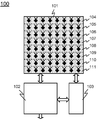
도 1은 전자기장 측정 시스템(100)을 개략적으로 도시한다. 시스템(100)은 블록도로 표현된다. 전자기장 측정 시스템(100)은, 예를 들어 전자파 흡수율(specific absorption rate)(SAR)을 측정하기 위해 사용될 수 있다. 전자기장 측정 시스템(100)은 전자기장 프로빙 장치(field probing arrangement)(101), 측정치 프로세싱 장치(measurement processing arrangement)(102) 및 제어기(103)를 포함한다. 전자기장 프로빙 장치(101)는 복수의 프로브 모듈들(104 내지 111)을 포함한다.Figure 1 schematically shows an electromagnetic
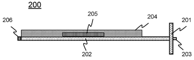
도 2는 전자기장 측정 시스템(100) 내의 프로브 모듈들(104 내지 111) 중 임의의 것에 대응할 수 있는 프로브 모듈(200)을 개략적으로 도시한다. 도 2는 프로브 모듈(200)의 개략적인 측면도를 제공한다. 프로브 모듈(200)은 프로브 기판(probe substrate)(201) 및 전송 라인 기판(transmission line substrate)(202)을 포함한다. 프로브 기판(201) 및 전송 라인 기판(202)은, 예를 들어 시판되는 전기 회로들 용 인쇄 회로 기판 재료로 형성될 수 있다.Figure 2 schematically illustrates a
프로브 기판(201)과 전송 라인 기판(202)은 T-형 구조를 형성한다. 전송 라인 기판(202)은 이러한 T-형 구조의 스템(stem)을 형성하는 반면, 프로브 기판(201)은 T-형 구조의 캡(cap)을 형성한다. 전송 라인 기판(202)은 프로브 기판(201)에 대해 수직으로 배치된다. 도 2에 도시된 바와 같이, 전송 라인 기판(202)의 프로브 결합부(probe coupling portion)(203)는 프로브 기판(201)에 수직하게 상기 프로브 기판으로부터 연장될 수 있다.The
전송 라인 기판(202)에는 도 2에 도시된 바와 같은 커버(204)가 제공될 수 있다. 커버(204)는 전자기 차폐물(electromagnetic shield)을 구성할 수 있다. 이를 위해, 커버(204)는, 예를 들어 전기 도전성 소자들을 포함할 수 있다. 전송 라인 기판(202)은 커버(204) 아래에 위치될 수 있는 프론트-엔드 회로(front-end circuit)(205)를 포함할 수 있다. 전송 라인 기판(202)은 또한 커넥터 장치(206)를 구비할 수 있다. 커넥터 장치(206)는 프로브 모듈(200)을 도 1에 도시된 측정치 프로세싱 장치(102) 및 제어기(103)에 결합시키는 것을 가능하게 할 수 있다.The
도 3은 또한 프로브 모듈(200)을 개략적으로 도시한다. 도 3은 프로브 모듈(200)의 개략적인 평면도를 제공한다. 프로브 기판(201)은 이러한 예에서 8 개의 프로브들인, 프로브들(301-308)의 어레이를 포함한다. 프로브 기판(201)은 프로브들(301 내지 308)이 그를 따라서 배치되는 슬롯 연장부(slot arrangement)(309)를 더 포함할 수 있다. 슬롯 연장부(309)는 프로브들(301 내지 308)과 교차한다. 도 2에 도시된 전송 라인 기판(202)의 프로브 결합부(probe coupling portion)(203)는 프로브 기판(201) 내의 슬롯 연장부(309)를 가로지른다.FIG. 3 also schematically shows the
이러한 예에서, 슬롯 연장부(309)는 좌측 슬롯(310) 및 우측 슬롯(311)의 2 개의 슬롯들을 포함한다. 4 개의 프로브들(301 내지 304)은 이러한 4 개의 프로브들(301 내지 304) 각각과 교차하는 좌측 슬롯(310)을 따라 배치된다. 4 개의 다른 프로브들(305 내지 308)은 이러한 4 개의 프로브들(305 내지 308) 각각과 교차하는 우측 슬롯(311)을 따라 배치된다. 전송 라인 기판(202)의 프로브 결합부(203)는 두 개의 프로브 결합 탭들(probe coupling tab), 즉 좌측 프로브 결합 탭(312) 및 우측 프로브 결합 탭(313)을 포함한다. 좌측 프로브 결합 탭(312)은 프로브 기판(201) 내의 좌측 슬롯(310)을 가로지른다. 우측 프로브 결합 탭(313)은 우측 슬롯(311)을 가로지른다.In this example,
도 2에 도시된 프론트-엔드 회로(205)는 스위치들의 어레이(arrange of switches)를 포함할 수 있으며, 상기 스위치들의 어레이는 프로브들(301 내지 308)의 어레이 내의 프로브의 선택을 가능하게 하며, 이러한 선택된 프로브가 커넥터 장치(206)에 전기적으로 결합되게 된다. 커넥터 장치(206)는 도 1에 도시된 제어기(103)로부터 프로브 선택 제어 신호 또는 임의의 다른 제어 신호를 수신할 수 있다.The front-
도 4는 또한 프로브 모듈(200)을 개략적으로 도시한다. 도 4는 프로브 모듈(200)의 개략적 정면도를 제공한다. 이러한 정면도에서, 전송 라인 기판(202)의 전면(front face)(401)은 가시적이다. 이러한 전면(401)은 도전성 재료의 차폐 평면(402)을 포함하는데, 이하 전측 차폐 평면(front shielding plane)(402)이라 한다. 전측 차폐 평면(402)은 "앵무새의 부리"로 지칭될 수 있는 특정 형태를 갖는 2 개의 부분들을 포함할 수 있는 외형을 갖는다. 이러한 특정 형태는 전자기 신호들에 대한 폐색부(choke)를 구성한다.FIG. 4 also schematically shows the
도 4에서, 좌측 프로브 결합 탭(312)의 메인 면(main face)(403)은 가시적이다. 이러한 메인 면(403)은 편의 및 설명의 이유들로 이하에서는 좌측 탭 전면(left tab front face)(403)으로 지칭될 것이다. 유사하게, 우측 프로브 결합 탭(313)의 메인 면(404)은 가시적이며, 이러한 메인 면(404)은 이하에서 우측 탭 전면(right tab front face)(404)으로 지칭될 것이다. 도 2를 참조하여 앞서 언급된 커넥터 장치(206) 및 커버(204)는 도 4에서 또한 가시적이다.In Figure 4, the main face 403 of the left probe-
좌측 탭 전면(403)은 복수의 도전성 텅 그룹들(conductive tongue groups)(405 내지 408)을 포함한다. 유사하게, 우측 탭 전면(404)은 또한 복수의 도전성 텅 그룹들(409 내지 412)을 포함한다. 도 3에 도시된 8 개의 프로브들(301 내지 308) 각각에 대해 하나의 도전성 텅 그룹이 있다. 도전성 텅 그룹은 3 개의 도전성 텅들, 즉 좌측 도전성 텅, 중간 도전성 텅 및 우측 도전성 텅을 포함한다. 도 4에서, 각각의 이러한 도전성 텅들은 비교적 작은 검은색 직사각형 영역으로 표현된다.The left tab front surface 403 includes a plurality of
도 5는 프로브 모듈(200)을 개략적으로 도시한다. 도 5는 프로브 모듈(200)의 배면도를 제공한다. 이러한 배면도에서, 전송 라인 기판(202)의 후면(501)은 가시적이다. 또한 이러한 후면(501)은, 이후에 후측 차폐 평면(502)으로 지칭될 도전성 재료의 차폐 평면(502)을 포함한다. 후측 차폐 평면(502)은, 적어도 부분적으로, 도 4에 도시된 전측 차폐 평면(402)과 상호보완적이다. 후측 차폐 평면(502)은 "앵무새의 부리" 형태의 두 부분들을 포함할 수 있는 외형을 갖는다. 이러한 부분들은 도 4에 도시된 전측 차폐 평면(402) 내에 존재하는 부분들과 유사하고 대칭이다.FIG. 5 schematically shows a
도 5에서, 좌측 프로브 결합 탭(312)의 또 다른 메인 면(503)은 가시적이다. 이러한 다른 메인 면은 편의 및 설명의 이유들로 이하에서 좌측 탭 후면(left tab rear face)(503)으로 지칭될 것이다. 유사하게, 우측 프로브 결합 탭(313)의 또 다른 메인 면(504)은 가시적이며, 이러한 메인 면(504)은 이하에서 우측 탭 후면(504)이라 지칭될 것이다. 도 2를 참조하여 앞서 언급된 커넥터 장치(206)는 또한 도 5에서 가시적이다.In Fig. 5, another main surface 503 of the left probe-engaging
좌측 탭 후면(503)은 복수의 도전성 텅들(505 내지 509)을 포함한다. 유사하게, 우측 탭 후면(504)은 또한 복수의 도전성 텅들(509 내지 512)을 포함한다. 도 3에 도시된 8 개의 프로브들(301 내지 308) 각각에 대해 하나의 도전성 텅이 있다.The left tab rear surface 503 includes a plurality of
도 6은 프로브 모듈(200)의 상부를 개략적으로 도시한다. 도 6은 도 4 및 도 5에서 A-A 선으로 나타낸 평면을 따라 절단했을 때의 프로브 모듈(200)의 상부의 개략적인 단면도를 제공한다. 도 6에서, 프로브 기판(201) 내의 좌측 슬롯(310)뿐만 아니라 이러한 좌측 슬롯(310)을 가로지르는 전송 라인 기판(202)의 좌측 프로브 결합 탭(312)이 가시적이다.Figure 6 schematically shows the top of the
도 6은 전송 라인 기판(202)이 복수의, 이러한 예에서는 4개의 도전 층들(601 내지 604)을 포함함을 도시한다. 보다 구체적으로는, 전송 라인 기판(202)은 기판(202)의 전면(401) 상에 외측 도전 층(601) 및 기판(202)의 후면(501) 상에 또 다른 외측 도전 층(602)을 포함한다. 이러한 외측 도전 층들은 이후에 전측 외측 도전 층(601) 및 후측 외측 도전 층(602)으로 지칭될 것이다. 도 4에 도시된 전측 차폐 평면(402)은 전측 외측 도전 층(601) 내에 포함된다. 도 5에 도시된 후측 차폐 평면(502)은 후측 외측 도전 층(602) 내에 포함된다.Figure 6 shows that the
전송 라인 기판(202)은 2개의 내측 도전성 층들, 즉 전송 라인 기판(202)의 전면(401)에 가장 가까운 내측 도전 층(603) 및 후면(501)에 가장 가까운 또 다른 내측 도전 층(604)을 포함한다. 이러한 내측 도전 층들은 편의 및 명료함의 이유들로, 이하에서 최전방 내측 도전 층(603) 및 최후방 내측 도전 층(604)으로 각각 지칭될 것이다. 도 6은 전송 라인 기판(202)의 4 개의 도전 층들(601 내지 604) 사이에서 연장되는 복수의 관통-홀 접속부들(through hole connections)(605 내지 611)을 더 도시한다. 관통-홀 접속부들은 이하에서 더 상세히 후술될 것이다.The
이러한 도면을 참조하여 그리고 도 3 내지 도 6을 참조하여 도 2에 도시된 프로브 모듈(200)의 상기 설명은, 따라서, 도 1에 도시된 자기장 측정 시스템(100) 내의 프로브 모듈(104 내지 111) 중 임의의 것에 적용될 수 있다.The above description of the
도 7은 도 2 내지 도 6을 참조하여 앞서 설명된 프로브 모듈(200)의 프로브들(301 내지 308) 중 임의의 프로브와 대응할 수 있는 프로브(700)를 개략적으로 도시한다. 도 7은 프로브(700)가 위치되는 프로브 기판(701)의 부분의 개략적인 평면도를 제공한다. 따라서, 이러한 프로브 기판(701)은 도 3에 도시된 프로브 기판(201)과 대응될 수 있다. 도 7에 도시된 프로브(700)는 도 3에 도시된 우측 슬롯(311)뿐만 아니라 좌측 슬롯(310)과 대응될 수 있는 슬롯(702)을 따라 배치된다. 전송 라인 기판의 프로브 결합 탭(703)은 도 7에 도시된 바와 같이 슬롯(702)을 통해 연장된다. 후속하여, 이러한 프로브 결합 탭(703)은 도 2 내지 도 6을 참조하여 앞서 기술된 설명을 이유로, 전송 라인 기판(202)에 속한다고 가정된다. 따라서, 도 7에 도시된 프로브 결합 탭(703)은 도 3에 도시된 우측 프로브 결합 탭(313)뿐만 아니라, 좌측 프로브 결합 탭(312)과 대응할 수 있다.FIG. 7 schematically illustrates a
전술한 바와 같이, 프로브 결합 탭(703)은, 프로브(700)에 대해, 프로브 결합 탭(703)의 전면 상에 도전성 텅 그룹(704)을 포함한다. 도전성 텅 그룹(704)은, 도 7에 도시된 바와 같이, 좌측 도전성 텅(705), 중간 도전성 텅(706) 및 우측 도전성 텅(707)을 포함한다. 프로브 결합 탭(703)은, 도 7에 도시된 바와 같이, 프로브 결합 탭(703)의 후면 상에 도전성 텅(708)을 포함한다. 이러한 도전성 텅은 이후에 후측 도전성 텅(rear conductive tongue)(708)으로 지칭될 것이다.The
프로브(700)는 스트립들의 형태의 2 개의 도전성 소자들(709,710)을 포함한다. 이러한 2 개의 도전성 소자들(709,710)은 편의 및 명료성의 이유들로 이후에서 각각 좌측 프로브 소자(709) 및 우측 프로브 소자(710)로 지칭될 것이다. 프로브(700)는 도전성 재료의 기준 평면(reference plane)(711)을 더 포함한다. 좌측 프로브 소자(709) 및 우측 프로브 소자(710)는 슬롯(702)의 전측 측면 상에 배치된다. 기준 평면(711)은 슬롯(702)의 후측 측면 상에 배치된다.
좌측 프로브 소자(709)와 우측 프로브 소자(710)의 사이에는 대칭 축(712)이 있다. 이러한 대칭축(712)은 전송 라인 기판(202)에 수직일 수 있고, 보다 구체적으로는, 전송 라인 기판(202)의 전면(401) 및 배면에 수직일 수 있다. 또한, 좌측 프로브 소자(709)와 우측 프로브 소자(710)는 서로에 대해 직각으로 배치될 수 있다. 이는 좌측 프로브 소자(709)의 종 축이 전송 라인 기판(202)에 대해 45°의 각도를 갖는다는 것을 의미한다. 또한, 우측 프로브 소자(710)의 종 축도 45°의 각도를 가지지만, 전송 라인 기판(202)에 대해 반대 부호를 이룬다.There is a
좌측 프로브 소자(709)는 프로브 결합 탭(703)의 전면 상의 좌측 도전성 텅(705)에 도전적으로 결합될 수 있다. 우측 프로브 소자(710)는 우측 도전성 텅(707)에 도전적으로 결합될 수 있다. 기준 평면(711)은 후측 도전성 텅(708)에 도전적으로 결합될 수 있다.The
도 7에 도시된 프로브(700)는 전자기장의 존재 하에서 다음과 같이 동작할 수 있다. 전자기장은 기준 평면(711)에 대하여 좌측 프로브 소자(709) 내에서 신호를 유도한다. 이러한 신호는 이하에서는 좌측 프로브 신호라 칭해질 것이다. 전자기장은 기준 평면(711)에 대하여 우측 프로브 소자(710) 내에서 또 다른 신호를 유도한다. 이 신호는 이하에서는 우측 프로브 신호라 칭해질 것이다.The
보다 상세하게는, 전자기장은 프로브 기판(701)과 일치하는 평면 내에 놓인 서로에 대해 직교하는 2 개의 성분들을 가질 수 있다. 하나의 성분은 전송 라인 기판(202)과 평행하게 배향될 수 있으며, 보다 구체적으로는, 기판(202)의 전면(401) 및 기판(202)의 후면(501)과 평행하게 배향될 수 있다. 이하에서, 이러한 성분을 수평 전자기장 성분(horizontal field component)이라 칭해질 것이다. 다른 성분은 전송 라인 기판(202)에 대하여 직각으로 배향될 수 있다. 이러한 성분은 이하에서 수직 전자기장 성분으로 칭해질 것이다.More specifically, the electromagnetic field may have two components orthogonal to each other lying in a plane coincident with the
전송 라인 기판(202)은 수직 전자기장 성분보다 더 큰 범위로 수평 전자기장 성분에 영향을 미칠 수 있다. 이는 전송 라인 기판(202)이 비교적 크고 수평 전자기장 성분과 평행한 다양한 도전성 평면들을 포함하기 때문이다. 이러한 도전성 평면들은 도 2 및 도 4에 도시된 커버(204)뿐만 아니라, 도 4에 도시된 전측 차폐 평면(402) 및 도 5에 도시된 후측 차폐 평면(502)을 포함한다. 이러한 도전성 평면들은 프로브(700)가 수평 전자기장 성분에 상대적으로 영향을 받지 않도록 할 수 있다.The
또한, 전송 라인 기판(202)은 전자기장의 산란을 야기할 수 있다. 이러한 산란은 전송 라인 기판(202)으로부터 방사되는 산란된 전자기장을 초래한다. 따라서, 프로브(700)는 측정될 전자기장에 더하여 이러한 산란된 전자기장을 수신할 수 있다. 또한, 산란된 전자기장 또는 산란된 전자기장의 적어도 일부는 심지어 전송 라인 기판(202) 내로 진입할 수도 있다.In addition, the
이러한 조건들에서, 좌측 프로브 신호는 이제 복수의 신호 성분들을 포함할 것이다. 이러한 신호 성분들은 측정될 전자기장의 수평 전자기장 성분에 의해 유도되는 신호 성분 및 수직 전자기장 성분에 의해 유도되는 다른 신호 성분을 포함한다. 하나의 신호 성분 및 다른 신호 성분은 이하 편의상 및 명료성의 이유들로 수평 신호 성분 및 수직 신호 성분으로 각각 지칭될 것이다. 수평 신호 성분 및 수직 신호 성분은 바람직한 신호 성분들이다. 이들 외에도, 좌측 프로브 신호는, 산란된 전자기장에 의해 유도되는 기생 신호 성분들(parasitic signal component)을 전송 라인 기판(202) 내에 더 포함할 것이다.In these conditions, the left probe signal will now contain a plurality of signal components. These signal components include a signal component induced by the horizontal electromagnetic field component of the electromagnetic field to be measured and another signal component induced by the vertical electromagnetic field component. One signal component and the other signal component will be referred to as horizontal signal component and vertical signal component, respectively, for convenience and clarity reasons below. The horizontal signal component and the vertical signal component are desirable signal components. In addition to these, the left probe signal will further include a parasitic signal component in the
우측 프로브 신호는 또한 전술된 것들과 유사한 복수의 성분들을 포함할 것이다. 즉, 이러한 신호 성분들은 측정될 전자기장의 수평 전자기장 성분에 의해 유도되는 수평 신호 성분과 수직 전자기장 성분에 의해 유도되는 수직 신호 성분을 포함한다. 이러한 바람직한 신호 성분들 이외에, 우측 프로브 신호는 또한, 산란된 전자기장에 의해 유도되는 기생 신호 성분을 전송 라인 기판(202) 내에 포함할 것이다. 이러한 기생 신호 성분은 일반적으로 좌측 프로브 신호의 기생 신호와 유사할 것이다. 그러므로, 산란된 전자기장에 의해 유도되는 하나의 기생 신호 성분 및 다른 기생 신호 성분은 이하에서 공통 모드 간섭 신호 성분(common mode interference signal component)이라 칭해질 것이다.The right probe signal will also include a plurality of components similar to those described above. That is, these signal components include a horizontal signal component induced by the horizontal electromagnetic field component of the electromagnetic field to be measured and a vertical signal component induced by the vertical electromagnetic field component. In addition to these desirable signal components, the right probe signal will also include a parasitic signal component that is induced by the scattered electromagnetic field in the
전술된 각각의 수평 신호 성분들은, 좌측 프로브 신호 내에서 및 우측 프로브 신호 내에서 일반적으로 비교적 약하다. 이것은, 전술된 바와 같이, 프로브(700)가 전송 라인 기판(202)의 존재로 인해 수직 전자기장 성분보다 수평 전자기장 성분에 덜 민감하기 때문이다.Each of the above-described horizontal signal components is generally relatively weak within the left probe signal and within the right probe signal. This is because the
도 7에 도시된 바와 같이, 프로브(700) 내에서, 좌측 프로브 소자(709) 및 우측 프로브 소자(710)는 크기 및 부호의 조건들의 측면에서, 좌측 프로브 신호 내의 수직 신호 성분이 우측 프로브 신호 내의 수직 신호 성분과 대응되도록 배치된다. 좌측 프로브 신호 내의 수평 신호 성분은 또한 우측 프로브 신호의 수평 신호 성분과 크기 측면에서 일치할 수 있다. 그러나, 이러한 2 개의 전술된 신호 성분들은 반대의 부호이다. 이러한 예에서, 좌측 프로브 신호 내의 수평 신호 성분은 양의 부호를 가지지만, 우측 프로브 신호 내의 수평 신호 성분은 음의 부호를 갖는다고 가정된다. 좌측 프로브 신호 내의 공통 모드 간섭 신호 성분은 우측 프로브 신호 내의 공통 모드 간섭 신호 성분과 대응한다.7, in the
좌측 프로브 소자(709) 및 우측 프로브 소자(710)의 이러한 배치는 개선된 측정 정밀도를 달성하는데 기여한다. 예를 들어, 상대적으로 큰 정밀도로 수평 전자기장 성분을 나타내는 측정 신호는 우측의 프로브 신호로부터 좌측 프로브 신호를 감산(subtract)하거나 또는 그 반대로 획득될 수 있다. 이러한 감산(subtract)은 간섭 상쇄 효과(interference cancellation effect)를 제공한다. 좌측 프로브 신호 내의 공통 모드 간섭 신호 성분 및 우측 프로브 신호 내의 공통 모드 간섭 신호 성분은 적어도 어느 정도는 서로를 상쇄시킨다. 좌측 프로브 신호 및 우측 프로브 신호 내의 각각의 수직 신호 성분들은 또한 감산의 결과로서 서로 상쇄시킨다. 남은 것은 좌측 프로브 신호와 우측 프로브 신호 내의 각각의 수평 신호 성분들의 합이다. 이러한 합계는 수평 전자기장 측정 신호를 구성한다.This arrangement of the
따라서, 좌측 프로브 소자(709) 및 우측 프로브 소자(710)의 배치는 이러한 프로브 소자들이 제공하는 각각의 수평 신호 성분들에 대한 간섭의 감소를 가능하게 다. 이러한 간섭의 감소는 전술된 바와 같이 이러한 수평 신호 성분들이 상대적으로 약하기 때문에 특히 적절하다. 반대로, 각각의 수직 신호 성분들은 비교적 강하다. 따라서, 직 신호 성분들은 수평 신호 성분보다 더 높은 수준의 간섭을 용인할 수 있다. 간섭 상쇄 효과는 덜 요구된다. 충분한 정밀도로 수직 전자기장 성분을 나타내는 측정 신호는 좌측 프로브 신호와 우측 프로브 신호를 합산함으로써 획득될 수 있다. 이러한 합계는 간섭 상쇄 효과를 제공하지 않는다.Thus, the arrangement of left and
도 2에 도시된 프로브 모듈(200) 상의 프론트-엔드 회로(205)는 전송 라인 기판과 평행한 전자기장의 수평 성분을 나타내는 수평 측정 신호를 획득하기 위해 좌측 프로브 신호로부터 우측 프로브 신호를 감산할 수 있다. 프론트-엔드 회로(205)는 전송 라인 기판(202)에 수직인 전자기장의 수직 성분을 나타내는 수직 측정 신호를 획득하기 위해 좌측 프로브 신호 및 우측 프로브 신호를 가산할 수도 있다. 또 다른 실시예에서, 이러한 동작들, 감산 및 가산은, 도 1에 도시된 전자기장 측정 시스템(100)의 측정치 프로세싱 장치(102) 내에서 수행될 수 있다.The front-
따라서, 도 7을 참조하여 도 7에서 예시된 프로브(700)의 설명은, 도 3에 도시된 프로브 모듈(200) 내의 프로브들(301 내지 308) 중 임의의 프로브에 적용될 수 있으며, 따라서 도 1에 도시된 전자기장 측정 시스템(100) 내의 프로브 모듈들 내의 프로브들(104 내지 111) 중 임의의 프로브에도 적용될 수 있다.7 can be applied to any one of the
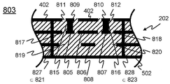
도 8은 프로브 모듈(200)의 전송 라인 기판(202) 내의 전송 라인 구조체(800)를 개략적으로 도시한다. 도 8은 전송 라인 구조체(800)의 개략적인 반투명 상면도를 제공하며, 반면에 도 2 및 도 4에 도시된 커버(204)는 생략된다. 도 8은 도 6에 도시된 전송 라인 기판(202)의 상이한 도전 층들(601 내지 604) 내에서의 특징부들(features)을 나타내는 상이한 유형들의 라인들을 포함한다. 실선들은 전측 외측 도전 층(601)의 특징부들을 나타낸다. 파선들은 전면에 가장 가까운 최전측 내측 도전 층(603)의 특징부들을 나타낸다. 점선들은 최후측 내측 도전 층(604)의 특징부들을 나타낸다. 실선들 내의 비교적 작은 원들은 관통-홀 접속부들(through-hole connections)을 나타낸다. 도 8은 복수의 점선들을 도시한다. 일점-쇄선은 단면도를 획득하기 위해 그를 따라서 절단면이 만들어질 수 있는 평면을 나타낸다.FIG. 8 schematically illustrates a
전송 라인 구조체(800)는 프로브 결합부(801), 헤드부(802), 전이부(transition section)(803) 및 마이크로-스트립 라인부(804)를 갖는다. 프로브 결합부(801)는 도 3에 도시된 전송 라인 기판(202)의 프로브 결합부(203) 내에 놓인다. 마이크로-스트립 라인부(804)는 도 2에 도시된 프론트-엔드 회로(205)까지 연장될 수 있다. 마이크로-스트립 라인부(804)는 적어도 부분적으로 커버(204) 아래에 위치될 수 있으며, 커버(204)는 명확성의 이유들로 도 8에서는 생략되었다. 커버(204)는 마이크로-스트립 라인부(804)를 위한 전자기 차폐물(electromagnetic shield)을 구성할 수 있다.The
프로브 결합부(801), 헤드부(802) 및 부분적으로 전이부(803)에서, 전송 라인 구조체(800)는 최전측 내측 도전 층(603) 내에 3 개의 도전성 스트립들(805, 806, 807)을 포함한다. 편의상 및 명료성의 이유들로, 이러한 3 개의 도전성 스트립들 중 하나는 이하에서 좌측 전측 내측 도전성 스트립(805), 다른 하나는 중간 전측 내측 도전성 스트립(806) 및 또 다른 하나는 우측 전측 내측 도전성 스트립(807)으로 지칭될 것이다. 상기 프로브 결합부(801), 헤드부(802) 및 부분적으로 전이부(803)에서, 전송 라인 구조체(800)는 최후측 내측 도전 층(604) 내에 도전성 스트립을 더 포함한다. 이러한 도전성 스트립은 편의 및 명료성의 이유들로 후측 내측 도전성 스트립(808)이라 지칭될 것이다. 도 8이 제공하는 정면도에서, 후측 내측 도전성 스트립(808)은 중간 전측 내측 도전성 스트립(806) 아래에 위치된다.The
마이크로-스트립 라인부(804) 및 부분적으로 전이부(803)에서, 전송 라인 구조체(800)는 전측 외측 도전 층(601) 내에 2 개의 도전성 스트립들(809,810)을 포함한다. 편의 및 명료성의 이유들로, 이러한 2 개의 도전성 스트립들 중 하나는 이하에서 좌측 외측 도전성 스트립(809)으로 지칭되고, 다른 하나는 우측 외측 도전성 스트립(810)으로 지칭될 것이다. 좌측 외측 도전성 스트립(809)은 전측 차폐 평면(402) 내의 핑거형(finger-shaped) 개구(811) 내에 놓이며, 스트립(809)은 또한 전송 라인 구조체(800)의 전측 외측 도전 층(601) 내에 포함된다. 유사하게, 우측 외측 도전성 스트립(810)은 또한 전측 차폐 평면(402) 내의 핑거형 개구(812) 내에 놓인다.In the
마이크로-스트립 라인부(804) 및, 부분적으로, 전이부(803)에서, 전송 라인 구조체(800)는 신호 접지(signal ground)에 도전적으로 결합되는 2 개의 도전성 평면들(813,814)을 더 포함한다. 이러한 도전성 평면들 중 하나(813)는 전송 라인 구조체(800)의 최전측 내측 도전 층(603) 내에 포함된다. 다른 도전성 평면(814)은 최후측 내측 도전 층(604) 내에 포함된다. 편의상 및 명료성의 이유들로, 하나의 도전성 평면 및 다른 도전성 평면은 이하에서 각각 전측 내측 접지 평면(ground plane)(813) 및 후측 내측 접지 평면(814)으로 지칭될 것이다.The
헤드부(802) 내에 존재하는 중간 전측 내측 도전성 스트립(806)은 손으로부터 연장되는 손가락과 유사한 방식으로, 마이크로-스트립 라인부(804) 내에 존재하는 전측 내측 접지 평면(813)으로부터 연장한다. 유사하게, 헤드부(802) 내에 존재하는 후측 내측 도전성 스트립(808)은 마이크로-스트립 라인부(804) 내에 존재하는 후측 내측 접지 평면(814)으로부터 연장한다.The median front inner
전이부(803)에서, 전송 라인 구조체(800)는 2개의 관통-홀 접속부들(815,816)을 포함한다. 하나의 관통-홀 접속부(815)는 좌측 전측 내측 도전성 스트립(805)과 좌측 외측 도전성 스트립(809)을 서로 도전적으로 결합시킨다. 다른 관통-홀 접속부(816)는 우측 전측 내측 도전성 스트립(807)과 우측 외측 도전성 스트립(810)을 서로 도전적으로 결합시킨다. 하나의 관통-홀 접속부 및 다른 하나의 관통-홀 접속부는 편의 및 명료성의 이유들로 이하에서 좌측 전이 관통-홀 접속부(815) 및 우측 전이 관통-홀 접속부(816)로 각각 지칭될 것이다.At the
전이부(803)에서, 전측 내측 접지 평면(813)은 2개의 U자형 개구들(817, 818)을 가지며, 하나는 좌측 전이 관통-홀 접속부(815) 주위에 위치되고, 다른 하나는 우측 전이 관통-홀 접속부(816) 주위에 위치된다. 하나의 U자형 개구 및 다른 U자형 개구는 이하에서 편의상 및 명료성의 이유들로 좌측 전측 내측 U자형 개구(817) 및 우측 전측 내측 U자형 개구(818)로 각각 지칭될 것이다. 후측 내측 접지 평면(814)은 2 개의 유사한 U자형 개구들을 가지며, 하나는 좌측 전이 관통-홀 접속부(815) 주위에 위치되고, 다른 하나는 우측 전이 관통-홀 접속부(816) 주위에 위치된다. 하나의 U자형 개구 및 다른 U자형 개구는 이하에서 좌측 후측 내측 U자형 개구(819) 및 우측 후측 내측 U자형 개구(820)라 지칭될 것이다.In the
전송 라인 구조체(800)는 도 7에 도시된 프로브(700)와 같은, 프로브로부터 도 2에 도시된 프론트-엔드 회로로의 좌측 프로브 신호의 전송을 가능하게 하는 신호 경로를 제공한다. 이러한 좌측 신호 경로는 좌측 전측 내측 도전성 스트립(805), 좌측 전이 관통-홀 결합부(815) 및 좌측 외측 도전성 스트립(809)을 포함한다. 대칭적으로, 전송 라인 구조체(800)는 관련 프로브(700)로부터 도 2에 도시된 프론트-엔드 회로(205)로 우측 프로브 신호의 전송을 가능하게 하는 신호 경로를 제공한다. 이러한 우측 신호 경로는 우측 전측 내측 도전성 스트립(807), 우측 전이 관통-홀 결합부(816) 및 우측 외측 도전성 스트립(810)을 포함한다.The
전송 라인 구조체(800)는 전측 차폐 평면(401)과 후측 차폐 평면(501) 사이에서 연장하는 관통-홀 접속부들의 다양한 어레이들(821,822,823)을 더 포함할 수 있다. 이러한 어레이들은 관통-홀 접속부들의 좌측 어레이(821), 관통-홀 접속부들의 중간 어레이(822), 및 우측 관통-홀 접속부들의 우측 어레이(823)를 포함한다. The
관통-홀 접속부들의 좌측 어레이(821)는 2개의 전술한 신호 경로들과 좌측 인접 전송 라인 구조체의 신호 경로들, 또는 또 다른 잠재적인 간섭원(source of interference) 사이의 차폐 펜스(shielding fence)를 구성한다. 유사하게, 관통-홀 접속부들의 우측 어레이(823)는 2개의 신호 경로들과 우측 인접한 전송 라인 구조체의 신호 경로들 또는 또 다른 잠재적인 간섭원 사이의 차폐 펜스를 구성한다. 관통-홀 접속부들의 중간 어레이(822)는 전송 라인 구조체(800) 자체의 좌측 신호 경로와 우측 신호 경로 사이의 차폐 펜스를 구성한다. 이는 이러한 신호 경로들 사이의 혼선을 방지하다. 좌측 프로브 신호와 우측 프로브 신호는 적절하게 분리된 채로 남아있다.The left array of through-
도 9는 전송 라인 구조체(800) 내 프로브 결합부(801)를 개략적으로 더 도시한다. 도 9는 도 8에 도시된 B-B 라인에 의해 표시된 평면을 따라 절단된 경우의 프로브 결합부(801)의 단면도를 제공한다. 프로브 결합부(801)는 전송 라인 기판(202)의 얇은 돌출부(thinned projecting portion) 내에 포함된다. 이러한 얇은 돌출부는 도 3 내지 도 5에 도시된 좌측 프로브 결합 탭(312), 우측 프로브 결합 탭(313), 또는 도 7에 도시된 프로브 결합 탭(703)과 같은 프로브 결합 탭을 형성한다.9 schematically further illustrates a
전송 라인 기판(202)의 얇은 돌출부에서, 최전측 내측 도전 층(603) 및 최후측 내측 도전 층(604)은 도 9에 도시된 바와 같이 외측 층들을 구성한다.In the thin protrusion of the
프로브 결합부(801)는 좌측 전측 내측 도전성 스트립(805)의 헤드 부분을 포함한다. 이러한 헤드 부분은 도 7에 도시된 좌측 도전성 텅(705)과 같은 좌측 도전성 텅을 구성할 수 있다. 프로브 결합부(801)는 우측 전측 내측 도전성 스트립(807)의 헤드 부분을 더 포함한다. 이러한 헤드 부분은 도 7에 도시된 우측 도전성 텅(707)과 같은 우측 도전성 텅을 구성할 수 있다. 프로브 결합부(801)는 중간 전측 내측 도전성 스트립(806)의 헤드 부분을 더 포함할 수 있다. 이러한 헤드 부분은 도 7에 도시된 중간 도전성 텅(706)과 같은 중간 도전성 텅을 구성할 수 있다. 프로브 결합부(801)는 후측 내측 도전성 스트립(808)의 헤드 부분을 더 포함할 수 있다. 이러한 헤드 부분은 도 7에 도시된 후측 도전성 텅(708)과 같은 후측 도전성 텅을 구성할 수 있다.The
도 10은 전송 라인 구조체(800) 내의 헤드부(802)를 개략적으로 더 도시한다. 도 10은 도 8에 도시된 C-C 라인에 의해 표시된 평면을 따라 절단될 때의 헤드부(802)의 단면도를 제공한다. 이러한 절단 평면은 전측 차폐 평면 (402), 후측 차폐 평면 (502), 및 하나(824)는 관통-홀 접속부들의 좌측 어레이(821)에 속하며, 또 다른 하나(825)는 중간 어레이(822)에 속하며, 그리고 또 다른 하나(826)는 우측 어레이(823)에 속하는 3개의 관통-홀 접속부들을 통과한다. 따라서, 이러한 소자들은 도 10에 도시되고 참조된다.10 schematically further illustrates a
헤드부(802)는 좌측 전측 내측 도전성 스트립(805)의 주요 부분(main portion), 중간 전측 내측 도전성 스트립(806)의 주요 부분, 및 우측 전측 내측 도전성 스트립(807)의 주요 부분을 포함한다. 헤드부(802)는 후측 내측 도전성 스트립(808)의 주요 부분을 더 포함한다. 이러한 도전성 스트립들은 도 10에 도시되고 참조된다.The
헤드부(802)에서, 중간 어레이(822)의 관통-홀 접속부(825)는 다음의 소자들을 서로 도전적으로 결합한다: 전측 차폐 평면(402), 중간 전측 내측 도전성 스트립(806), 후측 내측 도전성 스트립(808) 및 후측 차폐 평면(502).In the
헤드부(802) 내에 위치된 중간 어레이(822)의 다른 관통-홀 접속부들에도 동일하게 적용될 수 있다. 전술된 소자들은 신호 접지에 도전적으로 결합된다. 좌측 어레이(821) 및 우측 어레이(823)의 관통-홀 접속부들은 전측 차폐 평면(402)과 후측 차폐 평면(502)을 서로 도전적으로 결합시킨다. 이러한 어레이들(821,823)의 다른 관통-홀 접속부에도 동일하게 적용될 수 있다. Hole connections of the
헤드부(802)에서, 전술된 도전성 스트립들(805 내지 808)은 서로에 대해 그리고 전측 차폐 평면(402) 및 후측 차폐 평면(502)에 대해 특정한 공간적 관계를 가질 수 있다. 이러한 특정한 공간적 관계는 헤드부(802) 내에서, 좌측 신호 경로가 원하는 범위 내에 있는 특성 임피던스(characteristic impedance)를 갖도록 한다. 우측 신호 경로에도 동일하게 적용된다.In the
도 11은 전송 라인 구조체(800) 내의 전이부(803)를 개략적으로 도시한다. 도 11은 도 8에 도시된 D-D 라인에 의해 표시된 평면을 따라 절단될 때 전이부(803)의 단면도를 제공한다.FIG. 11 schematically illustrates a
이러한 절단 평면은 전측 차폐 평면(402), 후측 차폐 평면(502)을 통과할 뿐만 아니라, 좌측 어레이 (821)에 속하는 관통-홀 접속부(827) 및 우측 어레이(823)에 속하는 관통-홀 접속부(828)를 통과한다. 따라서, 이러한 소자들은 도 11에 도시되고 참조된다. These cut planes not only pass through the
전이부(803)는 좌측 전측 내측 도전성 스트립(805)의 꼬리 부분, 중간 전측 내측 도전성 스트립(806)의 꼬리 부분 및 우측 전측 내측 도전성 스트립(807)의 꼬리 부분을 포함한다. 전이부(803)는 후측 내측 도전성 스트립(808)의 베이스 부분을 더 포함한다. 전이부(803)는 둘 다 마이크로-스트립 라인부(804) 내로 연장되는 좌측 외측 도전성 스트립(809)의 헤드 부분 및 우측 외측 도전성 스트립(810)의 헤드 부분을 더 포함한다. 이러한 도전성 스트립들(803 내지 810)은 도 11에 도시되고 참조된다.The
또한, 도 11은 좌측 전이 관통-홀 접속부(815)뿐만 아니라 이러한 관통-홀 접속부(815) 주위에 위치된 좌측 전측 내측 U자형 개구(817) 및 좌측 후측 내측 U자형 개구(819)를 도시한다. 도 11은 우측 전이 관통-홀 접속부(816)뿐만 아니라 이러한 관통-홀 접속부(816) 주위에 위치된 우측 전측 내측 U자형 개구(818) 및 우측 후측 내측 U자형 개구(820)를 도시한다. 또한, 도 11은 우측 외측 도전성 스트립(810)이 그 내에 놓이는 핑거형 개구(812)뿐만 아니라 좌측 외측 도전성 스트립(809)이 그 내에 놓이는 전측 차폐 평면(402) 내의 핑거형 개구(811)를 도시한다.11 also shows the left front inner
도 12는 전송 라인 구조체(800) 내의 마이크로-스트립 라인부(804)를 개략적으로 도시한다. 도 12는 도 8에 도시된 E-E 라인에 의해 표시된 평면을 따라 절단될 때의 단면도를 제공한다. 이러한 절단 평면은 전측 차폐 평면(402) , 전측 내측 접지 평면(813), 후측 내측 접지 평면(814), 및 후측 차폐 평면(502)뿐만 아니라, 관통-홀 접속부들의 좌측 어레이(821)에 속하는 하나(829), 중간 어레이에 속하는 또 다른 하나(830), 그리고 우측 어레이에 속하는 또 다른 어레이(831)인 3개의 관통-홀 접속부를 통과한다. 따라서, 이러한 소자들은 도 12에 도시되고 참조된다.Figure 12 schematically illustrates the
도 12는 좌측 외측 도전성 스트립(809) 뿐만 아니라 이러한 도전성 스트립이 그 내에 놓이는 전측 차폐 평면(402) 내의 핑거형 개구(811)를 도시한다. 도 12는 우측 외측 도전성 스트립(810)뿐만 아니라 이러한 도전성 스트립이 그 내에 놓이는 전측 차폐 평면(402) 내의 핑거형 개구(812)를 도시한다.Figure 12 shows a finger-
마이크로-스트립 라인부(804)에서, 전술된 도전성 스트립들(809,810)은 전측 내측 접지 평면(813)에 대해, 그리고 전측 차폐 평면(402)에 대해서도 특정한 공간적 관계를 가질 수 있다. 이러한 특정한 공간적 관계는 마이크로-스트립 라인부(804)내에서, 좌측 신호 경로가 원하는 범위 내에 있는 특성 임피던스를 갖도록 한다. 또한, 이러한 특성 임피던스는 헤드부(802) 내의 특성 임피던스와 충분히 잘 매칭될 수 있다. 헤드부(802) 내의 및 마이크로-스트립 라인부(804) 내의 우측 신호 경로에 동일한 설명이 적용된다.In the
도 8에 도시되고 도 8 및 도 9 내지 도 12를 참조하여 상기 기술된 전송 라인 구조체(800)는 도 2 내지 도 6에 도시된 프로브 모듈(200)의 전송 라인 기판(202) 내의 임의의 전송 라인 구조체에 적용될 수 있다. 이러한 설명은 도 1에 도시된 전자기장 측정 시스템(100) 내의 임의의 프로브 모듈들(104 내지 111)의 전송 라인 기판 내의 임의의 전송 라인 구조체에도 적용될 수 있다.The
도 1에 도시된 전자기장 측정 시스템(100)은 기본적으로 다음과 같이 동작할 수 있다. 도시를 위해, 프로브 모듈들(104 내지 111)은 각각 도 2 내지 도 6을 참조하여 상술된 프로브 모듈(200)과 유사하다고 가정한다. 프로브 모듈들(104 내지 111)은 프로브 모듈들(104 내지 111)의 프로브 기판들에 의해 형성되는 측정 표면을 규정할 수 있다. 또한, 프로브 모듈들(104 내지 111) 내의 프로브들은 각각 도 7을 참조하여 앞서 설명된 프로브(700)와 유사하다고 가정된다. 각각의 프로브는 측정 표면 상에 독특한 위치를 가질 수 있다. 프로브들은 프로브가 격자 점(grid point)을 구성하는, 2차원 그리드로 배치될 수 있다. 또한, 각각의 프로브에 대한 각각의 전송 라인 구조체는 도 8 내지 도 12를 참조하여 앞서 설명된 전송 라인 구조체(800)와 유사하다고 가정된다.The electromagnetic
전자기장 프로빙 장치(101)는 예를 들어 인간의 머리와 같은 인체 부위의 물리적 모델 내에 위치될 수 있다. 물리적 모델은 관련 신체 부위 내의 생물학적 조직의 유전 특성들(dielectric properties)과 유사한 유전 특성들을 갖는 물질을 포함할 수 있다. 특허 공보 WO 2013/079621는 이러한 물질을 기재한다. 예를 들어 휴대 전화와 같은 전자기장 방출 장치는 물리적 모델 근처에 위치된다. 이러한 테스트 중인 장치는 물리적 모델을 관통할 전자기장을 생성한다. 전자기장 프로빙 장치(101) 내의 프로브들은 관통된 전자기장을 수신할 것이다.The electromagnetic
전술된 조건들에서, 프로브는 도 7에 도시된 프로브(700)를 참조하여 전술한 바와 같이, 좌측 프로브 신호 및 우측 프로브 신호를 제공할 것이다. 도 2를 참조하면, 프로브가 포함된 프로브 모듈(200)의 프론트-엔드 회로(205) 프로브와 관련된 한 쌍의 측정 신호들을 획득하기 위해 좌측 프로브 신호 및 우측 프로브 신호를 프로세싱할 수 있다. 예를 들어, 프론트-엔드 회로(205)는 전술된 바와 같이, 좌측 프로브 신호로부터 우측 프로브 신호를 감산하거나 또는 그 반대로 감산할 수 있고, 이러한 두 신호들을 가산할 수 있다. 또 다른 예로서, 프론트-엔드 회로(205)는 단지 좌측 프로브 신호 및 우측 프로브 신호를 증폭할 수 있으며, 이 경우 한 쌍의 측정 신호들은 좌측 프로브 신호의 증폭된 버전 및 우측 프로브 신호의 증폭된 버전을 포함한다.In the above-described conditions, the probe will provide the left probe signal and the right probe signal, as described above with reference to probe 700 shown in FIG. Referring to FIG. 2, the left probe signal and the right probe signal may be processed to obtain a pair of measurement signals associated with the front-
어떤 경우에도, 한 쌍의 측정 신호들은 프로브의 위치에서 전자기장의 2 개의 직교 성분들을 나타낸다. 이러한 2 개의 직교 성분들은 프로브가 포함되는 프로브 기판과 일치하는 평면 내에 놓여있다. 이러한 평면도 앞서 언급된 측정 표면과 일치한다.In any case, the pair of measurement signals represents two orthogonal components of the electromagnetic field at the location of the probe. These two quadrature components lie in a plane coincident with the probe substrate on which the probe is contained. This plane corresponds to the measurement surface mentioned above.
측정치 프로세싱 장치(102)는 전자기장 프로빙 장치(101)가 제공하는 각각의 측정 신호들을 프로세싱한다. 측정치 프로세싱 장치(102)는 각각의 측정 신호들이 관련된 각각의 프로브들의 각각의 위치들에서 전자기장의 하나의 성분 및 다른 성분의 진폭 및 위상을 검출한다. 따라서, 측정치 프로세싱 장치(102)는 측정 표면 상의 전자기장의 진폭 및 위상 맵을 설정한다.The
일단 전자기장의 2차원 진폭 및 위상 맵이 설정되면, 측정치 프로세싱 장치(102)는 이러한 맵에 기초하여 측정 표면 둘레의 전자기장의 3차원 모델을 생성할 수 있다. 이러한 3차원 모델은 테스트 중인 장치에 대한 전자파 흡수율의 결정을 가능하게 한다. 측정치 프로세싱 장치(102)는 특허 공보 WO 2011/080332 및 특허 공보 EP 2 610 628에 기술된 원리들에 따라 작동할 수 있다.Once the two-dimensional amplitude and phase map of the electromagnetic field is established, the
부연 설명Explanation
도면들을 참조한 상기 상세한 설명은 단지 본 발명의 예시이며 청구 범위에서 정의된 부가적인 특징들이다. 본 발명은 다수의 상이한 방식들로 구현될 수 있다. 이를 설명하기 위해 몇 가지 대안들이 간략하게 제시되었다.The foregoing detailed description with reference to the drawings is merely an example of the invention and additional features as defined in the claims. The present invention may be implemented in a number of different ways. Several alternatives have been briefly presented to illustrate this.
본 발명은 전자기장 측정과 관련된 수많은 유형들의 제품들 또는 방법들에 적용될 수 있다. 예를 들어, 본 발명은, 원칙적으로, 전자기장의 2차원 측정을 하고, 2차원 측정치에 포함된 진폭 및 위상 정보를 사용하여 이러한 2차원 측정치에 기초하여 이러한 전자기장의 3차원 표현을 구축하도록 구성된 임의의 유형의 제품에 적용될 수 있다.The present invention can be applied to many types of products or methods related to electromagnetic field measurements. For example, the present invention provides, in principle, an apparatus and method for generating a three-dimensional representation of an electromagnetic field based on such two-dimensional measurements using amplitude and phase information contained in a two- Lt; / RTI > type of product.
본 발명은 많은 상이한 방식들로 구현될 수 있다. 프로브 소자들은 반드시 서로에 대해 직각으로 배치될 필요는 없다. 예를 들어, 프로브 소자들 사이에 60°의 각도가 있을 수 있다. 전자기장의 2개의 직교 성분들을 나타내는 2 개의 신호들은 적절한 가중치 계수들(weighing coefficients)을 갖는 2개의 프로브 신호들의 2개의 선형 조합들을 생성함으로써 획득될 수 있다. 또한, 프로브는 반드시 스트립의 형상을 가질 필요는 없는 임의의 적합한 형상을 갖는 프로브 소자들을 포함할 수 있다. 유사한 언급은 도전성 기준 평면에 적용되며, 도전성 기준 평면은 반드시 직사각형 또는 정사각형의 형상을 가질 필요는 없다. 예를 들어, 다른 실시예에서, 도전성 기준 평면은 원형 또는 타원형의 형상을 가질 수 있다.The present invention can be implemented in many different ways. The probe elements do not necessarily have to be arranged at right angles to each other. For example, there may be an angle of 60 [deg.] Between the probe elements. The two signals representing the two quadrature components of the electromagnetic field can be obtained by generating two linear combinations of two probe signals with appropriate weighting coefficients. In addition, the probe may comprise probe elements having any suitable shape that does not necessarily have to have the shape of the strip. A similar reference applies to the conductive reference plane, and the conductive reference plane need not necessarily have a rectangular or square shape. For example, in other embodiments, the conductive reference plane may have a circular or oval shape.
전자기장의 2개의 직교 성분들을 나타내는 2개의 신호들을 획득하기 위해 2개의 프로브 신호들의 2 개의 선형 조합들을 만드는 수많은 상이한 방법들이 있다. 2개의 선형 조합들의 세트는 일반적으로 다음과 같이 표현될 수 있다:There are a number of different ways to create two linear combinations of two probe signals to obtain two signals representing the two quadrature components of the electromagnetic field. The set of two linear combinations can be generally expressed as:
UA = α1*UL + β1*UR (1) U A = α 1 * U L + β 1 * U R (1)
UB = α2*UL - β2*UR (2)U B = α 2 * U L - β 2 * U R (2)
여기서, UA 및 UB는 전자기장의 2개의 직교 성분들을 나타내는 한 쌍의 신호들을 나타내고, UL은 좌측 프로브 신호를 나타내고, UR은 우측 프로브 신호를 나타내고, α1, β1은 좌측 프로브 신호 및 우측 프로브 신호에 대한 계량 계수들을 나타내고, α2, β2는 각각 제 2 선형 조합(2) 내에서 좌측 프로브 신호 및 우측 프로브 신호에 대한 계량 계수들을 나타낸다. 따라서 두 선형 조합들의 한 세트는 신호들의 쌍이 전자기장의 두 개의 직교 성분들을 정확하게 나타낼 수 있도록 적절한 값들을 가질 수 있는 4 개의 계량 계수들 α1, β1, α2, β2의 세트로 특징지어진다. 적절한 값들은 두 프로브 소자들이 서로에 대해 어떻게 배치되는지에 달려있다. 상세한 설명은 4 개의 계량 계수들이 각각 1이고, 가중치 처리되지 않은(non-weighted) 감산 및 가중치 처리되지 않은 가산에 대응하는 예를 제공한다. 이 예들에서는, 이 예에서, 도 7에 도시된 두 개의 프로브 소자(709,710)가 서로에 대해 직각으로 배치되기 때문에 적절한 값들이다. 이러한 예에서, UA 및 UB가 전자기장의 2개의 직교 성분들을 나타내는 한 쌍의 신호들을 정확하게 나타내는 계량 계수들의 값들의 다른 세트들이 다수 존재한다.Where U A and U B represent a pair of signals representing two quadrature components of the electromagnetic field, U L represents the left probe signal, U R represents the right probe signal, and α 1 and β 1 represent the left probe signal and it represents the weighing coefficient of the right signal probe, α 2, β 2 represents the weighing coefficient of the probe signal to the left and right probe signals within each of the second linear combination (2). Thus, one set of two linear combinations is characterized by a set of four metric coefficients? 1 ,? 1 ,? 2 ,? 2 that can have appropriate values to accurately represent the two orthogonal components of the electromagnetic field . Appropriate values depend on how the two probe elements are arranged relative to one another. The detailed description provides examples where the four metric coefficients are each 1, corresponding to a non-weighted subtraction and an unweighted addition. In these examples, in this example, the two
예를 들어, α1 = 1, β1 = 0, α2 = 0, β2 = 1은, UA와 UB가 전자기장의 두 직교 성분들을 정확히 나타내는 또 다른 계량 계수 값들의 또 다른 세트를 구성한다.For example, α 1 = 1, β 1 = 0, α 2 = 0, β 2 = 1 , the configuration of yet another set of different weighing coefficients U A and U B are representative of two orthogonal components of the electromagnetic field exactly do.
프로브 기판을 구현하는 다양한 방법들이 존재한다. 예를 들어, 프로브 기판은 프로브들의 2차원 어레이를 포함할 수 있다. 이러한 프로브 기판은도 1에 도시된 복수의 프로브 기판들(104 내지 111)을 대체할 수 있으며, 각각은 도 3에 도시된 프로브 기판(200)과 같은 프로브들의 1차원 어레이를 포함할 수 있다. 또 다른 실시예에서, 프로브 기판은 단일 프로브만 포함할 수 있다.There are various ways to implement the probe substrate. For example, the probe substrate may comprise a two-dimensional array of probes. Such a probe substrate may replace the plurality of
전송 라인 기판을 구현하는 다양한 방법들이 존재한다. 예를 들어, 이러한 기판은 3개의 도전 층들만, 또는 4개 이상의 도전 층들을 포함할 수 있다. 예를 들어, 프론트-엔드 회로의 구현을 용이하게 하기 위해 하나 이상의 부가적인 도전 층들이 제공될 수 있다.There are various ways to implement a transmission line substrate. For example, such a substrate may comprise only three conductive layers, or four or more conductive layers. For example, one or more additional conductive layers may be provided to facilitate the implementation of the front-end circuitry.
일반적으로, 본 발명을 구현하는 다수의 상이한 방법이 존재하며, 상이한 구현들은 상이한 토폴로지들(topologies)을 가질 수 있다. 주어진 토폴로지에서 개체(entity)는 여러 기능들을 수행할 수 있고, 또는 여러 개체들이 공동으로 단일 기능을 수행할 수도 있다. 이러한 점에서, 도면들은 매우 개략적이다. 하드웨어 또는 소프트웨어, 또는이 둘의 조합을 통해 구현될 수 있는 많은 기능들이 있다. 소프트웨어-기반 구현에 대한 설명은 하드웨어-기반 구현을 제외하지 않으며, 반대의 경우도 마찬가지이다. 하나 이상의 전용 회로들은 물론 하나 이상의 적절하게 프로그래밍된 프로세서들을 포함하는 하이브리드 구현들도 가능하다. 예를 들어, 도면들을 참조하여 앞서 설명된 다양한 기능들은 하나 이상의 전용 회로들에 의해 구현될 수 있으며, 이에 의해 특정 회로 토폴로지가 특정 기능을 정의한다.In general, there are a number of different ways of implementing the invention, and different implementations may have different topologies. In a given topology, an entity may perform several functions, or several objects may perform a single function jointly. In this regard, the drawings are very schematic. There are many functions that can be implemented through hardware or software, or a combination of both. The description of a software-based implementation does not exclude a hardware-based implementation, and vice versa. Hybrid implementations that include one or more proprietary circuits as well as one or more appropriately programmed processors are possible. For example, the various functions described above with reference to the drawings may be implemented by one or more dedicated circuits, whereby a particular circuit topology defines a particular function.
본 발명에 따라 전자기장을 측정할 수 있게 하는 소프트웨어인, 일련의 명령어들(instructions)을 저장하고 배포하는 많은 방식들이 존재한다. 예를 들어, 소프트웨어는, 예를 들어 메모리 회로, 자기 디스크(magnetic disk) 또는 광 디스크와 같은 적절한 장치 판독가능 매체(device readable medium) 내에 저장될 수 있다. 소프트웨어가 저장된 장치 판독가능 매체는 개별 제품으로서 또는 소프트웨어를 실행할 수 있는 또 다른 제품으로서 제공될 수 있다. 이러한 매체는 소프트웨어를 실행할 수 있는 제품의 일부일 수도 있다. 소프트웨어는 유선, 무선 또는 하이브리드일 수 있는 통신 네트워크들을 통해 배포될 수도 있다. 예를 들어, 소프트웨어는 인터넷을 통해 배포될 수 있다. 소프트웨어는 서버를 통해 다운로드할 수 있도록 만들어질 수도 있다. 다운로드는 지불될 수 있다.There are many ways to store and distribute a set of instructions, which is software that enables the measurement of electromagnetic fields in accordance with the present invention. For example, the software may be stored in a suitable device readable medium such as, for example, a memory circuit, a magnetic disk, or an optical disk. The device-readable medium in which the software is stored may be provided as an individual product or as another product capable of executing software. Such media may be part of a product capable of executing software. The software may be distributed over communication networks, which may be wired, wireless or hybrid. For example, software may be distributed over the Internet. The software may be made available for download via the server. Download can be paid.
전술된 설명들은 도면들을 참조한 상세한 설명이 제한이 아닌 본 발명의 예시임을 입증한다. 본 발명은 첨부된 청구 범위의 범위 내에 있는 수많은 다른 방법들로 구현될 수 있다. 청구 범위의 등가물의 의미 및 범위 내에 있는 모든 변경들은 청구 범위의 범위 내에 포함되어야 한다. 청구 범위의 모든 참조 부호는 청구 범위를 제한하는 것으로 해석되어서는 안된다. "포함하는"이라는 단어는 청구 범위에 기재된 것 이외의 다른 소자들 또는 단계들의 존재를 배제하지 않는다. 소자들 또는 단계들의 단수형은 복수의 이러한 소자들 또는 단계들의 존재를 배제하지 않는다. 각각의 종속 항들이 각각의 부가적인 특징들을 정의한다는 단순한 사실은 청구 범위에 반영된 것들 이외의 부가적인 특징들의 조합들을 배제하지 않는다.The foregoing description demonstrates that the description with reference to the drawings is not limiting and is an example of the present invention. The invention may be embodied in many different ways that are within the scope of the appended claims. All changes that come within the meaning and range of equivalency of the claims are to be embraced within their scope. All reference signs in the claims should not be construed as limiting the claim. The word "comprising " does not exclude the presence of other elements or steps than those listed in the claims. The singular form of elements or steps does not exclude the presence of a plurality of such elements or steps. The mere fact that each subclause defines each additional feature does not exclude combinations of additional features other than those reflected in the claims.
Claims (15)
- 제 1 프로브 소자(709), 제 2 프로브 소자(710) 및 기준 평면(reference plane)(711)을 갖는 프로브(700)를 포함하는 프로브 기판(701)으로서, 전자기장은 상기 기준 평면에 대하여 제 1 도전성 프로브 소자 내에서 제 1 프로브 신호를 유도하고 상기 기준 평면에 대하여 상기 제 2 프로브 소자 내에서 제 2 프로브 신호를 유도하는, 상기 프로브 기판(701); 및
- 상기 프로브에 결합된 전송 라인 구조체(800)를 포함하는 전송 라인 기판(202)으로서, 상기 전송 라인 구조체(800)는 제 1 프로브 신호 및 제 2 프로브 신호를 기초한 측정 결과들을 제공하도록 구성된 측정치 프로세싱 장치(measurement processing arrangement)(102)를 향해 제 1 프로브 신호 및 제 2 프로브 신호를 개별적으로 안내하도록 구성된, 상기 전송 라인 기판(202);을 포함하며,
상기 프로브 기판 및 전송 라인 기판은 T형 구조체를 형성하고, 상기 프로브 기판은 캡을 형성하고, 상기 전송 라인 기판은 상기 T형 구조체의 스템(stem)을 형성하며;
상기 제 1 프로브 소자와 제 2 프로브 소자는 상기 제 1 프로브 소자 및 제 2 프로브 소자 사이에 상기 전송 라인 기판에 수직인 대칭 축(712)이 존재하도록 배치되는, 전자기장 측정 시스템(100).An electromagnetic field measurement system (100)
A probe substrate 701 comprising a probe 700 having a first probe element 709, a second probe element 710 and a reference plane 711, the electromagnetic field being directed relative to the reference plane 1. A probe substrate (701) for guiding a first probe signal in a conductive probe element and guiding a second probe signal in the second probe element with respect to the reference plane; And
- a transmission line substrate (202) comprising a transmission line structure (800) coupled to the probe, wherein the transmission line structure (800) comprises measurement processing configured to provide measurement results based on a first probe signal and a second probe signal And the transmission line substrate (202) configured to separately guide the first probe signal and the second probe signal toward a measurement processing arrangement (102)
Wherein the probe substrate and the transmission line substrate form a T-shaped structure, the probe substrate forms a cap, and the transmission line substrate forms a stem of the T-shaped structure;
Wherein the first probe element and the second probe element are disposed such that a symmetry axis (712) perpendicular to the transmission line substrate is present between the first probe element and the second probe element.
상기 전송 라인 구조체(800)는 헤드부(head section)(802)를 포함하며, 상기 헤드부(802)는,
- 상기 제 1 프로브 소자(709)에 도전적으로 결합된 제 1 도전성 스트립(805);
- 상기 제 2 프로브 소자(710)에 도전적으로 결합된 제 2 도전성 스트립(807); 및
- 상기 제 1 도전성 스트립 및 제 2 도전성 스트립 사이에 배치되고, 상기 프로브(700)의 상기 기준 평면(711)에 도전적으로 결합되는 중간 도전성 스트립(806)을 포함하는, 전자기장 측정 시스템(100).The method according to claim 1,
The transmission line structure 800 includes a head section 802, and the head section 802 includes:
- a first conductive strip (805) conductively coupled to the first probe element (709);
- a second conductive strip (807) conductively coupled to the second probe element (710); And
- an intermediate conductive strip (806) disposed between the first conductive strip and the second conductive strip and electrically coupled to the reference plane (711) of the probe (700).
상기 전송 라인 구조체(800)의 헤드부(802)의 제 1 도전성 스트립(805) 및 제 2 도전성 스트립(807)은 두 개의 도전성 차폐 평면들(shielding planes)(402, 502) 사이에 개재되고,
상기 두 개의 도전성 차폐 평면들은 상기 프로브(700)의 도전성 기준 평면(711)에 도전적으로 결합되는, 전자기장 측정 시스템(100).3. The method of claim 2,
The first conductive strip 805 and the second conductive strip 807 of the head portion 802 of the transmission line structure 800 are interposed between two conductive shielding planes 402 and 502,
Wherein the two conductive shield planes are electrically coupled to a conductive reference plane (711) of the probe (700).
상기 전송 라인 구조체(800)의 헤드부(802)의 제 1 도전성 스트립(805)과 제 2 도전성 스트립(807) 사이에 차폐 펜스(shielding fence)(822)가 배치되고,
상기 차폐 펜스는 상기 두 개의 도전성 차폐 평면들(402,502)과 상기 헤드부의 중간 도전성 스트립(806)을 서로 도전적으로 결합시키는 관통-홀 접속부들(through-hole connections)의 어레이에 의해 형성되는, 전자기장 측정 시스템(100).The method of claim 3,
A shielding fence 822 is disposed between the first conductive strip 805 and the second conductive strip 807 of the head portion 802 of the transmission line structure 800,
The shield fence is formed by an array of through-hole connections that electrically conductively couple the two conductive shield planes (402, 502) and the middle conductive strip (806) of the head portion to each other. (100).
두 개의 추가의 차폐 펜스들(821,823)을 포함하며,
상기 두 개의 추가의 차폐 펜스들(821, 823) 사이에, 상기 전송 라인 구조체(800)의 헤드부(802)의 제 1 도전성 스트립(805)과 제 2 도전성 스트립(807)이 배치되며,
상기 차폐 펜스는 상기 두 개의 도전성 차폐 평면들(402,502)을 서로 도전적으로 결합시키는 관통-홀 접속부들의 어레이에 의해 형성되는, 전자기장 측정 시스템(100).5. The method of claim 4,
Two additional shielding fences 821, 823,
A first conductive strip 805 and a second conductive strip 807 of the head portion 802 of the transmission line structure 800 are disposed between the two additional shielding fences 821 and 823,
Wherein the shield fence is formed by an array of through-hole connections that conductively couple the two conductive shield planes (402, 502) to each other.
상기 전송 라인 구조체(800)는 마이크로-스트립 라인부(804)를 포함하고, 상기 헤드부(803)는 상기 프로브(700)와 마이크로-스트립 라인부 사이에 개재되며,
상기 마이크로-스트립 라인부는:
- 상기 헤드부의 제 1 도전성 스트립(805)에 도전적으로 결합된 제 1 도전성 스트립(809);
- 상기 헤드부의 제 2 도전성 스트립(807)에 도전적으로 결합된 제 2 도전성 스트립(810); 및
- 상기 마이크로-스트립 라인부에서 상기 제 1 도전성 스트립 및 제 2 도전성 스트립과 평행하게 배치되고, 제 1 도전성 스트립 및 제 2 도전성 스트립과 마주하며, 상기 헤드부의 중간 도전성 스트립(806)에 도전적으로 결합된 접지 평면(ground plane)(813);을 포함하는, 전자기장 측정 시스템(100).6. The method according to any one of claims 1 to 5,
The transmission line structure 800 includes a micro-strip line unit 804 and the head unit 803 is interposed between the probe 700 and the micro-strip line unit,
The micro-strip line section comprises:
- a first conductive strip (809) conductively coupled to the first conductive strip (805) of the head portion;
- a second conductive strip (810) conductively coupled to the second conductive strip (807) of the head portion; And
Strip-line portion, the first conductive strip and the second conductive strip being disposed in parallel with the first and second conductive strips in the micro-strip line portion and facing the first conductive strip and the second conductive strip, And a ground plane (813), wherein the ground plane (813) is a ground plane.
상기 전송 라인 기판(800)은,
- 상기 두 개의 도전성 차폐 평면들 중 하나(402)를 포함하는 제 1 도전 층(601);
- 상기 헤드부(802)의 제 1 도전성 스트립(805), 제 2 도전성 스트립(807) 및 중간 도전성 스트립(806)을 포함하는 제 2 도전 층(603); 및
- 상기 두 개의 도전성 차폐 평면들 중 다른 하나(502)를 포함하는 제 3 도전 층(602);을 포함하는, 전자기장 측정 시스템(100).The method according to claim 6,
The transmission line substrate (800)
- a first conductive layer (601) comprising one of said two conductive shield planes (402);
A second conductive layer 603 comprising a first conductive strip 805, a second conductive strip 807 and an intermediate conductive strip 806 of the head portion 802; And
- a third conductive layer (602) comprising the other of the two conductive shield planes (502).
- 상기 제 1 도전성 층(601)은 상기 전송 라인 구조체(800)의 마이크로-스트립 라인부(804) 내의 제 1 도전성 스트립(809) 및 제 2 도전성 스트립(810)을 포함하며;
- 상기 제 2 도전 층(603)은 상기 마이크로-스트립 라인부의 접지 평면(813)을 포함하며;
- 상기 전송 라인 기판(202)은, 상기 마이크로-스트립 라인부의 제 1 도전성 스트립 및 제 2 도전성 스트립을, 상기 전송 라인 구조체의 헤드부(802)의 제 1 도전성 스트립(805) 및 제 2 도전성 스트립(807)에 각기 도전적으로 결합시키는 제 1 관통-홀 접속부(815) 및 제 2 관통-홀 접속부(816)를 포함하는, 전자기장 측정 시스템(100).8. The method of claim 7,
The first conductive layer 601 comprises a first conductive strip 809 and a second conductive strip 810 in the micro-strip line portion 804 of the transmission line structure 800;
The second conductive layer (603) comprises a ground plane (813) of the micro-strip line portion;
- the transmission line substrate (202) comprises a first conductive strip (805) and a second conductive strip (805) of the head portion (802) of the transmission line structure, the first conductive strip and the second conductive strip of the micro- Hole connection (815) and a second through-hole connection (816) that respectively couple electrically to the first through-hole connection (807).
- 상기 프로브 기판(701)은 슬롯(702)을 포함하며;
- 상기 전송 라인 기판(202)은 상기 프로브 기판의 슬롯을 따라서 연장된 프로브 결합 탭(probe coupling tab)(703)을 포함하는, 전자기장 측정 시스템(100).9. The method according to any one of claims 1 to 8,
The probe substrate 701 comprises a slot 702;
- The transmission line substrate (202) comprises a probe coupling tab (703) extending along a slot of the probe substrate.
상기 제 1 프로브 소자(709) 및 제 2 프로브 소자(710)는 상기 슬롯(702)의 일 측면 상에 배치되고, 상기 기준 평면(711)은 상기 슬롯의 다른 반대편 측면 상에 배치되는, 전자기장 측정 시스템(100).10. The method of claim 9,
Wherein the first probe element 709 and the second probe element 710 are disposed on one side of the slot 702 and the reference plane 711 is disposed on the other opposite side of the slot. (100).
상기 제 1 프로브 소자(709) 및 제 2 프로브 소자(710)는 서로에 대해 직교하도록 배치되는, 전자기장 측정 시스템(100).11. The method according to any one of claims 1 to 10,
Wherein the first probe element (709) and the second probe element (710) are arranged to be orthogonal to each other.
상기 제 1 프로브 신호 및 제 2 프로브 신호를 가산하고 상기 제 2 프로브 신호로부터 제 1 프로브 신호를 감산하도록 구성된 회로(205,102)를 포함하는, 전자기장 측정 시스템(100).12. The method according to any one of claims 1 to 11,
And circuitry (205,102) configured to add the first probe signal and the second probe signal and subtract a first probe signal from the second probe signal.
복수의 프로브 모듈(104 내지 111)을 포함하고,
상기 프로브 기판(201)과 전송 라인 기판(202)은 함께 프로브 모듈(200)을 형성하며,
다른 프로브 모듈들도 유사하게 구성되는, 전자기장 측정 시스템(100).13. The method according to any one of claims 1 to 12,
And a plurality of probe modules (104 to 111)
The probe substrate 201 and the transmission line substrate 202 together form a probe module 200,
The electromagnetic field measurement system (100), wherein other probe modules are similarly configured.
각각의 프로브들은 2차원 그리드로서 배치되며,
상기 2차원 그리드 내에서 프로브(700)는 격자 점(grid point)을 구성하는, 전자기장 측정 시스템(100).14. The method of claim 13,
Each probe is arranged as a two-dimensional grid,
Wherein the probe (700) in the two-dimensional grid constitutes a grid point.
Applications Claiming Priority (3)
| Application Number | Priority Date | Filing Date | Title |
|---|---|---|---|
| EP15307164.2A EP3187887A1 (en) | 2015-12-29 | 2015-12-29 | Electromagnetic field measurement system |
| EP15307164.2 | 2015-12-29 | ||
| PCT/EP2016/082759 WO2017114854A1 (en) | 2015-12-29 | 2016-12-28 | Electromagnetic field measurement system |
Publications (2)
| Publication Number | Publication Date |
|---|---|
| KR20180098661A true KR20180098661A (en) | 2018-09-04 |
| KR102868570B1 KR102868570B1 (en) | 2025-10-10 |
Family
ID=55589634
Family Applications (1)
| Application Number | Title | Priority Date | Filing Date |
|---|---|---|---|
| KR1020187022018A Active KR102868570B1 (en) | 2015-12-29 | 2016-12-28 | electromagnetic field measurement system |
Country Status (6)
| Country | Link |
|---|---|
| US (1) | US10725078B2 (en) |
| EP (2) | EP3187887A1 (en) |
| JP (1) | JP6873491B2 (en) |
| KR (1) | KR102868570B1 (en) |
| CN (1) | CN108700622B (en) |
| WO (1) | WO2017114854A1 (en) |
Cited By (1)
| Publication number | Priority date | Publication date | Assignee | Title |
|---|---|---|---|---|
| KR20220121292A (en) * | 2021-02-24 | 2022-09-01 | 주식회사 엘지에너지솔루션 | How to measure the electric field uniformity of a stripline clamp |
Families Citing this family (5)
| Publication number | Priority date | Publication date | Assignee | Title |
|---|---|---|---|---|
| US11310747B2 (en) * | 2019-06-12 | 2022-04-19 | Qualcomm Incorporated | Methods and apparatus for user equipment to differentiate human grip from protective covers |
| CN116917748A (en) * | 2021-03-09 | 2023-10-20 | 积分几何科学公司 | Inspection equipment and inspection methods |
| US20260056238A1 (en) * | 2022-11-16 | 2026-02-26 | Panasonic Connect Co., Ltd. | Method and device for detecting electric field |
| CN117783702B (en) * | 2023-12-29 | 2024-08-02 | 上海交通大学 | Dual-component near-field probe and system for simultaneously measuring perpendicular magnetic field and perpendicular electric field |
| CN120214546B (en) * | 2025-05-22 | 2025-07-22 | 东莞市台易电子科技有限公司 | Probe testing equipment and testing method |
Citations (2)
| Publication number | Priority date | Publication date | Assignee | Title |
|---|---|---|---|---|
| KR20120135221A (en) * | 2009-12-31 | 2012-12-12 | 아트-피 | System for measuring an electromagnetic field |
| EP2610628A1 (en) * | 2011-12-30 | 2013-07-03 | Art-Fi | Measuring an electromagnetic field |
Family Cites Families (7)
| Publication number | Priority date | Publication date | Assignee | Title |
|---|---|---|---|---|
| US6359596B1 (en) * | 2000-07-28 | 2002-03-19 | Lockheed Martin Corporation | Integrated circuit mm-wave antenna structure |
| US6573801B1 (en) * | 2000-11-15 | 2003-06-03 | Intel Corporation | Electromagnetic coupler |
| JP4025084B2 (en) * | 2002-02-04 | 2007-12-19 | 株式会社ルネサステクノロジ | EMI measuring device |
| FR2859064B1 (en) * | 2003-08-18 | 2005-12-30 | Satimo Sa | DEVICE FOR CONTROLLING THE SPECIFIC ABSORPTION RATE OF RADIANT OBJECTS MADE IN SERIES AND IN PARTICULAR PORTABLE TELEPHONES |
| CN101019033A (en) * | 2005-01-11 | 2007-08-15 | 太阳诱电株式会社 | Electromagnetic field distribution measuring method and apparatus thereof, computer program and information recording medium |
| US8502546B2 (en) * | 2006-04-05 | 2013-08-06 | Emscan Corporation | Multichannel absorberless near field measurement system |
| WO2013079621A1 (en) | 2011-11-29 | 2013-06-06 | Art-Fi | Composition simulating the dielectric properties of the human body and use thereof for sar measurement |
-
2015
- 2015-12-29 EP EP15307164.2A patent/EP3187887A1/en not_active Withdrawn
-
2016
- 2016-12-28 KR KR1020187022018A patent/KR102868570B1/en active Active
- 2016-12-28 CN CN201680082827.9A patent/CN108700622B/en active Active
- 2016-12-28 JP JP2018553302A patent/JP6873491B2/en active Active
- 2016-12-28 US US16/067,408 patent/US10725078B2/en active Active
- 2016-12-28 EP EP16829248.0A patent/EP3397975B1/en active Active
- 2016-12-28 WO PCT/EP2016/082759 patent/WO2017114854A1/en not_active Ceased
Patent Citations (2)
| Publication number | Priority date | Publication date | Assignee | Title |
|---|---|---|---|---|
| KR20120135221A (en) * | 2009-12-31 | 2012-12-12 | 아트-피 | System for measuring an electromagnetic field |
| EP2610628A1 (en) * | 2011-12-30 | 2013-07-03 | Art-Fi | Measuring an electromagnetic field |
Cited By (1)
| Publication number | Priority date | Publication date | Assignee | Title |
|---|---|---|---|---|
| KR20220121292A (en) * | 2021-02-24 | 2022-09-01 | 주식회사 엘지에너지솔루션 | How to measure the electric field uniformity of a stripline clamp |
Also Published As
| Publication number | Publication date |
|---|---|
| KR102868570B1 (en) | 2025-10-10 |
| JP6873491B2 (en) | 2021-05-19 |
| CN108700622B (en) | 2020-07-03 |
| US20190004100A1 (en) | 2019-01-03 |
| WO2017114854A1 (en) | 2017-07-06 |
| EP3397975A1 (en) | 2018-11-07 |
| CN108700622A (en) | 2018-10-23 |
| EP3187887A1 (en) | 2017-07-05 |
| JP2019508712A (en) | 2019-03-28 |
| EP3397975B1 (en) | 2020-02-12 |
| US10725078B2 (en) | 2020-07-28 |
Similar Documents
| Publication | Publication Date | Title |
|---|---|---|
| KR20180098661A (en) | Electromagnetic field measurement system | |
| US7522952B2 (en) | Combined positron emission tomography and magnetic resonance tomography unit | |
| US20060250133A1 (en) | Combined positron emission tomography and magnetic resonance tomography unit | |
| US10041987B2 (en) | Systems, devices and methods related to near-field electric and magnetic probes | |
| US20100275934A1 (en) | Magnetic Method and System for Locating A Target | |
| CN102782514B (en) | Systems for Measuring Electromagnetic Fields | |
| JP6259972B2 (en) | Microwave receiving antenna and microwave receiving antenna array | |
| US11994546B2 (en) | Bridge-based impedance sensor system | |
| JP2014131199A (en) | Antenna array device and abnormal tissue detector | |
| CN115327453B (en) | Electromagnetic field composite probe | |
| US20120112737A1 (en) | Ic current measuring apparatus and ic current measuring adapter | |
| US20150168564A1 (en) | Scintillating Fiber Dosimeter for Magnetic Resonance Imaging Enviroment | |
| Kuzmin et al. | Multiple Bands Dual Polarization Antenna System for Ground Surface State Estimation | |
| US6900637B1 (en) | Phased array coil with center shifted sensitivity | |
| DE102016120246A1 (en) | A method, apparatus and computer program for determining information about a position of an object, wherein the object emits a magnetic field | |
| JP2015516064A (en) | Ultra-wideband measurement bridge | |
| CN103519814A (en) | Catheter with synthetic aperture mri sensor | |
| US10932357B2 (en) | Electronic apparatus | |
| US9535136B2 (en) | Magnetic field probe | |
| US20040238213A1 (en) | Uniform impedance printed circuit board | |
| JP6566465B2 (en) | Abnormal tissue detection apparatus and signal transmission / reception method | |
| US7414414B2 (en) | Spatially distributed guarded impedance | |
| US10330753B2 (en) | Output combination of transistors in an MRT radio-frequency power amplifier | |
| Gebhardt et al. | RF interference reduction for simultaneous digital PET/MR using an FPGA-based, optimized spatial and temporal clocking distribution | |
| Sachs et al. | ULTRA-WIDEBAND RADIO TECHNOLOGIES FOR COMMUNICATIONS, LOCALIZATION AND SENSOR APPLICATIONS |
Legal Events
| Date | Code | Title | Description |
|---|---|---|---|
| PA0105 | International application |
St.27 status event code: A-0-1-A10-A15-nap-PA0105 |
|
| PG1501 | Laying open of application |
St.27 status event code: A-1-1-Q10-Q12-nap-PG1501 |
|
| A201 | Request for examination | ||
| PA0201 | Request for examination |
St.27 status event code: A-1-2-D10-D11-exm-PA0201 |
|
| E902 | Notification of reason for refusal | ||
| PE0902 | Notice of grounds for rejection |
St.27 status event code: A-1-2-D10-D21-exm-PE0902 |
|
| E13-X000 | Pre-grant limitation requested |
St.27 status event code: A-2-3-E10-E13-lim-X000 |
|
| P11-X000 | Amendment of application requested |
St.27 status event code: A-2-2-P10-P11-nap-X000 |
|
| P13-X000 | Application amended |
St.27 status event code: A-2-2-P10-P13-nap-X000 |
|
| E701 | Decision to grant or registration of patent right | ||
| PE0701 | Decision of registration |
St.27 status event code: A-1-2-D10-D22-exm-PE0701 |
|
| F11 | Ip right granted following substantive examination |
Free format text: ST27 STATUS EVENT CODE: A-2-4-F10-F11-EXM-PR0701 (AS PROVIDED BY THE NATIONAL OFFICE) |
|
| PR0701 | Registration of establishment |
St.27 status event code: A-2-4-F10-F11-exm-PR0701 |
|
| PR1002 | Payment of registration fee |
St.27 status event code: A-2-2-U10-U12-oth-PR1002 Fee payment year number: 1 |
|
| U12 | Designation fee paid |
Free format text: ST27 STATUS EVENT CODE: A-2-2-U10-U12-OTH-PR1002 (AS PROVIDED BY THE NATIONAL OFFICE) Year of fee payment: 1 |
|
| PG1601 | Publication of registration |
St.27 status event code: A-4-4-Q10-Q13-nap-PG1601 |
|
| Q13 | Ip right document published |
Free format text: ST27 STATUS EVENT CODE: A-4-4-Q10-Q13-NAP-PG1601 (AS PROVIDED BY THE NATIONAL OFFICE) |