KR20180098374A - Organic light emitting device - Google Patents
Organic light emitting device Download PDFInfo
- Publication number
- KR20180098374A KR20180098374A KR1020187021594A KR20187021594A KR20180098374A KR 20180098374 A KR20180098374 A KR 20180098374A KR 1020187021594 A KR1020187021594 A KR 1020187021594A KR 20187021594 A KR20187021594 A KR 20187021594A KR 20180098374 A KR20180098374 A KR 20180098374A
- Authority
- KR
- South Korea
- Prior art keywords
- light emitting
- carbon atoms
- hole
- layer
- group
- Prior art date
- Legal status (The legal status is an assumption and is not a legal conclusion. Google has not performed a legal analysis and makes no representation as to the accuracy of the status listed.)
- Ceased
Links
- 229920005989 resin Polymers 0.000 claims abstract description 62
- 239000011347 resin Substances 0.000 claims abstract description 62
- 230000005525 hole transport Effects 0.000 claims abstract description 44
- 239000003505 polymerization initiator Substances 0.000 claims abstract description 32
- 239000010410 layer Substances 0.000 claims description 170
- 125000004432 carbon atom Chemical group C* 0.000 claims description 40
- 229920000642 polymer Polymers 0.000 claims description 34
- 238000012690 ionic polymerization Methods 0.000 claims description 25
- 125000003118 aryl group Chemical group 0.000 claims description 12
- 125000001072 heteroaryl group Chemical group 0.000 claims description 12
- 125000006165 cyclic alkyl group Chemical group 0.000 claims description 10
- 125000004435 hydrogen atom Chemical class [H]* 0.000 claims description 9
- 125000003710 aryl alkyl group Chemical group 0.000 claims description 8
- 229910052736 halogen Inorganic materials 0.000 claims description 8
- 150000002367 halogens Chemical class 0.000 claims description 8
- 239000012044 organic layer Substances 0.000 claims description 8
- 229910052739 hydrogen Inorganic materials 0.000 claims description 7
- 239000001257 hydrogen Substances 0.000 claims description 7
- 125000004093 cyano group Chemical group *C#N 0.000 claims description 6
- 125000000449 nitro group Chemical group [O-][N+](*)=O 0.000 claims description 6
- 125000000304 alkynyl group Chemical group 0.000 claims description 4
- 125000004122 cyclic group Chemical group 0.000 claims description 4
- 125000003342 alkenyl group Chemical group 0.000 claims description 3
- 125000000524 functional group Chemical group 0.000 claims description 3
- 230000000379 polymerizing effect Effects 0.000 claims description 3
- 230000001747 exhibiting effect Effects 0.000 abstract description 6
- 239000010408 film Substances 0.000 description 56
- 238000000034 method Methods 0.000 description 27
- 239000011521 glass Substances 0.000 description 26
- 239000000758 substrate Substances 0.000 description 26
- 238000004132 cross linking Methods 0.000 description 21
- 239000000178 monomer Substances 0.000 description 16
- YXFVVABEGXRONW-UHFFFAOYSA-N Toluene Chemical compound CC1=CC=CC=C1 YXFVVABEGXRONW-UHFFFAOYSA-N 0.000 description 15
- 239000003999 initiator Substances 0.000 description 13
- 230000005684 electric field Effects 0.000 description 12
- 238000001723 curing Methods 0.000 description 11
- 230000008569 process Effects 0.000 description 11
- 238000000576 coating method Methods 0.000 description 9
- 239000000203 mixture Substances 0.000 description 9
- 239000010409 thin film Substances 0.000 description 9
- 238000009826 distribution Methods 0.000 description 8
- 238000006243 chemical reaction Methods 0.000 description 7
- 238000010586 diagram Methods 0.000 description 7
- 150000002500 ions Chemical class 0.000 description 7
- ODHXBMXNKOYIBV-UHFFFAOYSA-N triphenylamine Chemical compound C1=CC=CC=C1N(C=1C=CC=CC=1)C1=CC=CC=C1 ODHXBMXNKOYIBV-UHFFFAOYSA-N 0.000 description 7
- -1 1-phenethyl Chemical group 0.000 description 6
- UHOVQNZJYSORNB-UHFFFAOYSA-N Benzene Chemical compound C1=CC=CC=C1 UHOVQNZJYSORNB-UHFFFAOYSA-N 0.000 description 6
- 239000011248 coating agent Substances 0.000 description 6
- 150000001875 compounds Chemical class 0.000 description 6
- 238000004519 manufacturing process Methods 0.000 description 6
- 239000003960 organic solvent Substances 0.000 description 6
- 238000002835 absorbance Methods 0.000 description 5
- 239000000969 carrier Substances 0.000 description 5
- 230000014509 gene expression Effects 0.000 description 5
- 239000005394 sealing glass Substances 0.000 description 5
- 239000000243 solution Substances 0.000 description 5
- 229910052782 aluminium Inorganic materials 0.000 description 4
- MWPLVEDNUUSJAV-UHFFFAOYSA-N anthracene Chemical compound C1=CC=CC2=CC3=CC=CC=C3C=C21 MWPLVEDNUUSJAV-UHFFFAOYSA-N 0.000 description 4
- IOJUPLGTWVMSFF-UHFFFAOYSA-N benzothiazole Chemical compound C1=CC=C2SC=NC2=C1 IOJUPLGTWVMSFF-UHFFFAOYSA-N 0.000 description 4
- 238000011156 evaluation Methods 0.000 description 4
- 238000005259 measurement Methods 0.000 description 4
- 230000007246 mechanism Effects 0.000 description 4
- 229910052751 metal Inorganic materials 0.000 description 4
- 239000002184 metal Substances 0.000 description 4
- 238000002156 mixing Methods 0.000 description 4
- 229910052757 nitrogen Inorganic materials 0.000 description 4
- AHHWIHXENZJRFG-UHFFFAOYSA-N oxetane Chemical compound C1COC1 AHHWIHXENZJRFG-UHFFFAOYSA-N 0.000 description 4
- 239000007787 solid Substances 0.000 description 4
- 239000002904 solvent Substances 0.000 description 4
- 108091006149 Electron carriers Proteins 0.000 description 3
- 238000006069 Suzuki reaction reaction Methods 0.000 description 3
- 125000000217 alkyl group Chemical group 0.000 description 3
- XAGFODPZIPBFFR-UHFFFAOYSA-N aluminium Chemical compound [Al] XAGFODPZIPBFFR-UHFFFAOYSA-N 0.000 description 3
- 150000001450 anions Chemical class 0.000 description 3
- 230000015572 biosynthetic process Effects 0.000 description 3
- 230000000903 blocking effect Effects 0.000 description 3
- 229910052799 carbon Inorganic materials 0.000 description 3
- 150000001768 cations Chemical class 0.000 description 3
- 230000003247 decreasing effect Effects 0.000 description 3
- 238000010438 heat treatment Methods 0.000 description 3
- 238000007654 immersion Methods 0.000 description 3
- 239000007788 liquid Substances 0.000 description 3
- 238000001771 vacuum deposition Methods 0.000 description 3
- UJOBWOGCFQCDNV-UHFFFAOYSA-N 9H-carbazole Chemical compound C1=CC=C2C3=CC=CC=C3NC2=C1 UJOBWOGCFQCDNV-UHFFFAOYSA-N 0.000 description 2
- PAYRUJLWNCNPSJ-UHFFFAOYSA-N Aniline Chemical compound NC1=CC=CC=C1 PAYRUJLWNCNPSJ-UHFFFAOYSA-N 0.000 description 2
- WKBOTKDWSSQWDR-UHFFFAOYSA-N Bromine atom Chemical compound [Br] WKBOTKDWSSQWDR-UHFFFAOYSA-N 0.000 description 2
- RYGMFSIKBFXOCR-UHFFFAOYSA-N Copper Chemical compound [Cu] RYGMFSIKBFXOCR-UHFFFAOYSA-N 0.000 description 2
- YLQBMQCUIZJEEH-UHFFFAOYSA-N Furan Chemical compound C=1C=COC=1 YLQBMQCUIZJEEH-UHFFFAOYSA-N 0.000 description 2
- UFWIBTONFRDIAS-UHFFFAOYSA-N Naphthalene Chemical compound C1=CC=CC2=CC=CC=C21 UFWIBTONFRDIAS-UHFFFAOYSA-N 0.000 description 2
- KYQCOXFCLRTKLS-UHFFFAOYSA-N Pyrazine Chemical compound C1=CN=CC=N1 KYQCOXFCLRTKLS-UHFFFAOYSA-N 0.000 description 2
- JUJWROOIHBZHMG-UHFFFAOYSA-N Pyridine Chemical compound C1=CC=NC=C1 JUJWROOIHBZHMG-UHFFFAOYSA-N 0.000 description 2
- KAESVJOAVNADME-UHFFFAOYSA-N Pyrrole Chemical compound C=1C=CNC=1 KAESVJOAVNADME-UHFFFAOYSA-N 0.000 description 2
- SMWDFEZZVXVKRB-UHFFFAOYSA-N Quinoline Chemical compound N1=CC=CC2=CC=CC=C21 SMWDFEZZVXVKRB-UHFFFAOYSA-N 0.000 description 2
- DZBUGLKDJFMEHC-UHFFFAOYSA-N acridine Chemical compound C1=CC=CC2=CC3=CC=CC=C3N=C21 DZBUGLKDJFMEHC-UHFFFAOYSA-N 0.000 description 2
- RDOXTESZEPMUJZ-UHFFFAOYSA-N anisole Chemical compound COC1=CC=CC=C1 RDOXTESZEPMUJZ-UHFFFAOYSA-N 0.000 description 2
- 125000005018 aryl alkenyl group Chemical group 0.000 description 2
- UFVXQDWNSAGPHN-UHFFFAOYSA-K bis[(2-methylquinolin-8-yl)oxy]-(4-phenylphenoxy)alumane Chemical compound [Al+3].C1=CC=C([O-])C2=NC(C)=CC=C21.C1=CC=C([O-])C2=NC(C)=CC=C21.C1=CC([O-])=CC=C1C1=CC=CC=C1 UFVXQDWNSAGPHN-UHFFFAOYSA-K 0.000 description 2
- GDTBXPJZTBHREO-UHFFFAOYSA-N bromine Substances BrBr GDTBXPJZTBHREO-UHFFFAOYSA-N 0.000 description 2
- 229910052794 bromium Inorganic materials 0.000 description 2
- 238000004364 calculation method Methods 0.000 description 2
- 150000001721 carbon Chemical group 0.000 description 2
- 125000002091 cationic group Chemical group 0.000 description 2
- 230000008859 change Effects 0.000 description 2
- WDECIBYCCFPHNR-UHFFFAOYSA-N chrysene Chemical compound C1=CC=CC2=CC=C3C4=CC=CC=C4C=CC3=C21 WDECIBYCCFPHNR-UHFFFAOYSA-N 0.000 description 2
- 229910052802 copper Inorganic materials 0.000 description 2
- 239000010949 copper Substances 0.000 description 2
- 239000003431 cross linking reagent Substances 0.000 description 2
- 230000006866 deterioration Effects 0.000 description 2
- ZUOUZKKEUPVFJK-UHFFFAOYSA-N diphenyl Chemical compound C1=CC=CC=C1C1=CC=CC=C1 ZUOUZKKEUPVFJK-UHFFFAOYSA-N 0.000 description 2
- 239000003822 epoxy resin Substances 0.000 description 2
- 238000013210 evaluation model Methods 0.000 description 2
- NIHNNTQXNPWCJQ-UHFFFAOYSA-N fluorene Chemical compound C1=CC=C2CC3=CC=CC=C3C2=C1 NIHNNTQXNPWCJQ-UHFFFAOYSA-N 0.000 description 2
- 125000005843 halogen group Chemical group 0.000 description 2
- 125000005842 heteroatom Chemical group 0.000 description 2
- 238000005286 illumination Methods 0.000 description 2
- AMGQUBHHOARCQH-UHFFFAOYSA-N indium;oxotin Chemical compound [In].[Sn]=O AMGQUBHHOARCQH-UHFFFAOYSA-N 0.000 description 2
- CECAIMUJVYQLKA-UHFFFAOYSA-N iridium 1-phenylisoquinoline Chemical compound [Ir].C1=CC=CC=C1C1=NC=CC2=CC=CC=C12.C1=CC=CC=C1C1=NC=CC2=CC=CC=C12.C1=CC=CC=C1C1=NC=CC2=CC=CC=C12 CECAIMUJVYQLKA-UHFFFAOYSA-N 0.000 description 2
- AWJUIBRHMBBTKR-UHFFFAOYSA-N isoquinoline Chemical compound C1=NC=CC2=CC=CC=C21 AWJUIBRHMBBTKR-UHFFFAOYSA-N 0.000 description 2
- 239000002932 luster Substances 0.000 description 2
- 239000000463 material Substances 0.000 description 2
- 239000012299 nitrogen atmosphere Substances 0.000 description 2
- YNPNZTXNASCQKK-UHFFFAOYSA-N phenanthrene Chemical compound C1=CC=C2C3=CC=CC=C3C=CC2=C1 YNPNZTXNASCQKK-UHFFFAOYSA-N 0.000 description 2
- 229920000647 polyepoxide Polymers 0.000 description 2
- 238000006116 polymerization reaction Methods 0.000 description 2
- BWHMMNNQKKPAPP-UHFFFAOYSA-L potassium carbonate Chemical compound [K+].[K+].[O-]C([O-])=O BWHMMNNQKKPAPP-UHFFFAOYSA-L 0.000 description 2
- BBEAQIROQSPTKN-UHFFFAOYSA-N pyrene Chemical compound C1=CC=C2C=CC3=CC=CC4=CC=C1C2=C43 BBEAQIROQSPTKN-UHFFFAOYSA-N 0.000 description 2
- 239000011343 solid material Substances 0.000 description 2
- 239000000126 substance Substances 0.000 description 2
- 238000006467 substitution reaction Methods 0.000 description 2
- 229910052717 sulfur Inorganic materials 0.000 description 2
- TVIVIEFSHFOWTE-UHFFFAOYSA-K tri(quinolin-8-yloxy)alumane Chemical compound [Al+3].C1=CN=C2C([O-])=CC=CC2=C1.C1=CN=C2C([O-])=CC=CC2=C1.C1=CN=C2C([O-])=CC=CC2=C1 TVIVIEFSHFOWTE-UHFFFAOYSA-K 0.000 description 2
- NAWXUBYGYWOOIX-SFHVURJKSA-N (2s)-2-[[4-[2-(2,4-diaminoquinazolin-6-yl)ethyl]benzoyl]amino]-4-methylidenepentanedioic acid Chemical compound C1=CC2=NC(N)=NC(N)=C2C=C1CCC1=CC=C(C(=O)N[C@@H](CC(=C)C(O)=O)C(O)=O)C=C1 NAWXUBYGYWOOIX-SFHVURJKSA-N 0.000 description 1
- SLLFVLKNXABYGI-UHFFFAOYSA-N 1,2,3-benzoxadiazole Chemical compound C1=CC=C2ON=NC2=C1 SLLFVLKNXABYGI-UHFFFAOYSA-N 0.000 description 1
- YJTKZCDBKVTVBY-UHFFFAOYSA-N 1,3-Diphenylbenzene Chemical group C1=CC=CC=C1C1=CC=CC(C=2C=CC=CC=2)=C1 YJTKZCDBKVTVBY-UHFFFAOYSA-N 0.000 description 1
- BCMCBBGGLRIHSE-UHFFFAOYSA-N 1,3-benzoxazole Chemical compound C1=CC=C2OC=NC2=C1 BCMCBBGGLRIHSE-UHFFFAOYSA-N 0.000 description 1
- AZQWKYJCGOJGHM-UHFFFAOYSA-N 1,4-benzoquinone Chemical compound O=C1C=CC(=O)C=C1 AZQWKYJCGOJGHM-UHFFFAOYSA-N 0.000 description 1
- GOLORTLGFDVFDW-UHFFFAOYSA-N 3-(1h-benzimidazol-2-yl)-7-(diethylamino)chromen-2-one Chemical compound C1=CC=C2NC(C3=CC4=CC=C(C=C4OC3=O)N(CC)CC)=NC2=C1 GOLORTLGFDVFDW-UHFFFAOYSA-N 0.000 description 1
- OGGKVJMNFFSDEV-UHFFFAOYSA-N 3-methyl-n-[4-[4-(n-(3-methylphenyl)anilino)phenyl]phenyl]-n-phenylaniline Chemical compound CC1=CC=CC(N(C=2C=CC=CC=2)C=2C=CC(=CC=2)C=2C=CC(=CC=2)N(C=2C=CC=CC=2)C=2C=C(C)C=CC=2)=C1 OGGKVJMNFFSDEV-UHFFFAOYSA-N 0.000 description 1
- BGBCYDVLLQOGEI-UHFFFAOYSA-N 4-(4-aminophenyl)-3-naphthalen-2-ylaniline Chemical compound C1=CC(N)=CC=C1C1=CC=C(N)C=C1C1=CC=C(C=CC=C2)C2=C1 BGBCYDVLLQOGEI-UHFFFAOYSA-N 0.000 description 1
- ZCYVEMRRCGMTRW-UHFFFAOYSA-N 7553-56-2 Chemical compound [I] ZCYVEMRRCGMTRW-UHFFFAOYSA-N 0.000 description 1
- OKTJSMMVPCPJKN-UHFFFAOYSA-N Carbon Chemical compound [C] OKTJSMMVPCPJKN-UHFFFAOYSA-N 0.000 description 1
- ZAMOUSCENKQFHK-UHFFFAOYSA-N Chlorine atom Chemical compound [Cl] ZAMOUSCENKQFHK-UHFFFAOYSA-N 0.000 description 1
- RWSOTUBLDIXVET-UHFFFAOYSA-N Dihydrogen sulfide Chemical class S RWSOTUBLDIXVET-UHFFFAOYSA-N 0.000 description 1
- PXGOKWXKJXAPGV-UHFFFAOYSA-N Fluorine Chemical compound FF PXGOKWXKJXAPGV-UHFFFAOYSA-N 0.000 description 1
- UFHFLCQGNIYNRP-UHFFFAOYSA-N Hydrogen Chemical compound [H][H] UFHFLCQGNIYNRP-UHFFFAOYSA-N 0.000 description 1
- 150000001204 N-oxides Chemical class 0.000 description 1
- DMBHHRLKUKUOEG-UHFFFAOYSA-N N-phenyl aniline Natural products C=1C=CC=CC=1NC1=CC=CC=C1 DMBHHRLKUKUOEG-UHFFFAOYSA-N 0.000 description 1
- ZCQWOFVYLHDMMC-UHFFFAOYSA-N Oxazole Chemical compound C1=COC=N1 ZCQWOFVYLHDMMC-UHFFFAOYSA-N 0.000 description 1
- PCNDJXKNXGMECE-UHFFFAOYSA-N Phenazine Natural products C1=CC=CC2=NC3=CC=CC=C3N=C21 PCNDJXKNXGMECE-UHFFFAOYSA-N 0.000 description 1
- 239000004793 Polystyrene Substances 0.000 description 1
- NRCMAYZCPIVABH-UHFFFAOYSA-N Quinacridone Chemical compound N1C2=CC=CC=C2C(=O)C2=C1C=C1C(=O)C3=CC=CC=C3NC1=C2 NRCMAYZCPIVABH-UHFFFAOYSA-N 0.000 description 1
- PJANXHGTPQOBST-VAWYXSNFSA-N Stilbene Natural products C=1C=CC=CC=1/C=C/C1=CC=CC=C1 PJANXHGTPQOBST-VAWYXSNFSA-N 0.000 description 1
- XBDYBAVJXHJMNQ-UHFFFAOYSA-N Tetrahydroanthracene Natural products C1=CC=C2C=C(CCCC3)C3=CC2=C1 XBDYBAVJXHJMNQ-UHFFFAOYSA-N 0.000 description 1
- FZWLAAWBMGSTSO-UHFFFAOYSA-N Thiazole Chemical compound C1=CSC=N1 FZWLAAWBMGSTSO-UHFFFAOYSA-N 0.000 description 1
- DGEZNRSVGBDHLK-UHFFFAOYSA-N [1,10]phenanthroline Chemical compound C1=CN=C2C3=NC=CC=C3C=CC2=C1 DGEZNRSVGBDHLK-UHFFFAOYSA-N 0.000 description 1
- 239000007864 aqueous solution Substances 0.000 description 1
- 150000004982 aromatic amines Chemical class 0.000 description 1
- 239000012298 atmosphere Substances 0.000 description 1
- 230000008901 benefit Effects 0.000 description 1
- 125000001797 benzyl group Chemical group [H]C1=C([H])C([H])=C(C([H])=C1[H])C([H])([H])* 0.000 description 1
- 235000010290 biphenyl Nutrition 0.000 description 1
- 239000004305 biphenyl Substances 0.000 description 1
- 125000000484 butyl group Chemical group [H]C([*])([H])C([H])([H])C([H])([H])C([H])([H])[H] 0.000 description 1
- 229910052801 chlorine Inorganic materials 0.000 description 1
- 239000000460 chlorine Substances 0.000 description 1
- 239000002131 composite material Substances 0.000 description 1
- 239000012141 concentrate Substances 0.000 description 1
- 229920006037 cross link polymer Polymers 0.000 description 1
- 238000004090 dissolution Methods 0.000 description 1
- 238000005401 electroluminescence Methods 0.000 description 1
- 125000001495 ethyl group Chemical group [H]C([H])([H])C([H])([H])* 0.000 description 1
- KTWOOEGAPBSYNW-UHFFFAOYSA-N ferrocene Chemical class [Fe+2].C=1C=C[CH-]C=1.C=1C=C[CH-]C=1 KTWOOEGAPBSYNW-UHFFFAOYSA-N 0.000 description 1
- GVEPBJHOBDJJJI-UHFFFAOYSA-N fluoranthrene Natural products C1=CC(C2=CC=CC=C22)=C3C2=CC=CC3=C1 GVEPBJHOBDJJJI-UHFFFAOYSA-N 0.000 description 1
- 229910052731 fluorine Inorganic materials 0.000 description 1
- 239000011737 fluorine Substances 0.000 description 1
- 125000002541 furyl group Chemical group 0.000 description 1
- 238000005227 gel permeation chromatography Methods 0.000 description 1
- 238000013007 heat curing Methods 0.000 description 1
- 125000003187 heptyl group Chemical group [H]C([*])([H])C([H])([H])C([H])([H])C([H])([H])C([H])([H])C([H])([H])C([H])([H])[H] 0.000 description 1
- 125000004446 heteroarylalkyl group Chemical group 0.000 description 1
- 125000004051 hexyl group Chemical group [H]C([H])([H])C([H])([H])C([H])([H])C([H])([H])C([H])([H])C([H])([H])* 0.000 description 1
- 150000007857 hydrazones Chemical class 0.000 description 1
- XMBWDFGMSWQBCA-UHFFFAOYSA-N hydrogen iodide Chemical class I XMBWDFGMSWQBCA-UHFFFAOYSA-N 0.000 description 1
- 125000002883 imidazolyl group Chemical group 0.000 description 1
- 125000001041 indolyl group Chemical group 0.000 description 1
- 238000002347 injection Methods 0.000 description 1
- 239000007924 injection Substances 0.000 description 1
- 239000011630 iodine Substances 0.000 description 1
- 229910052740 iodine Inorganic materials 0.000 description 1
- 125000002183 isoquinolinyl group Chemical group C1(=NC=CC2=CC=CC=C12)* 0.000 description 1
- 125000001786 isothiazolyl group Chemical group 0.000 description 1
- 125000000842 isoxazolyl group Chemical group 0.000 description 1
- 238000010030 laminating Methods 0.000 description 1
- 238000003475 lamination Methods 0.000 description 1
- 125000000040 m-tolyl group Chemical group [H]C1=C([H])C(*)=C([H])C(=C1[H])C([H])([H])[H] 0.000 description 1
- 230000014759 maintenance of location Effects 0.000 description 1
- 238000013178 mathematical model Methods 0.000 description 1
- 239000000155 melt Substances 0.000 description 1
- UZKWTJUDCOPSNM-UHFFFAOYSA-N methoxybenzene Substances CCCCOC=C UZKWTJUDCOPSNM-UHFFFAOYSA-N 0.000 description 1
- 125000002496 methyl group Chemical group [H]C([H])([H])* 0.000 description 1
- 230000007935 neutral effect Effects 0.000 description 1
- 125000004433 nitrogen atom Chemical group N* 0.000 description 1
- 125000002347 octyl group Chemical group [H]C([*])([H])C([H])([H])C([H])([H])C([H])([H])C([H])([H])C([H])([H])C([H])([H])C([H])([H])[H] 0.000 description 1
- 239000011368 organic material Substances 0.000 description 1
- WCPAKWJPBJAGKN-UHFFFAOYSA-N oxadiazole Chemical compound C1=CON=N1 WCPAKWJPBJAGKN-UHFFFAOYSA-N 0.000 description 1
- 125000002971 oxazolyl group Chemical group 0.000 description 1
- 125000004430 oxygen atom Chemical group O* 0.000 description 1
- 125000005704 oxymethylene group Chemical group [H]C([H])([*:2])O[*:1] 0.000 description 1
- NFHFRUOZVGFOOS-UHFFFAOYSA-N palladium;triphenylphosphane Chemical compound [Pd].C1=CC=CC=C1P(C=1C=CC=CC=1)C1=CC=CC=C1.C1=CC=CC=C1P(C=1C=CC=CC=1)C1=CC=CC=C1.C1=CC=CC=C1P(C=1C=CC=CC=1)C1=CC=CC=C1.C1=CC=CC=C1P(C=1C=CC=CC=1)C1=CC=CC=C1 NFHFRUOZVGFOOS-UHFFFAOYSA-N 0.000 description 1
- 238000000059 patterning Methods 0.000 description 1
- 125000001147 pentyl group Chemical group C(CCCC)* 0.000 description 1
- 125000002080 perylenyl group Chemical group C1(=CC=C2C=CC=C3C4=CC=CC5=CC=CC(C1=C23)=C45)* 0.000 description 1
- CSHWQDPOILHKBI-UHFFFAOYSA-N peryrene Natural products C1=CC(C2=CC=CC=3C2=C2C=CC=3)=C3C2=CC=CC3=C1 CSHWQDPOILHKBI-UHFFFAOYSA-N 0.000 description 1
- 125000001997 phenyl group Chemical group [H]C1=C([H])C([H])=C(*)C([H])=C1[H] 0.000 description 1
- 125000000843 phenylene group Chemical group C1(=C(C=CC=C1)*)* 0.000 description 1
- 238000000016 photochemical curing Methods 0.000 description 1
- 229920002223 polystyrene Polymers 0.000 description 1
- 229910000027 potassium carbonate Inorganic materials 0.000 description 1
- 238000002360 preparation method Methods 0.000 description 1
- 125000001436 propyl group Chemical group [H]C([*])([H])C([H])([H])C([H])([H])[H] 0.000 description 1
- 125000003373 pyrazinyl group Chemical group 0.000 description 1
- DNXIASIHZYFFRO-UHFFFAOYSA-N pyrazoline Chemical compound C1CN=NC1 DNXIASIHZYFFRO-UHFFFAOYSA-N 0.000 description 1
- 125000003226 pyrazolyl group Chemical group 0.000 description 1
- 125000002098 pyridazinyl group Chemical group 0.000 description 1
- UMJSCPRVCHMLSP-UHFFFAOYSA-N pyridine Natural products COC1=CC=CN=C1 UMJSCPRVCHMLSP-UHFFFAOYSA-N 0.000 description 1
- 125000004076 pyridyl group Chemical group 0.000 description 1
- 125000000714 pyrimidinyl group Chemical group 0.000 description 1
- 125000000168 pyrrolyl group Chemical group 0.000 description 1
- 125000002943 quinolinyl group Chemical group N1=C(C=CC2=CC=CC=C12)* 0.000 description 1
- 230000009257 reactivity Effects 0.000 description 1
- 230000009467 reduction Effects 0.000 description 1
- 230000004044 response Effects 0.000 description 1
- 238000007151 ring opening polymerisation reaction Methods 0.000 description 1
- 238000007142 ring opening reaction Methods 0.000 description 1
- YYMBJDOZVAITBP-UHFFFAOYSA-N rubrene Chemical compound C1=CC=CC=C1C(C1=C(C=2C=CC=CC=2)C2=CC=CC=C2C(C=2C=CC=CC=2)=C11)=C(C=CC=C2)C2=C1C1=CC=CC=C1 YYMBJDOZVAITBP-UHFFFAOYSA-N 0.000 description 1
- 238000001894 space-charge-limited current method Methods 0.000 description 1
- 238000004528 spin coating Methods 0.000 description 1
- PJANXHGTPQOBST-UHFFFAOYSA-N stilbene Chemical compound C=1C=CC=CC=1C=CC1=CC=CC=C1 PJANXHGTPQOBST-UHFFFAOYSA-N 0.000 description 1
- 235000021286 stilbenes Nutrition 0.000 description 1
- 125000005504 styryl group Chemical group 0.000 description 1
- 125000004434 sulfur atom Chemical group 0.000 description 1
- 238000003786 synthesis reaction Methods 0.000 description 1
- IFLREYGFSNHWGE-UHFFFAOYSA-N tetracene Chemical compound C1=CC=CC2=CC3=CC4=CC=CC=C4C=C3C=C21 IFLREYGFSNHWGE-UHFFFAOYSA-N 0.000 description 1
- 125000003831 tetrazolyl group Chemical group 0.000 description 1
- 125000001113 thiadiazolyl group Chemical group 0.000 description 1
- 125000000335 thiazolyl group Chemical group 0.000 description 1
- 125000001544 thienyl group Chemical group 0.000 description 1
- 125000001425 triazolyl group Chemical group 0.000 description 1
- 229910052720 vanadium Inorganic materials 0.000 description 1
- 238000007740 vapor deposition Methods 0.000 description 1
Images



Classifications
-
- H01L51/5052—
-
- H—ELECTRICITY
- H10—SEMICONDUCTOR DEVICES; ELECTRIC SOLID-STATE DEVICES NOT OTHERWISE PROVIDED FOR
- H10K—ORGANIC ELECTRIC SOLID-STATE DEVICES
- H10K85/00—Organic materials used in the body or electrodes of devices covered by this subclass
- H10K85/10—Organic polymers or oligomers
- H10K85/111—Organic polymers or oligomers comprising aromatic, heteroaromatic, or aryl chains, e.g. polyaniline, polyphenylene or polyphenylene vinylene
-
- H—ELECTRICITY
- H10—SEMICONDUCTOR DEVICES; ELECTRIC SOLID-STATE DEVICES NOT OTHERWISE PROVIDED FOR
- H10K—ORGANIC ELECTRIC SOLID-STATE DEVICES
- H10K50/00—Organic light-emitting devices
- H10K50/10—OLEDs or polymer light-emitting diodes [PLED]
- H10K50/14—Carrier transporting layers
- H10K50/15—Hole transporting layers
- H10K50/155—Hole transporting layers comprising dopants
-
- C—CHEMISTRY; METALLURGY
- C08—ORGANIC MACROMOLECULAR COMPOUNDS; THEIR PREPARATION OR CHEMICAL WORKING-UP; COMPOSITIONS BASED THEREON
- C08G—MACROMOLECULAR COMPOUNDS OBTAINED OTHERWISE THAN BY REACTIONS ONLY INVOLVING UNSATURATED CARBON-TO-CARBON BONDS
- C08G61/00—Macromolecular compounds obtained by reactions forming a carbon-to-carbon link in the main chain of the macromolecule
- C08G61/02—Macromolecular compounds containing only carbon atoms in the main chain of the macromolecule, e.g. polyxylylenes
-
- C—CHEMISTRY; METALLURGY
- C08—ORGANIC MACROMOLECULAR COMPOUNDS; THEIR PREPARATION OR CHEMICAL WORKING-UP; COMPOSITIONS BASED THEREON
- C08G—MACROMOLECULAR COMPOUNDS OBTAINED OTHERWISE THAN BY REACTIONS ONLY INVOLVING UNSATURATED CARBON-TO-CARBON BONDS
- C08G61/00—Macromolecular compounds obtained by reactions forming a carbon-to-carbon link in the main chain of the macromolecule
- C08G61/12—Macromolecular compounds containing atoms other than carbon in the main chain of the macromolecule
-
- C—CHEMISTRY; METALLURGY
- C08—ORGANIC MACROMOLECULAR COMPOUNDS; THEIR PREPARATION OR CHEMICAL WORKING-UP; COMPOSITIONS BASED THEREON
- C08G—MACROMOLECULAR COMPOUNDS OBTAINED OTHERWISE THAN BY REACTIONS ONLY INVOLVING UNSATURATED CARBON-TO-CARBON BONDS
- C08G61/00—Macromolecular compounds obtained by reactions forming a carbon-to-carbon link in the main chain of the macromolecule
- C08G61/12—Macromolecular compounds containing atoms other than carbon in the main chain of the macromolecule
- C08G61/122—Macromolecular compounds containing atoms other than carbon in the main chain of the macromolecule derived from five- or six-membered heterocyclic compounds, other than imides
- C08G61/123—Macromolecular compounds containing atoms other than carbon in the main chain of the macromolecule derived from five- or six-membered heterocyclic compounds, other than imides derived from five-membered heterocyclic compounds
- C08G61/124—Macromolecular compounds containing atoms other than carbon in the main chain of the macromolecule derived from five- or six-membered heterocyclic compounds, other than imides derived from five-membered heterocyclic compounds with a five-membered ring containing one nitrogen atom in the ring
-
- H01L51/0035—
-
- H01L51/5056—
-
- H—ELECTRICITY
- H10—SEMICONDUCTOR DEVICES; ELECTRIC SOLID-STATE DEVICES NOT OTHERWISE PROVIDED FOR
- H10K—ORGANIC ELECTRIC SOLID-STATE DEVICES
- H10K50/00—Organic light-emitting devices
-
- H—ELECTRICITY
- H10—SEMICONDUCTOR DEVICES; ELECTRIC SOLID-STATE DEVICES NOT OTHERWISE PROVIDED FOR
- H10K—ORGANIC ELECTRIC SOLID-STATE DEVICES
- H10K50/00—Organic light-emitting devices
- H10K50/10—OLEDs or polymer light-emitting diodes [PLED]
- H10K50/14—Carrier transporting layers
- H10K50/15—Hole transporting layers
-
- H—ELECTRICITY
- H10—SEMICONDUCTOR DEVICES; ELECTRIC SOLID-STATE DEVICES NOT OTHERWISE PROVIDED FOR
- H10K—ORGANIC ELECTRIC SOLID-STATE DEVICES
- H10K50/00—Organic light-emitting devices
- H10K50/10—OLEDs or polymer light-emitting diodes [PLED]
- H10K50/14—Carrier transporting layers
- H10K50/16—Electron transporting layers
-
- H—ELECTRICITY
- H10—SEMICONDUCTOR DEVICES; ELECTRIC SOLID-STATE DEVICES NOT OTHERWISE PROVIDED FOR
- H10K—ORGANIC ELECTRIC SOLID-STATE DEVICES
- H10K50/00—Organic light-emitting devices
- H10K50/80—Constructional details
- H10K50/805—Electrodes
- H10K50/81—Anodes
-
- H—ELECTRICITY
- H10—SEMICONDUCTOR DEVICES; ELECTRIC SOLID-STATE DEVICES NOT OTHERWISE PROVIDED FOR
- H10K—ORGANIC ELECTRIC SOLID-STATE DEVICES
- H10K50/00—Organic light-emitting devices
- H10K50/80—Constructional details
- H10K50/805—Electrodes
- H10K50/82—Cathodes
-
- H—ELECTRICITY
- H10—SEMICONDUCTOR DEVICES; ELECTRIC SOLID-STATE DEVICES NOT OTHERWISE PROVIDED FOR
- H10K—ORGANIC ELECTRIC SOLID-STATE DEVICES
- H10K85/00—Organic materials used in the body or electrodes of devices covered by this subclass
- H10K85/10—Organic polymers or oligomers
-
- H—ELECTRICITY
- H10—SEMICONDUCTOR DEVICES; ELECTRIC SOLID-STATE DEVICES NOT OTHERWISE PROVIDED FOR
- H10K—ORGANIC ELECTRIC SOLID-STATE DEVICES
- H10K85/00—Organic materials used in the body or electrodes of devices covered by this subclass
- H10K85/10—Organic polymers or oligomers
- H10K85/111—Organic polymers or oligomers comprising aromatic, heteroaromatic, or aryl chains, e.g. polyaniline, polyphenylene or polyphenylene vinylene
- H10K85/115—Polyfluorene; Derivatives thereof
-
- H—ELECTRICITY
- H10—SEMICONDUCTOR DEVICES; ELECTRIC SOLID-STATE DEVICES NOT OTHERWISE PROVIDED FOR
- H10K—ORGANIC ELECTRIC SOLID-STATE DEVICES
- H10K85/00—Organic materials used in the body or electrodes of devices covered by this subclass
- H10K85/10—Organic polymers or oligomers
- H10K85/151—Copolymers
Landscapes
- Chemical & Material Sciences (AREA)
- Engineering & Computer Science (AREA)
- Materials Engineering (AREA)
- Physics & Mathematics (AREA)
- Optics & Photonics (AREA)
- Health & Medical Sciences (AREA)
- Chemical Kinetics & Catalysis (AREA)
- Medicinal Chemistry (AREA)
- Polymers & Plastics (AREA)
- Organic Chemistry (AREA)
- Electroluminescent Light Sources (AREA)
- Polyoxymethylene Polymers And Polymers With Carbon-To-Carbon Bonds (AREA)
Abstract
양극과, 정공 수송층과, 발광층과, 음극을 구비하며, 정공 수송층은 양극과 발광층 사이에 배치되고, 정공 수송층은 이온 중합 개시제와 경화 수지를 포함하고, 경화 수지는 이온 중합 개시제에 의해 화학 도프되어 발생한 정공 캐리어를 갖고, 정공 수송층은 오믹 전도성을 나타내는, 유기 발광 소자를 사용한다. 이에 의해, 유기 발광 소자의 발광 효율을 높이고, 또한 수명 특성을 향상시킨다.A positive hole transporting layer, a light emitting layer, and a negative electrode, wherein the positive hole transporting layer is disposed between the anode and the light emitting layer, the positive hole transporting layer includes an ion polymerization initiator and a hardening resin, and the hardening resin is chemically doped An organic light emitting element having a hole carrier generated and exhibiting an ohmic conductivity is used as the hole transport layer. This improves the luminous efficiency of the organic light emitting element and improves the lifetime characteristics.
Description
본 발명은 유기 발광 소자에 관한 것이다.The present invention relates to an organic light emitting device.
유기 발광 소자는, 두께 수십㎚의 유기 고체 재료를 사용함으로써, 박형, 경량, 플렉시블한 조명이나 디스플레이를 제공하는 소자로서 주목받고 있다. 또한, 자발광이기 때문에, 고시야각이 가능하고, 발광체 자체의 응답 속도도 높고, 고속 동화상 표시에 적합하기 때문에, 차세대의 플랫 패널 디스플레이나 시트 디스플레이로서 기대되고 있다. 또한, 대면적에서의 균일 발광이 가능하기 때문에, 차세대 조명으로서도 주목받고 있다.The organic light emitting element is attracting attention as an element which provides a thin, lightweight, and flexible illumination or display by using an organic solid material having a thickness of several tens nm. Further, since it is a self-emission, it is possible to have a high viewing angle, a response speed of the light-emitting body itself is high, and is suitable for high-speed moving picture display, and is expected as a next-generation flat panel display or sheet display. In addition, since uniform light emission can be performed in a large area, it is attracting attention as a next generation illumination.
유기 발광 소자에서는, 양극과 음극 사이에 끼워진 유기 적층막에 전압을 인가함으로써, 양극으로부터 정공이, 음극으로부터 전자가, 유기 적층막에 도입되고, 전자와 정공이 발광층에서 재결합함으로써 발광한다.In the organic light emitting device, holes are injected from the anode and electrons are injected from the cathode into the organic laminated film by applying a voltage to the organic laminated film sandwiched between the anode and the cathode, and electrons and holes recombine in the light emitting layer.
유기 발광 소자는, 양극, 양극으로부터 발광층으로 정공을 수송하기 위한 정공 수송층, 발광층, 음극으로부터 발광층으로 전자를 수송하기 위한 전자 수송층 및 음극을 포함한다. 전자 및 정공을 발광층에 효율적으로 주입하기 위해, 정공 수송층 및 전자 수송층으로서, 각각 복수의 상이한 막을 적층하는 경우도 있다.The organic light emitting element includes a positive electrode, a hole transporting layer for transporting holes from the positive electrode to the light emitting layer, a light emitting layer, an electron transporting layer for transporting electrons from the negative electrode to the light emitting layer, and a negative electrode. In order to efficiently inject electrons and holes into the light emitting layer, a plurality of different films may be laminated as the hole transporting layer and the electron transporting layer, respectively.
유기 발광 소자의 유기 고체 재료를 적층하는 방법은 진공 증착층과 습식 프로세스로 크게 구별된다. 진공 증착법과 비교하여, 도포 인쇄법 및 잉크젯법으로 대표되는 습식 프로세스는 양산성, 제조 프로세스의 저비용화 및 대화면화의 이점에서 기대되고 있다.The method of laminating the organic solid material of the organic light emitting device is largely classified into a vacuum deposition layer and a wet process. Compared with the vacuum evaporation method, the wet process represented by the application printing method and the ink jet method is expected to be mass production, cost reduction of the manufacturing process, and advantage of a large screen.
습식 프로세스로는, 유기막을 적층하면, 새로운 층을 제막할 때에 이전에 제막한 층이 녹는 문제가 있다. 이 대책으로서, 유기 분자에 경화성의 가교기를 부가한 주제를 포함하는 경화성 용액을, 습식 프로세스로 도포한 후에, 열이나 광 처리에 의해, 고분자를 경화시키는 방법이 있다. 경화한 막(경화 수지)은 용매에 녹기 어려운 성질을 가지므로, 습식 프로세스로의 적층이 용이해진다.In the wet process, when an organic film is laminated, there is a problem that a previously formed layer melts when a new layer is formed. As a countermeasure, there is a method in which a curable solution containing a subject having a curable crosslinking group added to organic molecules is applied by a wet process and then the polymer is cured by heat or light treatment. Since the cured film (hardened resin) has a property that it is difficult to dissolve in a solvent, lamination into a wet process becomes easy.
종래의 유기 발광 소자에 있어서, 유기 분자를 경화시키는 기술로서, 이하가 존재한다.As a technique for curing organic molecules in conventional organic light emitting devices, the following are present.
특허문헌 1에는, 정공 수송층용 조성물을 정공 주입층 위에 성막한 후, 중합성 화합물을 중합시켜, 정공 수송층을 형성함으로써, 반응 후의 정공 수송층의 용해성이 저하되는 것, 이에 의해 정공 수송층 위에 유기 발광층을 더 형성한 경우에도 정공 수송층(4)이 유기 발광층용 조성물에 용해되지 않는 것 등이 기재되어 있다.
특허문헌 2에는, 유기 일렉트로루미네센스 소자에 있어서, 정공 수송층은 중합 개시제의 존재 하, 개환 중합성기를 함유하는 중합성 화합물이 개환 중합함으로써 얻어진 수지 경화물에 의해 형성되어 있는 것, 정공 수송층의 상면에서의 최대 산 높이 Rp 및 최대 골 깊이 Rv는 모두 14㎚ 이하인 것에 의해, 우수한 양산성 및 높은 발광 효율을 실현할 수 있는 것이 기재되어 있다.
도포 프로세스로 형성한 막 두께는, 진공 증착법과 비교하여, 불균일해지기 쉽다. 종래의 유기 발광 소자에 있어서는, 정공 수송층을 통전하는 전류는 공간 전하 제한 전류 기구에 의한다.The film thickness formed by the coating process is liable to become uneven as compared with the vacuum evaporation method. In the conventional organic light emitting device, the electric current that energizes the hole transport layer is based on the space charge limiting current mechanism.
공간 전하 제한 전류는, 양극으로부터 정공 수송층에 주입된 전류이고, 주입된 전류는, 정공 수송층 내에서 공간 전하를 형성한다. 이로 인해, 공간 전하 제한 전류는 막 두께의 3승에 반비례하는 것이 알려져 있다. 따라서, 막 두께의 불균일에 대하여, 정공 수송층의 전류 분포는 더욱 불균일해지고, 효율의 저하로 연결된다. 또한, 전류가 집중하는 부위에서의 열화의 진행을 초래한다.The space charge limiting current is a current injected from the anode into the hole transporting layer, and the injected current forms a space charge in the hole transporting layer. As a result, it is known that the space charge limiting current is inversely proportional to the third power of the film thickness. Therefore, the current distribution in the hole transporting layer becomes more uneven with respect to the unevenness of the film thickness, leading to a decrease in efficiency. Further, the deterioration progresses at a region where the current concentrates.
상기와 같이, 정공 수송층 등의 유기층에 가교기를 포함하는 유기 분자로 형성한 유기 발광 소자가 알려져 있다.As described above, there is known an organic light emitting element formed of an organic molecule including a crosslinking group in an organic layer such as a hole transporting layer.
특허문헌 1에 기재되어 있는 유기층은, 도포 프로세스에 있어서 과제인 균일한 막 두께를 제공하는 것은 아니고, 또한 막 두께의 불균일에 의한 전류 분포의 불균일을 저감시키는 것은 아니다.The organic layer described in
특허문헌 2에 기재된 방법에서는, 정공 수송층의 최대 산 높이 Rp와 골 깊이 Rv를 14㎚ 이하로 하고 있지만, 정공 수송층의 막 두께는 수십㎚인 점에서, 불균일성은 크고, 전류는 불균일하다.In the method described in
본 발명은, 유기 발광 소자의 발광 효율을 높이고, 또한 수명 특성을 향상시키는 것을 목적으로 한다.An object of the present invention is to improve the luminous efficiency and lifetime characteristics of an organic light emitting device.
상기 과제를 해결하기 위해, 양극과, 정공 수송층과, 발광층과, 음극을 구비하며, 정공 수송층은 양극과 발광층 사이에 배치되고, 정공 수송층은 이온 중합 개시제와 경화 수지를 포함하고, 경화 수지는 이온 중합 개시제에 의해 화학 도프되어 발생한 정공 캐리어를 갖고, 정공 수송층은 오믹 전도성을 나타내는, 유기 발광 소자를 사용한다.In order to achieve the above object, the present invention provides an organic light emitting device comprising: an anode; a hole transporting layer; a light emitting layer; and a cathode, wherein the hole transporting layer is disposed between the anode and the light emitting layer, An organic light emitting element having a hole carrier generated by chemical dope by a polymerization initiator and exhibiting an ohmic conductivity is used as the hole transporting layer.
본 발명에 따르면, 유기 발광 소자의 발광 효율을 높이고, 또한 수명 특성을 향상시킬 수 있다.INDUSTRIAL APPLICABILITY According to the present invention, it is possible to improve the luminous efficiency and lifetime characteristics of the organic light emitting device.
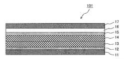
도 1은 유기 발광 소자의 구조를 나타내는 모식 단면도이다.
도 2는 공간 전하 제한 전류에 의한 전류 밀도 분포와 오믹 전류에 의한 전류 밀도 분포를 대비하여 나타내는 모식도이다.
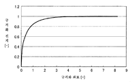
도 3은 En과 xn의 관계를 나타내는 그래프이다.
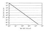
도 4는 특성 길이 D와 정공 밀도의 관계를 나타내는 그래프이다.
도 5a는 정공 수송층에서의 전류 밀도와 전압의 관계를 나타내는 그래프이다.
도 5b는 정공 밀도 n0과 전압의 관계를 나타내는 그래프이다.
도 6a는 이온 개시제의 혼합 비율을 파라미터로 한 경우의 정공 수송층에 인가한 전압과 전류 밀도의 관계를 나타내는 그래프이다.
도 6b는 도 6a의 전류 밀도의 전압에 관한 미분값을 산출한 결과를 나타내는 그래프이다.
도 7은 홀 온리 소자 및 임피던스 측정계를 나타내는 모식 구성도이다.
도 8은 유기 발광 소자 및 임피던스 측정계를 나타내는 모식 구성도이다.1 is a schematic sectional view showing a structure of an organic light emitting device.
2 is a schematic diagram showing a comparison of a current density distribution due to a space charge limiting current and a current density distribution due to an ohmic current.
3 is a graph showing the relationship between E n and x n .
4 is a graph showing the relationship between the characteristic length D and the hole density.
5A is a graph showing the relationship between the current density and the voltage in the hole transporting layer.
5B is a graph showing the relationship between the hole density n 0 and the voltage.
6A is a graph showing the relationship between the voltage and the current density applied to the hole transport layer when the mixing ratio of the ionic initiator is used as a parameter.
FIG. 6B is a graph showing a result of calculating a differential value with respect to the voltage of the current density in FIG. 6A. FIG.
7 is a schematic diagram showing a hole-only element and an impedance meter.
8 is a schematic diagram showing an organic light emitting element and an impedance measuring system.
본 발명은, 이온 개시제를 혼합한 경화 수지를 사용하여, 정공 수송층을 오믹 전도성으로 한 유기 발광 소자에 관한 것이다.The present invention relates to an organic light emitting device in which a hole transporting layer is made to be ohmic conductive by using a curing resin mixed with an ionic initiator.
이하, 본 발명의 실시 형태에 대하여 설명한다.Hereinafter, an embodiment of the present invention will be described.
<이온 개시제를 함유하는 경화 수지를 정공 수송층으로서 사용한 유기 발광 소자>≪ Organic light emitting element using a curable resin containing an ionic initiator as a hole transporting layer >
본 명세서에 있어서, 「경화성 중합체」는, 기판에 도포한 후에, 열 또는 광과 같은 경화 처리에 의해, 가교기가 측쇄에 결합한 고분자의 가교 반응을 개시시켜, 고분자간 및/또는 고분자내 가교를 형성시킴으로써, 경화한 수지(이하 「경화 수지」라고도 기재함)를 의미한다. 이하의 실시예에서는, 고분자를 가교기로 가교한 경화성 중합체를 예로 들어 설명하지만, 저분자 유기물을 가교기로 가교한 구성이어도 된다.In the present specification, the term " curable polymer " refers to a polymer which, after being applied to a substrate, initiates a crosslinking reaction of a polymer bound to the side chain by a curing treatment such as heat or light to form a crosslinking between the polymers and / (Hereinafter also referred to as " cured resin "). In the following examples, the curable polymer obtained by crosslinking the polymer with a cross-linking agent is described as an example, but the low molecular organic material may be cross-linked with a cross-linking agent.
유기 발광 소자의 제작에 있어서, 하지(下地)의 유기층 위에 다음 유기층을 습식 프로세스에 의해 적층하면, 하지의 유기층이 용해되어 버린다. 이에 대하여, 경화성 중합체를 습식 프로세스로 도포한 후, 열 혹은 광경화 처리에 의해 경화시킨 층은, 다음 층을 습식 프로세스로 도포해도 용해되지 않고 남는다.In the production of the organic light emitting device, when the following organic layer is laminated on the underlying organic layer by a wet process, the underlying organic layer is dissolved. On the contrary, a layer obtained by applying a curable polymer by a wet process and then curing by heat or photo-curing treatment remains unmelted even if the next layer is applied by a wet process.
또한, 양이온 중합성의 이온 중합 개시제는 플러스로 하전된 양이온 분자와 마이너스로 하전된 반대 음이온 분자의 조합으로 이루어진다(이하, 이들의 이온 중, 경화 후에 경화 수지 내에 잔존하는 이온을 포함하여, 「이온 중합 개시제」라고 칭함). 양이온 분자는 경화 처리에 의해 활성화되어, 가교기의 가교 반응을 촉진하는 화합물이다. 음이온 분자는 양이온 분자의 플러스 전하를 중성으로 유지하기 위해 첨가하는 것이며, 마이너스로 하전된 상태가 안정된 분자이다.The cationic polymerizable ionic polymerization initiator is composed of a combination of a positively charged cationic molecule and a negatively charged counter anion molecule (hereinafter referred to as " ionic polymerization ") including ions remaining in the cured resin after curing, Initiator "). The cation molecule is a compound which is activated by a curing treatment to promote the crosslinking reaction of the crosslinking group. The anion molecule is added to keep the positive charge of the cation molecule neutral, and the negatively charged state is a stable molecule.
본 발명의 경화성 중합체의 고분자 조성물의 주쇄에 포함되는 전하 수송성 혹은 발광성 단량체는, 유기 소자의 제조, 예를 들어 유기 발광 소자의 정공 수송층, 발광층, 전자 수송층을 형성하는 수지를 제조하기 위해 사용되는 공지의 단량체이면 된다. 상기 단량체로서는, 한정하는 것은 아니지만, 예를 들어 아릴아민, 스틸벤, 히드라존, 카르바졸, 아닐린, 옥사졸, 옥사디아졸, 벤조옥사졸, 벤조옥사디아졸, 벤조퀴논, 퀴놀린, 이소퀴놀린, 퀴녹살린, 티오펜, 벤조티오펜, 티아디아졸, 벤조디아졸, 벤조티아디아졸, 트리아졸, 페릴렌, 퀴나크리돈, 피라졸린, 안트라센, 루브렌, 쿠마린, 나프탈렌, 벤젠, 비페닐, 터페닐, 안트라센, 테트라센, 플루오렌, 페난트렌, 피렌, 크리센, 피리딘, 피라진, 아크리딘, 페난트롤린, 푸란 및 피롤, 그리고 이들의 유도체를 골격으로서 갖는 화합물을 들 수 있다.The charge-transporting or luminescent monomer contained in the main chain of the polymer composition of the curable polymer of the present invention can be used in the production of organic devices, for example, a known technique used for producing a resin for forming a hole transport layer, Lt; / RTI > Examples of the monomer include, but are not limited to, arylamine, stilbene, hydrazone, carbazole, aniline, oxazole, oxadiazole, benzoxazole, benzoxadiazole, benzoquinone, quinoline, isoquinoline, Benzene, biphenyl, benzothiazole, benzothiazole, thiazole, perylene, quinacridone, pyrazoline, anthracene, rubrene, coumarin, naphthalene, benzene, There can be mentioned compounds having a skeleton such as terphenyl, anthracene, tetracene, fluorene, phenanthrene, pyrene, chrysene, pyridine, pyrazine, acridine, phenanthroline, furan and pyrrole and derivatives thereof.
바람직하게는, 직쇄상 및 분지상 공액 단량체는 하기 구조식 (1) 내지 (3)으로 표시되는 골격을 갖는 화합물에서 선택된다.Preferably, the linear and branched conjugated monomers are selected from compounds having a skeleton represented by the following structural formulas (1) to (3).


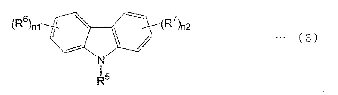
이들의 구조식에서, R1 내지 R7은 서로 독립적으로 수소, 할로겐, 시아노기, 니트로기, 탄소수 1 내지 22의 직쇄상, 분지상 또는 환상의 알킬기, 탄소수 2 내지 22의 직쇄상, 분지상 또는 환상의 알케닐기, 탄소수 2 내지 22의 직쇄상, 분지상 또는 환상의 알키닐기, 탄소수 6 내지 21의 아릴기, 탄소수 12 내지 20의 헤테로아릴기, 탄소수 7 내지 21의 아르알킬기 및 탄소수 13 내지 20의 헤테로아릴알킬기로 이루어지는 군에서 선택되는 것이 바람직하고, 수소, 할로겐, 시아노기, 니트로기, 탄소수 1 내지 22의 직쇄상, 분지상 또는 환상의 알킬기, 탄소수 6 내지 21의 아릴기, 탄소수 12 내지 20의 헤테로아릴기 및 탄소수 7 내지 21의 아르알킬기로 이루어지는 군에서 선택되는 것이 보다 바람직하고, 수소, 할로겐, 탄소수 1 내지 10의 직쇄상, 분지상 또는 환상의 알킬기 및 탄소수 6 내지 10의 아릴기로 이루어지는 군에서 선택되는 것이 더욱 바람직하고, 수소, 브롬, 메틸기, 에틸기, 프로필기, 부틸기, 펜틸기, 헥실기, 헵틸기, 옥틸기, 노닐기, 데실기 및 페닐기로 이루어지는 군에서 선택되는 것이 특히 바람직하다.In these structural formulas, R 1 to R 7 independently represent hydrogen, a halogen, a cyano group, a nitro group, a linear, branched or cyclic alkyl group having 1 to 22 carbon atoms, a linear, branched or cyclic alkyl group having 2 to 22 carbon atoms Branched or cyclic alkynyl group having 2 to 22 carbon atoms, an aryl group having 6 to 21 carbon atoms, a heteroaryl group having 12 to 20 carbon atoms, an aralkyl group having 7 to 21 carbon atoms, and a heteroaryl group having 13 to 20 carbon atoms A halogen atom, a cyano group, a nitro group, a linear, branched or cyclic alkyl group having 1 to 22 carbon atoms, an aryl group having 6 to 21 carbon atoms, a heteroaryl group having a carbon number of 12 to 22, More preferably an alkyl group having 7 to 21 carbon atoms, and more preferably a group selected from the group consisting of hydrogen, halogen, a straight, branched or cyclic alkyl group having 1 to 10 carbon atoms And an aryl group having 6 to 10 carbon atoms, and more preferably a group selected from the group consisting of hydrogen, bromine, methyl, ethyl, propyl, butyl, pentyl, hexyl, heptyl, octyl, And a phenyl group is particularly preferable.
상기한 관능기는 비치환 또는 1 혹은 복수의 할로겐으로 치환되어 있는 것이 바람직하고, 비치환인 것이 보다 바람직하다.The above functional groups are preferably unsubstituted or substituted with one or more halogens, and more preferably unsubstituted.
m1 및 m2는 서로 독립적으로 0 내지 5의 정수인 것이 바람직하고, 0 또는 1인 것이 보다 바람직하다.m1 and m2 are preferably independently an integer of 0 to 5, more preferably 0 or 1.
n1 및 n2는 서로 독립적으로 0 내지 4의 정수인 것이 바람직하고, 0 또는 1인 것이 보다 바람직하다.n1 and n2 are each independently preferably an integer of 0 to 4, more preferably 0 or 1.
본 명세서에 있어서, 「아르알킬기」는 알킬기의 수소 원자의 1개가 아릴기로 치환된 관능기를 의미한다. 적합한 아르알킬기는, 한정하는 것은 아니지만, 예를 들어 벤질기, 1-페네틸기, 2-페네틸기 등을 들 수 있다.In the present specification, the term "aralkyl group" means a functional group in which one of the hydrogen atoms of the alkyl group is substituted with an aryl group. Suitable aralkyl groups include, but are not limited to, benzyl, 1-phenethyl, 2-phenethyl and the like.
본 명세서에 있어서, 「아릴알케닐기」는, 알케닐기의 수소 원자의 1개가 상기 아릴기로 치환된 기를 의미한다. 적합한 아릴알케닐기는, 한정하는 것은 아니지만, 예를 들어 스티릴기 등을 들 수 있다.In the present specification, the "arylalkenyl group" means a group in which one of the hydrogen atoms of the alkenyl group is substituted with the above aryl group. Suitable arylalkenyl groups include, but are not limited to, styryl groups and the like.
본 명세서에 있어서, 「헤테로아릴기」는 아릴기의 1개 이상의 탄소 원자가 각각 독립적으로 질소 원자(N), 황 원자(S) 및 산소 원자(O)에서 선택되는 복소 원자로 치환된 기를 의미한다. 예를 들어, 「탄소수 12 내지 20의 헤테로아릴기」 및 「(환의) 원수 12 내지 20의 헤테로아릴기」는 적어도 12개 또한 많아도 20개의 탄소 원자를 포함하는 방향족기의 1개 이상의 탄소 원자가 각각 독립적으로 상기한 복소 원자로 치환된 기를 의미한다.In the present specification, the "heteroaryl group" means a group in which at least one carbon atom of the aryl group is independently substituted with a heteroatom selected from a nitrogen atom (N), a sulfur atom (S) and an oxygen atom (O). For example, a "heteroaryl group having 12 to 20 carbon atoms" and a "heteroaryl group having 12 to 20 carbon atoms (ring)" means that at least one carbon atom of an aromatic group containing at least 12 and at most 20 carbon atoms Quot; means a group independently substituted by the above-mentioned hetero atom.
이 경우에 있어서, N 또는 S에 의한 치환은 각각 N-옥시드 또는 S의 옥시드 혹은 디옥시드에 의한 치환을 포함한다. 적합한 헤테로아릴기는, 한정하는 것은 아니지만, 예를 들어 푸라닐기, 티에닐기, 피롤릴기, 이미다졸릴기, 피라졸릴기, 트리아졸릴기, 테트라졸릴기, 티아졸릴기, 옥사졸릴기, 이소옥사졸릴기, 옥사디아졸릴기, 티아디아졸릴기, 이소티아졸릴기, 피리딜기, 피리다지닐기, 피라지닐기, 피리미디닐기, 퀴놀리닐기, 이소퀴놀리닐기 및 인돌릴기 등을 들 수 있다.In this case, substitution by N or S includes substitution by an oxide or a dioxide of N-oxide or S, respectively. Suitable heteroaryl groups include, but are not limited to, furanyl, thienyl, pyrrolyl, imidazolyl, pyrazolyl, triazolyl, tetrazolyl, thiazolyl, oxazolyl, isoxazolyl A thiadiazolyl group, an isothiazolyl group, a pyridyl group, a pyridazinyl group, a pyrazinyl group, a pyrimidinyl group, a quinolinyl group, an isoquinolinyl group and an indolyl group.
본 명세서에 있어서, 「헤테로아릴알킬기」는 알킬의 수소 원자의 1개가 상기 헤테로아릴기로 치환된 기를 의미한다.In the present specification, the "heteroarylalkyl group" means a group in which one of the hydrogen atoms of the alkyl is substituted with the above-mentioned heteroaryl group.
본 명세서에 있어서, 「할로겐」은 불소, 염소, 브롬 또는 요오드를 의미한다.In the present specification, "halogen" means fluorine, chlorine, bromine or iodine.
특히 바람직하게는, 전하 수송성 혹은 발광성 단량체는, 트리페닐아민, N-(4-부틸페닐)-N',N"-디페닐아민, 9,9-디옥틸-9H-플루오렌, N-페닐-9H-카르바졸, N,N'-디페닐-N,N'-비스(3-메틸페닐)-[1,1'-비페닐]-4,4'-디아민 및 N,N'-비스(3-메틸페닐)-N,N'-비스(2-나프틸)-[1,1'-비페닐]-4,4'-디아민, 그리고 이들의 유도체를 골격으로서 갖는 화합물에서 선택된다.Particularly preferably, the charge transporting or luminescent monomer is at least one member selected from the group consisting of triphenylamine, N- (4-butylphenyl) -N ', N' '- diphenylamine, 9,9- -9H-carbazole, N, N'-diphenyl-N, N'-bis (3-methylphenyl) - [1,1'-biphenyl] -4,4'- diamine and N, 3-methylphenyl) -N, N'-bis (2-naphthyl) - [1,1'-biphenyl] -4,4'-diamine, and derivatives thereof as a skeleton.
정공 수송층으로서, 상기한 골격을 갖는 전하 수송성 혹은 발광성 단량체의 주쇄를 포함하는 고분자 조성물을 사용함으로써, 발광층 재료의 이온화 에너지에 따라, 정공 수송층의 이온화 에너지를 적정값으로 조정할 수 있다. 통상은, 양극의 일함수와 발광층의 이온화 에너지 사이의 값, 혹은 발광층의 이온화 에너지보다도 큰 값이 적합하다.The ionization energy of the hole transporting layer can be adjusted to an appropriate value according to the ionization energy of the light emitting layer material by using the polymer composition containing the main chain of the charge transporting or luminescent monomer having the above skeleton as the hole transporting layer. Usually, a value between the work function of the anode and the ionization energy of the light emitting layer or a value larger than the ionization energy of the light emitting layer is suitable.
본 발명의 유기 발광 소자는, 양극과 발광층 사이에 정공 수송층을, 발광층과 음극 사이에 전자 수송층을, 각각, 적어도 1층을 포함한다. 발광층으로부터의 전자의 통과를 방지하기 위해, 전자 블로킹층을 형성해도 되지만, 본 명세서에서는, 전자 블로킹층 등, 양극과 발광층 사이에 형성된 층을 「정공 수송층」이라고 칭하는 것으로 한다. 마찬가지로, 전자 수송층은 정공 블로킹층도 포함하는 것으로 한다.The organic light emitting device of the present invention includes at least one layer each of a hole transporting layer between the anode and the light emitting layer and an electron transporting layer between the light emitting layer and the cathode. In order to prevent the passage of electrons from the light emitting layer, an electron blocking layer may be formed. In this specification, a layer formed between the anode and the light emitting layer, such as an electron blocking layer, is referred to as a " hole transporting layer ". Similarly, the electron transport layer also includes a hole blocking layer.
또한, 상기한 경화 처리는 가교 중합체와 이온 중합 개시제를 혼합한 혼합물에 대하여 실시한다. 본 발명에 있어서, 이온 중합 개시제의 정공 수송층의 경화 수지에, 정공 캐리어를 화학 도핑한다. 또한, 이온 중합 개시제는 상기한 경화 처리에 의해 활성화되어, 가교기의 가교 반응을 촉진하는 기능을 갖는다.The curing treatment is carried out on a mixture of a cross-linked polymer and an ionic polymerization initiator. In the present invention, the hole carrier is chemically doped in the cured resin of the hole transporting layer of the ion polymerization initiator. The ionic polymerization initiator is activated by the above-mentioned curing treatment and has a function of accelerating the crosslinking reaction of the crosslinking group.
본 발명의 경화성 중합체의 경화 처리에 적용되는 가교 개시제로서는, 예를 들어 요오도늄염, 술포늄염 및 페로센 유도체를 들 수 있다. 상기한 가교 개시제는 반응성이 높은 점에서 바람직하다.Examples of the crosslinking initiator used in the curing treatment of the curable polymer of the present invention include iodonium salts, sulfonium salts and ferrocene derivatives. The above-mentioned crosslinking initiator is preferable in view of high reactivity.
특히 바람직하게는, 이온 중합 개시제는 하기 구조식 (4) 내지 (6)으로 표시되는 화합물에서 선택된다.Particularly preferably, the ionic polymerization initiator is selected from the compounds represented by the following structural formulas (4) to (6).


이들의 구조식에서, X-는, Sb6 -, (C6F5)4B-, CF3SO3 -, PF6 -, BF4 -, C4F9SO3 - 또는 CH3C6H4SO3 -이고, R11 내지 R15는 서로 독립적으로 수소, 할로겐, 시아노기, 니트로기, 탄소수 1 내지 22의 직쇄상, 분지상 또는 환상의 알킬기, 탄소수 2 내지 22의 직쇄상, 분지상 또는 환상의 알케닐기, 탄소수 2 내지 22의 직쇄상, 분지상 또는 환상의 알키닐기, 탄소수 6 내지 21의 아릴기, 탄소수 12 내지 20의 헤테로아릴기, 탄소수 7 내지 21의 아르알킬기 및 탄소수 13 내지 20의 헤테로아릴알킬기로 이루어지는 군에서 선택되는 것이 바람직하고, 수소, 할로겐, 시아노기, 니트로기, 탄소수 1 내지 22의 직쇄상, 분지상 또는 환상의 알킬기, 탄소수 6 내지 21의 아릴기, 탄소수 12 내지 20의 헤테로아릴기 및 탄소수 7 내지 21의 아르알킬기로 이루어지는 군에서 선택되는 것이 보다 바람직하고, 수소인 것이 더욱 바람직하다.In these structural formulas, X - is, Sb 6 -, (C 6 F 5) 4 B -,
s1, s2, t1, t2 및 t3은 서로 독립적으로 0 내지 5의 정수인 것이 바람직하다.s1, s2, t1, t2 and t3 are preferably integers of 0 to 5 independently of each other.
특히 바람직하게는, 본 발명의 경화성 중합체와 상기에서 설명한 가교 개시제를 혼합한 혼합물을 가열 처리함으로써 가교기를 반응시켜, 분자간 및/또는 분자내 가교를 형성시킨다. 이 경우, 가열 처리의 온도는 100 내지 250℃의 범위인 것이 바람직하다.Particularly preferably, a crosslinking group is reacted by heat-treating a mixture of the curable polymer of the present invention and the above-described crosslinking initiator to form intermolecular and / or intramolecular crosslinking. In this case, the temperature of the heat treatment is preferably in the range of 100 to 250 ° C.
또한, 가열 처리의 시간은 10 내지 180분의 범위인 것이 바람직하다.Further, the time of the heat treatment is preferably in the range of 10 to 180 minutes.
본 발명에 있어서, 정공 수송층의 경화 수지는, 이온 중합 개시제에 의해 화학 도프된 정공 캐리어에 의해, 전도 특성을 오믹 전도성으로 한다.In the present invention, the cured resin of the hole transporting layer is made of a hole carrier chemically doped with an ionic polymerization initiator to make the conduction characteristic ohmic.
도 2는 공간 전하 제한 전류에 의한 전류 밀도 분포와 오믹 전류에 의한 전류 밀도 분포의 비교를 나타내는 개략도이다.2 is a schematic diagram showing a comparison of a current density distribution due to a space charge limiting current and a current density distribution due to an ohmic current.
본 도면에서는, 유기 발광 소자의 단면을 모식적으로 도시하여, 정공 캐리어(27) 및 전자 캐리어(28)의 미시적인 분포를 표현하고 있다.In this figure, a cross section of the organic light emitting element is schematically shown, and microscopic distribution of the
공간 전하 제한 전류를 상정한 경우, 유기 발광 소자는 유리 기판(21), 양극(22), 정공 수송층(23a)(공간 전하 제한 전도성의 경화 수지), 정공 수송층(23b)(공간 전하 제한 전도성의 경화 수지), 발광층(24), 전자 수송층(25) 및 음극(26)을 이 순서로 적층한 구조를 갖는다. 전압 인가 없음의 상태에서는, 정공 수송층(23a) 및 정공 수송층(23b)에 정공 캐리어(27)가 치우침 없이 분포되어 있다. 한편, 전압 인가를 한 상태에서는, 음극(26)에 전자 캐리어(28)가 발생하여, 정공 수송층(23b)을 향해 이동한다. 이때, 정공 캐리어(27)는 균일하지 않게 되고, 그 밀도가 높은 영역과 낮은 영역이 생긴다.When the space charge limitation current is assumed, the organic light emitting element is a
이에 대하여, 오믹 전류를 상정한 경우, 유기 발광 소자는 유리 기판(21), 양극(22), 정공 수송층(23c)(오믹 전도성의 경화 수지), 정공 수송층(23d)(오믹 전도성의 경화 수지), 발광층(24), 전자 수송층(25) 및 음극(26)을 이 순서로 적층한 구조를 갖는다. 전압 인가 없음의 상태에서는, 정공 캐리어(27)는 정공 수송층(23c) 및 정공 수송층(23d)에 치우침 없이, 공간 전하 제한 전류의 경우에 비해 밀하게 분포되어 있다.On the other hand, when the ohmic current is assumed, the organic light emitting element includes the
그리고, 전압 인가를 한 상태에서는, 전자 캐리어(28)는 공간 전하 제한 전류의 경우와 마찬가지이지만, 정공 캐리어(27)는 균일하게 분포된 상태를 유지하고, 전류 밀도도 균일해진다.In the state in which the voltage is applied, the
이와 같은 차이가 생기는 이유는 다음과 같다.The reason for this difference is as follows.
정공 수송층을 도포 프로세스로 형성하면, 막 두께가 불균일해지기 쉽다. 또한, 양극인 ITO가 패터닝되어 있는 경우, ITO와 유리 기판의 단차에서, 막 두께가 얇아진다.If the hole transporting layer is formed by a coating process, the film thickness tends to become uneven. Further, in the case where the anode ITO is patterned, the film thickness becomes thinner at the step between the ITO and the glass substrate.
막 두께 불균일이 존재하면, 공간 전하 제한 전류에 의한 전류 밀도는 막 두께의 3승에 반비례하기 때문에, 박막부에 전류가 집중한다. 이에 대하여, 오믹 전류에 의한 전류 밀도는 막 두께의 1승에 반비례하기 때문에, 공간 전하 제한 전류와 비교하여, 전류의 불균일성은 완화된다.If the film thickness unevenness exists, the current density due to the space charge limiting current is inversely proportional to the third power of the film thickness, so that the current is concentrated in the thin film portion. On the other hand, since the current density due to the ohmic current is inversely proportional to the first power of the film thickness, the nonuniformity of the current is relaxed as compared with the space charge limiting current.
이와 같이, 전류 밀도 분포의 불균일이 완화되면, 발광 효율이 향상된다. 또한, 박막에서의 전류 집중을 완화함으로써, 박막부에서의 열화가 억제되어, 수명이 향상된다.As described above, if the unevenness of the current density distribution is relaxed, the luminous efficiency is improved. Further, by alleviating the current concentration in the thin film, deterioration in the thin film portion is suppressed, and the lifetime is improved.
<도포액의 조정><Adjustment of Coating Solution>
본 발명의 유기 발광 소자의 정공 수송층으로서 사용되는 경화 수지에 포함되는 이온 중합 개시제는, 가교 반응을 진행시킬 뿐만 아니라, 정공 캐리어를 화학 도핑함으로써 오믹 전도성을 실현한다. 통상보다도 첨가량이 많은 이온 중합 개시제를 도포액에 용해시킬 필요가 있는 경우가 있다.The ionic polymerization initiator contained in the cured resin used as the hole transport layer of the organic light emitting device of the present invention not only promotes the crosslinking reaction but also realizes ohmic conductivity by chemically doping the hole carriers. It may be necessary to dissolve the ionic polymerization initiator having a larger amount than usual in the coating liquid.
용해 방법으로서는, 경화성 중합체와 이온 중합 개시제를 상이한 용매에 용해하여, 혼합하는 방법이 있다. 혼합 전의 각 용매 중의 경화 중합체와 이온 개시제의 농도는, 혼합 후의 경화 중합체와 이온 중합 개시제의 비율이 소정의 값이 되도록 조정한다. 혹은, 이온 중합 개시제로서, 용매와의 친화성이 높은 분자 구조를 갖는 개시제를 선택하는 방법이 있다.As a dissolving method, there is a method of dissolving the curable polymer and the ionic polymerization initiator in different solvents and mixing them. The concentration of the curing polymer and the ionic initiator in each solvent before mixing is adjusted so that the ratio of the cured polymer after mixing to the ionic polymerization initiator becomes a predetermined value. Alternatively, as an ionic polymerization initiator, there is a method of selecting an initiator having a molecular structure having a high affinity with a solvent.
<공간 전하 제한 전류><Space Charge Limiting Current>
이하에 나타내는 수식 모델에서의 단위계는 SI 단위이고, 전류 밀도의 단위로서 [A/㎡], 이동도의 단위로서 [㎡/V/sec], 밀도의 단위로서 [개/㎥], 막 두께의 단위로서 [m]을 사용한다. 실험 조건으로서 이하에 구체적으로 나타내는 수치는, 관례에 따라, 전류 밀도의 단위로서, [㎃/㎠], 이동도의 단위로서, [㎠/V/sec], 밀도의 단위로서, [개/㎤], 막 두께의 단위로서, [㎚]의 단위를 사용하지만, 수식 모델로 평가할 때에는, SI 단위로 환산한다.The unit system in the following mathematical model is an SI unit, and is expressed by [A / m 2] as a unit of current density, [
유기 발광 소자의 정공 수송층에 사용되는 종래의 유기 고체는, 수㎛ 이상의 막 두께로 한 경우, 양호한 절연 특성을 나타낸다. 즉, 전압을 인가하고 있지 않은 상태에서는, 유기 고체 중에서 자유롭게 전도할 수 있는 정공은 존재하고 있지 않다. 100㎚ 이하의 박막으로 한 유기 고체에 전압을 인가하면, 양극으로부터 정공이 주입되어 통전된다. 주입된 정공은 유기 고체 중에서 공간 전하를 형성한다. 공간 전하는 수지의 내부에서 전계를 발생시킨다. 수지에 주입되어 공간 전하를 형성한 전자나 정공에 의한 통전 기구를 「공간 전하 제한 전류」라고 칭한다.Conventional organic solids used for the hole transport layer of the organic light emitting device exhibit good insulating properties when the film thickness is several μm or more. That is, in the state where no voltage is applied, there is no hole that can freely conduct in the organic solid. When a voltage is applied to an organic solid formed into a thin film of 100 nm or less, holes are injected from the anode to be energized. The injected holes form a space charge in the organic solid. The space charge generates an electric field inside the resin. Quot; space charge limiting current " is referred to as an " space charge limiting current ".
이하, 공간 전하 제한 전류에 기초하는, 전류와 전압의 관계에 대하여 설명한다.Hereinafter, the relationship between the current and the voltage based on the space charge limiting current will be described.
전류의 통전 방향을 x축으로 하고, x=0을 양극과 정공 수송층의 계면, x=d를 정공 수송층의 막 두께하고, 막 두께는 균일한 것으로 한다. 양극으로부터 주입되어 공간 전하를 형성하는 정공 밀도를 ninj(x)로 하면, 정공 수송층에 통전하는 정상 전류를 j는 하기 식 (1)로 부여된다.X = 0 is the interface between the anode and the hole transporting layer, x = d is the film thickness of the hole transporting layer, and the film thickness is uniform. Assuming that the hole density injected from the anode to form a space charge is n inj (x), the steady current j flowing through the hole transport layer is given by the following equation (1).

여기서, e는 전기소량(=1.6×10⁻¹⁹[C])이고, μ은 정공의 이동도이고, E(x)는 전계이다.Here, e is a small electric quantity (= 1.6 × 10 -19 [C]), μ is the mobility of holes, and E (x) is an electric field.
공간 전하 ninj와 수지 내에서 전계 E와의 관계는, 하기 식 (2)로 표시되는 푸아송 방정식으로 부여된다.The relationship between the space charge n inj and the electric field E in the resin is given by the Poisson equation expressed by the following equation (2).

여기서, ε은 비유전율이고, ε0은 진공의 유전율(=8.85×10⁻¹²[F/m])이다.Here,? Is a relative dielectric constant, and? 0 is a dielectric constant of vacuum (= 8.85 × 10 -12 [F / m]).
상기 식 (2)를 상기 식 (1)에 대입하면, 하기 식 (3)으로 표시되는 공간 전하 제한 전류식이 얻어진다.Substituting the above equation (2) into the above equation (1), the space charge limiting current equation expressed by the following equation (3) is obtained.

정상 상태에서는, j는 좌표에 따르지 않고 일정하다. 전계 E를 x=0에서부터 막 두께 d의 범위에서 적분함으로써, 하기 식 (4)가 얻어진다.In steady state, j is constant regardless of coordinates. By integrating the electric field E in the range of the film thickness d from x = 0, the following equation (4) is obtained.

경계 조건으로서, x=0에서, E=0으로 한다. 전류는 정공 수송층에 인가된 전압의 2승에 비례하고, 막 두께 d의 3승에 반비례한다. 따라서, 막 두께가 불균일한 경우에는, 전류 밀도의 불균일성은 커진다. 특히, 박막 부위에서의 전류가 커진다.As a boundary condition, let E = 0 at x = 0. The current is proportional to the square of the voltage applied to the hole transporting layer, and inversely proportional to the third power of the film thickness d. Therefore, when the film thickness is nonuniform, the non-uniformity of the current density becomes large. In particular, the current at the thin film portion becomes large.
<오믹 전류><Ohmic Current>
도 2의 우측 상란에 나타낸 바와 같이, 본 발명의 경화 수지를 정공 수송층으로 한 유기 발광 소자의 경우, 경화 수지는 이온 중합 개시제를 포함하고, 또한 전압을 인가하고 있지 않은 상태에서도, 정공 캐리어가 경화 수지 중에 미리 도프되어 있다.2, in the case of an organic light emitting device in which the curable resin of the present invention is used as a hole transport layer, the cured resin contains an ionic polymerization initiator, and even when no voltage is applied, Are pre-doped in the resin.
미리 도프된 정공 밀도를 n0으로 하면, 전류 밀도는 하기 식 (5)로 부여된다.When the pre-doped hole density is n 0 , the current density is given by the following equation (5).

전류는, 정공 수송층에 인가된 전압에 비례하고, 막 두께 d의 1승에 반비례한다. 따라서, 공간 전하 제한 전류 기구에 기초하는 통전과 비교하여, 막 두께의 불균일에 대한 전류 밀도의 불균일성은 완화된다.The current is in proportion to the voltage applied to the hole transporting layer and inversely proportional to the first power of the film thickness d. Therefore, the non-uniformity of the current density with respect to the unevenness of the film thickness is alleviated as compared with the energization based on the space charge limiting current mechanism.
<오믹 전류 조건> <Ohmic current condition>
본 발명자는, 이온 개시제를 첨가하여, 미리 정공을 도프한 경화 수지여도, 통전 기구가 오믹 전류로는 되지 않는 것을 발견했다. 또한, 정공 수송층에서의 통전 기구가, 공간 전하 제한 전류인지, 오믹 전류가 되는지를 결정하는 평가 모델을 고안했다.The inventor of the present invention has found that even when a cured resin doped with holes is added in advance by adding an ionic initiator, the current-carrying mechanism does not become an ohmic current. Further, an evaluation model for de- termining whether the energizing mechanism in the hole-transporting layer is a space charge limiting current or an ohmic current is devised.
이하에, 평가 모델을 나타낸다.The evaluation model is shown below.
전류 밀도 j의 산출은 공간 전하 제한 전류식 (3) 및 오믹 전류식 (5)의 항을 결합한 것을 사용한다. 이에 의해, 양쪽의 현상이 반영된 형식이 된다.The current density j is calculated by combining the space charge limiting current equation (3) and the term of the ohmic current equation (5). Thereby, the form in which both phenomena are reflected is obtained.

상기 식 (5)에서는, 전계 E는 좌표를 따르지 않았다. 이에 대하여, 상기 식 (6)의 우변 제2항의 오믹 전류 유래의 식에는 공간 전하의 존재에 의한 좌표 의존성을 고려하고 있다. 양변을 x로 적분하면, 하기 식 (7)이 부여된다.In the above equation (5), the electric field E does not follow the coordinates. On the other hand, the coordinate dependence due to the presence of space charge is taken into account in the formula derived from the Ohmic current of the second term on the right side of the above-mentioned formula (6). If both sides are integrated with x, the following equation (7) is given.

여기서, En은 전계 E에 비례하는 규격화된 무차원의 전계이고, xn은 규격화된 무차원의 좌표이다. 이들은 하기 식 (8) 및 (9)로 표시된다.Where E n is a normalized dimensionless electric field proportional to the electric field E, and x n is a normalized non-dimensional coordinate. These are expressed by the following equations (8) and (9).


도 3은 En과 xn의 관계를 플롯한 것이다. 횡축에 규격화 좌표 xn을 취하고, 종축에 규격화 전계 En을 취하고 있다.Fig. 3 is a plot of the relationship between E n and x n . The normalized coordinate x n is taken on the abscissa, and the normalized electric field E n is taken on the ordinate.
본 도면에 나타낸 바와 같이, xn이 1보다도 충분히 크면, En은 1이 된다. En=1에 가까운 영역에서는, 오믹 전류가 주성분이 된다. 한편, xn이 1보다도 충분히 작으면, 전류는 공간 전하 제한 전류가 된다. 따라서, xn의 분모로 부여되는 특성 길이 D와 막 두께의 관계에 의해, 공간 전하 제한 전류인지 오믹 전류인지가 결정된다. 특성 길이 D는 하기 식 (10)으로 정의한다.As shown in the figure, if x n is sufficiently larger than 1, E n becomes 1. In the region close to E n = 1, the ohmic current becomes the main component. On the other hand, if x n is sufficiently smaller than 1, the current becomes a space charge limiting current. Therefore, the relationship between the characteristic length D given by the denominator of x n and the film thickness determines whether the space charge limiting current or the ohmic current is present. The characteristic length D is defined by the following equation (10).
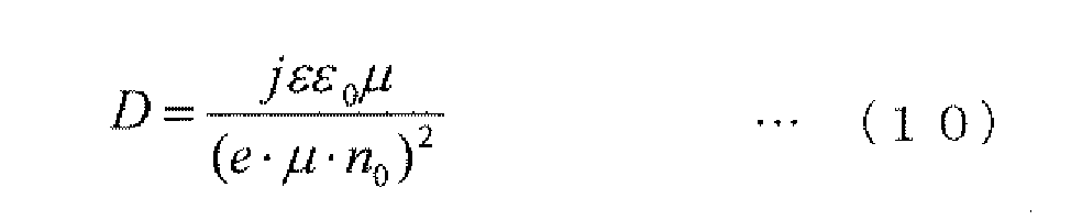
정공 수송층의 특성으로서 전형적인 값으로서, 정공 이동도=10-5[㎠ /V/sec], 비유전율=3.2의 경우를 예로 들어, 특성 길이 D와 정공 밀도의 관계를 설명한다.The relationship between the characteristic length D and the hole density will be described as an example of a typical value of the hole transporting layer as a hole mobility = 10 -5 [
도 4는, 유기 발광 소자의 동작 전류 밀도를 j=100㎃/㎠에서의로 한 경우의 D와 정공 밀도 n0의 관계를 나타낸 것이다. 여기서, 유기 발광 소자는 양극, 정공 수송층, 발광층 및 음극이 직렬로 접속된 구성을 갖기 때문에, 유기 발광 소자의 동작 전류 밀도는, 정상 상태에서는, 정공 수송층의 전류 밀도와 동등해진다.4 shows the relationship between D and the hole density n 0 when the operating current density of the organic light emitting element is set to j = 100 mA /
정공 밀도 n0<1018[개/㎤]에서는, D>20㎚이고, 통상의 유기 발광 소자에서 사용되는 각 유기층의 막 두께와 동일 정도이다. 따라서, 오믹 전류로는 되지 않는다.D> 20 nm at a hole density n 0 <10 18 [number / cm 3], and is about the same as the film thickness of each organic layer used in an ordinary organic light emitting device. Therefore, it is not an ohmic current.
한편, n0>1019[개/㎤] 이상에서는, D<1Å이다. 1Å은, 공간 제한 전류 제한에서 유래하는 전류는 원자 1층분뿐이고, 막 전체가 오믹 영역이 되어, 오믹 전류이다.On the other hand, when n 0 > 10 19 [number / cm 3] or more, D <1 Å. 1 A, the current resulting from the space limit current limitation is only one atomic layer, and the whole film becomes an ohmic region, which is an ohmic current.
상기 식 (7)에 관하여, 전계 E를 x=0에서부터 막 두께 d까지 적분함으로써, 전류 밀도 j와 정공 수송층에 인가되는 전압을 계산했다. j는 0 내지 1000㎃/㎠의 범위로 하고, 이동도 및 비유전율은 도 4의 조건과 동일하게 하고, 막 두께는 40㎚로 했다.With respect to the formula (7), the electric field E was integrated from x = 0 to the film thickness d to calculate the current density j and the voltage applied to the hole transport layer. j was in the range of 0 to 1000 mA /
도 5a에 결과를 나타낸다. 상기 식(4)에 기초하여, 공간 전하 제한 전류 밀도도 플롯했다.The results are shown in Fig. 5A. Based on the above equation (4), the space charge limiting current density was also plotted.
본 도면에 나타낸 바와 같이, 정공 밀도 n0<1018[개/㎤]의 범위에서는, 전류는 전압의 2승에 비례하고, 공간 전하 제한 전류가 된다. 이에 대하여, 정공 밀도 n0>1018[개/㎤]에서는, 전류는 전압의 1승에 비례하고, 직선이 된다. 즉, 소위 오믹 전류가 된다.As shown in the figure, in the range of the hole density n 0 <10 18 [number / cm 3], the current becomes proportional to the square of the voltage and becomes the space charge limiting current. On the other hand, at a hole density n 0 > 10 18 [number / cm 3], the current is proportional to the first power of the voltage and becomes a straight line. That is, a so-called ohmic current flows.
도 5b에, 횡축을 정공 밀도 n0, 종축에 전류 밀도 500㎃/㎠에서의 전압을 플롯한다. 계산 조건은 도 5a와 동일하고, 상기 식 (7)에 관하여, 전계 E를 x=0에서부터 막 두께 d까지 적분함으로써, 전류 밀도 j와 정공 수송층에 인가되는 전압을 계산했다.5B, the horizontal axis represents the hole density n 0 , and the vertical axis represents the voltage at a current density of 500 mA /
또한, 오믹 전도인 경우에는, 상기 식 (5)에서, 전계 E는 좌표 x에 의존하지 않고, E=V/d(V는 인가 전압, d는 막 두께)로 부여된다. 따라서, 오믹 전류의 경우의 전압 V와 정공 밀도 n0의 관계는 하기 식 (11)로 부여된다.In the case of the ohmic conduction, in the above equation (5), the electric field E is given by E = V / d (V is the applied voltage, and d is the film thickness) without depending on the coordinate x. Therefore, the relationship between the voltage V and the hole density n 0 in the case of the ohmic current is given by the following equation (11).

도 5b에는 상기 식 (11)로 부여되는 정공 밀도와 전류 밀도 500㎃/㎠에서의 전압의 관계도 플롯했다. 정공 밀도 n0>1018[개/㎤]에서는, 상기 식 (7)로부터 산출한 곡선과 상기 식 (10)으로부터 산출한 곡선이 일치한다. 한편, n0<1018[개/㎤]에서는, 일치하지 않고, 전압은 n0에 의하지 않고 일정해진다. 이것은 n0<1018[개/㎤]에서는, 전극으로부터 주입되는 정공에 의한 공간 전하 제한 전류가 되기 때문이다. 따라서, 정공 밀도 n0>1018[개/㎤]에서, 오믹 전도성을 나타내는 것을 알 수 있다.FIG. 5B also plots the relationship between the hole density given by the equation (11) and the voltage at a current density of 500 mA /
이와 같은 오믹 전류가 되는 정공 수송층은, 이온 중합 개시제와, 오믹 전도성의 경화 수지를 포함하는 것이다. 「오믹 전도성의 경화 수지」는 이온 중합 개시제에 의해 화학 도프된 정공 캐리어의 밀도가 높기 때문에, 소위 오믹 전류가 된다.Such a hole transporting layer as an ohmic current includes an ionic polymerization initiator and an ohmic conductive hardening resin. The " ohmic conductive cured resin " has a high density of hole carriers chemically doped by an ionic polymerization initiator, and thus, an ohmic current is generated.
정리하면, 유기 발광 소자에 있어서, 정공 수송층을 구성하는 경화 수지는 이온 중합 개시제에 의해 화학 도프되어 발생한 정공 캐리어를 가져, 정공 수송층은 오믹 전도성을 나타낸다.In summary, in the organic light emitting device, the cured resin constituting the hole transporting layer has a hole carrier formed by chemical doping with an ion polymerization initiator, and the hole transporting layer exhibits an ohmic conductivity.
오믹 전류를 부여하는 D의 범위로서는, 막 두께 d의 90% 이상이 오믹 전류 영역이 되어 있는 것이 바람직하다. 도 3에서, 규격화 전계가 0.9를 초과하는 규격화 좌표는 2.0이다. 규격화 좌표 2.0 이하의 영역에서는, 오믹 전도성이 없다. 전체의 막 두께가, 규격화 좌표 2.0×10=20 이상에 상당하는 막 두께(「규격화 막 두께」라고 정의함)가 되는 조건에서는, 오믹 전도성이 없는 영역이 10% 이하가 되고, 전체 막 두께의 90% 이상이 오믹 전류 영역이 된다. 따라서, 규격화 막 두께=막 두께 d/특성 길이 D>20, 즉, 특성 길이 D가 막 두께의 1/20 미만인 경우에 오믹 전류를 실현하는 것을 알 수 있다. 이 상태에서는, 하기 식 (12)가 만족된다.It is preferable that 90% or more of the film thickness d is in the ohmic current region as the range of D to which the ohmic current is applied. In Fig. 3, the standardized coordinate whose standardized electric field exceeds 0.9 is 2.0. In the region of normalized coordinates 2.0 or less, there is no ohmic conductivity. Under the condition that the film thickness as a whole becomes a film thickness equivalent to a standardized coordinate of 2.0 x 10 = 20 or more (defined as " normalized film thickness "), the region having no ohmic conductivity is 10% or less, 90% or more becomes the ohmic current region. Therefore, it can be seen that the ohmic current is realized when the normalized film thickness = the film thickness d / the characteristic length D> 20, that is, the characteristic length D is less than 1/20 of the film thickness. In this state, the following expression (12) is satisfied.

상기 식 (12)에 의하면, 막 두께 d가 얇은 경우, 오믹 전류를 실현하기 위한 부등식의 상한이 작아진다. 정공 수송층의 막 두께가 불균일한 경우에는, 정공 수송층의 막 두께의 최솟값, 즉, 정공 수송층은 양극 또는 발광층과 접하는 계면 면적의 90% 이상의 영역에서 상기 부등식 (12)를 만족시키는 것이 바람직하다.According to the expression (12), when the film thickness d is thin, the upper limit of the inequality for realizing the ohmic current becomes small. When the film thickness of the hole transporting layer is non-uniform, it is preferable that the inequality (12) is satisfied at the minimum value of the film thickness of the hole transporting layer, that is, in the region of 90% or more of the interface area of the hole transporting layer in contact with the anode or the light emitting layer.
상술한 도 4의 설명과 같이, n0>1019[개/㎤]에서는 D<1Å이고, 막 전체가 오믹 영역이 된다. 이 바람직한 상태를 일반화하면, 하기 식 (13)이 얻어진다.4, D <1 Å at n 0 > 10 19 [number / cm 3], and the entire film becomes an ohmic region. Generalizing this preferred state results in the following equation (13).

<정공 밀도의 상한값>≪ Upper limit of hole density >
유기 발광 소자에 있어서, 양극으로부터 광을 취출하는 경우에는, 정공 수송층에서, 발광층으로부터의 광을 반사하는 것은 바람직하지 않다. 일반적으로, 구리나 알루미늄 등의 금속에서는, 금속 내의 전자의 밀도 n에 따라 하기 식 (14)로 부여되는 플라스마 주파수 ωp보다도 에너지가 작은 광을 반사하여, 금속 특유의 광택을 나타낸다.In the organic light emitting device, when light is extracted from the anode, it is not preferable to reflect light from the light emitting layer in the hole transporting layer. Generally, a metal such as copper or aluminum reflects light having energy smaller than the plasma frequency? P given by the following equation (14) according to the density n of electrons in the metal, and exhibits luster unique to the metal.

여기서, ε은 재료의 비유전율, ε0은 진공의 유전율, m은 전자 혹은 정공의 유효 질량이다. 구리나 알루미늄의 전자 밀도는 1022[개/㎤] 이상이다. 정공 수송층에서의 광의 반사를 방지하기 위해서는, 정공 밀도는 1022[개/㎤] 이하인 것이 바람직하다.Where ε is the relative dielectric constant of the material, ε 0 is the dielectric constant of vacuum, and m is the effective mass of electrons or holes. The electron density of copper or aluminum is 10 22 [pieces / cm 3] or more. In order to prevent reflection of light in the hole transporting layer, it is preferable that the hole density is 10 22 [pieces / cm 3] or less.
<정공 밀도 n0의 측정 원리><Principle of measurement of hole density n 0 >
정공 수송층을 양극 ITO와 음극 Al 등의 전극으로 끼운 구조의 소자를 「홀 온리 소자」라고 칭한다. 정공 수송층의 일함수(5eV 이상)가 Al의 일함수(4.2eV)의 차이에 의해, 정공 수송층과 Al의 계면에 있어서, 정공 수송층측에서 정공 밀도가 낮은 영역(「공핍층」이라고 칭함)이 발생한다. 공핍층의 두께 d'은 하기 식 (15)로 부여된다.A device having a structure in which a hole transport layer is sandwiched by electrodes such as a cathode ITO and a cathode Al is referred to as a " hole-only element ". (Called a " depletion layer ") at the interface between the hole transporting layer and Al is formed by the difference of the work function (5 eV or more) of the hole transporting layer and the work function Occurs. The thickness d 'of the depletion layer is given by the following equation (15).

여기서, Δφ는 정공 수송층과 Al의 일함수의 차이고, V는 양극과 음극 사이에 가한 전압이다.Here, DELTA phi is a difference in work function between the hole transporting layer and Al, and V is a voltage between the anode and the cathode.
공핍층에서의 정전 용량 C'은 하기 식 (16)으로 부여된다.The capacitance C 'in the depletion layer is given by the following equation (16).
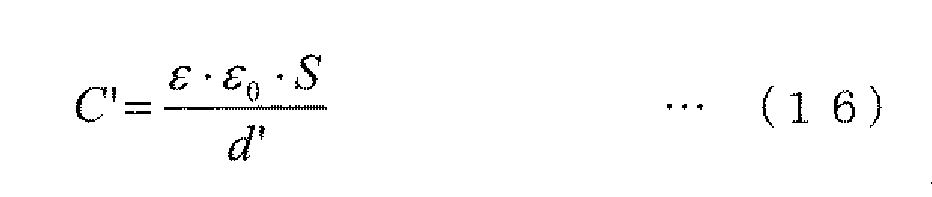
여기서, S는 소자의 면적이다. 양극과 음극 사이에 전압을 인가하고, 정전 용량을 측정함으로써, 정공 밀도 n0이 얻어진다.Where S is the area of the device. By applying a voltage between the anode and the cathode and measuring the capacitance, the hole density n 0 is obtained.
공핍층에서 유래하는 정전 용량은, LCR 미터를 사용한 홀 온리 소자의 임피던스의 주파수 의존성을 측정함으로써 분리할 수 있다.The capacitance derived from the depletion layer can be separated by measuring the frequency dependence of the impedance of the hole-only element using the LCR meter.
<유기 발광 소자>≪ Organic light emitting element &
도 1은 본 발명의 유기 발광 소자의 일 실시 형태를 나타내는 모식 단면도이다.1 is a schematic cross-sectional view showing an embodiment of an organic light-emitting device of the present invention.
본 도면에서, 유기 발광 소자(101)는, 유리 기판(11)과, 양극(12)과, 정공 수송층(13)(「정공 주입층」이라고 불리는 경우도 있음)과, 발광층(14)과, 전자 수송층(15)과, 음극(16)과, 밀봉 유리판(17)을 갖고, 이들을 이 순서로 적층한 구성을 갖는다.In this figure, the organic
양극(12)은, 예를 들어 유리 기판(11) 위에 산화인듐주석(ITO)을 패터닝함으로써 형성된다. 이하, 유리 기판(11) 위에 양극(12)으로서 ITO를 패터닝한 것을 「ITO 유리 기판」이라고 한다.The
음극(16)은, 예를 들어 ITO 유리 기판인 양극(12) 구비 유리 기판(11)에, 정공 수송층(13) 및 발광층(14)을 순차 형성한 후, 발광층(14) 위에 알루미늄(Al)을 증착함으로써 형성된다. 이어서, 음극(16) 위에 밀봉 유리판(17)을 겹치고, 유리 기판(11)과 밀봉 유리판(17)을, 예를 들어 광경화성 에폭시 수지와 같은 경화 수지를 사용하여 접합함으로써 밀봉되는 것이 바람직하다.The
본 발명의 유기 발광 소자에 있어서, 정공 수송층은 가교성 중합체에 의해 형성되는 수지를 사용하여 제조된다. 정공 수송층은 당해 기술 분야에서 관용되는 수단을 사용하여 제조할 수 있다. 예를 들어, 유리 기판 위에 패터닝된 양극 위에, 스핀 코트법, 인쇄법, 잉크젯법 등의 습식 프로세스에 의해 본 발명의 경화성 중합체를 도포한 후, 상기에서 설명한 경화 처리에 의해 수지를 형성시킴으로써 제조하면 된다.In the organic light emitting device of the present invention, the hole transporting layer is produced by using a resin formed by a crosslinkable polymer. The hole transporting layer can be produced by means known in the art. For example, when the curable polymer of the present invention is applied onto a patterned anode on a glass substrate by a wet process such as a spin coating method, a printing method, or an ink jet method, and then the resin is formed by the curing treatment described above do.
중합성 도포액에 의해 형성되는 수지는, 경화성이 높고, 유기 용매 내성이 우수하다. 이로 인해, 상기 수지를 사용하여 제조된 정공 수송층의 표면에, 예를 들어 상기한 습식 프로세스에 의해 발광층을 적층시키는 경우, 발광층의 도포 용액에 포함되는 유기 용매에 의해 정공 수송층이 용해되는 것을 억제할 수 있다. 예를 들어, 본 발명의 경화성 중합체에 의해 형성되는 수지를 사용하여 제조되는 정공 수송층은, 통상 잔막률이 60 내지 100%의 범위이고, 전형적으로는 80 내지 99%의 범위이다. 상기한 잔막률로 표시되는 유기 용매 내성을 갖는 수지는 경화성이 높다. 그러므로, 본 발명의 수지를 정공 수송층에 사용함으로써, 습식 프로세스에 의한 유기 발광 소자의 생산성을 향상시키는 것이 가능해진다.The resin formed by the polymerizable coating liquid has high curability and is excellent in organic solvent resistance. Therefore, when the light emitting layer is laminated on the surface of the hole transport layer produced using the resin, for example, by the wet process described above, dissolution of the hole transport layer by the organic solvent contained in the coating solution of the light emitting layer is suppressed . For example, the hole transporting layer produced using the resin formed by the curable polymer of the present invention usually has a residual film ratio in the range of 60 to 100%, and typically in the range of 80 to 99%. Resins having an organic solvent resistance represented by the residual film ratio have high curability. Therefore, by using the resin of the present invention for the hole transporting layer, it becomes possible to improve the productivity of the organic light emitting element by the wet process.
또한, 잔막률의 평가는, 예를 들어 이하의 수순으로 실시할 수 있다. ITO 유리 기판의 양극 위에, 본 발명의 경화성 중합체 및 이온 중합 개시제에 의해 형성되는 수지를 사용하여 정공 수송층을 제작한다. 정공 수송층이 형성된 ITO 유리 기판을, 유기 용매(예를 들어, 톨루엔)에 20 내지 250℃, 10 내지 60초간의 조건에서 침지시킨다. 그 후, ITO 유리 기판을 유기 용매 중에서 취출하고, 침지 전후의 박막의 흡광도를 측정했다. 흡광도의 비로부터 박막의 잔존율(잔막률)을 구했다. 흡광도는 막 두께에 비례하므로, 흡광도의 비(침지 있음/침지 없음)는 정공 수송층의 잔막률(침지 있음/침지 없음)에 일치한다. 잔막률이 높을수록, 유기 용매 내성이 높다고 평가된다.The residual film ratio can be evaluated, for example, by the following procedure. A hole transport layer is formed on the anode of the ITO glass substrate by using the resin formed by the curable polymer and the ion polymerization initiator of the present invention. The ITO glass substrate on which the hole transport layer is formed is immersed in an organic solvent (for example, toluene) at 20 to 250 DEG C for 10 to 60 seconds. Thereafter, the ITO glass substrate was taken out from the organic solvent, and the absorbance of the thin film before and after the immersion was measured. (Residual film ratio) of the thin film was obtained from the ratio of the absorbance. Since the absorbance is proportional to the film thickness, the ratio of absorbance (with / without immersion) corresponds to the retention rate (with / without immersion) of the hole transport layer. It is evaluated that the higher the residual film ratio, the higher the organic solvent resistance.
이하, 실시예를 사용하여 본 발명을 더욱 구체적으로 설명한다. 단, 본 발명의 기술적 범위는 이들 실시예에 한정되는 것은 아니다.Hereinafter, the present invention will be described more specifically with reference to Examples. However, the technical scope of the present invention is not limited to these embodiments.
실시예Example 1 One
오믹 전도성의 정공 수송층에 사용하는 경화 수지에 대하여 설명한다.The cured resin used for the hole transport layer of the ohmic conductivity will be described.
[가교성 중합체의 합성][Synthesis of crosslinkable polymer]
직쇄상 트리페닐아민 단량체 (1), 분지상 트리페닐아민 단량체 (2), 옥세탄 가교 단량체 (3)을, 스즈키 반응으로 중합하여, 가교성 중합체를 합성했다. 가교성의 직쇄상 트리페닐아민 단량체 (1) 및 분지 트리페닐아민 단량체 (2)는, 스즈키 반응의 반응점을, 각각, 2개 및 3개 갖고 있고, 중합에 의해 주쇄를 형성한다.A crosslinkable polymer was synthesized by polymerizing straight chain triphenylamine monomer (1), branched triphenylamine monomer (2), and oxetane crosslinking monomer (3) by Suzuki reaction. The crosslinkable straight-chain triphenylamine monomer (1) and the branched triphenylamine monomer (2) each have 2 and 3 Suzuki reaction points, and form a main chain by polymerization.
가교성의 옥세탄 가교 단량체 (3)은, 모두 스즈키 반응의 반응점을 1개 갖고 있고, 중합에 의해 측쇄를 형성한다. 가교성의 옥세탄 가교 단량체 (3)은, 페닐렌 및 옥시메틸렌의 조합을 포함하는 2가의 가교기에, 1-에틸옥세탄-1-일기가 결합한 구조를 갖는 단량체이다.The crosslinkable oxetane crosslinking monomer (3) has one reaction site of the Suzuki reaction and forms a side chain by polymerization. The crosslinkable oxetane crosslinking monomer (3) is a monomer having a structure in which a 1-ethyloxetan-1-yl group is bonded to a divalent crosslinking group containing a combination of phenylene and oxymethylene.
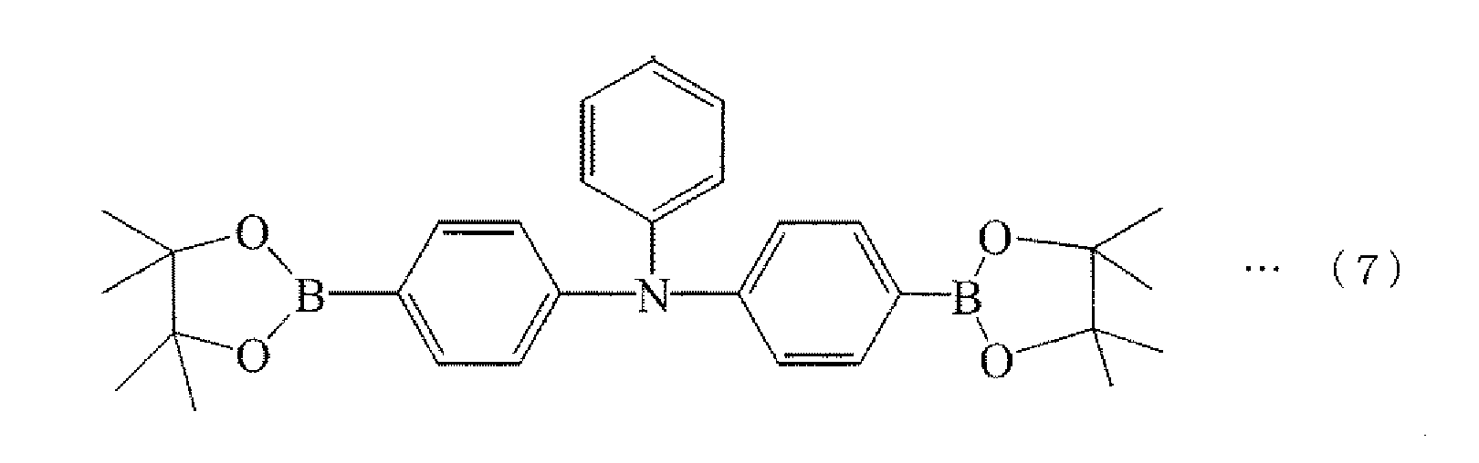


환저 플라스크에, 4,4'-비스(4,4,5,5-테트라메틸-1,3,2-디옥사보롤란-2-일)-4"-n-부틸트리페닐아민 (1)(0.4㎜ol), 4,4',4"-트리브로모트리페닐아민 (2)(1.0㎜ol), 3-(4-브로모페녹시메틸)3-에틸옥세탄 (3)(1.2㎜ol), 2-브로모-3-n-옥틸티오펜 (4)(5.3㎜ol), 테트라키스트리페닐포스핀팔라듐(0.008㎜ol), 2M 탄산칼륨 수용액(5.3㎜ol), Aliquat(등록 상표) 336(0.4㎜ol) 및 아니솔 4ml를 넣고, 질소 분위기 하, 90℃에서 2시간 교반했다.4,4'-bis (4,4,5,5-tetramethyl-1,3,2-dioxaborolan-2-yl) -4'-n-butyltriphenylamine (1) (0.4 mmol), 4,4 ', 4 "-tribromotriphenylamine (2) (1.0 mmol), 3- (4-bromophenoxymethyl) 3-n-octylthiophene (4) (5.3 mmol), tetrakistriphenylphosphine palladium (0.008 mmol), 2M potassium carbonate aqueous solution (5.3 mmol), Aliquat (Registered trademark) 336 (0.4 mmols) and 4 ml of anisole, and the mixture was stirred at 90 占 폚 for 2 hours under a nitrogen atmosphere.
상기한 방법으로, 가교성 직쇄상 트리페닐아민 단량체 (1):가교성 분지 트리페닐아민 단량체 (2):가교성 옥세탄 가교 단량체 (3)=20:50:40의 몰비로 합성한바, 분자량 40kDa의 가교기를 갖는 고분자 조성물 A를 얻었다. 분자량은, 겔 침투 크로마토그래피를 사용하여, 폴리스티렌 환산으로 측정했을 때의 수 평균으로 결정했다.In the same manner as described above, the polymer was synthesized in a molar ratio of the crosslinkable straight chain triphenylamine monomer (1): crosslinkable branched triphenylamine monomer (2): crosslinkable oxetane crosslinking monomer (3) = 20: 50: To obtain a polymer composition A having a crosslinking group of 40 kDa. The molecular weight was determined by number average as measured by polystyrene conversion using gel permeation chromatography.
[도포액의 제조][Preparation of Coating Solution]
상기 경화성 중합체(올리고머)를 (4.2㎎), 상기 구조식 (4)로 표시되는 이온 개시제(식 중, 양이온의 R11, R12는 H이고, s1, s2=1, 음이온 X=(C6F5)4B)를 0.02, 0.04, 0.42㎎(100질량부의 경화성 중합체에 대하여, 각각 z=0.5, 1.0, 10질량부에 대응함) 중 어느 것의 농도로 하여 1.2ml의 톨루엔에 용해한다.And ions of the initiator (an expression indicative of the curable polymer (oligomer) to (4.2㎎), the
이온 개시제의 농도가 0.42㎎인 경우에는, 이온 개시제가 고농도이기 때문에, 용액에 탁도가 발생했다. 경화성 중합체 4.2㎎을 0.6ml의 톨루엔에, 이온 중합 개시제 0.42㎎을 0.6ml의 톨루엔에 나누어 용해하여, 혼합한바, 탁도는 소실되었다.When the concentration of the ionic initiator was 0.42 mg, turbidity occurred in the solution because the concentration of the ionic initiator was high. 4.2 mg of the curable polymer was dissolved in 0.6 ml of toluene and 0.42 mg of the ionic polymerization initiator was dissolved in 0.6 ml of toluene, and the mixture was mixed to lose turbidity.
[가교성 중합체를 사용한 수지의 형성][Formation of Resin Using Crosslinkable Polymer]
산화인듐주석(ITO: Indium Tin Oxide)을, 1.6㎜ 폭으로 유리 기판 위에 패터닝했다. 이 ITO 유리 기판 위에, 상기한 도포액을 300회전/분의 조건에서 스핀 코트했다. 그 후, 가교성 중합체를 코트한 ITO 유리 기판을, 핫 플레이트 위에서 180℃, 7분간 가열함으로써 경화 처리하여, 경화성 중합체를 가열 중합시켜, 수지를 형성시켰다. 본 수지를, 수지 A(z)(z=0.5, 1.0, 10질량부)로 한다.Indium tin oxide (ITO) was patterned on the glass substrate with a width of 1.6 mm. The above-mentioned coating liquid was spin-coated on the ITO glass substrate at 300 rpm. Thereafter, the ITO glass substrate coated with the crosslinkable polymer was cured by heating on a hot plate at 180 캜 for 7 minutes to thermally polymerize the curable polymer to form a resin. This resin is referred to as Resin A (z) (z = 0.5, 1.0, 10 parts by mass).
[잔막률의 평가] [Evaluation of Residual Film Ratio]
수지 A(z)(z=0.5, 1.0, 10질량부)의 박막을 유리판째 톨루엔 중에서 린스하고, 린스 전후의 박막의 흡광도를 측정하여, 린스 전후의 흡광도의 비로부터 박막의 잔존율(잔막률)을 구했다. 수지 A' 및 A"의 수지는, 잔막률은 90% 이상이었다.The thin film of Resin A (z) (z = 0.5, 1.0, 10 parts by mass) was rinsed in toluene on the glass plate and the absorbance of the thin film before and after rinsing was measured. The residual ratio ). Resins A 'and A "had a residual film ratio of 90% or more.
[홀 온리 소자의 평가][Evaluation of hole-only element]
상기한 수지 A(z)(z=0.5, 1.0, 10질량부)의 시료 위에 100㎚의 막 두께의 Al 전극을 증착시켰다. 이 소자를 「홀 온리 소자」라고 칭한다. 본 실시예에서는, 상기한 [가교성 중합체를 사용한 수지의 형성]에서 설명한 방법으로 수지를 형성한 후에, 1.6㎜ 폭의 Al(막 두께 100㎚)층을 패터닝했다. ITO 패턴과 Al 패턴이 교차하는 면이 발광 소자가 되고, 소자의 면적은 1.6×1.6㎟로 부여된다.An Al electrode having a thickness of 100 nm was deposited on the sample of the resin A (z) (z = 0.5, 1.0, 10 parts by mass). This element is referred to as a " hole-only element ". In this example, a resin was formed by the method described above in "Formation of Resin Using a Crosslinkable Polymer", and then a layer of Al (
도 6a는 각 시료의 전압과 전류 밀도의 관계를 나타내는 그래프이다. 도 6b는 도 6a의 전류 밀도의 전압에 관한 미분값을 산출하여 나타낸 것이다. 어느 것의 시료에서도, 평균 막 두께는 40㎚였다. 정전 용량을 측정하여, 비유전율은 3.2가 얻어졌다.6A is a graph showing the relationship between voltage and current density of each sample. FIG. 6B is a diagram showing a calculation of the derivative value with respect to the voltage of the current density of FIG. 6A. In both samples, the average film thickness was 40 nm. The capacitance was measured, and a relative dielectric constant of 3.2 was obtained.
이들의 도면으로부터, z=0.5, 1.0질량부의 시료에서는 공간 전하 제한 전류가 되어 있다. 이에 대하여, z=10질량부의 시료에서는 오믹 전류가 되어 있는 것을 알 수 있다.From these figures, a space charge limiting current is obtained at a sample of z = 0.5 and 1.0 mass part. On the other hand, it can be seen that the sample of z = 10 parts by mass has an ohmic current.
z=0.5, 1.0질량부의 전류 밀도의 미분값은 전압과 함께 증대되었다. 전류 밀도의 미분값의 기울기를 선형이라고 가정하면, 공간 전하 제한 전류식 (4)를 사용하여, 정공의 이동도 10-5[㎠/Vsec]를 얻었다.z = 0.5, and 1.0 parts by mass of the current density were increased with the voltage. Assuming that the slope of the differential value of the current density is linear, the hole mobility of 10 -5 [
이에 대하여, z=10질량부에서는, 인가 전압 0의 상태에서부터, 큰 미분값을 갖는다.On the other hand, in the case of z = 10 parts by mass, it has a large differential value from the state of the applied
이것은, z=10질량부에서는 오믹 전도인 것을 나타낸다.This means that it is an ohmic conduction at z = 10 parts by mass.
따라서, 경화 수지와 이온 중합 개시제의 질량비는 100:10 이상인 것이 바람직하다.Therefore, the mass ratio of the cured resin to the ionic polymerization initiator is preferably 100: 10 or more.
[정공 밀도 n0의 측정][Measurement of hole density n 0 ]
도 7은 홀 온리 소자 및 임피던스 측정계를 나타내는 모식 구성도이다.7 is a schematic diagram showing a hole-only element and an impedance meter.
본 도면에서, 홀 온리 소자(501)는, 유리 기판(11)과, 양극(12)과, 정공 수송층(13)과, 음극(16)을 갖고, 이들을 이 순서로 적층한 구성을 갖는다. 홀 온리 소자(501)의 양극(12) 및 음극(16)에는 LCR 미터(502)가 접속되어 있다. LCR 미터(502)로서는, NF 회로 블록 ZM2376을 사용했다.In this figure, the hole-only
이와 같은 구성에 의해, 홀 온리 소자(501)의 정전 용량을 측정했다. 인가 전압 0V 하에서는 0.1 내지 100㎐의 범위에서, 0.5질량부의 수지로 4×10⁻⁹[F], 1.0질량부의 수지로 1×10⁻⁹[F], 1.0질량부의 수지로 3×10⁻¹⁰[F]의 정전 용량 성분을 계측했다. 양극을 플러스, 음극을 마이너스로 하여 0V에서부터 0.8V까지의 범위에서 전압을 인가하면, 정전 용량은 증가했다. 한편, 양극을 마이너스, 음극을 플러스로 하여 0V에서부터 2.5V까지의 범위에서 전압을 인가하면, 정전 용량은 감소했다. 그리고, 상기 식 (13) 및 (14)를 사용하여, 정공 밀도 n0을 산출했다.With this configuration, the electrostatic capacity of the hole-only
홀 온리 소자의 직류 특성이 공간 전하 제한 전류를 나타낸 z=0.5질량부의 소자에서는, 정공 밀도는 1018[개/㎤] 이하, z=1.0질량부의 소자에서는, 정공 밀도는 1018[개/㎤] 정도였다. 한편, 오믹 전류를 나타낸 z=10질량부의 소자에서는, 정공 밀도가 2×10¹⁹[개/㎤]였다.The device has a hole density of 10 18 [pieces / cm 3] or less and a hole density of 10 18 [pieces / cm 3 ]. On the other hand, in the device of z = 10 parts by mass showing the ohmic current, the hole density was 2 x 10 19 [pieces / cm 3].
또한, 이온 중합 개시제의 질량부가 클수록, 정공 밀도가 크다. 이것은 정공이 이온 중합 개시제에 의해 화학 도프되기 때문이다.Further, the larger the mass ratio of the ionic polymerization initiator, the larger the hole density. This is because the holes are chemically doped by the ionic polymerization initiator.
정공 밀도가 1022[개/㎤]까지 증가하면, 금속 광택을 나타내는 것이 염려된다.When the hole density is increased to 10 22 [pieces / cm 3], it is feared that metal luster is exhibited.
여기서, 정공 밀도가 이온 중합 개시제의 질량부에 비례한다고 가정하고, 이온 중합 개시제의 10질량부에서의 정공 밀도를 1019[개/㎤]의 오더로 하면, 1022[개/㎤]/1019[개/㎤]=1000, 즉, 이온 중합 개시제의 질량부는 상기한 10질량부의 1000배인 10000질량부 이하인 것이 바람직한 것이 된다.Here, assuming that the hole density is proportional to the mass part of the ion polymerization initiator, assuming that the hole density at 10 parts by mass of the ion polymerization initiator is 10 19 [pieces / cm 3], 10 22 [pieces / 19 [number / cm3] = 1000, that is, the mass part of the ionic polymerization initiator is preferably 10000 parts by mass or less, which is 1000 times the aforementioned 10 parts by mass.
이상을 정리하면, 100질량부의 경화성 중합체(경화 수지)에 대하여, 이온 중합 개시제는 10질량부 이상 10000질량부 이하인 것이 바람직하다.In summary, it is preferable that the ionic polymerization initiator is 10 parts by mass or more and 10000 parts by mass or less based on 100 parts by mass of the curable polymer (cured resin).
실시예Example 2 2
유기 발광 소자의 제작 및 그의 정전 용량의 측정에 대하여 설명한다.The fabrication of the organic light emitting device and the measurement of its capacitance will be described.
[유기 발광 소자의 제작][Production of organic light emitting device]
ITO를 1.6㎜ 폭으로 패터닝한 유리 기판 위에, 정공 수송층(40㎚)으로서, 실시예 1에 기재된 방법으로, 수지 A(z)(z=0.5, 10질량부)로 이루어지는 적층했다. 이어서, 얻어진 유리 기판을 진공 증착 장치 중으로 옮기고, CBP+Ir(piq)3(40㎚), BAlq(10㎚), Alq3(30㎚), LiF(막 두께 0.5㎚)의 순으로 증착했다. 마지막으로 1.6㎜ 폭의 Al(막 두께 100㎚)층을 패터닝했다. ITO 패턴과 Al 패턴이 교차하는 면이 발광 소자가 되며, 소자의 면적은 1.6×1.6㎟이다.(Z = 0.5, 10 parts by mass) as a hole transport layer (40 nm) by the method described in Example 1 on a glass substrate having ITO patterned with a width of 1.6 mm. Subsequently, the obtained glass substrate was transferred into a vacuum vapor deposition apparatus, and then vapor-deposited in the order of CBP + Ir (piq) 3 (40 nm), BAlq (10 nm), Alq3 (30 nm) and LiF (film thickness 0.5 nm). Finally, a layer of Al (
전극 형성 후, 대기 개방하지 않고, 건조 질소 환경 중으로 기판을 이동하여, 0.7㎜의 무알칼리 유리에 0.4㎜의 스폿 페이싱을 넣은 밀봉 유리와 ITO 기판을, 광경화성 에폭시 수지를 사용하여 접합함으로써 밀봉을 행하여, 다층 구조의 고분자형 유기 EL 소자를 제작했다.After the electrodes were formed, the substrate was moved into a dry nitrogen atmosphere without being opened to the atmosphere, and the sealing glass having 0.4 mm of spot-peening in 0.7 mm of alkali-free glass and an ITO substrate were bonded using a photocurable epoxy resin, To prepare a polymer type organic EL device having a multilayer structure.
<측정예: 유기 발광 소자의 정전 용량>≪ Measurement example: capacitance of organic light emitting device >
도 8은 유기 발광 소자 및 임피던스 측정계를 나타내는 모식 구성도이다.8 is a schematic diagram showing an organic light emitting element and an impedance measuring system.
본 도면에서, 유기 발광 소자(101)는, 유리 기판(11)과, 양극(12)과, 정공 수송층(13)과, 발광층(14)과, 전자 수송층(15)과, 음극(16)과, 밀봉 유리판(17)을 갖고, 이들을 이 순서로 적층한 구성을 갖는다. 유기 발광 소자(101)의 양극(12) 및 음극(16)에는 LCR 미터(502)가 접속되어 있다. LCR 미터(502)로서는, NF 회로 블록 ZM2376을 사용했다.In this figure, the organic
이와 같은 구성에 의해, 유기 발광 소자(101)의 정전 용량을 측정했다.With such a configuration, the electrostatic capacity of the organic
오믹 전도성을 나타내는 경화 수지를 정공 수송층으로서 사용한 유기 EL 소자 A(z)(z=10질량부)에서는, 전압을 인가하고 있지 않은 상태의 정전 용량은 9×10⁻⁹[F]였다. 이 정전 용량은, 본 실시예에서 사용한 유기층 중, 발광층(CBP+Ir(piq)3(40㎚)), 전자 수송층(BAlq(10㎚), Alq3(30㎚), LiF(막 두께 0.5㎚))에서, 각 층의 유전율 ε을 3.2로 하고, 발광층 및 전자 수송층 두께의 합계 W=80.5㎚, 소자의 면적 S=1.6×1.6㎟로부터, 하기 식 (17)로 정의되는 기하 용량 C(두께 및 면적의 기하학 구조에서 결정되는 정전 용량)와 일치한다.In the organic EL element A (z) (z = 10 parts by mass) in which a cured resin exhibiting an ohmic conductivity was used as the hole transporting layer, the electrostatic capacity in the state in which no voltage was applied was 9 x 10⁻⁹ [F]. This electrostatic capacity was measured in the same manner as in Example 1 except that the light emitting layer (CBP + Ir (piq) 3 (40 nm)), the electron transporting layer (BAlq (10 nm), Alq3 (30 nm) ), The dielectric constant e of each layer was set to 3.2, the sum of the light emitting layer and the electron transporting layer W = 80.5 nm, and the area of the device S = 1.6 x 1.6

즉, 정전 용량은, 유기층 중, 정공 수송층의 기여를 제외한 층의 기하 용량으로 부여된다. 또한, 음극과 양극 사이에 전압을 -0.5V에서부터 0.5V까지 인가한 경우에도, 정전 용량의 변화는 보이지 않았다. 이것은, 오믹 전도성을 나타내는 경화 수지인 정공 수송층의 정전 용량을 무시할 수 있고, 저항체로서 기능하고 있는 것을 나타낸다.That is, the electrostatic capacity is given as the geometric capacity of the organic layer excluding the contribution of the hole transport layer. Further, even when a voltage between -0.5 V and 0.5 V was applied between the cathode and the anode, no change in capacitance was observed. This indicates that the electrostatic capacity of the hole transporting layer, which is a hardening resin exhibiting ohmic conductivity, can be neglected and functions as a resistor.
한편, 공간 전하 제한 전류를 나타내는 경화 수지를 정공 수송층으로서 사용한 유기 EL 소자 A(z)(z=1질량부)에서는, 전압을 인가하고 있지 않은 상태의 정전 용량은 7×10⁻⁹[F]로 저하되었다. 이것은, 유기 EL 소자 A(z)(z=10질량부)에서 관측한 발광층 및 전자 수송층 두께에 상당하는 기하 용량과, 공간 전하 제한 전류를 나타내는 경화 수지의 정전 용량을 포함하는 합성 용량이 저하되었기 때문이다. 또한, 음극과 양극 사이에 전압을 0V에서부터 0.5V까지 인가하면, 정전 용량은 증가했다. 또한, 전압을 5V 이상 인가하면, 유기 EL 소자 A(z)(z=10질량부)에서 관측한 발광층 및 전자 수송층 두께에 상당하는 기하 용량 9×10⁻⁹[F]의 일정값이 되었다. 한편, 음극과 양극 사이에 전압이 0V에서부터 -0.5V까지 인가하면, 정전 용량은 감소했다. 이것은, 정공 밀도가 낮은 공간 전하 제한 전류를 나타내는 경화 수지에서는, 정공 수송층과 발광층 사이에 공핍층이 발현하기 때문이다.On the other hand, in a cured resin showing a space-charge limited current organic EL device A (z) (z = 1 parts by weight) used as the hole transport layer, the electrostatic capacity of not applying a voltage state is 7 × 10 -9 [F] . This is because the composite capacitance including the geometrical capacitance corresponding to the thickness of the light emitting layer and electron transport layer observed from the organic EL element A (z) (z = 10 parts by mass) and the capacitance of the cured resin exhibiting the space charge limiting current decreased Because. Further, when a voltage was applied from 0 V to 0.5 V between the cathode and the anode, the capacitance increased. When a voltage of 5 V or more was applied, a constant value of the
<사용예: 유기 발광 소자의 성능 평가>≪ Use Example: Performance Evaluation of Organic Light Emitting Device &
실시예 2의 유기 EL 소자 A(z)(z=0.5, 10질량부)의 성능 평가는, 대기 중, 실온(25℃)에서 평가했다.The performance evaluation of the organic EL device A (z) (z = 0.5, 10 parts by mass) of Example 2 was evaluated in the air and at room temperature (25 占 폚).
3000cd/㎡의 휘도를 유지하기 위한 전압은 유기 발광 소자 A(z=0.5질량부)에서는 5.8V였던 것에 비해, 발광 소자 A(z=10질량부)에서는 5.0V였다. 또한, 초기 휘도 3000cd/㎡가 되는 전압의 일정한 조건에서, 휘도의 변화를 측정한바, 휘도가 1500cd/㎡가 되는 시간은, 유기 발광 소자 A(z=0.5질량부)에서는 55시간이었던 것에 비해, 유기 발광 소자 A(z=10질량부)에서는 80시간으로 향상되었다.The voltage for maintaining the luminance of 3000 cd /
본 발명의 유기 발광 소자는 고효율화와 장수명화를 양립할 수 있다.The organic light emitting device of the present invention can achieve both high efficiency and long life.
101: 유기 EL 소자
11 : 유리 기판
12 : 양극
13 : 정공 수송층(오믹 전도성의 경화 수지)
14 : 발광층
15 : 전자 수송층
16 : 음극
17 : 밀봉 유리판
21 : 유리 기판
22 : 양극
23a : 정공 수송층(공간 전하 제한 전도성의 경화 수지)
23b : 정공 수송층(공간 전하 제한 전도성의 경화 수지)
23c : 정공 수송층(오믹 전도성의 경화 수지)
23d : 정공 수송층(오믹 전도성의 경화 수지)
24 : 발광층
25 : 전자 수송층
26 : 음극
27 : 정공 캐리어
28 : 전자 캐리어101: Organic EL device
11: glass substrate
12: anode
13: Hole transport layer (cured resin of ohmic conductivity)
14:
15: electron transport layer
16: cathode
17: Sealed glass plate
21: glass substrate
22: anode
23a: Hole transport layer (space charge-limited conductive resin)
23b: Hole transport layer (cured resin with space charge-limited conductivity)
23c: Hole transport layer (cured resin of ohmic conductivity)
23d: Hole transport layer (cured resin of ohmic conductivity)
24:
25: electron transport layer
26: cathode
27: Hole carrier
28: Electronic carrier
Claims (10)
상기 정공 수송층은 상기 양극과 상기 발광층 사이에 배치되고,
상기 정공 수송층은 이온 중합 개시제와 경화 수지를 포함하고,
상기 경화 수지는 상기 이온 중합 개시제에 의해 화학 도프되어 발생한 정공 캐리어를 갖고,
상기 정공 수송층은 오믹 전도성을 나타내는, 유기 발광 소자.An anode, a hole transporting layer, a light emitting layer, and a cathode,
Wherein the hole transport layer is disposed between the anode and the light emitting layer,
Wherein the hole transport layer comprises an ionic polymerization initiator and a curable resin,
Wherein the curable resin has a hole carrier formed by chemically doping with the ionic polymerization initiator,
Wherein the hole transport layer exhibits ohmic conductivity.

(식 중, ε은 상기 정공 수송층의 비유전율이고, ε0은 진공의 유전율 8.85×10⁻¹²[F/m]이고, μ는 상기 정공 수송층의 정공의 이동도(㎡/V/sec)이고, e는 전기소량이고, n0은 상기 정공 수송층의 정공 밀도(개/㎥)이고, d는 상기 정공 수송층의 막 두께(m)이다.)The organic light emitting device according to claim 1, wherein the current density j (A / m 2) of the hole transport layer satisfies the following inequality (1).
(A, ε is the relative dielectric constant of the hole transport layer in the formula, ε 0 is the vacuum dielectric constant 8.85 × 10 -12 [F / m ], μ is the hole mobility of the hole transporting layer also (㎡ / V / sec) and , e is a small amount of electrons, n 0 is a hole density (number / m 3) of the hole transport layer, and d is a film thickness (m) of the hole transport layer.

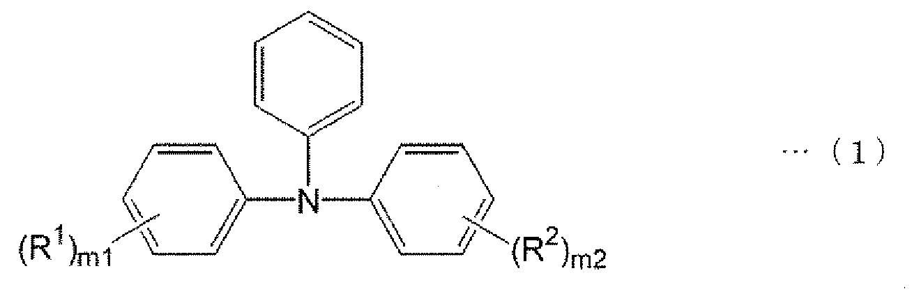


(식 중, R1 내지 R7은 서로 독립적으로 수소, 할로겐, 시아노기, 니트로기, 탄소수 1 내지 22의 직쇄상, 분지상 또는 환상의 알킬기, 탄소수 2 내지 22의 직쇄상, 분지상 또는 환상의 알케닐기, 탄소수 2 내지 22의 직쇄상, 분지상 또는 환상의 알키닐기, 탄소수 6 내지 21의 아릴기, 탄소수 12 내지 20의 헤테로아릴기, 탄소수 7 내지 21의 아르알킬기 및 탄소수 13 내지 20의 헤테로아릴알킬기로 이루어지는 군에서 선택된 관능기이고(이들의 관능기는 비치환 또는 1 혹은 복수의 할로겐으로 치환되어 있다.), m1 및 m2는 서로 독립적으로 0 내지 5의 정수이고, n1 및 n2는 서로 독립적으로 0 내지 4의 정수이다.)The organic electroluminescent device according to any one of claims 1 to 6, wherein the curable resin comprises a polymer formed by polymerizing any one of the following structural formulas (1) to (3).
(Wherein R 1 to R 7 independently represent hydrogen, halogen, cyano, nitro, a straight, branched or cyclic alkyl group having 1 to 22 carbon atoms, a linear, branched or cyclic alkyl group having 2 to 22 carbon atoms Branched or cyclic alkynyl group having 2 to 22 carbon atoms, an aryl group having 6 to 21 carbon atoms, a heteroaryl group having 12 to 20 carbon atoms, an aralkyl group having 7 to 21 carbon atoms, and an alkenyl group having 13 to 20 carbon atoms (Wherein the functional groups are unsubstituted or substituted with one or more halogens), m1 and m2 are each independently an integer of 0 to 5, n1 and n2 are independent of each other And is an integer of 0 to 4.)
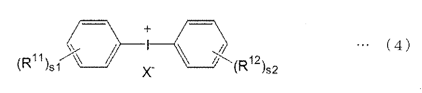
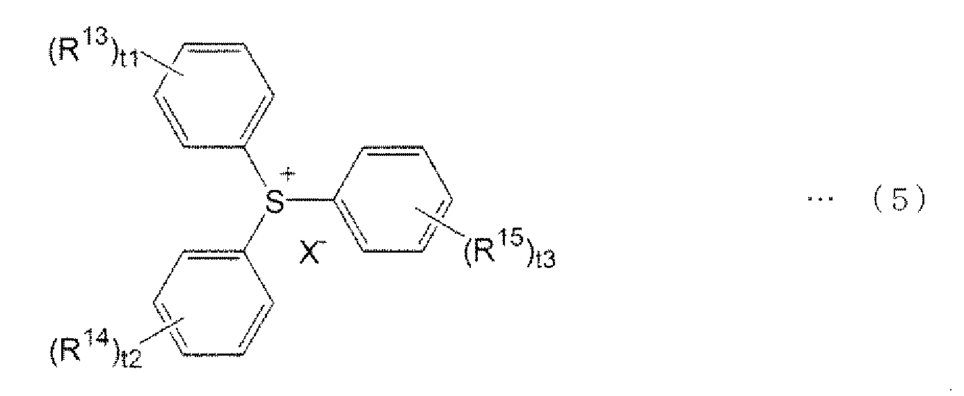
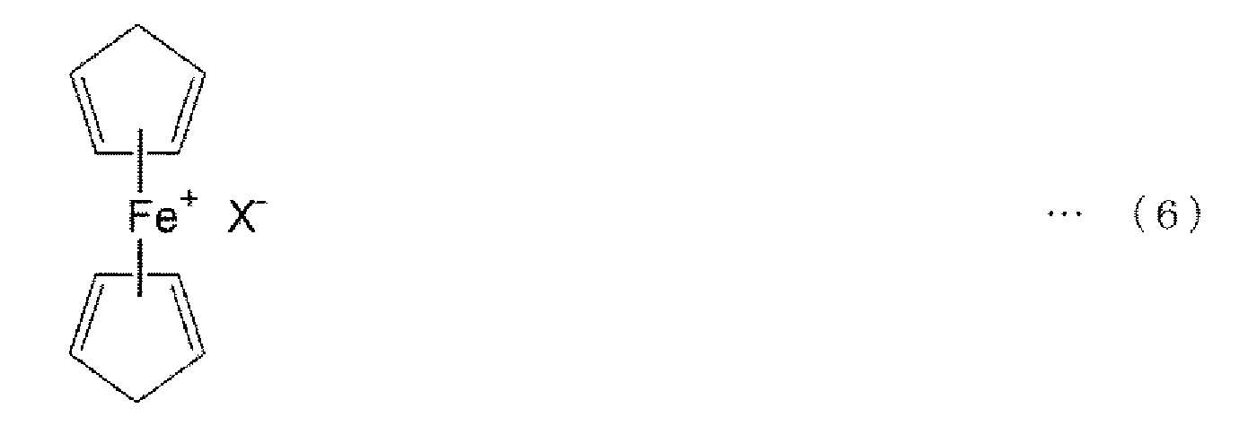
(식 중, X-는 Sb6 -, (C6F5)4B-, CF3SO3 -, PF6 -, BF4 -, C4F9SO3 - 또는 CH3C6H4SO3 -이고, R11 내지 R15는 서로 독립적으로 수소, 할로겐, 시아노기, 니트로기, 탄소수 1 내지 22의 직쇄상, 분지상 또는 환상의 알킬기, 탄소수 2 내지 22의 직쇄상, 분지상 또는 환상의 알케닐기, 탄소수 2 내지 22의 직쇄상, 분지상 또는 환상의 알키닐기, 탄소수 6 내지 21의 아릴기, 탄소수 12 내지 20의 헤테로아릴기, 탄소수 7 내지 21의 아르알킬기 및 탄소수 13 내지 20의 헤테로아릴알킬기로 이루어지는 군에서 선택된 관능기이고, s1, s2, t1, t2 및 t3은 서로 독립적으로 0 내지 5의 정수이다.)The organic electroluminescent device according to any one of claims 1 to 7, wherein the ionic polymerization initiator is any one of the following structural formulas (4) to (6).
(Wherein X - represents Sb 6 - , (C 6 F 5 ) 4 B - , CF 3 SO 3 - , PF 6 - , BF 4 - , C 4 F 9 SO 3 - or CH 3 C 6 H 4 SO 3 - , and R 11 to R 15 independently represent hydrogen, halogen, cyano, nitro, a linear, branched or cyclic alkyl group having 1 to 22 carbon atoms, a linear, branched or cyclic alkyl group having 2 to 22 carbon atoms Branched or cyclic alkynyl group having 2 to 22 carbon atoms, an aryl group having 6 to 21 carbon atoms, a heteroaryl group having 12 to 20 carbon atoms, an aralkyl group having 7 to 21 carbon atoms, and an alkenyl group having 13 to 20 carbon atoms And s1, s2, t1, t2 and t3 are independently of each other an integer of 0 to 5).
Applications Claiming Priority (3)
| Application Number | Priority Date | Filing Date | Title |
|---|---|---|---|
| JPJP-P-2016-019476 | 2016-02-04 | ||
| JP2016019476A JP2017139342A (en) | 2016-02-04 | 2016-02-04 | Organic light emitting device |
| PCT/JP2016/084757 WO2017134905A1 (en) | 2016-02-04 | 2016-11-24 | Organic light emission element |
Publications (1)
| Publication Number | Publication Date |
|---|---|
| KR20180098374A true KR20180098374A (en) | 2018-09-03 |
Family
ID=59499545
Family Applications (1)
| Application Number | Title | Priority Date | Filing Date |
|---|---|---|---|
| KR1020187021594A Ceased KR20180098374A (en) | 2016-02-04 | 2016-11-24 | Organic light emitting device |
Country Status (7)
| Country | Link |
|---|---|
| US (1) | US20190040187A1 (en) |
| EP (1) | EP3413368A4 (en) |
| JP (1) | JP2017139342A (en) |
| KR (1) | KR20180098374A (en) |
| CN (1) | CN108886102A (en) |
| TW (1) | TW201740589A (en) |
| WO (1) | WO2017134905A1 (en) |
Cited By (1)
| Publication number | Priority date | Publication date | Assignee | Title |
|---|---|---|---|---|
| KR20200083925A (en) * | 2018-12-28 | 2020-07-09 | 삼성전자주식회사 | Quantum dot electroluminescence device |
Families Citing this family (4)
| Publication number | Priority date | Publication date | Assignee | Title |
|---|---|---|---|---|
| JP2018203889A (en) * | 2017-06-06 | 2018-12-27 | 日立化成株式会社 | Curable polymer, polymerization liquid, conductive film and organic light-emitting element |
| KR102870803B1 (en) | 2020-08-20 | 2025-10-14 | 삼성디스플레이 주식회사 | Amine compound and light emitting device including the same |
| JP7707526B2 (en) * | 2020-11-18 | 2025-07-15 | 三菱ケミカル株式会社 | Compound, composition, and photoelectric conversion device |
| KR102811547B1 (en) | 2020-11-30 | 2025-05-23 | 삼성디스플레이 주식회사 | Organic electro luminescence device and display device including the same |
Citations (2)
| Publication number | Priority date | Publication date | Assignee | Title |
|---|---|---|---|---|
| JP2008227483A (en) | 2007-02-15 | 2008-09-25 | Mitsubishi Chemicals Corp | Organic electroluminescent element and organic device manufacturing method |
| WO2014038071A1 (en) | 2012-09-07 | 2014-03-13 | パイオニア株式会社 | Organic electroluminescent element and method for manufacturing same |
Family Cites Families (5)
| Publication number | Priority date | Publication date | Assignee | Title |
|---|---|---|---|---|
| US7956349B2 (en) * | 2001-12-05 | 2011-06-07 | Semiconductor Energy Laboratory Co., Ltd. | Organic semiconductor element |
| JP2003264085A (en) * | 2001-12-05 | 2003-09-19 | Semiconductor Energy Lab Co Ltd | Organic semiconductor device, organic electroluminescence device and organic solar cell |
| JP4692025B2 (en) * | 2004-03-11 | 2011-06-01 | 三菱化学株式会社 | Charge transport film composition and ionic compound, charge transport film and organic electroluminescent device using the same, method for producing organic electroluminescent device, and method for producing charge transport film |
| JP5491796B2 (en) * | 2008-08-11 | 2014-05-14 | 三菱化学株式会社 | Charge transporting polymer, composition for organic electroluminescent device, organic electroluminescent device, organic EL display and organic EL lighting |
| JP2015012105A (en) * | 2013-06-28 | 2015-01-19 | 日立化成株式会社 | Organic light-emitting element |
-
2016
- 2016-02-04 JP JP2016019476A patent/JP2017139342A/en active Pending
- 2016-11-24 US US16/072,899 patent/US20190040187A1/en not_active Abandoned
- 2016-11-24 CN CN201680079964.7A patent/CN108886102A/en active Pending
- 2016-11-24 KR KR1020187021594A patent/KR20180098374A/en not_active Ceased
- 2016-11-24 WO PCT/JP2016/084757 patent/WO2017134905A1/en not_active Ceased
- 2016-11-24 EP EP16889388.1A patent/EP3413368A4/en not_active Withdrawn
-
2017
- 2017-01-16 TW TW106101415A patent/TW201740589A/en unknown
Patent Citations (2)
| Publication number | Priority date | Publication date | Assignee | Title |
|---|---|---|---|---|
| JP2008227483A (en) | 2007-02-15 | 2008-09-25 | Mitsubishi Chemicals Corp | Organic electroluminescent element and organic device manufacturing method |
| WO2014038071A1 (en) | 2012-09-07 | 2014-03-13 | パイオニア株式会社 | Organic electroluminescent element and method for manufacturing same |
Cited By (1)
| Publication number | Priority date | Publication date | Assignee | Title |
|---|---|---|---|---|
| KR20200083925A (en) * | 2018-12-28 | 2020-07-09 | 삼성전자주식회사 | Quantum dot electroluminescence device |
Also Published As
| Publication number | Publication date |
|---|---|
| TW201740589A (en) | 2017-11-16 |
| WO2017134905A1 (en) | 2017-08-10 |
| US20190040187A1 (en) | 2019-02-07 |
| CN108886102A (en) | 2018-11-23 |
| EP3413368A1 (en) | 2018-12-12 |
| JP2017139342A (en) | 2017-08-10 |
| EP3413368A4 (en) | 2019-09-04 |
Similar Documents
| Publication | Publication Date | Title |
|---|---|---|
| Cheng et al. | Thermally cross-linkable hole-transporting materials on conducting polymer: synthesis, characterization, and applications for polymer light-emitting devices | |
| KR101485470B1 (en) | Organic electronic material, polymerization initiator and thermal polymerization initiator, ink composition, organic thin film and production method for same, organic electronic element, organic electroluminescent element, lighting device, display element, and display device | |
| Zou et al. | Unexpected Propeller‐Like Hexakis (fluoren‐2‐yl) benzene Cores for Six‐Arm Star‐Shaped Oligofluorenes: Highly Efficient Deep‐Blue Fluorescent Emitters and Good Hole‐Transporting Materials | |
| US20100059738A1 (en) | Conductive Polymer Compositions in Opto-Electrical Devices | |
| Hung et al. | A new thermally crosslinkable hole injection material for OLEDs | |
| WO2017134905A1 (en) | Organic light emission element | |
| TW201823423A (en) | Organic electronic material, organic layer, organic electronic element, organic electroluminescent element, display element, illumination device, and display device | |
| TW201823422A (en) | Organic electronic material and use of same | |
| JP2015012105A (en) | Organic light-emitting element | |
| JPWO2018139487A1 (en) | Organic electronic material, ink composition, organic layer, organic electronic element, organic electroluminescent element, display element, lighting device, and display device | |
| JP2016167570A (en) | Organic light-emitting element | |
| WO2018159694A1 (en) | Organic electronic material and use of same | |
| JP6015520B2 (en) | Polymerizable coating liquid, resin and organic electroluminescent element formed using the same, and polymerizable coating liquid and method for producing organic electroluminescent element | |
| WO2020065926A1 (en) | Organic electronic material and use thereof | |
| JP7409088B2 (en) | Organic thin film manufacturing method, organic thin film and its use | |
| TWI675048B (en) | Curable polymer, polymerization liquid, conductive film, and organic light emitting device | |
| Lin et al. | Hole mobilities of thermally polymerized triaryldiamine derivatives and their application as hole-transport materials in organic light-emitting diodes (OLEDs) | |
| JP6775731B2 (en) | Charge transport material and its use | |
| WO2019167346A1 (en) | Curable polymer, polymerization solution and resin, and organic light-emitting element manufactured using same | |
| Dey | Synthesis and characterizations of bis-diazirines and their applications in organic electronics | |
| JP2015192133A (en) | organic transistor | |
| JP6657701B2 (en) | Organic electronics materials and their use | |
| JP2017059718A (en) | Organic electronics material, ink composition containing the material, organic electronics element, and organic electroluminescence element | |
| JP2020042940A (en) | Method for producing charge transporting polymer thin film |
Legal Events
| Date | Code | Title | Description |
|---|---|---|---|
| A201 | Request for examination | ||
| PA0105 | International application |
Patent event date: 20180726 Patent event code: PA01051R01D Comment text: International Patent Application |
|
| PA0201 | Request for examination | ||
| PG1501 | Laying open of application | ||
| E902 | Notification of reason for refusal | ||
| PE0902 | Notice of grounds for rejection |
Comment text: Notification of reason for refusal Patent event date: 20190817 Patent event code: PE09021S01D |
|
| E601 | Decision to refuse application | ||
| PE0601 | Decision on rejection of patent |
Patent event date: 20200227 Comment text: Decision to Refuse Application Patent event code: PE06012S01D Patent event date: 20190817 Comment text: Notification of reason for refusal Patent event code: PE06011S01I |