JP2017139342A - Organic light-emitting element - Google Patents
Organic light-emitting element Download PDFInfo
- Publication number
- JP2017139342A JP2017139342A JP2016019476A JP2016019476A JP2017139342A JP 2017139342 A JP2017139342 A JP 2017139342A JP 2016019476 A JP2016019476 A JP 2016019476A JP 2016019476 A JP2016019476 A JP 2016019476A JP 2017139342 A JP2017139342 A JP 2017139342A
- Authority
- JP
- Japan
- Prior art keywords
- transport layer
- organic light
- hole transport
- light emitting
- group
- Prior art date
- Legal status (The legal status is an assumption and is not a legal conclusion. Google has not performed a legal analysis and makes no representation as to the accuracy of the status listed.)
- Pending
Links
- 230000005525 hole transport Effects 0.000 claims abstract description 106
- 229920005989 resin Polymers 0.000 claims abstract description 69
- 239000011347 resin Substances 0.000 claims abstract description 69
- 239000003505 polymerization initiator Substances 0.000 claims abstract description 35
- 238000012690 ionic polymerization Methods 0.000 claims abstract description 22
- 239000000969 carrier Substances 0.000 claims abstract description 13
- 239000010410 layer Substances 0.000 claims description 178
- 125000004432 carbon atom Chemical group C* 0.000 claims description 38
- 125000003118 aryl group Chemical group 0.000 claims description 12
- 125000001072 heteroaryl group Chemical group 0.000 claims description 10
- 125000004435 hydrogen atom Chemical class [H]* 0.000 claims description 10
- 229910052736 halogen Inorganic materials 0.000 claims description 9
- 150000002367 halogens Chemical class 0.000 claims description 9
- 229910052739 hydrogen Inorganic materials 0.000 claims description 9
- 239000001257 hydrogen Substances 0.000 claims description 9
- 239000012044 organic layer Substances 0.000 claims description 9
- 125000003710 aryl alkyl group Chemical group 0.000 claims description 8
- 150000001875 compounds Chemical class 0.000 claims description 8
- 125000004122 cyclic group Chemical group 0.000 claims description 8
- 125000004093 cyano group Chemical group *C#N 0.000 claims description 6
- 125000006165 cyclic alkyl group Chemical group 0.000 claims description 6
- 125000000449 nitro group Chemical group [O-][N+](*)=O 0.000 claims description 6
- 125000003342 alkenyl group Chemical group 0.000 claims description 5
- 125000000524 functional group Chemical group 0.000 claims description 5
- 125000004446 heteroarylalkyl group Chemical group 0.000 claims description 5
- 125000000304 alkynyl group Chemical group 0.000 claims description 4
- 230000001747 exhibiting effect Effects 0.000 claims description 3
- OKTJSMMVPCPJKN-UHFFFAOYSA-N Carbon Chemical compound [C] OKTJSMMVPCPJKN-UHFFFAOYSA-N 0.000 claims description 2
- 229910052799 carbon Inorganic materials 0.000 claims description 2
- 230000000379 polymerizing effect Effects 0.000 claims 1
- 239000000126 substance Substances 0.000 abstract description 3
- 239000010408 film Substances 0.000 description 57
- 229920000642 polymer Polymers 0.000 description 32
- 238000000034 method Methods 0.000 description 28
- 239000000758 substrate Substances 0.000 description 26
- 239000011521 glass Substances 0.000 description 25
- 238000001894 space-charge-limited current method Methods 0.000 description 24
- 150000002500 ions Chemical group 0.000 description 20
- 238000004132 cross linking Methods 0.000 description 18
- 239000000178 monomer Substances 0.000 description 17
- YXFVVABEGXRONW-UHFFFAOYSA-N Toluene Chemical compound CC1=CC=CC=C1 YXFVVABEGXRONW-UHFFFAOYSA-N 0.000 description 15
- 239000003999 initiator Substances 0.000 description 12
- 230000005684 electric field Effects 0.000 description 11
- 230000008569 process Effects 0.000 description 11
- 238000000576 coating method Methods 0.000 description 10
- 238000001723 curing Methods 0.000 description 8
- 238000009826 distribution Methods 0.000 description 8
- 239000000203 mixture Substances 0.000 description 8
- 239000000243 solution Substances 0.000 description 8
- 239000010409 thin film Substances 0.000 description 8
- 239000011248 coating agent Substances 0.000 description 7
- 229910052757 nitrogen Inorganic materials 0.000 description 7
- 238000006243 chemical reaction Methods 0.000 description 6
- 238000010586 diagram Methods 0.000 description 6
- 239000003960 organic solvent Substances 0.000 description 6
- 239000005394 sealing glass Substances 0.000 description 6
- ODHXBMXNKOYIBV-UHFFFAOYSA-N triphenylamine Chemical compound C1=CC=CC=C1N(C=1C=CC=CC=1)C1=CC=CC=C1 ODHXBMXNKOYIBV-UHFFFAOYSA-N 0.000 description 6
- 238000002835 absorbance Methods 0.000 description 5
- 238000004519 manufacturing process Methods 0.000 description 5
- 230000007246 mechanism Effects 0.000 description 5
- 238000002156 mixing Methods 0.000 description 5
- -1 1-phenethyl groups Chemical group 0.000 description 4
- 108091006149 Electron carriers Proteins 0.000 description 4
- 229910052782 aluminium Inorganic materials 0.000 description 4
- MWPLVEDNUUSJAV-UHFFFAOYSA-N anthracene Chemical compound C1=CC=CC2=CC3=CC=CC=C3C=C21 MWPLVEDNUUSJAV-UHFFFAOYSA-N 0.000 description 4
- 230000015572 biosynthetic process Effects 0.000 description 4
- 150000001768 cations Chemical class 0.000 description 4
- 230000003247 decreasing effect Effects 0.000 description 4
- 238000011156 evaluation Methods 0.000 description 4
- 238000002847 impedance measurement Methods 0.000 description 4
- 238000005259 measurement Methods 0.000 description 4
- AHHWIHXENZJRFG-UHFFFAOYSA-N oxetane Chemical compound C1COC1 AHHWIHXENZJRFG-UHFFFAOYSA-N 0.000 description 4
- 239000007787 solid Substances 0.000 description 4
- 239000002904 solvent Substances 0.000 description 4
- UHOVQNZJYSORNB-UHFFFAOYSA-N Benzene Chemical compound C1=CC=CC=C1 UHOVQNZJYSORNB-UHFFFAOYSA-N 0.000 description 3
- 238000006069 Suzuki reaction reaction Methods 0.000 description 3
- XAGFODPZIPBFFR-UHFFFAOYSA-N aluminium Chemical compound [Al] XAGFODPZIPBFFR-UHFFFAOYSA-N 0.000 description 3
- 150000001450 anions Chemical class 0.000 description 3
- 230000000903 blocking effect Effects 0.000 description 3
- 125000005842 heteroatom Chemical group 0.000 description 3
- 238000007654 immersion Methods 0.000 description 3
- AMGQUBHHOARCQH-UHFFFAOYSA-N indium;oxotin Chemical compound [In].[Sn]=O AMGQUBHHOARCQH-UHFFFAOYSA-N 0.000 description 3
- 229910052751 metal Inorganic materials 0.000 description 3
- 239000002184 metal Substances 0.000 description 3
- 238000001771 vacuum deposition Methods 0.000 description 3
- NAWXUBYGYWOOIX-SFHVURJKSA-N (2s)-2-[[4-[2-(2,4-diaminoquinazolin-6-yl)ethyl]benzoyl]amino]-4-methylidenepentanedioic acid Chemical compound C1=CC2=NC(N)=NC(N)=C2C=C1CCC1=CC=C(C(=O)N[C@@H](CC(=C)C(O)=O)C(O)=O)C=C1 NAWXUBYGYWOOIX-SFHVURJKSA-N 0.000 description 2
- FCEHBMOGCRZNNI-UHFFFAOYSA-N 1-benzothiophene Chemical compound C1=CC=C2SC=CC2=C1 FCEHBMOGCRZNNI-UHFFFAOYSA-N 0.000 description 2
- ISONQKSIWXLJOQ-UHFFFAOYSA-N 2-bromo-3-octylthiophene Chemical compound CCCCCCCCC=1C=CSC=1Br ISONQKSIWXLJOQ-UHFFFAOYSA-N 0.000 description 2
- OIDSERXZWSSIEF-UHFFFAOYSA-N 3-[(4-bromophenoxy)methyl]-3-ethyloxetane Chemical compound C=1C=C(Br)C=CC=1OCC1(CC)COC1 OIDSERXZWSSIEF-UHFFFAOYSA-N 0.000 description 2
- ZRXVCYGHAUGABY-UHFFFAOYSA-N 4-bromo-n,n-bis(4-bromophenyl)aniline Chemical compound C1=CC(Br)=CC=C1N(C=1C=CC(Br)=CC=1)C1=CC=C(Br)C=C1 ZRXVCYGHAUGABY-UHFFFAOYSA-N 0.000 description 2
- UJOBWOGCFQCDNV-UHFFFAOYSA-N 9H-carbazole Chemical compound C1=CC=C2C3=CC=CC=C3NC2=C1 UJOBWOGCFQCDNV-UHFFFAOYSA-N 0.000 description 2
- PAYRUJLWNCNPSJ-UHFFFAOYSA-N Aniline Chemical compound NC1=CC=CC=C1 PAYRUJLWNCNPSJ-UHFFFAOYSA-N 0.000 description 2
- IJGRMHOSHXDMSA-UHFFFAOYSA-N Atomic nitrogen Chemical compound N#N IJGRMHOSHXDMSA-UHFFFAOYSA-N 0.000 description 2
- WKBOTKDWSSQWDR-UHFFFAOYSA-N Bromine atom Chemical compound [Br] WKBOTKDWSSQWDR-UHFFFAOYSA-N 0.000 description 2
- RYGMFSIKBFXOCR-UHFFFAOYSA-N Copper Chemical compound [Cu] RYGMFSIKBFXOCR-UHFFFAOYSA-N 0.000 description 2
- YLQBMQCUIZJEEH-UHFFFAOYSA-N Furan Chemical compound C=1C=COC=1 YLQBMQCUIZJEEH-UHFFFAOYSA-N 0.000 description 2
- UFWIBTONFRDIAS-UHFFFAOYSA-N Naphthalene Chemical compound C1=CC=CC2=CC=CC=C21 UFWIBTONFRDIAS-UHFFFAOYSA-N 0.000 description 2
- KYQCOXFCLRTKLS-UHFFFAOYSA-N Pyrazine Chemical compound C1=CN=CC=N1 KYQCOXFCLRTKLS-UHFFFAOYSA-N 0.000 description 2
- JUJWROOIHBZHMG-UHFFFAOYSA-N Pyridine Chemical compound C1=CC=NC=C1 JUJWROOIHBZHMG-UHFFFAOYSA-N 0.000 description 2
- KAESVJOAVNADME-UHFFFAOYSA-N Pyrrole Chemical compound C=1C=CNC=1 KAESVJOAVNADME-UHFFFAOYSA-N 0.000 description 2
- SMWDFEZZVXVKRB-UHFFFAOYSA-N Quinoline Chemical compound N1=CC=CC2=CC=CC=C21 SMWDFEZZVXVKRB-UHFFFAOYSA-N 0.000 description 2
- YTPLMLYBLZKORZ-UHFFFAOYSA-N Thiophene Chemical compound C=1C=CSC=1 YTPLMLYBLZKORZ-UHFFFAOYSA-N 0.000 description 2
- DZBUGLKDJFMEHC-UHFFFAOYSA-N acridine Chemical compound C1=CC=CC2=CC3=CC=CC=C3N=C21 DZBUGLKDJFMEHC-UHFFFAOYSA-N 0.000 description 2
- RDOXTESZEPMUJZ-UHFFFAOYSA-N anisole Chemical compound COC1=CC=CC=C1 RDOXTESZEPMUJZ-UHFFFAOYSA-N 0.000 description 2
- 125000005018 aryl alkenyl group Chemical group 0.000 description 2
- 239000012298 atmosphere Substances 0.000 description 2
- UFVXQDWNSAGPHN-UHFFFAOYSA-K bis[(2-methylquinolin-8-yl)oxy]-(4-phenylphenoxy)alumane Chemical compound [Al+3].C1=CC=C([O-])C2=NC(C)=CC=C21.C1=CC=C([O-])C2=NC(C)=CC=C21.C1=CC([O-])=CC=C1C1=CC=CC=C1 UFVXQDWNSAGPHN-UHFFFAOYSA-K 0.000 description 2
- GDTBXPJZTBHREO-UHFFFAOYSA-N bromine Substances BrBr GDTBXPJZTBHREO-UHFFFAOYSA-N 0.000 description 2
- 229910052794 bromium Inorganic materials 0.000 description 2
- WDECIBYCCFPHNR-UHFFFAOYSA-N chrysene Chemical compound C1=CC=CC2=CC=C3C4=CC=CC=C4C=CC3=C21 WDECIBYCCFPHNR-UHFFFAOYSA-N 0.000 description 2
- 229910052802 copper Inorganic materials 0.000 description 2
- 239000010949 copper Substances 0.000 description 2
- 230000006866 deterioration Effects 0.000 description 2
- ZUOUZKKEUPVFJK-UHFFFAOYSA-N diphenyl Chemical compound C1=CC=CC=C1C1=CC=CC=C1 ZUOUZKKEUPVFJK-UHFFFAOYSA-N 0.000 description 2
- 239000003822 epoxy resin Substances 0.000 description 2
- 238000013210 evaluation model Methods 0.000 description 2
- NIHNNTQXNPWCJQ-UHFFFAOYSA-N fluorene Chemical compound C1=CC=C2CC3=CC=CC=C3C2=C1 NIHNNTQXNPWCJQ-UHFFFAOYSA-N 0.000 description 2
- 238000010438 heat treatment Methods 0.000 description 2
- 238000002347 injection Methods 0.000 description 2
- 239000007924 injection Substances 0.000 description 2
- CECAIMUJVYQLKA-UHFFFAOYSA-N iridium 1-phenylisoquinoline Chemical compound [Ir].C1=CC=CC=C1C1=NC=CC2=CC=CC=C12.C1=CC=CC=C1C1=NC=CC2=CC=CC=C12.C1=CC=CC=C1C1=NC=CC2=CC=CC=C12 CECAIMUJVYQLKA-UHFFFAOYSA-N 0.000 description 2
- AWJUIBRHMBBTKR-UHFFFAOYSA-N isoquinoline Chemical compound C1=NC=CC2=CC=CC=C21 AWJUIBRHMBBTKR-UHFFFAOYSA-N 0.000 description 2
- 238000010030 laminating Methods 0.000 description 2
- 239000000463 material Substances 0.000 description 2
- 238000013178 mathematical model Methods 0.000 description 2
- 238000000059 patterning Methods 0.000 description 2
- YNPNZTXNASCQKK-UHFFFAOYSA-N phenanthrene Chemical compound C1=CC=C2C3=CC=CC=C3C=CC2=C1 YNPNZTXNASCQKK-UHFFFAOYSA-N 0.000 description 2
- 229920000647 polyepoxide Polymers 0.000 description 2
- 238000006116 polymerization reaction Methods 0.000 description 2
- BWHMMNNQKKPAPP-UHFFFAOYSA-L potassium carbonate Chemical compound [K+].[K+].[O-]C([O-])=O BWHMMNNQKKPAPP-UHFFFAOYSA-L 0.000 description 2
- BBEAQIROQSPTKN-UHFFFAOYSA-N pyrene Chemical compound C1=CC=C2C=CC3=CC=CC4=CC=C1C2=C43 BBEAQIROQSPTKN-UHFFFAOYSA-N 0.000 description 2
- XSCHRSMBECNVNS-UHFFFAOYSA-N quinoxaline Chemical compound N1=CC=NC2=CC=CC=C21 XSCHRSMBECNVNS-UHFFFAOYSA-N 0.000 description 2
- 230000009467 reduction Effects 0.000 description 2
- 239000011343 solid material Substances 0.000 description 2
- 238000006467 substitution reaction Methods 0.000 description 2
- 229910052717 sulfur Inorganic materials 0.000 description 2
- FNQJDLTXOVEEFB-UHFFFAOYSA-N 1,2,3-benzothiadiazole Chemical compound C1=CC=C2SN=NC2=C1 FNQJDLTXOVEEFB-UHFFFAOYSA-N 0.000 description 1
- SLLFVLKNXABYGI-UHFFFAOYSA-N 1,2,3-benzoxadiazole Chemical compound C1=CC=C2ON=NC2=C1 SLLFVLKNXABYGI-UHFFFAOYSA-N 0.000 description 1
- YJTKZCDBKVTVBY-UHFFFAOYSA-N 1,3-Diphenylbenzene Chemical group C1=CC=CC=C1C1=CC=CC(C=2C=CC=CC=2)=C1 YJTKZCDBKVTVBY-UHFFFAOYSA-N 0.000 description 1
- BCMCBBGGLRIHSE-UHFFFAOYSA-N 1,3-benzoxazole Chemical compound C1=CC=C2OC=NC2=C1 BCMCBBGGLRIHSE-UHFFFAOYSA-N 0.000 description 1
- AZQWKYJCGOJGHM-UHFFFAOYSA-N 1,4-benzoquinone Chemical compound O=C1C=CC(=O)C=C1 AZQWKYJCGOJGHM-UHFFFAOYSA-N 0.000 description 1
- BAXOFTOLAUCFNW-UHFFFAOYSA-N 1H-indazole Chemical compound C1=CC=C2C=NNC2=C1 BAXOFTOLAUCFNW-UHFFFAOYSA-N 0.000 description 1
- GOLORTLGFDVFDW-UHFFFAOYSA-N 3-(1h-benzimidazol-2-yl)-7-(diethylamino)chromen-2-one Chemical compound C1=CC=C2NC(C3=CC4=CC=C(C=C4OC3=O)N(CC)CC)=NC2=C1 GOLORTLGFDVFDW-UHFFFAOYSA-N 0.000 description 1
- OGGKVJMNFFSDEV-UHFFFAOYSA-N 3-methyl-n-[4-[4-(n-(3-methylphenyl)anilino)phenyl]phenyl]-n-phenylaniline Chemical compound CC1=CC=CC(N(C=2C=CC=CC=2)C=2C=CC(=CC=2)C=2C=CC(=CC=2)N(C=2C=CC=CC=2)C=2C=C(C)C=CC=2)=C1 OGGKVJMNFFSDEV-UHFFFAOYSA-N 0.000 description 1
- BGBCYDVLLQOGEI-UHFFFAOYSA-N 4-(4-aminophenyl)-3-naphthalen-2-ylaniline Chemical compound C1=CC(N)=CC=C1C1=CC=C(N)C=C1C1=CC=C(C=CC=C2)C2=C1 BGBCYDVLLQOGEI-UHFFFAOYSA-N 0.000 description 1
- ZCYVEMRRCGMTRW-UHFFFAOYSA-N 7553-56-2 Chemical compound [I] ZCYVEMRRCGMTRW-UHFFFAOYSA-N 0.000 description 1
- RXACYPFGPNTUNV-UHFFFAOYSA-N 9,9-dioctylfluorene Chemical compound C1=CC=C2C(CCCCCCCC)(CCCCCCCC)C3=CC=CC=C3C2=C1 RXACYPFGPNTUNV-UHFFFAOYSA-N 0.000 description 1
- VIJYEGDOKCKUOL-UHFFFAOYSA-N 9-phenylcarbazole Chemical compound C1=CC=CC=C1N1C2=CC=CC=C2C2=CC=CC=C21 VIJYEGDOKCKUOL-UHFFFAOYSA-N 0.000 description 1
- 239000005964 Acibenzolar-S-methyl Substances 0.000 description 1
- ZAMOUSCENKQFHK-UHFFFAOYSA-N Chlorine atom Chemical compound [Cl] ZAMOUSCENKQFHK-UHFFFAOYSA-N 0.000 description 1
- RWSOTUBLDIXVET-UHFFFAOYSA-N Dihydrogen sulfide Chemical class S RWSOTUBLDIXVET-UHFFFAOYSA-N 0.000 description 1
- PXGOKWXKJXAPGV-UHFFFAOYSA-N Fluorine Chemical compound FF PXGOKWXKJXAPGV-UHFFFAOYSA-N 0.000 description 1
- UFHFLCQGNIYNRP-UHFFFAOYSA-N Hydrogen Chemical compound [H][H] UFHFLCQGNIYNRP-UHFFFAOYSA-N 0.000 description 1
- 125000000815 N-oxide group Chemical group 0.000 description 1
- ZCQWOFVYLHDMMC-UHFFFAOYSA-N Oxazole Chemical compound C1=COC=N1 ZCQWOFVYLHDMMC-UHFFFAOYSA-N 0.000 description 1
- PCNDJXKNXGMECE-UHFFFAOYSA-N Phenazine Natural products C1=CC=CC2=NC3=CC=CC=C3N=C21 PCNDJXKNXGMECE-UHFFFAOYSA-N 0.000 description 1
- 239000004793 Polystyrene Substances 0.000 description 1
- NRCMAYZCPIVABH-UHFFFAOYSA-N Quinacridone Chemical compound N1C2=CC=CC=C2C(=O)C2=C1C=C1C(=O)C3=CC=CC=C3NC1=C2 NRCMAYZCPIVABH-UHFFFAOYSA-N 0.000 description 1
- PJANXHGTPQOBST-VAWYXSNFSA-N Stilbene Natural products C=1C=CC=CC=1/C=C/C1=CC=CC=C1 PJANXHGTPQOBST-VAWYXSNFSA-N 0.000 description 1
- XBDYBAVJXHJMNQ-UHFFFAOYSA-N Tetrahydroanthracene Natural products C1=CC=C2C=C(CCCC3)C3=CC2=C1 XBDYBAVJXHJMNQ-UHFFFAOYSA-N 0.000 description 1
- DGEZNRSVGBDHLK-UHFFFAOYSA-N [1,10]phenanthroline Chemical compound C1=CN=C2C3=NC=CC=C3C=CC2=C1 DGEZNRSVGBDHLK-UHFFFAOYSA-N 0.000 description 1
- 239000003513 alkali Substances 0.000 description 1
- 125000000217 alkyl group Chemical group 0.000 description 1
- 150000004982 aromatic amines Chemical class 0.000 description 1
- 125000004429 atom Chemical group 0.000 description 1
- 230000008901 benefit Effects 0.000 description 1
- 125000001797 benzyl group Chemical group [H]C1=C([H])C([H])=C(C([H])=C1[H])C([H])([H])* 0.000 description 1
- 235000010290 biphenyl Nutrition 0.000 description 1
- 239000004305 biphenyl Substances 0.000 description 1
- 125000000484 butyl group Chemical group [H]C([*])([H])C([H])([H])C([H])([H])C([H])([H])[H] 0.000 description 1
- 238000004364 calculation method Methods 0.000 description 1
- 125000002091 cationic group Chemical group 0.000 description 1
- 230000008859 change Effects 0.000 description 1
- 239000003795 chemical substances by application Substances 0.000 description 1
- 229910052801 chlorine Inorganic materials 0.000 description 1
- 239000000460 chlorine Substances 0.000 description 1
- 239000012141 concentrate Substances 0.000 description 1
- 229920006037 cross link polymer Polymers 0.000 description 1
- 125000002704 decyl group Chemical group [H]C([H])([H])C([H])([H])C([H])([H])C([H])([H])C([H])([H])C([H])([H])C([H])([H])C([H])([H])C([H])([H])C([H])([H])* 0.000 description 1
- 238000000151 deposition Methods 0.000 description 1
- 238000011978 dissolution method Methods 0.000 description 1
- 238000005401 electroluminescence Methods 0.000 description 1
- 125000001495 ethyl group Chemical group [H]C([H])([H])C([H])([H])* 0.000 description 1
- KTWOOEGAPBSYNW-UHFFFAOYSA-N ferrocene Chemical class [Fe+2].C=1C=C[CH-]C=1.C=1C=C[CH-]C=1 KTWOOEGAPBSYNW-UHFFFAOYSA-N 0.000 description 1
- GVEPBJHOBDJJJI-UHFFFAOYSA-N fluoranthrene Natural products C1=CC(C2=CC=CC=C22)=C3C2=CC=CC3=C1 GVEPBJHOBDJJJI-UHFFFAOYSA-N 0.000 description 1
- 229910052731 fluorine Inorganic materials 0.000 description 1
- 239000011737 fluorine Substances 0.000 description 1
- 125000002541 furyl group Chemical group 0.000 description 1
- 238000005227 gel permeation chromatography Methods 0.000 description 1
- 125000005843 halogen group Chemical group 0.000 description 1
- 238000013007 heat curing Methods 0.000 description 1
- 125000003187 heptyl group Chemical group [H]C([*])([H])C([H])([H])C([H])([H])C([H])([H])C([H])([H])C([H])([H])C([H])([H])[H] 0.000 description 1
- 125000004051 hexyl group Chemical group [H]C([H])([H])C([H])([H])C([H])([H])C([H])([H])C([H])([H])C([H])([H])* 0.000 description 1
- 150000007857 hydrazones Chemical class 0.000 description 1
- XMBWDFGMSWQBCA-UHFFFAOYSA-N hydrogen iodide Chemical class I XMBWDFGMSWQBCA-UHFFFAOYSA-N 0.000 description 1
- 238000005286 illumination Methods 0.000 description 1
- 125000002883 imidazolyl group Chemical group 0.000 description 1
- 125000001041 indolyl group Chemical group 0.000 description 1
- 239000011630 iodine Substances 0.000 description 1
- 229910052740 iodine Inorganic materials 0.000 description 1
- 125000002183 isoquinolinyl group Chemical group C1(=NC=CC2=CC=CC=C12)* 0.000 description 1
- 125000001786 isothiazolyl group Chemical group 0.000 description 1
- 125000000842 isoxazolyl group Chemical group 0.000 description 1
- 238000003475 lamination Methods 0.000 description 1
- 239000002932 luster Substances 0.000 description 1
- 125000000040 m-tolyl group Chemical group [H]C1=C([H])C(*)=C([H])C(=C1[H])C([H])([H])[H] 0.000 description 1
- UZKWTJUDCOPSNM-UHFFFAOYSA-N methoxybenzene Substances CCCCOC=C UZKWTJUDCOPSNM-UHFFFAOYSA-N 0.000 description 1
- 125000002496 methyl group Chemical group [H]C([H])([H])* 0.000 description 1
- 230000007935 neutral effect Effects 0.000 description 1
- 239000012299 nitrogen atmosphere Substances 0.000 description 1
- 125000004433 nitrogen atom Chemical group N* 0.000 description 1
- 125000001400 nonyl group Chemical group [H]C([*])([H])C([H])([H])C([H])([H])C([H])([H])C([H])([H])C([H])([H])C([H])([H])C([H])([H])C([H])([H])[H] 0.000 description 1
- 125000002347 octyl group Chemical group [H]C([*])([H])C([H])([H])C([H])([H])C([H])([H])C([H])([H])C([H])([H])C([H])([H])C([H])([H])[H] 0.000 description 1
- WCPAKWJPBJAGKN-UHFFFAOYSA-N oxadiazole Chemical compound C1=CON=N1 WCPAKWJPBJAGKN-UHFFFAOYSA-N 0.000 description 1
- 125000001715 oxadiazolyl group Chemical group 0.000 description 1
- 125000002971 oxazolyl group Chemical group 0.000 description 1
- 125000004430 oxygen atom Chemical group O* 0.000 description 1
- 125000005704 oxymethylene group Chemical group [H]C([H])([*:2])O[*:1] 0.000 description 1
- NFHFRUOZVGFOOS-UHFFFAOYSA-N palladium;triphenylphosphane Chemical compound [Pd].C1=CC=CC=C1P(C=1C=CC=CC=1)C1=CC=CC=C1.C1=CC=CC=C1P(C=1C=CC=CC=1)C1=CC=CC=C1.C1=CC=CC=C1P(C=1C=CC=CC=1)C1=CC=CC=C1.C1=CC=CC=C1P(C=1C=CC=CC=1)C1=CC=CC=C1 NFHFRUOZVGFOOS-UHFFFAOYSA-N 0.000 description 1
- 125000001147 pentyl group Chemical group C(CCCC)* 0.000 description 1
- 125000002080 perylenyl group Chemical group C1(=CC=C2C=CC=C3C4=CC=CC5=CC=CC(C1=C23)=C45)* 0.000 description 1
- CSHWQDPOILHKBI-UHFFFAOYSA-N peryrene Natural products C1=CC(C2=CC=CC=3C2=C2C=CC=3)=C3C2=CC=CC3=C1 CSHWQDPOILHKBI-UHFFFAOYSA-N 0.000 description 1
- 125000001997 phenyl group Chemical group [H]C1=C([H])C([H])=C(*)C([H])=C1[H] 0.000 description 1
- 125000000843 phenylene group Chemical group C1(=C(C=CC=C1)*)* 0.000 description 1
- 238000000016 photochemical curing Methods 0.000 description 1
- 229920002223 polystyrene Polymers 0.000 description 1
- 229910000027 potassium carbonate Inorganic materials 0.000 description 1
- 238000002360 preparation method Methods 0.000 description 1
- 230000001737 promoting effect Effects 0.000 description 1
- 125000001436 propyl group Chemical group [H]C([*])([H])C([H])([H])C([H])([H])[H] 0.000 description 1
- 125000003373 pyrazinyl group Chemical group 0.000 description 1
- DNXIASIHZYFFRO-UHFFFAOYSA-N pyrazoline Chemical compound C1CN=NC1 DNXIASIHZYFFRO-UHFFFAOYSA-N 0.000 description 1
- 125000003226 pyrazolyl group Chemical group 0.000 description 1
- 125000002098 pyridazinyl group Chemical group 0.000 description 1
- UMJSCPRVCHMLSP-UHFFFAOYSA-N pyridine Natural products COC1=CC=CN=C1 UMJSCPRVCHMLSP-UHFFFAOYSA-N 0.000 description 1
- 125000004076 pyridyl group Chemical group 0.000 description 1
- 125000000714 pyrimidinyl group Chemical group 0.000 description 1
- 125000000168 pyrrolyl group Chemical group 0.000 description 1
- 125000002943 quinolinyl group Chemical group N1=C(C=CC2=CC=CC=C12)* 0.000 description 1
- 230000009257 reactivity Effects 0.000 description 1
- 238000005215 recombination Methods 0.000 description 1
- 230000006798 recombination Effects 0.000 description 1
- 230000004044 response Effects 0.000 description 1
- 238000007151 ring opening polymerisation reaction Methods 0.000 description 1
- 238000007142 ring opening reaction Methods 0.000 description 1
- YYMBJDOZVAITBP-UHFFFAOYSA-N rubrene Chemical compound C1=CC=CC=C1C(C1=C(C=2C=CC=CC=2)C2=CC=CC=C2C(C=2C=CC=CC=2)=C11)=C(C=CC=C2)C2=C1C1=CC=CC=C1 YYMBJDOZVAITBP-UHFFFAOYSA-N 0.000 description 1
- 238000007789 sealing Methods 0.000 description 1
- 238000004528 spin coating Methods 0.000 description 1
- PJANXHGTPQOBST-UHFFFAOYSA-N stilbene Chemical compound C=1C=CC=CC=1C=CC1=CC=CC=C1 PJANXHGTPQOBST-UHFFFAOYSA-N 0.000 description 1
- 235000021286 stilbenes Nutrition 0.000 description 1
- 125000005504 styryl group Chemical group 0.000 description 1
- 125000004434 sulfur atom Chemical group 0.000 description 1
- 238000003786 synthesis reaction Methods 0.000 description 1
- IFLREYGFSNHWGE-UHFFFAOYSA-N tetracene Chemical compound C1=CC=CC2=CC3=CC4=CC=CC=C4C=C3C=C21 IFLREYGFSNHWGE-UHFFFAOYSA-N 0.000 description 1
- 125000003831 tetrazolyl group Chemical group 0.000 description 1
- VLLMWSRANPNYQX-UHFFFAOYSA-N thiadiazole Chemical compound C1=CSN=N1.C1=CSN=N1 VLLMWSRANPNYQX-UHFFFAOYSA-N 0.000 description 1
- 125000001113 thiadiazolyl group Chemical group 0.000 description 1
- 125000000335 thiazolyl group Chemical group 0.000 description 1
- 125000001544 thienyl group Chemical group 0.000 description 1
- 229930192474 thiophene Natural products 0.000 description 1
- 150000003852 triazoles Chemical class 0.000 description 1
- 125000001425 triazolyl group Chemical group 0.000 description 1
- 125000006617 triphenylamine group Chemical group 0.000 description 1
- 229910052720 vanadium Inorganic materials 0.000 description 1
- 238000007740 vapor deposition Methods 0.000 description 1
Images


Classifications
-
- H—ELECTRICITY
- H10—SEMICONDUCTOR DEVICES; ELECTRIC SOLID-STATE DEVICES NOT OTHERWISE PROVIDED FOR
- H10K—ORGANIC ELECTRIC SOLID-STATE DEVICES
- H10K50/00—Organic light-emitting devices
- H10K50/10—OLEDs or polymer light-emitting diodes [PLED]
- H10K50/14—Carrier transporting layers
- H10K50/15—Hole transporting layers
- H10K50/155—Hole transporting layers comprising dopants
-
- C—CHEMISTRY; METALLURGY
- C08—ORGANIC MACROMOLECULAR COMPOUNDS; THEIR PREPARATION OR CHEMICAL WORKING-UP; COMPOSITIONS BASED THEREON
- C08G—MACROMOLECULAR COMPOUNDS OBTAINED OTHERWISE THAN BY REACTIONS ONLY INVOLVING UNSATURATED CARBON-TO-CARBON BONDS
- C08G61/00—Macromolecular compounds obtained by reactions forming a carbon-to-carbon link in the main chain of the macromolecule
- C08G61/12—Macromolecular compounds containing atoms other than carbon in the main chain of the macromolecule
-
- C—CHEMISTRY; METALLURGY
- C08—ORGANIC MACROMOLECULAR COMPOUNDS; THEIR PREPARATION OR CHEMICAL WORKING-UP; COMPOSITIONS BASED THEREON
- C08G—MACROMOLECULAR COMPOUNDS OBTAINED OTHERWISE THAN BY REACTIONS ONLY INVOLVING UNSATURATED CARBON-TO-CARBON BONDS
- C08G61/00—Macromolecular compounds obtained by reactions forming a carbon-to-carbon link in the main chain of the macromolecule
- C08G61/02—Macromolecular compounds containing only carbon atoms in the main chain of the macromolecule, e.g. polyxylylenes
-
- C—CHEMISTRY; METALLURGY
- C08—ORGANIC MACROMOLECULAR COMPOUNDS; THEIR PREPARATION OR CHEMICAL WORKING-UP; COMPOSITIONS BASED THEREON
- C08G—MACROMOLECULAR COMPOUNDS OBTAINED OTHERWISE THAN BY REACTIONS ONLY INVOLVING UNSATURATED CARBON-TO-CARBON BONDS
- C08G61/00—Macromolecular compounds obtained by reactions forming a carbon-to-carbon link in the main chain of the macromolecule
- C08G61/12—Macromolecular compounds containing atoms other than carbon in the main chain of the macromolecule
- C08G61/122—Macromolecular compounds containing atoms other than carbon in the main chain of the macromolecule derived from five- or six-membered heterocyclic compounds, other than imides
- C08G61/123—Macromolecular compounds containing atoms other than carbon in the main chain of the macromolecule derived from five- or six-membered heterocyclic compounds, other than imides derived from five-membered heterocyclic compounds
- C08G61/124—Macromolecular compounds containing atoms other than carbon in the main chain of the macromolecule derived from five- or six-membered heterocyclic compounds, other than imides derived from five-membered heterocyclic compounds with a five-membered ring containing one nitrogen atom in the ring
-
- H—ELECTRICITY
- H10—SEMICONDUCTOR DEVICES; ELECTRIC SOLID-STATE DEVICES NOT OTHERWISE PROVIDED FOR
- H10K—ORGANIC ELECTRIC SOLID-STATE DEVICES
- H10K50/00—Organic light-emitting devices
-
- H—ELECTRICITY
- H10—SEMICONDUCTOR DEVICES; ELECTRIC SOLID-STATE DEVICES NOT OTHERWISE PROVIDED FOR
- H10K—ORGANIC ELECTRIC SOLID-STATE DEVICES
- H10K50/00—Organic light-emitting devices
- H10K50/10—OLEDs or polymer light-emitting diodes [PLED]
- H10K50/14—Carrier transporting layers
- H10K50/15—Hole transporting layers
-
- H—ELECTRICITY
- H10—SEMICONDUCTOR DEVICES; ELECTRIC SOLID-STATE DEVICES NOT OTHERWISE PROVIDED FOR
- H10K—ORGANIC ELECTRIC SOLID-STATE DEVICES
- H10K50/00—Organic light-emitting devices
- H10K50/10—OLEDs or polymer light-emitting diodes [PLED]
- H10K50/14—Carrier transporting layers
- H10K50/16—Electron transporting layers
-
- H—ELECTRICITY
- H10—SEMICONDUCTOR DEVICES; ELECTRIC SOLID-STATE DEVICES NOT OTHERWISE PROVIDED FOR
- H10K—ORGANIC ELECTRIC SOLID-STATE DEVICES
- H10K50/00—Organic light-emitting devices
- H10K50/80—Constructional details
- H10K50/805—Electrodes
- H10K50/81—Anodes
-
- H—ELECTRICITY
- H10—SEMICONDUCTOR DEVICES; ELECTRIC SOLID-STATE DEVICES NOT OTHERWISE PROVIDED FOR
- H10K—ORGANIC ELECTRIC SOLID-STATE DEVICES
- H10K50/00—Organic light-emitting devices
- H10K50/80—Constructional details
- H10K50/805—Electrodes
- H10K50/82—Cathodes
-
- H—ELECTRICITY
- H10—SEMICONDUCTOR DEVICES; ELECTRIC SOLID-STATE DEVICES NOT OTHERWISE PROVIDED FOR
- H10K—ORGANIC ELECTRIC SOLID-STATE DEVICES
- H10K85/00—Organic materials used in the body or electrodes of devices covered by this subclass
- H10K85/10—Organic polymers or oligomers
-
- H—ELECTRICITY
- H10—SEMICONDUCTOR DEVICES; ELECTRIC SOLID-STATE DEVICES NOT OTHERWISE PROVIDED FOR
- H10K—ORGANIC ELECTRIC SOLID-STATE DEVICES
- H10K85/00—Organic materials used in the body or electrodes of devices covered by this subclass
- H10K85/10—Organic polymers or oligomers
- H10K85/111—Organic polymers or oligomers comprising aromatic, heteroaromatic, or aryl chains, e.g. polyaniline, polyphenylene or polyphenylene vinylene
- H10K85/115—Polyfluorene; Derivatives thereof
-
- H—ELECTRICITY
- H10—SEMICONDUCTOR DEVICES; ELECTRIC SOLID-STATE DEVICES NOT OTHERWISE PROVIDED FOR
- H10K—ORGANIC ELECTRIC SOLID-STATE DEVICES
- H10K85/00—Organic materials used in the body or electrodes of devices covered by this subclass
- H10K85/10—Organic polymers or oligomers
- H10K85/151—Copolymers
Abstract
Description
本発明は、有機発光素子に関する。 The present invention relates to an organic light emitting device.
有機発光素子は、厚さ数十nmの有機固体材料を用いることで、薄型、軽量、フレキシブルな照明やディスプレイを提供する素子として注目されている。また、自発光であるため、高視野角が可能で、発光体自体の応答速度も高く、高速動画表示に適しているため、次世代のフラットパネルディスプレイやシートディスプレイとして期待されている。更に、大面積からの均一発光が可能であるため、次世代照明としても注目されている。 Organic light-emitting elements are attracting attention as elements that provide thin, light, and flexible lighting and displays by using organic solid materials with a thickness of several tens of nanometers. In addition, since it is self-luminous, a high viewing angle is possible, the response speed of the illuminant itself is high, and it is suitable for high-speed moving image display. Therefore, it is expected as a next-generation flat panel display or sheet display. Furthermore, since uniform light emission from a large area is possible, it has been attracting attention as next-generation illumination.
有機発光素子では、陽極と陰極との間に挟まれた有機積層膜に電圧を印加することで、陽極から正孔が、陰極から電子が、有機積層膜に導入され、電子と正孔とが発光層で再結合することにより、発光する。 In an organic light emitting device, by applying a voltage to an organic laminated film sandwiched between an anode and a cathode, holes are introduced from the anode, electrons are introduced from the cathode, and electrons are introduced into the organic laminated film. Light is emitted by recombination in the light emitting layer.
有機発光素子は、陽極、陽極から発光層へ正孔を輸送するための正孔輸送層、発光層、陰極から発光層へ電子を輸送するための電子輸送層、及び陰極からなる。電子及び正孔を発光層に効率的に注入するために、正孔輸送層及び電子輸送層として、それぞれ複数の異なる膜を積層する場合もある。 The organic light emitting device includes an anode, a hole transport layer for transporting holes from the anode to the light emitting layer, a light emitting layer, an electron transport layer for transporting electrons from the cathode to the light emitting layer, and a cathode. In order to efficiently inject electrons and holes into the light emitting layer, a plurality of different films may be stacked as the hole transport layer and the electron transport layer, respectively.
有機発光素子の有機固体材料を積層する方法は、真空蒸着層と湿式プロセスとに大別される。真空蒸着法と比較して、塗布印刷法及びインクジェット法に代表される湿式プロセスは、量産性、製造プロセスの低コスト化、及び大画面化の利点で期待されている。 The method of laminating the organic solid material of the organic light emitting device is roughly divided into a vacuum deposition layer and a wet process. Compared with the vacuum vapor deposition method, wet processes represented by a coating printing method and an ink jet method are expected to be advantageous in terms of mass productivity, cost reduction of a manufacturing process, and an increase in screen size.
湿式プロセスでは、有機膜を積層すると、新たな層を製膜する際に、既に製膜した層が溶ける問題がある。この対策として、有機分子に硬化性の架橋基を付加した主剤を含む硬化性溶液を、湿式プロセスで塗布した後に、熱や光処理により、高分子を硬化させる方法がある。硬化した膜(硬化樹脂)は、溶媒に溶けにくい性質を持つので、湿式プロセスでの積層が容易になる。 In the wet process, when an organic film is stacked, when a new layer is formed, there is a problem that the already formed layer is melted. As a countermeasure, there is a method in which a polymer is cured by heat or light treatment after a curable solution containing a main agent in which a curable crosslinking group is added to an organic molecule is applied by a wet process. Since the cured film (cured resin) has a property of being hardly soluble in a solvent, lamination by a wet process becomes easy.
従来の有機発光素子において、有機分子を硬化させる技術として、以下が存在する。 In the conventional organic light emitting device, the following exists as a technique for curing organic molecules.
特許文献1には、正孔輸送層用組成物を正孔注入層上に成膜した後、重合性化合物を重合させ、正孔輸送層を形成することにより、反応後の正孔輸送層の溶解性が低下すること、これにより正孔輸送層の上に更に有機発光層を形成した場合にも正孔輸送層4が有機発光層用組成物に溶解しないことなどが記載されている。
In
特許文献2には、有機エレクトロルミネッセンス素子において、正孔輸送層は、重合開始剤の存在下、開環重合性基を含有する重合性化合物が開環重合することにより得られた樹脂硬化物により形成されていること、正孔輸送層の上面における最大山高さRpおよび最大谷深さRvは、いずれも14nm以下であることにより、優れた量産性及び高い発光効率を実現できることが記載されている。
In
塗布プロセスで形成した膜厚は、真空蒸着法と比較して、不均一となりやすい。従来の有機発光素子においては、正孔輸送層を通電する電流は、空間電荷制限電流機構による。空間電荷制限電流は、陽極から、正孔輸送層に注入された電流であり、注入された電流は、正孔輸送層内で空間電荷を形成する。このため、空間電荷制限電流は、膜厚の3乗に反比例することが知られている。従って、膜厚の不均一に対して、正孔輸送層の電流分布は更に不均一となり、効率の低下につながる。更に、電流が集中する部位での劣化の進行を招く。 The film thickness formed by the coating process tends to be non-uniform compared to the vacuum deposition method. In the conventional organic light emitting device, the current passing through the hole transport layer is based on the space charge limited current mechanism. The space charge limited current is a current injected from the anode into the hole transport layer, and the injected current forms a space charge in the hole transport layer. For this reason, it is known that the space charge limiting current is inversely proportional to the cube of the film thickness. Therefore, the current distribution in the hole transport layer becomes more non-uniform with respect to the non-uniform thickness, leading to a reduction in efficiency. Furthermore, the deterioration is caused at the portion where the current is concentrated.
上記のように、正孔輸送層などの有機層に架橋基を含む有機分子で形成した有機発光素子が知られている。 As described above, an organic light emitting element formed of an organic molecule containing a crosslinking group in an organic layer such as a hole transport layer is known.
特許文献1に記載されている有機層は、塗布プロセスにとって課題である均一な膜厚を提供するものではなく、かつ、膜厚の不均一による電流分布の不均一を低減するものではない。
The organic layer described in
特許文献2に記載の方法では、正孔輸送層の最大山高さRpと谷深さRvを14nm以下としているが、正孔輸送層の膜厚は数十nmであることから、不均一性は大きく、電流は不均一である。
In the method described in
本発明は、有機発光素子の発光効率を高め、かつ、寿命特性を向上することを目的とする。 An object of the present invention is to increase the light emission efficiency of an organic light emitting device and improve the life characteristics.
上記課題を解決するため、陽極と、正孔輸送層と、発光層と、陰極と、を備え、正孔輸送層は、陽極と発光層との間に配置され、正孔輸送層は、イオン重合開始剤と、硬化樹脂と、を含み、硬化樹脂は、イオン重合開始剤により化学ドープされて生じた正孔キャリアを有し、正孔輸送層は、オーミック伝導性を示す、有機発光素子を用いる。 In order to solve the above problems, an anode, a hole transport layer, a light emitting layer, and a cathode are provided, the hole transport layer is disposed between the anode and the light emitting layer, and the hole transport layer is an ion An organic light emitting device comprising a polymerization initiator and a cured resin, the cured resin having hole carriers generated by chemical doping with an ionic polymerization initiator, and the hole transport layer exhibiting ohmic conductivity; Use.
本発明によれば、有機発光素子の発光効率を高め、かつ、寿命特性を向上することができる。 ADVANTAGE OF THE INVENTION According to this invention, the luminous efficiency of an organic light emitting element can be improved and a lifetime characteristic can be improved.
本発明は、イオン開始剤を混合した硬化樹脂を用い、正孔輸送層をオーミック伝導性とした有機発光素子に関する。 The present invention relates to an organic light emitting device using a cured resin mixed with an ion initiator and having a hole transport layer in ohmic conductivity.
以下、本発明の実施形態について説明する。 Hereinafter, embodiments of the present invention will be described.
<イオン開始剤を含有する硬化樹脂を正孔輸送層として用いた有機発光素子>
本明細書において、「硬化性重合体」は、基板に塗布した後に、熱又は光のような硬化処理によって、架橋基が側鎖に結合した高分子の架橋反応を開始させて、高分子間及び/又は高分子内架橋を形成させることにより、硬化した樹脂(以下「硬化樹脂」とも記載する。)を意味する。以下の実施例では、高分子を架橋基で架橋した硬化性重合体を例に説明するが、低分子有機物を架橋基で架橋した構成であってもよい。
<Organic light-emitting device using a cured resin containing an ion initiator as a hole transport layer>
In the present specification, the “curable polymer” refers to a polymer between a polymer and a polymer having a crosslinking group bonded to a side chain by a curing treatment such as heat or light after being applied to a substrate. And / or a resin cured by forming intramolecular crosslinks (hereinafter also referred to as “cured resin”). In the following examples, a curable polymer obtained by crosslinking a polymer with a crosslinking group will be described as an example. However, a structure in which a low molecular weight organic substance is crosslinked with a crosslinking group may be used.
有機発光素子の作製において、下地の有機層の上に、次の有機層を湿式プロセスにより、積層すると、下地の有機層が溶解してしまう。これに対して、硬化性重合体を湿式プロセスで、塗布したのち、熱もしくは光硬化処理によって、硬化させた層は、次の層を湿式プロセスで塗布しても溶解せずに残る。 In the production of an organic light emitting device, when the next organic layer is laminated on the underlying organic layer by a wet process, the underlying organic layer is dissolved. On the other hand, after the curable polymer is applied by a wet process, the layer cured by heat or photocuring treatment remains undissolved even if the next layer is applied by a wet process.
更に、カチオン重合性のイオン重合開始剤は、プラスに荷電したカチオン分子とマイナスに荷電した対アニオン分子の組合せからなる(以下、これらのイオンのうち、硬化後に硬化樹脂内に残存するイオンを含めて、「イオン重合開始剤」と呼ぶ。)。カチオン分子は、硬化処理によって活性化され、架橋基の架橋反応を促進する化合物である。アニオン分子は、カチオン分子のプラス電荷を中性に保つために添加するもので、マイナスに荷電した状態が安定な分子である。 Furthermore, the cation polymerizable ion polymerization initiator is composed of a combination of a positively charged cation molecule and a negatively charged counter anion molecule (hereinafter, including those ions remaining in the cured resin after curing. (Referred to as “ionic polymerization initiator”). The cationic molecule is a compound that is activated by a curing treatment and promotes a crosslinking reaction of a crosslinking group. The anion molecule is added to keep the positive charge of the cation molecule neutral, and the negatively charged state is a stable molecule.
本発明の硬化性重合体の高分子組成物の主鎖に含まれる電荷輸送性もしくは発光性モノマは、有機素子の製造、例えば有機発光素子の正孔輸送層、発光層、電子輸送層を形成する樹脂を製造するために使用される公知のモノマであればよい。前記モノマとしては、限定するものではないが、例えば、アリールアミン、スチルベン、ヒドラゾン、カルバゾール、アニリン、オキサゾール、オキサジアゾール、ベンゾオキサゾール、ベンゾオキサジアゾール、ベンゾキノン、キノリン、イソキノリン、キノキサリン、チオフェン、ベンゾチオフェン、チアジアゾール、ベンゾジアゾール、ベンゾチアジアゾール、トリアゾール、ペリレン、キナクリドン、ピラゾリン、アントラセン、ルブレン、クマリン、ナフタレン、ベンゼン、ビフェニル、ターフェニル、アントラセン、テトラセン、フルオレン、フェナントレン、ピレン、クリセン、ピリジン、ピラジン、アクリジン、フェナントロリン、フラン及びピロール、並びにこれらの誘導体を骨格として有する化合物を挙げることができる。 The charge transporting or light emitting monomer contained in the main chain of the polymer composition of the curable polymer of the present invention forms an organic device, for example, a hole transport layer, a light emitting layer, and an electron transport layer of the organic light emitting device. Any known monomer used to produce a resin to be used may be used. Examples of the monomer include, but are not limited to, arylamine, stilbene, hydrazone, carbazole, aniline, oxazole, oxadiazole, benzoxazole, benzooxadiazole, benzoquinone, quinoline, isoquinoline, quinoxaline, thiophene, benzo Thiophene, thiadiazole, benzodiazole, benzothiadiazole, triazole, perylene, quinacridone, pyrazoline, anthracene, rubrene, coumarin, naphthalene, benzene, biphenyl, terphenyl, anthracene, tetracene, fluorene, phenanthrene, pyrene, chrysene, pyridine, pyrazine, Examples include acridine, phenanthroline, furan and pyrrole, and compounds having these derivatives as the skeleton. .
好ましくは、直鎖状及び分岐状共役モノマは、下記構造式(1)〜(3)で表される骨格を有する化合物から選択される。 Preferably, the linear and branched conjugated monomers are selected from compounds having a skeleton represented by the following structural formulas (1) to (3).
これらの構造式において、R1〜R7は、互いに独立して、水素、ハロゲン、シアノ基、ニトロ基、炭素数1〜22の直鎖状、分岐状又は環状のアルキル基、炭素数2〜22の直鎖状、分岐状又は環状のアルケニル基、炭素数2〜22の直鎖状、分岐状又は環状のアルキニル基、炭素数6〜21のアリール基、炭素数12〜20のヘテロアリール基、炭素数7〜21のアラルキル基及び炭素数13〜20のヘテロアリールアルキル基からなる群より選択されることが好ましく、水素、ハロゲン、シアノ基、ニトロ基、炭素数1〜22の直鎖状、分岐状又は環状のアルキル基、炭素数6〜21のアリール基、炭素数12〜20のヘテロアリール基及び炭素数7〜21のアラルキル基からなる群より選択されることがより好ましく、水素、ハロゲン、炭素数1〜10の直鎖状、分岐状又は環状のアルキル基及び炭素数6〜10のアリール基からなる群より選択されることがさらに好ましく、水素、臭素、メチル基、エチル基、プロピル基、ブチル基、ペンチル基、ヘキシル基、ヘプチル基、オクチル基、ノニル基、デシル基及びフェニル基からなる群より選択されることが特に好ましい。 In these structural formulas, R 1 to R 7 are independently of each other hydrogen, halogen, cyano group, nitro group, linear, branched or cyclic alkyl group having 1 to 22 carbon atoms, and 2 to 2 carbon atoms. 22 linear, branched or cyclic alkenyl groups, linear, branched or cyclic alkynyl groups having 2 to 22 carbon atoms, aryl groups having 6 to 21 carbon atoms, heteroaryl groups having 12 to 20 carbon atoms , Preferably selected from the group consisting of aralkyl groups having 7 to 21 carbon atoms and heteroarylalkyl groups having 13 to 20 carbon atoms, hydrogen, halogen, cyano group, nitro group, straight chain having 1 to 22 carbon atoms More preferably selected from the group consisting of a branched or cyclic alkyl group, an aryl group having 6 to 21 carbon atoms, a heteroaryl group having 12 to 20 carbon atoms and an aralkyl group having 7 to 21 carbon atoms, hydrogen, Halo Is more preferably selected from the group consisting of a linear, branched or cyclic alkyl group having 1 to 10 carbon atoms and an aryl group having 6 to 10 carbon atoms, hydrogen, bromine, methyl group, ethyl group, Particularly preferred is a group selected from the group consisting of propyl, butyl, pentyl, hexyl, heptyl, octyl, nonyl, decyl and phenyl.
上記の官能基は、非置換又は1若しくは複数のハロゲンで置換されていることが好ましく、非置換であることがより好ましい。 The functional group is preferably unsubstituted or substituted with one or more halogens, and more preferably unsubstituted.
m1及びm2は、互いに独立して、0〜5の整数であることが好ましく、0又は1であることがより好ましい。 m1 and m2 are each independently preferably an integer of 0 to 5, and more preferably 0 or 1.
n1及びn2は、互いに独立して、0〜4の整数であることが好ましく、0又は1であることがより好ましい。 n1 and n2 are each independently preferably an integer of 0 to 4, and more preferably 0 or 1.
本明細書において、「アラルキル基」は、アルキル基の水素原子の1個がアリール基に置換された官能基を意味する。好適なアラルキル基は、限定するものではないが、例えばベンジル基、1−フェネチル基、2−フェネチル基等を挙げることが出来る。 In the present specification, the “aralkyl group” means a functional group in which one of hydrogen atoms of an alkyl group is substituted with an aryl group. Suitable aralkyl groups include, but are not limited to, benzyl groups, 1-phenethyl groups, 2-phenethyl groups, and the like.
本明細書において、「アリールアルケニル基」は、アルケニル基の水素原子の1個が前記アリール基に置換された基を意味する。好適なアリールアルケニル基は、限定するものではないが、例えばスチリル基等を挙げることが出来る。 In the present specification, the “arylalkenyl group” means a group in which one of the hydrogen atoms of the alkenyl group is substituted with the aryl group. Suitable arylalkenyl groups include, but are not limited to, styryl groups.
本明細書において、「ヘテロアリール基」は、アリール基の1個以上の炭素原子が、それぞれ独立して窒素原子(N)、硫黄原子(S)及び酸素原子(O)から選択される複素原子に置換された基を意味する。例えば、「炭素数12〜20のヘテロアリール基」及び「(環の)員数12〜20のヘテロアリール基」は、少なくとも12個且つ多くても20個の炭素原子を含む芳香族基の1個以上の炭素原子が、それぞれ独立して上記の複素原子に置換された基を意味する。 In the present specification, a “heteroaryl group” is a heteroatom in which one or more carbon atoms of an aryl group are each independently selected from a nitrogen atom (N), a sulfur atom (S), and an oxygen atom (O). Means a substituted group. For example, “a heteroaryl group having 12 to 20 carbon atoms” and “heteroaryl group having 12 to 20 carbon atoms” are one of aromatic groups containing at least 12 and at most 20 carbon atoms. The above carbon atoms are groups independently substituted with the above heteroatoms.
この場合において、N又はSによる置換は、それぞれN−オキシド又はSのオキシド若しくはジオキシドによる置換を包含する。好適なヘテロアリール基は、限定するものではないが、例えばフラニル基、チエニル基、ピロリル基、イミダゾリル基、ピラゾリル基、トリアゾリル基、テトラゾリル基、チアゾリル基、オキサゾリル基、イソオキサゾリル基、オキサジアゾリル基、チアジアゾリル基、イソチアゾリル基、ピリジル基、ピリダジニル基、ピラジニル基、ピリミジニル基、キノリニル基、イソキノリニル基及びインドリル基等を挙げることが出来る。 In this case, substitution with N or S includes substitution with N-oxide or S oxide or dioxide, respectively. Suitable heteroaryl groups include, but are not limited to, for example, furanyl, thienyl, pyrrolyl, imidazolyl, pyrazolyl, triazolyl, tetrazolyl, thiazolyl, oxazolyl, isoxazolyl, oxadiazolyl, thiadiazolyl , Isothiazolyl group, pyridyl group, pyridazinyl group, pyrazinyl group, pyrimidinyl group, quinolinyl group, isoquinolinyl group and indolyl group.
本明細書において、「ヘテロアリールアルキル基」は、アルキルの水素原子の1個が前記ヘテロアリール基に置換された基を意味する。 In the present specification, the “heteroarylalkyl group” means a group in which one of alkyl hydrogen atoms is substituted with the heteroaryl group.
本明細書において、「ハロゲン」は、フッ素、塩素、臭素又はヨウ素を意味する。 In the present specification, “halogen” means fluorine, chlorine, bromine or iodine.
特に好ましくは、電荷輸送性もしくは発光性モノマは、トリフェニルアミン、N−(4−ブチルフェニル)−N’,N”−ジフェニルアミン、9,9−ジオクチル−9H−フルオレン、N−フェニル−9H−カルバゾール、N,N’−ジフェニル−N,N’−ビス(3−メチルフェニル)−[1,1’−ビフェニル]−4,4’−ジアミン及びN,N’−ビス(3−メチルフェニル)−N,N’−ビス(2−ナフチル)−[1,1’−ビフェニル]−4,4’−ジアミン、並びにこれらの誘導体を骨格として有する化合物から選択される。 Particularly preferably, the charge transporting or luminescent monomer is triphenylamine, N- (4-butylphenyl) -N ′, N ″ -diphenylamine, 9,9-dioctyl-9H-fluorene, N-phenyl-9H— Carbazole, N, N′-diphenyl-N, N′-bis (3-methylphenyl)-[1,1′-biphenyl] -4,4′-diamine and N, N′-bis (3-methylphenyl) It is selected from —N, N′-bis (2-naphthyl)-[1,1′-biphenyl] -4,4′-diamine and compounds having these derivatives as a skeleton.
正孔輸送層として、上記の骨格を有する電荷輸送性もしくは発光性モノマの主鎖からなる高分子組成物を用いることで、発光層材料のイオン化エネルギーに応じて、正孔輸送層のイオン化エネルギーを適正値に調整することができる。通常は、陽極の仕事関数と発光層のイオン化エネルギーの間の値、もしくは発光層のイオン化エネルギーよりも大きな値が好適である。 By using a polymer composition composed of the main chain of the charge transporting or light emitting monomer having the above skeleton as the hole transporting layer, the ionization energy of the hole transporting layer is changed according to the ionization energy of the light emitting layer material. It can be adjusted to an appropriate value. Usually, a value between the work function of the anode and the ionization energy of the light emitting layer or a value larger than the ionization energy of the light emitting layer is suitable.
本発明の有機発光素子は、陽極と発光層の間に、正孔輸送層を、発光層と陰極の間に電子輸送層を、それぞれ、少なくとも一層を含む。発光層からの電子の通過を防ぐために、電子ブロッキング層を設けてもよいが、本明細書では、電子ブロッキング層等、陽極と発光層との間に設けた層を「正孔輸送層」と呼ぶこととする。同様に、電子輸送層は、正孔ブロッキング層も含むこととする。 The organic light emitting device of the present invention includes at least one layer each including a hole transport layer between the anode and the light emitting layer, and an electron transport layer between the light emitting layer and the cathode. In order to prevent the passage of electrons from the light emitting layer, an electron blocking layer may be provided, but in this specification, a layer provided between the anode and the light emitting layer, such as an electron blocking layer, is referred to as a “hole transport layer”. I will call it. Similarly, the electron transport layer includes a hole blocking layer.
更に、上記の硬化処理は、架橋重合体とイオン重合開始剤とを混合した混合物に対して実施する。本発明において、イオン重合開始剤の正孔輸送層の硬化樹脂に、正孔キャリアを化学ドーピングする。また、イオン重合開始剤は、上記の硬化処理によって活性化され、架橋基の架橋反応を促進する機能を有する。 Further, the above curing treatment is performed on a mixture obtained by mixing a crosslinked polymer and an ionic polymerization initiator. In the present invention, hole carriers are chemically doped into the cured resin of the hole transport layer of the ion polymerization initiator. Further, the ionic polymerization initiator is activated by the above curing treatment and has a function of promoting the crosslinking reaction of the crosslinking group.
本発明の硬化性重合体の硬化処理に適用される架橋開始剤としては、例えば、ヨードニウム塩、スルホニウム塩及びフェロセン誘導体を挙げることができる。上記の架橋開始剤は、反応性が高いことから好ましい。 Examples of the crosslinking initiator applied to the curing treatment of the curable polymer of the present invention include iodonium salts, sulfonium salts, and ferrocene derivatives. The above crosslinking initiator is preferable because of its high reactivity.
特に好ましくは、イオン重合開始剤は、下記構造式(4)〜(6)で表される化合物から選択される。 Particularly preferably, the ionic polymerization initiator is selected from compounds represented by the following structural formulas (4) to (6).
これらの構造式において、X−は、Sb6 −、(C6F5)4B−、CF3SO3 −、PF6 −、BF4 −、C4F9SO3 −又はCH3C6H4SO3 −であり、R11〜R15は、互いに独立して、水素、ハロゲン、シアノ基、ニトロ基、炭素数1〜22の直鎖状、分岐状又は環状のアルキル基、炭素数2〜22の直鎖状、分岐状又は環状のアルケニル基、炭素数2〜22の直鎖状、分岐状又は環状のアルキニル基、炭素数6〜21のアリール基、炭素数12〜20のヘテロアリール基、炭素数7〜21のアラルキル基及び炭素数13〜20のヘテロアリールアルキル基からなる群より選択されることが好ましく、水素、ハロゲン、シアノ基、ニトロ基、炭素数1〜22の直鎖状、分岐状又は環状のアルキル基、炭素数6〜21のアリール基、炭素数12〜20のヘテロアリール基及び炭素数7〜21のアラルキル基からなる群より選択されることがより好ましく、水素であることがさらに好ましい。 In these structural formulas, X − represents Sb 6 − , (C 6 F 5 ) 4 B − , CF 3 SO 3 − , PF 6 − , BF 4 − , C 4 F 9 SO 3 — or CH 3 C 6. H 4 SO 3 — , R 11 to R 15 are each independently hydrogen, halogen, cyano group, nitro group, linear, branched or cyclic alkyl group having 1 to 22 carbon atoms, carbon number 2-22 linear, branched or cyclic alkenyl groups, C2-22 linear, branched or cyclic alkynyl groups, C6-21 aryl groups, C12-20 hetero It is preferably selected from the group consisting of an aryl group, an aralkyl group having 7 to 21 carbon atoms, and a heteroarylalkyl group having 13 to 20 carbon atoms, and includes hydrogen, halogen, cyano group, nitro group, and straight chain having 1 to 22 carbon atoms. Chain, branched or cyclic alkyl It is more preferably selected from the group consisting of a group, an aryl group having 6 to 21 carbon atoms, a heteroaryl group having 12 to 20 carbon atoms, and an aralkyl group having 7 to 21 carbon atoms, and more preferably hydrogen.
s1、s2、t1、t2及びt3は、互いに独立して、0〜5の整数であることが好ましい。 It is preferable that s1, s2, t1, t2, and t3 are integers of 0 to 5 independently of each other.
特に好ましくは、本発明の硬化性重合体と上記で説明した架橋開始剤とを混合した混合物を加熱処理することによって架橋基を反応させて、分子間及び/又は分子内架橋を形成させる。この場合、加熱処理の温度は、100〜250℃の範囲であることが好ましい。また、加熱処理の時間は、10〜180分の範囲であることが好ましい。 Particularly preferably, a mixture obtained by mixing the curable polymer of the present invention and the crosslinking initiator described above is subjected to a heat treatment to react the crosslinking groups to form intermolecular and / or intramolecular crosslinking. In this case, it is preferable that the temperature of heat processing is the range of 100-250 degreeC. Moreover, it is preferable that the time of heat processing is the range for 10 to 180 minutes.
本発明において、正孔輸送層の硬化樹脂は、イオン重合開始剤により化学ドープされた正孔キャリアにより、伝導特性をオーミック伝導性とする。 In the present invention, the cured resin of the hole transport layer has an ohmic conductivity due to hole carriers chemically doped with an ionic polymerization initiator.
図2は、空間電荷制限電流による電流密度分布とオーミック電流による電流密度分布との比較を表す概略図である。 FIG. 2 is a schematic diagram showing a comparison between a current density distribution by a space charge limited current and a current density distribution by an ohmic current.
本図においては、有機発光素子の断面を模式的に示し、正孔キャリア27及び電子キャリア28の微視的な分布を表現している。
In the drawing, a cross section of the organic light emitting device is schematically shown, and a microscopic distribution of the
空間電荷制限電流を想定した場合、有機発光素子は、ガラス基板21、陽極22、正孔輸送層23a(空間電荷制限伝導性の硬化樹脂)、正孔輸送層23b(空間電荷制限伝導性の硬化樹脂)、発光層24、電子輸送層25及び陰極26をこの順に積層した構造を有する。電圧印加なしの状態においては、正孔輸送層23a及び正孔輸送層23bに正孔キャリア27が偏りなく分布している。一方、電圧印加をした状態においては、陰極26に電子キャリア28が発生し、正孔輸送層23bに向かって移動する。このとき、正孔キャリア27は、一様でなくなり、その密度が高い領域と低い領域とが生じる。
Assuming a space charge limited current, the organic light emitting device comprises a
これに対して、オーミック電流を想定した場合、有機発光素子は、ガラス基板21、陽極22、正孔輸送層23c(オーミック伝導性の硬化樹脂)、正孔輸送層23d(オーミック伝導性の硬化樹脂)、発光層24、電子輸送層25及び陰極26をこの順に積層した構造を有する。電圧印加なしの状態においては、正孔キャリア27は、正孔輸送層23c及び正孔輸送層23dに偏りなく、空間電荷制限電流の場合に比べて密に分布している。そして、電圧印加をした状態においては、電子キャリア28は空間電荷制限電流の場合と同様であるが、正孔キャリア27は一様に分布した状態を保ち、電流密度も一様となる。
On the other hand, when an ohmic current is assumed, the organic light emitting element includes a
このような違いが生じる理由は、次のとおりである。 The reason for this difference is as follows.
正孔輸送層を塗布プロセスで形成すると、膜厚が不均一となりやすい。また、陽極であるITOがパターニングされている場合、ITOとガラス基板の段差において、膜厚が薄くなる。 When the hole transport layer is formed by a coating process, the film thickness tends to be non-uniform. Moreover, when ITO which is an anode is patterned, the film thickness becomes thin at the step between the ITO and the glass substrate.
膜厚不均一が存在すると、空間電荷制限電流による電流密度は、膜厚の3乗に反比例するため、薄膜部に電流が集中する。これに対して、オーミック電流による電流密度は、膜厚の1乗に反比例するため、空間電荷制限電流と比較して、電流の不均一性は緩和される。 If the film thickness is non-uniform, the current density due to the space charge limiting current is inversely proportional to the cube of the film thickness, so that the current concentrates on the thin film portion. On the other hand, since the current density due to the ohmic current is inversely proportional to the first power of the film thickness, the current non-uniformity is reduced as compared with the space charge limited current.
このように、電流密度分布の不均一が緩和されると、発光効率が向上する。更に、薄膜での電流集中を緩和することで、薄膜部における劣化が抑制され、寿命が向上する。 Thus, when the non-uniformity of the current density distribution is alleviated, the light emission efficiency is improved. Furthermore, by reducing the current concentration in the thin film, deterioration in the thin film portion is suppressed and the life is improved.
<塗布液の調整>
本発明の有機発光素子の正孔輸送層として用いられる硬化樹脂に含まれるイオン重合開始剤は、架橋反応を進行させるだけでなく、正孔キャリアを化学ドーピングすることでオーミック伝導性を実現する。通常よりも添加量の多いイオン重合開始剤を塗布液に溶解させる必要がある場合がある。
<Adjustment of coating solution>
The ionic polymerization initiator contained in the cured resin used as the hole transport layer of the organic light-emitting device of the present invention not only advances the crosslinking reaction but also realizes ohmic conductivity by chemically doping hole carriers. In some cases, it is necessary to dissolve an ionic polymerization initiator in a larger amount than usual in the coating solution.
溶解方法としては、硬化性重合体とイオン重合開始剤を異なる溶媒に溶解し、混合する方法がある。混合前の各溶媒中の硬化重合体とイオン開始剤の濃度は、混合後の硬化重合体とイオン重合開始剤の比率が所定の値となるように調整する。もしくは、イオン重合開始剤として、溶媒との親和性の高い分子構造を有する開始剤を選択する方法がある。 As a dissolution method, there is a method in which a curable polymer and an ionic polymerization initiator are dissolved in different solvents and mixed. The concentration of the cured polymer and the ion initiator in each solvent before mixing is adjusted so that the ratio of the cured polymer and the ion polymerization initiator after mixing becomes a predetermined value. Or there exists the method of selecting the initiator which has a molecular structure with high affinity with a solvent as an ion polymerization initiator.
<空間電荷制限電流>
以下に示す数式モデルにおける単位系はSI単位であり、電流密度の単位として[A/m2]、移動度の単位として[m2/V/sec]、密度の単位として[個/m3]、膜厚の単位として[m]を用いる。実験条件として以下に具体的に示す数値は、慣例に従って、電流密度の単位として、[mA/cm2]、移動度の単位として、[cm2/V/sec]、密度の単位として、[個/cm3]、膜厚の単位として、[nm]の単位を用いるが、数式モデルで評価する際には、SI単位に換算する。
<Space charge limited current>
The unit system in the following mathematical model is SI unit, [A / m 2 ] as a unit of current density, [m 2 / V / sec] as a unit of mobility, and [pieces / m 3 ] as a unit of density. [M] is used as a unit of film thickness. The numerical values specifically shown below as experimental conditions are, according to convention, [mA / cm 2 ] as a unit of current density, [cm 2 / V / sec] as a unit of mobility, and [units as a unit of density. / Cm 3 ], the unit of [nm] is used as the unit of film thickness, but when evaluating with a mathematical model, it is converted to SI unit.
有機発光素子の正孔輸送層に用いられる従来の有機固体は、数μm以上の膜厚とした場合、良好な絶縁特性を示す。すなわち、電圧を印加していない状態では、有機固体中で自由に伝導できる正孔は存在していない。100nm以下の薄膜とした有機固体に電圧を印加すると、陽極から正孔が注入され、通電する。注入された正孔は、有機固体中で空間電荷を形成する。空間電荷は、樹脂の内部で、電界を生じさせる。樹脂に注入され空間電荷を形成した電子や正孔による通電機構を「空間電荷制限電流」と呼ぶ。 The conventional organic solid used for the hole transport layer of the organic light emitting device exhibits good insulating properties when the film thickness is several μm or more. That is, in the state where no voltage is applied, there are no holes that can be freely conducted in the organic solid. When a voltage is applied to an organic solid having a thickness of 100 nm or less, holes are injected from the anode and energized. The injected holes form space charges in the organic solid. The space charge generates an electric field inside the resin. The energization mechanism by electrons and holes injected into the resin to form space charge is called “space charge limited current”.
以下、空間電荷制限電流に基づく、電流と電圧との関係について説明する。 Hereinafter, the relationship between the current and the voltage based on the space charge limited current will be described.
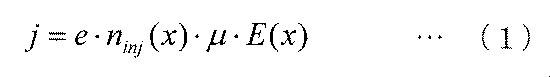
電流の通電方向をx軸とし、x=0を陽極と正孔輸送層の界面、x=dを正孔輸送層の膜厚し、膜厚は均一であるとする。陽極から注入され空間電荷を形成する正孔密度をninj(x)とすると、正孔輸送層に通電する定常電流をjは、下記式(1)で与えられる。 Assume that the direction of current flow is the x-axis, x = 0 is the interface between the anode and the hole transport layer, x = d is the film thickness of the hole transport layer, and the film thickness is uniform. When the hole density injected from the anode and forming the space charge is n inj (x), j is a steady-state current that is passed through the hole transport layer, and is given by the following formula (1).
![]()
![]()
ここで、eは電気素量(=1.6×10⁻¹⁹[C])であり、μは正孔の移動度であり、E(x)は電界である。 Here, e is the elementary charge (= 1.6 × 10 −19 [C]), μ is the mobility of holes, and E (x) is the electric field.
空間電荷ninjと樹脂内で電界Eとの関係は、下記式(2)で表されるポワソン方程式で与えられる。 The relationship between the space charge n inj and the electric field E in the resin is given by the Poisson equation expressed by the following equation (2).
ここで、εは比誘電率であり、ε0は真空の誘電率(=8.85×10⁻¹²[F/m])である。 Here, ε is a relative dielectric constant, and ε 0 is a vacuum dielectric constant (= 8.85 × 10 −12 [F / m]).
上記式(2)を上記式(1)に代入すると、下記式(3)で表される空間電荷制限電流式が得られる。 When the above equation (2) is substituted into the above equation (1), the space charge limited current equation represented by the following equation (3) is obtained.
定常状態においては、jは、座標に依らずに一定である。電界Eをx=0から膜厚dの範囲で積分することにより、下記式(4)が得られる。 In the steady state, j is constant regardless of the coordinates. The following formula (4) is obtained by integrating the electric field E in the range of x = 0 to the film thickness d.
境界条件として、x=0において、E=0とする。電流は、正孔輸送層に印加された電圧の2乗に比例し、膜厚dの3乗に反比例する。従って、膜厚の不均一な場合には、電流密度の不均一性は大きくなる。特に、薄膜部位における電流が大きくなる。 As a boundary condition, E = 0 when x = 0. The current is proportional to the square of the voltage applied to the hole transport layer and inversely proportional to the cube of the film thickness d. Therefore, when the film thickness is non-uniform, the non-uniformity of current density increases. In particular, the current at the thin film portion increases.
<オーミック電流>
図2の右上欄に示すように、本発明の硬化樹脂を正孔輸送層とした有機発光素子の場合、硬化樹脂は、イオン重合開始剤を含み、かつ、電圧を印加していない状態でも、正孔キャリアが硬化樹脂中に予めドープされている。
<Ohmic current>
As shown in the upper right column of FIG. 2, in the case of an organic light-emitting device having the cured resin of the present invention as a hole transport layer, the cured resin contains an ionic polymerization initiator and is not applied with a voltage. Hole carriers are pre-doped in the cured resin.
予めドープされた正孔密度をn0とすると、電流密度は、下記式(5)で与えられる。 When the pre-doped hole density is n 0 , the current density is given by the following formula (5).
![]()
![]()
電流は、正孔輸送層に印加された電圧に比例し、膜厚dの1乗に反比例する。従って、空間電荷制限電流機構に基づく通電と比較して、膜厚の不均一に対する電流密度の不均一性は緩和される。 The current is proportional to the voltage applied to the hole transport layer and inversely proportional to the first power of the film thickness d. Therefore, the nonuniformity of the current density with respect to the nonuniformity of the film thickness is reduced as compared with the energization based on the space charge limited current mechanism.
<オーミック電流条件>
本発明者は、イオン開始剤を添加し、予め正孔をドープした硬化樹脂であっても、通電機構がオーミック電流とはならないことを見出した。更に、正孔輸送層における通電機構が、空間電荷制限電流であるか、オーミック電流となるかを決定する評価モデルを考案した。
<Ohm current condition>
The present inventor has found that the energization mechanism does not become an ohmic current even in a cured resin in which an ion initiator is added and holes are doped in advance. Furthermore, an evaluation model was devised to determine whether the energization mechanism in the hole transport layer is a space charge limited current or an ohmic current.
以下に、評価モデルを示す。 The evaluation model is shown below.
電流密度jの算出は、空間電荷制限電流式(3)及びオーミック電流式(5)の項を結合したものを用いる。これにより、両方の現象が反映された形式となる。 The current density j is calculated using a combination of the terms of the space charge limiting current equation (3) and the ohmic current equation (5). As a result, the format reflects both phenomena.
上記式(5)においては、電界Eは座標に依らなかった。これに対して、上記式(6)の右辺第2項のオーミック電流由来の式には、空間電荷の存在による座標依存性を考慮している。両辺をxで積分すると、下記式(7)が与えられる。 In the above formula (5), the electric field E did not depend on the coordinates. On the other hand, in the equation derived from the ohmic current in the second term on the right side of the equation (6), the coordinate dependency due to the presence of space charge is considered. When both sides are integrated with x, the following equation (7) is given.
![]()
![]()
ここで、Enは、電界Eに比例する規格化された無次元の電界であり、xnは、規格化された無次元の座標である。これらは、下記式(8)及び(9)で表される。 Here, E n is a normalized dimensionless electric field proportional to the electric field E, and x n is a normalized dimensionless coordinate. These are represented by the following formulas (8) and (9).
図3は、Enとxnとの関係をプロットしたものである。横軸に規格化座標xnをとり、縦軸に規格化電界Enをとっている。 Figure 3 is a plot of the relationship between E n and x n. Take the normalized coordinates x n on the horizontal axis and taking the normalized electric field E n on the vertical axis.
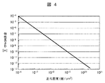
本図に示すように、xnが1よりも十分大きいと、Enは1となる。En=1に近い領域では、オーミック電流が主成分となる。一方、xnが1よりも十分小さいと、電流は空間電荷制限電流となる。従って、xnの分母で与えられる特性長さDと膜厚の関係によって、空間電荷制限電流かオーミック電流であるかが決まる。特性長さDは、下記式(10)で定義する。 As shown in the figure, the x n is sufficiently greater than 1, E n is one. In the region close to E n = 1, the ohmic current is the main component. On the other hand, when xn is sufficiently smaller than 1, the current becomes a space charge limited current. Therefore, the relationship between the characteristic length D given by the denominator of xn and the film thickness determines whether the current is a space charge limited current or an ohmic current. The characteristic length D is defined by the following formula (10).
正孔輸送層の特性として典型的な値として、正孔移動度=10−5[cm2/V/sec]、比誘電率=3.2の場合を例にとり、特性長さDと正孔密度との関係を説明する。 Typical values for the characteristics of the hole transport layer include a case where the hole mobility = 10 −5 [cm 2 / V / sec] and the relative dielectric constant = 3.2. The relationship with density will be described.
図4は、有機発光素子の動作電流密度をj=100mA/cm2におけるとした場合のDと正孔密度n0との関係を示したものである。ここで、有機発光素子は、陽極、正孔輸送層、発光層及び陰極が直列に接続された構成を有するため、有機発光素子の動作電流密度は、定常状態においては、正孔輸送層の電流密度と等しくなる。 FIG. 4 shows the relationship between D and hole density n 0 when the operating current density of the organic light emitting device is j = 100 mA / cm 2 . Here, since the organic light emitting device has a configuration in which an anode, a hole transport layer, a light emitting layer, and a cathode are connected in series, the operating current density of the organic light emitting device is the current of the hole transport layer in a steady state. It becomes equal to the density.
正孔密度n0<1018[個/cm3]では、D>20nmであり、通常の有機発光素子で用いられる各有機層の膜厚と同程度である。従って、オーミック電流とはならない。一方、n0>1019[個/cm3]以上では、D<1Åである。1Åは、空間制限電流制限に由来する電流は、原子一層分のみであり、膜全体がオーミック領域となり、オーミック電流である。 In the hole density n 0 <10 18 [pieces / cm 3 ], D> 20 nm, which is about the same as the thickness of each organic layer used in a normal organic light emitting device. Therefore, it is not an ohmic current. On the other hand, when n 0 > 10 19 [pieces / cm 3 ] or more, D <1D. First, the current derived from the space-limited current limit is only for one atom, and the entire film becomes an ohmic region, which is an ohmic current.
上記式(7)に関して、電界Eをx=0から膜厚dまで積分することで、電流密度jと正孔輸送層に印加される電圧を計算した。jは、0〜1000mA/cm2の範囲とし、移動度及び比誘電率は、図4の条件と同一とし、膜厚は40nmとした。 With respect to the above formula (7), the electric field E was integrated from x = 0 to the film thickness d to calculate the current density j and the voltage applied to the hole transport layer. j was in the range of 0 to 1000 mA / cm 2 , the mobility and relative dielectric constant were the same as those in FIG. 4, and the film thickness was 40 nm.
図5Aに結果を示す。上記式(4)に基づいて、空間電荷制限電流密度もプロットした。 The results are shown in FIG. 5A. Based on the above equation (4), the space charge limited current density was also plotted.
本図に示すように、正孔密度n0<1018[個/cm3]の範囲では、電流は電圧の二乗に比例し、空間電荷制限電流となる。これに対して、正孔密度n0>1018[個/cm3]では、電流は電圧の1乗に比例し、直線となる。すなわち、いわゆるオーミック電流となる。 As shown in this figure, in the range of hole density n 0 <10 18 [pieces / cm 3 ], the current is proportional to the square of the voltage and becomes a space charge limited current. On the other hand, when the hole density n 0 > 10 18 [pieces / cm 3 ], the current is proportional to the first power of the voltage and becomes a straight line. That is, a so-called ohmic current is obtained.
図5Bに、横軸を正孔密度n0、縦軸に電流密度500mA/cm2における電圧をプロットする。計算条件は、図5Aと同一であり、上記式(7)に関して、電界Eをx=0から膜厚dまで積分することで、電流密度jと正孔輸送層に印加される電圧を計算した。また、オーミック伝導である場合には、上記式(5)において、電界Eは、座標xに依存せずに、E=V/d(Vは印加電圧、dは膜厚)で与えられる。従って、オーミック電流の場合の電圧Vと正孔密度n0の関係は、下記式(11)で与えられる。 In FIG. 5B, the horizontal axis represents the hole density n 0 , and the vertical axis represents the voltage at a current density of 500 mA / cm 2 . The calculation conditions are the same as those in FIG. 5A, and the electric current E is integrated from x = 0 to the film thickness d by calculating the current density j and the voltage applied to the hole transport layer with respect to the above formula (7). . In the case of ohmic conduction, in the above formula (5), the electric field E is given by E = V / d (V is an applied voltage and d is a film thickness) without depending on the coordinate x. Therefore, the relationship between the voltage V and the hole density n 0 in the case of an ohmic current is given by the following formula (11).
図5Bには、上記式(11)で与えられる正孔密度と電流密度500mA/cm2における電圧の関係もプロットした。正孔密度n0>1018[個/cm3]では、上記式(7)から算出した曲線と上記式(10)から算出した曲線とが一致する。一方、n0<1018[個/cm3]では、一致せずに、電圧は、n0によらず一定となる。これは、n0<1018[個/cm3]では、電極から注入される正孔による空間電荷制限電流となるためである。従って、正孔密度n0>1018[個/cm3]で、オーミック伝導性を示すことが判る。 FIG. 5B also plots the relationship between the hole density given by the above equation (11) and the voltage at a current density of 500 mA / cm 2 . When the hole density n 0 > 10 18 [pieces / cm 3 ], the curve calculated from the above formula (7) matches the curve calculated from the above formula (10). On the other hand, when n 0 <10 18 [pieces / cm 3 ], they do not coincide with each other, and the voltage is constant regardless of n 0 . This is because when n 0 <10 18 [pieces / cm 3 ], a space charge limited current is generated by holes injected from the electrodes. Therefore, it can be seen that the hole density n 0 > 10 18 [pieces / cm 3 ] exhibits ohmic conductivity.
このようなオーミック電流となる正孔輸送層は、イオン重合開始剤と、オーミック伝導性の硬化樹脂と、を含むものである。「オーミック伝導性の硬化樹脂」は、イオン重合開始剤により化学ドープされた正孔キャリアの密度が高いため、いわゆるオーミック電流となる。 Such a hole transport layer having an ohmic current includes an ion polymerization initiator and an ohmic conductive curable resin. The “ohmic conductive cured resin” has a so-called ohmic current because the density of hole carriers chemically doped with an ionic polymerization initiator is high.
まとめると、有機発光素子において、正孔輸送層を構成する硬化樹脂は、イオン重合開始剤により化学ドープされて生じた正孔キャリアを有し、正孔輸送層は、オーミック伝導性を示す。 In summary, in the organic light emitting device, the cured resin constituting the hole transport layer has hole carriers generated by being chemically doped with the ion polymerization initiator, and the hole transport layer exhibits ohmic conductivity.
オーミック電流を与えるDの範囲としては、膜厚dの90%以上がオーミック電流領域となっていることが望ましい。図3において、規格化電界が0.9を超える規格化座標は、2.0である。規格化座標2.0以下の領域では、オーミック伝導性がない。全体の膜厚が、規格化座標2.0×10=20以上に相当する膜厚(「規格化膜厚」と定義する。)となる条件においては、オーミック伝導性のない領域が10%以下となり、全膜厚の90%以上がオーミック電流領域となる。従って、規格化膜厚=膜厚d/特性長さD>20、すなわち、特性長さDが膜厚の1/20未満の場合にオーミック電流を実現することがわかる。この状態においては、下記式(12)が満たされる。 As a range of D giving an ohmic current, it is desirable that 90% or more of the film thickness d is an ohmic current region. In FIG. 3, the standardized coordinate where the standardized electric field exceeds 0.9 is 2.0. There is no ohmic conductivity in the region where the normalized coordinate is 2.0 or less. Under conditions where the total film thickness is equivalent to a normalized coordinate of 2.0 × 10 = 20 or more (defined as “standardized film thickness”), the region without ohmic conductivity is 10% or less. Thus, 90% or more of the total film thickness becomes the ohmic current region. Therefore, it can be seen that the ohmic current is realized when the normalized film thickness = film thickness d / characteristic length D> 20, that is, the characteristic length D is less than 1/20 of the film thickness. In this state, the following formula (12) is satisfied.
上記式(12)によると、膜厚dが薄い場合、オーミック電流を実現するための不等式の上限が小さくなる。正孔輸送層の膜厚が不均一である場合には、正孔輸送層の膜厚の最小値、すなわち、正孔輸送層は、陽極又は発光層と接する界面の面積の90%以上の領域で上記不等式(12)を満たすことが望ましい。 According to the above equation (12), when the film thickness d is small, the upper limit of the inequality for realizing the ohmic current becomes small. When the film thickness of the hole transport layer is not uniform, the minimum value of the film thickness of the hole transport layer, that is, the hole transport layer is a region of 90% or more of the area of the interface in contact with the anode or the light emitting layer It is desirable to satisfy the above inequality (12).
上述の図4の説明のとおり、n0>1019[個/cm3]では、D<1Åであり、膜全体がオーミック領域となる。この望ましい状態を一般化すると、下記式(13)が得られる。 As described above with reference to FIG. 4, when n 0 > 10 19 [pieces / cm 3 ], D <1 <, and the entire film becomes an ohmic region. When this desirable state is generalized, the following formula (13) is obtained.
<正孔密度の上限値>
有機発光素子において、陽極から光を取り出す場合には、正孔輸送層で、発光層からの光を反射することは望ましくない。一般に、銅やアルミニウムなどの金属では、金属内の電子の密度nに応じて下記式(14)で与えられるプラズマ周波数ωpよりもエネルギーの小さい光を反射し、金属特有の光沢を示す。
<Upper limit of hole density>
In the organic light emitting device, when light is extracted from the anode, it is not desirable to reflect the light from the light emitting layer at the hole transport layer. In general, a metal such as copper or aluminum reflects light having energy lower than the plasma frequency ω p given by the following formula (14) according to the density n of electrons in the metal, and exhibits a gloss specific to the metal.
ここで、εは材料の比誘電率、ε0は真空の誘電率、mは電子もしくは正孔の有効質量である。銅やアルミニウムの電子密度は、1022[個/cm3]以上である。正孔輸送層における光の反射を防ぐためには、正孔密度は1022[個/cm3]以下であることが望ましい。 Here, ε is the relative dielectric constant of the material, ε 0 is the dielectric constant of vacuum, and m is the effective mass of electrons or holes. The electron density of copper or aluminum is 10 22 [pieces / cm 3 ] or more. In order to prevent reflection of light in the hole transport layer, the hole density is desirably 10 22 [pieces / cm 3 ] or less.
<正孔密度n0の測定原理>
正孔輸送層を陽極ITOと陰極Alなどの電極で挟んだ構造の素子を「ホールオンリー素子」と呼ぶ。正孔輸送層の仕事関数(5eV以上)がAlの仕事関数(4.2eV)の違いにより、正孔輸送層とAlとの界面において、正孔輸送層側で正孔密度の低い領域(「空乏層」と呼ぶ。)が発生する。空乏層の厚さd’は、下記式(15)で与えられる。
<Measurement principle of hole density n 0>
An element having a structure in which a hole transport layer is sandwiched between electrodes such as an anode ITO and a cathode Al is referred to as a “hole-only element”. Due to the difference in the work function of the hole transport layer (5 eV or more) and the work function of Al (4.2 eV), at the interface between the hole transport layer and Al, a region with a low hole density on the hole transport layer side (“ Called "depletion layer"). The thickness d ′ of the depletion layer is given by the following formula (15).
ここで、ΔΦは、正孔輸送層とAlとの仕事関数の差であり、Vは、陽極と陰極との間に加えた電圧である。 Here, ΔΦ is a difference in work function between the hole transport layer and Al, and V is a voltage applied between the anode and the cathode.
空乏層における静電容量C’は、下記式(16)で与えられる。 The capacitance C ′ in the depletion layer is given by the following formula (16).
ここで、Sは、素子の面積である。陽極と陰極との間に電圧を印加し、静電容量を測定することで、正孔密度n0が得られる。 Here, S is the area of the element. A hole density n 0 is obtained by applying a voltage between the anode and the cathode and measuring the capacitance.
空乏層に由来する静電容量は、LCRメータを用いたホールオンリー素子のインピーダンスの周波数依存性を測定することで、分離することができる。 The capacitance derived from the depletion layer can be separated by measuring the frequency dependence of the impedance of the hole-only element using an LCR meter.
<有機発光素子>
図1は、本発明の有機発光素子の一実施形態を示す模式断面図である。
<Organic light emitting device>
FIG. 1 is a schematic cross-sectional view showing an embodiment of the organic light-emitting device of the present invention.
本図において、有機発光素子101は、ガラス基板11と、陽極12と、正孔輸送層13(「正孔注入層」と呼ばれる場合もある。)と、発光層14と、電子輸送層15と、陰極16と、封止ガラス板17と、を有し、これらをこの順に積層した構成を有する。
In this figure, the organic
陽極12は、例えば、ガラス基板11上に酸化インジウムスズ(ITO)をパターニングすることによって形成される。以下、ガラス基板11上に陽極12としてITOをパターニングしたものを「ITOガラス基板」という。
The
陰極16は、例えば、ITOガラス基板である陽極12付きのガラス基板11に、正孔輸送層13及び発光層14を順次形成した後、発光層14の上にアルミニウム(Al)を蒸着することによって形成される。さらに、陰極16の上に封止ガラス板17を重ね、ガラス基板11と封止ガラス板17とを、例えば光硬化性エポキシ樹脂のような硬化樹脂を用いて貼り合わせることによって封止されることが好ましい。
For example, the
本発明の有機発光素子において、正孔輸送層は、架橋性重合体によって形成される樹脂を用いて製造される。正孔輸送層は、当該技術分野で慣用される手段を用いて製造することができる。例えば、ガラス基板上にパターニングされた陽極の上に、スピンコート法、印刷法、インクジェット法等の湿式プロセスによって本発明の硬化性重合体を塗布した後、上記で説明した硬化処理により樹脂を形成させることによって製造すればよい。 In the organic light emitting device of the present invention, the hole transport layer is produced using a resin formed of a crosslinkable polymer. A positive hole transport layer can be manufactured using the means conventionally used in the said technical field. For example, after applying the curable polymer of the present invention on an anode patterned on a glass substrate by a wet process such as a spin coating method, a printing method, or an ink jet method, a resin is formed by the curing treatment described above. What is necessary is just to manufacture by making it.
重合性塗布液によって形成される樹脂は、硬化性が高く、有機溶媒耐性に優れる。このため、前記樹脂を用いて製造された正孔輸送層の表面に、例えば上記の湿式プロセスによって発光層を積層させる場合、発光層の塗布溶液に含まれる有機溶媒によって正孔輸送層が溶解することを抑制することができる。例えば、本発明の硬化性重合体によって形成される樹脂を用いて製造される正孔輸送層は、通常、残膜率が60〜100%の範囲であり、典型的には80〜99%の範囲である。上記の残膜率で表される有機溶媒耐性を有する樹脂は硬化性が高い。それ故、本発明の樹脂を正孔輸送層に用いることにより、湿式プロセスによる有機発光素子の生産性を向上させることが可能となる。 The resin formed by the polymerizable coating solution has high curability and excellent organic solvent resistance. For this reason, when laminating a light emitting layer on the surface of the hole transport layer manufactured using the resin by, for example, the above wet process, the hole transport layer is dissolved by the organic solvent contained in the light emitting layer coating solution. This can be suppressed. For example, a hole transport layer produced using a resin formed from the curable polymer of the present invention usually has a remaining film ratio in the range of 60 to 100%, typically 80 to 99%. It is a range. The resin having organic solvent resistance expressed by the above remaining film ratio has high curability. Therefore, by using the resin of the present invention for the hole transport layer, it becomes possible to improve the productivity of the organic light emitting device by a wet process.
なお、残膜率の評価は、例えば以下の手順で実施することができる。ITOガラス基板の陽極の上に、本発明の硬化性重合体及びイオン重合開始剤によって形成される樹脂を用いて正孔輸送層を作製する。正孔輸送層が形成されたITOガラス基板を、有機溶媒(例えばトルエン)に20〜250℃、10〜60秒間の条件で浸漬させる。その後、ITOガラス基板を有機溶媒中から取り出し、浸漬前後の薄膜の吸光度を測定した。吸光度の比より薄膜の残存率(残膜率)を求めた。吸光度は、膜厚に比例するので、吸光度の比(浸漬あり/浸漬なし)は、正孔輸送層の残膜率(浸漬あり/浸漬なし)に一致する。残膜率が高い程、有機溶媒耐性が高いと評価される。 The remaining film rate can be evaluated, for example, according to the following procedure. On the anode of the ITO glass substrate, a hole transport layer is prepared using a resin formed by the curable polymer of the present invention and an ionic polymerization initiator. The ITO glass substrate on which the hole transport layer is formed is immersed in an organic solvent (for example, toluene) at 20 to 250 ° C. for 10 to 60 seconds. Thereafter, the ITO glass substrate was taken out from the organic solvent, and the absorbance of the thin film before and after immersion was measured. The residual ratio of the thin film (residual film ratio) was determined from the absorbance ratio. Since the absorbance is proportional to the film thickness, the ratio of absorbance (with / without immersion) corresponds to the remaining film ratio (with / without immersion) of the hole transport layer. It is evaluated that the higher the residual film ratio, the higher the organic solvent resistance.
以下、実施例を用いて本発明を更に具体的に説明する。但し、本発明の技術的範囲は、これらの実施例に限定されるものではない。 Hereinafter, the present invention will be described more specifically with reference to examples. However, the technical scope of the present invention is not limited to these examples.
オーミック伝導性の正孔輸送層に用いる硬化樹脂について説明する。 The cured resin used for the ohmic conductive hole transport layer will be described.
[架橋性重合体の合成]
直鎖状トリフェニルアミンモノマ(1)、分岐状トリフェニルアミンモノマ(2)、オキセタン架橋モノマ(3)を、鈴木反応で重合して、架橋性重合体を合成した。架橋性の直鎖状トリフェニルアミンモノマ(1)及び分岐トリフェニルアミンモノマ(2)は、鈴木反応の反応点を、それぞれ、2個及び3個有しており、重合によって主鎖を形成する。架橋性のオキセタン架橋モノマ(3)は、いずれも鈴木反応の反応点を1個有しており、重合によって側鎖を形成する。架橋性のオキセタン架橋モノマ(3)は、フェニレン及びオキシメチレンの組み合わせからなる二価の架橋基に、1−エチルオキセタン−1−イル基が結合した構造を有するモノマである。
[Synthesis of crosslinkable polymer]
A linear triphenylamine monomer (1), a branched triphenylamine monomer (2), and an oxetane crosslinked monomer (3) were polymerized by the Suzuki reaction to synthesize a crosslinkable polymer. The crosslinkable linear triphenylamine monomer (1) and branched triphenylamine monomer (2) have two and three reaction points for the Suzuki reaction, respectively, and form a main chain by polymerization. . Each of the crosslinkable oxetane crosslinked monomers (3) has one reaction point of the Suzuki reaction and forms a side chain by polymerization. The crosslinkable oxetane crosslinked monomer (3) is a monomer having a structure in which a 1-ethyloxetane-1-yl group is bonded to a divalent crosslinking group composed of a combination of phenylene and oxymethylene.
丸底フラスコに、4,4’−ビス(4,4,5,5−テトラメチル−1,3,2−ジオキサボロラン−2−イル)−4”−n−ブチルトリフェニルアミン(1)(0.4mmol)、4,4’,4”−トリブロモトリフェニルアミン(2)(1.0mmol)、3−(4−ブロモフェノキシメチル)3−エチルオキセタン(3)(1.2mmol)、2−ブロモ−3−n−オクチルチオフェン(4)(5.3mmol)、テトラキストリフェニルホスフィンパラジウム(0.008mmol)、2M炭酸カリウム水溶液(5.3mmol)、Aliquat(登録商標)336(0.4mmol)及びアニソール(4ml)を入れ、窒素雰囲気下、90℃で2時間撹拌した。 In a round bottom flask, 4,4′-bis (4,4,5,5-tetramethyl-1,3,2-dioxaborolan-2-yl) -4 ″ -n-butyltriphenylamine (1) (0 .4 mmol), 4,4 ′, 4 ″ -tribromotriphenylamine (2) (1.0 mmol), 3- (4-bromophenoxymethyl) 3-ethyloxetane (3) (1.2 mmol), 2- Bromo-3-n-octylthiophene (4) (5.3 mmol), tetrakistriphenylphosphine palladium (0.008 mmol), 2M aqueous potassium carbonate (5.3 mmol), Aliquat® 336 (0.4 mmol) and Anisole (4 ml) was added, and the mixture was stirred at 90 ° C. for 2 hours under a nitrogen atmosphere.
上記の方法で、架橋性直鎖状トリフェニルアミンモノマ(1):架橋性分岐トリフェニルアミンモノマ(2):架橋性オキセタン架橋モノマ(3)=20:50:40のモル比で合成したところ、分子量40kDaの架橋基を有する高分子組成物Aを得た。分子量は、ゲル浸透クロマトグラフィーを用いて、ポリスチレン換算で測定したときの数平均で決定した。 When synthesized by the above method at a molar ratio of crosslinkable linear triphenylamine monomer (1): crosslinkable branched triphenylamine monomer (2): crosslinkable oxetane crosslinked monomer (3) = 20: 50: 40 A polymer composition A having a crosslinking group with a molecular weight of 40 kDa was obtained. The molecular weight was determined by the number average when measured in terms of polystyrene using gel permeation chromatography.
[塗布液の調製]
上記硬化性重合体(オリゴマ)を(4.2mg)、上記構造式(4)で表されるイオン開始剤(式中、カチオンのR11、R12はHであり、s1、s2=1、アニオンX=(C6F5)4B)を0.02、0.04、0.42mg(100質量部の硬化性重合体に対して、それぞれ、z=0.5、1.0、10質量部に対応する。)のいずれかの濃度として1.2mlのトルエンに溶解する。
[Preparation of coating solution]
(4.2 mg) of the curable polymer (oligomer), an ion initiator represented by the structural formula (4) (wherein R 11 and R 12 of the cation are H, s1, s2 = 1, Anion X = (C 6 F 5 ) 4 B) 0.02, 0.04, 0.42 mg (for 100 parts by weight of curable polymer, z = 0.5, 1.0, 10 It is dissolved in 1.2 ml of toluene as one of the concentrations of 1).
イオン開始剤の濃度が0.42mgの場合には、イオン開始剤が高濃度であるため、溶液に濁りが発生した。硬化性重合体4.2mgを0.6mlのトルエンに、イオン重合開始剤0.42mgを0.6mlのトルエンに分けて溶解し、混合したところ、濁りは消失した。 When the concentration of the ion initiator was 0.42 mg, the solution was turbid because the ion initiator was at a high concentration. When 4.2 mg of the curable polymer was dissolved in 0.6 ml of toluene and 0.42 mg of the ionic polymerization initiator was dissolved in 0.6 ml of toluene and mixed, the turbidity disappeared.
[架橋性重合体を用いた樹脂の形成]
酸化インジウムスズ(ITO:Indium Tin Oxide)を、1.6mm幅でガラス基板上にパターンニングした。このITOガラス基板上に、上記の塗布液を300回転/分の条件でスピンコートした。その後、架橋性重合体をコートしたITOガラス基板を、ホットプレート上で180℃、7分間加熱することで硬化処理して、硬化性重合体を加熱重合させて、樹脂を形成させた。本樹脂を、樹脂A(z)(z=0.5,1.0,10質量部)とする。
[Formation of resin using crosslinkable polymer]
Indium tin oxide (ITO: Indium Tin Oxide) was patterned on a glass substrate with a width of 1.6 mm. The above coating solution was spin-coated on this ITO glass substrate at 300 rpm. Thereafter, the ITO glass substrate coated with the crosslinkable polymer was cured by heating at 180 ° C. for 7 minutes on a hot plate, and the curable polymer was heat polymerized to form a resin. This resin is referred to as resin A (z) (z = 0.5, 1.0, 10 parts by mass).
[残膜率の評価]
樹脂A(z)(z=0.5、1.0、10質量部)の薄膜をガラス板ごとトルエン中でリンスし、リンス前後の薄膜の吸光度を測定し、リンス前後の吸光度の比より薄膜の残存率(残膜率)を求めた。樹脂A’及びA”の樹脂は、残膜率は90%以上だった。
[Evaluation of remaining film ratio]
A thin film of resin A (z) (z = 0.5, 1.0, 10 parts by mass) is rinsed with toluene in a glass plate, and the absorbance of the thin film before and after rinsing is measured. The residual ratio (remaining film ratio) was determined. Resins A ′ and A ″ had a residual film ratio of 90% or more.
[ホールオンリー素子の評価]
上記の樹脂A(z)(z=0.5、1.0、10質量部)の試料の上に100nmの膜厚のAl電極を蒸着させた。この素子を「ホールオンリー素子」と呼ぶ。本実施例では、上記の[架橋性重合体を用いた樹脂の形成]にて説明した方法で樹脂を形成した後に、1.6mm幅のAl(膜厚100nm)層をパターンニングした。ITOパターンとAlパターンが交差する面が発光素子となり、素子の面積は1.6×1.6mm2で与えられる。
[Evaluation of Hall-only devices]
An Al electrode having a thickness of 100 nm was deposited on a sample of the resin A (z) (z = 0.5, 1.0, 10 parts by mass). This element is called a “hole-only element”. In this example, after the resin was formed by the method described in [Formation of Resin Using Crosslinkable Polymer], an Al (film thickness: 100 nm) layer having a width of 1.6 mm was patterned. A surface where the ITO pattern and the Al pattern intersect is a light emitting element, and the area of the element is given by 1.6 × 1.6 mm 2 .
図6Aは、各試料の電圧と電流密度との関係を示すグラフである。図6Bは、図6Aの電流密度の電圧に関する微分値を算出して示したものである。いずれの試料においても、平均膜厚は40nmであった。静電容量を測定し、比誘電率は3.2が得られた。 FIG. 6A is a graph showing the relationship between the voltage and current density of each sample. FIG. 6B shows a calculated differential value related to the voltage of the current density shown in FIG. 6A. In any sample, the average film thickness was 40 nm. The capacitance was measured, and a relative dielectric constant of 3.2 was obtained.
これらの図から、z=0.5、1.0質量部の試料では空間電荷制限電流となっている。これに対して、z=10質量部の試料ではオーミック電流となっていることがわかる。 From these figures, the sample of z = 0.5 and 1.0 part by mass has a space charge limiting current. On the other hand, it can be seen that the sample with z = 10 parts by mass has an ohmic current.
z=0.5、1.0質量部の電流密度の微分値は、電圧とともに増大した。電流密度の微分値の傾きを線形と仮定すると、空間電荷制限電流式(4)を用いて、正孔の移動度10−5[cm2/Vsec]を得た。 The differential value of the current density of z = 0.5, 1.0 part by mass increased with the voltage. Assuming that the slope of the differential value of the current density is linear, the hole mobility of 10 −5 [cm 2 / Vsec] was obtained using the space charge limited current equation (4).
これに対して、z=10質量部では、印加電圧0の状態から、大きな微分値を有する。これは、z=10質量部では、オーミック伝導であることを示す。
On the other hand, in z = 10 mass parts, it has a big differential value from the state of the applied
よって、硬化樹脂とイオン重合開始剤との質量比は、100:10以上であることが望ましい。 Therefore, the mass ratio between the cured resin and the ionic polymerization initiator is desirably 100: 10 or more.
[正孔密度n0の測定]
図7は、ホールオンリー素子及びインピーダンス測定系を示す模式構成図である。
[Measurement of hole density n 0 ]
FIG. 7 is a schematic configuration diagram showing a hole-only element and an impedance measurement system.
本図において、ホールオンリー素子501は、ガラス基板11と、陽極12と、正孔輸送層13と、陰極16と、を有し、これらをこの順に積層した構成を有する。ホールオンリー素子501の陽極12及び陰極16には、LCRメータ502が接続されている。LCRメータ502としては、NF回路ブロックZM2376を用いた。
In this drawing, a hole-
このような構成により、ホールオンリー素子501の静電容量を測定した。印加電圧0Vのもとでは、0.1〜100Hzの範囲で、0.5質量部の樹脂で4×10⁻⁹[F]、1.0質量部の樹脂で1×10⁻⁹[F]、1.0質量部の樹脂で3×10⁻¹⁰[F]の静電容量成分を計測した。陽極をプラス、陰極をマイナスとして0Vから0.8Vまでの範囲で電圧を印加すると、静電容量は増加した。一方、陽極をマイナス、陰極をプラスとして0Vから2.5Vまでの範囲で電圧を印加すると、静電容量は減少した。そして、上記式(13)及び(14)を用いて、正孔密度n0を算出した。
With such a configuration, the capacitance of the hole-only
ホールオンリー素子の直流特性が空間電荷制限電流を示したz=0.5質量部の素子では、正孔密度は1018[個/cm3]以下、z=1.0質量部の素子では、正孔密度は1018[個/cm3]程度であった。一方、オーミック電流を示したz=10質量部の素子では、正孔密度が2×1019[個/cm3]であった。 In the element of z = 0.5 part by mass where the direct current characteristic of the hole-only element indicates space charge limited current, the hole density is 10 18 [pieces / cm 3 ] or less, and in the element of z = 1.0 part by mass, The hole density was about 10 18 [pieces / cm 3 ]. On the other hand, in the element of z = 10 parts by mass that showed an ohmic current, the hole density was 2 × 10 19 [pieces / cm 3 ].
また、イオン重合開始剤の質量部が大きいほど、正孔密度が大きい。これは、正孔がイオン重合開始剤により化学ドープされるためである。 Moreover, the larger the mass part of the ionic polymerization initiator, the larger the hole density. This is because holes are chemically doped with an ion polymerization initiator.
正孔密度が1022[個/cm3]まで増加すると、金属光沢を示すことが懸念される。 When the hole density increases to 10 22 [pieces / cm 3 ], there is a concern that a metallic luster is exhibited.
ここで、正孔密度がイオン重合開始剤の質量部に比例すると仮定し、イオン重合開始剤の10質量部における正孔密度を1019[個/cm3]のオーダーとすると、1022[個/cm3]/1019[個/cm3]=1000、すなわち、イオン重合開始剤の質量部は、上記の10質量部の1000倍である10000質量部以下であることが望ましいことになる。 Here, assuming that the hole density is proportional to the mass part of the ion polymerization initiator, and the hole density in 10 mass parts of the ion polymerization initiator is on the order of 10 19 [pieces / cm 3 ], 10 22 [pieces]. / Cm 3 ] / 10 19 [pieces / cm 3 ] = 1000, that is, the mass part of the ion polymerization initiator is desirably 10,000 parts by mass or less, which is 1000 times the above 10 parts by mass.
以上をまとめると、100質量部の硬化性重合体(硬化樹脂)に対して、イオン重合開始剤は、10質量部以上10000質量部以下であることが望ましい。 In summary, the ionic polymerization initiator is preferably 10 parts by mass or more and 10000 parts by mass or less with respect to 100 parts by mass of the curable polymer (cured resin).
有機発光素子の作製及びその静電容量の測定について説明する。 The production of the organic light emitting device and the measurement of its capacitance will be described.
[有機発光素子の作製]
ITOを1.6mm幅にパターンニングしたガラス基板上に、正孔輸送層(40nm)として、実施例1に記載の方法で、樹脂A(z)(z=0.5,10質量部)からなる積層した。次に、得られたガラス基板を真空蒸着装置中に移し、CBP+Ir(piq)3(40nm)、BAlq(10nm)、Alq3(30nm)、LiF(膜厚0.5nm)の順に蒸着した。最後に1.6mm幅のAl(膜厚100nm)層をパターンニングした。ITOパターンとAlパターンが交差する面が発光素子となり、素子の面積は1.6×1.6mm2である。
[Production of organic light-emitting element]
From the resin A (z) (z = 0.5, 10 parts by mass) by the method described in Example 1 as a hole transport layer (40 nm) on a glass substrate patterned with a width of 1.6 mm of ITO. Laminated. Next, the obtained glass substrate was transferred into a vacuum deposition apparatus, and CBP + Ir (piq) 3 (40 nm), BAlq (10 nm), Alq 3 (30 nm), and LiF (film thickness 0.5 nm) were deposited in this order. Finally, a 1.6 mm wide Al (film thickness: 100 nm) layer was patterned. A surface where the ITO pattern and the Al pattern intersect is a light emitting element, and the area of the element is 1.6 × 1.6 mm 2 .
電極形成後、大気開放することなく、乾燥窒素環境中に基板を移動し、0.7mmの無アルカリガラスに0.4mmのザグリを入れた封止ガラスとITO基板を、光硬化性エポキシ樹脂を用いて貼り合わせることにより封止を行い、多層構造の高分子型有機EL素子を作製した。 After electrode formation, the substrate is moved into a dry nitrogen environment without opening to the atmosphere, and the sealing glass and ITO substrate in which 0.4 mm of counterbore is added to 0.7 mm non-alkali glass are coated with a photocurable epoxy resin. Sealing was performed by using them together to produce a polymer organic EL device having a multilayer structure.
<測定例:有機発光素子の静電容量>
図8は、有機発光素子及びインピーダンス測定系を示す模式構成図である。
<Measurement example: Capacitance of organic light emitting device>
FIG. 8 is a schematic configuration diagram showing an organic light emitting device and an impedance measurement system.
本図において、有機発光素子101は、ガラス基板11と、陽極12と、正孔輸送層13と、発光層14と、電子輸送層15と、陰極16と、封止ガラス板17と、を有し、これらをこの順に積層した構成を有する。有機発光素子101の陽極12及び陰極16には、LCRメータ502が接続されている。LCRメータ502としては、NF回路ブロックZM2376を用いた。
In this figure, the organic
このような構成により、有機発光素子101の静電容量を測定した。
With such a configuration, the capacitance of the organic
オーミック伝導性を示す硬化樹脂を正孔輸送層として用いた有機EL素子A(z)(z=10質量部)では、電圧を印加していない状態の静電容量は、9×10⁻⁹[F]であった。この静電容量は、本実施例で用いた有機層のうち、発光層(CBP+Ir(piq)3(40nm))、電子輸送層(BAlq(10nm)、Alq3(30nm)、LiF(膜厚0.5nm))において、各層の誘電率εを3.2とし、発光層及び電子輸送層厚さの合計W=80.5nm、素子の面積S=1.6×1.6mm2から、下記式(17)で定義される幾何容量C(厚さ及び面積の幾何学構造で決定される静電容量)と一致する。
In the organic EL element A (z) (z = 10 parts by mass) using a cured resin showing ohmic conductivity as the hole transport layer, the capacitance in the state where no voltage is applied is 9 × 10 −9 [ F]. Among the organic layers used in this example, this capacitance is the light emitting layer (CBP + Ir (piq) 3 (40 nm)), the electron transport layer (BAlq (10 nm), Alq 3 (30 nm), LiF (
すなわち、静電容量は、有機層のうち、正孔輸送層の寄与を除いた層の幾何容量で与えられる。更に、陰極と陽極との間に電圧を−0.5Vから0.5Vまで印加した場合にも、静電容量の変化は見られなかった。これは、オーミック伝導性を示す硬化樹脂である正孔輸送層の静電容量が無視でき、抵抗体として機能していることを示す。 That is, the capacitance is given by the geometric capacitance of the organic layer excluding the contribution of the hole transport layer. Furthermore, no change in capacitance was observed when a voltage of −0.5 V to 0.5 V was applied between the cathode and the anode. This indicates that the capacitance of the hole transport layer, which is a cured resin showing ohmic conductivity, is negligible and functions as a resistor.
一方、空間電荷制限電流を示す硬化樹脂を正孔輸送層として用いた有機EL素子A(z)(z=1質量部)では、電圧を印加していない状態の静電容量は、7×10⁻⁹[F]と低下した。これは、有機EL素子A(z)(z=10質量部)にて観測した発光層及び電子輸送層厚さに相当する幾何容量と、空間電荷制限電流を示す硬化樹脂の静電容量からなる合成容量が低下したためである。更に、陰極と陽極間に電圧を0Vから0.5Vまで印加すると、静電容量は増加した。更に、電圧を5V以上印加すると、有機EL素子A(z)(z=10質量部)にて観測した発光層及び電子輸送層厚さに相当する幾何容量9×10⁻⁹[F]の一定値となった。一方、陰極と陽極間に電圧を0Vから−0.5Vまで印加すると、静電容量は減少した。これは、正孔密度が低い空間電荷制限電流を示す硬化樹脂では、正孔輸送層と発光層との間に空乏層が発現するためである。 On the other hand, in the organic EL element A (z) (z = 1 part by mass) using a cured resin showing a space charge limited current as a hole transport layer, the capacitance in the state where no voltage is applied is 7 × 10. It decreased to -9 [F]. This is composed of a geometric capacity corresponding to the thickness of the light emitting layer and the electron transport layer observed in the organic EL element A (z) (z = 10 parts by mass) and a capacitance of a cured resin exhibiting a space charge limited current. This is because the synthetic capacity has decreased. Furthermore, when the voltage was applied from 0V to 0.5V between the cathode and the anode, the capacitance increased. Furthermore, when a voltage of 5 V or more is applied, the geometric capacitance 9 × 10 −9 [F] corresponding to the thickness of the light emitting layer and the electron transport layer observed in the organic EL element A (z) (z = 10 parts by mass) is constant. Value. On the other hand, when the voltage was applied from 0V to -0.5V between the cathode and the anode, the capacitance decreased. This is because a depletion layer appears between the hole transport layer and the light emitting layer in the cured resin having a space charge limited current with a low hole density.
<使用例:有機発光素子の性能評価>
実施例2の有機EL素子A(z)(z=0.5,10質量部)の性能評価は、大気中、室温(25℃)において評価した。
<Usage example: Performance evaluation of organic light emitting device>
The performance evaluation of the organic EL device A (z) (z = 0.5, 10 parts by mass) of Example 2 was performed in the atmosphere at room temperature (25 ° C.).
3000cd/m2の輝度を維持するための電圧は、有機発光素子A(z=0.5質量部)においては、5.8Vであったのに対して、発光素子A(z=10質量部)では、5.0Vであった。また、初期輝度3000cd/m2となる電圧一定の条件で、輝度の変化を測定したところ、輝度が1500cd/m2となる時間は、有機発光素子A(z=0.5質量部)では、55時間であったのに対して、有機発光素子A(z=10質量部)では、80時間に向上した。 The voltage for maintaining the luminance of 3000 cd / m 2 was 5.8 V in the organic light emitting device A (z = 0.5 parts by mass), whereas the voltage for the light emitting device A (z = 10 parts by mass). ) Was 5.0V. Also, the initial brightness 3000 cd / m 2 and comprising voltage certain conditions, was measured changes in intensity, time luminance is 1500 cd / m 2 is, in the organic light-emitting element A (z = 0.5 parts by weight), Compared to 55 hours, the organic light emitting device A (z = 10 parts by mass) improved to 80 hours.
本発明の有機発光素子は、高効率化と長寿命化とを両立できる。 The organic light emitting device of the present invention can achieve both high efficiency and long life.
101:有機EL素子、11:ガラス基板、12:陽極、13:正孔輸送層(オーミック伝導性の硬化樹脂)、14:発光層、15:電子輸送層、16:陰極、17:封止ガラス板、21:ガラス基板、22:陽極、23a:正孔輸送層(空間電荷制限伝導性の硬化樹脂)、23b:正孔輸送層(空間電荷制限伝導性の硬化樹脂)、23c:正孔輸送層(オーミック伝導性の硬化樹脂)、23d:正孔輸送層(オーミック伝導性の硬化樹脂)、24:発光層、25:電子輸送層、26:陰極、27:正孔キャリア、28:電子キャリア。 101: Organic EL element, 11: Glass substrate, 12: Anode, 13: Hole transport layer (ohmic conductive cured resin), 14: Light emitting layer, 15: Electron transport layer, 16: Cathode, 17: Sealing glass Plate, 21: Glass substrate, 22: Anode, 23a: Hole transport layer (space charge limited conductive cured resin), 23b: Hole transport layer (space charge limited conductive cured resin), 23c: Hole transport Layer (ohmic conductive cured resin), 23d: hole transport layer (ohmic conductive cured resin), 24: light emitting layer, 25: electron transport layer, 26: cathode, 27: hole carrier, 28: electron carrier .
Claims (10)
前記正孔輸送層は、前記陽極と前記発光層との間に配置され、
前記正孔輸送層は、イオン重合開始剤と、硬化樹脂と、を含み、
前記硬化樹脂は、前記イオン重合開始剤により化学ドープされて生じた正孔キャリアを有し、
前記正孔輸送層は、オーミック伝導性を示す、有機発光素子。 An anode, a hole transport layer, a light emitting layer, and a cathode,
The hole transport layer is disposed between the anode and the light emitting layer;
The hole transport layer includes an ionic polymerization initiator and a cured resin,
The curable resin has hole carriers generated by being chemically doped with the ion polymerization initiator,
The hole transport layer is an organic light emitting device exhibiting ohmic conductivity.
前記正孔輸送層の電流密度j(A/m2)は、下記不等式(1)を満たすことを特徴とする有機発光素子。
The current density j (A / m 2 ) of the hole transport layer satisfies the following inequality (1).
前記正孔輸送層の電流密度j(A/m2)は、下記不等式(2)を満たすことを特徴とする有機発光素子。
The current density j (A / m 2 ) of the hole transport layer satisfies the following inequality (2).
有機発光素子の静電容量が正孔輸送層を除いた有機層の幾何容量で与えられることを特徴とする有機発光素子。 In the organic light emitting element as described in any one of Claims 1-3,
An organic light-emitting device, wherein the capacitance of the organic light-emitting device is given by the geometric capacitance of the organic layer excluding the hole transport layer.
前記正孔輸送層は、前記陽極又は前記発光層と接する界面の面積の90%以上の領域で前記不等式(1)を満たすことを特徴とする有機発光素子。 The organic light emitting device according to claim 2, wherein
The organic light emitting device, wherein the hole transport layer satisfies the inequality (1) in a region of 90% or more of an area of an interface contacting the anode or the light emitting layer.
前記陽極と前記陰極との間に+0.5Vから−0.5Vまでの範囲の電圧を印加した条件における前記有機発光素子の静電容量がほぼ一定であることを特徴とする有機発光素子。 In the organic light emitting element according to any one of claims 1 to 5,
An organic light-emitting device, wherein a capacitance of the organic light-emitting device is substantially constant under a condition in which a voltage in a range of +0.5 V to -0.5 V is applied between the anode and the cathode.
前記硬化樹脂は、下記構造式(1)〜(3)のいずれか1種類のモノマを重合して形成されたものを含むことを特徴とする有機発光素子。
The cured resin includes an organic light-emitting element formed by polymerizing any one of the following structural formulas (1) to (3).
前記イオン重合開始剤は、下記構造式(4)〜(6)のいずれか1種類の化合物であることを特徴とする有機発光素子。
The organic light-emitting device, wherein the ionic polymerization initiator is a compound of any one of the following structural formulas (4) to (6).
前記イオン重合開始剤と前記硬化樹脂との質量比は、10:100以上であることを特徴とする有機発光素子。 In the organic light emitting element according to any one of claims 1 to 8,
The organic light-emitting device, wherein a mass ratio of the ionic polymerization initiator to the curable resin is 10: 100 or more.
前記イオン重合開始剤と前記硬化樹脂との質量比は、10:100以上かつ10000:100以下であることを特徴とする有機発光素子。 In the organic light emitting element according to any one of claims 1 to 9,
The organic light-emitting device, wherein a mass ratio of the ionic polymerization initiator and the curable resin is 10: 100 or more and 10000: 100 or less.
Priority Applications (7)
| Application Number | Priority Date | Filing Date | Title |
|---|---|---|---|
| JP2016019476A JP2017139342A (en) | 2016-02-04 | 2016-02-04 | Organic light-emitting element |
| EP16889388.1A EP3413368A4 (en) | 2016-02-04 | 2016-11-24 | Organic light emission element |
| PCT/JP2016/084757 WO2017134905A1 (en) | 2016-02-04 | 2016-11-24 | Organic light emission element |
| KR1020187021594A KR20180098374A (en) | 2016-02-04 | 2016-11-24 | Organic light emitting device |
| US16/072,899 US20190040187A1 (en) | 2016-02-04 | 2016-11-24 | Organic light emitting device |
| CN201680079964.7A CN108886102A (en) | 2016-02-04 | 2016-11-24 | Organic illuminating element |
| TW106101415A TW201740589A (en) | 2016-02-04 | 2017-01-16 | Organic light emission element |
Applications Claiming Priority (1)
| Application Number | Priority Date | Filing Date | Title |
|---|---|---|---|
| JP2016019476A JP2017139342A (en) | 2016-02-04 | 2016-02-04 | Organic light-emitting element |
Publications (1)
| Publication Number | Publication Date |
|---|---|
| JP2017139342A true JP2017139342A (en) | 2017-08-10 |
Family
ID=59499545
Family Applications (1)
| Application Number | Title | Priority Date | Filing Date |
|---|---|---|---|
| JP2016019476A Pending JP2017139342A (en) | 2016-02-04 | 2016-02-04 | Organic light-emitting element |
Country Status (7)
| Country | Link |
|---|---|
| US (1) | US20190040187A1 (en) |
| EP (1) | EP3413368A4 (en) |
| JP (1) | JP2017139342A (en) |
| KR (1) | KR20180098374A (en) |
| CN (1) | CN108886102A (en) |
| TW (1) | TW201740589A (en) |
| WO (1) | WO2017134905A1 (en) |
Families Citing this family (1)
| Publication number | Priority date | Publication date | Assignee | Title |
|---|---|---|---|---|
| JP2018203889A (en) * | 2017-06-06 | 2018-12-27 | 日立化成株式会社 | Curable polymer, polymerization liquid, conductive film and organic light-emitting element |
Citations (3)
| Publication number | Priority date | Publication date | Assignee | Title |
|---|---|---|---|---|
| JP2003264085A (en) * | 2001-12-05 | 2003-09-19 | Semiconductor Energy Lab Co Ltd | Organic semiconductor element, organic electroluminescence element and organic solar cell |
| JP2006233162A (en) * | 2004-03-11 | 2006-09-07 | Mitsubishi Chemicals Corp | Composition for charge transport membrane and ionic compound, charge transport membrane and organic electroluminescent device each using the same, and method for producing the device and method for producing the membrane |
| JP2015012105A (en) * | 2013-06-28 | 2015-01-19 | 日立化成株式会社 | Organic light-emitting element |
Family Cites Families (4)
| Publication number | Priority date | Publication date | Assignee | Title |
|---|---|---|---|---|
| SG176316A1 (en) * | 2001-12-05 | 2011-12-29 | Semiconductor Energy Lab | Organic semiconductor element |
| TWI474759B (en) | 2007-02-15 | 2015-02-21 | Mitsubishi Chem Corp | Method for manufacturing organic field emitting element and organic field emitting element |
| JP5491796B2 (en) * | 2008-08-11 | 2014-05-14 | 三菱化学株式会社 | Charge transporting polymer, composition for organic electroluminescent device, organic electroluminescent device, organic EL display and organic EL lighting |
| US9502657B2 (en) | 2012-09-07 | 2016-11-22 | Pioneer Corporation | Organic electroluminescence device and manufacturing method thereof |
-
2016
- 2016-02-04 JP JP2016019476A patent/JP2017139342A/en active Pending
- 2016-11-24 CN CN201680079964.7A patent/CN108886102A/en active Pending
- 2016-11-24 EP EP16889388.1A patent/EP3413368A4/en not_active Withdrawn
- 2016-11-24 KR KR1020187021594A patent/KR20180098374A/en not_active Application Discontinuation
- 2016-11-24 WO PCT/JP2016/084757 patent/WO2017134905A1/en active Application Filing
- 2016-11-24 US US16/072,899 patent/US20190040187A1/en not_active Abandoned
-
2017
- 2017-01-16 TW TW106101415A patent/TW201740589A/en unknown
Patent Citations (3)
| Publication number | Priority date | Publication date | Assignee | Title |
|---|---|---|---|---|
| JP2003264085A (en) * | 2001-12-05 | 2003-09-19 | Semiconductor Energy Lab Co Ltd | Organic semiconductor element, organic electroluminescence element and organic solar cell |
| JP2006233162A (en) * | 2004-03-11 | 2006-09-07 | Mitsubishi Chemicals Corp | Composition for charge transport membrane and ionic compound, charge transport membrane and organic electroluminescent device each using the same, and method for producing the device and method for producing the membrane |
| JP2015012105A (en) * | 2013-06-28 | 2015-01-19 | 日立化成株式会社 | Organic light-emitting element |
Also Published As
| Publication number | Publication date |
|---|---|
| WO2017134905A1 (en) | 2017-08-10 |
| US20190040187A1 (en) | 2019-02-07 |
| EP3413368A1 (en) | 2018-12-12 |
| EP3413368A4 (en) | 2019-09-04 |
| CN108886102A (en) | 2018-11-23 |
| TW201740589A (en) | 2017-11-16 |
| KR20180098374A (en) | 2018-09-03 |
Similar Documents
| Publication | Publication Date | Title |
|---|---|---|
| US10134988B2 (en) | System for forming an electroactive layer | |
| Lee et al. | Luminescence properties of structurally modified PPVs: PPV derivatives bearing 2-(4-tert-butylphenyl)-5-phenyl-1, 3, 4-oxadiazole pendants | |
| TWI388432B (en) | Hole injection/transport layer compositions and devices | |
| KR101516813B1 (en) | Organic electronic devices | |
| CN102106017B (en) | Organic electroluminescent element, organic el display device and organic EL illuminating device | |
| WO2008029155A2 (en) | Conductive polymer compositions in opto-electrical devices | |
| CN102349172A (en) | Process for manufacturing organic electroluminescent element, organic electroluminescent element, organic EL display, and organic EL lighting | |
| TW201823422A (en) | Organic electronic material and use of same | |
| JP2015012105A (en) | Organic light-emitting element | |
| JP2016167570A (en) | Organic light-emitting element | |
| TWI675048B (en) | Curable polymer, polymerization liquid, conductive film, and organic light emitting device | |
| EP2673818A2 (en) | Process and materials for making contained layers and devices made with same | |
| WO2017134905A1 (en) | Organic light emission element | |
| JPWO2018139487A1 (en) | Organic electronic material, ink composition, organic layer, organic electronic element, organic electroluminescent element, display element, lighting device, and display device | |
| JP7409088B2 (en) | Organic thin film manufacturing method, organic thin film and its use | |
| WO2020065926A1 (en) | Organic electronic material and use thereof | |
| JP5304301B2 (en) | Organic electroluminescence device, organic EL display and organic EL lighting | |
| WO2019167346A1 (en) | Curable polymer, polymerization solution and resin, and organic light-emitting element manufactured using same | |
| JP6891505B2 (en) | Manufacturing method of organic electroluminescent device | |
| Dey | Synthesis and characterizations of bis-diazirines and their applications in organic electronics | |
| JP2014192355A (en) | Material for organic electroluminescent element and organic electroluminescent element using the same | |
| JP2018181872A (en) | Charge transport material, ink composition, and organic electronic device | |
| JP2020042940A (en) | Method of manufacturing charge transporting polymer thin film |
Legal Events
| Date | Code | Title | Description |
|---|---|---|---|
| A621 | Written request for application examination |
Free format text: JAPANESE INTERMEDIATE CODE: A621 Effective date: 20180220 |
|
| A131 | Notification of reasons for refusal |
Free format text: JAPANESE INTERMEDIATE CODE: A131 Effective date: 20190205 |
|
| A521 | Request for written amendment filed |
Free format text: JAPANESE INTERMEDIATE CODE: A523 Effective date: 20190325 |
|
| A02 | Decision of refusal |
Free format text: JAPANESE INTERMEDIATE CODE: A02 Effective date: 20190903 |