KR20180098171A - High Efficiency EV Charger with Small Ripple Current - Google Patents
High Efficiency EV Charger with Small Ripple Current Download PDFInfo
- Publication number
- KR20180098171A KR20180098171A KR1020180022174A KR20180022174A KR20180098171A KR 20180098171 A KR20180098171 A KR 20180098171A KR 1020180022174 A KR1020180022174 A KR 1020180022174A KR 20180022174 A KR20180022174 A KR 20180022174A KR 20180098171 A KR20180098171 A KR 20180098171A
- Authority
- KR
- South Korea
- Prior art keywords
- winding
- switch
- unit
- resonance
- switching
- Prior art date
- Legal status (The legal status is an assumption and is not a legal conclusion. Google has not performed a legal analysis and makes no representation as to the accuracy of the status listed.)
- Granted
Links
Images


Classifications
-
- H—ELECTRICITY
- H02—GENERATION; CONVERSION OR DISTRIBUTION OF ELECTRIC POWER
- H02M—APPARATUS FOR CONVERSION BETWEEN AC AND AC, BETWEEN AC AND DC, OR BETWEEN DC AND DC, AND FOR USE WITH MAINS OR SIMILAR POWER SUPPLY SYSTEMS; CONVERSION OF DC OR AC INPUT POWER INTO SURGE OUTPUT POWER; CONTROL OR REGULATION THEREOF
- H02M3/00—Conversion of DC power input into DC power output
- H02M3/22—Conversion of DC power input into DC power output with intermediate conversion into AC
- H02M3/24—Conversion of DC power input into DC power output with intermediate conversion into AC by static converters
- H02M3/28—Conversion of DC power input into DC power output with intermediate conversion into AC by static converters using discharge tubes with control electrode or semiconductor devices with control electrode to produce the intermediate AC
- H02M3/325—Conversion of DC power input into DC power output with intermediate conversion into AC by static converters using discharge tubes with control electrode or semiconductor devices with control electrode to produce the intermediate AC using devices of a triode or a transistor type requiring continuous application of a control signal
- H02M3/335—Conversion of DC power input into DC power output with intermediate conversion into AC by static converters using discharge tubes with control electrode or semiconductor devices with control electrode to produce the intermediate AC using devices of a triode or a transistor type requiring continuous application of a control signal using semiconductor devices only
-
- H02J7/0052—
-
- H—ELECTRICITY
- H02—GENERATION; CONVERSION OR DISTRIBUTION OF ELECTRIC POWER
- H02M—APPARATUS FOR CONVERSION BETWEEN AC AND AC, BETWEEN AC AND DC, OR BETWEEN DC AND DC, AND FOR USE WITH MAINS OR SIMILAR POWER SUPPLY SYSTEMS; CONVERSION OF DC OR AC INPUT POWER INTO SURGE OUTPUT POWER; CONTROL OR REGULATION THEREOF
- H02M1/00—Details of apparatus for conversion
- H02M1/0048—Circuits or arrangements for reducing losses
- H02M1/0054—Transistor switching losses
- H02M1/0058—Transistor switching losses by employing soft switching techniques, i.e. commutation of transistors when applied voltage is zero or when current flow is zero
-
- H—ELECTRICITY
- H02—GENERATION; CONVERSION OR DISTRIBUTION OF ELECTRIC POWER
- H02M—APPARATUS FOR CONVERSION BETWEEN AC AND AC, BETWEEN AC AND DC, OR BETWEEN DC AND DC, AND FOR USE WITH MAINS OR SIMILAR POWER SUPPLY SYSTEMS; CONVERSION OF DC OR AC INPUT POWER INTO SURGE OUTPUT POWER; CONTROL OR REGULATION THEREOF
- H02M1/00—Details of apparatus for conversion
- H02M1/08—Circuits specially adapted for the generation of control voltages for semiconductor devices incorporated in static converters
- H02M1/083—Circuits specially adapted for the generation of control voltages for semiconductor devices incorporated in static converters for the ignition at the zero crossing of the voltage or the current
-
- H02J2007/0059—
-
- H02M2001/0058—
-
- Y—GENERAL TAGGING OF NEW TECHNOLOGICAL DEVELOPMENTS; GENERAL TAGGING OF CROSS-SECTIONAL TECHNOLOGIES SPANNING OVER SEVERAL SECTIONS OF THE IPC; TECHNICAL SUBJECTS COVERED BY FORMER USPC CROSS-REFERENCE ART COLLECTIONS [XRACs] AND DIGESTS
- Y02—TECHNOLOGIES OR APPLICATIONS FOR MITIGATION OR ADAPTATION AGAINST CLIMATE CHANGE
- Y02B—CLIMATE CHANGE MITIGATION TECHNOLOGIES RELATED TO BUILDINGS, e.g. HOUSING, HOUSE APPLIANCES OR RELATED END-USER APPLICATIONS
- Y02B70/00—Technologies for an efficient end-user side electric power management and consumption
- Y02B70/10—Technologies improving the efficiency by using switched-mode power supplies [SMPS], i.e. efficient power electronics conversion e.g. power factor correction or reduction of losses in power supplies or efficient standby modes
Landscapes
- Engineering & Computer Science (AREA)
- Power Engineering (AREA)
- Dc-Dc Converters (AREA)
Abstract
작은 출력전류 리플을 갖는 고효율 충전기가 개시된다. 이는 공진 컨버터부와 풀브리지 컨버터부를 하이브리드 방식으로 구성하여 스위칭 동작시 출력인덕터에 인가되는 전압을 감소시킴으로써 작은 인덕턴스를 갖는 인덕터를 사용하여 리플전류를 감소시킬 수 있다. 또한, 정류기의 내압도 낮은 값으로 유지할 수 있으며, 공진 컨버터부와 풀브리지 컨버터부를 단일 변압기를 사용하여 하이브리드 방식으로 구성함으로써 부하에 따른 전력분배의 문제점을 해결 할 수 있다.A high efficiency charger with small output current ripple is disclosed. This can reduce the ripple current by using the inductor having a small inductance by reducing the voltage applied to the output inductor during the switching operation by configuring the resonant converter part and the full bridge converter part in a hybrid manner. Also, the internal pressure of the rectifier can be maintained at a low value, and the resonance converter unit and the full bridge converter unit can be configured in a hybrid manner using a single transformer, thereby solving the problem of power distribution depending on the load.
Description
본 발명은 충전기에 관한 것으로, 더욱 상세하게는 작은 출력전류 리플을 갖는 고효율 EV 충전기에 관한 것이다.The present invention relates to a charger, and more particularly, to a high efficiency EV charger having a small output current ripple.
일반적인 대용량 LED 전원장치의 경우, 상용 전원을 입력으로 사용하므로 90Vrms~265Vrms의 입력전압 범위에서 사용이 가능하여야 하며, 역률 개선이 가능해야 한다. 또한, 발광 다이오드의 사양에 따라 넓은 범위의 출력전압에 대한 대응이 가능해야 한다.Typical large-capacity LED power supplies should be available in input voltage range of 90Vrms to 265Vrms, and power factor improvement should be possible because commercial power is used as input. Also, it is necessary to be able to cope with a wide range of output voltage according to the specification of the light emitting diode.
이러한 요구조건을 만족하기 위해 역률개선 기능을 담당하는 PFC(Power Factor Correction) 단과 DC/DC 단의 2단 구성의 전력변환기가 일반적으로 사용된다. 이중에서 DC/DC 단은 절연을 위해 절연형 변압기를 사용하고, 효율에 많은 영향을 미친다.In order to satisfy these requirements, a power converter of a PFC (Power Factor Correction) stage and a DC / DC stage of a two stage stage are generally used. Of these, the DC / DC stage uses an isolation transformer for isolation and has a significant impact on efficiency.
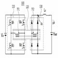
도 1은 종래의 위상 천이 풀 브리지 전원장치를 도시한 회로도이다.1 is a circuit diagram showing a conventional phase shift full bridge power supply.
도 1을 참조하면, 종래의 위상 천이 풀 브리지 전원장치(100)는 입력전원(Vin), 스위칭부(110), 변압부(120), 정류부(130)를 포함한다.1, a conventional phase shift full bridge
입력전원(Vin)으로 동작상태로 되는 스위칭부(110)는 제1 내지 제4 스위치(M1, M2, M3, M4)를 포함하고, 제어부(미도시)의 제1 내지 제4 스위칭 신호에 따라 스위칭 동작하여 직류 전압은 펄스성 직류 전압으로 변환된다. 이후, 펄스성 직류 전압은 변압부(120)의 1차 코일(TF1) 및 2차 코일(TF2)의 권선비율에 따라 2차 교류 전압으로 변환된 후, 정류부(130)에 의해 직류 전압으로 정류된다.The
이러한 종래 기술에 따른 풀 브리지 전원장치(100)는 누설인덕턴스에 흐르는 전류를 이용하여 소프트 스위칭 동작이 수행되는데, 저부하에서는 누설 인덕턴스에 흐르는 전류가 작으므로 소프트 스위칭이 어려워지고, 이에 따라 저부하 효율 저하가 발생된다. 또한, 정류부(130)의 다이오드(D1, D2, D3, D4)에 전류가 흐를 때, 전압강하가 발생하므로 변압기의 누설과 다이오드 접합 커패시턴스와의 공진으로 인해 과도한 서지 전압이 발생하여 이를 억제하기 위한 추가적인 스너버 회로가 요구된다.In the full bridge
또한, 일반적으로 고압의 다이오드의 경우, 큰 전압강하를 보이므로 도통 손실이 증가하고, 전압 제한을 위한 스너버 손실도 존재하므로 고효율의 DC/DC 컨버터 설계에 불리하며, 비용 상승의 일 요인이 된다.In general, high-voltage diodes are disadvantageous in designing a high-efficiency DC / DC converter because they exhibit large voltage drop and increase conduction loss and have snubber loss for voltage limitation, which is a factor of cost increase .
본 발명이 이루고자 하는 기술적 과제는 작은 리플 전류를 구현하며, 부하에 따른 전력분배의 문제점을 해결할 수 있는 풀브리지 컨버터와 공진컨버터를 이용한 하이브리드 방식의 고효율 충전기를 제공하는데 있다.SUMMARY OF THE INVENTION It is an object of the present invention to provide a hybrid type high efficiency charger using a full bridge converter and a resonance converter capable of realizing a small ripple current and solving the problem of power distribution depending on a load.
상기 과제를 해결하기 위한 본 발명은 입력전원, 서로 직렬 접속된 제1스위치 및 제2스위치와, 제3스위치 및 제4스위치가 각각 상기 입력전원의 양단에 병렬로 접속되어, 스위칭 제어신호에 따라 스위칭하는 스위칭부, 상기 스위칭부의 스위칭 동작에 따라 1차측 권선에 의한 에너지를 2차측 권선으로 유도하기 위한 변압부, 상기 2차측 권선에 연결된 공진 컨버터부 및 상기 2차측 권선에 연결되고, 상기 공진 컨버터부와 직렬로 연결된 풀브리지 컨버터부를 포함한다.According to an aspect of the present invention, there is provided an input power supply including a first switch and a second switch connected in series to each other, and a third switch and a fourth switch connected in parallel to both ends of the input power source, A resonance converter unit connected to the secondary side winding, and a resonance converter connected to the secondary side winding, wherein the resonance converter includes a switching unit for switching the switching unit, a switching unit for switching the switching unit, And a full bridge converter section connected in series with the bridge section.
2차측 권선은, 상기 공진 컨버터부와 연결된 제1권선, 상기 풀브리지 컨버터부와 연결된 제2권선 및 상기 풀브리지 컨버터부와 연결되고, 상기 제2권선과 일측이 연결된 제3권선을 포함할 수 있다.The secondary winding may include a first winding connected to the resonant converter unit, a second winding connected to the full bridge converter unit, and a third winding connected to the full bridge converter unit and connected to the first winding. have.
상기 공진 컨버터부와 상기 풀브리지 컨버터부는 하나의 변압기를 갖을 수 있다.The resonant converter unit and the full bridge converter unit may have one transformer.
상기 공진 컨버터부는, 상기 제1권선에서 출력되는 전압을 정류하는 제1정류부, 상기 스위칭부의 스위칭 동작에 따라 공진을 수행을 공진탱크부 및 상기 제1정류부에 의해 정류된 전압을 평활하여 출력하는 평활 커패시터를 포함할 수 있다.The resonance converter unit includes a first rectifying unit for rectifying a voltage output from the first winding, a resonance tank for performing resonance according to the switching operation of the switching unit, and a smoothing unit for smoothing and outputting a voltage rectified by the first rectifying unit Capacitors.
상기 풀브리지 컨버터부는, 상기 제2권선 또는 상기 제3권선에서 출력되는 전압을 정류하는 제2정류부 및 상기 제2정류부와 연결된 출력인덕터를 포함할 수 있다.The full bridge converter may include a second rectifier for rectifying a voltage output from the second winding or the third winding, and an output inductor connected to the second rectifier.
상기 공진탱크부는, 상기 스위칭부와 상기 1차측 권선에 연결된 공진 인덕터 및 상기 제1정류부와 상기 2차측 제1권선에 연결된 공진 커패시터를 포함할 수 있다.The resonance tank unit may include a resonance inductor connected to the switching unit, the primary winding, and a resonance capacitor connected to the first rectification unit and the secondary side first winding.
상기 제2권선 및 제3권선의 접속 노드는 상기 제1정류부 및 상기 평활 커패시터의 접속 노드와 연결될 수 있다.And the connection node of the second winding and the third winding may be connected to the connection node of the first rectification part and the smoothing capacitor.
상기 제1스위치 및 상기 제3스위치가 턴온됨에 따라, 상기 1차측 권선의 에너지가 상기 2차측 제1권선 및 제2권선으로 전달될 수 있다.As the first switch and the third switch are turned on, the energy of the primary winding can be transferred to the secondary primary winding and the secondary winding.
상기 공진 컨버터부는, 상기 2차측 제1권선의 자화인덕턴스를 이용하여 낮은 부하에서 상기 제1스위치 및 상기 제2스위치의 소프트 스위칭을 수행할 수 있다.The resonant converter unit may perform soft switching of the first switch and the second switch at a low load using the magnetizing inductance of the secondary winding.
상기 출력인덕터는 프리휠링(Freewheeling)시 상기 출력인덕터에 흐르는 전류의 하강기울기가 감소됨에 따라 낮은 인덕턴스를 갖을 수 있다.The output inductor may have a low inductance as the downward slope of the current flowing through the output inductor is reduced at the time of freewheeling.
본 발명에 따른 하이브리드 방식의 고효율 충전기는 풀브리지 컨버터부와 공진 컨버터부를 하이브리드로 구성한 충전기로써, 스위칭 동작시 출력인덕터에 인가되는 전압을 감소시킴으로써 작은 인덕턴스를 갖는 인덕터를 사용하여 리플전류를 감소시킬 수 있다.The hybrid type high efficiency charger according to the present invention is a charger in which a full bridge converter unit and a resonance converter unit are configured in a hybrid manner. By reducing a voltage applied to an output inductor during a switching operation, an inductor having a small inductance can be used to reduce a ripple current have.
또한, 풀브리지 컨버터부와 공진 컨버터부를 단일 변압기를 사용하여 하이브리드로 구성함으로써 부하에 따른 전력분배의 문제점을 해결 할 수 있다.In addition, the full bridge converter unit and the resonance converter unit can be configured as a hybrid by using a single transformer, thereby solving the problem of power distribution depending on the load.
본 발명의 기술적 효과들은 이상에서 언급한 것들로 제한되지 않으며, 언급되지 않은 또 다른 기술적 효과들은 아래의 기재로부터 당업자에게 명확하게 이해될 수 있을 것이다.The technical effects of the present invention are not limited to those mentioned above, and other technical effects not mentioned can be clearly understood by those skilled in the art from the following description.
도 1은 종래의 위상 천이 풀 브리지 전원장치를 도시한 회로도이다.
도 2는 본 발명의 바람직한 실시예에 따른 풀 브리지 컨버터와 공진컨버터를 사용한 하이브리드 방식의 충전기를 도시한 회로도이다.
도 3은 도 2에 도시된 회로의 동작파형을 도시한 타이밍도이다.
도 4 내지 도 6은 도 2에 도시된 회로의 동작모드를 도시한 회로도들이다.
도 7은 실험예에 따른 각 부의 파형을 측정한 그래프이다.
도 8은 본 발명의 실험예에 따른 스위칭부의 전류, 전압 파형을 측정한 그래프이다.
도 9는 본 발명의 충전기에서 배터리 전압에 따른 효율을 측정한 그래프이다.1 is a circuit diagram showing a conventional phase shift full bridge power supply.
2 is a circuit diagram showing a hybrid type charger using a full bridge converter and a resonance converter according to a preferred embodiment of the present invention.
3 is a timing chart showing the operation waveform of the circuit shown in Fig.
Figs. 4 to 6 are circuit diagrams showing operation modes of the circuit shown in Fig. 2. Fig.
7 is a graph showing the waveforms of the respective parts according to the experimental example.
8 is a graph showing current and voltage waveforms of the switching unit according to the experimental example of the present invention.
9 is a graph illustrating the efficiency of the battery charger according to the battery voltage.
본 발명은 본 발명은 다양한 변경을 가할 수 있고 여러 가지 형태를 가질 수 있는 바, 특정 실시예들을 도면에 예시하고 본문에 상세하게 설명하고자 한다. 그러나, 이는 본 발명을 특정한 개시 형태에 대해 한정하려는 것이 아니며, 본 발명의 사상 및 기술 범위에 포함되는 모든 변경, 균등물 내지 대체물을 포함하는 것으로 이해되어야 한다. 각 도면을 설명하면서 유사한 참조부호를 유사한 구성요소에 대해 사용하였다.While the present invention has been described in connection with what is presently considered to be the most practical and preferred embodiment, it is to be understood that the invention is not limited to the disclosed embodiments, but, on the contrary, It should be understood, however, that the invention is not intended to be limited to the particular forms disclosed, but includes all modifications, equivalents, and alternatives falling within the spirit and scope of the invention. Like reference numerals are used for like elements in describing each drawing.
다르게 정의되지 않는 한, 기술적이거나 과학적인 용어를 포함해서 여기서 사용되는 모든 용어들은 본 발명이 속하는 기술 분야에서 통상의 지식을 가진 자에 의해 일반적으로 이해되는 것과 동일한 의미를 가지고 있다. 일반적으로 사용되는 사전에 정의되어 있는 것과 같은 용어들은 관련 기술의 문맥 상 가지는 의미와 일치하는 의미를 가지는 것으로 해석되어야 하며, 본 출원에서 명백하게 정의하지 않는 한, 이상적이거나 과도하게 형식적인 의미로 해석되지 않는다.Unless defined otherwise, all terms used herein, including technical or scientific terms, have the same meaning as commonly understood by one of ordinary skill in the art to which this invention belongs. Terms such as those defined in commonly used dictionaries are to be interpreted as having a meaning consistent with the contextual meaning of the related art and are to be interpreted as either ideal or overly formal in the sense of the present application Do not.
이하, 본 발명에 따른 실시 예들을 첨부도면을 참조하여 상세히 설명하기로 하며, 첨부 도면을 참조하여 설명함에 있어, 동일하거나 대응하는 구성 요소는 동일한 도면번호를 부여하고 이에 대한 중복되는 설명은 생략하기로 한다.DETAILED DESCRIPTION OF THE PREFERRED EMBODIMENTS Hereinafter, exemplary embodiments of the present invention will be described in detail with reference to the accompanying drawings. Referring to the accompanying drawings, the same or corresponding components are denoted by the same reference numerals, .
실시예Example
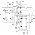
도 2는 본 발명의 바람직한 실시예에 따른 풀 브리지 컨버터와 공진컨버터를 사용한 하이브리드 방식의 충전기를 도시한 회로도이다.2 is a circuit diagram showing a hybrid type charger using a full bridge converter and a resonance converter according to a preferred embodiment of the present invention.
도 2를 참조하면, 본 발명에 따른 하이브리드 방식의 충전기(200)는 입력전원(Vin), 스위칭부(210), 변압부(220), 공진 컨버터부(230) 및 풀브리지 컨버터부(240)를 포함한다.2, the
입력전원(Vin)은 상기 공진 컨버터부(230) 및 풀브리지 컨버터부(240)에 직류 전압을 공급한다.The input power supply (Vin) supplies the DC voltage to the resonance converter unit (230) and the full bridge converter unit (240).
스위칭부(210)는 풀브리지 타입의 제1 내지 제4스위치(M1, M2, M3, M4)를 포함하고, 서로 직렬 접속된 제1스위치(M1) 및 제2스위치(M2), 제3스위치(M3) 및 제4스위치(M4)는 상기 입력전원(Vin)의 양단에 각각 병렬로 접속된다. 또한, 스위칭부(210)는 회로내에 구비된 제어부(미도시)의 스위칭 제어에 따라 스위칭되도록 이루어지며, 스위칭부(210)의 제1 내지 제4스위치(M4)는 제어부의 제어 동작에 따라 각각의 스위치가 후술할 변압부(220)의 1차측 권선(TF1)과 교번적으로 폐루프를 형성하도록 형성될 수 있다.The
변압부(220)는 상기 스위칭부(210)의 제1 및 제2스위치(M1, M2)의 접속노드와 상기 제3 및 제4스위치(M3, M4)의 접속노드 사이에 연결된 1차측 권선(TF1), 공진 컨버터부(230)와 풀브리지 컨버터부(240)에 접속된 2차측 권선(TF2)을 포함한다. 또한, 2차측 권선(TF2)은 공진 컨버터부(230)에 연결된 2차측 제1권선(TF2a)과 풀브리지 컨버터부(240)에 연결된 2차측 제2권선(TF2b) 및 제3권선(TF2c)을 포함할 수 있다. 여기서 2차측 제2권선(TF2b)은 제3권선(TF2c)과 일측이 연결되도록 형성될 수 있다. 이러한 변압부(220)는 1차측 권선(TF1), 2차측의 제1 내지 제3권선(TF2a,TF2b,TF2c)의 권선비율에 따라 1차측 권선(TF1)에 의한 에너지를 2차측 권선(TF2)의 제1권선(TF2a), 제2권선(TF2b) 또는 제3권선(TF2c)으로 전달한다.The
또한, 본 발명의 충전기는 공진 컨버터부(230)와 풀브리지 컨버터부(240)를 하이브리드 방식으로 구성되나, 변압부(220)에서 사용되는 변압기는 단일 변압기를 사용함으로써 부하에 따른 전력분배의 문제점을 해결할 수 있다.The charger of the present invention is configured such that the
공진 컨버터부(230)는 상기 2차측 권선(TF2)에 연결된 제1정류부(231), 공진탱크부(232) 및 평활 커패시터(Co2)를 포함할 수 있다.The
제1정류부(231)는 상기 변압부(220)의 2차측 제1권선(TF2a)에서 출력되는 전압을 정류하도록 제1다이오드 내지 제4다이오드(D1,D2,D3,D4)를 포함하는 브리지 다이오드로 이루어질 수 있다. 즉, 2차측 제1권선(TF2a)의 일단은 제1다이오드(D1) 및 제2다이오드(D2)의 접속노드에 연결되며, 타단은 제3다이오드(D3) 및 제4다이오드(D4)의 접속노드에 연결될 수 있다. 따라서, 상기 스위칭부(210)의 스위칭 동작에 따라 1차측 권선(TF1)에 의한 에너지를 2차측 제1권선(TF2a)으로 유도한다.The first rectifying
공진탱크부(232)는 공진 인덕터(Lr)와 공진 커패시터(Cr)를 포함할 수 있다. 공진탱크부(232)는 공진 인덕터(Lr)와 공진 커패시터(Cr)를 이용하여 공진을 수행한다. 공진 인덕터(Lr)의 일단은 상기 스위칭부(210)의 제1스위치(M1) 및 제2스위치(M2)의 접속노드에 연결되며, 타단은 1차측 권선(TF1)의 일측에 연결될 수 있다. 또한, 공진 커패시터(Cr)는 제1다이오드(D1)와 제2다이오드(D2)의 접속노드에 연결된 2차측 제1권선(TF2a)의 일측 사이에 연결될 수 있다. 즉, 공진 인덕터(Lr)를 1차측 권선(TF1)에 연결하고, 공진 커패시터(Cr)를 2차측 권선(TF2)에 분리하여 연결함으로써, 공진 인덕터(Lr)는 1차측에서 공진으로써 기능하고 공진 커패시터(Cr)는 PWM제어로 기능하는 분리 형태를 취할 수 있다.The
평활 커패시터(Co2)는 제1정류부(231)와 연결되고, 상기 제1정류부(231)에 의해 정류된 전압을 평활하여 출력한다.The smoothing capacitor Co2 is connected to the
풀브리지 컨버터부(240)는 상기 2차측 권선(TF2)에 연결된 제2정류부(241) 및 출력인덕터(Lo)를 포함할 수 있다.The full
제2정류부(241)는 2차측 제2권선(TF2b)에 연결된 제5다이오드(D5) 및 2차측 제3권선(TF2c)에 연결된 제6다이오드(D6)를 포함할 수 있다. 제5다이오드(D5)는 애노드(anode)가 2차측 제2권선(TF2b)의 일측에 연결되고, 캐소드(cathode)가 제6다이오드(D6)의 캐소드와 연결된다. 제6다이오드(D6)의 애노드는 2차측 제3권선(TF2c)의 일측에 연결될 수 있다. 따라서, 제2정류부(241) 는 상기 변압부(220)의 2차측 제2권선(TF2b) 및 제3권선(TF2c)에서 출력되는 전압을 정류하도록 기능할 수 있다.The
출력인덕터(Lo)는 일단이 상기 제2정류부(241)와 연결되고, 타단이 배터리(Vbatt)에 연결된다. 본 발명에 따른 충전기(200)는 스위칭부(210)의 스위칭 동작시 출력인덕터(Lo)에 인가되는 전압을 감소시킴으로써, 작은 인덕턴스를 갖는 인덕터를 이용하여 리플전류를 감소시킬 수 있다. 즉, 도 1에서와 같이 종래의 풀브리지 컨버터(100)의 경우 프리휠링(Freewheeling)시 출력인덕터(Lo)에 -Vbatt의 전압이 인가되어 출력인덕터(Lo)에 인가되는 전압의 기울기가 커지기 때문에 동일한 리플을 얻기 위해서는 큰 인덕턴스를 갖는 인덕터가 필요하다. 하지만 본 발명에 따른 충전기(200)는 프리휠링시 출력인덕터(Lo)에 Vo2-Vbatt의 전압이 인가되기 때문에, 출력인덕터(Lo)에 흐르는 전류의 하강기울기가 감소됨에 따라, 작은 인덕턴스를 갖는 인덕터로도 종래의 풀브리지 컨버터와 동일한 리플전류를 얻을 수 있다.One end of the output inductor Lo is connected to the
상기와 같이, 2차측 권선(TF2)중 제1권선(TF2a)은 공진 컨버터부(230)와 연결되고, 제2권선(TF2b) 및 제3권선(TF2c)은 풀브리지 컨버터부(240)와 연결되며, 제2권선(TF2b) 및 제3권선(TF2c)의 접속 노드가 제1정류부(231) 및 평활 커패시터(Co2)의 접속 노드와 연결되는 구조를 취함으로써, 본 발명의 충전기(200)는 공진 컨버터부(230)와 풀브리지 컨버터부(240)를 단일 변압기를 이용하여 하이브리드 구조를 취할 수 있다.The first winding TF2a of the secondary winding TF2 is coupled to the
동작모드Operation mode
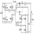
도 3은 도 2에 도시된 회로의 동작파형을 도시한 타이밍도이고, 도 4 내지 도 6은 도 2에 도시된 회로의 동작모드를 도시한 회로도들이다.3 is a timing chart showing the operation waveform of the circuit shown in Fig. 2, and Figs. 4 to 6 are circuit diagrams showing an operation mode of the circuit shown in Fig.
도 3내지 도 6을 참조하여 본 발명의 충전기에 따른 동작모드를 아래에 상세히 설명한다.3 to 6, the operation modes according to the charger of the present invention will be described in detail below.
도 4는 모드 1에 대한 전류흐름도이다. 도 3과 도 4를 참조하면, 제3스위치(M3)가 도통되어 있는 상태에서 제2스위치(M2)가 차단되고 제1스위치(M1)가 도통된다. 제3스위치(M3)와 제1스위치(M1)가 도통됨으로써, 전류경로는 도 4에서와 같이 1차측에서는 입력전원(Vin), 제1스위치(M1), 공진 인덕터(Lr), 1차측 권선(TF1) 및 제3스위치(M3)로 전류경로가 형성되고, 공진 컨버터부(230)의 전류경로는 2차측 제1권선(TF2a)에 의해 2차측 제1권선(TF2a), 공진 커패시터(Cr), 제1다이오드(D1), 평활 커패시터(Co2) 및 제3다이오드(D3)의 전류경로가 형성된다. 또한, 풀브리지 컨버터부(240)의 전류경로는 2차측 제2권선(TF2b)에 의해 2차측 제2권선(TF2b), 제5다이오드(D5), 출력인덕터(Lo), 배터리 및 평활 커패시터(Co2)로 전류경로가 형성된다.4 is a current flow chart for
즉, 공진 컨버터부(230)의 제1정류부(241)에서 제1다이오드(D1)와 제3다이오드(D3)의 전류경로가 형성되기 때문에 평활 커패시터(Co2)를 충전하며, 풀브리지 컨버터부(240)의 제2정류부(241)에서는 제5다이오드(D5), 출력인덕터(Lo), 배터리 및 평활 커패시터(Co2)의 경로로 충전전류가 흐른다.That is, since the current path between the first diode D1 and the third diode D3 is formed in the
도 3에서와 같이 모드 1에서는 공진 인덕터(Lr)와 공진 커패시터(Cr)에 의한 공진 전류와 배터리 전류의 1차측 환원전류의 합이 변압부(220)의 1차측으로 흐르며, 제1스위치(M1)는 자화전류를 이용하여 소프트 스위칭이 달성되고 있음을 확인할 수 있다.3, in
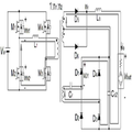
도 5는 모드 2에 대한 전류흐름도이다. 도 3과 도 5를 참조하면, 제3스위치(M3)가 도통되어 있는 상태에서 제1스위치(M1)가 차단되고, 제2스위치(M2)가 도통된다. 제2스위치(M2)와 제3스위치(M3)가 도통됨으로써, 전류경로는 도 5에서와 같이 1차측에서는 공진 인덕터(Lr), 1차측 권선(TF1), 제3스위치(M3) 및 제2스위치(M2)의 바디다이오드의 경로로 전류경로가 형성된다. 또한, 공진 컨버터부(230)와 풀브리지 컨버터부(240)는 모드 1의 경로를 그대로 유지한다. 이때, 공진 인덕터(Lr)에는 모드 1과 반대방향의 전압이 인가되기 때문에 변압기 1차측 전류는 0까지 감소하게 된다.5 is a current flow chart for
도 6은 모드 3에 대한 전류흐름도이다. 도 3과 도 6을 참조하면, 1차측 전류경로는 모드 2의 전류 경로를 그대로 유지하며, 공진전류는 없고, 출력인덕터(Lo) 전류의 1차측 환원전류와 자화전류만 흐르므로 일정한 전류가 흐른다.6 is a current flow chart for
모드 3 이후에는 제2스위치(M2)가 도통되어 있는 상태에서 제3스위치(M3)가 차단되고, 제4스위치(M4)가 도통되면서 다음 반주기가 시작되며, 이에 따른 동작은 모드 1 내지 모드 3과 동일하게 동작된다.After the
상술한 도 3의 타이밍도와 도 4 내지 도 6의 동작모드에서와 같이, 도 1과 같은 종래의 풀브리지 컨버터의 경우 프리휠링(Freewheeling)시 출력인덕터(Lo)에 -Vbatt의 전압이 인가되어 출력인덕터(Lo)에 인가되는 전압의 기울기가 커지기 때문에 동일한 리플을 얻기 위해서는 큰 인덕턴스를 갖는 인덕터가 필요하지만, 본 발명에 따른 하이브리드 방식의 충전기(200)는 프리휠링시 출력인덕터(Lo)에 Vo2-Vbatt의 전압이 인가되기 때문에, 출력인덕터(Lo)에 흐르는 전류의 하강기울기가 감소됨에 따라, 작은 인덕턴스를 갖는 인덕터로도 종래의 풀브리지 컨버터와 동일한 리플전류를 얻을 수 있다. 또한, 도 3에 도시된 제5다이오드(D5) 및 제6다이오드(D6)에 인가되는 전압 파형과 같이 정류기의 내압도 매우 낮은 값으로 유지되고 있음을 확인할 수 있다.As in the timing of FIG. 3 and the operation mode of FIG. 4 to FIG. 6, in the conventional full bridge converter as shown in FIG. 1, the voltage of -V batt is applied to the output inductor Lo during freewheeling, The inductor having a large inductance is required to obtain the same ripple because the slope of the voltage applied to the inductor Lo becomes large. However, in the
입출력 이득 및 인덕터 전류 리플I / O Gain and Inductor Current Ripple
도 3의 파형을 참조하여 입출력 이득과 인덕터 전류리플에 대해 상세히 설명한다.The input / output gain and the inductor current ripple will be described in detail with reference to the waveforms of FIG.
본 실시예의 컨버터의 입력과 출력전압의 이득은 출력인덕터(Lo) 양단 전압의 전압시간 평형곱으로 도출할 수 있으며, 하기의 수학식 1로 표현된다.The gain of the input and output voltages of the converter of this embodiment can be derived by the voltage time balance product of the voltage across the output inductor Lo and is expressed by
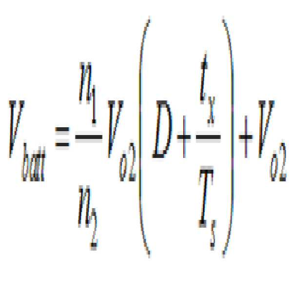
여기서, n1은 1차측 권선(TF1)의 권선수, n2는 2차측 권선(TF2)의 권선수, Vo2는 공진 컨버터부(230)의 출력전압, D는 시비율(Duty Ratio), tx는 모드 2의 지속시간(duration)이며, Ts는 스위칭 주기를 나타낸다.Here, n1 is the winding of the primary winding TF1, n2 is the winding of the secondary winding TF2, Vo2 is the output voltage of the
또한, tx는 하기의 수학식으로 표현된다.Also, tx is expressed by the following equation.
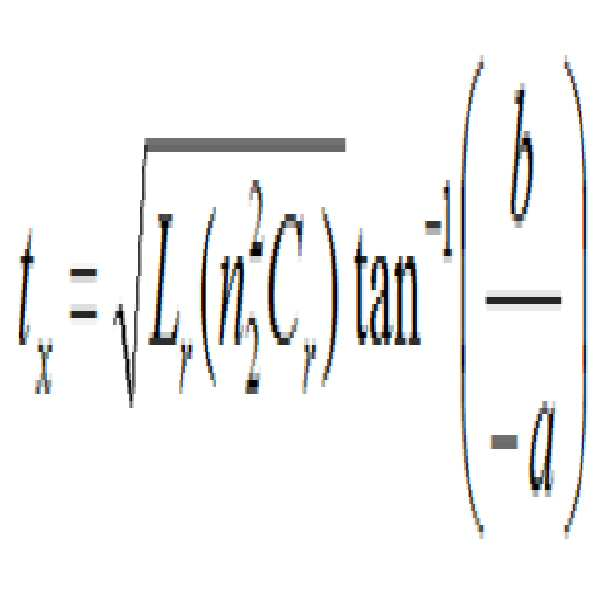
a와 b는 아래와 같이 수학식 3과 4와 같이 각각 나타낼 수 있다.a and b can be expressed by the following equations (3) and (4), respectively.
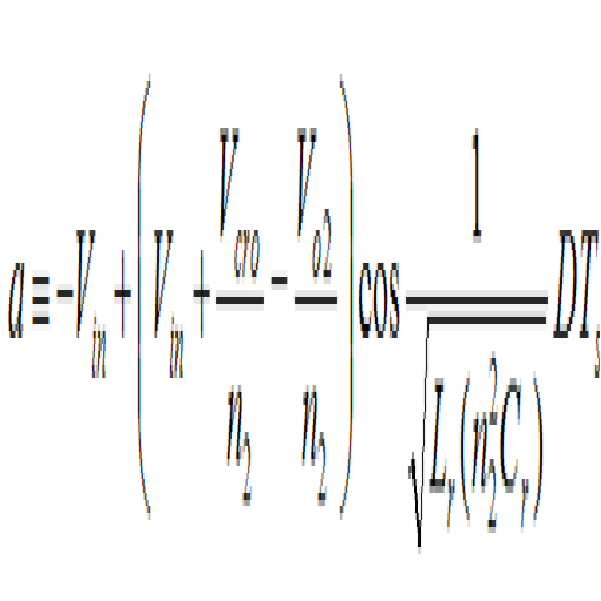
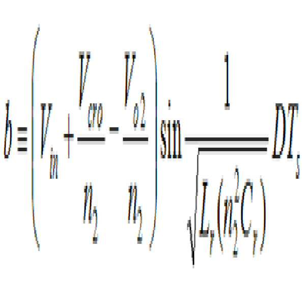
여기서, Vin는 입력전원, Lr은 공진 인덕터의 L값, Cr은 공진 커패시터의 C값을 나타내고, Vcro는 공진 커패시터의 첨두값으로 하기의 수학식 5로 표현된다.Here, Vin is the input power, Lr is the L value of the resonant inductor, Cr is the C value of the resonant capacitor, and Vcro is the peak value of the resonant capacitor expressed by the following equation (5).
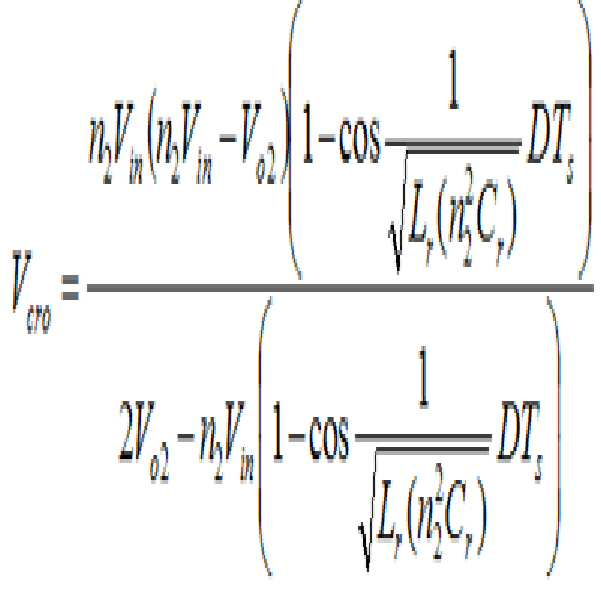
수학식 5에서 공진 컨버터부(230)의 출력전압인 Vo2는 하기의 수학식 6으로 표현된다.In Equation (5), Vo2, which is the output voltage of the
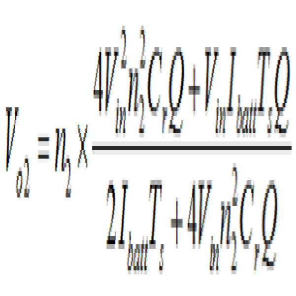
여기서, Q는 하기의 수학식 7과 같다.Here, Q is expressed by Equation (7) below.
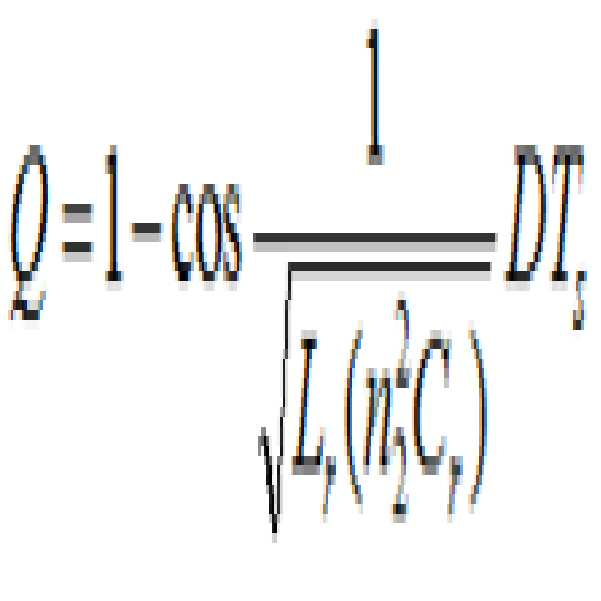
또한, 전류 리플은 하기의 수학식 8과 같이 나타낼 수 있다.The current ripple can be expressed by the following equation (8).
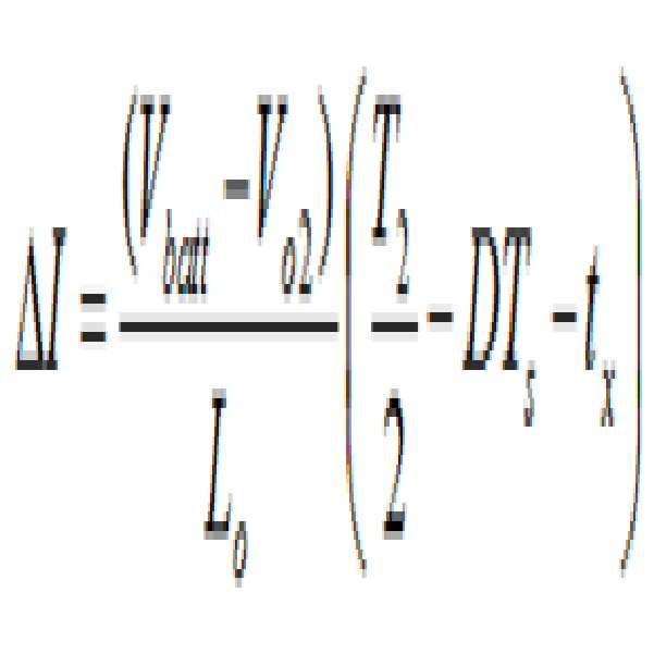
따라서, 종래의 풀브리지 컨버터에 비해 같은 인덕터를 사용하더라도 작은 전류 리플이 발생함을 확인할 수 있다.Therefore, it can be confirmed that small current ripple occurs even when the same inductor is used as compared with the conventional full bridge converter.
실험예Experimental Example
본 발명의 하이브리드 방식으로 형성된 충전기의 성능을 평가하기 위하여, 본 발명의 충전기에 따른 회로를 구성하고 실험을 실시하였다.In order to evaluate the performance of the charger formed by the hybrid method of the present invention, a circuit according to the charger of the present invention was constructed and an experiment was conducted.
도 7은 실험예에 따른 각 부의 파형을 측정한 그래프이다.7 is a graph showing the waveforms of the respective parts according to the experimental example.
도 7을 참조하면, 실험 조건은 6.6kW(Vin=400V, Vbatt=413V), n1=0.1, n2=1.2로 설정하여 Vo2가 400V가 되도록 하였으며, 스위칭 주파수는 50kHz, Lo=50μ로 설정하였다. 도 7의 측정 파형에서 알 수 있듯이, 출력인덕터(Lo) 전류의 리플이 매우 작은 것을 확인할 수 있으며, 정류기의 내압도 매우 낮은 값으로 유지하고 있음을 확인할 수 있다.Referring to FIG. 7, the experimental conditions were set to 6.6 kW (Vin = 400 V, Vbatt = 413 V), n1 = 0.1 and n2 = 1.2 so that Vo2 was 400 V and the switching frequency was set to 50 kHz and Lo = 50. As can be seen from the measurement waveform of FIG. 7, it can be seen that the ripple of the output inductor (Lo) current is very small, and the internal pressure of the rectifier is maintained at a very low value.
도 8은 본 발명의 실험예에 따른 스위칭부의 전류, 전압 파형을 측정한 그래프이다.8 is a graph showing current and voltage waveforms of the switching unit according to the experimental example of the present invention.
도 8은 제1스위치와 제2스위치의 전류 파형과 전압 파형을 각각 측정한 그래프를 나타낸다. 도 8에 도시한 바와 같이, 스위칭부(210)의 스위치 동작시 영전압-영전류 스위칭(ZV-ZCS)이 달성됨을 확인할 수 있다.8 is a graph showing current waveforms and voltage waveforms of the first switch and the second switch, respectively. As shown in FIG. 8, it can be confirmed that the zero voltage-zero current switching (ZV-ZCS) is achieved during the switching operation of the
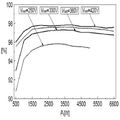
도 9는 본 발명의 충전기에서 배터리 전압에 따른 효율을 측정한 그래프이다.9 is a graph illustrating the efficiency of the battery charger according to the battery voltage.
도 9에 도시한 바와 같이, 배터리 전압을 250V, 330V, 360V, 420V에 따라 효율을 측정한 결과, 360V/6.6kW에서 97.2%의 효율을 확인할 수 있으며, 413V/6.6kW에서 최대효율인 97.4%로 고효율을 달성함을 확인할 수 있다.As shown in FIG. 9, the efficiency was measured according to the battery voltage of 250V, 330V, 360V and 420V. As a result, the efficiency of 97.2% was confirmed at 360V / 6.6kW and 97.4% at 413V / 6.6kW, And it can be confirmed that high efficiency is achieved.
상술한 바와 같이 본 발명에 따른 하이브리드 방식의 충전기(200)는 공진 컨버터부(230)와 풀브리지 컨버터부(240)를 하이브리드로 구성한 충전기로써, 스위칭 동작시 출력인덕터(Lo)에 인가되는 전압을 감소시킴으로써 작은 인덕턴스를 갖는 인덕터를 사용하여 리플전류를 감소시킬 수 있으며, 정류기의 내압도 낮은 값으로 유지할 수 있다. 또한, 공진 컨버터부(230)와 풀브리지 컨버터부를 단일 변압기를 사용하여 하이브리드 방식으로 구성함으로써 부하에 따른 전력분배의 문제점을 해결 할 수 있으며, 실험 결과에서와 같이 고효율을 달성할 수 있다.As described above, the
한편, 본 명세서와 도면에 개시된 본 발명의 실시 예들은 이해를 돕기 위해 특정 예를 제시한 것에 지나지 않으며, 본 발명의 범위를 한정하고자 하는 것은 아니다. 여기에 개시된 실시 예들 이외에도 본 발명의 기술적 사상에 바탕을 둔 다른 변형 예들이 실시 가능하다는 것은, 본 발명이 속하는 기술 분야에서 통상의 지식을 가진 자에게 자명한 것이다.It should be noted that the embodiments of the present invention disclosed in the present specification and drawings are only illustrative of specific examples for the purpose of understanding and are not intended to limit the scope of the present invention. It will be apparent to those skilled in the art that other modifications based on the technical idea of the present invention are possible in addition to the embodiments disclosed herein.
210 : 스위칭부
220 : 변압부
230 : 공진 컨버터부
231 : 제1정류부
232 : 공진탱크부
240 : 풀브리지 컨버터부
241 : 제2정류부210: switching unit 220:
230: resonance converter section 231: first rectification section
232: resonance tank section 240: full bridge converter section
241: second rectifying part
Claims (10)
서로 직렬 접속된 제1스위치 및 제2스위치와, 제3스위치 및 제4스위치가 각각 상기 입력전원의 양단에 병렬로 접속되어, 스위칭 제어신호에 따라 스위칭하는 스위칭부;
상기 스위칭부의 스위칭 동작에 따라 1차측 권선에 의한 에너지를 2차측 권선으로 유도하기 위한 변압부;
상기 2차측 권선에 연결된 공진 컨버터부; 및
상기 2차측 권선에 연결되고, 상기 공진 컨버터부와 직렬로 연결된 풀브리지 컨버터부를 포함하는 작은 출력전류 리플을 갖는 고효율 충전기.Input power;
A switching unit for connecting the first switch and the second switch connected in series to each other and the third switch and the fourth switch in parallel at both ends of the input power source and switching in accordance with the switching control signal;
A transformer for inducing the energy of the primary winding to the secondary winding according to the switching operation of the switching unit;
A resonance converter unit connected to the secondary winding; And
And a full-bridge converter portion connected to the secondary winding and connected in series with the resonant converter portion.
상기 공진 컨버터부와 연결된 제1권선;
상기 풀브리지 컨버터부와 연결된 제2권선; 및
상기 풀브리지 컨버터부와 연결되고, 상기 제2권선과 일측이 연결된 제3권선을 포함하는 작은 출력전류 리플을 갖는 고효율 충전기.The secondary winding of claim 1,
A first winding connected to the resonant converter unit;
A second winding connected to the full bridge converter; And
And a small output current ripple connected to the full bridge converter portion and including a third winding connected to the second winding.
상기 공진 컨버터부와 상기 풀브리지 컨버터부는 하나의 변압기를 갖는 것인 작은 출력전류 리플을 갖는 고효율 충전기.The method according to claim 1,
Wherein the resonant converter portion and the full bridge converter portion have a single transformer.
상기 제1권선에서 출력되는 전압을 정류하는 제1정류부;
상기 스위칭부의 스위칭 동작에 따라 공진을 수행을 공진탱크부; 및
상기 제1정류부에 의해 정류된 전압을 평활하여 출력하는 평활 커패시터를 포함하는 작은 출력전류 리플을 갖는 고효율 충전기.The resonator according to claim 2,
A first rectifying section for rectifying the voltage output from the first winding;
A resonance tank unit for performing resonance according to the switching operation of the switching unit; And
And a smoothing capacitor for smoothing and outputting a voltage rectified by the first rectification part.
상기 제2권선 또는 상기 제3권선에서 출력되는 전압을 정류하는 제2정류부; 및
상기 제2정류부와 연결된 출력인덕터를 포함하는 작은 출력전류 리플을 갖는 고효율 충전기.The power converter according to claim 2, wherein the full-
A second rectifying unit for rectifying a voltage output from the second winding or the third winding; And
And a small output current ripple including an output inductor coupled to the second rectifier.
상기 스위칭부와 상기 1차측 권선에 연결된 공진 인덕터; 및
상기 제1정류부와 상기 2차측 제1권선에 연결된 공진 커패시터를 포함하는 작은 출력전류 리플을 갖는 고효율 충전기.The resonator according to claim 4,
A resonance inductor connected to the switching unit and the primary winding; And
And a small output current ripple comprising a resonant capacitor coupled to the first rectification section and the secondary side first winding.
상기 제2권선 및 제3권선의 접속 노드는 상기 제1정류부 및 상기 평활 커패시터의 접속 노드와 연결되는 것인 작은 출력전류 리플을 갖는 고효율 충전기.6. The method of claim 5,
And the connection node of the second winding and the third winding is connected to the connection node of the first rectification section and the smoothing capacitor.
상기 제1스위치 및 상기 제3스위치가 턴온됨에 따라, 상기 1차측 권선의 에너지가 상기 2차측 제1권선 및 제2권선으로 전달되는 것인 작은 출력전류 리플을 갖는 고효율 충전기.3. The method of claim 2,
Wherein the energy of the primary winding is transferred to the secondary primary winding and the secondary winding as the first switch and the third switch are turned on.
상기 2차측 제1권선의 자화인덕턴스를 이용하여 낮은 부하에서 상기 제1스위치 및 상기 제2스위치의 소프트 스위칭을 수행하는 것인 작은 출력전류 리플을 갖는 고효율 충전기.The resonator according to claim 2,
And a small output current ripple that performs soft switching of the first switch and the second switch at a low load using the magnetizing inductance of the secondary side first winding.
상기 출력인덕터는 프리휠링(Freewheeling)시 상기 출력인덕터에 흐르는 전류의 하강기울기가 감소됨에 따라 낮은 인덕턴스를 갖는 것인 작은 출력전류 리플을 갖는 고효율 충전기.6. The method of claim 5,
Wherein the output inductor has a low inductance as the falling slope of the current flowing through the output inductor is reduced upon freewheeling.
Applications Claiming Priority (2)
| Application Number | Priority Date | Filing Date | Title |
|---|---|---|---|
| KR20170024576 | 2017-02-24 | ||
| KR1020170024576 | 2017-02-24 |
Publications (2)
| Publication Number | Publication Date |
|---|---|
| KR20180098171A true KR20180098171A (en) | 2018-09-03 |
| KR102030918B1 KR102030918B1 (en) | 2019-10-10 |
Family
ID=63600895
Family Applications (1)
| Application Number | Title | Priority Date | Filing Date |
|---|---|---|---|
| KR1020180022174A Expired - Fee Related KR102030918B1 (en) | 2017-02-24 | 2018-02-23 | High Efficiency EV Charger with Small Ripple Current |
Country Status (1)
| Country | Link |
|---|---|
| KR (1) | KR102030918B1 (en) |
Cited By (2)
| Publication number | Priority date | Publication date | Assignee | Title |
|---|---|---|---|---|
| KR20230036115A (en) * | 2020-07-15 | 2023-03-14 | 프로드라이브 테크놀로지즈 이노베이션 서비시즈 비.브이. | Voltage Waveform Generator for Plasma Auxiliary Processing Devices |
| CN117240089A (en) * | 2023-09-12 | 2023-12-15 | 南京航空航天大学 | Control circuit and control method of bidirectional four-tube Buck-Boost converter |
Citations (5)
| Publication number | Priority date | Publication date | Assignee | Title |
|---|---|---|---|---|
| JPH04331420A (en) * | 1991-05-01 | 1992-11-19 | Bridgestone Corp | Power source circuit |
| KR20110029782A (en) | 2009-09-16 | 2011-03-23 | 전남대학교산학협력단 | Full-Bridge Insulated DC / DC Converters |
| KR20160085224A (en) * | 2015-01-06 | 2016-07-15 | 단국대학교 산학협력단 | Hybride type LED Power Supply |
| KR20160093515A (en) * | 2015-01-28 | 2016-08-08 | 단국대학교 산학협력단 | Hybride type LED Power Supply |
| KR20160147575A (en) * | 2015-06-15 | 2016-12-23 | 계명대학교 산학협력단 | Power Converter for Charging Battery of Electric Vehicle |
-
2018
- 2018-02-23 KR KR1020180022174A patent/KR102030918B1/en not_active Expired - Fee Related
Patent Citations (5)
| Publication number | Priority date | Publication date | Assignee | Title |
|---|---|---|---|---|
| JPH04331420A (en) * | 1991-05-01 | 1992-11-19 | Bridgestone Corp | Power source circuit |
| KR20110029782A (en) | 2009-09-16 | 2011-03-23 | 전남대학교산학협력단 | Full-Bridge Insulated DC / DC Converters |
| KR20160085224A (en) * | 2015-01-06 | 2016-07-15 | 단국대학교 산학협력단 | Hybride type LED Power Supply |
| KR20160093515A (en) * | 2015-01-28 | 2016-08-08 | 단국대학교 산학협력단 | Hybride type LED Power Supply |
| KR20160147575A (en) * | 2015-06-15 | 2016-12-23 | 계명대학교 산학협력단 | Power Converter for Charging Battery of Electric Vehicle |
Cited By (2)
| Publication number | Priority date | Publication date | Assignee | Title |
|---|---|---|---|---|
| KR20230036115A (en) * | 2020-07-15 | 2023-03-14 | 프로드라이브 테크놀로지즈 이노베이션 서비시즈 비.브이. | Voltage Waveform Generator for Plasma Auxiliary Processing Devices |
| CN117240089A (en) * | 2023-09-12 | 2023-12-15 | 南京航空航天大学 | Control circuit and control method of bidirectional four-tube Buck-Boost converter |
Also Published As
| Publication number | Publication date |
|---|---|
| KR102030918B1 (en) | 2019-10-10 |
Similar Documents
| Publication | Publication Date | Title |
|---|---|---|
| Cho et al. | A half-bridge LLC resonant converter adopting boost PWM control scheme for hold-up state operation | |
| US10637363B2 (en) | Converters with hold-up operation | |
| US9660536B2 (en) | Switching power supply device performs power transmission by using resonance phenomenon | |
| CN102948057B (en) | The two-stage resonant vibration converter of the soft handover in support isolation level | |
| CN108352787A (en) | Flyback converter | |
| CN111656661B (en) | Constant frequency DC/DC power converter | |
| KR20180004675A (en) | Bidirectional Converter with Auxiliary LC Resonant Circuit and Operating Method thereof | |
| US20160049858A1 (en) | Lc resonant converter using phase shift switching method | |
| US20110069513A1 (en) | Current-Sharing Power Supply Apparatus With Bridge Rectifier Circuit | |
| Chu et al. | Analysis and design of a current-fed zero-voltage-switching and zero-current-switching CL-resonant push–pull dc–dc converter | |
| Lee et al. | Reduction of input voltage/current ripples of boost half-bridge DC-DC converter for photovoltaic micro-inverter | |
| US11764693B2 (en) | Dual-capacitor resonant circuit for use with quasi-resonant zero-current-switching DC-DC converters | |
| KR102030918B1 (en) | High Efficiency EV Charger with Small Ripple Current | |
| US20110058392A1 (en) | Current-sharing power supply apparatus | |
| KR20170104434A (en) | Resonance-type dc-dc converter | |
| KR101813778B1 (en) | Hybride type LED Power Supply | |
| Wang et al. | A new LLC converter family with synchronous rectifier to increase voltage gain for hold-up application | |
| Huang et al. | Analysis and design of a single-stage buck-type AC-DC adaptor | |
| Hwu et al. | Ultrahigh step-down converter with active clamp | |
| Bagawade et al. | Novel high-gain hybrid current-driven DC-DC converter topology | |
| Abbasi et al. | A constant frequency step-up resonant converter with a re-structural feature and a PWM-controlled voltage multiplier | |
| KR101721321B1 (en) | Hybride type LED Power Supply | |
| CN113938024A (en) | PWM control series resonant converter and method for electric vehicle charger | |
| JP4415363B2 (en) | Switching power supply | |
| Lin et al. | Zero voltage switching double-ended converter |
Legal Events
| Date | Code | Title | Description |
|---|---|---|---|
| PA0109 | Patent application |
St.27 status event code: A-0-1-A10-A12-nap-PA0109 |
|
| A201 | Request for examination | ||
| PA0201 | Request for examination |
St.27 status event code: A-1-2-D10-D11-exm-PA0201 |
|
| PG1501 | Laying open of application |
St.27 status event code: A-1-1-Q10-Q12-nap-PG1501 |
|
| D13-X000 | Search requested |
St.27 status event code: A-1-2-D10-D13-srh-X000 |
|
| D14-X000 | Search report completed |
St.27 status event code: A-1-2-D10-D14-srh-X000 |
|
| E902 | Notification of reason for refusal | ||
| PE0902 | Notice of grounds for rejection |
St.27 status event code: A-1-2-D10-D21-exm-PE0902 |
|
| AMND | Amendment | ||
| E13-X000 | Pre-grant limitation requested |
St.27 status event code: A-2-3-E10-E13-lim-X000 |
|
| P11-X000 | Amendment of application requested |
St.27 status event code: A-2-2-P10-P11-nap-X000 |
|
| P13-X000 | Application amended |
St.27 status event code: A-2-2-P10-P13-nap-X000 |
|
| E601 | Decision to refuse application | ||
| PE0601 | Decision on rejection of patent |
St.27 status event code: N-2-6-B10-B15-exm-PE0601 |
|
| X091 | Application refused [patent] | ||
| AMND | Amendment | ||
| E13-X000 | Pre-grant limitation requested |
St.27 status event code: A-2-3-E10-E13-lim-X000 |
|
| P11-X000 | Amendment of application requested |
St.27 status event code: A-2-2-P10-P11-nap-X000 |
|
| P13-X000 | Application amended |
St.27 status event code: A-2-2-P10-P13-nap-X000 |
|
| PX0901 | Re-examination |
St.27 status event code: A-2-3-E10-E12-rex-PX0901 |
|
| PX0701 | Decision of registration after re-examination |
St.27 status event code: A-3-4-F10-F13-rex-PX0701 |
|
| X701 | Decision to grant (after re-examination) | ||
| GRNT | Written decision to grant | ||
| PR0701 | Registration of establishment |
St.27 status event code: A-2-4-F10-F11-exm-PR0701 |
|
| PR1002 | Payment of registration fee |
St.27 status event code: A-2-2-U10-U11-oth-PR1002 Fee payment year number: 1 |
|
| PG1601 | Publication of registration |
St.27 status event code: A-4-4-Q10-Q13-nap-PG1601 |
|
| P22-X000 | Classification modified |
St.27 status event code: A-4-4-P10-P22-nap-X000 |
|
| R18-X000 | Changes to party contact information recorded |
St.27 status event code: A-5-5-R10-R18-oth-X000 |
|
| P22-X000 | Classification modified |
St.27 status event code: A-4-4-P10-P22-nap-X000 |
|
| FPAY | Annual fee payment |
Payment date: 20220920 Year of fee payment: 4 |
|
| PR1001 | Payment of annual fee |
St.27 status event code: A-4-4-U10-U11-oth-PR1001 Fee payment year number: 4 |
|
| P14-X000 | Amendment of ip right document requested |
St.27 status event code: A-5-5-P10-P14-nap-X000 |
|
| PN2301 | Change of applicant |
St.27 status event code: A-5-5-R10-R11-asn-PN2301 |
|
| PN2301 | Change of applicant |
St.27 status event code: A-5-5-R10-R14-asn-PN2301 |
|
| P16-X000 | Ip right document amended |
St.27 status event code: A-5-5-P10-P16-nap-X000 |
|
| Q16-X000 | A copy of ip right certificate issued |
St.27 status event code: A-4-4-Q10-Q16-nap-X000 |
|
| P14-X000 | Amendment of ip right document requested |
St.27 status event code: A-5-5-P10-P14-nap-X000 |
|
| PR1001 | Payment of annual fee |
St.27 status event code: A-4-4-U10-U11-oth-PR1001 Fee payment year number: 5 |
|
| R18-X000 | Changes to party contact information recorded |
St.27 status event code: A-5-5-R10-R18-oth-X000 |
|
| PR1001 | Payment of annual fee |
St.27 status event code: A-4-4-U10-U11-oth-PR1001 Fee payment year number: 6 |
|
| R18-X000 | Changes to party contact information recorded |
St.27 status event code: A-5-5-R10-R18-oth-X000 |
|
| PC1903 | Unpaid annual fee |
St.27 status event code: A-4-4-U10-U13-oth-PC1903 Not in force date: 20251003 Payment event data comment text: Termination Category : DEFAULT_OF_REGISTRATION_FEE |
|
| R18 | Changes to party contact information recorded |
Free format text: ST27 STATUS EVENT CODE: A-5-5-R10-R18-OTH-X000 (AS PROVIDED BY THE NATIONAL OFFICE) |
|
| R18-X000 | Changes to party contact information recorded |
St.27 status event code: A-5-5-R10-R18-oth-X000 |
|
| K11 | Ip right revival requested |
Free format text: ST27 STATUS EVENT CODE: A-6-4-K10-K11-OTH-X000 (AS PROVIDED BY THE NATIONAL OFFICE) |
|
| K11-X000 | Ip right revival requested |
St.27 status event code: A-6-4-K10-K11-oth-X000 |
|
| K12 | Request for ip right revival rejected |
Free format text: ST27 STATUS EVENT CODE: A-6-4-K10-K12-OTH-X000 (AS PROVIDED BY THE NATIONAL OFFICE) |
|
| K12-X000 | Request for ip right revival rejected |
St.27 status event code: A-6-4-K10-K12-oth-X000 |
|
| K11-X000 | Ip right revival requested |
St.27 status event code: A-6-4-K10-K11-oth-X000 |
|
| PC1903 | Unpaid annual fee |
St.27 status event code: N-4-6-H10-H13-oth-PC1903 Ip right cessation event data comment text: Termination Category : DEFAULT_OF_REGISTRATION_FEE Not in force date: 20251003 |
|
| PR0401 | Registration of restoration |
St.27 status event code: A-6-4-K10-K13-oth-PR0401 |
|
| PR1001 | Payment of annual fee |
St.27 status event code: A-4-4-U10-U11-oth-PR1001 Fee payment year number: 7 |