KR20180098019A - Transparent Electrode and Method of Preparing the Same - Google Patents
Transparent Electrode and Method of Preparing the Same Download PDFInfo
- Publication number
- KR20180098019A KR20180098019A KR1020170024937A KR20170024937A KR20180098019A KR 20180098019 A KR20180098019 A KR 20180098019A KR 1020170024937 A KR1020170024937 A KR 1020170024937A KR 20170024937 A KR20170024937 A KR 20170024937A KR 20180098019 A KR20180098019 A KR 20180098019A
- Authority
- KR
- South Korea
- Prior art keywords
- transparent conductive
- conductive layer
- layer
- transparent electrode
- transparent
- Prior art date
- Legal status (The legal status is an assumption and is not a legal conclusion. Google has not performed a legal analysis and makes no representation as to the accuracy of the status listed.)
- Withdrawn
Links
Images


Classifications
-
- H—ELECTRICITY
- H01—ELECTRIC ELEMENTS
- H01B—CABLES; CONDUCTORS; INSULATORS; SELECTION OF MATERIALS FOR THEIR CONDUCTIVE, INSULATING OR DIELECTRIC PROPERTIES
- H01B5/00—Non-insulated conductors or conductive bodies characterised by their form
- H01B5/14—Non-insulated conductors or conductive bodies characterised by their form comprising conductive layers or films on insulating-supports
-
- H—ELECTRICITY
- H01—ELECTRIC ELEMENTS
- H01B—CABLES; CONDUCTORS; INSULATORS; SELECTION OF MATERIALS FOR THEIR CONDUCTIVE, INSULATING OR DIELECTRIC PROPERTIES
- H01B1/00—Conductors or conductive bodies characterised by the conductive materials; Selection of materials as conductors
- H01B1/02—Conductors or conductive bodies characterised by the conductive materials; Selection of materials as conductors mainly consisting of metals or alloys
-
- H—ELECTRICITY
- H01—ELECTRIC ELEMENTS
- H01B—CABLES; CONDUCTORS; INSULATORS; SELECTION OF MATERIALS FOR THEIR CONDUCTIVE, INSULATING OR DIELECTRIC PROPERTIES
- H01B13/00—Apparatus or processes specially adapted for manufacturing conductors or cables
-
- H01L51/5215—
-
- H—ELECTRICITY
- H10—SEMICONDUCTOR DEVICES; ELECTRIC SOLID-STATE DEVICES NOT OTHERWISE PROVIDED FOR
- H10K—ORGANIC ELECTRIC SOLID-STATE DEVICES
- H10K50/00—Organic light-emitting devices
- H10K50/80—Constructional details
- H10K50/805—Electrodes
- H10K50/81—Anodes
- H10K50/816—Multilayers, e.g. transparent multilayers
Landscapes
- Engineering & Computer Science (AREA)
- Manufacturing & Machinery (AREA)
- Physics & Mathematics (AREA)
- Optics & Photonics (AREA)
- Non-Insulated Conductors (AREA)
Abstract
본 발명은 투명 전극 및 그 제조 방법에 관한 것으로, 보다 상세하게는 기판, 상기 기판 상에 배치되는 다결정 구조의 제1 투명 전도성 층, 상기 제1 투명 전도성 층 상에 배치되는 금속 나노와이어 층, 상기 금속 나노와이어 층상에 배치되는 비정질 구조의 제2 투명 전도성 층으로 이루어진 투명 전도성 패턴을 포함하여, 미세 패턴 형성이 가능한 투명 전극 및 그 제조 방법에 관한 것이다.More particularly, the present invention relates to a transparent electrode and a method of manufacturing the transparent electrode. More particularly, the present invention relates to a transparent electrode and a method of manufacturing the transparent electrode, And a transparent conductive pattern composed of a second transparent conductive layer of an amorphous structure disposed on the metal nanowire layer, and to a method of manufacturing the transparent electrode.
Description
본 발명은 투명 전극 및 그 제조 방법에 관한 것으로, 보다 상세하게는 미세 패턴 형성이 가능한 투명 전극 및 그 제조 방법에 관한 것이다.The present invention relates to a transparent electrode and a manufacturing method thereof, and more particularly to a transparent electrode capable of forming a fine pattern and a manufacturing method thereof.
투명 전극은 LCD(liquid crystal display), PDP(plasma display panel), OLED(organic light emitting diode) 등과 같은 평판 디스플레이와 터치 패널, 전자파 차폐막, 정전기 방지막, 열 반사막, 면 발열체, 광전변환 소자 등 다양한 분야에서 응용된다. The transparent electrode can be applied to various fields such as a flat panel display such as a liquid crystal display (LCD), a plasma display panel (PDP), an organic light emitting diode (OLED), a touch panel, an electromagnetic wave shielding film, an antistatic film, .
투명 전극 소재로는 투명 전도성 산화물, 금속 나노와이어, 탄소나노튜브, 그래핀, 고분자 전도체, 금속 메시 등이 있으며, 원하는 특성을 얻기 위하여 이 중 2 이상의 층을 포함하는 다층 구조를 사용하기도 한다.Examples of the transparent electrode material include a transparent conductive oxide, a metal nanowire, a carbon nanotube, a graphene, a polymer conductor, and a metal mesh. In order to obtain desired characteristics, a multilayer structure including two or more layers may be used.
예를 들면, 대한민국 등록특허 제10-1391510호에서는 투명 유연 기판; 및 상기 투명 유연 기판의 상면에 스퍼터링 방식으로 증착 형성되는 하부 투명 전극층과, 상기 하부 투명 전극층의 상면에 코팅 방식으로 코팅 형성되는 금속 나노와이어 층과, 상기 금속 나노와이어 층의 상면에 스퍼터링 방식으로 증착 형성되는 상부 투명 전극층을 구비하여 형성된 다층 투명 전극층을 포함하는 투명 전극 소자를 개시하고 있다.For example, Korean Patent No. 10-1391510 discloses a transparent flexible substrate; A lower transparent electrode layer deposited on the upper surface of the transparent flexible substrate by sputtering; a metal nanowire layer coated on the upper surface of the lower transparent electrode layer in a coating manner; and a metal layer formed on the upper surface of the metal nanowire layer by sputtering Discloses a transparent electrode element including a multilayer transparent electrode layer formed with an upper transparent electrode layer formed thereon.
그러나, 종래의 다층 투명 전극층의 경우, 식각 공정을 통해 패턴을 형성할 때 금속 나노와이어 층의 잔사가 패턴 사이에 잔류하게 되어 패턴 사이의 폭을 넓게 형성하여야 하며, 이에 따라 미세 패턴의 구현이 어려운 문제가 있다.However, in the case of the conventional multilayered transparent electrode layer, the residues of the metal nanowire layer are left between the patterns when the pattern is formed through the etching process, so that the width between the patterns must be widened. As a result, there is a problem.
본 발명의 한 목적은 미세 패턴 형성이 가능한 투명 전극 및 그 제조 방법을 제공하는 것이다.An object of the present invention is to provide a transparent electrode capable of forming a fine pattern and a method of manufacturing the transparent electrode.
본 발명의 다른 목적은 상기 투명 전극을 사용한 미세 패턴 형성 방법을 제공하는 것이다.Another object of the present invention is to provide a method of forming a fine pattern using the transparent electrode.
이와 같은 과제를 해결하기 위하여 본 발명에서는, 기판과, 기판 상에 배치되는 다결정 구조의 제1 투명 전도성 층, 제1 투명 전도성 층 상에 배치되는 금속 나노와이어 층, 금속 나노와이어 층 상에 배치되는 비정질 구조의 제2 투명 전도성 층으로 이루어진 투명 전도성 패턴을 포함하는 투명 전극을 제공한다.According to an aspect of the present invention, there is provided a method of manufacturing a thin film transistor comprising a substrate, a first transparent conductive layer having a polycrystalline structure disposed on the substrate, a metal nanowire layer disposed on the first transparent conductive layer, There is provided a transparent electrode comprising a transparent conductive pattern made of a second transparent conductive layer of an amorphous structure.
여기에서, 상기 제1 투명 전도성 층은 XRD 분석에 따른 결정화 개수가 6000 이상인 다결정 인듐주석산화물로 이루어질 수 있다.Here, the first transparent conductive layer may be made of polycrystalline indium tin oxide having a crystallization number of 6000 or more according to XRD analysis.
상기 제2 투명 전도성 층은 비정질 인듐주석산화물 또는 비정질 인듐아연산화물로 이루어질 수 있으며, 상기 금속 나노와이어 층은 은 나노와이어 층일 수 있다.The second transparent conductive layer may be made of amorphous indium tin oxide or amorphous indium zinc oxide, and the metal nanowire layer may be a silver nanowire layer.
상기 투명 전도성 패턴의 패턴 간 간격은 10μm 이하일 수 있다. The interval between the patterns of the transparent conductive pattern may be 10 m or less.
본 발명의 다른 양상에 따르면 투명 전극의 제조 방법이 제공되며, 이 방법은 기판 상에 제1 투명 전도성 층을 성막하는 단계, 상기 제1 투명 전도성 층을 결정화하는 단계, 상기 제1 투명 전도성 층 상에 금속 나노와이어 층을 형성하는 단계, 상기 금속 나노와이어 층 상에 제2 투명 전도성 층을 성막하는 단계를 포함한다.According to another aspect of the present invention, there is provided a method of manufacturing a transparent electrode, comprising the steps of depositing a first transparent conductive layer on a substrate, crystallizing the first transparent conductive layer, Forming a metal nanowire layer on the metal nanowire layer; and forming a second transparent conductive layer on the metal nanowire layer.
여기에서, 상기 제1 투명 전도성 층을 결정화하는 단계는 상기 제1 투명 전도성 층의 어닐링을 포함할 수 있다.Here, the step of crystallizing the first transparent conductive layer may include annealing the first transparent conductive layer.
상기 제1 투명 전도성 층은 인듐주석산화물로 이루어질 수 있으며, 이때 상기 제1 투명 전도성 층을 결정화하는 단계 이후에, 상기 제1 투명 전도성 층은 XRD 분석에 따른 결정화 개수가 6000 이상인 다결정 인듐주석산화물로 될 수 있다.The first transparent conductive layer may be made of indium tin oxide, wherein after crystallizing the first transparent conductive layer, the first transparent conductive layer is a polycrystalline indium tin oxide having a crystallization number of 6000 or more according to XRD analysis .
본 발명의 제조 방법은 또한 상기 제2 투명 전도성 층을 성막하는 단계 이후에, 금속막 식각액을 사용하여 상기 제2 투명 전도성 층 및 상기 금속 나노와이어 층을 식각하는 단계와 금속 산화물 막 식각액을 사용하여 상기 제1 투명 전도성 층을 식각하는 단계를 포함할 수 있다.The manufacturing method of the present invention may further comprise: after the step of forming the second transparent conductive layer, etching the second transparent conductive layer and the metal nanowire layer using a metal film etchant and etching the metal nanowire layer using a metal oxide film etchant And etching the first transparent conductive layer.
또한, 상기 제1 투명 전도성 층을 식각하는 단계 이후에 형성되는 상기 제1 투명 전도성 층, 상기 금속 나노와이어 층 및 상기 제2 투명 전도성 층의 패턴의 패턴 간 간격은 10μm 이하일 수 있다.The interval between the patterns of the first transparent conductive layer, the metal nanowire layer, and the second transparent conductive layer formed after the step of etching the first transparent conductive layer may be 10 m or less.
본 발명에 따른 투명 전극은 하부의 금속 산화막 층을 결정화하고 그 위에 금속 나노와이어 층과 상부 금속 산화막 층의 삼층막 구조를 형성한 다음, 이를 2차에 걸쳐 나누어 식각함으로써 미세 패턴의 형성이 가능하다.The transparent electrode according to the present invention can form a fine pattern by crystallizing the lower metal oxide layer, forming a three-layer structure of the metal nanowire layer and the upper metal oxide layer on the lower electrode, .
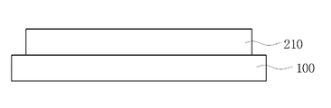
도 1은 본 발명의 일 실시예에 따른 투명 전극을 개략적으로 도시한 단면도이다.
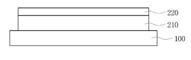
도 2는 본 발명의 다른 실시예에 따른 투명 전극을 개략적으로 도시한 단면도이다.
도 3a 내지 3g는 본 발명의 일 실시예에 따른 투명 전극의 제조 방법을 개략적으로 도시한 공정 단면도이다.
도 4a 및 4b는 각각 비교예와 실험예의 사진이다.1 is a cross-sectional view schematically illustrating a transparent electrode according to an embodiment of the present invention.
2 is a cross-sectional view schematically illustrating a transparent electrode according to another embodiment of the present invention.
3A to 3G are process cross-sectional views schematically showing a method of manufacturing a transparent electrode according to an embodiment of the present invention.
4A and 4B are photographs of Comparative Examples and Experimental Examples, respectively.
이하, 본 발명을 보다 상세히 설명한다. 다만 본 발명을 설명함에 있어서 본 명세서에 첨부된 도면들을 참조할 때, 도면들은 단지 본 발명을 설명하기 위한 예시일 뿐, 본 발명이 도면에 의해 한정되는 것은 아니다. 또한, 설명 상의 편의를 위해 일부 구성요소들은 도면 상에서 과장되게 표현되거나, 축소 또는 생략되어 있을 수 있다.
Hereinafter, the present invention will be described in more detail. In the following description of the present invention, reference will be made to the accompanying drawings, which are included to provide a further understanding of the invention, and are not intended to limit the invention. Also, for ease of explanation, some of the elements may be exaggerated in the drawings, or may be omitted or omitted.
도 1은 본 발명의 일 실시예에 따른 투명 전극을 개략적으로 도시한 단면도이다.1 is a cross-sectional view schematically illustrating a transparent electrode according to an embodiment of the present invention.
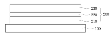
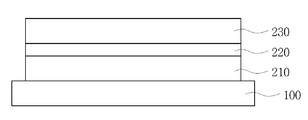
도 1에 나타난 바와 같이, 본 발명의 일 실시예에 따른 투명 전극은 기판(100) 위에 다결정 구조의 제1 투명 전도성 층(210), 금속 나노와이어 층(220) 및 비정질 구조의 제2 투명 전도성 층(230)이 차례로 적층된 삼층막(200)으로 이루어진다.1, a transparent electrode according to an exemplary embodiment of the present invention includes a first transparent
다결정 구조의 제1 투명 전도성 층(210)은 다결정 인듐주석산화물(ITO)일 수 있다. 이때, 다결정 ITO의 결정화 정도는 엑스선 회절(X-ray diffraction, XRD) 분석에 따른 ITO의 주요 결정화 방향인 (222) 방향의 결정화 정도가 6000개 이상이다. ITO의 경우 IZO나 다른 금속 산화물에 비하여 결정화가 잘 이루어질 수 있어 다결정 구조의 제1 투명 전도성 층(210)을 형성하기에 유리하다. The first transparent
금속 나노와이어 층(220)은 은 나노와이어, 구리 나노와이어, 지르코늄 나노와이어, 금 나노와이어 중 어느 하나가 될 수 있으며, 특히 은 나노와이어로 이루어질 수 있다.The
비정질 구조의 제2 투명 전도성 층(230)은 인듐주석산화물(ITO), 인듐아연산화물(IZO), 인듐아연주석산화물(IZTO), 알루미늄아연산화물(AZO), 갈륨아연산화물(GZO), 불소주석산화물(FTO), 아연산화물(ZnO) 중 어느 하나의 금속 산화물로 형성될 수 있으며, 특히 ITO 또는 IZO로 이루어질 수 있다.The second transparent
기판(100)은 유리 기판이거나, 투명 전극이 유연성 전자 장치를 위한 것인 경우 유연성 필름 기재일 수 있다. 특히 투명 전극이 표시장치에 사용될 경우, 기판(100)은 투명필름이나 편광판일 수 있다. The
투명필름은 투명성, 기계적 강도, 열안정성이 우수한 필름이 사용될 수 있으며, 구체적인 예로는, 폴리에틸렌테레프탈레이트, 폴리에틸렌이소프탈레이트, 폴리에틸렌나프탈레이트, 폴리부틸렌테레프탈레이트 등의 폴리에스테르계 수지; 디아세틸셀룰로오스, 트리아세틸셀룰로오스 등의 셀룰로오스계 수지; 폴리카보네이트계 수지; 폴리메틸(메타)아크릴레이트, 폴리에틸(메타)아크릴레이트 등의 아크릴계 수지; 폴리스티렌, 아크릴로니트릴-스티렌 공중합체 등의 스티렌계 수지; 폴리에틸렌, 폴리프로필렌, 시클로계 또는 노보넨 구조를 갖는 폴리올레핀, 에틸렌-프로필렌 공중합체 등의 폴리올레핀계 수지; 염화비닐계 수지; 나일론, 방향족 폴리아미드 등의 아미드계 수지; 이미드계 수지; 폴리에테르술폰계 수지; 술폰계 수지; 폴리에테르에테르케톤계 수지; 황화 폴리페닐렌계 수지; 비닐알코올계 수지; 염화비닐리덴계 수지; 비닐부티랄계 수지; 알릴레이트계 수지; 폴리옥시메틸렌계 수지; 에폭시계 수지 등과 같은 열가소성 수지로 구성된 필름을 들 수 있으며, 상기 열가소성 수지의 블렌드물로 구성된 필름도 사용할 수 있다. 또한, (메타)아크릴계, 우레탄계, 아크릴우레탄계, 에폭시계, 실리콘계 등의 열경화형 수지 또는 자외선 경화형 수지로 된 필름을 이용할 수도 있다. As the transparent film, a film excellent in transparency, mechanical strength and thermal stability may be used. Specific examples thereof include polyester resins such as polyethylene terephthalate, polyethylene isophthalate, polyethylene naphthalate and polybutylene terephthalate; Cellulose-based resins such as diacetylcellulose and triacetylcellulose; Polycarbonate resin; Acrylic resins such as polymethyl (meth) acrylate and polyethyl (meth) acrylate; Styrene resins such as polystyrene and acrylonitrile-styrene copolymer; Polyolefin resins such as polyethylene, polypropylene, cyclo- or norbornene-structured polyolefins, ethylene-propylene copolymers; Vinyl chloride resin; Amide resins such as nylon and aromatic polyamide; Imide resin; Polyether sulfone type resin; Sulfone based resin; Polyether ether ketone resin; A sulfided polyphenylene resin; Vinyl alcohol-based resin; Vinylidene chloride resins; Vinyl butyral resin; Allylate series resin; Polyoxymethylene type resin; Epoxy resin, and the like, and a film composed of the blend of the thermoplastic resin may also be used. Further, a film made of a thermosetting resin such as (meth) acrylic, urethane, acrylic urethane, epoxy or silicone, or a film made of an ultraviolet curable resin may also be used.
이와 같은 투명필름의 두께는 적절히 결정할 수 있지만, 일반적으로는 강도나 취급성 등의 작업성, 박층성 등의 점에서 1~500㎛ 정도이며, 1~300㎛가 바람직하고, 5~200㎛가 보다 바람직하다.Though the thickness of such a transparent film can be suitably determined, it is generally 1 to 500 占 퐉, preferably 1 to 300 占 퐉, and preferably 5 to 200 占 퐉, from the viewpoint of workability such as strength and handling property, More preferable.
이러한 투명필름은 적절한 1종 이상의 첨가제가 함유된 것일 수도 있다. 첨가제로는, 예컨대 자외선흡수제, 산화방지제, 윤활제, 가소제, 이형제, 착색방지제, 난연제, 대전방지제, 안료, 착색제 등을 들 수 있다. 상기 투명 필름은 필름의 일면 또는 양면에 하드코팅층, 반사방지층, 가스배리어층과 같은 다양한 기능성층을 포함하는 구조일 수 있으며, 기능성층은 전술한 것으로 한정되는 것은 아니며, 용도에 따라 다양한 기능성층을 포함할 수 있다.Such a transparent film may contain one or more suitable additives. Examples of the additive include an ultraviolet absorber, an antioxidant, a lubricant, a plasticizer, a release agent, a coloring inhibitor, a flame retardant, an antistatic agent, a pigment and a colorant. The transparent film may be a structure including various functional layers such as a hard coating layer, an antireflection layer, and a gas barrier layer on one side or both sides of the film. The functional layer is not limited to the above, and various functional layers .
또한, 필요에 따라 투명필름은 표면 처리된 것일 수 있다. 이러한 표면 처리로는 플라즈마 처리, 코로나 처리, 프라이머 처리 등의 건식 처리, 검화 처리를 포함하는 알칼리 처리 등의 화학 처리 등을 들 수 있다.Further, if necessary, the transparent film may be surface-treated. Examples of the surface treatment include a chemical treatment such as an alkaline treatment including a dry treatment such as a plasma treatment, a corona treatment, a primer treatment, and a saponification treatment.
또한, 투명필름은 등방성필름, 위상차필름 또는 보호필름(Protective Film)일 수 있다.Further, the transparent film may be an isotropic film, a retardation film, or a protective film.
등방성필름일 경우 면내 위상차(Ro, Ro=[(nx-ny)ⅹd], nx, ny는 필름 평면 내의 주굴절률, nz는 필름 두께 방향의 굴절률, d는 필름 두께이다)가 40nm 이하이고, 15nm 이하가 바람직하며, 두께방향 위상차(Rth, Rth=[(nx+ny)/2-nz]ⅹd)가 -90nm~+75nm 이며, 바람직하게는 -80nm~+60nm, 특히 -70nm~+45nm 가 바람직하다.Nx and ny are the main indices of refraction in the film plane, nz is the refractive index in the film thickness direction, d is the film thickness) is 40 nm or less, and 15 nm And the retardation in the thickness direction (Rth, Rth = [(nx + ny) / 2-nz] xd) is from -90 nm to +75 nm, preferably -80 nm to +60 nm, particularly preferably -70 nm to +45 nm desirable.
위상차필름은 고분자필름의 일축 연신, 이축 연신, 고분자코팅, 액정코팅의 방법으로 제조된 필름이며, 일반적으로 디스플레이의 시야각보상, 색감개선, 빛샘개선, 색미조절 등의 광학특성 향상 및 조절을 위하여 사용된다.The retardation film is a film produced by the uniaxial stretching, biaxial stretching, polymer coating and liquid crystal coating method of a polymer film, and is generally used for improving the viewing angle of the display, improving the color feeling, improving the light leakage, do.
위상차필름의 종류에는 1/2 이나 1/4 등의 파장판, 양의 C플레이트, 음의 C플레이트, 양의 A플레이트, 음의 A플레이트, 이축성 파장판을 포함한다.The types of the retardation film include a wave plate of 1/2 or 1/4, a positive C plate, a negative C plate, a positive A plate, a negative A plate, and a biaxial wave plate.
보호필름은 고분자수지로 이루어진 필름의 적어도 일면에 점착층을 포함하는 필름이거나 폴리프로필렌 등의 자가점착성을 가진 필름일 수 있으며, 투명 전극을 포함하는 전자 장치의 표면 보호, 공정성 개선을 위하여 사용될 수 있다.
The protective film may be a film including an adhesive layer on at least one side of a film made of a polymer resin, or a self-adhesive film such as polypropylene, and may be used for surface protection and improvement of the processability of an electronic device including a transparent electrode .
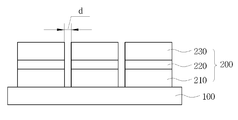
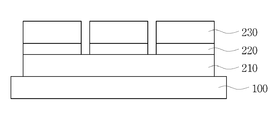
본 발명에 따르면, 도 1에 나타난 바와 같은 3층막 구조로 이루어진 투명 전극을 사용하여 패턴 간 간격이 10μm 이하인 미세 패턴을 갖는 투명 전극을 얻을 수 있다. According to the present invention, a transparent electrode having a fine pattern having a pattern interval of 10 μm or less can be obtained by using a transparent electrode having a three-layer structure as shown in FIG.
도 2는 본 발명의 다른 실시예에 따른 투명 전극을 개략적으로 도시한 단면도이다.2 is a cross-sectional view schematically illustrating a transparent electrode according to another embodiment of the present invention.
도 2를 참조하면, 본 발명에서는 도 1을 참조하여 설명한 본 발명의 일 실시예에서와 마찬가지로 기판(100) 상에서 다결정 구조의 제1 투명 전도성 층(210), 금속 나노와이어 층(220) 및 비정질 구조의 제2 투명 전도성 층(230)의 3층막 구조(200)를 이루며 패턴 사이의 간격 d가 10μm 이하로 형성된 투명 전극을 제공한다.Referring to FIG. 2, a first transparent
기판(100), 제1 투명 전도성 층(210), 금속 나노와이어 층(220) 및 제2 투명 전도성 층(230)에 관한 자세한 사항은 도 1을 참조하여 설명한 본 발명의 실시예와 유사하므로 설명을 생략한다.
The details of the
이제, 본 발명의 실시예에 따른 투명 전극의 제조 방법에 대해 자세히 설명한다. Now, a method of manufacturing a transparent electrode according to an embodiment of the present invention will be described in detail.
본 발명에 의하면, 투명 전극 최하부의 투명 전도성 층을 어닐링하여 결정화한 후 상부층을 형성하여 3층 구조를 완성하고, 최종 형성된 3층막을 2단계에 걸쳐 식각함으로써 미세한 패턴을 구현할 수 있다.According to the present invention, a fine pattern can be realized by annealing and crystallizing the transparent conductive layer at the bottom of the transparent electrode, forming an upper layer to complete the three-layer structure, and etching the finally formed three-layer film in two steps.
또한, 본 발명의 투명 전극은 사용하고자 하는 기판 상에 직접 형성하거나, 캐리어 기판을 이용하여 공정을 진행하여 투명 전극을 형성한 후 캐리어 기판을 분리하고 기재 필름을 부착할 수 있다.In addition, the transparent electrode of the present invention may be formed directly on a substrate to be used, or may be formed by forming a transparent electrode by carrying out a process using a carrier substrate, separating the carrier substrate, and attaching the substrate film.
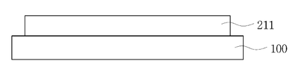
이하에서는, 기판 상에 직접 투명 전극을 형성하는 방법에 대해 설명한다. 도 3a 내지 3g는 본 발명의 일 실시예에 따른 투명 전극의 제조 방법을 개략적으로 도시한 공정 단면도이다.Hereinafter, a method of forming a transparent electrode directly on a substrate will be described. 3A to 3G are process cross-sectional views schematically showing a method of manufacturing a transparent electrode according to an embodiment of the present invention.
도 3a에 나타난 바와 같이, 먼저 기판(100) 상에 투명 전도성 층(211)을 성막한다. As shown in FIG. 3A, a transparent
상기 투명 전도성 층은 CVD(Chemical Vapor Deposition), PVD(Physical Vapor Deposition), PECVD(Plasma Enhanced Chemical Vapor Deposition) 등의 스퍼터링(Sputtering) 공정, 스크린인쇄, 그라비아(Gravure) 인쇄, 리버스오프셋(Reverse Offset), 잉크젯(Ink Jet) 등의 인쇄공정, 건식 또는 습식의 도금 공정을 이용하여 성막할 수 있다.The transparent conductive layer may be formed by a sputtering process such as CVD (Chemical Vapor Deposition), PVD (Physical Vapor Deposition) or PECVD (Plasma Enhanced Chemical Vapor Deposition), screen printing, gravure printing, reverse offset, , Ink jet (Ink Jet), or the like, or a dry or wet plating process.
성막된 투명 전도성 층(211)은 비정질 상태이다.The deposited transparent
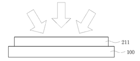
다음, 도 3b에 나타난 바와 같이, 어닐링을 실시하여 투명 전도성 층(211)을 결정화한다.Next, as shown in FIG. 3B, annealing is performed to crystallize the transparent
어닐링은 필요에 따라 다양한 조건으로 실시할 수 있다. 예를 들면, 200℃에서 20분간 어닐링을 실시할 수 있다. The annealing can be carried out under various conditions as required. For example, annealing may be performed at 200 ° C for 20 minutes.
사용되는 기판(100)의 종류에 따라 어닐링 조건이 달라질 수 있다. 예를 들어, 유연성 필름기재 상에 직접 투명 전극을 제조하는 경우, 유연성 필름기재가 고온에서 손상될 수 있어 더 낮은 온도에서 어닐링하여야 할 수 있으며, 유리 기판을 사용하는 경우 고온에서 어닐링할 수 있다.The annealing conditions may vary depending on the type of the
어닐링을 실시한 후에는, 도 3c에 나타난 바와 같이, 투명 전도성 층이 결정화되어 다결정 투명 전도성 층(210)이 형성된다. 이 때, 투명 전도성 층(210)의 결정화 정도는 XRD 분석에 따른 결정화 개수가 6000개 이상이다. After the annealing, as shown in FIG. 3C, the transparent conductive layer is crystallized to form the polycrystalline transparent
이제, 도 3d 및 도 3e에 각각 나타난 바와 같이, 투명 전도성 층(210) 위에 금속 나노와이어 층(220)과 제2 투명 전도성 층(230)을 차례로 형성하면, 본 발명의 일 실시예에 따른 3층 구조의 투명 전극을 형성할 수 있다.Now, as shown in FIGS. 3D and 3E, if the
금속 나노와이어 층(220)과 제2 투명 전도성 층(230)의 재료 등 자세한 사항은 앞서 도 1을 참조하여 설명한 것과 유사하며, 그 형성 방법은 일반적으로 투명 전극을 형성하는 데 사용되는 공정을 제한 없이 사용할 수 있다.The details of the material of the
이제, 도 3e에 나타난 바와 같은 투명 전극을 식각하여 미세 패턴을 갖는 투명 전극을 형성하는 방법을 이어서 설명한다.Now, a method of forming a transparent electrode having a fine pattern by etching a transparent electrode as shown in FIG. 3E will be described.
도 3f에 나타난 바와 같이, 먼저 금속막 식각액을 사용하여 제2 투명 전도성 층(230)과 금속 나노와이어 층(220)을 식각한다. As shown in FIG. 3F, the second transparent
다음, 도 3g에 나타난 바와 같이, 금속 산화물 막 식각액을 사용하여 제1 투명 전도성 층(210)을 식각한다.Next, as shown in FIG. 3G, the first transparent
제1 투명 전도성 층을 결정화하지 않는 통상의 3중막 구조에서는, 금속막 식각액을 사용하여 투명 전극을 패터닝할 경우 금속 나노와이어 층으로부터의 잔사가 발생하게 되고, 금속 산화물 막 식각액을 사용하여 투명 전극을 패터닝할 경우 빠른 식각속도로 인하여 금속 나노와이어 층이 심하게 식각되어 패턴 형성이 어렵다.In a conventional triple-film structure in which the first transparent conductive layer is not crystallized, when a transparent electrode is patterned using a metal film etchant, residues are generated from the metal nanowire layer, and the transparent electrode is etched using the metal oxide film etchant When patterning, the metal nanowire layer is severely etched due to the rapid etching rate, which makes pattern formation difficult.
본 발명에 따르면, 금속막 식각액을 사용하여 제2 투명 전도성 층(230)과 금속 나노와이어 층(220)을 1차 식각하고, 금속 산화물 막 식각액을 사용하여 결정성인 제1 투명 전도성 층(210)을 빠르게 식각하면서 금속 나노와이어 층(220)의 잔사를 함께 제거할 수 있다.According to the present invention, the second transparent
이상에서, 기판 상에 직접 투명 전극을 형성하는 방법에 대해 설명하였으나, 유연성 필름기재 상에 투명 전극을 배치하고자 할 경우 캐리어 기판 상에 투명 전극을 형성하고 캐리어 기판을 분리한 뒤 유연성 필름 기재를 부착할 수도 있다. 통상 유연성 필름기재의 경우 고온을 견딜 수 없어 제1 투명 전도성 층의 어닐링이 어려울 수 있으므로, 캐리어 기판을 사용하는 전사 공정이 유리할 수 있다.
In the above, a method of forming a transparent electrode directly on a substrate has been described. However, when a transparent electrode is disposed on a flexible film substrate, a transparent electrode is formed on the carrier substrate, the carrier substrate is separated, You may. In general, in the case of a flexible film base, since the first transparent conductive layer can not withstand a high temperature, annealing of the first transparent conductive layer may be difficult, so that a transfer process using the carrier substrate may be advantageous.
이하에서 실험예와 비교예에 의해 본 발명을 더욱 구체적으로 설명하고자 한다. 그러나, 이하의 실험예와 비교예는 본 발명을 설명하기 위한 것으로, 본 발명의 범위가 어떤 의미로든 이에 의해 제한되지 않는다.
Hereinafter, the present invention will be described in more detail with reference to experimental examples and comparative examples. However, the following experimental examples and comparative examples are intended to illustrate the present invention, and the scope of the present invention is not limited thereto in any sense.
실험예 및 비교예Experimental Examples and Comparative Examples
30μm의 패턴 폭과 8μm의 패턴 사이 간격을 갖는 두 가지 샘플을 제작하였다. 제1 투명 전도성 층과 제2 투명 전도성 층으로는 ITO를 사용하였고, 금속 나노와이어 층은 은 나노와이어로 형성하였다. Two samples with a pattern width of 30 [mu] m and a spacing of 8 [mu] m were prepared. ITO was used for the first transparent conductive layer and the second transparent conductive layer, and the metal nanowire layer was formed of silver nanowires.
실험예는 앞서 설명한 본 발명의 실시예에 따른 방법에 의하여 제1 ITO 층을 200도에서 30분간 어닐링하여 결정화시킨 후 두 단계로 나누어 식각하였다. 제2 ITO 층 및 은 나노와이어 층의 1차 식각은 금속막 식각액 PSW01을 사용하고, 제1 ITO 층의 2차 식각은 금속 산화물 막 식각액 MAS02를 사용하였다.In the experimental example, the first ITO layer was crystallized by annealing at 200 degrees for 30 minutes by the method according to the embodiment of the present invention described above, and then divided into two steps. The first etching of the second ITO layer and the silver nanowire layer used the metal film etching solution PSW01 and the second etching of the first ITO layer used the metal oxide film etching solution MAS02.
비교예는 제1 ITO 층을 결정화하지 않고 제1 ITO 층의 성막에 이어서 바로 은 나노와이어 층과 제2 ITO 층을 차례로 형성하였으며, 금속막 식각액 PSW01을 사용하여 삼층막을 일괄 식각하였다.In the comparative example, the first ITO layer was not crystallized, followed by the formation of the first ITO layer, followed by the formation of the silver nanowire layer and the second ITO layer, and the three-layer film was etched by using the metal film etching solution PSW01.
도 4a 및 4b는 각각 비교예 및 실험예에 따라 형성된 투명 전극 패턴의 사진이다. 4A and 4B are photographs of a transparent electrode pattern formed according to Comparative Examples and Experimental Examples, respectively.
도 4a에 나타난 비교예의 경우 패턴 사이에 은 나노와이어의 잔사가 남아 있는 것을 볼 수 있는 데 비하여, 도 4b에 나타난 실험예의 경우 정확한 패턴이 형성된 것을 볼 수 있다.
In the case of the comparative example shown in FIG. 4A, it can be seen that the silver nanowire remains between the patterns, whereas in the case of the experiment shown in FIG. 4B, the accurate pattern is formed.
이상에서 본 발명의 바람직한 실시예에 대하여 도면을 참조하여 설명하였지만, 본 발명은 상술한 실시예에 한정되는 것은 아니며, 본 발명의 본질적인 특성에서 벗어나지 않는 범위에서 변형된 형태로 본 발명이 구현될 수 있음을 이해할 수 있을 것이다. 상술한 본 발명의 실시예들은 독립적으로 또는 그 특징들의 일부 또는 전부를 조합하여 적용될 수 있다. While the present invention has been particularly shown and described with reference to exemplary embodiments thereof, it is to be understood that the invention is not limited to the disclosed embodiments, but, on the contrary, It can be understood that. The above-described embodiments of the present invention can be applied independently or in combination of some or all of the features.
그러므로, 본 발명의 범위는 전술한 설명이 아니라 특허청구범위에 의해 정해지며, 그와 동등한 범위 내에 있는 모든 차이점은 본 발명에 포함되는 것으로 해석되어야 할 것이다.Therefore, the scope of the present invention is defined by the appended claims rather than the foregoing description, and all differences within the scope of equivalents thereof should be construed as being included in the present invention.
100: 기판
200: 투명 전극 삼층막
210: 제1 투명 전도성 층
211: 비정질 투명 전도성 층
220: 금속 나노와이어 층
230: 제2 투명 전도성 층100: substrate 200: transparent electrode three-layer film
210: first transparent conductive layer 211: amorphous transparent conductive layer
220: metal nanowire layer 230: second transparent conductive layer
Claims (10)
상기 기판 상에 배치되는 다결정 구조의 제1 투명 전도성 층, 상기 제1 투명 전도성 층 상에 배치되는 금속 나노와이어 층, 상기 금속 나노와이어 층 상에 배치되는 비정질 구조의 제2 투명 전도성 층으로 이루어진 투명 전도성 패턴을 포함하는,
투명 전극.Board,
A first transparent conductive layer of a polycrystalline structure disposed on the substrate, a metal nanowire layer disposed on the first transparent conductive layer, and a second transparent conductive layer of an amorphous structure disposed on the metal nanowire layer Including a conductive pattern,
Transparent electrode.
상기 제1 투명 전도성 층은 XRD 분석에 따른 결정화 개수가 6000 이상인 다결정 인듐주석산화물로 이루어진 투명 전극.The method according to claim 1,
Wherein the first transparent conductive layer is made of polycrystalline indium tin oxide having a crystallization number of 6000 or more according to XRD analysis.
상기 제2 투명 전도성 층은 비정질 인듐주석산화물 또는 비정질 인듐아연산화물로 이루어진 투명 전극.The method according to claim 1,
Wherein the second transparent conductive layer is made of amorphous indium tin oxide or amorphous indium zinc oxide.
상기 금속 나노와이어 층은 은 나노와이어 층인 투명 전극.The method according to claim 1,
Wherein the metal nanowire layer is a silver nanowire layer.
상기 투명 전도성 패턴의 패턴 간 간격은 10μm 이하인 투명 전극.The method according to claim 1,
Wherein a distance between the patterns of the transparent conductive pattern is 10 占 퐉 or less.
상기 제1 투명 전도성 층을 결정화하는 단계,
상기 제1 투명 전도성 층 상에 금속 나노와이어 층을 형성하는 단계,
상기 금속 나노와이어 층 상에 제2 투명 전도성 층을 성막하는 단계를 포함하는,
투명 전극의 제조 방법.Forming a first transparent conductive layer on a substrate,
Crystallizing the first transparent conductive layer,
Forming a metal nanowire layer on the first transparent conductive layer,
And forming a second transparent conductive layer on the metal nanowire layer.
A method of manufacturing a transparent electrode.
상기 제1 투명 전도성 층을 결정화하는 단계는 상기 제1 투명 전도성 층의 어닐링을 포함하는,
투명 전극의 제조 방법.The method according to claim 6,
Wherein the step of crystallizing the first transparent conductive layer comprises annealing the first transparent conductive layer.
A method of manufacturing a transparent electrode.
상기 제1 투명 전도성 층은 인듐주석산화물로 이루어지며,
상기 제1 투명 전도성 층을 결정화하는 단계 이후에, 상기 제1 투명 전도성 층은 XRD 분석에 따른 결정화 개수가 6000 이상인 다결정 인듐주석산화물로 되는,
투명 전극의 제조 방법.The method according to claim 6,
Wherein the first transparent conductive layer is made of indium tin oxide,
Wherein the first transparent conductive layer is made of polycrystalline indium tin oxide having a crystallization number of 6000 or more according to XRD analysis, after crystallization of the first transparent conductive layer,
A method of manufacturing a transparent electrode.
상기 제2 투명 전도성 층을 성막하는 단계 이후에,
금속막 식각액을 사용하여 상기 제2 투명 전도성 층 및 상기 금속 나노와이어 층을 식각하는 단계,
금속 산화물 막 식각액을 사용하여 상기 제1 투명 전도성 층을 식각하는 단계를 포함하는,
투명 전극의 제조 방법.The method according to claim 6,
After the step of forming the second transparent conductive layer,
Etching the second transparent conductive layer and the metal nanowire layer using a metal film etchant,
And etching the first transparent conductive layer using a metal oxide film etchant.
A method of manufacturing a transparent electrode.
상기 제1 투명 전도성 층을 식각하는 단계 이후에 형성되는 상기 제1 투명 전도성 층, 상기 금속 나노와이어 층 및 상기 제2 투명 전도성 층의 패턴의 패턴 간 간격은 10μm 이하인 투명 전극의 제조 방법.10. The method of claim 9,
Wherein the interval between the patterns of the first transparent conductive layer, the metal nanowire layer, and the second transparent conductive layer formed after the step of etching the first transparent conductive layer is 10 m or less.
Priority Applications (1)
| Application Number | Priority Date | Filing Date | Title |
|---|---|---|---|
| KR1020170024937A KR20180098019A (en) | 2017-02-24 | 2017-02-24 | Transparent Electrode and Method of Preparing the Same |
Applications Claiming Priority (1)
| Application Number | Priority Date | Filing Date | Title |
|---|---|---|---|
| KR1020170024937A KR20180098019A (en) | 2017-02-24 | 2017-02-24 | Transparent Electrode and Method of Preparing the Same |
Publications (1)
| Publication Number | Publication Date |
|---|---|
| KR20180098019A true KR20180098019A (en) | 2018-09-03 |
Family
ID=63601001
Family Applications (1)
| Application Number | Title | Priority Date | Filing Date |
|---|---|---|---|
| KR1020170024937A Withdrawn KR20180098019A (en) | 2017-02-24 | 2017-02-24 | Transparent Electrode and Method of Preparing the Same |
Country Status (1)
| Country | Link |
|---|---|
| KR (1) | KR20180098019A (en) |
Cited By (3)
| Publication number | Priority date | Publication date | Assignee | Title |
|---|---|---|---|---|
| KR20210081028A (en) * | 2019-12-23 | 2021-07-01 | 엘지이노텍 주식회사 | Transparent antenna and antenna apparatus comprising the same |
| JPWO2022054151A1 (en) * | 2020-09-09 | 2022-03-17 | ||
| JPWO2022054150A1 (en) * | 2020-09-09 | 2022-03-17 |
Citations (1)
| Publication number | Priority date | Publication date | Assignee | Title |
|---|---|---|---|---|
| KR101391510B1 (en) | 2013-03-19 | 2014-05-07 | 경희대학교 산학협력단 | Muliple transparent electrode comprising metal nano wire |
-
2017
- 2017-02-24 KR KR1020170024937A patent/KR20180098019A/en not_active Withdrawn
Patent Citations (1)
| Publication number | Priority date | Publication date | Assignee | Title |
|---|---|---|---|---|
| KR101391510B1 (en) | 2013-03-19 | 2014-05-07 | 경희대학교 산학협력단 | Muliple transparent electrode comprising metal nano wire |
Cited By (6)
| Publication number | Priority date | Publication date | Assignee | Title |
|---|---|---|---|---|
| KR20210081028A (en) * | 2019-12-23 | 2021-07-01 | 엘지이노텍 주식회사 | Transparent antenna and antenna apparatus comprising the same |
| JPWO2022054151A1 (en) * | 2020-09-09 | 2022-03-17 | ||
| WO2022054151A1 (en) * | 2020-09-09 | 2022-03-17 | 株式会社 東芝 | Trasparent electrode, mehod for producing trasparent electrode, and electronic device |
| JPWO2022054150A1 (en) * | 2020-09-09 | 2022-03-17 | ||
| WO2022054150A1 (en) * | 2020-09-09 | 2022-03-17 | 株式会社 東芝 | Transparent electrode, method for manufacturing transparent electrode, and electronic device |
| US11942575B2 (en) | 2020-09-09 | 2024-03-26 | Kabushiki Kaisha Toshiba | Transparent electrode, method of producing transparent electrode, and electronic device |
Similar Documents
| Publication | Publication Date | Title |
|---|---|---|
| US11609668B2 (en) | Film touch sensor and manufacturing method therefor | |
| KR101444132B1 (en) | Touch sensing electrode combined with complexed polarization plate and touch screen panel comprising the same | |
| KR102142144B1 (en) | Window film combined with polarization plate and touch sensing electrode | |
| KR101989457B1 (en) | High performance touch sensor and manufacturing method thereof | |
| US10261642B2 (en) | Film touch sensor with an inorganic passivation layer | |
| KR101586739B1 (en) | Film Touch Sensor and Method for Fabricating the Same | |
| KR101586736B1 (en) | Film Touch Sensor and Method for Fabricating the Same | |
| WO2011162414A1 (en) | Transparent planar body and transparent touch panel | |
| US20160170540A1 (en) | Touch sensor electrode integrated with polarizing plate | |
| US20170285780A1 (en) | Touch sensor and method for preparing the same | |
| KR20180097212A (en) | Metal Mesh Electrode and Flexible Device Comprising the Same | |
| US10585504B2 (en) | Film touch sensor and method for fabricating the same | |
| KR20180098019A (en) | Transparent Electrode and Method of Preparing the Same | |
| KR20190085319A (en) | Touch Sensor and Display Device Including the Same | |
| CN210123552U (en) | Touch sensor | |
| KR20140134227A (en) | Touch sensing electrode combined with complex polarization plate | |
| US11262880B2 (en) | High performance film-type touch sensor | |
| US10852860B2 (en) | Touch sensor having enhanced durability and optical characteristics and method of manufacturing the same | |
| KR102205985B1 (en) | High-performance touch sensor | |
| KR101841946B1 (en) | Touch sensor film manufacturing method using tension control | |
| KR20190113098A (en) | Multilayer transparent electric conductor and manufacturing method thereof | |
| KR20170096475A (en) | Foldable touch sensor and manufacturing method therof | |
| KR20170112989A (en) | Touch sensor film manufacturing method | |
| JP2015152981A (en) | Touch sensor |
Legal Events
| Date | Code | Title | Description |
|---|---|---|---|
| PA0109 | Patent application |
Patent event code: PA01091R01D Comment text: Patent Application Patent event date: 20170224 |
|
| PG1501 | Laying open of application | ||
| PC1203 | Withdrawal of no request for examination | ||
| WITN | Application deemed withdrawn, e.g. because no request for examination was filed or no examination fee was paid |