KR20180089538A - An article having a microstructured layer - Google Patents
An article having a microstructured layer Download PDFInfo
- Publication number
- KR20180089538A KR20180089538A KR1020187021373A KR20187021373A KR20180089538A KR 20180089538 A KR20180089538 A KR 20180089538A KR 1020187021373 A KR1020187021373 A KR 1020187021373A KR 20187021373 A KR20187021373 A KR 20187021373A KR 20180089538 A KR20180089538 A KR 20180089538A
- Authority
- KR
- South Korea
- Prior art keywords
- layer
- microstructured
- major surface
- article
- film
- Prior art date
Links
- 239000000203 mixture Substances 0.000 claims abstract description 80
- 239000000463 material Substances 0.000 claims abstract description 41
- 239000010408 film Substances 0.000 abstract description 66
- 230000003287 optical effect Effects 0.000 abstract description 39
- 239000012788 optical film Substances 0.000 abstract description 15
- 239000010410 layer Substances 0.000 description 245
- NIXOWILDQLNWCW-UHFFFAOYSA-M acrylate group Chemical group C(C=C)(=O)[O-] NIXOWILDQLNWCW-UHFFFAOYSA-M 0.000 description 62
- 229920000642 polymer Polymers 0.000 description 22
- 239000012790 adhesive layer Substances 0.000 description 18
- 238000001878 scanning electron micrograph Methods 0.000 description 16
- 238000004519 manufacturing process Methods 0.000 description 14
- 229920005989 resin Polymers 0.000 description 14
- 239000011347 resin Substances 0.000 description 14
- 239000011342 resin composition Substances 0.000 description 14
- 238000003848 UV Light-Curing Methods 0.000 description 12
- 238000000034 method Methods 0.000 description 12
- 239000004593 Epoxy Substances 0.000 description 11
- -1 2-ethylhexyl Chemical group 0.000 description 10
- 239000000853 adhesive Substances 0.000 description 10
- 230000001070 adhesive effect Effects 0.000 description 10
- 150000001875 compounds Chemical class 0.000 description 10
- 238000004132 cross linking Methods 0.000 description 10
- 238000000576 coating method Methods 0.000 description 9
- 230000004927 fusion Effects 0.000 description 9
- 229920006267 polyester film Polymers 0.000 description 9
- LYCAIKOWRPUZTN-UHFFFAOYSA-N Ethylene glycol Chemical compound OCCO LYCAIKOWRPUZTN-UHFFFAOYSA-N 0.000 description 8
- 229920000728 polyester Polymers 0.000 description 8
- 239000011324 bead Substances 0.000 description 7
- 239000011248 coating agent Substances 0.000 description 7
- 230000000737 periodic effect Effects 0.000 description 7
- IJGRMHOSHXDMSA-UHFFFAOYSA-N Atomic nitrogen Chemical compound N#N IJGRMHOSHXDMSA-UHFFFAOYSA-N 0.000 description 6
- PEDCQBHIVMGVHV-UHFFFAOYSA-N Glycerine Chemical compound OCC(O)CO PEDCQBHIVMGVHV-UHFFFAOYSA-N 0.000 description 6
- 239000011243 crosslinked material Substances 0.000 description 6
- 238000001723 curing Methods 0.000 description 6
- MTHSVFCYNBDYFN-UHFFFAOYSA-N diethylene glycol Chemical compound OCCOCCO MTHSVFCYNBDYFN-UHFFFAOYSA-N 0.000 description 6
- 238000010030 laminating Methods 0.000 description 6
- 238000005259 measurement Methods 0.000 description 6
- 230000005855 radiation Effects 0.000 description 6
- 239000012815 thermoplastic material Substances 0.000 description 6
- QVGXLLKOCUKJST-UHFFFAOYSA-N atomic oxygen Chemical compound [O] QVGXLLKOCUKJST-UHFFFAOYSA-N 0.000 description 5
- 238000006243 chemical reaction Methods 0.000 description 5
- 239000003999 initiator Substances 0.000 description 5
- 239000001301 oxygen Substances 0.000 description 5
- 229910052760 oxygen Inorganic materials 0.000 description 5
- 230000035515 penetration Effects 0.000 description 5
- 238000009792 diffusion process Methods 0.000 description 4
- 239000000835 fiber Substances 0.000 description 4
- 239000000945 filler Substances 0.000 description 4
- 230000001788 irregular Effects 0.000 description 4
- 229910052757 nitrogen Inorganic materials 0.000 description 4
- WXZMFSXDPGVJKK-UHFFFAOYSA-N pentaerythritol Chemical compound OCC(CO)(CO)CO WXZMFSXDPGVJKK-UHFFFAOYSA-N 0.000 description 4
- 229920000647 polyepoxide Polymers 0.000 description 4
- 125000003700 epoxy group Chemical group 0.000 description 3
- 239000000178 monomer Substances 0.000 description 3
- 239000013047 polymeric layer Substances 0.000 description 3
- 238000010526 radical polymerization reaction Methods 0.000 description 3
- 238000011160 research Methods 0.000 description 3
- CZDYPVPMEAXLPK-UHFFFAOYSA-N tetramethylsilane Chemical compound C[Si](C)(C)C CZDYPVPMEAXLPK-UHFFFAOYSA-N 0.000 description 3
- DTGKSKDOIYIVQL-WEDXCCLWSA-N (+)-borneol Chemical group C1C[C@@]2(C)[C@@H](O)C[C@@H]1C2(C)C DTGKSKDOIYIVQL-WEDXCCLWSA-N 0.000 description 2
- MYRTYDVEIRVNKP-UHFFFAOYSA-N 1,2-Divinylbenzene Chemical compound C=CC1=CC=CC=C1C=C MYRTYDVEIRVNKP-UHFFFAOYSA-N 0.000 description 2
- FIHBHSQYSYVZQE-UHFFFAOYSA-N 6-prop-2-enoyloxyhexyl prop-2-enoate Chemical compound C=CC(=O)OCCCCCCOC(=O)C=C FIHBHSQYSYVZQE-UHFFFAOYSA-N 0.000 description 2
- XKRFYHLGVUSROY-UHFFFAOYSA-N Argon Chemical compound [Ar] XKRFYHLGVUSROY-UHFFFAOYSA-N 0.000 description 2
- RTZKZFJDLAIYFH-UHFFFAOYSA-N Diethyl ether Chemical compound CCOCC RTZKZFJDLAIYFH-UHFFFAOYSA-N 0.000 description 2
- BAPJBEWLBFYGME-UHFFFAOYSA-N Methyl acrylate Chemical compound COC(=O)C=C BAPJBEWLBFYGME-UHFFFAOYSA-N 0.000 description 2
- 241000428199 Mustelinae Species 0.000 description 2
- VYPSYNLAJGMNEJ-UHFFFAOYSA-N Silicium dioxide Chemical compound O=[Si]=O VYPSYNLAJGMNEJ-UHFFFAOYSA-N 0.000 description 2
- PPBRXRYQALVLMV-UHFFFAOYSA-N Styrene Chemical compound C=CC1=CC=CC=C1 PPBRXRYQALVLMV-UHFFFAOYSA-N 0.000 description 2
- ZJCCRDAZUWHFQH-UHFFFAOYSA-N Trimethylolpropane Chemical compound CCC(CO)(CO)CO ZJCCRDAZUWHFQH-UHFFFAOYSA-N 0.000 description 2
- 238000010521 absorption reaction Methods 0.000 description 2
- 150000001252 acrylic acid derivatives Chemical class 0.000 description 2
- 239000002390 adhesive tape Substances 0.000 description 2
- 230000002411 adverse Effects 0.000 description 2
- 125000001931 aliphatic group Chemical group 0.000 description 2
- 150000001408 amides Chemical class 0.000 description 2
- 239000012298 atmosphere Substances 0.000 description 2
- ISAOCJYIOMOJEB-UHFFFAOYSA-N benzoin Chemical compound C=1C=CC=CC=1C(O)C(=O)C1=CC=CC=C1 ISAOCJYIOMOJEB-UHFFFAOYSA-N 0.000 description 2
- 230000001588 bifunctional effect Effects 0.000 description 2
- WERYXYBDKMZEQL-UHFFFAOYSA-N butane-1,4-diol Chemical compound OCCCCO WERYXYBDKMZEQL-UHFFFAOYSA-N 0.000 description 2
- 238000010538 cationic polymerization reaction Methods 0.000 description 2
- 239000007795 chemical reaction product Substances 0.000 description 2
- 239000002131 composite material Substances 0.000 description 2
- 230000007547 defect Effects 0.000 description 2
- 238000010894 electron beam technology Methods 0.000 description 2
- 238000005516 engineering process Methods 0.000 description 2
- 150000002148 esters Chemical class 0.000 description 2
- 239000010438 granite Substances 0.000 description 2
- 125000000959 isobutyl group Chemical group [H]C([H])([H])C([H])(C([H])([H])[H])C([H])([H])* 0.000 description 2
- 239000004973 liquid crystal related substance Substances 0.000 description 2
- 230000007246 mechanism Effects 0.000 description 2
- 150000002734 metacrylic acid derivatives Chemical class 0.000 description 2
- 125000002496 methyl group Chemical group [H]C([H])([H])* 0.000 description 2
- 125000001280 n-hexyl group Chemical group C(CCCCC)* 0.000 description 2
- SLCVBVWXLSEKPL-UHFFFAOYSA-N neopentyl glycol Chemical compound OCC(C)(C)CO SLCVBVWXLSEKPL-UHFFFAOYSA-N 0.000 description 2
- 230000000149 penetrating effect Effects 0.000 description 2
- 229920003229 poly(methyl methacrylate) Polymers 0.000 description 2
- 239000004417 polycarbonate Substances 0.000 description 2
- 229920000515 polycarbonate Polymers 0.000 description 2
- 229920001223 polyethylene glycol Polymers 0.000 description 2
- 229920006254 polymer film Polymers 0.000 description 2
- 239000004926 polymethyl methacrylate Substances 0.000 description 2
- 150000003077 polyols Chemical group 0.000 description 2
- 238000003825 pressing Methods 0.000 description 2
- 238000012545 processing Methods 0.000 description 2
- 239000000047 product Substances 0.000 description 2
- 239000002904 solvent Substances 0.000 description 2
- 239000000126 substance Substances 0.000 description 2
- LDHQCZJRKDOVOX-UHFFFAOYSA-N trans-crotonic acid Natural products CC=CC(O)=O LDHQCZJRKDOVOX-UHFFFAOYSA-N 0.000 description 2
- ZIBGPFATKBEMQZ-UHFFFAOYSA-N triethylene glycol Chemical compound OCCOCCOCCO ZIBGPFATKBEMQZ-UHFFFAOYSA-N 0.000 description 2
- 238000004804 winding Methods 0.000 description 2
- PAPBSGBWRJIAAV-UHFFFAOYSA-N ε-Caprolactone Chemical compound O=C1CCCCCO1 PAPBSGBWRJIAAV-UHFFFAOYSA-N 0.000 description 2
- MSAHTMIQULFMRG-UHFFFAOYSA-N 1,2-diphenyl-2-propan-2-yloxyethanone Chemical compound C=1C=CC=CC=1C(OC(C)C)C(=O)C1=CC=CC=C1 MSAHTMIQULFMRG-UHFFFAOYSA-N 0.000 description 1
- DKEGCUDAFWNSSO-UHFFFAOYSA-N 1,8-dibromooctane Chemical compound BrCCCCCCCCBr DKEGCUDAFWNSSO-UHFFFAOYSA-N 0.000 description 1
- JWYVGKFDLWWQJX-UHFFFAOYSA-N 1-ethenylazepan-2-one Chemical compound C=CN1CCCCCC1=O JWYVGKFDLWWQJX-UHFFFAOYSA-N 0.000 description 1
- 239000012956 1-hydroxycyclohexylphenyl-ketone Substances 0.000 description 1
- PIZHFBODNLEQBL-UHFFFAOYSA-N 2,2-diethoxy-1-phenylethanone Chemical compound CCOC(OCC)C(=O)C1=CC=CC=C1 PIZHFBODNLEQBL-UHFFFAOYSA-N 0.000 description 1
- JAHNSTQSQJOJLO-UHFFFAOYSA-N 2-(3-fluorophenyl)-1h-imidazole Chemical compound FC1=CC=CC(C=2NC=CN=2)=C1 JAHNSTQSQJOJLO-UHFFFAOYSA-N 0.000 description 1
- KUAUJXBLDYVELT-UHFFFAOYSA-N 2-[[2,2-dimethyl-3-(oxiran-2-ylmethoxy)propoxy]methyl]oxirane Chemical compound C1OC1COCC(C)(C)COCC1CO1 KUAUJXBLDYVELT-UHFFFAOYSA-N 0.000 description 1
- KMNCBSZOIQAUFX-UHFFFAOYSA-N 2-ethoxy-1,2-diphenylethanone Chemical compound C=1C=CC=CC=1C(OCC)C(=O)C1=CC=CC=C1 KMNCBSZOIQAUFX-UHFFFAOYSA-N 0.000 description 1
- RIWRBSMFKVOJMN-UHFFFAOYSA-N 2-methyl-1-phenylpropan-2-ol Chemical compound CC(C)(O)CC1=CC=CC=C1 RIWRBSMFKVOJMN-UHFFFAOYSA-N 0.000 description 1
- SXIFAEWFOJETOA-UHFFFAOYSA-N 4-hydroxy-butyl Chemical group [CH2]CCCO SXIFAEWFOJETOA-UHFFFAOYSA-N 0.000 description 1
- OECTYKWYRCHAKR-UHFFFAOYSA-N 4-vinylcyclohexene dioxide Chemical compound C1OC1C1CC2OC2CC1 OECTYKWYRCHAKR-UHFFFAOYSA-N 0.000 description 1
- OCKGFTQIICXDQW-ZEQRLZLVSA-N 5-[(1r)-1-hydroxy-2-[4-[(2r)-2-hydroxy-2-(4-methyl-1-oxo-3h-2-benzofuran-5-yl)ethyl]piperazin-1-yl]ethyl]-4-methyl-3h-2-benzofuran-1-one Chemical compound C1=C2C(=O)OCC2=C(C)C([C@@H](O)CN2CCN(CC2)C[C@H](O)C2=CC=C3C(=O)OCC3=C2C)=C1 OCKGFTQIICXDQW-ZEQRLZLVSA-N 0.000 description 1
- FYYIUODUDSPAJQ-UHFFFAOYSA-N 7-oxabicyclo[4.1.0]heptan-4-ylmethyl 2-methylprop-2-enoate Chemical compound C1C(COC(=O)C(=C)C)CCC2OC21 FYYIUODUDSPAJQ-UHFFFAOYSA-N 0.000 description 1
- 239000004925 Acrylic resin Substances 0.000 description 1
- 229920000178 Acrylic resin Polymers 0.000 description 1
- 239000004342 Benzoyl peroxide Substances 0.000 description 1
- OMPJBNCRMGITSC-UHFFFAOYSA-N Benzoylperoxide Chemical compound C=1C=CC=CC=1C(=O)OOC(=O)C1=CC=CC=C1 OMPJBNCRMGITSC-UHFFFAOYSA-N 0.000 description 1
- OKTJSMMVPCPJKN-UHFFFAOYSA-N Carbon Chemical compound [C] OKTJSMMVPCPJKN-UHFFFAOYSA-N 0.000 description 1
- 229920000089 Cyclic olefin copolymer Polymers 0.000 description 1
- 239000004713 Cyclic olefin copolymer Substances 0.000 description 1
- 239000004641 Diallyl-phthalate Substances 0.000 description 1
- JOYRKODLDBILNP-UHFFFAOYSA-N Ethyl urethane Chemical compound CCOC(N)=O JOYRKODLDBILNP-UHFFFAOYSA-N 0.000 description 1
- 206010073306 Exposure to radiation Diseases 0.000 description 1
- UFHFLCQGNIYNRP-UHFFFAOYSA-N Hydrogen Chemical compound [H][H] UFHFLCQGNIYNRP-UHFFFAOYSA-N 0.000 description 1
- CERQOIWHTDAKMF-UHFFFAOYSA-N Methacrylic acid Chemical compound CC(=C)C(O)=O CERQOIWHTDAKMF-UHFFFAOYSA-N 0.000 description 1
- WHNWPMSKXPGLAX-UHFFFAOYSA-N N-Vinyl-2-pyrrolidone Chemical compound C=CN1CCCC1=O WHNWPMSKXPGLAX-UHFFFAOYSA-N 0.000 description 1
- 239000004698 Polyethylene Substances 0.000 description 1
- 239000002202 Polyethylene glycol Substances 0.000 description 1
- 239000004743 Polypropylene Substances 0.000 description 1
- IFQDEGDKLBEYHN-UHFFFAOYSA-N Porson Natural products C1=C2C(OC)=C(OC)C(OC)=C1CCCCC(=O)C(O)CC1=CC=C(O)C2=C1 IFQDEGDKLBEYHN-UHFFFAOYSA-N 0.000 description 1
- 239000004820 Pressure-sensitive adhesive Substances 0.000 description 1
- OFOBLEOULBTSOW-UHFFFAOYSA-N Propanedioic acid Natural products OC(=O)CC(O)=O OFOBLEOULBTSOW-UHFFFAOYSA-N 0.000 description 1
- 235000019892 Stellar Nutrition 0.000 description 1
- 244000028419 Styrax benzoin Species 0.000 description 1
- 235000000126 Styrax benzoin Nutrition 0.000 description 1
- NINIDFKCEFEMDL-UHFFFAOYSA-N Sulfur Chemical compound [S] NINIDFKCEFEMDL-UHFFFAOYSA-N 0.000 description 1
- 235000008411 Sumatra benzointree Nutrition 0.000 description 1
- XSTXAVWGXDQKEL-UHFFFAOYSA-N Trichloroethylene Chemical compound ClC=C(Cl)Cl XSTXAVWGXDQKEL-UHFFFAOYSA-N 0.000 description 1
- QYKIQEUNHZKYBP-UHFFFAOYSA-N Vinyl ether Chemical group C=COC=C QYKIQEUNHZKYBP-UHFFFAOYSA-N 0.000 description 1
- LFOXEOLGJPJZAA-UHFFFAOYSA-N [(2,6-dimethoxybenzoyl)-(2,4,4-trimethylpentyl)phosphoryl]-(2,6-dimethoxyphenyl)methanone Chemical compound COC1=CC=CC(OC)=C1C(=O)P(=O)(CC(C)CC(C)(C)C)C(=O)C1=C(OC)C=CC=C1OC LFOXEOLGJPJZAA-UHFFFAOYSA-N 0.000 description 1
- YIMQCDZDWXUDCA-UHFFFAOYSA-N [4-(hydroxymethyl)cyclohexyl]methanol Chemical compound OCC1CCC(CO)CC1 YIMQCDZDWXUDCA-UHFFFAOYSA-N 0.000 description 1
- NIYNIOYNNFXGFN-UHFFFAOYSA-N [4-(hydroxymethyl)cyclohexyl]methanol;7-oxabicyclo[4.1.0]heptane-4-carboxylic acid Chemical compound OCC1CCC(CO)CC1.C1C(C(=O)O)CCC2OC21.C1C(C(=O)O)CCC2OC21 NIYNIOYNNFXGFN-UHFFFAOYSA-N 0.000 description 1
- 238000002835 absorbance Methods 0.000 description 1
- 150000008062 acetophenones Chemical class 0.000 description 1
- NIXOWILDQLNWCW-UHFFFAOYSA-N acrylic acid group Chemical group C(C=C)(=O)O NIXOWILDQLNWCW-UHFFFAOYSA-N 0.000 description 1
- 239000002318 adhesion promoter Substances 0.000 description 1
- 229920003180 amino resin Polymers 0.000 description 1
- 229910052786 argon Inorganic materials 0.000 description 1
- 238000000429 assembly Methods 0.000 description 1
- 125000004429 atom Chemical group 0.000 description 1
- 239000005441 aurora Substances 0.000 description 1
- 229940050390 benzoate Drugs 0.000 description 1
- 229960002130 benzoin Drugs 0.000 description 1
- RWCCWEUUXYIKHB-UHFFFAOYSA-N benzophenone Chemical compound C=1C=CC=CC=1C(=O)C1=CC=CC=C1 RWCCWEUUXYIKHB-UHFFFAOYSA-N 0.000 description 1
- 239000012965 benzophenone Substances 0.000 description 1
- 235000019400 benzoyl peroxide Nutrition 0.000 description 1
- 125000001797 benzyl group Chemical group [H]C1=C([H])C([H])=C(C([H])=C1[H])C([H])([H])* 0.000 description 1
- 230000005540 biological transmission Effects 0.000 description 1
- DJUWPHRCMMMSCV-UHFFFAOYSA-N bis(7-oxabicyclo[4.1.0]heptan-4-ylmethyl) hexanedioate Chemical compound C1CC2OC2CC1COC(=O)CCCCC(=O)OCC1CC2OC2CC1 DJUWPHRCMMMSCV-UHFFFAOYSA-N 0.000 description 1
- QUDWYFHPNIMBFC-UHFFFAOYSA-N bis(prop-2-enyl) benzene-1,2-dicarboxylate Chemical compound C=CCOC(=O)C1=CC=CC=C1C(=O)OCC=C QUDWYFHPNIMBFC-UHFFFAOYSA-N 0.000 description 1
- FPODCVUTIPDRTE-UHFFFAOYSA-N bis(prop-2-enyl) hexanedioate Chemical compound C=CCOC(=O)CCCCC(=O)OCC=C FPODCVUTIPDRTE-UHFFFAOYSA-N 0.000 description 1
- MQDJYUACMFCOFT-UHFFFAOYSA-N bis[2-(1-hydroxycyclohexyl)phenyl]methanone Chemical compound C=1C=CC=C(C(=O)C=2C(=CC=CC=2)C2(O)CCCCC2)C=1C1(O)CCCCC1 MQDJYUACMFCOFT-UHFFFAOYSA-N 0.000 description 1
- 238000005282 brightening Methods 0.000 description 1
- 229910052799 carbon Inorganic materials 0.000 description 1
- 150000001732 carboxylic acid derivatives Chemical class 0.000 description 1
- 150000001735 carboxylic acids Chemical class 0.000 description 1
- 239000003795 chemical substances by application Substances 0.000 description 1
- 238000001816 cooling Methods 0.000 description 1
- 238000012936 correction and preventive action Methods 0.000 description 1
- 239000002537 cosmetic Substances 0.000 description 1
- LDHQCZJRKDOVOX-NSCUHMNNSA-N crotonic acid Chemical compound C\C=C\C(O)=O LDHQCZJRKDOVOX-NSCUHMNNSA-N 0.000 description 1
- 238000000151 deposition Methods 0.000 description 1
- 125000005520 diaryliodonium group Chemical group 0.000 description 1
- 238000007607 die coating method Methods 0.000 description 1
- GYZLOYUZLJXAJU-UHFFFAOYSA-N diglycidyl ether Chemical compound C1OC1COCC1CO1 GYZLOYUZLJXAJU-UHFFFAOYSA-N 0.000 description 1
- 150000002009 diols Chemical class 0.000 description 1
- 230000009977 dual effect Effects 0.000 description 1
- 230000000694 effects Effects 0.000 description 1
- 239000003822 epoxy resin Substances 0.000 description 1
- 125000001495 ethyl group Chemical group [H]C([H])([H])C([H])([H])* 0.000 description 1
- 238000001125 extrusion Methods 0.000 description 1
- 239000007789 gas Substances 0.000 description 1
- 239000011521 glass Substances 0.000 description 1
- 125000003055 glycidyl group Chemical group C(C1CO1)* 0.000 description 1
- 238000007756 gravure coating Methods 0.000 description 1
- 235000019382 gum benzoic Nutrition 0.000 description 1
- 229910052736 halogen Inorganic materials 0.000 description 1
- 150000002367 halogens Chemical class 0.000 description 1
- LNEPOXFFQSENCJ-UHFFFAOYSA-N haloperidol Chemical compound C1CC(O)(C=2C=CC(Cl)=CC=2)CCN1CCCC(=O)C1=CC=C(F)C=C1 LNEPOXFFQSENCJ-UHFFFAOYSA-N 0.000 description 1
- XXMIOPMDWAUFGU-UHFFFAOYSA-N hexane-1,6-diol Chemical compound OCCCCCCO XXMIOPMDWAUFGU-UHFFFAOYSA-N 0.000 description 1
- 239000001257 hydrogen Substances 0.000 description 1
- 229910052739 hydrogen Inorganic materials 0.000 description 1
- WGCNASOHLSPBMP-UHFFFAOYSA-N hydroxyacetaldehyde Natural products OCC=O WGCNASOHLSPBMP-UHFFFAOYSA-N 0.000 description 1
- 238000005286 illumination Methods 0.000 description 1
- 230000000977 initiatory effect Effects 0.000 description 1
- 239000010954 inorganic particle Substances 0.000 description 1
- LDHQCZJRKDOVOX-IHWYPQMZSA-N isocrotonic acid Chemical compound C\C=C/C(O)=O LDHQCZJRKDOVOX-IHWYPQMZSA-N 0.000 description 1
- 239000012948 isocyanate Substances 0.000 description 1
- 150000002513 isocyanates Chemical class 0.000 description 1
- ZFSLODLOARCGLH-UHFFFAOYSA-N isocyanuric acid Chemical compound OC1=NC(O)=NC(O)=N1 ZFSLODLOARCGLH-UHFFFAOYSA-N 0.000 description 1
- VZCYOOQTPOCHFL-UPHRSURJSA-N maleic acid Chemical compound OC(=O)\C=C/C(O)=O VZCYOOQTPOCHFL-UPHRSURJSA-N 0.000 description 1
- 239000011976 maleic acid Substances 0.000 description 1
- 125000005395 methacrylic acid group Chemical group 0.000 description 1
- LVHBHZANLOWSRM-UHFFFAOYSA-N methylenebutanedioic acid Natural products OC(=O)CC(=C)C(O)=O LVHBHZANLOWSRM-UHFFFAOYSA-N 0.000 description 1
- 238000001000 micrograph Methods 0.000 description 1
- 238000012986 modification Methods 0.000 description 1
- 230000004048 modification Effects 0.000 description 1
- 229940088644 n,n-dimethylacrylamide Drugs 0.000 description 1
- YLGYACDQVQQZSW-UHFFFAOYSA-N n,n-dimethylprop-2-enamide Chemical compound CN(C)C(=O)C=C YLGYACDQVQQZSW-UHFFFAOYSA-N 0.000 description 1
- 125000004108 n-butyl group Chemical group [H]C([H])([H])C([H])([H])C([H])([H])C([H])([H])* 0.000 description 1
- ZQXSMRAEXCEDJD-UHFFFAOYSA-N n-ethenylformamide Chemical compound C=CNC=O ZQXSMRAEXCEDJD-UHFFFAOYSA-N 0.000 description 1
- 125000004433 nitrogen atom Chemical group N* 0.000 description 1
- 239000004033 plastic Substances 0.000 description 1
- 229920003023 plastic Polymers 0.000 description 1
- 229920000058 polyacrylate Polymers 0.000 description 1
- 229920000570 polyether Polymers 0.000 description 1
- 229920000573 polyethylene Polymers 0.000 description 1
- 229920005862 polyol Polymers 0.000 description 1
- 229920001155 polypropylene Polymers 0.000 description 1
- VHBRVHUPCPJJMZ-UHFFFAOYSA-N porson Chemical compound C1=C2C(OC)=CC=C1CC(O)C(=O)CCCCC1=CC2=C(OC)C(OC)=C1O VHBRVHUPCPJJMZ-UHFFFAOYSA-N 0.000 description 1
- 238000002360 preparation method Methods 0.000 description 1
- HJWLCRVIBGQPNF-UHFFFAOYSA-N prop-2-enylbenzene Chemical compound C=CCC1=CC=CC=C1 HJWLCRVIBGQPNF-UHFFFAOYSA-N 0.000 description 1
- QQONPFPTGQHPMA-UHFFFAOYSA-N propylene Natural products CC=C QQONPFPTGQHPMA-UHFFFAOYSA-N 0.000 description 1
- 125000004805 propylene group Chemical group [H]C([H])([H])C([H])([*:1])C([H])([H])[*:2] 0.000 description 1
- 230000001681 protective effect Effects 0.000 description 1
- 239000002096 quantum dot Substances 0.000 description 1
- 238000003847 radiation curing Methods 0.000 description 1
- 150000003254 radicals Chemical class 0.000 description 1
- 230000009467 reduction Effects 0.000 description 1
- 150000003839 salts Chemical class 0.000 description 1
- 238000007650 screen-printing Methods 0.000 description 1
- 239000000377 silicon dioxide Substances 0.000 description 1
- 229910052717 sulfur Inorganic materials 0.000 description 1
- 239000011593 sulfur Substances 0.000 description 1
- 150000003512 tertiary amines Chemical class 0.000 description 1
- 238000010998 test method Methods 0.000 description 1
- 238000012360 testing method Methods 0.000 description 1
- UWHCKJMYHZGTIT-UHFFFAOYSA-N tetraethylene glycol Chemical compound OCCOCCOCCOCCO UWHCKJMYHZGTIT-UHFFFAOYSA-N 0.000 description 1
- 238000001029 thermal curing Methods 0.000 description 1
- 229920001169 thermoplastic Polymers 0.000 description 1
- 239000004416 thermosoftening plastic Substances 0.000 description 1
- VZCYOOQTPOCHFL-UHFFFAOYSA-N trans-butenedioic acid Natural products OC(=O)C=CC(O)=O VZCYOOQTPOCHFL-UHFFFAOYSA-N 0.000 description 1
- 238000012546 transfer Methods 0.000 description 1
- 125000005409 triarylsulfonium group Chemical group 0.000 description 1
- XSQUKJJJFZCRTK-UHFFFAOYSA-N urea group Chemical group NC(=O)N XSQUKJJJFZCRTK-UHFFFAOYSA-N 0.000 description 1
- 150000003673 urethanes Chemical class 0.000 description 1
Images


Classifications
-
- B—PERFORMING OPERATIONS; TRANSPORTING
- B32—LAYERED PRODUCTS
- B32B—LAYERED PRODUCTS, i.e. PRODUCTS BUILT-UP OF STRATA OF FLAT OR NON-FLAT, e.g. CELLULAR OR HONEYCOMB, FORM
- B32B3/00—Layered products comprising a layer with external or internal discontinuities or unevennesses, or a layer of non-planar form; Layered products having particular features of form
- B32B3/26—Layered products comprising a layer with external or internal discontinuities or unevennesses, or a layer of non-planar form; Layered products having particular features of form characterised by a particular shape of the outline of the cross-section of a continuous layer; characterised by a layer with cavities or internal voids ; characterised by an apertured layer
- B32B3/30—Layered products comprising a layer with external or internal discontinuities or unevennesses, or a layer of non-planar form; Layered products having particular features of form characterised by a particular shape of the outline of the cross-section of a continuous layer; characterised by a layer with cavities or internal voids ; characterised by an apertured layer characterised by a layer formed with recesses or projections, e.g. hollows, grooves, protuberances, ribs
-
- B—PERFORMING OPERATIONS; TRANSPORTING
- B32—LAYERED PRODUCTS
- B32B—LAYERED PRODUCTS, i.e. PRODUCTS BUILT-UP OF STRATA OF FLAT OR NON-FLAT, e.g. CELLULAR OR HONEYCOMB, FORM
- B32B27/00—Layered products comprising a layer of synthetic resin
- B32B27/06—Layered products comprising a layer of synthetic resin as the main or only constituent of a layer, which is next to another layer of the same or of a different material
- B32B27/08—Layered products comprising a layer of synthetic resin as the main or only constituent of a layer, which is next to another layer of the same or of a different material of synthetic resin
-
- B—PERFORMING OPERATIONS; TRANSPORTING
- B32—LAYERED PRODUCTS
- B32B—LAYERED PRODUCTS, i.e. PRODUCTS BUILT-UP OF STRATA OF FLAT OR NON-FLAT, e.g. CELLULAR OR HONEYCOMB, FORM
- B32B27/00—Layered products comprising a layer of synthetic resin
- B32B27/18—Layered products comprising a layer of synthetic resin characterised by the use of special additives
-
- B—PERFORMING OPERATIONS; TRANSPORTING
- B32—LAYERED PRODUCTS
- B32B—LAYERED PRODUCTS, i.e. PRODUCTS BUILT-UP OF STRATA OF FLAT OR NON-FLAT, e.g. CELLULAR OR HONEYCOMB, FORM
- B32B27/00—Layered products comprising a layer of synthetic resin
- B32B27/28—Layered products comprising a layer of synthetic resin comprising synthetic resins not wholly covered by any one of the sub-groups B32B27/30 - B32B27/42
- B32B27/285—Layered products comprising a layer of synthetic resin comprising synthetic resins not wholly covered by any one of the sub-groups B32B27/30 - B32B27/42 comprising polyethers
-
- B—PERFORMING OPERATIONS; TRANSPORTING
- B32—LAYERED PRODUCTS
- B32B—LAYERED PRODUCTS, i.e. PRODUCTS BUILT-UP OF STRATA OF FLAT OR NON-FLAT, e.g. CELLULAR OR HONEYCOMB, FORM
- B32B27/00—Layered products comprising a layer of synthetic resin
- B32B27/30—Layered products comprising a layer of synthetic resin comprising vinyl (co)polymers; comprising acrylic (co)polymers
- B32B27/308—Layered products comprising a layer of synthetic resin comprising vinyl (co)polymers; comprising acrylic (co)polymers comprising acrylic (co)polymers
-
- B—PERFORMING OPERATIONS; TRANSPORTING
- B32—LAYERED PRODUCTS
- B32B—LAYERED PRODUCTS, i.e. PRODUCTS BUILT-UP OF STRATA OF FLAT OR NON-FLAT, e.g. CELLULAR OR HONEYCOMB, FORM
- B32B27/00—Layered products comprising a layer of synthetic resin
- B32B27/32—Layered products comprising a layer of synthetic resin comprising polyolefins
- B32B27/325—Layered products comprising a layer of synthetic resin comprising polyolefins comprising polycycloolefins
-
- B—PERFORMING OPERATIONS; TRANSPORTING
- B32—LAYERED PRODUCTS
- B32B—LAYERED PRODUCTS, i.e. PRODUCTS BUILT-UP OF STRATA OF FLAT OR NON-FLAT, e.g. CELLULAR OR HONEYCOMB, FORM
- B32B27/00—Layered products comprising a layer of synthetic resin
- B32B27/36—Layered products comprising a layer of synthetic resin comprising polyesters
- B32B27/365—Layered products comprising a layer of synthetic resin comprising polyesters comprising polycarbonates
-
- B—PERFORMING OPERATIONS; TRANSPORTING
- B32—LAYERED PRODUCTS
- B32B—LAYERED PRODUCTS, i.e. PRODUCTS BUILT-UP OF STRATA OF FLAT OR NON-FLAT, e.g. CELLULAR OR HONEYCOMB, FORM
- B32B27/00—Layered products comprising a layer of synthetic resin
- B32B27/38—Layered products comprising a layer of synthetic resin comprising epoxy resins
-
- B—PERFORMING OPERATIONS; TRANSPORTING
- B32—LAYERED PRODUCTS
- B32B—LAYERED PRODUCTS, i.e. PRODUCTS BUILT-UP OF STRATA OF FLAT OR NON-FLAT, e.g. CELLULAR OR HONEYCOMB, FORM
- B32B27/00—Layered products comprising a layer of synthetic resin
- B32B27/40—Layered products comprising a layer of synthetic resin comprising polyurethanes
-
- B—PERFORMING OPERATIONS; TRANSPORTING
- B32—LAYERED PRODUCTS
- B32B—LAYERED PRODUCTS, i.e. PRODUCTS BUILT-UP OF STRATA OF FLAT OR NON-FLAT, e.g. CELLULAR OR HONEYCOMB, FORM
- B32B37/00—Methods or apparatus for laminating, e.g. by curing or by ultrasonic bonding
- B32B37/14—Methods or apparatus for laminating, e.g. by curing or by ultrasonic bonding characterised by the properties of the layers
- B32B37/144—Methods or apparatus for laminating, e.g. by curing or by ultrasonic bonding characterised by the properties of the layers using layers with different mechanical or chemical conditions or properties, e.g. layers with different thermal shrinkage, layers under tension during bonding
-
- B—PERFORMING OPERATIONS; TRANSPORTING
- B32—LAYERED PRODUCTS
- B32B—LAYERED PRODUCTS, i.e. PRODUCTS BUILT-UP OF STRATA OF FLAT OR NON-FLAT, e.g. CELLULAR OR HONEYCOMB, FORM
- B32B7/00—Layered products characterised by the relation between layers; Layered products characterised by the relative orientation of features between layers, or by the relative values of a measurable parameter between layers, i.e. products comprising layers having different physical, chemical or physicochemical properties; Layered products characterised by the interconnection of layers
- B32B7/04—Interconnection of layers
- B32B7/05—Interconnection of layers the layers not being connected over the whole surface, e.g. discontinuous connection or patterned connection
-
- B—PERFORMING OPERATIONS; TRANSPORTING
- B32—LAYERED PRODUCTS
- B32B—LAYERED PRODUCTS, i.e. PRODUCTS BUILT-UP OF STRATA OF FLAT OR NON-FLAT, e.g. CELLULAR OR HONEYCOMB, FORM
- B32B7/00—Layered products characterised by the relation between layers; Layered products characterised by the relative orientation of features between layers, or by the relative values of a measurable parameter between layers, i.e. products comprising layers having different physical, chemical or physicochemical properties; Layered products characterised by the interconnection of layers
- B32B7/04—Interconnection of layers
- B32B7/12—Interconnection of layers using interposed adhesives or interposed materials with bonding properties
- B32B7/14—Interconnection of layers using interposed adhesives or interposed materials with bonding properties applied in spaced arrangements, e.g. in stripes
-
- G—PHYSICS
- G02—OPTICS
- G02B—OPTICAL ELEMENTS, SYSTEMS OR APPARATUS
- G02B5/00—Optical elements other than lenses
- G02B5/02—Diffusing elements; Afocal elements
- G02B5/0205—Diffusing elements; Afocal elements characterised by the diffusing properties
- G02B5/021—Diffusing elements; Afocal elements characterised by the diffusing properties the diffusion taking place at the element's surface, e.g. by means of surface roughening or microprismatic structures
- G02B5/0231—Diffusing elements; Afocal elements characterised by the diffusing properties the diffusion taking place at the element's surface, e.g. by means of surface roughening or microprismatic structures the surface having microprismatic or micropyramidal shape
-
- G—PHYSICS
- G02—OPTICS
- G02B—OPTICAL ELEMENTS, SYSTEMS OR APPARATUS
- G02B5/00—Optical elements other than lenses
- G02B5/02—Diffusing elements; Afocal elements
- G02B5/0273—Diffusing elements; Afocal elements characterized by the use
- G02B5/0278—Diffusing elements; Afocal elements characterized by the use used in transmission
-
- G—PHYSICS
- G02—OPTICS
- G02B—OPTICAL ELEMENTS, SYSTEMS OR APPARATUS
- G02B5/00—Optical elements other than lenses
- G02B5/02—Diffusing elements; Afocal elements
- G02B5/0273—Diffusing elements; Afocal elements characterized by the use
- G02B5/0284—Diffusing elements; Afocal elements characterized by the use used in reflection
-
- G—PHYSICS
- G02—OPTICS
- G02B—OPTICAL ELEMENTS, SYSTEMS OR APPARATUS
- G02B6/00—Light guides; Structural details of arrangements comprising light guides and other optical elements, e.g. couplings
- G02B6/0001—Light guides; Structural details of arrangements comprising light guides and other optical elements, e.g. couplings specially adapted for lighting devices or systems
- G02B6/0011—Light guides; Structural details of arrangements comprising light guides and other optical elements, e.g. couplings specially adapted for lighting devices or systems the light guides being planar or of plate-like form
- G02B6/0033—Means for improving the coupling-out of light from the light guide
- G02B6/005—Means for improving the coupling-out of light from the light guide provided by one optical element, or plurality thereof, placed on the light output side of the light guide
- G02B6/0053—Prismatic sheet or layer; Brightness enhancement element, sheet or layer
-
- B—PERFORMING OPERATIONS; TRANSPORTING
- B32—LAYERED PRODUCTS
- B32B—LAYERED PRODUCTS, i.e. PRODUCTS BUILT-UP OF STRATA OF FLAT OR NON-FLAT, e.g. CELLULAR OR HONEYCOMB, FORM
- B32B2250/00—Layers arrangement
- B32B2250/24—All layers being polymeric
-
- B—PERFORMING OPERATIONS; TRANSPORTING
- B32—LAYERED PRODUCTS
- B32B—LAYERED PRODUCTS, i.e. PRODUCTS BUILT-UP OF STRATA OF FLAT OR NON-FLAT, e.g. CELLULAR OR HONEYCOMB, FORM
- B32B2305/00—Condition, form or state of the layers or laminate
- B32B2305/72—Cured, e.g. vulcanised, cross-linked
-
- B—PERFORMING OPERATIONS; TRANSPORTING
- B32—LAYERED PRODUCTS
- B32B—LAYERED PRODUCTS, i.e. PRODUCTS BUILT-UP OF STRATA OF FLAT OR NON-FLAT, e.g. CELLULAR OR HONEYCOMB, FORM
- B32B2307/00—Properties of the layers or laminate
- B32B2307/40—Properties of the layers or laminate having particular optical properties
- B32B2307/416—Reflective
-
- B—PERFORMING OPERATIONS; TRANSPORTING
- B32—LAYERED PRODUCTS
- B32B—LAYERED PRODUCTS, i.e. PRODUCTS BUILT-UP OF STRATA OF FLAT OR NON-FLAT, e.g. CELLULAR OR HONEYCOMB, FORM
- B32B2307/00—Properties of the layers or laminate
- B32B2307/40—Properties of the layers or laminate having particular optical properties
- B32B2307/418—Refractive
-
- B—PERFORMING OPERATIONS; TRANSPORTING
- B32—LAYERED PRODUCTS
- B32B—LAYERED PRODUCTS, i.e. PRODUCTS BUILT-UP OF STRATA OF FLAT OR NON-FLAT, e.g. CELLULAR OR HONEYCOMB, FORM
- B32B2307/00—Properties of the layers or laminate
- B32B2307/40—Properties of the layers or laminate having particular optical properties
- B32B2307/42—Polarizing, birefringent, filtering
-
- B—PERFORMING OPERATIONS; TRANSPORTING
- B32—LAYERED PRODUCTS
- B32B—LAYERED PRODUCTS, i.e. PRODUCTS BUILT-UP OF STRATA OF FLAT OR NON-FLAT, e.g. CELLULAR OR HONEYCOMB, FORM
- B32B2307/00—Properties of the layers or laminate
- B32B2307/50—Properties of the layers or laminate having particular mechanical properties
- B32B2307/514—Oriented
- B32B2307/518—Oriented bi-axially
-
- B—PERFORMING OPERATIONS; TRANSPORTING
- B32—LAYERED PRODUCTS
- B32B—LAYERED PRODUCTS, i.e. PRODUCTS BUILT-UP OF STRATA OF FLAT OR NON-FLAT, e.g. CELLULAR OR HONEYCOMB, FORM
- B32B2307/00—Properties of the layers or laminate
- B32B2307/70—Other properties
- B32B2307/732—Dimensional properties
-
- B—PERFORMING OPERATIONS; TRANSPORTING
- B32—LAYERED PRODUCTS
- B32B—LAYERED PRODUCTS, i.e. PRODUCTS BUILT-UP OF STRATA OF FLAT OR NON-FLAT, e.g. CELLULAR OR HONEYCOMB, FORM
- B32B2457/00—Electrical equipment
- B32B2457/20—Displays, e.g. liquid crystal displays, plasma displays
-
- B—PERFORMING OPERATIONS; TRANSPORTING
- B32—LAYERED PRODUCTS
- B32B—LAYERED PRODUCTS, i.e. PRODUCTS BUILT-UP OF STRATA OF FLAT OR NON-FLAT, e.g. CELLULAR OR HONEYCOMB, FORM
- B32B2457/00—Electrical equipment
- B32B2457/20—Displays, e.g. liquid crystal displays, plasma displays
- B32B2457/202—LCD, i.e. liquid crystal displays
-
- B—PERFORMING OPERATIONS; TRANSPORTING
- B32—LAYERED PRODUCTS
- B32B—LAYERED PRODUCTS, i.e. PRODUCTS BUILT-UP OF STRATA OF FLAT OR NON-FLAT, e.g. CELLULAR OR HONEYCOMB, FORM
- B32B2551/00—Optical elements
-
- G—PHYSICS
- G02—OPTICS
- G02B—OPTICAL ELEMENTS, SYSTEMS OR APPARATUS
- G02B6/00—Light guides; Structural details of arrangements comprising light guides and other optical elements, e.g. couplings
- G02B6/0001—Light guides; Structural details of arrangements comprising light guides and other optical elements, e.g. couplings specially adapted for lighting devices or systems
- G02B6/0011—Light guides; Structural details of arrangements comprising light guides and other optical elements, e.g. couplings specially adapted for lighting devices or systems the light guides being planar or of plate-like form
- G02B6/0065—Manufacturing aspects; Material aspects
-
- G—PHYSICS
- G02—OPTICS
- G02F—OPTICAL DEVICES OR ARRANGEMENTS FOR THE CONTROL OF LIGHT BY MODIFICATION OF THE OPTICAL PROPERTIES OF THE MEDIA OF THE ELEMENTS INVOLVED THEREIN; NON-LINEAR OPTICS; FREQUENCY-CHANGING OF LIGHT; OPTICAL LOGIC ELEMENTS; OPTICAL ANALOGUE/DIGITAL CONVERTERS
- G02F1/00—Devices or arrangements for the control of the intensity, colour, phase, polarisation or direction of light arriving from an independent light source, e.g. switching, gating or modulating; Non-linear optics
- G02F1/01—Devices or arrangements for the control of the intensity, colour, phase, polarisation or direction of light arriving from an independent light source, e.g. switching, gating or modulating; Non-linear optics for the control of the intensity, phase, polarisation or colour
- G02F1/13—Devices or arrangements for the control of the intensity, colour, phase, polarisation or direction of light arriving from an independent light source, e.g. switching, gating or modulating; Non-linear optics for the control of the intensity, phase, polarisation or colour based on liquid crystals, e.g. single liquid crystal display cells
- G02F1/133—Constructional arrangements; Operation of liquid crystal cells; Circuit arrangements
- G02F1/1333—Constructional arrangements; Manufacturing methods
- G02F1/1335—Structural association of cells with optical devices, e.g. polarisers or reflectors
- G02F1/1336—Illuminating devices
- G02F1/133602—Direct backlight
- G02F1/133606—Direct backlight including a specially adapted diffusing, scattering or light controlling members
- G02F1/133607—Direct backlight including a specially adapted diffusing, scattering or light controlling members the light controlling member including light directing or refracting elements, e.g. prisms or lenses
Abstract
물품은 제1 재료를 포함하고 서로 반대편에 있는 제1 주 표면 및 제2 주 표면을 갖는 제1 미세구조화 층 - 제1 주 표면은 미세구조화 표면이고, 미세구조화 표면은 피크들 및 밸리들을 갖고, 피크들은 각각의 미세구조 특징부의 피크와 인접 밸리 사이의 거리에 의해 한정되는 높이를 각각 갖는 미세구조 특징부들임 -; 및 가교결합성 조성물 또는 가교결합된 조성물 중 적어도 하나를 포함하는 제2 층 - 제2 층의 제2 주 표면의 적어도 일부분은 제1 미세구조화 층의 제1 주 표면의 적어도 일부분에 직접 부착됨 - 을 포함한다.
본 명세서에 기재된 물품은, 예를 들어, 광학 필름 응용을 위해 유용하다. 예를 들어, 규칙적인 프리즘형 미세구조화 패턴을 포함하는 물품은 휘도 향상 필름으로서 사용하기 위한 내부 전반사 필름으로서 작용할 수 있고; 코너-큐브 프리즘형 미세구조화 패턴을 포함하는 물품은 후면 반사기와 조합될 때 반사 필름으로서 사용하기 위한 재귀반사 필름 또는 요소로서 작용할 수 있고; 프리즘형 미세구조화 패턴을 포함하는 물품은 광학 디스플레이에 사용하기 위한 광학 터닝 필름 또는 요소로서 작용할 수 있다.The article comprises a first microstructured layer having a first major surface and a second major surface, the first major surface being opposite to the first material, the first major surface being a microstructured surface, the microstructured surface having peaks and valleys, Wherein the peaks are microstructural features each having a height defined by a distance between a peak of each microstructural feature and an adjacent valley; And at least a portion of the second major surface of the second layer-second layer comprising at least one of the crosslinkable composition or the crosslinked composition is directly attached to at least a portion of the first major surface of the first micro- structured layer- .
The articles described herein are useful, for example, for optical film applications. For example, an article comprising a regular prismatic microstructured pattern can serve as an internal total reflection film for use as a brightness enhancement film; An article comprising a corner-cube prismatic microstructured pattern can act as a retroreflective film or element for use as a reflective film when combined with a back reflector; An article comprising a prismatic microstructured pattern may serve as an optical turning film or element for use in an optical display.

Description
미세구조화 필름이 광학 디스플레이에서 유용할 수 있다. 예를 들어, 프리즘형 미세구조화 필름은 휘도 향상 필름(brightness enhancement film)으로서 작용할 수 있다. 둘 이상의 미세구조화 필름이 다양한 종류의 광학 디스플레이에서 함께 사용될 수 있다. 또한, 하나 이상의 다른 광학 필름이 하나 이상의 미세구조화 필름과 함께 광학 디스플레이에서 사용될 수 있다. 이들 미세구조화 필름 및 다른 광학 필름은 전형적으로 개별적으로 제조되고 광학 디스플레이의 제조 시에 광학 디스플레이에 통합되거나, 또는 광학 디스플레이의 제조 시에 광학 디스플레이에 통합되도록 의도된 하위-조립체 또는 구성요소에 통합된다. 이는 비용이 많이 드는, 시간 및/또는 노동 집약적인 제조 단계일 수 있다. 일부 그러한 미세구조화 필름 및 다른 광학 필름은 필름 제조, 필름 변환, 필름 이송, 및 광학 디스플레이 또는 하위-조립체 구성요소 제조 중의 취급에 있어서 강성(stiffness) 또는 다른 이점을 제공하는 것을 목적으로 하는 층을 포함하도록 설계된다. 이는 그러한 필름에 그의 광학 기능을 수행하는 데 필요로 하는 것을 넘어서는 두께 및 중량을 부가할 수 있다. 때때로, 그러한 미세구조화 필름 및 다른 광학 필름은 광학 디스플레이 또는 하위-조립체 구성요소가 제조될 때 접착제 층 또는 층들을 사용하여 서로 접착된다. 이는 또한 광학 디스플레이 또는 하위-조립체 구성요소에 두께 및 중량을 부가할 수 있으며, 이것은 또한 때때로 광학 특성에 악영향을 줄 수 있다. 때때로, 그러한 미세구조화 필름 및 다른 광학 필름은 그들의 주 광학 축이 서로에 대해 정확한 각도로 놓이도록 광학 디스플레이 내에 매우 정확하게 배열되어야 한다. 이는 비용이 많이 드는, 시간 및/또는 노동 집약적인 제조 단계일 수 있으며, 약간의 오정렬조차도 광학 성능에 악영향을 줄 수 있다. 상기에 논의된 단점들 중 하나를 다루거나 개선하는 것들을 포함하는 추가적인 미세구조화 필름 구조물이 필요하다.Microstructured films may be useful in optical displays. For example, a prismatic microstructured film can act as a brightness enhancement film. Two or more microstructured films can be used together in various kinds of optical displays. In addition, one or more other optical films may be used in the optical display with one or more microstructured films. These microstructured films and other optical films are typically incorporated into sub-assemblies or components that are individually manufactured and intended to be incorporated into an optical display during manufacture of the optical display, or integrated into an optical display during manufacture of the optical display . This can be a costly, time and / or labor intensive manufacturing step. Some such microstructured films and other optical films include layers intended to provide stiffness or other advantages in handling during film making, film conversion, film transfer, and optical display or sub-assembly component manufacturing . This may add thickness and weight to those films beyond that required to perform its optical function. Occasionally, such microstructured films and other optical films are adhered to one another using adhesive layers or layers when optical display or sub-assembly components are made. It can also add thickness and weight to optical display or sub-assembly components, which can also sometimes adversely affect optical properties. Occasionally, such microstructured films and other optical films must be highly precisely arranged in the optical display such that their principal optical axis lies at an exact angle relative to one another. This can be an expensive, time- and / or labor-intensive manufacturing step, and even slight misalignment can adversely affect optical performance. There is a need for additional microstructured film structures that include those that address or improve one of the disadvantages discussed above.
일 태양에서, 본 발명은,In one aspect,
제1 재료를 포함하고 서로 반대편에 있는 제1 주 표면 및 제2 주 표면을 갖는 제1 미세구조화 층 - 제1 주 표면은 미세구조화 표면이고, 미세구조화 표면은 피크(peak)들 및 밸리(valley)들을 갖고, 피크들은 각각의 미세구조 특징부의 피크와 인접 밸리 사이의 거리에 의해 한정되는 높이를 각각 갖는 미세구조 특징부들임 -; 및A first microstructured layer having a first major surface and a second major surface comprising a first material and opposite to each other, the first major surface being a microstructured surface, the microstructured surface comprising peaks and valleys, And the peaks are microstructural features each having a height defined by the distance between the peak of each microstructural feature and the adjacent valley; And
가교결합성 조성물 또는 가교결합된 조성물 중 적어도 하나를 포함하며 서로 반대편에 있는 제1 주 표면 및 제2 주 표면을 갖는 제2 층 - 제2 미세구조화 층의 제2 주 표면의 적어도 일부분은 제1 미세구조화 층의 제1 주 표면의 적어도 일부분에 직접 부착됨 - 을 포함하는 물품을 기재한다. 일부 실시 형태에서, 제2 층의 제1 주 표면은 미세구조화 표면이고, 미세구조화 표면은 피크들 및 밸리들을 갖고, 피크들은 각각의 미세구조 특징부의 피크와 인접 밸리 사이의 거리에 의해 한정되는 높이를 각각 갖는 미세구조 특징부들이다.At least a portion of the second major surface of the second microstructured layer comprising at least one of the cross-linkable composition or the cross-linked composition and having a first major surface and a second major surface opposite to each other, Directly attached to at least a portion of the first major surface of the microstructured layer. In some embodiments, the first major surface of the second layer is a microstructured surface, the microstructured surface has peaks and valleys, the peaks are defined by a height defined by the distance between the peak of each microstructural feature and the adjacent valleys Respectively.
다른 태양에서, 본 발명은 본 명세서에 기술된 물품의 제조 방법을 기재하는데, 본 방법은In another aspect, the present invention describes a method of making an article described herein,
부분적으로 가교결합된 가교결합성 조성물을 포함하며 서로 반대편에 있는 제1 주 표면 및 제2 주 표면을 갖는 제1 층을 제공하는 단계;Providing a first layer comprising a partially crosslinked crosslinkable composition and having opposite first and second major surfaces;
서로 반대편에 있는 제1 주 표면 및 제2 주 표면을 갖는 제2 미세구조화 층을 제공하는 단계 - 제1 주 표면은 미세구조 특징부들을 갖는 미세구조화 표면임 -; 및Providing a second microstructured layer having a first major surface and a second major surface opposite to each other, the first major surface being a microstructured surface having microstructural features; And
제2 미세구조화 층의 제1 주 표면을, 제2 층의 제1 주 표면이 제1 층의 제2 주 표면에 부착되도록, 라미네이팅하는 단계를 포함한다. 일부 실시 형태에서, 제1 층은 미세구조화 층이고, 제1 층의 제1 주 표면은 미세구조 특징부들을 갖는 미세구조화 표면이다.And laminating the first major surface of the second microstructured layer such that the first major surface of the second layer is attached to the second major surface of the first layer. In some embodiments, the first layer is a microstructured layer and the first major surface of the first layer is a microstructured surface having microstructural features.
본 명세서에 기재된 물품은, 예를 들어, 광학 필름 응용에 유용하다. 예를 들어, 규칙적인 프리즘형 미세구조화 패턴을 포함하는 물품은 후면 반사기와 조합될 때 휘도 향상 필름으로서 사용하기 위한 내부 전반사 필름으로서 작용할 수 있고; 코너-큐브(corner-cube) 프리즘형 미세구조화 패턴을 포함하는 물품은 반사 필름으로서 사용하기 위한 재귀반사 필름 또는 요소로서 작용할 수 있고; 프리즘형 미세구조화 패턴을 포함하는 물품은 광학 디스플레이에 사용하기 위한 광학 터닝 필름 또는 요소로서 작용할 수 있다.The articles described herein are useful, for example, in optical film applications. For example, an article comprising a regular prismatic microstructured pattern can serve as an internal total reflection film for use as a brightness enhancement film when combined with a back reflector; An article comprising a corner-cube prismatic microstructured pattern may serve as a retroreflective film or element for use as a reflective film; An article comprising a prismatic microstructured pattern may serve as an optical turning film or element for use in an optical display.
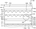
도 1 및 도 1a는 본 명세서에 기재된 예시적인 물품의 단면도이다.
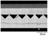
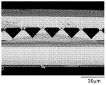
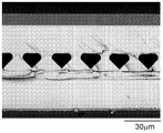
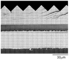
도 2a는 제1 미세구조화 층의 프리즘에 수직으로 절단된 1900X에서의 실시예 1 물품의 주사 전자 현미경 (SEM) 현미경 사진이다.
도 2b는 제2 미세구조화 층의 프리즘에 수직으로 절단된 1900X에서의 실시예 1 물품의 SEM 현미경 사진이다.
도 3a는 제1 미세구조화 층의 프리즘에 수직으로 절단된 1900X에서의 실시예 2 물품의 SEM 현미경 사진이다.
도 3b는 제2 미세구조화 층의 프리즘에 수직으로 절단된 1900X에서의 실시예 2 물품의 SEM 현미경 사진이다.
도 4a는 제1 미세구조화 층의 프리즘에 수직으로 절단된 1900X에서의 실시예 3 물품의 SEM 현미경 사진이다.
도 4b는 제2 미세구조화 층의 프리즘에 수직으로 절단된 1900X에서의 실시예 3 물품의 SEM 현미경 사진이다.
도 5a는 제1 미세구조화 층의 프리즘에 수직으로 절단된 1300X에서의 실시예 4 물품의 SEM 현미경 사진이다.
도 5b는 제2 미세구조화 층의 프리즘에 수직으로 절단된 1500X에서의 실시예 4 물품의 SEM 현미경 사진이다.Figures 1 and 1a are cross-sectional views of exemplary articles described herein.
2A is a scanning electron microscope (SEM) micrograph of the Example 1 article at 1900X cut perpendicular to the prism of the first microstructured layer.
2B is a SEM micrograph of the Example 1 article at 1900X cut perpendicular to the prism of the second microstructured layer.
3A is an SEM micrograph of the Example 2 article at 1900X cut perpendicular to the prism of the first microstructured layer.
Figure 3B is a SEM micrograph of the Example 2 article at 1900X cut perpendicular to the prism of the second microstructured layer.
4A is a SEM micrograph of the Example 3 article at 1900X cut perpendicular to the prism of the first microstructured layer.
4B is an SEM micrograph of the Example 3 article at 1900X cut perpendicular to the prism of the second microstructured layer.
5A is an SEM micrograph of the Example 4 article at 1300X cut perpendicular to the prism of the first microstructured layer.
5B is a SEM micrograph of the Example 4 article at 1500X cut perpendicular to the prism of the second microstructured layer.
본 명세서에 기재된 예시적인 물품은, 순서대로, 선택적인 확산기 층, 선택적인 접착제, 선택적인 중합체 층, 선택적인 확산기 층, 미세구조화 층, 층 (일부 실시 형태에서, 이 층은 선택적으로 미세구조화 층임), 선택적인 접착제 층, 선택적인 중합체 층, 및 선택적인 접착제 층을 포함한다.Exemplary articles described herein include, in order, an optional diffuser layer, a selective adhesive, an optional polymeric layer, a selective diffuser layer, a microstructured layer, a layer (in some embodiments this layer is optionally a micro- ), An optional adhesive layer, an optional polymeric layer, and a selective adhesive layer.
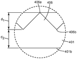
도 1 및 도 1a를 참조하면, 예시적인 물품(400)은 선택적인 확산기 층(412), 선택적인 접착제 층(411), 선택적인 중합체 층(405), 선택적인 확산기 층(407), 미세구조화 층(401), 층(403) (도시된 바와 같이 미세구조화 층), 선택적인 접착제 층(408), 선택적인 중합체 층(409), 및 선택적인 접착제 층(410)을 포함한다. 미세구조화 층(401)은 서로 반대편에 있는 제1 주 표면 및 제2 주 표면(401a, 401b)을 가지며, 주 표면(401a)은 미세구조화 표면이다. 미세구조화 층(403)은 서로 반대편에 있는 제1 주 표면 및 제2 주 표면(403a, 403b)을 갖는다. 주 표면(403a)은 미세구조화 표면이다. 주 표면(401a)의 적어도 일부분은 주 표면(403b)에 직접 부착된다. 도시된 바와 같이, 미세구조화 표면(401a)의 부분(404)은 미세구조화 층(403) 내로 침투한다. 미세구조화 표면(401a)은 피크들(406a) 및 밸리들(406b)을 갖는 미세구조 특징부들(406)을 가지며, 각각의 미세구조 특징부는 피크(406a)로부터 최저 인접 밸리(406b)까지 측정되는 높이, d1을 갖는다. 높이 측정치는 표면(401b)에 수직인 높이인 것으로 이해된다. 미세구조화 층(401)은 최저 인접 밸리(406b)로부터 주 표면(401b)까지 측정되는 두께, d2를 갖는다.1 and 1A, an
선택적인 확산기 층(412)은 제1 주 표면 및 제2 주 표면(412a, 412b)을 갖는다. 선택적인 접착제 층(411)은 제1 주 표면 및 제2 주 표면(411a, 411b)을 갖는다. 도시된 바와 같이 선택적인 확산기 표면(412a)의 부분(413)은 선택적인 접착제 층(411) 내로 침투한다. 선택적인 확산기 층(407)은 서로 반대편에 있는 제1 주 표면 및 제2 주 표면(407a, 407b)을 갖는다. 도시된 바와 같이, 주 표면(407a)은 주 표면(401b)에 적어도 부분적으로 직접 부착된다. 선택적인 중합체 층(405)은 서로 반대편에 있는 제1 주 표면 및 제2 주 표면(405a, 405b)을 갖는다. 도시된 바와 같이, 주 표면(411a)은 주 표면(405b)에 적어도 부분적으로 직접 부착된다. 도시된 바와 같이, 주 표면(405a)은 주 표면(407b)에 적어도 부분적으로 직접 부착된다. 선택적인 접착제 층(408)은 서로 반대편에 있는 제1 주 표면 및 제2 주 표면(408a, 408b)을 갖는다. 도시된 바와 같이, 주 표면(408b)은 주 표면(403a)에 적어도 부분적으로 직접 부착된다. 선택적인 중합체 층(409)은 서로 반대편에 있는 제1 주 표면 및 제2 주 표면(409a, 409b)을 갖는다. 도시된 바와 같이, 주 표면(409b)은 주 표면(408a)에 적어도 부분적으로 직접 부착된다. 선택적인 접착제 층(410)은 서로 반대편에 있는 제1 주 표면 및 제2 주 표면(410a, 410b)을 갖는다. 도시된 바와 같이, 주 표면(410b)은 주 표면(409a)에 적어도 부분적으로 직접 부착된다. 임의의 선택적인 층이 존재하지 않는 경우, 존재하는 층들의 각각의 인접한 주 표면들이 직접 부착될 수 있다.The
일반적으로, 미세구조화 층은 본 기술 분야에 공지되어 있으며 본 기술 분야에 공지된 기술을 사용하여 제공될 수 있다 (예를 들어, 미국 특허 제5,182,069호 (위크(Wick)), 제5,175,030호 (루(Lu) 등), 제5,183,597호 (루), 및 제7,074,463 B2호 (존스(Jones) 등)를 참조하며, 이들의 개시 내용은 본 명세서에 참고로 포함된다).In general, the microstructured layer is known in the art and may be provided using techniques known in the art (see, for example, U.S. Patent No. 5,182,069 (Wick), 5,175,030 (Lu (Lu), etc., 5,183,597 (Lu), and 7,074,463 B2 (Jones et al.), The disclosures of which are incorporated herein by reference).
가교결합성 재료로부터 제조된 통상적인 미세구조화 층은 전형적으로 상이한 재료로 구성된 중합체 필름 (예를 들어, 폴리에스테르 필름)에 부착된 가교결합된 미세구조화 층의 복합 구조물이다. 그러나, 가교결합성 재료로 제조된 모놀리식(monolithic) 미세구조화 층이 또한 본 기술 분야에 공지되어 있다 (예를 들어, 미국 특허 제4,576,850호 (마르텐스(Martens))를 참조한다). 본 명세서에 기재된 물품의 제2 층 (일부 실시 형태에서, 미세구조화 층임)은 적어도 일부분이 제1 미세구조화 층에 직접 부착된다. 즉, 제1 미세구조화 층 및 제2 층의 미세구조화 표면들 사이에는, 중합체 층이 없는 것을 비롯하여, 개재된 층이 없다. 이러한 구조물은 전형적인 산업 공정 (예를 들어, 연속 또는 반연속 웨브 처리)에서 (예를 들어, 얇은 두께 또는 조성으로 인해) 독립적으로 취급되기에 충분히 견고하지 않은 비교적 얇은 가교결합된 (일부 실시 형태에서, 미세구조화된) 층조차도 다른 층들과 조합되게 하여 본 명세서에 기재된 물품을 형성한다. 제1 층과 제2 층 사이의 중합체 층을 제거함으로써, 본 명세서에 기재된 물품은 비견되는 광학 성능을 제공하면서 두께 감소를 제공할 수 있다.Conventional microfabricated layers made from crosslinkable materials are typically a composite structure of crosslinked microfabricated layers attached to a polymeric film (e.g., a polyester film) comprised of a different material. However, monolithic microstructured layers made of crosslinkable materials are also known in the art (see, for example, U.S. Patent No. 4,576,850 (Martens)). At least a portion of the second layer (in some embodiments, the microstructured layer) of the article described herein is directly attached to the first micro-structured layer. That is, between the microstructured surfaces of the first microstructured layer and the second layer, there is no intervening layer, including no polymer layer. Such structures may be relatively thin, crosslinked (in some embodiments, in some embodiments) that is not sufficiently rigid to be handled independently in a typical industrial process (e.g., continuous or semi-continuous web treatment) , Microstructured) layers are also combined with other layers to form the articles described herein. By removing the polymer layer between the first and second layers, the articles described herein can provide thickness reduction while providing comparable optical performance.
본 명세서에 기재된 물품을 위한 미세구조화 층은, 예를 들어, 가교결합성 조성물을 툴링(tooling) 표면 상에 코팅하고, 가교결합성 조성물을 가교결합하고, 툴링 표면으로부터 미세구조화 층을 제거함으로써 형성될 수 있다. 본 명세서에 기재된 물품을 위한 미세구조화 층은 또한, 예를 들어, 가교결합성 조성물을 툴링 표면 상에 코팅하고, 중합체 층을 적용하고, 가교결합성 조성물을 가교결합하고, 툴링 표면 및 선택적으로 중합체 층을 제거함으로써 형성될 수 있다. 2개의 미세구조화 표면을 포함하는 미세구조화 층은, 예를 들어, 가교결합성 조성물을 툴링 표면 상에 코팅하고, 중합체 층 - 가교결합성 조성물과 접촉해 있는 중합체 층의 주 표면은 미세구조화 표면임 - 을 적용하고, 가교결합성 조성물을 가교결합하고, 툴링 표면 및 중합체 층을 제거함으로써 형성될 수 있다. 본 명세서에 기재된 물품을 위한 미세구조화 층은 또한, 예를 들어, 용융된 열가소성 재료를 툴링 표면 상에 압출하고, 열가소성 재료를 냉각하고, 툴링 표면을 제거함으로써 형성될 수 있다. 미세구조체는 규칙적인 프리즘형 패턴, 불규칙적인 프리즘형 패턴 (예를 들어, 환상 프리즘형 패턴, 큐브-코너 패턴 또는 임의의 다른 렌즈형 미세구조체), 비-주기적 돌출부, 유사-비-주기적 돌출부, 또는 비-주기적 함몰부, 또는 유사-비-주기적 함몰부를 포함하는 다양한 패턴을 가질 수 있다. 제2 층이 미세구조화 층이 아니더라도 동일한 기술이 제2 층을 제공하는 데 사용될 수 있으며, 이 경우에 툴 표면은, 예를 들어, 단순히 평면이다.The microstructured layer for the articles described herein can be formed, for example, by coating a cross-linkable composition on a tooling surface, cross-linking the cross-linkable composition, and removing the micro-structured layer from the tooling surface . The microstructured layer for the articles described herein may also be formed by, for example, coating a cross-linkable composition on a tooling surface, applying a polymer layer, crosslinking the cross-linkable composition, Lt; / RTI > layer. The microstructured layer comprising two microstructured surfaces may be formed, for example, by coating a cross-linkable composition on a tooling surface and the main surface of the polymer layer in contact with the polymeric layer-cross-linkable composition is a microstructured surface -, cross-linking the cross-linkable composition, and removing the tooling surface and the polymer layer. The microstructured layer for the articles described herein may also be formed, for example, by extruding a molten thermoplastic material onto a tooling surface, cooling the thermoplastic material, and removing the tooling surface. The microstructure may include a regular prismatic pattern, an irregular prismatic pattern (e.g., an annular prismatic pattern, a cube-corner pattern or any other lenticular microstructure), a non-periodic protrusion, a pseudo- Or non-periodic depressions, or pseudo-non-periodic depressions. Although the second layer is not a microstructured layer, the same technique can be used to provide the second layer, in which case the tool surface is, for example, simply a plane.
미세구조화 층의 미세구조 특징부들이 방향성(directionality)을 갖는 경우 (예를 들어, 프리즘과 같은 선형 구조체), 미세구조 특징부들의 방향성은 임의의 각도로 배향될 수 있다. 미세구조화 층의 프리즘들은, 예를 들어, 다른 층의 미세구조 특징부들에 대해 평행할 수 있거나, 수직할 수 있거나, 또는 임의의 다른 각도로 있을 수 있다. 예를 들어, 실시예 1 물품의 제1 미세구조화 층의 프리즘들 및 제2 미세구조화 층의 프리즘들은 서로에 대해 수직으로 배향된다 (도 2a 및 도 2b).If the microstructural features of the microstructured layer have a directionality (e.g., a linear structure such as a prism), the orientation of the microstructural features can be oriented at any angle. The prisms of the microstructured layer may, for example, be parallel to, perpendicular to, or at any other angle to the microstructural features of the other layer. For example, the prisms of the first micro-structured layer and the prisms of the second micro-structured layer of the Example 1 article are oriented perpendicular to each other (Figs. 2A and 2B).
미세구조화 층은, 예를 들어, 가교결합성 조성물 또는 가교결합된 조성물 또는 열가소성 재료를 포함할 수 있다. 예시적인 가교결합성 조성물 또는 가교결합된 조성물은 자유 라디칼 중합 메커니즘에 의해 경화 가능하거나 또는 경화된 것일 수 있는 수지 조성물을 포함한다. 자유 라디칼 중합은 방사선 (예를 들어, 전자 빔, 자외광, 및/또는 가시광) 및/또는 열에 대한 노출에 의해 일어날 수 있다. 예시적인 적합한 가교결합성 조성물 또는 가교결합된 조성물은 또한 벤조일 퍼옥사이드와 같은 열개시제의 첨가에 의해 열적으로 중합 가능하거나 중합된 것을 포함한다. 방사선에 의해 개시되는 양이온 중합성 수지가 또한 사용될 수 있다. 적합한 수지는 (메트)아크릴레이트 기를 갖는 적어도 하나의 화합물과 광개시제의 블렌드일 수 있다.The microstructured layer may comprise, for example, a crosslinkable composition or a crosslinked composition or a thermoplastic material. Exemplary crosslinkable or crosslinked compositions include resin compositions that may be curable or cured by a free radical polymerization mechanism. Free radical polymerization can occur by exposure to radiation (e.g., electron beam, ultraviolet light, and / or visible light) and / or heat. Exemplary suitable crosslinkable or crosslinked compositions also include thermally polymerizable or polymerized by the addition of thermal initiators such as benzoyl peroxide. Cationically polymerizable resins initiated by radiation can also be used. A suitable resin may be a blend of at least one compound having a (meth) acrylate group and a photoinitiator.
자유 라디칼 메커니즘에 의해 중합될 수 있는 예시적인 수지에는 에폭시, 폴리에스테르, 폴리에테르, 및 우레탄으로부터 유도된 아크릴계 수지, 에틸렌계 불포화 화합물, 적어도 하나의 펜던트 (메트)아크릴레이트 기를 갖는 아미노플라스트(aminoplast) 유도체, 적어도 하나의 펜던트 (메트)아크릴레이트 기를 갖는 아이소시아네이트 유도체, (메트)아크릴레이트화 에폭시 이외의 에폭시 수지, 및 이들의 혼합물 및 조합이 포함된다. 용어 (메트)아크릴레이트는 아크릴레이트 및 메타크릴레이트 화합물 둘 모두가 존재하는 경우 본 명세서에서 아크릴레이트 및 메타크릴레이트 화합물 둘 모두를 포괄하기 위해 사용된다. 그러한 수지에 대한 추가의 상세 사항은 미국 특허 제4,576,850호 (마르텐스)에 보고되어 있으며, 이의 개시 내용은 본 명세서에 참고로 포함된다.Exemplary resins that can be polymerized by a free radical mechanism include acrylic resins derived from epoxies, polyesters, polyethers, and urethanes, ethylenically unsaturated compounds, aminoplasts having at least one pendant (meth) acrylate group ) Derivatives, isocyanate derivatives having at least one pendant (meth) acrylate group, epoxy resins other than (meth) acrylated epoxies, and mixtures and combinations thereof. The term (meth) acrylate is used herein to encompass both acrylate and methacrylate compounds when both acrylate and methacrylate compounds are present. Further details on such resins are reported in U.S. Patent 4,576,850 (Martens), the disclosure of which is incorporated herein by reference.
에틸렌계 불포화 수지는 탄소, 수소 및 산소, 그리고 선택적으로 질소, 황 및 할로겐의 원자를 함유하는 단량체 화합물 및 중합체 화합물 둘 모두를 포함한다. 산소 또는 질소 원자, 또는 이들 둘 모두는 일반적으로 에테르, 에스테르, 우레탄, 아미드, 및 우레아 기에 존재한다. 일부 실시 형태에서, 에틸렌계 불포화 화합물은 수 평균 분자량이 약 4,000 미만이다 (일부 실시 형태에서, 이는 지방족 모노하이드록시 기, 지방족 폴리하이드록시 기를 함유하는 화합물과 불포화 카르복실산 (예를 들어, 아크릴산, 메타크릴산, 이타콘산, 크로톤산, 아이소크로톤산, 및 말레산)의 반응으로부터 제조되는 에스테르이다). 본 발명에 사용하기에 적합한 아크릴 기 또는 메타크릴 기를 갖는 화합물의 일부 예시적인 예가 하기에 열거된다:Ethylenically unsaturated resins include both monomeric compounds and polymeric compounds containing carbon, hydrogen and oxygen, and optionally atoms of nitrogen, sulfur and halogen. Oxygen or nitrogen atoms, or both, are generally present in the ether, ester, urethane, amide, and urea groups. In some embodiments, the ethylenically unsaturated compound has a number average molecular weight of less than about 4,000 (in some embodiments, it is an aliphatic monohydroxy group, a compound containing an aliphatic polyhydroxy group and an unsaturated carboxylic acid (e.g., , Methacrylic acid, itaconic acid, crotonic acid, isocrotonic acid, and maleic acid). Some illustrative examples of compounds having an acrylic or methacrylic group suitable for use in the present invention are listed below:
(1) 1작용성 화합물: 에틸 (메트)아크릴레이트, n-부틸 (메트)아크릴레이트, 아이소부틸 (메트)아크릴레이트, 2-에틸헥실 (메트)아크릴레이트, n-헥실 (메트)아크릴레이트, n-옥틸 (메트)아크릴레이트, 아이소옥틸 (메트)아크릴레이트, 보르닐 (메트)아크릴레이트, 테트라하이드로푸르푸릴 (메트)아크릴레이트, 2-페녹시에틸 (메트)아크릴레이트, 및 N,N-다이메틸아크릴아미드;(Meth) acrylate, isobutyl (meth) acrylate, 2-ethylhexyl (meth) acrylate, n-hexyl (meth) acrylate, (meth) acrylate, n-octyl (meth) acrylate, isooctyl (meth) acrylate, bornyl (meth) acrylate, tetrahydrofurfuryl , N-dimethyl acrylamide;
(2) 2작용성 화합물: 1,4-부탄다이올 다이(메트)아크릴레이트, 1,6-헥산다이올 다이(메트)아크릴레이트, 네오펜틸글리콜 다이(메트)아크릴레이트, 에틸렌 글리콜 다이(메트)아크릴레이트, 트라이에틸렌글리콜 다이(메트)아크릴레이트, 테트라에틸렌 글리콜 다이(메트)아크릴레이트, 및 다이에틸렌 글리콜 다이(메트)아크릴레이트; 및(2) bifunctional compounds: 1,4-butanediol di (meth) acrylate, 1,6-hexanediol di (meth) acrylate, neopentyl glycol di (meth) acrylate, ethylene glycol di (Meth) acrylate, triethylene glycol di (meth) acrylate, tetraethylene glycol di (meth) acrylate, and diethylene glycol di (meth) acrylate; And
(3) 다작용성 화합물: 트라이메틸올프로판 트라이(메트)아크릴레이트, 글리세롤 트라이(메트)아크릴레이트, 펜타에리트리톨 트라이(메트)아크릴레이트, 펜타에리트리톨 테트라(메트)아크릴레이트, 및 트리스(2-아크릴로일옥시에틸) 아이소시아누레이트.(3) polyfunctional compounds: trimethylolpropane tri (meth) acrylate, glycerol tri (meth) acrylate, pentaerythritol tri (meth) acrylate, pentaerythritol tetra (meth) acrylate, and tris - acryloyloxyethyl) isocyanurate.
다른 에틸렌계 불포화 화합물 및 수지의 일부 대표적인 것에는 스티렌, 다이비닐벤젠, 비닐 톨루엔, N-비닐 포름아미드, N-비닐 피롤리돈, N-비닐 카프로락탐, 모노알릴, 폴리알릴, 및 폴리메탈릴 에스테르, 예를 들어 다이알릴 프탈레이트 및 다이알릴 아디페이트, 및 카르복실산의 아미드, 예를 들어 N,N-다이알릴아디프아미드가 포함된다. 일부 실시 형태에서, 둘 이상의 (메트)아크릴레이트 또는 에틸렌계 불포화 성분이 가교결합성 수지 조성물 또는 가교결합된 수지 조성물에 존재할 수 있다.Some representative examples of other ethylenically unsaturated compounds and resins are styrene, divinylbenzene, vinyltoluene, N-vinylformamide, N-vinylpyrrolidone, N-vinylcaprolactam, monoallyl, polyallyl, Esters such as diallyl phthalate and diallyl adipate, and amides of carboxylic acids such as N, N-diallyl adipamide. In some embodiments, two or more (meth) acrylate or ethylenically unsaturated components may be present in the crosslinkable resin composition or crosslinked resin composition.
수지 조성물이 전자 빔 이외의 방사선에 의해 경화될 경우, 광개시제가 수지 조성물에 포함될 수 있다. 수지 조성물이 열적으로 경화될 경우, 열개시제가 수지 조성물에 포함될 수 있다. 일부 실시 형태에서, 방사선 경화와 열 경화의 조합이 사용될 수 있다. 그러한 실시 형태에서, 조성물은 광개시제와 열개시제 둘 모두를 포함할 수 있다.When the resin composition is cured by radiation other than an electron beam, a photoinitiator may be included in the resin composition. When the resin composition is thermally cured, the release agent may be included in the resin composition. In some embodiments, a combination of radiation curing and thermal curing may be used. In such embodiments, the composition may comprise both a photoinitiator and a thermal initiator.
수지에 블렌딩될 수 있는 예시적인 광개시제에는 하기가 포함된다: 벤질(benzil), 메틸 o-벤조에이트, 벤조인, 벤조인 에틸 에테르, 벤조인 아이소프로필 에테르, 벤조인 아이소부틸 에테르 등, 벤조페논/3차 아민, 아세토페논 (예를 들어, 2,2-다이에톡시아세토페논, 벤질 메틸 케탈, 1-하이드록시사이클로헥실페닐 케톤, 2-하이드록시-2-메틸-1-페닐프로판-1-온, 1-(4-아이소프로필페닐)-2-하이드록시-2-메틸프로판-1-온, 2-벤질-2-N,N-다이메틸아미노-1-(4-모르폴리노페닐)-1-부타논, 2,4,6-트라이메틸벤조일-다이페닐포스핀 옥사이드, 2-메틸-1-4(메틸티오), 페닐-2-모르폴리노-1-프로파논, 비스(2,4,6-트라이메틸벤조일)-페닐포스핀 옥사이드 및 비스(2,6-다이메톡시벤조일)(2,4,4-트라이메틸펜틸)포스핀 옥사이드). 화합물은 개별적으로 또는 조합하여 사용될 수 있다. 양이온 중합성 재료는 에폭시 및 비닐 에테르 작용기를 함유하는 재료를 포함한다. 이들 시스템은 오늄 염 개시제, 예를 들어 트라이아릴설포늄, 및 다이아릴요오도늄 염에 의해 광개시된다. 다른 예시적인 가교결합성 수지 조성물 또는 가교결합된 수지 조성물이, 예를 들어, 미국 특허 제8,986,812 B2호 (헌트(Hunt) 등), 제8,282,863 B2호 (존스 등), 및 2014년 3월 27일자로 공개된 국제특허 공개 WO 2014/46837호에 기재되어 있으며, 이들의 개시 내용은 본 명세서에 참고로 포함된다.Exemplary photoinitiators that can be blended into the resin include benzyl, methyl o-benzoate, benzoin, benzoin ethyl ether, benzoin isopropyl ether, benzoin isobutyl ether, etc., benzophenone / Tertiary amines, acetophenones (e.g., 2,2-diethoxyacetophenone, benzylmethylketal, 1-hydroxycyclohexylphenylketone, 2-hydroxy-2-methyl- 2-methyl-1- (4-isopropylphenyl) -2-hydroxy-2-methylpropan- (Methylthio) phenyl-2-morpholino-1-propanone, bis (2-methyl- , 4,6-trimethylbenzoyl) -phenylphosphine oxide and bis (2,6-dimethoxybenzoyl) (2,4,4-trimethylpentyl) phosphine oxide). The compounds may be used individually or in combination. Cationically polymerizable materials include materials containing epoxy and vinyl ether functionalities. These systems are optically initiated by onium salt initiators, such as triarylsulfonium, and diaryliodonium salts. Other exemplary crosslinkable or crosslinked resin compositions are disclosed in U.S. Patent Nos. 8,986,812 B2 (Hunt et al.), 8,282,863 B2 (Jones et al.), And U.S. Patent Nos. In WO 2014/46837, the disclosures of which are incorporated herein by reference.
일부 실시 형태에서, 미세구조화 층의 제1 재료는 가교결합성 조성물 또는 가교결합된 조성물 중 적어도 하나를 포함한다. 일부 실시 형태에서, 미세구조화 층은 가교결합된 재료로 본질적으로 이루어진다.In some embodiments, the first material of the microstructured layer comprises at least one of a cross-linkable composition or a cross-linked composition. In some embodiments, the microstructured layer consists essentially of a crosslinked material.
가교결합성 재료는, 화학 방사선 (예를 들어, e-빔 또는 자외광)을 포함하는, 본 기술 분야에 공지된 기술에 의해 부분적으로 가교결합될 수 있다. 가교결합성 재료를 부분적으로 가교결합하는 기술은 (메트)아크릴레이트 모이어티(moiety) 함유 조성물을 산소 함유 분위기의 존재 하에 화학 방사선에 노출시키는 것을 포함한다. (메트)아크릴레이트 함유 조성물은 산소가 실질적으로 없는 분위기에서 화학 방사선에 대한 노출에 의해 추가로 가교결합될 수 있다. 가교결합성 조성물을 부분적으로 가교결합하는 기술은, 반응들이 독립적으로 개시될 수 있는 하나 초과의 유형의 가교결합 반응으로 반응하는 성분들을 포함하는 가교결합성 조성물 (예를 들어, 양이온 중합에 의해 가교결합될 수 있는 에폭시 성분 및 자유 라디칼 중합에 의해 가교결합될 수 있는 (메트)아크릴레이트 성분 둘 모두를 함유하는 혼합물)을 사용하는 것을 추가로 포함한다. 가교결합성 조성물은 가교결합 반응 (예를 들어, 에폭시의 양이온 중합)을 개시한 후에 단시간에 부분적으로 가교결합될 수 있다. 부분적으로 가교결합된 조성물은 화학 방사선 (예를 들어, e-빔 또는 자외광)에 대한 노출과 같은 본 기술 분야에 공지된 기술에 의해 추가로 경화될 수 있다.The crosslinkable material may be partially crosslinked by techniques known in the art, including actinic radiation (e. G., E-beam or ultraviolet light). Techniques for partially crosslinking a crosslinkable material include exposing the composition containing a (meth) acrylate moiety to actinic radiation in the presence of an oxygen-containing atmosphere. (Meth) acrylate-containing compositions can be further crosslinked by exposure to actinic radiation in an atmosphere substantially free of oxygen. Techniques for partially crosslinking a crosslinkable composition include crosslinking compositions comprising components that react with more than one type of crosslinking reaction where the reactions can be independently initiated (e.g., crosslinking by cationic polymerization A mixture containing both an epoxy component that can be combined and a (meth) acrylate component that can be cross-linked by free radical polymerization). The crosslinkable composition may be partially crosslinked in a short time after initiation of the crosslinking reaction (e.g., cationic polymerization of the epoxy). The partially crosslinked composition may be further cured by techniques known in the art, such as exposure to actinic radiation (e. G., E-beam or ultraviolet light).
가교결합성 조성물에 사용되는 재료는, 예를 들어, 미국 펜실베이니아주 엑스턴 소재의 사토머 컴퍼니(Sartomer Company); 미국 뉴저지주 우드랜드 파크 소재의 사이텍 인더스트리즈(Cytec Industries); 일본 도쿄 소재의 소켄 케미칼(Soken Chemical); 미국 뉴저지주 포트 리 소재의 다이셀 (유에스에이), 인크.(Daicel (USA), Inc.); 벨기에 브뤼셀 소재의 알넥스(Allnex); 미국 노스캐롤라이나주 샬롯 소재의 바스프 코포레이션(BASF Corporation); 미국 미시간주 미들랜드 소재의 다우 케미칼 컴퍼니(Dow Chemical Company); 대한민국 경기도 소재의 미원 스페셜티 케미칼 컴퍼니 리미티드(Miwon Specialty Chemical Co. Ltd.); 미국 코네티컷주 스트라트포드 소재의 햄프포드 리서치 인크.(Hampford Research Inc.); 및 미국 미주리주 세인트 루이스 소재의 시그마 알드리치(Sigma Aldrich)로부터 입수가능하다.Materials used in the crosslinkable compositions include, for example, Sartomer Company, Exton, Pa .; Cytec Industries, Woodland Park, NJ; Soken Chemical, Tokyo, Japan; Daicel (USA), Inc., Fort Lee, NJ; Allnex, Brussels, Belgium; BASF Corporation of Charlotte, North Carolina; Dow Chemical Company, Midland, Mich .; Miwon Specialty Chemical Co. Ltd., located in Gyeonggi-do, Korea; Hampford Research Inc., Stratford, Conn., USA; And Sigma Aldrich, St. Louis, Missouri, USA.
예시적인 열가소성 재료는 압출과 같은 열가소성 처리 기술에 의해 처리될 수 있는 그러한 재료를 포함한다. 예시적인 열가소성 재료에는 폴리에틸렌, 폴리프로필렌, 폴리메틸 메타크릴레이트, 폴리카르보네이트, 및 폴리에스테르가 포함된다.Exemplary thermoplastic materials include those materials that can be processed by thermoplastic processing techniques such as extrusion. Exemplary thermoplastic materials include polyethylene, polypropylene, polymethyl methacrylate, polycarbonate, and polyester.
일부 실시 형태에서, 미세구조화 층의 양측 주 표면은 미세구조화 표면을 포함한다. 일부 실시 형태에서, 미세구조화 층은 제1 미세구조화 층의 임의의 밸리로부터 제2 주 표면까지의 최소 거리에 의해 한정되는 두께를 가지며, 이 두께는 25 마이크로미터 이하 (일부 실시 형태에서, 20 마이크로미터 이하, 15 마이크로미터 이하, 또는 심지어 10 마이크로미터 이하)이다.In some embodiments, both major surfaces of the microstructured layer comprise a microstructured surface. In some embodiments, the microstructured layer has a thickness defined by a minimum distance from any valley of the first microstructured layer to a second major surface, the thickness being less than or equal to 25 micrometers (in some embodiments, Less than 15 meters, or even less than 10 micrometers).
일부 실시 형태에서, 미세구조화 층의 미세구조 특징부의 높이는 1 마이크로미터 내지 200 마이크로미터의 범위 (일부 실시 형태에서, 1 마이크로미터 내지 150 마이크로미터, 5 마이크로미터 내지 150 마이크로미터, 또는 심지어 5 마이크로미터 내지 100 마이크로미터의 범위)이다.In some embodiments, the height of the microstructured features of the microstructured layer is in the range of 1 micrometer to 200 micrometers (in some embodiments, 1 micrometer to 150 micrometers, 5 micrometers to 150 micrometers, or even 5 micrometers To 100 micrometers).
미세구조화 층은, 예를 들어, 가교결합성 조성물 또는 가교결합된 조성물 또는 열가소성 재료를 포함할 수 있지만, 제2 미세구조화 층은 가교결합성 조성물 또는 가교결합된 조성물을 포함한다.The microstructured layer may comprise, for example, a crosslinkable composition or a crosslinked composition or a thermoplastic material, but the second microstructured layer comprises a crosslinkable composition or a crosslinked composition.
일부 실시 형태에서, 미세구조화 층의 제1 재료는 가교결합성 조성물 또는 가교결합된 조성물 중 적어도 하나를 포함한다. 일부 실시 형태에서, 미세구조화 층은 가교결합된 재료로 본질적으로 이루어진다.In some embodiments, the first material of the microstructured layer comprises at least one of a cross-linkable composition or a cross-linked composition. In some embodiments, the microstructured layer consists essentially of a crosslinked material.
일부 실시 형태에서, 미세구조화 층의 미세구조 특징부의 높이는 1 마이크로미터 내지 200 마이크로미터의 범위 (일부 실시 형태에서, 1 마이크로미터 내지 150 마이크로미터, 5 마이크로미터 내지 150 마이크로미터, 또는 심지어 5 마이크로미터 내지 100 마이크로미터의 범위)이다.In some embodiments, the height of the microstructured features of the microstructured layer is in the range of 1 micrometer to 200 micrometers (in some embodiments, 1 micrometer to 150 micrometers, 5 micrometers to 150 micrometers, or even 5 micrometers To 100 micrometers).
일부 실시 형태에서, 제1 미세구조화 층의 미세구조 특징부들의 각각의 일부분은 제2 미세구조화 층 내로 적어도 부분적으로 침투한다 (일부 실시 형태에서, 제1 미세구조화 층은 각각의 미세구조 특징부의 평균 높이 미만의 깊이로 제2 미세구조화 층 내로 적어도 부분적으로 침투한다). 일부 실시 형태에서, 각각의 침투하는 미세구조 특징부의 침투 깊이는 미세구조 특징부의 각각의 높이의 50% 이하 (일부 실시 형태에서, 45, 40, 35, 30, 25, 20, 15, 10% 이하, 또는 심지어 5% 이하)이다. 전술한 것은 인접 층의 주 표면에 인접한 미세구조 특징부들과 관련하여 다른 미세구조 층에 또한 적용될 수 있다.In some embodiments, a portion of each of the microstructured features of the first microstructured layer at least partially penetrates into the second microstructured layer (in some embodiments, the first microstructured layer has an average of the respective microstructured features At least partially penetrates into the second micro-structured layer at a depth less than the height. In some embodiments, the penetration depth of each penetrating microstructural feature is less than or equal to 50% of the height of each of the microstructural features (in some embodiments, 45, 40, 35, 30, 25, 20, 15, 10% , Or even 5% or less). The foregoing may also be applied to other microstructured layers in connection with the microstructure features adjacent to the major surface of the adjacent layer.
예시적인 접착제 재료는 폴리아크릴레이트 성분과 중합성 단량체의 반응 생성물의 상호 침입 네트워크를 포함한다 (예를 들어, 미국 특허 출원 공개 제2014/0016208 A1호 (에드몬즈(Edmonds) 등)를 참조하며, 이의 개시 내용은 본 명세서에 참고로 포함된다).Exemplary adhesive materials include an interpenetrating network of reaction products of a polyacrylate component and a polymerizable monomer (see, for example, U.S. Patent Application Publication No. 2014/0016208 A1 (Edmonds et al.), The disclosure of which is incorporated herein by reference).
다른 예시적인 접착제는 (메트)아크릴레이트 및 에폭시를 서로의 존재 하에 포함하는 혼합물의 반응 생성물을 포함한다. 일부 실시 형태에서, 혼합물의 총 중량을 기준으로, (메트)아크릴레이트는 5 내지 95 중량%의 범위 (일부 실시 형태에서, 10 내지 90 또는 심지어 20 내지 80 중량%의 범위)로 존재하고 에폭시는 5 내지 95 중량%의 범위 (일부 실시 형태에서, 5 내지 95, 10 내지 90, 또는 심지어 20 내지 80 중량%의 범위)로 존재한다. 예시적인 (메트)아크릴레이트에는 1작용성 (메트)아크릴레이트 화합물 (예를 들어, 에틸(메트)아크릴레이트, n-부틸(메트)아크릴레이트, 아이소부틸(메트)아크릴레이트, 2-에틸헥실(메트)아크릴레이트, n-헥실(메트)아크릴레이트, n-옥틸(메트)아크릴레이트, 아이소옥틸 (메트)아크릴레이트, 아이소보르닐 (메트)아크릴레이트, 테트라하이드로푸르푸릴 (메트)아크릴레이트, 2-페녹시에틸 (메트)아크릴레이트, 메톡시 폴리에틸렌 글리콜 모노(메트)아크릴레이트 및 N,N-다이메틸아크릴아미드), 2작용성 (메트)아크릴레이트 재료 (예를 들어, 1,4-부탄다이올 다이(메트)아크릴레이트, 1,6-헥산다이올 다이(메트)아크릴레이트, 네오펜틸글리콜 다이(메트)아크릴레이트, 에틸렌 글리콜 다이(메트)아크릴레이트, 트라이에틸렌글리콜 다이(메트)아크릴레이트, 테트라에틸렌 글리콜 다이(메트)아크릴레이트, 다이에틸렌 글리콜 다이(메트)아크릴레이트) 및 다작용성 (메트)아크릴레이트 재료 (예를 들어, 트라이메틸올프로판 트라이(메트)아크릴레이트, 에톡실레이트 트라이메틸올프로판 트라이(메트)아크릴레이트, 글리세롤트라이(메트)아크릴레이트, 펜타에리트리톨 트라이(메트)아크릴레이트, 및 펜타에리트리톨 테트라(메트)아크릴레이트)가 포함된다. 일부 실시 형태에서, 둘 이상의 (메트)아크릴레이트 성분이 접착제 재료에 사용될 수 있다. 예시적인 에폭시에는 (3-4-에폭시사이클로헥산) 메틸 3'-4'-에폭시사이클로헥실-카르복실레이트, 비스(3,4-에폭시사이클로헥실메틸) 아디페이트, 4-비닐-1-사이클로헥센 1,2-에폭사이드, 폴리에틸렌 글리콜 다이에폭사이드, 비닐사이클로헥센 다이옥사이드, 네오펜틸 글리콜 다이글리시딜 에테르 및 1,4-사이클로헥산다이메탄올 비스(3,4-에폭시사이클로헥산카르복실레이트가 포함된다. 일부 실시 형태에서, (메트)아크릴레이트 및 에폭시는 동일 분자 상에 존재한다 (예를 들어, (3-4-에폭시사이클로헥실) 메틸 아크릴레이트, 3,4-에폭시사이클로헥실메틸 메타크릴레이트, 글리시딜 (메트)아크릴레이트, 및 4-하이드록시부틸 (메트)아크릴레이트 글리시딜에테르). 일부 실시 형태에서, 이 혼합물은 폴리올 작용성 물질(polyol functionality) (예를 들어, 폴리에틸렌 글리콜, 카프로락톤 단량체로부터 유도된 폴리에스테르 다이올, 카프로락톤 단량체로부터 유도된 폴리에스테르 트라이올)을 추가로 포함한다. 일부 실시 형태에서, 이 혼합물은 1작용성 (메트)아크릴레이트가 실질적으로 없다 (즉, 이는 접착제 재료의 총 중량을 기준으로 10 중량% 미만의 1작용성 (메트)아크릴레이트를 함유한다). 일부 실시 형태에서, (메트)아크릴레이트 및 에폭시는 서로 반응하지 않는다.Other exemplary adhesives include reaction products of a mixture comprising (meth) acrylate and an epoxy in the presence of each other. In some embodiments, (meth) acrylate is present in a range from 5 to 95 weight percent, in some embodiments in the range of from 10 to 90 or even 20 to 80 weight percent, based on the total weight of the mixture, (In some embodiments, in the range of 5 to 95, 10 to 90, or even 20 to 80% by weight). Exemplary (meth) acrylates include monofunctional (meth) acrylate compounds such as ethyl (meth) acrylate, n-butyl (meth) acrylate, isobutyl (meth) acrylate, (Meth) acrylate, isobornyl (meth) acrylate, tetrahydrofurfuryl (meth) acrylate, n-hexyl (meth) (Meth) acrylate, methoxypolyethylene glycol mono (meth) acrylate and N, N-dimethyl acrylamide), bifunctional (meth) acrylate materials (Meth) acrylate, neopentyl glycol di (meth) acrylate, ethylene glycol di (meth) acrylate, triethylene glycol di (meth) acrylate, Meth) acrylate, tetra (Meth) acrylate, diethylene glycol di (meth) acrylate, and polyfunctional (meth) acrylate materials such as trimethylolpropane tri (meth) acrylate, ethoxylate trimethylol (Meth) acrylate, propylene tri (meth) acrylate, glycerol tri (meth) acrylate, pentaerythritol tri (meth) acrylate, and pentaerythritol tetra (meth) acrylate. In some embodiments, more than one (meth) acrylate component may be used in the adhesive material. Exemplary epoxies include, but are not limited to, (3-4-epoxycyclohexane) methyl 3'-4'-epoxycyclohexyl-carboxylate, bis (3,4-epoxycyclohexylmethyl) adipate, 1,2-epoxide, polyethylene glycol diepoxide, vinylcyclohexene dioxide, neopentyl glycol diglycidyl ether and 1,4-cyclohexanedimethanol bis (including 3,4-epoxycyclohexanecarboxylate) (Meth) acrylate and epoxy are present on the same molecule (for example, (3-4-epoxycyclohexyl) methyl acrylate, 3,4-epoxycyclohexylmethyl methacrylate , Glycidyl (meth) acrylate, and 4-hydroxybutyl (meth) acrylate glycidyl ether. In some embodiments, the mixture comprises polyol functionality A recurring, a polyester diol derived from caprolactone monomer, a polyester triol derived from caprolactone monomer). In some embodiments, the mixture is substantially free of monofunctional (meth) acrylate (I. E., It contains less than 10% by weight of monofunctional (meth) acrylate based on the total weight of adhesive material). In some embodiments, the (meth) acrylate and epoxy do not react with one another.
예시적인 접착제 재료는 본 기술 분야에 공지된 감압 접착제, 광학적으로 투명한 접착제 및 구조 접착제를 또한 포함한다. 예시적인 접착제 재료는 또한 가교결합성 조성물을 포함한다.Exemplary adhesive materials also include pressure sensitive adhesives, optically clear adhesives, and structural adhesives known in the art. Exemplary adhesive materials also include cross-linkable compositions.
일부 실시 형태에서, 예를 들어, 광학 결함의 가시성을 감소시키기 위해, 확산 (즉, 광을 확산시키는 코팅 또는 코팅들 또는 층 또는 층들, 또는 광을 확산시키는, 기존 층 내의 요소들)을 통합하는 것이 바람직할 수 있다. 일부 실시 형태에서, 접착제 재료를 포함하는 층은 충전제 재료 (예를 들어, 유리 비드, 중합체 비드, 무기 입자, 예를 들어 건식 실리카)를 추가로 포함한다. 일부 실시 형태에서, 접착제 층은 불연속적일 수 있거나 패턴화될 수 있다 (예를 들어, 규칙적이거나 불규칙적인 도트의 어레이).In some embodiments, for example, to reduce the visibility of optical defects, it is desirable to incorporate diffusions (i.e., coatings or coatings or layers or layers that diffuse light, or elements within existing layers that diffuse light) May be preferred. In some embodiments, the layer comprising the adhesive material further comprises a filler material (e.g., glass beads, polymer beads, inorganic particles, for example, dry silica). In some embodiments, the adhesive layer may be discontinuous or may be patterned (e.g., an array of regular or irregular dots).
예시적인 중합체 층은 폴리에스테르, 폴리카르보네이트, 환형 올레핀 공중합체 또는 폴리메틸 메타크릴레이트를 포함하는 것들을 포함한다. 예시적인 중합체 층은 반사 편광 필름 (예를 들어, 미국 미네소타주 세인트 폴 소재의 쓰리엠 컴퍼니(3M Company)로부터 입수가능한 상표명 "이중 휘도 향상 필름"(DUAL BRIGHTNESS ENHANCEMENT FILM) 또는 "향상된 편광 필름"(ADVANCED POLARIZING FILM)으로 입수가능함) 또는 반사 필름 (예를 들어, 쓰리엠 컴퍼니로부터 입수가능한 상표명 "향상된 정반사기"(ENHANCED SPECULAR REFLECTOR)로 입수가능함)을 포함하는 다층 광학 필름을 포함한다. 예시적인 중합체 층은 광학 디스플레이에 사용되는 광 가이드를 포함한다. 일부 실시 형태에서, 예시적인 중합체 층은 확산기 층을 포함한다.Exemplary polymeric layers include those comprising a polyester, polycarbonate, cyclic olefin copolymer or polymethylmethacrylate. Exemplary polymer layers include reflective polarizing films (e.g., DUAL BRIGHTNESS ENHANCEMENT FILM or "ADVANCED ") available from 3M Company, St. Paul, Minn. (Available as POLARIZING FILM) or a reflective film (e.g., available under the trade designation "ENHANCED SPECULAR REFLECTOR " available from 3M Company). An exemplary polymer layer includes a light guide used in an optical display. In some embodiments, an exemplary polymer layer comprises a diffuser layer.
예시적인 확산기 층은 본 기술 분야에 공지된 벌크 확산기 및 표면 확산기를 포함한다.Exemplary diffuser layers include bulk diffusers and surface diffusers known in the art.
예시적인 확산기 층은 매립된(embedded) 미세구조화 층 또는 충전제 재료를 포함하는 층을 포함하며, 본 기술 분야에 공지된 기술에 의해 제조될 수 있다. 매립된 미세구조화 층은, 예를 들어, 소정 굴절률을 갖는 재료 (예를 들어, 중합체 재료 또는 가교결합성 재료)를 사용하여 원하는 표면 상에 미세구조 특징부들을 생성하고, 이어서 미세구조 특징부들 위에 상이한 굴절률을 갖는 상이한 재료 (예를 들어, 중합체 재료 또는 가교결합성 재료)를 코팅함으로써 제조될 수 있다. 충전제 재료를 포함하는 확산 층은, 예를 들어, 소정 굴절률을 갖는 충전제 재료를 상이한 굴절률을 갖는 중합체 재료 또는 가교결합성 재료와 조합하고 확산 혼합물을 원하는 표면 상에 적용하거나 코팅함으로써 제조될 수 있다.An exemplary diffuser layer comprises a layer comprising an embedded microstructured layer or filler material and can be made by techniques known in the art. The embedded microstructured layer can be formed, for example, by using a material having a predetermined refractive index (e.g., a polymeric material or a crosslinkable material) to create microstructured features on the desired surface, (E.g., a polymeric material or a crosslinkable material) having different refractive indices. The diffusion layer comprising the filler material can be made, for example, by combining a filler material having a certain refractive index with a polymeric material or crosslinkable material having a different refractive index and applying or coating the diffusion mixture on the desired surface.
예시적인 확산기 층은 주 표면들 중 하나 또는 둘 모두 상에 미세구조화 표면을 갖는 층을 포함한다 (예를 들어, 쓰리엠 컴퍼니로부터 입수가능한 상표명 "울트라 확산기 필름"(ULTRA DIFFUSER FILM)으로 입수가능함). 예시적인 확산기 층은 색체 조절 확산기를 포함한다 (예를 들어, 쓰리엠 컴퍼니로부터 입수가능한 상표명 "쓰리엠 양자점 향상 필름"(3M QUANTUM DOT ENHANCEMENT FILM)으로 입수가능함). 일부 실시 형태에서, 확산기 층의 미세구조화 표면의 오직 일부분만 인접 층에 부착된다.An exemplary diffuser layer includes a layer having a microstructured surface on one or both of the major surfaces (e.g., available under the trade designation "ULTRA DIFFUSER FILM " available from 3M Company). Exemplary diffuser layers include a hue adjustment diffuser (available, for example, under the trademark "3M QUANTUM DOT ENHANCEMENT FILM " available from 3M Company). In some embodiments, only a portion of the microstructured surface of the diffuser layer is attached to an adjacent layer.
일부 실시 형태에서, 확산기 층은 다수의 층 (예를 들어, 가교결합된 층(들), 미세구조화 층(들), 중합체 층(들), 또는 충전제 재료를 포함하는 층(들) 중 둘 이상의 조합)으로 구성될 수 있다.In some embodiments, the diffuser layer may be formed by depositing two or more of the layer (s) comprising multiple layers (e.g., crosslinked layer (s), microstructured layer (s), polymer layer Combination).
다른 태양에서, 본 발명은 본 명세서에 기술된 물품의 제조 방법을 기재하는데, 본 방법은In another aspect, the present invention describes a method of making an article described herein,
부분적으로 가교결합된 가교결합성 조성물을 포함하며 서로 반대편에 있는 제1 주 표면 및 제2 주 표면을 갖는 제1 층을 제공하는 단계;Providing a first layer comprising a partially crosslinked crosslinkable composition and having opposite first and second major surfaces;
서로 반대편에 있는 제1 주 표면 및 제2 주 표면을 갖는 제2 미세구조화 층을 제공하는 단계 - 제1 주 표면은 미세구조 특징부들을 갖는 미세구조화 표면임 -; 및Providing a second microstructured layer having a first major surface and a second major surface opposite to each other, the first major surface being a microstructured surface having microstructural features; And
제2 미세구조화 층의 제1 주 표면을, 제2 층의 제1 주 표면이 제1 층의 제2 주 표면에 부착되도록, 라미네이팅하는 단계를 포함한다. 일부 실시 형태에서, 제1 층은 미세구조화 층이고, 제1 층의 제1 주 표면은 미세구조 특징부들을 갖는 미세구조화 표면이다.And laminating the first major surface of the second microstructured layer such that the first major surface of the second layer is attached to the second major surface of the first layer. In some embodiments, the first layer is a microstructured layer and the first major surface of the first layer is a microstructured surface having microstructural features.
일부 실시 형태에서, 본 방법은 중합체 층 (예를 들어, 폴리에스테르 층 또는 다층 광학 필름 (예를 들어, 편광 필름 또는 반사 필름))을 제2 층의 제2 주 표면에 부착하는 단계를 추가로 포함한다.In some embodiments, the method further comprises attaching a polymer layer (e.g., a polyester layer or multilayer optical film (e.g., a polarizing film or reflective film)) to the second major surface of the second layer .
일부 실시 형태에서, 제2 미세구조화 층은 툴링 표면 상에 수지를 코팅하고, 수지를 경화시키고, 툴링 표면으로부터 제2 미세구조화 층을 제거함으로써 제공되며, 여기서 툴링 표면은 미세구조화 제2 층의 미세구조화 제1 주 표면을 형성하기 위한 주형이다. 제2 미세구조화 층은, 예를 들어, 툴링 표면 상에 가교결합성 재료를 적용하고, 가교결합된 재료에 접착되지 않은 가요성 중합체 필름을 코팅된 툴링 표면에 프레싱하고, 가교결합성 재료를 가교결합하고, 중합체 필름을 제거하고, 이어서 제2 미세구조화 층을 제거함으로써 형성될 수 있다.In some embodiments, the second micro-structured layer is provided by coating the resin on the tooling surface, curing the resin, and removing the second micro-structured layer from the tooling surface, wherein the tooling surface is micro- It is a template for forming the structured first main surface. The second microstructured layer can be formed, for example, by applying a crosslinkable material on a tooling surface, pressing a flexible polymeric film that is not bonded to the crosslinked material onto a coated tooling surface, And removing the polymer film, and then removing the second micro-structured layer.
일부 실시 형태에서, 본 방법은 수지를 경화시키기 전에 제2 미세구조화 층의 제2 주 표면에 중합체 층을 부착하는 단계를 추가로 포함한다. 제2 미세구조화 층은, 예를 들어, 툴링 표면 상에 가교결합성 재료를 적용하고, 가교결합된 재료에 접착된 가요성 중합체 필름을 코팅된 툴링 표면에 프레싱하고, 가교결합성 재료를 가교결합하고, 제2 미세구조화 층의 제2 주 표면이 중합체 필름에 부착된 상태로 제2 미세구조 층을 제거함으로써 형성될 수 있다.In some embodiments, the method further comprises attaching a polymer layer to a second major surface of the second microstructured layer prior to curing the resin. The second micro-structured layer can be formed, for example, by applying a cross-linkable material on a tooling surface, pressing a flexible polymeric film bonded to the cross-linked material onto a coated tooling surface, And removing the second microstructure layer with the second major surface of the second microstructured layer attached to the polymer film.
일부 실시 형태에서, 라미네이팅 동안, 제2 층의 미세구조화 표면의 미세구조 특징부들은 제1 층의 제2 주 표면 내로 침투한다.In some embodiments, during laminating, the microstructural features of the microstructured surface of the second layer penetrate into the second major surface of the first layer.
일부 실시 형태에서, 제1 층의 제2 주 표면 내로의 제2 층의 미세구조 특징부들의 침투 깊이를 제어하는 것이 바람직하다. 침투 깊이는, 예를 들어, 제1 층의 두께를 제어함으로써 제어될 수 있다. 침투 깊이는 또한 제1 층이 표면에 적용된 후에 제1 층의 점도를 증가시킴으로써 제어될 수 있다. 예를 들어, 제1 층의 점도는, 용매 중에 제1 층의 조성물을 용해시키고, 조성물을 표면 상에 적용하고, 이어서 제3 층의 미세구조 특징부들을 부착하기 전에 조성물로부터 용매를 제거함으로써 코팅한 후에 증가될 수 있다. 제1 층의 점도는, 제2 층의 미세구조화 표면을 부착하기 전에 조성물을 표면 상에 적용한 후에 조성물을 부분적으로 가교결합함으로써 또한 변경될 수 있다.In some embodiments, it is desirable to control the penetration depth of the microstructural features of the second layer into the second major surface of the first layer. The penetration depth can be controlled, for example, by controlling the thickness of the first layer. The penetration depth can also be controlled by increasing the viscosity of the first layer after the first layer is applied to the surface. For example, the viscosity of the first layer can be adjusted by dissolving the composition of the first layer in a solvent, applying the composition onto the surface, and then removing the solvent from the composition before attaching the microstructural features of the third layer Can be increased. The viscosity of the first layer may also be altered by partially cross-linking the composition after applying the composition on the surface before attaching the microstructured surface of the second layer.
일부 실시 형태에서, 제1 미세구조화 층은 툴링 표면 상에 수지를 코팅하고 수지를 경화시킴으로써 제공된다. 일부 실시 형태에서, 제1 미세구조화 층에 제2 층을 적용하는 것은 제1 층이 여전히 툴링 표면과 접촉해 있을 때 일어난다. 일부 실시 형태에서, 라미네이팅은 제1 미세구조화 층이 여전히 툴링 표면과 접촉해 있는 동안 수행된다. 일부 실시 형태에서, 본 방법은 생성되는 제1 및 제2 층 복합재를 툴링 표면으로부터 제거하는 단계를 추가로 포함한다.In some embodiments, a first micro-structured layer is provided by coating the resin on the tooling surface and curing the resin. In some embodiments, applying the second layer to the first microstructured layer occurs when the first layer is still in contact with the tooling surface. In some embodiments, laminating is performed while the first micro-structured layer is still in contact with the tooling surface. In some embodiments, the method further comprises removing the resulting first and second layer composite from the tooling surface.
가교결합성 조성물은 공지의 코팅 기술 (예를 들어, 다이 코팅, 그라비어 코팅, 스크린 인쇄 등)을 사용하여 원하는 표면 (예를 들어, 툴링 표면 또는 중합체 층) 상에 코팅될 수 있다.The crosslinkable composition may be coated on a desired surface (e.g., a tooling surface or a polymer layer) using known coating techniques (e.g., die coating, gravure coating, screen printing, etc.).
일부 실시 형태에서, 본 명세서에 기재된 물품은 두께가 80 마이크로미터 이하 (일부 실시 형태에서, 75 마이크로미터, 70 마이크로미터, 65 마이크로미터, 60 마이크로미터, 55 마이크로미터, 50 마이크로미터, 45 마이크로미터 이하, 또는 심지어 40 마이크로미터 이하)이다.In some embodiments, the articles of manufacture described herein have a thickness of less than 80 micrometers (in some embodiments, 75 micrometers, 70 micrometers, 65 micrometers, 60 micrometers, 55 micrometers, 50 micrometers, 45 micrometers Or even less than 40 micrometers).
일부 실시 형태에서, 본 명세서에 기재된 물품은 실시예에서의 "광 이득의 측정"(Measurement of Optical Gain)에 의해 측정할 때 광 이득이 2.0 초과 (일부 실시 형태에서, 2.1 초과, 2.2 초과 또는 심지어 2.3 초과)이다.In some embodiments, the articles of manufacture described herein exhibit an optical gain greater than 2.0 (in some embodiments, greater than 2.1, greater than 2.2, or even greater than 2.0 in some embodiments) as measured by " Measurement of Optical Gain " 2.3).
본 명세서에 기재된 물품의 층들은 물품의 추가 처리를 가능하게 하기에 충분히 접착된다. 예를 들어, 후속 제조 공정에서 광학 필름을 보호하기 위해 임시 필름 (예를 들어, 프리마스크 필름)이 광학 필름에 라미네이팅될 수 있다. 광학 필름은 원하는 형상으로 절단되거나 변환될 수 있으며, 보호 필름은 제거될 수 있고, 이어서 광학 필름은 광학 디스플레이 또는 하위-조립체로 조립될 수 있다. 본 명세서에 기재된 물품의 층들은 변환 단계, 임시 필름의 제거, 및 광학 디스플레이로의 조립에 걸쳐 접착된 채로 남아 있을 만큼 충분히 접착된다.The layers of the article described herein are sufficiently adhered to enable further processing of the article. For example, a temporary film (e. G., A pre-mask film) can be laminated to the optical film to protect the optical film in subsequent manufacturing processes. The optical film can be cut or converted into a desired shape, the protective film can be removed, and the optical film can then be assembled into an optical display or sub-assembly. The layers of the article described herein are adhered sufficiently to remain adhered throughout the conversion step, removal of the temporary film, and assembly into the optical display.
본 명세서에 기재된 물품은, 예를 들어, 광학 필름 응용을 위해 유용하다. 예를 들어, 규칙적인 프리즘형 미세구조화 패턴을 포함하는 물품은 후면 반사기와 조합될 때 휘도 향상 필름으로서 사용하기 위한 내부 전반사 필름으로서 작용할 수 있고; 코너-큐브 프리즘형 미세구조화 패턴을 포함하는 물품은 반사 필름으로서 사용하기 위한 재귀반사 필름 또는 요소로서 작용할 수 있고; 프리즘형 미세구조화 패턴을 포함하는 물품은 광학 디스플레이에 사용하기 위한 광학 터닝 필름 또는 요소로서 작용할 수 있다.The articles described herein are useful, for example, for optical film applications. For example, an article comprising a regular prismatic microstructured pattern can serve as an internal total reflection film for use as a brightness enhancement film when combined with a back reflector; An article comprising a corner-cube prismatic microstructured pattern may serve as a retroreflective film or element for use as a reflective film; An article comprising a prismatic microstructured pattern may serve as an optical turning film or element for use in an optical display.
백라이트 시스템은 광원 (즉, 전력 공급될 수 있거나 달리 광을 제공할 수 있는 공급원 (예를 들어, LED)), 광 가이드 또는 파장판(waveplate), 후면 반사기, 및 본 명세서에 기재된 적어도 하나의 물품을 포함할 수 있다. 제조 또는 취급을 통해 부여된 표면적인 결함(cosmetic defect)의 가시성을 은폐하기 위해, 또는 핫 스팟(hot spot), 헤드램프 효과(headlamp effect), 또는 다른 불균일성을 은폐하기 위해, 확산기 ― 표면 확산기 또는 벌크 확산기 중 어느 하나 ― 가 선택적으로 백라이트 내에 포함될 수 있다. 백라이트 시스템은, 예를 들어, 디스플레이 (예를 들어, 액정 디스플레이)에 통합될 수 있다. 이 디스플레이는, 예를 들어, 액정 모듈 (적어도 하나의 흡수 편광기를 포함함), 및 반사 편광기 (본 명세서에 기재된 물품의 실시 형태에 이미 포함되어 있을 수 있음)를 포함할 수 있다.A backlight system includes a light source (i.e., a source (e.g., LED) that can be powered or otherwise provide light), a light guide or waveplate, a back reflector, and at least one article . ≪ / RTI > A diffuser-surface diffuser, or a diffuser-diffuser, to conceal the visibility of the cosmetic defect imparted through manufacture or handling, or to conceal a hot spot, headlamp effect, Any of the bulk diffusers may optionally be included in the backlight. The backlight system may be integrated into, for example, a display (e.g., a liquid crystal display). The display may comprise, for example, a liquid crystal module (comprising at least one absorption polarizer) and a reflective polarizer (which may already be included in embodiments of the article described herein).
예시적인 실시 형태Exemplary embodiments
1A.1A.
제1 재료를 포함하고 서로 반대편에 있는 제1 주 표면 및 제2 주 표면을 갖는 제1 미세구조화 층 - 제1 주 표면은 미세구조화 표면이고, 미세구조화 표면은 피크들 및 밸리들을 갖고, 피크들은 각각의 미세구조 특징부의 피크와 인접 밸리 사이의 거리에 의해 한정되는 높이를 각각 갖는 미세구조 특징부들임 -; 및A first microstructured layer having a first major surface and a second major surface comprising a first material and opposite to each other, the first major surface being a microstructured surface, the microstructured surface having peaks and valleys, Microstructural features each having a height defined by the distance between the peak of each microstructural feature and the adjacent valley; And
가교결합성 조성물 또는 가교결합된 조성물 중 적어도 하나를 포함하며 서로 반대편에 있는 제1 주 표면 및 제2 주 표면을 갖는 제2 층 - 제2 층의 제2 주 표면의 적어도 일부분은 제1 미세구조화 층의 제1 주 표면의 적어도 일부분에 직접 부착됨 - 을 포함하는, 물품. 일부 실시 형태에서, 제2 층의 제1 주 표면은 미세구조화 표면이고, 미세구조화 표면은 피크들 및 밸리들을 갖고, 피크들은 각각의 미세구조 특징부의 피크와 인접 밸리 사이의 거리에 의해 한정되는 높이를 각각 갖는 미세구조 특징부들이다.At least a portion of the second major surface of the second layer-second layer having a first major surface and a second major surface opposite to each other comprising at least one of a crosslinkable composition or a crosslinked composition comprises a first microstructured Directly attached to at least a portion of the first major surface of the layer. In some embodiments, the first major surface of the second layer is a microstructured surface, the microstructured surface has peaks and valleys, the peaks are defined by a height defined by the distance between the peak of each microstructural feature and the adjacent valleys Respectively.
2A.
예시적인 실시 형태 1A의 물품으로서, 제1 미세구조화 층의 미세구조 특징부들의 각각의 일부분은 제2 층의 제2 재료 내로 적어도 부분적으로 침투한다 (일부 실시 형태에서, 제1 미세구조화 층은 각각의 미세구조 특징부의 평균 높이 미만의 깊이로 제2 미세구조화 층 내로 적어도 부분적으로 침투한다).2A.
As an
3A. 예시적인 실시 형태 2A의 물품으로서, 각각의 침투하는 미세구조 특징부의 침투 깊이는 미세구조 특징부의 각각의 높이의 50% 이하 (일부 실시 형태에서, 45, 40, 35, 30, 25, 20, 15, 10% 이하, 또는 심지어 5% 이하)이다.3A. The article of example 2A wherein the penetration depth of each penetrating microstructural feature is less than or equal to 50% of the height of each of the microstructural features (in some embodiments, 45, 40, 35, 30, 25, 20, , 10%, or even 5%).
4A.
임의의 전술한 예시적인 실시 형태 1A 내지 3A의 물품으로서, 제1 미세구조화 층의 제1 재료는 가교결합성 조성물 또는 가교결합된 조성물 중 적어도 하나를 포함한다.4A.
In any of the above-described
5A.
예시적인 실시 형태 1A 내지 3A의 물품으로서, 제1 미세구조화 층은 가교결합성 조성물을 포함한다.5A.
As an example of
6A.
예시적인 실시 형태 1A 내지 3A의 물품으로서, 제1 미세구조화 층은 가교결합된 조성물을 포함한다.6A.
As an example of
7A.
예시적인 실시 형태 1A 내지 3A의 물품으로서, 제1 층은 가교결합된 재료로 본질적으로 이루어진다.7A.
As an example of
8A.
예시적인 실시 형태 1A 내지 7A 중 임의의 실시 형태의 물품으로서, 제2 층은 가교결합성 조성물을 포함한다.8A.
As an article of any of the
9A.
예시적인 실시 형태 1A 내지 7A 중 임의의 실시 형태의 물품으로서, 제2 층은 가교결합된 조성물을 포함한다.9A.
As an article of any of the
10A.
예시적인 실시 형태 1A 내지 7A 중 임의의 실시 형태의 물품으로서, 제2 층은 가교결합된 재료로 본질적으로 이루어진다.10A.
As an article of any of the
11A.
임의의 전술한 예시적인 실시 형태 1A 내지 10A의 물품으로서, 제1 미세구조화 층은 제1 미세구조화 층의 임의의 밸리로부터 제2 주 표면까지의 최소 거리에 의해 한정되는 두께를 가지며, 이 두께는 25 마이크로미터 이하 (일부 실시 형태에서, 20 마이크로미터 이하, 또는 심지어 15 마이크로미터 이하)이다.11A.
In any of the above-described
12A.
임의의 전술한 예시적인 실시 형태 1A 내지 11A의 물품으로서, 제1 미세구조화 층의 미세구조 특징부들은 하기 형상들 중 적어도 하나의 형태이다: 규칙적인 프리즘형 패턴, 불규칙적인 프리즘형 패턴 (예를 들어, 환상 프리즘형 패턴, 큐브-코너 패턴 또는 임의의 다른 렌즈형 미세구조체), 비-주기적 돌출부, 유사-비-주기적 돌출부, 또는 비-주기적 함몰부, 또는 유사-비-주기적 함몰부.12A.
In any of the above-described
13A.
임의의 전술한 예시적인 실시 형태 1A 내지 12A의 물품으로서, 제1 층의 미세구조 특징부의 높이는 1 마이크로미터 내지 200 마이크로미터의 범위 (일부 실시 형태에서, 1 마이크로미터 내지 150 마이크로미터, 5 마이크로미터 내지 150 마이크로미터, 또는 심지어 5 마이크로미터 내지 100 마이크로미터의 범위)이다.13A.
As an article of any of the foregoing
14A.
임의의 전술한 예시적인 실시 형태 1A 내지 13A의 물품으로서, 제1 미세구조화 층의 제2 주 표면은 미세구조화 표면을 포함한다.14A.
In any of the above-described
15A.
임의의 전술한 예시적인 실시 형태 1A 내지 14A의 물품으로서, 제2 층은 미세구조화 층이며 제1 미세구조화 층의 임의의 밸리로부터 제2 주 표면까지의 최소 거리에 의해 한정되는 두께를 가지며, 이 두께는 25 마이크로미터 이하 (일부 실시 형태에서, 20 마이크로미터 이하, 또는 심지어 15 마이크로미터 이하)이다.15A.
Any of the above-described
16A.
임의의 전술한 예시적인 실시 형태 1A 내지 15A의 물품으로서, 제2 층은 (메트)아크릴레이트 또는 에폭시를 포함하는 가교결합성 조성물 또는 가교결합된 조성물 중 적어도 하나를 포함한다.16A.
As any of the above-described
17A.
임의의 전술한 예시적인 실시 형태 1A 내지 16A의 물품으로서, 제2 층의 미세구조 특징부들은 하기 형상들 중 적어도 하나의 형태이다: 규칙적인 프리즘형 패턴, 불규칙적인 프리즘형 패턴 (예를 들어, 환상 프리즘형 패턴, 큐브-코너 패턴 또는 임의의 다른 렌즈형 미세구조체), 비-주기적 돌출부, 유사-비-주기적 돌출부, 또는 비-주기적 함몰부, 또는 유사-비-주기적 함몰부.17A.
In any of the above-described
18A.
임의의 전술한 예시적인 실시 형태 1A 내지 17A의 물품으로서, 제2 층의 미세구조 특징부의 높이는 1 마이크로미터 내지 200 마이크로미터의 범위 (일부 실시 형태에서, 1 마이크로미터 내지 150 마이크로미터, 5 마이크로미터 내지 150 마이크로미터, 또는 심지어 5 마이크로미터 내지 100 마이크로미터의 범위)이다.18A.
As an article of any of the foregoing
19A.
임의의 전술한 예시적인 실시 형태 1A 내지 18A의 물품으로서, 제2 미세구조화 층의 제2 주 표면은 미세구조화 표면을 포함한다.19A.
In any of the above-described
20A. 임의의 전술한 예시적인 실시 형태 1A 내지 19A의 물품으로서, 물품은 제1 주 표면 및 제2 주 표면을 갖는 확산기 층을 추가로 포함하며, 제1 주 표면은 제1 미세구조화 층의 제2 주 표면에 부착된다.20A. The article further comprises a diffuser layer having a first major surface and a second major surface, wherein the first major surface comprises a second main surface of the first microstructured layer, Is attached to the surface.
21A. 예시적인 실시 형태 20A의 물품으로서, 물품은 제1 미세구조화 층과 확산기 층 사이에 배치된 제1 접착제 층을 추가로 포함한다.21A. As an article of exemplary embodiment 20A, the article further comprises a first adhesive layer disposed between the first micro-structured layer and the diffuser layer.
22A.
임의의 전술한 예시적인 실시 형태 1A 내지 21A의 물품으로서, 물품은 제1 주 표면 및 제2 주 표면을 갖는 제1 중합체 층 (예를 들어, 폴리에스테르 층 또는 다층 광학 필름 (예를 들어, 편광 필름 또는 반사 필름))을 추가로 포함하며, 제1 주 표면은 제1 미세구조화 층의 제2 주 표면에 부착된다.22A.
In any of the above-described
23A. 예시적인 실시 형태 22A의 물품으로서, 물품은 제1 층과 제1 중합체 층 사이에 배치된 확산기 층을 추가로 포함한다.23A. As an article of Exemplary Embodiment 22A, the article further comprises a diffuser layer disposed between the first layer and the first polymer layer.
24A.
임의의 전술한 예시적인 실시 형태 1A 내지 23A의 물품으로서, 물품은 서로 반대편에 있는 제1 주 표면 및 제2 주 표면을 갖는 제2 접착제 층을 추가로 포함하며, 제2 접착제 층의 제2 주 표면은 제2 미세구조화 층의 제1 주 표면에 부착된다.24A.
In any of the above-described
25A. 예시적인 실시 형태 24A의 물품으로서, 물품은 제1 주 표면 및 제2 주 표면을 갖는 제2 중합체 층 (예를 들어, 폴리에스테르 층 또는 다층 광학 필름 (예를 들어, 편광 필름 또는 반사 필름))을 추가로 포함하며, 제2 주 표면은 제2 접착제 층의 제1 주 표면에 부착된다.25A. 24A, the article includes a second polymer layer (e.g., a polyester layer or a multilayer optical film (e.g., a polarizing film or a reflective film) having a first major surface and a second major surface) And the second major surface is attached to the first major surface of the second adhesive layer.
26A. 예시적인 실시 형태 25A의 물품으로서, 물품은 서로 반대편에 있는 제1 주 표면 및 제2 주 표면을 갖는 제3 접착제 층을 추가로 포함하며, 제3 접착제 층의 제2 주 표면은 제2 중합체 층의 제1 주 표면에 부착된다.26A. The article further comprises a third adhesive layer having a first major surface and a second major surface opposite to each other and a second major surface of the third adhesive layer comprises a second polymeric layer, As shown in FIG.
27A.
임의의 전술한 예시적인 실시 형태 1A 내지 26A의 물품으로서, 물품은 제1 주 표면 및 제2 주 표면을 갖는 확산기 층을 추가로 포함하며, 제1 주 표면은 제1 중합체 층의 제2 주 표면에 부착된다.27A.
In any of the above-described
28A. 예시적인 실시 형태 27A의 물품으로서, 물품은 제1 중합체 층과 제2 확산기 층 사이에 배치된 제4 접착제 층을 추가로 포함한다.28A. 27. The article of embodiment 27A, wherein the article further comprises a fourth adhesive layer disposed between the first polymer layer and the second diffuser layer.
29A.
임의의 전술한 예시적인 실시 형태 1A 내지 28A의 물품으로서, 물품은 두께가 80 마이크로미터 이하 (일부 실시 형태에서, 75 마이크로미터, 70 마이크로미터, 65 마이크로미터, 60 마이크로미터, 55 마이크로미터, 50 마이크로미터, 45 마이크로미터 이하, 또는 심지어 40 마이크로미터 이하)이다.29A.
Any of the above-described
30A.
임의의 전술한 예시적인 실시 형태 1A 내지 29A의 물품으로서, 물품은 광 이득이 2.0 초과 (일부 실시 형태에서, 2.1 초과, 2.2 초과, 또는 심지어 2.3 초과)이다.30A.
Any of the above-described
31A.
광원, 후면 반사기, 및 임의의 전술한 예시적인 실시 형태 1A 내지 30A의 적어도 하나의 물품을 포함하는, 백라이트 시스템.31A.
A light source, a back reflector, and at least one article of any of the above-described
1B. 예시적인 실시 형태 1A 내지 30A 중 임의의 실시 형태의 물품의 제조 방법으로서, 이 방법은1B. A method of manufacturing an article of any one of the embodiments < RTI ID = 0.0 > 1A-30A, <
부분적으로 가교결합된 가교결합성 조성물을 포함하며 서로 반대편에 있는 제1 주 표면 및 제2 주 표면을 갖는 제1 층을 제공하는 단계;Providing a first layer comprising a partially crosslinked crosslinkable composition and having opposite first and second major surfaces;
서로 반대편에 있는 제1 주 표면 및 제2 주 표면을 갖는 제2 미세구조화 층을 제공하는 단계 - 제1 주 표면은 미세구조 특징부들을 갖는 미세구조화 표면임 -; 및Providing a second microstructured layer having a first major surface and a second major surface opposite to each other, the first major surface being a microstructured surface having microstructural features; And
제2 미세구조화 층의 제1 주 표면을, 제2 층의 제1 주 표면이 제1 층의 제2 주 표면에 부착되도록, 라미네이팅하는 단계를 포함한다. 일부 실시 형태에서, 제1 층은 미세구조화 층이고, 제1 층의 제1 주 표면은 미세구조 특징부들을 갖는 미세구조화 표면이다.And laminating the first major surface of the second microstructured layer such that the first major surface of the second layer is attached to the second major surface of the first layer. In some embodiments, the first layer is a microstructured layer and the first major surface of the first layer is a microstructured surface having microstructural features.
본 발명의 이점 및 실시 형태가 하기 실시예들에 의해 추가로 예시되지만, 이들 실시예에 언급된 특정 재료 및 그의 양뿐만 아니라 다른 조건 및 상세 사항은 본 발명을 부당하게 제한하는 것으로 해석되어서는 안 된다. 모든 부 및 백분율은 달리 지시되지 않는 한 중량 기준이다.Although the advantages and embodiments of the present invention are further illustrated by the following examples, it should be understood that the specific materials and amounts thereof as well as other conditions and details referred to in these examples are not to be construed as unduly limiting the present invention do. All parts and percentages are by weight unless otherwise indicated.
실시예Example
시험 방법Test Methods
- 광 이득의 측정:- Measurement of optical gain:
광 이득은 확산 투과성 중공 라이트 박스(diffusively transmissive hollow light box)의 상부에 필름 또는 필름 라미네이트를 배치함으로써 측정하였다. 라이트 박스의 확산 투과 및 반사는 대략 램버시안이었다. 라이트 박스는 약 0.6 mm 두께의 확산 폴리테트라플루오로에틸렌 (PTFE) 플레이트로 제조된, 치수 12.5 cm x 12.5 cm x 11.5 cm의 6면 중공 직육면체였다. 박스의 한 면을 샘플 표면으로서 지정하였다. 중공 라이트 박스는, 400 내지 700 nm 파장 범위에 걸쳐 평균한, 샘플 표면에서 측정된 확산 반사율이 약 0.83%였다.The optical gain was measured by placing a film or film laminate on top of a diffusively transmissive hollow light box. The diffuse transmission and reflection of the light box was approximately lambertian. The light box was a six-sided hollow rectangular parallelepiped of dimensions 12.5 cm x 12.5 cm x 11.5 cm, made from a diffusion PTT plate with a thickness of about 0.6 mm. One side of the box was designated as the sample surface. The hollow light box had a diffuse reflectance of about 0.83%, measured at the sample surface, averaged over a wavelength range of 400 to 700 nm.
이득 시험 동안, 광이 샘플 표면을 향해 지향되도록, 샘플 표면 반대편의 박스 표면에 있는 약 1 cm 직경의 원형 구멍을 통해 내부로부터 박스를 조명하였다. 이 조명은 1 cm 직경의 섬유 다발 연장부 (쇼트 노스 아메리카(Schott North America)로부터 상표명 "쇼트 파이버 옵틱 번들"(SCHOTT FIBER OPTIC BUNDLE)로 입수함)를 갖는, 광을 지향시키는 데 사용되는 광섬유 다발에 부착된 안정화된 광대역 백열 광원 (미국 매사추세츠주 사우스브릿지 소재의 쇼트 노스 아메리카로부터 상표명 "포스텍(FOSTEC) DCR-III"으로 입수함)에 의해 제공되었다. 선형 흡수 편광기 (미국 뉴멕시코주 앨버커키 소재의 씨브이아이 멜레스 그리오트(CVI Melles Griot)로부터 상표명 "멜레스 그리오트(MELLES GRIOT) 03 FPG 007"로 입수함)를 회전 스테이지 (미국 펜실베이니아주 피츠버그 소재의 에어로테크(Aerotech)로부터 상표명 "ART310-UA-G54-BMS-9DU-HC"로 입수함) 상에 장착하고 샘플과 카메라 사이에 배치하였다. 카메라를 약 0.28 미터의 거리에서 라이트 박스의 샘플 표면에 대해 초점을 맞추고, 흡수 편광기를 카메라 렌즈로부터 약 1.3 cm에 배치하였다.During the gain test, the box was illuminated from the inside through a circular hole approximately 1 cm in diameter on the surface of the box opposite the sample surface, so that light was directed toward the sample surface. The illumination is a fiber bundle used to direct light with a 1 cm diameter fiber bundle extension (available from SCHOTT North America under the trade designation "SCHOTT FIBER OPTIC BUNDLE"). (Available as FOSTEC DCR-III from SCHOTT NORTH AMERICA, SOUTH BRIDGE, MA, USA) attached to a < / RTI > A linear absorption polarizer (available under the trade designation "MELLES GRIOT 03 FPG 007" from CVI Melles Griot, Albuquerque, NM) was mounted on a rotating stage (Pennsylvania, USA) (Available from Aerotech, Pittsburgh, under the trade designation "ART310-UA-G54-BMS-9DU-HC") and placed between the sample and the camera. The camera was focused on the sample surface of the light box at a distance of about 0.28 meters and the absorbance polariser was placed at about 1.3 cm from the camera lens.
편광기는 제자리에 있고 샘플 필름은 제자리에 없는 채로 측정한, 조명된 라이트 박스의 휘도(luminance)는 150 칸델라/제곱미터(cd/m2) 초과였다. 광섬유 케이블 (스텔라네트 인크.(StellarNet Inc.)로부터 상표명 "F1000-VIS-NIR"로 입수함)을 통해 시준 렌즈에 연결된 분광계 (미국 플로리다주 탬파 소재의 스텔라네트 인크.로부터 상표명 "EPP2000"으로 입수함)를 사용하여 샘플 휘도를 측정하였고; 샘플 필름이 샘플 표면 상에 배치된 때에 분광계를 박스 샘플 표면의 평면에 수직 입사로 배향시켰다. 시준 렌즈는 렌즈 튜브 (미국 뉴저지주 뉴튼 소재의 쏘어랩스(Thorlabs)로부터 상표명 "SM1L30"으로 입수함) 및 평면-볼록 렌즈 (쏘어랩스로부터 상표명 "LA1131"로 입수함)로 구성되었고; 검출기에서 5 mm의 초점 부위 크기를 달성하도록 설비(setup)를 조립하였다. 샘플이 존재하지 않는 상태에서의 라이트 박스로부터의 휘도에 대한 샘플 필름이 제자리에 있는 상태에서의 휘도의 비로서 광 이득을 결정하였다. 모든 필름에 대해, 샘플 배향에 대해 0도, 45도 및 90도의 편광기 각도에서 광 이득을 결정하였다. 반사 편광 필름을 포함하지 않는 샘플의 경우, 0도 및 90도에서 측정된 값들의 평균 광 이득을 보고하였다. 반사 편광 필름을 포함하는 샘플의 경우, 최대 광 이득을 보고하였다.The luminance of the illuminated light box, measured with the polarizer in place and the sample film in place, was greater than 150 candelas per square meter (cd / m 2 ). Obtained from Stellar Networks Inc. of Tampa, Fla., Under the trade designation "EPP2000" via a fiber optic cable (available from StellarNet Inc. under the trade designation "F1000-VIS-NIR" ) Was used to measure the sample brightness; When the sample film was placed on the sample surface, the spectrometer was oriented perpendicular to the plane of the box sample surface. The collimating lens was composed of a lens tube (available from Thorlabs, New York, USA, under the trade designation "SM1L30") and a plano-convex lens (available under the trade designation "LA1131" from Thorlabs); The setup was assembled to achieve a focal spot size of 5 mm on the detector. The optical gain was determined as the ratio of the luminance in the state in which the sample film was in place with respect to the luminance from the light box in the state where no sample was present. For all films, the optical gain was determined at a polarizer angle of 0 deg., 45 deg. And 90 deg. Relative to the sample orientation. For samples that do not contain a reflective polarizing film, the average optical gain of the measured values at 0 degrees and 90 degrees is reported. For samples containing reflective polarizing films, maximum optical gain was reported.
- 두께의 측정- Measurement of thickness
화강암 베이스 스탠드 (미국 일리노이주 데스 플레이네스 소재의 시카고 다이얼 인디케이터스 컴퍼니, 인크.(Chicago Dial Indicators Co., Inc.)로부터 상표명 "CDI812-1"로 입수함) 상에 장착된 디지털 표시계 (미국 일리노이주 오로라 소재의 미투토요 아메리카(Mitutoyo America)로부터 상표명 "ID-F125E" 로 입수함)를 사용하여 두께를 측정하였다. 화강암 베이스와 접촉한 채로 디지털 표시계의 영점을 맞추었다. 샘플 두께의 측정치 5개를 3 cm x 3 cm 정사각형의 모서리들 및 중심에서 측정하였다. 두께 측정치 5개의 평균을 보고하였다.A digital display system mounted on a granite base stand (available from Chicago Dial Indicators Co., Inc., Des Plaines, Illinois, under the trade designation "CDI812-1 & Thickness was measured using Mitutoyo America, Aurora, Inc. under the trade designation "ID-F125E ". The zero point of the digital display was kept in contact with the granite base. Five measurements of sample thickness were measured at the corners and center of a 3 cm x 3 cm square. Five averages of thickness measurements were reported.
- 주사 전자 현미경 사진 이미지- Scanning electron microscope photo image
샘플을 진공 챔버 (미국 뉴저지주 무어스타운 소재의 덴톤 배큠 엘엘씨(Denton Vacuum LLC)로부터 상표명 "덴톤 배큠 데스크(DENTON VACUUM DESK) II"로 입수함) 내에서 금속화하고 주사 전자 현미경 (네덜란드 소재의 페놈-월드 비브이(Phenom-World BV)로부터 상표명 "페놈 퓨어"(PHENOM PURE) 모델 PW-100-010으로 입수함)에서 이미지화하여 주사 전자 현미경 사진 이미지를 얻었다.Samples were metallized in a vacuum chamber (available from Denton Vacuum LLC, Moorestown, N.J., under the trade designation "DENTON VACUUM DESK II") and examined under a scanning electron microscope (Available from Phenom-World BV, under the trade designation "PENOM PURE " model PW-100-010) to obtain scanning electron micrograph images.
- 툴링 표면의 제조- Manufacture of tooling surfaces
개시 내용이 본 명세서에 참고로 포함된 미국 특허 제9,102,083 B2호 (데이비드(David) 등)의 실시예 4에 기재된 바와 같이 테트라메틸실란 및 산소 플라즈마에서 휘도 향상 필름 (쓰리엠 컴퍼니로부터 상표명 "비쿠티(VIKUTI) 씬 휘도 향상 필름 (TBEF) II 90/24" 필름으로 입수함)의 미세복제된(microreplicated) 표면을 처리하여 툴링 표면을 제조하였다. 휘도 향상을 250 표준 입방 센티미터/분 (SCCM)의 유량, 25 밀리토르 (mTorr)의 압력 및 1000 와트 (W)의 RF 출력으로 30초 동안 아르곤 가스로 프라이밍하였다. 후속하여, 이 필름을 테트라메틸실란 (TMS) 플라즈마에 150 SCCM의 TMS 유량으로 노출시켰다. 챔버 내의 압력은 25 mTorr였고, RF 출력은 10초 동안 1000 W였다.(As described in U.S. Patent No. 9,102,083 B2 (David et al.), The disclosure of which is incorporated herein by reference, in a tetramethylsilane and oxygen plasma, a luminance enhancement film (commercially available from 3M Company under the trade designation " The microreplicated surface of a VIKUTI scene brightening film (TBEF) II 90/24 " film was processed to produce a tooling surface. The brightness enhancement was primed with argon gas for 30 seconds at a flow rate of 250 standard cubic centimeters per minute (SCCM), a pressure of 25 milliTorr (mTorr) and an RF output of 1000 watts (W). Subsequently, the film was exposed to a tetramethylsilane (TMS) plasma at a TMS flow rate of 150 SCCM. The pressure in the chamber was 25 mTorr and the RF power was 1000 W for 10 seconds.
- 가교결합성 수지 조성물 A의 제조- Preparation of Crosslinkable Resin Composition A
75 중량부의 에폭시 아크릴레이트 (사토머 컴퍼니로부터 상표명 "CN 120"으로 입수함), 25 중량부의 1,6 헥산다이올 다이아크릴레이트 (사토머 컴퍼니로부터 상표명 "SR 238"로 입수함), 0.25 중량부의 개시제 (바스프 코포레이션으로부터 상표명 "다로큐르(DAROCUR) 1173"로 입수함) 및 0.1 중량부의 개시제 (바스프 코포레이션으로부터 상표명 "이르가큐어(IRGACURE) TPO"로 입수함)를 혼합하여 가교결합성 수지 조성물을 제조하였다.25 parts by weight of 1,6 hexane diol diacrylate (available under the trade designation "SR 238 " from Satoromer Company), 0.25 parts by weight (available from Sartomer Company) (Available from BASF Corporation under the trade designation " DAROCUR 1173 ") and 0.1 part by weight of initiator (obtained from BASF Corporation under the trade designation" IRGACURE TPO ") were mixed to obtain a crosslinkable resin composition .
실시예 1Example 1
개시 내용이 본 명세서에 참고로 포함된 미국 특허 제8,282,863 B2호 (존스 등)의 실시예 2에 따라 가교결합성 수지 조성물을 제조하였다. 가교결합성 조성물의 비드를 툴링 표면 상에 배치하였다. 통상적인 0.050 mm (50 마이크로미터) 두께의 이축 배향 폴리에스테르 필름을 핸드 롤러로 가교결합성 수지 위에 라미네이팅하였다. 이어서, 구조물을 15.2 미터/분(m/min)의 속도로 3600 와트에서 작동하는 D 전구를 갖는 UV 경화 시스템 (미국 메릴랜드주 가이터스버그 소재의 퓨전 유브이 시스템즈, 인크.(Fusion UV Systems, Inc.)로부터 상표명 "퓨전 유브이 큐어링 시스템"(FUSION UV CURING SYSTEM)으로 입수함)으로부터의 UV 광에 노출시켰다. 툴링 표면을 제거하여 폴리에스테르 필름 표면 상에 제1 미세구조화 층을 남겼다. 가교결합성 조성물의 비드를 툴링 표면 상에 배치하고 와이어 권취 막대 (알.디. 스페셜티즈(R.D. Specialties)로부터 상표명 "#5 와이어 와운드 로드(WIRE WOUND ROD)"로 입수함)를 사용하여 펴 발랐다. 툴링 표면 상의 가교결합성 조성물을 15.2 m/min의 속도로 3600 와트에서 작동하는 D 전구를 갖는 UV 경화 시스템 ("퓨전 유브이 큐어링 시스템")으로부터의 UV 광에 노출시킴으로써, 제2 미세구조화 층을 제조하였다. 제1 미세구조화 층 및 제2 미세구조화 층을 하나의 에지에서 접착제 테이프 (미국 미네소타주 세인트 폴 소재의 쓰리엠 컴퍼니로부터 상표명 "스카치 매직 테이프(SCOTCH MAGIC TAPE), CAT. 810"으로 입수함)로 부착시켰으나, 두 미세구조화 층들의 표면들은 닿지 않도록 하였다. 제1 미세구조화 층 및 제2 미세구조화 층의 프리즘들을 서로에 대해 대략 직교하게 배향시켰다. 제1 미세구조화 층 및 제2 미세구조화 층을 재밀폐 가능한 백 (미국 오하이오주 리마 소재의 유나이티드 스테이츠 플라스틱 코포레이션(United States Plastic Corporation)으로부터 상표명 "리록 지핏"(RELOC ZIPPIT)으로 입수함)에 넣었다. 백을 3분 동안 질소로 퍼징하였다. 여전히 재밀폐 가능한 백 안에 둔 채로, 제1 미세구조 층의 미세구조화 표면을 제2 층의 비-미세구조화 표면에 라미네이팅하였다. 이어서, 구조물을 15.2 m/min의 속도로 6000 와트에서 작동하는 D 전구를 갖는 UV 경화 시스템 ("퓨전 유브이 큐어링 시스템")으로부터의 광에 노출시켰다. 생성되는 실시예 1 물품은 제1 미세구조 층으로부터 폴리에스테르 필름을 제거하고 제2 미세구조화 층으로부터 툴링 표면을 제거함으로써 제조하였다.Crosslinkable resin compositions were prepared according to Example 2 of U.S. Patent No. 8,282,863 B2 (Jones et al.), The disclosure of which is incorporated herein by reference. The beads of the crosslinkable composition were placed on the tooling surface. A typical biaxially oriented polyester film 0.050 mm (50 micrometers) thick was laminated onto the cross-linkable resin with a hand roller. The structure was then irradiated with a UV curing system (Fusion UV Systems, Inc., Gaithersburg, Maryland, USA) having a D bulb operating at 3600 watts at a rate of 15.2 meters per minute (m / min). (Available from FUSION UV CURING SYSTEM under the trade designation "FUSION UV CURING SYSTEM "). The tooling surface was removed leaving a first micro-structured layer on the polyester film surface. The beads of the crosslinkable composition were placed on the tooling surface and spread out using a wire winding rod (obtained from RD Specialties under the trade designation "# 5 Wire Wound ROD"). It was good. By exposing the crosslinkable composition on the tooling surface to UV light from a UV curing system ("Fusion UV curing system") with a D bulb operating at 3600 watts at a rate of 15.2 m / min, the second micro- . The first microstructured layer and the second microstructured layer were adhered on one edge with an adhesive tape (available from 3M Company, St. Paul, Minn., Under the trade designation "SCOTCH MAGIC TAPE, CAT. 810") , But the surfaces of the two microstructured layers were not contacted. The prisms of the first micro-structured layer and the second micro-structured layer were oriented substantially orthogonal to each other. The first micro-structured layer and the second micro-structured layer were placed in a resealable bag (obtained from United States Plastic Corporation, Lima, Ohio, under the trade name "RELOC ZIPPIT ") . The bag was purged with nitrogen for 3 minutes. The microstructured surface of the first microstructured layer was laminated to the non-microstructured surface of the second layer while still in the reclosable bag. The structure was then exposed to light from a UV curing system ("Fusion UV curing system") with a D bulb operating at 6000 watts at a rate of 15.2 m / min. The resulting Example 1 article was prepared by removing the polyester film from the first microstructure layer and removing the tooling surface from the second microstructured layer.
실시예 1 물품의 두께는 0.065 mm로 측정되었고, 평균 광 이득은 2.05로 측정되었다.Example 1 The thickness of the article was measured at 0.065 mm and the average optical gain was measured at 2.05.
실시예 1 물품의 단면을 제1 미세구조화 층의 프리즘에 대략 평행하고 수직하게 면도날로 절단하였다. 도 2a는 제1 미세구조화 층의 프리즘에 수직으로 절단된 1900X에서의 실시예 1 물품의 SEM 현미경 사진이다. 도 2b는 제2 미세구조화 층의 프리즘에 수직으로 절단된 1900X에서의 실시예 1 물품의 SEM 현미경 사진이다.Example 1 The cross section of the article was cut with a razor blade approximately parallel and perpendicular to the prism of the first microstructured layer. 2A is an SEM micrograph of the Example 1 article at 1900X cut perpendicular to the prism of the first microstructured layer. 2B is a SEM micrograph of the Example 1 article at 1900X cut perpendicular to the prism of the second microstructured layer.
실시예 2Example 2
표 1 (하기)의 성분들을 표시된 중량비로 혼합하여 가교결합성 수지 조성물을 제조하였다.The components in Table 1 (below) were mixed at the indicated weight ratios to prepare a crosslinkable resin composition.
[표 1][Table 1]

가교결합성 조성물의 비드를 툴링 표면 상에 배치하였다. 통상적인 0.050 mm (50 마이크로미터) 두께의 이축 배향 폴리에스테르 필름을 핸드 롤러로 가교결합성 수지 위에 라미네이팅하였다. 이어서, 구조물을, 질소 퍼징된 분위기에서 UV 공급원 아래에서 1.9 cm의 거리 및 7.6 m/min의 속도로 구조물을 통과시킴으로써, 100% 출력에서 작동하는 공급원 (미국 오리건주 힐보로 소재의 포세온 테크놀로지 인크.(Phoseon Technology Inc.)로부터 상표명 "파이어파워(FIREPOWER) FP501"로 입수함)으로부터의 UV 광에 노출시켰다. 폴리에스테르 필름을 제거하여, 툴링 표면 상에 제2 미세구조화 층을 남겼다. 휘도 향상 필름 (쓰리엠 컴퍼니로부터 상표명 "씬 휘도 향상 필름 TBEF3 (24) N"으로 입수함)의 미세구조화 표면을 제2 미세구조화 층에 라미네이팅하였다. 이어서, 샘플을 15.2 m/min의 속도로 3600 와트에서 작동하는 D 전구를 갖는 UV 경화 시스템 ("퓨전 유브이 큐어링 시스템")으로부터의 광에 노출시켰다. 생성되는 실시예 2 물품은 툴링 표면을 제거함으로써 제조하였다.The beads of the crosslinkable composition were placed on the tooling surface. A typical biaxially oriented polyester film 0.050 mm (50 micrometers) thick was laminated onto the cross-linkable resin with a hand roller. The structure was then treated with a source operating at 100% power (Porson Technology Inc., Hillboro, Oregon, USA) by passing the structure through a structure at a distance of 1.9 cm and a speed of 7.6 m / min under a UV source in a nitrogen- (Available from Phoseon Technology Inc. under the trade designation "FIREPOWER FP501"). The polyester film was removed to leave a second micro-structured layer on the tooling surface. The microstructured surface of the luminance enhancement film (obtained from 3M Company under the trade name "scene brightness enhancement film TBEF3 (24) N") was laminated to the second microstructured layer. The sample was then exposed to light from a UV curing system ("Fusion UV curing system") with a D bulb operating at 3600 watts at a rate of 15.2 m / min. The resulting Example 2 article was prepared by removing the tooling surface.
실시예 2 물품의 두께는 0.071 mm로 측정되었고, 평균 광 이득은 1.75로 측정되었다.Example 2 The thickness of the article was measured as 0.071 mm and the average optical gain was measured as 1.75.
실시예 2 물품의 단면을 제1 미세구조화 층의 프리즘에 대략 평행하고 수직하게 면도날로 절단하였다. 도 3a는 제1 미세구조화 층의 프리즘에 수직으로 절단된 1900X에서의 실시예2 물품의 SEM 현미경 사진이다. 도 3b는 제2 미세구조화 층의 프리즘에 수직으로 절단된 1900X에서의 실시예 2 물품의 SEM 현미경 사진이다.Example 2 The cross section of the article was cut into a blade approximately parallel and perpendicular to the prism of the first microstructured layer. 3A is an SEM micrograph of the Example 2 article at 1900X cut perpendicular to the prism of the first microstructured layer. Figure 3B is a SEM micrograph of the Example 2 article at 1900X cut perpendicular to the prism of the second microstructured layer.
실시예 3Example 3
가교결합성 수지 조성물 A의 비드를 툴링 표면 상에 배치하고 와이어 권취 막대 (알.디. 스페셜티즈로부터 상표명 "#6 와이어 와운드 로드"로 입수함)를 사용하여 펴 발랐다. 이어서, 구조물을 15.2 m/min의 속도로 3600 와트에서 작동하는 D 전구를 갖는 UV 경화 시스템 ("퓨전 유브이 큐어링 시스템")으로부터의 UV 광에 노출시켰다. 부분적으로 경화된 조성물 및 하나의 휘도 향상 필름 ("씬 휘도 향상 필름 TBEF3 (24) N")을 하나의 에지에서 접착 테이프 ("스카치 매직 테이프, CAT. 810)로 부착시켰으나, 두 미세구조화 층들의 표면들은 닿지 않도록 하였다. 두 미세구조화 층의 프리즘들을 서로에 대해 대략 직교하게 배향시켰다. 구조물을 재밀폐 가능한 백 ("리록 지핏")에 넣고, 백을 3분 동안 질소로 퍼징하였다. 여전히 재밀폐 가능한 백 안에 둔 채로, 휘도 향상 필름의 미세구조화 표면을 제2 미세구조화 층의 비-미세구조화 표면에 라미네이팅하였다. 이어서, 구조물을 15.2 m/min의 속도로 6000 와트에서 작동하는 D 전구를 갖는 UV 경화 시스템 ("퓨전 유브이 큐어링 시스템")으로부터의 광에 노출시켰다. 생성되는 실시예 3 물품은 툴링 표면을 제거함으로써 제조하였다.The beads of the crosslinkable resin composition A were placed on the tooling surface and spread out using a wire winding rod (obtained from Aldrich Specialties under the trade designation "# 6 wirewound rod"). The structure was then exposed to UV light from a UV curing system ("Fusion UV curing system") with a D bulb operating at 3600 watts at a rate of 15.2 m / min. The partially cured composition and one brightness enhancement film ("scene brightness enhancement film TBEF3 (24) N") were adhered with an adhesive tape ("Scotch Magic Tape, CAT. 810") on one edge, The prisms of the two microstructured layers were oriented approximately orthogonally to each other. The structure was placed in a resealable bag ("roroge") and the bag was purged with nitrogen for 3 minutes. The microstructured surface of the brightness enhancement film was laminated to the non-microstructured surface of the second microstructured layer, leaving the possible white. The structure was then laminated to a UV light source with a D bulb operating at 6000 watts at a rate of 15.2 m / And exposed to light from a curing system ("Fusion UV Curing System"). The resulting Example 3 article was prepared by removing the tooling surface.
실시예 3 물품의 두께는 0.086 mm로 측정되었고, 평균 광 이득은 1.74로 측정되었다.Example 3 The thickness of the article was measured at 0.086 mm and the average optical gain was measured at 1.74.
실시예 3 물품의 단면을 제1 미세구조화 층의 프리즘에 대략 평행하고 수직하게 면도날로 절단하였다. 도 4a는 제1 미세구조화 층의 프리즘에 수직으로 절단된 1900X에서의 실시예 3 물품의 SEM 현미경 사진이다. 도 4b는 제2 미세구조화 층의 프리즘에 수직으로 절단된 1900X에서의 실시예 3 물품의 SEM 현미경 사진이다.Example 3 The cross section of the article was cut with a razor blade approximately parallel and perpendicular to the prism of the first microstructured layer. 4A is a SEM micrograph of the Example 3 article at 1900X cut perpendicular to the prism of the first microstructured layer. 4B is an SEM micrograph of the Example 3 article at 1900X cut perpendicular to the prism of the second microstructured layer.
실시예 4Example 4
제1 미세구조화 층을 미국 특허 제5,175,030호 (루 등) 및 제5,183,597호 (루)에 일반적으로 기재된 바와 같이 제조하였으며, 이들의 개시 내용은 본 명세서에 참고로 포함된다. 더욱 구체적으로, 제1 미세구조화 층은 미국 특허 출원 공개 제2013/0004728호 (보이드(Boyd) 등)에 기재된 프리즘 필름이었고, 이의 개시 내용은 본 명세서에 참고로 포함된다. 제1 미세구조화 층은 미국 특허 출원 공개 제2013/0004728호 (보이드 등)에 기재된 접합 부분을 각각의 프리즘 상에 포함하였다. 프리즘은 90도 각도를 가지며 0.024 mm (24 마이크로미터)마다 이격되었다. 가교결합성 수지 조성물 A 및 접착 촉진제 ("로플렉스(RHOPLEX) 3208")를 갖는 0.029 mm (29 마이크로미터) 두께의 통상적인 이축 배향 폴리에스테르 필름을 사용하였다.First microstructured layers were prepared as generally described in U.S. Patent Nos. 5,175,030 (Lu et al.) And 5,183,597 (Lu), the disclosures of which are incorporated herein by reference. More specifically, the first microstructured layer was a prism film described in U.S. Patent Application Publication No. 2013/0004728 (Boyd et al.), The disclosure of which is incorporated herein by reference. The first microstructured layer contained the junctions described in U.S. Patent Application Publication No. 2013/0004728 (Void et al.) On each prism. The prism has an angle of 90 degrees and is spaced every 0.024 mm (24 micrometers). A conventional biaxially oriented polyester film 0.029 mm (29 micrometers) thick with a crosslinkable resin composition A and an adhesion promoter ("RHOPLEX 3208") was used.
80 중량부의 에폭시 ("셀록사이드 2021P"), 20 중량부의 폴리올 (페르스토르프로부터 상표명 "CAPA 3091"로 입수함) 및 1 중량부의 개시제 (미국 코네티컷주 스트라트포드 소재의 햄포드 리서치 프로덕츠(Hamford Research Products)로부터 상표명 "OPPI SbF6"으로 입수함)를 혼합하여 가교결합성 조성물을 제조하였다. 툴링 표면의 하나의 에지를 따라 가교결합성 조성물의 비드를 배치하고 0.125 mm (125 마이크로미터) 두께의 하나의 통상적인 이축 배향 폴리에스테르 필름을 핸드 롤러로 라미네이팅함으로써, 가교결합성 조성물을 툴링 표면 상에 코팅하였다. 이어서, 폴리에스테르 필름을 제거하고 툴링 표면 상에 남아 있는 가교결합성 조성물을 1분 동안 레벨링되게 두었다. 이어서, 가교결합성 조성물을 15.2 m/min의 속도로 2400 와트에서 작동하는 D 전구를 갖는 UV 경화 시스템 ("퓨전 유브이 큐어링 시스템")으로부터의 UV 광에 노출시켰다.80 parts by weight of epoxy ("Celloxide 2021P"), 20 parts by weight of polyol (available from FERSTORPRO, under the trade designation "CAPA 3091") and 1 part by weight of initiator (Hamford Research Products, Stratford, Conn. (Available from Hamford Research Products under the trade designation "OPPI SbF6") were mixed to prepare a crosslinkable composition. By placing the beads of the crosslinkable composition along one edge of the tooling surface and laminating one conventional biaxially oriented polyester film with a thickness of 0.125 mm (125 micrometers) with a hand roller, the crosslinkable composition is applied onto the tooling surface Lt; / RTI > The polyester film was then removed and the remaining crosslinkable composition on the tooling surface was left to level for one minute. The crosslinkable composition was then exposed to UV light from a UV curing system ("Fusion UV curing system") with a D bulb operating at 2400 watts at a rate of 15.2 m / min.
가교결합성 조성물을 UV 광에 노출한 지 30초 후에 제1 미세구조화 층의 미세구조화 표면을 가교결합성 조성물에 라미네이팅하였다. 제1 미세구조화 층의 프리즘들 및 가교결합성 조성물의 프리즘들을 서로에 대해 대략 직교하게 배향시켰다. 구조물을 80℃ 오븐 내에 5분 동안 넣어 두었다. 생성되는 실시예 4 물품은 툴링 표면을 제거함으로써 제조하였다.After 30 seconds of exposure of the crosslinkable composition to UV light, the microstructured surface of the first microstructured layer was laminated to the crosslinkable composition. The prisms of the first microstructured layer and the prisms of the cross-linkable composition were oriented approximately orthogonal to each other. The structure was placed in an oven at 80 ° C for 5 minutes. The resulting Example 4 article was prepared by removing the tooling surface.
실시예 4 물품의 두께는 0.096 mm로 측정되었고, 평균 광 이득은 1.95로 측정되었다.Example 4 The thickness of the article was measured at 0.096 mm and the average optical gain was measured at 1.95.
실시예 4 물품의 단면을 제1 미세구조화 층의 프리즘에 대략 평행하고 수직하게 면도날로 절단하였다. 도 5a는 제1 미세구조화 층의 프리즘에 수직으로 절단된 1300X에서의 실시예 4 물품의 SEM 현미경 사진이다. 도 5b는 제2 미세구조화 층의 프리즘에 수직으로 절단된 1500X에서의 실시예 4 물품의 SEM 현미경 사진이다.Example 4 The cross section of the article was cut with a razor blade approximately parallel and perpendicular to the prism of the first microstructured layer. 5A is an SEM micrograph of the Example 4 article at 1300X cut perpendicular to the prism of the first microstructured layer. 5B is a SEM micrograph of the Example 4 article at 1500X cut perpendicular to the prism of the second microstructured layer.
본 발명의 범주 및 사상으로부터 벗어남이 없이 본 발명의 예측가능한 변형 및 변경이 당업자에게 명백할 것이다. 본 발명은 예시의 목적으로 본 출원에 기재된 실시 형태로 제한되어서는 안 된다.Predictable variations and modifications of the present invention will be apparent to those skilled in the art without departing from the scope and spirit of the present invention. The present invention should not be limited to the embodiments described in this application for the purpose of illustration.
Claims (10)
가교결합성 조성물 또는 가교결합된 조성물 중 적어도 하나를 포함하며 서로 반대편에 있는 제1 주 표면 및 제2 주 표면을 갖는 제2 미세구조화 층 - 제1 주 표면은 미세구조화 표면이고, 미세구조화 표면은 피크들 및 밸리들을 갖고, 피크들은 각각의 미세구조 특징부의 피크와 인접 밸리 사이의 거리에 의해 한정되는 높이를 각각 갖는 미세구조 특징부들이고, 제2 미세구조화 층의 제2 주 표면의 적어도 일부분은 제1 미세구조화 층의 제1 주 표면의 적어도 일부분에 직접 부착됨 ―
을 포함하는, 물품.A first microstructured layer having a first major surface and a second major surface comprising a first material and opposite to each other, the first major surface being a microstructured surface, the microstructured surface comprising peaks and valleys, And the peaks are microstructural features each having a height defined by the distance between the peak of each microstructural feature and the adjacent valley; And
A first microstructured layer having a first major surface and a second major surface opposite to each other comprising at least one of a cross-linkable composition or a cross-linked composition, the first major surface being a microstructured surface, Peaks and valleys wherein the peaks are microstructural features each having a height defined by the distance between the peak of each microstructural feature and the distance between adjacent valleys and at least a portion of the second major surface of the second microstructured layer Directly attached to at least a portion of the first major surface of the first microstructured layer,
. ≪ / RTI >
Applications Claiming Priority (3)
| Application Number | Priority Date | Filing Date | Title |
|---|---|---|---|
| US201562271611P | 2015-12-28 | 2015-12-28 | |
| US62/271,611 | 2015-12-28 | ||
| PCT/US2016/068321 WO2017116991A1 (en) | 2015-12-28 | 2016-12-22 | Article with microstructured layer |
Publications (1)
| Publication Number | Publication Date |
|---|---|
| KR20180089538A true KR20180089538A (en) | 2018-08-08 |
Family
ID=59225971
Family Applications (1)
| Application Number | Title | Priority Date | Filing Date |
|---|---|---|---|
| KR1020187021373A KR20180089538A (en) | 2015-12-28 | 2016-12-22 | An article having a microstructured layer |
Country Status (6)
| Country | Link |
|---|---|
| US (1) | US11407196B2 (en) |
| JP (1) | JP6960407B2 (en) |
| KR (1) | KR20180089538A (en) |
| CN (1) | CN108472917B (en) |
| TW (1) | TW201736103A (en) |
| WO (1) | WO2017116991A1 (en) |
Families Citing this family (5)
| Publication number | Priority date | Publication date | Assignee | Title |
|---|---|---|---|---|
| US11312100B2 (en) | 2015-12-28 | 2022-04-26 | 3M Innovative Properties Company | Article with microstructured layer |
| CA3018752C (en) * | 2016-03-25 | 2022-06-07 | Firestone Building Products Company, Llc | Fully-adhered roof system adhered and seamed with a common adhesive |
| DE102017003036A1 (en) * | 2017-03-29 | 2018-10-04 | Singulus Technologies Ag | illuminant |
| WO2019161376A2 (en) * | 2018-02-19 | 2019-08-22 | Corning Incorporated | Lcd backlight unit comprising a solvent free micro-replication resin |
| TW202204937A (en) | 2020-07-30 | 2022-02-01 | 鮑威源 | Mirror assembly for directing light toward designated position, zoom mirror assembly for directing light toward designated position, light transmission assembly, and applications thereof |
Family Cites Families (56)
| Publication number | Priority date | Publication date | Assignee | Title |
|---|---|---|---|---|
| US3515778A (en) | 1967-03-02 | 1970-06-02 | Du Pont | Continuous molding of thermoplastic resin |
| US4097634A (en) | 1976-04-19 | 1978-06-27 | Minnesota Mining And Manufacturing Company | Thermoplastic resin molding of complex decorative relief |
| US4576850A (en) | 1978-07-20 | 1986-03-18 | Minnesota Mining And Manufacturing Company | Shaped plastic articles having replicated microstructure surfaces |
| US5183597A (en) | 1989-02-10 | 1993-02-02 | Minnesota Mining And Manufacturing Company | Method of molding microstructure bearing composite plastic articles |
| US5175030A (en) | 1989-02-10 | 1992-12-29 | Minnesota Mining And Manufacturing Company | Microstructure-bearing composite plastic articles and method of making |
| US5182069A (en) | 1991-01-04 | 1993-01-26 | Exxon Chemical Patents Inc. | Process for producing micropattern-embossed oriented elastomer films |
| US5635278A (en) * | 1995-02-03 | 1997-06-03 | Minnesota Mining And Manufacturing Company | Scratch resistant optical films and method for producing same |
| US5786006A (en) | 1996-04-08 | 1998-07-28 | Lindon Hearty Water, Llc | Mineralized drinking water and method of making same |
| US7230764B2 (en) | 2000-08-18 | 2007-06-12 | Reflexite Corporation | Differentially-cured materials and process for forming same |
| US20040190102A1 (en) | 2000-08-18 | 2004-09-30 | Mullen Patrick W. | Differentially-cured materials and process for forming same |
| MY128644A (en) | 2000-08-31 | 2007-02-28 | Georgia Tech Res Inst | Fabrication of semiconductor devices with air gaps for ultra low capacitance interconnections and methods of making same |
| JP3710368B2 (en) | 2000-09-25 | 2005-10-26 | シャープ株式会社 | Manufacturing method of laminated film |
| US7713604B2 (en) | 2002-06-17 | 2010-05-11 | 3M Innovative Properties Company | Curable adhesive articles having topographical features therein |
| JP4574145B2 (en) | 2002-09-13 | 2010-11-04 | ローム・アンド・ハース・エレクトロニック・マテリアルズ,エル.エル.シー. | Air gap formation |
| US7294934B2 (en) | 2002-11-21 | 2007-11-13 | Intel Corporation | Low-K dielectric structure and method |
| US6846089B2 (en) | 2003-05-16 | 2005-01-25 | 3M Innovative Properties Company | Method for stacking surface structured optical films |
| US7678443B2 (en) | 2003-05-16 | 2010-03-16 | 3M Innovative Properties Company | Complex microstructure film |
| US20060132945A1 (en) * | 2003-06-06 | 2006-06-22 | Koichi Sano | Microstructured optical film and production process thereof |
| JP2004361835A (en) | 2003-06-06 | 2004-12-24 | Three M Innovative Properties Co | Optical film and its manufacturing method |
| US7074463B2 (en) | 2003-09-12 | 2006-07-11 | 3M Innovative Properties Company | Durable optical element |
| US20050069678A1 (en) | 2003-09-25 | 2005-03-31 | General Electric Company | Joined multi functional optical device |
| TWI339743B (en) | 2005-12-06 | 2011-04-01 | Ubright Optronics Corp | A luminance enhancement film and manufacturing method thereof and method for enhancing brightness of an image |
| TWI447442B (en) * | 2008-06-26 | 2014-08-01 | Eternal Chemical Co Ltd | Optical film having non-spherical particles |
| KR100848664B1 (en) | 2006-11-01 | 2008-07-28 | 성기숙 | Prism sheet and method of manufacture thereof |
| EP2091999B1 (en) | 2006-12-13 | 2020-08-12 | Pibond Oy | Novel nanoparticle containing siloxane polymers |
| US8986812B2 (en) | 2007-07-09 | 2015-03-24 | 3M Innovative Properties Company | Thin microstructured optical films |
| US7850813B2 (en) | 2007-07-17 | 2010-12-14 | Kimoto Co., Ltd. | Method for producing a functional member having no base material |
| JP5431320B2 (en) | 2007-07-17 | 2014-03-05 | クリー インコーポレイテッド | Optical element having internal optical function and method for manufacturing the same |
| JP5153493B2 (en) * | 2007-07-17 | 2013-02-27 | 株式会社きもと | Manufacturing method of base material-less functional member |
| US8623140B2 (en) | 2007-07-25 | 2014-01-07 | 3M Innovative Properties Company | System and method for making a film having a matte finish |
| US20090041553A1 (en) | 2007-08-06 | 2009-02-12 | 3M Innovative Properties Company | Fly-cutting system and method, and related tooling and articles |
| JP5161310B2 (en) | 2007-09-06 | 2013-03-13 | スリーエム イノベイティブ プロパティズ カンパニー | Method for forming a mold and method for forming an article using the mold |
| US20090160738A1 (en) * | 2007-12-19 | 2009-06-25 | 3M Innovative Properties Company | Optical article having protective layer |
| WO2009083971A2 (en) | 2007-12-27 | 2009-07-09 | Safend Ltd. | System and method for contextual and behavioral based data access control |
| US8730579B2 (en) | 2008-07-29 | 2014-05-20 | Dae-Hwan Lee | Optical sheet having enhanced optical characteristics |
| TWI379840B (en) * | 2008-08-01 | 2012-12-21 | Eternal Chemical Co Ltd | Polymerizable composition and its uses |
| WO2010074862A1 (en) | 2008-12-15 | 2010-07-01 | 3M Innovative Properties Company | High refractive index inorganic oxide nanoparticles comprising surface treatment, polymerizable resin, and articles |
| US20110157867A1 (en) | 2009-12-28 | 2011-06-30 | Chi-Feng Lin | Diffusion plate having microstructures with two lengthy and slant faces applied for backlight module and optical device |
| KR20110112593A (en) | 2010-04-07 | 2011-10-13 | 온누리전자(주) | Prism sheet fabricating apparatus and method thereof |
| TWI537615B (en) * | 2010-04-12 | 2016-06-11 | 3M新設資產公司 | Light directing film |
| US9261638B2 (en) | 2010-06-07 | 2016-02-16 | Ubright Optronics Corporation | Light guide film |
| KR101898753B1 (en) | 2011-04-04 | 2018-09-13 | 쓰리엠 이노베이티브 프로퍼티즈 컴파니 | Optical stack comprising adhesive |
| CN103561930B (en) | 2011-05-31 | 2016-05-18 | 3M创新有限公司 | Solidify the method for microstructured articles for the preparation of distinct patterns |
| KR102056751B1 (en) | 2012-04-26 | 2019-12-17 | 도쿄엘렉트론가부시키가이샤 | Plasma processing method and plasma processing apparatus |
| US9780335B2 (en) | 2012-07-20 | 2017-10-03 | 3M Innovative Properties Company | Structured lamination transfer films and methods |
| US20140046837A1 (en) | 2012-08-09 | 2014-02-13 | Ebay, Inc. | Systems and methods for facilitating electronic payment service provider transactions using physical objects |
| CN105008966B (en) | 2012-09-20 | 2019-12-03 | 3M创新有限公司 | The micro-structural film of monomer comprising nano particle and containing alkylene oxide repetitive unit |
| TWI472844B (en) * | 2012-12-27 | 2015-02-11 | Au Optronics Corp | Backlight module adjusting light pattern |
| US20140242343A1 (en) | 2013-02-27 | 2014-08-28 | 3M Innovative Properties Company | Lamination transfer films for forming embedded nanostructures |
| JP6453864B2 (en) | 2013-10-02 | 2019-01-16 | スリーエム イノベイティブ プロパティズ カンパニー | An article comprising a polyacrylate pressure sensitive primer and an adhesive comprising a polyacrylate component |
| KR102267204B1 (en) | 2013-10-02 | 2021-06-22 | 쓰리엠 이노베이티브 프로퍼티즈 컴파니 | Microstructured diffuser comprising first microstructured layer and coating, optical stacks, and method |
| US9246134B2 (en) | 2014-01-20 | 2016-01-26 | 3M Innovative Properties Company | Lamination transfer films for forming articles with engineered voids |
| JP2015200898A (en) | 2015-05-19 | 2015-11-12 | 大日本印刷株式会社 | Optical sheet, surface light source device, and liquid crystal display device |
| WO2017116984A1 (en) | 2015-12-28 | 2017-07-06 | 3M Innovative Properties Company | Article with microstructured layer |
| US11312100B2 (en) | 2015-12-28 | 2022-04-26 | 3M Innovative Properties Company | Article with microstructured layer |
| WO2017116987A1 (en) | 2015-12-28 | 2017-07-06 | 3M Innovative Properties Company | Article with microstructured layer |
-
2016
- 2016-12-22 JP JP2018533221A patent/JP6960407B2/en active Active
- 2016-12-22 WO PCT/US2016/068321 patent/WO2017116991A1/en active Application Filing
- 2016-12-22 CN CN201680076553.2A patent/CN108472917B/en active Active
- 2016-12-22 US US16/066,943 patent/US11407196B2/en active Active
- 2016-12-22 KR KR1020187021373A patent/KR20180089538A/en not_active Application Discontinuation
- 2016-12-27 TW TW105143279A patent/TW201736103A/en unknown
Also Published As
| Publication number | Publication date |
|---|---|
| JP6960407B2 (en) | 2021-11-05 |
| TW201736103A (en) | 2017-10-16 |
| CN108472917A (en) | 2018-08-31 |
| US20190016086A1 (en) | 2019-01-17 |
| WO2017116991A1 (en) | 2017-07-06 |
| CN108472917B (en) | 2020-10-23 |
| JP2019503285A (en) | 2019-02-07 |
| US11407196B2 (en) | 2022-08-09 |
Similar Documents
| Publication | Publication Date | Title |
|---|---|---|
| JP7010451B2 (en) | Articles with a microstructured layer | |
| US11407196B2 (en) | Article with microstructured layer | |
| JP4938767B2 (en) | Brightness enhancement film and display device having the same | |
| JP2022043035A (en) | Article having fine structure layer | |
| JP5620366B2 (en) | Adhesive layer for multilayer optical film | |
| KR102316118B1 (en) | Anisotropic optical film | |
| TWI670350B (en) | Article comprising polyacrylate pressure sensitive primer and adhesive comprising polyacrylate component | |
| KR20180089539A (en) | An article having a microstructured layer | |
| KR102540565B1 (en) | Light guide laminate using anisotropic optical film and planar light source device using the same | |
| KR20170023165A (en) | 360 degree privacy film | |
| KR20180049102A (en) | Matrix for quantum dot article | |
| KR102025965B1 (en) | Protective film, film layered product and polarizer | |
| TW201722702A (en) | Segmented transfer tape and method of making and use thereof | |
| TWI786368B (en) | Light guide plate for image display | |
| US20090160738A1 (en) | Optical article having protective layer | |
| WO2022030482A1 (en) | Optical element and method for producing same | |
| KR20140135546A (en) | Composite optical sheet and optical display device comprising the same | |
| KR20210125385A (en) | Laminate | |
| JP2016216618A (en) | Resin composition, protective film, and polarizer |
Legal Events
| Date | Code | Title | Description |
|---|---|---|---|
| A201 | Request for examination | ||
| E902 | Notification of reason for refusal | ||
| E601 | Decision to refuse application |