KR20180088798A - Electrical device having a thin solder stop layer and method for manufacturing - Google Patents
Electrical device having a thin solder stop layer and method for manufacturing Download PDFInfo
- Publication number
- KR20180088798A KR20180088798A KR1020187011776A KR20187011776A KR20180088798A KR 20180088798 A KR20180088798 A KR 20180088798A KR 1020187011776 A KR1020187011776 A KR 1020187011776A KR 20187011776 A KR20187011776 A KR 20187011776A KR 20180088798 A KR20180088798 A KR 20180088798A
- Authority
- KR
- South Korea
- Prior art keywords
- stop layer
- carrier
- solder stop
- lss
- top surface
- Prior art date
Links
Images

Classifications
-
- H—ELECTRICITY
- H01—ELECTRIC ELEMENTS
- H01L—SEMICONDUCTOR DEVICES NOT COVERED BY CLASS H10
- H01L24/00—Arrangements for connecting or disconnecting semiconductor or solid-state bodies; Methods or apparatus related thereto
- H01L24/01—Means for bonding being attached to, or being formed on, the surface to be connected, e.g. chip-to-package, die-attach, "first-level" interconnects; Manufacturing methods related thereto
- H01L24/10—Bump connectors ; Manufacturing methods related thereto
- H01L24/15—Structure, shape, material or disposition of the bump connectors after the connecting process
- H01L24/16—Structure, shape, material or disposition of the bump connectors after the connecting process of an individual bump connector
-
- H—ELECTRICITY
- H01—ELECTRIC ELEMENTS
- H01L—SEMICONDUCTOR DEVICES NOT COVERED BY CLASS H10
- H01L24/00—Arrangements for connecting or disconnecting semiconductor or solid-state bodies; Methods or apparatus related thereto
- H01L24/80—Methods for connecting semiconductor or other solid state bodies using means for bonding being attached to, or being formed on, the surface to be connected
- H01L24/81—Methods for connecting semiconductor or other solid state bodies using means for bonding being attached to, or being formed on, the surface to be connected using a bump connector
-
- H—ELECTRICITY
- H01—ELECTRIC ELEMENTS
- H01L—SEMICONDUCTOR DEVICES NOT COVERED BY CLASS H10
- H01L21/00—Processes or apparatus adapted for the manufacture or treatment of semiconductor or solid state devices or of parts thereof
- H01L21/02—Manufacture or treatment of semiconductor devices or of parts thereof
- H01L21/04—Manufacture or treatment of semiconductor devices or of parts thereof the devices having at least one potential-jump barrier or surface barrier, e.g. PN junction, depletion layer or carrier concentration layer
- H01L21/48—Manufacture or treatment of parts, e.g. containers, prior to assembly of the devices, using processes not provided for in a single one of the subgroups H01L21/06 - H01L21/326
- H01L21/4814—Conductive parts
- H01L21/4846—Leads on or in insulating or insulated substrates, e.g. metallisation
- H01L21/4853—Connection or disconnection of other leads to or from a metallisation, e.g. pins, wires, bumps
-
- H—ELECTRICITY
- H01—ELECTRIC ELEMENTS
- H01L—SEMICONDUCTOR DEVICES NOT COVERED BY CLASS H10
- H01L21/00—Processes or apparatus adapted for the manufacture or treatment of semiconductor or solid state devices or of parts thereof
- H01L21/02—Manufacture or treatment of semiconductor devices or of parts thereof
- H01L21/04—Manufacture or treatment of semiconductor devices or of parts thereof the devices having at least one potential-jump barrier or surface barrier, e.g. PN junction, depletion layer or carrier concentration layer
- H01L21/50—Assembly of semiconductor devices using processes or apparatus not provided for in a single one of the subgroups H01L21/06 - H01L21/326, e.g. sealing of a cap to a base of a container
- H01L21/56—Encapsulations, e.g. encapsulation layers, coatings
- H01L21/565—Moulds
-
- H—ELECTRICITY
- H01—ELECTRIC ELEMENTS
- H01L—SEMICONDUCTOR DEVICES NOT COVERED BY CLASS H10
- H01L23/00—Details of semiconductor or other solid state devices
- H01L23/28—Encapsulations, e.g. encapsulating layers, coatings, e.g. for protection
- H01L23/31—Encapsulations, e.g. encapsulating layers, coatings, e.g. for protection characterised by the arrangement or shape
- H01L23/3107—Encapsulations, e.g. encapsulating layers, coatings, e.g. for protection characterised by the arrangement or shape the device being completely enclosed
- H01L23/3121—Encapsulations, e.g. encapsulating layers, coatings, e.g. for protection characterised by the arrangement or shape the device being completely enclosed a substrate forming part of the encapsulation
-
- H—ELECTRICITY
- H01—ELECTRIC ELEMENTS
- H01L—SEMICONDUCTOR DEVICES NOT COVERED BY CLASS H10
- H01L23/00—Details of semiconductor or other solid state devices
- H01L23/48—Arrangements for conducting electric current to or from the solid state body in operation, e.g. leads, terminal arrangements ; Selection of materials therefor
- H01L23/488—Arrangements for conducting electric current to or from the solid state body in operation, e.g. leads, terminal arrangements ; Selection of materials therefor consisting of soldered or bonded constructions
- H01L23/498—Leads, i.e. metallisations or lead-frames on insulating substrates, e.g. chip carriers
- H01L23/49811—Additional leads joined to the metallisation on the insulating substrate, e.g. pins, bumps, wires, flat leads
-
- H—ELECTRICITY
- H01—ELECTRIC ELEMENTS
- H01L—SEMICONDUCTOR DEVICES NOT COVERED BY CLASS H10
- H01L23/00—Details of semiconductor or other solid state devices
- H01L23/48—Arrangements for conducting electric current to or from the solid state body in operation, e.g. leads, terminal arrangements ; Selection of materials therefor
- H01L23/488—Arrangements for conducting electric current to or from the solid state body in operation, e.g. leads, terminal arrangements ; Selection of materials therefor consisting of soldered or bonded constructions
- H01L23/498—Leads, i.e. metallisations or lead-frames on insulating substrates, e.g. chip carriers
- H01L23/49838—Geometry or layout
-
- H—ELECTRICITY
- H01—ELECTRIC ELEMENTS
- H01L—SEMICONDUCTOR DEVICES NOT COVERED BY CLASS H10
- H01L23/00—Details of semiconductor or other solid state devices
- H01L23/48—Arrangements for conducting electric current to or from the solid state body in operation, e.g. leads, terminal arrangements ; Selection of materials therefor
- H01L23/488—Arrangements for conducting electric current to or from the solid state body in operation, e.g. leads, terminal arrangements ; Selection of materials therefor consisting of soldered or bonded constructions
- H01L23/498—Leads, i.e. metallisations or lead-frames on insulating substrates, e.g. chip carriers
- H01L23/49866—Leads, i.e. metallisations or lead-frames on insulating substrates, e.g. chip carriers characterised by the materials
- H01L23/49894—Materials of the insulating layers or coatings
-
- H—ELECTRICITY
- H01—ELECTRIC ELEMENTS
- H01L—SEMICONDUCTOR DEVICES NOT COVERED BY CLASS H10
- H01L24/00—Arrangements for connecting or disconnecting semiconductor or solid-state bodies; Methods or apparatus related thereto
- H01L24/01—Means for bonding being attached to, or being formed on, the surface to be connected, e.g. chip-to-package, die-attach, "first-level" interconnects; Manufacturing methods related thereto
- H01L24/02—Bonding areas ; Manufacturing methods related thereto
-
- H—ELECTRICITY
- H01—ELECTRIC ELEMENTS
- H01L—SEMICONDUCTOR DEVICES NOT COVERED BY CLASS H10
- H01L24/00—Arrangements for connecting or disconnecting semiconductor or solid-state bodies; Methods or apparatus related thereto
- H01L24/01—Means for bonding being attached to, or being formed on, the surface to be connected, e.g. chip-to-package, die-attach, "first-level" interconnects; Manufacturing methods related thereto
- H01L24/10—Bump connectors ; Manufacturing methods related thereto
- H01L24/11—Manufacturing methods
-
- H—ELECTRICITY
- H01—ELECTRIC ELEMENTS
- H01L—SEMICONDUCTOR DEVICES NOT COVERED BY CLASS H10
- H01L24/00—Arrangements for connecting or disconnecting semiconductor or solid-state bodies; Methods or apparatus related thereto
- H01L24/01—Means for bonding being attached to, or being formed on, the surface to be connected, e.g. chip-to-package, die-attach, "first-level" interconnects; Manufacturing methods related thereto
- H01L24/10—Bump connectors ; Manufacturing methods related thereto
- H01L24/12—Structure, shape, material or disposition of the bump connectors prior to the connecting process
- H01L24/14—Structure, shape, material or disposition of the bump connectors prior to the connecting process of a plurality of bump connectors
-
- H—ELECTRICITY
- H01—ELECTRIC ELEMENTS
- H01L—SEMICONDUCTOR DEVICES NOT COVERED BY CLASS H10
- H01L2224/00—Indexing scheme for arrangements for connecting or disconnecting semiconductor or solid-state bodies and methods related thereto as covered by H01L24/00
- H01L2224/01—Means for bonding being attached to, or being formed on, the surface to be connected, e.g. chip-to-package, die-attach, "first-level" interconnects; Manufacturing methods related thereto
- H01L2224/02—Bonding areas; Manufacturing methods related thereto
- H01L2224/023—Redistribution layers [RDL] for bonding areas
- H01L2224/0237—Disposition of the redistribution layers
- H01L2224/02375—Top view
-
- H—ELECTRICITY
- H01—ELECTRIC ELEMENTS
- H01L—SEMICONDUCTOR DEVICES NOT COVERED BY CLASS H10
- H01L2224/00—Indexing scheme for arrangements for connecting or disconnecting semiconductor or solid-state bodies and methods related thereto as covered by H01L24/00
- H01L2224/01—Means for bonding being attached to, or being formed on, the surface to be connected, e.g. chip-to-package, die-attach, "first-level" interconnects; Manufacturing methods related thereto
- H01L2224/02—Bonding areas; Manufacturing methods related thereto
- H01L2224/023—Redistribution layers [RDL] for bonding areas
- H01L2224/0239—Material of the redistribution layers
-
- H—ELECTRICITY
- H01—ELECTRIC ELEMENTS
- H01L—SEMICONDUCTOR DEVICES NOT COVERED BY CLASS H10
- H01L2224/00—Indexing scheme for arrangements for connecting or disconnecting semiconductor or solid-state bodies and methods related thereto as covered by H01L24/00
- H01L2224/01—Means for bonding being attached to, or being formed on, the surface to be connected, e.g. chip-to-package, die-attach, "first-level" interconnects; Manufacturing methods related thereto
- H01L2224/02—Bonding areas; Manufacturing methods related thereto
- H01L2224/04—Structure, shape, material or disposition of the bonding areas prior to the connecting process
- H01L2224/0401—Bonding areas specifically adapted for bump connectors, e.g. under bump metallisation [UBM]
-
- H—ELECTRICITY
- H01—ELECTRIC ELEMENTS
- H01L—SEMICONDUCTOR DEVICES NOT COVERED BY CLASS H10
- H01L2224/00—Indexing scheme for arrangements for connecting or disconnecting semiconductor or solid-state bodies and methods related thereto as covered by H01L24/00
- H01L2224/01—Means for bonding being attached to, or being formed on, the surface to be connected, e.g. chip-to-package, die-attach, "first-level" interconnects; Manufacturing methods related thereto
- H01L2224/10—Bump connectors; Manufacturing methods related thereto
- H01L2224/1012—Auxiliary members for bump connectors, e.g. spacers
- H01L2224/10122—Auxiliary members for bump connectors, e.g. spacers being formed on the semiconductor or solid-state body to be connected
- H01L2224/10145—Flow barriers
-
- H—ELECTRICITY
- H01—ELECTRIC ELEMENTS
- H01L—SEMICONDUCTOR DEVICES NOT COVERED BY CLASS H10
- H01L2224/00—Indexing scheme for arrangements for connecting or disconnecting semiconductor or solid-state bodies and methods related thereto as covered by H01L24/00
- H01L2224/01—Means for bonding being attached to, or being formed on, the surface to be connected, e.g. chip-to-package, die-attach, "first-level" interconnects; Manufacturing methods related thereto
- H01L2224/10—Bump connectors; Manufacturing methods related thereto
- H01L2224/1012—Auxiliary members for bump connectors, e.g. spacers
- H01L2224/10152—Auxiliary members for bump connectors, e.g. spacers being formed on an item to be connected not being a semiconductor or solid-state body
- H01L2224/10175—Flow barriers
-
- H—ELECTRICITY
- H01—ELECTRIC ELEMENTS
- H01L—SEMICONDUCTOR DEVICES NOT COVERED BY CLASS H10
- H01L2224/00—Indexing scheme for arrangements for connecting or disconnecting semiconductor or solid-state bodies and methods related thereto as covered by H01L24/00
- H01L2224/01—Means for bonding being attached to, or being formed on, the surface to be connected, e.g. chip-to-package, die-attach, "first-level" interconnects; Manufacturing methods related thereto
- H01L2224/10—Bump connectors; Manufacturing methods related thereto
- H01L2224/11—Manufacturing methods
- H01L2224/113—Manufacturing methods by local deposition of the material of the bump connector
- H01L2224/1131—Manufacturing methods by local deposition of the material of the bump connector in liquid form
- H01L2224/1132—Screen printing, i.e. using a stencil
-
- H—ELECTRICITY
- H01—ELECTRIC ELEMENTS
- H01L—SEMICONDUCTOR DEVICES NOT COVERED BY CLASS H10
- H01L2224/00—Indexing scheme for arrangements for connecting or disconnecting semiconductor or solid-state bodies and methods related thereto as covered by H01L24/00
- H01L2224/01—Means for bonding being attached to, or being formed on, the surface to be connected, e.g. chip-to-package, die-attach, "first-level" interconnects; Manufacturing methods related thereto
- H01L2224/10—Bump connectors; Manufacturing methods related thereto
- H01L2224/11—Manufacturing methods
- H01L2224/1147—Manufacturing methods using a lift-off mask
- H01L2224/1148—Permanent masks, i.e. masks left in the finished device, e.g. passivation layers
-
- H—ELECTRICITY
- H01—ELECTRIC ELEMENTS
- H01L—SEMICONDUCTOR DEVICES NOT COVERED BY CLASS H10
- H01L2224/00—Indexing scheme for arrangements for connecting or disconnecting semiconductor or solid-state bodies and methods related thereto as covered by H01L24/00
- H01L2224/01—Means for bonding being attached to, or being formed on, the surface to be connected, e.g. chip-to-package, die-attach, "first-level" interconnects; Manufacturing methods related thereto
- H01L2224/10—Bump connectors; Manufacturing methods related thereto
- H01L2224/11—Manufacturing methods
- H01L2224/118—Post-treatment of the bump connector
- H01L2224/11848—Thermal treatments, e.g. annealing, controlled cooling
- H01L2224/11849—Reflowing
-
- H—ELECTRICITY
- H01—ELECTRIC ELEMENTS
- H01L—SEMICONDUCTOR DEVICES NOT COVERED BY CLASS H10
- H01L2224/00—Indexing scheme for arrangements for connecting or disconnecting semiconductor or solid-state bodies and methods related thereto as covered by H01L24/00
- H01L2224/01—Means for bonding being attached to, or being formed on, the surface to be connected, e.g. chip-to-package, die-attach, "first-level" interconnects; Manufacturing methods related thereto
- H01L2224/10—Bump connectors; Manufacturing methods related thereto
- H01L2224/12—Structure, shape, material or disposition of the bump connectors prior to the connecting process
- H01L2224/13—Structure, shape, material or disposition of the bump connectors prior to the connecting process of an individual bump connector
- H01L2224/13001—Core members of the bump connector
- H01L2224/13099—Material
- H01L2224/131—Material with a principal constituent of the material being a metal or a metalloid, e.g. boron [B], silicon [Si], germanium [Ge], arsenic [As], antimony [Sb], tellurium [Te] and polonium [Po], and alloys thereof
-
- H—ELECTRICITY
- H01—ELECTRIC ELEMENTS
- H01L—SEMICONDUCTOR DEVICES NOT COVERED BY CLASS H10
- H01L2224/00—Indexing scheme for arrangements for connecting or disconnecting semiconductor or solid-state bodies and methods related thereto as covered by H01L24/00
- H01L2224/01—Means for bonding being attached to, or being formed on, the surface to be connected, e.g. chip-to-package, die-attach, "first-level" interconnects; Manufacturing methods related thereto
- H01L2224/10—Bump connectors; Manufacturing methods related thereto
- H01L2224/12—Structure, shape, material or disposition of the bump connectors prior to the connecting process
- H01L2224/13—Structure, shape, material or disposition of the bump connectors prior to the connecting process of an individual bump connector
- H01L2224/13001—Core members of the bump connector
- H01L2224/13099—Material
- H01L2224/13198—Material with a principal constituent of the material being a combination of two or more materials in the form of a matrix with a filler, i.e. being a hybrid material, e.g. segmented structures, foams
- H01L2224/13199—Material of the matrix
- H01L2224/13294—Material of the matrix with a principal constituent of the material being a liquid not provided for in groups H01L2224/132 - H01L2224/13291
-
- H—ELECTRICITY
- H01—ELECTRIC ELEMENTS
- H01L—SEMICONDUCTOR DEVICES NOT COVERED BY CLASS H10
- H01L2224/00—Indexing scheme for arrangements for connecting or disconnecting semiconductor or solid-state bodies and methods related thereto as covered by H01L24/00
- H01L2224/01—Means for bonding being attached to, or being formed on, the surface to be connected, e.g. chip-to-package, die-attach, "first-level" interconnects; Manufacturing methods related thereto
- H01L2224/10—Bump connectors; Manufacturing methods related thereto
- H01L2224/12—Structure, shape, material or disposition of the bump connectors prior to the connecting process
- H01L2224/13—Structure, shape, material or disposition of the bump connectors prior to the connecting process of an individual bump connector
- H01L2224/13001—Core members of the bump connector
- H01L2224/13099—Material
- H01L2224/13198—Material with a principal constituent of the material being a combination of two or more materials in the form of a matrix with a filler, i.e. being a hybrid material, e.g. segmented structures, foams
- H01L2224/13298—Fillers
- H01L2224/13299—Base material
- H01L2224/133—Base material with a principal constituent of the material being a metal or a metalloid, e.g. boron [B], silicon [Si], germanium [Ge], arsenic [As], antimony [Sb], tellurium [Te] and polonium [Po], and alloys thereof
-
- H—ELECTRICITY
- H01—ELECTRIC ELEMENTS
- H01L—SEMICONDUCTOR DEVICES NOT COVERED BY CLASS H10
- H01L2224/00—Indexing scheme for arrangements for connecting or disconnecting semiconductor or solid-state bodies and methods related thereto as covered by H01L24/00
- H01L2224/01—Means for bonding being attached to, or being formed on, the surface to be connected, e.g. chip-to-package, die-attach, "first-level" interconnects; Manufacturing methods related thereto
- H01L2224/10—Bump connectors; Manufacturing methods related thereto
- H01L2224/15—Structure, shape, material or disposition of the bump connectors after the connecting process
- H01L2224/16—Structure, shape, material or disposition of the bump connectors after the connecting process of an individual bump connector
- H01L2224/1605—Shape
- H01L2224/16057—Shape in side view
- H01L2224/16058—Shape in side view being non uniform along the bump connector
-
- H—ELECTRICITY
- H01—ELECTRIC ELEMENTS
- H01L—SEMICONDUCTOR DEVICES NOT COVERED BY CLASS H10
- H01L2224/00—Indexing scheme for arrangements for connecting or disconnecting semiconductor or solid-state bodies and methods related thereto as covered by H01L24/00
- H01L2224/01—Means for bonding being attached to, or being formed on, the surface to be connected, e.g. chip-to-package, die-attach, "first-level" interconnects; Manufacturing methods related thereto
- H01L2224/10—Bump connectors; Manufacturing methods related thereto
- H01L2224/15—Structure, shape, material or disposition of the bump connectors after the connecting process
- H01L2224/16—Structure, shape, material or disposition of the bump connectors after the connecting process of an individual bump connector
- H01L2224/1605—Shape
- H01L2224/16057—Shape in side view
- H01L2224/16059—Shape in side view comprising protrusions or indentations
-
- H—ELECTRICITY
- H01—ELECTRIC ELEMENTS
- H01L—SEMICONDUCTOR DEVICES NOT COVERED BY CLASS H10
- H01L2224/00—Indexing scheme for arrangements for connecting or disconnecting semiconductor or solid-state bodies and methods related thereto as covered by H01L24/00
- H01L2224/01—Means for bonding being attached to, or being formed on, the surface to be connected, e.g. chip-to-package, die-attach, "first-level" interconnects; Manufacturing methods related thereto
- H01L2224/10—Bump connectors; Manufacturing methods related thereto
- H01L2224/15—Structure, shape, material or disposition of the bump connectors after the connecting process
- H01L2224/16—Structure, shape, material or disposition of the bump connectors after the connecting process of an individual bump connector
- H01L2224/161—Disposition
- H01L2224/16135—Disposition the bump connector connecting between different semiconductor or solid-state bodies, i.e. chip-to-chip
- H01L2224/16145—Disposition the bump connector connecting between different semiconductor or solid-state bodies, i.e. chip-to-chip the bodies being stacked
-
- H—ELECTRICITY
- H01—ELECTRIC ELEMENTS
- H01L—SEMICONDUCTOR DEVICES NOT COVERED BY CLASS H10
- H01L2224/00—Indexing scheme for arrangements for connecting or disconnecting semiconductor or solid-state bodies and methods related thereto as covered by H01L24/00
- H01L2224/01—Means for bonding being attached to, or being formed on, the surface to be connected, e.g. chip-to-package, die-attach, "first-level" interconnects; Manufacturing methods related thereto
- H01L2224/10—Bump connectors; Manufacturing methods related thereto
- H01L2224/15—Structure, shape, material or disposition of the bump connectors after the connecting process
- H01L2224/16—Structure, shape, material or disposition of the bump connectors after the connecting process of an individual bump connector
- H01L2224/161—Disposition
- H01L2224/16151—Disposition the bump connector connecting between a semiconductor or solid-state body and an item not being a semiconductor or solid-state body, e.g. chip-to-substrate, chip-to-passive
- H01L2224/16221—Disposition the bump connector connecting between a semiconductor or solid-state body and an item not being a semiconductor or solid-state body, e.g. chip-to-substrate, chip-to-passive the body and the item being stacked
- H01L2224/16225—Disposition the bump connector connecting between a semiconductor or solid-state body and an item not being a semiconductor or solid-state body, e.g. chip-to-substrate, chip-to-passive the body and the item being stacked the item being non-metallic, e.g. insulating substrate with or without metallisation
- H01L2224/16227—Disposition the bump connector connecting between a semiconductor or solid-state body and an item not being a semiconductor or solid-state body, e.g. chip-to-substrate, chip-to-passive the body and the item being stacked the item being non-metallic, e.g. insulating substrate with or without metallisation the bump connector connecting to a bond pad of the item
-
- H—ELECTRICITY
- H01—ELECTRIC ELEMENTS
- H01L—SEMICONDUCTOR DEVICES NOT COVERED BY CLASS H10
- H01L2224/00—Indexing scheme for arrangements for connecting or disconnecting semiconductor or solid-state bodies and methods related thereto as covered by H01L24/00
- H01L2224/01—Means for bonding being attached to, or being formed on, the surface to be connected, e.g. chip-to-package, die-attach, "first-level" interconnects; Manufacturing methods related thereto
- H01L2224/10—Bump connectors; Manufacturing methods related thereto
- H01L2224/15—Structure, shape, material or disposition of the bump connectors after the connecting process
- H01L2224/16—Structure, shape, material or disposition of the bump connectors after the connecting process of an individual bump connector
- H01L2224/161—Disposition
- H01L2224/16151—Disposition the bump connector connecting between a semiconductor or solid-state body and an item not being a semiconductor or solid-state body, e.g. chip-to-substrate, chip-to-passive
- H01L2224/16221—Disposition the bump connector connecting between a semiconductor or solid-state body and an item not being a semiconductor or solid-state body, e.g. chip-to-substrate, chip-to-passive the body and the item being stacked
- H01L2224/16225—Disposition the bump connector connecting between a semiconductor or solid-state body and an item not being a semiconductor or solid-state body, e.g. chip-to-substrate, chip-to-passive the body and the item being stacked the item being non-metallic, e.g. insulating substrate with or without metallisation
- H01L2224/16238—Disposition the bump connector connecting between a semiconductor or solid-state body and an item not being a semiconductor or solid-state body, e.g. chip-to-substrate, chip-to-passive the body and the item being stacked the item being non-metallic, e.g. insulating substrate with or without metallisation the bump connector connecting to a bonding area protruding from the surface of the item
-
- H—ELECTRICITY
- H01—ELECTRIC ELEMENTS
- H01L—SEMICONDUCTOR DEVICES NOT COVERED BY CLASS H10
- H01L2224/00—Indexing scheme for arrangements for connecting or disconnecting semiconductor or solid-state bodies and methods related thereto as covered by H01L24/00
- H01L2224/80—Methods for connecting semiconductor or other solid state bodies using means for bonding being attached to, or being formed on, the surface to be connected
- H01L2224/81—Methods for connecting semiconductor or other solid state bodies using means for bonding being attached to, or being formed on, the surface to be connected using a bump connector
- H01L2224/8119—Arrangement of the bump connectors prior to mounting
- H01L2224/81192—Arrangement of the bump connectors prior to mounting wherein the bump connectors are disposed only on another item or body to be connected to the semiconductor or solid-state body
-
- H—ELECTRICITY
- H01—ELECTRIC ELEMENTS
- H01L—SEMICONDUCTOR DEVICES NOT COVERED BY CLASS H10
- H01L2224/00—Indexing scheme for arrangements for connecting or disconnecting semiconductor or solid-state bodies and methods related thereto as covered by H01L24/00
- H01L2224/80—Methods for connecting semiconductor or other solid state bodies using means for bonding being attached to, or being formed on, the surface to be connected
- H01L2224/81—Methods for connecting semiconductor or other solid state bodies using means for bonding being attached to, or being formed on, the surface to be connected using a bump connector
- H01L2224/818—Bonding techniques
- H01L2224/81801—Soldering or alloying
- H01L2224/81815—Reflow soldering
-
- H—ELECTRICITY
- H01—ELECTRIC ELEMENTS
- H01L—SEMICONDUCTOR DEVICES NOT COVERED BY CLASS H10
- H01L24/00—Arrangements for connecting or disconnecting semiconductor or solid-state bodies; Methods or apparatus related thereto
- H01L24/01—Means for bonding being attached to, or being formed on, the surface to be connected, e.g. chip-to-package, die-attach, "first-level" interconnects; Manufacturing methods related thereto
- H01L24/02—Bonding areas ; Manufacturing methods related thereto
- H01L24/04—Structure, shape, material or disposition of the bonding areas prior to the connecting process
- H01L24/05—Structure, shape, material or disposition of the bonding areas prior to the connecting process of an individual bonding area
-
- H—ELECTRICITY
- H01—ELECTRIC ELEMENTS
- H01L—SEMICONDUCTOR DEVICES NOT COVERED BY CLASS H10
- H01L24/00—Arrangements for connecting or disconnecting semiconductor or solid-state bodies; Methods or apparatus related thereto
- H01L24/01—Means for bonding being attached to, or being formed on, the surface to be connected, e.g. chip-to-package, die-attach, "first-level" interconnects; Manufacturing methods related thereto
- H01L24/10—Bump connectors ; Manufacturing methods related thereto
- H01L24/12—Structure, shape, material or disposition of the bump connectors prior to the connecting process
- H01L24/13—Structure, shape, material or disposition of the bump connectors prior to the connecting process of an individual bump connector
-
- H—ELECTRICITY
- H01—ELECTRIC ELEMENTS
- H01L—SEMICONDUCTOR DEVICES NOT COVERED BY CLASS H10
- H01L2924/00—Indexing scheme for arrangements or methods for connecting or disconnecting semiconductor or solid-state bodies as covered by H01L24/00
- H01L2924/15—Details of package parts other than the semiconductor or other solid state devices to be connected
- H01L2924/181—Encapsulation
-
- H—ELECTRICITY
- H01—ELECTRIC ELEMENTS
- H01L—SEMICONDUCTOR DEVICES NOT COVERED BY CLASS H10
- H01L2924/00—Indexing scheme for arrangements or methods for connecting or disconnecting semiconductor or solid-state bodies as covered by H01L24/00
- H01L2924/30—Technical effects
- H01L2924/38—Effects and problems related to the device integration
- H01L2924/384—Bump effects
- H01L2924/3841—Solder bridging
Abstract
전기 디바이스 및 전기 디바이스의 제조를 위한 방법이 명시된다. 디바이스는 상부 면 및 그 상에 배열되는 금속화된 콘택트 표면뿐 아니라 상부 면의 일부를 커버하지만 콘택트 표면은 커버하지 않는 솔더 정지 층을 갖는 캐리어를 갖는다. 솔더 정지 층은 200 nm 이하의 두께를 가져서, 이에 의해, 디바이스를 봉합하기 위한 후속의 공정 단계들을 가능하게 한다.Electrical devices and methods for the manufacture of electrical devices are specified. The device has a carrier having a top surface and a metallized contact surface arranged thereon as well as a solder stop layer that covers a portion of the top surface but does not cover the contact surface. The solder stop layer has a thickness of 200 nm or less, thereby enabling subsequent processing steps to seal the device.
Description
본 발명은 전기 디바이스들, 예를 들어 표면 실장(SMT = surface-mount technology)에 적합한 디바이스들 또는 SMT 기술로 설치되는 전기 컴포넌트들을 갖는 디바이스들뿐 아니라 그들의 제조를 위한 공정에 관한 것이다.The present invention relates to electrical devices, such as devices suitable for surface mount technology (SMT = surface-mount technology) or devices having electrical components installed with SMT technology, as well as processes for their manufacture.
최신 SMT 기술에서, 솔더링가능한 범프들이 지지부, 예를 들어 인쇄 회로 보드와 전기 컴포넌트, 예컨대 이산 컴포넌트들 또는 모듈들 사이의 전기적 상호접속 및 기계적 접속에 사용된다. 범프 재료는 단일 단계에서, 예를 들어 스텐실 프린팅에 의해 적용되고, 이어서 가열된다(리플로우 공정). 통상의 솔더 재료들, 예컨대 솔더 페이스트는 가열 동안에 캐리어의 표면을 공격하는 플럭스들을 함유할 수 있다. 또한, 예를 들어, 솔더 페이스트가 전기적 단락 회로들을 방지하기 위해 솔더가 없는 상태로 남아 있어야 하는 솔더링가능한 표면들에 도달하는 위험성이 있다.In modern SMT technology, solderable bumps are used for electrical interconnection and mechanical connection between supports, e.g., printed circuit boards, and electrical components such as discrete components or modules. The bump material is applied in a single step, for example by stencil printing, and then heated (reflow process). Conventional solder materials, such as solder paste, may contain fluxes that attack the surface of the carrier during heating. There is also the risk of reaching solderable surfaces where, for example, the solder paste must remain free of solder to prevent electrical short circuits.
이들 위험성을 회피시키기 위해, 표면의 감응성 영역들이 보호 층, 예컨대 솔더 정지 층에 의해 커버될 수 있다.To avoid these hazards, sensitive areas of the surface may be covered by a protective layer, e.g., a solder stop layer.
솔더 정지 층을 사용하는 데 있어서의 문제는 컴포넌트들의 제조 시의 비용 증가인데, 이는, 최적의 경우에, 모든 감응성 영역들이 보호 층에 의해 커버되지만 실제로 솔더가 제공되어야 하는 영역들은 커버되지 않는 방식으로 솔더 정지 층이 구조화되어야 하기 때문이다. 그것은, 또한, 전기 디바이스들이 점점 더 작은 치수들을 가져야 하는 경우이다. 종래의 솔더 정지 층들은, 범프 접속부들의 현재 치수들에 비해, 디바이스들을 봉합하기 위한 후속 단계들 동안에 추가 문제들이 발생할 수 있을 정도로 이미 너무 두껍다. 많은 디바이스들이 상부 면을 몰딩 화합물로 오버몰딩함으로써 봉합되고 기계적으로 안정화되는데, 몰딩 화합물은 이어서 경화된다. 여기서, 문제는, 솔더 정지 층의 두께로 인해 중간 공간이 너무 낮은 경우에 몰딩 화합물이 충분한 신뢰도로 컴포넌트와 캐리어 사이의 중간 공간을 더 이상 채우지 않는다는 것이다.The problem with using a solder stop layer is the increased cost of manufacturing components because in the best case all the sensitive areas are covered by the protective layer but the areas where the solder is actually to be provided are not covered Because the solder stop layer must be structured. It is also the case that electrical devices have to have increasingly smaller dimensions. Conventional solder stop layers are already too thick compared to the current dimensions of the bump connections, so that additional problems can occur during subsequent steps to seal the devices. Many devices are sealed and mechanically stabilized by overmolding the top surface with a molding compound, which is then cured. The problem here is that when the intermediate space is too low due to the thickness of the solder stop layer, the molding compound no longer fills the intermediate space between the component and the carrier with sufficient reliability.
이러한 이유로, 솔더가 원하는 영역들만을 습윤시키고, 가열 공정 이후에, 콘택트 표면에 인접한 영역들로 확산되지 않고서 볼 또는 하프-볼(half-ball)을 형성할 수 있는 전기 디바이스를 제공하는 태스크가 부각되었다. 보호 층은 캐리어의 표면에 대한 양호한 접착력을 가져야 하고, 리플로우 공정에서 열화 없이 고온, 예를 들어 250℃ 초과를 견뎌야 하고, 기계적으로 안정적이고 화학적으로 중성적이어야 하며, 전기 전류를 통전시켜서는 안 된다. 구체적으로, 보호 층은 나중에 적용될 몰딩 화합물이 가능하면 중간 공간들을 채우게 하기 위해 마찬가지로 가능한 한 얇아야 한다. 또한, 그러한 컴포넌트를 제조하기 위한 공정이 희망되었다.For this reason, the task of providing an electrical device that allows the solder to wet only the desired areas and form a ball or half-ball after the heating process without diffusing into areas adjacent to the contact surface, . The protective layer must have good adhesion to the surface of the carrier and must withstand high temperatures, such as above 250 DEG C, without deterioration in the reflow process, be mechanically stable, chemically neutral, and not conduct electrical current. In particular, the protective layer must likewise be as thin as possible to allow the molding compound to be applied later to fill intermediate spaces where possible. Also, a process for manufacturing such components has been desired.
이러한 희망은 독립 청구항에 따른 전기 디바이스 및 전기 디바이스를 제조하기 위한 방법에 의해 충족되었다. 종속 청구항들은 유리한 실시예들을 특정한다.Such a desire has been met by an electrical device according to the independent claim and a method for manufacturing the electrical device. Dependent claims specify advantageous embodiments.
전기 디바이스는 상부 면, 상부 면 상의 금속화된 콘택트 표면, 및 상부 면의 일부를 커버하지만 콘택트 표면은 커버하지 않는 솔더 정지 층을 갖는 캐리어를 포함한다. 솔더 정지 층은 200 nm 이하의 두께를 갖는다.The electrical device includes a carrier having a top surface, a metallized contact surface on the top surface, and a solder stop layer that covers a portion of the top surface but does not cover the contact surface. The solder stop layer has a thickness of 200 nm or less.
따라서, 솔더 정지 층은, 범프 연결부들의 현재의 작은 치수들 및 이에 따른 캐리어와 전기 컴포넌트 사이의 작은 간격들에서도, 중간 공간들이 여전히 신뢰성있게 채워질 수 있는 두께를 갖는다.Thus, the solder stop layer has a thickness such that the intermediate spaces can still be reliably filled, even at the present small dimensions of the bump connections and hence in the small gaps between the carrier and the electrical component.
여기서, 캐리어는 인쇄 회로 보드 또는 칩일 수 있다. 금속화된 콘택트 표면은, 바람직하게는, 범프 연결부를 통해 연결되도록 의도된 솔더링가능한 금속화된 표면이다. 여기서, 금속화된 콘택트 표면은, 특히, 소위 언더-범프 금속화물일 수 있고, 한편으로는, 다층 구조를 가질 수 있다.Here, the carrier may be a printed circuit board or a chip. The metallized contact surface is preferably a solderable metallized surface intended to be connected through a bump connection. Here, the metallized contact surface may in particular be a so-called under-bump metallization, and on the other hand it may have a multilayer structure.
솔더 정지 층이 30 nm 내지 80 nm의 두께를 갖는 것이 가능하다.It is possible that the solder stop layer has a thickness of 30 nm to 80 nm.
디바이스가 금속화된 콘택트 표면 상에 범프 볼을 갖는 것도 또한 가능하다.It is also possible for the device to have a bump ball on the metallized contact surface.
이어서, 금속화된 콘택트 표면 상의 범프 볼은 스텐실 프린팅 방법에 의해 금속화된 콘택트 표면의 영역에 적용되었던 솔더 재료로 이루어질 수 있다. 후속 가열 공정 동안, 재료는 용융되고, 표면 장력으로 인해, 상대적으로 작은 표면적을 갖는 형상, 즉 볼을 형성한다. 금속화된 콘택트 표면은 캐리어의 상부 면 상의 추가 금속화물, 예를 들어 스트립라인의 형태인 신호 라인에 연결될 수 있다. 이러한 금속화물 외에도, 추가 금속화물이 캐리어의 상부 면 상에 배치될 수 있다. 캐리어의 상부 면 상의 콘택트 표면뿐 아니라 2개의 추가 금속화물들이, 바람직하게는, 솔더 정지 층에 의해 커버된다. 솔더 정지 층은 불량한 솔더 습윤성을 가질 수 있다. 이어서, 가열 시, 솔더 재료는 불량한 습윤성의 영역으로부터, 솔더 정지 층의 재료가 없는 금속화된 콘택트 표면을 향해서 자체가 독립적으로 중심을 조정한다.The bump balls on the metallized contact surface can then be made of a solder material which has been applied to the area of the metallized contact surface by the stencil printing method. During the subsequent heating process, the material melts and forms a shape, i.e., a ball, with a relatively small surface area due to the surface tension. The metallized contact surface may be connected to a signal line in the form of a further metallization, for example a stripline, on the top surface of the carrier. In addition to these metal oxides, additional metal oxides may be disposed on the upper surface of the carrier. Two additional metallizations, as well as a contact surface on the top surface of the carrier, are preferably covered by a solder stop layer. The solder stop layer may have poor solder wettability. Subsequently, upon heating, the solder material is self-centering independently from the region of poor wettability toward the metallized contact surface without the material of the solder stop layer.
솔더 재료 및/또는 그의 플럭스는, 여기서, 캐리어의 상부 면 상의 감응성 영역들을 공격하지 않는다. 전기 전도성 솔더 재료가 콘택트 표면에 인접한 영역에 남겨져 있는 경우에도, 솔더 정지 층은 전기 절연체로서 작용하고 신호 라인들은 단락되지 않는다.The solder material and / or its flux does not attack the sensitive areas on the upper surface of the carrier. Even when the electrically conductive solder material is left in the area adjacent to the contact surface, the solder stop layer acts as an electrical insulator and the signal lines are not short-circuited.
디바이스가 전기 컴포넌트를 추가로 포함하는 것도 또한 가능하다. 이러한 전기 컴포넌트는 하부 면 상에 콘택트 표면을 가질 수 있다. 이어서, 디바이스는 2개의 콘택트 표면들을 연결하는 범프 연결부를 추가로 포함할 것이다.It is also possible that the device further includes an electrical component. Such an electrical component may have a contact surface on the bottom surface. The device will then further include a bump connection connecting the two contact surfaces.
캐리어 및 전기 컴포넌트, 예를 들어 이산 디바이스 또는 모듈은 범프 연결부를 통해 전기 전도성으로 그리고 기계적으로 서로 연결된다.The carrier and electrical components, for example discrete devices or modules, are electrically connected both electrically and mechanically through the bump connection.
물론, 캐리어는 그의 표면 상에 복수의 추가 금속화된 콘택트 표면들을 가질 수 있다. 디바이스는, 범프 연결부들을 통해 캐리어의 금속화된 콘택트 표면들에 접합 및 연결되는 복수의 상이한 전기 컴포넌트들을 추가로 포함할 수 있는데, 여기서 전기 컴포넌트들 각각은, 이어서, 그의 하부 면 상에 금속화된 콘택트 표면을 갖는다.Of course, the carrier may have a plurality of additional metallized contact surfaces on its surface. The device may further include a plurality of different electrical components that are bonded and connected to the metallized contact surfaces of the carrier through the bump connections wherein each of the electrical components is then bonded to a metalized contact surface And has a contact surface.
단일의 전기 컴포넌트 또는 복수의 전기 컴포넌트들이, 또한, 각각의 경우에, 하부 면 상에 솔더 정지 층을 가질 수 있다. 전기 컴포넌트들의 솔더 정지 층들은, 여기서, 종래의 보호 층들일 수 있다. 그들은, 또한, 본 발명의 보호 층 타입의 솔더 정지 층들일 수 있다.A single electrical component or a plurality of electrical components may also have, in each case, a solder stop layer on the bottom surface. The solder stop layers of the electrical components can here be conventional protective layers. They may also be solder stop layers of the protective layer type of the present invention.
구체적으로, 2개의 보호 층들이 컴포넌트와 캐리어 사이에 배열되는 경우, 본 발명의 보호 층들의 낮은 두께의 이점이 발휘되는데, 이는 자유로운 중간 공간의 높이에 대한 효과가 두 배가 되기 때문이다.Specifically, when two protective layers are arranged between the component and the carrier, the advantage of the low thickness of the protective layers of the present invention is exerted because the effect on the height of the free intermediate space is doubled.
따라서, 디바이스가 적어도 하나의 전기 컴포넌트 및 캐리어의 상부 면의 적어도 일부분들을 커버하는 몰딩 화합물을 포함하는 것이 가능하다.Thus, it is possible that the device comprises at least one electrical component and a molding compound that covers at least a portion of the top surface of the carrier.
이는 이어서, 몰딩 화합물이, 또한, 전기 컴포넌트와 캐리어 사이 또는 모든 전기 컴포넌트들과 캐리어 사이의 중간 공간을 채우는 경우에 특히 유리하다.This is then particularly advantageous when the molding compound also fills an intermediate space between the electrical component and the carrier or between all electrical components and the carrier.
감응성 디바이스 구조물들이 캐리어의 상부 면 상에 또는 전기 컴포넌트, 예를 들어 SAW(SAW = surface acoustic wave) 구조물들, BAW(BAW = bulk acoustic wave) 구조물들 등과 같은 MEMS 디바이스 구조물들의 하부 면 상에 배열되어야 하는 경우, 컴포넌트와 캐리어 사이의 기밀 밀봉 체적부는 몰딩 화합물의 재료가 없는 상태로 남겨지는 것이 바람직하다. 그렇게 하기 위해, 컴포넌트와 캐리어 사이에 추가 프레임 구조물이 배열될 수 있는데, 이는 중공 공간을 횡방향으로 둘러싼다. 이어서, 중공 공간은 캐리어 및 컴포넌트의 표면들에 의해 그리고 프레임에 의해 형성된다.Sensitive device structures must be arranged on the top surface of the carrier or on the bottom surface of MEMS device structures such as electrical components, e.g., SAW (SAW = surface acoustic wave) structures, BAW (bulk acoustic wave) structures, The hermetic sealing volume between the component and the carrier is preferably left free of the molding compound material. To do so, an additional frame structure may be arranged between the component and the carrier, which transversely surrounds the hollow space. The hollow space is then formed by the surfaces of the carrier and component and by the frame.
디바이스가, 콘택트 표면에 연결되고 캐리어의 상부 면 상에 위치되는 제1 신호 라인을 포함하는 것이 가능하다. 디바이스는 캐리어의 상부 면 상에 제2 신호 라인을 추가로 갖는다. 2개의 신호 라인들은 솔더 정지 층에 의해 적어도 부분적으로 커버된다. 2개의 신호 라인들 사이의 전기 저항은 100 MΩ 이상이다.It is possible that the device includes a first signal line connected to the contact surface and located on the upper surface of the carrier. The device further has a second signal line on the upper surface of the carrier. The two signal lines are at least partially covered by a solder stop layer. The electrical resistance between the two signal lines is more than 100 M ?.
여기서, 신호 라인들 사이의 횡방향 거리는 180 μm의 영역 내에 있을 수 있다. 솔더 정지 층은, 층의 재료에 따라, 100 MΩ의 최소 저항이 보장되도록 선택되는 두께를 갖는다.Here, the lateral distance between the signal lines can be in the region of 180 [mu] m. The solder stop layer has a thickness selected to ensure a minimum resistance of 100 M ?, depending on the material of the layer.
솔더 정지 층이 그의 주요 구성성분으로서 실리콘을 포함하는 것 또는 전체적으로 실리콘으로 제조되는 것이 가능하다.It is possible for the solder stop layer to comprise silicon as its major constituent or to be made entirely of silicon.
실리콘 또는 유사한 전기 절연 속성을 갖는 다른 재료로 제조된 이러한 종류의 얇은 솔더 정지 층들은, 후술되는 방법이 이용되는 경우에, 놀랍게도 제조하기 쉽다는 것이 밝혀졌다. 원칙적으로, 충분히 낮은 솔더 습윤성 및 충분히 낮은 전기 전도성을 갖는 임의의 재료가 솔더 정지 층에 사용될 수 있다. 여기서, 재료들이 통상의 프로세싱 방법들, 예컨대 반도체 산업의 방법들에 의해 침착될 수 있고 그들이 캐리어의 상부 면에 잘 접착되는 것이 바람직하다.It has been found that thin solder stop layers of this kind made of silicon or other materials with similar electrical insulation properties are surprisingly easy to manufacture when the method described below is used. In principle, any material with sufficiently low solder wettability and sufficiently low electrical conductivity can be used in the solder stop layer. Here, it is desirable that the materials be deposited by conventional processing methods, such as methods of the semiconductor industry, and that they adhere well to the top surface of the carrier.
솔더 정지 층은, 또한, 그의 주요 구성성분으로서 게르마늄을 포함할 수 있거나, 또는 전체적으로 게르마늄으로 제조될 수 있다.The solder stop layer may also include germanium as its major constituent, or may be made entirely of germanium.
원칙적으로, 솔더 정지 층은 임의의 유전체 재료로 구성될 수 있다. 그러나, 적절하게 얇은 층으로서 비교적 용이하게 침착될 수 있는 그러한 재료들이 바람직하다. 이들은, 특히, 반응성 또는 비반응성 PVD 공정들에 의해 표면들에 적용될 수 있는 재료들, 예컨대 실리콘, 티타늄, 알루미늄, 또는 크롬의 산화물들 및 질화물들을 포함한다.In principle, the solder stop layer can be composed of any dielectric material. However, those materials that can be deposited relatively easily as a suitably thin layer are desirable. These include, among others, oxides and nitrides of materials that can be applied to surfaces by reactive or non-reactive PVD processes, such as silicon, titanium, aluminum, or chromium.
디바이스가 캐리어의 상부 면 상에 또는 적어도 하나의 전기 컴포넌트의 하부 면 상에 디바이스 구조물들을 갖는 것이 가능하다. 디바이스 구조물들은 40 μm 이상의 높이를 가질 수 있다. 디바이스 구조물들은 SAW 디바이스 구조물들, BAW 디바이스 구조물들, MEMS(MEMS = micro-electro-mechanical system) 디바이스 구조물들 또는 GBAW(GBAW = guided bulk acoustic wave) 디바이스 구조물들 또는 유사한 컴포넌트 구조물들일 수 있다. 따라서, 그의 상부 면 상의 캐리어 또는 그의 하부 면 상의 전기 컴포넌트는 종래의 솔더 정지 층들에 의해 오로지 불량하게만 커버될 수 있거나 또는 전혀 커버될 수 없는 복잡한 토폴로지(topology)를 갖는다.It is possible for the device to have device structures on the top surface of the carrier or on the bottom surface of the at least one electrical component. Device structures can have a height of more than 40 μm. The device structures may be SAW device structures, BAW device structures, MEMS (micro-electro-mechanical system) MEMS device structures or GBAW (GBAW) device structures or similar component structures. Thus, the electrical component on the carrier on its top surface or its lower surface has a complicated topology that can only be covered poorly by conventional solder stop layers or can not be covered at all.
솔더 정지 층에 의해 보호될 다른 솔더링가능한 금속 표면들은 니켈, 구리, 이들 2개의 요소들의 합금들 또는 이들 2개의 요소와 금, 은, 팔라듐, 로듐, 주석, 및/또는 아연의 합금들을 포함할 수 있다.Other solderable metal surfaces to be protected by the solder stop layer may include nickel, copper, alloys of these two elements or alloys of these two elements with gold, silver, palladium, rhodium, tin, and / have.
원칙적으로, 전기 컴포넌트들의 콘택트 표면들 및 전기 컴포넌트들의 콘택트 표면들의 개수는 제한되지 않고, 특히 집적 회로들을 갖는 전기 컴포넌트들의 경우, 전기 컴포넌트 및 캐리어는 수 백개의 범프 연결부들을 통해 접합 및 연결될 수 있다.In principle, the number of contact surfaces of electrical components and the number of contact surfaces of electrical components is not limited, and in the case of electrical components, especially those with integrated circuits, the electrical components and carriers can be bonded and connected through several hundred bump connections.
캐리어는 인쇄 회로 보드들로 제한되지 않는다. 이어서, 캐리어 자체는 추가 캐리어 또는 추가 전기 컴포넌트 등 상에 배열되고 그에 연결되는 전기 컴포넌트일 수 있다.The carrier is not limited to printed circuit boards. The carrier itself may then be an electrical component arranged on and connected to an additional carrier or additional electrical component, and so on.
그러한 전기 디바이스를 제조하기 위한 방법은 하기 단계들을 포함한다:A method for manufacturing such an electrical device includes the following steps:
- 상부 면을 갖는 캐리어 및 상부 면 상의 금속화된 콘택트 표면의 제공,Providing a carrier having a top surface and a metallized contact surface on the top surface,
- 래커 층의 재료가 콘택트 표면 상에 남아 있고 어떠한 콘택트 표면도 갖지 않는 표면의 영역들에 래커 층의 재료가 없도록 하는 방식으로 상부 면 상에 래커 층을 배열하고 바니시(varnish)의 층을 구조화,Arranging the lacquer layer on the upper surface in such a way that the material of the lacquer layer remains on the contact surface and that there is no material of the lacquer layer in areas of the surface which have no contact surface and the layer of varnish is structured,
- 캐리어의 상부 면 상에 솔더 정지 층을 침착,Depositing a solder stop layer on the top surface of the carrier,
- 콘택트 표면 위의 솔더 정지 층의 재료와 함께 래커 층의 남아 있는 재료를 제거.- Remove the remaining material from the lacquer layer with the material of the solder stop layer on the contact surface.
여기서, 래커 층은 포토리소그래피 공정들을 위한 통상의 재료를 포함할 수 있고, 예를 들어, 스핀 코팅에 의해 적용될 수 있다. 일단 솔더 정지 층의 재료가 구조화된 래커 층의 남아 있는 영역들 및 캐리어의 현재 노출된 표면들에 적용되었다면, 포토레지스트의 재료는 스트리핑에 의해 제거될 수 있다. 이에 의해, 구조화된 솔더 정지 층은 솔더 정지 층의 추가적인 구조화 없이 원하는 솔더 정지 마스크의 형태로 생성된다. 이러한 방법은 종래의 방법들과 비교하여 디바이스를 제조하는 전체적인 공정의 복잡도 및 비용을 감소시킨다.Here, the lacquer layer may comprise conventional materials for photolithographic processes and may be applied, for example, by spin coating. Once the material of the solder stop layer has been applied to the remaining areas of the structured lacquer layer and the currently exposed surfaces of the carrier, the material of the photoresist can be removed by stripping. Thereby, the structured solder stop layer is produced in the form of the desired solder stop mask without further structuring of the solder stop layer. This method reduces the complexity and cost of the overall process of manufacturing the device compared to conventional methods.
솔더 정지 층에 200 nm 이하의 두께가 제공되는 것이 가능하다.It is possible for the solder stop layer to be provided with a thickness of 200 nm or less.
특히, 솔더 정지 층에 20 nm 내지 80 nm의 두께가 제공되는 것이 가능하다.In particular, it is possible for the solder stop layer to be provided with a thickness of 20 nm to 80 nm.
공정 동안에 형성된 솔더 정지 층이 그의 주요 구성성분으로서 게르마늄을 갖는 것 또는 전체적으로 실리콘 또는 게르마늄으로 이루어지는 것이 가능하다.It is possible for the solder stop layer formed during the process to have germanium as its major constituent or consist entirely of silicon or germanium.
유사한 전기 속성들 및 유사한 습윤성을 갖는 다른 재료들이 또한 가능하다.Other electrical properties and other materials with similar wettability are also possible.
전기 디바이스가 상부 면 상에 추가의 솔더링가능한 금속 표면을 갖는 것, 및 솔더 정지 층이 추가의 솔더링가능한 금속 표면 바로 위에 침착되는 것이 가능하다.It is possible that the electrical device has an additional solderable metal surface on the top surface and that the solder stop layer is deposited directly on the additional solderable metal surface.
여기서, 추가의 솔더링가능한 금속 표면은 신호 라인의 금속 표면, 또는 캐리어의 상부 면 상에 구현되는 용량성, 유도성, 또는 저항성 요소일 수 있다.Here, the additional solderable metal surface may be a capacitive, inductive, or resistive element embodied on the metal surface of the signal line, or on the upper surface of the carrier.
솔더 정지 층의 재료가 PVD(PVD = physical vapor deposition)에 의해 또는 CVD(CVD = chemical vapor deposition)에 의해 적용되는 것이 가능하다.It is possible that the material of the solder stop layer is applied by PVD (PVD = physical vapor deposition) or by CVD (chemical vapor deposition).
방법이, 솔더 페이스트를 적어도 콘택트 표면 상에 배열하는 단계; 캐리어의 상부 면 상에, 그의 하부 면 상에 콘택트 표면을 갖는 전기 컴포넌트를 배열하는 단계; 디바이스를 리플로우 솔더링하는 단계; 및A method, comprising: arranging a solder paste on at least a contact surface; Arranging an electrical component on the top surface of the carrier, the electrical component having a contact surface on its bottom surface; Reflow soldering the device; And
범프 연결부에 의해 2개의 콘택트 표면들을 연결하는 단계를 포함하는 것도 또한 가능하다.It is also possible to include connecting the two contact surfaces by a bump connection.
방법이, 전기 디바이스를 몰딩 화합물로 감싸는 단계를 포함하는 것도 또한 가능하다. 여기서, 몰딩 화합물은, 또한, 컴포넌트와 캐리어 사이의 영역을 채운다.It is also possible that the method includes enclosing the electrical device with a molding compound. Here, the molding compound also fills the area between the component and the carrier.
솔더 정지 마스크를 수용하기 위해 솔더 정지 층의 재료의 적용 이전에 구조화되는 래커는, 0.5 μm 내지 10 μm, 예를 들어 2 μm 내지 4 μm의 두께를 가질 수 있고, 반도체 제조에 사용되는 표준 래커일 수 있다. 래커는 스핀 코팅될 수 있을 뿐만 아니라, 캐리어의 상부 면 상으로 분무될 수 있다.The lacquer that is structured prior to application of the material of the solder stop layer to receive the solder stop mask may have a thickness of from 0.5 μm to 10 μm, for example from 2 μm to 4 μm, and may be a standard lacquer used in semiconductor manufacturing . The lacquer not only can be spin coated, but can also be sprayed onto the top surface of the carrier.
디바이스 및 제조 방법, 그리고 또한 개략적인 예들의 기저를 이루는 동작의 주요 아이디어들 및 원리들이 도면에 개요가 서술되어 있다.The device and method of manufacture, and also the main ideas and principles of the underlying operation of the schematic examples, are outlined in the drawings.
도 1은 전기 디바이스의 단면도이다.
도 2는 추가 봉합재를 갖는 디바이스의 단면도이다.
도 3은 콘택트 표면 상에 범프 볼을 갖는 디바이스의 단면도이다.
도 4는 디바이스의 제조에 있어서의 제1 중간 단계이다.
도 5는 제2 중간 단계이다.
도 6은 제3 중간 단계이다.
도 7은 제4 중간 단계이다.
도 8은 복잡한 전기 디바이스의 제조에 있어서의 제1 중간 결과물이다.
도 9는 추가의 중간 단계이다.
도 10은 가열 이후의 추가의 중간 단계이다.
도 11은 디바이스의 간단한 실시예의 단면도이다.
도 12는 대안의 실시예의 단면도이다.
도 13은 얇은 솔더 정지 층, 및 전기 컴포넌트와 캐리어 사이의 중간 공간들을 채우는 몰딩 화합물을 갖는 디바이스의 단면도이다.1 is a cross-sectional view of an electrical device.
Figure 2 is a cross-sectional view of a device with additional sealing material.
3 is a cross-sectional view of a device having a bump ball on a contact surface.
Figure 4 is the first intermediate step in the manufacture of the device.
5 is a second intermediate step.
6 is a third intermediate step.
7 is a fourth intermediate step.
Figure 8 is the first intermediate result in the manufacture of a complicated electrical device.
Figure 9 is a further intermediate step.
Figure 10 is an additional intermediate step after heating.
11 is a cross-sectional view of a simple embodiment of a device.
12 is a cross-sectional view of an alternative embodiment.
Figure 13 is a cross-sectional view of a device having a thin solder stop layer and a molding compound that fills intermediate spaces between the electrical component and the carrier.
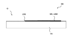
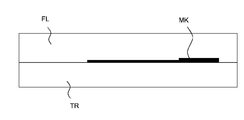
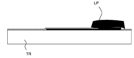
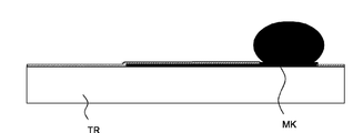
도 1은 전기 디바이스(EB)의 간단한 실시예의 단면도를 도시한다. 전기 디바이스(EB)는 금속화된 콘택트 표면(MK)이 구조화되는 캐리어(TR)를 갖는다. 금속화된 콘택트 표면(MK)은 범프 연결부를 통해 전기 컴포넌트에 연결되도록 의도된다. 캐리어(TR)의 상부 면(O) 상에, 캐리어 TR의 상부 면 중에서 솔더 재료와 직접 접촉해서는 안 되는 그러한 영역들을 커버하는 솔더 정지 층(LSS)이 배열된다.Figure 1 shows a cross-sectional view of a simple embodiment of an electrical device EB. The electrical device EB has a carrier TR on which the metallized contact surface MK is structured. The metallized contact surface (MK) is intended to be connected to the electrical component through the bump connection. A solder stop layer (LSS) is arranged on the top surface (O) of the carrier (TR) to cover those areas that should not come into direct contact with the solder material from the top surface of the carrier TR.
여기서, 금속화된 콘택트 표면은 소위 언더-범프 금속화물(UBM)일 수 있고, 용이하게 습윤가능한 표면을 가질 수 있다.Here, the metallized contact surface may be a so-called under-bump metallization (UBM) and may have a readily wettable surface.
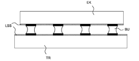
도 2는 상대적으로 두꺼운 솔더 정지 층(LSS)을 갖는 소정 형태의 전기 디바이스의 단면도를 도시한다. 캐리어(TR)의 상부 면이 충분히 편평하다면, 솔더 정지 층(LSS)은 솔더에 의해 습윤되는 것으로부터 캐리어(TR)의 상부 면 상의 감응성 영역들을 신뢰성있게 보호한다. 그러나, 디바이스가 몰딩 화합물(MM)에 의해 봉합되는 경우, 두꺼운 솔더 정지 층은, 범프 연결부들(BU)을 통해 캐리어(TR)에 접합 및 연결되는 전기 컴포넌트(EK)의 하부 면과 캐리어(TR) 사이의 중간 공간(Z)을 채우는 것에 대한 장애물이 될 것이다.Figure 2 shows a cross-sectional view of a certain type of electrical device with a relatively thick solder stop layer (LSS). If the top surface of the carrier TR is sufficiently flat, the solder stop layer LSS reliably protects the sensitive areas on the top surface of the carrier TR from being wetted by the solder. However, when the device is sealed by a molding compound (MM), the thick solder stop layer is formed on the lower surface of the electrical component EK, which is bonded and connected to the carrier TR via the bump connections BU, (Z). ≪ / RTI >
도 3은 범프 볼(BU)이 금속화된 콘택트 표면(MK) 상에 이미 형성된 전기 디바이스의 단면도를 도시한다. 솔더의 표면 장력으로 인해, 볼과 같은 형상이 리플로우 공정의 과정 동안에 형성된다. 솔더 정지 층(LSS)의 두께는 범프 볼, 또는 전기 컴포넌트에 대한 후속 범프 접합 연결부의 높이에 비해 매우 작다.Figure 3 shows a cross-sectional view of an electrical device in which the bump balls BU have already been formed on the metallized contact surface MK. Due to the surface tension of the solder, a ball-like shape is formed during the course of the reflow process. The thickness of the solder stop layer (LSS) is very small compared to the height of the bump balls, or subsequent bump joint connections to electrical components.
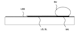
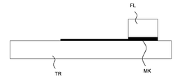
솔더링가능한 표면(LO)을 갖는 재료, 예를 들어 신호 라인(SL)은 캐리어의 표면 상에 배열되고, 니켈, 구리, 금, 또는 은을 포함할 수 있다. 솔더 정지 층(LSS)이 없다면, 범프 볼(BU)의 재료는 콘택트 표면(MK) 상에 축적되는 것이 아니라, 신호 라인을 공격하고, 가능하게는, 캐리어의 상부 면 상의 추가의 회로 요소 및 신호 라인을 단락시키는 위험성이 있다.A material having a solderable surface (LO), for example a signal line SL, is arranged on the surface of the carrier and may comprise nickel, copper, gold, or silver. Without the solder stop layer LSS the material of the bump balls BU does not accumulate on the contact surface MK but rather attack the signal lines and possibly further circuit elements on the top surface of the carrier and the signal There is a risk of shorting the line.
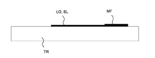
도 4는 전기 디바이스의 제조에 있어서의 제1 중간 결과물의 단면도를 도시한다. 보호될 요소들의 예들로서 콘택트 표면(MK) 및 신호 도체(SL)는 캐리어(TR)의 상부 면 상에 배열된다.Figure 4 shows a cross-sectional view of a first intermediate product in the manufacture of an electrical device. As examples of elements to be protected, the contact surface MK and the signal conductor SL are arranged on the upper surface of the carrier TR.
도 5는 추가의 중간 단계의 단면도를 도시하는데, 여기서 보호될 영역들 및 솔더에 의해 후속으로 습윤될 영역들을 포함하는 전체 표면이 포토레지스트(FL)에 의해 커버된다.Fig. 5 shows a cross-sectional view of a further intermediate stage in which the entire surface comprising the areas to be protected and the areas to be subsequently wetted by the solder is covered by the photoresist FL.
도 6은 추가의 중간 단계의 단면도를 도시하는데, 여기서 포토레지스트(FL)는 나중에 솔더 정지 층의 재료가 없는 상태로 남아 있어야 하는 영역들(MK)만이 포토레지스트(FL)의 재료에 의해 커버된 상태로 남아 있도록 구조화된다.Figure 6 shows a cross-sectional view of a further intermediate stage in which only the areas MK where the photoresist FL should remain free of material of the solder stop layer later are covered by the material of the photoresist FL Lt; / RTI >
이러한 목적을 위해, 포토레지스트가 선택적으로 노출 및 전사될 수 있다.For this purpose, the photoresist can be selectively exposed and transferred.
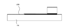
도 7은 추가의 중간 단계의 결과물을 도시하는데, 여기서 이전 전기 디바이스의 전체 상부 면이 후속의 솔더 정지 층(LSS)의 재료에 의해 커버된다. 감응성 영역들은 솔더 정지 층(LSS)의 재료에 의해 직접적으로 커버된다. 솔더가 후속으로 배치되는 곳은 남아 있는 포토레지스트(FL)가 솔더 정지 층(LSS)의 재료와 콘택트 표면 사이에서 발견되는 곳이다.Figure 7 shows the result of a further intermediate stage, where the entire top surface of the previous electrical device is covered by the material of the subsequent solder stop layer (LSS). The sensitive regions are covered directly by the material of the solder stop layer (LSS). Where the solder is subsequently deposited is where the remaining photoresist FL is found between the material of the solder stop layer (LSS) and the contact surface.
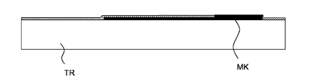
그에 대응하여, 도 8은 추가의 공정 단계의 결과물을 도시하는데, 여기서 포토레지스트(FL)의 남아 있는 나머지들은 그들 상에 침착된 솔더 정지 층(LSS)의 재료의 세그먼트들과 함께 제거되어, 습윤될 표면이 솔더 정지 층에 의해 커버되지 않은 상태로 노출된 채 놓이게 하였다.Correspondingly, Figure 8 shows the result of an additional process step, in which the remaining remainder of the photoresist FL is removed with the segments of material of the solder stop layer (LSS) deposited on them, The exposed surface was left uncovered by the solder stop layer.
도 9는, 추가 단계의 결과물, 즉 콘택트 표면들(MK)의 영역들에 주로 대응하는 영역들에 솔더 페이스트(LP)를 적용한 결과물을 도시한다. 솔더 정지 층(LSS)의 정밀하게 정의된 에지들로 인해, 콘택트 표면(MK)의 상당한 면적이 솔더 페이스트(LP)에 의해 커버되는 한, 솔더 페이스트(LP)의 적용 동안에 횡방향 위치설정은 과도하게 정확할 필요가 없다.Fig. 9 shows the result of applying the solder paste (LP) to the areas of the result of the further step, namely the areas of the contact surfaces MK. Due to the precisely defined edges of the solder stop layer LSS the transverse positioning during the application of the solder paste LP can be transient as long as a substantial area of the contact surface MK is covered by the solder paste LP. There is no need to be accurate.
도 10은 전기 디바이스의 제조에 있어서의 추가의 중간 단계의 결과물을 도시하는데, 여기서 가열 후, 솔더 페이스트(LP)의 재료는 콘택트 표면(MK)의 위치에서 볼로 농축된다.Fig. 10 shows the result of a further intermediate step in the manufacture of an electric device, where after heating the material of the solder paste LP is concentrated into a ball at the location of the contact surface MK.
도 11은 전기 디바이스의 단면도를 도시하는데, 여기서 전기 컴포넌트(EK)의 하부 면 상의 콘택트 표면(MK) 및 캐리어(TR)의 상부 면 상의 콘택트 표면(MK)은 도 10에서의 범프 볼로부터 전개된 범프 연결부를 통해 연결된다.11 shows a cross-sectional view of an electrical device in which a contact surface MK on the lower surface of the electrical component EK and a contact surface MK on the upper surface of the carrier TR are formed Bump connection.
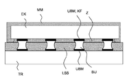
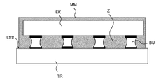
도 12는 추가의 실시예의 단면도를 도시하는데, 여기서 전기 컴포넌트(EK) 및 캐리어(TR)는 복수의 범프 연결부들(BU)을 통해 접합 및 연결된다. 캐리어(TR)의 상부 면 상의 솔더 정지 층(LSS) 외에도, 솔더 정지 층(LSS) - 바람직하게는 동등하게 얇음 - 이 전기 컴포넌트(EK)의 하부 면 상에 배열될 수 있다.Figure 12 shows a cross-sectional view of a further embodiment in which the electrical component EK and the carrier TR are joined and connected through a plurality of bump connections BU. In addition to the solder stop layer LSS on the top surface of the carrier TR, a solder stop layer LSS, preferably equally thin, can be arranged on the bottom side of the electrical component EK.
마지막으로, 도 13은 봉합된 전기 디바이스의 단면도를 도시하는데, 여기서 몰딩 화합물(MM)은 캐리어(TR)의 상부 면 상에 전기 컴포넌트를 봉합하고, 전기 컴포넌트(EK)와 캐리어(TR) 사이의 중간 공간들(Z)을 채운다.Finally, FIG. 13 shows a cross-sectional view of the sealed electrical device, wherein the molding compound MM seals the electrical component on the top surface of the carrier TR and the electrical connection between the electrical component EK and the carrier TR And fills the intermediate spaces (Z).
BU:
범프 연결부
EB:
전기 디바이스
EK:
전기 컴포넌트
FL:
포토레지스트
KF:
콘택트 표면
LO:
솔더링가능한 표면
LP:
솔더 페이스트
LSS:
솔더 정지 층
MK:
금속화된 콘택트 표면
MM:
몰딩 화합물
O:
캐리어의 상부 면
SL:
신호 라인
TR:
캐리어
UBM:
언더-범프 금속화물
Z:
중간 공간BU: bump connection
EB: Electrical device
EK: electrical component
FL: photoresist
KF: contact surface
LO: Solderable surface
LP: Solder paste
LSS: solder stop layer
MK: Metallized contact surface
MM: Molding compound
O: the upper surface of the carrier
SL: Signal line
TR: Carrier
UBM: Under-bump metal cargo
Z: Intermediate space
Claims (17)
- 상부 면(O)을 갖는 캐리어(TR),
- 상기 상부 면(O) 상의 금속화된 콘택트 표면(MK), 및
- 상기 상부 면(O)의 일부를 커버하지만 상기 콘택트 표면(MF)을 커버하지 않는 솔더 정지 층 (LSS)을 포함하고,
- 상기 솔더 정지 층(LSS)은 200 nm 이하의 두께를 갖는, 전기 디바이스.An electrical device (EB)
A carrier TR having a top surface O,
A metallized contact surface (MK) on said top surface (O), and
- a solder stop layer (LSS) covering a portion of said top surface (O) but not covering said contact surface (MF)
- the solder stop layer (LSS) has a thickness of 200 nm or less.
- 상기 캐리어(TR)의 상기 상부 면(O) 상에 있고 상기 콘택트 표면(MK)과 상호연결되는 제1 신호 라인(SL), 및
- 상기 캐리어(TR)의 상기 상부 면(O) 상의 제2 신호 라인(SL)을 추가로 포함하고,
- 신호 라인들(SL) 양측 모두는 상기 솔더 정지 층(LSS)에 의해 적어도 부분적으로 커버되고,
- 상기 2개의 신호 라인들(SL) 사이의 전기 저항은 100 MΩ 이상인, 전기 디바이스.7. The method according to any one of claims 1 to 6,
- a first signal line (SL) on the top surface (O) of the carrier (TR) and interconnected with the contact surface (MK), and
- a second signal line (SL) on said top surface (O) of said carrier (TR)
- both sides of the signal lines (SL) are at least partly covered by the solder stop layer (LSS)
- the electrical resistance between the two signal lines (SL) is at least 100 M ?.
- 상부 면(O)을 갖는 캐리어(TR) 및 상기 상부 면(O) 상의 금속화된 콘택트 표면(MK)의 제공 단계,
- 래커 층(FL)의 재료가 상기 콘택트 표면(MK) 상에 남아 있고 어떠한 콘택트 표면(MK)도 갖지 않는 상기 표면(O)의 영역들에 상기 래커 층(FL)의 재료가 없도록 하는 방식으로 상기 상부 면(O) 상에 래커 층(FL)을 배열하고 상기 래커 층(FL)을 구조화하는 단계,
- 상기 캐리어(TR)의 상기 상부 면(O) 상에 솔더 정지 층(LSS)을 침착하는 단계, 및
- 상기 콘택트 표면(MK) 위의 상기 솔더 정지 층(LSS)의 재료와 함께 상기 래커 층(FL)의 남아 있는 재료를 제거하는 단계를 포함하는, 방법.A method for manufacturing an electric device (EB)
Providing a carrier TR with a top surface O and a metallized contact surface MK on said top surface O,
In such a way that the material of the lacquer layer FL remains on the areas of the surface O on which the material of the lacquer layer FL remains on the contact surface MK and which has no contact surface MK Arranging a lacquer layer (FL) on the top surface (O) and structuring the lacquer layer (FL)
- depositing a solder stop layer (LSS) on the top surface (O) of the carrier (TR), and
- removing the remaining material of the lacquer layer (FL) with the material of the solder stop layer (LSS) on the contact surface (MK).
- 적어도 상기 콘택트 표면(MK) 상에 솔더 페이스트(LP)를 배열하는 단계,
- 자신의 하부 면 상에 콘택트 표면(MK, KF)을 갖는 전기 컴포넌트(EK)를 상기 캐리어(TR)의 상기 상부 면(O) 상에 배열하는 단계,
- 상기 디바이스(EB)를 리플로우 솔더링하는 단계, 및 범프 연결부(BU)에 의해 상기 2개의 콘택트 표면들(MK, KF)을 연결하는 단계를 추가로 포함하는, 방법.16. The method according to any one of claims 11 to 15,
- arranging a solder paste (LP) on at least the contact surface (MK)
- arranging on the upper surface (O) of the carrier (TR) an electrical component (EK) having a contact surface (MK, KF) on its lower surface,
- reflow soldering the device (EB), and connecting the two contact surfaces (MK, KF) by a bump connection (BU).
- 상기 전기 컴포넌트(EK)를 몰딩 화합물(MM)로 봉합하는 단계를 추가로 포함하고,
- 상기 몰딩 화합물(MM)은, 또한, 상기 컴포넌트(EK)와 상기 캐리어(TR) 사이의 영역을 채우는, 방법.17. The method of claim 16,
- sealing the electrical component (EK) with a molding compound (MM)
- the molding compound (MM) also fills an area between the component (EK) and the carrier (TR).
Applications Claiming Priority (3)
| Application Number | Priority Date | Filing Date | Title |
|---|---|---|---|
| DE102015120647.1A DE102015120647B4 (en) | 2015-11-27 | 2015-11-27 | Electrical device with thin solder stop layer and method of manufacture |
| DE102015120647.1 | 2015-11-27 | ||
| PCT/EP2016/070973 WO2017088998A1 (en) | 2015-11-27 | 2016-09-06 | Electrical component with thin solder resist layer and method for the production thereof |
Publications (1)
| Publication Number | Publication Date |
|---|---|
| KR20180088798A true KR20180088798A (en) | 2018-08-07 |
Family
ID=56883787
Family Applications (1)
| Application Number | Title | Priority Date | Filing Date |
|---|---|---|---|
| KR1020187011776A KR20180088798A (en) | 2015-11-27 | 2016-09-06 | Electrical device having a thin solder stop layer and method for manufacturing |
Country Status (8)
| Country | Link |
|---|---|
| US (1) | US20180331062A1 (en) |
| EP (1) | EP3381052A1 (en) |
| JP (1) | JP2018536994A (en) |
| KR (1) | KR20180088798A (en) |
| CN (1) | CN108369935A (en) |
| BR (1) | BR112018010666A8 (en) |
| DE (1) | DE102015120647B4 (en) |
| WO (1) | WO2017088998A1 (en) |
Families Citing this family (1)
| Publication number | Priority date | Publication date | Assignee | Title |
|---|---|---|---|---|
| FI130166B (en) | 2019-03-08 | 2023-03-23 | Picosun Oy | Solder mask |
Family Cites Families (21)
| Publication number | Priority date | Publication date | Assignee | Title |
|---|---|---|---|---|
| JPH03218644A (en) * | 1990-01-24 | 1991-09-26 | Sharp Corp | Connection structure of circuit board |
| US5620131A (en) * | 1995-06-15 | 1997-04-15 | Lucent Technologies Inc. | Method of solder bonding |
| US6294840B1 (en) * | 1999-11-18 | 2001-09-25 | Lsi Logic Corporation | Dual-thickness solder mask in integrated circuit package |
| US6645791B2 (en) * | 2001-04-23 | 2003-11-11 | Fairchild Semiconductor | Semiconductor die package including carrier with mask |
| AU2002357645A1 (en) * | 2002-09-20 | 2004-04-08 | Honeywell International, Inc. | Interlayer adhesion promoter for low k materials |
| AU2003300201A1 (en) * | 2002-12-20 | 2004-07-22 | Agere Systems Inc. | Structure and method for bonding to copper interconnect structures |
| US6790759B1 (en) * | 2003-07-31 | 2004-09-14 | Freescale Semiconductor, Inc. | Semiconductor device with strain relieving bump design |
| US7294451B2 (en) * | 2003-11-18 | 2007-11-13 | Texas Instruments Incorporated | Raised solder-mask-defined (SMD) solder ball pads for a laminate electronic circuit board |
| US7132303B2 (en) * | 2003-12-18 | 2006-11-07 | Freescale Semiconductor, Inc. | Stacked semiconductor device assembly and method for forming |
| KR100626617B1 (en) * | 2004-12-07 | 2006-09-25 | 삼성전자주식회사 | Ball land structure of circuit substrate for semiconductor package |
| JP4795112B2 (en) * | 2006-05-17 | 2011-10-19 | 株式会社フジクラ | Manufacturing method of bonding substrate |
| JP5031403B2 (en) * | 2007-03-01 | 2012-09-19 | 京セラケミカル株式会社 | Epoxy resin composition for sealing, resin-encapsulated semiconductor device and manufacturing method thereof |
| US7812460B2 (en) * | 2008-05-30 | 2010-10-12 | Unimicron Technology Corp. | Packaging substrate and method for fabricating the same |
| US9524945B2 (en) * | 2010-05-18 | 2016-12-20 | Taiwan Semiconductor Manufacturing Company, Ltd. | Cu pillar bump with L-shaped non-metal sidewall protection structure |
| US8922004B2 (en) * | 2010-06-11 | 2014-12-30 | Taiwan Semiconductor Manufacturing Company, Ltd. | Copper bump structures having sidewall protection layers |
| TWI575684B (en) * | 2011-06-13 | 2017-03-21 | 矽品精密工業股份有限公司 | Chip-scale package structure |
| KR101307436B1 (en) * | 2011-11-10 | 2013-09-12 | (주)유우일렉트로닉스 | Mems sensor pakiging and the method |
| US10192804B2 (en) * | 2012-07-09 | 2019-01-29 | Taiwan Semiconductor Manufacturing Company, Ltd. | Bump-on-trace packaging structure and method for forming the same |
| GB2520952A (en) * | 2013-12-04 | 2015-06-10 | Ibm | Flip-chip electronic device with carrier having heat dissipation elements free of solder mask |
| CN104637967A (en) * | 2015-02-13 | 2015-05-20 | 苏州晶方半导体科技股份有限公司 | Packaging method and packaging structure |
| US9859234B2 (en) * | 2015-08-06 | 2018-01-02 | Invensas Corporation | Methods and structures to repair device warpage |
-
2015
- 2015-11-27 DE DE102015120647.1A patent/DE102015120647B4/en active Active
-
2016
- 2016-09-06 US US15/776,019 patent/US20180331062A1/en not_active Abandoned
- 2016-09-06 BR BR112018010666A patent/BR112018010666A8/en not_active Application Discontinuation
- 2016-09-06 CN CN201680062169.7A patent/CN108369935A/en active Pending
- 2016-09-06 JP JP2018527165A patent/JP2018536994A/en not_active Ceased
- 2016-09-06 EP EP16762778.5A patent/EP3381052A1/en not_active Withdrawn
- 2016-09-06 WO PCT/EP2016/070973 patent/WO2017088998A1/en active Application Filing
- 2016-09-06 KR KR1020187011776A patent/KR20180088798A/en not_active Application Discontinuation
Also Published As
| Publication number | Publication date |
|---|---|
| CN108369935A (en) | 2018-08-03 |
| WO2017088998A1 (en) | 2017-06-01 |
| US20180331062A1 (en) | 2018-11-15 |
| DE102015120647A1 (en) | 2017-06-01 |
| DE102015120647B4 (en) | 2017-12-28 |
| BR112018010666A8 (en) | 2019-02-26 |
| EP3381052A1 (en) | 2018-10-03 |
| BR112018010666A2 (en) | 2018-11-13 |
| JP2018536994A (en) | 2018-12-13 |
Similar Documents
| Publication | Publication Date | Title |
|---|---|---|
| US11862539B2 (en) | Method of forming a packaged semiconductor device having enhanced wettable flank and structure | |
| KR101518611B1 (en) | Method and apparatus for connecting packages onto printed circuit boards | |
| CN101548378B (en) | Semiconductor device and manufacturing method thereof | |
| US10147691B2 (en) | Semiconductor structure and manufacturing method thereof | |
| CN110233112A (en) | Electronic packing piece and its preparation method | |
| CN110098169A (en) | Electronic packing piece and its preparation method | |
| US8435837B2 (en) | Panel based lead frame packaging method and device | |
| CN103035598B (en) | Without the formation of the connector of UBM | |
| US9806045B2 (en) | Interconnection structure including a metal post encapsulated by solder joint having a concave outer surface | |
| US9293433B2 (en) | Intermetallic compound layer on a pillar between a chip and substrate | |
| KR101235498B1 (en) | Methods and systems for packaging integrated circuits with integrated passive components | |
| US9379076B2 (en) | Semiconductor device and manufacturing method thereof | |
| CN101930960B (en) | Ic chip package and forming method | |
| CN113035832B (en) | Wafer-level chip packaging structure, manufacturing method thereof and electronic equipment | |
| EP1313143B1 (en) | Perimeter anchored thick film pad | |
| KR20180088798A (en) | Electrical device having a thin solder stop layer and method for manufacturing | |
| CN105244327A (en) | Electronic device module and method of manufacturing the same | |
| US8952531B2 (en) | Packaging method using solder coating ball and package having solder pattern including metal pattern | |
| JP2010040891A (en) | Wiring board with built-in component | |
| CN113035831A (en) | Wafer-level chip packaging structure, manufacturing method thereof and electronic equipment | |
| JP2011077200A (en) | Semiconductor device and method of manufacturing the same | |
| JP2009295647A (en) | Method for manufacturing circuit board and circuit board applying the method |
Legal Events
| Date | Code | Title | Description |
|---|---|---|---|
| A201 | Request for examination | ||
| E902 | Notification of reason for refusal | ||
| E601 | Decision to refuse application |