KR20180071368A - Technologies for combining CMP process trace data with 3D-printed CMP consumables - Google Patents
Technologies for combining CMP process trace data with 3D-printed CMP consumables Download PDFInfo
- Publication number
- KR20180071368A KR20180071368A KR1020187015966A KR20187015966A KR20180071368A KR 20180071368 A KR20180071368 A KR 20180071368A KR 1020187015966 A KR1020187015966 A KR 1020187015966A KR 20187015966 A KR20187015966 A KR 20187015966A KR 20180071368 A KR20180071368 A KR 20180071368A
- Authority
- KR
- South Korea
- Prior art keywords
- polishing
- printed
- wireless communication
- sensor
- polishing pad
- Prior art date
Links
- 238000000034 method Methods 0.000 title claims abstract description 87
- 230000008569 process Effects 0.000 title claims abstract description 46
- 238000005516 engineering process Methods 0.000 title claims description 3
- 238000005498 polishing Methods 0.000 claims abstract description 304
- 238000004891 communication Methods 0.000 claims abstract description 149
- 238000004519 manufacturing process Methods 0.000 claims abstract description 33
- 238000007639 printing Methods 0.000 claims abstract description 14
- 239000000126 substance Substances 0.000 claims abstract description 13
- 239000000463 material Substances 0.000 claims description 114
- 239000000758 substrate Substances 0.000 claims description 64
- 238000007517 polishing process Methods 0.000 claims description 26
- 239000000203 mixture Substances 0.000 claims description 21
- 229920000642 polymer Polymers 0.000 claims description 20
- 239000004020 conductor Substances 0.000 claims description 16
- 239000004065 semiconductor Substances 0.000 claims description 13
- -1 Phenylene vinylene Chemical group 0.000 claims description 10
- 238000000151 deposition Methods 0.000 claims description 10
- 229920000728 polyester Polymers 0.000 claims description 7
- 150000001252 acrylic acid derivatives Chemical class 0.000 claims description 6
- 239000002861 polymer material Substances 0.000 claims description 6
- UFWIBTONFRDIAS-UHFFFAOYSA-N Naphthalene Chemical compound C1=CC=CC2=CC=CC=C21 UFWIBTONFRDIAS-UHFFFAOYSA-N 0.000 claims description 4
- CUFNKYGDVFVPHO-UHFFFAOYSA-N azulene Chemical compound C1=CC=CC2=CC=CC2=C1 CUFNKYGDVFVPHO-UHFFFAOYSA-N 0.000 claims description 4
- 230000008859 change Effects 0.000 claims description 4
- NIHNNTQXNPWCJQ-UHFFFAOYSA-N fluorene Chemical compound C1=CC=C2CC3=CC=CC=C3C2=C1 NIHNNTQXNPWCJQ-UHFFFAOYSA-N 0.000 claims description 4
- BBEAQIROQSPTKN-UHFFFAOYSA-N pyrene Chemical compound C1=CC=C2C=CC3=CC=CC4=CC=C1C2=C43 BBEAQIROQSPTKN-UHFFFAOYSA-N 0.000 claims description 4
- 230000004044 response Effects 0.000 claims description 4
- 229920000069 polyphenylene sulfide Polymers 0.000 claims description 3
- 239000004593 Epoxy Substances 0.000 claims description 2
- 150000001412 amines Chemical class 0.000 claims description 2
- 125000003700 epoxy group Chemical group 0.000 claims description 2
- GVEPBJHOBDJJJI-UHFFFAOYSA-N fluoranthrene Natural products C1=CC(C2=CC=CC=C22)=C3C2=CC=CC3=C1 GVEPBJHOBDJJJI-UHFFFAOYSA-N 0.000 claims description 2
- 230000001939 inductive effect Effects 0.000 claims description 2
- 230000000977 initiatory effect Effects 0.000 claims description 2
- 229920000647 polyepoxide Polymers 0.000 claims description 2
- 229920001296 polysiloxane Polymers 0.000 claims description 2
- 150000003673 urethanes Chemical class 0.000 claims description 2
- 230000001133 acceleration Effects 0.000 claims 3
- UJOBWOGCFQCDNV-UHFFFAOYSA-N 9H-carbazole Chemical compound C1=CC=C2C3=CC=CC=C3NC2=C1 UJOBWOGCFQCDNV-UHFFFAOYSA-N 0.000 claims 2
- SIKJAQJRHWYJAI-UHFFFAOYSA-N Indole Chemical compound C1=CC=C2NC=CC2=C1 SIKJAQJRHWYJAI-UHFFFAOYSA-N 0.000 claims 2
- KAESVJOAVNADME-UHFFFAOYSA-N Pyrrole Chemical compound C=1C=CNC=1 KAESVJOAVNADME-UHFFFAOYSA-N 0.000 claims 2
- 229920000265 Polyparaphenylene Polymers 0.000 claims 1
- 208000037062 Polyps Diseases 0.000 claims 1
- XYOVOXDWRFGKEX-UHFFFAOYSA-N azepine Chemical compound N1C=CC=CC=C1 XYOVOXDWRFGKEX-UHFFFAOYSA-N 0.000 claims 1
- PZOUSPYUWWUPPK-UHFFFAOYSA-N indole Natural products CC1=CC=CC2=C1C=CN2 PZOUSPYUWWUPPK-UHFFFAOYSA-N 0.000 claims 1
- RKJUIXBNRJVNHR-UHFFFAOYSA-N indolenine Natural products C1=CC=C2CC=NC2=C1 RKJUIXBNRJVNHR-UHFFFAOYSA-N 0.000 claims 1
- 229920001568 phenolic resin Polymers 0.000 claims 1
- 239000005011 phenolic resin Substances 0.000 claims 1
- 239000012528 membrane Substances 0.000 abstract description 48
- 238000010146 3D printing Methods 0.000 abstract description 26
- 238000012545 processing Methods 0.000 description 24
- 239000002131 composite material Substances 0.000 description 17
- 238000003860 storage Methods 0.000 description 16
- 235000019589 hardness Nutrition 0.000 description 12
- 239000002002 slurry Substances 0.000 description 9
- 230000033001 locomotion Effects 0.000 description 7
- 238000012544 monitoring process Methods 0.000 description 7
- 230000003287 optical effect Effects 0.000 description 7
- NIXOWILDQLNWCW-UHFFFAOYSA-M Acrylate Chemical compound [O-]C(=O)C=C NIXOWILDQLNWCW-UHFFFAOYSA-M 0.000 description 6
- 230000006870 function Effects 0.000 description 6
- 229920002635 polyurethane Polymers 0.000 description 6
- 239000004814 polyurethane Substances 0.000 description 6
- 239000000843 powder Substances 0.000 description 6
- 239000002243 precursor Substances 0.000 description 6
- 229920001169 thermoplastic Polymers 0.000 description 6
- 239000004695 Polyether sulfone Substances 0.000 description 5
- 230000008901 benefit Effects 0.000 description 5
- 230000008021 deposition Effects 0.000 description 5
- 238000013461 design Methods 0.000 description 5
- 238000001514 detection method Methods 0.000 description 5
- 230000001976 improved effect Effects 0.000 description 5
- 239000002245 particle Substances 0.000 description 5
- 229920006393 polyether sulfone Polymers 0.000 description 5
- 230000008054 signal transmission Effects 0.000 description 5
- 230000003466 anti-cipated effect Effects 0.000 description 4
- 238000005266 casting Methods 0.000 description 4
- 238000011960 computer-aided design Methods 0.000 description 4
- 238000011065 in-situ storage Methods 0.000 description 4
- 238000003475 lamination Methods 0.000 description 4
- 238000005259 measurement Methods 0.000 description 4
- 239000002184 metal Substances 0.000 description 4
- 229910052751 metal Inorganic materials 0.000 description 4
- 238000000465 moulding Methods 0.000 description 4
- 229920003229 poly(methyl methacrylate) Polymers 0.000 description 4
- 239000004926 polymethyl methacrylate Substances 0.000 description 4
- 230000005540 biological transmission Effects 0.000 description 3
- 239000013590 bulk material Substances 0.000 description 3
- 229920001577 copolymer Polymers 0.000 description 3
- 239000000976 ink Substances 0.000 description 3
- 239000007788 liquid Substances 0.000 description 3
- 239000012705 liquid precursor Substances 0.000 description 3
- 239000002105 nanoparticle Substances 0.000 description 3
- 238000012546 transfer Methods 0.000 description 3
- 229920002943 EPDM rubber Polymers 0.000 description 2
- 229920000877 Melamine resin Polymers 0.000 description 2
- 239000004952 Polyamide Substances 0.000 description 2
- 239000004721 Polyphenylene oxide Substances 0.000 description 2
- 239000004743 Polypropylene Substances 0.000 description 2
- 239000004793 Polystyrene Substances 0.000 description 2
- VYPSYNLAJGMNEJ-UHFFFAOYSA-N Silicium dioxide Chemical compound O=[Si]=O VYPSYNLAJGMNEJ-UHFFFAOYSA-N 0.000 description 2
- 239000004676 acrylonitrile butadiene styrene Substances 0.000 description 2
- 239000000654 additive Substances 0.000 description 2
- 230000000996 additive effect Effects 0.000 description 2
- 239000011230 binding agent Substances 0.000 description 2
- 230000015572 biosynthetic process Effects 0.000 description 2
- 239000000919 ceramic Substances 0.000 description 2
- 230000001143 conditioned effect Effects 0.000 description 2
- 238000013480 data collection Methods 0.000 description 2
- 238000009826 distribution Methods 0.000 description 2
- 239000012530 fluid Substances 0.000 description 2
- 239000006260 foam Substances 0.000 description 2
- 229930195733 hydrocarbon Natural products 0.000 description 2
- 150000002430 hydrocarbons Chemical class 0.000 description 2
- 238000001746 injection moulding Methods 0.000 description 2
- 230000002093 peripheral effect Effects 0.000 description 2
- 229920001084 poly(chloroprene) Polymers 0.000 description 2
- 229920002493 poly(chlorotrifluoroethylene) Polymers 0.000 description 2
- 229920002492 poly(sulfone) Polymers 0.000 description 2
- 229920002239 polyacrylonitrile Polymers 0.000 description 2
- 229920002647 polyamide Polymers 0.000 description 2
- 239000005023 polychlorotrifluoroethylene (PCTFE) polymer Substances 0.000 description 2
- 229920000570 polyether Polymers 0.000 description 2
- 229920001601 polyetherimide Polymers 0.000 description 2
- 229920001155 polypropylene Polymers 0.000 description 2
- 229920002223 polystyrene Polymers 0.000 description 2
- 239000004810 polytetrafluoroethylene Substances 0.000 description 2
- 229920001343 polytetrafluoroethylene Polymers 0.000 description 2
- 229920002689 polyvinyl acetate Polymers 0.000 description 2
- 238000009877 rendering Methods 0.000 description 2
- 230000000717 retained effect Effects 0.000 description 2
- 239000007779 soft material Substances 0.000 description 2
- 239000007787 solid Substances 0.000 description 2
- 235000019587 texture Nutrition 0.000 description 2
- 239000012780 transparent material Substances 0.000 description 2
- 239000011800 void material Substances 0.000 description 2
- 244000043261 Hevea brasiliensis Species 0.000 description 1
- 239000004696 Poly ether ether ketone Substances 0.000 description 1
- 239000004697 Polyetherimide Substances 0.000 description 1
- 239000004642 Polyimide Substances 0.000 description 1
- 239000004734 Polyphenylene sulfide Substances 0.000 description 1
- 239000003082 abrasive agent Substances 0.000 description 1
- XECAHXYUAAWDEL-UHFFFAOYSA-N acrylonitrile butadiene styrene Chemical compound C=CC=C.C=CC#N.C=CC1=CC=CC=C1 XECAHXYUAAWDEL-UHFFFAOYSA-N 0.000 description 1
- 229920000122 acrylonitrile butadiene styrene Polymers 0.000 description 1
- PNEYBMLMFCGWSK-UHFFFAOYSA-N aluminium oxide Inorganic materials [O-2].[O-2].[O-2].[Al+3].[Al+3] PNEYBMLMFCGWSK-UHFFFAOYSA-N 0.000 description 1
- 238000004458 analytical method Methods 0.000 description 1
- 238000003491 array Methods 0.000 description 1
- 239000003990 capacitor Substances 0.000 description 1
- CETPSERCERDGAM-UHFFFAOYSA-N ceric oxide Chemical compound O=[Ce]=O CETPSERCERDGAM-UHFFFAOYSA-N 0.000 description 1
- 229910000422 cerium(IV) oxide Inorganic materials 0.000 description 1
- 238000004140 cleaning Methods 0.000 description 1
- 238000010276 construction Methods 0.000 description 1
- 238000007796 conventional method Methods 0.000 description 1
- 230000006837 decompression Effects 0.000 description 1
- 230000007547 defect Effects 0.000 description 1
- 230000001419 dependent effect Effects 0.000 description 1
- 238000012938 design process Methods 0.000 description 1
- 238000010586 diagram Methods 0.000 description 1
- 230000000694 effects Effects 0.000 description 1
- 239000013013 elastic material Substances 0.000 description 1
- 230000005611 electricity Effects 0.000 description 1
- 230000009969 flowable effect Effects 0.000 description 1
- 230000004927 fusion Effects 0.000 description 1
- 230000007274 generation of a signal involved in cell-cell signaling Effects 0.000 description 1
- PCHJSUWPFVWCPO-UHFFFAOYSA-N gold Chemical compound [Au] PCHJSUWPFVWCPO-UHFFFAOYSA-N 0.000 description 1
- 229910052737 gold Inorganic materials 0.000 description 1
- 239000010931 gold Substances 0.000 description 1
- 238000010438 heat treatment Methods 0.000 description 1
- 230000002209 hydrophobic effect Effects 0.000 description 1
- 238000007641 inkjet printing Methods 0.000 description 1
- 229910000765 intermetallic Inorganic materials 0.000 description 1
- 230000007246 mechanism Effects 0.000 description 1
- JDSHMPZPIAZGSV-UHFFFAOYSA-N melamine Chemical compound NC1=NC(N)=NC(N)=N1 JDSHMPZPIAZGSV-UHFFFAOYSA-N 0.000 description 1
- 150000007974 melamines Chemical class 0.000 description 1
- 239000007769 metal material Substances 0.000 description 1
- 229910044991 metal oxide Inorganic materials 0.000 description 1
- 150000004706 metal oxides Chemical class 0.000 description 1
- 150000002739 metals Chemical class 0.000 description 1
- 238000002156 mixing Methods 0.000 description 1
- 239000005543 nano-size silicon particle Substances 0.000 description 1
- 229920003052 natural elastomer Polymers 0.000 description 1
- 229920001194 natural rubber Polymers 0.000 description 1
- 150000002825 nitriles Chemical class 0.000 description 1
- 125000000843 phenylene group Chemical group C1(=C(C=CC=C1)*)* 0.000 description 1
- 230000000704 physical effect Effects 0.000 description 1
- 229920003023 plastic Polymers 0.000 description 1
- 239000004033 plastic Substances 0.000 description 1
- 229920000767 polyaniline Polymers 0.000 description 1
- 229910021420 polycrystalline silicon Inorganic materials 0.000 description 1
- 229920002530 polyetherether ketone Polymers 0.000 description 1
- 229920001721 polyimide Polymers 0.000 description 1
- 239000012704 polymeric precursor Substances 0.000 description 1
- 235000013824 polyphenols Nutrition 0.000 description 1
- 229920005591 polysilicon Polymers 0.000 description 1
- 229920000123 polythiophene Polymers 0.000 description 1
- 239000011148 porous material Substances 0.000 description 1
- 238000004886 process control Methods 0.000 description 1
- 238000012827 research and development Methods 0.000 description 1
- 238000007650 screen-printing Methods 0.000 description 1
- 238000000110 selective laser sintering Methods 0.000 description 1
- 239000000377 silicon dioxide Substances 0.000 description 1
- 229910052709 silver Inorganic materials 0.000 description 1
- 239000004332 silver Substances 0.000 description 1
- 238000005245 sintering Methods 0.000 description 1
- 230000005236 sound signal Effects 0.000 description 1
- 238000001228 spectrum Methods 0.000 description 1
- 230000000153 supplemental effect Effects 0.000 description 1
- 230000008093 supporting effect Effects 0.000 description 1
- 238000010408 sweeping Methods 0.000 description 1
- 238000007669 thermal treatment Methods 0.000 description 1
- 229920002725 thermoplastic elastomer Polymers 0.000 description 1
- 239000012815 thermoplastic material Substances 0.000 description 1
- 229920001187 thermosetting polymer Polymers 0.000 description 1
- 239000004634 thermosetting polymer Substances 0.000 description 1
- 238000012876 topography Methods 0.000 description 1
- 238000001429 visible spectrum Methods 0.000 description 1
- XLYOFNOQVPJJNP-UHFFFAOYSA-N water Substances O XLYOFNOQVPJJNP-UHFFFAOYSA-N 0.000 description 1
Images


Classifications
-
- H—ELECTRICITY
- H01—ELECTRIC ELEMENTS
- H01L—SEMICONDUCTOR DEVICES NOT COVERED BY CLASS H10
- H01L21/00—Processes or apparatus adapted for the manufacture or treatment of semiconductor or solid state devices or of parts thereof
- H01L21/67—Apparatus specially adapted for handling semiconductor or electric solid state devices during manufacture or treatment thereof; Apparatus specially adapted for handling wafers during manufacture or treatment of semiconductor or electric solid state devices or components ; Apparatus not specifically provided for elsewhere
- H01L21/67005—Apparatus not specifically provided for elsewhere
- H01L21/67242—Apparatus for monitoring, sorting or marking
- H01L21/67259—Position monitoring, e.g. misposition detection or presence detection
-
- B—PERFORMING OPERATIONS; TRANSPORTING
- B24—GRINDING; POLISHING
- B24B—MACHINES, DEVICES, OR PROCESSES FOR GRINDING OR POLISHING; DRESSING OR CONDITIONING OF ABRADING SURFACES; FEEDING OF GRINDING, POLISHING, OR LAPPING AGENTS
- B24B37/00—Lapping machines or devices; Accessories
- B24B37/11—Lapping tools
- B24B37/20—Lapping pads for working plane surfaces
- B24B37/26—Lapping pads for working plane surfaces characterised by the shape of the lapping pad surface, e.g. grooved
-
- H—ELECTRICITY
- H01—ELECTRIC ELEMENTS
- H01L—SEMICONDUCTOR DEVICES NOT COVERED BY CLASS H10
- H01L21/00—Processes or apparatus adapted for the manufacture or treatment of semiconductor or solid state devices or of parts thereof
- H01L21/02—Manufacture or treatment of semiconductor devices or of parts thereof
- H01L21/04—Manufacture or treatment of semiconductor devices or of parts thereof the devices having at least one potential-jump barrier or surface barrier, e.g. PN junction, depletion layer or carrier concentration layer
- H01L21/18—Manufacture or treatment of semiconductor devices or of parts thereof the devices having at least one potential-jump barrier or surface barrier, e.g. PN junction, depletion layer or carrier concentration layer the devices having semiconductor bodies comprising elements of Group IV of the Periodic System or AIIIBV compounds with or without impurities, e.g. doping materials
- H01L21/30—Treatment of semiconductor bodies using processes or apparatus not provided for in groups H01L21/20 - H01L21/26
- H01L21/302—Treatment of semiconductor bodies using processes or apparatus not provided for in groups H01L21/20 - H01L21/26 to change their surface-physical characteristics or shape, e.g. etching, polishing, cutting
- H01L21/304—Mechanical treatment, e.g. grinding, polishing, cutting
-
- B—PERFORMING OPERATIONS; TRANSPORTING
- B24—GRINDING; POLISHING
- B24B—MACHINES, DEVICES, OR PROCESSES FOR GRINDING OR POLISHING; DRESSING OR CONDITIONING OF ABRADING SURFACES; FEEDING OF GRINDING, POLISHING, OR LAPPING AGENTS
- B24B37/00—Lapping machines or devices; Accessories
-
- B—PERFORMING OPERATIONS; TRANSPORTING
- B24—GRINDING; POLISHING
- B24B—MACHINES, DEVICES, OR PROCESSES FOR GRINDING OR POLISHING; DRESSING OR CONDITIONING OF ABRADING SURFACES; FEEDING OF GRINDING, POLISHING, OR LAPPING AGENTS
- B24B37/00—Lapping machines or devices; Accessories
- B24B37/11—Lapping tools
- B24B37/20—Lapping pads for working plane surfaces
- B24B37/24—Lapping pads for working plane surfaces characterised by the composition or properties of the pad materials
-
- B—PERFORMING OPERATIONS; TRANSPORTING
- B24—GRINDING; POLISHING
- B24B—MACHINES, DEVICES, OR PROCESSES FOR GRINDING OR POLISHING; DRESSING OR CONDITIONING OF ABRADING SURFACES; FEEDING OF GRINDING, POLISHING, OR LAPPING AGENTS
- B24B37/00—Lapping machines or devices; Accessories
- B24B37/27—Work carriers
-
- B—PERFORMING OPERATIONS; TRANSPORTING
- B24—GRINDING; POLISHING
- B24B—MACHINES, DEVICES, OR PROCESSES FOR GRINDING OR POLISHING; DRESSING OR CONDITIONING OF ABRADING SURFACES; FEEDING OF GRINDING, POLISHING, OR LAPPING AGENTS
- B24B37/00—Lapping machines or devices; Accessories
- B24B37/34—Accessories
-
- B—PERFORMING OPERATIONS; TRANSPORTING
- B24—GRINDING; POLISHING
- B24B—MACHINES, DEVICES, OR PROCESSES FOR GRINDING OR POLISHING; DRESSING OR CONDITIONING OF ABRADING SURFACES; FEEDING OF GRINDING, POLISHING, OR LAPPING AGENTS
- B24B49/00—Measuring or gauging equipment for controlling the feed movement of the grinding tool or work; Arrangements of indicating or measuring equipment, e.g. for indicating the start of the grinding operation
- B24B49/003—Measuring or gauging equipment for controlling the feed movement of the grinding tool or work; Arrangements of indicating or measuring equipment, e.g. for indicating the start of the grinding operation involving acoustic means
-
- B—PERFORMING OPERATIONS; TRANSPORTING
- B24—GRINDING; POLISHING
- B24B—MACHINES, DEVICES, OR PROCESSES FOR GRINDING OR POLISHING; DRESSING OR CONDITIONING OF ABRADING SURFACES; FEEDING OF GRINDING, POLISHING, OR LAPPING AGENTS
- B24B49/00—Measuring or gauging equipment for controlling the feed movement of the grinding tool or work; Arrangements of indicating or measuring equipment, e.g. for indicating the start of the grinding operation
- B24B49/10—Measuring or gauging equipment for controlling the feed movement of the grinding tool or work; Arrangements of indicating or measuring equipment, e.g. for indicating the start of the grinding operation involving electrical means
-
- B—PERFORMING OPERATIONS; TRANSPORTING
- B24—GRINDING; POLISHING
- B24B—MACHINES, DEVICES, OR PROCESSES FOR GRINDING OR POLISHING; DRESSING OR CONDITIONING OF ABRADING SURFACES; FEEDING OF GRINDING, POLISHING, OR LAPPING AGENTS
- B24B49/00—Measuring or gauging equipment for controlling the feed movement of the grinding tool or work; Arrangements of indicating or measuring equipment, e.g. for indicating the start of the grinding operation
- B24B49/14—Measuring or gauging equipment for controlling the feed movement of the grinding tool or work; Arrangements of indicating or measuring equipment, e.g. for indicating the start of the grinding operation taking regard of the temperature during grinding
-
- B—PERFORMING OPERATIONS; TRANSPORTING
- B24—GRINDING; POLISHING
- B24B—MACHINES, DEVICES, OR PROCESSES FOR GRINDING OR POLISHING; DRESSING OR CONDITIONING OF ABRADING SURFACES; FEEDING OF GRINDING, POLISHING, OR LAPPING AGENTS
- B24B49/00—Measuring or gauging equipment for controlling the feed movement of the grinding tool or work; Arrangements of indicating or measuring equipment, e.g. for indicating the start of the grinding operation
- B24B49/16—Measuring or gauging equipment for controlling the feed movement of the grinding tool or work; Arrangements of indicating or measuring equipment, e.g. for indicating the start of the grinding operation taking regard of the load
-
- B—PERFORMING OPERATIONS; TRANSPORTING
- B24—GRINDING; POLISHING
- B24B—MACHINES, DEVICES, OR PROCESSES FOR GRINDING OR POLISHING; DRESSING OR CONDITIONING OF ABRADING SURFACES; FEEDING OF GRINDING, POLISHING, OR LAPPING AGENTS
- B24B51/00—Arrangements for automatic control of a series of individual steps in grinding a workpiece
-
- B—PERFORMING OPERATIONS; TRANSPORTING
- B24—GRINDING; POLISHING
- B24D—TOOLS FOR GRINDING, BUFFING OR SHARPENING
- B24D18/00—Manufacture of grinding tools or other grinding devices, e.g. wheels, not otherwise provided for
-
- B—PERFORMING OPERATIONS; TRANSPORTING
- B29—WORKING OF PLASTICS; WORKING OF SUBSTANCES IN A PLASTIC STATE IN GENERAL
- B29C—SHAPING OR JOINING OF PLASTICS; SHAPING OF MATERIAL IN A PLASTIC STATE, NOT OTHERWISE PROVIDED FOR; AFTER-TREATMENT OF THE SHAPED PRODUCTS, e.g. REPAIRING
- B29C64/00—Additive manufacturing, i.e. manufacturing of three-dimensional [3D] objects by additive deposition, additive agglomeration or additive layering, e.g. by 3D printing, stereolithography or selective laser sintering
- B29C64/10—Processes of additive manufacturing
- B29C64/106—Processes of additive manufacturing using only liquids or viscous materials, e.g. depositing a continuous bead of viscous material
-
- B—PERFORMING OPERATIONS; TRANSPORTING
- B33—ADDITIVE MANUFACTURING TECHNOLOGY
- B33Y—ADDITIVE MANUFACTURING, i.e. MANUFACTURING OF THREE-DIMENSIONAL [3-D] OBJECTS BY ADDITIVE DEPOSITION, ADDITIVE AGGLOMERATION OR ADDITIVE LAYERING, e.g. BY 3-D PRINTING, STEREOLITHOGRAPHY OR SELECTIVE LASER SINTERING
- B33Y10/00—Processes of additive manufacturing
-
- B—PERFORMING OPERATIONS; TRANSPORTING
- B33—ADDITIVE MANUFACTURING TECHNOLOGY
- B33Y—ADDITIVE MANUFACTURING, i.e. MANUFACTURING OF THREE-DIMENSIONAL [3-D] OBJECTS BY ADDITIVE DEPOSITION, ADDITIVE AGGLOMERATION OR ADDITIVE LAYERING, e.g. BY 3-D PRINTING, STEREOLITHOGRAPHY OR SELECTIVE LASER SINTERING
- B33Y80/00—Products made by additive manufacturing
-
- H—ELECTRICITY
- H01—ELECTRIC ELEMENTS
- H01L—SEMICONDUCTOR DEVICES NOT COVERED BY CLASS H10
- H01L21/00—Processes or apparatus adapted for the manufacture or treatment of semiconductor or solid state devices or of parts thereof
- H01L21/02—Manufacture or treatment of semiconductor devices or of parts thereof
- H01L21/04—Manufacture or treatment of semiconductor devices or of parts thereof the devices having at least one potential-jump barrier or surface barrier, e.g. PN junction, depletion layer or carrier concentration layer
- H01L21/18—Manufacture or treatment of semiconductor devices or of parts thereof the devices having at least one potential-jump barrier or surface barrier, e.g. PN junction, depletion layer or carrier concentration layer the devices having semiconductor bodies comprising elements of Group IV of the Periodic System or AIIIBV compounds with or without impurities, e.g. doping materials
- H01L21/30—Treatment of semiconductor bodies using processes or apparatus not provided for in groups H01L21/20 - H01L21/26
- H01L21/302—Treatment of semiconductor bodies using processes or apparatus not provided for in groups H01L21/20 - H01L21/26 to change their surface-physical characteristics or shape, e.g. etching, polishing, cutting
- H01L21/306—Chemical or electrical treatment, e.g. electrolytic etching
- H01L21/30625—With simultaneous mechanical treatment, e.g. mechanico-chemical polishing
-
- H—ELECTRICITY
- H01—ELECTRIC ELEMENTS
- H01L—SEMICONDUCTOR DEVICES NOT COVERED BY CLASS H10
- H01L21/00—Processes or apparatus adapted for the manufacture or treatment of semiconductor or solid state devices or of parts thereof
- H01L21/67—Apparatus specially adapted for handling semiconductor or electric solid state devices during manufacture or treatment thereof; Apparatus specially adapted for handling wafers during manufacture or treatment of semiconductor or electric solid state devices or components ; Apparatus not specifically provided for elsewhere
- H01L21/67005—Apparatus not specifically provided for elsewhere
- H01L21/67011—Apparatus for manufacture or treatment
- H01L21/67017—Apparatus for fluid treatment
- H01L21/67063—Apparatus for fluid treatment for etching
- H01L21/67075—Apparatus for fluid treatment for etching for wet etching
-
- H—ELECTRICITY
- H01—ELECTRIC ELEMENTS
- H01L—SEMICONDUCTOR DEVICES NOT COVERED BY CLASS H10
- H01L21/00—Processes or apparatus adapted for the manufacture or treatment of semiconductor or solid state devices or of parts thereof
- H01L21/67—Apparatus specially adapted for handling semiconductor or electric solid state devices during manufacture or treatment thereof; Apparatus specially adapted for handling wafers during manufacture or treatment of semiconductor or electric solid state devices or components ; Apparatus not specifically provided for elsewhere
- H01L21/67005—Apparatus not specifically provided for elsewhere
- H01L21/67242—Apparatus for monitoring, sorting or marking
- H01L21/67253—Process monitoring, e.g. flow or thickness monitoring
-
- H—ELECTRICITY
- H01—ELECTRIC ELEMENTS
- H01L—SEMICONDUCTOR DEVICES NOT COVERED BY CLASS H10
- H01L21/00—Processes or apparatus adapted for the manufacture or treatment of semiconductor or solid state devices or of parts thereof
- H01L21/67—Apparatus specially adapted for handling semiconductor or electric solid state devices during manufacture or treatment thereof; Apparatus specially adapted for handling wafers during manufacture or treatment of semiconductor or electric solid state devices or components ; Apparatus not specifically provided for elsewhere
- H01L21/67005—Apparatus not specifically provided for elsewhere
- H01L21/67242—Apparatus for monitoring, sorting or marking
- H01L21/67294—Apparatus for monitoring, sorting or marking using identification means, e.g. labels on substrates or labels on containers
-
- H—ELECTRICITY
- H01—ELECTRIC ELEMENTS
- H01L—SEMICONDUCTOR DEVICES NOT COVERED BY CLASS H10
- H01L22/00—Testing or measuring during manufacture or treatment; Reliability measurements, i.e. testing of parts without further processing to modify the parts as such; Structural arrangements therefor
- H01L22/20—Sequence of activities consisting of a plurality of measurements, corrections, marking or sorting steps
-
- B—PERFORMING OPERATIONS; TRANSPORTING
- B29—WORKING OF PLASTICS; WORKING OF SUBSTANCES IN A PLASTIC STATE IN GENERAL
- B29K—INDEXING SCHEME ASSOCIATED WITH SUBCLASSES B29B, B29C OR B29D, RELATING TO MOULDING MATERIALS OR TO MATERIALS FOR MOULDS, REINFORCEMENTS, FILLERS OR PREFORMED PARTS, e.g. INSERTS
- B29K2995/00—Properties of moulding materials, reinforcements, fillers, preformed parts or moulds
- B29K2995/0003—Properties of moulding materials, reinforcements, fillers, preformed parts or moulds having particular electrical or magnetic properties, e.g. piezoelectric
- B29K2995/0005—Conductive
-
- B—PERFORMING OPERATIONS; TRANSPORTING
- B29—WORKING OF PLASTICS; WORKING OF SUBSTANCES IN A PLASTIC STATE IN GENERAL
- B29L—INDEXING SCHEME ASSOCIATED WITH SUBCLASS B29C, RELATING TO PARTICULAR ARTICLES
- B29L2031/00—Other particular articles
- B29L2031/736—Grinding or polishing equipment
-
- H—ELECTRICITY
- H01—ELECTRIC ELEMENTS
- H01L—SEMICONDUCTOR DEVICES NOT COVERED BY CLASS H10
- H01L22/00—Testing or measuring during manufacture or treatment; Reliability measurements, i.e. testing of parts without further processing to modify the parts as such; Structural arrangements therefor
- H01L22/10—Measuring as part of the manufacturing process
- H01L22/12—Measuring as part of the manufacturing process for structural parameters, e.g. thickness, line width, refractive index, temperature, warp, bond strength, defects, optical inspection, electrical measurement of structural dimensions, metallurgic measurement of diffusions
-
- H—ELECTRICITY
- H01—ELECTRIC ELEMENTS
- H01L—SEMICONDUCTOR DEVICES NOT COVERED BY CLASS H10
- H01L22/00—Testing or measuring during manufacture or treatment; Reliability measurements, i.e. testing of parts without further processing to modify the parts as such; Structural arrangements therefor
- H01L22/20—Sequence of activities consisting of a plurality of measurements, corrections, marking or sorting steps
- H01L22/26—Acting in response to an ongoing measurement without interruption of processing, e.g. endpoint detection, in-situ thickness measurement
-
- H—ELECTRICITY
- H05—ELECTRIC TECHNIQUES NOT OTHERWISE PROVIDED FOR
- H05K—PRINTED CIRCUITS; CASINGS OR CONSTRUCTIONAL DETAILS OF ELECTRIC APPARATUS; MANUFACTURE OF ASSEMBLAGES OF ELECTRICAL COMPONENTS
- H05K2201/00—Indexing scheme relating to printed circuits covered by H05K1/00
- H05K2201/10—Details of components or other objects attached to or integrated in a printed circuit board
- H05K2201/10007—Types of components
- H05K2201/10098—Components for radio transmission, e.g. radio frequency identification [RFID] tag, printed or non-printed antennas
Abstract
본 명세서에서는 화학적 기계적 연마(CMP) 장치, 및 CMP 장치를 제조하기 위한 방법들이 제공된다. CMP 장치는 다른 것들 중에서도 연마 패드들, 연마 헤드 리테이닝 링들, 및 연마 헤드 멤브레인들을 포함할 수 있고, CMP 장치는 3차원(3D) 프린팅 프로세스들과 같은 적층 제조 프로세스들을 통해 제조될 수 있다. CMP 장치는 내부에 통합된 무선 통신 장치 컴포넌트들을 포함할 수 있다. CMP 장치를 제조하는 방법들은 무선 통신 장치를 연마 패드 내에 3D 프린팅하는 단계, 및 미리 형성된 무선 통신 장치를 수용하도록 구성된 리세스를 갖는 연마 패드를 프린팅하는 단계를 포함한다.Methods of manufacturing chemical mechanical polishing (CMP) devices and CMP devices are provided herein. The CMP apparatus may include, among other things, polishing pads, polishing head retaining rings, and polishing head membranes, and the CMP apparatus may be fabricated through laminate manufacturing processes such as three-dimensional (3D) printing processes. The CMP device may include wireless communication device components integrated therein. Methods of manufacturing a CMP apparatus include 3D printing of a wireless communication device in a polishing pad, and printing of a polishing pad having a recess configured to receive a preformed wireless communication device.
Description
본 개시내용의 실시예들은 일반적으로 화학적 기계적 연마(CMP) 장치, 및 CMP 장치를 제조하고 이용하는 방법들에 관한 것이다. 더 구체적으로, 본 명세서에 설명된 실시예들은 CMP 장치에서 데이터를 수집하기 위한, 예컨대 CMP 프로세스에 관한 데이터 및/또는 CMP 연마 장치에서 발견되는 컴포넌트에 관련된 데이터를 수집하기 위한 기술들에 관한 것이다.Embodiments of the present disclosure generally relate to chemical mechanical polishing (CMP) devices, and methods of making and using CMP devices. More specifically, the embodiments described herein relate to techniques for collecting data in a CMP apparatus, for example, data relating to a CMP process and / or data relating to components found in a CMP polishing apparatus.
화학적 기계적 연마(CMP)는 반도체 디바이스들의 제조 동안 기판들을 평탄화하기 위해 흔하게 이용되는 기술이다. CMP 프로세스 동안, 처리 중인 기판은 디바이스 표면을 회전하는 연마 패드에 맞닿아 위치시킨 채로 캐리어 헤드 상에 장착된다. 캐리어 헤드는 디바이스 표면을 연마 패드 쪽으로 밀기 위해 기판에 제어가능한 로드를 제공한다. 전형적으로, 연마 입자들(abrasive particles)을 갖는 슬러리와 같은 연마 액체(polishing liquid)가 연마 패드의 표면에 공급된다. 연마 패드들은 전형적으로 특정 개수의 기판들을 연마한 후에 마모되는 소모성 컴포넌트들이다. 따라서, 패드들, 및 다른 CMP 소모성 컴포넌트들은 일관되고 적합한 연마 성능을 유지하기 위해 가끔씩 교체될 필요가 있다.Chemical mechanical polishing (CMP) is a commonly used technique for planarizing substrates during fabrication of semiconductor devices. During the CMP process, the substrate being processed is mounted on the carrier head with the device surface positioned against the rotating polishing pad. The carrier head provides a controllable rod to the substrate for pushing the device surface toward the polishing pad. Typically, a polishing liquid such as a slurry with abrasive particles is supplied to the surface of the polishing pad. Polishing pads are typically wearable components that wear out after polishing a certain number of substrates. Thus, pads, and other CMP consumable components, need to be replaced occasionally to maintain consistent and appropriate polishing performance.
연마 패드들은 전형적으로 폴리우레탄 재료들을 성형(molding), 주조(casting), 또는 소결(sintering)함으로써 만들어진다. 성형의 경우에서, 연마 패드들은 예를 들어 사출 성형(injection molding)에 의해 한 번에 하나씩 만들어질 수 있다. 주조의 경우에서는, 액체 프리커서가 케이크(cake)로 주조 및 경화되고, 그 케이크가 후속하여 개별 패드 단편들로 슬라이싱된다. 다음으로, 이러한 패드 단편들은 최종 두께로 머시닝될 수 있다. 홈들은 연마 표면 내에 머시닝될 수 있거나, 사출 성형 프로세스의 일부로서 형성될 수 있다. 연마 패드들을 제조하는 이러한 방법들은 비용이 많이 들고 시간 소모적이다. 더욱이, 이러한 방법들에 의해 제조되는 연마 패드들은 종종 불균일한 연마 결과들을 산출해낸다. 예를 들어, CMP 동안, 기판 상의 상이한 영역들은 상이한 속도들로 연마될 수 있고, 이는 일부 영역들에서는 지나치게 많은 재료가 제거되게 하거나("과다 연마"), 다른 영역들에서는 지나치게 적은 재료가 제거되게 한다("과소 연마").Abrasive pads are typically made by molding, casting, or sintering polyurethane materials. In the case of molding, the polishing pads can be made one at a time, for example by injection molding. In the case of casting, the liquid precursor is cast and cured into a cake, which is subsequently sliced into individual pad pieces. Next, these pad segments can be machined to a final thickness. The grooves can be machined in the polishing surface or can be formed as part of an injection molding process. These methods of manufacturing polishing pads are costly and time consuming. Moreover, the polishing pads produced by these methods often yield non-uniform polishing results. For example, during CMP, different areas of the substrate may be polished at different speeds, which may cause too much material to be removed ("over polishing") in some areas and too little material to be removed in other areas ("Under-polishing").
추가로, 종래의 기술들에 의해 제조되는 연마 패드들 및 다른 CMP 장치는 다양한 추적, 감지, 모니터링, 및 프로세스 계측 기능들을 수행하기 위한 디바이스들 및 방법들을 종종 갖지 않는다. 종래의 CMP 시스템들은 첨단 기술의 집적 회로 노드들에서 형성되는 디바이스들을 평탄화하는 데에 요구되는 CMP 프로세스들을 적절하게 제어하는 데에 충분한 데이터를 전형적으로 제공하지 않는 시스템 레벨 감지 기술들에 종종 의존한다. Additionally, polishing pads and other CMP devices manufactured by conventional techniques often do not have devices and methods for performing various tracking, sensing, monitoring, and process measurement functions. Conventional CMP systems often rely on system level sensing techniques that typically do not provide sufficient data to adequately control the CMP processes required to flatten devices formed in advanced integrated circuit nodes.
그러므로, 개선된 연마 성능 및 바람직한 프로세스 감지 능력들을 제공하는 CMP 시스템들, 연마 패드들 및 다른 CMP 장치가 필요하다. 추가로, 그러한 장치를 제조하는 방법들이 필요하다.Therefore, there is a need for CMP systems, polishing pads, and other CMP devices that provide improved polishing performance and desirable process sensing capabilities. In addition, methods for manufacturing such devices are needed.
일 실시예에서, 연마 패드 장치가 제공된다. 장치는 기판에 접촉하도록 구성된 상부 표면을 갖는 하나 이상의 연마 피처를 포함하는 프린팅된 폴리머 바디를 포함한다. 프린팅된 폴리머 바디는 제1 재료를 포함하는 제1 영역, 및 제2 재료를 포함하는 제2 영역을 포함한다. RFID 태그는 프린팅된 폴리머 바디 내에 일체로(integrally) 배치될 수 있고, RFID 태그는 상부 표면으로부터 거리를 두고서 위치될 수 있다.In one embodiment, a polishing pad apparatus is provided. The apparatus includes a printed polymer body comprising at least one abrasive feature having an upper surface configured to contact the substrate. The printed polymer body comprises a first region comprising a first material, and a second region comprising a second material. The RFID tag can be disposed integrally within the printed polymer body, and the RFID tag can be positioned at a distance from the top surface.
다른 실시예에서, 화학적 기계적 연마 시스템이 제공된다. 시스템은 지지 표면을 갖는 플래튼, 및 내부에 배치된 RFID 태그를 갖는 프린팅된 연마 패드를 포함한다. 프린팅된 연마 패드는 플래튼의 지지 표면 위에 배치될 수 있고, 인터로게이터(interrogator)는 또한 플래튼에 결합될 수 있다. 인터로게이터 및 RFID 태그는 무선 통신 기술을 이용하여 서로 통신하도록 구성된다. 연마 헤드는 또한 플래튼에 대향하여 위치될 수 있고, 연마 헤드는 기판을 프린팅된 연마 패드의 연마 표면 쪽으로 압박하도록 구성될 수 있다. In another embodiment, a chemical mechanical polishing system is provided. The system includes a platen having a support surface, and a printed polishing pad having an RFID tag disposed therein. The printed polishing pad may be disposed on the support surface of the platen, and an interrogator may also be coupled to the platen. Interrogators and RFID tags are configured to communicate with each other using wireless communication technology. The polishing head may also be positioned against the platen and the polishing head may be configured to urge the substrate toward the polishing surface of the printed polishing pad.
또 다른 실시예에서, 연마 패드를 제조하는 방법이 제공된다. 방법은 프린트 헤드의 제1 노즐로부터 하나 이상의 제1 폴리머 재료를 분산시킴으로써 연마 패드의 프린팅된 제1 부분을 퇴적하는 단계를 포함한다. 하나 이상의 제1 폴리머 재료는 비 전기 전도체일 수 있고, 프린팅된 RFID 태그는 프린트 헤드의 제2 노즐로부터 연마 헤드의 프린팅된 제1 부분 상에 하나 이상의 제2 폴리머 재료를 분산시킴으로써 퇴적될 수 있다. 하나 이상의 제2 폴리머 재료는 적어도 하나의 전기 전도체 또는 반도체 폴리머 재료를 포함할 수 있다. 연마 패드의 프린팅된 제2 부분은 프린트 헤드의 제1 노즐로부터 하나 이상의 제1 폴리머 재료를 분산시킴으로써, 프린팅된 RFID 태그 및 프린팅된 제1 부분 위에 퇴적될 수 있다. In yet another embodiment, a method of manufacturing a polishing pad is provided. The method includes depositing a printed first portion of a polishing pad by dispersing the at least one first polymeric material from a first nozzle of the printhead. The at least one first polymeric material may be a non-electrical conductor and the printed RFID tag may be deposited by dispersing one or more second polymeric materials onto the printed first portion of the polishing head from a second nozzle of the printhead. The one or more second polymeric materials may comprise at least one electrical conductor or semiconductor polymeric material. The printed second portion of the polishing pad may be deposited over the printed RFID tag and the printed first portion by dispersing the at least one first polymeric material from the first nozzle of the printhead.
또 다른 실시예에서, 프린팅된 연마 헤드를 사용하는 방법이 제공된다. 방법은 프린팅된 연마 패드 내에 배치된 RFID 태그로 하나 이상의 처리 파라미터를 감지하는 단계, 및 인터로게이터를 통해 RFID 태그로부터 하나 이상의 신호를 수신하는 단계를 포함한다. 방법은 또한 하나 이상의 신호를 연마 프로세스를 제어하도록 적응된 제어기에 전달하는 단계를 포함한다.In yet another embodiment, a method of using a printed polishing head is provided. The method includes sensing one or more process parameters with an RFID tag disposed within the printed polishing pad and receiving one or more signals from the RFID tag via the interrogator. The method also includes delivering one or more signals to a controller adapted to control the polishing process.
또 다른 실시예에서, 무선 통신 방법이 제공된다. 방법은 연마 시스템 내에서 기판 연마 프로세스를 수행하는 단계를 포함한다. 연마 시스템은 플래튼, 플래튼에 결합된 연마 패드, 및 연마 헤드에 제거가능하게 결합되는 하나 이상의 컴포넌트를 포함하는 연마 헤드를 포함할 수 있다. RFID 태그는 하나 이상의 컴포넌트에 결합될 수 있고, 하나 이상의 무선 통신 신호는 플래튼 내에 고정가능하게(fixably) 배치되는 인터로게이터를 통해 RFID 태그로부터 수신될 수 있다. 하나 이상의 무선 통신 신호가 분석될 수 있고, 하나 이상의 컴포넌트는 연마 헤드로부터 제거될 수 있다. In yet another embodiment, a method of wireless communication is provided. The method includes performing a substrate polishing process within the polishing system. The polishing system may include a platen, a polishing pad coupled to the platen, and a polishing head including one or more components removably coupled to the polishing head. The RFID tag may be coupled to one or more components and one or more wireless communication signals may be received from the RFID tag via an interrogator that is arranged in a fixably manner within the platen. One or more wireless communication signals may be analyzed, and one or more components may be removed from the polishing head.
또 다른 실시예에서, 설계 프로세스에서 이용되는 머신 판독가능한 매체 내에 구현되는 구조물이 제공된다. 구조물은 기판에 접촉하도록 구성된 상부 표면을 갖는 하나 이상의 연마 피처를 포함하는 프린팅된 폴리머 바디를 포함한다. 프린팅된 폴리머 바디는 하나 이상의 실질적으로 비 전기 전도체인 제1 재료를 포함하고, 하나 이상의 제2 재료를 포함하는 프린팅된 RFID 태그는 프린팅된 폴리머 바디 내에 일체로 배치될 수 있다. 하나 이상의 제2 재료는 전도체 또는 반도체일 수 있다.In yet another embodiment, a structure is provided that is implemented in a machine readable medium for use in a design process. The structure includes a printed polymer body comprising at least one abrasive feature having an upper surface configured to contact the substrate. The printed polymer body comprises a first material that is one or more substantially non-electrical conductors, and the printed RFID tag comprising the one or more second materials may be disposed integrally within the printed polymer body. The at least one second material may be a conductor or a semiconductor.
또 다른 실시예에서, 비일시적인 컴퓨터 판독가능한 매체(non-transitory computer readable medium)가 제공된다. 컴퓨터 판독가능한 매체는 프로세서에 의해 실행될 때, 컴퓨터 시스템이 기판 연마 프로세스의 개시를 야기하고 하나 이상의 처리 파라미터에 대응하는 신호들을 수신하는 동작들을 수행함으로써 기판 연마 프로세스를 구현하게 하는 명령어들을 저장할 수 있다. 신호들은 프린팅된 연마 패드 내에 배치된 무선 통신 장치에 의해 발생될 수 있다. 처리 조건들을 결정하기 위해 신호들이 분석될 수 있고, 하나 이상의 처리 파라미터 중 적어도 하나는 처리 조건들에 응답하여 변경될 수 있다.In yet another embodiment, a non-transitory computer readable medium is provided. The computer readable medium when executed by a processor may store instructions that cause a computer system to implement a substrate polishing process by performing operations that cause initiation of a substrate polishing process and receive signals corresponding to one or more process parameters. The signals may be generated by a wireless communication device disposed within the printed polishing pad. Signals can be analyzed to determine processing conditions, and at least one of the one or more processing parameters can be changed in response to processing conditions.
일부 실시예들에서, RFID 태그는 연마 패드 내에 배치되거나 연마 패드에 결합될 수 있고, 판독기는 플래튼 또는 연마 헤드 내에 배치될 수 있다. 다른 실시예에서, RFID 태그는 리테이닝 링 내에 배치되거나 리테이닝 링에 결합될 수 있고, 판독기는 플래튼 내에 배치될 수 있다. 다른 실시예에서, RFID 태그는 멤브레인 내에 배치되거나 멤브레인에 결합될 수 있고, 판독기는 플래튼 내에 배치될 수 있다. 다양한 센서들은 인-시튜 모니터링, 감지, 및 계측 기능을 제공하도록 RFID 태그에 결합될 수 있다. In some embodiments, the RFID tag may be disposed within the polishing pad or coupled to the polishing pad, and the reader may be disposed within the platen or polishing head. In another embodiment, the RFID tag may be disposed within the retaining ring or coupled to the retaining ring, and the reader may be disposed within the platen. In another embodiment, the RFID tag may be disposed within the membrane or coupled to the membrane, and the reader may be disposed within the platen. Various sensors may be coupled to the RFID tag to provide in-situ monitoring, sensing, and metering functions.
위에서 언급된 본 개시내용의 특징들이 상세하게 이해될 수 있도록, 위에 간략하게 요약된 본 개시내용의 더 구체적인 설명은 실시예들을 참조할 수 있으며, 그들 중 일부는 첨부 도면들에 도시되어 있다. 그러나, 첨부 도면들은 예시적인 실시예들만을 도시하며, 따라서 그것의 범위를 제한하는 것으로 간주되어서는 안 되며, 동등한 효과의 다른 실시예들을 허용할 수 있다는 점에 주목해야 한다.
도 1a는 본 명세서에 설명된 실시예들에 따른 연마 장치의 개략적 단면도를 도시한다.
도 1b는 본 명세서에 설명된 실시예들에 따른 도 1a의 연마 장치의 캐리어 헤드의 더 상세한 단면도를 도시한다.
도 2는 본 명세서에 설명된 실시예들에 따른 연마 패드의 개략적인 사시 단면도이다.
도 3은 본 명세서에 설명된 실시예들에 따른 연마 패드의 개략적인 단면도이다.
도 4는 본 명세서에 설명된 실시예들에 따른 하나 이상의 관측 윈도우를 갖는 연마 패드의 개략적 단면도이다.
도 5는 본 명세서에 설명된 실시예들에 따른 지지 층을 포함하는 연마 패드의 개략적 단면도이다.
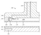
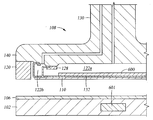
도 6은 본 명세서에 설명된 실시예들에 따라, 각각 RFID 태그 및 판독을 내부에 포함하는 연마 패드 및 플래튼의 개략적 부분 단면도를 도시한다.
도 7은 본 명세서에 설명된 실시예들에 따른 RFID 태그의 전기 컴포넌트 개략도를 도시한다.
도 8은 본 명세서에 설명된 실시예들에 따른 근거리 무선 통신 컴포넌트들을 포함하는 연마 헤드 리테이닝 링 및 플래튼의 부분 단면도를 도시한다.
도 9는 본 명세서에 설명된 실시예들에 따른 근거리 무선 통신 컴포넌트들을 포함하는 연마 헤드 멤브레인 및 플래튼의 부분 단면도를 도시한다.
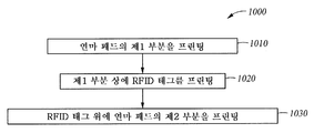
도 10은 본 명세서에 설명된 일 실시예에 따른 RFID 태그를 갖는 연마 패드를 제조하는 방법을 도시한다.
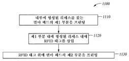
도 11은 본 명세서에 설명된 일 실시예에 따른 RFID 태그를 갖는 연마 패드를 제조하는 방법을 도시한다.
도 12는 본 명세서에 설명된 실시예들에 따른 연마 패드들을 제조하기 위한 장치의 개략적 단면도이다.
이해를 용이하게 하기 위해서, 가능한 경우에, 도면들에 공통인 동일한 요소들을 지시하는 데에 동일한 참조 번호들이 이용되었다. 일 실시예의 요소들 및 특징들은 추가 언급 없이도 다른 실시예들에 유익하게 통합될 수 있을 것으로 예상된다.In order that the features of the present disclosure discussed above may be understood in detail, a more particular description of the invention, briefly summarized above, may be had by reference to embodiments, some of which are illustrated in the accompanying drawings. It should be noted, however, that the appended drawings illustrate only exemplary embodiments and, therefore, should not be construed as limiting the scope of, and may permit, other embodiments of the same effect.
FIG. 1A shows a schematic cross-sectional view of a polishing apparatus according to embodiments described herein.
1B shows a more detailed cross-sectional view of the carrier head of the polishing apparatus of FIG. 1A according to the embodiments described herein.
2 is a schematic perspective sectional view of a polishing pad according to embodiments described herein.
3 is a schematic cross-sectional view of a polishing pad in accordance with the embodiments described herein.
4 is a schematic cross-sectional view of a polishing pad having at least one viewing window in accordance with the embodiments described herein.
5 is a schematic cross-sectional view of a polishing pad comprising a support layer in accordance with the embodiments described herein.
Figure 6 shows a schematic partial cross-sectional view of an abrasive pad and platen, each containing an RFID tag and a read, in accordance with the embodiments described herein.
7 shows a schematic diagram of the electrical components of an RFID tag according to the embodiments described herein.
8 illustrates a partial cross-sectional view of a polishing head retaining ring and platen including near field wireless communication components in accordance with the embodiments described herein.
Figure 9 illustrates a partial cross-sectional view of a polishing head membrane and platen including near field wireless communication components in accordance with the embodiments described herein.
10 illustrates a method of manufacturing a polishing pad with an RFID tag according to one embodiment described herein.
11 illustrates a method of manufacturing a polishing pad having an RFID tag according to one embodiment described herein.
12 is a schematic cross-sectional view of an apparatus for manufacturing polishing pads in accordance with the embodiments described herein.
To facilitate understanding, identical reference numerals have been used, where possible, to designate identical elements that are common to the figures. It is contemplated that the elements and features of one embodiment may be advantageously incorporated into other embodiments without further recitation.
본 개시내용의 실시예들은 일반적으로 CMP 장치, 및 CMP 장치를 제조하고 이용하는 방법들을 포함한다. CMP 장치는 다른 것들 중에서도 특히, 연마 패드들, 연마 헤드 리테이닝 링들, 및 연마 헤드 멤브레인들을 포함할 수 있고, CMP 장치는 3차원(3D) 프린팅 프로세스들 또는 2.5차원(2.5D) 프린팅 프로세스들과 같은 적층 제조 프로세스들(additive manufacturing processes)을 통해 제조될 수 있다. CMP 장치는 내부에 통합된 무선 주파수 식별부(radio frequency identification)(RFID) 또는 다른 컴포넌트들과 같은 무선 통신 장치를 포함할 수 있다. CMP 장치를 제조하는 방법들은 RFID 태그를 연마 패드 내에 또는 연마 패드 상에 3D 프린팅하는 단계, 및 RFID 태그를 수용하도록 구성된 리세스를 갖는 연마 패드를 프린팅하는 단계를 포함할 수 있다.Embodiments of the present disclosure generally include CMP apparatus, and methods of making and using a CMP apparatus. The CMP apparatus may include, among other things, polishing pads, polishing head retaining rings, and polishing head membranes, and the CMP apparatus may include three dimensional (3D) printing processes or 2.5 dimensional (2.5D) Can be manufactured through the same additive manufacturing processes. The CMP device may include a wireless communication device, such as radio frequency identification (RFID) or other components integrated therein. The methods of manufacturing the CMP apparatus may include 3D printing of the RFID tag in a polishing pad or on a polishing pad, and printing of a polishing pad having a recess configured to receive the RFID tag.
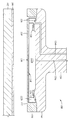
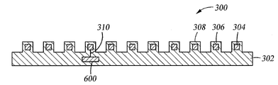
도 1a는 본 명세서에 설명된 실시예들에 따른 연마 장치(100)의 개략적 단면도를 도시한다. 연마 장치(100)는 기판 연마를 수행하기 위해 연마 시스템 내에서 이용될 수 있다. 연마 스테이션(100)은 중심 축(104)에 대해 회전할 수 있는 플래튼(102)을 포함한다. 플래튼(102)은 일반적으로 원 형상이지만, 다른 형상들이 유리하게 이용될 수 있음이 예상된다. 연마 패드(106)는 플래튼(102)에 결합될 수 있다. 플래튼(102)에 결합된 단일 연마 패드(106)로서 도시되어 있지만, 요구되는 연마 특성들에 따라, 복수의 연마 패드가 또한 플래튼에 결합될 수 있음이 예상된다. 연마 패드(106)는 본 개시내용의 실시예들에 따라, 단일 재료 층 바디(mono-material layer body) 또는 복합 재료 바디(composite material body)를 포함할 수 있다. 연마 패드(106)는 기판들에 접촉하고 기판으로부터 적어도 일부 재료를 제거함으로써 기판들을 처리하도록 구성된 연마 표면(112)을 포함한다. 플래튼(102)은 연마 동안 연마 패드(106)를 지지하고 연마 패드(106)를 회전시킨다. IA shows a schematic cross-sectional view of an
캐리어 헤드(108)는 처리 중인 기판(110)을 연마 패드(106)의 연마 표면(112)에 맞닿아 고정시키고 유지할 수 있다. 캐리어 헤드(108)는 중심 축(114)에 대해 회전할 수 있고/있거나 기판(110)과 연마 패드(106) 사이의 상대적인 움직임을 발생시키기 위해 스위핑 모션(sweeping motion)으로 이동할 수 있다. 연마 동안, 연마 슬러리와 같은 연마 유체(116)는 전달 암(118)에 의해 연마 표면(112)에 공급될 수 있다. 연마 액체(116)는 기판(110)의 화학적 기계적 연마를 가능하게 하기 위해, 연마 입자들, pH 조절자, 및/또는 화학적으로 활성인 성분들을 포함할 수 있다.The
하나 이상의 무선 통신 장치(600)가 연마 패드(106) 내에 배치되거나 연마 패드에 다르게 결합될 수 있다. 하나 이상의 인터로게이터(601)가 플래튼(102) 내에 배치될 수 있거나 플래튼에 다르게 결합될 수 있다. 무선 통신 장치(600) 및 인터로게이터(601)는 통신 링크(607)를 통해 통신하도록 구성된다. 일 실시예에서, 통신 링크(607)는 무선 통신 프로토콜일 수 있다. 다른 실시예에서, 통신 링크(607)는 유선 접속일 수 있다. 인터로게이터는 인터로게이터(601)를 통해 무선 통신 장치(600)로부터의 입력을 수신할 수 있는 제어기(612)에 통신 결합된다. 무선 통신 장치(600), 인터로게이터(601), 및 제어기는 도 6을 참조하여 더 상세하게 논의된다.One or more
일반적으로, 무선 통신 장치(600)는 다양한 처리 파라미터들 및 시스템 컴포넌트들을 감지하도록 구성된다. 무선 통신 장치(600)는 연마 패드(106) 내의 다양한 위치들에 위치될 수 있고, 전체 연마 표면(112)에 걸쳐서 개선된 데이터 수집을 제공할 수 있고, 이는 연마 프로세스의 제어를 개선하기 위해 제어기(612)에 의해 분석될 수 있다. 무선 통신 장치(600)를 통해 수집되는 데이터는 실시간 프로세스 제어를 위해, 및/또는 다른 시스템 컴포넌트들 중에서도 특히, 적합한 리테이닝 링(120) 또는 가요성 멤브레인(도시되지 않음)과 같은 호환가능한 시스템 컴포넌트들의 이용을 보장하기 위해 이용될 수 있다. 이러한 실시예들에서, 다른 적합한 시스템 컴포넌트들은 또한 인터로게이터(601)와 통신하기 위해 무선 통신 장치를 이용할 수 있다.In general, the
도 1b는 본 명세서에 설명된 실시예들에 따른 도 1a의 연마 장치(100)의 캐리어 헤드(108)의 더 상세한 단면도를 도시한다. 위에서 설명된 바와 같이, 캐리어 헤드(108)는 연마 또는 다른 처리 동안 기판(110)을 유지하도록 구성된다. 캐리어 헤드(108)는 기판(110)을 회전가능한 플래튼(102)에 의해 지지되는 연마 패드(106)에 맞닿게 유지할 수 있고, 기판(110)의 후면 표면(136)에 걸쳐 연마 패드(106)를 향해 압력을 분산시킨다.FIG. 1B illustrates a more detailed cross-sectional view of the
캐리어 헤드들(108)은 베이스 어셈블리(140)[회전가능한 드라이브 샤프트(130)에 직접적으로 또는 간접적으로 결합될 수 있음], 리테이닝 링(120), 및 가요성 멤브레인(132)을 포함한다. 가요성 멤브레인(132)은 베이스 어셈블리(140) 아래에 연장되고 베이스 어셈블리에 결합되어, 비원형(non-circular) 내측 챔버(122a) 및 인접한 외측 챔버(122b)를 포함하는 복수의 가압가능한 챔버를 제공한다. 챔버들(122a 및 122b)을 각각 연마 장치(100) 내의 압력 조절기들에 유체 결합하기 위해, 베이스 어셈블리(140)를 통해 통로들(124a 및 124b)이 형성된다. 도 1b는 2개의 가압가능한 챔버를 도시하지만, 캐리어 헤드(108)는 임의의 개수의 챔버들, 예를 들어, 3개, 4개, 5개, 또는 그보다 많은 챔버를 가질 수 있다.The carrier heads 108 include a base assembly 140 (which may be coupled directly or indirectly to the rotatable drive shaft 130), a retaining
도시되지는 않지만, 캐리어 헤드(108)는 드라이브 샤프트(130)에 고정가능하고 그로부터 베이스 어셈블리(140)가 이동가능하게 매달려지는 하우징, 베이스 어셈블리(140)가 피벗하는 것을 허용하는 짐벌 메커니즘(gimbal mechanism)[베이스 어셈블리(140)의 일부로서 고려될 수 있음], 베이스 어셈블리(140)와 하우징 사이의 로딩 챔버, 챔버들(122a 및 122b) 내부의 하나 이상의 지지 구조물, 또는 기판(110)에 보충 압력을 인가하기 위해 가요성 멤브레인(132)의 내측 표면에 접촉하는 하나 이상의 내부 멤브레인과 같은 다른 요소들을 포함할 수 있다. Although not shown, the
가요성 멤브레인(132)은 소수성일 수 있고, 내구성이 있을 수 있으며, 연마 프로세스에 관련하여 화학적으로 불활성일 수 있다. 가요성 멤브레인(132)은 기판(110)의 후면 표면(136)에 접촉하도록 구성되는 장착 부분(138)을 포함할 수 있다. 하나 이상의 플랩(flaps)(134)은 장착 부분(138)을 클램프 링들(126, 128)을 통해 베이스 어셈블리(140)에 결합할 수 있다. 하나 이상의 플랩(134)은 기판(110)에 걸친 면적 압력 제어(areal pressure control)를 제공하기 위해, 챔버들(122a, 122b)을 분할할 수 있다. The
리테이닝 링(120)은 가요성 멤브레인(132)의 방사상 외측에서 베이스 어셈블리(140)에 결합될 수 있다. 일반적으로, 리테이닝 링(120)은 가요성 멤브레인(132)에 대한 기판(110)의 과도한 이동을 방지하고, 기판(110)의 횡방향 이동을 방지하도록 구성된다. 리테이닝 링은 연마 프로세스에서 이용되는 화학적 조성들에 불활성인 재료들로 이루어질 수 있다. 리테이닝 링(120)은 요구되는 응용들에 따라, 폴리머들, 세라믹들, 및 금속들과 같은 적합한 재료들로 이루어질 수 있음이 예상된다. The retaining
진보된 패드 구성들 및 설계 예들Advanced Pad Configurations and Design Examples
도 2는 본 명세서에 설명된 실시예들에 따른 연마 패드(200)의 개략적인 사시 단면도이다. 연마 패드(200)는 화학적 기계적 연마에 의해 반도체 기판들을 연마하기 위해, 연마 스테이션(100)과 같은 연마 스테이션들에서 이용될 수 있다. 다른 산업계들은 본 명세서에 설명된 실시예들에 따른 연마 패드들을 이용하여 유리하게 처리될 수 있는 다른 타입들의 기판들을 이용할 수 있음이 예상된다. 예를 들어, 광학 산업계들은 본 명세서에 설명된 패드들 및 다른 연관 장치를 이용하여 다양한 렌즈들 또는 거울들을 연마할 수 있다. 2 is a schematic perspective cross-sectional view of a
도시된 실시예에서, 연마 패드(200)는 복합 패드 바디(composite pad body)(202)를 포함한다. 도시되지는 않았지만, 연마 패드 바디(202)는 복수의 재료를 대신하여 단일 재료로 형성될 수 있음이 예상된다. 복합 패드 바디(202)는 하나 이상의 제1 피처(204) 및 하나 이상의 제2 피처(206)를 포함한다. 제1 피처들(204) 및 제2 피처들(206)은 그 경계들에서 함께 접합되어(joined) 복합 패드 바디(202)를 형성하는 개별 피처들이다. 일 실시예에서, 제1 피처들(204)은 약 40 쇼어 D 스테일(Shore D scale) 내지 약 90 쇼어 D 스케일의 경도(hardness)를 가질 수 있다. 제2 피처들(206)은 약 26 쇼어 A 스케일 내지 약 95 쇼어 A 스케일의 경도 값을 가질 수 있다.In the illustrated embodiment, the
복합 패드 바디(202)는 적층 제조(예를 들어, 3D 프린팅 또는 2.5D 프린팅), 또는 주조 또는 성형 기술들과 같은 다른 적합한 기술들에 의해 형성될 수 있다. 복합 패드 바디(202)는 복수의 층을 포함할 수 있고, 각각의 층은 복합 패드 바디(202)의 설계에 따라 제2 피처들(206)의 영역들 및/또는 제1 피처들(204)의 영역들을 포함할 수 있다. 일 실시예에서, 제1 피처들(204) 및/또는 제2 피처들(206)을 포함하는 각각의 영역은 3D 프린터에 의해 동시적 또는 순차적 프린팅 프로세스로 퇴적될 수 있다. 다음으로, 복수의 층은 예를 들어 UV 광에 의해, 또는 열원에 의해 경화되어, 고체화되고 목표 경도를 달성할 수 있다. 퇴적 및 경화 후에, 함께 결합 또는 접합된 제1 피처들(204) 및 제2 피처들(206)을 포함하는 단일체 복합 패드 바디(202)가 형성된다. 비-복합 연마 패드들에 관한 실시예들에서, 경화 프로세스는 필요할 수도 있고 필요하지 않을 수도 있다. The
목표 연마 프로세스를 달성하기 위해, 제2 피처들(206) 및 제1 피처들(204)에 대해 상이한 기계적 속성들을 갖는 재료들이 선택될 수 있다. 제2 피처들(206) 및 제1 피처들(204)의 동적 기계적 속성들은 피처 형성 프로세스 동안 사용되는 상이한 경화 프로세스들을 고르고/거나 상이한 재료들을 선택하는 것에 의해 달성될 수 있다. 일 실시예에서, 제2 피처들(206)은 낮은 경도 값 및 낮은 값의 탄성률(elastic modulus)을 가질 수 있는 한편, 제1 피처들(204)은 높은 경도 값 및 높은 값의 탄성률을 가질 수 있다. 다른 실시예에서, 탄성률(또는 저장 탄성률) 및 손실 탄성률과 같은 동적 기계적 속성들은 각각의 피처 내에서, 및/또는 연마 패드(200)의 연마 표면 내의 또는 연마 표면에 걸친 제2 피처들(206) 및 제1 피처들(204)의 물리적 레이아웃, 패턴, 또는 조합에 의해 조절되거나 제어될 수 있다.To achieve the target polishing process, materials having different mechanical properties for the
제1 피처들(204)은 하나 이상의 폴리머 재료로 형성될 수 있다. 제1 피처들(204)을 형성하기 위해 이용되는 재료(들)는 목표 기계적, 표면, 화학적, 또는 열적 속성들을 달성하기 위해 단일 폴리머 재료, 또는 2개 이상의 폴리머의 혼합물을 포함할 수 있다. 일 실시예에서, 제1 피처들(204)은 하나 이상의 열가소성 폴리머로 형성될 수 있다. 제1 피처들(204)은 열가소성 폴리머들, 예컨대 폴리우레탄, 폴리프로필렌, 폴리스티렌, 폴리아크릴로니트릴, 폴리메틸 메타크릴레이트, 폴리클로로트리플루오로에틸렌(polychlorotrifluoroethylene), 폴리테트라플루오로에틸렌(polytetrafluoroethylene), 폴리옥시메틸렌, 폴리카보네이트, 폴리이미드, 폴리에테르에테르케톤(polyetheretherketone), 폴리페닐린 설파이드, 폴리에테르 설폰, 아크릴로니트릴 부타디엔 스티렌(ABS: acrylonitrile butadiene styrene), 폴리에테르이미드, 폴리아미드들, 멜라민들, 폴리에스테르들, 폴리설폰들, 폴리비닐 아세테이트들, 불화계 탄화수소들 및 그와 유사한 것, 및 이들의 아크릴레이트들, 코폴리머들, 그래프트들(grafts) 및 혼합물들로 형성될 수 있다. 일 실시예에서, 제1 피처들(204)은 아크릴레이트들로 형성될 수 있다. 예를 들어, 제1 피처들(204)은 폴리우레탄 아크릴레이트, 폴리에테르 아크릴레이트, 또는 폴리에스테르 아크릴레이트일 수 있다. 다른 실시예에서, 제1 피처들(204)은 하나 이상의 열경화성 폴리머(thermosetting polymers), 예컨대 에폭시들, 페놀수지들(phenolics), 아민들(amines), 폴리에스테르들, 우레탄들, 실리콘, 및 이들의 아크릴레이트들, 혼합물들, 코폴리머들 및 그래프트들을 포함할 수 있다. The first features 204 may be formed of one or more polymeric materials. The material (s) used to form the
일 실시예에서, 제1 피처들(204)은 시뮬레이팅 플라스틱 3D 프린팅 재료로 형성될 수 있다. 다른 실시예에서, 제1 피처들(204)은 단일 폴리머 또는 폴리머들의 조합일 수 있는 폴리머 재료, 또는 열가소성 폴리머와 같은 열가소성 재료로 형성될 수 있다. 일 실시예에서, 연마 입자들은 연마 프로세스를 증강시키기 위해 제1 피처들(204) 내에 매립될 수 있다. 연마 입자들을 포함하는 재료는 금속 산화물, 예컨대 세리아, 알루미나, 실리카, 또는 이들의 조합, 폴리머, 합금(inter-metallic) 또는 세라믹일 수 있다.In one embodiment, the
제2 피처들(206)을 형성하기 위해 이용되는 재료(들)는 하나 이상의 폴리머 재료를 포함할 수 있다. 제2 피처들(206)은 목표 속성들을 달성하기 위해 단일 폴리머 재료, 또는 2개 이상의 폴리머의 혼합물로 형성될 수 있다. 일 실시예에서, 제2 피처들(206)은 하나 이상의 열가소성 폴리머로 형성될 수 있다. 예를 들어, 제2 피처들(206)은 열가소성 폴리머들, 예컨대 폴리우레탄, 폴리프로필렌, 폴리스티렌, 폴리아크릴로니트릴, 폴리메틸 메타크릴레이트, 폴리클로로트리플루오로에틸렌, 폴리테트라플루오로에틸렌, 폴리옥시메틸렌, 폴리카보네이트, 폴리이미드, 폴리에테르에테르케톤, 폴리페닐린 설파이드, 폴리에테르 설폰, 아크릴로니트릴 부타디엔 스티렌(ABS), 폴리에테르이미드, 폴리아미드들, 멜라민들, 폴리에스테르들, 폴리설폰들, 폴리비닐 아세테이트들, 불화계 탄화수소들 및 그와 유사한 것, 및 이들의 아크릴레이트들, 코폴리머들, 그래프트들 및 혼합물들로 형성될 수 있다. 일 실시예에서, 제2 피처들(206)은 아크릴레이트들로 형성될 수 있다. 예를 들어, 제2 피처들(206)은 폴리우레탄 아크릴레이트, 폴리에테르 아크릴레이트, 또는 폴리에스테르 아크릴레이트일 수 있다. 다른 실시예에서, 제2 피처들(206)은 열가소성 엘라스토머들로 형성될 수 있다. 일 실시예에서, 제2 피처들(206)은 고무 유사(rubber-like) 3D 프린팅 재료로 형성될 수 있다. The material (s) used to form the
일부 실시예들에서, 제1 피처들(204)은 제2 피처들(206)에 비해 더 경성이고 더 강건한 한편, 제2 피처들(206)은 제1 피처들(204)에 비해 더 연성이고 더 가요성이다. 제1 피처들(204) 및 제2 피처들(206)의 재료들 및 패턴들은 연마 패드(200)의 "조정된(tuned)" 벌크 재료를 달성하도록 선택될 수 있다. 이러한 "조정된" 벌크 재료로 형성된 연마 패드(200)는 개선된 연마 결과들, 감소된 제조 비용, 연장된 패드 수명과 같은 다양한 이점들을 갖는다. 일 실시예에서, "조정된" 벌크 재료 또는 전체로서의 연마 패드는 약 65 쇼어 A 내지 약 75 쇼어 D의 경도를 가질 수 있다. 연마 패드의 인장 강도(tensile strength)는 5MPa 내지 약 75MPa일 수 있다. 연마 패드는 약 5% 내지 약 350%의 파단신율(elongation to break)을 가질 수 있다. 연마 패드는 약 10MPa을 초과하는 전단 강도(shear strength)를 가질 수 있다. 연마 패드는 약 5MPa 내지 약 2000MPa의 저장 탄성률을 가질 수 있다. 연마 패드는 약 25℃ 내지 약 90℃의 온도 범위에 대해 안정적인 저장 탄성률을 가질 수 있고, 그에 의해 E30/E90에서의 저장 탄성률 비율은 약 6 내지 약 30의 범위 내에 포함되게 되고, 여기서 E30은 30℃에서의 저장 탄성률이고 E90은 90℃에서의 저장 탄성률이다. In some embodiments, the
일 실시예에서, 제1 피처들(204) 및 제2 피처들(206)의 재료들은 연마 슬러리로부터의 공격에 대한 화학적 저항성을 갖는다. 다른 실시예에서, 제1 피처들(204) 및 제2 피처들(206)의 재료들은 친수성이다.In one embodiment, the materials of the
일반적으로, 제1 피처들(204) 및 제2 피처들(206)은 원형의 복합 패드 바디(202)를 형성하도록 교대로 배열된, 교대하는 동심 링들일 수 있다. 다른 실시예들에서, 제1 피처들(206) 및 제2 피처들(106)은 바디(202)로부터 교대하는 또는 다른 적합한 배열로 연장되는 개별 포스트들일 수 있다. 다양한 다른 연마 패드 표면 설계들은 또한 본 명세서에 설명된 실시예들과 함께 유리하게 이용될 수 있음이 예상된다. 일 실시예에서, 제1 피처들(204)의 상부 표면들(208)이 제2 피처들(206)로부터 돌출되도록, 제1 피처들(204)의 높이(210)는 제2 피처들(206)의 높이(212)보다 높다. 제1 피처들(204)과 제2 피처들(206) 사이에 홈들(218) 또는 채널들이 형성된다. 연마 동안, 제1 피처들(204)의 상부 표면들(208)은 기판에 접촉하는 연마 표면을 형성하는 한편, 홈들(218)은 연마 유체를 보유한다. 일 실시예에서, 제1 피처들(204)은 복합 패드 바디(202)에 평행한 평면에 수직한 방향에서 제2 피처들(206)의 두께보다 큰 두께로 형성되고, 그에 의해 홈들(218) 및/또는 채널들은 복합 패드 바디(202)의 최상부면 상에 형성된다. In general, the
일 실시예에서, 제1 피처들(204)의 폭(214)은 약 250 미크론 내지 약 2 밀리미터일 수 있다. 제1 피처들(204) 사이의 피치(216)는 약 0.5 밀리미터 내지 약 5 밀리미터일 수 있다. 각각의 제1 피처(204)는 약 250 미크론 내지 약 2 밀리미터 범위 내의 폭(214)을 가질 수 있다. 폭(214) 및/또는 피치(216)는 다양한 경도의 구역들에 대해 연마 패드(200)의 반경에 걸쳐서 달라질 수 있다.In one embodiment, the
전통적인 연마 패드들과 비교하여, 본 개시내용의 복합 연마 패드(200)는 수 개의 이점을 갖는다. 전통적인 연마 패드들은 기판들을 연마하기 위한 목표 경도 또는 탄성률을 획득하기 위해, 기포(foam)와 같은 연성 재료로 형성된 서브패드에 의해 지지되는 연마 재료들 및/또는 텍스처화된 연마 표면을 갖는 연마 층을 일반적으로 포함한다. 포아송 비, 탄성률, 및 손실 탄성률과 같은 다양한 기계적 속성들을 갖는 재료들을 선택하고, 피처들의 치수들 및 간격을 조절하거나 상이한 피처들의 배열을 변경함으로써, 바람직한 경도, 동적 속성들, 및/또는 기계적 속성들이 서브패드를 이용하지 않고서 복합 패드 바디(202) 내에서 달성될 수 있다. 그러므로, 연마 패드(200)는 서브패드들을 제거함으로써 소유 비용을 감소시킨다. 추가로, 연마 패드(200)의 경도 및 연마도(abrasiveness)는 상이한 경도 및 연마도를 갖는 피처들을 혼합함으로써 조정될 수 있고, 그에 의해 연마 성능이 개선된다. Compared to conventional polishing pads, the
본 개시내용에 따른 복합 연마 패드들은 패턴 편차 및/또는 피처 크기 편차를 조절함으로써, 제1 피처들(204)과 같은 표면 피처들, 및 제2 피처들(206)과 같은 베이스 재료들에 걸쳐 탄성률(영률) 및 손실 탄성률과 같은 다양한 기계적 속성들을 가질 수 있다. 목표 속성들을 달성하기 위해, 연마 패드들에 걸친 기계적 속성들은 대칭 또는 비대칭, 균일 또는 불균일할 수 있다. 표면 피처들의 패턴은 연마 패드에 걸쳐 탄성률 및 손실 탄성률과 같은 미리 결정된 기계적 속성들과 같은 목표 속성을 달성하기 위해, 방사상, 동심상, 직사각형, 또는 무작위일 수 있다. 일부 실시예에서, 제1 피처들 및 제2 피처들은 복합 연마 패드의 강도를 개선하고 복합 연마 패드의 물리적 완결성을 개선하기 위해 연동될 수 있다. 제1 피처들 및 제2 피처들의 연동은 연마 패드의 전단 강도, 압축 강도 및/또는 인장 강도를 증가시킬 수 있다. The composite abrasive pads according to the present disclosure may be used to control surface characteristics, such as
3D 프린팅과 같은 적층 제조 프로세스들은 연마 패드 내에 다양한 감지 장치를 통합시킬 때 이점들을 제공할 수 있다. RFID 태그들 및 계측 센서들과 같은 감지 장치는 이하에서 도 6 및 도 7에 관련하여 더 상세하게 논의될 것이다.Lamination manufacturing processes such as 3D printing can provide advantages when incorporating various sensing devices within the polishing pad. Sensing devices such as RFID tags and metrology sensors will be discussed in more detail below with respect to Figures 6 and 7.
도 3은 본 명세서에 설명된 실시예들에 따른 연마 패드(300)의 개략적인 단면도이다. 연마 패드(300)는 연마 패드(200)의 제2 피처들(206)의 실시예와 유사한, 연성이며 탄성을 갖는 베이스 층(302)을 포함한다. 제2 피처들(206)과 마찬가지로, 베이스 층(302)은 하나 이상의 엘라스토머 폴리머로 형성될 수 있다. 연마 패드(300)는 베이스 층(302)으로부터 연장되는 복수의 표면 피처(306)를 포함한다. 표면 피처들(306)의 외측 표면들(308)은 연성 재료 또는 연성 재료들의 조성물로 형성될 수 있다. 일 실시예에서, 표면 피처들(306)의 외측 표면(308)은 베이스 층(302)과 동일한 재료 또는 동일한 재료 조성물로 형성될 수 있다. 표면 피처들(306)은 내부에 매립된 제1 피처(304)를 또한 포함할 수 있다. 제1 피처들(304)은 표면 피처들(306)보다 경성인 재료 또는 재료 조성물로 형성될 수 있다. 제1 피처들(304)은 연마 패드(200)의 제1 피처들(204)의 재료 또는 재료들과 유사한 재료들로 형성될 수 있다. 매립된 제1 피처들(304)은 표면 피처들(306)의 유효 기계적 속성들을 변경하고, 따라서 연마를 위해 바람직한 기계적 및/또는 동적 속성들을 갖는 패드를 제공할 수 있다. 외측 표면(308)의 연성 폴리머 층은 연마 중인 기판 상에서 결함들을 감소시키고 평탄화를 개선하기 위해 이용될 수 있다. 대안적으로, 연성 폴리머 재료는 본 개시내용의 연마 패드들을 포함하는 다른 더 경성의 재료의 표면들 상에 프린팅되어 유사한 이점들을 제공할 수 있다.3 is a schematic cross-sectional view of a
연마 패드(300)는 또한 내부에 배치된 무선 통신 장치(600)를 포함할 수 있다. 제1 피처들(304)에 의해 제공되는 기계적 속성들에 더하여, 제1 피처들(304)은 또한 무선 통신 장치(600)에 결합될 수 있고, 그에 의해 소정 형태의 전기적 데이터(예를 들어, 용량, 저항 등)가 무선 통신 장치(600) 내의 컴포넌트들에 의해 수집될 수 있다. 제1 피처들(304)은 연마 패드 제조 프로세스 동안 프린팅될 수 있는 와이어(310) 또는 그와 유사한 것을 통해 무선 통신 장치(600)에 결합될 수 있다. 일 실시예에서, 와이어(310)는 연마 패드(300)를 프린팅하기 위해 이용되는 재료들과 호환가능한 하나 이상의 전도체 재료로 프린팅될 수 있다. The
일 실시예에서, 제1 피처들(304)은 마모 표시자(wear indicator)로서 기능하는 전도체 요소들을 포함할 수 있다. 일부 실시예들에서, 연마 동안, 표면 피처들(306)은 결국에는 마모되어 버릴 수 있고, 제1 피처들(304)을 노출시킬 수 있다. 표면 피처들(306)이 제거되고 제1 피처들(304)이 노출될 때, 무선 통신 장치(600)에 의해 수신되는 다양한 신호들(음향, 전기, 압력 등)이 개시될 수 있다. 제1 피처들(304)의 노출에 응답한 신호의 변화 및/또는 생성은, 무선 통신 장치(600)가 인터로게이터(601)(도시되지 않음)와 통신하고 처리 데이터를 제어기(612)에 제공하게 할 수 있다. 따라서, 처리 시스템의 운영자들은 사용량 및 연마 파라미터들에 관한 실시간 데이터를 수신할 수 있다. 일 실시예에서, 제1 피처들(304)의 노출은 연마 패드 마모를 나타낼 수 있고, 기판들의 적절한 연마를 보장하도록 연마 패드(300)가 교체될 수 있다. In one embodiment, the
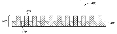
도 4는 본 명세서에 설명된 실시예들에 따른, 내부에 형성된 하나 이상의 관측 윈도우(410)를 갖는 연마 패드(400)의 개략적 단면도이다. 연마 패드(400)는 연마 패드(200)와 유사한 패드 바디(402)를 가질 수 있다. 패드 바디(402)는 하나 이상의 제2 피처(406), 및 연마를 위해 제2 피처들(406)로부터 연장되는 복수의 제1 피처(404)를 포함할 수 있다. 제2 피처들(406) 및 제1 피처들(404)은 연마 패드(200)의 제2 피처들(206) 및 제1 피처들(204)과 유사한 재료들로 형성될 수 있다. 제1 피처들(404)은 본 개시내용에 따른 임의의 적합한 패턴들로 배열될 수 있다.4 is a schematic cross-sectional view of an
연마 동안 기판의 관측을 허용하기 위해, 연마 패드(400)는 또한 투명 재료로 형성될 수 있는 하나 이상의 관측 윈도우(410)를 포함한다. 관측 윈도우들(410)은 제2 피처(406) 또는 제1 피처들(404)을 통해, 및/또는 제2 피처(406) 또는 제1 피처들(404)의 일부분들에 인접하여 형성될 수 있다. 제1 피처들(402) 및 제2 피처들(406)이 적층 제조 프로세스들을 이용하여 형성되고 있는 동안, 관측 윈도우(410)가 형성될 수 있다. 일부 실시예들에서, 관측 윈도우(410)는 실질적으로 투명한 재료로 형성될 수 있고, 따라서 CMP 광학 종료점 검출 시스템에서 사용하기 위한 레이저 및/또는 백색 광원으로부터 방출되는 광을 투과시킬 수 있다. 일 실시예에서, 관측 윈도우(410)는 투명한 3D 프린팅 포토폴리머로 형성될 수 있다. 예를 들어, 관측 윈도우(410)는 폴리메틸메타크릴레이트(PMMA)로 형성될 수 있다. 일부 실시예들에서, 공기/윈도우/물 계면으로부터의 반사를 감소시키고, 관측 윈도우(410)를 통한 기판으로의 광의 투과, 및 관측 윈도우를 통한 기판으로부터의 광의 투과를 개선하기 위해, 관측 윈도우(410)는 연마 슬러리에 대한 것인 낮은 굴절률을 가지며 높은 광학적 투명도를 갖는 재료로 형성된다. 재료의 광학적 투명도(optical clarity)는 종료점 검출 시스템의 광학 검출기에 의해 이용되는 광 빔의 파장 범위에 걸쳐서 적어도 약 25%(예를 들어, 적어도 약 50%, 적어도 약 80%, 적어도 약 90%, 적어도 약 95%)의 광 투과를 제공하도록 선택된다. 전형적인 광학 종료점 검출 파장 범위들은 가시 스펙트럼(예를 들어 약 400nm 내지 약 800nm), 자외선(UV) 스펙트럼(예를 들어, 약 300nm 내지 약 400nm), 및/또는 적외선 스펙트럼(예를 들어, 약 800nm 내지 약 1550nm)을 포함한다. To permit observation of the substrate during polishing, the
도 5는 후면 층(backing layer)(506)을 포함하는 연마 패드(500)의 개략적 사시 단면도이다. 연마 패드(500)는 베이스 재료 층(504), 및 베이스 재료 층(504)으로부터 돌출되는 복수의 표면 피처(502)를 포함한다. 연마 패드(500)는 베이스 재료 층(504)에 부착된 후면 층(506)을 갖는다는 점을 제외하고는 위에서 설명된 연마 패드들(200, 300, 400)과 유사할 수 있다. 후면 층(506)은 연마 패드(500)에 요구되는 압축성을 제공할 수 있다. 후면 층(506)은 또한 요구되는 경도를 달성하고/하거나 요구되는 동적 재료 속성들(예를 들어, 탄성률 및 손실 탄성률)을 갖도록 연마 패드(500)의 전체적인 기계적 속성들을 변경하기 위해 이용될 수 있다. 후면 층(506)은 80 미만의 쇼어 A 스케일의 경도 값을 가질 수 있다.FIG. 5 is a schematic perspective cross-sectional view of a
일 실시예에서, 후면 층(506)은 압력이 가해질 때 셀들/공극들이 붕괴되고 후면 층(506)이 예측가능한 방식으로 압축되도록, 공극들을 갖는 폴리실리콘 또는 폴리우레탄과 같은 연속 또는 독립 기포(an open-cell or a closed-cell foam)로 형성될 수 있다. 다른 실시예에서, 후면 층(506)은 다른 것들 중에서도 특히, 천연 고무, 에틸렌 프로필렌 디엔 모노머(ethylene propylene diene monomer, EPDM) 고무, 니트릴, 또는 폴리클로로프렌(네오프렌)으로 형성될 수 있다. In one embodiment, the
일 실시예에서, 후면 층(506)은 3D 프린팅 프로세스와 같은 적층 제조 프로세스를 이용하여 형성될 수 있다. 이러한 구성에서, 후면 층(506)은 바람직한 기계적 및 동적 재료 속성들을 달성하기 위해, 단일 폴리머 재료, 또는 2개 이상의 폴리머의 혼합물로 형성될 수 있다. 일 구성에서, 표면 피처들(502) 및 베이스 재료 층(504)은 후면 층(506) 상에 직접 형성된다. 일 실시예에서, 후면 층(506)은 하나 이상의 열가소성 폴리머로 형성될 수 있고, 따라서 제1 피처(204) 및/또는 제2 피처(206)와 관련하여 위에서 설명된 재료들 중 하나 이상을 포함할 수 있다.In one embodiment, the
특정 실시예들에서, 무선 통신 장치(600)는 연마 패드(500) 내에 배치되거나 연마 패드에 결합될 수 있다. 일 실시예에서, 무선 통신 장치(600)는 베이스 재료 층(504) 또는 표면 피처들(502) 내에 배치될 수 있다. 도시된 실시예에서, 무선 통신 장치(600)는 후면 층(506) 내에 배치될 수 있다. 무선 통신 장치(600)의 위치에 무관하게, 무선 통신 장치(600)는 복수의 표면 피처(502)에 걸쳐 하나 이상의 처리 파라미터를 감지하기 위한 크기를 가질 수 있다. 예를 들어, 2개 이상의 표면 피처(502)가 무선 통신 장치(600)에 의해 동시에 감지될 수 있다. 결과적으로, 단일 표면 피처(502)를 감지하는 대신에, 연마 표면의 더 큰 영역에 걸쳐서 다양한 처리 파라미터들(온도, 압력, 전도율 등)이 감지될 수 있다. 연마 표면의 더 큰 영역을 감지함으로써, 영역적으로 평균화된 신호(regionally averaged signal)가 무선 통신 장치(600)에 의해 검출될 수 있다. 복수의 무선 통신 장치(600)를 이용하는 실시예들에서는, 개별적인 무선 통신 장치(600)로부터의 데이터를 조합함으로써 더 전역적으로 평균화된 신호가 결정될 수 있다. In certain embodiments, the
정보 수집 시스템 구성 예들Examples of Information Collection System
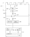
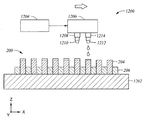
도 6은 본 명세서에 설명된 실시예들에 따라, 무선 통신 장치(600) 및 인터로게이터(601)를 각각 내부에 포함하는 연마 패드(200) 및 플래튼(102)의 부분적인 개략적 단면도를 도시한다. 연마 패드(200)는 통합된 감지 또는 계측 장치를 내부에 포함하도록 구성된 임의의 연마 패드를 표현하도록 의도된다. 예를 들어, 연마 패드는 내부에 배치된 무선 통신 장치(600)와 함께 프린팅되거나 주조되거나 성형될 수 있다. 일 실시예에서, 무선 통신 장치(600)는 인터로게이터와 무선으로 통신하도록 구성된다. 무선 통신 프로토콜들의 예들은 근거리 무선 통신 기술들, Bluetooth®, 광학 신호 전송 기술들, 음향 신호 전송 기술들, 무선 주파수 통신 기술들, 및 다른 적합한 무선 통신 기술들을 포함한다. 대안적으로, 무선 통신 장치(600)는 인터로게이터(601)에 배선 연결되어(hardwired), 그들 사이의 통신을 용이하게 할 수 있다. 6 depicts a partial schematic cross-sectional view of a
도 6에는 단일의 무선 통신 장치(600)와 단일의 인터로게이터(601)가 도시되어 있지만, 패드들 및 플래튼들 내에서 각각 복수의 무선 통신 장치(600) 및 인터로게이터(601)가 구현될 수 있음이 예상된다(도 1 참조). 추가로, 하나 이상의 무선 통신 장치(600)가 단일의 인터로게이터(601)에 의해 감지될 수 있다. 또한, 무선 통신 장치(600)는 중심 위치(즉, 원형 패드의 원점 또는 회전 축 일치 점), 중간 위치(즉, 원형 패드의 원점으로부터의 반경의 1/2), 또는 외측 위치(즉, 원형 패드의 원주에 인접함)와 같은 다양한 위치들에서 패드(200)의 표면 내에 또는 표면 상에 위치될 수 있음이 예상된다. 또한, 복수의 NFC 장치(600)가 조합하여 이용될 수 있고, 다양한 위치들(즉, 중심 위치 및 외측 위치, 또는 중심, 중간 및 위측 위치들)이 함께 이용될 수 있다. 복수의 무선 통신 장치(600)를 서로 협력시켜 이용함으로써, 패드(200)에 걸친 복수의 위치들에서의 데이터 수집으로 인해, 처리 환경의 더 포괄적인 조망이 생성될 것이다. 일반적으로, 무선 통신 장치(600)는 처리 동안의 연마 시스템(100)의 연마 표면에 걸친 기판(110)의 경로가 연마 프로세스의 다양한 지점들 동안 중첩되도록, 패드(200)에 대해 위치된다.Although a single
마찬가지로, 인터로게이터(601)는 중심, 중간, 및 외측 위치와 같은 다양한 위치들에서 플래튼(102) 내에 위치될 수 있다. 인터로게이터의 위치는 무선 통신 장치(600)의 위치에 독립하여 결정될 수 있거나, 무선 통신 장치(600)와 인터로게이터(601) 사이의 통신을 용이하게 하기 위해, 적어도 부분적으로 무선 통신 장치의 위치에 의해 결정될 수 있다.Likewise, the
플래튼(102) 내에 배치된 인터로게이터(601)는 일반적으로 판독기(608) 및 안테나(610)를 포함한다. 판독기는 RF 전원과 같은 전원을 포함하거나 전원에 결합될 수 있고, 무선 통신 장치(600)에 의해 수신될 신호를 안테나(610)를 통해 송신하도록 구성될 수 있다. 일 실시예에서, 판독기(608)는 다른 장치들 중에서도, 판독기(608)에 의한 신호 전송 및 수신을 관리하도록 구성된 RF 변조기 및 인터로게이터 제어기를 포함할 수 있다. 일 실시예에서, RF 변조기는 약 13.56MHz의 파장을 갖는 RF 신호를 생성 및/또는 변조하도록 구성될 수 있다. 수동 태그 실시예에서, 인터로게이터(601) 및 무선 통신 장치(600)는 약 12인치 미만, 예를 들어 약 2인치 미만, 예컨대 약 1인치 미만의 거리를 갖는 공간 관계로 위치될 수 있다. 능동 태그 실시예에서, 인터로게이터(601)와 무선 통신 장치(600) 사이의 공간 관계는 수동 태그 실시예들보다 클 수 있고, 신호 전송을 위해 이용가능한 전력에 의존될 수 있다. The
무선 통신 장치(600)는 태그(602), 및 태그(602)에 결합되거나 태그 내에 일체로 제조되는 안테나(606)를 일반적으로 포함한다. 특정 실시예들에서, 센서(604)는 또한 태그(602)에 통신 결합될 수 있다. 태그(602)는 요구되는 구현에 따라 능동 태그 또는 수동 태그일 수 있다. 능동 태그 실시예에서, 배터리와 같은 전원이 태그에 전기 결합될 수 있고, 태그에 적합한 전력을 제공할 수 있으며, 따라서 태그는 디바이스들 사이에 형성된 통신 링크(607)를 통해 인터로게이터(601)에 신호를 송신할 수 있다. 능동 태그는 전력이 태그에 결합되는 실시예들에서 구현될 수 있음이 예상된다. 추가로, 능동 태그는 태그에 의해 전송되는 데이터가 수동 태그를 이용할 때 획득될 수 있는 것보다 더 먼 거리에서 인터로게이터(601)에 의해 감지되도록 의도되는 실시예들에서 이용될 수 있다. 그러나, 능동 태그는 수동 태그가 적합한 용도를 찾을 수 있는 근거리 무선 통신 실시예들에서 이용될 수 있음이 예상된다. The
수동 태그 실시예에서, 태그는 인터로게이터(601)로부터 무선 주파수 신호와 같은 신호를 수신하고, 태그(602)에 고유한 소정량의 데이터를 포함하는 신호를 통신 링크(607)를 통해 다시 인터로게이터(601)에 전송(또는 반사)하기 위해, 수신된 신호의 전자기 에너지를 이용하도록 구성될 수 있다. 수동 태그는 인터로게이터(601)가 태그(602)로부터 임계 통신 거리보다 적게 떨어져서 위치되는 실시예들에서 이용될 수 있다. 일반적으로, 임계 통신 거리는 그 거리를 넘어서면 수동 태그에 의해 반사되는 전자기 신호들이 인터로게이터(601)에 의해 신뢰가능하게 수신되지 않는 거리로서 정의된다. 임계 통신 거리는 인터로게이터(601)에 의해 생성되는 신호에 연관된 전력의 양, 및 태그 전송기의 크기 및 전력에 의존하여, 실시예들에 따라 달라질 수 있다. 수동 태그의 더 상세한 설명은 이하에서 도 7을 참조하여 논의된다. In the passive tag embodiment, the tag receives a signal, such as a radio frequency signal, from the
도 7은 본 명세서에 설명된 실시예들에 따른 무선 통신 장치(600)의 전기 컴포넌트 개략도를 도시한다. 도 7에 도시된 실시예는 기본 기능 태그를 표현하도록 의도되고, 따라서 태그의 요구되는 기능을 달성하기 위해 다양한 다른 전기 컴포넌트 설계들 또는 구성들이 구현될 수 있음이 예상된다. 태그(602)는 일반적으로 트랜지스터(702), 인덕터(704), 커패시터(706), 및 집적 회로(708)를 포함한다. 일 실시예에서, 집적 회로(708)는 태그(602)에 고유한 데이터를 저장하도록 구성된 메모리를 표현할 수 있다. 다른 실시예에서, 메모리는 데이터를 인터로게이터(601)에 전송하기 전에, 센서(604)에 의해 수신되는 데이터를 저장하도록 구성될 수 있다. 특정 실시예들에서, 유도 코일과 같은 인덕터(704)는 인터로게이터(601)와 인덕터(704) 사이에서 신호들을 수신 및 전송하기 위한 안테나로서 이용될 수 있다. 일 실시예에서, 인덕터(704)는 안테나(606)이고, 태그(602)로부터의 데이터를 포함하는 신호를 디바이스들 사이에 형성된 통신 링크를 통해 인터로게이터(601)에 유도 반사(inductively reflect)시키도록 기능한다.FIG. 7 illustrates a schematic electrical component of a
도 6을 다시 참조하면, 무선 통신 장치(600), 더 구체적으로는 태그(602)는 연마 패드(200) 내에서, 처리 동안 기판들에 접촉하는 패드(200)의 상부 표면(208) 아래에 위치될 수 있다. 일 실시예에서, 무선 통신 장치(600)는 상부 표면(208)보다 약 200㎛ 내지 약 500㎛ 아래의 거리(620)에 위치된다. 거리(620)는 태그(602) 및/또는 센서(604)에 의해 수행되는 감지의 요구되는 타입, 및 패드(200)의 표면의 토포그래피(예를 들어, 홈들, 채널들, 또는 다른 피처들)에 기초하여 선택될 수 있다. 다른 실시예에서, 태그(602)는 최상부면(208) 아래에서 거리(620)에 위치될 수 있지만, 센서(604)는 최상부면(208)에 더 가까울 수 있다. 단 하나의 센서(604)만이 도시되어 있지만, 연마 성능을 모니터링하고 개선하기 위해 추적, 감지 및 계측 데이터의 모음을 제공하도록 복수의 센서가 포함될 수 있음이 예상된다. 예를 들어, 무선 통신 장치(600)에 의해 결정되는 연마 성능은 인-시튜로(즉, 연마 동안) 수행될 수 있고, 처리 파라미터들은 기판 연마 특성들을 개선하기 위해 인-시튜로 조절될 수 있다. 감지될 수 있는 처리 파라미터들은 온도 데이터, 압력 데이터, 전기 전도율 데이터, 탄성률 데이터, 광학 데이터, 음향 데이터, 막 두께 데이터, 및 기판 연마 프로세스 동안 처리 파라미터들을 측정하도록 구성된 다른 데이터 타입들을 포함한다. 6, a
일 실시예에서, 센서(604)와 패드(200)의 연마 표면 사이에 배치된 패드(200)의 영역(622)은 영역(622)에 결합되는 센서(604)의 사용에 의해 요구되는 처리 파라미터들의 측정을 증강시키도록 구성될 수 있다. 일 실시예에서, 영역(622)은 센서(604)로부터 패드(200)의 최상부면(208)까지 연장될 수 있고, 또는 다른 실시예에서, 영역(622)은 센서(604)로부터 홈들(218)까지 연장될 수 있다. 요구되는 처리 파라미터를 감지하는 "저항"을 감소시킴으로써, 처리 파라미터의 더 정확한 측정이 실시간으로 달성될 수 있다. 예를 들어, 센서(604)가 온도 센서인 경우, 영역(622)은 패드(200)의 나머지 부분보다 더 높은 열 전도 계수를 갖는 열 전도성 재료로 형성될 수 있다. 패드(200)의 연마 표면과 센서(604) 사이의 열 저항을 감소시킴으로써, 센서(604)에 의한 신호 검출은 더 빠른 속도로 달성될 수 있다.The
다른 예에서, 센서(604)가 압력 센서인 경우, 영역(622)은 패드(200)의 나머지 부분보다 큰 탄성률을 갖는 재료로 형성될 수 있다. 즉, 연마 표면에 인가되는 압력의 더 정확한 감지를 용이하게 하기 위해, 영역(622)은 주변 패드 재료보다 더 딱딱할 수 있다. 다른 예에서, 센서(604)가 연마 표면에서의 전도율의 변화들을 검출하도록 구성된 전기 전도율 센서인 경우, 영역(622)은 주변 패드 재료들보다 더 전기 전도성인 영역들을 포함하는 재료로 형성될 수 있다. 따라서, 영역(622) 내의 전기 저항은 감소될 수 있고, 이는 센서(604)가 연마 표면으로부터 신호들을 수신하는 데이터 속도를 개선할 수 있다. 처리 파라미터 검출의 정확도를 개선하기 위해, 다양한 다른 센서들이 이용될 수 있고, 영역(622) 내에서 적절하게 구성된 재료들이 이용될 수 있음이 예상된다. 일반적으로, 영역(622)의 제조는 유리하게는 비용 효율적이고 제어가능한 방식으로 패드(200) 내에서의 재료 선택성을 가능하게 하는 3D 프린팅 프로세스들을 통해 이용될 수 있음이 예상된다. In another example, if the
센서(604)는 CMP 프로세스들에서 이용하기에 적합한 다양한 타입들의 감지 및 계측 장치를 표현하도록 의도된다. 일 실시예에서, 센서(604)는 연마 시스템 식별 및 추적을 위해 구성될 수 있다. 예를 들어, 연마 시스템(100)은 무선 통신 장치(600)를 갖는 연마 패드가 플래튼(102)에 장착될 때의 동작에 관여하도록 구성될 수 있다. 본 실시예에서, 플래튼(102) 내의 인터로게이터(601)는 올바른 타입의 연마 패드가 연마 시스템 상에 설치되었음을 나타내는 데이터를 태그(602)로부터 수신할 것이다. 인터로게이터(601)에 의해 수신되는 태그 데이터를 통한 연마 패드 타입의 인증 후에, 연마 시스템(101)은 전체 연마 기능을 "잠금해제"하고 관여할 것이다. 일부 실시예들에서, 수신된 태그 데이터를 통한 연마 패드 타입의 인증 후에, 연마 시스템(101)은 수신된 태그 데이터에 기초하여 하나 이상의 연마 파라미터를 조절한다. 일례에서, 수신된 태그 데이터는 연마 패드 타입, 패드 구성[예를 들어, 표면 피처들(502), 베이스 재료 층(504), 및 후면 층(506) 타입들, 두께], 패드(200)의 표면 구조, 또는 다른 유용한 정보에 관한 정보를 포함할 수 있다.
다른 실시예에서, 센서(604)는 연마 시스템(100) 상에 설치된 연마 패드들의 사용량 통계를 추적하기 위해 이용될 수 있다. 예를 들어, 패드가 이용된 사이클들의 수가 무선 통신 장치(600)에 의해 추적될 수 있고, 그 데이터는 인터로게이터(601)에 전송될 수 있다. 데이터가 해석될 수 있고, 패드 수명이 더 정확하게 추적되어, 개선된 연마 특성들을 제공하는 간격들에서의 패드 교체를 보장할 수 있다. 일부 실시예들에서, 연마 시스템(101)은 전송된 태그 데이터에서 수신된 연마 패드의 추적된 사용량 통계에 기초하여 하나 이상의 연마 파라미터를 조절한다.In another embodiment, the
일부 실시예들에서, 센서(604)(또는 특정 실시예들에서는 복수의 센서)는 하나 이상의 연마 파라미터를 검출하도록 구성될 수 있다. 일례에서, 센서(604)는 연마 패드(200), 슬러리, 기판(110), 또는 이들의 임의의 조합들의 온도를 검출하도록 구성된 컴포넌트들을 포함하는 열 센서(예를 들어, RTD, 열전대)일 수 있다. 다른 예에서, 센서(604)는 연마 프로세스 동안 음향 진동 변화들을 결정하도록 구성된 음향 센서(도시되지 않음)일 수 있다. 전도율 센서는 무선 통신 장치(600) 내에서 이용될 수 있는 다른 타입의 센서(604)이다. 이 예에서, 전도율 센서(도시되지 않음)는 패드(200)의 다양한 영역들로부터의 슬러리 세정의 결과로서, 슬러리 내의 금속 로딩(metal loading)(즉, 금속 농도의 증가), 또는 패드(200)의 표면에 걸친 전도율 변화를 검출하도록 구성될 수 있다. 일 구성에서, 전도율 센서는 태그(602) 및 무선 통신 장치(600)와 통신하며 연마 표면(208)에 각각 노출되는 2개의 전극(도시되지 않음)을 포함할 수 있다. 그러면, 노출된 전극들은 태그(602) 내에서 발견되는 컴포넌트들의 사용에 의해 전극들 양단에 전압을 인가함으로써, 슬러리, 기판 표면, 및/또는 패드(200)의 표면의 전도율을 직접 측정하기 위해 이용될 수 있다. 일부 실시예들에서, 연마 시스템(101)은 태그(602)로부터 인터로게이터(601)에 전달되는 전송 태그 데이터 내에서 수신된 하나 이상의 연마 파라미터 데이터에 기초하여 하나 이상의 연마 파라미터를 조절한다.In some embodiments, the sensor 604 (or in some embodiments, a plurality of sensors) may be configured to detect one or more polishing parameters. In one example, the
센서(604)의 다른 예는 각 운동량(angular momentum), 동적 힘들(dynamic forces), 회전의 각도 방향에 대한 평면 밖으로의 진동 이동(vibrational movement out of plane relative to an angular direction of rotation), 및/또는 토크의 변화들을 감지하도록 구성될 수 있는 가속도계(예를 들어, MEMS 디바이스)이다. 센서(604)의 추가의 예는 연마 동안 기판(110)에 대한 패드(200)의 전단 응력을 감지하기 위한 스트레인 게이지와 같은 마찰 센서이다. 센서(604)의 또 다른 실시예는 패드(200)에 인가되는 힘 및 기판(110)에 걸친 구역 압력(zonal pressure)[즉, 챔버(122a, 122b)]을 측정하도록 구성될 수 있는 로드 셀(load cell)(예를 들어, MEMS 로드 셀)과 같은 압력 센서이다. 일부 실시예들에서, 연마 시스템(101)은 태그(602)로부터 인터로게이터(601)에 전달되는 가속도계, 마찰 센서, 전단 응력, 및/또는 로드 데이터에 기초하여 하나 이상의 CMP 연마 파라미터를 조절한다.Other examples of
위에서 언급된 센서 실시예들은 연마 동안 처리 파라미터들을 더 효과적으로 측정하기 위해 단독으로, 또는 서로와 결합하여 이용될 수 있다. 인-시튜 처리, 및/또는 연마 프로세스에 대한 실시간 조절들은 예를 들어 연마 균일성 및 연마 종료점 검출을 개선하도록 구현될 수 있음이 예상된다. 일반적으로, 하나 이상의 검출된 처리 파라미터에 응답하여 센서(604)에 의해 발생되는 신호들은 태그(602)에 의해 인코딩되고 안테나(606)에 의해 전송될 수 있다. 연마 시스템(101)은 태그(602)로부터 인터로게이터(601) 및 제어기(612)에 전달되는 전송 태그 데이터 내에서 수신된 센서 데이터에 기초하여 하나 이상의 연마 프로세스 파라미터들을 조절하도록 구성된다.The above-described sensor embodiments may be used alone or in combination with each other to more effectively measure process parameters during polishing. It is contemplated that real-time adjustments to the in-situ processing, and / or the polishing process can be implemented, for example, to improve polishing uniformity and polishing endpoint detection. Generally, signals generated by the
인터로게이터(601)는 또한 제어기(612)와 같은 프로세서 기반 시스템 제어기에 통신 결합될 수 있다. 예를 들어, 제어기(612)는 판독기(608)에 의한 신호의 발생을 야기하도록 구성될 수 있다. 제어기(612)는 인터로게이터(601)를 통해 무선 통신 장치(600)로부터 수신되는 데이터를 수신하고 분석하도록 구성될 수 있다. 제어기(612)는 기판 연마 프로세스의 제어를 용이하게 하기 위해 연마 장치(100)의 다양한 컴포넌트들에 결합된, 메모리(618)(예를 들어, 비휘발성 메모리) 및 대용량 저장 디바이스와 함께 동작가능한 프로그래밍가능한 중앙 처리 유닛(CPU)(614), 입력 제어 유닛, 및 디스플레이 유닛(도시되지 않음), 예컨대 전력 공급부들, 클럭들, 캐시, 입력/출력(I/O) 회로들, 및 그와 유사한 것을 포함한다. 제어기(612)는 또한 연마 장치(100) 내의 시스템 레벨 센서들을 통해 기판 처리를 모니터링하기 위한 하드웨어를 또한 포함할 수 있다.
위에서 설명된 바와 같은 연마 장치(100), 그리고 더 구체적으로는 무선 통신 장치(600) 및 인터로게이터(601)의 제어를 용이하게 하기 위해, CPU(614)는 다양한 챔버들 및 서브-프로세서들을 제어하기 위해 산업용 세팅에서 이용될 수 있는 임의의 형태의 범용 컴퓨터 프로세서 중 하나, 예컨대 프로그래밍가능한 로직 제어기(programmable logic controller, PLC)일 수 있다. 메모리(618)는 CPU(614)에 결합되고, 메모리(618)는 비일시적(non-transitory)이며, 랜덤 액세스 메모리(RAM), 판독 전용 메모리(ROM), 플로피 디스크, 하드 디스크, 또는 임의의 다른 형태의 로컬 또는 원격 디지털 저장소와 같은 쉽게 이용가능한 메모리 중 하나 이상일 수 있다. 지원 회로들(616)은 종래의 방식으로 프로세서를 지원하기 위해 CPU(614)에 결합된다. 인터로게이터(601)를 통한 무선 통신 장치(600)로부터의 신호 생성 명령어들, 데이터 수신, 및 분석은 전형적으로 소프트웨어 루틴에 의해 수행될 수 있고, 소프트웨어 루틴으로서 메모리(618) 내에서 저장될 수 있다. 또한, 소프트웨어 루틴은 CPU(618)에 의해 제어되는 하드웨어로부터 원격 배치되어 있는 제2 CPU(도시되지 않음)에 의해 저장 및/또는 실행될 수 있다.To facilitate control of the
메모리(618)는 CPU(614)에 의해 실행될 때 무선 통신 장치(600) 및 인터로게이터(601)의 동작을 포함하여, 연마 장치(100)의 동작을 용이하게 하는 명령어들을 포함하는 컴퓨터 판독가능한 저장 매체의 형태로 되어 있다. 메모리(618) 내의 명령어들은 본 개시내용의 방법을 구현하는 프로그램과 같은 프로그램 제품의 형태이다. 프로그램 코드는 다수의 상이한 프로그래밍 언어들 중 임의의 것을 따를 수 있다. 일례에서, 본 개시내용은 컴퓨터 시스템과 함께 사용하기 위한 컴퓨터 판독가능한 저장 매체 상에 저장된 프로그램 제품으로서 구현될 수 있다. 프로그램 제품의 프로그램(들)은 (본 명세서에 설명된 방법들을 포함하는) 실시예들의 기능들을 정의한다. 예시적인 컴퓨터 판독가능한 저장 매체는 (i) 정보가 영구적으로 저장되는 기입 불가능한 저장 매체(예를 들어, 컴퓨터 내의 판독 전용 메모리 디바이스들, 예컨대 CD-ROM 드라이브에 의해 판독가능한 CD-ROM 디스크, 플래시 메모리, ROM 칩, 또는 임의의 타입의 고체 상태 비휘발성 반도체 메모리); 및 (ii) 변경가능한 정보가 저장되는 기입가능한 저장 매체(예를 들어, 디스켓 드라이브 내의 플로피 디스크 또는 하드 디스크 드라이브 또는 임의의 타입의 고체 상태 랜덤 액세스 반도체 메모리)를 포함하지만, 그에 한정되지 않는다. 그러한 컴퓨터 판독가능한 저장 매체는 본 명세서에 설명된 방법들의 기능들을 지시하는 컴퓨터 판독가능한 명령어들을 보유할 때 본 개시내용의 실시예들로 된다.The
도 8은 본 명세서에 설명된 실시예들에 따른 무선 통신 장치(600)를 포함하는 리테이닝 링(120) 및 플래튼(102)을 도시하는 연마 헤드(108)의 부분 단면도를 도시한다. 리테이닝 링(120)은 일반적으로 연마 프로세스들 동안의 기판(110)의 바람직하지 않은 이동을 방지하도록 구성되고 위치된다. 도시된 바와 같이, 리테이닝 링(120)은 가요성 멤브레인(132)의 방사상 외측에 배치될 수 있다. 따라서, 리테이닝 링(120)은 패드(106) 및 플래튼(102)에 인접하여 매우 가깝게 배치된다. 특정 실시예들에서, 리테이닝 링(120)은 요구되는 경우 리테이닝 링(120)의 교체를 용이하게 하기 위해 연마 헤드(108)에 제거가능하게 결합될 수 있다. 8 illustrates a partial cross-sectional view of a polishing
일 실시예에서, 무선 통신 장치(600)는 패드(106)를 향하는 리테이닝 링(120)의 표면 상에 배치될 수 있거나 그러한 표면을 정의할 수 있다. 대안적으로, 무선 통신 장치(600)는 패드(106)를 향하는 리테이닝 링(120)의 표면의 반대를 향하는 리테이닝 링(120) 내의 다른 위치에 배치될 수 있다. 무선 통신 장치(600) 및 인터로게이터(601)는 연마 프로세스들 동안 근거리 무선 통신을 허용하게 되는 근접범위 내에 배치될 수 있다. 따라서, 위에서 설명된 센서들과 같은 하나 이상의 센서를 리테이닝 링(120) 내에 포함시키는 것이 유리할 수 있다.In one embodiment, the
일 실시예에서, 리테이닝 링(120) 및 무선 통신 장치(600)는 3D 프린팅 프로세스에 의해 제조될 수 있다. 3D 프린팅 프로세스는 리테이닝 링(120) 및 무선 통신 장치(600)의 동시 제조를 가능하게 할 수 있다. 대안적으로, 공극은 리테이닝 링(120)의 3D 프린팅 동안 유지될 수 있고, 후속하여, 미리 제조된 무선 통신 장치가 공극 내에 삽입될 수 있다. 특정 실시예들에서, 무선 통신 장치(600)는 연마 시스템(100)을 통한 연마 헤드(108)의 회전들(revolutions)에 관한 처리 데이터를 제공할 수 있다. 또한, 리테이닝 링(100) 및 무선 통신 장치(600)는 패드(106), 플래튼(102), 및 연마 헤드(108)와 같은 적합하게 구성된 컴포넌트들이 연마 시스템(100) 상에 각각 설치되지 않으면 연마 시스템(100)의 동작을 "잠금"하기 위해 이용될 수 있음이 예상된다. 열, 전도율, 압력, 응력, 및 음향 감지와 같은 다른 연마 프로세스 파라미터의 모니터링 및 감지는 리테이닝 링(120) 내에 배치된 무선 통신 장치(600)에 의해 검출될 수 있다. In one embodiment, retaining
도 9는 본 명세서에 설명된 실시예들에 따라 무선 통신 장치(600)를 포함하는 가요성 멤브레인(132) 및 플래튼(102)의 부분 단면도를 도시한다. 가요성 멤브레인(132)은 일반적으로 연마 동안 기판(110)을 그 위에 고정하고 기판(110)을 패드(106) 쪽으로 압박하도록 구성된다. 가요성 멤브레인(132)은 일반적으로 연마 프로세스들 동안의 기판(110)의 바람직하지 않은 이동을 방지하도록 기판(110)을 그 위에 결합하기 위해 압력 경사를 이용한다. 특정 실시예들에서, 가요성 멤브레인(132)은 요구되는 경우 가요성 멤브레인(132)의 교체를 용이하게 하기 위해 연마 헤드(108)에 제거가능하게 결합될 수 있다. 9 illustrates a partial cross-sectional view of a
일 실시예에서, 무선 통신 장치(600)는 챔버들(122a, 122b) 중 어느 하나 또는 둘 다를 정의하는 가요성 멤브레인(132)의 표면 상에 배치될 수 있거나 그러한 표면을 정의할 수 있다. 대안적으로, 하나 이상의 무선 통신 장치(600)가 가요성 멤브레인(132)의 일부분 내에 배치될 수 있다. 따라서, 가요성 멤브레인(132)은 패드(106) 및 플래튼(102) 쪽으로 압박되고 있는 기판(110)의 후방 표면에 인접하여 매우 가깝게 배치된다. 무선 통신 장치(600) 및 인터로게이터(601)는 연마 프로세스들 동안 근거리 무선 통신을 허용하게 되는 근접범위 내에 배치될 수 있다. 따라서, 위에서 설명된 센서들과 같은 하나 이상의 센서를 가요성 멤브레인(132) 내에 포함시키는 것이 유리할 수 있다.In one embodiment, the
일 실시예에서, 가요성 멤브레인(132) 및 무선 통신 장치(600)는 3D 프린팅 프로세스에 의해 제조될 수 있다. 3D 프린팅 프로세스는 가요성 멤브레인 및 무선 통신 장치(600)의 동시 제조를 가능하게 할 수 있다. 본 실시예에서, 무선 통신 장치(600)는 가요성 멤브레인(132) 내에 전체적으로 또는 부분적으로 배치될 수 있다. 본 예에서, 무선 통신 장치(600)는 가요성 멤브레인(132)의 굴곡(flexing)을 수용하기 위해 적합한 정도의 가요성을 나타낼 수 있을 것으로 예상된다. 대안적으로, 공극은 가요성 멤브레인(132)의 3D 프린팅 동안 유지될 수 있고, 후속하여, 미리 제조된 무선 통신 장치가 공극 내에 삽입될 수 있다. In one embodiment, the
리테이닝 링(120) 내에 배치된 무선 통신 장치와 마찬가지로, 무선 통신 장치(600)는 연마 시스템(100)을 통한 가요성 멤브레인(132)을 포함하는 연마 헤드(108)의 회전들에 관한 처리 데이터를 제공할 수 있다. 다른 실시예에서, 무선 통신 장치(600)는 가요성 멤브레인(132)의 가압 및 감압 사이클들에 관한 처리 데이터를 제공할 수 있다. 또한, 가요성 멤브레인(132) 및 무선 통신 장치(600)는 패드(106), 플래튼(102), 및 가요성 멤브레인(132)을 포함하는 연마 헤드(108)와 같은 적합하게 구성된 컴포넌트들이 연마 시스템(100) 상에 각각 설치되지 않으면 연마 시스템(100)의 동작을 "잠금"하기 위해 이용될 수 있음이 예상된다. 위에서 설명된 바와 같이, 무선 통신 장치(600)를 포함하는 가요성 멤브레인(132)은 기판(110)에 대해 인가되는 압력 데이터의 모니터링 및 감지를 제공하는 데에 특히 유용할 수 있다. 열, 전도율, 응력, 및 음향 감지와 같은 다른 연마 프로세스 파라미터의 모니터링 및 감지는 또한 가요성 멤브레인(132) 내에 배치된 무선 통신 장치(600)에 의해서 수행될 수 있다.Similar to the wireless communication device disposed within the retaining
도 8 및 도 9의 실시예들은 리테이닝 링(120) 및 가요성 멤브레인(132) 둘 다의 내부에 배치되는 무선 통신 장치(600)를 갖는 연마 시스템(100)을 제공하도록 결합될 수 있음이 예상된다. 일반적으로, 무선 통신 장치(600)는 연마 시스템(100) 내의 상이한 위치들에서 동일한 처리 파라미터를 감지하도록 구성될 수 있거나, 무선 통신 장치(600)는 상이한 처리 파라미터들을 감지하도록 구성될 수 있다. 더욱이, 무선 통신 장치(600)는 연마 헤드(108)의 다른 컴포넌트들, 예컨대 3D 프린팅된 컴포넌트들 내에 제조될 수 있다. 추가로, 리테이닝 링(120) 또는 가요성 멤브레인(132) 중 어느 하나에 결합된 무선 통신 장치(600)는 플래튼(102) 내에 고정가능하게 배치될 수 있는 인터로게이터(601)와 통신할 수 있다. 인터로게이터(601)에 의해 수신된 신호들은 제어기(612)에 의해 분석될 수 있고, 리테이닝 링(120) 및/또는 가요성 멤브레인(132)은 연마 헤드(108)로부터 제거될 수 있다. 예를 들어, 무선 통신 장치(600)로부터의 신호가 리테이닝 링(120) 및/또는 가요성 멤브레인(132)의 불량한 처리 성능을 나타내는 경우, 리테이닝 링(120) 및/또는 가요성 멤브레인(132)이 교체될 수 있다. 대안적으로, 리테이닝 링(120) 및/또는 가요성 멤브레인(132)이 연마 헤드(108) 내에서의 사용을 위해 구성되지 않은 경우, 제어기(612)는 그것들의 호환불가능성을 나타낼 수 있고, 그것들은 적합한 구성의 컴포넌트들로 교체될 수 있다. The embodiments of Figures 8 and 9 may be combined to provide a
일반적으로, 무선 통신 장치(600)는 밀리초 데이터 속도 또는 그보다 큰 데이터 속도로 데이터를 수집하도록 구성된다. 따라서, 처리 파라미터 데이터를 검출 및 전송하는 데에 적합한 시간 상수는 무선 통신 장치(600)의 유리한 점(advantage)일 수 있다. 특정 실시예들에서 검출되는 파라미터들에 대해, 개선된 시간 상수들은 무선 통신 장치(600)의 물리적 위치로부터 도출될 수 있다. 따라서, 연마 프로세스들을 개선하기 위해, 실시간 파라미터 감지가 수행되고 제어기(612)에 통신될 수 있다.In general, the
추가로, 무선 통신 장치(600)는 연속적으로 또는 간헐적으로 작동될 수 있다. 예를 들어, 무선 통신 장치(600)가 패드(200) 내에 배치된 경우, 무선 통신 장치(600)는 다양한 처리 파라미터들을 연속적으로 감지하도록 구성될 수 있다. 대안적으로, 무선 통신 장치(600)는 무선 통신 장치(600)에 인접한 영역에서 기판이 연마되고 있을 때 처리 파라미터들을 검출하도록 간헐적으로 작동될 수 있다. 마찬가지로, 리테이닝 링(120) 또는 가요성 멤브레인(132)에 결합된 무선 통신 장치(600)는 연속적으로 또는 간헐적으로 작동될 수 있다. 제어기(612)는 인터로게이터(601)에 대한 연마 헤드(108)의 위치를 결정할 수 있는 근접 센서(도시되지 않음) 또는 그와 유사한 것에 결합될 수 있다. 근접 센서는 연마 헤드가 인터로게이터(601)에 의한 통신에 적합한 영역 내에 위치될 때 제어기(612)에 신호를 제공할 수 있다. 제어기(612)는 인터로게이터(601)가 무선 통신 장치(600)와 인터로게이터(601) 사이에서 신호 전송을 개시하게 할 수 있다. 연마 헤드(108)[및 리테이닝 링(120) 또는 가요성 멤브레인(132) 중 어느 하나에 결합되는 무선 통신 장치(600)]가 인터로게이터(601)와의 통신에 적합하지 않은 위치에 위치될 때, 근접 센서는 제어기(612)에 시그널링할 수 있고, 제어기(612)는 인터로게이터(601)로부터의 신호 전송 및/또는 수신을 중지할 수 있다. Additionally, the
복수의 무선 통신 장치(600)를 이용하는 실시예들에서, 인터로게이터(601)는 복수의 무선 통신 장치(600)와 통신하고 제어기(612)를 통해 연마를 조정하도록 구성될 수 있다. 대안적으로, 복수의 인터로게이터가 이용될 수 있다. 이러한 실시예에서, 단일의 무선 통신 장치가 단일의 인터로게이터에 통신 결합될 수 있다. 연마 프로세스 모니터링 및 감지를 개선하기 위해, 임의의 개수의 무선 통신 장치 및 인터로게이터들이 이용될 수 있음이 예상된다. 복수의 무선 통신 장치 및 인터로게이터가 이용되는 경우, 무선 통신 장치 및/또는 인터로게이터들 간의 바람직하지 않은 누화를 감소시키거나 제거하기 위해, 다양한 파장 필터들 및/또는 전자기 차폐 장치가 연마 시스템 내에 통합될 수 있다. In embodiments utilizing a plurality of
도 10은 본 명세서에 설명된 일 실시예에 따른 RFID 태그를 갖는 연마 패드를 제조하는 방법(1000)을 도시한다. 아래에 설명되는 도 10 및 도 11의 실시예들은 연마 패드의 적층 제조에 관한 것이지만, 실시예들은 다른 것들 중에서도 특히 리테이닝 링들 및 가요성 멤브레인들과 같은 다른 연마 시스템 컴포넌트들에 적용가능할 수 있음이 예상된다. 더욱이, 내부에 배치된 RFID 태그를 갖는 패드를 형성하기 위해, 주조 및 성형과 같은 다른 제조 프로세스들이 이용될 수 있다. FIG. 10 illustrates a
동작(1010)에서, 연마 패드의 제1 부분이 프린팅된다. 제1 부분의 적합한 재료들은 도 2와 관련하여 언급된 것들을 포함할 수 있지만, 일반적으로 기판을 연마하도록 구성된 폴리머 재료들을 포함할 수 있다. 3D 프린팅 프로세스와 같은 프린팅 프로세스는 도 12에 관련하여 더 상세하게 설명된다. 연마 패드의 제1 부분은 베이스 층, 또는 패드 피처들의 조합일 수 있다. At
동작(1020)에서, RFID 태그와 같은 무선 통신 장치(600)가 제1 부분 상에 프린팅된다. RFID 태그를 프린팅하기 위한 적합한 재료들은 전도체 재료들 또는 반도체 재료들을 일반적으로 포함한다. 전도체 및/또는 반도체 폴리머 재료들의 예들은 다른 것들 중에서도 특히, 폴리(플루오렌), 폴리(페닐린), 폴리(피렌), 폴리(아줄렌), 폴리(나프탈렌), 폴리(아세틸렌), 폴리(p-페닐렌 비닐렌), 폴리(피롤), 폴리(카바졸), 폴리(인돌), 폴리(아제핀), 폴리(아닐린), 폴리(싸이오펜), 폴리(3,4-에틸렌디옥시씨펜), 폴리(p-페닐렌 설파이드) 재료들, 및 이들의 조합들 및 혼합물들을 포함하지만 그에 한정되지 않는다. 추가로, 요구되는 전도체 또는 반도체 속성들의 나노 입자들을 포함하는 잉크들과 같은 재료들이 이용될 수 있다. 예를 들어, 전도체 잉크를 형성하기 위해 은 또는 금 나노 입자들이 이용될 수 있거나, 반도체 잉크를 형성하기 위해 실리콘 나노 입자들이 이용될 수 있다. 위에서 언급된 나노 입자들은 위에서 언급된 폴리머 재료들 내에 포함될 수 있거나, 다른 적합한 재료들과 함께 이용될 수 있다. 다른 실시예들에서, RFID 태그의 다양한 부분들은 적층 제조 프로세스(3D 프린팅) 또는 스크린 프린팅 프로세스에 의해 금속 재료들을 퇴적함으로써 프린팅될 수 있다.At
동작(1030)에서, 연마 패드의 제2 부분이 RFID 태그 위에, 그리고 그 주위에 프린팅된다. 연마 패드의 제2 부분은 또한 연마 패드의 제1 부분 위에 프린팅될 수 있다. 그와 같이, RFID 태그는 연마 패드 내에 전체적으로 또는 부분적으로 캡슐화될 수 있다. 일 실시예에서, 연마 패드의 제2 부분이 기판에 접촉하고 기판을 연마하도록 구성될 수 있다. 다른 실시예에서, 연마 패드의 제1 부분이 기판에 접촉하고 기판을 연마하도록 구성될 수 있다. At
도 11은 본 명세서에 설명된 일 실시예에 따라, RFID 태그와 같은 무선 통신 장치(600)를 포함하는 연마 패드를 제조하는 방법(1100)을 도시한다. 동작(1110)에서, 연마 패드의 제1 부분이 내부에 형성된 리세스 또는 공극과 함께 프린팅될 수 있다. 리세스는 패드 재료가 실질적으로 존재하지 않는 제1 부분의 영역일 수 있다. 리세스는 미리 제조된 RFID 태그를 수용하기 위한 적합한 치수들로 크기가 정해질 수 있다. FIG. 11 illustrates a
동작(1120)에서, 미리 형성된 RFID 태그가 제1 부분 내에 형성된 리세스 내에 삽입될 수 있다. RFID 태그는 태그 기판 상에 형성될 수 있거나, 리세스 내의 제1 부분에 프레스 피팅되거나(press fit), 접착되거나, 부착되거나, 다르게 기계적으로 결합될 수 있다. 동작(1130)에서, 연마 패드의 제2 부분이 RFID 태그 위에, 그리고 그 주위에 프린팅될 수 있다. 따라서, 미리 제조된 RFID 태그는 패드의 제1 및 제2 부분 내에 캡슐화되고 배치될 수 있다. In
도 10 및 도 11에 관련하여 설명된 실시예들에서, 태그 프린팅 프로세스 및 리세스 형성 프로세스는 궁극적으로 형성되는 패드의 압축가능성을 고려할 수 있다. RFID 태그는 일반적으로 제1 및 제2 패드 부분의 재료들과는 다른 기계적 속성들 및 동적 속성들을 가질 수 있는 재료들로 형성되므로, 패드에 걸쳐 더 균일한 기계적 속성들 및 동적 속성들을 갖는 패드를 제공하기 위해, 다양한 미세구조 요소들이 RFID 태그 또는 패드의 부분들에 포함될 수 있음이 예상된다. 또한, 배선과 같은 다양한 다른 컴포넌트들이 연마 패드 내에 일체로 제조될 수 있음이 예상된다. 일부 실시예들에서, RFID 태그 아래에 및/또는 그 위에 배치되는 첨가 재료의 층들의 조성 및/또는 속성들은 패드에 걸쳐 균일한 기계적 속성들 및 동적 속성들을 제공하도록 조절된다. 즉, 연마 패드의 국소화된 영역들 내의 RFID 태그의 존재는 본 명세서에 설명된 적층 제조 프로세스들을 이용하여 퇴적된 재료들 및/또는 재료 구조들을 조절하는 것에 의해 RFID 태그 아래의, 그 위의, 또는 그에 인접한 재료들의 재료 속성들을 조절함으로써 보상될 수 있다. 따라서, 형성된 디바이스 내에 하나 이상의 RFID 태그가 배치되더라도, 적층 제조 프로세스의 이용에 의해 형성되고 내부에 배치된 하나 이상의 RFID 태그를 갖는 패드들, 멤브레인들, 리테이닝 링들, 및 다른 구조물들은 더 균일한 기계적 및 동적 속성들을 가질 수 있다.In the embodiments described with reference to Figs. 10 and 11, the tag printing process and the recess forming process can consider the compressibility of the pad ultimately formed. The RFID tag is generally formed of materials that may have mechanical and dynamic properties that are different from those of the first and second pad portions, thus providing a pad with more uniform mechanical and dynamic properties across the pad , It is anticipated that various microstructural elements may be included in portions of the RFID tag or pad. It is also anticipated that various other components, such as wiring, may be fabricated integrally within the polishing pad. In some embodiments, the composition and / or properties of the layers of additive material disposed below and / or above the RFID tag are adjusted to provide uniform mechanical and dynamic properties across the pad. That is, the presence of the RFID tag in the localized areas of the polishing pad may be determined by measuring the deposited material and / or material structures using the laminate manufacturing processes described herein, Can be compensated by adjusting the material properties of the materials adjacent thereto. Thus, even if one or more RFID tags are placed in the formed device, the pads, membranes, retaining rings, and other structures having one or more RFID tags formed and disposed therein by use of the lamination manufacturing process may have a more uniform mechanical And dynamic attributes.
도 12는 본 명세서에 설명된 실시예들에 따라, 연마 패드들 및 다른 CMP 장치를 제조하기 위한 3D 프린팅 장치(1200)의 개략적 단면도이다. 이하에 설명되는 구체적인 예들은 연마 패드, 예컨대 연마 패드들(200, 300, 400 및 500)을 참조하지만, 리테이닝 링들[즉, 리테이닝 링(120)] 및 가요성 멤브레인들[즉, 가요성 멤브레인(132)]과 같은 다른 CMP 장치가 3D 프린팅 프로세스들에 의해 제조될 수 있음이 예상된다. 일 실시예에서, 연마 패드(200)는 지지체(1202) 상에 프린팅될 수 있다. 연마 패드(200)는 CAD(computer-aided design) 프로그램으로부터 액적 분출 프린터(droplet ejecting printer)(1206)에 의해 형성된다. 액적 분출 프린터(1206) 및 지지체(1202)는 프린팅 프로세스 동안 서로에 대해 이동할 수 있다.12 is a schematic cross-sectional view of a
액적 분출 프린터(1206)는 프리커서들을 공급하기 위한 노즐들을 갖는 하나 이상의 프린트 헤드를 일반적으로 포함한다. 프리커서들은 액체 또는 파우더 형태와 같은 다양한 모폴로지들로 제공될 수 있다. 도시된 실시예에서, 액적 분출 프린터(1206)는 제1 노즐(1210)을 갖는 제1 프린트 헤드(1208) 및 제2 노즐(1212)을 갖는 제2 프린트 헤드(1214)를 포함한다. 제1 노즐(1210)은 연성 또는 탄성 재료와 같은 제1 재료를 위한 액체 프리커서를 공급하도록 구성될 수 있는 한편, 제2 노즐(1212)은 경성 재료와 같은 제2 재료를 위한 액체 프리커서를 공급하기 위해 이용될 수 있다. 다른 실시예에서, 헤드들(1208, 1214) 및 노즐들(1210, 1212)은 요구되는 장치의 형성을 가능하게 하도록 프리커서를 유동가능한 상태 또는 액체 유사 상태(liquid-like state)로 유동시키기 위해, 폴리머 프리커서를 가열하도록 구성될 수 있다. The
다른 실시예들에서, 액적 분출 프린터(1206)는 2가지보다 많은 재료로 연마 패드들을 형성하기 위해 2개보다 많은 프린트 헤드를 포함할 수 있다. 예를 들어, 무선 통신 장치(600)와 같은 RFID 태그를 프린팅하는 것에 관련된 실시예들에서, 제1 노즐(1210)은 태그의 전기 전도성 컴포넌트들을 프린팅하기 위해, 전도체 또는 반도체 재료의 폴리머 프리커서를 공급하도록 구성될 수 있다. 제2 노즐(1212)은 비 전기 전도성 태그 컴포넌트들을 위해 비 전기 전도성 재료의 폴리머 프리커서를 공급하도록 구성될 수 있다. 프리커서들은 연마 패드(200)를 형성하기 위해 선택된 위치들 또는 영역들에 공급될 수 있다. 이러한 선택된 위치들은 집합적으로 목표 프린팅 패턴을 형성하고, 액적 분출 프린터(1206)를 제어하는 전자 제어기(1204)(예를 들어, 컴퓨터)에 의해 나중에 판독되는 CAD 호환가능한 파일로서 저장될 수 있다. In other embodiments,
본 명세서에 설명된 것과 같은 3D 프린팅 프로세스들은 다른 3D 퇴적 또는 프린팅 프로세스들 중에서도 특히, 폴리젯 퇴적(polyjet deposition), 잉크젯 프린팅(inkjet printing), 용융 퇴적 모델링(fused deposition modeling), 바인더 젯팅(binder jetting), 파우더 베드 퓨전(powder bed fusion), 선택적 레이저 소결(selective laser sintering), 스테레오리소그래피(stereolithography), 배트 포토폴리머화 디지털 광 처리(vat photopolymerization digital light processing), 시트 라미네이션(sheet lamination), 지향성 에너지 퇴적(directed energy deposition)을 포함하지만, 그에 한정되지는 않는다. 3D printing processes, such as those described herein, may be used in other 3D deposition or printing processes, particularly in polyjet deposition, inkjet printing, fused deposition modeling, binder jetting, ), Powder bed fusion, selective laser sintering, stereolithography, vat photopolymerization digital light processing, sheet lamination, directional energy But is not limited to, directed energy deposition.
3D 프린팅 후에, 연마 패드들은 경화에 의해 고체화될 수 있다. 경화는 프린팅된 연마 패드들을 경화 온도로 가열함으로써 수행될 수 있다. 대안적으로, 경화는 프린팅된 연마 패드를 자외선 광원에 의해 발생되는 자외선 광에 노출시킴으로써 수행될 수 있다. After 3D printing, the polishing pads can be solidified by curing. Curing can be performed by heating the printed polishing pads to a curing temperature. Alternatively, the curing may be performed by exposing the printed polishing pad to ultraviolet light generated by an ultraviolet light source.
3D 프린팅은 상이한 재료들 및/또는 상이한 재료 조성물들로 형성된 연마 패드들을 생성하기 위한 편리하고 고도로 제어가능한 프로세스를 제공한다. 예를 들어, 3D 프린팅은 RFID 태그들과 같은 NFC 장치를 연마 패드들에 효율적이고 비용 효과적으로 포함시키는 것을 가능하게 한다. 3D printing provides a convenient and highly controllable process for producing polishing pads formed of different materials and / or different material compositions. For example, 3D printing enables efficient and cost effective inclusion of NFC devices such as RFID tags on polishing pads.
예를 들어, 연마 패드(200)는 2 이상의 재료의 혼합물로 형성될 수 있다. 본 실시예에서, 패드 및 패드 피처들은 하나 이상의 제1 재료로 형성될 수 있고, 패드 내에 일체로 배치된 무선 통신 장치(600)는 하나 이상의 제2 재료로 형성될 수 있다. 일 실시예에서, 하나 이상의 제1 재료는 주로 전기 전도체가 아닌 한편, 하나 이상의 제2 재료는 주로 전기 전도체 또는 반도체이다. 본 실시예에서, 패드(200) 및 연마 피처들(204, 206)은 제1 프린트 헤드(1208)를 통해 제1 노즐(1210)로부터 발산되는 제1 재료 액적들의 혼합물로 형성될 수 있다. 무선 통신 장치(여기에는 도시되지 않지만, 도 6에는 더 상세하게 도시됨)는 제2 프린트 헤드(1214)를 통해 제2 노즐(1212)로부터 발산되는 제2 재료 액적들의 혼합물로 형성될 수 있다. 프린트 헤드(1210)는 우선 연마 피처들(204, 206)에 대응하는 픽셀들과 정렬될 수 있고, 미리 결정된 픽셀들 상에 액적들을 공급할 수 있다. 다음으로, 프린트 헤드(1212)는 무선 통신 장치에 대응하는 픽셀들과 정렬될 수 있고, 다음으로 미리 결정된 픽셀들에 액적들을 공급할 수 있다. 결과적으로, 연마 피처들(204, 206) 및 무선 통신 장치는 순차적인 프로세스로 형성될 수 있다. 연마 피처들(204, 206) 및 무선 통신 장치(600)는 3D 프린팅 장치(1200)의 설계에 의존하여 동시에 형성될 수 있음이 또한 예상된다. For example, the
연마 피처들(204, 206)의 속성들은 하나 이상의 제1 재료의 비율 및/또는 분포에 따라 조절 또는 조정될 수 있다. 무선 통신 장치(600)는 하나 이상의 제2 재료의 비율 및/또는 분포에 따라 형성될 수 있다. 일 실시예에서, 연마 피처들(204, 206)의 조성은 제1 노즐(1210)로부터 발산되는 액적들의 크기, 위치, 속도 및/또는 밀도를 선택함으로써 제어된다. 마찬가지로, 무선 통신 장치의 조성은 제2 노즐(1212)로부터 발산되는 액적들의 크기, 위치, 속도, 및/또는 밀도를 선택함으로써 제어된다. 따라서, 본 개시내용의 실시예들은 복수의 재료로 연마 패드를 형성하는 것을 포괄하며, 재료는 본 명세서에 배치된 무선 통신 장치를 갖는 연마 패드를 제조하기 위해 이용될 수 있음이 예상된다.The attributes of the polishing features 204, 206 may be adjusted or adjusted according to the ratio and / or distribution of the one or more first materials. The
적층 제조 프로세스 예Lamination Manufacturing Process Example
일 실시예에서, 3D 프린팅은 본 명세서에 설명된 연마 패드들, 리테이닝 링들, 가요성 멤브레인들, 및 다른 CMP 연마 장치 컴포넌트들을 제조하기 위해 이용될 수 있다. 일 실시예에서, 3D 객체를 형성하는 방법은 컴포넌트들의 CAD 모델의 사용, 및 3D 객체의 모든 층의 컴포넌트들에 관한 정보를 매핑하는 데에 이용되는 슬라이싱 알고리즘의 이용에 의해 수행될 수 있다. 객체의 층은 파우더 베드의 표면에 걸쳐서 파우더를 분산시킴으로써 형성될 수 있다. 다음으로, 객체의 영역들이 형성될 곳들에서 입자들을 선택적으로 접합하기 위해, 선택된 바인더 재료가 퇴적될 수 있다. 파우더 베드, 및 제조 중인 컴포넌트들을 지지하는 액추에이터(예를 들어, 피스톤)는 후속 파우더 층이 형성되도록 하강될 수 있다. 각각의 층이 형성된 후, 프로세스가 반복되고 최종 경화 프로세스(예를 들어, UV 노출 또는 열 트리트먼트)가 후속하여, 객체의 일부를 마무리한다. 3D 프린팅은 재료 조성, 미세구조, 및 표면 텍스처에 대한 국소적 제어를 행사할 수 있으므로, 다양한(그리고 이전에는 접근가능하지 않던) 기하형상들이 본 명세서에 설명된 방법들로 달성될 수 있다. In one embodiment, 3D printing may be used to fabricate the polishing pads, retaining rings, flexible membranes, and other CMP polishing device components described herein. In one embodiment, a method of forming a 3D object may be performed by using a CAD model of components, and using a slicing algorithm used to map information about the components of all layers of the 3D object. A layer of the object may be formed by dispersing the powder over the surface of the powder bed. Next, the selected binder material may be deposited to selectively bond the particles at locations where regions of the object will be formed. The powder bed, and actuators (e.g., pistons) supporting the components under construction can be lowered to form a subsequent powder layer. After each layer is formed, the process is repeated and the final curing process (e.g., UV exposure or thermal treatment) is followed to finish a portion of the object. 3D printing can exercise local control over material composition, microstructure, and surface texture, so that various (and previously unachievable) geometric shapes can be achieved with the methods described herein.
일 실시예에서, 본 명세서에 설명된 것과 같은 연마 패드는 컴퓨터 렌더링 디바이스 또는 컴퓨터 디스플레이 디바이스에 의해 판독가능한 데이터 구조로 표현될 수 있다. 도 12는 일 실시예에 따른 컴퓨터 판독가능한 매체를 구비하는 컴퓨터 시스템[즉, 전자 제어기(1204)]의 개략적 표현을 도시한다. 컴퓨터 판독가능한 매체는 연마 패드를 표현하는 데이터 구조를 포함할 수 있다. 데이터 구조는 컴퓨터 파일일 수 있고, 하나 이상의 컴포넌트의 구조들, 재료들, 텍스처들, 물리적 속성들, 또는 다른 특성들에 관한 정보를 포함할 수 있다. 데이터 구조는 또한 컴퓨터 렌더링 디바이스 또는 컴퓨터 디스플레이 디바이스의 선택된 기능을 관여시키는 컴퓨터 실행가능한 코드 또는 디바이스 제어 코드와 같은 코드를 또한 포함할 수 있다. 데이터 구조는 컴퓨터 판독가능한 매체 상에 저장될 수 있다. 컴퓨터 판독가능한 매체는 자기 메모리, 또는 임의의 편리한 물리적 저장 매체와 같은 물리적 저장 매체를 포함할 수 있다. 물리적 저장 매체는 데이터 구조에 의해 표현되는 컴포넌트를, 3D 프린터와 같은 적층 제조 디바이스일 수 있는 물리적 렌더링 디바이스 또는 컴퓨터 스크린 상에 렌더링하기 위해 컴퓨터 시스템에 의해 판독가능할 수 있다.In one embodiment, a polishing pad such as the one described herein may be represented by a data structure readable by a computer-rendered device or a computer display device. 12 illustrates a schematic representation of a computer system (i.e., electronic controller 1204) having a computer readable medium according to one embodiment. The computer readable medium may include a data structure representing the polishing pad. The data structure may be a computer file and may include information about the structures, materials, textures, physical properties, or other characteristics of one or more components. The data structure may also include code such as computer executable code or device control code that engages a selected function of the computer-rendering device or computer display device. The data structure may be stored on a computer readable medium. The computer-readable medium may comprise a magnetic storage medium, or a physical storage medium such as any convenient physical storage medium. The physical storage medium may be readable by a computer system to render the components represented by the data structure on a physical rendering device or computer screen, which may be a layered manufacturing device such as a 3D printer.
상술한 것은 본 개시내용의 실시예들에 관한 것이지만, 본 개시내용의 다른 추가의 실시예들은 그것의 기본 범위로부터 벗어나지 않고서 만들어질 수 있으며, 그것의 범위는 이하의 청구항들에 의해 결정된다.While the foregoing is directed to embodiments of the present disclosure, other and further embodiments of the present disclosure can be made without departing from its basic scope, and the scope thereof is determined by the claims that follow.
Claims (15)
기판에 접촉하도록 구성된 상부 표면을 갖는 하나 이상의 연마 피처를 포함하는 프린팅된 폴리머 바디 - 상기 프린팅된 폴리머 바디는 제1 재료를 포함하는 제1 영역, 및 제2 재료를 포함하는 제2 영역을 포함함 - ; 및
상기 프린팅된 폴리머 바디 내에 일체로(integrally) 배치된 RFID 태그 - 상기 RFID 태그는 상기 상부 표면으로부터 거리를 두고서 위치됨 -
를 포함하는 연마 패드 장치.As a polishing pad apparatus,
A printed polymer body comprising at least one abrasive feature having an upper surface configured to contact a substrate, the printed polymer body comprising a first region comprising a first material and a second region comprising a second material -; And
An RFID tag disposed integrally within the printed polymer body, the RFID tag being located at a distance from the upper surface,
.
상기 RFID 태그에 통신 결합되는 센서를 더 포함하고, 상기 센서는 열 센서, 음향 센서, 전도율 센서, 가속도 센서, 토크 센서, 마찰 센서, 및 압력 센서로 이루어진 그룹으로부터 선택되고, 상기 RFID 태그는 무선 통신 기술을 이용하여 인터로게이터와 통신하도록 구성되는, 연마 패드 장치.The method according to claim 1,
Wherein the sensor is selected from the group consisting of a thermal sensor, an acoustic sensor, a conductivity sensor, an acceleration sensor, a torque sensor, a friction sensor, and a pressure sensor communicatively coupled to the RFID tag, Wherein the polishing pad device is configured to communicate with the interrogator using the technique.
지지 표면을 갖는 플래튼;
내부에 배치된 RFID 태그를 갖는 프린팅된 연마 패드 - 상기 프린팅된 연마 패드는 상기 플래튼의 상기 지지 표면 위에 배치됨 - ;
상기 플래튼에 결합되는 인터로게이터 - 상기 인터로게이터 및 상기 RFID 태그는 무선 통신 기술을 이용하여 서로 통신하도록 구성됨 - ; 및
상기 플래튼에 대향하여 위치된 연마 헤드 - 상기 연마 헤드는 기판을 상기 프린팅된 연마 패드의 연마 표면 쪽으로 압박하도록 구성됨 -
를 포함하는 화학적 기계적 연마 시스템.As a chemical mechanical polishing system,
A platen having a support surface;
A printed abrasive pad having an RFID tag disposed therein, the printed abrasive pad being disposed on the support surface of the platen;
An interrogator coupled to the platen, the interrogator and the RFID tag configured to communicate with each other using wireless communication technology; And
A polishing head positioned opposite the platen, the polishing head configured to urge the substrate toward the polishing surface of the printed polishing pad;
And a chemical mechanical polishing system.
프린트 헤드의 제1 노즐로부터 하나 이상의 제1 폴리머 재료를 분산시킴으로써 연마 패드의 프린팅된 제1 부분을 퇴적하는 단계 - 상기 하나 이상의 제1 폴리머 재료는 비 전기 전도체임 - ;
프린트 헤드의 제2 노즐로부터 상기 연마 패드의 상기 프린팅된 제1 부분 상에 하나 이상의 제2 폴리머 재료를 분산시킴으로써 프린팅된 RFID 태그를 퇴적하는 단계 -상기 하나 이상의 제2 폴리머 재료는 적어도 하나의 전기 전도체 또는 반도체 폴리머 재료를 포함함 - ; 및
상기 프린트 헤드의 상기 제1 노즐로부터 상기 하나 이상의 제1 폴리머 재료를 분산시킴으로써 상기 프린팅된 RFID 태그 및 상기 프린팅된 제1 부분 위에 상기 연마 패드의 프린팅된 제2 부분을 퇴적하는 단계
를 포함하는 방법.A method of making a polishing pad,
Depositing a printed first portion of a polishing pad by dispersing at least one first polymeric material from a first nozzle of the printhead, wherein the at least one first polymeric material is a non-electrical conductor;
Depositing a printed RFID tag by dispersing at least one second polymeric material onto the printed first portion of the polishing pad from a second nozzle of the printhead, the at least one second polymeric material comprising at least one electrical conductor Or semiconductor polymer material; And
Depositing the printed second portion of the polishing pad onto the printed RFID tag and the printed first portion by dispersing the at least one first polymeric material from the first nozzle of the printhead
≪ / RTI >
상기 프린팅된 RFID 태그에 결합되는 센서를 프린팅하는 단계를 더 포함하고, 상기 센서와 상기 연마 패드의 연마 표면 사이에 배치되는 상기 연마 패드의 영역은 처리 파라미터 감지의 정확도를 개선하도록 구성되는 속성들을 갖는 재료들로 제조되는, 방법.10. The method of claim 9,
Further comprising printing a sensor coupled to the printed RFID tag, wherein the area of the polishing pad disposed between the sensor and the polishing surface of the polishing pad has attributes configured to improve the accuracy of process parameter sensing ≪ / RTI >
프린팅된 연마 패드 내에 배치된 RFID 태그로 하나 이상의 처리 파라미터를 감지하는 단계;
인터로게이터를 통해, 상기 RFID 태그로부터 하나 이상의 신호를 수신하는 단계; 및
상기 하나 이상의 신호를 상기 연마 프로세스를 제어하도록 적응된 제어기에 전달하는 단계 - 상기 제어기는 상기 하나 이상의 신호를 수신하는 것에 응답하여 상기 연마 프로세스의 변화를 개시함 -
를 포함하는 방법.A method of polishing a substrate,
Sensing one or more process parameters with an RFID tag disposed within the printed polishing pad;
Receiving, via the interrogator, one or more signals from the RFID tag; And
Communicating the one or more signals to a controller adapted to control the polishing process, the controller initiating a change in the polishing process in response to receiving the one or more signals,
≪ / RTI >
연마 시스템 내에서 기판 연마 프로세스를 수행하는 단계 - 상기 연마 시스템은,
플래튼;
상기 플래튼에 결합된 연마 패드; 및
연마 헤드
를 포함하고, 상기 연마 헤드는 상기 연마 헤드에 제거가능하게 결합되는 하나 이상의 컴포넌트를 포함하고, RFID 태그는 상기 하나 이상의 컴포넌트에 결합됨 - ;
상기 플래튼 내에 고정가능하게(fixably) 배치되는 인터로게이터를 통해, 상기 RFID 태그로부터 하나 이상의 무선 통신 신호를 수신하는 단계;
상기 하나 이상의 무선 통신 신호를 분석하는 단계; 및
상기 연마 헤드로부터 상기 하나 이상의 컴포넌트를 제거하는 단계
를 포함하는 방법.A wireless communication method comprising:
Performing a substrate polishing process within the polishing system,
Platen;
A polishing pad coupled to the platen; And
Polishing head
The polishing head including one or more components removably coupled to the polishing head, wherein the RFID tag is coupled to the one or more components;
Receiving one or more wireless communication signals from the RFID tag through an interrogator disposed in a fixably manner within the platen;
Analyzing the at least one wireless communication signal; And
Removing the at least one component from the polishing head
≪ / RTI >
Applications Claiming Priority (3)
| Application Number | Priority Date | Filing Date | Title |
|---|---|---|---|
| US14/935,134 | 2015-11-06 | ||
| US14/935,134 US10593574B2 (en) | 2015-11-06 | 2015-11-06 | Techniques for combining CMP process tracking data with 3D printed CMP consumables |
| PCT/US2016/057669 WO2017078933A1 (en) | 2015-11-06 | 2016-10-19 | Techniques for combining cmp process tracking data with 3d printed cmp consumables |
Publications (1)
| Publication Number | Publication Date |
|---|---|
| KR20180071368A true KR20180071368A (en) | 2018-06-27 |
Family
ID=58662314
Family Applications (1)
| Application Number | Title | Priority Date | Filing Date |
|---|---|---|---|
| KR1020187015966A KR20180071368A (en) | 2015-11-06 | 2016-10-19 | Technologies for combining CMP process trace data with 3D-printed CMP consumables |
Country Status (6)
| Country | Link |
|---|---|
| US (2) | US10593574B2 (en) |
| JP (2) | JP6940497B2 (en) |
| KR (1) | KR20180071368A (en) |
| CN (2) | CN108369904B (en) |
| TW (2) | TWI749562B (en) |
| WO (1) | WO2017078933A1 (en) |
Cited By (1)
| Publication number | Priority date | Publication date | Assignee | Title |
|---|---|---|---|---|
| US11522319B2 (en) * | 2020-06-08 | 2022-12-06 | Global Inventive Consulting Inc. | RFID-enabled electrical connector |
Families Citing this family (29)
| Publication number | Priority date | Publication date | Assignee | Title |
|---|---|---|---|---|
| DE102013217422A1 (en) | 2013-09-02 | 2015-03-05 | Carl Zeiss Industrielle Messtechnik Gmbh | Coordinate measuring machine and method for measuring and at least partially producing a workpiece |
| US9873180B2 (en) | 2014-10-17 | 2018-01-23 | Applied Materials, Inc. | CMP pad construction with composite material properties using additive manufacturing processes |
| WO2016060712A1 (en) | 2014-10-17 | 2016-04-21 | Applied Materials, Inc. | Cmp pad construction with composite material properties using additive manufacturing processes |
| US10875153B2 (en) | 2014-10-17 | 2020-12-29 | Applied Materials, Inc. | Advanced polishing pad materials and formulations |
| US11745302B2 (en) | 2014-10-17 | 2023-09-05 | Applied Materials, Inc. | Methods and precursor formulations for forming advanced polishing pads by use of an additive manufacturing process |
| CN108290267B (en) * | 2015-10-30 | 2021-04-20 | 应用材料公司 | Apparatus and method for forming polishing article having desired zeta potential |
| CN106853610B (en) * | 2015-12-08 | 2019-11-01 | 中芯国际集成电路制造(北京)有限公司 | Polishing pad and its monitoring method and monitoring system |
| US10391605B2 (en) | 2016-01-19 | 2019-08-27 | Applied Materials, Inc. | Method and apparatus for forming porous advanced polishing pads using an additive manufacturing process |
| US10930535B2 (en) | 2016-12-02 | 2021-02-23 | Applied Materials, Inc. | RFID part authentication and tracking of processing components |
| US11471999B2 (en) | 2017-07-26 | 2022-10-18 | Applied Materials, Inc. | Integrated abrasive polishing pads and manufacturing methods |
| WO2019032286A1 (en) | 2017-08-07 | 2019-02-14 | Applied Materials, Inc. | Abrasive delivery polishing pads and manufacturing methods thereof |
| JP6948878B2 (en) * | 2017-08-22 | 2021-10-13 | ラピスセミコンダクタ株式会社 | Semiconductor manufacturing equipment and semiconductor substrate polishing method |
| JP6985107B2 (en) * | 2017-11-06 | 2021-12-22 | 株式会社荏原製作所 | Polishing method and polishing equipment |
| US11654615B2 (en) | 2017-12-27 | 2023-05-23 | Solvay Specialty Polymers Usa, Llc | Method for manufacturing a three-dimensional object |
| WO2019152222A1 (en) | 2018-02-05 | 2019-08-08 | Applied Materials, Inc. | Piezo-electric end-pointing for 3d printed cmp pads |
| WO2019212485A1 (en) | 2018-04-30 | 2019-11-07 | Hewlett-Packard Development Company, L. P. | Post-print processing of three dimensional (3d) printed objects |
| IT201800007903A1 (en) * | 2018-08-06 | 2020-02-06 | Mole Abrasivi Ermoli Srl | ABRASIVE WHEEL AND CONTROL METHOD FOR A GRINDING MACHINE INCLUDING THIS WHEEL |
| WO2020046502A1 (en) * | 2018-08-31 | 2020-03-05 | Applied Materials, Inc. | Polishing system with capacitive shear sensor |
| KR20210042171A (en) | 2018-09-04 | 2021-04-16 | 어플라이드 머티어리얼스, 인코포레이티드 | Formulations for advanced polishing pads |
| US20220023991A1 (en) * | 2018-11-27 | 2022-01-27 | 3M Innovative Properties Company | Polishing pads and systems and methods of making and using the same |
| EP3946809A4 (en) * | 2019-04-03 | 2022-12-07 | Saint-Gobain Abrasives, Inc. | Abrasive article, abrasive system and method for using and forming same |
| US11851570B2 (en) | 2019-04-12 | 2023-12-26 | Applied Materials, Inc. | Anionic polishing pads formed by printing processes |
| CN111816570A (en) * | 2019-07-05 | 2020-10-23 | 北京荷清柔创科技有限公司 | Flexible electronic device and preparation method and preparation device thereof |
| IT201900014214A1 (en) * | 2019-08-07 | 2021-02-07 | Technoprobe Spa | Method of manufacturing contact probes for measuring heads of electronic devices and relative contact probe |
| US11738517B2 (en) | 2020-06-18 | 2023-08-29 | Applied Materials, Inc. | Multi dispense head alignment using image processing |
| US11878389B2 (en) | 2021-02-10 | 2024-01-23 | Applied Materials, Inc. | Structures formed using an additive manufacturing process for regenerating surface texture in situ |
| US11951590B2 (en) | 2021-06-14 | 2024-04-09 | Applied Materials, Inc. | Polishing pads with interconnected pores |
| KR20240023190A (en) * | 2021-07-06 | 2024-02-20 | 어플라이드 머티어리얼스, 인코포레이티드 | Combination of acoustic sensors for chemical mechanical polishing |
| CN114013028A (en) | 2021-11-03 | 2022-02-08 | 北京理工大学 | Method for constructing semiconductor nanocrystalline device microstructure with highlight overflow effect |
Family Cites Families (38)
| Publication number | Priority date | Publication date | Assignee | Title |
|---|---|---|---|---|
| US6090475A (en) * | 1996-05-24 | 2000-07-18 | Micron Technology Inc. | Polishing pad, methods of manufacturing and use |
| US6736714B2 (en) * | 1997-07-30 | 2004-05-18 | Praxair S.T. Technology, Inc. | Polishing silicon wafers |
| US5919082A (en) * | 1997-08-22 | 1999-07-06 | Micron Technology, Inc. | Fixed abrasive polishing pad |
| US6106661A (en) * | 1998-05-08 | 2000-08-22 | Advanced Micro Devices, Inc. | Polishing pad having a wear level indicator and system using the same |
| TW480205B (en) * | 1999-07-20 | 2002-03-21 | Agere Syst Guardian Corp | Engineered polishing pad for improved slurry distribution |
| US6407669B1 (en) | 2001-02-02 | 2002-06-18 | 3M Innovative Properties Company | RFID tag device and method of manufacturing |
| US20060014475A1 (en) | 2004-07-15 | 2006-01-19 | Disco Corporation | Grindstone tool |
| WO2006057713A2 (en) | 2004-11-29 | 2006-06-01 | Rajeev Bajaj | Electro-method and apparatus for improved chemical mechanical planarization pad with uniform polish performance |
| US7815778B2 (en) | 2005-11-23 | 2010-10-19 | Semiquest Inc. | Electro-chemical mechanical planarization pad with uniform polish performance |
| US7846008B2 (en) | 2004-11-29 | 2010-12-07 | Semiquest Inc. | Method and apparatus for improved chemical mechanical planarization and CMP pad |
| WO2006057720A1 (en) | 2004-11-29 | 2006-06-01 | Rajeev Bajaj | Method and apparatus for improved chemical mechanical planarization pad with pressure control and process monitor |
| US20070149094A1 (en) | 2005-12-28 | 2007-06-28 | Choi Jae Y | Monitoring Device of Chemical Mechanical Polishing Apparatus |
| EP1975985A4 (en) * | 2006-01-25 | 2011-08-10 | Jsr Corp | Chemical mechanical polishing pad and method for manufacturing same |
| US8691116B2 (en) * | 2006-03-24 | 2014-04-08 | Clemson University | Conducting polymer ink |
| US7840305B2 (en) * | 2006-06-28 | 2010-11-23 | 3M Innovative Properties Company | Abrasive articles, CMP monitoring system and method |
| KR20100082770A (en) | 2007-09-03 | 2010-07-19 | 세미퀘스트, 인코포레이티드 | Polishing pad |
| US8388410B2 (en) * | 2007-11-05 | 2013-03-05 | P.R. Hoffman Machine Products, Inc. | RFID-containing carriers used for silicon wafer quality |
| KR101618273B1 (en) | 2008-04-29 | 2016-05-04 | 세미퀘스트, 인코포레이티드 | Polishing pad composition and method of manufacture and use |
| TWM347669U (en) | 2008-06-19 | 2008-12-21 | Bestac Advanced Material Co Ltd | Polishing pad and polishing device |
| KR20110019442A (en) | 2008-06-26 | 2011-02-25 | 쓰리엠 이노베이티브 프로퍼티즈 캄파니 | Polishing pad with porous elements and method of making and using the same |
| JP5450622B2 (en) * | 2008-07-18 | 2014-03-26 | スリーエム イノベイティブ プロパティズ カンパニー | Polishing pad with a floating element, method for producing and using the same |
| TW201016387A (en) * | 2008-10-22 | 2010-05-01 | jian-min Song | CMP Pad Dressers with Hybridized abrasive surface and related methods |
| WO2010068469A1 (en) * | 2008-11-25 | 2010-06-17 | Kovio, Inc. | Printed antennas, methods of printing an antenna, and devices including the printed antenna |
| US8292692B2 (en) | 2008-11-26 | 2012-10-23 | Semiquest, Inc. | Polishing pad with endpoint window and systems and method using the same |
| US8676537B2 (en) | 2009-08-07 | 2014-03-18 | Taiwan Semiconductor Manufacturing Company, Ltd. | Portable wireless sensor |
| US8712571B2 (en) | 2009-08-07 | 2014-04-29 | Taiwan Semiconductor Manufacturing Company, Ltd. | Method and apparatus for wireless transmission of diagnostic information |
| TWI410299B (en) | 2009-08-24 | 2013-10-01 | Bestac Advanced Material Co Ltd | Polishing pad, use thereof and method for making the same |
| KR20120125612A (en) | 2009-12-30 | 2012-11-16 | 쓰리엠 이노베이티브 프로퍼티즈 컴파니 | Polishing pads including phase-separated polymer blend and method of making and using the same |
| JP5551479B2 (en) * | 2010-03-19 | 2014-07-16 | ニッタ・ハース株式会社 | Polishing apparatus, polishing pad and polishing information management system |
| US8968058B2 (en) * | 2011-05-05 | 2015-03-03 | Nexplanar Corporation | Polishing pad with alignment feature |
| TWI462797B (en) * | 2011-11-24 | 2014-12-01 | Univ Nat Taiwan Science Tech | Electric field assisted chemical mechanical polishing system and its method |
| US9067299B2 (en) * | 2012-04-25 | 2015-06-30 | Applied Materials, Inc. | Printed chemical mechanical polishing pad |
| KR20150085000A (en) * | 2012-11-16 | 2015-07-22 | 어플라이드 머티어리얼스, 인코포레이티드 | Recording measurements by sensors for a carrier head |
| KR102252673B1 (en) | 2013-09-25 | 2021-05-18 | 쓰리엠 이노베이티브 프로퍼티즈 컴파니 | Multi-layered polishing pads |
| US9421666B2 (en) * | 2013-11-04 | 2016-08-23 | Applied Materials, Inc. | Printed chemical mechanical polishing pad having abrasives therein |
| TWM481855U (en) * | 2013-12-18 | 2014-07-11 | Hui-Teng Xue | ABS brake accessory set having tightening-releasing mode |
| DE102014202945B4 (en) * | 2014-02-18 | 2017-01-05 | Fraunhofer-Gesellschaft zur Förderung der angewandten Forschung e.V. | Method for producing an organic electronic component and organic electronic component |
| JP2015174272A (en) * | 2014-03-14 | 2015-10-05 | セイコーエプソン株式会社 | Method for producing three-dimensional shaped object, apparatus for producing three-dimensional shaped object, and three-dimensional shaped object |
-
2015
- 2015-11-06 US US14/935,134 patent/US10593574B2/en active Active
-
2016
- 2016-10-19 CN CN201680070545.7A patent/CN108369904B/en active Active
- 2016-10-19 WO PCT/US2016/057669 patent/WO2017078933A1/en active Application Filing
- 2016-10-19 JP JP2018522976A patent/JP6940497B2/en active Active
- 2016-10-19 CN CN202310301737.6A patent/CN116197811A/en active Pending
- 2016-10-19 KR KR1020187015966A patent/KR20180071368A/en not_active Application Discontinuation
- 2016-10-21 TW TW109117279A patent/TWI749562B/en active
- 2016-10-21 TW TW105133977A patent/TWI697384B/en active
-
2019
- 2019-12-31 US US16/731,492 patent/US20200135517A1/en active Pending
-
2021
- 2021-09-02 JP JP2021142999A patent/JP7277528B2/en active Active
Cited By (1)
| Publication number | Priority date | Publication date | Assignee | Title |
|---|---|---|---|---|
| US11522319B2 (en) * | 2020-06-08 | 2022-12-06 | Global Inventive Consulting Inc. | RFID-enabled electrical connector |
Also Published As
| Publication number | Publication date |
|---|---|
| TW202110581A (en) | 2021-03-16 |
| CN108369904A (en) | 2018-08-03 |
| US20200135517A1 (en) | 2020-04-30 |
| CN108369904B (en) | 2023-04-07 |
| JP6940497B2 (en) | 2021-09-29 |
| WO2017078933A1 (en) | 2017-05-11 |
| TW201718178A (en) | 2017-06-01 |
| US20170133252A1 (en) | 2017-05-11 |
| JP2022023027A (en) | 2022-02-07 |
| TWI697384B (en) | 2020-07-01 |
| JP2018535107A (en) | 2018-11-29 |
| US10593574B2 (en) | 2020-03-17 |
| CN116197811A (en) | 2023-06-02 |
| JP7277528B2 (en) | 2023-05-19 |
| TWI749562B (en) | 2021-12-11 |
Similar Documents
| Publication | Publication Date | Title |
|---|---|---|
| JP7277528B2 (en) | Techniques for Combining CMP Process Tracking Data with 3D Printed CMP Consumables | |
| KR102523016B1 (en) | Printed chemical mechanical polishing pad having controlled porosity | |
| JP6898379B2 (en) | Chemical mechanical polishing pad by printing | |
| CN100410016C (en) | Polishing pad for endpoint detection and related methods | |
| JP4019087B2 (en) | Polishing pad manufacturing method and polishing pad | |
| KR101495145B1 (en) | Cmp pad with local area transparency | |
| KR20170072261A (en) | Polishing articles and integrated system and methods for manufacturing chemical mechanical polishing articles | |
| KR20170070210A (en) | Cmp pad construction with composite material properties using additive manufacturing processes | |
| KR20220153122A (en) | Printed chemical mechanical polishing pad having abrasives therein | |
| US9272386B2 (en) | Polishing head, and chemical-mechanical polishing system for polishing substrate | |
| US20220055181A1 (en) | Retaining ring design |
Legal Events
| Date | Code | Title | Description |
|---|---|---|---|
| A201 | Request for examination | ||
| E902 | Notification of reason for refusal | ||
| E902 | Notification of reason for refusal | ||
| E601 | Decision to refuse application |