KR20180059504A - Receive-side beamforming for ultrasonic image sensors - Google Patents
Receive-side beamforming for ultrasonic image sensors Download PDFInfo
- Publication number
- KR20180059504A KR20180059504A KR1020187011514A KR20187011514A KR20180059504A KR 20180059504 A KR20180059504 A KR 20180059504A KR 1020187011514 A KR1020187011514 A KR 1020187011514A KR 20187011514 A KR20187011514 A KR 20187011514A KR 20180059504 A KR20180059504 A KR 20180059504A
- Authority
- KR
- South Korea
- Prior art keywords
- pixel
- ultrasonic
- plane wave
- output signals
- acquisition time
- Prior art date
Links
Images


Classifications
-
- G—PHYSICS
- G01—MEASURING; TESTING
- G01S—RADIO DIRECTION-FINDING; RADIO NAVIGATION; DETERMINING DISTANCE OR VELOCITY BY USE OF RADIO WAVES; LOCATING OR PRESENCE-DETECTING BY USE OF THE REFLECTION OR RERADIATION OF RADIO WAVES; ANALOGOUS ARRANGEMENTS USING OTHER WAVES
- G01S15/00—Systems using the reflection or reradiation of acoustic waves, e.g. sonar systems
- G01S15/88—Sonar systems specially adapted for specific applications
- G01S15/89—Sonar systems specially adapted for specific applications for mapping or imaging
- G01S15/8906—Short-range imaging systems; Acoustic microscope systems using pulse-echo techniques
- G01S15/895—Short-range imaging systems; Acoustic microscope systems using pulse-echo techniques characterised by the transmitted frequency spectrum
- G01S15/8956—Short-range imaging systems; Acoustic microscope systems using pulse-echo techniques characterised by the transmitted frequency spectrum using frequencies at or above 20 MHz
-
- G—PHYSICS
- G01—MEASURING; TESTING
- G01S—RADIO DIRECTION-FINDING; RADIO NAVIGATION; DETERMINING DISTANCE OR VELOCITY BY USE OF RADIO WAVES; LOCATING OR PRESENCE-DETECTING BY USE OF THE REFLECTION OR RERADIATION OF RADIO WAVES; ANALOGOUS ARRANGEMENTS USING OTHER WAVES
- G01S7/00—Details of systems according to groups G01S13/00, G01S15/00, G01S17/00
- G01S7/52—Details of systems according to groups G01S13/00, G01S15/00, G01S17/00 of systems according to group G01S15/00
- G01S7/52017—Details of systems according to groups G01S13/00, G01S15/00, G01S17/00 of systems according to group G01S15/00 particularly adapted to short-range imaging
- G01S7/52079—Constructional features
-
- G—PHYSICS
- G01—MEASURING; TESTING
- G01S—RADIO DIRECTION-FINDING; RADIO NAVIGATION; DETERMINING DISTANCE OR VELOCITY BY USE OF RADIO WAVES; LOCATING OR PRESENCE-DETECTING BY USE OF THE REFLECTION OR RERADIATION OF RADIO WAVES; ANALOGOUS ARRANGEMENTS USING OTHER WAVES
- G01S7/00—Details of systems according to groups G01S13/00, G01S15/00, G01S17/00
- G01S7/52—Details of systems according to groups G01S13/00, G01S15/00, G01S17/00 of systems according to group G01S15/00
- G01S7/521—Constructional features
-
- G06K9/0002—
-
- G—PHYSICS
- G06—COMPUTING; CALCULATING OR COUNTING
- G06V—IMAGE OR VIDEO RECOGNITION OR UNDERSTANDING
- G06V40/00—Recognition of biometric, human-related or animal-related patterns in image or video data
- G06V40/10—Human or animal bodies, e.g. vehicle occupants or pedestrians; Body parts, e.g. hands
- G06V40/12—Fingerprints or palmprints
- G06V40/13—Sensors therefor
- G06V40/1306—Sensors therefor non-optical, e.g. ultrasonic or capacitive sensing
Landscapes
- Engineering & Computer Science (AREA)
- Physics & Mathematics (AREA)
- Radar, Positioning & Navigation (AREA)
- Remote Sensing (AREA)
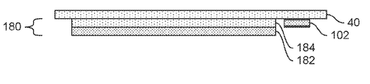
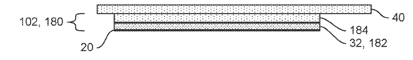
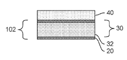
- General Physics & Mathematics (AREA)
- Acoustics & Sound (AREA)
- Computer Networks & Wireless Communication (AREA)
- Multimedia (AREA)
- Human Computer Interaction (AREA)
- Theoretical Computer Science (AREA)
- Measurement Of Velocity Or Position Using Acoustic Or Ultrasonic Waves (AREA)
- Investigating Or Analyzing Materials By The Use Of Ultrasonic Waves (AREA)
- Ultra Sonic Daignosis Equipment (AREA)
- Length Measuring Devices Characterised By Use Of Acoustic Means (AREA)
- Measurement Of The Respiration, Hearing Ability, Form, And Blood Characteristics Of Living Organisms (AREA)
- Image Input (AREA)
- Transducers For Ultrasonic Waves (AREA)
Abstract
방법들, 시스템들 및 저장 매체들이 설명되는데, 이들 각각은 초음파 평면파들을 사용하여 오브젝트의 이미지를 생성하기 위해 사용될 수 있다. 예컨대, 생성된 이미지는 압반 표면 상에 포지셔닝된 목표 오브젝트의 이미지일 수 있다. 이미지는 복수의 선택된 센서 픽셀들로부터 획득되는 정정된 출력 신호들로부터 유도될 수 있다. 정정된 출력 신호들은 압반 표면 상에 포지셔닝된 목표 오브젝트로부터 반사된 초음파 평면파들의 회절을 조정할 수 있다. 목표 오브젝트는 손가락 또는 스타일러스의 팁일 수 있다.Methods, systems and storage media are described, each of which can be used to generate an image of an object using ultrasonic plane waves. For example, the generated image may be an image of the target object positioned on the platen surface. The image may be derived from corrected output signals obtained from a plurality of selected sensor pixels. The corrected output signals can adjust the diffraction of the reflected ultrasonic plane waves from the target object positioned on the platen surface. The target object may be a tip of a finger or a stylus.
Description
[0001] 본 출원은 2015년 9월 24일에 “RECEIVE-SIDE BEAM FORMING FOR AN ULTRASONIC IMAGE SENSOR”란 명칭으로 출원된 미국 특허 출원 번호 제 14/864,555호를 우선권으로 주장하고, 그로 인해 그 미국 특허 출원은 인용에 의해 통합된다.[0001] This application claims priority from U.S. Patent Application No. 14 / 864,555, filed on September 24, 2015, entitled " RECEIVE-SIDE BEAM FORM FOR FOR ULTRASONIC IMAGE SENSOR "Lt; / RTI >
[0002] 본 개시내용은 초음파 이미징 어레이들을 위한 위상 검출 및 수신-측 빔형성의 디바이스들 및 방법들에 관한 것이다.[0002] The present disclosure relates to devices and methods for phase detection and receive-side beamforming for ultrasound imaging arrays.
[0003] 많은 초음파 이미징 시스템들은, 송신기로부터의 초음파 에너지를 목표 오브젝트 쪽으로 송신하고 그리고 목표 오브젝트에 의해서 반사되어진 송신된 초음파 에너지의 그 일부를 검출함으로써 동작한다. 반사되어진 초음파 에너지를 검출하는 것은 초음파 수신기들의 어레이에 의해서 달성될 수 있다. 그러한 시스템들은, 예컨대, 압반(platen) 상에 놓이는 손가락에 대응하는 지문들의 이미지들을 생성하도록 존재한다.[0003] Many ultrasound imaging systems operate by transmitting ultrasound energy from a transmitter towards a target object and detecting a portion of the transmitted ultrasound energy reflected by the target object. Detecting the reflected ultrasound energy can be accomplished by an array of ultrasonic receivers. Such systems exist, for example, to produce images of fingerprints corresponding to the fingers lying on the platen.
[0004] 이상적으로, 송신된 초음파 에너지는 목표 오브젝트로 곧바로 이동하고, 그 오브젝트에 의해서 반사된 임의의 초음파 에너지는 수신기로 곧바로 이동한다. 실제로, 일부 에너지는 목표 오브젝트로 그리고 목표 오브젝트로부터 그렇게 직접 이동하지는 않는다. 초음파 에너지의 일부는 회절되고, 일부는 목표 오브젝트 이외의 오브젝트들에 의해서 반사된다. 그에 따라, 송신기로부터 나오는 초음파 에너지는, 그 에너지가 송신기로부터 목표 오브젝트로 그리고 이어서 수신기들로 이동하기 때문에, 계속해서 적절히 조직화되어 있지 않다. 초음파 에너지의 조직화가 악화됨에 따라, 목표 오브젝트의 깨끗한 이미지를 생성하기 위한 능력도 역시 악화되는데, 그 이유는 수신기 어레이의 특정 수신기에 의해서 검출되는 에너지의 일부가 송신기로부터 목표 오브젝트로 곧바로 그리고 이어서 그 수신기로 곧바로 이동하지 않기 때문이다. 그러므로, 수신기들의 어레이에서 수신되는 일부 초음파 에너지가 송신기로부터 목표 오브젝트로 곧바로 그리고 이어서 목표 오브젝트로부터 어레이의 특정 수신기로 곧바로 이동하지 않았다는 사실로부터 발생하는 선명성의 손실을 줄이기 위한 방법을 갖는 것이 유용할 것이다.[0004] Ideally, the transmitted ultrasound energy moves directly to the target object, and any ultrasound energy reflected by the object travels directly to the receiver. Indeed, some energy does not go directly to and from the target object. Some of the ultrasonic energy is diffracted, and some are reflected by objects other than the target object. Accordingly, the ultrasonic energy coming from the transmitter is not properly organized since it is moving from the transmitter to the target object and then to the receivers. As the organization of the ultrasound energy deteriorates, the ability to generate a clean image of the target object also worsens because some of the energy detected by a particular receiver of the receiver array goes straight from the transmitter to the target object, Because it does not go straight to. It would therefore be useful to have a method for reducing the loss of sharpness resulting from the fact that some of the ultrasound energy received in the array of receivers does not go straight from the transmitter to the target object and then directly from the target object to the particular receiver in the array.
[0005] 본 개시내용은 초음파 평면파들을 사용하여 오브젝트의 이미지를 생성하기 위해 사용될 수 있는 방법들, 시스템들 및 저장 매체들을 설명한다. 예컨대, 생성된 이미지는 압반 표면 상에 포지셔닝된 목표 오브젝트의 이미지일 수 있고, 복수의 선택된 센서 픽셀들로부터 유도되는 정정된 출력 신호들에 기반할 수 있다. 정정된 출력 신호는 압반 표면 상에 포지셔닝된 목표 오브젝트로부터 반사된 초음파 평면파들의 회절을 정정할 수 있다. 일부 구현들에서, 목표 오브젝트는 손가락의 리지들(ridges) 또는 스타일러스(stylus)의 팁(tip)일 수 있다.[0005] The present disclosure describes methods, systems and storage media that can be used to generate an image of an object using ultrasonic plane waves. For example, the generated image may be an image of a target object positioned on a platen surface, and may be based on corrected output signals derived from a plurality of selected sensor pixels. The corrected output signal can correct the diffraction of the ultrasonic plane waves reflected from the target object positioned on the platen surface. In some implementations, the target object may be the ridges of a finger or the tip of a stylus.
[0006] 하나의 그러한 방법에서, 제1 초음파 평면파는 평면파 생성기로부터 압반 표면(platen surface) 쪽으로 론칭(launching)된다. 제1 초음파 평면파는 하나 또는 그 초과의 사이클들을 포함할 수 있다. 제1 초음파 평면파의 주파수는 (a) 센서 어레이로부터 압반 표면까지의 거리 및/또는 (b) 압반 표면 상에 포지셔닝된 목표 오브젝트의 폭에 기반할 수 있다.[0006] In one such method, the first ultrasonic plane wave is launched from the plane wave generator toward the platen surface. The first ultrasonic plane wave may comprise one or more cycles. The frequency of the first ultrasonic plane wave may be based on (a) the distance from the sensor array to the platen surface and / or (b) the width of the target object positioned on the platen surface.
[0007] 제1 세트의 픽셀 출력 신호들이 제1 초음파 평면파의 론치로부터 제1 포착 시간 지연만큼 지연되는 제1 포착 시간에 포착될 수 있다. 제1 포착 시간 지연은 선택된 픽셀과 압반 표면 간의 거리를 감안할 수 있다. 제1 세트의 픽셀 출력 신호들로부터의 각각의 픽셀 출력 신호는 압반 표면으로부터 반사되는 제1 초음파 평면파의 센서 픽셀 어레이에서의 로컬 크기를 나타낼 수 있다.[0007] The first set of pixel output signals may be captured at a first acquisition time that is delayed by a first acquisition time delay from the launch of the first ultrasonic plane waves. The first acquisition time delay may take into account the distance between the selected pixel and the platen surface. Each pixel output signal from the first set of pixel output signals may represent the local size in the sensor pixel array of the first ultrasonic plane wave reflected from the platen surface.
[0008] 이어서, 제2 초음파 평면파가 평면파 생성기로부터 압반 표면 쪽으로 론칭될 수 있다. 제2 초음파 평면파는 하나 또는 그 초과의 사이클들을 포함할 수 있다. 제2 초음파 평면파의 주파수는 (a) 센서 어레이로부터 압반 표면까지의 거리 및/또는 (b) 압반 표면 상에 포지셔닝된 목표 오브젝트의 폭에 기반할 수 있다.[0008] The second ultrasonic plane wave can then be launched from the plane wave generator towards the platen surface. The second ultrasonic plane wave may comprise one or more cycles. The frequency of the second ultrasonic plane wave may be based on (a) the distance from the sensor array to the platen surface and / or (b) the width of the target object positioned on the platen surface.
[0009] 제2 세트의 픽셀 출력 신호들이 제2 초음파 평면파의 론치로부터 제2 포착 시간 지연만큼 지연되는 제2 포착 시간에 포착될 수 있다. 제2 포착 시간 지연은 선택된 픽셀과 그 선택된 픽셀 가까운 제1 세트의 이웃 픽셀들 간의 평균 거리를 감안할 수 있다. 제2 세트의 픽셀 출력 신호들로부터의 각각의 픽셀 출력 신호는 압반 표면으로부터 반사되는 제2 초음파 평면파의 센서 픽셀 어레이에서의 로컬 크기를 나타낼 수 있다.[0009] The second set of pixel output signals may be captured at a second acquisition time that is delayed by a second acquisition time delay from the launch of the second ultrasonic wave. The second acquisition time delay may take into account the average distance between the selected pixel and the first set of neighboring pixels near the selected pixel. Each pixel output signal from the second set of pixel output signals may represent a local size in a sensor pixel array of a second ultrasonic plane wave reflected from the platen surface.
[0010] 센서 픽셀 어레이의 선택된 픽셀에 대한 정정된 출력 신호가 (a) 제1 세트의 픽셀 출력 신호들로부터의 선택된 출력 신호 및 (b) 제2 세트의 픽셀 출력 신호들로부터의 제1-레벨 정정 신호들에 기반하여 생성될 수 있다. 선택된 출력 신호는 선택된 픽셀에 대응하고, 제1-레벨 정정 신호들은 선택된 픽셀에 가까운 제1 세트의 이웃 픽셀들에 대응한다. 선택된 픽셀에 대한 정정된 출력 신호를 생성하는 것은 선택된 출력 신호와는 상이하게 제1-레벨 정정 신호들을 가중화하는 것을 포함한다.[0010] (A) a selected output signal from a first set of pixel output signals and (b) first-level correction signals from a second set of pixel output signals, wherein the corrected output signal for a selected pixel of the sensor pixel array is Lt; / RTI > The selected output signal corresponds to a selected pixel and the first-level correction signals correspond to a first set of neighboring pixels that are close to the selected pixel. Generating a corrected output signal for the selected pixel comprises weighting the first-level correction signals differently from the selected output signal.
[0011] 제1 포착 시간 지연과 2 포착 시간 지연은 선택된 픽셀에 도달하는 반사된 제1 초음파 평면파와 제1 세트의 이웃 픽셀들에 도달하는 반사된 제2 초음파 평면파 간의 위상 차이를 감안하기 위해서 상이할 수 있다.[0011] The first acquisition time delay and the second acquisition time delay may be different to account for the phase difference between the reflected first ultrasonic plane wave arriving at the selected pixel and the reflected second ultrasonic plane wave arriving at the first set of neighboring pixels .
[0012] 제1 세트의 픽셀 출력 신호들을 포착하는 것은 제1 포착 시간 윈도우 동안 반사된 제1 초음파 평면파의 로컬 크기를 나타내는 진폭을 검출하는 것을 포함할 수 있다. 제1 포착 시간 윈도우는 반사된 제1 초음파 평면파의 주기보다 짧은 지속기간을 가질 수 있다. 제1 포착 시간 윈도우는 반사된 제1 초음파 평면파의 적어도 하나의 주기의 지속기간을 가질 수 있다. 제2 세트의 픽셀 출력 신호들을 포착하는 것은 제2 포착 시간 윈도우 동안 반사된 제2 초음파 평면파의 로컬 크기를 나타내는 진폭을 검출하는 것을 포함할 수 있다.[0012] Capturing the first set of pixel output signals may include detecting an amplitude representing a local size of the reflected first ultrasonic plane wave during the first acquisition time window. The first acquisition time window may have a duration that is shorter than a period of the reflected first ultrasonic plane waves. The first acquisition time window may have a duration of at least one period of the reflected first ultrasonic plane waves. Capturing the second set of pixel output signals may include detecting an amplitude representing a local size of the reflected second ultrasonic plane wave during the second acquisition time window.
[0013] 제1 세트의 픽셀 출력 신호들을 포착하는 것은 제1 포착 시간에 샘플링 전압을 센서 픽셀 어레이에 인가하는 것을 포함할 수 있다. 제2 세트의 픽셀 출력 신호들을 포착하는 것은 제2 포착 시간에 샘플링 전압을 센서 픽셀 어레이에 인가하는 것을 포함할 수 있다. 샘플링 전압들은 센서 픽셀 어레이의 수신기 바이어스 전극에 인가될 수 있다. 그러한 샘플링 전압들은 센서 픽셀 어레이의 다이오드 바이어스 전극에 인가될 수 있다.[0013] Capturing the first set of pixel output signals may comprise applying a sampling voltage to the sensor pixel array at a first acquisition time. Capturing a second set of pixel output signals may comprise applying a sampling voltage to the sensor pixel array at a second acquisition time. The sampling voltages may be applied to the receiver bias electrodes of the sensor pixel array. Such sampling voltages may be applied to the diode bias electrodes of the sensor pixel array.
[0014] 제3 초음파 평면파가 평면파 생성기로부터 압반 표면 쪽으로 론칭될 수 있고, 제3 세트의 픽셀 출력 신호들이 제3 초음파 평면파의 론치로부터 제3 포착 시간 지연만큼 지연되는 제3 포착 시간에 포착될 수 있다. 제3 세트의 픽셀 출력 신호들로부터의 각각의 픽셀 출력 신호는 압반 표면으로부터 반사되는 제3 초음파 평면파의 센서 픽셀 어레이에서의 로컬 크기를 나타낼 수 있다. 선택된 픽셀에 대한 정정된 출력 신호를 생성하는 것은 (a) 선택된 출력 신호, (b) 제1-레벨 정정 신호들, 및/또는 (c) 제3 세트의 픽셀 출력 신호들로부터 유도될 수 있는 제2-레벨 정정 신호들의 가중된 합에 기반할 수 있다. 제2-레벨 정정 신호들은 선택된 픽셀에 가까운 제2 세트의 이웃 픽셀들에 대응할 수 있다. 제2 세트의 이웃 픽셀들은 선택된 픽셀로부터의 제1 세트의 이웃 픽셀들의 평균 거리와는 상이한 선택된 픽셀로부터의 평균 거리를 가질 수 있다.[0014] A third ultrasonic plane wave can be launched from the plane wave generator toward the platen surface and a third set of pixel output signals can be captured at a third acquisition time that is delayed by a third acquisition time delay from the launch of the third ultrasonic plane wave. Each pixel output signal from a third set of pixel output signals may represent a local size in a sensor pixel array of a third ultrasonic plane wave reflected from the platen surface. Generating a corrected output signal for a selected pixel comprises: (a) selecting the output signal that is derived from the selected output signal, (b) first-level correction signals, and / or (c) May be based on the weighted sum of the two-level correction signals. The second-level correction signals may correspond to a second set of neighboring pixels close to the selected pixel. The second set of neighboring pixels may have an average distance from a selected pixel that is different from the average distance of the first set of neighboring pixels from the selected pixel.
[0015] 본 개시내용은 센서 시스템들을 설명한다. 하나의 그러한 센서 시스템은 초음파 센서 어레이, 압반, 초음파 평면파 생성기, 및 센서 픽셀 어레이와 통신하는 하나 또는 그 초과의 프로세서들을 가질 수 있다. 압반은 압반 표면을 갖고, 압반은 센서 픽셀 어레이에 고정될 수 있다. 압반은 코팅 표면을 갖는 코팅 층을 포함할 수 있고, 그 코팅 표면은 압반 표면으로서 기능할 수 있다.[0015] The present disclosure describes sensor systems. One such sensor system may have an ultrasonic sensor array, a platen, an ultrasonic plane wave generator, and one or more processors in communication with the sensor pixel array. The platen has a platen surface, and the platen can be fixed to the sensor pixel array. The platen may comprise a coating layer having a coating surface, which coating surface may serve as a platen surface.
[0016] 평면파 생성기는 센서 픽셀 어레이에 커플링될 수 있다. 센서 픽셀 어레이의 각각의 픽셀은 수신된 초음파에 대한 응답으로 픽셀 출력 신호를 생성하도록 구성될 수 있다. 프로세서(들)는 선택된 출력 신호와 제1-레벨 정정 신호들의 가중된 합에 기반하여 정정된 출력 신호를 생성하도록 구성될 수 있다. 프로세서(들)는 센서 픽셀 어레이의 복수의 선택된 픽셀들에 대한 정정된 출력 신호들에 기반하여 압반 표면 상에 포지셔닝된 목표 오브젝트의 이미지를 생성하도록 추가로 구성될 수 있다.[0016] The plane wave generator may be coupled to the sensor pixel array. Each pixel of the sensor pixel array may be configured to generate a pixel output signal in response to the received ultrasound. The processor (s) may be configured to generate a corrected output signal based on the weighted sum of the selected output signal and the first-level correction signals. The processor (s) may be further configured to generate an image of a target object positioned on the platen surface based on the corrected output signals for a plurality of selected pixels of the sensor pixel array.
[0017] 하나 또는 그 초과의 프로세서들은 평면파 생성기로부터의 제1 초음파 평면파를 압반 표면 쪽으로 론칭하는 것을 개시하고; 제1 초음파 평면파의 론치로부터 제1 포착 시간 지연만큼 지연되는 제1 포착 시간에 제1 세트의 픽셀 출력 신호들을 포착하고 ― 제1 세트의 픽셀 출력 신호들로부터의 각각의 픽셀 출력 신호는 압반 표면으로부터 반사되는 제1 초음파 평면파의 센서 픽셀 어레이에서의 로컬 크기를 나타냄 ―; 평면파 생성기로부터의 제2 초음파 평면파를 압반 표면 쪽으로 론칭하는 것을 개시하고; 제2 초음파 평면파의 론치로부터 제2 포착 시간 지연만큼 지연되는 제2 포착 시간에 제2 세트의 픽셀 출력 신호들을 포착하며 ― 제2 세트의 픽셀 출력 신호들로부터의 각각의 픽셀 출력 신호는 압반 표면으로부터 반사되는 제2 초음파 평면파의 센서 픽셀 어레이에서의 로컬 크기를 나타냄 ―; 그리고 (i) 제1 세트의 픽셀 출력 신호들로부터의 선택된 출력 신호 및 (ii) 제2 세트의 픽셀 출력 신호들로부터의 제1-레벨 정정 신호들에 기반하여 센서 픽셀 어레이의 선택된 픽셀에 대한 정정된 출력 신호를 생성하도록 구성될 수 있고, 선택된 출력 신호는 선택된 픽셀에 대응하고, 제1-레벨 정정 신호들은 선택된 픽셀에 가까운 제1 세트의 이웃 픽셀들에 대응한다. 제1 세트의 이웃 픽셀들은 선택된 픽셀로부터 등거리에 있을 수 있다.[0017] One or more processors initiating launching a first ultrasonic plane wave from the plane wave generator towards the platen surface; Capturing a first set of pixel output signals at a first acquisition time that is delayed by a first acquisition time delay from a launch of a first ultrasound plane wave, and wherein each pixel output signal from a first set of pixel output signals Representing a local size in a sensor pixel array of reflected first ultrasonic plane waves; Disclose launching a second ultrasonic plane wave from a plane wave generator towards the platen surface; Capturing a second set of pixel output signals at a second acquisition time that is delayed by a second acquisition time delay from the launch of a second ultrasound plane wave, each pixel output signal from a second set of pixel output signals Representing a local size in a sensor pixel array of a reflected second ultrasonic plane wave; And (ii) correcting for a selected pixel of the sensor pixel array based on (i) a selected output signal from the first set of pixel output signals and (ii) first-level correction signals from the second set of pixel output signals, The selected output signal corresponding to a selected pixel, and the first-level correction signals corresponding to a first set of neighboring pixels proximate a selected pixel. The first set of neighboring pixels may be equidistant from the selected pixel.
[0018] 센서 픽셀 어레이의 각각의 픽셀은 제1 세트의 픽셀 출력 신호들 및 제2 세트의 픽셀 출력 신호들의 포착 동안 위상-동기 신호를 제공하도록 구성된 로컬 발진기에 전기적으로 커플링될 수 있다. 제2 세트의 픽셀 출력 신호들의 포착 동안 사용되는 위상-동기 신호는 제1 세트의 픽셀 출력 신호들의 포착 동안 사용되는 위상-동기 신호와 비교해서 실질적으로 동일한 진폭을 갖지만 상이한 위상을 가질 수 있다. 제2 세트의 픽셀 출력 신호들의 포착 동안 사용되는 위상-동기 신호는 제1 세트의 픽셀 출력 신호들의 포착 동안 사용되는 위상-동기 신호와 비교해서 상이한 진폭 및 상이한 위상을 가질 수 있다.[0018] Each pixel of the sensor pixel array may be electrically coupled to a local oscillator configured to provide a phase-synchronized signal during acquisition of a first set of pixel output signals and a second set of pixel output signals. The phase-locked signal used during acquisition of the second set of pixel output signals may have substantially the same amplitude but different phases compared to the phase-locked signal used during acquisition of the first set of pixel output signals. The phase-locked signal used during acquisition of the second set of pixel output signals may have different amplitudes and different phases compared to the phase-locked signal used during acquisition of the first set of pixel output signals.
[0019] 일반적으로 말해서, 본원에서 설명되는 시스템들은 이미지를 생성하기 위한 시스템들로서 요약될 수 있다. 그러한 시스템들은 제1 초음파 평면파를 압반 표면 쪽으로 론칭하기 위한 수단; 제1 초음파 평면파의 론치로부터 제1 포착 시간 지연만큼 지연되는 제1 포착 시간에 제1 세트의 픽셀 출력 신호들을 포착하기 위한 수단 ― 제1 세트의 픽셀 출력 신호들로부터의 각각의 픽셀 출력 신호는 압반 표면으로부터 반사되는 제1 초음파 평면파의 로컬 크기를 나타냄 ―; 제2 초음파 평면파를 압반 표면 쪽으로 론칭하기 위한 수단; 제2 초음파 평면파의 론치로부터 제2 포착 시간 지연만큼 지연되는 제2 포착 시간에 제2 세트의 픽셀 출력 신호들을 포착하기 위한 수단 ― 제2 세트의 픽셀 출력 신호들로부터의 각각의 픽셀 출력 신호는 압반 표면으로부터 반사되는 제2 초음파 평면파의 로컬 크기를 나타냄 ―; 및 제1 세트의 픽셀 출력 신호들로부터의 선택된 출력 신호 및 제2 세트의 픽셀 출력 신호들로부터의 제1-레벨 정정 신호들에 기반하여, 선택된 픽셀에 대한 정정된 출력 신호를 생성하기 위한 수단을 포함하고, 선택된 출력 신호는 선택된 픽셀에 대응하고, 제1-레벨 정정 신호들은 선택된 픽셀에 가까운 제1 세트의 이웃 픽셀들에 대응한다.[0019] Generally speaking, the systems described herein can be summarized as systems for generating images. Such systems include means for launching a first ultrasonic plane wave towards the platen surface; Means for capturing a first set of pixel output signals at a first acquisition time that is delayed by a first acquisition time delay from a launch of a first ultrasonic plane wave, each pixel output signal from a first set of pixel output signals comprising: A local size of the first ultrasonic plane wave reflected from the surface; Means for launching a second ultrasonic plane wave towards the platen surface; Means for capturing a second set of pixel output signals at a second acquisition time that is delayed by a second acquisition time delay from the launch of a second ultrasound plane wave, each pixel output signal from a second set of pixel output signals comprising: A local size of a second ultrasonic plane wave reflected from the surface; And means for generating a corrected output signal for the selected pixel based on the selected output signal from the first set of pixel output signals and the first-level correction signals from the second set of pixel output signals Wherein the selected output signal corresponds to a selected pixel and the first-level correction signals correspond to a first set of neighboring pixels proximate to the selected pixel.
[0020] 본 설명은 또한 이미지를 생성하는 방법을 수행하기 위해서 평면파 생성기 및 센서 픽셀 어레이와 통신하는 하나 또는 그 초과의 프로세서들에 의해 실행하기 위한 컴퓨터 판독가능 명령들의 하나 또는 그 초과의 컴퓨터 프로그램들을 포함하는 비-일시적 컴퓨터-판독가능 저장 매체를 설명한다. 컴퓨터 프로그램(들)은 평면파 생성기로부터의 제1 초음파 평면파를 압반 표면 쪽으로 론칭하기 위한 명령들; 제1 초음파 평면파의 론치로부터 제1 포착 시간 지연만큼 지연되는 제1 포착 시간에 제1 세트의 픽셀 출력 신호들을 포착하기 위한 명령들 ― 제1 세트의 픽셀 출력 신호들로부터의 각각의 픽셀 출력 신호는 압반 표면으로부터 반사되는 제1 초음파 평면파의 센서 픽셀 어레이에서의 로컬 크기를 나타냄 ―; 평면파 생성기로부터의 제2 초음파 평면파를 압반 표면 쪽으로 론칭하기 위한 명령들; 제2 초음파 평면파의 론치로부터 제2 포착 시간 지연만큼 지연되는 제2 포착 시간에 제2 세트의 픽셀 출력 신호들을 포착하기 위한 명령들 ― 제2 세트의 픽셀 출력 신호들로부터의 각각의 픽셀 출력 신호는 압반 표면으로부터 반사되는 제2 초음파 평면파의 센서 픽셀 어레이에서의 로컬 크기를 나타냄 ―; 및 제1 세트의 픽셀 출력 신호들로부터의 선택된 출력 신호 및 제2 세트의 픽셀 출력 신호들로부터의 제1-레벨 정정 신호들에 기반하여, 센서 픽셀 어레이로부터 선택된 픽셀에 대한 정정된 출력 신호를 생성하기 위한 명령들을 포함할 수 있고, 선택된 출력 신호는 선택된 픽셀에 대응하고, 제1-레벨 정정 신호들은 선택된 픽셀에 가까운 제1 세트의 이웃 픽셀들에 대응한다.[0020] The present disclosure also relates to a method and apparatus for generating images, including a planar wave generator and a non-linear array of computer readable instructions for carrying out one or more computer programs for execution by one or more processors in communication with the sensor pixel array - A temporary computer-readable storage medium is described. The computer program (s) may include instructions for launching a first ultrasonic plane wave from a plane wave generator toward the platen surface; Instructions for capturing a first set of pixel output signals at a first acquisition time that is delayed by a first acquisition time delay from a launch of a first ultrasound plane wave, each pixel output signal from a first set of pixel output signals A local size in a sensor pixel array of a first ultrasonic plane wave reflected from a platen surface; Instructions for launching a second ultrasonic plane wave from the plane wave generator towards the platen surface; Instructions for capturing a second set of pixel output signals at a second acquisition time that is delayed by a second acquisition time delay from a launch of a second ultrasound plane wave, each pixel output signal from a second set of pixel output signals A local size in a sensor pixel array of a second ultrasonic plane wave reflected from the platen surface; And generating a corrected output signal for the selected pixel from the sensor pixel array based on the selected output signal from the first set of pixel output signals and the first-level correction signals from the second set of pixel output signals The selected output signal corresponding to the selected pixel, and the first-level correction signals corresponding to a first set of neighboring pixels proximate to the selected pixel.
[0021]
본 개시내용의 특성 및 목적들에 대한 완전한 이해를 위해서, 첨부 도면들 및 후속하는 설명에 대한 참조가 이루어져야 한다. 본 개시내용은 이제 첨부된 도면들 및 다이어그램들을 참조하여 비제한적인 예들을 통해 설명될 것이다.
[0022]
도 1a 내지 도 1c는 본 개시내용의 양상들에 따라, 초음파 센서 시스템의 예를 예시한다.
[0023]
도 2는 초음파 센서 시스템의 분해된 사시도의 예를 도시한다.
[0024]
도 3은 초음파 센서 시스템의 블록 다이어그램을 예시한다.
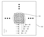
[0025]
도 4는 초음파 센서를 위한 센서 픽셀들의 4×4 픽셀 어레이에 대한 양상들을 대표적으로 도시한다.
[0026]
도 5는 도 1 내지 도 4의 초음파 센서들에 포함될 수 있는 센서 픽셀 회로의 예를 예시한다.
[0027]
도 6a는 본 개시내용의 양상들에 따라, 초음파 센서 어레이, 압반, 및 압반의 표면 상에 포지셔닝된 손가락과 같은 목표 오브젝트의 예시적인 구현에 대한 단면도를 예시한다.
[0028]
도 6b는 압전 층의 각 측면 상에 배치되는 송신기 전극들 사이에 포지셔닝된 그 압전 층을 갖는 초음파 송신기로부터 론칭되는 실질적으로 평평한 초음파 평면파를 예시한다.
[0029]
도 6c는 초음파 센서 어레이의 센서 표면 상에 포지셔닝된 손가락과 함께 초음파 센서 어레이의 확대된 부분을 도시한다.
[0030]
도 6d는 초음파 센서 어레이의 센서 표면 상에 포지셔닝된 손가락의 다수의 리지들로부터의 회절 효과들을 도시한다.
[0031]
도 6e는 초음파 센서 어레이의 센서 표면 상에 포지셔닝된 스타일러스의 스타일러스 팁으로부터의 회절 효과들을 도시한다.
[0032]
도 6f는 초음파 센서 어레이의 센서 표면 상에 포지셔닝된 목표 오브젝트의 포인트로부터 방출되는 구면파들을 예시한다.
[0033]
도 7a는 압반의 표면으로부터 밑에 있는 초음파 센서 어레이의 선택된 픽셀로의 초음파 평면파의 반사를 도시한다.
[0034]
도 7b는 압반의 표면으로부터 밑에 있는 초음파 센서 어레이의 선택된 픽셀에 가까운 제1 세트의 이웃 픽셀들로의 초음파 평면파의 반사를 도시한다.
[0035]
도 7c는 압반의 표면으로부터 밑에 있는 초음파 센서 어레이의 선택된 픽셀에 가까운 제2 세트의 이웃 픽셀들로의 초음파 평면파의 반사를 도시한다.
[0036]
도 7d는 초음파 센서 어레이의 선택된 픽셀 및 그 선택된 픽셀에 가까운 다수의 세트들의 이웃 픽셀들을 예시한다.
[0037]
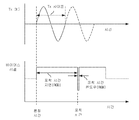
도 8a 내지 도 8g는 초음파 송신기에 제공되는 송신기 여기 신호들의 다양한 사이클들(위의 그래프들) 및 초음파 센서 어레이의 수신기 바이어스 전극에 적용되는 다양한 바이어스 레벨들(아래의 그래프들)을 그래프로 예시하고, 샘플링 윈도우들의 다양한 지속기간들 및 다양한 포착 시간 지연들은 다양한 세트들의 픽셀 출력 신호들의 포착을 허용한다.
[0038]
도 8h 내지 도 8l은 로컬 발진기의 출력(위의 그래프들)과 동기화되고 초음파 송신기(중간 그래프들)에 제공되는 송신기 여기 신호들의 다양한 사이클들 및 반사된 파를 검출하기 위해 초음파 센서 어레이의 수신기 바이어스 전극에 적용되는 다양한 바이어스 레벨들(아래의 그래프들)을 그래프로 예시하고, 샘플링 윈도우들의 다양한 지속기간들, 초음파의 론치로부터의 다양한 포착 시간 지연들, 및 바이어스 레벨들과 로컬 발진기 신호의 다양한 혼합이 다양한 세트들의 픽셀 출력 신호들의 포착을 허용한다.
[0039]
도 8m은 초음파 송신기에 제공되는 송신기 여기 신호들의 다양한 사이클들(위의 그래프) 및 초음파 센서 어레이의 다이오드 바이어스 전극에 적용되는 다양한 바이어스 레벨들(아래의 그래프)을 그래프로 예시한다.
[0040]
도 9는 초음파 센서 어레이의 복수의 픽셀들에 대한 정정된 출력 신호들에 기반하여 압반 표면 상에 포지셔닝된 목표 오브젝트의 이미지의 생성을 예시한다.
[0041]
도 10a 내지 도 10c는 정정이 없는(도 10a), 필터링을 통해(도 10b), 및 수신-측 빔형성을 통해(도 10c) 압반 표면 상에 포지셔닝된 스타일러스 팁의 포착된 초음파 이미지들을 도시한다.
[0042]
도 11a 내지 도 11c는 선택된 픽셀들로부터의 출력 신호들 및 이웃 픽셀들로부터의 정정 신호들에 기반하여 목표 오브젝트의 초음파 이미지를 생성하는 방법들을 예시하는 흐름도들이다.
[0043]
도 12a는 본 개시내용의 양상들에 따라, 사용자의 지문 등록 및/또는 인증을 위해 초음파 센서 어레이를 사용하기 위한 일반적인 흐름들을 예시한다.
[0044]
도 12b는 본 개시내용의 양상들에 따라, 스타일러스 검출 및 포지션 결정을 위해 초음파 센서 어레이를 사용하기 위한 일반적인 흐름들을 예시한다.
[0045]
도 13a 내지 도 13d는 디스플레이 디바이스를 갖는 초음파 센서 어레이의 다양한 구성들을 예시한다.
[0046]
도 14는 초음파 센서 시스템의 일반적인 블록 다이어그램을 예시한다.
[0047]
도 15a 및 도 15b는 본원에서 설명되는 바와 같이 초음파 센서 시스템을 포함하는 디스플레이 디바이스를 예시하는 시스템 블록 다이어그램들의 예들을 도시한다.[0021] For a thorough understanding of the nature and objects of the disclosure, reference should be made to the accompanying drawings and the subsequent description. The present disclosure will now be described, by way of non-limiting examples, with reference to the accompanying drawings and diagrams.
[0022] FIG. 1A-1C illustrate an example of an ultrasonic sensor system, in accordance with aspects of the present disclosure.
[0023] FIG. 2 shows an example of an exploded perspective view of an ultrasonic sensor system.
[0024] FIG. 3 illustrates a block diagram of an ultrasonic sensor system.
[0025] FIG. 4 representatively illustrates aspects of a 4 × 4 pixel array of sensor pixels for an ultrasonic sensor.
[0026] FIG. 5 illustrates an example of a sensor pixel circuit that may be included in the ultrasonic sensors of FIGS. 1-4.
[0027] FIG. 6A illustrates a cross-sectional view of an exemplary implementation of a target object, such as an ultrasonic sensor array, a platen, and a finger positioned on the surface of the platen, in accordance with aspects of the present disclosure.
[0028] FIG. 6b illustrates a substantially planar ultrasonic plane wave launched from an ultrasonic transmitter having its piezoelectric layer positioned between transmitter electrodes disposed on each side of the piezoelectric layer.
[0029] FIG. 6C shows an enlarged portion of the ultrasonic sensor array with the fingers positioned on the sensor surface of the ultrasonic sensor array.
[0030] FIG. 6D shows diffraction effects from multiple ridges of a finger positioned on the sensor surface of an ultrasonic sensor array.
[0031] FIG. 6E shows the diffraction effects from the stylus tip of the stylus positioned on the sensor surface of the ultrasonic sensor array.
[0032] FIG. 6F illustrates spherical waves emitted from a point of a target object positioned on the sensor surface of the ultrasonic sensor array;
[0033] FIG. 7A shows the reflection of ultrasonic plane waves from the surface of the platen to the selected pixels of the underlying ultrasonic sensor array.
[0034] FIG. 7B shows the reflection of ultrasonic plane waves from a surface of the platen to a first set of neighboring pixels close to a selected pixel of the underlying ultrasonic sensor array.
[0035] FIG. 7C shows the reflection of ultrasonic plane waves from the surface of the platen to a second set of neighboring pixels close to the selected pixel of the underlying ultrasonic sensor array.
[0036] FIG. 7D illustrates a selected pixel of the ultrasonic sensor array and neighboring pixels of a plurality of sets close to the selected pixel.
[0037] Figures 8a-8g illustrate various cycles of transmitter excitation signals provided in an ultrasonic transmitter (graphs above) and various bias levels (graphs below) applied to a receiver bias electrode of an ultrasonic sensor array And the various durations of the sampling windows and the various acquisition time delays allow the capture of the various sets of pixel output signals.
[0038] Figures 8h through 8l illustrate the use of an ultrasonic sensor array to detect various cycles and reflected waves of transmitter excitation signals that are synchronized with the output of the local oscillator (the graphs above) and provided to the ultrasonic transmitter Graphically illustrating the various bias levels (graphs below) applied to the receiver bias electrode of the receiver, the various durations of the sampling windows, the various acquisition time delays from the launch of the ultrasonic waves, and the bias levels and the local oscillator signal ≪ / RTI > allows the capture of the various sets of pixel output signals.
[0039] FIG. 8m graphically illustrates various cycles of the transmitter excitation signals provided in the ultrasonic transmitter (graph above) and various bias levels applied to the diode bias electrode of the ultrasonic sensor array (graph below).
[0040] FIG. 9 illustrates the generation of an image of a target object positioned on a platen surface based on corrected output signals for a plurality of pixels of an ultrasonic sensor array.
[0041] Figures 10a-10c illustrate a captured ultrasound image of a stylus tip positioned on a platen surface without correction (Figure 10a), through filtering (Figure 10b), and via receive-side beam formation (Figure 10c) Lt; / RTI >
[0042] Figures 11a-11c are flow charts illustrating methods for generating ultrasound images of target objects based on output signals from selected pixels and correction signals from neighboring pixels.
[0043] FIG. 12A illustrates general flows for using an ultrasonic sensor array for fingerprint registration and / or authentication of a user, in accordance with aspects of the present disclosure.
[0044] FIG. 12B illustrates general flows for using an ultrasonic sensor array for stylus detection and position determination, in accordance with aspects of the present disclosure.
[0045] Figures 13A-13D illustrate various configurations of an ultrasonic sensor array having a display device.
[0046] Figure 14 illustrates a general block diagram of an ultrasonic sensor system.
[0047] Figures 15A and 15B illustrate examples of system block diagrams illustrating a display device including an ultrasonic sensor system as described herein.
[0048]
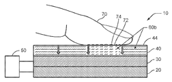
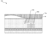
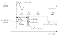
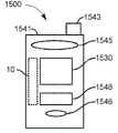
도 1a 내지 도 1c는 본 개시내용의 양상들에 따라, 초음파 센서 시스템(10)의 예를 예시한다. 도 1a에 도시된 바와 같이, 초음파 센서 시스템(10)은 압반(40) 아래에 초음파 송신기(20) 및 초음파 수신기(30)를 포함할 수 있다. 초음파 송신기(20)는 초음파들(80a)을 생성할 수 있는 압전 송신기일 수 있다(도 1b 참조). 초음파 수신기(30)는 기판 상에 배치되는 픽셀 회로들의 어레이 및 압전 물질 층을 포함할 수 있다. 동작 시에, 초음파 송신기(20)는 초음파 수신기(30)를 통해 압반(40)의 노출된 표면(44)으로 이동하는 하나 또는 그 초과의 초음파들(80a)을 생성할 수 있다. 압반(40)의 노출된 표면(44)에서, 초음파 에너지는 압반(40)과 접촉하는 목표 오브젝트(70), 이를테면 지문 리지 지역(72)의 피부에 의해 투과, 흡수 또는 산란되거나, 또는 초음파 수신기(30) 쪽으로 다시 반사될 수 있다. 공기가 압반(40)의 노출된 표면(44)에 접촉하는 위치들에서, 예컨대 지문 리지 지역들(72) 간의 계곡 지역들(74)들에서, 초음파의 대부분이 검출을 위해 초음파 수신기(30) 쪽으로 다시 반사될 것이다(도 1c 참조). 제어 전자 장치(50)는 초음파 송신기(20) 및 초음파 수신기(30)에 커플링될 수 있고, 초음파 송신기(20)로 하여금 하나 또는 그 초과의 초음파들(80a)을 생성하여 론칭하게 하는 타이밍 신호들을 공급할 수 있다. 이어서, 제어 전자 장치(50)는 반사된 초음파 에너지, 이를테면 압반(40)의 노출된 표면(44)으로부터 반사될 수 있는 하나 또는 그 초과의 반사된 초음파들(80b)을 표시하는 신호들을 초음파 수신기(30)로부터 수신할 수 있다. 제어 전자 장치(50)는 목표 오브젝트(70)의 디지털 이미지를 구성하기 위해 초음파 수신기(30)로부터 수신되는 출력 신호들을 사용할 수 있다. 일부 구현들에서, 제어 전자 장치(50)는 또한 시간에 걸쳐, 목표 오브젝트(70)의 존재 및/또는 이동을 검출하기 위해 출력 신호들을 연속적으로 샘플링할 수 있다.[0048]
1A-1C illustrate an example of an
[0049]
본 개시내용의 양상들에 따라, 초음파 송신기(20)는 실질적으로 평평한 압전 송신기 층(24)을 포함하는 평면파 생성기일 수 있다. 도 2를 참조하자. 초음파들은 인가되는 신호에 의존하여 압전 층(24)을 팽창 또는 수축시키기 위해 그 압전 층(24)에 전압을 인가함으로써 생성되고, 그로 인해서 평면파가 생성될 수 있다. 전압은 제1 송신기 전극(22) 및 제2 송신기 전극(26)을 통해 압전 송신기 층(24)에 걸쳐 인가될 수 있다. 이러한 형태로, 초음파(80a)는 압전 효과를 통해 층의 두께를 변경함으로써 만들어질 수 있다. 초음파(80a)는 압반(40)을 통과해서 손가락(또는 검출될 다른 오브젝트) 쪽으로 이동할 수 있다. 검출될 오브젝트에 의해 흡수 또는 투과되지 않는 파의 부분은 압반(40)을 다시 통과하여 초음파 수신기(30)에 의해 수신되도록 반사될 수 있다.[0049]
In accordance with aspects of the present disclosure, the
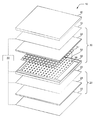
[0050]
초음파 수신기(30)는 기판(32) 상에 배치되는 픽셀 회로들(36)의 어레이를 포함하는 회로(33) 및 압전 수신기 층(38)을 포함할 수 있다. 일부 구현들에서, 각각의 픽셀 회로(36)는 하나 또는 그 초과의 트랜지스터들, 전기 상호연결 트레이스들, 및 일부 구현들에서는, 다이오드들, 커패시터들 등과 같은 하나 또는 그 초과의 추가 회로 엘리먼트들을 포함할 수 있다. 도 2 내지 도 5를 참조하자. 각각의 픽셀 회로(36)는 픽셀 회로(36) 부근의 압전 수신기 층(38)에 의해 생성되는 전기 전하를 전기 신호로 변환하도록 구성될 수 있다.[0050]
The
[0051]
도 2에 도시되어진 예시된 구현에서, 수신기 바이어스 전극(39)은 압반(40) 부근의 압전 수신기 층(38)의 측면 상에 배치될 수 있다. 수신기 바이어스 전극(39)은 금속화된 전극일 수 있고, 그리고 어떤 신호들이 픽셀 회로들(36)에 전달되는지를 제어하기 위해서 접지되거나 바이어싱될 수 있다. 압반(40)의 노출된(상단) 표면(44)으로부터 반사되는 초음파 에너지는 압전 수신기 층(38)에 의해서 국부적인 전기 전하들로 변환될 수 있다. 이들 국부적인 전하들은 픽셀 입력 전극(37)에 의해 수집되고 밑에 있는 픽셀 회로들(36)에 전달될 수 있다. 전하들은 픽셀 회로(36)에 의해서 증폭되거나 버퍼링되고, 출력 신호들을 프로세싱할 수 있는 제어 전자 장치(50)에 제공될 수 있다. 예시적인 픽셀 회로의 간략화된 개략도가 도 4에 도시되지만, 당업자는 그 간략화된 개략도에 도시된 예시적인 픽셀 회로의 많은 변경들 및 수정들이 활용될 수 있음을 인식할 것이다.[0051]
In the illustrated implementation shown in FIG. 2, a
[0052]
제어 전자 장치(50)는 제1 송신기 전극(22) 및 제2 송신기 전극(26)뿐만 아니라 수신기 바이어스 전극(39), 기판(32) 상의 픽셀 회로들(36), 및 센서 시스템(10)과 연관된 다른 제어 및 데이터 라인들에 전기적으로 연결될 수 있다.[0052]
The
[0053]
도 1a 내지 도 1c는 초음파 센서에서 초음파 송신기(20) 및 수신기(30)의 배열에 대한 예를 도시하지만, 다른 배열들도 가능하다. 예컨대, 일부 구현들에서, 초음파 송신기(20)는 초음파 수신기(30) 위에, 즉, 검출할 오브젝트에 더욱 가까이 있을 수 있다. 일부 구현들에서, 초음파 센서는 청각 음향 지연 층을 포함할 수 있다. 예컨대, 음향 지연 층은 초음파 송신기(20)와 초음파 수신기(30) 사이로 초음파 센서 시스템(10)에 통합될 수 있다. 일부 구현들에서, 기판(32)은 음향 지연 층으로서 기능할 수 있다. 일부 구현들에서, 초음파 송신기(20)와 초음파 수신기(30) 사이에 포지셔닝되는 추가 층(미도시)은 음향 지연 층으로서 기능할 수 있다. 일부 구현들에서, 압반(40), 또는 초음파 수신기(30)와 압반(40) 사이에 포지셔닝되는 추가 층(미도시)은 음향 지연 층으로서 기능할 수 있다. 음향 지연 층은 초음파 펄스 타이밍을 조정하고 그와 동시에 초음파 송신기(20)로부터 초음파 수신기(30)를 전기 절연시키기 위해 이용될 수 있다. 그 지연 층은 실질적으로 균일한 두께를 가질 수 있는데, 지연 층을 위해 사용되는 물질 및/또는 지연 층의 두께는 반사된 초음파 에너지가 초음파 수신기(30)에 도달하는데 걸리는 시간에 있어서 원하는 지연을 제공하도록 선택된다. 그렇게 하는데 있어서, 목표 오브젝트(70)에 의해 반사됨으로써 목표 오브젝트(70)에 대한 정보를 운반하는 에너지 펄스가 초음파 수신기(30)에 도달하게 만들어질 수 있는 시간 범위는 초음파 센서 시스템(10)의 다른 부분들로부터 반사되는 에너지가 초음파 수신기(30)에 도달하는 가능성이 없는 시간 범위 동안이다.[0053]
1A to 1C show examples of the arrangement of the
[0054]
도 2는 압반(40) 아래에 초음파 송신기(20) 및 초음파 수신기(30)를 포함하는 초음파 센서 시스템(10)의 분해된 사시도의 예를 도시한다. 초음파 송신기(20)는 압전 송신기 층(24)의 각각의 측면 상에 배치되는 제1 송신기 전극(22) 및 제2 송신기 전극(26)을 갖는 실질적으로 평평한 그 압전 송신기 층(24)을 포함할 수 있다. 제1 및 제2 송신기 전극들(22 및 26)은 금속화된 전극들, 예컨대, 압전 송신기 층(24)의 대향 측면들을 코팅하는 금속 층들일 수 있다.[0054]
2 shows an exploded perspective view of an
[0055]
초음파 수신기(30)는, 본원에서 구현에 따라 TFT(thin-film transistor) 기판, 뒤판, 패널, 서브-패널 또는 반도체 기판으로서 또한 지칭될 수 있는 기판(32) 상에 배치되는 픽셀 회로들(36)의 어레이, 및 압전 수신기 층(38)을 포함할 수 있다. 각각의 픽셀 회로(36)는 압전 수신기 층(38)을 픽셀 회로(36)에 전기적으로 커플링하는 픽셀 입력 전극(37)을 포함할 수 있다. 압전 수신기 층(38)은 픽셀 입력 전극들(37)과 직접 접촉하거나(코팅 또는 증착 프로세스를 통해서와 같이), 또는 픽셀 입력 전극들(37)에 용량성 커플링될 수 있다(압전 층이 얇은 접착 층과 부착되는 결합 또는 적층 프로세스를 통해서와 같이). 일부 구현들에서, 기판(32)은 유리 또는 플라스틱으로 만들어진 얇은 기판일 수 있고, 그 기판 위에서 센서 픽셀 회로들(36)이 제작된다. 일부 구현들에서, 기판(32)은 실리콘, 단결정 실리콘 또는 다른 반도체 물질, 이를테면 실리콘 웨이퍼 또는 실리콘-온-절연체 웨이퍼일 수 있다. 픽셀 회로들(36) 및 기판(32)에 관련된 다른 회로가 종래 실리콘 디바이스 웨이퍼와 같은 기판에 제작된 트랜지스터들로부터 형성될 수 있다. 픽셀 회로들(36) 이외에도, 기판(32)은 그 위에 제작된 추가 컴포넌트들, 이를테면 하나 또는 그 초과의 전도성 결합 패드들 및 연결 트레이스들을 가질 수 있다.[0055]
[0056]
예시된 구현에서, 도 1a 내지 도 1c에 대해 위에서 설명된 바와 같이, 수신기 바이어스 전극(39)은 압반(40) 부근의 압전 수신기 층(38)의 측면 상에 배치될 수 있다. 제어 전자 장치(50)는 제1 송신기 전극(22) 및 제2 송신기 전극(26) 뿐만 아니라 수신기 바이어스 전극(39), 픽셀 회로들(36), 및 기판(32) 상의 다른 회로와 전기적으로 연결될 수 있다. 제어 전자 장치(50)는 실질적으로 도 1a 내지 도 1c에 대해 앞서 논의된 바와 같이 동작할 수 있다.[0056]
In the illustrated implementation, a
[0057]
압반(40)은 수신기에 음향적으로 커플링될 수 있는 임의의 적합한 물질일 수 있다. 음향적으로 커플링된 물질들은 초음파들과 같은 음향파들의 하나의 층으로부터 다른 층으로의 송신을 허용한다. 압반을 위해 적절할 수 있는 물질들의 예들은 플라스틱, 세라믹, 유리, 사파이어, 고릴라 유리(gorilla glass), 알루미늄, 스테인리스 강, 금속, 금속 합금, 폴리카보네이트, 고분자 물질, 또는 금속-충전 플라스틱을 포함할 수 있다. 일부 구현들에서, 압반(40)은 커버 판, 예컨대 디스플레이를 위한 커버 유리 또는 렌즈 유리일 수 있다. 요구되다면 비교적 두꺼운 압반들, 예컨대 1mm 이상의 압반들을 통해 검출 및 이미징이 수행될 수 있다.[0057]
The
[0058] 다양한 구현들에 따라 이용될 수 있는 압전 물질들의 예들은 적합한 음향 특성들, 예컨대 약 2.5MRayls와 5MRayls 사이의 음향 임피던스를 갖는 압전 중합체들을 포함한다. 이용될 수 있는 압전 물질들의 특정 예들은 강유전성 중합체들, 이를테면 PVDF(polyvinylidene) 및 PVDF-TrFE(polyvinylidene fluoride-trifluoroethylene) 공중합체들을 포함한다. PVDF 공중합체들의 예들은 60:40 (molar percent) PVDF-TrFE, 70:30 PVDF-TrFE, 80:20 PVDF-TrFE, 및 90:10 PVDF-TrFE를 포함한다. 이용될 수 있는 압전 물질들의 다른 예들은 PVDC(polyvinylidene chloride) 동종중합체들 및 공중합체들, PTFE(polytetrafluoroethylene) 동종중합체들 및 공중합체들, 및 DIPAB(diisopropylammonium bromide)를 포함한다.[0058] Examples of piezoelectric materials that can be used in accordance with various implementations include suitable acoustic properties, such as piezoelectric polymers having an acoustic impedance between about 2.5 MRayls and 5 MRayls. Specific examples of piezoelectric materials that may be used include ferroelectric polymers such as PVDF (polyvinylidene) and PVDF-TrFE (polyvinylidene fluoride-trifluoroethylene) copolymers. Examples of PVDF copolymers include PVDF-TrFE 60:40, 70:30 PVDF-TrFE, 80:20 PVDF-TrFE, and 90:10 PVDF-TrFE. Other examples of piezoelectric materials that may be used include PVDC (polyvinylidene chloride) homopolymers and copolymers, PTFE (polytetrafluoroethylene) homopolymers and copolymers, and DIPAB (diisopropylammonium bromide).
[0059]
압전 송신기 층(24) 및 압전 수신기 층(38) 각각의 두께는 초음파들을 생성하고 수신하기에 적절하도록 선택될 수 있다. 일 예에서, PVDF 압전 송신기 층(24)은 대략 28㎛ 두께이고, PVDF-TrFE 수신기 층(38)은 대략 12㎛ 두께이다. 초음파들의 예시적인 주파수들은 약 ¼ 밀리미터 이하의 파장들을 가지면서 5MHz 내지 30MHz의 범위 내에 있다.[0059]
The thickness of each of the
[0060]
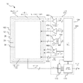
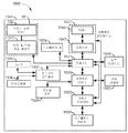
도 3은 초음파 센서 시스템(10)의 블록 다이어그램을 예시한다. 초음파 센서 시스템(10)은 초음파 센서 픽셀 회로 어레이(35)를 포함하는 TFT 회로(33)를 포함한 TFT 기판(32) 및 초음파 송신기(20)를 갖는 초음파 센서 어레이(102)를 포함할 수 있다. 초음파 송신기(20)는 송신기 드라이버(168)에 (예컨대, 하나 또는 그 초과의 전자 연결부들을 통해) 전자 통신할 수 있다. 일부 구현들에서, 송신기 드라이버(168)는 초음파 송신기(20)와 연관된 하나 또는 그 초과의 송신기 전극들(22 및 26)과 전자 통신하는 포지티브 극성 출력 신호 및 네거티브 극성 출력 신호를 가질 수 있다. 송신기 드라이버(168)는 센서 제어기(104)의 제어 유닛(160)과 전자 통신할 수 있다. 도시된 엘리먼트들 중 다수는 위의 도 1a 내지 도 1c 및 도 2에 대해 설명된 바와 같이 제어 전자 장치(50)의 부분을 형성할 수 있다. 센서 제어기(104)는 센서 시스템(10)의 다양한 양상들, 예컨대 초음파 송신기 타이밍 및 여기(excitation) 파형들, 초음파 수신기(30) 및 픽셀 회로(36)에 대한 바이어스 전압들, 픽셀 어드레싱, 신호 필터링 및 변환, 판독 프레임 레이트들 등을 제어하도록 구성된 제어 유닛(160)을 포함할 수 있다. 제어 유닛(160)은 하나 또는 그 초과의 송신기 여기 신호들을 송신기 드라이버(168)에 제공할 수 있다. 제어 유닛(160)은 레벨 선택 입력 버스를 통해 수신기 바이어스 드라이버(162)와 전자 통신할 수 있다. 수신기 바이어스 드라이버(162)는 센서 픽셀 회로들(36)의 픽셀 입력 전극들(37)에 부착될 수 있는 압전 수신기 층(38)의 표면 상에 배치되는 수신기 바이어스 전극(39)에 수신기 바이어스 전압을 제공할 수 있다(도 2 참조). 제어 유닛(160)은 하나 또는 그 초과의 역다중화기들(164)과 전자 통신할 수 있다. 역다중화기들(164)은 복수의 게이트 드라이버들(166)과 전자 통신할 수 있다. 게이트 드라이버들(166)은 초음파 센서 어레이(102)의 센서 픽셀 어레이(35)와 전자 통신할 수 있다. 게이트 드라이버들(166)은 센서 픽셀 어레이(35) 외부에 포지셔닝되거나, 또는 일부 구현들에서 동일 기판(32) 상에 센서 픽셀 어레이(35)로서 포함될 수 있다. 센서 픽셀 어레이(35) 외부에 있거나 또는 센서 픽셀 어레이(35)와 동일 기판 상에 포함될 수 있는 역다중화기들(164)은 특정 게이트 드라이버들(166)을 선택하기 위해 사용될 수 있다. 게이트 드라이버들(166)은 센서 픽셀 어레이(35)의 하나 또는 그 초과의 행들 또는 열들을 선택할 수 있다. 센서 픽셀 어레이(35)는 하나 또는 그 초과의 디지털화기들(172)과 전자 통신할 수 있다. 디지털화기들(172)은 센서 픽셀 어레이(35)의 하나 또는 그 초과의 센서 픽셀들(34)로부터의 아날로그 픽셀 출력 신호들을, 센서 제어기(104)의 부분이거나 또는 센서 제어기(104) 외부에 있을 수 있는 데이터 프로세서(170) 내에서의 추가 프로세싱에 적절한 디지털 신호들로 변환할 수 있다. 센서 제어기(104)는 센서 픽셀 어레이(35)로부터 데이터를 수신하는 하나 또는 그 초과의 데이터 프로세서들(170)을 포함할 수 있다. 센서 제어기(104)는 데이터 출력들을 외부 시스템 또는 프로세서, 이를테면 모바일 디바이스의 애플리케이션 프로세서에 제공할 수 있다. 데이터 프로세서(170)는 디지털화된 데이터를 지문의 이미지 데이터로 바꾸거나 또는 추가 프로세싱을 위해 그 데이터를 포맷팅할 수 있다.[0060]
FIG. 3 illustrates a block diagram of an
[0061]
일부 구현들에서, 제어 유닛(160)은 송신기(Tx) 드라이버(168)로 하여금 초음파 송신기(20)를 여기시켜 평면 초음파들을 생성하도록 하기 위해서 규칙적인 간격들로 TX 드라이버(168)에 송신기(Tx) 여기 신호를 전송할 수 있다. 제어 유닛(160)은 수신기 바이어스 전극(39)을 바이어싱시키기 위해서 수신기(Rx) 바이어스 드라이버(162)를 통해 레벨 선택 입력 신호들을 전송하고, 센서 픽셀들(34)에 의한 초음파 신호 검출의 게이팅(gating)을 허용할 수 있다. 일부 구현들에서, 제어 유닛(160)은 DBIAS(diode bias) 드라이버(174)를 통해 레벨 선택 입력 신호들을 센서 픽셀 어레이(35)의 픽셀 회로들(36)에 전송할 수 있다. 하나 또는 그 초과의 역다중화기(164)는 센서 픽셀 어레이(35)의 특별 행 또는 열이 픽셀 출력 신호들을 제공하게 하는 게이트 드라이버들(166)을 턴 온 및 오프시키는데 사용될 수 있다. 픽셀 회로들(36)로부터의 출력 신호들이 전하 증폭기, RC(resistor-capacitor) 필터 또는 에일리어싱-방지 필터와 같은 필터, 및 디지털화기(172)를 통해서 데이터 프로세서(170)에 전송될 수 있다. 하나 또는 그 초과의 제어 라인들(176)이 센서 제어기(104)와 초음파 센서 어레이(102) 간에 제어 신호들을 반송할 수 있다. 센서 제어기(104)의 부분들이 TFT 기판(32) 상에 포함될 수 있고, 다른 부분들이 연관된 집적 회로에 포함될 수 있다는 점을 주목하자.[0061]
In some implementations, the
[0062]
도 4는 초음파 센서를 위한 센서 픽셀들(34)의 4×4 픽셀 어레이(35)에 대한 양상들을 대표적으로 도시한다. 각각의 픽셀(34)은, 예컨대, 압전 센서 물질(PSM), 피크 검출 다이오드(D1) 및 판독 트랜지스터(M3)의 국부적인 지역과 연관될 수 있고; 이러한 엘리먼트들 중 대다수 또는 모두가 픽셀 회로(36)를 형성하기 위해서 기판(32) 상에 또는 기판(32) 내에 형성될 수 있다. 실제로, 각각의 픽셀(34)의 압전 센서 물질의 국부적인 지역은 수신된 초음파 에너지를 전기 전하들로 변환할 수 있다. 피크 검출 다이오드(D1)는 압전 센서 물질(PSM)의 국부적인 지역에 의해 검출되는 최대량의 전하를 기록할 수 있다. 이어서, 픽셀 어레이(35)의 각각의 행은 예컨대 행 선택 메커니즘, 게이트 드라이버, 또는 시프트 레지스터를 통해 스캐닝될 수 있고, 각각의 열에 대한 판독 트랜지스터(M3)는 각각의 픽셀(34)에 대한 피크 전하의 크기로 하여금 추가 회로, 예컨대 다중화기 및 A/D 변환기에 의해 판독되게 허용하기 위해서 트리거링될 수 있다. 픽셀 회로(36)는 픽셀(34)의 게이팅, 어드레싱 및 리셋팅을 허용하기 위해서 하나 또는 그 초과의 TFT들을 포함할 수 있다.[0062]
Figure 4 representatively illustrates aspects of a
[0063]
각각의 픽셀 회로(36)는 초음파 센서 시스템(10)에 의해 검출되는 오브젝트의 작은 부분에 대한 정보를 제공할 수 있다. 비록 예시의 편의를 위해서 도 4에 도시된 예는 비교적 개략적인 해상도를 갖지만, 인치당 약 500개 이상의 픽셀들의 해상도를 갖는 초음파 센서들이 적절히 스케일링된 구조를 갖도록 구성될 수 있다. 초음파 센서 시스템(10)의 검출 영역은 예정된 검출 오브젝트에 따라 선택될 수 있다. 예컨대, 검출 영역은 하나의 손가락에 대한 약 5mm×5mm 내지 4개의 손가락들에 대한 약 3인치×3인치의 범위일 수 있다. 정사각형, 직사각형 및 비-직사각형 기하학적 구조들을 포함한 더 작은 그리고 더 큰 영역들이 목표 오브젝트(70)에 대해 적합한 것으로서 사용될 수 있다.[0063]
Each
[0064]
도 5는 도 1 내지 도 4의 초음파 센서들에 포함될 수 있는 센서 픽셀 회로(36)의 예를 예시한다. 예컨대, 압전 센서 픽셀 회로(36)는 도 3에 도시된 초음파 센서 어레이(102)의 센서 픽셀 어레이(35)의 각각의 센서 픽셀(34)에 포함될 수 있다. 일부 구현들에서, 센서 픽셀 어레이(35)의 센서 픽셀들(34) 각각은 센서 픽셀 회로(36)를 포함할 수 있다. 센서 픽셀 회로(36)가 압전 수신기 층(38)과 같은 전기 커플링된 압전 층들과 동작할 수 있기 때문에, 센서 픽셀 회로(36)는 압전 층을 통과하는 투과되거나 반사된 초음파들의 로컬 크기들을 검출할 수 있다.[0064]
FIG. 5 illustrates an example of a
[0065]
도 5의 예에서, 센서 픽셀 회로(36)는 커패시터(Cf), 커패시터(Cp), 다이오드(D1), 트랜지스터(M1), 트랜지스터(M2), 트랜지스터(M3), 및 커패시터(C2)를 포함할 수 있다. 트랜지스터들(M1, M2 및 M3) 각각은 NMOS(n-type metal-oxide-semiconductor) 트랜지스터에 대응할 수 있다. 다이오드(D1)는 p-n 타입 다이오드 또는 p-i-n 타입(PIN) 다이오드에 대응할 수 있고, 피크-검출 또는 정류 다이오드로서 기능할 수 있다. 커패시터(Cf)는 각각의 센서 픽셀 회로(36)와 연관된 압전 필름 또는 압전 수신기 층(38)의 커패시턴스를 나타낸다. 예컨대, 커패시터(Cf)는 수신기 바이어스 전극(39)과 픽셀 입력 전극(37) 간의 커패시턴스를 나타낼 수 있는데, 압전 수신기 층(38)의 일부는 수신기 바이어스 전극(39)과 픽셀 입력 전극(37) 사이에 포지셔닝되는 유전체 층이다. 커패시터(C2)는 출력 커패시턴스(예컨대, 특정 구성에 따라 열 또는 행 커패시턴스)를 나타내고, 그 커패시턴스는 센서 어레이의 사이즈 및 구성에 따라 변할 수 있다. 예컨대, 행들 또는 열들에 부착되는 매우 많은 수의 출력 트랜지스터들 및 더 긴 전기 트레이스들로 인해, 대형 3-인치×3-인치 센서 어레이는 소형 직사각형 8mm×3mm 센서 어레이보다 현저히 더 높은 출력 커패시턴스(C2)를 가질 수 있다. 비록 정사각형 구성들은 행-어드레싱되는지 또는 열-어드레싱되는지와 상관없이 실질적으로 유사한 출력 커패시턴스들을 가질 수 있지만, 직사각형 구성들은 센서 어레이가 행-어드레싱되는지 또는 열-어드레싱되는지 여부에 따라 상이한 출력 커패시턴스들을 가질 수 있다. 도 5의 예에서, 커패시터들(Cf 및 C2)은 거의 13 fF(femtofarads) 및 10 pF(picofarads)의 커패시턴스들을 각각 가질 수 있다. 도 5의 예는 예시적이라는 것 및 디바이스 파라미터들(이를테면 커패시턴스 값들)이 픽셀 회로들의 특정 애플리케이션 또는 레이아웃에 기반하여 선택 또는 결정될 수 있다는 것이 인지되어야 한다. 대안적으로, 트랜지스터들(M1, M2 및 M3) 각각은 PMOS(p-type metal-oxide-semiconductor) 트랜지스터에 대응할 수 있는데, 동작을 위해 필요에 따라 전압들 및 전압 값들을 공급하기 위해 조정들이 이루어진다.[0065]
5, the
[0066] 트랜지스터(M1)는 센서 어레이에 대한 공급 전압(Vcc)에 반응할 수 있다. 공급 전압(Vcc)은 AP("array power")로서 또한 지칭될 수 있다. 트랜지스터(M1)가 소스 팔로워(source follower)로서 기능하여서, M1의 게이트 상의 신호가 패스 트랜지스터(M3)에 그리고 패스 트랜지스터(M3)가 턴 온될 때는 출력(Dn)에 전달되게 허용할 수 있다. 다이오드(D1) 및 소스 팔로워 트랜지스터(M1)는 다이오드 바이어스 전압(다이오드 바이어스 또는 "DBIAS")에 반응할 수 있다. 다이오드(D1)가 순방향 바이어싱될 때 또는 리셋 트랜지스터(M2)가 턴 온될 때, 다이오드 바이어스 전압 레벨이 M1의 게이트에 적용될 수 있다. 리셋 트랜지스터(M2)는 픽셀 회로들의 인접한 (n+1) 행 또는 열에 대한 게이트 드라이버(Gn+1)에 커플링될 수 있고(미도시), 트랜지스터(M3)는 n번째 행 또는 열에 대한 게이트 드라이버(Gn)에 커플링될 수 있다(미도시).[0066] Transistor M1 may be responsive to supply voltage Vcc to the sensor array. The supply voltage Vcc may also be referred to as AP ("array power"). The transistor M1 may function as a source follower to allow a signal on the gate of M1 to pass to the pass transistor M3 and to pass to the output Dn when the pass transistor M3 is turned on. Diode D1 and source follower transistor M1 may be responsive to a diode bias voltage (diode bias or "DBIAS"). The diode bias voltage level may be applied to the gate of M1 when the diode D1 is forward biased or when the reset transistor M2 is turned on. The reset transistor M2 may be coupled (not shown) to the gate driver Gn + 1 for an adjacent (n + 1) row or row of pixel circuits and the transistor M3 may be coupled to the gate driver (Not shown).
[0067]
예컨대, 리셋 트랜지스터(M2)는 다음 (n+1) 행 또는 열이 판독될 때 행 또는 열 n의 트랜지스터(M1) 상의 게이트 전압을 리셋하기 위해서 턴 온될 수 있다. 게이트 드라이버 전압(Gn)이 M1의 게이트 상의 신호 전압으로 하여금 센서 픽셀 회로(36)로부터 판독될 수 있게 하기 위해서 패스 트랜지스터(M3)를 활성(또는 "턴 온")시킬 수 있는 동시에, 앞선 (n-1) 행 또는 열 상의 트랜지스터(M1)의 게이트를 또한 리셋시킬 수 있다(미도시). 다이오드(D1)는 도 5에 예시된 다이오드 바이어스 신호와 같은 바이어스 신호를 사용하여 바이어싱될 수 있는데, 그 바이어스 신호는 예시적인 예들로서 피크-검출 동작 모드 또는 정류 동작 모드로 다이오드(D1)를 바이어싱시킬 수 있다. 다이오드 바이어스 신호는 다이오드(D1)의 애노드와 같은 다이오드 바이어스 전극(510)에 인가될 수 있다. 일부 구현들에서, 다이오드 바이어스 신호는 도 1의 제어 전자 장치(50) 또는 도 3의 센서 제어기(104)에 의해서 생성될 수 있다. 다른 구현들에서, 다이오드 바이어스 신호는 도 3의 초음파 센서 어레이(102)와 같은 다른 위치에서 생성될 수 있다.[0067]
For example, the reset transistor M2 may be turned on to reset the gate voltage on the transistor (M1) of row or column n when the next (n + 1) row or column is read. The gate driver voltage Gn can activate (or "turn on") the pass transistor M3 to allow the signal voltage on the gate of M1 to be read from the
[0068]
동작 시에, 센서 픽셀 회로(36)는 픽셀 회로를 통과하는 초음파, 이를테면 도 1c에 도시된 반사된 초음파(80b)에 반응할 수 있다. 도 5의 예에서, 초음파는 센서 어레이의 외부 표면 상에 놓이는 목표 오브젝트(70)(예컨대, 사용자의 손가락 또는 스타일러스)로부터 반사될 수 있다. 그 반사는 압전 효과에 따라 전하/전압을 생성할 수 있다. 예컨대, 그 반사는 압전 디바이스의 결정 구조들 및/또는 세라믹 구조들, 이를테면 센서 픽셀 회로(36)에 커플링될 수 있는 압전 수신기 층(38)에 대한 동적 인장 및 압축 기계적 응력들을 야기할 수 있다. 압전 수신기 층(38)에 적절한 물질들은 PVDF(polyvinylidene fluoride) 또는 PVDF-TrFE(PVDF and trifluoroethylene)의 공중합체를 포함한다. 기계적 응력은 센서 픽셀 회로(36)에 의해서, 이를테면 정류 다이오드(D1)에 의해서 검출될 수 있는 표면 전하 또는 전압을 생성할 수 있다. M1의 게이트 상의 초기 바이어스 전압 및 정류된 신호는 트랜지스터(M1)의 게이트 전압을 결정할 수 있는데, 그 게이트 전압은 센서 픽셀 회로(36)의 트랜지스터(M3)를 턴 온시킴으로써 판독될 수 있다. 도 5의 예에서, 기생 커패시턴스(Cp)는 특정 교류(AC) 신호들을 접지로 단락시켜서, 특정 신호들(예컨대, 고 주파수 잡음)을 필터링할 수 있다. 센서 픽셀 회로(36)는 그 센서 픽셀 회로(36)에 의해서 검출될 때 반사된 초음파의 세기 또는 크기를 표시하는 크기 또는 전압을 갖는 n번째 행 또는 열에 대한 픽셀 출력 신호 또는 데이터 출력 신호(Dn)를 생성할 수 있다. 데이터 출력 신호(Dn)는 도 3이 데이터 출력 샘플들 중 하나에 대응할 수 있다.[0068]
In operation, the
[0069]
일부 구현들에서, 수신기 바이어스 전극(39) 및 압전 수신기 층(38)은 트랜지스터(M1)의 게이트에 용량성 커플링될 수 있다. 용량성 전압 분배기가 트랜지스터(M1)의 게이트 커패시턴스와 Cf 사이에 형성될 수 있다. 용량성 전압 분배기의 동작은 기생 커패시턴스들(Cp)과 트랜지스터(M2) 및 다이오드(D1)와 연관된 커패시턴스들에 의해서 추가로 영향을 받을 수 있다. 수신기 바이어스 전압이 수신기 바이어스 전극(39)에 인가될 때, M1 게이트 바이어스 전압이 용량성 전압 분배기 네트워크에 따라 트랜지스터(M1)의 게이트에서 생성될 수 있다. 예컨대, M1 게이트 바이어스 전압은 "온" 상태의 트랜지스터(M1)를 바이어싱시키기 위해 기능할 수 있다. 다중-레벨 동작 모드에서, 수신기 바이어스 전극(39)에 인가되는 "차단(block)" 값 또는 전압은 패싱 초음파로 인해 압전 층에 의해서 생성되는 전압들이 차단되게 할 수 있는 깊은 역 바이어스 모드로 동작하도록 다이오드(D1)를 바이어싱시킬 수 있고, 수신기 바이어스 전극(39)에 인가되는 "샘플" 값 또는 전압은 바이어싱하여 다이오드(D1)의 캐소드 상의 전압이 순방향 바이어스 모드로 동작하도록 허용하고, 압전 수신기 층(38)에 걸쳐 생성되는 신호 전압들을 정류할 수 있으며, 그리고 수신기 바이어스 전극(39)에 인가되는 "홀드" 값 또는 전압은 마일드(mild) 역 바이어스 모드에서 동작하도록 다이오드(D1)를 바이어싱시키고 센서 픽셀 회로(36)의 트랜지스터(M1)의 게이트 상의 샘플 전압 값으로 하여금 요구될 때 판독되게 허용할 수 있다.[0069]
In some implementations, the
[0070]
대안적인 동작 모드에서, 다수의 레벨들의 바이어스 전압들이 도 5의 다이오드 바이어스 전극(510)에 인가될 수 있다. 이들 다이오드 바이어스 값들은 준비 또는 홀드 모드, 차단 모드, 및 샘플 모드에서의 동작을 각각 허용하기 위해 홀드 값, 차단 값, 및 샘플 값에 대응할 수 있다. 예시적인 구현에서, 제어 전자 장치(50)는 픽셀 회로(36)의 다이오드 바이어스 전극(510)을 선택적으로 바이어싱시킴으로써 초음파 센서 어레이(102)에서 홀드 동작 모드, 차단 동작 모드, 또는 샘플 동작 모드를 선택적으로 개시하도록 구성될 수 있다. 예컨대, 바이어스 전압은 픽셀 회로들(36)이 전류 값을 유지하도록 하기 위해서(예컨대, 전류 값을 "홀딩"하도록 하기 위해서) 다이오드 바이어스 전극(510)에 인가되는 홀드 값을 가질 수 있다. 바이어스 전압은 픽셀 회로들(36)이 신호들을 포착하거나 검출하는 것을 막기 위해서(예컨대, 픽셀 회로들(36)이 신호들을 포착하거나 검출하는 것을 "차단"하기 위해서) 다이오드 바이어스 전극(510)에 인가되는 차단 값을 가질 수 있다. 바이어스 전압은 픽셀 회로들(36)이 초음파들을 검출하도록 하기 위해서(예컨대, 초음파들을 "샘플링"하도록 하기 위해서) 다이오드 바이스 전극(510)에 인가되는 샘플 값을 가질 수 있다. DBIAS 레벨 제어를 통한 이들 동작 모드들 동안, RBIAS(예컨대, 수신기 바이어스 전극(39))에 인가되는 값은 일정하게(이를테면 접지 전위로) 유지될 수 있거나 또는 일부 구현들에서는 변하도록 야기될 수 있다. DBIAS 방법들을 통한 값들 및 타이밍은 초음파 센서 어레이(102)를 동작시키는 RBIAS 방법들로부터 변할 수 있지만, 여전히 기능성은 유사하거나 실질적으로 유사할 수 있다. 다른 구현들에서, DBIAS의 기능성은 RBIAS의 기능성과 상이할 수 있다. 다른 동작 모드들은 동작 동안 RBIAS 값들, DBIAS 값들, 또는 그 둘 모두를 바꿀 수 있다.[0070]
In an alternative mode of operation, multiple levels of bias voltages may be applied to the
[0071]
따라서, TFT 픽셀 회로(예컨대, 센서 픽셀 회로(36))는 다이오드 바이어스 신호(예컨대, 도 5의 다이오드 바이어스 신호)에 반응하는 다이오드(예컨대, 다이오드(D1))를 포함할 수 있다. TFT 픽셀 회로는 트랜지스터(M1)와 같은 제1 트랜지스터를 추가로 포함할 수 있다. 제1 트랜지스터는 용량성 커플링을 통해 수신기 바이어스 전압에 반응할 수 있다. 예컨대, 제1 트랜지스터의 게이트 단자는 수신기 바이어스 전극(39)에 용량성 커플링될 수 있다. 압전 수신기 층(38)은 반사된 초음파에 기반하여, 이를테면 반사된 초음파(80b)에 기반하여 표면 전하를 생성하도록 구성될 수 있다. 다이오드(D1) 및 제1 트랜지스터(M1)는 표면 전하에 반응하여 특정 신호를 생성할 수 있다. TFT 픽셀 회로(36)는 트랜지스터(M3)와 같은 제2 트랜지스터를 추가로 포함할 수 있다. 제2 트랜지스터(M3)는 그 특정 신호에 반응하여, TFT 픽셀 회로(36)의 데이터 출력 신호(Dn), 이를테면 도 5의 데이터 출력 신호(Dn)를 생성할 수 있다. 데이터 출력 신호(Dn)는 도 3의 데이터 출력에 포함될 수 있다.[0071]
Thus, the TFT pixel circuit (e.g., sensor pixel circuit 36) may include a diode (e.g., diode D1) responsive to a diode bias signal (e.g., the diode bias signal of FIG. 5). The TFT pixel circuit may further include a first transistor such as transistor M1. The first transistor may be responsive to the receiver bias voltage through a capacitive coupling. For example, the gate terminal of the first transistor may be capacitively coupled to the
[0072]
도 6a 내지 도 6e는 손가락 도는 스타일러스의 팁과 같은 목표 오브젝트(70)로부터의 반사된 초음파 신호들을 예시하는 초음파 센서 시스템(10)의 초음파 센서 어레이(102)에 대한 단면도들을 도시한다.[0072]
6A-6E illustrate cross-sectional views of an
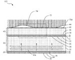
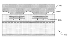
[0073]
도 6a는 본 개시내용의 양상들에 따라, 초음파 센서 어레이(102), 압반(40), 및 압반의 노출된 표면(44) 상에 포지셔닝된 손가락과 같은 목표 오브젝트(70)의 예시적인 구현에 대한 단면도를 예시한다. 도 6a에 도시된 예에서, 초음파 센서 어레이(102)는 커버 층으로서 기능하는 압반(40), 위에 있는 수신기 바이어스 전극(39) 및 연관된 TFT 회로를 갖는 TFT 기판(32)을 가지는 초음파 수신기(30), 및 초음파 송신기(20)를 포함할 수 있다. 초음파 송신기(20)는 압전 송신기 층의 각 측면 상에 배치되는 상위 및 하위 전극들을 가질 수 있다.[0073]
6A illustrates an exemplary implementation of a
[0074]
도 6b는 압전 송신기 층(24)의 각 측면 상에 배치되는 송신기 전극들(22 및 26) 사이에 포지셔닝된 그 압전 송신기 층(24)을 갖는 초음파 송신기(20)로부터 론칭되는 실질적으로 평평한 초음파 평면파(80a)를 예시한다. 초음파 송신기(20)는 TFT 회로(33)가 상부에 형성된 TFT 기판(32)에 커플링될 수 있다. 초음파 송신기(20)는 TFT 기판(32), TFT 회로(33) 및 압반(40)을 통해 하나 또는 그 초과의 초음파 평면파(80a)를 론칭할 수 있다. 일부 구현들에서, 압반(40)은 보호 코팅 층(42)을 가질 수 있다. 일부 구현들에서, 디스플레이 디바이스의 커버 유리 또는 커버 렌즈는 커버 층으로서 또는 압반(40)으로서 기능할 수 있다. 보호 코팅 층(42)은 압반(40)의 외부 표면 상에 포함될 수 있다. 코팅 층(42)은 얼룩-방지 층, 스크래치-방지 층, 환경 보호 층, 음향 임피던스 매칭 층, 광 간섭 필터, 또는 다른 기능 층으로서 기능할 수 있다. 코팅 층(42)은 서브-층들의 다중-층 스택을 포함할 수 있다. 일부 구현들에서, 코팅 층(42)의 노출된 표면은 센서 표면(44)으로서 기능할 수 있다. 일부 구현들에서, 코팅 층(42)은 초음파 수신기(30) 상에 바로 포지셔닝될 수 있고, 압반(40)으로서 기능할 수 있다. 일부 구현들에서, 초음파 센서 어레이(102)는 압반(40) 또는 코팅 층(42)이 없이 구성될 수 있는데, 초음파 수신기(30)의 외부 표면이 센서 표면(44)으로서 기능한다. 많은 구현들에서는 센서 표면(44)이 압반(40)의 노출된 표면(44) 또는 코팅 층(42)의 외부 표면(44)에 대응한다는 점에 주목하자.[0074]
6B illustrates a substantially planar ultrasonic wave propagating from an
[0075]
손가락(70a) 또는 스타일러스 팁과 같은 목표 오브젝트가 초음파 센서 어레이(102)의 외부 센서 표면(44) 상에 포지셔닝될 수 있다. 압반(40) 및 선택적인 코팅 층(42)을 통해 이동하는 초음파 평면파(80a)는 초음파 센서 어레이(102)와 손가락(70a) 사이의 센서 표면(44)으로부터 반사할 수 있다. 손가락(70a)의 리지 지역들(72) 사이의 계곡 지역들(74)은 입사하는 초음파 에너지의 대부분을 TFT 회로(33) 쪽으로 다시 반사시킬 수 있다. 센서 표면(44)에 접촉하는 손가락(70a)의 리지 지역들(72)은 입사하는 초음파 에너지를 흡수, 산란 또는 투과시킬 수 있어서, 결국 TFT 회로(33) 쪽으로 다시 반사되는 초음파 에너지의 양이 줄어든다. 손가락(70a)의 리지 및 계곡 지역들로부터의 반사되는 초음파 에너지는 TFT 회로(33)의 모두 또는 일부 위에 포지셔닝된 압전 수신기 층(38)에 의해서, TFT 회로(33)의 센서 픽셀들(34)의 밑에 있는 센서 픽셀 어레이(35)에 의해 검출될 수 있는 전기 전하로 변환될 수 있다. 수신기 바이어스 전압은 반사된 초음파들(80b)(도 6c 참고)이 압전 수신기 층(38) 및 TFT 회로(33)를 통과할 때 이미지 정보의 포착을 허용하기 위해서 압전 수신기 층(38) 위에 포지셔닝되는 수신기 바이어스 전극(39)에 인가될 수 있다. 일단 포착되면, 센서 픽셀 어레이(35)로부터의 픽셀 출력 신호들이 하나 또는 그 초과의 데이터 및 제어 라인들을 사용하여 추가 프로세싱을 위해 TFT 회로(33)로부터 클록 아웃될 수 있다.[0075]
A target object such as a
[0076]
도 6c는 손가락(70a)의 리지 지역(72)으로부터의 반사된 초음파들(80b)을 예시하면서, 초음파 센서 어레이(102)의 센서 표면(44) 상에 포지셔닝된 손가락(70a)과 함께 초음파 센서 어레이(102)의 확대된 부분을 도시한다. 입사하는 초음파 평면파들(80a)이 센서 표면(44)으로부터 반사될 수 있는데, 반사되는 파들(80b)의 부분은 손가락 리지 지역(72)의 가장자리로부터 더 높은 각도로 반사되고, 손가락(70a)의 손가락 리지 부분(72)의 다른 부분들과 비교해서 다소 지연된 시간을 갖는다. 반사된 파(80b)의 지연된 및 회절된 부분은, 이웃 픽셀들로부터의 픽셀 출력 신호들을 포착함으로써, 이웃 센서 픽셀들에 의해 측정될 때 반사된 초음파들(80b)의 위상 지연 및 진폭을 감안함으로써, 그리고 어레이(102)의 각각의 관심 픽셀에 대한 정정된 출력 신호를 생성함으로써 보상될 수 있다.[0076]
6C illustrates the reflected
[0077]
도 6d는 초음파 센서 어레이(102)의 센서 표면(44) 상에 포지셔닝된 손가락(70a)의 다수의 리지들로부터의 회절 효과들을 도시한다. 손가락(70a)의 눌려진 리지들과 같은 균일한 목표 오브젝트의 부분들 또는 터치하는 오브젝트의 외면과 리지들 사이의 큰 공기 지역들로부터 반사하는 초음파들(80b)에 대해 회절 효과들은 최소가 될 수 있지만, 손가락, 손가락 리지들, 또는 다른 표면 특징들과 같은 목표 오브젝트(70)의 가장자리들 또는 가장자리 특징들에서는 여전히 중요할 수 있다는 것을 주목하자. 압반 두께가 작거나 또는 존재하지 않을 때 회절 효과들은 감소될 수 있다는 것을 또한 주목하자. 유사한 방식으로, 도 6e는 초음파 센서 어레이(102)의 센서 표면(44) 상에 포지셔닝된 스타일러스(70b)의 스타일러스 팁으로부터의 반사된 초음파들(80b)의 회절 효과들을 도시하는데, 그 회절 효과들은 압반 표면(44)과 접촉하는 스타일러스의 팁 가까이에서 가장 확연하다.[0077]
Figure 6d shows diffraction effects from multiple ridges of the
[0078]
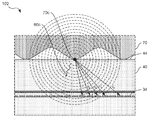
도 6f는 초음파 센서 어레이(102)의 센서 표면(44) 상에 포지셔닝된 목표 오브젝트(70)의 포인트(70c)로부터 방출되는 구면파들(80c)을 예시한다. 입사하는 초음파 평면파(미도시)는 포인트(70c)에 충돌하고, 본질적으로 구면 파면을 가지고 센서 픽셀(34) 쪽으로 다시 반사될 수 있다. 반경들(r1, r2, r3,... rn)은 포인트(70c)로부터 다양한 센서 픽셀들(34)까지의 거리들을 표시하는데, 센서 픽셀들(34)에 충돌하는 반사된 초음파(80c)의 시간(위상) 지연이 포인트(70c)로부터의 거리에 따라 변하는 것을 예시한다. 픽셀 출력 신호들에 대한 정정들이 이웃 센서 픽셀들에 충돌하는 회절된 초음파들의 다양한 위상 지연들을 감안함으로써 이루어질 수 있다.6f illustrates
[0079]
도 7a는 압반(40)의 노출된 표면(44)으로부터 밑에 있는 초음파 센서 어레이(102)의 선택된 센서 픽셀(34a)로의 초음파 평면파(80a)의 반사(80b)를 도시한다. 압반 표면(44)과 센서 픽셀(34a) 간의 간격은 거리(d0)에 의해서 주어질 수 있다. 센서 어레이(102)의 센서 픽셀들(34)의 5×5 부분이 본원에 설명된 개념들을 예시하기 위해 도시되어 있지만, 5×5 어레이로의 제한들이 의도되지는 않는다. 송신된 초음파 평면파(80a)는 센서 픽셀들(34)의 어레이를 통과하고, 압반(40)의 노출된 표면(44)에 충돌할 수 있다. 반사된 초음파(80b)가 센서 픽셀들(34)의 어레이에 도달할 수 있고, 그 센서 픽셀들(34)에서 그 반사된 초음파(80b)의 로컬 크기들이 검출될 수 있다. 반사된 파(80b)를 샘플링하기 이전의 제1 포착 시간 지연은 선택된 픽셀(34a)과 압반 표면(44) 간의 거리(d0)를 감안할 수 있다. 예컨대, 포착 시간 지연(예컨대, RGD1)은 압반(40)에서의 음속과 2배의 거리(d0)의 곱으로 제공되는, 초음파가 2배의 거리(d0)를 이동하는 비행 시간(+코팅들, 매칭 층들 또는 접착 층들과 같은 임의의 추가 층들을 통과하는 시간)과 거의 동일할 수 있다.7A shows the
[0080]
도 7b는 압반(40)의 노출된 표면(44)으로부터 밑에 있는 초음파 센서 어레이(102)의 선택된 픽셀(34a) 가까이 있는 제1 세트의 이웃 픽셀들(34b)로의 초음파 평면파(80a)의 반사(80b)를 도시한다. 회절 효과들은 반사된 초음파 평면파(80b)로 하여금 더 긴 거리를 이동하게 할 수 있고, 그리고 회절 효과들을 감안하여 보상하기 위해 제2 세트의 픽셀 출력 신호들을 포착할 때 다소 더 긴 포착 시간 지연이 포함될 수 있다. 예컨대, 제2 포착 시간 지연이 선택된 픽셀(34a)과 그 선택된 픽셀(34a)에 가까운 일 세트의 이웃 픽셀들(34b) 간의 평균(예컨대, 에버리지) 거리를 감안할 수 있다(이웃 픽셀들(34b)이 선택된 픽셀(34a)의 측면들에 인접한 센서 픽셀들로서 도시됨). 예컨대, 제2 포착 시간 지연 또는 동등하게 범위 게이트 지연(예컨대, RGD2)은 초음파가 거리(d0)를 이동하기 위한 비행 시간 및 레그들(d0 및 d1)의 길이에 의해 주어지는 삼각형의 빗변과 거의 동일할 수 있고, 이로 인해 d1은 도 7d에 대해 아래에서 설명된다. 제1 포착 시간 지연과 2 포착 시간 지연은 선택된 픽셀에 도달하는 반사된 제1 초음파 평면파와 제1 세트의 이웃 픽셀들에 도달하는 반사된 제2 초음파 평면파 간의 위상 차이를 감안하기 위해서 상이할 수 있다.7b shows the
[0081]
도 7c는 압반(40)의 노출된 표면(44)으로부터 밑에 있는 초음파 센서 어레이(102)의 선택된 픽셀(34a) 가까이 있는 제2 세트의 이웃 픽셀들(34c)로의 초음파 평면파(80a)의 반사(80b)를 도시한다. 회절 효과들은 반사된 초음파 평면파(80b)로 하여금 훨씬 더 긴 거리를 이동하게 할 수 있고, 그리고 회절 효과들을 감안하여 보상하기 위해 제3 세트의 픽셀 출력 신호들을 포착할 때 더 긴 포착 시간 지연이 요구될 수 있다. 예컨대, 제3 포착 시간 지연이 선택된 픽셀(34a)과 그 선택된 픽셀(34a) 가까이의 제2 세트의 이웃 픽셀들(34c) 간의 평균(예컨대, 에버리지) 거리를 감안할 수 있다(이웃 픽셀들(34c)이 선택된 픽셀(34a)의 코너들과 접촉하는 센서 픽셀들로서 도시됨). 예컨대, 제3 포착 시간 지연(예컨대, RGD3)은 초음파가 거리(d0)를 이동하기 위한 비행 시간 및 레그들(d0 및 d2)의 길이에 의해 주어지는 삼각형의 빗변과 거의 동일할 수 있고, 이로 인해 d2는 도 7d에 대해 아래에서 설명된다.FIG. 7C shows the
[0082]
도 7d는 초음파 센서 어레이(102)의 선택된 픽셀(34a)(P0) 및 그 선택된 픽셀(34a)에 가까운 다수의 세트들의 이웃 픽셀들을 예시한다. 선택된 픽셀(34a)은 거의 센서 어레이(102)의 임의의 센서 픽셀일 수 있고, 도면에서 P0로 지정되어 있다. 예시 목적들을 위해, 선택된 픽셀(P0)의 중심으로부터 제1 세트의 이웃 픽셀들(P1)의 중심까지의 거리(d1)에 대응하는 반경을 갖는 원이 도시되어 있는데, 거리(d1)는 선택된 픽셀(P0)과 제1 세트의 이웃 픽셀들(P1) 간의 평균(에버리지) 거리(예컨대, 2개의 인접 픽셀들 간의 중심간 거리)를 나타낸다. 선택된 픽셀(P0)의 중심으로부터 제2 세트의 이웃 픽셀들(P2)의 중심까지의 거리(d2)에 대응하는 반경을 갖는 제2 원이 도시되어 있는데, 거리(d2)는 선택된 픽셀(P0)과 제2 세트의 이웃 픽셀들(P2) 간의 평균(에버리지) 거리를 나타낸다. 선택된 픽셀(P0)의 중심으로부터 추가 세트들의 이웃 픽셀들(Pn)의 중심까지의 거리들(d3, d4 및 d5)에 대응하는 반경을 갖는 추가 원들이 도시되어 있는데, 거리들(d3, d4 및 d5)은 선택된 픽셀(P0)과 추가 세트들의 이웃 픽셀들(P3, P4 및 P5) 간의 평균 거리를 각각 나타낸다. 이런 절차는 추가 센서 픽셀들을 식별하여 다양한 세트들의 이웃 픽셀들에 할당하고 그리고 회절 효과들에 대한 보상을 허용하기 위해서 후속될 수 있다.[0082] Figure 7d illustrates a selected
[0083] 추가 세트들의 픽셀 출력 신호들을 포착하고 이웃 세트들의 픽셀들로부터의 센서 픽셀 데이터를 갖는 정정된 출력 신호들을 생성함으로써, 픽셀 출력 신호들에 대해 회절 효과들로 인한 상당한 정정들이 이루어질 수 있다는 것이 주목될 수 있다. 일부 구현들에서, 각각의 선택된 픽셀에 가까운 단지 일 세트의 이웃 픽셀들(예컨대, 가장 가까운 이웃들)로부터의 픽셀 출력 신호들을 포착함으로써 정정들이 이루어질 수 있다. 일부 구현들에서, 각각의 선택된 픽셀에 가까운 2개의 상이한 세트들의 이웃 픽셀들(예컨대, 가장 가까운 이웃들 및 다음으로 가장 가까운 이웃들)로부터의 픽셀 출력 신호들을 포착함으로써 정정들이 이루어질 수 있다. 일부 구현들에서, 각각의 선택된 픽셀에 가까운 3개, 4개, 5개 또는 더 많은 상이한 세트들의 이웃 픽셀들로부터의 픽셀 출력 신호들을 포착함으로써 정정들이 이루어질 수 있다.[0083] It can be noted that significant corrections due to diffraction effects can be made on the pixel output signals by capturing additional sets of pixel output signals and generating corrected output signals with sensor pixel data from pixels of neighboring sets have. In some implementations, corrections may be made by capturing pixel output signals from only a set of neighboring pixels (e.g., nearest neighbors) that are close to each selected pixel. In some implementations, corrections may be made by capturing pixel output signals from two different sets of neighboring pixels (e.g., nearest neighbors and next closest neighbors) near each selected pixel. In some implementations, corrections can be made by capturing pixel output signals from three, four, five or more different sets of neighboring pixels that are close to each selected pixel.
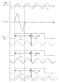
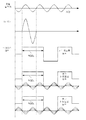
[0084] 도 8a 내지 도 8g는 초음파 송신기에 제공되는 송신기 여기 신호들의 다양한 사이클들(위의 그래프들) 및 초음파 센서 어레이의 수신기 바이어스 전극에 적용되는 다양한 바이어스 레벨들(아래의 그래프들)을 그래프로 예시하고, 샘플링 윈도우들의 다양한 지속기간들 및 다양한 포착 시간 지연들은 다양한 세트들의 픽셀 출력 신호들의 포착, 예컨대 제1 세트의 픽셀 출력 신호들, 제2 세트의 픽셀 출력 신호들, 또는 제3 세트의 픽셀 출력 신호들의 포착을 허용한다. 초음파 평면파를 론칭하는 것과 관련된 아래의 설명이 제1 초음파 평면파 및/또는 제2 초음파 평면파를 론칭하는 것에 적용가능한 것으로 이해되어야 하도록, 아래의 설명은 본원에서 개시된 다양한 구현들에 일반적이다. 유사하게, 픽셀 출력 신호들을 포착하는 것에 관련된 아래의 설명은 제1 세트의 픽셀 출력 신호들 및/또는 제2 세트의 픽셀 출력 신호들을 포착하는 것에 적용가능한 것으로 이해되어야 한다. 아래에서 포착 시간 지연들의 일반적인 설명은 제1 포착 시간 지연 및 제2 포착 시간 지연에 적용가능한 것으로 또한 이해되어야 한다.[0084] Figures 8A-8G graphically illustrate various cycles of transmitter excitation signals provided to an ultrasonic transmitter (graphs above) and various bias levels (graphs below) applied to a receiver bias electrode of an ultrasonic sensor array The various durations of the sampling windows and the various acquisition time delays may be used to capture various sets of pixel output signals, e.g., a first set of pixel output signals, a second set of pixel output signals, Lt; / RTI > The following description is generic to the various implementations disclosed herein so that it should be understood that the following description relating to launching ultrasonic plane waves is applicable to launching first ultrasonic plane waves and / or second ultrasonic plane waves. Similarly, it should be understood that the following description relating to capturing pixel output signals is applicable to capturing a first set of pixel output signals and / or a second set of pixel output signals. It should also be understood that the general description of the acquisition time delays below is applicable to the first acquisition time delay and the second acquisition time delay.
[0085]
도 8a는 초음파 송신기에 제공될 수 있는 송신기 여기 신호들의 다양한 사이클들(위의 그래프) 및 초음파 센서 어레이(102)의 수신기 바이어스 전극(39)에 적용될 수 있는 다양한 바이어스 레벨들(아래의 그래프)을 그래프로 예시한다. 미리 결정된 주파수 및 스캔 레이트의 초음파 송신기 여기 신호의 하나 또는 그 초과의 사이클들은 도면의 최상부 부분에 도시된 바와 같이 송신기(Tx)에 적용될 수 있다. 하나의 Tx 사이클이 실선으로 도시되어 있는 반면에, 추가 사이클들은 파선으로 도시되어 있다. 일부 구현들에서는, 단일 송신기 여기 사이클이 사용될 수 있다. 일부 구현들에서는, 2개의 사이클들, 3개의 사이클들, 4개의 사이클들, 5개의 사이클들 또는 그 초과 개수의 사이클들과 같은 다수의 여기 사이클들이 사용될 수 있다. 비록 예시적인 목적들을 위해 사인 파형들로 도시되어 있지만, 일부 구현들에서의 송신기 여기 신호들은 구형 파들, 방형 파들, 부분 파들, 펄스 파들(pulsed waves), 다중-주파수 파들, 처프 파들(chirped waves), 저 또는 고 듀티-사이클 파들, 가변-진폭 파들, 가변-주파수 파들, 또는 초음파 송신기(20)를 구동시키기 위한 다른 적절한 파형일 수 있다. 발신 초음파의 송신 동안, 차단 모드에 대응하는 초음파 센서 어레이(102)의 수신기 바이어스 전극(39)에 제어 신호가 인가될 수 있는데, 여기서 발신하는 송신된 파들로부터의 신호들이 픽셀 회로들(36)에 의해 포착되는 것을 막기 위해서 바이어스 레벨이 차단 값으로 세팅된다. 반사된 초음파 신호들이 샘플 모드 동안 포착될 수 있는데, 그 샘플 모드 동안에 수신기 바이어스 전극(39)에 인가되는 제어 신호의 바이어스 레벨은 샘플 값으로 세팅된다. 불필요한 내부 반사들의 검출을 막기 위해서, 수신기 바이어스 전극(39)에 적용되는 바이어스 레벨이 짧은 시간 기간 동안에 차단 값으로 다시 될 수 있다. 수신기 바이어스 전극(39)에 적용되는 바이어스 레벨이 홀드 값으로 되는 홀드 모드 동안, 초음파 센서 어레이의 각각의 센서 픽셀에 저장된 신호들이 클록 아웃될 수 있다. 도 8a를 다시 참조하면, 제1 송신기 여기 신호가 초음파 송신기(20)에 인가될 수 있고, 센서 어레이의 바이어스 레벨이 론치 시간에 차단 값으로 세팅될 수 있다. 범위-게이트 지연(RGD)으로 또한 지칭되는 포착 시간 지연 이후에, 바이어스 레벨은 샘플 값으로 되고, 샘플링 윈도우 또는 범위-게이트 윈도우(RGW)로 또한 지칭되는 포착 시간 윈도우에 대응하는 지속기간 동안에 그 샘플 값으로 유지될 수 있다. 일부 구현들에서의 포착 시간 윈도우는 송신기 여기 사이클의 주기보다 길거나 그와 동일하거나 또는 다른 구현들에서 송신기 여기 사이클의 주기보다 짧은 시간 인터벌에 대응할 수 있다는 것을 주목하자. 송신기 여기 사이클의 주기는 일반적으로 대응하는 송신된 및 반사된 초음파들의 주기와 동일하다는 것을 주목하자. 포착 시간 윈도우에 대응하는 시간 인터벌 이후에, 수신기 바이어스 전극(39)에 적용되는 바이어스 레벨은 다시 차단 값으로 될 수 있다. 다른 시간 인터벌 이후에, 바이어스 레벨은 픽셀 출력 신호들의 클록 아웃을 허용하기 위해 홀드 값으로 될 수 있다. 예컨대, 초음파 평면파는 평면파 생성기와 같은 초음파 송신기(20)로부터 압반 표면 쪽으로 론치 시간에 론칭될 수 있다. 일 세트의 픽셀 출력 신호들이 초음파 평면파의 론치로부터 포착 시간 지연만큼 지연되는 포착 시간에 포착될 수 있다. 픽셀 출력 신호들은 평면파가 압반 표면으로부터 반사된 이후 미리 결정된 시간들에 초음파 평면파의 로컬 크기들을 나타낼 수 있다. 추가 세트들의 픽셀 출력 신호들은 추가 초음파 평면파들을 론칭한 이후에 포착될 수 있다. 픽셀 출력 신호들은 동일하거나 상이한 포착 시간 지연들 이후에 그리고 동일하거나 상이한 포착 시간 윈도우들을 통해 포착될 수 있다.[0085]
8A shows various cycles of transmitter excitation signals (graph above) that may be provided to the ultrasonic transmitter and various bias levels (graph below) that may be applied to the
[0086]
도 8b는 초음파 송신기에 제공될 수 있는 송신기 여기 신호의 단일 사이클(위의 그래프) 및 반사된 파를 검출하기 위해 초음파 센서 어레이(102)의 수신기 바이어스 전극(39)에 적용될 수 있는 다양한 바이어스 레벨들(아래의 그래프)을 그래프로 예시한다. 제1 시간 인터벌 이후에, 초음파 평면파를 론칭하기 위해서 송신기 여기 신호가 초음파 송신기(20)에 인가될 수 있다. 수신기 바이어스 전극(39)에 적용되는 바이어스 레벨은 홀드 값으로부터 차단 값으로 변경될 수 있고, 이는 초음파가 픽셀 회로 어레이를 통과할 때 픽셀 회로들이 신호를 포착하는 것을 차단할 수 있다. 포착 시간 지연 또는 동등하게 범위-게이트 지연(RGD)에 대응하는 제2 시간 인터벌 이후에, 수신기 바이어스 전극(39)에 적용되는 바이어스 레벨은 도면에서 수신 파로서 도시되는 센서 압반(40)의 표면으로부터 반사되어진 초음파의 로컬 크기의 샘플링 및 정류를 허용하기 위해 샘플 값으로 될 수 있다. 포착 시간 윈도우 또는 동등하게 범위-게이트 윈도우(RGW)에 대응하는 제3 시간 인터벌 이후에, 수신기 바이어스 전극(39)에 적용되는 바이어스 레벨은 센서 스택에서 초음파들의 잔향들이 차츰 잦아들도록 허용하기 위해서 차단 값으로 다시 될 수 있다. 제4 시간 인터벌 이후에, 수신기 바이어스 전극(39)에 적용되는 바이어스 레벨은 홀드 값으로 될 수 있고, 이는 초음파 센서 어레이의 하나 또는 그 초과의 픽셀들에 의해 포착되는 픽셀 출력 신호들이 판독되게 허용한다. 제5 시간 인터벌 이후에, 시퀀스가 반복될 수 있어서, 추가 세트들의 픽셀 출력 신호들이 포착되게 허용한다.[0086]
FIG. 8B illustrates various biasing levels that can be applied to the
[0087]
도 8c는 초음파 송신기에 제공될 수 있는 송신기 여기 신호의 다수의 사이클들(위의 그래프) 및 반사된 파를 검출하기 위해 초음파 센서 어레이(102)의 수신기 바이어스 전극(39)에 적용될 수 있는 다양한 바이어스 레벨들(아래의 그래프)을 그래프로 예시한다. 송신기 여기 전압의 개시 시에, 수신기 바이어스 전극(39)은 차단 값으로 될 수 있는데 반해, 다수의 여기 사이클들이 초음파 송신기(20)에 적용될 수 있다. 여기 사이클들의 종료 시에 또는 거의 종료 시에, 수신기 바이어스 전극(39)은 샘플 값으로 될 수 있는데, 반사된 초음파의 크기의 로컬 진폭을 표시하는 센서 신호들이 센서 픽셀들에서 포착된다. 범위-게이트 윈도우(RGW)는 송신기(20)에 적용되는 사이클들 중 임의의 사이클로부터 가장 큰 정류된 신호들을 포착하기에 충분히 넓은 것으로 도시되어 있다는 것을 주목하자. 동작 시에, 범위-게이트 윈도우의 폭은 송신기 여기 신호의 하나의 사이클의 주기와 동일하거나 그보다 클 수 있는데 반해, 대부분의 구현들에서 범위-게이트 윈도우의 폭은 수신된 초음파를 따라 다양한 포인트들에서의 샘플링을 허용하기 위해서 송신기 여기 사이클보다 현저히 더 짧다.[0087]
FIG. 8C illustrates various cycles (upper graph) of the transmitter excitation signal that may be provided to the ultrasonic transmitter and various biases that may be applied to the
[0088]
도 8d는 초음파 송신기에 제공될 수 있는 송신기 여기 신호의 단일 사이클(위의 그래프) 및 반사된 파를 검출하기 위해 초음파 센서 어레이(102)의 수신기 바이어스 전극(39)에 적용될 수 있는 다양한 바이어스 레벨들(아래의 그래프)을 그래프로 예시하는데, 샘플링 윈도우는 송신기 여기 신호의 하나의 사이클의 주기보다 훨씬 더 짧다. 이 예에서, 단지 하나의 송신기 여기 사이클이 사용되고, 범위-게이트 윈도우는 송신기 여기 사이클의 주기보다 훨씬 더 작다. 유사한 방식으로, 도 8e는 초음파 송신기에 제공되는 송신기 여기 신호의 다수의 사이클들(위의 그래프) 및 반사된 파를 검출하기 위해 초음파 센서 어레이(102)의 수신기 바이어스 전극(39)에 적용되는 다양한 바이어스 레벨들(아래의 그래프)을 그래프로 예시하는데, 샘플링 윈도우는 송신기 여기 신호의 하나의 사이클의 주기보다 훨씬 더 짧다.[0088]
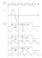
Figure 8d illustrates various biasing levels that can be applied to the
[0089] 도 8f는 초음파 송신기에 제공될 수 있는 송신기 여기 신호의 사이클(위의 그래프) 및 반사된 파를 검출하기 위해 초음파 센서 어레이의 수신기 바이어스 전극에 적용될 수 있는 다양한 바이어스 레벨들(아래의 그래프)을 그래프로 예시하는데, 샘플링 윈도우는 송신기 여기 신호의 하나의 사이클의 주기보다 훨씬 더 짧고 초음파의 론치로부터 시간에 따라 변한다(2개의 샘플들이 도시됨). 제1 샘플의 범위-게이트 지연(RGD1a)은 제2 샘플의 범위-게이트 지연(RGD1b)보다 더 짧고, 이는 반사된 초음파를 따라 다양한 포인트들에서 다수의 세트들의 픽셀 출력 신호들의 포착을 예시한다. 각각의 샘플링 윈도우 내에서, 초음파 신호의 정류는 일반적으로 샘플링 윈도우 내에서 단지 피크 신호를 포착하는데, 그 피크 신호가 반사된 파의 피크 신호에 반드시 대응하는 것은 아니다.[0089] Figure 8f illustrates various bias levels that can be applied to the receiver bias electrode of the ultrasonic sensor array to detect a cycle of the transmitter excitation signal (graph above) and a reflected wave that can be provided to the ultrasonic transmitter ) In which the sampling window is much shorter than the period of one cycle of the transmitter excitation signal and changes with time from the launch of the ultrasonic waves (two samples are shown). The range-gate delay (RGD 1a ) of the first sample is shorter than the range-gate delay (RGD 1b ) of the second sample, which illustrates the capture of multiple sets of pixel output signals at various points along the reflected ultrasound do. Within each sampling window, the rectification of the ultrasonic signal typically captures only the peak signal within the sampling window, which peak signal does not necessarily correspond to the peak signal of the reflected wave.
[0090] 도 8g는 초음파 송신기에 제공될 수 있는 송신기 여기 신호의 사이클(위의 그래프) 및 반사된 파를 검출하기 위해 초음파 센서 어레이의 수신기 바이어스 전극에 적용될 수 있는 다양한 바이어스 레벨들(아래의 그래프)을 그래프로 예시하는데, 샘플링 윈도우는 송신기 여기 신호의 하나의 사이클의 주기보다 훨씬 더 짧고, 선택된 픽셀들로부터의 그리고 이웃 픽셀들의 세트들(3개의 샘플들이 도시됨)로부터의 반사된 파의 수신을 검출하기 위해서 초음파의 론치로부터 시간에 따라 변한다. 이런 예에서, 반사된 초음파의 3개의 샘플들이 3개의 상이한 범위-게이트 지연들(RGD1, RGD2 및 RGD3)을 사용함으로써 포착된다.[0090] FIG. 8g illustrates various bias levels that can be applied to the receiver bias electrode of the ultrasonic sensor array to detect a cycle of the transmitter excitation signal (graph above) and a reflected wave that may be provided to the ultrasonic transmitter ) In which the sampling window is much shorter than the period of one cycle of the transmitter excitation signal and the reception of reflected waves from selected pixels and from sets of neighboring pixels (three samples are shown) And changes with time from the launch of the ultrasonic wave to detect the ultrasonic wave. In this example, three samples of the reflected ultrasound are captured using three different range-gate delays RGD 1 , RGD 2 and RGD 3 .
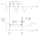
[0091] 도 8h 내지 도 8l은 로컬 발진기의 출력(위의 그래프들)과 동기화되고 초음파 송신기에 제공되는 송신기 여기 신호들의 다양한 사이클들(중간 그래프들) 및 반사된 파를 검출하기 위해 초음파 센서 어레이의 수신기 바이어스 전극에 적용되는 다양한 바이어스 레벨들(아래의 그래프들)을 그래프로 예시하고, 샘플링 윈도우들의 다양한 지속기간들, 초음파의 론치로부터의 다양한 포착 시간 지연들, 및 바이어스 레벨들과 로컬 발진기 신호의 다양한 혼합이 다양한 세트들의 픽셀 출력 신호들의 포착을 허용한다.[0091] Figures 8h-l illustrate various cycles (intermediate graphs) of transmitter excitation signals that are synchronized with the output of the local oscillator (the graphs above) and provided to the ultrasonic transmitter and the receiver bias of the ultrasonic sensor array Graphically illustrating the various bias levels (graphs below) applied to the electrodes, various durations of the sampling windows, various acquisition time delays from the launch of the ultrasonic waves, and various combinations of bias levels and local oscillator signals This allows capture of the various sets of pixel output signals.
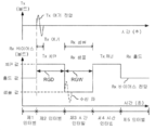
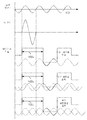
[0092]
도 8h는 로컬 발진기의 출력(위의 그래프)과 동기화되고 초음파 송신기에 제공되는 송신기 여기 신호의 사이클(중간 그래프) 및 반사된 파를 검출하기 위해 초음파 센서 어레이의 수신기 바이어스 전극에 적용되는 다양한 바이어스 레벨들(아래의 그래프)을 그래프로 예시하는데, 샘플링 윈도우는 송신기 여기 신호의 하나의 사이클의 주기보다 훨씬 더 짧고, 샘플링 동안 바이어스 레벨과 로컬 발진기 신호를 혼합하면서 다수의 세트들의 픽셀 출력 신호들(3개의 샘플들이 도시됨)을 포착하기 위해서 초음파의 론치로부터 시간에 따라 변한다. 혼합된 신호가 수신기 바이어스 전극 전압 상에 중첩될 수 있거나, 일부 구현들에서는 샘플링 윈도우 동안에만 수신기 바이어스 전극(39)에 인가될 수 있다. 수신기 바이어스 신호와 혼합될 때 로컬 발진기 신호의 진폭은 송신기 여기 신호보다 훨씬 작을 수 있지만, 그 두 신호들은 시간적으로 동기화될 수 있다. 예시된 바와 같이, 로컬 발진기 신호의 제어된 진폭 및 위상과 혼합될 때 반사된 초음파를 샘플링하는 동안에 다수의 세트들의 픽셀 출력 신호들이 여러 범위-게이트 지연들(RGD1, RGD2, RGD3 등)을 통해 포착될 수 있다.[0092] FIG. 8h illustrates a cycle (intermediate graph) of the transmitter excitation signal that is synchronized with the output of the local oscillator (the graph above) and provided to the ultrasonic transmitter, and the cycle of the transmitter excitation signal applied to the receiver bias electrode of the ultrasonic sensor array The graph illustrates the various bias levels (graph below), with the sampling window being much shorter than the period of one cycle of the transmitter excitation signal, while mixing the bias level with the local oscillator signal during sampling, ≪ / RTI > changes from time to time from the launch of the ultrasound to capture the ultrasound (three samples are shown). The mixed signal may be superimposed on the receiver bias electrode voltage, or in some implementations may be applied to the
[0093]
도 8i는 로컬 발진기의 출력(위의 그래프)과 동기화되고 초음파 송신기에 제공되는 송신기 여기 신호의 사이클(중간 그래프) 및 반사된 파를 검출하기 위해 초음파 센서 어레이의 수신기 바이어스 전극(39)에 적용되는 다양한 바이어스 레벨들(아래의 그래프들)을 그래프로 예시하는데, 샘플링 윈도우는 송신기 여기 신호의 하나의 사이클의 주기보다 훨씬 더 짧고, 혼합된 로컬 발진기 신호가 포착된 세트들의 픽셀 출력 신호들 간의 실질적으로 동일한 진폭 그러나 상이한 위상(지연)을 갖도록 샘플링 동안 바이어스 레벨과 로컬 발진기 신호를 혼합하면서 다수의 세트들의 픽셀 출력 신호들(3개의 세트들이 도시됨)을 포착하기 위해서 초음파의 론치로부터 시간에 따라 변하지 않는다. 이런 예에서, 동일한 범위-게이트 지연(RGD1)이 각각의 샘플의 포착을 위해 적용되는데 반해, 혼합된 로컬 발진기 신호가 각각의 샘플에 대해 동일한 진폭 그러나 상이한 위상들을 갖는다.[0093] FIG. 8i shows a cycle (intermediate graph) of the transmitter excitation signal synchronized with the output of the local oscillator (upper graph) and provided to the ultrasonic transmitter, and the
[0094]
도 8j는 로컬 발진기의 출력(위의 그래프)과 동기화되고 초음파 송신기에 제공되는 송신기 여기 신호의 사이클(중간 그래프) 및 반사된 파를 검출하기 위해 초음파 센서 어레이(102)의 수신기 바이어스 전극(39)에 적용되는 다양한 바이어스 레벨들(아래의 그래프들)을 그래프로 예시하는데, 샘플링 윈도우는 송신기 여기 신호의 하나의 사이클의 주기보다 훨씬 더 짧고, 혼합된 로컬 발진기 신호가 포착된 세트들의 픽셀 출력 신호들 간의 상이한 진폭 및 상이한 위상을 갖도록 샘플링 동안 바이어스 레벨과 로컬 발진기 신호를 혼합하면서 다수의 세트들의 픽셀 출력 신호들(3개의 세트들이 도시됨)을 포착하기 위해서 초음파의 론치로부터 시간에 따라 변하지 않는다. 이런 예에서, 범위-게이트 지연(RGD1)이 각각의 샘플에 대해 동일한데 반해, 혼합된 로컬 발진기 신호가 각각의 샘플에 대해 상이한 진폭들 및 상이한 위상들을 갖는다.[0094] Figure 8j shows a cycle (intermediate graph) of the transmitter excitation signal being synchronized with the output of the local oscillator (the graph above) and provided to the ultrasonic transmitter, (The graphs below) applied to the
[0095]
도 8k는 로컬 발진기의 출력(위의 그래프)과 동기화되고 초음파 송신기에 제공되는 송신기 여기 신호의 사이클(중간 그래프) 및 반사된 파를 검출하기 위해 초음파 센서 어레이(102)의 수신기 바이어스 전극(39)에 적용되는 다양한 바이어스 레벨들(아래의 그래프들)을 그래프로 예시하는데, 샘플링 윈도우는 송신기 여기 신호의 하나의 사이클의 주기와 실질적으로 동일한 폭을 갖고, 혼합된 로컬 발진기 신호가 포착된 세트들의 픽셀 출력 신호들 간의 실질적으로 동일한 진폭 그러나 상이한 위상을 갖도록 샘플링 동안 바이어스 레벨과 로컬 발진기 신호를 혼합하면서 다수의 세트들의 픽셀 출력 신호들(3개의 세트들이 도시됨)을 포착하기 위해서 초음파의 론치로부터 시간에 따라 변하지 않는다. 이런 예에서, 범위-게이트 지연(RGD1)이 각각의 샘플에 대해 동일한데 반해, 혼합된 로컬 발진기 신호가 각각의 샘플에 대해 실질적으로 동일한 진폭 그러나 상이한 위상들(0, 90 및 180도가 도시됨)을 갖는다.[0095] FIG. 8k illustrates a cycle (intermediate graph) of the transmitter excitation signal that is synchronized with the output of the local oscillator (the graph above) and provided to the ultrasonic transmitter and the receiver bias electrode of the ultrasonic sensor array 102 (Graphs below) applied to the
[0096] 도 8l는 로컬 발진기의 출력(위의 그래프)과 동기화되고 초음파 송신기에 제공되는 송신기 여기 신호의 사이클(중간 그래프) 및 반사된 파를 검출하기 위해 초음파 센서 어레이의 수신기 바이어스 전극에 적용되는 다양한 바이어스 레벨들(아래의 그래프들)을 그래프로 예시하는데, 샘플링 윈도우는 송신기 여기 신호의 하나의 사이클의 주기와 실질적으로 동일한 폭을 갖고, 혼합된 로컬 발진기 신호가 포착된 세트들의 픽셀 출력 신호들 간의 상이한 진폭들 그러나 실질적으로 동일한 위상을 갖도록 샘플링 동안 바이어스 레벨과 로컬 발진기 신호를 혼합하면서 다수의 세트들의 픽셀 출력 신호들(3개의 세트들이 도시됨)을 포착하기 위해서 초음파의 론치로부터 시간에 따라 변하지 않는다. 이런 예에서, 범위-게이트 지연(RGD1)이 각각의 샘플에 대해 동일한데 반해, 혼합된 로컬 발진기 신호가 각각의 샘플에 대해 상이한 진폭들 그러나 동일한 위상을 갖는다.[0096] FIG. 8L shows a cycle (intermediate graph) of the transmitter excitation signal synchronized with the output of the local oscillator (the graph above) and applied to the receiver bias electrode of the ultrasonic sensor array to detect the reflected wave Graphically illustrating the various bias levels (graphs below), the sampling window has a width that is substantially the same as the period of one cycle of the transmitter excitation signal, and the mixed local oscillator signal is divided into pixel output signals Vary from time to time from the launch of the ultrasound to capture the multiple sets of pixel output signals (three sets shown) while mixing the bias level and the local oscillator signal during sampling to have different amplitudes but substantially the same phase Do not. In this example, the mixed local oscillator signal has different amplitudes but the same phase for each sample, while the range-gate delay (RGD 1 ) is the same for each sample.
[0097]
도 8m은 초음파 송신기에 제공되는 송신기 여기 신호들의 다양한 사이클들(위의 그래프) 및 초음파 센서 어레이의 다이오드 바이어스 전극에 적용되는 다양한 바이어스 레벨들(아래의 그래프)을 그래프로 예시한다. 미리 결정된 주파수 및 스캔 레이트의 초음파 송신기 여기 신호의 하나 또는 그 초과의 사이클들은, 도면의 최상부 부분에 도시된 바와 같이 그리고 도 8a에 대해 위에서 설명된 바와 같이, 송신기(Tx)에 적용될 수 있다. 발신 초음파의 송신 동안, 차단 모드에 대응하는 초음파 센서 어레이(102)의 다이오드 바이어스 전극(510)에 제어 신호가 인가될 수 있는데, 여기서 바이어스 레벨이 차단 값으로 세팅된다. 다이오드 바이어스 전극(510)에 인가되는 제어 신호의 바이어스 레벨이 샘플 값으로 세팅될 때, 반사된 초음파 신호들은 샘플 모드 동안 포착될 수 있다. 불필요한 내부 반사들의 검출을 막기 위해서, 다이오드 바이어스 전극(510)에 적용되는 바이어스 레벨이 짧은 시간 기간 동안에 차단 값으로 다시 될 수 있다. 다이오드 바이어스 전극(510)에 적용되는 바이어스 레벨이 홀드 값으로 되는 홀드 모드 동안, 초음파 센서 어레이(102)의 각각의 센서 픽셀에 저장된 신호들이 클록 아웃될 수 있다. 도 8m을 다시 참조하면, 제1 송신기 여기 신호가 초음파 송신기(20)에 인가될 수 있고, 센서 어레이(102)의 바이어스 레벨이 론치 시간에 차단 값으로 세팅될 수 있다. 범위-게이트 지연(RGD)으로 또한 지칭되는 포착 시간 지연 이후에, 바이어스 레벨은 샘플 값으로 되고, 범위-게이트 윈도우(RGW)로 또한 지칭되는 포착 시간 윈도우에 대응하는 지속기간 동안에 그 샘플 값으로 유지될 수 있다. 포착 시간 지연은 송신기 여기 사이클의 주기보다 길거나 그와 동일하거나 또는 송신기 여기 사이클보다 짧은 시간 인터벌에 대응할 수 있다는 것을 주목하자. 포착 시간 윈도우에 대응하는 시간 인터벌 이후에, 다이오드 바이어스 전극(510)에 적용되는 바이어스 레벨은 다시 차단 값으로 될 수 있다. 다른 시간 인터벌 이후에, 바이어스 레벨은 픽셀 출력 신호들의 클록 아웃을 허용하기 위해 홀드 값으로 될 수 있다. 픽셀 출력 신호들을 포착하기 위해 다이오드 바이어스 전극(510)에 적용되는 다이오드 바이어스 전압들 및 타이밍의 동작은 수신기 바이어스 전극(39)에 적용되는 전압들 및 타이밍과 매우 유사할 수 있다(도 8a에 대해 위에서 설명된 바와 같이 그리고 다른 곳에서는 비록 전압들의 극성들 및 크기가 그들 간에 상이할 수 있지만). 일부 구현들에서, 초음파 센서 어레이(102)는 요구될 때 초음파 이미징을 위해 어느 하나의 모드 또는 두 모드들 모두에서 동작될 수 있다.[0097]
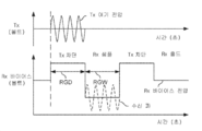
Figure 8m graphically illustrates various cycles of transmitter excitation signals provided in an ultrasonic transmitter (graph above) and various bias levels applied to a diode bias electrode of an ultrasonic sensor array (graph below). One or more cycles of the ultrasonic transmitter excitation signal at a predetermined frequency and scan rate may be applied to the transmitter Tx as shown in the top part of the figure and as described above with respect to figure 8a. During transmission of the outgoing ultrasonic waves, a control signal may be applied to the
[0098]
도 9는 초음파 센서 어레이(102)의 복수의 픽셀들에 대한 정정된 출력 신호들에 기반하여 압반 표면(40) 상에 포지셔닝된 목표 오브젝트(70)의 이미지의 생성을 예시한다. 2개 또는 그 초과의 세트들의 픽셀 출력 신호들 각각은 초음파 이미지 정보의 픽셀-단위 산술 가중화와 결합될 수 있다. 각각의 픽셀에 대한 정정된 출력 신호는 후속적으로 포착된 세트들의 픽셀 출력 신호들을 초기에 포착된 픽셀 출력 신호로 가중화하고 그리고 각각의 픽셀에 대한 결과들을 함께 결합함으로써 생성되고, 그리고 결합된 표현 또는 이미지 정보 세트를 형성하기 위해서 선택적으로 정규화될 수 있다. 각각의 선택된 픽셀에 대한 픽셀 출력 신호들을 이웃 픽셀들로부터의 픽셀 출력 신호들의 가중화된 결합들로 픽셀-단위로 가중화하는 것을 사용하여, 상이한 범위-게이트 지연들의 다양한 세트들의 픽셀 출력 신호들로부터의 반사된 초음파의 로컬 크기들, 범위-게이트 윈도우들, 및 여기 주파수들이 그들의 개개의 위상-정정 및 진폭-정정된 가중치들에 의해 곱해지고, 함께 더해지고 그리고 선택적으로 정규화됨으로써, 복수의 선택된 픽셀들에 대한 정정된 출력 신호들에 기반하여 압반 표면 상에 포지셔닝된 목표 오브젝트(70)의 이미지를 나타내는 이미지 정보 세트를 생성할 수 있다.[0098]
Figure 9 illustrates the generation of an image of a
[0099]
일부 구현들에서, 압반 표면(40) 상에 포지셔닝된 목표 오브젝트(70)의 이미지의 생성은 초음파 센서 어레이(102)의 복수의 선택된 픽셀들에 대한 정정된 출력 신호들에 기반할 수 있다. 복수의 픽셀들은 초음파 센서 어레이(102)의 각각의 픽셀 또는 그것의 서브세트를 포함할 수 있다. 예컨대, 센서 어레이의 활성 영역에 있는 각각의 그리고 모든 픽셀에서, 또는 손가락의 마찰 리지가 어떤 손가락도 놓이지 않은 지역들에서의 대규모 계산들을 회피하고 레이턴시를 줄이기 위해 식별되는 지역과 같은 어레이 내의 픽셀들의 더 작은 블록 내에서 이미지가 정정된 출력 값들로부터 생성될 수 있다.[0099]
In some implementations, the generation of the image of the
[00100]
센서 픽셀 어레이의 하나 또는 그 초과의 선택된 픽셀들에 대한 정정된 출력 신호들이 하나 또는 그 초과의 세트들의 픽셀 출력 신호들에 일련의 동작들을 적용함으로써 생성될 수 있다. 다양한 세트들의 픽셀 출력 신호들(이를테면 제1 세트의 픽셀 출력 신호들, 제2 세트의 픽셀 출력 신호들, 및/또는 제3 세트의 픽셀 출력 신호들)이 예컨대 상이한 범위-게이트 지연들, 범위-게이트 윈도우들, 및 여기 주파수들을 통해 획득될 수 있다. 일부 구현들에서, 센서 픽셀 어레이의 하나 또는 그 초과의 선택된 픽셀들에 대한 정정된 출력 신호들이 범위-게이트 윈도우의 폭의 미세한 단계적 변화들(예컨대, 128-MHz 클록 주파수에 대한 7.8ns 증분들)을 허용하는 64MHz 또는 128MHz와 같은 고 샘플링 클록 주파수를 통해 초음파 센서 데이터를 맨 먼저 포착함으로써 생성될 수 있다. 범위-게이트 지연은 초음파 송신기와 센서 픽셀들 간의 거리에 의해서 결정될 수 있는데, 이는 위에 있는 압반의 두께와 그 압반에서의 음속에 부분적으로 기반할 수 있다. 범위-게이트 지연들은 거의 400-um 두께 유리 압반에 대해 대략 0.65 내지 1.0 마이크로초일 수 있다. 더 두껍거나 더 얇은, 또는 상이한 물질들로 만들어진 압반들의 다양한 구현들에서, 통상적인 범위-게이트 지연들은 약 0.2 마이크로초와 약 2.0 마이크로초 사이에서 변할 수 있다. 일 세트의 픽셀 출력 신호들이 범위-게이트 지연과 동등한 제1 포착 시간에 포착될 수 있다. 샘플링 윈도우는 정수개의 샘플링 클록 주기들 길이일 수 있는데, 이를테면 거의 54 마이크로초의 포착 시간 윈도우에 대해 7개의 클록 사이클들일 수 있다. 송신된/반사된 초음파의 주기보다 더 짧을 수 있는 지속기간 또는 적어도 송신된/반사된 초음파의 한 주기만큼 긴 지속기간을 갖는 다른 샘플링 윈도우 사이즈들이 사용될 수 있다. 임의의 비-제로 바이어스 값들을 삭제하기 위해서 그리고 제로 평균을 갖는 수정된 세트의 픽셀 출력 신호들을 획득하기 위해서, 픽셀 출력 신호들이 평균화되고 평균 값이 각각의 픽셀 출력 신호로부터 감산될 수 있다. 기준 세트의 픽셀 출력 신호들(목표 오브젝트를 갖지 않음)이 포착되어 수정된 세트의 픽셀 출력 신호로부터 감산될 수 있고, 결과적인 세트가 임의의 체계적 백그라운드 신호들을 감산하고, 일 세트의 값들을 화이트닝시키고(whiten), 그리고 동적 범위를 증가시키기 위해서 정규화될 수 있다. 수정된 세트의 픽셀 출력 신호들은 이를테면 그 수정된 세트를 ![]()
![]()
[00101] 다음 동작 시에, 시간-도메인 값들이 주파수-도메인 값들로 변환되고, 이어서 파수 도메인 값들로 변환되고, 그리고 이어서 공간-도메인 값들로 변환될 수 있다. 예컨대, 공간-도메인 값들은 선형 시스템들의 각각의 송신기 주파수에서 초음파의 그룹 속도로 시간-도메인 값들을 스케일링함으로써 획득될 수 있다. 협대역 여기 및 최소 분산(예컨대, 관심 주파수들에 걸쳐 압반 물질들을 통한 음속의 작은 변화)을 갖는 상황들에서, 시간-도메인 값들은 예컨대 DFT(discrete Fourier transform)를 사용하여 주파수 도메인으로 변환될 수 있다. 주파수-도메인 값들은 파수 도메인으로 변환되고, 이어서 역 이산 푸리에 변환을 사용하여 공간 도메인으로 변환될 수 있다. FFT(Fast Fourier Transform), DCT(discrete cosine transform), LT(Laplace transform), 또는 다른 적절한 변환과 같은 다른 변환들 및 그들의 개개의 인버스들이 사용될 수 있다. 초음파 주파수에서 사운드의 작용이 송신 주파수에 의존하고 매질이 분산적인 비선형 시스템들의 경우에 또는 고조파들이 존재하는 경우에, 비선형 의존성들과 함께 그룹 속도 및 위상 속도 둘 모두가 시간-도메인 값들을 공간-도메인 값들로 변환하기 위해 사용될 수 있다.[00101] In the next operation, the time-domain values may be converted to frequency-domain values, then to wavenumber domain values, and then to space-domain values. For example, the space-domain values can be obtained by scaling the time-domain values at group velocities of the ultrasonic at each transmitter frequency of the linear systems. In situations with narrowband excitation and minimal dispersion (e. G., Small changes in sonic speed across platelets over the frequencies of interest), the time-domain values can be converted to the frequency domain using, for example, discrete Fourier transform have. The frequency-domain values may be converted to the wavenumber domain and then converted to the spatial domain using an inverse discrete Fourier transform. Other transforms such as Fast Fourier Transform (FFT), discrete cosine transform (DCT), Laplace transform (LT), or other suitable transforms and their respective inverses may be used. Both group velocity and phase velocity together with nonlinear dependencies can be used to transform time-domain values into space-domain values in the case of nonlinear systems in which the action of sound at ultrasonic frequencies is dependent on the transmission frequency and in the case of non- Values. ≪ / RTI >
[00102]
선택된 픽셀에 대한 정정된 출력 신호는 이웃 픽셀들의 세트들, 이를테면 제1 세트의 이웃 픽셀들, 제2 세트의 이웃 픽셀들, 및 선택된 픽셀에 가까운 추가 세트들의 이웃 픽셀들로부터의 정정 신호들과 선택된 픽셀로부터의 출력 신호의 가중된 합일 수 있다. 제1-레벨 정정 신호들 및 다른 레벨들의 정정 신호들은 선택된 픽셀로부터의 출력 신호와 상이하게 가중화될 수 있다. 예컨대, 각각의 포착된 세트의 픽셀 출력 신호들에 대한 위에서 설명된 공간-도메인 값들은 선택된 픽셀로부터 이웃 픽셀들까지의 음향 거리 또는 기하학적 거리에 의존하는 가중화, 이를테면 가우시안 가중화 방법을 통해 합산될 수 있다. 일부 구현들에서, 가중화는 각각의 선택된 픽셀에 가까운 센서 픽셀들의 작은 어레이, 이를테면 몇몇 예들을 들자면 선택된 픽셀이 중심이 되는 5×5 정사각형 어레이 또는 11×11 어레이로 제한될 수 있다. 그 합은 도 9에 도시된 바와 같이 제1 포착된 세트의 선택된 픽셀로부터의 변환된 값들 및 후속적으로 포착된 세트들에 대한 인근 픽셀들로부터의 값들을 포함할 수 있다. 일부 구현들에서, 가중화 계수들이 경험적으로, 예컨대 압반 표면에 눌려지는 스타일러스의 날까로운 핀 또는 팁을 통한 초음파 송신기의 다양한 파이어링들(firings)에 대한 픽셀 출력 신호들의 측정 및 디컨볼루션에 의해서 디컨볼브되고 획득될 수 있다. 다른 구현들에서, 가중화 계수들은 압반 표면에서 시뮬레이팅된 포인트 소스를 통한 초음파 송신기의 다양한 파이어링들에 대한 픽셀 출력 신호들의 시뮬레이션에 기반하여 결정될 수 있다. 다양한 파이어링들은, 본원에서 사용되는 바와 같이, 각각의 론치 및 포착에서 포착되는 출력 신호들이 상이한 포착 시간 지연 또는 범위 게이트 지연을 가질 수 있는 경우에 평면파 생성기로부터 압반 표면 쪽으로 초음파 평면파의 다수의 론칭들 및 포착들을 지칭하는 것으로 이해된다.[00102]
The corrected output signal for the selected pixel may include correction signals from the sets of neighboring pixels, such as the first set of neighboring pixels, the second set of neighboring pixels, and additional sets of neighboring pixels close to the selected pixel, May be the weighted sum of the output signals from the pixels.
[00103] 일부 구현들에서, 다수의 이웃 센서 픽셀들로부터 위상 시프트 및 진폭 정정을 적용함으로써 지문 이미지의 각각의 픽셀에 대해 수신-측 빔형성이 획득될 수 있다. 일반적으로, 정정된 출력 신호들을 생성하기 위한 정보가 각각의 선택된 픽셀을 포함하는 n×m 영역의 이웃 픽셀들로부터 획득될 수 있다. 비록 지금까지 설명된 구현들은 n 및 m이 동일한 것으로 가정하였지만, 일부 구현들에서는, 각각의 선택된 픽셀을 둘러싸는 n×m 영역에 기반하여 정정된 출력 신호들을 생성하는 것이 유용할 수 있는데, 여기서 n 및 m은 상이하다. 예컨대, 초음파 센서의 가장자리에서 또는 그 근처에서는, 다른 치수에서보다 센서 어레이를 따라 하나의 치수에서 더 많은 이웃 픽셀들로부터의 정보를 사용하는 것이 일부 구현들에서는 유용할 수 있다. 하나의 그런 구현에서, 초음파 센서의 가장자리에서 또는 그 근처에서 선택된 픽셀을 둘러싸는 직사각형 n×m 영역은 가장자리에 평행한 치수에 있는 픽셀들의 수에 비해서 가장자리에 수직한 치수에 있는 더 많은 수의 픽셀들을 포함할 수 있다. 초음파 송신기의 다양한 파이어링들 및 픽셀 출력 신호들의 세트들의 포착 이후에, 주어진 선택된 픽셀(sp)에 대한 정정된 출력 신호가 아래의 수학식에 따라서 n×m 영역에 있는 픽셀들에 대한 각각의 세트의 픽셀 출력 신호들에 대한 각각의 값을 적합한 가중화 계수로 곱한 이후에 그 값들을 합산함으로써 획득될 수 있다.[00103] In some implementations, receive-side beamforming may be obtained for each pixel of the fingerprint image by applying phase shift and amplitude correction from a plurality of neighboring sensor pixels. In general, information for generating corrected output signals may be obtained from neighboring pixels of the nxm region including each selected pixel. Although the implementations described so far assume that n and m are the same, in some implementations it may be useful to generate corrected output signals based on the n x m area surrounding each selected pixel, where n And m are different. For example, at or near the edge of an ultrasonic sensor, it may be useful in some implementations to use information from more neighboring pixels in one dimension along the sensor array than in other dimensions. In one such implementation, a rectangular nxm area surrounding a selected pixel at or near the edge of the ultrasonic sensor has a larger number of pixels in a dimension perpendicular to the edge as compared to the number of pixels in a dimension parallel to the edge Lt; / RTI > After acquisition of the various fires of the ultrasonic transmitter and the set of pixel output signals, a corrected output signal for a given selected pixel sp is calculated for each set of pixels in the n x m region according to the following equation ≪ / RTI > of the pixel output signals of pixel < RTI ID = 0.0 > 1, < / RTI >
![]()
![]()
[00104]
위에서 명백한 바와 같이, 일부 구현들에서, 선택된 픽셀(![]()
![]()
[00105]
첫번째 항은 초음파 평면파의 제1 론치 및 포착에서 측정되는 선택된 픽셀에서의 포착된 진폭과 픽셀-의존 가중치의 곱 ![]()
![]()
![]()
![]()
![]()
![]()
![]()
![]()
![]()
![]()
![]()
![]()
![]()
![]()
![]()
![]()
[00106]
두번째 항은 초음파 평면파의 제2 론칙 및 포착에서 측정되는 제1 세트의 이웃들(Pj) 각각에서의 포착된 진폭과 픽셀-의존 가중치의 곱 ![]()
![]()
![]()
![]()
![]()
![]()
![]()
![]()
![]()
![]()
![]()
![]()
![]()
![]()
![]()
![]()
![]()
![]()
![]()
![]()
![]()
![]()
![]()
![]()
![]()
![]()
![]()
![]()
![]()
![]()
![]()
![]()
![]()
![]()
![]()
![]()
[00107] 정정된 출력 신호들이 목표 오브젝트의 이미지를 생성하기 위해서 사용될 수 있거나, 또는 예컨대 실제 이미지를 생성하는 것을 통해서 또는 이를 필요로 하지 않고 지문들을 매칭하기 위해 다른 방식으로 프로세싱될 수 있다. 목표 오브젝트의 이미지는 예컨대 복수의 선택된 픽셀들로부터의 정정된 픽셀 출력 신호들을 스크린 상에 디스플레이함으로써 생성될 수 있다.[00107] Corrected output signals may be used to generate an image of the target object, or may be processed in other ways, for example, to match fingerprints with or without creating an actual image. The image of the target object can be generated, for example, by displaying the corrected pixel output signals from a plurality of selected pixels on the screen.
[00108] 도 10a 내지 도 10c는 정정이 없는(도 10a), 필터링(예컨대, 픽셀 출력 데이터의 로컬 에버리징 및 평활화)을 통해(도 10b), 및 수신-측 빔형성을 통해(도 10c) 압반 표면 상에 포지셔닝된 스타일러스 팁의 포착된 초음파 이미지들을 도시한다. 부착된 압반을 갖는 초음파 센서 어레이 및 압반 표면과 접촉하는 스타일러스 팁으로부터의 미가공 이미지가 도 10a에 도시되어 있다. 픽셀마다에 기초한 필터링이 도 10b에 도시된 결과를 제공한다. 상이한 포착 시간 지연들 및 짧은 포착 시간 윈도우들을 갖는 이웃 픽셀들로부터의 픽셀 출력 신호들의 세트에 적용되는 빔-형성 계수들의 사용은 도 10c의 빔-형성된 이미지에서 스타일러스 팁을 나타낸다.[00108] Figs. 10A-10C illustrate an example of an embodiment of the present invention on a platen surface (Fig. 10A) with no correction (Fig. 10A), filtering (e.g., local averaging and smoothing of pixel output data) Lt; RTI ID = 0.0 > stylus < / RTI > A raw image from an ultrasonic sensor array having an attached platen and a stylus tip in contact with the platen surface is shown in FIG. Filtering on a pixel-by-pixel basis provides the results shown in Figure 10B. The use of the beam-forming coefficients applied to the set of pixel output signals from neighboring pixels with different acquisition time delays and short acquisition time windows represents the stylus tip in the beam-formed image of Figure 10C.
[00109] 도 11a 내지 도 11c는 선택된 픽셀들로부터의 출력 신호들 및 이웃 픽셀들로부터의 정정 신호들에 기반하여 목표 오브젝트의 초음파 이미지를 생성하는 방법들을 예시하는 흐름도들이다. 도 11a에 도시된 방법에 따라, 제1 초음파 평면파는 압반 표면 쪽으로 론칭될 수 있고(1102), 제1 세트의 픽셀 출력 신호들이 제1 포착 시간에 포착될 수 있다(1104). 제2 초음파 평면파가 압반 표면 쪽으로 론칭될 수 있고(1106), 제2 세트의 픽셀 출력 신호들이 제2 포착 시간에 포착될 수 있다(1108). 선택된 픽셀에 대한 정정된 출력 신호가 생성될 수 있고(1110), 그 정정된 출력 신호는 제1 세트의 픽셀 출력 신호들로부터의 선택된 출력 신호뿐만 아니라 제2 세트의 픽셀 출력 신호들로부터의 제1-레벨 정정 신호들로부터 생성될 수 있다. 복수의 픽셀들로부터의 정정된 출력 신호들을 사용함으로써 압반 표면 상에 포지셔닝된 목표 오브젝트의 이미지가 생성될 수 있다.[00109] Figures 11A-11C are flow charts illustrating methods for generating ultrasound images of target objects based on output signals from selected pixels and correction signals from neighboring pixels. According to the method illustrated in FIG. 11A, a first ultrasonic plane wave may be launched 1102 towards the platen surface, and a first set of pixel output signals may be captured 1104 at a first acquisition time. A second ultrasonic plane wave may be launched 1106 towards the platen surface, and a second set of pixel output signals may be captured 1108 at a second acquisition time. A corrected output signal for the selected pixel may be generated 1110 and the corrected output signal may include a selected output signal from the first set of pixel output signals as well as a first output signal from the second set of pixel output signals, - level correction signals. An image of the positioned target object on the platen surface can be generated by using the corrected output signals from the plurality of pixels.
[00110] 도 11b에 도시된 방법에 따라, 제1 초음파 평면파는 압반 표면 쪽으로 론칭될 수 있고(1122), 제1 세트의 픽셀 출력 신호들이 제1 포착 시간에 포착될 수 있다(1124). 제2 초음파 평면파가 압반 표면 쪽으로 론칭될 수 있고(1126), 제2 세트의 픽셀 출력 신호들이 제2 포착 시간에 포착될 수 있다(1128). 제3 초음파 평면파가 압반 표면 쪽으로 론칭될 수 있고(1130), 제3 세트의 픽셀 출력 신호들이 제3 포착 시간에 포착될 수 있다(1132). 선택된 픽셀에 대한 정정된 출력 신호가 생성될 수 있고(1134), 그 정정된 출력 신호는 제1 세트의 픽셀 출력 신호들로부터의 선택된 출력 신호뿐만 아니라 제2 세트의 픽셀 출력 신호들로부터의 제1-레벨 정정 신호들 및 제3 세트의 픽셀 출력 신호들로부터의 제2-레벨 정정 신호들로부터 생성될 수 있다. 복수의 픽셀들로부터의 정정된 출력 신호들을 사용함으로써 압반 표면 상에 포지셔닝된 목표 오브젝트의 이미지가 생성될 수 있다.[00110] According to the method illustrated in FIG. 11B, a first ultrasonic plane wave may be launched 1122 towards the platen surface, and a first set of pixel output signals may be captured 1124 at a first acquisition time. A second ultrasonic plane wave may be launched 1126 towards the platen surface and a second set of pixel output signals may be captured 1128 at a second acquisition time. A third ultrasonic plane wave may be launched 1130 towards the platen surface and a third set of pixel output signals may be captured 1132 at a third acquisition time. A corrected output signal for the selected pixel may be generated 1134 and the corrected output signal may include a selected output signal from the first set of pixel output signals as well as a first output signal from the second set of pixel output signals, - level correction signals and second-level correction signals from the third set of pixel output signals. An image of the positioned target object on the platen surface can be generated by using the corrected output signals from the plurality of pixels.
[00111] 도 11c에 도시된 방법에 따라, 제1 초음파 평면파는 압반 표면 쪽으로 론칭될 수 있고(1142), 제1 세트의 픽셀 출력 신호들이 제1 포착 시간에 포착될 수 있다(1144). 추가 초음파 평면파들이 압반 표면 쪽으로 론칭될 수 있고(1146), 추가 세트들의 픽셀 출력 신호들이 추가 포착 시간들에 포착될 수 있다(1148). 선택된 픽셀에 대한 정정된 출력 신호가 생성될 수 있고(1150), 그 정정된 출력 신호는 제1 세트의 픽셀 출력 신호들로부터의 선택된 출력 신호뿐만 아니라 추가 세트들의 픽셀 출력 신호들로부터 생성될 수 있다. 압반 표면 상에 포지셔닝된 목표 오브젝트의 이미지가 생성될 수 있다(1152).[00111] According to the method shown in FIG. 11C, a first ultrasonic plane wave may be launched 1142 towards the platen surface, and a first set of pixel output signals may be captured 1144 at a first acquisition time. Additional ultrasonic plane waves may be launched 1146 toward the platen surface, and additional sets of pixel output signals may be captured 1148 at additional acquisition times. A corrected output signal for the selected pixel may be generated 1150 and the corrected output signal may be generated from the additional set of pixel output signals as well as the selected output signal from the first set of pixel output signals . An image of the target object positioned on the platen surface may be generated (1152).
[00112]
도 12a는 본 개시내용의 양상들에 따라, 사용자의 지문 등록 및/또는 인증을 위해 초음파 센서 어레이를 사용하기 위한 일반적인 흐름들을 예시한다. 이 예에서, 블록(1200)은 등록 프로세스를 설명하고, 블록(1220)은 검증/인증 프로세스를 설명한다. 등록(1200) 동안, 포착된 이미지는 로컬 또는 외부 데이터베이스(1210)에 저장될 수 있는 템블릿(예컨대, 템플릿 정보, 템플릿 데이터, 바이오메트릭 참조 데이터, 또는 참조)을 생성하기 위해 프로세싱될 수 있다. 참조는 하나 또는 그 초과의 템플릿들, 모델들, 또는 미가공 이미지들을 포함할 수 있다는 것을 주목하자. 일부 구현들에서, 등록 프로세스는 이미지 포착(1202), 이미지 프로세싱(1204), 특징 추출(1206), 템플릿 생성(1208), 및 데이터베이스(1210)로의 데이터 저장을 포함할 수 있다. 검증/인증 프로세스(1220)는 이미지 포착(1222), 이미지 프로세싱(1224), 특징 추출(1226), 템플릿 생성(1228), 데이터베이스(1210)에 저장된 정보를 사용한 지문 매칭(1230), 및 매치 출력 신호(1234)를 결정하고 제공하기 위한 매치 결정(1232)을 포함할 수 있다. 식별/검증/인증 스테이지에서, 각각의 포착된 이미지가 템플릿을 생성하기 위해서 프로세싱될 수 있고, 생성된 템플릿들이 매칭을 위해 사용될 수 있다. 지문 검증/인증 블록(1220)은 매치가 발생했는지 여부를 표시하는 매치 출력 신호(1234)를 제공할 수 있다.[00112]
Figure 12A illustrates general flows for using an ultrasonic sensor array for fingerprint registration and / or authentication of a user, in accordance with aspects of the present disclosure. In this example,
[00113]
도 12b는 본 개시내용의 양상들에 따라, 스타일러스 검출 및 포지션 결정을 위해 초음파 센서 어레이를 사용하기 위한 일반적인 흐름들을 예시한다. 이 예에서, 블록(1240)은 스타일러스 검출 및 포지션 결정 프로세스를 설명한다. 스타일러스 검출/결정 프로세스(1240)는 이미지 포착(1242), 이미지 프로세싱(1244), 특징 추출(1246), 스타일러스 결정(1248), 및 스타일러스 위치 결정(1250)을 포함할 수 있다. 이진 스타일러스/비-스타일러스 출력 신호(1252)가 스타일러스 결정 블록(1248)으로부터의 출력으로서 제공될 수 있다. 지문-가능 터치스크린 또는 지문 전용 센서 상의 x-y 좌표들과 같은 스타일러스 위치 출력(1254)이 스타일러스 위치 결정 블록(1250)으로부터의 출력으로서 제공될 수 있다.[00113]
12B illustrates general flows for using an ultrasonic sensor array for stylus detection and position determination, in accordance with aspects of the present disclosure. In this example,
[00114]
도 13a 내지 도 13d는 디스플레이 디바이스를 갖는 초음파 지문 센서와 같은 초음파 센서 어레이의 다양한 구성들을 예시한다. 예컨대, 초음파 센서 어레이(102)는 디스플레이(180) 및 그 초음파 센서 어레이(102)를 위한 별개의 또는 공통의 TFT 기판들을 가질 수 있다. 초음파 센서 어레이(102)는 지문 센서로서 기능하고, 일부 구현들에서는 초음파 터치스크린 또는 터치패드로서 기능할 수 있다. 공통 커버 유리 또는 터치스크린이 초음파 센서 어레이(102)의 엘리먼트들과 디스플레이 간에 공유되고, 초음파 센서 어레이(102)를 위한 압반(40) 또는 코팅 층(42)(도 6b 참조)으로서 기능할 수 있다. 대안적인 구성들에서, 선택적인 코팅 층(42)을 갖는 초음파 센서 어레이(102)가 베즐(bezel) 상에서, 측면 상에, 또는 모바일 디바이스 인클로저의 뒤에 포지셔닝될 수 있다. 일부 구현들에서, 초음파 센서 어레이(102)는 초음파 버튼의 위에 놓이거나 또는 그 초음파 버튼의 부분으로서 포지셔닝될 수 있다. 초음파 버튼은 기계적이거나 또는 비-기계적일 수 있다. 예컨대, 초음파 버튼은 전기기계식 스위치에 기계적으로 커플링될 수 있다. 초음파 버튼은 인증되거나 또는 비-인증될 수 있다. 일부 구현들에서, 초음파 센서 어레이(102)는 디스플레이의 활성 영역에 부수적일 수 있는데, 그 디스플레이는 디스플레이 컬러 필터 유리(184) 및 디스플레이 TFT 기판(182)을 포함할 수 있다. 도 13a에 도시된 예에서, 초음파 센서 어레이(102)는 공통 커버 층 밑에 포지셔닝될 수 있는데, 그 공통 커버 층은 초음파 센서 어레이(102)를 위한 압반(40)으로서 그리고 디스플레이(180)를 위한 터치스크린 또는 커버 유리로서 기능할 수 있다. 다른 예에서, 초음파 센서 어레이(102)는 디스플레이로부터 떨어져서, 이를테면 모바일 디바이스 인클로저의 베즐 지역, 측벽 또는 후면에 위치될 수 있다(미도시). 도 13b에 도시된 다른 예에서, 초음파 센서 어레이(102)는 디스플레이(180)의 엘리먼트들, 이를테면 디스플레이 컬러 필터 유리(184) 및 디스플레이 TFT 기판(182) 밑에 또는 뒤에 위치될 수 있다. 도 13c에 도시된 다른 예에서, 초음파 센서 어레이(102)의 부분들 또는 모두는 디스플레이 TFT 기판(182) 내에 통합될 수 있다. 초음파 센서 어레이(102)는 디스플레이 TFT 기판과 통합될 수 있어서, 디스플레이의 활성 영역의 일부 또는 모두를 커버하거나 전혀 커버하지 않는 초음파 센서 어레이(102)의 활성 영역과 공통 TFT 기판들을 공유하게 된다. 일부 구현들에서, 초음파 센서 어레이(102)는 디스플레이(180)의 활성 영역의 부분 또는 모두를 포함할 수 있다. 도 13d는 초음파 센서 어레이(102) 위에 포지셔닝된 압반(40)으로서 기능하는 커버 층과 함께 초음파 송신기(20) 및 TFT 기판(32)을 포함한 초음파 수신기(30)를 갖는 초음파 센서 어레이(102)의 단면도를 도시한다.[00114]
13A to 13D illustrate various configurations of an ultrasonic sensor array such as an ultrasonic fingerprint sensor having a display device. For example, the
[00115]
도 14는 초음파 센서 시스템(10)의 일반적인 블록 다이어그램을 예시한다. 초음파 센서 시스템(10)은 초음파 센서 어레이(102) 및 센서 제어기(104)를 포함할 수 있다. 초음파 센서 어레이(102)는 센서 픽셀들의 하나 또는 그 초과의 어레이들을 포함할 수 있다. 초음파 센서 시스템(10)은 적어도 하나의 초음파 센서 어레이(102)를 포함할 수 있다. 일부 구현들에서, 초음파 센서 어레이(102)의 컴포넌트들은 도 15a 및 도 15b를 참조하여 아래에서 설명된 터치 센서 시스템의 컴포넌트들과 유사할 수 있다. 일부 구현들에서, 초음파 센서 어레이(102) 및 센서 제어기(104)는 상이하게 구성될 수 있다. 예컨대, 초음파 센서 시스템(10) 및 초음파 센서 어레이(102)는 특정 구현들에 따라 디스플레이 디바이스와 연관된 터치 센서 시스템의 부분일 수 있다.[00115]
FIG. 14 illustrates a general block diagram of an
[00116]
센서 제어기(104)는 하나 또는 그 초과의 범용 단일- 또는 다중-칩 프로세서들, DSP들(digital signal processors), ASIC들(application specific integrated circuits), FPGA들(field programmable gate arrays) 또는 다른 프로그램가능 로직 디바이스들, 이산 게이트들 또는 트랜지스터 로직, 이산 하드웨어 컴포넌트들, 또는 이들의 결합들을 포함할 수 있다. 센서 제어기(104)는 또한 하나 또는 그 초과의 메모리 디바이스들, 이를테면 하나 또는 그 초과의 RAM(random access memory) 디바이스들, ROM(read-only memory) 디바이스들 등을 포함할 수 있다(그리고/또는 그것들과 통신하도록 구성될 수 있다). 센서 제어기(104)는 초음파 센서 어레이(102)로부터의 지문 센서 이미지 정보를 수신하여 프로세싱할 수 있다. 일부 구현들에서, 센서 제어기(104)의 기능들 중 일부 또는 모두는 모바일 디바이스의 애플리케이션 프로세서에 상주하거나 또는 그것에 의해 수행될 수 있다.[00116]
The
[00117]
도 15a 및 도 15b는 본원에서 설명되는 바와 같이 지문 감지 시스템을 포함하는 디스플레이 디바이스를 예시하는 시스템 블록 다이어그램들의 예들을 도시한다. 디스플레이 디바이스(1500)는 예컨대 모바일 디스플레이 디바이스, 이를테면 스마트폰, 셀룰러 또는 모바일 전화기 등일 수 있다. 그러나, 디스플레이 디바이스(1500)의 동일한 컴포넌트들 또는 그것의 약간의 변동들은 또한 다양한 타입들의 디스플레이 디바이스, 이를테면 텔레비전들, 컴퓨터들, 태블릿 컴퓨터들, e-판독기들, 핸드-헬드 디바이스들 및 휴대용 미디어 디바이스들의 예시이다.[00117]
15A and 15B illustrate examples of system block diagrams illustrating a display device including a fingerprint sensing system as described herein. The
[00118]
이 예에서, 디스플레이 디바이스(1500)는 하우징(1541), 디스플레이(1530), 초음파 센서 시스템(10)(그것의 일부는 영상 디스플레이(1530)의 부분이거나 그로부터 분리될 수 있음), 안테나(1543), 스피커(1545), 입력 디바이스(1548) 및 마이크로폰(1546)을 포함할 수 있다. 일부 구현들에서, 입력 디바이스(1548)는 초음파 지문 센서, 터치패드, 또는 터치스크린의 부분으로서 기능할 수 있는 초음파 센서 어레이(102)를 포함할 수 있다. 하우징(1541)은 사출 성형 및 진공 성형을 포함한 다양한 제조 프로세스들 중 임의의 프로세스로부터 형성될 수 있다. 게다가, 하우징(1541)은 플라스틱, 금속, 유리, 사파이어, 고무, 세라믹, 또는 이들의 결합을 포함한(그러나 이들로 제한되지는 않음) 다양한 물질들 중 임의의 물질로 만들어질 수 있다. 하우징(1541)은 상이한 로고들, 사진들 또는 심볼들을 갖거나 상이한 컬러의 다른 제거가능 부분들로 교체될 수 있는 제거가능 부분들(미도시)을 포함할 수 있다.[00118]
In this example, the
[00119]
디스플레이(1530)는 플라스마, OLED(organic light-emitting diode) 또는 LCD(liquid crystal display)와 같은 평판 디스플레이 또는 CRT(cathode ray tube) 또는 다른 튜브 디바이스와 같은 비-평판 디스플레이를 포함한 다양한 디스플레이들 중 임의의 디스플레이일 수 있다. 게다가, 디스플레이(1530)는 IMOD(interferometric modulator)-기반 디스플레이 또는 마이크로-셔터 기반 디스플레이를 포함할 수 있다.[00119]
The
[00120]
디스플레이 디바이스(1500)의 일 예의 컴포넌트들이 도 15b에 개략적으로 예시되어 있다. 여기서, 디스플레이 디바이스(1500)는 하우징(1541)을 포함할 수 있고, 내부에 적어도 부분적으로 밀봉된 추가 컴포넌트들을 포함할 수 있다. 예컨대, 디스플레이 디바이스(1500)는 하나 또는 그 초과의 트랜시버들(1547)에 커플링될 수 있는 하나 또는 그 초과의 안테나들(1543)을 갖는 네트워크 인터페이스(1527)를 포함할 수 있다. 네트워크 인터페이스(1527)는 디스플레이 디바이스(1500) 상에 디스플레이될 수 있는 이미지 정보에 대한 소스일 수 있다. 그에 따라서, 네트워크 인터페이스(1527)는 이미지 소스 모듈의 일 예이지만, 프로세서(1521) 및 입력 디바이스(1548)도 또한 이미지 소스 모듈로서 기능할 수 있다. 트랜시버(1547)는 프로세서(1521)에 연결될 수 있고, 프로세서(1521)는 컨디셔닝 하드웨어(1552)에 연결될 수 있다. 컨디셔닝 하드웨어(1552)는 신호를 컨디셔닝(이를테면 필터를 적용하거나 그렇지 않으면 신호를 조작)할 수 있다. 컨디셔닝 하드웨어(1552)는 스피커(1545) 및 마이크로폰(1546)에 연결될 수 있다. 프로세서(1521)는 또한 입력 디바이스(1548) 및 드라이버 제어기(1529)에 연결될 수 있다. 드라이버 제어기(1529)는 프레임 버퍼(1528) 및 어레이 드라이버(1522)에 커플링될 수 있고, 그 어레이 드라이버(1522)는 이어서 디스플레이 어레이(1530)에 커플링될 수 있다. 도 15b에 상세히 도시되지 않은 엘리먼트들을 포함해서 디스플레이 디바이스(1500)의 하나 또는 그 초과의 엘리먼트들은 메모리 디바이스로서 기능할 수 있고, 프로세서(1521) 또는 제어 시스템의 다른 컴포넌트들과 통신할 수 있다. 일부 구현들에서, 전력 공급부(1550)는 특정 디스플레이 디바이스(1500) 설계의 실질적으로 모든 컴포넌트들에 전력을 제공할 수 있다.[00120]
One example components of the
[00121]
이 예에서, 디스플레이 디바이스(1500)는 터치 및/또는 지문 제어기(1577)를 포함할 수 있다. 터치 및/또는 지문 제어기(1577)는 예컨대 위에서 설명된 것과 같은 초음파 센서 시스템(10)의 부분일 수 있다. 예컨대, 터치 및/또는 지문 제어기(1577)는 위에서 설명된 바와 같이 센서 제어기(104)의 기능을 포함하고 그리고 센서 제어기(104)로서 기능할 수 있다. 그에 따라서, 일부 구현들에서, 터치 및/또는 지문 제어기(1577)(및/또는 초음파 센서 시스템(10)의 다른 컴포넌트들)는 하나 또는 그 초과의 메모리 디바이스들을 포함할 수 있다. 일부 구현들에서, 초음파 센서 시스템(10)은 또한 도 15b에 도시된 프로세서(1521), 어레이 드라이버(1522) 및/또는 드라이버 제어기(1529)와 같은 컴포넌트들을 포함할 수 있다. 터치 및/또는 지문 제어기(1577)는 예컨대 라우팅 와이어들을 통해 초음파 센서 시스템(10)과 통신할 수 있고, 초음파 센서 시스템(10)을 제어할 수 있다. 터치 및/또는 지문 제어기(1577)는 초음파 센서 시스템(10) 상의 또는 그에 근접한 손가락들과 같은 하나 또는 그 초과의 오브젝트들의 위치 및/또는 이동을 결정할 수 있다. 일부 구현들에서, 프로세서(1521)(또는 초음파 센서 시스템(10)의 다른 부분)는 위에서 설명된 바와 같은 터치 및/또는 지문 제어기(1577), 초음파 센서 시스템(10) 및/또는 센서 제어기(104)의 기능의 일부 또는 모두를 제공할 수 있다.[00121]
In this example, the
[00122]
터치 및/또는 지문 제어기(1577)(및/또는 초음파 센서 시스템(10)의 다른 엘리먼트)는 하나 또는 그 초과의 터치 위치들에 따라 디스플레이 디바이스(1500)를 제어하기 위한 입력을 제공할 수 있다. 일부 구현들에서, 터치 및/또는 지문 제어기(1577)는 하나 또는 그 초과의 터치 위치들의 이동들을 결정하고 그 이동들에 따라 디스플레이 디바이스(1500)를 제어하기 위한 입력을 제공할 수 있다. 대안적으로 또는 추가적으로, 터치 및/또는 지문 제어기(1577)는 디스플레이 디바이스(1500)에 근접한 오브젝트들의 위치들 및/또는 이동들을 결정할 수 있다. 그에 따라서, 터치 및/또는 지문 제어기(1577)는, 심지어 디스플레이 디바이스(1500)와의 어떤 접촉도 이루어지지 않은 경우에도, 손가락 또는 스타일러스 이동들, 손 제스처들 등을 검출할 수 있다. 터치 및/또는 지문 제어기(1577)는 그러한 검출된 이동들 및/또는 제스처들에 따라 디스플레이 디바이스(1500)를 제어하기 위한 입력을 제공할 수 있다.[00122]
The touch and / or fingerprint controller 1577 (and / or other elements of the ultrasonic sensor system 10) may provide an input for controlling the
[00123]
본원의 다른 곳에서 설명된 바와 같이, 터치 및/또는 지문 제어기(1577)(또는 초음파 센서 시스템(10)의 다른 엘리먼트)는 하나 또는 그 초과의 지문 검출 동작 모드들을 제공할 수 있다. 그에 따라서, 일부 구현들에서, 터치 및/또는 지문 제어기(1577)(또는 초음파 센서 시스템(10)의 다른 엘리먼트)는 지문 이미지들을 생성할 수 있다. 일부 구현들에서는, 이를테면 초음파 센서 시스템(10)의 초음파 센서 어레이(102)가 영상 디스플레이(1530)로부터 물리적으로 분리될 때, 초음파 센서 시스템(10)의 제어기는 터치 제어기로부터 분리되고 그 터치 제어기와 거의 독립적으로 동작할 수 있다.[00123]
As described elsewhere herein, the touch and / or fingerprint controller 1577 (or other element of the ultrasonic sensor system 10) may provide one or more fingerprint detection modes of operation. Accordingly, in some implementations, the touch and / or fingerprint controller 1577 (or other element of the ultrasonic sensor system 10) may generate fingerprint images. In some implementations, such as when the
[00124]
일부 구현들에서, 초음파 센서 시스템(10)은 본원의 다른 곳에서 설명된 바와 같이 초음파 수신기(30) 및/또는 초음파 송신기(20)를 포함할 수 있다. 일부 그러한 구현들에 따라, 터치 및/또는 지문 제어기(1577)(또는 초음파 센서 시스템(10)의 다른 엘리먼트)는 초음파 수신기(30)로부터 입력을 수신하고 그리고 초음파 송신기(20) 및/또는 디스플레이 디바이스(1500)의 다른 컴포넌트에 전력을 공급하거나 "웨이크 업"시킬 수 있다.[00124]
In some implementations, the
[00125]
네트워크 인터페이스(1527)는 디스플레이 디바이스(1500)가 네트워크를 통해 하나 또는 그 초과의 디바이스들과 통신할 수 있도록 안테나(1543) 및 트랜시버(1547)를 포함할 수 있다. 네트워크 인터페이스(1527)는 또한 예컨대 프로세서(1521)의 데이터 프로세싱 요건들을 완화시키기 위해서 일부 프로세싱 성능들을 가질 수 있다. 안테나(1543)는 신호들을 송신 및 수신할 수 있다. 일부 구현들에서, 안테나(1543)는 IEEE(Institute of Electrical and Electronics Engineers) 16.11(a), (b), 또는 (g)를 포함한 IEEE 16.11 표준 또는 IEEE 802.11a, b, g, n, ac, ad를 포함한 IEEE 802.11 표준, 및 그것의 추가 구현들에 따라 RF(radio frequency) 신호들을 송신 및 수신한다. 일부 구현들에서, 안테나(1543)는 Bluetooth? 표준에 따라 RF 신호들을 송신 및 수신할 수 있다. 셀룰러 전화기의 경우에, 안테나(1543)는 CDMA(code division multiple access), FDMA(frequency division multiple access), TDMA(time division multiple access), GSM(Global System for Mobile communications), GSM/GPRS(General Packet Radio Service), EDGE(Enhanced Data GSM Environment), TETRA(Terrestrial Trunked Radio), W-CDMA(Wideband-CDMA), EV-DO(Evolution Data Optimized), 1xEV-DO, EV-DO Rev A, EV-DO Rev B, HSPA(High Speed Packet Access), HSDPA(High Speed Downlink Packet Access), HSUPA(High Speed Uplink Packet Access), HSPA+(Evolved High Speed Packet Access), LTE(Long Term Evolution), AMPS, 또는 3G, 4G 또는 5G 기술을 활용하는 시스템과 같은 무선 네트워크 내에서 통신하기 위해 사용되는 다른 공지된 신호들을 수신하도록 설계될 수 있다. 트랜시버(1547)는 안테나(1543)로부터 수신된 신호들을 사전-프로세싱할 수 있고, 그럼으로써 그 신호들이 프로세서(1521)에 의해 수신되어 추가로 조작될 수 있다. 트랜시버(1547)는 또한 프로세서(1521)로부터 수신되는 신호들을 프로세싱할 수 있고, 그럼으로써 그 신호들이 안테나(1543)를 통해 디스플레이 디바이스(1500)로부터 송신될 수 있다.[00125]
The
[0126]
일부 구현들에서, 트랜시버(1547)는 수신기에 의해서 대체될 수 있다. 게다가, 일부 구현들에서, 네트워크 인터페이스(1527)는 프로세서(1521)에 전송될 이미지 정보를 저장하거나 생성할 수 있는 이미지 소스에 의해서 대체될 수 있다. 프로세서(1521)는 디스플레이 디바이스(1500)의 전체적인 동작을 제어할 수 있다. 프로세서(1521)는 네트워크 인터페이스(1527) 또는 이미지 소스로부터 압축된 이미지 정보와 같은 데이터를 수신하고, 그 데이터를 미가공 이미지 정보로 또는 미가공 이미지 정보로 쉽게 프로세싱될 수 있는 포맷으로 프로세싱할 수 있다. 프로세서(1521)는 프로세싱된 데이터를 드라이버 제어기(1529)에 또는 저장을 위한 프레임 버퍼(1528)에 전송할 수 있다. 미가공 데이터는 통상적으로 이미지 내의 각각의 위치에서 이미지 특징들을 식별하는 정보를 지칭한다. 예컨대, 그러한 이미지 특징들은 컬러, 채도 및 그레이-스케일 레벨을 포함할 수 있다.[0126]
In some implementations, the
[0127]
프로세서(1521)는 디스플레이 디바이스(1500)의 동작을 제어하기 위해 마이크로제어기, CPU, 또는 로직 유닛을 포함할 수 있다. 컨디셔닝 하드웨어(1552)는 신호들을 스피커(1545)에 송신하기 위해 그리고 마이크로폰(1546)으로부터 신호들을 수신하기 위해 증폭기들 및 필터들을 포함할 수 있다. 컨디셔닝 하드웨어(1552)는 디스플레이 디바이스(1500) 내의 이산 컴포넌트들일 수 있거나, 프로세서(1521) 또는 다른 컴포넌트들 내에 통합될 수 있다.[0127]
The
[0128]
드라이버 제어기(1529)는 직접적으로 프로세서(1521)로부터 또는 프레임 버퍼(1528)로부터 프로세서(1521)에 의해 생성되는 미가공 이미지 정보를 취할 수 있고, 어레이 드라이버(1522)로의 고속 송신을 위해 적절하게 미가공 이미지 정보를 재-포맷할 수 있다. 일부 구현들에서, 드라이버 제어기(1529)는 미가공 이미지 정보를 래스터(raster)-유형 포맷을 갖는 데이터 흐름으로 재-포맷할 수 있음으로써, 그것은 디스플레이 어레이(1530)에 걸쳐 스캐닝하기에 적절한 시간 순서를 갖는다. 드라이버 제어기(1529)는 포맷된 정보를 어레이 드라이버(1522)에 전송할 수 있다. 비록 드라이버 제어기(1529), 이를테면 LCD 제어기는 종종 독립형 IC(integrated circuit)로서 시스템 프로세서(1521)와 연관되지만, 그러한 제어기들은 많은 방식들로 구현될 수 있다. 예컨대, 제어기들은 프로세서(1521)에 하드웨어로서 삽입되거나, 프로세서(1521)에 소프트웨어로서 삽입되거나, 어레이 드라이버(1522)와 하드웨어에 완전히 통합될 수 있다.[0128]
The
[0129]
어레이 드라이버(1522)는 드라이버 제어기(1529)로부터 포맷된 정보를 수신할 수 있고, 디스플레이의 x-y 디스플레이 엘리먼트들 행렬로부터 발생하는 리드들의, 초당 여러 번 내지 수백 번, 및 때로는 수천 번(또는 그 이상) 적용되는 병렬 세트의 파형들로 비디오 데이터를 재-포맷할 수 있다.[0129]
The
[0130]
일부 구현들에서, 드라이버 제어기(1529), 어레이 드라이버(1522) 및 디스플레이 어레이(1530)는 본원에서 설명되는 디스플레이들의 타입들 중 임의의 타입에 적합하다. 예컨대, 드라이버 제어기(1529)는 종래 디스플레이 제어기 또는 쌍-안정 디스플레이 제어기일 수 있다. 추가적으로, 어레이 드라이버(1522)는 종래 드라이버 또는 쌍-안정 디스플레이 드라이버일 수 있다. 게다가, 디스플레이 어레이(1530)는 종래 디스플레이 어레이 또는 쌍-안정 디스플레이일 수 있다. 일부 구현들에서, 드라이버 제어기(1529)는 어레이 드라이버(1522)와 통합될 수 있다. 그러한 구현은 상당히 집적된 시스템들, 예컨대 모바일 폰들, 휴대용 전자 디바이스들, 시계들 또는 소형 디스플레이들에서 유용할 수 있다.[0130]
In some implementations, the
[0131]
일부 구현들에서, 입력 디바이스(1548)는 예컨대 사용자로 하여금 디스플레이 디바이스(1500)의 동작을 제어하도록 허용할 수 있다. 입력 디바이스(1548)는 키패드, 이를테면 QWERTY 키보드 또는 전화 키패드, 버튼, 스위치, 락커(rocker), 터치-감응 스크린, 디스플레이 어레이(1530)와 통합된 터치-감응 스크린, 압력- 또는 열-감응 멤브레인, 초음파 지문 센서, 초음파 터치패드, 또는 초음파 터치스크린을 포함할 수 있다. 마이크로폰(1546)은 디스플레이 디바이스(1500)를 위한 입력 디바이스로서 기능할 수 있다. 일부 구현들에서, 마이크로폰(1546)을 통한 음성 커맨드들이 디스플레이 디바이스(1500)의 동작들을 제어하기 위해 사용될 수 있다.[0131]
In some implementations, the
[0132]
전력 공급부(1550)는 다양한 에너지 저장 디바이스들을 포함할 수 있다. 예컨대, 전력 공급부(1550)는 재충전가능 배터리, 이를테면 니켈-카드뮴 배터리 또는 리튬-이온 배터리일 수 있다. 재충전가능 배터리를 사용하는 구현들에서, 재충전가능 배터리는 예컨대 벽 소켓 또는 광전지 디바이스 또는 어레이로부터 오는 전력을 사용하여 충전가능할 수 있다. 대안적으로, 재충전가능 배터리는 무선으로 충전가능할 수 있다. 전력 공급부(1550)는 또한 재생가능 에너지 소스, 커패시터, 또는 플라스틱 태양 전지 또는 태양 전지 페인트를 포함한 태양 전지일 수 있다. 전력 공급부(1550)는 또한 벽 아웃릿으로부터 전력을 수신할 수 있다.[0132]
The
[0133]
일부 구현들에서, 제어 프로그램가능성은 드라이버 제어기(1529)에 상주할 수 있는데, 그 드라이버 제어기(1529)는 전자 디스플레이 시스템 내의 몇몇 장소들에 위치될 수 있다. 일부 구현들에서, 제어 프로그램가능성은 어레이 드라이버(1522) 내에 상주할 수 있다. 위에서 설명된 최적화는 임의의 수의 하드웨어 및/또는 소프트웨어 컴포넌트들로 그리고 다양한 구성들로 구현될 수 있다.[0133]
In some implementations, control programmability may reside in the
[0134] 본원에서 개시된 구현들과 관련하여 설명되는 다양한 예시적인 로직들, 로직 블록들, 모듈들, 회로들, 및 알고리즘 프로세스들은 전자 하드웨어, 컴퓨터 소프트웨어, 또는 그 둘의 결합들로서 구현될 수 있다. 하드웨어와 소프트웨어의 상호교환가능성은 일반적으로 기능성 관점에서 설명되었고, 위에서 설명된 다양한 예시적인 컴포넌트들, 블록들, 모듈들, 회로들 및 프로세스들로 예시되었다. 이러한 기능성이 하드웨어 또는 소프트웨어로 구현되는지 여부는 전체 시스템에 부여된 설계 제약들 및 특정 애플리케이션에 의존한다.[0134] The various illustrative logics, logic blocks, modules, circuits, and algorithm processes described in connection with the implementations disclosed herein may be implemented as electronic hardware, computer software, or combinations of both. The interchangeability of hardware and software is generally described in terms of functionality and illustrated by the various exemplary components, blocks, modules, circuits, and processes described above. Whether such functionality is implemented in hardware or software depends upon the design constraints and specific applications assigned to the overall system.
[0135] 본원에 개시된 양상들과 관련하여 설명된 다양한 예시적인 로직들, 논리 블록들, 모듈들 및 회로들을 구현하기 위해 사용되는 하드웨어 및 데이터 프로세싱 장치는, 범용 단일-칩 또는 다중-칩 프로세서, DSP(digital signal processor), ASIC(application specific integrated circuit), FPGA(field programmable gate array) 또는 다른 프로그램가능 로직 디바이스, 이산 게이트 또는 트랜지스터 로직, 이산 하드웨어 컴포넌트들, 또는 본원에 설명된 기능들을 수행하도록 설계된 이들의 임의의 결합으로 구현되거나 수행될 수 있다. 범용 프로세서는 마이크로프로세서, 또는 임의의 종래의 프로세서, 제어기, 마이크로제어기, 또는 상태 머신일 수 있다. 프로세서는 또한 컴퓨팅 디바이스들의 결합, 예컨대 DSP와 마이크로프로세서의 결합, 복수의 마이크로프로세서들, DSP 코어와 연동하는 하나 또는 그 초과의 마이크로프로세서들, 또는 임의의 다른 그러한 구성으로서 구현될 수 있다. 일부 구현들에서, 특정 프로세스들 및 방법들이 주어진 기능에 대해 특정한 회로에 의해 수행될 수 있다.[0135] The hardware and data processing apparatus used to implement the various illustrative logic, logic blocks, modules, and circuits described in connection with the aspects disclosed herein may be implemented as a general purpose single-chip or multi-chip processor, a digital signal processor (DSP) signal processor, an application specific integrated circuit (ASIC), a field programmable gate array (FPGA) or other programmable logic device, discrete gate or transistor logic, discrete hardware components, or any of those designed to perform the functions described herein Or a combination thereof. A general purpose processor may be a microprocessor, or any conventional processor, controller, microcontroller, or state machine. The processor may also be implemented as a combination of computing devices, e.g., a combination of a DSP and a microprocessor, a plurality of microprocessors, one or more microprocessors in conjunction with a DSP core, or any other such configuration. In some implementations, specific processes and methods may be performed by circuitry specific to a given function.
[0136] 하나 또는 그 초과의 양상들에서, 설명된 기능들은 본 명세서에 개시된 구조들 및 이들의 구조적 등가물들을 비롯한 하드웨어, 디지털 전자 회로, 컴퓨터 소프트웨어, 펌웨어로 또는 이들의 임의의 결합으로 구현될 수 있다. 본 명세서에 설명된 청구대상의 구현들은 또한 하나 또는 그 초과의 컴퓨터 프로그램들, 즉, 데이터 프로세싱 장치에 의한 실행을 위해 또는 데이터 프로세싱 장치의 동작을 제어하기 위해 컴퓨터 저장 매체들 상에 인코딩된 컴퓨터 프로그램 명령들의 하나 또는 그 초과의 모듈들로서 구현될 수 있다.[0136] In one or more aspects, the functions described may be implemented in hardware, digital electronic circuitry, computer software, firmware, or any combination thereof, including the structures disclosed herein and their structural equivalents. Implementations of the claimed subject matter described herein may also be implemented in one or more computer programs, that is, computer programs encoded on computer storage media for execution by, or control of, the data processing apparatus May be implemented as one or more modules of instructions.
[0137] 소프트웨어로 구현되는 경우, 기능들은 컴퓨터-판독가능 매체, 이를테면 비-일시적 매체 상에 하나 또는 그 초과의 명령들 또는 코드로서 저장되거나 또는 이들을 통해 송신될 수 있다. 본원에 개시된 알고리즘 또는 방법의 프로세스들은 컴퓨터-판독가능 매체 상에 상주할 수 있는 프로세서-실행가능 소프트웨어 모듈로 구현될 수 있다. 컴퓨터-판독가능 매체들은 컴퓨터 저장 매체들, 및 한 장소로부터 다른 장소로의 컴퓨터 프로그램을 전달하도록 인에이블될 수 있는 임의의 매체를 포함하는 통신 매체들 둘 모두를 포함한다. 저장 매체들은 컴퓨터에 의해 액세스될 수 있는 임의의 이용가능한 매체들일 수 있다. 제한이 아닌 예로서, 비-일시적 매체들은 RAM, ROM, EEPROM, CD-ROM 또는 다른 광학 디스크 저장소, 자기 디스크 저장 또는 다른 자기 저장 디바이스들, 또는 명령들 또는 데이터 구조들의 형태로 원하는 프로그램 코드를 저장하는데 사용될 수 있고 컴퓨터에 의해 액세스될 수 있는 임의의 다른 매체를 포함할 수 있다. 또한, 임의의 연결수단이 컴퓨터-판독가능 매체로서 적절하게 지칭될 수 있다. 본원에서 사용된 바와 같이, 디스크(disk) 및 디스크(disc)는 CD(compact disc), 레이저 디스크(disc), 광학 디스크(disc), DVD(digital versatile disc), 플로피 디스크(disk) 및 블루-레이 디스크(disc)를 포함하며, 여기서 디스크(disk)들은 일반적으로 데이터를 자기적으로 재생하지만, 디스크(disc)들은 레이저를 이용하여 광학적으로 데이터를 재생한다. 상기한 것들의 결합들이 또한 컴퓨터-판독가능 매체들의 범위 내에 포함되어야 한다. 추가적으로, 방법 또는 알고리즘의 동작들은 컴퓨터 프로그램 제품에 통합될 수 있는 기계 판독가능 매체 및 컴퓨터-판독가능 매체 상에 코드들 및 명령들 중 하나 또는 이들의 임의의 조합 또는 세트로서 상주할 수 있다.[0137] When implemented in software, the functions may be stored on or transmitted via one or more instructions or code on a computer-readable medium, such as a non-transitory medium. The processes of the algorithms or methods disclosed herein may be implemented as processor-executable software modules that may reside on a computer-readable medium. Computer-readable media includes both computer storage media and communication media including any medium that can be enabled to carry a computer program from one place to another. The storage media may be any available media that can be accessed by a computer. By way of example, and not limitation, non-transitory mediums may store the desired program code in the form of RAM, ROM, EEPROM, CD-ROM or other optical disk storage, magnetic disk storage or other magnetic storage devices, And any other medium that can be accessed by a computer. In addition, any connection means may be suitably referred to as a computer-readable medium. As used herein, a disk and a disc may be referred to as a compact disc (CD), a laser disc, an optical disc, a digital versatile disc (DVD), a floppy disc, Ray discs in which discs generally reproduce data magnetically, while discs reproduce data optically using a laser. Combinations of the above should also be included within the scope of computer-readable media. Additionally, the acts of the methods or algorithms may reside as machine readable media, which can be integrated into a computer program product, and as any or a combination or set of codes and instructions on a computer-readable medium.
[0138] 비록 본 개시내용이 하나 또는 그 초과의 특정 실시예들에 대해 설명되었지만, 본 개시내용의 다른 실시예들이 본 개시내용의 사상 및 범위로부터 벗어나지 않고 이루어질 수 있다는 것이 이해될 것이다. 그에 따라서, 본 개시내용은 첨부된 청구항들 및 그것들의 적정한 해석에 의해서만 제한되는 것으로 간주된다.[0138] Although this disclosure has been described in terms of one or more specific embodiments, it will be understood that other embodiments of the disclosure may be made without departing from the spirit and scope of the disclosure. Accordingly, the present disclosure is to be considered as limited solely by the appended claims and their proper interpretation.
Claims (30)
평면파 생성기로부터의 제1 초음파 평면파를 압반 표면(platen surface) 쪽으로 론칭(launching)하는 단계;
상기 제1 초음파 평면파의 론치로부터 제1 포착 시간 지연만큼 지연되는 제1 포착 시간에 제1 세트의 픽셀 출력 신호들을 포착하는 단계 ― 상기 제1 세트의 픽셀 출력 신호들로부터의 각각의 픽셀 출력 신호는 상기 압반 표면으로부터 반사되는 상기 제1 초음파 평면파의 센서 픽셀 어레이에서의 로컬 크기를 나타냄 ―;
상기 평면파 생성기로부터의 제2 초음파 평면파를 상기 압반 표면 쪽으로 론칭하는 단계;
상기 제2 초음파 평면파의 론치로부터 제2 포착 시간 지연만큼 지연되는 제2 포착 시간에 제2 세트의 픽셀 출력 신호들을 포착하는 단계 ― 상기 제2 세트의 픽셀 출력 신호들로부터의 각각의 픽셀 출력 신호는 상기 압반 표면으로부터 반사되는 상기 제2 초음파 평면파의 센서 픽셀 어레이에서의 로컬 크기를 나타냄 ―; 및
상기 제1 세트의 픽셀 출력 신호들로부터의 선택된 출력 신호 및 상기 제2 세트의 픽셀 출력 신호들로부터의 제1-레벨 정 신호들에 기반하여, 상기 센서 픽셀 어레이의 선택된 픽셀에 대한 정정된 출력 신호를 생성하는 단계를 포함하고,
상기 선택된 출력 신호는 상기 선택된 픽셀에 대응하고, 상기 제1-레벨 정정 신호들은 상기 선택된 픽셀에 가까운 제1 세트의 이웃 픽셀들에 대응하고, 그리고
상기 제1 포착 시간 지연과 상기 제2 포착 시간 지연 간의 차이는 상기 선택된 픽셀과 상기 제1 세트의 이웃 픽셀들 간의 평균 거리에 대응하는, 이미지를 생성하는 방법.A method of generating an image,
Launching a first ultrasonic plane wave from a plane wave generator towards a platen surface;
Capturing a first set of pixel output signals at a first acquisition time that is delayed by a first acquisition time delay from the launch of the first ultrasonic plane waves, wherein each pixel output signal from the first set of pixel output signals A local size in the sensor pixel array of the first ultrasonic plane wave reflected from the platen surface;
Launching a second ultrasonic plane wave from the plane wave generator toward the platen surface;
Capturing a second set of pixel output signals at a second acquisition time that is delayed by a second acquisition time delay from the launch of the second ultrasonic plane wave, wherein each pixel output signal from the second set of pixel output signals A local size in the sensor pixel array of the second ultrasonic plane wave reflected from the platen surface; And
Based on the selected output signal from the first set of pixel output signals and the first-level positive signals from the second set of pixel output signals, a corrected output signal for a selected pixel of the sensor pixel array And generating,
The selected output signal corresponding to the selected pixel, the first-level correction signals corresponding to a first set of neighboring pixels proximate to the selected pixel, and
Wherein the difference between the first acquisition time delay and the second acquisition time delay corresponds to an average distance between the selected pixel and the first set of neighboring pixels.
상기 제1 포착 시간 지연은 상기 선택된 픽셀과 상기 압반 표면 간의 거리를 감안하는, 이미지를 생성하는 방법.The method according to claim 1,
Wherein the first acquisition time delay takes into account the distance between the selected pixel and the platen surface.
상기 제2 포착 시간 지연은 상기 1 포착 시간 지연보다 더 긴, 이미지를 생성하는 방법.The method according to claim 1,
Wherein the second acquisition time delay is longer than the one acquisition time delay.
상기 선택된 픽셀에 대한 정정된 출력 신호를 생성하는 단계는 상기 선택된 출력 신호와는 상이하게 상기 제1-레벨 정정 신호들을 가중화하는 단계를 포함하는, 이미지를 생성하는 방법.The method according to claim 1,
Wherein generating a corrected output signal for the selected pixel comprises weighting the first-level correction signals differently from the selected output signal.
상기 선택된 픽셀에 대한 정정된 출력 신호를 생성하는 단계는 교정 팩터와 기하학적 위상 팩터의 결합을 포함하는 픽셀-의존 가중치들을 통해, 상기 선택된 픽셀의 출력 신호와 상기 제1 세트의 이웃 픽셀들로부터의 제1-레벨 정정 신호들의 가중된 합을 계산하는 단계를 포함하는, 이미지를 생성하는 방법.The method according to claim 1,
Wherein generating a corrected output signal for the selected pixel comprises generating a corrected output signal for the selected pixel based on the output signal of the selected pixel and the output signal from the first set of neighboring pixels, And calculating a weighted sum of the one-level correction signals.
상기 제1 포착 시간 지연과 상기 2 포착 시간 지연은 상기 선택된 픽셀에 도달하는 반사된 제1 초음파 평면파와 상기 제1 세트의 이웃 픽셀들에 도달하는 반사된 제2 초음파 평면파 간의 위상 차이를 감안하기 위해서 상이한, 이미지를 생성하는 방법.The method according to claim 1,
The first acquisition time delay and the second acquisition time delay are used to account for the phase difference between the reflected first ultrasonic plane wave arriving at the selected pixel and the reflected second ultrasonic plane wave arriving at the first set of neighboring pixels A method for generating a different image.
상기 제1 세트의 픽셀 출력 신호들을 포착하는 단계는 제1 포착 시간 윈도우 동안 반사된 제1 초음파 평면파의 로컬 크기를 나타내는 진폭을 검출하는 단계를 포함하는, 이미지를 생성하는 방법.The method according to claim 1,
Wherein capturing the first set of pixel output signals comprises detecting an amplitude representing a local size of a reflected first ultrasonic plane wave during a first acquisition time window.
상기 제1 포착 시간 윈도우는 상기 반사된 제1 초음파 평면파의 적어도 하나의 주기 또는 상기 반사된 제1 초음파 평면파의 주기보다 더 짧은 주기로부터 선택되는 지속기간을 갖는, 이미지를 생성하는 방법.8. The method of claim 7,
Wherein the first acquisition time window has a duration selected from at least one period of the reflected first ultrasonic plane waves or a period shorter than the period of the reflected first ultrasonic plane waves.
상기 제2 세트의 픽셀 출력 신호들을 포착하는 단계는 제2 포착 시간 윈도우 동안 반사된 제2 초음파 평면파의 로컬 크기를 나타내는 진폭을 검출하는 단계를 포함하는, 이미지를 생성하는 방법.The method according to claim 1,
Wherein capturing the second set of pixel output signals comprises detecting an amplitude representing a local size of a reflected second ultrasonic plane wave during a second acquisition time window.
상기 제1 세트 또는 제2 세트의 픽셀 출력 신호들을 포착하는 단계는 각각 상기 제1 포착 시간 또는 상기 제2 포착 시간에 샘플링 전압을 상기 센서 픽셀 어레이에 인가하는 단계를 포함하는, 이미지를 생성하는 방법.The method according to claim 1,
Wherein capturing the first set or second set of pixel output signals comprises applying a sampling voltage to the sensor pixel array at either the first acquisition time or the second acquisition time, .
상기 샘플링 전압은 상기 센서 픽셀 어레이의 수신기 바이어스 전극에 인가되는, 이미지를 생성하는 방법.11. The method of claim 10,
Wherein the sampling voltage is applied to a receiver bias electrode of the sensor pixel array.
상기 샘플링 전압은 상기 센서 픽셀 어레이의 다이오드 바이어스 전극에 인가되는, 이미지를 생성하는 방법.11. The method of claim 10,
Wherein the sampling voltage is applied to a diode bias electrode of the sensor pixel array.
상기 제1 초음파 평면파 또는 상기 제2 초음파 평면파는 하나 또는 그 초과의 사이클들을 포함하는, 이미지를 생성하는 방법.The method according to claim 1,
Wherein the first ultrasonic plane wave or the second ultrasonic plane wave includes one or more cycles.
상기 제1 초음파 평면파 또는 상기 제2 초음파 평면파의 주파수는 상기 센서 픽셀 어레이로부터 상기 압반 표면까지의 거리에 기반하는, 이미지를 생성하는 방법.The method according to claim 1,
Wherein the frequency of the first ultrasonic plane wave or the second ultrasonic wave is based on a distance from the sensor pixel array to the platen surface.
상기 제1 초음파 평면파 또는 상기 제2 초음파 평면파의 주파수는 상기 압반 표면 상에 포지셔닝된 목표 오브젝트의 폭에 기반하는, 이미지를 생성하는 방법.The method according to claim 1,
Wherein the frequency of the first ultrasonic plane wave or the second ultrasonic plane wave is based on the width of the target object positioned on the platen surface.
상기 평면파 생성기로부터의 제3 초음파 평면파를 상기 압반 표면 쪽으로 론칭하는 단계; 및
상기 제3 초음파 평면파의 론치로부터 제3 포착 시간 지연만큼 지연되는 제3 포착 시간에 제3 세트의 픽셀 출력 신호들을 포착하는 단계를 더 포함하고,
상기 제3 세트의 픽셀 출력 신호들로부터의 각각의 픽셀 출력 신호는 상기 압반 표면으로부터 반사되는 상기 제3 초음파 평면파의 센서 픽셀 어레이에서의 로컬 크기를 나타내고,
상기 선택된 픽셀에 대한 정정된 출력 신호를 생성하는 단계는 상기 선택된 출력 신호, 상기 제1-레벨 정정 신호들, 및 상기 제3 세트의 픽셀 출력 신호들로부터의 제2-레벨 정정 신호들의 가중된 합에 추가로 기반하고,
상기 제2-레벨 정정 신호들은 상기 선택된 픽셀에 가까운 제2 세트의 이웃 픽셀들에 대응하며, 그리고
상기 제2 세트의 이웃 픽셀들은 상기 선택된 픽셀로부터의 상기 제1 세트의 이웃 픽셀들의 평균 거리와는 상이한 상기 선택된 픽셀로부터의 평균 거리를 갖는, 이미지를 생성하는 방법.The method according to claim 1,
Launching a third ultrasonic plane wave from the plane wave generator toward the platen surface; And
Further comprising capturing a third set of pixel output signals at a third acquisition time that is delayed by a third acquisition time delay from the launch of the third ultrasound plane wave,
Each pixel output signal from the third set of pixel output signals representing a local size in the sensor pixel array of the third ultrasonic plane wave reflected from the platen surface,
Wherein generating a corrected output signal for the selected pixel comprises: calculating a weighted sum of second-level correction signals from the selected output signal, the first-level correction signals, and the third set of pixel output signals, In addition,
The second-level correction signals corresponding to a second set of neighboring pixels proximate to the selected pixel, and
Wherein the second set of neighboring pixels has an average distance from the selected pixel that is different from the average distance of the first set of neighboring pixels from the selected pixel.
복수의 선택된 픽셀들에 대한 정정된 출력 신호들에 기반하여 상기 압반 표면 상에 포지셔닝된 목표 오브젝트의 이미지를 생성하는 단계를 더 포함하는, 이미지를 생성하는 방법.The method according to claim 1,
Further comprising generating an image of a target object positioned on the platen surface based on corrected output signals for a plurality of selected pixels.
센서 픽셀 어레이를 포함하는 초음파 센서 어레이 ― 각각의 픽셀이 수신된 초음파에 대한 응답으로 픽셀 출력 신호를 생성하도록 구성됨 ―;
상기 센서 픽셀 어레이에 고정된 압반(platen) ― 상기 압반은 압반 표면을 가짐 ―;
초음파 평면파 생성기; 및
상기 센서 픽셀 어레이와 통신하는 하나 또는 그 초과의 프로세서들을 포함하고,
상기 프로세서(들)는,
상기 평면파 생성기로부터의 제1 초음파 평면파를 상기 압반 표면 쪽으로 론칭하고,
상기 제1 초음파 평면파의 론치로부터 제1 포착 시간 지연만큼 지연되는 제1 포착 시간에 제1 세트의 픽셀 출력 신호들을 포착하고 ― 상기 제1 세트의 픽셀 출력 신호들로부터의 각각의 픽셀 출력 신호는 상기 압반 표면으로부터 반사되는 상기 제1 초음파 평면파의 센서 픽셀 어레이에서의 로컬 크기를 나타냄 ―;
상기 평면파 생성기로부터의 제2 초음파 평면파를 상기 압반 표면 쪽으로 론칭하고;
상기 제2 초음파 평면파의 론치로부터 제2 포착 시간 지연만큼 지연되는 제2 포착 시간에 제2 세트의 픽셀 출력 신호들을 포착하며 ― 상기 제2 세트의 픽셀 출력 신호들로부터의 각각의 픽셀 출력 신호는 상기 압반 표면으로부터 반사되는 상기 제2 초음파 평면파의 센서 픽셀 어레이에서의 로컬 크기를 나타냄 ―; 그리고
상기 제1 세트의 픽셀 출력 신호들로부터의 선택된 출력 신호 및 상기 제2 세트의 픽셀 출력 신호들로부터의 제1-레벨 정정 신호들에 기반하여, 상기 센서 픽셀 어레이로부터 선택된 픽셀에 대한 정정된 출력 신호를 생성하도록 구성되고,
상기 선택된 출력 신호는 상기 선택된 픽셀에 대응하고, 상기 제1-레벨 정정 신호들은 상기 선택된 픽셀에 가까운 제1 세트의 이웃 픽셀들에 대응하고, 그리고
상기 제1 포착 시간 지연과 상기 제2 포착 시간 지연 간의 차이는 상기 선택된 픽셀과 상기 제1 세트의 이웃 픽셀들 간의 평균 거리에 대응하는, 초음파 센서 시스템.As an ultrasonic sensor system,
An ultrasonic sensor array comprising a sensor pixel array, each pixel configured to generate a pixel output signal in response to received ultrasonic waves;
A platen fixed to the sensor pixel array, the platen having a platen surface;
Ultrasonic plane wave generator; And
And one or more processors in communication with the sensor pixel array,
The processor (s)
Launching a first ultrasonic plane wave from the plane wave generator toward the platen surface,
Capturing a first set of pixel output signals at a first acquisition time that is delayed by a first acquisition time delay from a launch of the first ultrasound plane wave, and wherein each pixel output signal from the first set of pixel output signals A local size in the sensor pixel array of the first ultrasonic plane wave reflected from the platen surface;
Launching a second ultrasonic plane wave from the plane wave generator toward the platen surface;
Capturing a second set of pixel output signals at a second acquisition time that is delayed by a second acquisition time delay from the launch of the second ultrasound plane wave, and wherein each pixel output signal from the second set of pixel output signals A local size in the sensor pixel array of the second ultrasonic plane wave reflected from the platen surface; And
Based on a selected output signal from the first set of pixel output signals and first-level correction signals from the second set of pixel output signals, a corrected output signal for a pixel selected from the sensor pixel array , ≪ / RTI >
The selected output signal corresponding to the selected pixel, the first-level correction signals corresponding to a first set of neighboring pixels proximate to the selected pixel, and
Wherein the difference between the first acquisition time delay and the second acquisition time delay corresponds to an average distance between the selected pixel and the first set of neighboring pixels.
상기 정정된 출력 신호는 상기 압반 표면 상에 포지셔닝된 목표 오브젝트로부터 반사된 초음파 평면파들의 회절을 정정하는, 초음파 센서 시스템.19. The method of claim 18,
Wherein the corrected output signal corrects the diffraction of the ultrasonic plane waves reflected from the target object positioned on the platen surface.
상기 목표 오브젝트는 손가락의 리지들(ridges) 또는 스타일러스의 팁(tip)을 포함하는, 초음파 센서 시스템.20. The method of claim 19,
Wherein the target object comprises ridges of a finger or tip of a stylus.
상기 제1 세트의 이웃 픽셀들의 각각의 픽셀은 상기 선택된 픽셀로부터 등거리에 있는, 초음파 센서 시스템.19. The method of claim 18,
Wherein each pixel of the first set of neighboring pixels is equidistant from the selected pixel.
상기 정정된 출력 신호를 생성하도록 구성된 프로세서(들)는 상기 선택된 출력 신호와 상기 제1-레벨 정정 신호들의 가중된 합에 기반하여 상기 정정된 출력 신호를 생성하도록 구성된 프로세서(들)를 포함하는, 초음파 센서 시스템.19. The method of claim 18,
Wherein the processor (s) configured to generate the corrected output signal comprises a processor (s) configured to generate the corrected output signal based on a weighted sum of the selected output signal and the first-level correction signals. Ultrasonic sensor system.
상기 센서 픽셀 어레이의 각각의 픽셀은 상기 제1 세트의 픽셀 출력 신호들 및 상기 제2 세트의 픽셀 출력 신호들의 포착 동안 위상-동기 신호를 제공하도록 구성된 로컬 발진기에 전기적으로 커플링되는, 초음파 센서 시스템.19. The method of claim 18,
Wherein each pixel of the sensor pixel array is electrically coupled to a local oscillator configured to provide a phase-synchronized signal during acquisition of the first set of pixel output signals and the second set of pixel output signals. .
상기 제2 세트의 픽셀 출력 신호들의 포착 동안 사용되는 상기 위상-동기 신호는 상기 제1 세트의 픽셀 출력 신호들의 포착 동안 사용되는 위상-동기 신호와 비교해서 실질적으로 동일한 진폭 그러나 상이한 위상을 갖는, 초음파 센서 시스템.24. The method of claim 23,
Wherein the phase-locked signal used during acquisition of the second set of pixel output signals is substantially equal to the phase-locked signal used during acquisition of the first set of pixel output signals, Sensor system.
상기 제2 세트의 픽셀 출력 신호들의 포착 동안 사용되는 상기 위상-동기 신호는 상기 제1 세트의 픽셀 출력 신호들의 포착 동안 사용되는 위상-동기 신호와 비교해서 상이한 진폭 및 상이한 위상을 갖는, 초음파 센서 시스템.24. The method of claim 23,
Wherein the phase-locked signal used during acquisition of the second set of pixel output signals has a different amplitude and different phase compared to the phase-locked signal used during acquisition of the first set of pixel output signals. .
상기 평면파 생성기는 상기 센서 픽셀 어레이에 커플링되는, 초음파 센서 시스템.19. The method of claim 18,
Wherein the plane wave generator is coupled to the sensor pixel array.
상기 압반은 코팅 표면을 갖는 코팅 층을 포함하고,
상기 코팅 표면은 상기 압반 표면으로서 기능하는, 초음파 센서 시스템.19. The method of claim 18,
Said platen comprising a coating layer having a coating surface,
Wherein the coating surface functions as the platen surface.
상기 프로세서(들)는 상기 센서 픽셀 어레이의 복수의 선택된 픽셀들에 대한 정정된 출력 신호들에 기반하여 상기 압반 표면 상에 포지셔닝된 목표 오브젝트의 이미지를 생성하도록 추가로 구성되는, 초음파 센서 시스템.19. The method of claim 18,
Wherein the processor (s) is further configured to generate an image of a target object positioned on the platen surface based on corrected output signals for a plurality of selected pixels of the sensor pixel array.
제1 초음파 평면파를 압반 표면 쪽으로 론칭하기 위한 수단;
상기 제1 초음파 평면파의 론치로부터 제1 포착 시간 지연만큼 지연되는 제1 포착 시간에 제1 세트의 픽셀 출력 신호들을 포착하기 위한 수단 ― 상기 제1 세트의 픽셀 출력 신호들로부터의 각각의 픽셀 출력 신호는 상기 압반 표면으로부터 반사되는 상기 제1 초음파 평면파의 로컬 크기를 나타냄 ―;
제2 초음파 평면파를 상기 압반 표면 쪽으로 론칭하기 위한 수단;
상기 제2 초음파 평면파의 론치로부터 제2 포착 시간 지연만큼 지연되는 제2 포착 시간에 제2 세트의 픽셀 출력 신호들을 포착하기 위한 수단 ― 상기 제2 세트의 픽셀 출력 신호들로부터의 각각의 픽셀 출력 신호는 상기 압반 표면으로부터 반사되는 상기 제2 초음파 평면파의 로컬 크기를 나타냄 ―; 및
상기 제1 세트의 픽셀 출력 신호들로부터의 선택된 출력 신호 및 상기 제2 세트의 픽셀 출력 신호들로부터의 제1-레벨 정정 신호들에 기반하여, 선택된 픽셀에 대한 정정된 출력 신호를 생성하기 위한 수단을 포함하고,
상기 선택된 출력 신호는 상기 선택된 픽셀에 대응하고, 상기 제1-레벨 정정 신호들은 상기 선택된 픽셀에 가까운 제1 세트의 이웃 픽셀들에 대응하고, 그리고
상기 제1 포착 시간 지연과 상기 제2 포착 시간 지연 간의 차이는 상기 선택된 픽셀과 상기 제1 세트의 이웃 픽셀들 간의 평균 거리에 대응하는, 이미지를 생성하기 위한 시스템.A system for generating an image,
Means for launching a first ultrasonic plane wave towards the platen surface;
Means for capturing a first set of pixel output signals at a first acquisition time that is delayed from a launch of the first ultrasonic plane wave by a first acquisition time delay, Represents the local size of the first ultrasonic plane wave reflected from the platen surface;
Means for launching a second ultrasonic plane wave towards the platen surface;
Means for capturing a second set of pixel output signals at a second acquisition time that is delayed by a second acquisition time delay from the launch of the second ultrasound plane wave, each pixel output signal from the second set of pixel output signals Represents the local size of the second ultrasonic plane wave reflected from the platen surface; And
Means for generating a corrected output signal for the selected pixel based on the selected output signal from the first set of pixel output signals and the first-level correction signals from the second set of pixel output signals, / RTI >
The selected output signal corresponding to the selected pixel, the first-level correction signals corresponding to a first set of neighboring pixels proximate to the selected pixel, and
Wherein the difference between the first acquisition time delay and the second acquisition time delay corresponds to an average distance between the selected pixel and the first set of neighboring pixels.
상기 컴퓨터 프로그램(들)은,
상기 평면파 생성기로부터의 제1 초음파 평면파를 압반 표면 쪽으로 론칭하기 위한 명령들;
상기 제1 초음파 평면파의 론치로부터 제1 포착 시간 지연만큼 지연되는 제1 포착 시간에 제1 세트의 픽셀 출력 신호들을 포착하기 위한 명령들 ― 상기 제1 세트의 픽셀 출력 신호들로부터의 각각의 픽셀 출력 신호는 상기 압반 표면으로부터 반사되는 상기 제1 초음파 평면파의 센서 픽셀 어레이에서의 로컬 크기를 나타냄 ―;
상기 평면파 생성기로부터의 제2 초음파 평면파를 상기 압반 표면 쪽으로 론칭하기 위한 명령들;
상기 제2 초음파 평면파의 론치로부터 제2 포착 시간 지연만큼 지연되는 제2 포착 시간에 제2 세트의 픽셀 출력 신호들을 포착하기 위한 명령들 ― 상기 제2 세트의 픽셀 출력 신호들로부터의 각각의 픽셀 출력 신호는 상기 압반 표면으로부터 반사되는 상기 제2 초음파 평면파의 센서 픽셀 어레이에서의 로컬 크기를 나타냄 ―; 및
상기 제1 세트의 픽셀 출력 신호들로부터의 선택된 출력 신호 및 상기 제2 세트의 픽셀 출력 신호들로부터의 제1-레벨 정정 신호들에 기반하여, 상기 센서 픽셀 어레이로부터 선택된 픽셀에 대한 정정된 출력 신호를 생성하기 위한 명령들을 포함하고,
상기 선택된 출력 신호는 상기 선택된 픽셀에 대응하고, 상기 제1-레벨 정정 신호들은 상기 선택된 픽셀에 가까운 제1 세트의 이웃 픽셀들에 대응하고, 그리고
상기 제1 포착 시간 지연과 상기 제2 포착 시간 지연 간의 차이는 상기 선택된 픽셀과 상기 제1 세트의 이웃 픽셀들 간의 평균 거리에 대응하는, 비-일시적 컴퓨터-판독가능 저장 매체.A non-transitory computer including one or more computer programs of computer readable instructions for execution by one or more processors in communication with a plane wave generator and a sensor pixel array to perform a method of generating an image, 12. A readable storage medium comprising:
The computer program (s)
Instructions for launching a first ultrasonic plane wave from the plane wave generator towards the platen surface;
Instructions for capturing a first set of pixel output signals at a first acquisition time that is delayed from a launch of the first ultrasonic plane wave by a first acquisition time delay, The signal representing a local size in the sensor pixel array of the first ultrasonic plane wave reflected from the platen surface;
Instructions for launching a second ultrasonic plane wave from the plane wave generator towards the platen surface;
Instructions for capturing a second set of pixel output signals at a second acquisition time that is delayed by a second acquisition time delay from the launch of the second ultrasound plane wave, each pixel output from the second set of pixel output signals The signal representing a local size in the sensor pixel array of the second ultrasonic plane wave reflected from the platen surface; And
Based on a selected output signal from the first set of pixel output signals and first-level correction signals from the second set of pixel output signals, a corrected output signal for a pixel selected from the sensor pixel array Comprising: instructions for generating a < RTI ID = 0.0 >
The selected output signal corresponding to the selected pixel, the first-level correction signals corresponding to a first set of neighboring pixels proximate to the selected pixel, and
Wherein the difference between the first acquisition time delay and the second acquisition time delay corresponds to an average distance between the selected pixel and the first set of neighboring pixels.
Applications Claiming Priority (3)
| Application Number | Priority Date | Filing Date | Title |
|---|---|---|---|
| US14/864,555 US10067229B2 (en) | 2015-09-24 | 2015-09-24 | Receive-side beam forming for an ultrasonic image sensor |
| US14/864,555 | 2015-09-24 | ||
| PCT/US2016/046879 WO2017052836A1 (en) | 2015-09-24 | 2016-08-12 | Receive-side beam forming for an ultrasonic image sensor |
Publications (1)
| Publication Number | Publication Date |
|---|---|
| KR20180059504A true KR20180059504A (en) | 2018-06-04 |
Family
ID=56889199
Family Applications (1)
| Application Number | Title | Priority Date | Filing Date |
|---|---|---|---|
| KR1020187011514A KR20180059504A (en) | 2015-09-24 | 2016-08-12 | Receive-side beamforming for ultrasonic image sensors |
Country Status (7)
| Country | Link |
|---|---|
| US (1) | US10067229B2 (en) |
| EP (1) | EP3353708B1 (en) |
| JP (1) | JP2018535712A (en) |
| KR (1) | KR20180059504A (en) |
| CN (1) | CN108140106A (en) |
| CA (1) | CA2997085A1 (en) |
| WO (1) | WO2017052836A1 (en) |
Families Citing this family (56)
| Publication number | Priority date | Publication date | Assignee | Title |
|---|---|---|---|---|
| US10325131B2 (en) * | 2015-06-30 | 2019-06-18 | Synaptics Incorporated | Active matrix capacitive fingerprint sensor for display integration based on charge sensing by a 2-TFT pixel architecture |
| US9726755B2 (en) * | 2015-09-23 | 2017-08-08 | Qualcomm Incorporated | Spoof detection by ultrasonic subdermal probe |
| US10067229B2 (en) * | 2015-09-24 | 2018-09-04 | Qualcomm Incorporated | Receive-side beam forming for an ultrasonic image sensor |
| KR102391478B1 (en) * | 2015-11-17 | 2022-04-28 | 삼성디스플레이 주식회사 | Pixel, display panel including the pixel and manufacturing method of the display panel |
| US10366269B2 (en) * | 2016-05-06 | 2019-07-30 | Qualcomm Incorporated | Biometric system with photoacoustic imaging |
| US10235551B2 (en) | 2016-05-06 | 2019-03-19 | Qualcomm Incorporated | Biometric system with photoacoustic imaging |
| KR102670998B1 (en) * | 2016-08-02 | 2024-05-30 | 삼성전자주식회사 | Analog front end for read-out signals from on-display fingerprint sensor and device having the same |
| KR102568386B1 (en) * | 2016-09-30 | 2023-08-21 | 삼성디스플레이 주식회사 | Display device having touch sensing unit |
| US9953205B1 (en) * | 2017-04-28 | 2018-04-24 | The Board Of Trustees Of The Leland Stanford Junior University | Acoustic biometric touch scanner |
| US10846501B2 (en) | 2017-04-28 | 2020-11-24 | The Board Of Trustees Of The Leland Stanford Junior University | Acoustic biometric touch scanner |
| US10489627B2 (en) | 2017-04-28 | 2019-11-26 | The Board Of Trustees Of The Leland Stanford Junior University | Acoustic biometric touch scanner |
| EP3425423A1 (en) * | 2017-07-06 | 2019-01-09 | Esaote S.p.A. | Ultrasound method and system for extracting signal components relating to spatial locations in a target region in the spatial and temporal frequency domain |
| CN107506704B (en) * | 2017-08-09 | 2021-06-08 | 深圳天珑无线科技有限公司 | Mobile terminal and fingerprint detection method thereof |
| JP2020530622A (en) | 2017-08-09 | 2020-10-22 | ザ ボード オブ トラスティーズ オブ ザ レランド スタンフォード ジュニア ユニバーシティー | Interactive biotouch scanner |
| US10503955B2 (en) * | 2017-08-29 | 2019-12-10 | Synaptics Incorporated | Device with improved circuit positioning |
| CN109492470B (en) * | 2017-09-12 | 2023-02-03 | 江西欧迈斯微电子有限公司 | Ultrasonic sensor and electronic device |
| US10775500B2 (en) | 2017-09-14 | 2020-09-15 | Qualcomm Incorporated | Ultrasonic transducer pixel readout circuitry and methods for ultrasonic phase imaging |
| US10725590B2 (en) * | 2017-09-29 | 2020-07-28 | Qualcomm Incorporated | Sliding range gate for large area ultrasonic sensor |
| CN109769084B (en) * | 2017-11-02 | 2020-12-11 | 联咏科技股份有限公司 | Image sensing device |
| WO2019125273A1 (en) * | 2017-12-21 | 2019-06-27 | Fingerprint Cards Ab | Display arrangement comprising ultrasonic biometric sensing system and method for manufacturing the display arrangement |
| US10846502B2 (en) * | 2018-04-20 | 2020-11-24 | Invensense, Inc. | Ultrasonic fingerprint sensor with a non-uniform contact layer |
| CN108446685B (en) * | 2018-05-24 | 2024-07-26 | 京东方科技集团股份有限公司 | Ultrasonic fingerprint identification module, preparation method thereof and display device |
| CN110716115B (en) * | 2018-06-27 | 2021-01-22 | 京东方科技集团股份有限公司 | Ultrasonic signal detection circuit, ultrasonic signal detection method, and display panel |
| US11126814B2 (en) | 2018-10-17 | 2021-09-21 | Qualcomm Incorporated | Ultrasonic fingerprint sensor with flexible substrate |
| EP3644092A1 (en) * | 2018-10-24 | 2020-04-29 | IMEC vzw | Ultrasound imaging using a null subtraction imaging technique |
| KR102631414B1 (en) * | 2018-11-23 | 2024-01-29 | 엘지디스플레이 주식회사 | Sensing device and display device |
| KR102526492B1 (en) * | 2018-11-23 | 2023-04-27 | 엘지전자 주식회사 | mobile terminal |
| US10929636B2 (en) | 2019-01-18 | 2021-02-23 | Qualcomm Incorporated | Ultrasonic fingerprint sensor with electrically nonconductive acoustic layer |
| CN109614963B (en) * | 2019-01-28 | 2023-08-29 | 京东方科技集团股份有限公司 | Fingerprint identification structure and display device |
| EP3915045A2 (en) * | 2019-02-21 | 2021-12-01 | Next Biometrics Group ASA | Method of detecting replay attacks in a fingerprint sensor system |
| US10891458B2 (en) * | 2019-02-28 | 2021-01-12 | Qualcomm Incorporated | Module architecture for large area ultrasonic fingerprint sensor |
| CN111695386B (en) * | 2019-03-15 | 2024-04-26 | 虹软科技股份有限公司 | Fingerprint image enhancement, fingerprint identification and application program starting method |
| US10817694B2 (en) * | 2019-03-22 | 2020-10-27 | Qualcomm Incorporated | Reducing background signal in imaging sensors |
| CN109872683B (en) * | 2019-03-28 | 2020-08-25 | 京东方科技集团股份有限公司 | Pixel circuit, display panel and driving method |
| CN110008897B (en) | 2019-04-02 | 2021-04-02 | 京东方科技集团股份有限公司 | Ultrasonic sensor pixel circuit, driving method thereof and display panel |
| KR102472120B1 (en) * | 2019-05-03 | 2022-11-28 | 메이 선 테크놀로지 씨오 엘티디 | Pseudo-Piezoelectric d33 Vibration Device and Display Integrating The Same |
| US11545612B2 (en) * | 2019-05-03 | 2023-01-03 | May Sun Technology Co., Ltd. | Pseudo-piezoelectric D33 device and electronic device using the same |
| WO2020232632A1 (en) * | 2019-05-21 | 2020-11-26 | Boe Technology Group Co., Ltd. | A sensor circuit for generating and detecting ultrasonic sensing signal, an ultrasonic sensing display apparatus |
| SE1950682A1 (en) * | 2019-06-10 | 2020-12-11 | Fingerprint Cards Ab | Ultrasonic imaging device and method for image acquisition in the ultrasonic device |
| SE1950681A1 (en) * | 2019-06-10 | 2020-12-11 | Fingerprint Cards Ab | Ultrasonic imaging device and method for image acquisition in the ultrasonic device |
| EP3983937A4 (en) * | 2019-06-10 | 2023-11-15 | Fingerprint Cards Anacatum IP AB | Ultrasonic imaging device and method for image acquisition in the ultrasonic device |
| KR20210000766A (en) * | 2019-06-25 | 2021-01-06 | 삼성디스플레이 주식회사 | Ultrasonic detection device and display device including the same |
| CN110412587B (en) * | 2019-07-19 | 2021-04-09 | 中国科学院声学研究所 | Deconvolution-based downward-looking synthetic aperture three-dimensional imaging method and system |
| CN113168531B (en) * | 2019-09-24 | 2022-07-15 | 指纹卡安娜卡敦知识产权有限公司 | Ultrasound biometric imaging system and method for controlling an ultrasound biometric imaging system |
| TWI727507B (en) * | 2019-11-19 | 2021-05-11 | 瑞昱半導體股份有限公司 | Signal processing device and signal processing method |
| CN112953562B (en) * | 2019-11-26 | 2024-02-09 | 瑞昱半导体股份有限公司 | Signal processing device and signal processing method |
| US11093090B2 (en) * | 2019-12-06 | 2021-08-17 | Fingerprint Cards Ab | TFT-based fingerprint sensing system with corrected read-out |
| CN111062344B (en) * | 2019-12-20 | 2024-04-23 | 京东方科技集团股份有限公司 | Ultrasonic fingerprint identification method, device and system, display device and storage medium |
| US11276251B2 (en) * | 2020-06-23 | 2022-03-15 | Qualcomm Incorporated | Selective fingerprint sensor activation |
| KR20220008402A (en) | 2020-07-09 | 2022-01-21 | 삼성디스플레이 주식회사 | Ultrasonic fingerprint sensor, and method of sensing using the same |
| CN214704663U (en) * | 2020-07-20 | 2021-11-12 | 神盾股份有限公司 | Fingerprint sensing device |
| TWI750011B (en) * | 2021-01-19 | 2021-12-11 | 友達光電股份有限公司 | Ultrasonic driving circuit |
| CN112883828B (en) * | 2021-01-28 | 2022-08-16 | 厦门天马微电子有限公司 | Ultrasonic fingerprint identification circuit, display panel, display device and driving method |
| CN113903061B (en) * | 2021-10-08 | 2024-05-24 | 上海天马微电子有限公司 | Fingerprint identification method of display panel, display panel and display device |
| KR20230099334A (en) * | 2021-12-27 | 2023-07-04 | 현대모비스 주식회사 | Dual band ultrasonic sensing apparatus for vehicle and control method thereof |
| CN115661870B (en) * | 2022-09-16 | 2024-03-15 | 深圳市汇顶科技股份有限公司 | Ultrasonic fingerprint identification method, ultrasonic fingerprint device and electronic equipment |
Family Cites Families (24)
| Publication number | Priority date | Publication date | Assignee | Title |
|---|---|---|---|---|
| US5224174A (en) * | 1990-11-07 | 1993-06-29 | Niagara Technology Incorporated | Surface feature mapping using high resolution c-scan ultrasonography |
| US7128712B2 (en) * | 2004-06-21 | 2006-10-31 | General Electric Company | Adaptive ultrasound imaging system |
| WO2008066956A2 (en) * | 2006-05-25 | 2008-06-05 | Ultra-Scan Corporation | Biometrical object reader having an ultrasonic wave manipulation device |
| JP5259175B2 (en) * | 2007-12-26 | 2013-08-07 | 株式会社東芝 | Ultrasonic diagnostic apparatus, ultrasonic image processing apparatus, and ultrasonic image processing program |
| CN101683274B (en) * | 2008-09-25 | 2012-12-19 | 深圳迈瑞生物医疗电子股份有限公司 | Deflection convex array digital scanning conversion and convex array space compound method and imaging system |
| US20110279662A1 (en) * | 2010-05-11 | 2011-11-17 | Schneider John K | Reflex Longitudinal Imaging Using Through Sensor Insonification |
| CN103548035B (en) * | 2010-10-08 | 2018-01-02 | 苹果公司 | Finger sensing apparatus and correlation technique including difference measurement circuit |
| US8539837B2 (en) | 2010-12-10 | 2013-09-24 | Palo Alto Research Center Incorporated | Ultrasonic imaging using thin film transistor backplane |
| KR101288178B1 (en) | 2011-11-30 | 2013-07-19 | 삼성전기주식회사 | Sensor and method for detecting fingerprint |
| US9967481B2 (en) * | 2013-03-13 | 2018-05-08 | Intel Corporation | Techniques for image sensor pixel correction |
| US20140359757A1 (en) | 2013-06-03 | 2014-12-04 | Qualcomm Incorporated | User authentication biometrics in mobile devices |
| US20140355387A1 (en) * | 2013-06-03 | 2014-12-04 | Qualcomm Incorporated | Ultrasonic receiver with coated piezoelectric layer |
| EP3066614A1 (en) * | 2013-11-04 | 2016-09-14 | Qualcomm Incorporated | User authentication biometrics in mobile devices |
| JP6291814B2 (en) * | 2013-11-29 | 2018-03-14 | セイコーエプソン株式会社 | Ultrasonic transducer device, ultrasonic measuring device and ultrasonic imaging device |
| US10478858B2 (en) | 2013-12-12 | 2019-11-19 | Qualcomm Incorporated | Piezoelectric ultrasonic transducer and process |
| US9817108B2 (en) * | 2014-01-13 | 2017-11-14 | Qualcomm Incorporated | Ultrasonic imaging with acoustic resonant cavity |
| US10503948B2 (en) * | 2014-03-06 | 2019-12-10 | Qualcomm Incorporated | Multi-spectral ultrasonic imaging |
| EP3166734A1 (en) * | 2014-07-08 | 2017-05-17 | Qualcomm Incorporated | Piezoelectric ultrasonic transducer and process |
| US10139479B2 (en) * | 2014-10-15 | 2018-11-27 | Qualcomm Incorporated | Superpixel array of piezoelectric ultrasonic transducers for 2-D beamforming |
| CN104866813A (en) * | 2015-04-17 | 2015-08-26 | 麦克思股份有限公司 | Fingerprint identification device |
| US9726755B2 (en) * | 2015-09-23 | 2017-08-08 | Qualcomm Incorporated | Spoof detection by ultrasonic subdermal probe |
| US10067229B2 (en) * | 2015-09-24 | 2018-09-04 | Qualcomm Incorporated | Receive-side beam forming for an ultrasonic image sensor |
| US10140534B2 (en) * | 2015-09-26 | 2018-11-27 | Qualcomm Incorporated | Ultrasonic imaging devices and methods |
| US10497748B2 (en) * | 2015-10-14 | 2019-12-03 | Qualcomm Incorporated | Integrated piezoelectric micromechanical ultrasonic transducer pixel and array |
-
2015
- 2015-09-24 US US14/864,555 patent/US10067229B2/en not_active Expired - Fee Related
-
2016
- 2016-08-12 CN CN201680054866.8A patent/CN108140106A/en active Pending
- 2016-08-12 CA CA2997085A patent/CA2997085A1/en not_active Abandoned
- 2016-08-12 WO PCT/US2016/046879 patent/WO2017052836A1/en active Application Filing
- 2016-08-12 JP JP2018515028A patent/JP2018535712A/en active Pending
- 2016-08-12 KR KR1020187011514A patent/KR20180059504A/en unknown
- 2016-08-12 EP EP16763123.3A patent/EP3353708B1/en active Active
Also Published As
| Publication number | Publication date |
|---|---|
| EP3353708B1 (en) | 2024-03-27 |
| CA2997085A1 (en) | 2017-03-30 |
| WO2017052836A1 (en) | 2017-03-30 |
| EP3353708A1 (en) | 2018-08-01 |
| EP3353708C0 (en) | 2024-03-27 |
| CN108140106A (en) | 2018-06-08 |
| US10067229B2 (en) | 2018-09-04 |
| JP2018535712A (en) | 2018-12-06 |
| US20170090028A1 (en) | 2017-03-30 |
| BR112018005977A2 (en) | 2018-10-23 |
Similar Documents
| Publication | Publication Date | Title |
|---|---|---|
| EP3353708B1 (en) | Receive-side beam forming for an ultrasonic image sensor | |
| US10274590B2 (en) | Ultrasonic imaging with acoustic resonant cavity | |
| US11086453B2 (en) | Layer for inducing varying delays in ultrasonic signals propagating in ultrasonic sensor | |
| US10891458B2 (en) | Module architecture for large area ultrasonic fingerprint sensor | |
| EP3066545B1 (en) | Piezoelectric force sensing array | |
| KR102452268B1 (en) | Hybrid capacitive and ultrasonic sensing | |
| US9990089B2 (en) | Sensor array with receiver bias electrode | |
| WO2015066599A2 (en) | Piezoelectric force sensing array | |
| US11573665B2 (en) | Beamforming optimization for segmented thin-film acoustic imaging systems incorporated in personal portable electronic devices | |
| TW202046526A (en) | Broadband ultrasonic sensor | |
| US20240127620A1 (en) | Apparatus and method for ultrasonic fingerprint and touch sensing | |
| TW202045951A (en) | Ultrasonic sensor array control to facilitate screen protectors | |
| JP6400236B2 (en) | Correction of diffraction effects in ultrasonic sensors. | |
| BR112018005977B1 (en) | RECEIVING SIDE BEAM FORMATION FOR ULTRASONIC IMAGE SENSOR |