KR20180033167A - Laminated lens structure, method of manufacturing the same, and electronic device - Google Patents
Laminated lens structure, method of manufacturing the same, and electronic device Download PDFInfo
- Publication number
- KR20180033167A KR20180033167A KR1020187000558A KR20187000558A KR20180033167A KR 20180033167 A KR20180033167 A KR 20180033167A KR 1020187000558 A KR1020187000558 A KR 1020187000558A KR 20187000558 A KR20187000558 A KR 20187000558A KR 20180033167 A KR20180033167 A KR 20180033167A
- Authority
- KR
- South Korea
- Prior art keywords
- lens
- substrate
- hole
- light
- attached
- Prior art date
Links
- 238000004519 manufacturing process Methods 0.000 title description 42
- 239000000758 substrate Substances 0.000 claims abstract description 1091
- 230000003287 optical effect Effects 0.000 claims description 131
- 238000000034 method Methods 0.000 claims description 98
- 239000006059 cover glass Substances 0.000 claims description 39
- 229910052799 carbon Inorganic materials 0.000 claims description 16
- 150000004767 nitrides Chemical class 0.000 claims description 14
- 239000012535 impurity Substances 0.000 claims description 12
- OKTJSMMVPCPJKN-UHFFFAOYSA-N Carbon Chemical compound [C] OKTJSMMVPCPJKN-UHFFFAOYSA-N 0.000 claims description 4
- 238000005516 engineering process Methods 0.000 abstract description 25
- 238000010030 laminating Methods 0.000 abstract description 11
- 229920005989 resin Polymers 0.000 description 273
- 239000011347 resin Substances 0.000 description 273
- 239000010408 film Substances 0.000 description 154
- 239000010410 layer Substances 0.000 description 116
- 238000010411 cooking Methods 0.000 description 106
- 239000002344 surface layer Substances 0.000 description 78
- 230000000052 comparative effect Effects 0.000 description 68
- 238000005530 etching Methods 0.000 description 44
- 238000012545 processing Methods 0.000 description 44
- 230000000694 effects Effects 0.000 description 39
- 239000000463 material Substances 0.000 description 36
- 229910052751 metal Inorganic materials 0.000 description 36
- 239000002184 metal Substances 0.000 description 36
- 230000008569 process Effects 0.000 description 29
- 238000010586 diagram Methods 0.000 description 28
- 238000003491 array Methods 0.000 description 27
- 238000001723 curing Methods 0.000 description 26
- 230000006870 function Effects 0.000 description 25
- 230000009471 action Effects 0.000 description 24
- 239000002775 capsule Substances 0.000 description 22
- 238000006243 chemical reaction Methods 0.000 description 15
- 230000004048 modification Effects 0.000 description 15
- 238000012986 modification Methods 0.000 description 15
- 238000005452 bending Methods 0.000 description 13
- 238000004891 communication Methods 0.000 description 13
- 238000012546 transfer Methods 0.000 description 13
- 238000003384 imaging method Methods 0.000 description 12
- 239000007789 gas Substances 0.000 description 11
- 230000001681 protective effect Effects 0.000 description 11
- XUIMIQQOPSSXEZ-UHFFFAOYSA-N Silicon Chemical compound [Si] XUIMIQQOPSSXEZ-UHFFFAOYSA-N 0.000 description 10
- 230000015572 biosynthetic process Effects 0.000 description 10
- 238000000016 photochemical curing Methods 0.000 description 10
- 229910052710 silicon Inorganic materials 0.000 description 10
- 239000010703 silicon Substances 0.000 description 10
- 238000001039 wet etching Methods 0.000 description 10
- 238000001312 dry etching Methods 0.000 description 9
- 239000011358 absorbing material Substances 0.000 description 8
- 238000009833 condensation Methods 0.000 description 8
- 230000005494 condensation Effects 0.000 description 8
- 229910010272 inorganic material Inorganic materials 0.000 description 8
- 239000011147 inorganic material Substances 0.000 description 8
- 239000011810 insulating material Substances 0.000 description 8
- 238000003475 lamination Methods 0.000 description 8
- 230000007246 mechanism Effects 0.000 description 8
- 239000004065 semiconductor Substances 0.000 description 8
- 239000000126 substance Substances 0.000 description 8
- 229910052581 Si3N4 Inorganic materials 0.000 description 7
- 238000001514 detection method Methods 0.000 description 7
- HQVNEWCFYHHQES-UHFFFAOYSA-N silicon nitride Chemical compound N12[Si]34N5[Si]62N3[Si]51N64 HQVNEWCFYHHQES-UHFFFAOYSA-N 0.000 description 7
- ZOXJGFHDIHLPTG-UHFFFAOYSA-N Boron Chemical compound [B] ZOXJGFHDIHLPTG-UHFFFAOYSA-N 0.000 description 6
- VYPSYNLAJGMNEJ-UHFFFAOYSA-N Silicium dioxide Chemical compound O=[Si]=O VYPSYNLAJGMNEJ-UHFFFAOYSA-N 0.000 description 6
- 229910052796 boron Inorganic materials 0.000 description 6
- 239000000853 adhesive Substances 0.000 description 5
- 230000001070 adhesive effect Effects 0.000 description 5
- 230000008859 change Effects 0.000 description 5
- 230000018044 dehydration Effects 0.000 description 5
- 238000006297 dehydration reaction Methods 0.000 description 5
- 150000002500 ions Chemical class 0.000 description 5
- 238000000678 plasma activation Methods 0.000 description 5
- 229910052814 silicon oxide Inorganic materials 0.000 description 5
- 238000013461 design Methods 0.000 description 4
- 239000011521 glass Substances 0.000 description 4
- 238000010438 heat treatment Methods 0.000 description 4
- 125000002887 hydroxy group Chemical group [H]O* 0.000 description 4
- 238000005259 measurement Methods 0.000 description 4
- 229910021421 monocrystalline silicon Inorganic materials 0.000 description 4
- 238000005240 physical vapour deposition Methods 0.000 description 4
- 238000001020 plasma etching Methods 0.000 description 4
- 229920006395 saturated elastomer Polymers 0.000 description 4
- WGTYBPLFGIVFAS-UHFFFAOYSA-M tetramethylammonium hydroxide Chemical compound [OH-].C[N+](C)(C)C WGTYBPLFGIVFAS-UHFFFAOYSA-M 0.000 description 4
- KFZMGEQAYNKOFK-UHFFFAOYSA-N Isopropanol Chemical compound CC(C)O KFZMGEQAYNKOFK-UHFFFAOYSA-N 0.000 description 3
- OBNDGIHQAIXEAO-UHFFFAOYSA-N [O].[Si] Chemical compound [O].[Si] OBNDGIHQAIXEAO-UHFFFAOYSA-N 0.000 description 3
- 238000000137 annealing Methods 0.000 description 3
- 230000033228 biological regulation Effects 0.000 description 3
- 238000000576 coating method Methods 0.000 description 3
- 239000013078 crystal Substances 0.000 description 3
- 238000009826 distribution Methods 0.000 description 3
- 229910052739 hydrogen Inorganic materials 0.000 description 3
- 230000005499 meniscus Effects 0.000 description 3
- 238000000465 moulding Methods 0.000 description 3
- -1 polyoxyethylene Polymers 0.000 description 3
- 238000003825 pressing Methods 0.000 description 3
- 230000009467 reduction Effects 0.000 description 3
- 239000000243 solution Substances 0.000 description 3
- 239000010936 titanium Substances 0.000 description 3
- 229910052719 titanium Inorganic materials 0.000 description 3
- 239000004593 Epoxy Substances 0.000 description 2
- YCKRFDGAMUMZLT-UHFFFAOYSA-N Fluorine atom Chemical compound [F] YCKRFDGAMUMZLT-UHFFFAOYSA-N 0.000 description 2
- UFHFLCQGNIYNRP-UHFFFAOYSA-N Hydrogen Chemical compound [H][H] UFHFLCQGNIYNRP-UHFFFAOYSA-N 0.000 description 2
- 239000012670 alkaline solution Substances 0.000 description 2
- 238000000347 anisotropic wet etching Methods 0.000 description 2
- 230000000903 blocking effect Effects 0.000 description 2
- 239000003795 chemical substances by application Substances 0.000 description 2
- 239000011248 coating agent Substances 0.000 description 2
- 239000003086 colorant Substances 0.000 description 2
- 230000000295 complement effect Effects 0.000 description 2
- 230000002950 deficient Effects 0.000 description 2
- 230000006866 deterioration Effects 0.000 description 2
- 238000006073 displacement reaction Methods 0.000 description 2
- 238000005401 electroluminescence Methods 0.000 description 2
- 239000003822 epoxy resin Substances 0.000 description 2
- 238000011049 filling Methods 0.000 description 2
- 229910052731 fluorine Inorganic materials 0.000 description 2
- 239000011737 fluorine Substances 0.000 description 2
- 239000001257 hydrogen Substances 0.000 description 2
- 230000006872 improvement Effects 0.000 description 2
- 230000001788 irregular Effects 0.000 description 2
- 238000005304 joining Methods 0.000 description 2
- 230000031700 light absorption Effects 0.000 description 2
- 239000007788 liquid Substances 0.000 description 2
- 230000033001 locomotion Effects 0.000 description 2
- 239000007769 metal material Substances 0.000 description 2
- 229910044991 metal oxide Inorganic materials 0.000 description 2
- 150000004706 metal oxides Chemical class 0.000 description 2
- BDAGIHXWWSANSR-UHFFFAOYSA-N methanoic acid Natural products OC=O BDAGIHXWWSANSR-UHFFFAOYSA-N 0.000 description 2
- 238000012544 monitoring process Methods 0.000 description 2
- 239000002245 particle Substances 0.000 description 2
- 230000000737 periodic effect Effects 0.000 description 2
- 239000000049 pigment Substances 0.000 description 2
- 239000004033 plastic Substances 0.000 description 2
- 229920003023 plastic Polymers 0.000 description 2
- 229920000647 polyepoxide Polymers 0.000 description 2
- 230000008929 regeneration Effects 0.000 description 2
- 238000011069 regeneration method Methods 0.000 description 2
- 230000004044 response Effects 0.000 description 2
- 229910052709 silver Inorganic materials 0.000 description 2
- 239000002356 single layer Substances 0.000 description 2
- 239000007787 solid Substances 0.000 description 2
- 125000006850 spacer group Chemical group 0.000 description 2
- 239000007921 spray Substances 0.000 description 2
- 238000004544 sputter deposition Methods 0.000 description 2
- 238000003860 storage Methods 0.000 description 2
- 229910052715 tantalum Inorganic materials 0.000 description 2
- OSWFIVFLDKOXQC-UHFFFAOYSA-N 4-(3-methoxyphenyl)aniline Chemical compound COC1=CC=CC(C=2C=CC(N)=CC=2)=C1 OSWFIVFLDKOXQC-UHFFFAOYSA-N 0.000 description 1
- OAICVXFJPJFONN-UHFFFAOYSA-N Phosphorus Chemical compound [P] OAICVXFJPJFONN-UHFFFAOYSA-N 0.000 description 1
- 229920003171 Poly (ethylene oxide) Polymers 0.000 description 1
- 239000002202 Polyethylene glycol Substances 0.000 description 1
- YZCKVEUIGOORGS-IGMARMGPSA-N Protium Chemical compound [1H] YZCKVEUIGOORGS-IGMARMGPSA-N 0.000 description 1
- 229910004298 SiO 2 Inorganic materials 0.000 description 1
- 229910020177 SiOF Inorganic materials 0.000 description 1
- BQCADISMDOOEFD-UHFFFAOYSA-N Silver Chemical compound [Ag] BQCADISMDOOEFD-UHFFFAOYSA-N 0.000 description 1
- 229910010413 TiO 2 Inorganic materials 0.000 description 1
- RTAQQCXQSZGOHL-UHFFFAOYSA-N Titanium Chemical compound [Ti] RTAQQCXQSZGOHL-UHFFFAOYSA-N 0.000 description 1
- UMVBXBACMIOFDO-UHFFFAOYSA-N [N].[Si] Chemical compound [N].[Si] UMVBXBACMIOFDO-UHFFFAOYSA-N 0.000 description 1
- 230000001133 acceleration Effects 0.000 description 1
- 230000003213 activating effect Effects 0.000 description 1
- 238000001994 activation Methods 0.000 description 1
- 230000004913 activation Effects 0.000 description 1
- 239000012790 adhesive layer Substances 0.000 description 1
- 150000005215 alkyl ethers Chemical class 0.000 description 1
- 125000005037 alkyl phenyl group Chemical group 0.000 description 1
- 238000005275 alloying Methods 0.000 description 1
- 229910052782 aluminium Inorganic materials 0.000 description 1
- 229910052787 antimony Inorganic materials 0.000 description 1
- WATWJIUSRGPENY-UHFFFAOYSA-N antimony atom Chemical compound [Sb] WATWJIUSRGPENY-UHFFFAOYSA-N 0.000 description 1
- 239000007864 aqueous solution Substances 0.000 description 1
- 229910052785 arsenic Inorganic materials 0.000 description 1
- RQNWIZPPADIBDY-UHFFFAOYSA-N arsenic atom Chemical compound [As] RQNWIZPPADIBDY-UHFFFAOYSA-N 0.000 description 1
- 239000012298 atmosphere Substances 0.000 description 1
- 125000004429 atom Chemical group 0.000 description 1
- QVGXLLKOCUKJST-UHFFFAOYSA-N atomic oxygen Chemical compound [O] QVGXLLKOCUKJST-UHFFFAOYSA-N 0.000 description 1
- 230000003796 beauty Effects 0.000 description 1
- 230000008901 benefit Effects 0.000 description 1
- 230000005540 biological transmission Effects 0.000 description 1
- 210000004204 blood vessel Anatomy 0.000 description 1
- 239000006229 carbon black Substances 0.000 description 1
- 238000004140 cleaning Methods 0.000 description 1
- 150000001875 compounds Chemical class 0.000 description 1
- 239000000470 constituent Substances 0.000 description 1
- 230000008602 contraction Effects 0.000 description 1
- 238000001816 cooling Methods 0.000 description 1
- 230000008878 coupling Effects 0.000 description 1
- 238000010168 coupling process Methods 0.000 description 1
- 238000005859 coupling reaction Methods 0.000 description 1
- 238000002425 crystallisation Methods 0.000 description 1
- 230000008025 crystallization Effects 0.000 description 1
- 238000013144 data compression Methods 0.000 description 1
- 230000007547 defect Effects 0.000 description 1
- 238000007872 degassing Methods 0.000 description 1
- 238000000151 deposition Methods 0.000 description 1
- 230000008021 deposition Effects 0.000 description 1
- 238000011161 development Methods 0.000 description 1
- 230000018109 developmental process Effects 0.000 description 1
- 239000010432 diamond Substances 0.000 description 1
- 229910003460 diamond Inorganic materials 0.000 description 1
- RTZKZFJDLAIYFH-UHFFFAOYSA-N ether Substances CCOCC RTZKZFJDLAIYFH-UHFFFAOYSA-N 0.000 description 1
- 235000019253 formic acid Nutrition 0.000 description 1
- 125000004435 hydrogen atom Chemical group [H]* 0.000 description 1
- 238000005286 illumination Methods 0.000 description 1
- 229910052738 indium Inorganic materials 0.000 description 1
- 238000007641 inkjet printing Methods 0.000 description 1
- 210000000936 intestine Anatomy 0.000 description 1
- 238000007733 ion plating Methods 0.000 description 1
- 229960004592 isopropanol Drugs 0.000 description 1
- 239000004973 liquid crystal related substance Substances 0.000 description 1
- 238000001459 lithography Methods 0.000 description 1
- 230000014759 maintenance of location Effects 0.000 description 1
- 229910052748 manganese Inorganic materials 0.000 description 1
- 239000002082 metal nanoparticle Substances 0.000 description 1
- 238000001465 metallisation Methods 0.000 description 1
- 229910052759 nickel Inorganic materials 0.000 description 1
- 238000013041 optical simulation Methods 0.000 description 1
- 210000000056 organ Anatomy 0.000 description 1
- 239000001301 oxygen Substances 0.000 description 1
- 229910052760 oxygen Inorganic materials 0.000 description 1
- 230000035515 penetration Effects 0.000 description 1
- 230000002093 peripheral effect Effects 0.000 description 1
- 229910052698 phosphorus Inorganic materials 0.000 description 1
- 239000011574 phosphorus Substances 0.000 description 1
- 229920002120 photoresistant polymer Polymers 0.000 description 1
- 238000005498 polishing Methods 0.000 description 1
- 229920001223 polyethylene glycol Polymers 0.000 description 1
- 229920001296 polysiloxane Polymers 0.000 description 1
- 230000002265 prevention Effects 0.000 description 1
- 238000007639 printing Methods 0.000 description 1
- 210000001747 pupil Anatomy 0.000 description 1
- 239000010453 quartz Substances 0.000 description 1
- 230000001172 regenerating effect Effects 0.000 description 1
- 210000004761 scalp Anatomy 0.000 description 1
- 238000007789 sealing Methods 0.000 description 1
- 230000035945 sensitivity Effects 0.000 description 1
- LIVNPJMFVYWSIS-UHFFFAOYSA-N silicon monoxide Chemical compound [Si-]#[O+] LIVNPJMFVYWSIS-UHFFFAOYSA-N 0.000 description 1
- 239000004332 silver Substances 0.000 description 1
- 238000004611 spectroscopical analysis Methods 0.000 description 1
- 238000005507 spraying Methods 0.000 description 1
- 210000002784 stomach Anatomy 0.000 description 1
- 239000013077 target material Substances 0.000 description 1
- 229920005992 thermoplastic resin Polymers 0.000 description 1
- 229920001187 thermosetting polymer Polymers 0.000 description 1
- 239000010409 thin film Substances 0.000 description 1
- 229910052718 tin Inorganic materials 0.000 description 1
- 229910052721 tungsten Inorganic materials 0.000 description 1
- 238000009849 vacuum degassing Methods 0.000 description 1
- 238000007740 vapor deposition Methods 0.000 description 1
- 229910052725 zinc Inorganic materials 0.000 description 1
Images


Classifications
-
- B—PERFORMING OPERATIONS; TRANSPORTING
- B29—WORKING OF PLASTICS; WORKING OF SUBSTANCES IN A PLASTIC STATE IN GENERAL
- B29D—PRODUCING PARTICULAR ARTICLES FROM PLASTICS OR FROM SUBSTANCES IN A PLASTIC STATE
- B29D11/00—Producing optical elements, e.g. lenses or prisms
- B29D11/00009—Production of simple or compound lenses
- B29D11/00365—Production of microlenses
- B29D11/00375—Production of microlenses by moulding lenses in holes through a substrate
-
- G—PHYSICS
- G02—OPTICS
- G02B—OPTICAL ELEMENTS, SYSTEMS OR APPARATUS
- G02B1/00—Optical elements characterised by the material of which they are made; Optical coatings for optical elements
- G02B1/10—Optical coatings produced by application to, or surface treatment of, optical elements
- G02B1/11—Anti-reflection coatings
-
- G—PHYSICS
- G02—OPTICS
- G02B—OPTICAL ELEMENTS, SYSTEMS OR APPARATUS
- G02B13/00—Optical objectives specially designed for the purposes specified below
- G02B13/001—Miniaturised objectives for electronic devices, e.g. portable telephones, webcams, PDAs, small digital cameras
- G02B13/0085—Miniaturised objectives for electronic devices, e.g. portable telephones, webcams, PDAs, small digital cameras employing wafer level optics
-
- H—ELECTRICITY
- H01—ELECTRIC ELEMENTS
- H01L—SEMICONDUCTOR DEVICES NOT COVERED BY CLASS H10
- H01L27/00—Devices consisting of a plurality of semiconductor or other solid-state components formed in or on a common substrate
- H01L27/14—Devices consisting of a plurality of semiconductor or other solid-state components formed in or on a common substrate including semiconductor components sensitive to infrared radiation, light, electromagnetic radiation of shorter wavelength or corpuscular radiation and specially adapted either for the conversion of the energy of such radiation into electrical energy or for the control of electrical energy by such radiation
- H01L27/144—Devices controlled by radiation
- H01L27/146—Imager structures
- H01L27/14601—Structural or functional details thereof
- H01L27/14625—Optical elements or arrangements associated with the device
- H01L27/14627—Microlenses
-
- H—ELECTRICITY
- H01—ELECTRIC ELEMENTS
- H01L—SEMICONDUCTOR DEVICES NOT COVERED BY CLASS H10
- H01L27/00—Devices consisting of a plurality of semiconductor or other solid-state components formed in or on a common substrate
- H01L27/14—Devices consisting of a plurality of semiconductor or other solid-state components formed in or on a common substrate including semiconductor components sensitive to infrared radiation, light, electromagnetic radiation of shorter wavelength or corpuscular radiation and specially adapted either for the conversion of the energy of such radiation into electrical energy or for the control of electrical energy by such radiation
- H01L27/144—Devices controlled by radiation
- H01L27/146—Imager structures
- H01L27/14601—Structural or functional details thereof
- H01L27/14632—Wafer-level processed structures
-
- H—ELECTRICITY
- H01—ELECTRIC ELEMENTS
- H01L—SEMICONDUCTOR DEVICES NOT COVERED BY CLASS H10
- H01L27/00—Devices consisting of a plurality of semiconductor or other solid-state components formed in or on a common substrate
- H01L27/14—Devices consisting of a plurality of semiconductor or other solid-state components formed in or on a common substrate including semiconductor components sensitive to infrared radiation, light, electromagnetic radiation of shorter wavelength or corpuscular radiation and specially adapted either for the conversion of the energy of such radiation into electrical energy or for the control of electrical energy by such radiation
- H01L27/144—Devices controlled by radiation
- H01L27/146—Imager structures
- H01L27/14683—Processes or apparatus peculiar to the manufacture or treatment of these devices or parts thereof
- H01L27/14685—Process for coatings or optical elements
-
- H—ELECTRICITY
- H01—ELECTRIC ELEMENTS
- H01L—SEMICONDUCTOR DEVICES NOT COVERED BY CLASS H10
- H01L27/00—Devices consisting of a plurality of semiconductor or other solid-state components formed in or on a common substrate
- H01L27/14—Devices consisting of a plurality of semiconductor or other solid-state components formed in or on a common substrate including semiconductor components sensitive to infrared radiation, light, electromagnetic radiation of shorter wavelength or corpuscular radiation and specially adapted either for the conversion of the energy of such radiation into electrical energy or for the control of electrical energy by such radiation
- H01L27/144—Devices controlled by radiation
- H01L27/146—Imager structures
- H01L27/14683—Processes or apparatus peculiar to the manufacture or treatment of these devices or parts thereof
- H01L27/14687—Wafer level processing
Abstract
적층 렌즈의 변형을 저감한다. 적층렌즈 구조체는, 기판에 형성된 관통구멍의 내측에 렌즈가 배치된 렌즈부착 기판끼리가 직접접합에 의해 접합되어 적층되어 구성되어 있다. 본 기술은, 예를 들면, 기판에 관통구멍이 형성되고, 그 관통구멍의 내측에 렌즈가 형성된 렌즈부착 기판인 제1 내지 제3의 렌즈부착 기판의 3장의 렌즈부착 기판이 적어도 적층된 적층렌즈 구조체와 수광 소자를 일체화한 카메라 모듈 등에 적용할 수 있다.The deformation of the laminated lens is reduced. The laminated lens structure is formed by laminating a lens-attached substrate on which a lens is arranged inside a through-hole formed in a substrate, by bonding directly to each other. The present technology is applied to a case where, for example, a lens-attached substrate in which a through hole is formed in a substrate and a lens is formed inside the through hole, And a camera module in which a structure and a light receiving element are integrated with each other.
Description
본 기술은, 적층렌즈 구조체 및 그 제조 방법, 및 전자 기기에 관한 것으로, 특히, 반도체 장치나 플랫 패널 디스플레이 장치 등의 전자 디바이스의 제조에 사용할 수 있는 기판에 렌즈를 형성하고, 기판 상태에서 이것을 적층하여 형성한 적층렌즈 구조체 및 그 제조 방법, 및 전자 기기에 관한 것이다.The present invention relates to a laminated lens structure, a method of manufacturing the same, and an electronic apparatus. More particularly, the present invention relates to a laminated lens structure in which a lens is formed on a substrate usable for manufacturing an electronic device such as a semiconductor device or a flat panel display device, And a method of manufacturing the same, and an electronic apparatus.
<관련 출원의 상호 참조><Cross reference of related application>
본 출원은 2015년 7월 31일에 출원된 일본 우선권 특허출원 JP2015-152921의 이익을 주장하고, 그 전체 내용은 본원에 참고로서 인용된다.This application claims the benefit of Japanese priority patent application JP2015-152921, filed on July 31, 2015, the entire contents of which are incorporated herein by reference.
웨이퍼 기판의 평면 방향으로 렌즈를 복수 배열시키는 웨이퍼 레벨 렌즈 프로세스는, 렌즈를 형성할 때의 형상 정밀도나 위치 정밀도의 요구가 엄격하다. 특히, 웨이퍼 기판끼리를 적층하여 적층렌즈 구조체를 제조하는 프로세스는 매우 난이도가 높고, 양산 레벨에서는 3층 이상의 적층은 실현되고 있지 않다.The wafer level lens process for arranging a plurality of lenses in the plane direction of the wafer substrate has strict requirements for shape accuracy and positional accuracy when forming the lenses. In particular, the process of manufacturing a laminated lens structure by laminating wafer substrates together is very difficult, and lamination of three or more layers at the mass production level is not realized.
웨이퍼 레벨 렌즈 프로세스에 관해서는, 지금까지도 다양한 기술이 고안되고, 제안되어 있다. 예를 들면, 특허문헌 1에서는, 기판에 형성한 관통구멍 내에 렌즈 재료를 충전하여 렌즈를 형성할 때, 그 렌즈 재료를 그대로 접착제로 함으로써, 웨이퍼 기판을 적층하는 방법이 제안되어 있다.With respect to the wafer level lens process, various techniques have been devised and proposed so far. For example,
그렇지만, 특허문헌 1이 개시하는 바와 같이 웨이퍼 기판을 수지의 접착제를 사용하여 접착하면, 수지의 수축이나 팽창에 의해, 적층 렌즈의 왜곡이나 위치 어긋남이라는 변형을 일으키기 쉽다.However, as disclosed in
본 기술은, 이와 같은 상황을 감안하여 이루어진 것으로, 적층 렌즈의 변형을 저감할 수 있도록 하는 것이다.The present technology has been made in view of such a situation, and it is possible to reduce deformation of the laminated lens.
본 기술의 제1의 측면에 관한 적층렌즈 구조체는, 제1의 관통구멍을 갖는 제1의 기판 및 제2의 관통구멍을 갖는 제2의 기판을 포함하는 복수의 기판과, 상기 제1의 관통구멍 내에 배치된 제1의 렌즈 및 상기 제2의 관통구멍 내에 배치된 제2의 렌즈를 포함하는 복수의 렌즈를 포함하고, 상기 제1의 기판은 상기 제2의 기판에 직접접합(直接接合)된다.A laminated lens structure according to a first aspect of the present invention includes a plurality of substrates including a first substrate having a first through hole and a second substrate having a second through hole, A plurality of lenses including a first lens disposed in the hole and a second lens disposed in the second through hole, wherein the first substrate is directly bonded (directly bonded) to the second substrate, do.
본 기술의 제2의 측면에 관한 적층렌즈 구조체의 제조 방법은, 내부에 제1의 렌즈가 배치된 제1의 관통구멍을 포함하는 제1의 기판을 형성하는 단계와, 내부에 제2의 렌즈가 배치된 제2의 관통구멍을 포함하는 제2의 기판을 형성하는 단계를 포함하고, 상기 제1의 기판은 상기 제2의 기판에 직접접합된다.A manufacturing method of a laminated lens structure according to a second aspect of the present invention includes the steps of forming a first substrate including a first through hole in which a first lens is disposed, Forming a second substrate including a second through hole in which the first through hole is disposed, wherein the first substrate is directly bonded to the second substrate.
본 기술의 제2의 측면에 관한 전자 기기는, 적층렌즈 구조체를 포함하는 카메라 모듈을 포함하고, 상기 적층렌즈 구조체는, 제1의 관통구멍을 갖는 제1의 기판 및 제2의 관통구멍을 갖는 제2의 기판을 포함하는 복수의 기판과, 상기 제1의 관통구멍 내에 배치된 제1의 렌즈 및 상기 제2의 관통구멍 내에 배치된 제2의 렌즈를 포함하는 복수의 렌즈를 포함하고, 상기 제1의 기판은 상기 제2의 기판에 직접접합된다.An electronic apparatus according to a second aspect of the present invention includes a camera module including a laminated lens structure, wherein the laminated lens structure has a first substrate having a first through hole and a second substrate having a second through hole A plurality of substrates including a second substrate, a plurality of lenses including a first lens disposed in the first through hole and a second lens disposed in the second through hole, The first substrate is directly bonded to the second substrate.
본 기술의 제1 내지 제5의 측면에 의하면, 적층 렌즈의 변형을 저감할 수 있다.According to the first to fifth aspects of the present technology, deformation of the laminated lens can be reduced.
또한, 여기에 기재된 효과는 반드시 한정되는 것이 아니고, 본 개시 중에 기재된 어느 하나의 효과라도 좋다.The effects described herein are not necessarily limited, and any of the effects described in the present disclosure may be used.
도 1은 본 기술을 적용한 적층렌즈 구조체를 이용한 카메라 모듈의 제1의 실시의 형태를 도시하는 도면.
도 2는 특허문헌 1에 개시된 적층렌즈 구조체의 단면 구조도.
도 3은 도 1의 카메라 모듈의 적층렌즈 구조체의 단면 구조도.
도 4는 렌즈부착 기판의 직접접합을 설명하는 도면.
도 5는 도 1의 카메라 모듈을 형성하는 공정을 도시하는 도면.
도 6은 도 1의 카메라 모듈을 형성하는 공정을 도시하는 도면.
도 7은 도 1의 카메라 모듈을 형성하는 다른 공정을 도시하는 도면.
도 8은 렌즈부착 기판의 구성을 설명하는 도면.
도 9는 본 기술을 적용한 적층렌즈 구조체를 이용한 카메라 모듈의 제2의 실시의 형태를 도시하는 도면.
도 10은 본 기술을 적용한 적층렌즈 구조체를 이용한 카메라 모듈의 제3의 실시의 형태를 도시하는 도면.
도 11은 본 기술을 적용한 적층렌즈 구조체를 이용한 카메라 모듈의 제4의 실시의 형태를 도시하는 도면.
도 12는 본 기술을 적용한 적층렌즈 구조체를 이용한 카메라 모듈의 제5의 실시의 형태를 도시하는 도면.
도 13은 제4의 실시의 형태에 관한 카메라 모듈의 상세 구성을 설명하는 도면.
도 14는 지지 기판과 렌즈 수지부의 평면도와 단면도.
도 15는 적층렌즈 구조체와 조리개판을 도시하는 단면도.
도 16은 본 기술을 적용한 적층렌즈 구조체를 이용한 카메라 모듈의 제6의 실시의 형태를 도시하는 도면.
도 17은 본 기술을 적용한 적층렌즈 구조체를 이용한 카메라 모듈의 제7의 실시의 형태를 도시하는 도면.
도 18은 렌즈부착 기판의 상세 구성을 도시하는 단면도.
도 19는 렌즈부착 기판의 제조 방법을 설명하는 도면.
도 20은 렌즈부착 기판의 제조 방법을 설명하는 도면.
도 21은 렌즈부착 기판의 제조 방법을 설명하는 도면.
도 22는 렌즈부착 기판의 제조 방법을 설명하는 도면.
도 23은 렌즈부착 기판의 제조 방법을 설명하는 도면.
도 24는 렌즈부착 기판의 제조 방법을 설명하는 도면.
도 25는 렌즈부착 기판의 제조 방법을 설명하는 도면.
도 26은 렌즈부착 기판의 제조 방법을 설명하는 도면.
도 27은 렌즈부착 기판의 제조 방법을 설명하는 도면.
도 28은 렌즈부착 기판의 제조 방법을 설명하는 도면.
도 29는 렌즈부착 기판의 제조 방법을 설명하는 도면.
도 30은 기판 상태의 렌즈부착 기판끼리의 접합을 설명하는 도면.
도 31은 기판 상태의 렌즈부착 기판끼리의 접합을 설명하는 도면.
도 32는 5장의 렌즈부착 기판을 기판 상태에서 적층하는 제1의 적층 방법을 설명하는 도면.
도 33은 5장의 렌즈부착 기판을 기판 상태에서 적층하는 제2의 적층 방법을 설명하는 도면.
도 34는 본 기술을 적용한 적층렌즈 구조체를 이용한 카메라 모듈의 제8의 실시의 형태를 도시하는 도면.
도 35는 본 기술을 적용한 적층렌즈 구조체를 이용한 카메라 모듈의 제9의 실시의 형태를 도시하는 도면.
도 36은 본 기술을 적용한 적층렌즈 구조체를 이용한 카메라 모듈의 제10의 실시의 형태를 도시하는 도면.
도 37은 본 기술을 적용한 적층렌즈 구조체를 이용한 카메라 모듈의 제11의 실시의 형태를 도시하는 도면.
도 38은 비교 구조례 1로서의 웨이퍼 레벨 적층 구조의 단면도.
도 39는 비교 구조례 2로서의 렌즈 어레이 기판의 단면도.
도 40은 도 39의 렌즈 어레이 기판의 제조 방법을 설명하는 도면.
도 41은 비교 구조례 3으로서의 렌즈 어레이 기판의 단면도.
도 42는 도 41의 렌즈 어레이 기판의 제조 방법을 설명하는 도면.
도 43은 비교 구조례 4로서의 렌즈 어레이 기판의 단면도.
도 44는 도 43의 렌즈 어레이 기판의 제조 방법을 설명하는 도면.
도 45는 비교 구조례 5로서의 렌즈 어레이 기판의 단면도.
도 46은 렌즈가 되는 수지가 가져오는 작용을 설명하는 도면.
도 47은 렌즈가 되는 수지가 가져오는 작용을 설명하는 도면.
도 48은 비교 구조례 6으로서의 렌즈 어레이 기판을 모식적으로 도시한 도면.
도 49는 비교 구조례 7로서의 적층렌즈 구조체의 단면도.
도 50은 도 49의 적층렌즈 구조체가 가져오는 작용을 설명하는 도면.
도 51은 비교 구조례 8로서의 적층렌즈 구조체의 단면도.
도 52는 도 51의 적층렌즈 구조체가 가져오는 작용을 설명하는 도면.
도 53은 본 구조를 채용한 적층렌즈 구조체의 단면도.
도 54는 도 53의 적층렌즈 구조체를 모식적으로 도시한 도면.
도 55는 커버 유리에 조리개를 추가한 제1의 구성례를 도시하는 도면.
도 56은 도 55의 커버 유리의 제조 방법을 설명하는 도면.
도 57은 커버 유리에 조리개를 추가한 제2의 구성례를 도시하는 도면.
도 58은 커버 유리에 조리개를 추가한 제3의 구성례를 도시하는 도면.
도 59는 관통구멍의 개구 자체를 조리개 기구로 하는 구성례를 도시하는 도면.
도 60은 금속 접합을 이용한 웨이퍼 레벨에서의 맞붙임을 설명하는 도면.
도 61은 고농도 도프 기판을 이용한 렌즈부착 기판의 예를 도시하는 도면.
도 62는 도 61의 A의 렌즈부착 기판의 제조 방법을 설명하는 도면.
도 63은 도 61의 B의 렌즈부착 기판의 제조 방법을 설명하는 도면.
도 64는 카메라 모듈에 구비되는 조리개판의 평면 형상의 예를 도시하는 도면.
도 65는 카메라 모듈의 수광 영역의 구성을 설명하는 도면.
도 66은 카메라 모듈의 수광 영역의 화소 배열의 제1의 예를 도시하는 도면.
도 67은 카메라 모듈의 수광 영역의 화소 배열의 제2의 예를 도시하는 도면.
도 68은 카메라 모듈의 수광 영역의 화소 배열의 제3의 예를 도시하는 도면.
도 69는 카메라 모듈의 수광 영역의 화소 배열의 제4의 예를 도시하는 도면.
도 70은 도 66에 도시한 화소 배열의 변형례를 도시하는 도면.
도 71은 도 68의 화소 배열의 변형례를 도시하는 도면.
도 72는 도 69의 화소 배열의 변형례를 도시하는 도면.
도 73은 카메라 모듈의 수광 영역의 화소 배열의 제5의 예를 도시하는 도면.
도 74는 카메라 모듈의 수광 영역의 화소 배열의 제6의 예를 도시하는 도면.
도 75는 카메라 모듈의 수광 영역의 화소 배열의 제7의 예를 도시하는 도면.
도 76은 카메라 모듈의 수광 영역의 화소 배열의 제8의 예를 도시하는 도면.
도 77은 카메라 모듈의 수광 영역의 화소 배열의 제9의 예를 도시하는 도면.
도 78은 카메라 모듈의 수광 영역의 화소 배열의 제10의 예를 도시하는 도면.
도 79는 카메라 모듈의 수광 영역의 화소 배열의 제11의 예를 도시하는 도면.
도 80은 본 기술을 적용한 전자 기기로서의 촬상 장치의 구성례를 도시하는 블록도.
도 81은 내부 정보 획득 시스템의 개략적인 구성의 한 예를 도시하는 블록도.
도 82는 이미지 센서의 사용례를 설명하는 도면.1 is a view showing a first embodiment of a camera module using a laminated lens structure to which the present technology is applied.
Fig. 2 is a cross-sectional structural view of the laminated lens structure disclosed in
3 is a cross-sectional structural view of a laminated lens structure of the camera module of Fig. 1;
4 is a view for explaining direct bonding of a lens-attached substrate;
Fig. 5 is a view showing a process of forming the camera module of Fig. 1; Fig.
6 is a view showing a process of forming the camera module of Fig. 1;
7 is a view showing another process of forming the camera module of Fig. 1; Fig.
8 is a view for explaining the configuration of a lens-affixed substrate;
9 is a view showing a second embodiment of a camera module using a laminated lens structure to which the present technology is applied.
10 is a view showing a third embodiment of a camera module using a laminated lens structure to which the present technology is applied.
11 is a view showing a fourth embodiment of a camera module using a laminated lens structure to which the present technology is applied.
12 is a view showing a fifth embodiment of a camera module using a laminated lens structure to which the present technology is applied.
13 is a view for explaining a detailed configuration of a camera module according to the fourth embodiment;
14 is a plan view and a cross-sectional view of the support substrate and the lens resin portion;
15 is a cross-sectional view showing a laminated lens structure and a cooking cavity.
16 is a view showing a sixth embodiment of a camera module using a laminated lens structure to which the present technology is applied.
17 is a view showing a seventh embodiment of a camera module using a laminated lens structure to which the present technology is applied.
18 is a sectional view showing a detailed configuration of a lens-affixed substrate;
19 is a view for explaining a method of manufacturing a lens-attached substrate;
20 is a view for explaining a method of manufacturing a lens-attached substrate;
21 is a view for explaining a method of manufacturing a lens-fitted substrate;
22 is a view for explaining a method of manufacturing a lens-fitted substrate;
23 is a view for explaining a method of manufacturing a lens-fitted substrate;
24 is a view for explaining a method of manufacturing a lens-attached substrate;
25 is a view for explaining a method of manufacturing a lens-attached substrate;
26 is a view for explaining a method of manufacturing a lens-fitted substrate;
27 is a view for explaining a manufacturing method of a lens-fitted substrate;
28 is a view for explaining a manufacturing method of a lens-attached substrate;
29 is a view for explaining a method of manufacturing a lens-attached substrate;
30 is a view for explaining the bonding of the lens-attached substrates in the substrate state;
31 is a view for explaining bonding of lens-mounted substrates in a substrate state;
32 is a view for explaining a first laminating method for laminating five lens-attached substrates on a substrate.
33 is a view for explaining a second laminating method for laminating five lens-attached substrates in a substrate state;
34 is a view showing an eighth embodiment of a camera module using a laminated lens structure to which the present technology is applied;
35 is a view showing a ninth embodiment of a camera module using a laminated lens structure to which the present technology is applied;
36 is a view showing a tenth embodiment of a camera module using a laminated lens structure to which the present technology is applied;
37 is a view showing an eleventh embodiment of a camera module using a laminated lens structure to which the present technology is applied;
38 is a cross-sectional view of a wafer level laminated structure as
39 is a cross-sectional view of a lens array substrate as Comparative Example 2. Fig.
40 is a view for explaining a manufacturing method of the lens array substrate of Fig. 39;
41 is a cross-sectional view of a lens array substrate as Comparative Example 3;
42 is a view for explaining a manufacturing method of the lens array substrate of FIG. 41;
43 is a cross-sectional view of a lens array substrate as Comparative Example 4. Fig.
44 is a view for explaining a manufacturing method of the lens array substrate of Fig. 43;
45 is a cross-sectional view of the lens array substrate as Comparative Example 5;
Fig. 46 is a view for explaining an action brought about by a resin serving as a lens; Fig.
FIG. 47 is a view for explaining an action brought about by a resin serving as a lens; FIG.
48 is a view schematically showing a lens array substrate as a comparative example 6. Fig.
49 is a cross-sectional view of a laminated lens structure as Comparative Example 7. Fig.
50 is a view for explaining an action brought about by the laminated lens structure of FIG. 49;
51 is a cross-sectional view of a laminated lens structure as Comparative Example 8;
Fig. 52 is a view for explaining an action brought about by the laminated lens structure of Fig. 51; Fig.
53 is a sectional view of a laminated lens structure adopting this structure.
54 is a view schematically showing the laminated lens structure of FIG. 53;
55 is a view showing a first configuration example in which a stop is added to a cover glass;
56 is a view for explaining a manufacturing method of the cover glass of Fig. 55;
57 is a view showing a second configuration example in which a stop is added to a cover glass;
58 is a view showing a third configuration example in which a stop is added to a cover glass;
Fig. 59 is a diagram showing an example of an arrangement in which the aperture itself of the through hole is an iris mechanism; Fig.
60 is a view for explaining bonding at the wafer level using metal bonding;
61 is a view showing an example of a lens-attached substrate using a high-concentration dope substrate;
FIG. 62 is a view for explaining a manufacturing method of the lens-affixed substrate of FIG. 61A; FIG.
Fig. 63 is a view for explaining the manufacturing method of the lens-affixed substrate of Fig. 61B; Fig.
Fig. 64 is a diagram showing an example of the planar shape of the cooking cavity provided in the camera module; Fig.
65 is a view for explaining a configuration of a light receiving area of the camera module;
Fig. 66 is a diagram showing a first example of the pixel arrangement of the light receiving area of the camera module; Fig.
67 is a view showing a second example of the pixel arrangement of the light receiving area of the camera module;
68 is a view showing a third example of the pixel arrangement of the light receiving area of the camera module;
69 is a view showing a fourth example of the pixel arrangement of the light receiving area of the camera module;
FIG. 70 is a view showing a modification of the pixel arrangement shown in FIG. 66; FIG.
Fig. 71 is a view showing a modification of the pixel arrangement of Fig. 68;
72 is a view showing a modification of the pixel arrangement of Fig. 69;
73 is a view showing a fifth example of the pixel arrangement of the light receiving area of the camera module;
74 is a view showing a sixth example of the pixel arrangement of the light receiving region of the camera module;
75 is a view showing a seventh example of the pixel arrangement of the light receiving area of the camera module;
76 is a view showing an eighth example of the pixel arrangement of the light receiving area of the camera module;
FIG. 77 is a view showing a ninth example of the pixel arrangement of the light receiving area of the camera module; FIG.
78 is a diagram showing a tenth example of the pixel arrangement of the light receiving area of the camera module;
79 is a view showing an eleventh example of the pixel arrangement of the light receiving area of the camera module;
80 is a block diagram showing a configuration example of an image pickup apparatus as an electronic apparatus to which the present technology is applied;
81 is a block diagram showing an example of a schematic configuration of an internal information obtaining system;
82 is a view for explaining an example of use of an image sensor;
이하, 본 기술을 실시하기 위한 형태(이하, 실시의 형태라고 한다)에 관해 설명한다. 또한, 설명은 이하의 순서로 행한다.Hereinafter, a mode for carrying out the present technology (hereinafter referred to as an embodiment) will be described. The description will be made in the following order.
1. 카메라 모듈의 제1의 실시의 형태1. First Embodiment of Camera Module
2.카메라 모듈의 제2의 실시의 형태2. Second Embodiment of Camera Module
3. 카메라 모듈의 제3의 실시의 형태3. Third Embodiment of Camera Module
4. 카메라 모듈의 제4의 실시의 형태4. Fourth Embodiment of Camera Module
5. 카메라 모듈의 제5의 실시의 형태5. Fifth Embodiment of Camera Module
6. 제4의 실시의 형태의 카메라 모듈의 상세 구성6. Detailed configuration of camera module according to the fourth embodiment
7. 카메라 모듈의 제6의 실시의 형태7. Sixth Embodiment of Camera Module
8. 카메라 모듈의 제7의 실시의 형태8. Seventh Embodiment of Camera Module
9. 렌즈부착 기판의 상세 구성9. Detailed configuration of substrate with lens
10. 렌즈부착 기판의 제조 방법10. Manufacturing method of lens-attached substrate
11. 렌즈부착 기판끼리의 접합11. Bonding between lens-attached boards
12.카메라 모듈의 제8 및 제9의 실시의 형태12. The eighth and ninth embodiments of the camera module
13. 카메라 모듈의 제10의 실시의 형태13. Tenth Embodiment of Camera Module
14. 카메라 모듈의 제11의 실시의 형태14. Eleventh Embodiment of Camera Module
15. 다른 구조와 비교한 본 구조의 효과15. Effects of this structure compared to other structures
16. 각종의 변형례16. Various Modifications
17. 수광 소자의 화소 배열과 조리개판의 구조와 용도 설명17. Pixel arrangement of light-receiving element and structure and use of cooktop
18. 전자 기기에의 적용례18. Application to electronic equipment
19. 이미지 센서의 사용례19. Usage of Image Sensor
<1. 카메라 모듈의 제1의 실시의 형태><1. First Embodiment of Camera Module>
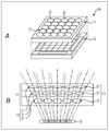
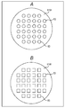
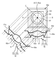
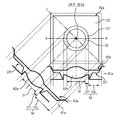
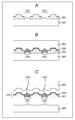
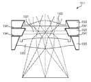
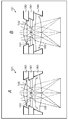
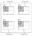
도 1의 A 및 B는, 본 기술을 적용한 적층렌즈 구조체를 이용한 카메라 모듈의 제1의 실시의 형태를 도시하는 도면이다.1A and 1B are views showing a first embodiment of a camera module using a laminated lens structure to which the present technology is applied.
도 1의 A는, 카메라 모듈(1)의 제1의 실시의 형태로서의 카메라 모듈(1A)의 구성을 도시하는 모식도이다. 도 1의 B는, 카메라 모듈(1A)의 개략 단면도이다.Fig. 1 (A) is a schematic diagram showing the configuration of a
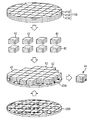
카메라 모듈(1A)은, 적층렌즈 구조체(11)와 수광 소자(12)를 구비한다. 적층렌즈 구조체(11)는, 종횡 각각 5개씩, 합계 25개의 광학 유닛(13)을 구비한다. 광학 유닛(13)은, 1개의 광축 방향으로 복수장의 렌즈(21)를 포함하여 구성된다. 카메라 모듈(1A)은, 광학 유닛(13)을 복수개 구비한 복안 카메라 모듈이다.The
카메라 모듈(1A)이 구비하는 복수개의 광학 유닛(13)의 광축은, 도 1의 B에 도시되는 바와 같이, 모듈의 외측을 향하여 넓어지도록 배치되고, 이에 의해 광각의 화상의 촬영이 가능하게 되어 있다.The optical axes of the plurality of
또한, 도 1의 B에서는, 간단함을 위해, 적층렌즈 구조체(11)는 렌즈(21)를 3층만 적층한 구조로 되어 있는데, 보다 많은 렌즈(21)를 적층하여도 좋음은 말할 필요도 없다.1B, for the sake of simplicity, the
도 1의 카메라 모듈(1A)은, 복수개의 광학 유닛(13)을 통하여 촬영한 복수장의 화상을 이어 합쳐서, 1장의 광각 화상을 만들어 낼 수 있다. 복수장의 화상을 이어 합치기 위해, 각 화상을 촬영하는 각 광학 유닛(13)의 형성 및 배치에는, 높은 정밀도가 요구된다. 또한, 특히 광각측의 광학 유닛(13)은, 렌즈(21)에의 광의 입사각도가 작기 때문에, 광학 유닛(13)의 내에서의 각 렌즈(21)의 위치 관계와 배치에도, 높은 정밀도가 요구된다.The
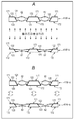
도 2는, 특허문헌 1이 개시하는, 수지에 의한 고착 기술을 이용한 적층렌즈 구조체의 단면 구조도이다.Fig. 2 is a cross-sectional structural view of a laminated lens structure using a resin fixing technique disclosed in
도 2에 도시되는 적층렌즈 구조체(500)에서는, 렌즈(511)를 구비한 기판(512)끼리를 고착하는 수단으로서, 수지(513)가 사용되고 있다. 수지(513)는, UV 경화성 등의 에너지 경화성 수지이다.In the
기판(512)끼리를 맞붙이기 전에, 기판(512) 표면 전면에 수지(513)의 층이 형성된다. 그 후, 기판(512)끼리가 맞붙여지고, 또한, 수지(513)가 경화된다. 이에 의해, 맞붙여진 기판(512)끼리가 고착된다.A layer of the
그러나, 수지(513)를 경화시킨 때에, 수지(513)는 경화 수축한다. 도 2에 도시되는 구조의 경우, 기판(512) 전체에 수지(513)의 층을 형성한 후, 수지(513)를 경화시키기 때문에, 수지(513)의 변위량이 커져 버린다.However, when the
또한, 기판(512)끼리를 맞붙여서 형성한 적층렌즈 구조체(500)를 개편화하고, 촬상 소자를 조합시켜서 카메라 모듈을 형성한 후도, 카메라 모듈에 구비되는 적층렌즈 구조체(500)는, 도 2에 도시되는 바와 같이, 렌즈(511)을 구비하는 기판(512) 사이 전체에, 수지(513)가 존재하고 있다. 이 때문에, 카메라 모듈을 카메라의 몸체 내에 탑재하고, 실사용(實使用)한 때에, 기기(機器)의 발열에 의한 온도 상승에 의해, 적층렌즈 구조체(500)의 기판 사이의 수지가 열팽창할 우려가 있다.After the
도 3은, 도 1의 A 및 B의 카메라 모듈(1A)의 적층렌즈 구조체(11)만을 도시한 단면 구조도이다.3 is a cross-sectional structural view showing only the
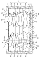
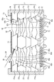
카메라 모듈(1A)의 적층렌즈 구조체(11)도, 렌즈(21)를 구비하는 렌즈부착 기판(41)을 복수장 적층하여 형성되어 있다.The
카메라 모듈(1A)의 적층렌즈 구조체(11)에서는, 렌즈(21)를 구비한 렌즈부착 기판(41)끼리를 고정하는 수단으로서, 도 2의 적층렌즈 구조체(500)나 기타의 선행 기술 문헌에 나타나는 것과는 완전히 다른 고정 수단이 이용되고 있다.In the
즉, 적층된 2장의 렌즈부착 기판(41)은, 일방의 기판 표면에 형성한 산화물이나 질화물에 의한 표면층과, 타방의 기판 표면에 형성한 산화물이나 질화물에 의한 표면층 사이의 공유결합에 의해, 직접접합된다. 구체적인 예로서, 도 4의 A에 도시되는 바와 같이, 적층한 2장의 렌즈부착 기판(41) 각각의 표면에, 표면층으로서 실리콘산화막 또는 실리콘질화막이 형성되고, 이것에 수산기(水酸基)를 결합시킨 후, 2장의 렌즈부착 기판(41)끼리가 맞붙여지고, 승온되어 탈수축합(脫水縮合)된다. 그 결과, 2장의 렌즈부착 기판(41)의 표면층의 사이에서, 실리콘-산소 공유결합이 형성된다. 이에 의해 2장의 렌즈부착 기판(41)이 직접접합된다. 또한, 축합의 결과, 2장의 표면층에 포함되는 원소끼리가 직접 공유결합을 형성하는 일도 일어날 수 있다.That is, the laminated two lens-attached
다른 예로서, 도 4의 B에 도시되는 바와 같이, 실리콘질화막(42)은, 2장의 렌즈부착 기판(41)의 표면 상에 형성되어 표면층으로서 적층되고, 수산기는 막과 결합한다. 예를 들면, NH3는 플라즈마 활성 처리 동안 사용될 수 있다. 그 후, 2장의 렌즈부착 기판(41)끼리가 맞붙여지고, 승온되어 탈수축합된다. 그 결과, 2장의 렌즈부착 기판(41)의 표면층(42)의 사이에서, 실리콘-질소 공유결합이 형성된다. 이에 의해 2장의 렌즈부착 기판(41)이 직접접합된다. 또한, 축합의 결과, 2장의 표면층에 포함되는 원소끼리가 직접 공유결합을 형성하는 일도 일어날 수 있다.As another example, as shown in Fig. 4B, the
본 명세서에서는, 이와 같이, 2장의 렌즈부착 기판(41)의 사이에 배치한 무기물의 층을 통하여 2장의 렌즈부착 기판(41)을 고정하는 것, 또는, 2장의 렌즈부착 기판(41)의 표면에 각각 배치한 무기물의 층끼리를 화학 결합시킴으로써 2장의 렌즈부착 기판(41)을 고정하는 것, 또는, 2장의 렌즈부착 기판(41)의 표면에 각각 배치한 무기물의 층의 사이에 탈수축합에 의한 결합을 형성함으로써 2장의 렌즈부착 기판(41)을 고정하는 것, 또는, 2장의 렌즈부착 기판(41)의 표면에 각각 배치한 무기물의 층의 사이에, 산소를 통한 공유결합 또는 서로의 무기물의 층에 포함되는 원소끼리의 공유결합을 형성함으로써 2장의 렌즈부착 기판(41)을 고정하는 것, 또는, 2장의 렌즈부착 기판(41)의 표면에 각각 배치한 실리콘산화물층 또는 실리콘질화물층의 사이에, 실리콘―산소 공유결합 또는 실리콘―실리콘 공유결합을 형성함으로써 2장의 렌즈부착 기판(41)을 고정하는 것을 직접접합(直接接合)이라고 부른다.In this specification, the two lens-attached
이 맞붙임과 승온에 의한 탈수축합을 행하기 위해, 본 실시의 형태에서는, 반도체 장치나 플랫 디스플레이 장치의 제조 분야에서 사용되는 기판을 이용하여, 기판 상태에서 렌즈가 형성되고, 기판 상태에서 맞붙임 및 승온에 의한 탈수축합이 행하여지고, 기판 상태에서 공유결합에 의한 접합이 행하여진다. 2장의 렌즈부착 기판(41)의 표면에 형성한 무기물의 층의 사이를, 공유결합에 의해 접합시킨 구조는, 특허문헌 1이 개시한 도 2에서 설명한 기술을 이용한 경우에 우려되는, 기판 전체에 걸치는 수지(513)의 경화 수축에 의한 변형이나, 실사용시의 수지(513)의 열팽창에 의한 변형을 억제한다, 라는 작용 또는 효과를 가져온다.In this embodiment, in order to carry out dewatering and condensation by this attachment and temperature elevation, a lens is formed in the state of a substrate using a substrate used in the field of manufacturing a semiconductor device or a flat display device, And dehydration condensation is carried out by raising the temperature, and bonding by covalent bonding is performed in the state of a substrate. The structure in which the layers of the inorganic material formed on the surfaces of the two lens-attached
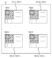
도 5 및 도 6은, 적층렌즈 구조체(11)와 수광 소자(12)를 조합시킨 도 1의 A 및 B의 카메라 모듈(1A)을 형성하는 공정을 도시하는 도면이다.Figs. 5 and 6 are diagrams showing the steps of forming the
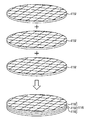
우선, 도 5에 도시되는 바와 같이, 각 렌즈(21)(부도시)가 평면 방향으로 복수 형성된 렌즈부착 기판(41W)이 복수장 준비되고, 이들이 적층된다. 이에 의해, 기판 상태의 렌즈부착 기판(41W)이 복수장 적층된, 기판 상태의 적층렌즈 구조체(11W)가 얻어진다.First, as shown in Fig. 5, a plurality of lens-attached
다음에, 도 6에 도시되는 바와 같이, 수광 소자(12)가 평면 방향으로 복수 형성된 기판 상태의 센서 기판(43W)이, 도 5에 도시한 기판 상태의 적층렌즈 구조체(11W)와는 별도로 제작되고, 준비된다.Next, as shown in Fig. 6, a
그리고, 기판 상태의 센서 기판(43W)과, 기판 상태의 적층렌즈 구조체(11W)가, 적층되어, 맞붙여진 기판의 모듈마다 외부 단자를 붙임으로써, 기판 상태의 카메라 모듈(44W)이 얻어진다.The
최후에, 기판 상태의 카메라 모듈(44W)이, 모듈 단위 또는 칩 단위로 개편화된다. 개편화된 카메라 모듈(44)이, 별도 준비된 몸체(부도시)에 봉입됨으로서, 최종적인 카메라 모듈(44)이 얻어진다.Finally, the
또한, 본 명세서 및 도면에서는, 예를 들면, 렌즈부착 기판(41W)과 같이, 부호에 "W"가 부가된 부품은, 그것이 기판 상태(웨이퍼 상태)인 것을 나타내고, 렌즈부착 기판(41)과 같이 "W"가 붙여지지 않은 것은, 모듈 단위 또는 칩 단위로 개편화된 상태인 것을 나타낸다. 기타, 센서 기판(43W), 카메라 모듈(44W) 등에 대해서도 마찬가지이다.In the present specification and drawings, a component to which the symbol "W" is added, such as the lens-attached
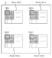
도 7은, 적층렌즈 구조체(11)와 수광 소자(12)를 조합시킨 도 1의 A 및 B의 카메라 모듈(1A)을 형성하는 다른 공정을 도시하는 도면이다.Fig. 7 is a view showing another step of forming the
우선, 상술하는 공정과 마찬가지로, 기판 상태의 렌즈부착 기판(41W)이 복수장 적층된, 기판 상태의 적층렌즈 구조체(11W)가 제조된다.First, similarly to the above-described step, a
다음에, 기판 상태의 적층렌즈 구조체(11W)가, 개편화된다.Next, the
또한, 기판 상태의 적층렌즈 구조체(11W)와는 달리, 기판 상태의 센서 기판(43W)이 제작되고, 준비된다.Unlike the
그리고, 기판 상태의 센서 기판(43W)의 각 수광 소자(12)의 위에, 개편화된 적층렌즈 구조체(11)가 1개씩 마운트된다.On the
최후에, 개편화된 적층렌즈 구조체(11)가 마운트된, 기판 상태의 센서 기판(43W)이 모듈 단위 또는 칩 단위로 개편화된다. 적층렌즈 구조체(11)가 마운트되고, 개편화된 센서 기판(43)이, 별도 준비된 몸체(부도시)에 봉입되고, 또한 외부 단자가 붙여짐으로써, 최종적인 카메라 모듈(44)이 얻어진다.Finally, the
또한, 적층렌즈 구조체(11)와 수광 소자(12)를 조합시킨 도 1의 카메라 모듈(1A)을 형성하는 다른 공정의 예로서, 도 7에 도시한 기판 상태의 센서 기판(43W)을 개편화하고, 그 결과 얻어진 개개의 수광 소자(12)에, 개편화 후의 적층렌즈 구조체(11)를 각각 마운트하여, 개편화된 카메라 모듈(44)을 얻어도 좋다.As another example of forming the
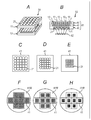
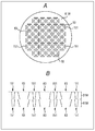
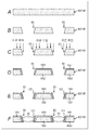
도 8의 A 내지 H는, 카메라 모듈(1A)에서의 렌즈부착 기판(41)의 구성을 설명하는 도면이다.8A to 8H are views for explaining the configuration of the lens-attached
도 8의 A는, 도 1의 A와 같은, 카메라 모듈(1A)의 구성을 도시하는 모식도이다.Fig. 8A is a schematic diagram showing the configuration of the
도 8의 B는, 도 1의 B와 같은, 카메라 모듈(1A)의 개략 단면도이다.Fig. 8B is a schematic cross-sectional view of the
카메라 모듈(1A)은, 도 8의 B에 도시되는 바와 같이, 복수장의 렌즈(21)를 조합시켜서 형성하고, 1개의 광축을 구비하는 광학 유닛(13)을, 복수개 구비한 복안 카메라 모듈이다. 적층렌즈 구조체(11)는, 종횡 각각 5개씩, 합계 25개의 광학 유닛(13)을 구비한다.As shown in Fig. 8B, the
카메라 모듈(1A)에서는, 복수개의 광학 유닛(13)의 광축이, 모듈의 외측을 향하여 넓어지도록 배치되고, 이에 의해, 광각의 화상의 촬영이 가능하게 되어 있다. 도 8의 B에서는, 간단함을 위해, 적층렌즈 구조체(11)는, 렌즈부착 기판(41)을 3층만 적층한 구조로 되어 있는데, 보다 많은 렌즈부착 기판(41)을 적층하여도 좋음은 말할 필요도 없다.In the
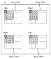
도 8의 C 내지 E는, 적층렌즈 구조체(11)를 구성하는 3층의 렌즈부착 기판(41) 각각의 평면 형상을 도시하는 도면이다.8E to 8E are diagrams showing planar shapes of the three lens-attached
도 8의 C는, 3층 중의 최상층의 렌즈부착 기판(41)의 평면도이고, 도 8의 D는, 중층의 렌즈부착 기판(41)의 평면도이고, 도 8의 D는, 최하층의 렌즈부착 기판(41)의 평면도이다. 카메라 모듈(1)은, 복안 광각 카메라 모듈이기 때문에, 상층이 됨에 따라서 렌즈(21)의 지름이 커짐과 함께, 렌즈 사이의 피치가 넓어져 있다.8C is a plan view of the lens-affixed
도 8의 F 내지 H는, 도 8의 C 내지 E에 도시한 렌즈부착 기판(41)을 얻기 위한, 기판 상태의 렌즈부착 기판(41W)의 평면도이다.8F to 8H are plan views of the lens-attached
도 8의 F에 도시되는 렌즈부착 기판(41W)은, 도 8의 C의 렌즈부착 기판(41)에 대응하는 기판 상태를 나타내고, 도 8의 G에 도시되는 렌즈부착 기판(41W)은, 도 8의 D의 렌즈부착 기판(41)에 대응하는 기판 상태를 나타내고, 도 8의 H에 도시되는 렌즈부착 기판(41W)은, 도 8의 E의 렌즈부착 기판(41)에 대응하는 기판 상태를 나타내고 있다.The lens-attached
도 8의 F 내지 H에 도시되는 기판 상태의 렌즈부착 기판(41W)은, 도 8의 A에 도시한 카메라 모듈(1A)을, 기판 1매당 8개 얻어지는 구성으로 되어 있다.The lens-attached
도 8의 F 내지 H의 각 렌즈부착 기판(41W)의 사이에서, 모듈 단위의 렌즈부착 기판(41) 내의 렌즈 사이의 피치는, 상층의 렌즈부착 기판(41W)과 하층의 렌즈부착 기판(41W)에서 다른 한편, 각 렌즈부착 기판(41W)에서, 모듈 단위의 렌즈부착 기판(41)을 배치하는 피치는, 상층의 렌즈부착 기판(41W)부터 하층의 렌즈부착 기판(41W)까지, 일정하게 되어 있음을 알 수 있다.The pitch between the lenses in the lens-mounted
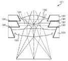
<2. 카메라 모듈의 제2의 실시의 형태><2. Second Embodiment of Camera Module>
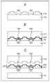
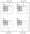
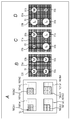
도 9의 A 내지 H는, 본 기술을 적용한 적층렌즈 구조체를 이용한 카메라 모듈의 제2의 실시의 형태를 도시하는 도면이다.9A to 9H are views showing a second embodiment of a camera module using a laminated lens structure to which the present technology is applied.
도 9의 A는, 카메라 모듈(1)의 제2의 실시의 형태로서의 카메라 모듈(1B)의 외관을 도시하는 모식도이다. 도 9의 B는, 카메라 모듈(1B)의 개략 단면도이다.Fig. 9A is a schematic diagram showing the appearance of the
카메라 모듈(1B)은, 2개의 광학 유닛(13)을 구비한다. 2개의 광학 유닛(13)은, 적층렌즈 구조체(11)의 최상층에, 조리개판(51)을 구비한다. 조리개판(51)에는, 개구부(52)가 마련되어 있다.The
카메라 모듈(1B)은 2개의 광학 유닛(13)을 구비하는데, 이들 2개의 광학 유닛(13)의 광학 파라미터는 다르다. 즉, 카메라 모듈(1B)은, 광학 성능이 다른 2종류의 광학 유닛(13)을 구비한다. 2종류의 광학 유닛(13)은, 예를 들면, 근경을 촬영하기 위한 초점 거리가 짧은 광학 유닛(13)과, 원경을 촬영하기 위해 초점 거리가 긴 광학 유닛(13)으로 할 수 있다.The
카메라 모듈(1B)에서는, 2개의 광학 유닛(13)의 광학 파라미터가 다르기 때문에, 예를 들면, 도 9의 B에 도시되는 바와 같이, 2개의 광학 유닛(13)의 렌즈(21)의 매수가 다르다. 또한, 2개의 광학 유닛(13)이 구비하는 적층렌즈 구조체(11)의 같은 층의 렌즈(21)에서, 지름, 두께, 표면 형상, 체적, 또는, 인접하는 렌즈와의 거리의 어느 하나가 다른 구성이 가능하게 되어 있다. 이 때문에, 카메라 모듈(1B)에서의 렌즈(21)의 평면 형상은, 예를 들면, 도 9의 C에 도시되는 바와 같이, 2개의 광학 유닛(13)이 같은 지름의 렌즈(21)를 구비하고 있어도 좋고, 도 9의 D에 도시하는 바와 같이, 다른 형상의 렌즈(21)를 구비하고 있어도 좋고, 도 9의 E에 도시하는 바와 같이, 일방이 렌즈(21)를 구비하지 않은 공동(21X)이 된 구조라도 좋다.Since the optical parameters of the two
도 9의 F 내지 H는, 도 9의 C 내지 E에 도시한 렌즈부착 기판(41)을 얻기 위한, 기판 상태의 렌즈부착 기판(41W)의 평면도이다.9F to 9H are plan views of the lens-attached
도 9의 F에 도시되는 렌즈부착 기판(41W)은, 도 9의 C의 렌즈부착 기판(41)에 대응하는 기판 상태를 나타내고, 도 9의 G에 도시되는 렌즈부착 기판(41W)은, 도 9의 D의 렌즈부착 기판(41)에 대응하는 기판 상태를 나타내고, 도 9의 H에 도시되는 렌즈부착 기판(41W)은, 도 9의 E의 렌즈부착 기판(41)에 대응하는 기판 상태를 나타내고 있다.The lens-attached
도 9의 F 내지 H에 도시되는 기판 상태의 렌즈부착 기판(41W)은, 도 9의 A에 도시한 카메라 모듈(1B)을, 기판 1매당 16개 얻어지는 구성으로 되어 있다.The lens-attached
도 9의 F 내지 H에 도시되는 바와 같이, 카메라 모듈(1B)을 형성하기 위해, 기판 상태의 렌즈부착 기판(41W)의 기판 전면에 같은 형상의 렌즈를 형성하는 것이나, 다른 형상의 렌즈를 형성하는 것이나, 렌즈를 형성하거나 형성하지 않거나 하는 것이 가능하다.As shown in FIGS. 9F to 9H, in order to form the
<3. 카메라 모듈의 제3의 실시의 형태><3. Third Embodiment of Camera Module>
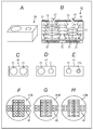
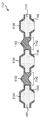
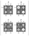
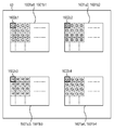
도 10의 A 내지 F는, 본 기술을 적용한 적층렌즈 구조체를 이용한 카메라 모듈의 제3의 실시의 형태를 도시하는 도면이다.10A to 10F are views showing a third embodiment of a camera module using a laminated lens structure to which the present technology is applied.
도 10의 A는, 카메라 모듈(1)의 제3의 실시의 형태로서의 카메라 모듈(1C)의 외관을 도시하는 모식도이다. 도 10의 B는, 카메라 모듈(1C)의 개략 단면도이다.Fig. 10A is a schematic diagram showing the appearance of the
카메라 모듈(1C)은, 광의 입사면상에, 종횡 2개씩, 합계 4개의 광학 유닛(13)을 구비한다. 4개의 광학 유닛(13)끼리는, 렌즈(21)의 형상은 같게 되어 있다.The
4개의 광학 유닛(13)은, 적층렌즈 구조체(11)의 최상층에, 조리개판(51)을 구비하는데, 그 조리개판(51)의 개구부(52)의 크기가, 4개의 광학 유닛(13)의 사이에서 다르다. 이에 의해, 카메라 모듈(1C)은, 예를 들면, 이하와 같은 카메라 모듈(1C)을 실현할 수 있다. 즉, 예를 들면 방범용의 감시 카메라에서, 주간의 컬러 화상 감시용으로, RGB 3종류의 컬러 필터를 구비하여 RGB 3종의 광을 수광하는 수광 화소와, 야간의 흑백 화상 감시용으로, RGB용의 컬러 필터를 구비하지 않은 수광 화소를 구비한 수광 소자(12)를 이용한 카메라 모듈(1C)에서, 조도가 낮은 야간의 흑백 화상을 촬영하기 위한 화소만 조리개의 개구의 크기를 크게 하는 것이 가능해진다. 이 때문에, 1개의 카메라 모듈(1C)에서의 렌즈(21)의 평면 형상은, 예를 들면 도 10의 C에 도시되는 바와 같이, 4개의 광학 유닛(13)이 구비하는 렌즈(21)의 지름은 같고, 또한, 도 10의 D에 도시되는 바와 같이, 조리개판(51)의 개구부(52)의 크기는, 광학 유닛(13)에 따라 다르다.The four
도 10의 E는, 도 10의 C에 도시한 렌즈부착 기판(41)을 얻기 위한, 기판 상태의 렌즈부착 기판(41W)의 평면도이다. 도 10의 F는, 도 10의 D에 도시한 조리개판(51)을 얻기 위한, 기판 상태에서의 조리개판(51W)을 도시하는 평면도이다.10E is a plan view of the lens-attached
도 10의 E의 기판 상태의 렌즈부착 기판(41W), 및, 도 10의 F의 기판 상태의 조리개판(51W)에서는, 도 10의 A에 도시한 카메라 모듈(1C)을, 기판 1매당 8개 얻어지는 구성으로 되어 있다.In the case of the lens-attached
도 10의 F에 도시되는 바와 같이, 기판 상태에서의 조리개판(51W)에서는, 카메라 모듈(1C)을 형성하기 위해, 카메라 모듈(1C)이 구비하는 광학 유닛(13)마다, 다른 개구부(52)의 크기를 설정할 수 있다.10F, in each of the
<4. 카메라 모듈의 제4의 실시의 형태><4. Fourth Embodiment of Camera Module>
도 11은, 본 기술을 적용한 적층렌즈 구조체를 이용한 카메라 모듈의 제4의 실시의 형태를 도시하는 도면이다.11 is a view showing a fourth embodiment of a camera module using a laminated lens structure to which the present technique is applied.
도 11의 A는, 카메라 모듈(1)의 제4의 실시의 형태로서의 카메라 모듈(1D)의 외관을 도시하는 모식도이다. 도 11의 B는, 카메라 모듈(1D)의 개략 단면도이다.11A is a schematic diagram showing the appearance of the
카메라 모듈(1D)은, 카메라 모듈(1C)과 마찬가지로, 광의 입사면상에, 종횡 2개씩, 합계 4개의 광학 유닛(13)을 구비한다. 4개의 광학 유닛(13)끼리는, 렌즈(21)의 형상과 조리개판(51)의 개구부(52)의 크기는 같게 되어 있다.Like the
카메라 모듈(1D)은, 광의 입사면의 종방향과 횡방향의 각각에 관해 2개씩 배치한 광학 유닛(13)에 구비되는 광축이, 같은 방향으로 늘어나 있다. 도 11의 B에 도시되는 1점쇄선은, 광학 유닛(13) 각각의 광축을 나타내고 있다. 이와 같은 구조의 카메라 모듈(1D)은, 초해상(超解像) 기술을 이용하여, 1개의 광학 유닛(13)으로 촬영하는 것보다도, 해상도가 높은 화상을 촬영하는 것에 적합하다.In the
카메라 모듈(1D)에서는, 종방향과 횡방향의 각각에 관해, 광축이 같은 방향을 방향이지만, 다른 위치에 배치된 복수개의 수광 소자(12)로 화상을 촬영함에 의해, 또는 1개의 수광 소자(12)의 중이 다른 영역의 수광 화소로 화상을 촬영함에 의해, 광축이 같은 방향을 방향이지만, 반드시 동일하지가 않은 복수장의 화상을 얻을 수 있다. 이들 동일하지 않은 복수장의 화상이 갖고 있는 장소마다의 화상 데이터를 합침으로써, 해상도가 높은 화상을 얻을 수 있다. 이 때문에, 1개 카메라 모듈(1D)에서의 렌즈(21)의 평면 형상은, 도 11의 C에 도시되는 바와 같이, 4개의 광학 유닛(13)에서 같게 되어 있는 것이 바람직하다.In the
도 11의 D는, 도 11의 C에 도시한 렌즈부착 기판(41)을 얻기 위한, 기판 상태의 렌즈부착 기판(41W)의 평면도이다. 기판 상태의 렌즈부착 기판(41W)은, 도 11의 A에 도시한 카메라 모듈(1D)을, 기판 1매당 8개 얻어지는 구성으로 되어 있다.11D is a plan view of the lens-attached
도 11의 D에 도시되는 바와 같이, 기판 상태의 렌즈부착 기판(41W)에서는, 카메라 모듈(1D)을 형성하기 위해, 카메라 모듈(1D)이 복수개의 렌즈(21)를 구비하고, 이 1개의 모듈용의 렌즈군이, 기판상에 일정한 피치로 복수개 배치되어 있다.As shown in Fig. 11D, in order to form the
<5. 카메라 모듈의 제5의 실시의 형태><5. Fifth Embodiment of Camera Module>
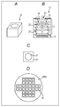
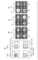
도 12의 A 내지 D는, 본 기술을 적용한 적층렌즈 구조체를 이용한 카메라 모듈의 제5의 실시의 형태를 도시하는 도면이다.12A to 12D are views showing a fifth embodiment of a camera module using a laminated lens structure to which the present technology is applied.
도 12의 A는, 카메라 모듈(1)의 제5의 실시의 형태로서의 카메라 모듈(1E)의 외관을 도시하는 모식도이다. 도 12의 B는, 카메라 모듈(1E)의 개략 단면도이다.Fig. 12A is a schematic diagram showing the appearance of the
카메라 모듈(1E)은, 1개의 광축을 갖는 광학 유닛(13)을 카메라 모듈(1E) 내에 1개 구비하는, 단안(單眼, monocular)의 카메라 모듈이다.The
도 12의 C는, 카메라 모듈(1E)에서의 렌즈(21)의 평면 형상을 도시하는 렌즈부착 기판(41)의 평면도이다. 카메라 모듈(1E)은, 1개의 광학 유닛(13)을 구비한다.12C is a plan view of the lens-attached
도 12의 D는, 도 12의 C에 도시한 렌즈부착 기판(41)을 얻기 위한, 기판 상태의 렌즈부착 기판(41W)의 평면도이다. 기판 상태의 렌즈부착 기판(41W)은, 도 12의 A에 도시한 카메라 모듈(1E)를, 기판 1매당 32개 얻어지는 구성으로 되어 있다.12D is a plan view of the lens-attached
도 12의 D에 도시되는 바와 같이, 기판 상태의 렌즈부착 기판(41W)에서는, 카메라 모듈(1E) 용의 렌즈(21)이, 기판상에 일정한 피치로 복수개 배치되어 있다.As shown in Fig. 12D, a plurality of
<6. 제4의 실시의 형태의 카메라 모듈의 상세 구성><6. Detailed configuration of camera module according to the fourth embodiment >
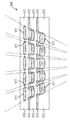
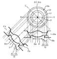
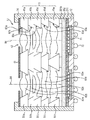
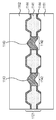
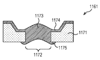
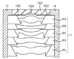
다음에, 도 13을 참조하여, 도 11의 A 내지 D에 도시한 제4의 실시의 형태에 관한 카메라 모듈(1D)의 상세 구성에 관해 설명한다.Next, the detailed configuration of the
도 13은, 도 11의 B에 도시한 카메라 모듈(1D)의 단면도이다.Fig. 13 is a sectional view of the
카메라 모듈(1D)은, 복수의 렌즈부착 기판(41a 내지 41e)이 적층된 적층렌즈 구조체(11)와, 수광 소자(12)를 포함하여 구성된다. 적층렌즈 구조체(11)는, 복수개의 광학 유닛(13)을 구비한다. 1점쇄선(84)은, 각각의 광학 유닛(13)의 광축을 나타낸다. 수광 소자(12)는, 적층렌즈 구조체(11)의 하측에 배치되어 있다. 카메라 모듈(1D)에서, 상방부터 카메라 모듈(1D) 내로 입사한 광은, 적층렌즈 구조체(11)를 투과하여, 적층렌즈 구조체(11)의 하측에 배치된 수광 소자(12)에서 수광된다.The
적층렌즈 구조체(11)는, 적층된 5장의 렌즈부착 기판(41a 내지 41e)을 구비한다. 5장의 렌즈부착 기판(41a 내지 41e)을 특히 구별하지 않는 경우에는, 단지, 렌즈부착 기판(41)이라고 기술하여 설명한다.The
적층렌즈 구조체(11)를 구성하는 각 렌즈부착 기판(41)의 관통구멍(83)의 단면 형상은, 하측(수광 소자(12)을 배치하는 측)을 향하여 개구폭이 작아지는, 이른바 아래로 테이퍼된 형상(downward tapered shape)으로 되어 있다.The sectional shape of the through
적층렌즈 구조체(11)의 위에는, 조리개판(51)이 배치되어 있다. 조리개판(51)은, 예를 들면, 광흡수성 또는 차광성을 갖는 재료로 형성된 층을 구비한다. 조리개판(51)에는, 개구부(52)가 마련되어 있다.On the
수광 소자(12)는, 예를 들면, 표면 조사형 또는 이면 조사형의 CMOS(Complementary Metal Oxide Semiconductor) 이미지 센서로 구성된다. 수광 소자(12)의 적층렌즈 구조체(11)측이 되는 상측의 면에는, 온 칩 렌즈(71)가 형성되어 있고, 수광 소자(12)의 하측의 면에는, 신호를 입출력하는 외부 단자(72)가 형성되어 있다.The
적층렌즈 구조체(11), 수광 소자(12), 조리개판(51) 등은, 렌즈 배럴(74)에 수납되어 있다.The
수광 소자(12)의 상측에는, 구조재(73)가 배치되어 있다. 그 구조재(73)를 통하여, 적층렌즈 구조체(11)와 수광 소자(12)가 고정되어 있다. 구조재(73)는, 예를 들면 에폭시계의 수지이다.On the upper side of the
본 실시의 형태에서는, 적층렌즈 구조체(11)는, 적층된 5장의 렌즈부착 기판(41a 내지 41e)을 구비하는데, 렌즈부착 기판(41)의 적층 매수는 2장 이상이라면 특히 한정되지 않는다.In the present embodiment, the
적층렌즈 구조체(11)를 구성하는 각각의 렌즈부착 기판(41)은, 지지 기판(81)에 렌즈 수지부(82)가 추가된 구성이다. 지지 기판(81)은 관통구멍(83)을 가지며, 관통구멍(83)의 내측에, 렌즈 수지부(82)가 형성되어 있다. 렌즈 수지부(82)는, 상술한 렌즈(21)를 포함하여, 지지 기판(81)까지 연재되어 렌즈(21)를 지지하는 부위도 아울러서, 렌즈(21)를 구성하는 재료에 의해 일체가 된 부분을 나타낸다.Each of the lens-attached
또한, 렌즈부착 기판(41a 내지 41e) 각각의 지지 기판(81), 렌즈 수지부(82), 또는, 관통구멍(83)을 구별하는 경우에는, 도 13에 도시되는 바와 같이, 렌즈부착 기판(41a 내지 41e)에 대응하여, 지지 기판(81a 내지 81e), 렌즈 수지부(82a 내지 82e), 또는, 관통구멍(83a 내지 83e)와 같이 기술하여 설명한다.13, in the case of distinguishing the
<렌즈 수지부의 상세 설명>≪ Detailed description of lens part &
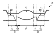
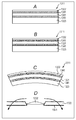
다음에, 렌즈부착 기판(41a)의 렌즈 수지부(82a)를 예로, 렌즈 수지부(82)의 형상에 관해 설명한다.Next, the shape of the
도 14는, 렌즈부착 기판(41a)을 구성하는 지지 기판(81a)과 렌즈 수지부(82a)의 평면도와 단면도이다.14 is a plan view and a cross-sectional view of the
도 14에 도시되는 지지 기판(81a)과 렌즈 수지부(82a)의 단면도는, 평면도에 도시되어 있는 B-B'선과 C-C'선의 단면도이다.Sectional views of the supporting
렌즈 수지부(82a)는, 렌즈(21)를 구성하는 재료에 의해 일체가 되어 형성한 부위이고, 렌즈부(91)와 지지부(92)를 구비한다. 상술한 설명에서, 렌즈(21)란, 렌즈부(91) 또는 렌즈 수지부(82a) 전체에 상당한다.The
렌즈부(91)는, 렌즈로서의 성능을 갖는 부위, 환언하면, "광을 굴절시켜서 집속 또는 발산시키는 부위", 또는, "볼록면이나 오목면이나 비구면 등의 곡면을 구비하는 부위, 또는 프레넬 렌즈나 회절 격자를 이용한 렌즈로 이용하는 복수개의 다각형을 연속하여 배치한 부위"이다.The
지지부(92)는, 렌즈부(91)로부터 지지 기판(81a)까지 연재되어 렌즈부(91)를 지지하는 부위이다. 지지부(92)는, 완부(腕部, arm portion)(101)와 각부(脚部, leg portion)(102)로 구성되고, 렌즈부(91)의 외주에 위치한다.The supporting
완부(101)는, 렌즈부(91)의 외측에, 렌즈부(91)에 접하여 배치하고, 렌즈부(91)로부터 외측 방향으로 일정한 막두께로 연재되는 부위이다. 각부(102)는, 지지부(92) 중에서 완부(101) 이외의 부분으로, 또한 관통구멍(83a)의 측벽에 접하는 부분을 포함하는 부위이다. 각부(102)는, 완부(101)보다도 수지의 막두께가 두꺼운 것이 바람직하다.The
지지 기판(81a)에 형성된 관통구멍(83a)의 평면 형상은 원형이고, 그 단면 형상은 당연히 직경의 방향에 의하지 않고 같다. 렌즈 형성시에 상형(上型)과 하형(下型)의 형태에 의해 정하여지는 형상인 렌즈 수지부(82a)의 형상도, 그 단면 형상이 직경의 방향에 의하지 않고 같게 되도록 형성되어 있다.The planar shape of the through
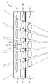
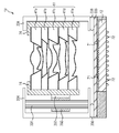
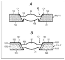
도 15는, 도 13의 카메라 모듈(1D)의 일부인 적층렌즈 구조체(11)와 조리개판(51)을 도시하는 단면도이다.15 is a sectional view showing the
카메라 모듈(1D)에서는, 모듈에 입사되는 광이 조리개판(51)에서 조여진 후, 적층렌즈 구조체(11)의 내부에서 넓어져서, 적층렌즈 구조체(11)의 하방에 배치된 수광 소자(12)(도 15에서는 부도시)에 입사된다. 즉, 적층렌즈 구조체(11) 전체에 관해 개관(槪觀)하면, 모듈에 입사된 광은, 조리개판(51)의 개구부(52)로부터 하측을 향하여, 거의 부채모양으로 넓어져서 진행한다. 이 때문에, 적층렌즈 구조체(11)에 구비되는 렌즈 수지부(82)의 크기의 한 예로서, 도 15의 적층렌즈 구조체(11)에서는, 조리개판(51)의 바로 아래에 배치된 렌즈부착 기판(41a)에 구비되는 렌즈 수지부(82a)가 가장 작고, 적층렌즈 구조체(11)의 최하층에 배치된 렌즈부착 기판(41e)에 구비되는 렌즈 수지부(82e)가 가장 크게 되어 있다.In the
가령 렌즈부착 기판(41)의 렌즈 수지부(82)의 두께를 일정하게 한 경우, 크기가 작은 렌즈보다도 큰 렌즈를 만들기가 어렵다. 그것은 예를 들면, 렌즈를 제조할 때에 렌즈에 가하여지는 하중에 의해 렌즈가 변형하기 쉽고, 크기가 크기 때문에 강도를 유지하기가 어렵다, 라는 이유에 의한다. 이 때문에, 크기가 큰 렌즈는, 크기가 작은 렌즈보다도, 두께를 두껍게 하는 것이 바람직하다. 이 때문에, 도 15의 적층렌즈 구조체(11)에서는, 렌즈 수지부(82)의 두께는, 최하층에 배치한 렌즈부착 기판(41e)에 구비되는 렌즈 수지부(82e)가 가장 두껍게 되어 있다.When the thickness of the
도 15의 적층렌즈 구조체(11)는, 렌즈 설계의 자유도를 높이기 위해, 또한 이하의 특징의 적어도 하나를 구비한다.The
(1) 지지 기판(81)의 두께가, 적층렌즈 구조체(11)를 구성하는 적어도 복수장의 렌즈부착 기판(41)의 사이에서 다르다. 예를 들면, 지지 기판(81)의 두께가, 하층의 렌즈부착 기판(41)의 쪽이 두껍다.(1) The thickness of the supporting
(2) 렌즈부착 기판(41)에 구비되는 관통구멍(83)의 개구폭이, 적층렌즈 구조체(11)를 구성하는 적어도 복수장의 렌즈부착 기판(41)의 사이에서 다르다. 예를 들면, 관통구멍(83)의 개구폭이, 하층의 렌즈부착 기판(41)의 쪽이 크다.(2) The opening width of the through
(3) 렌즈부착 기판(41)에 구비되는 렌즈부(91)의 직경이, 적층렌즈 구조체(11)를 구성하는 적어도 복수장의 렌즈부착 기판(41)의 사이에서 다르다. 예를 들면, 렌즈부(91)의 직경이, 하층의 렌즈부착 기판(41)의 렌즈부(91)의 쪽이 크다.(3) The diameter of the
(4) 렌즈부착 기판(41)에 구비되는 렌즈부(91)의 두께가, 적층렌즈 구조체(11)를 구성하는 적어도 복수장의 렌즈부착 기판(41)의 사이에서 다르다. 예를 들면, 렌즈부(91)의 두께가, 하층의 렌즈부착 기판(41)의 렌즈부(91)의 쪽이 두껍다.(4) The thickness of the
(5) 렌즈부착 기판(41)에 구비되는 렌즈 사이의 거리가, 적층렌즈 구조체(11)를 구성하는 적어도 복수장의 렌즈부착 기판(41)의 사이에서 다르다.(5) The distance between the lenses provided on the lens-attached
(6) 렌즈부착 기판(41)에 구비되는 렌즈 수지부(82)의 체적이, 적층렌즈 구조체(11)를 구성하는 적어도 복수장의 렌즈부착 기판(41)의 사이에서, 다르다. 예를 들면, 렌즈 수지부(82)의 체적이, 하층의 렌즈부착 기판(41)의 렌즈 수지부(82)의 쪽이 크다.(6) The volume of the
(7) 렌즈부착 기판(41)에 구비되는 렌즈 수지부(82)의 재료가, 적층렌즈 구조체(11)를 구성하는 적어도 복수장의 렌즈부착 기판(41)의 사이에서 다르다.(7) The material of the
일반적으로, 카메라 모듈에 입사되는 입사광은, 수직 입사광과 사(斜)입사광을 아울러서 포함하고 있다. 사입사광의 대부분은 조리개판(51)에 닿아, 그곳에서 흡수 또는 카메라 모듈(1D)의 외측으로 반사된다. 조리개판(51)에 의해 완전히 조여지지 않은 사입사광은, 그 입사각도에 따라서는 관통구멍(83)의 측벽에 닿아 버리고, 그곳에서 반사될 가능성이 있다.In general, incident light incident on the camera module includes both vertical incident light and oblique incident light. Most of the incident light comes into contact with the
사입사광의 반사광이 진행하는 방향은, 도 13에서 도시되는, 사입사광(85)의 입사각도와, 관통구멍(83)의 측벽의 각도에 의해 정하여진다. 관통구멍(83)의 개구폭이, 입사측부터 수광 소자(12)측을 향하여 커지는, 이른바, 부채의 형상인 경우, 조리개판(51)에 의해 완전히 조여지지 않은 특정한 입사각도의 사입사광(85)이, 관통구멍(83)의 측벽에 닿아 버린 때에는, 그것이 수광 소자(12) 방향으로 반사되어 버려, 이것이 미광(迷光) 또는 노이즈광이 될 가능성이 있다.The direction in which the reflected light of the incident light advances is determined by the incident angle of the incident light 85 shown in FIG. 13 and the angle of the side wall of the through
그렇지만, 도 13에 도시한 적층렌즈 구조체(11)에서는, 도 15에 도시되는 바와 같이, 관통구멍(83)은, 하측(수광 소자(12)를 배치하는 측)을 향하여 개구폭이 작아지는, 이른바 아래로 테이퍼된 형상으로 되어 있다. 이 형상인 경우, 관통구멍(83)의 측벽에 닿은 사입사광(85)은, 하측 방향 이른바 수광 소자(12)의 방향이 아니라, 상측 방향, 이른바 입사측 방향으로 반사된다. 이에 의해, 미광 또는 노이즈광의 발생을 억제한다는 작용 또는 효과를 얻을 수 있다.However, in the
렌즈부착 기판(41)의 관통구멍(83)은, 그 측벽에 닿아 반사된 광을 저감하기 위해, 광흡수성의 재료를 측벽에 배치하면 더욱 좋다.It is preferable that the through
한 예로서, 카메라 모듈(1D)을 카메라로서 사용할 때에 수광하고 싶은 파장의 광(예를 들면 가시광)을, 제1의 광으로 하고, 그 제1의 광과는 파장이 다른 광(예를 들면 UV광)을, 제2의 광으로 한 경우, 제2의 광(UV광)에 의해 경화하는 수지에, 제1의 광(가시광)의 흡수 재료로서 카본 입자를 분산시킨 것을, 지지 기판(81)의 표면에 도포 또는 분사하고, 관통구멍(83)의 측벽부의 수지에만 제2의 광(UV광)을 조사하여 경화시키고, 이 이외의 영역의 수지를 제거함으로써, 관통구멍(83)의 측벽에, 제1의 광(가시광)에 대한 광흡수성을 갖는 재료의 층을 형성하면 좋다.For example, when the
도 15에 도시한 적층렌즈 구조체(11)는, 적층한 복수장의 렌즈부착 기판(41)의 맨 위에, 조리개판(51)을 배치한 구조의 예이다. 조리개판(51)은, 적층한 복수장의 렌즈부착 기판(41)의 맨 위가 아니라, 중간의 렌즈부착 기판(41)의 어딘가에 삽입하여 배치하여도 좋다.The
또한 다른 예로서, 판형상(板狀)의 조리개판(51)을 렌즈부착 기판(41)과 별도로 구비하는 것이 아니고, 렌즈부착 기판(41)의 표면에, 광흡수성을 갖는 재료의 층을 형성하고, 이것을 조리개로서 기능시켜도 좋다. 예를 들면, 상기 제2의 광(UV광)에 의해 경화하는 수지에, 상기 제1의 광(가시광)의 흡수재료로서 카본 입자를 분산시킨 것을, 렌즈부착 기판(41)의 표면에 도포 또는 분사하고, 조리개로서 기능시킬 때에 광을 투과시키고 싶은 영역을 제외하고, 그 이외의 영역의 수지에 제2의 광(UV광)을 조사하고, 상기 수지를 경화시키고 나머지, 경화시키지 않은 영역, 즉 조리개로서 기능시킬 때에 광을 투과시키고 싶은 영역의 수지를 제거함으로써, 렌즈부착 기판(41)의 표면에 조리개를 형성하여도 좋다.As another example, a plate-
또한, 상기 표면에 조리개를 형성하는 렌즈부착 기판(41)은, 적층렌즈 구조체(11)의 최상층에 배치된 렌즈부착 기판(41)이면 좋고, 또는, 적층렌즈 구조체(11)의 내층이 되는 렌즈부착 기판(41)이라도 좋다.The lens-attached
도 15에 도시한 적층렌즈 구조체(11)는, 렌즈부착 기판(41)을 적층한 구조를 구비한다.The
다른 실시 형태로서, 적층렌즈 구조체(11)는, 렌즈부착 기판(41)을 복수장과, 렌즈 수지부(82)를 구비하지 않은 지지 기판(81)을 적어도 1장, 아울러서 구비한 구조라도 좋다. 이 구조에서, 렌즈 수지부(82)를 구비하지 않은 지지 기판(81)은, 적층렌즈 구조체(11)의 최하층 또는 최상층에 배치하여도 좋고, 적층렌즈 구조체(11)에서의 내측의 층으로서 배치하여도 좋다. 이 구조는, 예를 들면, 적층렌즈 구조체(11)가 구비하는 복수장의 렌즈 사이의 거리나, 적층렌즈 구조체(11)의 최하층의 렌즈 수지부(82)와 적층렌즈 구조체(11)의 하측에 배치된 수광 소자(12)와의 거리를, 임의로 설정할 수 있다, 라는 작용 또는 효과를 가져온다.In another embodiment, the
또는 또한, 이 구조는, 렌즈 수지부(82)를 구비하지 않은 지지 기판(81)의 개구폭을 적절하게 설정하고, 또한, 개구부를 제외한 영역에 광흡수성을 갖는 재료를 배치함에 의해, 이것을 조리개판으로서 기능시킬 수 있다, 라는 작용 또는 효과를 가져온다.Alternatively, this structure can be configured such that the opening width of the supporting
<7. 카메라 모듈의 제6의 실시의 형태><7. Sixth Embodiment of Camera Module>
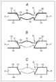
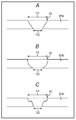
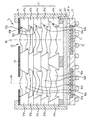
도 16은, 본 기술을 적용한 적층렌즈 구조체를 이용한 카메라 모듈의 제6의 실시의 형태를 도시하는 도면이다.16 is a view showing a sixth embodiment of a camera module using a laminated lens structure to which the present technology is applied.
도 16에서, 도 13에 도시한 제4의 실시의 형태와 대응하는 부분에 관해서는 같은 부호를 붙이고 있고, 도 13의 카메라 모듈(1D)과 다른 부분에 주목하여 설명한다.In Fig. 16, parts corresponding to those of the fourth embodiment shown in Fig. 13 are denoted by the same reference numerals and will be described with attention paid to parts different from those of the
도 16에 도시되는 카메라 모듈(1F)에서도, 도 13에 도시한 카메라 모듈(1D)과 마찬가지로, 입사한 광이, 조리개판(51)에서 조여진 후, 적층렌즈 구조체(11)의 내부에서 넓어져서, 적층렌즈 구조체(11)의 하방에 배치된 수광 소자(12)에 입사된다. 즉, 적층렌즈 구조체(11) 전체에 관해 개관하면, 광은, 조리개판(51)의 개구부(52)로부터 하측을 향하여, 부채모양으로 넓어져서 진행한다.In the
도 16의 카메라 모듈(1F)은, 적층렌즈 구조체(11)를 구성하는 각 렌즈부착 기판(41)의 관통구멍(83)의 단면 형상이, 하측(수광 소자(12)를 배치하는 측)을 향하여 개구폭이 커지는, 이른바 부채의 형상으로 되어 있는 점이, 도 13에 도시한 카메라 모듈(1D)과 다르다.The
카메라 모듈(1F)의 적층렌즈 구조체(11)는, 입사한 광이, 조리개판(51)의 개구부(52)로부터 하측을 향하여 부채모양으로 넓어져서 진행하는 구조이기 때문에, 관통구멍(83)의 개구폭이 하측 향하여 커지는 부채 형상은, 관통구멍(83)의 개구폭이 하측을 향하여 작아지는 아래로 테이퍼된 형상보다도, 예를 들면, 지지 기판(81)이 광로의 방해가 되기 어렵다. 이에 의해, 렌즈 설계의 자유도가 높다는 작용을 가져온다.Since the
또한, 지지부(92)를 포함하는 렌즈 수지부(82)의 기판 평면 방향의 단면적은, 관통구멍(83)의 개구폭이 하측을 향하여 작아지는 아래로 테이퍼된 형상인 경우, 렌즈 수지부(82)의 하면에서는, 렌즈(21)에 입사한 광선을 투과시키기 위해 특정한 크기가 되고, 또한, 렌즈 수지부(82)의 하면부터 상면을 향하여, 그 단면적이 커져 간다.The cross sectional area of the
이에 대해, 관통구멍(83)의 개구폭이 하측 향하여 커지는 부채 형상인 경우, 렌즈 수지부(82)의 하면에서의 단면적은, 아래로 테이퍼된 형상인 경우와 대강 같게 되지만, 렌즈 수지부(82)의 하면부터 상면을 향하여, 그 단면적이 작게 되어 간다.On the contrary, in the case of a fan shape in which the opening width of the through
이에 의해, 관통구멍(83)의 개구폭이 하측을 향하여 커지는 구조는, 지지부(92)를 포함하는 렌즈 수지부(82)의 크기를, 작게 억제할 수 있다는 작용 또는 효과를 가져온다. 또한, 이에 의해, 앞서 기술한 렌즈가 큰 경우에 생기는 렌즈 형성의 어려움을, 저감할 수 있다는 작용 또는 효과를 가져온다.Thus, the structure in which the opening width of the through
<8. 카메라 모듈의 제7의 실시의 형태><8. Seventh Embodiment of Camera Module>
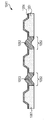
도 17은, 본 기술을 적용한 적층렌즈 구조체를 이용한 카메라 모듈의 제7의 실시의 형태를 도시하는 도면이다.17 is a view showing a seventh embodiment of a camera module using a laminated lens structure to which the present technique is applied.
도 17에서도, 도 13과 대응하는 부분에 관해서는 같은 부호를 붙이고 있고, 도 13에 도시한 카메라 모듈(1D)과 다른 부분에 주목하여 설명한다.In Fig. 17, the parts corresponding to those in Fig. 13 are denoted by the same reference numerals and will be described with attention paid to parts different from the
도 17의 카메라 모듈(1G)은, 역시, 적층렌즈 구조체(11)를 구성하는 각 렌즈부착 기판(41)의 렌즈 수지부(82)와 관통구멍(83)의 형상이, 도 13에 도시한 카메라 모듈(1D)과 다르다.The
카메라 모듈(1G)의 적층렌즈 구조체(11)는, 관통구멍(83)의 형상이, 하측(수광 소자(12)를 배치하는 측)을 향하여 개구폭이 작아지는, 이른바 아래로 테이퍼된 형상이 된 렌즈부착 기판(41)과, 관통구멍(83)의 형상이, 하측을 향하여 개구폭이 커지는, 이른바 부채의 형상이 된 렌즈부착 기판(41)의 쌍방을 구비한다.The
관통구멍(83)이, 하측을 향하여 개구폭이 작아지는, 이른바 아래로 테이퍼된 형상이 된 렌즈부착 기판(41)은, 앞서 기술한 바와 같이, 관통구멍(83)의 측벽에 닿은 사입사광(85)이, 상측 방향 이른바 입사측 방향으로 반사되고, 이에 의해 미광 또는 노이즈광의 발생을 억제한다, 라는 작용 또는 효과를 가져온다.As described above, the lens-attached
그래서, 도 17의 적층렌즈 구조체(11)에서는, 적층렌즈 구조체(11)를 구성하는 복수장의 렌즈부착 기판(41) 중, 특히 상측(입사측)의 복수장에 있어서, 관통구멍(83)이, 하측을 향하여 개구폭이 작아지는, 이른바 아래로 테이퍼된 형상이 된 렌즈부착 기판(41)이 사용되고 있다.Therefore, in the
관통구멍(83)이, 하측을 향하여 개구폭이 커지는, 이른바 부채의 형상이 된 렌즈부착 기판(41)은, 앞서 기술한 바와 같이, 렌즈부착 기판(41)에 구비되는 지지 기판(81)이 광로의 방해가 되기 어렵고, 이에 의해, 렌즈 설계의 자유도가 늘어나는, 또는, 렌즈부착 기판(41)에 구비되는 지지부(92)를 포함하는 렌즈 수지부(82)의 크기를 작게 억제한다, 라는 작용 또는 효과를 가져온다.The lens-attached
도 17의 적층렌즈 구조체(11)에서는, 광은 조리개로부터 하측을 향하여, 부채모양으로 넓어져서 진행하기 때문에, 적층렌즈 구조체(11)를 구성하는 복수장의 렌즈부착 기판(41) 중, 하측에 배치한 몇장의 렌즈부착 기판(41)에 구비되는 렌즈 수지부(82)의 크기가 크다. 이와 같은 큰 렌즈 수지부(82)에서, 부채의 형상의 관통구멍(83)을 이용하면, 렌즈 수지부(82)의 크기를 억제하는 작용이 크게 나타난다.In the
그래서, 도 17의 적층렌즈 구조체(11)에서는, 적층렌즈 구조체(11)를 구성하는 복수장의 렌즈부착 기판(41) 중, 특히 하측의 복수장에서, 관통구멍(83)이, 하측을 향하여 개구폭이 커지는, 이른바 부채의 형상이 된 렌즈부착 기판(41)을 이용하고 있다.In the
<9. 렌즈부착 기판의 상세 구성><9. Detailed configuration of substrate with lens>
다음에, 렌즈부착 기판(41)의 상세 구성에 관해 설명한다.Next, the detailed configuration of the lens-attached
도 18의 A 내지 C는, 렌즈부착 기판(41)의 상세 구성을 도시하는 단면도이다.18A to 18C are sectional views showing the detailed configuration of the lens-attached
또한, 도 18의 A 내지 C에서는, 5장의 렌즈부착 기판(41a 내지 41e) 중의, 최상층의 렌즈부착 기판(41a)이 도시되어 있는데, 기타의 렌즈부착 기판(41)도 마찬가지로 구성되어 있다.18A to 18C, the uppermost lens-attached
렌즈부착 기판(41)이 구성으로서는, 도 18의 A 내지 C의 어느 하나의 구성을 취할 수 있다.As the configuration of the lens-attached
도 18의 A에 도시되는 렌즈부착 기판(41)에는, 지지 기판(81)에 마련된 관통구멍(83)에 대해, 상면에서 보아 관통구멍(83)을 막도록 렌즈 수지부(82)가 형성되어 있다. 렌즈 수지부(82)는, 도 14를 참조하여 설명한 바와 같이, 중앙부의 렌즈부(91)(부도시)와, 그 주변부의 지지부(92)(부도시)로 구성된다.A lens-equipped
렌즈부착 기판(41)의 관통구멍(83)이 되는 측벽에는, 광반사를 기인(起因)으로 하는 고스트나 플레어를 방지하기 위해 광흡수성 또는 차광성을 갖는 막(121)이 성막되어 있다. 이들의 막(121)을 편의적으로 차광막(121)이라고 부른다.A
지지 기판(81)과 렌즈 수지부(82)의 상측 표면에는, 산화물 또는 질화물 또는 기타의 절연물을 포함하는 상측 표면층(122)이 형성되어 있고, 지지 기판(81)과 렌즈 수지부(82)의 하측 표면에는, 산화물 또는 질화물 또는 기타의 절연물을 포함하는 하측 표면층(123)이 형성되어 있다.An
상측 표면층(122)은, 한 예로서, 저굴절막과 고굴절막을 교대로 복수층 적층한 반사 방지막을 구성하고 있다. 반사 방지막은, 예를 들면, 저굴절막과 고굴절막을 교대로 합계 4층 적층하여 구성할 수 있다. 저굴절막은, 예를 들면, SiOx(1≤x≤2), SiOC, SiOF 등의 산화막, 고굴절막은, 예를 들면, TiO, TaO, Nb2O5 등의 금속 산화막으로 구성된다.As an example, the
또한, 상측 표면층(122)의 구성은, 예를 들면, 광학 시뮬레이션을 이용하여 소망하는 반사 방지성능을 얻을 수 있도록 설계되어 있으면 되고, 저굴절막 및 고굴절막의 재료, 막두께, 적층수 등은 특히 한정되지 않는다. 본 실시의 형태에서는, 상측 표면층(122)의 최표면은, 저굴절막으로 되어 있고, 그 막두께는, 예를 들면 20 내지 1000㎚, 밀도는, 예를 들면 2.2 내지 2.5g/㎤, 평탄도가, 예를 들면 1㎚ 이하 정도의 제곱평균 거칠기(Rq)(RMS)로 되어 있다. 또한, 상세는 후술하지만, 이 상측 표면층(122)은, 다른 렌즈부착 기판(41)과 접합될 때의 접합막으로도 되어 있다.The material of the
상측 표면층(122)은, 한 예로서, 저굴절막과 고굴절막을 교대로 복수층 적층한 반사 방지막이면 좋고, 그 중에서도 무기물의 반사 방지막이면 좋다. 상측 표면층(122)은, 다른 예로서, 산화물 또는 질화물 또는 기타의 절연물을 포함하는 단층막이라도 좋고, 그 중에서도 무기물의 막이라도 좋다.For example, the
하측 표면층(123)도, 한 예로서, 저굴절막과 고굴절막을 교대로 복수층 적층한 반사 방지막이면 좋고, 그 중에서도 무기물의 반사 방지막이면 좋다. 하측 표면층(123)은, 다른 예로서, 산화물 또는 질화물 또는 기타의 절연물을 포함하는 단층막이라도 좋고, 그 중에서도 무기물의 막이라도 좋다.For example, the
도 18의 B 및 C의 렌즈부착 기판(41)에 관해서는, 도 18의 A에 도시한 렌즈부착 기판(41)과 다른 부분에 관해서만 설명한다.The lens-attached
도 18의 B에 도시되는 렌즈부착 기판(41)에서는, 지지 기판(81)과 렌즈 수지부(82)의 하측 표면에 형성되어 있는 막이, 도 18의 A에 도시한 렌즈부착 기판(41)과 다르다.In the lens-attached
도 18의 B의 렌즈부착 기판(41)에서는, 지지 기판(81)의 하측 표면에는, 산화물 또는 질화물 또는 기타의 절연물을 포함하는 하측 표면층(124)이 형성되어 있는 한편, 렌즈 수지부(82)의 하측 표면에는, 하측 표면층(124)이 형성되어 있지 않다. 하측 표면층(124)은, 상측 표면층(122)과 동일 재료라도 좋고, 다른 재료라도 좋다.18B, the
이와 같은 구조는, 예를 들면, 렌즈 수지부(82)를 형성하기 전에, 지지 기판(81)의 하측 표면에 하측 표면층(124)을 형성하여 두고, 그 후, 렌즈 수지부(82)를 형성하는 제법(製法)에 의해, 형성할 수 있다. 또는, 렌즈 수지부(82)를 형성한 후에, 렌즈 수지부(82)에 마스크를 형성하고, 지지 기판(81)상에는 마스크를 형성하지 않은 상태에서, 하측 표면층(124)을 구성하는 막을, 예를 들면 PVD에 의해, 지지 기판(81)의 하측 표면에 퇴적시킴으로써, 형성할 수 있다.In such a structure, for example, before forming the
도 18의 C의 렌즈부착 기판(41)에서는, 지지 기판(81)의 상측 표면에, 산화물 또는 질화물 또는 기타의 절연물을 포함하는 상측 표면층(125)이 형성되어 있는 한편, 렌즈 수지부(82)의 상측 표면에는, 상측 표면층(125)이 형성되어 있지 않다.18C, an
마찬가지로, 렌즈부착 기판(41)의 하측 표면에서도, 지지 기판(81)의 하측 표면에, 산화물 또는 질화물 또는 기타의 절연물을 포함하는 하측 표면층(124)이 형성되어 있는 한편, 렌즈 수지부(82)의 하측 표면에는, 하측 표면층(124)이 형성되어 있지 않다.Likewise, the
이와 같은 구조는, 예를 들면, 렌즈 수지부(82)가 형성도기 전에, 지지 기판(81)에 상측 표면층(125)과 하측 표면층(124)을 형성하여 두고, 그 후, 렌즈 수지부(82)를 형성하는 제법에 의해, 형성할 수 있다. 또는, 렌즈 수지부(82)를 형성한 후에, 렌즈 수지부(82)에 마스크를 형성하고, 지지 기판(81)상에는 마스크를 형성하지 않은 상태에서, 상측 표면층(125) 및 하측 표면층(124)을 구성하는 막을, 예를 들면 PVD에 의해, 지지 기판(81)의 표면에 퇴적시킴으로써, 형성할 수 있다. 하측 표면층(124)과 상측 표면층(125)은, 동일 재료라도 좋고, 다른 재료라도 좋다.In such a structure, for example, the
렌즈부착 기판(41)은, 이상과 같이 구성할 수 있다.The lens-attached
<10. 렌즈부착 기판의 제조 방법><10. Method of manufacturing substrate with lens>
다음에, 도 19의 A 및 B 내지 도 29를 참조하여, 렌즈부착 기판(41)의 제조 방법을 설명한다.Next, a manufacturing method of the lens-attached
처음에, 복수의 관통구멍(83)이 형성된 기판 상태의 지지 기판(81W)이 준비된다. 지지 기판(81W)은, 예를 들면, 통상의 반도체 장치에 이용하는, 실리콘의 기판을 이용할 수 있다. 지지 기판(81W)의 형상은, 예를 들면 도 19의 A에 도시되는 바와 같은 원형으로, 그 직경은, 예를 들면 200㎜나 300㎜ 등이 된다. 지지 기판(81W)은, 실리콘의 기판이 아니라, 예를 들면, 유리의 기판, 수지의 기판, 또는 금속의 기판이라도 좋다.First, a supporting
또한, 관통구멍(83)의 평면 형상은, 본 실시의 형태에서는, 도 19의 A에 도시되는 바와 같이 원형이라고 하지만, 도 19의 B에 도시되는 바와 같이, 관통구멍(83)의 평면 형상은, 예를 들면 사각형 등의 다각형이라도 좋다.19A, the planar shape of the through
관통구멍(83)의 개구폭은, 예를 들면, 100㎛ 정도로부터 20㎜ 정도까지 취할 수 있다. 이 경우, 지지 기판(81W)에는, 예를 들면 100개 정도로부터 500만개 정도까지의 관통구멍(83)을 배치할 수 있다.The opening width of the through
본 명세서에서는, 렌즈부착 기판(41)의 평면 방향에서의 관통구멍(83)의 크기를, 개구폭(開口幅)이라고 부른다. 개구폭은, 특히 단서가 없는 한, 관통구멍(83)의 평면 형상이 사각형인 경우는 1변의 길이, 관통구멍(83)의 평면 형상이 원형인 경우는 직경을 의미한다.In this specification, the size of the through
관통구멍(83)은, 도 20에 도시되는 바와 같이, 지지 기판(81W)의 제1의 표면에서의 제1의 개구폭(131)보다도, 제1의 표면과 대향하는 제2의 표면에서의 제2의 개구폭(132)의 쪽이, 작게 되어 있다.20, the through
제1의 개구폭(131)보다도 제2의 개구폭(132)의 쪽이 작은 관통구멍(83)의 3차원 형상의 예로서, 관통구멍(83)은, 도 20의 A에 도시되는 원추대(圓錐臺)의 형상(truncated conical shape)이면 좋고, 다각형의 각추대의 형상(truncated polygonal pyramidal shape)이라도 좋다. 관통구멍(83)의 측벽의 단면 형상은, 도 20의 A에 도시되는 바와 같은 직선이면 좋고, 도 20의 B에 도시되는 바와 같은 곡선이라도 좋다. 또는 또한, 도 20의 C에 도시되는 바와 같이, 단차(段差)가 있어도 좋다.As an example of the three-dimensional shape of the through
제1의 개구폭(131)보다도 제2의 개구폭(132)의 쪽이 작은 형상인 관통구멍(83)은, 관통구멍(83) 내에 수지를 공급하고, 이 수지를, 제1과 제2의 표면의 각각으로부터 대향하는 방향으로 형부재(型部材, mold member)로 누름으로써 렌즈 수지부(82)를 형성할 때에, 렌즈 수지부(82)가 되는 수지가, 대향하는 2개의 형부재로부터의 힘을 받아, 관통구멍(83)의 측벽에 꽉 눌린다. 이에 의해, 렌즈 수지부(82)가 되는 수지와 지지 기판과의 밀착 강도가 높아진다는 작용을 가져올 수 있다.The through
또한, 관통구멍(83)의 다른 실시의 형태로서, 제1의 개구폭(131)과 제2의 개구폭(132)이 같은 형상, 즉 관통구멍(83)의 측벽의 단면 형상이 수직이 되는 형상이라도 좋다.As another embodiment of the through
<웨트 에칭을 이용한 관통구멍의 형성 방법>≪ Method of Forming Through-hole Using Wet Etching >
지지 기판(81W)의 관통구멍(83)은, 지지 기판(81W)을 웨트 에칭에 의해, 에칭함에 의해 형성할 수 있다. 구체적으로는, 지지 기판(81W)을 에칭하기 전에, 지지 기판(81W)의 비개구 영역이 에칭되는 것을 막기 위한 에칭 마스크가, 지지 기판(81W)의 표면에 형성된다. 에칭 마스크의 재료로는, 예를 들면 실리콘산화막 또는 실리콘질화막 등의 절연막이 사용된다. 에칭 마스크는, 에칭 마스크 재료의 층을 지지 기판(81W)의 표면에 형성하고, 이 층에 관통구멍(83)의 평면 형상이 되는 패턴을 개구함으로써, 형성된다. 에칭 마스크가 형성된 후, 지지 기판(81W)을 에칭함에 의해, 지지 기판(81W)에 관통구멍(83)이 형성된다.The through holes 83 of the
지지 기판(81W)으로서, 예를 들면, 기판 표면 방위가 (100)의 단결정 실리콘을 사용하는 경우, 관통구멍(83)을 형성하기 위해서는, KOH 등의 알칼리성의 용액을 사용한 결정 이방성 웨트 에칭을 채용할 수 있다.In the case where single crystal silicon having a substrate surface orientation of 100 is used as the supporting
기판 표면 방위가 (100)의 단결정 실리콘인 지지 기판(81W)에, KOH 등의 알칼리성의 용액을 사용한 결정 이방성 웨트 에칭을 행하면, 개구 측벽에 (111)면이 나타나도록 에칭이 진행한다. 그 결과, 에칭 마스크의 개구부의 평면 형상이 원형 또는 사각형의 어느 쪽이라도, 평면 형상이 사각형이고, 관통구멍(83)의 개구폭은 제1의 개구폭(131)보다도 제2의 개구폭(132)의 쪽이 작고, 관통구멍(83)의 3차원 형상이 각추대 또는 이것에 유사한 형상이 되는 관통구멍(83)을 얻을 수 있다. 각추대가 되는 관통구멍(83)의 측벽의 각도는, 기판 평면에 대해, 약 55°의 각도가 된다.Crystal anisotropic wet etching using an alkaline solution such as KOH is carried out on the supporting
관통구멍 형성을 위한 에칭은, 다른 실시의 예로서, 국제공개 제2011/010739호 등에 개시된, 결정 방위의 제약을 받지 않고 임의의 형상으로 실리콘을 에칭 가능한 약액을 사용한 웨트 에칭에 의해 행하여도 좋다. 이 약액으로서는, 예를 들면, TMAH(수산화테트라메틸암모늄) 수용액에, 계면활성제인 폴리옥시에틸렌알킬페닐에테르, 폴리옥시알킬렌알킬에테르, 폴리에틸렌글리콜의 적어도 하나를 가한 약액, 또는, KOH 수용액에 이소프로필알코올을 가한 약액, 등을 채용할 수 있다.Etching for forming the through holes may be performed by wet etching using a chemical solution capable of etching silicon in an arbitrary shape without being restricted by the crystal orientation disclosed in International Publication No. 2011/010739 and the like as another embodiment. As the chemical liquid, for example, a chemical solution in which at least one of polyoxyethylene alkyl phenyl ether, polyoxyalkylene alkyl ether, and polyethylene glycol is added to an aqueous solution of TMAH (tetramethylammonium hydroxide), or a solution of iso Propyl alcohol, or the like can be employed.
기판 표면 방위가 (100)의 단결정 실리콘인 지지 기판(81W)에, 상술한 어느 하나의 약액을 사용하여 관통구멍(83) 형성을 위한 에칭을 행하면, 에칭 마스크의 개구부의 평면 형상이 원형인 경우는, 평면 형상이 원형이고, 제1의 개구폭(131)보다도 제2의 개구폭(132)의 쪽이 작고, 3차원 형상이 원추대 또는 이것에 유사한 형상이 되는 관통구멍(83)을 얻을 수 있다.When etching is performed for forming the through
에칭 마스크의 개구부의 평면 형상이 사각형인 경우에는, 평면 형상이 사각형이고, 개구폭은 제1의 개구폭(131)보다도 제2의 개구폭(132)의 쪽이 작고, 3차원 형상이 각추대 또는 이것에 유사한 형상이 되는 관통구멍(83)을 얻을 수 있다. 상기 원추대 또는 각추대가 되는 관통구멍(83)의 측벽의 각도는, 기판 평면에 대해, 약 45°의 각도가 된다.When the planar shape of the opening portion of the etching mask is rectangular, the planar shape is rectangular, and the opening width is smaller than the
<드라이 에칭을 이용한 관통구멍의 형성 방법>≪ Method of forming through hole using dry etching >
또한, 관통구멍(83) 형성의 에칭에는, 상술한 웨트 에칭이 아니라, 드라이 에칭을 이용하는 것도 가능하다.It is also possible to use dry etching instead of the wet etching described above for etching for forming the through holes 83. [
도 21의 A 내지 F를 참조하여, 드라이 에칭을 이용한 관통구멍(83)의 형성 방법에 관해 설명한다.A method of forming the through
도 21의 A에 도시되는 바와 같이, 지지 기판(81W)의 일방의 표면에, 에칭 마스크(141)가 형성된다. 에칭 마스크(141)는, 관통구멍(83)을 형성하는 부분이 개구된 마스크 패턴으로 되어 있다.As shown in Fig. 21A, an
다음에, 도 21의 B에 도시되는 바와 같이, 에칭 마스크(141)의 측벽을 보호하기 위한 보호막(142)이 형성된 후, 도 21의 C에 도시되는 바와 같이, 드라이 에칭에 의해 지지 기판(81W)이 소정의 깊이로 에칭된다. 드라이 에칭 공정에 의해, 지지 기판(81W) 표면과 에칭 마스크(141) 표면의 보호막(142)은 제거되지만, 에칭 마스크(141) 측면의 보호막(142)은 잔존하고, 에칭 마스크(141)의 측벽은 보호된다. 에칭 후, 도 21의 D에 도시되는 바와 같이, 측벽의 보호막(142)이 제거되고, 에칭 마스크(141)가, 개구 패턴의 패턴 사이즈를 크게 하는 방향으로 후퇴된다.Next, as shown in Fig. 21B, after the
그리고, 재차, 도 21의 B 내지 D의 보호막 형성 공정, 드라이 에칭 공정, 에칭 마스크 후퇴 공정이, 복수회 반복 행하여진다. 이에 의해, 도 21의 E에 도시되는 바와 같이, 지지 기판(81W)은, 주기성이 있는 단차를 갖는 계단 형상(요철 형상)로 되도록 에칭된다.Again, the protective film forming process, the dry etching process, and the etching mask retreat process of FIGS. 21A to 21D are repeated a plurality of times. Thereby, as shown in FIG. 21E, the supporting
최후에, 에칭 마스크(141)가 제거되면, 도 21의 F에 도시되는 바와 같이, 계단 형상의 측벽을 갖는 관통구멍(83)이, 지지 기판(81W)에 형성된다. 관통구멍(83)의 계단 형상의 평면 방향의 폭(1단의 폭)은, 예를 들면, 400㎚ 내지 1㎛ 정도가 된다.Finally, when the
이상과 같이 드라이 에칭을 이용하여 관통구멍(83)을 형성하는 경우에는, 보호막 형성 공정, 드라이 에칭 공정, 에칭 마스크 후퇴 공정이 반복하여 실행된다.When the through
관통구멍(83)의 측벽이 주기성이 있는 계단 형상(요철 형상)인 것에 의해, 입사광의 반사를 억제할 수 있다. 또한, 가령, 관통구멍(83)의 측벽이 랜덤한 크기의 요철 형상인 경우에는, 관통구멍(83) 내에 형성된 렌즈와 측벽 사이의 밀착층에 보이드(공극)가 발생하고, 그 보이드가 원인으로 렌즈와의 밀착성이 저하되는 경우가 있다. 그렇지만, 상술한 형성 방법에 의하면, 관통구멍(83)의 측벽은 주기성이 있는 요철 형상으로 되기 때문에, 밀착성이 향상하고, 렌즈 위치 어긋남에 의한 광학 특성의 변화를 억제할 수 있다.Since the sidewall of the through
각 공정에서 사용되는 재료의 한 예로서는, 예를 들면, 지지 기판(81W)은 단결정 실리콘, 에칭 마스크(141)는 포토레지스트, 보호막(142)은, C4F8나 CHF3 등의 가스 플라즈마를 이용하여 형성하는 플로우카본 폴리머, 에칭 처리는, SF6/O2, C4F8/SF6 등 F를 포함하는 가스를 사용한 플라즈마 에칭, 마스크 후퇴 공정은, O2 가스, CF4/O2 등 O2를 포함하는 플라즈마 에칭으로 할 수 있다.For example, the supporting
또는 또한, 지지 기판(81W)은 단결정 실리콘, 에칭 마스크(141)는 SiO2, 에칭은, Cl2를 포함하는 플라즈마, 보호막(142)은, O2 플라즈마를 이용하여 에칭 대상재를 산화시킨 산화막, 에칭 처리는, Cl2를 포함하는 가스를 사용한 플라즈마 에칭 마스크 후퇴 공정은, CF4/O2 등 F를 포함하는 가스를 사용한 플라즈마 에칭으로 할 수 있다.Or also, the support substrate (81W) is single crystal silicon, the
이상과 같이, 웨트 에칭, 또는, 드라이 에칭에 의해, 지지 기판(81W)에, 복수의 관통구멍(83)을 동시 형성할 수 있는데, 지지 기판(81W)에는, 도 22의 A에 도시되는 바와 같이, 관통구멍(83)을 형성하지 않는 영역에 관통홈(151)을 형성하여도 좋다.As described above, it is possible to simultaneously form a plurality of through
도 22의 A는, 관통구멍(83)에 더하여 관통홈(151)을 형성한 지지 기판(81W)의 평면도이다.22A is a plan view of a supporting
관통홈(151)은, 예를 들면, 도 22의 A에 도시되는 바와 같이, 행렬상형상으로 배치된 복수개의 관통구멍(83)을 피하여, 행방향과 열방향의 각각의 관통구멍(83)의 사이의 일부에만 배치된다.22A, the through-
또한, 지지 기판(81W)의 관통홈(151)은, 적층렌즈 구조체(11)를 구성하는 각 렌즈부착 기판(41)끼리, 동일한 위치에 배치할 수 있다. 이 경우에는, 적층렌즈 구조체(11)로서 복수장의 지지 기판(81W)이 적층된 상태에서는, 도 22의 B의 단면도와 같이, 복수장의 지지 기판(81W)의 관통홈(151)이, 복수장의 지지 기판(81W)의 사이에서 관통한 구조가 된다.The through-
렌즈부착 기판(41)의 일부로서의 지지 기판(81W)의 관통홈(151)은, 예를 들면, 렌즈부착 기판(41)을 변형시키는 응력이 렌즈부착 기판(41)의 외부로부터 작용한 경우에, 응력에 의한 렌즈부착 기판(41)의 변형을 완화하는 작용 또는 효과를 가져올 수 있다.The
또는, 관통홈(151)은, 예를 들면, 렌즈부착 기판(41)을 변형시키는 응력이 렌즈부착 기판(41)의 내부에서 발생한 경우에, 응력에 의한 렌즈부착 기판(41)의 변형을 완화하는 작용 또는 효과를 가져올 수 있다.Alternatively, the through
<렌즈부착 기판의 제조 방법>≪ Method of manufacturing substrate with lens &
다음에, 도 23의 A 내지 G를 참조하여, 기판 상태의 렌즈부착 기판(41W)의 제조 방법에 관해 설명한다.Next, a manufacturing method of the lens-attached
처음에, 도 23의 A에 도시되는 바와 같이, 관통구멍(83)이 복수 형성된 지지 기판(81W)이 준비된다. 관통구멍(83)의 측벽에는 차광막(121)이 성막되어 있다. 도 23에서는, 지면(紙面)의 제약상, 2개의 관통구멍(83)만이 도시되어 있지만, 실제로는, 도 19의 A 및 B에서 도시한 바와 같이, 지지 기판(81W)의 평면 방향으로, 다수의 관통구멍(83)이 형성되어 있다. 또한, 지지 기판(81W)의 외주에 가까운 영역에는, 위치맞춤을 위한 얼라인먼트 마크(부도시)가 형성되어 있다.Initially, as shown in Fig. 23A, a supporting
지지 기판(81W) 상측의 표측(表側) 평탄부(171)와, 하측의 이측(裏側) 평탄부(172)는, 후의 공정에서 행하여지는 플라즈마 접합이 가능할 정도로 평탄하게 형성된 평탄면으로 되어 있다. 지지 기판(81W)의 두께는, 최종적으로 렌즈부착 기판(41)으로서 개편화되고, 다른 렌즈부착 기판(41)과 겹쳐진 때에, 렌즈 사이 거리를 결정하는 스페이서로서의 역할도 담당하고 있다.The front side
지지 기판(81W)에는, 열팽창 계수가 10ppm/℃ 이하의 저열팽창 계수의 기재(基材)를 사용하는 것이 바람직하다.It is preferable that a base material having a low thermal expansion coefficient of 10 ppm / 占 폚 or less is used as the
다음에, 도 23의 B에 도시되는 바와 같이, 오목형상의 광학 전사면(轉寫面)(182)이 일정한 간격으로 복수 배치된 하형(181)의 위에, 지지 기판(81W)이 배치된다. 보다 상세하게는, 오목형상의 광학 전사면(182)이 지지 기판(81W)의 관통구멍(83)의 내측에 위치하도록, 지지 기판(81W)의 이측 평탄부(172)와 하형(181)의 평탄면(183)이 겹쳐진다. 하형(181)의 광학 전사면(182)은, 지지 기판(81W)의 관통구멍(83)과 1대 1로 대응하도록 형성되어 있고, 대응하는 광학 전사면(182)과 관통구멍(83)의 중심이 광축 방향으로 일치하도록, 지지 기판(81W)과 하형(181)의 평면 방향의 위치가 조정된다. 하형(181)은, 경질의 형부재로 형성되어 있고, 예를 들면, 금속이나 실리콘, 석영, 유리로 구성된다.Next, as shown in Fig. 23B, the supporting
다음에, 도 23의 C에 도시되는 바와 같이, 겹쳐진 하형(181)과 지지 기판(81W)의 관통구멍(83)의 내측에, 에너지 경화성 수지(191)가 충전(적하)된다. 렌즈 수지부(82)는, 이 에너지 경화성 수지(191)를 사용하여 형성된다. 그 때문에, 에너지 경화성 수지(191)는, 기포를 포함하지 않도록 미리 탈포 처리되어 있는 것이 바람직하다. 탈포 처리로서는, 진공 탈포 처리, 또는, 원심력에 의한 탈포 처리인 것이 바람직하다. 또한, 진공 탈포 처리는 충전 후에 행하는 것이 바람직하다. 탈포 처리를 행함에 의해, 기포를 끌어들이는 일 없이, 렌즈 수지부(82)의 성형이 가능해진다.23C, the energy-
다음에, 도 23의 D에 도시되는 바와 같이, 겹쳐진 하형(181)과 지지 기판(81W)의 위에, 상형(201)이 배치된다. 상형(201)에는, 오목형상의 광학 전사면(202)이 일정한 간격으로 복수 배치되어 있고, 하형(181)을 배치한 때와 마찬가지로, 관통구멍(83)의 중심과 광학 전사면(202)의 중심이 광축 방향으로 일치하도록, 정밀도 좋게 위치 결정된 다음, 상형(201)이 배치된다.Next, as shown in Fig. 23D, the
지면상의 종방향이 되는 높이 방향에 관해서는, 상형(201)과 하형(181)과의 간격을 제어하는 제어 장치에 의해, 상형(201)과 하형(181)과의 간격이 미리 정한 거리가 되도록, 상형(201)의 위치가 고정된다. 이때, 상형(201)의 광학 전사면(202)과 하형(181)의 광학 전사면(182)으로 끼여지는 공간은, 광학 설계에 의해 계산된 렌즈 수지부(82)(렌즈(21))의 두께와 동등하게 된다.The distance between the
또는 또한, 도 23의 E에 도시되는 바와 같이, 하형(181)을 배치한 때와 마찬가지로, 상형(201)의 평탄면(203)과, 지지 기판(81W)의 표측 평탄부(171)를, 겹쳐도 좋다. 이 경우, 상형(201)과 하형(181)과의 거리는, 지지 기판(81W)의 두께와 같은 값이 되고, 평면 방향 및 높이 방향의 고정밀한 위치맞춤이 가능해진다.23E, the
상형(201)과 하형(181)과의 간격이 미리 설정한 거리가 되도록 제어한 때, 상술한 도 23의 C의 공정에서, 지지 기판(81W)의 관통구멍(83)의 내측에 적하된 에너지 경화성 수지(191)의 충전량은, 지지 기판(81W)의 관통구멍(83)과, 그 상하의 상형(201) 및 하형(181)로 둘러싸인 공간에서 넘치지 않도록 컨트롤된 양으로 되어 있다. 이에 의해, 에너지 경화성 수지(191)의 재료를 낭비하는 일 없이, 제조 비용을 삭감할 수 있다.When the distance between the
계속해서, 도 23의 E에 도시되는 상태에 있어서, 에너지 경화성 수지(191)의 경화 처리가 행하여진다. 에너지 경화성 수지(191)는, 예를 들면, 열 또는 UV광을 에너지로서 주고, 소정의 시간 방치함으로써, 경화한다. 경화 중에는, 상형(201)을 하방향으로 꽉누르거나, 얼라인먼트를 함에 의해, 에너지 경화성 수지(191)의 수축에 의한 변형을 최소한으로 억제할 수 있다.Subsequently, in the state shown in FIG. 23E, the energy-
에너지 경화성 수지(191) 대신에, 열가소성 수지를 사용하여도 좋다. 그 경우에는, 도 23의 E에 도시되는 상태에서, 상형(201)과 하형(181)을 승온함으로써 에너지 경화성 수지(191)가 렌즈 형상으로 성형되고, 냉각함으로써 경화한다.Instead of the energy-
다음에, 도 23의 F에 도시되는 바와 같이, 상형(201)과 하형(181)의 위치를 제어하는 제어 장치가, 상형(201)을 상방향, 하형(181)을 하방향으로 이동시켜, 상형(201)과 하형(181)을 지지 기판(81W)로부터 이형한다. 상형(201)과 하형(181)이 지지 기판(81W)으로부터 이형되면, 지지 기판(81W)의 관통구멍(83)의 내측에, 렌즈(21)를 포함하는 렌즈 수지부(82)가 형성되어 있다.23, the control device for controlling the positions of the
또한, 지지 기판(81W)과 접촉하는 상형(201)과 하형(181)의 표면을 불소계 또는 실리콘계 등의 이형제로 코팅하여도 좋다. 그와 같이 함에 의해, 상형(201)과 하형(181)로부터 지지 기판(81W)을 용이하게 이형할 수 있다. 또한, 지지 기판(81W)과의 접촉면으로부터 용이하게 이형하는 방법으로서, 불소 함유 DLC(Diamond Like Carbon) 등의 각종 코팅을 행하여도 좋다.The upper and
다음에, 도 23의 G에 도시되는 바와 같이, 지지 기판(81W)과 렌즈 수지부(82)의 표면에 상측 표면층(122)이 형성되고, 지지 기판(81W)과 렌즈 수지부(82)의 이면에, 하측 표면층(123)이 형성된다. 상측 표면층(122) 및 하측 표면층(123)의 성막 전후에서, 필요에 응하여 CMP(Chemical Mechanical Polishing) 등을 행함으로써, 지지 기판(81W)의 표측 평탄부(171)와 이측 평탄부(172)를 평탄화하여도 좋다.23G, an
이상과 같이, 지지 기판(81W)에 형성된 관통구멍(83)에, 에너지 경화성 수지(191)를 상형(201)과 하형(181)을 이용하여 가압 성형(임프린트(imprint))함으로써, 렌즈 수지부(82)를 형성하고, 렌즈부착 기판(41)을 제조할 수 있다.As described above, by press-molding (imprinting) the energy-
광학 전사면(182) 및 광학 전사면(202)의 형상은, 상술한 오목형상으로 한정되는 것이 아니고, 렌즈 수지부(82)의 형상에 응하여 적절히 결정된다. 도 15에 도시한 바와 같이, 렌즈부착 기판(41a 내지 41e)의 렌즈 형상은, 광학계 설계에 의해 도출된 다양한 형상을 취할 수 있고, 예를 들면, 양철(兩凸) 형상(biconvex shape), 양요(兩凹) 형상(biconcave shape), 평철(平凸) 형상(plano-convex shape), 평요(平凹) 형상(plano-concave shape), 볼록 메니스커스 형상(convex meniscus shape), 오목 메니스커스 형상(concave meniscus shape), 나아가서는 고차원 비구면 형상(high-order aspherical shape) 등이라도 좋다.The shapes of the
또한, 광학 전사면(182) 및 광학 전사면(202)의 형상은, 형성 후의 렌즈 형상이 모스 아이 구조(moth-eye structure)가 되는 형상으로 할 수도 있다.The shape of the
상술한 제조 방법에 의하면, 에너지 경화성 수지(191)의 경화 수축에 의한 렌즈 수지부(82)끼리의 평면 방향의 거리의 변동을, 지지 기판(81W)의 개재(interpose)에 의해 단절(斷切)할 수 있기 때문에, 렌즈 거리간 정밀도를 고정밀도로 제어할 수 있다. 또한, 강도가 약한 에너지 경화성 수지(191)를, 강도가 강한 지지 기판(81W)에 의해 보강하는 효과가 있다. 이에 의해, 핸들링성이 좋은 렌즈를 복수 배치한 렌즈 어레이 기판을 제공할 수 있음과 함께, 렌즈 어레이 기판의 휘어짐을 억제할 수 있는 효과를 갖는다.The variation of the distance in the plane direction of the
<관통구멍 형상이 다각형인 예>≪ Example in which the through hole shape is polygonal >
도 19의 B에 도시한 바와 같이, 관통구멍(83)의 평면 형상은, 예를 들면 사각형 등의 다각형이라도 좋다.As shown in Fig. 19B, the plane shape of the through
도 24는, 관통구멍(83)의 평면 형상이 사각형인 경우의, 렌즈부착 기판(41a)의 지지 기판(81a)과 렌즈 수지부(82a)의 평면도와 단면도이다.24 is a plan view and a cross-sectional view of the
도 24에서의 렌즈부착 기판(41a)의 단면도는, 평면도의 B-B'선과 C-C'선에서의 단면도를 도시하고 있다.The cross-sectional view of the lens-attached
B-B'선 단면도와 C-C'선 단면도를 비교하여 알 수 있는 바와 같이, 관통구멍(83a)이 사각형인 경우, 관통구멍(83a)의 중심으로부터 관통구멍(83a)의 상부 외연(外緣)까지의 거리, 및, 관통구멍(83a)의 중심으로부터 관통구멍(83a)의 하부 외연까지의 거리는, 사각형인 관통구멍(83a)의 변방향과 대각선 방향에서 다르고, 대각선 방향의 쪽이 크다. 이 때문에, 관통구멍(83a)의 평면 형상이 사각형인 경우, 렌즈부(91)를 원형으로 하면, 렌즈부(91) 외로부터 관통구멍(83a) 측벽까지의 거리, 환언하면, 지지부(92)의 길이를, 사각형의 변방향과 대각선 방향에서 다른 길이로 할 필요가 있다.As can be seen by comparing the sectional view taken along the line B-B 'and the sectional view taken along the line C-C', when the through
그래서, 도 24에 도시되는 렌즈 수지부(82a)는, 이하의 구조를 구비한다.Thus, the
(1) 렌즈부(91)의 외주에 배치한 완부(101)의 길이는, 사각형의 변방향과 대각선 방향에서 같다.(1) The length of the writing
(2) 완부(101)의 외측에 배치하고, 관통구멍(83a) 측벽까지 연재된 각부(102)의 길이는, 사각형의 변방향의 각부(102)의 길이보다도 대각선 방향의 각부(102)의 길이의 쪽을, 길게 하고 있다.(2) The length of each
도 24에 도시되는 바와 같이, 각부(102)는, 렌즈부(91)에 직접은 접하지 않는 한편, 완부(101)는, 렌즈부(91)에 직접 접하여 있다.The
도 24의 렌즈 수지부(82a)에서는, 렌즈부(91)에 직접 접하여 있는 완부(101)의 길이와 두께를, 렌즈부(91)의 외주 전체에 걸쳐서 일정하게 함으로써, 렌즈부(91) 전체를 치우침 없이 일정한 힘으로 유지한다, 라는 작용 또는 효과를 가져올 수 있다.The length and thickness of the
또한, 렌즈부(91) 전체를 치우침 없이 일정한 힘으로 유지함에 의해, 예를 들면, 관통구멍(83a)을 둘러싸는 지지 기판(81a)으로부터, 관통구멍(83a)의 외주 전체에 걸쳐서 응력이 가하여지는 경우에는, 이것을 렌즈부(91) 전체에 치우침 없이 전함으로써, 렌즈부(91)의 특정한 부분에만 치우쳐서 응력이 전해지는 것을 억제한다, 라는 작용 또는 효과를 가져올 수 있다.The whole of the
도 25는, 평면 형상이 사각형인 관통구멍(83)의 기타의 예에 관해 도시하는, 렌즈부착 기판(41a)의 지지 기판(81a)과 렌즈 수지부(82a)의 평면도와 단면도이다.25 is a plan view and a cross-sectional view of a
도 25에서의 렌즈부착 기판(41a)의 단면도는, 평면도의 B-B'선과 C-C'선에서의 단면도를 도시하고 있다.25 is a cross-sectional view taken along line B-B 'and line C-C' in the plan view.
도 25에서도, 도 22와 마찬가지로, 관통구멍(83a)의 중심으로부터 관통구멍(83a)의 상부 외연까지의 거리, 및, 관통구멍(83a)의 중심으로부터 관통구멍(83a)의 하부 외연까지의 거리는, 사각형인 관통구멍(83a)의 변방향과 대각선 방향에서 다르고, 대각선 방향의 쪽이 크다. 이 때문에, 관통구멍(83a)의 평면 형상이 사각형인 경우, 렌즈부(91)를 원형으로 하면, 렌즈부(91) 외주로부터 관통구멍(83a) 측벽까지의 거리, 환언하면, 지지부(92)의 길이를, 사각형의 변방향과 대각선 방향에서 다른 길이로 하는 필요가 있다.25, the distance from the center of the through
그래서, 도 25에 도시되는 렌즈 수지부(82a)는, 이하의 구조를 구비한다.Thus, the
(1) 렌즈부(91)의 외주에 배치한 각부(102)의 길이를, 관통구멍(83a)의 사각형의 4개의 변에 따라, 일정하게 하고 있다.(1) The length of each
(2) 상기 (1)의 구조를 실현하기 위해, 완부(101)의 길이는, 사각형의 변방향의 완부의 길이보다도 대각선 방향의 완부의 길이의 쪽을, 길게 하고 있다.(2) In order to realize the structure of (1) above, the length of the
도 25에 도시되는 바와 같이, 각부(102)는 완부(101)보다도, 수지의 막두께가 두껍다. 이 때문에, 렌즈부착 기판(41a)의 평면 방향의 단위 면적당의 체적도, 각부(102)는 완부(101)보다도 크다.As shown in Fig. 25, each
도 25의 실시례에서는, 각부(102)의 체적을 가능한 한 작게 하고, 또한, 관통구멍(83a)의 사각형의 4변에 따라 일정하게 함으로써, 예를 들면 수지의 팽창과 같은 변형이 발생하는 경우에는, 이에 의한 체적 변화를 가능한 한 억제하고, 또한 체적 변화가 렌즈부(91)의 외주 전체에 걸쳐서 가능한 한 치우치지 않도록 한다, 라는 작용 또는 효과를 가져올 수 있다.In the embodiment of Fig. 25, when the volume of each
도 26은, 렌즈부착 기판(41)의 렌즈 수지부(82)와 관통구멍(83)의 다른 실시 형태를 도시하는 단면도이다.26 is a cross-sectional view showing another embodiment of the lens-receiving
도 26에 도시되는 렌즈 수지부(82)와 관통구멍(83)은, 이하의 구조를 구비한다.The
(1) 관통구멍(83)의 측벽은, 단부착부(段付き部)(221)를 구비하는 단부착 형상이다.(1) The side wall of the through
(2) 렌즈 수지부(82)의 지지부(92)의 각부(102)가, 관통구멍(83)의 측벽 상방에 배치될 뿐만 아니라, 관통구멍(83)에 구비되는 단부착부(221)의 위에도, 렌즈부착 기판(41)의 평면 방향으로 연재되어 있다.(2) The
도 27의 A 내지 F를 참조하여, 도 26에 도시한 단부착 형상의 관통구멍(83)의 형성 방법에 관해 설명한다.Referring to Figs. 27A to 27F, a method of forming the stepped through
처음에, 도 27의 A에 도시되는 바와 같이, 지지 기판(81W)의 일방의 면에, 관통구멍 개구할 때의 웨트 에칭에 대한 내성을 갖는 에칭 스톱막(241)이 형성된다. 에칭 스톱막(241)은, 예를 들면, 실리콘질화막으로 할 수 있다.First, as shown in Fig. 27A, an
뒤이어, 지지 기판(81W)의 또한 일방의 면에, 관통구멍 개구할 때의 웨트 에칭에 대한 내성을 갖는 하드 마스크(242)가 형성된다. 하드 마스크(242)도, 예를 들면 실리콘질화막으로 할 수 있다.Subsequently, a
다음에, 도 27의 B에 도시되는 바와 같이, 하드 마스크(242)의 소정의 영역이, 1회째의 에칭을 위해 개구된다. 1회째의 에칭에서는, 관통구멍(83)의 단부착부(221)의 상단(上段)이 되는 부분이 에칭된다. 이 때문에, 1회째의 에칭을 위한 하드 마스크(242)의 개구부는, 도 26에 기재된 렌즈부착 기판(41)의 상측 기판 표면에서의 개구에 대응하는 영역이 된다.Next, as shown in Fig. 27B, a predetermined region of the
다음에, 도 27의 C에 도시되는 바와 같이, 웨트 에칭에 의해, 하드 마스크(242)의 개구부에 응하여, 지지 기판(81W)이 소정의 깊이분만큼 에칭된다.Next, as shown in Fig. 27C, the
다음에, 도 27의 D에 도시되는 바와 같이, 에칭 후의 지지 기판(81W)의 표면에, 하드 마스크(243)가 다시 형성되고, 관통구멍(83)의 단부착부(221)의 하측이 되는 부분에 대응하여 하드 마스크(243)가 개구된다. 2회째의 하드 마스크(243)도, 예를 들면 실리콘질화막을 채용할 수 있다.27D, the
다음에, 도 27의 E에 도시되는 바와 같이, 웨트 에칭에 의해, 하드 마스크(243)의 개구부에 응하여, 에칭 스톱막(241)에 도달할 때까지 지지 기판(81W)이 에칭된다.27E, the
최후에, 도 27의 F에 도시되는 바와 같이, 지지 기판(81W)의 상측 표면의 하드 마스크(243)와, 하측 표면의 에칭 스톱막(241)이 제거된다.Finally, as shown in Fig. 27F, the
이상과 같이, 웨트 에칭에 의한 관통구멍 형성을 위한 지지 기판(81W)의 에칭을 2회로 나누어 행함으로써, 도 26에 도시한 단부착 형상의 관통구멍(83)을 얻을 수 있다.As described above, the etching of the
도 28은, 관통구멍(83a)이 단부착부(221)를 가지며, 또한, 관통구멍(83a)의 평면 형상이 원형인 경우의, 렌즈부착 기판(41a)의 지지 기판(81a)과 렌즈 수지부(82a)의 평면도와 단면도이다.28 shows the relationship between the distance between the supporting
도 28에서의 렌즈부착 기판(41a)의 단면도는, 평면도의 B-B'선과 C-C'선에서의 단면도를 도시하고 있다.A cross-sectional view of the lens-attached
관통구멍(83a)의 평면 형상이 원형인 경우, 관통구멍(83a)의 단면 형상은 당연히 직경의 방향에 의하지 않고 같다. 이에 덧붙여, 렌즈 수지부(82a)의 외연, 완부(101), 및 각부(102)의 단면 형상도, 직경의 방향에 의하지 않고 같게 되도록 형성되어 있다.When the plane shape of the through
도 28의 단부착 형상을 갖는 관통구멍(83a)은, 관통구멍(83a) 내에 단부착부(221)를 구비하지 않은 도 14의 관통구멍(83a)과 비교하여, 렌즈 수지부(82)의 지지부(92)의 각부(102)가, 관통구멍(83a)의 측벽과 접촉하는 면적을 크게 할 수 있다, 라는 작용 또는 효과를 가져온다. 또한, 이에 의해, 렌즈 수지부(82)와 관통구멍(83a)의 측벽과의 밀착 강도, 환언하면, 렌즈 수지부(82a)와 지지 기판(81W)과의 밀착 강도를 증가시킨다, 라는 작용 또는 효과를 가져온다.The through
도 29는, 관통구멍(83a)이 단부착부(221)를 가지며, 또한, 관통구멍(83a)의 평면 형상이 사각형인 경우의, 렌즈부착 기판(41a)의 지지 기판(81a)과 렌즈 수지부(82a)의 평면도와 단면도이다.29 shows the relationship between the distance between the supporting
도 29에서의 렌즈부착 기판(41a)의 단면도는, 평면도의 B-B'선과 C-C'선에서의 단면도를 도시하고 있다.29 is a cross-sectional view taken along the line B-B 'and C-C' in the plan view of the lens-attached
도 29에 도시되는 렌즈 수지부(82)와 관통구멍(83)은, 이하의 구조를 구비한다.The
(1) 렌즈부(91)의 외주에 배치한 완부(101)의 길이는, 사각형의 변방향과 대각선 방향에서 같다.(1) The length of the writing
(2) 완부(101)의 외측에 배치하고, 관통구멍(83a)의 측벽까지 연재된 각부(102)의 길이는, 사각형의 변방향의 각부(102)의 길이보다도, 대각선 방향의 각부(102)의 길이가 길다.(2) The length of each
도 29에 도시되는 바와 같이, 각부(102)는, 렌즈부(91)에 직접은 접하지 않는 한편, 완부(101)는, 렌즈부(91)에 직접 접하여 있다.The
도 29의 렌즈 수지부(82a)에서는, 도 24에 기재된 렌즈 수지부(82a)와 마찬가지로, 렌즈부(91)에 직접 접하여 있는 완부(101)의 길이와 두께를, 렌즈부(91)의 외주 전체에 걸쳐서 일정하게 함으로써, 렌즈부(91) 전체를 치우침 없이 일정한 힘으로 유지한다, 라는 작용 또는 효과를 가져올 수 있다.24, the length and the thickness of the
또한, 렌즈부(91) 전체를 치우침 없이 일정한 힘으로 유지함에 의해, 예를 들면, 관통구멍(83a)을 둘러싸는 지지 기판(81a)으로부터, 관통구멍(83a)의 외주 전체에 걸쳐서 응력이 가하여지는 경우에는, 이것을 렌즈부(91) 전체에 치우침 없이 전함으로써, 렌즈부(91)의 특정한 부분에만 치우쳐서 응력이 전해지는 것을 억제한다, 라는 작용 또는 효과를 가져올 수 있다.The whole of the
또한, 도 29의 관통구멍(83a)의 구조는, 관통구멍(83a) 내에 단부착부(221)를 구비하지 않은 도 24 등의 관통구멍(83a)과 비교하여, 렌즈 수지부(82a)의 지지부(92)의 각부(102)가, 관통구멍(83a)의 측벽과 접촉하는 면적을 크게 할 수 있다, 라는 작용 또는 효과를 가져온다. 이에 의해, 렌즈 수지부(82a)와 관통구멍(83a)의 측벽부와의 밀착 강도, 환언하면, 렌즈 수지부(82a)와 지지 기판(81a)과의 밀착 강도가 증가한다, 라는 작용 또는 효과를 가져온다.The structure of the through
<11. 렌즈부착 기판끼리의 직접접합><11. Direct bonding of lens-attached substrates to each other>
다음에, 복수의 렌즈부착 기판(41)이 형성된 기판 상태의 렌즈부착 기판(41W)끼리의 직접접합에 관해 설명한다.Next, direct bonding of the lens-attached
이하의 설명에서는, 도 30의 A 및 B에 도시되는 바와 같이, 복수의 렌즈부착 기판(41a)이 형성된 기판 상태의 렌즈부착 기판(41W)을, 렌즈부착 기판(41W-a)이라고 기술하고, 복수의 렌즈부착 기판(41b)이 형성된 기판 상태의 렌즈부착 기판(41W)을, 렌즈부착 기판(41W-b)이라고 기술한다. 기타의 렌즈부착 기판(41c 내지 41e)에 대해서도 마찬가지로 나타낸다.In the following description, as shown in Figs. 30A and 30B, a lens-attached
도 31의 A 및 B를 참조하여, 기판 상태의 렌즈부착 기판(41W-a)과, 기판 상태의 렌즈부착 기판(41W-b)과의 직접접합에 관해 설명한다.Referring to Figs. 31A and 31B, the direct bonding of the lens-attached
또한, 도 31의 A 및 B에서는, 렌즈부착 기판(41W-a)의 각 부분과 대응하는 렌즈부착 기판(41Wb)의 부분에는, 렌즈부착 기판(41W-a)과 같은 부호를 붙여서 설명한다.In Figs. 31A and 31B, the portions of the lens-attached substrate 41Wb corresponding to the respective portions of the lens-attached
렌즈부착 기판(41W-a)과 렌즈부착 기판(41W-b)의 상측 표면에는, 상측 표면층(122 또는 125)이 형성되어 있다. 렌즈부착 기판(41W-a)과 렌즈부착 기판(41W-b)의 하측 표면에는, 하측 표면층(123 또는 124)이 형성되어 있다. 그리고, 도 31의 A에 도시되는 바와 같이, 렌즈부착 기판(41W-a와 41W-a)이 접합되는 면이 되는, 렌즈부착 기판(41W-a)의 이측 평탄부(172)를 포함하는 하측 표면 전체, 및, 렌즈부착 기판(41W-b)의 표측 평탄부(171)를 포함하는 상측 표면 전체에, 플라즈마 활성 처리가 행하여진다. 플라즈마 활성 처리에 사용되는 가스는, O2, N2, He, Ar, H2 등 플라즈마 처리 가능한 가스라면 무엇이라도 좋다. 단, 플라즈마 활성 처리에 사용되는 가스로서, 상측 표면층(122) 및 하측 표면층(123)의 구성 원소와 같은 가스를 사용하면, 상측 표면층(122) 및 하측 표면층(123)의 막 자체의 변질을 억제할 수 있기 때문에, 바람직하다.An
그리고, 도 31의 B에 도시되는 바와 같이, 활성화된 표면 상태의 렌즈부착 기판(41Wa)의 이측 평탄부(172)과, 렌즈부착 기판(41W-b)의 표측 평탄부(171)를 맞붙인다.Then, as shown in Fig. 31B, the second
이 렌즈부착 기판끼리의 맞붙임 처리에 의해, 렌즈부착 기판(41W-a)의 하측 표면층(123 또는 124)의 표면의 OH기(基)의 수소와 렌즈부착 기판(41W-b)의 상측 표면층(122 또는 125)의 표면의 OH기의 수소와의 사이에 수소 결합이 생긴다. 이에 의해, 렌즈부착 기판(41W-a)과 렌즈부착 기판(41W-b)이 고정된다. 이 렌즈부착 기판끼리의 맞붙임 처리는, 대기압의 조건하에서 행할 수 있다.By this process of attaching the lens-attached substrates, the hydrogen of the OH group on the surface of the
상기 맞붙임처리를 행한 렌즈부착 기판(41W-a)과 렌즈부착 기판(41W-b)에, 어닐 처리를 가한다. 이에 의해 OH기끼리가 수소 결합한 상태에서 탈수축합이 일어나고, 렌즈부착 기판(41W-a)의 하측 표면층(123 또는 124)과, 렌즈부착 기판(41Wb)의 상측 표면층(122 또는 125)의 사이에, 산소를 통한 공유결합이 형성된다. 또는, 렌즈부착 기판(41W-a)의 하측 표면층(123 또는 124)에 포함되는 원소와, 렌즈부착 기판(41W-b)의 상측 표면층(122 또는 125)에 포함되는 원소가 공유결합한다. 이들의 결합에 의해, 2장의 렌즈부착 기판이 강고하게 고정된다. 이와 같이, 상측에 배치한 렌즈부착 기판(41W)의 하측 표면층(123 또는 124)과, 하측에 배치한 렌즈부착 기판(41W)의 상측 표면층(122 또는 125)과의 사이에 공유결합이 형성되고, 이에 의해 2장의 렌즈부착 기판(41W)이 고정되는 것을, 본 명세서에서는 직접접합이라고 부른다. 특허문헌 1이 개시하는 복수장의 렌즈부착 기판을 기판 전면에 걸쳐서 수지에 의해 고착하는 방법은, 수지의 경화 수축이나 열팽창과 이에 의한 렌즈의 변형의 우려가 있다. 이에 대해, 본 기술의 직접접합은, 복수장의 렌즈부착 기판(41W)을 고정할 때에 수지를 사용하지 않기 때문에, 이에 의한 경화 수축이나 열팽창을 일으키는 일 없이, 복수장의 렌즈부착 기판(41W)을 고정할 수 있다, 라는 작용 또는 효과를 가져온다.An annealing process is applied to the lens-attached
상기 어닐 처리도, 대기압의 조건하에서 행할 수 있다. 이 어닐 처리는, 탈수축합을 행하기 위해, 100℃ 이상 또는 150℃ 이상 또는 200℃ 이상으로 할 수 있다. 한편, 이 어닐 처리는, 렌즈 수지부(82)를 형성하기 위한 에너지성 경화 수지(191)를 열로부터 보호하는 관점이나 에너지성 경화 수지(191)로부터의 탈가스를 억제하는 관점에서, 400℃ 이하 또는 350℃ 이하 또는 300℃ 이하에서 행할 수 있다.The annealing can also be performed under atmospheric pressure. This annealing treatment may be carried out at 100 占 폚 or higher, or 150 占 폚 or higher, or 200 占 폚 or higher, for dehydration condensation. On the other hand, from the viewpoint of protecting the energy
상기 렌즈부착 기판(41W)끼리의 맞붙임처리 또는 상기 렌즈부착 기판(41W)끼리의 직접접합 처리를, 가령 대기압 이외의 조건하에서 행한 경우에는, 접합된 렌즈부착 기판(41W-a)과 렌즈부착 기판(41W-b)을 대기압의 환경으로 되돌리면, 접합된 렌즈 수지부(82)와 렌즈 수지부(82)와의 사이의 공간과, 렌즈 수지부(82)의 외부와의 압력차가 생겨 버린다. 이 압력차에 의해, 렌즈 수지부(82)에 압력이 가하여지고, 렌즈 수지부(82)가 변형하여 버릴 우려가 있다.In the case where the process of attaching the lens-attached
상기 렌즈부착 기판(41W)끼리의 맞붙임처리 또는 상기 렌즈부착 기판끼리의 직접접합 처리의 쌍방을, 대기압의 조건하에서 행하는 것은, 접합을 대기압 이외의 조건하에서 행한 경우에 우려되는 렌즈 수지부(82)의 변형을 회피할 수 있다, 라는 작용 또는 효과를 가져온다.The process of attaching the lens-attached
플라즈마 활성 처리를 시행한 기판을 직접접합하는, 환언하면 플라즈마 접합함으로써, 예를 들면, 접착제로서 수지를 사용한 경우와 같은 유동성, 열팽창을 억제할 수 있기 때문에, 렌즈부착 기판(41W-a)과 렌즈부착 기판(41W-b)을 접합할 때의 위치 정밀도를 향상시킬 수 있다.It is possible to suppress the fluidity and the thermal expansion as in the case of using a resin as an adhesive, for example, by directly joining the substrate subjected to the plasma activation treatment, in other words, by plasma bonding, It is possible to improve the positional accuracy when bonding the bonded
렌즈부착 기판(41W-a)의 이측 평탄부(172)와, 렌즈부착 기판(41W-b)의 표측 평탄부(171)에는, 상술한 바와 같이, 상측 표면층(122) 또는 하측 표면층(123)이 성막되어 있다. 이 상측 표면층(122) 및 하측 표면층(123)은, 앞서 행한 플라즈마 활성 처리에 의해, 댕글링 본드가 형성되기 쉽게 되어 있다. 즉, 렌즈부착 기판(41W-a)의 이측 평탄부(172)에 성막한 하측 표면층(123)과, 렌즈부착 기판(41W-b)의 표측 평탄부(171)에 성막한 상측 표면층(122)은, 접합 강도를 증가시키는 역할도 갖고 있다.The
또한, 상측 표면층(122) 또는 하측 표면층(123)이 산화막으로 구성되어 있는 경우에는, 플라즈마(O2)에 의한 막질 변화의 영향을 받지 않기 때문에, 렌즈 수지부(82)에 대해서는, 플라즈마에 의한 부식을 억제하는 효과도 가진다.In the case where the
이상과 같이, 복수의 렌즈부착 기판(41a)이 형성된 기판 상태의 렌즈부착 기판(41W-a)과, 복수의 렌즈부착 기판(41b)이 형성된 기판 상태의 렌즈부착 기판(41W-)이, 플라즈마에 의한 표면 활성화 처리를 시행한 다음 직접접합되는, 환언하면, 플라즈마 접합을 이용하여 접합된다.As described above, the lens-attached
도 32의 A 내지 F는, 도 31의 A 및 B를 참조하여 설명한 기판 상태의 렌즈부착 기판(41W)끼리의 접합 방법을 이용하여, 도 13의 적층렌즈 구조체(11)에 대응하는 5장의 렌즈부착 기판(41a 내지 41e)을 기판 상태에서 적층하는 제1의 적층 방법을 도시하고 있다.32A to 32F illustrate a case where the lens-attached
최초에, 도 32의 A에 도시되는 바와 같이, 적층렌즈 구조체(11)에서의 최하층에 위치하는 기판 상태의 렌즈부착 기판(41W-e)이 준비된다.First, as shown in Fig. 32A, the lens-attached
다음에, 도 32의 B에 도시되는 바와 같이, 적층렌즈 구조체(11)에서의 아래로부터 2층째에 위치하는 기판 상태의 렌즈부착 기판(41W-d)이, 기판 상태의 렌즈부착 기판(41W-e)의 위에 접합된다.Next, as shown in Fig. 32B, the lens-attached
다음에, 도 32의 C에 도시되는 바와 같이, 적층렌즈 구조체(11)에서의 아래로부터 3층째에 위치하는 기판 상태의 렌즈부착 기판(41W-c)이, 기판 상태의 렌즈부착 기판(41W-d)의 위에 접합된다.Next, as shown in Fig. 32C, the lens-attached
다음에, 도 32의 D에 도시되는 바와 같이, 적층렌즈 구조체(11)에서의 아래로부터 4층째에 위치하는 기판 상태의 렌즈부착 기판(41W-b)이, 기판 상태의 렌즈부착 기판(41W-c)의 위에 접합된다.Next, as shown in Fig. 32D, the lens-attached
다음에, 도 32의 E에 도시되는 바와 같이, 적층렌즈 구조체(11)에서의 아래로부터 5층째에 위치하는 기판 상태의 렌즈부착 기판(41W-a)이, 기판 상태의 렌즈부착 기판(41W-b)의 위에 접합된다.Next, as shown in FIG. 32E, the lens-attached
최후에, 도 32의 F에 도시되는 바와 같이, 적층렌즈 구조체(11)에서의 렌즈부착 기판(41a)의 상층에 위치하는 조리개판(51W)이, 기판 상태의 렌즈부착 기판(41W-a)의 위에 접합된다.Finally, as shown in Fig. 32F, the
이상과 같이, 기판 상태의 5장의 렌즈부착 기판(41W-a 내지 41W-e)을, 적층렌즈 구조체(11)에서의 하층의 렌즈부착 기판(41W)부터, 상층의 렌즈부착 기판(41W)으로, 1장씩 순번대로 적층하여 감으로써, 기판 상태의 적층렌즈 구조체(11W)가 얻어진다.As described above, the five lens-attached
도 33의 A 내지 F는, 도 31의 A 및 B를 참조하여 설명한 기판 상태의 렌즈부착 기판(41W)끼리의 접합 방법을 이용하여, 도 13의 적층렌즈 구조체(11)에 대응하는 5장의 렌즈부착 기판(41a 내지 41e)을 기판 상태에서 적층하는 제2의 적층 방법을 도시하고 있다.33A to 33F illustrate a case in which the lens-attached
최초에, 도 33의 A에 도시되는 바와 같이, 적층렌즈 구조체(11)에서의 렌즈부착 기판(41a)의 상층에 위치하는 조리개판(51W)이 준비된다.Firstly, as shown in Fig. 33A, the
다음에, 도 33의 B에 도시되는 바와 같이, 적층렌즈 구조체(11)에서의 최상층에 위치하는 기판 상태의 렌즈부착 기판(41W-a)이, 상하를 반전시킨 다음, 조리개판(51W)의 위에 접합된다.Next, as shown in Fig. 33B, the lens-attached
다음에, 도 33의 C에 도시되는 바와 같이, 적층렌즈 구조체(11)에서의 위에서(2)층째에 위치하는 기판 상태의 렌즈부착 기판(41W-b)이, 상하를 반전시킨 다음, 기판 상태의 렌즈부착 기판(41W-a)의 위에 접합된다.Next, as shown in Fig. 33C, the lens-attached
다음에, 도 33의 D에 도시되는 바와 같이, 적층렌즈 구조체(11)에서의 위에서 3층째에 위치하는 기판 상태의 렌즈부착 기판(41W-c)이, 상하를 반전시킨 다음, 기판 상태의 렌즈부착 기판(41W-b)의 위에 접합된다.Next, as shown in Fig. 33D, the lens-attached
다음에, 도 33의 E에 도시되는 바와 같이, 적층렌즈 구조체(11)에서의 위에서 4층째에 위치하는 기판 상태의 렌즈부착 기판(41W-d)이, 상하를 반전시킨 다음, 기판 상태의 렌즈부착 기판(41W-c)의 위에 접합된다.Next, as shown in Fig. 33E, the lens-attached
최후에, 도 33의 F에 도시되는 바와 같이, 적층렌즈 구조체(11)에서의 위에서 5층째에 위치하는 기판 상태의 렌즈부착 기판(41W-e)이, 상하를 반전시킨 다음, 기판 상태의 렌즈부착 기판(41W-d)의 위에 접합된다.Finally, as shown in Fig. 33F, the lens-attached
이상과 같이, 기판 상태의 5장의 렌즈부착 기판(41W-a 내지 41W-e)을, 적층렌즈 구조체(11)에서의 상층의 렌즈부착 기판(41W)부터, 하층의 렌즈부착 기판(41W)으로, 1장씩 순번대로 적층하여 감으로써, 기판 상태의 적층렌즈 구조체(11W)가 얻어진다.As described above, the five lens-attached
도 32의 A 내지 F 또는 도 33의 A 내지 F에서 설명한 적층 방법에 의해 적층한 기판 상태의 5장의 렌즈부착 기판(41W-a 내지 41W-e)은, 블레이드 또는 레이저 등을 이용하여 모듈 단위 또는 칩 단위로 개편화됨으로써, 5장의 렌즈부착 기판(41a 내지 41e)이 적층된 적층렌즈 구조체(11)가 된다.The five lens-attached
<12.카메라 모듈의 제8 및 제9의 실시의 형태>≪ 12th and ninth embodiment of camera module >
도 34는, 본 기술을 적용한 적층렌즈 구조체를 이용한 카메라 모듈의 제8의 실시의 형태를 도시하는 도면이다.34 is a view showing an eighth embodiment of a camera module using a laminated lens structure to which the present technique is applied.
도 35는, 본 기술을 적용한 적층렌즈 구조체를 이용한 카메라 모듈의 제9의 실시의 형태를 도시하는 도면이다.35 is a view showing a ninth embodiment of a camera module using a laminated lens structure to which the present technique is applied.
도 34 및 도 35의 설명에서는, 도 13에 도시한 카메라 모듈(E)과 다른 부분에 관해서만 설명한다.In the description of Figs. 34 and 35, only the portions different from the camera module E shown in Fig. 13 will be described.
도 34의 카메라 모듈(1H)과 도 35의 카메라 모듈(1J)은, 도 13에 도시한 카메라 모듈(E)에서의 구조재(73)의 부분이 다른 구조로 치환되어 있다.The
도 34의 카메라 모듈(1H)에서는, 카메라 모듈(1J)에서의 구조재(73)의 부분이, 구조재(301a 및 301b)와, 광투과성 기판(302)으로 치환되어 있다.In the
구체적으로는, 수광 소자(12)의 상측의 일부에, 구조재(301a)가 배치되어 있다. 그 구조재(301a)를 통하여, 수광 소자(12)와 광투과성 기판(302)이 고정되어 있다. 구조재(301a)는, 예를 들면 에폭시계의 수지이다.Specifically, a
광투과성 기판(302)의 상측에는, 구조재(301b)가 배치되어 있다. 그 구조재(301b)를 통하여, 광투과성 기판(302)과 적층렌즈 구조체(11)가 고정되어 있다. 구조재(301b)는, 예를 들면 에폭시계의 수지이다.On the upper side of the light-transmitting
이에 대해, 도 35의 카메라 모듈(1J)에서는, 도 34의 카메라 모듈(1H)의 구조재(301a)의 부분이, 광투과성을 갖는 수지층(311)으로 치환되어 있다.On the other hand, in the
수지층(311)은, 수광 소자(12)의 상측 전면에 배치되어 있다. 그 수지층(311)을 통하여, 수광 소자(12)와 광투과성 기판(302)이 고정되어 있다. 수광 소자(12)의 상측 전면에 배치된 수지층(311)은, 광투과성 기판(302)의 상방부터 광투과성 기판(302)에 응력이 가하여진 경우에, 이것이 수광 소자(12)의 일부의 영역에 집중하여 인가되는 것을 막고, 수광 소자(12) 전면에 응력을 분산시켜서 받아 내는 작용 또는 효과를 가져온다.The
광투과성 기판(302)의 상측에는, 구조재(301b)가 배치되어 있다. 그 구조재(301b)를 통하여, 광투과성 기판(302)과 적층렌즈 구조체(11)가 고정되어 있다.On the upper side of the light-transmitting
도 34의 카메라 모듈(1H)과 도 35의 카메라 모듈(1J)은, 수광 소자(12)의 상측에 광투과성 기판(302)을 구비한다. 광투과성 기판(302)은, 예를 들면, 카메라 모듈(1H 또는 1J)을 제조하는 도중에, 수광 소자(12)에 상처가 붙는 것을 억제한다, 라는 작용 또는 효과를 가져온다.The
<13. 카메라 모듈의 제10의 실시의 형태><13. Tenth embodiment of camera module>
도 36은, 본 기술을 적용한 적층렌즈 구조체를 이용한 카메라 모듈의 제10의 실시의 형태를 도시하는 도면이다.36 is a diagram showing a tenth embodiment of a camera module using a laminated lens structure to which the present technique is applied.
도 36에 도시되는 카메라 모듈(1J)에서, 적층렌즈 구조체(11)는, 렌즈 배럴(74)에 수납되어 있다. 렌즈 배럴(74)은, 샤프트(331)에 따라 이동하는 이동부재(332)와, 고정부재(333)로 고정되어 있다. 렌즈 배럴(74)이 부도시의 구동 모터에 의해 샤프트(331)의 축방향으로 이동됨에 의해, 적층렌즈 구조체(11)로부터 수광 소자(12)의 촬상면까지의 거리가 조정된다.In the
렌즈 배럴(74), 샤프트(331), 이동부재(332), 및, 고정부재(333)는, 하우징(334)에 수납되어 있다. 수광 소자(12)의 상부에는 보호 기판(335)이 배치되고, 보호 기판(335)과 하우징(334)이, 접착제(336)에 의해 접속되어 있다.The
상기한 적층렌즈 구조체(11)를 이동시키는 기구는, 카메라 모듈(1J)을 이용한 카메라가, 화상을 촬영할 때에, 오토 포커스 동작을 행하는 것을 가능하게 한다, 라는 작용 또는 효과를 가져온다.The mechanism for moving the
<14. 카메라 모듈의 제11의 실시의 형태><14. Eleventh Embodiment of Camera Module>
도 37은, 본 기술을 적용한 적층렌즈 구조체를 이용한 카메라 모듈의 제11의 실시의 형태를 도시하는 도면이다.37 is a view showing an eleventh embodiment of a camera module using a laminated lens structure to which the present technique is applied.
도 37의 카메라 모듈(1L)은, 압전 소자에 의한 초점 조절 기구를 추가한 카메라 모듈이다.The
즉, 카메라 모듈(1L)에서는, 도 34의 카메라 모듈(1H)과 마찬가지로, 수광 소자(12)의 상측의 일부에, 구조재(301a)가 배치되어 있다. 그 구조재(301a)를 통하여, 수광 소자(12)와 광투과성 기판(302)이 고정되어 있다. 구조재(301a)는, 예를 들면 에폭시계의 수지이다.That is, in the
광투과성 기판(302)의 상측에는, 압전 소자(351)가 배치되어 있다. 그 압전 소자(351)를 이용하여, 광투과성 기판(302)과 적층렌즈 구조체(11)가 고정되어 있다.On the upper side of the light-transmitting
카메라 모듈(1L)에서는, 적층렌즈 구조체(11)의 하측에 배치한 압전 소자(351)에 전압을 인가 및 차단함으로써, 적층렌즈 구조체(11)를 상하 방향으로 이동시킬 수 있다. 적층렌즈 구조체(11)를 이동하는 수단으로서는, 압전 소자(351)로 한하지 않고, 전압의 인가 및 차단에 의해 형상이 변화하는 다른 디바이스를 이용할 수 있다. 예를 들면 MEMS 디바이스를 이용할 수 있다.In the
상기한 적층렌즈 구조체(11)를 이동시키는 기구는, 카메라 모듈(1L)을 이용한 카메라가, 화상을 촬영할 때에, 오토 포커스 동작을 행하는 것을 가능하게 한다, 라는 작용 또는 효과를 가져온다.The mechanism for moving the
<15. 다른 구조와 비교한 본 구조의 효과><15. Effect of this structure compared to other structures>
적층렌즈 구조체(11)은, 렌즈부착 기판(41)끼리를 직접접합에 의해 고정시킨 구조(이하, 본 구조라고 한다.)이다. 본 구조의 작용 및 효과에 관해, 렌즈가 형성된 렌즈부착 기판의 기타의 구조와 비교하여 설명한다.The
<비교 구조례 1>≪ Comparative Example 1 &
도 38은, 본 구조와 비교하기 위한 제1의 기판 구조(이하, 비교 구조례 1이라고 한다.)이고, 일본 특개2011-138089호 공보(이하, 비교문헌 1이라고 한다.)에서의 도 14B로서 개시된 웨이퍼 레벨 적층 구조의 단면도이다.Fig. 38 shows a first substrate structure (hereinafter, referred to as Comparative Regulation 1) for comparison with this structure, and Fig. 14B in Japanese Patent Application Laid-Open No. 2011-138089 (hereinafter referred to as Comparative Document 1) Lt; / RTI > is a cross-sectional view of the disclosed wafer level stacking structure.
도 38에 도시되는 웨이퍼 레벨 적층 구조(1000)는, 웨이퍼 기판(1010)상에 이미지 센서(1011)가 복수 배열되어 있는 센서 어레이 기판(1012)의 위에, 2장의 렌즈 어레이 기판(1021)이, 주상(柱狀)의 스페이서(1022)를 통하여 적층된 구조를 갖는다. 각 렌즈 어레이 기판(1021)은, 렌즈부착 기판(1031)과, 그 렌즈부착 기판(1031)에 복수 형성된 관통구멍 부분에 형성되어 있는 렌즈(1032)로 구성된다.The wafer-level
<비교 구조례 2>≪ Comparative Example 2 &
도 39는, 본 구조와 비교하기 위한 제2의 기판 구조(이하, 비교 구조례 2라고 한다.)이고, 일본 특개2009-279790호 공보(이하, 비교문헌 2라고 한다.)에서의 도 5(a)로서 개시된 렌즈 어레이 기판의 단면도이다.Fig. 39 shows a second substrate structure (hereinafter referred to as comparative example 2) to be compared with the present structure, and Fig. 5 (corresponding to the comparative example 2) in Japanese Patent Laid-open Publication No. 2009-279790 sectional view of the lens array substrate disclosed as a).
도 39에 도시되는 렌즈 어레이 기판(1041)에서는, 판형상의 기판(1051)에 마련된 복수의 관통구멍(1052) 각각에, 렌즈(1053)가 마련되어 있다. 각 렌즈(1053)는, 수지(에너지 경화성 수지)(1054)로 형성되어 있고, 그 수지(1054)는, 기판(1051)의 상면에도 형성되어 있다.39. In the
도 40의 A 내지 C를 참조하여, 도 39의 렌즈 어레이 기판(1041)의 제조 방법에 관해 간단히 설명한다.A manufacturing method of the
도 40의 A는, 복수개의 관통구멍(1052)이 형성된 기판(1051)이, 하형(1061)의 위에 놓여진 상태를 도시하고 있다. 하형(1061)은, 이후의 공정에서, 수지(1054)를 하방부터 상방으로 누르는 금형이다.40A shows a state in which the
도 40의 B는, 복수개의 관통구멍(1052) 내부와 기판(1051) 상면에 수지(1054)를 도포한 후, 상형(1062)을 기판(1051)의 위에 배치하고, 상형(1062)과 하형(1061)을 이용하여, 가압 성형하고 있는 상태를 도시하고 있다. 상형(1062)은, 수지(1054)를 상방부터 하방으로 누르는 금형이다. 도 40의 B에 도시되는 상태에서, 수지(1054)의 경화가 행하여진다.40B shows a state in which the
도 40의 C는, 수지(1054)가 경화한 후, 상형(1062)과 하형(1061)을 이형시켜, 렌즈 어레이 기판(1041)이 완성된 상태를 도시하고 있다.40C shows a state in which the
이 렌즈 어레이 기판(1041)은, (1) 기판(1051)의 관통구멍(1052)의 위치에 형성된 수지(1054)가 렌즈(1053)가 되고, 이 렌즈(1053)가 기판(1051)에 복수개 형성되고, 또한, (2) 이들 복수개의 렌즈(1053)의 사이에 위치하는 기판(1051)의 상측 표면 전체에, 수지(1054)의 얇은 층이 형성되어 있는, 것이 특징이다.The
이 렌즈 어레이 기판(1041)을 복수 적층한 구조체를 형성하는 경우, 기판(1051)의 상측 표면 전체에 형성된 수지(1054)의 얇은 층이, 기판끼리를 접착하는 접착제로서의 작용 또는 효과를 가져온다.When a plurality of the
또한, 렌즈 어레이 기판(1041)을 복수 적층한 구조체를 형성하는 경우, 비교 구조례 1로서 도시한 도 38의 웨이퍼 레벨 적층 구조(1000)와 비교하여, 기판끼리를 접착하는 면적을 크게할 수 있기 때문에, 기판끼리를 보다 강한 힘으로 접착할 수 있다.Further, in the case of forming a structure in which a plurality of
<비교 구조례 2에서 수지가 가져오는 작용><Functionality of Resin in
비교 구조례 2인 도 39의 렌즈 어레이 기판(1041)이 개시되어 있는 비교문헌 2에서, 렌즈(1053)가 되는 수지(1054)의 작용으로서, 이하의 것이 개시되어 있다.Comparative Example 2 In
비교 구조례 2에서, 수지(1054)로서 에너지 경화성 수지가 사용되고 있다. 그리고, 에너지 경화성 수지의 한 예로서, 광경화성 수지가 사용되고 있다. 에너지 경화성 수지로서 광경화성 수지를 사용하는 경우, UV광이 수지(1054)에 조사되면, 수지(1054)가 경화한다. 이 경화에 의해, 수지(1054)에서는, 경화 수축이 일어난다.In Comparative Example 2, an energy-curable resin is used as the
그러나, 도 39의 렌즈 어레이 기판(1041)의 구조에 의하면, 수지(1054)의 경화 수축이 일어나도, 복수개 있는 렌즈(1053)의 사이에는 기판(1051)이 개재하기 때문에, 수지(1054)의 경화 수축에 의한 렌즈(1053) 사이의 거리의 변동을 단절할 수 있고, 이에 의해, 복수개의 렌즈(1053)를 배치한 렌즈 어레이 기판(1041)의 휘어짐을 억제할 수도 있다 라고 하고 있다.However, even if the
<비교 구조례 3>≪ Comparative Example 3 &
도 41은, 본 구조와 비교하기 위한 제3의 기판 구조(이하, 비교 구조례 3이라고 한다.)이고, 일본 특개2010-256563호 공보(이하, 비교문헌 3이라고 한다.)에서 도 1로서 개시된 렌즈 어레이 기판의 단면도이다.Fig. 41 shows a third substrate structure (hereinafter referred to as Comparative Example 3) for comparison with this structure, which is disclosed in Japanese Unexamined Patent Publication No. 2010-256563 (hereinafter referred to as Comparative Document 3) Sectional view of the lens array substrate.
도 41에 도시되는 렌즈 어레이 기판(1081)에서는, 판형상의 기판(1091)에 마련된 복수의 관통구멍(1092) 각각에, 렌즈(1093)가 마련되어 있다. 각 렌즈(1093)는 수지(에너지 경화성 수지)(1094)로 형성되어 있고, 그 수지(1094)는, 관통구멍(1092)이 마련되지 않은 기판(1091)의 상면에도 형성되어 있다.In the
도 42의 A 내지 C를 참조하여, 도 41의 렌즈 어레이 기판(1081)의 제조 방법에 관해 간단히 설명한다.A manufacturing method of the
도 42의 A는, 복수개의 관통구멍(1092)이 형성된 기판(1091)이, 하형(1101)의 위에 놓여진 상태를 도시하고 있다. 하형(1101)은, 이 후의 공정에서, 수지(1094)를 하방부터 상방으로 누르는 금형이다.FIG. 42A shows a state in which the
도 42의 B는, 복수개의 관통구멍(1092) 내부와 기판(1091) 상면에 수지(1094)를 도포한 후, 상형(1102)을 기판(1091)의 위에 배치하고, 상형(1102)과 하형(1101)을 이용하여, 가압 성형하고 있는 상태를 도시하고 있다. 상형(1102)은, 수지(1094)를 상방부터 하방으로 누르는 금형이다. 도 42의 B에 도시되는 상태에서, 수지(1094)의 경화가 행하여진다.42B shows a state in which the
도 42의 C는, 수지(1094)가 경화한 후, 상형(1102)과 하형(1101)을 이형시켜, 렌즈 어레이 기판(1081)이 완성된 상태를 도시하고 있다.42C shows a state in which the
이 렌즈 어레이 기판(1081)은, (1) 기판(1091)의 관통구멍(1092)의 위치에 형성된 수지(1094)가 렌즈(1093)가 되고, 이 렌즈(1093)가 기판(1091)에 복수개 형성되고, 또한, (2) 이들 복수개의 렌즈(1093)의 사이에 위치하는 기판(1091)의 상측 표면 전체에, 수지(1094)의 얇은 층이 형성되어 있는, 것이 특징이다.The
<비교 구조례 3에서 수지가 가져오는 작용>≪ Action brought about by the resin in Comparative Example 3 &
비교 구조례 3인 도 41의 렌즈 어레이 기판(1081)이 개시되어 있는 비교문헌 3에서는, 렌즈(1093)가 되는 수지(1094)의 작용으로서, 이하의 것이 개시되어 있다.Comparative Example 3 In
비교 구조례 3에서는, 수지(1094)로서 에너지 경화성 수지가 사용되고 있다. 그리고, 에너지 경화성 수지의 한 예로서, 광경화성 수지가 사용되고 있다. 에너지 경화성 수지로서 광경화성 수지를 사용한 경우, UV광이 수지(1094)에 조사되면, 수지(1094)가 경화한다. 이 경화에 의해, 수지(1094)에서는, 경화 수축이 일어난다.In Comparative Example 3, an energy-curable resin is used as the
그러나, 도 41의 렌즈 어레이 기판(1081)의 구조에 의하면, 수지(1094)의 경화 수축이 일어나도, 복수개 있는 렌즈(1093)의 사이에는 기판(1091)이 개재하기 때문에, 수지(1094)의 경화 수축에 의한 렌즈(1093) 사이의 거리의 변동을 단절할 수 있고, 이에 의해, 복수개의 렌즈(1093)를 배치한 렌즈 어레이 기판(1081)의 휘어짐을 억제하는 것이 가능하다고 하고 있다.However, even if the
이상과 같이, 비교문헌 2 및 3에서는, 광경화성 수지가 경화할 때, 경화 수축이 일어나는 것이 개시되어 있다. 또한, 광경화성 수지가 경화할 때, 경화 수축이 일어나는 것은, 비교문헌 2 및 3 이외에도, 예를 들면, 일본 특개2013-1091호 공보 등에도 개시되어 있다.As described above, in
또한, 수지를 렌즈의 형상으로 성형하고, 성형 후의 수지를 경화시키면, 수지에 경화 수축이 일어나 문제가 되는 것은, 광경화성 수지로 한하는 것이 아니다. 예를 들면, 광경화성 수지와 마찬가지로 에너지 경화성 수지의 일종인 열경화성 수지에서도, 경화할 때에 경화 수축이 일어나는 것이 문제가 된다. 이것은, 예를 들면, 비교문헌 1이나 3, 일본 특개2010-204631호 공보 등에서도 개시되어 있다.Further, when the resin is molded into the shape of a lens and the resin after curing is hardened, curing shrinkage occurs in the resin, which is not a problem with the photo-curing resin. For example, in the case of a thermosetting resin, which is a type of energy curable resin as well as a photo-curing resin, it is a problem that curing shrinkage occurs at the time of curing. This is also disclosed, for example, in
<비교 구조례 4>≪ Comparative Example 4 &
도 43은, 본 구조와 비교하기 위한 제4의 기판 구조(이하, 비교 구조례 4라고 한다.)이고, 상술한 비교문헌 2에서 도 6으로서 개시된 렌즈 어레이 기판의 단면도이다.Fig. 43 is a cross-sectional view of the lens array substrate disclosed in Fig. 6 in the above-mentioned
도 43의 렌즈 어레이 기판(1121)은, 도 39에 도시한 렌즈 어레이 기판(1041)과 비교하면, 관통구멍(1042) 부분 이외의 기판(1141)의 형상이, 상측뿐만 아니라 하측에도 돌출한 형상으로 되어 있는 점, 및, 기판(1141)의 하측 표면의 일부에도, 수지(1144)가 형성되어 있는 점이 다르다. 렌즈 어레이 기판(1121)의 기타의 구성은, 도 39에 도시한 렌즈 어레이 기판(1041)과 마찬가지이다.The
도 44는, 도 43의 렌즈 어레이 기판(1121)의 제조 방법을 설명하는 도면이고, 도 40의 B에 대응하는 도면이다.Fig. 44 is a view for explaining the manufacturing method of the
도 44는, 복수개의 관통구멍(1142) 내부와 기판(1141) 상면에 수지(1144)를 도포한 후, 상형(1152)과 하형(1151)을 이용하여, 가압 성형하고 있는 상태를 도시하고 있다. 수지(1144)는, 기판(1141) 하면과 하형(1151)과의 사이에도 주입되어 있다. 도 44에 도시되는 상태에서, 수지(1144)의 경화가 행하여진다.44 shows a state in which the
이 렌즈 어레이 기판(1121)은, (1) 기판(1141)의 관통구멍(1142)의 위치에 형성된 수지(1144)가 렌즈(1143)가 되고, 이 렌즈(1143)가 기판(1141)에 복수개 형성되고, 또한, (2) 이들 복수개의 렌즈(1143)의 사이에 위치하는 기판(1141)의 상측 표면 전체에, 수지(1144)의 얇은 층이 형성되어 있을 뿐만 아니라, 기판(1141)의 하측 표면의 일부에도, 수지(1144)의 얇은 층이 형성되어 있는, 것이 특징이다.The
<비교 구조례 4에서 수지가 가져오는 작용>≪ Action brought about by the resin in Comparative Example 4 &
비교 구조례 4인 도 43의 렌즈 어레이 기판(1121)이 개시되어 있는 비교문헌 2에서, 렌즈(1143)가 되는 수지(1144)의 작용으로서, 이하의 것이 개시되어 있다.Comparative Example 4 In
비교 구조례 4인 도 43의 렌즈 어레이 기판(1121)에서도, 수지(1144)로서, 에너지 경화성 수지의 한 예인 광경화성 수지가 사용되고 있다. 그리고, UV광이 수지(1144)에 조사되면, 수지(1144)가 경화한다. 이 경화에 의해, 비교 구조례 2 및 3과 마찬가지로, 수지(1144)에서는, 경화 수축이 일어난다.In the
그러나, 비교 구조례 4의 렌즈 어레이 기판(1121)에서는, 복수개의 렌즈(1143)의 사이에 위치하는 기판(1141)의 상측 표면 전체뿐만 아니라, 기판(1141)의 하측 표면의 일정한 영역에도, 수지(1144)의 얇은 층이 형성되어 있다.However, in the
이와 같이, 기판(1141)의 상측 표면과 하측 표면의 쌍방에 수지(1144)를 형성한 구조로 함에 의해, 렌즈 어레이 기판(1121) 전체의 휘어짐의 방향을 상쇄할 수 있다.By thus forming the
이에 대해, 비교 구조례 2로서 도 39에 도시한 렌즈 어레이 기판(1041)에서는, 복수개의 렌즈(1053)의 사이에 위치하는 기판(1051)의 상측 표면 전체에는 수지(1054)의 얇은 층이 형성되어 있는데, 기판(1051)의 하측 표면에는, 수지(1054)의 얇은 층이 일체 형성되어 있지 않다.On the other hand, in the
따라서 도 43의 렌즈 어레이 기판(1121)에서는, 도 39의 렌즈 어레이 기판(1041)과 비교하여, 휘어짐량을 보다 작게 한 렌즈 어레이 기판을 제공할 수 있다.Therefore, the
<비교 구조례 5>≪ Comparative Example 5 &
도 45는, 본 구조와 비교하기 위한 제5의 기판 구조(이하, 비교 구조례 5라고 한다.)이고, 상술한 비교문헌 2에서 도 9로서 개시된 렌즈 어레이 기판의 단면도이다.Fig. 45 is a cross-sectional view of the lens array substrate disclosed in Fig. 9 in the above-described
도 45의 렌즈 어레이 기판(1161)은, 도 39에 도시한 렌즈 어레이 기판(1041)과 비교하면, 기판(1171)에 형성된 관통구멍(1172) 부근의 기판 이면에, 수지 비어져나옴 영역(1175)을 갖고 있는 점이 다르다. 렌즈 어레이 기판(1161)의 기타의 구성은, 도 39에 도시한 렌즈 어레이 기판(1041)과 마찬가지이다.The
또한, 도 45의 렌즈 어레이 기판(1161)은, 개편화된 후의 상태를 나타내고 있다.The
이 렌즈 어레이 기판(1161)은, (1) 기판(1171)의 관통구멍(1172)의 위치에 형성된 수지(1174)가 렌즈(1173)가 되고, 이 렌즈(1173)가 기판(1171)에 복수개 형성되고, 또한, (2) 이들 복수개의 렌즈(1173)의 사이에 위치하는 기판(1171)의 상측 표면 전체에, 수지(1174)의 얇은 층이 형성되어 있을 뿐만 아니라, 기판(1171)의 하측 표면의 일부에도, 수지(1174)의 얇은 층이 형성되어 있는, 것이 특징이다.The
<비교 구조례 5에서 수지가 가져오는 작용>≪ Action brought about by the resin in Comparative Example 5 >
비교 구조례 5인 도 45의 렌즈 어레이 기판(1161)이 개시되어 있는 비교문헌 2에서, 렌즈(1173)가 되는 수지(1174)의 작용으로서, 이하의 것이 개시되어 있다.Comparative Example 5 In
비교 구조례 5인 도 45의 렌즈 어레이 기판(1161)에서도, 수지(1174)로서, 에너지 경화성 수지의 한 예인 광경화성 수지가 사용되고 있다. 그리고, UV광이 수지(1174)에 조사되면, 수지(1174)가 경화한다. 이 경화에 의해, 비교 구조례 2 및 3과 마찬가지로, 수지(1174)에서는, 경화 수축이 일어난다.Comparative Example 5 In the
그러나, 비교 구조례 5의 렌즈 어레이 기판(1171)에서는, 복수개의 렌즈(1173)의 사이에 위치하는 기판(1171)의 상측 표면 전체뿐만 아니라, 기판(1171)의 하측 표면의 일정한 영역에도, 수지(1174)의 얇은 층(수지 비어져나옴 영역(1175))이 형성되어 있다. 이에 의해, 렌즈 어레이 기판(1171) 전체의 휘어짐의 방향을 상쇄하고, 휘어짐량을 보다 작게 한 렌즈 어레이 기판을 제공할 수 있다.However, in the
<비교 구조례 2 내지 5에서 수지가 가져오는 작용의 비교>≪ Comparison of the action of the resin in Comparative Examples 2 to 5 >
비교 구조례 2 내지 5에서 수지가 가져오는 작용에 관해 정리하면, 다음과 같이 된다.The action of the resin in Comparative Examples 2 to 5 is summarized as follows.
(1) 비교 구조례 2 및 3과 같이, 렌즈 어레이 기판의 상면 전체에 수지의 층을 배치한 구조의 경우, 복수개의 렌즈를 배치한 기판에, 휘어짐이 발생하여 버린다.(1) In the case of a structure in which a resin layer is disposed on the entire upper surface of the lens array substrate as in Comparative Examples 2 and 3, warpage occurs in the substrate on which a plurality of lenses are arranged.
도 46은, 비교 구조례 2 및 3과 같이, 렌즈 어레이 기판의 상면 전체에 수지의 층을 배치한 구조를 모식적으로 도시한 도면이고, 렌즈가 되는 수지가 가져오는 작용을 설명하는 도면이다.46 is a view schematically showing a structure in which a resin layer is disposed on the entire upper surface of a lens array substrate as in Comparative Examples 2 and 3, and is a view for explaining an action brought about by a resin serving as a lens.
도 46의 A 및 B에 도시되는 바와 같이, 렌즈 어레이 기판(1211)(렌즈 및 관통구멍의 도시는 생략)의 상면에 배치된 광경화성 수지(1212)의 층에서는, 경화를 위한 UV광의 조사에 의해, 경화 수축이 생긴다. 이에 의해, 광경화성 수지(1212)의 층 내에서는, 광경화성 수지(1212)에 기인한 수축 방향의 힘이 발생한다.As shown in Figs. 46A and 46B, in the layer of the
한편, 렌즈 어레이 기판(1211) 자체는, UV광을 조사하여도, 수축도 팽창도 하지 않는다. 즉, 렌즈 어레이 기판(1211) 자체에는, 기판에 기인한 힘은 발생하지 않는다. 그 결과, 렌즈 어레이 기판(1211)은, 도 46의 C에 도시되는 바와 같이, 아래로 볼록한 형상으로 휘어 버린다.On the other hand, the
(2) 그러나, 비교 구조례 4 및 5와 같이, 렌즈 어레이 기판의 상면과 하면의 쌍방에 수지의 층을 배치한 구조의 경우, 렌즈 어레이 기판의 휘어짐의 방향이 상쇄되기 때문에, 비교 구조례 2 및 3보다도, 렌즈 어레이 기판의 휘어짐량을 작게 할 수 있다.(2) However, in the case of a structure in which resin layers are disposed on both the upper and lower surfaces of the lens array substrate as in the
도 47의 A 내지 C는, 비교 구조례 4 및 5와 같이, 렌즈 어레이 기판의 상면과 하면의 쌍방에 수지의 층을 배치한 구조를 모식적으로 도시한 도면이고, 렌즈가 되는 수지가 가져오는 작용을 설명하는 도면이다.47A to 47C are diagrams schematically showing a structure in which resin layers are arranged on both upper and lower surfaces of a lens array substrate as in
도 47의 A 및 B에 도시되는 바와 같이, 렌즈 어레이 기판(1211)의 상면에 배치한 광경화성 수지(1212)의 층에서는, 경화를 위한 UV광의 조사에 의해, 경화 수축이 생긴다. 이에 의해, 렌즈 어레이 기판(1211)의 상면에 배치한 광경화성 수지(1212)의 층 내에서는, 광경화성 수지(1212)에 기인한 수축 방향의 힘이 발생한다. 이 때문에, 렌즈 어레이 기판(1211)의 상면측에서는, 렌즈 어레이 기판(1211)을 아래로 볼록한 형상으로 휘게 하는 힘이 작용한다.As shown in Figs. 47A and 47B, in the layer of the
이에 대해, 렌즈 어레이 기판(1211) 자체는, UV광을 조사하여도, 수축도 팽창도 하지 않는다. 즉, 렌즈 어레이 기판(1211) 자체에는, 기판에 기인한 힘은 발생하지 않는다.On the other hand, the
한편, 렌즈 어레이 기판(1211)의 하면에 배치한 광경화성 수지(1212)의 층에서는, 경화를 위한 UV광의 조사에 의해, 경화 수축이 생긴다. 이에 의해, 렌즈 어레이 기판(1211)의 하면에 배치한 광경화성 수지(1212)의 층 내에서는, 광경화성 수지(1212)에 기인한 수축 방향의 힘이 발생한다. 이 때문에, 렌즈 어레이 기판(1211)의 하면측에서는, 렌즈 어레이 기판(1211)을 위로 볼록한 형상으로 휘게 하는 힘이 작용한다.On the other hand, in the layer of the photo-curing
렌즈 어레이 기판(1211)의 상면측에서의, 렌즈 어레이 기판(1211)을 아래로 볼록한 형상으로 휘게 하는 힘과, 렌즈 어레이 기판(1211)의 하면측에서의, 렌즈 어레이 기판(1211)을 위로 볼록한 형상으로 휘게 하는 힘은, 상쇄되도록 작용한다.The force for bending the
그 결과, 도 47의 C에 도시되는 바와 같이, 비교 구조례 4 및 5에서의 렌즈 어레이 기판(1211)의 휘어짐량은, 도 46의 C에 도시한 비교 구조례 2 및 3에서의 휘어짐량보다도 저감된다.As a result, as shown in Fig. 47C, the amount of warpage of the
이상과 같이, 렌즈 어레이 기판을 휘게 하는 힘 및 렌즈 어레이 기판의 휘어짐량은, (1) 당해 렌즈 어레이 기판의 상면에서 당해 렌즈 어레이 기판에 작용하는 힘의 방향 및 크기와, (2) 당해 렌즈 어레이 기판의 하면에서 당해 렌즈 어레이 기판에 작용하는 힘의 방향 및 크기의 상대 관계의 영향을 받는다.As described above, the force for bending the lens array substrate and the amount of bending of the lens array substrate are (1) the direction and size of the force acting on the lens array substrate on the upper surface of the lens array substrate, and (2) Is influenced by the relative relationship between the direction and the magnitude of the force acting on the lens array substrate at the lower surface of the substrate.
<비교 구조례 6><Comparative Regulation 6>
그래서, 예를 들면, 도 48의 A에 도시되는 바와 같이, 렌즈 어레이 기판(1211)의 상면에 배치한 광경화성 수지(1212)의 층 및 면적과, 렌즈 어레이 기판(1211)의 하면에 배치한 광경화성 수지(1212)의 층 및 면적을, 마찬가지로 하는 렌즈 어레이 기판 구조가 생각된다. 이 렌즈 어레이 기판 구조를, 본 구조와 비교하기 위한 제6의 기판 구조(이하, 비교 구조례 6이라고 한다.)라고 부른다.48A, the layer and the area of the
비교 구조례 6에서는, 렌즈 어레이 기판(1211)의 상면에 배치된 광경화성 수지(1212)의 층에서는, 광경화성 수지(1212)에 기인한 수축 방향의 힘이 발생한다. 렌즈 어레이 기판(1211) 자체는, 기판에 기인한 힘이 발생하지 않는다. 이 때문에, 렌즈 어레이 기판(1211)의 상면측에서는, 렌즈 어레이 기판(1211)을 아래로 볼록한 형상으로 휘게 하는 힘이 작용한다.In Comparative Example 6, in the layer of the photo-curing
한편, 렌즈 어레이 기판(1211)의 하면에 배치된 광경화성 수지(1212)의 층에서는, 광경화성 수지(1212)에 기인한 수축 방향의 힘이 발생한다. 렌즈 어레이 기판(1211) 자체는, 기판에 기인한 힘이 발생하지 않는다. 이 때문에, 렌즈 어레이 기판(1211)의 하면측에서는, 렌즈 어레이 기판(1211)을 위로 볼록한 형상으로 휘게 하는 힘이 작용한다.On the other hand, in the layer of the
렌즈 어레이 기판(1211)을 휘게 하는 상기 2개의 힘이, 도 47의 A에 도시한 구조보다도 더욱 상쇄하는 방향으로 작용한다. 그 결과, 렌즈 어레이 기판(1211)을 휘게 하는 힘 및 렌즈 어레이 기판(1211)의 휘어짐량은, 비교 구조례 4 및 5보다도 더욱 저감된다.The above two forces for bending the
<비교 구조례 7>≪ Comparative Example 7 &
그런데, 실제로는, 카메라 모듈에 조립된 적층렌즈 구조체를 구성하는 렌즈부착 기판의 형상은 전부 같지가 않다. 보다 구체적으로는, 적층렌즈 구조체를 구성하는 복수의 렌즈부착 기판끼리는, 예를 들면, 렌즈부착 기판의 두께나 관통구멍의 크기가 다르거나, 관통구멍에 형성된 렌즈의 두께나 형상, 체적 등이 다른 경우가 있다. 다시 말하면, 렌즈부착 기판의 상면 및 하면에 형성된 광경화성 수지의 막두께 등도, 각 렌즈부착 기판에서 다른 경우도 있다.However, in reality, the shapes of the lens-attached substrates constituting the laminated lens structure assembled in the camera module are not all the same. More specifically, the plurality of lens-attached substrates constituting the laminated lens structure are different from each other in the thickness of the lens-attached substrate, the size of the through hole, or the thickness, shape and volume of the lens formed in the through- There is a case. In other words, the film thickness of the photocurable resin formed on the upper and lower surfaces of the lens-attached substrate may also differ from the lens-attached substrate.
도 49는, 제7의 기판 구조(이하, 비교 구조례 7이라고 한다.)로서의, 3장의 렌즈부착 기판의 적층으로 구성된 적층렌즈 구조체의 단면도이다. 이 적층렌즈 구조체에서는, 도 48에서 도시한 비교 구조례 6과 마찬가지로, 각 렌즈부착 기판의 상면 및 하면에 배치된 광경화성 수지의 층 및 면적이 동일하게 형성되어 있는 것으로 한다.49 is a cross-sectional view of a laminated lens structure composed of a laminate of three lens-attached substrates as a seventh substrate structure (hereinafter referred to as comparative example 7). In this laminated lens structure, it is assumed that the layers and areas of the photo-curing resin disposed on the upper and lower surfaces of the substrate with lenses are formed in the same manner as in comparative example 6 shown in Fig.
도 49에 도시되는 적층렌즈 구조체(1311)는, 3장의 렌즈부착 기판(1321 내지 1323)으로 구성된다.The
이하에서는, 3장의 렌즈부착 기판(1321 내지 1323) 중, 한중의 렌즈부착 기판(1321)을, 제1의 렌즈부착 기판(1321), 최상층의 렌즈부착 기판(1322)을, 제2의 렌즈부착 기판(1322), 최하층의 렌즈부착 기판(1323)을, 제3의 렌즈부착 기판(1323)이라고 한다.Hereinafter, the lens-fitted
최상층에 배치된 제2의 렌즈부착 기판(1322)과, 최하층에 배치된 제3의 렌즈부착 기판(1323)은, 기판의 두께, 및, 렌즈의 두께가 다르다.The thickness of the substrate and the thickness of the lens are different between the second lens-attached
보다 구체적으로는, 렌즈의 두께가, 제2의 렌즈부착 기판(1322)보다도 제3의 렌즈부착 기판(1323)의 쪽이 두껍게 형성되어 있고, 그에 수반하여, 기판의 두께도, 제2의 렌즈부착 기판(1322)보다도 제3의 렌즈부착 기판(1323)의 쪽이 두껍게 형성되어 있다.More specifically, the thickness of the lens is formed to be thicker on the third lens-attached
제1의 렌즈부착 기판(1321)과 제2의 렌즈부착 기판(1322)과의 접촉면, 및, 제1의 렌즈부착 기판(1321)과 제3의 렌즈부착 기판(1323)과의 접촉면에는, 수지(1341)가 전면에 걸쳐서 형성되어 있다.On the contact surface between the first lens-attached
3장의 렌즈부착 기판(1321 내지 1323)의 관통구멍의 단면 형상은, 기판상면보다도 기판 하면의 쪽이 넓은, 이른바 부채 형상이다.The cross-sectional shapes of the through-holes of the three lens-attached
도 50의 A 내지 D를 참조하여, 형상이 다른 3장의 렌즈부착 기판(1321 내지 1323)이 가져오는 작용에 관해 설명한다.Referring to Figs. 50A to 50D, the action of the three lens-attached
도 50의 A 내지 C는, 도 49에 도시한 적층렌즈 구조체(1311)를 모식적으로 도시한 도면이다.50A to 50C are diagrams schematically showing the
이 적층렌즈 구조체(1311)와 같이, 제1의 렌즈부착 기판(1321)의 상면과 하면에, 기판의 두께가 다른 제2의 렌즈부착 기판(1322)과 제3의 렌즈부착 기판(1323)을 배치한 경우, 3장의 렌즈부착 기판(1321 내지 1323)의 접촉면 전면에 걸쳐서 존재하는 수지(1341)의 층이, 적층렌즈 구조체(1311)의 두께 방향의 어느 위치에 존재하는지에 의해, 이 적층렌즈 구조체(1311)를 휘게 하는 힘, 및, 적층렌즈 구조체(1311)가 휘는 양이, 변한다.A second lens-attached
3장의 렌즈부착 기판(1321 내지 1323)의 접촉면 전면에 걸쳐서 존재하는 수지(1341)의 층이, 적층렌즈 구조체(1311)의 중심선, 즉, 적층렌즈 구조체(1311)의 두께 방향의 중점을 통하여, 기판 평면 방향으로 달리는 선에 대해 대칭으로 배치되어 있지 않으면, 제1의 렌즈부착 기판(1321)의 상면과 하면에 배치된 수지(1341)의 경화 수축에 의해 발생하는 힘의 작용을, 도 48의 C에 도시한 바와 같이, 완전하게 상쇄할 수가 없다. 그 결과, 적층렌즈 구조체(1311)는 어느 하나의 방향으로 휘어 버린다.The layer of the
예를 들면, 제1의 렌즈부착 기판(1321)의 상면과 하면의 2층의 수지(1341)가, 적층렌즈 구조체(1311)의 두께 방향의 중심선보다도 상측 방향으로 어긋나 배치된 경우, 2층의 수지(1341)가 경화 수축을 일으키면, 적층렌즈 구조체(1311)는, 도 50의 C에 도시되는 바와 같이, 아래로 볼록한 형상으로 휘어 버린다.For example, when the two
또한, 제2의 렌즈부착 기판(1322)과 제3의 렌즈부착 기판(1323) 중, 두께가 얇은 쪽의 기판의 관통구멍의 단면 형상이, 제1의 렌즈부착 기판(1321)의 방향을 향하여 커지는 형상인 경우에는, 렌즈의 결손 또는 파손이 될 우려가 증가한다.The sectional shape of the through hole of the substrate with the thinner thickness among the second lens-attached
도 49에 도시한 예에서는, 제2의 렌즈부착 기판(1322)과 제3의 렌즈부착 기판(1323) 중, 두께가 얇은 쪽의 제2의 렌즈부착 기판(1322)의 관통구멍의 단면 형상이, 제1의 렌즈부착 기판(1321)의 방향을 향하여 커지는 부채 형상이다. 이와 같은 형상에서, 제1의 렌즈부착 기판(1321)의 상면과 하면의 2층의 수지(1341)가 경화 수축한 때에는, 적층렌즈 구조체(1311)에는, 도 50의 C에 도시하는 바와 같이 아래로 볼록한 형상으로 휘는 힘이 작용하고, 이 힘은, 도 50의 D에 도시되는 바와 같이, 제2의 렌즈부착 기판(1322)에서, 렌즈와 기판이 이간하는 방향의 힘으로서 작용한다. 이 작용에 의해, 제2의 렌즈부착 기판(1322)의 렌즈(1332)가, 결손 또는 파손이 될 우려가 증가한다.In the example shown in Fig. 49, the sectional shape of the through-hole of the second lens-attached
다음에, 수지가 열팽창한 경우에 관해 생각한다.Next, consider the case where the resin expands thermally.
<비교 구조례 8><Comparative Example 8>
도 51은, 제8의 기판 구조(이하, 비교 구조례 8이라고 한다.)로서의, 3장의 렌즈부착 기판의 적층으로 구성된 적층렌즈 구조체의 단면도이다. 이 적층렌즈 구조체에서는, 도 48의 A 내지 C에서 도시한 비교 구조례 6과 마찬가지로, 각 렌즈부착 기판의 상면 및 하면에 배치된 광경화성 수지의 층 및 면적이 동일하게 형성되어 있는 것으로 한다.51 is a cross-sectional view of a laminated lens structure composed of lamination of three lens-attached substrates as an eighth substrate structure (hereinafter referred to as comparative example 8). In this laminated lens structure, it is assumed that the layers and areas of the photo-curing resin disposed on the upper and lower surfaces of each lens-fitted substrate are formed in the same manner as in comparative example 6 shown in Figs. 48A to 48C.
도 51의 비교 구조례 8은, 3장의 렌즈부착 기판(1321 내지 1323)의 관통구멍의 단면 형상이, 기판상면보다도 기판 하면의 쪽이 좁은, 이른바 아래로 테이퍼된 형상인 점만이, 도 49의 비교 구조례 7과 다르다.51 shows only the point that the sectional shape of the through holes of the three lens-attached
도 52의 A 내지 C는, 도 51에 도시한 적층렌즈 구조체(1311)를 모식적으로 도시한 도면이다.52A to 52C are diagrams schematically showing the
유저가 카메라 모듈을 실사용할 때, 동작에 수반하는 소비 전력의 증대에 의해 카메라의 몸체 내의 온도가 상승하고, 카메라 모듈의 온도도 상승한다. 이 온도 상승에 의해, 도 51의 적층렌즈 구조체(1311)에서, 제1의 렌즈부착 기판(1321)의 상면과 하면에 배치된 수지(1341)가 열팽창한다.When the user actually uses the camera module, the temperature in the camera body rises due to an increase in power consumption accompanying the operation, and the temperature of the camera module also rises. With this temperature rise, the
제1의 렌즈부착 기판(1321)의 상면과 하면에 배치한 수지(1341)의 면적과 두께를, 도 48의 A와 같이 동일하게 하였다고 하여도, 3장의 렌즈부착 기판(1321 내지 1323)의 접촉면 전면에 걸쳐서 존재하는 수지(1341)의 층이, 적층렌즈 구조체(1311)의 중심선, 즉, 적층렌즈 구조체(1311)의 두께 방향의 중점을 통하여, 기판 평면 방향으로 달리는 선에 대해 대칭으로 배치되어 있지 않으면, 제1의 렌즈부착 기판(1321)의 상면과 하면에 배치된 수지(1341)의 열팽창에 의해 발생한 발생하는 힘의 작용을, 도 48의 C에 도시한 바와 같이, 완전하게 상쇄할 수가 없다. 그 결과, 적층렌즈 구조체(1311)는 어느 하나의 방향으로 휘어 버린다.Even if the area and the thickness of the
예를 들면, 제1의 렌즈부착 기판(1321)의 상면과 하면의 2층의 수지(1341)가, 적층렌즈 구조체(1311)의 두께 방향의 중심선보다도 상측 방향으로 어긋나 배치된 경우, 2층의 수지(1341)가 열팽창을 일으키면, 적층렌즈 구조체(1311)는, 도 52의 C에 도시되는 바와 같이, 위로 볼록한 형상으로 휘어 버린다.For example, when the two
또한, 도 51에 도시한 예에서는, 제2의 렌즈부착 기판(1322)과 제3의 렌즈부착 기판(1323) 중, 두께가 얇은 쪽의 제2의 렌즈부착 기판(1322)의 관통구멍의 단면 형상이, 제1의 렌즈부착 기판(1321)의 방향을 향하여 작아지는 아래로 테이퍼된 형상이다. 이와 같은 형상에서, 제1의 렌즈부착 기판(1321)의 상면과 하면의 2층의 수지(1341)가 열팽창한 때에는, 적층렌즈 구조체(1311)에는, 위로 볼록한 형상으로 휘는 힘이 작용하고, 이 힘은, 도 52의 D에 도시되는 바와 같이, 제2의 렌즈부착 기판(1322)에서, 렌즈와 기판이 이간하는 방향의 힘으로서 작용한다. 이 작용에 의해, 제2의 렌즈부착 기판(1322)의 렌즈(1332)가, 결손 또는 파손이 될 우려가 증가한다.In the example shown in Fig. 51, the cross-section of the through hole of the second lens-attached
<본 구조><Structure>
도 53의 A 및 B는, 본 구조를 채용한3장의 렌즈부착 기판(1361 내지 1363)로 이루어지는 적층렌즈 구조체(1371)를 도시하는 도면이다.53A and 53B show a
도 53의 A는, 도 49의 적층렌즈 구조체(1311)에 대응하는 구조이고, 관통구멍의 단면 형상이, 이른바 부채 형상의 구조이다. 한편, 도 53의 B는, 도 51의 적층렌즈 구조체(1311)에 대응하는 구조이고, 관통구멍의 단면 형상이, 이른바 아래로 테이퍼된 형상의 구조이다.53A shows a structure corresponding to the
도 54의 A 내지 C는, 본 구조가 가져오는 작용을 설명하기 위해, 도 53의 A 및 B의 적층렌즈 구조체(1371)를 모식적으로 도시한 도면이다.54A to 54C are diagrams schematically showing the
적층렌즈 구조체(1371)는, 한가운데의 제1의 렌즈부착 기판(1361)의 상방에 제2의 렌즈부착 기판(1362)을 배치하고, 제1의 렌즈부착 기판(1361)의 하방에 제3의 렌즈부착 기판(1363)을 배치한 구조이다.The
최상층에 배치된 제2의 렌즈부착 기판(1362)과, 최하층에 배치된 제3의 렌즈부착 기판(1363)는, 기판의 두께, 및, 렌즈의 두께가 다르다. 보다 구체적으로는, 렌즈의 두께가, 제2의 렌즈부착 기판(1362)보다도 제3의 렌즈부착 기판(1363)의 쪽이 두껍게 형성되어 있고, 그에 수반하여, 기판의 두께도, 제2의 렌즈부착 기판(1362)보다도 제3의 렌즈부착 기판(1363)의 쪽이 두껍게 형성되어 있다.The thickness of the substrate and the thickness of the lens are different between the second lens-attached
본 구조의 적층렌즈 구조체(1371)에서는, 렌즈부착 기판끼리를 고착하는 수단으로서, 기판끼리의 직접접합이 사용된다. 환언하면, 고착시키는 렌즈부착 기판에 플라즈마 활성 처리가 시행되고, 고착시키는 2개의 렌즈부착 기판이 플라즈마 접합된다. 또한 환언하면, 적층한 2장의 렌즈부착 기판 각각의 표면에, 실리콘산화막을 형성하고, 이것에 수산기를 결합시킨 후, 2장의 렌즈부착 기판끼리를 맞붙이고, 이것을 승온하여 탈수축합시킨다. 이렇게 하여, 2장의 렌즈부착 기판이, 실리콘-산소 공유결합에 의해, 직접접합되어 있다.In the
따라서 본 구조의 적층렌즈 구조체(1371)에서는, 렌즈부착 기판끼리를 고착시키는 수단으로서, 수지에 의한 접착은 이용되고 있지 않다. 이 때문에, 렌즈부착 기판과 렌즈부착 기판 사이에, 렌즈 형성용의 수지 또는 기판을 접착하기 위한 수지가 배치되지 않는다. 또한, 렌즈부착 기판의 상면이나 하면에 수지가 배치되지 않기 때문에, 렌즈부착 기판의 상면이나 하면에서, 수지가 열팽창하거나, 경화 수축하는 일은 없다.Therefore, in the
따라서 적층렌즈 구조체(1371)에서는, 제1의 렌즈부착 기판(1351)의 상층 및 하층에, 렌즈의 두께, 및, 기판의 두께가 다른 제2의 렌즈부착 기판(1362)과 제3의 렌즈부착 기판(1363)이 배치되어도, 상술한 각 비교 구조례 1 내지 8과 같은, 경화 수축에 기인한 기판의 휘어짐, 및, 열팽창에 기인한 기판의 휘어짐은 발생하지 않는다.Therefore, in the
즉, 렌즈부착 기판끼리를 직접접합에 의해 고착시킨 본 구조는, 상방과 하방에, 렌즈의 두께, 및, 기판의 두께가 다른 렌즈부착 기판을 적층한 경우에도, 상술한 각 비교 구조례 1 내지 8보다도, 기판의 휘어짐을 크게 억제할 수 있다, 라는 작용 및 효과를 가져온다.That is, the present lens structure in which the lens-attached substrates are fixed to each other by direct bonding can be obtained even when the lens-attached substrates having different thicknesses of the lens and the substrate are stacked on the upper and lower sides, 8, the warpage of the substrate can be suppressed to a large extent.
<16. 각종의 변형례><16. Various Modifications>
상술한 각 실시의 형태의 기타의 변형례에 관해, 이하 설명한다.Other modifications of the above-described embodiments will be described below.
<16.1 광학 조리개 부착 커버 유리><16.1 Cover glass with optical aperture>
적층렌즈 구조체(11)의 상부에는, 적층렌즈 구조체(11)의 렌즈(21)의 표면을 보호하기 위해, 커버 유리를 마련하는 경우가 있다. 이 경우, 커버 유리에, 광학 조리개의 기능을 갖도록 할 수 있다.A cover glass may be provided on the upper part of the
도 55는, 커버 유리가 광학 조리개의 기능을 구비하는 제1의 구성을 도시하는 도면이다.55 is a diagram showing a first configuration in which the cover glass has the function of an optical aperture.
도 55에 도시되는 커버 유리가 광학 조리개의 기능을 구비하는 제1의 구성례에서는, 적층렌즈 구조체(11)의 상부에 커버 유리(1501)가 또한 적층되어 있다. 그리고, 적층렌즈 구조체(11)와 커버 유리(1501)의 외측에, 렌즈 배럴(74)이 배치되어 있다.In the first configuration example in which the cover glass shown in Fig. 55 has the function of an optical stop, a
커버 유리(1501)의 렌즈부착 기판(41a)측의 면(도면 중, 커버 유리(1501)의 하면)에, 차광막(1502)이 형성되어 있다. 여기서, 각 렌즈부착 기판(41a 내지 41e)의 렌즈 중심(광학 중심)로부터 소정의 범위는, 차광막(1502)이 형성되지 않은 개구부(1503)로 되어 있고, 개구부(1503)는, 광학 조리개로서 기능한다. 이에 의해, 예를 들면, 도 13의 카메라 모듈(1D) 등에서 구성되어 있던 조리개판(51)이 생략되어 있다.A
도 56의 A 및 B는, 차광막(1502)이 형성된 커버 유리(1501)의 제조 방법을 설명하는 도면이다.56A and 56B are views for explaining a manufacturing method of the
처음에, 도 56의 A에 도시되는 바와 같이, 예를 들면, 웨이퍼 또는 패널 형태의 커버 유리(유리 기판1501W)의 일방의 면 전체에, 광흡수 재료가 스핀 코트 도포됨에 의해, 차광막(1502)이 형성된다. 차광막(1502)이 되는 광흡수 재료로서는, 예를 들면, 카본블랙 안료나, 티탄블랙 안료를 내첨(內添)한 광흡수성을 갖는 수지가 사용된다.56A, a light-shielding
다음에, 차광막(1502)의 소정의 영역이 리소그래피 기술 또는 에칭 처리에 의해 제거됨에 의해, 도 56의 B에 도시되는 바와 같이, 개구부(1503)가 소정의 간격으로 복수 형성된다. 개구부(1503)의 배치는, 도 23의 지지 기판(81W)의 관통구멍(83)의 배치와 1대1로 대응한다. 또한, 차광막(1502)과 개공부(1503)의 다른 형성 방법의 예로서, 개구부(1503)를 제외한 영역에 잉크젯에 의해 차광막(1502)이 되는 광흡수 재료를 분사한다는 방법을 이용할 수도 있다.Next, a predetermined region of the light-shielding
이상과 같이 하여 제조된 기판 상태의 커버 유리(1501W)와, 마찬가지로 기판 상태의 복수장의 렌즈부착 기판(41W)이, 맞붙여진 후, 블레이드 또는 레이저 등을 활용한 다이싱 등에 의해 개편화된다. 이에 의해, 도 55에 도시한, 조리개 기능을 구비하는 커버 유리(1501)가 적층된 적층렌즈 구조체(11)가 완성된다.The
이와 같이, 반도체 프로세스의 한 공정으로서, 커버 유리(1501)를 형성함에 의해, 다른 조립 공정에서 커버 유리를 형성하는 경우에 우려되는 티끌 결함의 발생을 억제할 수 있다.As described above, by forming the
도 55에 도시한 제1의 구성례에 의하면, 도포에 의해 광학 조리개를 형성하기 때문에, 차광막(1502)은 1㎛ 정도의 얇은 막두께로 형성할 수 있고, 조리개가 소정의 두께를 가짐에 의해 입사광이 차폐되는 것에 기인하는 광학 성능의 열화(주변부의 감광(減光))을 억제할 수 있다.According to the first configuration example shown in Fig. 55, since the optical stop is formed by coating, the light-shielding
또한, 상술한 예에서는, 커버 유리(1501W)의 개편화를, 복수장의 렌즈부착 기판(41W)과 접합한 후에 행하였지만, 접합 전에 행하여도 좋다. 환언하면, 차광막(1502)을 구비한 커버 유리(1501)와 5장의 렌즈부착 기판(41a 내지 41e)과의 접합은, 웨이퍼 레벨에서 행하여도 좋고, 칩 레벨에서 행하여도 좋다.In the above example, the individual pieces of the
차광막(1502)의 표면은 거칠게 하여도 좋다. 이 경우, 차광막(1502)을 형성한 커버 유리(1501) 표면의 표면 반사를 줄임과 함께, 차광막(1502)의 표면적을 증대시킬 수 있기 때문에, 커버 유리(1501)와 렌즈부착 기판(41)과의 접합 강도를 향상시킬 수 있다.The surface of the light-shielding
차광막(1502)의 표면을 조면(粗面)으로 하는 방법으로서는, 예를 들면, 차광막(1502)이 되는 광흡수 재료를 도포 후, 에칭 등에 의해 조면으로 가공하는 방법, 광흡수 재료를 도포 전의 커버 유리(1501)를 조면으로 형성 후, 광흡수 재료를 도포하는 방법, 응집되는 광흡수 재료에 의해 성막 후에 표면에 요철이 생기도록 하는 방법, 고형분을 포함하는 광흡수 재료에 의해 성막 후에 표면에 요철이 생기도록 하는 방법, 등이 있다.As a method of making the surface of the light-shielding
또한, 차광막(1502)과 커버 유리(1501)와의 사이에, 반사 방지막을 형성하여도 좋다.Further, an anti-reflection film may be formed between the light-shielding
커버 유리(1501)가 조리개의 지지(支持) 기판을 겸용함에 의해, 카메라 모듈(1)의 사이즈를 소형화할 수 있다.Since the
도 57은, 커버 유리가 광학 조리개의 기능을 구비하는 제2의 구성을 도시하는 도면이다.57 is a diagram showing a second configuration in which the cover glass has a function of an optical aperture.
도 57에 도시되는 커버 유리가 광학 조리개의 기능을 구비하는 제2의 구성례에서는, 커버 유리(1501)가, 렌즈 배럴(74)의 개구부의 위치에 배치되어 있다. 기타의 구성은, 도 55에 도시한 제1의 구성례와 같다.57, the
도 58은, 커버 유리가 광학 조리개의 기능을 구비하는 제3의 구성을 도시하는 도면이다.58 is a diagram showing a third configuration in which the cover glass has a function of an optical aperture.
도 58에 도시되는 커버 유리가 광학 조리개의 기능을 구비하는 제3의 구성례에서는, 차광막(1502)이, 커버 유리(1501)의 상면, 환언하면, 렌즈부착 기판(41a)과 반대측에 형성되어 있다. 기타의 구성은, 도 55에 도시한 제1의 구성례와 같다.58, a light-shielding
또한, 도 57에 도시한, 렌즈 배럴(74)의 개구부에 커버 유리(1501)를 배치한 구성에서도, 차광막(1502)을, 커버 유리(1501)의 상면에 형성하여도 좋다.
<16.2 관통구멍에 의한 조리개 형성>≪ 16.2 Formation of diaphragm by through hole >
다음에, 상술한 조리개판(51)이나 커버 유리(1501)를 이용한 조리개에 대신하여, 렌즈부착 기판(41)의 관통구멍(83)의 개구 자체를 조리개 기구로 하는 예에 관해 설명한다.Next, an example in which the aperture itself of the through
도 59의 A는, 관통구멍(83)의 개구 자체를 조리개 기구로 하는 제1의 구성례를 도시하는 도면이다.59A is a diagram showing a first configuration example in which the aperture of the through
또한, 도 59의 A 내지 C의 설명에서는, 도 58에 도시한 적층렌즈 구조체(11)와 다른 부분에 관해서만 설명하고, 동일 부분의 설명은 적절히 생략한다. 또한, 도 59에서는, 도면이 번잡하여지는 것을 피하기 위해, 설명에 필요해지는 부호만 도시되어 있다.In the description of Figs. 59A to 59C, only the portions different from the
도 59의 A에 도시되는 적층렌즈 구조체(11f)는, 도 58에 도시한 적층렌즈 구조체(11)를 구성하는 5장의 렌즈부착 기판(41a 내지 41e) 중, 광 입사측에 가장 가깝고, 수광 소자(12)로부터 가장 먼 위치에 있는 렌즈부착 기판(41a)이, 렌즈부착 기판(41f)으로 치환된 구성으로 되어 있다.The laminated lens structure 11f shown in Figure 59A is the closest to the light incidence side among the five lens-attached
렌즈부착 기판(41f)을 도 58의 렌즈부착 기판(41a)과 비교하면, 도 58의 렌즈부착 기판(41a)에서는, 상면의 구멍 지름이 하면의 구멍 지름보다도 크게 되어 있음에 대해, 도 59의 A 내지 C의 렌즈부착 기판(41f)에서는, 상면의 구멍 지름(D1)이 하면의 구멍 지름(D2)보다도 작게 되어 있다. 즉, 렌즈부착 기판(41f)의 관통구멍(83)의 단면 형상은, 이른바 부채 형상으로 되어 있다.When the lens-attached
렌즈부착 기판(41f)의 관통구멍(83)에 형성되어 있는 렌즈(21)의 최표면의 높이 위치는, 도 59의 A에서 1점쇄선으로 도시되는, 렌즈부착 기판(41f)의 최상면의 위치보다도 낮게 되어 있다.The height position of the outermost surface of the
적층렌즈 구조체(11f)에서는, 복수장의 렌즈부착 기판(41) 중, 최상층의 렌즈부착 기판(41f)의 관통구멍(83)의 광 입사측의 구멍 지름이 가장 작게 됨에 의해, 이 관통구멍(83)의 구멍 지름의 가장 작은 부분(구멍 지름(D1)의 부분)이, 입사광의 광선을 제한하는 광학 조리개로서 기능한다.In the laminated lens structure 11f, the hole diameter of the through-
도 59의 B는, 관통구멍(83)의 개구 자체를 조리개 기구로 하는 제2의 구성례를 도시하는 도면이다.59B is a view showing a second configuration example in which the aperture of the through
도 59의 B에 도시되는 적층렌즈 구조체(11g)는, 도 58에 도시한 적층렌즈 구조체(11)를 구성하는 5장의 렌즈부착 기판(41a 내지 41e) 중, 역시, 최상층의 렌즈부착 기판(41a)이, 렌즈부착 기판(41g)으로 치환된 구성으로 되어 있다. 그리고, 렌즈부착 기판(41g)의 또한 위에, 기판(1511)이 적층된 구성으로 되어 있다.The
렌즈부착 기판(41g)의 관통구멍(83)의 구멍 지름은, 도 59의 A에 도시한 렌즈부착 기판(41f)과 마찬가지로 광 입사측의 쪽이 작은 부채 형상이 되어 있다. 기판(1511)은, 관통구멍(83)을 갖지만, 렌즈(21)를 유지하고 있지 않는 기판이다. 렌즈부착 기판(41g)과 기판(1511)의 관통구멍(83)의 단면 형상은, 모두, 이른바 부채 형상으로 되어 있다.The hole diameter of the through
렌즈부착 기판(41g)의 위에 기판(1511)이 적층됨에 의해, 입사광이 입사되는 평면 영역이, 도 59의 A의 렌즈부착 기판(41f)보다도 더욱 좁혀져 있다. 기판(1511)의 상면의 구멍 지름(D3)은, 렌즈(21)의 곡면 부분(렌즈부(91))의 직경(D4)보다도 작게 구성되어 있다. 이에 의해, 기판(1511)의 관통구멍(83)의 구멍 지름의 가장 작은 부분(구멍 지름(D3)의 부분)이, 입사광의 광선을 제한하는 광학 조리개로서 기능한다.The
광학 조리개의 위치는, 적층렌즈 구조체(11g)의 중의 최상면의 렌즈(21)로부터 가능한 한 떨어진 위치에 있는 쪽이, 사출동(射出瞳, exit pupil) 위치를 떼고, 셰이딩(shading)을 억제할 수 있다.The position of the optical stop is a position away from the
도 59의 B에 도시되는 바와 같이, 5장의 렌즈부착 기판(41b 내지 41e 및 41g)의 또한 위에 기판(1511)을 적층함에 의해, 광학 조리개의 위치를, 적층렌즈 구조체(11g) 중에서 최상면의 렌즈(21)가 되는, 렌즈부착 기판(41g)의 렌즈(21)로부터, 광 입사 방향의 반대 방향으로 크게 떨어진 위치로 할 수 있고, 셰이딩을 억제할 수 있다.59B, the
도 59의 C는, 관통구멍(83)의 개구 자체를 조리개 기구로 하는 제3의 구성례를 도시하는 도면이다.59C is a diagram showing a third configuration example in which the aperture of the through
도 59의 C에 도시되는 적층렌즈 구조체(11h)는, 도 58에 도시한 적층렌즈 구조체(11)를 구성하는 5장의 렌즈부착 기판(41a 내지 41f) 중의 렌즈부착 기판(41a)의 또한 위에, 기판(1512)이 적층된 구성으로 되어 있다.The
기판(1512)은, 관통구멍(83)을 갖지만, 렌즈(21)를 유지하지 않는 기판이다. 기판(1512)의 관통구멍(83)은, 구멍 지름이 기판(1512)의 최상면과 최하면에서 다르고, 상면의 구멍 지름(D5)이 하면의 구멍 지름(D5)보다도 작은, 이른바 부채 형상이다. 또한, 기판(1512)의 최상면의 구멍 지름(D5)은, 렌즈(21)의 곡면 부분(렌즈부(91))의 직경보다도 작게 구성되어 있다. 이에 의해, 이 관통구멍(83)의 구멍 지름의 가장 작은 부분(구멍 지름(D5)의 부분)이, 입사광의 광선을 제한하는 광학 조리개로서 기능한다. 또한, 기판(1512)의 형상의 다른 예로서, 상면의 구멍 지름(D5)이 하면의 구멍 지름(D5)보다도 큰, 이른바 아래로 테이퍼된 형상이라도 좋다.The
또한, 도 59의 A 내지 C의 예는, 모두, 적층렌즈 구조체(11)를 구성하는 복수장의 렌즈부착 기판(41) 중에서, 최상면(수광 소자(12)로부터 가장 떨어진 위치)의 렌즈부착 기판(41f)의 관통구멍(83)의 구멍 지름을, 광학 조리개로서 구성하거나, 최상층에 배치한 기판(1511 또는 1512)의 관통구멍(83)의 구멍 지름을, 광학 조리개로서 구성하는 예이다.59A to 59C are all examples of the
그렇지만, 적층렌즈 구조체(11)를 구성하는 복수장의 렌즈부착 기판(41) 중의, 최상면 이외의 렌즈부착 기판(41b 내지 41e) 어느 하나의 관통구멍(83)의 구멍 지름을, 상술한 렌즈부착 기판(41f) 또는 기판(1511 또는 1512)과 같이 구성하여, 광학 조리개로서 기능시켜도 좋다.However, the hole diameter of any one of the through-
단, 셰이딩을 억제하는 관점에서는, 도 59의 A 내지 C에 도시한 바와 같이, 광학 조리개의 기능을 갖는 렌즈부착 기판(41)은, 최상층, 또는, 가능한 한 상방(수광 소자(12)로부터 가장 먼 위치)에 배치한 쪽이 좋다.59 (A) to (C), the lens-fitted
이상과 같이, 적층렌즈 구조체(11)를 구성하는 복수장의 렌즈부착 기판(41) 중의 소정의 1장의 렌즈부착 기판(41), 또는, 렌즈(21)를 유지하지 않는 기판(1511 또는 1512)이, 광학 조리개의 기능을 겸비함으로써, 적층렌즈 구조체(11) 및 카메라 모듈(1)로서의 사이즈를 소형화할 수 있다.As described above, the predetermined one lens-attached
광학 조리개가, 렌즈(21)를 유지하는 렌즈부착 기판(41)과 일체로 함으로써, 결상 성능에 영향을 주는 조리개에 가장 가까운 렌즈 곡면과 광학 조리개의 위치 정밀도가 향상하고, 결상 성능을 향상시킬 수 있다.By integrating the optical diaphragm with the lens-attached
<16.3 금속 접합에 의한 웨이퍼 레벨 접합><16.3 Wafer level bonding by metal bonding>
상술한 실시의 형태에서는, 관통구멍(83)에 렌즈(21)가 형성된 렌즈부착 기판(41W)끼리를, 플라즈마 접합에 의해 접합하도록 하였지만, 금속 접합을 이용하여 접합하도록 할 수도 있다.In the above-described embodiment, the lens-attached
도 60의 A 내지 E는, 금속 접합을 이용한 웨이퍼 레벨에서의 접합을 설명하는 도면이다.60A to 60E are views for explaining bonding at the wafer level using metal bonding.
처음에, 도 60의 A에 도시되는 바와 같이, 복수 형성된 관통구멍(1532)의 각각에 렌즈(1533)가 형성된 기판 상태의 렌즈부착 기판(1531W-a)이 준비되고, 그 렌즈부착 기판(1531W-a)의 상측 표면과 하측 표면에, 반사 방지막(1535)이 성막된다.First, as shown in Fig. 60A, a lens-attached
이 렌즈부착 기판(1531W)은, 상술한 기판 상태의 렌즈부착 기판(41W)에 대응하는 것이다. 또한, 반사 방지막(1535)은, 상술한 상측 표면층(122)과 하측 표면층(123)에 대응한다.This lens-attached
여기서, 렌즈부착 기판(1531W-a)의 상측 표면에 형성된 반사 방지막(1535)의 일부에, 이물(1536)이 혼입된 상태를 상정(想定)한다. 렌즈부착 기판(1531W-a)의 상측 표면은, 후술하는 도 60의 D의 공정에서, 렌즈부착 기판(1531W-b)과 접합되는 면이다.Here, it is assumed that a
다음에, 도 60의 B에 도시되는 바와 같이, 금속막(1542)이, 렌즈부착 기판(1531W-b)과의 접합면이 되는 렌즈부착 기판(1531W-a)의 상측 표면에 형성된다. 이때, 렌즈(1533)가 형성되어 있는 관통구멍(1532)의 부분은, 금속막(1542)이 형성되지 않도록, 메탈 마스크(1541)를 이용하여 마스크 된다.Next, as shown in Fig. 60B, the
금속막(1542)의 재료로서는, 예를 들면, 금속 접합으로서 자주 사용되는 Cu를 사용할 수 있다. 금속막(1542)의 성막 방법으로서는, 저온에서 형성이 가능한 증착법이나 스퍼터법, 이온 플레이팅법 등의 PVD법을 이용할 수 있다.As a material of the
또한, 금속막(1542)의 재료로서는, Cu 이외에, Ni, Co, Mn, Al, Sn, In, Ag, Zn 등이나, 이들 2종 이상의 합금 재료를 사용하여도 좋다. 또한, 소성변형하기 쉬운 금속재료라면, 예시한 이외의 재료라도 좋다.As the material of the
금속막(1542)의 성막법으로서, PVD법과 메탈 마스크에 의한 형성 이외에도, 예를 들면, 은(銀) 입자 등의 금속 나노입자를 사용한 잉크젯법을 이용하여도 좋다.As the film formation method of the
다음에, 도 60의 C에 도시되는 바와 같이, 접합 전의 전처리로서, 대기에 개방한 때에 금속막(1542)의 표면에 형성된 산화피막을, 포름산, 수소 가스, 수소 래디칼 등의 환원성 가스를 사용하여 제거함에 의해, 금속막(1542)의 표면이 청정화된다.Next, as shown in Fig. 60C, an oxide film formed on the surface of the
금속막(1542)의 표면의 청정화의 방법으로서, 환원 가스 이외에도, 플라즈마 중의 Ar 이온을 금속 표면에 입사시켜서 스퍼터 작용에 의해 물리적으로 산화피막을 제거하여도 좋다.As a method of cleaning the surface of the
상술한 도 60의 A 내지 C와 같은 공정에 의해, 접합하는 또한 일방의 기판 상태의 렌즈부착 기판(1531W)인 렌즈부착 기판(1531W-b)이 준비된다.The lens-attached
그리고, 도 60의 D에 도시되는 바와 같이, 렌즈부착 기판(1531W-b)의 접합면과, 렌즈부착 기판(1531W-a)의 접합면이 마주 보도록 배치되고, 위치맞춤이 행하여진 후, 적절한 압력이 가하여지면, 렌즈부착 기판(1531W-a)의 금속막(1542)과 렌즈부착 기판(1531W-b)의 금속막(1542)이, 금속 접합에 의해 접합된다.Then, as shown in Fig. 60D, after the alignment surfaces of the lens-attached
여기서, 렌즈부착 기판(1531W-b)의 접합면이 되는 렌즈부착 기판(1531W-b)의 하측 표면에도, 예를 들면, 이물(1543)이 혼입되어 있다고 한다. 그렇지만, 이물(1536)이나 이물(1543)이 있어도, 금속막(1542)로서, 소성변형하기 쉬운 금속재료를 사용하여 있기 때문에, 금속막(1542)은 변형하여, 렌즈부착 기판(1531W-a)과 렌즈부착 기판(1531W-b)이 접합된다.Here, it is assumed that a
최후에, 도 60의 E에 도시되는 바와 같이, 열처리를 가함에 의해, 금속의 원자 사이 접합, 결정화를 촉구하여, 접합 강도가 높아진다. 또한, 이 열처리 공정은 생략할 수도 있다.Finally, as shown in FIG. 60E, by applying a heat treatment, bonding between the atoms of the metal and crystallization are urged to increase the bonding strength. The heat treatment step may be omitted.
이상과 같이 하여, 복수의 관통구멍(1532)의 각각에 렌즈(1533)가 형성된 렌즈부착 기판(1531W)끼리를, 금속 접합을 이용하여 맞붙일 수 있다.As described above, the lens-attached
또한, 렌즈부착 기판(1531W-a)과 금속막(1542)의 접합을 얻기 위해, 밀착층이 되는 막을, 렌즈부착 기판(1531W-a)과 금속막(1542)의 사이에 형성하는 것도 가능하다. 이 경우, 밀착층은, 반사 방지막(1535)의 상측(외측), 환언하면, 반사 방지막(1535)과 금속막(1542)의 사이에 형성된다. 밀착층으로서는, 예를 들면, Ti, Ta, 또는, W 등을 사용할 수 있다. 또는, Ti, Ta, W 등의 질화물 또는 산화물, 또는, 질화물과 산화물과의 적층 구조를 이용하여도 좋다. 렌즈부착 기판(1531W-b)과 금속막(1542)과의 접합에 대해서도 마찬가지이다.It is also possible to form a film to be the adhesion layer between the lens-attached
또한, 렌즈부착 기판(1531W-a)에 성막하는 금속막(1542)의 재료와, 렌즈부착 기판(1531W-b)에 성막하는 금속막(1542)의 재료는, 다른 금속재료로 하여도 좋다.The material of the
기판 상태의 렌즈부착 기판(1531W)끼리를, 영률이 낮고 소성변형하기 쉬운 금속 접합을 이용하여 맞붙임으로써, 접합면에 이물이 존재하는 경우라도 꽉누르는 압(壓)에 의해 변형함으로써 접촉면적이 얻어진다.The lens-affixed
금속 접합을 이용하여 맞붙인 복수의 렌즈부착 기판(1531W)을 개편화하여 적층렌즈 구조체(11)로 하여, 상술한 카메라 모듈(1)에 조립한 경우, 금속막(1542)은, 밀본성에 우수하고, 측면으로부터의 광이나 수분의 유입을 방지할 수 있기 때문에, 신뢰성이 높은 적층렌즈 구조체(11) 및 카메라 모듈(1)을 제작할 수 있다.In the case where the plurality of lens-attached
<16.4 고농도 도프 기판을 이용한 렌즈부착 기판><16.4 Lens Mounted Substrate Using High Density Doped Substrate>
도 61의 A 및 B는, 상술한 렌즈부착 기판(41a)의 변형례인 렌즈부착 기판(41a'-1과 41a'-2)의 단면도이다.61A and 61B are sectional views of the lens-attached
도 61의 A 및 B의 렌즈부착 기판(41a'-1과 41a'-2)의 설명에서는, 상술한 렌즈부착 기판(41a)과 동일한 부분의 설명은 생략하고, 다른 부분에 관해서만 설명한다.In the description of the lens-affixed
도 61의 A에 도시되는 렌즈부착 기판(41a'-1)은, 실리콘 기판에, B(붕소)가 고농도로 확산(이온 주입)된 고농도 도프 기판이다. 렌즈부착 기판(41a'-1)의 불순물 농도는, 예를 들면, 1×10¹⁹㎝-3 정도의 농도이고, 렌즈부착 기판(41a'-1)은, 넓은 범위의 파장의 광을 효율적으로 흡수할 수 있다.The lens-attached
렌즈부착 기판(41a'-1)의 기타의 구성은, 상술한 렌즈부착 기판(41a)과 마찬가지이다.The other configuration of the lens-attached
한편, 도 61의 B에 도시되는 렌즈부착 기판(41a'-2)에서는, 실리콘 기판의 영역이, 불순물 농도가 다른 2개의 영역, 즉, 제1의 영역(1551)과 제2의 영역(1552)으로 나눠진다.On the other hand, in the lens-attached
제1의 영역(1551)은, 광이 입사되는 측의 기판 표면부터 소정의 깊이(예를 들면, 3㎛ 정도)로 형성되어 있다. 제1의 영역(1551)의 불순물 농도는, 예를 들면, 1×10¹⁶㎝-3 정도의 고농도이다. 제2의 영역(1552)은, 그 불순물 농도가, 예를 들면, 1×10¹⁰㎝-3 정도가 되어, 제1의 농도보다도 낮은 농도로 되어 있다. 제1의 영역(1551) 및 제2의 영역(1552)에 확산(이온 주입)된 이온은, 예를 들면, 렌즈부착 기판(41a'-1)과 마찬가지로, B(붕소)이다.The
렌즈부착 기판(41a'-2)의 광 입사측이 되는 제1의 영역(1551)의 불순물 농도는, 1×10¹⁶㎝-3 정도이고, 렌즈부착 기판(41a'-1)의 불순물 농도(예를 들면, 1×10¹⁹㎝-3)보다도 낮다. 그래서, 렌즈부착 기판(41a'-2)에서는, 관통구멍(83)의 측벽에 형성된 차광막(121')의 막두께가, 도 61의 A의 렌즈부착 기판(41a'-1)의 차광막(121)보다도 두껍게 형성되어 있다. 예를 들면, 렌즈부착 기판(41a'-1)의 차광막(121)의 막두께가 2㎛라고 하면, 렌즈부착 기판(41a'-2)의 차광막(121')의 막두께는, 5㎛로 형성되어 있다.The impurity concentration of the
렌즈부착 기판(41a'-2)의 기타의 구성은, 상술한 렌즈부착 기판(41a)과 마찬가지이다.The other configuration of the lens-attached
이상과 같이, 렌즈부착 기판(41a'-1 및 41a'-2)으로서, 고농도 도프 기판을 채용함에 의해, 차광막(121)이나 상측 표면층(122)을 투과하여 기판에 도달한 광을 기재 그 자체로 흡수할 수 있기 때문에, 반사광을 억제할 수 있다. 도핑량은, 기판에 도달한 광을 흡수할 수 있으면 좋기 때문에, 기판에 도달해 오는 광량이나, 차광막(121)이나 상측 표면층(122)의 막두께에 의해, 적절히 설정할 수 있다.As described above, by using the high-concentration dope substrate as the lens-attached
또한, 렌즈부착 기판(41a'-1 및 41a'-2)으로서, 취급 용이한 실리콘 기판을 이용하기 때문에, 핸들링이 용이하다. 차광막(121)이나 상측 표면층(122)을 투과하여 기판에 도달한 광을 기재 그 자체로 흡수할 수 있기 때문에, 차광막(121)이나 상측 표면층(122), 적층된 기판 자체의 두께 등을 얇게 하는 것도 가능하고, 박막화, 구조의 간편화가 가능하다.Further, as the lens-attached
또한, 렌즈부착 기판(41a'-1 및 41a'-2)에서, 실리콘 기판에 도프되는 이온은, B(붕소)로 한정되지 않고, 기타, 예를 들면, 인(P), 비소(As), 또는 안티몬(Sb) 등이라도 좋고, 다시 말하면, 광흡수량이 증가하는 밴드 구조를 취할 수 있는 원소라면 좋다.In addition, in the lens-attached
또한, 적층렌즈 구조체(11)를 구성하는 기타의 렌즈부착 기판(41b 내지 41e)에 대해서도, 렌즈부착 기판(41a'-1 및 41a'-2)과 같은 구성으로 할 수 있다.Other lens-attached
<제조 방법><Manufacturing Method>
도 62의 A 내지 D를 참조하여, 도 61의 A에 도시한 렌즈부착 기판(41a'-1)의 제조 방법에 관해 설명한다.A manufacturing method of the lens-attached
처음에, 도 62의 A에 도시되는 바와 같이, B(붕소)가 고농도로 확산(이온 주입)된 기판 상태의 고농도 도프 기판(1561W)이 준비된다. 고농도 도프 기판(1561W)의 불순물 농도는, 예를 들면, 1×10¹⁹㎝-3 정도이다.Initially, as shown in Fig. 62A, a highly doped
다음에, 도 62의 B에 도시되는 바와 같이, 고농도 도프 기판(1561W)의 소정의 위치에, 에칭에 의해, 관통구멍(83)이 형성된다. 도 62에서는, 지면의 제약상, 2개의 관통구멍(83)만이 도시되어 있지만, 실제로는, 고농도 도프 기판(1561W)의 평면 방향으로, 다수의 관통구멍(83)이 형성되어 있다.Next, as shown in Fig. 62B, a through
다음에, 도 62의 C에 도시되는 바와 같이, 관통구멍(83)의 측벽에, 흑색의 레지스트 재료를 스프레이 코트에 의해 도포함에 의해, 차광막(121)이 성막된다.Next, as shown in Fig. 62C, the light-shielding
그리고, 도 62의 D에 도시되는 바와 같이, 렌즈(21)를 포함하는 렌즈 수지부(82)가, 도 23을 참조하여 설명한 상형(201)과 하형(181)을 이용한 가압 성형에 의해, 관통구멍(83)의 내측에 형성된다.62D, the
그 후, 도시는 생략하지만, 고농도 도프 기판(1561W)과 렌즈 수지부(82)의 상측 표면에 상측 표면층(122)이 성막되고, 고농도 도프 기판(1561W)과 렌즈 수지부(82)의 하측 표면에 하측 표면층(123)이 성막되고, 개편화된다. 이에 의해, 도 61의 A에 도시한 렌즈부착 기판(41a'-1)이 완성된다.The
다음에, 도 63의 A 내지 F를 참조하여, 도 61의 B에 도시한 렌즈부착 기판(41a'-2)의 제조 방법에 관해 설명한다.Next, a manufacturing method of the lens-attached
처음에, 도 63의 A에 도시되는 바와 같이, B(붕소)가 소정의 농도로 확산(이온 주입)된 기판 상태의 도프 기판(1571W)이 준비된다. 도프 기판(1571W)의 불순물 농도는, 예를 들면, 1×10¹⁰㎝-3 정도이다.Initially, as shown in Fig. 63A, a
다음에, 도 63의 B에 도시되는 바와 같이, 도프 기판(1571W)의 소정의 위치에, 에칭에 의해, 관통구멍(83)이 형성된다. 도 63에서는, 지면의 제약상, 2개의 관통구멍(83)만이 도시되어 있지만, 실제로는, 도프 기판(1571W)의 평면 방향으로, 다수의 관통구멍(83)이 형성되어 있다.Next, as shown in Fig. 63B, a through
다음에, 도 63의 C에 도시되는 바와 같이, 도프 기판(1571W)의 광입사면측의 기판 표면에서 소정의 깊이(예를 들면, 3㎛ 정도)까지, B(붕소)가 이온 주입된 후, 900℃로 열처리가 행하여진다. 그 결과, 도 63의 D에 도시되는 바와 같이, 불순물 농도가 고농도인 제1의 영역(1551)과, 그보다도 저농도인 제2의 영역(1552)이 형성된다.Next, as shown in FIG. 63C, B (boron) is ion-implanted to a predetermined depth (for example, about 3 mu m) from the substrate surface on the light incident surface side of the
그리고, 도 63의 E에 도시되는 바와 같이, 관통구멍(83)의 측벽에, 흑색의 레지스트 재료를 스프레이 코트에 의해 도포함에 의해, 차광막(121)이 성막된다.63E, the
또한, 도 63의 F에 도시되는 바와 같이, 렌즈(21)를 포함하는 렌즈 수지부(82)가, 도 23을 참조하여 설명한 상형(201)과 하형(181)을 이용한 가압 성형에 의해, 관통구멍(83)의 내측에 형성된다.As shown in Fig. 63F, the
그 후, 도시는 생략하지만, 도프 기판(1571W)과 렌즈 수지부(82)의 상측 표면에 상측 표면층(122)이 성막되고, 도프 기판(1571W)과 렌즈 수지부(82)의 하측 표면에 하측 표면층(123)이 성막되고, 개편화된다. 이에 의해, 도 61의 B에 도시한 렌즈부착 기판(41a'-2)이 완성된다.An
도 1의 A 및 B에 도시한 적층렌즈 구조체(11)를 구성하는 렌즈부착 기판(41a 내지 41e)의 각각을, 도 61에 도시한 바와 같은 고농도 도프 기판으로 할 수 있다. 이에 의해, 기판 자체의 광흡수량을 올릴 수 있다.Each of the lens-attached
<17. 수광 소자의 화소 배열과 조리개판의 구조와 용도 설명><17. Pixel arrangement of light receiving element and structure and use of cooktop>
다음에, 도 10의 A 내지 F와 도 11의 A 내지 D에서 도시한 카메라 모듈(1)이 구비하는 수광 소자(12)의 화소 배열과 조리개판(51)의 구성에 관해 또한 설명한다.Next, the arrangement of the pixel array of the light-receiving
도 64의 A 내지 D는, 도 10의 A 내지 F와 도 11의 A 내지 D에서 도시한 카메라 모듈(1)에 구비되는 조리개판(51)의 평면 형상의 예를 도시하는 도면이다.64A to 64D are diagrams showing examples of planar shapes of the
조리개판(51)은, 광을 흡수 또는 반사함으로써 입사를 막는 차폐 영역(51a)과, 광을 투과시키는 개구 영역(51b)을 구비한다.The
도 10의 A 내지 F와 도 11의 A 내지 D에서 도시한 카메라 모듈(1)에 구비되는 4개의 광학 유닛(13)은, 조리개판(51)의 개구 영역(51b)의 개구경(開口徑)이, 도 64의 A 내지 D에 도시되는 바와 같이, 4개 모두 같은 크기라도 좋고, 다른 크기라도 좋다. 도 64의 도면 중의 "L", "M", "S"는, 개구 영역(51b)의 개구경이 "대", "중", "소"인 것을 나타낸다.The four
도 64의 A에 기재된 조리개판(51)은, 4개의 개구 영역(51b)의 개구경이 같다.In the
도 64의 B에 기재된 조리개판(51)은, 2개의 개구 영역(51b)의 개구경의 크기가 "중" 즉, 표준적인 조리개의 개구이다. 이것은 예를 들면 도 13에 기재한 바와 같이, 조리개판(51)이, 렌즈부착 기판(41)의 렌즈(21)에 약간 중첩하여도 좋은, 환언하면, 렌즈(21)의 직경보다도 조리개판(51)의 개구 영역(51b)의 쪽이 약간 작아도 좋다. 그리고, 도 64의 B에 기재된 조리개판(51)의 나머지 2개의 개구 영역(51b)은, 개구경의 크기가 "대" 즉, 앞서 기술한 개구경의 크기가 "중"의 것 보다도, 개구경이 크다. 이 큰 개구 영역(51b)은, 예를 들면 피사체의 조도가 낮은 경우에, 보다 많은 광을 카메라 모듈(1)에 구비되는 수광 소자(12)에 입사시킨다는 작용을 가져온다.The
도 64의 C에 기재된 조리개판(51)은, 2개의 개구 영역(51b)의 개구경의 크기가 "중" 즉, 표준적인 조리개의 개구이다. 그리고, 도 64의 C에 기재된 조리개판(51)의 나머지 2개의 개구 영역(51b)은, 개구경의 크기가 "소" 즉, 앞서 기술한 개구경의 크기가 "중"의 것보다도, 개구경이 작다. 이 작은 개구 영역(51b)은, 예를 들면 피사체의 조도가 높고, 여기서의 광을 개구경의 크기가 "중"인 개구 영역(51b)을 통하여 카메라 모듈(1)에 구비되는 수광 소자(12)에 입사시키면 수광 소자(12)에 구비되는 광전 변환부에서 발생하는 전하가 광전 변환부의 포화 전하량을 넘어 버리는 경우에, 수광 소자(12)에 입사하는 광량을 줄인다는 작용을 가져온다.In the
도 64의 D에 기재된 조리개판(51)은, 2개의 개구 영역(51b)의 개구경의 크기가 "중" 즉, 표준적인 조리개의 개구이다. 그리고, 도 64의 D에 기재된 조리개판(51)의 나머지 2개의 개구 영역(51b)은, 개구경의 크기가 1개가 "대", 1개가 "소"이다. 이들의 개구 영역(51b)은, 도 64의 B와 도 64의 C로 기술한 개구경의 크기가 "대" 및 "소"의 개구 영역(51b)과 같은 작용을 가져온다.The
도 65는, 도 10의 A 내지 F와 도 11의 A 내지 D에서 도시한 카메라 모듈(1)의 수광 영역의 구성을 도시하고 있다.Fig. 65 shows the configuration of the light receiving area of the
카메라 모듈(1)은, 도 65에 도시되는 바와 같이, 4개의 광학 유닛(13)(부도시)을 구비한다. 그리고, 이들 4개의 광학 유닛(13)에 입사한 광을, 각각의 광학 유닛(13)에 대응한 수광 수단에서 각각 수광한다. 그 때문에, 도 10의 A 내지 F와 도 11의 A 내지 D에서 도시한 카메라 모듈(1)은, 수광 소자(12)가, 4개의 수광 영역(1601a1 내지 1601a4)을 구비한다.The
또한 수광 수단에 관한 다른 실시의 형태로서, 카메라 모듈(1)에 구비되는 1개의 광학 유닛(13)에 입사한 광을 수광한 수광 영역(1601a)을, 수광 소자(12)가 1개 구비하고, 카메라 모듈(1)이 이와 같은 수광 소자(12)를, 카메라 모듈(1)에 구비되는 광학 유닛(13)의 개수분만큼, 예를 들면 도 10과 도 11에 기재된 카메라 모듈(1)의 경우는 4개, 구비하는 구성이라도 좋다.As another embodiment of the light receiving means, one
수광 영역(1601a1 내지 1601a4)은, 각각에 광을 수광하는 화소를 어레이형상으로 배열한 화소 어레이(1601b1 내지 1601b4)를 구비한다.The light receiving regions 1601a1 to 1601a4 each include pixel arrays 1601b1 to 1601b4 in which pixels for receiving light are arranged in an array.
또한, 도 65에서는, 간단함을 위해, 화소 어레이에 구비되는 화소를 구동하기 위한 회로나 화소를 판독하기 위한 회로를 생략하고, 수광 영역(1601a1 내지 1601a4)과, 화소 어레이(1601b1 내지 1601b4)를 같은 크기로 나타내고 있다.In Fig. 65, for the sake of simplicity, the circuit for driving the pixels provided in the pixel array and the circuit for reading the pixels are omitted, and the light receiving regions 1601a1 to 1601a4 and the pixel arrays 1601b1 to 1601b4 The same size.
수광 영역(1601a1 내지 1601a4)에 구비되는 화소 어레이(1601b1 내지 1601b4)는, 복수의 화소로 이루어지는 화소의 반복 단위(1602c1 내지 1602c4)를 구비하고, 이들 반복 단위(1602c1 내지 1602c4)를 종방향과 횡방향의 쌍방에 각각 복수개 어레이형상으로 배열함으로써, 화소 어레이(1601b1 내지 1601b4)가 구성되어 있다.The pixel arrays 1601b1 to 1601b4 provided in the light-receiving regions 1601a1 to 1601a4 include repeating units 1602c1 to 1602c4 of pixels composed of a plurality of pixels, and these repeating units 1602c1 to 1602c4 are arranged in the vertical and horizontal directions And the pixel arrays 1601b1 to 1601b4 are arranged in a plurality of arrays.
수광 소자(12)에 구비되는 4개의 수광 영역(1601a1 내지 1601a4)상에는, 각각에 광학 유닛(13)이 배치된다. 4개의 광학 유닛(13)은, 그 일부로서 조리개판(51)을 구비한다. 도 65에서는, 조리개판(51)의 4개의 개구 영역(51b)의 개구경의 한 예로서, 도 64의 D에 도시한 조리개판(51)의 개구 영역(51b)이 파선으로 도시되어 있다.On each of the four light receiving regions 1601a1 to 1601a4 provided in the
화상의 신호 처리의 분야에서는, 원화상(元畵像, original image)에 대해 적용함으로써 보다 해상도가 높은 화상을 얻는 기술로서, 초해상 기술이 알려져 있다. 그 한 예는, 예를 들면 일본 특개2015-102794에 개시되어 있다.BACKGROUND ART In the field of signal processing of images, a super resolution technique is known as a technique for obtaining an image with higher resolution by applying the image to an original image (original image). One example thereof is disclosed, for example, in Japanese Patent Laid-Open No. 2015-102794.
도 10의 A 내지 F와 도 11의 A 내지 D에 기재된 카메라 모듈(1)은, 단면 구조로서, 도 13, 도 16, 도 17이나, 도 34, 도 35, 도 37, 도 55에 기재된 구조를 취할 수 있다.The
이들의 카메라 모듈(1)은, 광의 입사면이 되는 모듈(1)의 표면의 종방향과 횡방향의 각각에 관해 2개씩 배치한 광학 유닛(13)에 구비되는 광축이, 같은 방향으로 늘어나 있다. 이에 의해, 광축이 같은 방향을 향하면서, 다른 수광 영역을 이용하여, 반드시는 동일하지 않은 복수장의 화상을 얻을 수 있다.In these
이와 같은 구조의 카메라 모듈(1)은, 얻어진 복수장의 원화상을 기초로, 이들에 초해상 기술을 이용하여, 1개의 광학 유닛(13)으로부터 얻어지는 1장의 화상보다도, 해상도가 높은 화상을 얻는 것에 적합하다.The
도 66 내지 도 69는, 도 10의 A 내지 F와 도 11의 A 내지 D에서 도시한 카메라 모듈(1)의 수광 영역의 화소의 구성례를 도시하고 있다.Figs. 66 to 69 show a configuration example of the pixels of the light receiving region of the
또한, 도 66 내지 도 69에서, G의 화소는, 녹색 파장의 광을 수광하는 화소를 나타내고, R의 화소는, 적색 파장의 광을 수광하는 화소를 나타내고, B의 화소는, 청색 파장의 광을 수광하는 화소를 나타낸다. C의 화소는, 가시광의 전파장 영역의 광을 수광하는 화소를 나타낸다.66 to 69, a pixel of G represents a pixel that receives light of a green wavelength, a pixel of R represents a pixel that receives light of a red wavelength, and a pixel of B represents a pixel of blue light And the like. The pixel C represents a pixel that receives light in the propagation region of visible light.
도 66은, 카메라 모듈(1)의 수광 소자(12)에 구비되는 4개의 화소 어레이(1601b1 내지 1601b4)의 화소 배열의 제1의 예를 도시하고 있다.66 shows a first example of the pixel arrangement of the four pixel arrays 1601b1 to 1601b4 provided in the
4개의 화소 어레이(1601b1 내지 1601b4)에서는, 각각, 반복 단위(1602c1 내지 1602c4)가 행방향 및 열방향으로 반복 배열되어 있다. 도 66의 반복 단위(1602c1 내지 1602c4) 각각은, R, G, B, G의 화소로 구성되어 있다.In the four pixel arrays 1601b1 to 1601b4, the repeating units 1602c1 to 1602c4 are repeatedly arranged in the row direction and the column direction, respectively. Each of the repetition units 1602c1 to 1602c4 in Fig. 66 is composed of R, G, B, and G pixels.
도 66의 화소 배열은, 가시광이 조사된 피사체로부터의 입사광을 적색(R)·녹색(G)·청색(B)으로 분광하여 RGB 3색으로 이루어지는 화상을 얻는 것에 적합하다, 라는 작용을 가져온다.The pixel arrangement in Fig. 66 is effective for obtaining an image composed of RGB three colors by spectrally separating incident light from a subject irradiated with visible light into red (R) green (G) blue (B).
도 67은, 카메라 모듈(1)의 수광 소자(12)에 구비되는 4개의 화소 어레이(1601b1 내지 1601b4)의 화소 배열의 제2의 예를 도시하고 있다.67 shows a second example of the pixel arrangement of the four pixel arrays 1601b1 to 1601b4 provided in the
도 67의 화소 배열은, 도 66의 화소 배열과는, 반복 단위(1602c1 내지 1602c4)를 구성하는 각 화소가 수광하는 광의 파장(색)의 조합이 다르다. 도 67에서는, 반복 단위(1602c1 내지 1602c4) 각각은, R, G, B, C의 화소로 구성되어 있다.The pixel arrangement in Fig. 67 differs from the pixel arrangement in Fig. 66 in the combination of the wavelengths (colors) of light received by the pixels constituting the repeating units 1602c1 to 1602c4. In Fig. 67, each of the repeating units 1602c1 to 1602c4 is composed of R, G, B, and C pixels.
도 67의 화소 배열은, 상술한 바와 같이 R, G, B로 분광하지 않고 가시광의 전파장 영역의 광을 수광하는 C의 화소를 구비한다. C의 화소는 분광한 일부의 광을 수광하는 R, G, B의 화소보다도 수광하는 광량이 많다. 이 때문에 이 구성은, 예를 들면 피사체의 조도가 낮은 경우라도, 이 수광량이 많은 C의 화소에서 얻어지는 정보, 예를 들면 피사체의 휘도 정보를 이용하여, 명도가 보다 높은 화상 또는 휘도에 관한 계조성(階調性, gradation)이 보다 많은 화상을 얻을 수 있다, 라는 작용을 가져온다.The pixel array in Fig. 67 has a pixel C for receiving light in the propagation region of visible light without spectroscopy as R, G, and B as described above. The pixels of C receive a larger amount of light than R, G, and B pixels that receive a part of the light that is spectrally separated. For this reason, even when the illuminance of the subject is low, for example, this configuration is advantageous in that information obtained from the pixels of C having a large amount of received light, for example, brightness information of the subject, (Gradation) can be obtained.
도 68은, 카메라 모듈(1)의 수광 소자(12)에 구비되는 4개의 화소 어레이(1601b1 내지 1601b4)의 화소 배열의 제3의 예를 도시하고 있다.68 shows a third example of the pixel arrangement of the four pixel arrays 1601b1 to 1601b4 provided in the
도 68에서는, 반복 단위(1602c1 내지 1602c4) 각각은, R, C, B, C의 화소로 구성되어 있다.In Fig. 68, each of the repeating units 1602c1 to 1602c4 is composed of R, C, B, and C pixels.
도 68에 기재된 화소의 반복 단위(1602c1 내지 1602c4)는, G의 화소를 구비하지 않는다. G의 화소에 상당하는 정보는, C, R, 및 B의 화소로부터의 정보를 연산 처리함에 의해 얻는다. 예를 들면, C의 화소의 출력치로부터, R의 화소와 B의 화소의 출력치를 뺌에 의해 얻는다.The pixel repeat units 1602c1 to 1602c4 shown in Fig. 68 do not include the G pixels. The information corresponding to the pixel of G is obtained by arithmetically processing information from the pixels of C, R and B. [ For example, from the output value of the pixel of C, the output value of the pixel of R and the output of the pixel of B are obtained from the output.
도 68에 기재된 화소의 반복 단위(1602c1 내지 1602c4)는, 전파장 영역의 광을 수광하는 C의 화소를, 도 67에 기재된 반복 단위(1602c1 내지 1602c4)의 2배가 되는 2개 구비한다. 또한, 도 68에 구비되는 화소 어레이(1601b)에서의 C의 화소의 피치가, 화소 어레이(1601b)의 종방향과 횡방향의 쌍방에어서, 도 67에 구비되는 화소 어레이(1601b)에서의 C의 화소의 피치의 2배가 되도록, 도 68에 기재된 화소의 반복 단위(1602c1 내지 1602c4)는, 2개의 C의 화소를 반복 단위(1602c)의 외형선(外形線)의 대각선 방향으로 배치하고 있다.The pixel repeating units 1602c1 to 1602c4 described in Fig. 68 include two pixels which receive the light in the propagation region and which are twice as many as the repeating units 1602c1 to 1602c4 described in Fig. 67. The pitch of the pixels of C in the pixel array 1601b provided in Fig. 68 corresponds to the pitch of C in the pixel array 1601b provided in Fig. 67 in both the longitudinal direction and the lateral direction of the pixel array 1601b The pixel repeating units 1602c1 to 1602c4 described in Fig. 68 are arranged so that two C pixels are arranged in the diagonal direction of the outline of the repetition unit 1602c so as to be twice the pitch of the pixels of the repetition unit 1602c.
이 때문에 도 68에 기재된 구성은, 예를 들면 피사체의 조도가 낮은 경우에, 수광량이 많은 C의 화소로부터 얻는 정보, 예를 들면 휘도 정보를, 도 67에 기재된 구성과 비교하여, 2배의 해상도로 얻는 것이 가능해지고, 이에 의해 해상도가 2배 높고 선명한 화상을 얻을 수 있다, 라는 작용을 가져온다.Therefore, the configuration described in FIG. 68 can be realized by comparing the information obtained from the pixels of C, for example, luminance information, which has a large amount of received light, in the case where the illuminance of the subject is low, It is possible to obtain a clear image with a resolution two times higher than that of the original image.
도 69는, 카메라 모듈(1)의 수광 소자(12)에 구비되는 4개의 화소 어레이(1601b1 내지 1601b4)의 화소 배열의 제4의 예를 도시하고 있다.69 shows a fourth example of the pixel arrangement of the four pixel arrays 1601b1 to 1601b4 provided in the
도 69에서는, 반복 단위(1602c1 내지 1602c4) 각각은, R, C, C, C의 화소로 구성되어 있다.In Fig. 69, each of the repeating units 1602c1 to 1602c4 is composed of R, C, C, and C pixels.
예를 들면, 자동차에 탑재하여 전방을 촬영하는 카메라 용도인 경우, 컬러 화상은 반드시는 필요하게 되지 않는 경우가 많이 있다. 전방을 주행하는 자동차의 적색의 브레이크 램프와 도로에 마련된 신호기의 적신호를 인식할 수 있고, 또한, 기타의 피사체의 형상을 인식할 수 있을 것을 요구되는 경우가 많다.For example, in the case of a camera which is mounted on an automobile and photographs the front side, there are many cases where a color image is not necessarily required. It is often required to be able to recognize the red light of a red brake lamp of a car traveling in front and a signal provided on a road and to be able to recognize the shape of other objects.
이 때문에 도 69에 기재된 구성은, R의 화소를 구비함으로써 자동차의 적색의 브레이크 램프와 도로에 마련된 신호기의 적신호를 인식하고, 또한, 수광량이 많은 C의 화소를 도 68에 기재된 화소의 반복 단위(1602c)보다도 더욱 수많이 구비함으로써, 예를 들면 피사체의 조도가 낮은 경우에도, 보다 해상도가 높고 선명한 화상을 얻을 수 있다, 라는 작용을 가져온다.Therefore, the configuration shown in FIG. 69 is configured to recognize the red signal of the red brake lamp of the automobile and the signal provided on the road by including the pixels of R, and further, the pixel of C having the large amount of received light is referred to as a repeating unit 1602c, it is possible to obtain a high-resolution and clear image even when the illuminance of the subject is low, for example.
또한, 도 66 내지 69에 도시한 수광 소자(12)를 구비하는 카메라 모듈(1)은, 그 어느 것이나, 조리개판(51)의 형상으로서, 도 64의 A 내지 D에 기재된 어느 것을 이용하여도 좋다.The
도 66 내지 69에 도시한 수광 소자(12)의 어느 하나와, 도 64의 A 내지 D 어느 하나의 조리개판(51)을 구비한, 도 10의 A 내지 F와 도 11의 A 내지 D에 기재된 카메라 모듈(1)은, 광의 입사면이 되는 카메라 모듈(1)의 표면의 종방향과 횡방향의 각각에 관해 2개씩 배치한 광학 유닛(13)에 구비되는 광축이, 같은 방향으로 늘어나 있다.10A to 10F and 11A to 11D in which one of the
이와 같은 구조의 카메라 모듈(1)은, 얻어진 복수장의 원화상에 초해상 기술을 적응하여, 보다 해상도가 높은 화상을 얻을 수 있다, 라는 작용을 가져온다.The
도 70은, 도 66에 도시한 화소 배열의 변형례를 도시하고 있다.Fig. 70 shows a modification of the pixel arrangement shown in Fig.
도 66의 반복 단위(1602c1 내지 1602c4)는, R, G, B, G의 화소로 구성되고, 같은 색의 2개의 G의 화소의 구조가 동일함에 대해, 도 70에서는, 반복 단위(1602c1 내지 1602c4)는, R, G1, B, G2의 화소로 구성되고, 같은 색의 2개의 G의 화소, 즉, G1의 화소와 G2의 화소에서, 화소의 구조가 다르다.The repetition units 1602c1 to 1602c4 in Fig. 66 are composed of R, G, B and G pixels, and the two G pixels of the same color have the same structure. In Fig. 70, ) Is composed of R, G1, B, and G2 pixels, and the structure of the pixel is different between two G pixels of the same color, that is, a pixel of G1 and a pixel of G2.
G1의 화소와 G2의 화소는, 화소에 구비되는 신호 생성 수단(예를 들면 포토 다이오드)으로서, G1의 화소보다도 G2의 화소의 쪽이, 그 적정한 동작 한계가 높은 것(예를 들면 포화 전하량이 큰 것)을 구비한다. 또한, 화소에 구비되는 생성 신호의 변환 수단(예를 들면 전하 전압 변환 용량)의 크기도, G1의 화소보다도 G2의 화소의 쪽이 큰 것을 구비한다.The pixel of G1 and the pixel of G2 are signal generating means (for example, a photodiode) provided in the pixel, and the pixel of G2 is higher than the pixel of G1 by a suitable operating limit (for example, A large one). The size of the conversion means (for example, the charge-voltage conversion capacity) of the generation signal provided in the pixel also has a larger G2 pixel than the G1 pixel.
이들의 구성에 의해, G2의 화소는, 단위 시간당에 일정량의 신호(예를 들면 전하)가 생성된 경우의 출력 신호가 G1의 화소보다도 작게 억제되고, 또한 포화 전하량이 크기 때문에, 예를 들면, 피사체의 조도가 높은 경우에도, 화소가 동작 한계에는 이르지 않고, 이에 의해 높은 계조성을 갖는 화상을 얻을 수 있다, 라는 작용을 가져온다.With these configurations, the output signal when a constant amount of signal (for example, charge) is generated per unit time is suppressed to be smaller than the pixel of G1, and the saturated charge amount is large. Therefore, for example, Even when the illuminance of the subject is high, the pixel does not reach the operation limit, and thereby an image having a high gradation can be obtained.
한편, G1의 화소는, 단위 시간당에 일정량의 신호(예를 들면 전하)가 생성된 경우에, G2의 화소보다도 큰 출력 신호를 얻을 수 있기 때문에, 예를 들면, 피사체의 조도가 낮은 경우에도, 높은 계조성을 갖는 화상을 얻을 수 있다, 라는 작용을 가져온다.On the other hand, the pixel of G1 can obtain an output signal larger than the pixel of G2 when a constant amount of signal (e.g., charge) is generated per unit time. Therefore, even when the illuminance of the object is low, An image having a high gradation can be obtained.
도 70에 기재된 수광 소자(12)는, 이와 같은 G1의 화소와 G2의 화소를 구비하기 때문에, 넓은 조도 범위에 있어서 높은 계조성을 갖는 화상을 얻을 수 있는, 이른바 다이내믹 레인지가 넓은 화상을 얻을 수 있다, 라는 작용을 가져온다.Since the
도 71은, 도 68의 화소 배열의 변형례를 도시하고 있다.Fig. 71 shows a modification of the pixel arrangement shown in Fig.
도 68의 반복 단위(1602c1 내지 1602c4)는, R, C, B, C의 화소로 구성되고, 같은 색의 2개의 C의 화소의 구조가 동일함에 대해, 도 71에서는, 반복 단위(1602c1 내지 1602c4)는, R, C1, B, C2의 화소로 구성되고, 같은 색의 2개의 C의 화소, 즉, C1의 화소와 C2의 화소에서, 화소의 구조가 다르다.The repetition units 1602c1 to 1602c4 in Fig. 68 are composed of R, C, B, and C pixels, and the two C pixels of the same color have the same structure. In Fig. 71, ) Is composed of R, C1, B, and C2 pixels, and the structure of the pixel is different between the two C pixels of the same color, that is, the pixel of C1 and the pixel of C2.
C1의 화소와 C2의 화소도, 화소에 구비되는 신호 생성 수단(예를 들면 포토 다이오드)으로서, C1의 화소보다도 C2의 화소의 쪽이, 그 동작 한계가 높은 것(예를 들면 포화 전하량이 큰 것)을 구비한다. 또한, 화소에 구비되는 생성 신호의 변환 수단(예를 들면 전하 전압 변환 용량)의 크기도, C1의 화소보다도 C2의 화소의 쪽이 큰 것을 구비한다.The pixel of C1 and the pixel of C2 are provided as signal generating means (for example, a photodiode) provided in the pixel, and the pixel of C2 has a higher operation limit than the pixel of C1 (for example, ). Also, the size of the conversion means (for example, the charge-voltage conversion capacity) of the generated signal provided in the pixel is larger than that of the pixel of C1.
도 72는, 도 69의 화소 배열의 변형례를 도시하고 있다.Fig. 72 shows a modification of the pixel arrangement shown in Fig.
도 69의 반복 단위(1602c1 내지 1602c4)는, R, C, C, C의 화소로 구성되고, 같은 색의 3개의 C의 화소의 구조가 동일함에 대해, 도 72에서는, 반복 단위(1602c1 내지 1602c4)는, R, C1, C2, C3의 화소로 구성되고, 같은 색의 3개의 C의 화소, 즉, C1 내지 C3의 화소에서, 화소의 구조가 다르다.The repeating units 1602c1 to 1602c4 in Fig. 69 are composed of the pixels of R, C, C and C, and the three C pixels of the same color have the same structure. In Fig. 72, ) Is composed of R, C1, C2, and C3 pixels, and the structure of the pixel is different in the three C pixels of the same color, that is, the pixels of C1 to C3.
예를 들면, C1 내지 C3의 화소도, 화소에 구비되는 신호 생성 수단(예를 들면 포토 다이오드)으로서, C1의 화소보다도 C2의 화소, C2의 화소보다도 C3의 화소의 쪽이, 그 동작 한계가 높은 것(예를 들면 포화 전하량이 큰 것)을 구비한다. 또한, 화소에 구비되는 생성 신호의 변환 수단(예를 들면 전하 전압 변환 용량)의 크기도, C1의 화소보다도 C2의 화소, C2의 화소보다도 C3의 화소의 쪽이 큰 것을 구비한다.For example, as for the pixels C1 to C3, as the signal generating means (for example, a photodiode) provided in the pixel, the pixel of C2 is larger than the pixel of C1 and the pixel of C3 is higher than the pixel of C2. (For example, a saturated charge amount is large). The size of the generation signal conversion means (for example charge voltage conversion capacity) provided in the pixel is also such that the pixel of C2 is larger than the pixel of C1 and the pixel of C3 is larger than the pixel of C2.
도 71 및 도 72에 기재된 수광 소자(12)는, 상기한 구성을 구비하기 때문에, 도 70에 기재된 수광 소자(12)와 마찬가지로 넓은 조도 범위에서 높은 계조성을 갖는 화상을 얻을 수 있는, 이른바 다이내믹 레인지가 넓은 화상을 얻을 수 있다, 라는 작용을 가져온다.The light-receiving
도 70 내지 도 72에 기재된 수광 소자(12)를 구비하는 카메라 모듈(1)의 조리개판(51)의 구성으로서는, 도 64의 A 내지 D에 도시한 각종의 조리개판(51)의 구성이나, 그들의 변형례를 채용할 수 있다.The configuration of the
도 70 내지 도 72에 도시한 수광 소자(12)의 어느 하나와, 도 64의 A 내지 D어떠한 조리개판(51)를 구비한, 도 10의 A 내지 F와 도 11의 A 내지 D에 기재된 카메라 모듈(1)은, 광의 입사면이 되는 카메라 모듈(1)의 표면의 종방향과 횡방향의 각각에 관해 2개씩 배치한 광학 유닛(13)에 구비되는 광축이, 같은 방향으로 늘어나 있다.The
이와 같은 구조의 카메라 모듈(1)은, 얻어진 복수장의 원화상에 초해상 기술을 적응하여, 보다 해상도가 높은 화상을 얻을 수 있다, 라는 작용을 가져온다.The
도 73의 A는, 카메라 모듈(1)의 수광 소자(12)에 구비되는 4개의 화소 어레이(1601b1 내지 1601b4)의 화소 배열의 제5의 예를 도시하고 있다.FIG. 73A shows a fifth example of the pixel arrangement of the four pixel arrays 1601b1 to 1601b4 provided in the
수광 소자(12)에 구비되는 4개의 화소 어레이(1601b1 내지 1601b4)는, 상술한 바와 같이 반드시 동일한 구조가 아니라, 도 73의 A에 도시되는 바와 같이, 다른 구조라도 좋다.The four pixel arrays 1601b1 to 1601b4 provided in the
도 73의 A에 도시되는 수광 소자(12)에서는, 화소 어레이(1601b1)와 화소 어레이(1601b4)의 구조가 같고, 화소 어레이(1601b1과 1601b4)를 구성하는 반복 단위(1602c1과 1602c4)의 구조도 같다.The structure of the pixel array 1601b1 and the pixel array 1601b4 and the structure of the repeating units 1602c1 and 1602c4 constituting the pixel arrays 1601b1 and 1601b4 in the light-receiving
이에 대해, 화소 어레이(1601b2)와 화소 어레이(1601b3)의 구조는, 화소 어레이(1601b1)와 화소 어레이(1601b4)의 구조와 다르다. 구체적으로는, 화소 어레이(1601b2)와 화소 어레이(1601b3)의 반복 단위(1602c2와 1602c3)에 포함되는 화소 사이즈가, 화소 어레이(1601b1)와 화소 어레이(1601b4)의 반복 단위(1602c1과 1602c4)의 화소 사이즈보다 크다. 다시 말하면, 화소에 포함되는 광전 변환부의 크기가 크다. 화소 사이즈가 크기 때문에, 반복 단위(1602c2와 1602c3)의 영역 사이즈도, 반복 단위(1602c1과 1602c4)의 영역 사이즈보다 크다. 이 때문에, 화소 어레이(1601b2)와 화소 어레이(1601b3)는, 화소 어레이(1601b1)와 화소 어레이(1601b4)와 비교하여, 같은 면적이지만, 적은 화소수로 구성되어 있다.On the other hand, the structures of the pixel array 1601b2 and the pixel array 1601b3 are different from those of the pixel array 1601b1 and the pixel array 1601b4. More specifically, when the pixel size included in the repeating units 1602c2 and 1602c3 of the pixel array 1601b2 and the pixel array 1601b3 is larger than the pixel size of the repeating units 1602c1 and 1602c4 of the pixel array 1601b1 and the pixel array 1601b4 Is larger than the pixel size. In other words, the size of the photoelectric conversion portion included in the pixel is large. Since the pixel size is large, the area size of the repeating units 1602c2 and 1602c3 is also larger than the area size of the repeating units 1602c1 and 1602c4. Therefore, the pixel array 1601b2 and the pixel array 1601b3 have the same area but a smaller number of pixels than the pixel array 1601b1 and the pixel array 1601b4.
도 73의 A의 수광 소자(12)를 구비하는 카메라 모듈(1)의 조리개판(51)의 구성으로서는, 도 64의 A 내지 C에 도시한 각종의 조리개판(51)의 구성, 또는, 도 73의 B 내지 D에 도시되는 조리개판(51)의 구성, 또는, 그들의 변형례를 채용할 수 있다.The configuration of the
일반적으로, 큰 화소를 이용하는 수광 소자는, 작은 화소를 이용하는 수광 소자보다도, 신호 노이즈비(S/N비)가 좋은 화상을 얻을 수 있다, 라는 작용을 가져온다.In general, a light-receiving element using a large pixel has an effect that an image with a good signal-to-noise ratio (S / N ratio) can be obtained as compared with a light-receiving element using a small pixel.
예를 들면 신호의 판독 회로나 판독 신호를 증폭하는 회로에서의 노이즈의 크기는, 큰 화소를 이용하는 수광 소자와 작은 화소를 이용하는 수광 소자에서 거의 같음에 대해, 화소에 구비되는 신호 생성부에서 생성하는 신호의 크기는, 화소가 클수록 커진다.For example, the magnitude of noise in a signal readout circuit or a circuit for amplifying a readout signal is almost the same in a light receiving element using a large pixel and a light receiving element using a small pixel, The larger the size of the signal, the larger the size of the pixel.
이 때문에, 큰 화소를 이용하는 수광 소자는, 작은 화소를 이용하는 수광 소자보다도, 신호 노이즈비(S/N비)가 좋은 화상을 얻을 수 있다, 라는 작용을 가져온다.Therefore, a light-receiving element using a large pixel has an effect that an image with a good signal-to-noise ratio (S / N ratio) can be obtained as compared with a light-receiving element using a small pixel.
한편, 화소 어레이의 크기가 같으면, 작은 화소를 이용하는 수광 소자는, 큰 화소를 이용하는 수광 소자보다도, 해상도가 높아진다.On the other hand, when the size of the pixel array is the same, the light receiving element using a small pixel has higher resolution than a light receiving element using a large pixel.
이 때문에, 작은 화소를 이용하는 수광 소자는, 큰 화소를 이용하는 수광 소자보다도, 해상도가 높은 화상을 얻을 수 있다, 라는 작용을 가져온다.For this reason, the light receiving element using a small pixel has an effect that an image having a higher resolution can be obtained than a light receiving element using a large pixel.
도 73의 A에 기재된 수광 소자(12)에 구비되는 상기한 구성은, 예를 들면, 피사체의 조도가 높고 그 때문에 수광 소자(12)에서 큰 신호를 얻을 수 있는 경우에는, 화소 사이즈가 작고 해상도가 높은 수광 영역(1601a1과 1601a4)을 이용하여, 해상도가 높은 화상을 얻는 것이 가능해지고, 또한 이들 2장의 화상에 초해상 기술을 적응하여 보다 해상도가 높은 화상도 얻는다, 라는 작용을 가져온다.The above-described configuration provided in the light-receiving
또한, 피사체의 조도가 낮고 그 때문에 수광 소자(12)에서 큰 신호를 얻을 수가 없기 때문에, 화상의 S/N비가 저하될 우려가 있는 경우에는, S/N비가 높은 화상을 얻을 수 있는 수광 영역(1601a2와 1601a3)을 이용하여, S/N비가 높은 화상을 얻는 것이 가능해지고, 또한 이들 2장의 화상에 초해상 기술을 적응하여 보다 해상도가 높은 화상도 얻는다, 라는 작용을 가져온다.In addition, when there is a fear that the S / N ratio of the image may be lowered because the illuminance of the subject is low and therefore a large signal can not be obtained from the
이 경우, 도 73의 A에 도시한 수광 소자(12)를 구비하는 카메라 모듈(1)은, 조리개판(51)의 형상으로서, 도 73의 B 내지 D에 기재한 조리개판(51)의 형상에 관계되는 3장 중, 예를 들면, 도 73의 B에 기재된 조리개판(51)의 형상을 이용하면 좋다.In this case, the
도 73의 B 내지 D에 기재한 조리개판(51)의 형상에 관계되는 3장 중, 예를 들면, 도 73의 C의 조리개판(51)은, 큰 화소를 이용한 수광 영역(1601a2와 1601a3)과 조합시켜서 이용하는 조리개판(51)의 개구 영역(51b)이, 다른 수광 영역과 조합시켜서 이용하는 조리개판(51)의 개구 영역(51b)보다도 크다.For example, of the three chapters related to the shape of the
이 때문에, 도 73의 B 내지 D에 기재한 조리개판(51)의 형상에 관계되는 3장 중, 도 73의 C의 조리개판(51)을, 도 73의 A에 도시한 수광 소자(12)와 조합시켜서 이용하는 카메라 모듈(1)은, 도 73의 B의 조리개판(51)을, 도 73의 A에 도시한 수광 소자(12)와 조합시켜서 이용하는 카메라 모듈(1)보다도, 예를 들면, 피사체의 조도가 낮고 그 때문에 수광 소자(12)에서 큰 신호를 얻을 수가 없는 경우에, 수광 영역(1601a2와 1601a3)에서, 보다 S/N비가 높은 화상을 얻는 것이 가능해진다, 라는 작용을 가져온다.73C out of the three sheets related to the shape of the
도 73의 B 내지 D에 기재한 조리개판(51)의 형상에 관계되는 3장 중, 예를 들면, 도 73의 D의 조리개판(51)은, 큰 화소를 이용한 수광 영역(1601a2와 1601a3)과 조합시켜서 이용하는 조리개판(51)의 개구 영역(51b)이, 다른 수광 영역과 조합시켜서 이용하는 조리개판(51)의 개구 영역(51b)보다도 작다.For example, among the three pieces related to the shape of the
이 때문에, 도 73의 B 내지 D에 기재한 조리개판(51)의 형상에 관계되는 3장 중, 도 73의 D의 조리개판(51)을, 도 73의 A에 도시한 수광 소자(12)와 조합시켜서 이용하는 카메라 모듈(1)은, 도 73의 B 내지 D에 기재한 조리개판(51)의 형상에 관계되는 3장 중, 도 73의 B의 조리개판(51)을, 도 73의 A에 도시한 수광 소자(12)와 조합시켜서 이용하는 카메라 모듈(1)보다도, 예를 들면, 피사체의 조도가 높고 그 때문에 수광 소자(12)에서 큰 신호를 얻을 수 있는 경우에, 수광 영역(1601a2와 1601a3)에 입사하는 광의 양을 억제한다, 라는 작용을 가져온다.Therefore, the
이에 의해, 수광 영역(1601a2와 1601a3)에 구비되는 화소에 과대한 광이 입사하여 버리고, 이에 의해 수광 영역(1601a2와 1601a3)에 구비되는 화소의 적정한 동작 한계를 초과하여 버린다(예를 들면 포화 전하량을 넘어 버린다)는 사태의 발생을 억제한다, 라는 작용을 가져온다.As a result, excessive light is incident on the pixels provided in the light-receiving regions 1601a2 and 1601a3, thereby exceeding the proper operation limits of the pixels provided in the light-receiving regions 1601a2 and 1601a3 (for example, ), Which is the cause of the situation, is suppressed.
도 74의 A는, 카메라 모듈(1)의 수광 소자(12)에 구비되는 4개의 화소 어레이(1601b1 내지 1601b4)의 화소 배열의 제6의 예를 도시하고 있다.74A shows a sixth example of the pixel arrangement of the four pixel arrays 1601b1 to 1601b4 provided in the
도 74의 A에 도시되는 수광 소자(12)에서는, 화소 어레이(1601b1)의 반복 단위(1602c1)의 영역 사이즈가, 화소 어레이(1601b2 및 1601b3)의 반복 단위(1602c1 및 1602c2)의 영역 사이즈보다 작다. 화소 어레이(1601b4)의 반복 단위(1602c4)의 영역 사이즈는, 화소 어레이(1601b2 및 1601b3)의 반복 단위(1602c1 및 1602c2)의 영역 사이즈보다 크다.The area size of the repeating unit 1602c1 of the pixel array 1601b1 is smaller than the area size of the repeating units 1602c1 and 1602c2 of the pixel arrays 1601b2 and 1601b3 in the
즉, 반복 단위(1602c1 내지 1602c4)의 영역 사이즈에는, (반복 단위(1602c1))<[(반복 단위(1602c2))=(반복 단위(1602c3))]<(반복 단위(1602c4)), 라는 관계가 있다.That is, the region size of the repeating units (1602c1 to 1602c4) has a relationship of (repeating unit (1602c1)) <[(repeating unit (1602c2)] = (repeating unit (1602c3) .
반복 단위(1602c1 내지 1602c4)의 영역 사이즈가 클수록, 화소 사이즈도 크고, 광전 변환부의 사이즈도 크다.The larger the area size of the repeating units 1602c1 to 1602c4, the larger the pixel size and the larger the size of the photoelectric conversion unit.
도 74의 A의 수광 소자(12)를 구비하는 카메라 모듈(1)의 조리개판(51)의 구성으로서는, 도 64의 A 내지 C에 도시한 각종의 조리개판(51)의 구성, 또는, 도 74의 B 내지 D에 도시되는 조리개판(51)의 구성, 또는, 그들의 변형례를 채용할 수 있다.The configuration of the
도 74의 A에 기재된 수광 소자(12)에 구비되는 상기한 구성은, 예를 들면, 피사체의 조도가 높고 그 때문에 수광 소자(12)에서 큰 신호를 얻을 수 있는 경우에는, 화소 사이즈가 작고 해상도가 높은 수광 영역(1601a1)을 이용하여, 해상도가 높은 화상을 얻는 것이 가능해진다, 라는 작용을 가져온다.The above-described configuration provided in the light-receiving
또한, 피사체의 조도가 낮고 그 때문에 수광 소자(12)에서 큰 신호를 얻을 수가 없기 때문에, 화상의 S/N비가 저하될 우려가 있는 경우에는, S/N비가 높은 화상을 얻을 수 있는 수광 영역(1601a2와 1601a3)을 이용하여, S/N비가 높은 화상을 얻는 것이 가능해지고, 또한 이들 2장의 화상에 초해상 기술을 적응하여 보다 해상도가 높은 화상도 얻는다, 라는 작용을 가져온다.In addition, when there is a fear that the S / N ratio of the image may be lowered because the illuminance of the subject is low and therefore a large signal can not be obtained from the
피사체의 조도가 더욱 낮고 그 때문에 수광 소자(12)에서의 화상의 S/N비가 더욱 저하될 우려가 있는 경우에는, S/N비가 더욱 높은 화상을 얻을 수 있는 수광 영역(1601a4)을 이용하여, S/N비가 더욱 높은 화상을 얻는 것이 가능해진다, 라는 작용을 가져온다.When the illuminance of the subject is lower and the S / N ratio of the image in the light-receiving
이 경우, 도 74의 A에 도시한 수광 소자(12)를 구비하는 카메라 모듈(1)은, 조리개판(51)의 형상으로서, 도 74의 B 내지 D에 기재한 조리개판(51)의 형상에 관계되는 3장 중, 예를 들면, 도 74의 B에 기재된 조리개판(51)의 형상을 이용하면 좋다.74. In this case, the
도 74의 B 내지 D에 기재한 조리개판(51)의 형상에 관계되는 3장 중, 예를 들면, 도 74의 C의 조리개판(51)은, 큰 화소를 이용한 수광 영역(1601a2와 1601a3)와 조합시켜서 이용하는 조리개판(51)의 개구 영역(51b)이, 작은 화상을 이용한 수광 영역(1601a1)과 조합시켜서 이용하는 조리개판(51)의 개구 영역(51b)보다도 크다. 또한, 더욱 큰 화소를 이용한 수광 영역(1601a4)과 조합시켜서 이용하는 조리개판(51)의 개구 영역(51b)은, 더욱 크다.For example, of the three chapters related to the shape of the
이 때문에, 도 74의 B 내지 D에 기재한 조리개판(51)의 형상에 관계되는 3장 중, 도 74의 C의 조리개판(51)을, 도 74의 A에 도시한 수광 소자(12)와 조합시켜서 이용하는 카메라 모듈(1)은, 도 74의 B 내지 D에 기재한 조리개판(51)의 형상에 관계되는 3장 중, 도 74의 B의 조리개판(51)을, 도 74의 A에 도시한 수광 소자(12)와 조합시켜서 이용하는 카메라 모듈(1)보다도, 예를 들면, 피사체의 조도가 낮고 그 때문에 수광 소자(12)에서 큰 신호를 얻을 수가 없는 경우에, 수광 영역(1601a2와 1601a3)에서, 보다 S/N비가 높은 화상을 얻는 것이 가능해짐과 함께, 피사체의 조도가 더욱 낮은 경우에, 수광 영역(1601a4)에서, 더욱 S/N비가 높은 화상을 얻는 것이 가능해진다, 라는 작용을 가져온다.Therefore, the
도 74의 B 내지 D에 기재한 조리개판(51)의 형상에 관계되는 3장 중, 예를 들면, 도 74의 D의 조리개판(51)은, 큰 화소를 이용한 수광 영역(1601a2와 1601a3)과 조합시켜서 이용하는 조리개판(51)의 개구 영역(51b)이, 작은 화상을 이용한 수광 영역(1601a1)과 조합시켜서 이용하는 조리개판(51)의 개구 영역(51b)보다도 작다. 또한, 더욱 큰 화소를 이용한 수광 영역(1601a4)과 조합시켜서 이용하는 조리개판(51)의 개구 영역(51b)은, 더욱 작다.For example, of the three chapters related to the shape of the
이 때문에, 도 74의 B 내지 D에 기재한 조리개판(51)의 형상에 관계되는 3장 중, 도 74의 D의 조리개판(51)을, 도 74의 A에 도시한 수광 소자(12)와 조합시켜서 이용하는 카메라 모듈(1)은, 도 74의 B 내지 D에 기재한 조리개판(51)의 형상에 관계되는 3장 중, 도 74의 B의 조리개판(51)을, 도 74의 A에 도시한 수광 소자(12)와 조합시켜서 이용하는 카메라 모듈(1)보다도, 예를 들면, 피사체의 조도가 높고 그 때문에 수광 소자(12)에서 큰 신호를 얻을 수 있는 경우에, 수광 영역(1601a2와 1601a3)에 입사하는 광의 양을 억제한다, 라는 작용을 가져온다.Therefore, the
이에 의해, 수광 영역(1601a2와 1601a3)에 구비되는 화소에 과대한 광이 입사하여 버리고, 이에 의해 수광 영역(1601a2와 1601a3)에 구비되는 화소의 적정한 동작 한계를 초과하여 버린다(예를 들면 포화 전하량을 넘어 버린다)는 사태의 발생을 억제한다, 라는 작용을 가져온다.As a result, excessive light is incident on the pixels provided in the light-receiving regions 1601a2 and 1601a3, thereby exceeding the proper operation limits of the pixels provided in the light-receiving regions 1601a2 and 1601a3 (for example, ), Which is the cause of the situation, is suppressed.
또한, 수광 영역(1601a4)에 입사하는 광의 양을 더욱 억제하고, 이에 의해, 수광 영역(1601a4)에 구비되는 화소에 과대한 광이 입사하여 버리고, 이에 의해 수광 영역(1601a4)에 구비되는 화소의 적정한 동작 한계를 초과하여 버린다(예를 들면 포화 전하량을 넘어 버린다)는 사태의 발생도 억제한다, 라는 작용을 가져온다.Further, the amount of light incident on the light-receiving region 1601a4 is further suppressed, whereby excessive light is incident on the pixels provided in the light-receiving region 1601a4, (For example, exceeding the saturated charge amount) exceeds the proper operation limit, the occurrence of the situation is also suppressed.
또한, 다른 실시 형태로서, 예를 들면 일반적인 카메라에서 이용되는 바와 같이, 복수장의 판(板)을 조합시키고, 그 위치 관계를 바꿈으로써 개구의 크기를 바꾸는 조리개와 같은 구조를 이용하여, 개구 영역(51b)이 가변이 되는 조리개판(51)을 카메라 모듈이 구비하고, 피사체의 조도에 응하여 조리개의 개구의 크기를 바꾸는 구조로 하여도 좋다.Further, as another embodiment, for example, a plurality of plates may be combined and a structure such as a diaphragm for changing the size of the opening by changing the positional relationship may be used, 51b may be variable, and the size of the opening of the diaphragm may be changed in accordance with the illuminance of the subject.
예를 들면, 도 73의 A와 도 74의 A에 기재된 수광 소자(12)를 이용하는 경우에, 피사체의 조도가 낮은 경우에는, 도 73의 B 내지 D와 도 74의 B 내지 D에 기재한 조리개판(51)의 형상에 관계되는 3장 중, 도 73의 C와 도 74의 C의 형상을 이용하고, 이보다도 피사체의 조도가 높은 경우에는, 도 73의 B와 도 74의 B의 형상을 이용하고, 이보다도 더욱 피사체의 조도가 높은 경우에는, 도 73의 D와 도 74의 D의 형상을 이용한다, 라는 구조로 하여도 좋다.For example, in the case of using the
도 75는, 카메라 모듈(1)의 수광 소자(12)에 구비되는 4개의 화소 어레이(1601b1 내지 1601b4)의 화소 배열의 제7의 예를 도시하고 있다.75 shows a seventh example of the pixel arrangement of the four pixel arrays 1601b1 to 1601b4 provided in the
도 75에 도시되는 수광 소자(12)에서는, 화소 어레이(1601b1)의 전 화소는, 녹색의 파장의 광을 수광하는 화소로 구성되어 있다. 화소 어레이(1601b2)의 전 화소는, 청색의 파장의 광을 수광하는 화소로 구성되어 있다. 화소 어레이(1601b3)의 전 화소는, 적색의 파장의 광을 수광하는 화소로 구성되어 있다. 화소 어레이(1601b4)의 전 화소는, 녹색의 파장의 광을 수광하는 화소로 구성되어 있다.In the light-receiving
도 76은, 카메라 모듈(1)의 수광 소자(12)에 구비되는 4개의 화소 어레이(1601b1 내지 1601b4)의 화소 배열의 제8의 예를 도시하고 있다.76 shows an eighth example of the pixel arrangement of the four pixel arrays 1601b1 to 1601b4 provided in the
도 76에 도시되는 수광 소자(12)에서는, 화소 어레이(1601b1)의 전 화소는, 녹색의 파장의 광을 수광하는 화소로 구성되어 있다. 화소 어레이(1601b2)의 전 화소는, 청색의 파장의 광을 수광하는 화소로 구성되어 있다. 화소 어레이(1601b3)의 전 화소는, 적색의 파장의 광을 수광하는 화소로 구성되어 있다. 화소 어레이(1601b4)의 전 화소는, 가시광 전체의 영역의 파장의 광을 수광하는 화소로 구성되어 있다.In the light-receiving
도 77은, 카메라 모듈(1)의 수광 소자(12)에 구비되는 4개의 화소 어레이(1601b1 내지 1601b4)의 화소 배열의 제9의 예를 도시하고 있다.77 shows a ninth example of the pixel arrangement of the four pixel arrays 1601b1 to 1601b4 provided in the
도 77에 도시되는 수광 소자(12)에서는, 화소 어레이(1601b1)의 전 화소는, 가시광 전체의 영역의 파장의 광을 수광하는 화소로 구성되어 있다. 화소 어레이(1601b2)의 전 화소는, 청색의 파장의 광을 수광하는 화소로 구성되어 있다. 화소 어레이(1601b3)의 전 화소는, 적색의 파장의 광을 수광하는 화소로 구성되어 있다. 화소 어레이(1601b4)의 전 화소는, 가시광 전체의 영역의 파장의 광을 수광하는 화소로 구성되어 있다.In the light-receiving
도 78은, 카메라 모듈(1)의 수광 소자(12)에 구비되는 4개의 화소 어레이(1601b1 내지 1601b4)의 화소 배열의 제10의 예를 도시하고 있다.78 shows a tenth example of the pixel arrangement of the four pixel arrays 1601b1 to 1601b4 provided in the
도 78에 도시되는 수광 소자(12)에서는, 화소 어레이(1601b1)의 전 화소는, 가시광 전체의 영역의 파장의 광을 수광하는 화소로 구성되어 있다. 화소 어레이(1601b2)의 전 화소는, 가시광 전체의 영역의 광을 수광하는 화소로 구성되어 있다. 화소 어레이(1601b3)의 전 화소는, 적색의 파장의 광을 수광하는 화소로 구성되어 있다. 화소 어레이(1601b4)의 전 화소는, 가시광 전체의 영역의 파장의 광을 수광하는 화소로 구성되어 있다.In the light-receiving
도 75 내지 도 78에 도시한 바와 같이, 수광 소자(12)의 화소 어레이(1601b1 내지 1601b4)은, 화소 어레이 단위로 동일 대역의 파장의 광을 수광하도록 구성할 수 있다.As shown in Figs. 75 to 78, the pixel arrays 1601b1 to 1601b4 of the light-receiving
종래로부터 알려지는 RGB 3판식의 고체 촬상 장치는, 수광 소자를 3개 구비하고 각각의 수광 소자가, R화상만, G화상만, B화상만을 촬영한다. 종래로부터 알려지는 RGB 3판식의 고체 촬상 장치는, 1개의 광학 유닛에 입사한 광을, 프리즘에 의해 3방향으로 분광한 후, 3개의 수광 소자를 이용하여 수광하고 있다. 이 때문에, 3개의 수광 소자에 입사하는 피사체 화상의 위치는, 3개의 사이에서 동일하다. 이 때문에 이들 3개의 화상에 초해상 기술을 적용하여, 감도가 높은 화상을 얻기는 어렵다.Conventionally known three-color RGB solid-state imaging devices have three light-receiving elements, and each light-receiving element captures only the R image, only the G image, and only the B image. Conventionally known three-color RGB solid-state image pickup devices, light incident on one optical unit is divided into three directions by a prism and then received by three light receiving elements. For this reason, the positions of the subject images incident on the three light receiving elements are the same among the three. For this reason, it is difficult to apply a super resolution technique to these three images to obtain an image with high sensitivity.
이에 대해, 도 75 내지 도 78에 기재된 수광 소자(12) 중 어느 하나를 이용하는, 도 10의 A 내지 F와 도 11의 A 내지 D에 기재된 카메라 모듈(1)은, 광의 입사면이 되는 카메라 모듈(1)의 표면에서, 그 면 내의 종방향과 횡방향의 각각에 2개씩 광학 유닛(13)이 배치되고, 또한 이들 4개의 광학 유닛(13)에 구비되는 광축이, 평행하게 되어 같은 방향으로 늘어나 있다. 이에 의해, 광축이 같은 방향을 방향이지만, 수광 소자(12)가 구비한 4개의 다른 수광 영역(1601a1 내지 1601a4)을 이용하여, 반드시는 같지 않다는 복수장의 화상을 얻을 수 있다.On the other hand, the
이와 같은 구조의 카메라 모듈(1)은, 상기한 배치의 4개의 광학 유닛(13)로부터 얻어진 복수장의 화상을 기초로, 이들에 초해상 기술을 이용하여, 1개의 광학 유닛(13)로부터 얻어지는 1장의 화상보다도, 해상도가 높은 화상을 얻을 수 있다, 라는 작용을 가져온다.The
또한, 도 75에 기재된 수광 소자(12)에 의해, G, R, G, B, 4장의 화상을 얻는 구성은, 도 66에 기재된 수광 소자(12)에서, G, R, G, B, 4개의 화소를 반복 단위로 하는 구성에 의해 초래되는 작용과, 같은 작용을 가져온다.The configuration for obtaining four images of G, R, G, and B by the
도 76에 기재된 수광 소자(12)에서, R, G, B, C, 4장의 화상을 얻는 구성은, 도 67에 기재된 수광 소자(12)에서, R, G, B, C, 4개의 화소를 반복 단위로 하는 구성에 의해 초래되는 작용과, 같은 작용을 가져온다.The configuration for obtaining four images of R, G, B, and C in the light-receiving
도 77에 기재된 수광 소자(12)에서, R, C, B, C, 4장의 화상을 얻는 구성은, 도 68에 기재된 수광 소자(12)에서, R, C, B, C, 4개의 화소를 반복 단위로 하는 구성에 의해 초래되는 작용과, 같은 작용을 가져온다.The configuration for obtaining four images of R, C, B and C in the light-receiving
도 78에 기재된 수광 소자(12)에서, R, C, C, C, 4장의 화상을 얻는 구성은, 도 69에 기재된 수광 소자(12)에서, R, C, C, C, 4개의 화소를 반복 단위로 하는 구성에 의해 초래되는 작용과, 같은 작용을 가져온다.The configuration for obtaining four images of R, C, C, and C in the
도 75 내지 도 78에 도시한 수광 소자(12) 어느 하나를 구비하는 카메라 모듈(1)의 조리개판(51)의 구성으로서는, 도 64의 A 내지 D에 도시한 각종의 조리개판(51)의 구성이나, 그들의 변형례를 채용할 수 있다.The configuration of the
도 79의 A는, 카메라 모듈(1)의 수광 소자(12)에 구비되는 4개의 화소 어레이(1601b1 내지 1601b4)의 화소 배열의 제11의 예를 도시하고 있다.79A shows an eleventh example of the pixel arrangement of the four pixel arrays 1601b1 to 1601b4 provided in the
도 79의 A에 도시되는 수광 소자(12)에서는, 화소 어레이(1601b1 내지 1601b4) 각각에서, 1화소의 화소 사이즈, 또는, 각 화소가 수광하는 광의 파장이 다르다.In the light-receiving
화소 사이즈에 관해서는, 화소 어레이(1601b1)가 가장 작고, 화소 어레이(1601b2와 1601b3)가 같은 사이즈이고, 화소 어레이(1601b1)보다도 크고, 화소 어레이(1601b4)가, 화소 어레이(1601b2와 1601b3)보다도, 더욱 크게 구성되어 있다. 화소 사이즈의 크기는, 각 화소가 구비하는 광전 변환부의 크기와 비례한다.Regarding the pixel size, the pixel array 1601b1 is the smallest, and the pixel arrays 1601b2 and 1601b3 are the same size and larger than the pixel array 1601b1, and the pixel array 1601b4 is smaller than the pixel arrays 1601b2 and 1601b3 , And a larger size. The size of the pixel size is proportional to the size of the photoelectric conversion portion of each pixel.
각 화소가 수광하는 광의 파장에 관해서는, 화소 어레이(1601b1, 1601b2, 및 1601b4)은, 가시광 전체의 영역의 파장의 광을 수광하는 화소로 구성되고, 화소 어레이(1601b3)는, 적색의 파장의 광을 수광하는 화소로 구성되어 있다.Regarding the wavelength of light received by each pixel, the pixel arrays 1601b1, 1601b2, and 1601b4 are configured of pixels that receive light having a wavelength in the entire visible light region, and the pixel array 1601b3 has a red wavelength And a pixel for receiving light.
도 79의 A에 기재된 수광 소자(12)에 구비되는 상기한 구성은, 예를 들면, 피사체의 조도가 높고 그 때문에 수광 소자(12)에서 큰 신호를 얻을 수 있는 경우에는, 화소 사이즈가 작고 해상도가 높은 수광 영역(1601a1)을 이용하여, 해상도가 높은 화상을 얻는 것이 가능해진다, 라는 작용을 가져온다.The above-described configuration provided in the light-receiving
또한, 피사체의 조도가 낮고 그 때문에 수광 소자(12)에서 큰 신호를 얻을 수가 없기 때문에, 화상의 S/N비가 저하될 우려가 있는 경우에는, S/N비가 높은 화상을 얻을 수 있는 수광 영역(1601a2)을 이용하여, S/N비가 높은 화상을 얻는 것이 가능해진다, 라는 작용을 가져온다.In addition, when there is a fear that the S / N ratio of the image may be lowered because the illuminance of the subject is low and therefore a large signal can not be obtained from the
피사체의 조도가 더욱 낮고 그 때문에 수광 소자(12)에서의 화상의 S/N비가 더욱 저하될 우려가 있는 경우에는, S/N비가 더욱 높은 화상을 얻을 수 있는 수광 영역(1601a4)을 이용하여, S/N비가 더욱 높은 화상을 얻는 것이 가능해진다, 라는 작용을 가져온다.When the illuminance of the subject is lower and the S / N ratio of the image in the light-receiving
또한, 도 79의 A에 기재된 수광 소자(12)에, 도 79의 B 내지 D에 기재한 조리개판(51)의 형상에 관계되는 3장 중, 도 79의 B의 조리개판(51)을 조합시켜서 이용하는 구성은, 도 74의 A에 기재된 수광 소자(12)에, 도 74의 B 내지 D에 기재한 조리개판(51)의 형상에 관계되는 3장 중, 도 74의 B의 조리개판(51)을 조합시켜서 이용하는 구성에 의해 초래되는 작용과, 같은 작용을 가져온다.79A and 79B of the three sheets related to the shape of the
또한, 도 79의 A에 기재된 수광 소자(12)에, 도 79의 B 내지 D에 기재한 조리개판(51)의 형상에 관계되는 3장 중, 도 79의 C의 조리개판(51)을 조합시켜서 이용하는 구성은, 도 74의 A에 기재된 수광 소자(12)에, 도 74의 B 내지 D에 기재한 조리개판(51)의 형상에 관계되는 3장 중, 도 74의 C의 조리개판(51)을 조합시켜서 이용하는 구성에 의해 초래되는 작용과, 같은 작용을 가져온다.79A to 79C are combined with the
또한, 도 79의 A에 기재된 수광 소자(12)에, 도 79의 B 내지 D에 기재한 조리개판(51)의 형상에 관계되는 3장 중, 도 79의 D의 조리개판(51)을 조합시켜서 이용하는 구성은, 도 74의 A에 기재된 수광 소자(12)에, 도 74의 B 내지 D에 기재한 조리개판(51)의 형상에 관계되는 3장 중, 도 74의 D의 조리개판(51)을 조합시켜서 이용함에 의해 초래되는 작용과, 같은 작용을 가져온다.79A to 79D of the three sheets relating to the shape of the
도 79의 A의 수광 소자(12)를 구비하는 카메라 모듈(1)에는, 도 64의 A 또는 D에 도시한 조리개판(51)의 구성, 또는, 도 79의 B 내지 D에 도시되는 조리개판(51)의 구성, 또는, 그들의 변형례를 채용할 수 있다.The
<18. 전자 기기에의 적용례><18. Application to electronic devices>
상술한 카메라 모듈(1)은, 디지털 카메라나 비디오 카메라 등의 촬상 장치나, 촬상 기능을 갖는 휴대 단말 장치나, 화상 판독부에 고체 촬상 장치를 이용하는 복사기 등, 화상 취입부(광전 변환부)에 고체 촬상 장치를 이용하는 전자 기기에 조립한 형태로 사용하는 것이 가능하다.The
도 80은, 본 기술을 적용한 전자 기기로서의, 촬상 장치의 구성례를 도시하는 블록도이다.Fig. 80 is a block diagram showing a configuration example of an image pickup apparatus as an electronic apparatus to which the present technique is applied.
도 80의 촬상 장치(2000)는, 카메라 모듈(2002), 및 카메라 신호 처리 회로인 DSP(Digital Signal Processor) 회로(2003)를 구비한다. 또한, 촬상 장치(2000)는, 프레임 메모리(2004), 표시부(2005), 기록부(2006), 조작부(2007), 및 전원부(2008)도 구비한다. DSP 회로(2003), 프레임 메모리(2004), 표시부(2005), 기록부(2006), 조작부(2007) 및 전원부(2008)는, 버스 라인(2009)을 통하여 상호 접속되어 있다.80 includes a
카메라 모듈(2002) 내의 이미지 센서(2001)는, 피사체로부터의 입사광(상광)을 취입하고 촬상면상에 결상된 입사광의 광량을 화소 단위로 전기 신호로 변환하고 화소 신호로서 출력한다. 이 카메라 모듈(2002)로서, 상술한 카메라 모듈(1)이 채용되고 있고, 이미지 센서(2001)는, 상술한 수광 소자(12)에 대응한다.The
표시부(2005)는, 예를 들면, 액정 패널이나 유기 EL(Electro Luminescence) 패널 등의 패널형 표시 장치로 이루어지고, 이미지 센서(2001)에서 촬상된 동화 또는 정지화를 표시한다. 기록부(2006)는, 이미지 센서(2001)에서 촬상된 동화 또는 정지화를, 하드 디스크나 반도체 메모리 등의 기록 매체에 기록한다.The
조작부(2007)는, 유저에 의한 조작하에, 촬상 장치(2000)가 갖는 다양한 기능에 관해 조작 지령을 발한다. 전원부(2008)는, DSP 회로(2003), 프레임 메모리(2004), 표시부(2005), 기록부(2006) 및 조작부(2007)의 동작 전원이 되는 각종의 전원을, 이들 공급 대상에 대해 적절히 공급한다.The
상술한 바와 같이, 카메라 모듈(2002)로서, 고정밀도로 위치 결정되고 접합(적층)된 적층렌즈 구조체(11)를 탑재한 카메라 모듈(1)을 이용함으로써, 고화질화 및 소형화를 실현할 수 있다. 따라서, 비디오 카메라나 디지털 스틸 카메라, 나아가서는 휴대 전화기 등의 모바일 기기용 카메라 모듈 등의 촬상 장치(2000)에서도, 반도체 패키지의 소형화와, 촬상 화상의 고화질화의 양립을 도모할 수 있다.As described above, high quality and miniaturization can be realized by using the
<19. 이미지 센서의 사용례><19. Usage of Image Sensor>
본 개시의 실시의 형태에 따른 본 기술은 다양한 제품에 적용될 수 있다. 예를 들면, 본 개시의 실시의 형태에 따른 본 기술은, 환자를 위한 내시경 캡슐을 사용하는 내부 정보 획득 시스템에 적용될 수 있다.The technique according to the embodiment of the present disclosure can be applied to various products. For example, the present technique according to the embodiment of the present disclosure can be applied to an internal information acquisition system using an endoscope capsule for a patient.
도 81은 본 개시의 실시의 형태에 관한 기술이 적용될 수 있는 내부 정보 획득 시스템(5400)의 개략적인 구성의 예를 나타내는 도면이다. 도 81를 참조하면, 내부 정보 획득 시스템(5400)은, 내시경 캡슐(5401)과, 내부 정보 획득 시스템(5400)의 동작을 중앙에서 제어하는 외부 제어 장치(5423)를 포함한다. 내시경 캡슐(5401)은 검사시 환자에 의해 삼켜진다. 내시경 캡슐(5401)은, 화상 캡쳐 기능과 무선 통신 기능을 갖는다. 내시경 캡슐(5401)은, 환자로부터 자연적으로 배출될 때까지, 연동 운동 등에 의해 위나 장의 장기의 내부를 통과하면서, 소정의 간격으로 해당 장기의 내부 화상(이하, 내부 화상이라고도 함)을 연속적으로 촬상하고, 내부 화상에 대한 정보를 몸체 외부의 외부 제어 장치(5423)로 연속적으로 무선 송신한다. 외부 제어 장치(5423)는, 내부 화상에 관한 수신된 정보에 의거하여, 표시 장치(도시하지 않음)에 내부 화상을 표시하기 위한 화상 데이터를 생성한다. 이러한 방식으로, 내부 정보 획득 시스템(5400)에 의해, 내시경 캡슐(5401)이 삼켜지는 시간으로부터 내시경 캡슐(5401)이 배출되는 시간까지, 환자의 내부 상태를 나타내는 화상이 연속적으로 얻어질 수 있다.81 is a diagram showing an example of the schematic configuration of the internal
내시경 캡슐(5401) 및 외부 제어 장치(5423)의 구성 및 기능에 대하여 더 상세하게 설명한다. 도 81에 도시된 바와 같이, 내시경 캡슐(5401)은, 캡슐형 하우징(5403)에 내장된 광원부(5405), 촬상부(5407), 화상 처리부(5409), 무선 통신부(5411), 전력 공급부(5415), 전원부(5417), 상태 검출부(5419) 및 제어부(5421)를 포함한다.The configuration and function of the
광원부(5405)는, 예를 들면, 발광 다이오드(LED) 등의 광원을 포함하고, 촬상부(5407)의 촬상계에 광을 조사한다.The
촬상부(5407)는, 이미지 센서와, 이미지 센서 앞에 제공된 복수의 렌즈로 이루어진 광학계를 포함한다. 관찰의 대상인 신체 조직을 조사하기 위해 사용된 광으로부터의 반사광(이하, 관찰광이라고 함)은, 광학 시스템에 의해 집광되어 이미지 센서 상에 입사한다. 이미지 센서는, 관찰광을 수광하고 광전변환하여, 관찰광에 대응하는 전기 신호, 즉 관찰된 화상에 대응하는 화상 신호를 생성한다. 촬상부(5407)에 의해 생성된 화상 신호는, 화상 처리부(5409)에 제공된다. CMOS(Complementary Meta-Oxide-Semiconductor) 이미지 센서 또는 CCD(Charged-Couple Device) 이미지 센서와 같은 다양한 공지된 이미지 센서는, 촬상부(5407)의 이미지 센서로서 사용될 수 있다.The
화상 처리부(5409)는 CPU(Central Processing Unit) 또는 GPU(Graphics Processing Unit) 등의 처리부를 포함하고, 촬상부(5407)에 의해 생성된 화상 신호에 대하여 각종 신호 처리를 행한다. 이러한 신호 처리는, 화상 신호를 외부 제어 장치(5423)에 송신하기 위한 최소 레벨의 처리(예를 들면, 화상 데이터 압축, 프레임 레이트 변환, 데이터 레이트 변환, 및/또는 포맷 변환 등)일 수 있다. 화상 처리부(5409)를 최소 필요 레벨의 처리만을 수행하도록 구성함으로써, 내시경 캡슐(5401)에 바람직하게, 더욱 소형화된 형태에서 보다 저전력 소비를 갖는 화상 처리부(5409)를 실현할 수 있다. 그러나, 하우징(5403) 내에 여분의 공간 또는 이용 가능한 전력이 있는 경우, 추가적인 신호 처리(예를 들면, 노이즈 제거 프로세스 또는 다른 화상 품질 개선 프로세스)가 이미지 처리 유닛(5409)에 의해 수행될 수도 있다. 화상 처리부(5409)는, 무선 통신부(5411)에 신호 처리된 화상 신호를 로우 데이터(raw data)로서 공급한다. 상태 검출부(5419)에 의해 내시경 캡슐(5401)의 상태(이동이나 방향 등)에 관한 정보가 획득된 경우, 화상 처리부(5409)는, 그 정보와 관련지어 화상 신호를 무선 통신부에 또한 제공한다. 이에 따라, 화상이 촬상된 신체 내부의 위치, 화상이 촬상된 방향 등을 촬상된 화상과 관련시킬 수 있다.The
무선 통신부(5411)는, 외부 제어 장치(5423)와의 사이에서 다양한 형태의 정보를 송신 및 수신할 수 있는 통신 장치를 포함한다. 이 통신 장치는, 예를 들면, 안테나(5413)와, 신호를 송신 및 수신하기 위한 변조 처리 등의 처리를 수행하는 처리 회로를 포함한다. 무선 통신부(5411)는, 화상 처리부(5409)에 의해 신호 처리된 화상 신호 상에 변조 처리 등의 소정의 처리를 행하고, 안테나(5413)를 통해 외부 제어 장치(5423)에 화상 신호를 송신한다. 또한, 무선 통신부(5411)는, 내시경 캡슐(5401)의 구동 제어에 관한 제어 신호를 안테나(5413)를 통해 외부 제어 장치(5423)로부터 수신한다. 무선 통신부(5411)는, 수신된 제어 신호를 제어부(5421)에 제공한다.The
전력 공급부(5415)는, 예를 들며, 전력을 수신하기 위한 안테나 코일, 안테나 코일에서 제공된 전류로부터 전력을 재생하기 위한 전력 재생 회로 및 전압 승압 회로(voltage step-up circuit)를 포함한다. 전력 공급부(5415)에서, 비접촉 또는 무선 충전으로 불리는 원리가 전력을 생성하는 것에 사용된다. 구체적으로, 전력 공급부(5415)의 안테나 코일에 제공된 소정의 주파수의 외부 자장(전자파)는 안테나 코일에 유도 기전력이 발생한다. 이 전자파는, 예를 들면, 안테나(5425)를 통해 외부 제어 장치(5423)로부터 송신된 반송파일 수 있다. 유도된 기전력으로부터 전력 재생 회로에 의해 전력이 재생되고, 전압 승압 회로에서 전력의 전위가 적절하게 조정되어, 전력 저장용 전력을 생성한다. 전력 공급부(5415)에 의해 생성된 전력은 전원부(5417)에 저장된다.The
전원부(5417)는 2차전지를 포함하고, 전력 공급부(5415)에 의해 생성된 전력을 저장한다. 도 81은 전원부(5417)로부터의 전력의 수취자를 나타내는 화살표 등은 간결하게 하기 위해 생략하고 있지만, 전원부(5417)에 저장된 전력은 광원부(5405), 촬상부(5407), 화상 처리부(5409), 무선 통신부(5411), 상태 검출부(5419), 및 제어부(5421)에 공급되고, 이들을 구동하기 위해 사용될 수 있다.The
상태 검출부(5419)는 내시경 캡슐(5401)의 상태를 검출하기 위한 가속도 센서 및/또는 자이로 센서와 같은 센서를 포함한다. 상태 검출부(5419)는 센서로부터의 검출 결과로부터 내시경 캡슐(5401)의 상태에 관한 정보를 획득할 수 있다. 상태 검출부(5419)는 내시경 캡슐(5401)의 상태에 관한 획득된 정보를 화상 처리부(5409)에 제공한다. 전술한 바와 같이, 화상 처리부(5409)에서, 내시경 캡슐(5401)의 상태에 관한 정보는 화상 신호와 관련될 수 있다.The
제어부(5421)는 CPU와 같은 프로세서를 포함하고, 소정의 프로그램에 따라 동작함으로써 내시경 캡슐(5401)의 동작을 중앙에서 제어한다. 제어부(5421)는, 외부 제어 장치(5423)로부터 송신된 제어 신호에 따라, 광원부(5405), 촬상부(5407), 화상 처리부(5409), 무선 통신부(5411), 전력 공급부(5415), 전원부(5417) 및 상태 검출부(5419)를 적절하게 제어하고, 상술한 바와 같이 각 구성 요소의 기능을 실현한다.The
외부 제어 장치(5423)는 CPU 또는 GPU와 같은 프로세서, 또는 마이크로 컨트롤러 또는 프로세서 및 메모리와 같은 저장 소자가 탑재된 제어 보드와 같은 장치일 수 있다. 외부 제어 장치(5423)는 안테나(5425)를 포함하고, 안테나(5425)를 통해 내시경 캡슐(5401)과 다양한 형태의 정보를 송신 및 수신할 수 있다. 구체적으로는, 외부 제어 장치(5423)는 내시경 캡슐(5401)의 제어부(5421)에 제어 신호를 송신함에 의하여, 내시경 캡슐(5401)의 동작을 제어한다. 예를 들면, 광원부(5405)가 관찰 대상을 광으로 조사하는 광 조사 조건은, 외부 제어 장치(5423)로부터의 제어 신호에 의해 변경될 수 있다. 또한, 외부 제어 장치(5423)로부터의 제어 신호에 의해 촬상 조건(예를 들면, 촬상부(5407)에서의 프레임 레이트 및 노광 레벨 등)이 변경될 수 있다. 또한, 화상 처리부(5409)에서의 처리 내용 및 무선 통신부(5411)가 화상 신호를 송신하는 조건(예를 들면, 송신 간격 및 송신하는 화상의 수 등)은 외부 제어 장치(5423)로부터의 제어 신호에 의해 변경될 수 있다.The
또한, 외부 제어 장치(5423)는 내시경 캡슐(5401)로부터 송신된 화상 신호 상에 다양한 형태의 화상 처리를 수행하고, 표시 장치 상에 촬상된 내부 화상을 표시하기 위한 화상 데이터를 생성한다. 화상 처리로서는, 현상 처리(development processing)(디모자이킹 처리(demosaicing processing)), 화질 개선 처리(대역 강조 처리, 초해상 처리, 노이즈 감소(NR(Noise Reduction)) 처리 및/또는 흔들림 보정 처리 등) 및/또는 확대 처리(전자 줌 처리)가 수행될 수 있다. 외부 제어 장치(5423)는 표시 장치(도시하지 않음)의 구동을 제어하고, 생성된 화상 데이터에 의거하여 촬상된 내부 화상을 표시 장치에 표시시킨다. 또는, 외부 제어 장치(5423)는, 기록 장치(도시하지 않음)에 생성된 화상 데이터를 기록시키거나, 또는 인쇄 장치(도시하지 않음)에 생성된 화상 데이터의 인쇄 출력을 행하게 할 수도 있다.In addition, the
상술한 바에 의하여, 본 개시의 실시의 형태에 관한 기술이 적용될 수 있는 내부 정보 획득 시스템(5400)의 예를 설명하였다. 전술한 구성 중, 본 개시의 실시의 형태에 관한 기술은 내시경 캡슐에 바람직하게 적용될 수 있다. 즉, 본 발명은, 본 실시의 형태에 관한 기술을 적용하여, 촬상 장치의 소형화 및 환자에 대해 부담을 경감하는 효과가 있다.By way of example, an example of an internal
도 82는, 카메라 모듈(1)로서 구성된 이미지 센서를 사용한 사용례를 도시하는 도면이다.Fig. 82 is a diagram showing an example of using an image sensor configured as a
카메라 모듈(1)로서 구성된 이미지 센서는, 예를 들면, 이하와 같이, 가시광이나, 적외광, 자외광, X선 등의 광을 센싱 한 다양한 케이스에 사용할 수 있다.The image sensor configured as the
디지털 카메라나, 카메라 기능 부착의 휴대 기기 등의, 감상용으로 제공되는 화상을 촬영하는 장치A device for photographing an image provided for listening, such as a digital camera or a portable device with a camera function
자동 정지 등의 안전운전이나, 운전자의 상태의 인식 등을 위해, 자동차의 전방이나 후방, 주위, 차내 등을 촬영하는 차량탑재용 센서, 주행 차량이나 도로를 감시하는 감시 카메라, 차량 사이 등의 거리측정을 행하는 거리측정 센서 등의, 교통용으로 제공되는 장치A sensor mounted on a vehicle for photographing the front, rear, surroundings, or the inside of a car, a surveillance camera for monitoring a driving vehicle or a road, a distance between vehicles, and the like for the purpose of safe driving such as automatic stop, A device provided for traffic, such as a distance measuring sensor for performing measurement
유저의 제스처를 촬영하고, 그 제스처에 따른 기기 조작을 행하기 위해, TV 나, 냉장고, 에어 컨디셔너 등의 가전에 제공되는 장치In order to shoot a user's gesture and to operate the device in accordance with the gesture, a device provided in a home appliance such as a TV, a refrigerator, an air conditioner,
내시경이나, 적외광의 수광에 의한 혈관 촬영을 행하는 장치 등의, 의료나 헬스케어용으로 제공되는 장치A device provided for medical treatment or healthcare, such as an endoscope or an apparatus for performing blood vessel imaging by receiving infrared light
방범 용도의 감시 카메라나, 인물 인증 용도의 카메라 등의, 시큐리티용으로 제공되는 장치A device provided for security, such as a surveillance camera for security purposes or a camera for person authentication
피부를 촬영하는 피부 측정기나, 두피를 촬영하는 마이크로스코프 등의, 미용용으로 제공되는 장치A device provided for the beauty, such as a skin measuring device for photographing the skin or a microscope for photographing the scalp
스포츠 용도 등 용의 액션 카메라나 웨어러블 카메라 등의, 스포츠용으로 제공되는 장치A device provided for sports, such as an action camera or a wearable camera for sports purposes
밭이나 작물의 상태를 감시하기 위한 카메라 등의, 농업용으로 제공되는 장치Devices provided for agriculture, such as cameras for monitoring the condition of fields and crops
본 기술의 실시의 형태는, 상술한 실시의 형태로 한정되는 것이 아니고, 본 기술의 요지를 일탈하지 않는 범위에서 여러 가지의 변경이 가능하다.The embodiments of the present technology are not limited to the above-described embodiments, and various modifications are possible without departing from the gist of the present invention.
예를 들면, 본 기술은, 가시광의 입사광량의 분포를 검지하여 화상으로서 촬상하는 고체 촬상 장치에의 적용으로 한하지 않고, 적외선이나 X선, 또는 입자 등의 입사량의 분포를 화상으로서 촬상하는 고체 촬상 장치나, 광의의 의미로서, 압력이나 정전용량 등, 다른 물리량의 분포를 검지하여 화상으로서 촬상하는 지문 검출 센서 등의 고체 촬상 장치(물리량 검지 장치) 전반에 대해 적용 가능하다.For example, the present technology is not limited to a solid-state imaging device in which the distribution of incident light amount of visible light is detected and picked up as an image, and the distribution of the incident amount of infrared rays, X-rays, (Physical quantity detecting device) such as a fingerprint detecting sensor for detecting the distribution of other physical quantities such as pressure and electrostatic capacity and picking up an image as an image in the light of the solid state image pickup device.
예를 들면, 상술한 복수의 실시의 형태의 전부 또는 일부를 조합시킨 형태를 채용할 수 있다.For example, all or some of the above-described embodiments may be combined.
또한, 본 명세서에 기재된 효과는 어디까지나 예시이고 한정되는 것이 아니고, 본 명세서에 기재된 것 이외의 효과가 있어도 좋다.In addition, the effects described in the present specification are merely illustrative and not limitative, and effects other than those described in this specification may be effected.
또한, 본 기술은 이하와 같은 구성도 취할 수 있다.The present technology can also take the following configuration.
(1)(One)
기판에 형성된 관통구멍의 내측에 렌즈가 배치된 렌즈부착 기판끼리가 직접접합에 의해 접합되어 적층되어 있는 적층렌즈 구조체.And a lens-attached substrate on which a lens is disposed are bonded to each other by direct bonding and laminated on the inner side of the through hole formed in the substrate.
(2)(2)
상기 렌즈부착 기판의 접합면에는, 반사 방지막이 성막되어 있는 상기 (1)에 기재된 적층렌즈 구조체.The laminated lens structure according to the above (1), wherein an anti-reflection film is formed on the bonding surface of the lens-attached substrate.
(3)(3)
상기 반사 방지막은, 상기 렌즈 표면에 성막된 반사 방지막과 동일한 상기 (2)에 기재된 적층렌즈 구조체.The antireflection film is the same as the antireflection film formed on the surface of the lens.
(4)(4)
상기 반사 방지막은, 굴절률이 다른 복수의 막으로 구성된 상기 (2) 또는 (3)에 기재된 적층렌즈 구조체.The laminated lens structure according to (2) or (3), wherein the antireflection film comprises a plurality of films having different refractive indexes.
(5)(5)
상기 복수의 막은, 제1의 굴절률을 갖는 저굴절막과, 그보다 높은 제2의 굴절률을 갖는 고굴절막을 적어도 포함하고,Wherein the plurality of films include at least a low refractive film having a first refractive index and a high refractive film having a second refractive index higher than the low refractive film,
상기 반사 방지막의 최표면의 막은, 상기 저굴절막인 상기 (4)에 기재된 적층렌즈 구조체.The laminated lens structure according to (4), wherein the film on the outermost surface of the antireflection film is the low refractive film.
(6)(6)
상기 직접접합은, 플라즈마 접합인 상기 (1) 내지 (5)의 어느 하나에 기재된 적층렌즈 구조체.The direct lamination is the plasma lamination according to any one of (1) to (5) above.
(7)(7)
상기 관통구멍의 측벽에, 차광막이 성막되어 있는 상기 (1) 내지 (6)의 어느 하나에 기재된 적층렌즈 구조체.The laminated lens structure according to any one of (1) to (6), wherein a light-shielding film is formed on the side wall of the through hole.
(8)(8)
상기 렌즈를 보호하는 커버 유리를 또한 구비하고,And a cover glass for protecting the lens,
상기 커버 유리에, 광학 조리개로서 기능하는 차광막이 성막되어 있는 상기 (1) 내지 (7)의 어느 하나에 기재된 적층렌즈 구조체.The laminated lens structure according to any one of (1) to (7), wherein a light-shielding film functioning as an optical stop is formed on the cover glass.
(9)(9)
적층된 복수의 상기 렌즈부착 기판 중의 1장의 렌즈부착 기판의 상기 관통구멍의 구멍 지름이, 광학 조리개로서 기능하는 상기 (1) 내지 (7)의 어느 하나에 기재된 적층렌즈 구조체.The laminated lens structure according to any one of (1) to (7) above, wherein the hole diameter of the through-hole of the one lens-affixed substrate among the plurality of laminated lens-fitted substrates functions as an optical stop.
(10)(10)
복수의 상기 렌즈부착 기판과, 상기 관통구멍에 렌즈가 형성되지 않은 기판이 적층되어 있고, 상기 렌즈가 형성되지 않은 기판의 상기 관통구멍의 구멍 지름이, 광학 조리개로서 기능하는 상기 (1) 내지 (7)의 어느 하나에 기재된 적층렌즈 구조체.Wherein a plurality of the lens-attached substrates and a substrate on which the lenses are not formed are laminated, and the hole diameters of the through holes of the substrate on which the lenses are not formed function as the optical apertures (1) to 7). ≪ / RTI >
(11)(11)
상기 광학 조리개로서 기능하는 상기 관통구멍의 구멍 지름이, 상기 적층렌즈 구조체를 구성하는 복수의 렌즈의 곡면 부분의 직경보다도 작은 상기 (9) 내지 (10)의 어느 하나에 기재된 적층렌즈 구조체.The laminated lens structure according to any one of (9) to (10), wherein a diameter of the through-hole serving as the optical aperture is smaller than a diameter of a curved surface portion of a plurality of lenses constituting the laminated lens structure.
(12)(12)
상기 광학 조리개로서 기능하는 상기 관통구멍의 구멍 지름이, 상기 적층렌즈 구조체를 구성하는 복수의 렌즈의 최상면부터, 광 입사 방향의 반대 방향으로 떨어진 위치에 배치되어 있는 상기 (9) 내지 (11)의 어느 하나에 기재된 적층렌즈 구조체.(9) to (11), wherein the hole diameter of the through-hole serving as the optical diaphragm is disposed at a position away from the uppermost surface of the plurality of lenses constituting the laminated lens structure in the direction opposite to the light incidence direction Wherein the laminated lens structure is a laminated lens structure.
(13)(13)
상기 렌즈부착 기판끼리가 금속 접합에 의해 접합되어 적층되어 있는 상기 (9) 내지 (11)의 어느 하나에 기재된 적층렌즈 구조체.The laminated lens structure according to any one of the above (9) to (11), wherein the lens-attached substrates are laminated by metal bonding.
(14)(14)
상기 기판은 소정 원소의 이온이 도프된 고농도 도프 기판인 상기 (1) 내지 (13)의 어느 하나에 기재된 적층렌즈 구조체.The laminated lens structure according to any one of (1) to (13), wherein the substrate is a heavily doped substrate doped with ions of a predetermined element.
(15)(15)
상기 기판은, 불순물 농도가 다른 2개의 영역으로 나눠지는 상기 (14)에 기재된 적층렌즈 구조체.The laminated lens structure according to (14), wherein the substrate is divided into two regions having different impurity concentrations.
(16)(16)
상기 관통구멍의 측벽은, 계단 형상인 상기 (1) 내지 (15)의 어느 하나에 기재된 적층렌즈 구조체.The laminated lens structure according to any one of (1) to (15), wherein the sidewall of the through hole has a stepped shape.
(17)(17)
상기 계단 형상의 평면 방향의 폭은, 400㎚ 내지 1㎛의 범위인 상기 (16)에 기재된 적층렌즈 구조체.The laminated lens structure according to (16), wherein a width of the step shape in a planar direction is in a range of 400 nm to 1 mu m.
(18)(18)
상기 관통구멍은, 마스크 후퇴 공정과 에칭 공정을 복수회 반복 행함으로써 형성되는 상기 (16) 또는 (17)에 기재된 적층렌즈 구조체.The laminated lens structure according to (16) or (17), wherein the through hole is formed by repeating the mask retreat process and the etching process a plurality of times.
(19)(19)
상기 에칭 공정은, 마스크의 측벽을 보호하는 보호막 형성 공정과, 드라이 에칭 공정으로 이루어지는 상기 (18)에 기재된 적층렌즈 구조체.(18), wherein the etching step comprises a protective film forming step of protecting the side wall of the mask and a dry etching step.
(20)(20)
기판에 형성된 관통구멍의 내측에 렌즈가 배치된 렌즈부착 기판끼리를 직접접합에 의해 접합하여 적층하는 적층렌즈 구조체의 제조 방법.And the lens-attached substrates on which lenses are arranged are bonded to each other by direct bonding and laminated on the inner side of the through-holes formed in the substrate.
(21)(21)
기판에 형성된 관통구멍의 내측에 렌즈가 배치된 렌즈부착 기판끼리가 직접접합에 의해 접합되어 적층되어 있는 적층렌즈 구조체를 포함하는 카메라 모듈을 구비하는 전자 기기.And a lens module having a lens disposed on an inner side of a through hole formed in a substrate, wherein the lens module is laminated and bonded together by direct bonding.
(22)(22)
기판에 관통구멍이 형성되고, 그 관통구멍의 내측에 렌즈가 형성된 렌즈부착 기판인 제1 내지 제3의 렌즈부착 기판의 3장의 렌즈부착 기판이 적어도 적층되고,The three lens-attached substrates of the first to third lens-attached substrates, that is, the lens-attached substrates, in which the through holes are formed in the substrate and the lenses are formed inside the through holes,
상기 제1의 렌즈부착 기판의 상방에, 상기 제2의 렌즈부착 기판이 배치되고,The second lens-attached substrate is disposed above the first lens-bearing substrate,
상기 제1의 렌즈부착 기판의 하방에, 상기 제3의 렌즈부착 기판이 배치되고,The third lens-attached substrate is disposed below the first lens-bearing substrate,
상기 제2와 제3의 렌즈부착 기판은, 기판의 두께가 다르고,Wherein the second and third lens-attached substrates have different thicknesses of the substrates,
상기 제2 및 제3의 렌즈부착 기판 중, 기판의 두께가 얇은 쪽의 기판에서는, 상기 관통구멍의 지름이, 상기 제1의 렌즈부착 기판의 방향을 향하여 작아지고, 또한, 상기 제1과 제2의 렌즈부착 기판의 기판끼리, 및, 상기 제1과 제3의 렌즈부착 기판의 기판끼리가, 직접접합에 의해 접합되어 있는 적층렌즈 구조체.The diameter of the through-hole is reduced toward the direction of the first lens-attached substrate in the substrate of the second and third lens-attached substrates having a thinner substrate, and the diameter of the through- 2 and the substrates of the first and third lens-attached substrates are bonded to each other by direct bonding.
(23)(23)
기판에 관통구멍이 형성되고, 그 관통구멍의 내측에 렌즈가 형성된 렌즈부착 기판인 제1 내지 제3의 렌즈부착 기판의 3장의 렌즈부착 기판이 적어도 적층되고,The three lens-attached substrates of the first to third lens-attached substrates, that is, the lens-attached substrates, in which the through holes are formed in the substrate and the lenses are formed inside the through holes,
상기 제1의 렌즈부착 기판의 상방에, 상기 제2의 렌즈부착 기판이 배치되고,The second lens-attached substrate is disposed above the first lens-bearing substrate,
상기 제1의 렌즈부착 기판의 하방에, 상기 제3의 렌즈부착 기판이 배치되고,The third lens-attached substrate is disposed below the first lens-bearing substrate,
상기 제2와 제3의 렌즈부착 기판은, 상기 렌즈의 체적이 다르고,Wherein the second and third lens-attached substrates have different volumes of the lenses,
상기 제2 및 제3의 렌즈부착 기판 중, 상기 관통구멍의 내측에 형성된 렌즈의 체적이 작은 쪽의 기판에서는, 상기 관통구멍의 지름이, 제1의 렌즈부착 기판의 방향을 향하여 작아지고, 또한, 상기 제1과 제2의 렌즈부착 기판의 기판끼리, 및, 상기 제1과 제3의 렌즈부착 기판의 기판끼리가, 직접접합에 의해 접합되어 있는 적층렌즈 구조체.The diameter of the through hole becomes smaller toward the direction of the first lens-attached substrate in the substrate having the smaller volume of the lens formed inside the through-hole among the second and third lens-attached substrates, , The substrates of the first and second lens-attached substrates, and the substrates of the first and third lens-attached substrates are bonded to each other by direct bonding.
(24)(24)
제1의 관통구멍을 갖는 제1의 기판 및 제2의 관통구멍을 갖는 제2의 기판을 포함하는 복수의 기판과,A plurality of substrates including a first substrate having a first through hole and a second substrate having a second through hole,
상기 제1의 관통구멍 내에 배치된 제1의 렌즈 및 상기 제2의 관통구멍 내에 배치된 제2의 렌즈를 포함하는 복수의 렌즈를 구비하고,And a plurality of lenses including a first lens disposed in the first through hole and a second lens disposed in the second through hole,
상기 제1의 기판은 상기 제2의 기판에 직접접합되는 적층렌즈 구조체.Wherein the first substrate is directly bonded to the second substrate.
(25)(25)
제1층은 상기 제1의 기판 상에 형성되고, 제2층은 상기 제2의 기판 상에 형성되고, 각각의 상기 제1층 및 상기 제2층은 산화물, 질화물 또는 탄소 중 하나 이상을 포함하는 상기 (24)에 기재된 적층렌즈 구조체.A first layer is formed on the first substrate, a second layer is formed on the second substrate, and each of the first layer and the second layer comprises at least one of oxide, nitride or carbon (24). ≪ / RTI >
(26) (26)
상기 제1의 기판은, 상기 제1층 및 상기 제2층을 통하여 상기 제2의 기판에 직접접합되는 상기 (25)에 기재된 적층렌즈 구조체.The laminated lens structure according to (25), wherein the first substrate is directly bonded to the second substrate through the first layer and the second layer.
(27)(27)
상기 제1층 및 상기 제2층은, 플라즈마 접합부를 포함하는 상기 (26)에 기재된 적층렌즈 구조체.The laminated lens structure according to (26), wherein the first layer and the second layer include a plasma junction.
(28)(28)
반사 방지막은, 상기 복수의 기판 중 적어도 하나의 기판의 접합면 상에 형성되는 상기 (24) 내지 (27)의 어느 하나에 기재된 적층렌즈 구조체.The multilayer lens structure according to any one of (24) to (27), wherein the antireflection film is formed on a bonding surface of at least one of the plurality of substrates.
(29)(29)
상기 반사 방지막은, 상기 복수의 렌즈 중 적어도 하나의 렌즈의 표면 상에 형성되는 상기 (28)에 기재된 적층렌즈 구조체.The multilayer lens structure according to (28), wherein the antireflection film is formed on a surface of at least one of the plurality of lenses.
(30)(30)
상기 반사 방지막은, 다른 굴절율을 갖는 복수의 막을 포함하는 상기 (28)에 기재된 적층렌즈 구조체.The multilayer lens structure according to (28), wherein the antireflection film includes a plurality of films having different refractive indices.
(31)(31)
상기 복수의 막은, 제1의 굴절률을 갖는 저굴절률막 및 제2의 굴절률을 갖는 고굴절률막을 포함하고,Wherein the plurality of films comprise a low refractive index film having a first refractive index and a high refractive index film having a second refractive index,
상기 반사 방지막의 최상층의 막은, 상기 저굴절률막인 상기 (30)에 기재된 적층렌즈 구조체.The laminated lens structure according to (30), wherein the film on the uppermost layer of the antireflection film is the low refractive index film.
(32)(32)
차광막은, 상기 제1의 관통구멍 및 상기 제2의 관통구멍 중 적어도 하나의 측벽 상에 형성되는 상기 (24) 내지 (31)의 어느 하나에 기재된 적층렌즈 구조체.The laminated lens structure according to any one of (24) to (31), wherein the light-shielding film is formed on at least one of the first through-hole and the second through-hole.
(33) 그 위에 형성된 광학 조리개를 포함하는 커버 유리를 더 구비하고, 상기 광학 조리개는 차광막 내에 형성된 개구를 포함하는 상기 (24) 내지 (32)의 어느 하나에 기재된 적층렌즈 구조체.The laminated lens structure according to any one of (24) to (32), further comprising a cover glass including an optical aperture formed thereon, wherein the optical aperture comprises an aperture formed in the light-shielding film.
(34)(34)
상기 복수의 기판 중 적어도 하나의 기판에 형성된 상기 관통구멍의 지름에 기초한 광학 조리개는, 상기 적어도 하나의 기판을 통과하는 광량을 줄이는 상기 (24) 내지 (33)의 어느 하나에 기재된 적층렌즈 구조체.The multilayer lens structure according to any one of (24) to (33), wherein an optical diaphragm based on a diameter of the through-hole formed in at least one of the plurality of substrates reduces an amount of light passing through the at least one substrate.
(35)(35)
렌즈가 없는 관통구멍을 포함하는 기판과 상기 제1의 기판 및 상기 제2의 기판 중 적어도 하나는 적층되고,At least one of the first substrate and the second substrate and the substrate including the through hole having no lens are laminated,
상기 렌즈가 없는 관통구멍의 지름에 기초한 광학 조리개는, 상기 렌즈가 없는 관통구멍을 통과하는 광량을 제어하는 상기 (24) 내지 (34)의 어느 하나에 기재된 적층렌즈 구조체.The multilayer lens structure according to any one of (24) to (34), wherein the optical diaphragm based on the diameter of the through-hole without the lens controls the amount of light passing through the through-hole without the lens.
(36) (36)
상기 렌즈가 없는 관통구멍의 지름은, 상기 복수의 렌즈 중 적어도 하나의 렌즈의 곡면 부분의 직경보다 작은 상기 (35)에 기재된 적층렌즈 구조체.The diameter of the through-hole without the lens is smaller than the diameter of the curved surface portion of at least one of the plurality of lenses.
(37)(37)
상기 렌즈가 없는 관통구멍의 지름은, 적층렌즈 구조체를 형성하는 상기 복수의 기판 중 최상층 상에 배치되는 상기 (35)에 기재된 적층렌즈 구조체.The diameter of the through-hole without the lens is arranged on the uppermost one of the plurality of substrates forming the laminated lens structure.
(38)(38)
상기 복수의 기판 중 적어도 하나의 기판은, 다른 불순물 농도를 갖는 2개의 영역으로 나눠지는 상기 (24) 내지 (37)의 어느 하나에 기재된 적층렌즈 구조체.The laminated lens structure according to any one of (24) to (37), wherein at least one of the plurality of substrates is divided into two regions having different impurity concentrations.
(39)(39)
상기 제1의 관통구멍 및 상기 제2의 관통구멍 중 적어도 하나의 관통구멍의 측벽은, 계단 형상인 상기 (24) 내지 (38)의 어느 하나에 기재된 적층렌즈 구조체.The multilayer lens structure according to any one of (24) to (38), wherein the sidewall of at least one of the first through hole and the second through hole is stepped.
(40)(40)
상기 계단 형상의 폭은, 400㎚ 내지 1㎛인 상기 (24) 내지 (39)의 어느 하나에 기재된 적층렌즈 구조체.The laminated lens structure according to any one of (24) to (39), wherein the width of the stepped shape is 400 nm to 1 占 퐉.
(41)(41)
제3의 관통구멍 및 그 내부에 배치된 제3의 렌즈를 갖는 제3의 기판을 더 구비하고,Further comprising a third substrate having a third through hole and a third lens disposed therein,
상기 제2의 기판은, 상기 제1의 기판 위에 배치되고,The second substrate is disposed on the first substrate,
상기 제3의 기판은, 상기 제1의 기판 아래에 배치되고,Wherein the third substrate is disposed below the first substrate,
(ⅰ) 상기 제2의 기판의 두께는, 상기 제3의 기판의 두께와 다르거나, 또는 (ⅱ) 상기 제2의 기판 내의 상기 제2의 렌즈의 두께는, 상기 제3의 기판 내의 상기 제3의 렌즈의 두께와 다른 적어도 어느 하나이고,(I) the thickness of the second substrate is different from the thickness of the third substrate, or (ii) the thickness of the second lens in the second substrate is different from the thickness of the third substrate in the third substrate The thickness of the third lens is different from the thickness of the third lens,
상기 제1의 기판과 상기 제2의 기판은 직접접합되고, 상기 제1의 기판과 상기 제3의 기판은 직접접합되는 상기 (24) 내지 (40)의 어느 하나에 기재된 적층렌즈 구조체.The laminated lens structure according to any one of (24) to (40), wherein the first substrate and the second substrate are directly bonded, and the first substrate and the third substrate are directly bonded.
(42)(42)
내부에 제1의 렌즈가 배치된 제1의 관통구멍을 포함하는 제1의 기판을 형성하는 단계와,Forming a first substrate including a first through hole in which a first lens is disposed,
내부에 제2의 렌즈가 배치된 제2의 관통구멍을 포함하는 제2의 기판을 형성하는 단계를 구비하고,And forming a second substrate including a second through hole in which a second lens is disposed,
상기 제1의 기판은 상기 제2의 기판에 직접접합되는 적층렌즈 구조체의 제조 방법.Wherein the first substrate is directly bonded to the second substrate.
(43)(43)
적층렌즈 구조체를 포함하는 카메라 모듈을 구비하고,And a camera module including a laminated lens structure,
상기 적층렌즈 구조체는,Wherein the laminated lens structure comprises:
제1의 관통구멍을 갖는 제1의 기판 및 제2의 관통구멍을 갖는 제2의 기판을 포함하는 복수의 기판과,A plurality of substrates including a first substrate having a first through hole and a second substrate having a second through hole,
상기 제1의 관통구멍 내에 배치된 제1의 렌즈 및 상기 제2의 관통구멍 내에 배치된 제2의 렌즈를 포함하는 복수의 렌즈를 포함하고,A plurality of lenses including a first lens disposed in the first through hole and a second lens disposed in the second through hole,
상기 제1의 기판은 상기 제2의 기판에 직접접합되는 전자 기기.And the first substrate is directly bonded to the second substrate.
1 : 카메라 모듈
11 : 적층렌즈 구조체
12 : 수광 소자
13 : 광학 유닛
21 : 렌즈
41(41a 내지 41g) : 렌즈부착 기판
43 : 센서 기판
51 : 조리개판
52 : 개구부
81 : 지지 기판
82 : 렌즈 수지부
83 : 관통구멍
121 : 차광막
122 : 상측 표면층
123 : 하측 표면층
141 : 에칭 마스크
142 : 보호막
1501 : 커버 유리
1502 : 차광막
1503 : 개구부
1511, 1512 : 기판
1531 : 렌즈부착 기판
1542 : 금속막
1551 : 제1의 영역
1552 : 제2의 영역
1561W: 고농도 도프 기판
2000 : 촬상 장치
2001 : 이미지 센서
2002 : 카메라 모듈1: Camera module
11: laminated lens structure
12: Light receiving element
13: Optical unit
21: Lens
41 (41a to 41g): A lens-
43: Sensor substrate
51: Cooking dish
52: opening
81: Support substrate
82:
83: Through hole
121:
122: upper surface layer
123: Lower surface layer
141: etching mask
142: Shield
1501: Cover glass
1502:
1503:
1511, 1512: substrate
1531: substrate with lens
1542: metal film
1551: First area
1552: second area
1561W: Heavily doped substrate
2000: Imaging device
2001: Image sensor
2002: Camera module
Claims (20)
상기 제1의 관통구멍 내에 배치된 제1의 렌즈 및 상기 제2의 관통구멍 내에 배치된 제2의 렌즈를 포함하는 복수의 렌즈를 구비하고,
상기 제1의 기판은 상기 제2의 기판에 직접접합되는 것을 특징으로 하는 적층렌즈 구조체.A plurality of substrates including a first substrate having a first through hole and a second substrate having a second through hole,
And a plurality of lenses including a first lens disposed in the first through hole and a second lens disposed in the second through hole,
Wherein the first substrate is directly bonded to the second substrate.
제1층은 상기 제1의 기판 상에 형성되고, 제2층은 상기 제2의 기판 상에 형성되고, 각각의 상기 제1층 및 상기 제2층은 산화물, 질화물 또는 탄소 중 하나 이상을 포함하는 것을 특징으로 하는 적층렌즈 구조체.The method according to claim 1,
A first layer is formed on the first substrate, a second layer is formed on the second substrate, and each of the first layer and the second layer comprises at least one of oxide, nitride or carbon And a second lens unit having a negative refractive power.
상기 제1의 기판은, 상기 제1층 및 상기 제2층을 통하여 상기 제2의 기판에 직접접합되는 것을 특징으로 하는 적층렌즈 구조체.3. The method of claim 2,
Wherein the first substrate is directly bonded to the second substrate through the first layer and the second layer.
상기 제1층 및 상기 제2층은, 플라즈마 접합부를 포함하는 것을 특징으로 하는 적층렌즈 구조체.The method of claim 3,
Wherein the first layer and the second layer comprise a plasma junction.
반사 방지막은, 상기 복수의 기판 중 적어도 하나의 기판의 접합면 상에 형성되는 것을 특징으로 하는 적층렌즈 구조체.The method according to claim 1,
Wherein the antireflection film is formed on the bonding surface of at least one of the plurality of substrates.
상기 반사 방지막은, 상기 복수의 렌즈 중 적어도 하나의 렌즈의 표면 상에 형성되는 것을 특징으로 하는 적층렌즈 구조체.6. The method of claim 5,
Wherein the antireflection film is formed on a surface of at least one of the plurality of lenses.
상기 반사 방지막은, 다른 굴절율을 갖는 복수의 막을 포함하는 것을 특징으로 하는 적층렌즈 구조체.6. The method of claim 5,
Wherein the antireflection film comprises a plurality of films having different refractive indexes.
상기 복수의 막은, 제1의 굴절률을 갖는 저굴절률막 및 제2의 굴절률을 갖는 고굴절률막을 포함하고,
상기 반사 방지막의 최상층의 막은, 상기 저굴절률막인 것을 특징으로 하는 적층렌즈 구조체.8. The method of claim 7,
Wherein the plurality of films comprise a low refractive index film having a first refractive index and a high refractive index film having a second refractive index,
Wherein the film on the uppermost layer of the antireflection film is the low refractive index film.
차광막은, 상기 제1의 관통구멍 및 상기 제2의 관통구멍 중 적어도 하나의 측벽 상에 형성되는 것을 특징으로 하는 적층렌즈 구조체.The method according to claim 1,
Shielding film is formed on at least one side wall of the first through hole and the second through hole.
그 위에 형성된 광학 조리개를 포함하는 커버 유리를 더 구비하고, 상기 광학 조리개는 차광막 내에 형성된 개구를 포함하는 것을 특징으로 하는 적층렌즈 구조체.The method according to claim 1,
Further comprising a cover glass including an optical stop formed thereon, wherein the optical stop includes an aperture formed in the light-shielding film.
상기 복수의 기판 중 적어도 하나의 기판에 형성된 상기 관통구멍의 지름에 기초한 광학 조리개는, 상기 적어도 하나의 기판을 통과하는 광량을 줄이는 것을 특징으로 하는 적층렌즈 구조체. The method according to claim 1,
Wherein an optical diaphragm based on a diameter of the through hole formed in at least one of the plurality of substrates reduces an amount of light passing through the at least one substrate.
렌즈가 없는 관통구멍을 포함하는 기판과 상기 제1의 기판 및 상기 제2의 기판 중 적어도 하나는 적층되고,
상기 렌즈가 없는 관통구멍의 지름에 기초한 광학 조리개는, 상기 렌즈가 없는 관통구멍을 통과하는 광량을 제어하는 것을 특징으로 하는 적층렌즈 구조체.The method according to claim 1,
At least one of the first substrate and the second substrate and the substrate including the through hole having no lens are laminated,
Wherein the optical iris based on the diameter of the through-hole without the lens controls the amount of light passing through the through-hole without the lens.
상기 렌즈가 없는 관통구멍의 지름은, 상기 복수의 렌즈 중 적어도 하나의 렌즈의 곡면 부분의 직경보다 작은 것을 특징으로 하는 적층렌즈 구조체.13. The method of claim 12,
Wherein a diameter of the through hole having no lens is smaller than a diameter of a curved portion of at least one of the plurality of lenses.
상기 렌즈가 없는 관통구멍의 지름은, 적층렌즈 구조체를 형성하는 상기 복수의 기판 중 최상층 상에 배치되는 것을 특징으로 하는 적층렌즈 구조체.13. The method of claim 12,
Wherein the diameter of the through hole having no lens is arranged on the uppermost one of the plurality of substrates forming the laminated lens structure.
상기 복수의 기판 중 적어도 하나의 기판은, 다른 불순물 농도를 갖는 2개의 영역으로 나눠지는 것을 특징으로 하는 적층렌즈 구조체.The method according to claim 1,
Wherein at least one of the plurality of substrates is divided into two regions having different impurity concentrations.
상기 제1의 관통구멍 및 상기 제2의 관통구멍 중 적어도 하나의 관통구멍의 측벽은, 계단 형상인 것을 특징으로 하는 적층렌즈 구조체.The method according to claim 1,
And the side wall of at least one of the first through hole and the second through hole has a stepped shape.
상기 계단 형상의 폭은, 400㎚ 내지 1㎛인 것을 특징으로 하는 적층렌즈 구조체.The method according to claim 1,
Wherein a width of the stepped shape is 400 nm to 1 占 퐉.
제3의 관통구멍 및 그 내부에 배치된 제3의 렌즈를 갖는 제3의 기판을 더 구비하고,
상기 제2의 기판은, 상기 제1의 기판 위에 배치되고,
상기 제3의 기판은, 상기 제1의 기판 아래에 배치되고,
(ⅰ) 상기 제2의 기판의 두께는, 상기 제3의 기판의 두께와 다르거나, 또는 (ⅱ) 상기 제2의 기판 내의 상기 제2의 렌즈의 두께는, 상기 제3의 기판 내의 상기 제3의 렌즈의 두께와 다른 적어도 어느 하나이고,
상기 제1의 기판과 상기 제2의 기판은 직접접합되고, 상기 제1의 기판과 상기 제3의 기판은 직접접합되는 것을 특징으로 하는 적층렌즈 구조체.The method according to claim 1,
Further comprising a third substrate having a third through hole and a third lens disposed therein,
The second substrate is disposed on the first substrate,
Wherein the third substrate is disposed below the first substrate,
(I) the thickness of the second substrate is different from the thickness of the third substrate, or (ii) the thickness of the second lens in the second substrate is different from the thickness of the third substrate in the third substrate The thickness of the third lens is different from the thickness of the third lens,
Wherein the first substrate and the second substrate are directly bonded to each other, and the first substrate and the third substrate are directly bonded to each other.
내부에 제2의 렌즈가 배치된 제2의 관통구멍을 포함하는 제2의 기판을 형성하는 단계를 구비하고,
상기 제1의 기판은 상기 제2의 기판에 직접접합되는 것을 특징으로 하는 적층렌즈 구조체의 제조 방법.Forming a first substrate including a first through hole in which a first lens is disposed,
And forming a second substrate including a second through hole in which a second lens is disposed,
Wherein the first substrate is directly bonded to the second substrate.
상기 적층렌즈 구조체는,
제1의 관통구멍을 갖는 제1의 기판 및 제2의 관통구멍을 갖는 제2의 기판을 포함하는 복수의 기판과,
상기 제1의 관통구멍 내에 배치된 제1의 렌즈 및 상기 제2의 관통구멍 내에 배치된 제2의 렌즈를 포함하는 복수의 렌즈를 포함하고,
상기 제1의 기판은 상기 제2의 기판에 직접접합되는 것을 특징으로 하는 전자 기기.And a camera module including a laminated lens structure,
Wherein the laminated lens structure comprises:
A plurality of substrates including a first substrate having a first through hole and a second substrate having a second through hole,
A plurality of lenses including a first lens disposed in the first through hole and a second lens disposed in the second through hole,
And the first substrate is directly bonded to the second substrate.
Applications Claiming Priority (3)
| Application Number | Priority Date | Filing Date | Title |
|---|---|---|---|
| JP2015152921 | 2015-07-31 | ||
| JPJP-P-2015-152921 | 2015-07-31 | ||
| PCT/JP2016/003350 WO2017022188A1 (en) | 2015-07-31 | 2016-07-15 | Stacked lens structure, method of manufacturing the same, and electronic apparatus |
Publications (1)
| Publication Number | Publication Date |
|---|---|
| KR20180033167A true KR20180033167A (en) | 2018-04-02 |
Family
ID=56684204
Family Applications (1)
| Application Number | Title | Priority Date | Filing Date |
|---|---|---|---|
| KR1020187000558A KR20180033167A (en) | 2015-07-31 | 2016-07-15 | Laminated lens structure, method of manufacturing the same, and electronic device |
Country Status (7)
| Country | Link |
|---|---|
| US (3) | US10431618B2 (en) |
| EP (1) | EP3329314B1 (en) |
| JP (1) | JP6764578B2 (en) |
| KR (1) | KR20180033167A (en) |
| CN (1) | CN107771357B (en) |
| TW (1) | TWI741988B (en) |
| WO (1) | WO2017022188A1 (en) |
Families Citing this family (18)
| Publication number | Priority date | Publication date | Assignee | Title |
|---|---|---|---|---|
| TWI781085B (en) * | 2015-11-24 | 2022-10-21 | 日商索尼半導體解決方案公司 | Fly-eye lens module and fly-eye camera module |
| CN110381980A (en) * | 2017-01-06 | 2019-10-25 | 艾维迪提生物科学有限责任公司 | The method that nucleic acid-peptide composition and inducing exon are skipped |
| US10222555B2 (en) * | 2017-01-10 | 2019-03-05 | International Business Machines Corporation | Integrated optoelectronic chip and lens array |
| JP6949515B2 (en) * | 2017-03-15 | 2021-10-13 | ソニーセミコンダクタソリューションズ株式会社 | Camera modules, their manufacturing methods, and electronic devices |
| US10852460B2 (en) * | 2017-08-04 | 2020-12-01 | Canon Kabushiki Kaisha | Diffraction optical element, manufacturing method thereof, and optical apparatus |
| JP7032103B2 (en) * | 2017-10-27 | 2022-03-08 | 日本電産コパル株式会社 | Imaging device |
| KR101855274B1 (en) * | 2017-11-02 | 2018-05-08 | 에스케이씨 주식회사 | Releasing method for plastic lens and releasing apparatus |
| US10818778B2 (en) * | 2017-11-27 | 2020-10-27 | Taiwan Semiconductor Manufacturing Co., Ltd. | Heterogeneous semiconductor device substrates with high quality epitaxy |
| JP2019184719A (en) | 2018-04-05 | 2019-10-24 | ソニーセミコンダクタソリューションズ株式会社 | Laminated lens structure and method for manufacturing the same, and electronic apparatus |
| WO2019227033A1 (en) * | 2018-05-24 | 2019-11-28 | International Electronic Machines Corp. | Sensitive area management |
| DE102019107075A1 (en) * | 2019-03-20 | 2020-09-24 | HELLA GmbH & Co. KGaA | Lighting device for vehicles |
| TWI701127B (en) * | 2019-05-16 | 2020-08-11 | 趙崇禮 | Molding device for lens array |
| CN112582803B (en) * | 2019-09-30 | 2022-08-12 | Oppo广东移动通信有限公司 | Array lens, lens antenna, and electronic apparatus |
| TWI748791B (en) * | 2020-07-31 | 2021-12-01 | 友達光電股份有限公司 | Photo sensor and manufacturing method thereof |
| TWI752802B (en) * | 2020-08-17 | 2022-01-11 | 友達光電股份有限公司 | Fingerprint sensing module and fingerprint identification apparatus |
| US20220345604A1 (en) * | 2021-04-27 | 2022-10-27 | Apple Inc. | Camera integration for portable electronic devices |
| JP2022170447A (en) * | 2021-04-28 | 2022-11-10 | 株式会社ジャパンディスプレイ | detector |
| TWI769814B (en) * | 2021-05-14 | 2022-07-01 | 聯華電子股份有限公司 | Method for improving semiconductor bonding quality |
Family Cites Families (27)
| Publication number | Priority date | Publication date | Assignee | Title |
|---|---|---|---|---|
| JPH08199118A (en) * | 1995-01-19 | 1996-08-06 | Mitsubishi Materials Corp | Joining of silicon to silicon |
| CN100440544C (en) * | 2002-09-17 | 2008-12-03 | 安特约恩股份有限公司 | Camera device, method of manufacturing a camera device, wafer scale package |
| TWI289352B (en) * | 2005-07-06 | 2007-11-01 | Asia Optical Co Inc | Micro lens and its manufacturing method |
| US20080181558A1 (en) * | 2007-01-31 | 2008-07-31 | Hartwell Peter G | Electronic and optical circuit integration through wafer bonding |
| CN101269917B (en) * | 2007-03-21 | 2011-11-30 | 鸿富锦精密工业(深圳)有限公司 | Glass with low radiation |
| KR100969987B1 (en) * | 2008-01-10 | 2010-07-15 | 연세대학교 산학협력단 | Wafer scale optical package and method for fabricating the same |
| JP2009279790A (en) | 2008-05-20 | 2009-12-03 | Sharp Corp | Lens, its method for manufacturing, lens array, camera module, its method for manufacturing, and electronic equipment |
| FR2931585B1 (en) * | 2008-05-26 | 2010-09-03 | Commissariat Energie Atomique | NITROGEN PLASMA SURFACE TREATMENT IN A DIRECT COLLECTION PROCESS |
| WO2010006219A2 (en) * | 2008-07-09 | 2010-01-14 | Baxter International Inc. | Use of scaffold comprising fibrin for delivery of stem cells |
| GB2465607A (en) | 2008-11-25 | 2010-05-26 | St Microelectronics | CMOS imager structures |
| JP2010204632A (en) | 2009-02-06 | 2010-09-16 | Fujifilm Corp | Method of manufacturing wafer level lens array, wafer lens array, lens module and imaging unit |
| US8184195B2 (en) | 2009-04-01 | 2012-05-22 | Aptina Imaging Corporation | Lens shielding structures for digital image sensors |
| JP2010256563A (en) | 2009-04-23 | 2010-11-11 | Sharp Corp | Lens array, method for manufacturing the lens array, and utilization thereof |
| JP2011138089A (en) | 2010-01-04 | 2011-07-14 | Fujifilm Corp | Wafer-level lens array, lens module and imaging unit |
| JP2011186306A (en) * | 2010-03-10 | 2011-09-22 | Fujifilm Corp | Wafer lens unit and method for manufacturing the same |
| US8194335B2 (en) * | 2010-04-13 | 2012-06-05 | Himax Technologies Limited | Optical lens on wafer level and related method for forming the optical lens one wafer level |
| US8557679B2 (en) * | 2010-06-30 | 2013-10-15 | Corning Incorporated | Oxygen plasma conversion process for preparing a surface for bonding |
| WO2012022000A1 (en) * | 2010-08-17 | 2012-02-23 | Heptagon Oy | Method of manufacturing a plurality of optical devices for cameras |
| JP2012084608A (en) * | 2010-10-07 | 2012-04-26 | Sony Corp | Solid-state imaging device, method of manufacturing the same, and electronic apparatus |
| EP2667225A4 (en) * | 2011-01-21 | 2014-07-09 | Fujifilm Corp | Stack lens array and lens module |
| EP2682797B1 (en) * | 2011-03-01 | 2015-11-25 | FUJIFILM Corporation | Method for manufacturing lens module, and lens module |
| JP2014112116A (en) * | 2011-03-14 | 2014-06-19 | Fujifilm Corp | Anti-reflection tape, wafer-level lens, and image capturing device |
| JP2013001091A (en) | 2011-06-21 | 2013-01-07 | Konica Minolta Advanced Layers Inc | Method of manufacturing optical element |
| US8388793B1 (en) * | 2011-08-29 | 2013-03-05 | Visera Technologies Company Limited | Method for fabricating camera module |
| TWI509292B (en) * | 2011-09-07 | 2015-11-21 | Hon Hai Prec Ind Co Ltd | Lens and lens module having lens |
| KR101262597B1 (en) * | 2011-09-28 | 2013-05-09 | 엘지이노텍 주식회사 | Carmera module |
| JP6257285B2 (en) | 2013-11-27 | 2018-01-10 | キヤノン株式会社 | Compound eye imaging device |
-
2016
- 2016-07-07 TW TW105121638A patent/TWI741988B/en active
- 2016-07-15 WO PCT/JP2016/003350 patent/WO2017022188A1/en active Application Filing
- 2016-07-15 US US15/567,289 patent/US10431618B2/en active Active
- 2016-07-15 CN CN201680035947.3A patent/CN107771357B/en active Active
- 2016-07-15 KR KR1020187000558A patent/KR20180033167A/en unknown
- 2016-07-15 EP EP16751017.1A patent/EP3329314B1/en active Active
- 2016-07-15 JP JP2018524588A patent/JP6764578B2/en active Active
-
2019
- 2019-09-09 US US16/564,444 patent/US10818717B2/en active Active
-
2020
- 2020-07-31 US US16/945,247 patent/US11342371B2/en active Active
Also Published As
| Publication number | Publication date |
|---|---|
| CN107771357B (en) | 2022-01-14 |
| TWI741988B (en) | 2021-10-11 |
| JP2018525684A (en) | 2018-09-06 |
| WO2017022188A1 (en) | 2017-02-09 |
| US20200365639A1 (en) | 2020-11-19 |
| US10431618B2 (en) | 2019-10-01 |
| EP3329314A1 (en) | 2018-06-06 |
| US20200006415A1 (en) | 2020-01-02 |
| US20180108697A1 (en) | 2018-04-19 |
| US11342371B2 (en) | 2022-05-24 |
| TW201710726A (en) | 2017-03-16 |
| US10818717B2 (en) | 2020-10-27 |
| JP6764578B2 (en) | 2020-10-07 |
| EP3329314B1 (en) | 2022-04-20 |
| CN107771357A (en) | 2018-03-06 |
Similar Documents
| Publication | Publication Date | Title |
|---|---|---|
| JP6764578B2 (en) | Laminated lens structure, its manufacturing method, and electronic devices | |
| JP6859263B2 (en) | Camera module and electronics | |
| CN107430216B (en) | Substrate with lens, laminated lens structure, camera module, manufacturing apparatus and manufacturing method | |
| US10627549B2 (en) | Stacked lens structure, method of manufacturing the same, and electronic apparatus | |
| JP6878018B2 (en) | AF module, camera module, and electronic devices | |
| CN108025515B (en) | Lens substrate, method for manufacturing semiconductor device, and electronic apparatus | |
| KR102508561B1 (en) | Laminated lens structures, camera modules, and electronic devices | |
| JP6660115B2 (en) | Substrate with lens and method of manufacturing laminated lens structure | |
| JP2018120113A (en) | Camera module and method of manufacturing the same, and electronic apparatus | |
| KR20190098988A (en) | Lens module and manufacturing method of the lens module |