KR20180016492A - LED Light Bulb Assembly and Method for Manufacturing Same - Google Patents
LED Light Bulb Assembly and Method for Manufacturing Same Download PDFInfo
- Publication number
- KR20180016492A KR20180016492A KR1020187000334A KR20187000334A KR20180016492A KR 20180016492 A KR20180016492 A KR 20180016492A KR 1020187000334 A KR1020187000334 A KR 1020187000334A KR 20187000334 A KR20187000334 A KR 20187000334A KR 20180016492 A KR20180016492 A KR 20180016492A
- Authority
- KR
- South Korea
- Prior art keywords
- assembly
- substrate
- led bulb
- support
- mounting portion
- Prior art date
Links
Images


Classifications
-
- F—MECHANICAL ENGINEERING; LIGHTING; HEATING; WEAPONS; BLASTING
- F21—LIGHTING
- F21K—NON-ELECTRIC LIGHT SOURCES USING LUMINESCENCE; LIGHT SOURCES USING ELECTROCHEMILUMINESCENCE; LIGHT SOURCES USING CHARGES OF COMBUSTIBLE MATERIAL; LIGHT SOURCES USING SEMICONDUCTOR DEVICES AS LIGHT-GENERATING ELEMENTS; LIGHT SOURCES NOT OTHERWISE PROVIDED FOR
- F21K9/00—Light sources using semiconductor devices as light-generating elements, e.g. using light-emitting diodes [LED] or lasers
- F21K9/20—Light sources comprising attachment means
- F21K9/23—Retrofit light sources for lighting devices with a single fitting for each light source, e.g. for substitution of incandescent lamps with bayonet or threaded fittings
- F21K9/238—Arrangement or mounting of circuit elements integrated in the light source
-
- F—MECHANICAL ENGINEERING; LIGHTING; HEATING; WEAPONS; BLASTING
- F21—LIGHTING
- F21K—NON-ELECTRIC LIGHT SOURCES USING LUMINESCENCE; LIGHT SOURCES USING ELECTROCHEMILUMINESCENCE; LIGHT SOURCES USING CHARGES OF COMBUSTIBLE MATERIAL; LIGHT SOURCES USING SEMICONDUCTOR DEVICES AS LIGHT-GENERATING ELEMENTS; LIGHT SOURCES NOT OTHERWISE PROVIDED FOR
- F21K9/00—Light sources using semiconductor devices as light-generating elements, e.g. using light-emitting diodes [LED] or lasers
- F21K9/20—Light sources comprising attachment means
- F21K9/23—Retrofit light sources for lighting devices with a single fitting for each light source, e.g. for substitution of incandescent lamps with bayonet or threaded fittings
- F21K9/232—Retrofit light sources for lighting devices with a single fitting for each light source, e.g. for substitution of incandescent lamps with bayonet or threaded fittings specially adapted for generating an essentially omnidirectional light distribution, e.g. with a glass bulb
-
- F—MECHANICAL ENGINEERING; LIGHTING; HEATING; WEAPONS; BLASTING
- F21—LIGHTING
- F21K—NON-ELECTRIC LIGHT SOURCES USING LUMINESCENCE; LIGHT SOURCES USING ELECTROCHEMILUMINESCENCE; LIGHT SOURCES USING CHARGES OF COMBUSTIBLE MATERIAL; LIGHT SOURCES USING SEMICONDUCTOR DEVICES AS LIGHT-GENERATING ELEMENTS; LIGHT SOURCES NOT OTHERWISE PROVIDED FOR
- F21K9/00—Light sources using semiconductor devices as light-generating elements, e.g. using light-emitting diodes [LED] or lasers
- F21K9/20—Light sources comprising attachment means
- F21K9/23—Retrofit light sources for lighting devices with a single fitting for each light source, e.g. for substitution of incandescent lamps with bayonet or threaded fittings
- F21K9/235—Details of bases or caps, i.e. the parts that connect the light source to a fitting; Arrangement of components within bases or caps
-
- F—MECHANICAL ENGINEERING; LIGHTING; HEATING; WEAPONS; BLASTING
- F21—LIGHTING
- F21K—NON-ELECTRIC LIGHT SOURCES USING LUMINESCENCE; LIGHT SOURCES USING ELECTROCHEMILUMINESCENCE; LIGHT SOURCES USING CHARGES OF COMBUSTIBLE MATERIAL; LIGHT SOURCES USING SEMICONDUCTOR DEVICES AS LIGHT-GENERATING ELEMENTS; LIGHT SOURCES NOT OTHERWISE PROVIDED FOR
- F21K9/00—Light sources using semiconductor devices as light-generating elements, e.g. using light-emitting diodes [LED] or lasers
- F21K9/90—Methods of manufacture
-
- F—MECHANICAL ENGINEERING; LIGHTING; HEATING; WEAPONS; BLASTING
- F21—LIGHTING
- F21V—FUNCTIONAL FEATURES OR DETAILS OF LIGHTING DEVICES OR SYSTEMS THEREOF; STRUCTURAL COMBINATIONS OF LIGHTING DEVICES WITH OTHER ARTICLES, NOT OTHERWISE PROVIDED FOR
- F21V19/00—Fastening of light sources or lamp holders
- F21V19/001—Fastening of light sources or lamp holders the light sources being semiconductors devices, e.g. LEDs
- F21V19/0015—Fastening arrangements intended to retain light sources
-
- F—MECHANICAL ENGINEERING; LIGHTING; HEATING; WEAPONS; BLASTING
- F21—LIGHTING
- F21V—FUNCTIONAL FEATURES OR DETAILS OF LIGHTING DEVICES OR SYSTEMS THEREOF; STRUCTURAL COMBINATIONS OF LIGHTING DEVICES WITH OTHER ARTICLES, NOT OTHERWISE PROVIDED FOR
- F21V19/00—Fastening of light sources or lamp holders
- F21V19/001—Fastening of light sources or lamp holders the light sources being semiconductors devices, e.g. LEDs
- F21V19/003—Fastening of light source holders, e.g. of circuit boards or substrates holding light sources
-
- F—MECHANICAL ENGINEERING; LIGHTING; HEATING; WEAPONS; BLASTING
- F21—LIGHTING
- F21V—FUNCTIONAL FEATURES OR DETAILS OF LIGHTING DEVICES OR SYSTEMS THEREOF; STRUCTURAL COMBINATIONS OF LIGHTING DEVICES WITH OTHER ARTICLES, NOT OTHERWISE PROVIDED FOR
- F21V23/00—Arrangement of electric circuit elements in or on lighting devices
- F21V23/06—Arrangement of electric circuit elements in or on lighting devices the elements being coupling devices, e.g. connectors
-
- F—MECHANICAL ENGINEERING; LIGHTING; HEATING; WEAPONS; BLASTING
- F21—LIGHTING
- F21V—FUNCTIONAL FEATURES OR DETAILS OF LIGHTING DEVICES OR SYSTEMS THEREOF; STRUCTURAL COMBINATIONS OF LIGHTING DEVICES WITH OTHER ARTICLES, NOT OTHERWISE PROVIDED FOR
- F21V3/00—Globes; Bowls; Cover glasses
-
- F—MECHANICAL ENGINEERING; LIGHTING; HEATING; WEAPONS; BLASTING
- F21—LIGHTING
- F21V—FUNCTIONAL FEATURES OR DETAILS OF LIGHTING DEVICES OR SYSTEMS THEREOF; STRUCTURAL COMBINATIONS OF LIGHTING DEVICES WITH OTHER ARTICLES, NOT OTHERWISE PROVIDED FOR
- F21V3/00—Globes; Bowls; Cover glasses
- F21V3/02—Globes; Bowls; Cover glasses characterised by the shape
-
- F—MECHANICAL ENGINEERING; LIGHTING; HEATING; WEAPONS; BLASTING
- F21—LIGHTING
- F21Y—INDEXING SCHEME ASSOCIATED WITH SUBCLASSES F21K, F21L, F21S and F21V, RELATING TO THE FORM OR THE KIND OF THE LIGHT SOURCES OR OF THE COLOUR OF THE LIGHT EMITTED
- F21Y2107/00—Light sources with three-dimensionally disposed light-generating elements
- F21Y2107/40—Light sources with three-dimensionally disposed light-generating elements on the sides of polyhedrons, e.g. cubes or pyramids
-
- F—MECHANICAL ENGINEERING; LIGHTING; HEATING; WEAPONS; BLASTING
- F21—LIGHTING
- F21Y—INDEXING SCHEME ASSOCIATED WITH SUBCLASSES F21K, F21L, F21S and F21V, RELATING TO THE FORM OR THE KIND OF THE LIGHT SOURCES OR OF THE COLOUR OF THE LIGHT EMITTED
- F21Y2115/00—Light-generating elements of semiconductor light sources
- F21Y2115/10—Light-emitting diodes [LED]
Abstract
본 발명은 LED 전구 조립체(1, 1')에 관한 것으로, 조립체(1, 1')는 전구 소켓에 상기 조립체(1, 1')를 연결하기 위한 연결부 (20, 20 ') 및 지지부(21, 21')를 구비하는 베이스(2, 2')로서, 상기 연결부(20, 20') 및 상기 지지부(21, 21')는 상기 조립체(1, 1')의 중심 축선(M)과 실질적으로 평행하게 대향하는 반대 방향을 향하는, 베이스(2, 2'); 및 하나 이상의 LED 구비하며 상기 조립체(1, 1')의 완전 조립 상태(W)에서 상기 지지부(21, 21')에 부착되는 장착부(30)를 포함하는 기판(3)을 포함한다. 또한, 본 발명은 전술한 전구 조립체(1, 1')를 조립하는 방법에 관한 것이다. LED 전구 조립체(1, 1')는 조립이 용이하면서도 견고하고 생산을 완전 자동화하거나 제조 노력을 최소화할 수 있어 LED 전구의 비용을 감소시키며, 이는 본 발명에 따라 상기 지지부(21, 21') 및 상기 장착부(30)가 완전 조립 상태에서 상기 중심 축선(M)에 실질적으로 평행하게 연장하는 평면 상에서 서로를 지지함으로써 제공되고, 이로써 그 조립 방법은 상기 기판(3)을 상기 지지부(21, 21')에 부착 시 상기 지지부(21, 21') 및 상기 장착부(30)가 상기 중심 축선(M)에 실질적으로 평행하게 연장하는 평면 상에서 서로를 지지하게 만드는 단계를 포함한다.The present invention relates to an LED bulb assembly (1, 1 '), in which assemblies (1, 1') have connection parts (20, 20 ') for connecting the assemblies (1, 1' Wherein the connecting portion and the supporting portion are formed to be substantially parallel to a central axis M of the assembly 1 or 1 'and a base 2, 2' A base (2, 2 ') facing in an opposite, opposite, parallel direction to said base And a mounting portion 30 having at least one LED and attached to the supporting portions 21 and 21 'in a fully assembled state W of the assembly 1 and 1'. The present invention also relates to a method of assembling the aforementioned bulb assembly (1, 1 '). The LED bulb assembly 1, 1 'is easy to assemble, is robust, can be fully automated, or minimizes manufacturing effort, thereby reducing the cost of the LED bulb, The mounting portion 30 is provided in a fully assembled state by supporting each other on a plane extending substantially parallel to the central axis M so that the method of assembling the substrate 3 is carried out by the supporting portions 21 and 21 ' (21, 21 ') and the mounting portion (30) support each other on a plane extending substantially parallel to the central axis (M).
Description
본 발명은 발광 다이오드(LED) 전구 조립체에 관한 것이다. 또한, 본 발명은 LED 전구 조립체의 제조 방법에 관한 것이다.The present invention relates to a light emitting diode (LED) bulb assembly. The present invention also relates to a method of manufacturing an LED bulb assembly.
조명 기기로서, LED를 사용하는 것이 최근 증가하고 있다. 특히 표준화된 소켓, 예를 들어, 필라멘트와 같은 광원들에서 이전에 사용된 바 있는 E22 또는 E26 소켓용 전구들에서, 형광 튜브 및 다른 발광 재료들은 근래에 LED로 대체되고 있다. 이로써, 전구의 에너지 소모가 감소될 수 있다.As a lighting device, the use of LEDs is increasing recently. Fluorescent tubes and other light emitting materials have recently been replaced by LEDs, particularly in standardized sockets, for example bulbs for E22 or E26 sockets previously used in light sources such as filaments. Thereby, the energy consumption of the bulb can be reduced.
종래의 기술에 따른 LED 전구에서, LED는 통상적으로 기판에 내장되고, 이 기판은, 예를 들어 인쇄회로기판(PCB)일 수 있다. LED는 PCB에 납땜되거나 다른 방식으로 실장될 수 있다. 하나 또는 그 보다 많은 PCB들이 나사 또는 리벳과 같은 고정 수단을 이용하여 전구의 베이스에 장착된다. 베이스에는 전구를 소켓에 기계적으로 연결함은 물론 소켓의 접촉부에 각각 전기 접촉시켜 전구 및 전구의 하나 이상의 LED에 전기 에너지를 제공하는 수단이 제공된다. 종래의 기술에 따른 그러한 전구들은, 예를 들어, 특허문헌 US 8,894,268B2, US 8, 704, 432 B2, US 2014/005600181, US 2014/98303 A1, 및 EP 2 5 277 308 A1에서 공지되어 있다.In a conventional LED bulb, the LED is typically embedded in a substrate, which may be, for example, a printed circuit board (PCB). The LED may be soldered to the PCB or otherwise mounted. One or more PCBs are mounted on the base of the bulb using fastening means such as screws or rivets. The base is provided with means for mechanically connecting the bulb to the socket as well as providing electrical energy to one or more LEDs of the bulb and bulb, respectively, in electrical contact with the contacts of the socket. Such bulbs according to the prior art are known, for example, from patent documents US 8,894,268 B2, US 8,704, 432 B2, US 2014/005600181, US 2014/98303 A1, and
종래 기술에 따른 LED 전구는 그 조립체, 특히 PCB를 베이스에 장착하려면 특히 그에 따른 고정 수단이 사용되어야 하므로 다소 번거롭다는 단점이 있다. 또한, 종래 기술에 따른 전구에 포함되는 부품의 수는 상당히 많다. 조립이 복잡하고 부품 수가 많기 때문에, 종래 기술에 따른 LED 전구의 제조를 완전히 자동화하는 것은 거의 불가능하다. 따라서 생산과 관련한 수작업 단계가 여전히 유지되고 있다. 결과적으로, 종래 기술에 따른 LED 전구를 제조하는 것은 비효율적이며 광범위한 비용을 유발하고, 이는 공지된 LED 전구의 상대적으로 높은 가격을 다시 초래한다.LED bulbs according to the prior art have the disadvantage that it is rather cumbersome to mount the assembly, especially the PCB, on the base, since the fixing means must be used accordingly. In addition, the number of parts included in the bulb according to the related art is considerably large. Because of the complexity of the assembly and the large number of parts, it is almost impossible to fully automate the manufacture of LED bulbs according to the prior art. Therefore, the manual steps related to production are still being maintained. As a result, the fabrication of LED bulbs according to the prior art is inefficient and leads to widespread costs, which again leads to the relatively high price of known LED bulbs.
전술한 바와 같은 공지된 LED 전구의 단점에서 살피면, 본 발명의 근간을 이루는 목적은 조립이 용이하면서도 견고하며, 제조를 완전히 자동화하거나 적어도 제조 노력을 최소화하고, 이로써 LED 전구의 비용을 절감 할 수 있는 LED 전구 조립체를 제공하는 것이다.In view of the disadvantages of the known LED bulbs as described above, the object underlying the present invention is to provide a light source that is easy to assemble, is robust, is fully automated to manufacture, or at least minimizes manufacturing effort, LED bulb assembly.
본 발명에 따르면, 이러한 목적들은 독립항의 기술적 특징들을 통해 달성된다. 또한, 추가적인 바람직한 실시예들이 종속항 및 상세한 설명에서 후술된다.According to the invention, these objects are achieved through the technical features of the independent claims. Further preferred embodiments are described below in the dependent claims and the detailed description.
본 발명에 따르면, 상기 목적들은 LED 전구 조립체에 의해 달성되고, 구체적으로, 이 조립체는 전구 소켓에 조립체를 연결하기 위한 연결부 및 지지부를 갖는 베이스로서, 연결부와 지지부가 조립체의 중심축선과 실질적으로 평행하게 대향하는 반대 방향을 향하는, 베이스; 및 하나 이상의 LED 가지며 조립체의 완전 조립 상태에서 지지부에 부착되는 장착부를 갖는 기판을 포함하되, 상기 지지부 및 상기 장착부는 완전 조립 상태에서 상기 중심 축에 평행하게 연장하는 평면 상에서 서로를 지지한다.According to the invention, the above objects are achieved by an LED bulb assembly, in particular a base having a connection and a support for connecting the assembly to a bulb socket, the connection and the support being substantially parallel to the center axis of the assembly Facing the opposite direction; And a substrate having one or more LEDs and a mounting portion attached to the support portion in a fully assembled state of the assembly, wherein the support portion and the mounting portion support each other on a plane extending in parallel with the central axis in a fully assembled state.
본 명세서의 서두에 언급된 방법에 대하여, 전술한 목적들이 달성되며, 여기서, 베이스에는 전구 소켓에 조립체를 연결하기 위한 연결부 및 지지부가 제공되고, 연결부 및 지지부는 상기 조립체의 중심 축에 실질적으로 평행하게 연장하는 반대 방향을 향하고; 하나 이상의 LED를 가지는 기판은 조립체의 완전 조립 상태에서 상기 기판을 상기 지지부에 고정하기 위한 장착부를 구비하고, 상기 지지부와 상기 장착부는 완전 조립 상태에서 상기 중심 축에 실질적으로 평행하게 연장하는 평면 상에서 서로를 지지한다. With respect to the method mentioned at the beginning of this specification, the above-mentioned objects are achieved, wherein the base is provided with a connection and a support for connecting the assembly to the bulb socket, wherein the connection and the support are substantially parallel to the central axis of the assembly To extend in the opposite direction; Wherein the substrate having one or more LEDs has a mounting portion for fixing the substrate to the support portion in a fully assembled state of the assembly, wherein the support portion and the mounting portion are integrally formed with each other on a plane extending substantially parallel to the central axis .
이러한 해결책들은 기판과 베이스가, 중심 축선에 실질적으로 평행하게 서로를 향해 이동된다는 점에서, 단순하게 함께 끼움 접속될(plugged) 수 있게 한다. 지지부 및 장착부는, 베이스에 대해 기판이 단일 슬라이딩 이동(single sliding movement)됨으로써, 결합될 수 있다. 따라서, 기판, 특히 그 장착 부분이 중심 축에 수직하게 배향될 때, 기판을 베이스에 고정하기 위한 추가적인 고정 수단이 생략 될 수 있다. 장착부와 지지부는 서로 결합 될 때 기판과 베이스 사이에서 마찰 끼워 맞춤(friction fit) 및/ 또는 강제 끼워 맞춤(force fit)이 이루어 지도록, 장착부와 지지부는 쐐기 모양을 가질 수 있다.These solutions enable the substrate and the base to simply plug together in that they are moved toward each other substantially parallel to the central axis. The support and the mount can be joined by a single sliding movement of the substrate relative to the base. Thus, when the substrate, in particular its mounting portion, is oriented perpendicular to the central axis, an additional fixing means for fixing the substrate to the base can be omitted. The mounting portion and the support portion may have a wedge shape so that a friction fit and / or a force fit is provided between the substrate and the base when the mounting portion and the supporting portion are engaged with each other.
즉, 기판은 조립체의 삽입 방향으로 기판을 베이스쪽으로 이동시킴으로써 베이스에 부착 될 수 있다. 기판의 장착부 및 베이스의 지지부는 기판이 강제 끼워 맞춤 및/ 또는 마찰 끼워 맞춤 방식으로 베이스에 직접 고정되도록 형성되고 배열 될 수 있다. 조립체를 원하는 표준 전기 전조 소켓 또는 끼움부에 연결하며 소켓 또는 끼움부 내로 부분적으로 삽입되는 삽입 방향을 따라 연장하는 연결부는 베이스에 제공될 수 있다.That is, the substrate can be attached to the base by moving the substrate toward the base in the insertion direction of the assembly. The mounting portion of the substrate and the support portion of the base may be formed and arranged such that the substrate is directly fastened to the base in a forced fit and / or frictional fit manner. A connection may be provided to the base that extends along the insertion direction, which connects the assembly to the desired standard electric convection socket or socket and is partially inserted into the socket or socket.
다음 단락에서, 본 발명에 따른 방법 및 조립체의 추가적인 개선 사항들이 설명된다. 특정한 개선 사항의 특정한 이점이 특정한 경우 별로 필요한지 여부에 따라 추가 개선 사항들은 서로 독립적으로 결합 될 수도 있다.In the following paragraphs, further improvements of the method and assembly according to the present invention are described. Additional enhancements may be combined independently of each other, depending on whether a particular benefit of a particular enhancement is needed in a particular case.
본 조립체의 첫 번째 개선안에 따르면, 완전 조립 상태에서, 기판은 지지부 내로 적어도 부분적으로 관입될 수 있다. 특히, 장착부는 삽입 방향으로 지지부 및/ 또는 연결부 내로 관입될 수 있다. 이로써, 장착부와 지지부는 중심축에 실질적으로 평행한 평면 내에서 쉽게 서로 맞대어 지지될 수 있다. 동시에, 특히 중심 축선 또는 조립체의 높이 방향에 평행하게 측정된, 조립체의 전체 치수가 최소화 될 수 있다.According to a first aspect of the present assembly, in a fully assembled state, the substrate can be at least partially penetrated into the support. In particular, the mounting portion can be inserted into the support and / or connection in the inserting direction. In this way, the mounting portion and the support portion can be easily supported against each other in a plane substantially parallel to the central axis. At the same time, the overall dimensions of the assembly, especially measured parallel to the center axis or the height direction of the assembly, can be minimized.
완전 조립 상태에서, 기판과 연결부는 조립체의 반경 방향으로 서로 중첩 될 수 있으며, 이 반경 방향은 중심 축으로부터 실질적으로 수직하게 연장된다. 지지부는 반경 방향을 따라 돌출되는 부분에서 연결부와 적어도 부분적으로 중첩될 수 있다. 즉, 장착부는 삽입 방향에 대해 반대 방향을 향하는 지지부의 단부 영역을 넘어 슬라이딩 될 수 있다. 이는 장착부를 지지부에 결합시키며 이들 사이에 강제 끼워 맞춤 및 / 또는 마찰 끼워 맞춤을 용이하게 한다.In the fully assembled state, the substrate and the connection can overlap each other in the radial direction of the assembly, and this radial direction extends substantially perpendicularly from the central axis. The support portion may at least partially overlap the connection portion at a portion protruding along the radial direction. That is, the mounting portion may slide over the end region of the support portion facing the opposite direction with respect to the insertion direction. This joins the mounting portion to the support and facilitates forcing and / or frictional fitting therebetween.
완전 조립 상태에서, 지지부는 베이스의 연장부 내에 형성된 캐비티 내에 적어도 부분적으로 배치 될 수 있다. 대안적으로 및/또는 부가적으로, 상기 연장부의 외주는 적어도 연결부의 일부를 형성 할 수 있다. 이로써, 조립체의 전체적인 치수, 특히 높이 방향 치수가 감소 될 수 있다. 또한, 기판, 특히 그 장착부와 연결부 사이의 전기 접촉을 공고히 하는 것이 용이한데, 그 이유는 이들 사이의 거리가 종래 기술로부터 알려진 조립체들에 비해 감소되기 때문이다.In fully assembled condition, the support can be at least partially disposed within the cavity formed in the extension of the base. Alternatively and / or additionally, the periphery of the extension may form at least a part of the connection. In this way, the overall dimensions of the assembly, in particular the height dimension, can be reduced. It is also easier to establish electrical contact between the substrate, and in particular its mounting, and the connection, because the distance therebetween is reduced compared to assemblies known from the prior art.
장착부는 적어도 부분적으로 지지부와 포지티브 결합(positive engagement)될 수 있다. 장착부와 지지부 사이에 강제 끼워 맞춤, 마찰 끼워 맞춤 및/ 또는 포지티브 결합이 이루어짐으로써, 기판은 베이스에 신뢰성 있게 고정 될 수 있다. 포지티브 결합은 특히 중심 축선을 중심으로 기판이 베이스에 대하여 의도치 않게 회전하는 것을 방지한다. 장착부와 지지부 사이에서 적절한 끼워 맞춤 결합이 이루어 질 수 있도록, 기판에는 높이 방향을 따라 연장되며 삽입 방향으로 개방되는 슬롯이 제공되며 이로써 해제(keying) 또는 정렬(coding) 수단이 기판을 베이스에 결합시키면서 그 슬롯으로 인입(enter)될 수 수 있다.The mounting portion may at least partially be positively engaged with the support. By providing a forced fit, a frictional fit and / or a positive fit between the mounting portion and the support portion, the substrate can be reliably fixed to the base. The positive coupling prevents the substrate from rotating unexpectedly about the base, especially about the center axis. The substrate is provided with a slot extending in the height direction and opening in the insertion direction so that a suitable fitting engagement can be made between the mounting portion and the support, whereby a keying or coding means is provided for coupling the substrate to the base And may be entered into the slot.
적어도 장착부의 단면은 중심 축선 및/또는 삽입 방향을 따라 돌출된 부분에서 다각형 형상을 가질 수 있다. 다각형 형상은 기판과 베이스 사이에 포지티브 결합을 형성하는 것에 도움이 될 수 있다. 예를 들어, 단면은 육각형 형상을 가질 수 있다. 임의의 경우에서, 기판, 특히 그 장착부는 튜브형 일 수 있다. 장착부 위에 배치되는 기판의 조명부도 또한 튜브형일 수 있고 LED를 보유하기 위한 몇 개의 측면들을 제공할 수 있다. 상기 조명부는 장착부에 합쳐질 수 있고 이로써 이 들은 삽입 방향 및/ 또는 높이 방향을 따르는 돌출되는 부분에서 서로 정렬될 수 있다. 또한, 기판에는 하나 이상의 LED를 보유하기 위한 다른 표면을 제공하는 평평한 상단부(flat top) 또는 캡(cap)이 제공될 수 있다. 기판의 측부 및 상단부의 각각은 하나 이상의 LED를 보유할 수 있다.At least the cross section of the mounting portion may have a polygonal shape in a portion protruding along the central axis and / or the insertion direction. The polygonal shape may help form a positive bond between the substrate and the base. For example, the cross section may have a hexagonal shape. In any case, the substrate, particularly its mounting portion, may be tubular. The illumination portion of the substrate disposed over the mount can also be tubular and can provide several sides for holding the LED. The illumination portions can be joined to the mounting portion so that they can be aligned with each other at the protruding portions along the insertion direction and / or the height direction. In addition, the substrate may be provided with a flat top or cap providing another surface for holding one or more LEDs. Each of the side and top portions of the substrate may have one or more LEDs.
상기 장착부에는 상기 기판을 상기 연결부에 전기적으로 접속시키기 위한 하나 이상의 접촉면이 형성 될 수 있다. 완전 조립 상태에서, 하나 이상의 접촉면은 실질적으로 중심 축선에 평행한 평면을 따라 연장 될 수 있다. 하나 이상의 접촉면이 기판의 장착부에 제공 될 수 있다. 이에 의해, 기판을 베이스에 장착하기 위하여 장착부를 지지부에 맞대어 지지시킬 때, 동시에 하나 이상의 접촉면에 접촉함으로써 기판과의 전기 접촉이 이루어질 수 있다.The mounting portion may have at least one contact surface for electrically connecting the substrate to the connection portion. In the fully assembled state, the one or more contact surfaces may extend substantially along a plane parallel to the central axis. One or more contact surfaces may be provided in the mounting portion of the substrate. Thereby, electrical contact with the substrate can be made by contacting the at least one contact surface at the same time when the mounting part is held against the support to mount the substrate to the base.
기판의 외주 및/또는 내주를 따라 기판 및 하나 이상의 접촉면이 서로 인접하게 배치되는 방식으로, 기판 및 하나 이상의 접촉면을 유지하기 위한 하나 이상의 장착면이 장착부에 형성 될 수 있다. 이에, 복수의 장착면 및 복수의 접촉면이 장착부에 형성되며, 이들은 기판을 베이스에 결합시킬 때 동시에 지지부와 맞대어 지지될 수 있다.One or more mounting surfaces for holding the substrate and the at least one contact surface may be formed in the mount in such a manner that the substrate and the at least one contact surface are disposed adjacent to each other along the outer and / or inner periphery of the substrate. Thus, a plurality of mounting surfaces and a plurality of contact surfaces are formed in the mounting portion, and they can be held against the supporting portion simultaneously when the substrate is coupled to the base.
복수의 접촉면 및 장착면이 교대로 외주 및/ 또는 내주를 따라 배치 될 수 있다. 이에 의해, 하나 이상의 지지면이 소정의 상이한 전기 편파를 갖는 2 개의 접촉면 사이에 배열 될 수 있다. 이는 베이스와 기판이 부정 결합되는 것을 방지하는 데 도움이 된다. 기판, 특히 그 장착부는 지지부와 관련하여 소정의 방향으로 베이스에만 결합 될 수 있는 방식으로 형성 될 수 있다. 이러한 배향은 예를 들어 기판과 베이스가 부정 결합되는 것을 방지하는 데 도움이 되는 슬롯 또는 다른 정렬 수단에 의해 형성 될 수 있다.A plurality of contact surfaces and mounting surfaces can be alternately arranged along the outer and / or inner circumference. Thereby, one or more of the support surfaces can be arranged between two contact surfaces having predetermined different electrical polarization. This helps prevent the base and the substrate from being bonded improperly. The substrate, particularly its mounting portion, may be formed in such a way that it can be coupled only to the base in a predetermined direction with respect to the support. This orientation may be formed, for example, by a slot or other alignment means to help prevent misalignment of the substrate and the base.
상기 조립체는 완전 조립 상태에서 상기 장착부와 상기 지지부 사이에 적어도 부분적으로 배치되어 상기 기판과 전기 접촉을 이루는 하나 이상의 제1 접촉 요소를 더 포함 할 수 있다. 이 접촉 요소는 예를 들어, 전기 전도성 폴리머 및/또는 전기 전도성 금속 또는 금속 합금으로 이루어 질 수 있다. 다만, 폴리머는 생산 기술 및 자원 측면에서 더 비용 효율적일 수 있어, 금속보다 이점을 가진다. 접촉 요소는 베이스에 기판을 고정하는 것을 용이케 하도록 지지면 및/또는 접촉면과 맞대어 지지할 수 있다.The assembly may further include at least one first contact element at least partially disposed between the mounting portion and the support portion in a fully assembled state and in electrical contact with the substrate. The contact element may comprise, for example, an electrically conductive polymer and / or an electrically conductive metal or metal alloy. However, polymers can be more cost effective in terms of production technology and resources, and have advantages over metals. The contact element can be held against the support surface and / or the contact surface to facilitate securing the substrate to the base.
하나 이상의 제1 접촉 요소는 장착부 및/또는 지지부에 대해 상보적인 형상을 갖는 피팅부(fitting portion)를 포함 할 수 있다. 이에 의해, 기판, 베이스 및 하나 이상의 제1 접촉 요소 중 적어도 2 개가 서로 상보적으로 형성 될 수 있다. 완전 조립 상태에서, 기판, 특히 그 장착부, 베이스, 특히 그 유지 섹션 및 하나 이상의 제1 접촉 요소, 특히 그 피팅부는 서로 포지티브 결합(positive engagement)될 수 있다. 피팅부는 장착부와 지지부 사이에 단단히 끼워 질 수 있다. 즉, 피팅부는 장착부와 지지부 사이에 끼워져 기판, 베이스 및 접촉 요소에 대한 컴팩트한(compact) 배치가 이루어질 수 있다.The at least one first contact element may comprise a fitting portion having a complementary shape to the mounting portion and / or the support portion. Thereby, at least two of the substrate, the base, and the at least one first contact element can be complementarily formed with each other. In the fully assembled state, the substrate, in particular its mounting, base, in particular its retaining section and one or more first contact elements, in particular its fittings, can be positively engaged with each other. The fitting portion can be securely fitted between the mounting portion and the supporting portion. That is, the fitting portion may be sandwiched between the mounting portion and the supporting portion to provide a compact arrangement for the substrate, the base, and the contact element.
조립체의 제1 전기 접촉부는 완전 조립 상태에서 연결부에서 조립체의 외부로부터 접속 가능하며 이는 하나 이상의 제1 접촉 요소에 형성 될 수 있다. 제1 전기 접촉부는 소위 핫 접촉부(hot contact) 일 수 있다. 하나 이상의 제1 접촉 요소는 전기 도전 방식으로 전기 접촉부에 피팅부를 연결할 수 있는 도체부를 포함 할 수 있다 피팅부, 도체부 및/또는 접촉 요소는 하나 이상의 제1 접촉 요소에 일체로 형성 될 수 있다. 하나 이상의 제1 접촉 요소는 앞서 언급 된 전도성 폴리머와 같은 단일 물질로 형성 및/또는 구성 될 수 있다.The first electrical contact of the assembly is connectable from the outside of the assembly at the connection in a fully assembled state, which may be formed in the at least one first contact element. The first electrical contact may be a so-called hot contact. The at least one first contact element may comprise a conductor portion capable of connecting the fitting portion to the electrical contact in an electrically conductive manner. The fitting portion, the conductor portion and / or the contact element may be integrally formed with the at least one first contact element. The at least one first contact element may be formed and / or constructed of a single material, such as the conductive polymer mentioned above.
조립체는 완전 조립 상태에서 상기 장착부와 상기 지지부 사이에 적어도 부분적으로 배치되어 상기 기판과의 전기 접촉을 이루는 하나 이상의 제2 접촉 요소를 더 포함 할 수 있다. 이에 의해, 제2 전기 접촉부, 예를들어 접지(ground) 또는 냉 접점(cold contact)이 조립체를 소켓에 전기적으로 연결하기 위해 제공 될 수 있다. 하나 이상의 제2 접촉부는 하나 이상의 제1 접촉부와 유사하게 형성되고 배열 될 수 있다. 하나 이상의 제1 및/또는 제2 접촉 요소에는 조립체를 소켓에 연결하기 위해 요구되는 나사 등이 제공 될 수 있고, 예를 들어, 이는 조립체를 부착하는 공지된 방식으로서 조립체를 소켓 내에 나사 결합시키면서 동시에 조립체와 소켓 내의 각각의 대응 전기 접촉부 사이에 전기 접촉이 이루어지게 함으로써 이루어질 수 있다.The assembly may further include at least one second contact element at least partially disposed between the mounting portion and the support portion in a fully assembled state to establish electrical contact with the substrate. Thereby, a second electrical contact, for example a ground or a cold contact, can be provided for electrically connecting the assembly to the socket. The one or more second contacts may be formed and arranged similar to the one or more first contacts. The one or more first and / or second contact elements may be provided with screws or the like required to connect the assemblies to the socket, for example, by screwing the assemblies into the socket in a known manner for attaching the assemblies And making electrical contact between the assembly and respective corresponding electrical contacts within the socket.
조립체는 완전 조립 상태에서 상기 베이스에 부착되어 상기 기판 내에 수용 될 수 있는 하나 이상의 반투명 돔을 더 포함 할 수 있다. 상기 돔과 베이스는 서로 포지티브 결합 될 수 있다. 돔에는 베이스에 대한 기판의 이동을 제한 및/또는 억제하기 위해 칼라(collars), 제한 스톱(limit stop), 벽 및/또는 측 방향 지지대 등을 포함 할 수 있는 고정 구조체가 제공될 수 있다.The assembly may further include one or more translucent domes attached to the base in a fully assembled state and received within the substrate. The dome and the base may be positively coupled to each other. The dome may be provided with a fixing structure that may include collars, limit stops, walls and / or lateral supports, etc. to limit and / or inhibit movement of the substrate relative to the base.
본 명세서의 서두에 언급된 방법에 대해, 본 발명에 따른 해결책은 조립체에 관해 전술한 기술적 특징들에 따라 더욱 개선 될 수 있다. 당업자는, 전술한 조립체가 하나 이상의 바람직한 방법이며 이는 조립체를 제조하는 것 및/또는 조립체에 원하는 기술적 사양을 제공하는 것을 쉽게 하도록 필요에 따라 선택되는 것으로서, 전술한 조립체와 관련하여 언급 된 모든 기기 또는 장치적 특징을 구현하는 것을 이해하는 데에 어려움이 없을 것이다.With respect to the method mentioned at the beginning of this specification, the solution according to the invention can be further improved according to the technical features described above with respect to the assembly. Those skilled in the art will appreciate that the above-described assemblies are one or more preferred methods, and may be any device or apparatus mentioned in connection with the foregoing assemblies, as selected as necessary to facilitate making the assemblies and / or providing the desired technical specifications to the assemblies There will be no difficulty in understanding how to implement the device characteristic.
예를 들어, 기판은 삽입 방향을 따라 지지부에 고정 될 수 있고, 여기서, 연결부는 소켓 내에 삽입될 수 있다. 기판의 장착부에는 삽입 방향에 실질적으로 평행하게 배열 될 수 있는 지지면이 제공 될 수 있다. 장착부는 삽입 방향으로 기판을 베이스쪽으로 이동시킴으로써 조립체의 베이스와 결합 될 수 있으며, 이에 의해 기판, 베이스 및/또는 조립체의 하나 이상의 접촉 요소는 서로에 대해 쐐기 결합(wedged) 및/또는 서로 포지티브 결합될 수 있다. 이에 따라, 기판이 기판에 부착 되면서 동시에 전기 접촉부가 베이스와 기판 사이에 형성 될 수 있다.For example, the substrate can be secured to the support along the insertion direction, wherein the connection can be inserted into the socket. The mounting portion of the substrate may be provided with a supporting surface which can be arranged substantially parallel to the inserting direction. The mounting portion may be engaged with the base of the assembly by moving the substrate toward the base in the inserting direction so that the one or more contact elements of the substrate, base and / or assembly are wedged and / or positively coupled to each other . Accordingly, the electrical contact can be formed between the base and the substrate at the same time as the substrate is attached to the substrate.
이하의 단락들에서, 본 발명과 그 개선 사항들이 그 예시적인 실시예 및 첨부된 도면을 참조하여 보다 상세하게 설명된다. 전술 한 바와 같이, 실시예들에서 도시된 다양한 특징들은 특정 응용물 각각의 요구에 따라 서로 독립적으로 사용될 수 있거나 생략 될 수 있다. 본 발명은, 예시적으로, 도면을 참조하여 상세히 설명 될 것이다.In the following paragraphs, the invention and its improvements are explained in more detail with reference to the illustrative embodiments and the accompanying drawings. As described above, the various features shown in the embodiments may be used independently of each other or may be omitted according to the requirements of each specific application. The present invention will be described in detail with reference to the drawings by way of example.
도 1은 본 발명에 따른 LED 전구 조립체의 일 실시예의 개략적인 분해 사시도이다.
도 2는 완전 조립 상태에서 도 1에 도시된 조립체의 개략 정면도이다.
도 3은 도 2에 도시된 조립체의 개략적인 측면도이다.
도 4는 도 2 및 도 3에 도시된 조립체의 개략적인 저면도이다.
도 5는 도 1 내지 도 4에 도시된 조립체의 개략적인 상면도이다.
도 6은 도 3의 단면선 A-A를 따른 개략적인 단면도이다.
도 7은 도 6에 B영역의 상세도이다.
도 8은 도 3에 도시된 단면선 C-C를 따른 개략적인 단면도이다.
도 9는 도 8의 D 영역의 상세도이다.
도 10은 도 8의 E 영역의 상세도이다.
도 11은 도 5에 도시된 단면산 F-F를 따른 개략적인 단면도이다.
도 12는 본 발명에 따른 LED 전구 조립체의 다른 실시예의 개략적인 분해도이다.
도 13은 완전 조립 상태에서 도 12에 도시된 조립체의 개략 정면도이다.
도 14는 도 13에 도시된 조립체의 개략적인 측면도이다.
도 15는 도 13 및 도 14에 도시된 조립체의 개략적인 저면도이다.
도 16은도 13 내지 도 15에 도시된 조립체의 개략적 상면도이다.
도 17은 도 13 내지 도 16에 도시 된 조립체의, 도 14에 도시 된 단면선 A-A를 따른 단면도이다.
도 18은 도 13 내지 도 17에 도시된 조립체의, 도 17의 상세도이다.
도 19는 도 13 내지 18에 도시된 조립체의, 도 13에 도시된 단면선 C-C를 따른 개략적인 단면도이다.
도 20은 도 13 내지 도 19에 대한, 도 19에 도시된 D 영역의 상세도이다.
도 21은 도 16에 도시된 단면서 E-E에 따른 도 13 내지 도 20에 도시된 조립체의 개략적인 단면도이다.1 is a schematic exploded perspective view of one embodiment of an LED bulb assembly according to the present invention.
Figure 2 is a schematic front view of the assembly shown in Figure 1 in fully assembled condition.
Figure 3 is a schematic side view of the assembly shown in Figure 2;
Figure 4 is a schematic bottom view of the assembly shown in Figures 2 and 3;
Figure 5 is a schematic top view of the assembly shown in Figures 1-4;
Figure 6 is a schematic cross-sectional view along the section line AA of Figure 3;
Fig. 7 is a detailed view of the area B in Fig.
8 is a schematic cross-sectional view along the section line CC shown in Fig.
FIG. 9 is a detailed view of the area D in FIG.
10 is a detailed view of the area E in FIG.
11 is a schematic cross-sectional view along section FF shown in Fig.
12 is a schematic exploded view of another embodiment of an LED bulb assembly according to the present invention.
Figure 13 is a schematic front view of the assembly shown in Figure 12 in fully assembled condition.
Figure 14 is a schematic side view of the assembly shown in Figure 13;
15 is a schematic bottom view of the assembly shown in Figs. 13 and 14. Fig.
Figure 16 is a schematic top view of the assembly shown in Figures 13-15.
17 is a cross-sectional view of the assembly shown in Figs. 13-16, taken along line AA shown in Fig.
Figure 18 is a detail view of Figure 17 of the assembly shown in Figures 13-17.
19 is a schematic cross-sectional view of the assembly shown in Figs. 13 to 18 along section line CC shown in Fig.
Fig. 20 is a detailed view of the area D shown in Fig. 19 for Figs. 13 to 19. Fig.
21 is a schematic cross-sectional view of the assembly shown in Figs. 13 to 20 according to EE and shown in Fig. 16. Fig.
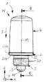
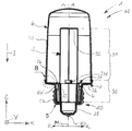
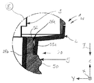
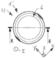
도 1은 본 발명에 따른 LED 전구 조립체(1)의 일 실시예를 개략적인 사시도로 도시한다. 조립체(1)는 함께 직교 좌표계를 형성하는 측 방향 (X), 횡방향 (Y) 및 높이 방향 (Z)을 따라 연장되고, 여기서, 측방향(X)은 횡방향(Y)에 수직하게 연장하면서, 횡방향(Y)에 수직하게 연장하는 높이방향(Z)에도 수직하게 연장한다. 도 1에서, 조립체 (1)는 비조립 상태 (U)로 도시되어 있으며, 여기서 그 모든 구성 요소는 서로 분리되어 조립되기 위한 재치 상태이다.1 shows a schematic perspective view of an embodiment of an
조립체 (1)는 높이 방향 (Z)으로 서로 이격된 베이스 (2), 기판 (3), 제1 접촉 요소 (4), 제2 접촉 요소 (5) 및 반투명 돔 (6)을 포함하고 이들은 높이 방향(Z)로 서로 이격되어 있다. 조립체의 중앙 축선 또는 중심 축선(M)은 높이 방향(Z)에 실질적으로 평행하게 연장된다. 조립체(1)의 삽입 방향 (I)은 중심 축선 (M)에 실질적으로 평행하게 연장되고 그 중심 축선에 중첩 될 수 있다. 삽입 방향 (I)에서, 조립체 (1)는 전구 소켓 (미도시) 내로 삽입 될 수 있다. 또한, 삽입 방향(I)에서, 기판 (3), 제1 접촉 요소 (4) 및 돔 (6)은 베이스 (2)와 결합 될 수 있고, 이 때, 제2 접촉 요소 (5)는 삽입 방향(I)과 반대 방향으로 베이스 (2)에 결합 될 수 있다.The
베이스 (2)에는 조립체(1)를 전구 소켓, 예를 들어, 표준 E26 소켓에 연결하도록 구성된 연결부(20) 및 기판(3)을 지지하기 위한 지지부(21)가 제공된다. 베이스는 지지부 (21)를 원주 방향으로 둘러싸며 돔 (6)을 지지하도록 구성된 플랜지 (22)를 더 포함한다. 연결부(20)는 플랜지(22)로부터 삽입 방향으로 돌출되며 칼라(24)(collar)에 의해 부분적으로 원주 방향으로 둘러싸인 스터드 (23)를 포함한다. 칼라의 개구 (24a)를 통해, 지지부 (21)는 플랜지 (22) 아래에서 접근 가능하며 이로써 조립체(1)의 완전 조립 상태(W)에서, 제2 접촉 요소 (5)가 조립체(1)의 외부로부터 조립체(1)의 내로 베이스(2)를 통해 관입될 수 있다(도 2 내지 도 12 참조). 플랜지 (22)는 림 (22a)을 가질 수 있다. 하나 이상의 래칭 요소(latching element)(22b)가 플랜지(22), 특히 림 (22a)에 형성되어, 완전 조립 상태 (W)에서, 돔(60은 베이스 (2)에 래칭(걸림) 될 수 있다.The
지지부 (21)는 기판 (3)을 지지하기 위한 홀더(holder)(25)를 포함한다. 홀더(25)는 캐비티(cavity)(26) 내에 배치되며 홀더 (25)의 상부 에지 (25a)가 측방향(X) 및 횡방향(Y)을 따라 연장하는 평면 상에서 캐비티 (26)의 에지 (26a)에 대해 실질적으로 정렬될 수 있도록, 즉, 실질적으로 동일한 높이로 배열되도록 설계될 수 있다. 홀더 (25)는 튜브 형상을 가질 수 있고 예를 들어 원형 단면을 갖는 캐비티(26)와 동축으로 배치 될 수 있다. 홀더 (25)는 모서리 (25c)에 의해 서로 구별될 수 있는 복수의 지지면 (25b)을 구비 할 수 있다. 지지면 (25b) 및 모서리 (25c)는, 홀더 (25)가 삽입 방향 (I)을 따라 돌출된 부분에서 다각형 단면을 갖도록, 규칙적인 및/또는 동일한 길이와 각도를 각각 가질 수 있다. 홀더 (25)는 삽입 방향 (I)으로 개방되어 제1 접촉 요소 (4)를 캐비티(26) 내에 수용 가능하게 하는 절개부(cut-out)(25d)를 더 구비할 수 있다.The
기판 (3)은 예를 들어, 튜브 형상을 가질 수 있는 인쇄 회로 기판 (PCB)일 수 있다. 기판(3)은 장착부(30) 및 조명부(31)를 가진다. 기판 (3)의 상부에, 특히 조명부 (31)의 상부에, 캡 (32)이 배치 될 수 있다. 조명부 (31), 예를 들어, 그 외주 및/또는 캡 (32)은 하나 이상의 LED를 구비 할 수 있다. 장착부 (30)는 하부 에지 (30a) 및 홀더 (25)의 지지면 (25b)과 동일하거나 유사한 방식으로 모서리 (30c)에 의해 서로 구별 될 수 있는 복수의 내부 장착면 (30b)을 가질 수 있다. 장착면 (30b)은 기판 (3), 특히 장착부 (30)의 내주를 따라 고르게 분포된다. 노치 또는 슬롯 (30d)이 기판 (3), 특히 장착부 (30)에 형성 될 수 있다. 슬롯 (30)은, 베이스(2)에 대하여 기판(3)의 정확한 배향이 이루어 지도록, 하부 에지(30a)로부터 상방향으로, 예를 들어, 기판(3)의 벽 부분에, 형성될 수 있다. 즉, 슬롯 (30d)은 베이스 (2)에 대한 기판 (3)의 배향을 정렬하는데 기여하여 기판 (3)과 베이스 (2)가 부정결합되는 것이 방지된다. 또한, 외부 장착면 (30e)이 기판 (3)의 외주, 특히 장착부 (30)의 외주를 따라 배치 될 수 있으며 또한 기판 (3)을 베이스에 고정 시키는데 사용될 수 있다.The
기판(3) 상에 구비된 LED와 전기적 접촉을 이루기 위해, 기판은 장착면(30b, 30e)과 유사하게 배열 될 수 있는 접촉면 (33)을 구비 할 수 있다. 접촉면 (33)은 기판 (3)의 외주를 따라 위치 될 수 있다. 도 1에 도시된 예시적인 실시예에서, 두 개의 접촉면(33)이 제2 접촉 요소(5)에 할당되며 이는 장착부(30)에 배열될 수 있다. 추가 접촉면(34)이 제1 접촉 요소 (4) (도 11 참조)와 전기 접촉을 이루기 위해 제공 될 수 있다.In order to make electrical contact with the LEDs provided on the
제1 접촉 요소 (4)는 전기 접촉부 (40), 도체부 (41) 및 피팅부 (42)를 포함 할 수 있다. 전기 접촉부 (40)는 제1 접촉 요소 (4)로부터 삽입 방향 (I)으로 돌출하는 접촉 파일(contact pile) 및/또는 접촉 지점으로 형성될 수 있다. 전기 접촉부 (40)는 도체부 (41)의 레그(leg)(41a)의 단부 영역에 형성 될 수 있다. 레그 (41a)는 피팅부 (42)로부터 실질적으로 수직으로 연장되는 빔(beam)(41b)으로부터 삽입 방향(I)으로 하방으로 연정할 수 있다. 제1 접촉 요소 (4)의 피팅부 (42)는 지지부 (21)의 내주, 특히 그 캐비티(26)에 상보적인 형상일 수 있는 외부 피팅면(fitting surface)(43)을 가질 수 있다. 접촉 요소 (4)의 내부 피팅면 (44)은 완전 조립 상태 (W)에서 추가 접촉면 (34)에 대해 동일 평면 상에 놓이도록 형성되고 배열 될 수 있다.The
제2 접촉 요소 (5)는, 제2 전기 접촉부 (50), 외부 피팅면 (53) 및 하나 이상의 내부 피팅면 (54)을 갖는 제2 피팅부(52)의 일부이거나 일체로 형성될 수 있는 제2 도체부 (51)를 구비할 수 있다. 제2 전기 접촉부 (50)는 예를 들어, B26 표준을 준수하는 나사형으로 형성될 수 있다. 제2 도체부(51)는 제2 전기 접촉부 (50)로부터 삽입 방향 (I)에 대해 상방향으로 연장되며, 제2 도체부는 본 명세서에서 도시된 바와 같이 제2 전기 접촉부(50)가 피팅부 (52)에 통합될 때 생략될 수 있다. 외부 피팅면 (53)은 캐비티(26)의 내주 형상에 상보적인 형상일 수 있다. 제2 내부 피팅면 (54)은 접촉면(33)의 영역 내에서 기판 (3)의 외주 형상에 상보적인 형상일 수 있다. 제2 내부 피팅면 (54)은 완전 조립 상태 (W)에서 접촉면 (33)의 영역 내에서 기판 (3)의 외주에 대해 평평하게 놓이도록 형성되고 배열 될 수 있다.The
돔 (6)은 튜브형 본체(6)을 가질 수 있고, 이는, 기판 (3)을 돔 (6) 내로 삽입 할 수 있도록, 삽입 방향 (I)으로 개방되는 튜브형 본체 (60)의 개구 (62)를 원주 방향으로 둘러싸는 하부 림부(lower rim portion) (61)를 가진다. 완전 조립 상태 (W)에서 돔(6)을 베이스 (2)에 고정시키기 위해, 대응 래칭 수단(counter latching means) (63)이 하부 에지부(61)의 영역 내에 배열되면서 베이스 (2)에 형성된 래칭 요소 (22b)와 상호 작용하도록 구성 될 수 있다.The
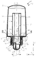
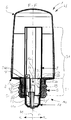
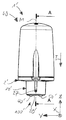
도 2 내지 도 5는 완전 조립 상태 (W)의 조립체 (1)에 대한 개략적인 정면도, 개략적인 측면도, 개략적인 저면도 및 개략적인 상면도를 각각 도시한다. 완전 조립 상태에 도달하기 위해, 몇 개의 사전 조립 상태(V) 비조립 상태(U)와 완전 조립 상태(W) 사이에 있을 수 있다. 어쨌든, 완전 조립 상태 (W)에서, 베이스 (2), 기판 (3), 제1 접촉 요소 (4), 제 2 접촉 요소 (5) 및 돔 (6)은 실질적으로 결합되어 안정적인 LED 전구를 구성한다.Figs. 2 to 5 show a schematic front view, a schematic side view, a schematic bottom view and a schematic top view, respectively, of the
특히 도 2 및 도 3에 도시된 바와 같이, 조립체 (1)의 하부 단부 영역에서, 제1 전기 접촉부(40)는 스터드 (stud)(23)로부터 하방으로 돌출한다. 제2 접촉부 (5)는 칼라 (24)의 주위에 끼워 맞춤 결합되며 제2 전기 접촉부(50)을 제공한다. 돔(6)은, 베이스 상의 래칭 요소(22b) 내로 스냅 결합되는(snapped) 돔의 대응 래칭 요소(63)를 이용해 베이스 (2)의 플랜지 (22) 상에 끼워지고, 이로써 돔(6)은 베이스(2)에 제거 가능하게 부착된다.2 and 3, in the lower end region of the
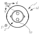
도 6은 완전 조립 상태(W)의 조립체 (1)에 대한 도 3에 도시된 단면선 A-A를 따른 개략적인 단면도이다. 여기서, 완전 조립 상태 (W)에서, 기판 (3)의 장착부 (30)가 캐비티(26) 내로 삽입되어 홀더 (25)가 장착부 (30)와 결합하는 것이 명백하게 보여진다. 지지면 (25b)은 기판(3)의 내부 장착면 (30b)에 맞대어 지지되도록 정렬된다. 즉, 기판(3)의 내부 장착면(30b)은 베이스(2)의 지지면(25b)에 대해 평행하게 놓인다. 이에, 장착부 (30), 특히 내부 장착면 (30b)은 지지부(21)에, 특히, 조립체(1)의 반경 방향(R)을 따라 돌출된 부분에서 홀더 (25)의 지지면 (25b)에 중첩된다. 유사한 방식으로, 제1 접촉 요소 (4)의 내부 피팅면 (44)은 기판 (3)의 추가 접촉면(34)을 맞대어 지지한다.6 is a schematic cross-sectional view along line A-A shown in Fig. 3 for the
따라서, 기판 (3)은 홀더 (25)와 제1 접촉 요소 (4) 사이에서 그 장착부로 막혀 있으면서, 돔 (6) 내의 캡 (32)의 영역 내에서 추가적으로 지지될 필요 없이, 그로부터 종 방향으로 위쪽으로 돌출된다. 완전 조립 상태 (W)에서 지지부 (21)와 장착부 (30)가, 중심 축선 (M)에 실질적으로 평행하게 연장되는 몇 개의 가능한 평면 중 하나 이상에서, 서로 맞대어 지지될 수 있다. 그러한 평면의 수는 특별히 제한되지 않으며, 이는 그 표면에 수직한 벡터들이, 중심 축선 (M)에 단순히 수직으로 연장, 예를 들어, 각각의 반경 방향(R)으로 평행하고 및/또는 중첩 될 뿐이기 때문이다.Thus, the
도 7은 도 6에 도시된 B 영역을 상세히 도시한다. 여기서, 완전 조립 상태 (W)에서 돔 (6)이 베이스 (2)에 래칭되는 방법이 명백하게 보여진다. 러그(lug) 또는 래칭 노우즈(latcing nose) 형태인 대응 래칭 수단 (63)이 함몰부, 오목부, 관통 구멍 또는 림(22a)과 유사한 형상일 수 있는 래칭 요소(22b) 내로 돌출한다. 돔 (6)의 하부 림부 (61)는 림 (22a)에 의해 원주 방향으로 둘러싸일 수 있어 삽입 방향(I)로 플랜지에서 림(22a) 내로 삽입될 수 있고, 이로써 돔 (6)은 베이스 (2)에 단단히 지지될 수 있다.FIG. 7 shows the area B shown in FIG. 6 in detail. Here, the way in which the
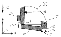
도 8은, 도 2에 도시 된 단면선 C-C를 따른, 완전 조립 상태(W)인 조립체(1)에 대한 개략적인 단면도를 도시한다. 여기서, 연결부 (20)의 영역에서, 지지부 (21), 제1 접촉 요소 (4) 및 제2 접촉 요소 (5)가 함께 조립체 (1)의 커넥터 (100)를 형성한다는 것이 명백하게 보여진다. 커넥터(100)는 삽입 방향(I)로 플랜지(22)로부터 하방으로 돌출하면서 조립체를 소켓(미도시)에 기계적으로 및 전기적으로 연결시킨다.Fig. 8 shows a schematic cross-sectional view of the
제1 전기 접촉부 (40)는 삽입 방향 (I)으로 스터드 (23) 아래로 돌출한다. 레그 (41a)는 제1 전기 접촉부 (40)로부터 상 방향으로 연장되며 빔(41b)에 합쳐지고, 빔(41b)은 캐비티(26)의 내주 및 장착부(30) 사이에 배열되는 피팅부(42)에 레그(41a)를 연결한다. 전기 접촉부 (40)는 조립체를 소켓의 제1 전기 대응 접촉부에 전기적으로 연결시킨다.The first
피팅부 (42)는, 내부 피팅면 (44)이 기판 (3), 특히 그 접촉면 (34)에 대해 평평하게 놓이며 외부 피팅면(43)이 캐비티(26)의 내주에 대패 평평하게 놓이도록, 장착부(30)와 캐비티(26)의 벽 사이에 끼어 질 수 있다. 완전 조립 상태 (W)에서 지지부 (21)와 장착부 (30)가, 중심 축선 (M)에 실질적으로 평행하게 연장되는 몇 개의 가능한 평면 중 하나 이상에서, 서로 맞대어 지지될 수 있다. 그러한 평면의 수는 특별히 제한되지 않으며, 이는 그 표면에 수직한 벡터들이, 중심 축선 (M)에 단순히 수직으로 연장, 예를 들어, 각각의 반경 방향(R)으로 평행하고 및/또는 중첩 될 뿐이기 때문이다.The
제2 접촉부 (5)는, 제2 피팅부 (52)가 칼라 (24)의 개구 (24a) 내로 삽입되는, 베이스의 연결부(20)에 결합될 수 있다. 따라서, 제2 내부 피팅면 (54)은 홀더(25)의 지지면 (25b) 및 기판 (3)의 접촉면 (33)에 대해 평행하게 놓일 수 있다. 제2 전기 접촉부 (50)는 조립체 (1)를 소켓 내의 제2 대응 접촉 요소에 기계적으로 및 전기적으로 연결시키는 나사형으로 형성될 수 있다. 플랜지(22)의 하부면이 실질적으로 삽입 방향(I)으로 향하여 소켓의 상부 림(upper rim)에 조립체가 맞대어 지지됨으로써, 소켓 내에 있는 조립체 (1)를 갖는 설비에 대한 기계적 안정성이 추가적으로 제공될 수 있다. 스터드(23)는 소켓 내에서 상보적으로 형성된 개구 내로 돌출될 수 있어서, 추가적인 기계적 안정성이 제공 될 수 있다.The
도 9는 도 8에 도시된 D 영역의 상세도이다. 여기서, 어깨부(shoulder)(43a)가 피팅부 (42)의 외부 피팅면 (43)에 형성되며 릿지(ledge)(26b)가 캐비티(26) 내에 형성되는 것이 명백하게 보여진다. 이에, 제1 접촉 요소 (4)는 지지부 (21)에 래칭되고, 이로써 베이스 (2)에 대한 제1 접촉 요소 (4)의 이동이 삽입 방향 (I)으로 억제된다.Fig. 9 is a detailed view of the area D shown in Fig. It is evident here that a
도 10은 도 8에 도시된 E 영역의 상세도이다. 여기서, 칼라 (24)의 개구 (24a) 내에서, 돌출부(bulge)(24b)가 반경 방향 (R)에 대해 개구 (24a)의 벽 부분으로부터 돌출되어 제2 접촉 요소(5)의 제2 피팅부 (52)와 결합하도록 형성된다. 제2 피팅부 (52)는, 제2 피팅부 (52)의 외측에서 노우즈 (53a)가 형성되는, 상단부 영역에 움푹 들어간 곳을 가진다. 노우즈 (53a)는 돌출부(24b)에 중첩되어 삽입 방향(I)으로 베이스(2)에 대한 제2 접촉 요소(5)의 움직임을 제한한다. 즉, 완전 조립 상태 (W)에서, 제2 접촉 요소 (5)는 돌출부 (24b) 및 노우즈 (53)를 이용하여 베이스 (2)에 래칭되고, 이로써, 접촉 요소 (5)는 베이스 (2)를 삽입 방향 (I)을 따라 돌출되는 부분에 중첩시켜 제2 접촉 요소 (5)와 베이스 (2) 사이에 포지티브 결합을 형성한다.10 is a detailed view of the area E shown in FIG. Here, in the
도 11은, 도 5에 도시된 횡단면 F-F에 따른, 완전 조립 상태 (W)에서의 조립체 (1)의 개략적인 단면도를 도시한다. 여기서, 제1 접촉 요소 (4)의 측면, 특히 그 피팅부 (42)에서, 기판 (3)의 장착부 (30)가 홀더 (25)와 제1 접촉 요소 (4) 사이에 끼워 질 수 있다는 것이 명백하게 보여진다. 기판(3)의 내부 장착면 (30g)은 홀더의 지지면 (25b)에 대하여 평평하게 놓일 수 있다. 외부 접촉면 (34)은 접촉 요소 (4)의 내부 피팅면 (44)에 대해 평평하게 놓일 수 있다. 완전 조립 상태 (W)에서 지지부 (21)와 장착부 (30)가, 중심 축선 (M)에 실질적으로 평행하게 연장되는 몇 개의 가능한 평면 중 하나 이상에서, 서로 맞대어 지지될 수 있다. 그러한 평면의 수는 특별히 제한되지 않으며, 이는 그 표면에 수직한 벡터들이, 중심 축선 (M)에 단순히 수직으로 연장, 예를 들어, 각각의 반경 방향(R)으로 평행하고 및/또는 중첩 될 뿐이기 때문이다.Figure 11 shows a schematic cross-sectional view of the
접촉 요소(4), 특히 그 피팅부 (42)는 장착부 (30)와 캐비티(26)의 벽 사이에 끼워 질 수 있다. 접촉 요소 (4)의 내부 장착면 (44)이 장착부 (30)에 대하여 평행하게 놓여진 상태에서, 피팅부 (42)의 피팅면(43)이 캐비티(26)의 내벽에 대하여 평행하게 놓일 수 있다. 제1 접촉 요소 (4)의 피팅부 (42)는 연결부(2)의 칼라(24)에 의해 지지부(21)를 둘러싸는 제2 접촉 요소(5)로부터 전기적으로 절연될 수 있다.The
중심 축선(M)에 대해 제1 접촉 요소 (4)의 피팅부 (42)를 대향시키는 연결부(20)의 일측 상에서, 기판 (3), 특히 그 장착부 (30)는 제2 접촉 요소 (5)의 제2 피팅부(52) 및 홀더 (25) 사이에 배치될 수 있다. 기판 (3)의 내부 장착면 (30b)은 홀더 (25)의 지지면 (25b)에 대하여 평행하게 놓일 수 있는 한편, 제2 접촉 요소(5), 특히, 그 피팅부(52)의 내부 피팅면(54)은 기판(3)의 접촉면(33, 34) 및/또는 장착면(33b, 33e)에 평행하게 놓일 수 있다.On one side of the connecting
베이스 (2), 기판 (3), 제1 접촉 요소(4) 및 제2 접촉 요소(5) 모두가 연결부 (30)의 영역 내에서 반경 방향 (R)으로 서로 중첩되기 때문에, 기판 (3)은 지지부 (21) 내에서 단단히 지지되고 커넥터 (100)는 높은 안정성을 가진다. 기판 (3)은 지지부 (21) 내에서 쐐기 형상인 것으로 볼 수 있으므로 기판(3)은 베이스 (2)에 마찰 끼워 맞춤 및/또는 강제 끼워 맞춤되어 지지될 수 있다. 연결부 (20)와 지지부 (21)는 중첩, 즉, 반경 방향 (R)으로 중첩될 수 있다.Since both the
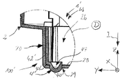
도 12는 본 발명의 다른 실시예에 따른 LED 전구 조립체 (1')의 개략적인 투시 분해도를 도시한다. 간결성을 위해, 이하에서, 조립체 (1')와 조립체 (1) 사이의 차이점이 주로 상세히 설명될 것이다. 조립체 (1')는 조립체(1)에서 사용된 기판(3) 및 돔(6)과 동일한 외관을 갖는 기판 (3) 및 돔 (6)을 포함 할 수 있다. 그러나, 조립체 (1')는, 조립체 (1)와 상이한 종류의 소켓 (미도시)에 조립체(1')를 연결시키는, 베이스(2'), 제1 접촉 요소 (4') 및 제2 접촉 요소 (5')를 포함 할 수 있다. 특히, 조립체(1')는 소위 베이요닛 (Bayonette) 타입 소켓, 예를 들어, 표준 B22 소켓에 호환될 수 있도록 설계될 수 있다.Figure 12 shows a schematic perspective exploded view of an LED bulb assembly 1 'according to another embodiment of the present invention. For the sake of brevity, the differences between the assembly 1 'and the
도 13 내지 도 16은 완전 조립 상태 (W)의 조립체 (1')에 대한 개략적인 정면도, 개략적인 측면도, 개략적인 저면도 및 개략적인 상면도를 도시한다. 조립체 (1)와 대조적으로, 조립체 (1')는 베이요닛형 소켓 및/또는 커플링에 적합한 커넥터 (100')를 가질 수 있다. 따라서, 커넥터 (100')는 그 대향 측면 상에서 베이스 (2')의 연결부 (20')로부터 반경 방향 (R)으로 측 방향으로 돌출하는 2 개의 핀 (27)을 구비 할 수 있다. 또한, 접촉 요소 (4', 5')에 각각 형성 될 수 있는 2 개의 전기 접촉부 (40', 50')가 삽입 방향으로 연결부 (20')로부터 하향 돌출할 수 있고, 이로써 이 들은 연결부 (20')의 바닥부(28') 아래로 돌출된다.Figures 13 to 16 show a schematic front view, a schematic side view, a schematic bottom view and a schematic top view, respectively, of the assembly 1 'in the fully assembled state (W). In contrast to the
접촉 요소들(4', 5')을 베이스 (2')에 끼우기 위해, 접촉 요소들(4', 5')은 각각 연장부 (45) 및 연장부 (55)를 구비 할 수 있다. 연장부들(45, 55)의 말단부 영역에는 보스(boss) (46, 56)가 각각 제공 될 수 있다. 보스들(46, 56)은 베이스 (2')의 플랜지 (22')에 형성된 오목부 (25e)의 형상에 상보적으로 형성 될 수 있다. 완전 조립 상태 (W)에서, 접촉 요소 (4') 및 접촉 요소 (5')의 보스들(46, 56)은 각각 베이스 (2')에 형성된 오목부 (22c) 내로 돌출 될 수 있다.In order to fit the contact elements 4 ', 5' into the base 2 ', the contact elements 4', 5 'may have an
또한, 베이스 (2')의 지지부 (21')는 조립체 (1)의 베이스 (2)에 형성되는 것과 유사한 캐비티 (26')를 포함 할 수 있다. 그러나, 베이스 (2)의 지지부 (21)와 다르게, 베이스(2')의 지지부(21')는 2 개의 지지면 (25b')을 가질 수 있는 2 개의 홀더 (25')를 포함 할 수 있다. 지지면 (25')은 벽 (25e)에 의해 서로 연결될 수 있고, 이는 홀더(25')를 안정시킨다.The support 21 'of the base 2' may also include a cavity 26 'similar to that formed in the
도 18은 도 15에 도시된 B 영역의 상세도이다. 여기서, 보스들(46, 56)이 삽입 방향 (I)으로 점점 가늘어져, 베이스(2')에서 접촉 요소들(4', 5')의 강제 끼움 맞춤 및/또는 마찰 끼움 맞춤이 될 수 있도록, 보스들은 오목부들(22) 내에서 쐐기 형상일 수 있음이 명백하게 보여진다. 또한, 조립체 (1)와 유사하게, 조립체(1')의 돔(6)은, 도 1 내지 도 11에 도시된 조립체(1)와 관련하여 앞서 설명한 방식으로, 래칭 수단(22a) 및 대응 래칭 수단(63)을 이용하여 베이스(2')에 래칭된다.Fig. 18 is a detailed view of the area B shown in Fig. 15. Fig. Here, the
도 19는, 완전 조립 상태 (W)의 조립체 (1')로서, 도 13에 도시된 횡단선 C-C을 따른 개략적인 단면도를 도시한다. 접촉 요소들(40', 50')은 각각, 외부 피팅면들(43', 53')이 캐비티(26)의 내부 원주에 대해 평행하게 놓이도록, 캐비티(26) 내로 삽입 될 수 있다. 접촉부들 (40', 50')은 연결부(20')의 바닥부(28') 내에 형성된 개개의 관통 구멍을 통해 돌출될 수 있다.Fig. 19 shows a schematic cross-sectional view along a transverse line C-C shown in Fig. 13 as an assembly 1 'in a fully assembled state W. Fig. The contact elements 40 'and 50' may be inserted into the
도 20은 도 19에 도시된 D 영역의 상세도이다. 여기서, 전기 접촉부 (40')가 조립체 (1')의 내부, 특히 연결부 (20')의 내부로부터 바닥부 (28') 내 구멍 (29)을 통해 조립체 (1')의 외부로 어떻게 연장되는 지가 명백하게 보여진다. 도체부 (41')는 전기 접촉부 (40')를 접촉 요소(4')의 피팅부 (42')에 연결한다. 전기 접촉부 (40')에는 삽입 방향 (I)을 향하는 그 측면 상에 접촉 캐비티(47)가 제공될 수 있다.20 is a detailed view of the area D shown in FIG. Herein, how the electrical contact 40 'extends from the interior of the assembly 1', in particular from the interior of the connection 20 'to the exterior of the assembly 1' through the
도 21은 완전 조립 상태(W)의 조립체(1')로서, 도 16에 도시 된 횡단선E-E를 따른 개략적인 단면도를 도시한다. 여기서, 일 측면에서 기판 (3)의 장착부 (30)는 홀더들(25') 중 하나와 접촉 요소 (4') 사이에 끼워지고, 다른 측면에서, 홀더들(25') 중 하나와 제2 접촉 요소(5') 사이에 끼워지는 것이 명백히 보여진다. 내부 장착면 (30b)은 지지면(25b)에 대해 평행하게 놓일 수 있는 한편, 추가 접촉면 (34)은 제1 접촉 요소 (4')의 내부 장착면 (44')에 대해 평행하게 놓일 수 있다. 제1 접촉 요소 (4')의 피팅부 (42')는 기판 (3)과 캐비티 (26')의 벽 사이에 끼워 질 수 있다. 외부 피팅면 (43')은 캐비티 (26')의 내부 원주에 대해 동일 평면에 놓일 수 있다. 완전 조립 상태 (W)에서 지지부 (21')와 장착부 (30)가, 중심 축선 (M)에 실질적으로 평행하게 연장되는 몇 개의 가능한 평면 중 하나 이상에서, 서로 맞대어 지지될 수 있다. 그러한 평면의 수는 특별히 제한되지 않으며, 이는 그 표면에 수직한 벡터들이, 중심 축선 (M)에 단순히 수직으로 연장, 예를 들어, 각각의 반경 방향(R)으로 평행하고 및/또는 중첩 될 뿐이기 때문이다.Fig. 21 shows a schematic cross-sectional view along line E-E shown in Fig. 16 as an assembly 1 'in a fully assembled state W. Fig. Here, in one aspect, the mounting
다른 측면에서, 장착부 (30)는 홀더 (25')와 접촉 요소 (5') 사이에 끼워 질 수 있다. 내부 장착면 (33)은 지지면 (25')에 대해 평행하게 놓일 수 있다. 완전 조립 상태 (W)에서 지지부 (21')와 장착부 (30)가, 중심 축선 (M)에 실질적으로 평행하게 연장되는 몇 개의 가능한 평면 중 하나 이상에서, 서로 맞대어 지지될 수 있다. 그러한 평면의 수는 특별히 제한되지 않으며, 이는 그 표면에 수직한 벡터들이, 중심 축선 (M)에 단순히 수직으로 연장, 예를 들어, 각각의 반경 방향(R)으로 평행하고 및/또는 중첩 될 뿐이기 때문이다.In another aspect, the mounting
접촉면 (33)은 접촉 요소 (5')의 외부 피팅면 (54')에 대해 평행하게 놓일 수 있다. 제2 접촉 요소 (5')의 피팅부 (52')는 장착부 (30)와 캐비티 (26')의 내주 사이에 끼워 질 수 있다. 외부 피팅면 (53')은 캐비티 (26')의 내부 원주에 대하여 평행하게 놓일 수 있다. 장착부 (30)의 하부 에지(30a)는 캐비티 (26')의 바닥부 (28')에서 지지 될 수 있다. 따라서, 기판 (3)은 지지부 (21')에서 장착부 (30)에 견고하게 지지되며 모든 방향으로 고정 될 수 있다.The
따라서, 조립체(1)와 관련하여 위에서 설명된 것과 유사하게, 조립체 (1')의 기판 (3)은, 홀더(25')에 연결되지 않으면서, 돔 (6) 내에서 중심 축선 (M)을 따라 홀더 (25')로부터 종방향으로 상부로 연장될 수 있다. 연결부 (30)와 지지부 (21')는 중첩될 수, 즉, 반경 방향 (R)으로 중첩 될 수 있다. 캡 (32)의 영역에서, 돔(6)에 추가적인 고정 구조물 없이 기판 (3)이 견고하게 장착된다.Thus the
전술한 본 발명에 따른 조립체 (1, 1')의 실시예들에 대한 다른 실시예들이 본 발명의 사상을 벗어남 없이 도출될 수 있다. 특정 표준에 부합하여 설계될 수 있는 개별적인 소켓들의 요구 조건들을 만족하는 커넥터(100, 100')를 갖는 LED 전구를 제공하기 위해, 조립체들(1, 1')에는 원하는 수와 형태로 베이스 (2,2'), 기판 (3), 접촉 요소 (4, 4', 5, 5') 및 반투명 돔(6)이 제공될 수 있다.Other embodiments of the embodiments of the
베이스 (2, 2')는 연결부(20, 20'), 지지부(21, 21'), 림(22a)과 래칭 요소(22b)와 오목부(22c)를 갖는 플랜지(22, 22'), 스터드(33), 칼라(24), 개구(24a), 돌출부(24b), 홀더(25, 25'), 지지면(25b, 25b'), 모서리(25c) 절개부(25d), 벽(25b), 에지(26a)와 릿지(26b)를 갖는 공동(26), 핀(26), 바닥부(28, 28') 및/또는 관통홀(29)를 가질 수 있고 그 개수 및 형상은 형상 맞춤 결합(form fit), 마찰 끼움 결합) 및/또는 포지티브 끼움 결합 방식으로 기판(3)을 지지하기 위해 필요에 따라 바뀔 수 있다.The
기판 (3)은 하부 에지(30a), 내부 장착면(30b), 모서리(33), 슬롯 또는 노치(30d), 및 외부 장착면(30)을 갖는 장착부(30), 그리고, 조명부 (31), 캡 (32) 및/또는 접촉면 (33, 34)을 구비할 수 있고, 그 개수 및 형상은 조립체 (1, 1')의 하나 이상의 LED를 구비하여 전기적으로 연결하기 위해 필요에 따라 바뀔 수 있다.The
제1 접촉 요소 (4, 4') 및/또는 제2 접촉 요소 (5, 5')는 제1 및 제2 전기 접촉부 (40, 40', 50, 50'), 도체부(41, 41', 51, 51'), 피팅부(44, 44', 54, 54'), 외부 피팅면(43, 43', 53, 53'), 내부 피팅면(44, 44', 54, 54'), 연장부 (45, 55), 보스 (46, 56), 노우즈 (53a) 및/또는 접촉 캐비티(47)을 구비할 수 있고, 그 개수 및 형태는 기판 (3) 및/또는 소켓 내의 대응 접촉부를 지지 및/또는 전기적으로 접촉시키기 위해 필요에 따라 바뀔 수 있다.The first and
반투명 돔 (6)은 하부 림부(61), 개구(62) 및/또는 대응 래칭 수단(63)을 갖는 관형 몸체(60)를 가질 수 있고, 그 수 및 형태는 조립체(1, 1')의 내부를 보호하고 및/또는 기판(3)을 덮기 위해 필요에 따라 바뀔 수 있다.The
Claims (15)
전구 소켓에 상기 조립체(1, 1')를 연결하기 위한 연결부 (20, 20 ') 및 지지부(21, 21')를 구비하는 베이스(2, 2')로서, 상기 연결부(20, 20') 및 상기 지지부(21, 21')는 상기 조립체(1, 1')의 중심 축선(M)과 실질적으로 평행하게 대향하는 반대 방향을 향하는, 베이스(2, 2'); 및
하나 이상의 LED를 보유하며 상기 조립체(1, 1')의 완전 조립 상태(W)에서 상기 지지부(21, 21')에 부착되는 장착부(30)를 포함하는 기판(3)을 포함하되,
상기 지지부(21, 21') 및 상기 장착부(30)는 완전 조립 상태에서 상기 중심 축선(M)에 실질적으로 평행하게 연장하는 평면 상에서 서로를 지지하는,
LED 전구 조립체.In the LED bulb assembly (1, 1 '),
A base (2, 2 ') having connecting portions (20, 20') and supporting portions (21, 21 ') for connecting the assembly (1, 1' And the supports (21, 21 ') are oriented in opposite directions opposite to and substantially parallel to the central axis (M) of the assembly (1, 1'); And
(3) having at least one LED and a mounting portion (30) attached to the support (21, 21 ') in a fully assembled state (W) of the assembly (1, 1'
The supporting portions 21 and 21 'and the mounting portion 30 are mutually supported on a plane extending substantially parallel to the central axis M in a completely assembled state,
LED bulb assembly.
LED 전구 조립체.2. The method of claim 1, wherein in the fully assembled state (M), the substrate (3) is at least partly projected into the support (21, 21 '
LED bulb assembly.
LED 전구 조립체.3. The assembly (1, 1 ') according to claim 1 or 2, wherein in the fully assembled state (M), the substrate (3) and the connection portions And the radial direction (R) extends substantially perpendicular to the central axis (M)
LED bulb assembly.
LED 전구 조립체.4. Device according to any one of the preceding claims, characterized in that the support (21, 21 ') is at least partly disposed in a cavity (26, 26') formed in the extension of the base , The outer periphery of which forms at least part of the connection (20, 20 ').
LED bulb assembly.
LED 전구 조립체.5. A device according to any one of claims 1 to 4, characterized in that the mounting part (30) is at least partly positively coupled to the support part (21, 21 '
LED bulb assembly.
LED 전구 조립체.6. The connector according to any one of claims 1 to 5, wherein at least a part of the cross section of the mounting portion (30) has a polygonal shape at a portion protruding along the central axis (M)
LED bulb assembly.
LED 전구 조립체.The apparatus according to any one of claims 1 to 6, wherein at least one contact surface (33, 34) for connecting the substrate (3) to the connection part (20, 20 ') is formed in the mounting part (30) W), said at least one contact surface (33, 34) extends along a plane substantially parallel to said central axis (M)
LED bulb assembly.
LED 전구 조립체.8. The apparatus according to claim 7, wherein at least one mounting surface (30b, 30e) for supporting the substrate (3) and at least one contact surface (33, 34) formed in the mounting portion (30) / RTI > and / or < RTI ID = 0.0 >
LED bulb assembly.
LED 전구 조립체.9. The apparatus according to claim 8, wherein a plurality of contact surfaces (33, 34) and mounting surfaces (30b, 30e) are alternately arranged along the outer and /
LED bulb assembly.
LED 전구 조립체.The assembly (1, 1 ') according to any one of claims 1 to 9, further comprising at least one contact element (4, 4', 5, 5 ' 5 'are at least partly disposed between the mounting portion 30 and the support portions 21, 21' in a fully assembled state W to provide electrical contact with the substrate 3,
LED bulb assembly.
LED 전구 조립체.11. The device according to claim 10, wherein said at least one contact element (4, 4 ', 5, 5') comprises a fitting portion (42, 42 ''Has a complementary shape to the mounting portion 30 and / or the support portion 21, 21'
LED bulb assembly.
LED 전구 조립체.The method of claim 10 or 11, wherein the electrical contacts (40, 40 ', 50, 50') of the assembly (1, 1 ' Is accessible from the outside of the assembly (1, 1 ') and the electrical contacts (40, 40', 50, 50 ') are formed in the one or more contact elements (4, 4', 5, 5 '
LED bulb assembly.
LED 전구 조립체.The assembly according to any one of the preceding claims, wherein the assembly (1, 1 ') further comprises at least one second contact element (4, 4' 5, 5 ' And 5 'and 5' are arranged at least partly between the mounting portion 30 and the support portions 21 and 21 'in a fully assembled state W to make electrical contact with the substrate 3. [
LED bulb assembly.
LED 전구 조립체.14. A method according to any one of claims 1 to 13, characterized in that the assembly (1, 1 ') comprises at least one translucent dome (6), the translucent dome (6) ') And covering the substrate (3)
LED bulb assembly.
전구 소켓에 상기 조립체(1, 1')를 연결하기 위한 연결부 (20, 20 ') 및 지지부(21, 21')를 베이스(2, 2')에 제공하는 단계로서, 상기 연결부(20, 20') 및 상기 지지부(21, 21')는 상기 조립체(1, 1')의 중심 축선(M)과 실질적으로 평행하게 대향하는 반대 방향을 향하는, 단계;
상기 조립체(1, 1')를 비조립 상태(U)로부터 완전 조립 상태(W)로 변환 시 상기 기판(3)을 상기 상기 지지부(21, 21')에 부착시키기 위한 장착부(30)를 하나 이상의 LED 구비한 기판(3)에 제공하는 단계; 및
상기 기판(3)을 상기 지지부(21, 21')에 부착 시 상기 지지부(21, 21') 및 상기 장착부(30)가 상기 중심 축선(M)에 실질적으로 평행하게 연장하는 평면 상에서 서로를 지지하게 만드는 단계를 포함하는,
방법.A method of assembling a bulb assembly (1, 1 '),
(20, 20 ') and supports (21, 21') to the base (2, 2 ') for connecting said assembly (1, 1') to a bulb socket, 'And the supports 21 and 21' are oriented in opposite directions substantially parallel to the central axis M of the assembly 1, 1 ';
(30) for attaching the substrate (3) to the support portions (21, 21 ') when converting the assembly (1, 1') from the unassembled state (U) To the substrate (3) with LEDs; And
When the substrate 3 is attached to the support portions 21 and 21 ', the support portions 21 and 21' and the mounting portion 30 support each other on a plane extending substantially parallel to the central axis M ≪ / RTI >
Way.
Applications Claiming Priority (5)
| Application Number | Priority Date | Filing Date | Title |
|---|---|---|---|
| IN2157/MUM/2015 | 2015-06-04 | ||
| IN2157MU2015 | 2015-06-04 | ||
| CHCH01045/2015 | 2015-07-17 | ||
| CH01045/15A CH711339B1 (en) | 2015-07-17 | 2015-07-17 | LED lamp assembly and method of making the same. |
| PCT/IN2016/050166 WO2016194005A1 (en) | 2015-06-04 | 2016-06-03 | Led light bulb assembly and method for manufacturing same |
Publications (1)
| Publication Number | Publication Date |
|---|---|
| KR20180016492A true KR20180016492A (en) | 2018-02-14 |
Family
ID=56561397
Family Applications (1)
| Application Number | Title | Priority Date | Filing Date |
|---|---|---|---|
| KR1020187000334A KR20180016492A (en) | 2015-06-04 | 2016-06-03 | LED Light Bulb Assembly and Method for Manufacturing Same |
Country Status (11)
| Country | Link |
|---|---|
| US (1) | US10612728B2 (en) |
| EP (1) | EP3303915B1 (en) |
| JP (1) | JP6837059B2 (en) |
| KR (1) | KR20180016492A (en) |
| CN (1) | CN108291708B (en) |
| BR (1) | BR112017025425A2 (en) |
| ES (1) | ES2774472T3 (en) |
| MX (1) | MX2017015409A (en) |
| RU (1) | RU2718345C2 (en) |
| WO (1) | WO2016194005A1 (en) |
| ZA (1) | ZA201708457B (en) |
Families Citing this family (3)
| Publication number | Priority date | Publication date | Assignee | Title |
|---|---|---|---|---|
| USD938095S1 (en) * | 2013-04-01 | 2021-12-07 | Pathy Medical, Llc | Lighting device |
| US10794544B2 (en) | 2017-06-14 | 2020-10-06 | Consumer Lighting (US), LLC | LED lamp |
| JP7441681B2 (en) * | 2020-03-05 | 2024-03-01 | ソニー・オリンパスメディカルソリューションズ株式会社 | storage case |
Family Cites Families (12)
| Publication number | Priority date | Publication date | Assignee | Title |
|---|---|---|---|---|
| CN102095172A (en) * | 2009-12-15 | 2011-06-15 | 富士迈半导体精密工业(上海)有限公司 | Light emitting diode lamp |
| JP5662059B2 (en) * | 2010-06-04 | 2015-01-28 | パナソニックIpマネジメント株式会社 | LED lamp |
| DE202011101257U1 (en) | 2011-05-23 | 2012-05-30 | Promotec Gmbh | Light-bulbs |
| US8704432B2 (en) | 2011-05-25 | 2014-04-22 | Seoul Semiconductor Co., Ltd. | LED lamp |
| JP5936906B2 (en) | 2011-06-29 | 2016-06-22 | ローム株式会社 | LED bulb |
| US20130088880A1 (en) * | 2011-10-11 | 2013-04-11 | Cooler Master Co., Ltd. | Led lighting device |
| RU2516228C2 (en) * | 2012-04-12 | 2014-05-20 | Общество С Ограниченной Ответственностью "Светозар" | Led lamp |
| US9410687B2 (en) * | 2012-04-13 | 2016-08-09 | Cree, Inc. | LED lamp with filament style LED assembly |
| US20140056001A1 (en) | 2012-08-24 | 2014-02-27 | Industrial Technology Research Institute | Led light bulb module |
| JP6089551B2 (en) | 2012-10-09 | 2017-03-08 | セイコーエプソン株式会社 | Lighting device |
| CN104421682B (en) * | 2013-08-26 | 2018-04-03 | 赵依军 | LED light source module and the LEDbulb lamp comprising the module |
| CN203641941U (en) * | 2013-10-31 | 2014-06-11 | 陈清辉 | LED bulb |
-
2016
- 2016-06-03 US US15/572,700 patent/US10612728B2/en active Active
- 2016-06-03 CN CN201680029008.8A patent/CN108291708B/en not_active Expired - Fee Related
- 2016-06-03 JP JP2018515365A patent/JP6837059B2/en active Active
- 2016-06-03 MX MX2017015409A patent/MX2017015409A/en unknown
- 2016-06-03 RU RU2017144588A patent/RU2718345C2/en active
- 2016-06-03 KR KR1020187000334A patent/KR20180016492A/en not_active Application Discontinuation
- 2016-06-03 ES ES16745857T patent/ES2774472T3/en active Active
- 2016-06-03 EP EP16745857.9A patent/EP3303915B1/en active Active
- 2016-06-03 WO PCT/IN2016/050166 patent/WO2016194005A1/en active Application Filing
- 2016-06-03 BR BR112017025425A patent/BR112017025425A2/en active Search and Examination
-
2017
- 2017-12-13 ZA ZA2017/08457A patent/ZA201708457B/en unknown
Also Published As
| Publication number | Publication date |
|---|---|
| US20180135811A1 (en) | 2018-05-17 |
| EP3303915B1 (en) | 2020-02-19 |
| RU2718345C2 (en) | 2020-04-02 |
| WO2016194005A1 (en) | 2016-12-08 |
| BR112017025425A2 (en) | 2018-08-07 |
| CN108291708A (en) | 2018-07-17 |
| CN108291708B (en) | 2020-09-08 |
| MX2017015409A (en) | 2018-03-09 |
| RU2017144588A3 (en) | 2019-11-18 |
| RU2017144588A (en) | 2019-07-09 |
| ES2774472T3 (en) | 2020-07-21 |
| JP2018516446A (en) | 2018-06-21 |
| ZA201708457B (en) | 2019-05-29 |
| US10612728B2 (en) | 2020-04-07 |
| EP3303915A1 (en) | 2018-04-11 |
| JP6837059B2 (en) | 2021-03-03 |
Similar Documents
| Publication | Publication Date | Title |
|---|---|---|
| US7892031B1 (en) | Quick insertion lamp assembly | |
| TWI383551B (en) | Anschlusselement zur elektrischen anbindung einer led | |
| US8636380B2 (en) | Lighting module, lighting device comprising a lighting module, method for assembling a lighting module and method for assembly of a lighting device | |
| WO2017092373A1 (en) | Integrated electric connection structure for led lamp | |
| KR20180016492A (en) | LED Light Bulb Assembly and Method for Manufacturing Same | |
| US20110227471A1 (en) | Integrally ballasted lamp assembly including a spacer disk | |
| JP2006032368A (en) | Ceiling hook and luminaire | |
| US20110003497A1 (en) | Fluorescent lamp holder assembly | |
| EP3172481B1 (en) | Rotationally adjustable lamp and manufacturing method | |
| WO2019196807A1 (en) | Lamp | |
| CN108317409B (en) | Lamp fitting | |
| KR102191714B1 (en) | Light-emitting arrangement and light-emitting system | |
| CN214840694U (en) | Connector, connection combination, fixing seat, connecting seat and lamp fixing device | |
| TWI661618B (en) | Electrical connector and electrical connector assembly | |
| CN113266808A (en) | Connector, connection combination, fixing seat, connecting seat and lamp fixing device | |
| JP5669656B2 (en) | Sockets and lighting fixtures | |
| JP2013098076A (en) | Straight tube type led lighting device | |
| CN215523191U (en) | Lamp bracket and lamp | |
| JP2022133237A (en) | Lighting device having mounting guide structure | |
| KR101651480B1 (en) | Connecter unit for line type lighting device | |
| US11371664B2 (en) | LED lamp with a connection module with an antenna function | |
| CN216591633U (en) | Lamp fixture | |
| KR20120016759A (en) | A led lamp | |
| KR20150028944A (en) | Lamp socket | |
| JP2016181429A (en) | Lamp device and lighting device |
Legal Events
| Date | Code | Title | Description |
|---|---|---|---|
| A201 | Request for examination | ||
| E902 | Notification of reason for refusal | ||
| E601 | Decision to refuse application |