KR20180004677A - Bridgeless interleaved power factor correction and method for controling thereof - Google Patents
Bridgeless interleaved power factor correction and method for controling thereof Download PDFInfo
- Publication number
- KR20180004677A KR20180004677A KR1020170085018A KR20170085018A KR20180004677A KR 20180004677 A KR20180004677 A KR 20180004677A KR 1020170085018 A KR1020170085018 A KR 1020170085018A KR 20170085018 A KR20170085018 A KR 20170085018A KR 20180004677 A KR20180004677 A KR 20180004677A
- Authority
- KR
- South Korea
- Prior art keywords
- switch
- boost
- inductor
- circuit
- operation mode
- Prior art date
Links
Images


Classifications
-
- H—ELECTRICITY
- H02—GENERATION; CONVERSION OR DISTRIBUTION OF ELECTRIC POWER
- H02M—APPARATUS FOR CONVERSION BETWEEN AC AND AC, BETWEEN AC AND DC, OR BETWEEN DC AND DC, AND FOR USE WITH MAINS OR SIMILAR POWER SUPPLY SYSTEMS; CONVERSION OF DC OR AC INPUT POWER INTO SURGE OUTPUT POWER; CONTROL OR REGULATION THEREOF
- H02M1/00—Details of apparatus for conversion
- H02M1/42—Circuits or arrangements for compensating for or adjusting power factor in converters or inverters
- H02M1/4208—Arrangements for improving power factor of AC input
-
- Y—GENERAL TAGGING OF NEW TECHNOLOGICAL DEVELOPMENTS; GENERAL TAGGING OF CROSS-SECTIONAL TECHNOLOGIES SPANNING OVER SEVERAL SECTIONS OF THE IPC; TECHNICAL SUBJECTS COVERED BY FORMER USPC CROSS-REFERENCE ART COLLECTIONS [XRACs] AND DIGESTS
- Y02—TECHNOLOGIES OR APPLICATIONS FOR MITIGATION OR ADAPTATION AGAINST CLIMATE CHANGE
- Y02B—CLIMATE CHANGE MITIGATION TECHNOLOGIES RELATED TO BUILDINGS, e.g. HOUSING, HOUSE APPLIANCES OR RELATED END-USER APPLICATIONS
- Y02B70/00—Technologies for an efficient end-user side electric power management and consumption
- Y02B70/10—Technologies improving the efficiency by using switched-mode power supplies [SMPS], i.e. efficient power electronics conversion e.g. power factor correction or reduction of losses in power supplies or efficient standby modes
Landscapes
- Engineering & Computer Science (AREA)
- Power Engineering (AREA)
- Dc-Dc Converters (AREA)
Abstract
Description
본 발명은 브릿지리스 인터리브 역률보정회로 및 그 구동방법에 관한 것으로서, 더욱 상세하게는 전기자동차용 배터리 충전 장치를 위한 브릿지리스 인터리브 역률보정회로 및 그 구동방법에 관한 것이다.The present invention relates to a bridgeless interleaved power factor correction circuit and a driving method thereof, and more particularly, to a bridgeless interleaved power factor correction circuit and a driving method thereof for a battery charging device for an electric vehicle.
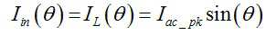
브릿지리스(bridgeless) 역률보정회로(Power Factor Correction, PFC) 컨버터는 종래의 부스트(boost) 역률보정회로에 비해 효율면에서 우수한 성능이 발휘된다는 점으로 인해 최근 많은 주목을 받고 있다. 부스트 모스펫(MOSFET)의 바디 다이오드를 이용함으로써 입력 브릿지 다이오드를 제거할 수 있으며, 이로 인해 브릿지리스 인터리브형 역률보정회로(BIPFC)는 종래의 부스트 컨버터에 비해 총 손실의 37% 가량을 절감할 수 있다. 하지만, 이러한 장점에도 불구하고, 종래의 브릿지리스 인터리브형 역률보정회로가 구현된 컨버터는 높은 EMI 노이즈, 회로 구성요소의 낮은 사용률 및 복잡한 피드백 회로에 의해서만 상술한 고효율을 달성할 수 있다는 문제점이 있다.The bridgeless power factor correction (PFC) converter has received a lot of attention in recent years due to its excellent performance in comparison with the conventional boost power factor correction circuit. By using the body diode of the boost MOSFET, the input bridge diode can be eliminated, which allows the bridgeless interleaved power factor correction circuit (BIPFC) to save 37% of the total loss compared to the conventional boost converter . Despite these advantages, however, the conventional bridgeless interleaved power factor correction circuit implemented converter has a problem that high EMI noise, low utilization of circuit components, and complicated feedback circuit can achieve the above-mentioned high efficiency.
도 1은 종래 기술에 따른 컨버터의 회로도이다. 도 1의 (a)는 종래의 인터리브형 역률보정회로이고, 도 1의 (b)는 종래 기술에 따른 브릿지리스 인터리브형 역률보정회로이다. 1 is a circuit diagram of a converter according to the prior art. 1 (a) is a conventional interleaved power factor correcting circuit, and Fig. 1 (b) is a bridgeless interleaved power factor correcting circuit according to the prior art.
도 1의 (b)에 도시된 바와 같이, 종래의 브릿지리스 인터리브형 역률보정회로(BIPFC)는 인터리브 구성을 사용하는 두 개의 브릿지리스 역률보정회로(BPFC)로 구성되며, 네 개의 부스트 레그(boot leg)를 포함한다. 여기서, 2개의 레그는 PWM(Pulse Width Modulation)로 동작하고, 다른 2개의 레그는 정류기로 동작한다. 복귀 경로상의 인덕터는 입력 저주파 전류를 전달하고, 본체 다이오드만이 이러한 경로에 이용된다. 결과적으로, 종래의 브릿지리스 인터리브형 역률보정회로를 이용할 경우, 저조한 이용률로 인해 회로의 전체 부피가 증가하며 높은 비용이 요구될 수 있다.As shown in FIG. 1 (b), a conventional bridgeless interleaved power factor correction circuit (BIPFC) is composed of two bridgeless power factor correcting circuits (BPFC) using an interleave configuration, and four booster legs leg. Here, the two legs operate in PWM (Pulse Width Modulation), and the other two legs operate as rectifiers. The inductor on the return path carries the input low frequency current, and only the body diode is used in this path. As a result, when the conventional bridgeless interleaved power factor correction circuit is used, the total volume of the circuit is increased due to a poor utilization rate and high cost may be required.
또한, 종래의 브릿지리스 인터리브형 역률보정회로(BIPFC)는 피드백 제어 회로에 대한 또다른 문제점을 가지고 있다. 피드백 제어 회로는 출력 전압과 입력 전류를 모두 조절해야 되기 때문에, 입력 전류, 입력 전압 및 출력 전압을 포함하는 많은 요소를 센싱해야 될 필요가 있다. 특히, 전류 제어 루프는 높은 대역폭을 필요로 하므로 고성능 전류 센서가 요구된다.In addition, the conventional bridgeless interleaved power factor correction circuit (BIPFC) has another problem for the feedback control circuit. Since the feedback control circuit must regulate both the output voltage and the input current, it is necessary to sense many components, including input current, input voltage and output voltage. In particular, current control loops require high bandwidths and therefore require high performance current sensors.
도시된 바와 같이, 종래의 BIPFC는 네 개의 입력 전류 센서(L1 내지 L4)가 구비되어 있다. 구체적으로, 종래의 BIPFC는 입력측에 4개의 홀 센서(hall sensor)가 구비되거나, 스위치에 4개의 변류기(Current Transformer, CT)가 구비되는 것을 특징으로 한다. 이때, 4개 홀 센서를 사용할 경우 회로를 제작하는 비용이 높아지고, 4개의 변류기를 사용할 경우 복잡한 리셋 회로(reset circuitry)가 요구된다는 문제점이 있다. As shown, the conventional BIPFC includes four input current sensors L 1 through L 4 . Specifically, the conventional BIPFC has four hall sensors on the input side or four current transformers (CT) on the switches. In this case, when the four Hall sensors are used, the cost of manufacturing a circuit increases, and a complicated reset circuitry is required when four current converters are used.
본 발명의 일측면은 종래의 인터리브형 역률보정회로에 비해 동작 성능은 향상되면서, 종래의 브릿지리스 인터리브 역률보정회로에 비해 제작 비용이 절감되면서도 콤팩트한 회로로 구현될 수 있는 브릿지리스 인터리브 역률보정회로 및 그 구동방법을 제공한다.One aspect of the present invention is to provide a bridgeless interleaved power factor correcting circuit which can be realized as a compact circuit while reducing manufacturing cost compared to a conventional bridgeless interleaved power factor correcting circuit, And a driving method thereof.
본 발명의 기술적 과제는 이상에서 언급한 기술적 과제로 제한되지 않으며, 언급되지 않은 또 다른 기술적 과제들은 아래의 기재로부터 당업자에게 명확하게 이해될 수 있을 것이다.The technical problem of the present invention is not limited to the technical problems mentioned above, and other technical problems which are not mentioned can be understood by those skilled in the art from the following description.
본 발명의 일 실시예에 따른 브릿지리스 인터리브 역률보정회로는, 입력 전원과 연결되며 인덕터를 포함하는 적어도 하나의 단일 부스트 레그와, 상기 입력 전원과 연결되며 인덕터 및 저속 다이오드를 포함하는 복수의 병합 부스트 레그를 포함하는 복수의 부스트 레그, 하나의 상기 단일 부스트 레그와 연결되는 단일 스위치 회로와, 적어도 두 개의 상기 병합 부스트 레그와 연결되는 병합 스위치 회로를 포함하는 복수의 스위치 회로 및 상기 스위치 회로와 연결되고, 미리 정해진 동작 구간 및 미리 정해진 전류 측정 시점에 따라 출력 전류를 측정하는 단일 전류 센서를 포함한다. The bridgeless interleaved power factor correction circuit according to an embodiment of the present invention includes at least one single boost leg connected to an input power source and including an inductor and a plurality of merge boosts connected to the input power source and including an inductor and a low speed diode, A plurality of switch circuits including a plurality of boost legs including the legs, a single switch circuit connected to one of the single boost legs and a merge switch circuit connected to at least two of the merge boost legs, And a single current sensor for measuring an output current according to a predetermined operating range and a predetermined current measuring time point.
상기 복수의 부스트 레그는 제1 부스트 레그 내지 제4 부스트 레그를 포함하고, 상기 제1 부스트 레그 및 상기 제4 부스트 레그는 상기 단일 부스트 레그이고, 제2 부스트 레그 및 제3 부스트 레그는 상기 병합 부스트 레그일 수 있다.Wherein the plurality of boost legs comprise a first boost leg to a fourth boost leg, wherein the first boost leg and the fourth boost leg are the single boost legs, and the second boost leg and the third boost leg comprise the first and second boost legs, Lt; / RTI >
상기 복수의 스위치 회로는 제1 스위치 회로 내지 제3 스위치 회로를 포함하고, 상기 제1 스위치 회로는 상기 제1 부스트 레그와 연결되고, 제2 스위치 회로는 상기 제2 부스트 레그 및 상기 제3 부스트 레그와 병렬로 연결되며, 상기 제3 스위치 회로는 상기 제4 부스트 레그와 연결될 수 있다.Wherein the plurality of switch circuits includes a first switch circuit to a third switch circuit, the first switch circuit is connected to the first boost leg, and the second switch circuit is connected to the second boost leg and the third boost leg, And the third switch circuit may be connected to the fourth boost leg.
상기 스위치 회로는 고속 다이오드 및 스위치를 포함하고, 상기 저속 다이오드는 상기 고속 다이오드와 직렬로 연결되어 상기 입력 전원의 순환 전류를 차단할 수 있다.The switch circuit includes a high-speed diode and a switch, and the low-speed diode may be connected in series with the high-speed diode to cut off the circulating current of the input power.
상기 브릿지리스 인터리브 역률보정회로는, 스위칭 주파수가 라인 주파수보다 높은 상태인 경우, 라인 전압의 1/2주기마다 상기 입력 전원으로부터 공급되는 입력 전압의 극성을 변화시키는 부스트 컨버터로 동작될 수 있다.The bridgeless interleaved power factor correction circuit may be operated as a boost converter that changes the polarity of the input voltage supplied from the input power source every 1/2 period of the line voltage when the switching frequency is higher than the line frequency.
상기 브릿지리스 인터리브 역률보정회로는, 상기 라인 전압의 1/2주기동안 변화되는 듀티 사이클 값이 미리 정해진 기준값보다 작은 경우, 상기 복수의 스위치 회로가 제1 동작 모드 내지 제3 동작 모드 중 어느 하나의 동작 모드로 작동되도록 제어하고, 상기 듀티 사이클 값이 상기 기준값보다 큰 경우, 상기 복수의 스위치 회로가 제4 동작 모드 내지 제6 동작 모드 중 어느 하나의 동작 모드로 작동되도록 제어할 수 있다.Wherein the bridgeless interleaved power factor correcting circuit is configured such that when the duty cycle value which is changed during 1/2 period of the line voltage is smaller than a predetermined reference value, the plurality of switch circuits are operated in any one of the first to third operation modes And to control the plurality of switch circuits to operate in any one of the fourth to sixth operation modes when the duty cycle value is greater than the reference value.
상기 복수의 스위치 회로는, 상기 듀티 사이클 값이 미리 정해진 값보다 작은 경우, 상기 라인 전압의 1/2주기를 구성하는 제1 구간은 제1 동작 모드로 제어되고, 상기 제1 구간 이후의 제2 구간은 제2 동작 모드로 제어되고, 상기 제2 구간 이후의 제3 구간은 제3 동작 모드로 제어되며, 상기 제3 구간 이후의 제4 구간은 상기 제2 동작 모드로 제어되고, 상기 듀티 사이클 값이 미리 정해진 값보다 큰 경우, 상기 라인 전압의 1/2주기를 구성하는 제1 구간은 제4 동작 모드로 제어되고, 상기 제1 구간 이후의 제2 구간은 제5 동작 모드로 제어되고, 상기 제2 구간 이후의 제3 구간은 상기 제4 동작 모드로 제어되며, 상기 제3 구간 이후의 제4 구간은 제6 동작 모드로 제어될 수 있다.When the duty cycle value is smaller than a predetermined value, the first section constituting the half cycle of the line voltage is controlled to the first operation mode, and the second section after the first section is controlled to the second operation mode, The third section after the second section is controlled in the third operation mode, the fourth section after the third section is controlled in the second operation mode, the duty cycle is controlled in the second operation mode, The first period constituting the half period of the line voltage is controlled to the fourth operation mode and the second period after the first period is controlled to the fifth operation mode, The third section after the second section may be controlled to the fourth operation mode and the fourth section after the third section may be controlled to the sixth operation mode.
상기 복수의 스위치 회로가 제1 스위치 회로 내지 제3 스위치 회로로 마련되는 경우, 상기 브릿지리스 인터리브 역률보정회로는, 상기 제1 동작 모드 및 상기 제6 동작 모드에서 상기 제1 스위치 회로의 제1 스위치와 상기 제3 스위치 회로의 제3 스위치는 턴오프 시키고, 제2 스위치 회로의 제2 스위치는 턴온시키고, 상기 제2 동작 모드에서 상기 상기 제1 스위치 내지 상기 제3 스위치를 턴오프시키고, 상기 제3 동작 모드에서 상기 제1 스위치 및 상기 제3 스위치는 턴온시키고, 상기 제2 스위치는 턴오프시키고, 상기 제4 동작 모드에서 상기 제1 스위치 내지 상기 제3 스위치를 턴온시키며, 상기 제5 동작 모드에서 상기 제1 스위치 내지 상기 제3 스위치는 턴온시키고, 상기 제2 스위치는 턴오프시킬 수 있다.Wherein when the plurality of switch circuits are provided from the first switch circuit to the third switch circuit, the bridgeless interleaved power factor correcting circuit is configured so that, in the first operation mode and the sixth operation mode, And the third switch of the third switch circuit are turned off and the second switch of the second switch circuit is turned on and in the second operation mode the first switch and the third switch are turned off, The first switch and the third switch are turned on and the second switch is turned off in the first operation mode and the first switch and the third switch are turned on in the fourth operation mode, The first switch to the third switch may be turned on and the second switch may be turned off.
또한, 본 발명의 일 실시예에 따른 인덕터가 구비된 복수의 부스트 레그와, 적어도 하나의 상기 부스트 레그와 연결되는 복수의 스위칭 회로와, 상기 인덕터로부터 전달된 출력 전류를 감지하는 단일 전류 센서를 포함하는 브릿지리스 인터리브 역률보정회로의 동작 방법은, 상기 복수의 스위칭 회로는, 라인 전압의 소정 주기동안 변화되는 듀티 사이클 값을 미리 정해진 기준값과 비교한 결과에 따라 각각의 스위치 회로의 동작 모드가 제어되고, 상기 단일 전류 센서는, 상기 각각의 스위치 회로의 온오프 조합에 따라 상기 출력 전류를 측정할지 여부가 결정된다. Also, the present invention includes a plurality of boost legs having inductors according to an embodiment of the present invention, a plurality of switching circuits connected to at least one of the boost legs, and a single current sensor for sensing an output current delivered from the inductors The operation modes of the respective switch circuits are controlled in accordance with a result of comparing a duty cycle value which is varied during a predetermined period of the line voltage with a predetermined reference value , The single current sensor determines whether to measure the output current according to the on / off combination of the respective switch circuits.
상기 부스트 레그는, 입력 전원과 연결되며 인덕터를 포함하는 적어도 하나의 단일 부스트 레그와, 상기 입력 전원과 연결되며 인덕터 및 저속 다이오드를 포함하는 복수의 병합 부스트 레그를 포함하며, 상기 스위치 회로는, 하나의 상기 단일 부스트 레그와 연결되는 단일 스위치 회로와, 적어도 두 개의 상기 병합 부스트 레그와 연결되는 병합 스위치 회로를 포함할 수 있다.Wherein the boost leg comprises at least one single boost leg coupled to the input power source and comprising an inductor and a plurality of merge boost legs coupled to the input power source and including an inductor and a low speed diode, And a merging switch circuit connected to at least two of the merging boost legs.
상기 스위치 회로는, 상기 라인 전압의 1/2주기동안 변화되는 듀티 사이클 값이 미리 정해진 기준값보다 작은 경우, 제1 동작 모드 내지 제3 동작 모드 중 어느 하나의 동작 모드로 동작되고, 상기 듀티 사이클 값이 상기 기준값보다 큰 경우, 제4 동작 모드 내지 제6 동작 모드 중 어느 하나의 동작 모드로 동작될 수 있다.Wherein the switch circuit is operated in any one of a first operation mode to a third operation mode when the duty cycle value that is changed during 1/2 period of the line voltage is smaller than a predetermined reference value, Is greater than the reference value, it can be operated in any one of the fourth to sixth operation modes.
상술한 본 발명의 일측면에 따르면, 적어도 두 개의 병합 부스트 레그를 하나의 고속 다이오드에 병합함으로써, 종래의 기술보다 더욱 적은 능동 소자로 구현되면서도 높은 디바이스 이용률을 가질 수 있다. 또한, 단일 전류 센서를 이용함으로써, 종래의 선형 평균 전류 제어 방식을 통한 전류 센싱 기법에 비해 회로의 크기가 소형화되고 저비용으로 회로를 제작할 수 있다.According to one aspect of the present invention described above, by incorporating at least two merging boost legs into one high-speed diode, it is possible to achieve a higher device utilization while implementing less active elements than the prior art. Also, by using a single current sensor, the circuit size can be reduced and the circuit can be manufactured at a low cost as compared with the current sensing technique using the conventional linear average current control method.
도 1은 종래 기술에 따른 인터리브형 역률보정회로 및 브릿지리스 역률보정회로의 회로도이다.
도 2는 본 발명의 일 실시예에 따른 브릿지리스 인터리브 역률보정회로가 개략적으로 구현된 회로도이다.
도 3 내지 도 5는 도 2의 브릿지리스 인터리브 역률보정회로의 동작 특성 및 구동 원리가 도시된 도면이다.
도 6 내지 도 7은 도 2의 전류 센서(500)의 구체적인 동작 방법이 도시된 도면이다.
도 9 내지 도 16은 도 2의 브릿지리스 인터리브 역률보정회로의 실험 결과를 나타낸 도면이다.1 is a circuit diagram of an interleaved power factor correction circuit and a bridgeless power factor correction circuit according to the prior art.
2 is a circuit diagram schematically illustrating a bridgeless interleaved power factor correction circuit according to an embodiment of the present invention.
Figs. 3 to 5 are diagrams showing the operation characteristics and the operating principle of the bridgeless interleaved power factor correction circuit of Fig. 2. Fig.
6 to 7 are views showing a specific operation method of the
9 to 16 are graphs showing experimental results of the bridgeless interleaved power factor correction circuit of FIG.
후술하는 본 발명에 대한 상세한 설명은, 본 발명이 실시될 수 있는 특정 실시예를 예시로서 도시하는 첨부 도면을 참조한다. 이들 실시예는 당업자가 본 발명을 실시할 수 있기에 충분하도록 상세히 설명된다. 본 발명의 다양한 실시예는 서로 다르지만 상호 배타적일 필요는 없음이 이해되어야 한다. 예를 들어, 여기에 기재되어 있는 특정 형상, 구조 및 특성은 일 실시예와 관련하여 본 발명의 정신 및 범위를 벗어나지 않으면서 다른 실시예로 구현될 수 있다. 또한, 각각의 개시된 실시예 내의 개별 구성요소의 위치 또는 배치는 본 발명의 정신 및 범위를 벗어나지 않으면서 변경될 수 있음이 이해되어야 한다. 따라서, 후술하는 상세한 설명은 한정적인 의미로서 취하려는 것이 아니며, 본 발명의 범위는, 적절하게 설명된다면, 그 청구항들이 주장하는 것과 균등한 모든 범위와 더불어 첨부된 청구항에 의해서만 한정된다. 도면에서 유사한 참조부호는 여러 측면에 걸쳐서 동일하거나 유사한 기능을 지칭한다.The following detailed description of the invention refers to the accompanying drawings, which illustrate, by way of illustration, specific embodiments in which the invention may be practiced. These embodiments are described in sufficient detail to enable those skilled in the art to practice the invention. It should be understood that the various embodiments of the present invention are different, but need not be mutually exclusive. For example, certain features, structures, and characteristics described herein may be implemented in other embodiments without departing from the spirit and scope of the invention in connection with an embodiment. It is also to be understood that the position or arrangement of the individual components within each disclosed embodiment may be varied without departing from the spirit and scope of the invention. The following detailed description is, therefore, not to be taken in a limiting sense, and the scope of the present invention is to be limited only by the appended claims, along with the full scope of equivalents to which such claims are entitled, if properly explained. In the drawings, like reference numerals refer to the same or similar functions throughout the several views.
이하, 도면들을 참조하여 본 발명의 바람직한 실시예들을 보다 상세하게 설명하기로 한다.Hereinafter, preferred embodiments of the present invention will be described in more detail with reference to the drawings.
도 2는 본 발명의 일 실시예에 따른 브릿지리스 인터리브 역률보정회로(1000)의 개략적인 구성이 도시된 회로도이다.2 is a circuit diagram showing a schematic configuration of a bridgeless interleaved power
본 실시예에 따른 브릿지리스 인터리브 역률보정회로(1000)는 전기 자동차의 충전기에 구현될 수 있으며, 구체적으로는 자동차의 레벨 2 온-보드(level 2 on-board) 배터리 충전기를 위한 단일 위상 역률보정회로(Power Factor Correction, PFC)가 구현된 컨버터일 수 있다.The bridgeless interleaved power
구체적으로, 본 실시예에 따른 브릿지리스 인터리브 역률보정회로(1000)는 입력 전원(100), 배터리(200), 복수의 부스트 레그(300), 스위치 회로(400) 및 단일 전류 센서(500)를 포함한다.More specifically, the bridgeless interleaved power
복수의 부스트 레그(boost leg, 300)는 입력전원(100)과 병렬로 연결될 수 있다. 부스트 레그는 입력 전원(100)으로부터 공급받는 입력 전압(Vac)를 스위치 회로(400)로 전달할 수 있다. 즉, 각각의 부스트 레그(300)는 일단은 입력 전원(100)과 연결되고, 타단은 스위치 회로(400)와 연결될 수 있다.A plurality of boost legs 300 may be connected in parallel with the
또한, 각각의 부스트 레그(300)는 스위치 회로(400)의 제어에 따라 에너지를 저장하거나 방출하는 인덕터(L1, L2, L3, L4)를 포함한다. 하나의 부스트 레그(310, 320, 330, 340)은 하나의 인덕터(L1, L2, L3, L4)가 구비될 수 있다. 예를 들어, 제1 부스트 레그(310)에는 제1 인덕터(L1)를 포함하고, 제2 부스트 레그(320)에는 제2 인덕터(L2)가 마련되어 있을 수 있다. Each of the boost legs 300 includes inductors L 1 , L 2 , L 3 , and L 4 that store or discharge energy under the control of the
이러한 입력전원(100)과 병렬로 연결되는 부스트 레그는 최소 2개 이상 마련되며, 도시된 바와 같이 네 개의 부스트 레그(310, 320, 330, 340)로 구성되는 것이 바람직하다. 하지만, 부스트 레그의 개수는 2개 이상이기만 하면 구비되는 개수에는 제한이 없으며, 사용 환경에 따라 다양하게 변경될 수 있다. 이하에서는, 도시된 바와 같이 네 개의 부스트 레그(310, 320, 330, 340)가 마련되는 것으로 가정하여 설명하기로 한다.At least two boost legs connected in parallel with the
한편, 본 발명에 따른 브릿지리스 인터리브 역률보정회로(1000)는 복수의 부스트 레그 중 적어도 두 개의 부스트 레그에는 저속 다이오드(Da1, Da2)가 구비될 수 있다. 도시된 바와 같이, 제1 부스트 레그(310)는 제1 인덕터(L1)를 포함하고, 제4 부스트 레그(340)는 제4 인덕터(L4)를 포함할 수 있다. 반면, 제2 부스트 레그(320)는 제2 인덕터(L2)와 함께 제1 저속 다이오드(Da1)를 더 포함하고, 제3 부스트 레그(330)는 제3 인덕터(L3)와 함께 제2 저속 다이오드(Da2)를 더 포함할 수 있다. 이하에서는, 설명의 편의를 위해, 제1 부스트 레그(310), 제4 부스트 레그(340)와 같이, 인덕터로만 구성된 부스트 레그를 단일 부스트 레그로 정의하고, 제2 부스트 레그(320) 및 제3 부스트 레그(340)와 같이, 인덕터 및 저속 다이오드를 함께 포함하는 부스트 레그를 병합 부스트 레그로 정의하여 설명하기로 한다.Meanwhile, in the bridgeless interleaved power
스위치 회로(400)는 적어도 하나의 부스트 레그와 연결되며, 복수의 고속 다이오드(D1, D2, D3)와 복수의 스위치(S1, S2, S3)를 포함할 수 있다. 스위치 회로(400)는 복수 개로 마련될 수 있으며, 하나의 스위치 회로는 하나의 고속 다이오드와 하나의 스위치를 포함할 수 있다. 구체적으로, 제1 스위치 회로(410)는 제1 고속 다이오드(D1)와 제1 스위치(S1)로 구성되고, 제2 스위치 회로(420)는 제2 고속 다이오드(D2)와 제2 스위치(S2)로 구성되며, 제3 스위치 회로(430)는 제3 고속 다이오드(D3)와 제3 스위치(S3)로 구성될 수 있다.The
이때, 스위치 회로를 구성하는 고속 다이오드와 스위치는 연결되는 부스트 레그에 대하여 병렬로 연결될 수 있다. 예를 들어, 제1 스위치 회로(410)와 제1 부스트 레그(310)는 제1 접점(10)을 통해 연결되며, 이때 제1 스위치 회로(410)를 구성하는 제1 고속 다이오드(D1)와 제1 스위치(S1)는 제1 접점(10)을 기준으로 서로 병렬로 연결될 수 있다. 이와 유사한 방법으로, 제2 스위치 회로(420)를 구성하는 제2 고속 다이오드(D2)와 제2 스위치(S2)는 제2 접점(20) 또는 제3 접점(30)을 기준으로 서로 병렬로 연결되며, 제3 스위치 회로(430)를 구성하는 제3 고속 다이오드(D3)와 제3 스위치는 제4 접점(40)을 기준으로 서로 병렬로 연결될 수 있다. At this time, the high-speed diodes and the switches constituting the switch circuit can be connected in parallel to the connected boost legs. For example, the
복수의 고속 다이오드(D1, D2, D3)는 저속 다이오드(Da1, Da2)에 비해 정류 속도가 빠른 다이오드일 수 있다. 그리고, 복수의 스위치(S1, S2, S3)는 BJT, JFET, MOSFET 등으로 마련될 수 있으며, 이하의 설명에서는 복수의 스위치(S1, S2, S3)가 MOSFET 스위치로 마련된 것을 예로 들어 설명한다.The plurality of high-speed diodes D1, D2, and D3 may be diodes having a higher rectification speed than the low-speed diodes Da1 and Da2 . The plurality of switches S1, S2, and S3 may be provided by a BJT, a JFET, or a MOSFET. In the following description, a plurality of switches S1, S2, and S3 are provided as MOSFET switches.
한편, 제1 스위치 회로(410), 제2 스위치 회로(420) 및 제3 스위치 회로(430)는 적어도 하나의 부스트 레그와 연결될 수 있다. 도시된 바와 같이, 제1 스위치 회로(410)는 제1 부스트 레그(310)와 연결되고, 제2 스위치 회로(420)는 제2 부스트 레그(320)와 제3 부스트 레그(330)와 연결되며, 제3 스위치 회로(430)는 제4 부스트 레그(340)와 연결될 수 있다. 즉, 스위치 회로(400)는 하나의 부스트 레그와 연결되거나, 두 개 이상의 부스트 레그와 연결될 수 있다. The
이때, 본 발명에 따른 브릿지리스 인터리브 역률보정회로(1000)는 부스트 레그가 인덕터만으로 구성된 단일 부스트 레그일 경우, 어느 하나의 단일 부스트 레그와 어느 하나의 스위치 회로가 1:1로 연결되는 것을 특징으로 할 수 있다. 또한, 부스트 레그가 인덕터와 저속 다이오드로 구성된 병합 부스트 레그인 경우, 하나의 스위치 회로에 적어도 두 개의 병합 부스트 레그가 연결되는 것을 특징으로 할 수 있다. 이하에서는, 설명의 편의를 위해 단일 부스트 레그와 연결되는 스위치 회로를 단일 스위치 회로로 구분하고, 적어도 두 개의 병합 부스트 레그와 연결되는 스위치 회로를 병합 스위치 회로로 구분하여 설명하기로 한다. 즉, 도시된 실시예에서는, 제1 부스트 레그(310)와 연결된 제1 스위치 회로(410)와, 제4 부스트 레그(340)와 연결된 제3 스위치 회로(430)는 단일 스위치 회로이고, 제2 부스트 레그(320) 및 제3 부스트 레그(330)와 연결된 제2 스위치 회로(420)는 병합 스위치 회로로 정의될 수 있다. 결과적으로, 본 발명의 일 실시예에 따른 브릿지리스 인터리브 역률보정회로(1000)는 스위치 회로의 개수가 부스트 레그의 개수보다 작은 것을 특징으로 할 수 있다.In this case, the bridgeless interleaved power
전류 센서(500)는 스위치 회로(400)와 연결되어 어느 하나의 스위치 회로(410 내지 430)로부터 전달되는 전류의 세기를 측정할 수 있다. 전류 센서(500)는 미리 정해진 동작 구간 및 동작 모드에 따라 전류 측정 시기가 제어될 수 있다. 이와 관련된 구체적인 설명은 후술하기로 한다.The
종합하면, 본 발명에 따른 브릿지리스 인터리브 역률보정회로(1000)는 적어도 두 개의 병합 부스트 레그가 적어도 두 개의 저속 다이오드(보조 다이오드, Da1, Da2)에 의해 하나의 병합 스위치 회로에 의해 병합될 수 있다. 그리고, 적어도 두 개의 저속 다이오드(Da1, Da2)는 병합 스위치 회로(420)를 구성하는 제2 고속 다이오드(D2)와 직렬로 연결되어 입력 전원(100)의 순환 전류를 차단할 수 있다. 다시 말해, 병합 부스트 레그를 구성하는 보조 다이오드(Da1, Da2)는 역회복(reverse recovery) 문제를 방지시킬 수 있으며, 저가의 저속 다이오드로 구현될 수 있다. 결과적으로, 본 발명에 따른 브릿지리스 인터리브 역률보정회로(1000)는 종래의 브릿지리스 인터리브 역률보정회로에 비해 전력 손실 효율은 향상되면서도 제작 비용은 감소될 수 있다. 본 발명에 따른 브릿지리스 인터리브 역률보정회로(1000)의 효과는 도 9 내지 도 16을 참조하여 후술하기로 한다.In summary, the bridgeless interleaved power
도 3 내지 도 4는 도 2의 브릿지리스 인터리브 역률보정회로(1000)의 구체적인 동작 특성 및 구동 원리가 도시된 도면이다.FIGS. 3 to 4 are diagrams showing specific operation characteristics and driving principles of the bridge-less interleaved power
스위칭 주파수가 라인 주파수보다 월등히 높은 상태에서, 본 발명에 따른 브릿지리스 인터리브 역률보정회로(1000)는 라인 전압의 1/2주기마다 입력 전압의 극성을 변화시키는 부스트 컨버터로 동작될 수 있다. 이때, 라인 주기(line cycle)의 1/2주기 동안, 라인 전압은 0에서부터 피크 값까지 변화하고, 이에 따라 본 발명에 따른 브릿지리스 인터리브 역률보정회로(1000)의 듀티 사이클(duty cycle)은 0에서 1에 근접한 값까지 변동 될 수 있다. In a state where the switching frequency is much higher than the line frequency, the bridgeless interleaved power
이 과정에서, 본 발명에 따른 브릿지리스 인터리브 역률보정회로(1000)는 듀티 사이클이 미리 정해진 값보다 작은 경우와, 듀티 사이클 미리 정해진 값보다 큰 경우 서로 다른 동작 모드로 동작될 수 있다. 이하에서는, 미리 정해진 값이 0.5인 경우로 정의하여 설명하기로 한다.In this process, the bridgeless interleaved power
먼저, 도 3은 본 발명에 따른 브릿지리스 인터리브 역률보정회로(1000)의 듀티 사이클이 0.5보다 작은 경우에서의 구체적인 동작 과정이 도시된 도면이다.3 is a diagram illustrating a specific operation process when the duty cycle of the bridgeless interleaved power
구체적으로, 도 3은 양의 반 사이클(positive half cycle) 동작 중 0.5보다 작은 듀티 주기에 대한 컨버터의 세 가지 서로 다른 모드(제1 동작 모드 내지 제3 동작 모드)가 도시된 도면이다. 이러한 조건(양의 반 사이클(positive half cycle) 동작 중 0.5보다 작은 듀티 주기를 가지는 경우)에서의 컨버터의 파형은 도 5의 (a)에 도시된 파형과 같은 형상을 가질 수 있다. 이때, 본 발명에 따른 브릿지리스 인터리브 역률보정회로(1000)의 스위칭 주파수가 입력 라인 전압의 주파수보다 월등히 높기 때문에, 입력 전원(100)으로부터 제공받는 입력 전압은 일정한 것으로 가정하여 설명하기로 한다.Specifically, FIG. 3 is a diagram illustrating three different modes (the first to third modes of operation) of the converter for a duty cycle less than 0.5 in a positive half cycle operation. The waveform of the converter at such a condition (in the case of having a duty cycle smaller than 0.5 in a positive half cycle operation) may have the same shape as the waveform shown in Fig. 5A. Since the switching frequency of the bridgeless interleaved power
양의 반 사이클(positive half cycle) 동작 중 0.5보다 큰 듀티 주기가 t0~t4의 시구간을 가질 경우, 본 발명에 따른 브릿지리스 인터리브 역률보정회로(1000)는 네 구간에 따라 서로 다른 동작 모드로 동작될 수 있다. 이하에서는, 이러한 네 구간을 제1 구간(t0~t1), 제2 구간(t1~t2), 제3 구간(t2~t3) 및 제4 구간, (t3~t4)으로 구분하여 설명하기로 한다.In a positive half cycle operation, when the duty cycle greater than 0.5 has a time period from t0 to t4, the bridgeless interleaved power
우선, 도 3의 (a)는 본 발명에 따른 브릿지리스 인터리브 역률보정회로(1000)가 제1 구간(t0~t1)에서 동작하는 구체적인 동작 과정이 도시된 도면이다. 도시된 바와 같이, 본 발명에 따른 브릿지리스 인터리브 역률보정회로(1000)는 제1 구간의 t0 시점에서, 제1 스위치(S1)와 제3 스위치(S3)는 오프(off) 상태이고, 제2 스위치(S2)는 턴-온(turn on)되는 제1 동작 모드로 제어될 수 있다. 제1 구간 동안, 제1 인덕터(L1)내의 전류는 선형적으로 감소하고, 제1 고속 다이오드(D1)와 제3 스위치(S3)의 몸체 다이오드(body diode)를 통해 부하로 에너지를 전달할 수 있다. 제1 인덕터(L1)내의 전류량의 변화를 수학식으로 나타내면 다음과 같다.3 (a) is a diagram illustrating a specific operation process in which the bridge-less interleaved power

여기서, iL1은 제1 인덕터(L1) 내의 전류를 의미한다.Here, i L1 denotes a current in the
한편, 제2 인덕터(L2) 내의 전류의 변화량은 하기의 수학식 2에 의해 결정된 기울기에 따라 선형적으로 증가할 수 있다. 그리고, 제1 저속 다이오드(Da1), 제2 스위치(S2) 및 제3 스위치(S3)의 몸체 다이오드를 제2 인덕터(L2)에 에너지를 저장할 수 있다. On the other hand, the change amount of the current in the second inductor L2 can be linearly increased according to the slope determined by the following equation (2). The body diode of the first low-speed diode Da1 , the second switch S2, and the third switch S3 may store energy in the second inductor L2.

여기서, iL2은 제2 인덕터(L2) 내의 전류를 의미한다. 그리고, 제4 인덕터(L4)의 전류는 제1 인덕터(L1) 내의 전류(iL1)와 제2 인덕터(L2) 내의 전류(iL2)의 합으로 표현될 수 있다.Here, i L2 represents the current in the second inductor L2. And a fourth current in the inductor (L4) can be expressed as the sum of the first inductor current (i L1) and current (i L2) in the second inductor (L2) in the (L1).
다음으로, 도 3의 (b)는 본 발명에 따른 브릿지리스 인터리브 역률보정회로(1000)가 제2 구간(t1~t2)에서 동작하는 구체적인 동작 과정이 도시된 도면이다.Next, FIG. 3 (b) is a diagram illustrating a concrete operation process in which the bridge-less interleaved power
제2 구간의 t1 시점에서, 본 발명에 따른 브릿지리스 인터리브 역률보정회로(1000)는 제1 구간에서 턴온된 제2 스위치(S2)는 턴-오프되는 도록 제어하고, 제1 스위치(S1) 및 제3 스위치(S3) 또한 오프 상태가 유지되도록 제어되는 제2 동작 모드로 작동될 수 있다. 이러한 제2 구간에서, 제1 인덕터(L1)내의 전류는 선형적으로 감소하며, 이를 수학식으로 표현하면 다음과 같다.At the time point t1 of the second section, the bridgeless interleaved power

상술한 제어 과정에 따라, 제1 고속 다이오드(D1) 및 제3 스위치(S3)의 몸체 다이오드를 통해 제1 구간동안 제1 인덕터(L1)에 저장된 에너지를 부하로 전달할 수 있다. 제2 구간에서는 모든 스위치가 오프된 상태이므로, 제2 인덕터(L2) 내의 전류 또한 선형적으로 감소할 수 있다(수학식 4). 그리고, 제1 저속 다이오드(Da1), 제2 고속 다이오드(D2) 및 제3 스위치(S3)의 몸체 다이오드를 통해 부하로 에너지가 전달될 수 있다.The energy stored in the first inductor L1 may be transferred to the load during the first period through the body diode of the first high-speed diode D1 and the third switch S3 according to the control process described above. Since all switches are off in the second section, the current in the second inductor L2 can also be linearly reduced (Equation 4). Energy can be transferred to the load through the body diodes of the first low-speed diode Da1, the second high-speed diode D2 and the third switch S3.

계속해서, 도 3의 (c)는 본 발명에 따른 브릿지리스 인터리브 역률보정회로(1000)가 제3 구간(t2~t3)에서 동작하는 구체적인 동작 과정이 도시된 도면이다.3 (c) is a diagram showing a specific operation process in which the bridgeless interleaved power
제3 구간의 t2 시점에서, 본 발명에 따른 브릿지리스 인터리브 역률보정회로(1000)는 제1 스위치(S1) 및 제3 스위치(S3)는 턴-온되고, 제2 스위치(S2)는 오프상태가 유지되도록 제어되는 제3 동작 모드로 작동될 수 있다. 즉, 제3 구간 동안, 제1 인덕터(L1)내의 전류는 선형적으로 증가하며, 하기의 수학식 5에 의해 산출된 기울기로 제1 스위치(S1) 및 제3 스위치(S3)에 의해 형성된 루프를 통해 에너지를 제1 인덕터(L1)에 저장할 수 있다. 반면, 제2 인덕터(L2)내의 전류는 선형적으로 감소하고, 하기의 수학식 6에 의해 산출된 변화량에 따라 제1 저속 다이오드(Da1), 제2 고속 다이오드(D2) 및 제3 스위치(S3)의 몸체 다이오드를 통해 부하로 에너지를 전달할 수 있다.The first switch S1 and the third switch S3 are turned on and the second switch S2 is turned off in the bridgeless interleave power


한편, 본 발명에 따른 브릿지리스 인터리브 역률보정회로(1000)의 제4 구간에서의 동작 과정은 제2 구간에서의 동작 과정과 동일하므로, 반복되는 설명은 생략하기로 한다. 요약하면, 도 3의 (b)에 도시된 바와 같이, 제4 구간의 t3 시점에서, 본 발명에 따른 브릿지리스 인터리브 역률보정회로(1000)는 제3 구간에서 턴온된 제1 스위치(S1) 및 제3 스위치(S3)를 턴-오프시키고, 제2 스위치(S2)를 오프 상태가 유지되도록 제어할 수 있다. 결론적으로, 본 발명에 따른 브릿지리스 인터리브 역률보정회로(1000)는 듀티값이 0.5보다 작은 경우 미리 정해진 시간 구간 동안 제1 동작 모드-제2 동작 모드-제3 동작 모드-제2 동작 모드 순으로 작동될 수 있다.Meanwhile, the operation of the bridgeless interleaved power
상술한 바에 따르면, 제1 구간 또는 제3 구간에서 제1 인덕터(L1)내의 전류와 제2 인덕터(L2)내의 전류는 동일하다. 따라서, 전류 센서(500)는 제1 구간 또는 제3 구간에서 출력 전류를 센싱하는 경우, 제1 인덕터(L1)및 제2 인덕터(L2)내의 전류량을 측정할 수 있다. 이때, 입력 전압이 라인 주기의 양의 절반 상에 있을 경우, 제1 스위치(S1)와 제2 스위치(S2)는 활성화된 스위치로 동작하고, 제3 스위치(S3)는 정류기로 동작할 수 있다.According to the above description, the current in the first inductor L1 and the current in the second inductor L2 are the same in the first section or the third section. Therefore, when sensing the output current in the first or third period, the
다음으로, 도 4는 본 발명에 따른 브릿지리스 인터리브 역률보정회로(1000)의 듀티가 0.5보다 큰 경우에서의 구체적인 동작 과정이 도시된 도면이다.Next, FIG. 4 is a diagram illustrating a specific operation process when the duty of the bridgeless interleaved power
구체적으로, 도 4는 양의 반 사이클(positive half cycle) 동작 중 0.5보다 큰 듀티 주기에 대한 컨버터의 세 가지 서로 다른 모드가 도시된 도면이다. 이러한 조건(양의 반 사이클(positive half cycle) 동작 중 0.5보다 큰 듀티 주기를 가지는 경우)에서의 컨버터의 파형은 도 5의 (b)에 도시된 파형과 같은 형상을 가질 수 있다.Specifically, FIG. 4 is a diagram illustrating three different modes of converter for a duty cycle greater than 0.5 during a positive half cycle operation. The waveform of the converter at this condition (when having a duty cycle greater than 0.5 in a positive half cycle operation) may have the same shape as the waveform shown in Fig. 5 (b).
도 4의 (a)는 본 발명에 따른 브릿지리스 인터리브 역률보정회로(1000)가 미리 정해진 기준값보다 큰, 즉 듀티 사이클이 0.5보다 큰 제1 구간(t0~t1)에서 동작하는 구체적인 동작 과정이 도시된 도면이다.4A shows a concrete operation process in which the bridgeless interleaved power
이 구간의 시점 t0에서, 본 발명에 따른 BIPFC(1000)는 제1 내지 제3 스위치(S1, S2, S3)가 턴-온 시키는 제4 동작 모드로 작동도록 제어될 수 있다. 제4 동작 모드로 동작되는 동안, 제1 인덕터(L1)의 전류는 선형적으로 증가하고, 제1 스위치(S1) 및 제3 스위치(S3)를 통해 제1 인덕터(L1)에 에너지가 저장될 수 있다. 이와 유사하게, 제2 인덕터(L2) 내의 에너지는 제1 저속 다이오드(Da1), 제2 스위치(S2) 및 제3 스위치(S3)에 의해 형성된 전류 루프를 통해 증가될 수 있다. 이때, 제4 인덕터(L4)내의 전류량은 하기의 수학식 7에 의해 산출된 제1 인덕터(L1)의 전류 변화량과, 수학식 8에 의해 산출된 제2 인덕터(L2)의 전류 변화량의 합으로 정의될 수 있다.At this time point t0, the


계속해서, 도 4의 (b)는 본 발명에 따른 브릿지리스 인터리브 역률보정회로(1000)가 미리 정해진 기준값보다 큰, 즉 듀티 값이 0.5보다 큰 제2 구간(t1~t2)에서 동작하는 구체적인 동작 과정이 도시된 도면이다.4B shows a concrete operation in which the bridgeless interleaved power
제2 구간의 시작 시점 t1에서, 본 발명에 따른 BIPFC(1000)는 제2 스위치(S2)는 턴-오프되고, 제1 스위치(S1)및 제3 스위치(S3)는 온 상태가 유지되는 제5 동작 모드로 작동되도록 제어될 수 있다. 제2 구간 동안 제1 인덕터(L1)의 전류는 하기의 수학식 9에 의해 산출된 기울기에 따라 선형적으로 증가하며, 이는 제1 인덕터(L1)에 에너지가 저장됨을 의미한다. 반면, 제1 구간동안 제2 인덕터(L2)내의 에너지는 제1 저속 다이오드(Da1), 제2 고속 다이오드(D2) 및 제3 스위치(S3)를 통해 부하로 방출될 수 있다. 제2 인덕터(L2)의 전류의 변화량은 다음의 수학식 10에 의해 산출될 수 있다.At the start time t1 of the second section, the


제3 구간에서의 동작 모드는 제1 구간에서의 동작 모드와 동일하게 설정될 수 있다. 즉, 제3 구간의 시점 t2에서, 본 발명에 따른 BIPFC(1000)는 제1 내지 제3 스위치(S1, S2, S3)가 턴-온 시키는 제4 동작 모드로 작동도록 제어될 수 있다. 제3 구간에서의 인덕터 내의 전류의 변화량은 상술한 수학식 7 내지 8을 참조한 제1 구간에서의 전류량과 동일할 수 있다.The operation mode in the third section may be set to be the same as the operation mode in the first section. That is, at the time point t2 of the third section, the
마지막으로, 도 4의 (c)는 본 발명에 따른 브릿지리스 인터리브 역률보정회로(1000)가 미리 정해진 기준값보다 큰, 즉 듀티 값이 0.5보다 큰 제4 구간(t3~t4)에서 동작하는 구체적인 동작 과정이 도시된 도면이다.4C shows a concrete operation in which the bridgeless interleaved power
제4 구간의 시작 시점 t3에서, 제2 스위치(S2)는 턴-온되고, 제1 스위치(S1) 및 제3 스위치(S3)은 오프상태가 유지되는 제6 동작 모드로 동작되도록 제어될 수 있다. 이는, 도 3의 (a)에서 상술한 제1 동작 모드와 유사한 스위치 제어 모드일 수 있다.At the start time t3 of the fourth section, the second switch S2 is turned on and the first switch S1 and the third switch S3 are controlled to be operated in the sixth operation mode in which the off state is maintained have. This may be a switch control mode similar to the first operation mode described above with reference to FIG. 3 (a).
제4 구간 동안, 제1 인덕터(L1)의 전류는 선형적으로 감소하고, 하기 수학식 11에 의해 산출된 기울기에 따른 에너지량만큼 제1 고속 다이오드(D1)과 제3 스위치(S3)의 몸체 다이오드를 통해 부하로 선형적으로 방출될 수 있다. 그리고, 제2 인덕터(L2)는 제1 저속 다이오드(Da1), 제2 스위치(S2) 및 제3 스위치(S3)의 몸체 다이오드를 통해 에너지를 공급받을 수 있다. 공급받는 에너지량은 하기 수학식 12에 의해 산출될 수 있다.During the fourth period, the current of the first inductor L1 decreases linearly and decreases by the amount of energy according to the slope calculated by the following equation (11) And can be linearly discharged to the load through the diode. The second inductor L2 may receive energy through the body diode of the first low-speed diode Da1, the second switch S2 and the third switch S3. The amount of supplied energy can be calculated by the following equation (12).


상술한 도 4를 참조한 내용을 요약하면, 본 발명에 따른 브릿지리스 인터리브 역률보정회로(1000)는 듀티 사이클의 값이 0.5보다 큰 경우 미리 정해진 시간 구간 동안 제4 동작 모드-제5 동작 모드-제4 동작 모드-제6 동작 모드 순으로 작동될 수 있다.4, the bridgeless interleaved power
상술한 바에 따르면, 제2 구간 또는 제4 구간에서 제1 인덕터(L1)내의 전류와 제2 인덕터(L2)내의 전류는 동일하다. 따라서, 전류 센서(500)는 제2 구간 또는 제4 구간에서 출력 전류를 센싱하는 경우, 제1 인덕터(L1)및 제2 인덕터(L2)내의 전류량을 측정할 수 있다. 이때, 입력 전압이 라인 주기의 양의 절반 상에 있을 경우, 제1 스위치(S1)와 제2 스위치(S2)는 활성화된 스위치로 동작하고, 제3 스위치(S3)는 정류기로 동작할 수 있다.According to the above description, the current in the first inductor L1 and the current in the second inductor L2 are the same in the second section or the fourth section. Accordingly, when sensing the output current in the second or fourth period, the
한편, 본 발명에 따른 브릿지리스 인터리브 역률보정회로(1000)는 입력 전압의 음의 절반의 라인 주기에서의 동작 방법은 입력 전압의 양의 절반의 주기 동안의 동작과 동일한 동작 모드로 작동되도록 제어될 수 있다.Meanwhile, the bridgeless interleaved power
도 6 내지 도 8은 도 1의 전류 센서(500)의 구체적인 동작 방법이 도시된 도면이다. 6 to 8 are diagrams showing a specific operation method of the
도 6은 범용적인 2-위상 인터리브형 역률보정회로(general 2-phase interleaved PFC)의 회로도이다. 먼저, 도 6 내지 도 7을 참조하여 범용적인 2-위상 인터리브형 역률보정회로에서의 전류 감지 방법을 설명한 후, 도 8을 참조하여 본 발명에 따른 브릿지리스 인터리브 역률보정회로(1000)를 구성하는 전류 센서(500)의 구체적인 전류 감지 방법을 설명하기로 한다.6 is a circuit diagram of a general-purpose two-phase interleaved PFC. First, a current sensing method in a general-purpose two-phase interleaved power factor correction circuit will be described with reference to FIGS. 6 to 7, and then, with reference to FIG. 8, a configuration of a bridgeless interleaved power
범용적인 2-위상 인터리브형 역률보정회로는 스위치가 오프 상태일 때의 값은 0으로, 온 상태일 때의 값은 1로 설정될 때, 표 1에 나열된 네 가지 종류의 스위치 조합을 가질 수 있다. 도시된 바와 같이, 스위치 조합 1 또는 4에서, 출력 전류를 모든 인덕터 전류의 합이거나 그 값이 0이 되므로, 스위치 조합이 1, 4인 경우는 하나의 인덕터에 대한 출력 전류를 감지할 수 없다.A general purpose two-phase interleaved power factor correction circuit can have the four kinds of switch combinations listed in Table 1 when the switch is set to a value of 0 when the switch is off and to a value of 1 when the switch is on . As shown, in

반면, 스위치 조합이 조합 2 또는 3일 때 어느 하나의 인덕터로부터 전달된 전류량을 측정할 수 있다. 도 7의 (a)는 범용적인 2-위상 인터리브형 역률보정회로에서 조합 2에 따른 스위치 조합의 일 예를 나타내는 도면이고, 도 7의 (b)는 조합 3에 따른 스위치 조합의 일 예를 나타내는 도면이다. 이와 같이, 출력 전류의 측정이 스위치 조합 2 또는 스위치 조합 3인 시간 구간 동안에 수행되면, 입력 전압에 따라 입력 전류를 형성하는 전류 제어기에 대한 입력 전류값을 획득할 수 있다. On the other hand, when the switch combination is
이때, 듀티 사이클의 값은 입력 전압이 라인 주기의 1/2 주기 이내에서, 0부터 피크값까지 변화함에 따라 최대값에서 최소값을 가질 수 있다. 듀티 사이클의 값, 즉 듀티값이 최대값 또는 최소값에 도달할 때, 스위치 조합 2 또는 스위치 조합 3의 구간 시간은 가장 짧은 시간 구간을 가질 수 있다. At this time, the value of the duty cycle can have a minimum value at the maximum value as the input voltage changes from 0 to the peak value within 1/2 cycle of the line period. When the value of the duty cycle, i.e., the duty value, reaches the maximum or minimum value, the interval time of
이를 기초로, 본 발명에 따른 단일 전류 센서(500)의 구체적인 전류 측정 방법을 설명하기로 한다.Based on this, a specific current measuring method of the single
도 8은 본 발명에 따른 브릿지리스 인터리브 역률보정회로(1000)의 전류 측정 방법의 구체적인 과정이 도시된 도면이다.8 is a diagram showing a specific procedure of the current measurement method of the bridgeless interleaved power
구체적으로, 도 8은 단일 전류 센서(500)가 라인 주기(line cycle)의 양의 1/2주기(positive half)동안 본 발명에 따른 브릿지리스 인터리브 역률보정회로(1000)를 통해 전류를 샘플링하는 방법이 도시된 도면이다.Specifically, FIG. 8 illustrates that the single
도시된 실시예에서, 단일 전류 센서(500)는 복수의 스위치(S1, S2, S3)의 펄스 폭 변조(Pulse Width Modulation, PWM) 제어신호와 동기화되며, 180°의 위상 시프트를 갖는 두 개의 대칭 PWM 캐리어가 적용된 것으로 가정하여 설명하기로 한다.In the illustrated embodiment, the single
t1 내지 t2 구간 동안, 출력 전류는 제1 인덕터(L1)의 전류와 동일할 수 있다. 이를 수학식으로 표현하면 다음과 같다.During the period from t1 to t2, the output current may be the same as the current of the first inductor Ll. This can be expressed as follows.

수학식 1, 11, 12로부터, 출력 전류는 아래의 수학식 14와 같이 유도될 수 있다.From Equations (1), (11) and (12), the output current can be derived as shown in Equation (14) below.

도 8의 (a)와 (b)에 도시된 바와 같이, ts1 시점에서 PWM1의 캐리어는 0에 도달하고, 출력 전류는 제1 인턱터 전류(iL1)의 평균값과 동일하다. 이를 수학식으로 표현하면 다음과 같다.As shown in Figs. 8A and 8B, at time ts1, the carrier of PWM1 reaches zero, and the output current is equal to the average value of the first inductor current (i L1 ). This can be expressed as follows.
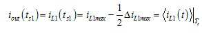
즉, 단일 전류 센서(500)는 t1 내지 t2 구간의 중간 시점인 ts1 시점에 출력 전류를 샘플링할 수 있다. 이에 따라, 단일 전류 센서(500)는 PWM주기에서 제1 인덕터(L1)의 평균 전류값을 측정할 수 있다.That is, the single
이와 유사하게, ts2 시점에서 PWM2의 캐리어는 0에 도달하고, 이 때의 출력 전류는 제2 인턱터 전류(iL2)의 PWM 주기의 평균값과 동일하다. 이를 수학식으로 표현하면 다음과 같다.Similarly, at time ts2, the carrier of PWM2 reaches zero, and the output current at this time is equal to the average value of the PWM periods of the second inductor current (i L2 ). This can be expressed as follows.

단일 전류 센서(500)에 의해 측정된 제1 인덕터(L1)와 제2 인덕터(L2)의 선형화된 전류값은 두 개의 병렬 전류 루프에 대한 피드백 신호일 수 있다. 그런 이유로, 두 개의 전류 루프는 해당 전류 루프의 레퍼런스를 따르도록 피드백 신호를 강제한다. 따라서, 본 발명에 따른 단일 전류 센서(500)에 의한 전류 측정 방법은 제1 인덕터(L1)와 제2 인덕터(L2) 사이의 전류를 동일하게 공유하고, 라인 주기의 양의 1/2주기에서 입력 전압을 따르는 입력 전류를 형성하도록 할 수 있다.The linearized current value of the first inductor L1 and the second inductor L2 measured by the single
이를 종합하면, 본 발명에 따른 브릿지리스 인터리브 역률보정회로(1000)에 구현된 단일 전류 센서(500)는, 라인 주기의 양의 1/2주기에서 듀티값이 0.5보다 작은 경우(도 8의 (a)), 제1 스위치(S1)와 제3 스위치(S3)오프 상태이고, 제2 스위치(S2)는 온 상태인 시간 구간(t1~t2 구간)에서, t1 시점과 t2 시점의 중간 시점(ts1)에서 출력되는 전류를 측정하도록 제어될 수 있다. 이를 도 5의 (a)를 다시 참조하여 바꾸어 말하면, 본 발명에 따른 브릿지리스 인터리브 역률보정회로(1000)는 제1 구간(t0~t1)에서 제1 동작 모드(제1 스위치(S1)와 제3 스위치(S3)는 턴오프, 제2 스위치(S2)는 턴온 상태)로 동작하며, 이때 단일 전류 센서(500)는 제1 구간의 중간 시점에 출력 전류를 측정할 수 있다. 이 경우, 단일 전류 센서(500)에 의해 측정되는 출력 전류값은 상술한 수학식 15에 나타난 바와 같이, 제1 인덕터(L1) 내의 전류값의 평균과 동일할 수 있다. In this case, the single
그리고, 도 8의 (a)에서, 제1, 3 스위치(S1, S3)는 턴온 상태이고 제2 스위치(S2)는 턴오프 상태인 t3~t4구간은 도 5의 (a)의 제3 구간(t2~t3)과 대응될 수 있다. 이 경우, 단일 전류 센서(500)는 제3 구간(t2~t3)에서 t2 시점과 t3 시점의 중간 시점에서 출력되는 전류를 측정하도록 설계될 수 있다. 이때, 단일 전류 센서(500)에 의해 측정되는 출력 전류값은 상술한 수학식 16에 나타난 바와 같이, 제2 인덕터(L2) 내의 전류값의 평균과 동일할 수 있다.8A, the period from t3 to t4 in which the first and third switches S1 and S3 are in a turned-on state and the second switch S2 is in a turned-off state is the same as that in the third period (t2 to t3). In this case, the single
결과적으로, 따라서, 전류 센서(500)는 제1 구간 또는 제3 구간에서 출력 전류를 센싱하는 경우, 제1 인덕터(L1)및 제2 인덕터(L2)내의 전류량을 측정할 수 있다. 이때, 입력 전압이 라인 주기의 양의 절반 상에 있을 경우, 상술한 바와 같이 제1 스위치(S1)와 제2 스위치(S2)는 활성화된 스위치로 동작하고, 제3 스위치(S3)는 정류기로 동작할 수 있다.Consequently, the
또한, 본 발명에 따른 브릿지리스 인터리브 역률보정회로(1000)에 구현된 단일 전류 센서(500)는, 라인 주기의 양의 1/2주기에서 듀티값이 0.5보다 큰 경우(도 8의 (b)), 제1, 3 스위치(S1, S3)는 턴오프 상태이면서, 제2 스위치는 턴온 상태인 t1~t2 구간(도 5의 t3~t4 구간에 대응)에서 출력 전류를 센싱할 수 있다. 그리고, 단일 전류 센서(500)는 제1, 3 스위치(S1, S3)는 턴온 상태이면서, 제2 스위치는 턴오프 상태인 t3~t4 구간(도 5의 t1~t2 구간에 대응)에서 출력 전류를 센싱할 수 있다. In the single
요약하면, 본 발명에 따른 브릿지리스 인터리브 역률보정회로(1000)는 라인 주기의 양의 1/2주기에서 듀티값이 0.5보다 작은 경우, 미리 정해진 시간 구간별로 제1 동작 모드 내지 제4 동작 모드 중 어느 하나의 동작 모드에 따라 동작되며, 이때 단일 전류 센서(500)는 제1 동작 모드 및 제3 동작 모드로 동작되는 시간 구간에서 출력 전류를 센싱할 수 있다. 그리고, 본 발명에 따른 브릿지리스 인터리브 역률보정회로(1000)는 라인 주기의 양의 1/2주기에서 듀티값이 0.5보다 큰 경우, 미리 정해진 시간 구간별로 제4 동작 모드 내지 제6 동작 모드 중 어느 하나의 동작 모드에 따라 동작되며, 이때 단일 전류 센서(500)는 제5 동작 모드 및 제6 동작 모드로 동작되는 시간 구간에서 출력 전류를 센싱할 수 있다. 이를 도 5에 도시된 시구간으로 표현하면, 단일 전류 센서(500)는 도 5의 (a)의 제1 구간(t0~t1)과 제3 구간(t2~t3)에서 출력 전류를 센싱하고, 도 5의 (b)의 t1~t2, t2~t3 구간에서 출력 전류를 센싱하여 제1 인덕터(L1) 및 제2 인덕터(L2)의 전류값을 측정할 수 있다.In summary, the bridgeless interleaved power
한편, 라인 주기의 음의 1/2주기에서(도 8의 (b)), 제3 인덕터(L3)와 제4 인덕터(L4)의 인덕터 전류는 입력 전류를 제어하고 공유할 필요가 있다. 제3 인덕터(L3)와 제4 인덕터(L4)의 인덕터 전류는 상술한 제1, 2인덕터의 전류를 측정하는 방법과 유사한 방법으로 출력 전류를 샘플링함으로써 측정될 수 있다.On the other hand, the inductor currents of the third inductor L3 and the fourth inductor L4 need to control and share the input current in the negative half period of the line period (Fig. 8 (b)). The inductor currents of the third inductor L3 and the fourth inductor L4 can be measured by sampling the output current in a manner similar to the method of measuring the currents of the first and second inductors described above.
도 9는 본 발명에 따른 브릿지리스 인터리브 역률보정회로(1000)의 구동 및 제어 방법을 설명하기 위한 회로도이다. 구체적으로, 본 발명에 따른 브릿지리스 인터리브 역률보정회로(1000)는 서브 컨버터 간 전력이 공유되도록 구성될 수 있다.9 is a circuit diagram for explaining a method of driving and controlling the bridgeless interleaved power
도시된 바와 같이, 외부 전압 루프는 낮은 대역폭으로 출력 전압을 제어할 수 있다. 그리고, 두 개의 고속 내부 전류 루프는 입력 전압에 따라 전류를 성형하도록 설계될 수 있다. 또한, 대칭형 PWM(Pulse Width Modulation)에 의해 출력 전류가 각각의 PWM 구간마다 두 번씩 샘플링되고, 따라서 각각의 서브 컨버터는 PWM 구간마다 한 번씩 입력 전류 피드백 값을 순차적으로 갱신할 수 있다.As shown, the external voltage loop can control the output voltage with low bandwidth. And, two high-speed internal current loops can be designed to form the current according to the input voltage. Also, the output current is sampled twice in each PWM section by symmetrical PWM (Pulse Width Modulation), and each sub-converter can sequentially update the input current feedback value once per PWM section.
도 9에 도시된 회로를 구성하는 구성 요소들에 걸리는 스트레스(stress)를 구체적으로 살펴보면, 먼저 입력 전압은 하기 수학식 17에 의해 산출되는 사인파로 표현되며, 두 개의 서브 컨버터는 동일한 파라미터를 가질 수 있다. 이때, 스위칭 주파수는 기본 주파수보다 큰 것으로 가정한다.9, the input voltage is represented by a sine wave calculated by the following equation (17), and the two sub-converters have the same parameters have. At this time, it is assumed that the switching frequency is larger than the fundamental frequency.

또한, 부스트 컨버터에 대한 종래의 기본적인 수학식으로부터, 본 발명에 따른 브릿지리스 인터리브 역률보정회로(1000)의 듀티 사이클의 값은 다음과 같이 산출될 수 있다.Further, from the conventional basic equation for the boost converter, the value of the duty cycle of the bridgeless interleaved power

그리고, 선형화된 스위치(S1 내지 S3)의 전류와 입력 전류는 각각 수학식 19 및 수학식 20에 의해 산출될 수 있다.The current and the input current of the linearized switches S1 to S3 can be calculated by Equations (19) and (20), respectively.

수학식 18 내지 수학식 20으로부터, 제1 스위치(S1) 및 제3 스위치(S3)의 전류 실효값(Root Mean Square, RMS)은 다음의 수학식 21과 같이 산출되고, 제2 스위치(S2)의 전류 실효값은 하기 수학식 22에 의해 산출될 수 있다.From the equations (18) to (20), the root mean square (RMS) of the first switch S1 and the third switch S3 is calculated according to the following expression (21) Can be calculated by the following equation (22). &Quot; (22) "


또한, 인덕터의 리플 전류(ripple current)가 40% 리플로 설계되었다고 가정하면, 인덕터(L1 내지 L4)의 RMS값은 다음과 같이 근사될 수 있다.Further, assuming that the ripple current of the inductor is designed to be 40% ripple, the RMS values of the inductors L1 to L4 can be approximated as follows.

고속 다이오드(D1 내지 D3)의 선형화된 전류는 수학식 24에 의해 산출될 수 있다. 이때, 제1 고속 다이오드(D1) 및 제3 고속 다이오드(D3)의 평균 전류값은 수학식 25에 의해, 제2 고속 다이오드(D2)의 평균 전류값은 수학식 26에 의해 산출될 수 있다.The linearized currents of the high-speed diodes D1 to D3 can be calculated by the equation (24). The average current value of the first high-speed diode D1 and the third high-speed diode D3 can be calculated by Equation 25, and the average current value of the second high-speed diode D2 can be calculated by Equation 26. [


마지막으로, 출력 커패시터(C) 전류의 고주파 성분의 RMS값은 하기의 수학식 27과 같이 나타낼 수 있으며, 커패시터(C) 전류의 저주파 성분의 RMS값은 아래 수학식 28와 같이 나타낼 수 있다.Finally, the RMS value of the high frequency component of the output capacitor C current can be expressed by Equation (27), and the RMS value of the low frequency component of the capacitor (C) current can be expressed by Equation (28).


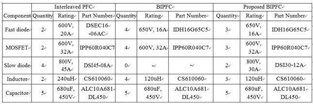
표 2는 본 발명에 따른 브릿지리스 인터리브 역률보정회로(1000)와 종래의 전류 스트레스를 비교한 결과를 나타내는 도표이다. 상술한 바와 같이, 본 발명에 따른 브릿지리스 인터리브 역률보정회로(1000)는 제2 인덕터(L2)를 포함하는 제2 부스트 레그(320)와 제3 인턱터(L3)를 포함하는 제3 부스트 레그(330)가 결합된 것을 특징으로 할 수 있다. 이에 따라, 자기 코어의 총 개수는 4개에서 3개로 감소될 수 있다. 또한, 결합된 두 부스트 레그에서, 디바이스의 사용률은 종래의 브릿지리스 역률보정회로보다 높은 사용률을 보여주는 종래의 인터리브형 역률보정회보와 동일하게 증가됨을 알 수 있다.Table 2 is a table showing the results of comparison of the conventional current stress with the bridgeless interleaved power

이하에서는, 도 10내지 도 17을 참조하여, 본 발명의 일 실시예에 따른 브릿지리스 인터리브 역률보정회로(1000)의 유리한 효과에 대하여 구체적으로 설명하기로 한다.Hereinafter, advantageous effects of the bridgeless interleaved power
먼저, 본 발명의 일 실시예에 따른 브릿지리스 인터리브 역률보정회로(1000)의 동작 특성을 확인하고, 그 효과를 확인하기 위해 아래 표 3과 같은 사양의 컨버터를 설계하였으며, 6.6Kw의 레벨 2 온-보드 충전기에 적용하였다. 또한, 표 4는 종래의 인터리브형 역률보정회로(Interleaved PFC), 종래의 브릿지리스 인터리브 역률보정회로(BIPFC) 및 본 발명에 따른 브릿지리스 인터리브 역률보정회로(Proposed BIPFC)의 전력 손실을 비교하기 위하여, 각각의 주요 스펙을 표시한 도표이다. 그리고, 도 10는 본 발명의 브릿지리스 인터리브 역률보정회로(1000)과 종래 기술들간의 전력 손실을 비교한 그래프이며, 도 11은 본 발명의 브릿지리스 인터리브 역률보정회로(1000)과 종래 기술들을 6.6Kw의 레벨 2 온-보드 충전기에 적용했을 때의 성능을 비교한 그래프이다.First, to confirm the operation characteristics of the bridgeless interleaved power

일반적으로, 스위치는 전도 손실, 스위칭 손실 및 고유 다이오드 손실 등과 같은 손실이 발생하며, 이는 전력 손실에 있어 상당한 부분을 차지하고 있다. 하지만, 본 발명에 따른 브릿지리스 인터리브 역률보정회로(1000)는 종래의 다른 기술들에 비해 스위치(MOSFET)의 수가 작기 때문에, 도 9에 도시된 바와 같이 전체 스위치에서 발생되는 손실인 Pmosfet이 종래의 기술들에 비해 감소될 수 있다. In general, a switch is subject to losses such as conduction losses, switching losses and intrinsic diode losses, which is a significant portion of the power loss. However, since the bridgeless interleaved power
또한, 본 발명에 따른 브릿지리스 인터리브 역률보정회로(1000)는 고속 다이오드의 전체 개수 또한 감소되지만, 고속 다이오드 전체에서 발생되는 손실인 Pfastdiode는 두 개의 병합 부스트 레그와 연결된 제2 고속 다이오드(D2)의 전류 정격을 증가시킴으로써 종래의 브릿지리스 인터리브 역률보정회로 내의 손실과 유사할 수 있다. In the bridgeless interleaved power
더욱이, 본 발명에 따른 브릿지리스 인터리브 역률보정회로(1000)에 포함된 두 개의 저속 다이오드(Da1, Da2)는 컨버터의 전체 손실을 0.23%(15.5W)증가시키지만, 종래의 인터리브형 역률보정회로(Interleaved PFC) 내의 브릿지 정류기와 비교하여 전체적인 손실은 개선될 수 있다. 그리고, 본 발명에 따른 브릿지리스 인터리브 역률보정회로(1000, proposed BIPFC)는 종래의 브릿지리스 인터리브 역률보정회로(BIPFC)에 비해 인덕터를 통과하는 복귀 전류가 증가하기 때문에, 인덕터 전체 손실(Pinductor) 또한 증가될 수 있다. 하지만, 상술한 바와 같이, 본 발명에 따른 브릿지리스 인터리브 역률보정회로(1000)는 종래의 기술에 비해 전체적인 손실이 개선될 수 있다.In addition, although the two low-speed diodes Da1 and Da2 included in the bridgeless interleaved power
한편, 도 11에 도시된 바와 같이, 본 발명에 따른 브릿지리스 인터리브 역률보정회로(1000)는 스위치의 전류 스트레스가 종래의 다른 기술들의 능동 스위치에 비해 높은 것으로 도시되지만, 이는 종래의 인터리브형 역률보정회로에서 입력 브릿지 정류기의 스트레와 동일한 수치일 수 있다. 또한, 각 기술들을 제작하는 비용(cost of components)는 게이트 드라이버(gate driver)와 전류 센서를 포함하는 천여 개 부품의 가격을 기준으로 평가되었다.11, the bridgeless interleaved power
결론적으로, 도 11을 참조하였을 때, 본 발명에 따른 브릿지리스 인터리브 역률보정회로(1000)는 저가의 종래 인터리브형 역률보정회로(interleaved PFC)의 성능이 개선되면서도, 고비용 고성능의 종래 브릿지리스 인터리브 역률보정회로(BIPC)의 높은 제작 비용을 감소시킬 수 있는 효과를 가질 수 있다.11, the bridgeless interleaved power
이하에서는, 도 12 내지 도 17을 참조하여, 본 발명에 따른 브릿지리스 인터리브 역률보정회로(1000)를 표 5의 규격을 갖는 6.6Kw 차량용 충전기에 구현시킨 후, 이를 이용한 실험 결과들을 설명하기로 한다.Hereinafter, with reference to FIGS. 12 to 17, experimental results using a bridgeless interleaved power
먼저, 도 12는 인터럽트에 기초한 디지털 신호 처리를 수행하는 디지털 제어기의 동작 루틴이 표현된 도면이다. 12 is a diagram showing an operation routine of a digital controller that performs digital signal processing based on an interrupt.
두 개의 인터리브형 컨버터를 구동시키기 위해, 180도 위상 시프트를 갖는 두 개의 PWM(PWM1, PWM2)가 사용될 수 있다. 그리고, ADC의 샘플링 시점을 고정시키도록, 대칭형 PWM 방식이 채택되었다. PWM 카운터가 최대값이 도달할 때, 본 발명에 따른 브릿지리스 인터리브 역률보정회로(1000)는 ADC의 데이터 변환을 시작하기 위한 신호를 생성할 수 있다. 변환 시간 지연(TADC)이 경과한 후, ADC 결과를 사용할 수 있으며, 전류 제어기는 ISR에서 실행될 수 있다. 디지털 신호 처리의 스트레를 감소시키도록, 별도의 저속 타이머의 인터럽트 내에서 동작하는 전압 루프가 설계되는데, 이는 요구되는 대역폭이 훨씬 낮기 때문이다.To drive two interleaved converters, two PWMs (PWM1, PWM2) with a 180 degree phase shift can be used. A symmetrical PWM method is adopted to fix the sampling point of the ADC. When the PWM counter reaches its maximum value, the bridgeless interleaved power
도 13은 10% 부하(Vin = 220V, Pout = 0.66 kW)에서의 주요 파형이고, 도 14 및 도 15는 완전한 부하(도 13은 Vin = 220V, Pout = 6.6 kW, 도 15는 Vin = 240V, Pout = 6.6 kW인 경우)에서의 실험 파형이 도시된 도면이다. 여기서, 입력 전류는 4.12%의 THD(Total Harmonic Distortion)와 0.998의 역률을 갖는 사인파일 수 있다. 그리고, 출력 전압은 5% 미만의 120Hz 리플을 갖는 400V로 조절될 수 있다.Fig. 13 shows the main waveforms at the 10% load (Vin = 220V, Pout = 0.66 kW), Figs. 14 and 15 show the waveforms of the full load (Vin = 220V, Pout = 6.6 kW, Fig. Pout = 6.6 kW). In Fig. Here, the input current can be a sinusoidal file having a THD (Total Harmonic Distortion) of 4.12% and a power factor of 0.998. And, the output voltage can be regulated to 400V with 120Hz ripple less than 5%.
도 16은 입력 전압을 변경시킴에 따른 전력 효율이 도시된 도면이며, 도 17은 입력된 역률(Power factor)을 나타내는 그래프이다. 도시된 바와 같이, 역률은 220V의 교류 입력 전압 상에서, 절반의 부하로부터 최대 부하까지 0.99이상의 값을 가질 수 있다.FIG. 16 is a graph showing the power efficiency as the input voltage is changed, and FIG. 17 is a graph showing the input power factor. As shown, the power factor can have a value of 0.99 or more, from a half load to a full load, on an AC input voltage of 220V.
이상에서는 실시예들을 참조하여 설명하였지만, 해당 기술 분야의 숙련된 당업자는 하기의 특허 청구범위에 기재된 본 발명의 사상 및 영역으로부터 벗어나지 않는 범위 내에서 본 발명을 다양하게 수정 및 변경시킬 수 있음을 이해할 수 있을 것이다.While the present invention has been particularly shown and described with reference to exemplary embodiments thereof, it will be understood by those skilled in the art that various changes and modifications may be made therein without departing from the spirit and scope of the invention as defined in the appended claims. It will be possible.
100: 입력 전원
200: 배터리
300: 부스트 레그
400: 스위치 회로
500: 단일 전류 센서100: Input power
200: Battery
300: Boost leg
400: Switch circuit
500: Single current sensor
Claims (12)
하나의 상기 단일 부스트 레그와 연결되는 단일 스위치 회로와, 적어도 두 개의 상기 병합 부스트 레그와 연결되는 병합 스위치 회로를 포함하는 복수의 스위치 회로; 및
상기 스위치 회로와 연결되고, 미리 정해진 동작 구간 및 미리 정해진 전류 측정 시점에 따라 출력 전류를 측정하는 단일 전류 센서를 포함하는, 브릿지리스 인터리브 역률보정회로.
A plurality of boost legs including at least one single boost leg coupled to the input power source and including an inductor, and a plurality of merge boost legs coupled to the input power source and including an inductor and a low speed diode;
A plurality of switch circuits including a single switch circuit connected to one of said single boost legs and a merge switch circuit connected to at least two said merge boost legs; And
And a single current sensor connected to the switch circuit and measuring an output current according to a predetermined operating period and a predetermined current measuring time point.
상기 복수의 부스트 레그는 제1 부스트 레그 내지 제4 부스트 레그를 포함하고,
상기 제1 부스트 레그 및 상기 제4 부스트 레그는 상기 단일 부스트 레그이고, 제2 부스트 레그 및 제3 부스트 레그는 상기 병합 부스트 레그인, 브릿지리스 인터리브 역률보정회로.
The method according to claim 1,
Wherein the plurality of boost legs include first to fourth boost legs,
Wherein the first boost leg and the fourth boost leg are the single boost leg and the second boost leg and the third boost leg are the merge boost legs.
상기 복수의 스위치 회로는 제1 스위치 회로 내지 제3 스위치 회로를 포함하고,
상기 제1 스위치 회로는 상기 제1 부스트 레그와 연결되고, 제2 스위치 회로는 상기 제2 부스트 레그 및 상기 제3 부스트 레그와 병렬로 연결되며, 상기 제3 스위치 회로는 상기 제4 부스트 레그와 연결되는, 브릿지리스 인터리브 역률보정회로.
3. The method of claim 2,
Wherein the plurality of switch circuits include a first switch circuit to a third switch circuit,
Wherein the first switch circuit is connected to the first boost leg and the second switch circuit is connected in parallel to the second boost leg and the third boost leg and the third switch circuit is connected to the fourth boost leg A bridgeless interleaved power factor correction circuit.
상기 스위치 회로는 고속 다이오드 및 스위치를 포함하고,
상기 저속 다이오드는 상기 고속 다이오드와 직렬로 연결되어 상기 입력 전원의 순환 전류를 차단하는, 브릿지리스 인터리브 역률보정회로.
The method according to claim 1,
The switch circuit including a high speed diode and a switch,
Wherein the low speed diode is connected in series with the high speed diode to cut off the circulating current of the input power source.
상기 브릿지리스 인터리브 역률보정회로는, 스위칭 주파수가 라인 주파수보다 높은 상태인 경우, 라인 전압의 1/2주기마다 상기 입력 전원으로부터 공급되는 입력 전압의 극성을 변화시키는 부스트 컨버터로 동작되는, 브릿지리스 인터리브 역률보정회로.
The method according to claim 1,
Wherein the bridgeless interleaved power factor correcting circuit operates as a boost converter for changing the polarity of the input voltage supplied from the input power source every 1/2 period of the line voltage when the switching frequency is higher than the line frequency, Power factor correction circuit.
상기 브릿지리스 인터리브 역률보정회로는,
상기 라인 전압의 1/2주기동안 변화되는 듀티 사이클 값이 미리 정해진 기준값보다 작은 경우, 상기 복수의 스위치 회로가 제1 동작 모드 내지 제3 동작 모드 중 어느 하나의 동작 모드로 작동되도록 제어하고,
상기 듀티 사이클 값이 상기 기준값보다 큰 경우, 상기 복수의 스위치 회로가 제4 동작 모드 내지 제6 동작 모드 중 어느 하나의 동작 모드로 작동되도록 제어하는, 브릿지리스 인터리브 역률보정회로.
6. The method of claim 5,
Wherein the bridgeless interleaved power factor correction circuit comprises:
Controlling the plurality of switch circuits to operate in any one of the first to third operation modes when a duty cycle value which is changed during a half period of the line voltage is smaller than a predetermined reference value,
Wherein the control circuit controls the plurality of switch circuits to operate in any one of the fourth to sixth operation modes when the duty cycle value is larger than the reference value.
상기 복수의 스위치 회로는,
상기 듀티 사이클 값이 미리 정해진 값보다 작은 경우,
상기 라인 전압의 1/2주기를 구성하는 제1 구간은 제1 동작 모드로 제어되고, 상기 제1 구간 이후의 제2 구간은 제2 동작 모드로 제어되고, 상기 제2 구간 이후의 제3 구간은 제3 동작 모드로 제어되며, 상기 제3 구간 이후의 제4 구간은 상기 제2 동작 모드로 제어되고,
상기 듀티 사이클 값이 미리 정해진 값보다 큰 경우,
상기 라인 전압의 1/2주기를 구성하는 제1 구간은 제4 동작 모드로 제어되고, 상기 제1 구간 이후의 제2 구간은 제5 동작 모드로 제어되고, 상기 제2 구간 이후의 제3 구간은 상기 제4 동작 모드로 제어되며, 상기 제3 구간 이후의 제4 구간은 제6 동작 모드로 제어되는, 브릿지리스 인터리브 역률보정회로.
The method according to claim 6,
Wherein the plurality of switch circuits comprises:
If the duty cycle value is smaller than a predetermined value,
A first section constituting a half period of the line voltage is controlled in a first operation mode, a second section after the first section is controlled in a second operation mode, and a third section after the second section Is controlled to the third operation mode, the fourth section after the third section is controlled to the second operation mode,
If the duty cycle value is greater than a predetermined value,
The first period constituting the half period of the line voltage is controlled to the fourth operation mode, the second period after the first period is controlled to the fifth operation mode, and the third period after the second period Is controlled in the fourth operation mode, and the fourth section after the third section is controlled in a sixth operation mode.
상기 단일 전류 센서는,
상기 듀티 사이클 값이 미리 정해진 값보다 작은 경우, 상기 제1 구간에서 출력 전류를 측정하여 상기 제1 인덕터의 인덕터 전류를 측정하고, 상기 제3 구간에서 출력 전류를 측정하여 상기 제2 인덕터의 인덕터 전류를 측정하며,
상기 듀티 사이클 값이 미리 정해진 값보다 큰 경우, 상기 제4 구간에서 출력 전류를 측정하여 상기 제1 인덕터의 인덕터 전류를 측정하고, 상기 제2 구간에서 출력 전류를 측정하여 상기 제2 인덕터의 인덕터 전류를 측정하는, 브릿지리스 인터리브 역률보정회로.
8. The method of claim 7,
Wherein the single current sensor comprises:
Measuring an output current in the first section to measure an inductor current of the first inductor when the duty cycle value is less than a predetermined value and measuring an inductor current of the second inductor by measuring an inductor current in the third section, Respectively,
Measuring an inductor current of the first inductor by measuring an output current in the fourth section when the duty cycle value is greater than a predetermined value and measuring an inductor current of the second inductor by measuring an inductor current of the first inductor, Interleaved power factor correction circuit.
상기 복수의 스위치 회로가 제1 스위치 회로 내지 제3 스위치 회로로 마련되는 경우, 상기 브릿지리스 인터리브 역률보정회로는,
상기 제1 동작 모드 및 상기 제6 동작 모드에서 상기 제1 스위치 회로의 제1 스위치와 상기 제3 스위치 회로의 제3 스위치는 턴오프 시키고, 제2 스위치 회로의 제2 스위치는 턴온시키고,
상기 제2 동작 모드에서 상기 상기 제1 스위치 내지 상기 제3 스위치를 턴오프시키고,
상기 제3 동작 모드에서 상기 제1 스위치 및 상기 제3 스위치는 턴온시키고, 상기 제2 스위치는 턴오프시키고,
상기 제4 동작 모드에서 상기 제1 스위치 내지 상기 제3 스위치를 턴온시키며,
상기 제5 동작 모드에서 상기 제1 스위치 및 상기 제3 스위치는 턴온시키고, 상기 제2 스위치는 턴오프시키는, 브릿지리스 인터리브 역률보정회로.
8. The method of claim 7,
When the plurality of switch circuits are provided from the first switch circuit to the third switch circuit, the bridgeless interleaved power factor correcting circuit comprises:
In the first operation mode and the sixth operation mode, the first switch of the first switch circuit and the third switch of the third switch circuit are turned off, the second switch of the second switch circuit is turned on,
Turning off the first switch and the third switch in the second operation mode,
The first switch and the third switch are turned on in the third operation mode, the second switch is turned off,
Turning on the first switch or the third switch in the fourth operation mode,
Wherein the first switch and the third switch are turned on and the second switch is turned off in the fifth operation mode.
상기 복수의 스위칭 회로는,
라인 전압의 소정 주기동안 변화되는 듀티 사이클 값을 미리 정해진 기준값과 비교한 결과에 따라 각각의 스위치 회로의 동작 모드가 제어되고,
상기 단일 전류 센서는,
상기 각각의 스위치 회로의 온오프 조합에 따라 상기 출력 전류를 측정할지 여부가 결정되는, 브릿지리스 인터리브 역률보정회로의 구동 방법. An operation method of a bridgeless interleaved power factor correction circuit including a plurality of boost legs provided with inductors, a plurality of switching circuits connected to at least one of the boost legs, and a single current sensor for sensing an output current delivered from the inductors In this case,
Wherein the plurality of switching circuits includes:
The operation mode of each switch circuit is controlled according to a result of comparing a duty cycle value, which is varied during a predetermined period of the line voltage, with a predetermined reference value,
Wherein the single current sensor comprises:
And determining whether to measure the output current according to on / off combinations of the respective switch circuits.
상기 부스트 레그는,
입력 전원과 연결되며 인덕터를 포함하는 적어도 하나의 단일 부스트 레그와, 상기 입력 전원과 연결되며 인덕터 및 저속 다이오드를 포함하는 복수의 병합 부스트 레그를 포함하며,
상기 스위치 회로는,
하나의 상기 단일 부스트 레그와 연결되는 단일 스위치 회로와, 적어도 두 개의 상기 병합 부스트 레그와 연결되는 병합 스위치 회로를 포함하는, 브릿지리스 인터리브 역률보정회로의 구동 방법.
11. The method of claim 10,
Wherein the boost leg comprises:
At least one single boost leg coupled to an input power source and including an inductor, and a plurality of merge boost legs coupled to the input power source and including an inductor and a low speed diode,
The switch circuit includes:
A single switch circuit connected to one of said single boost legs and a merging switch circuit connected to at least two said merge boost legs.
상기 스위치 회로는,
상기 라인 전압의 1/2주기동안 변화되는 듀티 사이클 값이 미리 정해진 기준값보다 작은 경우, 제1 동작 모드 내지 제3 동작 모드 중 어느 하나의 동작 모드로 동작되고,
상기 듀티 사이클 값이 상기 기준값보다 큰 경우, 제4 동작 모드 내지 제6 동작 모드 중 어느 하나의 동작 모드로 동작되는, 브릿지리스 인터리브 역률보정회로의 구동 방법.11. The method of claim 10,
The switch circuit includes:
When the duty cycle value which is changed during 1/2 period of the line voltage is smaller than a predetermined reference value, the operation mode is operated in any one of the first to third operation modes,
Wherein the operation mode is operated in any one of the fourth to sixth operation modes when the duty cycle value is larger than the reference value.
Applications Claiming Priority (2)
| Application Number | Priority Date | Filing Date | Title |
|---|---|---|---|
| KR20160084209 | 2016-07-04 | ||
| KR1020160084209 | 2016-07-04 |
Related Child Applications (1)
| Application Number | Title | Priority Date | Filing Date |
|---|---|---|---|
| KR1020190003060A Division KR102068923B1 (en) | 2019-01-10 | 2019-01-10 | Bridgeless interleaved power factor correction and method for controling thereof |
Publications (1)
| Publication Number | Publication Date |
|---|---|
| KR20180004677A true KR20180004677A (en) | 2018-01-12 |
Family
ID=61001151
Family Applications (1)
| Application Number | Title | Priority Date | Filing Date |
|---|---|---|---|
| KR1020170085018A KR20180004677A (en) | 2016-07-04 | 2017-07-04 | Bridgeless interleaved power factor correction and method for controling thereof |
Country Status (1)
| Country | Link |
|---|---|
| KR (1) | KR20180004677A (en) |
Cited By (2)
| Publication number | Priority date | Publication date | Assignee | Title |
|---|---|---|---|---|
| WO2020159640A1 (en) * | 2019-01-28 | 2020-08-06 | Murata Manufacturing Co., Ltd. | Bootstrap pre-charge circuit in totem-pole power factor correction converter |
| CN113647003A (en) * | 2019-03-29 | 2021-11-12 | 株式会社村田制作所 | Self-tuning regulator and self-tuning regulation method for interleaved power factor correction circuit |
Citations (3)
| Publication number | Priority date | Publication date | Assignee | Title |
|---|---|---|---|---|
| US20080002444A1 (en) * | 2006-06-30 | 2008-01-03 | Sampat Shekhawat | High-efficiency power converter system |
| US8385032B1 (en) * | 2011-08-23 | 2013-02-26 | Futurewei Technologies, Inc. | High efficiency bridgeless PFC converter and method |
| KR101303341B1 (en) * | 2012-05-07 | 2013-09-03 | 주식회사 동아일렉콤 | Bridgeless power factor compensation circuit |
-
2017
- 2017-07-04 KR KR1020170085018A patent/KR20180004677A/en active Application Filing
Patent Citations (3)
| Publication number | Priority date | Publication date | Assignee | Title |
|---|---|---|---|---|
| US20080002444A1 (en) * | 2006-06-30 | 2008-01-03 | Sampat Shekhawat | High-efficiency power converter system |
| US8385032B1 (en) * | 2011-08-23 | 2013-02-26 | Futurewei Technologies, Inc. | High efficiency bridgeless PFC converter and method |
| KR101303341B1 (en) * | 2012-05-07 | 2013-09-03 | 주식회사 동아일렉콤 | Bridgeless power factor compensation circuit |
Non-Patent Citations (4)
| Title |
|---|
| Hee-Jun Kim, The 2014 International Power Electronics Conference * |
| Khairul Safuan Bin Muhammad, IEEE TRANSACTIONS ON INDUSTRIAL ELECTRONICS, VOL. 62, NO. 5, MAY 2015 * |
| Woojin Choi, 전력전자학술대회논문집, 2016.7, 363-364 (2 pages) * |
| 최우진, 전력전자학술대회논문집, 2017.7, 24-25 (2 pages) * |
Cited By (3)
| Publication number | Priority date | Publication date | Assignee | Title |
|---|---|---|---|---|
| WO2020159640A1 (en) * | 2019-01-28 | 2020-08-06 | Murata Manufacturing Co., Ltd. | Bootstrap pre-charge circuit in totem-pole power factor correction converter |
| US11949328B2 (en) | 2019-01-28 | 2024-04-02 | Murata Manufacturing Co., Ltd. | Bootstrap pre-charge circuit in totem-pole power factor correction converter |
| CN113647003A (en) * | 2019-03-29 | 2021-11-12 | 株式会社村田制作所 | Self-tuning regulator and self-tuning regulation method for interleaved power factor correction circuit |
Similar Documents
| Publication | Publication Date | Title |
|---|---|---|
| EP2248249B1 (en) | Electronic driver circuit and method | |
| US9294001B2 (en) | Power converter with dead-time control function | |
| US8026704B2 (en) | System and method for controlling a converter | |
| Wei et al. | A novel bridgeless buck-boost PFC converter | |
| US20110109283A1 (en) | System and method for controlling a converter | |
| CN108736727B (en) | Power converter and control method thereof | |
| WO2010131496A1 (en) | Pfc converter | |
| TW201924200A (en) | Digital control of switched boundary mode interleaved power converter | |
| CN105305818A (en) | System and Method for Switched Power Supply Current Sampling | |
| KR20120020080A (en) | Method and apparatus for bridgeless power factor correction | |
| US8773875B2 (en) | Power conversion apparatus | |
| US20120014149A1 (en) | Power conversion apparatus and method | |
| US20170025969A1 (en) | Synchronous rectifier phase control to improve load efficiency | |
| US8824180B2 (en) | Power conversion apparatus | |
| CN105493388A (en) | Electric power conversion device | |
| US20200220452A1 (en) | Enhanced power factor correction | |
| Zhang et al. | A digital adaptive discontinuous current source driver for high-frequency interleaved boost PFC converters | |
| CN106059294B (en) | Switching power supply and conversion method | |
| KR20180004677A (en) | Bridgeless interleaved power factor correction and method for controling thereof | |
| Nandankar et al. | Design and implementation of efficient three-phase interleaved DC-DC converter | |
| KR102068923B1 (en) | Bridgeless interleaved power factor correction and method for controling thereof | |
| US20150171746A1 (en) | Buck type dc-to-dc converter and method of operating the same | |
| US20130038303A1 (en) | Controller and a method for a dc converter, and also a dc converter | |
| Channappanavar et al. | Current sensorless Power Factor correction circuit using FPGA | |
| CN102710131A (en) | Converter and driving method thereof and power factor correcting device comprising converter |
Legal Events
| Date | Code | Title | Description |
|---|---|---|---|
| A201 | Request for examination | ||
| E902 | Notification of reason for refusal | ||
| E601 | Decision to refuse application | ||
| E601 | Decision to refuse application | ||
| E801 | Decision on dismissal of amendment | ||
| A107 | Divisional application of patent |