KR20170141665A - Socket structure for 3D memory - Google Patents
Socket structure for 3D memory Download PDFInfo
- Publication number
- KR20170141665A KR20170141665A KR1020177029491A KR20177029491A KR20170141665A KR 20170141665 A KR20170141665 A KR 20170141665A KR 1020177029491 A KR1020177029491 A KR 1020177029491A KR 20177029491 A KR20177029491 A KR 20177029491A KR 20170141665 A KR20170141665 A KR 20170141665A
- Authority
- KR
- South Korea
- Prior art keywords
- electrode
- edge
- planar
- electrodes
- horizontal
- Prior art date
Links
Images


Classifications
-
- H01L27/11556—
-
- H—ELECTRICITY
- H10—SEMICONDUCTOR DEVICES; ELECTRIC SOLID-STATE DEVICES NOT OTHERWISE PROVIDED FOR
- H10B—ELECTRONIC MEMORY DEVICES
- H10B41/00—Electrically erasable-and-programmable ROM [EEPROM] devices comprising floating gates
- H10B41/20—Electrically erasable-and-programmable ROM [EEPROM] devices comprising floating gates characterised by three-dimensional arrangements, e.g. with cells on different height levels
- H10B41/23—Electrically erasable-and-programmable ROM [EEPROM] devices comprising floating gates characterised by three-dimensional arrangements, e.g. with cells on different height levels with source and drain on different levels, e.g. with sloping channels
- H10B41/27—Electrically erasable-and-programmable ROM [EEPROM] devices comprising floating gates characterised by three-dimensional arrangements, e.g. with cells on different height levels with source and drain on different levels, e.g. with sloping channels the channels comprising vertical portions, e.g. U-shaped channels
-
- H—ELECTRICITY
- H01—ELECTRIC ELEMENTS
- H01L—SEMICONDUCTOR DEVICES NOT COVERED BY CLASS H10
- H01L21/00—Processes or apparatus adapted for the manufacture or treatment of semiconductor or solid state devices or of parts thereof
- H01L21/70—Manufacture or treatment of devices consisting of a plurality of solid state components formed in or on a common substrate or of parts thereof; Manufacture of integrated circuit devices or of parts thereof
- H01L21/71—Manufacture of specific parts of devices defined in group H01L21/70
- H01L21/768—Applying interconnections to be used for carrying current between separate components within a device comprising conductors and dielectrics
-
- H—ELECTRICITY
- H01—ELECTRIC ELEMENTS
- H01L—SEMICONDUCTOR DEVICES NOT COVERED BY CLASS H10
- H01L23/00—Details of semiconductor or other solid state devices
- H01L23/52—Arrangements for conducting electric current within the device in operation from one component to another, i.e. interconnections, e.g. wires, lead frames
- H01L23/522—Arrangements for conducting electric current within the device in operation from one component to another, i.e. interconnections, e.g. wires, lead frames including external interconnections consisting of a multilayer structure of conductive and insulating layers inseparably formed on the semiconductor body
- H01L23/5226—Via connections in a multilevel interconnection structure
-
- H01L27/11524—
-
- H01L27/11548—
-
- H01L27/1157—
-
- H01L27/11575—
-
- H01L27/11582—
-
- H01L27/2481—
-
- H01L45/16—
-
- H—ELECTRICITY
- H10—SEMICONDUCTOR DEVICES; ELECTRIC SOLID-STATE DEVICES NOT OTHERWISE PROVIDED FOR
- H10B—ELECTRONIC MEMORY DEVICES
- H10B41/00—Electrically erasable-and-programmable ROM [EEPROM] devices comprising floating gates
- H10B41/30—Electrically erasable-and-programmable ROM [EEPROM] devices comprising floating gates characterised by the memory core region
- H10B41/35—Electrically erasable-and-programmable ROM [EEPROM] devices comprising floating gates characterised by the memory core region with a cell select transistor, e.g. NAND
-
- H—ELECTRICITY
- H10—SEMICONDUCTOR DEVICES; ELECTRIC SOLID-STATE DEVICES NOT OTHERWISE PROVIDED FOR
- H10B—ELECTRONIC MEMORY DEVICES
- H10B41/00—Electrically erasable-and-programmable ROM [EEPROM] devices comprising floating gates
- H10B41/50—Electrically erasable-and-programmable ROM [EEPROM] devices comprising floating gates characterised by the boundary region between the core region and the peripheral circuit region
-
- H—ELECTRICITY
- H10—SEMICONDUCTOR DEVICES; ELECTRIC SOLID-STATE DEVICES NOT OTHERWISE PROVIDED FOR
- H10B—ELECTRONIC MEMORY DEVICES
- H10B43/00—EEPROM devices comprising charge-trapping gate insulators
- H10B43/20—EEPROM devices comprising charge-trapping gate insulators characterised by three-dimensional arrangements, e.g. with cells on different height levels
- H10B43/23—EEPROM devices comprising charge-trapping gate insulators characterised by three-dimensional arrangements, e.g. with cells on different height levels with source and drain on different levels, e.g. with sloping channels
- H10B43/27—EEPROM devices comprising charge-trapping gate insulators characterised by three-dimensional arrangements, e.g. with cells on different height levels with source and drain on different levels, e.g. with sloping channels the channels comprising vertical portions, e.g. U-shaped channels
-
- H—ELECTRICITY
- H10—SEMICONDUCTOR DEVICES; ELECTRIC SOLID-STATE DEVICES NOT OTHERWISE PROVIDED FOR
- H10B—ELECTRONIC MEMORY DEVICES
- H10B43/00—EEPROM devices comprising charge-trapping gate insulators
- H10B43/30—EEPROM devices comprising charge-trapping gate insulators characterised by the memory core region
- H10B43/35—EEPROM devices comprising charge-trapping gate insulators characterised by the memory core region with cell select transistors, e.g. NAND
-
- H—ELECTRICITY
- H10—SEMICONDUCTOR DEVICES; ELECTRIC SOLID-STATE DEVICES NOT OTHERWISE PROVIDED FOR
- H10B—ELECTRONIC MEMORY DEVICES
- H10B43/00—EEPROM devices comprising charge-trapping gate insulators
- H10B43/50—EEPROM devices comprising charge-trapping gate insulators characterised by the boundary region between the core and peripheral circuit regions
-
- H—ELECTRICITY
- H10—SEMICONDUCTOR DEVICES; ELECTRIC SOLID-STATE DEVICES NOT OTHERWISE PROVIDED FOR
- H10B—ELECTRONIC MEMORY DEVICES
- H10B63/00—Resistance change memory devices, e.g. resistive RAM [ReRAM] devices
- H10B63/80—Arrangements comprising multiple bistable or multi-stable switching components of the same type on a plane parallel to the substrate, e.g. cross-point arrays
- H10B63/84—Arrangements comprising multiple bistable or multi-stable switching components of the same type on a plane parallel to the substrate, e.g. cross-point arrays arranged in a direction perpendicular to the substrate, e.g. 3D cell arrays
-
- H—ELECTRICITY
- H10—SEMICONDUCTOR DEVICES; ELECTRIC SOLID-STATE DEVICES NOT OTHERWISE PROVIDED FOR
- H10N—ELECTRIC SOLID-STATE DEVICES NOT OTHERWISE PROVIDED FOR
- H10N70/00—Solid-state devices without a potential-jump barrier or surface barrier, and specially adapted for rectifying, amplifying, oscillating or switching
- H10N70/011—Manufacture or treatment of multistable switching devices
Abstract
영역을 효율적으로 이용하도록 구성된 소켓 구조물, 및 영역을 효율적으로 이용하는 소켓 영역을 제공하기 위한 방법이 제공된다. 계단형 타입 컨택트 영역 또는 소켓 영역은, 인접한 평면 전극 바로 아래에 놓인 평면 전극의 일부를 부분적으로 덮는 인접한 평면 전극들 사이의 유전체 층들을 포함한다. 인접한 평면 전극들 사이의 유전체 층의 부분은, 위에 놓인 평면 전극의 엣지로부터 아래에 놓인 평면 전극의 엣지와 위에 놓인 평면 전극의 엣지에 대응하는 지점 사이의 지점으로 연장되도록 경사질 수 있다.There is provided a socket structure configured to use an area efficiently, and a method for providing a socket area that efficiently uses the area. The stepped contact region or the socket region includes dielectric layers between adjacent planar electrodes that partially cover a portion of the planar electrode immediately below the adjacent planar electrode. The portion of the dielectric layer between adjacent planar electrodes may be inclined to extend to a point between the edge of the planar electrode lying below the edge of the overlying planar electrode and the point corresponding to the edge of the overlying planar electrode.
Description
본 출원은 그 각각의 전체 내용이 참조로 본 명세서에 포함되는 2015년 4월 24일 출원된 미국 우선권 특허 출원 US14/695835호의 우선권을 주장한다.This application claims priority to United States priority patent application US14 / 695835, filed April 24, 2015, the entire contents of each of which are incorporated herein by reference.
본 개시내용은 3차원 메모리를 위한 소켓 구성에 관한 것으로, 특히 3차원 메모리를 위한 소켓의 면적 효율을 개선하는 것에 관한 것이다.This disclosure relates to socket configurations for three-dimensional memory, and more particularly to improving the area efficiency of a socket for three-dimensional memory.
메모리 디바이스는 광범위한 분야에서 이용된다. 예를 들어, 솔리드 스테이트 메모리는 컴퓨팅 디바이스와 관련하여 프로그램 명령어 및 데이터의 장기간 또는 단기간의 저장에 이용될 수 있다. 메모리 밀도, 액세스 속도, 및 신뢰성은 모두 솔리드 스테이트 메모리를 설계할 때 중요한 고려사항이다. 최근의 솔리드 스테이트 메모리 설계는 3차원 아키텍쳐를 이용해 왔다. 이러한 설계는 메모리 밀도를 증가시킬 수 있다. 또한, 이러한 설계는, 저항식 랜덤 액세스 메모리(ReRAM), 및 상 변화 랜덤 액세스 메모리(PCRAM 또는 PRAM)와 관련하여 이용하기에 적합하다.Memory devices are used in a wide variety of fields. For example, solid state memory may be used for long term or short term storage of program instructions and data in connection with a computing device. Memory density, access speed, and reliability are all important considerations when designing solid state memory. Recent solid-state memory designs have used a three-dimensional architecture. This design can increase memory density. This design is also suitable for use in connection with resistive random access memory (ReRAM) and phase change random access memory (PCRAM or PRAM).
3차원(3D) 메모리 구조물에서, 비트라인(BL) 및 워드라인(WL)을 포함한 신호 라인은 메모리 구조물의 주변 영역 상의 소켓 영역들과 메모리 어레이 그 자체 사이에서 연장된다. 더 구체적으로는, 메모리 어레이의 제1 측면 상의 제1 소켓 영역은 비트라인과 연관된 전극 또는 컨택트를 포함할 수 있고, 메모리 어레이의 제2 측면 상의 제2 소켓 영역은 워드라인과 연관된 전극 또는 컨택트를 포함할 수 있다. 다른 구성에서, 메모리 어레이의 제1 및 제2 대향 측면들 상의 소켓 영역들은 비트라인과 연관될 수 있고, 메모리 어레이의 제3 및 제4 대향 측면들 상의 소켓 영역들은 워드라인과 연관될 수 있다. 메모리 어레이에 포함된 메모리 셀의 수가 증가함에 따라, 신호 라인(즉, 비트라인 및/또는 워드라인)의 수가 증가한다. 또한, 비트라인 및 워드라인의 크기에서의 물리적 제약으로 인해, 소켓 영역에 의해 점유되는 메모리 구조물의 면적은 메모리 어레이의 면적에 비해 점점 커지게 된다. 이 문제는, 메모리 셀의 크기 및 메모리 셀 피치의 크기에서의 감소와 메모리 어레이의 밀도에서의 증가에 의해 악화된다.In a three-dimensional (3D) memory structure, signal lines, including bit lines BL and word lines WL, extend between the socket regions on the peripheral region of the memory structure and the memory array itself. More specifically, a first socket region on a first side of the memory array may include an electrode or a contact associated with a bit line, and a second socket region on a second side of the memory array may include an electrode or contact associated with the word line . In other arrangements, the socket regions on the first and second opposing sides of the memory array may be associated with the bit line, and the socket regions on the third and fourth opposing sides of the memory array may be associated with the word line. As the number of memory cells included in the memory array increases, the number of signal lines (i.e., bit lines and / or word lines) increases. Also, due to physical constraints on the size of the bit lines and word lines, the area of the memory structure occupied by the socket area becomes larger than the area of the memory array. This problem is exacerbated by the decrease in the size of the memory cell and the size of the memory cell pitch and the increase in the density of the memory array.
소켓 영역에 의해 점유되는 메모리 구조물의 면적은 또한, 메모리 구조물 내의 데크(deck) 또는 층의 수가 증가함에 따라 메모리 어레이에 의해 점유되는 메모리 구조물의 면적에 비해 증가한다. 더 구체적으로는, 종래의 소켓 배치에서, 상이한 수평 전극들에 대응하는 상이한 데크들 또는 층들은 계단형 타입 배열로 배치된다. 이들 상이한 층들은 수직 도체에 의해 액세스된다. 그 결과, 증가된 수의 수평 전극을 수용하기 위해 소켓 영역의 크기가 증가되어야 한다. 즉, "계단형"에서 "계단"의 수가 증가되어야 하는데, 이것은, 주어진 전극 컨택트 크기로 인해, 메모리 어레이로부터 멀어지는 방향으로 소켓 영역의 길이가 비례적으로 증가하게 한다. 또한, 수평 전극과 수직 도체 사이에 설정된 컨택트의 크기는 다양한 요인에 의해 제약된다. 예를 들어, 적절한 전기적 컨택트 및 그에 따른 적절하게 낮은 전기 저항을 제공하기 위해 최소한의 컨택트 면적이 유지될 필요가 있다. 또한, 수직 도체를 원하는 컨택트 영역에 정렬시키는 능력은 제조 공차에 의해 제한될 수 있으므로, 소정의 최소한의 컨택트 면적 여유폭을 요구한다. 따라서, 메모리 셀 영역 밀도가 증가함에 따라, 접속 영역 또는 소켓 영역에 의해 점유되는 총 면적의 비율이 점점 더 커지는 경향이 있다.The area of the memory structure occupied by the socket area also increases relative to the area of the memory structure occupied by the memory array as the number of decks or layers in the memory structure increases. More specifically, in conventional socket arrangements, different decks or layers corresponding to different horizontal electrodes are arranged in a stepped type arrangement. These different layers are accessed by vertical conductors. As a result, the size of the socket area must be increased to accommodate an increased number of horizontal electrodes. That is, the number of "stairs" in "stepped" must be increased, which causes the length of the socket area to increase proportionally in the direction away from the memory array due to the given electrode contact size. Further, the size of the contact set between the horizontal electrode and the vertical conductor is restricted by various factors. For example, a minimum contact area needs to be maintained to provide a suitable electrical contact and accordingly a suitably low electrical resistance. In addition, the ability to align vertical conductors to desired contact regions can be limited by manufacturing tolerances, thus requiring a certain minimum contact area margin width. Therefore, as the memory cell region density increases, the ratio of the total area occupied by the connection region or the socket region tends to become larger and larger.
이러한 문제 때문에, 메모리 구조물의 전체 크기의 감소는 메모리 어레이 자체의 크기 감소와 보조를 맞추지 못해 왔고, 3차원 메모리 구조물을 제공하는 것과 연관된 비용은 비교적 높게 유지되었다.Because of this problem, the reduction in the overall size of the memory structure has not kept pace with the reduction in size of the memory array itself, and the cost associated with providing a three-dimensional memory structure has remained relatively high.
3차원 메모리 구조물에서, 메모리 셀들은 메모리 어레이 내에 조밀하게 팩킹될 수 있다. 그러나, 주어진 면적 내의 메모리 셀의 수가 증가함에 따라, 메모리 셀보다는 소켓 영역에 의해 점유되는 메모리 구조물의 전체 면적의 비율이 증가한다.In a three-dimensional memory structure, the memory cells can be packed tightly within the memory array. However, as the number of memory cells in a given area increases, the ratio of the total area of the memory structure occupied by the socket area rather than the memory cell increases.
본 개시내용의 실시예는 메모리 어레이 내의 메모리 셀로의 접속을 효율적으로 제공하도록 구성된 3차원 메모리를 위한 소켓 구조물을 제공한다. 솔리드 스테이트 메모리 디바이스에서, 개개의 메모리 셀은 비트라인 및 워드라인을 선택적으로 통전함으로써 액세스된다. 비트라인 및 워드라인은 각각 비트라인 소켓 영역 또는 영역들과 워드라인 소켓 영역 또는 영역들을 통해 액세스된다. 주어진 배선 치수에 대해, 비트라인 및 워드라인의 수가 증가함에 따라, 비트라인 소켓 영역 또는 워드라인 소켓 영역의 면적도 역시 증가한다. 본 개시내용의 실시예는, 보통은 유사하게 구성되는 종래의 구성보다 적은 면적을 요구하는 계단형 컨택트 영역을 포함하는 소켓 영역을 제공한다. 더욱 상세하게는, 계단형 배열로 배치된 인접한 수평 전극들 사이에 유전체 또는 절연 층을 제공하되, 유전체 층이 위에 놓인 수평 전극의 단부와 아래에 놓인 수평 전극의 단부 사이의 지점까지 연장되게 함으로써, 데크 또는 수평 전극의 수에 의존하는 길이 인자가 종래 구성에 비해 감소될 수 있다.The embodiments of the present disclosure provide a socket structure for a three-dimensional memory configured to efficiently provide a connection to a memory cell in a memory array. In a solid state memory device, individual memory cells are accessed by selectively energizing the bit lines and word lines. The bit lines and word lines are accessed through the bit line socket regions or regions and the word line socket regions or regions, respectively. For a given wiring dimension, as the number of bit lines and word lines increases, the area of the bit line socket area or the word line socket area also increases. Embodiments of the present disclosure provide a socket region that includes a stepped contact region that requires less area than a conventional configuration that is typically configured similarly. More particularly, by providing a dielectric or insulating layer between adjacent horizontal electrodes arranged in a stepped arrangement, the dielectric layer is extended to a point between the end of the horizontal electrode overlying and the end of the underlying horizontal electrode, A length factor depending on the number of decks or horizontal electrodes can be reduced as compared with the conventional configuration.
본 개시내용의 실시예에 따른 계단형 타입 컨택트 배열은 접속 도체에 적용되는 정렬 여유폭이 종래의 구성에 비해 감소되는 것을 허용한다. 또한, 본 개시내용의 실시예는 컨택트가 수평 전극의 상단면(top surface)과 엣지면(edge surface) 양쪽 모두에 전기적으로 접속되는 것을 허용한다. 그 결과, 수평 전극의 상단면 상에서 이용가능한 컨택트 영역이 종래의 구성에 비해 감소되어 있더라도, 적절하게 낮은 전기 저항 등의 전기적 성능이 유지될 수 있다.The stepped type contact arrangement according to the embodiment of the present disclosure allows the alignment margin width applied to the connecting conductors to be reduced compared to the conventional arrangement. In addition, embodiments of the present disclosure allow the contacts to be electrically connected to both the top surface and the edge surface of the horizontal electrode. As a result, even if the contact area usable on the upper surface of the horizontal electrode is reduced as compared with the conventional structure, the electrical performance such as appropriately low electric resistance can be maintained.
본 개시내용의 적어도 일부 실시예에 따르면, 인접한 수평 또는 평면 전극들 사이에 개재된 유전체 층의 엣지는 경사져 있다. 예를 들어, 유전체 층의 엣지의 상단은, 제1 수평 전극의 엣지에 대응하는 지점으로부터, 제2 수평 전극의 엣지와 제1 차원에서의 제1 전극의 가장 먼 범위와 동일한 상기 제1 차원에서의 제2 수평 전극 상의 지점 사이에 있는, 제2 수평 전극 상의 지점까지 연장될 수 있다.According to at least some embodiments of the present disclosure, the edges of the dielectric layer interposed between adjacent horizontal or planar electrodes are inclined. For example, the top of the edge of the dielectric layer may extend from a point corresponding to the edge of the first horizontal electrode to the edge of the second horizontal electrode and to the edge of the first electrode in the first dimension, To a point on the second horizontal electrode, which is between points on the second horizontal electrode of the second horizontal electrode.
본 개시내용의 실시예에 따른 방법은, 대응하는 소켓 영역이, 종래 구성에 따라 구성된 계단형 컨택트에 비해 감소된 면적을 갖는 것을 허용하는 계단형 타입 컨택트 배열을 제공한다. 이러한 방법에 따르면, 계단형의 계단으로서 평면 전극들을 연속적으로 드러내기 위해 풀백 프로세스(pullback process)가 이용된다. 인접한 평면 전극들 사이에 배치된 유전체 층들은, 각각의 유전체 층의 엣지의 적어도 일부가 아래에 놓인 수평 전극의 엣지와 위에 놓인 수평 전극의 엣지 사이의 영역에 놓이도록 에칭된다. 적어도 일부 실시예에 따르면, 각각의 유전체 층의 엣지는 경사져 있다. 본 개시내용의 실시예에 따른 방법은, 추가적으로, 전극의 상단면의 일부와 전극의 엣지면의 일부 양쪽 모두와 접촉하는 접속 도체를 제공하는 단계를 포함할 수 있다.A method according to an embodiment of the present disclosure provides a stepped contact arrangement that allows a corresponding socket region to have a reduced area compared to a stepped contact configured according to a conventional configuration. According to this method, a pullback process is used to continuously expose the planar electrodes as a stepped step. The dielectric layers disposed between adjacent planar electrodes are etched such that at least a portion of the edge of each dielectric layer lies in an area between the edge of the underlying horizontal electrode and the edge of the overlying horizontal electrode. According to at least some embodiments, the edges of each dielectric layer are inclined. The method according to an embodiment of the present disclosure may further comprise providing a connecting conductor in contact with both a portion of the top surface of the electrode and a portion of the edge surface of the electrode.
적어도 일부 실시예에 따르면, x, y 및 z 차원으로 연장되고 복수의 메모리 셀을 포함하는 메모리 어레이 체적을 갖는 3차원 메모리를 위한 소켓 구조물이 제공된다. 소켓 영역은, 메모리 어레이 체적의 한 측면을 따라 위치하되 메모리 체적의 한 측면을 따라 x 차원으로 연장되고, 메모리 어레이 체적으로부터 y차원으로 연장된다. 메모리 구조물은, x 및 y 차원으로 연장되는 평면들에 놓여 있는 복수의 유전체 층, 및 x 및 y 차원으로 연장되는 평면들에 역시 놓여 있는 복수의 수평 전극을 더 포함한다. 복수의 수평 전극에 포함된 인접한 수평 전극들은 복수의 유전체 층에 포함된 유전체 층들 중 적어도 하나에 의해 z 차원에서 서로 분리된다. 또한, 적어도 제1 방향으로 z 차원을 따라 이동함에 따라, 수평 전극들은 메모리 어레이 영역으로부터 제1 소켓 영역으로 더 많은 양만큼 연장되어, 계단형 구조물을 형성한다. 제1 수평 전극과 제2 수평 전극 사이에 배치된 유전체 층의 엣지는 제1 수평 전극의 엣지와 제2 수평 전극의 엣지 사이에 위치한다. 제1 소켓 영역 내에서, 복수의 수평 전극 중의 각각의 수평 전극은 유전체 층에 의해 덮이지 않은 부분을 포함하되, 수평 전극들 각각이 z 차원에 평행한 하나 이상의 라인을 따라 액세스가능하게 한다.According to at least some embodiments, there is provided a socket structure for a three-dimensional memory having a memory array volume extending in x, y and z dimensions and including a plurality of memory cells. The socket region is located along one side of the memory array volume and extends x dimension along one side of the memory volume and extends from the memory array volume to the y dimension. The memory structure further includes a plurality of dielectric layers lying in planes extending in the x and y dimensions, and a plurality of horizontal electrodes also lying in planes extending in the x and y dimensions. Adjacent horizontal electrodes included in the plurality of horizontal electrodes are separated from each other in the z dimension by at least one of the dielectric layers included in the plurality of dielectric layers. Also, as the electrodes move along the z dimension in at least the first direction, the horizontal electrodes extend by a greater amount from the memory array area to the first socket area, forming a stepped structure. The edge of the dielectric layer disposed between the first horizontal electrode and the second horizontal electrode is positioned between the edge of the first horizontal electrode and the edge of the second horizontal electrode. Within the first socket region, each horizontal electrode of the plurality of horizontal electrodes includes a portion not covered by the dielectric layer, allowing each of the horizontal electrodes to be accessible along one or more lines parallel to the z dimension.
추가 실시예에 따르면, 소켓 영역이 제공된다. 소켓 영역은, 복수의 절연 층, 및 절연 층들 중 적어도 하나에 의해 서로 분리된 복수의 평면 전극을 포함한다. 평면 전극들 각각은 소켓 영역 내에서 상이한 거리만큼 연장되되, 각각의 평면 전극의 일부가 계단을 형성하게 한다. 각각의 절연 층의 단부면(end surface)의 일부는 인접한 평면 전극들의 단부면들 사이에 위치한다.According to a further embodiment, a socket area is provided. The socket region includes a plurality of planar electrodes separated from each other by at least one of a plurality of insulating layers and insulating layers. Each of the planar electrodes extends a different distance in the socket region, with a portion of each planar electrode forming a step. A portion of the end surface of each insulating layer is located between the end faces of adjacent planar electrodes.
역시 다른 실시예에 따르면, 계단형 컨택트 소켓 영역을 형성하기 위한 방법이 제공된다. 이 방법은, 복수의 평면 전극 및 복수의 절연 층을 갖는 스택을 제공하는 단계를 포함하고, 여기서, 인접한 평면 전극들은 절연 층에 의해 서로 분리된다. 마스크는 스택 상에 배치되고, 마스크 아래에 있지 않은 제1 절연 층의 제1 부분은 에칭되어 복수의 평면 전극 중의 제1 평면 전극의 제1 부분을 노출시킨다.According to yet another embodiment, there is provided a method for forming a stepped contact socket region. The method includes providing a stack having a plurality of planar electrodes and a plurality of insulating layers, wherein adjacent planar electrodes are separated from each other by an insulating layer. A mask is disposed on the stack and a first portion of the first insulating layer that is not under the mask is etched to expose a first portion of the first planar electrode of the plurality of planar electrodes.
그 다음 마스크가 풀백된다(pulled back). 이 방법은, 마스크를 풀백하는 단계, 제1 절연 층의 제2 부분을 에칭하는 단계, 제1 평면 전극의 제1 부분을 에칭하는 단계, 및 제2 절연 층의 제1 부분을 에칭하는 단계를 더 포함한다. 에칭에 의해 형성된 제2 절연 층의 엣지는 경사지고, 제1 평면 전극의 엣지로부터 제1 평면 전극의 엣지와 제2 평면 전극의 엣지 사이로 연장된다.The mask is then pulled back. The method includes the steps of pulling back the mask, etching the second portion of the first insulating layer, etching the first portion of the first planar electrode, and etching the first portion of the second insulating layer . The edge of the second insulating layer formed by etching is inclined and extends between the edge of the first planar electrode and the edge of the second planar electrode from the edge of the first planar electrode.
본 개시내용의 실시예들의 추가적 피쳐 및 이점들은, 특히 첨부된 도면과 연계하여 취해질 때 이하의 상세한 설명으로부터 더 용이하게 명백해 질 것이다.Additional features and advantages of the embodiments of the present disclosure will become more readily apparent from the following detailed description when taken in connection with the accompanying drawings in particular.
도 1은 예시적인 3차원 메모리 구조물의 사시도이다.
도 2는 3차원 메모리 구조물의 영역들을 평면도로 도시한다.
도 3은 종래 기술의 3차원 메모리 구조물을 입면도로 도시한다.
도 4는 도 3의 종래 기술의 3차원 메모리 구조물을 평면도로 도시한다.
도 5는 본 개시내용의 실시예에 따른 3차원 메모리 구조물을 입면도로 도시한다.
도 6은 도 5의 3차원 메모리 구조물을 평면도로 도시한다.
도 7은 기준 3차원 메모리 구조물의 면적 효율과 비교하여 본 발명의 실시예에 따른 예시적인 3차원 메모리 구조물의 면적 효율을 나타내는 그래프이다.
도 8은 본 개시내용의 실시예에 따른 방법의 양태를 도시하는 플로차트이다.
도 9a는 본 개시내용의 실시예에 따른 계단형 컨택트 구조물을 형성하기 위한 프로세스의 단계들을 도시한다.
도 9b는 본 개시내용의 실시예에 따른 계단형 컨택트 구조물을 형성하기 위한 프로세스의 단계들을 도시한다.
도 9c는 본 개시내용의 실시예에 따른 계단형 컨택트 구조물을 형성하기 위한 프로세스의 단계들을 도시한다.
도 9d는 본 개시내용의 실시예에 따른 계단형 컨택트 구조물을 형성하기 위한 프로세스의 단계들을 도시한다.Figure 1 is a perspective view of an exemplary three-dimensional memory structure.
Figure 2 shows areas of a three-dimensional memory structure in plan view.
Figure 3 shows a prior art three-dimensional memory structure in elevation.
Figure 4 shows a top view of the prior art three-dimensional memory structure of Figure 3;
5 illustrates an elevational view of a three dimensional memory structure in accordance with an embodiment of the present disclosure;
Figure 6 shows the three dimensional memory structure of Figure 5 in plan view.
FIG. 7 is a graph illustrating the area efficiency of an exemplary three-dimensional memory structure in accordance with an embodiment of the present invention compared to the area efficiency of a reference three-dimensional memory structure.
8 is a flow chart illustrating aspects of a method according to an embodiment of the present disclosure.
Figure 9A illustrates steps of a process for forming a stepped contact structure in accordance with an embodiment of the present disclosure.
Figure 9B illustrates the steps of a process for forming a stepped contact structure in accordance with an embodiment of the present disclosure.
Figure 9C illustrates the steps of a process for forming a stepped contact structure in accordance with an embodiment of the present disclosure.
Figure 9D illustrates the steps of a process for forming a stepped contact structure in accordance with an embodiment of the present disclosure.
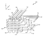
도 1은 예시적인 3차원 메모리 구조물(100)을 도시한다. 더 구체적으로는, 수직 메모리 어레이 형태의 3차원 메모리 구조물(100)이 도시되어 있다. 메모리 구조물(100)은 수직 메모리 소자(108)의 단부에 전기적으로 접속된 복수의 비트라인(104)을 포함한다. 메모리 구조물(100)은 또한, 복수의 워드라인(112) 및 복수의 수평 또는 평면 전극(116)을 포함한다. 각각의 워드라인(112)은 직접적으로 또는 접속 도체(120)를 통해 수평 전극 또는 데크(116)의 상단면(114)에 접속된다. 수평 전극(116)은 일반적으로 x 및 y 차원으로 연장되는 평면 내에 배치된다. 메모리 셀(124)들은 수평 전극(116)에 인접한 수직 메모리 소자(108)들의 영역에 형성되고, 일반적으로 메모리 구조물의 메모리 어레이(128) 내에 포함된다. 또한, 메모리 어레이(128)는 3차원(x, y, z)으로 연장되는 체적 내에 포함된다.FIG. 1 illustrates an exemplary three-
예시적인 메모리 구조물(100)에서, 비트라인(104)은, 메모리 어레이 영역(128)의 한 측면에 인접한 비트라인 소켓 영역(132) 내에서 액세스될 수 있도록 연장된다. 다른 실시예들에 따르면, 비트라인(104)은 메모리 어레이 영역(128)의 대향 측면들까지 연장되되, 2개의 비트라인 소켓 영역(132)이 제공되도록 연장될 수 있다. 비트라인 소켓 영역(132) 내에서 액세스될 수 있는 비트라인 컨택트 또는 비트(106)의 수는 이 예에서는 비트라인(104)의 수와 동일하다.In an
마찬가지로, 워드라인(112)은 메모리 어레이 영역(128)의 한 측면에 인접한 워드라인 소켓 영역(136)으로부터 연장된다. 다른 실시예들에 따르면, 워드라인 소켓 영역(136)은 메모리 어레이(128)의 추가적 측면들 상에 제공될 수 있다. 워드라인 컨택트 또는 비트(140)의 수는, 이 예에서는, 비트라인(112)의 수와 동일하다. 컨택트(142)에서 접속 도체(120)에 전기적으로 접속된 수평 전극(116)의 접속 부분(138)이, 상이한 수평 전극들 또는 데크(116)들의 접속 부분(138)이 메모리 어레이 영역(128)으로부터 상이한 거리들에 배치되어 있는 계단형 타입 배열로 배치되어 있기 때문에, 워드라인 소켓 영역(136)에 의해 둘러싸인 영역은 돌출부로서 도시되어 있다.Likewise, the
메모리 구조물(100) 내의 메모리 셀(124)의 수가 증가함에 따라, 비트라인(108) 및/또는 워드라인(112)의 수도 역시 증가한다. 이 예에서, 비트라인(104)의 수보다 워드라인(112)의 수는 더 많아서, 증가된 수의 수평 전극 또는 데크(116)를 허용함으로써 일반적으로 고밀도 메모리 어레이 영역(128)을 지원한다. 또한, 예시적인 종래 기술의 메모리 구조물(100) 등의 3차원 메모리 구조물은 3차원으로 배치된 메모리 셀(124)을 갖지만, 비트라인(132) 및 워드라인(136) 소켓 영역은 접속을 완료할 수평 전극(116)에 평행한 평면 내의 소정량의 영역을 요구한다. 그 결과, 메모리 셀(124)의 수가 증가함에 따라, 특히 수평 전극 또는 데크(116)의 수가 증가함에 따라, 비트라인(132) 및 워드라인(136) 소켓 영역에 의해 점유되는 메모리 구조물의 총 면적도 점점 더 커지게 된다.As the number of
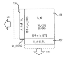
도 2에 도시된 바와 같이, 워드라인 소켓 영역(136)의 길이(Ls_word)는, 계단형 컨택트 배열로 배치된 수평 전극(116)들로의 접속 도체(120) 액세스를 제공하기 위하여, 수평 전극(116)의 수(n)가 증가함에 따라 증가한다. 따라서, 데크 또는 수평 전극(116)의 수가 증가함에 따라, 메모리 어레이(128)의 영역 밀도가 증가하고, 워드라인 소켓 영역 또는 영역들(136)에 의해 점유되는 면적도 역시 증가한다. 유사하게, 비트라인(104)의 수(m)가 증가함에 따라, 비트라인 소켓 영역 또는 영역들(132)에 의해 점유된 영역이 증가한다. 또한, 주어진 소켓 영역(132, 136) 배열에 있어서, 소켓 영역(132, 136)에 의해 점유된 메모리 구조물(100)의 전체 면적은, 데크(116)의 수, 및 그에 따른 주어진 메모리 셀 영역(128) 내의 메모리 셀(124)의 수가 증가함에 따라 점점 커지게 된다.2, the length L s_word of the word
또한, 소켓 영역(132, 136)에 의해 점유되는 면적은, 메모리 셀 영역(128)의 밀도가 증가함에 따라 메모리 구조물(100)의 전체 면적의 점점 더 큰 비율이 된다. 본 개시내용을 고려한 후에 본 기술분야의 통상의 기술자라면 이해할 수 있는 바와 같이, 면적 효율의 감소는 수직 메모리 구조물에 포함된 소켓 영역(132, 136)의 수에 관계없이 발생한다.In addition, the area occupied by the
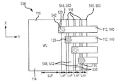
도 3은, 종래 기술의 워드라인 소켓 영역(136)을 포함하는, 도 1에 도시된 메모리 구조물(100) 등의 예시적인 메모리 구조물의 일부를, x 차원을 따라 취해진 시선으로부터 입면도로 도시한다. 도 4는, 도 3에 도시된 메모리 구조물(100)의 워드라인 소켓 영역(136) 부분을, z 축 또는 차원을 따라 취해진 시선으로부터 평면도로 도시한다. 도시된 바와 같이, 워드라인 소켓 영역(136)은 계단형 타입 컨택트 영역을 포함할 수 있다. 추가로, 수평 전극(116)의 컨택트 영역(138)과 접속 도체(120) 사이의 각각의 컨택트(142)는 수평 전극(116)의 상단면(114) 상에 완전히 배치된다. y 축에 평행한 방향으로의 워드라인 소켓 영역(136)의 길이는 데크(116)의 수에 비례하고, 이 예에서의 구성은 다음 표현식으로 주어진다 : Ls= {Lc+Ln n}F, 여기서, Ls는 소켓 길이, Lc는 일정 길이 인자, Ln은 데크(116)의 수에 의존하는 길이 인자, n은 데크(116)의 수, 및 F는 메모리 셀 영역(128)의 절반 피치이다.FIG. 3 illustrates a portion of an exemplary memory structure, such as the
도 3에 도시된 바와 같이, 각각의 수평 전극(116)은 유전체 또는 절연 층(248)에 의해 인접한 수평 전극(116)으로부터 분리된다. 각각의 절연 층(248)은, 수직이고(즉, 수평 전극(116)의 상단면(114)에 대해 직교 또는 90도이고 z 차원에 평행 하고) 절연 층(248) 바로 위의 수평 전극(116)보다 y 방향으로 더 멀리 연장되지 않는 단부면(end surface)(252)을 갖는다. 따라서, 각각의 수평 전극(116)의 평면 상단면(114)의 일부는, 대응하는 접속 도체(120)와의 컨택트(142)가 형성될 수 있는 컨택트 영역(138)으로서 이용가능하다. 그러나, 인접한 접속 도체(120)들 사이, 더 구체적으로는 선택된 수평 전극(116)에 전기적으로 접속된 접속 도체(120)와 선택된 수평 전극(116)의 어느 한 측 상의 수평 전극(116) 사이에서 y 차원에서 유지되어야 하는 정렬 여유폭 또는 간격 인자는 비교적 커서, LnF로 주어지는 간격이 그에 대응하여 커진다.Each
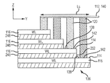
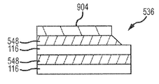
도 5는, 본 개시내용의 실시예에 따라 구성된 워드라인 소켓 영역(536)을 포함하는, 도 1에 나타낸 메모리 구조물(100) 등의 3차원 메모리 구조물의 일부를 x 축을 따라 취해진 시선으로부터 입면도로 도시한다. 도 6은, 도 5에 도시된 메모리 구조물(100)의 워드라인 소켓 영역(536) 부분을, z 축을 따라 취해진 시선으로부터 평면도로 도시한다. 소켓 영역(536)은, 평면 전극(116)의 단부가, 전극들이 스택에서 더 아래쪽일수록 y 차원으로 더 연장되는 계단형 타입 배열로 배치되어 있다는 점에서 종래의 소켓 영역(136)과 유사하다. 또한, 각각의 평면 전극(116)은 인접한 유전체 층들 사이에 개재된 절연 층 또는 유전체 층(548)에 의해 인접한 전극으로부터 분리된다. 도시된 바와 같이, 수직 또는 접속 도체(120) 사이의 간격은 y 방향에서 감소되었다. 즉, 정렬 여유폭 또는 길이 인자는 도 3 및 도 4에 나타낸 종래 기술의 구성에 비해 감소되었다. 예를 들어, 종래의 구성은 접속 도체(120)들 사이에서 소정의 정렬 여유폭이 y 방향으로 유지될 것을 요구하지만, 본 개시내용의 실시예는 감소된 정렬 여유폭으로 구성될 수 있다. 본 개시내용의 적어도 일부 실시예에 따르면, 정렬 여유폭은 0일 수 있다. 역시 다른 실시예에 따르면, 정렬 여유폭은, 접속 도체(120)들이 x 차원에서 서로 분리되어 있는 한, y 차원에서 서로 중첩되도록 음수일 수 있다. 그 결과, 본 개시내용의 실시예들은 수직 도체(120)들의 중심선들 사이의 간격이 종래 기술에 따른 수직 도체(120)들 사이의 간격에 비해 감소되는 것을 허용한다. 따라서, 주어진 수의 데크(116) 및 다른 모든 인자들이 동일할 경우, 본 개시내용의 실시예에 따라 구성된 소켓 영역(536)의 길이는, 종래 기술에 따라 구성된 소켓 영역(136)의 소켓 길이보다 짧을 것이다. 이 감소된 간격은, 인접한 수평 전극(116)들 사이의 유전체 층(548)의 엣지면(552)의 테이퍼링된 또는 경사진 구성에 의해 가능하게 된다.Figure 5 illustrates a portion of a three-dimensional memory structure, such as the
본 개시내용의 실시예에 따르면, 유전체 층(548)(예를 들어, 유전체 층(548a))의 y 차원에서 가장 먼 범위에 대응하거나 이를 포함하는 엣지(552)는, 유전체 층(548) 바로 위의 수평 전극(116)(예를 들어, 수평 전극(116a))의 y 차원에서 가장 먼 범위와 유전체 층(548) 바로 아래의 수평 전극(116)(예를 들어, 수평 전극(116b)) 사이의 지점까지 연장된다. 특히, 수평 전극(116a)의 엣지면(554)과 위에 놓인 수평 전극(116)의 엣지면(554) 사이의 아래에 놓인 수평 전극(116)의 상단면(114)의 일부는 유전체 층(548)에 의해 부분적으로 덮인다. 또한, 이 예에서, 각각의 유전체 층(548)의 엣지면(552)은 경사져 있되, 유전체 층(548) 위에 놓인 수평 전극(116)의 바닥면의 단부에 대응하는 지점으로부터 아래에 놓인 수평 전극(116)의 엣지 표면(554) 쪽으로 향하지만 엣지 표면(554)까지는 아닌 지점까지 연장되도록 경사져 있다. 따라서, 컨택트 영역(542)으로서 이용가능한 아래에 놓인 수평 전극(116)의 상단면(114)의 덮이지 않은 부분(538)은 유전체 층의 엣지가 수직인 구성에 비해 감소된다. 달리 말하면, 본 개시내용의 실시예에서는, 위에 놓인 수평 전극(116)에 의해 중첩되지 않는 아래에 놓인 수평 전극(116)의 상단면(114)의 영역은 중간 유전체 층(548)의 경사진 단부(552)에 의해 부분적으로 덮인다. 이러한 구성의 결과로서, 정렬 공차, 및 그에 따른 정렬 여유폭 요구는, 종래 구성에 비해 감소되거나 완전히 제거된다. 특히, 오정렬된 수직 도체(120)는, 타겟 수평 전극(116) 아래에 놓인 유전체 층(548)에 의해, 타겟 수평 전극(116) 바로 아래의 수평 전극(116)과 접촉하는 것이 방지될 것이다. 즉, 적어도 일부 범위에 걸쳐, 오정렬된 수직 도체(120)의 영향이 제거될 수 있다. 이와 같이 이용가능하게 된 감소된 정렬 여유폭 요건의 결과로서, 주어진 간격 인자 및 데크(116)의 수에 대해, 본 발명의 실시예의 소켓 영역의 길이 Ls는 수직 유전체 층 엣지를 갖는 종래의 구성에 비해 감소된다.In accordance with an embodiment of the present disclosure, an
또한, 타겟 수평 전극(116)의 엣지 부분(554)은 컨택트 영역(542)의 일부로서 이용가능하다. 따라서, 상단면(538)의 덮이지 않은 부분의 면적이 종래의 구성에 비해 감소되더라도, 수평 전극(116)과 연관된 수직 도체(120) 사이에서, 적절하게 낮은 전기 저항을 포함한 그러나 이것으로 제한되지 않는, 전기적 성능이 유지될 수 있다. 적어도 일부 실시예에 따르면, 수직 도체는 타겟 수평 전극(116)의 어느 한 측 상의 유전체 층(548)의 일부와 접촉하도록 크기조정되고 정렬된다.In addition, the
도 7은, 종래 기술(플롯 704)에 따라 구성된 워드라인 소켓 영역(136)의 길이를 본 개시내용의 실시예(플롯 708)에 따라 구성된 워드라인 소켓 영역(536)의 길이와 비교하는 그래프이다. 더 구체적으로는, 상이한 수의 층(116)을 갖는 3차원 메모리 구조물에 대한 워드라인 소켓 영역(136, 536)의 길이(Ls)가 도시되어 있다. 이 예에서, 일정한 일정 길이 인자 및 셀 영역의 주어진 절반 피치에 대해, 본 개시내용의 실시예에 따라 구성된 워드라인 소켓 영역(536)의 길이는, 데크의 수(n)에 따라, 종래 기술에 따라 구성된 워드라인 소켓 영역(136)의 길이가 증가하는 비율보다 작은 비율로 증가한다. 따라서, 메모리 구조물의 크기 감소가 달성될 수 있다.7 is a graph comparing the length of a
또한, 본 개시내용의 실시예에 따라 구성된 워드라인 소켓 영역(536)을 이용하는 3차원 메모리 구조물의 면적 효율은 종래의 구성보다 더 클 수 있다. 특히, 3차원 메모리 구조물의 면적 효율은, 메모리 어레이의 면적 + 소켓 영역의 면적에 대한 메모리 어레이의 면적의 비율로서 평가될 수 있다. 더 상세하게는, 면적 효율은 다음과 같이 표현될 수 있다:In addition, the area efficiency of the three-dimensional memory structure using the word
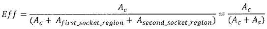
여기서, Eff는 메모리 구조물의 면적 효율, Ac는 메모리 셀 영역의 면적, Afirst_socket_region은 제1 소켓 영역의 면적, Asecond_socket_region은 제2 소켓 영역의 면적, As는 비트라인 소켓 영역 및 워드라인 소켓 영역의 전체 면적이다. 예를 들어, 도 2를 참조하면, 면적 효율은, 메모리 어레이 영역(128)의 면적을 메모리 어레이 영역(128)과 동일한 면적 + 비트라인 소켓 영역(132)의 면적 + 워드라인 소켓 영역(136, 536)의 면적으로 나눈 값과 동일하며, 여기서, 영역들 모두는 수평 전극 또는 데크(116)에 대체로 평행한 평면 내에 있다. 따라서, 소켓 영역이 계단형 컨택트 영역을 포함하는 경우, 그 소켓 영역의 면적은 그 영역의 수평면 상으로의 투사에 의해 주어진다. 도 5 및 도 6에 나타낸 바와 같이 경사진 엣지(552)를 갖는 유전체 층(548)을 워드라인 소켓 영역(536)에 제공함으로써, 본 개시내용의 실시예의 결과적인 3차원 메모리 구조물(500)의 면적 효율은 종래 구성에 비해 개선될 수 있다.Here, Eff is the area efficiency of the memory structure, A c is the area of the memory cell region, A first_socket_region is the area, A second_socket_region of the first socket region is the area of the second receptacle area, A s is the bit line socket region and a word line socket The total area of the area. For example, referring to FIG. 2, the area efficiency is determined such that the area of the
본 개시내용의 실시예들에 따르면, 종래의 기술 또는 구성에 비해 감소된 영역 내에 소켓 영역을 제공하기 위한 방법이 제공된다. 도 8은 이러한 방법의 프로세스 단계들을 도시하는 플로차트를 나타내며, 프로세스 단계들의 수행 동안 상이한 스테이지들에서의 소켓 구조물(536)이 도 9a 내지 도 9d에서 입면도로 도시되어 있다. 이 방법은, 각각의 평면 전극(116)이 유전체 층(548)에 의해 인접한 평면 전극(116)으로부터 분리되어 있는, 평면 또는 수평 전극(116)의 스택을 제공하는 단계(단계 804)를 포함할 수 있다. 그 다음, 마스크 층이 상단 유전체 층(548) 위에 형성되되, 마스크가 아래에 놓인 유전체 층의 일부를 덮지 않도록 형성될 수 있다(단계 808). 도 9a는 마스크(904)를 추가한 후의 소켓 영역(536)을 나타낸다. 그 다음, 유전체 층(548)의 노출된 부분이 에칭될 수 있다(단계 812). 에칭의 초기 단계 후의 소켓 영역(536)은 도 9b에 도시되어 있다. 그 다음, 마스크(904)가 풀백될 수 있다(단계 816). 마스크(904)를 풀백한 후의 소켓 영역(536)은 도 9c에 도시되어 있다. 그 다음, 이전 에칭 단계에서 노출된 평면 전극(116) 및 다음 유전체 층(548)이 에칭될 수 있는 한편, 상위 유전체 층(548)은 더 에칭될 수 있다(단계 820). 단계(820)의 완료 후의 소켓 영역(536)이 도 9d에 도시되어 있다. 이러한 풀백 프로세스는, 마지막 평면 전극(116)의 일부가 노출될 때까지 계속될 수 있다. 본 개시내용의 실시예에 따르면, 에칭 프로세스 동안, 유전체 층(548)은, 아래에 놓인 평면 전극(116)의 상단면에 직각으로 에칭되는 것이 아니라 경사진 표면을 생성하도록 테이퍼링된다. 대안으로서, 유전체 층(548)이 "풀백되는" 양은 위에 놓인 평면 전극(116)이 "풀백되는" 양보다 적을 수 있다. 단계 824에서, 마지막 평면 전극(116)에 도달했는지에 관한 결정이 이루어질 수 있다. 도달하지 않았다면, 프로세스는 단계 816으로 되돌아 갈 수 있다.SUMMARY OF THE INVENTION According to embodiments of the present disclosure, a method is provided for providing a socket area in a reduced area compared to a conventional technique or configuration. Figure 8 shows a flow chart showing the process steps of this method, with the
마지막 전극에 도달된 후에, 적어도 하나의 수직 도체(120)가 각각의 평면 전극(116)에 접속되도록, 수직 또는 접속 도체(120)가 형성될 수 있다(단계 828). 수직 도체(120)를 형성하는 단계 동안, 평면 전극(116)과 연관된 수직 도체(120) 사이의 컨택트 영역(552)은 수평 전극(116)의 상단면(114)의 일부뿐만 아니라 평면 전극(116)의 엣지면(554)의 일부도 포함한다. 본 개시내용을 고려한 후에 본 기술분야의 통상의 기술자라면 이해할 수 있는 바와 같이, 경사진 엣지(532)를 갖는 유전체 층(548)의 제공은, 수직 도체(120)가 타겟 평면 전극(116) 아래의 평면 전극(116)에 전기적으로 접촉하는 것을 방지한다. 따라서, 주어진 제조 공차를 위해 요구되는 정렬 여유폭이 종래의 계단형 타입 컨택트 구성에 비해 감소될 수 있다. 각각의 평면 전극(116)을 수직 도체(120)에 전기적으로 접속한 후에, 프로세스는 종료될 수 있다.After reaching the last electrode, a vertical or
본 개시내용의 실시예들이 3차원 메모리 구조물과 관련하여 종래의 소켓 영역 구성에 비해 감소된 영역을 점유할 수 있는 소켓 영역 구성을 논의하였지만, 본 개시내용의 실시예들은 이러한 구조물과 관련한 이용으로 제한되는 것은 아니다. 특히, 여기서 개시된 소켓 영역은 컨택트들이 계단형 타입 배열로 배치되는 임의의 전기적 구조물과 관련하여 이용될 수 있다.Although embodiments of the present disclosure have discussed a socket area configuration that can occupy a reduced area over a conventional socket area configuration in connection with a three dimensional memory structure, embodiments of the present disclosure are limited to use in connection with such structures It is not. In particular, the socket regions disclosed herein may be used in connection with any electrical structure in which the contacts are arranged in a stepped-type arrangement.
더 구체적으로는, 본 개시내용의 실시예들은, 정렬 여유폭이 계단형 타입 배열로 배치된 전기적 컨택트에 관해 감소될 수 있는 구성을 제공한다.More specifically, embodiments of the present disclosure provide a configuration in which the alignment margin width can be reduced with respect to electrical contacts disposed in a stepped-type arrangement.
본 개시내용의 실시예들의 다양한 피쳐 및 컴포넌트들이 편의상 "수직" 및 "수평" 기준 방향과 관련하여 설명되었다. 일반적으로, "수직"이란, 다양한 도면에 도시된 기준 좌표계의 z 축에 평행한 차원을 말한다. "수평" 차원은 일반적으로 기준 좌표계의 x 및 y 차원에 놓인 평면에 대응한다. 좌표계의 절대적인 배향, 및 그에 따른 "수직" 및 "수평" 컴포넌트 또는 피쳐들의 배향이 반드시 고정되어 있는 것은 아니다. 따라서, 본 개시내용의 실시예에 따르면, 좌표계의 배향은 절대 기준 프레임 내에서 고정되지 않는다.The various features and components of the embodiments of the present disclosure have been described with respect to "vertical" and "horizontal" reference directions for convenience. In general, "vertical" refers to a dimension parallel to the z-axis of the reference coordinate system shown in various drawings. The "horizontal" dimension generally corresponds to a plane lying in the x and y dimensions of the reference coordinate system. The absolute orientation of the coordinate system, and hence the orientation of the "vertical" and "horizontal" components or features, is not necessarily fixed. Thus, according to the embodiment of the present disclosure, the orientation of the coordinate system is not fixed within the absolute reference frame.
본 발명의 상기의 논의는 예시와 설명의 목적을 위해 제공되었다. 또한, 이 설명은 본 발명을 여기서 설명된 형태로 제한하려는 것이 아니다. 결과적으로, 상기 교시 및 관련 기술 분야의 기술 및 지식 내에서의 변형 및 수정은 본 발명의 범위 내에 있다. 상기에서 설명된 실시예들은, 본 발명을 실시하는 현재 알려진 최상의 형태를 설명하고 본 기술분야의 통상의 기술자가 이와 같은 또는 다른 실시예들에서 본 발명의 특정한 응용 또는 이용에 의해 요구되는 다양한 수정과 함께 본 발명을 이용할 수 있게 하는 것을 추가로 의도한다. 첨부된 청구항들은 종래 기술에 의해 허용된 범위까지의 대안적 실시예들을 포함하는 것으로 해석될 것을 의도한다.The foregoing discussion of the present invention has been presented for purposes of illustration and description. Furthermore, this description is not intended to limit the invention to the form described herein. As a result, variations and modifications within the skill and knowledge of the above teachings and related art are within the scope of the present invention. The embodiments described above are intended to illustrate the presently known and best mode for carrying out the invention and to enable any person skilled in the art to make and use various modifications required by the specific applications or uses of the invention in such or other embodiments It is further contemplated that the invention may be utilized together. It is intended that the appended claims be construed to include alternative embodiments to the extent permitted by the prior art.
Claims (20)
메모리 어레이 체적, ―상기 메모리 어레이 체적은, x, y, 및 z 차원으로 연장되고, 상기 메모리 어레이 체적은 복수의 메모리 셀을 포함함―;
소켓 영역, ―상기 소켓 영역은 상기 메모리 어레이 체적의 한 측면을 따라 위치하되, 상기 메모리 어레이 체적의 상기 한 측면을 따라 x 차원으로 연장되고, 상기 메모리 어레이 체적으로부터 y 차원으로 연장됨―;
x 및 y 차원으로 연장되는 평면들에 놓인 복수의 유전체 층; 및
x 및 y 차원으로 연장되는 평면들에 놓인 복수의 수평 전극
을 포함하고,
상기 복수의 수평 전극에 포함된 수평 전극들은 z 차원으로 적층되며,
상기 복수의 수평 전극에 포함된 인접한 수평 전극들은 상기 복수의 유전체 층에 포함된 유전체 층들 중 적어도 하나에 의해 z 차원에서 서로 분리되고,
적어도 제1 방향으로 상기 z 차원을 따라 이동함에 따라, 상기 수평 전극들은 상기 메모리 어레이 영역으로부터 제1 소켓 영역으로 더 많은 양만큼 연장되어 계단형 구조물을 형성하며,
제1 수평 전극과 제2 수평 전극 사이에 배치된 유전체 층의 엣지는, 상기 제1 수평 전극의 엣지와 상기 제2 수평 전극의 엣지 사이에 위치하며,
상기 제1 소켓 영역 내에서, 상기 복수의 수평 전극 중의 각각의 수평 전극은, 수평 전극들 각각이 z 차원에 평행한 하나 이상의 라인을 따라 액세스가능하도록, 유전체 층에 의해 덮이지 않은 부분을 포함하는, 3차원 메모리 구조물.As a three-dimensional memory structure,
A memory array volume, the memory array volume extending in x, y, and z dimensions, the memory array volume including a plurality of memory cells;
A socket region, said socket region being located along one side of said memory array volume, said memory array volume extending x dimension along said one side of said memory array volume and extending in y dimension from said memory array volume;
a plurality of dielectric layers disposed in planes extending in the x and y dimensions; And
A plurality of horizontal electrodes < RTI ID = 0.0 >
/ RTI >
The horizontal electrodes included in the plurality of horizontal electrodes are stacked in z-dimension,
Adjacent horizontal electrodes included in the plurality of horizontal electrodes are separated from each other in the z dimension by at least one of the dielectric layers included in the plurality of dielectric layers,
As they move along the z dimension in at least a first direction, the horizontal electrodes extend a greater amount from the memory array region to the first socket region to form a stepped structure,
The edge of the dielectric layer disposed between the first horizontal electrode and the second horizontal electrode is positioned between the edge of the first horizontal electrode and the edge of the second horizontal electrode,
Within the first socket region, each horizontal electrode of the plurality of horizontal electrodes includes a portion that is not covered by the dielectric layer, such that each of the horizontal electrodes is accessible along one or more lines parallel to the z dimension , Three-dimensional memory structure.
복수의 접속 도체를 더 포함하고, 상기 접속 도체들 각각은 z 차원을 따라 연장되고, 상기 소켓 영역 내의 대응하는 수평 전극의 일부와 접촉하는, 3차원 메모리 구조물.The method according to claim 1,
Further comprising a plurality of connection conductors, each of the connection conductors extending along a z dimension and contacting a portion of a corresponding horizontal electrode in the socket region.
복수의 접속 도체를 더 포함하고, 상기 접속 도체들 각각은 대응하는 수평 전극의 상단면 및 엣지면과 접촉하는, 3차원 메모리 구조물.8. The method of claim 7,
Further comprising a plurality of connection conductors, each of the connection conductors being in contact with a top surface and an edge surface of a corresponding horizontal electrode.
복수의 절연 층; 및
복수의 평면 전극을 포함하고,
인접한 평면 전극들은 상기 절연 층들 중 적어도 하나에 의해 서로 분리되며,
각각의 평면 전극은, 각각의 평면 전극의 일부가 계단을 형성하도록 상기 소켓 영역 내에서 상이한 거리로 연장되고;
각각의 절연 층의 단부면(end surface)의 적어도 일부는 인접한 평면 전극들의 단부면들 사이에 위치하는, 소켓 영역.As a socket area,
A plurality of insulating layers; And
Comprising a plurality of planar electrodes,
Adjacent planar electrodes are separated from each other by at least one of said insulating layers,
Each planar electrode extending at a different distance within the socket region such that a portion of each planar electrode forms a step;
Wherein at least a portion of an end surface of each insulating layer is positioned between end surfaces of adjacent planar electrodes.
복수의 접속 도체를 더 포함하고, 상기 복수의 접속 도체 중의 각각의 접속 도체는 상기 평면 전극들 중 하나에 접속되는, 소켓 영역.12. The method of claim 11,
Further comprising a plurality of connecting conductors, each connecting conductor of the plurality of connecting conductors being connected to one of the planar electrodes.
복수의 평면 전극 및 복수의 절연 층을 포함하는 스택을 제공하는 단계, ―인접한 평면 전극들은 절연 층에 의해 서로 분리됨―;
상기 스택 상에 마스크를 배치하는 단계;
상기 마스크 아래에 있지 않은 상기 복수의 절연 층 중의 제1 절연 층의 제1 부분을 에칭하여 상기 복수의 평면 전극 중의 제1 평면 전극의 제1 부분을 노출시키는 단계;
마스크를 풀백(pull back)하는 단계; 및
상기 마스크를 풀백한 후에, 상기 마스크를 풀백함으로써 노출된 상기 제1 절연 층의 제2 부분을 에칭하고, 상기 제1 평면 전극의 상기 제1 부분의 일부를 에칭하고, 상기 복수의 절연 층에 포함된 제2 절연 층의 제1 부분을 에칭하는 단계, ― 상기 에칭에 의해 형성된 상기 제2 절연 층의 엣지는 경사져 있고 상기 제1 평면 전극의 엣지로부터 상기 제1 평면 전극의 엣지와 상기 제2 평면 전극의 엣지 사이로 연장됨―;
를 포함하는 방법.A method for forming a stepped contact socket region,
Providing a stack comprising a plurality of planar electrodes and a plurality of insulating layers, wherein adjacent planar electrodes are separated from each other by an insulating layer;
Disposing a mask on the stack;
Etching a first portion of the first insulating layer of the plurality of insulating layers that is not under the mask to expose a first portion of the first planar electrode of the plurality of planar electrodes;
Pull back the mask; And
Etching the second portion of the exposed first insulating layer by full-backing the mask after full-back of the mask, etching a portion of the first portion of the first planar electrode, Wherein the edge of the second insulating layer formed by the etching is inclined and extends from the edge of the first planar electrode to the edge of the first planar electrode and to the second plane of the second planar electrode from the edge of the first planar electrode, Extending between the edges of the electrode;
≪ / RTI >
복수의 접속 도체를 형성하는 단계를 더 포함하고, 각각의 접속 도체는 평면 전극들 중 하나의 상단면 및 엣지면에 전기적으로 접속되는, 방법.20. The method of claim 19,
Further comprising the step of forming a plurality of connecting conductors, wherein each connecting conductor is electrically connected to the top and edge surfaces of one of the planar electrodes.
Applications Claiming Priority (3)
| Application Number | Priority Date | Filing Date | Title |
|---|---|---|---|
| US14/695,835 US9515125B2 (en) | 2015-04-24 | 2015-04-24 | Socket structure for three-dimensional memory |
| US14/695,835 | 2015-04-24 | ||
| PCT/JP2016/002025 WO2016170759A1 (en) | 2015-04-24 | 2016-04-14 | Socket structure for three-dimensional memory |
Publications (1)
| Publication Number | Publication Date |
|---|---|
| KR20170141665A true KR20170141665A (en) | 2017-12-26 |
Family
ID=55863153
Family Applications (1)
| Application Number | Title | Priority Date | Filing Date |
|---|---|---|---|
| KR1020177029491A KR20170141665A (en) | 2015-04-24 | 2016-04-14 | Socket structure for 3D memory |
Country Status (4)
| Country | Link |
|---|---|
| US (3) | US9515125B2 (en) |
| JP (1) | JP6788607B2 (en) |
| KR (1) | KR20170141665A (en) |
| WO (1) | WO2016170759A1 (en) |
Families Citing this family (8)
| Publication number | Priority date | Publication date | Assignee | Title |
|---|---|---|---|---|
| US9478556B2 (en) | 2014-09-11 | 2016-10-25 | Kabushiki Kaisha Toshiba | Semiconductor memory device |
| KR102536261B1 (en) * | 2015-12-18 | 2023-05-25 | 삼성전자주식회사 | Three dimensional device |
| US9767901B1 (en) * | 2016-08-24 | 2017-09-19 | Hewlett Packard Enterprise Development Lp | Circuits having selector devices with different I-V responses |
| US10777566B2 (en) * | 2017-11-10 | 2020-09-15 | Macronix International Co., Ltd. | 3D array arranged for memory and in-memory sum-of-products operations |
| US10453854B2 (en) | 2017-11-15 | 2019-10-22 | Sandisk Technologies Llc | Three-dimensional memory device with thickened word lines in terrace region |
| US10461163B2 (en) | 2017-11-15 | 2019-10-29 | Sandisk Technologies Llc | Three-dimensional memory device with thickened word lines in terrace region and method of making thereof |
| WO2019099103A1 (en) * | 2017-11-15 | 2019-05-23 | Sandisk Technologies Llc | Three-dimensional memory device with thickened word lines in terrace region and method of making thereof |
| US11222695B2 (en) * | 2019-11-15 | 2022-01-11 | Micron Technology, Inc. | Socket design for a memory device |
Family Cites Families (9)
| Publication number | Priority date | Publication date | Assignee | Title |
|---|---|---|---|---|
| ITTO20021118A1 (en) * | 2002-12-24 | 2004-06-25 | St Microelectronics Srl | MOS DEVICE AND MANUFACTURING PROCEDURE OF |
| JP5016832B2 (en) * | 2006-03-27 | 2012-09-05 | 株式会社東芝 | Nonvolatile semiconductor memory device and manufacturing method thereof |
| US7910973B2 (en) * | 2008-03-17 | 2011-03-22 | Kabushiki Kaisha Toshiba | Semiconductor storage device |
| JP2010027870A (en) * | 2008-07-18 | 2010-02-04 | Toshiba Corp | Semiconductor memory and manufacturing method thereof |
| JP5380190B2 (en) * | 2009-07-21 | 2014-01-08 | 株式会社東芝 | Nonvolatile semiconductor memory device and manufacturing method thereof |
| KR101559958B1 (en) * | 2009-12-18 | 2015-10-13 | 삼성전자주식회사 | 3 3 Method for manufacturing three dimensional semiconductor device and three dimensional semiconductor device manufactured by the method |
| JP2011211039A (en) * | 2010-03-30 | 2011-10-20 | Toshiba Corp | Memory device, and method of manufacturing the same |
| US8885382B2 (en) * | 2012-06-29 | 2014-11-11 | Intel Corporation | Compact socket connection to cross-point array |
| JP2015056452A (en) * | 2013-09-10 | 2015-03-23 | 株式会社東芝 | Semiconductor storage device and manufacturing method of the same |
-
2015
- 2015-04-24 US US14/695,835 patent/US9515125B2/en active Active
-
2016
- 2016-04-14 WO PCT/JP2016/002025 patent/WO2016170759A1/en active Application Filing
- 2016-04-14 KR KR1020177029491A patent/KR20170141665A/en active IP Right Grant
- 2016-04-14 JP JP2017552102A patent/JP6788607B2/en active Active
- 2016-11-03 US US15/342,819 patent/US9728722B2/en active Active
-
2017
- 2017-06-14 US US15/623,030 patent/US9935266B2/en active Active
Also Published As
| Publication number | Publication date |
|---|---|
| US9515125B2 (en) | 2016-12-06 |
| WO2016170759A1 (en) | 2016-10-27 |
| JP6788607B2 (en) | 2020-11-25 |
| US20170288141A1 (en) | 2017-10-05 |
| US20170077399A1 (en) | 2017-03-16 |
| JP2018513559A (en) | 2018-05-24 |
| US9935266B2 (en) | 2018-04-03 |
| US9728722B2 (en) | 2017-08-08 |
| US20160315121A1 (en) | 2016-10-27 |
Similar Documents
| Publication | Publication Date | Title |
|---|---|---|
| KR20170141665A (en) | Socket structure for 3D memory | |
| US10050085B2 (en) | Block architecture for vertical memory array | |
| KR102024723B1 (en) | Three dimensional semiconductor device | |
| US8482133B2 (en) | Semiconductor package | |
| US8835990B2 (en) | 3D memory array | |
| US8946892B2 (en) | Semiconductor package | |
| JPWO2020117978A5 (en) | ||
| US20070295818A1 (en) | Power plane to reduce voltage difference between connector power pins | |
| US8614507B2 (en) | Semiconductor devices having lower and upper interconnection structures that exhibit reduced coupling | |
| US9305901B2 (en) | Non-circular die package interconnect | |
| CN102881317B (en) | 3 D memory array | |
| US20210013395A1 (en) | Magnetic tunnel junction (mtj) device | |
| US20130168633A1 (en) | Semiconductor device and manufacturing method thereof | |
| US20150155388A1 (en) | Semiconductor structure | |
| US10211150B2 (en) | Memory structure | |
| US20150349440A1 (en) | Semiconductor module socket and connection structure of the same | |
| US20160099209A1 (en) | Memory device and manufacturing method thereof | |
| WO2018119987A1 (en) | Dual in-line memory modules and connectors for increased system performance | |
| TWI462278B (en) | Semiconductor structure and manufacturing method of the same | |
| US20130039111A1 (en) | Connection and addressing of multi-plane crosspoint devices | |
| US20230197651A1 (en) | Techniques for positioning bond pads of microelectronic devices and related microelectronic devices, methods, and systems | |
| US20140042629A1 (en) | Semiconducting multi-layer structure and method for manufacturing the same | |
| CN104681539B (en) | Semiconductor structure | |
| CN114678366A (en) | Three-dimensional memory device and manufacturing method thereof | |
| CN116169038A (en) | Three-dimensional chip, preparation method and electronic equipment |
Legal Events
| Date | Code | Title | Description |
|---|---|---|---|
| E902 | Notification of reason for refusal | ||
| E701 | Decision to grant or registration of patent right |