KR20170141663A - Patterned transparent conductive film and process for producing such a patterned transparent conductive film - Google Patents
Patterned transparent conductive film and process for producing such a patterned transparent conductive film Download PDFInfo
- Publication number
- KR20170141663A KR20170141663A KR1020177029469A KR20177029469A KR20170141663A KR 20170141663 A KR20170141663 A KR 20170141663A KR 1020177029469 A KR1020177029469 A KR 1020177029469A KR 20177029469 A KR20177029469 A KR 20177029469A KR 20170141663 A KR20170141663 A KR 20170141663A
- Authority
- KR
- South Korea
- Prior art keywords
- coating material
- regions
- insulating
- objects
- insulating coating
- Prior art date
- Legal status (The legal status is an assumption and is not a legal conclusion. Google has not performed a legal analysis and makes no representation as to the accuracy of the status listed.)
- Withdrawn
Links
Classifications
-
- H—ELECTRICITY
- H01—ELECTRIC ELEMENTS
- H01B—CABLES; CONDUCTORS; INSULATORS; SELECTION OF MATERIALS FOR THEIR CONDUCTIVE, INSULATING OR DIELECTRIC PROPERTIES
- H01B5/00—Non-insulated conductors or conductive bodies characterised by their form
- H01B5/16—Non-insulated conductors or conductive bodies characterised by their form comprising conductive material in insulating or poorly conductive material, e.g. conductive rubber
-
- B—PERFORMING OPERATIONS; TRANSPORTING
- B05—SPRAYING OR ATOMISING IN GENERAL; APPLYING FLUENT MATERIALS TO SURFACES, IN GENERAL
- B05D—PROCESSES FOR APPLYING FLUENT MATERIALS TO SURFACES, IN GENERAL
- B05D1/00—Processes for applying liquids or other fluent materials
- B05D1/26—Processes for applying liquids or other fluent materials performed by applying the liquid or other fluent material from an outlet device in contact with, or almost in contact with, the surface
-
- B—PERFORMING OPERATIONS; TRANSPORTING
- B05—SPRAYING OR ATOMISING IN GENERAL; APPLYING FLUENT MATERIALS TO SURFACES, IN GENERAL
- B05D—PROCESSES FOR APPLYING FLUENT MATERIALS TO SURFACES, IN GENERAL
- B05D1/00—Processes for applying liquids or other fluent materials
- B05D1/28—Processes for applying liquids or other fluent materials performed by transfer from the surfaces of elements carrying the liquid or other fluent material, e.g. brushes, pads, rollers
-
- B—PERFORMING OPERATIONS; TRANSPORTING
- B05—SPRAYING OR ATOMISING IN GENERAL; APPLYING FLUENT MATERIALS TO SURFACES, IN GENERAL
- B05D—PROCESSES FOR APPLYING FLUENT MATERIALS TO SURFACES, IN GENERAL
- B05D3/00—Pretreatment of surfaces to which liquids or other fluent materials are to be applied; After-treatment of applied coatings, e.g. intermediate treating of an applied coating preparatory to subsequent applications of liquids or other fluent materials
- B05D3/04—Pretreatment of surfaces to which liquids or other fluent materials are to be applied; After-treatment of applied coatings, e.g. intermediate treating of an applied coating preparatory to subsequent applications of liquids or other fluent materials by exposure to gases
- B05D3/0466—Pretreatment of surfaces to which liquids or other fluent materials are to be applied; After-treatment of applied coatings, e.g. intermediate treating of an applied coating preparatory to subsequent applications of liquids or other fluent materials by exposure to gases the gas being a non-reacting gas
-
- H—ELECTRICITY
- H01—ELECTRIC ELEMENTS
- H01B—CABLES; CONDUCTORS; INSULATORS; SELECTION OF MATERIALS FOR THEIR CONDUCTIVE, INSULATING OR DIELECTRIC PROPERTIES
- H01B1/00—Conductors or conductive bodies characterised by the conductive materials; Selection of materials as conductors
- H01B1/20—Conductive material dispersed in non-conductive organic material
- H01B1/22—Conductive material dispersed in non-conductive organic material the conductive material comprising metals or alloys
-
- H—ELECTRICITY
- H01—ELECTRIC ELEMENTS
- H01B—CABLES; CONDUCTORS; INSULATORS; SELECTION OF MATERIALS FOR THEIR CONDUCTIVE, INSULATING OR DIELECTRIC PROPERTIES
- H01B13/00—Apparatus or processes specially adapted for manufacturing conductors or cables
- H01B13/0036—Details
-
- H—ELECTRICITY
- H10—SEMICONDUCTOR DEVICES; ELECTRIC SOLID-STATE DEVICES NOT OTHERWISE PROVIDED FOR
- H10K—ORGANIC ELECTRIC SOLID-STATE DEVICES
- H10K71/00—Manufacture or treatment specially adapted for the organic devices covered by this subclass
- H10K71/621—Providing a shape to conductive layers, e.g. patterning or selective deposition
-
- B—PERFORMING OPERATIONS; TRANSPORTING
- B82—NANOTECHNOLOGY
- B82Y—SPECIFIC USES OR APPLICATIONS OF NANOSTRUCTURES; MEASUREMENT OR ANALYSIS OF NANOSTRUCTURES; MANUFACTURE OR TREATMENT OF NANOSTRUCTURES
- B82Y30/00—Nanotechnology for materials or surface science, e.g. nanocomposites
-
- G—PHYSICS
- G06—COMPUTING OR CALCULATING; COUNTING
- G06F—ELECTRIC DIGITAL DATA PROCESSING
- G06F2203/00—Indexing scheme relating to G06F3/00 - G06F3/048
- G06F2203/041—Indexing scheme relating to G06F3/041 - G06F3/045
- G06F2203/04103—Manufacturing, i.e. details related to manufacturing processes specially suited for touch sensitive devices
Landscapes
- Physics & Mathematics (AREA)
- Chemical & Material Sciences (AREA)
- Dispersion Chemistry (AREA)
- Spectroscopy & Molecular Physics (AREA)
- Engineering & Computer Science (AREA)
- Manufacturing & Machinery (AREA)
- Manufacturing Of Electric Cables (AREA)
- Non-Insulated Conductors (AREA)
- Laminated Bodies (AREA)
Abstract
본 발명은 전도도가 보다 높은 영역들 및 전도도가 보다 낮은 영역들을 포함하는 패터닝된 투명 전도성 필름에 관한 것으로, 여기서 전도도가 보다 높은 영역들에서는 나노오브젝트가 상호 연결되어 전도도가 보다 높은 영역들을 형성하도록 나노오브젝트가 바인더 매트릭스 내에 배치되며, 전도도가 보다 낮은 영역들에서는 나노오브젝트가 구조적으로 그대로 유지되고 절연성 코팅 재료로 코팅된다. 본 발명은 또한 전도도가 보다 낮은 영역들 및 전도도가 보다 높은 영역들을 포함하는 이러한 패터닝된 투명 전도성 필름의 제조 방법에 관한 것으로, (a) 전기 전도성 나노오브젝트들 및 바인더를 포함하는 잉크를 기재 상에 도포하여 제 1 층을 형성하는 단계로서, 전도성 나노오브젝트들의 양은 상기 제 1 층이 건조 후에 전도성이 되도록 하는, 상기 제 1 층을 형성하는 단계; (b) 상기 제 1 층을 건조하는 단계; (c) 상기 전도도가 보다 낮은 영역들을 형성하는 상기 제 1 층의 부분들에 절연성 코팅 재료 또는 절연성 코팅 재료의 전구체를 포함하는 혼합물을 도포하는 단계로서, 상기 절연성 코팅 재료 또는 상기 전구체는 상기 전기 전도성 나노와이어들 주변에 절연성 코팅을 형성하는, 상기 혼합물을 도포하는 단계; (d) 코팅된 기재를 건조하는 단계를 포함한다.The present invention relates to a patterned transparent conductive film comprising regions of higher conductivity and regions of lower conductivity where the nano objects are interconnected to form nano-objects with higher conductivity, The object is placed in the binder matrix, and in regions of lower conductivity, the nano object is structurally retained and coated with an insulating coating material. The present invention also relates to a method of making such a patterned transparent conductive film comprising regions of lower conductivity and regions of higher conductivity, comprising the steps of: (a) providing an ink comprising electrically conductive nano objects and a binder on a substrate Forming a first layer, wherein the amount of conductive nano objects is such that the first layer is conductive after being dried; forming the first layer; (b) drying the first layer; (c) applying a mixture comprising portions of the first layer that form regions of lower conductivity, the coating comprising a precursor of an insulating coating material or an insulating coating material, wherein the insulating coating material or precursor is electrically conductive Applying the mixture to form an insulating coating around the nanowires; (d) drying the coated substrate.
Description
본 발명은 전도도가 보다 낮은 영역들 및 전도도가 보다 높은 영역들을 포함하는 패터닝된 투명 전도성 필름에 관한 것이다. 본 발명은 또한 전도도가 보다 낮은 영역들 및 전도도가 보다 높은 영역들을 포함하는 이러한 패터닝된 투명 전도성 필름의 제조 방법에 관한 것이다.The present invention relates to a patterned transparent conductive film comprising regions of lower conductivity and regions of higher conductivity. The present invention also relates to a method of making such a patterned transparent conductive film comprising regions of lower conductivity and regions of higher conductivity.
투명한 전도성 층을 포함하는 패터닝된 투명 전도성 필름은 예를 들어 평면 액정 디스플레이, 터치 패널, 전계 발광 디바이스, 박막 광전지에서, 정전기 방지층 및 전자기파 차폐층으로 사용된다.Patterned transparent conductive films comprising a transparent conductive layer are used, for example, in flat panel liquid crystal displays, touch panels, electroluminescent devices, thin film photovoltaic cells, as antistatic and electromagnetic shielding layers.
투명 전도성 층은 일반적으로 광학적으로 투명한 연속적인 고체상 및 고체상을 통해 연장이 되는 전도성 나노오브젝트의 전도성 네트워크를 포함하는 복합체이다. 매트릭스라고도 하는 고체상은 하나 이상의 광학적으로 투명한 중합체로 형성된다. 매트릭스는 층 내의 도전성 나노오브젝트를 결합하고, 도전성 나노오브젝트 사이의 공극을 채우고, 층에 기계적 무결성 및 안정성을 제공하고, 그리고 기재의 표면에 층을 결합시킨다. 도전성 나노오브젝트의 전도성 네트워크는 층 내에서의 인접 및 중첩하는 도전성 나노오브젝트 사이의 전류의 흐름을 허용한다. 나노오브젝트의 작은 치수로 인해, 복합체의 광학적 거동에 미치는 영향은 매우 작아서 광학적으로 투명한 복합체, 즉 ASTM D 1003에 따라 측정되는 가시광선 영역들 (400 ~ 700 nm) 에서 80% 이상의 광 투과율을 갖는 복합체를 형성할 수 있다.The transparent conductive layer is a complex comprising a conductive network of conductive nanoparticles extending through an optically transparent continuous solid and solid phase in general. A solid phase, also referred to as a matrix, is formed from one or more optically transparent polymers. The matrix combines the conductive nano objects in the layer, fills the pores between the conductive nano objects, provides mechanical integrity and stability to the layer, and bonds the layer to the surface of the substrate. The conductive network of conductive nano objects allows the flow of current between adjacent and overlapping conductive nano objects within the layer. Due to the small dimensions of the nano object, the effect on the optical behavior of the composite is so small that it can be used as an optically transparent composite, i.e. a composite having a light transmittance of 80% or more in visible light regions (400-700 nm) measured according to ASTM D 1003 Can be formed.
투명 전도성 층 및 그 제조 방법은 예를 들어 WO-A 2013/095971에 개시되어 있다. 투명 전기 전도체를 제조하기 위해, 전기 전도성 층이 투명 기재 상에 배치된다. 전기 전도성 층은 복수의 상호 연결되는 금속 나노와이어 및 중합성 오버코트 층을 포함한다. 전기 전도성 층에서 패턴이 형성되고, 패턴은 전기적으로 절연된 트레이스에 의해 분리되는 보다 높은 전기 전도도를 갖는 영역들을 포함한다. 트레이스는 레이저로 조사함으로써 제조되며, 전기 전도성 층의 재료는 제거된다. 따라서, 트레이스는 전기 전도성 층에서 밸리 (valley) 로 형성된다. 밸리는 10 내지 100nm 범위의 깊이 및 10 내지 1000㎛ 범위의 단면 폭을 갖는다. 밸리는 50 내지 100nm 범위의 깊이를 갖는 복수의 틈을 더 포함한다.Transparent conductive layers and methods for their preparation are disclosed, for example, in WO-A 2013/095971. To produce a transparent electrical conductor, an electrically conductive layer is disposed on the transparent substrate. The electrically conductive layer comprises a plurality of interconnected metal nanowires and a polymeric overcoat layer. A pattern is formed in the electrically conductive layer, and the pattern includes regions having higher electrical conductivity separated by an electrically insulated trace. Traces are manufactured by laser irradiation, and the material of the electrically conductive layer is removed. Thus, the trace is formed as a valley in the electrically conductive layer. The valley has a depth in the range of 10 to 100 nm and a cross-sectional width in the range of 10 to 1000 mu m. The valley further comprises a plurality of gaps having a depth in the range of 50 to 100 nm.
중합체 매트릭스 및 전도성 나노와이어를 포함하는 추가의 투명 전도성 층은 US-A 2007/0074316 또는 US-B 8,018,568에 개시되어 있다. 보다 높은 전도성을 갖는 영역들에서, 나노와이어는 상호 연결된다. 전도도가 보다 낮은 영역들은 광경화성 매트릭스 재료를 사용하는 것에 의한 에칭 또는 광 패터닝에 의해 형성된다.Additional transparent conductive layers, including polymeric matrices and conductive nanowires, are disclosed in US-A 2007/0074316 or US-B 8,018,568. In areas with higher conductivity, the nanowires are interconnected. Areas of lower conductivity are formed by etching or photopatterning by using a photocurable matrix material.
이러한 선행 기술에서, 금속 나노와이어는 패터닝된 영역들에서 완전히 또는 부분적으로 제거된다. 따라서, 패턴을 볼 수 있다. WO-A 2013/095971에 개시된 프로세스의 단점은, 나노와이어의 금속이 레이저에 의해 조사된 스폿들의 에지상에서 기화 및 재증착되어, 반사율이 높은 수십 미크론 사이즈의 도트 또는 서클을 형성한다는 것이다. 따라서, 조사된 영역들에서의 헤이즈, 투명도 및 반사율의 현저한 변화가 있을 수 있는데, 이는 패턴이 또한 보일 수 있음을 의미한다.In this prior art, the metal nanowires are completely or partially removed in the patterned regions. Thus, the pattern can be seen. A disadvantage of the process disclosed in WO-A 2013/095971 is that the metal of the nanowire is vaporized and redeposited on the edge of the spots irradiated by the laser to form dots or circles of high tens of microns in reflectivity. Thus, there can be a significant change in haze, transparency and reflectivity in the irradiated areas, which means that the pattern can also be seen.
C. Graf et al., 콜로이드 입자를 실리카로 코팅하기 위한 일반적인 방법, Langmuir 2003, 제 19권, 페이지 6693 ~ 6700, 또는 Y. Yin et al., 은 나노와이어는 은/실리카의 잘 제어된 동축 나노케이블을 생성하기 위해 비정질 실리카로 바로 코팅될 수 있는 은 나노와이어, Nano Letters, 2002, 제 2권, 제 4호, 페이지 427 ~ 430로부터, 실리카로 나노와이어 또는 나노입자를 코팅하는 것이 알려져 있다. 그러나, 이러한 공정은 중합성 매트릭스에 포함되지 않은 나노오브젝트에만 사용된다. C. Graf et al., A General Method for Coating Colloidal Particles with Silica, Langmuir 2003, vol. 19, pp. 6693-6700, or Y. Yin et al., Silver nanowires are a well- It is known to coat nanowires or nanoparticles with silica from silver nanowires that can be directly coated with amorphous silica to produce nanocables, Nano Letters, 2002, Vol. 2, No. 4, pages 427-430 . However, this process is only used for nano objects not included in the polymerizable matrix.
따라서, 본 발명의 목적은 패턴이 보이지 않고 패터닝된 영역들에서 나노오브젝트가 제거되지 않는 투명 전도성 층을 제공하는 것이다. 본 발명의 다른 목적은 그러한 투명 전도성 층을 제조하는 방법을 제공하는 것이다.It is therefore an object of the present invention to provide a transparent conductive layer in which no pattern is visible and nano objects are not removed in the patterned regions. Another object of the present invention is to provide a method for producing such a transparent conductive layer.
이 목적은 전도도가 보다 높은 영역들 및 전도도가 보다 낮은 영역들을 포함하는 패터닝된 투명 전도성 필름에 의해 달성되며, 여기서 전도도가 보다 높은 영역들에서는 나노오브젝트가 상호 연결되어 전도도가 보다 높은 영역들을 형성하도록 나노오브젝트가 바인더 매트릭스 내에 배치되며, 전도도가 보다 낮은 영역들에서는 나노오브젝트가 구조적으로 그대로 유지되고 절연성 코팅 재료로 코팅된다. This object is achieved by a patterned transparent conductive film comprising regions of higher conductivity and regions of lower conductivity, wherein in regions of higher conductivity the nanoobjects are interconnected to form regions of higher conductivity A nano object is disposed in the binder matrix, and in areas of lower conductivity, the nano object is structurally retained and coated with an insulating coating material.
추가 목적은 전도도가 보다 높은 영역들 및 전도도가 보다 낮은 영역들을 포함하는 이러한 패터닝된 투명 전도성 필름의 제조 방법에 의해 달성되며, 다음의 단계들을 포함한다:A further object is achieved by a method of manufacturing such a patterned transparent conductive film comprising regions of higher conductivity and regions of lower conductivity, comprising the steps of:
(a) 전기 전도성 나노오브젝트들 및 바인더를 포함하는 잉크를 기재 상에 도포하여 제 1 층을 형성하는 단계로서, 전도성 나노오브젝트들의 양은 상기 제 1 층이 건조 후에 전도성이 되도록 하는, 상기 제 1 층을 형성하는 단계; (a) applying an ink comprising electrically conductive nano objects and a binder onto a substrate to form a first layer, wherein the amount of conductive nano objects is such that the first layer is conductive after drying, ;
(b) 상기 제 1 층을 건조하는 단계; (b) drying the first layer;
(c) 상기 전도도가 보다 낮은 영역들을 형성하는 상기 제 1 층의 부분들에 절연성 코팅 재료 또는 절연성 코팅 재료의 전구체를 포함하는 혼합물을 도포하는 단계로서, 상기 절연성 코팅 재료 또는 상기 전구체는 상기 전기 전도성 나노와이어들 주변에 절연성 코팅을 형성하는, 상기 혼합물을 도포하는 단계;(c) applying a mixture comprising portions of the first layer that form regions of lower conductivity, the coating comprising a precursor of an insulating coating material or an insulating coating material, wherein the insulating coating material or precursor is electrically conductive Applying the mixture to form an insulating coating around the nanowires;
(d) 상기 코팅된 기재를 린싱 및 건조하는 단계.(d) rinsing and drying the coated substrate.
절연성 코팅 재료 또는 그 전구체를 포함하는 혼합물을 도포함으로써, 건조된 제 1 층에 나노오브젝트를 코팅하는 것이 가능하다. 코팅에 의해, 나노오브젝트는 절연되고, 이에 따라서 나노오브젝트들 사이의 전자 수송은 감소되거나 또는 바람직하게는 중단된다. 코팅 후, 나노오브젝트는 구조적으로 그대로 유지된 상태로 남아 있다. 또한, 나노오브젝트의 수 밀도는 전도도가 보다 높은 영역들 및 전도도가 보다 낮은 영역들에서 실질적으로 동일하다. 따라서, 패터닝된 투명 전도성 필름의 광학 특성은 현저하게 변화하지 않고 패턴은 보이지 않는다.It is possible to coat the nano object on the dried first layer by applying a mixture comprising the insulating coating material or its precursor. By coating, the nano objects are insulated, and accordingly the electron transport between the nano objects is reduced or preferably discontinued. After coating, the nanoparticles remain structurally intact. In addition, the number density of the nano objects is substantially the same in regions where conductivity is higher and regions where conductivity is lower. Therefore, the optical characteristics of the patterned transparent conductive film are not significantly changed, and the pattern is not seen.
"구조적으로 그대로 유지된"은 전도도가 보다 낮은 영역들에서의 나노오브젝트들이 전도도가 보다 높은 영역에서와 동일한 구조를 가지며 전도도가 보다 낮은 영역들을 형성하기 위해 파괴되지 않는다는 것을 의미한다. "Structurally retained" means that nano objects in regions of lower conductivity have the same structure as in regions of higher conductivity and are not destroyed to form regions of lower conductivity.
패터닝된 투명 전도성 필름이 도포되는 기재는 일반적으로 또한 광학적으로 투명하다. 기재는 바람직하게 유리, 폴리카보네이트, 폴리에틸렌 테레프탈레이트, 환형 올레핀 중합체, 폴리이미드, 열가소성 폴리우레탄 또는 폴리메틸 메타크릴레이트로 제조된다. The substrate to which the patterned transparent conductive film is applied is generally also optically transparent. The substrate is preferably made of glass, polycarbonate, polyethylene terephthalate, cyclic olefin polymer, polyimide, thermoplastic polyurethane or polymethylmethacrylate.
전도도가 보다 높은 영역들 및 전도도가 보다 낮은 영역들은 이들의 시트 저항에 의해 정의된다. 시트 저항은 시트, 즉 두께가 균일한 시트의 저항의 측정치이다. 용어 "시트 저항"은 전류 흐름이 시트에 수직이 아닌 시트의 평면을 따르고 있음을 의미한다. 두께 (t), 길이 (L) 및 폭 (W) 을 갖는 시트에 대해, 저항 (R) 은 The higher conductivity regions and the lower conductivity regions are defined by their sheet resistance. The sheet resistance is a measure of the resistance of a sheet, i. E., A sheet of uniform thickness. The term "sheet resistance" means that current flow follows the plane of the sheet, not perpendicular to the sheet. For a sheet having a thickness t, a length L and a width W,

여기서 Rsh는 시트 저항이다. 이에 따라서, 시트 저항 Rsh는Where R sh is sheet resistance. Accordingly, the sheet resistance R sh
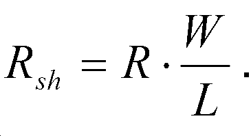
상기 주어진 식에서, 벌크 저항 (R) 은 시트 저항 (Rsh) 을 얻기 위해 무차원 양 (W/L) 으로 곱해지므로, 시트 저항의 단위는 옴이다. 벌크 저항 (R) 과 혼동을 피하기 위해, 시트 저항의 값은 일반적으로, 정사각형 시트의 특정 경우에 W=L 및 Rsh=R을 적용하기 때문에 일반적으로 "옴 퍼 스퀘어 (Ohm per Square)"로 표시된다. 시트 저항은 예를 들어 4점 프로브를 사용하여 측정된다.In the given equation, the bulk resistance R is multiplied by a dimensionless amount (W / L) to obtain the sheet resistance R sh , so the unit of sheet resistance is ohm. To avoid confusion with the bulk resistance (R), the value of the sheet resistance is generally referred to as " Ohm per Square "because it applies W = L and R sh = R in certain instances of the square sheet. Is displayed. The sheet resistance is measured, for example, using a four-point probe.
바람직한 실시형태에서, 전도도가 보다 낮은 영역들 및 전도도가 보다 높은 영역들에서의 시트 저항의 비는 1000보다 크다. 특히 바람직한 실시형태에서, 전도도가 보다 낮은 영역들 및 전도도가 보다 높은 영역들에서의 시트 저항의 비는 10000보다 크다. 전도도가 보다 낮은 영역들의 시트 저항은 바람직하게 100,000 OPS (ohms per square) 보다 크고, 보다 바람직하게 1,000,000 OPS 보다 크며, 그리고 특히 10,000,000 OPS 보다 크다. 전도도가 보다 높은 영역의 시트 저항은 바람직하게 1000 OPS 보다 작고, 보다 바람직하게 5 ~ 500 OPS 범위이고, 특히 10 ~ 100 OPS 범위이다.In a preferred embodiment, the ratio of sheet resistance in regions of lower conductivity and regions of higher conductivity is greater than 1000. In a particularly preferred embodiment, the ratio of sheet resistance in regions of lower conductivity and regions of higher conductivity is greater than 10,000. The sheet resistance of regions with lower conductivity is preferably greater than 100,000 OPS (ohms per square), more preferably greater than 1,000,000 OPS, and especially greater than 10,000,000 OPS. The sheet resistance in the region of higher conductivity is preferably less than 1000 OPS, more preferably in the range of 5 to 500 OPS, especially in the range of 10 to 100 OPS.
보이지 않는 패터닝된 투명 전도성 필름을 얻으려면, 전도도가 보다 낮은 영역들과 전도도가 보다 높은 영역들 광 투과율의 차이가 바람직하게 5% 미만이다. 특히 바람직하게, 전도도가 보다 낮은 영역들과 전도도가 보다 높은 영역들의 광 투과율의 차이는 0.5% 미만이다. 광 투과율은 매체를 통해 투과되는 입사광의 백분율을 지칭한다. 본 발명에 따른 전도도가 보다 높은 영역들의 광 투과율은 ASTM D 1003 (절차 A) 에 따라 측정되는 경우 적어도 80%이다. 보다 바람직하게, 각각의 경우 ASTM D 1003 (절차 A) 에 따라 측정된 광 투과율은 적어도 85%이고, 더욱 바람직하게 적어도 90%이고, 특히 바람직하게 적어도 95% 이다.In order to obtain an invisible patterned transparent conductive film, the difference in light transmittance between regions having lower conductivity and regions having higher conductivity is preferably less than 5%. Especially preferably, the difference in the light transmittance between the regions having lower conductivity and the regions having higher conductivity is less than 0.5%. The light transmittance refers to the percentage of incident light that is transmitted through the medium. The light transmittance of the higher conductivity regions according to the present invention is at least 80% when measured according to ASTM D 1003 (Procedure A). More preferably, in each case the light transmittance measured according to ASTM D 1003 (Procedure A) is at least 85%, more preferably at least 90%, particularly preferably at least 95%.
전도도가 보다 낮은 영역들과 전도도가 보다 높은 영역들의 헤이즈의 차이는 바람직하게 0.5% 미만이다. 특히 바람직하게 헤이즈의 차이는 0.1% 미만이다. 투명한 도전성 층의 전도도가 보다 높은 영역들의 헤이즈는 각각의 경우 ASTM D 1003에 따라 측정되어 바람직하게는 2% 이하, 보다 바람직하게는 1.8% 이하, 더욱 바람직하게는 1.5% 이하, 특히 바람직하게는 1.2% 이다 (절차 A).The difference in the haze of regions having lower conductivity and regions having higher conductivity is preferably less than 0.5%. Particularly preferably, the difference in haze is less than 0.1%. The haze of the regions where the conductivity of the transparent conductive layer is higher is preferably not more than 2%, more preferably not more than 1.8%, more preferably not more than 1.5%, particularly preferably not more than 1.2%, as measured according to ASTM D 1003 in each case % (Procedure A).
헤이즈 미터에 의해 헤이즈 및 광 투과율 (ASTM D 1003에서는, 바디에 의해 투과된 광속과 그에 입사하는 광속의 비율인 시감 투과율 (luminous transmittance) 로 지칭됨) 의 측정은 ASTM D 1003에서 "절차 A - 해이즈미터"로 정의된다. 본 발명의 문맥에서 주어진 헤이즈 및 광 투과율 (ASTM D 1003에서 정의된 시감 투과율에 상응함) 의 값은 이 절차를 참조한다.Measurements of haze and light transmittance (referred to as luminous transmittance, the ratio of the light flux transmitted by the body to the light flux transmitted by the body in ASTM D 1003) by the haze meter are described in ASTM D 1003 as " Is defined as the " Izmit meter ". The values of haze and light transmittance (corresponding to the luminous transmittance defined in ASTM D 1003) given in the context of the present invention refer to this procedure.
일반적으로 헤이즈는 광 확산의 지표이다. 그것은 입사광으로부터 분리되어 투과 중에 산란되는 광량의 백분율을 지칭한다. 그것은 일반적으로 표면 거칠기에 의해, 그리고 매립된 입자 또는 매체에서의 조성 불균일에 의해 발생된다. Generally, haze is an index of light diffusion. It refers to the percentage of the amount of light that is separated from the incident light and scattered during transmission. It is generally caused by surface roughness and by composition irregularities in the buried particles or medium.
ASTM D 1003에 따르면, 투과율에서, 헤이즈는 상기 시편을 통해 시인되는 오브젝트의 콘트라스트 감소를 담당하는 표면에 의한 광의 산란이며, 즉 방향이 입사 빔의 방향으로부터 특정 각도 (2.5°) 초과하여 벗어나도록 산란되는 투과된 광의 비율이다. According to ASTM D 1003, in the transmittance, the haze is the scattering of light by the surface responsible for reducing the contrast of the object viewed through the specimen, i.e. scattering such that the direction deviates from the direction of the incident beam by more than a certain angle (2.5 DEG) Is the ratio of the transmitted light.
본 발명에 관한 나노오브젝트는 나노스케일에서, 즉 약 1 nm 내지 100 nm 의 크기 범위에서 1, 2 또는 3개의 외부 치수를 갖는 오브젝트이다. 본 발명에 사용되는 전기 전도성 나노오브젝트들은, 1 nm 내지 100 nm 범위의 2 개의 외부 치수 및 1 ㎛ 내지 100 ㎛ 범위의 제 3 외부 치수를 갖는 전기 전도성 나노오브젝트이다. 전형적으로, 1 nm 내지 100 nm 의 범위에 있는 상기 2 개의 외부 치수는 유사하며, 즉 3 배 미만으로 크기가 상이하다. 전기 전도성 나노오브젝트의 제 3 치수는 상당히 더 크며, 즉 다른 2개의 외부 치수와는 3 배 초과하여 상이하다. 이러한 나노오브젝트는 나노섬유라고도 한다.The nanoobject of the present invention is an object having one, two, or three external dimensions at a nanoscale, i.e., a size range of about 1 nm to 100 nm. The electrically conductive nanoobjects used in the present invention are electrically conductive nanoobjects having two external dimensions in the range of 1 nm to 100 nm and a third external dimension in the range of 1 m to 100 m. Typically, the two external dimensions in the range of 1 nm to 100 nm are similar, i.e., less than three times the size. The third dimension of the electrically conductive nanoobject is considerably larger, i.e., it differs by more than three times the other two external dimensions. These nano objects are also referred to as nanofibers.
본 발명에서 사용된 전기 전도성 나노오브젝트들은 바람직하게 나노와이어들 또는 나노튜브들이다. 나노와이어들은 전기적으로 전도성 나노섬유들이며, 나노튜브들은 중공 나노섬유들이다. The electrically conductive nano objects used in the present invention are preferably nanowires or nanotubes. The nanowires are electrically conductive nanofibers, and the nanotubes are hollow nanofibers.
본 발명에 사용되는 전기 전도성 나노오브젝트는 통상적으로 원형 형상에 가까운 단면을 갖는다. 상기 단면은 1 ㎛ 내지 500 ㎛ 의 범위인 상기 외부 치수에 수직으로 연장된다. 따라서, 나노스케일인 상기 2개의 외부 치수는 상기 원형 단면의 직경에 의해 정의된다. 상기 직경에 수직으로 연장되는 상기 제 3 외부 치수는 길이라고 불린다.The electrically conductive nanoobjects used in the present invention typically have a cross-section that is close to a circular shape. The cross section extends perpendicular to the external dimension in the range of 1 [mu] m to 500 [mu] m. Thus, the two external dimensions that are nanoscale are defined by the diameter of the circular cross-section. The third external dimension extending perpendicular to the diameter is called the length.
바람직하게, 전기 전도성 나노오브젝트들은 1 ㎛ 내지 500 ㎛, 보다 바람직하게는 3 ㎛ 내지 100 ㎛, 특히 바람직하게는 10 ㎛ 내지 50 ㎛ 범위의 길이를 갖는다. 전기 전도성 나노오브젝트들의 직경은 바람직하게는 1nm 내지 100nm, 보다 바람직하게는 2nm 내지 50nm, 특히 바람직하게는 3nm 내지 30nm 범위이다.Preferably, the electrically conductive nano-objects have a length in the range of 1 탆 to 500 탆, more preferably 3 탆 to 100 탆, particularly preferably in the range of 10 탆 to 50 탆. The diameter of the electrically conductive nano objects is preferably in the range of 1 nm to 100 nm, more preferably 2 nm to 50 nm, particularly preferably 3 nm to 30 nm.
충분한 전기 전도성을 제공하기 위해, 전기 전도성 나노오브젝트는 금속 또는 탄소로 만들어진다. 바람직하게, 전기 전도성 나노오브젝트들은 은, 구리, 금, 백금, 팔라듐, 니켈 또는 탄소로 제조된다. 전기 전도성 나노오브젝트들이 금속, 바람직하게는 은, 구리, 금, 백금, 팔라듐 또는 니켈로 제조되는 경우, 나노오브젝트들은 바람직하게 나노와이어들이다. 전기 전도성 나노오브젝트들이 탄소로 제조되는 경우, 나노오브젝트들은 나노튜브들인 것이 바람직하다. 특히 바람직하게, 나노오브젝트들은 은 나노와이어들, 금 나노와이어들 또는 구리 나노와이어들, 특히 은 나노와이어들이다.To provide sufficient electrical conductivity, the electrically conductive nano-objects are made of metal or carbon. Preferably, the electrically conductive nano-objects are made of silver, copper, gold, platinum, palladium, nickel or carbon. When the electrically conductive nano objects are made of a metal, preferably silver, copper, gold, platinum, palladium or nickel, the nano objects are preferably nanowires. When the electrically conductive nanoparticles are made of carbon, the nanoparticles are preferably nanotubes. Particularly preferably, the nano objects are silver nanowires, gold nanowires or copper nanowires, especially silver nanowires.
투명 전도성 층의 전도도가 보다 높은 영역에서, 나노오브젝트는 상호 연결된다. 나노오브젝트의 양은 상호 연결된 나노오브젝트가 컨택하도록 한다. 나노오브젝트의 컨택으로 인해, 전도도가 보다 높은 영역들에서 전류가 흐를 수 있다.In regions where the conductivity of the transparent conductive layer is higher, the nano objects are interconnected. The amount of nano objects causes the interconnected nano objects to contact. Due to the contact of the nano object, current can flow in regions of higher conductivity.
금속들로 제조된 나노와이어들, 예를 들어 은 나노와이어들은 일반적으로 수분산액 형태로 시판되며, 여기서 분산액을 안정화시키기 위해 폴리비닐피롤리돈이 나노와이어들의 표면 상에 흡착된다. 나노와이어들의 표면 상에 흡착된 임의의 물질은 전기 전도성 나노오브젝트들의 상기 정의된 치수 및 조성에 포함되지 않는다.Nanowires made from metals, such as silver nanowires, are typically marketed in the form of an aqueous dispersion wherein polyvinylpyrrolidone is adsorbed on the surface of the nanowires to stabilize the dispersion. Any material adsorbed on the surface of the nanowires is not included in the defined dimensions and composition of the electrically conductive nano objects.
전도성인 제 1 층을 얻기 위해, 단계 (a) 에서 제 1 층을 형성하도록 도포되는 전기 전도성 나노오브젝트를 포함하는 잉크는 바람직하게는 0.01 내지 1 중량%, 바람직하게는 0.05 내지 0.5 중량%의 전기 전도성 나노오브젝트, 0.02 내지 5 중량%, 바람직하게는 0.1 내지 1.5 중량%의 바인더 및 용매를 포함한다.In order to obtain a conductive first layer, the ink comprising an electrically conductive nano-object applied to form the first layer in step (a) preferably comprises 0.01 to 1% by weight, preferably 0.05 to 0.5% Conductive nanoparticles, 0.02 to 5 wt.%, Preferably 0.1 to 1.5 wt.% Of a binder and a solvent.
잉크에 포함되는 바인더는 건조에 의해 제 1 층의 매트릭스를 형성한다. 기재에 도포될 수 있는 잉크를 제공하기 위해, 용매는 바인더가 용매에서 용해되거나 입자 또는 섬유로서 용매에 분산될 수 있도록 선택된다. 나노와이어가 용해되지 않기 때문에, 나노와이어는 용해되거나 분산된 바인더를 포함하는 용매에 분산된다. 바인더는 바람직하게 하이드로프로필메틸 셀룰로오스, 메틸 셀룰로오스, 스티렌(메트)아크릴 공중합체, 결정질 셀룰로오스, 폴리(메트)아크릴레이트, 아크릴레이트와 메타크릴레이트의 공중합체, 스티렌과 (메트)아크릴레이트의 공중합체, 카르복시메틸 셀룰로오스, 폴리 아크릴아미드, 폴리비닐알코올, 폴리비닐피롤리돈, 폴리스티렌술폰산, 덱스트란 또는 이들의 블렌드로 이루어지는 그룹으로부터 선택된다. The binder contained in the ink forms a matrix of the first layer by drying. To provide an ink that can be applied to a substrate, the solvent is selected so that the binder can be dissolved in the solvent or dispersed in the solvent as particles or fibers. Because the nanowires are not dissolved, the nanowires are dispersed in a solvent containing a dissolved or dispersed binder. The binder is preferably selected from the group consisting of hydroformyl methylcellulose, methylcellulose, styrene (meth) acrylic copolymer, crystalline cellulose, poly (meth) acrylate, copolymer of acrylate and methacrylate, copolymer of styrene and (meth) , Carboxymethylcellulose, polyacrylamide, polyvinyl alcohol, polyvinylpyrrolidone, polystyrenesulfonic acid, dextran, or a blend thereof.
용매는 바람직하게 물이다. 하지만, 중합체가 물에 용해되지 않거나 입자 또는 섬유와 같이 물에 분산될 수 없는 바인더로서 사용되는 경우, 용매는 바람직하게 유기 용매이다. 바람직하게, 용매는 알코올, 케톤, 에테르, 탄화수소 또는 방향족 용매로 이루어지는 그룹으로부터 선택된다. 적합한 방향족 용매는 예를 들어 벤젠, 톨루엔 또는 크실렌이다. 그러나, 특히 바람직하게, 바인더는 수용성인 중합체로부터 선택되고 용매는 물이다. 일부 경우, 용매는 2 종 이상의 혼화성 용매, 예를 들어 물 및 이소프로판올의 혼합물일 수 있다.The solvent is preferably water. However, when the polymer is used as a binder which is not soluble in water or can not be dispersed in water, such as particles or fibers, the solvent is preferably an organic solvent. Preferably, the solvent is selected from the group consisting of alcohols, ketones, ethers, hydrocarbons or aromatic solvents. Suitable aromatic solvents are, for example, benzene, toluene or xylene. However, particularly preferably, the binder is selected from water-soluble polymers and the solvent is water. In some cases, the solvent may be a mixture of two or more miscible solvents, for example, water and isopropanol.
잉크를 기재 상에 도포하기 위해, 임의의 적합한 인쇄 공정이 사용될 수 있다. 바람직한 실시형태에서, 전도성 나노와이어들 및 바인더를 포함하는 잉크는 스핀 코팅, 드로우 다운 코팅, 롤 투 롤 코팅, 그라비어 인쇄, 마이크로그라비어 인쇄, 스크린 인쇄, 플렉소인쇄 및 슬롯 다이 코팅에 의해 도포된다.In order to apply the ink onto the substrate, any suitable printing process may be used. In a preferred embodiment, the ink comprising conductive nanowires and a binder is applied by spin coating, drawdown coating, roll to roll coating, gravure printing, microgravure printing, screen printing, flexographic printing and slot die coating.
바람직하게, 잉크는 1㎛ 내지 200㎛, 바람직하게 2㎛ 내지 60㎛ 범위의 두께로 기재의 표면에 도포된다. 두께는 또한 "습윤 두께"로 지칭되며, 건조에 의한 잉크의 액체 성분을 제거하기 전의 상태에 관한 것이다. (전술한 바와 같이 조성물의 액체 성분을 제거한 후의) 주어진 타겟 두께에서 및 이에 따라 제조될 수 있는 도전성 층의 주어진 타겟 시트 저항 및 광 투과율에서, 습윤 두께가 두꺼울수록 잉크 내의 조성물의 고체 성분들의 농도는 더 낮아진다. 잉크의 도포 공정은, 특히 낮은 습윤 두께를 사용할 필요가 없을 때 촉진된다.Preferably, the ink is applied to the surface of the substrate in a thickness in the range of 1 m to 200 m, preferably 2 m to 60 m. The thickness is also referred to as the "wet thickness" and relates to the condition prior to removal of the liquid component of the ink by drying. At a given target thickness (after removal of the liquid component of the composition as described above) and at a given target sheet resistance and light transmittance of the conductive layer, which can be made accordingly, the thicker the wet thickness, Lower. The application process of the ink is promoted particularly when it is not necessary to use a low wet thickness.
기재에 잉크를 도포한 후, 잉크를 도포함으로써 형성된 층은 건조시켜 용매를 제거하고 고체 층을 얻는다. 건조에 의해 잉크로부터 형성되는 고체 층은 바람직하게는 10 nm 내지 1000 nm, 바람직하게는 50 nm 내지 500 nm 범위의 두께를 갖는다. After the ink is applied to the substrate, the layer formed by applying the ink is dried to remove the solvent to obtain a solid layer. The solid layer formed from the ink by drying preferably has a thickness in the range of 10 nm to 1000 nm, preferably 50 nm to 500 nm.
제 1 층의 건조는 바람직하게는 20 내지 200℃의 온도에서 0.5 내지 30 분 동안 수행된다. 특히 바람직하게, 건조는 100 내지 150℃ 범위의 온도에서 수행된다. 건조 공정의 지속 시간은 특히 바람직하게 1 내지 15 분의 범위이다. The drying of the first layer is preferably carried out at a temperature of 20 to 200 DEG C for 0.5 to 30 minutes. Particularly preferably, drying is carried out at a temperature in the range from 100 to 150 < 0 > C. The duration of the drying process is particularly preferably in the range of 1 to 15 minutes.
건조 공정이 수행되는 온도는 사용된 용매, 나노와이어의 융점 및 코팅 공정에 의존한다. 은 나노와이어의 경우, 상한은 약 200℃이다. 쉽게 증발하는 용매가 사용되는 경우, 보다 낮은 온도, 예를 들어 주위 온도가 사용될 수 있다. 다른 한편, 용매가 저온에서 증발하지 않거나 소량의 용매만이 증발하는 경우 층을 건조시키기 위해 더 높은 온도가 사용되어야 한다. 건조 공정을 촉진시키기 위해, 건조는 바람직하게 적어도 100℃의 고온에서 수행된다. 그러나, 잉크가 그라비어 인쇄, 플렉소인쇄 및 슬롯 다이 코팅과 같은 롤 투 롤 코팅에 의해 기재에 도포되는 경우, 층의 건조는 주위 조건에서 수행될 수 있다.The temperature at which the drying process is performed depends on the solvent used, the melting point of the nanowires and the coating process. For silver nanowires, the upper limit is about 200 ° C. If an easily evaporating solvent is used, lower temperatures, for example ambient temperatures, may be used. On the other hand, if the solvent does not evaporate at low temperature or only a small amount of solvent evaporates, higher temperatures should be used to dry the layer. In order to promote the drying process, drying is preferably carried out at a high temperature of at least 100 캜. However, if the ink is applied to the substrate by a roll-to-roll coating such as gravure printing, flexographic printing and slot die coating, drying of the layer may be performed at ambient conditions.
건조 공정의 지속 시간은 건조 온도에 의존한다. 지속 시간은 건조 공정의 마지막에 잉크의 잔류 수분 함량이 정의된 값 미만이 되도록 선택된다. 원하는 잔류 수분 함량을 달성하기 위해, 증발 지속 시간은 동일한 용매에 대한 온도가 감소함에 따라 증가한다.The duration of the drying process depends on the drying temperature. The duration is chosen so that the residual water content of the ink at the end of the drying process is less than the defined value. To achieve the desired residual moisture content, the duration of the evaporation increases as the temperature for the same solvent decreases.
물을 용매로 사용하는 경우, 일반적으로 건조는 100 내지 150℃ 범위의 온도에서 1 내지 15 분 동안 수행된다. 롤 투 롤 코팅과 같은 몇몇 경우에, 건조는 또한 주위 온도에서 수행될 수도 있다.When water is used as a solvent, drying is generally carried out at a temperature in the range of from 100 to 150 DEG C for from 1 to 15 minutes. In some cases, such as roll to roll coating, drying may also be performed at ambient temperature.
건조가 수행되는 분위기는 바람직하게 분위기의 임의의 성분과 잉크 사이에서 화학 반응이 일어나지 않도록 선택된다. 제 1 층의 건조가 수행되는 분위기는 바람직하게 예를 들어 공기, 질소, 또는 희귀 가스, 예를 들어 아르곤를 포함한다. 공기 또는 질소가 특히 바람직하다.The atmosphere in which drying is performed is preferably selected so that no chemical reaction takes place between any components of the atmosphere and the ink. The atmosphere in which the drying of the first layer is carried out preferably comprises, for example, air, nitrogen or a rare gas, for example argon. Air or nitrogen is particularly preferred.
통상적으로, 패턴은 전도도가 보다 낮은 선들 및 전도도가 보다 낮은 선들에 의해 둘러싸인 전도도가 보다 높은 영역들을 포함한다. 전도도가 보다 낮은 선들의 폭은 바람직하게 10 내지 1000 ㎛, 특히 50 내지 500 ㎛ 범위이다.Typically, the pattern comprises regions of higher conductivity surrounded by lower conductivity lines and lower conductivity lines. The width of the lines with lower conductivity is preferably in the range of 10 to 1000 mu m, particularly in the range of 50 to 500 mu m.
전도도가 보다 낮은 영역 및 전도도가 보다 높은 영역을 포함하는 패터닝된 전도성 필름을 형성하기 위해, 절연성 코팅 재료 또는 절연성 코팅 재료의 전구체를 포함하는 혼합물이 제 1 층 상에 도포된다. 절연성 코팅 재료는 제 1 층 내로 침투하고 전기 전도성 나노오브젝트들 주위에 절연성 코팅을 형성한다. 이로써 전도도가 보다 낮은 영역들이 형성된다.A mixture comprising an insulating coating material or a precursor of an insulating coating material is applied on the first layer to form a patterned conductive film comprising a region of lower conductivity and a region of higher conductivity. The insulating coating material penetrates into the first layer and forms an insulating coating around the electrically conductive nano objects. As a result, regions having lower conductivity are formed.
이에 따라서 절연성 코팅 재료는 바람직하게 절연성 산화물 및 절연성 중합체로 이루어진 그룹으로부터 선택된다. 전구체가 사용되는 경우, 전구체가 제 1 층으로 침투하고 전도성 나노오브젝트들을 둘러싸면서 절연성 코팅 재료로 변형되도록 전구체는 선택된다. 전구체의 변형이 화학 반응의 결과라면, 전구체를 포함하는 혼합물은 추가로 절연성 코팅을 형성하기 위한 화학 반응을 수행하는데 필요한 모든 성분을 포함한다. Accordingly, the insulating coating material is preferably selected from the group consisting of an insulating oxide and an insulating polymer. When a precursor is used, the precursor is selected so that the precursor penetrates into the first layer and is surrounded by the conductive nanoparticles and transformed into an insulating coating material. If the deformation of the precursor is the result of a chemical reaction, the mixture comprising the precursor further comprises all of the components necessary to carry out the chemical reaction to form the insulating coating.
적합한 절연성 산화물은 예를 들어 SiO2, Al2O3, ZrO2 및 지르코늄 실리케이트이다. 적합한 절연성 중합체는 예를 들어 폴리스티렌, 폴리에틸렌, 그래핀 산화물 및 플루오르화 폴리이미드이다. 절연성 산화물로서 특히 바람직한 것은 SiO2이다. Suitable insulating oxides are, for example, SiO 2 , Al 2 O 3 , ZrO 2 and zirconium silicates. Suitable insulating polymers are, for example, polystyrene, polyethylene, graphene oxide and fluorinated polyimide. Particularly preferred as the insulating oxide is SiO 2.
SiO2를 절연성 코팅 재료로서 사용하는 경우, 단계 (c)에서 SiO2의 전구체를 포함하는 혼합물을 도포한다. SiO2의 절연성 코팅을 형성하는 적합한 전구체들은 예를 들어 실리콘 알콕사이드 또는 물 유리이다. 전구체로서 특히 바람직한 것은 테트라에틸 오르토실리케이트 (TEOS) 이다.When SiO 2 is used as an insulating coating material, a mixture containing a precursor of SiO 2 is applied in step (c). Suitable precursors for forming an insulating coating of SiO 2 are, for example, silicon alkoxide or water glass. Particularly preferred as the precursor is tetraethylorthosilicate (TEOS).
전구체로서의 실리콘 알콕사이드의 경우에는, 제 1 층 상에 도포될 수 있고 도전성 나노오브젝트들 주위에 절연성 코팅의 형성을 허용하는 혼합물을 달성하기 위하여, 전구체는 암모늄 하이드록사이드 또는 암모늄 플루오라이드와 같은 촉매와, 물과 실리콘 알콕사이드 및 물 양자와 혼화성인 제 2 용매를 포함하는 혼합 용매와 혼합된다. 적합한 제 2 용매는 예를 들어 알코올 또는 아세톤, 바람직하게는 이소프로필 알코올이다.In the case of a silicon alkoxide as a precursor, in order to achieve a mixture which can be applied on the first layer and which permits the formation of an insulating coating around the conductive nano objects, the precursor is reacted with a catalyst such as ammonium hydroxide or ammonium fluoride , A water and a second solvent which is compatible with both the silicon alkoxide and water. Suitable second solvents are, for example, alcohols or acetone, preferably isopropyl alcohol.
전구체로서의 물 유리의 경우에는, 제 1 층 상에 도포될 수 있고 전기 전도성 나노오브젝트 주위에 절연성 코팅의 형성을 허용하는 혼합물을 달성하기 위해, 전구체는 물 및 염산과 같은 산성 촉매와 혼합된다.In the case of water glass as a precursor, the precursor is mixed with an acidic catalyst such as water and hydrochloric acid, in order to achieve a mixture that can be applied on the first layer and allow the formation of an insulating coating around the electrically conductive nanoobject.
바람직한 실시형태에서, 절연성 코팅 재료 또는 절연성 코팅 재료의 전구체를 포함하는 혼합물 내의 절연성 코팅 재료 또는 절연성 코팅 재료의 전구체의 농도는 0.01 내지 1 mol/l 범위이다. 특히 바람직한 것은, 절연성 코팅 재료 또는 절연성 코팅 재료의 전구체의 농도는 0.05 내지 0.5 mol/l 범위이다.In a preferred embodiment, the concentration of the precursor of the insulating coating material or of the insulating coating material in the mixture comprising the precursor of the insulating coating material or insulating coating material is in the range of 0.01 to 1 mol / l. Particularly preferably, the concentration of the precursor of the insulating coating material or the insulating coating material is in the range of 0.05 to 0.5 mol / l.
단계 (c) 에서 절연성 코팅 재료의 전구체를 사용할 때 전기 전도성 나노오브젝트들 상의 절연성 코팅은 전구체를 졸 겔 공정, 화학적 기상 증착, 물리적 기상 증착 또는 원자 층 증착에 의한 절연성 코팅 재료로의 변형에 의해 형성된다. 특히, 전구체가 TEOS 또는 물 유리인 경우, 전구체는 졸 겔 공정에 의해 절연성 코팅 재료로 변형된다. When using the precursor of the insulating coating material in step (c), the insulating coating on the electrically conductive nano-objects is formed by transformation of the precursor into an insulating coating material by a sol-gel process, chemical vapor deposition, physical vapor deposition or atomic layer deposition do. In particular, when the precursor is TEOS or water glass, the precursor is transformed into an insulating coating material by a sol-gel process.
절연성 코팅 재료 또는 절연성 코팅 재료의 전구체를 포함하는 혼합물을 도포하기 위해, 임의의 적합한 인쇄 공정 또는 코팅 공정이 사용될 수있다. 적합한 코팅 공정은 예를 들어 침지, 스핀 코팅, 드로우 다운 코팅, 롤 투 롤 코팅, 그라비어 인쇄, 마이크로그라비어 인쇄, 스크린 인쇄, 플렉소인쇄 및 슬롯 다이 코팅이다. 침지되는 경우, 패턴을 정의하고 절연성 코팅 재료로 코팅되지 않는 영역을 보호하기 위해 마스크를 사용할 수 있다.Any suitable printing or coating process may be used to apply the mixture comprising the insulating coating material or the precursor of the insulating coating material. Suitable coating processes are, for example, dipping, spin coating, drawdown coating, roll to roll coating, gravure printing, microgravure printing, screen printing, flexographic printing and slot die coating. If soaked, a mask may be used to define the pattern and to protect areas not covered by the insulating coating material.
절연성 코팅 재료 또는 절연성 코팅 재료의 전구체를 포함하는 혼합물의 도포 후에, 코팅 공정에 따라, 절연성 코팅 재료가 제 1 층으로 침투하고 나노오브젝트를 코팅하도록 컨택 시간을 하는 것이 바람직하다. 절연성 코팅 재료의 전구체와의 혼합물이 도포되고 절연성 코팅 재료가 졸 겔 공정에 의해 처리되는 경우, 0.5 분 내지 1 시간, 바람직하게는 1 분 내지 30 분, 특히 1 분 내지 10 분의 컨택 시간을 하는 것이 바람직하다.After application of the mixture comprising the insulating coating material or the precursor of the insulating coating material, it is preferred that the insulating coating material penetrate into the first layer and coat the nano-objects according to a coating process. When a mixture with a precursor of an insulating coating material is applied and the insulating coating material is treated by a sol-gel process, a contact time of 0.5 minutes to 1 hour, preferably 1 minute to 30 minutes, especially 1 minute to 10 minutes .
절연성 코팅 재료 또는 절연성 코팅 재료의 전구체를 포함하는 혼합물의 도포 및 컨택 시간 후에, 필요시, 코팅된 기재가 단계 (d)에서 린싱 및 건조된다. 린싱 용매는 졸 겔 공정에 사용되는 용매인 것이 바람직하다. 이 건조 단계의 건조 변수는 바람직하게 단계 (b)에서의 제 1 건조 단계의 건조 변수에 상응하며, 이것은 건조가 바람직하게 20 내지 200℃의 온도에서 0.5 내지 30 분 동안 수행된다는 것을 의미한다. 특히 바람직하게 건조는 100 내지 150°C의 온도에서 수행된다. 건조 공정의 지속 시간은 특히 바람직하게 1 내지 15 분의 범위이다.After application and contact time of the mixture comprising the insulating coating material or the precursor of the insulating coating material, the coated substrate is rinsed and dried in step (d), if necessary. The rinsing solvent is preferably a solvent used in the sol-gel process. The drying parameter of this drying step preferably corresponds to the drying parameter of the first drying step in step (b), which means that the drying is preferably carried out at a temperature of 20 to 200 DEG C for 0.5 to 30 minutes. Particularly preferably, the drying is carried out at a temperature of 100 to 150 ° C. The duration of the drying process is particularly preferably in the range of 1 to 15 minutes.
실시예들Examples
제조예 1: 유리 기재 상의 은 나노와이어 필름의 제조 Preparation Example 1: Preparation of silver nanowire film on glass substrate
예를 들어 BASF SE에 의한 Jonocryl® 60으로 입수 가능한 고형분 35 중량%를 갖는 스티렌 아크릴 공중합체 수용액은 물에서 20 중량%의 농도로 희석된다. BASF SE에 의한 Acronal® LR9014로 입수 가능한 2-에틸헥실 아크릴레이트 메틸 메타크릴레이트의 공중합체는 물에서 10 중량%의 농도로 희석된다. 물에서의 0.5 wt% 은 나노와이어들, 희석된 스티렌 아크릴 공중합체 수용액 및 2-에틸헥실 아크릴레이트 메틸 메타크릴레이트의 희석된 공중합체의 분산액은 은 나노와이어의 최종 농도가 0.4 wt%가 되도록 물에 혼합되고, 그리고 스티렌 아크릴 공중합체, 2-에틸헥실 아크릴레이트 메틸 메타크릴레이트의 공중합체 및 나노와이어의 질량비는 각각 4:3:3이다. 혼합물을 1000rpm에서 30 초 동안 유리 기재 상에 스핀 코팅하고 135 ℃에서 5 분 동안 건조시킨다. 시트 저항은 4점 프로브 스테이션 (Lucas lab pro-4) 에 의해 측정되고 광학 특성은 BYK 헤이즈 가드 플러스에 의해 측정된다. For example, a styrene acrylic copolymer aqueous solution having a solids content of 35% by weight, which is obtainable by Jonocryl 60 by BASF SE, is diluted to a concentration of 20% by weight in water. Copolymer of 2-ethylhexyl acrylate methyl methacrylate available under the trade name Acronal® LR9014 by BASF SE is diluted to a concentration of 10% by weight in water. A dispersion of 0.5 wt% silver nanowires, a dilute styrene acrylic copolymer aqueous solution, and a diluted copolymer of 2-ethylhexyl acrylate methyl methacrylate in water was prepared so that the final concentration of silver nanowires was 0.4 wt% , And the mass ratio of the styrene acrylic copolymer, the copolymer of 2-ethylhexyl acrylate methyl methacrylate and the nanowire is 4: 3: 3 respectively. The mixture is spin-coated on a glass substrate at 1000 rpm for 30 seconds and dried at 135 캜 for 5 minutes. The sheet resistance is measured by a four-point probe station (Lucas lab pro-4) and the optical properties are measured by BYK haze guard plus.
제조예 2: 폴리카보네이트 기재 상의 은 나노와이어 필름의 제조 Production Example 2: Preparation of Silver Nanowire Film on Polycarbonate Base
예를 들어 BASF SE에 의한 Jonocryl® 60으로 입수 가능한 고형분 35 중량%를 갖는 스티렌 아크릴 공중합체 수용액은 물에서 20 중량%의 농도로 희석된다. BASF SE에 의한 Acronal® LR9014로 입수 가능한 2-에틸헥실 아크릴레이트 메틸 메타크릴레이트의 공중합체는 물에서 10 중량%의 농도로 희석된다. 물에서의 0.5 wt% 은 나노와이어들, 희석된 스티렌 아크릴 공중합체 수용액 및 2-에틸헥실 아크릴레이트 메틸 메타크릴레이트의 희석된 공중합체의 분산액은 은 나노와이어의 최종 농도가 0.4 wt%가 되도록 물에 혼합되고, 그리고 스티렌 아크릴 공중합체, 2-에틸헥실 아크릴레이트 메틸 메타크릴레이트의 공중합체 및 나노와이어의 질량비는 각각 4:3:3이다. 혼합물을 3 분 동안 볼 밀링하여 균질화시킨다. 전도성 필름은, 코팅 속도 5 cm/초이고 습윤 두께가 6㎛ 인 드로우 다운 바를 사용하여, 예를 들어 베이어 재료 사이언스 (Bayer Material Science) 의 제품 사양 Makrofol® DE 1-1 175 ㎛ 하에 시판되는 광학 폴리카보네이트 호일 상에 인쇄되고, 이후에 135℃에서 5 분 동안 건조된다. 시트 저항 및 광학 특성은 제조예 1에서와 같이 측정되었다.For example, a styrene acrylic copolymer aqueous solution having a solids content of 35% by weight, which is obtainable by Jonocryl 60 by BASF SE, is diluted to a concentration of 20% by weight in water. Copolymer of 2-ethylhexyl acrylate methyl methacrylate available under the trade name Acronal® LR9014 by BASF SE is diluted to a concentration of 10% by weight in water. A dispersion of 0.5 wt% silver nanowires, a dilute styrene acrylic copolymer aqueous solution, and a diluted copolymer of 2-ethylhexyl acrylate methyl methacrylate in water was prepared so that the final concentration of silver nanowires was 0.4 wt% , And the mass ratio of the styrene acrylic copolymer, the copolymer of 2-ethylhexyl acrylate methyl methacrylate and the nanowire is 4: 3: 3 respectively. The mixture is ball milled for 3 minutes to homogenize. Conductive films were prepared using a drawdown bar with a coating speed of 5 cm / sec and a wet thickness of 6 m, for example, under the product specification Makrofol® DE 1-1 175 μm by Bayer Material Science, Printed on a carbonate foil, and then dried at 135 캜 for 5 minutes. The sheet resistance and optical properties were measured as in Production Example 1.
제조예 3: 유리 기재 상의 은 나노와이어 필름의 제조 Preparation Example 3: Preparation of silver nanowire film on glass substrate
0.5 중량%의 은 나노와이어의 양을 갖는 물에서의 은 나노와이어들 및 1 중량%의 하이드록시프로필 메틸셀룰로오스 (HPMC) 의 수용액의 분산액은, 은 나노와이어의 최종 농도가 0.2 wt%가 되도록 물에 혼합되고, HPMC와 은 나노와이어의 질량비는 각각 2:1이다. 혼합물을 1000rpm에서 30 초 동안 유리 기재 상에 스핀 코팅하고 135 ℃에서 5 분 동안 건조시킨다. 시트 저항은 4점 프로브 스테이션 (Lucas lab pro-4) 에 의해 측정되고 광학 특성은 BYK 헤이즈 가드 플러스에 의해 측정된다. The dispersion of aqueous solutions of silver nanowires and 1% by weight of hydroxypropylmethylcellulose (HPMC) in water having a silver nanowire content of 0.5% by weight was prepared by mixing water , And the mass ratio of HPMC and silver nanowires is 2: 1. The mixture is spin-coated on a glass substrate at 1000 rpm for 30 seconds and dried at 135 캜 for 5 minutes. The sheet resistance is measured by a four-point probe station (Lucas lab pro-4) and the optical properties are measured by BYK haze guard plus.
실시예 1, 2 및 3: 유리 기재 상의 SiO2-코팅된 은 나노와이어 필름Examples 1, 2 and 3: SiO 2 -coated silver nanowire films on glass substrates
연속적으로 자기 교반하면서, 이소프로필 알코올 20ml와 물 4ml의 혼합물에 28% 암모니아 수용액 0.4ml와 다양한 양의 테트라에틸 오르토실리케이트 (TEOS) 를 연속적으로 첨가했다. 제조예 1에 따라 제조된 유리 기재 상의 은 나노와이어 필름을 소정량의 시간 동안 이 용액에 침지하여 나노와이어들 상에 SiO2 코팅을 형성하고, 탈이온수로 린싱하고, 그리고 5 분 동안 135℃ 에서 건조한다. SiO2에 의한 코팅 전후의 시트 저항 및 광학 특성은 제조예 1에서와 같이 측정된다. 결과는 표 1에 나타낸다. 실시예 1 및 2는 동일한 양의 TEOS로 상이한 침지 시간에 대한 결과를 나타내고, 실시예 3은 TEOS가 없는 비교예이다. 표 1에서 "Rsh"는 시트 저항을 의미하고, "T"는 투과율 및 "H"는 헤이즈를 의미한다. "전"은 SiO2로 코팅하기 전에 은 나노와이어 필름으로 코팅된 기재의 측정을 나타내고, "후"는 SiO2로 코팅한 후의 측정을 나타낸다.While continuously stirring, 0.4 ml of a 28% ammonia aqueous solution and various amounts of tetraethylorthosilicate (TEOS) were continuously added to a mixture of 20 ml of isopropyl alcohol and 4 ml of water. A silver nanowire film on a glass substrate made according to Preparation Example 1 was immersed in this solution for a predetermined amount of time to form a SiO 2 coating on the nanowires, rinsed with deionized water, and dried at 135 ° C for 5 minutes Dry. The sheet resistance and optical characteristics before and after the coating with SiO 2 were measured as in Production Example 1. The results are shown in Table 1. Examples 1 and 2 show the results for different immersion times with the same amount of TEOS, and Example 3 is a comparative example without TEOS. In Table 1, "R sh " means sheet resistance, "T" means the transmittance and "H" means the haze. "Prior" refers to the measurement of a substrate coated with silver nanowire film before coating with SiO 2 , and "after " refers to the measurement after coating with SiO 2 .
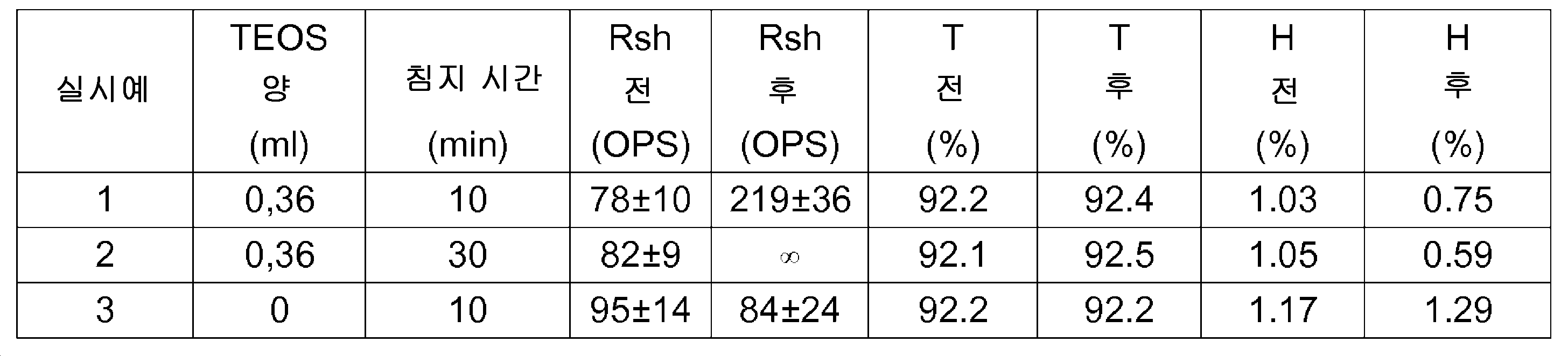
동일한 농도의 TEOS에 의한 보다 긴 침지 시간은 코팅된 필름의 훨씬 더 높은 시트 저항을 초래한다는 것을 예들로부터 알 수 있다. 다른 한편, TEOS가 없는 암모니아 용액에 침지하면 시트 저항에 차이가 없다. 더욱이, SiO2에 의한 코팅은 패터닝된 전도성 필름의 투과율에 대해 어떠한 효과도 가지지 않으며 헤이즈만 약간 낮은 값을 갖는다.It can be seen from examples that a longer immersion time with the same concentration of TEOS results in a much higher sheet resistance of the coated film. On the other hand, immersing in ammonia solution without TEOS makes no difference in sheet resistance. Moreover, the coating with SiO 2 has no effect on the transmittance of the patterned conductive film and has only a slightly lower value of haze.
실시예 4, 5: 폴리카보네이트 기재 상의 SiO2-코팅된 은 나노와이어 필름Examples 4 and 5: SiO 2 -coated silver nanowire films on polycarbonate substrates
연속적으로 자기 교반하면서, 이소프로필 알코올 20ml와 물 4ml의 혼합물에 28% 암모니아 수용액 0.4ml와 다양한 양의 테트라에틸 오르토실리케이트 (TEOS) 를 연속적으로 첨가했다. 제조예 2에 따라 제조된 폴리카보네이트 기재 상의 은 나노와이어 필름의 스트립 상에, 빠른 건조 페이스트를 컨택 패드로서 양단에 페인팅하였다. 다음, 스트립의 중앙 영역을 30 분 동안 용액에 침지하고 탈 이온수로 린싱하고 135℃에서 5분 동안 건조시킨다. SiO2로의 코팅 전후로 2개의 은 컨택 패드 사이의 저항은 Keithley 소스 미터로 측정된다. 결과는 표 2에 나타내지며, 실시예 5는 비교예이다. 표 1에서와 같이 "Rsh"는 시트 저항을 의미하며 "전"과 "후"는 TEOS 함유 용액으로 코팅하기 전과 후의 측정을 나타낸다.While continuously stirring, 0.4 ml of a 28% ammonia aqueous solution and various amounts of tetraethylorthosilicate (TEOS) were continuously added to a mixture of 20 ml of isopropyl alcohol and 4 ml of water. On the strip of silver nanowire film on the polycarbonate substrate prepared according to Preparation Example 2, a fast drying paste was painted as a contact pad at both ends. Next, the central region of the strip is immersed in the solution for 30 minutes, rinsed with deionized water and dried at 135 캜 for 5 minutes. The resistance between two silver contact pads before and after coating with SiO 2 is measured with a Keithley source meter. The results are shown in Table 2, and Example 5 is a comparative example. As in Table 1, "R sh " refers to sheet resistance and "before" and "after " represent measurements before and after coating with TEOS containing solution.
이 예에서, 은 컨택 패드는 전자 흐름이 SiO2 코팅 영역에 걸쳐 정지되는지 여부를 표시하기 위해 SiO2 코팅 영역 외부에 배치된다.In this example, the contact pad is disposed outside the SiO 2 coating area to indicate whether the electron flow is stopped over a SiO 2 coating area.

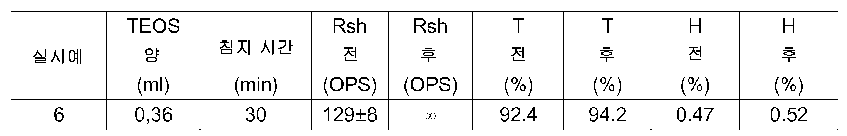
실시예 6: 유리 기재 상의 SiO2-코팅된 은 나노와이어 필름Example 6: SiO 2 -coated silver nanowire film on glass substrate
연속적으로 자기 교반하면서, 이소프로필 알코올 20ml와 물 4ml의 혼합물에 28% 암모니아 수용액 0.4ml와 다양한 양의 테트라에틸 오르토실리케이트 (TEOS) 를 연속적으로 첨가했다. 제조예 3에 따라 제조된 유리 기재 상의 은 나노와이어 필름을 30분 동안 이 용액에 침지하여 나노와이어들 상에 SiO2 코팅을 형성하고, 탈이온수로 린싱하고, 그리고 5 분 동안 135℃ 에서 건조한다. SiO2에 의한 코팅 전후의 시트 저항 및 광학 특성은 제조예 6에서와 같이 측정된다. 결과는 표 3에 나타낸다. 표 3에서 "Rsh"는 시트 저항을 의미하고, "T"는 투과율 및 "H"는 헤이즈를 의미한다. "전"은 SiO2로 코팅하기 전에 은 나노와이어 필름으로 코팅된 기재의 측정을 나타내고, "후"는 SiO2로 코팅한 후의 측정을 나타낸다. While continuously stirring, 0.4 ml of a 28% ammonia aqueous solution and various amounts of tetraethylorthosilicate (TEOS) were continuously added to a mixture of 20 ml of isopropyl alcohol and 4 ml of water. A silver nanowire film on a glass substrate made according to Preparation Example 3 was immersed in this solution for 30 minutes to form a SiO 2 coating on the nanowires, rinsed with deionized water, and dried at 135 ° C for 5 minutes . The sheet resistance and optical properties before and after coating by SiO 2 were measured as in Production Example 6. [ The results are shown in Table 3. In Table 3, "R sh " means sheet resistance, "T" means the transmittance and "H" means the haze. "Prior" refers to the measurement of a substrate coated with silver nanowire film before coating with SiO 2 , and "after " refers to the measurement after coating with SiO 2 .
Claims (24)
상기 전도도가 보다 높은 영역들에서는 나노오브젝트들이 상호 연결되어 전도도가 보다 높은 영역을 형성하도록 상기 나노오브젝트들이 바인더 매트릭스 내에 배치되며, 상기 전도도가 보다 낮은 영역들에서는 상기 나노오브젝트들이 구조적으로 그대로 유지되고 절연성 코팅 재료로 코팅되는, 패터닝된 투명 전도성 필름. 1. A patterned transparent conductive film comprising regions of higher conductivity and regions of lower conductivity,
Wherein the nano objects are arranged in a binder matrix such that the nano objects are interconnected to form a higher conductivity region in regions having higher conductivity, and in the regions having lower conductivity, the nano objects are structurally maintained, A patterned transparent conductive film coated with a coating material.
상기 절연성 코팅 재료는 절연성 산화물들, 복합 절연성 산화물들 및 절연성 중합체들로 이루어진 그룹으로부터 선택되는, 패터닝된 투명 전도성 필름. The method according to claim 1,
Wherein the insulating coating material is selected from the group consisting of insulating oxides, composite insulating oxides, and insulating polymers.
상기 절연성 산화물은 SiO2, Al2O3, ZrO2 및 지르코늄 실리케이트로부터 선택되는, 패터닝된 투명 전도성 필름. 3. The method of claim 2,
The insulating oxide is SiO 2, Al 2 O 3, ZrO 2 and the patterned transparent conductive film selected from zirconium silicate.
상기 절연성 중합체는 폴리스티렌, 폴리에틸렌, 그래핀 산화물 및 플루오르화 폴리이미드로부터 선택되는, 패터닝된 투명 전도성 필름. 3. The method of claim 2,
Wherein the insulating polymer is selected from polystyrene, polyethylene, graphene oxide, and fluorinated polyimide.
전기 전도성 나노오브젝트들은 나노와이어들 또는 나노튜브들인, 패터닝된 투명 전도성 필름. The method according to claim 1,
Wherein the electrically conductive nano objects are nanowires or nanotubes.
전기 전도성 나노오브젝트들은 은, 구리, 금, 백금, 팔라듐, 니켈 또는 탄소로 제조되는, 패터닝된 투명 전도성 필름. The method according to claim 1,
The electrically conductive nano-objects are made of silver, copper, gold, platinum, palladium, nickel or carbon.
전기 전도성 나노오브젝트들은 1 내지 100 nm 범위의 직경 및 1 내지 500 ㎛ 범위의 길이를 갖는, 패터닝된 투명 전도성 필름. The method according to claim 1,
Wherein the electrically conductive nano-objects have a diameter in the range of 1 to 100 nm and a length in the range of 1 to 500 [mu] m.
상기 전도도가 보다 낮은 영역들에서의 나노오브젝트들 및 상기 전도도가 보다 높은 영역들에서의 나노오브젝트들은 실질적으로 동일한 수 밀도를 갖는, 패터닝된 투명 전도성 필름.The method according to claim 1,
Wherein the nano objects in regions with lower conductivity and the nano objects in regions with higher conductivity have substantially the same number density.
(a) 전기 전도성 나노오브젝트들 및 바인더를 포함하는 잉크를 기재 상에 도포하여 제 1 층을 형성하는 단계로서, 전도성 나노오브젝트들의 양은 건조 후에 상기 제 1 층이 전도성이 되도록 하는, 상기 제 1 층을 형성하는 단계;
(b) 상기 제 1 층을 건조하는 단계;
(c) 상기 전도도가 보다 낮은 영역들을 형성하는 상기 제 1 층의 부분들에 절연성 코팅 재료 또는 절연성 코팅 재료의 전구체를 포함하는 혼합물을 도포하는 단계로서, 상기 절연성 코팅 재료 또는 상기 전구체는 상기 전기 전도성 나노와이어들 주변에 절연성 코팅을 형성하는, 상기 혼합물을 도포하는 단계;
(d) 상기 코팅된 기재를 린싱 및 건조하는 단계를 포함하는, 패터닝된 투명 전도성 필름의 제조 방법. 9. A method of manufacturing a patterned transparent conductive film according to any one of claims 1 to 8, wherein the conductive transparent conductive film comprises regions having lower conductivity and regions having higher conductivity,
(a) applying ink comprising electrically conductive nano objects and a binder onto a substrate to form a first layer, the amount of conductive nano objects being such that after drying the first layer is conductive, ;
(b) drying the first layer;
(c) applying a mixture comprising portions of the first layer that form regions of lower conductivity, the coating comprising a precursor of an insulating coating material or an insulating coating material, wherein the insulating coating material or precursor is electrically conductive Applying the mixture to form an insulating coating around the nanowires;
(d) rinsing and drying the coated substrate to form a patterned transparent conductive film.
상기 전기 전도성 나노오브젝트들은 나노와이어들 또는 나노튜브들인, 패터닝된 투명 전도성 필름의 제조 방법.10. The method of claim 9,
Wherein the electrically conductive nano objects are nanowires or nanotubes.
상기 전기 전도성 나노오브젝트들은 은, 구리, 금, 백금, 팔라듐, 니켈 또는 탄소로 제조되는, 패터닝된 투명 전도성 필름의 제조 방법. 10. The method of claim 9,
Wherein the electrically conductive nano-objects are made of silver, copper, gold, platinum, palladium, nickel, or carbon.
상기 전기 전도성 나노오브젝트들은 1 내지 100 nm 범위의 직경 및 1 내지 500 ㎛ 범위의 길이를 갖는, 패터닝된 투명 전도성 필름의 제조 방법. 10. The method of claim 9,
Wherein the electrically conductive nano-objects have a diameter in the range of 1 to 100 nm and a length in the range of 1 to 500 [mu] m.
상기 전기 전도성 나노오브젝트들을 포함하는 상기 잉크는 0.01 내지 0.5 중량%의 전기 전도성 나노오브젝트들, 0.02 내지 2.5 중량%의 바인더 및 용매를 포함하는, 패터닝된 투명 전도성 필름의 제조 방법.10. The method of claim 9,
Wherein the ink comprising the electrically conductive nano objects comprises 0.01 to 0.5 wt% of electrically conductive nanoparticles, 0.02 to 2.5 wt% of a binder, and a solvent.
상기 용매는 물, 알코올들, 케톤들, 에테르들, 탄화수소들 또는 방향족 용매들로 이루어지는 그룹으로부터 선택되는, 패터닝된 투명 전도성 필름의 제조 방법. 14. The method of claim 13,
Wherein the solvent is selected from the group consisting of water, alcohols, ketones, ethers, hydrocarbons or aromatic solvents.
전도성 나노와이어들 및 바인더를 포함하는 상기 잉크는 스핀 코팅, 드로우 다운 코팅, 롤 투 롤 코팅, 그라비어 인쇄, 마이크로그라비어 인쇄, 스크린 인쇄, 플렉소인쇄 및 슬롯 다이 코팅에 의해 도포되는, 패터닝된 투명 전도성 필름의 제조 방법. 10. The method of claim 9,
The ink comprising conductive nanowires and a binder may be patterned to form a patterned transparent conductive layer that is applied by spin coating, drawdown coating, roll to roll coating, gravure printing, microgravure printing, screen printing, ≪ / RTI >
상기 전기 전도성 나노오브젝트들을 포함하는 상기 잉크는 상기 제 1 층의 습윤 두께가 100 nm 내지 40 ㎛ 범위가 되도록 도포되는, 패터닝된 투명 전도성 필름의 제조 방법. 10. The method of claim 9,
Wherein the ink comprising the electrically conductive nano-objects is applied such that the wet thickness of the first layer is in the range of 100 nm to 40 占 퐉.
상기 단계 (b) 에서의 건조하는 단계 및 상기 단계 (d) 에서의 건조하는 단계는 20 내지 200℃ 범위의 온도에서 0.5 내지 30 분 동안 독립적으로 수행되는, 패터닝된 투명 전도성 필름의 제조 방법. 10. The method of claim 9,
Wherein the step of drying in step (b) and the step of drying in step (d) are performed independently for 0.5 to 30 minutes at a temperature in the range of 20 to 200 占 폚.
상기 절연성 코팅 재료는 절연성 산화물들, 복합 절연성 산화물들 및 절연성 중합체들로 이루어진 그룹으로부터 선택되는, 패터닝된 투명 전도성 필름의 제조 방법. 10. The method of claim 9,
Wherein the insulating coating material is selected from the group consisting of insulating oxides, composite insulating oxides, and insulating polymers.
상기 절연성 산화물은 SiO2, Al2O3, ZrO2 및 지르코늄 실리케이트로부터 선택되는, 패터닝된 투명 전도성 필름의 제조 방법. 19. The method of claim 18,
The insulating oxide is SiO 2, Al 2 O 3, ZrO 2 and a method of producing a patterned transparent conductive film selected from zirconium silicate.
상기 절연성 중합체는 폴리스티렌, 폴리에틸렌, 및 플루오르화 폴리이미드로부터 선택되는, 패터닝된 투명 전도성 필름의 제조 방법. 19. The method of claim 18,
Wherein the insulating polymer is selected from polystyrene, polyethylene, and fluorinated polyimide.
상기 절연성 코팅 재료는 SiO2 이고 상기 절연성 코팅 재료의 전구체는 실리콘 알콕사이드 또는 물 유리인, 패터닝된 투명 전도성 필름의 제조 방법. 10. The method of claim 9,
The insulating coating material is SiO 2 and the precursor of the dielectric coating material is produced in the silicon alkoxide or water glass is, the patterned transparent conductive film.
상기 절연성 코팅 재료 또는 상기 절연성 코팅 재료의 전구체를 포함하는 혼합물에서의 상기 절연성 코팅 재료 또는 상기 절연성 코팅 재료의 전구체의 농도는 0.01 내지 0.5 mol/l 범위인, 패터닝된 투명 전도성 필름의 제조 방법. 10. The method of claim 9,
Wherein the concentration of the insulating coating material or the precursor of the insulating coating material in the mixture comprising the insulating coating material or the precursor of the insulating coating material is in the range of 0.01 to 0.5 mol / l.
상기 단계 (c) 에서 절연성 코팅 재료의 전구체를 사용할 때 상기 전구체는 상기 절연 코팅 재료로 변형되어 졸 겔 공정, 화학적 기상 증착, 물리적 기상 증착 또는 원자 층 증착에 의해 절연성 코팅을 형성하는, 패터닝된 투명 전도성 필름의 제조 방법. 10. The method of claim 9,
Wherein the precursor is modified with the insulating coating material to form an insulating coating by a sol-gel process, chemical vapor deposition, physical vapor deposition or atomic layer deposition when using the precursor of the insulating coating material in step (c) A method for producing a conductive film.
상기 단계 (c) 에서의 혼합물은 침지, 스핀 코팅, 드로우 다운 코팅, 롤 투 롤 코팅, 그라비어 인쇄, 마이크로그라비어 인쇄, 스크린 인쇄, 플렉소인쇄 및 슬롯 다이 코팅에 의해 도포되는, 패터닝된 투명 전도성 필름의 제조 방법. 10. The method of claim 9,
Wherein the mixture in step (c) is a patterned transparent conductive film applied by immersion, spin coating, drawdown coating, roll to roll coating, gravure printing, microgravure printing, screen printing, flexographic printing and slot die coating ≪ / RTI >
Applications Claiming Priority (3)
| Application Number | Priority Date | Filing Date | Title |
|---|---|---|---|
| US201562148241P | 2015-04-16 | 2015-04-16 | |
| US62/148,241 | 2015-04-16 | ||
| PCT/EP2016/058101 WO2016166148A1 (en) | 2015-04-16 | 2016-04-13 | Patterned transparent conductive film and process for producing such a patterned transparent conductive film |
Publications (1)
| Publication Number | Publication Date |
|---|---|
| KR20170141663A true KR20170141663A (en) | 2017-12-26 |
Family
ID=55862738
Family Applications (1)
| Application Number | Title | Priority Date | Filing Date |
|---|---|---|---|
| KR1020177029469A Withdrawn KR20170141663A (en) | 2015-04-16 | 2016-04-13 | Patterned transparent conductive film and process for producing such a patterned transparent conductive film |
Country Status (5)
| Country | Link |
|---|---|
| US (1) | US10902970B2 (en) |
| JP (1) | JP6771485B2 (en) |
| KR (1) | KR20170141663A (en) |
| TW (1) | TWI708267B (en) |
| WO (1) | WO2016166148A1 (en) |
Families Citing this family (6)
| Publication number | Priority date | Publication date | Assignee | Title |
|---|---|---|---|---|
| CN106531357B (en) * | 2016-12-08 | 2018-06-26 | 南通盛洲纺织品有限公司 | A kind of preparation method of conductive film |
| CN108727543A (en) * | 2018-05-24 | 2018-11-02 | 王秋林 | The graphene preparation process of surface modification |
| CN111383804B (en) * | 2020-02-28 | 2022-12-09 | 深圳市华科创智技术有限公司 | Preparation method of anisotropic nanowire conductive film and nanowire conductive film |
| CN113362991A (en) * | 2021-06-04 | 2021-09-07 | 深圳先进电子材料国际创新研究院 | Transparent conductive film and preparation method and application thereof |
| KR102944598B1 (en) | 2024-02-02 | 2026-03-26 | 국립공주대학교 산학협력단 | METHOD FOR MANUFACTURING CONDUCTIVE polymer FILM WITH NANO-NETWORK STRUCTURE, CONDUCTIVE polymer FILM MANUFACTURED THEREBY, AND BENDING SENSOR COMPRISING THE SAME |
| CN120692784B (en) * | 2025-07-07 | 2026-02-17 | 浙江羽默电子科技有限公司 | An antistatic circuit board and its manufacturing process |
Family Cites Families (17)
| Publication number | Priority date | Publication date | Assignee | Title |
|---|---|---|---|---|
| EP1847386B1 (en) * | 2005-02-07 | 2013-10-23 | Teijin Dupont Films Japan Limited | Conductive multilayer film |
| ATE532217T1 (en) * | 2005-08-12 | 2011-11-15 | Cambrios Technologies Corp | METHOD FOR PRODUCING TRANSPARENT NANOWIRE-BASED CONDUCTORS |
| TWI426531B (en) * | 2006-10-12 | 2014-02-11 | 坎畢歐科技公司 | Transparent conductor based on nanowire and its application |
| US8018568B2 (en) | 2006-10-12 | 2011-09-13 | Cambrios Technologies Corporation | Nanowire-based transparent conductors and applications thereof |
| JP5646424B2 (en) * | 2011-09-27 | 2014-12-24 | 株式会社東芝 | Transparent electrode laminate |
| US9603242B2 (en) | 2011-12-21 | 2017-03-21 | 3M Innovative Properties Company | Laser patterning of silver nanowire-based transparent electrically conducting coatings |
| US20130323482A1 (en) * | 2012-06-01 | 2013-12-05 | Nuovo Film Inc. | Low Haze Transparent Conductive Electrodes and Method of Making the Same |
| US9050775B2 (en) * | 2012-10-12 | 2015-06-09 | Nano And Advanced Materials Institute Limited | Methods of fabricating transparent and nanomaterial-based conductive film |
| US8941095B2 (en) * | 2012-12-06 | 2015-01-27 | Hrl Laboratories, Llc | Methods for integrating and forming optically transparent devices on surfaces |
| WO2014150577A1 (en) * | 2013-03-15 | 2014-09-25 | Sinovia Technologies | Photoactive transparent conductive films, method of making them and touch sensitive device comprising said films |
| CN104521005B (en) * | 2013-04-05 | 2016-08-24 | 苏州诺菲纳米科技有限公司 | Transparency conductive electrode, their structure with fused metal nano wire design and manufacture method |
| JP6366577B2 (en) * | 2013-04-26 | 2018-08-01 | 昭和電工株式会社 | Manufacturing method of conductive pattern and conductive pattern forming substrate |
| CN105474140B (en) * | 2013-08-05 | 2018-09-25 | 阿尔卑斯电气株式会社 | Transparent conductive component and its layout method |
| KR20150077765A (en) * | 2013-12-30 | 2015-07-08 | 주식회사 동진쎄미켐 | Method for pattering metallic nanowire-based transparent conductive film by surface treatment |
| JP6052330B2 (en) * | 2015-04-24 | 2016-12-27 | Tdk株式会社 | Transparent conductor, manufacturing method thereof, and touch panel |
| US11154902B2 (en) * | 2016-12-01 | 2021-10-26 | Showa Denko K.K. | Transparent conductive substrate and method for producing same |
| US10329660B2 (en) * | 2017-04-07 | 2019-06-25 | Mind Technology Development Limited | Flexible transparent thin film |
-
2016
- 2016-04-13 KR KR1020177029469A patent/KR20170141663A/en not_active Withdrawn
- 2016-04-13 WO PCT/EP2016/058101 patent/WO2016166148A1/en not_active Ceased
- 2016-04-13 JP JP2017554275A patent/JP6771485B2/en not_active Expired - Fee Related
- 2016-04-13 US US15/566,228 patent/US10902970B2/en not_active Expired - Fee Related
- 2016-04-15 TW TW105111806A patent/TWI708267B/en not_active IP Right Cessation
Also Published As
| Publication number | Publication date |
|---|---|
| US10902970B2 (en) | 2021-01-26 |
| TW201643896A (en) | 2016-12-16 |
| TWI708267B (en) | 2020-10-21 |
| JP6771485B2 (en) | 2020-10-21 |
| US20180090239A1 (en) | 2018-03-29 |
| JP2018517238A (en) | 2018-06-28 |
| WO2016166148A1 (en) | 2016-10-20 |
Similar Documents
| Publication | Publication Date | Title |
|---|---|---|
| US10902970B2 (en) | Patterned transparent conductive film and process for producing such a patterned transparent conductive film | |
| Kim et al. | Highly reliable AgNW/PEDOT: PSS hybrid films: efficient methods for enhancing transparency and lowering resistance and haziness | |
| KR101778738B1 (en) | Etch patterning of nanostructure transparent conductors | |
| JP6392213B2 (en) | Metal nanostructured network structure and transparent conductive material | |
| KR20170081575A (en) | Conductors and electronic devices including the same | |
| CN115171958B (en) | Conductive film, conductive film roll using same, electronic paper, touch panel, and flat panel display | |
| Frey et al. | Patterning of a High Surface Area Liquid Metal‐Carbon Composite Film Using Laser Processing | |
| TWI689951B (en) | Transparent conductive layer, a film comprising the layer, and a process for its production | |
| CN104103336B (en) | Method Of Manufacturing A Patterned Transparent Conductor | |
| US10800940B2 (en) | Process for producing a patterned transparent conductive film and a transparent conductive film | |
| KR20160004846A (en) | Transparant electrode containing silver nanowire-patterned layer and graphene layer, and manufacturing method thereof | |
| JP2018012101A (en) | Method for producing a patterned coating | |
| KR101514743B1 (en) | The method for manufacturing patterned metal nanowire transparent electrode and the patterned metal nanowire transparent electrode thereby | |
| WO2018122745A1 (en) | Methods for preparing electrically conductive patterns and articles containing electrically conductive patterns | |
| Pawar et al. | Adhesion-Promoting Surface Modification with Zinc-Oxide and Graphene-Oxide for Direct Electroless Metallization in Through-Glass Vias | |
| KR102821402B1 (en) | High-performance flexible smart window and method of manufacturing the same | |
| KR102645559B1 (en) | Substrate surface modification composition comprising polyethersulfone and substrate surface modification method using the same | |
| TWI836748B (en) | Electrically-conductive laminated body and its production method | |
| CN104681125A (en) | Process for forming and composite comprising conducting paths comprising silver |
Legal Events
| Date | Code | Title | Description |
|---|---|---|---|
| PA0105 | International application |
Patent event date: 20171013 Patent event code: PA01051R01D Comment text: International Patent Application |
|
| PG1501 | Laying open of application | ||
| PA0201 | Request for examination |
Patent event code: PA02012R01D Patent event date: 20210408 Comment text: Request for Examination of Application |
|
| PC1202 | Submission of document of withdrawal before decision of registration |
Comment text: [Withdrawal of Procedure relating to Patent, etc.] Withdrawal (Abandonment) Patent event code: PC12021R01D Patent event date: 20230116 |
|
| WITB | Written withdrawal of application |