KR20170135896A - EUV tolerant trenches and hole patterning using dual frequency capacitively coupled plasma (CCP) - Google Patents
EUV tolerant trenches and hole patterning using dual frequency capacitively coupled plasma (CCP) Download PDFInfo
- Publication number
- KR20170135896A KR20170135896A KR1020177031849A KR20177031849A KR20170135896A KR 20170135896 A KR20170135896 A KR 20170135896A KR 1020177031849 A KR1020177031849 A KR 1020177031849A KR 20177031849 A KR20177031849 A KR 20177031849A KR 20170135896 A KR20170135896 A KR 20170135896A
- Authority
- KR
- South Korea
- Prior art keywords
- layer
- etching
- photoresist
- euv
- substrate
- Prior art date
Links
Images


Classifications
-
- H—ELECTRICITY
- H01—ELECTRIC ELEMENTS
- H01L—SEMICONDUCTOR DEVICES NOT COVERED BY CLASS H10
- H01L21/00—Processes or apparatus adapted for the manufacture or treatment of semiconductor or solid state devices or of parts thereof
- H01L21/02—Manufacture or treatment of semiconductor devices or of parts thereof
- H01L21/027—Making masks on semiconductor bodies for further photolithographic processing not provided for in group H01L21/18 or H01L21/34
- H01L21/0271—Making masks on semiconductor bodies for further photolithographic processing not provided for in group H01L21/18 or H01L21/34 comprising organic layers
- H01L21/0273—Making masks on semiconductor bodies for further photolithographic processing not provided for in group H01L21/18 or H01L21/34 comprising organic layers characterised by the treatment of photoresist layers
- H01L21/0274—Photolithographic processes
-
- H—ELECTRICITY
- H01—ELECTRIC ELEMENTS
- H01L—SEMICONDUCTOR DEVICES NOT COVERED BY CLASS H10
- H01L21/00—Processes or apparatus adapted for the manufacture or treatment of semiconductor or solid state devices or of parts thereof
- H01L21/02—Manufacture or treatment of semiconductor devices or of parts thereof
- H01L21/027—Making masks on semiconductor bodies for further photolithographic processing not provided for in group H01L21/18 or H01L21/34
- H01L21/0271—Making masks on semiconductor bodies for further photolithographic processing not provided for in group H01L21/18 or H01L21/34 comprising organic layers
- H01L21/0273—Making masks on semiconductor bodies for further photolithographic processing not provided for in group H01L21/18 or H01L21/34 comprising organic layers characterised by the treatment of photoresist layers
-
- G—PHYSICS
- G03—PHOTOGRAPHY; CINEMATOGRAPHY; ANALOGOUS TECHNIQUES USING WAVES OTHER THAN OPTICAL WAVES; ELECTROGRAPHY; HOLOGRAPHY
- G03F—PHOTOMECHANICAL PRODUCTION OF TEXTURED OR PATTERNED SURFACES, e.g. FOR PRINTING, FOR PROCESSING OF SEMICONDUCTOR DEVICES; MATERIALS THEREFOR; ORIGINALS THEREFOR; APPARATUS SPECIALLY ADAPTED THEREFOR
- G03F7/00—Photomechanical, e.g. photolithographic, production of textured or patterned surfaces, e.g. printing surfaces; Materials therefor, e.g. comprising photoresists; Apparatus specially adapted therefor
- G03F7/20—Exposure; Apparatus therefor
- G03F7/2002—Exposure; Apparatus therefor with visible light or UV light, through an original having an opaque pattern on a transparent support, e.g. film printing, projection printing; by reflection of visible or UV light from an original such as a printed image
- G03F7/2004—Exposure; Apparatus therefor with visible light or UV light, through an original having an opaque pattern on a transparent support, e.g. film printing, projection printing; by reflection of visible or UV light from an original such as a printed image characterised by the use of a particular light source, e.g. fluorescent lamps or deep UV light
-
- H—ELECTRICITY
- H01—ELECTRIC ELEMENTS
- H01L—SEMICONDUCTOR DEVICES NOT COVERED BY CLASS H10
- H01L21/00—Processes or apparatus adapted for the manufacture or treatment of semiconductor or solid state devices or of parts thereof
- H01L21/02—Manufacture or treatment of semiconductor devices or of parts thereof
- H01L21/04—Manufacture or treatment of semiconductor devices or of parts thereof the devices having at least one potential-jump barrier or surface barrier, e.g. PN junction, depletion layer or carrier concentration layer
- H01L21/18—Manufacture or treatment of semiconductor devices or of parts thereof the devices having at least one potential-jump barrier or surface barrier, e.g. PN junction, depletion layer or carrier concentration layer the devices having semiconductor bodies comprising elements of Group IV of the Periodic System or AIIIBV compounds with or without impurities, e.g. doping materials
- H01L21/30—Treatment of semiconductor bodies using processes or apparatus not provided for in groups H01L21/20 - H01L21/26
- H01L21/31—Treatment of semiconductor bodies using processes or apparatus not provided for in groups H01L21/20 - H01L21/26 to form insulating layers thereon, e.g. for masking or by using photolithographic techniques; After treatment of these layers; Selection of materials for these layers
- H01L21/3105—After-treatment
- H01L21/31058—After-treatment of organic layers
-
- H—ELECTRICITY
- H01—ELECTRIC ELEMENTS
- H01L—SEMICONDUCTOR DEVICES NOT COVERED BY CLASS H10
- H01L21/00—Processes or apparatus adapted for the manufacture or treatment of semiconductor or solid state devices or of parts thereof
- H01L21/02—Manufacture or treatment of semiconductor devices or of parts thereof
- H01L21/04—Manufacture or treatment of semiconductor devices or of parts thereof the devices having at least one potential-jump barrier or surface barrier, e.g. PN junction, depletion layer or carrier concentration layer
- H01L21/18—Manufacture or treatment of semiconductor devices or of parts thereof the devices having at least one potential-jump barrier or surface barrier, e.g. PN junction, depletion layer or carrier concentration layer the devices having semiconductor bodies comprising elements of Group IV of the Periodic System or AIIIBV compounds with or without impurities, e.g. doping materials
- H01L21/30—Treatment of semiconductor bodies using processes or apparatus not provided for in groups H01L21/20 - H01L21/26
- H01L21/31—Treatment of semiconductor bodies using processes or apparatus not provided for in groups H01L21/20 - H01L21/26 to form insulating layers thereon, e.g. for masking or by using photolithographic techniques; After treatment of these layers; Selection of materials for these layers
- H01L21/3105—After-treatment
- H01L21/311—Etching the insulating layers by chemical or physical means
- H01L21/31105—Etching inorganic layers
- H01L21/31111—Etching inorganic layers by chemical means
- H01L21/31116—Etching inorganic layers by chemical means by dry-etching
-
- H—ELECTRICITY
- H01—ELECTRIC ELEMENTS
- H01L—SEMICONDUCTOR DEVICES NOT COVERED BY CLASS H10
- H01L21/00—Processes or apparatus adapted for the manufacture or treatment of semiconductor or solid state devices or of parts thereof
- H01L21/02—Manufacture or treatment of semiconductor devices or of parts thereof
- H01L21/04—Manufacture or treatment of semiconductor devices or of parts thereof the devices having at least one potential-jump barrier or surface barrier, e.g. PN junction, depletion layer or carrier concentration layer
- H01L21/18—Manufacture or treatment of semiconductor devices or of parts thereof the devices having at least one potential-jump barrier or surface barrier, e.g. PN junction, depletion layer or carrier concentration layer the devices having semiconductor bodies comprising elements of Group IV of the Periodic System or AIIIBV compounds with or without impurities, e.g. doping materials
- H01L21/30—Treatment of semiconductor bodies using processes or apparatus not provided for in groups H01L21/20 - H01L21/26
- H01L21/31—Treatment of semiconductor bodies using processes or apparatus not provided for in groups H01L21/20 - H01L21/26 to form insulating layers thereon, e.g. for masking or by using photolithographic techniques; After treatment of these layers; Selection of materials for these layers
- H01L21/3105—After-treatment
- H01L21/311—Etching the insulating layers by chemical or physical means
- H01L21/31127—Etching organic layers
- H01L21/31133—Etching organic layers by chemical means
- H01L21/31138—Etching organic layers by chemical means by dry-etching
-
- H—ELECTRICITY
- H01—ELECTRIC ELEMENTS
- H01L—SEMICONDUCTOR DEVICES NOT COVERED BY CLASS H10
- H01L21/00—Processes or apparatus adapted for the manufacture or treatment of semiconductor or solid state devices or of parts thereof
- H01L21/02—Manufacture or treatment of semiconductor devices or of parts thereof
- H01L21/04—Manufacture or treatment of semiconductor devices or of parts thereof the devices having at least one potential-jump barrier or surface barrier, e.g. PN junction, depletion layer or carrier concentration layer
- H01L21/18—Manufacture or treatment of semiconductor devices or of parts thereof the devices having at least one potential-jump barrier or surface barrier, e.g. PN junction, depletion layer or carrier concentration layer the devices having semiconductor bodies comprising elements of Group IV of the Periodic System or AIIIBV compounds with or without impurities, e.g. doping materials
- H01L21/30—Treatment of semiconductor bodies using processes or apparatus not provided for in groups H01L21/20 - H01L21/26
- H01L21/31—Treatment of semiconductor bodies using processes or apparatus not provided for in groups H01L21/20 - H01L21/26 to form insulating layers thereon, e.g. for masking or by using photolithographic techniques; After treatment of these layers; Selection of materials for these layers
- H01L21/3105—After-treatment
- H01L21/311—Etching the insulating layers by chemical or physical means
- H01L21/31144—Etching the insulating layers by chemical or physical means using masks
Landscapes
- Engineering & Computer Science (AREA)
- General Physics & Mathematics (AREA)
- Physics & Mathematics (AREA)
- Microelectronics & Electronic Packaging (AREA)
- Manufacturing & Machinery (AREA)
- Computer Hardware Design (AREA)
- Condensed Matter Physics & Semiconductors (AREA)
- Power Engineering (AREA)
- Chemical & Material Sciences (AREA)
- Chemical Kinetics & Catalysis (AREA)
- General Chemical & Material Sciences (AREA)
- Inorganic Chemistry (AREA)
- Exposure And Positioning Against Photoresist Photosensitive Materials (AREA)
- Exposure Of Semiconductors, Excluding Electron Or Ion Beam Exposure (AREA)
- Drying Of Semiconductors (AREA)
Abstract
기판 상에 반사 방지 코팅(604)을 에칭하는 방법이 개시된다. 기판(600)은 유기층(606), 상기 유기층(606) 위에 배치된 반사 방지 코팅층(604), 및 상기 반사 방지 코팅층(604) 위에 배치된 포토레지스트 층(602)을 포함한다. 상기 방법은 반사 방지 코팅층(604)의 마스크되지 않은(non-masked) 부분을 노출시키도록 포토레지스트 층(602)을 패터닝하는 단계 및 반사 방지 코팅층(604)의 마스크되지 않은 부분 및 패터닝된 포토 레지스트 층(602)의 비측벽(non-sidewall) 부분 상에 탄소 함유층(609)을 선택적으로 성막하는 단계(608)를 포함한다. 상기 방법은 또한 탄소 함유층(609)을 제거하고 포토 레지스트 층(602)의 두께를 감소시키지 않고 반사 방지 코팅층(604)의 마스크되지 않은 부분의 부분 두께를 제거하기 위해 기판(600)을 에칭하는 단계(610)를 더 포함한다. 상기 방법은 하부 유기층(606)을 노출시키기 위해 적어도 반사 방지 코팅층(604)의 마스크되지 않은 부분의 전체 두께가 제거될 때까지 선택적인 성막(608) 및 에칭(610)을 반복하는 단계(612)를 더 포함한다.A method for etching an anti-reflective coating (604) on a substrate is disclosed. The substrate 600 includes an organic layer 606, an antireflective coating layer 604 disposed over the organic layer 606, and a photoresist layer 602 disposed over the antireflective coating layer 604. The method includes patterning the photoresist layer 602 to expose a non-masked portion of the antireflective coating layer 604 and patterning the unmasked portions of the antireflective coating layer 604 and the patterned photoresist 604. [ (608) selectively depositing a carbon-containing layer (609) on a non-sidewall portion of the layer (602). The method also includes etching the substrate 600 to remove the carbon-containing layer 609 and remove the partial thickness of the unmasked portion of the anti-reflective coating layer 604 without reducing the thickness of the photoresist layer 602 (610). The method includes repeating 612 the optional deposition 608 and etch 610 until at least the entire thickness of the unmasked portion of the antireflective coating layer 604 is removed to expose the lower organic layer 606, .

Description
37 C.F.R. § 1.78(a)(4)에 따라, 본 출원은 참조에 의해 여기에 명확하게 포함되는, 2015년 4월 2일에 출원되어 계류중인 미국 가출원 No. 62/142,020에 대한 우선권의 이익을 주장한다.37 C.F.R. In accordance with § 1.78 (a) (4), this application is a continuation-in-part of U.S. Provisional Application No. 62 / 142,020.
본 발명은, 반도체 프로세싱 기술에 관련되고, 특히 기판을 처리하기 위한 프로세싱 시스템의 속성을 제어하기 위한 장치 및 방법에 관한 것이다.The present invention relates to semiconductor processing techniques and, more particularly, to an apparatus and method for controlling attributes of a processing system for processing substrates.
10 nm 및 서브-10 nm(sub-10 nm) 패터닝 기술 노드(technology node)는 반도체 산업에서 핵심 과제 중 하나입니다. 논리 기술에 의해 요구되는 공격적인 피치 요구 사항을 가능하게 하기 위해 여러 패터닝 기술이 연구 중이다. EUV(Extreme ultraviolet) 리소그래피 기반 패터닝이 서브-10 nm 노드를 위한 주요 후보로 간주되고 있다. EUV 기술의 하나의 과제는, EUV 레지스트가 전통적인 193 nm 레지스트보다 더 낮은 에칭 선택도 및 더 나쁜 라인 엣지 거칠기(LER: line edge roughness)와 라인 폭 거칠기 (LWR: line width roughness)를 갖는 경향이 있다는 것이다. 결과적으로, 건식 에칭 프로세스의 특성은 패터닝 프로세스의 결과를 정의하는데 점차 중요한 역할을 한다.10 nm and sub-10 nm (sub-10 nm) patterning technology nodes are one of the key challenges in the semiconductor industry. Several patterning techniques are under study to enable the aggressive pitch requirements required by logic technology. Extreme ultraviolet (EUV) lithography-based patterning is considered a major candidate for sub-10 nm nodes. One challenge with EUV technology is that EUV resists tend to have lower etch selectivity and worse line edge roughness (LER) and line width roughness (LWR) than traditional 193 nm resists will be. As a result, the characteristics of the dry etching process play an increasingly important role in defining the results of the patterning process.
서브-30 nm 노드 반도체 제조는 전통적인 리소그래피 기술의 물리적 한계에 많은 어려움을 겪고 있다. LELE(Litho-Etch-Litho-Etch), SADP(Self Aligned Double Patterning) 및 SAQP(Self Aligned Quadruple Patterning)로 193i 리소그래피의 증가(augmentation)를 수반하는 대안적인 패터닝 전략에 대한 요구가 있다. 그러나, 다수의 패터닝 방법은, 엣지 배치 오차, 리소그래피 및 다른 프로세싱 단계를 통한 더 많은 수의 패스(pass)로 인한 더 높은 비용 및 몇몇 프로세싱 단계에서의 피치 워킹(pitch walking)의 도입의 형태에서의 추가적인 과제(challenge)를 가져온다.Sub-30 nm node semiconductor fabrication suffers from the physical limitations of traditional lithography techniques. There is a need for an alternative patterning strategy involving augmentation of 193i lithography with LELE (Litho-Etch-Litho-Etch), Self Aligned Double Patterning (SADP) and Self Aligned Quadruple Patterning (SAQP). However, a large number of patterning methods have been used in the form of edge placement errors, higher costs due to more passes through lithography and other processing steps, and the introduction of pitch walking at some processing steps Brings up a challenge.
개시된 방법은 종래의 접근법에 비해 더 큰 EUV 포토레지스트 에칭 선택도 및 현저히 감소된 LER(line edge roughness)과 LWR(line width roughness)을 제공한다.The disclosed method provides greater EUV photoresist etch selectivity and significantly reduced line edge roughness (LER) and line width roughness (LWR) compared to conventional approaches.
실시형태에 따르면, 기판 상에 반사 방지 코팅층을 에칭하는 방법이 개시된다. 기판은 유기층, 상기 유기층 위에 배치된 반사 방지 코팅층, 및 상기 반사 방지 코팅층 위에 배치된 포토레지스트 층을 포함한다. 상기 방법은 반사 방지 코팅층의 마스크되지 않은(non-masked) 부분을 노출시키도록 포토레지스트 층을 패터닝하는 단계 및 반사 방지 코팅층의 마스크되지 않은 부분 및 패터닝된 포토 레지스트 층의 비측벽(non-sidewall) 부분 상에 탄소 함유층을 선택적으로 성막하는 단계를 포함한다. 상기 방법은 또한 탄소 함유층을 제거하고 포토 레지스트 층의 두께를 감소시키지 않고 반사 방지 코팅층의 마스크되지 않은 부분의 부분 두께를 제거하기 위해 필름 스택(film stack)을 에칭하는 단계를 더 포함한다. 상기 방법은 하부 유기층을 노출시키기 위해 적어도 반사 방지 코팅층의 마스크되지 않은 부분의 전체 두께가 제거될 때까지 선택적인 성막 및 에칭을 반복하는 단계를 더 포함한다.According to an embodiment, a method of etching an antireflective coating layer on a substrate is disclosed. The substrate includes an organic layer, an antireflective coating disposed over the organic layer, and a photoresist layer disposed over the antireflective coating. The method includes patterning the photoresist layer to expose a non-masked portion of the antireflective coating layer and patterning the non-masked portions of the antireflective coating layer and the non-sidewall portions of the patterned photoresist layer. And selectively depositing a carbon-containing layer on the portion. The method also includes etching the film stack to remove the carbon-containing layer and to remove the partial thickness of the unmasked portion of the anti-reflective coating layer without reducing the thickness of the photoresist layer. The method further includes repeating selective deposition and etching until at least the entire thickness of the unmasked portion of the anti-reflective coating layer is removed to expose the underlying organic layer.
실시형태에 따르면, 패터닝된 기판을 에칭하는 추가적인 방법이 개시된다. 상기 방법은, 패터닝된 EUV(extreme ultraviolet) 포토레지스트, TL(transfer layer), 및 OPL(organic planarizing layer)을 포함하는 패터닝된 기판을 제공하는 단계를 포함한다. 상기 방법은 TL을 통해 그리고 OPL로 선택적으로 점진적으로 에칭하도록 성막/에칭 프로세스를 반복적으로 수행하는 단계를 더 포함하며, EUV 포토 레지스트 및 TL은 EUV 포토 레지스트로부터 OPL로 패턴을 전사하기 위한 마스크로서 작용한다. 성막/에칭 프로세스는 이하의 2개의 서브 프로세스(sub-process)를 차례로 포함한다. 제1 서브 프로세스(1)에서, 상기 방법은 EUV 포토레지스트 및 TL 또는 OPL의 노출 부분 상에 성막을 포함하는 패터닝된 기판 상에 플루오로카본 층을 성막하는 단계를 포함한다. 제2 서브 프로세스(2)에서, 상기 방법은 플루오로카본 층 및 EUV 포토레지스트에 비해 선택적으로 TL 또는 OPL의 증가 부분을 제거하기 위한 반응 이온 에칭 단계를 포함한다. 상기 방법은 반응 이온 에칭 프로세스만을 수행함으로써 얻어지는 것보다 더 큰 포토레지스트 에칭 선택도로 TL 및 OPL을 에칭하기 위해 성막/에칭 서브 프로세스(1) 및 (2)를 반복적으로 수행하는 단계를 더 포함한다.According to an embodiment, an additional method of etching a patterned substrate is disclosed. The method includes providing a patterned substrate comprising a patterned EUV (extreme ultraviolet) photoresist, a transfer layer (TL), and an organic planarizing layer (OPL). The method further comprises repeatedly performing a deposition / etching process to selectively etch progressively through the TL and to the OPL, wherein the EUV photoresist and the TL act as a mask for transferring the pattern from the EUV photoresist to the OPL do. The deposition / etching process includes the following two sub-processes in order. In a first sub-process (1), the method comprises depositing a fluorocarbon layer on a patterned substrate comprising a film on an exposed portion of an EUV photoresist and a TL or OPL. In the second sub-process (2), the method includes a reactive ion etching step to selectively remove an increased portion of TL or OPL relative to the fluorocarbon layer and the EUV photoresist. The method further comprises repeatedly performing the deposition / etching sub-processes (1) and (2) to etch the larger photoresist etch selections TL and OPL than would be obtained by performing only a reactive ion etch process.
본 명세서에 포함되고 본 명세서의 일부에 포함되고 본 명세서의 일부를 구성하는 첨부도면은 본 발명을 설명하는 이하의 상세한 설명과 상기 본 발명의 일반적인 설명과 함께 본 발명의 실시형태를 예시한다. 또한, 도면부호의 가장 좌측의 숫자(digit)는 도면부호가 처음 나타나는 도면을 나타낸다.
도 1a는 종래의 EUV 리소그래피 기술로부터 얻어지는 라인 엣지 거칠기(LER), 라인 폭 거칠기(LWR), 및 콘택트 엣지 거칠기를 도시한다.
도 1b는 전기적 테스트 동안 칩 실패를 초래할 수 있는 종래의 EUV 리소그래피 기술들로 인한 더 높은 결함을 도시한다.
도 1c는 높은 선택도 전달층 에칭을 요구하는 종래의 EUV 리소그래피 기술로 인한 에칭 내성의 감소 및 레지스트 마진의 감소를 도시한다.
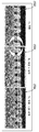
도 2는 실시형태에 따른 EUV 패터닝된 기판을 에칭하는데 사용되는 듀얼 주파수 용량성 결합 플라즈마(CCP: Capacitively Coupled Plasma) 리액터(reactor)의 개략도(1000)이다.
도 3a는 실시형태에 따른, 리소그래피 이후 및 에칭 패턴 전사 후의 라인/공간 및 접촉/바 기준 구조의 탑-다운(top-down) 및 단면(cross sectional) 전자 현미경 사진 이미지를 도시한다.
도 3b는 실시형태에 따른, EUV 패터닝을 위한 통상적인 물질 층 스택의 개략도이다.
도 3c는 실시형태에 따른, 프로세싱의 각 단계에서 임계 치수, LER 및 LWR의 정규화된 값의 플롯(plot)이다.
도 4a는 실시형태에 따른, CCP 챔버의 상부 전극에 DC 전위를 인가함으로써 얻어지는 직류 중첩(DCS: Direct Current Superposition)의 프로세스의 개략도이다.
도 4b는 실시형태에 따른, 전사층 에칭 동안 유기 선택도에 대한 DCS가 미치는 영향을 나타내는 탑-다운 및 단면 전자 현미경 사진 이미지를 도시한다.
도 5a는 EUV 패터닝을 위한 인커밍 스택(incoming stack)을 개략적으로 도시한다.
도 5b는 실시형태에 따른, 도 5a의 스택의 트렌치 패터닝에 대한 EUV 리소그래피의 적용에서의 레지스트 선택도에 대한 DCS 경화 및 에칭 프로세스 최적화의 효과를 나타내는 단면 전자 현미경 사진 이미지를 도시한다.
도 6은 실시형태에 따른, 반복된 성막/에칭 프로세스의 개략도이다.
도 7은 실시형태에 따른, 예시적 성막/에칭 프로세스에 대한 프로세스 조건을 도시하는 표이다.
도 8은 실시형태에 따른, 종래의 에칭과 비교하여 성막/에칭 프로세스의 효과를 나타내는 단면 전자 현미경 사진 이미지를 도시한다.
도 9a 내지 도 9e는 실시형태에 따른, 성막/에칭 프로세스의 사용으로 인한 LER 및 LWR의 개선을 나타내는 EUV 리소그래피를 사용하는 트렌치 패터닝 동안 LER 및 LWR의 전개(evolution)를 도시한다.
도 10a 내지도 10e는 패턴 어긋남(wiggling) 및 왜곡(distortion)에 대한 효과 종횡비(effect aspect ratio)를 도시한다.
도 11a는 종래 기술을 사용하여 얻어진 유기 평탄화제 층의 기계적 안정성 및 결과적인 하류 패턴 거칠기를 도시한다.
도 11b는 도 11a에 도시된 바와 같이 DCS 경화가 없는 프로세스와 비교하여, 실시형태에 따른, 유기 평탄화제 층의 기계적 안정성 및 결과적인 하류 패턴 거칠기에 대한 DCS 경화 프로세스의 영향을 도시한다.
도 12a 및 도 12b는 각각 스컴 발생(scummed) 콘택트 홀 및 브릿지된 접촉 홀 결함의 탑-다운 단면 전자 현미경 사진 이미지를 도시한다.
도 13은 PR 선택도의 튜닝에 기초하여 콘택트 홀 어레이에서 결함을 감소시키는 종래의 접근법의 결과를 도시한다.
도 14는 실시형태에 따른, 반복된 성막/에칭 프로세스의 수행을 포함하는 기술에 기초하여 콘택트 홀 어레이에서 결함을 감소시키는 접근법의 결과를 도시한다.
도 15는 실시형태에 따른, TL 개방 에칭의 3개의 스테이지에서 나타나는 단면 전자 현미경 사진 이미지를 도시한다.BRIEF DESCRIPTION OF THE DRAWINGS The accompanying drawings, which are included in and constitute a part of this specification and which are incorporated in and constitute a part of this specification, illustrate embodiments of the invention in conjunction with the following detailed description and the generic description of the invention. In addition, the leftmost digit of the reference numerals indicates the first reference numerals.
FIG. 1A shows line edge roughness (LER), line width roughness (LWR), and contact edge roughness obtained from conventional EUV lithography techniques.
Figure IB shows higher defects due to conventional EUV lithography techniques that can lead to chip failure during electrical testing.
Figure 1C illustrates a reduction in etch resistance and a decrease in resist margin due to conventional EUV lithography techniques that require high selectivity transfer layer etch.
2 is a schematic diagram 1000 of a dual frequency capacitively coupled plasma (CCP) reactor used to etch an EUV patterned substrate according to an embodiment.
Figure 3a shows top-down and cross sectional electron micrograph images of line / space and contact / bar reference structures after and after lithography and etch pattern transfer, in accordance with an embodiment.
3B is a schematic diagram of a typical material layer stack for EUV patterning, in accordance with an embodiment.
3C is a plot of normalized values of critical dimensions, LER and LWR at each step of processing, according to an embodiment.
4A is a schematic diagram of a process of direct current superposition (DCS) obtained by applying a DC potential to an upper electrode of a CCP chamber, in accordance with an embodiment.
Figure 4B shows a top-down and cross-sectional electron micrographic image showing the effect of DCS on organic selectivity during transfer layer etching, according to an embodiment.
Figure 5A schematically shows an incoming stack for EUV patterning.
Figure 5B shows a cross-sectional electron micrograph showing the effect of DCS curing and etching process optimization on resist selectivity in the application of EUV lithography to trench patterning of the stack of Figure 5a, in accordance with an embodiment.
6 is a schematic diagram of a repeat deposition / etching process according to an embodiment.
7 is a table showing process conditions for an exemplary film deposition / etching process, according to an embodiment.
8 shows a cross-sectional electron micrograph showing the effect of the film-forming / etching process in comparison with the conventional etching according to the embodiment.
Figures 9A-9E illustrate the evolution of LER and LWR during trench patterning using EUV lithography to demonstrate improvements in LER and LWR due to the use of a deposition / etching process, in accordance with an embodiment.
Figures 10A-10E illustrate effect aspect ratios for pattern wiggling and distortion.
11A shows the mechanical stability and resulting downstream pattern roughness of the organic flattening agent layer obtained using the prior art.
Figure 11B shows the effect of the DCS curing process on the mechanical stability of the organic planarization layer and the resulting downstream pattern roughness, in comparison to a process without DCS curing as shown in Figure 11A.
Figures 12A and 12B show top-down cross-sectional electron micrograph images of scummed contact holes and bridged contact hole defects, respectively.
Figure 13 shows the results of a conventional approach to reducing defects in a contact hole array based on tuning of PR selectivity.
Figure 14 illustrates the results of an approach to reducing defects in a contact hole array based on a technique involving performing a repetitive deposition / etching process, in accordance with an embodiment.
15 shows a cross-sectional electron micrograph image taken at three stages of TL open etch, according to an embodiment.
이하의 상세한 설명은 본 개시와 일치하는 예시적 실시형태를 도시하기 위한 첨부 도면을 참조한다. 상세한 설명에서 "일 실시형태", "실시형태", "예시적 실시형태" 등으로 나타낸 것은, 설명하는 예시적 실시형태가 특정 피처(feature), 구조, 또는 특징을 포함할 수 있지만, 모든 예시적 실시형태가 특정 피처, 구조, 또는 특징을 포함할 필요는 없다는 것을 나타낸다. 또한, 이러한 문구는 동일 실시형태를 나타낼 필요가 없다. 또한, 입자 피처(particle feature), 구조, 또는 특성이 실시형태와 관련되어 개시될 때, 다른 예시적 실시형태와 관련된 이러한 피처, 구조, 또는 특성에 영향을 미친다는 것이 명확하게 개시되었는지 여부는 통상의 기술자의 지식 내에 있다.The following detailed description refers to the accompanying drawings which show an exemplary embodiment consistent with the present disclosure. It is to be understood that, in the detailed description, "an embodiment", "an embodiment", "an example embodiment", etc. indicates that the illustrative embodiments described may include a particular feature, structure, That an embodiment does not have to include a particular feature, structure, or characteristic. Further, these phrases do not need to show the same embodiment. Also, it should be understood that when a particle feature, structure, or characteristic is disclosed in connection with an embodiment, whether it is specifically disclosed to affect such feature, structure, or characteristic in relation to other exemplary embodiments Within the knowledge of the technician of the machine.
여기에 개시된 예시적 실시형태들은 한정이 아닌 예시를 목적으로 제공된다. 다른 실시형태들도 가능하고, 본 개시의 범위 내에서 예시적 실시형태들에 대한 수정들도 가능하다. 따라서, 상세한 설명은 본 개시를 한정하는 것을 의미하지 않는다. 대신, 본 개시의 범위는 후속하는 청구범위와 그 등가물에 의해서만 규정된다.The exemplary embodiments disclosed herein are provided for purposes of illustration and not limitation. Other embodiments are possible, and modifications to the illustrative embodiments are possible within the scope of this disclosure. Accordingly, the detailed description is not meant to limit the present disclosure. Instead, the scope of the present disclosure is defined only by the following claims and their equivalents.
예시적 실시형태의 이하의 상세한 설명은, 다른 것들은 통상의 기술자의 지식을 적용함으로써 본 개시의 범위로부터 벗어나지 않고, 지나친 실험(experimentation)없이 이러한 예시적 실시형태에 다양한 적용을 위해 용이하게 수정하고 및/또는 적응시킬 수 있는 본 개시의 일반적인 특성을 완전히 나타낼 것이다. 따라서, 이러한 적응 및 수정은 여기에 개시된 가르침과 안내에 기초하는 예시적 실시형태의 의미(meaning) 및 복수의 등가물 내에 있는 것으로 의도된다. 본 명세서의 용어 또는 어법이 여기에서의 가르침을 고려하여 통상의 기술자에 의해 이해되게 하기 위해, 여기에서의 어법 또는 용어는 한정이 아닌 설명을 위한 것임이 이해되어야 한다.The following detailed description of the exemplary embodiments is provided to enable any person of ordinary skill in the art to make modifications and adaptations to these exemplary embodiments for various applications without undue experimentation without departing from the scope of this disclosure by applying the knowledge of the ordinary artisans, / RTI > and / or < RTI ID = 0.0 > adaptable < / RTI > Accordingly, such adaptations and modifications are intended to be within the meaning of the exemplary embodiments and the plurality of equivalents based on the teachings and guidance herein disclosed. It is to be understood that the phraseology or terminology herein is for the purpose of description and not of limitation, in order that the terminology or phraseology of the specification may be understood by those of ordinary skill in the art in view of the teachings herein.
서브-30 nm 노드 반도체 제조는 전통적인 리소그래피 기술의 물리적 한계에 많은 어려움을 겪고 있다. EUV 리소그래피는 10 nm 및 서브-10 nm 기술 노드에서의 패터닝의 과제에 직면하는 유망한 접근법이다. 그러나, EUV 리소그래피는 또한 예컨대 도 1a 내지 도 1c에 도시된 바와 같이, 다수의 중대한 난제를 겪고 있다. Sub-30 nm node semiconductor fabrication suffers from the physical limitations of traditional lithography techniques. EUV lithography is a promising approach to the challenges of patterning at 10 nm and sub-10 nm technology nodes. However, EUV lithography also suffers from a number of significant challenges, for example, as shown in Figures 1A-1C.
도 1a는 종래의 EUV 리소그래피 기술로부터 얻어지는 라인 엣지 거칠기(LER), 라인 폭 거칠기(LWR), 및 콘택트 엣지 거칠기를 도시한다. 다른 실시예에서, 도 1b는 전기적 테스트 동안 칩 실패를 초래할 수 있는 종래의 EUV 리소그래피 기술들로 인한 더 높은 결함을 도시한다. 또 다른 실시예에서, 도 1c는 높은 선택도 전달층 에칭을 요구하는 종래의 EUV 리소그래피 기술로 인한 에칭 내성의 감소 및 레지스트 마진의 감소를 도시한다.FIG. 1A shows line edge roughness (LER), line width roughness (LWR), and contact edge roughness obtained from conventional EUV lithography techniques. In another embodiment, Figure IB shows a higher defect due to conventional EUV lithography techniques that can lead to chip failure during electrical testing. In yet another embodiment, FIG. 1C illustrates a reduction in etch resistance and a decrease in resist margin due to conventional EUV lithography techniques that require high selectivity transfer layer etch.
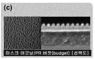
포토레지스트 버짓(budget)은 각 기술 노드마다 끊임없이 줄어들고 있다. 더 작은 피치에서 리소그래피를 수행할 수 있는 능력은 PR 두께의 트레이드 오프가 따른다. 서브-30 nm 기술 노드에 대한 PR의 일반적인 두께는 60-20 nm이며, 드라이 에칭에 사용할 수 있는 더 얇은 인커밍 레지스트를 갖는 더 작은 기술 노드가 있다. 또한, EUV 레지스트의 에칭 내성은 193/193i 리소그래피 레지스트보다 훨씬 작고, 보다 높은 선택도 프로세스를 제공하기 위한 에칭 프로세스 개발에 대한 추가 요구가 제기된다. 이러한 과제를 극복하기 위한 노력에는 EUV 소스 최적화 및 새로운 EUV 레지스트 재료 개발을 포함한다.The photoresist budget is constantly decreasing for each technology node. The ability to perform lithography at a smaller pitch follows a trade-off of PR thickness. The typical thickness of the PR for the sub-30 nm technology node is 60-20 nm, and there is a smaller technology node with a thinner combustion resist that can be used for dry etching. In addition, the etch resistance of EUV resists is much smaller than the 193 / 193i lithographic resist, and a further need exists for the development of etching processes to provide a higher selectivity process. Efforts to overcome these challenges include optimizing EUV sources and developing new EUV resist materials.
본 개시는 EUV 패터닝 과제를 충족시키기 위해 용량성 결합 플라즈마(CCP) 건식 에칭 방법론에 기초한 리소그래피 기술을 제시한다. 개시된 시스템 및 방법은 반복된 성막/에칭 프로세스를 포함하는 패터닝 프로세스에서 듀얼 주파수 CCP를 사용한다. 후술하는 바와 같이, 개시된 실시형태는 홀 및 라인 패턴에 대하여 LER/LWR, 레지스트 선택도, 및 임계 치수(CD: critical dimension) 조정가능성에서의 향상을 나타낸다. 개시된 실시형태를 사용하여 얻어진 결과는 종래의 플라즈마 경화 방법을 사용하여 얻어진 결과에 비교된다. CD의 주요 패터닝 메트릭, 레지스트 선택도, 및 LER/LWR에 영향을 미치는 다양한 플라즈마 에칭 파라미터의 역할을 보여주는 체계적 스터드(systematic stud)로부터의 데이터가 제시된다.This disclosure presents lithography techniques based on capacitively coupled plasma (CCP) dry etching methodology to meet EUV patterning challenges. The disclosed systems and methods use a dual frequency CCP in a patterning process that involves repeated deposition / etching processes. As described below, the disclosed embodiments show improvements in LER / LWR, resist selectivity, and critical dimension (CD) tunability for hole and line patterns. The results obtained using the disclosed embodiments are compared to those obtained using conventional plasma hardening methods. Data from a systematic stud showing the key patterning metrics, resist selectivity, and the role of various plasma etch parameters affecting the LER / LWR of the CD are presented.
실시형태에 따르면, LER 및 LWR을 향상시키기 위한 한가지 기술은 플라즈마 리액터의 전극들 중 하나에서 무선 주파수(RF: radio-frequency) 플라즈마에 음의(negative) DC 전압을 중첩시키는 것을 포함한다. 플라즈마 케미스트리(plasma chemistry)와 함께 탄도 전자의 결과 방출은 아래에서 더 상세히 설명하는 바와 같이 LER 및 LWR을 개선하는 것으로 나타났다. According to an embodiment, one technique for improving LER and LWR involves superimposing a negative DC voltage on a radio-frequency (RF) plasma at one of the electrodes of the plasma reactor. The resulting emission of ballistic electrons with plasma chemistry has been shown to improve LER and LWR as described in more detail below.
도 2는 실시형태에 따른 EUV 패터닝된 기판을 에칭하는데 사용되는 듀얼 주파수 CCP 리액터의 개략도(200)이다. 패터닝될 웨이퍼(202)는 정전 척(ESC: electrostatic chuck)(204)에 장착된다. 실시형태에 따르면, 웨이퍼(202)의 전압을 고정하기 위해 ESC에 바이어스 RF 전압(206)이 인가될 수 있다. 리액터는 고주파(HF: high frequency) 전압(210)이 인가될 수 있는 상부 전극(EL)(208)을 포함할 수 있다. HF 전압(210)에 추가하여, 음의 DC 전압(212)도 상부 El(208)에 인가될 수 있다. 실시형태에 따르면, DC 애노드 El(214)이 제공될 수도 있다. 실시형태에 따르면,인가될 수 있는 1 kV DC 바이어스(216)가 상부 EL(208)과 DC 애노드 EL(214) 사이에 인가될 수 있다.2 is a schematic 200 of a dual frequency CCP reactor used to etch an EUV patterned substrate according to an embodiment. The
실시형태에 따르면, 프로세스 가스의 도입과 ESC(204), 상부 EL(208), 및 애노드 El(214)에 대한 바이어스 전압(206)의 인가를 통해 도 2의 리액터에 이온화 플라즈마(ionized plasma)가 생성된다. 실시형태에 따르면, 프로세스 가스는 Ar, N2H2, 및 다양한 플로오로카본(CFx)을 포함할 수 있다. DC 전위의 상부 EL(208)로의 인가는 하부 영역(216)과 상부 영역(218)을 가진 플라즈마를 생성한다. 상부 영역(218)은, 하부 영역(216)보다 더 높은 플라즈마 밀도와 플라즈마의 더 균일한 방사상 분포를 가진 시스(sheath)이다. 상기 DC 전위를 사용하여 플라즈마를 생성하는 프로세스는, (도 4a 및 도 4b 및 관련 논의 참조하여) 더 상세히 후술하는 바와 같이, 직류 중첩(DCS: Direct Current Superposition) 또는 DCS 경화라고 불린다.According to an embodiment, an ionized plasma is applied to the reactor of Figure 2 through the introduction of a process gas and application of a bias voltage 206 to the
EUV 기반 포토 레지스트를 이용한 초기 에칭 실현가능성 연구를 완화된 피치 샘플에서 실행하여, 레지스트 물질 변화가 CD 바이어스 제어 및 패턴 충실도에 미치는 영향을 측정했다. 이 작업을 위해, 패터닝은 IBM EUV 리소그래피 도구 세트를 사용하여 수행되었다. Initial etch feasibility studies using EUV-based photoresists were run on relaxed pitch samples to determine the effects of resist material changes on CD bias control and pattern fidelity. For this task, patterning was performed using the IBM EUV lithography tool set.
도 3a 내지 도 3c는 실시형태에 따른 초기 에칭 실현가능성 연구의 결과를 도시한다. 도 3a는 실시형태에 따른, 리소그래피 이후 및 에칭 패턴 전사 후의 라인/공간 및 접촉/바 기준 구조의 탑-다운(top-down) 및 단면(cross sectional) 전자 현미경 사진 이미지를 도시한다. 도 3b는 실시형태에 따른, EUV 패터닝을 위한 통상적인 물질 층 스택의 개략도이다. 포토레지스트(PR)(302), 전사층(TL)(304), 및 유기 평탄화제 층(OPL)(306)의 3층 패터닝 방식이 사용되었다. TL(304)은 PR(302)과 OPL(306) 모두에 대한 높은 수준의 플라즈마 에칭 선택도 때문에 선택되었으며 OPL(306)은 그 이름에서 알 수 있듯이 임의의 기존 지형을 평탄화하는 이점을 갖는다. 실시형태에 따르면, 3중층 스택(trilayer stack)은 유전체 스택(308)의 상부에 생성될 수 있다.Figures 3A-3C illustrate the results of an initial etch feasibility study according to an embodiment. Figure 3a shows top-down and cross sectional electron micrograph images of line / space and contact / bar reference structures after and after lithography and etch pattern transfer, in accordance with an embodiment. 3B is a schematic diagram of a typical material layer stack for EUV patterning, in accordance with an embodiment. A three-layer patterning scheme of a photoresist (PR) 302, a transfer layer (TL) 304, and an organic flatting agent layer (OPL) 306 was used. TL 304 has been selected because of its high level of plasma etch selectivity for both
RIE1 - RIE4로 지칭되는 4개의 반응 이온 에칭(RIE: reactive ion etch) 프로세스 조건이, 예컨대 도 3a에 도시된 바와 같이, 인커밍 디벨롭 CD(incoming develop CD)의 0 내지 50 %의 CD 바이어스 제어를 나타내는 전사층 개방용으로 개발되었다. RIE1 - RIE4에서, 시간, 압력, 전극 주파수, DC 전위, 가스 유속(gas flow rate), 또는 기판 온도 중 하나 이상에서 변화가 이루어졌다. 더 희박한 '0 에칭 바이어스' 케이스(case)에서 PR 버짓에 대한 몇가지 초기 우려는, LER 저하 또는 브리징이 관찰되지 않았기 때문에 무시할 만하다고 판명되었다. 또한, 모든 에칭 케이스는 에칭 조건과 무관하게 인커밍(즉, 인커밍 패터닝된 레지스트와 관련하여)에 비해 대략 63 %의 LWR의 극적인 개선을 나타낸다. LER는, CD 바이어스의 함수로서 약간 저하되고, 예컨대 도 3c에 도시된 바와 같이, 전송 층 개방에서 사용된 플루오로카본(CFx) 패시베이션(passivation)이 원하는 것보다 크고 LER 생성에 기여한다는 표시가 될 수 있다. 도 3c는 실시형태에 따른, 프로세싱의 각 단계에서 임계 치수, LER 및 LWR의 정규화된 값의 플롯(plot)이다.Four reactive ion etch (RIE) process conditions, referred to as RIE1 - RIE4, are used to control the CD bias control of 0 to 50% of the incoming develop CD, Lt; RTI ID = 0.0 > open. ≪ / RTI > In RIE1 - RIE4, changes were made in at least one of time, pressure, electrode frequency, DC potential, gas flow rate, or substrate temperature. In the sparse '0 etch bias' case, some initial concerns about the PR budget turned out to be negligible because no LER degradation or bridging was observed. In addition, all etch cases exhibit a dramatic improvement of LWR of approximately 63% compared to incoming (i.e., with respect to incoming patterned resist) regardless of the etch conditions. The LER is slightly degraded as a function of the CD bias and an indication that the fluorocarbon (CF x ) passivation used in the transport layer opening is greater than desired and contributes to LER generation, as shown, for example, in Figure 3C . 3C is a plot of normalized values of critical dimensions, LER and LWR at each step of processing, according to an embodiment.
라인-스페이스 적용을 위한 적극적인 피치 스케일링은 포토레지스트에서 높은 종횡비를 유도하여 패턴 붕괴 마진을 유도한다. EUV 레지스트 높이 스케일링과 동시에, 에칭 선택도 요건을 감소시키기 위해 TL 두께를 감소시키는 것이 바람직하다. TL 두께의 하한은 부분적으로 레지스트 솔벤트 및 현상액에 대한 기밀성(hermeticity)에 의해 지시된다(dictated). EUV 레지스트와 관련된 과제 중 하나는 패턴을 TL로 전사할 때의 선택도이다. 따라서, LER 및 LWR을 감소시켜 양호한 패턴 전사를 가능하게 하기 위해서는, 양호한 레지스트 선택도를 갖는 것이 바람직하다. 적절한 패턴 전달 충실도를 달성하기 위해, 실시형태에 따르면, 에칭 선택도는 TL : EUV PR > 5:1이어야 하는 것으로 추정된다.Aggressive pitch scaling for line-space applications leads to high aspect ratios in the photoresist leading to pattern collapse margins. At the same time as EUV resist height scaling, it is desirable to reduce the TL thickness to reduce the etch selectivity requirement. The lower limit of the TL thickness is dictated, in part, by the hermeticity of the resist solvent and developer. One of the challenges associated with EUV resists is the selectivity when transferring a pattern to a TL. Therefore, in order to reduce LER and LWR to enable good pattern transfer, it is preferable to have good resist selectivity. In order to achieve the appropriate pattern transfer fidelity, according to an embodiment, it is assumed that the etch selectivity should be TL: EUV PR > 5: 1.
전술한 결과는 통상적인 EUV 리소그래피 기술의 전형이다. 실시형태에 따르면, 다음에서 논의되는 바와 같이, DCS 기술의 사용을 통해 개선된 결과가 얻어질 수 있다.The above results are typical of conventional EUV lithography techniques. According to the embodiment, as discussed below, improved results can be obtained through the use of the DCS technique.
도 4a는 실시형태에 따른, CCP 챔버의 상부 전극에 DC 전위를 인가함으로써 얻어지는 DCS의 프로세스의 개략도이다. 이 프로세스에서, 상부 El(402)에 대한 DC 전위의 인가는, DC 바이어스의 인가없이 생성된 플라즈마에 비해 플라즈마의 방사상 분포를 변화시키고 플라즈마 밀도를 증가시켜 더 두꺼운 상부 시스(404)를 생성한다. 4A is a schematic diagram of a process of DCS obtained by applying a DC potential to an upper electrode of a CCP chamber, in accordance with an embodiment. In this process, application of the DC potential to the
또한, 실시형태에 따르면, DC 전위는 상부 전극을 향하여 양이온(406)을 가속시킨다. 상부 전극에 대한 양이온의 충돌은 웨이퍼 표면(410)을 향하여 DC 전위에 의해 가속되는 2차 전자 방출(408)을 발생시킨다. 전자는, 바닥 시스(412)를 관통하고 레지스트 (414)를 포함하는 유기 막의 전하 소거 및 교차 결합을 포함하여 웨이퍼 표면(410)에서 프로세스에 영향을 미치기에 충분한 에너지를 갖는다. 이 전자빔 유도 교차 결합/경화는 유기 포토레지스트 및 유기 평탄화제(organic planarizer)에 대한 에칭 선택도를 향상시킬 수 있다. Further, according to the embodiment, the DC potential accelerates the
도 4b는 실시형태에 따른, 전사층 에칭 동안 유기 선택도에 대한 DCS가 미치는 영향을 나타내는 탑-다운 및 단면 전자 현미경 사진 이미지를 도시한다. DCS를 사용하여 얻은 결과(418)와 비교하여 DCS가 없는 프로세스를 사용하면 더 많은 레지스트가 소모된다는 것이 분명하다. 또한, 개선된 CD 바이어스(420)는 DCS가 사용되지 않을 때 얻어진 바이어스(422)보다 DCS를 사용하여 얻어진다. DCS가 있는 경우와 없는 경우의 비교 결과는 다음과 같다.Figure 4B shows a top-down and cross-sectional electron micrographic image showing the effect of DCS on organic selectivity during transfer layer etching, according to an embodiment. Obviously, using a process without DCS as compared to the result (418) obtained using DCS consumes more resist. In addition, the
도 5a는 EUV 패터닝을 위한 스택을 개략적으로 도시하고, 도 5b는 실시형태에 따른, 트렌치 패터닝에 대한 EUV 리소그래피의 적용에서의 레지스트 선택도에 대한 DCS 경화 및 에칭 프로세스 최적화의 효과를 나타내는 스택의 단면 전자 현미경 사진 이미지를 도시한다. 본 실시예에서, 도 5a에 개략적으로 도시된 바와 같이, EUV 패터닝(502)을 위한 스택은 유전체 스택(510)의 상부에 구성된 EUV 패터닝된 PR(504), TL(506) 및 유기 평탄화제 층 (OPL)(508)을 포함한다. PR(504)은 40nm 미만의 피치를 나타내는 피쳐(512)를 갖고 패턴화 되었다.Figure 5a schematically depicts a stack for EUV patterning and Figure 5b illustrates a cross section of the stack showing the effect of DCS curing and etching process optimization on resist selectivity in the application of EUV lithography to trench patterning, Electron microscope photograph image. 5A, a stack for
도 5b의 제1 패널(514)은 에칭 이전의 인커밍 패터닝된 기판의 단면 전자 현미경 사진 이미지이다. 도 5b의 제2 패널(516)은 트렌치에 적용된 종래 전사층 개방의 결과를 나타낸다. 이는 EUV 레지스트에 대한 낮은 레지스트 선택도(즉, 1.3 : 1)를 가지며, TL 개방 동안 대부분의 레지스트가 소모되어 열악한 패턴 전달이 초래된다. 제3 패널(518)에서, 전사층 개방 프로세스 전에 DC 전압 기반 처리가 채택되었다. 상부 전극에 인가된 DC 전압에 의해 발생된 탄도 전자는 웨이퍼 레벨에서 수집될 수 있으며, 레지스트의 하드닝(hardening) 및 큐어링(curing)을 초래할 수 있다. 이러한 EUV 레지스트의 경우, DC 전압 기반 전처리는 또한 2.2 : 1의 레지스트 선택도 증가를 나타냈다. The
도 5b의 제4 패널(520)은 이온 에너지의 감소로 인한 레지스트 선택도의 증가를 나타낸다. 본 실시예에서, 전사층 개방 단계에서의 이온 에너지의 감소는 레지스트 선택도를 3.6:1로 향상시켰다. 이온 에너지의 감소는 또한 EUV 레지스트 프로파일을 개선하여 레지스트 모서리의 "침식"을 줄여서 보다 직선적인 프로파일을 유지할 수 있게 했다.The
실시형태에 따르면, 도 5b의 결과는 EUV 레지스트에 대한 선택도가 종래의 TL 개방 프로세스에 대해 점진적으로 증가될 수 있음을 예시한다. 레지스트 선택도를 극적으로 개선하기 위해, 아래에서 보다 상세히 설명되는 바와 같이, 반복된 성막/에칭 프로세스가 개발되었다. 반복된 성막/에칭 프로세스를 사용하여 얻어진 결과는 도 5b의 제5 패널 (522)에 도시된다. 이 결과는 본 발명의 실시형태의 성막/에칭 프로세스를 사용하여 레지스트 에칭 선택도에서 3.6 : 1에서 7.8 : 1까지의 극적인 개선을 보여준다.According to an embodiment, the results of Figure 5B illustrate that selectivity for EUV resists can be incrementally increased for a conventional TL opening process. To dramatically improve resist selectivity, a repeat deposition / etch process has been developed, as described in more detail below. The results obtained using the repeated deposition / etching process are shown in the
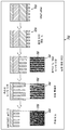
도 6은 실시형태에 따른, 상기 반복된 성막/에칭 프로세스의 개략도이다. 이 접근법은 에칭 프로세스가 이어지는 성막 프로세스로 구성된 프로세스 시퀀스에 기초한다. 본 실시에에서, 인커밍 기판(600)은 PR(602), TL(604), 및 OPL과 같은 유기층(606)을 포함한다. 실시형태에 따르면, Pr(602)은 유기 포토레지스트, 예컨대 EUV 포토레지스트이다. 또한, 실시형태에 따르면, TL(604)은 SiARC(silicon anti-reflection coating)이 될 수 있다. PR(602)은, TL(604)의 마스크되지 않은 부분을 노출시키면서 Pr(602)이 하부 TL(604)의 일부를 마스크하도록, 패터닝된다.6 is a schematic diagram of the repeated deposition / etching process according to an embodiment. This approach is based on a process sequence consisting of a deposition process followed by an etching process. In this embodiment, the
제1 단계 또는 스테이지에서, 성막 프로세스(608)가 수행된다. 실시형태에 따르면, 성막 프로세스(608)동안 플루오로카본(CFx) 중합체와 같은 카본 함유층(609)이 기판 상에 성막될 수 있다. 바람직하게는, CFx 중합체는 TL(604)의 노출된 마스크되지 않은 부분 및 PR(602)의 비측벽 부분 상에 성막된다. 이온 플럭스(flux) 및 CFx 래디컬의 플럭스는 상부 El(예컨대, 도 4의 402)에 DC 전압을 인가함으로써 제어될 수 있다. 실시형태에 따르면, 이온 플럭스는 비교적 낮은 에너지(예컨대, < 100eV)를 가질 수 있다. 성막 단계(608)에서, 플루오로카본 가스의 가스 흐름은 CFx 래디컬 플럭스를 제어하고 이에 따라 성막을 제어한다. 실시형태에 따르면, CFx 중합체는 레지스트 패턴 상에 우선적으로 성막된다. 환언하면, CFx 중합체는 TL(604)의 마스크되지 않은 부분보다 PR(602)의 비측벽 부분 상에 더 두껍게 성막된다.In the first step or stage, a
실시형태에 따르면, 제2 단계 또는 스테이지에서, 반응 이온 에칭(610)이 수행된다. 반응 이온 에칭(610)에서, TL(604)의 일부분은 PR(602)이 크게 남아있는 동안 우선적으로 에칭될 수 있다. 달리 말하면, TL(604)의 부분 두께는 PR(602)의 두께를 어느 정도 감축시키지 않고 에칭된다. 일 실시형태에서, TL(604)이 에칭됨에 따라 PR(602)을 경화시키는 에칭(610) 동안 DCS가 사용되고 이에 따라 선택적 에칭(preferential etch)을 용이하게 한다. According to an embodiment, in a second step or stage, a
추가 단계 또는 스테이지에서, 화살표(612)로 표시된 바와 같이, 성막(608) 다음 에칭(610)의 순차적 프로세스가 반복된다. 반복되는 프로세스가 진행됨에 따라, TL(604)은 하부 OPL의 에칭에 이어서 에칭되어 패턴을 OPL(606)로 전사한다. 실시형태에 따르면, 이러한 반복된 프로세스는 PR이 상당히 손상되지 않은 채로 TL(604) 및 평탄화제 층이 에칭되는 구조(614)를 얻는다. 순차적 성막(608)/에칭(610) 프로세스가 반복되어야하는 횟수는 TL(604) 및 유기층(606)의 초기 두께 및 각각의 반복에서 에칭된 부분 두께에 의해 결정된다.In a further step or stage, the sequential process of
도 7은 실시형태에 따른, 예시적 성막/에칭 프로세스에 대한 프로세스 조건을 도시하는 표(700)이다. 본 실시예에서, 제1 성막 프로세스(702) 동안 플루오로카본(CH3F)(704) 및 CF4(706)는 각각 40 sccm, 50 sccm 및 330 sccm의 가스 유속에서 H2(708)와 함께 플라즈마 리액터로 도입된다. 제1 에칭/경화 프로세스(710) 동안, 플루오로카본(704 및 706)의 흐름은 중단되고, H2(708) 및 N2(712)는 각각 450 sccm의 가스 유속으로 플라즈마 리액터 내로 도입된다. 교번 성막/에칭(경화)은 미리 결정된 횟수의 반복으로 반복된다.FIG. 7 is a table 700 illustrating process conditions for an exemplary film / etch process, in accordance with an embodiment. In this embodiment, the first film forming process fluorocarbons for (702) (CH 3 F) (704) and CF 4 (706) is H 2 (708) at a gas flow rate of 40 sccm, 50 sccm and 330 sccm, respectively, and Together are introduced into the plasma reactor. During the first etch / cure process 710, the flow of
본 실시예에서, 결합된 성막/에칭(경화) 프로세스가 3회 반복된다. 다른 실시형태에서, 성막/에칭(경화) 프로세스는 필요에 따라 미리 결정된 임의의 횟수로 반복될 수 있다. 표(700)에 제공된 다른 프로세스 파라미터는 가스 압력(714), 고주파(HF)에서 상부 E (208)(도 2 참조)에 공급되는 전력(716), ESC(204)(도 2 참조)에 공급되는 전력(718), 상부 EL(208)에 인가된 DC 전압(720)(도 2 참조)을 포함한다. In this embodiment, the combined deposition / etching (curing) process is repeated three times. In another embodiment, the deposition / etching (curing) process may be repeated as desired at any predetermined number of times. Other process parameters provided in the table 700 may be supplied to the ESC 204 (see FIG. 2) via the
도 8은 실시형태에 따른, 종래의 에칭과 비교하여 성막/에칭 프로세스의 효과를 나타내는 단면 전자 현미경 사진 이미지(800)를 도시한다. 제1 이미지(802)는 패터닝된 PR(804), SiARC 전달층(806) 및 OPL(808)을 갖는 인커밍 기판을 도시한다. 제2 이미지(810)는 종래의 프로세스로 PR(804)이 SiARC 에칭 프로세스 동안 소모된다는 것을 명확하게 보여준다. 제3 이미지(812)는 SiARC(806)가 에칭되고 OPL(808)이 부분적으로 에칭 된 후에, 본 발명의 실시형태의 성막/에칭(경화) 프로세스의 결과를 도시한다. 본 실시예에서, PR(814)은 손상되지 않고 PR(814)의 높이는 감소되지 않는다.FIG. 8 shows a cross-sectional electron
도 9a 내지 도 9e는 실시형태에 따른, 성막/에칭 프로세스의 1 사이클의 사용으로 인한 LER 및 LWR의 개선을 나타내는 EUV 리소그래피를 사용하는 트렌치 패터닝 동안 LER 및 LWR의 전개(evolution)를 도시한다. DC 전압 기반 플라즈마 조건은 상대적으로 낮은 이온 에너지에서 CFx 래디칼 플럭스의 양호한 제어를 가능하게 하여 레지스트 버짓 및 레지스트 프로파일을 유지하는 데 도움이 된다. Figures 9A-9E illustrate the evolution of the LER and LWR during trench patterning using EUV lithography to demonstrate improvements in LER and LWR due to the use of one cycle of the deposition / etching process, in accordance with an embodiment. DC voltage based plasma conditions allow good control of the CF x radical flux at relatively low ion energies to help maintain the resist budget and resist profile.
도 9a는 인커밍 기판(900)의 개략적인 단면도이다. 인커밍 기판(900)은 패터닝된 레지스트(902), 전사층(904), 및 평탄화제(906)를 포함한다. 실시형태에 따르면, 기판(900)은 또한 하드 마스크(HM: hard mask) 스택(908)을 포함할 수 있다. HM 스택(908)은 유전체 스택(910)의 상부 상에 제공되어 유전체 스택(910)을 패터닝하는데 사용될 수 있다.9A is a schematic cross-sectional view of an
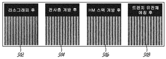
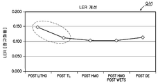
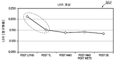
도 9b는 에칭 프로세스의 상이한 스테이지에서 에칭된 기판의 피쳐를 도시하는 탑-다운 전자 현미경 사진 이미지(912, 914, 916, 및 918)를 포함한다. 이미지(912)는 EUV 리소그래피 후의 기판을 나타낸다. 이미지(914)는 TL 에칭("TL 개방") 프로세스 후의 기판을 나타낸다. 이미지(916)는 HM 스택 개방 프로세스 후의 기판을 나타낸다. 이미지(918)는 트렌치 및 유전층 에칭 프로세스 후의 기판을 나타낸다. LER 전개에 대한 결과는 도 9c의 그래프(920)에 도시된다. LWR 전개에 대한 결과는 도 9d의 그래프(922)에 도시된다. 이 결과들은 TL 층 개방 후에 측정된 양호한 CD 균일성이 달성된 것을 나타낸다. 이 결과들은 또한 도 9e의 표(924)에 요약된 바와 같이, 측정된 LER 및 LWR의 약 25-30%의 감소를 나타낸다.FIG. 9B includes top-down
도 10a 내지 도 10e는 실시형태에 따른, 성막/에칭 프로세스의 1 사이클을 사용하여 패턴 어긋남 및 왜곡에 대한 효과적인 종횡비를 도시한다. 다중 패터닝 방식과 달리, EUV 리소그래피는 완전한 라인-스페이스 패턴(line-space pattern)이 싱글 패스(single pass)로 노출되도록 한다. 라인-스페이스 피치가 감소함에 따라, 소프트 마스크(soft mask)의 높은 종횡비는 상대적 기계적 안정성을 감소시킨다. 이것은 종횡비에 따른 패턴 왜곡 및 어긋남을 유발한다. FIGS. 10A-10E illustrate effective aspect ratios for pattern misalignment and distortion using one cycle of the film deposition / etching process, according to an embodiment. Unlike the multiple patterning approach, EUV lithography allows a complete line-space pattern to be exposed in a single pass. As the line-space pitch decreases, the high aspect ratio of the soft mask reduces the relative mechanical stability. This causes pattern distortion and misalignment depending on the aspect ratio.
도 10a에서, 탑-다운 전자 현미경 사진 이미지(1002)는 대략 4.1의 종횡비를 갖는 기판을 패터닝하는 양호한 결과를 나타낸다. 도 10b에서, 유사한 탑-다운 전자 현미경 사진 이미지(1004)는 대략 4.25의 종횡비를 갖는 기판을 패터닝하는 양호한 결과를 나타낸다. 그러나, 얻어진 패터닝된 기판에서의 왜곡은 대략 4.5보다 큰 종횡비를 갖는 기판에 대해 관찰된다. 예컨대, 도 10c에서, 탑-다운 전자 현미경 사진 이미지(1006)는 대략 4.6의 종횡비를 갖는 기판을 패터닝하는 것에 대한 패턴 왜곡(즉, LER 및 LWR)을 나타낸다. 탑 다운 전자 현미경 사진 이미지(1008)에서, 도 10d에 도시된 바와 같이, 약 6.1의 종횡비를 갖는 기판에 대해 현저한 어긋남 왜곡이 관찰된다. 도 10a 내지 도 10d의 결과는 정규화된 CD가 종횡비의 함수로서 표시된 도 10e에 그래픽으로 도시되어 있다.10A, a top-down
실시형태에 따르면, 소프트 마스크의 종횡비를 4.5 미만으로 유지하면, 도 10a, 도 10b 및 도 10e에 도시된 바와 같이, 작은 피치 크기에서도 하드 마스크로의 양호한 패턴 전사가 달성될 수 있다. 6.0 이상의 종횡비에서, 소프트 마스크는 더 이상 패턴을 유지할 수 없고, 도 10d 및 도 10e에서의 이미지(1008)에 도시된 바와 같이, 어긋남이 유도된다. 종횡비 4.5와 6.0 사이에서, 도 10c 및 도 10e에 도시된 바와 같이, 소량의 패턴 왜곡이 관찰된다. According to the embodiment, if the aspect ratio of the soft mask is kept below 4.5, good pattern transfer to the hard mask can be achieved even at small pitch sizes, as shown in Figs. 10A, 10B and 10E. At an aspect ratio of 6.0 or higher, the soft mask can no longer maintain the pattern and a shift is induced, as shown in the
소프트 마스크의 종횡비는 통합 및 평면화 물질 성능에 필요한 피치 치수에 의해 결정된다. 더 얇은 평탄화 층은 종횡비를 감소시키지만, 그러한 층을 신뢰성있게 생성하는 프로세스는 도전적일(challenging) 수 있으며 스택의 디자인을 제한한다. 또한, 결과적으로 후속 단계에서 더 얇은 소프트 마스크가 발생하여 추가적인 높은 선택도 프로세스가 요구된다. 패턴 왜곡의 개시(onset)는 또한 평탄화 층을 에칭하기 위해 사용되는 에칭 케미스트리(etch chemisty)에 좌우될 수 있다. 새로운 에칭 케미스트리 및 조건의 사용은 소프트 마스크에 강성을 부여할 수 있으며 높은 종횡비에서 어긋남 없는 프로세스를 가능하게 한다.The aspect ratio of the soft mask is determined by the pitch dimensions required for integrated and planarizing material performance. A thinner planarization layer reduces the aspect ratio, but the process of reliably creating such a layer can be challenging and limits the design of the stack. Also, as a result, a thinner soft mask is generated in subsequent steps, requiring an additional high selectivity process. The onset of pattern distortion may also depend on the etch chemistry used to etch the planarization layer. The use of new etch chemistries and conditions can impart rigidity to the soft mask and enable a process free from high aspect ratios.
예컨대, 도 9a 내지 9e에 도시된 바와 같이, 에칭 시퀀스의 파티션을 통한 탑-다운 검사(top-down inspection)는 라인 어긋남을 유도하는 메커니즘에 대한 몇 가지 추가적인 이해(insight)를 제공한다. TL 스트립 후에 엣지 거칠기가 분명하기는 하지만, 마스크 CD 성장과 산화물 에칭 후의 현저한 라인 어긋남의 저하가 관찰된다. 플라즈마 케미스트리 노출로부터의 소프트 마스크의 CFx 성막 또는 팽윤이 라인 어긋남을 통해 완화되는 압축 응력을 유도하는 것이 가능하다. 이러한 비이상적 현상은 포스트 애쉬 이미지(post-ash image)(도 11a 및 도 11b를 참조하여 이하에서 더 논의됨)에 도시된 바와 같이 유전체로 직접 전달될 수 있다. TL 개방 이전 또는 도중의 DCS 경화의 적용은 이러한 어긋남 현상을 제거할 수 있다. 어긋남이 가장 명백한 40 nm 이하의 공격적인 피치에서, 효과는 도 11a 및 도 11b에 도시된 바와 같이 육안 검사에 의해 극적이고 용이하게 명백해지고, 이하에서 더 상세히 설명된다. For example, top-down inspection through a partition of the etch sequence, as shown in FIGS. 9A-9E, provides some additional insight into the mechanism for inducing line misalignment. Although the edge roughness is obvious after the TL strip, a remarkable decrease in line shift after the mask CD growth and oxide etching is observed. It is possible to induce a compressive stress in which the CF x film formation or swelling of the soft mask from plasma chemical exposure is relaxed through line displacement. This non-ideal phenomenon can be transferred directly to the dielectric as shown in a post-ash image (discussed further below with reference to FIGS. 11A and 11B). The application of DCS hardening before or during TL opening can eliminate this discrepancy. At an aggressive pitch of 40 nm or less where the discrepancy is most obvious, the effect becomes dramatic and easily apparent by visual inspection as shown in Figs. 11A and 11B, and is described in more detail below.
도 11a 및 도 11b는 실시형태에 따른, 유기 평탄화제 층의 기계적 안정성 및 결과적인 하류 패턴 거칠기에 대한 DCS 경화 프로세스의 영향을 도시한다. 도 11a의 프로세스(1102)는 DCS 경화 프로세스의 적용 없이 높은 종횡비 기판을 에칭하는 것에 대하여 얻어진 결과를 도시한다. 본 실시예에서 약 5:1의 종횡비가 사용되었지만, 다른 종횡비도 고려된다. 도 11b의 프로세스(1104)는 DCS 경화 프로세스의 적용 없이 높은 종횡비 기판을 에칭하는 것에 대하여 얻어진 향상된 결과를 도시한다. 패널(1106)은 인커밍 기판을 개략적으로 도시한다. 패널(1108)은 TL 개방 동작이 적용된 후의 기판을 개략적으로 도시한다. 제3 패널(1110)은 유기 마스크 개구/TL 스트립 프로세스 후의 현저한 어긋남을 나타내는 탑-다운 전자 현미경 사진 이미지(1112)를 포함한다. 제4 패널(1114)은 산화물 에칭 프로세스 후의 증가된 어긋남을 나타내는 탑-다운 전자 현미경 사진 이미지(1116)를 포함한다. 패널(1118)은 최종 에칭된 유전체의 현저한 어긋남을 나타내는 탑-다운 전자 현미경 사진 이미지(1120)를 포함한다.11A and 11B illustrate the effect of the DCS curing process on the mechanical stability of the organic planarization layer and the resulting downstream pattern roughness, according to an embodiment.
DCS 경화 프로세스 수행의 효과는 도 11b의 프로세스(1104)에서 도시된다. 패널(1122)은 프로세스(1102)에서의 인커밍 기판과 동일한 인커밍 기판을 개략적으로 도시한다. 패널(1124)은 TL 개방 동작이 적용된 후의 기판을 개략적으로 도시하고, TL 개방 동작은 DCS 경화 프로세스의 적용을 포함한다. 패널(1128)은 유기 마스크 개방/TL 스트립 동작을 개략적을 도시하고, 패널(1128)은 산화물 에칭 프로세스를 개략적으로 도시한다. 패널(1130)은 최종 에칭된 유전체의 탑-다운 전자 현미경 사진 이미지(1132)를 포함한다. 이미지(1132)는, DCS 경화 프로세스 없이 수행되는 에칭 프로세스로부어 얻어진 이미지 (1120)와 대조적으로, 패널(1124)의 DCS 경화 프로세스로부터 얻어진 개선된 LER 및 LWR 특성을 명확하게 나타낸다.The effect of performing the DCS curing process is illustrated in
도 11a 및 도 11b는 동일한 포스트 에칭(post-etch) CD에 의한 2개의 프로세스의 결과 및 이에 따른 평탄화제 종횡비를 도시한다. TL 개방에서 DCS 경화가 없다면 LWR은 인커밍으로부터 34 %까지 향상된다(도 11a). TL 개방 이전의 DCS 경화의 포함(inclusion)(도 11b)은 인커밍으로부터 52 % 감소로 추가적인 개선을 제공한다. 평탄화제 종횡비가 이전에 확인된 4.5 : 1 임계값보다 훨씬 낮은 완화된 피치를 갖는 기판에 대해서도 LER 및 LWR의 현저한 개선이 관찰되었다(결과는 여기에 도시되지 않음). Figs. 11A and 11B show the results of two processes by the same post-etch CD and corresponding flattener aspect ratios. Without DCS cure at TL opening, the LWR is improved by 34% from incoming (Fig. 11A). The inclusion of DCS cure prior to TL opening (FIG. 11B) provides an additional improvement of 52% reduction from incoming. Significant improvement in LER and LWR was also observed (results not shown here) for substrates with planarizer aspect ratios that are much lower than previously identified 4.5: 1 threshold values.
도 11b에 도시된 DCS 경화 프로세스를 사용하여 얻어진 개선된 결과는 탄도 전자와 평탄화제 스택의 상호 작용에 기인할 수 있다. 스케일된(scaled) 레지스트, TL 및 평탄화제 두께로, 탄도 전자는 평탄화제 스택으로 잘 침투하여(penetrate) 산화물 에칭 중에 이전에 관측된 응력-유도 변형(stress-induced deformation)에 대한 향상된 기계적 내성을 제공할 수 있다.The improved results obtained using the DCS curing process shown in FIG. 11B can be attributed to the interaction of the traction electrons with the planarizing agent stack. With scaled resist, TL, and planarizing agent thickness, the traction electrons penetrate well into the planarizing agent stack and provide improved mechanical resistance to previously observed stress-induced deformation during oxide etching. .
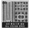
이 평가를 위해 관찰된 또 다른 패턴 충실도 과제는, 각각 "스컴 발생(scummed)" 콘택트 홀 및 브릿지된 콘택트 홀 결함의 탑-다운 단면 전자 현미경 사진 이미지를 도시하는 도 12a 및 12b에 도시된 바와 같이, 밀도가 높은 1x1 콘택트 홀 어레이에 대한 누락(missing) 및 브릿지된 콘택트 사이의 트레이드오프(tradeoff)이다. 인커밍 패턴의 정밀한 검사는, 레지스트 물질이 예정된 구멍(intended hole)으로부터 불완전하게 전개되는(developed) 동시 스컴 발생 콘택트(1202) 및 인접 콘택트 사이의 레지스트 높이가 의도한 것보다 훨씬 작은 부분적으로 브릿지된 콘택트(1204)를 나타낸다(reveal).Another pattern fidelity task observed for this evaluation is to provide a top-down cross-sectional electron micrograph of each of the " scummed "contact holes and bridged contact hole defects, as shown in FIGS. 12A and 12B, , A missing for a dense 1 x 1 contact hole array, and a tradeoff between bridged contacts. A precise inspection of the incoming pattern can be accomplished by the fact that the resist material is developed partially incompletely from the intended hole and is partially bridged with the resist height between
종래의 에칭 프로세스는 독립적으로 두가지 문제(즉, 스컴 발생 콘택트(scummed contact)(1202) 또는 브릿지된 콘택트(1204))를 해결할 수 있지만, TL을 개방하기 전에 (스컴 발생 결함을 경화시키기 위한) 디-스컴 프로세스(de-scum process)를 삽입하기에 부적절한 PR 버짓이 존재한다. 또한, TL 개방의 PR 선택도를 단순히 튜닝(tuning)하기에 불충분한 마진(margin)이 존재한다. The conventional etching process can solve two problems independently (i.e., a
도 13은 PR 선택도의 튜닝에 기초하여 콘택트 홀 어레이에서 결함을 감소시키는 종래의 접근법을 도시한다. 본 실시예에서, 도 13은 각각 낮은, 중간, 및 높은 PR 선택도 TL 개방 레시피(recipe)의 적용에 의한 3개의 어레이(1302, 1304, 1306)를 도시한다. 3개의 어레이(1302, 1304, 1306)는 각각 2200개의 콘택트를 가진 1x1 콘택트 홀이었다. 각각의 경우에, 콘택트에 누락 또는 브릿지된 콘택트가 있는지 검사하였다. 2200개 콘택트의 이러한 샘플링 레이트(sampling rate)는 제조 레벨 수율 분석에서 매우 낮지만, 이것은 경쟁적 결함 모드 간의 트레이드오프(trade-off)를 레지스트 선택도의 함수로서 관찰하기 위한 적절한 해상도를 제공한다. Figure 13 illustrates a conventional approach to reducing defects in a contact hole array based on tuning of PR selectivity. In this embodiment, Fig. 13 shows three
도 13의 결과는 PR 선택도를 튜닝하는 기능으로서 브릿지된 콘택트 및 스컴 발생 콘택트 사이에 트레이드오프가 있음을 명확하게 나타낸다. 예컨대, 어레이(1302)에서의 낮은 PR 선택도에서, 브릿지된 콘택트(1310)는 스컴 발생 콘택트보다 우선적으로 형성된다. 그러나, PR 선택도가 어레이(1304)에서 중간 PR 선택도로 증가하고 어레이(1306)에서 높은 PR 선택도로 증가함에 따라, 스컴 발생 콘택트(1312, 1316)는 브릿지된 콘택트보다 우선적으로 형성된다. 예컨대, 낮은 PR 선택도 레시피가 사용되는 경우, 2200개의 콘택트 홀의 어레이(1302)에서 스컴 발생 콘택트가 검출되지 않았고, 4개의 브릿지된 콘택트(1310)가 관찰되었다. 중간 PR 선택도 레시피가 사용된 경우, 2200개의 콘택트 홀의 어레이(1304)에서 5개의 스컴 발생 콘택트(1312)가 관찰되었지만, 브릿지된 콘택트는 관찰되지 않았다. 마지막으로, 높은 PR 선택도 레시피가 사용된 경우, 2200개의 콘택트 홀의 어레이(1306)에서 20개의 스컴 발생 콘특트(1316)가 관찰되었지만, 브릿지된 콘택트는 관찰되지 않았다.The result in Figure 13 clearly shows that there is a tradeoff between the bridged contact and the scum generating contact as a function of tuning the PR selectivity. For example, in the low PR selectivity in the
도 14는 실시형태에 따른, (위에서 설명하고, 도 5a, 도 5b, 도 6, 도 7, 및 도 8에 도시된) 반복된 성막/에칭 프로세스의 수행을 포함하는 기술에 기초하여 콘택트 홀 어레이에서 결함을 감소시키는 접근법의 결과를 도시한다. 도 14는 2200개의 콘택트 홀의 어레이(1402)에 대해 스컴 발생 결함이 없고, 브릿지 콘택트가 관찰되지 않았음을 도시한다. 이러한 결과는 도 13에 도시된 종래의 접근법에 비해 현저한 개선을 나타낸다. 이러한 향상된 결과에 대한 가능한 설명은 다음과 같다.FIG. 14 is a flow diagram of a method of fabricating a contact hole array (not shown) based on a technique including performing a repetitive deposition / etching process (described above and shown in FIGS. 5A, 5B, 6, 7, and 8) ≪ / RTI > shows the result of an approach to reducing defects in the field. Fig. 14 shows that there is no scum occurrence defect for the array of 2200
전술된 높은 선택도[도 5b의 패널(522)에 도시된 7.8 : 1] 성막/에칭 프로세스의 구성 단계의 추가의 특성화는 도 14의 개선된 결과에 대한 가능한 설명에 대한 이해를 제공한다. 이 조사의 결과는 다음과 같이 도 15에 제시된다. Further characterization of the high selectivity (7.8: 1 shown in
도 15는 실시형태에 따른, TL 개방 에칭의 3개의 스테이지에서 나타나는 단면 전자 현미경 사진 이미지를 도시한다. 표준 TL 개방 레시피의 적용은 이미지(1502)에 도시된 바와 같이, 단조 테이퍼(monotonic taper)를 갖는 사다리꼴 마스크 형상을 초래한다. DCS-향상 성막 프로세스의 적용은, 이미지(1504)에 도시된 바와 같이, CFx 중합체를 우선적으로 레지스트 상에 성막하여 보다 수직의 프로파일(more vertical profile)을 생성한다. 성막 시간을 두 배로하면 종횡비에 의존하는 성막이 발생하며 이미지(1506)에서와 같이 구조의 상단이 라운딩(rounding)되고 중합체 오버행이 형성됨을 알 수 있다. 낮은 종횡비 구조의 레지스트에 CFx를 우선적으로 성막하면 부분적으로 브릿지된 콘택트 홀의 약한 부분을 높은 종횡비의 홀의 바닥에 스커밍/남은 레지스트(scumming/remaining resist)에 현저한 성막없이 패시베이션될 수 있는 메커니즘이 제공된다. 도 14에 도시된 바와 같이, 유기 에칭/디스컴(descum)으로 이 새로운 성막 프로세스를 순환시키는(cycling) 것이 TL 개방 전에 적용되어, 샘플링된 2200개의 콘택트 홀에 대한 분명한 제거(arrarent elimination) 또는 양(both) 결함 모드(즉, 스컴 발생 및 브릿지된 콘택트)를 초래한다. 15 shows a cross-sectional electron micrograph image taken at three stages of TL open etch, according to an embodiment. The application of the standard TL opening recipe results in a trapezoidal mask shape with a monotonic taper, as shown in the
성막/에칭 시퀀스의 반복을 포함하는 개시된 방법은, 트렌치 및 콘택트 홀 패터닝 응용을 위한 EUV 리소그래피를 가능하게 하는 CCP 플라즈마 기반 에칭 솔루션을 성공적으로 입증하였다. EUV의 적용은 서브-40 nm 피치 애플리케이션에 대한 레티클 카운트, 사이클 시간, 통합 복잡성, 및 내부 레벨 오버레이 변화를 감소시킨다. 이러한 방법은 패턴 붕괴를 피하기 위해 인커밍 유기 마스크 두께를 감소시키는 과제에 대한 약속을 보여준다. The disclosed method, including repetition of deposition / etch sequences, has successfully demonstrated CCP plasma based etching solutions that enable EUV lithography for trench and contact hole patterning applications. The application of EUV reduces the reticle count, cycle time, integration complexity, and internal level overlay changes for sub-40 nm pitch applications. This approach demonstrates the commitment to reducing the incoming organic mask thickness to avoid pattern collapse.
개시된 방법들은 또한 유기 강성 및 에칭 내성을 향상시키는데 유리하도록 성막/에칭 시퀀스에서의 DCS의 적용을 보여준다. DCS는 또한 평탄화제 층 개방 프로세스 동안 발생하는 패턴 왜곡을 완화시키는데 도움을 줌으로써, 하류 패턴 거칠기를 감소시킨다. 트렌치 패터닝 동안 높은 레지스트 선택도를 제공하고, 레지스트 패턴에 대한 선택적 패시베이션에 의한 콘택트 홀 패터닝 애플리케이션에 대한 결함을 개선시키기 위한 플라즈마 에칭 방법이 또한 개시되었다.The disclosed methods also show the application of DCS in a deposition / etching sequence to advantage in improving organic stiffness and etch resistance. DCS also helps mitigate pattern distortion that occurs during the flattener layer opening process, thereby reducing the downstream pattern roughness. A plasma etching method has also been disclosed to provide high resist selectivity during trench patterning and to improve defects in contact hole patterning applications by selective passivation to resist patterns.
요약 섹션이 아닌 상세한 설명 섹션이 청구범위를 해석하기 위해 사용되는 것을 의도한다고 인식되어야 한다. 요약 섹션은 본 개시의 전체가 아닌 하나 이상의 예시적 실시형태를 제시할 수 있고, 이에 따라 첨부된 청구범위와 본 개시를 어떠한 방식으로 한정하는 것을 의도하지 않는다.It is to be appreciated that a detailed description section, rather than a summary section, is intended to be used to interpret the claims. The Summary section may suggest one or more exemplary embodiments that are not exhaustive of the disclosure, and thus are not intended to limit the appended claims and the disclosure in any manner.
하나 이상의 실시형태의 설명에 의해 본 개시가 예시되었고, 실시형태가 매우 상세히 설명되었지만, 첨부된 청구범위의 범위를 이러한 세부사항에 제한하거나 어떠한 방식으로 한정하는 것을 의도하지 않는다. 추가적인 장점 및 수정사항은 통상의 기술자에게 용이하게 보일 것이다. 따라서, 더 넓은 양태를 갖는 본 발명은, 특정 세부사항, 대표적인 장치와 방법 및 설명되고 도시된 예시적 실시예에 한정되지 않는다. 따라서, 이러한 세부사항으로부터 총괄적 발명의 개념의 범위로부터 벗어나지 않는 이탈(departure)가 이루어질 수 있다.While this disclosure has been illustrated by a description of one or more embodiments and while the embodiments have been described in considerable detail, it is not intended that the scope of the appended claims be limited or limited in any way to such details. Additional advantages and modifications will readily appear to those of ordinary skill in the art. Accordingly, the invention in its broader aspects is not limited to the specific details, representative apparatus and method, and illustrative embodiments shown and described. Accordingly, departures may be made from these details without departing from the scope of the general inventive concept.
Claims (20)
상기 기판 상에 필름 스택(film stack) - 상기 필름 스택은 하부 유기층, 상기 하부 유기층 위에 배치된 반사 방지 코팅층, 및 상기 반사 방치 코팅층 위에 배치된 포토레지스트 층을 포함함 - 을 형성하는 단계;
상기 반사 방지 코팅층의 마스킹되지 않은 부분을 노출시키기 위해 상기 포토레지스트 층을 패터닝하는 단계;
상기 반사 방지 코팅층의 마스킹되지 않은 부분 상에 그리고 상기 패터닝된 포토레지스트 층의 비측벽(non-sidewall) 부분 상에 카본 함유층을 선택적으로 성막하는 단계;
상기 카본 함유층을 제거하고 상기 포토레지스트 층의 두께 감소 없이 상기 반사 방지 코팅층의 마스킹되지 않은 부분의 부분 두께를 제거하기 위해 상기 필름 스택을 에칭하는 단계; 및
적어도 상기 반사 방지 코팅층의 마스킹되지 않은 부분의 전체 두께가 제거되어 상기 하부 유기층이 노출될 때까지 상기 선택적 성막 단계와 에칭 단계를 반복하는 단계
를 포함하는 기판 상에 반사 방지 코팅층을 통해 에칭하는 방법.A method for etching through an antireflective coating on a substrate,
Forming a film stack on the substrate, the film stack including a lower organic layer, an anti-reflective coating disposed over the lower organic layer, and a photoresist layer disposed over the reflective coating layer;
Patterning the photoresist layer to expose an unmasked portion of the antireflective coating;
Selectively depositing a carbon-containing layer on an unmasked portion of the antireflective coating and on a non-sidewall portion of the patterned photoresist layer;
Etching the film stack to remove the carbon-containing layer and to remove a portion thickness of the unmasked portion of the anti-reflective coating layer without reducing the thickness of the photoresist layer; And
Repeating the selective deposition step and the etching step until at least the entire thickness of the unmasked portion of the anti-reflective coating layer is removed and the lower organic layer is exposed
RTI ID = 0.0 > a < / RTI > substrate comprising an antireflective coating.
상기 카본 함유층을 선택적으로 성막하는 단계는, 상기 반사 방지 코팅층의 마스킹되지 않은 부분 상에서보다 상기 패터닝된 포토레지스트 층의 비측벽 부분 상에 더 큰 두께로 성막하는 단계를 포함하는 것인 기판 상에 반사 방지 코팅층을 통해 에칭하는 방법.The method according to claim 1,
Wherein selectively depositing the carbon-containing layer comprises depositing a greater thickness on a non-sidewall portion of the patterned photoresist layer than on an unmasked portion of the antireflective coating layer. / RTI > coating layer.
상기 기판으로 가속화되는 2차 전자 방출을 생성하여 상기 에칭을 용이하게 하고, 그리고 상기 포토레지스트 층의 두께를 감소시키지 않고 상기 반사 방지 코팅층의 마스킹되지 않은 부분의 부분 두께를 추가로 제거할 수 있도록 상기 카본 함유층의 제거시에 상기 포토레지스트 층에 함침하는(impregnate) 실리콘 원자를 스퍼터링하여 상기 함침된 포토레지스트 층이 상기 에칭에 대하여 더 내성을 갖게 하기 위해, 상기 에칭 동안 상부 실리콘 전극에 직류 전위가 인가되는 것인 기판 상에 반사 방지 코팅층을 통해 에칭하는 방법.The method according to claim 1,
Further comprising the steps of: generating secondary electron emissions to be accelerated to the substrate to facilitate the etching and to further remove the partial thickness of the unmasked portion of the anti-reflective coating layer without reducing the thickness of the photoresist layer; In order to make the impregnated photoresist layer more resistant to the etching by sputtering silicon atoms impregnated in the photoresist layer upon removal of the carbon-containing layer, a DC potential is applied to the upper silicon electrode during the etching Lt; RTI ID = 0.0 > anti-reflective coating < / RTI >
상기 에칭 단계는 N2H2 가스로부터 생성된 플라즈마를 사용하는 반응성 이온 에칭에 의한 것인 기판 상에 반사 방지 코팅층을 통해 에칭하는 방법.The method according to claim 1,
The etching step is to etch through the anti-reflective coating layer on the substrate by means of reactive ion etching using a plasma generated from N 2 H 2 gas.
상기 하부 유기층은 평탄화제 층(planarizer layer)이고, 상기 반사 방지 코팅층은 SiARC 층이고, 상기 포토레지스트 층은 EUV(extreme ultraviolet) 포토레지스트 층이고, 상기 카본 함유층은 플루오로카본(fluorocarbon)인 것인 기판 상에 반사 방지 코팅층을 통해 에칭하는 방법.5. The method of claim 4,
Wherein the lower organic layer is a planarizer layer, the antireflective coating layer is an SiARC layer, the photoresist layer is an extreme ultraviolet (EUV) photoresist layer, and the carbon containing layer is a fluorocarbon A method for etching on a substrate through an antireflective coating.
패터닝된 EUV(extreme ultraviolet) 포토레지스트, 전사층(TL: transfer layer), 및 유기 평탄화 층(OPL: organic planarizing layer)을 포함하는 패터닝된 기판을 제공하는 단계; 및
상기 EUV 포토레지스트로부터 상기 OPL로 패턴을 전사하기 위한 마스크로서 상기 EUV 포토레지스트 및 TL을 사용하여 상기 TL을 통해 그리고 상기 OPL로 선택적으로 그리고 점진적으로 에칭하기 위해 성막/에칭 프로세스를 반복적으로 수행하는 단계
를 포함하고,
상기 성막/에칭 프로세스는, 순차적으로,
(1) 상기 EUV 포토레지스트 및 상기 TL 또는 OPL의 노출 부분을 포함하는 상기 패터닝된 기판 상에 플루오로카본 층을 성막하는 단계; 및
(2) 상기 플루오로카본 층 및 상기 EUV 포토레지스트에 비해 선택적으로 상기 TL 또는 OPL의 증가 부분을 제거하기 위해 반응성 이온 에칭하는 단계
를 포함하고,
상기 성막/에칭 프로세스[(1) 및 (2)]를 반복적으로 수행함으로써, 상기 TL 및 OPL을 에칭하는 것이 반응성 이온 에칭 프로세스만을 수행하는 것에 의해 얻어지는 포토레지스트 에칭 선택도보다 더 큰 포토레지스트 에칭 선택도를 갖게 하는 것인 패터닝된 기판을 에칭하는 방법.A method of etching a patterned substrate,
Providing a patterned substrate comprising a patterned EUV (extreme ultraviolet) photoresist, a transfer layer (TL), and an organic planarizing layer (OPL); And
Repeatedly performing a film / etch process to selectively and progressively etch through the TL and into the OPL using the EUV photoresist and TL as a mask for transferring the pattern from the EUV photoresist to the OPL
Lt; / RTI >
The film-forming / etching process is performed sequentially,
(1) depositing a fluorocarbon layer on the patterned substrate comprising the EUV photoresist and exposed portions of the TL or OPL; And
(2) selectively etching the reactive ion to remove the increased portion of the TL or OPL relative to the fluorocarbon layer and the EUV photoresist
Lt; / RTI >
By repeatedly performing the above film-forming / etching processes [(1) and (2)], etching of the TL and OPL results in a photoresist etching selectivity greater than that of the photoresist etching selectivity obtained by performing only a reactive ion etching process Gt; a < / RTI > patterned substrate.
상기 반응성 이온 에칭하는 단계(2)는 직류 전위를 중첩시키면서 듀얼 주파수 용량성 결합된 플라즈마를 생성하는 단계를 포함하는 것인 패터닝된 기판을 에칭하는 방법.The method according to claim 6,
The reactive ion etching step (2) comprises generating a dual frequency capacitively coupled plasma while superimposing direct current potentials.
상기 플라즈마는 N2H2를 포함하는 것인 패터닝된 기판을 에칭하는 방법.8. The method of claim 7,
Wherein the plasma comprises N 2 H 2 .
상기 직류 전위는 실리콘 전극으로부터의 스퍼터링에 의해 생성되는 상기 플라즈마 내에 실리콘 종(silicon species)을 생성하기 위해 상기 실리콘 전극에 인가되고, 실리콘 원자는 상기 EUV 포토레지스트의 에칭 선택도를 증가시키는 작용을 하는 것인 패터닝된 기판을 에칭하는 방법.9. The method of claim 8,
The direct current potential is applied to the silicon electrode to produce a silicon species in the plasma generated by sputtering from the silicon electrode, and the silicon atom acts to increase the etch selectivity of the EUV photoresist ≪ / RTI >
실리콘 필름이 상기 EUV 포토레지스트 상에 형성되어 상기 EUV 포토레지스트의 에칭 선택도를 증가시키는 작용을 하는 것인 패터닝된 기판을 에칭하는 방법.10. The method of claim 9,
Wherein a film of silicon is formed on the EUV photoresist to act to increase the etch selectivity of the EUV photoresist.
상기 EUV 포토레지스트 및 상기 OPL은 카본 중합체를 포함하는 것인 패터닝된 기판을 에칭하는 방법.The method according to claim 6,
Wherein the EUV photoresist and the OPL comprise a carbon polymer.
상기 TL 및 상기 OPL은 상기 EUV 포토레지스트에 비해 (2) 단계에서 우선적으로 에칭되는 것인 패터닝된 기판을 에칭하는 방법.12. The method of claim 11,
Wherein the TL and the OPL are preferentially etched in step (2) relative to the EUV photoresist.
상기 성막/에칭 프로세스를 반복적으로 수행함으로써 얻어지는 상기 EUV 포토레지스트 에칭 선택도는 적어도 7.8:1인 것인 패터닝된 기판을 에칭하는 방법.The method according to claim 6,
Wherein the EUV photoresist etch selectivity obtained by repeatedly performing the film deposition / etching process is at least 7.8: 1.
상기 플루오로카본 층은 상기 TL에 비해 상기 패터닝된 EUV 포토레지스트의 비측벽 부분 상에서 우선적으로 성막되는 것인 패터닝된 기판을 에칭하는 방법.The method according to claim 6,
Wherein the fluorocarbon layer is preferentially deposited on non-sidewall portions of the patterned EUV photoresist relative to the TL.
상기 성막/에칭 프로세스[(1) 및 (2)]를 반복적으로 수행하는 단계는, 상기 TL 및 OPL을 에칭하여, 반응성 이온 에칭 프로세스만을 수행함으로써 초래되는 라인 폭 거칠기에 비해 적어도 52 %까지 개선된 라인 폭 거칠기를 얻는 것인 패터닝된 기판을 에칭하는 방법.The method according to claim 6,
Repeatedly performing the deposition / etching process [(1) and (2)] may include etching the TL and OPL to improve the line width roughness by at least 52% Width line roughness of the patterned substrate.
상기 성막/에칭 프로세스[(1) 및 (2)]를 반복적으로 수행하는 단계는, 상기 TL 및 OPL을 에칭하여, 반응성 이온 에칭 프로세스만을 수행함으로써 얻어지는 결과에 비해 스컴 발생 결함(scummed defect) 및 브릿지 결함 모두가 감소되는 것인 패터닝된 기판을 에칭하는 방법.The method according to claim 6,
The step of repeatedly performing the film forming / etching process [(1) and (2)] is advantageous in that the TL and the OPL are etched to provide scummed defects and bridges Wherein all of the defects are reduced.
상기 플루오로카본 층은 스컴 발생 결함보다 브릿지 결함에 더 큰 정도로 우선적으로 성막되는 것인 패터닝된 기판을 에칭하는 방법.17. The method of claim 16,
Wherein the fluorocarbon layer is preferentially deposited to a greater degree in bridging defects than scum generation defects.
상기 패터닝된 EUV 포토레지스트는 60 nm보다 작은 두께 및 40 nm보다 작은 패터닝 임계 치수를 갖고, 상기 TL은 60 nm보다 작은 두께를 갖는 실리콘 반사 방지 코팅을 포함하고, 상기 OPL은 200 nm보다 작은 두께를 갖는 것인 패터닝된 기판을 에칭하는 방법.The method according to claim 6,
Wherein the patterned EUV photoresist has a thickness less than 60 nm and a patterning critical dimension less than 40 nm, the TL comprises a silicon anti-reflective coating having a thickness less than 60 nm, the OPL having a thickness less than 200 nm And etching the patterned substrate.
상기 직류 전위의 인가를 통해 생성된 탄도 전자(ballistic electron)는 상기 EUV 포토레지스트를 변화시키고 경화시켜서 포토레지스트 선택도를 향상시키는 것인 패터닝된 기판을 에칭하는 방법.8. The method of claim 7,
Wherein ballistic electrons generated through application of the direct current potential change and cure the EUV photoresist to enhance photoresist selectivity.
상기 플루오로카본 층은 CH3F 및 CF4를 포함하는 것인 패터닝된 기판을 에칭하는 방법.The method according to claim 6,
A carbon layer as the fluorinated method for etching of the patterned substrate comprises a CH 3 F and CF 4.
Applications Claiming Priority (3)
| Application Number | Priority Date | Filing Date | Title |
|---|---|---|---|
| US201562142020P | 2015-04-02 | 2015-04-02 | |
| US62/142,020 | 2015-04-02 | ||
| PCT/US2016/025555 WO2016161287A1 (en) | 2015-04-02 | 2016-04-01 | Trench and hole patterning with euv resists using dual frequency capacitively coupled plasma (ccp) |
Publications (1)
| Publication Number | Publication Date |
|---|---|
| KR20170135896A true KR20170135896A (en) | 2017-12-08 |
Family
ID=55752773
Family Applications (1)
| Application Number | Title | Priority Date | Filing Date |
|---|---|---|---|
| KR1020177031849A KR20170135896A (en) | 2015-04-02 | 2016-04-01 | EUV tolerant trenches and hole patterning using dual frequency capacitively coupled plasma (CCP) |
Country Status (5)
| Country | Link |
|---|---|
| US (2) | US9607834B2 (en) |
| KR (1) | KR20170135896A (en) |
| CN (1) | CN107567650A (en) |
| TW (1) | TWI625784B (en) |
| WO (1) | WO2016161287A1 (en) |
Cited By (2)
| Publication number | Priority date | Publication date | Assignee | Title |
|---|---|---|---|---|
| KR20190142426A (en) * | 2017-05-16 | 2019-12-26 | 램 리써치 코포레이션 | Eliminate Probabilistic Yield Effects in Lithography |
| WO2021055542A1 (en) * | 2019-09-19 | 2021-03-25 | Tokyo Electron Limited | Method of forming a narrow trench |
Families Citing this family (18)
| Publication number | Priority date | Publication date | Assignee | Title |
|---|---|---|---|---|
| US9824893B1 (en) | 2016-06-28 | 2017-11-21 | Lam Research Corporation | Tin oxide thin film spacers in semiconductor device manufacturing |
| US10002773B2 (en) * | 2016-10-11 | 2018-06-19 | Lam Research Corporation | Method for selectively etching silicon oxide with respect to an organic mask |
| US10566212B2 (en) | 2016-12-19 | 2020-02-18 | Lam Research Corporation | Designer atomic layer etching |
| US10082736B2 (en) * | 2017-01-13 | 2018-09-25 | International Business Machines Corporation | Approach to lowering extreme ultraviolet exposure dose for inorganic hardmasks for extreme ultraviolet patterning |
| KR20180093798A (en) | 2017-02-13 | 2018-08-22 | 램 리써치 코포레이션 | Method to create air gaps |
| US10546748B2 (en) | 2017-02-17 | 2020-01-28 | Lam Research Corporation | Tin oxide films in semiconductor device manufacturing |
| TW201841221A (en) * | 2017-02-22 | 2018-11-16 | 日商東京威力科創股份有限公司 | Method for reducing lithography defects and pattern transfer |
| KR102630349B1 (en) | 2018-01-30 | 2024-01-29 | 램 리써치 코포레이션 | Tin oxide mandrels in patterning |
| US10504851B2 (en) * | 2018-02-26 | 2019-12-10 | Globalfoundries Inc. | Structure and method to improve overlay performance in semiconductor devices |
| US11131919B2 (en) | 2018-06-22 | 2021-09-28 | International Business Machines Corporation | Extreme ultraviolet (EUV) mask stack processing |
| CN109227036A (en) * | 2018-08-17 | 2019-01-18 | 基准精密工业(惠州)有限公司 | The manufacturing method of amorphous alloy precision component |
| US11921427B2 (en) | 2018-11-14 | 2024-03-05 | Lam Research Corporation | Methods for making hard masks useful in next-generation lithography |
| US10777414B1 (en) * | 2019-03-14 | 2020-09-15 | Applied Materials, Inc. | Methods for reducing transfer pattern defects in a semiconductor device |
| WO2020263718A1 (en) * | 2019-06-24 | 2020-12-30 | Lam Research Corporation | Selective carbon deposition |
| CN114270479B (en) | 2019-06-27 | 2022-10-11 | 朗姆研究公司 | Alternating etch and passivation process |
| US11837471B2 (en) | 2019-12-17 | 2023-12-05 | Tokyo Electron Limited | Methods of patterning small features |
| US20220005688A1 (en) * | 2020-07-02 | 2022-01-06 | Applied Materials, Inc. | Selective deposition of carbon on photoresist layer for lithography applications |
| KR20220017837A (en) * | 2020-08-05 | 2022-02-14 | 가부시키가이샤 아루박 | Silicon dry etching method |
Family Cites Families (5)
| Publication number | Priority date | Publication date | Assignee | Title |
|---|---|---|---|---|
| US7265056B2 (en) * | 2004-01-09 | 2007-09-04 | Taiwan Semiconductor Manufacturing Company, Ltd. | Method for forming novel BARC open for precision critical dimension control |
| CN101777492A (en) * | 2004-11-05 | 2010-07-14 | 东京毅力科创株式会社 | Plasma processing method |
| US7927779B2 (en) * | 2005-06-30 | 2011-04-19 | Taiwan Semiconductor Manufacturing Companym, Ltd. | Water mark defect prevention for immersion lithography |
| KR20090076743A (en) * | 2008-01-07 | 2009-07-13 | 삼성전자주식회사 | Method of forming fine patterns of semiconductor device |
| US8569091B2 (en) | 2009-08-27 | 2013-10-29 | International Business Machines Corporation | Integrated circuit switches, design structure and methods of fabricating the same |
-
2016
- 2016-04-01 TW TW105110468A patent/TWI625784B/en active
- 2016-04-01 WO PCT/US2016/025555 patent/WO2016161287A1/en active Application Filing
- 2016-04-01 CN CN201680025639.2A patent/CN107567650A/en active Pending
- 2016-04-01 KR KR1020177031849A patent/KR20170135896A/en not_active Application Discontinuation
- 2016-04-01 US US15/088,701 patent/US9607834B2/en active Active
-
2017
- 2017-03-14 US US15/458,476 patent/US9818610B2/en active Active
Cited By (3)
| Publication number | Priority date | Publication date | Assignee | Title |
|---|---|---|---|---|
| KR20190142426A (en) * | 2017-05-16 | 2019-12-26 | 램 리써치 코포레이션 | Eliminate Probabilistic Yield Effects in Lithography |
| WO2021055542A1 (en) * | 2019-09-19 | 2021-03-25 | Tokyo Electron Limited | Method of forming a narrow trench |
| US11841617B2 (en) | 2019-09-19 | 2023-12-12 | Tokyo Electron Limited | Method of forming a narrow trench |
Also Published As
| Publication number | Publication date |
|---|---|
| US9607834B2 (en) | 2017-03-28 |
| CN107567650A (en) | 2018-01-09 |
| TWI625784B (en) | 2018-06-01 |
| TW201705269A (en) | 2017-02-01 |
| US20170263443A1 (en) | 2017-09-14 |
| WO2016161287A1 (en) | 2016-10-06 |
| US9818610B2 (en) | 2017-11-14 |
| US20160293405A1 (en) | 2016-10-06 |
Similar Documents
| Publication | Publication Date | Title |
|---|---|---|
| KR20170135896A (en) | EUV tolerant trenches and hole patterning using dual frequency capacitively coupled plasma (CCP) | |
| US10049892B2 (en) | Method for processing photoresist materials and structures | |
| US9978596B2 (en) | Self-aligned multiple spacer patterning schemes for advanced nanometer technology | |
| US20140315380A1 (en) | Trench patterning with block first sidewall image transfer | |
| KR102550498B1 (en) | Methods for reducing pattern transfer and lithography defects | |
| US10868244B2 (en) | Multiple hard mask patterning to fabricate 20nm and below MRAM devices | |
| TW201439668A (en) | Method for etching EUV material layers utilized to form a photomask | |
| US20210217614A1 (en) | Multiple patterning with selective mandrel formation | |
| KR100849190B1 (en) | Method for forming fine pattern in semiconductor device | |
| US20060105574A1 (en) | Process for defining integrated circuits in semiconductor electronic devices | |
| Feurprier et al. | Trench and hole patterning with EUV resists using dual frequency capacitively coupled plasma (CCP) | |
| US8409457B2 (en) | Methods of forming a photoresist-comprising pattern on a substrate | |
| TWI623020B (en) | Method for patterning incorporating misalignment error protection | |
| US20160246171A1 (en) | Method for Patterning Using a Composite Pattern | |
| CN108962727B (en) | Method for manufacturing semiconductor structure | |
| Romero et al. | A novel approach for the patterning and high-volume production of sub-40-nm gates | |
| US8389402B2 (en) | Method for via formation in a semiconductor device | |
| US7482225B2 (en) | Method of fabricating floating gate of flash memory device | |
| Montgomery et al. | Driving contact hole resolution to 45nm using novel process enhancement techniques | |
| TW202145342A (en) | Forming a semiconductor feature using atomic layer etch | |
| de Marneffe et al. | Patterning of 25 nm contact holes at 90 nm pitch: Combination of line/space double exposure immersion lithography and plasma-assisted shrink technology | |
| KR20050117880A (en) | Method of forming bi-layer photo mask using neutral beam source | |
| KR20020002137A (en) | Method of making pattern for semiconductor device | |
| KR20070021506A (en) | Method of manufacturing semiconductor device | |
| KR20090016935A (en) | Method for fabricating pattern in semiconductor device |
Legal Events
| Date | Code | Title | Description |
|---|---|---|---|
| E902 | Notification of reason for refusal | ||
| E601 | Decision to refuse application |