KR20170131121A - Semicondutor devices - Google Patents
Semicondutor devices Download PDFInfo
- Publication number
- KR20170131121A KR20170131121A KR1020160062384A KR20160062384A KR20170131121A KR 20170131121 A KR20170131121 A KR 20170131121A KR 1020160062384 A KR1020160062384 A KR 1020160062384A KR 20160062384 A KR20160062384 A KR 20160062384A KR 20170131121 A KR20170131121 A KR 20170131121A
- Authority
- KR
- South Korea
- Prior art keywords
- vertical
- patterns
- channel patterns
- vertical channel
- structures
- Prior art date
Links
- 239000004065 semiconductor Substances 0.000 claims abstract description 71
- 238000000034 method Methods 0.000 claims abstract description 36
- 238000003860 storage Methods 0.000 claims description 34
- 238000002955 isolation Methods 0.000 claims description 19
- 230000010354 integration Effects 0.000 abstract description 8
- 239000010410 layer Substances 0.000 description 79
- 239000010408 film Substances 0.000 description 68
- 239000000758 substrate Substances 0.000 description 45
- 238000005530 etching Methods 0.000 description 17
- 230000002093 peripheral effect Effects 0.000 description 16
- XUIMIQQOPSSXEZ-UHFFFAOYSA-N Silicon Chemical compound [Si] XUIMIQQOPSSXEZ-UHFFFAOYSA-N 0.000 description 15
- 229910052710 silicon Inorganic materials 0.000 description 15
- 239000010703 silicon Substances 0.000 description 15
- VYPSYNLAJGMNEJ-UHFFFAOYSA-N Silicium dioxide Chemical compound O=[Si]=O VYPSYNLAJGMNEJ-UHFFFAOYSA-N 0.000 description 14
- 229910052751 metal Inorganic materials 0.000 description 14
- 239000002184 metal Substances 0.000 description 14
- 229910052814 silicon oxide Inorganic materials 0.000 description 14
- 239000011229 interlayer Substances 0.000 description 13
- 238000010586 diagram Methods 0.000 description 12
- 239000000463 material Substances 0.000 description 11
- 238000009413 insulation Methods 0.000 description 9
- 230000000903 blocking effect Effects 0.000 description 6
- 238000004519 manufacturing process Methods 0.000 description 6
- 150000004767 nitrides Chemical class 0.000 description 6
- 229910052581 Si3N4 Inorganic materials 0.000 description 5
- 238000013500 data storage Methods 0.000 description 5
- HQVNEWCFYHHQES-UHFFFAOYSA-N silicon nitride Chemical compound N12[Si]34N5[Si]62N3[Si]51N64 HQVNEWCFYHHQES-UHFFFAOYSA-N 0.000 description 5
- 229910000577 Silicon-germanium Inorganic materials 0.000 description 4
- 230000015572 biosynthetic process Effects 0.000 description 4
- 229910021420 polycrystalline silicon Inorganic materials 0.000 description 4
- 230000004044 response Effects 0.000 description 4
- LEVVHYCKPQWKOP-UHFFFAOYSA-N [Si].[Ge] Chemical compound [Si].[Ge] LEVVHYCKPQWKOP-UHFFFAOYSA-N 0.000 description 3
- 229910052732 germanium Inorganic materials 0.000 description 3
- GNPVGFCGXDBREM-UHFFFAOYSA-N germanium atom Chemical compound [Ge] GNPVGFCGXDBREM-UHFFFAOYSA-N 0.000 description 3
- 229910000449 hafnium oxide Inorganic materials 0.000 description 3
- WIHZLLGSGQNAGK-UHFFFAOYSA-N hafnium(4+);oxygen(2-) Chemical compound [O-2].[O-2].[Hf+4] WIHZLLGSGQNAGK-UHFFFAOYSA-N 0.000 description 3
- 239000012535 impurity Substances 0.000 description 3
- 239000012212 insulator Substances 0.000 description 3
- TWNQGVIAIRXVLR-UHFFFAOYSA-N oxo(oxoalumanyloxy)alumane Chemical compound O=[Al]O[Al]=O TWNQGVIAIRXVLR-UHFFFAOYSA-N 0.000 description 3
- 229920005591 polysilicon Polymers 0.000 description 3
- 101100481702 Arabidopsis thaliana TMK1 gene Proteins 0.000 description 2
- 206010010144 Completed suicide Diseases 0.000 description 2
- NBIIXXVUZAFLBC-UHFFFAOYSA-N Phosphoric acid Chemical compound OP(O)(O)=O NBIIXXVUZAFLBC-UHFFFAOYSA-N 0.000 description 2
- 239000004020 conductor Substances 0.000 description 2
- 239000013256 coordination polymer Substances 0.000 description 2
- 238000001312 dry etching Methods 0.000 description 2
- 238000005240 physical vapour deposition Methods 0.000 description 2
- 239000010409 thin film Substances 0.000 description 2
- 238000009966 trimming Methods 0.000 description 2
- WFKWXMTUELFFGS-UHFFFAOYSA-N tungsten Chemical compound [W] WFKWXMTUELFFGS-UHFFFAOYSA-N 0.000 description 2
- 229910052721 tungsten Inorganic materials 0.000 description 2
- 239000010937 tungsten Substances 0.000 description 2
- -1 tungsten) Chemical compound 0.000 description 2
- 229910000147 aluminium phosphate Inorganic materials 0.000 description 1
- 238000000231 atomic layer deposition Methods 0.000 description 1
- 239000003990 capacitor Substances 0.000 description 1
- 238000005229 chemical vapour deposition Methods 0.000 description 1
- 230000000295 complement effect Effects 0.000 description 1
- 239000011370 conductive nanoparticle Substances 0.000 description 1
- 239000013078 crystal Substances 0.000 description 1
- 230000002401 inhibitory effect Effects 0.000 description 1
- 238000005468 ion implantation Methods 0.000 description 1
- 229910021421 monocrystalline silicon Inorganic materials 0.000 description 1
- 230000003647 oxidation Effects 0.000 description 1
- 238000007254 oxidation reaction Methods 0.000 description 1
- 230000007261 regionalization Effects 0.000 description 1
- 230000003252 repetitive effect Effects 0.000 description 1
- 238000000926 separation method Methods 0.000 description 1
- 230000005641 tunneling Effects 0.000 description 1
- 238000001039 wet etching Methods 0.000 description 1
Images


Classifications
-
- H—ELECTRICITY
- H10—SEMICONDUCTOR DEVICES; ELECTRIC SOLID-STATE DEVICES NOT OTHERWISE PROVIDED FOR
- H10B—ELECTRONIC MEMORY DEVICES
- H10B43/00—EEPROM devices comprising charge-trapping gate insulators
- H10B43/20—EEPROM devices comprising charge-trapping gate insulators characterised by three-dimensional arrangements, e.g. with cells on different height levels
-
- H—ELECTRICITY
- H10—SEMICONDUCTOR DEVICES; ELECTRIC SOLID-STATE DEVICES NOT OTHERWISE PROVIDED FOR
- H10B—ELECTRONIC MEMORY DEVICES
- H10B43/00—EEPROM devices comprising charge-trapping gate insulators
- H10B43/10—EEPROM devices comprising charge-trapping gate insulators characterised by the top-view layout
-
- H—ELECTRICITY
- H10—SEMICONDUCTOR DEVICES; ELECTRIC SOLID-STATE DEVICES NOT OTHERWISE PROVIDED FOR
- H10B—ELECTRONIC MEMORY DEVICES
- H10B41/00—Electrically erasable-and-programmable ROM [EEPROM] devices comprising floating gates
- H10B41/20—Electrically erasable-and-programmable ROM [EEPROM] devices comprising floating gates characterised by three-dimensional arrangements, e.g. with cells on different height levels
- H10B41/23—Electrically erasable-and-programmable ROM [EEPROM] devices comprising floating gates characterised by three-dimensional arrangements, e.g. with cells on different height levels with source and drain on different levels, e.g. with sloping channels
-
- H01L27/11553—
-
- H01L27/11548—
-
- H01L27/11556—
-
- H01L27/11575—
-
- H01L27/1158—
-
- H01L27/11582—
-
- H—ELECTRICITY
- H01—ELECTRIC ELEMENTS
- H01L—SEMICONDUCTOR DEVICES NOT COVERED BY CLASS H10
- H01L29/00—Semiconductor devices adapted for rectifying, amplifying, oscillating or switching, or capacitors or resistors with at least one potential-jump barrier or surface barrier, e.g. PN junction depletion layer or carrier concentration layer; Details of semiconductor bodies or of electrodes thereof ; Multistep manufacturing processes therefor
- H01L29/02—Semiconductor bodies ; Multistep manufacturing processes therefor
- H01L29/06—Semiconductor bodies ; Multistep manufacturing processes therefor characterised by their shape; characterised by the shapes, relative sizes, or dispositions of the semiconductor regions ; characterised by the concentration or distribution of impurities within semiconductor regions
- H01L29/08—Semiconductor bodies ; Multistep manufacturing processes therefor characterised by their shape; characterised by the shapes, relative sizes, or dispositions of the semiconductor regions ; characterised by the concentration or distribution of impurities within semiconductor regions with semiconductor regions connected to an electrode carrying current to be rectified, amplified or switched and such electrode being part of a semiconductor device which comprises three or more electrodes
- H01L29/0843—Source or drain regions of field-effect devices
- H01L29/0847—Source or drain regions of field-effect devices of field-effect transistors with insulated gate
-
- H—ELECTRICITY
- H01—ELECTRIC ELEMENTS
- H01L—SEMICONDUCTOR DEVICES NOT COVERED BY CLASS H10
- H01L29/00—Semiconductor devices adapted for rectifying, amplifying, oscillating or switching, or capacitors or resistors with at least one potential-jump barrier or surface barrier, e.g. PN junction depletion layer or carrier concentration layer; Details of semiconductor bodies or of electrodes thereof ; Multistep manufacturing processes therefor
- H01L29/02—Semiconductor bodies ; Multistep manufacturing processes therefor
- H01L29/06—Semiconductor bodies ; Multistep manufacturing processes therefor characterised by their shape; characterised by the shapes, relative sizes, or dispositions of the semiconductor regions ; characterised by the concentration or distribution of impurities within semiconductor regions
- H01L29/10—Semiconductor bodies ; Multistep manufacturing processes therefor characterised by their shape; characterised by the shapes, relative sizes, or dispositions of the semiconductor regions ; characterised by the concentration or distribution of impurities within semiconductor regions with semiconductor regions connected to an electrode not carrying current to be rectified, amplified or switched and such electrode being part of a semiconductor device which comprises three or more electrodes
- H01L29/1025—Channel region of field-effect devices
- H01L29/1029—Channel region of field-effect devices of field-effect transistors
- H01L29/1033—Channel region of field-effect devices of field-effect transistors with insulated gate, e.g. characterised by the length, the width, the geometric contour or the doping structure
- H01L29/1037—Channel region of field-effect devices of field-effect transistors with insulated gate, e.g. characterised by the length, the width, the geometric contour or the doping structure and non-planar channel
-
- H—ELECTRICITY
- H10—SEMICONDUCTOR DEVICES; ELECTRIC SOLID-STATE DEVICES NOT OTHERWISE PROVIDED FOR
- H10B—ELECTRONIC MEMORY DEVICES
- H10B41/00—Electrically erasable-and-programmable ROM [EEPROM] devices comprising floating gates
- H10B41/10—Electrically erasable-and-programmable ROM [EEPROM] devices comprising floating gates characterised by the top-view layout
-
- H—ELECTRICITY
- H10—SEMICONDUCTOR DEVICES; ELECTRIC SOLID-STATE DEVICES NOT OTHERWISE PROVIDED FOR
- H10B—ELECTRONIC MEMORY DEVICES
- H10B41/00—Electrically erasable-and-programmable ROM [EEPROM] devices comprising floating gates
- H10B41/20—Electrically erasable-and-programmable ROM [EEPROM] devices comprising floating gates characterised by three-dimensional arrangements, e.g. with cells on different height levels
- H10B41/23—Electrically erasable-and-programmable ROM [EEPROM] devices comprising floating gates characterised by three-dimensional arrangements, e.g. with cells on different height levels with source and drain on different levels, e.g. with sloping channels
- H10B41/27—Electrically erasable-and-programmable ROM [EEPROM] devices comprising floating gates characterised by three-dimensional arrangements, e.g. with cells on different height levels with source and drain on different levels, e.g. with sloping channels the channels comprising vertical portions, e.g. U-shaped channels
-
- H—ELECTRICITY
- H10—SEMICONDUCTOR DEVICES; ELECTRIC SOLID-STATE DEVICES NOT OTHERWISE PROVIDED FOR
- H10B—ELECTRONIC MEMORY DEVICES
- H10B41/00—Electrically erasable-and-programmable ROM [EEPROM] devices comprising floating gates
- H10B41/50—Electrically erasable-and-programmable ROM [EEPROM] devices comprising floating gates characterised by the boundary region between the core region and the peripheral circuit region
-
- H—ELECTRICITY
- H10—SEMICONDUCTOR DEVICES; ELECTRIC SOLID-STATE DEVICES NOT OTHERWISE PROVIDED FOR
- H10B—ELECTRONIC MEMORY DEVICES
- H10B43/00—EEPROM devices comprising charge-trapping gate insulators
- H10B43/20—EEPROM devices comprising charge-trapping gate insulators characterised by three-dimensional arrangements, e.g. with cells on different height levels
- H10B43/23—EEPROM devices comprising charge-trapping gate insulators characterised by three-dimensional arrangements, e.g. with cells on different height levels with source and drain on different levels, e.g. with sloping channels
- H10B43/27—EEPROM devices comprising charge-trapping gate insulators characterised by three-dimensional arrangements, e.g. with cells on different height levels with source and drain on different levels, e.g. with sloping channels the channels comprising vertical portions, e.g. U-shaped channels
-
- H—ELECTRICITY
- H10—SEMICONDUCTOR DEVICES; ELECTRIC SOLID-STATE DEVICES NOT OTHERWISE PROVIDED FOR
- H10B—ELECTRONIC MEMORY DEVICES
- H10B43/00—EEPROM devices comprising charge-trapping gate insulators
- H10B43/30—EEPROM devices comprising charge-trapping gate insulators characterised by the memory core region
- H10B43/35—EEPROM devices comprising charge-trapping gate insulators characterised by the memory core region with cell select transistors, e.g. NAND
-
- H—ELECTRICITY
- H10—SEMICONDUCTOR DEVICES; ELECTRIC SOLID-STATE DEVICES NOT OTHERWISE PROVIDED FOR
- H10B—ELECTRONIC MEMORY DEVICES
- H10B43/00—EEPROM devices comprising charge-trapping gate insulators
- H10B43/40—EEPROM devices comprising charge-trapping gate insulators characterised by the peripheral circuit region
-
- H—ELECTRICITY
- H10—SEMICONDUCTOR DEVICES; ELECTRIC SOLID-STATE DEVICES NOT OTHERWISE PROVIDED FOR
- H10B—ELECTRONIC MEMORY DEVICES
- H10B43/00—EEPROM devices comprising charge-trapping gate insulators
- H10B43/50—EEPROM devices comprising charge-trapping gate insulators characterised by the boundary region between the core and peripheral circuit regions
-
- H—ELECTRICITY
- H01—ELECTRIC ELEMENTS
- H01L—SEMICONDUCTOR DEVICES NOT COVERED BY CLASS H10
- H01L29/00—Semiconductor devices adapted for rectifying, amplifying, oscillating or switching, or capacitors or resistors with at least one potential-jump barrier or surface barrier, e.g. PN junction depletion layer or carrier concentration layer; Details of semiconductor bodies or of electrodes thereof ; Multistep manufacturing processes therefor
- H01L29/40—Electrodes ; Multistep manufacturing processes therefor
- H01L29/41—Electrodes ; Multistep manufacturing processes therefor characterised by their shape, relative sizes or dispositions
- H01L29/423—Electrodes ; Multistep manufacturing processes therefor characterised by their shape, relative sizes or dispositions not carrying the current to be rectified, amplified or switched
- H01L29/42312—Gate electrodes for field effect devices
- H01L29/42316—Gate electrodes for field effect devices for field-effect transistors
- H01L29/4232—Gate electrodes for field effect devices for field-effect transistors with insulated gate
- H01L29/42324—Gate electrodes for transistors with a floating gate
- H01L29/42332—Gate electrodes for transistors with a floating gate with the floating gate formed by two or more non connected parts, e.g. multi-particles flating gate
-
- H—ELECTRICITY
- H01—ELECTRIC ELEMENTS
- H01L—SEMICONDUCTOR DEVICES NOT COVERED BY CLASS H10
- H01L29/00—Semiconductor devices adapted for rectifying, amplifying, oscillating or switching, or capacitors or resistors with at least one potential-jump barrier or surface barrier, e.g. PN junction depletion layer or carrier concentration layer; Details of semiconductor bodies or of electrodes thereof ; Multistep manufacturing processes therefor
- H01L29/40—Electrodes ; Multistep manufacturing processes therefor
- H01L29/41—Electrodes ; Multistep manufacturing processes therefor characterised by their shape, relative sizes or dispositions
- H01L29/423—Electrodes ; Multistep manufacturing processes therefor characterised by their shape, relative sizes or dispositions not carrying the current to be rectified, amplified or switched
- H01L29/42312—Gate electrodes for field effect devices
- H01L29/42316—Gate electrodes for field effect devices for field-effect transistors
- H01L29/4232—Gate electrodes for field effect devices for field-effect transistors with insulated gate
- H01L29/4234—Gate electrodes for transistors with charge trapping gate insulator
- H01L29/42348—Gate electrodes for transistors with charge trapping gate insulator with trapping site formed by at least two separated sites, e.g. multi-particles trapping site
Abstract
Description
본 발명은 반도체 소자에 관한 것으로, 더욱 상세하게는 수직형 메모리 소자에 관한 것이다.The present invention relates to a semiconductor device, and more particularly, to a vertical memory device.
우수한 성능 및 저렴한 가격을 충족시키기 위해 반도체 소자의 집적도를 증가시키는 것이 요구되고 있다. 특히, 반도체 소자의 집적도는 제품의 가격을 결정하는 중요한 요인이다. 종래의 2차원 반도체 소자의 집적도는 단위 메모리 셀이 점유하는 면적에 의해 주로 결정되기 때문에, 미세 패턴 형성 기술의 수준에 크게 영향을 받는다. 하지만, 패턴의 미세화를 위해서는 초고가의 장비들이 필요하기 때문에, 2차원 반도체 반도체 소자의 집적도는 증가하고는 있지만 여전히 제한적이다. It is required to increase the degree of integration of semiconductor devices to satisfy excellent performance and low cost. In particular, the degree of integration of semiconductor devices is an important factor in determining the price of a product. The degree of integration of the conventional two-dimensional semiconductor device is largely determined by the area occupied by the unit memory cell, and thus is greatly influenced by the level of the fine pattern formation technique. However, the integration of the two-dimensional semiconductor semiconductor devices is increasing, but is still limited, because of the high-cost equipment required to miniaturize the pattern.
본 발명은 공정 단순화가 가능하고, 집적도 및 신뢰성이 증가된 반도체 소자를 제공하기 위한 것이다.The present invention is intended to provide a semiconductor device capable of simplifying the process and increasing the degree of integration and reliability.
발명의 실시예들에 따른 반도체 소자는 반도체 층 상에 차례로 적층된 게이트 전극들을 포함하는 전극 구조체; 상기 전극 구조체를 관통하며 제 1 방향으로 연장되고 상기 제 1 방향과 교차하는 제 2 방향으로 이격된 수직 구조체들, 상기 수직 구조체들 각각은 상기 제 1 방향으로 배열된 수직 채널 패턴들을 포함하고; 및 상기 전극 구조체 아래에서 상기 제 1 방향과 교차하는 제 3 방향으로 연장되는 수평 구조체들, 상기 수평 구조체들은 수평 채널 패턴들을 포함하고; 상기 수평 채널 패턴들 각각은 상기 수직 채널 패턴들 중 적어도 3개와 연결될 수 있다. A semiconductor device according to embodiments of the present invention includes: an electrode structure including gate electrodes sequentially stacked on a semiconductor layer; Vertical structures extending through the electrode structure in a first direction and spaced apart in a second direction intersecting the first direction, each of the vertical structures including vertical channel patterns arranged in the first direction; And horizontal structures that extend under the electrode structure in a third direction that intersects the first direction, the horizontal structures include horizontal channel patterns; Each of the horizontal channel patterns may be connected to at least three of the vertical channel patterns.
상기 게이트 전극들은 상기 수직 구조체들을 사이에 두고 상기 제 2 방향으로 분리될 수 있다. 상기 제 1 방향 및 상기 제 2 방향은 상기 반도체 층의 상면과 평행하고, 상기 제 3 방향은 상기 반도체 층의 상면과 평행하고 상기 제 2 방향과 교차할 수 있다. 상기 수직 채널 패턴들은 상기 게이트 전극들을 사이에 두고 이격되는 제 1 수직 채널 및 상기 제 1 수직 채널에 인접한 제 2 수직 채널을 포함하고, 상기 제 1 수직 채널과 상기 제 2 수직 채널은 상기 제 3 방향으로 이격될 수 있다. The gate electrodes may be separated in the second direction with the vertical structures therebetween. The first direction and the second direction may be parallel to an upper surface of the semiconductor layer, and the third direction may be parallel to an upper surface of the semiconductor layer and intersect the second direction. Wherein the vertical channel patterns comprise a first vertical channel spaced with the gate electrodes therebetween and a second vertical channel adjacent to the first vertical channel and the first vertical channel and the second vertical channel are arranged in the third direction . ≪ / RTI >
상기 수직 구조체들 각각은 수직 정보 저장막을 더 포함하고, 상기 수평 구조체들 각각은 수평 정보 저장막을 더 포함하고, 상기 수평 정보 저장막은 상기 수직 저장막과 연결될 수 있다. 상기 수직 구조체들은 상기 수직 채널 패턴들 상에 패드들을 더 포함하고, 상기 수직 채널 패턴들은: 상기 수평 채널 패턴들 중 하나에 공통적으로 연결되는 제 1 수직 채널 패턴들; 및 상기 하나의 수평 채널 패턴에 인접한 다른 하나의 수평 채널 패턴에 공통적으로 연결되는 제 2 수직 채널 패턴들을 포함하고, 상기 제 1 수직 채널 패턴들 상의 패드들의 도전형은 상기 제 2 수직 채널 패턴들 상의 패드들의 도전형과 다를 수 있다. 상기 제 1 수직 채널 패턴들과 상기 제 2 수직 채널 패턴들은 상기 제 3 방향을 따라 교대로 배치될 수 있다. Each of the vertical structures further includes a vertical information storage layer, and each of the horizontal structures further includes a horizontal information storage layer, and the horizontal information storage layer may be connected to the vertical storage layer. The vertical structures further comprising pads on the vertical channel patterns, the vertical channel patterns comprising: first vertical channel patterns commonly connected to one of the horizontal channel patterns; And second vertical channel patterns commonly connected to another horizontal channel pattern adjacent to the one horizontal channel pattern, wherein a conductivity type of the pads on the first vertical channel patterns is different from a conductivity type of the second vertical channel patterns on the second vertical channel patterns The conductivity type of the pads may be different. The first vertical channel patterns and the second vertical channel patterns may be alternately arranged along the third direction.
상기 반도체 층은 상기 수직 채널 패턴들이 배치되는 셀 어레이 영역 및 상기 셀 어레이 영역에 인접하고 상기 게이트 전극들이 계단 형태로 배치되는 콘택 영역을 포함하고, 상기 반도체 소자는 상기 수직 구조체들 각각으로부터 상기 콘택 영역으로 연장되며 상기 게이트 전극들을 상기 제 2 방향으로 분리하는 분리 절연 패턴들을 더 포함할 수 있다. Wherein the semiconductor layer includes a cell array region in which the vertical channel patterns are disposed and a contact region adjacent to the cell array region and in which the gate electrodes are arranged in a stepped manner, And separating the gate electrodes in the second direction.
상기 반도체 층은 상기 셀 어레이 영역과 상기 콘택 영역 사이의 경계 영역을 더 포함하고, 상기 수직 구조체들과 상기 분리 절연 패턴들은 상기 경계 영역 상에서 오버랩되고, 상기 수평 구조체들은 상기 셀 어레이 영역에 한정되어 제공될 수 있다.Wherein the semiconductor layer further includes a boundary region between the cell array region and the contact region, the vertical structures and the isolation insulating patterns overlap on the boundary region, and the horizontal structures are limited to the cell array region .
반도체 층 상에 차례로 제공되고 제 1 방향으로 연장되는 복수의 게이트 전극들을 포함하는 전극 구조체; 및 상기 복수의 게이트 전극들 각각을 상기 제 1 방향과 수직하는 제 2 방향으로 분리하는 수직 구조체들, 상기 수직 구조체들은 정보 저장막들 및 채널 패턴들을 포함하고, 상기 채널 패턴들은 상기 정보 저장막을 사이에 두고 상기 제 1 방향으로 이격되는 수직 채널 패턴들, 및 상기 수직 채널 패턴들로부터 상기 전극 구조체 아래로 연장되어 인접한 수직 구조체들의 수직 채널 패턴들과 연결되는 수평 채널 패턴들을 포함할 수 있다.An electrode structure comprising a plurality of gate electrodes sequentially provided on a semiconductor layer and extending in a first direction; And vertical structures for separating each of the plurality of gate electrodes in a second direction perpendicular to the first direction, the vertical structures include information storage layers and channel patterns, and the channel patterns are formed between the information storage layers And horizontal channel patterns connected to the vertical channel patterns of the vertical structures extending under the electrode structure from the vertical channel patterns and adjacent to the vertical structures.
상기 수평 채널 패턴들 각각은 적어도 3개의 수직 채널 패턴들과 연결될 수 있다. 상기 전극 구조체 및 상기 수직 구조체들은 복수의 메모리 셀 스트링들을 구성하고, 하나의 수직 채널 패턴 및 상기 하나의 수직 채널 패턴을 사이에 두고 이격된 게이트 전극들은 서로 다른 한 쌍의 메모리 셀 스트링들로 동작할 수 있다. 하나의 수평 채널 패턴에 연결되고 서로 인접한 한 쌍의 수직 채널 패턴들은 동일한 메모리 셀 스트링의 채널 영역으로 동작할 수 있다. Each of the horizontal channel patterns may be connected to at least three vertical channel patterns. The electrode structure and the vertical structures constitute a plurality of memory cell strings, and the gate electrodes spaced apart by one vertical channel pattern and the one vertical channel pattern operate as a pair of different memory cell strings . A pair of vertical channel patterns connected to one horizontal channel pattern and adjacent to each other can operate as a channel region of the same memory cell string.
상기 수평 채널 패턴들 각각은 상기 제 1 방향 및 상기 제 2 방향과 교차하는 제 3 방향으로 연장되고, 상기 정보 저장막들은 상기 수평 채널 패턴들을 따라 상기 제 3 방향으로 연장될 수 있다. 상기 반도체 층은 상기 수직 채널 패턴들이 배치되는 셀 어레이 영역 및 상기 셀 어레이 영역에 인접하고 상기 게이트 전극들이 계단 형태로 배치되는 콘택 영역을 포함하고, 상기 반도체 소자는 상기 수직 구조체들 각각으로부터 상기 콘택 영역으로 연장되며 상기 게이트 전극들을 상기 제 2 방향으로 분리하는 분리 절연 패턴들을 더 포함할 수 있다.Each of the horizontal channel patterns extends in a third direction intersecting the first direction and the second direction, and the information storage layers may extend in the third direction along the horizontal channel patterns. Wherein the semiconductor layer includes a cell array region in which the vertical channel patterns are disposed and a contact region adjacent to the cell array region and in which the gate electrodes are arranged in a stepped manner, And separating the gate electrodes in the second direction.
본 발명의 실시예들에 따르면, 3차원 반도체 소자의 집적도를 높일 수 있으며 제조 공정을 단순화할 수 있다.According to embodiments of the present invention, the degree of integration of the three-dimensional semiconductor device can be increased and the manufacturing process can be simplified.
도 1은 본 발명의 실시예들에 따른 반도체 소자를 나타내는 블록도이다.
도 2는 도 1의 메모리 셀 어레이의 예를 나타내는 블록도이다.
도 3a는 본 발명의 실시예들에 따른 반도체 소자의 평면도이다.
도 3b는 도 3a의 I-I'선에 따른 단면도이다.
도 3c는 도 3a의 II-II'선에 따른 단면도이다.
도 4는 본 발명의 실시예들에 따른 반도체 반도체 소자의 셀 어레이를 나타낸 간략 회로도이다.
도 5a는 도 4의 P 영역으로 하나의 메모리 블록의 회로도이다.
도 5b는 각 게이트 전극들을 구별하기 위하여 도 5a의 구성 요소들을 각 게이트 전극들에 도시한 개념도이다.
도 6a 내지 도 13a는 본 발명의 실시예들에 따른 반도체 소자의 제조 방법을 설명하기 위한 평면도들이다.
도 6b 내지 도 13b는 도 6a 내지 도 13a의 I-I'선에 따른 단면도들이다.
도 6c 내지 도 13c는 도 6a 내지 도 13a의 II-II'선에 따른 단면도들이다.
도 14a 및 도 14b는 본 발명의 실시예들에 따른 수직 정보 저장막들을 설명하기 위한 수평 단면도들이다.
도 15는 본 발명의 실시예들에 따른 반도체 소자의 제조 방법을 설명하기 위한 도면으로, 도 8a의 II-II'선에 따른 단면도이다.
도 16은 본 발명의 실시예들에 따른 반도체 소자의 개략 블록도이다.
도 17은 본 발명의 실시예들에 따른 반도체 메모리 소자의 단면도이다. 설명의 간소화를 위하여 중복된 구성에 대한 설명은 생략된다.
도 18a 및 도 18b은 수직 홀들의 형상을 설명하기 위한 수평 단면도들이다.1 is a block diagram illustrating a semiconductor device according to embodiments of the present invention.
2 is a block diagram showing an example of the memory cell array of FIG.
3A is a plan view of a semiconductor device according to embodiments of the present invention.
FIG. 3B is a cross-sectional view taken along the line I-I 'in FIG. 3A.
3C is a cross-sectional view taken along line II-II 'in FIG. 3A.
4 is a simplified circuit diagram showing a cell array of semiconductor semiconductor devices according to embodiments of the present invention.
5A is a circuit diagram of one memory block in the P region of FIG.
FIG. 5B is a conceptual diagram showing the components of FIG. 5A on each gate electrode in order to distinguish each gate electrode.
6A to 13A are plan views illustrating a method of manufacturing a semiconductor device according to embodiments of the present invention.
Figs. 6B to 13B are cross-sectional views taken along a line I-I 'in Figs. 6A to 13A.
Figs. 6C to 13C are cross-sectional views taken along line II-II 'in Figs. 6A to 13A. Fig.
14A and 14B are horizontal sectional views illustrating vertical information storage layers according to embodiments of the present invention.
FIG. 15 is a cross-sectional view taken along the line II-II 'of FIG. 8A to illustrate a method of manufacturing a semiconductor device according to embodiments of the present invention.
16 is a schematic block diagram of a semiconductor device according to embodiments of the present invention.
17 is a cross-sectional view of a semiconductor memory device according to embodiments of the present invention. A description of the redundant configuration is omitted for the sake of simplicity.
18A and 18B are horizontal sectional views for explaining the shape of the vertical holes.
이상의 본 발명의 목적들, 다른 목적들, 특징들 및 이점들은 첨부된 도면과 관련된 이하의 바람직한 실시예들을 통해서 쉽게 이해될 것이다. 그러나, 본 발명은 여기서 설명되는 실시예들에 한정되지 않고 다른 형태로 구체화될 수도 있다. 오히려, 여기서 소개되는 실시예는 개시된 내용이 철저하고 완전해질 수 있도록 그리고 당업자에게 본 발명의 사상이 충분히 전달될 수 있도록 하기 위해 제공되는 것이다.BRIEF DESCRIPTION OF THE DRAWINGS The above and other objects, features, and advantages of the present invention will become more readily apparent from the following description of preferred embodiments with reference to the accompanying drawings. However, the present invention is not limited to the embodiments described herein but may be embodied in other forms. Rather, the embodiments disclosed herein are provided so that the disclosure can be thorough and complete, and will fully convey the scope of the invention to those skilled in the art.
본 명세서에서, 어떤 막(또는 층)이 다른 막(또는 층) 또는 기판 상에 있다고 언급되는 경우에 그것은 다른 막(또는 층) 또는 기판 상에 직접 형성될 수 있거나 또는 그들 사이에 제 3의 막(또는 층)이 개재될 수도 있다 또한, 도면들에 있어서, 구성들의 크기 및 두께 등은 명확성을 위하여 과장된 것이다. 또한, 본 명세서의 다양한 실시예들에서 제 1, 제 2, 제 3 등의 용어가 다양한 영역, 막들(또는 층들) 등을 기술하기 위해서 사용되었지만, 이들 영역, 막들이 이 같은 용어들에 의해서 한정되어서는 안 된다. 이들 용어들은 단지 어느 소정 영역 또는 막(또는 층)을 다른 영역 또는 막(또는 층)과 구별시키기 위해서 사용되었을 뿐이다. 여기에 설명되고 예시되는 각 실시예는 그것의 상보적인 실시예도 포함한다. 본 명세서에서 '및/또는' 이란 표현은 전후에 나열된 구성요소들 중 적어도 하나를 포함하는 의미로 사용된다. 명세서 전체에 걸쳐서 동일한 참조번호로 표시된 부분들은 동일한 구성요소들을 나타낸다.In this specification, when it is mentioned that a film (or layer) is on another film (or layer) or substrate, it may be formed directly on another film (or layer) or substrate, or a third film (Or layer) may be interposed. In the drawings, the sizes and thicknesses of the structures and the like are exaggerated for the sake of clarity. It should also be understood that although the terms first, second, third, etc. have been used in various embodiments herein to describe various regions, films (or layers), etc., It should not be. These terms are merely used to distinguish any given region or film (or layer) from another region or film (or layer). Each embodiment described and exemplified herein also includes its complementary embodiment. The expression " and / or " is used herein to mean including at least one of the elements listed before and after. Like numbers refer to like elements throughout the specification.
이하, 도면들을 참조하여, 본 발명의 개념에 따른 실시예들에 대해 상세히 설명하기로 한다. Hereinafter, embodiments according to the concept of the present invention will be described in detail with reference to the drawings.
도 1은 본 발명의 실시예들에 따른 반도체 소자를 나타내는 블록도이다. 도 1을 참조하면, 본 발명의 실시예들에 따른 반도체 소자(105)는 메모리 셀 어레이(10), 어드레스 디코더(20), 읽기/쓰기 회로(30), 데이터 입출력 회로(40), 및 제어 로직(50)을 포함할 수 있다.1 is a block diagram illustrating a semiconductor device according to embodiments of the present invention. 1, a
상기 메모리 셀 어레이(10)는 복수 개의 워드 라인들(WL)을 통해 상기 어드레스 디코더(20)에 연결되고, 비트 라인들(BL)을 통해 읽기 및 쓰기 회로(30)에 연결될 수 있다. 상기 메모리 셀 어레이(10)는 복수 개의 메모리 셀들을 포함한다. 예를 들어, 상기 메모리 셀 어레이(10)는 셀 당 하나 또는 그 이상의 비트를 저장할 수 있도록 구성된다.The
상기 어드레스 디코더(20)는 상기 워드 라인들(WL)을 통해 상기 메모리 셀 어레이(10)에 연결될 수 있다. 상기 어드레스 디코더(20)는 상기 제어 로직(50)의 제어에 응답하여 동작하도록 구성된다. 상기 어드레스 디코더(20)는 외부로부터 어드레스(ADDR)를 수신할 수 있다. 상기 어드레스 디코더(20)는 수신된 어드레스(ADDR) 중 행 어드레스를 디코딩하여, 복수 개의 워드 라인들(WL) 중 대응하는 워드 라인을 선택한다. 또한, 상기 어드레스 디코더(20)는 상기 수신된 어드레스(ADDR) 중 열 어드레스를 디코딩하고, 디코딩된 열 어드레스를 상기 읽기/쓰기 회로(30)에 전달한다. 예를 들어, 상기 어드레스 디코더(20)는 행 디코더, 열 디코더, 어드레스 버퍼 등을 포함할 수 있다.The
상기 읽기/쓰기 회로(30)는 상기 비트 라인들(BL)을 통해 상기 메모리 셀 어레이(10)에 연결되고, 데이터 라인들(DL)을 통해 상기 데이터 입출력 회로(40)에 연결될 수 있다. 상기 읽기/쓰기 회로(30)는 상기 제어 로직(50)의 제어에 응답하여 동작할 수 있다. 상기 읽기/쓰기 회로(30)는 상기 어드레스 디코더(20)로부터 디코딩된 열 어드레스를 수신하도록 구성된다. 디코딩된 열 어드레스를 이용하여, 상기 읽기/쓰기 회로(30)는 비트 라인(BL)을 선택한다. 예를 들어, 상기 읽기/쓰기 회로(30)는 상기 데이터 입출력 회로(40)로부터 데이터를 수신하고, 수신된 데이터를 상기 메모리 셀 어레이(10)에 기입한다. 상기 읽기/쓰기 회로(30)는 상기 메모리 셀 어레이(10)로부터 데이터를 읽고, 읽어진 데이터를 상기 데이터 입출력 회로(40)에 전달한다. 상기 읽기/쓰기 회로(30)는 상기 메모리 셀 어레이(10)의 제 1 저장 영역으로부터 데이터를 읽고, 읽어진 데이터를 상기 메모리 셀 어레이(10)의 제 2 저장 영역에 기입한다. 예를 들면, 상기 읽기/쓰기 회로(30)는 카피-백(copy-back) 동작을 수행하도록 구성될 수 있다. The read /
상기 읽기/쓰기 회로(30)는 페이지 버퍼(또는 페이지 레지스터) 및 열 선택 회로를 포함하는 구성 요소들을 포함할 수 있다. 다른 예로서, 상기 읽기/쓰기 회로(30)는 감지 증폭기, 쓰기 드라이버, 및 열 선택 회로를 포함하는 구성 요소들을 포함할 수 있다.The read /
상기 데이터 입출력 회로(40)는 데이터 라인들(DL)을 통해 상기 읽기/쓰기 회로(30)에 연결될 수 있다. 상기 데이터 입출력 회로(40)는 상기 제어 로직(50)의 제어에 응답하여 동작한다. 상기 데이터 입출력 회로(40)는 외부와 데이터(DATA)를 교환하도록 구성된다. 상기 데이터 입출력 회로(40)는 외부로부터 전달되는 데이터(DATA)를 데이터 라인들(DL)을 통해 상기 읽기/쓰기 회로(30)에 전달하도록 구성된다. 상기 데이터 입출력 회로(40)는 읽기 및 쓰기 회로로부터 데이터 라인들(DL)을 통해 전달되는 데이터(DATA)를 외부로 출력하도록 구성된다. 예를 들어, 상기 데이터 입출력 회로(40)는 데이터 버퍼 등과 같은 구성 요소를 포함할 수 있다.The data input /
상기 제어 로직(50)은 상기 어드레스 디코더(20), 상기 읽기/쓰기 회로(30), 및 상기 데이터 입출력 회로(40)에 연결될 수 있다. 상기 제어 로직(50)은 반도체 소자의 동작을 제어하도록 구성된다. 상기 제어 로직(50)은 외부로부터 전달되는 제어 신호(CTRL)에 응답하여 동작할 수 있다.The
도 2는 도 1의 상기 메모리 셀 어레이(10)의 예를 나타내는 블록도이다. 도 2를 참조하면, 상기 메모리 셀 어레이(10)는 복수 개의 메모리 블록들(BLK1~BLKn)을 포함할 수 있다. 각 메모리 블록은 3차원 구조(또는 수직 구조)를 가질 수 있다. 예를 들면, 각 메모리 블록은 서로 교차하는 제 1 내지 제 3 방향들(X, Y, Z)로 연장된 구조물들을 포함할 수 있다. 예를 들면, 각 메모리 블록은 제 3 방향(Z)으로 연장된 복수 개의 셀 스트링들을 포함한다.2 is a block diagram showing an example of the
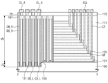
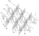
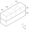
도 3a는 본 발명의 실시예들에 따른 반도체 소자의 평면도이다. 도 3b는 도 3a의 I-I'선에 따른 단면도이다. 도 3c는 도 3a의 II-II'선에 따른 단면도이다. 3A is a plan view of a semiconductor device according to embodiments of the present invention. FIG. 3B is a cross-sectional view taken along the line I-I 'in FIG. 3A. 3C is a cross-sectional view taken along line II-II 'in FIG. 3A.
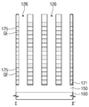
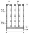
도 3a 내지 도 3c를 참조하면, 반도체 층 상에 차례로 적층된 게이트 전극들(GE)을 포함하는 전극 구조체가 제공될 수 있다. 일 예로, 상기 반도체 층은 기판(100)일 수 있으나 이에 한정되지 않는다. 상기 기판(100)은 제 1 도전형, 예를 들면 P형을 갖는 반도체 기판일 수 있다. 반도체 기판은 단결정 실리콘막, SOI(silicon on insulator), 실리콘 게르마늄(SiGe)막 상에 형성된 실리콘 막, 절연막 상에 형성된 실리콘 단결정막, 및 절연막 상에 형성된 폴리실리콘막 중 하나일 수 있다. 3A to 3C, an electrode structure including gate electrodes GE sequentially stacked on a semiconductor layer may be provided. For example, the semiconductor layer may be a
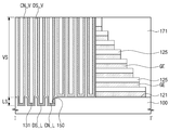
상기 기판(100)은 메모리 셀들이 제공되는 셀 어레이 영역(CAR), 게이트 전극들(GE)과 배선들의 연결을 위한 콘택 영역(CTR), 및 상기 셀 어레이 영역(CAR)과 상기 콘택 영역(CTR) 사이의 경계 영역(BR)을 포함할 수 있다. 상기 게이트 전극들(GE) 각각은 제 1 방향(D1)으로 연장되며, 상기 콘택 영역(CTR)에서 배선들과의 연결을 위한 계단형 구조를 가질 수 있다. 즉, 각 게이트 전극들(GE)은 바로 아래의 게이트 전극(GE) 보다 제 1 방향(D1)으로 짧은 길이를 가지며, 그에 따라 각 게이트 전극들(GE)은 이하 설명될 콘택들과 연결될 수 있는 패드 영역들(PD)을 노출할 수 있다. 상기 패드 영역들(PD)은 제 1 층간 절연막(171)에 의하여 덮일 수 있다. 상기 제 1 층간 절연막(171)은 실리콘 산화막을 포함할 수 있다. The
상기 기판(100)과 상기 게이트 구조체 사이에 버퍼 유전막(121)이 제공될 수 있다. 상기 버퍼 유전막(121)은 실리콘 산화막일 수 있다. 수직적으로 적층된 상기 게이트 전극들(GE) 사이에 절연 패턴들(125)이 제공될 수 있다. 상기 절연 패턴들(125)은 실리콘 산화막 또는 실리콘 산화질화막을 포함할 수 있다. 상기 절연 패턴들(125)의 두께는 동일할 수 있으나, 이에 한정되지 않는다. 일 예로, 최상층 절연 패턴의 두께는 그 아래의 절연 패턴들(125) 보다 두꺼울 수 있다. 상기 버퍼 유전막(121)은 절연 패턴들(125)에 비하여 얇을 수 있다. 상기 게이트 전극들(GE)은 도핑된 실리콘, 금속(예를 들어, 텅스텐), 금속 질화물, 금속 실리사이드들 또는 이들의 조합을 포함할 수 있다. 도면에는 게이트 전극들이 수직적으로 8개가 적층된 것으로 도시되었으나, 이에 한정되지 않고 그 이상 또는 그 이하일 수 있다.A
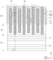
상기 게이트 전극들(GE)을 제 1 방향(D1)과 교차하는 제 2 방향(D2)으로 분리하는 수직 구조체들(VS)이 제공될 수 있다. 일 예로, 상기 제 2 방향(D2)은 상기 제 1 방향(D1)과 수직할 수 있다. 즉, 상기 기판(100)의 상면으로부터 동일한 레벨에 배치되는 게이트 전극들(GE)은 제 1 방향(D1)으로 연장되는 상기 수직 구조체들(VS)에 의하여 제 2 방향(D2)으로 상호 분리될 수 있다. 상기 수직 구조체들(VS)은 제 1 방향(D1)으로 연장되는 오프닝들(126) 내에 제공될 수 있다. 상기 오프닝들(126) 각각은 제 2 방향(D2)으로의 폭이 넓은 영역과 좁은 영역이 교대로 반복하여 배치될 수 있다. 일 예로, 평면적 관점에서, 상기 오프닝들(126) 각각은 제 1 방향(D1)을 따라 배치된 원들 각각이 인접하는 원들과 부분적으로 오버랩되는 형상일 수 있다. Vertical structures VS separating the gate electrodes GE in a second direction D2 intersecting the first direction D1 may be provided. For example, the second direction D2 may be perpendicular to the first direction D1. That is, the gate electrodes GE disposed at the same level from the upper surface of the
각 수직 구조체(VS)는 상기 게이트 전극들(GE)을 관통하여 수직적으로 연장되는 수직 채널 패턴들(CN_V)을 포함할 수 있다. 상기 수직 채널 패턴들(CN_V)은 트랜지스터들의 채널이 형성되는 영역일 수 있다. 상기 채널 패턴들(SP)은 실리콘, 게르마늄, 및 실리콘 게르마늄 중 적어도 하나를 포함할 수 있다. 일 예로, 상기 수직 채널 패턴들(CN_V)은 다결정(일 예로, 폴리 실리콘)일 수 있다. 상기 수직 채널 패턴들(CN_V)은 상기 제 1 도전형, 즉 P형 반도체 패턴일 수 있으나, 이에 한정되지 않으며 진성 상태일 수 있다. 인접하는 수직 구조체들(VS)의 수직 채널 패턴들(CN_V)은 제 1 방향(D1)으로 서로 오프셋 될 수 있다. 그 결과, 상기 수직 채널 패턴들(CN_V)은 제 3 방향(D3)으로 열들을 구성할 수 있다. Each vertical structure VS may include vertical channel patterns CN_V extending vertically through the gate electrodes GE. The vertical channel patterns CN_V may be regions where channels of transistors are formed. The channel patterns SP may include at least one of silicon, germanium, and silicon germanium. For example, the vertical channel patterns CN_V may be polycrystalline (e.g., polysilicon). The vertical channel patterns CN_V may be the first conductive type, that is, the P-type semiconductor pattern, but it is not limited thereto and may be an intrinsic state. The vertical channel patterns CN_V of the adjacent vertical structures VS may be offset from each other in the first direction D1. As a result, the vertical channel patterns CN_V may form columns in the third direction D3.
상기 수직 채널 패턴들(CN_V)과 상기 게이트 전극들(GE) 사이에 수직 정보 저장막(DS_V)이 제공될 수 있다. 각 수직 구조체(VS)의 수직 채널 패턴들(CN_V)은 제 1 방향(D1)으로 서로 분리될 수 있다. 즉, 상기 수직 정보 저장막(DS_V)은 제 1 방향(D1)으로 인접한 수직 채널 패턴들(CN_V) 사이로 연장되어 이들을 전기적으로 분리할 수 있다. 상기 수직 정보 저장막(DS_V)을 포함한 정보 저장막에 대해서는 이하, 도 14a 및 도 14b를 참조하여 보다 상세히 설명된다. A vertical data storage layer DS_V may be provided between the vertical channel patterns CN_V and the gate electrodes GE. The vertical channel patterns CN_V of the respective vertical structures VS may be separated from each other in the first direction D1. That is, the vertical data storage layer DS_V may extend between the adjacent vertical channel patterns CN_V in the first direction D1 to electrically isolate the vertical channel patterns CN_V. The information storage film including the vertical information storage film DS_V will be described in more detail below with reference to FIGS. 14A and 14B.
상기 수직 구조체들(VS)은 상기 수직 채널 패턴들(CN_V) 각각에 의하여 둘러싸인 매립 절연막들(131)을 포함할 수 있다. 상기 매립 절연막들(131)은 실리콘 산화물 또는 실리콘 산화질화물을 포함할 수 있다. 이와는 달리, 상기 매립 절연막들(131)은 생략될 수 있다. The vertical structures VS may include buried insulating
상기 수직 구조체들(VS) 각각은 상기 셀 어레이 영역(CAR)으로부터 상기 경계 영역(BR)으로 연장될 수 있다. 즉, 상기 경계 영역(BR)은 상기 수직 구조체들(VS)의 단부들이 배치되는 영역일 수 있다. 상기 수직 구조체들(VS)의 단부들과 오버랩되고 상기 경계 영역(BR)으로부터 상기 콘택 영역(CTR)으로 연장되며 상기 게이트 전극들(GE)을 수평적으로 분리하는 분리 절연 패턴들(141)이 제공될 수 있다. 상기 분리 절연 패턴들(141) 각각은 분리 트렌치(140) 내에 제공될 수 있다. 상기 분리 트렌치(140)는 평면적 관점에서 상기 수직 구조체들(VS) 각각과 오버랩되며, 제 1 방향(D1)으로 연장될 수 있다. 상기 수직 구조체들(VS) 및 상기 분리 절연 패턴들(141)에 의하여 제 2 방향(D2)으로 인접하는 게이트 전극들(GE)은 물리적으로 및 전기적으로 분리될 수 있다. 즉, 하나의 수직 구조체(VS) 및 이로부터 연장되는 분리 절연 패턴(141)을 사이에 두고 수평적으로 이격된 게이트 전극들(GE)은 전기적으로 분리되므로 이하 동작 방법에서 설명되는 바와 같이 서로 다른 전압이 인가될 수 있다. 상기 분리 절연 패턴들(141)은 실리콘 산화물, 실리콘 질화물 및 실리콘 산화질화물 중 적어도 하나를 포함할 수 있다. 상기 분리 절연 패턴들(141)의 제 2 방향(D2)으로의 폭이 상기 수직 구조체들(VS)의 폭보다 작은 것으로 도시되었으나, 이와는 달리 상기 분리 절연 패턴들(141)의 폭이 상기 수직 구조체들(VS)의 폭보다 클 수 있다. Each of the vertical structures VS may extend from the cell array region CAR to the boundary region BR. That is, the boundary region BR may be a region in which the ends of the vertical structures VS are disposed. The
상기 수직 구조체들(VS)과 상기 기판(100) 사이에 수평 구조체들(LS)이 제공될 수 있다. 상기 수평 구조체들(LS)은 상기 기판(100)의 상부에 매립되거나, 상기 기판(100) 상에 형성된 층(일 예로, 다결정 실리콘층) 내에 제공될 수 있다. 일 예로, 상기 수평 구조체들(LS)은 상기 기판(100)의 상부에 형성된 연결 트렌치들(150) 내에 제공될 수 있다. 상기 수평 구조체들(LS) 각각은 제 1 방향(D1) 및 제 2 방향(D2) 모두와 교차하는 제 3 방향(D3)으로 연장될 수 있다. 상기 수평 구조체들(LS)은 수평 채널 패턴들(CN_L) 및 수평 정보 저장막들(DS_L)을 포함할 수 있다. Horizontal structures LS may be provided between the vertical structures VS and the
상기 수평 구조체들(LS) 각각은 이와 교차하는 상기 수직 구조체들(VS)의 하부들과 연결될 수 있다. 상기 수평 채널 패턴들(CN_L) 각각은 제 3 방향(D3)을 따라 배치된 수직 채널 패턴들(CN_V)과 공통적으로 연결될 수 있다. 마찬가지로, 상기 수평 정보 저장막들(DS_L) 각각은 상기 수직 정보 저장막들(DS_V)과 공통적으로 연결되며 상기 연결 트렌치들(150)을 따라 연장될 수 있다. 상기 수평 채널 패턴들(CN_L)은 상기 수평 정보 저장막들(DS_L)에 의하여 상기 기판(100)과 분리될 수 있다. 상기 매립 절연막들(131) 각각은 상기 수직 채널 패턴들(CN_V)의 내측벽들로부터 상기 수평 채널 패턴(CN_L)의 내측벽으로 연결될 수 있다. Each of the horizontal structures LS may be connected to the lower portions of the vertical structures VS intersecting with each other. Each of the horizontal channel patterns CN_L may be commonly connected to the vertical channel patterns CN_V arranged along the third direction D3. Likewise, each of the horizontal data storage layers DS_L may be connected to the vertical data storage layers DS_V and extend along the
상기 수평 구조체들(LS)은 상기 셀 어레이 영역(CAR)에 제공되며, 상기 경계 영역(BR) 및 상기 콘택 영역(CTR)에 제공되지 않을 수 있다. 이하, 본 명세서에서 상기 셀 어레이 영역(CAR)과 상기 경계 영역(BR)의 경계는 상기 수평 구조체들(LS)의 단부들을 연결하는 가상의 선으로 정의될 수 있다. 상기 경계 영역(BR) 상의 상기 수직 채널 패턴들(CN_V)은 상기 수평 채널 패턴들(CN_L)과 연결되지 않을 수 있다. 즉, 상기 경계 영역(BR) 상의 상기 수직 채널 패턴들(CN_V)은 메모리 셀들을 구성하지 않는 더미 셀들일 수 있다. The horizontal structures LS may be provided in the cell array region CAR and may not be provided in the boundary region BR and the contact region CTR. Hereinafter, the boundary between the cell array area CAR and the border area BR may be defined as a virtual line connecting the ends of the horizontal structures LS. The vertical channel patterns CN_V on the border region BR may not be connected to the horizontal channel patterns CN_L. That is, the vertical channel patterns CN_V on the boundary region BR may be dummy cells that do not constitute memory cells.
상기 수직 채널 패턴들(CN_V) 상에 패드들(181, 182)이 제공될 수 있다. 상기 패드들(181, 182)은 상기 수직 채널 패턴들(CN_V) 각각 상에서 서로 이격될 수 있다. 상기 패드들(181, 182)은 상기 절연 패턴들(125) 중 최상층 내에 제공되고, 상기 최상층 절연 패턴과 상기 패드들(181, 182) 사이에 상기 수직 정보 저장막들(DS_V)이 개재되는 것으로 도시하였으나 이에 한정되지 않으며, 상기 패드들(181, 182)은 별도의 절연층 내에 제공되거나 상기 최상층 절연 패턴과 접할 수 있다. 일 예로, 상기 패드들(181, 182)은 도핑된 반도체 패턴들일 수 있다.
상기 패드들(181, 182)은 제 1 패드들(181) 및 제 2 패드들(182)을 포함할 수 있다. 상기 제 1 패드들(181)과 상기 제 2 패드들(182)은 서로 도전형이 다를 수 있다. 일 예로, 상기 제 1 패드들(181)은 p형 반도체 패턴들이고 상기 제 2 패드들(182)은 n형 반도체 패턴들일 수 있다. 하나의 수직 구조체(VS) 내의 수직 채널 패턴들(CN_V) 상에는 동일한 타입의 패드들이 제공될 수 있다. 일 예로, 짝수 번째 수직 구조체들(VS)의 수직 채널 패턴들(CN_V) 상에는 제 1 패드들(181)이 제공될 수 있고, 홀수 번째 수직 구조체들(VS)의 수직 채널 패턴들(CN_V) 상에는 제 2 패드들(182)이 제공될 수 있다. 하나의 수평 구조체(LS)에 연결되는 수직 채널 패턴들(CN_V) 상에는 상기 제 1 패드(181)와 상기 제 2 패드(182)가 교대로 반복하여 배치될 수 있다. The
상기 패드들(181, 182) 상에 셀 스터드들(CS)이 제공될 수 있다. 상기 셀 스터드들(CS)은 상기 셀 어레이 영역(CAR) 상의 패드들(181, 182) 상에 한정되어 제공되며, 상기 경계 영역(BR) 상의 패드들(181, 182) 상에는 제공되지 않을 수 있다. 이와는 달리, 상기 경계 영역(BR) 상의 수직 채널 패턴들(CN_V) 상에는 상기 패드들(181, 182)이 제공되지 않거나, 상기 패드들(181, 182) 및 상기 셀 스터드들(CS) 모두가 제공되지 않을 수 있다. Cell studs CS may be provided on the
제 2 방향(D2)으로 연장하며 상기 셀 스터드들(CS)을 연결하는 도전 라인들(CL_A, CL_B)이 제공될 수 있다. 도 3a에서 상기 도전 라인들(CL_A, CL_B)은 일부 셀 스터드들(CS) 상에만 도시되었으나 이는 표현의 간소화를 위한 것이며 제 1 방향(D1)을 따라 제 1 도전 라인들(CL_A)과 제 2 도전 라인들(CL_B)이 반복하여 교대로 배치될 수 있다. 상기 셀 스터드들(CS)은 상기 제 1 층간 절연막(171) 상의 제 2 층간 절연막(172) 내에 제공될 수 있다. 제 1 도전 라인들(CL_A)은 짝수 번째 수직 구조체들(VS)의 수직 채널 패턴들(CN_V)과 연결되고, 제 2 도전 라인들(CL_B)은 홀수 번째 수직 구조체들(VS)의 수직 채널 패턴들(CN_V)과 연결될 수 있다. 즉, 상기 제 1 도전 라인들(CL_A)은 상기 셀 스터드들(CS)을 통하여 상기 제 1 패드들(181)과 연결되고, 상기 제 2 도전 라인들(CL_B)은 상기 셀 스터드들(CS)을 통하여 상기 제 2 패드들(182)과 연결될 수 있다. Conductive lines CL_A and CL_B extending in the second direction D2 and connecting the cell studs CS may be provided. 3A, the conductive lines CL_A and CL_B are shown only on some of the cell studs CS, but this is for simplification of representation and is not limited to the first conductive lines CL_A and the second conductive lines CL_A along the first direction D1. The conductive lines CL_B can be repeatedly arranged alternately. The cell studs CS may be provided in the second
상기 콘택 영역(CTR) 상에 상기 게이트 전극들(GE)과 연결되는 콘택들(CT)이 제공될 수 있다. 상기 콘택들(CT)은 상기 제 1 층간 절연막(171) 및 상기 제 2 층간 절연막(172)을 관통하여 상기 게이트 전극들(GE)의 패드 영역들(PD) 각각에 연결될 수 있다. 평면적 관점에서, 상기 콘택들(CT)은 제 2 방향(D2)을 따라 지그-재그 형태로 배치될 수 있다. 상기 콘택들(CT) 상에 배선들(CGL)이 배치될 수 있다. 도 3a에서 상기 배선들(CGL)은 일부 콘택들(CT) 상에만 도시되었으나 이는 표현의 간소화를 위한 것이다. 상기 도전 라인들(CL_A, CL_B), 상기 배선들(CGL), 상기 셀 스터드들(CS) 및 상기 콘택들(CT) 각각은 금속, 도전성 금속 질화물 및 도핑된 반도체 물질 중 적어도 하나를 포함할 수 있다. And contacts CT connected to the gate electrodes GE may be provided on the contact region CTR. The contacts CT may be connected to the pad regions PD of the gate electrodes GE through the first
도 14a 및 도 14b는 본 발명의 실시예들에 따른 수직 정보 저장막들(DS_V)을 설명하기 위한 수평 단면도들이다. 상기 수직 정보 저장막들(DS_V)은 상기 오프닝들(126)의 측벽 상에 차례로 형성된 블로킹 절연막(BLK), 전하 저장막(CIL), 및 터널 절연막(TIL)을 포함할 수 있다. 도시를 생략하였으나, 상기 수평 정보 저장막들(DS_L)의 구조는 상기 수직 정보 저장막들(DS_V)과 실질적으로 동일할 수 있다. 상술한 바와 같이, 상기 오프닝들(126) 각각은 제 2 방향(D2)으로의 폭이 넓은 영역과 좁은 영역이 교대로 반복하여 배치되므로, 폭이 좁은 영역들(이하, 협폭 영역들(NWR))에서 상기 블로킹 절연막(BLK) 및/또는 상기 전하 저장막(CIL)이 서로 연결될 수 있다. 일 예로, 도 14a에 도시된 바와 같이 각 오프닝(126)의 양 측벽들 상의 블로킹 절연막들(BLK)은 상기 협폭 영역들(NWR)에서 서로 연결될 수 있다. 그 결과, 각 오프닝(126) 내에 제공되는 상기 전하 저장막들(CIL), 상기 터널 절연막들(TIL), 상기 수직 채널 패턴들(CN_V) 및 상기 매립 절연막들(131) 각각은 제 1 방향(D1)으로 서로 분리되어 형성될 수 있다. 14A and 14B are horizontal cross-sectional views illustrating vertical information storage layers DS_V according to embodiments of the present invention. The vertical data storage layers DS_V may include a blocking insulating layer BLK, a charge storage layer CIL, and a tunnel insulating layer TIL, which are sequentially formed on sidewalls of the
다른 예로, 도 14b에 도시된 바와 같이 상기 블로킹 절연막(BLK) 뿐 아니라, 각 오프닝(126)의 양 측벽들 상의 전하 저장막들(CIL)도 상기 협폭 영역들(NWR)에서 서로 연결될 수 있다. 그 결과, 각 오프닝(126) 내에 제공되는 상기 터널 절연막들(TIL), 상기 수직 채널 패턴들(CN_V) 및 상기 매립 절연막들(131) 각각은 제 1 방향(D1)으로 서로 분리되어 형성될 수 있다.As another example, not only the blocking insulating film BLK but also the charge storage films CIL on both side walls of each
상기 블로킹 절연막(BLK)은 복수의 박막들로 구성되는 다층막일 수 있다. 예를 들면, 블로킹 절연막(BLK)은 하프늄 산화막, 알루미늄 산화막 및/또는 실리콘 산화막을 포함할 수 있으며, 하프늄 산화막, 알루미늄 산화막 및 실리콘 산화막의 적층 순서는 다양할 수 있다. 상기 전하 저장막(CIL)은 전하 트랩막 또는 도전성 나노 입자를 포함하는 절연막일 수 있다. 전하 트랩막은, 예를 들면 실리콘 질화막을 포함할 수 있다. 상기 터널 절연막(TIL)은 실리콘 산화막을 포함할 수 있다. 상기 터널 절연막(TIL)은 고유전막(예를 들어, 하프늄 산화막 또는 알루미늄 산화막)을 더 포함할 수 있다. 다른 실시예들에 있어서, 상기 수직 정보 저장막들(DS_V)은 가변저항 패턴일 수 있다. 가변저항 패턴은 그것의 저항이 변화될 수 있는, 가변저항 특성을 갖는 물질들 중의 적어도 하나를 포함할 수 있다. The blocking insulating film BLK may be a multilayer film composed of a plurality of thin films. For example, the blocking insulating film BLK may include a hafnium oxide film, an aluminum oxide film, and / or a silicon oxide film, and the order of stacking the hafnium oxide film, the aluminum oxide film, and the silicon oxide film may vary. The charge storage film (CIL) may be an insulating film containing a charge trap film or conductive nanoparticles. The charge trap film may include, for example, a silicon nitride film. The tunnel insulating layer (TIL) may include a silicon oxide layer. The tunnel insulating film TIL may further include a high-k film (for example, a hafnium oxide film or an aluminum oxide film). In other embodiments, the vertical information storage layers DS_V may be a variable resistance pattern. The variable resistance pattern may include at least one of materials having a variable resistance characteristic, the resistance of which can be changed.
도 4는 본 발명의 실시예들에 따른 반도체 반도체 소자의 셀 어레이를 나타낸 간략 회로도이다. 도 5a는 도 4의 P 영역으로 하나의 메모리 블록의 회로도이다. 도 5b는 각 게이트 전극들을 구별하기 위하여 도 5a의 구성 요소들을 각 게이트 전극들에 도시한 개념도이다. 4 is a simplified circuit diagram showing a cell array of semiconductor semiconductor devices according to embodiments of the present invention. 5A is a circuit diagram of one memory block in the P region of FIG. FIG. 5B is a conceptual diagram showing the components of FIG. 5A on each gate electrode in order to distinguish each gate electrode.
도 4, 도 5a 및 도 5b를 참조하면, 본 발명의 실시예들에 따른 반도체 소자는 제 1 도전 라인들(CL_A)과 제 2 도전 라인들(CL_B) 사이에 배치되는 복수개의 셀 스트링들(CSTR)을 포함할 수 있다. 도 3a 내지 도 3c를 참조하여 설명된 게이트 전극들(GE)은 최상층인 상부 선택 라인들(TS), 최하층인 제 1 하부 선택 라인들(BS1), 상기 상부 선택 라인들(TS)과 상기 제 1 하부 선택 라인들(BS1) 사이의 워드 라인들(WL), 및 최하층 워드 라인들(WL)과 상기 제 1 하부 선택 라인들(BS1) 사이의 제 2 하부 선택 라인들(BS2)을 포함할 수 있다. 상기 상부 선택 라인들(TS) 및 상기 제 1 및 제 2 하부 선택 라인들(BS1, BS2) 각각은 하나의 도전층으로부터 분리된 동일 레벨의 패턴들로 도시되었으나, 이에 한정되지 않는다. 4, 5A, and 5B, a semiconductor device according to embodiments of the present invention includes a plurality of cell strings (not shown) disposed between first conductive lines CL_A and second conductive lines CL_B CSTR). The gate electrodes GE described with reference to FIGS. 3A to 3C include upper select lines TS as the uppermost layer, first lower select lines BS1 as the lowermost layer, Word lines WL between one lower select line BS1 and second lower select lines BS2 between the lowest word lines WL and the first lower select lines BS1 . Each of the upper select lines TS and the first and second lower select lines BS1 and BS2 are shown as patterns of the same level separated from one conductive layer, but are not limited thereto.
상기 제 1 도전 라인들(CL_A)은 공통 소스 라인들일 수 있고, 상기 제 2 도전 라인들(CL_B)은 비트 라인들일 수 있다. 상기 상부 선택 라인들(TS) 중 일부는 스트링 선택 트랜지스터의 게이트 전극들일 수 있으며, 나머지는 접지 선택 트랜지스터의 게이트 전극들일 수 있다. 일 예로, 도 5a 및 도 5b에 도시된 셀 스트링(CSTR)의 경우, TSj+3는 접지 선택 트랜지스터의 게이트 전극일 수 있으며 TSj+1는 스트링 선택 트랜지스터의 게이트 전극일 수 있다. 제 1 하부 선택 라인들(BS1)은 인접하는 수직 채널 패턴들(CN_V), 보다 상세하게는 인접하는 수직 채널 패턴들(CN_V) 내에 형성되는 반전 영역들(inversion layer)을 연결 또는 분리하기 위한 스위칭 게이트들일 수 있다. 상기 워드 라인들(WL)은 메모리 셀 트랜지스터들의 게이트 전극들일 수 있다. 상기 제 2 하부 선택 라인들(BS2)은 상기 메모리 셀 트랜지스터들과 상기 스위칭 게이트들을 연결하는 게이트들일 수 있다. 이와는 달리, 상기 제 2 하부 선택 라인들(BS2)은 생략될 수 있다. The first conductive lines CL_A may be common source lines, and the second conductive lines CL_B may be bit lines. Some of the upper select lines TS may be the gate electrodes of the string select transistor and the remainder may be the gate electrodes of the ground select transistor. For example, in the case of the cell string CSTR shown in FIGS. 5A and 5B, TSj + 3 may be the gate electrode of the ground selection transistor and TSj + 1 may be the gate electrode of the string selection transistor. The first lower selection lines BS1 are connected to the vertical channel patterns CN_V adjacent to the vertical channel patterns CN_V, Gates. The word lines WL may be gate electrodes of memory cell transistors. The second lower selection lines BS2 may be gates connecting the memory cell transistors and the switching gates. Alternatively, the second lower selection lines BS2 may be omitted.
도 5a 및 도 5b를 다시 참조하여, 본 발명의 실시예들에 따른 반도체 소자의 동작 방법이 설명된다. 소거의 경우 각 게이트 전극들 및 도전 라인들의 전압 조건은 다음과 같다. 아래의 표 1과 같은 조건 하에서, 하나의 메모리 블록의 모든 메모리 셀들이 소거될 수 있다. 이하, On은 트랜지스터가 턴-온되는 것을 지칭하고, OFF는 트랜지스터가 턴-오프되는 것을 지칭한다. Referring again to Figures 5A and 5B, a method of operating a semiconductor device according to embodiments of the present invention is described. In the erase operation, the voltage conditions of the gate electrodes and the conductive lines are as follows. Under the conditions shown in Table 1 below, all the memory cells of one memory block can be erased. Herein, On means that the transistor is turned on, and OFF means that the transistor is turned off.
기입의 경우, 각 게이트 전극들 및 도전 라인들의 전압 조건은 다음과 같다. 아래의 표2와 같은 조건 하에서, 도 5a의 셀 스트링(CSTR)이 선택되며, 해당 셀 스트링(CSTR)의 선택 메모리 셀(SM)에 기입 동작이 수행될 수 있다. 금지 전압(inhibiting voltage: VIN)은 해당 셀 스트링의 기입을 방지하기 위한 전압이다. 프로그램 전압(Vpgm)은 채널로부터의 FN 터널링을 유발할 수 있을 정도로 큰 전압이고, 패스 전압(Vpass)은 메모리 셀 트랜지스터의 문턱 전압(Vth)보다는 크고 상기 프로그램 전압(Vpgm)보다는 작은 범위에서 선택될 수 있다. 일 실시예에 따른 기입 방법의 경우, 셀프-부스팅을 이용하여 선택된 스트링들의 메모리 셀들을 프로그램하고, 금지된 스트링들(inhibited strings) 및 선택되지 않은 스트링들(unselected strings)의 메모리 셀들에서의 프로그램을 방지하는 선택적 프로그램 단계를 포함할 수 있다.In the case of writing, the voltage conditions of the gate electrodes and the conductive lines are as follows. The cell string CSTR shown in FIG. 5A is selected under the conditions shown in Table 2 below, and a write operation can be performed on the selected memory cell SM of the corresponding cell string CSTR. The inhibiting voltage (V IN ) is the voltage to prevent writing of the corresponding cell string. The program voltage V pgm is a voltage large enough to cause FN tunneling from the channel and the pass voltage V pass is in a range greater than the threshold voltage V th of the memory cell transistor and less than the program voltage V pgm ≪ / RTI > In the case of the writing method according to an embodiment, self-boosting is used to program the memory cells of selected strings and program in memory cells of inhibited strings and unselected strings Or < / RTI >
독출의 경우, 각 게이트 전극들 및 도전 라인들의 전압 조건은 다음과 같다. 아래의 표3과 같은 조건 하에서, 도 5a의 셀 스트링(CSTR)이 선택되며, 해당 셀 스트링(CSTR)의 선택 메모리 셀(SM)의 독출 동작이 수행될 수 있다. 비트 라인 전압(VBL)은 문턱 전압(Vth)보다 큰 소정의 전압(예를 들면, 외부 전원으로부터 공급되는 전압)일 수 있다. In the case of reading, the voltage conditions of the respective gate electrodes and the conductive lines are as follows. The cell string CSTR of FIG. 5A is selected under the conditions shown in Table 3 below, and the read operation of the selected memory cell SM of the corresponding cell string CSTR can be performed. The bit line voltage V BL may be a predetermined voltage (for example, a voltage supplied from an external power supply) larger than the threshold voltage Vth.
하나의 수평 채널 패턴(CN_L)에 연결되고 서로 인접한 한 쌍의 수직 채널 패턴들(CN_V)은 동일한 셀 스트링의 채널 영역으로 동작할 수 있다. 상술한 바와 같이, 하나의 수직 채널 패턴(CN_V)을 사이에 두고 이격되는 게이트 전극들은 전기적으로 분리되어 서로 다른 전압이 인가될 수 있으므로, 하나의 수직 채널 패턴(CN_V)이 2개의 셀 스트링들(CSTR)에 의하여 공유될 수 있다. 또한, 하나의 수직 채널 패턴(CN_V) 및 이를 사이에 두고 이격된 게이트 전극들은 서로 다른 한 쌍의 셀 스트링들(CSTR)로 동작할 수 있다. 이에 따라, 반도체 소자의 집적도가 향상될 수 있다. A pair of adjacent vertical channel patterns CN_V connected to one horizontal channel pattern CN_L may operate as a channel region of the same cell string. As described above, since the gate electrodes spaced apart by one vertical channel pattern CN_V can be electrically separated and applied with different voltages, one vertical channel pattern CN_V can be applied to two cell strings CSTR). In addition, one vertical channel pattern CN_V and gate electrodes spaced therebetween can operate as a pair of different cell strings CSTR. Thus, the degree of integration of the semiconductor device can be improved.
도 6a 내지 도 13a는 본 발명의 실시예들에 따른 반도체 소자의 제조 방법을 설명하기 위한 평면도들이다. 도 6b 내지 도 13b는 도 6a 내지 도 13a의 I-I'선에 따른 단면도들이다. 도 6c 내지 도 13c는 도 6a 내지 도 13a의 II-II'선에 따른 단면도들이다.6A to 13A are plan views illustrating a method of manufacturing a semiconductor device according to embodiments of the present invention. Figs. 6B to 13B are cross-sectional views taken along a line I-I 'in Figs. 6A to 13A. Figs. 6C to 13C are cross-sectional views taken along line II-II 'in Figs. 6A to 13A. Fig.
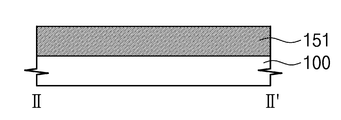
도 6a 내지 도 6c를 참조하여, 기판(100)이 제공된다. 상기 기판(100)은 제 1 도전형, 예를 들면 P형의 도전형을 가질 수 있다. 상기 기판(100)은 메모리 셀들이 형성되는 셀 어레이 영역(CAR), 게이트 전극들과 배선들의 연결을 위한 콘택 영역(CTR), 및 상기 셀 어레이 영역(CAR)과 상기 콘택 영역(CTR) 사이의 경계 영역(BR)을 포함할 수 있다. 6A to 6C, a
상기 기판(100)의 상부에 연결 트렌치들(150)이 형성될 수 있다. 상기 연결 트렌치들(150) 각각은 제 3 방향으로 연장될 수 있다. 상기 연결 트렌치들(150)은 건식 식각 공정으로 형성될 수 있다. 상기 연결 트렌치들(150)은 상기 셀 어레이 영역(CAR)에 형성되며 상기 경계 영역(BR) 및 상기 콘택 영역(CTR)에는 형성되지 않을 수 있다.
상기 연결 트렌치들(150)은 채우는 희생 패턴들(151)이 형성될 수 있다. 상기 희생 패턴들(151)은 이하 설명될 게이트 전극들 및 절연 패턴들과 식각 선택성이 있는 물질을 포함할 수 있다. 일 예로, 상기 희생 패턴들(151)은 실리콘 질화물 또는 실리콘 산화질화물을 포함할 수 있다. 상기 희생 패턴들(151)은 상기 연결 트렌치들(150)을 채우는 절연막을 형성한 후, 상기 기판(100)의 상면이 노출될 때까지 평탄화 공정을 수행하여 형성될 수 있다. 이하 설명의 간소화를 위하여 상기 희생 패턴들(151)이 상기 기판(100)의 상부에 형성되는 것으로 설명되나, 이와는 달리 상기 기판(100) 상에 형성된 별개의 층 내에 형성될 수 있다. 이와 관련된 실시예는 도 16 및 도 17을 참조하여 설명된다. The
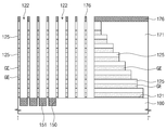
도 7a 내지 도 7c를 참조하여, 상기 기판(100) 상에 버퍼 유전막(121)을 형성할 수 있다. 상기 버퍼 유전막(121)은, 예를 들어 실리콘 산화막일 수 있다. 상기 버퍼 유전막(121)은, 예를 들어 열산화 공정에 의하여 형성될 수 있다. 상기 버퍼 유전막(121) 상에 게이트 전극들(GE) 및 절연 패턴들(125)이 교대로 반복하여 형성될 수 있다. 상기 게이트 전극들(GE)은 도핑된 실리콘, 금속(예를 들어, 텅스텐), 금속 질화물, 금속 실리사이드들 또는 이들의 조합을 포함할 수 있다. 상기 절연 패턴들(125)은 실리콘 산화막 또는 실리콘 산화질화막을 포함할 수 있다. 최상층 절연 패턴의 두께는 그 아래의 절연 패턴들(125) 보다 두꺼울 수 있다. 상기 버퍼 유전막(121), 상기 게이트 전극들(GE), 및 상기 절연 패턴들(125)은 화학 기상 증착 또는 물리 기상 증착으로 형성될 수 있다. Referring to FIGS. 7A to 7C, a
상기 콘택 영역(CTR)에 패드 영역들(PD)이 형성될 수 있다. 상기 패드 영역들(PD)은 상기 게이트 전극들(GE)의 단부들로, 계단형 구조를 가질 수 있다. 즉, 각 게이트 전극들(GE)은 바로 아래의 게이트 전극(GE) 보다 제 1 방향(D1)으로 짧은 길이를 가질 수 있다. 각 게이트 전극들(GE)의 상면들과 접하는 절연 패턴들(125)은 각 게이트 전극들(GE)과 동일한 길이를 가질 수 있다. 상기 패드 영역들(PD)의 형성은 마스크 패턴의 형성 및 상기 마스크 패턴의 폭을 줄이는 복수의 트리밍 공정들을 포함할 수 있다. 일 예로, 상기 트리밍 공정들은 등방적 건식 식각 방법 또는 습식 식각 방법으로 수행될 수 있다. 상기 패드 영역들(PD)을 덮는 제 1 층간 절연막(171)이 형성될 수 있다. 상기 제 1 층간 절연막(171)은 실리콘 산화막을 포함할 수 있다. Pad regions PD may be formed in the contact region CTR. The pad regions PD may have a stepped structure with the ends of the gate electrodes GE. That is, each gate electrode GE may have a shorter length in the first direction D1 than the gate electrode GE immediately below. The insulating
상기 게이트 전극들(GE), 상기 절연 패턴들(125), 및 상기 버퍼 유전막(121)을 관통하는 수직 홀들(122)이 형성될 수 있다. 상기 수직 홀들(122)은 상기 셀 어레이 영역(CAR) 및 상기 경계 영역(BR) 상에 형성될 수 있다. 상기 수직 홀들(122)은 이방성 식각 공정으로 형성될 수 있다. 일 예로, 최상층 절연 패턴(125) 상에 마스크 패턴들(176)을 형성한 후, 이를 식각 마스크로 이방성 식각 공정이 수행될 수 있다. 상기 마스크 패턴들(176)은 상기 절연 패턴들(125)과 식각 선택성이 있는 물질을 포함할 수 있다. 일 예로, 상기 절연 패턴들(125)이 실리콘 산화막인 경우, 상기 마스크 패턴들(176)은 실리콘 질화막 또는 실리콘 산화질화막일 수 있다. The gate electrodes GE, the insulating
제 2 방향(D2)으로 인접한 상기 수직 홀들(122) 사이의 거리는 제 1 방향(D1)으로 인접한 수직 홀들(122) 사이의 거리보다 클 수 있다. 상기 수직 홀들(122)은 제 1 방향(D1)으로 열들을 구성할 수 있다. 인접하는 열들의 수직 홀들(122)은 상기 희생 패턴들(151)과 정렬되도록 제 1 방향(D1)으로 오프셋될 수 있다. 그 결과, 상기 희생 패턴들(151) 각각 상에 복수의 수직 홀들(122)이 형성될 수 있다. 상기 수직 홀들(122)은 상기 셀 어레이 영역(CAR)에서 상기 희생 패턴들(151)의 상면들을 노출할 수 있고, 상기 경계 영역(BR)에서 상기 기판(100)의 상면을 노출할 수 있다. The distance between adjacent
상기 수직 홀들(122)의 형상이 도 18a 및 도 18b를 참조하여 설명된다. 상기 수직 홀들(122) 각각은 도 18a와 같이 제 1 방향(D1)으로의 폭(w1)과 제 2 방향(D2)으로의 폭(w2)이 실질적으로 동일할 수 있다. 이와는 달리, 상기 수직 홀들(122) 각각은 도 18b와 같이 제 1 방향(D1)으로의 폭(w1)이 제 2 방향(D2)으로의 폭(w2)보다 클 수 있다.The shape of the
도 8a 내지 도 8c를 참조하여, 상기 수직 홀들(122)이 확장되어 제 1 방향(D1)으로 연장되는 오프닝들(126)이 형성될 수 있다. 상기 수직 홀들(122)의 확장 공정은 복수의 식각 공정을 포함할 수 있다. 일 예로, 상기 수직 홀들(122)의 확장 공정은 상기 게이트 전극들(GE)의 측벽들의 식각 공정 및 상기 절연 패턴들(125)의 측벽들의 식각 공정을 포함할 수 있다. 일 예로, 상기 게이트 전극들(GE)의 식각은 SC1 용액으로 수행될 수 있고, 상기 절연 패턴들(125)의 식각은 HF로 수행될 수 있다. 상기 수직 홀들(122)이 확장됨에 따라 제 1 방향(D1)으로 인접한 수직 홀들(122)이 서로 연결되어 오프닝들(126)이 형성될 수 있다. 8A to 8C,
상기 오프닝들(126)의 형성에 의하여 상기 게이트 전극들(GE) 및 상기 절연 패턴들(125)은 상기 오프닝들(126)을 사이에 두고 제 2 방향(D2)으로 분리될 수 있다. 상기 셀 어레이 영역(CAR)에서 상기 희생 패턴들(151)은 제거되지 않고 잔류할 수 있다. 도시된 바와는 달리, 상기 희생 패턴들(151)이 형성되지 않은 상기 경계 영역(BR)의 경우, 상기 기판(100)의 상부가 함께 식각 될 수 있다. 상기 수직 홀들(122)을 형성하기 위하여 상기 마스크 패턴들(176)에 형성된 홀들은 상기 수직 홀들(122)과 함께 확장되지 않을 수 있으며, 이에 따라 상기 마스크 패턴들(176)은 그 아래의 게이트 전극들(GE) 및 절연 패턴들(125)을 구조적으로 지지할 수 있다. By the formation of the
도 9a 내지 도 9c를 참조하여, 상기 희생 패턴들(151)이 선택적으로 제거될 수 있다. 상기 희생 패턴들(151)의 제거는 상기 게이트 전극들(GE) 및 상기 절연 패턴들(125)의 식각을 최소화하며 수행될 수 있다. 일 예로, 상기 희생 패턴들(151)의 선택적 제거는 인산으로 수행될 수 있다. 상기 희생 패턴들(151)의 제거에 의하여 상기 연결 트렌치들(150)이 노출될 수 있다. 그 결과 상기 오프닝들(126)은 상기 연결 트렌치들(150)과 연결될 수 있다. 상기 마스크 패턴들(176)은 상기 희생 패턴들(151)과 함께 제거되거나, 별개의 식각 공정으로 제거될 수 있다. 9A to 9C, the
도 10a 내지 도 10c를 참조하여, 상기 오프닝들(126) 및 상기 연결 트렌치들(150) 내에 정보 저장막들(DS_V, DS_N), 채널 패턴들(CN_V, CN_L), 및 매립 절연막들(131)이 차례로 형성될 수 있다. 그 결과, 수직 구조체들(VS) 및 수평 구조체들(LS)이 형성될 수 있다. 상기 오프닝들(126) 내에 형성되는 상기 수직 구조체들(VS)은 수직 정보 저장막들(DS_V) 및 수직 채널 패턴들(CN_V)을 포함하고, 상기 연결 트렌치들(150) 내에 형성되는 상기 수평 구조체들(LS)은 수평 정보 저장막들(DS_L) 및 수평 채널 패턴들(CN_L)을 포함할 수 있다.The information storage films DS_V and DS_N, the channel patterns CN_V and CN_L and the buried insulating
상기 수직 구조체들(VS) 및 상기 수평 구조체들(LS)의 형성은 원자층 증착(Atomic Layer Deposition) 공정을 포함할 수 있다. 상기 정보 저장막들(DS_V, DS_N)은 도 14a 및 도 14b를 참조하여 설명된 바와 같은 구조를 가질 수 있다. 일 예로, 상기 채널 패턴들(CN_V, CN_L)은 폴리 실리콘으로 형성될 수 있고, 상기 매립 절연막들(131)은 실리콘 산화막으로 형성될 수 있다. 이후, 평탄화 공정이 수행되어 최상층 절연 패턴(125)의 상면이 노출될 수 있다. The formation of the vertical structures VS and the horizontal structures LS may include an Atomic Layer Deposition process. The information storage layers DS_V and DS_N may have a structure as described with reference to FIGS. 14A and 14B. For example, the channel patterns CN_V and CN_L may be formed of polysilicon, and the buried insulating
도 11a 내지 도 11c를 참조하여, 상기 수직 채널 패턴들(CN_V) 상에 패드들(181, 182)이 형성될 수 있다. 상기 패드들(181, 182)은 상기 수직 채널 패턴들(CN_V) 각각 상에서 서로 이격될 수 있다. 일 예로, 상기 패드들(181, 182)은 상기 수직 채널 패턴들(CN_V)의 상부들 및 상기 매립 절연막들(131)의 상부들을 제거한 후, 제거된 영역 내에 도전성 물질을 채워 형성될 수 있다. 일 예로, 상기 패드들(181, 182)은 도핑된 반도체 패턴들로 형성될 수 있다. Referring to FIGS. 11A to 11C,
상기 패드들(181, 182)은 복수의 이온 주입 공정을 통하여 형성될 수 있다. 일 예로, 상기 패드들(181, 182)은 제 1 패드들(181) 및 제 2 패드들(182)을 포함하고, 상기 제 1 패드들(181)과 상기 제 2 패드들(182)은 서로 도전형이 다를 수 있다. 일 예로, 상기 제 1 패드들(181)은 p형 반도체 패턴들이고 상기 제 2 패드들(182)은 n형 반도체 패턴들일 수 있다. 하나의 수직 구조체(VS) 내의 수직 채널 패턴들(CN_V) 상에는 동일한 타입의 패드들이 제공될 수 있다. 일 예로, 짝수 번째 수직 구조체들(VS)의 수직 채널 패턴들(CN_V) 상에는 제 1 패드들(181)이 제공될 수 있고, 홀수 번째 수직 구조체들(VS)의 수직 채널 패턴들(CN_V) 상에는 제 2 패드들(182)이 제공될 수 있다. The
도 12a 내지 도 12c를 참조하여, 상기 패드들(181, 182) 상에 제 2 층간 절연막(172)을 형성한 후, 상기 패드들(181, 182)과 연결되는 셀 스터드들(CS)을 형성할 수 있다. 상기 셀 스터드들(CS)은 상기 셀 어레이 영역(CAR) 상의 패드들(181, 182) 상에 한정되어 제공되며, 상기 경계 영역(BR) 상의 패드들(181, 182) 상에는 제공되지 않을 수 있다. 상기 셀 스터드들(CS)은 금속, 도전성 금속 질화물 및 도핑된 반도체 물질 중 적어도 하나를 포함할 수 있다. 일 예로, 상기 셀 스터드들(CS)은 물리 기상 증착으로 형성될 수 있다. 12A to 12C, a second
도 13a 내지 도 13c를 참조하여, 상기 수직 구조체들(VS)의 단부들 각각과 오버랩되고 상기 경계 영역(BR)으로부터 상기 콘택 영역(CTR)으로 연장되며 상기 게이트 전극들(GE)을 수평적으로 분리하는 분리 트렌치들(140)이 형성될 수 있다. 상기 분리 트렌치들(140)의 형성은 이방성 식각 공정을 포함할 수 있다. 상기 수직 구조체들(VS) 및 상기 분리 트렌치들(140)에 의하여 제 2 방향(D2)으로 인접하는 게이트 전극들(GE)은 물리적으로 및 전기적으로 분리될 수 있다. 상기 분리 트렌치들(140) 내에 분리 절연 패턴들(141)이 형성될 수 있다. 상기 분리 절연 패턴들(141)은 실리콘 산화물, 실리콘 질화물 및 실리콘 산화질화물 중 적어도 하나를 포함할 수 있다. 상기 분리 절연 패턴들(141)은 상기 분리 트렌치들(140)을 채우는 절연막을 형성한 후, 상기 제 2 층간 절연막(172)의 상면이 노출될 때까지 평탄화 공정을 수행하여 형성될 수 있다. Referring to FIGS. 13A to 13C, the gate electrodes GE are overlapped with the ends of the vertical structures VS and extend from the boundary region BR to the contact region CTR, Separating
도 3a 내지 도 3c를 다시 참조하여, 상기 콘택 영역(CTR) 상에 상기 게이트 전극들(GE)과 연결되는 콘택들(CT)이 형성될 수 있다. 상기 콘택들(CT)은 상기 제 1 층간 절연막(171) 및 상기 제 2 층간 절연막(172)을 관통하여 상기 게이트 전극들(GE)의 패드 영역들(PD)을 노출하는 콘택홀들을 형성한 후, 이를 도전 물질로 채워 형성될 수 있다. 일 예로, 상기 콘택들(CT)은 금속, 도전성 금속 질화물 및 도핑된 반도체 물질 중 적어도 하나를 포함할 수 있다. 평면적 관점에서, 상기 콘택들(CT)은 제 2 방향(D2)을 따라 지그-재그 형태로 배치될 수 있다. 상술한 바와는 달리, 상기 콘택들(CT)과 상기 셀 스터드들(CS)은 동시에 형성될 수 있다. Referring again to FIGS. 3A to 3C, contacts CT connected to the gate electrodes GE may be formed on the contact region CTR. The contacts CT pass through the first
제 2 방향(D2)으로 연장하며 상기 셀 스터드들(CS)을 연결하는 도전 라인들(CL_A, CL_B)이 형성될 수 있다. 제 1 도전 라인들(CL_A)은 짝수 번째 수직 구조체들(VS)의 수직 채널 패턴들(CN_V)과 연결되고, 제 2 도전 라인들(CL_B)은 홀수 번째 수직 구조체들(VS)의 수직 채널 패턴들(CN_V)과 연결될 수 있다. 상기 콘택들(CT) 상에 배선들(CGL)이 배치될 수 있다. 상기 도전 라인들(CL_A, CL_B) 및 상기 배선들(CGL)은 금속, 도전성 금속 질화물 및 도핑된 반도체 물질 중 적어도 하나를 포함하는 물질로 형성될 수 있다. Conductive lines CL_A and CL_B extending in the second direction D2 and connecting the cell studs CS may be formed. The first conductive lines CL_A are connected to the vertical channel patterns CN_V of the even vertical structures VS and the second conductive lines CL_B are connected to the vertical channel patterns CN_V of the odd vertical structures VS, Lt; RTI ID = 0.0 > CN_V. ≪ / RTI > Wiring lines CGL may be disposed on the contacts CT. The conductive lines CL_A and CL_B and the lines CGL may be formed of a material including at least one of a metal, a conductive metal nitride, and a doped semiconductor material.
도 15는 본 발명의 실시예들에 따른 반도체 소자의 제조 방법을 설명하기 위한 도면으로, 도 8a의 II-II'선에 따른 단면도이다. 설명의 간소화를 위하여 중복되는 구성에 대한 설명은 생략된다. FIG. 15 is a cross-sectional view taken along the line II-II 'of FIG. 8A to illustrate a method of manufacturing a semiconductor device according to embodiments of the present invention. A description of the redundant configuration is omitted for the sake of simplicity.
본 실시예에 있어서, 게이트 전극들(GE)은 상기 기판(100)의 상면으로부터의 거리에 따라 서로 식각 특성이 다른 물질들로 형성될 수 있다. 일 예로, 도 8a 내지 도 8c를 참조하여 설명된 수직 홀들(122)의 확장 공정에서 상대적으로 상기 기판(100)과 가까운 제 1 게이트 전극들(GE_A)은 상기 기판(100)으로부터 먼 제 2 게이트 전극들(GE_B)보다 식각 속도가 빠를 수 있다. 일 예로, 상기 기판(100)과 가까운 4개의 게이트 전극들(GE)은 제 1 게이트 전극들(GE_A)일 수 있고, 나머지 4개는 제 2 게이트 전극들(GE_B)일 수 있다. 이와는 달리, 상기 게이트 전극들(GE)은 서로 식각 특성이 다른 3개 이상의 게이트 전극들을 포함할 수 있다.In this embodiment, the gate electrodes GE may be formed of materials having different etching characteristics from each other depending on the distance from the upper surface of the
이와 마찬가지로, 상기 절연 패턴들(125)도 상기 기판(100)의 상면으로부터의 거리에 따라 서로 식각 특성이 다른 물질들로 형성될 수 있다. 일 예로, 도 8a 내지 도 8c를 참조하여 설명된 수직 홀들(122)의 확장 공정에서 상대적으로 상기 기판(100)과 가까운 제 1 절연 패턴들(125_A)은 상기 기판(100)으로부터 먼 제 2 절연 패턴들(125_B)보다 식각 속도가 빠를 수 있다.Similarly, the insulating
식각 공정의 특성 상, 상기 수직 홀들(122)의 수직 길이가 길어짐에 따라 상기 수직 홀들(122)의 직경은 상부에 비하여 하부에서 작아질 수 있다. 본 실시예의 경우, 상기 기판(100)에 가까운 층들을 상대적으로 식각 속도가 큰 물질로 형성하고, 그에 따라 상기 수직 홀들(122)의 확장 공정에서 상기 수직 홀들(122)의 하부들이 상부들에 비하여 더 확장될 수 있다. 그 결과, 상기 오프닝들(126)의 측벽은 보다 수직에 가깝게 형성될 수 있다. As the vertical length of the
도 16은 본 발명의 실시예들에 따른 반도체 소자의 개략 블록도이다.16 is a schematic block diagram of a semiconductor device according to embodiments of the present invention.
도 16을 참조하면, 실시예들에 따른 반도체 소자는 주변 로직 구조체(PSS) 및 셀 어레이 구조체(CSS)를 포함하며, 주변 로직 구조체(PSS) 상에 셀 어레이 구조체(CSS)가 적층될 수 있다. 즉, 주변 로직 구조체(PSS)와 셀 어레이 구조체(CSS)가 수직적으로 오버랩될 수 있다. 일 예로, 주변 로직 구조체(PSS)는 도 1을 참조하여 설명된 어드레스 디코더(20), 읽기/쓰기 회로(30), 데이터 입출력 회로(40), 및 제어 로직(50)을 포함할 수 있다. 셀 어레이 구조체(CSS)는 데이터 소거 단위인 복수 개의 메모리 블록들(BLK1~BLKn)을 포함할 수 있다. 16, a semiconductor device according to embodiments includes a peripheral logic structure (PSS) and a cell array structure (CSS), and a cell array structure (CSS) may be stacked on a peripheral logic structure (PSS) . That is, the peripheral logic structure (PSS) and the cell array structure (CSS) can vertically overlap. As an example, the peripheral logic structure (PSS) may include the
도 17은 본 발명의 실시예들에 따른 반도체 메모리 소자의 단면도이다. 설명의 간소화를 위하여 중복된 구성에 대한 설명은 생략된다. 17 is a cross-sectional view of a semiconductor memory device according to embodiments of the present invention. A description of the redundant configuration is omitted for the sake of simplicity.
도 17을 참조하면, 반도체 기판(11) 상에 주변 로직 구조체(PSS) 및 셀 어레이 구조체(CSS)가 차례로 적층될 수 있다. 즉, 상기 주변 로직 구조체(PSS)는 상기 반도체 기판(11)과 상기 셀 어레이 구조체(CSS) 사이에 배치될 수 있다. 상기 반도체 기판(11)은 벌크(bulk) 실리콘 기판, 실리콘-온-인슐레이터(silicon on insulator: SOI) 기판, 게르마늄 기판, 게르마늄-온-인슐레이터(germanium on insulator: GOI) 기판, 실리콘-게르마늄 기판, 또는 선택적 에피택시얼 성장(selective epitaxial growth: SEG)을 수행하여 획득한 에피택시얼 박막의 기판일 수 있다. Referring to FIG. 17, a peripheral logic structure (PSS) and a cell array structure (CSS) may be sequentially stacked on a
상기 주변 로직 구조체(PSS)는 상기 셀 어레이 구조체(CSS)와 전기적으로 연결되는 NMOS 및 PMOS 트랜지스터들, 저항(resistor) 및 캐패시터(capacitor)를 포함할 수 있다. 이러한 주변 회로들은 상기 반도체 기판(11)의 전면 상에 형성될 수 있다. 또한, 상기 반도체 기판(11)은 n형 불순물이 도핑된 n웰 영역(NW)과 p형 불순물이 도핑된 p웰 영역(PW)을 포함할 수 있다. 상기 n웰 영역(NW)과 상기 p웰 영역(PW)에는 소자 분리막(21)에 의해 활성 영역들이 정의될 수 있다.The peripheral logic structure (PSS) may include NMOS and PMOS transistors, a resistor, and a capacitor electrically connected to the cell array structure (CSS). These peripheral circuits may be formed on the front surface of the
상기 주변 로직 구조체(PSS)는 주변 게이트 전극들(PG), 주변 게이트 전극들(PG) 양측의 소오스 및 드레인 불순물 영역들, 주변 콘택 플러그들(CP), 주변 회로 배선들(ICL), 및 주변 회로들을 덮는 하부 층간 절연막(174)을 포함할 수 있다. 보다 상세하게, 상기 n웰 영역(NW) 상에 PMOS 트랜지스터들이 형성될 수 있으며, 상기 p웰 영역(PW) 상에 NMOS 트랜지스터들이 형성될 수 있다. 상기 주변 회로 배선들(ICL)은 상기 주변 콘택 플러그들(CP)을 통해 주변 회로들과 전기적으로 연결될 수 있다. The peripheral logic structure PSS includes source and drain impurity regions on both sides of peripheral gate electrodes PG, peripheral gate electrodes PG, peripheral contact plugs CP, peripheral circuit wirings ICL, And a lower
상기 셀 어레이 구조체(CSS)는 반도체층(104)을 제외하고는 도 3a 내지 도 3c의 반도체 소자의 구조와 동일할 수 있다. 즉, 본 실시예의 경우 도 3a 내지 도 3c의 기판(100)은 반도체층(104)으로 대체될 수 있다. 상기 셀 어레이 구조체(CSS)의 제조 공정에서, 도 6a 내지 도 6c를 참조하여 설명된 연결 트렌치들(150)은 상기 반도체층(104) 내에 형성될 수 있다. The cell array structure CSS may be the same as the structure of the semiconductor device of FIGS. 3A to 3C except for the
이상, 첨부된 도면들을 참조하여 본 발명의 실시 예들을 설명하였지만, 본 발명은 그 기술적 사상이나 필수적인 특징을 변경하지 않고서 다른 구체적인 형태로 실시될 수도 있다. 그러므로 이상에서 기술한 실시 예들에는 모든 면에서 예시적인 것이며 한정적이 아닌 것으로 이해해야만 한다.Although the embodiments of the present invention have been described with reference to the accompanying drawings, the present invention may be embodied in other specific forms without departing from the spirit or essential characteristics thereof. It is therefore to be understood that the embodiments described above are illustrative in all aspects and not restrictive.
Claims (10)
상기 전극 구조체를 관통하며 제 1 방향으로 연장되고 상기 제 1 방향과 교차하는 제 2 방향으로 이격된 수직 구조체들, 상기 수직 구조체들 각각은 상기 제 1 방향으로 배열된 수직 채널 패턴들을 포함하고; 및
상기 전극 구조체 아래에서 상기 제 1 방향과 교차하는 제 3 방향으로 연장되는 수평 구조체들, 상기 수평 구조체들은 수평 채널 패턴들을 포함하고;
상기 수평 채널 패턴들 각각은 상기 수직 채널 패턴들 중 적어도 3개와 연결되는 반도체 소자.
An electrode structure including gate electrodes sequentially stacked on a semiconductor layer;
Vertical structures extending through the electrode structure in a first direction and spaced apart in a second direction intersecting the first direction, each of the vertical structures including vertical channel patterns arranged in the first direction; And
Horizontal structures that extend under the electrode structure in a third direction that intersects the first direction, the horizontal structures include horizontal channel patterns;
Wherein each of the horizontal channel patterns is connected to at least three of the vertical channel patterns.
상기 게이트 전극들은 상기 수직 구조체들을 사이에 두고 상기 제 2 방향으로 분리되는 반도체 소자.
The method according to claim 1,
Wherein the gate electrodes are separated in the second direction with the vertical structures interposed therebetween.
상기 제 1 방향 및 상기 제 2 방향은 상기 반도체 층의 상면과 평행하고,
상기 제 3 방향은 상기 반도체 층의 상면과 평행하고 상기 제 2 방향과 교차하는 반도체 소자.
The method according to claim 1,
Wherein the first direction and the second direction are parallel to an upper surface of the semiconductor layer,
And the third direction is parallel to the upper surface of the semiconductor layer and crosses the second direction.
상기 수직 채널 패턴들은 상기 게이트 전극들을 사이에 두고 이격되는 제 1 수직 채널 및 상기 제 1 수직 채널에 인접한 제 2 수직 채널을 포함하고,
상기 제 1 수직 채널과 상기 제 2 수직 채널은 상기 제 3 방향으로 이격되는 반도체 소자.
The method of claim 3,
Wherein the vertical channel patterns comprise a first vertical channel spaced between the gate electrodes and a second vertical channel adjacent the first vertical channel,
Wherein the first vertical channel and the second vertical channel are spaced apart in the third direction.
상기 수직 구조체들 각각은 수직 정보 저장막을 더 포함하고,
상기 수평 구조체들 각각은 수평 정보 저장막을 더 포함하고,
상기 수평 정보 저장막은 상기 수직 저장막과 연결되는 반도체 소자.
The method according to claim 1,
Each of the vertical structures further comprising a vertical information storage film,
Each of the horizontal structures further comprising a horizontal information storage film,
Wherein the horizontal information storage layer is connected to the vertical storage layer.
상기 수직 구조체들은 상기 수직 채널 패턴들 상에 패드들을 더 포함하고,
상기 수직 채널 패턴들은:
상기 수평 채널 패턴들 중 하나에 공통적으로 연결되는 제 1 수직 채널 패턴들; 및
상기 하나의 수평 채널 패턴에 인접한 다른 하나의 수평 채널 패턴에 공통적으로 연결되는 제 2 수직 채널 패턴들을 포함하고,
상기 제 1 수직 채널 패턴들 상의 패드들의 도전형은 상기 제 2 수직 채널 패턴들 상의 패드들의 도전형과 다른 반도체 소자.
The method according to claim 1,
The vertical structures further comprising pads on the vertical channel patterns,
The vertical channel patterns are:
First vertical channel patterns commonly connected to one of the horizontal channel patterns; And
And second vertical channel patterns commonly connected to another horizontal channel pattern adjacent to the one horizontal channel pattern,
Wherein the conductive type of the pads on the first vertical channel patterns is different from the conductive type of the pads on the second vertical channel patterns.
상기 제 1 수직 채널 패턴들과 상기 제 2 수직 채널 패턴들은 상기 제 3 방향을 따라 교대로 배치되는 반도체 소자.
The method according to claim 6,
Wherein the first vertical channel patterns and the second vertical channel patterns are alternately arranged along the third direction.
상기 반도체 층은 상기 수직 채널 패턴들이 배치되는 셀 어레이 영역 및 상기 셀 어레이 영역에 인접하고 상기 게이트 전극들이 계단 형태로 배치되는 콘택 영역을 포함하고,
상기 반도체 소자는 상기 수직 구조체들 각각으로부터 상기 콘택 영역으로 연장되며 상기 게이트 전극들을 상기 제 2 방향으로 분리하는 분리 절연 패턴들을 더 포함하는 반도체 소자.
The method according to claim 1,
Wherein the semiconductor layer includes a cell array region in which the vertical channel patterns are arranged and a contact region adjacent to the cell array region and in which the gate electrodes are arranged in a stepped manner,
Wherein the semiconductor device further comprises isolation isolation patterns extending from each of the vertical structures to the contact region and separating the gate electrodes in the second direction.
상기 반도체 층은 상기 셀 어레이 영역과 상기 콘택 영역 사이의 경계 영역을 더 포함하고,
상기 수직 구조체들과 상기 분리 절연 패턴들은 상기 경계 영역 상에서 오버랩되고,
상기 수평 구조체들은 상기 셀 어레이 영역에 한정되어 제공되는 반도체 소자.
9. The method of claim 8,
Wherein the semiconductor layer further comprises a boundary region between the cell array region and the contact region,
The vertical structures and the isolation insulating patterns overlap on the boundary region,
Wherein the horizontal structures are provided in the cell array region.
상기 복수의 게이트 전극들 각각을 상기 제 1 방향과 수직하는 제 2 방향으로 분리하는 수직 구조체들, 상기 수직 구조체들은 정보 저장막들 및 채널 패턴들을 포함하고,
상기 채널 패턴들은 상기 정보 저장막을 사이에 두고 상기 제 1 방향으로 이격되는 수직 채널 패턴들, 및 상기 수직 채널 패턴들로부터 상기 전극 구조체 아래로 연장되어 인접한 수직 구조체들의 수직 채널 패턴들과 연결되는 수평 채널 패턴들을 포함하는 반도체 소자.
An electrode structure comprising a plurality of gate electrodes sequentially provided on a semiconductor layer and extending in a first direction; And
Vertical structures that separate each of the plurality of gate electrodes in a second direction perpendicular to the first direction, the vertical structures include information storage layers and channel patterns,
Wherein the channel patterns include vertical channel patterns spaced apart from each other in the first direction with the information storage layer interposed therebetween, and horizontal channels connected to the vertical channel patterns of the vertical structures extending below the electrode structure from the vertical channel patterns, ≪ / RTI >
Priority Applications (2)
| Application Number | Priority Date | Filing Date | Title |
|---|---|---|---|
| KR1020160062384A KR20170131121A (en) | 2016-05-20 | 2016-05-20 | Semicondutor devices |
| US15/436,759 US20170338238A1 (en) | 2016-05-20 | 2017-02-17 | Semiconductor device |
Applications Claiming Priority (1)
| Application Number | Priority Date | Filing Date | Title |
|---|---|---|---|
| KR1020160062384A KR20170131121A (en) | 2016-05-20 | 2016-05-20 | Semicondutor devices |
Publications (1)
| Publication Number | Publication Date |
|---|---|
| KR20170131121A true KR20170131121A (en) | 2017-11-29 |
Family
ID=60329087
Family Applications (1)
| Application Number | Title | Priority Date | Filing Date |
|---|---|---|---|
| KR1020160062384A KR20170131121A (en) | 2016-05-20 | 2016-05-20 | Semicondutor devices |
Country Status (2)
| Country | Link |
|---|---|
| US (1) | US20170338238A1 (en) |
| KR (1) | KR20170131121A (en) |
Cited By (1)
| Publication number | Priority date | Publication date | Assignee | Title |
|---|---|---|---|---|
| US11672115B2 (en) | 2019-06-28 | 2023-06-06 | Yangtze Memory Technologies Co., Ltd. | Methods of semiconductor device fabrication |
Families Citing this family (10)
| Publication number | Priority date | Publication date | Assignee | Title |
|---|---|---|---|---|
| CN110021607A (en) * | 2018-01-10 | 2019-07-16 | 三星电子株式会社 | Three-dimensional semiconductor device and forming method thereof |
| US11342351B2 (en) | 2018-01-10 | 2022-05-24 | Samsung Electronics Co., Ltd. | Three-dimensional semiconductor device |
| KR102620598B1 (en) | 2018-06-05 | 2024-01-04 | 삼성전자주식회사 | Three-dimensional semiconductor device |
| JP2020047786A (en) | 2018-09-19 | 2020-03-26 | キオクシア株式会社 | Semiconductor storage |
| KR20200132136A (en) * | 2019-05-15 | 2020-11-25 | 삼성전자주식회사 | Three dimensional semiconductor memory device |
| KR20200144184A (en) * | 2019-06-17 | 2020-12-29 | 삼성전자주식회사 | Semiconductor device including data storage pattern |
| KR20210062465A (en) * | 2019-11-21 | 2021-05-31 | 에스케이하이닉스 주식회사 | Semiconductor memory device |
| KR20210129366A (en) * | 2020-04-20 | 2021-10-28 | 에스케이하이닉스 주식회사 | Semiconductor memory device and manufacturing method thereof |
| CN112173106A (en) * | 2020-09-27 | 2021-01-05 | 华南理工大学 | Unmanned aerial vehicle umbrella |
| KR20230013524A (en) * | 2021-07-19 | 2023-01-26 | 에스케이하이닉스 주식회사 | Resistive memory device and operating method of the resistive memory device |
Family Cites Families (25)
| Publication number | Priority date | Publication date | Assignee | Title |
|---|---|---|---|---|
| JP5142692B2 (en) * | 2007-12-11 | 2013-02-13 | 株式会社東芝 | Nonvolatile semiconductor memory device |
| JP5279560B2 (en) * | 2009-03-11 | 2013-09-04 | 株式会社東芝 | Nonvolatile semiconductor memory device |
| JP2011040706A (en) * | 2009-07-15 | 2011-02-24 | Toshiba Corp | Nonvolatile semiconductor memory device |
| JP2011061159A (en) * | 2009-09-14 | 2011-03-24 | Toshiba Corp | Nonvolatile semiconductor memory device |
| JP2012009512A (en) * | 2010-06-22 | 2012-01-12 | Toshiba Corp | Nonvolatile semiconductor memory device and method of manufacturing the same |
| JP2012028537A (en) * | 2010-07-22 | 2012-02-09 | Toshiba Corp | Nonvolatile semiconductor storage device and manufacturing method thereof |
| JP2012069606A (en) * | 2010-09-21 | 2012-04-05 | Toshiba Corp | Nonvolatile semiconductor memory device |
| KR101784695B1 (en) * | 2010-10-21 | 2017-10-13 | 삼성전자주식회사 | Vertical memory devices and methods of manufacturing the same |
| KR20130045622A (en) * | 2011-10-26 | 2013-05-06 | 에스케이하이닉스 주식회사 | 3d structured non-volatile memory device ane method for manufacturing the same |
| KR20140020628A (en) * | 2012-08-10 | 2014-02-19 | 에스케이하이닉스 주식회사 | Semiconductor memory device |
| KR102054181B1 (en) * | 2013-02-26 | 2019-12-10 | 삼성전자주식회사 | Vertical memory devices and methods of manufacturing the same |
| US9698153B2 (en) * | 2013-03-12 | 2017-07-04 | Sandisk Technologies Llc | Vertical NAND and method of making thereof using sequential stack etching and self-aligned landing pad |
| US9437606B2 (en) * | 2013-07-02 | 2016-09-06 | Sandisk Technologies Llc | Method of making a three-dimensional memory array with etch stop |
| JP2015028990A (en) * | 2013-07-30 | 2015-02-12 | 株式会社東芝 | Non-volatile memory device |
| KR20150014680A (en) * | 2013-07-30 | 2015-02-09 | 에스케이하이닉스 주식회사 | Semiconductor memory apparatus |
| KR20150029403A (en) * | 2013-09-10 | 2015-03-18 | 에스케이하이닉스 주식회사 | Semiconductor device and method of manufacturing the same |
| KR20150067879A (en) * | 2013-12-10 | 2015-06-19 | 에스케이하이닉스 주식회사 | Semiconductor device and method of manufacturing the same |
| KR102145062B1 (en) * | 2014-03-17 | 2020-08-18 | 에스케이하이닉스 주식회사 | Semiconductor apparatus |
| KR20150134934A (en) * | 2014-05-23 | 2015-12-02 | 에스케이하이닉스 주식회사 | Three dimensional non-volatile memory device, semiconductor system comprising the same and method of manufacturing the same |
| KR102179168B1 (en) * | 2014-06-11 | 2020-11-16 | 삼성전자주식회사 | Non-volatile memory device having vertical cell |
| KR20160006866A (en) * | 2014-07-09 | 2016-01-20 | 삼성전자주식회사 | Semiconductor device and method of manufacturing the same |
| US9960178B2 (en) * | 2015-03-13 | 2018-05-01 | Toshiba Memory Corporation | Semiconductor memory device and method for manufacturing same |
| KR20170014036A (en) * | 2015-07-28 | 2017-02-08 | 삼성전자주식회사 | Semiconductor devices |
| KR102378821B1 (en) * | 2015-08-10 | 2022-03-28 | 삼성전자주식회사 | Semiconductor devices |
| KR102461150B1 (en) * | 2015-09-18 | 2022-11-01 | 삼성전자주식회사 | Three dimensional semiconductor device |
-
2016
- 2016-05-20 KR KR1020160062384A patent/KR20170131121A/en unknown
-
2017
- 2017-02-17 US US15/436,759 patent/US20170338238A1/en not_active Abandoned
Cited By (2)
| Publication number | Priority date | Publication date | Assignee | Title |
|---|---|---|---|---|
| US11672115B2 (en) | 2019-06-28 | 2023-06-06 | Yangtze Memory Technologies Co., Ltd. | Methods of semiconductor device fabrication |
| US11871565B2 (en) | 2019-06-28 | 2024-01-09 | Yangtze Memory Technologies Co., Ltd. | Methods of semiconductor device fabrication |
Also Published As
| Publication number | Publication date |
|---|---|
| US20170338238A1 (en) | 2017-11-23 |
Similar Documents
| Publication | Publication Date | Title |
|---|---|---|
| KR20170131121A (en) | Semicondutor devices | |
| CN106558591B (en) | Three-dimensional semiconductor device | |
| US10354740B2 (en) | Three-dimensional semiconductor memory devices including first contact having a stepwise profile at interface between two portions | |
| US20190319038A1 (en) | Semiconductor devices | |
| KR100724029B1 (en) | Semiconductor memory device | |
| KR102352153B1 (en) | Integrated circuit device and method for manufacturing the same | |
| KR101736982B1 (en) | Vertical structure non-volatile memory device | |
| KR101543331B1 (en) | Method of fabricating vertical structure Non-volatile memory device having metal source line | |
| US9391082B2 (en) | Memory arrays with a memory cell adjacent to a smaller size of a pillar having a greater channel length than a memory cell adjacent to a larger size of the pillar and methods | |
| US20160329340A1 (en) | Nonvolatile memory device | |
| JP4908238B2 (en) | Nonvolatile semiconductor memory device | |
| CN102959632B (en) | Storer and formation thereof | |
| WO2012096841A2 (en) | Memory devices incorporating strings of memory cells having string select gates, and methods of forming the same | |
| JP2004111478A (en) | Nonvolatile semiconductor storage device and its manufacturing method | |
| JP2019087742A (en) | Three-dimensional semiconductor device | |
| US11812609B2 (en) | Three-dimensional semiconductor device having a first main separation structure and a second main separation structure on a lower structure | |
| JP2002368141A (en) | Non-volatile semiconductor memory device | |
| US11087844B2 (en) | Non-volatile memory device | |
| US20160093633A1 (en) | Semiconductor memory device and manufacturing method thereof | |
| US20210407989A1 (en) | Methods of forming circuit-protection devices | |
| JP2007273859A (en) | Semiconductor device and manufacturing method therefor | |
| JP5801341B2 (en) | Semiconductor memory | |
| US10431308B1 (en) | Memory cell size reduction for scalable logic gate non-volatile memory arrays | |
| TWI748321B (en) | Semiconductor device and manufacturing method of semiconductor device | |
| TW202412193A (en) | Semiconductor memory device and manufacturing method thereof |