KR20170123384A - Display device - Google Patents
Display device Download PDFInfo
- Publication number
- KR20170123384A KR20170123384A KR1020160052181A KR20160052181A KR20170123384A KR 20170123384 A KR20170123384 A KR 20170123384A KR 1020160052181 A KR1020160052181 A KR 1020160052181A KR 20160052181 A KR20160052181 A KR 20160052181A KR 20170123384 A KR20170123384 A KR 20170123384A
- Authority
- KR
- South Korea
- Prior art keywords
- electrode
- light blocking
- disposed
- gate
- line
- Prior art date
Links
- 239000000758 substrate Substances 0.000 claims abstract description 85
- 239000004065 semiconductor Substances 0.000 claims abstract description 52
- 230000000903 blocking effect Effects 0.000 claims description 179
- 238000000034 method Methods 0.000 claims description 20
- 239000004020 conductor Substances 0.000 claims description 11
- 239000010410 layer Substances 0.000 description 204
- 239000011229 interlayer Substances 0.000 description 25
- 239000004698 Polyethylene Substances 0.000 description 23
- 239000004973 liquid crystal related substance Substances 0.000 description 14
- 239000010409 thin film Substances 0.000 description 13
- 230000003071 parasitic effect Effects 0.000 description 12
- 239000000463 material Substances 0.000 description 11
- XLOMVQKBTHCTTD-UHFFFAOYSA-N Zinc monoxide Chemical compound [Zn]=O XLOMVQKBTHCTTD-UHFFFAOYSA-N 0.000 description 10
- 239000003990 capacitor Substances 0.000 description 10
- 239000010949 copper Substances 0.000 description 8
- 239000011651 chromium Substances 0.000 description 7
- 229910052751 metal Inorganic materials 0.000 description 7
- 239000002184 metal Substances 0.000 description 7
- 239000010936 titanium Substances 0.000 description 6
- VYZAMTAEIAYCRO-UHFFFAOYSA-N Chromium Chemical compound [Cr] VYZAMTAEIAYCRO-UHFFFAOYSA-N 0.000 description 5
- RYGMFSIKBFXOCR-UHFFFAOYSA-N Copper Chemical compound [Cu] RYGMFSIKBFXOCR-UHFFFAOYSA-N 0.000 description 5
- ZOKXTWBITQBERF-UHFFFAOYSA-N Molybdenum Chemical compound [Mo] ZOKXTWBITQBERF-UHFFFAOYSA-N 0.000 description 5
- 101100489584 Solanum lycopersicum TFT1 gene Proteins 0.000 description 5
- 229910052782 aluminium Inorganic materials 0.000 description 5
- XAGFODPZIPBFFR-UHFFFAOYSA-N aluminium Chemical compound [Al] XAGFODPZIPBFFR-UHFFFAOYSA-N 0.000 description 5
- 229910052802 copper Inorganic materials 0.000 description 5
- 239000011810 insulating material Substances 0.000 description 5
- 229910052750 molybdenum Inorganic materials 0.000 description 5
- 239000011733 molybdenum Substances 0.000 description 5
- VYPSYNLAJGMNEJ-UHFFFAOYSA-N silicon dioxide Inorganic materials O=[Si]=O VYPSYNLAJGMNEJ-UHFFFAOYSA-N 0.000 description 5
- 239000011787 zinc oxide Substances 0.000 description 5
- 229910052581 Si3N4 Inorganic materials 0.000 description 4
- RTAQQCXQSZGOHL-UHFFFAOYSA-N Titanium Chemical compound [Ti] RTAQQCXQSZGOHL-UHFFFAOYSA-N 0.000 description 4
- 229910045601 alloy Inorganic materials 0.000 description 4
- 239000000956 alloy Substances 0.000 description 4
- 229910052804 chromium Inorganic materials 0.000 description 4
- 230000000694 effects Effects 0.000 description 4
- -1 polyethylene naphthalate Polymers 0.000 description 4
- HQVNEWCFYHHQES-UHFFFAOYSA-N silicon nitride Chemical compound N12[Si]34N5[Si]62N3[Si]51N64 HQVNEWCFYHHQES-UHFFFAOYSA-N 0.000 description 4
- 229910052814 silicon oxide Inorganic materials 0.000 description 4
- 229910052719 titanium Inorganic materials 0.000 description 4
- WFKWXMTUELFFGS-UHFFFAOYSA-N tungsten Chemical compound [W] WFKWXMTUELFFGS-UHFFFAOYSA-N 0.000 description 4
- 229910052721 tungsten Inorganic materials 0.000 description 4
- 239000010937 tungsten Substances 0.000 description 4
- XUIMIQQOPSSXEZ-UHFFFAOYSA-N Silicon Chemical compound [Si] XUIMIQQOPSSXEZ-UHFFFAOYSA-N 0.000 description 3
- 101150037603 cst-1 gene Proteins 0.000 description 3
- 238000010586 diagram Methods 0.000 description 3
- 150000002739 metals Chemical class 0.000 description 3
- 230000002093 peripheral effect Effects 0.000 description 3
- 238000007789 sealing Methods 0.000 description 3
- 229910052710 silicon Inorganic materials 0.000 description 3
- 239000010703 silicon Substances 0.000 description 3
- 101100327840 Arabidopsis thaliana CHLI1 gene Proteins 0.000 description 2
- 101150076592 CST3 gene Proteins 0.000 description 2
- 239000004593 Epoxy Substances 0.000 description 2
- NIXOWILDQLNWCW-UHFFFAOYSA-N acrylic acid group Chemical group C(C=C)(=O)O NIXOWILDQLNWCW-UHFFFAOYSA-N 0.000 description 2
- 230000015572 biosynthetic process Effects 0.000 description 2
- 230000007423 decrease Effects 0.000 description 2
- 239000011521 glass Substances 0.000 description 2
- AMGQUBHHOARCQH-UHFFFAOYSA-N indium;oxotin Chemical compound [In].[Sn]=O AMGQUBHHOARCQH-UHFFFAOYSA-N 0.000 description 2
- 239000007769 metal material Substances 0.000 description 2
- 230000035699 permeability Effects 0.000 description 2
- 229920003207 poly(ethylene-2,6-naphthalate) Polymers 0.000 description 2
- 239000011112 polyethylene naphthalate Substances 0.000 description 2
- 229920000139 polyethylene terephthalate Polymers 0.000 description 2
- 239000005020 polyethylene terephthalate Substances 0.000 description 2
- 239000000126 substance Substances 0.000 description 2
- YVTHLONGBIQYBO-UHFFFAOYSA-N zinc indium(3+) oxygen(2-) Chemical compound [O--].[Zn++].[In+3] YVTHLONGBIQYBO-UHFFFAOYSA-N 0.000 description 2
- GYHNNYVSQQEPJS-UHFFFAOYSA-N Gallium Chemical compound [Ga] GYHNNYVSQQEPJS-UHFFFAOYSA-N 0.000 description 1
- 239000004642 Polyimide Substances 0.000 description 1
- 101100214488 Solanum lycopersicum TFT2 gene Proteins 0.000 description 1
- ATJFFYVFTNAWJD-UHFFFAOYSA-N Tin Chemical compound [Sn] ATJFFYVFTNAWJD-UHFFFAOYSA-N 0.000 description 1
- 229910021417 amorphous silicon Inorganic materials 0.000 description 1
- QVGXLLKOCUKJST-UHFFFAOYSA-N atomic oxygen Chemical compound [O] QVGXLLKOCUKJST-UHFFFAOYSA-N 0.000 description 1
- 230000003247 decreasing effect Effects 0.000 description 1
- 230000005684 electric field Effects 0.000 description 1
- 229910052733 gallium Inorganic materials 0.000 description 1
- 229910052738 indium Inorganic materials 0.000 description 1
- APFVFJFRJDLVQX-UHFFFAOYSA-N indium atom Chemical compound [In] APFVFJFRJDLVQX-UHFFFAOYSA-N 0.000 description 1
- 238000004519 manufacturing process Methods 0.000 description 1
- 239000011159 matrix material Substances 0.000 description 1
- 229910052760 oxygen Inorganic materials 0.000 description 1
- 239000001301 oxygen Substances 0.000 description 1
- 229910021420 polycrystalline silicon Inorganic materials 0.000 description 1
- 229920001721 polyimide Polymers 0.000 description 1
- 229920001296 polysiloxane Polymers 0.000 description 1
- 239000010453 quartz Substances 0.000 description 1
- 239000000565 sealant Substances 0.000 description 1
- 229910052715 tantalum Inorganic materials 0.000 description 1
- GUVRBAGPIYLISA-UHFFFAOYSA-N tantalum atom Chemical compound [Ta] GUVRBAGPIYLISA-UHFFFAOYSA-N 0.000 description 1
- JBQYATWDVHIOAR-UHFFFAOYSA-N tellanylidenegermanium Chemical compound [Te]=[Ge] JBQYATWDVHIOAR-UHFFFAOYSA-N 0.000 description 1
- XOLBLPGZBRYERU-UHFFFAOYSA-N tin dioxide Chemical compound O=[Sn]=O XOLBLPGZBRYERU-UHFFFAOYSA-N 0.000 description 1
- 229910001887 tin oxide Inorganic materials 0.000 description 1
- 238000002834 transmittance Methods 0.000 description 1
Images


Classifications
-
- G—PHYSICS
- G02—OPTICS
- G02F—OPTICAL DEVICES OR ARRANGEMENTS FOR THE CONTROL OF LIGHT BY MODIFICATION OF THE OPTICAL PROPERTIES OF THE MEDIA OF THE ELEMENTS INVOLVED THEREIN; NON-LINEAR OPTICS; FREQUENCY-CHANGING OF LIGHT; OPTICAL LOGIC ELEMENTS; OPTICAL ANALOGUE/DIGITAL CONVERTERS
- G02F1/00—Devices or arrangements for the control of the intensity, colour, phase, polarisation or direction of light arriving from an independent light source, e.g. switching, gating or modulating; Non-linear optics
- G02F1/01—Devices or arrangements for the control of the intensity, colour, phase, polarisation or direction of light arriving from an independent light source, e.g. switching, gating or modulating; Non-linear optics for the control of the intensity, phase, polarisation or colour
- G02F1/13—Devices or arrangements for the control of the intensity, colour, phase, polarisation or direction of light arriving from an independent light source, e.g. switching, gating or modulating; Non-linear optics for the control of the intensity, phase, polarisation or colour based on liquid crystals, e.g. single liquid crystal display cells
- G02F1/133—Constructional arrangements; Operation of liquid crystal cells; Circuit arrangements
- G02F1/136—Liquid crystal cells structurally associated with a semi-conducting layer or substrate, e.g. cells forming part of an integrated circuit
- G02F1/1362—Active matrix addressed cells
- G02F1/136209—Light shielding layers, e.g. black matrix, incorporated in the active matrix substrate, e.g. structurally associated with the switching element
-
- H—ELECTRICITY
- H01—ELECTRIC ELEMENTS
- H01L—SEMICONDUCTOR DEVICES NOT COVERED BY CLASS H10
- H01L27/00—Devices consisting of a plurality of semiconductor or other solid-state components formed in or on a common substrate
- H01L27/02—Devices consisting of a plurality of semiconductor or other solid-state components formed in or on a common substrate including semiconductor components specially adapted for rectifying, oscillating, amplifying or switching and having at least one potential-jump barrier or surface barrier; including integrated passive circuit elements with at least one potential-jump barrier or surface barrier
- H01L27/12—Devices consisting of a plurality of semiconductor or other solid-state components formed in or on a common substrate including semiconductor components specially adapted for rectifying, oscillating, amplifying or switching and having at least one potential-jump barrier or surface barrier; including integrated passive circuit elements with at least one potential-jump barrier or surface barrier the substrate being other than a semiconductor body, e.g. an insulating body
- H01L27/1214—Devices consisting of a plurality of semiconductor or other solid-state components formed in or on a common substrate including semiconductor components specially adapted for rectifying, oscillating, amplifying or switching and having at least one potential-jump barrier or surface barrier; including integrated passive circuit elements with at least one potential-jump barrier or surface barrier the substrate being other than a semiconductor body, e.g. an insulating body comprising a plurality of TFTs formed on a non-semiconducting substrate, e.g. driving circuits for AMLCDs
- H01L27/1251—Devices consisting of a plurality of semiconductor or other solid-state components formed in or on a common substrate including semiconductor components specially adapted for rectifying, oscillating, amplifying or switching and having at least one potential-jump barrier or surface barrier; including integrated passive circuit elements with at least one potential-jump barrier or surface barrier the substrate being other than a semiconductor body, e.g. an insulating body comprising a plurality of TFTs formed on a non-semiconducting substrate, e.g. driving circuits for AMLCDs comprising TFTs having a different architecture, e.g. top- and bottom gate TFTs
-
- G—PHYSICS
- G02—OPTICS
- G02F—OPTICAL DEVICES OR ARRANGEMENTS FOR THE CONTROL OF LIGHT BY MODIFICATION OF THE OPTICAL PROPERTIES OF THE MEDIA OF THE ELEMENTS INVOLVED THEREIN; NON-LINEAR OPTICS; FREQUENCY-CHANGING OF LIGHT; OPTICAL LOGIC ELEMENTS; OPTICAL ANALOGUE/DIGITAL CONVERTERS
- G02F1/00—Devices or arrangements for the control of the intensity, colour, phase, polarisation or direction of light arriving from an independent light source, e.g. switching, gating or modulating; Non-linear optics
- G02F1/01—Devices or arrangements for the control of the intensity, colour, phase, polarisation or direction of light arriving from an independent light source, e.g. switching, gating or modulating; Non-linear optics for the control of the intensity, phase, polarisation or colour
- G02F1/13—Devices or arrangements for the control of the intensity, colour, phase, polarisation or direction of light arriving from an independent light source, e.g. switching, gating or modulating; Non-linear optics for the control of the intensity, phase, polarisation or colour based on liquid crystals, e.g. single liquid crystal display cells
- G02F1/133—Constructional arrangements; Operation of liquid crystal cells; Circuit arrangements
- G02F1/136—Liquid crystal cells structurally associated with a semi-conducting layer or substrate, e.g. cells forming part of an integrated circuit
- G02F1/13606—Liquid crystal cells structurally associated with a semi-conducting layer or substrate, e.g. cells forming part of an integrated circuit having means for reducing parasitic capacitance
-
- G—PHYSICS
- G02—OPTICS
- G02F—OPTICAL DEVICES OR ARRANGEMENTS FOR THE CONTROL OF LIGHT BY MODIFICATION OF THE OPTICAL PROPERTIES OF THE MEDIA OF THE ELEMENTS INVOLVED THEREIN; NON-LINEAR OPTICS; FREQUENCY-CHANGING OF LIGHT; OPTICAL LOGIC ELEMENTS; OPTICAL ANALOGUE/DIGITAL CONVERTERS
- G02F1/00—Devices or arrangements for the control of the intensity, colour, phase, polarisation or direction of light arriving from an independent light source, e.g. switching, gating or modulating; Non-linear optics
- G02F1/01—Devices or arrangements for the control of the intensity, colour, phase, polarisation or direction of light arriving from an independent light source, e.g. switching, gating or modulating; Non-linear optics for the control of the intensity, phase, polarisation or colour
- G02F1/13—Devices or arrangements for the control of the intensity, colour, phase, polarisation or direction of light arriving from an independent light source, e.g. switching, gating or modulating; Non-linear optics for the control of the intensity, phase, polarisation or colour based on liquid crystals, e.g. single liquid crystal display cells
- G02F1/133—Constructional arrangements; Operation of liquid crystal cells; Circuit arrangements
- G02F1/136—Liquid crystal cells structurally associated with a semi-conducting layer or substrate, e.g. cells forming part of an integrated circuit
- G02F1/1362—Active matrix addressed cells
- G02F1/136227—Through-hole connection of the pixel electrode to the active element through an insulation layer
-
- G—PHYSICS
- G02—OPTICS
- G02F—OPTICAL DEVICES OR ARRANGEMENTS FOR THE CONTROL OF LIGHT BY MODIFICATION OF THE OPTICAL PROPERTIES OF THE MEDIA OF THE ELEMENTS INVOLVED THEREIN; NON-LINEAR OPTICS; FREQUENCY-CHANGING OF LIGHT; OPTICAL LOGIC ELEMENTS; OPTICAL ANALOGUE/DIGITAL CONVERTERS
- G02F1/00—Devices or arrangements for the control of the intensity, colour, phase, polarisation or direction of light arriving from an independent light source, e.g. switching, gating or modulating; Non-linear optics
- G02F1/01—Devices or arrangements for the control of the intensity, colour, phase, polarisation or direction of light arriving from an independent light source, e.g. switching, gating or modulating; Non-linear optics for the control of the intensity, phase, polarisation or colour
- G02F1/13—Devices or arrangements for the control of the intensity, colour, phase, polarisation or direction of light arriving from an independent light source, e.g. switching, gating or modulating; Non-linear optics for the control of the intensity, phase, polarisation or colour based on liquid crystals, e.g. single liquid crystal display cells
- G02F1/133—Constructional arrangements; Operation of liquid crystal cells; Circuit arrangements
- G02F1/136—Liquid crystal cells structurally associated with a semi-conducting layer or substrate, e.g. cells forming part of an integrated circuit
- G02F1/1362—Active matrix addressed cells
- G02F1/136286—Wiring, e.g. gate line, drain line
-
- H—ELECTRICITY
- H01—ELECTRIC ELEMENTS
- H01L—SEMICONDUCTOR DEVICES NOT COVERED BY CLASS H10
- H01L27/00—Devices consisting of a plurality of semiconductor or other solid-state components formed in or on a common substrate
- H01L27/02—Devices consisting of a plurality of semiconductor or other solid-state components formed in or on a common substrate including semiconductor components specially adapted for rectifying, oscillating, amplifying or switching and having at least one potential-jump barrier or surface barrier; including integrated passive circuit elements with at least one potential-jump barrier or surface barrier
- H01L27/12—Devices consisting of a plurality of semiconductor or other solid-state components formed in or on a common substrate including semiconductor components specially adapted for rectifying, oscillating, amplifying or switching and having at least one potential-jump barrier or surface barrier; including integrated passive circuit elements with at least one potential-jump barrier or surface barrier the substrate being other than a semiconductor body, e.g. an insulating body
- H01L27/1214—Devices consisting of a plurality of semiconductor or other solid-state components formed in or on a common substrate including semiconductor components specially adapted for rectifying, oscillating, amplifying or switching and having at least one potential-jump barrier or surface barrier; including integrated passive circuit elements with at least one potential-jump barrier or surface barrier the substrate being other than a semiconductor body, e.g. an insulating body comprising a plurality of TFTs formed on a non-semiconducting substrate, e.g. driving circuits for AMLCDs
- H01L27/124—Devices consisting of a plurality of semiconductor or other solid-state components formed in or on a common substrate including semiconductor components specially adapted for rectifying, oscillating, amplifying or switching and having at least one potential-jump barrier or surface barrier; including integrated passive circuit elements with at least one potential-jump barrier or surface barrier the substrate being other than a semiconductor body, e.g. an insulating body comprising a plurality of TFTs formed on a non-semiconducting substrate, e.g. driving circuits for AMLCDs with a particular composition, shape or layout of the wiring layers specially adapted to the circuit arrangement, e.g. scanning lines in LCD pixel circuits
-
- H—ELECTRICITY
- H01—ELECTRIC ELEMENTS
- H01L—SEMICONDUCTOR DEVICES NOT COVERED BY CLASS H10
- H01L29/00—Semiconductor devices adapted for rectifying, amplifying, oscillating or switching, or capacitors or resistors with at least one potential-jump barrier or surface barrier, e.g. PN junction depletion layer or carrier concentration layer; Details of semiconductor bodies or of electrodes thereof ; Multistep manufacturing processes therefor
- H01L29/66—Types of semiconductor device ; Multistep manufacturing processes therefor
- H01L29/68—Types of semiconductor device ; Multistep manufacturing processes therefor controllable by only the electric current supplied, or only the electric potential applied, to an electrode which does not carry the current to be rectified, amplified or switched
- H01L29/76—Unipolar devices, e.g. field effect transistors
- H01L29/772—Field effect transistors
- H01L29/78—Field effect transistors with field effect produced by an insulated gate
- H01L29/786—Thin film transistors, i.e. transistors with a channel being at least partly a thin film
- H01L29/78606—Thin film transistors, i.e. transistors with a channel being at least partly a thin film with supplementary region or layer in the thin film or in the insulated bulk substrate supporting it for controlling or increasing the safety of the device
- H01L29/78633—Thin film transistors, i.e. transistors with a channel being at least partly a thin film with supplementary region or layer in the thin film or in the insulated bulk substrate supporting it for controlling or increasing the safety of the device with a light shield
-
- G02F2001/13606—
Landscapes
- Physics & Mathematics (AREA)
- Engineering & Computer Science (AREA)
- Power Engineering (AREA)
- Microelectronics & Electronic Packaging (AREA)
- General Physics & Mathematics (AREA)
- Nonlinear Science (AREA)
- Computer Hardware Design (AREA)
- Condensed Matter Physics & Semiconductors (AREA)
- Mathematical Physics (AREA)
- Chemical & Material Sciences (AREA)
- Crystallography & Structural Chemistry (AREA)
- Optics & Photonics (AREA)
- Ceramic Engineering (AREA)
- Liquid Crystal (AREA)
- Devices For Indicating Variable Information By Combining Individual Elements (AREA)
Abstract
Description
본 발명은 표시 장치에 관한 것이다.The present invention relates to a display device.
액정 표시 장치는 현재 널리 사용되는 표시 장치들 중 하나로서, 서로 대향하는 2개의 기판들 상에 형성된 전극들(화소 전극 및 공통 전극)에 전압을 인가하여 그 사이에 개재된 액정층의 액정의 배열을 제어함으로써 투과되는 빛의 양을 조정하는 표시 장치이다.BACKGROUND ART [0002] Liquid crystal displays (LCDs) are one of the widely used display devices, in which voltages are applied to electrodes (pixel electrodes and common electrodes) formed on two substrates facing each other to form a liquid crystal array Thereby adjusting the amount of transmitted light.
이러한 액정 표시 장치는 전극들과 연결되는 박막트랜지스터를 포함한다. 박막트랜지스터는 액정 표시 장치에서 각 화소를 독립적으로 구동시키는 스위칭 소자로 사용된다. Such a liquid crystal display device includes a thin film transistor connected to electrodes. The thin film transistor is used as a switching element for driving each pixel independently in a liquid crystal display device.
구체적으로, 박막트랜지스터는 각 화소에서 게이트 라인을 통해 제공되는 게이트 신호에 따라 데이터 라인을 통해 화소 전극에 제공되는 데이터 신호를 제어하는 스위칭 소자로서, 게이트 라인과 연결되는 게이트 전극, 게이트 전극 상에 배치되며 채널을 형성하는 활성층(반도체층), 활성층 상에 배치되며 데이터 라인과 연결되는 소스 전극, 활성층을 중심으로 소스 전극과 이격된 드레인 전극을 포함한다.Specifically, the thin film transistor is a switching element for controlling a data signal supplied to a pixel electrode through a data line in accordance with a gate signal provided through a gate line in each pixel, and is a gate electrode connected to the gate line, A source electrode connected to the data line, and a drain electrode spaced apart from the source electrode around the active layer.
한편, 박막트랜지스터에서 게이트 전극은 기판의 하부에 위치하는 백라이트 유닛에서 조사되는 빛이 활성층에 유입되는 것을 차단하도록 소스 전극 및 드레인 전극과 일정 폭을 가지고 중첩한다. On the other hand, in the thin film transistor, the gate electrode overlaps the source electrode and the drain electrode with a certain width so as to block the light emitted from the backlight unit located under the substrate from entering the active layer.
그런데, 게이트 전극은 소스 전극 또는 드레인 전극과 기생 용량을 형성할 수 있으며, 특히 게이트 전극과 드레인 전극의 중첩 영역이 커질수록 기생 용량이 커질 수 있다. 이러한 기생 용량은 게이트 신호에 의해 박막트랜지스터가 턴온되어 데이터 신호인 데이터 전압이 화소 전극에 인가될 때 순간적으로 감소되는 데이터 전압과 액정층에 충전되는 전압의 차이로 정의되는 킥백 전압을 증가시킬 수 있다. 이 경우, 표시 장치의 구동시 플리커 등이 발생되어 표시 장치의 표시 품질이 저하될 수 있다. However, the gate electrode can form a parasitic capacitance with the source electrode or the drain electrode. Particularly, the larger the overlap region of the gate electrode and the drain electrode, the larger the parasitic capacitance can be. Such a parasitic capacitance can increase a kickback voltage defined by a difference between a data voltage instantaneously decreased and a voltage charged in the liquid crystal layer when a thin film transistor is turned on by a gate signal and a data voltage, which is a data signal, is applied to the pixel electrode . In this case, flicker or the like may be generated at the time of driving the display device, and the display quality of the display device may be deteriorated.
이에, 본 발명이 해결하고자 하는 과제는 킥백 전압을 감소시키고 표시 품질을 향상시킬 수 있는 표시 장치를 제공하는 것이다.SUMMARY OF THE INVENTION Accordingly, it is an object of the present invention to provide a display device capable of reducing a kickback voltage and improving display quality.
본 발명의 과제들은 이상에서 언급한 기술적 과제로 제한되지 않으며, 언급되지 않은 또 다른 기술적 과제들은 아래의 기재로부터 당업자에게 명확하게 이해될 수 있을 것이다.The present invention has been made in view of the above problems, and it is an object of the present invention to provide a method of manufacturing the same.
상기 과제를 달성하기 위한 본 발명의 일 실시예에 따른 표시 장치는 제1 베이스 기판; 상기 제1 베이스 기판 상에 배치되고, 제1 방향을 따라 연장된 광차단 라인, 및 상기 광차단 라인으로부터 상기 제1 방향에 교차하는 제2 방향으로 돌출된 광차단 돌출부를 포함하는 광차단 패턴; 상기 광차단 패턴 상에 상기 제1 방향을 따라 연장되도록 배치된 게이트 라인과, 상기 게이트 라인과 연결되고 상기 제2 방향을 따라 돌출된 게이트 전극을 포함하는 게이트 배선; 상기 게이트 배선 상에 상기 게이트 전극과 중첩되게 배치되고, 소스 영역, 채널 영역 및 드레인 영역을 포함하는 반도체 패턴; 상기 반도체 패턴 상에 상기 제2 방향을 따라 연장되도록 배치되고, 상기 소스 영역과 전기적으로 연결되는 데이터 배선; 및 상기 반도체 패턴 상에서 상기 데이터 배선과 이격되게 배치되고, 상기 광차단 돌출부와 중첩하며, 상기 드레인 영역과 전기적으로 연결되는 드레인 전극을 포함하며, 상기 광차단 돌출부는 상기 게이트 배선과 부분적으로 중첩하며, 상기 제1 방향에서 상기 게이트 전극의 가장자리가 상기 드레인 영역과 상기 광차단 돌출부 간 중첩 영역 상에 위치한다.According to an aspect of the present invention, there is provided a display device comprising: a first base substrate; A light blocking pattern disposed on the first base substrate and including a light blocking line extending along a first direction and a light blocking protrusion protruding from the light blocking line in a second direction crossing the first direction; A gate line disposed on the light blocking pattern so as to extend along the first direction, and a gate electrode connected to the gate line and protruding along the second direction; A semiconductor pattern disposed on the gate wiring so as to overlap the gate electrode, the semiconductor pattern including a source region, a channel region, and a drain region; A data line arranged to extend along the second direction on the semiconductor pattern and electrically connected to the source region; And a drain electrode disposed on the semiconductor pattern so as to be spaced apart from the data line and overlapping the light blocking protrusion and electrically connected to the drain region, the light blocking protrusion partially overlapping the gate line, The edge of the gate electrode in the first direction is located on the overlap region between the drain region and the light shielding projection.
또한, 상기 표시 장치는 상기 드레인 전극 상에 배치되며, 상기 드레인 전극과 전기적으로 연결되는 화소 전극; 및 상기 드레인 전극과 상기 화소 전극 사이에 위치하고, 상기 드레인 전극 및 상기 화소 전극과 절연된 공통 전극을 포함하며, 상기 공통 전극은 상기 광차단 돌출부와 전기적으로 연결될 수 있다.The display device may further include: a pixel electrode disposed on the drain electrode and electrically connected to the drain electrode; And a common electrode disposed between the drain electrode and the pixel electrode and insulated from the drain electrode and the pixel electrode, and the common electrode may be electrically connected to the light blocking protrusion.
상기 게이트 전극과 상기 광차단 돌출부는 부분적으로 중첩하며, 제1 방향에서 상기 게이트 전극과 광차단 돌출부가 중첩하는 폭은 0.5um 내지 3um일 수 있다.The gate electrode and the light shielding protrusion partially overlap, and the width in which the gate electrode and the light shielding protrusion overlap in the first direction may be 0.5 um to 3 um.
상기 게이트 전극과 상기 광차단 돌출부는 부분적으로 중첩하며, 상기 광차단 돌출부는 상기 제2 방향으로 상기 반도체 패턴과 완전히 중첩될 수 있다.The gate electrode and the light shielding protrusion partially overlap, and the light shielding protrusion can be completely overlapped with the semiconductor pattern in the second direction.
상기 제2 방향에서 상호 마주보는 상기 게이트 전극의 가장자리와 상기 광차단 돌출부의 가장자리 사이의 거리는 0.5um 내지 3um일 수 있다.The distance between the edge of the gate electrode facing each other in the second direction and the edge of the light blocking protrusion may be 0.5 um to 3 um.
상기 드레인 전극은 상기 광차단 패턴과 완전히 중첩할 수 있다.The drain electrode may completely overlap the light blocking pattern.
상기 광차단 라인과 상기 게이트 라인은 비중첩하며, 상기 광차단 돌출부와 상기 게이트 전극을 사이에 두고 마주볼 수 있다.The light blocking line and the gate line may overlap each other and may face each other with the light intercepting projection and the gate electrode interposed therebetween.
상기 광차단 라인은 상기 게이트 배선과 비중첩하며, 상기 광차단 돌출부의 돌출 방향은 상기 제2 방향에서 상기 게이트 전극의 돌출 방향과 반대 방향일 수 있다.The light blocking line may not overlap the gate line, and the protruding direction of the light blocking protrusion may be opposite to the protruding direction of the gate electrode in the second direction.
상기 광차단 라인이 상기 게이트 라인과 중첩하며, 상기 광차단 돌출부의 돌출 방향은 상기 제2 방향에서 상기 게이트 전극의 돌출 방향과 동일한 방향일 수 있다.The light blocking line overlaps the gate line and the protruding direction of the light shielding protrusion may be the same direction as the protruding direction of the gate electrode in the second direction.
또한, 상기 표시 장치는 상기 드레인 전극 상에 배치되는 화소 전극; 상기 드레인 전극과 상기 화소 전극 사이에 절연되게 배치되며, 제1 개구부가 형성된 공통 전극; 및 상기 공통 전극 상에 배치되며, 접속부를 포함하는 공통 배선을 포함하며, 상기 화소 전극은 상기 제1 개구부를 통해 상기 드레인 전극과 전기적으로 연결되고, 상기 광차단 패턴은 상기 광차단 라인에 연결되는 접속 단자를 포함할 수 있다.The display device may further include: a pixel electrode disposed on the drain electrode; A common electrode disposed between the drain electrode and the pixel electrode in an insulated manner and having a first opening; And a common wiring disposed on the common electrode and including a connection portion, the pixel electrode is electrically connected to the drain electrode through the first opening, and the light blocking pattern is connected to the light blocking line And may include a connection terminal.
상기 공통 전극은 상기 접속 단자를 노출하는 제2 개구부를 포함하고, 상기 화소 전극과 동일한 층에 배치되며, 상기 제2 개구부를 통해 상기 접속 단자와 상기 접속부를 전기적으로 연결하는 연결 전극을 더 포함할 수 있다.The common electrode further includes a connection electrode electrically connected to the connection terminal through the second opening, wherein the common electrode includes a second opening exposing the connection terminal, and is disposed in the same layer as the pixel electrode .
상기 공통 전극은 상기 접속 단자를 노출하는 제2 개구부를 포함하고, 상기 접속부가 상기 제2 개구부를 통해 상기 접속 단자와 전기적으로 연결될 수 있다.The common electrode may include a second opening exposing the connection terminal, and the connection portion may be electrically connected to the connection terminal through the second opening.
또한, 상기 표시 장치는 상기 광차단 패턴과 상기 게이트 배선 사이에 배치되며, 상기 접속 단자를 노출하는 컨택홀을 포함하는 버퍼층; 및 상기 게이트 배선과 동일한 층에 배치되며, 상기 컨택홀을 통해 상기 접속 단자와 전기적으로 연결되는 연결 전극을 더 포함하며, 상기 공통 전극은 상기 연결 전극을 노출하는 제2 개구부를 포함하고, 상기 접속부는 상기 제2 개구부를 통해 상기 연결 전극과 전기적으로 연결될 수 있다.The display device further includes a buffer layer disposed between the light intercepting pattern and the gate wiring, the buffer layer including a contact hole exposing the connection terminal; And a connection electrode disposed on the same layer as the gate wiring and electrically connected to the connection terminal via the contact hole, wherein the common electrode includes a second opening exposing the connection electrode, May be electrically connected to the connection electrode through the second opening.
또한, 상기 표시 장치는 상기 광차단 패턴과 상기 데이터 라인 사이에 배치되며, 상기 접속 단자를 노출하는 컨택홀을 포함하는 게이트 절연층; 상기 데이터 배선과 동일한 층에 배치되며, 상기 컨택홀을 통해 상기 접속 단자와 전기적으로 연결되는 연결 전극; 및 상기 공통 전극은 상기 연결 전극을 노출하는 제2 개구부를 포함하고, 상기 접속부는 상기 제2 개구부를 통해 상기 연결 전극과 전기적으로 연결될 수 있다.The display device may further include: a gate insulating layer disposed between the light blocking pattern and the data line, the gate insulating layer including a contact hole exposing the connection terminal; A connection electrode disposed on the same layer as the data line and electrically connected to the connection terminal through the contact hole; And the common electrode includes a second opening exposing the connection electrode, and the connection portion may be electrically connected to the connection electrode through the second opening.
또한, 상기 표시 장치는 상기 광차단 패턴과 상기 게이트 배선 사이에 배치된 버퍼층을 더 포함하며, 상기 드레인 전극은 상기 버퍼층과 접촉하며, 상기 광차단 패턴과 중첩할 수 있다.The display device may further include a buffer layer disposed between the light blocking pattern and the gate line, the drain electrode being in contact with the buffer layer and overlapping the light blocking pattern.
또한, 상기 표시 장치는 상기 드레인 전극을 노출하는 관통홀을 포함하는 평탄화층; 상기 평탄화층 상에 배치되며, 상기 관통홀을 통해 상기 드레인 전극과 전기적으로 연결되는 화소 전극; 상기 화소 전극 상에 배치되는 절연층; 및 상기 절연층 상에 배치되는 공통 전극을 더 포함할 수 있다.The display device may further include: a planarization layer including a through hole exposing the drain electrode; A pixel electrode disposed on the planarization layer and electrically connected to the drain electrode through the through hole; An insulating layer disposed on the pixel electrode; And a common electrode disposed on the insulating layer.
또한, 상기 표시 장치는 상기 드레인 전극을 노출하는 제1 관통홀을 포함하는 평탄화층; 상기 평탄화층 상에 배치되며, 상기 제1 관통홀을 통해 상기 드레인 전극과 전기적으로 연결되는 화소 전극; 상기 평탄화층 상에 상기 화소 전극과 절연되게 배치되며, 접속부를 포함하는 공통 배선; 상기 제1 베이스 기판과 이격되는 제2 베이스 기판; 상기 제2 베이스 기판의 일면에 배치되는 공통 전극; 및 상기 공통 전극과 상기 접속부 사이에 개재되는 도전체를 더 포함하며, 상기 광차단 패턴은 상기 광차단 라인에 연결되는 접속 단자를 포함할 수 있다.The display device may further include: a planarization layer including a first through hole exposing the drain electrode; A pixel electrode disposed on the planarization layer and electrically connected to the drain electrode through the first through hole; A common line disposed on the planarization layer so as to be insulated from the pixel electrode, the common line including a connection portion; A second base substrate spaced apart from the first base substrate; A common electrode disposed on one surface of the second base substrate; And a conductor interposed between the common electrode and the connection portion, wherein the light interception pattern may include a connection terminal connected to the light interception line.
상기 평탄화층은 상기 접속 단자를 노출하는 제2 관통홀을 포함하고, 상기 접속부가 상기 제2 관통홀을 통해 상기 접속 단자와 전기적으로 연결될 수 있다.The planarization layer may include a second through hole exposing the connection terminal, and the connection portion may be electrically connected to the connection terminal through the second through hole.
또한, 상기 표시 장치는 상기 광차단 패턴과 상기 게이트 배선 사이에 배치되며, 상기 접속 단자를 노출하는 컨택홀을 포함하는 버퍼층; 및 상기 게이트 배선과 동일한 층에 배치되며, 상기 컨택홀을 통해 상기 접속 단자와 전기적으로 연결되는 연결 전극을 더 포함하며, 상기 평탄화층은 상기 연결 전극을 노출하는 제2 관통홀을 포함하고, 상기 접속부가 상기 제2 관통홀을 통해 상기 연결 전극과 전기적으로 연결될 수 있다.The display device further includes a buffer layer disposed between the light intercepting pattern and the gate wiring, the buffer layer including a contact hole exposing the connection terminal; And a connection electrode disposed on the same layer as the gate wiring and electrically connected to the connection terminal via the contact hole, wherein the planarization layer includes a second through hole exposing the connection electrode, And the connecting portion may be electrically connected to the connecting electrode through the second through hole.
또한, 상기 표시 장치는 상기 광차단 패턴과 상기 데이터 라인 사이에 배치되며, 상기 접속 단자를 노출하는 컨택홀을 포함하는 게이트 절연층; 및 상기 데이터 배선과 동일한 층에 배치되며, 상기 컨택홀을 통해 상기 접속 단자와 전기적으로 연결되는 연결 전극을 더 포함하며, 상기 평탄화층은 상기 연결 전극을 노출하는 제2 관통홀을 포함하고, 상기 접속부가 상기 제2 관통홀을 통해 상기 연결 전극과 전기적으로 연결될 수 있다.The display device may further include: a gate insulating layer disposed between the light blocking pattern and the data line, the gate insulating layer including a contact hole exposing the connection terminal; And a connection electrode disposed on the same layer as the data line and electrically connected to the connection terminal through the contact hole, wherein the planarization layer includes a second through hole exposing the connection electrode, And the connecting portion may be electrically connected to the connecting electrode through the second through hole.
상기 광차단 패턴은 금속 물질로 형성될 수 있다.The light blocking pattern may be formed of a metal material.
또한, 상기 과제를 달성하기 위한 본 발명의 또다른 실시예에 따른 표시 장치는 베이스 기판 상에 배치된 광차단 패턴; 상기 광차단 패턴 상에 배치된 제1 절연층; 상기 제1 절연층 상에 배치되며, 상기 광차단 패턴과 중첩되는 드레인 전극을 포함하는 박막트랜지스터; 상기 제1 절연층 상에 상기 박막트랜지스터를 덮도록 배치되는 제2 절연층; 상기 제2 절연층 상에 배치되고, 공통 전압이 인가되는 공통 전극; 및 상기 제1 절연층 상에 배치되며, 화소 전압이 인가되는 화소 전극을 포함하고, 상기 광차단 패턴에는 상기 공통 전압과 동일 레벨의 전압이 인가될 수 있다.According to another aspect of the present invention, there is provided a display device including: a light blocking pattern disposed on a base substrate; A first insulating layer disposed on the light blocking pattern; A thin film transistor disposed on the first insulating layer and including a drain electrode overlapping the light blocking pattern; A second insulating layer disposed on the first insulating layer so as to cover the thin film transistor; A common electrode disposed on the second insulating layer and to which a common voltage is applied; And a pixel electrode that is disposed on the first insulating layer and to which a pixel voltage is applied, and a voltage of the same level as the common voltage may be applied to the light blocking pattern.
상기 박막트랜지스터는 상기 드레인 전극과 부분적으로 중첩하면서 절연되게 배치되는 게이트 전극을 포함하며, 상기 광차단 패턴은 상기 게이트 전극과 부분적으로 중첩하고, 상기 드레인 전극과 완전히 중첩할 수 있다.The thin film transistor includes a gate electrode partially disposed over and insulated from the drain electrode, and the light blocking pattern partially overlaps with the gate electrode and completely overlaps with the drain electrode.
기타 실시예들의 구체적인 사항들은 상세한 설명 및 도면들에 포함되어 있다.The details of other embodiments are included in the detailed description and drawings.
본 발명의 일 실시예에 따른 표시 장치에 따르면, 킥백 전압의 발생이 줄어들어 표시 품질이 향상될 수 있다.According to the display device according to the embodiment of the present invention, the occurrence of the kickback voltage can be reduced, and the display quality can be improved.
본 발명에 따른 효과는 이상에서 예시된 내용에 의해 제한되지 않으며, 더욱 다양한 효과들이 본 명세서 내에 포함되어 있다.The effects according to the present invention are not limited by the contents exemplified above, and more various effects are included in the specification.
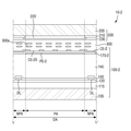
도 1은 본 발명의 일 실시예에 따른 표시 장치의 개략적인 분해 사시도이다.
도 2는 도 1에 도시된 화소의 레이아웃도이다.
도 3은 도 2의 I-I' 선을 따라 자른 단면도이다.
도 4는 도 2의 II-II' 선을 따라 자른 단면도이다.
도 5는 도 2의 게이트 배선과 광차단 패턴의 배치 관계를 나타내는 레이아웃도이다.
도 6은 도 2의 'A' 부분의 확대 레이아웃도이다.
도 7은 도 2의 광차단 패턴과 공통 배선의 전기적 연결 구조를 보여주는 개략적인 레이아웃도이다.
도 8은 도 7의 III-III' 선을 따라 자른 단면도이다.
도 9 내지 도 11은 도 8에 도시된 광차단 패턴과 공통 배선의 전기적 연결 구조의 다양한 실시예들을 보여주는 단면도들이다.
도 12는 본 발명의 다른 실시예에 따른 표시 장치 중 도 6과 대응되는 부분의 부분 레이아웃도이다.
도 13은 본 발명의 또다른 실시예에 따른 표시 장치 중 도 6과 대응되는 부분의 부분 레이아웃도이다.
도 14 및 도 15는 본 발명의 또다른 실시예에 따른 표시 장치 중 도 3 및 도 4와 대응되는 부분의 단면도들이다.
도 16은 본 발명의 또다른 실시예에 따른 표시 장치 중 도 2와 대응되는 부분의 평면도이다.
도 17은 도 16의 IV-IV' 선을 따라 자른 단면도이다.
도 18은 도 16의 V-V' 선을 따라 자른 단면도이다.
도 19 및 도 20은 본 발명의 또다른 실시예에 따른 표시 장치 중 도 3 및 도 4와 대응되는 부분의 단면도들이다.
도 21은 도 19의 광차단 패턴과 공통 배선의 전기적 연결 구조를 보여주는 개략적인 레이아웃도이다.
도 22는 도 21의 VI-VI' 선을 따라 자른 단면도이다.
도 23 및 도 24는 도 22에 도시된 광차단 패턴과 공통 배선의 전기적 연결 구조의 다양한 실시예들을 보여주는 단면도들이다.1 is a schematic exploded perspective view of a display device according to an embodiment of the present invention.
2 is a layout diagram of the pixel shown in Fig.
3 is a sectional view taken along the line II 'in Fig.
4 is a cross-sectional view taken along line II-II 'of FIG.
5 is a layout view showing the arrangement relationship of the gate interconnection and the light intercepting pattern in Fig.
6 is an enlarged layout view of a portion 'A' in FIG.
7 is a schematic layout view showing an electrical connection structure between the light intercepting pattern and the common interconnection in FIG.
8 is a cross-sectional view taken along line III-III 'of FIG.
FIGS. 9 to 11 are cross-sectional views showing various embodiments of the electrical connection structure of the light intercepting pattern and the common wiring shown in FIG.
Fig. 12 is a partial layout diagram of a portion corresponding to Fig. 6 of a display apparatus according to another embodiment of the present invention.
FIG. 13 is a partial layout view of a portion corresponding to FIG. 6 of a display device according to another embodiment of the present invention.
FIGS. 14 and 15 are cross-sectional views of portions corresponding to FIGS. 3 and 4 of a display device according to another embodiment of the present invention. FIG.
16 is a plan view of a portion corresponding to FIG. 2 of a display device according to another embodiment of the present invention.
17 is a cross-sectional view taken along the line IV-IV 'in Fig.
18 is a sectional view taken along the line VV 'in Fig.
Figs. 19 and 20 are cross-sectional views of portions corresponding to Figs. 3 and 4 of a display apparatus according to another embodiment of the present invention.
21 is a schematic layout view showing the electrical connection structure of the light intercepting pattern and the common wiring in Fig.
22 is a sectional view taken along the line VI-VI 'in FIG.
23 and 24 are cross-sectional views showing various embodiments of the electrical connection structure of the light intercepting pattern and the common wiring shown in FIG.
본 발명의 이점 및 특징, 그리고 그것들을 달성하는 방법은 첨부되는 도면과 함께 상세하게 후술되어 있는 실시예들을 참조하면 명확해질 것이다. 그러나 본 발명은 이하에서 개시되는 실시예들에 한정되는 것이 아니라 서로 다른 다양한 형태로 구현될 것이며, 단지 본 실시예들은 본 발명의 개시가 완전하도록 하며, 본 발명이 속하는 기술분야에서 통상의 지식을 가진 자에게 발명의 범주를 완전하게 알려주기 위해 제공되는 것이며, 본 발명은 청구항의 범주에 의해 정의될 뿐이다. BRIEF DESCRIPTION OF THE DRAWINGS The advantages and features of the present invention and the manner of achieving them will become apparent with reference to the embodiments described in detail below with reference to the accompanying drawings. The present invention may, however, be embodied in many different forms and should not be construed as being limited to the embodiments set forth herein. Rather, these embodiments are provided so that this disclosure will be thorough and complete, and will fully convey the scope of the invention to those skilled in the art. Is provided to fully convey the scope of the invention to those skilled in the art, and the invention is only defined by the scope of the claims.
소자(elements) 또는 층이 다른 소자 또는 층"위(on)"로 지칭되는 것은 다른 소자 바로 위에 또는 중간에 다른 층 또는 다른 소자를 개재한 경우를 모두 포함한다. 명세서 전체에 걸쳐 동일 참조 부호는 동일 구성 요소를 지칭한다.It is to be understood that elements or layers are referred to as being "on " other elements or layers, including both intervening layers or other elements directly on or in between. Like reference numerals refer to like elements throughout the specification.
비록 제1, 제2 등이 다양한 구성요소들을 서술하기 위해서 사용되나, 이들 구성요소들은 이들 용어에 의해 제한되지 않음은 물론이다. 이들 용어들은 단지 하나의 구성요소를 다른 구성요소와 구별하기 위하여 사용하는 것이다. 따라서, 이하에서 언급되는 제1 구성요소는 본 발명의 기술적 사상 내에서 제2 구성요소일 수도 있음은 물론이다.Although the first, second, etc. are used to describe various components, it goes without saying that these components are not limited by these terms. These terms are used only to distinguish one component from another. Therefore, it goes without saying that the first component mentioned below may be the second component within the technical scope of the present invention.
이하, 도면을 참조하여 본 발명의 실시예들에 대하여 설명한다.Hereinafter, embodiments of the present invention will be described with reference to the drawings.
도 1은 본 발명의 일 실시예에 따른 표시 장치의 개략적인 분해 사시도이다. 1 is a schematic exploded perspective view of a display device according to an embodiment of the present invention.
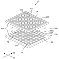
도 1을 참조하면, 본 발명의 일 실시예에 따른 표시 장치(10)는 제1 표시 기판(100), 제1 표시 기판(100)에 대향하는 제2 표시 기판(200), 및 제1 표시 기판(100)과 제2 표시 기판(200) 사이에 개재된 액정층(300)을 포함한다.1, a
각 표시 기판(100, 200)은 표시 영역(DA) 및 표시 영역(DA) 주변에 배치된 비표시 영역(NDA)을 포함한다. 비표시 영역(NDA)은 표시 영역(DA)을 둘러싸도록 배치될 수 있다. 표시 영역(DA)에는 제1 방향(D1; 또는 행 방향) 및 제1 방향(D1)과 교차하는 제2 방향(D2; 또는 열 방향)을 따라 매트릭스 형상으로 배열된 복수의 화소가 정의될 수 있다. Each of the
표시 영역(DA)은 복수의 투광 영역(PA)과, 투광 영역(PA) 주변에 배치된 차광 영역(NPA)을 포함한다. 투광 영역(PA)은 빛이 투과되어 영상이 표시되는 영역이고, 차광 영역(NPA)은 차광 부재(210) 등과 중첩되어 빛이 투과되지 않는 영역으로 정의될 수 있다. 투광 영역(PA)은 차광 영역(NPA)에 의해 둘러싸인다. 각 화소는 적어도 하나의 투광 영역(PA) 및 이를 둘러싸는 차광 영역(NPA)을 포함한다. The display area DA includes a plurality of light transmitting areas PA and a light shielding area NPA disposed around the light transmitting area PA. The light-transmitting area PA is an area through which light is transmitted to display an image, and the light-shielding area NPA can be defined as an area in which light is not transmitted by overlapping with the light-shielding
제1 표시 기판(100)은 표시 영역(DA) 및 비표시 영역(NDA)에 걸쳐 배치된 복수의 게이트 배선(GL)과 복수의 데이터 배선(DL)을 포함한다. 표시 영역(DA) 내에서 게이트 배선들(GL)과 데이터 배선들(DL)은 차광 영역(NPA) 내에 배치된다.The
게이트 배선들(GL) 및 데이터 배선들(DL)은 서로 교차하며 서로 절연되게 배치된다. 각 게이트 배선들(GL)은 화소의 경계를 따라 제1 방향(D1)으로 연장될 수 있다. 각 게이트 배선들(GL)은 비표시 영역(NDA)에 배치되는 게이트 구동부(미도시)에 연결되어 순차적으로 인가되는 게이트 신호들을 수신할 수 있다. 각 데이터 배선들(DL)은 화소의 경계를 따라 제2 방향(D2)으로 연장될 수 있다. 각 데이터 배선들(DL)은 비표시 영역(NDA)에 배치되는 데이터 구동부(DDP)에 연결되어 데이터 신호들을 수신할 수 있다.The gate wirings GL and the data wirings DL are arranged to be insulated from each other. Each of the gate wirings GL may extend in the first direction D1 along the boundary of the pixel. Each gate line GL is connected to a gate driver (not shown) disposed in the non-display area NDA to receive sequentially applied gate signals. Each data line DL may extend in the second direction D2 along the boundary of the pixel. Each data line DL is connected to a data driver DDP disposed in the non-display area NDA to receive data signals.
제1 표시 기판(100)의 표시 영역(DA)에는 각 화소마다 화소 전극(PE)이 배치될 수 있다. 화소 전극(PE)은 표시 영역(DA)의 투광 영역(PA)에 배치된다. 화소 전극(PE)은 박막트랜지스터(도 2의 TFT1)를 통해 데이터 전압을 제공받을 수 있다. 또한, 제1 표시 기판(100)의 표시 영역(DA) 전면에는 공통 전극(도면 미도시)이 배치될 수 있다. 상기 공통 전극(도면 미도시)은 표시 영역(DA)의 투광 영역(PA) 뿐만 아니라, 차광 영역(NPA)에도 배치될 수 있다. 화소 전극(PE)과 상기 공통 전극(도면 미도시)은 함께 전계를 생성하여 액정층(300)의 액정(300a)의 배열 방향을 제어할 수 있다.The pixel electrode PE may be disposed for each pixel in the display area DA of the
제1 표시 기판(100)의 비표시 영역(NDA)에는 표시 영역(DA)의 각 화소에 게이트 신호를 제공하는 게이트 구동부(미도시) 및 표시 영역(DA)의 각 화소에 데이터 신호를 제공하는 데이터 구동부(DDP)가 배치될 수 있다. A non-display area NDA of the
제2 표시 기판(200)의 표시 영역(DA)에는 각 화소마다 컬러 필터(220)가 배치될 수 있다. 컬러 필터(220)는 투광 영역(PA)에 배치될 수 있다. 컬러 필터(220)는 적색 컬러 필터, 녹색 컬러 필터, 청색 컬러 필터 중 어느 하나를 포함할 수 있다. 상기 적색 컬러 필터, 상기 녹색 컬러 필터 및 상기 청색 컬러 필터는 교대로 배열될 수 있다. 각 컬러 필터(220)간 경계에는 차광 부재(210)가 배치될 수 있다. 차광 부재(210)는 차광 영역(NPA)에 배치되며, 제1 표시 기판(100)의 게이트 배선들(GL) 및 데이터 배선들(DL)과 중첩되도록 배치될 수 있다. 차광 부재(210)는 제2 표시 기판(200)의 비표시 영역(NDA)에까지 배치될 수 있다.The display area DA of the
제1 표시 기판(100)과 제2 표시 기판(200)은 실런트 등으로 이루어진 실링 부재(미도시)에 의해 합착될 수 있다. 상기 실링 부재는 제1 표시 기판(100) 및 제2 표시 기판(200)의 주변부로서, 비표시 영역(NDA)에 위치할 수 있다.The
액정층(300)은 액정(300a)을 포함한다. 액정(300)은 제1 표시 기판(100)과 제2 표시 기판(200) 사이에 개재되고, 실링 부재에 의해 가두어진다. 액정층(300)은 표시 영역(DA)과 비표시 영역(NDA) 전체에 걸쳐 배치될 수 있다.The
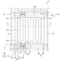
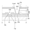
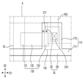
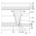
도 2는 도 1에 도시된 화소의 레이아웃도, 도 3은 도 2의 I-I' 선을 따라 자른 단면도, 도 4는 도 2의 II-II' 선을 따라 자른 단면도, 도 5는 도 2의 게이트 배선과 광차단 패턴의 배치 관계를 나타내는 레이아웃도, 도 6은 도 2의 'A' 부분의 확대 레이아웃도이다.2 is a cross-sectional view taken along line II 'of FIG. 2. FIG. 4 is a cross-sectional view taken along line II-II' of FIG. 2. FIG. FIG. 6 is an enlarged layout view of a portion "A" in FIG. 2; FIG.
이하, 도 2 내지 도 6을 참조하여 표시 장치(10)의 각 화소의 구조에 대해 한 화소를 예로 들어 더욱 상세히 설명하기로 한다. Hereinafter, the structure of each pixel of the
이하 제1 표시 기판(100)에 대해 설명한다.Hereinafter, the
제1 표시 기판(100)은 제1 베이스 기판(105), 광차단 패턴(110), 버퍼층(115), 게이트 배선(GL), 게이트 절연층(120), 반도체 패턴(130), 데이터 배선(DL), 드레인 전극(145), 층간 절연층(150), 평탄화층(160), 공통 전극(CE), 절연층(170) 및 화소 전극(PE)을 포함한다. The
제1 베이스 기판(105)은 투과성, 내열성, 내화학성 등이 우수한 물질을 포함할 수 있다. 예를 들면, 제1 베이스 기판(105)은 광 투과력이 우수한 유리, 석영, 폴리이미드, 폴리에틸렌나프탈레이트, 폴리에틸렌테레프탈레이트 및 폴리아크릴 중 어느 하나를 포함할 수 있다.The
광차단 패턴(110)은 제1 베이스 기판(105) 상에 위치하고 차광 영역(NPA)에 배치된다. 광차단 패턴(110)은 화소의 행마다 하나씩 배치될 수 있다. 광차단 패턴(110)은 공통 배선(도 7의 CL)을 통해 공통 전압을 인가받는다. 광차단 패턴(110)과 공통 배선(도 7의 CL)의 전기적 연결 구조는 후술한다. The
광차단 패턴(110)은 불투명한 금속 물질, 예를 들어 몰리브덴(Mo), 크롬(Cr), 구리(Cu), 탄탈륨(Ta), 알루미늄(Al) 중 선택된 어느 하나로 형성될 수 있다. 광차단 패턴(110)은 제1 방향(D1)을 따라 연장되는 광차단 라인(111)과, 광차단 라인(111)으로부터 제2 방향(D2)으로 돌출되는 광차단 돌출부(112)를 포함할 수 있다. The
광차단 패턴(110)의 광차단 라인(111)은 소정 폭을 가지며 제1 방향(D1)으로 연장된다. 광차단 패턴(110)의 광차단 라인(111)은 게이트 전극(GE)과 부분적으로 중첩할 수 있다. The
광차단 패턴(110)의 광차단 돌출부(112)는 화소마다 하나씩 배치될 수 있다. 즉, 광차단 패턴(110)의 광차단 라인(111)으로부터 화소마다 하나씩 제2 방향(D2)으로 광차단 돌출부(112)가 돌출될 수 있다. 예시적인 실시예에서, 광차단 패턴(110)의 광차단 돌출부(112)의 돌출 방향은 게이트 전극(GE)의 돌출 방향과 반대 방향일 수 있지만, 이에 제한되는 것은 아니다. The
광차단 패턴(110)의 광차단 돌출부(112)는 제1 베이스 기판(105)의 하측에 위치하는 백라이트 유닛에서 조사되는 빛이 반도체 패턴(130)에 유입되는 것을 차단하는 역할을 한다. 광차단 패턴(110)의 광차단 돌출부(112)는 후술할 드레인 전극(145)과 부분적으로 중첩할 수 있다. 또한 광차단 돌출부(112)는 후술할 게이트 배선(GL)과 소정 폭으로 부분적으로 중첩할 수 있다. 즉, 광차단 돌출부(112)는 게이트 배선(GL)과 중첩하는 부분 및 게이트 배선(GL)과 중첩하지 않는 부분을 포함할 수 있다.The
버퍼층(115)은 제1 베이스 기판(105) 상에 광차단 패턴(110)을 덮도록 배치된다. 버퍼층(115)은 제1 베이스 기판(105)의 전면(全面)에 배치될 수 있다. 버퍼층(115)은 절연 물질, 예를 들어 실리콘 질화물이나, 실리콘 산화물로 형성될 수 있다.The
게이트 배선(GL)은 버퍼층(115) 상에 위치하고 차광 영역(NPA)에 배치된다. 게이트 배선(GL)은 제1 방향(D1)을 따라 연장되는 게이트 라인(GB)과, 게이트 라인(GB)과 연결되고 제2 방향(D2)을 따라 돌출된 게이트 전극(GE)을 포함할 수 있다. 상술한 바와 같이 인접한 게이트 배선(GL)과 광차단 패턴(110)에서 게이트 전극(GE)의 돌출 방향과 광차단 패턴(110)의 광차단 돌출부(112)의 돌출 방향은 서로 반대 방향일 수 있다.The gate wiring GL is located on the
게이트 라인(GB)은 광차단 패턴(110)의 광차단 라인(111)과 비중첩하며, 게이트 전극(GE)과 광차단 돌출부(112)를 사이에 두고 광차단 패턴(110)의 광차단 라인(111)과 마주볼 수 있다. 게이트 전극(GE)은 제1 방향(D1)을 따라 복수개로 구비될 수 있다. 예를 들어, 게이트 전극(GE)은 화소마다 하나씩 배치되고, 각 게이트 전극(GE)은 제1 방향(D1)을 따라 소정 간격으로 이격될 수 있다. The gate line GB overlaps with the
한편, 도 5 및 도 6에 도시된 바와 같이 게이트 전극(GE)과 광차단 패턴(110)의 광차단 돌출부(112)는 상호 부분적으로 중첩할 수 있다. 게이트 전극(GE)과 광차단 패턴(110)의 광차단 돌출부(112)가 중첩하는 제1 방향(D1)의 폭, 다시 말하면, 게이트 전극(GE)과 광차단 돌출부(112)의 중첩 영역을 사이에 두고 게이트 전극(GE)의 가장자리와 광차단 돌출부(112)의 가장자리 사이의 거리(DT1)는 약 0.5um 내지 약 3um일 수 있다. 이와 같이 게이트 전극(GE)과 광차단 패턴(110)의 광차단 돌출부(112)가 약 0.5um 내지 약 3um의 폭으로 중첩하면, 공정상 마진이 확보되어 게이트 전극(GE)과 광차단 돌출부(112) 사이가 이격될 가능성이 줄어든다. 따라서, 제1 베이스 기판(105) 아래에 위치하는 백라이트 유닛(도면 미도시)에서 게이트 전극(GE)과 광차단 돌출부(112) 사이의 틈을 통해 후술할 반도체 패턴(130)으로 유입되는 것을 안정적으로 방지할 수 있다.5 and 6, the gate electrode GE and the
또한, 백라이트 유닛으로부터 반도체 패턴(130)으로 빛이 유입되는 것을 안정적으로 차단하기 위해 광차단 돌출부(112)는 돌출 방향(제2 방향, D2)으로 반도체 패턴(130)과 완전히 중첩될 뿐만 아니라, 일정한 마진을 갖도록 반도체 패턴(130)을 지나 더욱 돌출될 수 있다. 광차단 돌출부(112)의 끝단과 그와 마주보는 반도체 패턴(130)의 끝단 사이의 거리(DT2)는 약 1um 내지 약 3um일 수 있다. 상기 수치 범위에서, 백라이트 유닛의 빛이 반도체 패턴(130)으로 유입되는 것을 보다 완전하게 차단할 수 있다. In order to stably block light from entering the
게이트 배선(GL)은 구리(Cu), 몰리브덴(Mo), 알루미늄(Al), 텅스텐(W), 크롬(Cr), 티타늄(Ti)과 같은 금속이나, 적어도 하나의 상기 금속을 포함하는 합금으로 이루어질 수 있다.The gate wiring GL is made of a metal such as copper (Cu), molybdenum (Mo), aluminum (Al), tungsten (W), chromium (Cr), titanium (Ti), or an alloy containing at least one of the above metals Lt; / RTI >
게이트 절연층(120)은 게이트 배선(GL)을 덮도록 제1 베이스 기판(105) 상에 배치된다. 게이트 절연층(120)은 표시 영역(DA)과 비표시 영역(NDA)에 걸쳐 배치될 수 있다. 게이트 절연층(120)은 절연 물질, 예를 들어 실리콘 질화물, 실리콘 산화물이나, 실리콘 산질화물 등으로 형성될 수 있다.The
반도체 패턴(130)은 게이트 절연층(120) 상에 위치하고 차광 영역(NPA)에 배치된다. 반도체 패턴(130)은 게이트 절연층(120) 상에서 게이트 전극(GE)과 중첩하도록 배치될 수 있다. 반도체 패턴(130)은 비정질 실리콘 또는 다결정 실리콘으로 형성될 수 있다. 또한, 반도체 패턴(130)은 산화물 반도체 물질로 형성될 수도 있다. 상기 산화물 반도체 물질은, 예를 들어 갈륨(Ga), 인듐(In), 아연(Zn), 및 주석(Sn) 중에서 선택된 하나 이상의 원소와 산소(O)를 포함하는 산화물일 수 있다. 구체적으로, 상기 산화물 반도체 물질은 산화 아연(ZnO), 아연주석 산화물(ZTO), 아연 인듐 산화물(ZIO), 인듐 산화물(InO), 티타늄 산화물(TiO), 인듐 갈륨 아연 산화물(IGZO) 또는 인듐 아연 주석 산화물(IZTO)을 포함할 수 있다.The
반도체 패턴(130)은 연속된 소스 영역(131), 채널 영역(132) 및 드레인 영역(133)으로 구분될 수 있다. 소스 영역(131)은 상부의 소스 전극(140)과 중첩되는 영역이고, 드레인 영역(133)은 상부의 드레인 전극(145)과 중첩되는 영역으로 정의된다. 채널 영역(132)은 소스 영역(131)과 드레인 영역(133) 사이의 영역으로서, 데이터 배선(DL)에 의해 덮이지 않는 영역으로 정의된다. The
평면 배치상, 제1 방향(D1)에서 게이트 전극(GE)의 끝단은 반도체 패턴(130)의 드레인 영역(133)과 광차단 패턴(110)의 광차단 돌출부(112)가 중첩하는 영역 상에 위치할 수 있다.In plan view, the end of the gate electrode GE in the first direction D1 is located on the region where the
데이터 배선(DL)은 반도체 패턴(130) 및 게이트 절연층(120) 상에 배치된다. 데이터 배선(DL)은 차광 영역(NPA)에 배치된다. 데이터 배선(DL)은 제1 베이스 기판(105) 상에 위치하고, 제2 방향(D2)을 따라 연장되게 배치되며, 게이트 배선(GL)과 절연되어 교차한다. 데이터 배선(DL) 중 일부분은 광차단 패턴(110), 반도체 패턴(130)의 소스 영역(131) 및 게이트 배선(GL) 중 게이트 전극(GE)을 포함하는 부분과 중첩할 수 있다. 한편, 데이터 배선(DL) 중 반도체 패턴(130)의 소스 영역(131)과 중첩하는 부분은 소스 전극(140)으로 정의될 수 있다. 소스 전극(140)은 데이터 배선(DL) 중 게이트 배선(GL)과 교차하는 영역에 위치할 수 있다. 소스 전극(140)은 반도체 패턴(130)의 소스 영역(131)과 물리적, 전기적으로 연결될 수 있다.The data line DL is disposed on the
드레인 전극(145)은 반도체 패턴(130) 상에서 소스 전극(140)과 이격되게 배치되고, 반도체 패턴(130)의 드레인 영역(133)과 접하며 중첩한다. 또한, 드레인 전극(145)은 게이트 전극(GE)과 부분적으로 중첩하며, 광차단 패턴(110)과 완전히 중첩한다.The
광차단 패턴(110)의 광차단 돌출부(112)가 배치됨에 따라, 게이트 배선(GL)이 반도체 패턴(130)과 드레인 전극(145)의 일부와 중첩되는 면적을 감소시킬 수 있다. 따라서, 게이트 배선(GL)과 드레인 전극(145)의 중첩에 의해 형성되는 기생 용량(Cgd)을 줄일 수 있어 킥백 전압의 크기를 줄일 수 있다. Shielding
또한, 화소 전극(PE)과 공통 전극(CE)이 형성하는 스토리지 커패시터(Cst1) 외에, 광차단 돌출부(112)와 드레인 전극(145)은, 추가적인 스토리지 커패시터(Cst2)를 형성한다. 따라서, 킥백 전압의 크기를 더욱 줄일 수 있다. In addition to the storage capacitor Cst1 formed by the pixel electrode PE and the common electrode CE, the
데이터 배선(DL)과 드레인 전극(145)은 구리, 몰리브덴, 알루미늄, 텅스텐, 크롬, 티타늄과 같은 금속이나, 적어도 하나의 상기 금속을 포함하는 합금으로 형성될 수 있다.The data line DL and the
게이트 전극(GE), 반도체 패턴(130), 소스 전극(140) 및 드레인 전극(145)은 스위칭 소자인 박막트랜지스터(TFT1)를 형성할 수 있다.The gate electrode GE, the
층간 절연층(150)은 표시 영역(DA) 및 비표시 영역(도 1의 NDA)에 배치된다. 층간 절연층(150)은 데이터 배선(DL)과, 반도체 패턴(130)과 드레인 전극(145)을 덮도록 게이트 절연층(120) 상에 배치될 수 있다. 층간 절연층(150)은 절연 물질, 예를 들어 실리콘 질화물, 실리콘 산화물이나, 실리콘 산질화물 등으로 형성될 수 있다. 층간 절연층(150)은 드레인 전극(145)을 노출시키는 관통홀(150a)을 더 포함할 수 있다. The interlayer insulating
평탄화층(160)은 표시 영역(DA) 및 비표시 영역(도 1의 NDA)에 배치된다. 평탄화층(160)은 층간 절연층(150) 상에 배치될 수 있다. 평탄화층(160)은 유기 절연 물질, 예를 들어 아크릴계 에폭시실리콘으로 형성될 수 있다. 평탄화층(160)은 드레인 전극(145)을 노출시키는 관통홀(160a)을 더 포함할 수 있다. The
공통 전극(CE)은 표시 영역(DA)에 배치되며, 비표시 영역(NDA)까지 연장되게 배치될 수 있다. 공통 전극(CE)은 평탄화층(160) 상에 위치할 수 있다. 공통 전극(CE)은 접속부(도 8의 CLcon)를 포함하는 공통 배선(도 7의 CL)을 통해 공통 전압을 인가받을 수 있다. 또한, 공통 전극(CE)은 공통 배선(도 7의 CL)을 통해 광차단 패턴(110)과 전기적으로 연결될 수 있다. 공통 전극(CE)과 광차단 패턴(110)이 전기적으로 연결됨에 따라 공통 전극(CE)의 전체 저항이 감소하며, 화소 전극(PE)에 인가되는 데이터 전압이 스윙될 때 공통 전극(CE)에 인가된 공통 전압이 흔들리는 리플 현상이 줄어들 수 있다.The common electrode CE is disposed in the display area DA and may extend to the non-display area NDA. The common electrode CE may be located on the
공통 전극(CE)은 평탄화층(160)의 관통홀(160a)과 중첩하는 제1 개구부(OP1)를 포함한다. 제1 개구부(OP1)는 실질적으로 공통 전극(CE)이 배치되지 않는 영역이다. 평탄화층(160)의 관통홀(160a)은 제1 개구부(OP1)와 완전히 중첩할 수 있다. 제1 개구부(OP1)의 평면상 면적은 평탄화층(160)의 관통홀(160a) 평면상 면적보다 클 수 있다.The common electrode CE includes a first opening OP1 overlapping the through
공통 전극(CE)은 투명한 도전성 물질, 예를 들어 인듐틴옥사이드(ITO), 인듐징크옥사이드(IZO), 또는 징크옥사이드(ZO) 등으로 형성될 수 있다.The common electrode CE may be formed of a transparent conductive material, for example, indium tin oxide (ITO), indium zinc oxide (IZO), zinc oxide (ZO), or the like.
절연층(170)은 표시 영역(DA) 및 비표시 영역(도 1의 NDA)에 배치된다. 절연층(170)은 공통 전극(CE) 상에 배치될 수 있다. 절연층(170)은 절연 물질, 예를 들어 실리콘 질화물, 실리콘 산화물, 실리콘 산질화물 등으로 형성될 수 있다. 절연층(170)은 드레인 전극(145)을 노출시키는 관통홀(170a)을 포함할 수 있다. 절연층(170)은 평탄화층(160)의 관통홀(160a) 내측벽을 덮도록 형성될 수 있지만, 이에 제한되는 것은 아니다.The insulating
한편, 층간 절연층(150)의 관통홀(150a), 평탄화층(160)의 관통홀(160a), 절연층(170)의 관통홀(170a) 및 공통 전극(CE)의 제1 개구부(OP1)는 화소 전극(PE)을 드레인 전극(145)에 연결하기 위한 컨택홀(CH1)을 형성할 수 있다. 컨택홀(CH1)은 제1 베이스 기판(105)의 차광 영역(NPA)에서 광차단 패턴(110)의 광차단 돌출부(112)와 중첩할 수 있다. The through
화소 전극(PE)은 절연층(170) 상에 공통 전극(CE)과 절연되어 배치되며, 화소마다 배치된다. 구체적으로, 화소 전극(PE)은 절연층(170) 상에 위치하고 투광 영역(PA)에 배치되며, 컨택홀(CH1) 통해 드레인 전극(145)에 연결된다. The pixel electrode PE is disposed on the insulating
예시적인 실시예에서, 화소 전극(PE)은 평면상에서 적어도 하나의 줄기부(PE1)와, 줄기부(PE1)로부터 돌출되어 형성된 복수의 가지부들(PE2)과, 줄기부(PE1)와 드레인 전극(145)을 연결하는 연장부(PE3)를 포함할 수 있다. 가지부들(PE2)은 서로 일정 간격 이격된다. 가지부들(PE2)은 소정 방향으로 평행하게 연장되도록 형성될 수 있다. 줄기부(PE1)와 가지부(PE2)는 도 2에 도시된 배열 형태로 한정되는 것은 아니며, 다양한 배열 형태를 가질 수 있다. 예를 들어, 가지부(PE2)가 줄기부(PE1)로부터 일 방향으로 돌출될 수 있다. 또한, 가지부(PE2)가 줄기부(PE1)의 연장 방향과 수직한 양측 방향으로 모두 돌출되어 연장될 수도 있다. 또는 줄기부(PE1)나 가지부(PE2)가 복수회 절곡된 형태로 형성될 수도 있다. In the exemplary embodiment, the pixel electrode PE includes at least one stripe portion PE1 on a plane, a plurality of fringes PE2 protruding from the stripe portion PE1, a plurality of stripe portions PE1 and PE2, And an extension part PE3 connecting the
화소 전극(PE)은 투명한 도전성 물질, 예를 들어 인듐틴옥사이드(ITO), 인듐징크옥사이드(IZO), 또는 징크옥사이드(ZO) 등으로 형성될 수 있다.The pixel electrode PE may be formed of a transparent conductive material such as indium tin oxide (ITO), indium zinc oxide (IZO), zinc oxide (ZO), or the like.
이하 제2 표시 기판(200)에 대해 설명한다.Hereinafter, the
제2 표시 기판(200)은 제2 베이스 기판(205), 차광 부재(210), 컬러 필터(220) 및 오버 코팅층(230)을 포함할 수 있다.The
제2 베이스 기판(205)은 제1 베이스 기판(105)과 대향한다. 제2 베이스 기판(205)은 투과성, 내열성, 내화학성 등이 우수한 물질을 포함할 수 있다. 예를 들면, 제2 베이스 기판(205)은 광 투과력이 우수한 유리, 폴리에틸렌나프탈레이트, 폴리에틸렌테레프탈레이트 및 폴리아크릴 중 어느 하나를 포함할 수 있다.The
차광 부재(210)는 제1 표시 기판(100)과 대향하는 제2 베이스 기판(205)의 일면 상에 배치된다. 차광 부재(210)는 차광 영역(NPA) 내에 배치된다. 차광 부재(210)는 광차단 패턴(110), 게이트 배선(GL) 박막트랜지스터(TFT1) 및 데이터 배선(DL)과 중첩할 수 있다. 차광 부재(210)는 광차단 물질로 형성되어, 빛샘이나 혼색을 방지할 수 있다.The
컬러 필터(220)는 제2 베이스 기판(205)의 일면 상에 배치된다. 컬러 필터(220)는 투광 영역(PA)에 배치되고, 화소 전극(PE)과 중첩할 수 있다. The
오버 코팅층(230)은 제2 베이스 기판(205)의 일면 상에 배치되어 차광 부재(210) 및 컬러 필터(220)를 덮을 수 있다. 오버 코팅층(230)은 컬러 필터(220)가 액정층(30)에 노출되는 것을 방지하고 평탄면을 제공할 수 있다. 오버 코팅층(230)은 아크릴계 에폭시 재료를 이용하여 형성될 수 있다.The
이하, 상기와 같은 표시 장치(10)의 광차단 패턴(110)과 공통 배선(CL)의 전기적 연결 구조에 대해 상세히 설명하기로 한다. Hereinafter, the electrical connection structure of the
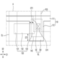
도 7은 도 2의 광차단 패턴과 공통 배선의 전기적 연결 구조를 보여주는 개략적인 레이아웃도, 도 8은 도 7의 'B' 부분의 확대 단면도, 도 9 내지 도 11은 도 8에 도시된 광차단 패턴과 공통 배선의 전기적 연결 구조의 다양한 실시예들을 보여주는 단면도들이다. 도 7에서, 복수의 게이트 배선(GL)과 복수의 데이터 배선(DL)은 배치만 나타나도록 간략히 라인으로 표시되었다.FIG. 7 is a schematic layout view showing an electrical connection structure between the light intercepting pattern and the common interconnection of FIG. 2, FIG. 8 is an enlarged cross-sectional view of the portion 'B' of FIG. 7, Sectional views showing various embodiments of an electrical connection structure of a pattern and a common wiring. In Fig. 7, a plurality of gate lines GL and a plurality of data lines DL are simply indicated by lines so that only the layout is shown.
도 7 및 도 8을 참조하면, 광차단 패턴(110)은 화소행마다 배치된다. 광차단 패턴(110)은 제1 베이스 기판(105) 상에 위치하고, 표시 영역(DA)의 외측인 비표시 영역(NDA)에 배치되며, 광차단 라인(111)에 연결된 접속 단자(113)를 더 포함할 수 있다. 비표시 영역(NDA)에서 버퍼층(115), 게이트 절연층(120), 층간 절연층(150) 및 평탄화층(160)은 각각 광차단 패턴(110)의 접속 단자(113)를 노출하고, 상호 중첩하는 관통홀(115b, 120b, 150b, 160b)을 포함할 수 있다. 한편, 평탄화층(160) 상에 배치되는 공통 전극(CE)은 평탄화층(160)의 관통홀(160b)과 중첩하는 제2 개구부(OP2)를 포함한다. 제2 개구부(OP2)는 실질적으로 공통 전극(CE)이 배치되지 않는 영역이다.7 and 8, the
비표시 영역(NDA)에는 공통 배선(CL) 및 공통 배선(CL)과 연결된 연결 전극(BE1)이 배치될 수 있다. The connection electrode BE1 connected to the common wiring CL and the common wiring CL may be disposed in the non-display area NDA.
공통 배선(CL)은 공통 전극(CE)과 광차단 패턴(110)에 공통 전압을 제공한다. 공통 배선(CL)은 공통 전극(CE) 상에 배치될 수 있다. 예시적인 실시예에서 공통 배선(CL)은 폐루프 형상을 가질 수 있으나, 이에 한정되는 것은 아니다. 공통 배선(CL)은 공통 전극(CE) 상에 접촉하도록 배치되어 공통 전극(CE)과 전기적으로 연결될 수 있다. 공통 배선(CL)은 전도성 물질로 형성될 수 있으며, 전기 저항이 낮은 물질, 예를 들어 구리, 몰리브덴, 알루미늄, 텅스텐, 크롬, 티타늄과 같은 금속이나, 적어도 하나의 상기 금속을 포함하는 합금으로 형성될 수 있다. 도시되진 않았지만, 또 다른 예로, 공통 배선(CL)은 공통 전극(CE) 상에 절연되게 배치된 상태에서 별도의 연결 전극을 통해 공통 전극(CE)과 전기적으로 연결될 수도 있다. The common line CL provides a common voltage to the common electrode CE and the
한편, 제1 베이스 기판(105) 상의 비표시 영역(NDA)에서 절연층(170)은 공통 배선(CL)을 덮도록 공통 전극(CE) 상에 배치된다. 절연층(170)은 광차단 패턴(110)의 접속 단자(113)를 노출하며 버퍼층(115)의 관통홀(115b)과 중첩하는 관통홀(170b)을 더 포함할 수 있다. 절연층(170)은 평탄화층(160)의 관통홀(160b) 내측벽을 덮도록 형성될 수 있지만, 이에 제한되는 것은 아니다. On the other hand, in the non-display area NDA on the
관통홀들(115b, 120b, 150b, 160b, 170b) 및 제2 개구부(OP2)는 연결 전극(BE1)을 광차단 패턴(110)의 접속 단자(113)에 연결하기 위한 컨택홀(CH2)을 형성할 수 있다. 또한, 절연층(170)은 공통 배선(CL) 중 제1 방향(D1)에서 광차단 패턴(110)의 접속 단자(113)와 인접한 접속부(CLcon)를 노출하며, 연결 전극(BE1)을 공통 배선(CL)의 접속부(CLcon)에 연결하기 위한 컨택홀(CH3)을 더 포함할 수 있다.The through
연결 전극(BE1)은 절연층(170) 상에 배치될 수 있다. 연결 전극(BE1)은 컨택홀(CH2)을 통해 광차단 패턴(110)의 접속 단자(113)와 전기적으로 연결되고, 컨택홀(CH3)을 통해 공통 배선(CL)의 접속부(CLcon)에 전기적으로 연결될 수 있다. 연결 전극(BE1)은 화소 전극(PE)과 동일한 층에 배치될 수 있으며, 화소 전극(PE)의 형성 물질과 동일한 물질로 형성될 수 있다. The connection electrode BE1 may be disposed on the insulating
상기와 같이 광차단 패턴(110)은 연결 전극(BE1)을 통해 공통 배선(CL)과 전기적으로 연결될 수 있다. 이에 따라, 광차단 패턴(110)이 공통 배선(CL)을 통해 공통 전압을 인가받아 광차단 패턴(110)의 전압이 일정한 전압으로 유지될 수 있으며, 이 경우 화소 전극(PE)과 전기적으로 연결된 드레인 전극(145)과 광차단 패턴(110)은 스토리지 커패시터(도 3의 Cst2)를 형성할 수 있다.As described above, the
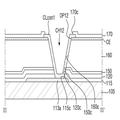
도 9 내지 도 11은 도 8에 도시된 광차단 패턴과 공통 배선의 전기적 연결 구조의 다양한 실시예들을 보여주는 단면도이다.9 to 11 are cross-sectional views showing various embodiments of the electrical connection structure of the light intercepting pattern and the common wiring shown in FIG.
도 9는 광차단 패턴(도 7의 110)의 접속 단자(113a)가 공통 배선(도 7의 CL)과 직접 연결되는 것을 예시한다.9 illustrates that the
구체적으로, 광차단 패턴(110)의 접속 단자(113a)는 광차단 패턴(도 7의 110)의 광차단 라인(도 7의 111)으로부터 제1 방향(D1)을 따라 연장되어 형성될 수 있으며, 비표시 영역(도 7의 NDA)에서 공통 배선(도 7의 CL)과 중첩할 수 있다. 된다. Specifically, the
또한, 공통 배선(도 7의 CL)은 컨택홀(CH12)을 통해 광차단 패턴(도 7의 110)의 접속 단자(113a)와 연결된다. 컨택홀(CH12)은 광차단 패턴(도 7의 110)의 접속 단자(113a)를 노출하는 버퍼층(115)의 관통홀(115c), 게이트 절연층(120)의 관통홀(120c), 층간 절연층(150)의 관통홀(150c), 평탄화층(160)의 관통홀(160c) 및 공통 전극(CE)의 제2 개구부(OP12)에 의해 형성될 수 있다. The common wiring (CL in Fig. 7) is connected to the
또한, 공통 배선(도 7의 CL)의 접속부(CLcon1)는 공통 전극(CE)과 직접 접촉할 수 있으며, 공통 배선(도 7의 CL)은 접속부(CLcon1)를 통해 공통 전극(CE)과 전기적으로 연결될 수 있다. 7) can be in direct contact with the common electrode CE through the connecting portion CLcon1 and the common line CL can be electrically connected to the common electrode CE via the connecting portion CLcon1, .
절연층(170)은 공통 배선(도 7의 CL)의 접속부(CLcon1)를 노출하는 관통홀(170c)을 포함할 수 있다.The insulating
도 10은 광차단 패턴(도 7의 110)의 접속 단자(113)가 게이트 배선(도 7의 GL)과 동일한 층에 배치되는 연결 전극(BE2)을 통해 공통 배선(도 7의 CL)과 연결되는 것을 예시한다. 10 shows a state in which the
구체적으로, 버퍼층(115)은 광차단 패턴(도 7의 110)의 접속 단자(113)를 노출시키는 컨택홀(CH22)을 더 포함한다. 이 경우, 연결 전극(BE2)은 버퍼층(115) 상에 위치하여 컨택홀(CH22)을 통해 광차단 패턴(도 7의 110)의 접속 단자(113)와 접속한다. More specifically, the
게이트 절연층(120)은 연결 전극(BE2)을 덮도록 버퍼층(115) 상에 배치되며, 연결 전극(BE2) 중 광차단 패턴(도 7의 110)의 접속 단자(113)와 비중첩하는 접속부(BE2a)를 노출하는 관통홀(120d)을 포함한다. The
층간 절연층(150)은 게이트 절연층(120) 상에 배치되며, 게이트 절연층(120)의 관통홀(120d)과 중첩하는 관통홀(150d)을 포함한다.The interlayer insulating
평탄화층(160)은 층간 절연층(150)의 관통홀(150d)과 중첩하는 관통홀(160d)을 포함한다. 한편, 평탄화층(160) 상에 배치되는 공통 전극(CE)은 평탄화층(160)의 관통홀(160d)과 중첩하는 제2 개구부(OP22)를 포함한다. The
관통홀들(120d, 150d, 160d)과 제2 개구부(OP22)는 컨택홀(CH23)을 형성한다.The through-
또한, 공통 배선(도 7의 CL)의 접속부(CLcon2)는 컨택홀(CH23)을 통해 연결 전극(BE2)의 접속부(BE2a)와 물리적, 전기적으로 연결된다. 절연층(170)은 공통 배선(도 7의 CL)의 접속부(CLcon2)를 노출하는 관통홀(170d)을 포함할 수 있다.The connection portion CLcon2 of the common wiring (CL in Fig. 7) is physically and electrically connected to the connection portion BE2a of the connection electrode BE2 through the contact hole CH23. The insulating
도 11은 광차단 패턴(도 7의 110)의 접속 단자(113)가 데이터 배선(도 7의 DL)과 동일한 층에 배치되는 연결 전극(BE3)을 통해 공통 배선(도 7의 CL)과 연결되는 것을 예시한다. 11 shows a state in which the
구체적으로, 버퍼층(115)은 광차단 패턴(도 7의 110)의 접속 단자(113)를 노출시키는 관통홀(115e)을 포함하며, 게이트 절연층(120)은 버퍼층(115)의 관통홀(115e)과 중첩하는 관통홀(120e)을 포함한다. 관통홀들(115e, 120e)은 컨택홀(CH32)을 형성한다. 이 경우, 연결 전극(BE3)은 컨택홀(CH32)을 통해 광차단 패턴(도 7의 110)의 접속 단자(113)와 전기적으로 연결된다. Specifically, the
층간 절연층(150)은 연결 전극(BE3)을 덮도록 게이트 절연층(120) 상에 배치되며, 관통홀(150e)을 포함한다. 관통홀(150e)은 연결 전극(BE3) 중 광차단 패턴(도 7의 110)의 접속 단자(113)와 비중첩하는 접속부(BE3a)를 노출한다. 층간 절연층(160)은 층간 절연층(150) 상에 배치되며, 층간 절연층(150)의 관통홀(150e)과 중첩하는 관통홀(160e)를 포함한다.The interlayer insulating
평탄화층(160) 상에 배치되는 공통 전극(CE)은 평탄화층(160)의 관통홀(160e)과 중첩하는 제2 개구부(OP32)를 포함한다. 관통홀들(150e, 160e)과 제2 개구부(OP32)는 컨택홀(CH33)을 형성한다.The common electrode CE disposed on the
공통 배선(도 7의 CL)의 접속부(CLcon3)는 컨택홀(CH33)을 통해 연결 전극(BE3)의 접속부(BE3a)와 물리적, 전기적으로 연결된다. 절연층(170)은 공통 배선(CL)의 접속부(CLcon3)를 노출하는 관통홀(170e)을 포함할 수 있다.The connection portion CLcon3 of the common wiring (CL in Fig. 7) is physically and electrically connected to the connection portion BE3a of the connection electrode BE3 through the contact hole CH33. The insulating
상기와 같이 본 발명의 일 실시예에 따른 표시 장치(10)는 공통 전압을 인가받아 일정한 전압을 유지하는 광차단 라인(111)과, 게이트 배선(GL)과 소정 폭으로 중첩하면서 드레인 전극(145)과 중첩되게 배치되는 광차단 돌출부(112)를 포함하는 광차단 패턴(110)을 구비함으로써, 화소 전극(PE)과 공통 전극(CE) 사이에 형성되는 스토리지 커패시터(Cst1) 외에 추가적인 스토리지 커패시터(Cst2)를 형성하게 할 수 있다. 또한 본 발명의 일 실시예에 따른 표시 장치(10)는 광차단 패턴(110)을 포함함에 따라 게이트 배선(GL)과 드레인 전극(145)의 중첩영역을 감소시킬 수 있고, 이에 따라, 게이트 배선(GL)과 드레인 전극(145)의 중첩에 의해 형성되는 기생 용량(Cgd)을 감소시킬 수 있다. 즉, 본 발명의 일 실시예에 따른 표시 장치(10)는 추가적인 스토리지 커패시터(Cst2)를 형성하고 기생 용량(Cgd)을 감소시킴에 따라, 킥백 전압의 발생이 감소될 수 있다.As described above, the
따라서, 표시 장치(10)의 구동시 플리커 현상이 발생되는 것을 줄일 수 있으며, 표시 장치(10)의 표시 품질을 향상시킬 수 있다.Therefore, it is possible to reduce the occurrence of flicker when the
또한, 표시 장치(10)는 광차단 패턴(110)이 공통 전극(CE)과 전기적으로 연결되는 바, 공통 전극(CE)에 공통 전압이 인가될 때 저항 성분을 감소시킬 수 있다. 또한 광차단 패턴(110)이 주변 구성, 예를 들어 게이트 전극(GE) 또는 반도체 패턴(130)의 소스 영역(121)과 기생 용량을 형성하는 것을 줄일 수 있다. 따라서, 화소 전극(PE)에 인가되는 데이터 전압이 스윙될 때 공통 전극(CE)에 인가된 공통 전압이 흔들리는 리플 현상을 줄일 수 있으며, 게이트 전극(GE)과 반도체 패턴(130)간의 기생 용량을 감소시킴으로써 박막트랜지스터(도 2 또는 도 3의 TFT1)의 동작 신뢰성 저하를 방지할 수 있다.In addition, the
도 12는 본 발명의 다른 실시예에 따른 표시 장치 중 도 6과 대응되는 부분의 부분 레이아웃도이다.Fig. 12 is a partial layout diagram of a portion corresponding to Fig. 6 of a display apparatus according to another embodiment of the present invention.
본 발명의 다른 실시예에 따른 표시 장치는 도 1 내지 도 11의 표시 장치(10)와 비교하여 광차단 패턴(610)만 다를 뿐 이외의 구성은 도 1 내지 도 11의 설명에서 상술한 바와 동일하다. 따라서, 본 발명의 다른 실시예에 따른 표시 장치에서는 광차단 패턴(610)에 대해서 중점적으로 설명하기로 한다. The display device according to another embodiment of the present invention is different from the
도 12를 참조하면, 광차단 패턴(610)은 광차단 라인(611)과 광차단 돌출부(612)를 포함하며, 도 6의 광차단 패턴(도 6의 110)과 유사하다. Referring to FIG. 12, the
다만, 광차단 패턴(610)의 광차단 라인(611)은 게이트 배선(GL)의 게이트 전극(GE)과 비중첩하는 점에서 도 6의 광차단 패턴(도 6의 110)과 상이하다. 이 경우, 광차단 라인(611)과 게이트 전극(GE)이 중첩하여 형성되는 기생 용량을 감소시킬 수 있으며, 광차단 라인(611)과 게이트 전극(GE) 사이의 기생 용량에 의한 박막트랜지스터(도 2 또는 도 3의 TFT1)의 동작 신뢰성 저하를 방지할 수 있다.6) in that the
도 13은 본 발명의 또다른 실시예에 따른 표시 장치 중 도 6과 대응되는 부분의 부분 레이아웃도이다.FIG. 13 is a partial layout view of a portion corresponding to FIG. 6 of a display device according to another embodiment of the present invention.
본 발명의 또다른 실시예에 따른 표시 장치는 도 1 내지 도 11의 표시 장치(10)와 비교하여 광차단 패턴(710)만 다를 뿐 이외의 구성은 도 1 내지 도 11의 설명에서 상술한 바와 동일하다. 따라서, 본 발명의 또다른 실시예에 따른 표시 장치에서는 광차단 패턴(710)에 대해서 중점적으로 설명하기로 한다.The display device according to another embodiment of the present invention differs from the
도 13을 참조하면, 광차단 패턴(710)은 광차단 라인(711)과 광차단 돌출부(712)를 포함하며, 도 6의 광차단 패턴(도 6의 110)과 유사하다.13, the
다만, 광차단 패턴(710)의 광차단 라인(711)이 게이트 배선(GL)의 게이트 라인(GB)과 중첩하는 점, 광차단 돌출부(712)의 돌출 방향이 게이트 전극(GE)의 돌출 방향과 동일한 방향인 점에서 차이점이 존재한다.The
이와 같은 광차단 패턴(710)을 포함하는 표시 장치는 도 1 내지 도 11의 표시 장치(10)와 동일한 효과를 제공할 수 있다. A display device including such a
도 14 및 도 15는 본 발명의 또다른 실시예에 따른 표시 장치 중 도 3 및 도 4와 대응되는 부분의 단면도들이다.FIGS. 14 and 15 are cross-sectional views of portions corresponding to FIGS. 3 and 4 of a display device according to another embodiment of the present invention. FIG.
본 발명의 또다른 실시예에 따른 표시 장치(10-1)는 도 1 내지 도 11의 표시 장치(10)와 비교하여 게이트 절연층(120-1), 반도체 패턴(130-1) 및 드레인 전극(145-1)만 다를 뿐 이외의 구성들은 동일하다. 따라서, 본 발명의 또다른 실시예에 따른 표시 장치(10-1)에서는 게이트 절연층(120-1), 반도체 패턴(130-1) 및 드레인 전극(145-1)에 대해서 중점적으로 설명하기로 한다.The display device 10-1 according to another embodiment of the present invention is different from the
도 14 및 도 15를 참조하면, 제1 표시 기판(100-1)은 제1 베이스 기판(105), 광차단 패턴(110), 버퍼층(115), 게이트 배선(GL), 게이트 절연층(120-1), 반도체 패턴(130-1), 데이터 배선(DL), 드레인 전극(145-1), 층간 절연층(150), 평탄화층(160), 화소 전극(PE), 절연층(170) 및 공통 전극(CE)을 포함한다.14 and 15, the first display substrate 100-1 includes a
게이트 절연층(120-1)은 도 3의 게이트 절연층(도 3의 120)과 유사하다. 다만, 게이트 절연층(120-1)은 제1 베이스 기판(105), 구체적으로 버퍼층(115) 상에서 게이트 배선(도 2의 GL)과 중첩하는 영역에만 배치된다. 즉, 게이트 절연층(120-1)은 버퍼층(115) 전면에 배치되지 않고 게이트 전극(GE)을 포함한 게이트 배선(GL)을 커버하는 범위 내에서만 배치될 수 있다.The gate insulating layer 120-1 is similar to the gate insulating layer (120 in Fig. 3) in Fig. However, the gate insulating layer 120-1 is disposed only on the region of the
반도체 패턴(130-1)은 도 3의 반도체 패턴(도 3의 130)과 유사하다. 다만, 반도체 패턴(130-1)은 게이트 절연층(120-1)의 배치에 의해 버퍼층(115)과 접촉하게 배치될 수 있다. The semiconductor pattern 130-1 is similar to the
드레인 전극(145-1)은 도 3의 드레인 전극(도 3의 145)과 유사하다. 다만, 드레인 전극(145-1)은 게이트 절연층(120-1)과 반도체 패턴(130-1)의 배치에 의해 버퍼층(115)과 접촉하게 배치될 수 있다. 이 경우, 도 3에 도시된 바와는 달리, 광차단 패턴(110)과 드레인 전극(145-1) 사이에 게이트 절연층(120-1)이 위치하지 않는다. 따라서 광차단 패턴(110)과 드레인 전극(145-1) 사이의 간격이 감소하는 바, 광차단 패턴(110)과 드레인 전극(145-1) 사이에 형성되는 스토리지 커패시터(Cst2)의 용량을 증가시킬 수 있다. The drain electrode 145-1 is similar to the
이와 같은 게이트 절연층(120-1)을 포함하는 표시 장치(10-1)는 화소 전극(PE)과 공통 전극(CE) 사이에 형성되는 스토리지 커패시터(Cst1) 외에, 추가 스토리지 커패시터(Cst2)의 형성을 확보함으로써 킥백 전압의 발생을 줄일 수 있다.The display device 10-1 including the gate insulating layer 120-1 includes a storage capacitor Cst1 formed between the pixel electrode PE and the common electrode CE and a storage capacitor Cst2 formed between the pixel electrode PE and the common electrode CE. The generation of the kickback voltage can be reduced.
도 16은 본 발명의 또다른 실시예에 따른 표시 장치 중 도 2와 대응되는 부분의 평면도, 도 17은 도 16의 IV-IV' 선을 따라 자른 단면도, 도 18은 도 16의 V-V' 선을 따라 자른 단면도이다.16 is a plan view of a portion corresponding to FIG. 2 of a display device according to another embodiment of the present invention, FIG. 17 is a sectional view taken along line IV-IV 'of FIG. 16, FIG.
본 발명의 또다른 실시예에 따른 표시 장치(10-2)는 도 1 내지 도 11의 표시 장치(10)와 비교하여 화소 전극(PE-2), 절연층(170-2) 및 공통 전극(CE-2)만 다를 뿐, 이외의 구성들은 동일하다. 따라서, 본 발명의 또다른 실시예에 따른 표시 장치에서는 화소 전극(PE-2), 절연층(170-2) 및 공통 전극(CE-2)에 대해서 중점적으로 설명하기로 한다.The display device 10-2 according to another embodiment of the present invention is different from the
도 16 내지 도 18을 참조하면, 제1 표시 기판(100-2)은 제1 베이스 기판(105), 광차단 패턴(110), 버퍼층(115), 게이트 배선(GL), 게이트 절연층(120), 반도체 패턴(130), 데이터 배선(DL), 드레인 전극(145), 층간 절연층(150), 평탄화층(160), 화소 전극(PE-2), 절연층(170-2) 및 공통 전극(CE-2)을 포함한다.16 to 18, the first display substrate 100-2 includes a
화소 전극(PE-2)은 도 3 및 도 4의 화소 전극(PE)과 유사하다. 다만, 화소 전극(PE-2)은 평탄화층(160) 상에 배치된다. 화소 전극(PE-2)은 일체형으로 형성될 수 있다.The pixel electrode PE-2 is similar to the pixel electrode PE shown in Figs. 3 and 4. However, the pixel electrode PE-2 is disposed on the
절연층(170-2)은 도 3 및 도 4의 절연층(170)과 유사하다. 다만, 절연층(170-2)은 화소 전극(PE-2) 상에 배치된다. The insulating layer 170-2 is similar to the insulating
공통 전극(CE-2)은 도 3 및 도 4의 공통 전극(CE)과 유사하다. 다만, 공통 전극(CE-2)은 절연층(170-2) 상에 배치되며, 투광 영역(PA)에서 복수의 슬릿(CE-2S)을 포함할 수 있다.The common electrode CE-2 is similar to the common electrode CE of Figs. However, the common electrode CE-2 may be disposed on the insulating layer 170-2 and may include a plurality of slits CE-2S in the light transmitting region PA.
이와 같은 화소 표시 장치(10-2)는 도 1 내지 도 11의 표시 장치(10)와 동일한 효과를 제공할 수 있다. Such a pixel display device 10-2 can provide the same effect as the
도 19 및 도 20은 본 발명의 또다른 실시예에 따른 표시 장치 중 도 3 및 도 4와 대응되는 부분의 단면도들이다.Figs. 19 and 20 are cross-sectional views of portions corresponding to Figs. 3 and 4 of a display apparatus according to another embodiment of the present invention.
본 발명의 또다른 실시예에 따른 표시 장치(20)는 도 1 내지 도 11의 표시 장치(10)와 비교하여 공통 전극(CE20)의 배치가 상이하다. 이에 따라, 본 발명의 또다른 실시예에 따른 표시 장치(20)에서는 공통 전극(CE20)의 배치에 따라 달라지는 구성들 위주로 설명하기로 한다.The
도 19 및 도 20을 참조하면, 본 발명의 또다른 실시예에 따른 표시 장치(20)는 제1 표시 기판(800), 제1 표시 기판(800)에 대향하는 제2 표시 기판(900), 및 제1 표시 기판(800)과 제2 표시 기판(900) 사이에 개재된 액정층(300)을 포함할 수 있다.19 and 20, a
제1 표시 기판(800)은 제1 베이스 기판(105), 광차단 패턴(110), 버퍼층(115), 게이트 배선(도 2의 GL), 스토리지 전극(STE), 게이트 절연층(820), 반도체 패턴(130), 데이터 배선(DL), 드레인 전극(845), 층간 절연층(150), 평탄화층(160) 및 화소 전극(PE20)을 포함한다.The
스토리지 전극(STE)은 게이트 배선(도 2의 GL)과 동일층에 형성되며, 게이트 배선(GL)과 동일한 물질로 형성될 수 있다. 스토리지 전극(STE)은 게이트 절연층(820)을 사이에 두고 드레인 전극(845)과 중첩되어 스토리지 커패시터(Cst3)를 형성한다. The storage electrode STE is formed on the same layer as the gate wiring (GL in Fig. 2), and may be formed of the same material as the gate wiring GL. The storage electrode STE overlaps the
게이트 절연층(820)은 도 3 및 도 4의 게이트 절연층(도 3 및 도 4의 120)과 유사하다. 다만, 게이트 절연층(820)은 게이트 배선(도 2의 GL)과 스토리지 전극(STE)을 덮도록 배치될 수 있다.The
드레인 전극(845)은 도 3의 드레인 전극(도 3의 145)과 유사하다. 다만, 드레인 전극(845)은 스토리지 전극(STE)과 중첩되도록 연장되게 배치될 수 있다.The
화소 전극(PE20)은 도 3 및 도 4의 화소 전극(도 3 및 도 4의 PE20)과 유사하다. 다만, 화소 전극(PE20)은 평탄화층(160) 상에 배치될 수 있다.The pixel electrode PE20 is similar to the pixel electrodes (PE20 in Figs. 3 and 4) in Figs. 3 and 4. However, the pixel electrode PE20 may be disposed on the
제2 표시 기판(900)은 제2 베이스 기판(205), 차광 부재(210), 컬러 필터(220), 오버 코팅층(230) 및 공통 전극(CE20)을 포함할 수 있다.The
공통 전극(CE20)은 도 3 및 도 4의 공통 전극(도 3 및 도 4의 CE)과 유사하다. 다만, 공통 전극(CE20)은 제1 표시 기판(800)을 향하는 제2 베이스 기판(205)의 일면 상에 배치되며, 더 구체적으로 오버 코팅층(230) 상에 배치될 수 있다. The common electrode CE20 is similar to the common electrode of Figures 3 and 4 (CE in Figures 3 and 4). However, the common electrode CE20 may be disposed on one surface of the
이하, 상기와 같은 표시 장치(20)의 광차단 패턴(110)과 공통 배선의 전기적 연결 구조에 대해 상세히 설명하기로 한다. Hereinafter, the electrical connection structure of the
도 21은 도 19의 광차단 패턴과 공통 배선의 전기적 연결 구조를 보여주는 개략적인 레이아웃도, 도 22는 도 21의 VI-VI' 선을 따라 자른 단면도이다. 도 21에서, 복수의 게이트 배선(GL)과 복수의 데이터 배선(DL)은 배치만 나타나도록 간략히 라인으로 표시되었다.FIG. 21 is a schematic layout view showing the electrical connection structure of the light intercepting pattern and the common wiring of FIG. 19, and FIG. 22 is a sectional view taken along the line VI-VI 'of FIG. In Fig. 21, a plurality of gate lines GL and a plurality of data lines DL are simply indicated by lines so that only the arrangement is shown.
도 21 및 도 22를 참조하면, 광차단 패턴(110)은 화소행마다 배치된다. 광차단 패턴(110)은 제1 베이스 기판(105) 상에 위치하고 비표시 영역(NDA)에 배치된 접속 단자(113a)를 더 포함할 수 있다. 접속 단자(113a)는 광차단 패턴(110)의 광차단 라인(111)과 연결된 부분이다. 21 and 22, the
비표시 영역(NDA)에서 버퍼층(115)은 접속 단자(113a)를 덮도록 제1 베이스 기판(105) 상에 배치되며, 광차단 패턴(110)의 접속 단자(113a)를 노출하는 관통홀(115c)을 더 포함할 수 있다. In the non-display area NDA, the
게이트 절연층(820)은 광차단 패턴(110)의 접속 단자(113a)를 노출하며 버퍼층(115)의 관통홀(115c)과 중첩하는 관통홀(820c)을 더 포함할 수 있다. The
층간 절연층(150)은 광차단 패턴(110)의 접속 단자(113a)를 노출하며 버퍼층(115)의 관통홀(115c)과 중첩하는 관통홀(150c)을 더 포함할 수 있다. The interlayer insulating
평탄화층(160)은 층간 절연층(150) 상에 배치되며, 광차단 패턴(110)의 접속 단자(113a)를 노출하며 층간 절연층(150)의 관통홀(150c)과 중첩하는 관통홀(160c)을 더 포함할 수 있다. The
관통홀들(115c, 820c, 150c, 160c)은 하나의 컨택홀(CH42)을 형성할 수 있다. The through
공통 배선(CL1)은 광차단 패턴(110)에 공통 전압을 전달하는 부분으로서, 평탄화층(160) 상에 배치될 수 있다. 예시적으로, 공통 배선(CL)은 화소 전극(도 19의 PE20)과 동일한 층에 배치될 수 있다. 예시적인 실시예에서, 공통 배선(CL1)은 폐루프 형상을 가질 수 있으나, 이에 한정되는 것은 아니다. 공통 배선(CL1)은 전도성 물질, 예컨대 구리(Cu), 몰리브덴(Mo), 알루미늄(Al), 텅스텐(W), 크롬(Cr), 티타늄(Ti)과 같은 금속이나, 적어도 하나의 상기 금속을 포함하는 합금으로 이루어질 수 있다. 또는 공통 배선(CL1)은 화소 전극(도 19의 PE20)과 동일한 물질로 형성될 수도 있다. 이러한 공통 배선(CL1)은 컨택홀(CH42)을 통해 광차단 패턴(110)의 접속 단자(113a)와 접속하는 접속부(CLcon4)를 포함한다. The common line CL1 may be disposed on the
도전체(CND)는 공통 배선(CL1)의 접속부(CLcon4)와 공통 전극(CE20) 사이에 개재되며, 공통 전극(CE20)에 공통 전압을 제공한다. 도전체(CND)는 도전성 물질로 형성될 수 있다.The conductor CND is interposed between the connection portion CLcon4 of the common line CL1 and the common electrode CE20 and provides a common voltage to the common electrode CE20. The conductor (CND) may be formed of a conductive material.
상기와 같이 광차단 패턴(110)은 공통 배선(CL1)과 전기적으로 연결될 수 있다. 이에 따라, 광차단 패턴(110)은 공통 배선(CL1)을 통해 공통 전압을 인가받을 수 있으며, 드레인 전극(도 19의 845)과 광차단 패턴(110)은 스토리지 커패시터(도 19의 Cst3)를 형성할 수 있다.As described above, the
도 23 및 도 24는 도 22에 도시된 광차단 패턴과 공통 배선의 전기적 연결 구조의 다양한 실시예들을 보여주는 단면도이다.23 and 24 are sectional views showing various embodiments of the electrical connection structure of the light intercepting pattern and the common wiring shown in FIG.
도 23은 광차단 패턴(도 21의 110)의 접속 단자(113)가 게이트 배선(도 21의 GL)과 동일한 층에 배치되는 연결 전극(BE2)을 통해 공통 배선(도 21의 CL1)과 연결되는 것을 예시한다. 23 shows a state in which the
구체적으로, 버퍼층(115)은 광차단 패턴(110)의 접속 단자(113)를 노출시키는 컨택홀(CH52)을 더 포함한다. 이 경우, 연결 전극(BE2)은 컨택홀(CH52)을 통해 광차단 패턴(도 21의 110)의 접속 단자(113)와 접속하며, 제1 베이스 기판(105) 상의 비표시 영역(도 21의 NDA)에서 제1 방향(D1)으로 연장되게 배치된다. 게이트 절연층(820)은 연결 전극(BE2)을 덮도록 버퍼층(115) 상에 배치되며, 연결 전극(BE2) 중 광차단 패턴(도 21의 110)의 접속 단자(113)와 비중첩하는 접속부(BE2a)를 노출하는 관통홀(820d)을 포함한다. 층간 절연층(150)은 게이트 절연층(120) 상에 배치되며, 게이트 절연층(820)의 관통홀(820d)과 중첩하는 관통홀(150d)을 포함한다. 평탄화층(160)은 층간 절연층(150)의 관통홀(150d)과 중첩하는 관통홀(160d)을 포함한다. 관통홀들(820d, 150d, 160d)은 컨택홀(CH53)을 형성한다.More specifically, the
또한, 공통 배선(도 21의 CL1)은 접속부(CLcon5)가 컨택홀(CH53)을 통해 연결 전극(BE2)의 접속부(BE2a)에 접속되도록 형성된다. The common wiring (CL1 in FIG. 21) is formed such that the connection portion CLcon5 is connected to the connection portion BE2a of the connection electrode BE2 through the contact hole CH53.
도 24는 광차단 패턴(도 21의 110)의 접속 단자(113)가 데이터 배선(도 21의 DL)과 동일한 층에 배치되는 연결 전극(BE4)을 통해 공통 배선(도 21의 CL1)과 연결되는 것을 예시한다. 24 shows a state in which the
구체적으로, 버퍼층(115)은 광차단 패턴(도 21의 110)의 접속 단자(113)를 노출시키는 관통홀(115e)을 포함하며, 게이트 절연층(820)은 버퍼층(115)의 관통홀(115e)과 중첩하는 관통홀(820e)을 포함한다. 관통홀들(115e, 820e)은 컨택홀(CH62)을 형성한다. 이 경우, 연결 전극(BE4)은 컨택홀(CH62)을 통해 광차단 패턴(도 21의 110)의 접속 단자(113)와 전기적으로 연결되며, 제1 베이스 기판(105) 상의 비표시 영역(도 21의 NDA)에서 제1 방향(D1)을 따라 연장되게 배치된다. 층간 절연층(150)은 연결 전극(BE4)을 덮도록 게이트 절연층(820) 상에 배치되며, 연결 전극(BE4) 중 광차단 패턴(도 21의 110)의 접속 단자(113)와 비중첩하는 접속부(BE4a)를 노출하는 관통홀(150e)을 포함한다. 평탄화층(160)은 층간 절연층(150)의 관통홀(150e)과 중첩하는 관통홀(160e)을 포함한다. 관통홀들(150e, 160e)은 컨택홀(CH63)을 형성한다.Specifically, the
또한, 공통 배선(도 21의 CL1)은 접속부(CLcon6)가 컨택홀(CH63)을 통해 연결 전극(BE4)의 접속부(BE4a)에 전기적으로 연결되도록 배치된다. The common wiring (CL1 in Fig. 21) is arranged such that the connection portion CLcon6 is electrically connected to the connection portion BE4a of the connection electrode BE4 through the contact hole CH63.
상기와 같이 본 발명의 또다른 실시예에 따른 표시 장치(20)는 공통 전압을 인가받아 일정한 전압을 유지하는 광차단 라인(111)과, 게이트 배선(GL)과 소정 폭으로 중첩하면서 드레인 전극(845)과 중첩되게 배치되는 광차단 돌출부(112)를 포함하는 광차단 패턴(110)과, 제2 기판(900) 상에 배치되는 공통 전극(CE20)을 구비함으로써, 공통 전극(CE20)이 제2 기판(900) 상에 배치되는 표시 장치에서 킥백 전압의 발생을 줄어들게 할 수 있다.As described above, the
따라서, 표시 장치(20)의 구동시 플리커 현상이 발생되는 것을 줄일 수 있으며, 표시 장치(20)의 표시 품질을 향상시킬 수 있다.Therefore, it is possible to reduce the occurrence of the flicker phenomenon at the time of driving the
또한, 표시 장치(20)는 광차단 패턴(110)이 공통 전극(CE20)과 전기적으로 연결되는 바, 공통 전극(CE20)에 공통 전압이 인가될 때 저항 성분을 감소시킬 수 있으며 광차단 패턴(110)이 주변 구성과 기생 용량을 형성하는 것을 줄일 수 있다.Since the
따라서, 화소 전극(PE20)에 인가되는 데이터 전압이 스윙될 때 공통 전극(CE20)에 인가된 공통 전압이 흔들리는 리플 현상을 줄일 수 있으며, 게이트 전극(GE)과 반도체 패턴(130)간의 기생 용량을 감소시킴으로써 박막트랜지스터(도 19의 TFT2)의 동작 신뢰성 저하를 방지할 수 있다.Therefore, the ripple phenomenon in which the common voltage applied to the common electrode CE20 shakes when the data voltage applied to the pixel electrode PE20 swings can be reduced, and the parasitic capacitance between the gate electrode GE and the
이상 첨부된 도면을 참조하여 본 발명의 실시예들을 설명하였지만, 본 발명이 속하는 기술분야에서 통상의 지식을 가진 자는 본 발명의 그 기술적 사상이나 필수적인 특징을 변경하지 않고서 다른 구체적인 형태로 실시될 수 있다는 것을 이해할 수 있을 것이다. 그러므로 이상에서 기술한 실시예들은 모든 면에서 예시적인 것이며 한정적이 아닌 것으로 이해해야만 한다.While the present invention has been described in connection with what is presently considered to be practical exemplary embodiments, it is to be understood that the invention is not limited to the disclosed embodiments, but, on the contrary, You will understand. It is therefore to be understood that the above-described embodiments are illustrative in all aspects and not restrictive.
10, 20: 표시 장치
100, 100-1, 100-2, 800: 제1 표시 기판
105: 제1 베이스 기판
110, 600, 700: 광차단 패턴
111, 611, 711: 광차단 라인
111, 612, 712: 광차단 돌출부
120, 120-1, 820: 게이트 절연층
130, 130-1: 반도체 패턴
140: 소스 전극
145, 145-1, 845: 드레인 전극
150, 150-1: 층간 절연층
160: 평탄화층
CE, CE-2, CE20: 공통 전극
170, 170-2: 절연층
PE, PE-2, PE20: 화소 전극
200, 800: 제2 표시 기판
205: 제2 베이스 기판
210: 차광 부재
220: 컬러 필터
230: 오버 코팅층10, 20: display device
100, 100-1, 100-2, 800: first display substrate
105: first base substrate
110, 600, 700: light blocking pattern
111, 611, 711: light blocking line
111, 612, and 712: light blocking protrusions
120, 120-1, 820: gate insulating layer
130, 130-1: semiconductor pattern
140: source electrode
145, 145-1 and 845: drain electrodes
150, 150-1: interlayer insulating layer
160: planarization layer
CE, CE-2, CE20: common electrode
170, 170-2: insulating layer
PE, PE-2, and PE20:
200, 800: second display substrate
205: second base substrate
210: Shading member
220: Color filter
230: overcoat layer
Claims (20)
상기 제1 베이스 기판 상에 배치되고, 제1 방향을 따라 연장된 광차단 라인, 및 상기 광차단 라인으로부터 상기 제1 방향에 교차하는 제2 방향으로 돌출된 광차단 돌출부를 포함하는 광차단 패턴;
상기 광차단 패턴 상에 상기 제1 방향을 따라 연장되도록 배치된 게이트 라인과, 상기 게이트 라인과 연결되고 상기 제2 방향을 따라 돌출된 게이트 전극을 포함하는 게이트 배선;
상기 게이트 배선 상에 상기 게이트 전극과 중첩되게 배치되고, 소스 영역, 채널 영역 및 드레인 영역을 포함하는 반도체 패턴;
상기 반도체 패턴 상에 상기 제2 방향을 따라 연장되도록 배치되고, 상기 소스 영역과 전기적으로 연결되는 데이터 배선; 및
상기 반도체 패턴 상에서 상기 데이터 배선과 이격되게 배치되고, 상기 광차단 돌출부와 중첩하며, 상기 드레인 영역과 전기적으로 연결되는 드레인 전극을 포함하며,
상기 광차단 돌출부는 상기 게이트 배선과 부분적으로 중첩하며, 상기 제1 방향에서 상기 게이트 전극의 가장자리가 상기 드레인 영역과 상기 광차단 돌출부 간 중첩 영역 상에 위치하는 표시 장치.A first base substrate;
A light blocking pattern disposed on the first base substrate and including a light blocking line extending along a first direction and a light blocking protrusion protruding from the light blocking line in a second direction crossing the first direction;
A gate line disposed on the light blocking pattern so as to extend along the first direction, and a gate electrode connected to the gate line and protruding along the second direction;
A semiconductor pattern disposed on the gate wiring so as to overlap the gate electrode, the semiconductor pattern including a source region, a channel region, and a drain region;
A data line arranged to extend along the second direction on the semiconductor pattern and electrically connected to the source region; And
And a drain electrode disposed on the semiconductor pattern so as to be spaced apart from the data line and overlapped with the light blocking protrusion and electrically connected to the drain region,
Wherein the light shielding protrusion partially overlaps with the gate wiring and the edge of the gate electrode in the first direction is located on the overlapping region between the drain region and the light shielding projection.
상기 드레인 전극 상에 배치되며, 상기 드레인 전극과 전기적으로 연결되는 화소 전극; 및
상기 드레인 전극과 상기 화소 전극 사이에 위치하고, 상기 드레인 전극 및 상기 화소 전극과 절연된 공통 전극을 포함하며,
상기 공통 전극은 상기 광차단 돌출부와 전기적으로 연결되는 표시 장치.The method according to claim 1,
A pixel electrode disposed on the drain electrode and electrically connected to the drain electrode; And
And a common electrode disposed between the drain electrode and the pixel electrode and insulated from the drain electrode and the pixel electrode,
And the common electrode is electrically connected to the light blocking protrusion.
상기 게이트 전극과 상기 광차단 돌출부는 부분적으로 중첩하며, 제1 방향에서 상기 게이트 전극과 광차단 돌출부가 중첩하는 폭은 0.5um 내지 3um인 표시 장치.The method according to claim 1,
Wherein the gate electrode and the light shielding protrusion partially overlap and the width of overlapping the gate electrode and the light shielding protrusion in the first direction is 0.5 mu m to 3 mu m.
상기 게이트 전극과 상기 광차단 돌출부는 부분적으로 중첩하며, 상기 광차단 돌출부는 상기 제2 방향으로 상기 반도체 패턴과 완전히 중첩되는 표시 장치.The method according to claim 1,
Wherein the gate electrode and the light shielding protrusion partially overlap, and the light shielding protrusion completely overlaps with the semiconductor pattern in the second direction.
상기 제2 방향에서 상호 마주보는 상기 게이트 전극의 가장자리와 상기 광차단 돌출부의 가장자리 사이의 거리는 0.5um 내지 3um인 표시 장치.5. The method of claim 4,
And the distance between the edge of the gate electrode facing each other in the second direction and the edge of the light blocking protrusion is 0.5 mu m to 3 mu.
상기 드레인 전극은 상기 광차단 패턴과 완전히 중첩하는 표시 장치.The method according to claim 1,
And the drain electrode completely overlaps with the light blocking pattern.
상기 광차단 라인과 상기 게이트 라인은 비중첩하며, 상기 광차단 돌출부와 상기 게이트 전극을 사이에 두고 마주보는 표시 장치.The method according to claim 1,
Wherein the light blocking line and the gate line are non-overlapping, and face each other with the light blocking projection and the gate electrode interposed therebetween.
상기 광차단 라인은 상기 게이트 배선과 비중첩하며, 상기 광차단 돌출부의 돌출 방향은 상기 제2 방향에서 상기 게이트 전극의 돌출 방향과 반대 방향인 표시 장치.The method according to claim 1,
Wherein the light blocking line overlaps with the gate wiring and the protruding direction of the light blocking protrusion is opposite to the protruding direction of the gate electrode in the second direction.
상기 광차단 라인이 상기 게이트 라인과 중첩하며, 상기 광차단 돌출부의 돌출 방향은 상기 제2 방향에서 상기 게이트 전극의 돌출 방향과 동일한 방향인 표시 장치.The method according to claim 1,
Wherein the light blocking line overlaps with the gate line and the protruding direction of the light shielding protrusion is the same direction as the protruding direction of the gate electrode in the second direction.
상기 드레인 전극 상에 배치되는 화소 전극;
상기 드레인 전극과 상기 화소 전극 사이에 절연되게 배치되며, 제1 개구부가 형성된 공통 전극; 및
상기 공통 전극 상에 배치되며, 접속부를 포함하는 공통 배선을 포함하며,
상기 화소 전극은 상기 제1 개구부를 통해 상기 드레인 전극과 전기적으로 연결되고,
상기 광차단 패턴은 상기 광차단 라인에 연결되는 접속 단자를 포함하는 표시 장치.The method according to claim 1,
A pixel electrode disposed on the drain electrode;
A common electrode disposed between the drain electrode and the pixel electrode in an insulated manner and having a first opening; And
A common wiring disposed on the common electrode and including a connection portion,
Wherein the pixel electrode is electrically connected to the drain electrode through the first opening,
Wherein the light blocking pattern includes a connection terminal connected to the light blocking line.
상기 공통 전극은 상기 접속 단자를 노출하는 제2 개구부를 포함하고,
상기 화소 전극과 동일한 층에 배치되며, 상기 제2 개구부를 통해 상기 접속 단자와 상기 접속부를 전기적으로 연결하는 연결 전극을 더 포함하는 표시 장치.11. The method of claim 10,
Wherein the common electrode includes a second opening exposing the connection terminal,
And a connection electrode which is disposed on the same layer as the pixel electrode and electrically connects the connection terminal and the connection portion through the second opening.
상기 공통 전극은 상기 접속 단자를 노출하는 제2 개구부를 포함하고,
상기 접속부가 상기 제2 개구부를 통해 상기 접속 단자와 전기적으로 연결되는 표시 장치.11. The method of claim 10,
Wherein the common electrode includes a second opening exposing the connection terminal,
And the connection portion is electrically connected to the connection terminal through the second opening.
상기 광차단 패턴과 상기 게이트 배선 사이에 배치되며, 상기 접속 단자를 노출하는 컨택홀을 포함하는 버퍼층; 및
상기 게이트 배선과 동일한 층에 배치되며, 상기 컨택홀을 통해 상기 접속 단자와 전기적으로 연결되는 연결 전극을 더 포함하며,
상기 공통 전극은 상기 연결 전극을 노출하는 제2 개구부를 포함하고,
상기 접속부는 상기 제2 개구부를 통해 상기 연결 전극과 전기적으로 연결되는 표시 장치.11. The method of claim 10,
A buffer layer disposed between the light blocking pattern and the gate wiring, the buffer layer including a contact hole exposing the connection terminal; And
And a connection electrode disposed on the same layer as the gate wiring and electrically connected to the connection terminal through the contact hole,
Wherein the common electrode includes a second opening exposing the connection electrode,
And the connection portion is electrically connected to the connection electrode through the second opening.
상기 광차단 패턴과 상기 데이터 라인 사이에 배치되며, 상기 접속 단자를 노출하는 컨택홀을 포함하는 게이트 절연층;
상기 데이터 배선과 동일한 층에 배치되며, 상기 컨택홀을 통해 상기 접속 단자와 전기적으로 연결되는 연결 전극; 및
상기 공통 전극은 상기 연결 전극을 노출하는 제2 개구부를 포함하고,
상기 접속부는 상기 제2 개구부를 통해 상기 연결 전극과 전기적으로 연결되는 표시 장치.11. The method of claim 10,
A gate insulating layer disposed between the light blocking pattern and the data line, the gate insulating layer including a contact hole exposing the connection terminal;
A connection electrode disposed on the same layer as the data line and electrically connected to the connection terminal through the contact hole; And
Wherein the common electrode includes a second opening exposing the connection electrode,
And the connection portion is electrically connected to the connection electrode through the second opening.
상기 광차단 패턴과 상기 게이트 배선 사이에 배치된 버퍼층을 더 포함하며,
상기 드레인 전극은 상기 버퍼층과 접촉하며, 상기 광차단 패턴과 중첩하는 표시 장치.The method according to claim 1,
And a buffer layer disposed between the light blocking pattern and the gate wiring,
Wherein the drain electrode is in contact with the buffer layer and overlaps the light blocking pattern.
상기 드레인 전극을 노출하는 관통홀을 포함하는 평탄화층;
상기 평탄화층 상에 배치되며, 상기 관통홀을 통해 상기 드레인 전극과 전기적으로 연결되는 화소 전극;
상기 화소 전극 상에 배치되는 절연층; 및
상기 절연층 상에 배치되는 공통 전극을 더 포함하는 표시 장치. The method according to claim 1,
A planarization layer including a through hole exposing the drain electrode;
A pixel electrode disposed on the planarization layer and electrically connected to the drain electrode through the through hole;
An insulating layer disposed on the pixel electrode; And
And a common electrode disposed on the insulating layer.
상기 드레인 전극을 노출하는 제1 관통홀을 포함하는 평탄화층;
상기 평탄화층 상에 배치되며, 상기 제1 관통홀을 통해 상기 드레인 전극과 전기적으로 연결되는 화소 전극;
상기 평탄화층 상에 상기 화소 전극과 절연되게 배치되며, 접속부를 포함하는 공통 배선;
상기 제1 베이스 기판과 이격되는 제2 베이스 기판;
상기 제2 베이스 기판의 일면에 배치되는 공통 전극; 및
상기 공통 전극과 상기 접속부 사이에 개재되는 도전체를 더 포함하며,
상기 광차단 패턴은 상기 광차단 라인에 연결되는 접속 단자를 포함하는 표시 장치.The method according to claim 1,
A planarization layer including a first through hole exposing the drain electrode;
A pixel electrode disposed on the planarization layer and electrically connected to the drain electrode through the first through hole;
A common line disposed on the planarization layer so as to be insulated from the pixel electrode, the common line including a connection portion;
A second base substrate spaced apart from the first base substrate;
A common electrode disposed on one surface of the second base substrate; And
And a conductor interposed between the common electrode and the connection portion,
Wherein the light blocking pattern includes a connection terminal connected to the light blocking line.
상기 평탄화층은 상기 접속 단자를 노출하는 제2 관통홀을 포함하고,
상기 접속부가 상기 제2 관통홀을 통해 상기 접속 단자와 전기적으로 연결되는 표시 장치.18. The method of claim 17,
Wherein the planarization layer includes a second through hole exposing the connection terminal,
And the connecting portion is electrically connected to the connecting terminal through the second through hole.
상기 광차단 패턴과 상기 게이트 배선 사이에 배치되며, 상기 접속 단자를 노출하는 컨택홀을 포함하는 버퍼층; 및
상기 게이트 배선과 동일한 층에 배치되며, 상기 컨택홀을 통해 상기 접속 단자와 전기적으로 연결되는 연결 전극을 더 포함하며,
상기 평탄화층은 상기 연결 전극을 노출하는 제2 관통홀을 포함하고,
상기 접속부가 상기 제2 관통홀을 통해 상기 연결 전극과 전기적으로 연결되는 표시 장치.18. The method of claim 17,
A buffer layer disposed between the light blocking pattern and the gate wiring, the buffer layer including a contact hole exposing the connection terminal; And
And a connection electrode disposed on the same layer as the gate wiring and electrically connected to the connection terminal through the contact hole,
Wherein the planarization layer includes a second through hole exposing the connection electrode,
And the connecting portion is electrically connected to the connecting electrode through the second through hole.
상기 광차단 패턴과 상기 데이터 라인 사이에 배치되며, 상기 접속 단자를 노출하는 컨택홀을 포함하는 게이트 절연층; 및
상기 데이터 배선과 동일한 층에 배치되며, 상기 컨택홀을 통해 상기 접속 단자와 전기적으로 연결되는 연결 전극을 더 포함하며,
상기 평탄화층은 상기 연결 전극을 노출하는 제2 관통홀을 포함하고,
상기 접속부가 상기 제2 관통홀을 통해 상기 연결 전극과 전기적으로 연결되는 표시 장치.18. The method of claim 17,
A gate insulating layer disposed between the light blocking pattern and the data line, the gate insulating layer including a contact hole exposing the connection terminal; And
And a connection electrode disposed on the same layer as the data line and electrically connected to the connection terminal through the contact hole,
Wherein the planarization layer includes a second through hole exposing the connection electrode,
And the connecting portion is electrically connected to the connecting electrode through the second through hole.
Priority Applications (2)
| Application Number | Priority Date | Filing Date | Title |
|---|---|---|---|
| KR1020160052181A KR20170123384A (en) | 2016-04-28 | 2016-04-28 | Display device |
| US15/499,651 US10438977B2 (en) | 2016-04-28 | 2017-04-27 | Display device |
Applications Claiming Priority (1)
| Application Number | Priority Date | Filing Date | Title |
|---|---|---|---|
| KR1020160052181A KR20170123384A (en) | 2016-04-28 | 2016-04-28 | Display device |
Publications (1)
| Publication Number | Publication Date |
|---|---|
| KR20170123384A true KR20170123384A (en) | 2017-11-08 |
Family
ID=60156926
Family Applications (1)
| Application Number | Title | Priority Date | Filing Date |
|---|---|---|---|
| KR1020160052181A KR20170123384A (en) | 2016-04-28 | 2016-04-28 | Display device |
Country Status (2)
| Country | Link |
|---|---|
| US (1) | US10438977B2 (en) |
| KR (1) | KR20170123384A (en) |
Cited By (1)
| Publication number | Priority date | Publication date | Assignee | Title |
|---|---|---|---|---|
| US11243445B2 (en) | 2019-01-30 | 2022-02-08 | Samsung Display Co., Ltd. | Display device |
Families Citing this family (4)
| Publication number | Priority date | Publication date | Assignee | Title |
|---|---|---|---|---|
| JP6779709B2 (en) * | 2016-08-26 | 2020-11-04 | 株式会社ジャパンディスプレイ | Display device |
| CN108461548B (en) | 2018-03-27 | 2021-10-01 | 京东方科技集团股份有限公司 | Thin film transistor and manufacturing method and application thereof |
| KR20200110573A (en) * | 2019-03-15 | 2020-09-24 | 삼성디스플레이 주식회사 | Display device |
| KR20210086309A (en) * | 2019-12-31 | 2021-07-08 | 엘지디스플레이 주식회사 | Light emitting display apparatus and multi screen display apparatus using the same |
Family Cites Families (7)
| Publication number | Priority date | Publication date | Assignee | Title |
|---|---|---|---|---|
| KR101160831B1 (en) | 2005-06-01 | 2012-06-28 | 삼성전자주식회사 | Liquid crystal display |
| US20120153289A1 (en) * | 2009-09-01 | 2012-06-21 | Sharp Kabushiki Kaisha | Semiconductor device, active matrix substrate, and display device |
| US20130300968A1 (en) * | 2011-01-27 | 2013-11-14 | Sharp Kabushiki Kaisha | Substrate for liquid crystal display panel and liquid crystal display device |
| KR101863759B1 (en) | 2011-09-29 | 2018-06-04 | 삼성디스플레이 주식회사 | Liquid crystal display |
| CN103137616B (en) * | 2011-11-25 | 2017-04-26 | 上海天马微电子有限公司 | Thin film transistor (TFT) array substrate and forming method and display panel thereof |
| KR102367450B1 (en) * | 2015-04-10 | 2022-02-28 | 삼성디스플레이 주식회사 | Display apparatus |
| CN105304500B (en) * | 2015-10-26 | 2018-01-30 | 深圳市华星光电技术有限公司 | N-type TFT preparation method |
-
2016
- 2016-04-28 KR KR1020160052181A patent/KR20170123384A/en unknown
-
2017
- 2017-04-27 US US15/499,651 patent/US10438977B2/en not_active Expired - Fee Related
Cited By (1)
| Publication number | Priority date | Publication date | Assignee | Title |
|---|---|---|---|---|
| US11243445B2 (en) | 2019-01-30 | 2022-02-08 | Samsung Display Co., Ltd. | Display device |
Also Published As
| Publication number | Publication date |
|---|---|
| US10438977B2 (en) | 2019-10-08 |
| US20170317114A1 (en) | 2017-11-02 |
Similar Documents
| Publication | Publication Date | Title |
|---|---|---|
| KR100351398B1 (en) | Display device | |
| US7855767B2 (en) | Transflective liquid crystal display | |
| KR20170123384A (en) | Display device | |
| EP1890188A1 (en) | Liquid crystal display panel having floating electrode | |
| EP3173861A1 (en) | Liquid crystal display device and manufacturing method thereof | |
| KR20170045414A (en) | Display device and method of fabricating the same | |
| JP2009223245A (en) | Liquid crystal display device | |
| KR101391884B1 (en) | Display apparatus and method of fabricating the same | |
| KR20040103774A (en) | Electro-optical device and electronic apparatus comprising the same | |
| KR20040050311A (en) | Liquid Crystal Display Device and Method for fabricating the same | |
| KR20150061250A (en) | Liquid crystal display | |
| CN109307949B (en) | Display device | |
| KR20060082105A (en) | Thin film transistor array panel | |
| JP5806383B2 (en) | Liquid crystal display | |
| US20230205020A1 (en) | Display device | |
| KR20060066486A (en) | High aperture ratio liquid crystal display device | |
| KR102374537B1 (en) | Display device | |
| KR102461634B1 (en) | Liquid crystal display device and manufacturing method thereof | |
| KR20190031390A (en) | Display device | |
| KR20090005817A (en) | Display substrate and display panel having the same | |
| US20090219471A1 (en) | Electro-optical device and method of manufacturing electro-optical device | |
| KR20080046960A (en) | Electrophoretic display and method for manufacturing thereof | |
| KR20160066580A (en) | Display device | |
| US11664385B2 (en) | Display device | |
| US11169424B2 (en) | Display device |